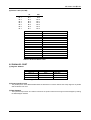
1
AR-B1564
DISK SIZE PENTIUM(586)
All-In-One CPU BOARD
User’ s Guide
Edition: 1.0
Book Number: AR-B1564-99.A01
AR-B1564 User¡¦s Guide
Table of Contents
0.
PREFACE....................................................................................................................................................... 0-3
0.1
0.2
0.3
0.4
0.5
0.6
0.7
1.
OVERVIEW..................................................................................................................................................... 1-1
1.1
1.2
1.3
2.
COPYRIGHT NOTICE AND DISCLAIMER ................................................................................................................................0-3
WELCOME TO THE AR-B1564 CPU BOARD...........................................................................................................................0-3
BEFORE YOU USE THIS GUIDE...............................................................................................................................................0-3
RETURNING YOUR BOARD FOR SERVICE............................................................................................................................0-3
TECHNICAL SUPPORT AND USER COMMENTS ...................................................................................................................0-3
ORGANIZATION..........................................................................................................................................................................0-4
STATIC ELECTRICITY PRECAUTIONS....................................................................................................................................0-4
INTRODUCTION .........................................................................................................................................................................1-1
PACKING LIST ............................................................................................................................................................................1-1
FEATURES ..................................................................................................................................................................................1-2
SYSTEM CONTROLLER ................................................................................................................................ 2-1
2.1
DMA CONTROLLER ...................................................................................................................................................................2-1
2.2
KEYBOARD CONTROLLER AND PS/2 MOUSE .........................................................................................................................2-1
2.3
INTERRUPT CONTROLLER ......................................................................................................................................................2-2
2.3.1
I/O Port Address Map..........................................................................................................................................................2-3
2.3.2
Real-Time Clock and Non-Volatile RAM ............................................................................................................................2-4
2.3.3
Timer ....................................................................................................................................................................................2-4
2.4
SERIAL PORT .............................................................................................................................................................................2-5
2.5
PARALLEL PORT........................................................................................................................................................................2-7
3.
SETTING UP THE SYSTEM............................................................................................................................ 3-1
3.1
OVERVIEW..................................................................................................................................................................................3-1
3.2
SYSTEM SETTING .....................................................................................................................................................................3-2
3.2.1
Serial Port ............................................................................................................................................................................3-2
3.2.2
Hard Disk (IDE) Connector .................................................................................................................................................3-7
3.2.3
Power Connector.................................................................................................................................................................3-8
3.2.4
FDD Port Connector (CN7) .................................................................................................................................................3-8
3.2.5
Parallel Port Connector (CN8) ............................................................................................................................................3-9
3.2.6
PC/104 Connector .............................................................................................................................................................3-10
3.2.7
CPU Setting .......................................................................................................................................................................3-12
3.2.8
Memory Setting..................................................................................................................................................................3-16
3.2.9
LED Header .......................................................................................................................................................................3-16
3.2.10
PS/2 Mouse ...................................................................................................................................................................3-17
3.2.11
Keyboard Connector (J6)..............................................................................................................................................3-17
3.2.12
External Speaker Header (J4) ......................................................................................................................................3-18
3.2.13
Reset Header (J13).......................................................................................................................................................3-18
3.2.14
USB Connector (CN2)...................................................................................................................................................3-18
3.2.15
26-Pin Audio Connector (CN9) .....................................................................................................................................3-19
3.2.16
D.O.C. Memory Address Select (SW2-4).....................................................................................................................3-19
3.2.17
120-Pin PCI Connector (BUS1) ....................................................................................................................................3-20
4.
CRT/LCD FLAT PANEL DISPLAY .................................................................................................................. 4-1
4.1
CRT CONNECTOR (CN13) ........................................................................................................................................................4-1
4.2
LCD FLAT PANEL DISPLAY ......................................................................................................................................................4-2
4.2.1
LCD Supported Voltage Select (JP8) .................................................................................................................................4-3
4.2.2
DE/E Signal from M or LP Select (JP3)..............................................................................................................................4-3
4.2.3
LCD Panel Display Connector (CN12) ...............................................................................................................................4-3
4.2.4
Touch Screen Connector (J3).............................................................................................................................................4-4
4.3
SUPPORTED LCD PANEL .........................................................................................................................................................4-4
5.
ETHERNET CONTROLLER ............................................................................................................................ 5-1
5.1
OVERVIEW..................................................................................................................................................................................5-1
5.2
FEATURES ..................................................................................................................................................................................5-1
5.3
NETWORK PORT .......................................................................................................................................................................5-1
5.3.1
Ethernet Connector (J2)......................................................................................................................................................5-1
5.3.2
Network Active LED Header (J10)......................................................................................................................................5-2
5.3.3
Network 100Mbps Transferring LED Header (J12)............................................................................................................5-2
6.
INSTALLATION .............................................................................................................................................. 6-1
6.1
OVERVIEW..................................................................................................................................................................................6-1
6.2
UTILITY DISKETTE.....................................................................................................................................................................6-1
6.2.1
VGA Driver...........................................................................................................................................................................6-2
6.2.2
Network Utility......................................................................................................................................................................6-4
6.2.3
Audio Driver .........................................................................................................................................................................6-4
6.3
WATCHDOG TIMER ...................................................................................................................................................................6-6
6.3.1
Watchdog Timer Setting......................................................................................................................................................6-6
0-1
AR-B1564 User¡¦s Guide
6.3.2
6.3.3
6.3.4
7.
Watchdog Timer Enabled....................................................................................................................................................6-7
Watchdog Timer Trigger......................................................................................................................................................6-7
Watchdog Timer Disabled...................................................................................................................................................6-7
BIOS CONSOLE............................................................................................................................................. 7-1
7.1
BIOS SETUP OVERVIEW ..........................................................................................................................................................7-1
7.2
STANDARD CMOS SETUP........................................................................................................................................................7-2
7.3
ADVANCED CMOS SETUP........................................................................................................................................................7-3
7.4
ADVANCED CHIPSET SETUP...................................................................................................................................................7-6
7.5
POWER MANAGEMENT ............................................................................................................................................................7-7
7.6
PCI/PLUG AND PLAY .................................................................................................................................................................7-8
7.7
PERIPHERAL SETUP.................................................................................................................................................................7-9
7.8
AUTO-DETECT HARD DISKS..................................................................................................................................................7-10
7.9
PASSWORD SETTING.............................................................................................................................................................7-10
7.9.1
Setting Password...............................................................................................................................................................7-10
7.9.2
Password Checking...........................................................................................................................................................7-10
7.10
LOAD DEFAULT SETTING ..................................................................................................................................................7-10
7.10.1
Auto Configuration with Optimal Setting.......................................................................................................................7-10
7.10.2
Auto Configuration with Fail Safe Setting.....................................................................................................................7-10
7.11
BIOS EXIT .............................................................................................................................................................................7-11
7.11.1
Save Settings and Exit ..................................................................................................................................................7-11
7.11.2
Exit Without Saving .......................................................................................................................................................7-11
7.12
BIOS UPDATE.......................................................................................................................................................................7-11
8.
9.
SPECIFICATIONS .......................................................................................................................................... 8-1
PLACEMENET & DIMENSIONS...................................................................................................................... 9-1
9.1
9.2
10.
10.1
10.2
0-2
PLACEMENT ...............................................................................................................................................................................9-1
DIMENSIONS ..............................................................................................................................................................................9-2
PROGRAMMING RS-485 & INDEX ............................................................................................................10-1
PROGRAMMING RS-485 .....................................................................................................................................................10-1
INDEX ....................................................................................................................................................................................10-3
AR-B1564 User¡¦s Guide
0.PREFACE
0.1 COPYRIGHT NOTICE AND DISCLAIMER
June 1999
Acrosser Technology makes no representations or warranties with respect to the contents hereof and specifically
disclaims any implied warranties of merchantability or fitness for any particular purpose. Furthermore, Acrosser
Technology reserves the right to revise this publication and to make changes from time to time in the contents
hereof without obligation of Acrosser Technology to notify any person of such revisions or changes.
Possession, use, or copying of the software described in this publication is authorized only pursuant to a valid
written license from Acrosser or an authorized sublicensor.
(C) Copyright Acrosser Technology Co., Ltd., 1999. All rights Reserved.
No part of this publication may be reproduced, transmitted, transcribed, stored in a retrieval system, or translated
into any language or computer language, in any form or any means, electronic, mechanical, magnetic, optical,
chemical, manual or otherwise, without the prior written consent of Acrosser Technology.
Acrosser, ALI, AMI, PC/AT, Windows for Workgroup 3.11, Windows 95, Windows NT, LAN, Netware, CHIPS, NEC,
HITACHI, ORION, SHARP …are registered trademarks.
All other trademarks and registered trademarks are the property of their respective holders.
This document was produced with Adobe Acrobat 3.01.
0.2 WELCOME TO THE AR-B1564 CPU BOARD
This guide introduces the Acrosser AR-B1564 CPU board.
Use the information describes this card’ s functions, features, and how to start, set up and operate your AR-B1564
serial CPU board. You also could find general system information here.
0.3 BEFORE YOU USE THIS GUIDE
If you have not already installed this AR-B1564 CPU card, refer to the Chapter 3, “Setting Up the System” in this
guide. Check the packing list, make sure the accessories in the package.
AR-B1564 serial diskette provides the newest information about the card. Please refer to the README.DOC
file of the enclosed utility diskette. It contains the modification and hardware & software information, and
adding the description or modification of product function after manual published.
0.4 RETURNING YOUR BOARD FOR SERVICE
If your board requires servicing, contact the dealer from whom you purchased the product for service information.
If you need to ship your board to us for service, be sure it is packed in a protective carton. We recommend that
you keep the original shipping container for this purpose.
You can help assure efficient servicing of your product by following these guidelines:
1.
Include your name, address, telephone and facsimile number where you may be reached during the day.
2.
A description of the system configuration and/or software at the time is malfunction.
3.
A brief description is in the symptoms.
0.5 TECHNICAL SUPPORT AND USER COMMENTS
User’ s comments are always welcome as they assist us in improving the usefulness of our products and the
understanding of our publications. They form a very important part of the input used for product enhancement
and revision.
We may use and distribute any of the information you supply in any way we believe appropriate without incurring
any obligation. You may, of course, continue to use the information you supply.
If you have suggestions for improving particular sections or if you find any errors, please indicate the manual title
and book number.
Please send your comments to Acrosser Technology Co., Ltd. or your local sales representative.
Internet electronic mail to: [email protected]
0-3
AR-B1564 User¡¦s Guide
0.6 ORGANIZATION
This information for users covers the following topics (see the Table of Contents for a detailed listing):
l
l
l
l
l
l
l
l
l
l
Chapter 1, “Overview”, provides an overview of the system features and packing list.
Chapter 2, “System Controller” describes the major structure.
Chapter 3, “Setting Up the System”, describes how to adjust the jumper, and the connectors setting.
Chapter 4, “CRT/LCD Flat Panel Display”, describes the configuration and installation procedure using
LCD display.
Chapter 5, “Ethernet Controller,” describes the features of network and the connector.
Chapter 6, “Installation”, describes setup procedures including information on the utility diskette.
Chapter 7, “BIOS Console”, providing the BIOS options setting.
Chapter 8, Specifications
Chapter 9, Placement & Dimensions
Chapter 10, Programming RS-485 & Index
0.7 STATIC ELECTRICITY PRECAUTIONS
Before removing the board from its anti-static bag, read this section about static electricity precautions.
Static electricity is a constant danger to computer systems. The charge that can build up in your body may be
more than sufficient to damage integrated circuits on any PC board. It is, therefore, important to observe basic
precautions whenever you use or handle computer components. Although areas with humid climates are much
less prone to static build-up, it is always best to safeguard against accidents may result in expensive repairs. The
following measures should generally be sufficient to protect your equipment from static discharge:
•
Touch a grounded metal object to discharge the static electricity in your body (or ideally, wear a grounded
wrist strap).
•
When unpacking and handling the board or other system component, place all materials on an antic static
surface.
•
Be careful not to touch the components on the board, especially the “golden finger” connectors on the bottom
of every board.
0-4
AR-B1564 User¡¦s Guide
1. OVERVIEW
This chapter provides an overview of your system features and capabilities. The following topics are covered:
l
l
l
Introduction
Packing List
Features
1.1 INTRODUCTION
Built to unleash the total potential of the Pentium Processor, the AR-B1564 is all-in-one single boards computer
capable of handling today’ s demanding requirements. Able to support 75-333 MHz CPU’ s, This unit supports
10/100M MII interface network port, a PCI and no-stack through PC/104 expansion bus, synchronous pipe line
burst SRAM 512KB, DiskOnChip (DOC), and a 2MB PCI-VGA controller that can support both LCD’ s and CRT’ s
simultaneously or independently.
Each AR-B1564 has four ports for I/O communications. One RS-232C/422/485 and three RS-232C ports are
available. One port is at TTL level for even greater performance. There is also a watchdog timer that can be
configured from software to automatically reset the system or generate an interrupt if there is a system’ s or EMI
problem.
A PC/104 bus is provided for system expansion. The AR-B1564 can support up to six modules which allows
tremendous flexibility for the most demanding applications. And for easy configuration, AMI and Award BIOS are
available.
Power management is also featured to lower the rate of consumption. The unit supports doze mode, <Suspend
Mode> and <Standby mode> as well as it adheres to the “Green Function” standard.
The AR-B1564 is perfect for POS and POI applications, network systems, panel / MMI’ s, order entry kiosks, test
equipment, OEM projects or as a motherboard for a panel PC. The unit is only 146X203mm, offering unparalleled
performance in a very small foot print.
1.2 PACKING LIST
The accessories are included with the system. Before you begin installing your AR-B1564 CPU boards, take a
moment to make sure that the following items have been included inside the AR-B1564 package.
l
l
l
l
l
l
l
l
l
l
l
l
l
l
l
l
l
The quick setup manual
1 AR-B1564 all-in-one single CPU board
1 40-pin hard disk drive interface cable for 3.5” HDD
1 44-pin hard disk drive interface cable for 2.5” HDD
1 Floppy disk drive interface cable
1 Parallel port interface cable
1 Keyboard adapter cable for 5-pin JAE to mini DIN female header
1 Keyboard adapter cable for mini DIN male to DIN female header
1 RS-232C interface cable (one 40-pin to 4 DB-9 header)
1 PS/2 mouse cable
1 CRT adapter cable
1 TTL/RS422/RS485 adapter cable
1 USB cable
1 network cable
1 audio adapter cable
1 AR-B9425 card
5 Software utility diskettes
1-1
AR-B1564 User¡¦s Guide
1.3 FEATURES
The system provides a number of special features that enhance its reliability, ensure its availability, and improve its
expansion capabilities, as well as its hardware structure.
l
l
l
l
l
l
l
l
l
l
l
l
l
l
l
l
l
l
1-2
Disk size all-in-one Pentium grade single board computer
Supports from 75MHz to 333MHz Pentium CPUs
Up to 128MB DRAM system
Up to 512KB PBSRAM L2 cache system
On-board CRT and LCD panel display
100M/10Mbps Ethernet with 7-pin JST connector for 100BASE2
PC/104 extension bus
Supports IDE hard disk drives
Supports floppy disk drives
Supports 1 bi-directional parallel port
Supports 4 serial ports (RS-232C, RS-422, RS-485 and TTL level)
PC/AT compatible keyboard and PS/2 mouse interface
Supports DiskOnChip
Programmable watchdog timer
Flash BIOS
Built-in status LEDs indicator
Multi-layer PCB for noise reduction
Dimensions : 146mmX203mm
AR-B1564 User¡¦s Guide
2. SYSTEM CONTROLLER
This chapter describes the major structure of the AR-B1564 CPU board. The following topics are covered:
l
l
l
l
l
DMA Controller
Keyboard Controller and PS/2 Mouse
Interrupt Controller
Serial Port
Parallel Port
2.1 DMA CONTROLLER
The equivalent of two 8237A DMA controllers are implemented in the AR-B1564 board. Each controller is a fourchannel DMA device which will generate the memory addresses and control signals necessary to transfer
information directly between a peripheral device and memory. This allows high speed information transfer with less
CPU intervention. The two DMA controllers are internally cascaded to provide four DMA channels for transfers to
8-bit peripherals (DMA1) and three channels for transfers to 16-bit peripherals (DMA2). DMA2 channel 0 provides
the cascade interconnection between the two DMA devices, thereby maintaining IBM PC/AT compatibility.
Following is the system information of DMA channels:
DMA Controller 1
Channel 0: Spare
DMA Controller 2
Channel 4: Cascade for controller 1
Channel 1: IBM SDLC
Channel 5: Spare
Channel 2: Diskette adapter
Channel 6: Spare
Channel 3: Spare
Channel 7: Spare
Table 2-1 DMA Channel Controller
2.2 KEYBOARD CONTROLLER AND PS/2 MOUSE
The 8042 processor is programmed to support the serial keyboard and PS/2 mouse interface. The keyboard
controller receives serial data from the keyboard, checks its parity, translates scan codes, and presents it to the
system as a byte data in its output buffer. The controller can interrupt the system when data is placed in its output
buffer, or wait for the system to poll its status register to determine when data is available.
Data can be written to the keyboard by writing data to the output buffer of the keyboard controller.
Each byte of data is sent to the keyboard controller in series with an odd parity bit automatically inserted. The
keyboard controller is required to acknowledge all data transmissions. Therefore, another byte of data will not be
sent to keyboard controller until acknowledgment is received for the previous byte sent. The “output buffer full”
interrupt may be used for both send and receive routines.
When using the PS/2 mouse interface, it will save 1 COM port. But it will also occupy IRQ12 interrupt level.
2-1
N
o
T
Im
R
n
0
g
rA
tR
d
Q
Ih
o
w
ifn
R
a
e
A
rQ
Io
U
u
a
9
t1
ire
d
:0
va
S
n
s2
e
ctS
u
d
B
R
p
C
.)set(e
h
fi
AR-B1564 User¡¦s Guide
2.3 INTERRUPT CONTROLLER
The equivalent of two 8259 Programmable Interrupt Controllers (PIC) are included on the AR-B1564 board. They
accept requests from peripherals, resolve priorities on pending interrupts in service, issue interrupt requests to the
CPU, and provide vectors which are used as acceptance indices by the CPU to determine which interrupt service
routine to execute.
Following is the system information of interrupt levels:
Figure 2-1 Interrupt Controller
2-2
AR-B1564 User¡¦s Guide
2.3.1 I/O Port Address Map
Hex Range
Device
000-01F
DMA controller 1
020-021
Interrupt controller 1
022-023
SiS 5582 chipset address
040-04F
Timer 1
050-05F
Timer 2
060-06F
8042 keyboard/controller
070-071
Real-time clock (RTC), non-maskable interrupt (NMI)
076-077
Watchdog
080-09F
DMA page registers
0A0-0A1
Interrupt controller 2
0C0-0DF
DMA controller 2
0F0
Clear Math Co-processor
0F1
Reset Math Co-processor
0F8-0FF
Math Co-processor
170-178
Fixed disk 1
1F0-1F8
Fixed disk 0
201
Game port
208-20A
EMS register 0
214-215
Watchdog
218-21A
EMS register 1
220-22F
Sound
278-27F
Parallel printer port 2 (LPT 2)
2E8-2EF
Serial port 4 (COM 4)
2F8-2FF
Serial port 2 (COM 2)
300-305
Sound
378-37F
Parallel printer port 1 (LPT 1)
388-38B
Sound
3A0-3AF
Bisynchronous
3B0-3BF
Monochrome display and printer port 3 (LPT 3)
3C0-3CF
EGA/VGA adapter
3D0-3DF
Color/graphics monitor adapter
3E8-3EF
Serial port 3 (COM 3)
3F0-3F7
Diskette controller
3F8-3FF
Serial port 1 (COM 1)
Table 2-2 I/O Port Address Map
2-3
AR-B1564 User¡¦s Guide
2.3.2 Real-Time Clock and Non-Volatile RAM
The AR-B1564 contains a real-time clock compartment that maintains the date and time in addition to storing
configuration information about the computer system. It contains 14 bytes of clock and control registers and 114
bytes of general purpose RAM. Because of the use of CMOS technology, it consumes very little power and can be
maintained for long period of time using an internal Lithium battery. The contents of each byte in the CMOS RAM
are listed as follows:
Address
Description
00
Seconds
01
Second alarm
02
Minutes
03
Minute alarm
04
Hours
05
Hour alarm
06
Day of week
07
Date of month
08
Month
09
Year
0A
Status register A
0B
Status register B
0C
Status register C
0D
Status register D
0E
Diagnostic status byte
0F
Shutdown status byte
10
Diskette drive type byte, drive A and B
11
Fixed disk type byte, drive C
12
Fixed disk type byte, drive D
13
Reserved
14
Equipment byte
15
Low base memory byte
16
High base memory byte
17
Low expansion memory byte
18
High expansion memory byte
19-2D
Reserved
2E-2F
2-byte CMOS checksum
30
Low actual expansion memory byte
31
High actual expansion memory byte
32
Date century byte
33
Information flags (set during power on)
34-7F
Reserved for system BIOS
Table 2-3 Real-Time Clock & Non-Volatile RAM
2.3.3 Timer
The AR-B1564 provides three programmable timers, each with a timing frequency of 1.19 MHz.
2-4
Timer 0
The output of this timer is tied to interrupt request 0. (IRQ 0)
Timer 1
This timer is used to trigger memory refresh cycles.
Timer 2
This timer provides the speaker tone.
Application programs can load different counts into this timer to generate various sound frequencies.
AR-B1564 User¡¦s Guide
2.4 SERIAL PORT
The ACEs (Asynchronous Communication Elements ACE1 to ACE4) are used to convert parallel data to a serial
format on the transmit side and convert serial data to parallel on the receiver side. The serial format, in order of
transmission and reception, is a start bit, followed by five to eight data bits, a parity bit (if programmed) and one,
one and half (five-bit format only) or two stop bits. The ACEs are capable of handling divisors of 1 to 65535, and
produce a 16x clock for driving the internal transmitter logic.
Provisions are also included to use this 16x clock to drive the receiver logic. Also included in the ACE a completed
MODEM control capability, and a processor interrupt system that may be software tailored to the computing time
required handle the communications link.
The following table is summary of each ACE accessible register
DLAB
0
Port Address
Register
base + 0
Receiver buffer (read)
Transmitter holding register (write)
0
base + 1
Interrupt enable
X
base + 2
Interrupt identification (read only)
X
base + 3
Line control
X
base + 4
MODEM control
X
base + 5
Line status
X
base + 6
MODEM status
X
base + 7
Scratched register
1
base + 0
Divisor latch (least significant byte)
1
base + 1
Divisor latch (most significant byte)
Table 2-4 ACE Accessible Registers
(1) Receiver Buffer Register (RBR)
Bit 0-7: Received data byte (Read Only)
(2) Transmitter Holding Register (THR)
Bit 0-7: Transmitter holding data byte (Write Only)
(3) Interrupt Enable Register (IER)
Bit 0: Enable Received Data Available Interrupt (ERBFI)
Bit 1: Enable Transmitter Holding Empty Interrupt (ETBEI)
Bit 2: Enable Receiver Line Status Interrupt (ELSI)
Bit 3: Enable MODEM Status Interrupt (EDSSI)
Bit 4: Must be 0
Bit 5: Must be 0
Bit 6: Must be 0
Bit 7: Must be 0
(4) Interrupt Identification Register (IIR)
Bit 0: “0” if Interrupt Pending
Bit 1: Interrupt ID Bit 0
Bit 2: Interrupt ID Bit 1
Bit 3: Must be 0
Bit 4: Must be 0
Bit 5: Must be 0
Bit 6: Must be 0
Bit 7: Must be 0
2-5
AR-B1564 User¡¦s Guide
(5) Line Control Register (LCR)
Bit 0: Word Length Select Bit 0 (WLS0)
Bit 1: Word Length Select Bit 1 (WLS1)
WLS1
WLS0
Word Length
0
0
5 Bits
0
1
6 Bits
1
0
7 Bits
1
1
8 Bits
Bit 2: Number of Stop Bit (STB)
Bit 3: Parity Enable (PEN)
Bit 4: Even Parity Select (EPS)
Bit 5: Stick Parity
Bit 6: Set Break
Bit 7: Divisor Latch Access Bit (DLAB)
(6) MODEM Control Register (MCR)
Bit 0: Data Terminal Ready (DTR)
Bit 1: Request to Send (RTS)
Bit 2: Out 1 (OUT 1)
Bit 3: Out 2 (OUT 2)
Bit 4: Loop
Bit 5: Must be 0
Bit 6: Must be 0
Bit 7: Must be 0
(7) Line Status Register (LSR)
Bit 0: Data Ready (DR)
Bit 1: Overrun Error (OR)
Bit 2: Parity Error (PE)
Bit 3: Framing Error (FE)
Bit 4: Break Interrupt (BI)
Bit 5: Transmitter Holding Register Empty (THRE)
Bit 6: Transmitter Shift Register Empty (TSRE)
Bit 7: Must be 0
(8) MODEM Status Register (MSR)
Bit 0: Delta Clear to Send (DCTS)
Bit 1: Delta Data Set Ready (DDSR)
Bit 2: Training Edge Ring Indicator (TERI)
Bit 3: Delta Receive Line Signal Detect (DSLSD)
Bit 4: Clear to Send (CTS)
Bit 5: Data Set Ready (DSR)
Bit 6: Ring Indicator (RI)
Bit 7: Received Line Signal Detect (RSLD)
2-6
AR-B1564 User¡¦s Guide
(9) Divisor Latch (LS, MS)
LS
Bit 0
Bit 1
Bit 2
Bit 3
Bit 4
Bit 5
Bit 6
Bit 7
Bit 0:
Bit 1:
Bit 2:
Bit 3:
Bit 4:
Bit 5:
Bit 6:
Bit 7:
MS
Bit 8
Bit 9
Bit 10
Bit 11
Bit 12
Bit 13
Bit 14
Bit 15
Desired Baud Rate
Divisor Used to Generate 16x Clock
300
384
600
192
1200
96
1800
64
2400
48
3600
32
4800
24
9600
12
14400
8
19200
6
28800
4
38400
3
57600
2
115200
1
Table 2-5 Serial Port Divisor Latch
2.5 PARALLEL PORT
(1) Register Address
Port Address
Read/Write
base + 0
Write
base + 0
Read
base + 1
Read
base + 2
Write
Table 2-6 Registers’ Address
Register
Output data
Input data
Printer status buffer
Printer control latch
(2) Printer Interface Logic
The parallel portion of the SMC37C669 makes the attachment of various devices that accept eight bits of parallel
data at standard TTL level.
(3) Data Swapper
The system microprocessor can read the contents of the printer’ s Data Latch through the Data Swapper by reading
the Data Swapper address.
2-7
AR-B1564 User¡¦s Guide
(4) Printer Status Buffer
The system microprocessor can read the printer status by reading the address of the Printer Status Buffer. The bit
definitions are described as follows:
Figure 2-2 Printer Status Buffer
NOTE: X presents not used.
Bit 7: This signal may become active during data entry, when the printer is off-line during printing, or when the
print head is changing position or in an error state. When Bit 7 is active, the printer is busy and can not
accept data.
Bit 6: This bit represents the current state of the printer’ s ACK signal. A 0 means the printer has received the
character and is ready to accept another. Normally, this signal will be active for approximately 5
microseconds before receiving a BUSY message stops.
Bit 5: A 1 means the printer has detected the end of the paper.
Bit 4: A 1 means the printer is selected.
Bit 3: A 0 means the printer has encountered an error condition.
(5) Printer Control Latch & Printer Control Swapper
The system microprocessor can read the contents of the printer control latch by reading the address of printer
control swapper. Bit definitions are as follows:
Figure 2-3 Bit’ s Definition
NOTE: X presents not used.
Bit 5: Direction control bit. When logic 1, the output buffers in the parallel port are disabled allowing data driven
from external sources to be read; when logic 0, they work as a printer port. This bit is write only.
Bit 4: A 1 in this position allows an interrupt to occur when ACK changes from low state to high state.
Bit 3: A 1 in this bit position selects the printer.
Bit 2: A 0 starts the printer (50 microseconds pulse, minimum).
Bit 1: A 1 causes the printer to line-feed after a line is printed.
Bit 0: A 0.5 microsecond minimum highly active pulse clocks data into the printer. Valid data must be present
for a minimum of 0.5 microseconds before and after the strobe pulse.
2-8
1
43
8
9
2
1
BUS1
J1
U11
CN2
CN1
J4
M6
0
M5
3
5
52
43
44
26
M
6
2
1
JP2
JP8
J14
JP3
U10
CN12
CN9
5
AR-B1564 User¡¦s Guide
3. SETTING UP THE SYSTEM
This section describes pin assignments for system’ s external connectors and the jumpers setting.
l
l
Overview
System Setting
3.1 OVERVIEW
The AR-B1564 is all-in-one half size, Pentium single CPU board. This section provides hardware jumper settings,
the connector locations and the pin assignment.
Figure 3-1 AR-B1564 Placement
3-1
AR-B1564 User¡¦s Guide
3.2 SYSTEM SETTING
Jumper pins allow you to set specific system parameters. Set them by changing the pin location of jumper blocks.
(A jumper block is a small plastic-encased conductor that slips over the pins.) To change a jumper setting, remove
the jumper from its current location with your fingers or small needle-nosed pliers. Place the jumper over the two
pins designated for the desired setting. Press the jumper evenly onto the pins. Be careful not to bend the pins.
We will show the locations of the AR-B1564 jumper pins, and the factory-default setting.
CAUTION: Do not touch any electronic component unless you are safely grounded. Wear a grounded wrist strap
or touch an exposed metal part of the system unit chassis. The static discharges from your fingers can
permanently damage electronic components.
3.2.1 Serial Port
(1) RS-422/RS-485 Jumper Setting
(A) COM-A RS-485/RS-422 Adapter Select (JP4)
Figure 3-2 JP4: Serial Port Select —RS-422/RS-485
(B) Terminal Select (JP4)
Figure 3-3 JP4: Serial Port Select —Terminator Select
3-2
AR-B1564 User¡¦s Guide
(C) COM-A RS-232/TTL Select (SW2-1)
Figure 3-4 SW2-1: COM-A RS-232/TTL Select
(D) COM-B RS-232C/RS-422 Select (SW2-2 & SW2-3)
Figure 3-5 SW2-2 & SW2-3: COM-B RS-232/RS-422 Select
3-3
AR-B1564 User¡¦s Guide
(E) RS-485 Mode Select (SW2-2 & SW2-3)
Figure 3-6 SW2-2 & SW2-3: RS-485 Mode Select
When RS-422 or RS-485 mode is selected, you also need to change JP4 to select between RS-422 or RS-485
mode.
NOTE: 1. The recommended configuration for RS-485 interface is to set the transmitter to the controlled by DTR
and set the transmitter. Receiver is disabled.
2. The receiver is always enabled, so you will receive data that you transmitted previously. It is not
recommended to use this setting as RS-485 interface.
(2) TTL I/O Connector (CN15)
Figure 3-7 CN15: TTL Connector
CN15
Signal
1
TTLOP0
3
TTLOP1
5
TTLOP2
7
TTLOP3
9
GROUND
Table 3-7 TTL Pin Assignment
3-4
CN15
2
4
6
8
10
Signal
TTLIP0
TTLIP1
TTLIP2
TTLIP3
VCC
AR-B1564 User¡¦s Guide
(3) TTL & RS-485/RS-422 Connector (CN14)
CN14 supports TTL, RS-422, RS-485 pinout of serial port 1 and port 2. The serial port 1 is set to be TTL mode; the
serial port 2 is set to be RS-422/RS-485 mode.
Use the enclosed TTL/RS-422/RS-485 adapter cable connecting the CN14, there is two DB-9 serial ports. COM A
is connected to the TTL, COM B is connected to the RS-422/RS-485. CN14 pin assignments are as follows:
Figure 3-8 CN14: TTL & RS-422/RS-485 Connector
Port
CN14 DB-9
Signal
CN14 DB-9
Signal
1
1
-DCD (TTL)
2
6
-DSR (TTL)
3
2
RXD (TTL)
4
7
-RTS (TTL)
Port 1
5
3
TXD (TTL)
6
8
-CTS (TTL)
(COM A)
7
4
-DTR (TTL)
8
9
-RI (TTL)
9
5
Ground
10
-VCC
11
1
Ground
12
6
CTS+
13
2
RTS+
14
7
CTS Port 2
15
3
RTS 16
8
RXD+
(COM B)
17
4
TXD+
18
9
RXD 19
5
TXD20
-GND
Table 3-1 TTL & RS-422/RS-485 Pin Assignment
3-5
AR-B1564 User¡¦s Guide
(4) RS-232C Connector (CN3)
There are 4 serial ports with EIA RS-232C interface on the AR-B1564. To configure these serial ports, use the
BIOS Setup program to do well.
To use the enclosed RS-232 interface cable connecting the CN3, there are four DB-9 serial ports.
The pin assignments of the CN3 for serial port A, B, C, & D are as follows:
Figure 3-9 CN3: RS-232C Connector
Port
CN3 DB-9
Signal
CN3 DB-9
1
1
-DCD A
2
6
3
2
RXD A
4
7
Port 1
5
3
TXD A
6
8
(COM A)
7
4
-DTR A
8
9
9
5
GROUND A 10
-11
1
-DCD B
12
6
13
2
RXD B
14
7
Port 2
15
3
TXD B
16
8
(COM B)
17
4
-DTR B
18
9
19
5
GROUND B 20
-21
1
-DCD C
22
6
23
2
RXD C
24
7
Port 3
25
3
TXD C
26
8
(COM C)
27
4
-DTR C
28
9
29
5
GROUND C 30
-31
1
-DCD D
32
6
33
2
RXD D
34
7
Port 4
35
3
TXD D
36
8
(COM D)
37
4
-DTR D
38
9
39
5
GROUND D 40
-Table 3-2 RS-232C Connector Pin Assignment
Signal
-DSR A
-RTS A
-CTS A
-RI A
VCC A
-DSR B
-RTS B
-CTS B
-RI B
VCC B
-DSR C
-RTS C
-CTS C
-RI C
VCC C
-DSR D
-RTS D
-CTS D
-RI D
VCC D
NOTE: 1) N.C. means “Not Connect”.
2) If COM A selected TTL mode, please connect to COM A header of CN14.
3) If COM B selected RS-422 or RS-485 mode, please connect to COM B header of CN14.
(5) IrDA Header (J5)
Figure 3-10 J5: IrDA Header
3-6
GROUND 19
IDEDRQB
21
AR-B1564 User¡¦s Guide
3.2.2 Hard Disk (IDE) Connector
(1) 40-Pin Hard Disk (IDE) Connector (CN4)
A 40-pin header type connector (CN4) is provided to interface with up to two embedded hard disk drives (IDE AT
bus). This interface, through a 40-pin cable, allows the user to connect up to two drives in a “daisy chain” fashion.
To enable or disable the hard disk controller, please use the BIOS Setup program. The following table illustrates
the pin assignments of the hard disk drive’ s 40-pin connector.
Figure 3-11 CN4: Hard Disk (IDE) Connector
(2) 44-Pin Hard Disk (IDE) Connector (CN6)
AR-B1564 also provides IDE interface 44-pin connector to connect with the hard disk device.
Figure 3-12 CN6: Hard Disk (IDE) Connector
3-7
7 GND
3
AR-B1564 User¡¦s Guide
3.2.3 Power Connector
(1) 8-Pin Power Connector (J1)
J1 is an 8-pin power connector. You can directly connect the power supply to the onboard power connector for
stand-alone applications.
Figure 3-13 J1: 8-Pin Power Connector
(2) 4-Pin Power Connector (CN5)
Figure 3-14 CN5: 4-Pin Power Connector
3.2.4 FDD Port Connector (CN7)
The AR-B1564 provides a 34-pin header type connector for supporting up to two floppy disk drives.
To enable or disable the floppy disk controller, please use BIOS Setup program to select.
Figure 3-15 CN7: FDD Port Connector
3-8
AR-B1564 User¡¦s Guide
3.2.5 Parallel Port Connector (CN8)
To use the parallel port, an adapter cable has been connected to the CN8 (26-pin header type) connector. This
adapter cable is included in your AR-B1564 package. The connector for the parallel port is a 25-pin D-type female
connector.
Figure 3-16 CN8: Parallel Port Connector
CN8 DB-25
Signal
CN8
1
1
-Strobe
2
3
2
Data 0
4
5
3
Data 1
6
7
4
Data 2
8
9
5
Data 3
10
11
6
Data 4
12
13
7
Data 5
14
15
8
Data 6
16
17
9
Data 7
18
19
10
-Acknowledge
20
21
11
Busy
22
23
12
Paper
24
25
13
Printer Select
26
Table 3-3 Parallel Port Pin Assignment
DB-25
14
15
16
17
18
19
20
21
22
23
24
25
--
Signal
-Auto Form Feed
-Error
-Initialize
-Printer Select In
Ground
Ground
Ground
Ground
Ground
Ground
Ground
Ground
No Connect
3-9
A15
A14
A13
A12
A11
A10
A9
A8
A7
A6
A5
A4
A3
A2
A1
AR-B1564 User¡¦s Guide
3.2.6 PC/104 Connector
(1) 64-Pin PC/104 Connector Bus A & B (CN10)
Figure 3-17 CN10: 64-Pin PC/104 Connector Bus A & B
(2) 40-Pin PC/104 Connector Bus C & D (CN11)
Figure 3-18 CN11: 40-Pin PC/104 Connector Bus C & D
3-10
AR-B1564 User¡¦s Guide
(3) PC/104 ISA Bus Signal Description
Name
Description
BUSCLK [Output]
The BUSCLK signal of the I/O channel is asynchronous
to the CPU clock.
RSTDRV [Output]
This signal goes high during power-up, low line-voltage or
hardware reset
SA0 - SA19
The System Address lines run from bit 0 to 19. They are
[Input / Output] latched onto the falling edge of "BALE"
LA17 - LA23
The Unlatched Address line run from bit 17 to 23
[Input/Output]
SD0 - SD15
System Data bit 0 to 15
[Input/Output]
BALE [Output]
The Buffered Address Latch Enable is used to latch SA0
– SA19 onto the falling edge. This signal is forced high
during DMA cycles
-IOCHCK [Input]
The I/O Channel Check is an active low signal which
indicates that a parity error exist on the I/O board
IOCHRDY
This signal lengthens the I/O, or memory read/write cycle,
[Input, Open collector] and should be held low with a valid address
IRQ 3-7, 9-12, 14, 15
The Interrupt Request signal indicates I/O service request
[Input] attention. They are prioritized in the following sequence :
(Highest) IRQ 9, 10, 11, 12, 13, 15, 3, 4, 5, 6, 7 (Lowest)
-IOR
The I/O Read signal is an active low signal which
[Input/Output] instructs the I/O device to drive its data onto the data bus
-IOW [Input/Output]
The I/O write signal is an active low signal which instructs
the I/O device to read data from the data bus
-SMEMR [Output]
The System Memory Read is low while any of the low
1mega bytes of memory are being used
-MEMR
The Memory Read signal is low while any memory
[Input/Output] location is being read
-SMEMW [Output]
The System Memory Write is low while any of the low
1mega bytes of memory is being written
-MEMW
The Memory Write signal is low while any memory
[Input/Output] location is being written
DRQ 0-3, 5-7 [Input]
DMA Request channels 0 to 3 are for 8-bit data transfers.
DMA Request channels 5 to 7 are for 16-bit data
transfers. DMA request should be held high until the
corresponding DMA has been completed. DMA request
priority is in the following sequence:(Highest) DRQ 0, 1,
2, 3, 5, 6, 7 (Lowest)
-DACK 0-3, 5-7
The DMA Acknowledges 0 to 3, 5 to 7 are the
[Output] corresponding acknowledge signals for DRQ 0 to 3 and 5
to 7
AEN [output]
The DMA Address Enable is high when the DMA
controller is driving the address bus. It is low when the
CPU is driving the address bus
-REFRESH
This signal is used to indicate a memory refresh cycle
[Input/Output] and can be driven by the microprocessor on the I/O
channel
TC [Output]
Terminal Count provides a pulse when the terminal count
for any DMA channel is reached
SBHE [Input/Output]
The System Bus High Enable indicates the high byte SD8
- SD15 on the data bus
3-11
AR-B1564 User¡¦s Guide
Name
Description
-MASTER [Input]
The MASTER is the signal from the I/O processor which
gains control as the master and should be held low for a
maximum of 15 microseconds or system memory may be
lost due to the lack of refresh
-MEMCS16
The Memory Chip Select 16 indicates that the present
[Input, Open collector] data transfer is a 1-wait state, 16-bit data memory
operation
-IOCS16
The I/O Chip Select 16 indicates that the present data
[Input, Open collector] transfer is a 1-wait state, 16-bit data I/O operation
OSC [Output]
The Oscillator is a 14.31818 MHz signal
-ZWS
The Zero Wait State indicates to the microprocessor that
[Input, Open collector] the present bus cycle can be completed without inserting
additional wait cycle
Table 3-4 PC/104 ISA Bus Pin Assignment
3.2.7 CPU Setting
The AR-B1564 accepts many types of 586 microprocessor, such as INTEL Pentium, AMD-K5, AMD-K6, and
CYRIX 6x86. All of these CPUs include an integer processing unit, floating-point processing unit, memorymanagement unit, and cache. They can give a two to en-fold performance improvement in speed over the 486
processor, depending on the clock speeds used and specific application. Like the 486 processor, the 586
processor includes both segment-based and page-based memory protection schemes. Instruct processing time
has reduced by on-chip instruction pipelining. By performing fast, on-chip memory management and caching, the
586 processor relaxes requirements for memory response for a given level of system performance.
(1) CPU Logic Core Voltage Select (SW3)
Figure 3-19 SW3: CPU Logic Core Voltage
SW3-1 SW3-2 SW3-3 SW3-4 SW3-5
OFF
ON
OFF
OFF
OFF
ON
ON
OFF
OFF
OFF
ON
OFF
OFF
ON
OFF
OFF
ON
OFF
ON
OFF
OFF
ON
ON
ON
OFF
ON
ON
ON
ON
OFF
Table 3-5 SW3: CPU Logic Core Voltage
SW3-6
-------
(2) System Base Clock & CPU Clock Multiplier (SW1)
Figure 3-20 SW1: CPU Clock Multiplier
3-12
Voltage
Setting A
Setting B
Setting C
Setting D
Setting E
Setting F
AR-B1564 User¡¦s Guide
(A) CPU Clock Multiplier Select (SW1)
The CPU clock multiplier needs to be set by SW1.
SW1-1 SW1-2 SW1-3
ON
OFF
ON
OFF
ON
OFF
ON
OFF
ON
ON
OFF
OFF
ON
ON
OFF
OFF
OFF
OFF
OFF
OFF
ON
ON
ON
ON
P54C
P55C
2.5X
3.0X
2.0X
1.5X
-----
2.5X
3.0X
2.0X
3.5X
4.5X
5.0X
4.0X
5.5X
Table 3-6 SW1: CPU Clock Multiplier
(B) CPU Base Clock Select (SW1)
This board supports different types of CPUs. The clock generator needs to be set by SW1.
The CPU input clock is twice the operation clock.
SW1-4 SW1-5 SW1-6 Base Clock PCI Clock
ON
OFF
ON
OFF
ON
OFF
ON
OFF
ON
ON
OFF
OFF
ON
ON
OFF
OFF
OFF
OFF
OFF
OFF
ON
ON
ON
ON
50MHz
66.6MHz
60MHz
55MHz
51.3MHz
68.4MHz
61.6MHz
75MHz
25MHz
33.3MHz
30MHz
27.5MHz
25.6MHz
34.2MHz
30.8MHz
37.5MHz
Table 3-7 SW1: CPU Clock Multiplier
NOTE: 1.
2.
SW1 jumper setting – BF0-BF2: On presents Low, Off presents High.
Intel CPU MMX – 233 is factory default setting.
(3) P54C/P55C CPU Type Select (JP2)
Figure 3-21 JP2: P54C/P55C CPU Type Select
3-13
AR-B1564 User¡¦s Guide
Intel CPU
CPU Type
Work
Frequency
Pentium - 75
Pentium - 90
Pentium - 100
Pentium - 120
Pentium - 133
Pentium - 150
Pentium - 166
Pentium - 200
MMX-166
MMX-200
MMX-233
75MHz
90MHz
100MHz
120MHz
133MHz
150MHz
166MHz
200MHz
166MHz
200MHz
233MHz
SW1
SW1-1 SW1-2 SW1-3
SW3
Clock Multiplier BF0 BF1 BF2
50.0MHz
60.0MHz
66.7MHz
60.0MHz
66.7MHz
60.0MHz
66.7MHz
66.7MHz
66.7MHz
66.7MHz
66.7MHz
1.5X
1.5X
1.5X
2.0X
2.0X
2.5X
2.5X
3.0X
2.5X
3.0X
3.5X
Off
Off
Off
On
On
On
On
Off
On
Off
Off
Off
Off
Off
Off
Off
On
On
On
On
On
Off
Off
Off
Off
Off
Off
Off
Off
Off
Off
Off
Off
Setting E
Setting E
Setting E
Setting E
Setting E
Setting E
Setting E
Setting E
Setting C
Setting C
Setting C
Table 3-8 Intel CPU Base Clock Setting
AMD CPU
CPU Type
K5-PR75 (ABR)
K5-PR90 (ABR)
K5-PR100 (ABR)
K5-PR120 (ABR)
K5-PR133 (ABR)
K5-PR166 (ABR)
K5-PR75 (AFR)
K5-PR90 (AFR)
K5-PR100 (AFR)
K5-PR120 (AFR)
K5-PR133 (AFR)
K5-PR166 (AFR)
K6-166 (MMX)(ANR)
K6-200 (MMX)(ANR)
K6-233 (MMX)(ANR)
K6-2-300
K6-2-333
Work
Frequency
SW1
SW1-1 SW1-2 SW1-3
Clock Multiplier BF0 BF1 BF2
75MHz
50.0MHz
1.5X
Off
Off
Off
90MHz
60.0MHz
1.5X
Off
Off
Off
100MHz 66.7MHz
1.5X
Off
Off
Off
90MHz
60.0MHz
1.5X
On
Off
Off
100MHz 66.7MHz
1.5X
On
Off
Off
116.7MHz 66.7MHz 1.75X
On
On
Off
75MHz
50.0MHz
1.5X
Off
Off
Off
90MHz
60.0MHz
1.5X
Off
Off
Off
100MHz 66.7MHz
1.5X
Off
Off
Off
90MHz
60.0MHz
1.5X
On
Off
Off
100MHz 66.7MHz
1.5X
On
Off
Off
116.7MHz 66.7MHz 1.75X
On
On
Off
166MHz 66.7MHz
2.5X
On
On
Off
200MHz 66.7MHz
3.0X
On
Off
Off
233MHz 66.7MHz
3.5X
Off
Off
Off
300MHz 66.7MHz
4.5X
On
On
On
333MHz 66.7MHz
5.0X
Off
On
On
SW3
Setting F
Setting F
Setting F
Setting F
Setting F
Setting F
Setting E
Setting E
Setting E
Setting E
Setting E
Setting E
Setting D
Setting D
Setting E
Setting B
Setting B
Table 3-9 AMD CPU Base Clock Setting
Cyrix CPU
CPU Type
Work
Frequency
SW1
Clock
6X86-PR100
80MHz
40.0MHz
6X86-PR120
100MHz 50.0MHz
6X86-PR133
110MHz 55.0MHz
6X86-PR150
120MHz 60.0MHz
6X86-PR166
133MHz 66.7MHz
6X86-PR200
150MHz 75.0MHz
6X86L-PR120
100MHz 50.0MHz
6X86L-PR133
110MHz 55.0MHz
6X86L-PR150
120MHz 60.0MHz
6X86L-PR166
133MHz 66.7MHz
6X86L-PR200
150MHz 75.0MHz
6X86-PR166 (MMX) 150/133MHz 60/66.7MHz
6X86-PR200 (MMX) 166/150MHz 66.7/75MHz
6X86-PR233 (MMX) 187.5/200MHz 75//66.7MHz
6X86-PR300 (MMX) 233MHz 66.7MHz
SW1-1 SW1-2 SW1-3
Multiplier BF0 BF1 BF2
2.0X
On
Off
Off
2.0X
On
Off
Off
2.0X
On
Off
Off
2.0X
On
Off
Off
2.0X
On
Off
Off
2.0X
On
Off
Off
2.0X
On
Off
Off
2.0X
On
Off
Off
2.0X
On
Off
Off
2.0X
On
Off
Off
2.0X
On
Off
Off
2.5/2.0X On On/Off Off
2.5/2.0X On Off/On Off
2.5/3.0X Off/On On
Off
3.5X
Off
Off
Off
Table 3-10 Cyrix CPU Base Clock Setting
3-14
SW3
Setting E
Setting E
Setting E
Setting E
Setting E
Setting E
Setting C
Setting C
Setting C
Setting C
Setting C
Setting D
Setting D
Setting D
Setting D
AR-B1564 User¡¦s Guide
IDT Winchip CPU
CPU Type
IDT C6-180
IDT C6-200
IDT C6-225
IDT C6-240
Work
Frequency
180MHz
200MHz
225MHz
240MHz
SW1
SW1-1 SW1-2 SW1-3
BF1 BF2
SW3
On
On
On
Off
Setting F
Setting F
Setting F
Setting F
Clock Multiplier BF0
60.0MHz
66.7MHz
75.0MHz
60.0MHz
3.0X
3.0X
3.0X
4.0X
Off
Off
Off
On
Off
Off
Off
On
Table 3-11 IDT Winchip CPU Base Clock Setting
NOTE: 1.
2.
SW1 jumper setting – BF0-BF2: On presents Low, Off presents High.
Intel CPU MMX - 233 is factory default setting.
(4) CPU Cooling Fan Power Connector (CN1 & J14)
Figure 3-22 CN1 & J14: CPU Cooling Fan Power Connector
3-15
5 LED2
AR-B1564 User¡¦s Guide
3.2.8 Memory Setting
There are two 32-bit memory banks on the AR-B1564 board. It can be one-side or double-side SIMM (Single-Line
Memory Modules) which is designed to accommodate 256KX36 bit to 16MX36-bit SIMMs. This provides the user
with up to 128MB of main memory. The 32-bit SIMM (without parity bit) also can be used on AR-B1564 board.
Please refer to the following table for details:
SIMM2
256KX32(X36)
SIMM1
None
Total Memory
1MB
256KX32(X36)
512KX32(X36)
256KX32(X36)
None
2MB
2MB
512KX32(X36)
512KX32(X36)
4MB
1MX32(X36)
1MX32(X36)
None
1MX32(X36)
4MB
8MB
2MX32(X36)
None
8MB
2MX32(X36)
2MX32(X36)
16MB
4MX32(X36)
4MX32(X36)
None
4MX32(X36)
16MB
32MB
8MX32(X36)
None
32MB
8MX32(X36)
8MX32(X36)
64MB
16MX32(X36)
None
16MX32(X36)
16MX32(X36)
Table 3-12 DRAM Configuration
64MB
128MB
3.2.9 LED Header
(1) External Power LED & Keyboard Lock Header (J8)
Figure 3-23 J8: Power LED & Key Lock Header
(2) HDD LED Header (J11)
Figure 3-24 J11: HDD LED Header
(3) Watchdog LED Header (J9)
Figure 3-25 J9: Watchdog LED Header
3-16
AR-B1564 User¡¦s Guide
3.2.10 PS/2 Mouse
(1) PS/2 Mouse IRQ 12 Setting (JP7)
If user doesn’ t use the PS/2 mouse and will share the IRQ12 for other peripheral using, user can select Disabled
for share this IRQ.
Figure 3-26 JP7: PS/2 Mouse IRQ12 Setting
(2) PS/2 Mouse Connector (J7)
To use the PS/2, an adapter cable has to be connected to the J7 (6-pin header type) connector. This adapter
cable is mounted on a bracket and is included in your AR-B1564 package. The connector for the PS/2 mouse is a
Mini-DIN 6-pin connector. Pin assignments for the PS/2 port connector are as follows:
Figure 3-27 J7: PS/2 Mouse Connector
3.2.11 Keyboard Connector (J6)
An PC/AT compatible keyboard can be used by connecting the provided adapter cable between J6 and the
keyboard. The pin assignments of J6 connector are as follows:
Figure 3-28 J6: Keyboard Connector
3-17
2, Reset+
1
2
Reset3, 4: :SpeakerSpeaker+
AR-B1564 User¡¦s Guide
3.2.12 External Speaker Header (J4)
Besides the on board buzzer, you can use an external speaker by connecting J4 header directly.
Figure 3-29 J4: Speaker Header
3.2.13 Reset Header (J13)
J13 is used to connect to an external reset switch. Shorting these two pins will reset the system.
Figure 3-30 J13: Reset Header
3.2.14 USB Connector (CN2)
USB is the abbreviation of Universal Serial Bus. The Universal Serial Bus (USB) standard is a low-to-medium
speed interface for the connection of PC peripherals.
The USB standard simplifies the connection of peripherals to PCs with a uniform hardware and software interface.
Personal computers equipped with USB allow computer peripherals to be automatically configured as soon as they
are physically attached - without the need to reboot or run setup.
USB is a leading edge technology that allows the user to quickly and easily adding wide range peripheral devices
from printers to keyboards and telephony devices to fax/modems. Universal Host Controller Interface (UHCI) and
future support for the Open Host Controller Interface (OHCI) ensure USB compatibility and usability well into the
future.
The connector on the CPU board supports two Universal Serial Bus ports. An optional external port bracket
attaches to the onboard connector via an attached cable. With the optional port bracket installed you can attach
USB devices to the external ports. If the USB ports are installed, the USB Controller line in the Integrated
Peripherals section of the CMOS Setup utility must be set to “Enabled”. USB ports may also require Operating
System support for USB devices.
Figure 3-31 CN2: USB Connector
Pin
1
3
5
7
9
Description
VCC
-DATA
+DATA
GND
CASE
Pin
2
4
6
8
10
Table 3-13 CN2: USB Connector Pin Assignment
3-18
Description
VCC
-DATA
+DATA
GND
CASE
AR-B1564 User¡¦s Guide
3.2.15 26-Pin Audio Connector (CN9)
Figure 3-32 CN9: 26-Pin Audio Connector
CN9
Signal
CN9
1
AUXAL
2
3
AUXAR
4
5
+12V
6
7
AUDIOL
8
9
AUDIOR
10
11
GND
12
13
MIDIIN
14
15
GND
16
17
-JSWA
18
19
-JSWB
20
21
-JSWC
22
23
-JSWD
24
25
GND
26
Table 3-14 Audio Connector Pin Assignment
Signal
LINEL
LINER
VJOYS
MICPH
PCSPKO
GND
MIDIOP
GND
JTMA
JTMB
JTMC
JTMD
GND
3.2.16 D.O.C. Memory Address Select (SW2-4)
This section provides the information about how to use the D.O.C. (DiskOnChip).
hardware setting and software configuration.
There divided two parts:
Step 1: Use SW2 to select the correct D.O.C. memory address.
Step 2: Insert programmed DiskOnChip into sockets U28 setting as DOC.
Step 3: Line up and insert the AR-B1564 card into any free slot of your computer.
Figure 3-33 SW2-4: D.O.C. Memory Address
SW2-4
Address
Note
OFF
ON
D000 : 0000
D400 : 0000
Factory Preset
Table 3-15 D.O.C. Memory Address
3-19
AR-B1564 User¡¦s Guide
3.2.17 120-Pin PCI Connector (BUS1)
Figure 3-34 BUS1: 120-Pin PCI Connector
BUS1 Signal BUS1 Signal BUS1 Signal
1
-TRST
2
+12V
61
-12V
3
TMS
4
TDI
63
GND
5
+5V
6
-INTA
65
+5V
7
-INTC
8
+5V
67
-INTB
9
NC
10
+5V
69
-PRST1
11
NC
12
GND
71
-PRST2
13
GND
14
NC
73
GND
15
-RST
16
+5V
75
GND
17
-GNT
18
GND
77
GND
19
NC
20
AD30
79
+5V
21
+3.3V
22
AD28
81
AD29
23
AD26
24
GND
83
AD27
25
AD24
26
IDSEL
85
+3.3V
27
+3.3V
28
AD22
87
AD23
29
AD20
30
GND
89
AD21
31
AD18
32
AD16
91
+3.3V
33
+3.3V
34
-FRAME
93
C/BE2
35
GND
36
-TRDY
95
-IRDY
37
GND
38
-STOP
97
-DEVSL
39
+3.3V
40
SDONE
99
-LOCK
41
-SB0
42
GND
101
+3.3V
43
PAR
44
AD15
103
+3.3V
45
+3.3V
46
AD13
105
AD14
47
AD11
48
GND
107
AD12
49
AD9
50
C/BE0
109
GND
51
+3.3V
52
AD6
111
AD7
53
AD4
54
GND
113
AD5
55
AD2
56
AD0
115
GND
57
+5V
58
-REQ64
117
+5V
59
+5V
60
+5V
119
+5V
Table 3-16 120-Pin PCI Connector Pin Assignment
3-20
BUS1
62
64
66
68
70
72
74
76
78
80
82
84
86
88
90
92
94
96
98
100
102
104
106
108
110
112
114
116
118
120
Signal
TCK
TD0
+5V
-INTD
NC
GND
NC
CLK
-REQ
AD31
GND
AD25
C/BE3
GND
AD19
AD17
GND
+3.3V
GND
-PERR
-SERR
C/BE1
GND
AD10
AD8
+3.3V
AD3
AD1
-ACK64
+5V
AR-B1564 User¡¦s Guide
4. CRT/LCD FLAT PANEL DISPLAY
This chapter describes the configuration and installation procedure using LCD and CRT display. The following
topics are covered:
l
l
l
CRT Connector
LCD Flat Panel Display
Supported LCD Panel
4.1 CRT CONNECTOR (CN13)
To connect a CRT monitor, an adapter cable has to be connected to the CN13 (10-pin header type) connector.
This adapter cable is included in your AR-B1564 package.
The AR-B1564 support CRT color monitors. AR-B1564 used onboard VGA chipset and supported 2MB on-board
VRAM. For different VGA display modes, your monitor must possess certain characteristics to display the mode
you want.
To connect to a CRT monitor, an adapter cable has to be connected to the CN13 connector. CN13 is used to
connect with a VGA monitor when you are using the on-board VGA controller as a display adapter.
CN13 is a 10-pin connector that attaches to the CRT monitor via a HD-sub 15-pin adapter cable. Pin assignments
for the CN13 & HDB15 connector is as follows:
Figure 4-1 CN13: CRT Connector
CN13
1
3
5
7
9
DB-15
1
2
3
14
13
FUNCTION
Red
Green
Blue
V-sync
H-sync
CN13
2
4
6
8
10
DB-15
5
6
7
8
10
FUNCTION
GND
AGND
AGND
AGND
GND
Table 4-1 CRT Connector Assignment
4-1
VBL Control
AR-B1564 User¡¦s Guide
4.2 LCD FLAT PANEL DISPLAY
This section describes the configuration and installation procedure using LCD display. Skip this section if you are
using CRT monitor only.
Using the Flash memory Writer utility to download the new BIOS file into the ROM chip to configure the BIOS
default setting for different types of LCD panel. And then set your system properly and configure the AR-B1564
VGA module for the right type of LCD panel you are using.
The sample LCD models listed on the table are just some of the LCD panel models available in the market that the
Chips & Technologies used by AR-B1564 VGA module can support. If you are using a different LCD panel other
than those listed, choose from the panel description column which type of LCD panel you are using.
The following shows the block diagram of using AR-B1564 for LCD display.
Figure 4-1 LCD Panel Block Diagram
The block diagram shows that AR-B1564 still needs components to be used for LCD panel. The inverter board
provides the control for the brightness and the contrast of the LCD panel while the inverter is the one that supplies
the high voltage to drive the LCD panel. Each item will be explained further in the section.
Figure 4-2 LCD Panel Cable Installation Diagram
NOTE: Be careful with the pin orientation when installing connectors and the cables. A wrong connection can easily
destroy your LCD panel. The pin 1 of the cable connectors is indicated with a sticker and the pin1 of the
ribbon cable is usually with different color.
The inverter board is the one that supplies the high voltage signals to drive the LCD panel by converting the 12
volt signal from the AR-B1564 into high voltage AC signal for LCD panel. It can be installed freely on the space
4-2
AR-B1564 User¡¦s Guide
provided over the VR board. If the VR board is installed on the bracket, you have to provide a place to install the
inverter board into your system.
The AR-B1564 supports CRT colored monitor, STN, Dual-Scan, TFT, monochrome and color panels. It can be
connected to create a compact video solution for the industrial environment. 2MB of RAM on-boarded allows a
maximum CRT resolution of 1024X768 with 64K colors and a LCD resolution of 800X600 with 64K colors. For
different VGA display modes, your monitor must possess certain characteristics to display the mode you want.
4.2.1 LCD Supported Voltage Select (JP8)
Figure 4-3 JP8: LCD Supported Voltage Select
4.2.2 DE/E Signal from M or LP Select (JP3)
Figure 4-4 JP3: DE/E Signal from M or LP
4.2.3 LCD Panel Display Connector (CN12)
Attach a display panel connector to this 44-pin connector with pin assignments as shown below:
Figure 4-5 CN12: LCD Display Connector
Pin
1
3
5
7
9
11
13
15
17
19
21
23
25
27
29
31
33
35
37
39
41
43
Signal
GND
GND
FLM
P0
P2
P4
GND
P7
P9
P11
P12
P14
P16
GND
P19
P21
P23
VCC
+12V
GND
DE
GND
Pin
2
4
6
8
10
12
14
16
18
20
22
24
26
28
30
32
34
36
38
40
42
44
Signal
SHFCLK
LP
GND
P1
P3
P5
P6
P8
P10
GND
P13
P15
P17
P18
P20
P22
GND
VCC
+12V
GND
ENABLK
VEE
Table 4-2 LCD Display Pin Assignment
4-3
2 TXDD
AR-B1564 User¡¦s Guide
4.2.4 Touch Screen Connector (J3)
Figure 4-6 J3: Touch Screen Connector
4.3 SUPPORTED LCD PANEL
At present, this VGA card can provide the total solution with inverter board for the following list of standard LCD
panel. Consult your Acrosser representative for new developments, when using other models of standard LCD
panels in the market.
NO.
Manufacture
Model No.
Description
1
2
NEC
NEC
NL-6448AC30-10
NL-6448AC32-10
TFT 9.4”
TFT 10.2”
3
4
NEC
HITACHI
NL-6448AC33-10
LMG5371
TFT 10.4”
MONO 9.4” Dual Scan
5
6
7
HITACHI
HITACHI
ORION
LMG9200
LMG9400
OGM-640CN03C-S
DSTN 9.4”
DSTN 10.4”
DSTN 10.4”
8
SHARP
LQ10D321
Table 4-1 LCD Panel Type List
TFT 10.4”
CAUTION: 1. If you want to connect the LCD panel, you must update the AR-B1564’ s BIOS, then you can setup
the corrected BIOS. Please contact Acrosser for the latest BIOS update.
2. If user needs to update the BIOS version or connect other LCD, please contact the sales
department. The detail supported LCDs are listed in the Acrosser Web site, user can download the
suitable BIOS. The address is as follows:
http:\\www.acrosser.com
4-4
5
AR-B1564 User¡¦s Guide
5.ETHERNET CONTROLLER
This chapter describes the features of network and the connector. The following topics are covered:
l
l
l
Overview
Features
Network Port
5.1 OVERVIEW
The Ethernet controller of the AR-B1564 is a highly integrated design that supports the Media Independent
Interface (MII) network interface with the IEEE 802.3 standard. Network interfaces include 100M local area
networks complies with PCI specification V2.1. The Ethernet controller can interface directly to the PCI bus without
any external device.
5.2 FEATURES
The Ethernet controller chipset provides a number of special features that enhance its reliability, and improve its
expansion capabilities, as well as its hardware structure.
l
l
l
l
l
l
l
l
l
l
Single chip Fast Ethernet controller for PCI bus interface
High performance PCI mastering structure
Provides standard 100M bit MII interface
10/100MHz full duplex half duplex operation
Contains two deeper 2K bytes FIFO for receive and transmit controller both supports bursts of up
to full Ethernet length
Support physical, Broadcast, Mulitcast adddress filtering using hashing function
Support Magic packet and wake on address filtering
Support external Boot-rom up to 64K bytes no external address latch
Software controllable power down feature
Single +5V supply, 0.5um standard CMOS technology
5.3 NETWORK PORT
5.3.1 Ethernet Connector (J2)
Figure 5-1 J2: RJ-45 Connector
PIN (J2)
FUNCTION
1
2
TPTX+
TPTX -
3
TPRX+
4
5
TPRX GROUND
6
7
GROUND
GROUND
Table 5-1 Ethernet Connector Pin Assignment
5-1
1 LED+
2
LED-
AR-B1564 User¡¦s Guide
5.3.2 Network Active LED Header (J10)
Figure 5-2 J10: Network Active LED Header
5.3.3 Network 100Mbps Transferring LED Header (J12)
Figure 5-3 J12: Network LED Header
5-2
AR-B1564 User¡¦s Guide
6. INSTALLATION
This chapter describes the procedure of the installation. The following topics are covered:
l
l
l
Overview
Utility Diskette
Watchdog Timer
6.1 OVERVIEW
This chapter provides information for you to set up a working system based on the AR-B1564 CPU card. Please
read the details of the CPU card’ s hardware descriptions before installation carefully, especially jumper setting,
switch settings and cable connections.
Follow steps listed below for proper installation:
Step 1 :
Read the CPU board’ s hardware description in this manual.
Step 2 :
Install any DRAM SIMM onto the CPU card.
Step 3 :
Set jumpers.
Step 4 :
Make sure that the power supply connected to your passive CPU board is turned off.
Step 5 :
Plug the CPU card into a free AT-bus slot or PICMG slot on the backplane and secure it in place with
a screw to the system chassis.
Step 6 :
Connect all necessary cables. Make sure that the FDC, HDC, serial and parallel cables are
connected to pin 1 of the related connector.
Step 7 :
Connect the hard disk/floppy disk flat cables from the CPU board to the drives. Connect a power
source to each drive.
Step 8 :
Plug the keyboard into the keyboard connector.
Step 9 :
Turn on the power.
Step 10:
Configure your system with the BIOS Setup program then re-boot your system.
Step 11:
If the CPU board does not work, turn off the power and read the hardware description carefully
again.
Step 12:
If the CPU board still does not perform properly, return the board to your dealer for immediate
service.
6.2 UTILITY DISKETTE
AR-B1564 provides three VGA driver diskettes, supports WIN31, WIN95, WINNT3.5, WINNT4.0 and OS/2 WARP
3.0.
There are three VGA diskettes: disk#1 is for WIN31, disk#2 is for WIN95, & OS/2, disk#3 is for WINNT3.5 &
WINNT4.0. Disk#4 is for network utility, disk#5 is for audio utility. In disk#1 to disk#4 the compressed files are
auto-extracted. In the disk#5 utility directory attached the extract program -- PKUNZIP.EXE, to extract the files in
the audio directory, including the README.TXT file in the compress file. Please refer to the file for any
troubleshooting before install the driver.
6-1
AR-B1564 User¡¦s Guide
6.2.1 VGA Driver
(1) WIN 3.1 Driver
For the WIN31 operation system, user must in the DOS mode decompress the compress file. And then as to the
steps:
Step 1:
Make the new created directory to put the VGA drivers. Change directory to the new created directory
C:\>MD VGAW31
C:\>CD VGAW31
Step 2:
Insert the Utility Disk #1 in the floppy disk drive, and then copy the compress file —WIN31DRV.EXE in
the new created directory, and extract the compress file.
C:\VGAW31>COPY A:\WIN31DRV.EXE C:\VGAW31
C:\VGAW31>WIN31DRV
Step 3:
In WIN31 mode execute the SETUP.BAT file. It generates the SETUP MENU.
C:\VGAW31>SETUP
Step 4:
The screen shows the chip type, and presses any key enter the main menu.
Step 5:
Please choose the <Windows Version 3.1 (6555X accelerated drivers)>, press [ENTER] to select <All
Resolutions>. When this line appears [*], that means this item is selected. Press [End] to install.
Step 6:
The screen will show the dialog box to prompt the user for the WIN31 path. The default is C:\WINDOWS.
Step 7:
Follow the setup steps’ messages.
following.
As completed the setup procedure will generate the message
Installation is done!
Change to your Windows directory and type SETUP to run the Windows Setup program. Choose one of
the new drivers marked by an *. Please refer to the User’ s Guide to complete the installation.
Step 8:
Press [Esc] to return the main menu, and press [Esc] to return to the DOS mode.
Step 9:
In WIN31, you can find the <Chips CPL> icon located in the {CONTROL PANEL} group.
Step 10:
Adjust the <Refresh Rate>, <Cursor Animation>, <Font size>, <Resolution>, and <Big Cursor>.
(2) WIN 95 Driver
For the WIN95 operation system, user must decompress the compress file in the DOS mode. And then setup step
by step:
Step 1:
Make the new created directory to put the VGA drivers. Change directory to the new created directory
C:\>MD VGAW95
C:\>CD VGAW95
Step 2:
Insert the Utility Disk #2 in the floppy disk drive, and then copy the compress file —WIN95DRV.EXE in
the new created directory, and extract the compress file.
C:\VGAW95>COPY A:\WIN95DRV.EXE C:\VGAW95
C:\VGAW95>WIN95DRV
Step 3:
In the WIN95 operating system, please choose the <SETTING> item of the <DISPLAY> icon in the
{CONTROL PANEL}. Please select the <From Disk Install> item, and type the factory source files’ path.
C:\VGAW95
Step 4:
Find the <Chips and Tech 65550 PCI > item, select and click the <OK> button.
Step 5:
Finally, find the <DISPLAY> icon and the <Chips> item. You can select this item, and adjust the
<Screen Resolution>, <Refresh Rate>, <Font Size> …and other functions. Please refer to the
messages during installation.
CAUTION: If you decompress files in the newly created directory, you can find the README file, it describes detailed
installation information.
6-2
AR-B1564 User¡¦s Guide
(3) WINNT Driver
For the WINNT3.5 & WINNT4.0 operating system, the user must decompress the compressed files in DOS mode.
And then setup step by step:
Step 1:
Make the new created directory to put the VGA drivers. Change directory to the new created directory
C:\>MD VGANTXX
C:\>CD VGANTXX
Step 2:
Insert the Utility Disk #3 in the floppy disk drive, and then copy the compress file —NTXXDRV.EXE in the
new created directory, and extract the compress file.
C:\VGANTXX>COPY A:\NTXXDRV.EXE C:\VGANTXX
C:\VGANTXX>NTXXDRV
Step 4:
In the WINNTXX operating system, choose the <SETTING> item of the <DISPLAY> icon in the
{CONTROL PANEL}. Please select the <From Disk Install> item, and type the factory source files’ path.
C:\VGANTXX
Step 5:
Find the <Chips Video Accelerator (65545 / 48 / 50 / 54 / 55 68554)> item, select it and click the <OK>
button.
Step 6:
Find the <Chips> item in the <DISPLAY> icon. You can select this item, and adjust the <Screen
Resolution>, <Refresh Rate>, <Font Size> …and other function. Please refer to the messages during
installation.
(4) OS/2 Warp 3.0 Driver
The following steps must be performed before you install the 65550 display driver:
CAUTION:
1. OS/2 DOS Support must be installed.
2. If you previously installed SVGA support, you must do the following:
a) Close all DOS Full Screen and WIN-OS2 sessions.
b) Reset the system to VGA mode. VGA is the default video mode enabled when OS/2 is
installed. To restore VGA mode, use Selective Install and select VGA for Primary Display. For
more information on this procedure, see the section on Changing Display Adapter Support in
the OS/2 Users Guide.
To install this driver, do the following steps:
Step 1:
Open an OS/2 full screen or windowed session.
Step 2:
Place the 65550 PCI Display Driver Diskette in drive A. (DISK #2)
Step 3:
Because the diskette enclosed a compressed file, extract it with the following steps.
Step 4:
In the OS/2-DOS mode, make a VGA directory for decompressing the driver.
C:\>MD VGAOS2
C:\>CD VGAOS2
C:\VGAOS2>COPY A:\OS2DRV.EXE
C:\VGAOS2>OS2DRV
Step 5:
At the OS/2 command prompt, type the following commands to copy the files to the OS/2 drive:
C:\VGAOS2> SETUP C:\VGAOS2 C: <ENTER>
Step 6:
When the Setup Program is completed, you will need to perform a shutdown and then restart the system
in order for changes to take effect.
Step 7:
Please refer to the README.TXT file. When the installation to completed, adjust the VGA resolution in
the SYSTEM icon <SCREEN> item of the <SYSTEM SETUP>.
6-3
AR-B1564 User¡¦s Guide
6.2.2 Network Utility
The forth diskette provides network function for user application. The file is LAN.EXE.
1. Make the new created directory to put the nwtwork drivers. Change directory to the new created directory
C:\>MD NET
C:\>CD NET
2. Insert the Utility Disk #4 in the floppy disk drive, and then copy the compressed file —LAN.EXE in the new
created directory, and extract the compressed file.
C:\NET>COPY A:\NET.EXE C:\NET
C:\NET>NET
3. And then enter the operation system, as the installation steps process. Please refer to the decompressed file.
There is the README file in every sub-directory, and has detail description for using the drivers.
6.2.3 Audio Driver
(1) WIN 3.1 Driver
For the WIN31 operating system, user must in the DOS mode decompress the compress file. And then as to the
steps:
Step 1:
Make the new created directory to put the audio drivers.
C:\>MD AUW31
Step 2:
Insert the Utility Disk #5 in the floppy disk drive, and then copy the compress file —WIN31DRV.ZIP,
and the extract program —PKUNZIP.EXE, in the new created directory.
C:\>COPY A:\ AUDIO\WIN31DRV.ZIP C:\AUW31
C:\>COPY A:\UTILITY\PKUNZIP.EXE C:\AUW31
Step 3:
Change directory to the new created directory, and extract the compress file.
C:\>CD AUW31
C:\AUW31>PKUNZIP -d WIN31DRV.ZIP
Step 4:
In the FILE MANAGER ICON execute the SETUP.EXE file.
Step 5:
The screen shows the chip type, and presses any key enter the main menu.
Step 6:
There are some items for choice to setup. Please choose the <Driver Installation> item, notice the
function key defined. And then the screen shows the hardware setting, press [OK] starts to install.
Step 7:
Completed the installation, user will find two drivers: <ESS AudioDrive ES1869 4.17.08> and <ESS
AudioDrive MPU-401 4.17.08>.
(2) WIN 95 Driver
For the WIN95 operating system, user must in the DOS mode decompress the compress file. And then as to the
steps:
6-4
Step 1:
Make the new created directory to put the audio drivers.
C:\>MD AUW95
Step 2:
Insert the Utility Disk #4 in the floppy disk drive, and then copy the compress file —WIN95DRV.ZIP,
and the extract program —PKUNZIP.EXE, in the new created directory.
C:\>COPY A:\AUDIO\WIN95DRV.ZIP C:\AUW95
C:\>COPY A:\UTILITY\PKUNZIP.EXE C:\AUW95
Step 3:
Change directory to the new created directory, and extract the compress file.
C:\>CD AUW95
C:\AUW95>PKUNZIP -d WIN95DRV.ZIP
AR-B1564 User¡¦s Guide
Step 4:
In the WIN95 operation system, please choose the <ADDING NEW HARDWARE> icon in the
{CONTROL PANEL}. Please select the <From Disk Install> item, and type the factory source files’
path.
C:\AUW95
Step 5:
And then you can find the <ES1869 Plug and Play AudioDrive> item, select it and click the <OK>
button.
Step 6:
Finally, the installation is completed and user must reboot the system.
(3) WINNT Driver
For the WINNT4.0 and WINNT3.5 operating system, user must in the DOS mode decompress the compress file.
And then the following steps are for WINNT4.0:
Step 1:
Make the new created directory to put the audio drivers.
C:\>MD AUNT40
Step 2:
Insert the Utility Disk #4 in the floppy disk drive, and then copy the compress file —NT40DRV.ZIP,
and the PKUNZIP.EXE program —,in the new created directory.
C:\>COPY A:\AUNT40\NT40DRV.ZIP C:\AUNT40
C:\>COPY A:\UTILITY\PKUNZIP.EXE C:\AUNT40
Step 3:
Change directory to the new created directory, and extract the compress file.
C:\>CD AUNT40
C:\AUNT40>PKUNZIP -d NT40DRV.ZIP
Step 4:
In the WINNT4.0 operation system, please choose the <ADDING NEW HARDWARE> icon in the
{CONTROL PANEL}. Please select the <From Disk Install> item, and type the factory source files’
path.
C:\AUNT40
Step 5:
And then you can find the <ES1869 Plug and Play AudioDrive> item, select it and click the <OK>
button.
Step 6:
Finally, the installation is completed and user must reboot the system.
(4) DOS Driver
Step 1:
Make the new created directory to put the audio drivers.
C:\>MD AUDOS
Step 2:
Insert the Utility Disk #4 in the floppy disk drive, and then copy the compress file —DOSDRV.ZIP,
and the extract program —PKUNZIP.EXE, in the new created directory.
C:\>COPY A:\AUDIO\DOSDRV.ZIP C:\AUDOS
C:\>COPY A:\UTILITY\PKUNZIP.EXE C:\AUDOS
Step 3:
Change directory to the new created directory, and extract the compress file.
C:\>CD AUDOS
C:\AUDOS>PKUNZIP -d DOSDRV.ZIP
Step 4:
In the DOS mode execute the SETUP.EXE file.
C:\AUDOS>ESS
Step 5:
The screen shows the hardware configuration items for setup the base address, IRQ, DMA …etc. If
these items setting all are correct. The setup will ask the directory to install the files. The default
directory is C:\AUDIODRV, and then press the [ENTER] key the installation is completed.
6-5
AR-B1564 User¡¦s Guide
6.3 WATCHDOG TIMER
This section describes how to use the Watchdog Timer, disabled, enabled, and trigger.
The AR-B1564 is equipped with a programmable time-out period watchdog timer. This watchdog timer can be
enabled by your program. Once you have enabled the watchdog timer, the program should trigger it every time
before it times out. If your program fails to trigger or disable this timer before it times out because of system hangup, it will generate a reset signal to reset the system. The time-out period can be programmed to be 3 to 42
seconds.
Figure 6-1 Watchdog Block Diagram
6.3.1 Watchdog Timer Setting
The watchdog timer is a circuit that may be used from your program software to detect crashes or hang-ups.
Whenever the watchdog timer is enabled, the LED will blink to indicate that the timer is counting. The watchdog
timer is automatically disabled after reset.
Once you have enabled the watchdog timer, your program must trigger the watchdog timer every time before it
times-out. After you trigger the watchdog timer, it will be set to zero and start to count again. If your program fails
to trigger the watchdog timer before time-out, it will generate a reset pulse to reset the system or trigger the IRQ15
signal to tell your program that the watchdog is times out.
The factor of the watchdog timer time-out constant is approximately 6 seconds. The period for the watchdog timer
time-out period is between 1 to 7 timer factors.
If you want to reset your system when watchdog times out, the following table listed the relation of timer factors
between time-out period.
Time Factor
80H
Time-Out Period (Seconds)
3
81H
82H
83H
6
12
18
84H
24
85H
86H
87H
30
36
42
Table 6-1 Time-Out Setting
6-6
AR-B1564 User¡¦s Guide
If you want to generate IRQ15 signal to warn your program when watchdog times out, the following table listed the
relation of timer factors between time-out period. And if you use the IRQ15 signal to warn your program when
watchdog timer out, please enter the BIOS Setup the <Peripheral Setup> menu, the <OnBoard PCI IDE> and <IDE
Prefetch> these two items must set to PRIMARY.
Time Factor
0C0H
0C1H
0C2H
0C3H
0C4H
0C5H
0C6H
0C7H
Table 6-2 Time-Out Setting
Time-Out Period (Seconds)
3
6
12
18
24
30
36
42
NOTE: 1. If you program the watchdog to generate IRQ15 signal when it times out, you should initial IRQ15
interrupt vector and enable the second interrupt controller (8259 PIC) in order to enable CPU to process
this interrupt. An interrupt service routine is required too.
2. Before you initial the interrupt vector of IRQ15 and enable the PIC, please enable the watchdog timer
previously, otherwise the watchdog timer will generate an interrupt at the time watchdog timer is
enabled.
6.3.2 Watchdog Timer Enabled
To enable the watchdog timer, you have to output a byte of timer factor to the watchdog register whose address is
76H. The following is a BASICA program which demonstrates how to enable the watchdog timer and set the timeout period at 24 seconds.
1000
REM Points to command register
1010
WD_REG% = 76H
1020
REM Timer factor = 84H (or 0C4H)
1030
TIMER_FACTOR% = %H84
1040
REM Output factor to watchdog register
1050
OUT WD_REG%, TIMER_FACTOR%
.,etc.
6.3.3 Watchdog Timer Trigger
After you enable the watchdog timer, your program must write the same factor as enabling to the watchdog register
at least once every time-out period to its previous setting. You can change the time-out period by writing another
timer factor to the watchdog register at any time, and you must trigger the watchdog before the new time-out period
in next trigger. Below is a BASICA program which demonstrates how to trigger the watchdog timer:
2000
2010
2020
2030
2040
2050
REM Points to command register
WD_REG% = 76H
REM Timer factor = 84H (or 0C4H)
TIMER_FACTOR% = &H84
REM Output factor to watchdog register
OUT WD_REG%, TIMER_FACTOR%
.,etc.
6.3.4 Watchdog Timer Disabled
To disable the watchdog timer, simply write a 00H to the watchdog register.
3000
3010
3020
3030
3040
3050
REM Points to command register
WD_REG% = 76H
REM Timer factor = 0
TIMER_FACTOR% = 0
REM Output factor to watchdog register
OUT WD_REG%, TIMER_FACTOR%
., etc.
6-7
AR-B1564 User¡¦s Guide
7. BIOS CONSOLE
This chapter describes the AR-B1564 BIOS menu displays and explains how to perform common tasks needed to
get up and running, and presents detailed explanations of the elements found in each of the BIOS menus. The
following topics are covered:
l
l
l
l
l
l
l
l
l
l
l
l
BIOS Setup Overview
Standard CMOS Setup
Advanced CMOS Setup
Advanced Chipset Setup
Power Management
PCI/PLUG and Play
Peripheral Setup
Auto-Detect Hard Disks
Password Setting
Load Default Setting
BIOS Exit
BIOS Update
7.1 BIOS SETUP OVERVIEW
BIOS is a program used to initialize and set up the I/O system of the computer, which includes the ISA bus and
connected devices such as the video display, diskette drive, and the keyboard.
The BIOS provides a menu-based interface to the console subsystem. The console subsystem contains special
software, called firmware that interacts directly with the hardware components and facilitates interaction between
the system hardware and the operating system.
The BIOS Default Values ensure that the system will function at its normal capability. In the worst situation the
user may have corrupted the original settings set by the manufacturer.
After the computer turned on, the BIOS will perform a diagnostics of the system and display the size of the
memory that is being tested. Press the [Del] key to enter the BIOS Setup program, and then the main menu will
show on the screen.
The BIOS Setup main menu includes some options. Use the [Up/Down] arrow key to highlight the option that you
wish to modify, and then press the [Enter] key to assure the option and configure the functions.
AMIBIOS HIFLEX SETUP UTILITY - VERSION 1.07
(C) 1996 American Megatrends, Inc. All Rights Reserved
Standard CMOS Setup
Advanced CMOS Setup
Advanced Chipset Setup
Power Management Setup
PCI/Plug and Play Setup
Peripheral Setup
Auto-Detect Hard Disks
Change User Password
Change Supervisor Password
Auto Configuration with Optimal Settings
Auto Configuration with Fail Safe Settings
Save Settings and Exit
Exit Without Saving
Standard CMOS setup for changing time, date, hard disk type, etc.
ESC:Exit ¡ ô¡ :õSel F2/F3:Color F10:Save & Exit
Figure 7-1 BIOS: Setup Main Menu
7-1
AR-B1564 User¡¦s Guide
CAUTION: 1. AR-B1564 BIOS the factory-default setting is used to the <Auto Configuration with Optimal Settings>
Acrosser recommends using the BIOS default setting, unless you are very familiar with the setting
function, or you can contact the technical support engineer.
2. If the BIOS loss setting, the CMOS will detect the <Auto Configuration with Fail Safe Settings> to
boot the operation system, this option will reduce the performance of the system. Acrosser
recommends choosing the <Auto Configuration with Optimal Setting> in the main menu. The option
is best-case values that should optimize system performance.
3. The BIOS settings are described in detail in this section.
7.2 STANDARD CMOS SETUP
The <Standard CMOS Setup> option allows you to record some basic system hardware configuration and set the
system clock and error handling. If the CPU board is already installed in a working system, you will not need to
select this option anymore.
AMIBIOS SETUP - STANDARD CMOS SETUP
(C) 1996 American Megatrends, Inc. All Rights Reserved
Date (mm/dd/yyyy): Sun Jun 06,1999
Time (hh/mm/ss): 13:39:30
Floppy Drive A:
Floppy Drive B:
640KB
0MB
Not Installed
Not Installed
Type
Pri Master : Auto
Pri Slave : Auto
Sec Master : Auto
Sec Slave : Auto
LBA Blk 32Bit PIO
Size Cyln Head Wpcom Sec Mode Mode Mode Mode
On
On Off Auto
On
On Off Auto
On
On Off Auto
On
On Off Auto
Boot Sector Virus Protection
Month: Jan - Dec
Day: 01 - 31
Year: 1901 - 2099
Disabled
ESC:Exit ¡ ô
¡ õ
:Sel
PgUp/PgDn:Modify
F2/F3:Color
Figure 7-2 BIOS: Standard CMOS Setup
Date & Time Setup
Highlight the <Date> field and then press the [Page Up] /[Page Down] or [+]/[-] keys to set the current date. Follow
the month, day and year format.
Highlight the <Time> field and then press the [Page Up] /[Page Down] or [+]/[-] keys to set the current date. Follow
the hour, minute and second format.
The user can bypass the date and time prompts by creating an AUTOEXEC.BAT file. For information on how to
create this file, please refer to the MS-DOS manual.
Floppy Setup
The <Standard CMOS Setup> option records the types of floppy disk drives installed in the system.
To enter the configuration value for a particular drive, highlight its corresponding field and then select the drive type
using the left-or right-arrow key.
Hard Disk Setup
The BIOS supports various types for user settings, The BIOS supports <Pri Master>, <Pri Slave>, <Sec Master>
and <Sec Slave> so the user can install up to two hard disks. For the master and slave jumpers, please refer to
the hard disk’ s installation descriptions and the hard disk jumper settings.
You can select <AUTO> under the <TYPE> and <MODE> fields. This will enable auto detection of your IDE drives
during bootup. This will allow you to change your hard drives (with the power off) and then power on without
having to reconfigure your hard drive type. If you use older hard disk drives which do not support this feature, then
you must configure the hard disk drive in the standard method as described above by the <USER> option.
7-2
AR-B1564 User¡¦s Guide
Virus Protection
This option protects the boot sector and partition table of your hard disk against accidental modifications. Any
attempt to write to them will cause the system to halt and display a warning message. If this occurs, you can either
allow the operation to continue or use a bootable virus-free floppy disk to reboot and investigate your system. The
default setting is <Disabled>. This setting is recommended because it conflicts with new operating systems.
Installation of new operating system requires that you disable this to prevent write errors.
7.3 ADVANCED CMOS SETUP
The <Advanced CMOS Setup> option consists of configuration entries that allow you to improve your system
performance, or let you set up some system features according to your preference. Some entries here are
required by the CPU board’ s design to remain in their default settings.
AMIBIOS SETUP - ADVANCED CMOS SETUP
(C) 1998 American Megatrends, Inc. All Rights Reserved
1st Boot Device
2nd Boot Device
3rd Boot Device
4th Boot Device
Boot From Card BIOS
Try Other Boot Devices
S.M.A.R.T. for Hard Disks
Quick Boot
BootUp Num-Lock
Floppy Drive Swap
Floppy Drive Seek
Floppy Access Control
HDD Access Control
PS/2 Mouse Support
Typematic Rate
System Keyboard
Primary Display
Password Check
Boot to OS/2, DRAM 64MB or Above
Wait For ¡¥F1¡¦If Error
Hit ¡¥DEL¡¦Message Display
Internal Cache
External Cache
System BIOS Cacheable
C000, 16k Shadow
C400, 16k Shadow
C800, 16k Shadow
CC00, 16k Shadow
D000, 16k Shadow
D400, 16k Shadow
D800, 16k Shadow
DC00, 16k Shadow
IDE-0
Floppy
CDROM
Disabled
Yes
Yes
Disabled
Disabled
On
Disabled
Disabled
Normal
Normal
Enabled
Fast
Present
VGA/EGA
Setup
No
Enabled
Enabled
WriteBack
WriteThru
Enabled
Enabled
Enabled
Disabled
Disabled
Disabled
Disabled
Disabled
Disabled
Available Options :
Disabled
IDE-0
IDE-1
IDE-2
IDE-3
Floppy
ARMD-FDD
ARMD-HDD
CDROM
SCSI
NETWORK
ESC:Exit ¡ ô
¡ õ
:Sel
PgUp/PgDn:Modify
F2/F3:Color
Figure 7-3 BIOS: Advanced CMOS Setup
1st Boot Device
2nd Boot Device
3rd Boot Device
4th Boot Device
These options determine where the system looks first for an operating system.
Quick Boot
This category speeds up Power On Self Test (POST) after you power on the computer. If it is set to Enabled,
BIOS will shorten or skip some check items during POST.
BootUp Num-Lock
This item is used to activate the Num-Lock function upon system boot. If the setting is on, after a boot, the NumLock light is lit, and user can use the number key.
7-3
AR-B1564 User¡¦s Guide
Floppy Drive Swap
The option reverses the drive letter assignments of your floppy disk drives in the Swap A, B setting, otherwise
leave on the setting of Disabled (No Swap). This works separately from the BIOS Features floppy disk swap
feature. It is functionally the same as physically interchanging the connectors of the floppy disk drives. When
<Enabled>, the BIOS swapped floppy drive assignments so that Drive A becomes Drive B, and Drive B becomes
Drive A under DOS.
Floppy Drive Seek
If the <Floppy Drive Seek> item is setting Enabled, the BIOS will seek the floppy <A> drive one time upon bootup.
PS/2 Mouse Support
The setting of Enabled allows the system to detect a PS/2 mouse on bootup. If detected, IRQ12 will be used for
the PS/2 mouse. IRQ 12 will be reserved for expansion cards if a PS/2 mouse is not detected. Disabled will
reserve IRQ12 for expansion cards and therefore the PS/2 mouse will not function.
Typematic Rate
This item specifies the speed at which a keyboard keystroke is repeated.
System Keyboard
This function specifies that a keyboard is attached to the computer.
Primary Display
The option is used to set the type of video display card installed in the system.
Password Check
This option enables password checking every time the computer is powered on or every time the BIOS Setup is
executed. If Always is chosen, a user password prompt appears every time the computer is turned on. If Setup is
chosen, the password prompt appears if the BIOS executed.
Boot to OS/2, DRAM 64MB or Above
When using the OS/2 operating system with installed DRAM of greater than 64MB, you need to Enabled this
option otherwise leave this on the setup default of Disabled.
Wait for ‘ F1’ If Error
AMIBIOS POST error messages are followed by:
Press <F1> to continue
If this option is set to Disabled, the AMIBIOS does not wait for you to press the <F1> key after an error message.
Hit ‘ DEL’ Message Display
Set this option to Disabled to prevent the message as follows:
Hit ‘DEL’ if you want to run setup
It will prevent the message from appearing on the first BIOS screen when the computer boots.
7-4
AR-B1564 User¡¦s Guide
Internal Cache
This option specifies the caching algorithm used for L1 internal cache memory. The settings are:
Setting
Disabled
WriteBack
Description
Neither L1 internal cache memory on the CPU or L2
secondary cache memory is enabled.
Use the write-back caching algorithm.
WriteThru Use the write-through caching algorithm.
Table 7-1 Internal Cache Setting
External Cache
This option specifies the caching algorithm used for L2 secondary (external) cache memory. The settings are:
Setting
Disabled
WriteBack
WriteThru
Description
Neither L1 internal cache memory on the CPU or L2
secondary cache memory is enabled.
Use the write-back caching algorithm.
Use the write-through caching algorithm.
Table 7-2 External Cache Setting
System BIOS Cacheable
When this option is set to Enabled, the contents of the F0000h system memory segment can be read from or
written to L2 secondary cache memory. The contents of the F0000h memory segment are always copied from the
BIOS ROM to system RAM for faster execution.
The settings are Enabled or Disabled. The <Optimal default settings> is Enabled. The <Fail-Safe default setting>
is Disabled.
Shadow
These options control the location of the contents of the 32KB of ROM beginning at the specified memory location.
If no adapter ROM is using the named ROM area, this area is made available to the local bus. The settings are:
SETTING
DESCRIPTION
The video ROM is not copied to RAM. The contents of
the video ROM cannot be read from or written to cache
memory.
Enabled The contents of C000h - C7FFFh are written to the same
address in system memory (RAM) for faster execution.
The contents of the named ROM area are written to the
Cached
same address in system memory (RAM) for faster
execution, if an adapter ROM will be using the named
ROM area. Also, the contents of the RAM area can be
read from and written to cache memory.
Table 7-3 Shadow Setting
Disabled
7-5
AR-B1564 User¡¦s Guide
7.4 ADVANCED CHIPSET SETUP
This option controls the configuration of the board’ s chipset. Control keys for this screen are the same as for the
previous screen.
AMIBIOS SETUP - ADVANCED CHIPSET SETUP
(C) 1998 American Megatrends, Inc. All Rights Reserved
DRAM Automatic Configuration
EDO Dram Access Time
FP Dram Access Time
Refresh Cycle Time
RAS Pulse Width When Refresh
DRAM Read Leadoff Time
ISA Bus Clock Frequency
MEMORY HOLE at 15M - 16M
USB Function
USB Keyboard / Mouse Legacy Support
Enabled
60ns
60ns
12
6T
1T
7.159MHZ
Disabled
Enabled
Enabled
Available Options :
Disabled
Enabled
ESC:Exit ¡ ô
¡ õ
:Sel
PgUp/PgDn:Modify
F2/F3:Color
Figure 7-4 BIOS: Advanced Chipset Setup
DRAM Automatic Configuration
If selecting a certain setting for one BIOS Setup option determines the settings for one or more other BIOS Setup
options, the BIOS automatically assigns the dependent settings and does not permit the end user to modify these
settings unless the setting for the parent option is changed. Invalid options are grayed and cannot be selected.
Memory Hole at 15-16 MB
This option specifies the range 15MB to 16MB in memory that cannot be addressed on the ISA bus.
ISA Bus Clock Frequency
This option is used to select the ISA bus clock rate.
USB Function
USB Keyboard/Mouse Legacy Support
These options are used to <Disabled> the USB function. If the options set <Enabled> in the same time will open
the <Shadow RAM DC00~DFFF>, and will occupied IRQ10.
ISA Bus Clock Frequency
This option sets the polling clock speed of ISA Bus (PC/104).
NOTE: 1. PCLK means the CPU inputs clock.
2. Acrosser recommends user setting at the range of 8MHz to 10MHz.
Refresh Cycle Time
This option sets the DRAM refresh cycle time.
7-6
AR-B1564 User¡¦s Guide
7.5 POWER MANAGEMENT
This section is used to configure Power management setup for configuring power management features. This
<Power management Setup> option allows you to reduce power consumption. This feature turns off the video
display and shuts down the hard disk after a period of inactivity.
AMIBIOS SETUP - Power Management Setup
(C) 1998 American Megatrends, Inc. All Rights Reserved
Power Management /APM
Video Power Down Mode
Hard Disk Power Down Mode
Hard Disk Time Out (Minute)
Standby Time Out (Minute)
Suspend Time Out (Minute)
Slow Clock Ratio
IRQ 3 – (COM2, COM4)
IRQ 4 – (COM1, COM3)
IRQ 5 – (LPT 2)
IRQ 7 – (LPT 1)
IRQ 9
IRQ 10
IRQ 11
IRQ 12 (PS2 Mouse)
IRQ 13 (Math Coprocessor)
IRQ 14
IRQ 15
Disabled
Disabled
Disabled
Disabled
Disabled
Disabled
1:4
Monitor
Monitor
Ignore
Monitor
Ignore
Ignore
Ignore
Monitor
Ignore
Monitor
Monitor
Available Options :
Disabled
Enabled
ESC:Exit ¡ ô
¡ õ
:Sel
PgUp/PgDn:Modify
F2/F3:Color
Figure 7-5 BIOS: Power Management Setup
Power Management /APM
Enabled this option is to enable the power management and APM (Advanced Power Management) features.
Video Power Down Mode
This option specifies the power management state that the video subsystem enters after the specified period of
display inactivity has expired.
Hard Disk Power Down Mode
This option specifies the power management states that the hard disk drive enters after the specified period of
display inactivity has expired.
Hard Disk Time Out
This option specifies the length of a period of hard disk inactivity. When this period expired, the hard disk drive
enters the power-conserving mode specified on the <Hard Disk Power Down Mode> option.
Standby Time Out
Suspend Time Out
These options specify the length of the period of system inactivity when the computer is already in Standby mode
before the computer is placed on Suspend mode. In Suspend mode, nearly all power use is curtailed.
Slow Clock Ratio
This option specifies the speed at which the system clock runs in power saving modes.
expressed as a ratio between the normal clock speed and the power down clock speed.
The settings are
IRQ
These options enable event monitoring. When the computer is in a power saving mode, activity on the named
interrupt request line is monitored by BIOS. When any activity occurs, the computer enters Full On mode.
7-7
AR-B1564 User¡¦s Guide
7.6 PCI/PLUG AND PLAY
This section is used to configure PCI / Plug and Play features. The <PCI & PNP Setup> option configures the PCI
bus slots. All PCI bus slots on the system use INTA#, thus all installed PCI cards must be set to this value.
AMIBIOS SETUP - PCI/PLUG AND PLAY SETUP
(C) 1998 American Megatrends, Inc. All Rights Reserved
Plug and Play Aware O/S
Clear NVRAM
PCI Latency Timer (PCI Clocks)
PCI IDE BusMaster
PCI Slot1 IRQ Priority
PCI Slot2 IRQ Priority
PCI Slot3 IRQ Priority
PCI Slot4 IRQ Priority
DMA Channel 0
DMA Channel 1
DMA Channel 3
DMA Channel 5
DMA Channel 6
DMA Channel 7
IRQ 3
IRQ 4
IRQ 5
IRQ 7
IRQ 9
IRQ 10
IRQ 11
IRQ 12
IRQ 14
IRQ 15
Reserved Memory Size
Reserved Memory Address
No
No
64
Disabled
Auto
Auto
Auto
Auto
PnP
PnP
PnP
PnP
PnP
PnP
PCI /PnP
PCI /PnP
PCI /PnP
PCI /PnP
PCI /PnP
PCI /PnP
PCI /PnP
PCI /PnP
PCI /PnP
PCI /PnP
Disabled
C800
Available Options :
Yes
No
ESC:Exit ¡ ô
¡ õ
:Sel
PgUp/PgDn:Modify
F2/F3:Color
Figure 7-6 BIOS: PCI /Plug and Play Setup
Plug and Play Aware O/S
Set this option to Yes if the operating system installed in the computer is Plug and Play-aware. The BIOS only
detects and enables PnP ISA adapter cards that are required for system boot. The Windows 95 operating system
detects and enables all other PnP-aware adapter cards. Windows 95 is PnP-aware. Set this option <No> if the
operating system (such as DOS, OS/2, Windows 3.x) does not use PnP. You must set this option correctly or
PnP-aware adapter cards installed in your computer will not be configured properly.
Clear NVRAM
This sets the operating mode of the boot block area of the BIOS FLASH ROM to allow programming in the Yes
setting.
PCI Latency Timer (PCI Clocks)
This option sets latency of all PCI devices on the PCI bus. The settings are in units equal to PCI clocks.
PCI IDE BusMaster
Enabled this option is to specify that the IDE controller on the PCI local bus has bus mastering capability.
DMA & IRQ
These options specify the bus that the named IRQs/DMAs lines are used on. These options allow you to specify
IRQs/DMAs for use by legacy ISA adapter cards. These options determine if the BIOS should remove an
IRQ/DMA from the pool of available IRQs/DMAs passed to BIOS configurable devices. If more IRQs/DMAs must
be removed from the pool, the end user can use these PCI/PnP Setup options to remove the IRQ/DMA by
assigning the option to the ISA/EISA setting. Onboard I/O is configurable by BIOS.
Reserved memory Size
This option specifies the size of the memory area reserved for legacy ISA adapter cards.
7-8
AR-B1564 User¡¦s Guide
Reserved memory Address
This option specifies the beginning address (in hex) of the reserved memory area. The specified ROM memory
area is reserved for use by legacy ISA adapter cards.
7.7 PERIPHERAL SETUP
This section is used to configure peripheral features.
AMIBIOS SETUP - PERIPHERAL SETUP
(C) 1998 American Megatrends, Inc. All Rights Reserved
OnBoard FDC
OnBoard Serial Port1
OnBoard Serial Port2
OnBoard Serial Port3
OnBoard Serial Port4
Serial Port4 Mode
IR Output MUX
IR Transmission Mode
Receiver Polarity
Transmitter Polarity
OnBoard Parallel Port
Parallel Port Mode
EPP Version
Parallel Port IRQ
Parallel Port DMA Channel
OnBoard PCI IDE
Primary Master Prefetch
Primary Slave Prefetch
Secondary Master Prefetch
Secondary Slave Prefetch
Auto
Auto
Auto
Auto
Auto
Standard
IRRX2/IRTX2
Full Duplex
N/A
N/A
Auto
Normal
N/A
Auto
N/A
Both
Enabled
Enabled
Enabled
Enabled
Available Options :
Auto
Disabled
Enabled
ESC:Exit ¡ ô
¡ õ
:Sel
PgUp/PgDn:Modify
F2/F3:Color
Figure 7-7 BIOS: Peripheral Setup
OnBoard FDC
This option enables the floppy drive controller on the AR-B1564.
OnBoard Serial Port
This option enables the serial port on the AR-B1564.
OnBoard Parallel Port
This option enables the parallel port on the AR-B1564.
Parallel Port Mode
This option specifies the parallel port mode. ECP and EPP are both bidirectional data transfer schemes that
adhere to the IEEE 284 specifications.
Parallel Port DMA Channel
This option is only available if the setting for the parallel Port Mode option is ECP.
OnBoard PCI MASTER/SLAVE Prefetch
This option specifies the onboard IDE controller channels that will be used.
7-9
AR-B1564 User¡¦s Guide
7.8 AUTO-DETECT HARD DISKS
This option detects the parameters of an IDE hard disk drive, and automatically enters them into the Standard
CMOS Setup screen.
7.9 PASSWORD SETTING
This BIOS Setup has an optional password feature. The system can be configured so that all users must enter a
password every time the system boots or when BIOS Setup is executed. User can set either a Supervisor
password or a User password.
7.9.1 Setting Password
Select the appropriate password icon (Supervisor or User) from the Security section of the BIOS Setup main menu.
Enter the password and press [Enter]. The screen does not display the characters entered. After the new
password is entered, retype the new password as prompted and press [Enter].
If the password confirmation is incorrect, an error message appears. If the new password is entered without error,
press [Esc] to return to the BIOS Main Menu. The password is stored in CMOS RAM after BIOS completes. The
next time the system boots, you are prompted for the password function is present and is enabled.
Enter new supervisor password:
7.9.2 Password Checking
The password check option is enabled in Advanced Setup by choosing either Always (the password prompt
appears every time the system is powered on) or Setup (the password prompt appears only when BIOS is run).
The password is stored in CMOS RAM. User can enter a password by typing on the keyboard. As user select
Supervisor or User. The BIOS prompts for a password, user must set the Supervisor password before user can
set the User password. Enter 1-6 character as password. The password does not appear on the screen when
typed. Make sure you write it down.
7.10 LOAD DEFAULT SETTING
In this section permit user to select a group of setting for all BIOS Setup options. Not only can you use these items
to quickly set system configuration parameters, you can choose a group of settings that have a better chance of
working when the system is having configuration related problems.
7.10.1 Auto Configuration with Optimal Setting
User can load the optimal default settings for the BIOS. The Optimal default settings are best-case values that
should optimize system performance. If CMOS RAM is corrupted, the optimal settings are loaded automatically.
Load high performance settings (Y/N) ?
7.10.2 Auto Configuration with Fail Safe Setting
User can load the Fail-Safe BIOS Setup option settings by selecting the Fail-Safe item from the Default section of
the BIOS Setup main menu.
The Fail-Safe settings provide far from optimal system performance, but are the most stable settings. Use this
option as a diagnostic aid if the system is behaving erratically.
Load failsafe settings (Y/N) ?
7-10
AR-B1564 User¡¦s Guide
7.11 BIOS EXIT
This section is used to exit the BIOS main menu in two types situation. After making your changes, you can either
save them or exit the BIOS menu and without saving the new values.
7.11.1 Save Settings and Exit
This item set in the <Standard CMOS Setup>, <Advanced CMOS Setup>, <Advanced Chipset Setup> and the new
password (if it has been changed) will be stored in the CMOS. The CMOS checksum is calculated and written into
the CMOS.
As you select this function, the following message will appear at the center of the screen to assist you to save data
to CMOS and Exit the Setup.
Save current settings and exit (Y/N) ?
7.11.2 Exit Without Saving
When you select this option, the following message will appear at the center of the screen to help to Abandon all
Data and Exit Setup.
Quit without saving (Y/N) ?
7.12 BIOS UPDATE
The BIOS program instructions are contained within computer chips called FLASH ROMs that are located on your
system board. The chips can be electronically reprogrammed, allowing you to upgrade your BIOS firmware
without removing and installing chips.
The AR-B1564 provides FLASH BIOS update function for you to easily upgrade newer BIOS version. Please
follow the operating steps for updating new BIOS:
Step 1:
Turn on your system and don’ t detect the CONFIG.SYS and AUTOEXEC.BAT files. The
importance is that the system has to load the HIMEM.SYS on the memory in the CONFIG.SYS
file.
Step 2:
Insert the FLASH BIOS diskette into the floppy disk drive.
Step 3:
In the MS-DOS mode, you can type the FLASH634 program.
A:\>FLASH634
Step 4:
The screen will show the message as follow:
Enter the BIOS File name from which Flash EPROM will be programmed. The File name must and
with a <ENTER> or press <ESC> to exit.
Step 5:
And then please enter the file name to the box of <Enter File Name>. And the box of <Message>
will show the notice as follow. In the bottom of this window always show the gray statement.
Flash EPROM Programming is going to start. System will not be usable until Programming of Flash
EPROM is successfully complete. In case of any error, existing Flash EPROM must be replaced by
new program Flash EPROM.
Step 6:
As the gray statement, press the <Y> key to updating the new BIOS.
And then the <Message> box will show the <Programming Flash EPROM>, and the gray statement
shows <Please Wait>.
Step 7:
The BIOS update is successful, the message will show <Flash Update Completed - Pass>.
7-11
AR-B1564 User¡¦s Guide
NOTE: 1. After turn on the computer and the system didn’ t detect the boot procedure, please press the [F5] key
immediately. The system will pass the CONFIG.SYS and AUTOEXEC.BAT files. The importance is
that the system has to load the HIMEM.SYS on the memory in the CONFIG.SYS file.
2. The BIOS Flash disk is not the standard accessory. Now the onboard BIOS is the newest BIOS, if user
needs adding some functions in the future please contact technical supporting engineers, they will
provide the newest BIOS for updating.
3. The file of FLASH634.EXE had to Version 6.34.
7-12
AR-B1564 User¡¦s Guide
8. SPECIFICATIONS
CPU:
Supports 75 to 333 Mhz CPU (Socket 7 w/o CPU)
Chipset:
SiS 5582 and C&T F65550
Bus Interface:
1 PCI and Non-stack through PC/104 bus
RAM Memory:
Supports FPM/EDO RAM, 128 MB maximum (Two 72-pin SIMMs w/o DRAM)
Cache Size:
512KB synchronous pipeline burst SRAM
Watchdog:
Software programmable, 3 to 42 seconds time interval
VGA/LCD Display: 2 MB RAM (PCI bus, 1024X768/64K colors)
HDC:
Supports two IDE type hard disk drives
FDC:
Supports two 5.25” or 3.5” floppy disk drives
Parallel Port:
1 bi-directional centronics type parallel port
Serial Port:
1 RS-232C, 1 RS-232C/422/485, and 1 RS-232C/TTL, 1 RS-232/IrDA
Keyboard:
PC/AT compatible keyboard and PS/2 mouse interface
Network:
100M/10Mbps Ethernet with 7-pin JST connector for 100BASE2
USB:
Built-in 2 port USB interface
BIOS:
AMI Flash BIOS (256KB, including VGA BIOS)
Real Time Clock:
BQ3287MT or compatible chips
Speaker:
On-board buzzer and external speaker
Flash Disk:
Build-in one DiskOnChip socket supports from 2MB to 72MB Flash disk
Sound System:
Build-in 16bit PnP sound blaster with DOS and Windows drivers
TTL I/Os:
Supports 4 TTL inputs and 4 TTL outputs
Indicator:
Power LED and watchdog LED
BUS Drive Cap.:
8 TTL level loads maximum (PC/104)
Power Req.:
+5V and +12V, 4A maximum (base on Pentium-75)
CE Design-In:
Add EMI components to COM ports, Parallel port, CRT, Keyboard and PS/2 mouse
PC Board:
8 layers, EMI considered
Dimensions:
146 mmX203mm (5.75”X8.00”)
8-1
1
43
8
9
2
1
BUS1
J1
U11
CN2
CN1
J4
M6
0
M5
3
5
52
43
44
26
M
6
2
1
JP2
JP8
J14
JP3
U10
CN12
CN9
5
AR-B1564 User¡¦s Guide
9. PLACEMENET & DIMENSIONS
9.1 PLACEMENT
9-1
AR-B1564 User¡¦s Guide
9.2 DIMENSIONS
Unit: mil (1 inch = 25.4 mm = 1000 mil)
9-2
AR-B1564 User¡¦s Guide
10.PROGRAMMING RS-485 & INDEX
10.1 PROGRAMMING RS-485
The majority communicative operation of the RS-485 is in the same of the RS-232. When the RS-485 proceeds
the transmission which needs control the TXC signal, and the installing steps are as follows:
Step 1:
Enable TXC
Step 2:
Send out data
Step 3:
Waiting for data empty
Step 4:
Disable TXC
NOTE: Please refer to the section of the “Serial Port” in the chapter “System Control” for the detail description of
the COM port’ s register.
(1) Initialize COM port
Step 1:
Initialize COM port in the receiver interrupt mode, and /or transmitter interrupt mode. (All of the
communication protocol buses of the RS-485 are in the same.)
Step 2:
Disable TXC (transmitter control), the bit 0 of the address of offset+4 just sets “0”.
NOTE:
Control the AR-B1564 CPU card’ s DTR signal to the RS-485’ s TXC communication.
(2) Send out one character (Transmit)
Step 1:
Enable TXC signal, and the bit 0 of the address of offset+4 just sets “1”.
Step 2:
Send out the data. (Write this character to the offset+0 of the current COM port address)
Step 3:
Wait for the buffer’ s data empty. Check transmitter holding register (THRE, bit 5 of the address of
offset+5), and transmitter shift register (TSRE, bit 6 of the address of offset+5) are all sets must be
“0”.
Step 4:
Disabled TXC signal, and the bit 0 of the address of offset+4 sets “0”
(3) Send out one block data (Transmit – the data more than two characters)
Step 1:
Enable TXC signal, and the bit 0 of the address of offset+4 just sets “1”.
Step 2:
Send out the data. (Write all data to the offset+0 of the current COM port address)
Step 3:
Wait for the buffer’ s data empty. Check transmitter holding register (THRE, bit 5 of the address of
offset+5), and transmitter shift register (TSRE, bit 6 of the address of offset+5) are all sets must be
“0”.
Step 4:
Disabled TXC signal, and the bit 0 of the address of offset+4 sets “0”
(4) Receive data
The RS-485’ s operation of receiving data is in the same of the RS-232’ s.
10-1
AR-B1564 User¡¦s Guide
(5) Basic Language Example
a.) Initial 86C450 UART
10
20
30
40
OPEN “COM1:9600,m,8,1”AS #1 LEN=1
REM Reset DTR
OUT &H3FC, (INP(%H3FC) AND &HFA)
RETURN
b.) Send out one character to COM1
10
20
30
40
50
60
70
80
90
REM Enable transmitter by setting DTR ON
OUT &H3FC, (INP(&H3FC) OR &H01)
REM Send out one character
PRINT #1, OUTCHR$
REM Check transmitter holding register and shift register
IF ((INP(&H3FD) AND &H60) >0) THEN 60
REM Disable transmitter by resetting DTR
OUT &H3FC, (INP(&H3FC) AND &HEF)
RETURN
c.) Receive one character from COM1
10
20
30
40
50
60
70
80
10-2
REM Check COM1: receiver buffer
IF LOF(1)<256 THEN 70
REM Receiver buffer is empty
INPSTR$”
RETURN
REM Read one character from COM1: buffer
INPSTR$=INPUT$(1,#1)
RETURN
AR-B1564 User¡¦s Guide
10.2 INDEX
Name
CN1
CN2
CN3
CN4
CN5
CN6
CN7
CN8
CN9
CN10
CN11
CN12
CN13
CN14
CN15
J1
J2
J3
J4
J5
J6
J7
J8
Function
4-pin CPU cooling fan power connector
USB connector
RS-232C connector
40-pin hard disk (IDE) connector
4-pin power connector
44-pin hard disk (IDE) connector
FDD port connector
Parallel port connector
26-pin audio connector
64-pin PC/104 connector bus A & B
40-pin PC/104 connector bus C & D
LCD panel display connector
CRT connector
TTL & RS-485/RS-422 connector
TTL I/O connector
8-pin power connector
Ethernet connector
Touch screen connector
External speaker header
IrDA header
Keyboard connector
PS/2 mouse connector
External power LED & keyboard lock
header
J9
Watchdog LED header
J10
Network active LED header
J11
HDD LED header
J12
Network 100Mbps transferring LED header
J13
Reset header
J14
2-pin CPU cooling fan power connector
BUS1
120-pin PCI connector
SIMM1~SIMM2 DRAM sockets
U28
D.O.C. socket
D1
Power LED
D3
Watchdog LED
JP2
P54C/P55C CPU type select
JP3
DE/E signal from M or LP select
JP4
COM-A RS-485/RS-422 adapter select
Terminal select
JP7
PS/2 mouse IRQ12 setting
JP8
LCD supported voltage select
SW1
System base clock & CPU clock multiplier
SW2
COM-A RS-232/TTL select
COM-B RS-232/RS-422 select
RS-485 mode select
D.O.C. memory address select
SW3
CPU logic core voltage select
Page
3-15
3-18
3-6
3-7
3-8
3-7
3-8
3-9
3-19
3-10
3-10
4-3
4-1
3-5
3-4
3-8
5-1
4-4
3-18
3-6
3-17
3-17
3-16
3-16
5-2
3-16
5-2
3-18
3-15
3-20
3-16
3-13
4-3
3-2
3-2
3-17
4-3
3-12
3-3
3-3
3-4
3-19
3-12
10-3