1
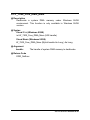
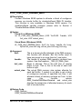
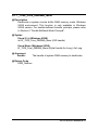
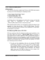
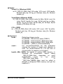
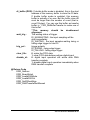
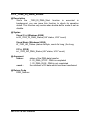
PCI-7200 / cPCI-7200
12MB/S High Speed
Digital Input/ Output Card
@Copyright 1999 ADLink Technology Inc.
All Rights Reserved.
Manual Rev. 2.10: September 16, 1999
The information in this document is subject to change without prior notice in order
to improve reliability, design and function and does not represent a commitment
on the part of the manufacturer.
In no event will the manufacturer be liable for direct, indirect, special, incidental,
or consequential damages arising out of the use or inability to use the product or
documentation, even if advised of the possibility of such damages.
This document contains proprietary information protected by copyright. All rights
are reserved. No part of this manual may be reproduced by any mechanical,
electronic, or other means in any form without prior written permission of the
manufacturer.
Trademarks
PCI-7200 and cPCI-7200 are registered trademarks of ADLink Technology Inc.,
Other product names mentioned herein are used for identification purposes only
and may be trademarks and/or registered trademarks of their respective
companies.
Getting service from ADLink Technology. Inc.
Customer satisfaction is always the most important thing for
ADLink Tech. You can get more information and our service from
several channels below.
1. Visit our web site: http://www.adlink.com.tw
2. For general customer service, please contact: [email protected]
3. For specific product, you can contact the product specialist as below:
NuDAQ: nudaq @adlink.com.tw
NuIPC:
nuipc @adlink.com.tw
NuDAM: nudam @adlink.com.tw
NuPRO: nupro @adlink.com.tw
Software:
sw @adlink.com.tw
AMB:
amb @adlink.com.tw
4. Or you can send a FAX to us. FAX: +886-2-8226-5717 Attn: ADLink Service
5. To take the benefit of efficiency, please give us the basic information as
below:
o Contact Person:
o Company/Organization:
o Tel #:
o Address:
o FAX #:
o Country:
o Dealer:
o Product Model:
o Environment to Use:
o OS:
o M/B:
CPU:
o Video Card:
o Network Interface Card:
o Problem Description:
o Email:
o Purchased Date:
o Any Suggestion is appreciated:
o Computer Brand:
Chipset:
Bios:
CONTENTS
CONTENTS
....................................................... i
How to Use This Guide........................................ v
CHAPTER 1
1.1
1.2
1.3
Applications ......................................................................2
Features.............................................................................2
Specifications....................................................................3
CHAPTER 2
2.1
2.2
2.3
2.4
2.5
2.6
2.7
Installation .................................... 5
What You Have..................................................................5
Unpacking .........................................................................6
Device Driver Installation for Windows 95 .......................6
PCI-7200’s Layout .............................................................8
PCI-7200 Installation Outline .......................................... 10
2.5.1 Hardware configuration ......................................... 10
2.5.2 Slot selection.......................................................... 10
2.5.3 Installation Procedure ............................................ 10
2.5.4 Running the 7200UTIL.EXE.................................... 11
Connector Pin Assignment ............................................ 11
2.6.1 PCI-7200 Pin Assignment....................................... 11
2.6.2 cPCI-7200 Pin Assignment..................................... 13
8254 for Timer Pacer Generation.................................... 13
CHAPTER 3
3.1
3.2
3.3
3.4
3.5
Introduction................................... 1
Register Structure & Format....... 15
I/O Registers Format ....................................................... 15
Digital Input Register (BASE + 10) ................................. 16
Digital Output Register (BASE + 14)............................... 16
DIO Status & Control Register (BASE + 18) ................... 17
Interrupt Status & Control Register (BASE + 1C) .......... 19
Contents • i
CHAPTER 4
Operation Theorem ..................... 23
4.1 Direct Program Control ...................................................... 23
4.2 Timer Pacer Mode............................................................... 24
4.3 External Trigger .................................................................. 26
4.4 Handshaking....................................................................... 27
4.5 Timing Characteristic ......................................................... 29
CHAPTER 5
5.1
5.2
5.3
5.4
5.5
5.6
5.7
5.8
5.9
5.10
5.11
5.12
5.13
5.14
5.15
5.16
5.17
5.18
5.19
5.20
5.21
5.22
5.23
5.24
5.25
ii • Contents
C/C++ & DLL Libraries ................. 33
Installation....................................................................... 33
5.1.1 Installation .............................................................. 33
Running Testing Utility (7200UTIL.EXE) ........................ 35
Software Driver Naming Convention.............................. 36
_7200_Initial .................................................................... 36
_7200_Switch_Card_No.................................................. 38
_7200_AUX_DI................................................................. 39
_7200_AUX_DI_Channel ................................................. 40
_7200_AUX_DO ............................................................... 41
_7200_AUX_DO_Channel ............................................... 42
_7200_DI .......................................................................... 43
_7200_DI_Channel .......................................................... 44
_7200_DO ........................................................................ 45
_7200_DO_Channel......................................................... 46
_7200_Alloc_DMA_Mem ................................................. 47
_7200_Free_DMA_Mem................................................... 49
_7200_Alloc_DBDMA_Mem ............................................ 50
_7200_Free_DBDMA_Mem.............................................. 51
_7200_DI_DMA_Start ...................................................... 52
_7200_DI_DMA_Status.................................................... 56
_7200_DI_DMA_Stop....................................................... 57
_7200_DblBufferMode..................................................... 58
_7200_CheckHalfReady .................................................. 59
_7200_DblBufferTransfer................................................ 60
_7200_GetOverrunStatus................................................ 61
_7200_DO_DMA_Start..................................................... 62
5.26
5.27
5.28
5.29
_7200_DO_DMA_Status .................................................. 64
_7200_DO_DMA_Stop..................................................... 65
_7200_DI_Timer............................................................... 66
_7200_DO_Timer............................................................. 68
CHAPTER 6
Double Buffer Mode Principle...... 71
CHAPTER 7
Limitation .................................... 73
Appendix A. 8254 Programmable Interval Timer ..
.................................................... 75
A.1
A.2
A.3
The Intel (NEC) 8254........................................................ 75
The Control Byte ............................................................. 76
Mode Definition ............................................................... 77
Product Warranty/Service ................................. 81
Contents • iii
How to Use This Guide
This manual is designed to help you use the PCI-7200 and cPCI-7200.
The functionality of PCI-7200 and cPCI-7200 are the same except that
cPCI-7200 has 4 auxiliary digital input and output. Therefore, the “PCI7200” represents both PCI-7200 and cPCI-7200 if not specified.
The manual describes how to modify various settings on the PCI-7200
card to meet your requirements. It is divided into seven chapters:
• Chapter 1, "Introduction," gives an overview of the
product features, applications, and specifications.
• Chapter 2, "Installation," describes how to install the PCI-7200.
The layout of PCI-7200 is shown, and the installation
procedures, pin assignment of connectors, and timer pacer
generation are specified.
• Chapter 3, "Register Structure & Format," describes the lowlevel register structure and format of the PCI-7200.
• Chapter 4, "Operation Theorem," describes how the PCI-7200
works.
• Chapter 5, "C/C++ & DLL Library," describes the high level C
and DLL library functions. It will help you to programming in
DOS, Win 3.11, and Win-95 environments.
• Chapter 6, "Double Buffer Mode Principle," describes the data
buffer for double-buffered DMA DI operation.
• Chapter 7, "Limitation," describes three limitations on using
PCI-7200.
• Appendix A, "8254 Programmable Interval Timer“, describes
the detailed structure and register format.
How to Use This Manual • v
1
Introduction
The PCI-7200/cPCI-7200 is PCI/CompactPCI form factor high speed
digital I/O card, it consists of 32 digital input channels, and 32 digital
output channels. High performance designs and the state-of-the-art
technology make this card to be ideal for high speed digital input and
output applications.
The PCI-7200 performs high-speed data transfers using bus mastering
DMA via 32-bit PCI bus architecture. The maximum data transfer rates
can be up to 12MB per second. It is very suitable for interface between
high speed peripherals and your computer system.
Several different digital I/O operation modes are supported:
1. Direct Program Control: the digital inputs and outputs can be
accessed and controlled by its corresponding I/O ports directly.
2. Timer Pacer Mode: the digital input and output operations are
handled by internal timer pacer clock and transferred by bus mastering
DMA.
3. External Clock Mode: the digital input operations are handled by
external input strobe signal (I_REQ) and transferred by bus mastering
DMA.
4. Handshaking: through REQ signal and ACK signal, the digital I/O
data can have simple handshaking data transfer.
Introduction • 1
Software Supporting: There are several software options help you get
your applications running quickly and easily.
1. Linking with data acquisition software packages, such as:
LabVIEW
HP-VEE
2. Custom Program: For the customer writing their own
programs, the PCI-7200 is supported by a comprehensive
set of drivers and programming tools. These software
supports are available in multiple platforms.
• MS-DOS Borland C/C++ program library
• DLL for Windows 95.
• PCIS-DASK/NT: Advanced data acquisition software kit
and DLL for Windows NT (Optional for PCI-7200).
1.1 Applications
•
•
•
•
•
•
•
Interface to high-speed peripherals
High-speed data transfers from other computers
Digital I/O control
Interface to external high-speed A/D and D/A converter
Digital pattern generator
Waveform and pulse generation
BCD interface driver
1.2 Features
The PCI-7200 high-speed DIO Card provides the following advanced
features:
• 32 TTL digital input channels
• 32 TTL digital output channels
• Transfer up to 12M Bytes per second
• High output driving and low input loading
• 32-bit PCI bus, Plug and Play
• On-board internal timer pacer clock
• Internal timer controls input sampling rate
• Internal timer controls digital output rate
• ACK and REQ for handshaking
• On-board 32-byte FIFO for both digital input and output
• Extra 8 Kbytes digital input FIFO for cPCI-7200
2 • Introduction
• 4 auxiliary digital input and output channels (cPCI-7200 only)
• Diode terminators for 32 input channels and control signals
(cPCI-7200 only)
• Multiple interrupt sources are selectable by software
1.3 Specifications
♦ Digital I/O (DIO)
• Channel: 32 TTL compatible inputs and outputs
• Device: TTL74F273 and TTL74F373
• FIFO: 8 words (32-bit) (for PCI-7200)
2K + 8 words (32-bit) (for cPCI-7200)
• Input Voltage:
Low: Min. 0V; Max. 0.8V
High: Min. +2.0V
• Input Load:
Low: +0.5V @ -0.6mA max.
High: +2.7V @+20µA max.
• Output Voltage:
Low: Min. 0V; Max. 0.5V
High: Min. +2.7V
• Driving Capacity:
Low: Max. +0.5V at 24mA (Sink)
High: Min. 2.4V at -3.0mA (Source)
♦ Auxiliary Digital I/O (AUXDIO)
• Channel: 4 TTL compatible inputs and outputs
• Device: TTL74F244
♦ Programmable Counter
• Device: 82C54-10
• Timer Pacer: 16-bit/32-bit timer (two 16-bit counter cascaded
together) with a 4MHz time base
• Counter: One 16-bit counter with a 4MHz time base
• Pacer Output: 0.00046 Hz ~ 2 MHz
♦ General Specifications
• I/O Base Address: 32 consecutive address location for PCI7200, 36 consecutive address location for cPCI-7200
• Operating Temperature: 0° C ~ 50° C
Introduction • 3
• Storage Temperature: -20° C ~ 80° C
• Humidity: 5 ~ 95%, non-condensing
• Connector:
PCI-7200:
one 37-pin D-type and one 40-pin ribbon
connector
cPCI-7200: one 100-pin SCSI-type connector
• Dimension:
PCI-7200:
Compact size, only 98mm (H) X 147mm (L)
cPCI-7200: Standard 3U CompactPCI form factor
• Power Consumption:
PCI-7200:
+5 V @ 500 mA max.
cPCI-7200: +5 V @ 600 mA max.
4 • Introduction
2
Installation
This chapter describes how to install the PCI-7200. At first, the content of
the package and the unpacking information that you should be careful
are described. Because the PCI-7200 is a plug and play device, there is
no more jumper or DIP switch setting for configuration. The Interrupt
number and I/O port address are assigned by the system BIOS during
system boot up.
2.1 What You Have
In addition to this User's Manual, the package includes the
following items:
• PCI-7200 Digital I/O & Counter Card (include ACL-10437: 40pin to 37-pin D-Sub cable)
or
• cPCI-7200 Digital I/O & Counter Card (include 100-pin SCSI
connector assembly )
• Manual & Software Utility CD
If any of these items is missing or damaged, contact the dealer
from whom you purchased the product. Save the shipping
materials and carton in case you want to ship or store the product
in the future.
Installation • 5
2.2 Unpacking
Your PCI-7200 card contains sensitive electronic components that
can be easily damaged by static electricity.
The card should be done on a grounded anti-static mat. The
operator should be wearing an anti-static wristband, grounded at
the same point as the anti-static mat.
Inspect the card module carton for obvious damage. Shipping and
handling may cause damage to your module. Be sure there are no
shipping and handling damages on the module before processing.
After opening the card module carton, extract the system module
and place it only on a grounded anti-static surface component side
up.
Again inspect the module for damage. Press down on all the
socketed IC's to make sure that they are properly seated. Do this
only with the module place on a firm flat surface.
Note: DO NOT APPLY POWER TO THE CARD IF IT HAS BEEN
DAMAGED.
You are now ready to install your PCI-7200.
2.3 Device Driver Installation for Windows 95
While you first plug PCI-7200 card and enter Windows 95, the
system will detect this device automatically and show the following
dialog box that prompts you to select the device information
source.
6 • Installation
Choose the default option “Driver from disk provided by hardware
manufacturer” and then a dialog box is shown to prompt you give
the path of installation disk.
Place ADLink’s “Manual & Software Utility” CD into the appropriate
CD driver. Type “X:\Software\NuDAQPCI\7200\Win95” in the input
field (X indicates the CD ROM driver) and then click OK. The
system will start the installation of PCI-7200.
Installation • 7
CN2
PCI-7200 Rev A1
Figure 2.1 PCI-7200 Layout Diagram
8 • Installation
PCI -Bus
Controller
ALTERA
.
.
.
.
.
.
.
.
.
.
.
.
.
.
.
.
.
.
.
.
.
.
.
.
.
.
.
.
.
.
.
.
.
.
.
.
.
.
.
.
CN1
2.4 PCI-7200’s Layout
Figure 2.1a PCI-7200 Layout Diagram
Installation • 9
2.5 PCI-7200 Installation Outline
2.5.1 Hardware configuration
Because PCI-7200 is a plug and play device, the interrupt number
and I/O port address are assigned by system BIOS. There is no
jumpers or DIP switches on-board for configuration setting.
2.5.2 Slot selection
For PCI-7200, choose a PCI expansion slot and make sure this
slot supports bus master mode data transfer.
For cPCI-7200, choose a peripheral slot which is marked with a
circle on the backplane and make sure this slot supports bus
master mode data transfer.
2.5.3 Installation Procedure
1. Turn off your computer
2. Turn off all accessories (printer, modem, monitor, etc.)
connected to computer.
3. Remove the cover from your computer.
4. Select a 32-bit PCI expansion slot (for PCI-7200) or
CompactPCI peripheral slot (for cPCI-7200). PCI slots are short
than ISA or EISA slots and are usually white or ivory.
CompactPCI peripheral slots are marked with a circle on the
backplane.
Caution!! Don‘t put PCI-7200 card into ISA or EISA slot.
5. Before handling the PCI-7200, discharge any static buildup on
your body by touching the metal case of the computer. Hold the
edge and do not touch the components.
6. Position the PCI-7200 board into the PCI slot you selected, or
position the cPCI-7200 board along the card guide into the
selected CompactPCI peripheral slot.
7. Secure the PCI-7200 in place at the rear panel of the system
unit using screw removed from the slot (for PCI-7200), or screw
the cPCI-7200 in place at the front panel of the CompactPCI
system.
10 • Installation
2.5.4 Running the 7200UTIL.EXE
The IRQ number and I/O port address can be configured by the
system. By using the 7200UTIL.EXE, you can get the above values
and they are displayed by this utility.
A testing program is included in this utility, you can check if your
PCI-7200 can work properly. Refer Section 5.2 for further detailed
information.
2.6 Connector Pin Assignment
2.6.1 PCI-7200 Pin Assignment
The PCI-7200 comes equipped with one 37-pin D-Sub connector
(CN2) located on the rear mounting plate and one 40-pin female
flat cable header connector (CN1). The CN2 is located on the rear
mounting plate; the CN1 is on front of the board. Refer section 2.2
PCI-7200‘s layout.
CN2 is used for digital inputs (DI 0 ~ DI 15) and digital outputs (DO
0 ~ DO 15), and the reminder digital I/O channels DI 16 ~ DI 31
and DO 16 ~ DO 31 are presented on the CN1. The pin
assignment of CN1 and CN2 is illustrated in the figure 2.2 and 2.3.
Legend:
DO n
DI n
GND
ACK
REQ
O_TRG
:
:
:
:
:
Digital Output CH n
Digital Input CH n
Ground
ACK Signal of handshaking communication
REQ Signal of handshaking communication
Input signal to start the DI data sampling
: Output signal can be controlled by software
Installation • 11
DI 16
DI 17
DI 18
DI 19
DI 20
DI 21
DI 22
DI 23
DI 24
DI 25
DI 26
DI 27
DI 28
DI 29
DI 30
DI 31
+5V
O_ACK
O_REQ
N/C
1
2
3
4
5
6
7
8
9
10
11
12
13
14
15
16
17
18
19
20
21
22
23
24
25
26
27
28
29
30
31
32
33
34
35
36
37
38
39
40
DO16
DO17
DO18
DO19
DO20
DO21
DO22
DO23
DO24
DO25
DO26
DO27
DO28
DO29
DO30
DO 31
GND
O_TRG
N/C
N/C
Figure 2.2 CN1 Pin Assignment
DI 0
DI 1
DI 2
DI 3
DI 4
DI 5
DI 6
DI 7
DI 8
DI 9
DI10
DI11
DI12
DI13
DI14
DI15
+5V
1
I_ACK
I_REQ
18
20
2
21
3
4
22
23
5
24
6
25
7
26
8
27
9
28
10
29
11
12
13
30
31
32
14
33
15
34
16
35
17
36
37
19
DO0
DO1
DO2
DO3
DO4
DO5
DO6
DO7
DO8
DO9
DO10
DO11
DO12
DO13
DO14
DO15
GND
I_TRG
Figure 2.3 CN2 Pin Assignment
12 • Installation
2.6.2 cPCI-7200 Pin Assignment
(1)
(2)
(3)
(48)
(49)
(50)
(51)
(52)
(53)
(98)
(99)
(100)
(1) DO0
(2) DO2
(3) DO4
(4) DO6
(5) DO8
(6) DO10
(7) DO12
(8) DO14
(9) GND
(10) DO16
(11) DO18
(12) DO20
(13) DO22
(14) DO24
(15) DO26
(16) DO28
(17) DO30
(18) GND
(19) +5Vout
(20) +5Vout
(21) AUXIN0
(22) AUXIN1
(23) I_TRG
(24) I_REQ
(25) I_ACK
(26) O_TRG
(27) O_REQ
(28) O_ACK
(29) AUXIN2
(30) AUXIN3
(31) +5Vout
(32) +5Vout
(33) GND
(34) DIN0
(35) DIN2
(36) DIN4
(37) DIN6
(38) DIN8
(39) DIN10
(40) DIN12
(41) DIN14
(42) GND
(43) DIN16
(44) DIN18
(45) DIN20
(46) DIN22
(47) DIN24
(48) DIN26
(49) DIN28
(50) DIN30
(51) DO1
(52) DO3
(53) DO5
(54) DO7
(55) DO9
(56) DO11
(57) DO13
(58) DO15
(59) GND
(60) DO17
(61) DO19
(62) DO21
(63) DO23
(64) DO25
(65) DO27
(66) DO29
(67) DO31
(68) GND
(69) GND
(70) GND
(71) AuxOut0
(72) AuxOut1
(73) GND
(74) GND
(75) GND
(76) GND
(77) GND
(78) GND
(79) AuxOut2
(80) AuxOut3
(81) GND
(82) GND
(83) GND
(84) DIN1
(85) DIN3
(86) DIN5
(87) DIN7
(88) DIN9
(89) DIN11
(90) DIN13
(91) DIN15
(92) GND
(93) DIN17
(94) DIN19
(95) DIN21
(96) DIN23
(97) DIN25
(98) DIN27
(99) DIN29
(100) DIN31
2.7 8254 for Timer Pacer Generation
8254 Timer/Counter
“H”
“H”
CLK0
GATE0
CLK1
GATE1
4MHz Clock
Timer 0
OUT0
Digital Input Timer Pacer
OUT1
Digital Output Timer Pacer
Timer 1
Timer 2
“H”
CLK2
GATE2
OUT2
Figure 2.4 8254 configuration
Installation • 13
The internal timer/counter 8254 on the PCI-7200 is configured as
above diagram (figure 2.4). User can use it to generate the timer
pacer for both digital input and digital output trigger.
The digital input timer pacer is from OUT0 (Timer 0), and the digital
output timer pacer is from OUT1 (Timer 1). Besides, Timer 0 and
Timer 2 can be cascaded together to generate more timer pacer
frequency for digital input. Also, the Timer 2 can be cascaded with
Timer 1 for digital output.
pacer rate = 4 MHz / ( C0 * C2)
if Timer 0 & Timer 2 are cascaded
pacer rate = 4 MHz / C0
if timer 0 & Timer 2 are not cascaded
The maximum pacer signal rate of input and output are
4MHz/2=2Mhz. The minimum signal rate is 4MHz/65535/65535,
which is a very slow frequency that user may never use it.
For example, if you wish to get a pacer rate 2.5 kHz, you can set
C0 = 40 and C2 = 40. That is
2.5KHz = 4Mhz / (40 x 40)
14 • Installation
3
Register Structure & Format
3.1 I/O Registers Format
The PCI-7200 occupies 8 consecutive 32-bit I/O addresses in the
PC I/O address space and the cPCI-7200 occupies 9 consecutive
32-bit I/O addresses. Table 4.1 shows the I/O Map
Address
Base + 0
Base + 4
Base + 8
Base + C
Base + 10
Base + 14
Base + 18
Base + 1C
Base + 20
(cPCI-7200
only)
Read
Counter 0
Counter 1
Counter 2
--Digital Input Reg.
Digital Output (Readback)
DIO Status & Control
INT Status & Control
AUXDIO Reg.
Write
Counter 0
Counter 1
Counter 2
CLK Control CW0
--Digital Output Reg.
DIO Status &Control
INT Status & Control
AUXDO Reg.
Caution: (1) I/O port is 32-bit width
(2) 8-bit or 16-bit I/O access is not allowed.
Register Structure & Format • 15
3.2 Digital Input Register (BASE + 10)
32 digital input channels can be read from this register
Address: BASE + 10
Attribute: READ Only
Data Format:
Byte
Base +10
Base +11
Base +12
Base +13
7
DI7
DI15
DI23
DI31
6
DI6
DI14
DI22
DI30
5
DI5
DI13
DI21
DI29
4
DI4
DI12
DI20
DI28
3
DI3
DI11
DI19
DI27
2
1
DI2
DI10
DI18
DI26
0
DI1
DI9
DI17
DI25
DI0
DI8
DI16
DI24
3.3 Digital Output Register (BASE + 14)
32 digital output channels can be write and read-back from this
register
Address: BASE + 14
Attribute: READ/WRITE
Data Format:
Byte
Base +14
Base +15
Base +16
Base +17
7
DO7
DO15
DO23
DO31
6
DO6
DO14
DO22
DO30
5
DO5
DO13
DO21
DO29
4
DO4
DO12
DO20
DO28
3
DO3
DO11
DO19
DO27
2
DO2
DO10
DO18
DO26
1
DO1
DO9
DO17
DO25
0
DO0
DO8
DO16
DO24
The digital output status can be readback through the same location
(BASE + 14)
16 • Register Structure & Format
3.4 DIO Status & Control Register (BASE + 18)
The data transfer mode of digital input is controlled and status is
checked through this register.
Address: BASE + 18
Attribute: READ/WRITE
Data Format:
Byte
7
Base +18
Base +19
Base +20
Base +21
6
5
4
3
2
1
I_TIME0 I_REQ
0
O_ACK
DIN_EN I_TRG
TRGPL
I_FIFO
I_ACK
----
I_OVER ----
----
O_TRG O_FIFO O_TIME1 O_REQ
----
----
----
----
----
----
----
O_UND
----
----
----
----
----
----
----
----
♦ Digital Input Mode Setting:
I_ACK: Input ACK Enable
1: Input ACK is enabled (input ACK will be asserted after
input data is read by CPU or written to input FIFO)
0: Input ACK is disabled
I_REQ: Input REQ Strobe Enabled
1: Use I_REQ edge to latch input data
0: I_REQ is disabled
I_TIME0: Input Timer 0 Enable
1: Input is sampled by falling edge of Counter 0 output
(COUT0)
0: Input Timer 0 is disabled
I_FIFO: Input FIFO Enable Mode
1: Input FIFO is enabled (input data is saved to input
FIFO)
0: Input FIFO is disabled
TRGPOL: Input Trigger Polarity
Register Structure & Format • 17
1: I_TRG is Rising Edge Active
0: I_TRG is Falling Edge Active
I_TRG: External Trigger Enable
1: Wait until I_TRG signal is active, digital input sampling
will begin after a rising or falling edge of I_TRG is
coming.
0: Start input sampling immediately (if input control
register is set)
DIN_EN: Digital Input Enable
1: Digital Input Enable
0: Digital Input Disabled, when this bit is set as 0, all
digital input operation will be stopped.
♦ Digital Output Mode Setting:
O_ACK: Output ACK Enable
1: Output ACK is enabled, the output circuit will wait for
O_ACK after O_REQ strobe is asserted.
0: Output ACK is disabled
O_REQ: Output REQ Enable
1: Output REQ is enabled, an O_REQ strobe will be
generated after output data is ready
0: Output REQ is disabled
O_TIME1: Output Timer 1 Enable
1: Output Timer 1 is enabled, output data is moved from
output FIFO to DO registers when output of Counter1
goes low.
0: Output Counter 1 is disabled
O_FIFO: Output FIFO Enable
1: Output FIFO is enabled
(output data is moved from output FIFO)
0: Output FIFO is disabled
18 • Register Structure & Format
O_TRG: Digital Output Trigger Signal
This bit is used to control the O_TRG output of PCI-7200, the
signal is on CN1 pin 36 of PCI-7200 or CN1 pin 26 of cPCI-7200 when
1: O_TRG 1 goes High (1)
0: O_TRG 1 goes Low (0)
♦ Digital I/O FIFO Status:
I_OVR: Input data overrun
1: Digital Input FIFO is full (overrun) during input data
transfer
0: No input data overrun occurred
Input data overrun occurred, the I_OVR bit is set when input
FIFO is full and there is new input data coming in. This bit
can be cleared by writing “1” to it.
O_UND: Output data FIFO is underrun
1: Output FIFO is empty during output data trancfer
0: No output data underrun occurred
Output data underrun, the O_UND bit is set when output
FIFO is empty and the output request for new data, this bit
can be cleared by writing “1” to it.
3.5 Interrupt Status & Control Register (BASE + 1C)
The interrupt modes/status are set/checked through this register.
Address: BASE + 1C
Attribute: READ/WRITE
Data Format:
Byte
Base +1C
Base +1D
Base +1E
Base +1F
7
SI_TO
6
5
SI_REQ SO_ACK
FIFOFF FIFOEF FIFORST
4
3
T2_EN
2
1
0
T1_EN
T0_EN
II_REQ
IO_ACK
REQ_NEG T1_T2
T0_T2
SI_T2
SI_T1
----
----
----
----
----
----
----
----
----
----
----
----
----
----
----
----
Register Structure & Format • 19
♦ Interrupt Control:
In PCI-7200, the interrupt can be triggered by many signal
sources such as O_ACK, I_REQ, timer 0, timer 1, and timer 2.
The interrupt source is controlled by the following bits:
IO_ACK: Interrupt is triggered by O_ACK signal.
1: O_ACK interrupt is enabled
0: O_ACK interrupt is disabled
II_REQ: Interrupt is triggered by I_REQ signal.
1: I_REQ interrupt is enabled
0: I_REQ interrupt is disabled
T0_EN: Interrupt is triggered by timer 0 output.
1: Timer 0 interrupt is enabled
0: Timer 0 interrupt is disabled
T1_EN: Interrupt is triggered by timer 1 output.
1: Timer 1 interrupt is enabled
0: Timer 1 interrupt is disabled
T2_EN: Interrupt is triggered by timer 2 output.
1: Timer 2 interrupt is enabled
0: Timer 2 interrupt is disabled
♦ Interrupt Status:
The following bits are used to check interrupt status:
SO_ACK: Status of O_ACK interrupt
1: O_ACK Interrupt occurred
0: No O_ACK interrupt
SI_REQ: Status of I_REQ interrupt
1: I_REQ Interrupt occurred
0: No I_REQ Interrupt
20 • Register Structure & Format
SI_T0: Status of timer 0 interrupt
1: OUT0 (output of timer 0) Interrupt occurred
0: No timer 0 Interrupt
SI_T1: Status of timer 1 interrupt
1: OUT1 (output of timer 1) Interrupt occurred
0: No timer 1 Interrupt
SI_T2: Status of timer 2 interrupt
1: OUT2 (output of timer 2) interrupt occurred
0: No timer 2 Interrupt
Note: All the interrupt status can be cleared by writing 1 to the
corresponding bit of the register. In order to make the interrupt
work properly, the interrupt service routine has to clear all the
interrupt status before end of the ISR.
♦ Timer Configuration Control:
The 8254 timer on the PCI-7200 can be configured as either
timer 0 cascaded with timer 2 or timer 1 cascaded with timer2.
These configuration are controlled by the following bits:
T0_T2: Timer 0 is cascaded with timer 2
1: Timer 0 and timer 2 are cascaded together, output of
timer 2 connects to the clock input of timer 0.
0: Not cascaded, the 4 MHz clock is connected to the
timer 0 clock input.
T1_T2: Timer 1 is cascaded with timer 2
1: Timer 1 and timer 2 are cascaded together, output of
timer 2 connects to the clock input of timer 1.
0: Not cascaded, the 4 MHz clock is connected to the
timer 1 clock input.
Register Structure & Format • 21
♦ I_REQ Polarity Selection:
When the input sampling is controlled by the I_REQ signal
only, the I_REQ can be programmed to be rising edge active
or falling edge active.
REQ_NEG: I_REQ trigger polarity
1: latch input data on falling edge of I_REQ
0: latch input data on rising edge of I_REQ
♦ FIFO Control and Status (cPCI-7200 only):
The cPCI-7200 has an extra 2K samples digital input FIFO.
The FIFO can be cleared and monitored by the following bits:
FIFORST (Write only): Clear the on-board DI FIFO
1: Write 1 to clear the data of the FIFO.
0: No operation.
FIFOEF (Read only): Empty flag of the DI FIFO
1: DI FIFO is empty.
0: DI FIFO is not empty.
FIFOFF (Read only): Full flag of the DI FIFO
1: DI FIFO is full.
0: DI FIFO is not full.
Note: The cPCI-7200 has 2 cascaded DI FIFOs. One is
located in the PCI controller chip, the other one is on the PCI7200 board. The above bits only control the on-board FIFO. In
order to control the on-chip FIFO, please refer to the AMCC5933 data book.
22 • Register Structure & Format
4
Operation Theorem
In PCI-7200, there are four data transfer modes can be used for digital
I/O access and control, these modes are:
1. Direct Program Control: the digital inputs and outputs can be
read/written and controlled by its corresponding I/O port address directly.
2. Internal Timer Pacer Mode: the digital input and output operations
are paced by internal timer pacer and transferred by bus mastering DMA.
3. External Clock Mode: the digital input operation is clocked by
external I_REQ strobe and transferred by bus mastering DMA.
4. Handshaking: through REQ and ACK signals, the digital I/O can have
simple handshaking data transfer.
4.1 Direct Program Control
The digital I/O operations can be controlled by I/O port BASE+10
for digital input and BASE+14 for digital output.
The I/O port address BASE is assigned by system BIOS, please
refer to Section 5 for more detailed description.
Operation Theorem • 23
The digital OUT operation is:
outport (BASE+14, 0xAAAAAAAA ) // (A : 0 ~ F)
The digital IN operation is:
value = inport (BASE+10)
// The input status is save in the
// value variable
4.2 Timer Pacer Mode
The digital I/O access control is clocked by timer pacer, which is
generated by a interval programming timer/counter chip 8254.
There are three timers on the 8254. The timer 0 is used to
generate timer pacer for digital input, and timer 1 is used for digital
output. The configuration is illustrated as below.
8254 Timer/Counter
“H”
“H”
CLK0
GATE0
CLK1
GATE1
4MHz Clock
Timer 0
OUT0
Digital Input Timer Pacer
OUT1
Digital Output Timer Pacer
Timer 1
Timer 2
“H”
24 • Operation Theorem
CLK2
GATE2
OUT2
The operation sequences are:
1. Define the frequency (timer pacer rate)
2. The digital input data are saved in FIFO after a timer pacer pulse
is generated. The sampling is controlled by timer pacer.
3. The data saved in FIFO will be transferred to main memory of
your computer system directly and automatically. This is
controlled by bus mastering DMA control, this function is
supported by PCI controller chip.
The operation flow is show as below:
8254 Timer/Counter
1
CLK0
GATE0
Timer 0
To Digital Input Trigger
Latch Digital Input
OUT0
2
3
PC's Main Memory
Bus mastering
DMA data Transfer
Digital Input FIFO
Operation Theorem • 25
4.3 External Clock Mode
The digital input is clocked by external strobe, which is from the Pin
19 (I_REQ) of CN2 (PCI-7200) or Pin 24 of CN1 (cPCI-7200). The
operation sequence is very similar to Timer Pacer Trigger. The only
difference is the clock source.
1. The external input strobe is generated from outside device, and
go through the Pin 19 (I_REQ) of CN2 and to latch the digital
input.
2. The digital input data are saved in FIFO after an I/O strobe
signal is coming in.
3. The data saved in input FIFO will be transferred to main memory
on your computer system directly. This is controlled by bus
mastering DMA control, this function is supported by PCI
1
To Digital Input Trigger
Pin 19 of CN2
Latch Digital
Input Data
2
3
PC's Main Memory
Bus mastering
DMA data Transfer
26 • Operation Theorem
Digital Input FIFO
4.4 Handshaking
In PCI-7200, it also supports a handshaking digital I/O transfer
mode. That is, after input data is ready, an I_REQ is sent form
external device, and I_ACK will go high to acknowledge the data
already accessed.
I_REQ & I_ACK for Digital Input
1. Digital Input Data is ready
2. An I_REQ signal is generated for digital input operation
3. Digital input data is saved to FIFO
4. An I_ACK signal is generated and sent to outside device
5. If the FIFO is not empty and PCI bus is not occupied, the data
will be transferred to main memory
Digital Input DATA
1
2
IN_REQ
Latch Digital Input
or Digital Output
IN_ACK
3
4
PC's Main Memory
Bus mastering
Digital Input FIFO
DMA data Transfer
5
Operation Theorem • 27
O_REQ & O_ACK for Digital Output
1. Digital Output Data is moved from PC memory to FIFO of PCI7200 by using DMA data mastering data transfer.
2. Move output data from FIFO to digital output circuit.
3. Output data is ready.
4. An O_REQ signal is generated and sent to outside device.
5. After an O_ACK is got, the step 2 to step 5 will be repeated
again.
** If the FIFO is not full, the output data is moved form PC‘s main
memory to FIFO automatically.
Digital Output DATA
O_REQ
4
3
Move Data to
Digital Output
O_ACK
5
PC's Main
Memory
Bus mastering
Digital Output FIFO
DMA data Transfer
1
28 • Operation Theorem
2
4.5 Timing Characteristic
1. I_REQ as input data strobe (Rising Edge Active)
th
tl
I_REQ
IN_REQ
t cyc
valid data
valid data
DI0~DI31
ts
tn
th
60ns
tl
ts
2ns
tn
60ns
t cyc
5 PCI CLK Cycle
30ns
2. I_REQ as input data strobe (Falling Edge Active)
th
tl
IN_REQ
I_REQ
t cyc
valid data
valid data
DI0~DI31
tn
ts
th
60ns
tl
60ns
ts
2ns
tn
30ns
t cyc
5 PCI CLK Cycle
Operation Theorem • 29
3. I_REQ & I_ACK Handshaking
t5
IN_REQ
I_REQ
t4
t3
IN_ACK
I_ACK
valid data
valid data
DI0~DI31
t1
t2
t1
0ns
t5
60ns
t2
0ns
t4
1 PCI CLK Cycle
t3
2 PCI CLK Cycle
4. O_REQ as output data strobe
th
OUT_REQ
O_REQ
t cyc
D00~D031
valid data
valid data
ts
ts
19ns
30 • Operation Theorem
t h = 2 PCI CLK Cycles
tcyc
500ns
5. O_REQ & O_ACK Handshaking
t3
OUT_REQ
O_REQ
t2
OUT_ACK
O_ACK
valid data
valid data
DO0~Do31
t1
t1
19ns
t2
1 PCI CLK Cycle
t3
5 PCI CLK Cycle
Note: O_ACK must be de-asserted before O_REQ asserts, O_ACK
can be asserted any time after O_REQ asserts, O_REQ will be
reasserted after O_ACK is asserted.
Operation Theorem • 31
5
C/C++ & DLL Libraries
In this chapter, the PCI-7200's software drivers: C/C++ language library
for DOS and DLL driver for Windows 95/98 are described.
5.1 Installation
5.1.1 Installation
The Library & Utility supplied with PCI-7200 includes a utility
software, C-language library, DLL libraries and some demonstration
programs which can help you reduce programming work.
♦ MS-DOS Installation :
1. Turn your PC's power switch on
2. Put the ADLink’s “All-in-one” CD into the appropriate CD drive.
3. Type the command (X indicates the CD-ROM drive):
X:\> CD NUDAQPCI\7200\DOS
X:\NUDAQPCI\7200\DOS> SETUP
4. An installation complete message will be shown on the
screen.
After installation, all the files of PCI-7200 Library & Utility for
DOS are stored in C:\ADLink\7200\DOS directory.
C/C++ & DLL Libraries • 33
♦ Windows 95/98 Installation:
1. Put the ADLink’s “All-in-one” CD into the appropriate CD drive.
2. If autorun setup program is not invoked automatically please
execute X:\setup.exe. (X indicates the CD-ROM drive)
3. Select NuDAQ PCI >> Drivers >> Win 95/98 >> PCI-7200 to
setup PCI-7200 DLL for Windows 95.
After a welcome dialog box, Setup prompts the following dialog
box for you to specify the destination directory. The default path
is C:\ADLink\7200\W95. If you want to install PCI-7200 DLL for
Windows 95 in another directory, please click Browse button to
change the destination directory.
Then you can click Next to begin installing PCI-7200 DLL for
Windows 95.
After you complete the installation of PCI-7200 Software, PCI7200’s DLL (7200.DLL) is copied to Windows System directory
(default is C:\WINDOWS\SYSTEM for Windows 95/98) and the
driver files (W95_7200.VXD and PCIW95.VXD) are also copied
to the appropriate directory.
34 • C/C++ & DLL Libraries
5.2 Running Testing Utility (7200UTIL.EXE)
After finishing the installation of PCI-7200 DOS software, you can
execute the utility by the following commands under DOS
environment:
C> cd \ADLINK\7200\DOS\UTIL
C> 7200UTIL
The following diagram will be displayed on you screen. You can test
the functionality :
1. Digital I/O in polling mode (Direct Program Control)
2. Digital I/O DMA mode (Timer Pacer Trigger and Bus-Mastering
DMA data transfer)
3. AUX Digital I/O (for cPCI-7200 only)
****** PCI-7200 Utility
Rev. 1.10 ******
Copyright ' 1995-1999, ADLink Technology Inc.
All rights reserved.
<F1> : DIO Polling Mode Testing.
<F2> : DIO DMA Mode Testing.
<F3> : AUX DIO Testing (cPCI-7200 only).
<Esc>: Quit.
>>> Select function key F1 ~ F3, or press <Esc> to quit. <<<
C/C++ & DLL Libraries • 35
5.3 Software Driver Naming Convention
The functions of PCI-7200's software drivers are using full-names to
represent the functions' real meaning. The naming convention rules
are :
Ÿ DOS
_{hardware_model}_{action_name}. e.g. _7200_Initial ().
Ÿ Windows 95/98
In order to recognize the difference between DOS library and
Windows library, A capital "W" is put on the head of each
function name of the Windows DLL driver. e.g. W_7200_Initial ()
There are 21 function calls provided by each driver for PCI-7200
Digital I/O cards; all drivers (DOS, Win-95/98) provide the same
function capability. The function names using in Windows is only a
capital "W" put on the head of each function name of DOS library.
The detailed descriptions of each function are specified in the
following sections.
5.4 _7200_Initial
@ Description
A PCI-7200 card is initialized according to the card number.
Because the PCI-7200 is PCI bus architecture and meets the plug
and play design, the IRQ and base_address ( pass-through
address) are assigned by system BIOS directly. Every PCI-7200 card
has to be initialized by this function before calling other functions.
36 • C/C++ & DLL Libraries
@ Syntax
Visual C++ (Windows 95/98)
int W_7200_Initial (U8 card_number, U16 *base_addresss, U8
*irq_no)
Visual Basic (Windows 95/98)
W_7200_Initial (ByVal card_number As Byte, base_addresss As
Integer, irq_no As Byte) As Long
C/C++ (DOS)
int _7200_Initial (U8 card_number, U16 *base_addresss,
*irq_no)
U8
@ Argument
card_number : the card number to be initialized, only four cards
can be initialized, the card number must be
CARD_1, CARD_2, CARD_3 or CARD_4.
base_address : the I/O port base address of the card, it is
assigned by system BIOS.
irq_no :
system will give an available interrupt number to
this card automatically.
@ Return Code
ERR_NoError
ERR_InvalidBoardNumber
ERR_PCIBiosNotExist
ERR_PCICardNotExist
ERR_PCIIrqNotExist
ERR_BaseAddressError
C/C++ & DLL Libraries • 37
5.5 _7200_Switch_Card_No
@ Description
After initialized more than one PCI-7200 cards, this function is used
to select which card is used currently.
@ Syntax
Visual C++ (Windows 95/98)
int W_7200_Switch_Card_No (U8 card_number)
Visual Basic (Windows 95/98)
W_7200_Switch_Card_No (ByVal card_number As Byte) As Long
C/C++ (DOS)
int _7200_Switch_Card_No (U8 card_number)
@ Argument
card_number : The card number to be initialized, four cards can
be initialized, the card number must be CARD_1,
CARD_2, CARD_3, or CARD_4, but only one card
is active.
@ Return Code
ERR_NoError
ERR_InvalidBoardNoInit
38 • C/C++ & DLL Libraries
5.6 _7200_AUX_DI
@ Description
Read data from auxiliary digital input port of cPCI-7200 card. You
can get all 4 bits input data by using this function.
@ Syntax
Visual C++ (Windows 95/98)
int W_7200_AUX_DI (U32 *aux_di)
Visual Basic (Windows 95/98)
W_7200_DI (aux_di As Long) As Long
C/C++ (DOS)
int _7200_DI (U32 *aux_di)
@ Argument
aux_di :
returns 4-bit value from auxiliary digital input port.
@ Return Code
ERR_NoError
ERR_FunctionNotAvailable
C/C++ & DLL Libraries • 39
5.7 _7200_AUX_DI_Channel
@ Description
Read data from auxiliary digital input channel of cPCI-7200 card.
There are 4 digital input channels on the cPCI-7200 auxiliary digital
input port. When performs this function, the auxiliary digital input port
is read and the value of the corresponding channel is returned.
* channel means each bit of digital input port.
@ Syntax
Visual C++( Windows 95/98)
int W_7200_AUX_DI_Channel (U8 di_ch_no, Boolean *aux_data)
Visual Basic (Windows 95/98)
W_7200_AUX_DI_Channel (ByVal di_ch_no As Byte, aux_data As
Byte) As Long
C/C++ ( DOS)
int _7200_AUX_DI_Channel (U8 di_ch_no, Boolean *aux_data)
@ Argument
di_ch_no :
aux_data :
the DI channel number, the value has to be set
within 0 and 3.
return value, either 0 or 1.
@ Return Code
ERR_NoError
ERR_InvalidDIChannel
ERR_FunctionNotAvailable
40 • C/C++ & DLL Libraries
5.8 _7200_AUX_DO
@ Description
Write data to auxiliary digital output port. There are 4 auxiliary digital
outputs on the cPCI-7200.
@ Syntax
Visual C++ (Windows 95/98)
int W_7200_AUX_DO (U32 aux_do)
Visual Basic (Windows 95/98)
W_7200_AUX_DO (ByVal aux_do As Long) As Long
C/C++ (DOS)
int _7200_AUX_DO (U32 aux_do)
@ Argument
aux_do :
value will be written to auxiliary digital output port
@ Return Code
ERR_NoError
ERR_FunctionNotAvailable
C/C++ & DLL Libraries • 41
5.9 _7200_AUX_DO_Channel
@ Description
Write data to auxiliary digital output channel (bit). There are 4
auxiliary digital output channels on the cPCI-7200. When performs
this function, the digital output data is written to the corresponding
channel.
l
channel means each bit of digital input port
@ Syntax
Visual C++ (Windows 95/98)
int W_7200_AUX_DO_Channel (U8 do_ch_no, Boolean aux_data)
Visual Basic (Windows 95/98)
W_7200_AUX_DO_Channel (ByVal do_ch_no As Byte, ByVal
aux_data As Byte) As Long
C/C++ (DOS)
int _7200_AUX_DO_Channel (U8 do_ch_no, Boolean aux_data)
@ Argument
do_ch_no :
aux_data :
the auxiliary DO channel number, the value has to
be set within 0 and 3.
either 0 (OFF) or 1 (ON).
@ Return Code
ERR_NoError
ERR_InvalidDOChannel
ERR_FunctionNotAvailable
42 • C/C++ & DLL Libraries
5.10 _7200_DI
@ Description
This function is used to read data from digital input port. There are
32-bit digital inputs on the PCI-7200. You can get all 32 input data
from _7200_DI by using this function.
@ Syntax
Visual C++ (Windows 95/98)
int W_7200_DI (U32 *di_data)
Visual Basic (Windows 95/98)
W_7200_DI (di_data As Long) As Long
C/C++ (DOS)
int _7200_DI (U32 *di_data)
@ Argument
di_data :
returns all 32-bit value from digital port.
@ Return Code
ERR_NoError
C/C++ & DLL Libraries • 43
5.11 _7200_DI_Channel
@ Description
This function is used to read data from digital input channels (bit).
There are 32 digital input channels on the PCI-7200. When performs
this function, the digital input port is read and the value of the
corresponding channel is returned.
* channel means each bit of digital input port.
@ Syntax
Visual C++( Windows 95/98)
int W_7200_DI_Channel (U8 di_ch_no, Boolean *di_data)
Visual Basic (Windows 95/98)
W_7200_DI_Channel (ByVal di_ch_no As Byte, di_data As Byte)
As Long
C/C++ ( DOS)
int _7200_DI_Channel (U8 di_ch_no, Boolean *di_data)
@ Argument
di_ch_no :
di_data :
the DI channel number, the value has to be set
within 0 and 31.
return value, either 0 or 1.
@ Return Code
ERR_NoError
ERR_InvalidDIChannel
44 • C/C++ & DLL Libraries
5.12 _7200_DO
@ Description
This function is used to write data to digital output port. There are 32
digital outputs on the PCI-7200.
@ Syntax
Visual C++ (Windows 95/98)
int W_7200_DO (U32 do_data)
Visual Basic (Windows 95/98)
W_7200_DO (ByVal do_data As Long) As Long
C/C++ (DOS)
int _7200_DO (U32 do_data)
@ Argument
do_data :
value will be written to digital output port
@ Return Code
ERR_NoError
C/C++ & DLL Libraries • 45
5.13 _7200_DO_Channel
@ Description
This function is used to write data to digital output channels (bit).
There are 32 digital output channels on the PCI-7200. When
performs this function, the digital output data is written to the
corresponding channel.
l
channel means each bit of digital input port
@ Syntax
Visual C++ (Windows 95/98)
int W_7200_DO_Channel (U8 do_ch_no, Boolean do_data)
Visual Basic (Windows 95/98)
W_7200_DO_Channel (ByVal do_ch_no As Byte, ByVal do_data
As Byte) As Long
C/C++ (DOS)
int _7200_DO_Channel (U8 do_ch_no, Boolean do_data)
@ Argument
do_ch_no :
do_data :
the DO channel number, the value has to be set
within 0 and 31.
either 0 (OFF) or 1 (ON).
@ Return Code
ERR_NoError
ERR_InvalidDOChannel
46 • C/C++ & DLL Libraries
5.14 _7200_Alloc_DMA_Mem
@ Description
Contact Windows 95/98 system to allocate a block of contiguous
memory for single-buffered DMA transfer. This function is only
available in Windows 95/98 version.
@ Syntax
Visual C++ (Windows 95/98)
int W_7200_Alloc_DMA_Mem (U32 *buff, U32 *handle, U32
buf_size, U32 *actual_size)
Visual Basic (Windows 95/98)
W_7200_Alloc_DMA_Mem (buff As Long, handle As Long, ByVal
buf_size As Long, actual_size As Long ) As Long
@ Argument
buff :
handle:
buf_size:
The start address of the user buffer for DMA data
transfer. This buffer will be attached to the DMA
memory allocated by this function. When using this
DMA memory handle as an argument of
W_7200_DI_DMA_Start function, DI data will be
copied to this buffer. When using this DMA memory
handle as an argument of W_7200_DO_DMA_Start
function, the data stored in this buffer will be the DO
data.
The handle of system DMA memory returned from
system. Use this handle in _7200_DI_DMA_Start or
_7200_DO_DMA_Start.
Bytes to allocate. Please be careful, the unit of this
parameter is BYTE, not SAMPLE.
C/C++ & DLL Libraries • 47
actual_size: The actual size system allocate for DMA memory.
The unit is BYTE. If system is not able to get a block
of contiguous memory of specified buf_size, it will
allocate a block of memory as large as it can. In this
case,
this
function
returns
ERR_SmallerDMAMemAllocated, and actual_size
denotes the actual size of allocated memory.
@ Return Code
ERR_NoError
ERR_SmallerDMAMemAllocated
48 • C/C++ & DLL Libraries
5.15 _7200_Free_DMA_Mem
@ Description
Deallocate a system DMA memory under Windows 95/98
environment. This function is only available in Windows 95/98
version.
@ Syntax
Visual C++ (Windows 95/98)
int W_7200_Free_DMA_Mem (U32 handle)
Visual Basic (Windows 95/98)
W_7200_Free_DMA_Mem (ByVal handle As Long ) As Long
@ Argument
handle:
The handle of system DMA memory to deallocate.
@ Return Code
ERR_NoError
C/C++ & DLL Libraries • 49
5.16 _7200_Alloc_DBDMA_Mem
@ Description
Contact Windows 95/98 system to allocate a block of contiguous
memory as circular buffer for double-buffered DMA DI transfer.
This function is only available in Windows 95/98 version. For
double-buffered transfer principle, please refer to Section 6
“Double Buffered Mode Principle”.
@ Syntax
Visual C++ (Windows 95/98)
int W_7200_Alloc_DBDMA_Mem (U32 *buff,U32 *handle, U32
buf_size, U32 *actual_size)
Visual Basic (Windows 95/98)
W_7200_Alloc_DBDMA_Mem (buff As Long, handle As Long,
ByVal buf_size As Long, actual_size As Long) As Long
@ Argument
buff :
The is a dummy buffer attached to the DMA memory
this function will allocate. But this buffer need to
have size equal to or more than buf_size bytes.
handle:
The handle of system DMA memory returned from
system. Use this handle in _7200_DI_DMA_Start.
buf_size:
Bytes to allocate. This is the half size of circular
buffer in byte. That is, this is the size of each half
buffer in byte.
actual_size: The actual DMA memory size system allocate for
each half buffer. If system is not able to get a block
of contiguous memory of specified buf_size, it will
allocate a block of memory as large as it can. In this
case,
this
function
returns
ERR_SmallerDMAMemAllocated, and actual_size
denotes the actual size of allocated memory for each
half of circular buffer.
@ Return Code
ERR_NoError
ERR_SmallerDMAMemAllocated
50 • C/C++ & DLL Libraries
5.17 _7200_Free_DBDMA_Mem
@ Description
Deallocate a system circular buffer DMA memory under Windows
95/98 environment. This function is only available in Windows
95/98 version. For double-buffered transfer principle, please refer
to Section 6 “Double Buffered Mode Principle”.
@ Syntax
Visual C++ (Windows 95/98)
int W_7200_Free_DBDMA_Mem (U32 handle)
Visual Basic (Windows 95/98)
W_7200_Free_DBDMA_Mem (ByVal handle As Long ) As Long
@ Argument
handle:
The handle of system DMA memory to deallocate.
@ Return Code
ERR_NoError
C/C++ & DLL Libraries • 51
5.18 _7200_DI_DMA_Start
@ Description
The function will perform digital input N times with DMA data transfer
by using one of the following four sampling modes :
1. pacer trigger (internal timer trigger)
2. external rising edge I_IRQ
3. external falling edge I_IRQ
4. I_REQ & I_ACK handshaking
It will take place in the background which will not stop until the Nth
input
data
is
transferred
or
your
program
execute
_7200_DI_DMA_Stop function to stop the process.
After executing this function, it is necessary to check the status of the
operation by using the function _7200_DI_DMA_Status. The PCI7200 Bus mastering DMA is different from traditional PC style DMA.
Its description is as follow :
Bus Mastering DMA mode of PCI-7200 :
PCI bus mastering offers the highest possible speed available on the
PCI-7200. When the function _7200_DI_DMA_Start is executed, it
will enable PCI bus master operation. This is conceptually similar to
DMA (Direct Memory Access) transfers in a PC but is really PCI bus
mastering. It does not use an 8237-style DMA controller in the host
computer and therefore isn't blocked in 64K max. groups. PCI-7200
bus mastering works as follows:
1. To set up bus mastering, first do all normal PCI-7200
initialization necessary to control the board in status mode.
This includes testing for the presence of the PCI BIOS,
determining the base addresses, slot number, vendor and
device ID's, I/O or memory, space allocation, etc. Please
make sure your PCI-7200 is plug in a bus master slot,
otherwise this function will not be workable.
52 • C/C++ & DLL Libraries
2. Load the PCI controller with the count and 32-bit physical
address of the start of previously allocated destination
memory which will accept data. This count is the number of
bytes (not long words!) transferred during the bus master
operation and can be a large number up to 64 million (2^26)
bytes. Since the PCI-7200 transfers are always long words,
this is 16 million long words (2^24).
3. After the input sampling is started, the input data is stored in
the FIFO of PCI controller. Each bus mastering data transfer
continually tests if any data in the FIFO and then blocks
transfer, the system will continuously loop until the conditions
are satisfied again but will not exit the block transfer cycle if
the block count is not complete. If there is momentarily no
input data, the PCI-7200 will relinquish the bus temporarily
but returns immediately when more input data appear. This
operation continues until the whole block is done.
4. This operation proceeds transparently until the PCI controller
transfer byte count is reached. All normal PCI bus operation
applies here such as a receiver which cannot accept the
transfers, higher priority devices requesting the PCI bus, etc.
Remember that only one PCI initiator can have bus mastering
at any one time. However, review the PCI priority and
"fairness" rules. Also study the effects of the Latency Timer.
And be aware that the PCI priority strategy (round robin
rotated, fixed priority, custom, etc.) is unique to your host PC
and is explicitly not defined by the PCI standard. You must
determine this priority scheme for your own PC (or replace it).
5. The interrupt request from the PCI controller can be optionally
set up to indicate that this loanword count is complete
although this can also be determined by polling the PCI
controller.
C/C++ & DLL Libraries • 53
@ Syntax
Visual C++ (Windows 95/98)
int W_7200_DI_DMA_Start (U8 mode, U32 count, U32 handle,
Boolean wait_trg, U8 trg_pol, Boolean clear_fifo, Boolean
disable_di)
Visual Basic (Windows 95/98)
W_7200_DI_DMA_Start (ByVal mode As Byte, ByVal count As
Long, ByVal handle As Long, ByVal wait_trg as Byte,
ByVal trg_pol As Byte, ByVal clear_fifo As Byte, ByVal
disable_di As Byte) As Long
C/C++ (DOS)
int _7200_DI_DMA_Start (U8 mode, U32 count, U32 *di_buffer,
Boolean wait_trig, U8 trig_pol, Boolean clear_fifo, Boolean
disable_di)
@ Argument
mode :
Digital Input trigger modes
DI_MODE0 : Internal timer pacer (TIME 0)
DI_MODE1 : external signal I_REQ rising edge
DI_MODE2 : external signal I_REQ falling edge
DI_MODE3 : I_REQ & I_ACK handshaking
count :
For non-double-buffered DI, this parameter
denotes the number of digital input samples to
read. For double-buffered DI, it is the size of
circular buffer (in samples, not in bytes!).
handle (Win 95/98): the handle of system DMA memory. In
Windows 95 environment, before calling
_7200_DI_DMA_Start, depending on using
double-buffer
mode
or
not,
either
_7200_Alloc_DMA_Mem
or
_7200_Alloc_DBDMA_Mem must be called to
allocate a contiguous DMA memory and get the
handle of it.
54 • C/C++ & DLL Libraries
di_buffer (DOS): If double buffer mode is disabled, this is the start
address of the memory buffer to store the DI data.
If double buffer mode is enabled, this memory
buffer is actually of no use. But the buffer size still
must be larger than the number of count (that is,
count*4 bytes). You can use this buffer as transfer
buffer in _7200_DblBufferTransfer to make use of
this buffer.
**This memory should be double-word
alignment.
wait_trig :
The waiting status of trigger
DI_NONWAITING : the input sampling will be
start immediately
DI_WAITING : the input samples waiting rising or
falling edge trigger to start DI
trig_pol :
trigger polarity
DI_RISING : rising edge trigger
DI_FALLING : falling edge trigger
clear_fifo :
0: retain the FIFO data
1: clear FIFO data before perform digital input
disable_di :
0: digital input operation still active after DMA
transfer complete
1: disable digital input operation immediately when
DMA transfer complete
@ Return Code
ERR_NoError
ERR_BoardNoInit
ERR_InvalidDIOMode
ERR_InvalidDIOCnt
ERR_NotDWordAlign
ERR_DMATransferNotAllowed
C/C++ & DLL Libraries • 55
5.19 _7200_DI_DMA_Status
@ Description
Since the _7200_DI_DMA_Start function is executed in
background, you can issue this function to check its operation
status. This function only works when double-buffer mode is set as
disable.
@ Syntax
Visual C++ (Windows 95/98)
int W_7200_DI_DMA_Status (U8 *status, U32 *count)
Visual Basic (Windows 95/98)
W_7200_AD_Status (status As Byte, count As Long ) As Long
C/C++ (DOS)
int _7200_AD_DMA_Status (U8 *status, U32 *count)
@ Argument
status :
count :
status of the DMA data transfer
0 : DI_DMA_STOP : DMA is completed
1 : DI_DMA_RUN : DMA is not completed
the numbers of DI data which has been transferred.
@ Return Code
ERR_NoError
56 • C/C++ & DLL Libraries
5.20 _7200_DI_DMA_Stop
@ Description
This function is used to stop the DMA data transferring. After
executing this function, the _7200_DI_DMA_Start function is
stopped. The function returns the number of the data which has
been transferred, no matter if the digital input DMA data transfer is
stopped by this function or by the DMA terminal count ISR.
@ Syntax
Visual C++ (Windows 95/98)
int W_7200_DI_DMA_Stop (U32 * count)
Visual Basic (Windows 95/98)
W_7200_DI_DMA_Stop ( count As Long ) As Long
C/C++ (DOS)
int _7200_DI_DMA_Stop (U32 *count)
@ Argument
count :
the number of DI data which has been transferred.
@ Return Code
ERR_NoError
ERR_BoardNoInit
C/C++ & DLL Libraries • 57
5.21 _7200_DblBufferMode
@ Description
This function is used to enable or disable double buffer mode for
DMA DI operation.
@ Syntax
Visual C++ (Windows 95/98)
int W_7200_DblBufferMode (Boolean db_flag)
Visual Basic (Windows 95/98)
W_7200_DblBufferMode (ByVal db_flag As Byte) As Long
C/C++ (DOS)
int _7200_CheckHalfReady (Boolean db_flag)
@ Argument
db_flag :
1 : double buffer mode enabled
0 : double buffer mode disabled
@ Return Code
ERR_NoError
58 • C/C++ & DLL Libraries
5.22 _7200_CheckHalfReady
@ Description
When you use _7200_DI_DMA_Start to sample digital input data and
double buffer mode is set as enable.
You must use
_7200_CheckHalfReady to check data ready (data half full) or not in
the circular buffer, and using _7200_DblBufferTransfer to get data.
@ Syntax
Visual C++ (Windows 95/98)
int W_7200_CheckHalfReady (Boolean * halfReady)
Visual Basic (Windows 95/98)
W_7200_CheckHalfReady (halfReady As Byte) As Long
C/C++ (DOS)
int _7200_CheckHalfReady (Booelan *halfReady)
@ Argument
halfReady :
1 (TRUE) or 0 (FALSE)
@ Return Code
ERR_NoError
C/C++ & DLL Libraries • 59
5.23 _7200_DblBufferTransfer
@ Description
Using this function to copy the input data in the circular buffer to the
transfer buffer. It copies half of the circular buffer, either first half or
second half, to the transfer buffer.
@ Syntax
Visual C++ (Windows 95/98)
int W_7200_DblBufferTransfer (U32 *userBuffer)
Visual Basic (Windows 95/98)
W_7200_DblBufferTransfer (userBuffer As Long) As Long
C/C++ (DOS)
int _7200_DblBufferTransfer (U32 *userBuffer)
@ Argument
userBuffer :
the start address of the transfer buffer.
W_7200_DblBufferTransfer function copies half of
the circular buffer to userBuffer.
@ Return Code
ERR_NoError
ERR_NotHalfReady
60 • C/C++ & DLL Libraries
5.24 _7200_GetOverrunStatus
@ Description
When you use _7200_DI_DMA_Start to convert Digital I/O data with
double buffer mode enabled, and if you do not use
_7200_DblBufferTransfer to move converted data then the double
buffer overrun will occur, using this function to check overrun count.
@ Syntax
Visual C++ (Windows 95/98)
int W_7200_GetOverrunStatus (U32 * overrunCount)
Visual Basic (Windows 95/98)
int W_7200_GetOverrunStatus (overrunCount As Long) As Long
C/C++ (DOS)
int _7200_GetOverrunStatus (U32 *overrunCount )
@ Argument
overrunCount :
number of overrun counts.
@ Return Code
ERR_NoError
C/C++ & DLL Libraries • 61
5.25 _7200_DO_DMA_Start
@ Description
The function will perform digital output N times with DMA data
transfer by using the following four sampling modes :
1. pacer trigger (internal timer trigger, TIME 1)
2. Internal timer pacer with O_REQ enable
3. O_REQ & O_ACK handshaking
It will takes place in the background which will not be stop until the
Nth conversion has been completed or your program execute
_7200_DO_DMA_Stop function to stop the process. After executing
this function, it is necessary to check the status of the operation by
using the function _7200_DO_DMA_Status.
@ Syntax
Visual C++ (Windows 95/98)
int W_7200_DO_DMA_Start (U8 mode, U32 count, U32 handle,
Boolean repeat)
Visual Basic (Windows 95/98)
W_7200_DO_DMA_Start (ByVal mode As Byte, ByVal count As
Long, ByVal handle As Long, ByVal repeat as Byte) As
Long
C/C++ (DOS)
int _7200_DO_DMA_Start (U8 mode, U32 count, U32 *do_buffer,
Boolean repeat)
@ Argument
mode :
count :
Digital output trigger modes
DO_MODE_0 : Internal timer pacer (TIME 1)
DO_MODE_1 : Internal timer pacer with O_REQ
enable
DO_MODE_2 : O_REQ & I_REQ handshaking
the sample number of digital output data (in
samples, not in bytes!)
62 • C/C++ & DLL Libraries
handle (Win 95/98): the handle of system DMA memory. In
Windows
95
environment,
before
calling
W_7200_DO_DMA_Start,
W_7200_Alloc_DMA_Mem must be called to
allocate a contiguous DMA memory and get the
handle of it. Also W_7200_Alloc_DMA_Mem will
attach a buffer to DMA memory. The DO data is
stored in the buffer attached to this handle.
do_buffer (DOS) : the start address of the memory buffer to
store the DO data.
** This memory should be double-word
alignment
repeat :
The digital output will be continuous or only one
shot.
CONTINUOUS : digital output will be continuous
until the _7200_DO_DMA_STOP is called.
ONE_SHOT : digital output only one-shot.
@ Return Code
ERR_NoError
ERR_InvalidDIMode
ERR_InvalidBoardNumber
ERR_BoardNoInit
ERR_InvalidDIOCnt
ERR_NotDWordAlign
ERR_DMATransferNotAllowed
C/C++ & DLL Libraries • 63
5.26 _7200_DO_DMA_Status
@ Description
Since the _7200_DO_DMA_Start function is executed in
background, you can issue the function _7200_DO_DMA_Status to
check its operation status.
@ Syntax
Visual C++ (Windows 95/98)
int W_7200_DO_DMA_Status (U8 *status, U32 * count)
Visual Basic (Windows 95/98)
W_7200_DO_Status ( status As Byte, count As Long ) As Long
C/C++ (DOS)
int _7200_DO_DMA_Status (U8 *status , U32 *count)
@ Argument
status :
count :
status of the DMA data transfer
0 : DO_DMA_STOP : DMA is completed
1 : DO_DMA_RUN : DMA is not completed
the numbers of DO data which has been transferred.
@ Return Code
ERR_NoError
64 • C/C++ & DLL Libraries
5.27 _7200_DO_DMA_Stop
@ Description
This function is used to stop the DMA DO operation. After executing
this function, the _7200_DO_DMA_Start function is stopped. The
function returns the number of the data which has been transferred,
no matter if the digital output DMA data transfer is stopped by this
function or by the DMA terminal count ISR.
@ Syntax
Visual C++ (Windows 95/98)
int W_7200_DO_DMA_Stop (U32 *count)
Visual Basic (Windows 95/98)
W_7200_DO_DMA_Stop (count As Long) As Long
C/C++ (DOS)
int _7200_DO_DMA_Stop (U32 *count)
@ Argument
count :
the number of digital output data which has been
transferred.
@ Return Code
ERR_NoError
ERR_BoardNoInit
C/C++ & DLL Libraries • 65
5.28 _7200_DI_Timer
@ Description
This function is used to set the internal timer pacer for digital input.
There are two configuration for the internal timer pacer :
1. Non-cascaded (One COUNTER 0 only)
8254 Timer/Counter
4MHz Input
Counter 0
CLK0
GATE0
OUT0
Digital Input Trigger
Timer pacer frequency = 4Mhz / C0
2. Cascaded (TIME2 cascaded with COUNTER0)
8254 Timer/Counter
Counter 0
CLK0
GATE0
OUT0
Digital Input Trigger
Counter 1
CLK1
GATE1
OUT1
4MHz Input
Counter 2
CLK2
GATE2
OUT2
Timer pacer frequency = 4Mhz / (C0 * C2)
@ Syntax
Visual C++ (Windows 95/98)
int W_7200_DI_Timer (U16 c0, U16 c2, Boolean mode)
Visual Basic (Windows 95/98)
W_7200_DI_Timer ( ByVal c0 As Integer, ByVal c2 As Integer,
ByVal mode As Byte ) As Long
66 • C/C++ & DLL Libraries
C/C++ (DOS)
int _7200_DI_Timer (U16 c0, U16 c2, Boolean mode)
@ Argument
c0 :
c2 :
mode :
frequency divider of Counter #0. Valid value ranges from
2 to 65535.
frequency divider of Counter #2. Valid value ranges from
2 to 65535.
TIMER_NONCASCADE or TIMER_CASCADE
@ Return Code
ERR_NoError
ERR_InvalidBoardNumber
ERR_InvalidTimerMode
ERR_BoardNoInit
C/C++ & DLL Libraries • 67
5.29 _7200_DO_Timer
@ Description
This function is used to set the internal timer pacer for digital output.
There are two configuration for the internal timer pacer :
1. Non-cascaded (One COUNTER 0 only)
8254 Timer/Counter
4MHz Input
Counter 1
CLK0
GATE0
OUT0
Digital Output Trigger
Timer pacer frequency = 4Mhz / C1
2. Cascaded (TIME2 cascaded with COUNTER0)
8254 Timer/Counter
Counter 0
CLK0
GATE0
OUT0
Counter 1
CLK1
GATE1
OUT1
Digital Input Trigger
4MHz Input
Counter 2
CLK2
GATE2
OUT2
Timer pacer frequency = 4Mhz / (C1 * C2)
@ Syntax
Visual C++ (Windows 95/98)
int W_7200_DO_Timer (U16 c1, U16 c2, Booelan mode)
Visual Basic (Windows 95/98)
W_7200_DO_Timer (ByVal c1 As Integer, ByVal c2 As Integer,
ByVal mode As Byte) As Long
68 • C/C++ & DLL Libraries
C/C++ (DOS)
int _7200_DO_Timer (U16 c1, U16 c2, Boolean mode)
@ Argument
c1 :
c2 :
mode :
frequency divider of Counter #1
frequency divider of Counter #2
TIMER_NONCASCADE or TIMER_CASCADE
@ Return Code
ERR_NoError
ERR_InvalidBoardNumber
ERR_InvalidTimerMode
ERR_BoardNoInit
C/C++ & DLL Libraries • 69
6
Double Buffer Mode Principle
The data buffer for double-buffered DMA DI operation is a
circular buffer logically. It logically divided into two equal halves.
The double-buffered DI begins when device starts writing data
into the first half of the circular buffer (Figure 6-1a). After device
begins writing to the second half of the circular buffer, you can
copy the data from the first half into the transfer buffer (Figure 61b). You now can process the data in the transfer buffer
according to application needs. After the board has filled the
second half of the circular buffer, the board returns to the first
half buffer and overwrites the old data. You now can copy the
second half of the circular buffer to the transfer buffer (Figure 61c). The data in the transfer buffer is again available for process.
The process can be repeated endlessly to provide a continuous
stream of data to your application (Figure 6-1d).
Double Buffer Mode Principle • 71
a
Incoming DMA
input data
b
Circular Buffer
>
>
>
>
>
>
Transfer Buffer
c
d
> >
> >
Empty Buffer
Untransferred Data
Transferred Data
Figure 6-1
The PCI-7200 double buffer mode functions were designed
according to the principle described above. If you use
_7200_DblBufferMode() to enable double buffer mode, the
following _7200_DI_DMA_Start() will perform double-buffered
DMA DI. You can call _7200_CheckHalfReady() to check if data
in the circular buffer is half full and ready for copying to the
transfer buffer. Then you can call _7200_DblBufferTransfer() to
copy data from the ready half buffer to the transfer buffer.
In Win-95 version, W_7200_Alloc_DBDMA_Mem() is needed to
allocates a contiguous DMA memory for the circular buffer. The
buf_size argument of W_7200_Alloc_DBDMA_Mem() is the half
size of circular buffer in byte, that is, the size of each half buffer
in byte. The DMA memory is referenced by the return parameter
handle. This memory is system memory, users are not allowed to
access it directly.
72 • Double Buffer Mode Principle
7
Limitation
1. The 12 MB/sec data transfer rate can only be possibly
achieved in a system in which the PCI-7200 card is the only
device using the bus, but the speed can not be guaranteed
due to the limited FIFO depth.
2. PCI-7200 supports three input clock modes, internal clock,
external clock, and handshaking modes. The first two
modes cannot guarantee the input data integrity in high
speed data rate because of the limited FIFO depth and the
PCI-bus latency variation. The handshaking mode is the
only mode that data integrity can be guaranteed. In
handshaking mode, you can expect 12 MB/sec data rate in
average but the speed is not guaranteed.
3. The guaranteed data rate with internal clock or external
clock mode is 1MB/sec in a machine that PCI-7200 card is
the only device using the bus.
4. The largest transfer size (in bytes) PCI-7200 can perform is
64 Mega.
Limitation • 73
Appendix A. 8254
Programmable Interval Timer
Note : The material of this section is adopted from
“Intel Microprocessor and Peripheral Handbook Vol. II --Peripheral”
A.1 The Intel (NEC) 8254
The Intel (NEC) 8254 contains three independent, programmable,
multi-mode 16 bit counter/timers. The three independent 16 bit
counters can be clocked at rates from DC to 5 MHz. Each counter
can be individually programmed with 6 different operating modes
by appropriately formatted control words. The most commonly
uses for the 8254 in microprocessor based system are:
•
•
•
•
•
•
programmable baud rate generator
event counter
binary rate multiplier
real-time clock
digital one-shot
motor control
For more information about the 8254, please refer to the NEC
Microprocessors and peripherals or Intel Microprocessor and
Peripheral Handbook.
8254 Programmable Interval Time • 75
A.2 The Control Byte
The 8254 occupies 8 I/O address locations in the PCI-7200 I/O
map. As shown below.
Base + 0
Base + 4
Base + 8
Base + C
LSB OR MSB OF COUNTER 0
LSB OR MSB OF COUNTER 1
LSB OR MSB OF COUNTER 2
CONTROL BYTE for Chip 0
Before loading or reading any of these individual counters, the
control byte (Base + C) must be loaded first. The format of control
byte is :
Control Byte : (Base + 7, Base + 11)
Bit
7
6
5
4
3
2
1
0
SC1
SC0
RL1
RL0
M2
M1
M0
BCD
• SC1 & SC1 - Select Counter (Bit7 & Bit 6)
SC1
0
0
1
1
SC0
0
1
0
1
COUNTER
0
1
2
ILLEGAL
• RL1 & RL0 - Select Read/Load operation (Bit 5 & Bit 4)
RL1
RL0
0
0
1
1
0
1
0
1
OPERATION
COUNTER LATCH
READ/LOAD LSB
READ/LOAD MSB
READ/LOAD LSB FIRST, THEN MSB
76 • 8254 Programmable Interval Time
• M2, M1 & M0 - Select Operating Mode (Bit 3, Bit 2, & Bit 1)
M2
0
0
x
x
1
1
M1
0
0
1
1
0
0
M0
0
1
0
1
0
1
MODE
0
1
2
3
4
5
• BCD - Select Binary/BCD Counting (Bit 0)
0
1
BINARY COUNTER 16-BITS
BINARY CODED DECIMAL (BCD) COUNTER (4
DECADES)
Note:
1. The count of the binary counter is from 0 up to 65,535.
2. The count of the BCD counter is from 0 up to 99,999.
A.3 Mode Definition
In 8254, there are six different operating modes can be selected.
The they are :
• Mode 0 : interrupt on terminal count
The output will be initially low after the mode set operation.
After the count is loaded into the selected count register, the
output will remain low and the counter will count. When
terminal count is reached, the output will go high and remain
high until the selected count register is reloaded with the
mode or a new count is loaded. The counter continues to
decrement after terminal count has been reached.
8254 Programmable Interval Time • 77
Rewriting a counter register during counting results in the
following:
(1) Write 1st byte stops the current counting.
(2) Write 2nd byte starts the new count.
• Mode 1 : Programmable One-Shot.
The output will go low on the count following the rising edge
of the gate input. The output will go high on the terminal
count. If a new count value is loaded while the output is low it
will not affect the duration of the one-shot pulse until the
succeeding trigger. The current count can be read at anytime
without affecting the one-shot pulse.
The one-shot is re-triggerable, hence the output will remain
low for the full count after any rising edge of the gate input.
• Mode 2 : Rate Generator.
Divided by N counter. The output will be low for one period of
the input clock. The period from one output pulse to the next
equals the number of input counts in the count register. If the
count register is reloaded between output pulses the present
period will not be affected, but the subsequent period will
reflect the new value.
The gate input when low, will force the output high. When the
gate input goes high, the counter will start form the initial
count. Thus, the gate input can be used to synchronized by
software.
When this mode is set, the output will remain high until after
the count register is loaded. The output then can also be
synchronized by software.
78 • 8254 Programmable Interval Time
• Mode 3 : Square Wave Rate Generator.
Similar to MODE 2 except that the output will remain high until
one half the count has been completed (or even numbers)
and
go low for the other half of the count. This is
accomplished by decrement the counter by two on the falling
edge of each clock pulse. When the counter reaches terminal
count, the state of the output is changed and the counter is
reloaded with the full count and the whole process is
repeated.
if the count is odd and the output is high, the first clock pulse
(after the count is loaded) decrements the count by 1.
Subsequent clock pulses decrement the clock by 2 after timeout, the output goes low and the full count is reloaded. The
first clock pulse (following the reload) decrements the counter
by 3. Subsequent clock pulses decrement the count by 2 until
time-out. Then the whole process is repeated. In this way, if
the count is odd, the output will be high for (N + 1)/2 counts
and low for (N - 1)/2 counts.
In Modes 2 and 3, if a CLK source other then the system
clock is used, GATE should be pulsed immediately following
Way Rate of a new count value.
• Mode 4 : Software Triggered Strobe.
After the mode is set, the output will be high. When the count
is loaded, the counter will begin counting. On terminal count,
the output will go low for one input clock period, then will go
high again.
If the count register is reloaded during counting, the new
count will be loaded on the next CLK pulse. The count will be
inhibited while the GATE input is low.
8254 Programmable Interval Time • 79
• Mode 5 : Hardware Triggered Strobe.
The counter will start counting after the rising edge of the
trigger input and will go low for one clock period when the
terminal count is reached. The counter is re-triggerable. the
output will not go low until the full count after the rising edge
of any trigger.
The detailed description of the mode of 8254, please refer the Intel
Microsystem Components Handbook.
80 • 8254 Programmable Interval Time
Product Warranty/Service
Seller warrants that equipment furnished will be free form defects
in material and workmanship for a period of one year from the
confirmed date of purchase of the original buyer and that upon
written notice of any such defect, Seller will, at its option, repair
or replace the defective item under the terms of this warranty,
subject to the provisions and specific exclusions listed herein.
This warranty shall not apply to equipment that has been
previously repaired or altered outside our plant in any way as to,
in the judgment of the manufacturer, affect its reliability. Nor will it
apply if the equipment has been used in a manner exceeding its
specifications or if the serial number has been removed.
Seller does not assume any liability for consequential damages
as a result from our products uses, and in any event our liability
shall not exceed the original selling price of the equipment.
The equipment warranty shall constitute the sole and exclusive
remedy of any Buyer of Seller equipment and the sole and
exclusive liability of the Seller, its successors or assigns, in
connection with equipment purchased and in lieu of all other
warranties expressed implied or statutory, including, but not
limited to, any implied warranty of merchant ability or fitness and
all other obligations or liabilities of seller, its successors or
assigns.
The equipment must be returned postage-prepaid. Package it
securely and insure it. You will be charged for parts and labor if
you lack proof of date of purchase, or if the warranty period is
expired.
Product Warranty/Service • 81