1
POWER BOOSTER
AMPLIFIER
Ramsey Electronics Model No.
LPA1
Looking to boost the output of a small transmitter or signal
generator? Look no further. Our general purpose broadband
power amplifier is ideal for the test bench as well as any ham
radio applications. Get up to 1 watt RF power output!
•
State of the art “MMIC” amplifier technology ensures great
quality amplification.
•
The perfect lab amplifier for any lab bench! Excellent
bandwidth and gain characteristics make the LPA1 a useful tool
for amateurs and professionals alike.
•
Boost almost any low power transmitter, up to 10mW maximum
input, from 300Khz to 1Ghz with up to one watt of power.
•
Specially engineered PC board makes building a snap!
•
No maintenance operation makes the LPA1 perfect for hassle
free operation.
•
Amplification at up to 7,000 times the input power at 10Mhz!
•
Perfect for boosting your QRP transmitter. Works on all bands
from 160 meters to the 1Ghz band!
LPA1 • 1
RAMSEY TRANSMITTER KITS
• FM100B Professional FM Stereo Transmitter
• FM25B Synthesized Stereo FM Transmitter
• MR6 Model Rocket Tracking Transmitter
• TV6 Television Transmitter
RAMSEY RECEIVER KITS
• FR1 FM Broadcast Receiver
• AR1 Aircraft Band Receiver
• SR2 Shortwave Receiver
• SC1 Shortwave Converter
RAMSEY HOBBY KITS
• SG7 Personal Speed Radar
• SS70A Speech Scrambler
• BS1 “Bullshooter” Digital Voice Storage Unit
• AVS10 Automatic Sequential Video Switcher
• WCT20 Cable Wizard Cable Tracer
• LABC1 Lead Acid Battery Charger
• ECG1 Heart Monitor
RAMSEY AMATEUR RADIO KITS
• HR Series HF All Mode Receivers
• QRP Series HF CW Transmitters
• CW7 CW Keyer
• CPO3 Code Practice Oscillator
• QRP Power Amplifiers
RAMSEY MINI-KITS
Many other kits are available for hobby, school, Scouts and just plain FUN. New
kits are always under development. Write or call for our free Ramsey catalog.
LPA1 POWER BOOSTER AMPLIFIER KIT INSTRUCTION MANUAL
Ramsey Electronics publication No. MLPA1 Revision 1.7a
First printing: April 2003
COPYRIGHT 1994 by Ramsey Electronics, Inc. 590 Fishers Station Drive, Victor, New York
14564. All rights reserved. No portion of this publication may be copied or duplicated without the
written permission of Ramsey Electronics, Inc. Printed in the United States of America.
LPA1 • 2
Ramsey Publication No. MLPA1
Price $5.00
KIT ASSEMBLY
AND INSTRUCTION MANUAL FOR
LPA1 POWER
BOOSTER AMPLIFIER
TABLE OF CONTENTS
Introduction to the LPA1 ................... 4
How It Works .................................... 4
LPA1 Parts List ................................. 7
Schematic Diagram .......................... 8
Parts Layout Diagram ....................... 9
Feedback Circuit Considerations .... 10
LPA1 Assembly Instructions ............ 11
Setup and Testing ........................... 16
Troubleshooting ............................... 17
Ramsey Kit Warranty ...................... .19
RAMSEY ELECTRONICS, INC.
590 Fishers Station Drive
Victor, New York 14564
Phone (585) 924-4560
Fax (585) 924-4555
LPA1 • 3
Welcome to the LPA Power Booster Amplifier
Thank you for purchasing the LPA1 Power Booster Amplifier. The LPA -1 is
a state of the art amplifier for almost any low power transmitter. With a frequency range from 100Khz to almost 1Ghz, it is no wonder that it is so versatile. And with an incredible gain of up to 38.5dB (7079 times the input
power) at 10 Mhz, you can finally be heard over all of the noise and interference on many bands. For very low power ham radio QRP equipment, VCR
“rabbits,” and virtually anything else that you can hook it to, you will notice a
big difference in the signal distance and clarity. A gain of 38.5dB means that
only 125 micro watts will get you 1 watt of crystal clear power!
You’ll notice that the PC board included with your kit contains plating on both
sides of the board. This topside ground “plane” is necessary to create the
proper RF impedance in the traces run on the bottom side of the board. We
have also used the latest in trouble free amplifiers, the Mini Circuits MAV3
IC, to provide crystal clear linear amplification.
NOTE TO NEWCOMERS: If you are a first time kit builder, you may find this
manual easier to understand than you may have expected. Each part in the
kit is checked off as you go, while a detailed description of each part is given.
If you are to follow each step in the manual in order, and practice good soldering and kit building skills, the kit is next to fail-safe.
Circuit description
Your Power Booster Amplifier consists of a simple circuit in terms of components. Since the kit operates at frequencies as high as 1Ghz, your board has
been specially engineered for proper impedance matching. As signals go up
in frequency, they behave very differently than you might expect. Without a
properly designed board, the signal may actually begin to reflect throughout
the circuit. These reflections may cause a substantial loss of gain in the circuit. To help eliminate this effect, your board has been designed using a
process called micro-strip design. This feature is what allows you to get relatively high gain from your LPA1 at very high frequencies. Throughout the
construction of this kit, it is extremely important to make sure that all leads on
components are kept as short as possible. If you do not make an attempt to
make the leads as short as possible, you may not find the output power or
gain as we have designed it.
The main components of the circuit are the RF amplifier and Q2, an MRF581
power transistor. The MAV3 is a state of the art amplifier specially designed
to work in a wide range of radio frequencies. The MAV3 amplifies the signal,
but does not have the power output capabilities to push out such high power.
For this reason, Q2 is placed in the circuit. Q2 amplifies the signal a bit more,
and is capable of generating a large amount of power out of the circuit.
LPA1 • 4
There are three other parts of this circuit. One simply turns on and supplies
power to the circuit. The second, supplies power to the MAV3 amplifier. The
third biases Q2 for proper operation.
Ramsey “Learn-as-you-build” Power Booster Assembly Strategy
Since the LPA1 runs at very high frequencies, it is extremely important that
you follow the instructions provided. Incorrectly installed components, excessively long component leads, and bad solder joints may mean that your kit
won’t work. For reasons like this it is advisable to follow the step-by-step instructions in the manual and not jump ahead.
Be sure to read through all of the steps, and check the boxes as you go along
to be sure that you didn't miss any important steps. Before you switch on the
power in a hurry to see results, check all transistors, the MAV3 amplifier, D1
and C3 for proper orientation. Also check the board for any possible solder
shorts, or cold solder joints. All of these mistakes could have detrimental effects on your kit - not to mention your ego!
Throughout the construction of the kit, we will try to explain the various components and their function in the circuit. Who ever said that you can’t learn
something while you are having fun? If your kit has problems, we have also
included a step by step troubleshooting section to guide you through them.
Please remember that most problems occur out of bad soldering technique
and improperly placed components. A clear head and a meter are all that you
probably need to solve the problem. Since it is virtually impossible for our
technicians to “troubleshoot” step by step over the phone, please follow the
troubleshooting guide provided in your manual.
Kit building tips:
Use a good soldering technique - let your soldering iron tip gently heat both
the wires and pads simultaneously. Apply the solder to the wire and the pad
when the pad is hot enough to melt the solder. The finished joint should look
like a drop of water on paper, somewhat soaked in. If the pads have not
heated up sufficiently, melted solder (heated by the iron itself) will form a cold
solder joint and will not conduct. These appear to be dull beads of solder, and
can be fixed easily be applying heat to the pad and wire. Mount all parts on
the top side of the board. This is the side with no traces or pads.
Part installation - when parts are installed, the part is placed flat to the board,
and the leads are bent on the backside of the board to prevent the part from
falling out before soldering. The part is then soldered securely to the board,
and the remaining lead length is clipped off. Please keep in mind that it is extremely vital to place the parts as close to the board as possible. This is necessary for proper operation over the wide frequency range of the amplifier.
LPA1 • 5
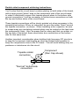
Double sided component soldering instructions:
You’ll notice that the circuit board contains plating on both sides of the board,
with a large ground “plane” area on the component side of the circuit board.
In order to electrically connect this topside ground plane to the bottom side
ground connections, it will be necessary to solder some connections on both
the top and bottom sides of the circuit board.
These topside connections will be clearly pointed out when necessary in the
assembly instructions. When so instructed, be sure the solder “flows” around
the topside connection, as shown. When installing a disc capacitor, be sure
to scrape away any insulating material which may be coated on the lead near
the components’ body. Also, be aware that for every part that you solder on
the top side of the board, there should also be a connection on the bottom
side for that same lead.
Another important consideration when building high frequency RF circuits is
to keep the component lead lengths as short as mechanically possible to
keep the components close to the PC board. This will avoid adding stray capacitance or inductance into the circuit.
Component
(Disc Cap shown)
Topside solder
connection
5
"Normal" bottomside
connection
LPA1 • 6
RAMSEY LPA1 Power Booster Amplifier Parts List
SEMICONDUCTORS
❒ 1 MAR3 RF amplifier [Small, black, round on one side] (U1)
❒ 1 PNP transistor [marked 221334] (Q1)
❒ 1 MRF581 NPN power transistor [Small, black, round and marked
“581”] (Q2)
❒ 1 Red LED (D1)
CAPACITORS
❒ 8 .01uF disc capacitor [marked .01 or 103 or 10nF] (C1,2,4,5,6,7,8,9)
❒ 1 10uF electrolytic (C3)
INDUCTORS
❒ 1 VK200 inductor [black ferrite core and bare wire to wind through it]
(L1)
❒ 1 5.6uH inductor [resembles a resistor marked green-blue-goldyellow] (L2)
RESISTORS
❒ 1 6.8 ohm resistor [blue-grey-gold] (R2)
❒ 4 1K ohm resistor [brown-black-red] (R1,5,6,7)
❒ 1 150 ohm resistor [brown-green-brown] (R4)
❒ 1 10K ohm resistor [brown-black-orange] (R3)
❒ 1 220 ohm resistor [red-red-brown] (R8)
MISCELLANEOUS
❒ 1 Power jack (J1)
❒ 2 RCA jacks (J2,3)
❒ 1 PB switch (S1)
REQUIRED, NOT SUPPLIED
❒
Power source, 12 VDC
❒
Enclosure, Ramsey CLPA or equal
❒
Transmitter (You know, the thing that you want to amplify!)
❒
Receiver (You know, the thing that you want to use to hear what you
amplify!)
LPA1 • 7
LPA1 • 8
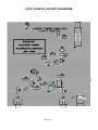
LPA1 PARTS LAYOUT DIAGRAM
LPA1 • 9
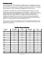
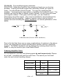
Feedback Circuit:
Your Ramsey LPA1 Power Booster Amplifier has been designed to give you
great amplification over a wide range of frequencies. Included in the design
of the circuit is a feedback loop consisting of the parts R8 and C5. You must
decide whether or not to include the feedback circuit into your kit.
According to the table below, with the feedback circuit in place, you may
experience a lower gain at frequencies up to 500Mhz. However, you will
note that this gain is relatively steady over this range. The loop also provides
slightly higher gain above 500Mhz. Please consider carefully which
frequency you are using and how much gain you require from the circuit.
Installing the feedback circuit has proven to add more circuit stability and
immunity to spurious signals. If you are experiencing difficulty with spurious
signals, it is a good idea to install the feedback circuit.
A good rule of thumb is to complete the circuit including the feedback circuit.
If you need more gain at lower frequencies, you are then able to remove the
feedback components.
Amplifier gain vs. frequency
Frequency
(Mhz)
Gain (dB)
w/o feedback
Gain
w/o feedback
Gain (dB)
w/ feedback
Gain
w/ feedback
10
36.4
4365
30
1000
50
35.7
3715
29.6
912
100
34.4
2754
28.9
776
200
30.6
1148
28.7
741
300
26.8
479
27
501
400
24.2
263
25.5
355
500
22
158
23.9
245
600
20.3
107
22.3
170
700
17.4
55
18.6
72
800
15.7
37
16.6
46
900
16.5
45
16.9
49
1000
16
40
16.4
44
LPA1 • 10
Now we will begin building our kit. There are just a few more things to know
before we put the first components in.
For each part, our word “Install” always means these steps.
1
2
3
4
Pick the correct value to start with.
Insert it into the correct PC board location.
Orient it correctly, following the PC board drawing and the written
directions for all parts - especially when there’s a right way and a wrong
way to solder it in. (Electrolytic capacitor polarity, transistor shapes,
dotted and notched ends of parts, and so forth.)
Solder all connections unless directed otherwise. Use enough heat and
solder flow for clean, shiny, completed connections.
Please take us seriously when we say that good soldering is essential to the
proper operation of your amplifier!
•
•
•
•
Use a 25 Watt soldering pencil with a clean, sharp tip.
Use only rosin core solder intended for electronics use.
Use bright lighting, a magnifying lamp or bench-style magnifier may be
helpful.
Do your work in stages, taking breaks to check your work. Brush away
any wire cuttings so that they don’t lodge between solder connections.
Since you may appreciate some “warm-up” soldering practice as well as a
chance to put some “landmarks” on the PC board, we’ll first install some
“hardware” components. This will also help us to get acquainted with the up down, left - right orientation of the circuit board.
❒
1. Install J2, the output RCA jack. Mount it flush with the board, making
sure that it is sitting on the “component side.” The component side is the
side that is almost completely covered with copper. The bottom side, or
foil side, is the one with traces on it. Solder each lead to the bottom side
of the board, making sure that the solder “flows” around all three
connections.
❒
2. Turn the board over to the top side and solder the connector mounting
flange securely to the board. There is no need to use a ton of solder, but
use enough to hold the connector firmly in place.
❒
3. Install J3, the input RCA jack. Mount it the same way that you did the
first one. Remember to solder the connections on the right and left sides
to both the top and bottom sides of the board.
LPA1 • 11
❒
4. Install J1, the power jack. This is a black plastic jack. Solder the
connection on the back of the jack to the bottom side of the board. Now,
solder the other connection to both the bottom and the top sides.
❒
5. Install S1, the main switch. The switch is black, with a white button
coming out of it. Solder all six pins.
First we are going to install the power circuit. This circuit, containing R5, C3
and D1 light up the LED when the switch is on. After that, we will construct
the part of the circuit that powers the MAR3.
❒
6. Install R5, 1K ohm resistor [brown-black-red]. All resistors must be
mounted flush with the board.
❒
7. Install C3, 10uF electrolytic capacitor. C3 has “polarity.” Polarity
means that the capacitor must be inserted a certain way. You may notice
that on one side of the capacitor, there is a black stripe with minus signs.
This is the negative end. Looking at the parts layout diagram, you will
notice the positive side marked. When looking at the board from the
front (switch and LED side) the black stripe should be to the left when
properly installed. Capacitors allow AC waves to pass, while blocking off
DC power. C3 filters off any noise in the power circuit into ground before
it can affect the circuit.
❒
8. Install D1, the LED. The flat edge (and the shorter leg) must face
towards the switch. If the LED is backwards, it will not light.
❒
9. Solder the topside connection of the LED leg closest to the switch.
You have now completed the power circuit.
❒
10. Install R4, 150 ohm resistor [brown-green-brown].
❒
11. Install L2, 5.6uH inductor [green-blue-gold-yellow]. It will look like a
large resistor. It does not have any polarity, so it can be mounted in any
direction, and should be mounted as close to the board as you can. L2 is
called a “choke,” and is used to prevent the RF signal from getting up
into the rest of the circuit.
❒
12. Install C4, .01 uF disc capacitor [marked .01 or 103 or 10nF]. In
order to get the capacitor as close as possible to the board, take a pair of
needle nose pliers or a sharp knife and scratch away or crack off the
insulation on the legs of the capacitors. (Be careful not to break their
legs off. Capacitors have feelings too!) Solder the connection closest to
the outside of the board on both the top and bottom sides of the board.
LPA1 • 12
Now that we have completed the power circuits, we will move on to the
biasing circuit. This circuit holds the transistor output voltages in the desired
range.
❒
13. Install C1, .01uF capacitor [marked .01 or 103 or 10nF]. Make sure
that you crack or peel off the insulation on the legs of the capacitor.
Solder the topside connection closest to the outside of the board
(towards the switch side) on both the top and bottom sides of the board.
This capacitor is also known as a power bypass capacitor because it
bypasses any RF energy to ground.
❒
14. Install R1, 1K ohm resistor [brown-black-red].
❒
15. Install R3, 10K ohm resistor [brown-black-orange]. Solder the lead
closest to C2 on the top side as well as the bottom side. R1 and R3 hold
a constant voltage on the base of Q1. This allows Q1 to act as a current
source.
❒
16. Install R2, 6.8 ohm resistor [blue-grey-gold].
❒
17. Install R6, 1K ohm resistor [brown-black-red]. Solder the lead
closest to the LED to the top side as well as the bottom side.
❒
18. Find C2, .01uF capacitor [marked .01 or 103 or 10nF]. Take off the
insulation on it’s legs and install the part. Solder the leg closest to the
LED to the top side of the board in addition to the bottom connections.
Don’t forget to take the insulation off of the legs. C2 keeps any RF energy
from affecting the bias voltage on Q2.
❒
19. Install R7, 1K ohm resistor [brown-black-red].
❒
20. Install Q1, PNP transistor [marked 221334]. You will notice that the
transistor has a flat side with no writing on it. This side must face away
from the RCA jacks.
❒
21. Insert L1, VK200 inductor. Look for a ferrite bead with 6 holes and a
piece of bare wire that you will need to “lace” through the holes as
shown. Pass 1 1/2 turns through the holes, filling three holes and leaving
a lead coming out at each end. Trim the ends to 1/4“ and bend as
needed for neat installation. Solder it so that it is laying flush with the
board.
LPA1 • 13
❒
22. Install C9, .01uF capacitor [marked .01 or 103 or 10nF]. The
insulation should be stripped from the legs and a topside connection
made nearest the edge of the board.
Now that you have installed the biasing circuit, we have only a few more
parts to put in before we install the amplifiers. This is a good time to look
back over your work and look for misplaced parts and bad solder joints. You
should take a rest now if you need one.
Take a look at the table on page 10. This table shows the gain of your Power
Booster Amplifier at certain frequencies. The higher the gain, the more
power your kit will put out with the same input signal. Using the table to aid
you, decide whether or not you would like to insert the feedback circuit (R8
and C5). As a default, you should install R8 and C5.
❒
23. If you have decided to include the feedback circuit, install R8 now.
R8 is a 220 ohm resistor [red-red-brown].
❒
24. Install C5 only if you have decided to include the feedback circuit.
C5 is a .01uF capacitor [marked .01 or 103]. Be sure to take the
insulation off of the legs first.
❒
25. Install C7, .01 uF capacitor [marked .01 or 103 or 10nF]. Strip the
insulation off of the legs before installing.
❒
26. Install C8, .01 uF capacitor [marked .01 or 103 or 10nF]. Strip the
insulation off of the legs.
❒
27. Install C6, .01uF capacitor [marked .01 or 103 or 10nF]. Do you
really need to strip the insulation off of the legs? YES!
❒
28. Identify Q2, an MRF581 NPN Power Transistor. This part is round,
has four legs coming off of it and is marked “581”. You may notice that
there are two parts matching this description. Q2 is the larger of the two
parts, and the other, the MAR3 Amplifier, is smaller and has a “3” printed
on it.
❒
29. Turn over the board, so that the soldered side is up. You should see
a small “M” near one lead of the transistor. This “M” should be near the
lead closest to L1. If there are two “M” s on the part, orient the part using
the Motorola trademark “M”. Taking the two leads on either side of the
lead nearest the Motorola “M,” insert them through the two holes in the
board. These two leads both go to ground. Check to see that the “M” is
still closest to L1. Solder the two leads on the top and bottom sides of
the board.
30. With the two remaining leads flat against the underside of the board,
❒
LPA1 • 14
BOTTOM SIDE OF BOARD
SOLDER
BEND LEGS THROUGH
BOARD AND SOLDER
ON BOTH SIDES
SOLDER
NOTE: BEFORE SOLDERING
PART, MAKE SURE THAT
THE MARKING IS ORIENTED
AS SHOWN IN THE PARTS
LAYOUT DIAGRAM!
SOLDER
COMPONENT SIDE
FOIL SIDE
SOLDER
MAR3 OR Q2
SOLDER
solder them directly onto the board. All four leads should now be
connected. Again, make sure that the small “M” is closest to L1. This is
very important.
❒
31. Find U1, the MAR3 amplifier. This looks like Q2, which you have
just installed, but is a bit smaller and has a dot printed on it. The leg
nearest this dot should be towards the outside of the board (or towards
C7). Insert the two legs on each side of the dot into the board, mounting
the part on the underside of the board.
❒
32. Again, make sure that the leg nearest the dot is also nearest C7. If it
is mounted properly, solder the two remaining legs flat on the underside
of the board.
Congratulations! You have just completed your LPA1 Power Booster
Amplifier. Please take a few minutes to look over your kit and ensure that all
of the parts have been assembled correctly. Since a few of the parts may be
unfamiliar to you, you may want to be extra sure that they have been inserted
correctly. Also, make sure that you have soldered all of the top side
connections in the correct spots. If you soldered the wrong connections,
your project may not work. After you are sure that everything seems to be
properly installed, move on to the setup and testing section. You will need a
12 volt supply, your transmitter, and a receiver.
LPA1 • 15
Setup and testing
Now you are ready to set up and test your amplifier. Follow the steps below.
If you have any problems, refer to our troubleshooting section.
❒
1. Plug your kit into a 12V power source with the switch on your LPA1
turned off (click it until it is in the “out” position). You should not see the
LED light up.
❒
2. Turn on the switch. The LED should light up and stay on.
❒
3. Turn on a (preferably portable) receiver to the same frequency as the
transmitter. You may need to transmit to make sure that the two units
are working properly.
❒
4. Plug the output of your transmitter into J3, the input jack. Plug your
antenna cable into J2, the output jack. Turn on the switch again. You
should be able to receive the transmitted signal. You are probably too
close to notice any increased power difference, so you may want to
move the receiver away from the transmitter and try to see how far it will
transmit. With such great amplification, the LPA1 should increase your
transmitting distance several times, and you may find yourself going far
away from your house!
That’s all that you need to do to test it out. You may now use your LPA1 for
it’s intended purpose. You do not need to do anything else to use it because
you have just set it up during testing.
Troubleshooting
PROBLEM: The LED does not light when I turn it on.
SOLUTION: Even if the LED doesn't work, your amplifier may. First
measure the voltage on the leg or R5 closest to the switch. If it does not
measure near 12V, you have a problem with the power supply, power jack or
the switch is not on. You may also have soldered a topside connection
where you shouldn’t have. Check to be sure that D1 is installed the correct
way (flat side towards switch).
PROBLEM: The LED comes on, but the amplifier is not working.
SOLUTION: Make sure that the MAV3 and Q2 are installed properly. The
dot on the MAV3 should point towards C8. The “M” on Q2 should point
towards C6. Next, check the placement and orientation of all parts. You
may also have incorrectly soldered a topside connection where you shouldn’t
have. A good place to check would be the topside connections of the jacks
themselves.
LPA1 • 16
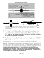
PROBLEM: The amplified signal is distorted.
SOLUTION: Make sure that all of the component leads are as short as
possible. Leaving the leads longer than necessary leaves you open for
noise. You should also check the gain. You may be overdriving the
amplifier. Try lowering the input power or installing the feedback circuit. The
amplifier will only be able to deliver a watt of power, so any more will cause
your signal to distort. If the gain is still too high, you can install an
attenuating circuit like shown. The circuit is installed in series between the
transmitter and the amplifier. Tables of resistor values can be found in
various sources including the ARRL Handbook, an annual publication of the
ARRL.
16dB attenuator (Source: ARRL Handbook)
Due to the fact that there are so many combinations of resistors in the above
circuit, we regret that we cannot provide either resistor values or technical
support. The ARRL handbook can be obtained by ordering direct from the
ARRL, or may be found at your local Radio Shack.
Ordering Amplifier Parts:
For convenience, we offer the following parts by mail request only. Please
do not call - complete and mail the order form. This saves you the small
order fee and normal handling charge.
Component
Qty
Price (ea)
MAR 3 RF AMP
$8.10
MRF 581 NPN
$8.85
221334 PNP
$.95
Postage & Handling
TOTAL
LPA1 • 17
SubTotal
$
1.00
Conclusion
We sincerely hope that you have enjoyed the construction of this Ramsey
Kit. As always, we have tried to compose our manual in the easiest, most
“user friendly” format that is possible. As our customers, we value your
opinions, comments, and additions that you would like to see in future
publications. Please submit comments or ideas to:
Ramsey Electronics
Attn. Hobby Kit Department
590 Fishers Station Drive
Victor, NY 14564
Thanks again, from the folks at Ramsey.
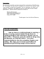
USAGE WARNING
Just as there is nothing illegal in owning a
knife or using a prescription drug, there is
nothing illegal in the owning or proper use of
the LPA-1. However, just as a knife or drug may
be abused, so may the LPA-1. It is your
responsibility to use this amplifier legally and
safely. We urge you to know and follow all
guidelines governing usage of this device.
LPA1 • 18
The Ramsey Kit Warranty
Please read carefully BEFORE calling or writing in about your kit. Most problems can be
solved without contacting the factory.
Notice that this is not a "fine print" warranty. We want you to understand your rights and ours too! All
Ramsey kits will work if assembled properly. The very fact that your kit includes this manual is your
assurance that a team of knowledgeable people have field-tested several "copies" of this kit straight
from the Ramsey Inventory. If you need help, please read through your manual carefully, all
information required to properly build and test your kit is contained within the pages!
1. DEFECTIVE PARTS: It's always easy to blame a part for a problem in your kit, Before you conclude
that a part may be bad, thoroughly check your work. Today's semiconductors and passive components
have reached incredibly high reliability levels, and it’s sad to say that our human construction skills
have not! But on rare occasions a sour component can slip through. All our kit parts carry the Ramsey
Electronics Warranty that they are free from defects for a full ninety (90) days from the date of
purchase. Defective parts will be replaced promptly at our expense. If you suspect any part to be
defective, please mail it to our factory for testing and replacement. Please send only the defective part
(s), not the entire kit. The part(s) MUST be returned to us in suitable condition for testing. Please be
aware that testing can usually determine if the part was truly defective or damaged by assembly or
usage. Don't be afraid of telling us that you 'blew-it', we're all human and in most cases, replacement
parts are very reasonably priced.
2. MISSING PARTS: Before assuming a part value is incorrect, check the parts listing carefully to see
if it is a critical value such as a specific coil or IC, or whether a RANGE of values is suitable (such as
"100 to 500 uF"). Often times, common sense will solve a mysterious missing part problem. If you're
missing five 10K ohm resistors and received five extra 1K resistors, you can pretty much be assured
that the '1K ohm' resistors are actually the 'missing' 10 K parts ("Hum-m-m, I guess the 'red' band
really does look orange!") Ramsey Electronics project kits are packed with pride in the USA. If you
believe we packed an incorrect part or omitted a part clearly indicated in your assembly manual as
supplied with the basic kit by Ramsey, please write or call us with information on the part you need
and proof of kit purchase
3. FACTORY REPAIR OF ASSEMBLED KITS:
To qualify for Ramsey Electronics factory repair, kits MUST:
1. NOT be assembled with acid core solder or flux.
2. NOT be modified in any manner.
3. BE returned in fully-assembled form, not partially assembled.
4. BE accompanied by the proper repair fee. No repair will be undertaken until we have received the
MINIMUM repair fee (1/2 hour labor) of $25.00, or authorization to charge it to your credit card
account.
5. INCLUDE a description of the problem and legible return address. DO NOT send a separate letter;
include all correspondence with the unit. Please do not include your own hardware such as
non-Ramsey cabinets, knobs, cables, external battery packs and the like. Ramsey
Electronics, Inc., reserves the right to refuse repair on ANY item in which we find excessive
problems or damage due to construction methods. To assist customers in such situations,
Ramsey Electronics, Inc., reserves the right to solve their needs on a case-by-case basis.
The repair is $50.00 per hour, regardless of the cost of the kit. Please understand that our technicians
are not volunteers and that set-up, testing, diagnosis, repair and repacking and paperwork can take
nearly an hour of paid employee time on even a simple kit. Of course, if we find that a part was
defective in manufacture, there will be no charge to repair your kit (But please realize that our
technicians know the difference between a defective part and parts burned out or damaged through
improper use or assembly).
4. REFUNDS: You are given ten (10) days to examine our products. If you are not satisfied, you may
return your unassembled kit with all the parts and instructions and proof of purchase to the factory for
a full refund. The return package should be packed securely. Insurance is recommended. Please do
not cause needless delays, read all information carefully.
LPA1 • 19
LPA1 POWER BOOSTER AMPLIFIER
Quick Reference Page Guide
Introduction to the LPA1 ................... 4
How it works ..................................... 4
LPA1 Parts list .................................. 7
Schematic diagram ........................... 8
Parts Layout diagram ....................... 9
Feedback circuit considerations ....... 10
LPA1 Assembly instructions ............. 11
Setup and testing ............................. 16
Troubleshooting................................ 17
Ramsey kit warranty ......................... .19
REQUIRED TOOLS
• Soldering Iron Ramsey WLC100
• Thin Rosin Core Solder Ramsey RTS12
• Needle Nose Pliers Ramsey MPP4 or RTS05
• Small Diagonal Cutters Ramsey RTS04
<OR> Technician’s Tool Kit TK405
ADDITIONAL SUGGESTED ITEMS
•
•
•
Holder for PC Board/Parts Ramsey HH3
Desoldering Braid Ramsey RTS08
Digital Multimeter Ramsey M133
Price: $5.00
Ramsey Publication No. MLPA1
Assembly and Instruction manual for:
RAMSEY MODEL NO. LPA1
POWER BOOSTER AMPLIFIER
RAMSEY ELECTRONICS, INC.
590 Fishers Station Drive
Victor, New York 14564
Phone (585) 924-4560
Fax (585) 924-4555
www.ramseykits.com
LPA1 • 20
TOTAL SOLDER POINTS
74
ESTIMATED ASSEMBLY
TIME
Beginner............... 2.3 hrs
Intermediate ......... 1.3 hrs
Advanced ............. 1.0 hrs