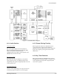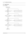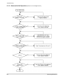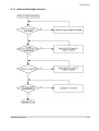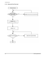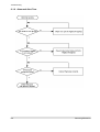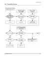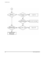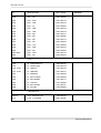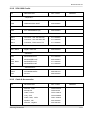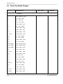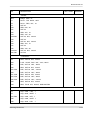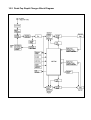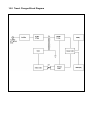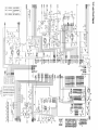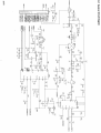
1
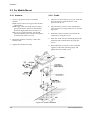
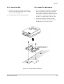
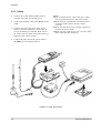
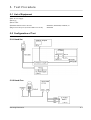
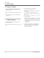
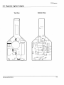
CDMA PORTABLE
PCS TELEPHONE
SCH-1900
SERVICE
CDMA PORTABLE PCS TELEPHONE
Manual
CONTENTS
1. Specification
2. Installation
3. NAM Programming
4. Circuit Description
5. Test Procedure
6. Troubleshooting
7. Exploded Views and Parts List
8. PCB Diagrams
9. Electrical Parts List
10. Block & Circuit Diagrams
Samsung Electronics Co.,Ltd.
GH68-60620A
Printed in Korea.
1. Specification
1-1 General
Frequency Range
Transmitter
Receiver
: 1850 ° ≠1910 MHz
: 1930 ° ≠1990 MHz
Channel Bandwidth
: 1.23 MHz
Channel Spacing
: 50 KHz
Number of Channels
: 1200
Duplex Separation
: 80 MHz
Type of Emission
: G7 W
Input/Output Impedance
: 50 ohms
Intermediate Frequency
Transmitter
Receiver
: 130.38 MHz
: 210.38 MHz
Local Frequency
Transmitter
Receiver
: 1st (FTX-130.38), 2nd (260.76 MHz)
: 1st (FRX-210.38), 2nd (420.76 MHz)
TCXO Frequency
: 19.68 MHz
Frequency Stability
: (FRX - 80 MHz) °æ 150 Hz
Operating Temperature
: -30 °… ° ≠+60 °…
Supply Voltage
: +4.8 V
Current Consumption (Average)
Standby
Talk
: 150 mA (Non-slot mode)
: 400 mA (at +10 dBm)
Size and Weight
Including Standard Battery
Including Extended Battery
: 114(H)°ø49.8(W)°ø10.5(D), 118.67 g
: 114(H)°ø49.8(W)°ø20.5(D), 161.86 g
Samsung Electronics
1-1
Specification
1-2 Transmitter
Waveform Quality
: 0.944 or more
Open Loop Power Control Range
-25 dBm
-65 dBm
-104dBm
: -60.5 dBm ° ≠-41.5 dBm
: -20.5 dBm ° ≠-1.5 dBm
: +15.0 dBm ° ≠+30.0 dBm
Minimum Tx Power Control
: -50 dBm below
Closed Loop Power Control Range
: °æ24 dB
Maximum RF Output Power
: 200 mW (+23 dBm)
Occupied Bandwidth
: 1.23 MHz
Conducted Spurious Emissions @1.25MHz
: -42 dBc/30KHz
1-3 Receiver
Rx Sensitivity and Dynamic Range
(Rate Set 1)
: -104 dBm, FER=0.5% or less
: -25 dBm, FER=0.5% or less
Conducted Spurious Emission
1930 ° ≠1990 MHz
1850 ° ≠1910 MHz
All Other Frequencies
: <-81 dBm
: <-61 dBm
: <-47 dBm
Single Tone Desensitization
Rx power=-101 dBm
Tone power=-30 dBm
Tone offset from carrier=°æ1.25 MHz
: lower than 1%
Intermodulation Spurious Response Attenuation : lower than 1%
Rx power=-101 dBm
Tone power 1=-43 dBm
Tone power 2=-43 dBm
Tone 1 offset from carrier=°æ1.25 MHz
Tone 2 offset from carrier=°æ2.05 MHz
1-2
Samsung Electronics
2. Installation
2-1 Installing a Battery Pack
1.
2.
To attach the battery pack after charging, align
it with the phone about 1cm (1/2") away from
its place so that the two arrows on the phone
are seen, the battery charge contacts pointing
downwards.
3.
To remove the battery pack, release it by
pressing the button on the rear of the phone.
4.
Slide the battery pack downwards about 1cm
(1/2") and lift it away from the phone.
Slide the battery pack upwards until it clicks
firmly into position. The phone is now ready
to be turned on.
Press this button to release
the battery pack
2-2 For Desk Top Use
1.
Choose a proper location to install the charger
for desk top use.
2.
Plug the power cord of the charger into an
appropriate wall socket. When the power cord
is connected correctly, the lamps turn on
briefly.
3.
To charge the battery pack, insert the battery
pack into the rear slot of the charger. The lamp
marked BAT on the front panel of the charger
lights up red.
4.
If you do not wish to use the phone while
charging the battery, insert the phone with the
battery pack attached into the front slot of the
charger. The lamp marked PHONE on the
front panel of the charger lights up red.
Figure 2-1 Charging The Phone and Battery
Samsung Electronics
2-1
Installation
2-3 For Mobile Mount
2-3-1 Antenna
2-3-2 Cradle
1.
Choose a proper location to install the
antenna.
¶UThe center of the roof top provides the best
performance.
¶UThe edge of the rear trunk also provides a
good performance. However, the antenna
should be higher than the roof of the car.
¶UIn case of on-glass antenna, you should
align the antenna base with the round plate
to connect the cables correctly.
1.
Choose a location where it is easy to reach and
does not interfere with the driver's safe
operation of the car.
2.
Separate the two halves of the clamshell by
removing the two large slotted screws. See the
figure 2-2.
3.
Drill holes and mount the lower half of the
clamshell by using the screws.
2.
Mount the antenna vertically, connect the
antenna cable.
4.
Place the cradle onto the remaining half of the
clamshell and assemble them by using the
screws.
3.
Tighten the antenna nut fully.
5.
Reassemble the two halves of the clamshell
together. Adjust the mounting angle and
tighten the two slotted screws.
Figure 2-2 Cradle Installation
2-2
Samsung Electronics
Installation
2-3-3 Hands-Free Box
2-3-4 Hands-Free Microphone
1.
Drill holes in a proper location for the handsfree box, attach the mounting bracket by using
the screws. See the figure 2-3.
1.
2.
Install the hands-free box into the bracket.
It is recommended to install the microphone
where it is 30-45 cm (12-18") away from the
driver. Choose the location where is least
susceptible to interference caused by external
noise sources, ie, adjacent windows, radio
speakers, etc. Normal place is the sun visor.
2.
Once the microphone has been correctly
positioned, connect the microphone wire to
the MIC jack on the hands-free box.
Figure 2-3 Hands-Free Box Installation
Samsung Electronics
2-3
Installation
2-3-5 Cables
1.
Connect the cradle and the hands-free box
with the data cable. See the figure 2-4.
2.
Connect the antenna cable to the RF jack of the
cradle.
3.
Connect one end of the power cable to the
battery or ignition terminal. Connect the red
wire to the battery (+) terminal, black wire to
the vehicle chassis. Then connect the battery (-)
terminal to the vehicle chassis.
4.
Connect the other end of the power cable to
the PWR jack of the hands-free box.
Notes:
¶UIt is recommended to connect the power cable
directly to the battery to avoid power noise.
¶UMake sure the connection between the battery terminal and the vehicle chassis is made
correctly.
¶UMake sure the fuse having a proper capacity is
used on the power cable.
¶UMake sure the cables do not pass over any sharp
metal edge that may damage it.
Figure 2-4 Cable Connections
2-4
Samsung Electronics
3. NAM Programming
NAM features can be programmed as follows:
Notes:
-If you enter the NAM program mode, each item shows the currently stored data. Go to the next item by
pressing OK.
-You can modify the data by entering a new data.
-If you enter a wrong digit, press CLR to delete the last digit. Press and hold CLR to delete all digits.
-To scroll items backwards or forwards, press the VOLUME button on the left side of the phone.
3-1 General Setup
LCD Display
Key in
Function
MENU, 5, 0
-selects NAM programming
Enter Lock
??????
6-digit code
-Enter random 6-digit code (MSL)
SVC Menu°Ë°È
1:PCS Phone#
2:General
2
-choose 'GENERAL.'
Volume °„
-Electronic Serial Number of the phone is displayed
Volume °„
-Common Air Interface version is displayed
VOC13K/8K
SO_VOICE_13K
°Ëor°È
OK
-Select vocoder service option
-stores it
SCM
Volume °„
-Station Class Mark displays the power class,
transmission, slotted class, dual mode.
ESN
B0000000
CAI version
1
00001010
Lock
Code
0000
Slot Mode
No
4-digit code
OK
Lock code, current status is displayed
-to change, enter new code.
-stores it.
°Ëor°È
OK
Slot mode. 'Yes' indicates the slot mode.
-changes the status.
-stores it.
0-7
OK
Slot mode index. The higher, the longer sleeping time.
-to change, enter new one.
-stores it.
Slot Index
2
Samsung Electronics
3-1
NAM Programming
3-2 Setting Up NAM
LCD Display
Key in
Function
SVC Menu°Ë°È
1:PCS Phone #
2:General
Volume °„
-NAM Programming Menu is displayed
SVC Menu°Ë°È
3:NAM
3
-choose 'Setup NAM'
IMSI_MCC
310
number
OK
IMSI Mobile Country Code, current code is displayed.
-to change, enter new one.
-stores it.
00
number
OK
IMSI Mobile Network Code, current code is displayed.
-to change, enter new one.
-stores it.
IMSI_MNC
class number
OK
CDMA Access Over load Class, current status is displayed.
-to change, enter new one.
-stores it.
CDMA HomeSID
Yes
°Ëor°È
OK
CDMA Home system ID, current status is displayed.
-changes the status.
-stores it.
CDMA
fSID
Yes
°Ëor°È
OK
CDMA foreign SID, current status is displayed.
-changes the status.
-stores it.
CDMA
fNID
Yes
°Ëor°È
OK
CDMA foreign NID, current status is displayed.
-changes the system.
-stores it.
4120
number
OK
first SID written in the list, current status is displayed.
-to change, enter new one.
-stores it.
65535
number
OK
first NID written in the list, current status is displayed.
-to change, enter new one.
-stores it.
CDMA ACCOLC
0
SID
NID
3-2
Samsung Electronics
4. Circuit Description
4-1 Logic Section
4-1-1 Power Supply
With the battery installed on the phone and by
pressing the PWR key, the VBATT and ON_SW
signals will be connected. This will turn on
Q108(2SC4081). This in turn will be supplied to
pin 6 of regulators U110 and U111, thus releasing
them from the shut-down state to output
regulated 3.3V. And then the pin 8 of (U110) stays
High.
The VBATT applied to ON_SW turns on
Q113(DTC144) and will result in the signal
ON_SW_SENSE to change state from HIGH to
LOW. The MSM recognizes this signal and sends
out PS_HOLD(logical HIGH) to turn on
Q108 even after the PWR key is released.
The power from U110 is used in the digital part of
MSM and BBA. The power from U111 is used in
the analog part of BBA.
CPU
INTEL 80186 CMOS type 16-bit microprocessor is
used and CPU controls all the circuitry. For the
CPU clock, 27MHz is used.
FLASH ROM
One 8Mbit FROM is used to store the terminal's
program. Using the down-loading program, the
program can be changed even after the terminal is
fully assembled.
SRAM
One 2Mbit SRAM is used to store the internal flag
information, call processing data, and time data.
EEPROM
4-1-2 Logic Part
The Logic part consists of internal CPU of MSM,
RAM, ROM and EEPROM. The MSM receives
TCXO and CHIPX8 clock signals from the BBA
and controls the phone. The major components are
as follows:
¶UCPU
¶UFROM
: INTEL 80186 core
: U112 (MBM29LV800T)-8MBIT
FLASH ROM
¶USRAM
: U113(KM68V2000BLTI)-2MBIT
STATIC RAM
¶UEEPROM : U109(24LC65-1/SM)-64KBIT
SERIAL EEPROM
One 64Kbit EEPROM is used to store ESN, NAM,
power level, volume level, and telephone number.
KEY-PAD
For key recognition, key matrix is setup using
SCAN0-6 of STROBE signals and KEY0-2 of input
ports of MSM. Six LEDs and backlight circuitry are
included in the keypad for easy operation in the
dark.
LCD MODULE
LCD module contains a controller which will
display the information onto the LCD by 8-bit data
from the MSM. It also consists a DC-DC converter
to supply -3.3V for fine view angle and LCD
reflector to improve the display efficiency.
Samsung Electronics
4-1
Circuit Description
4-1-3 Base Band
MOBILE SYSTEM MODEM (MSM)
The MSM equipped with the INTEL 80186 CPU
core is an important component of the CDMA
cellular phone. The MSM comes in a 176 pins
TQFP package. The interface block diagram is
shown on page4-3.
MICROPROCESSOR INTERFACE
The interface circuitry consists of reset circuit,
address bus (A0-A19), data bus (AD0-AD15), and
memory controls (ALE,DT-R,HWR/,LWR/,
RAM_CS/,ROM_CS).
ADC Interface
ADC_CLK (pin3), ADC_ENABLE (pin1) and
ADC_DATA (pin2) are required to control the
internal ADC in the BBA.
Data Port Interface
Includes the UART. Also, supports Diagnostic
Monitor (DM) and HP equipment Interface.
CODEC Interface
INPUT CLOCK
°§CPU clock : 27 MHz
°§TXCO/4 (pin34) : 4.92 MHz. This clock signal
from the BBA is the reference clock for the MSM
except in CDMA mode.
°§CHIPX8 : 9.8304 MHz.The reference clock used
during the CDMA mode.
BBA INTERFACE
CDMA,Data Interface
°§TX_IQDATA0-7 (pin24-32) : TX data bus used
during both CDMA.
°§C_RX_IDATA0-3 (pins16-20) and
C_RX_QDATA0-3(pins 12-15) : RX data bus
used during CDMA mode.
The MSM outputs 2.048MHz PCM_CLK (pin19)
and 8KHz CODEC_SYNC (pin16,20) to the
CODEC (U102). The voice PCM data from the
MSM (U101)PCM_DIN (pin135) is compressed
into 13KHz by PureVoice algorithm in the CDMA
mode.
RF Interface
TX : TX_AGC_ADJ (pin35) port is used to control
the TX power level and PA_ON (pin44) signal is
used to control the power amplifier.
RX : AGC_REF (pin36) port is used to control the
RX gain and TRK_LO_ADJ (pin45) is used to
compensate the TCXO clock.
General Purpose I/O Register Pins
Input/output ports to control external devices.
Clock
°§TX_CLK(pin 22), TX_CLK/(pin23) : Digital to
Analog Converter(DAC) reference clock used in
TX mode.
°§CHIPX8 : ADC reference clock used in CDMA
RX mode.
4-2
Power Down Control
When the IDLE/signal turns LOW, only the TX
sections will be disabled.If both the IDLE/ and
SLEEP/ are changed to LOW, all the pins except
for the TXCO are disabled.
Samsung Electronics
Circuit Description
Figure 4-1 Baseband Block Diagram
4-1-4 Audio Section
TX AUDIO PATH
The voice signal output from microphone is
filtered and amplified by the internal OP-AMP
and is converted to PCM data by the
CODEC(U102). This signal is then applied to the
MSM(U101)'s internal vocoder.
RX AUDIO PATH
The PCM data from the MSM are converted to
audio signal by DAC of CODEC(U102),is then
amplified by the speaker amplifer(U105) to be sent
to the speaker unit.
4-1-5 Buzzer Driving Circuitry
Buzzer generates alert tone. When the buzzer
receives the timer signal from the MSM, it
generates alert tone. The buzzer level is adjusted
by the alert signal's period generated from the
MSM timer.
4-1-6 Key Tone Generator
Ring signal (pin49) from MSM(U101) is passed
through LPF consisting of R180, C119, R124, and
C120, amplified at the speaker amp(U105) and
come out to speaker.
VOLUME ADJUST
Volume can be adjusted up to 8 steps for the user
to obtain a proper loudness of received signal.
Samsung Electronics
4-3
Circuit Description
4-2 Receiver Section
LOW NOISE AMPLIFIER (LNA)
BUFFER
The low noise amplifier featuring 1.6dB Noise
Figure and 19dB gain amplifies a weak signal
received from the base station to obtain the
optimum signal level.
Buffer (Q311) amplifies the signal from the VCO
(U305) to be applied to the local input of the down
converter (U302) when a phase is locked between
U304 and U305.
DOWN CONVERTER (MIXER)
The VCO (U305) generates the signal having
1750MHz center frequency and °æ30MHz
deviation with the voltage control. PLL IC(U304)
controls this signal.
First local signal is applied to this down converter.
The down converter transfers the signal amplified
at the LNA into 210.38 MHz IF signal. 210.38MHz
IF signal is made by subtracting 1960°æ30MHz RF
signal from 1749.62°æ30MHz first local signal. The
LNA is Q303 and down converter is U302.
IF AMP
The IF amp (Q310) amplifies the output signal of
the down converter (U302).
RF IF AUTOMATIC GAIN CONTROLLER
(AGC) AMP
210.38 MHz IF signal is applied to IF AGC
amp,the AGC output level is applied to BBA (Base
Band Asic). The AGC amp (U303) keeps the signal
at a constant level by controlling the gain.
Dynamic range is 90dB, up gain +45dB, and down
gain -45dB.
RF BAND PASS FILTER (BPF)
The RF BPF(F302) accepts only a specific
frequency (1960°æ30MHz) from the signal
received from the mobile station. The bandwidth
is 60MHz.
PHASE LOCKED LOOP (PLL)
Input reference frequency is generated at
VCTCXO (U306) and the local signal is generated
at VCO. PLL compares the two signals and allows
the VCO controlled by voltage to generate the
desired signal with pre-programmed counter.
VOLTAGE CONTROLLED TEMPERATURE
COMPENSATED CRYSTAL OSCILLATOR
It provides 19.68MHz reference frequency to PLL
(U304) and BBA (U401). A correct frequency
tuning is made by the voltage control.
DUPLEXER
Duplexer (F301) controls to transmit through the
antenna only the signals within acceptable Tx
frequency range (1880°æ30MHz) and to receive
through the antenna only the signals within
acceptable Rx frequency range (1960°æ30MHz). It
also matches LNA(Q303) input in receiving part
and PA output in transmitter part with the
antenna.
IF SAW BAND PASS FILTER FOR CDMA
IF SAW BPF (F303) is used for CDMA system
having 1.23 MHz wide band and °æ630kHz band
width. The filter also eliminates the image product
generated at the mixer.
4-4
Samsung Electronics
Circuit Description
4-3 Transmitter Section
POWER AMP MMIC
ANTENNA
Power Amp MMIC (U407) amplifies signal to be
sent out to the base station through the antenna.
ANT1 allows signals to send and to receive to
from the base station.
DRIVER AMP
RF BAND PASS FILTER (BPF)
The driver amp (Q413) allows the input signal to
the power amp MMIC(U407) to be within a
specified level.
The RF BPFS (F402, F403) accept only a specific
frequency (1880°æ30MHz) to send it out to power
amp MMIC. The bandwidth is 60MHz.
UP CONVERTER (MIXER)
POWER SUPPLY SWITCHING
The up-converter (U405) receives the first local
signal to generate 1880°æ30MHz from the signal
controlled by TX AGC amp (U404). 1880°æ30MHz
signal comes out of the mixer output by adding
130.38MHz IF signal to 1749.62°æ30MHz first local
signal. The driver amp's reference number is Q413
and up converter's reference number is U405.
Power supply switching (Q412) turns on TX
POWER when the phone is in traffic mode and
supplies power to the circuits.
IF AUTOMATIC GAIN CONTROLLER AMP
The signal output from BBA (Base Band ASIC)
should be a constant level. The TX IF AGC amp
(U404) controls power to keep the signal at a
desired level. Dynamic range is 85 dB, up gain
+40dB, and down gain -45dB.
POWER SUPPLY REGULATOR
ISOLATOR
Isolator (I401) is used to reduce a reflected signal
to protect the power amp MMIC from being
damaged.
POWER SUPPLY REGULATOR
The power supply regulator (U413,U414) supplies
a regulated power to each part of transmitter.
U413 supplies 4.8V to Tx driver (Q413) and Power
Amp MMIC (U407). U414 supplies 4.2V to the
others.
The power supply regulator (U414) generates the
regulated power.
Samsung Electronics
4-5
Circuit Description
4-4 Hands-Free Kit
Hands-free board is largely composed of car
adapter circuit and Hands-free circuit.
4-4-1 Car Adapter Circuit
POWER SUPPLY
Input power switching circuit : This circuit
includes Short protection circuit, and Power
switching control circuit. It supplies power for
HHP and hands-free kit.
+13.5V switching circuit (Q801, 802) : This circuit
switches power for power amplifier using MPU
mute signal.
HHP power circuit : This circuit is Switching
regulator. Input voltage is +13.6v, output voltage
is +5.8v.
Vcc regulator (U704) : This circuit regulates Vcc
(+5V).
CHARGER CIRCUIT
This circuit charges battery pack by detecting the
temperature of battery, the slope of temperature,
the slope of the voltage of battery, and charging
time, etc.
During charging, the charger LED turn on red.
When charging is completed, the charger LED
turns on green.
Battery Type Capacity
Temperature detection circuit : The temperature
of battery is measured by missing NTC thermistor.
NTC themistor has a characteristics of Log-scale. It
obtains a linear characteristics by the parallel
connection of resistors.
4-4-2 Hands-free Circuit
POWER SUPPLY (U704,U808)
+5V is regulated by U704 for hands-free circuit,
and -5V is regulated by U808.
TX PATH
The audio signal from external mic(JP705) flows
into U802 pin #11. U802 includes Amplifier and
Control circuit for hands-free operatin. U801A
amplifies input signal. Output signal is
transmitted to HHP.
RX PATH
Input audio signal cancels noise by difference
amplifier (U801c). U802 performs hands-free
action. The RX audio signal is input (U805). The
speaker drive amp (U804) amplifies the Rx audio
signal and the output of U804 goes out of speaker.
Charge Current Charge Voltage
Standard
850mAH
300mA
6.2V
Extended
1500mAH
600mA
6.7V
4-6
Voltage detection circuit : Charging circuit is
designed to stop charging when the voltage of
battery is dropped.
The voltage of battery is entered to A/D converter
located in U703 #2.
Samsung Electronics
Circuit Description
4-5 Desk-Top Rapid Charger
4-5-1 SMPS
4-5-2 Constant Current Circuit
1ST SWITCHING CIRCUIT
U2 (TL494) has two error-amps. VREF (+5V) is
supplied to INV terminal (pin 15) of amp 1 and
N.INV terminal (pin 16) is connected to ground. It
causes the amp 1 output to be zero. In amp 2, the
reference voltage 2.0V is supplied to INV terminal
(pin 15) through R37 and R38, and the voltage
obtained in proportion to constant current is
supplied N.INV terminal (pin 16). The constant
current circuit also includes the shunt resistor R40,
and Q21 and U7.
The AC current from AC plug transfers to a highvoltage DC through BD1, C2, and C3. TNR1 is AC
surge protector, and F1 is fuse to protect circuit
from overcurrent . The line filter composed of LF1
and C1 is used to protect from line noise and
switching noise.
The transferred DC voltage is switched by T1. 2nd
switching voltage is flattened into AC through D20
and C22, and filtered through L20 and C30.
The voltage is regulated through shunt regulator
U5, R28, R29.
2ND SWITCHING
The regulated voltage through 1st switching
circuit performs 2nd switching. Step-down
regulator is composed of Q20, U2, D22, L21, and
C25. Q20 performs high-speed switching
according to the output signal from U2. L21 stores
energy when the switching transistor turns on.
D22 is a fly-wheel diode and transfers the stored
energy when Q20 turns off.
Voltage mode PWM IC U2 controls duty cycle
between the switching on and off of Q20. C30 and
R34 are parameter to determine the switching
frequency of U2.
FAST CHARGING (MASTER MODE)
The fast charging formula is shown below.
ICHG =
R39
R40 x (R43 + RR)
x VREF (mA)
<RR=330ߟ, VREF=2.0 V>
For standard battery, RR is set with 680 ohm, and
for slim battery, 1 kohm is used.
SLOW (SLAVE MODE) AND TRICKLE
CHARGING
If batteries are installed both on front and rear port
of the desktop charger, the one installed in
advance performs fast charging while the other
installed later performs slow charging. In slave
mode, Q23 turns off. In trickle charging mode, Q24
turns off. The slow charging formula is shown
below.
ICHG =
R39
R40 x (R42)
x VREF (mA)
<VREF=2.0 V>
Samsung Electronics
4-7
Circuit Description
4-5-3 Master and Slave Mode
MPU(11)
CUR_CTRL
MPU(4)
CHG_A
MPU(3)
CHG_B
Fastcharging on front port
HIGH
LOW
HIGH
LOW
LOW
Fastcharging on rear port
LOW
HIGH
LOW
LOW
LOW
Front port master charging
Rear port slave charging
HIGH
LOW
LOW
LOW
HIGH
LOW
LOW
LOW
HIGH
LOW
HIGH
LOW
LOW
LOW
HIGH
LOW
LOW
LOW
HIGH
LOW
HIGH
LOW
LOW
HIGH
HIGH
Signal
Status
Rear port master charging
Front port slave charging
Fast charging on front port
Trickle charging on rear port
Fast charging on rear port
Trickle charging on front port
Trickle charging on both front and rear ports
MPU(13)
MPU(9)
FRNT_GRN REAR_GRN
4-5-4 Watch Dog and Reset Circuit
4-5-6 Temperature Detection
MPU U1 Reset pin is active in low state. U4 is used
as A/D reference voltage for MPU and whole
charging system, so the circuitry composed of
Q30-Q32 and D30 detects the voltage. In normal
state, Q31 turns on so U4 pin 3 becomes low. It
causes MPU Reset to be high. If an excessive
impulsive voltage is supplied to U4, Q30 turns on,
and U4 pin 3 becomes high. It causes MPU to be
reset.
The battery temperature and ambient temperature
can seriously damage Ni-MH battery, so the
temperature is constantly detected by MPU. The
ambient temperature is detected by MPU pin 19
through R54, TH1, and R56. The battery
temperature is detected by R45, R46, and NTC,
and measured as A/D value by MPU pin 20.
4-5-7 Charging Voltage Detection
4-5-5 Timer
Timer is used to protect the battery from being
overcharged. The timer is set at initial routine. If
fast charge is not completed until maximum time
value, fast charge is stopped by the timer and it
moves to automatic trickle charge routing. This is
the final step to protect battery from excessive
charging and damage. There are four timers
available, and the default timer is 140 minutes.
4-8
Time (minute)
Time-1 (RX1)
Time-2 (RX2)
140
VCC
VCC
210
GND
VCC
280
VCC
GND
350
GND
GND
The charging voltage of the battery is detected by
R47 and R48, and measured as A/D value by MPU
pin 18. The parameters, -ßEV, 0 ßEV, and Vmax,
used for checking charge level are also measured
by MPU.
4-5-8 Discharging Circuit
Discharging is available on the rear port only.
When MPU pin 14 acknowledges that the
discharging button is pressed, MPU pin 2 starts
discharging. Discharging is initiated immediately
when the button is pressed for over than 0.7
seconds within 30 seconds after battery installed. If
the voltage reaches 1 V/cell by discharge,
discharging stops, then fast charging starts
automatically.
Samsung Electronics
Circuit Description
4-6 Cigarette Lighter Adapter
4-6-1 Funtional Specification
SUMMARY
FUNCTIONS OF CLA
This standard describes on the specifications of
CLA(Cigarette Lighter Adaptor) for the SCH-1000
of SAMSUNG.
CLA AS ADAPTOR AND CHARGER
¶UAdaptor
directly supplies power in order to operate
cellular phone independent of the battery pack.
¶UCharger
for the NiMH battery pack
ELECTRICAL SPECIFICATION
¶UInput Voltage :
11V to 16.5V DC
(normal voltage : 13.5V DC)
¶UOutput Current
- HHP POWER : supplies 100mA if cellular
phone mode is in stand_by state and 300mA
to 600mA in carrier_on state.
- Battery Charge Current : 390mA +/- 10%
(carrier_off) 10ßðæ10ßÃ(carrier_on, full_charge)
¶UProtection Circuit
Protection Circuit is the circuit against the
electrical stress which is occured at
unexpected conditions of the source power of
CLA unit such as reverse voltage or overcurrent.
¶UDetection of cellular phone
If cellular phone is connected to CLA, the
CLA lamp is on to display whether charge
will be done normaly or not.
¶UDetect Carrier-On
In the case of Carrier-On, CLA detects the
resistance of the Cellular Phone and reduces
the charge current.
¶UDetect Full-Charge
If the temperature of the battery pack is
higher than the temperature outside of the
cellular phone, CLA detects the battery fully
charged and the state will be converted to the
Trickle Charge.
CLA CURL CABLE CONNECTION
¶UOutput Voltage (when 2K•ÿ is loaded to the
battery charge terminal)
- Battery Charge Terminal : 5.8°æ0.5V
- HHP POWER Terminal : 5.8V(+/- 0.3V)
¶URipple & Noise : 50mVp-p
PIN NO(CLC)
Description
PIN NO(HHP)
¶UNormal Fuse Capacity : 250V, 2A
#1
HHp Power
12 or 13
¶UCharge Time : 3Hrs. at 850mAh6Hrs. at
1500mAh
#2
BATT
16
#3
Thermistor
15
#4
C/F
3
#5
GND
ENVIRONMENTAL SPECIFICATION
2 or 4 or 6
¶UTemperature
- Operating Temperature : 0°… to 50°…
- Storage Temperature : -20°… to 85°…
¶UHumidity
- Operating Humidity : 5% to 90%
- Storage Humidity : 5% to 95%
Samsung Electronics
4-9
Circuit Description
4-6-2 Schematic Description
DC-DC CONTROLLER
PREVENT CHARGE CIRCUIT IN THE CASE
OF MOBILE PHONE CARRIER-ON
KA7500B(U1) is DC-DC Controller. It reads the
voltage difference between E1I+ Port and E1I- Port
and controls time to turn on Q1. E2I+ and E2Iturn on Q1 in the same way. U1 also supplies +5V
of Reference Voltage(Vref).
In the case of Mobile Phone carrier-on, the voltage
loaded on PIN-13 of U3D is lower than that of
PIN-12. So PIN-14 ouputs HIGH and Q3 is TURN
ON again. It results to the Prevent Charge.
STATIC CURRENT
LED-DRIVING CIRCUIT
E1I- Port of U1 detects about 1.25V untill FullCharge and controls the TURN ON time of Q1 in
order to detect 1.25V at E1I+ Port. To make the
E1I+ Port detect 1.25V continuously, 0.19V of
voltage reduction will be generated on R4. At the
equation of V=I*R, the current of R4 is around
390mA and it will be the charge current.
When battery is inserted to CLC, the voltage
loaded to PIN-2 of U3A is lower than that of PIN-3
and PIN-1 outputs HIGH. This TURN ON Q7 and
drives LED.
BATTERY CHARGE CURRENT CUTTING BY
RELATIVE TEMPERATURE
Although every battery sample applied to the
SCH-1000 has almost the same battery
temperature at Full-Charge, it varies according to
the relative temperature.
So the battery temperature at Full-Charge may be
different according to the temperature around the
cellular phone.
If Full-Charge occures at 25°…, the voltage of U3C
to which the battery thermistor is connected is
around 2.11V and the voltage of the parallel
resistance of Th1 and R18 is about 2.11V. PIN 8 of
U3C will be HIGH and turn on Q3 if the
temperature is up. This generates the voltage
detected at E1I- of U1 around 0.1V and the charge
current reduces to 40mA. If Full-Charge occurs at
high temperature and low temperature, the battery
temperature varies and the voltage decline of Th1
and R18 relatively varies. So the battery FullCharge condition will be fulfilled.
4-10
Samsung Electronics
Circuit Description
4-7 Travel Charger
4-7-1 Input Filter and Regulator
4-7-4 Battery Charging
The AC input converts to a high-voltage DC
through overcurrent protector F1 and F2, surge
protector VA1, noise eliminator CO1 and LF1, and
regulator D1 and C3.
Without battery installed, Q24 turns on. It turns
LED off. The output status of U23 and U24 are as
follows:
4-7-2 Switching Controller and
Transformer
DC voltage is biased to the gate of Q1 through
R3-R7, resulting Q1 to be on. When the current is
supplied to the primary winding of T1, the gate
voltage of Q1 is increased.
The voltage detected by R2 is biased to the base of
Q2 through R10 and C7. It turns Q2 on. The gate
voltage of Q1 is reduced so that Q1 turns off. The
flyback current transfers to the secondary
winding.
4-7-3 Feedback
The transferred current is rectified and flattened
by D20, C21 and C22. If there is no battery
installed or Q2 turns off, the current is biased to
U21 through R26 and R27, then applied to OP1
according to the value set through R27-R29. It
controls the bias voltage of Q2 base. It causes the
output voltage to be 8.0V.
U23
U24
OUT-A
L
L
OUT-B
L
L
Q21
Q20
OFF
OFF
With battery installed, and when the output
voltage of U23A pin 3 is smaller than pin 2, the
output status of U23 and U24 are as follows. Q24
turns off, the LED is lit in red.
U23
U24
OUT-A
L
H
OUT-B
L
H
Q21
Q20
OFF
OFF
When the battery voltage of pin 3 of U23A is
greater than pin 2, Q21 turns off, the output of
U23A becomes low, the output status of U23 and
U24 are as follows:
U23
U24
OUT-A
H
H
OUT-A
H
H
Q21
Q20
ON
ON
When Q20 and Q21 turn on, the battery is charged.
The output voltage detected by R21 is increased
until the output voltages of U22A pin 6 and pin 5
are the same level. When the output voltage of pin
5 becomes greater than that of pin 6, U22 becomes
high, resulting U21 reference voltage to be high.
When the OP1 current increases, Q2 turns on, Q1
turns off, and the output voltage is reduced.
The battery voltage is detected by U23B pin 5.
U23B compares the voltage with reference voltage
in pin 6, and remains low status until the voltage
reaches the reference voltage. It causes U24A to be
remained high.
Samsung Electronics
4-11
Circuit Description
When the battery is being charged, U23B becomes
high and the output voltage of U24A pin 2 returns
to the reference.
When the battery is fully charged, the battery
temperature is increased. After detecting the
temperature, if the U24A pin 2 is greater than pin
3, the output status of U23 and U24 are as follows:
U23
U24
OUT-A
L
L
OUT-B
H
H
Q21
Q20
OFF
OFF
When charging is completed, 20mA trickle current
flows through R24, R25, and D21. Q24 turns on,
and red LD1 turns off. Latch circuit operates so
that U24A remains in low and trickle current is
supplied to the battery. The latch is released when
AC power turns off or the battery is removed from
the main body.
4-12
Samsung Electronics
5. Test Procedure
5-1 List of Equipment
¶UDC Power Supply
¶UTest Jig
¶UTest Cable
¶UCDMA Mobile Station Test Set
¶USpectrum Analyzer (include CDMA test mode)
HP8924C, HP83236B, CMD-80, etc
HP8596E
5-2 Configuration of Test
5-2-1 Hand Set
5-2-2 Hand-Free
Samsung Electronics
5-1
Test Procedure
5-3 Test Procedure
5-3-1 Change to Test Mode
1. To change the phone from Normal Mode to test
Mode, You should enter the following keys.
"47*869#1235"
2. The command° ∞
0 1"(Suspend) is entered to start
test.
3. To finish the Test Mode, You should enter the
command "0 2".
5-3-2 Channel Selection and Tx Power
Output level Control
1. You should change the phone from Normal
Mode to Test mode
2. The command° ∞
0 1"(Suspend) is entered to start
test.
5-2
3. You should enter the following keys.
" 0 9, 0 5 2 5, #, 0 7, 3 4, 7 1, 4 7 5, #"
¶UIf you enter the command "0 9", You can select
the channel
ex) 0 9 X X X X (means channel number)
¶UThe command "0 7°±means Carrier On (Carrier
Off :° ∞
0 8°±)
¶UIf you enter the command "3 4", You can
spread the carrier.
¶UIf you enter the command "7 1", You can
control the power output level. Following
under-bar means AGC code. And you can
control the power output level using Volume
Up/Down Keys.
ex) 7 1 X X X
4. After enter the command "7 4" and control the
Tx Power Output Level to be 0.0dBm using
Volume Up/Down keys, press "STO" key to
store Data in EEPROM.
Samsung Electronics
Test Procedure
5-4 Test Command Table
Command No.
(OP, AB, RB)
Test Command
01(1F, 0, 0)
02(3F, 0, 0)
03(FD, 0, 0)
04(1D, 0, 1)
05(1C, 1, 0)
06(1E, 0, 0)
07(81, 0, 0)
08(82, 0, 0)
09(83, 4, 0)
10(84, 1, 0)
11(85, 0, 0)
12(86, 0, 0)
13(87, 0, 0)
14(88, 0, 0)
16(8F, 0, 0)
17(90, 0, 0)
22(91,96,96)
23(95, 3, 4)
24(9F, 7, 8)
25(92, 0, 0)
26(93, 0, 0)
27(96, 0, 0)
28(97, 0, 0)
29(9A, 0, 0)
30(9D,15, 0)
32(A0, 1, 0)
33(A1, 0, 0)
34(A2, 0, 0)
35(A3, 0, 0)
36(A4, 0, 0)
T_SUSPEND_I
T_RESTART_I
T_SAVE_VAL_I
T_GET_MODE_I
T_SET_MODE_I
T_WRITE_NV_I
T_CARRIERON_I
T_CARRIEROFF_I
T_LOADSYN_I
T_PWRLEVEL_I
T_RXMUTE_I
T_RXUNMUTE_I
T_TXMUTE_I
T_TXUNMUTE_I
T_STON_I
T_STOFF_I
T_SNDNAM_I
T_SNDVERSION_I
T_SNDESN_I
T_BACKLIGHT_ON_I
T_BACKLIGHT_OFF_I
T_LAMP_ON_I
T_LAMP_OFF_I
T_REBUILD_I
T_PLINE_I
T_SATON_I
T_SATOFF_I
T_CDATA_I
T_VOLUME_UP_I
T_VOLUME_DOWN_I
42(AA, 1, 0)
43(AB, 0, 0)
44(B0, 0, 0)
45(B1, 0, 0)
50(B6, 4, 0)
57(BC, 0, 0)
58(BD, 0, 0)
59(BE, 0, 0)
67(C6, 3, 6)
T_DTMFON_I
T_DTMFOFF_I
T_COMPANDORON_I
T_COMPANDOROFF_I
T_H_LIST_I
T_MIC_ON_I
T_MIC_OFF_I
T_ALLPATH_I
T_READ_BATT_I
Samsung Electronics
Description
Terminate the normal mode, enter to the test mode.
Terminate the test mode, enter to the normal mode.
Save value in EEPROM. (Only for Auto test)
Get mode. (CDMA or FM)
Set mode to CDMA or FM. (Only for Auto test)
Write an EEPROM item. (one of the NV items)
Turn the carrier on.
Turn the carrier off.
Set the synthesizer to the channel specified by ch_ data.
Set the RF power attenuation to the specified value.
Mute the receive-audio signal.
Unmute the receive-audio signal.
Mute the transmit-audio signal.
Unmute the transmit-audio signal.
Turn on ST.
Turn off ST.
Display and send NAM information.
Display and return S/W version.
Display and return ESN.
Turn on the backlight.
Turn off the backlight.
Turn on the LAMP.
Turn off the LAMP.
Rebuild EEPROM.
Display and return production date.
Turn on SAT.
Turn off SAT.
Continuously send TX control data.
Increase value of the last command. (Only for autotest)
Decrease value of the last command. (Only for autotest)
Activate dtmf generator with keycode.
Deactivate DTMF generator.
Turn on compandor.
Turn off compandor.
History Channel.
Mic path on.
Mic path off.
Set RX Path, TX Path Unmute to Earpiece.
Reads Low-Battery in the standby, talk.
5-3
Test Procedure
Command No.
(OP, AB, RB)
Signal. Name
Description
68(C8, 0, 3)
T_VBATT1_I
Set the low battery position in the standby.
69(C9, 0, 3)
T_VBATT2_I
Set the low battery position in the talking.
70(CA, 3, 0)
T_WRITE_BATT_I
Write low battery level value to NVM.
71(D1, 3, 0)
T_CDMA_TXADJ_I
Change PDM TX AGC in CDMA.
72(D2, 3, 0)
T_FM_TXADJ_I
Change PDM TX AGC in FM.
73(D3, 1, 0)
T_SET_PA_R_I
Set PA R1, R0 in CDMA.
74(D4, 3, 0)
T_TXADJ_0DBM_I
Set TX AGC ADJ for 0dBm power.
75(D5, 0, 3)
T_READ_RSSI_I
Read a RSSI.
76(D6, 3, 0)
T_WRITE_RSSI_I
Writes RSSI.
77(D7, 0, 3)
T_READ_TEMP_I
Read Temp.
79(D9, 1, 0)
T_BUZZER_ON_I
Buzzer On at DTMF 0 key.
80(DA, 0, 0)
T_BUZZER_OFF_I
Buzzer off.
81(E3, 0, 0)
T_VOC_PCMLPON_I
Play a PCM LOOP BACK.
82(E4, 0, 0)
T_VOC_PCMLPOFF_I
Play off a PCM LOOP BACK.
84(E6, 3, 0)
T_CD_MAX_LIMIT_I
CDMA MAX limit.
85(E7, 0, 0)
T_SPEAKER_ON_I
Turn on the speaker path.
86(E8, 0, 0)
T_SPEAKER_OFF_I
Turn off the speaker path.
87(E9, 0, 0)
T_FM_LOOP-TEST_I
Play a PCM FM loopback.
88(EA, 3, 0)
T_TRK_ADK_I
TRK LOCAL ADJUST.
89(EB, 3, 0)
T_CD_TRK_ADJ_I
CDMA TRK LOCAL ADJUST.
90(F0, 3, 0)
T_CDMA_LOW_CH_HIPWR_I
Setting the volume for LOW CH highpwr. (+18dBm)
91(F1, 3, 0)
T_CDMA_LOWMID_CH_HIPWR_I
Setting the volume for LOWMID CH highpwr. (+18dBm)
92(F2, 3, 0)
T_CDMA_MIDDLE_CH_HIPWR_I
Setting the volume for MIDDLE CH highpwr. (+18dBm)
93(F3, 3, 0)
T_CDMA_LOW_CH_LOPWR_I
Setting the volume for LOW CH lowpwr. (-41dBm)
94(F4, 3, 0)
T_CDMA_LOWMID_CH_LOPWR_I
Setting the volume for LOWMID CH lowpwr. (-41dBm)
95(F5, 3, 0)
T_CDMA_MIDDLE_CH_LOPWR_I
Setting the volume for MIDDLE CH lowpwr. (-41dBm)
96(F6, 3, 0)
T_CDMA_HIGHMID_CH_LOPWR_I Setting the volume for HIGHMID CH lowpwr. (-41dBm)
97(F7, 3, 0)
T_CDMA_HIGH_CH_LOPWR_I
Setting the volume for HIGH CH lowpwr. (-41dBm)
98(F8, 3, 0)
T_CDMA_HIGHMID_CH_HIPWR_I
Setting the volume for HIGHMID CH highpwr. (+18dBm)
99(F9, 3, 0)
T_CDMA_HIGH_CH_HIPWR_I
Setting the volume for HIGH CH highpwr. (+18dBm)
¶S
OP: Operation Command Number
AB: Input Argument Byte Number
RB: Return Byte Number
5-4
Samsung Electronics
6. Troubleshooting
6-1 Logic Section
6-1-1 No Power
Samsung Electronics
6-1
Troubleshooting
6-1-2 Abnormal Initial Operation (Normal +3.3V voltage source)
6-2
Samsung Electronics
Troubleshooting
6-1-3 Abnormal Backlight Operation
Samsung Electronics
6-3
Troubleshooting
6-1-4 Abnormal Key Data Input
6-4
Samsung Electronics
Troubleshooting
6-1-5 Abnormal Keytone
Samsung Electronics
6-5
Troubleshooting
6-1-6 Abnormal Alert Tone
6-6
Samsung Electronics
Troubleshooting
6-2 Transmitter Section
Samsung Electronics
6-7
Troubleshooting
6-8
Samsung Electronics
Troubleshooting
6-3 Receiver Section
Samsung Electronics
6-9
Troubleshooting
6-10
Samsung Electronics
Troubleshooting
Samsung Electronics
6-11
Troubleshooting
6-4 Hands-Free Car Kit
6-4-1 Abnormal Battery Charging
A: 2.47V °¬ V at U703 pin 1 < 2.98V
B: 1.53V °¬ V at U703 pin 1 < 2.47V
6-12
Samsung Electronics
Troubleshooting
6-4-2 No Power (HHP PWR +5.8V, +13.5V) Supply
Samsung Electronics
6-13
Troubleshooting
6-4-3 Hands-Free RX Path
6-14
Samsung Electronics
Troubleshooting
6-4-4 Hands-Free TX Path
Samsung Electronics
6-15
Troubleshooting
6-5 Desk-Top Rapid Charger
6-16
Samsung Electronics
Troubleshooting
6-6 Cigarette Lighter Adapter
6-6-1 Power Fault
Samsung Electronics
6-17
Troubleshooting
6-6-2 LED-On Fault
6-18
Samsung Electronics
Troubleshooting
6-6-3 Charge Fault
Samsung Electronics
6-19
Troubleshooting
6-7 Travel Charger
6-20
Samsung Electronics
7. Exploded View and its Parts List
7-1
Main Set Exploded View
7-2
Main Set Parts List
7-3
Hands-Free Kit Exploded View
7-4
Hands-Free Kit Parts List
7-5
Hands-Free Kit Cradle Exploded View
7-6
Hands-Free Kit Cradle Parts List
7-7
Desk-Top Rapid Charger Exploded View
7-8
Desk-Top Rapid Charger Parts List
7-9
Cigarette Lighter Adapter
7-10 Travel Charger
7-11 Main Set Packing Layout
7-12 Main Set Packing Parts List
7-13 Hands-Free Kit Packing Layout
7-14 Hands-Free Kit Packing Parts List
Samsung Electronics
7-1
Exploded View and its Parts List
7-1 Main Set Exploded View
7-2
Samsung Electronics
Exploded View and its Parts List
7-2 Main Set Parts List
NO
1
2
3
4
5
6
7
8
9
10
11
12
13
14
15
16
17
18
19
20
21
22
23
24
25
26
27
28
29
30
31
32
33
34
35
36
37
38
39
40
41
42
43
44
45
46
47
48
DESCRIPTION
FRONT-COVER
CAP-LED
TAPE-WINDOW
SPONGE-LCD
WINDOW-LCD
TAPE WINDOW-BOHO
KNOB-VOLUME
SPEAKER-TAPE
HOLDER BUZZER
HOLDER MIC
KEY-PAD
BUZZER COVER
SPEAKER COVER
KEY PBA ASSY
SHIELD COVER R/F
PBA MAIN
COVER-CONNECTOR
REAR COVER
CONTACT BRACKET
LOCKER MAIN
SPRING LOCKER
STRIP FINGER
ANTENNA
SCREW
LABEL ID MAIN
STD. BATT. PACK
EXT. BATT. PACK
BAR CODE ESN
LABEL (R) BAR CODE
STRIP-FINGER (L)
STRIP-FINGER (M)
SHIELD STRIP (D)
SHIELD STRIP (C)
SHIELD STRIP
SPONGE-MIC
HANGER-PIN
SHIELD STRIP (A)
SHIELD STRIP (B)
HINGE-HOUSING
SHAFT-HINGE
SPRING-HINGE
HOUSING-CAP
CAM-HINGE
LABEL (R)-FLIP
MAGNETIC
FLIP COVER
FLIP DUMMY
TAPE FLIP
Samsung Electronics
SEC. CODE
GH72-41229A
GH72-41208A
GH74-10591A
GH74-10590A
GH72-20006A
GH74-40107A
GH64-10010A
GH74-10546A
GH73-40612A
GH73-40536A
GH73-40613A
GH72-10503A
GH72-10528A
GH59-10015A
GH72-41231A
GH92-01030A
GH73-40577A
GH72-41232A
GH71-10572A
GH64-30021A
GH70-10516A
GH71-10551A
GH42-10509A
6001-000101
GH68-30901C
GH43-10056A
GH43-10055A
GH68-30936A
JF68-30572A
GH71-10548A
GH71-10549A
GH71-10643A
GH71-10641A
GH71-10644A
GH74-10526A
GH71-10632A
GH71-10639A
GH71-10640A
GH72-41227A
GH72-40725A
GH70-10524A
GH72-40727A
GH61-80001A
GH68-30985A
937 312008AA
GH72-41230A
GH72-20007A
GH74-10592A
Q'TY
REMARK
1
1
1
1
1
1
1
1
1
1
1
1
1
1
1
1
1
1
1
1
1
1
1
4
1
1
1
1
1
4
1
2
3
1
1
1
6
3
2
2
2
2
2
1
1
1
1
1
7-3
Exploded View and its Parts List
7-3 Hands-Free Kit Exploded View
7-4
Samsung Electronics
Exploded View and its Parts List
7-4 Hands-Free Kit Parts List
NO
DESCRIPTION
SEC. CODE
1
H/F UPPER HOUSING
GH72-41045A
1
2
LABEL (R)-LOGO H/F
GH68-30933A
1
3
H/F FELT-SPEAKER
GH74-10521A
1
4
AUDIO-SPEAKER
3001-000186
1
5
SCREW
6003-000115
4
6
H/F PBA
7
HEATSINK-H/F
GH71-10559A
1
8
SCREW
6003-000106
3
9
H/F LOWER HOUSING
GH72-40626A
1
10
SCREW
6003-000161
4
11
LABEL (R)-ID H/F
GH68-30932A
1
Samsung Electronics
Q'TY
REMARK
1
7-5
Exploded View and its Parts List
7-5 Hands-Free Kit Cradle Exploded View
7-6
Samsung Electronics
Exploded View and its Parts List
7-6 Hands-Free Kit Cradle Parts List
NO
DESCRIPTION
SEC. CODE
1
UPPER HOUSING-C/D
GH72-40014A
1
2
SOCKET PLATE-C/D
GH70-10526A
1
3
TORSION SPRING-C/D
GH70-40002A
2
4
EJECTOR SPRING-C/D
GH70-10520A
2
5
LOCKER-C/D
GH72-40013A
2
6
FRAME-C/D
GH72-40011A
1
7
SCREW, TAPTITE, B, BH, M2.6, L6
6003-000107
4
8
SCREW, TAPTITE, BH, M2.6, L6
6003-000107
2
9
CRADLE-PBA
10
SCREW, TAPPING, BH, M2, L6
6002-000342
4
11
HOLDER-C/D
GH72-40622A
1
12
LOWER HOUSING-C/D
GH72-40010A
1
13
SCREW, MACHINE, BH, M3, L8
6001-000556
1
14
LABEL (R)-ID C/D
GH68-30931A
1
15
CURL CORD
1
16
CRADLE DATA CABLE
1
Samsung Electronics
Q'TY
REMARK
1
7-7
Exploded View and its Parts List
7-7 Desk-Top Rapid Charger Exploded View
7-8
Samsung Electronics
Exploded View and its Parts List
7-8 Desk-Top Rapid Charger Parts List
NO
DESCRIPTION
1
CASE TOP
1
2
LABEL-LOGO DTC
1
3
HOOK PLATE (L)
1
4
HOOK PLATE (B)
2
5
HOUSING BATT
1
6
TAPPING SCREW
4
7
TAPPING SCREW
3
8
MAIN PBA
1
9
INSULATION PAPER
1
10
KNOB
1
11
CASE BOTTOM
1
12
TAPPING SCREW
4
13
FOOT RUBBER
4
14
LABEL-DTC
1
15
AC POWER CORD ASSY
1
16
WASHER
4
17
HOOK (A)
2
Samsung Electronics
SEC. CODE
Q'TY
REMARK
7-9
Exploded View and its Parts List
7-9 Cigarette Lighter Adapter
CIGARETTE LIGHTER ADAPTER ASS'Y :
GH44-40012A
7-10
Samsung Electronics
Exploded View and its Parts List
7-10 Travel Charger
TRAVEL CHARGER ASS'Y : GH44-40011A
Samsung Electronics
7-11
Exploded View and its Parts List
7-11 Main Set Packing Layout
7-12
Samsung Electronics
Exploded View and its Parts List
7-12 Main Set Packing Parts List
NO
DESCRIPTION
SEC. CODE
1
GIFT BOX MAIN
GH69-10884A
1
2
CUSHION CASE-MAIN
GH69-20558A
1
3
DESK TOP CHARGER
GH90-00611A
1
4
STD BATT. PACK
GH43-10048A
1
5
MAIN SET
Samsung Electronics
Q'TY
REMARK
1
7-13
Exploded View and its Parts List
7-13 Hands-Free Kit Packing Layout
7-14
Samsung Electronics
Exploded View and its Parts List
7-14 Hands-Free Kit Packing Parts List
NO
DESCRIPTION
SEC. CODE
1
GIFT BOX-H/F
GH69-11069A
1
2
CUSHION CASE-H/K
GH69-20622A
1
3
H/F BOX
1
4
CRADLE
1
5
CLAM SHELL MOUNT
GH75-10550A
1
6
SUA INSTALL SCREW
GH75-10552A
1
7
MTG BRACKET-H/F
GH72-40628A
1
8
H/F MIC ASS'Y
GH96-000736A
1
9
PWR-CABLE
GH39-10503A
1
10
MANUAL
Samsung Electronics
Q'TY
REMARK
7-15
Exploded View and its Parts List
7-16
Samsung Electronics
9. Electrical Parts List
9-1 Handset
NO
DESCRIPTION
SEC. CODE
REMARK
- Capacitors C101
Ceramic, Chip, 47nF
2203-001432
C102
Ceramic, Chip, 33nF
2203-001416
C104
Ceramic, Chip, 100nF
2203-000189
C105
Ceramic, Chip, 1nF
2203-000438
C106, C107
Ceramic, Chip, 100nF
2203-000189
C108, C109
Ceramic, Chip, 680F
2203-001124
C110
Ceramic, Chip, 8.2nF
2203-001210
C111
Tantalum, Chip, 1uF
2404-000151
C112, C113
Ceramic, Chip, 100nF
2203-000189
C114
Ceramic, Chip, 1nF
2203-000438
C115
Ceramic, Chip, 5.6nF
2203-001033
C116
Ceramic, Chip, 10nF
2203-000254
C117
Ceramic, Chip, 47nF
2203-001432
C118
Ceramic, Chip, 390pF
2203-000836
C119
Ceramic, Chip, 100nF
2203-000189
C120
Ceramic, Chip, 22nF
2203-001283
C121
Ceramic, Chip, 2.2nF
2203-000489
C122
Tantalum, Chip, 2.2uF
2404-000175
C123, C124
Ceramic, Chip, 5pF
2203-001437
C125, C126
Ceramic, Chip, 470pF
2203-000940
C127
Tantalum, Chip, 10uF
2404-000139
C129
Tantalum, Chip, 10uF
2404-000139
C130
Ceramic, Chip, 100nF
2203-000189
C131
Tantalum, Chip, 1uF
2404-000151
C133
Tantalum, Chip, 100uF
2404-001003
C134
Ceramic, Chip, 1nF
2203-000438
C137-C140
Ceramic, Chip, 8.2nF
2203-001210
C141, C142
Ceramic, Chip, 100nF
2203-000189
C143-C145
Tantalum, Chip, 4.7uF
2404-000232
C146
Ceramic, Chip, 10nF
2203-000254
C147
Ceramic, Chip, 100nF
2203-000189
C148
Ceramic, Chip, 10nF
2203-000254
C149-C151
Ceramic, Chip, 100nF
2203-000189
Samsung Electronics
9-1
Electrical Parts List
NO
DESCRIPTION
SEC. CODE
C152
Ceramic, Chip, 10nF
2203-000254
C153
Ceramic, Chip, 100nF
2203-000189
C154
Ceramic, Chip, 10nF
2203-000254
C155
Ceramic, Chip, 100nF
2203-000189
C156
Ceramic, Chip, 10nF
2203-000254
C157
Ceramic, Chip, 100nF
2203-000189
C158
Ceramic, Chip, 10nF
2203-000254
C159
Ceramic, Chip, 100nF
2203-000189
C160
Ceramic, Chip, 10nF
2203-000254
C161
Ceramic, Chip, 100nF
2203-000189
C162
Ceramic, Chip, 10nF
2203-000254
C163
Tantalum, Chip, 1uF
2404-000151
C302
Ceramic, Chip, 18pF
2203-000425
C303
Ceramic, Chip, 30pF
2203-001412
C304
Ceramic, Chip, 1nF
2203-000440
C305
Ceramic, Chip, 2.7nF
2203-000530
C308
Ceramic, Chip, 1nF
2203-000438
C309
Ceramic, Chip, 10nF
2203-000254
C315
Ceramic, Chip, 47pF
2203-000995
C316
Ceramic, Chip, 10nF
2203-000254
C317
Ceramic, Chip, 100nF
2203-000189
C318, C319
Ceramic, Chip, 10nF
2203-000254
C320
Ceramic, Chip, 2.7nF
2203-000530
C321
Tantalum, Chip, 4.7uF
2404-000232
C322, C323
Ceramic, Chip, 1nF
2203-000438
C324
Ceramic, Chip, 100nF
2203-000189
C325
Ceramic, Chip, 2.7nF
2203-000530
C326
Ceramic, Chip, 47nF
2203-001432
C327
Ceramic, Chip, 1nF
2203-000438
C328
Ceramic, Chip, 22pF
2203-000628
C329
Ceramic, Chip, 100nF
2203-000189
C330
Ceramic, Chip, 680pF
2203-001124
C331
Ceramic, Chip, 4pF
2203-001017
C332
Ceramic, Chip, 100nF
2203-000189
C333, C334
Ceramic, Chip, 10nF
2203-000254
C335, C336
Tantalum, Chip, 10uF
2404-000139
C337, C338
Ceramic, Chip, 10nF
2203-000254
C339
Ceramic, Chip, 100nF
2203-000189
9-2
REMARK
Samsung Electronics
Electrical Parts List
NO
DESCRIPTION
SEC. CODE
C340-C342
Ceramic, Chip, 100pF
2203-000233
C343
Ceramic, Chip, 10nF
2203-000254
C344
Ceramic, Chip, 100pF
2203-000233
C345
Ceramic, Chip, 10pF
2203-000278
C346
Ceramic, Chip, 1nF
2203-000438
C347
Ceramic, Chip, 100pF
2203-000233
C348
Tantalum, Chip, 1.5uF
2404-000274
C349
Ceramic, Chip, 100nF
2203-000189
C350
Ceramic, Chip, 2.2nF
2203-000489
C351
Tantalum, Chip, 10uF
2404-000139
C352
Ceramic, Chip, 100pF
2203-000233
C353
Tantalum, Chip, 1.5uF
2404-000274
C354
Ceramic, Chip, 100nF
2203-000189
C356
Ceramic, Chip, 2.7nF
2203-000530
C357
Ceramic, Chip, 10nF
2203-000254
C358
Ceramic, Chip, 100nF
2203-000189
C359
Ceramic, Chip, 27pF
2203-000679
C360
Ceramic, Chip, 10nF
2203-000254
C361
Ceramic, Chip, 15pF
2203-000386
C362
Ceramic, Chip, 10pF
2203-000278
C364
Ceramic, Chip, 1pF
2203-000466
C401, C402
Ceramic, Chip, 100pF
2203-000233
C403
Ceramic, Chip, 6pF
2203-001180
C404
Ceramic, Chip, 47nF
2203-001432
C405
Ceramic, Chip, 1nF
2203-000438
C406
Tantalum, Chip, 2.2uF
2404-000167
C420
Ceramic, Chip, 100pF
2203-000233
C421, C422
Ceramic, Chip, 33pF
2203-000812
C423
Ceramic, Chip, 3pF
2203-000870
C437
Ceramic, Chip, 10pF
2203-000278
C439-C442
Ceramic, Chip, 1nF
2203-000438
C445, C446
Ceramic, Chip, 10pF
2203-000278
C447
Ceramic, Chip, 100nF
2203-000189
C448
Ceramic, Chip, 1nF
2203-000438
C451, C452
Ceramic, Chip, 1nF
2203-000438
C457
Ceramic, Chip, 1nF
2203-000438
C464
Ceramic, Chip, 1nF
2203-000438
C467
Ceramic, Chip, 1nF
2203-000466
Samsung Electronics
REMARK
9-3
Electrical Parts List
NO
DESCRIPTION
SEC. CODE
C469
Ceramic, Chip, 15pF
2203-000386
C470
Ceramic, Chip, 1nF
2203-000438
C471
Ceramic, Chip, 100pF
2203-000233
C472
Ceramic, Chip, 100nF
2203-000189
C473
Ceramic, Chip, 1nF
2203-000438
C474
Ceramic, Chip, 10nF
2203-000254
C475
Tantalum, Chip, 4.7uF
2404-000232
C476
Ceramic, Chip, 220pF
2203-000585
C477
Ceramic, Chip, 1nF
2203-000438
C480
Ceramic, Chip, 100nF
2203-000189
C481
Ceramic, Chip, 220pF
2203-000585
C491
Ceramic, Chip, 1nF
2203-000466
C492
Ceramic, Chip, 1nF
2203-000438
C493
Ceramic, Chip, 100pF
2203-000233
C499, C500
Ceramic, Chip, 10nF
2203-000254
C501
Tantalum, Chip, 10uF
2404-000139
C502
Ceramic, Chip, 10nF
2203-000254
C503
Ceramic, Chip, 100nF
2203-000189
C504
Tantalum, Chip, 10uF
2404-000139
C505
Ceramic, Chip, 100pF
2203-000233
C506
Ceramic, Chip, 10nF
2203-000254
C507, C508
Ceramic, Chip, 100nF
2203-000189
C509
Ceramic, Chip, 100pF
2203-000233
C510
Ceramic, Chip, 10nF
2203-000254
C511
Ceramic, Chip, 1nF
2203-000438
C512, C513
Ceramic, Chip, 10nF
2203-000254
C514
Ceramic, Chip, 1nF
2203-000438
C515
Tantalum, Chip, 10uF
2404-000139
C516
Ceramic, Chip, 10nF
2203-000254
C517
Ceramic, Chip, 1nF
2203-000438
C518
Ceramic, Chip, 10nF
2203-000254
C519
Ceramic, Chip, 1nF
2203-000438
C520
Ceramic, Chip, 10nF
2203-000254
C521
Ceramic, Chip, 1nF
2203-000438
C522
Ceramic, Chip, 10nF
2203-000254
C523
Ceramic, Chip, 1nF
2203-000438
C524
Ceramic, Chip, 10nF
2203-000254
9-4
REMARK
Samsung Electronics
Electrical Parts List
NO
DESCRIPTION
SEC. CODE
C525
Ceramic, Chip, 1nF
2203-000438
C526
Ceramic, Chip, 47nF
2203-001432
C527
Ceramic, Chip, 100nF
2203-000189
C530
Ceramic, Chip, 1nF
2203-000438
C531
Ceramic, Chip, 10pF
2203-000278
C532
Ceramic, Chip, 220pF
2203-000585
C533
Ceramic, Chip, 100nF
2203-000189
C534
Tantalum, Chip, 4.7uF
2404-000232
C535
Ceramic, Chip, 33nF
2203-001416
C537
Ceramic, Chip, 33nF
2203-001416
C538
Ceramic, Chip, 15pF
2203-000386
C541
Ceramic, Chip, 10pF
2203-000278
C542
Ceramic, Chip, 220pF
2203-000585
C543
Ceramic, Chip, 9pF
2203-001283
C544
Ceramic, Chip, 33nF
2203-001416
C550
Ceramic, Chip, 2pF
2203-000696
C551
Ceramic, Chip, 10nF
2203-000254
REMARK
- Diodes D101, D102
Diode, Array, KDS226
0407-000122
D103
Diode, Array, DAN202U
0407-000115
D105
Diode, Array, DAN202U
0407-000115
D106, D107
Diode, Array, KDS226
0407-000122
D401 ~ D403
Diode, Varactor, ISV229
0405-000107
D406
Diode, Varactor, ISV229
0405-000107
- Filters F301
Filter-Duplexer, 1960MHz
2904-001037
F302
Filter-SAW, 1960MHz
2904-001021
F303
Filter-SAW, 210.38MHz
2904-001071
F401
Filter-SAW, 1880MHz
2904-001020
F402, F403
Filter-BPF, SCH-1000D
GH29-30502A
- Connectors J101
Connector, Socket
3710-001117
J301
Connector, Socket
3710-0010221
Samsung Electronics
9-5
Electrical Parts List
NO
DESCRIPTION
SEC. CODE
REMARK
- Coils L303
Inductor, SMD, 100nH
2703-001172
L307, L308
Inductor, SMD, 100nH
2703-001172
L309, L310
Inductor, SMD, 2.7uH
2703-000301
L311
Inductor, SMD, 47nH
2703-001259
L312
Inductor, SMD, 8.2nH
2703-001167
L313
Inductor, SMD, 2.2nH
2703-001205
L314
Inductor, SMD, 4.7nH
2703-001165
L315
Inductor, SMD, 2.2nH
2703-001205
L316
Inductor, SMD, 12nH
2703-001173
L317
Inductor, SMD, 56nH
2703-001175
L401
Inductor, SMD, 27nH
2703-000304
L405
Inductor, SMD, 15nH
2703-000302
L407
Inductor, SMD, 1.2nH
2703-001204
L412, L413
Inductor, SMD, 2.7nH
2703-000301
L414
Inductor, SMD, 1nH
2703-000300
L421
Inductor, SMD, 750nH
2703-000273
L423
Inductor, SMD, 180nH
2703-000144
L424, L425
Inductor, SMD, 3.3nH
2703-001258
L431
Inductor, SMD, 4.7nH
2703-001165
L432-L436
Inductor, SMD, 47nH
2703-001259
- Transistors Q101
Digital, RN2104
0504-000172
Q102
Small Signal:MMBT2222A
0501-000457
Q103
Digital, RN2104
0504-000172
Q104, Q105
Digital, RN1102
0504-000167
Q107
Digital, RN1104
0504-000168
Q108
Small Signal:2SC4081
0501-000218
Q110
Small Signal:2SA1576
0501-000162
Q111
Small Signal:2SC4081
0501-000218
Q112
Small Signal:MMBT2222A
0501-000457
Q113
Digital, RN1104
0504-000168
Q302
Small Signall:2SC4081
0501-000218
Q303
Small Signal:BFP405
0501-002037
Q310, Q311
Small Signal:AT-32011
0501-002060
9-6
Samsung Electronics
Electrical Parts List
NO
DESCRIPTION
SEC. CODE
Q404
Small Signal:AT-32011
0501-002060
Q406
Small Signal:MMBT2907A
0501-000462
Q407
Small Signal:2SC4081
0501-000218
Q408
Small Signal:2SA1576
0501-000162
Q412
Digital, RN1102
0504-000167
Q413
Small Signal:AT-32011
0501-002060
REMARK
- Resistors R101
Chip, 470ohm, 5%
2007-000932
R102
Chip, 10Kohm, 5%
2007-000148
R103
Chip, 0ohm, 5%
2007-000171
R104
Chip, 47Kohm, 5%
2007-000157
R105
Chip, 22Kohm, 5%
2007-000153
R106
Chip, 470ohm, 5%
2007-000932
R107
Chip, 22Kohm, 5%
2007-000153
R108
Chip, 47Kohm, 5%
2007-000157
R109
Chip, 58Kohm, 5%
2007-000160
R110
Chip, 47Kohm, 5%
2007-000157
R111
Chip, 4.7Kohm, 5%
2007-000143
R112
Chip, 75Kohm, 5%
2007-007021
R113
Chip, 1Kohm, 5%
2007-000140
R114
Chip, 10Kohm, 5%
2007-000148
R116
Chip, 150Kohm, 5%
2007-000164
R117
Chip, 100Kohm, 5%
2007-000162
R118
Chip, 150Kohm, 5%
2007-000164
R119
Chip, 30Kohm, 5%
2007-000156
R120
Chip, 82Kohm, 5%
2007-000161
R121
Chip, 91Kohm, 5%
2007-001244
R123
Chip, 1Kohm, 5%
2007-000140
R124
Chip, 4.7Kohm, 5%
2007-000143
R125
Chip, 39Kohm, 5%
2007-000831
R126
Chip, 3.3Kohm, 5%
2007-001325
R127
Chip, 1Kohm, 5%
2007-000140
R128
Chip, 15Kohm, 5%
2007-000151
R130
Chip, 1Mohm, 5%
2007-000170
R132
Chip, 150ohm, 5%
2007-001306
R133,R134
Chip, 470ohm, 5%
2007-000932
Samsung Electronics
9-7
Electrical Parts List
NO
DESCRIPTION
SEC. CODE
R137
Chip, 120ohm, 5%
2007-001305
R138
Chip, 10Kohm, 5%
2007-000148
R140
Chip, 150Kohm, 5%
2007-000164
R141, R142
Chip, 100Kohm, 5%
2007-000162
R143
Chip, 4.7Kohm, 5%
2007-000143
R144, R145
Chip, 100Kohm, 5%
2007-000162
R146
Chip, 2.2Kohm, 5%
2007-000141
R147, R148
Chip, 100Kohm, 5%
2007-000162
R149-R152
Chip, 20Kohm, 5%
2007-000152
R154
Chip, 10Kohm, 5%
2007-000148
R155
Chip, 91Kohm, 5%
2007-001244
R156
Chip, 1Kohm, 5%
2007-000140
R157, R158
Chip, 68ohm, 5%
2007-001301
R159
Chip, 22Kohm, 5%
2007-000153
R160
Chip, 3.3Kohm, 5%
2007-001325
R161
Chip, 10ohm, 5%
2007-000172
R162, R163
Chip, 10Kohm, 5%
2007-000148
R164, R165
Chip, 0ohm, 5%
2007-000171
R165, R166
Chip, 10Kohm, 5%
2007-000148
R167
Chip, 4.7Kohm, 5%
2007-000143
R168
Chip, 39Kohm, 5%
2007-000831
R169
Chip, 10Kohm, 5%
2007-000148
R170
Chip, 3.9Kohm, 5%
2007-007001
R171, R172
Chip, 100ohm, 5%
2007-000138
R173
Chip, 100Kohm, 5%
2007-000162
R174
Chip, 2Kohm, 5%
2007-000137
R175
Chip, 10Kohm, 5%
2007-000148
R176
Chip, 100Kohm, 5%
2007-000162
R179
Chip, 4.7Kohm, 5%
2007-000143
R180
Chip, 1.2Kohm, 5%
2007-001319
R181
Chip, 3.9Kohm, 5%
2007-007001
R184
Chip, 0ohm, 5%
2007-000171
R194
Chip, 4.7Kohm, 5%
2007-000143
R196
Chip, 10Kohm, 5%
2007-000148
R197
Chip, 270Kohm, 5%
2007-000636
R199
Chip, 0ohm, 5%
2007-000171
R301
Chip, 24Kohm, 5%
2007-000154
9-8
REMARK
Samsung Electronics
Electrical Parts List
NO
DESCRIPTION
SEC. CODE
R304
Chip, 110ohm, 5%
2007-000322
R302
Chip, 100ohm, 5%
2007-000138
R305
Chip, 56ohm, 5%
2007-002970
R306, R307
Chip, 0ohm, 5%
2007-000171
R308
Chip, 3.9Kohm, 5%
2007-007001
R309
Chip, 0ohm, 5%
2007-000171
R310
Chip, 470ohm, 5%
2007-000932
R311
Chip, 110ohm, 5%
2007-000322
R312
Chip, 100ohm, 5%
2007-000138
R313
Chip, 1Kohm, 5%
2007-000140
R314
Chip, 390ohm, 5%
2007-007095
R315
Chip, 47Kohm, 5%
2007-000157
R316
Chip, 100ohm, 5%
2007-000138
R317
Chip, 1Kohm, 5%
2007-000140
R318
Chip, 100ohm, 5%
2007-000138
R319
Chip, 1.2Kohm, 5%
2007-001319
R330
Chip, 56Kohm, 5%
2007-000159
R333, R334
Chip, 8.2Kohm, 5%
2007-000147
R335
Chip, 15Kohm, 5%
2007-000151
R336
Chip, 0ohm, 5%
2007-000151
R401
Chip, 10Kohm, 5%
2007-000171
R402
Chip, 1.8Kohm, 5%
2007-001320
R403-R405
Chip, 10Kohm, 5%
2007-000148
R406
Chip, 39Kohm, 5%
2007-000831
R411
Chip, 100ohm, 5%
2007-000138
R412, R413
Chip, 10Kohm, 5%
2007-000148
R415
Chip, 0ohm, 5%
2007-000070
R421
Chip, 10Kohm, 5%
2007-000148
R422
Chip, 0ohm, 5%
2007-000070
R425
Chip, 560ohm, 5%
2007-002797
R426, R427
Chip, 5.6Kohm, 5%
2007-000982
R428
Chip, 1.2Kohm, 5%
2007-001319
R430
Chip, 39ohm, 5%
2007-001295
R431
Chip, 30ohm, 5%
2007-001291
R433
Chip, 470ohm, 5%
2007-000932
R434-R436
Chip, 10ohm, 5%
2007-000172
R441
Chip, 100ohm, 5%
2007-000138
Samsung Electronics
REMARK
9-9
Electrical Parts List
NO
DESCRIPTION
SEC. CODE
R443
Chip, 22Kohm, 5%
2007-000153
R444
Chip, 8.2Kohm, 5%
2007-000147
R445
Chip, 12Kohm, 5%
2007-000149
R446
Chip, 1Kohm, 5%
2007-000140
R447
Chip, 470ohm, 5%
2007-000932
R449
Chip, 180ohm, 5%
2007-001307
R450
Chip, 4.7Kohm, 5%
2007-000143
R451
Chip, 24ohm, 5%
2007-000618
R452
Chip, 12Kohm, 5%
2007-000149
R453
Chip, 10ohm, 5%
2007-000172
R455
Chip, 4.7Kohm, 5%
2007-000143
R456
Chip, 12Kohm, 5%
2007-000149
R457
Chip, 39ohm, 5%
2007-001295
R458
Chip, 470ohm, 5%
2007-000932
R459
Chip, 47Kohm, 5%
2007-000157
R460
Chip, 1Kohm, 5%
2007-000140
R461
Chip, 100Kohm, 5%
2007-000162
R462
Chip, 9.1Kohm, 5%
2007-007013
R463
Chip, 10Kohm, 5%
2007-000148
R464
Chip, 3.3Kohm, 5%
2007-001325
R465
Chip, 39Kohm, 5%
2007-000831
R466
Chip, 1Kohm, 5%
2007-000140
R467-R470
Chip, 0ohm, 5%
2007-000171
R480
Chip, 820ohm, 5%
2007-001316
R481
Chip, 100ohm, 5%
2007-000138
R482
Chip, 56Kohm, 5%
2007-000159
R483
Chip, 100Kohm, 5%
2007-000162
R485
Chip, 100ohm, 5%
2007-000138
R486
Chip, 2.7Kohm, 5%
2007-000142
R488
Chip, 15Kohm, 1%
2007-007132
R489
Chip, 12Kohm, 1%
2007-007309
R499
Chip, 1.2Kohm, 5%
2007-001319
R503
Chip, 1.2Kohm, 5%
2007-001319
9-10
REMARK
Samsung Electronics
Electrical Parts List
NO
DESCRIPTION
SEC. CODE
REMARK
- IC's U101
IC, Data COMM., GEN.
1205-001196
U102
IC, ASP, TLV320AC361PT
1204-001106
U103
IC, TTL, 4W53
0803-003010
U104
IC, OP Amp, 7101
1201-001006
U105
IC, Audio Amp, 860
1201-000103
U109
IC, EEPROM 24LC65
1103-000171
U110
IC, Voltage Regulator
1203-001335
U111
IC, Voltage Regulator
1203-000384
U112
IC, Flash Memory
1107-001033
U113
IC, SRAM, 68V2000
1106-001130
U118, U119
IC, CMOS Logic, 7S04
0801-000885
U303
IC, AGC Amp, 5500
1201-001075
U304
IC, PLL Synthesiser
1209-001064
U307
IC, Switch Regulator
1203-001201
U401
IC, Data COMM., GEN.
1205-001203
U404
IC, AGC Amp, 5505
1201-001076
U405
IC, Mixer, MRFIC1813
1205-001267
U407
IC, Power Amp, 21007
1201-001077
U410, U411
IC, OP Amp, 7101
1201-001006
U414
IC, Switch Regulator
1203-001201
U415
IC, TTL, 4W53
0803-003010
- Miscellaneous D104
LED, Chip, RED
0601-000355
I401
Freq Isolator, 800M-20GHz
4709-001022
TH401
Thermistor-NTC, 10Kohm
1404-001040
U302
Freq, Mixer, DC-400MHz
4709-001029
U305
Oscillator, VCO
2806-001022
U306
Oscillator, VCTCXO
2809-001205
U413
FET-Slicon, SI9933DY
0505-000329
X1
Resonator Ceramic, 27MHz
2802-001048
Samsung Electronics
9-11
Electrical Parts List
9-2 Hands-free Car Kit
9-2-1 SCH-1900 HFK
NO
DESCRIPTION
SEC. CODE
REMARK
- Capacitors C701, C702
Chip, 0.1U
2203-000204
C703, C704
Chip, 3P
2203-000874
C705, C706
0.01U
2203-000260
C713
Chip, 0.1U
2203-000204
C714
Tantalum, 10U, 10V
2404-000120
C721, C722
Tantalum, 2.2U, 35V
2404-000292
C723
0.01U
2203-000260
C730, C731
1000U, 16V
2401-000039
C732
Chip, 0.1U
2203-000204
C733
Chip, 1000P
2203-000440
C735
Tantalum, 10U, 10V
2404-000120
C763
Chip, 0.1U
2203-000204
C767
Tantalum, 2.2U, 35V
2404-000292
C768
1000U, 25V
2401-000164
C769
Tantalum, 10U, 10V
2404-000120
C800-C802
Chip, 0.1U
2203-000204
C803
Tantalum, 4.7U, 10V
2404-000234
C804
Tantalum, 22U, 6.3V
2404-000304
C805, C806
47U, 16V
2401-001509
C807, C808
Chip, 0.1U
2203-000204
C809
Chip, 330P
2203-000778
C810
Chip, 0.1U
2203-000204
C811
Tantalum, 10U, 10V
2404-000120
C812
0.01U
2203-000260
C821
Chip, 0.1U
2203-000204
C824
Chip, 0.1U
2203-000204
C825
Chip, 4700P
2203-000891
C826, C827
Chip, 0.1U
2203-000204
C828
Tantalum, 2.2U, 35V
2404-000292
C829, C830
Tantalum, 0.47, 35V
2404-000272
C831
Tantalum, 2.2U, 35V
2404-000292
C832
Chip, 0.1U
2203-000204
9-12
Samsung Electronics
Electrical Parts List
NO
DESCRIPTION
SEC. CODE
C833, C834
0.01U
2203-000260
C835, C836
Chip, 0.1U
2203-000204
C837
470U, 25V
2401-001781
C838
Chip, 0.1U
2203-000204
C839
0.01U
2203-000260
C840
100U, 16V
2401-000042
C841
Chip, 0.1U
2203-000204
C842
1000U, 16V
2401-000135
C845
Chip, 0.1U
2203-000204
C856
Chip, 0.1U
2203-000204
C861-C863
Chip, 0.1U
2203-000204
C864, C865
Tantalum, 10U, 10V
2404-000120
C866
Chip, 0.1U
2203-000204
REMARK
- Diodes D701, D702
Diode, 1SS226
0407-000122
D713
Diode, 1N5818
0402-000164
D715, D716
Diode, 1N5818
0402-000164
D717
Diode, 1SS226
0407-000122
D720
Diode, 1N4004
0402-000345
D721
Diode, 1SS184
0407-000123
D722
Diode, MMBZ5234BL
0403-000283
D725
Diode, MMBZ5234BL
0403-000283
D741-D743
Diode, 1SS184
0407-000123
- Connectors JP701
Connector, RP13A-12RC-20PB
3706-000121
JP702
Connector, 623PCB6-B
3722-000574
JP703
Connector, RP13A-12RC-13PB
3706-000122
JP704
Connector, 2P-S2T2
3711-000443
JP705
Connector, HSJ1045-01-010
3722-001149
- Coil L702-L704
Samsung Electronics
Coil, HP-012Z
GH27-40001A
9-13
Electrical Parts List
NO
DESCRIPTION
SEC. CODE
REMARK
- Transistors Q701-Q703
KSR1104
0504-000129
Q704
MMBT2907A
0501-000462
Q708
KSR2102
0504-000154
Q709
IRF9540
0505-000340
Q710-Q712
KSR1104
0504-000129
Q715
KSR1104
0504-000129
Q717, Q718
KSR1104
0504-000129
Q801
Chip, 2SA1213
0501-000158
Q802, Q803
KSR1104
0504-000129
- Resistors R701
Chip, 10K
2007-000090
R702
Chip, 43K
2007-000913
R704, R705
Chip, 100K
2007-000102
R706, R707
Chip, 10K
2007-000090
R708
Chip, Inductor, 1M
2007-000109
R709
Chip, 4.7K
2007-000871
R710
Chip, 10K
2007-000090
R711
Chip, 12K
2007-000354
R741
Metal, 0.5
2003-000113
R742
Chip, 1K
2007-000078
R745
Chip, 6.2K
2007-001056
R746
Chip, 12K
2007-000354
R747
Chip, 22K
2007-000094
R748
Chip, 5.6K
2007-000086
R750
Chip, 6.2K
2007-001056
R751, R752
Chip, 18K
2007-000458
R753
Chip, 12K
2007-000354
R754
Chip, 22K
2007-000094
R755
Chip, 100K
2007-000102
R756
Chip, 22K
2007-000094
R758
Chip, 10K
2007-000090
R763
Chip, Inductor, 1M
2007-000109
R764
Chip, 10K
2007-000090
R765
Chip, Inductor, 1M
2007-000109
R766
Chip, 12K
2007-000354
9-14
Samsung Electronics
Electrical Parts List
NO
DESCRIPTION
SEC. CODE
R767
Chip, 22K
2007-000094
R768, R769
Chip, Inductor, 1M
2007-000109
R770
Chip, 10K
2007-000090
R771
Chip, 100K
2007-000102
R772
Chip, 100K
2007-000102
R781, R782
Chip, 22K
2007-000094
R787
Chip, 100K
2007-000102
R788
Chip, 10K
2007-000090
R789
Chip, Inductor, 1M
2007-000109
R790
Chip, 10K
2007-000090
R791
Chip, 4.7K
2007-000871
R792
Chip, 1K
2007-000078
R793
Chip, 120K
2007-000103
R794-R797
Chip, 10K
2007-000090
R799
Chip, 43K
2007-000913
R801, R802
Chip, 330K
2007-000133
R803
Chip, 5.1K
2007-000965
R804
Chip, 56K
2007-000098
R805
Chip, 10K
2007-000090
R806
Chip, 120K
2007-000103
R807
Chip, 10K
2007-000090
R808, R809
Chip, 100K
2007-000102
R810
Chip, 5.1K
2007-000965
R811
Chip, 220K
2007-000106
R812
Chip, 47K
2007-000097
R813
Chip, 1K
2007-000078
R814
Chip, 2.2K
2007-000124
R815
Chip, 330K
2007-000133
R816
Chip, 10K
2007-000090
R817
Chip, 2.2K
2007-000124
R818
Chip, 100K
2007-000102
R821-R823
Chip, 330K
2007-000133
R825
Chip, 56K
2007-000098
R826, R827
Chip, 5.1K
2007-000965
R828
Chip, 22K
2007-000094
R829
Chip, 47K
2007-000097
Samsung Electronics
REMARK
9-15
Electrical Parts List
NO
DESCRIPTION
SEC. CODE
R830
Chip, 10K
2007-000090
R832
Chip, 330K
2007-000133
R833
Chip, 120K
2007-000103
R834
Chip, 3.3
2007-000695
R842
Chip, 180K
2007-000132
R843
Chip, 120K
2007-000103
R844
Chip, 82K
2007-000101
R845
Chip, 56K
2007-000098
R846
Chip, 33K
2007-000134
R847
Chip, 15K
2007-000092
R848
Chip, 5.1K
2007-000965
R849
Chip, 100K
2007-000102
R850
Chip, 22K
2007-000094
R861-R863
Chip, 330K
2007-000133
R864
Chip, 100
2007-000074
REMARK
- IC's U703
IC, TMP91P640-10
0903-000123
U704
IC, LP2951ACM
1203-000148
U705, U706
IC, LM2576
1203-000185
U707, U709
IC, LM2904D
1201-000181
U801
IC, LM2902D
1201-000239
U802
IC, MC34118DW
1204-000282
U803
IC, MC14053BD
1001-000171
U804
IC, TDA1010
1201-000386
U805
IC, MC14051BD
1201-000121
U808
IC, ICL7660
1203-000269
- Miscellaneous VZR701
VZR, ENB330D-10B
1405-000136
X701
X-Tal, 4.9152MHz
2801-003292
9-16
Samsung Electronics
Electrical Parts List
9-2-2 SCH-1900 Cradle
NO
DESCRIPTION
SEC. CODE
REMARK
- Capacitors C871
GRM40X7R104K25PT
2203-000204
C872
GRM39COG221J50PT
2203-000592
- Diode D873
SLV-1529SAM5207-(B)
0604-000353
- Connectors JP871
Connector, Gils-15P-S2L2-EF
3711-000425
JP872
Connector, Gils-12P-S2L2-EF
3711-002036
JP874
Connector, ESQ-103-44-T-D
3711-002036
- Transistor Q871, Q872
Digital, KAR1104
0504-000129
- Resistors R871
MCRO3EZHJ221T
3711-002036
R874
MCRO3GEZH123T
2007-000354
R875, R876
MCRO3EZHJ331T
3711-002036
R877
MCRO3EZHJ102T
3711-002036
- Miscellaneous TH871
NTH300XQ103E01
0604-000118
U871
SG-215
0604-000166
9-2-3 Cable & Accessories
NO
Samsung Electronics
DESCRIPTION
SEC. CODE
Antenna, Gold
GH96-00733A
Microphone
GH96-00736
Cable, Power
GH39-10501A
Curly Cord
GH39-60506A
Cable, Data, 15Pin
GH81-10504A
Speaker, 3W
3001-000186
Antenna, Onglass
3001-000186
REMARK
9-17
Electrical Parts List
9-3 Desk-Top Rapid Charger
NO
DESCRIPTION
SEC. CODE
REMARK
- Capacitors C1
MP, 250VAC 104-X
C2
EL, 400V, 22ßfi
C3
CE, 1KV, 222
C4
CE, 1KV, 22pF
C5
Chip, 0805, 474Z
C6
EL, 10V, 100ßfi
C7
Chip, 0805, 104K
C8
Chip, 0805, 474Z
C12
CHIP, 0805, 474Z
C13, C14
CHIP, 0805, 102J
C22
EL, 25V, 470ßfi
C23
EL, 16V, 680ßfi
C24
CHIP, 0805, 104K
C25
EL, 25V, 330ßfi
C26A, C26B
MP, 250VAC 332-Y
C27A, C27B
MP, 250VAC 332-Y
C28A, C28B
Chip, 0805, 474Z
C30
Chip, 0805, 102J
C31-C37
Chip, 0805, 104K
C40
Chip, 0805, 104K
C41
EL, 16V, 1ßfi
C42
EL, 10V, 100ßfi
C43
Chip, 0805, 104K
C44
EL, 16V, 4.7ßfi
C45-C47
Chip, 0805, 104K
C50
EL, 25V, 330ßfi
C51
Chip, 0805, 102J
C52-C57
Chip, 0805, 104K
C90-C92
Chip, 0805, 104K
9-18
Samsung Electronics
Electrical Parts List
NO
DESCRIPTION
SEC. CODE
REMARK
- Diodes BD1
Bridge, 600V 1A
D1
DO-41, TVS 600W, 160V
D2
DO-41, FRD, 1KV, 1A
D3
SOT-23
D20
SBD, 60V, 3A
D21
SOT-23
D22
SBD, 40V, 1A
D23
SBD, 40V, 2A
D24-D26
SOT-23, 80V, 100mA
D30
SOT-23
D31
SOT-23, 80V, 100mA
D40
SBD, 40V, 1A
D41
SOT-23
D42
SBD, 40V, 2A
D43-D45
SOT-23, 80V, 100mA
D80, D81
SOT-23
- Transistors -
Q3
NPN, SOT-23 50V, 100mA
Q20
P-CH, SO-8P, Dual -30V, -3.5A, 85mV
Q21
PNP, SOT-23 -60V, -60mA
Q22
NPN, SOT-23 50V, 100mA
Q23, Q24
PNP, SOT-23 -50V, -100mA
Q30
PNP, SOT-23 -60V, -60mA
Q31, Q32
NPN, SOT-23 50V, 100mA
Q33, Q34
PNP, SOT-23 -60V, -60mA
Q36, Q37
PNP, SOT-23 -50V, -100mA
Q38
NPN, SOT-23 50V, 100mA
Q39
NPN, TO-92 40V, 500mA, DARLINGTON
- Resistors -
R1
Chip, 0805, 1.8ߟ
J
R5
Chip, 0805, 330ߟ
J
R24, R25
Chip, 0805, 47ߟ
R26
Chip, 0805, 100ߟ
J
R28
Chip, 0805, 5.6ß⁄
J
Samsung Electronics
J
9-19
Electrical Parts List
NO
DESCRIPTION
R29
Chip, 0805, 1.5ß⁄
R30
1/4W 1ß⁄, 5%
R32
1/4W 1ß⁄, 5%
R34
Chip, 0805, 33ß⁄
J
R35
Chip, 0805, 47ß⁄
J
R36
Chip, 0805, 1ߤ
J
R37
Chip, 0805, 3ß⁄
F
R38
Chip, 0805, 2ß⁄
F
R39
Chip, 0805, 91ߟ
R40
1W 0.22ߟ, 1%
R41
Chip, 0805, 2.2ß⁄
J
R42
Chip, 0805, 4.7ß⁄
F
R43
Chip, 0805, 470ߟ
F
R44
Chip, 0805, 220ߟ
J
R45
Chip, 0805, 4.7ß⁄
F
R46
Chip, 0805, 18ß⁄
F
R47
Chip, 0805, 33ß⁄
F
R48
Chip, 0805, 22ß⁄
F
R50-R53
Chip, 0805, 560ߟ
J
R54
Chip, 0805, 4.7ß⁄
F
R55
Chip, 0805, 220ߟ
J
R56
Chip, 0805, 18ß⁄
F
R57
Chip, 0805, 1.2ß⁄
F
R58
Chip, 0805, 4.7ß⁄
F
R60-R62
Chip, 0805, 2.2ß⁄
J
R63
Chip, 0805, 10ß⁄
J
R65
Chip, 0805, 10ß⁄
J
R66
2W 15ߟ, 5%
R67
Chip, 0805, 1.5ß⁄
F
R68
Chip, 0805, 2.2ß⁄
J
R69
Chip, 0805, 100ߟ
J
R70, R72
1/4W 1ß⁄, 5%
R74
Chip, 0805, 33ß⁄
J
R75
Chip, 0805, 47ß⁄
J
9-20
SEC. CODE
REMARK
J
F
Samsung Electronics
Electrical Parts List
NO
DESCRIPTION
SEC. CODE
R76
Chip, 0805, 1ߤ
J
R77
Chip, 0805, 3ß⁄
F
R78
Chip, 0805, 2ß⁄
F
R79
Chip, 0805, 6.8ß⁄
F
R80
Chip, 0805, 91ߟ
F
R81
1W 0.22ߟ, 1%
R82
Chip, 0805, 470ߟ
F
R83
Chip, 0805, 2.2ß⁄
J
R84
Chip, 0805, 220ߟ
J
R85
Chip, 0805, 4.7ß⁄
F
R86
Chip, 0805, 18ß⁄
F
R87
Chip, 0805, 33ß⁄
F
R88
Chip, 0805, 22ß⁄
F
R90
Chip, 0805, 5.1ߟ
J
R91
Chip, 0805, 10ß⁄
J
R92
Chip, 0805, 1ß⁄
R93
Chip, 0805, 47ß⁄
R94
Chip, 0805, 1ߤ
R95
Chip, 0805, 150ß⁄
J
R96
Chip, 0805, 100ß⁄
J
R101, R102
1/4W 4.7ߤ,
R103, R104
Chip, 0805, 22ߟ
J
RX1, RX2
Chip, 0805, 10ß⁄
J
REMARK
J
J
J
- IC's U1
20-DIP, MPU
U2, U3
SO-16P, P.W.M
U4
SO-8P, Low-Drop Voltage REG'
U5
TO-92, Shunt REG'
U6
SO-16P, Analog S/W
U7
SO-8P, Dual OP-AMP
U0
TO-220, 10~20W off Line PWM S/W
Samsung Electronics
9-21
Electrical Parts List
NO
DESCRIPTION
SEC. CODE
REMARK
- Miscellaneous FB1
6mm W/LEAD
F1
250V 1A, 4.5•ıx15mm
LD1, LD2
2-Color
LF1
C-Mode 0.15-140TS
L20
N-Mode 0.5-17.5TS, 7uH
L21, L22
N-Mode 220uH
PCB
70x112.5x1.2t
PC1
35V 50mA Photo Coupler
SW1
Switch, KPT1105S
Switch, KNOB
Conn. Wafer 3-PIN
TH1
10K/25°…
TNR1
300V, 3KA Surge Absorber
T1
EPC19 TYPE
X1
4MHz, 0.5%
Case, Top
Case, Bottom
Battery, Housing
Contact, Ass'y
Hook, Ass'y, Right
Hook, Ass'y, Left
Label
Bumpon 10
Gate Label
Insulation Sheet
Screw, BHT+ 2°ø3°ø5
Screw, BHT+ 2°ø2.6°ø6
Screw, BHT+ 2°ø2.6°ø12
AC Cord
9-22
Samsung Electronics
Electrical Parts List
9-4 Cigarette Lighter Adapter
NO
DESCRIPTION
SEC. CODE
REMARK
- Capacitors C1
Electrolytic, 100u, 25V, CESSL1E101M0611AB
C2
Chip, 1000P, CL10B102KBNCA
C3
Electrolytic, 200u, 16V, CESSL1C221M0812AB
C4
Chip, 0.1u, CL21B104KNER
C6, C7
Tantalum, Chip, 4.7u, 6.3V, TCSCS0J475MAAR
C9, C10
Tantalum, Chip, 4.7u, 6.3V, TCSCS0J475MAAR
C11
Chip, 0.1u, CL21B104KNER
C12
Tantalum, Chip, 4.7u, 16V, TCSCS1C476MBAR
C13
Tantalum, Chip, 4.7u, 6.3V, TCSCS0J475MAAR
- Diodes -
D1
Diode, 1N4004
D2
Diode, Zener, 1N5818
D3
Diode, 1N4004
D4
Diode, Zener, 1N5818
D5
Diode, Chip, SDS2838
D6
LED (Green), SM3511
D7
Diode, Chip, SDS2838
D8
Diode, Zener, 1N5818
- Filter -
F1, F2
Fuse, 250V, 2A, 41MS
- Connectors -
J3
Connector, 5pin, GIL-S-5P-S2T2-EF
- Coil -
L1
Coil, RF210
L2
Coil, AS59-8003
- Transistors -
Q1
KSB1151-Y
Q2
Chip, KST2907A
Q3-Q5
Chip, KSR1104
Q7, Q8
Chip, KSR1104
Samsung Electronics
9-23
Electrical Parts List
NO
DESCRIPTION
SEC. CODE
REMARK
- Resistors R1
Chip, 47K, RC1608J473CS
R2, R3
Chip, 1.8K, RC1608J182CS
R4
0.5, 5%, 1/4W, CR1/4W, 0.5, J, TB
R5
Chip, 51K, RC1608J513CS
R6
Chip, 150K, RC1608J154CS
R7
Chip, 200K, RC1608J204CS
R8
Chip, 47K, RC1608J473CS
R9
Chip, 1M, RC1608J105CS
R10, R11
Chip, 39K, RC1608J393CS
R12
Chip, 13K, RC1608J133CS
R13
Chip, 330, RC1608J331CS
R14
Chip, 3.3K, RC1608J332CS
R15
Chip, 510, RC1608J511CS
R16
Chip, 13K, RC1608J133CS
R17
Chip, 4.3K, RC1608F432CS
R18
Chip, 15K, RC1608F153CS
R19
Chip, 1K, RC1608J331CS
R21
Chip, 270, RC1608J271CS
R22, R23
Chip, 1K, RC1608J102CS
R24
Chip, 100K, RC1608J104CS
R25
Chip, 200K, RC1608J204CS
R26
Chip, 4.7K, RC1608F472CS
R27
Chip, 12K, RC1608F123CS
R28
Chip, 47K, RC1608F473CS
R29
Chip, 100K, RC1608J104CS
R31
Chip, 62K, RC1608F623CS
R32
Chip, 150K, RC1608F154CS
R35
Chip, 1.3M, RC1608F135CS
R37
Chip, 2.7M, RC1608F275CS
R40
Chip, 100K, RC1608J104CS
R41
Chip, 1.1M, RC1608F115CS
R42
Chip, 2M, RC1608F205CS
9-24
Samsung Electronics
Electrical Parts List
NO
DESCRIPTION
SEC. CODE
REMARK
- IC's U1
IC, 16pin, KA7500B
U2
IC, OP Amp, 8pin, KA2904D/T
U3
IC, OP Amp, 14pin, KA2902D/T
- Miscellaneous -
TH1
Thimster, TH310H36GBNI
Curl, Ass'y, 5pin
GND, Harness
Upper, Housing
Lower, Housing
Fuse, Cover
Fuse, Holder
Fuse, Plate
Outer, Spring
Power, Contact
Spring, CLC
Label, CLC
Taptite, Screw
Poly, Box
Carton, Box
Corrugated, PAD
Samsung Electronics
9-25
Electrical Parts List
9-5 Travel Charger
NO
DESCRIPTION
SEC. CODE
- Capacitors C1
C3
X-CAP, 100nF, 250V, KNB15300-104
2305-000139
X-CAP, 100nF, 250V, PCX2-335M-104
2301-001092
Cap-Elec. 10uF, 250V, 85°…, 10°ø16mm, CESSL2E100M
2401-000430
Cap-Elec. 10uF, 250V, 85°…, 10°ø16mm, SHL2EVB100M
2401-000430
Cap-Film, 15nF, 20%, 630V (400, 15.5°ø4.5°ø9.5m
2305-000199
Cap-Film, 15nF, 20%, 630V (400, 15.5°ø4.5°ø9.5m
2305-000499
C6, C7
Cap-Chip. 2012, 104-K, X7R, CL21B104KB(A)NC
2203-000206
Cap-Chip. 2012, 104-K, X7R, MCH215(2)C104KK
2203-000206
C8
Cap-Chip. 2012, 221-J, NPO, CL21C221JBNC
2203-000590
Cap-Chip. 2012, 221-J, NPO, CL21C221JBNC
2203-000595
Y-CAP, 2.2nF, 20%, 250V, HCYE2G222MAAT
2201-001004
C5
C9, C20
C21, C22
C23, C24
C25
C26
C27
C28
C29, C30
C31
C32
C33
C34
C35
C36
C37
9-26
Cap-Elec. 270uF, 16V, 105°…, 10°ø12.5, CESTL1C271M
2401-003161
Cap-Elec. 270uF, 16V, 105°…, 10°ø12.5, SXE16VB270M
2401-003161
Cap-Chip. 2012, 221-J, CL21C221JBNC
2203-000590
Cap-Chip. 2012, 221-J, CL21C221JBNC
2203-000595
Cap-Elec. 10uF, 25V, 85°…, 5°ø5, CESSM1E100M
2401-002353
Cap-Elec. 10uF, 25V, 85°…, 5°ø5, SRE25VB100M
2401-002568
Cap-Chip. 2012, 104-K, X7R, CL21B104KB(A)NC
2203-000206
Cap-Chip. 2012, 104-K, X7R, MCH215(2)C104KK
2203-000206
Cap-Elec. 1uF, 50V, 85°…, 4°ø7, CESSM1H1ROM
2401-000596
Cap-Elec. 1uF, 50V, 85°…, 4°ø7, SRA1HVB010M
2401-000593
Cap-Elec. 100uF, 16V, 85°…, 6.3°ø7, CESSM1C101M
2401-000250
Cap-Elec. 100uF, 16V, 85°…, 6.3°ø7, SRAICV101M
2401-000250
Cap-Chip. 2012, 104-K, X7R, CL21B104KB(A)NC
2203-000206
Cap-Chip. 2012, 104-K, X7R, MCH215(2)C104KK
2203-000206
Cap-Chip. 2012, 474-K, Z5U, CL21F474ZB(A)NC
2203-000922
Cap-Chip. 2012, 474-K, Z5U, MCH212(5)F474ZK
2203-000922
Cap-Elec. 3.3uF, 50V, 85°…, 4°ø7, CESSM1H3R3M
2401-001020
Cap-Elec. 3.3uF, 50V, 85°…, 4°ø7, SRA1HVB3R3M
2401-001018
Cap-Elec. 4.7uF, 50V, 85°…, 5°ø7, CESSM1H4R7M
2401-003167
Cap-Elec. 4.7uF, 50V, 85°…, 5°ø7, SRA1HVB4R7M
2401-001276
Cap-Elec. 3.3uF, 50V, 85°…, 4°ø7, CESSM1H3R3M
2401-001020
Cap-Elec. 3.3uF, 50V, 85°…, 4°ø7, SRA1HVB3R3M
2401-001018
Cap-Chip. 2012, 104-K, X7R, CL21B104KB(A)NC
2203-000206
Cap-Chip. 2012, 104-K, X7R, MCH215(2)C104KK
2203-000206
Cap-Elec. 10uF, 25V, 85°…, 5°ø5, CESSM1E100M
2401-002353
Cap-Elec. 10uF, 25V, 85°…, 5°ø5, SRE25VB100M
2401-002568
Cap-Chip. 2012, 474-K, Z5U, CL21F474ZB(A)NC
2203-000922
Cap-Chip. 2012, 474-K, Z5U, MCH212(5)F474ZK
2203-000922
Samsung Electronics
Electrical Parts List
NO
DESCRIPTION
SEC. CODE
- Diodes D1
Diode, Bridge, 600V, 1A, SOP-4, S1NB60
0402-001088
D2
Diode, FR, 1000V, 1A, BYV38
0402-000495
Diode, FR, 1000V, 1A, UF4007
0402-000012
Diode, Ultra, High, Speed, SOT-23, 85V, 100mA, 0.92V, KDS181 (A3)
60222-00181KA
Diode, Ultra, High, Speed, SOT-23, 85V, 100mA, 0.92V, DAP202K (P)
0407-000116
D4
Diode, Zener, 18V-Y, Z02W18V
0403-000742
D20, D21
Diode, Schottky, 40V, 1A, 1N5819
0402-000358
Diode, Schottky, 40V, 1A, 11DQ04
0402-000124
Diode, Ultra, High, Speed, SOT-23, 85V, 100mA, 0.92V, KDS181 (A3)
60222-00181KA
Diode, Ultra, High, Speed, SOT-23, 85V, 100mA, 0.92V, DAP202K (P)
0407-000116
D3
D22-D27
- Filter F1, F2
Fuse, 250VAC, 500mA, MST0034.6612
3601-001035
Fuse, 250VAC, 500mA, MRT500
3601-001035
- LED LD1
LED, RED/GRN Dual, 5°ø2, AL-225RGW
0601-001107
LED, RED/GRN Dual, 5°ø2, SMW-0523M
0601-001107
LED, RED/GRN Dual, 5°ø2, SAM5280
0601-001107
- Transistors Q1
FET-MOS (N), TO-220, 500V, 8A, IRF840
0505-000135
Q2
TR-NPN, SOT-23, 60V, 600mA, KST2222ATF (1P)
0501-000457
TR-NPN, SOT-23, 60V, 600mA, MMST2222A
TR-NPN, SOT-23, 60V, 600mA, KTN2222AS
Q20
Q21
FET-MOS (P), I-PAK, 50V, 3A, 2SJ132
0505-001105
FET-MOS (P), I-PAK, 50V, 3A, IRFU9120
0505-001022
TR-NPN, SOT-23, 50V, 100mA (Bias Resistor), DTC144EKA (26)
0504-000186
TR-NPN, SOT-23, 50V, 100mA (Bias Resistor), KSR1104 (R04)
0504-000129
TR-NPN, SOT-23, 50V, 100mA (Bias Resistor), KRC104S
Q22, Q23
TR-PNP, SOT-23, 60V, 600mA (Bias Resistor), DTA114EKA
0504-000001
TR-PNP, SOT-23, 60V, 600mA (Bias Resistor), KSR2102
0504-000154
TR-PNP, SOT-23, 60V, 600mA (Bias Resistor), KRC102S
Q24, Q25
TR-NPN, SOT-23, 60V, 600mA, KST2222ATF (1P)
0501-000457
TR-NPN, SOT-23, 60V, 600mA, MMST2222A
TR-NPN, SOT-23, 60V, 600mA, KTN2222AS
Samsung Electronics
9-27
Electrical Parts List
NO
DESCRIPTION
SEC. CODE
- Resistors R1
R-Metal Oxide, 1W, 470K, 5%, MOR-1, 470K, J
2003-001064
R2
R-Chip, 1/2W, 0.499ߟ, 1%, SR73H2ETDO.499F
2007-007410
R3-R7
R-Chip, 2012, 39Kߟ, 1%, RC2012F3902CS
2007-000827
R-Chip, 2012, 39Kߟ, 1%, MCR10EZHUF3902
R8, R9
R-Chip, 2012, 300ߟ, 5%, RC2012J301CS
2007-000728
R10
R-Chip, 2012, 1Kߟ, 1%, RC2012F1001CS
2007-000465
R12
R-Surage, 1/2W, 4.7M, 5%, RCR50+T524.7MJ
2009-001039
R20
R-Surage, 1/2W, 4.7M, 5%, RCR50+T524.7MJ
2009-001039
R21
R-Wire Wound, 1/2W, 0.5ߟ, 1%, ARW1/2N, 0.5, F, TP
2005-001007
R22, R23
R-Chip, 2012, 20ߟ, 5%, RC2012J200CS
2007-000551
R24, R25
R-Chip, 2012, 200ߟ, 5%, RC2012J201CS
2007-000026
R26
R-Chip, 2012, 300ߟ, 5%, RC2012J301CS
2007-000728
R27
R-Chip, 2012, 15Kߟ, 1%, RC2012F1502CS
2007-000406
R28
R-Chip, 2012, 9.1Kߟ, 5%, RC2012J912CS
2007-001224
R-Chip, 2012, 9.1Kߟ, 5%, MCR10EZHUJ912
R29
R-Chip, 2012, 20Kߟ, 5%, RC2012J203CS
2007-000546
R30
R-Chip, 2012, 30Kߟ, 1%, RC2012F3002CS
2007-000735
R31
R-Chip, 2012, 1Kߟ, 1%, RC2012F1001CS
2007-000465
R32
R-Chip, 2012, 430ߟ, 1%, RC2012F431CS
2007-000902
R33
R-Chip, 2012, 10Kߟ, 1%, RC2012F1002CS
2007-000297
R34
R-Chip, 2012, 20Kߟ, 5%, RC2012J203CS
2007-000546
R35, R36
R-Chip, 2012, 10Kߟ, 1%, RC2012F1002CS
2007-000297
R37
R-Chip, 2012, 1Kߟ, 1%, RC2012F1001CS
2007-000465
R38
R-Chip, 2012, 10Kߟ, 1%, RC2012F1002CS
2007-000297
R39, R40
R-Chip, 2012, 1Mߟ, 1%, RC2012F1004CS
2007-000474
R41
R-Chip, 2012, 33Kߟ, 1% RC2012F3302CS
2007-000771
R42
R-Chip, 2012, 30Kߟ, 1%, RC2012F3002CS
2007-000735
R43
R-Chip, 2012, 33Kߟ, 1% RC2012F3302CS
2007-000771
R44
R-Chip, 2012, 39Kߟ, 1%, RC2012F3902CS
2007-000827
R-Chip, 2012, 39Kߟ, 1%, MCR10EZHUF3902
R45
R-Chip, 2012, 4.7Kߟ, 1%, RC2012F4701CS
2007-000868
R46
R-Chip, 2012, 150ߟ, 1% RC2012F1500CS
2007-000398
R47
R-Chip, 2012, 11Kߟ, 1%, RC2012F1102CS
2007-000327
R48
R-NTC (Thermistor), 10Kߟ, 25°…, TH310H37GBNI
1404-000215
R-NTC (Thermistor), 10Kߟ, 25°…, TH310H37GBNI
1404-001014
9-28
Samsung Electronics
Electrical Parts List
NO
DESCRIPTION
SEC. CODE
R49
R-Chip, 2012, 4.7Kߟ, 1%, RC2012F4701CS
2007-000868
R50
R-Chip, 2012, 000ߟ, 5%, RC2012J000CS
2007-000029
R51
R-Chip, 2012, 12Kߟ, 1%, RC2012F1202CS
2007-000352
R52
R-Chip, 2012, 4.7Kߟ, 1%, RC2012F4701CS
2007-000868
R53
R-Chip, 2012, 10Kߟ, 1%, RC2012F1002CS
2007-000297
R54
R-Chip, 2012, 1.5Kߟ, 1%, RC2012F1501CS
2007-000238
R55
R-Chip, 2012, 10Kߟ, 1%, RC2012F1002CS
2007-000297
R56
R-Chip, 2012, 5.6Kߟ, 5%, RC2012J562CS
2007-000981
R57, R58
R-Chip, 2012, 470ߟ, 5%, RC2012J471CS
2007-000931
R59
R-Chip, 2012, 10Kߟ, 1%, RC2012F1002CS
2007-000297
R60
R-Chip, 2012, 2Kߟ, 5%, RC2012J202CS
2007-000671
R61
R-Chip, 2012, 1.5Kߟ, 1%, RC2012F1501CS
2007-000238
R62
R-Chip, 2012, 000ߟ, 5%, RC2012J000CS
2007-000029
R64
R-Chip, 2012, 39Kߟ, 1%, RC2012F3902CS
2007-000827
R-Chip, 2012, 39Kߟ, 1%, MCR10EZHUF3902
- IC's U20
IC, Regulator, 5V, 100mA, TO-92, LE50CZ
1203-001224
IC, Regulator, 5V, 100mA, TO-92, LP2950CZ-5.0
U21
IC, Linear, 35V, 100mA, TO-92, KA431Z
1203-000187
U22
IC, OP Amp, 28V, 0.15uA, Dual, DIP-8P, KA358A
1201-000530
IC, OP Amp, 28V, 0.15uA, Dual, DIP-8P, LM358A
U23, U24
IC, COMP., 36V, 1mA, Dual, DIP-8P, KA393A
1202-001006
IC, COMP., 36V, 1mA, Dual, DIP-8P, LM393A
- Miscellaneous J1, J2
R-Chip, 2012, 000ߟ, 5%, RC2012J000CS
2007-000029
LF1
Line Filter, TC-002, UU1014V, 22mH (Min), LF1
ML29-00023K
OP1
Photo-Coupler, 130-260%, 200mW, DIP-4, ST, PC817B
0604-000191
Photo-Coupler, 130-260%, 200mW, DIP-4, ST, TLP621GR
0604-000191
Trans, TC-001
ML26-00261S
T01
Samsung Electronics
9-29
Electrical Parts List
NO
DESCRIPTION
SEC. CODE
VA1
Varistor, 198-242V, 3500A, 15°ø18mm, TP, D6221ZOV141RA07
1405-000196
Varistor, 198-242V, 3500A, 15°ø18mm, TP, D6221ZOV151RA07
1405-000194
Label, 30°ø70mm, CTC-1900
ML68-00278U
Terminal-Bat, 5.5°ø30mm, 4, AGTC-04
3711-003551
Terminal-Input, 4°ø18°ø12mm, 3
ML71-00291E
Case Ass'y-Top, Cover, Gate, Label, Plug, Ass'y, 1900-TC-C
ML72-00239V
Case Ass'y-Bottom, Bottom, Gate, Label, Ass'y, 1900-TC-B
ML72-00239W
PCB, FR-4, 1.2t, 1oz, 46.5°ø132, 1900-TC
ML41-00224W
Screw-TAP, PH+, 2.6°ø10, BLK
6002-001014
Packing-Box, SW (A), 518°ø341°ø260
ML69-0007A
Packing-NIL-PAD, SW (A), 513°ø336
ML69-00028A
Packing-C/P-A, SW (A), 513°ø78
ML69-00099E
Packing-C/P-B, SW (A), 336°ø78
ML69-00099F
Packing-C/P-B, SW (A), 609°ø336
ML69-00099D
Adhesive, Sealant, DC739, 40RTV
0201-001029
Adhesive, Sealant, DC739, 40RTV
0201-000303
9-30
Samsung Electronics
10-2 Hands-Free Kit Block Diagram
10-3 Desk-Top Rapid Charger Block Diagram
10-4 Cigarette Lighter Adapter Block Diagram
10-5 Travel Charger Block Diagram