1
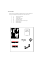
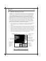
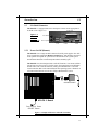
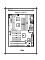
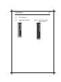
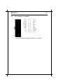
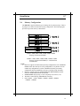
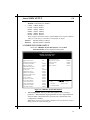
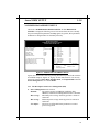
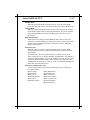
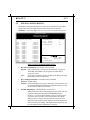
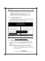
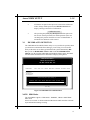
K P 6 -FX 2
A P e n tiu m ® II P r o c e s s o r b a s e d
m a in b o a r d
TRADEMARK
All products and company names are trademarks or
registered trademarks of their respective holders.
The specification is subject to change without notice.
1
Technical Support Services
If you need additional information or help during installation or normal use of this
product, contact your retailer. If your retailer can not help you may E-Mail us
with any questions at the following address [email protected].
Record your serial number before installing your KP6-FX 2 mainboard. (the serial
number is located near the ISA slots at the edge of the board)
EPoX motherboard serial number: _____________________________
BIOS Upgrades
Please use either our Web Site or BBS for current BIOS Upgrades.
Internet Access
http://www.epox.com
[email protected]
[email protected]
Modem Access
886-218-0997 (Taiwan)
714-990-8973 (USA)
31-182-618451 (The Netherlands)
You can access this number via a Hayes-compatible modem with a 2,400 to
28,800 baud rate. The following setup format is required:
8 Data Bits, No Parity, 1 Stop Bit.
If your modem is unable to connect at higher baud rates, try connecting at 2,400
baud before contacting Technical Support.
Thank you for using EPoX mainboard
User Notice
No part of this product, including the product and software may be reproduced,
transmitted, transcribed, stored in a retrieval system, or translated into any
language in any form by any means with the express written permission of EPoX
Computer Company (hereinafter referred to as EPoX) except documentation kept
by the purchaser for backup purposes.
EPoX provedes this manual “as is” without warranty of any kind, either express or
implied, including but not limited to the implied warranties or conditions of
merchantability or fitness for a particular purpose. In no event shall EPoX be
liable for any loss or profits, loss of business, loss of use or data, interruption of
business or for indirect, special incidental, or consequential damages of any kind,
even if EPoX has been advised of the possibility of such damages arising from
any defect or error in the manual or product. EPoX may review this manual from
time to time without notice. For updated BIOS, drivers, or products release
information you may visit EPoX’s home page at: http://www.epox.com
Products mentioned in this manual are mentioned for identification purposes only.
Product names appearing in this manual may or may not be registered trademarks
of copyrights of their respective companies.
The product name and revision number are both printed on the mainboard itself.
© Copyright 1997 EPoX Computer Company. All right reserved.
Handling Procedures
Static electricity can severely damage your equipment. Handle the KP6-FX 2
and any other device in your system with care and avoid contact with components
on the card.
Always work on an antistatic surface to avoid possible damage to the card from
static discharge. The packing material placed on a table top makes a good
antistatic work surface.
We assume no responsibility for any damage to the KP6-FX 2 mainboard that
results from failure to follow installation instructions or failure to observe safety
precautions.
CAUTION
The KP6-FX 2 mainboard is subject to
damage by static electricity. Always
observe the handling procedures.
3
Parts Checklist
Please make sure your package is complete before you start your installation. If
you discover a damaged or missing item, please contact your retailer.
√
√
√
√
√
√
√
A.
B.
C.
D.
E.
F.
G.
1 KP6-FX 2 mainboard
1 Users manual
1 Floppy ribbon cable
2 IDE ribbon cables
PS/2 to AT keyboard connector adapter
Bus Master Driver
Retention Module
USERS
MANUAL
B
A
E
F
C
D
G
Table of Contents
Page
Introduction
1-1
1-1.1
1-1.2
1-2
1-3
1-3.1
1-3.2
1-4
Pentium® II Processor Overview --------------------------------------------- 1-1
S.E.C. Cartridge Overview ---------------------------------------------------- 1-2
S.E.C. Cartridge Terminology ------------------------------------------------ 1-2
KP6-FX 2 Specification ------------------------------------------------------- 1-3
KP6-FX 2 Form-Factor Overview ------------------------------------------- 1-4
I/O Shield Connector ----------------------------------------------------------- 1-5
Power-On/Off (Remote) ------------------------------------------------------- 1-5
System Block Diagram -------------------------------------------------------- 1-6
Installation
2-1
2-1
2-2
2-3
2-4
KP6-FX 2 Layout --------------------------------------------------------------- 2-1
KP6-FX 2 Board Layout (Picture View) ------------------------------------ 2-2
Connectors and Jumpers ------------------------------------------------------- 2-3
I/O Connectors ------------------------------------------------------------------ 2-5
System Memory Configuration ----------------------------------------------- 2-7
Award BIOS SETUP
3-1
3-2
3-3
3-4
3-5
3-6
3-7
3-8
3-9
3-10
3-11
3-12
Award BIOS Setup ------------------------------------------------------------- 3-1
Standard CMOS Setup --------------------------------------------------------- 3-2
BIOS Features Setup ----------------------------------------------------------- 3-2
Chipset Features Setup -------------------------------------------------------- 3-6
Power Management Setup -------------------------------------------------- 3-10
PNP/PCI Configuration ------------------------------------------------------ 3-13
Integrated Peripherals -------------------------------------------------------- 3-14
Load Setup Defaults ---------------------------------------------------------- 3-17
Change Supervisor or User password ------------------------------------- 3-17
IDE HDD Auto Detection --------------------------------------------------- 3-18
HDD Low Level Format ----------------------------------------------------- 3-20
Save & Exit Setup ------------------------------------------------------------ 3-20
Exit Without Saving ---------------------------------------------------------- 3-20
Table of Contents
Appendixes
Appendix
Appendix
Appendix
Appendix
Appendix
Appendix
A-1:
A-2:
A-3:
A-4:
A-5:
B:
Memory Map -------------------------------------------------- A1
I/O Map --------------------------------------------------------- A1
Time & DMA Channels Map ------------------------------- A2
Interrupt Map -------------------------------------------------- A2
RTC & CMOS RAM Map ----------------------------------- A3
Post Codes ------------------------------------------------------ B1
Introduction
1-1
Introduction
EPoX is proud to introduce the KP6-FX 2 mainboard to support Intel Pentium® II
Processor Intel’s latest technology in CPU’s. The KP6-FX 2 is based on Intel’s 82440FX
chipset, and supports uni-Pentium® II Processor processor. Full specifications include 4
PCI and 4 ISA slots, USB ready, and a special ring-in feature all built into full ATX
format. KP6-FX 2 also supports a memory capacity upto 1GB to run the most demanding
applications. The KP6-FX 2 also uses Easy-Setting-Single-Jumper (ESSJ) to simplify
your CPU clock setting.
1-1
Pentium® II Processor Overview
The Pentium® II Processor processor is follow-on to the Pentium® Processor. The
Pentium® II Processor, like the Pentium® Pro processor implements a Dynamic Execution
micro-architecture -- a unique combination of multiple branch prediction, data flow
analysis, and speculative execution. This enables the Pentium® II Processor to deliver
higher performance than the Pentium® processor, while maintaining binary compatibility
with all previous Intel architecture processors.
A significant feature of the Pentium® II Processor, from a system perspective, is the buildin direct multiprocessing support. In order to achieve multi-processing, and maintain
memory and I/O bandwidth to support them, new system designs are needed. For systems
with dual processors, it is important to consider the additional power burdens and signal
integrity issues of supporting multiple loads on a high speed bus. The Pentium® II
Processor card supports both uni-processor and dual processor implementations.
The Pentium® II Processor utilizes Single Edge Contact (S.E.C.) (Figure 1-1) cartridge
packaging technology. The S.E.C. cartridge allows the L2 cache to remain tightly coupled
to the processor, while maintaining flexibility when implementing high performance
processors into OEM systems. The second level cache is performance optimized and
tested at the cartridge level. The S.E.C. cartridge utilizes surface mounted core components and a printed circuit board with an edge finger connection. The S.E.C. cartridge
package introduced on the Pentium® II Processor will also be used in future Slot 1
Thermal Plate
processors.
The S.E.C. cartridge has the following features: a
thermal plate, a cover and a PCB with an edge
Cover
finger connection. The thermal plate allows
standardized heatsink attachment or customized
thermal solutions. The thermal plate enables a reusable heatsink to minimize fit issues for serviceability, upgradability and replacement. The full
Processor
enclosure also protects the surface mount
Printed Circuit Board
components. The edge finger connection
Pentium® II Processor CPU with
maintains socketabilty for system configuration.
S.E.C. Cartridge
The edge finger connector is notated as ‘Slot 1
(Figure 1-1)
connector’in this and other documentation.
7
KP6-FX 2
1-2
1-1.1 S.E.C. Cartridge Overview
The entire enclosed product is called the Pentium® II Processor. The packaging
technology and each of the physical elements of the product are referred to using
accurate technical descriptions. This allows clear reference to the products as just
a processor. This is the model used in past packaging technologies like PGA,
TCP, PQFP, DIP, etc.
1-1.2 S.E.C. Cartridge Terminology
• Pentium® II Processor
•
•
•
•
•
•
•
The new enclosed card packaging technology is called a “Single Edge
Contact cartridge.” This is similar to previous names for packaging technology such as PGA or TCP.
Processor card
The green PCB (with or without components on it)
Processor core
The silicon on the PLGA package on the PCB
Cover
The plastic cover on the opposite side from the thermal plate.
Slot 1
The slot that the S.E.C. cartridge plugs into, just as the Pentium® Pro
processor uses Socket 8.
Retention mechanism
Formerly ‘retention module’the dual posts, etc. that hold the cartridge in
place.
Thermal plate
The heatsink attachment plate.
Heat sink supports
The support pieces that are mounted on the mainboard to provide added
support for heatsinks.
The L2 cache (TagRAM, PBSRAM) components keep standard industry names.
The Pentium® II Processor is the first product to utilize the S.E.C. cartridge
technology and Slot 1 connector. Unless otherwise noted, any references to
“Pentium® II Processor,” “Pentium® II Processor/Slot 1 processor” or Processor”
will apply to both the Pentium® II Processor desktop processors.
Introduction
1-3
1-2 KP6-FX 2 Specification
•
•
•
•
•
•
•
•
•
•
•
•
•
•
•
•
•
•
KP6-FX 2 is based on the Pentium® II Processor operating at 233 ~ 300 MHz on
slot 1. The board is configured by an Easy-Setting-Single-Jumper (ESSJ) to
match your CPU clock speed.
Designed with Intel’s 82440 FX PCIset
Supports upto 1 GigaByte of DRAM (minimum of 8 MB) on board, You can use
either 72-Pin SIMM x 4 or 168-Pin DIMM x 2 or both. It will automatically
detect Fast Page Mode (FPM) DRAM or Extended Data Output (EDO) DRAM
(please see page 2-7).
KP6-FX 2 will support Error Checking and Correcting (ECC) when using parity
DRAM modules. This will detect multiple bit errors and correct 1-bit memory
errors.
Supports (3) 16 bit ISA slots, (5) 32 bit PCI slots, and provides (2) independent
high performance PCI IDE interfaces capable of supporting PIO Mode 3 and
Mode 4 devices. The KP6-FX 2 supports (4) PCI Bus Master slots and a
jumperless PCI INT# control scheme which reduces configuration confusion
when plugging in PCI card(s).
Supports ATAPI (e.g. CD-ROM) devices on both Primary and Secondary IDE
interfaces.
Designed with SMC 37C932FR Multi I/O: (1) floppy port, (1) parallel port
(EPP, ECP), and (2) serial ports (16550 Fast UART).
Note: Japanese “Floppy 3 mode” is also supported
Includes a PS/2 mouse connector.
Allows use of a PS/2 or AT keyboard.
Features Award Plug & Play BIOS. With Flash Memory you can always upgrade
to the current BIOS as they are released.
Supports CPU Hardware sleep and SMM (System Management Mode).
KP6-FX 2 utilizes a Lithium battery which provides environmental protection and
longer battery life.
Supports the Universal Serial Bus (USB) connector. The onboard PIIX chip
provides the means for connecting PC peripherals such as monitors, keyboards,
joysticks, telephones, and modems.
Supports ATX 20 pin power supply connector.
Supports Remote On/Off when used with ATX power supplies.
Four Layer design technology and full ATX form factor.
(12” x 9.6”, 305mm X 244mm)
Supports ring-in feature (remote power-on through external modem), allows
system to be turned on remotely.
Supports Desktop Management Interface (DMI) facilitating the management of
desktop computers, hardware and software components and peripherals, whether
they are standalone systems or linked into networks. (option)
9
KP6-FX 2
1-3
1-4
KP6-FX 2 Form-Factor Overview
EPoX KP6-FX 2 is designed with ATX form factor - the latest industry standard
of chassis. The ATX form factor is essentially a Baby-AT baseboard rotated 90
degrees within the chassis enclosure and a new mounting configuration for the
power supply. With these changes the processor is relocated away from the
expansion slots, allowing them all to hold full length add-in cards. ATX defines a
double height aperture to the rear of the chassis which can be used to host a wide
range of on-board I/O. Only the size and position of this aperture is defined,
allowing PC manufacturers to add new I/O features (e.g.; TV input, TV output,
joystick, modem, LAN, audio, etc.) to systems that will help them differentiate
their products in the marketplace, and better meet your needs.
• By integrating more I/O down onto the board and better positioning the hard
drive and floppy connectors material cost of cables and add-in cards is
reduced.
• By reducing the number of cables and components in the system, manufacturing time and inventory holding costs are reduced and reliability will increase.
• By using an optimized power supply, it's possible to reduce cooling costs and
lower acoustical noise. An ATX power supply, which has a side-mounted fan,
allows direct cooling of the processor and add-in cards making a secondary
fan or active heatsink unnecessary in most system applications.
Expandable I/O
ATX
Power
Supply
Full length
slots
Floppy / IDE
connectors
close to
peripheral
bays
3 1/2"
Bay
5 1/4"
Bay
Figure 1-2: Summary of ATX chassis features
Single chassis
fan for
system
ATX power
connector
CPU located near
Power Supply
Easy to
access
memory
modules
Introduction
1-3
1-5
I/O Shield Connector
The KP6-FX 2 is equipped with an I/O back panel. Please use the appropriate I/
O shield. (refer to figure 1-3)
Parallel Port
Figure 1-3:
KP6-FX 2
I/O back
panel Layout
PS/2 Mouse
PS/2 Keyboard
USB
COM1
COM2
1-3.1 Power-On/Off (Remote)
The KP6-FX 2 has a single 20-PIN connector for ATX power supplies. For ATX
power supplies that support the Remote On/Off feature, this should be connected
to the systems front panel for system Power On/Off button. The systems power
On/Off button should be a momentary button that is normally open.
The KP6-FX 2 has been designed with “Soft Off" functions. You can turn Off the
system from one of two sources: The first is the front panel Power On/Off button,
and the other is the "Soft Off" function (coming from the KP6-FX 2’s on-board
circuit controller) that can be controlled by the the operating system. Windows 95
will controll this when the user clicks is ready to Shutdown the system.
ATX
POWER SUPPLY
JP 16
KP6-FX 2 Board
Case (chassis) Power
ON/OFF button
Figure 3-3: Simple ATX Power ON/OFF Controller
11
KP6-FX 2
1-6
1-4 System Block Diagram
Pentium® II
Processor
Processor
HOST BUS
MAIN MEMORY
PMC
PCI Bridge
and memory
controller
208 PQFP
MD[63:0]
MA[11:0]
>
CONTROL
>
<MPE[7:0]>
< >
PD[15:0]
<
>
>
CONTROL
PCI Slots
DBX
Data Bus
Accelerator
208PQFP
IDE CD-ROM
PIIX3
PCI BUS
I/O Bridge
Port_A
Port_B
Graphics
IDE HDD
208 PQFP
Universal Serial Bus
ISA Slots
BIOS
Flash Memory
Figure 1-4 System Block Diagram
SMC
37C932FR
Installation
2-1
Installation
2-1
KP6-FX 2 Layout
The KP6-FX 2 is designed with Intel 82440FX PCIset chipset which is developed by Intel Corporation to fully support PCI/ISA systems. The Intel 82440FX
PCIset chipset provides increased integration and improved performance. The
chipset provides an integrated IDE controller with two high performance IDE
interfaces for up to four IDE devices (hard drives, CD-ROM’s, etc.). The SMC
37C932FR Super I/O controller provides the standard PC I/O function: floppy
interface, two 16 Byte FIFO serial ports and EPP/ECP capable parallel port,
keyboard controller, and RTC. The KP6-FX 2 layout is shown in the next page (
Figure 2-1 ) for user's reference.
Care must be taken when inserting memory modules, inserting Pentium® II
Processor or even plugging in a PCI card into associated slots to avoid damaging
any circuits or sockets on board (Please unplug all power to the mainboard before
installing any components). A high efficiency fan and heatsink fan is strongly
recommended when installing a Pentium® II Processor to help prevent overheating.
The KP6-FX 2 supports a minimum of 8MB of system memory and a maximum
of 1GigaByte while the L2 Cache and cache controller are included in Pentium®
II Processor CPU.
The KP6-FX 2 supports standard Fast Page Mode (FPM) or Extended Data Out
(EDO) memory. The KP6-FX 2 provides four 72-pin SIMM sockets and two
168-pin DIMM sockets for memory modules. The 72-pin sockets (2 Banks)
support 1M x 32 (4MB), 2M x 32 (8MB), 4M x 32 (16MB), 8M x 32 (32MB)
16M x 32 (64MB), and 32M x 32 (128MB) single-sided or double-sided memory
modules and the 168-pin sockets (2 Banks) support 1M x 64 (8MB), 2M x 64
(32MB), 4M x 64 (64MB), 8M x 64 (128MB), 16M x 64 (256MB) single-sided
or double-sided memory modules. The memory timing requires 60ns or 70ns
FPM, EDO DRAM modules. Memory parity generation and checking or Error
Checking and Correction (ECC) are supported [DRAM Modules may be parity (x
72) or ECC (x 72)]. The BIOS will automatically detect which DRAM is installed
in the SIMM sockets.
The KP6-FX 2 supports Onboard two PCI IDE connectors, these will be
automatically detected by the BIOS to install your hard disk type at boot up.
The KP6-FX 2 supports Award Plug & Play BIOS for ISA and PCI cards. The
BIOS can be located in Flash memory. The advantage of having Flash memory is
the ease of upgrading your BIOS to the current one with software.
13
KP6-FX 2
2-2
KP6-FX 2 Layout
PCI #5
Figure 2-1
Installation
2-2
2-3
Connectors and Jumpers
This section describes all of the connectors and jumpers built into the
motherboard. The jumpers match Figure 2-1 on page 2-2
J16 1
Power On/Off
J9 +
IDE LED indicator - LED ON when Onboard PCI IDE Hard
disks activate
+
Power Saving LED indicator - LED ON when system is in
any saving mode
Sleep/Resume switch : Closed to enter sleep mode, a keystroke or mouse movement will instantly "wake up".
+
Turbo LED indicator - LED ON when higher speed is
selected
+
Reset - Closed to restart system.
1
Speaker - connect to the system's speaker for beeping
1. Speaker
3. GND
2. N/C
4. GND
1
KeyLock - Keyboard lock switch & Power LED connector
1. Power LED(+)
4. Keylock
2. N/C
5. GND
3. GND
15
KP6-FX 2
2-2
2-4
Connectors and Jumpers (continued)
Settings will match motherboard layout on Page 2-2
Clear CMOS Select
1-2
Normal (Default)
2-3
Clear
1 2 3
JP2
JP3
JP1
3
2
1
3
2
1
GND
+12V
GND
JP6
JP5
6
5
4
3
2
1
Flash Memory Voltage Select (Both JP2 & JP3)
1-2
12V Flash memory
2-3
5V Flash memory. (Default)
The Power Supply (+12V) for the CPU cooling fan.
Memory Voltage Selection
1-2 & 4-5
Reserved
2-3 & 5-6
3.3V DIMM module (Default)
5 IrDA/ASK IR CONNECTOR:
1. VCC
2. FIRRX
3. IRRXX
4. GND
5. IRTX
1
J1
JP7 10
5
6
1
CPU Clock Rate Select (ESSJ)
1-6 = 200 Mhz
2-7 = 233 Mhz (Default)
3-8 = 266 Mhz
3-8 & 5-10 = 300Mhz (PCB Rev. 0.2)
5-10 = Option
Installation
2-3
I/O Connectors
J17
Floppy Disk Connector
34
2
33
2-5
J18,J19
Primary/Secondary
IDE Connector
40
39
2
1
1
17
KP6-FX 2
2-3
2-6
I/O Connectors - continued
11
1
20
10
3.3 V
-12 V
GND
PS-ON
GND
GND
GND
-5 V
5V
5V
11
12
13
14
15
16
17
18
19
20
1
2
3
4
5
6
7
8
9
10
3.3 V
3.3 V
GND
5V
GND
5V
COM
PW-OK
5 VSB
12 V
Note: The ATX power supply has to support 3.3 Volts Power
Installation
2-4
2-7
Memory Configurations
The KP6-FX 2 supports different type of settings for the system memory. There is
no jumper nor connector needed for memory configuration. The following figure
provides all possible memory combinations.
SIMM = 4MB, 8MB, 16MB, 32MB, 64MB, 128MB
Fastpage or EDO mode SIMM
DIMM = 8MB, 16MB, 32MB, 64MB, 128MB, 512MB
Fastpage or EDO mode DIMM (3.3 volt unbuffered
recommended)
NOTE :
1. KP6-FX 2 supports and extends many memory configurations on its 4 SIMM & 2
DIMM sockets. The memory size of any configuration is very flexible. You can
combine any configuration as you like. The BIOS will detect your memory
configuration and size automatically, as long as you fill up a bank of memory.
2. KP6-FX 2 supports Fast Page Mode DRAM, EDO DRAM SIMMs, but they
cannot be mixed within the same memory bank.
3. SIMMs/DIMMs may be parity (x 72) or non parity (x 64) or ECC (x 72).
4. The 60ns or 70ns Fast Page, EDO DRAM is necessary.
5. ONE “BANK” = 64 Bit = SIMM 1+ SIMM2 = SIMM 3+ SIMM 4
= DIMM 1 = DIMM 2
19
KP6-FX 2
3-1
Award BIOS SETUP
Award's ROM BIOS provides a built-in Setup program which allows user to
modify the basic system configuration and hardware parameters. The modified
data will be stored in a battery-backed CMOS so data will be retained even when
the power is turned off. In general, the information saved in the CMOS RAM will
stay unchanged unless there is a configuration change in the system, such as hard
drive replacement or a device is added.
It is possible for the CMOS battery to fail, this will cause data lose in CMOS only.
If this does happen you will need to reconfigure your configuration parameter.
To enter Setup Program
Power on the computer and press <Del> key immediately, this will bring you into
BIOS CMOS SETUP UTILITY.
ROM PCI/ISA BIOS
CMOS SETUP UTILITY
AWARD SOFTWARE, INC.
STANDARD CMOS SETUP
SUPERVISOR PASSWORD
BIOS FEATURES SETUP
USER PASSWORD
CHIPSET FEATURES SETUP
IDE HDD AUTO DETECTION
POWER MANAGEMENT SETUP
HDD LOW LEVEL FORMAT
PNP/PCI CONFIGURATION
SAVE & EXIT SETUP
INTEGRATED PERIPHERALS
EXIT WITHOUT SAVING
LOAD SETUP DEFAULTS
ESC : Quit
F10 : Save & Exit Setup
(Shift)F2
: Select Item
: Change Color
Time, Date, Hard Disk Type...
Figure 3-1 CMOS SETUP UTILITY
The menu displays all the major selection items. Select the item you need to
reconfigure. The selection is made by moving cursor (press any direction key ) to
the item and press the 'Enter' key. An on-line help message is displayed at the
bottom of the screen as the cursor is moving to various items which provides a
better understanding of each function. When a selection is made, the menu of
selected item will appear so the user can modify associated configuration parameters.
Award BIOS SETUP
3-2
3-1 STANDARD CMOS SETUP
Choose "STANDARD CMOS SETUP" in the CMOS SETUP UTILITY Menu
(Fig.3-2). The STANDARD CMOS SETUP allows user to configure system
settings such as the current date and time, type of hard disk drive installed, floppy
drive type, and display type. Memory size is auto-detected by the BIOS and
displayed for your reference. When a field is highlighted (use direction keys to
move cursor and <Enter> key to select), the entries in the field will be changed by
pressing <PgDn> or <PgUp> keys.
Figure 3-2 STANDARD CMOS SETUP
NOTE: If hard disk Primary Master/Slave and Secondary Master/Slave were set
to Auto, then the hard disk size and model will be auto-detected.
NOTE: The "Halt On :" field is to determine when to halt the system by the BIOS
if error occurs.
3-2 BIOS FEATURES SETUP
Selecting the "BIOS FEATURES SETUP" option in the CMOS SETUP
UTILITY menu allows users to change system related parameters in the displayed menu. This menu shows all of the manufacturer's default values of KP6-FX
2.
21
KP6-FX 2
3-3
Pressing [F1] key to display help message of the selected item.
This provides the system a capability to recover from any possible error.
ROM PCI/ISA BIOS
BIOS FEATURES SETUP
AWARD SOFTWARE, INC.
Virus Warning
CPU Internal Cache
External Cache
Quick Power On Self Test
Boot Sequence
Swap Floppy Drive
Boot Up Floppy Seek
Boot Up NumLock Status
Boot UP System Speed
Gate A20 option
Typematic Rate Setting
Typematic Rate (Chars/Sec)
Typematic Delay (Msec)
Security Option
PCI/VGA Palette Snoop
OS Select For DRAM > 64MB
:
:
:
:
:
:
:
:
:
:
:
:
:
:
:
:
Disabled
Enabled
Enabled
Enabled
A,C,SCSI
Disabled
Enabled
On
High
Fast
Disabled
6
250
Setup
Disable
Non-OS2
Video BIOS
C8000-CBFFF
CC000-CFFFF
D0000-D3FFF
D4000-D7FFF
D8000-DBFFF
DC000-DFFFF
Shadow
Shadow
Shadow
Shadow
Shadow
Shadow
Shadow
Esc : Quit
F1 : Help
F5 : Old Values
F7 : Load Setup Defaults
:
:
:
:
:
:
:
Enabled
Disabled
Disabled
Disabled
Disabled
Disabled
Disabled
: Select Item
PU/PD/+/- : Modify
(Shift)F2 : Color
Figure 3-3 BIOS FEATURES SETUP
Note: The Security Option contains "setup" and "system". The "setup" indicates
that the password setting is for CMOS only while the "system" indicates the
password setting is for both CMOS and system boot up.
• Virus Warning: This category flashes on the screen. During and after the
system boots up, any attempt to write to the boot sector or partition table of
the hard disk drive will halt the system and a error message will appear. You
should then run an anti-virus program to locate the virus. Keep in mind that
this feature protects only the boot sector, not the entire hard drive. Default
value is Disabled
Enabled: Activates automatically when the system boots up causing a
warning message to appear when anything attempts to access the
boot sector.
Disabled: No warning message to appear when anything attempts to access
the boot sector.
Note: Many disk diagnostic programs that access the boot sector
table can trigger the virus warning message. If you plan to run
such a program, we recommend that you first disable the virus
warning.
Award BIOS SETUP
3-4
• CPU Internal Cache / External Cache: These two categories increase
•
•
performance to memory access. The Pentium® II Processor CPU includes
both Internal/External cache. The default value is Enable.
Note: If your Pentium® II Processor CPU is without External
Cache then this item " External Cache" will not be shown.
Enabled: Enable cache.
Disable: Disable cache.
Quick Power On Self Test: This category speeds up Power On Self Test
(POST) after you power on the computer. If it is set to Enable, BIOS will
shorten or skip some check items during POST. The default is Enabled.
Enabled: Enable quick POST.
Disabled: Normal POST.
Boot Sequence: This category determines which drive is searched first for
the O/S (Operating System). Default value is A,C,SCSI. The following is
your list of options.
[A, C, SCSI] - [C, A, SCSI] - [C, CDROM, A] - [CDROM, C, A] - [D, A, CDROM]
[E, A, CDROM] - [F, A, CDROM] - [SCSI, A, C] - [SCSI C, A] - [C Only]
•
•
Swap Floppy Drive: This will swap your physical drive letters A & B if you
are using two floppy disks. Default value is Disabled.
Enabled: Floppy A & B will be swapped under the O/S.
Disabled: Floppy A & B will be not swap.
Boot Up Floppy Seek: During Power-On-Self-Test (POST), BIOS will
determine if the floppy disk drive installed is 40 or 80 tracks. Only 360K
type is 40 tracks while 760K, 1.2M and 1.44M are all 80 tracks. The default
value is Enabled.
Enabled: BIOS searches for floppy disk drive to determine if it is 40 or 80
tracks, Note that BIOS can not tell from 720K, 1.2M or 1.44M
drive type as they are all 80 tracks.
Disabled: BIOS will not search for the type of floppy disk drive by track
number.
• Boot Up NumLock Status: Control the state of the NumLock key when the
•
system boots. The default value is On.
On:
Keypad is number keys.
Off:
Keypad is arrow keys.
Boot UP System Speed: Select Hight to boot at the default CPU speed;
select Low to boot at the speed of the AT bus.
High:
Set the speed to high.
Low:
Set the speed to low.
23
KP6-FX 2
3-5
• Gate A20 Option: This refers to the way the system addresses memory
above 1MB (extended memory). The default value is Fast.
Normal: The A20 signal is controlled by keyboard controller or chipset
hardware.
Fast:
The A20 signal is controlled by Port 92 or chipset specific
method.
• Typematic Rate Setting: This determines the keystrokes repeat rate.
Enabled: Enable typematic rate and typematic delay programming.
Disabled: Disable typematic rate and typematic delay programming. The rate
will be controlled by keyboard controller in your system.
• Typematic Rate(Chars/Sec):
6 : 6 characters per second.
10: 10 characters per second.
15: 15 characters per second.
24: 24 characters per second.
8 : 8 characters per second.
12: 12 characters per second.
20: 20 characters per second.
30: 30 characters per second.
• Typematic Delay(Msec): When holding a key, the time between the first and
second character displayed.
250 : 250 msec.
500 : 500 msec.
750 : 750 msec.
1000: 1000 msec.
• Security Option: This category allows you to limit access to the system and
Setup, or just to Setup. The default value is Setup.
System: The system will not boot and the access to Setup will be denied if
the correct password is not entered at the prompt.
Setup:
The system will boot; but the access to Setup will be denied if the
incorrect password is not entered at the prompt.
• PCI/VGA Palette Snoop: This filed controls the ability of a primary PCI
VGA controller to share a common palette (When a snoop write cycles) with
an ISA video card. The default value is Disabled.
Enabled: If an ISA card connects to a PCI VGA card via the VESA connector and that ISA card connects to VGA monitor and that ISA card
uses the RAMDAC of PCI card.
Disabled: Disable the VGA card Palette snoop function.
• Video BIOS Shadow:
It determines whether video BIOS will be copied
to RAM, however it is optional from chipset design. Video Shadow will
increase the video speed.
Enabled: Video shadow is enabled.
Award BIOS SETUP
3-6
Disabled: Video shadow is disabled.
• C8000 - CBFFF Shadow :
CC000 - CFFFF Shadow:
D0000 - D3FFF Shadow:
D4000 - D7FFF Shadow:
D8000 - DBFFF Shadow:
DC000 - DFFFF Shadow:
These categories determine whether optional ROM will be copied to RAM by
16K byte or 32K byte per unit and the size depends on chipset.
Enabled:
Optional shadow is enabled.
Disabled: Optional shadow is disabled.
3-3 CHIPSET FEATURES SETUP
Choose the "CHIPSET FEATURES SETUP" in the CMOS
SETUP UTILITY menu to display following menu.
ROM PCI/ISA BIOS
CHIPSET FEATURES SETUP
AWARD SOFTWARE, INC.
Auto Configuration
: Enabled
DRAM Speed Selection
DRAM RAS# Precharge Time
MA Additional Wait state
RAS# To Cas# Delay
DRAM Read Burst (B/E/F)
DRAM Write Burst (B/E/F)
ISA Bus Clock
DRAM Refresh Queue
DRAM RAS Only Refresh
DRAM ECC/PARITY Select
Fast Dram Refresh
Read-Around-Write
PCI Burst Write Combine
PCI-To-DRAM Pipeline
CPU-To-PCI Write Post
CPU-To-PCI IDE Posting
System BIOS Cacheable
Video RAM Cacheable
: 60ns
:4
: Disabled
: Disabled
: 2/2/3
: 2/2/3
: PCICLK/4
: Enabled
: Disabled
: Disabled
: Disabled
: Enabled
: Enabled
: Enabled
: Enabled
: Enabled
: Disabled
: Disabled
8 Bit I/O Recovery Time
16 Bit I/O Recovery Time
Memory Hole AT 15M-16M
DRAM Fast Leadoff
Passive Release
Delayed Transaction
Esc : Quit
F1 : Help
F5 : Old Values
F7 : Load Setup Defaults
:1
:1
: Disabled
: Disabled
: Enabled
: Disabled
: Select Item
PU/PD/+/- : Modify
(Shift)F2 : Color
Figure 3-4 CHIPSET FEATURES SETUP
• Auto Configuration: Selects predetermined optimal values of chipset
parameters. When Disabled, chipset parameters revert to setup information
stored in CMOS. Many fields in this screen are not available when Auto
Configuration is Enabled.
Note: When you insert slower memory modules in the system and set a faster
timing, maybe the system will hang up.
25
KP6-FX 2
3-7
• DRAM Speed Selection: This value must correspond to the speed of the
•
•
•
•
•
DRAM installed in your system. DO NOT change the default setting of this
field, as determined by the system board manufacturer for the installed
DRAM. This value is access speed, so a lower value means a faster system.
The default value is 60ns.
60ns:
(Faster) Burst Wait State, for 60~70ns Fast Page Mode/EDO
DRAM.
70ns:
(Slower) Burst Wait State, for 70ns Fast Page Mode/EDO DRAM.
DRAM RAS# Precharge Time: The precharge time is the number of cycles.
It takes for the RAS to accumulate its charge before DRAM refresh. If
insufficient time is allowed, refresh may be complete and the DRAM may fail
to retain data. The default value is 3.
3:
Time equals 3 host clocks.
4:
Time equals 4 host clocks.
MA Additional Wait State: This allows the option to insert an additional
wait state before the beginning of a memory read. The default value is
Disabled.
Enabled: One additional wait state is inserted before the assertion of the
first MAxx and CASx#/RASx# assertion during DRAM read or
write lead off cycles.
Disabled: No extra wait state for MAxx and CASx#/RASx#.
RAS# to CAS# Delay: Allows you to insert a timing delay between the CAS
and RAS strobe signals, used when DRAM is written to , read from, or
refreshed. The default value is Enabled.
Enabled: Adds one clock between the assertion of RAS# and CAS#. (Better
stability of the system)
Disabled: No delay between the assertion of RAS# and CAS#. (Faster
Performance)
DRAM Read/Write Burst (B/E/F): The default value is x2/2/3.
This field indicates the EDO/FPM(B/E/F) DRAM system Read/
Write burst mode. The value x2/2/3 stands for EDO(x222) or
FPM(x333) respectively.
ISA Bus Clock: Set the speed of the ISA bus here. The default value is
PCICLK/4.
PCICLK/4: If the system is operating at 60/66MHz, then the PCICLK is
30/33MHz.
PCICLK/3: The system is operating at 50MHz, than PCICLK is 25MHz.
Award BIOS SETUP
3-8
• DRAM RAS Only Refresh: Permits queuing up to four DRAM refresh
•
•
•
•
requests, so DRAM can refresh at optimal times. The default value is Disabled.
Enabled: The DRAM Refresh type is RAS only.
Disabled: The DRAM Refresh type is CAS before RAS.
ECC Checking/Generation: The default value is Enabled.
ECC:
This field is enabled the optional DRAM Error Checking and
Correction (ECC) with 72-bit Wide memory.
Parity:
This field is enabled the optional DRAM parity Error with 72-bits
wide memroy
Disabled: Disabled the ECC parity function.
Fast DRAM Refresh: The cache DRAM controller offers two refresh
modes, Normal and Hidden. In both modes, CAS takes place before RAS
but the Normal mode requires a CPU cycle for each. On the other hand, a
cycle is eliminated by “hiding” the CAS refresh in Hidden mode. Not only is
the Hidden mode faster and more efficient, but it also allows the CPU to
maintain the status of the cache even if the system goes into a power management “suspend” mode.
Enabled: Hidden Mode
Disabled: Normal Mode
Read-Around-Write: DRAM optimization feature (Default is Enabled)
Enabled: If a memory read is addressed to a location whose latest write is
being held in a buffer before being written to memory, the read is
satisfied through the buffer contents, and the read is not sent to the
DRAM.
Disabled: Memory read is addressed to a location on whose write through to
memory.
PCI Burst Write Combine:
Enabled: Chipset assembles long PCI bursts from the data held in these
buffers.
Disabled: The chipset doesn’t assemble long PCI bursts from the data held in
these buffers
• PCI-To-DRAM Pipeline: DRAM optimization feature:
Enabled: full PCI-to-DRAM write pipelining is enabled. Buffers in the
chipset store data written from the PCI bus to memory.
Disabled: When Disabled, PCI writes to DRAM are limited to a single
transfer per write cycle.
27
KP6-FX 2
3-9
• CPU-To-PCI Write Post:
•
•
•
•
•
Enabled: Writes from the CPU to the PCI bus are buffered, to compensate
for the speed differences between the CPU and the PCI bus.
Disabled: The writes are not buffered and the CPU must wait until the write
is complete before starting another write cycle.
CPU-To-PCI IDE Posting:
Enabled: To post write cycles from the CPU to the PCI IDE interface. IDE
accesses are posted in the CPU to PCI buffers, for cycle optimization.
Disabled: Doesn’t post write cycles from the CPU to the PCI buffers.
System BIOS Cacheable:
Enabled: Allows caching of the system BIOS ROM at F0000h-FFFFFh,
resulting in better system performance. However, if any program
writes to this memory area, a system error may result.
Disabled: System BIOS non-cacheable
Video BIOS Cacheable: Allows caching of the video BIOS ROM at
C0000h to C7FFFh, resulting in better video performance. The default value
is Enabled.
Enabled: Enables the Video BIOS Cacheable to speed up the VGA Performance.
Disabled: Will not use the Video BIOS Cacheable function.
8/16 Bit I/O Recovery Time:
The default value is 1.
8 Bit I/O Recovery Time:
This field defines the recovery time from
1 to 8 for 8-bit I/O.
16 Bit I/O Recovery Time:
To define the recovery time from 1 to 4
for 16-bit I/O.
Memory Hole at 15M-16M: The default value is Disabled.
Disabled: Normal Setting.
Enabled : This field enables the main memory (15~16MB) remap to ISA
BUS.
DRAM Fast Landoff: Shorten the leadoff cycles to optimize performance.
•
• Passive Release: The default value is enabled
• Delayed Transaction: The defaul value is disabled.
Award BIOS SETUP
3-10
3-4 POWER MANAGEMENT SETUP
Choose the "POWER MANAGEMENT SETUP" in the CMOS SETUP
UTILITY to display the following screen. This menu allows the user to modify
the power management parameters and IRQ signals. In general, these parameters
should not be changed unless it's absolutely necessary.
ROM PCI/ISA BIOS
POWER MANAGEMENT SETUP
AWARD SOFTWARE, INC.
Power Management
PM Control by APM
Video off Method
Modem Use IRQ
: User Define
: Yes
: V/H SYNC+Blank
:3
Doze Mode
Standby Mode
Suspend Mode
HDD Power Down
: Disable
: Disable
: Disable
: 15min
** Wake Up Events In Doze & Standby **
IRQ3 (Wake-Up Event)
: ON
IRQ4 (Wake-Up Event)
: ON
IRQ8 (Wake-Up Event)
: ON
IRQ12 (Wake-Up Event)
: ON
** Power Down & Resume Events
IRQ3 (COM 2)
IRQ4 (COM 1)
IRQ5 (LPT 2)
IRQ6 (Floppy Disk)
IRQ7 (LPT 1)
IRQ8 (RTC Alarm)
IRQ9 (IRQ2 Redir)
IRQ10 (Reserved)
IRQ11 (Reserved)
IRQ12 (PS/2 Mouse)
IRQ13 (Coprocessor)
IRQ14 (Hard Disk)
IRQ15 (Reserved0
Esc : Quit
F1 : Help
F5 : Old Values
F7 : Load Setup Defaults
**
: ON
: ON
: ON
: ON
: OFF
: OFF
: ON
: ON
: ON
: ON
: ON
: ON
: OFF
: Select Item
PU/PD/+/- : Modify
(Shift)F2 : Color
Figure 3-5 POWER MANAGEMENT SETUP
Again, user can move the cursor by pressing direction keys to the field needed to
be modified and press <PgDn> or <PgUp> to alter item selection. You can only
change the content of Doze Mode, Standby Mode, and Suspend Mode when the
Power Management is set to 'User Define'.
3-3-1 The Description of the Power Management (PM)
A. Power Management mode selection:
Disabled:
The system operates in NORMAL conditions (NonGREEN), and the Power Management function is disabled.
Max. saving:
Maximum power savings. Inactivity period is 1 minute in
each mode.
Min. saving:
Minimum power savings. Inactivity period is 1 minute in
each mode.
User define:
Allow user to define PM Timers parameters to control
power saving mode.
29
KP6-FX 2
3-11
B. Time-out parameters:
System Doze
The "System Doze" mode timer starts to count when there is no
"PM events" occurred. The valid time-out setting is from 1 minute
up to 1 hour.
System Standby
The "Standby" mode timer starts to count when "System Doze"
mode timer timed out and no "PM events" occurred. Valid range is
from 1 minute up to 1 hour.
System Suspend
This function works only when the Pentium® Pro Processor is
installed. The timer starts to count when "System Standby" mode
timer is timed out and no "PM Events" occurred. Valid range is
from 1 minute up to 1 hour.
HDD Power Down
HDD Standby timer can be set from 1 to 15 minute(s).
3-3-2 Description of the Green Functions
• PM Control by APM:
•
•
If Advanced Power Management (APM) is installed on your system, selecting
Yes gives better power savings.
Video Off Method: Determines the manner in which the monitor is blanked.
V/H SYNC+Blank:
System turns off vertical and horizontal synchronization ports and writes
blanks to the video buffer.
DPMS Support:
Select this option if your monitor supports the Display Power Management
Signaling (DPMS) standard of the Video Electronics Standards Association
(VESA). Use the software supplied for your video subsystem to select video
power management values.
Blank Screen:
System only writes blanks to the video buffer.
MODEM Use IRQ: Default value is IRQ 3
Name the interrupt request (IRQ) line assigned to the modem (if any) on your
system. Activity of the selected IRQ always awakens the system.
The KP6-FX 2 supports HDD Power Down, Doze and Standby power saving
functions when using Intel Pentium® II Processor.
Doze Mode
The system hardware will drop down CPU clock from normal working speed
when Doze mode time-out occurs.
Award BIOS SETUP
3-12
Standby Mode
When the system standby mode timer times-out, it will enter the standby
mode and retain CPU at slow working speed. The screen will be blanked out.
Suspend Mode
When the system suspend timer times-out, the system will enter the suspend
mode and the chipset will stop CPU clock immediately. The power consumption in Suspend Mode is lower than in standby mode. The screen is also
blanked out.
HDD Standby Mode
When system stop reading or writing HDD, the timer starts to count. The
system will cut off the HDD power when timer runs out of time. The system
will not resume operation until either a read from or a write to HDD command is executed again.
Wake Up Events
When the system is in Doze, suspend or Standby mode, you may disable
activity monitoring of some common interrupt requests so they do not wake
up the system.
The default wake-up event is keyboard activity. In these wake-up event
fields, you can turn On or Off four commonly used interrupts. For example, if
you have a modem on IRQ3, you can turn On IRQ3 as a wake-up event, so an
interrupt from the modem can wake up the system. Or you may wish to turn
Off IRQ12 (the PS/2) mouse as a wake-up event, so accidentally brushing the
mouse does not awaken the system.
Power Down and Resume Events
You may disable monitoring of common interrupt requests so they do not
reset activity timers.
IRQ9 (IRQ2 Redir)
IRQ3 (COM 2 )
IRQ10 (Reserved)
IRQ4 (COM 1)
IRQ11 (Reserved)
IRQ5 (LPT 2)
IRQ12 (PS/2 Mouse)
IRQ6 (Floppy Disk)
IRQ13 (Coprocessor)
IRQ7 (LPT 1)
IRQ14 (Hard Disk)
IRQ8 (RTC Alarm)
IRQ15 (Reserved)
31
KP6-FX 2
3-5
3-13
PNP/PCI CONFIGURATION
The PNP/PCI configuration program is for the user to modify the PCI/ISA IRQ
signals when various PCI/ISA cards are inserted in the PCI or ISA slots.
WARNING: Conflicting IRQ’s may cause the system to not find certain devices.
ROM PCI/ISA BIOS
PNP/PCI CONFIGURATION
AWARD SOFTWARE, INC.
Resources Controlled By: Manual
Reset Configuration Data : Disabled
IRQ-3
IRQ-4
IRQ-5
IRQ-7
IRQ-9
IRQ-10
IRQ-11
IRQ-12
IRQ-14
IRQ-15
DMA-0
DMA-1
DMA-3
DMA-5
DMA-6
DMA-7
assigned
assigned
assigned
assigned
assigned
assigned
assigned
assigned
assigned
assigned
assigned
assigned
assigned
assigned
assigned
assigned
to
to
to
to
to
to
to
to
to
to
to
to
to
to
to
to
: Legacy ISA
: Legacy ISA
: PCI/ISA PnP
: PCI/ISA PnP
: PCI/ISA PnP
: PCI/ISA PnP
: PCI/ISA PnP
: PCI/ISA PnP
: PCI/ISA PnP
: PCI/ISA PnP
: PCI/ISA PnP
: PCI/ISA PnP
: PCI/ISA PnP
: PCI/ISA PnP
: PCI/ISA PnP
: PCI/ISA PnP
PCI IRQ Actived By
PCI IDE IRQ Map To
Primary
IDE INT#
Secondary IDE INT#
: Level
: PCI-AUTO
:A
:B
Used MEM base addr
: N/A
Esc : Quit
F1 : Help
F5 : Old Values
F7 : Load Setup Defaults
: Select Item
PU/PD/+/- : Modify
(Shift)F2 : Color
Figure 3-6 PCI CONFIGURATION SETUP
• Resource Controlled By: The default value is Manual.
•
•
Manual: PNP Card's resources will be controlled manually. You can set
which IRQ-X and DMA-X are assigned to PCI/ISA PNP or
Legacy ISA Cards.
Auto:
If your ISA card and PCI card are all PNP cards, BIOS will assign
the interrupt resource automatically.
Reset Configuration Data: The default value is Disabled
Disabled: Normal Setting
Enabled: If you had plugged some Legacy cards in the system and they were
record into ESCD (Extended System Configuration Data), you can
set this field to Enabled to clear ESCD.
PCI IDE IRQ Map To: The default value is PCI-AUTO.
When you have true PCI card(s) plugged into the system, you will
not need to change any thing here in the SETUP program.
However, if you do not know whether you have true PCI card or
not, please refer to your PCI card user's manual for the details.
When you have a Legacy card (described in section 3-6) to be
plugged into the system, a proper setting is extremely important or
it may cause the system hang. The diagram shown below tells you
how the Rotating Priority Mechanism is designed.
Award BIOS SETUP
3-14
• Used MEM base addr and Used MEM Length: The default value is N/A.
The Used MEM base addr (CB00, CC00, D000, D400, D800, DC00)
and Used MEM Length (8K, 16K, 32K, 64K) were to support the some
specific ISA Legacy cards with requested memory space below 1M
address. Now with these two funtions, users canm define where the used
memory address is located and its length of the legacy area that is used
by the legacy device to avoid the memory space conflict. For example, if
users select “D000” for Used MEM base addr” and “16K” for “Used
MEM Length”, that means the address region D000H-D3FFFH is
occupied by ISA legacy cards, and thus BIOS will not assign this region
for PnP/ISA and PCI cards.
PCI#5
PCI#4
PCI#3
PCI#2
PCI#1
INTB
INTC
INTD
INTA
INTB
INTC
INTD
INTA
INTC
INTD
INTA
INTB
INTD
INTA
INTB
INTC
INTA INTA
INTB INTB
INTC INTC
INTD
INTD
PCI
Chipset
Figure 3-7 The Combination of PCI INT# lines
3-6
INTEGRATED PERIPHERALS
ROM PCI/ISA BIOS
INTEGRATED PERIPHERALS
WARD SOFTWARE, INC.
IDE HDD Block Mode
IDE Primary Master PIO
IDE Primary Slave PIO
IDE Secondary Master PIO
IDE Secondary Slave PIO
Onboard Primary PCI IDE
Onboard Secondary PCI IDE
PCI Slot IDE 2nd Channel
: Enabled
: Auto
: Auto
: Auto
: Auto
: Enabled
: Enabled
: Enabled
Onboard FDC Controller : Enabled
Onboard UART Port 1
Onboard UART Port 2
UART 2 Mode
: Auto
: Auto
: Standard
Onboard Parallel Port
Parallel Port Mode
ECP Mode Use DMA
: 378/IRQ7
: ECP+EPP1.9
:3
USB Controller
USB Keyboard Support *
: Disabled
: Disabled
* Only visible when USB is Enabled
Esc : Quit
F1 : Help
F5 : Old Values
F7 : Load Setup Defaults
: Select Item
PU/PD/+/- : Modify
(Shift)F2 : Color
Figure 3-8 INTEGRATED PERIPHERALS
33
KP6-FX 2
3-15
Note: If you do not use the Onboard IDE connector, then you will need set
Onboard Primary PCI IDE: Disabled and Onboard Secondary PCI IDE:
Disabled from CHIPSET FEATURES SETUP UTILITY.
The Onboard PCI IDE cable should be equal to or less than
18 inches (45 cm.).
• IDE HDD Block Mode: Select Enabled only if your hard drives support
•
•
•
•
•
•
•
block mode.
Enabled: Enabled IDE HDD Block Mode. Provides higher HDD transfer
rates.
Disabled: Disable IDE HDD Block Mode.
PCI Slot IDE 2nd Channel: The default value is Enabled.
Enabled: Enable secondary IDE port and BIOS will assign IRQ15 for this
port.
Disabled: Disable secondary IDE port and IRQ15 is available for other
device.
Onboard Primary PCI IDE: The default value is Enabled.
Enabled: Enables Onboard IDE primary port.
Disabled: Disables Onboard IDE primary port.
Onboard Secondary PCI IDE: The default value is Enabled.
Enabled: Enables Onboard IDE secondary port.
Disabled: Disables Onboard IDE secondary port.
IDE Primary Master PIO: The default value is Auto.
Auto:
BIOS will automatically detect the Onboard Primary Master
PCI IDE HDD Accessing mode.
Mode 0~4:
Manually set the IDE Accessing mode.
IDE Primary Slave PIO: The default value is Auto.
Auto:
BIOS will automatically detect the Onboard Primary Slave
PCI IDE HDD Accessing mode.
Mode 0~4:
Manually set the IDE Accessing mode.
IDE Secondary Master PIO: The default value is Auto.
Auto:
BIOS will automatically detect the Onboard Secondary
Master PCI IDE HDD Accessing mode.
Mode 0~4:
Manually set the IDE Accessing mode.
IDE Secondary Slave PIO: The default value is Auto.
Auto:
BIOS will automatically detect the Onboard Secondary
Slave PCI IDE HDD Accessing mode.
Mode 0~4:
Manually set the IDE Accessing mode.
Award BIOS SETUP
3-16
• Onboard FDC Controller: The default value is Enabled.
•
•
•
•
Enabled: Enable the Onboard SMC CHIP's floppy drive interface controller.
Disabled: Disable the Onboard SMC CHIP's floppy drive interface controller.
Onboard Serial Port 1: This field allows the user to select the serial port.
The default value is Auto.
AUTO: Enable Onboard Serial port 1 and address is Auto adjusted
COM1: Enable Onboard Serial port 1 and address is 3F8H/IRQ4.
COM2: Enable Onboard Serial port 1 and address is 2F8H/IRQ3.
COM3: Enable Onboard Serial port 1 and address is 3E8H/IRQ4.
COM4: Enable Onboard Serial port 1 and address is 2E8H/IRQ3.
Disabled: Disable Onboard SMC CHIP's Serial port 1.
Onboard UART 2: This field allows the user to sellect the serial port. The
default value is Auto.
AUTO: Enable Onboard Serial port 2 and address is Auto adjusted
COM1: Enable Onboard Serial port 2 and address is 3F8H/IRQ4.
COM2: Enable Onboard Serial port 2 and address is 2F8H/IRQ3.
COM3: Enable Onboard Serial port 2 and address is 3E8H/IRQ4.
COM4: Enable Onboard Serial port 2 and address is 2E8H/IRQ3.
Disabled: Disable Onboard SMC CHIP's Serial port 2.
Onboard UART 2 Mode: The default value is standard. This field allows the
user to select the COM2 port that can support a serial Infrared Interface.
Standard: Support a Serial Infrared Interface IrDA.
IrDA:
Support a Serial Infrared Interface format.
ASKIR: Support a Sharp Serial Infrared Interface format.
Onboard Parallel port: This field allows the user to sellect the LPT port.
The default value is 378H/IRQ7.
378H:
Enable Onboard LPT port and address is 378H and IRQ7
278H:
Enable Onboard LPT port and address is 278H and IRQ5.
3BCH:
Enable Onboard LPT port and address is 3BCH and IRQ7.
Disabled: Disable Onboard SMC CHIP's LPT port.
• Parallel Port Mode: This field allows the user to sellect the parallel port
mode. The default value is ECP+EPP.
Normal:
Standard mode. IBM PC/AT Compatible bidirectional
parallel port.
EPP:
Enhanced Parallel Port mode.
ECP:
Extended Capabilities Port mode.
EPP+ECP:
ECP Mode & EPP Mode.
35
KP6-FX 2
3-17
• ECP Mode USE DMA: This field allows the user to sellect DMA1 or
DMA3 for the ECP mode. The default value is DMA3.
DMA1: The filed selects the rounting of DMA1 for the ECP mode.
DMA3: The filed selects the rounting of DMA3 for the ECP mode.
3-7
LOAD SETUP DEFAULTS
The "LOAD SETUP DEFAULTS" function loads the system default data directly
from ROM and initializes the associated hardware properly. This function will be
necessary only when the system CMOS data is corrupted.
ROM PCI/ISA BIOS
CMOS SETUP UTILITY
AWARD SOFTWARE, INC.
STANDARD CMOS SETUP
SUPERVISOR PASSWORD
BIOS FEATURES SETUP
USER PASSWORD
CHIPSET FEATURES SETUP
IDE HDD AUTO DETECTION
POWER MANAGEMENT SETUP
HDD LOW LEVEL FORMAT
PNP/PCI CONFIGURATION
Load SETUP Default (Y/N)? Y
INTEGRATED PERIPHERALS
SETUP
SAVING
LOAD SETUP DEFAULTS
ESC: QUIT
F10:Save & Exit Setup
:SELECT ITEM
(Shift)F2 :Change Color
Load Setup Defaults Except Standard CMOS SETUP
Figure 3-10 LOAD SETUP DEFAULT
3-8
CHANGE SUPERVISOR or USER PASSWORD
To change the password, choose the "SUPERVISOR PASSWORD or USER
PASSWORD" option from the CMOS SETUP UTILITY menu and press
[Enter].
NOTE: Either "Setup" or "System" must be selected in the "Security Option" of
the BIOS FEATURES SETUP menu (Refer to Figure 4-3 for the details).
1.
If CMOS is corrupted or the option was not used, a default
password stored in the ROM will be used. The screen will display
the following message:
Enter Password:
Press the [Enter] key to continue after proper password is given.
Award BIOS SETUP
2.
If CMOS is corrupted or the option was used earlier and the user
wish to change default password, the SETUP UTILITY will
display a message and ask for a confirmation.
Confirm Password:
After pressing the [Enter] key (ROM password if the option was
not used) or current password (user-defined password), the user
can change the password and store new one in CMOS RAM. A
maximum of 8 characters can be entered.
3.
3-9
3-18
IDE HDD AUTO DETECTION
The "IDE HDD AUTO DETECTION" utility is a very useful tool especially when
you do not know which kind of hard disk type you are using. You can use this
utility to detect the correct disk type installed in the system automatically. But
now you can set HARD DISK TYPE to Auto in the STANDARD CMOS
SETUP. You don't need the "IDE HDD AUTO DETECTION" utility. The BIOS
will Auto-detect the hard disk size and model on display during POST.
ROM PCI/ISA BIOS
CMOS SETUP UTILITY
AWARD SOFTWARE, INC.
HARD DISKS
Primary Master
Primary Slave
Secondary Master
Secondary Slave
TYPE
SIZE CYLS
:
:
:
:
343
HEADS
665
PRECOMP
LANDZONE
65535
664
16
SECTORS
MODE
63 NORMAL
Select Secondary Slave Option (N=Skip) : N
OPTIONS
SIZE
CYLS
1 (Y)
0
0
HEAD
PRECOMP
0
LANDZ
0
SECTOR
0
MODE
0
NORMAL
ESC : Skip
Figure 3-9 IDE HDD AUTO DETECTION
NOTE: HDD Modes
The Award BIOS supports 3 HDD modes : NORMAL, LBA & LARGE NORMAL mode
Generic access mode in which neither the BIOS nor the IDE controller will make
any transformations during accessing.
37
KP6-FX 2
3-19
The maximum number of cylinders, head & sectors for NORMAL mode are.
1024, 16 & 63.
no. Cylinder
(1024)
x no. Head
( 16)
x no. Sector
( 63)
x no. per sector
( 512)
528 Megabytes
If user set his HDD to NORMAL mode, the maximum accessible HDD size
will be 528 Megabytes even though its physical size may be greater than that!
LBA (Logical Block Addressing) mode:
A new HDD accessing method to overcome the 528 Megabyte bottleneck.
The number of cylinders, heads & sectors shown in setup may not be the
number physically contained in the HDD. During HDD accessing, the IDE
controller will transform the logical address described by sector, head &
cylinder into its own physical address inside the HDD. The maximum HDD
size supported by LBA mode is 8.4 GigaBytes which is obtained by the
following formula:
no. Cylinder
(1024)
x no. Head
( 255)
x no. Sector
( 63)
( 512)
x bytes per sector
8.4 GigaBytes
LARGE mode:
Extended HDD access mode supported by Award Software.
Some IDE HDDs contain more than 1024 cylinder without LBA support (in
some cases, user do not want LBA). The Award BIOS provides another
alternative to support these kinds of LARGE mode.
CYLS
HEADS
SECTOR
MODE
1120
16
59
NORMAL
560
32
59
LARGE
BIOS tricks DOS (or other OS) that the number of cylinders is less than 1024
by dividing it by 2. At the same time, the number of heads is multiplied by 2.
A reverse transformation process will be made inside INT 12h in order to
access the right HDD address!
Award BIOS SETUP
Maximum HDD size:
no. Cylinder
x no. Head
x no. Sector
x bytes per sector
3-20
(1024)
( 32)
( 63)
( 512)
1 GigaByte
Note: To support LBA or LARGE mode of HDDs, there must be some
software involved. All the software is located in the Award HDD Service
Routine (1NT 13h). It may fail to access a HDD with LBA (LARGE) mode
selected if you are running under a Operating System which replaces the
whole 1NT 13h.
UNIX operating systems do not support either LBA or LARGE and must
utilize the Standard mode. UNIX can support drives larger than 528MB.
3-10
HDD LOW LEVEL FORMAT
Interleave:
Select the interleave number of the hard disk drive you wish to perform a low
level format on. You may select from 1 to 8. Check the documentation that
came with the drive for the correct interleave number, or select 0 for automatic detection.
Auto scan bad track:
This allows the utility to scan first then format by each track.
Start:
Press<Y>to start low level format.
3-11
SAVE & EXIT SETUP
The "SAVE & EXIT SETUP" option will bring you back to boot up procedure with all the changes you just recorded in the CMOS RAM.
3-12
EXIT WITHOUT SAVING
The "EXIT WITHOUT SAVING" option will bring you back to normal
boot up procedure without saving any data into CMOS RAM. All old data in
the CMOS will not be destroyed.
39
Appendix
A1
Appendix A:
A-1
MEMORY MAP
Address Range
[00000-7FFFF]
[80000-9FBFF]
[9FC00-9FFFF]
[A0000-C7FFF]
[C8000-DFFFF]
[E0000-EEFFF]
[EF000-EFFFF]
[F0000-F7FFF]
[F8000-FCFFF]
[FD000-FDFFF]
[FE000-FFFFF]
A-2
Size
512K
127K
1K
160K
96K
60K
4K
32K
20K
4K
8K
Description
Conventional memory
Extended Conventional memory
Extended BIOS data area if PS/2 mouse is installed
Available for Hi DOS memory
Available for Hi DOS memory and adapter ROMs
Available for UMB
Video service routine for Monochrome & CGA adaptor
BIOS CMOS setup utility
BIOS runtime service routine (2)
Plug and Play ESCD data area
BIOS runtime service routine (1)
I/O MAP
[000-01F]
[020-021]
[022-023]
[040-05F]
[060-06F]
[070-07F]
[080-09F]
[0A0-0BF]
[0C0-0DF]
[0F0-0FF]
[1F0-1F8 ]
[278-27F]
[2B0-2DF]
[2F8-2FF]
[360-36F]
[378-37F]
[3B0-3BF]
[3C0-3CF]
[3D0-3DF]
[3F0-3F7]
[3F8-3FF]
DMA controller.(Master)
INTERRUPT CONTROLLER.(Master)
CHIPSET control registers. I/O ports.
TIMER control registers.
KEYBOARD interface controller.(8042)
RTC ports & CMOS I/O ports.
DMA register.
INTERRUPT controller.(Slave)
DMA controller.(Slave)
MATH COPROCESSOR.
HARD DISK controller.
PARALLEL port 2.
GRAPHICS adapter controller.
SERIAL port 2.
NETWORK ports.
PARALLEL port 1.
MONOCHROME & PARALLEL port adapter.
EGA adapter.
CGA adapter.
FLOPPY DISK controller.
SERIAL port 1.
Appendix
A-3
A2
TIME & DMA CHANNELS MAP
TIME MAP:
TIMER
TIMER
TIMER
Channel 0
Channel 1
Channel 2
DMA CHANNELS:
DMA Channel 0
DMA Channel 1
DMA Channel 2
DMA Channel 3
DMA Channel 4
DMA Channel 5
DMA Channel 6
DMA Channel 7
A-4
System timer interrupt.
DRAM REFRESH request.
SPEAKER tone generator.
Available.
Onboard ECP (Option).
FLOPPY DISK (SMC CHIP).
Onboard ECP (default).
Cascade for DMA controller 1.
Available.
Available.
Available
INTERRUPT MAP
NMI :
Parity check error.
IRQ (H/W):
0
1
2
3
4
5
6
7
8
9
10
11
12
13
14
15
System TIMER interrupt from TIMER 0.
KEYBOARD output buffer full.
Cascade for IRQ 8-15.
SERIAL port 2.
SERIAL port 1.
PARALLEL port 2.
FLOPPY DISK (SMC CHIP).
PARALLEL port 1.
RTC clock.
Available.
Available.
Available.
PS/2 Mouse.
MATH coprocessor.
Onboard HARD DISK (IDE1) channel.
Onboard HARD DISK (IDE1) channel.
41
Appendix
A-5
RTC & CMOS RAM MAP
RTC & CMOS:
00
Seconds.
01
Second alarm.
02
Minutes.
03
Minutes alarm.
04
Hours.
05
Hours alarm.
06
Day of week.
07
Day of month.
08
Month.
09
Year.
0A
Status register A.
0B
Status register B.
0C
Status register C.
0D
Status register D.
0E
Diagnostic status byte.
0F
Shutdown byte.
10
FLOPPY DISK drive type byte.
11
Reserve.
12
HARD DISK type byte.
13
Reserve.
14
Equipment type.
15
Base memory low byte.
16
Base memory high byte.
17
Extension memory low byte.
18
Extension memory high byte.
19-2d
2E-2F
30
Reserved for extension memory low byte.
31
Reserved for extension memory high byte.
32
DATE CENTURY byte.
33
INFORMATION FLAG.
34-3F Reserve.
40-7F Reserved for CHIPSET SETTING DATA.
A3
Appendix
B1
Appendix B:
B
POST CODES
ISA POST codes are typically output to I/O port address 80h.
POST(hex)
DESCRIPTION
01-02
C0
03
Reserved.
Turn off OEM specific cache, shadow.
1. Initialize EISA registers (EISA BIOS only).
2. Initialize all the standard devices with default values
Standard devices includes.
-DMA controller (8237).
-Programmable Interrupt Controller (8259).
-Programmable Interval Timer (8254).
-RTC chip.
Reserved
1. Keyboard Controller Self-Test.
2. Enable Keyboard Interface.
Reserved.
Verifies CMOS's basic R/W functionality.
Auto-detection of onboard DRAM & Cache.
Copy the BIOS from ROM into E0000-FFFFF shadow RAM so that
POST will go faster.
Test the first 256K DRAM.
OEM specific cache initialization. (if needed)
1. Initialize the first 32 interrupt vectors with corresponding Interrupt
handlers. Initialize INT no from 33-120 with Dummy (Suprious)
Interrupt Handler.
2. Issue CPUID instruction to identify CPU type.
3. Early Power Management initialization. (OEM specific)
1. Verify the RTC time is valid or not.
2. Detect bad battery.
3. Read CMOS data into BIOS stack area.
4. PnP initializations including. (PnP BIOS only)
- Assign CSN to PnP ISA card.
- Create resource map from ESCD.
5. Assign IO & Memory for PCI devices. (PCI BIOS only)
Initialization of the BIOS Data Area. (40:ON - 40:FF)
04
05
06
07
08
C1
C5
08
09
0A
0B
0C
43
Appendix
0D
0E
0F
10
11
12-13
14
15
16
17
19
1A-1D
1E
1F-29
30
31
32
33-3B
3C
3D
3E
B2
1. Program some of the Chipset's value according to Setup. (Early
Setup Value Program)
2. Measure CPU speed for display & decide the system clock
speed.
3. Video initialization including Monochrome, CGA, EGA/VGA.
If no display device found, the speaker will beep.
1. Test video RAM. (If Monochrome display device found)
2. Show messages including.
- Award Logo, Copyright string, BIOS Data code & Part No.
- OEM specific sign on messages.
- Energy Star Logo. (Green BIOS ONLY)
- CPU brand, type & speed.
- Test system BIOS checksum. (Non-Compress
Version only)
DMA channel 0 test.
DMA channel 1 test.
DMA page registers test.
Reserved.
Test 8254 Timer 0 Counter 2.
Test 8259 interrupt mask bits for channel 1.
Test 8259 interrupt mask bits for channel 2.
Reserved.
Test 8259 functionality.
Reserved.
If EISA NVM checksum is good, execute EISA initialization.
(EISA BIOS only)
Reserved.
Detect Base Memory & Extended Memory Size.
1. Test Base Memory from 256K to 640K.
2. Test Extended Memory from 1M to the top of memory.
1.Display the Award Plug & Play BIOS Extension message. (PnP
BIOS only)
2.Program all onboard super I/O chips (if any) including COM
ports, LPT ports, FDD port ... according to setup value.
Reserved.
Set flag to allow users to enter CMOS Setup Utility.
1.Initialize Keyboard.
2.Install PS2 mouse.
Try to turn on Level 2 cache.
Note : Some chipset may need to turn on the L2 cache in this
stage. But usually, the cache is turn on later in POST 61h.
Appendix
3F-40
BF
41
42
43
45
44
45
46-4D
4E
4F
50
51
52
53
60
B3
Reserved.
1. Program the rest of the Chipset's value according to
Setup. (Later Setup Value Program)
2. If auto-configuration is enabled, programm the chipset
with pre-defined Values.
Initialize floppy disk drive controller.
Initialize Hard drive controller.
If it is a PnP BIOS, initialize serial & parallel ports.
Reserved.
Initialize math coprocessor.
Reserved.
If there is any error detected (such as video, kb...), show
all error messages on the screen & wait for user to press
<F1> key.
1.If password is needed, ask for password.
2.Clear the Energy Star Logo. (Green BIOS only)
Write all CMOS values currently in the BIOS stack area
back into the CMOS.
Reserved.
1.Initialize all ISA ROMs.
2.Later PCI initializations. (PCI BIOS only)
- assign IRQ to PCI devices.
- initialize all PCI ROMs.
3.PnP Initialzations. (PnP BIOS only)
- assign IO, Memory, IRQ & DMA to PnP ISA
devices.
- initialize all PnP ISA ROMs.
4.Program shadows RAM according to Setup settings.
5.Program parity according to Setup setting.
6.Power Management Initialization.
- Enable/Disable global PM.
- APM interface initialization.
1.If it is NOT a PnP BIOS, initialize serial & parallel
ports.
2.Initialize time value in BIOS data area by translate the
RTC time value into a timer tick value.
Setup Virus Protection. (Boot Sector Protection) functionality according to Setup setting.
45
Appendix
61
B4
1. Try to turn on Level 2 cache.
Note: If L2 cache is already turned on in POST 3D, this
part will be skipped.
2. Set the boot up speed according to Setup setting.
3. Last chance for Chipset initialization.
4. Last chance for Power Management initialization. (Green BIOS
only)
5. Show the system configuration table.
62
1. Setup daylight saving according to Setup value.
2. Program the NUM Lock, typematic rate & typematic speed
according to Setup setting.
63
1. If there is any changes in the hardware configuration, update
the ESCD information. (PnP BIOS only)
2. Clear memory that have been used.
3. Boot system via INT 19H.
FF
System Booting. This means that the BIOS already pass the
control right to the operating system.
Unexpected Errors:
POST (hex) DESCRIPTION
B0
If interrupt occurs in protected mode.
B1
Unclaimed NMI occurs.
NOTE :
The "LOAD SETUP DEFAULTS" function loads the system default data directly from
ROM and initializes the associated hardware properly. This function will be necessary
when you accept this mainboard, or the system CMOS data is corrupted.
ROM PCI/ISA BIOS
CMOS SETUP UTILITY
AWARD SOFTWARE, INC.
STANDARD CMOS SETUP
SUPERVISOR PASSWORD
BIOS FEATURES SETUP
USER PASSWORD
CHIPSET FEATURES SETUP
IDE HDD AUTO DETECTION
POWER MANAGEMENT SETUP
HDD LOW LEVEL FORMAT
PNP/PCI CONFIGURATION
Load SETUP Default (Y/N)? Y
INTEGRATED PERIPHERALS
SETUP
SAVING
LOAD SETUP DEFAULTS
ESC: Quit
F10:Save & Exit Setup
: Select Item
(Shift)F2 : Change Color
Load Setup Defaults Except Standard CMOS SETUP
LOAD SETUP DEFAULT
47