1
7. SED1560 Series
SED1560 Series
Contents
OVERVIEW .......................................................................................................................................................... 7-1
FEATURES ........................................................................................................................................................... 7-1
PAD LAYOUT .......................................................................................................................................................7-2
PAD Center Coordinates ......................................................................................................................................7-3
BLOCK DIAGRAM ................................................................................................................................................7-4
PIN DESCRIPTION ..............................................................................................................................................7-5
Power Supply ...............................................................................................................................................7-5
LCD Driver Supplies .................................................................................................................................... 7-5
Microprocessor Interface .............................................................................................................................7-6
Oscillator and Timing Control....................................................................................................................... 7-7
LCD Driver Outputs ......................................................................................................................................7-8
SPECIFICATIONS ................................................................................................................................................7-9
Absolute Maximum Ratings ......................................................................................................................... 7-9
DC Characteristics .....................................................................................................................................7-10
Reset .......................................................................................................................................................... 7-14
Display control timing ..................................................................................................................... 7-15
Input timing ....................................................................................................................... 7-15
Output timing .................................................................................................................... 7-16
(1) System buses ........................................................................................................................... 7-16
(2) System buses ........................................................................................................................... 7-18
(3) Serial interface .......................................................................................................................... 7-19
FUNCTIONAL DESCRIPTION ........................................................................................................................... 7-21
Microprocessor Interface ........................................................................................................................... 7-21
Parallel/serial interface ...................................................................................................................7-21
Parallel interface ............................................................................................................................. 7-21
Serial interface ............................................................................................................................... 7-21
Chip select inputs ........................................................................................................................... 7-22
Data Transfer .............................................................................................................................................7-22
Status Flag ................................................................................................................................................. 7-23
Display Data RAM...................................................................................................................................... 7-24
Column Address Counter ........................................................................................................................... 7-25
Page Address Register .............................................................................................................................. 7-25
Initial Display Line Register ........................................................................................................................ 7-25
Output Selection Circuit ............................................................................................................................. 7-25
SED1560 Output Status............................................................................................................................. 7-27
SED1561 Output Status............................................................................................................................. 7-27
SED1562 Output Status............................................................................................................................. 7-28
Display Timers ........................................................................................................................................... 7-28
Line counter and display data latch timing ..................................................................................... 7-28
FR and SYNC ................................................................................................................................. 7-28
Common timing signals .................................................................................................................. 7-28
LCD Driver ................................................................................................................................................. 7-31
Display Data Latch Circuit .......................................................................................................................... 7-32
LCD Driver Circuit ...................................................................................................................................... 7-32
Oscillator Circuit ......................................................................................................................................... 7-32
–i–
SED1560 Series
FR Control Circuit ...................................................................................................................................... 7-32
Power Supply Circuit .................................................................................................................................. 7-32
Voltage Tripler ............................................................................................................................................ 7-33
Voltage Regulator ...................................................................................................................................... 7-33
Liquid Crystal Voltage Generating Circuit ..................................................................................................7-36
Reset .......................................................................................................................................................... 7-39
COMMANDS ......................................................................................................................................................7-39
The Command Set .....................................................................................................................................7-39
Commands ................................................................................................................................................. 7-41
Display ON/OFF ............................................................................................................................. 7-41
Initial Display Line .......................................................................................................................... 7-41
Page Address Set .......................................................................................................................... 7-41
Column Address Set ...................................................................................................................... 7-41
Read status .................................................................................................................................... 7-41
Write Display Data .......................................................................................................................... 7-42
Read Display Data ......................................................................................................................... 7-42
Select ADC .....................................................................................................................................7-42
Normal/Inverse Display .................................................................................................................. 7-42
Display All Points ON/OFF ............................................................................................................. 7-42
Select Duty .....................................................................................................................................7-43
Duty +1 ........................................................................................................................................... 7-43
Set n-lineE Inversion ...................................................................................................................... 7-43
Cancel n-line Inversion ...................................................................................................................7-43
Modify Read ................................................................................................................................... 7-43
End ................................................................................................................................................. 7-44
Reset ..............................................................................................................................................7-44
Output Status Register ...................................................................................................................7-44
LCD Power Supply ON/OFF .......................................................................................................... 7-45
Completion of Built-in Power On .................................................................................................... 7-45
Sequence in the Built-in Power ON/OFF Status ............................................................................ 7-45
Electronic Volume Control Register ............................................................................................... 7-46
Power Save (Complex Command) ................................................................................................. 7-46
Sequence in the Power Save Status .............................................................................................. 7-46
COMMAND DESCRIPTION ...................................................................................................................... 7-48
Instruction Setup Examples ............................................................................................................ 7-48
Connection between LCD drivers ................................................................................................... 7-51
Microprocessor Interface ........................................................................................................................... 7-52
8080-series microprocessors ......................................................................................................... 7-52
6800-series microprocessors ......................................................................................................... 7-52
Serial interface ............................................................................................................................... 7-52
LCD Panel Interface Examples .................................................................................................................. 7-53
Single-chip configurations .............................................................................................................. 7-53
Multiple-chip configurations ............................................................................................................ 7-53
Special Common Driver Configurations ..................................................................................................... 7-54
SED1560T TAB Pin Layout ....................................................................................................................... 7-55
TCP DEMENSIONS (2 Ways) ...................................................................................................................7-56
TCP DEMENSIONS (4 Ways) ...................................................................................................................7-57
– ii –
SED1560 Series
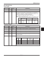
OVERVIEW
The SED1560 series is a single-chip LCD driver for dotmatrix liquid crystal displays. It accepts serial or 8-bit
parallel display data directly from a microprocessor and
stores data in an on-chip 166 × 65-bit RAM.
The SED1560 features 167 common and segment outputs to drive either a 65 × 102-pixel (SED1560) display
(4 rows × 6 columns with 16 × 16-pixel characters) or a
33 × 134-pixel (SED1561) display (2 rows × 8 columns
with 16 × 16-pixel characters) or a 17 × 150-pixel
(SED1562) display (1 row × 9 columns with 16 × 16
characters). In addition, two SED1560s can be connected together to drive a 65 × 268-pixel graphics display
panel.
The SED 1560 series can read and write RAM data with
the minimum current consumption as it does not require
any external operation clock. Also, it has a built-in LCD
power supply featuring the very low current consumption and, therefore, the display system of a high-performance but handy instrument can be realized by use of the
minimum current consumption and LSI chip configuration.
The SED 1560 Series has the SED1560, SED1561 and
SED1562 available according to the duty.
• On-chip 166 × 65-bit display RAM
• Direct relationship between RAM bits and display
pixels.
• High speed Interfaces to 6800- and 8080-series microprocessors
• Selectable 8-bit parallel/serial interface
• Many command functions
• On-chip LCD power circuit including DC/DC
voltage converter, voltage regulator and voltage
followers.
• On-Chip Contrast control.
• Two types of VREG (Built-in power supply regulator
temperature gradient).
• Type1 (SED156 *DO*, SED156*DA*)...–0.2%/˚C
• Type2 (SED1560DE*)...0.00%/˚C
• On-chip oscillator
• Ultra low power consumption
• Power Supply
VDD – VSS –2.4 V to –6.0 V
VDD – V5 –3.5 V to –16.0 V
• Ta = –30 to 85°C
• CMOS process
• TCP, QTCP
• The system is not designed against the radio activity.
FEATURES
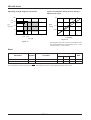
• Wide variety of duty and display areas
Model
Duty
LCD bias
Single-chip
display area
SED1560
1/65
1/64
1/49
1/48
1/9
1/7
65 × 102
64 × 102
49 × 102
48 × 102
SED1561
1/33
1/32
1/25
1/24
1/7
1/5
33 × 134
32 × 134
25 × 134
24 × 134
SED1562
1/17
1/16
1/5
17 × 150
16 × 150
Note: The LCD bias is obtained if the built-in power
supply is used.
EPSON
7–1
SED1560 Series
V5
V4
V3
V2
V1
VDD
VR
V5
VOUT
CAP2–
CAP2+
CAP1–
CAP1+
VSS
T1
T2
OSC1
OSC2
CL
FR
SYNC
CLO
DYO
D7
D6
D5
D4
D3
D2
D1
D0
VSS
RD
WR
A0
C86
CS2
CS1
P/S
S1
SCL
RES
M/S
VDD
V1
V2
V3
V4
V5
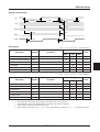
PAD LAYOUT
O0
1 216
49
COM1
O165
D156✻D 0B
95
8.08 × 5.28 mm
100 µm (Min.)
625 µm
300 µm (Al-pad)
Chip size
Pad pitch
Chip thickness
:
:
:
:
Bump size A
: 103 µm × 95 µm (Typ.) (Pad No. 1 ~ 6, 18, 36 ~ 42,
44 ~ 49)
: 69 µm × 95 µm (Typ.) (other then the above)
: 23 µm (Typ.)
• Au-Bump
Bump size B
Bump hight
• Al-pad
Pad size A
Bump size B
7–2
O121
O120
170
O46
O45
: 111 µm × 102 µm (Typ.) (Pad No. 1 ~ 6, 18, 36 ~ 42,
44 ~ 49)
: 77 µm × 99 µm (Typ.) (Other then the above)
EPSON
SED1560 Series
SED1560SERIES
Unit : µm
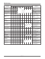
PAD Center Coordinates
PAD
PIN
No.
1
2
3
4
5
6
7
8
9
10
11
12
13
14
15
16
17
18
19
20
21
22
23
24
25
26
27
28
29
30
31
32
33
34
35
36
37
38
39
40
41
42
43
44
45
46
47
48
49
50
51
52
53
54
Name
V5
V4
V3
V2
V1
VDD
M/S
RES
SCL
SI
P/S
CS1
CS2
C86
A0
WR
RD
VSS
D0
D1
D2
D3
D4
D5
D6
D7
DYO
CLO
SYNC
FR
CL
OSC2
OSC1
T2
T1
VSS
CAP1+
CAP1CAP2+
CAP2VOUT
V5
VR
VDD
V1
V2
V3
V4
V5
00
01
02
03
04
X
Y
3640
3489
3339
3188
3037
2889
2755
2604
2453
2302
2151
2001
1850
1699
1548
1397
1247
1077
945
794
643
493
342
191
40
-111
-261
-412
-563
-714
-865
-1015
-1166
-1317
-1468
-1638
-1789
-1939
-2090
-2241
-2392
-2543
-2674
-2844
-2995
-3146
-3297
-3447
-3598
-3887
-3887
-3887
-3887
-3887
2487
2487
2487
2487
2487
2487
2487
2487
2487
2487
2487
2487
2487
2487
2487
2487
2487
2487
2487
2487
2487
2487
2487
2487
2487
2487
2487
2487
2487
2487
2487
2487
2487
2487
2487
2487
2487
2487
2487
2487
2487
2487
2487
2487
2487
2487
2487
2487
2487
2294
2194
2094
1994
1894
PAD
PIN
No.
55
56
57
58
59
60
61
62
63
64
65
66
67
68
69
70
71
72
73
74
75
76
77
78
79
80
81
82
83
84
85
86
87
88
89
90
91
92
93
94
95
96
97
98
99
100
101
102
103
104
105
106
107
108
Name
05
06
07
08
09
010
011
012
013
014
015
016
017
018
019
020
021
022
023
024
025
026
027
028
029
030
031
032
033
034
035
036
037
038
039
040
041
042
043
044
045
046
047
048
049
050
051
052
053
054
055
056
057
058
X
Y
-3887
-3887
-3887
-3887
-3887
-3887
-3887
-3887
-3887
-3887
-3887
-3887
-3887
-3887
-3887
-3887
-3887
-3887
-3887
-3887
-3887
-3887
-3887
-3887
-3887
-3887
-3887
-3887
-3887
-3887
-3887
-3887
-3887
-3887
-3887
-3887
-3887
-3887
-3887
-3887
-3887
-3711
-3611
-3511
-3411
-3311
-3211
-3111
-3011
-2911
-2811
-2711
-2611
-2511
1794
1694
1594
1494
1394
1294
1194
1094
994
894
794
694
594
494
394
294
194
94
-6
-106
-206
-306
-406
-506
-606
-706
-806
-906
-1006
-1106
-1206
-1306
-1406
-1506
-1606
-1706
-1806
-1906
-2006
-2106
-2206
-2487
-2487
-2487
-2487
-2487
-2487
-2487
-2487
-2487
-2487
-2487
-2487
-2487
PAD
PIN
No.
109
110
111
112
113
114
115
116
117
118
119
120
121
122
123
124
125
126
127
128
129
130
131
132
133
134
135
136
137
138
139
140
141
142
143
144
145
146
147
148
149
150
151
152
153
154
155
156
157
158
159
160
161
162
Name
059
060
061
062
063
064
065
066
067
068
069
070
071
072
073
074
075
076
077
078
079
080
081
082
083
084
085
086
087
088
089
090
091
092
093
094
095
096
097
098
099
0100
0101
0102
0103
0104
0105
0106
0107
0108
0109
0110
0111
0112
EPSON
X
Y
-2411
-2311
-2211
-2111
-2011
-1911
-1811
-1711
-1611
-1511
-1411
-1311
-1211
-1111
-1011
-911
-811
-711
-611
-511
-411
-311
-211
-111
-11
89
189
289
389
489
589
689
789
889
989
1089
1189
1289
1389
1489
1589
1689
1789
1889
1989
2089
2189
2289
2389
2489
2589
2689
2789
2889
-2487
-2487
-2487
-2487
-2487
-2487
-2487
-2487
-2487
-2487
-2487
-2487
-2487
-2487
-2487
-2487
-2487
-2487
-2487
-2487
-2487
-2487
-2487
-2487
-2487
-2487
-2487
-2487
-2487
-2487
-2487
-2487
-2487
-2487
-2487
-2487
-2487
-2487
-2487
-2487
-2487
-2487
-2487
-2487
-2487
-2487
-2487
-2487
-2487
-2487
-2487
-2487
-2487
-2487
PAD
PIN
No.
163
164
165
166
167
168
169
170
171
172
173
174
175
176
177
178
179
180
181
182
183
184
185
186
187
188
189
190
191
192
193
194
195
196
197
198
199
200
201
202
203
204
205
206
207
208
209
210
211
212
213
214
215
216
Name
0113
0114
0115
0116
0117
0118
0119
0120
0121
0122
0123
0124
0125
0126
0127
0128
0129
0130
0131
0132
0133
0134
0135
0136
0137
0138
0139
0140
0141
0142
0143
0144
0145
0146
0147
0148
0149
0150
0151
0152
0153
0154
0155
0156
0157
0158
0159
0160
0161
0162
0163
0164
0165
COMI
X
Y
2989
3089
3189
3289
3389
3489
3589
3689
3887
3887
3887
3887
3887
3887
3887
3887
3887
3887
3887
3887
3887
3887
3887
3887
3887
3887
3887
3887
3887
3887
3887
3887
3887
3887
3887
3887
3887
3887
3887
3887
3887
3887
3887
3887
3887
3887
3887
3887
3887
3887
3887
3887
3887
3887
-2487
-2487
-2487
-2487
-2487
-2487
-2487
-2487
-2206
-2106
-2006
-1906
-1806
-1706
-1606
-1506
-1406
-1306
-1206
-1106
-1006
-906
-806
-706
-606
-506
-406
-306
-206
-106
-6
94
194
294
394
494
594
694
794
894
994
1094
1194
1294
1394
1494
1594
1694
1794
1894
1994
2094
2194
2294
7–3
SED1560 Series
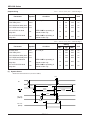
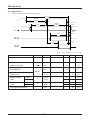
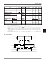
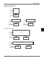
BLOCK DIAGRAM
O0 to O31
O32
to
O101 O102 to O165 COMI
VSS
VDD
VDD
V1
V1
V2
Common
and
segment
driver
V3
V4
Common
and
segment
driver
Segment
driver
V2
Common
I
V3
V4
V5
V5
Frame
control
Shift
register
Shift
register
CAP1+
CAP1–
CAP2+
Supply
voltage
generator1
166–bit display data latch
CAP2–
VR
T1, T2
Output
status
select
I/O
buffer
Line
address
decoder
166 x 65–bit display
data RAM
Line
counter
Display
initial line
register
166–bit column address decoder
FR
8–bit column address counter
SYNC
Page
address
register
Display
timing
generator
8–bit column address register
CL
CLO
DYO
M/S
Bus holder
7–4
OSC1
Command
decoder
Status flag
Oscillator
OSC2
MPU interface
I/O buffer
CS1 CS2 A0 RD WR C86 SI SCL P/S RES
D7 D6 D5 D4 D3 D2 D1 D0
EPSON
SED1560 Series
PIN DESCRIPTION
Power Supply
Number of pins
I/O
Name
Description
2
Supply
VDD
5V supply. Common to MPU power supply pin VCC.
2
Supply
VSS
Ground
11
Supply
V1 to V5
LCD driver supply voltages. The voltage determined by the LCD cell
is impedance-converted by a resistive divider or an operational
amplifier for application. Voltages should be determined on a VDDbasis so as to satisfy the following relationship.
The voltages must satisfy the following relationship.
VDD ≥ V0 ≥ V1 ≥ V2 ≥ V3 ≥ V4 ≥ V5.
When master mode selects, these voltages are generated on-chip.
SED1560D0B
V1
V2
V3
V4
1/9 V 5
2/9 V 5
7/9 V 5
8/9 V 5
SED1560DAB
SED1561D0B
1/7 V5
2/7 V5
5/7 V5
6/7 V5
SED1561DAB
SED1562D0B
1/5 V 5
2/5 V 5
3/5 V 5
4/5 V 5
LCD Driver Supplies
Number of pins
I/O
Name
Description
1
O
CAP1+
DC/DC voltage converter capacitor 1 positive connection
1
O
CAP1–
DC/DC voltage converter capacitor 1 negative connection
1
O
CAP2+
DC/DC voltage converter capacitor 2 positive connection
1
O
CAP2–
DC/DC voltage converter capacitor 2 negative connection
1
I/O
VOUT
1
I
VR
DC/DC voltage converter output
Voltage adjustment pin. Applies voltage between VDD and V5 using
a resistive divider.
2
I
T1, T2
Liquid crystal power control terminals
T1
T2
Boosting circuit
L
L
H
H
L
H
L
H
Valid
Valid
Invalid
Invalid
EPSON
Voltage
regulation
circuit
Valid
Valid
Valid
Invalid
V/F circuit
Valid
Valid
Valid
Valid
7–5
SED1560 Series
Microprocessor Interface
Number of pins
I/O
Name
Description
8
I/O
D0 to D7
1
I
A0
1
I
RES
2
I
CS1, CS2
1
I
RD (E)
Read enable input. See note. 1
1
I
WR (R/W)
Write enable input. See note. 2
1
I
C86
1
I
SI
1
I
SCL
Serial clock input. Data is read on the rising edge of SCL and
converted to 8-bit parallel data.
1
I
P/S
Parallel/serial data input select
Data inputs/outputs
Control/display data flag input. This is connected to the LSB
of the microprocessor address bus.
When LOW, the data on D0 to D7 is control data.
When HIGH, the data on D0 to D7 is display data.
Reset input. System is reset and initialized when LOW.
Chip select inputs. Data input/output is enabled when
CS1 is LOW and CS2 is HIGH.
Microprocessor interface select input. LOW when interfacing to
8080-series. HIGH when interfacing to 6800-series.
Serial data input
P/S
Operating
mode
Chip select
Data/command
Data
input/
output
Read/write
Serial
clock
HIGH
Parallel
CS1, CS2
A0
D0 to D7
RD, WR
—
LOW
Serial
CS1, CS2
A0
SI
Write only
SCL
In serial mode, data cannot be read from the RAM, and D0 to D7,
HZ, RD and WR must be HIGH or LOW. In parallel mode, SI and
SCL must be HIGH or LOW.
Note 1
When interfacing to 8080-series microprocessors, RD is active-LOW. When interfacing to 6800-series microprocessors, they are active-HIGH.
Note 2
When interfacing to 8080-series microprocessors, WR is active-LOW. When interfacing to 6800-series microprocessors, It will be read mode when WR is high and It will be write mode when WR is LOW.
7–6
EPSON
SED1560 Series
Oscillator and Timing Control
Number of pins
I/O
Name
Description
2
I
OSCI
Connecting pins for feedback resistors of the built-in oscillator
When M/S = “H”: Connect oscillator resistor Rf to the OSC1 and
OSC2 pins. The OSC2 pin is used for output of the oscillator
amplifier.
2
I/O
OSC2
When M/S = “L”: The OSC2 pin is used for input of oscillation signal.
The OSC1 pin should be left open. Fix the CL pin to the VSS level
when using the internal oscillator circuit as the display clock.
1
I
CL
Display clock input. The line counter increments on the rising edge
of CL and the display pattern is output on the falling edge. When
use external display clock, OSC1 = “H”, OSC2 = “L” and reset this
LSI by RES pin.
1
O
CLO
Display clock output. When using the master operation, the clock
signal is output on this pin. Connect CLO to YSCL on the common
driver.
1
I
M/S
Master/slave select input. Master makes some signals for display,
and slave gets them. This is for display syncronization.
Device
156XDOB
Operating
mode
Internal
oscillator
Power
supply
Low
Slave
OFF
OFF
I
I
Open
I
O
HIGH
Master
ON
ON
O
O
I
O
O
M/S
FR
SYNC OSC1 OSC2 DYO
Note
I = input mode
O = output mode
1
I/O
FR
LCD AC drive signal input/output. If the SED1560 series MPU’s are
used in master and slave configuration, this pin must be connected
to each FR pin. Also when the SED1560 series is used as the
master MPU, this pin must be connected to the FR pin of the
common driver. Output is selected when M/S is HIGH, and input is
selected when M/S is LOW.
1
I/O
SYNC
Display sync input/output. If the SED1560 series MPU’s are used in
master and slave configuration, this pin must be connected to each
SYNC pin. Output is selected when M/S is HIGH, and Input is
selected when M/S is LOW.
1
O
DYO
Start-up output for common driver. Connect to DIO of the common
driver.
EPSON
7–7
SED1560 Series
LCD Driver Outputs
Number of pins
I/O
Name
Description
166
O
O0 to O165
LCD driver outputs. O0 to O31 and O102 to O165 are selectable
segment or common outputs, determined by a selection command.
O32 to O101 are segment outputs only.
For segment outputs, the ON voltage level is given as shown in the
following table.
RAM data
LOW
HIGH
LCD ON voltage
FR
LOW
Normal display
V3
Inverse display
V5
HIGH
LOW
V2
V5
VDD
V3
HIGH
VDD
V2
For common outputs, the ON voltage is given as shown in the
following table.
Scan data
FR
LCD ON voltage
LOW
LOW
HIGH
V4
V1
LOW
VDD
HIGH
V5
HIGH
1
O
COMI
LCD driver common output. Common outputs when the “DUTY + 1”
command is executed are as follows:
SED1560
SED1561
SED1562
“DUTY + 1” ON
“DUTY + 1” OFF
COM64, COM48
COM32, COM24
COM16
V1 or V4
V1 or V4
V1 or V4
Common output special for the indicator.
7–8
EPSON
SED1560 Series
SPECIFICATIONS
Absolute Maximum Ratings
Parameter
Symbol
Rating
Unit
Supply voltage (1)
Supply voltage range (2)
(DC/DC When in use)
VSS
–7.0 +0.03
–6.0 to 0.3
(when triple boosting)
V
Driver supply voltage range (1)
V5
–18.0 to 0.3
V
Driver supply voltage range (2)
V1, V 2, V3, V4
V5 to 0.3
V
Input voltage range
VIN
VSS –0.3 to 0.3
V
Output voltage range
Vo
VSS –0.3 to 0.3
V
Operating temperature range
Topr
–30 to 85
deg. C
Storage temperature range (TCP)
Tstr
–55 to 100
deg. C
VCC
VDD
GND
VSS
VDD
V5
(System)
(SED1560 series)
Notes: 1. The voltages shown are based on VDD = 0 V.
2. Always keep the condition of VDD ≥ V1 ≥ V2 ≥ V3 ≥V4 ≥ V5 for voltages V1, V2, V 3 and V4.
3. If LSIs are used over the absolute maximum rating, the LSIs may be destroyed permanently. It is
desirable to use them under the electrical characteristic conditions for general operation. Otherwise, a
malfunction of the LSI may be caused and LSI reliability may be affected.
4. A guarantee on operating temperature below –30°C may be studied individually.
EPSON
7–9
SED1560 Series
DC Characteristics
VDD = 0 V, VSS = –5 V ± 10%, Ta = –30 to +85°C unless otherwise noted.
Item
Symbol
Power
Recommendvoltage (1) ed operation
Condition
Min.
Typ.
Max.
Unit
VSS
–5.5
–5.0
–4.5
V
–6.0
–2.4
V5
–16.0
–4.0
V
V5 *2
voltage (2) Operational
V1 , V2
0.4 × V5
VDD
V
V1, V2
Operational
V3 , V4
V5
0.6 × V5
V
V3, V4
VIHC1
0.3 × V SS
VDD
V
VIHC2
0.15 × VSS
VDD
*4
*3
Operational
Operating
Operational
High-level input voltage
Low-level input voltage
High-level output voltage
Low-level output voltage
0.3 × V SS
VDD
VSS = –2.7 V
0.2 × V SS
VDD
VILC1
VSS
0.7 × VSS
VILC2
VSS
0.85 × VSS
*4
VSS
0.7 × VSS
*3
VILC1
VSS = –2.7 V
VILC2
VSS = –2.7 V
VOHC1
VOHC2
0.8 × VSS
VDD
VDD
V
V
VSS = –2.7 V
IOH = –0.5 mA
0.2 × V SS
VDD
VSS = –2.7 V
IOH = –50 µA
0.2 × V SS
VDD
VOLC1
IOL = 1 mA
VSS
0.8 × VSS
VOLC2
IOL = 120 µA
VSS
0.8 × VSS
*3
*4
*5
OSC2
*5
OSC2
V
*5
OSC2
VOLC1
VSS = –2.7 V
IOL = 0.5 mA
VSS
0.8 × VSS
VOLC2
VSS = –2.7 V
IOL = 50 µA
VSS
0.8 × VSS
–1.0
1.0
µA
*6
–3.0
3.0
µA
*7
KΩ
RON
VIN = VDD or VSS
Ta = 25°C
V5 = –14.0 V
2.0
3.0
V5 = –8.0 V
3.0
4.5
Input terminal capacity
CIN
Oscillation frequency
fOSC
Rf=1 MΩ
±2%
Input voltage
Amplified output voltage
VSS
VOUT
5.0
µA
µA
V5
5.0
8.0
pF
*3 *4
kHz
*9
1.0
µs
*10
1.0
µs
*11
VSS = –5V
15
18
22
VSS = –2.7V
11
16
21
Voltage regulator
operation
voltage
VOUT
when triple
boosting
–2.4
V
V
*12
VOUT
–16.0
–6.0
V
VOUT
*13
Voltage regulutor
V5
1
Supplied to SED1560DOB
–16.0
–6.0
V
V5
2
Supplied to SED1561DOB
–16.0
–5.0
V
V5
3
Supplied to SED1561DAB
–16.0
–4.0
V
V5
4
Supplied to SED1562DOB
–16.0
–4.5
V
Ta = 25°C
–2.35
–2.65
V
*VSS = –2.4V is on the same basis as VSS = –2.7V.
EPSON
VSS
–6.0
–18.0
operation voltage
VREG
O0 to O166
*8
15.0
f=1MHz
tR
tRW
*5
OSC2
0.00
V5 = –18.0V
Ta = 25°C
V
0.01
ISSQ
I 5Q
Built-in power circuit
VSS
0.2 × V SS
0.2 × V SS
VOHC1
LCD driver ON resistance
7–10
*4
V
IOH = –1 mA
IOH = –120 µA
VOHC2
ILI
Reference voltage
*3
VSS = –2.7 V
I LO
Reset time
*1
VIHC2
Input leakage current
Reset “L” pulse width
VSS
VIHC1
Output leakage current
Static power consumption
Pin used
–2.5
* See the 4-12 page for details.
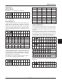
SED1560 Series
When dynamic current consumption (I) is displaye; the built-in power circuit is on and T1 = T2 =
Low.
VDD = 0 V, VSS = –5 V ± 10%, Ta = –30 to +85°C unless otherwise noted.
Item
Symbol
Condition
Min.
Typ.
Max.
Unit
SED1560
V5 = –12.5 V; 3 times amplified
169
340
µA
SED1561
V5 = –8.0 V ; 3 times amplified
124
250
µA
V5 = –6.0 V ; 2 times amplified
53
110
µA
VSS = –2.7 V; 3 times amplified
66
130
µA
SED1562
IDD (1)
Remarks
*16
V5 = –6.0 V
Typical current consumption characteristics
- Dynamic current consumption (I), if an external clock and an external power supply are used.
Conditions:
40
(µA)
30
I DD (1)
(ISS + I5)
20
561
SED1
SED1562
10
0
0
156
SED
1
2
3
4
5
6
7
(V)
VDD
Remarks:
The built-in power supply is off but
the external one is used.
SED1560 V5 – VDD = –12.5 V
SED1561 V5 – VDD = –8.0 V
SED1562 V5 – VDD = –6.0 V
External clock:
SED1560 fCL = 4 kHz
SED1561 fCL = 2 kHz
SED1562 fCL = 1 kHz
*14
- Dynamic current consumption (I), if the built-in oscillator and the external power supply are used.
Conditions:
80
(µA)
1
ED
I DD (1)
(ISS + I5)
40
S
561
D1
SE
1562
SED
20
0
0
56
60
1
2
3
4
VDD
5
6
7
(V)
Remarks:
EPSON
The built-in power supply is off but
the external one is used.
SED1560 V5 – VDD = –12.5 V
SED1561 V5 – VDD = –8.0 V
SED1562 V5 – VDD = –6.0 V
Internal oscillation:
SED1560 Rf = 1 MΩ
SED1561 Rf = 1 MΩ
SED1562 Rf = 1 MΩ
*15
7–11
SED1560 Series
- Dynamic current consumption (I), if the built-in power supply is used.
Conditions:
200
(µA)
I DD
0
56
ED1
S
150
(1)
100
62
0
SED15
1
2
3
4
VDD
5
V5 – VDD = –12.5 V; 3
times amplified
SED1561 V5 – VDD = –8.0 V; 3
times amplified
SED1562 V5 – VDD = –6.0 V; 2
times amplified
Internal oscillation:
SED1560 Rf = 1 MΩ
SED1561 Rf = 1 MΩ
SED1562 Rf = 1 MΩ
*16
SED1560
1561
SED
50
The built-in power supply is on and
T1 = T2 = Low.
6
7
(V)
Remarks:
Notes: *1. Although the wide range of operating voltage is guaranteed, a spike voltage change during access to the
MPU is not guaranteed.
*2. The operating voltage range of the VSS and V 5 systems (see Figure 11).
The operating voltage range is applied if an external power supply is used.
*3. Pins A0, D0 to D7, RD (E), WR (R/W), CS1, CS2, FR, SYNC, M/S, C86, SI, P/S, T1 and T2.
*4. Pins CL, SCL, and RES
*5. Pins D0 to D7, FR, SYNC, CL0, and DY0
*6. Pins A0, RD (E), WR (R/W), CS1, CS2, CL, M/S, RES, C86, SI, SCL, P/S, T1, and T2.
*7. Applied if pins D0 to D7, FR, and SYNC are high impedance.
*8. The resistance when the 0.1-volt voltage is applied between the “On” output terminal and each power
terminal (V1, V2, V3 or V4). It must be within the operating voltage (2).
R ON = 0.1 V/∆I
(∆I is the current that flows when 0.1 VDC is applied during power-on.)
*9. The relationship between the oscillation frequency, frame and Rf value (see Figure 10).
*10. “tr” (reset time) indicates the period between the time when the RES signal rises and when the internal
circuit has been reset. Therefore, the SED156* is usually operable after “tr” time.
*11. Specifies the minimum pulse width of RES” signal. The Low pulse greater than “tRW” must be entered
for reset.
*12. If the voltage is amplified three times by the built-in power circuit, the primary power VSS must be used
within the input voltage range.
*13. The V5 voltage can be adjusted within the voltage follower operating range by the voltage regulator
circuit.
*14, 15, 16 Indicates the current consumed by the separate IC. The current consumption due to the LCD panel
capacity and wiring capacity is not included.
The current consumption is shown if the checker is used, the display is turned on, the output status of
Case 6 is selected, and the SED1560D0B is set to 1/64 duty, the SED1561D0B is set to 1/32 duty, and the
SED1562D0B is set to 1/16 duty.
*14. Applied if an external clock is used and if not accessed by the MPU.
*15. Applied if the built-in oscillation circuit is used and if not accessed by the MPU.
*16. Applied if the built-in oscillation circuit and the built-in power circuit are used (T1 = T2 = Low) and if
not accessed by the MPU. Measuring conditions: C1 = 4.7 µF, C2 = 0.47 µF, Ra + Rb = 2 MΩ
This includes the current that flows through the voltage regulator resistor (Ra + Rb = 2 MΩ). If the
built-in power circuit is used, the current consumption is equal to the current of VSS power.
7–12
EPSON
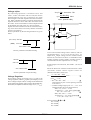
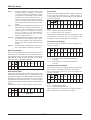
SED1560 Series
The relationship between oscillator frequency fOSC
and LCD frame frequency f F is obtained from the
following expression.
Oscillator frequency vs. frame vs. Rf
[SED156✽D0B]
Ta = 25°C
40
SED1560
30
[KHz]
20
f OSC
SED1561
10
SED1562
0
0.5
1.0
Rf
Duty
fF
1/64
fOSC/256
fOSC/192
fOSC/256
fOSC/192
fOSC/256
VSS = –5 V
1.5
[MΩ ]
2.0
2.5
(fF indicates not
AC.)
1/48
1/32
1/24
1/16
fF signal cycle but cycle of LCD
Figure 10 (a)
External clock (fCL) vs. frame [SED156✽D✽B]
200
duty 1/64 SED1560
duty 1/48
[Hz]
100
fF
duty 1/32 SED1561
duty 1/24
duty 1/16 SED1562
0
2
4
f CL [KHz]
6
8
Figure 10 (b)
EPSON
7–13
SED1560 Series
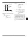
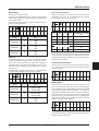
Operating voltage range for VSS and V5
–16
Power consumption during access (I DD (2)) MPU access cycle
–20
10
–15
1
5.0V
2.7V
–13
[V]
–10
V5–VDD
[mA]
I DD (2)
–5
0
0.1
0.01
2
2.4
4
3.0
VSS [V]
6
8
0
0.01
0.1
f cyc [MHz]
1
10
Figure 12
Figure 11
This graphic shows the current consumption when
the vertical patterns are written during “fcyc”. If not
accessed, IDD(1) is only shown.
Reset
Rating
Parameter
Symbol
tR
Reset LOW-level pulsewidth tRW
Reset time
Condition
See note.
Unit
Min.
Typ.
Max.
1.0
—
—
µs
1.0
—
—
µs
Note
tR is measured from the rising edge of RES. The SED1560 enters normal operating mode after a reset.
7–14
EPSON
SED1560 Series
Display control timing
CL
t WLCL
t WHCL
tf
tr
t DFR
FR
t DSNC
SYNC
t DOH
t DOL
t CDH
t CDL
DYO
CLO
Input timing
VSS = –5.5 to –4.5 V, Ta = –30 to 85 deg. C
Rating
Parameter
CL LOW-level pulsewidth
CL HIGH-level pulsewidth
CL rise time
CL fall time
FR delay time
SYNC delay time
Symbol
Condition
tWLCL
tWHCL
tr
tf
tDFR
tDSNC
Unit
Min.
Typ.
Max.
35
—
—
µs
35
—
—
µs
—
30
—
ns
—
30
—
ns
–1.0
—
1.0
µs
–1.0
—
1.0
µs
VSS = –4.5 to –2.7 V, Ta = –30 to 85 deg. C
Rating
Parameter
CL LOW-level pulsewidth
CL HIGH-level pulsewidth
CL rise time
CL fall time
FR delay time
SYNC delay time
Symbol
Condition
tWLCL
tWHCL
tr
tf
tDFR
tDSNC
Unit
Min.
Typ.
Max.
35
—
—
µs
35
—
—
µs
—
40
—
ns
—
40
—
ns
–1.0
—
1.0
µs
–1.0
—
1.0
µs
Notes: 1. Effective only when the SED156*DOB is in the master mode.
2. The FR/SYNC delay time input timing is provided in the slave operation.
The FR/SYNC delay time output timing is provided in the master operation.
3. Each timing is based on 20% and 80% of VSS.
4. When usingin the range of VSS = –2.4 ~ –4.5V, raise the above ratings for –2.7 ~ –4.5V equally by 30%.
EPSON
7–15
SED1560 Series
Output timing
VSS = –5.5 to –4.5 V, Ta = –30 to 85 deg. C
Rating
Parameter
Symbol
Condition
Unit
tDFR
SYNC delay time
tDSNC
DYO LOW-level delay time tDOL
DYO HIGH-level delay time tDOH
CL = 50 pF
CLO to DYO Low-level
SED156✽D0B operating in
FR delay time
delay time
CLO to DYO HIGH-level
delay time
tCDL
Min.
Typ.
Max.
—
60
150
ns
—
60
150
ns
—
70
160
ns
—
70
160
ns
10
40
100
ns
10
40
100
ns
master mode only
SED156✽D0B operating in
tCDH
master mode only
VSS = –4.5 to –2.7 V, Ta = –30 to 85 deg. C
Rating
Parameter
Symbol
Condition
Unit
tDFR
SYNC delay time
tDSNC
DYO LOW-level delay time tDOL
DYO HIGH-level delay time tDOH
CL = 50 pF
CLO to DYO LOW-level
SED156✽D0B operating in
FR delay time
delay time
CLO to DYO HIGH-level
delay time
tCDL
Min.
Typ.
Max.
—
120
240
ns
—
120
240
ns
—
140
250
ns
—
140
250
ns
10
100
200
ns
10
100
200
ns
master mode only
SED156✽D0B operating in
tCDH
master mode only
(1) System buses
Read/write characteristics I (80-series MPU)
t AH8
A0
t CYC8
t AW8
WR, RD
(CS)
tr
t CCLR
t CCLW
t CCHR
t CCHW
tf
t DH8
t DS8
D0 ~ D7
(WRITE)
t ACC8
D0 ~ D7
(READ)
7–16
EPSON
tCH8
SED1560 Series
VSS = –5.0 ±10%, Ta = –30 ~ 85 °C
Item
Address hold time
Signal
Symbol
A0, CS
tAH8
tAW8
tCYC8
Address setup time
System cycle time
Control L pulse width (WR)
WR
Control L pulse width (RD)
RD
Control H pulse width (WR)
WR
Control H pulse width (RD)
RD
Data setup time
Data hold time
RD access time
D0 to D7
Output disable time
Input signal change time
tCCLW
tCCLR
tCCHW
tCCHR
tDS8
tDH8
tACC8
tCH8
tr, tf
Conditions
Min.
Max.
Unit
10
ns
10
ns
200
ns
22
ns
77
ns
172
ns
117
ns
20
ns
10
ns
CL = 100pF
10
70
ns
50
ns
15
ns
VSS = –2.7 ~ –4.5 V, Ta = –30 ~ 85 °C
Item
Address hold time
Signal
Symbol
A0, CS
tAH8
tAW8
tCYC8
Address setup time
System cycle time
Control L pulse width (WR)
WR
Control L pulse width (RD)
RD
Control H pulse width (WR)
WR
Control H pulse width (RD)
RD
Data setup time
Data hold time
RD access time
Output disable time
Input signal change time
D0 to D7
tCCLW
tCCLR
tCCHW
tCCHR
tDS8
tDH8
tACC8
tCH8
tr, tf
Conditions
Min.
Max.
Unit
0
ns
0
ns
450
ns
44
ns
194
ns
394
ns
244
ns
20
ns
10
ns
CL = 100pF
10
140
ns
100
ns
15
ns
Notes: 1. When using the system cycle time in the high-speed mode, it is limited by tr + tf ≤ ( tCYC8–tCCLW–
tCCHW) or tr + tf ≤ ( tCYC8–tCCLR–tCCHR)
2. All signal timings are limited based on the 20% and 80% of VSS voltage.
3. Read/write operation is performed while CS (CS1 and CS2) is active and the RD or WR signal is in the
low level.
If read/write operation is performed by the RD or WR signal while CS is active, it is determined by the
RD or WR signal timing.
If read/write operation is performed by CS while the RD or WR signal is in the low level, it is determined by the CS active timing.
4. When usingin the range of VSS = –2.4 ~ –4.5V, raise the above ratings for –2.7 ~ –4.5V equally by 30%.
EPSON
7–17
SED1560 Series
(2) System buses
Read/write characteristics II (68-series MPU)
t CYC6
t EWLR
t EWLW
E
tr
t EWHR
t EWHW
t AW6
tf
t AH6
A0, R/W
t AH6
t DS6
t DH6
D0 ~ D7
(WRITE)
t OH6
t ACC6
D0 ~ D7
(READ)
VSS = –5.0 V ± 10%, Ta = –30 ~ 85 °C
Item
Signal
System cycle time
Address setup time
(A0)
Address hold time
R/W
Data setup time
Data hold time
D0~D7
Output disable time
Access time
Enable H pulse
READ
width
WRITE
Enable L pulse
READ
width
WRITE
Input signal change time
7–18
E
E
Symbol
Conditions
Min.
Max.
Unit
tCYC6
200
ns
tAW6
tAH6
tDS6
tDH6
tOH6
tACC5
tEWHR
tEWHW
tEWLR
tEWLW
tr, tf
10
ns
10
ns
20
ns
10
n
EPSON
CL = 100pF
10
50
ns
70
ns
77
ns
22
ns
117
ns
172
ns
15
ns
SED1560 Series
VSS = –2.7 V ~ 4.5 V, Ta = –30 ~ 85 °C
Item
Signal
Symbol
tCYC6
System cycle time
Address setup time
A0
Address hold time
R/W
tAW6
tAH6
tDS6
tDH6
tOH6
tACC5
tEWHR
tEWHW
tEWLR
tEWLW
tr, tf
Data setup time
Data hold time
D0 to D7
Output disable time
Access time
Enable H pulse
READ
width
WRITE
Enable L pulse
READ
width
WRITE
E
E
Input signal change time
Notes:
Conditions
CL = 100pF
Min.
Max.
Unit
450
ns
0
ns
0
ns
20
ns
10
ns
20
100
ns
140
ns
194
ns
44
ns
244
ns
394
ns
15
ns
1. When using the system cycle time in the high-speed mode, it is limited by tr + tf ≤ (tCYC6-tEWLW-tEWHW)
or tr + tf ≤ (tCYC6-tEWLR-tEWHR).
2. All signal timings are limited based on the 20% and 80% of VSS voltage.
3. Read/write operation is performed while CS (CS1 and CS2) is active and the E signal is in the high level.
If read/write operation is performed by the E signal while CS is active, it is determined by the E signal
timing.
If read/write operation is performed by CS while the E signal is in the high level, it is determined by the
CS active timing.
4. When usingin the range of VSS = –2.4 ~ –4.5V, raise the above ratings for –2.7 ~ –4.5V equally by 30%.
(3) Serial interface
t CSS
t CSH
CS
t SAS
t SAH
A0
t SCYC
t SLW
SCL
tr
tf
t SDS
t SHW
t SDH
SI
EPSON
7–19
SED1560 Series
VSS = –5.0 V ±10%, Ta = –30 ~ 85 °C
Item
Serial clock cycle
Signal
Symbol
SCL
tSCYC
tSHW
tSLW
tSAS
tSAH
tSDS
tSDH
tCSS
tCSH
tr, tf
SCL High pulse width
SCL Low pulse width
Address setup time
A0
Address hold time
Data setup time
SI
Data hold time
CS-SCL time
cs
Input signal change time
Conditions
Min.
Max.
Unit
250
ns
75
ns
75
ns
50
ns
200
ns
50
ns
30
ns
30
ns
400
50
ns
VSS = –2.7 V ~ –4.5 V, Ta = –30 ~ 85 °C
Item
Serial clock cycle
Signal
Symbol
SCL
tSCYC
tSHW
tSLW
tSAS
tSAH
tSDS
tSDH
tCSS
tCSH
tr, tf
SCL High pulse width
SCL Low pulse width
Address setup time
A0
Address hold time
Data setup time
SI
Data hold time
CS-SCL time
Input signal change time
cs
Conditions
Min.
Max.
500
ns
150
ns
150
ns
100
ns
400
ns
100
ns
100
ns
60
ns
800
50
*1. All signal timings are limited based on the 20% and 80% of VSS voltage.
*2. When usingin the range of VSS = –2.4 ~ –4.5V, raise the above ratings for –2.7 ~ –4.5V equally by 30%.
7–20
EPSON
Unit
ns
SED1560 Series
FUNCTIONAL DESCRIPTION
Microprocessor Interface
Parallel/serial interface
Parallel data can be transferred in either direction between the controlling microprocessor and the SED1560
series through the 8-bit I/O buffer (D0 to D7). Serial data
can be sent from the microprocessor to the SED1560
series through the serial data input (SI), but not from the
SED1560 series to the microprocessor. The parallel or
serial interface is selected by P/S as shown in table 1.
Table 1. Parallel/serial interface selection
P/S
Input type
CS1
CS2
A0
RD
WR
C86
SI
SCL
D0 to D7
HIGH
Parallel
CS1
CS2
A0
RD
WR
C86
—
—
D0 to D7
LOW
Serial
CS1
CS2
A0
—
—
—
SI
SCL
(Hz)
Note
“—” indicates fixed to either “H” or to “L”
For the parallel interface, the type of microprocessor is
selected by C86 as shown in table 2.
Common
Table 2. Microprocessor selection for parallel
interface
C86
MPU bus
type
CS1
CS2
A0
RD
WR D0 to D7
HIGH
6800-series
CS1
CS2
A0
E
R/W D0 to D7
LOW
8080-series
CS1
CS2
A0
RD
Table 3. Parallel data transfer
WR D0 to D7
Parallel interface
A0, WR (or R/W) and RD (or E) identify the type of
parallel data transfer to be made as shown in table 3.
Serial interface
The serial interface comprises an 8-bit shift register and
a 3-bit counter. These are reset when CS1 is HIGH and
CS2 is LOW. When these states are reversed, serial data
and clock pulses can be received from the microprocessor on SI and SCL, respectively.
6800 series
8080 series
A0
1
R/W
1
E
1
RD
0
WR
1
1
0
1
1
0
Display data write
0
1
1
0
1
Status read
0
0
1
1
0
Write to internal reigister
(command)
Description
Display data read out
Serial data is read on the rising edge of SCL and must be
input at SI in the sequence D7 to D0. On every eighth
clock pulse, the data is transferred from the shift register
and processed as 8-bit parallel data.
Input data is display data when A0 is HIGH and control
data when A0 is LOW. A0 is read on the rising edge of
every eighth clock signal.
The SLC signal is affected by the termination reflection
and external noise caused by the line length. The operation check on the actual machine is recommended.
EPSON
7–21
SED1560 Series
CS1
CS2
SI
D7
1
SCL
D6
2
D5
3
D4
4
D3
5
D2
6
D1
7
D0
8
D7
9
D6
10
A0
Figure 1. Serial interface timing
(dummy read cycle). On the next read cycle, the data is
read from the bus buffer onto the microprocessor bus. At
the same time, the next block of data is transferred from
RAM to the bus buffer. Likewise, when the microprocessor writes data to display data RAM, the data is first
stored in the bus buffer before being written to RAM at
the next write cycle.
When writing data from the microprocessor to RAM,
there is no delay since data is automatically transferred
from the bus buffer to the display data RAM. If the data
rate is required to slow down, the microprocessor can
insert an NOP instruction which has the same affect as
executing a wait procedure.
When a sequence of address sets is executed, a dummy
read cycle must be inserted between each pair of address
sets. This is necessary because the addressed data from
the RAM is delayed one cycle by the bus buffer, before
it is sent to the microprocessor. A dummy read cycle is
thus necessary after an address set and after a write cycle.
Chip select inputs
The SED1560 series has two chip select pins: CS1 and
CS2, and data exchange between the microprocessor and
the SED1560 series is enabled when CS1 is LOW and
CS2 is HIGH. When these pins are set to any other
combination, D0 to D7 are high impedance. The A0, RD,
WR, SI and SCI inputs are disabled. If the serial input
interface has been selected, the shift register and counter
are reset. The Reset signal is entered independent from
the CS1 and CS2 status.
Data Transfer
To match the timing of the display data RAM and
registers to that of the controlling microprocessor, the
SED1560 series uses an internal data bus and bus buffer.
A kind of pipeline processing takes place. When the
microprocessor reads the contents of RAM, the data for
the initial read cycle is first stored in the bus buffer
WR
MPU
DATA
Bus
holder
N
N+1
N
N+2
N+1
Internal
timing
WR
Figure 2. Write timing
7–22
EPSON
N+3
N+2
N+3
SED1560 Series
WR
MPU
RD
DATA
N
n
N
Address set
Dummy read
n+1
Data read n
Data read (n+1)
WR
RD
Internal
timing
Column
address
Bus
holder
N
N+1
N
n
N+2
N+1
N+2
Figure 3. Read timing
Status Flag
The SED1560 series has a single bit status flag, D7.
When D7 is HIGH, the device is busy and will only
accept a Status Read command. If cycle times are
monitored ed carefully, this flag does not have to be
checked before each command, and microprocessor capabilities can be fully utilized.
EPSON
7–23
SED1560 Series
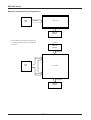
Display Data RAM
The display data RAM stores pixel data for the LCD. It
is a 166-column × 65-row addressable array as shown in
figure 4.
(If the display start line is set to 1ch)
0 0 1 0
0 0 1 1
0 1 0 0
0 1 0 1
0 1 1 0
0 1 1 1
Page 1
Page 2
Page 3
Page 4
Page 5
Page 6
Page 7
1/64
Start
1/32
Page 8
ADC
LCD
OUT DO DO
=1 =0
O0 A5 00
O1 A4 01
O2 A3 02
O3 A2 03
O4 A1 04
O5 A0 05
O6 9F 06
O7 9E 07
1 0 0 0
Page 0
A2
A3
A4
A5
0 0 0 1
D0
D1
D2
D3
D4
D5
D6
D7
D0
D1
D2
D3
D4
D5
D6
D7
D0
D1
D2
D3
D4
D5
D6
D7
D0
D1
D2
D3
D4
D5
D6
D7
D0
D1
D2
D3
D4
D5
D6
D7
D0
D1
D2
D3
D4
D5
D6
D7
D0
D1
D2
D3
D4
D5
D6
D7
D0
D1
D2
D3
D4
D5
D6
D7
D0
Common
address
COM 0
COM 1
COM 2
COM 3
COM 4
COM 5
COM 6
COM 7
COM 8
COM 9
COM10
COM11
COM12
COM13
COM14
COM15
COM16
COM17
COM18
COM19
COM20
COM21
COM22
COM23
COM24
COM25
COM26
COM27
COM28
COM29
COM30
COM31
COM32
COM33
COM34
COM35
COM36
COM37
COM38
COM39
COM40
COM41
COM42
COM43
COM44
COM45
COM46
COM47
COM48
COM49
COM50
COM51
COM52
COM53
COM54
COM55
COM56
COM57
COM58
COM59
COM60
COM61
COM62
COM63
COM I
to
O3
O2
O1
O0
0 0 0 0
Line
address
00H
01
02
03
04
05
06
07
08
09
0A
0B
0C
0D
0E
0F
10
11
12
13
14
15
16
17
18
19
1A
1B
1C
1D
1E
1F
20
21
22
23
24
25
26
27
28
29
2A
2B
2C
2D
2E
2F
30
31
32
33
34
35
36
37
38
39
3A
3B
3C
3D
3E
3F
Column address
DATA
to
O162
O163
O164
O165
Page
address
to
Figure 4. Display data RAM addressing
Note
For a 1/65 and 1/33 display duty cycles, page 8 is accessed following 1BH and 3BH, respectively.
7–24
EPSON
SED1560 Series
The 65 rows are divided into 8 pages of 8 lines and a ninth
page with a single line (D0 only). Data is read from or
written to the 8 lines of each page directly through D0 to
D7.
D0
D1
D2
D3
D4
The time taken to transfer data is very short, because the
microprocessor inputs D0 to D7 correspond to the LCD
common lines as shown in figure 5. Large display
configurations can thus be created using multiple
SED1560s.
COM0
COM1
COM2
COM3
COM4
1
0
1
0
0
Figure 5. RAM-to-LCD data transfer
The microprocessor reads from and writes to RAM
through the I/O buffer. Since the LCD controller operates independently, data can be written to RAM at the
same time as data is being displayed, without causing the
LCD to flicker.
Column Address Counter
The column address counter is an 8-bit presettable counter that provides the column address to display data
RAM. See figure 4. It is incremented by 1 each time a
read or write command is received. The counter automatically stops at the highest address, A6H. The contents of the column address counter are changed by the
Column Address Set command. This counter is independent of the page address register.
When the Select ADC command is used to select inverse
display operation, the column address decoder inverts
the relationship between the RAM column data and the
display segment outputs.
Page Address Register
The 4-bit page address register provides the page address
to display data RAM. The contents of the register are
changed by the Page Address Set command.
Page address 8 (D3 = H, D2, D1, D0 = L) is a special use
RAM area for the indicator.
Initial Display Line Register
The initial display line register stores the address of the
RAM line that corresponds to the first (normally the top)
line (COM0) of the display. See figure 4. The contents
of this 6-bit register are changed by the Initial Display
Line command. At the start of each LCD frame, synchronized with SYNC, the initial line is copied to the line
counter. The line counter is then incremented on the CL
clock signal once for every display line. This generates
the line addresses for the transfer of the 166 bits of RAM
data to the LCD drivers.
If a 1/65 or 1/33 display duty cycle is selected by the Duty
+ 1 command, the line address corresponding to the 65th
or 33rd SYNC signal is changed and the indicator special-use line address is selected. If the Duty + 1 command
is not used, the indicator special-use line address is not
selected.
Output Selection Circuit
The number of common (COM) and segment (SEG)
driver outputs can be selected to fit different LCD panel
configurations by the output selection circuit.
There are 70 segment-only outputs (O32 to O101) and 96
common or segment dual outputs (O0 to O31 and O102
to O165). A command select the status of the dual
common/segment outputs. Figure 6 shows the six different LCD driver arrangements.
Necessary LCD driver voltage is automatically allocated
to the COM/SEG dual outputs when their function is
determined by the output selection circuit.
The SED1560 selects Case 1, 2 or 6 while the SED1561
selects Case 3, 4, 5 or 6. As to the SED1562, COM/SEG
output status cannot be selected, being fixed.
EPSON
7–25
SED1560 Series
ADC
(D0)
L
H
0
→
165 ←
→ 165
0
←
Column address
Display data RAM
Case 1
Case 2
Case 3
Case 4
Case 5
Case 6
102 segments
16 commons
↑
O0
↑
O15
64 commons
32 commons
102 segments
134 segments
134 segments
134 segments
166 segments
↑
O101
32 commons
32 commons
↑
O31
32 commons
16 commons
↑
O133
↑
O149
↑
O165
Figure 6. Output configuration selection
When COM outputs are assigned to the output drivers,
the unused RAM area is not available. However, all
RAM column addresses can still be accessed by the
microprocessor.
Since duty setting and output selection are independent,
the appropriate duty must be selected for each case.
Cases 1 to 6 are determined according to the three lowest
bits in the output status register in the output selection
circuit. The COM output scanning direction can be
selected by setting bit D3 in the output status register to
“H” or “L”.
Table 4
SED1560
Duty
COM I function
SED1561
SED1562
1/64
1/48
1/32
1/24
1/16
COM64
COM48
COM32
COM24
COM16
When the DUTY + 1 command is executed, pin COM1
becomes as shown in Figure 4 irrelevant to output selection:
Since master/slave operation and the output selection
circuit are completely independent in the SED1560 series, a chip either on the master or slave side can be
allocated to the COM output function in multi-chip
configuration.
The LCD driver outputs shown in Table 5 become
ineffective when the SED1560 or SED1561 is used with
1/48 or 1/24 duty, respectively. In this case, ineffective
outputs are used in the open state.
Table 5
Case 1
SED1560
Case 2
Case 3
SED1561
Case 4
Case 5
7–26
D3
0
1
0
1
0
1
0
1
0
1
Output status register
D2
D1
1
0
1
0
1
0
1
0
0
1
0
1
0
1
0
1
0
0
0
0
EPSON
D0
1
1
0
0
1
1
0
0
1
1
Ineffective output
O150
O102
O150
O16
O0
O23
O158
O134
O158
O8
to
to
to
to
to
to
to
to
to
to
O165
O117
O165
O31
O7
O31
O165
O141
O165
O15
SED1560 Series
SED1560 Output Status
The SED1560 selects any output status from Cases 1, 2
and 6.
1/64 duty
Case
1
2
6
1
2
6
64 × 102)
Status register
LCD driver output
D3 D2 D1 D0 O0
O31 O32
O101 O102
O133 O134
O165
0
1
0
1
SEG102
COM0
COM63
1
1
0
1
SEG102
COM63
COM0
0
1
0
0
COM31
COM0
SEG102
COM32
COM63
1
1
0
0
COM32
COM63
SEG102
COM31
COM0
–
0
0
0
1/48 duty
Case
(Display Area
SEG166
(Display Area
48 × 102)
Status register
LCD driver output
D3 D2 D1 D0 O0
O31 O32
0
1
0
1
1
1
0
1
0
1
0
0
COM31
1
1
0
0
COM32
–
0
0
0
O101 O102
O133 O134
O165
COM47
COM0
COM0
COM47
COM0
47
SEG102
COM32
SEG102
COM31
47
COM0
SEG166
SED1561 Output Status
The SED1561 selects any output status from Cases 3, 4,
5 and 6.
1/32 duty
Case
3
4
5
6
(Display Area
3
4
5
6
LCD driver output
Status register
D3 D2 D1 D0 O0
O15 O16
O31 O32
O133 O134
149 150
O165
0
0
1
1
COM31
COM0
SEG134
1
0
1
1
COM0
COM31
SEG134
0
0
1
0
SEG134
COM0
COM31
1
0
1
0
SEG134
COM31
COM0
0
0
0
1
15←COM0
SEG134
COM16→31
1
0
0
1
COM16→31
SEG134
15←COM0
–
0
0
0
SEG166
(Display Area
1/24 duty
Case
32 × 134)
24 × 134)
LCD driver output
Status register
D3 D2 D1 D0 O0
O15 O16
O31 O32
O133 O134
149 150
O165
0
0
1
1
1
0
1
1
0
0
1
0
SEG134
1
0
1
0
SEG134
0
0
0
1
15←COM0
SEG134
16→23
1
0
0
1
16→23
SEG134
15←COM0
–
0
0
0
COM23
COM0
COM0
SEG134
SEG134
COM23
COM0
COM23
COM23
COM0
SEG166
EPSON
7–27
SED1560 Series
SED1562 Output Status
COM/SEG output status of the SED1562 is fixed.
1/16 duty (16 × 150)
LCD driver output
00
0149 150
15
SEG150
0165
COM0
Display Timers
Line counter and display data latch
timing
In a multiple-chip configuration, FR and SYNC are
inputs. The SYNC signal from the master synchronizes
the line counter and common timing of the slave.
The display clock, CL, provides the timing signals for the
line counter and the display data latch. The RAM line
address is generated synchronously using the display
clock. The display data latch synchronizes the 166-bit
display data with the display clock.
The timing of the LCD panel driver outputs is independent of the timing of the input data from the microprocessor.
Common timing signals
FR and SYNC
The LCD AC signal, FR, and the synchronization signal,
SYNC, are generated from the display clock. The FR
controller generates the timing for the LCD panel driver
outputs. Normally, 2-frame wave patterns are generated,
but n-line inverse wave patterns can also be generated.
These produce a high-quality display if n is based on the
LCD panel being used.
SYNC synchronizes the timing of the line counter and
common timers. It is also needed to synchronize the
frame period and a 50% duty clock.
7–28
The internal common timing and the special-use common driver start signal, DYO, are generated from CL.
As shown in figures 7 and 8, DYO outputs a HIGH-level
pulse on the rising edge of the CL clock pulse that
precedes a change on SYNC. DYO is generated by both
the SED1560D0B, regardless of whether the device is in
master or slave mode. However, when operating in slave
mode, the device duty and the external SYNC signal
must be the same as that of the master. In a multiple-chip
configuration, FR and SYNC must be supplied to the
slave from the master.
Table 6. Master and slave timing signal status
Part number
Mode
FR
SYNC
CLO
DYO
Master
Output
Output
CL
output
Output
Slave
Input
Input
SD156✽D✽B
EPSON
High
Output
impedance
SED1560 Series
2-frame AC driver waveform
(SED1561 1/32 duty)
31 32
1
2
3
4
5
6
27 28 29 30 31 32
1
2
3
4
5
CL
SYNC
FR
DYO
COM0
VDD
V1
V4
V5
COM1
VDD
V1
V4
V5
RAM
data
VDD
V2
V3
V5
SEG n
Figure 7. Frame driver timing
EPSON
7–29
SED1560 Series
n line inverse driver waveform (n = 5, line inverse register 4)
31 32
1
2
3
4
5
6
27 28 29 30 31 32
1
2
3
4
5
CL
SYNC
FR
DYO
COM0
VDD
V1
V4
V5
COM1
VDD
V1
V4
V5
RAM
data
VDD
V2
V3
V5
SEG n
Figure 8. Line inverse driver timing
Note
When n = 5, the line inversion register is set to 4.
7–30
EPSON
SED1560 Series
LCD Driver
The LCD driver converts RAM data into the 167 outputs
that drive the LCD panel. There are 70 segment outputs,
96 segment or common dual outputs, and a COM1 output
for the indicator display.
Two shift registers for the common/segment drivers are
used to ensure that the common outputs are output in the
correct sequence. The driver output voltages depend on
the display data, the common scanning signal and FR.
VDD
VSS
VDD
V1
V2
V3
V4
V5
VDD
V1
V2
V3
V4
V5
VDD
V1
V2
V3
V4
V5
VDD
V1
V2
V3
V4
V5
VDD
V1
V2
V3
V4
V5
V5
V4
V3
V2
V1
VDD
–V1
–V2
–V3
–V4
–V5
V5
V4
V3
V2
V1
VDD
–V1
–V2
–V3
–V4
–V5
FR
(SYNC)
COM0
COM1
COM0
COM2
COM3
COM4
COM5
COM1
COM6
COM7
COM8
COM9
COM2
COM10
COM 1
COM12
COM13
SEG0
COM14
COM15
SEG0 SEG1 SEG2 SEG3 SEG4
SEG1
COM0
to
SEG0
COM0
to
SEG1
Figure 9. Example of segment and common timing
EPSON
7–31
SED1560 Series
Display Data Latch Circuit
FR Control Circuit
The display data latch circuit temporarily stores the
output display data from the display data RAM to the
LCD driver circuit in each common period. Since the
Normal/Inverse Display, Display ON/OFF and Display
All Points ON/OFF commands control the data in this
latch, the data in the display data RAM is remains
unchanged.
The LCD driver voltage supplied to the LCD driver
outputs is selected using FR signal.
Power Supply Circuit
This is a power circuit to produce voltage needed to drive
liquid crystals at a low power consumption. This circuit
is valid only when the SED156*D*B master is in operation. The power circuit consists of voltage tripler, voltage
regulator and the voltage follower.
The power circuit built into SED1560✽D *B is set for
smaller scale liquid crystal panels and it is not too
suitable when the picture element is larger or to drive a
liquid crystal panel with lager indication capacity using
multiple chips. With liquid crystal panels with a larger
load capacity, the quality of display may become very
bad. Use an external power in such cases. (If an external
amp circuit is configured, we recommend to use the
SCI7660 and SCI7661.)
The power circuit can be controlled by the built-in power
ON/OFF command. When the built-in power is turned
off, all of the boosting circuit, voltage regulation circuit
and voltage follower circuit goes open. In this case, the
liquid crystal driving voltage V1, V 2, V3, V 4 and V5
should be supplied from outside and the terminals CAP1+,
CAP1-, CAP2+, CAP2-, Vout and VR should be kept
opened.
If the built-in power supply is turned on, you must always
enter this command after the wait time of the built-in
power supply turn-on completion command.
Various functions of the power circuit may be selected by
combinations of the setting of the T1 and T2. It is also
possible to make a combined use of the external power
LCD Driver Circuit
This multiplexer generates 4-value levels for the LCD
driver, having 167 outputs of 70 SEG outputs, 96 SEG/
COM dual outputs and a COM output for the indicator
display. The SEG/COM dual outputs have a shift register
and sequentially transmits COM scanning signals. The
LCD driver voltage is output according to the combination of display data, COM scanning signal and FR signal.
Figure 9 shows a typical SEG/COM output waveform.
Oscillator Circuit
The low power consumption type CR oscillator adjusting
the oscillator frequency by use of only oscillator resistor
Rf is used as a display timing signal source or clock for
the voltage raising circuit of the LCD power supply.
The oscillator circuit is only available in the master
operation mode. When a signal from the oscillator circuit
is used for display clock, fix the CL pin to the VSS level.
When the oscillator circuit is not used, fix the OSC1 or
OSC2 pin to the VDD or VSS level, respectively.
The oscillator signal frequency is divided and output
from the CLO pin as display clock. The frequency is
divided to one-fourth, one-eighth or one-sixteenth in the
SED1560, SED1561 or SED1562, respectively.
T1
T2
Voltage
tripler
Voltage
regulator
voltage
follower
L
L
H
H
L
H
L
H
●
●
×
×
●
●
●
×
●
●
●
●
supply and a portion of the functions of the built-in power
supply.
When (T1, T2) = (H, L), the boosting circuit does not
work and open the boosting circuit terminals (CAP1+,
CAP1-, CAP2+ and CAP2-) and apply liquid crystal
driving voltage to the Vout terminals from outside.
7–32
External
voltage
input
–
–
VOUT
V5
Voltage
tripler
terminals
OPEN
OPEN
VR terminals
OPEN
When (T1, T2) = (H. H), the boosting circuit and voltage
regulation circuit do not work and open the boosting
circuit terminals and the VR terminals and apply liquid
crystal driving voltage connecting the V5 terminals.
EPSON
SED1560 Series
Voltage tripler
V5=(1+ Rb ) VREG+IREF · Rb
Ra
R3+R2-∆R2
=(1+
) VREG
R1+∆R2
+IREF · (R3+R2-∆R2)
By connecting capacitors C1 between CAP1+ and
CAP1-, CAP2+ and CAP2- and VSS-Vout, the electric
potential between V DD-VSS is boosted to the triple
toward negative side and outputted from the Vout terminal. When a double boosting is required, disconnect the
capacitor between CAP2+ and CAP2- and short-circuit
the CAP2- and Vout terminals to obtain output boosted
to the double out of the Vout (or CAP2-) terminal.
Signals from the oscillation circuit are used in the boosting circuit and it then is necessary that the oscillation
circuit is in operation.
Electric potentials by the boosting functions are given
below.
VDD
R1
V REG
Ra
∆R2
+
R2
-
V5
VR IREF
(VCC =+5V) VDD =0V
(GND)
Rb
R3
VSS =–5V
VOUT =2VSS =–10V
Electric potentials of double boosting
VREG is the constant voltage source of the IC, and it is
.
constant and VREG =. –2.5 ± 0.15 V (if VDD is 0 V). To
adjust the V5 output voltage, insert a variable resistor
between VR, VDD and V5 as shown. A combination of R1
and R3 constant resistors and R2 variable resistor is
recommended for fine-adjustment of V5 voltage.
VDD =0V
VSS =–5V
Setup example of resistors R1, R2 and R3: (In case of
Type 1)
VOUT =3VSS =–15V
When the Electronic Volume Control Function is OFF
(electronic volume control register values are
(D4,D3,D2,D1,D0)=(0,0,0,0,0)):
Electric potentials of triple boosting
V5 =
Voltage Regulator
The boosting voltage occurring at VOUT is sent to the
voltage regulator, and the V5 liquid crystal display (LCD)
driver voltage is output. This V5 voltage can be determined
by the following equation when resistors Ra and Rb (R1,
R2 and R3) are adjusted within the range of |V5| < |VOUT|.
( 1 + R3 + R2 – ∆R2)
VREG .......................
R1 + ∆R2
1
(As IREF = 0 A)
• R1 + R2 + R3 = 5MΩ ................................ 2
(Determined by the current passing between
VDD and V5)
• Variable voltage range by R2 V5 = –6 to –10 V
(Determined by the LCD characteristics)
∆R2 = OΩ, VREG = –2.55V
To obtain V5 = -10 V, from equation 1 :
R2 + R3 = 2.92 × R1 ..................... 3
∆R2 = R2, VREG = –2.55V
To obtain V5 = -6 V, from equation 1 :
1.35 × (R1 + R2) = R3 .................. 4
From equations 2 ,
R1=1.27MΩ
R2=0.85MΩ
R3=2.88MΩ
EPSON
3
and
4
:
7–33
SED1560 Series
The voltage regulator has a temperature gradient of
approximately -0.2%/°C as the VREG voltage. To obtain
another temperature gradient, use the Electronic Volume
Control Function for software processing using the MPU.
As the VR pin has a high input impedance, the shielded
and short lines must be protected from a noise interference.
In case of Type 2, similarly preset R1, R2 and R3 on the
basis of VREG = VSS.
The SED1526 series have the built-in VREG reference
voltage and IREF current source which are constant
during voltage variation. However, they may change due
to the variation occurring in IC manufacturing and due to
the temperature change as shown below.
Consider such variation and temperature change, and set
the Ra and Rb appropriate to the LCD used.
VREG = –2.5V±0.15V } Type1
VREG = –0.2%/˚C
VREG = VSS
}Type2
VREG = 0.00%/˚C
VREG = –0.2%/°C
IREF = –3.2µA±40% (For 16 levels)
IREF = 0.023µA/°C
–6.5µA±40% (For 32 levels)
0.052µA/°C
Voltage regulator using the Electronic Volume
Control Function
The Electronic Volume Control Function can adjust the
intensity (brightness level) of liquid crystal display (LCD)
screen by command control of V5 LCD driver voltage.
This function sets five-bit data in the electronic volume
control register, and the V5 LCD driver voltage can be
one of 32-state voltages.
To use the Electronic Volume Control Function, issue
the Set Power Control command to simultaneously operate
both the voltage regulator circuit and voltage follower
circuit.
Also, when the boosting circuit is off, the voltage must be
supplied from VOUT terminal.
When the Electronic Volume Control Function is used,
the V5 voltage can be expressed as follows:
Ra is a variable resistor that is used to correct the V5
voltage change due to VREG and IREF variation. Also, the
contrast adjustment is recommended for each IC chip.
Before adjusting the LCD screen contrast, set the
electronic volume control register values to
(D4,D3,D2,D1,D0)=(1,0,0,0,0) or (0,1,1,1,1) first.
When not using the Electronic Volume Control Function,
set the register values to (D4,D3,D2,D1,D0)=(0,0,0,0,0)
by sending the RES signal or the Set Electronic Volume
Control Register command.
V5 = (1 + Rb ) VREG + Rb × ∆IREF ........................
Ra
Setup example of constants when Electronic Volume
Control Function is used:
5
Variable voltage range
V5 maximum voltage:
The increased V5 voltage is controlled by use of IREF
current source of the IC. (For 32 voltage levels, ∆IREF =
IREF/31)
The minimum setup voltage of the V5 absolute value is
determined by the ratio of external Ra and Rb, and the
increased voltage by the Electronic Volume Control
Function is determined by resistor Rb. Therefore, the
resistors must be set as follows:
1) Determine Rb resistor depending on the V5 variable
voltage range by use of the Electronic Volume Control.
V 5 = –6 V (Electronic
volume control register
values (D4,D3,D2,D1,D0)
= (0,0,0,0,0))
V5 minimum voltages:
V 5 = –10 V (Electronic
volume control register
values (D4,D3,D2,D1,D0)
= (1,1,1,1,1))
V5 variable voltage range: 4 V
Variable voltage levels:
32 levels
1) Determining the Rb:
R3 =
V variable voltage range
Rb = 5
IREF
Rb = 625KΩ
2) To obtain the minimum voltage of the V5 absolute
value, determine Ra using the Rb of Step 1) above.
Ra =
Rb
V5
–1
VREG
4V
V5 variable voltage range
=
| IREF |
6.5µA
2) Determining the Ra:
Ra =
{V5 = (1 + Rb/Ra) × VREG }
Rb
=
V5max
–1
VREG
625KΩ
–6V
–1
–2.55V
Ra = 462KΩ
7–34
EPSON
SED1560 Series
Ta=–10°C
V5max = (1+Rb/Ra) × VREG (Ta=–10°C)
= (1+625k/462k) × (–2.55V)
× {1+(–0.2%/°C) × (–10°C–25°C)}
= –6.42V
V5min = V5 max + Rb × IREF (Ta=–10°C)
= –6.42V + 625k
× {–6.5µA+(0.052µA/°C) ×
(–10°C–25°C)}
= –11.63V
SED1530 Series V5
[V]
-10V
V5
V5 variable voltage range
(32 levels)
-5V
(VDD) 0V
-20
0
20
40
Ta
60
[°C]
According to the V5 voltage and temperature change,
equation 5 can be as follows (if VDD = 0 V reference):
Ta=25°C
V5max = (1+Rb/Ra) × VREG
= (1+625k/442k) × (–2.55V)
= –6.0V
V5min = V 5 max + Rb × IREF
= –6V + 625k × (–6.5µA)
= –10.0V
Ta=–50°C
V5max = (1+Rb/Ra) × VREG (Ta=50°C)
= (1+625k/462k) × (–2.55V)
× {1+(–0.2%/°C) × (50°C–25°C)}
= –5.7V
V5min = V5 max + Rb × IREF (Ta=50°C)
= –5.7V + 625k
×{–6.5µA+(0.052µA/°C) ×
(50°C–25°C)}
= –8.95V
The margin must also be determined in the same procedure
given above by considering the VREG and IREF variation.
This margin calculation results show that the V5 center
value is affected by the VREG and IREF variation. The
voltage setup width of the Electronic Volume Control
depends on the IREF variation. When the typical value of
0.2 V/step is set, for example, the maximum variation
range of 0.12 to 0.28 V must be considered.
In case of Type 2, it so becomes that VREG = VSS (VDD
basis) and there is no temperature gradient. However,
IREF carries the same temperature characteristics as with
Type 1.
EPSON
7–35
SED1560 Series
Example of V5 Voltage When Using SED1560 Series Electronic Volume
(V)
SED 1560 Series V5
–14
–12
–10
➃
➀
➄
➇
➁
➆
–8
∗
➂
V5
∗
➅
∗
–6
V5 Min.
–4
V5 typ
∗ V5 Max.
–2
0
–20
–10
0
10
20
Ta
Liquid Crystal Voltage Generating Circuit
A V5 potential is resistively divided within the IC to
cause V1, V2, V3 and V4 potentials needed for driving of
liquid crystals. The V1, V 2, V 3 and V4 potentials are
further converted in the impedance by the voltage follower before supplied to the liquid crystal driving circuit.
The liquid crystal driving voltage is fixed with each type.
types
1/9 bias voltage
SED1560DAB
1/7 bias voltage
SED1561DOB
1/7 bias voltage
SED1561DAB
1/5 bias voltage
SED1562DOB
1/5 bias voltage
7–36
40
50
60
(°C)
As shown in Fig. 8, it needs to connect, externally voltage
stabilizing capacitors C2 to the liquid crystal power
terminals. When selecting such capacitor C2 make
actual liquid crystal displays matching to the display
capacity of the liquid crystal display panel, before determining on the capacitance as the constant value for
voltage stabilization.
Liquid crystal driving voltage
SED1560DOB
30
EPSON
SED1560 Series
When the built-in power circuit is not used
When the built-in power circuit is used
Rf *1
osc1
VSS
osc2
M/S
C1
C1
osc1
CL
VSS
CAP1+
CAP1–
CAP2+
CAP2–
VOUT
C1
Rf
VDD
VSS
VDD
osc2
M/S
VSS
CAP1+
CAP1–
CAP2+
CAP2–
VOUT
VSS
CL
VSS
R3
R2
*2
VDD
V5
VR
V5
VR
SED156*D*B
VDD
SED156*D*B
R1
VDD
VDD
C2
V1
V2
V3
V4
V5
Reference set values:
SED1560 V5
SED1561 V5
SED1562 V5
External
supply
voltage
.
=. –11~ –13 V
.
=. –7~ –9 V
.
=. –5~ –7 V (Variable)
4.7 µF
2.2 to
4.7 µF
2.2 to
4.7 µF
C2
0.1 to
0.47 µF
0.1 to
0.47 µF
0.1 µF
R1
1 MΩ
700 KΩ
500 KΩ
R2
200 KΩ
200 KΩ
200 KΩ
R3
4 MΩ
1.6 MΩ
700 KΩ
LCD
SIZE
32×51
mm
16×67
mm
8×75
mm
DOT
64×102
32×134
16×150
*1 Connect oscillator feedback resistor R f as
short as possible and place it close to the IC
for preventing a malfunction.
*2 Use short wiring or shielded cables for the
VR pin due to high input impedance.
SED1560 SED1561 SED1562
C1
V1
V2
V3
V4
V5
*3 Determine C1, C2 depending on the size of
LCD panel driven. You must set these values so that the LCD driving voltage becomes
stable. Set (T1, T2)=(H, L) and supply an
external voltage to VOUT. Display the LCD
heavy load pattern and determine C2 so that
the LCD driving voltages (V1 to V5) become
stable. Then, set (T1, T2)=(L, L) and determine C1.
Set the same capacitance for C2.
*4 The “LCD SIZE” indicates the vertical and
horizontal length of the LCD panel display
area.
EPSON
7–37
SED1560 Series
* Precautions when installing the COG
When installing the COG, it is necessary to duly consider
the fact that there exists a resistance of the ITO wiring
occurring between the driver chip and the externally
connected parts (such as capacitors and resistors). By the
influence of this resistance, non-conformity may occur
with the indications on the liquid crystal display.
Therefore, when installing the COG design the module
paying sufficient considerations to the following three
points.
1. Suppress the resistance occurring between the driver
chip pin to the externally connected parts as much as
possible.
2. Suppress the resistance connecting to the power
supply pin of the driver chip.
3. Make various COG module samples with different
ITO sheet resistance to select the module with the
sheet resistance with sufficient operation margin.
2.
the resistance of ITO wiring is being inserted in
series with the switching transistor, thus dominating
the boosting ability.
Consequently, the boosting ability will be hindered
as a result and pay sufficient attention to the wiring
to respective boosting capacitors.
Connection of the smoothing capacitors for the
liquid crystal drive
The smoothing capacitors for the liquid crystal
driving potentials (V 1 . V 2 , V 3 and V 4 ) are
indispensable for liquid crystal drives not only for
the purpose of mere stabilization of the voltage
levels. If the ITO wiring resistance which occurs
pursuant to installation of the COG is supplemented
to these smoothing capacitors, the liquid crystal
driving potentials become unstable to cause nonconformity with the indications of the liquid crystal
display. Therefore, when using the COG module,
we definitely recommend to connect reinforcing
resistors externally.
Reference value of the resistance is 100kΩ to 1MΩ.
Meanwhile, because of the existence of these
reinforcing resistors, current consumption will
increase.
Also, as for this driver IC, pay sufficient attention to the
following points when connecting to external parts for
the characteristics of the circuit.
1. Connection to the boosting capacitors The boosting
capacitors (the capacitors connecting to respective
CAP pins and capacitor being inserted between
VOUT and VSS2) of this IC are being switched over
by use of the transistor with very low ON-resistance
of about 10Ω. However, when installing the COG,
Indicated below is an exemplary connection diagram of
external resistors.
Please make sufficient evaluation work for the display
statuses with any connection tests.
Exemplary connection diagram 1.
Exemplary connection diagram 2.
VDD
VDD
VDD
R4
VDD
R4
V1
C2
V1
C2
V3
C2
V2
C2
V3
C2
R4
V4
C2
C2
V4
R4 R4
C2
7–38
V5
C2
EPSON
V5
SED1560 Series
V2
C2
SED1560 Series
R4
SED1560 Series
Consequently, it is necessary to provide means to suppress
noise occurring from package or the system or orovide
means to avoid influence of such noise.
Also, to cope with sudden noise, we suggest you to set up
the software so the operation status can be periodically
refreshed.
When the Reset command is used, only initial settings 9
to 14 are active.
Reset
When power is turned ON, the SED1560 is initialized on
the rising edge of RES. Initial settings are as follows.
1. Display
: OFF
2. Display mode
: Normal
3. n-line inversion
: OFF
4. Duty cycle
: 1/64 (SED1560)
1/32 (SED1561)
5. ADC select
: Normal (D0 = L)
6. Read/write modify
: OFF
7. Internal power supply
: OFF
8. Serial interface register data: Cleared
9. Display initial line register : Line 1
10. Column address counter
: 0
11. Page address register
: Page 0
12. Output selection circuit
: Case 6
13. n-line inversion register
: 16
14. Set the electronic control register to zero (0).
RES should be connected to the microprocessor reset
terminal so that both devices are reset at the same time.
RES must be LOW for at least 1 µs to correctly reset the
SED1560. Normal operation starts 1 µs after the rising
edge on RES.
If the built-in LCD power circuit of the SED156✽D✽B
is not used, the RES signal must be low when the external
LCD power supply is turned on. When the RES goes low,
each register is cleared to the above listed initial status.
However, the oscillation circuit and output pins (OSC2,
FR, SYNC, CLD, DYO, D0 to D7 pins) are not affected.
If the SED1560 is not properly initialized when power is
turned ON, it can lock itself into a state that cannot be
cancelled.
Although SED1560 Series devices maintain the operation
status under commands, when external noise of excessive
levels enters, their internal statys may be changed.
COMMANDS
The Command Set
A0, RD(E) and WR(R/W) identify the data bus commands. Interpretation and execution of commands are
synchronized to the internal clock. Since a busy check is
normally not needed, commands can be processed at
high speed.
For the 80-series MPU interface, the command is activated when a low pulse is entered in the RD pin during
read or when a low pulse is entered in the WR pin during
write. While the 68-series MPU interface is set to the
read status when a high pulse is entered in the R/W pin,
and it is set to the write status when a low pulse is entered
in this pin. The command is activated when a high pulse
is entered in the E pin. (For their timings, see Section 10
“Timing Characteristics.”) Therefore, the 68-series MPU
interface differs from the 80-series MPU interface in the
point where the RD (or E) signal is 1 (or high) during
status read and during display data read explained in the
command description and on the command table. The
following command description uses an 80-series MPU
interface example.
If the serial interface is selected, data is sequentially
entered from D7.
Table 7. SED1560 series command table
Command
Code
A0
RD
WR
D7
D6
D5
D4
D3
D2
D1
D0
Display ON/OFF
0
1
0
1
0
1
0
1
1
1
0
1
Display START
Line set
0
1
0
0
1
Page address set
0
1
0
1
0
1
1
Page address
Column address set;
high-order 4 bits
0
1
0
0
0
0
1
High-order
column address
Column address set;
low-order 4 bits
0
1
0
0
0
0
0
Low-order
column address
Dispaly start address
EPSON
Function
Turns the LCD display ON
and OFF
0 : OFF
1 : ON
Determines the RAM
display line for COM 0
Sets the display RAM
pages in the Page
Address register.
Sets the high-order 4
bits of the display RAM
column address in the
register.
Sets the low-order 4 bits
of the display RAM
column address in the
register.
7–39
SED1560 Series
Command
Code
A0
RD
WR
D7
D6
D5
D4
Status read
0
0
1
Display data write
1
1
0
Write Data
Display data read
1
0
1
Read Data
ADC select
0
1
0
1
0
1
Normal/reverse
display
0
1
0
1
0
All indicator
ON/OFF
0
1
0
1
Duty select
0
1
0
Duty +1
0
1
n-line reverse
register set
0
n-line reverse
register release
Function
D3
D2
D1
D0
0
0
0
0
0
0
0
0
0
1
1
0
0
1
1
0
1
Displays the LCD image
in normal or reverse
mode.
0: Normal 1: Reversed
0
1
0
0
1
0
0
1
Lights all indicators.
0: Normal display
1: All ON
1
0
1
0
1
0
0
0
1
Sets LCD drive duty (1).
0:1/24, 48 1:1/32, 64
0
1
0
1
0
1
0
1
0
1
Sets LCD drive duty (2).
0: Normal 1: Duty+1
1
0
0
0
1
1
No. of reversed
n-lines
0
1
0
0
0
1
0
0
0
0
0
Read Modify write
0
1
0
1
1
1
0
0
0
0
0
End
0
1
0
1
1
1
0
1
1
1
0
Releases the Read
Modify write mode.
Reset
0
1
0
1
1
1
0
0
0
1
0
Internal reset
Output status
register set
0
1
0
1
1
0
0
Output status
Built-in power
supply ON/OFF
0
1
0
0
0
1
0
0
1
0
0
1
0: Power OFF
1: Power ON
Power-on
completion
0
1
0
1
1
1
0
1
1
0
1
Completes the turn-on
sequence of built-in
power supply.
Electronic control
register set
0
1
0
1
0
0
Electronic control
value
Status
Power save
7–40
EPSON
Reads the status
information.
Writes data in the display
RAM.
Reads data from the
display RAM.
Outputs the display RAM
address for SEG.
0: Normal 1: Reversed
Sets the line reverse
driving and No. of
reverse lines in the line
reverse register.
Releases the line reverse
driving.
Increments by 1 during
write of column address
counter, and set to 0
during read.
Sets the COM and SEG
status in registers.
Sets the V5 output
voltage in the electronic
control register.
A complex command to
turn off the display and
light all indictors.
SED1560 Series
Commands
Display ON/OFF
Alternatively turns the display ON and OFF.
A0
0
E R/W
D7
RD WR
1
0
D6 D5 D4 D3 D2 D1 D0
1
0
1
0
1
1
1
D
Note
D = 0 Display OFF
D = 1 Display ON
Initial Display Line
Loads the RAM line address of the initial display line,
COM0, into the initial display line register. The RAM
display data becomes the top line of the LCD screen. It
is followed by the higher number lines in ascending
order, corresponding to the duty cycle. The screen can be
scrolled using this command by incrementing the line
address.
E R/W
A0 RD
D7 D6 D5 D4 D3 D2 D1 D0
WR
0
1
0
0
1
A5 A4 A3 A2 A1 A0
A3
A2
A1
A0
Page
0
0
0
0
0
0
0
0
1
1
0
0
1
0
2
0
0
1
1
3
0
1
0
0
4
0
1
0
1
5
0
1
1
0
6
0
1
1
1
7
1
0
0
0
8
Column Address Set
Loads the RAM column address from the microprocessor into the column address register. The column address
is divided into two parts-4 high-order bits and 4 loworder bits.
When the microprocessor reads or writes display data to
or from RAM, column addresses are automatically
incremented, starting with the address stored in the
column address register and ending with address 166.
The page address is not incremented automatically.
A5
A4
A3
A2
A1
A0
Line address
0
0
0
0
0
0
0
A0 RD WR D7 D6 D5 D4 D3 D2 D1 D0
0
0
0
0
0
1
1
0
0
0
0
0
1
0
2
↓
↓
1
1
1
1
1
0
62
1
1
1
1
1
1
63
0
E R/W
A0 RD
D7 D6 D5 D4 D3 D2 D1 D0
WR
1
0
1
0
1
1
R/W
1
0
E
R/W
1
0
0
0
0
1
A7 A6 A5 A4
A0 RD WR D7 D6 D5 D4 D3 D2 D1 D0
Page Address Set
Loads the RAM page address from the microprocessor
into the page address register. A page address, along with
a column address, defines a RAM location for writing or
reading display data. When the page address is changed,
the display status is not affected.
Page address 8 is a special use RAM area for the indicator. Only D0 is available for data exchange.
0
E
0
0
0
0
A3 A2 A1 A0
A7 A6 A5 A4 A3 A2 A1 A0 Column address
0
0
0
0
0
0
0
0
0
0
0
0
0
0
0
0
1
1
↓
1
0
1
0
↓
0
1
0
1
165
Read status
Indicates to the microprocessor the four SED1560 status
conditions.
A3 A2 A1 A0
E
0
EPSON
R/W
A0 RD WR D7 D6 D5 D4 D3 D2 D1 D0
0
ON/ RES- 0
1 Busy ADC OFF
ET
0
0
0
7–41
SED1560 Series
BUSY
ADC
ON/OFF
RESET
Indicates whether or not the SED1560 will
accept a command. If BUSY is 1, the device
is currently executing a command or is resetting, and no new commands can be accepted.
If BUSY is 0, a new command can be accepted. It is not necessary for the microprocessor to check the status of this bit if enough
time is allowed for the last cycle to be completed.
Indicates the relationship between RAM column addresses and the segment drivers. If
ADC is 1, the relationship is normal and
column address n corresponds to segment
driver n. If ADC is 0, the relationship is
inverted and column address (165 – n) corresponds to segment driver n.
Indicates whether the display is ON or OFF.
If ON/OFF is 1, the display is OFF. If ON/
OFF is 0, the display is ON. Note that this is
the opposite of the Display ON/OFF command.
Indicates when initialization is in process as
the result of RES or the Reset command.
Write Display Data
Writes bytes of display data from the microprocessor to
the RAM location specified by the column address and
page address registers. The column address is incremented
automatically so that the microprocessor can continuously write data to the addressed page.
E
R/W
1
0
A0 RD WR D7 D6 D5 D4 D3 D2 D1 D0
1
Write data
Read Display Data
Sends bytes of display data to the microprocessor from
the RAM location specified by the column address and
page address registers. The column address is incremented
automatically so that the microprocessor can continously
read data from the addressed page. A dummy read is
required after loading an address into the column address
register.
Display data cannot be read through the serial interface.
E
R/W
0
1
A0 RD WR D7 D6 D5 D4 D3 D2 D1 D0
1
7–42
Select ADC
Selects the relationship between the RAM column addresses and the segment drivers. When reading or
writing display data, the column address is incremented
as shown in figure 4.
E
R/W
1
0
A0 RD WR D7 D6 D5 D4 D3 D2 D1 D0
0
1
0
1
0
0
0
0
D
Note
D = 0 Rotate right (normal direction)
D = 1 Rotate left (reverse direction)
The output pin relationship can also be changed by the
microprocessor. There are very few restrictions on pin
assignments when constructing an LCD module.
Normal/Inverse Display
Determines whether the data in RAM is displayed normally or inverted.
E R/W
A0 RD
D7 D6 D5 D4 D3 D2 D1 D0
WR
0
1
0
1
0
1
0
0
1
1
D
Note
D = 0 LCD segment is ON when RAM data is 1
(normal).
D = 1 LCD segment is ON when RAM data is 0
(inverse).
Display All Points ON/OFF
Turns all LCD points ON independently of the display
data in RAM. The RAM contents are not changed.
This command has priority over the normal/inverse
display command.
A0
0
E R/W
D7
RD WR
1
0
1
D6 D5 D4 D3 D2 D1 D0
0
1
0
0
1
0
D
Note
D = 0 Normal display status
D = 1 All display segments ON
If this command is received when the display status is
OFF, the Power Save command is executed.
Read data
EPSON
SED1560 Series
Select Duty
Selects the LCD driver duty.
Since this is independent from contents of the output
status register, the duty must be selected according to the
LCD output status.
In multi-chip configuration, the master and slave devices
must have the same duty.
A0
0
E R/W
D7
RD WR
1
0
1
0
1
0
1
D
Duty
SED1560
0
1
1/48
1/64
SED1561
0
1
1/24
1/32
0
1
1/16
1/16
0
0
0
1
0
1
0
D
E R/W
D7
RD WR
1
0
0
D6 D5 D4 D3 D2 D1 D0
0
1
1
A3 A2 A1 A0
A3
A2
A1
A0
Number of inverted
lines
0
0
0
0
–
0
0
0
1
2
0
0
1
0
3
↓
Duty + 1
Increases the duty by 1. If 1/48 or 1/64 duty is selected
in the SED1560 for example, 1/49 or 1/65 is set, respectively and COM1 functions as either the COM48 or
COM64 output. The display line always accesses the
RAM area corresponding to page address 8, D0. (Refer
to Figure 4.)
In multi-chip configuration, the Duty + 1 command must
be executed to both the master and slave sides.
E R/W
A0 RD
D7
WR
A0
D6 D5 D4 D3 D2 D1 D0
Model
SED1562
Set n-lineE Inversion
Selects the number of inverse lines for the LCD AC
controller. The value of n is set between 2 to 16 and is
stored in the n-line inversion register.
↓
1
1
1
0
15
1
1
1
1
16
Do not use this command when using the votage follower
of the built-in power supply, the characteristics of the
built-in power supply cannot then be guaranteed to stay
within the specification.
Cancel n-line Inversion
Cancels n-line inversion and restores the normal 2-frame
AC control. The contents of the n-line inversion register
are not changed.
E R/W
A0 RD
D7 D6 D5 D4 D3 D2 D1 D0
WR
D6 D5 D4 D3 D2 D1 D0
0
0
1
0
1
0
Model
D
Duty
SED1560
0
1
1/48 or 1/64
1/49 or 1/65
SED1561
0
1
1/24 or 1/32
1/25 or 1/33
SED1562
0
1
1/16
1/17
1
1
0
0
0
1
0
0
0
0
0
D
Modify Read
Following this command, the column address is no
longer incremented automatically by a Read Display
Data command. The column address is still incremented
by the Write Display Data command. This mode is
cancelled by the End command. The column address is
then returned to its value prior to the Modify Read
command. This command makes it easy to manage the
duplication of data from a particular display area for
features such as cursor blinking.
A0
0
E R/W
D7
RD WR
1
0
1
D6 D5 D4 D3 D2 D1 D0
1
1
0
0
0
0
0
Note that the Column Address Set command cannot be
used in modify-read mode.
EPSON
7–43
SED1560 Series
End
Cancels the modify read mode. The column address
prior to the Modify Read command is restored.
Page address set.
Column address set.
E
R/W
1
0
A0 RD WR D7 D6 D5 D4 D3 D2 D1 D0
0
1
1
1
0
1
1
1
0
Read–modify–write cycle.
Reset
Resets the initial display line, column address, page
address, and n-line inversion registers to their initial
values. This command does not affect the display data in
RAM.
Dummy read.
Data read.
A0
E R/W
D7
RD WR
D6 D5 D4 D3 D2 D1 D0
Data write.
0
No
Changes
finished?
1
0
1
1
1
0
0
0
1
0
The reset command does not initialize the LCD power
supply. Only RES can be used to initialize the supplies.
Yes
END
Figure 13.
Command sequence for
cursor blinking
Return
Column
address
N
N+1
N+2
N+3
N+m
N
Read–modify–write mode set
Output Status Register
Available only in the SED1560 and SED1561.
This command selects the role of the COM/SEG dual
pins and determines the LCD driver output status.
The COM output scanning direction can be selected by
setting A3 to “H” or “L”. For details, refer to the Output
Status Circuit in each function description.
7–44
End
A0
0
E R/W
D7
RD WR
1
0
1
D6 D5 D4 D3 D2 D1 D0
1
0
0
A3 A2 A1 A0
A3: Selection of the COM output scanning direction
EPSON
SED1560 Series
Number of
COM/SEG
Output pins
A2 A1 A0
Output
Status
0 0 0
Case 6
SEG 166
0 0 1
Case 5
SEG 134, COM 32
0 1 0
Case 4
SEG 134, COM 32
0 1 1
Case 3
SEG 134, COM 32
1 0 0
Case 2
SEG 102, COM 64
1 0 1
Case 1
SEG 102, COM 64
1 1 0
Case 6
SEG 166
1 1 1
Case 6
SEG 166
Sequence in the Built-in Power supply
ON/OFF Status
To turn on built-in power supply, execute the above builtin power supply ON sequence. To turn off internal power
supply execute the power save sequence as shown in the
following power supply OFF status. Accordingly, to turn
on built-in power supply again after turn it off (power
save), execute the “Power Save Clear Sequence” that
will be described afterwards.
Remarks
Applies to the
SED1560/61
Applies to the
SED1561
Built-in power supply ON status
Applies to the
SED1560
Reset by RES signal
Applies to the
SED1560/61
LCD Power Supply ON/OFF
Turns the SED156*D*B internal LCD power supply
ON or OFF. When the power supply is ON, the voltage
converter, the voltage regulator circuit and the voltage
followers are operating. For the converter to function,
the oscillator must also be operating.
A0 E R/W D7
RD WR
D6 D5 D4 D3 D2 D1 D0
0
0
1
0
0
1
0
0
1
0
*1
Output Status Select
command
A*(H)
*2
*DUTY+1
command
AB(H)
Electronic Volume Control
setup
**(H)
Internal Power Supply ON
command
25(H)
command
ED(H)
*4,5
*3
(Waiting time)
Power Supply Startup End
Built-in power supply OFF status
0
Display OFF
command
AE(H)
Output Status case 6
command
CF(H)
*DUTY+1 Clear
command
AA(H)
Display All ON
command
A5(H)
Note
D = 0 Supply OFF
D = 1 Supply ON
*2
When an external power supply is used with the
SED156*D*B, the internal supply must be OFF.
If the SED156*D*B is used in a multiple-chip configuration, an external power supply that meets the specifications of the LCD panel must be used. An SED1560
operating as a slave must have its internal power supply
turned OFF.
*1: Regarding the SED 1562, it is not necessary to
execute a command to decide an output status.
*2: When the COMI pin is not used, it is not necessary
to enter the DUTY+1 and DUTY+1 Clear commands.
*3: When the built-in power supply startup end command is not executed, current is consumed
stationarily.
Built-in power supply startup end command must
always be used in a pair with built-in power supply
ON command.
*4: The waiting time depends on the externally-installed capacitance C2 (refer to 4-35). After the
waiting time shown in Graph 1, the power supply
can be started surely.
Completion of Built-in Power On
This command turns on the built-in power supply.
A0
0
E R/W
D7
RD WR
1
0
1
D6 D5 D4 D3 D2 D1 D0
1
1
0
1
1
0
1
The SED1560 series has the built-in, low-power LCD
driving voltage generator circuit which can cut almost all
currents except those required for LCD display. This is
the primary advantage of the SED1560 series product.
However, it has the low power and you need perform the
following power-on sequence when turning on the builtin power supply:
EPSON
7–45
SED1560 Series
120
(ms)
100
Waiting
time
80
60
40
V5 voltage conditions
1/9 bias V5 = –6.0 to –16.0 V
1/7 bias V5 = –5.0 to –12.0 V
1/5 bias V5 = –4.5 to –8.0 V
1/9 bias
1/7 bias
20
1/5 bias
0
0.5
1.0
Capacitance C2
Graph 1
(µF)
*5: Within the waiting time in built-in power supply ON status, any command other than built-in power supply control
commands such as Power Save, and display ON/OFF command, display normal rotation/reverse command, display
all ON command, output status select command and DUTY+1 clear command can accept another command without
any problem. RAM read and write operations can be freely performed.
Electronic Volume Control Register
Through these commands, the liquid crystal driving
voltage V5 being outputted from the voltage regulation
circuit of the built-in liquid crystal power supply, in order
to adjust the contrast of the liquid crystal display.
By setting data to the 4 bit register, one of the 16 voltage
status may be selected for the liquid crystal driving
voltage V5. External resistors are used for setting the
voltage regulation range of the V5. For details refer to the
paragraph of the voltage regulation circuit in the Clause
for the explanation of functions.
E
R/W
1
0
A0 RD WR D7 D6 D5 D4 D3 D2 D1 D0
0
1
0
A5 A4 A3 A2 A1 A0
A4 A3 A2 A1 A0
| V5 |
0
0
0
:
:
0
0
Small (as the absolute value)
1
1
1
1
1
Large (as the absolute value)
When not using the electronic volume control function,
set to (0, 0, 0, 0, 0).
Power Save (Complex Command)
If the Display All Points ON command is specified in the
display OFF state, the system enters the power save
status, reducing the power consumption to approximate
the static power consumption value. The internal state in
the power save status is as follows:
7–46
(a) The oscillator and power supply circuits are stopped.
(b) The LCD driver is stopped and segment and common driver outputs output the VDD level.
(c) An input of an external clock is inhibited and OSC2
enters the high-impedance state.
(d) The display data and operation mode before execution of the power save command are held.
(e) All LCD driver voltages are fixed to the VDD level.
The power save mode is cancelled by entering either the
Display ON command or the Display All Points OFF
command (display operation state). When external voltage driver resistors are used to supply the LCD driver
voltage level, the current through them must be cut off by
the power save signal.
If an external power supply is used, it must be turned OFF
using the power save signal in the same manner and
voltage levels must be fixed to the floating or VDD level.
Sequence in the Power Save Status
Power Save and Power Save Clear must be executed
according to the following sequence.
To give a liquid crystal driving voltage level by the
externally-installed resistance dividing circuit, the current flowing in this resistance must be cut before or
concurrently with putting the SED1560 series into the
power save status so that it may be fixed to the floating
or VDD level.
When using an external power supply, likewise, its
function must be stopped before or concurrently with
putting the SED1560 series ino the power save status so
that it may be fixed to the floating or VDD level. In a
configurationinwhich an exclusive common driver such
as SED1630 is combined with the SED1560 series, it is
necessary to stop the external power supply function
after putting all the common output into non-selection
level.
EPSON
SED1560 Series
Power save sequence
Power save clear sequence
Display OFF
command
AE(H)
Reset by RES signal
*3
Output Status case 6
command
CF(H)
*3
Output Status Select
command
C*(H)
*2
*DUTY+1 Clear
command
AA(H)
*2
*DUTY+1
command
AB(H)
*1
Display All ON
command
A5(H)
Internal Power Supply ON
command
25(H)
command
ED(H)
*1: In the power save sequence, the power save status is
provided after the display all ON command. In the
power save clear sequence, the power save status is
cleared after the display all ON status OFF command.
*2 When the COMI pin is not used, it is not necessary to
eneter the DUTY+1 command and DUTY+1 clear
command.
*3 In the SED1562, it is not necessary to execute a
command to decide an output status.
*4 The display ON command can be executed any-
*1
Display All ON Status OFF
*6
(Waiting time)
*5
Power Supply Startup End
where if it is later than the display all ON status OFF
command.
*5 When internal power supply startup end command is
not executed, current is consumed stationarily. Internal power supply startup end command must
always be used in a pair with internal power supply
ON command.
*6 The waiting time depends on the Externally-installed
capacitance C2 (refer to 4-35). After the waiting
time shown in the above Graph 1, the power supply
can be started surely.
EPSON
7–47
SED1560 Series
COMMAND DESCRIPTION – INSTRUCTION SETUP EXAMPLES
Instruction Setup Examples
Initial setup
Note: As power is turned on, this IC outputs non-LCD-drive potentials V2 – V 3 from SEG terminal (generates output
for driving the LCD) and V1 –V4 from COM terminal (also used for generating the LCD drive output). If charge
remains on the smoothing capacitor being inserted between the above LCD driving terminals, the display screen
can be blacked out momentarily. In order to avoid this trouble, it is recommended to employ the following
powering on procedure.
• When the built-in power is used immediately after the main power is turned on:
Turn on VDD and VSS power while maintaining
RES terminal at “L”.
Wait until the power supply is stabilized.
Cancel the reset mode (RES terminal = “H”).
Turn on the initial setup mode (Default). *1
Function select through the commands (user setup).
ADC select *2
Output state register set *3
Duty select *4
Duty + 1 *5
Electronic volume *6
n-line inversion register set *7
Operations ranging from powering on
through the power control set must be
completed within 5 ms.
Function select through the command (user setup).
Built-in power supply ON *8
Waiting time *9
Function select through the command (user setup)
Powering on is complete *10
Initial setup is complete
* This duration of 5 ms depends on the panel characteristics as well as capacity of the capacitor concerned.
Check them on the actual system.
Notes: *1:
*2:
*3:
*4:
*5:
*6:
Refer to the “Reset Circuit” in the Function Description.
Refer to the “ADC Select” in the Command Selection (8).
Refer to the “Output State Register Set” in the Command Description (18).
Refer to the “Duty Select” in the Command Description (11).
Refer to the “Duty + 1” in the Command Description.
Refer to the “Supply Circuit” in the Function Description and the “Electronic Volume Register Set” in
the Command Description (21).
*7: Refer to the “n-line Inversion Register Set” in the Command Description (13).
*8: Refer to the “Built-in Power Supply ON/OFF” in the Command Description (21).
*9: Refer to the “Built-in Power Supply ON/OFF Sequence” in the Command Description.
*10: Refer to the “Built-in Power Supply ON Complete” in the Command Description (20).
7–48
EPSON
SED1560 Series
• When the built-in power supply is not used immediately after the main power is turned on:
Turn VDD and VSS power on with RES terminal being set to “L”.
Wait until the power supply is stabilized.
Cancel the reset mode (RES terminal = “H”)
Turn on the initial setup mode (Default) *1
The power save mode
must be turned on within
5 ms from powering on.
Implement the power save sequence (multiple commands) *11
Function select through the commands (user setup)
ADC select *2
Output state register set *3
Duty select *4
Electronic volume *6
n-line inversion register set *7
Implement the power save cancel sequence *12
Initial setup is complete
* This duration of 5 ms depends on the panel characteristics as well as capacity of the capacitor concerned. Check
them on the actual system.
Notes: *1:
*2:
*3:
*4:
*6:
Refer to the “Reset Circuit” in the Function Description.
Refer to the “ADC Select” in the Command Description (8).
Refer to the “Output State Register Set” in the Command Description (18)
Refer to the “Duty Select” in the Command Description (11).
Refer to the “Supply Circuit” in the Function Description and the “Electronic Volume Register Set” in
the Command Description (21).
*7: Refer to the “n-line Inversion Register Set” in the Command Description (13).
*8: Refer to the “Built-in Power Supply ON/OFF” in the Command Description (19).
*11,12: You can select either the sleep mode or standby mode for the power save mode. Refer to the “Power
Save (Multiple Commands)” in the Command Description (22).
EPSON
7–49
SED1560 Series
• Data Display
Initial setup is complete
Function select through the commands (user setup)
Display start line set *13
Page address set *14
Column address set *15
Function select through the command (user setup)
Display data write *16
Function select through the command (user setup)
Display ON/OFF *17
Data display is complete
Notes: *13: Refer to the “Display Line Set” in the Command Description (2).
*14: Refer to the “Page Address Set” in the Command Description (3).
*15: Refer to the “Column Address Set” in the Command Description (4).
*16: Refer to the “Display Data Write” in the Command Description (6).
*17: Refer to the “Display ON/OFF” in the Command Description (1).
It is recommended to avoid the all-white-display of the display start data.
• Powering Off *18
Any state
Function select through the command (user setup)
Power save sequence *19
Turn VDD and VSS power
The time spent for the operations ranging from power
save through powering off (VDD – VSS = 2.4V) (tL)
must be longer than the time required for V5 to V1 go
under the LCD panel threshold voltage (normally 1V).
* tH is determined by time constant of the external
resisters Ra and Rb (for adjusting voltages V5 to V1)
and the smoothing capacitor C2.
* It is recommended to cut tL shorter by connecting a
resistor between VDD and V5.
Notes: *18:This IC functions as the logic circuit of the power supplies V DD – VSS, and used for controlling the
driver of LCD power supplies VDD – V5. Thus, if power supplies VDD – VSS are turned off while
voltage is still present on LCD power supplies VDD – V5, drivers (COM and SEG) may output
uncontrolled voltage. Therefore, you are required to observe the following powering off procedure:
Turn the built-in power supply off, then turn off the IC power supplies (VDD – VSS) only after making
sure that potential of V5 – V1 is below the LCD panel threshold voltage level. Refer to the “Supply
Circuit” in the Function Description.
*19: When the power save command is entered, you must not implement reset from RES terminal until VDD –
VSS power are turned off. Refer to the “Power Save” in the Command Description.
• Refresh
It is recommended to use the refresh sequence on a regular basis. This sequence, however, must not be turned on as
long as the initial setup, data display or powering off sequence is taking place.
Refresh sequence
Set every command according to the state being selected
(including setup of the default state).
Refresh the DDRAM.
7–50
EPSON
SED1560 Series
Connection between LCD drivers
The LCD display area can be increased by using the
SED1560 series in a multiple-chip configuration or with
the SED1560 series special common driver (SED1630).
Application with external Driver
*D* –SED1630
SED156
B
VDD
FR
SED1630
DIO
FR
SYNC
YSCL
M/S
SED156✻D✻B
(Master)
OSC1 OSC2
CL
CLO DYO
Rf
VSS
*
*
SED156 D*B–SED156 D*B
(when oscillator circuit is used)
VDD
SED156✻D ✻B
(Master)
M/S
OSC1 OSC2
FR
FR
SYNC
SYNC
CL CLO DYO
SED156✻D✻B
(Slave)
OSC1 OSC2
VSS
Rf
M/S
VSS
CL CLO DYO
VSS
VDD
OSC1 OSC2
FR
SYNC
SYNC
CL CLO DYO
VDD
VSS
Rf
*D* –SED156*D*
SED156
FR
SED156✻D0B
(Master)
M/S
B
SED156✻D0B
(Slave)
OSC1 OSC2
M/S
CL CLO DYO
VSS
B (External
clock)
VDD
SED156✻D ✻B
(Master)
M/S
OSC1 OSC2
FR
FR
SYNC
SYNC
CL CLO DYO
VDD
VSS
SED156✻D0B
(Slave)
OSC1 OSC2
M/S
VSS
CL CLO DYO
VSS
External clock
EPSON
7–51
SED1560 Series
Microprocessor Interface
The SED1560 series interfaces to either 8080- or 6800series microprocessors. The number of connections to
the microprocessor can be minimized by using a serial
interface. When used in a multiple-chip configuration,
the SED1560 is controlled by the chip select signals from
the microprocessor.
8080-series microprocessors
VCC
A0
A0
VDD
C86
A1 to A7
MPU
Decoder
IORQ
D0 to D7
GND
CS1
CS2
SED1560
D0 to D7
RD
WR
RES
RD
WR
RES
P/S
VSS
RESET
6800-series microprocessors
VCC
A0
A0
VDD
C86
A0 to A15
MPU
Decoder
VMA
D0 to D7
GND
CS1
CS2
SED1560
D0 to D7
E
R/W
RES
E
R/W
RES
VSS
A0
VDD
P/S
RESET
Serial interface
VCC
A0
C86
A0 to A7
Decoder
MPU
CS1
CS2
PORT1
PORT2
SI
SCL
RES
RES
SED1560
VDD
or
GND
P/S
GND
RESET
7–52
EPSON
VSS
SED1560 Series
LCD Panel Interface Examples
Single-chip configurations
65 x 102
Segments
Commons
SED1560
(Master)
Case 1
33 x 134
17 x 150
Segments
Segments
Commons
SED1561
(Master)
Commons
SED1562
Case 4
Multiple-chip configurations
65 x 268
Segments
Commons
Segments
SED1560
(Master)
SED1560
(Slave)
Case 1
Case 6
33 x 300
Segments
Commons
Segments
SED1561
(Master)
SED1561
(Slave)
Case 4
Case 6
EPSON
7–53
SED1560 Series
Special Common Driver Configurations
SED
1672
65 x 166
Commons
Segments
SED1560
(Master)
Case 6
* If an external amp circuit is configured,
we recommend to use the SCI7660 and
SCI7661.
Case 6
SED1560
(Master)
Segments
Commons
SED
1671
128 x 166
Commons
Segments
SED1560
(Slave)
Case 6
7–54
EPSON
SED1560 Series
SED1560T TAB Pin Layout
This drawing is not for specifying the TAB outline shape.
O0
SED1560
TOP
VIEW
V5
V4
V3
V2
V1
V DD
VR
V5
V OUT
CAP2–
CAP2+
CAP1–
CAP1+
V SS
T1
T2
OSC1
OSC2
CL
FR
SYNC
CLO
DYO
D7
D6
D5
D4
D3
D2
D1
D0
V SS
RD
WR
A0
C86
CS2
CS1
P/S
SI
SCL
RES
M/S
V DD
V1
V2
V3
V4
V5
O165
COMI
EPSON
7–55
Output terminal pattern shape
SR batten
PI batten
(Mold, marking area)
Specifications
• Base: U-rexS, 75µm
• Copper foil: Electrolytic copper foil, 35µm
• Sn plating
• Product pitch: 111P (52.25mm)
• Solder resist positional tolerance: ±0.3
(Punching hole
for good product)
SED1560 Series
TCP DIMENSIONS (2 ways)
7–56
EPSON
(Mold, marking area)
(Mold, marking area)
(Mold, marking area)
EPSON
Specifications
• Base: U-rexS, 75µm
• Copper foil: Electrolytic copper foil, 25µm
• Sn plating: 0.80±0.05µm
• Product pitch: 71P (33.25mm)
• Solder resist positional tolerance: ±0.3
HOKURIKU TORYO
Sealing plastic (epoxide plastic or equivalent)
Resist
(PI coating)
Output terminal pattern shape
SED1560 Series
TCP DIMENSIONS (4 ways)
7–57