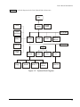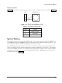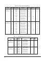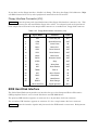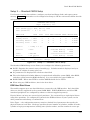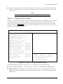
1
Little Board™ P6d Reference Manual P/N 5001451A Revision B 5215 Hellyer Avenue, San Jose, CA 95138-1007 Phone: 408 360-0200, FAX: 408 360-0222, Web: www.ampro.com TRADEMARKS The Ampro logo is a registered trademark, and Ampro, EnCore, Little Board, CoreModule, and MiniModule are trademarks of Ampro Computers, Inc. Pentium is a registered trademark of Intel, Incorporated. All other marks are the property of their respective companies. NOTICE No part of this document may be reproduced, transmitted, transcribed, stored in a retrieval system, or translated into any language or computer language, in any form or by any means, electronic, mechanical, magnetic, optical, chemical, manual, or otherwise, without prior written permission from Ampro Computers, Incorporated. DISCLAIMER Ampro Computers, Incorporated makes no representations or warranties with respect to the contents of this manual or of the associated Ampro products, and specifically disclaims any implied warranties of merchantability or fitness for any particular purpose. Ampro shall under no circumstances be liable for incidental or consequential damages or related expenses resulting from the use of this product, even if it has been notified of the possibility of such damages. Ampro reserves the right to revise this publication from time to time without obligation to notify any person of such revisions. If errors are found, please contact Ampro at the address listed on the title page of this document. REVISION HISTORY Revision Reason for Change Date 1 Pre-Production Release 08/00 A Production Release 11/00 B Updates/Revisions 02/02 © Copyright 2000, 2002, Ampro Computers, Incorporated AUDIENCE ASSUMPTIONS This reference manual is for the person who designs computer related equipment, including but not limited to hardware and software design and implementation of the same. Ampro Computers, Inc. assumes you are qualified in designing and implementing your hardware designs and its related software into your prototype computer equipment ii Table of Contents Preface Introduction......................................................................................................................................... vii Technical Support ......................................................................................................................... vii Introduction General Description .......................................................................................................................... 1–1 Product Feature Summary................................................................................................................ 1–1 CPU/Motherboard ....................................................................................................................... 1–1 Enhanced Embedded-PC BIOS ................................................................................................... 1–2 Modular PC/104-Plus Expansion Bus ......................................................................................... 1–2 CompactFlash Disk ..................................................................................................................... 1–2 Serial Ports.................................................................................................................................. 1–3 Parallel Port ................................................................................................................................ 1–3 Floppy Interface .......................................................................................................................... 1–3 PCI-Bus EIDE Interfaces ............................................................................................................ 1–3 PCI Audio Interface .................................................................................................................... 1–3 Flat Panel/CRT Display Controller ............................................................................................. 1–4 100 MBps Ethernet LAN Interface ............................................................................................. 1–4 Enhanced Reliability ................................................................................................................... 1–4 Software ............................................................................................................................................ 1–5 Designing Little Board Systems ....................................................................................................... 1–5 On-board MiniModule Expansion ............................................................................................... 1–5 Little Board Development Platform And QuickStart Kit ........................................................... 1–6 Connector Descriptions ............................................................................................................... 1–7 Switch Descriptions (S1 – S5) ..................................................................................................... 1–8 Product Reference Overview............................................................................................................................................ 2–1 Mounting Dimensions ....................................................................................................................... 2–1 Connector Summary.......................................................................................................................... 2–3 Jumper Summary.............................................................................................................................. 2–6 DC Power........................................................................................................................................... 2–7 Power Requirements ................................................................................................................... 2–7 Other Voltages ............................................................................................................................ 2–7 Switching Power Supplies ........................................................................................................... 2–8 Powerfail NMI ............................................................................................................................. 2–8 Backup Battery ........................................................................................................................... 2–8 Cooling Requirements ....................................................................................................................... 2–8 Thermal Sensor ........................................................................................................................... 2–8 Fan Switch................................................................................................................................... 2–9 iii System Memory ................................................................................................................................. 2–9 ROM BIOS..................................................................................................................................2–10 Shadowing ..................................................................................................................................2–10 BIOS Recovery ...........................................................................................................................2–10 Interrupt and DMA Channel Usage.................................................................................................2–10 Battery-Backed Clock.......................................................................................................................2–12 Serial Ports.......................................................................................................................................2–12 I/O Addresses and Interrupt Assignments ................................................................................2–13 ROM-BIOS Installation of the Serial Ports ...............................................................................2–13 Serial Port Connectors (J8, J11) ................................................................................................2–13 Serial TTL Option ......................................................................................................................2–15 Ampro Custom Serial Features..................................................................................................2–15 Serial Console Features .............................................................................................................2–15 Universal Serial Bus (USB) Ports....................................................................................................2–17 Infrared (IrDA) Interface .................................................................................................................2–18 Requirements for an IrDA Interface ..........................................................................................2–18 IrDA Connector (Part of Utility J19) .........................................................................................2–18 Multi-Mode Parallel Port .................................................................................................................2–19 I/O Addresses and Interrupts ....................................................................................................2–19 ROM-BIOS Installation of Parallel Ports ..................................................................................2–19 DMA Channels ...........................................................................................................................2–20 Parallel Port Connector (J9) ......................................................................................................2–20 IEEE-1284-compliant Cables .....................................................................................................2–21 Latch-Up Protection ...................................................................................................................2–22 Parallel Port Registers ...............................................................................................................2–22 Standard and Bidirectional Operation ......................................................................................2–22 Enabling the Parallel Port Interrupt .........................................................................................2–23 Floppy Disk Interface.......................................................................................................................2–25 Floppy Drive Considerations......................................................................................................2–25 Floppy Interface Configuration..................................................................................................2–25 Floppy Interface Connector (J14) ..............................................................................................2–26 EIDE Hard Disk Interface ...............................................................................................................2–26 IDE Interface Configuration ......................................................................................................2–28 CompactFlash Solid-State Disk .......................................................................................................2–28 Enabling the Drive .....................................................................................................................2–28 Master/Slave Setting ..................................................................................................................2–28 Solid-State Disk Preparation .....................................................................................................2–28 Audio Interface.................................................................................................................................2–29 Audio Amplifier ..........................................................................................................................2–29 Audio Interface Connector .........................................................................................................2–29 Flat Panel/CRT Video Controller .....................................................................................................2–32 Connecting a Flat Panel (J15)....................................................................................................2–33 BIOS Support of Standard Flat Panels......................................................................................2–35 Connecting a CRT (J17) .............................................................................................................2–35 Disabling the Video Controller ..................................................................................................2–37 Ethernet Network Interface.............................................................................................................2–37 Hardware Description ................................................................................................................2–37 iv Ethernet RJ45 Interface Connector (J13) ..................................................................................2–37 Ethernet Interface Software ......................................................................................................2–38 Ethernet Setup ...........................................................................................................................2–39 Ethernet Indicator LEDs ...........................................................................................................2–39 Watchdog Timer ...............................................................................................................................2–39 Utility Connectors (J19) ...................................................................................................................2–40 LED Connection .........................................................................................................................2–42 Speaker Connections ..................................................................................................................2–42 Push-button Reset Connection...................................................................................................2–42 Keyboard Connection .................................................................................................................2–42 PS/2 Mouse Connection ..............................................................................................................2–42 IrDA Interface ............................................................................................................................2–43 TTL Serial Ports .........................................................................................................................2–43 Miscellaneous Power Management Signals ...............................................................................2–43 PC/104-Plus Expansion Bus .............................................................................................................2–43 On-board MiniModule Expansion Details..................................................................................2–43 Using Standard PC and AT Bus Cards ......................................................................................2–44 Expansion Bus Connector Pinouts .............................................................................................2–44 Setup ................................................................................................................................................2–48 Setup Help..................................................................................................................................2–48 Setup 1 — Main Menu................................................................................................................2–50 Setup 2 — Standard CMOS Setup .............................................................................................2–51 Setup 3 — BIOS Features Setup................................................................................................2–53 Setup 4 — Chipset Features Setup ............................................................................................2–55 Setup 5 — Power Management Setup........................................................................................2–56 Setup 6 — PCI Configuration Setup ..........................................................................................2–58 Setup 7 — Integrated Peripherals Setup ...................................................................................2–59 Other Setup Screens ..................................................................................................................2–61 Technical Specifications Little Board P6d Technical Specifications ........................................................................................ 3–1 CPU/Motherboard ....................................................................................................................... 3–1 Embedded-PC System Enhancements ........................................................................................ 3–1 Support Software ........................................................................................................................ 3–3 Mechanical and Environmental Specifications........................................................................... 3–3 Flat Panel Displays ..................................................................................................................... 3–4 Hardware IRQ Map ..................................................................................................................... 3–9 Standards Contact Information Cables Index v vi Preface Introduction This manual is for integrators and programmers of systems based on the Ampro Little Board P6d, a full-featured CPU module conforming to the EBX 1.1 technical specification. It contains technical information about hardware requirements, interconnection, and software configuration. Technical Support Ampro Computers, Inc. provides a number of methods for contacting Technical Support listed in the following Table i. Ampro provides a comprehensive listing of Frequently Asked Questions on our web site at the Virtual Technician. If you can not find the answers to your questions, please continue in the Virtual Technician and ask for Personal Assistance. Requests for support through the web site are given the highest priority, and usually will be addressed within one working day. ! Internet – Provides the most information concerning Ampro products, including reference material and white papers. – Ampro Virtual Technician – This service is free and available 24 hours a day through the Ampro Computers World Wide Web site at http://www.ampro.com. However, you must sign in to access this service. The Ampro Virtual Technician is a searchable database of Frequently Asked Questions, which will help you with the common questions asked by most customers. This is good source of information to look at first for your technical solutions. . – Embedded Design Resource Center – This service is also free and available 24 hours-a-day at the Ampro web site at http://www.ampro.com. However, you must sign in to access this service . The Embedded Design Resource Center was created as a resource for embedded system developers to share Ampro's knowledge, insight, and expertise gained from years of experience. This page contains links to White Papers, Specifications, and additional technical information. ! Personal Assistance – This is the quickest way to obtain a response to your support questions. Please go to the following location on Ampro’s web site to submit your request 24 hours a day, 7 days a week. http://www.ampro.com/scripts/virtual_technician.exe/people Table i. USA Technical Support Contact Information Email Website FTP Surface Mail [email protected] http://www.ampro.com ftp://ftp.ampro.com Ampro Computers, Incorporated 5215 Hellyer Avenue San Jose, CA 95138-1007, USA vii viii Chapter 1 Introduction General Description The Little Board P6d system is a high integration, high-performance Pentium-II based PC/ATcompatible system that conforms to the EBX V1.1 specification. This rugged and high quality single-board system contains all the component subsystems of a PC/AT PCI motherboard plus the equivalent of up to six expansion boards. The Little Board P6d system meets the size, power consumption, temperature range, quality, and reliability demands of embedded system applications. Key functions on the Little Board P6d module include: – High-speed Pentium-II CPU – 64-bit wide 3.3V SDRAM - up to 256MB – – Dual PCI-bus EIDE/UltraDMA drive controllers 256KB Internal secondary cache – Flat panel/CRT display controller – Embedded-PC BIOS in Flash EPROM – Sound Blaster Audio – Four buffered serial ports (with RS232, RS485, TTL options) – Ethernet 100BaseT LAN interface, – CompactFlash solid-state IDE drive support – Standard PS/2 Keyboard/Mouse and speaker interfaces – Two universal serial bus (USB) ports – Infrared (IrDA) port – Multi-mode IEEE-1284 parallel port – Floppy controller In addition, Ampro has made many improvements to the architecture and firmware of the traditional desktop PC to optimize it for embedded applications. Among the many embedded-PC enhancements that ensure fail-safe embedded system operation and application versatility are a watchdog timer, a powerfail NMI generator, serial console support, serial boot loader, non-battery boot, failsafe boot, accelerated boot, on-board high-density CompactFlash disk, and BIOS extensions for OEM boot customization. System operation requires a single +5 Volt power source (and 3.3 Volts for low-voltage PCI expansion cards, if required) and offers "green PC" power-saving modes under support of Advanced Power Management (APM) BIOS functions. Product Feature Summary CPU/Motherboard The Little Board P6d module has a fully compatible PC architecture, with a Pentium-II low-voltage CPU. For improved reliability in harsh thermal environments, the board implements a CPU thermal sensor and configurable thermal-management control logic in the BIOS. 1-1 The board uses a single 3.3V DIMM memory module for main DRAM memory, and supports from 32MB to 256MB in a 64-bit or 72-bit (ECC) configuration. The module has a full complement of standard PCI PC/AT architectural features, including DMA channels, interrupt controllers, real-time clock, and timer counters. Enhanced Embedded-PC BIOS One of the most valuable features of the Little Board P6d module is its enhanced embedded-PC BIOS, which includes an extensive set of functions that meet the unique requirements of embeddedsystem applications. These enhancements include: ! CompactFlash support. You can use a solid-state CompactFlash memory module in place of a rotating media drive (see CompactFlash Disk, below). ! Watchdog timer. The WDT monitors the boot process and can be integrated into application programs using function calls provided in the BIOS. ! Fast boot operation. Normal or accelerated POST. ! Fail-safe boot support. Intelligently retries boot devices (configured in the BIOS) until a successful boot. ! Battery-free boot support. Saves system Setup information in non-volatile EEPROM. The board can use this information should the RTC battery fail. ! Serial console option. Let's you use a serial device, such as an ASCII serial terminal, as console. ! Serial loader option. Supports loading boot code from an external serial source. ! EEPROM access function. 256 bits of serial EEPROM storage are available to the user, useful for serialization, copy protection, security, etc. ! OEM customization hooks. The module can execute custom code prior to system boot via ROM extensions; allows sophisticated system customization without BIOS modification. Modular PC/104-Plus Expansion Bus The Little Board P6d module provides a PC/104-Plus expansion bus for additional system functions. This bus offers compact, self-stacking, modular expandability. It is an embedded system version of the signal set provided on a desktop PC's ISA bus. The PC/104-Plus bus includes this signal set, and in addition, signals implementing a PCI bus, available on an additional 120-pin PCI bus connector. The Little Board P6d module's on-board EIDE, Ethernet, and Audio interface are internally connected to its PCI bus. In addition, you can attach PCI peripherals to the board's stackable PCI bus expansion connector in much the same way PC/104 modules are stacked on the PC/104 connectors. The PCI expansion connector consists of 4 rows of 30 pins (120-pin header), and carries all of the appropriate PCI signals to accommodate up to 4 PCI add-on modules. The bus operates at clock speeds up to 33MHz. CompactFlash Disk The CompactFlash interface allows you to substitute solid-state Flash memory for a conventional Hard drive. Any DOS-based application, including the operating system, utilities, drivers, and application programs, can easily be run from the CompactFlash device without modification. 1-2 Little Board P6d Module The CompactFlash disk is a solid-state or rotating media disk system that emulates an IDE drive. It uses standard CompactFlash disk media, similar to a PCMCIA memory card, but smaller. Insert the CompactFlash disk media in the on-board CompactFlash socket, and use it in much the same way you would use a removable-media hard drive. The CompactFlash drive is architecturally equivalent to an IDE drive in your system. When installed, it becomes one of the two IDE drives supported by the primary EIDE disk controller. It can be configured as either an IDE master or slave drive. Serial Ports The Little Board P6d module provides four RS232C serial ports, implemented using 16C550-type UARTs. These UARTs are equipped with 16-byte FIFO buffers to improve throughput. Serial ports 1 & 2 have full modem support. There are RS232 level shifters on all signals. The RX and TX data signals can also be configured as RS485/RS422. The TTL versions of the TX and RX signals for port 1, 3, and 4 are also brought out to the utility connector. Port 2 TTL TX and RX are brought out to the Utility connector via the IrDA interface. Parallel Port An enhanced bidirectional parallel port interface conforms to the IEEE-1284 standard. It provides features attractive to embedded system designers, including increased speed, an internal FIFO buffer, and DMA transfer capability. Floppy Interface An on-board floppy disk interface provides access to standard floppy drives. The interface supports two floppy drives, 5-1/4 inch or 3-1/2 inch. All standard floppy drive types, from 360K at 5-1/4 inch to 1.44M at 3-1/2 inch are supported. PCI-Bus EIDE Interfaces On-board PCI EIDE/Ultra DMA/33 interfaces provide high-speed hard disk, IDE CD-ROM drive, and other IDE device access. The interfaces support up to four IDE devices (via primary and secondary drive interfaces). The interfaces are fully compliant with the AS/NSIS ATA Rev. 3.0 specification and the ATAPI Specification. The CompactFlash interface is implemented as an IDE drive. If it is installed, it takes the position of one of the drives of the primary IDE interface (settable as a master or slave drive). PCI Audio Interface The SoundBlaster™ compatible audio interface is implemented using a combination of the Trident 4DWAVE-NX PCI DirectSound Accelerator, the National LM4549 AD97 CODEC and a National LM4863 Audio Amplifier. 1-3 Flat Panel/CRT Display Controller A 69030 video display controller supports both flat panels and CRTs, and offers full software compatibility with all popular PC video standards (VGA, Super VGA, and VESA). All standard resolutions up to 1600x1200 pixels at 64K colors for CRTs and up to 1280x1024 pixels at 16.7M colors for flat panels are supported. 4MB of SDRAM are provided as standard video memory. The display controller features are: ! Enhanced AGP Bus Interface – The video controller provides a 66MHz AGP-bus path between the CPU and the controller. ! Full IBM VGA compatibility – VESA DPMS and DCC standards supported. ! Color Flat Panel Support – Up to 16.7 million colors can be displayed on color TFT LCD flat panels and color STN LCD panels. ! Dual Independent Displays – The controller provides three different modes, which include two completely separate and independent video displays (CRT and flat panel) with resolutions up to 1280x1024 at 256 colors at 60Hz. – Dual-Pipe Simultaneous Mode – This mode provides the same image on both displays and each display (CRT or flat panel) can operate at its optimum timing. – Dual-Pipe Mosaic Mode – This mode provides two displays with completely different images on each display and each display can be configured at its optimum resolution/timing. – Virtual Desktop Mode – This mode provides a single image or desktop spanned across the two displays. ! Automatic Power Sequencing Controls. The video controller provides the signals to safely sequence the power and data signals to LCD flat panels. ! Low-Power Modes. The Advanced Power Management (APM) and Advanced Configuration and Power Management Interface (ACPI) compliant features are implemented in the power control logic. ! ZV Port Support. The standard ZV input port for PCMCIA is supported. 100 MBps Ethernet LAN Interface The Ethernet subsystem is based on the Intel 82559ER 10/100BaseT PCI Ethernet Controller. It fully supports IEEE 802.3 Ethernet standards - 10BaseT and 100BaseT. Features of this Ethernet controller include: ! Chained memory structure ! Full Duplex support at 10 and 100Mbps ! IEEE 802.3u Auto-negotiable support 1-4 Little Board P6d Module Enhanced Reliability Reliability is especially important in embedded computer systems. Ampro, specializing in embedded system computers and peripherals, knows that embedded systems must be able to run reliably in rugged, hostile, and mission-critical environments without operator intervention. Over the years, Ampro has evolved system designs and a comprehensive testing program to ensure a reliable and stable system for harsh and demanding applications. These include: ISO 9001 Manufacturing. Ampro is a certified ISO 9001 vendor. Knowing that many embedded systems must qualify under EMC emissions and susceptibility testing, Ampro designs boards with careful attention to EMI issues. Wide-range temperature testing. Ampro Engineering qualifies all of its designs by extensive thermal and voltage margin testing. Shock and Vibration Testing. Ampro products are intended for use in harsh environments and are designed for shock and vibration durability to MIL-STD 202F, Method 213-I, Condition A (three 50G shocks in each axis) and MIL-STD 202F, Method 214A, Table 214-I, Condition D (11.95B random vibration, 100 Hz to 1000 Hz). Software The vast array of commercial and public-domain software for the IBM PC and PC/AT is usable in LB/P6d-based systems. You can use the most popular software development tools (editors, compilers, debuggers, etc.) for developing code for your application. With this software and the standard Ampro-supplied utilities and drivers, you can quickly tailor a system to your needs. Use the board's Setup function for all system configurations. Setup information is stored in both the battery-backed CMOS RAM-portion of the real-time clock, and in a configuration EEPROM. Setup information is retained in the EEPROM even if the real-time clock battery loses power, ensuring reliable start-up. Setup can be invoked by pressing the DEL key during the Power-On Self Test (POST). The contents of the EEPROM can be written and read from the DOS command line using a utility program, SETCMOS.EXE, available on the Little Board P6d Utilities diskette. Designing Little Board Systems The board affords a great deal of flexibility in system design. You can build a system using only the Little Board, serial or parallel devices for input/output, and a solid-state disk drive. On-board MiniModule Expansion The simplest way to expand a Little Board system is with self-stacking Ampro MiniModules. MiniModules are available for a wide variety of functions. You can stack the MiniModules on the Little Board and avoid the need for bus cables, card cages, and backplanes. For detailed information, see page 2-43. 1-5 Little Board Development Platform And QuickStart Kit To help developers quickly assemble an embedded system, Ampro offers the Little Board Development Platform. It includes a power supply, 3-1/2 inch 1.44M floppy disk drive, IDE hard drive, CD ROM drive, speaker, I/O connectors, a backplane for ISA and PCI expansion cards, an I/O development board (described below), and mounting studs for the Little Board. The Development Platform provides a "known good" environment for your development work. You can install the Little Board P6d module, MiniModules, or conventional expansion boards, keyboard, monitor, and I/O devices to quickly create a platform for your hardware and software engineering needs. The QuickStart Kit includes cables, documentation, and software needed to develop an application with the Little Board. Unlike the Development Platform, you must supply the disk drives and power supply. Technical drawings for the cables provided in the QuickStart Kit are included in Appendix B. There are other kits available from Ampro to aid in the development of your application. A Cable Kit that includes only the Little Board P6d cable set is available. To facilitate connections to the Little Board P6d utility connectors, Ampro provides the Little Board P6d Utility I/O Development Board. Figure 1-1 is an illustration of the I/O Development board showing the connectors and switches that are provided. It is included in the Development Platform Kit and the QuickStart Kit. Figure 1-1. I/O Development Board 1-6 Little Board P6d Module The Little Board P6d Utility I/O Development Board provides connections for the speaker, keyboard, mouse, IrDA, TTL serial, front panel switches, misc. power management signals, external power supply connections, and so forth. Table 1-1 summarizes the connectors available on the I/O Development Board. Table 1-1. I/O Development Board Connector Summary Connector Name Description J1 Utility Connect to Little Board P6d Utility J2 Power Provides connections for -12V and -5V J3 Misc. Misc. Power Management and TTL Serial J4 Keyboard J5 Mouse Plug in a standard PS/2 Keyboard Plug in PS/2 Mouse Connector Descriptions The following sections describe the use of each connector on the I/O Development Board. J1 — Utility The Utility connector connects to the Little Board P6d Utility connector. It provides connections to an on-board speaker, keyboard connector, Mouse connector, reset switch, IrDA Transceiver, TTL RS232 signals, misc. power management I/O, and a connector for external -5V and -12V power supplies, and a power LED. If you have the Ampro QuickStart Kit, connect a ribbon cable between J1 on the I/O Development Board and J19 on the Little Board. J2 — Power You can use J2 to connect -5V and -12V power supplies to the Little Board. Table 1-2. –5V and –12V Power Wiring Pin # Signal 1 -12 Volts 3 -5 Volts 2, 4 Ground 1-7 J3 — Misc. This connector contains miscellaneous Power Management signals and the TTL serial. Table 1-3. Miscellaneous Power Management and TTL Wiring Pin # Signal Pin # Signal 1 TTL_TX3 2 TTL_RX1 3 TTL_RX3 4 TTL_TX1 5 TTL_GND 6 SMBALRT 7 TTL_TX4 8 SMBDATA 9 TTL_RX4 10 SMBCLK J4 — Keyboard You can use J4 to connect a PS/2 keyboard. J4 is a standard 5-pin DIN connector. J5 — Mouse You can use J5 to connect a PS/2 mouse. J5 is a standard 6-pin mini-DIN connector. Switch Descriptions (S1 – S5) There are five switches on the I/O Development Board. They’re described in Table 1-4. Table 1-4. I/O Development Board Switches 1-8 Switch Name Description S1 LID S2 PWR S3 LO BAT Power management input: causes an SMI to simulate a low-battery condition. S4 RESET Standard Reset signal to the Little Board S5 RI Power management input: causes an SMI to simulate a laptop lid closure. Power management input (push-button switch): when pushed for 6 seconds, it powers down the board. When pressed again, the board powers up. Ring Indicator: causes an SMI to simulate a laptop modem ring. Little Board P6d Module Figure 1-2 is a block diagram of the Little Board P6d architecture. CPU Temp DRAM DIMM 443BX Serial EEPROM USB (2) PCI/120 Bus PIIX4E Audio Video 100BaseT Ethernet PC/104 Bus IDE (4) Buffer Compact Flash Floppy Multi-I/O Parallel BIOS Serial 1, 2 RTC Keyboard Mouse I/O Serial 3, 4 Figure 1-2. System Block Diagram 1-9 1-10 Chapter 2 Product Reference Overview This chapter contains the technical information you will need to install and configure the Little Board P6d system. The information is presented in the following order: ! Mounting Dimensions (page 2-1) ! Connector Summary (page 2-3) ! Jumper Summary (page 2-6) ! DC Power (page 2-7) ! System Memory (page 2-9) ! Battery Backed Clock (page 2-12) ! Serial Ports (page 2-12) ! Universal Serial Bus (USB) Ports (page 2-17) ! IrDA Port (page 2-18) ! Parallel Port (page 2-19) ! Floppy Interface (page 2-25) ! EIDE Hard Disk Interface (page 2-26) ! CompactFlash (page 2-28) ! Audio Interface (page 2-29) ! Flat Panel/CRT Video Controller (page 2-32) ! Ethernet Network Interface (page 2-37) ! Watchdog Timer (page 2-39) ! Utility Connector Wiring (page 2-40) ! Expansion Busses (page 2-43 ) ! Setup Function (page 2-48) Mounting Dimensions Figure 2-1 shows the Little Board P6d module’s mounting dimensions. 2-1 5.350 4.650 4.200 3.125 2.875 2.675 1.500 .750 .050 .250 .100 7.800 7.600 7.500 7.600 7.150 7.100 7.175 6.875 6.800 6.575 6.475 6.200 5.975 5.700 5.800 5.625 5.325 3.100 2.800 2.700 2.650 1.850 1.025 .400 .350 .207 .175 0.0 0.0 5.550 5.350 2.250 4.950 4.575 4.000 3.125 2.111 2.293 2.325 2.625 1.875 .650 .575 0.0 .200 .200 Figure 2-1. Little Board P6d Module with Mounting Dimensions 2-2 Little Board P6d Module Connector Summary Refer to Figure 2-2. Little Board P6d Connector and Jumper Locations for the locations of the connectors (J1 – J21) and configuration jumpers (W1 – W9). Table 2-1 summarizes the use of the I/O connectors. Each interface is described in its own section, showing connector pinouts, signal definitions, required mating connectors, and configuration jumper options. Many of the connectors have a key pin removed. This allows you to block the corresponding cable connector socket to help prevent improper assembly. Table 2-1 indicates which pins are key pins. Table 2-1. Connector Summary Connector Function Size Key Pin J1 A/B PC/104 Expansion Bus 64-Pin B10 J2 C/D PC/104 Expansion Bus 40-pin C19 J3 PCI Bus 120-pin A1/D30* J4 USB 1 5-PIN Mechanical Key** J5 USB 2 5-PIN Mechanical Key** J6 IDE1 Interface 44-pin 2mm 20 J7 IDE2 Interface 44-pin 2mm 20 J8 Serial 1 and Serial 2 20-pin None J9 Parallel Port 26-pin 26 J10 (J100) Power, +5V, +12V, +3.3V (J100 Alternate Connector) 7-pin Molex Mechanical Key** J11 Serial 3 and Serial 4 20-pin None J12 Audio Interface 26-pin 2mm 25 J13 Ethernet Twisted Pair RJ45 Mechanical Key** J14 Ethernet Option 6-pin None J15 Flat Panel Video 50-pin 2mm None J16 Video ZOOM 26-pin 2mm None J17 CRT Video 10-pin None J18 Floppy Interface 26-pin 2mm 1 J19 Utility 44-pin 2mm 31 J21 Fan Power 3-pin None J22 CompactFlash 50-pin Mechanical Key** Notes: *A1 and D30 keys are used to key the PCI connector for 5V or 3.3V respectively. **Connector provides keying mechanism . 2-3 Most I/O connectors are shrouded dual-row male headers for use with flat ribbon (IDC) female connectors and ribbon cable. Note Ampro recommends using “center-bump polarized” connectors to prevent accidentally installing cables backwards. You can also design a PC board assembly, made with female connectors in the same relative positions as the Little Board’s connectors, to eliminate cables, meet packaging requirements, add EMI filtering, or customize your installation in other ways. Precise dimensions for locating connectors are provided in Figure 2-1. The ISA portion of the PC/104-Plus bus appears on connector J1A, J1B, J2C, and J2D. You can expand the system with on-board MiniModule products or other PC/104-compliant expansion modules. These modules stack directly on the connectors, or use conventional or custom expansion hardware, including solutions available from Ampro. The PCI portion of the PC/104-Plus expansion bus appears on connector J3. It uses a 2 mm 4-row connector called out in the PC/104-Plus draft specification. Like the J1, J2 connector, J3 has both male and female connections, allowing for “stackthrough” assembly. 2-4 CRT J17 J16 J15 J21 W10 W3 J1 J3 J13 J22 W7 W6 J7 W2 J10 J6 W4 J8 J9 J100 Little Board P6d Module Figure 2-2. Little Board P6d Connector and Jumper Locations 2-5 Jumper Summary Ampro installs option jumpers in default positions so that in most cases the Little Board P6d module requires no special jumpering for standard AT operation. You can connect the power and peripherals and operate it immediately. Jumper-pin arrays are designated W1, W2, and so forth. Jumper pins are spaced 2 mm apart. A square solder pad identifies pin 1 of each jumper array. Table 2-2 is a summary of jumper use. Factory settings are shown in the Default column. Some jumpers are set at the factory to configure options that are not user-settable. These are indicated in the table. Do not change these settings. Table 2-2. Configuration Jumper Summary Jumper Group 2-6 Function Default W1 CompactFlash IDE Master/Slave ON=Master, OFF=Slave ON W2 BIOS Flash EPROM Programming Power ON=Programming enabled OFF= Programming disabled ON W3 External BIOS Board Enable/Cable Connection ON=Normal, OFF=External Cable ON W4 Serial 1 RS485 100 Ohm Termination ON=Terminated, OFF=Unterminated OFF W5 Serial 2 RS485 100 Ohm Termination ON=Terminated, OFF=Unterminated OFF W6 Serial 3 RS485 100 Ohm Termination ON=Terminated, OFF=Unterminated OFF W7 Serial 4 RS485 100 Ohm Termination ON=Terminated, OFF=Unterminated OFF W8 Local Head Phone Enable ON = Enable Local HP, OFF = Disable HP OFF W9 Watchdog timer reset enable ON=Enabled, OFF=Disabled OFF Little Board P6d Module DC Power The power connector J10 is a 7-pin polarized connector. Refer to Table 2-3 for power connections and Table 2-4 for mating connector information. Caution To prevent damage to the Little Board P6d or its power connector, ensure the power plug is wired correctly before applying power to the module!! See Table 2-3. Table 2-3. Power Connector (J10) Pin # Signal Name Function 1, 7 +5VDC +5VDC ±5% input 2, 3, 6 Ground Ground return 4 +12VDC +12VDC ±5% input 5 +3.3VDC +3.3V ±5% input (Only required for some PCI expansion boards) Table 2-4. J10 Mating Connector Connector Type Mating Connector DISCRETE WIRE MOLEX HOUSING 09-50-8073 Pins 08-52-0071 Power Requirements The Little Board P6d module requires only +5VDC (±5%) for operation. The voltage required for the RS232 ports is generated on-board from the +5VDC supply. An on-board low-voltage power supply circuit provides power to low-voltage CPUs and certain other on-board components. The exact power requirement of the Little Board P6d system depends on several factors, including the CPU speed, the peripheral connections, and which, if any, MiniModule products or other expansion boards are attached. For example, the keyboard draws its power from the board, and there can be some loading from the serial, parallel, and other peripheral ports. Consult the specifications in Chapter 3 for the basic power requirements of your model. Other Voltages There may be a requirement for an external +12 volt supply, depending on what peripherals you connect to the Little Board system. For instance, +12V is required for most flat panel backlight power supplies. You can connect a +12V supply to the Little Board module through the power connector, J10. This will supply +12V to the ISA and PCI portions of the PC/104 expansion busses. Similarly, you can connect -12V and -5V to the Utility Connector, to supply those voltages to both expansion busses. Pinouts for the Utility Connector are provided in Table 2-4. 2-7 If a PCI expansion card requiring 3.3V is installed, that voltage can be connected to J10-5 to supply power to J3, the PCI bus interface connector. Switching Power Supplies If you use a switching power supply, be sure it regulates properly with the load your system draws. Some switching power supplies do not regulate properly unless they are loaded to some minimum value. If this is the case with your supply, consult the manufacturer about additional loading, or use another supply or another type of power source (such as a linear supply, batteries, etc.). The minimum power for the Little Board P6d system appears in the power specifications in Chapter 1. Powerfail NMI The Little Board P6d module includes a circuit that can sense a power failure. If the +5V power supply falls below ~4.7V, the powerfail logic produces a non-maskable interrupt (NMI). When a NMI occurs, the BIOS detects the NMI and displays the message “Power Fail NMI” on the console. At this point you have two options via the keyboard. You can mask the NMI and continue (the PC architecture provides a mask bit for the non-maskable interrupt), or reboot the system. If you want your system to respond to the NMI, you can provide a NMI handler in your application, and patch the NMI interrupt vector address to point to your routine. Backup Battery The Real-Time Clock Battery on the Little Board P6d module should last 10 years under normal usage. Cooling Requirements The Pentium-II CPU, DRAM module, video controller, and core logic chips draw most of the power and generate most of the heat. The board is designed to support various speed versions of the Pentium-II from 333MHz to 366MHz with a 66MHz clock speed. A heat sink and fan are provided for the CPU and a thermal sensor is used to monitor the CPU temperature, as described below. Thermal Sensor A thermal sensor monitors the internal temperature of the Pentium-II CPU. If the thermal sensor detects the CPU temperature has exceeded its upper temperature threshold (100°C/212°F), the thermal sensor’s logic sends a signal to the BIOS to reduce the CPU clock speed. This speed reduction remains in effect until the processor has cooled to the lower sensor limit. Choosing to operate the CPU at a temperature higher than this upper limit should be avoided due to the possibility of CPU damage and its erratic operating speed. 2-8 Little Board P6d Module Fan Connector Figure 2-3 shows the connection between the fan and J21. The pinout of J21 is shown in Table 2-5. 5V CPU Fan J21 1 - 2 + TACH Figure 2-3. CPU Fan Connection (J21) Table 2-5. Fan Power Connector (J21) Pin # Function 1 Switched Ground 2 +5V Power 3 TACH Output System Memory The module supports a single 168-pin DIMM socket. The system supports both 64-bit SDRAM and 72-bit SDRAM. The 72-bit SDRAM is used to support ECC (Error Detection And Correction). You can install from 32MB to 256MB, depending on your memory needs. The ROM BIOS automatically detects the size of the installed memory module and configures the system accordingly at boot time (No jumpering or manual configuration is required.). The amount of memory the BIOS measures can be displayed by running Setup. Memory error correction (ECC) is supported by the chip set used on the Little Board P6d module. DRAM memory is allocated in the system as shown in Table 2-6. 2-9 Table 2-6. System Memory Map Memory Address Function FE0000h - FFFFFFh Duplicates BIOS at 0E0000-0FFFFFh. 100000h - FDFFFFh Extended memory 0E0000h - 0FFFFFh 128K ROM BIOS 0D0000h - 0DFFFFh BIOS extension option, if enabled. Otherwise, free. 0CB000h - 0CFFFFh USB 0C0000h - 0CAFFFh Video BIOS (44K) 0A0000h - 0BFFFFh Normally contains video RAM, as follows: CGA Video: B8000-BFFFFh Monochrome: B0000-B7FFFh EGA and VGA video: A0000-AFFFFh 000000h - 09FFFFh Lower 640K DRAM ROM BIOS The standard BIOS is installed in a 256KB Flash device at the factory. The top 128KB of the Flash device is reserved for the system BIOS, located at 000E0000h – 000FFFFFh and mirrored at the top of the memory address space. The remaining 128KB are mapped only to the top of memory. A utility program, PGM6X.COM, can be used to program the on-board Flash device. It can be used to update the system BIOS, video BIOS, or user area. The utility is included on the utility diskette that accompanies the Ampro Development Platform. The diskette includes documentation about how to use the program. Shadowing To improve system performance, the contents of the ROM BIOS and video BIOS are copied into DRAM for execution (“shadowed”), where they are accessed as 64-bit wide data. Shadowing a BIOS ROM substantially enhances system performance. Shadowing for both the ROM and video BIOS is built into the Ampro Extended BIOS. There is no user setting. BIOS Recovery If the BIOS Flash device somehow becomes corrupted, the Little Board P6d system may not boot. In this case, the BIOS will have to be reprogrammed. A disk with an image of the current BIOS along with the Utility PGM6X.COM may be used to restore the BIOS image. Before this can be done, the Little Board P6d system needs to be Booted and running DOS. Interrupt and DMA Channel Usage The PC architecture provides several interrupt and DMA control signals. When you expand the system through the ISA portion of the PC/104-Plus bus with MiniModule products or plug-in cards that require either interrupt or DMA support, you must select which interrupt or DMA channel to use. Typically this involves switches or jumpers on the expansion module. In most cases, these are not shared resources. It is important that you configure the new module to use an interrupt or 2-10 Little Board P6d Module DMA channel not already in use. For your convenience, Table 2-7 and Table 2-8 provide a summary of the normal interrupt and DMA channel assignments on the Little Board P6d module. The PCI bus uses four interrupts (INTA*, INTB*, INTC*, and INTD*). These interrupts are mapped to any of the available ISA interrupts by the BIOS. If an expansion card has multiple functions, then more interrupts may be required. You can set the priority in which interrupts are assigned on Setup 6 — PCI Configuration Setup. Table 2-7. Interrupt Channel Assignments Interrupt Function IRQ0 ROM BIOS clock tick function, from Timer 0 IRQ1 Keyboard interrupt IRQ2 Cascade input for IRQ8-15 IRQ3 Serial 2, Serial 4 IRQ4 Serial 1, Serial 3 IRQ5 PCI IRQ6 Floppy controller IRQ7 Parallel port (option) IRQ8 Reserved for battery-backed clock alarm IRQ9 PCI IRQ10 PCI, Serial 3, Serial 4 IRQ11 PCI IRQ12 PS/2 Mouse, Serial 3, Serial 4 IRQ13 Reserved for coprocessor IRQ14 Primary IDE hard disk controller IRQ15 Secondary IDE hard disk controller Note: IRQs for the Ethernet, Video, and Audio interfaces are automatically assigned by the BIOS plug and play logic. PCI Interrupts assigned during initialization cannot be used by non-PCI devices. 2-11 Table 2-8. DMA Channel Assignments Channel Function 0 Available for 8-bit transfers 1 Available for 8-bit transfers 2 Floppy controller 3 Available for 8-bit transfers 4 Cascade for channels 0-3 5 Available for 16-bit transfers 6 Available for 16-bit transfers 7 Available for 16-bit transfers Battery-Backed Clock An AT-compatible battery-backed real-time clock (with CMOS RAM) is standard on the Little Board P6d module. A 3.0 volt Lithium battery soldered to the board powers the clock. Battery drain for the clock is less than 0.4 uA. This battery will support the clock for more than 10 years of normal usage. The factory initializes the real-time clock and various parameters in the configuration memory for a standard configuration. The factory sets the date and time, but it may not be set for your time zone. Use Setup to change these values as needed. The contents of the configuration memory are also stored in an on-board EEPROM. The ROM BIOS reads the EEPROM to get configuration information if the CMOS RAM data is lost. This means the board will function if the battery fails. Note The real-time clock date and time will not be correct without a battery, or after the battery fails. Serial Ports The Little Board P6d module provides four RS232C serial ports, Serial 1 and Serial 2 at J8, and Serial 3 and Serial 4 at J11. Serial 1 and Serial 2 have full modem support. Serial 3 and Serial 4 support only RXD, TXD, RTS, CTS. All ports support software selectable standard baud rates up to 115.2Kbps, 5-8 data bits, and 1, 1.5, or 2 stop bits. Note The IEEE RS232C specification limits the serial port to 19.2Kbps on cables up to 50 feet in length. 2-12 Little Board P6d Module I/O Addresses and Interrupt Assignments The serial ports appear at the standard port addresses as shown in Table 2-9. Each serial port can be independently disabled using the Setup function, freeing its I/O addresses for use by other devices installed on the PC/104 and PCI expansion buses. When a serial port is disabled, its I/O addresses and IRQ are available to other peripherals installed on the PC/104 expansion bus. You can disable any of the serial ports using Setup. Table 2-9 also shows the IRQs assigned to each serial port. Note Serial 3 and Serial 4 ports may use interrupts IRQ10 (PCI) and IRQ12 (PS/2 Mouse), but these IRQs can only be allotted to one device or port at a time. For example, if you are using IRQ10 for a Serial Port 3 and also have it assigned to the PCI bus, the serial interrupt will not occur. You may disable the PCI slot or PS/2 Mouse, to free the IRQ. Table 2-9. Serial Port I/O Addresses and Interrupts Port I/O Address Interrupt Serial 1 3F8h - 3FFh 3, 4 Serial 2 2F8h - 2FFh 3, 4 Serial 3 3E8h - 3EFh 3, 4, 10, 12 Serial 4 2E8h - 2EFh 3, 4, 10, 12 ROM-BIOS Installation of the Serial Ports Normally, the ROM BIOS supports Serial 1 as the DOS COM1 device, Serial 2 as the DOS COM2 device, and so on. If you desire a serial port, and there is no substitute serial port in the system, then the ROM-BIOS assigns the COMn designations in sequence as it finds the serial ports, starting from the primary serial port and searching to the last one, Serial 4. Thus, for example, if Serial 1 and Serial 3 are disabled, the ROM-BIOS assigns COM1 to Serial 2 and COM2 to Serial 4. Serial Port Connectors (J8, J11) Serial 1 and Serial 2 appear on connector J8; Serial 3 and Serial 4 appear on connector J11. Table 2-10 gives the connector pinout and signal definitions for J8 and J11. Table 2-11 gives the RS485/RS422 serial port connections. The table also indicates the pins to which each signal is wired for compatibility with DB25 and DB9 connectors. The serial port pinout is arranged so that you can use a flat ribbon cable between the header and a standard DB9 connector. Split a 20-wire ribbon cable into two 10-wire sections, each one going to a DB9 connector. Normally PC serial ports use male DB connectors. Table 2-12 shows the manufacturer’s part number for mating connectors. The RS485/RS422 interface requires that the receiving end of the twisted-pair cable be terminated with 100 ohm resistors. You can terminate the RS485 interface with a resistor provided on the Little Board P6d module. To terminate the line, install a jumper on W4-W7, as shown in Table 2-13 . 2-13 Table 2-10. RS232 Serial Port Connection Ports Pin # Signal Name Serial 1 (J8) or Serial 3 (J11) 1 DCD Serial 2 (J8) or Serial 4 (J11) Function In/Out DB25 Pin DB9 Pin 1 Data Carrier Detect IN 8 1 1 Data Set Ready in 6 6 2 DSR 3 RXD Receive Data in 3 2 4 RTS Request To Send out 4 7 5 TXD Transmit Data out 2 3 6 CTS Clear to Send in 5 8 Data Terminal Ready out 20 4 Ring Indicator in 22 9 1 7 DTR 8 RI 1 9 GND Signal Ground - 7 5 10 N/A No Connection - - - 11 DCD 1 Data Carrier Detect IN 8 1 1 Data Set Ready in 6 6 12 DSR 13 RXD Receive Data in 3 2 14 RTS Request To Send out 4 7 15 TXD Transmit Data out 2 3 16 CTS Clear to Send in 5 8 Data Terminal Ready out 20 4 Ring Indicator in 22 9 1 17 DTR 18 RI 1 19 GND Signal Ground - 7 5 20 TXT TxD at TTL level - - - Note 1: Not supported on Serial 3 and Serial 4 Table 2-11. RS485/RS422 Serial Port Connection Ports Pin # Signal Name Function DB25 Pin DB9 Pin Serial 1 (J8) or Serial 3 (J11) 3 RXD- Receive Data - 3 2 4 TXD+ Transmit Data + 4 7 5 TXD- Transmit Data - 2 3 6 RXD+ Receive Data + 5 8 9 GND Signal Ground 7 5 13 RXD- Receive Data - 3 2 14 TXD+ Transmit Data + 4 7 15 TXD- Transmit Data - 2 3 16 RXD+ Receive Data + 5 8 19 GND Signal Ground 7 5 Serial 2 (J8) or Serial 4 (J11) Note: For RS485, externally connect TXD+ to RXD+ and TXD- to RXD2-14 Little Board P6d Module Table 2-12. J8 and J11 Mating Connector Connector Type RIBBON DISCRETE WIRE Mating Connector 3M 3421-7600 Latching Clip 3505-8020 MOLEX HOUSING 22-55-2202 PIN 16-02-0103 Table 2-13. RS485 Termination Jumper Result W4 On Serial 1 Terminated Off Serial 1 Unterminated W5 On Serial 2 Terminated Off Serial 2 Unterminated W6 On Serial 3 Terminated Off Serial 3 Unterminated W7 On Serial 4 Terminated Off Serial 4 Unterminated Serial TTL Option The TTL version of each of the four serial ports is brought out to the Utility connector. Serial 2 TTL can be configured to be output via the IrDA signals. The remaining three TTL serial ports are connected directly through the utility connector. The serial port signals appear as shown in Table 2-38. Utility Connector (J19). Ampro Custom Serial Features The Ampro extended BIOS provides custom serial port features useful in embedded applications. The serial console feature enables you to operate the Little Board P6d system from a standard ASCII terminal, replacing the standard keyboard and display devices. See Serial Console Features, below, for a description of the serial console capabilities. The serial boot facility enables the Little Board P6d system to boot from code downloaded through a serial port in a manner similar to booting from a local hard disk or from a network. The serial download feature permits updating the OEM Flash memory device over a serial port. Refer to Ampro Application Note AAN-9403 for a complete description of these features. Refer to the Ampro Common Utilities manual for descriptions of SERLOAD and SERPROG, utility programs used to support serial booting and serial downloading. Serial Console Features You can connect a device, such as an ASCII video terminal or PC running a video terminal emulation program, to either serial port to act as your system console. To use the serial console features, connect a serial console device to Serial 1 or Serial 2. Use Setup to enable the serial console feature. When enabled, the serial console is set up for: 2-15 ! 9600 baud ! No parity ! 8 bits ! One stop bit To use an ASCII terminal as the console device for your system, set the serial baud rate, parity, data length, and stop bits of the terminal to match the serial console settings. For proper display of Setup and POST messages from the BIOS, you must use an IEEE-compatible terminal or terminal emulation program that implements the standard ASCII cursor commands. The required commands and their hexadecimal codes are listed in Table 2-14. Some Programs that emulate an ASCII terminal do not properly support the basic ASCII command functions shown in Table 2-14. Ampro provides a suitable PC terminal emulator program, TVTERM, on the Common Utilities diskette. After booting this system, the keyboard and screen of the serial terminal become the system console. Note The programs you execute via the serial terminal must use ROM BIOS video functions (rather than direct screen addressing) for the display I/O. Some programs that emulate an ASCII terminal do not properly support the basic ASCII command functions shown in Table 2-14. Ampro provides a suitable PC terminal emulator program, TVTERM, on the Common Utilities diskette. After booting this system, the keyboard and screen of the serial terminal become the system console. The programs you execute via the serial terminal must use ROM BIOS video functions (rather than direct screen addressing) for the display I/O. Note DOS programs that write directly to video RAM will not display properly on a serial console device. Table 2-14. Required Cursor Commands Hex Command 08 Backspace 0A Line Feed 0B Vertical Tab 0C Non-destructive Space 0D Carriage Return Using a Standard PC Keyboard If you have both a serial terminal and a standard keyboard attached to your system at the same time, both keyboards will function. 2-16 Little Board P6d Module Using Arrow Keys During Setup During Setup, the serial console arrow keys and function keys must be simulated. To simulate the function keys, enter two keystrokes, an “F” followed by the function key number. Thus, function key F3 is simulated with the literal “F3” typed on the keyboard. (Don’t type the quotes). F10 is simulated with “F0”. Note The keystroke simulations are only valid during Setup, not during normal operation. The arrow keys are simulated with the substitute keystrokes shown in Table 2-15. Table 2-15. Arrow Key Substitutions Function Substitute Keys Up ^ or Ctrl e Down v or Ctrl x Right > or Ctrl d Left < or Ctrl s PgUp Ctrl r PgDn Ctrl c COM Port Table When the system boots under DOS, the serial ports are initialized to 9600 baud (typical). To preserve the selected console port parameters stored in Setup, the Ampro ROM BIOS deletes the selected console port from the internal COM port table, normally used by DOS to locate the serial ports. With the port deleted from the COM port table, DOS cannot change its parameters. Because it is not listed in the BIOS COM port table, it is not assigned a COMn designation (COM1, COM2, etc.). Universal Serial Bus (USB) Ports The Universal Serial Bus connects USB devices with a USB host, in this case, the Little Board P6d module. The USB physical interconnect is a tiered star topology, or tree, consisting of hubs and USB devices. Each USB segment is a point-to-point connection between hubs or between hubs and USB devices. The entire tree can support up to 127 USB devices. The USB interface standard is for keyboards, mice, modems, digitizer pads, and other low- to medium-speed peripherals. The bus can run at 12Mbps or 1.5Mbps, depending on the pull-up resistor on the peripheral device. A 1.5k ohm pull-up on the +data line sets the speed to 12Mbps. A 1.5k ohm pull-up on the -data line sets the speed to 1.5Mbps. The power to the peripheral device is current limited with self-resetting fuses. Each USB interface is implemented as a two-wire differential pair for data, a power wire, a ground wire, and a shield wire. The USB port signals appear on the two USB connectors (J4 and J5), as shown in Table 2-16 and Table 2-17. 2-17 Table 2-16. USB Port 1 Pinout J4 Pin # Signal Name Function 1 USBPWR1 USB1 +5 Volt Power 2 USBP-1 USB1 Data- 3 USBP+1 USB1 Data+ 4 USBGND1 Ground 5 SHIELD1 Cable Shield for USB1 Table 2-17. USB Port 2 Pinout J5 Pin # Signal Name Function 1 USBPWR2 USB2 +5 Volt Power 2 USBP-2 USB2 Data- 3 USBP+2 USB2 Data+ 4 USBGND2 Ground 5 SHIELD2 Cable Shield for USB2 Infrared (IrDA) Interface The Little Board P6d infrared interface provides for a two-way wireless communications port using infrared as a transmission medium. The Little Board P6d IrDA interface supports both SIR (Serial Infrared) and FIR (Fast Infrared) standards . The SIR standard allows serial communication at baud rates up to 115K Baud. The FIR standard allows data rates up to 4Mbps. Requirements for an IrDA Interface On the Little Board P6d module, the IrDA physical link hardware consists of an IR transmit encoder and IR receiver decoder. To implement an IrDA port, the OEM must supply an IR transducer, which consists of the output driver and IR emitter for transmitting, and the receiver IR detector. Particular IR transducers may require additional external components. The IrDA port uses the second serial port to drive its internal encoder/decoder. When using the IrDA interface, you cannot use serial 2 as an RS232, RS485, or RS422 port. IrDA Connector (Part of Utility J19) There are two popular implementations of Fast IR. One uses a separate receive line capable of receiving at the higher data rate (up to 4 Mbytes/second). The other is implemented with a mode control line. When the IR port is set for high speed, the mode select line (IRMODE) is high. This switches the external transceiver to high speed mode. The IrDA port pinout is listed in Table 2-18. 2-18 Little Board P6d Module Table 2-18. IrDA Interface Pinout J19 Pin # Signal Name Function 18 IRMODE /IRRXB Fast IR Receive/Mode Input 19 IRTX IR Transmit 20 IRRXA IR Receive (SIR) Multi-Mode Parallel Port The Little Board P6d system incorporates a multi-mode parallel port. This port supports four modes of operation: ! Standard PC/AT printer port (output only) ! PS/2-compatible bidirectional parallel port (SPP) ! Enhanced Parallel Port (EPP) ! Extended Capabilities Port (ECP) This section lists the pinout of the parallel port connector and describes how to configure it for its I/O port and interrupt assignments, how to assign a DMA channel to the port when operating in ECP mode. And programming information, including how to use the port for bidirectional I/O. I/O Addresses and Interrupts The parallel port functions are controlled by eight I/O ports and their associated register and control functionality. The Little Board P6d parallel port is assigned to the primary parallel port address normally assigned to LPT1 and cannot be changed. You may disable the port in Setup to free the hardware resources for other peripherals. The parallel port can be configured to generate an interrupt request upon a variety of conditions, depending on the mode the port is in. Assignment of an interrupt to the parallel port is optional, and its use depends on software requirements and which mode of operation you are using. IRQ 7 is the default parallel port IRQ assignment. Table 2-19 lists the parallel port addresses and IRQs. Table 2-19. Parallel Printer I/O Addresses and Interrupt Selection I/O Address Interrupt Primary 378h - 37Fh 7 Secondary 278h - 27Fh 5 Secondary 3BCh - 3BFh 7 Disable None None ROM-BIOS Installation of Parallel Ports Normally, the BIOS assigns the name LPT1 to the primary parallel port, and LPT2 to the secondary parallel port (if present), and so on. However, the BIOS scans the standard addresses for parallel ports and if it only finds a secondary port, it assigns LPT1 to that one. Therefore, if the Little Board’s parallel port is enabled, it will be assigned LPT1 by the BIOS. If it is disabled and there is another parallel port in your system, that port will be assigned LPT1 by the BIOS. 2-19 The ROM-BIOS scans I/O addresses for parallel ports in the following order: 3BCh, 378h, 278h. DMA Channels In ECP enhancement mode, the parallel port can send and receive data under control of an onboard DMA controller. On the Little Board P6d module, select a DMA channel in Setup. You can configure the parallel port to use either DMA channel 1 or DMA channel 3. If you will not be using DMA with the parallel port, leave it disabled. This makes the DMA channel available to other peripherals installed on the expansion buses. Parallel Port Connector (J9) The parallel port appears on J9. Its pinout is arranged so that a 26-pin ribbon cable can be directly connected to a 25-pin DB-25 connector to match the PC standard pinout. Table 2-20 gives the connector pinout and signal definitions for the parallel port. In addition, the table indicates the pins to which each signal must be wired for compatibility with a standard DB25 connector. Normally the PC parallel port uses a female “DB“ connector. 2-20 Little Board P6d Module Table 2-20. Parallel Port Connections (J9) Pin # Signal Name Function In/Out DB25 Pin 1 STB* Output Data Strobe Out 1 3 PD 0 LSB Of Printer Data I/O 2 5 PD 1 Printer Data 1 I/O 3 7 PD 2 Printer Data 2 I/O 4 9 PD 3 Printer Data 3 I/O 5 11 PD 4 Printer Data 4 I/O 6 13 PD 5 Printer Data 5 I/O 7 15 PD 6 Printer Data 6 I/O 8 17 PD 7 MSB Of Printer Data I/O 9 19 ACK* Character Accepted In 10 21 BUSY Cannot Receive Data In 11 23 PE Out of Paper In 12 25 SLCT Printer Selected In 13 2 AUTOFD* Autofeed Out 14 4 ERROR Printer Error In 15 6 INIT* Initialize Printer Out 16 8 SELIN* Selects Printer Out 17 26 KEY Key Pin N/A Note For maximum reliability, keep the cable between the board and the device it drives to 10 feet or less in length. IEEE-1284-compliant Cables Using the parallel port for high-speed data transfer in ECP/EPP modes requires special cabling for maximum reliability. Some of the parameters for a compliant IEEE-1284 cable assembly include: All signals are twisted pair with a signal and ground return Each signal and ground return should have a characteristic unbalanced impedance of 62 +/- 6 ohms within a frequency band of 4 to 16MHz The wire-to-wire crosstalk should be no greater than 10% Please refer to the IEEE-1284 standard for the complete list of requirements for a compliant cable assembly, including recommended connectors 2-21 Latch-Up Protection The parallel port incorporates chip protection circuitry on some inputs, designed to minimize the possibility of CMOS “latch up” due to a printer or other peripheral being powered up while the Little Board P6d system is turned off. Parallel Port Registers The low-level software interface to the parallel port consists of eight addressable registers. The address map of these registers is shown in Table 2-21. Table 2-21. Parallel Port Register Map Register Name Address Data Port Base address Status Port Base address + 1 Control Port Base address + 2 EPP Address Port Base address + 3 EPP Data Port 0 Base address + 4 EPP Data Port 1 Base address + 5 EPP Data Port 2 Base address + 6 EPP Data Port 3 Base address + 7 Note: EPP registers are only accessible when in EPP mode Standard and Bidirectional Operation You can use the parallel port as a standard output-only printer port or as a PS/2-compatible bidirectional data port with up to 12 output lines and 17 input lines. All data and interface control signals are TTL-compatible. Set the parallel port’s default mode using Setup. Using the Parallel Port in Bidirectional Mode To use the port as a bidirectional data or digital control port you must set the default mode to bidirectional in Setup or put it in bidirectional mode with a BIOS call. The following code example shows how to set the parallel port mode to bidirectional. ;---------------------------------------------------------; Code to set the parallel port mode to bidirectional ;---------------------------------------------------------MOV AH,0CDh ; AMPRO command MOV AL,0Ch ; AMPRO function MOV BX,01h ; Extended mode (use 00 to set output-only mode) INT 13h Within bidirectional mode, the port can be in its input state or output state. The code shown above leaves the port in its input state. An IN instruction of I/O address 378h reads the current state of the data lines. 2-22 Little Board P6d Module To change the port between input and output states, write a 1 to bit five of the control register to set the port to its input state; or a 0 to set it to its output state. Here is a code sample for dynamically changing the port direction (after it is in Extended Mode). ;---------------------------------------------------------; Code to change the parallel port direction to input ;---------------------------------------------------------MOV DX,37A IN AL,DX OR AL,20h ;set bit 5 (input) OUT DX,AL ; ;---------------------------------------------------------; Code to change the parallel port direction to output ;---------------------------------------------------------MOV DX,37Ah IN AL,DX AND AL,0DFh ;clear bit 5 OUT DX,AL Using the Control Lines for Additional I/O Besides the eight data lines, you can use the four control lines (STB*, AUTOFD*, INIT*, and SELIN*) as general purpose output lines. Similarly, you can use the five status lines (ERROR*, SLCT, PE, ACK*, and BUSY) as general purpose input lines. You can read the four control lines and use them as input lines. These lines have open collector drivers with 4.7k ohm pull-ups. To use a control line as an input line, you must first write to its corresponding bit in the control register. If the line is inverting (*), write a 0, otherwise write a 1. This will cause the line to float (pulled up by the 4.7k ohm resistors). When a line floats, you can use it as an input. Enabling the Parallel Port Interrupt Bit 4 in the Control Register enables the parallel port interrupt. If this bit is high 1, then a rising edge on the ACK* (IRQ) line will produce an interrupt on the parallel port interrupt, IRQ7. Table 2-22 lists the parallel port register bits. Parallel port register bit definitions are described in Table 2-23. 2-23 Table 2-22. Parallel Port Register Bits Signal Name or Function Active J5 DB25F In/Out High/Low Pin Pin I/O I/O I/O I/O I/O I/O I/O I/O High High High High High High High High 6 10 14 18 22 26 30 34 2 3 4 5 6 7 8 9 Register Bit DATA (378h) 0 1 2 3 4 5 6 7 STATUS (379h) 0 1 2 3 4 5 6 7 TMOUT 0 0 ERROR* SLCT PE ACK* (IRQ) BUSY In ----In In In In In ------Low High High Low High ------8 50 46 38 42 ------15 13 12 10 11 CONTROL (37Ah) 0 1 2 3 4 5 6 7 STB* AUTOFD* INIT* SELIN* IRQE PCD 1 1 Out* Out* Out* Out* --------- Low Low High High High High ----- 2 4 12 16 --------- 1 14 16 17 --------- PD PD PD PD PD PD PD PD 0 1 2 3 4 5 6 7 Note: * Can also be used as input (see text). Table 2-23. Standard and PS/2 Mode Register Bit Definitions Signal Name Full Name TMOUT Time-out ERR* Error SLCT Printer selected status PE Paper end ACK* Acknowledge BUSY* Busy STB* Strobe This bit is inverted and output to the -STROBE pin. AUTOFD Auto feed This bit is inverted and output to the -AUTOFD pin. INIT* Initiate output 2-24 Description Valid only in EPP mode , this signal goes true after a 10 µS timeout has occurred on the EPP bus. This bit is cleared by reset. Reflects the status of the -ERROR input. 0 means an error has occurred. Reflects the status of the SLCT input. 1 means a printer is on-line. Reflects the status of the PE input. 1 indicates paper end. Reflects the status of the ACK input. 0 indicates a printer received a character.. Reflects the complement of the BUSY input. 0 indicates a printer is busy. This bit is output to the -INIT pin. Little Board P6d Module SELIN* Printer select input This bit is inverted and output to the pin. It selects a printer. IRQE Interrupt request enable When set to 1, interrupts are enabled. An interrupt is generated by the positive-going -ACK input. PCD Parallel control direction When set to 1, port is in input mode. In printer mode, the printer is always in output mode regardless of the state of this bit. PD0-PD7 Parallel Data Bits Floppy Disk Interface The on-board floppy disk controller and ROM BIOS support one or two floppy disk drives in any of the standard DOS formats shown in Table 2-24. Table 2-24. Supported Floppy Formats Capacity Drive Size Tracks Data Rate 360K 5-1/4 inch 40 250KHz 1.2M 5-1/4 inch 80 500KHz 720K 3-1/2 inch 80 250KHz 1.44M 3-1/2 inch 80 500KHz Floppy Drive Considerations Nearly any type of soft-sectored, single or double-sided, 40 or 80 track, 5-1/4 inch or 3-1/2 inch floppy disk drive is usable with this interface. Using higher quality drives improves system reliability. Here are some considerations about the selection, configuration, and connection of floppy drives to the Little Board P6d module. Drive Interface—The drives must be compatible with the board’s floppy disk signal interface, as described below. Ampro recommends any standard PC-or AT-compatible 5-1/4 inch or 3-1/2 inch floppy drive. Drive Quality—Use high quality, DC servo, direct drive motor floppy disk drives. Drive Select Jumpering—Both drives must be jumpered to the second drive select. Floppy Cable—For systems with two drives, use a floppy cable with conductors 10-16 twisted between the two drives. This is standard practice for PC-compatible systems. Head Load Jumpering—When using drives with a Head Load option, jumper the drive for head load with motor on rather than head load with drive select. This is the default for PC-compatible drives. Drive Mounting—If you mount a floppy drive very close to the Little Board or another source of EMI, you may need to place a thin metal shield between the disk drive and the device to reduce the possibility of electromagnetic interference. Floppy Interface Configuration The floppy interface is configured using Setup to set the number and type of floppy drives connected to the system. Refer to the Setup section starting on page 2–48 for details. 2-25 If you don’t use the floppy interface, disable it in Setup. This frees the floppy’s I/O addresses, IRQ6, and DMA channel 2 for use by other peripherals installed on the PC/104 bus. Floppy Interface Connector (J14) Table 2-25 shows the pinout and signal definitions of the floppy disk interface connector, J14. This pinout does not meet the AT standard for floppy drive cables. An adapter board can be purchased from Ampro that will interface the 26-pin 2mm connector to a standard 3.5” floppy disk connector. Table 2-25. Floppy Disk Interface Connector (J14) Pin # Signal Name Function In/Out 1 KEY Cable Key Pin N/A 2 DEN Speed/Precomp OUT 4 IDX* Index Pulse IN 6 MO1* Motor On 1 OUT 8 DS2* Drive Select 2 OUT 10 DS1* Drive Select 1 OUT 11 MO2* Motor On 2 OUT 12 DIRC* Direction Select OUT 14 STEP* Step OUT 15 WD* Write Data OUT 16 WE* Write Enable OUT 18 TRKO* Track 0 IN 20 WP* Write Protect IN 22 RDD* Read Data IN 24 HS* Head Select OUT 26 DCHG* Disk Change IN - Other Odd Pins Signal grounds N/A EIDE Hard Disk Interface The Little Board P6d system provides an interface for up to four Integrated Device Electronics (IDE) peripheral devices, such as hard disk drives and CD-ROM drives. The primary IDE interface appears at connector J6, a 44-pin 2mm, dual-row connector. The secondary IDE interface appears at connector J7, also a 44-pin 2mm, dual-row connector. Table 2-26 shows the interface signals and pin outs for the IDE interface connectors. Both pinouts are identical. 2-26 Little Board P6d Module Note For maximum reliability, keep IDE drive cables less than 18 inches long. Table 2-26. IDE Interface Connectors (J6, J7) Pin # Signal Name Function Pin # Signal Name Function 1 RESET* Reset signal 2 GND Ground 3 D7 Data bit 7 4 D8 Data bit 8 5 D6 Data bit 6 6 D9 Data bit 9 7 D5 Data bit 5 8 D10 Data bit 10 9 D4 Data bit 4 10 D11 Data bit 11 11 D3 Data bit 3 12 D12 Data bit 12 13 D2 Data bit 2 14 D13 Data bit 13 15 D1 Data bit 1 16 D14 Data bit 14 17 D0 Data bit 0 18 D15 Data bit 15 19 GND Ground 20 KEY Keyed pin 21 DRQ0 DMA Request 0 22 GND Ground 23 IOW* Write strobe 24 GND Ground 25 IOR* Read strobe 26 GND Ground 27 IDERDY I/O Channel Ready 28 RSVD Reserved 29 DACK0* DMA Acknowledge 0 30 GND Ground 31 IRQ14/IRQ15 Interrupt request 32 IDE16 IOCS16 33 A1 Drive address 1 34 RSVD Reserved 35 A0 Drive address 0 36 A2 Drive address 2 37 CS0* Chip select 38 CS1* Chip select 39 RSVD Reserved 40 GND Ground 41 +5V Drive VCC 42 +5V Drive VCC 43 GND Ground 44 RSVD Reserved 2-27 IDE Interface Configuration Use Setup to specify your IDE hard disk drive types. See the Setup section beginning on page 2-48 for details. If you do not find a drive type whose displayed parameters match the drive you are using, use drive type USER. It allows you to manually enter the drive’s parameters. The drive manufacturer provides the drive parameters—check the drive’s documentation for the proper values to enter. If you are using a newer IDE drive, use drive type AUTO. It automatically configures the drive type parameters from information provided by the drive itself. CompactFlash Solid-State Disk The Little Board P6d system supports a CompactFlash device, a solid-state IDE hard-disk emulator. It acts as a removable hard-disk drive. You can format, read, and write the CompactFlash device much as you would any standard IDE drive. Enabling the Drive The CompactFlash interface emulates an IDE drive to the operating system. However, the CompactFlash interface takes up one of the positions of the primary IDE drive controller. Note If you use the CompactFlash interface, you can only add one additional hard drive to the primary IDE controller. Master/Slave Setting The CompactFlash interface can be configured to emulate a master or slave IDE device in the system. To configure the drive as master, install a jumper on W1. To configure the drive as slave, remove the jumper on W1. Note The IDE drive attached to the primary IDE controller must have the opposite setting. Solid-State Disk Preparation To prepare CompactFlash device for use in the system, insert the device. Boot the system and prepare the drive just as you would a new IDE drive. That is, use the DOS FDISK utility to set up one or more partitions, and then use the DOS FORMAT utility to format the drive. A CompactFlash device, properly formatted and programmed, can be used as a boot drive. To do so, you must configure the drive to be master by installing a jumper on W1. First FDISK the device as a primary DOS partition, then format the drive using the /S option to include the DOS operating system. 2-28 Little Board P6d Module Audio Interface The audio interface will be provided by a combination of the 4DWAVE-NX PCI DirectSound Accelerator, a Rev 2.1 compliant AC97 CODEC and a National LM4863 Audio Amplifier. It provides an advanced wavetable synthesizer, full legacy compatibility, multiple stereo capture channels, and is fully plug and play PCI compatible. Audio Amplifier The Amplifier is a dual bridge-connected audio power amplifier which will deliver 2.2W to a 4Ω load and 1.1W to an 8Ω load. Figure 2-4. Little Board P6d Audio Interface Adapter Audio Interface Connector The Audio interface is through a 26-pin 2mm connector. Standard input and output devices can be connected by using the interface shown in Figure 2-4. Little Board P6d Audio Interface Adapter and Figure 2-5. Audio Interface Adapter Schematic. Table 2-27. Audio Interface Connectors shows the connector pinout for the Audio Interface Adapter. Table 2-28. Audio Interface Input Connector (J12) shows the pinout of the Audio interface input connector. Table 2-29 shows manufacturer’s part numbers for mating connectors. 2-29 Table 2-27. Audio Interface Connectors Connector Function Type Signals J1 Audio Interface 26 Pin, Female, 2mm All Audio Signals from CPU J2 Video Sound In RCA Jack 1 – Ground 2 – Video Sound In Left J3 Video Sound In RCA Jack 1 – Ground 2 – Video Sound In Right J4 CD Input 4 Pin, Single Row, .1” 1 – CD In Left 2, 3 – CD In GND 4 – CD In Right J5 Line Input Stereo Mini Jack 1 – Line In GND 2 – Line In Right 3 – Line In Left J6 Mic Input Stereo Mini Jack 1 – Mic In GND 2 – Mic In Voltage Ref. 3 – Mic Input J7 Phone Input 4 Pin, Single Row, .1” & Mono Output 2-30 1 2 3 4 – – – – Phone In Phone GND Mono Out Mono GND J8 Speaker Out Stereo Mini Jack 1 – Speaker R+L – 2 – Speaker R+ 3 – Speaker L+ J9 Headphone Stereo Mini Jack 1 – Headphone GND 2 – Headphone Right 3 – Headphone Left 1K R1 J2 VIDEO SOUND IN VIDEO_L VIDEO_GND VIDEO_R CD_L CD_GND CD_R LINE_IN_L LINE_IN_GND LINE_IN_R MIC1 MIC_GND MIC2 MIC_REF KEY PHONE_IN PHONE_GND MON0_OUT MON0_GND -AOUT_L +AOUT_L -AOUT_R +AOUT_R GND HP_L HP_R HP_IN 1 2 3 R2 1K R3 1K R4 J3 1 2 3 4 4 5 6 7 8 9 1K R5 1K R6 10 11 12 13 14 15 16 17 18 19 20 21 22 23 24 25 26 1K R7 2 3 4 5 1 C1 C2 1000pF 470pF R8 4.7K 1K R9 1K R10 J4 CD IN J5 LINE IN 2 3 4 5 1 J6 MIC IN J7 1 2 3 4 1 5 4 3 2 1 5 4 3 2 PHONE IN MONO OUT J8 SPEAKER OUT J9 HEAD PHONE 2-31 Little Board P6d Module Figure 2-5. Audio Interface Adapter Schematic J1 1K Table 2-28. Audio Interface Input Connector (J12) Pin # Signal Function Pin # Signal Function 1 VIDEO_L Audio in Left from Video Source 2 VIDEO_GND Video Ground 3 VIDEO_R Audio in Right from Video Source 4 CD_L CD Audio Left 5 CD_GND CD Audio Ground 6 CD_R CD Audio Right 7 LINE_IN_L Line Audio In Left 8 LINE_IN_GND Line Audio Ground 9 LINE_IN_R Line Audio In Right 10 MIC1 Microphone in 1 11 MIC_GND Microphone Ground 12 MIC2 Microphone in 2 13 MIC_REF Mic Ref Voltage 14 KEY Key Pin 15 PHONE_IN Phone Input 16 PHONE_GND Phone Ground 17 MONO_OUT Mono Output 18 MONO_GND Mono Ground 19 -AOUT_L Amplified Out Left - 20 +AOUT_L Amplified Out Left + 21 -AOUT_R Amplified Out Right - 22 +AOUT_R Amplified Out Right + 23 GND Ground 24 HP_L Head Phone Left 25 HP_R Head Phone Right 26 HP_DETECT Head Phone Detect Table 2-29. J12 Mating Connectors Mating Connector Discrete Wire: Molex Housing 51110-2650 Molex Pin 50394-8051 Flat Panel/CRT Video Controller The Little Board P6d system provides an integrated high-performance super-VGA video controller. The standard video controller supports both CRT and flat panel displays, but only supports 3.3V video panels. Note If you are using 5V panels, an Application Note can be downloaded, which describes how to build a 3.3V-to-5V converter, or you can order a voltage converter through a recommended third party. All this information is provided on Ampro’s web site through the Virtual Technician, by searching for “translator card” and viewing the problem/solution text. There are three connectors associated with the video display and complete hardware details about each connector and its supported features are provided in the following sections. These connectors are summarized in Table 2-30. 2-32 Little Board P6d Module Table 2-30. Video Connector Summary Name Connector Pins/Type Description Flat Panel J15 50-pin Shrouded 2mm Header Provides connections for a broad array of standard flat panel displays. CRT J17 10-pin Shrouded .100 Header Provides connections for a CRT display. To connect to a standard CRT cable, use a short “transition cable” to a DB-15 connector. The pinout for a transition cable is provided below. ZV Port J16 26-pin 2mm Header Provides connections for external video overlay signals. Connecting a Flat Panel (J15) Signals for a wide range of flat panel displays, both color and gray-scale, appear on the Flat Panel connector. Although flat panels of a similar type use similar sets of signals from the video controller, these do not share a standardized interface connector pin configuration. The names of panel control signals vary from manufacturer to manufacturer. Read the description of each signal carefully to determine how each signal is to be used for your chosen display. Refer to the panel manufacturer’s technical literature to determine how to wire a cable for your chosen panel and application. In many applications, the power management functions control the LCD display; for example, in portable equipment. Furthermore, power and signals must be sequenced at the proper time when the system is energized to prevent damage to the display. The Little Board P6d video controller provides power and signal conditioning to meet these requirements. Table 2-31 lists the signals available on the Flat Panel connector. 2-33 Table 2-31. Flat Panel Video Connector (J15) Pin # Signal Name Description 1 SHFCLK 2 M DE 3 LP 4 FLM First Line Marker. Also called Frame Sync or Scan Start-up. Flat panel equivalent to VSYNC. 5,6 GND Ground 7-30 FP0-FP23 Flat panel video data 0 through 23 (in order). 31 ENAVDD Enable Vdd. Power sequencing control for panel driver electronics Vdd. Active high. 32 ENAVEE Enable Vee, active high. Power sequencing control for panel bias voltage. This signal is sent to the optional Vee supply board to control Vee output. 33 +3.3V Panel power 34 +12V +12 Volt supply (from J10) 35,36 GND Ground 37 ENABLK 38 +5.0V 39-50 FP24-FP35 Shift Clock. Pixel clock for flat panel data. M signal for panel AC drive control. Sometimes called ACDCLK or AC Drive. May also be configured to be -BLANK or as Display Enable (DE) for TFT panels. Latch Pulse. Sometimes called Load Clock, Line Load, or Input Data Latch. It’s the flat panel equivalent of HSYNC. Enable backlight. Power control for panel backlight. Active high. From Little Board P6d module. Flat panel video data 24 through 35 (in order). Power Sequencing Some LCD flat panel displays can be damaged if the voltage and data signals are applied at power up. This can result in damage to the panel or reduction of its operational life. The LB P6d module provides the control signals for switching the power supply lines to protect the flat panel. Power to the panel must be enabled using the special enable signals provided on the flat panel connector, ENAVEE, ENAVDD, and ENABKL. Advanced Power Management The same signals that support power sequencing are also used to provide the power management feature. In “panel off mode” both the CRT and flat panel interfaces are turned off, but the VGA subsystem (registers and display memory) remain powered. In “standby mode”, the CRT and flat panel interfaces are turned off, and in addition, the VGA subsystem is turned off. The screen DRAM is placed in a low-power mode in which only the DRAM is refreshed. 2-34 Little Board P6d Module BIOS Support of Standard Flat Panels The Little Board P6d system can support flat panel BIOS settings for up to 16 popular LCD panels, but only 8 have been configured in the BIOS. You select which flat panel BIOS settings to use in Setup. For details about configuring the video controller, refer to the description of the Integrated Peripherals Setup on page 2–48. For the current list of supported panels types, refer to Table 2-48. If you plan to use an unsupported panel, you must modify the standard BIOS to support the panel. Ampro can provide a BIOS modification kit to you for this purpose. The new video BIOS is then loaded into the on-board Flash device. To install the new video BIOS code in the on-board OEM Flash memory device: 1. Install jumper W2 to write-enable the Flash device. 2. Install your new video BIOS code in the on-board Flash device using a utility called PGM6X.COM, supplied by Ampro on the utility disk that comes with the Little Board P6d Development Platform. 3. Remove W2 to write-protect the on-board Flash device. PGM6X is a DOS utility designed to write to the on-board Flash device (The on-board Flash device contains the system’s BIOS and the video BIOS). Instructions for this utility are provided on the utility diskette. Contact your Ampro sales representative or Ampro Technical Support for information about the Little Board P6d Flat Panel BIOS Modification Kit. Connecting a CRT (J17) Analog video signals from the video controller appear on a 10-pin dual-row header. These signals are compatible with the standard video monitors commonly used with desktop PCs. Specifications for compatible monitors are provided in Chapter 3, Technical Specifications. Normally, the signals are connected to a standard DB-15 video connector by a “transition cable,” made from a ribbon cable connectors and a short length of 10-wire ribbon cable. A transition cable can connect the video signals to a bulkhead-mounted DB-15 connector, allowing any standard CRT to be easily connected using a standard monitor video cable. +5V power, protected by a fuse, can supply power to an external device, such as an NTSC Video adapter module. Table 2-32 gives the signal pinout of J17 and pin connections for a DB-15 connector. Table 2-33 shows mating connectors. 2-35 Table 2-32. CRT Interface Connector (J17) Pin # Signal Name DB-15 1 Red 1 2 Ground 6 3 Green 2 4 Ground 7 5 Blue 3 6 Ground 8 7 Horizontal Sync. 13 8 Ground 10 9 Vertical Sync. 14 10 +5V Power - Table 2-33. J17 Mating Connectors Connector Type RIBBON Mating Connector 3M 3473-7600 Latching Clip 3505-8010 DISCRETE WIRE MOLEX HOUSING 22-55-2102 PIN 16-02-0103 ZV Port Interface (J16) This section describes the ZV port interface. The ZV port is a PCMCIA standard for video input. The ZV port can be used to receive video data in either RGB or YUV format. The input data can be scaled, positioned, and can overlay the Little Board P6d system’s VGA data stream. It can use color keying for non-rectangular windowing, or X-Y window keying. The ZV connector is a high density connector with 2mm pitch pins. Table 2-34 lists the signals and pin numbers for J6 and Table 2-35 lists a compatible mating connector. Table 2-34. ZV Port Connector (J16) 2-36 J6 Pin # Name Function 1 - 16 VP0 - VP15 18 VREF Vertical Reference Input 20 HREF Horizontal Reference Input 22 RSVD Reserved 24 RSVD Reserved 26 PCLK Video Clock Output (DCLK or DCLK/2) 17, 19, 21,23, 25 Ground Video Data Inputs - Little Board P6d Module Table 2-35. J6 Mating Connector Mating Connector Discrete Wire: Molex Housing 51110-2650 Molex Pin 50394-8051 Disabling the Video Controller The video controller can be disabled in Setup. There are no jumpers to change. Ethernet Network Interface This section describes the hardware of the Ethernet interface and discusses relevant software considerations. Hardware Description The Ethernet subsystem is based on the Intel 82559ER 10/100BasetT PCI Ethernet Controller. The Ethernet controller fully supports IEEE 802.3 Ethernet standards, and supports standard 10BaseT and 100BaseT via a standard RJ45 connector. The Ethernet controller interfaces to the PCI portion of the bus. Features of this controller include: ! Speed auto-negotiation (complies with IEEE802.3 standard) ! Full-duplex operation at 10 Mb/s and 100 Mb/s ! Low-power energy modes Ethernet RJ45 Interface Connector (J13) The Ethernet connector is a standard RJ45 jack for connecting directly to an Ethernet network using category 5 UTP/STP cabling. Table 2-36 lists the signals and pin numbers of the Ethernet connector: Table 2-36. Ethernet RJ45 Connector (J13) Pin # Function 1 TX + 2 TX - 3 RX + 6 RX - 4, 5, 7, 8 Signal Common 2-37 Ethernet Interface Software Manufacturer's Ethernet ID Each manufacturer of Ethernet network adapters and interfaces is assigned a unique manufacturer's ID by the IEEE Standards Office. A network address consists of 48 bits. The upper 24 bits are the manufacturer's ID and the lower 24 bits are the board's unique ID. For developers who are creating network applications, knowing the manufacturer's ID for network adapters attached to the network may or may not be important. Ampro's 24-bit manufacturer's ID for Ethernet controllers is displayed in hex as follows: 00 40 53 Network Operating Systems The Ethernet interface is typically connected in a network controlled by a network operating system. The network operating system may be part of the computer's operating system or be provided separately. For example, Windows® NT provides the network operating system as part of a computer's operating system. Novell's NetWare™ provides a separate, add-on network operating system for DOS and Windows. The network operating system provides file server and network services to the distributed systems connected to the network. Each node on the network must have a compatible network operating system installed as well. Modern network architectures are based on the OSI model, which defines layers of software between the network hardware, the network operating system, and the applications that use the network services. The actual Ethernet cable and the Little Board P6d hardware interface are at the bottom level. A driver program at the next level handles communication between the hardware and the operating system, masking any unique differences in the hardware from the layers above it, including the network operating systems. Network OS Drivers The Little Board P6d Ethernet subsystem uses Intel drivers available from Intel. The driver is the only unique software you need to use the Little Board P6d system. The supported network operating systems provide the other software layers normally provided in the OSI model. These include: AHSM ODI Drivers (DOS, OS/2, Server) CHSM ODI Driver for NetWare 5.0 NDIS 2.0.1 Drivers (DOS version 6.x, OS/2 version 3.x and 4.x) NDIS 3.x MAC Drivers (for WFW 3.11; NT versions 3.5, 3.51, 4.0; Win95) NDIS 3.x Miniport Drivers (for Windows 95 and Windows NT 3.51) NDIS 4.x Driver (for Windows NT 4.0 and Windows 95 OSR 2) Novell UnixWare Drivers (for v1.1 and 2.0) There are also drivers for various flavors of UNIX and for other operating systems. Intel also supplies diagnostic software for testing your Ethernet setup. For the most up-to-date drivers and utility software, please refer to the Intel web page: 2-38 Little Board P6d Module http://developer.intel.com/design/network/drivers/index.htm#82559ER Note Intel updates its web site frequently and this location could move in the future. Ethernet Setup This section describes how to configure and connect the Ethernet LAN interface. There are no jumpers to set on the Ethernet interface, and no hardware configuration, other than connecting the network cable to an appropriate connector. Software configuration of the Ethernet interface includes the following steps: 1. In Setup, enable the Ethernet interface. 2. Install the proper driver for the network operating system you will be running. Follow Intel’s instructions for installing your driver. Ethernet Indicator LEDs Two LED indicator lamps are provided on the board to indicate the status of the Ethernet interface. You can use these LEDs as simple trouble-shooting aids when connecting to an Ethernet segment. Table 2-37 shows the meaning of each LED. Table 2-37. Ethernet Diagnostic LEDs Color Designation Function Green D3 Link Status Red D4 TX or RX Activity Watchdog Timer The watchdog timer function restarts the system if a mishap occurs. Possible problems include: failure to boot properly; application software losing control; temporary power supply problems; failure of an interface device; unexpected conditions on the bus; or other hardware or software malfunctions. The watchdog timer helps assure proper start-up after an interruption. The Little Board P6d ROM-BIOS supports the board’s watchdog timer function in two ways: There is an initial watchdog timer setting, specified using SETUP, which determines whether the watchdog timer monitors the system boot, and if so, how long the time-out is (30, 60, or 90 seconds). Set the initial time-out (using SETUP) long enough to guarantee that the system can boot and pass control to the application. Then, the application must periodically retrigger the timer by reading I/O Port 201h so the time-out does not occur. If the time-out does occur, the system will respond as determined by how the watchdog timer jumper, W8, is set (see Chapter 2). There is a standard ROM-BIOS function which may be used by application software to start and stop the watchdog timer function. Ampro provides the WATCHDOG program that you can use from the command line or in a batch program to manage the watchdog timer. It is described in the 2-39 Ampro Common Utilities manual. The following simple assembly language routine illustrates how to control the watchdog timer using the Ampro ROM-BIOS function provided for this purpose: ;---------------------------------------------------------; Watchdog timer control program ;---------------------------------------------------------MOV AH,0C3h ; Watchdog Timer BIOS function MOV AL,nn ; Use “00” to disable, “01” to enable ; timer. MOV BX,mm ; Selects time, in seconds ;(00-FFh; 1-255 seconds) INT 15h Utility Connectors (J19) The Utility connector is 44-pin dual row 2mm. Several functions appear on the Utility connector. Table 2-38 shows the pinout and signal definitions. Since there are connections for diverse features on this single connector, a discrete-wire connector is recommended. Table 2-39 shows manufacturer’s part numbers for both types of mating connectors. 2-40 Little Board P6d Module Table 2-38. Utility Connector (J19) Pin # Signal Name Function Pin # Signal Name Function 1 -12 External -12V input for expansion cards 2 GND Ground return 3 -5 External -5V input for expansion cards 4 GND Ground return 5 LED LED current source (+5V through 330 ohms) 6 RSVD No connection 7 SPKR+ PC audio signal output 8 GND Ground 9 RSTSW* To one side of manual reset button. 10 KBDATA Keyboard serial data 11 KBCLK Keyboard clock 12 GND Keyboard ground 13 +5 Keyboard +5V power 14 MDATA Mouse serial data 15 MCLK Mouse clock 16 GND Mouse ground 17 +5 Mouse +5V power 18 IR_MODE IrDA Mode/IrDA RXB 19 IRTX IrDA Transmit /TTL TX2 20 IRRX IrDA Receive/TTL RX2 21 GND Ground 22 TTL_TX1 TTL Transmit 1 23 TTL_RX1 TTL Receive 1 24 GND Ground 25 TTL_TX3 TTL Transmit 3 26 TTL_RX3 TTL Receive 3 27 GND Ground 28 TTL_TX4 TTL Transmit 4 29 TTL_RX1 TTL Receive 4 30 GND Ground 31 KEY Key Pin 32 LID Lid Switch Input 33 PWRBTN * Power Button Input 34 BATLOW* Battery Low Input 35 RI* Ring Indicator Serial 2 36 GND Ground 37 SUSV Voltage for Power Down 38 GND Ground 39 SUSC* Suspend Status C 40 SMBCLK SMBus clock 41 SMBDAT A SMBus Data 42 SMBALRT* SMBus Alert 43 BATV + Battery (Not Required) 44 Ground - Battery (Not Required) Table 2-39. Utility Mating Connector Connector Type Mating Connector Cable, Ribbon, 1mm, 44 pins 3M3625/44 or equivalent Connector, IDC, 2mm, 44 pins 3M87044-1000 or equivalent 2-41 LED Connection To connect an external LED power-on indication lamp, connect the LED anode to pin-5 and the cathode to ground. Pin 5 provides +5V through a 300 ohm resistor. Speaker Connections The board supplies about 100 mW for a speaker on pin-7. Connect the other side of the speaker to ground (pin-8). A transistor amplifier buffers the speaker signal. Use a permanent magnet speaker with an 8 ohm voice coil. Push-button Reset Connection Pin-9 provides a connection for an external normally-open momentary switch to manually reset the system. Connect the other side of the switch to ground. The reset signal is “de-bounced” on the board. Keyboard Connection You can connect an AT keyboard to the keyboard port. Normally, AT keyboards include a cable that terminates in a male 5-pin DIN plug for connection to an AT (or a 6-pin miniature DIN plug for PS/2). Table 2-40 gives the keyboard connector pinout and signal definitions, and includes corresponding pin numbers for DIN keyboard connectors. Table 2-40. Keyboard Connector (J19) Pin # Signal Name DIN-5 Pins DIN-6 Pins 10 Keyboard Data 2 1 11 Keyboard Clock 1 5 12 Ground 4 3 13 Keyboard power 5 4 PS/2 Mouse Connection You can connect aPS/2 Mouse to the mouse port. Normally, the PS/2 Mouse includes a cable that terminates in a 6-pin miniature DIN. Table 2-41 gives the keyboard connector pinout and signal definitions, and includes corresponding pin numbers for DIN keyboard connectors. Table 2-41. Keyboard Connector (J16) 2-42 Pin # Signal Name DIN-6 Pins 14 Mouse Data 1 15 Mouse Clock 5 16 Ground 3 17 Mouse power 4 Little Board P6d Module IrDA Interface The IrDA interface is described earlier in this chapter. TTL Serial Ports The TTL version of the serial ports 1,3, and 4 are brought out to the Utility connector. The TTL version of serial port 2 can be rerouted to the IrDA TX and RX lines. Miscellaneous Power Management Signals Table 2-42 describes miscellaneous Power Management signals. Table 2-42. Miscellaneous Power Management Signals Signal LIDSW Description Simulates the lid switch of a laptop PWRBTN Turns off all but minimum power or restores power BATLOW Simulates a low battery condition RI Ring indicator I/O: Input to wake up from power off; output from serial port 2 RI SUSV Low current input voltage to support power off. SUSC Indicates Suspend To Disk (Power Off) SMBCLK System Management Bus Clock SMBDATA System Management Bus Data I/O SMBALRT System Management Bus Alert BATV External Battery Input (Only used for special options) PC/104-Plus Expansion Bus The PC/104-Plus expansion bus appears on three header connectors, J1, J2, and J3. J1 is a 64-pin female dual-row header. J2 is a 40-pin female dual-row header, and J3 is a 120-pin 2mm female quad-row header (4 x 30). The PC bus subset of the PC/104-Plus expansion bus connects to J1. The AT expansion bus signals connect to J2. The layout of signals on J1 and J2 is compliant with the PC/104 bus specification, and make up the ISA bus portion of the PC/104-Plus bus. An implementation of the PCI bus appears on J3. PC/104-compatible expansion modules can be installed on the Little Board P6d expansion bus. The buffered output signals to the expansion bus are standard TTL level signals. All inputs to the Little Board P6d system operate at TTL levels and present a typical CMOS load to the expansion bus. On-board MiniModule Expansion Details When installed on the PC/104 expansion bus headers, expansion modules fit within the Little Board P6d module's outline dimensions. You can install one or more Ampro MiniModule products or other PC/104 modules on the Little Board P6d expansion connectors. When installed on J1 and J2, the expansion modules fit within the Little Board P6d module’s outline dimensions. 2-43 Most Ampro MiniModule products have stackthrough connectors compatible with the PC/104 specification. You can stack several modules on the Little Board P6d headers. Each additional module increases the thickness of the package by 0.66 inches (15 mm). Thus, a 3-module system fits within the outline of the Little Board and within a 2.4-inch vertical space. Figure 2-6 shows an example of how PC/104 modules stack on the Little Board P6d module. 4-40 screws 0.6 inch spacers PC/104 Module PC/104 Plus Module Stackthrough Expansion Bus Headers PCI Stackthrough Headers Little Board P6d 4-40 nuts Figure 2-6. Stacking PC/104 Modules on the Little Board P6d Module Using Standard PC and AT Bus Cards Ampro offers several options that allow you to add conventional 8-bit and 16-bit ISA expansion cards to the Little Board P6d system. Contact Ampro for further information about optional bus expansion products. Expansion Bus Connector Pinouts Table 2-43 and Table 2-44 show the pinout and signal functions on the ISA portion. Table 2-45 shows the PCI portion of the PC/104-Plus expansion bus connectors. These include J1, J2, and J3. The expansion bus pin numbers for J1 and J2 correspond to the scheme normally used on ISA expansion bus card sockets. Rather than numerical designations (1, 2, 3) they have alpha-numeric designations (A1, A2…, B1, B2…, etc.). Similarly, the rows of J3 are designated A, B, C, and D. The Little Board P6d system does not generate ±12VDC, 3.3V, or -5VDC for the expansion bus. If devices on the bus require these voltages, -12V and -5V can be supplied to the bus connector from the Utility 1 connector (J19). +12V can be supplied through J10-4. If a PCI peripheral board requires 3.3V, you can attach this voltage to J10-5. 2-44 Little Board P6d Module Table 2-43. PC/104 Expansion Bus Connector, J1 (A1-B32) Pin # Signal Name Function Pin # Signal Name Function A1 IOCHCK* Bus NMI input B1 GND Ground A2 SD7 Data bit 7 B2 RSTDRV System reset signal A3 SD6 Data bit 6 B3 +5V +5 Volt power A4 SD5 Data bit 5 B4 IRQ9 Interrupt request 9 A5 SD4 Data bit 4 B5 -5V To J16-3 A6 SD3 Data bit 3 B6 DRQ2 DMA request 2 A7 SD2 Data bit 2 B7 -12V To J16-1 A8 SD1 Data bit 1 B8 ZWS* Zero wait state A9 SD0 Data bit 0 B9 +12V To J10-1 A10 IOCHRDY I/O Ready Ctrl B10 N/A Keyed pin A11 AEN Address Enable B11 SMEMW* Mem Write(lwr 1MB) A12 SA19 Address bit 19 B12 SMEMR* Mem Read(lwr 1MB) A13 SA18 Address bit 18 B13 IOW I/O Write A14 SA17 Address bit 17 B14 IOR I/O Read A15 SA16 Address bit 16 B15 DACK3* DMA Acknowledge 3 A16 SA15 Address bit 15 B16 DRQ3 DMA Request 3 A17 SA14 Address bit 14 B17 DACK1* DMA Acknowledge 1 A18 SA13 Address bit 13 B18 DRQ1 DMA Request 1 A19 SA12 Address bit 12 B19 RFSH* Memory Refresh A20 SA11 Address bit 11 B20 SYSCLK Sys Clock A21 SA10 Address bit 10 B21 IRQ7 Interrupt Request 7 A22 SA9 Address bit 9 B22 IRQ6 Interrupt Request 6 A23 SA8 Address bit 8 B23 IRQ5 Interrupt Request 5 A24 SA7 Address bit 7 B24 IRQ4 Interrupt Request 4 A25 SA6 Address bit 6 B25 IRQ3 Interrupt Request 3 A26 SA5 Address bit 5 B26 DACK2* DMA Acknowledge 2 A27 SA4 Address bit 4 B27 TC DMA Terminal Count A28 SA3 Address bit 3 B28 BALE Address latch enable A29 SA2 Address bit 2 B29 +5V +5V power A30 SA1 Address bit 1 B30 OSC 14.3MHz clock A31 SA0 Address bit 0 B31 GND Ground A32 GND Ground B32 GND Ground 2-45 Table 2-44. PC/104 Expansion Bus Connector, J2 (C0-D19) 2-46 Pin # Signal Name Function Pin # Signal Name Function C0 GND Ground D0 GND Ground C1 SBHE* Bus High Enable D1 MCS16* 16-bit Mem Access C2 LA23 Address bit 23 D2 IOCS16* 16-bit I/O Access C3 LA22 Address bit 22 D3 IRQ10 Interrupt Request 10 C4 LA21 Address bit 21 D4 IRQ11 Interrupt Request 11 C5 LA20 Address bit 20 D5 IRQ12 Interrupt Request 12 C6 LA19 Address bit 19 D6 IRQ15 Interrupt Request 15 C7 LA18 Address bit 18 D7 IRQ14 Interrupt Request 14 C8 LA17 Address bit 17 D8 DACK0* DMA Acknowledge 0 C9 MEMR* Memory Read D9 DRQ0 DMA Request 0 C10 MEMW* Memory Write D10 DACK5* DMA Acknowledge 5 C11 SD8 Data Bit 8 D11 DRQ5 DMA Request 5 C12 SD9 Data Bit 9 D12 DACK6* DMA Acknowledge 6 C13 SD10 Data Bit 10 D13 DRQ6 DMA Request 6 C14 SD11 Data Bit 11 D14 DACK7* DMA Acknowledge 7 C15 SD12 Data Bit 12 D15 DRQ7 DMA Request 7 C16 SD13 Data Bit 13 D16 +5V +5 Volt Power C17 SD14 Data Bit 14 D17 MASTER* Bus Master Assert C18 SD15 Data Bit 15 D18 GND Ground C19 Key Key Pin D19 GND Ground Little Board P6d Module Table 2-45. PC/104-Plus Expansion Bus Connector, J3 (A1-D30) Pin A B C D 1 GND/5.0V KEY4 Reserved +5 AD00 2 VI/O (+5V) AD02 AD01 +5V 3 AD05 GND AD04 AD03 4 C/BE0* AD07 GND AD06 5 GND AD09 AD08 GND 6 AD11 VI/O (+5V) AD10 M66EN1 7 AD14 AD13 GND AD12 8 +3.3V C/BE1* AD15 +3.3V 9 SERR* GND SB0* PAR 10 GND PERR* +3.3V SDONE 11 STOP* +3.3V LOCK* GND 12 +3.3V TRDY* GND DEVSEL* 13 FRAME* GND IRDY* +3.3V 14 GND AD16 +3.3V C/BE2* 15 AD18 +3.3V AD17 GND 16 AD21 AD20 GND AD19 17 +3.3V AD23 AD22 +3.3V 18 IDSEL0 GND IDSEL1 IDSEL2 19 AD24 C/BE3* VI/O (+5V) IDSEL3 20 GND AD26 AD25 GND 21 AD29 +5V AD28 AD27 22 +5V AD30 GND AD31 23 REQ0* GND REQ1* VI/O 24 GND REQ2* +5V GNT0* 25 GNT1* VI/O (+5V) GNT2* GND 26 +5V CLK0 GND CLK1F 27 CLK2 +5V CLK3 GND 28 GND INTD* +5V RST* 29 +12V INTA* INTB* INTC* 30 -12V Reserved Reserved GND/3.3V KEY4 Notes: The shaded cells in the table denote unsupported signals. Signal M66EN is grounded on the motherboard (Ground = 33MHz bus speed). The KEY pins are to guarantee proper module installation. Pin A1 will be removed and the female side plugged for 5.0V I/O signals and Pin D30 will be modified in the same manner for 3.3V I/O. Both pins will be removed for 3.3/5.0 operation. 2-47 Setup Many options provided on the Little Board P6d system are controlled by the Setup function. The parameters are displayed on several screens, selected from a main menu screen. To configure the board, you modify the fields in these screens and save the results in the on-board configuration memory. The configuration memory consists of portions of the CMOS RAM in the battery-backed real-time clock chip and an Ampro-unique configuration EEPROM. To enhance embedded-system reliability, the contents of the EEPROM mirror the contents of the CMOS memory. The EEPROM retains your configuration information even if the clock’s backup battery fails. The Setup information is retrieved from configuration memory when the board is powered up or when it is rebooted with a CTL-ALT-DEL key combination. Changes made to the Setup parameters (with the exception of the real-time clock time and date settings) do not take effect until the system is rebooted. The Setup program is located in the ROM BIOS. To access Setup, press DEL while the computer is in the Power On Self Test (POST), just prior to booting. This is called hot key access. The screen will display a message indicating when entering DEL will access Setup. Some Setup fields, for example, the amount of DRAM memory installed on the board, are read-only fields, intended for informational purposes only. Setup Help You can access help information for many of the Setup options by pressing F1. The information is displayed in a popup window. Some help screens list all the available option settings, while others display additional information. Table 2-46 summarizes the choices found on each Setup page. 2-48 Little Board P6d Module Table 2-46. Functions on Each Setup Page Page Menu Name Functions 1 Main Menu 2 Standard CMOS Setup Set date and time Enter IDE hard disk parameters Set type and number of floppy disks Set default video state Configure BIOS error handling Displays amount of installed DRAM memory 3 BIOS Features Setup Enable/disable virus warning message Enable/disable internal CPU cache Enable/disable external cache Enable/disable quick POST Select boot sequence Additional floppy parameters Set NumLock default state Set initial system speed Configure keyboard typematic rates Enable/disable PCI/VGA palette snoop Select VGA video IRQ Set watchdog timer parameters Enable/disable system status messages Select OS for DRAM > 64MB Enable/disable shadowing of memory areas Enable/disable serial console Enable/disable boot loader 4 Chipset Features Setup 5 Power Management Setup 6 PCI Configuration Setup 7 Integrated Peripherals Setup Select various Setup screens Load Setup defaults Save and/or Exit Setup Configure memory timing (not recommended) Enable/disable cache options Set power management level Set power management options Set power management timers Select power management events IRQ configuration IDE interrupt configuration Set IDE mode Enable/disable/configure IDE interfaces Enable/disable support for USB keyboard Enable/disable floppy disk controller Enable/disable/configure serial ports Configure for IrDA support Enable/disable/configure parallel port Configure video mode, select flat panel type Enable/disable Ethernet interface 2-49 Setup 1 — Main Menu The first Setup page contains a menu for accessing several Setup screens, plus several additional parameters. Figure 2-7 shows Setup page 1. Sections following the figure describe each option. CMOS SETUP UTILITY Ampro Computers, Inc. STANDARD CMOS SETUP INTEGRATED PERIPHERALS BIOS FEATURES SETUP LOAD SETUP DEFAULTS CHIPSET FEATURES SETUP SAVE & EXIT SETUP POWER MANAGEMENT SETUP EXIT WITHOUT SAVING PCI CONFIGURATION SETUP ESC : Quit F10 : Save & Exit Setup ↑ ↓ → ← : Select Item (Shift)F2 : Change Color Help messages for each feature line appear here Figure 2-7. Setup 1 — Main Menu The main menu screen allows the selection of other optional SETUP screens. ! STANDARD CMOS SETUP allows the setup of time, date, hard and floppy disk, video, and POST halt conditions. ! BIOS FEATURES SETUP selects BIOS features including Virus Warning, caching, POST speed, boot sequence, floppy features, A20 options, memory parity, keyboard typematic selection, security, PCI/VGA palette snoop, and shadowing. ! CHIPSET FEATURES SETUP allows the modification of CHIPSET function including configuration, AT bus clock, DRAM timing, SRAM timing, refresh, ISA bus timing, memory allocation at 15M, CPU pipelining, IDE controller, IDE buffering, secondary IDE, IDE modes, and onboard FDC, serial, and parallel port. ! POWER MANAGEMENT SETUP selects the power management features and the related implementation. ! PCI CONFIGURATION SETUP configures the PCI interrupt and other PCI unique features. ! INTEGRATED PERIPHERALS configures the onboard peripheral device such as serial, parallel and other devices. ! LOAD SETUP DEFAULTS initializes all CMOS settings to a predefined default state. ! SAVE & EXIT SETUP option prompts to save CMOS information and exits. ! EXIT WITHOUT SAVING exits SETUP without writing setup information to CMOS. 2-50 Little Board P6d Module Setup 2 — Standard CMOS Setup Use Setup 2 to set the date and time, configure your hard and floppy disks, and report system memory. Figure 2-8 shows what can be configured on Setup 2, and the sections that follow describe each parameter. STANDARD CMOS Setup Ampro Computers, Inc. Date (mm:dd:yyyy) : Wed, Feb 23, 1998 Time (hh:mm:ss) : 8 : 17 : 25 HARD DISK Primary Master Primary Slave Secondary Master Secondary Slave Drive A Drive B Video Halt On ESC : Quit F1 : Help : : : : TYPE Auto Auto Auto Auto SIZE 0 0 0 0 CYLS HEAD PRECOMP LANDZ SECTOR MODE 0 0 0 0 0 AUTO 0 0 0 0 0 AUTO 0 0 0 0 0 AUTO 0 0 0 0 0 AUTO : 1.44M, 3.5 in. : None Base Memory: 640K Extended Memory: 31744K Other Memory: 384K ──────────────────────── : EGA/VGA Total Memory: 32768K : All Errors ↑ ↓ → ← : Select Item PU/PD/+/- : Modify (Shift)F2 : Change Color Figure 2-8. Setup 2 — Standard CMOS Setup The Standard CMOS Setup screen allows you to configure the following parameters: ! DATE – Requires the numeric entry of mm:dd:yyyy. Calendar month is displayed and year requires all 4 digits of century plus year. ! No parameters are displayed for auto-detect hard disk. ! The value displayed for Other Memory is required and utilized for system BIOS, video BIOS, and other system extension ROM shadowing. It is not available for general OEM use. ! HARD DISK – When Auto TYPE is used the MODE should also be AUTO. ! When using any IDE hard drive, Auto is the best choice. EIDE Hard Disk Drives The module supports up to two hard disk drives connected to the IDE interface. Only hard disk drives are directly supported in the system’s ROM BIOS. IDE CD-ROM drives and other IDEinterfaced peripherals are configured by software or drivers supplied separately. Physical drives can have one or more logical partitions. You can install up to eight logical drives using drive partitions. To configure the system for the IDE hard drives in your system, set the drive parameters with Setup, as outlined here: Drive Types — the configuration memory contains a default list of parameters that specify the physical format of each drive. Each type specifies the total number of cylinders, number of heads, cylinder to begin precompensation, landing zone cylinder number, and the number of sectors per 2-51 cylinder. The drive manufacturer supplies these parameters. The list contains “legacy values”, standard for PCs — a number of older (smaller) drives are defined. Drive type USER lets you enter drive parameters manually. If no built-in drive type matches your drive, select drive type USER and enter the drive parameters in the fields provided. Drive type AUTO selects Autoconfigure. Autoconfigure queries the drive for its parameters. Most modern drives will respond to the query, allowing the BIOS to set the drive parameter values automatically. This option also provides Logical Block Addressing (LBA) capability, which is used to support drives larger than 512MB. Note LBA uses a translation scheme to convert physical heads, sectors and cylinders to logical block numbers. Due to differences in the translation schemes used by different system BIOSs, LBA-compatible drives that have been formatted on Ampro systems may not function properly in other systems that support LBA mode. However, due to the intelligent translation algorithm in the Ampro BIOS, drives formatted in other systems are likely to be usable on the Little Board P6d CPU. This only applies to IDE drives that support LBA mode. Consult the technical literature for the drive you select to find out if it supports LBA mode. Drive Selection Besides specifying the physical characteristics of each IDE drive, you must also specify whether a drive is a master or slave drive. The first drive in a system is always configured as a master drive. A second drive would be a slave drive. Each manufacturer may use a different scheme to handle the master and slave relationship, so drives from different manufacturers may not be compatible. Be sure to test drive compatibility in systems with two IDE drives. Drives default to master from the factory, so if you only have one IDE drive in a system it is generally already set up properly. Once you have set the system’s configuration memory, the IDE drive(s) can be formatted and otherwise prepared normally. Refer to your operating system and disk drive documentation for specific procedures and requirements. Floppy Drives The ROM BIOS supports all of the popular DOS-compatible floppy disk formats. This includes all the 5-1/4 inch and 3-1/2 inch floppy formats — 360K, 720K, 1.2M, and 1.44M. Drive Parameter Setup Enter the number and type of floppy drives in the system. If the drives connected to the system do not match the parameters in the configuration memory, POST displays an error message. To eliminate the error message, set the drive parameters to match your floppy drives. 2-52 Little Board P6d Module Video Specify the initial video mode. Select Mono, CGA40, CGA80, or EGA/VGA. If your video display card is VGA, super VGA, or any other high resolution standard, specify EGA/VGA no matter how it is configured to come up. Error Halt Select which kinds of errors will halt the Power-On Self Test (POST). If you plan to use the module without a keyboard, be sure to set this option to not halt on keyboard error. DRAM Memory The ROM BIOS automatically detects the amount of memory during POST and stores the result when you save the configuration values when exiting Setup. This Setup page displays the amount of memory found in the system. Setup 3 — BIOS Features Setup Use Setup 3 to set a variety of BIOS feature options. Figure 2-9 shows what can be configured on Setup 3, and the sections that follow describe each parameter. BIOS FEATURES Setup Ampro Computers, Inc. Virus Warning : Disabled Video BIOS Shadow CPU Internal Cache : Enabled External Cache : Disabled Serial Console Serial Boot Loader Quick Power On Self Test : Disabled Boot Sequence : A,C,SCSI Swap Floppy Drive : Disabled Boot Up Floppy Seek : Enabled Boot Up Numlock Status : Off Gate A20 Option : Fast Typematic Rate Setting : Disabled Typematic Rate (chars/Sec) : 6 Typematic Delay(Msec) : 250 PS/2 mouse function PCI/VGA Palette Snoop OS Select for DRAM >64MB Report No FDD For WIN 95 Watchdog Timer : : : : : Disabled Disabled Non-OS2 Yes Disabled : Enabled : Disabled : Disabled ESC:Quit ↑ ↓ → ←: Select Item F1 :Help PU/PD/+/- : Modify F5 :Old Values (Shift)F2:Color F6 :Load BIOS Defaults F7 :Load Setup Defaults Figure 2-9. Setup 3 — BIOS Features Setup This Setup screen allows you to configure the following parameters: ! VIRUS WARNING – default is disabled. Virus Warning monitors for writes to the hard disk boot sector. It will display the following warning message, beep the speaker and wait for user confirmation. 2-53 !!! WARNING !!! Disk Boot sector is to be modified type "Y" to accept, any key to abort Award Software, Inc. ! BOOT SEQUENCE – is, [A,C], [C,A], [A,SCSI], [SCSI,A], [CD,A,C], [C only], or [SCSI only]. Note "C" refers to IDE/ATA drive and "CD" refers to a IDE/ATA CD-ROM drive. ! SWAP FLOPPY DRIVE – This allows swapping A and B drives. ! PS/2 MOUSE FUNCTION – The interface uses IRQ12. Disabling the interface will allow other uses for IRQ12. The PS2 mouse must be disabled before usingIRQ12 for other functions. ! PCI/VGA PALETTE SNOOP – With this enabled graphic screens may be distorted when booting Windows 95. ! OS SELECT FOR DRAM > 64MB – This is used to limit the reporting of memory above 64MB. Some operating systems will fail when more than 64MB of memory is reported. Some versions of OS/2 are known to have this problem. ! VIDEO BIOS SHADOW – PCI devices with onboard ROM always run from shadow ram regardless of settings. The onboard video always runs in shadow ram. ! SERIAL CONSOLE – This selection is limited to Serial Port 1 or 2. ! WATCHDOG TIME – This is located in the second SuperI/O chip. Read the Game port to tickle. Serial Console Operation during SETUP. When SETUP is being run using the serial console interface, the "ARROW" keys and "F" keys must be simulated. ! Arrow Keys – Arrow keys may be entered as displayed on the screen. The "^", "v", "<", and ">" keys will move the cursor in the represented direction. The WordStar diamond keys are also implemented identical to the MS-DOS editor. Note These keys only respond in this manner during SETUP and not during normal operation. Table 2-47. Key Simulations ^, Ctrl-e Up arrow >, Ctrl-d Right arrow v, Ctrl-x Down arrow <, Ctrl-s Left arrow Ctrl-r Page up Ctrl-c Page down Note: These keys simulate the arrow keys only during Setup, but not during normal computer operation. 2-54 Little Board P6d Module ! F keys – F keys are entered with two keystrokes. The first entry is "F" followed by the number. So that "F" followed by "1" is the same as using the "F1" key. F10 is simulated by entering F0, "F" and "0". Note This unique operation only occurs during SETUP. Setup 4 — Chipset Features Setup Setup 4 — Chipset Features Setup controls internal chipset features. The OEM or end user should never change most of these items, as they specify internal parameters that have been chosen to support the existing motherboard design. Change these parameters only if directed to by Ampro Technical Support. Figure 2-10 shows what can be configured on Setup 4. The items that can be changed by the OEM are listed below. Chipset Features Setup Ampro Computers, Inc. Auto Configuration EDO DRAM Speed Selection EDO CASx# MA Wait State EDO RASx# Wait State SDRAM RAS-to-CAS Delay SDRAM RAS Precharge Time SDRAM CAS Latency Time SDRAM Prechard Control DRAM Data Integrity Mode System BIOS Cacheable Video BIOS Cacheable Video RAM Cacheable 8 Bit I/O Recovery Time 16 Bit I/O Recovery Time Memory Hole At 15M-16M Passive Release Delayed Transaction AGP Aperture Size :Enabled :60ns :2 :2 :3 :3 :3 :Disabled :Non-ECC :Disabled :Disabled :Disabled :1 :1 :Disabled :Enabled :Disabled :64 CPU Warning Temperature:100ºC/212ºF Current CPU Temperature:68ºC/154ºF ESC:Quit ↑ ↓ → ← : Select Item F1 :Help PU/PD/+/- : Modify F5 :Old Values (Shift)F2:Color F6 :Load BIOS Defaults F7 :Load Setup Defaults Figure 2-10. Setup 4 — Chipset Features Setup This Chipset Features Setup screen allows you to configure the following parameters: ! AUTO CONFIGURATION — This controls the configuration of DRAM and SDRAM timing. ! MEMORY HOLE AT 15M-16M — Local Memory option creates a 1 Meg memory hole below 16 Meg (special video hardware) and is only used by external video or a video board located in an ISA bus slot. 2-55 Setup 5 — Power Management Setup The Little Board P6d CPU BIOS incorporates power management features compliant with Advanced Power Management (APM) BIOS Interface Specification Revision 1.1, created by Intel and Microsoft. Setup 5 — Power Management Setup allows you to configure your system to most effectively save energy while operating at the speed and response level you need in your application. Figure 2-11 shows what can be configured on the Setup 5 page. A description of each option is listed below. Note When features of the APM BIOS are enabled, some reduced power states are entered automatically. Reduced power states alter the performance of the system, usually slowing or halting the CPU. Use the power management functions with care when using the Little Board P6d in applications that require guaranteed maximum response times. Power Management : PM Control by APM : Video Off Option : Video Off After : Modem Use IRQ : Doze Mode : Standby Mode : Suspend Mode : HDD Power Down : Throttle Duty Cycle : PCI/VGA Act-Monitor : Soft Off by PWR-BTTN : CPU Fan Off In Suspend: Power-On By Ring : IRQ 8 Break Suspend : POWER MANAGEMENT Setup Ampro Computers, Inc. User Defined ** Reload Global Timer Events ** Yes IRQ[3-7,9-15],NMI : Enabled VH Sync+Blank Primary IDE 0 : Disabled Standby Primary IDE 1 : Disabled 3 Secondary IDE 0 : Disabled Disabled Secondary IDE 1 : Disabled Disabled Floppy Disk : Disabled Disabled Serial Port : Enabled Disabled Parallel Port : Disabled 62.5% Disabled Instant-Off Enabled Disabled Disabled ESC:Quit ↑↓→←: Select Item F1 :Help PU/PD/+/- : Modify F5 :Old Values (Shift)F2:Color F6 :Load BIOS Defaults F7 :Load Setup Defaults Figure 2-11. Setup 5 — Power Management Setup This Power Management Setup screen allows you to configure the following parameters: ! Power Management — This sets the type or degree of power savings and is directly related to the power management modes defined by the APM specification. Settings are Disable (default), Min. Savings, Max Savings, and User Defined. The difference between Min and Max Savings is the time period delays between modes. 2-56 Little Board P6d Module ! PM Control by APM — This selection, when enabled, allows operating systems with power management support to control the modes required for safe operation of shutdown occurrences. The default setting is Yes (Enabled). ! Video Off Option — This selection sets the conditions under which the BIOS powers down the video (assuming your video interface supports power management). ! ! – DPMS – Select this option only if your monitor supports the VESA Display Power Management Signaling standard. – H/H Sync+Blank – This options turns off the horizontal and vertical sync signals and blanks the video buffer. – Blank Screen – This option only blanks the video buffer. Power Management Timers — These timing modes are only configurable if the Power Management option is set to User Defined. Each timer sets the amount of idle time before the system enters the specified power-saving mode. These modes are: – Doze Mode — This mode reduces the CPU clock speed after a set time of system inactivity, when it is enabled. Other devices remain active. – Standby Mode — This mode reduces the CPU clock speed and shuts down the disk drives and video monitor after a set time of system inactivity, when it is enabled. Other devices remain active. – Suspend Mode — This mode shuts down all activities except DRAM refresh after a set time of system inactivity,. – HDD Power Down — This mode shuts down the hard disk drives after a set time of system inactivity, when it is enabled. All other devices remain active. – Throttle Duty Cycle — This mode selects a percentage of time the CPU runs in Doze Mode. – PCI/VGA Active Monitor — This mode restarts the Standby Mode timer, if there is any video activity, when enabled. – Soft-Off by PWR-BUTTN — This mode enables the PWR-BUTTN (Power Button) input. A 4 second signal from this input will cause a power-down of all on-board systems. External power is not controlled. The CPU fan may still run. – Power-On by Ring (also Resume by Ring) — The mode uses a ring to power on the board, but is Disabled by default. When power is suspended to the board, Windows shuts down and power is removed from the ring input. This also causes the ring input to act as a startup event if a ring occurs, which will restart the board. – IRQ 8 Break Suspend — This mode uses the RTC Interrupt to cause the power management mode to exit. – CPU Fan Off in Suspend — This feature turns off the CPU Fan in suspend mode, or keeps the fan running, allowing it to cool off the CPU. Reload Global Timer Events — Any of the Reload Global Timer Events will cause the Standby Mode timer to be restarted when the event is detected. 2-57 Setup 6 — PCI Configuration Setup The Little Board P6d CPU BIOS incorporates automatic PCI IRQ configuration for peripherals. You can, however, override the automatic features and specify PCI IRQ settings with SETUP 6. Figure 2-12 shows what can be configured on SETUP 6. A description of each option is listed below. 1st 2nd 3rd 4th Available Available Available Available IRQ IRQ IRQ IRQ PCI CONFIGURATION SETUP Ampro Computers, Inc. :10 :11 :9 :5 ESC:Quit ↑ ↓ → ← : Select Item F1 :Help PU/PD/+/- : Modify F5 :Old Values (Shift)F2:Color F6 :Load BIOS Defaults F7 :Load Setup Defaults Figure 2-12. Setup 6 — PCI Configuration Setup This Setup screen allows you to configure the following parameters: ! Nth Available IRQ — selects the order in which ISA IRQ channels can be assigned to PCI devices. ! PCI IDE Options — these options must be left in their default state. Note PCI interrupts may not be sharable with NON-PCI hardware onboard or on the ISA bus. For example, if you are using IRQ10 for a serial port and also have it assigned to the PCI bus, the serial interrupt will not occur. 2-58 Little Board P6d Module Setup 7 — Integrated Peripherals Setup The peripheral interfaces integrated on the Little Board P6d system can be configured on Setup 7 — Integrated Peripherals Setup (Figure 2-13). You can configure the IDE port, USB port, floppy controller, IrDA port, serial ports, and parallel port from this screen. INTEGRATED PERIPHERALS SETUP Ampro Computers, Inc. IDE HDD Block Mode IDE Primary Master PIO IDE Primary Slave PIO IDE Secondary Master PIO IDE Secondary Slave PIO IDE Primary Master UDMA IDE Primary Slave UDMA IDE Secondary Master UDMA IDE Secondary Slave UDMA On-Chip Primary PCI IDE ON-Chip Secondary PCI IDE USB Keyboard Support Init Display First : : : : : : : : : : : : : Enabled Auto Auto Auto Auto Auto Auto Auto Auto Enabled Enabled Disabled PCI Slot Onboard FDC Controller Onboard Serial Port 1 Onboard Serial Port 2 UART2 Mode : : : : Enabled 3F8/IRQ4 2F8/IRQ3 Standard Onboard Parallel Port : 378/IRQ7 Parallel Port Mode : ECP+EPP1.9 ECP Mode use DMA : 3 Onboard Serial Port 3 : 3E8H/IRQ4 Onboard Serial Port 4 : 2E8H/IRQ3 Interface Select Ser1 : RS232 Interface Select Ser2 : RS232 Interface Select Ser3 : RS232 Interface Select Ser4 : RS232 On-Board Sound Chip : Enabled On-Board LAN Chip : Enabled Assign IRQ for USB : Enabled Onboard VGA Display : Enabled VGA Flat Panel Type : 1 ESC:Quit ↑ ↓ → ← : Select Item F1 :Help PU/PD/+/-: Modify F5 :Old Values (Shift)F2:Color F6 :Load BIOS Defaults F7 :Load Setup Defaults Figure 2-13. Setup 7 — Integrated Peripherals Setup ! IDE HDD Block Mode —This items allows your hard drive system to use a mode where the interface transfers large blocks of data instead of the normal small blocks, when enabled. Enabled is the default state, and works for newer hard drives. Disable this feature if your drive does not support block mode transfers. ! IDE Primary/Secondary Master/Slave PIO Mode — This item sets the PIO mode for devices attached to the IDE interface. Auto (default) lets the BIOS automatically determine what mode is the fastest for each device. Mode 1 through Mode 4 forces the BIOS to use the specified mode, and overrides the MODE setting on the Standard CMOS Setup Screen, Setup 2. ! IDE Primary/Secondary Master/Slave UDMA — This item enables or disables support for Ultra DMA/33 mode on the selected IDE device. When set to “AUTO”, Ultra DMA/33 will be used if it is supported by the connected IDE drive. ! On-Chip Primary/Secondary PCI IDE — This items enables or disables the primary or secondary IDE controller. ! USB Keyboard Support — This item is a legacy entry and must remain Disabled to use the ISA memory region from D000:0 to D000:FFFF. This IRQ may be disabled for use elsewhere. This does not prevent the USB keyboard from functioning. ! Onboard FDC Controller — This item enables or disables the on-board floppy disk controller. 2-59 ! Onboard Serial Ports — These items configure each serial port’s address and interrupt. Available choices for the I/O addresses are 3F8, 2F8, 3E8H, and 2E8H. Available IRQ choices for all four serial ports are IRQ3 and IRQ4. You also use IRQ10 and IRQ12 for serial ports 3 and 4, if these IRQs are not already assigned. If you select Auto, the BIOS automatically selects the IRQ for you. You may also disable any serial port. ! Onboard Parallel Port — This item sets the parallel port address and IRQ assignments. Available addresses are 378, 278, or 3BC. Available IRQ assignments are IRQ7 and IRQ5. You may also disable the port. ! Parallel Port Mode — This item sets the type of parallel port mode (ECP or ECP/EPP). ! ECP Mode Use DMA — This item selects a DMA channel to use with the ECP mode of the parallel port. This selection only applies if the parallel port is configured for ECP or ECP/EPP modes. ! Interface Select SerX — These items set the respective port for RS232 or RS485 compatibility. ! Onboard Sound Chip — This item enables or disables the on-board Audio subsystem. ! Onboard LAN Chip — This item enables or disables the on-board Ethernet controller. ! Assign IRQ for USB — This item allows you to manual select an IRQ for the USB port by setting this to Enable. If you set this to Disable, the IRQ for the USB port is automatically assigned. ! Onboard VGA Display — Choices are CRT, FP (Flat Panel), CRT/FP (CRT and Flat paneldisplay default setting), NTSC, and PAL. Note In CRT/FP mode the CRT may not display correctly depending on the Flat Panel selected and the scan capabilities of the CRT monitor. ! VGA Flat Panel Type — There is support for 8 VGA Flat Panel Types, numbered 1 to 8. The list in Table 2-48 details the flat panel types available for each support number. For panel support not listed in Table 2-48, contact Ampro for more information. Table 2-48. VGA Flat Panel Types Panel # 2-60 Panel Class 1 1024x768 Dual Scan STN Color Panel 2 1280x1024 TFT Color Panel 3 640x480 Dual Scan STN Color Panel 4 800x600 Dual Scan STN Color Panel 5 640x480 Sharp TFT Color Panel 6 640x480 18-bit TFT Color Panel 7 1024x768 TFT Color Panel 8 800x600 TFT Color Panel Little Board P6d Module Other Setup Screens Load Setup Defaults Screen CMOS SETUP UTILITY Ampro Computers, Inc. STANDARD CMOS SETUP BIOS FEATURES SETUP CHIPSET FEATURES SETUP POWER MANAGEMENT SETUP LOAD SETUP DEFAULTS LOAD BIOS DEFAULTS IDE HDD AUTO DETECTION SAVE & EXIT SETUP PCI CONFIGURATION Load Setup Defaults(Y/N)?N VING ESC : Quit ↑ ↓ → ← : Select Item F10 : Save & Exit Setup (Shift)F2 : Change Color Load Setup Defaults except Standard CMOS SETUP Figure 2-14. Load Setup Defaults Screen IDE HDD Auto Detection Screen The IDE HDD AUTO DETECTION screen provides one or more options other than AUTO for configuring the hard disk drive. These options may include Logical Block Mode (LBA), Normal Mode, or Large Mode. HARD DISK TYPE SIZE CYLS HEAD PRECOMP LANDZ SECTOR MODE ─────────────────────────────────────────────────────────────────── Primary Master : Primary Slave : Secondary Master : Secondary Slave : Select Primary Master OPTIONS 1(Y) SIZE 0 Option (N=Skip) : N CYLS HEAD PRECOMP LANDZ SECTOR MODE 0 0 0 0 0 NORMAL Note: Some OSes (like SCO-UNIX) must use “NORMAL” for installation ESC : SKIP Figure 2-15. IDE HDD Auto Detection Screen 2-61 Save & Exit Setup Screen CMOS SETUP UTILITY Ampro Computers, Inc. STANDARD CMOS SETUP BIOS FEATURES SETUP CHIPSET FEATURES SETUP POWER MANAGEMENT SETUP PCI CONFIGURATION LOAD SETUP DEFAULTS LOAD BIOS DEFAULTS IDE HDD AUTO DETECTION SAVE & EXIT SETUP Save to CMOS and EXIT (Y/N)? N G ESC : Quit ↑ ↓ → ← : Select Item F10 : Save & Exit Setup (Shift)F2 : Change Color Save Data to CMOS & Exit SETUP Figure 2-16. Save & Exit Setup Screen Exit Without Saving Screen CMOS SETUP UTILITY Ampro Computers, Inc. STANDARD CMOS SETUP BIOS FEATURES SETUP CHIPSET FEATURES SETUP POWER MANAGEMENT SETUP PCI CONFIGURATION LOAD SETUP DEFAULTS LOAD BIOS DEFAULTS IDE HDD AUTO DETECTION SAVE & EXIT SETUP Quit Without Saving(Y/N)? N G ESC : Quit ↑ ↓ → ← : Select Item F10 : Save & Exit Setup (Shift)F2 : Change Color Abandon all Data & Exit SETUP Figure 2-17. Exit Without Saving Screen 2-62 Chapter 3 Technical Specifications Little Board P6d Technical Specifications The following section provides technical specifications for the Little Board P6d system. CPU/Motherboard ! CPU: Pentium-II processor ! System RAM: – DIMM module, utilizing 3.3V SDRAM memory chips – Supports from 32MB to 256MB total RAM – 256KB Internal level-two cache – Shadow RAM support provides fast system BIOS and video BIOS execution ! 15 interrupt channels (8259-equivalent) ! 7 DMA channels (8237-equivalent) ! 3 programmable counter/timers (8254-equivalent) ! Standard PC/AT keyboard port ! Standard PC speaker port with 0.1 watt output drive ! Battery-backed real-time clock and CMOS RAM: ! Up to 10 year battery life ! Supports battery-free operation ! Ampro Extended BIOS Embedded-PC System Enhancements ! ! ! ! CompactFlash Socket: – Usable with standard CompactFlash modules – Equivalent to an IDE drive – OEM Flash Memory (available with 1MB Flash BIOS option). 768KB OEM Flash memory is available for OEM use 4k-bit configuration EEPROM: – Stores system Setup parameters – Supports battery-free boot capability – 512 bits available for OEM use Watchdog Timer – Selectable Timeout: 30 seconds/60 seconds/90 seconds/Disabled – Timeout triggers hardware reset Powerfail NMI triggers when +5 Volt power drops below +4.7 Volts. 3–1 On-board Peripherals This section describes standard peripherals found on every Little Board P6d module. ! ! ! ! ! ! 3-2 Four buffered serial ports (Two with full handshaking) – Implemented with 16550-equivalent controllers with built-in 16-byte FIFO buffers – On-board generation of RS232C signal levels – All support either RS232C, RS485, or RS422 – Logged as COM1, COM2, COM3, and COM4 by DOS – Serial 1/Serial 3 and Serial2/Serial4 share interrupts (IRQs) Multi-mode Parallel Port – Superset of standard LPT printer port – Bidirectional data lines – IEEE-1284 (EPP/ECP) compliant – Standard hardware supports all four IEEE-1284 protocol modes – Internal 16-byte FIFO buffer – DMA option for data transfers Floppy Disk Controller – Supports one or two drives – Reliable digital phase-locked loop circuit – BIOS supports all standard PC/AT formats: 360K, 1.2M, 720K, and 1.44M PCI EIDE Disk Controllers – PCI bus implementation of Extended IDE (EIDE) hard disk controllers (2) – Supports up to four hard disk drives. – Fast ATA-capable interface supports high-speed PIO modes – BIOS supports drives larger than 528MB through Logical Block Addressing (LBA) – Supports CompactFlash interface PCI Audio Interface – SoundBlaster™ Pro/16 compatibility – Trident 4DWAVE-NX controller – National LM4549 AD97 CODEC – National LM4863 2W Audio Amplifier Flat Panel/CRT Video Controller – Supports CRTs and flat panel LCDs – Supports Enhanced AGP Bus Interface – Uses state-of-the-art 69030 Multimedia Accelerator – 4MB Embedded 83MHz SDRAM – MultiView for different/same images on separate displays (LCD with CRT or TV) – Video modes and resolutions, and memory requirements: See video tables starting on page 3-4. – Supports interlaced or non-interlaced displays in resolution modes up to 1280x1024. – Supports True Color at 800x600 VGA resolution – GUI accelerator for enhanced performance Little Board P6d Module ! – Software programmable flat panel interface. Flat panel video BIOS contained in an on-board Flash EPROM device for easy customization. – Standard model supports 3.3V flat panels; support for 5V flat panels with external adapter. – Supports Zoom Video Port Ethernet LAN Interface – Complies with IEEE 802.3 (ANSI 8802-3) MII – Controller: Intel 82559ER 10/100Mbps Ethernet controller – Topology: Ethernet bus, using CSMA/CD – Plug and Play compatible – 10/100BaseT via an on-board RJ45 connector – Data rate: automatic arbitration for 10/100Mbps operation – 32-bit PCI host interface for fast operation, up to 33MHz PCI clock frequency (PCI specification revision 2.1) – High-performance bus mastering capability – Boot ROM image can be installed in system using a Flash programming utility Support Software Ampro embedded PC-BIOS features: ! Watchdog timer (WDT) support ! Fail-safe boot logic ! Battery-free boot ! Serial console option ! Serial loader option ! EEPROM access functions ! Advanced Power Management (APM) support ! Large hard disk Logical Block Addressing (LBA) support ! See the Ampro Embedded-PC BIOS data sheet for additional details about these features. Software Utilities included: ! Watchdog timer support ! Serial access and development support ! Display controller support ! Ethernet controller support Mechanical and Environmental Specifications 146x203x30 mm (8.0x5.75x1.2”). Refer to Figure 2–1 for mounting dimensions. Power requirements of 3.5A (typical, with 16MB DRAM, measured at 5V ± 5%). Power requirements can vary, depending on the installed CPU and type of system DRAM installed. Operating environment: ! Standard: 0° to 60° C (with adequate airflow) ! Extended temperature range of –40° to +85° C can be tested by special order. Contact Ampro for more information. 3-3 ! 5 to 95% relative humidity (non-condensing) ! Storage temperature: -55° to +85° C ! Weight: 11.6 oz. (329 gm), no DRAM installed ! Shock and Vibration: Designed to MIL-STD 202F, Method 213B, Table 213-I, Condition A (three 50G shocks in each axis) and MIL-STD 202F, Method 214A, Table 214-I, Condition D (11.95B random vibration, 100 Hz to 1000 Hz for 5 minutes per axis). ! ISA portion of the PC/104-Plus expansion bus ! – Female, non-stackthrough, 16-bit bus connectors, for expansion via PC/104 modules – Four mounting holes PCI portion of the PC/104-Plus expansion bus: – 4x30 (120-pin) 2 mm pitch non-stackthrough connector. – Electrical specifications equivalent to the PCI Local Bus Specification Rev. 2.1. Flat Panel Displays The Little Board P6d display controller supports all flat panel display technologies including plasma, electroluminescent (EL), and LCD. LCD panel types include single panel-single drive (SS), and dual panel-dual drive (DD) configurations. The features of the Little Board P6d display controller include graphics acceleration, MPEG1 and MPEG2 playback, Video capture, and motion compensation for DVD. Note Flat panel support in the Little Board P6d ROM BIOS will change from time to time to maintain compatibility with current panel technology. BIOS Modes The video modes listed in this section show supported video BIOS modes. The support for these modes is strictly from the video BIOS. No support from a software driver is needed to display one of these modes. For Standard VGA Modes, see Table 3-1. For Low Resolution modes, see Table 3-2. For Extended Modes, see Table 3-3. 3-4 Little Board P6d Module Table 3-1. Supported CRT Video Modes—Standard VGA Video Pixel Color Font Character Pixel Clock Horizontal Vertical Mode # Resolution Depth Size Resolution (MHz) Frequency Frequency (KHz) (Hz) 00h 360x400 16 9x16 40x25 25.175 31.4 70 01h 360x400 16 9x16 40x25 25.175 31.4 70 02h 720x400 16 9x16 80x25 25.175 31.4 70 03h 720x400 16 9x16 80x25 25.175 31.4 70 04h 320x200 4 8x8 40x25 28.322 31.5 70 05h 320x200 4 8x8 40x25 28.322 31.5 70 06h 640x200 2 8x8 80x25 25.175 31.4 70 07h 720x400 Mono 9x16 80x25 25.175 31.4 70 08h -0Ch Reserved ---- ---- ---- ---- ---- ---- 0Dh 320x200 16 8x8 40x25 25.175 31.4 70 0Eh 640x200 16 8x8 80x25 25.175 31.4 70 0Fh 640x350 Mono 8x14 80x25 25.175 31.4 70 10h 640x350 16 8x14 80x25 25.175 31.4 70 11h 640x480 2 8x16 80x30 25.175 31.4 60 12h 640x480 16 8x16 80x30 25.175 31.4 60 13h 320x200 256 8x8 40x25 25.175 31.4 70 3-5 Table 3-2. Supported CRT Video Modes—Low Resolution Video Mode # VESA Pixel VBE Resolution Colors Font Character Pixel Clock Size Resolution (MHz) Mode Vert Freq Freq (KHz) (Hz) 14h ---- 320x200 256 8x16 40x12 12.587 31.5 70 15h ---- 320x200 64K 8x16 40x12 12.587 31.5 70 16h ---- 320x200 16M 8x16 40x12 12.587 31.5 70 17h ---- 320x240 256 8x16 40x15 12.587 31.5 60 18h ---- 320x240 64K 8x16 40x15 12.587 31.5 60 19h ---- 320x240 16M 8x16 40x15 12.587 31.5 60 1Ah ---- 400x300 256 8x16 50x18 20 37.5 60 1Bh ---- 400x300 64K 8x16 50x18 20 37.5 60 1Ch ---- 400x300 16M 8x16 50x18 20 37.5 60 1Dh ---- 512x384 256 8x16 64x24 32.5 48.4 60 1Eh ---- 512x384 64K 8x16 64x24 32.5 48.4 60 1Fh ---- 512x384 16M 8x16 64x24 32.5 48.4 60 31h 100h 640x400 256 8x16 80x25 25.175 31.5 70 61h ---- 640x400 64K 8x16 80x25 25.175 31.5 70 62h ---- 640x400 16M 8x16 80x25 25.175 31.5 70 Note: All modes in this table are Graphical and Linear, except where noted. 3-6 Horiz Little Board P6d Module Table 3-3. Supported CRT Video Modes—Extended Modes Video Mode # VESA Pixel VBE Resolution Colors Font Character Pixel Clock Size Resolution (MHz) Mode Horiz Vert Freq Freq (KHz) (Hz) 30h 101h 640x480 256 8x16 80x30 25.175 31.5 36 46 31.5 37.5 43.3 53.2 60 75 85 100 31h 100h 640x400 256 8x16 80x25 25.175 31.5 70 32h 103h 800x600 256 8x16 100x37 40 49.5 56.25 74 37.9 46.9 53.7 66.1 60 75 85 100 34h 105h 1024x768 256 8x16 128x48 44.9 65 78.75 94.5 121 35.5 48.4 60 68.7 84 43 (I) 60 75 85 100 36h ---- Generic 256 8x16 --- ------------- ------------- ------------- 38h 107h 1280x1024 256 8x16 160x64 78.75 108 135 47 64 79.98 43 (I) 60 75 3Ah ---- 1600x200 256 8x16 200x75 162 75 60 40h 110h 640x400 32K 8x16 80x30 25.175 31.5 36 46 31.5 37.5 43.3 53.2 60 75 85 100 41h 111h 640x480 64K 8x16 80x30 25.175 31.5 36 46 31.5 37.5 43.3 53.2 60 75 85 100 42h 113h 800x600 32K 8x16 100x37 40 49.5 56.25 74 37.9 46.9 53.7 66.1 60 75 85 100 43h 114h 800x600 64K 8x16 100x37 40 49.5 56.25 74 37.9 46.9 53.7 66.1 60 75 85 100 44h 116h 1024x768 32K 8x16 128x48 44.9 65 78.75 94.5 121 35.5 48.4 60 68.7 84 43 (I) 60 75 85 100 45h 117h 1024x768 64K 8x16 128x48 44.9 65 78.75 94.5 121 35.5 48.4 60 68.7 84 43 (I) 60 75 85 100 3-7 3-8 46h ---- Generic 32K 8x16 ---- ------------- ------------- ------------- 47h ---- Generic 64K 8x16 ---- ------------- ------------- ------------- 48h 119h 1280x1024 32K 8x16 160x64 78.75 108 135 47 64 79.98 43 (I) 60 75 49h 11Ah 1280x1024 64K 8x16 160x64 78.75 108 135 47 64 79.98 43 (I) 60 75 50h 112h 640x480 16M 8x16 80x30 25.175 31.5 36 46 31.5 37.5 43.3 53.2 60 75 85 100 52h 115h 800x600 16M 8x16 100x37 40 49.5 56.25 74 37.9 46.9 53.7 66.1 60 75 85 100 54h 118h 1024x768 16M 8x16 128x48 44.9 65 78.75 94.5 121 35.5 48.4 60 68.7 84 43 (I) 60 75 85 100 56h ---- Generic 16M 8x16 ---- ------------- ------------- ------------- 58h 11Bh 1280x1024 16M 8x16 160x64 78.75 108 135 47 64 79.98 43 (I) 60 75 6Ah 102h 800x600** 16* 8x16 100x37 40 49.5 56.25 74 37.9 46.9 53.7 66.1 60 75 85 100 64h 104h 1024x768** 16* 8x16 128x48 44.9 65 78.75 94.5 121 35.5 48.4 60 68.7 84 43 (I) 60 75 85 100 68h 106h 1280x1024** 16* 8x16 160x64 78.75 108 135 47 64 79.98 43 (I) 60 75 70h 101h 640x480 256* 8x16 80x30 25.175 31.5 36 46 31.5 37.5 43.3 53.2 60 75 85 100 71h 100h 640x400 256* 8x16 80x25 25.175 31.5 70 72h 103h 800x600 256* 8x16 100x37 40 49.5 56.25 37.9 46.9 53.7 60 75 85 Little Board P6d Module 74 66.1 100 74h 105h 1024x768 256* 8x16 128x48 44.9 65 78.75 94.5 121 35.5 48.4 60 68.7 84 43 (I) 60 75 85 100 78h 107h 1280x1024 256* 8x16 160x64 78.75 108 135 47 64 79.98 43 (I) 60 75 Notes: All modes in this table are Graphical, Linear, and the memory organization is Pack Pix, except where noted. Refer to manufacturer’s data sheet for more information. (I) = Interlaced *These modes are non-Linear. **The memory organization is Planar. Hardware IRQ Map Table 3-4 details the IRQ assignments for the Little Board P6d. Table 3-4. Hardware IRQ Map IRQ # 0 Timer tick X Keyboard Cascade 1 2 3 4 5 6 7 8 9 10 11 12 14 15 X X X X COM1 D COM2 D COM3 O D O O COM4 D O O O Floppy LPT1 13 X O RTC D X IDE Math X Mouse X PCI INTA O D O O PCI INTB O O O D PCI INTC D O O O PCI INTD O O D O D = default O = optional X = hardwired 3-9 3-10 Appendix A Standards Contact Information To contact the PC/104 Consortium for a copy of the proposed PC/104-Plus specification: PC/104 Consortium 1060–B North Fourth Street San Jose, CA 95112 Telephone: 650-903-8304 EPP and ECP Operation The board’s parallel port is compliant with the IEEE-1284 Extended Capabilities Port Protocol and ISA Standard (Rev 1.09, January 7, 1993), developed by Microsoft. Contact IEEE Customer Service and request IEEE Std 1284 for information about EPP and ECP operation. IEEE Customer Service 445 Hoes Lane PO Box 1331 Piscataway, NJ 08855-1331 USA Phone: FAX: Telex: Website: (800) 678-IEEE (in the US and Canada) (908) 981-0060 (outside the US and Canada) (908) 981-9667 833233 http://standards.IEEE.org A–1 A-2 Appendix B Cables Cables included in the QuickStart Kit (LB3-LB/P6d-K-00) and the Cable Kit (CBL-LB/P6d-Q-01) are detailed in this section. These cables are intended for use during your application development, and are only shown here to aid you in the design of cables for your particular application. Figure B-1. Little Board P6d Utility Cable Adapter B–1 B–2 Index A AAN-9403, Serial boot............................ 2-16 AGP Bus Interface, Enhanced ................. 1-4 Analog video ........................................... 2-36 APM, video ............................................. 2-35 architecture .............................................. 1-9 serial console arrow keys ....................... 2-17 ASCII terminal ....................................... 2-16 audio interface.......................................... 1-3 B backspace, serial console ........................ 2-17 battery ...................................................... 2-8 Battery-backed clock .............................. 2-12 BIOS ................................................ 1-2, 2-10 BIOS recovery ........................................ 2-10 block diagram ........................................... 1-9 C cable IEEE-1284........................................... 2-21 IrDA port............................................. 2-19 parallel port ........................................ 2-20 Cables IDE ...................................................... 2-27 Utility.................................................. 2-42 CGA40/CGA80 video modes ................... 2-55 Clock ....................................................... 2-12 COM port table....................................... 2-18 CompactFlash........................................... 1-3 CompactFlash device.............................. 2-29 Configuration Summary ............................................... 2-6 Connector CRT (J5) .............................................. 2-37 Floppy (J14) ........................................ 2-27 IDE (J12)............................................. 2-28 Keyboard (J16) .................................... 2-44 parallel port (J5) ................................. 2-21 PC/104 expansion bus ......................... 2-47 PC/104-PIus expansion bus (P3) ......... 2-49 Power (J10) ........................................... 2-7 Serial ports (J11, J13)............... 2-14, 2-15 USB (J5) ..............................................2-18 Utility (J16) .........................................2-43 connector locations ...................................2-5 connector usage summary ........................2-3 cooling, CPU .............................................2-8 CPU ...........................................................1-1 CPU, cooling .............................................2-8 CRT connector (J5) .................................2-37 CTL-ALT-DEL ........................................2-50 cursor commands, serial console ............2-17 customer support, Ampro ............................v D DC power ..................................................2-7 dimensions, mounting...............................2-2 DIN plug, keyboard ................................2-44 Disk, EIDE .....................................2-27, 2-53 Disk, floppy ....................................2-25, 2-54 DLC address, Ethernet ...........................2-39 DMA usage..............................................2-11 DMA, parallel port..................................2-20 DRAM ..............................................2-9, 2-55 drive types ..............................................2-54 E EGA/VGA video modes ...........................2-55 EIDE interface .................................1-3, 2-27 email, Ampro................................................v Embedded Design Resource Center.............v Embedded-PC System Enhancements......3-1 Environmental specifications ...................3-3 error halt.................................................2-55 Ethernet ID.............................................2-39 Ethernet interface ...........1-4, 2-39, 2-40, 3-3 drivers .................................................2-40 Expansion bus..................................1-2, 2-45 expansion cards ......................................2-46 External Video Overlay Connector (J6) .2-38 F fast IR .....................................................2-19 FIR ..........................................................2-19 Flat panel displays ...................................3-4 Flat panel video ......................................2-33 Index–1 Index motherboard..............................................1-1 mounting dimensions................................2-2 Flat Panel Video Connector (J3) ............ 2-35 Floppy connector (J14) ........................... 2-27 Floppy drives ................................. 2-26, 2-54 Floppy interface .............................. 1-3, 2-25 Frequently Asked Questions ....................... v FTP, Ampro ................................................. v N I O I/O Development Board ............................ 1-6 IDE connector (J12)................................ 2-28 IDE hard drives...................................... 2-53 IEEE-1284 cables ................................... 2-21 infrared................................................... 2-19 Installation, MiniModules............... 1-5, 2-45 Interface, EIDE ...................................... 2-27 Interface, floppy disk ............................. 2-25 interrupt usage....................................... 2-11 PCI interrupts ........................................ 2-11 IrDA........................................................ 2-19 IrDA port, cable...................................... 2-19 IRQ Map ................................................... 3-8 ISO 9001 ................................................... 1-5 OSI model ...............................................2-40 network operating systems.....................2-40 NMI ...........................................................2-8 P jumper locations ....................................... 2-5 Jumper summary ..................................... 2-6 Jumpering, general information .............. 2-6 Parallel port .....................................1-3, 2-19 parallel port connections (J5) .................2-21 PC/104 bus ................................................1-2 PC/104 bus connectors ............................2-47 PC/104-Plus bus ......................................2-45 PC/104-Plus bus connector (P3)..............2-49 phone numbers, Ampro................................ i port, serial...............................................2-12 Power Connector (J10)..............................2-7 Power LED ..............................................2-44 Power requirements..................................2-7 Power supplies, switching ........................2-8 power, DC .................................................2-7 Powerfail NMI ..........................................2-8 Printer port .............................................2-19 Pushbutton reset.....................................2-44 K R Keyboard connector (J16)....................... 2-44 Real-time clock.................................2-8, 2-12 reliability ..................................................1-5 Reset, pushbutton ...................................2-44 J L LBA......................................................... 2-54 LED, power............................................. 2-44 logical block addressing ......................... 2-54 M manufacturer ID .................................... 2-39 Mating connector J1........................................................... 2-7 J11, J13 ............................................... 2-15 J16....................................................... 2-43 J5......................................................... 2-37 J6......................................................... 2-38 J9......................................................... 2-33 Mechanical specifications......................... 3-3 system memory map................................. 2-9 MiniModule installation.................. 1-5, 2-45 Index–2 S Serial boot ...............................................2-16 serial console...........................................2-16 serial console COM port table ................2-18 Serial downloading .................................2-16 serial port.........................................1-3, 2-12 Serial port connectors (J11, J13) ...2-14, 2-15 SETUP ...........................................2-10, 2-50 Other SETUP Screens .........................2-63 page 1, main menu ..............................2-52 page 2, standard CMOS SETUP .........2-53 page 3, BIOS features .........................2-55 page 4, chipset features.......................2-57 page 6, PCI configuration....................2-59 page 7, integrated peripherals ............2-61 Index SETUP summary.................................... 2-51 shadowing............................................... 2-10 shock and vibration .................................. 1-5 SIR.......................................................... 2-19 Speaker................................................... 2-44 Specifications ....................................... v, 3-1 support, Ampro............................................ v Switching power supplies......................... 2-8 system block diagram............................... 1-9 T technical information .................................. v technical support, Ampro ............................ v temperature.............................................. 2-8 temperature testing ................................. 1-5 Termination, AT bus .............................. 2-45 thermal sensor.......................................... 2-8 U universal serial bus (USB) ..................... 2-18 Utility connector (J16) ........................... 2-43 V Video Connector Summary..................... 2-34 video controller......................................... 1-4 Video option.............................................. 3-2 W Watchdog Timer ..................................... 2-41 website, Ampro ............................................ v White Papers ............................................... v Index–3 Index Index–4