1
CY14B101K
1 Mbit (128K x 8) nvSRAM With Real Time Clock
Features
❐
❐
■
Data integrity of Cypress nvSRAM combined with full featured
Real Time Clock (RTC)
❐ Low power, 350 nA RTC current
❐ Capacitor or battery backup for RTC
Watchdog timer
■
Clock alarm with programmable interrupts
■
Hands off automatic STORE on power down with only a small
capacitor
■
STORE to QuantumTrap™ initiated by software, device pin, or
on power down
■
RECALL to SRAM initiated by software or on power up
■
Infinite READ, WRITE, and RECALL cycles
■
High reliability
Single 3V operation with tolerance of +20%, –10%
■
Commercial and industrial temperature
■
48-Pin SSOP package (ROHS compliant)
Functional Description
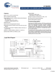
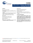
The Cypress CY14B101K combines a 1 Mbit nonvolatile static
RAM with a full featured real time clock in a monolithic integrated
circuit. The embedded nonvolatile elements incorporate
QuantumTrap technology producing the world’s most reliable
nonvolatile memory. The SRAM is read and written an infinite
number of times, while independent, nonvolatile data resides in
the nonvolatile elements.
The Real Time Clock function provides an accurate clock with
leap year tracking and a programmable high accuracy oscillator.
The alarm function is programmable for one time alarm or
periodic seconds, minutes, hours, or days. There is also a
programmable watchdog timer for process control.
de
d
fo
rN
■
■
ig
ns
Pin compatible with STK17TA8
es
■
D
25 ns, 35 ns, and 45 ns access times
ew
■
Endurance to 200K cycles
Data retention: 20 years at 55°C
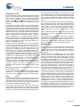
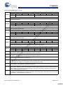
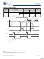
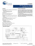
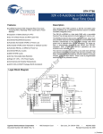
Logic Block Diagram
VCC
en
QuantumTrap
1024 x 1024
DQ 2
ot
N
DQ 4
DQ 5
DQ 6
STATIC RAM
ARRAY
1024 X 1024
POWER
CONTROL
STORE
RECALL
VRTCbat
VRTCcap
STORE/
RECALL
CONTROL
HSB
SOFTWARE
DETECT
A15 - A 0
COLUMN IO
COLUMN DEC
INPUT BUFFERS
DQ 1
DQ 3
m
om
ec
R
DQ 0
ROW DECODER
A5
A6
A7
A8
A9
A 12
A 13
A 14
A 15
A 16
VCAP
RTC
x1
x2
MUX
A16 - A 0
INT
A 0 A 1 A 2 A 3 A 4 A 10 A 11
DQ 7
OE
CE
WE
Cypress Semiconductor Corporation
Document Number: 001-06401 Rev. *J
•
198 Champion Court
•
San Jose, CA 95134-1709
•
408-943-2600
Revised November 26, 2009
[+] Feedback
CY14B101K
Contents
fo
rN
ew
D
es
ig
ns
Interrupts ..................................................................... 10
Interrupt Register ........................................................ 10
Flags Register ............................................................. 10
Maximum Ratings ............................................................. 16
Operating Range .............................................................. 16
DC Electrical Characteristics .......................................... 16
Data Retention and Endurance ....................................... 17
Capacitance ...................................................................... 17
Thermal Resistance ......................................................... 17
AC Test Conditions .......................................................... 17
AC Switching Characteristics ......................................... 18
AC Switching Characteristics (continued) ..................... 19
AutoStore or Power Up RECALL .................................... 20
Software Controlled STORE/RECALL Cycles ................ 21
Hardware STORE Cycle ................................................... 22
Soft Sequence Commands .............................................. 22
RTC Characteristics ......................................................... 23
Truth Table For SRAM Operations ................................. 23
Part Numbering Nomenclature ....................................... 24
Ordering Information ....................................................... 25
Package Diagrams ........................................................... 26
Document History Page ................................................... 27
Sales, Solutions, and Legal Information ........................ 29
Worldwide Sales and Design Support ......................... 29
Products ...................................................................... 29
N
ot
R
ec
om
m
en
de
d
Features .............................................................................. 1
Functional Description ....................................................... 1
Logic Block Diagram .......................................................... 1
Contents .............................................................................. 2
Pin Configurations ............................................................. 3
Device Operation ................................................................ 4
SRAM READ ................................................................. 4
SRAM WRITE ............................................................... 4
AutoStore® Operation ................................................... 4
Hardware STORE (HSB) Operation .............................. 4
Hardware RECALL (Power Up) ..................................... 5
Software STORE ........................................................... 5
Software RECALL ......................................................... 5
Data Protection ............................................................. 5
Noise Considerations .................................................... 5
Low Average Active Power ........................................... 6
Best Practices ............................................................... 6
Real Time Clock Operation ................................................ 8
nvTIME Operation ......................................................... 8
Clock Operations ........................................................... 8
Reading the Clock ......................................................... 8
Setting the Clock ........................................................... 8
Backup Power ............................................................... 8
Stopping and Starting the Oscillator .............................. 8
Calibrating the Clock ..................................................... 9
Alarm ............................................................................. 9
Watchdog Timer ............................................................ 9
Power Monitor ............................................................. 10
Document Number: 001-06401 Rev. *J
Page 2 of 29
[+] Feedback
CY14B101K
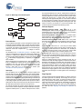
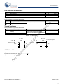
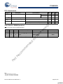
Pin Configurations
Figure 1. 48-Pin SSOP
V CAP
1
48
V CC
A 16
2
47
A 14
A 15
3
46
HSB
4
45
5
44
WE
A 13
A6
6
43
A5
7
42
INT
8
41
NC
11
NC
V SS
12
NC
14
V RTCbat
15
DQ0
16
A3
17
A2
18
DQ1
21
DQ2
x1
23
x2
24
DQ0 – DQ7
Input Output
NC
No Connect
NC
V SS
35
NC
V RTCcap
ew
d
de
en
NC
36
34
m
I/O Type
Input
(Not To Scale)
22
A 11
NC
33
DQ 6
32
OE
A 10
31
30
CE
29
DQ7
28
DQ5
27
DQ4
26
DQ3
25
V CC
Description
Address Inputs. Used to select one of the 131,072 bytes of the nvSRAM.
Bidirectional Data I/O Lines. Used as input or output lines depending on operation
om
Alt
38
rN
19
20
A0 – A16
Top View
37
fo
A1
Table 1. Pin Definitions
Pin Name
48-SSOP
13
A0
40
39
A9
NC
es
9
10
D
A4
NC
A8
ig
ns
A 12
A7
No Connects. This pin is not connected to the die
Input
CE
E
Input
Chip Enable Input, Active LOW. When LOW, selects the chip. When HIGH, deselects the chip.
OE
G
Input
Output Enable, Active LOW. The active low OE input enables the data output buffers during
READ cycles. Deasserting OE high causes the I/O pins to tri-state.
X2
R
ot
Output
N
X1
Write Enable Input, Active LOW. When the chip is enabled and WE is LOW, data on the I/O pins
is written to the specific address location.
ec
W
WE
Input
Crystal Connection Drives crystal on start up.
Crystal Connection for 32.768 kHz crystal.
VRTCcap
Power Supply Capacitor Supplied Backup RTC Supply Voltage. (Left unconnected if VRTCbat is used)
VRTCbat
Power Supply Battery Supplied Backup RTC Supply Voltage. (Left unconnected if VRTCcap is used)
INT
Output
Interrupt Output. Program to respond to the clock alarm, the watchdog timer, and the power
monitor. Programmable to either active HIGH (push or pull) or LOW (open drain).
VSS
Ground
Ground for the Device. Must be connected to ground of the system.
VCC
HSB
VCAP
Power Supply Power Supply Inputs to the Device.
Input Output
Hardware Store Busy. When LOW this output indicates a Hardware Store is in progress. When
pulled LOW external to the chip it initiates a nonvolatile STORE operation. A weak internal pull up
resistor keeps this pin HIGH if not connected (connection optional).
Power Supply AutoStore™ Capacitor. Supplies power to nvSRAM during power loss to store data from SRAM
to nonvolatile elements.
Document Number: 001-06401 Rev. *J
Page 3 of 29
[+] Feedback
CY14B101K
Device Operation
automatically disconnects the VCAP pin from VCC. A STORE
operation is initiated with power provided by the VCAP capacitor.
The CY14B101K nvSRAM consists of two functional components paired in the same physical cell. The components are
SRAM memory cell and a nonvolatile QuantumTrap cell. The
SRAM memory cell operates as a standard fast static RAM. Data
in the SRAM is transferred to the nonvolatile cell (the STORE
operation), or from the nonvolatile cell to SRAM (the RECALL
operation). Using this unique architecture, all cells are stored and
recalled in parallel. During the STORE and RECALL operations,
SRAM READ and WRITE operations are inhibited. The
CY14B101K suppots infinite reads and writes similar to a typical
SRAM. In addition, it provides infinite RECALL operations from
the nonvolatile cells and up to 200K STORE operations.
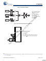
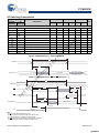
Figure 2. AutoStore Mode
V CC
0.1UF
10k Ohm
ig
ns
V CAP
WE
es
See the “Truth Table For SRAM Operations” on page 23 for a
complete description of read and write modes.
fo
rN
ew
D
SRAM READ
Figure 2 shows the proper connection of the storage capacitor
(VCAP) for automatic store operation. Refer to DC Electrical
Characteristics on page 16 for the size of the VCAP. The voltage
on the VCAP pin is driven to 5V by a charge pump internal to the
chip. A pull up should be placed on WE to hold it inactive during
power up. This pull up is only effective if the WE signal is tri-state
during power up. Many MPUs tri-state their controls on power up.
Verify this when using the pull up. When the nvSRAM comes out
of power-on-recall, the MPU must be active or the WE held
inactive until the MPU comes out of reset.
d
The CY14B101K performs a READ cycle whenever CE and OE
are LOW while WE and HSB are HIGH. The address specified
on pins A0-16 determines which of the 131,072 data bytes are
accessed. When the READ is initiated by an address transition,
the outputs are valid after a delay of tAA (see Figure 8 on page
18). If the READ is initiated by CE or OE, the outputs are valid at
tACE or at tDOE, whichever is later (see Figure 9 on page 18). The
data outputs repeatedly respond to address changes within the
tAA access time without the need for transitions on any control
input pins. This remains valid until another address change or
until CE or OE is brought HIGH, or WE or HSB is brought LOW.
V CC
V CAP
de
SRAM WRITE
R
AutoStore® Operation
ec
om
m
en
A WRITE cycle is performed whenever CE and WE are LOW and
HSB is HIGH. The address inputs must be stable before entering
the WRITE cycle and must remain stable until either CE or WE
go HIGH at the end of the cycle. The data on the common I/O
pins DQ0–7 is written into the memory if the data is valid tSD
before the end of a WE controlled WRITE or before the end of
an CE controlled WRITE. Keep OE HIGH during the entire
WRITE cycle to avoid data bus contention on common I/O lines.
If OE is left LOW, internal circuitry turns off the output buffers
tHZWE after WE goes LOW.
N
ot
The CY14B101K stores data to nvSRAM using one of three
storage operations:
1. Hardware Store activated by HSB
2. Software Store activated by an address sequence
3. AutoStore on device power down
AutoStore operation is a unique feature of QuantumTrap
technology and is enabled by default on the CY14B101K.
During normal operations, the device draws current from VCC to
charge a capacitor connected to the VCAP pin. This stored
charge is used by the chip to perform a single STORE operation.
If the voltage on the VCC pin drops below VSWITCH, the part
Document Number: 001-06401 Rev. *J
To reduce unnecessary nonvolatile stores, AutoStore and
Hardware Store operations are ignored unless at least one
WRITE operation takes place since the most recent STORE or
RECALL cycle. Software initiated STORE cycles are performed
regardless of whether a WRITE operation took place. Monitor the
HSB signal by the system to detect if an AutoStore cycle is in
progress.
Hardware STORE (HSB) Operation
The CY14B101K provides the HSB pin for controlling and
acknowledging the STORE operations. Use the HSB pin to
request a hardware STORE cycle. When the HSB pin is driven
LOW, the CY14B101K conditionally initiates a STORE operation
after tDELAY. An actual STORE cycle only begins if a WRITE to
the SRAM has taken place since the last STORE or RECALL
cycle. The HSB pin also acts as an open drain driver that is internally driven LOW to indicate a busy condition while the STORE
(initiated by any means) is in progress. This pin is externally
pulled up if it is used to drive other inputs.
Page 4 of 29
[+] Feedback
CY14B101K
SRAM READ and WRITE operations that are in progress when
HSB is driven LOW by any means are given time to complete
before the STORE operation is initiated. After HSB goes LOW,
the CY14B101K continues SRAM operations for tDELAY. During
tDELAY, multiple SRAM READ operations take place. If a WRITE
is in progress when HSB is pulled LOW, it is allowed a time,
tDELAY, to complete. However, any SRAM WRITE cycles
requested after HSB goes LOW are inhibited until HSB returns
HIGH.
The software sequence is clocked with CE controlled READs or
OE controlled READs. After the sixth address in the sequence is
entered, the STORE cycle commences and the chip is disabled.
It is important to use read cycles and not write cycles in the
sequence, although it is not necessary that OE be LOW for a
valid sequence. After the tSTORE cycle time is fulfilled, the SRAM
is activated again for READ and WRITE operation.
During any STORE operation, regardless of how it is initiated,
the CY14B101K continues to drive the HSB pin LOW, releasing
it only when the STORE is complete. After completing the
STORE operation, the CY14B101K remains disabled until the
HSB pin returns HIGH. Leave the HSB unconnected if it is not
used.
Data is transferred from the nonvolatile memory to the SRAM by
a software address sequence. A software RECALL cycle is
initiated with a sequence of READ operations in a manner similar
to the software STORE initiation. To initiate the RECALL cycle,
the following sequence of CE controlled READ operations are
performed:
1. Read Address 0x4E38 Valid READ
2. Read Address 0xB1C7 Valid READ
3. Read Address 0x83E0 Valid READ
4. Read Address 0x7C1F Valid READ
5. Read Address 0x703F Valid READ
6. Read Address 0x4C63 Initiate RECALL Cycle
ig
ns
Software RECALL
es
Hardware RECALL (Power Up)
ew
D
During power up or after any low power condition
(VCC < VSWITCH), an internal RECALL request is latched. When
VCC again exceeds the sense voltage of VSWITCH, a RECALL
cycle automatically initiates and takes tHRECALL to complete.
Internally, RECALL is a two step procedure. First, the SRAM data
is cleared and then the nonvolatile information is transferred into
the SRAM cells. After the tRECALL cycle time, the SRAM is again
ready for READ and WRITE operations. The RECALL operation
does not alter the data in the nonvolatile elements.
fo
Data Protection
de
d
Data is transferred from the SRAM to the nonvolatile memory by
a software address sequence. The CY14B101K software
STORE cycle is initiated by executing sequential CE controlled
READ cycles from six specific address locations in exact order.
During the STORE cycle, an erase of the previous nonvolatile
data is first performed followed by a program of the nonvolatile
elements. After a STORE cycle is initiated, further READs and
WRITEs are inhibited until the cycle is completed.
rN
Software STORE
m
en
Because a sequence of READs from specific addresses is used
for STORE initiation, it is important that no other READ or WRITE
accesses intervene in the sequence. If it intervenes, the
sequence is aborted and no STORE or RECALL takes place.
Noise Considerations
The CY14B101K is a high speed memory and must have a high
frequency bypass capacitor of approximately 0.1 µF connected
between VCC and VSS, using leads and traces that are as short
as possible. As with all high speed CMOS ICs, careful routing of
power, ground, and signals reduce circuit noise.
N
ot
R
ec
om
To initiate the software STORE cycle, the following READ
sequence are performed:
1. Read Address 0x4E38 Valid READ
2. Read Address 0xB1C7 Valid READ
3. Read Address 0x83E0 Valid READ
4. Read Address 0x7C1F Valid READ
5. Read Address 0x703F Valid READ
6. Read Address 0x8FC0 Initiate STORE cycle
The CY14B101K protects data from corruption during low
voltage conditions by inhibiting all externally initiated STORE
and WRITE operations. The low voltage condition is detected
when VCC is less than VSWITCH. If the CY14B101K is in a WRITE
mode (both CE and WE LOW) at power up, after a RECALL or
after a STORE, the WRITE is inhibited until a negative transition
on CE or WE is detected. This protects against inadvertent writes
during power up or brownout conditions.
Document Number: 001-06401 Rev. *J
Page 5 of 29
[+] Feedback
CY14B101K
Low Average Active Power
Best Practices
CMOS technology provides the CY14B101K the benefit of
drawing significantly less current when it is cycled at times longer
than 50 ns. Figure 3 shows the relationship between ICC and
READ/WRITE Cycle Time. The worst case current consumption
is shown for commercial temperature range, VCC = 3.6V, and
chip enable at maximum frequency. Only standby current is
drawn when the chip is disabled.
nvSRAM products have been used effectively for over 15 years.
While ease-of-use is one of the product’s main system values,
experience gained working with hundreds of applications has
resulted in the following suggestions as best practices:
■
The nonvolatile cells in an nvSRAM are programmed on the
test floor during final test and quality assurance. Incoming
inspection routines at customer or contract manufacturer’s
sites sometimes reprograms these values. Final NV patterns
are typically repeating patterns of AA, 55, 00, FF, A5, or 5A.
The end product’s firmware should not assume that an NV array
is in a set programmed state. Routines that check memory
content values to determine first time system configuration and
cold or warm boot status, must always program a unique NV
pattern (for example, complex 4-byte pattern of 46 E6 49 53
hex or more random bytes) as part of the final system manufacturing test to ensure these system routines work consistently.
■
The OSCEN bit in the Calibration register at 0x1FFF8 should
be set to 1 to preserve battery life when the system is in storage
(see Stopping and Starting the Oscillator on page 8).
■
The Vcap value specified in this data sheet includes a minimum
and a maximum value size. The best practice is to meet this
requirement and not exceed the maximum Vcap value because
the higher inrush currents may reduce the reliability of the
internal pass transistor. Customers who want to use a larger
Vcap value to make sure there is extra store charge should
discuss their Vcap size selection with Cypress.
The duty cycle of chip enable
■
The overall cycle rate for accesses
■
The ratio of READs to WRITEs
■
The operating temperature
■
The VCC level
■
I/O loading
ew
N
ot
R
ec
om
m
en
de
d
fo
rN
Figure 3. Current versus Cycle Time
D
es
■
ig
ns
The overall average current drawn by the CY14B101K depends
on the following items:
Document Number: 001-06401 Rev. *J
Page 6 of 29
[+] Feedback
CY14B101K
Table 2. Mode Selection
WE
OE
A15 – A0
Mode
I/O
Power
H
X
X
X
Not Selected
Output High Z
Standby
L
H
L
X
READ SRAM
Output Data
Active
L
L
X
X
WRITE SRAM
Input Data
Active
L
H
L
0x4E38
0xB1C7
0x83E0
0x7C1F
0x703F
0x8FC0
Read SRAM
Read SRAM
Read SRAM
Read SRAM
Read SRAM
Nonvolatile
STORE
Output Data
Output Data
Output Data
Output Data
Output Data
Output High Z
Active ICC2[1, 2, 3]
L
H
L
0x4E38
0xB1C7
0x83E0
0x7C1F
0x703F
0x4C63
Read SRAM
Read SRAM
Read SRAM
Read SRAM
Read SRAM
Nonvolatile
RECALL
Output Data
Output Data
Output Data
Output Data
Output Data
Output High Z
Active[1, 2, 3]
N
ot
R
ec
om
m
en
de
d
fo
rN
ew
D
es
ig
ns
CE
Notes
1. The six consecutive address locations are in the order listed. WE is HIGH during all six cycles to enable a nonvolatile cycle.
2. While there are 17 address lines on the CY14B101K, only the lower 16 lines are used to control software modes.
3. O state depends on the state of OE. The I/O table shown is based on OE Low.
Document Number: 001-06401 Rev. *J
Page 7 of 29
[+] Feedback
CY14B101K
Real Time Clock Operation
The clock oscillator uses very little current to maximize the
backup time available from the backup source. Regardless of
clock operation with the primary source removed, the data stored
in nvSRAM is secure, as it is stored in the nonvolatile elements
when power was lost.
nvTIME Operation
The CY14B101K offers internal registers that contain clock,
alarm, watchdog, interrupt, and control functions. RTC registers
use the last 16 address locations of the SRAM. Internal double
buffering of the clock and the clock or timer information registers
prevents accessing transitional internal clock data during a
READ or WRITE operation. Double buffering also circumvents
disrupting normal timing counts or clock accuracy of the internal
clock while accessing clock data. Clock and Alarm Registers
store data in BCD format.
During backup operation, the CY14B101K consumes a
maximum of 300 nA at 2V. The user should choose capacitor or
battery values according to the application.
Table 3. RTC Backup Time
The RTC register addresses for CY14B101K range from
0x1FFF0 to 0x1FFFF. Refer to RTC Register Map[5, 6] on page
12 and Register Map Detail on page 13 for detailed description.
es
Capacitor Value
0.1F
0.47F
1.0F
rN
ew
Using a capacitor has the obvious advantage of recharging the
backup source each time the system is powered up. If a battery
is used, use a 3V lithium; the CY14B101K only sources current
from the battery when the primary power is removed. However,
the battery is not recharged at any time by the CY14B101K. The
battery capacity is chosen for total anticipated cumulative
downtime required over the life of the system.
fo
Stopping and Starting the Oscillator
The OSCEN bit in the calibration register at 0x1FFF8 controls
the enable and disable of the oscillator. This active LOW bit is
nonvolatile and is shipped to customers in the “enabled” (set to
0) state. To preserve the battery life when the system is in
storage, OSCEN bit must be set to ‘1’. This turns off the oscillator
circuit, extending the battery life. If the OSCEN bit goes from
disabled to enabled, it takes approximately 5 seconds (10
seconds maximum) for the oscillator to start.
d
Reading the Clock
Backup Time
72 hours
14 days
30 days
D
Clock Operations
The clock registers maintain time up to 9,999 years in one
second increments. The user sets the time to any calendar time
and the clock automatically keeps track of days of the week,
month, leap years, and century transitions. There are eight
registers dedicated to the clock functions that are used to set
time with a WRITE cycle and to READ time during a READ cycle.
These registers contain the Time of Day in BCD format. Bits
defined as ‘0’ are currently not used and are reserved for future
use by Cypress.
ig
ns
Backup time values, based on maximum current specifications,
are shown in the following table. Nominal times are approximately three times longer.
m
en
de
The double buffered RTC register structure reduces the chance
of reading incorrect data from the clock. The user should stop
internal updates to the CY14B101K time keeping registers
before reading clock data, to prevent reading of data in transition.
Stopping the internal register updates does not affect clock
accuracy.
R
Setting the Clock
ec
om
The updating process is stopped by writing a ‘1’ to the read bit
‘R’ (in the flags register at 0x1FFF0), and does not restart until a
‘0’ is written to the read bit. The RTC registers are then read while
the internal clock continues to run. After a ‘0’ is written to the read
bit (‘R’), all CY14B101K registers are simultaneously updated
within 20 ms.
N
ot
Setting the write bit ‘W’ (in the flags register at 0x1FFF0) to a ‘1’
stops updates to the time keeping registers and enables the time
to be set. The correct day, date, and time are then written into
the registers in 24 hour BCD format. The time written is referred
to as the ‘Base Time’. This value is stored in nonvolatile registers
and used in calculation of the current time. Resetting the WRITE
bit to ‘0’ transfers those values to the actual clock counters, after
which the clock resumes normal operation.
Backup Power
The RTC in the CY14B101K is intended for permanently
powered operations. Either the VRTCcap or VRTCbat pin is
connected depending on whether a capacitor or battery is
chosen for the application. When the primary power, VCC, fails
and drops below VSWITCH, the device switches to the backup
power supply.
Document Number: 001-06401 Rev. *J
While system power is off, if the voltage on the backup supply
(VRTCcap or VRTCbat) falls below their respective minimum level,
the oscillator may fail.The CY14B101K has the ability to detect
oscillator failure when system power is restored. This is recorded
in the OSCF (Oscillator Failed bit) of the Flags register at
address 0x1FFF0. When the device is powered on (VCC goes
above VSWITCH), the OSCEN bit is checked for “enabled” status.
If the OSCEN bit is enabled and the oscillator is not active within
the first 5 ms, the OSCF bit is set to “1”. The system must check
for this condition and then write ‘0’ to clear the flag. Note that in
addition to setting the OSCF flag bit, the time registers are reset
to the “Base Time” (see “Setting the Clock” on page 8), which is
the value last written to the time keeping registers. The Control
or Calibration registers and the OSCEN bit are not affected by
the “oscillator failed” condition.
The value of OSCF must be reset to ‘0’ when the time registers
are written for the first time. This initializes the state of this bit
which may have become set when the system was first powered
on.
To reset OSCF, set the write bit “W” (in the flags register at
0x1FFF0) to “1” to enable writes to the Flag register. Write a “0”
to the OSCF bit and then reset the write bit to “0” to disable
writes.
Page 8 of 29
[+] Feedback
CY14B101K
Calibrating the Clock
the match process. Depending on the match bits, the alarm
occurs as specifically as once a month or as frequently as once
every minute. Selecting none of the match bits (all 1s) indicates
that no match is required and therefore, alarm is disabled.
Selecting all match bits (all 0s) causes an exact time and date
match.
The RTC is driven by a quartz controlled oscillator with a nominal
frequency of 32.768 kHz. Clock accuracy depends on the quality
of the crystal and calibration. The crystal oscillators typically
have an error of +20ppm to +35ppm. However, CY14B101K
employs a calibration circuit that improves the accuracy to +1/–2
ppm at 25°C. This implies an error of +2.5 seconds to -5 seconds
per month.
There are two ways to detect an alarm event: by reading the AF
flag or monitoring the INT pin. The AF flag in the flags register at
0x1FFF0 indicates that a date or time match has occurred. The
AF bit is set to “1” when a match occurs. Reading the flags or
control register clears the alarm flag bit (and all others). A
hardware interrupt pin may also be used to detect an alarm
event.
es
Note CY14B101K requires the alarm match bit for seconds
(0x1FFF2 - D7) to be set to ‘0’ for proper operation of Alarm Flag
and Interrupt.
ew
D
Alarm registers are not nonvolatile and, therefore, need to be
reinitialized by software on power up. To set, clear or enable an
alarm, set the ‘W’ bit (in Flags Register - 0x1FFF0) to ‘1’ to
enable writes to Alarm Registers. After writing the alarm value,
clear the ‘W’ bit back to “0” for the changes to take effect.
rN
Watchdog Timer
fo
The Watchdog Timer is a free running down counter that uses
the 32 Hz clock (31.25 ms) derived from the crystal oscillator.
The oscillator must be running for the watchdog to function. It
begins counting down from the value loaded in the Watchdog
Timer register.
de
d
Calibration occurs within a 64 minute cycle. The first 62 minutes
in the cycle may, once per minute, have one second shortened
by 128 or lengthened by 256 oscillator cycles. If a binary ‘1’ is
loaded into the register, only the first two minutes of the 64
minute cycle is modified. If a binary 6 is loaded, the first 12 are
affected, and so on. Therefore, each calibration step has the
effect of adding 512 or subtracting 256 oscillator cycles for every
125,829,120 actual oscillator cycles, that is, 4.068 or –2.034 ppm
of adjustment per calibration step in the Calibration register.
ig
ns
The calibration circuit adds or subtracts counts from the oscillator
divider circuit to achieve this accuracy. The number of pulses that
are suppressed (subtracted, negative calibration) or split (added,
positive calibration) depends upon the value loaded into the five
calibration bits found in Calibration register at 0x1FFF8. The
calibration bits occupy the five lower order bits in the Calibration
register. These bits are set to represent any value between ‘0’
and 31 in binary form. Bit D5 is a sign bit, where a ‘1’ indicates
positive calibration and a ‘0’ indicates negative calibration.
Adding counts speeds the clock up and subtracting counts slows
the clock down. If a binary ‘1’ is loaded into the register, it corresponds to an adjustment of 4.068 or –2.034 ppm offset in oscillator error, depending on the sign.
om
m
en
To determine the required calibration, the CAL bit in the Flags
register (0x1FFF0) must be set to ‘1’. This causes the INT pin to
toggle at a nominal frequency of 512 Hz. Any deviation
measured from the 512 Hz indicates the degree and direction of
the required correction. For example, a reading of 512.01024 Hz
indicates a +20 ppm error. Hence, a decimal value of –10
(001010b) must be loaded into the Calibration register to offset
this error.
ec
Note Setting or changing the Calibration register does not affect
the test output frequency.
N
Alarm
ot
R
To set or clear CAL, set the write bit “W” (in the flags register at
0x1FFF0) to “1” to enable writes to the Flag register. Write a
value to CAL, and then reset the write bit to “0” to disable writes.
The alarm function compares user programmed values of alarm
time and date (stored in the registers 0x1FFF1-5) with the corresponding time of day and date values. When a match occurs, the
alarm internal flag (AF) is set and an interrupt is generated on
INT pin if Alarm Interrupt Enable (AIE) bit is set.
There are four alarm match fields - date, hours, minutes, and
seconds. Each of these fields has a match bit that is used to
determine if the field is used in the alarm match logic. Setting the
match bit to ‘0’ indicates that the corresponding field is used in
Document Number: 001-06401 Rev. *J
The timer consists of a loadable register and a free running
counter. On power up, the watchdog time out value in register
0x1FFF7 is loaded into the Counter Load register. Counting
begins on power up and restarts from the loadable value any time
the Watchdog Strobe (WDS) bit is set to ‘1’. The counter is
compared to the terminal value of ‘0’. If the counter reaches this
value, it causes an internal flag and an optional interrupt output.
You can prevent the time out interrupt by setting WDS bit to ‘1’
prior to the counter reaching ‘0’. This causes the counter to
reload with the watchdog time out value and to be restarted. As
long as the user sets the WDS bit prior to the counter reaching
the terminal value, the interrupt and WDT flag never occur.
New time out values are written by setting the watchdog write bit
to ‘0’. When the WDW is ‘0’, new writes to the watchdog time out
value bits D5-D0 are enabled to modify the time out value. When
WDW is ‘1’, writes to bits D5-D0 are ignored. The WDW function
enables a user to set the WDS bit without concern that the
watchdog timer value is modified. A logical diagram of the
watchdog timer is shown in Figure 4. Note that setting the
watchdog time out value to ‘0’ disables the watchdog function.
The output of the watchdog timer is the flag bit WDF that is set if
the watchdog is allowed to time out. The flag is set upon a
watchdog time out and cleared when the user reads the Flags or
Control registers. If the watchdog time out occurs, the user also
enables an optional interrupt source to drive the INT pin.
Page 9 of 29
[+] Feedback
CY14B101K
two programmable bits, H/L and P/L, determine the behavior of
the output pin driver on INT pin. These two bits are located in the
Interrupt register and can be used to drive level or pulse mode
output from the INT pin. In pulse mode, the pulse width is
internally fixed at approximately 200 ms. This mode is intended
to reset a host microcontroller. In the level mode, the pin goes to
its active polarity until the Flags register is read by the user. This
mode is used as an interrupt to a host microcontroller. The
control bits are summarized in the following section.
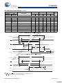
Figure 4. Watchdog Timer Block Diagram
Clock
Divider
Oscillator
32,768 KHz
1 Hz
32 Hz
Zero
Compare
Counter
WDF
Interrupt Register
Load
Register
Watchdog Interrupt Enable - WIE. When set to ‘1’, the
watchdog timer drives the INT pin and an internal flag when a
watchdog time out occurs. When WIE is set to ‘0’, the watchdog
timer only affects the WDF flag in Flags register.
ig
ns
WDS
Q
D
WDW
Alarm Interrupt Enable - AIE. When set to ‘1’, the alarm match
drives the INT pin and an internal flag. When AIE is set to ‘0’, the
alarm match only affects the AF flagin Flags register.
es
Q
Watchdog
Register
D
write to
Watchdog
Register
Power Fail Interrupt Enable - PFE. When set to ‘1’, the power
fail monitor drives the pin and an internal flag. When PFE is set
to ‘0’, the power fail monitor only affects the PF flag in Flags
register.
rN
Pulse/Level - P/L. When set to a ‘1’ and an interrupt occurs, the
INT pin is driven for approximately 200 ms. When P/L is set to a
‘0’, the INT pin is driven high or low (determined by H/L) until the
Flags or Control register is read.
en
de
d
As described in the “AutoStore® Operation” on page 4, when
VSWITCH is reached as VCC decays from power loss, a data store
operation is initiated from SRAM to the nonvolatile elements,
securing the last SRAM data state. Power is also switched from
VCC to the backup supply (battery or capacitor) to operate the
RTC oscillator.
High/Low - H/L. When set to a ‘1’, the INT pin is active HIGH
and the driver mode is push pull. The INT pin drives high only
when VCC is greater than VSWITCH. When set to a ‘0’, the INT pin
is active LOW and the drive mode is open drain. Active LOW
(open drain) is operational even in battery backup mode.
fo
The CY14B101K provides a power management scheme with
power fail interrupt capability. It also controls the internal switch
to backup power for the clock and protects the memory from low
VCC access. The power monitor is based on an internal band gap
reference circuit that compares the VCC voltage to VSWITCH
threshold.
ew
Power Monitor
ec
om
m
When operating from the backup source, read and write operations to nvSRAM are inhibited and the clock functions are not
available to the user. The clock continues to operate in the
background. The updated clock data is available to the user
tHRECALL delay after VCC is restored to the device (see
“AutoStore or Power Up RECALL” on page 20).
Interrupts
N
ot
R
The CY14B101K has a Flags register, Interrupt register and
Interrupt logic that can signal interrupt to the microcontroller.
There are three potential sources for interrupt: watchdog timer,
power monitor, and alarm timer. Each of these can be individually
enabled to drive the INT pin by appropriate setting in the Interrupt
register (0x1FFF6). In addition, each has an associated flag bit
in the Flags register (0x1FFF0) that the host processor uses to
determine the cause of the interrupt. The INT pin driver has two
bits that specify its behavior when an interrupt occurs.
An Interrupt is raised only if both a flag is raised by one of the
three sources and the respective interrupt enable bit in Interrupts
register is enabled (set to ‘1’). After an interrupt source is active,
Document Number: 001-06401 Rev. *J
When an enabled interrupt source activates the INT pin, an
external host reads the Flags registers to determine the cause.
Remember that all flags are cleared when the register is read. If
the INT pin is programmed for Level mode, then the condition
clears and the INT pin returns to its inactive state. If the pin is
programmed for Pulse mode, then reading the flag also clears
the flag and the pin. The pulse does not complete its specified
duration if the Flags register is read. If the INT pin is used as a
host reset, then the Flags or Control register is not read during a
reset.
Flags Register
The Flag register has three flag bits: WDF, AF, and PF, which can
be used to generate an interrupt. These flags are set by the
watchdog timeout, alarm match, or power fail monitor respectively. The processor can either poll this register or enable interrupts to be informed when a flag is set. These flags are automatically reset once the register is read. The flags register is
automatically loaded with the value 00h on power up (except for
the OSCF bit. See “Stopping and Starting the Oscillator” on
page 8.)
Page 10 of 29
[+] Feedback
CY14B101K
Figure 5. Interrupt Block Diagram
WDF
Watchdog
Timer
WIE
PF
Power
Monitor
VCC
P/L
Pin
Driver
PFE
INT
H/L
ig
ns
VINT
VSS
es
AF
Clock
Alarm
WDF - Watchdog Timer Flag
WIE - Watchdog Interrupt
Enable
PF - Power Fail Flag
PFE - Power Fail Enable
AF - Alarm Flag
AIE - Alarm Interrupt Enable
P/L - Pulse Level
H/L - High/Low
ew
D
AIE
de
d
fo
rN
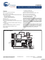
Figure 6. RTC Recommended Component Configuration
DQ 0
Y1 = 32.768 kHz
RF = 10 MΩ
C1 = 0 (install cap footprint, but leave unloaded)
C2 = 56 pF + 10% (do not vary from this value)
om
m
A3
A2
en
Recommended Values
A1
ec
Y1
R
X1
X2
N
ot
C2
RF
C1
A0
Note
4. Schottky diodes, (VF < 0.4V at IF=100 mA) are recommended at pins A0 - A3 and DQ0 in applications where undershoot exceeds -0.5V. Please see application note
AN49947 for further details.
Document Number: 001-06401 Rev. *J
Page 11 of 29
[+] Feedback
CY14B101K
Table 4. RTC Register Map[5, 6]
Register
BCD Format Data [5]
D7
D6
0x1FFFF
D5
D4
D3
D2
10s Years
0x1FFFE
0
0
0x1FFFD
0
0
0
Years: 00–99
Months
Months: 01–12
Day Of Month
Day of Month: 01–31
0
0
0x1FFFB
0
0
0x1FFFA
0
0x1FFF9
0
0x1FFF8
OSCEN
(0)
0
0x1FFF7
WDS (0)
WDW (0)
0x1FFF6
WIE (0)
AIE (0)
0x1FFF5
M (1)
0
10s Alarm Date
Alarm Day
Alarm, Day of Month: 01–31
0x1FFF4
M (1)
0
10s Alarm Hours
Alarm Hours
Alarm, Hours: 00–23
0x1FFF3
M (1)
10 Alarm Minutes
Alarm Minutes
Alarm, Minutes: 00–59
0x1FFF2
M (1)
10 Alarm Seconds
Alarm, Seconds
Alarm, Seconds: 00–59
0
Day of Week: 01–07
Hours: 00–23
10s Minutes
Minutes
Minutes: 00–59
10s Seconds
Seconds
Seconds: 00–59
Calibration Values [7]
Calibration (00000)
es
Cal Sign
(0)
ig
ns
Hours
H/L (1)
0
0
Centuries
PF
fo
AF
P/L (0)
ew
0
rN
PFE (0)
D
WDT (000000)
10s Centuries
WDF
Day of Week
10s Hours
OSCF
0
CAL (0)
W (0)
Watchdog [7]
Interrupts [7]
Centuries: 00–99
R (0)
Flags [7]
N
ot
R
ec
om
m
en
de
d
0x1FFF0
0
Function/Range
0x1FFFC
0x1FFF1
0
D0
Years
10s Months
10s Day of Month
D1
Notes
5. ( ) designates values shipped from the factory.
6. The unused bits of RTC registers are reserved for future use and should be set to ‘0’.
7. Is a binary value, not a BCD value.
Document Number: 001-06401 Rev. *J
Page 12 of 29
[+] Feedback
CY14B101K
Table 5. Register Map Detail
Time Keeping - Years
D7
D6
0x1FFFF
D5
D4
D3
D2
10s Years
D1
D0
Years
Contains the lower two BCD digits of the year. Lower nibble (four bits) contains the value for years; upper nibble (four
bits) contains the value for 10s of years. Each nibble operates from 0 to 9. The range for the register is 0–99.
Time Keeping - Months
D7
D6
D5
D4
D3
0
0
0
10s Month
D2
D1
D0
Months
ig
ns
0x1FFFE
Contains the BCD digits of the month. Lower nibble (four bits) contains the lower digit and operates from 0 to 9; upper
nibble (one bit) contains the upper digit and operates from 0 to 1. The range for the register is 1–12.
0
0
D5
D4
D3
10s Day of Month
D2
D1
D0
Day of Month
D
0x1FFFD
D6
es
Time Keeping - Date
D7
ew
Contains the BCD digits for the date of the month. Lower nibble (four bits) contains the lower digit and operates from 0
to 9; upper nibble (two bits) contains the 10s digit and operates from 0 to 3. The range for the register is 1–31. Leap
years are automatically adjusted for.
D6
D5
D4
0
0
0
0
fo
0x1FFFC
D7
rN
Time Keeping - Day
D3
D2
0
D1
D0
Day of Week
de
d
Lower nibble (three bits) contains a value that correlates to day of the week. Day of the week is a ring counter that counts
from 1 to 7 then returns to 1. The user must assign meaning to the day value, because the day is not integrated with the
date.
Time Keeping - Hours
D6
0
0
D5
en
D7
D4
D3
D2
10s Hours
D1
D0
Hours
m
0x1FFFB
om
Contains the BCD value of hours in 24 hour format. Lower nibble (four bits) contains the lower digit and operates from
0 to 9; upper nibble (two bits) contains the upper digit and operates from 0 to 2. The range for the register is 0–23.
D6
ec
D7
0x1FFFA
0
Time Keeping - Minutes
D5
D4
D3
D2
10s Minutes
D1
D0
Minutes
ot
R
Contains the BCD value of minutes. Lower nibble (four bits) contains the lower digit and operates from 0 to 9; upper
nibble (three bits) contains the upper minutes digit and operates from 0 to 5. The range for the register is 0–59.
0x1FFF9
N
D7
Time Keeping - Seconds
D6
0
D5
10s Seconds
D4
D3
D2
D1
D0
Seconds
Contains the BCD value of seconds. Lower nibble (four bits) contains the lower digit and operates from 0 to 9; upper
nibble (three bits) contains the upper digit and operates from 0 to 5. The range for the register is 0–59.
Document Number: 001-06401 Rev. *J
Page 13 of 29
[+] Feedback
CY14B101K
Table 5. Register Map Detail (continued)
Calibration/Control
0X1FFF8
OSCEN
D7
D6
D5
OSCEN
0
Calibration
Sign
D4
D3
D2
D1
D0
Calibration
Oscillator Enable. When set to 1, the oscillator is stopped. When set to 0, the oscillator runs. Disabling the oscillator
saves battery or capacitor power during storage.
Calibration Determines if the calibration adjustment is applied as an addition (1) to or as a subtraction (0) from the time-base.
Sign
ig
ns
Calibration These five bits control the calibration of the clock.
WatchDog Timer
D7
D6
WDS
WDW
D5
D4
D3
D2
WDT
D1
D0
es
0x1FFF7
Watchdog Strobe. Setting this bit to 1 reloads and restarts the watchdog timer. Setting the bit to 0 has no effect. The bit
is cleared automatically after the watchdog timer is reset. The WDS bit is write only. Reading it always returns a 0.
WDW
Watchdog Write Enable. Setting this bit to 1 disables any WRITE to the watchdog timeout value (D5–D0). This allows
the user to set the watchdog strobe bit without disturbing the timeout value. Setting this bit to 0 allows bits D5–D0 to be
written to the watchdog register when the next write cycle is complete. This function is explained in detail in the “Watchdog
Timer” on page 9.
WDT
Watchdog timeout selection. The watchdog timer interval is selected by the 6-bit value in this register. It represents a
multiplier of the 32 Hz count (31.25 ms). The range of timeout value is 31.25 ms (a setting of 1) to 2 seconds (setting of
3 Fh). Setting the watchdog timer register to 0 disables the timer. These bits can be written only if the WDW bit was set
to 0 on a previous cycle.
d
fo
rN
ew
D
WDS
D7
D6
D5
WIE
AIE
PFIE
en
0x1FFF6
de
Interrupt Status/Control
D4
D3
D2
D1
D0
0
H/L
P/L
0
0
Watchdog Interrupt Enable. When set to 1 and a watchdog timeout occurs, the watchdog timer drives the INT pin and
the WDF flag. When set to 0, the watchdog timeout affects only the WDF flag.
AIE
Alarm Interrupt Enable. When set to 1, the alarm match drives the INT pin and the AF flag. When set to 0, the alarm
match only affects the AF flag.
PFIE
Power Fail Enable. When set to 1, the alarm match drives the INT pin and the PF flag. When set to 0, the power fail
monitor affects only the PF flag.
om
ec
0
m
WIE
Reserved for future use
High/Low. When set to 1, the INT pin is driven active HIGH. When set to 0, the INT pin is open drain, active LOW.
P/L
Pulse/Level. When set to 1, the INT pin is driven active (determined by H/L) by an interrupt source for approximately
200 ms. When set to 0, the INT pin is driven to an active level (as set by H/L) until the flags register is read.
N
ot
R
H/L
0x1FFF5
Alarm - Day
D7
D6
M
0
D5
D4
10s Alarm Date
D3
D2
D1
D0
Alarm Date
Contains the alarm value for the date of the month and the mask bit to select or deselect the date value.
M
Match. When this bit is set to 0, the date value is used in the alarm match. Setting this bit to 1 causes the match circuit
to ignore the date value.
Document Number: 001-06401 Rev. *J
Page 14 of 29
[+] Feedback
CY14B101K
Table 5. Register Map Detail (continued)
Alarm - Hours
0x1FFF4
D7
D6
D5
M
D4
D3
D2
10s Alarm Hours
D1
D0
Alarm Hours
Contains the alarm value for the hours and the mask bit to select or deselect the hours value.
M
Match. When this bit is set to 0, the hours value is used in the alarm match. Setting this bit to 1 causes the match circuit
to ignore the hours value.
Alarm - Minutes
D7
D6
D5
M
D4
D3
D2
D1
ig
ns
0x1FFF3
10s Alarm Minutes
D0
Alarm Minutes
Contains the alarm value for the minutes and the mask bit to select or deselect the minutes value.
Alarm - Seconds
D7
D6
D5
M
D4
D3
ew
0x1FFF2
es
Match. When this bit is set to 0, the minutes value is used in the alarm match. Setting this bit to 1 causes the match
circuit to ignore the minutes value.
D
M
10s Alarm Seconds
D2
D1
D0
Alarm Seconds
M
rN
Contains the alarm value for the seconds and the mask bit to select or deselect the seconds’ value.
Match. When this bit is set to 0, the seconds value is used in the alarm match. Setting this bit to 1 causes the match
circuit to ignore the seconds value.
D5
10s Centuries
D4
D3
D2
d
D6
D1
D0
Centuries
de
D7
0x1FFF1
fo
Time Keeping - Centuries
D6
WDF
AF
Flags
D5
D4
D3
D2
D1
D0
PF
OSCF
0
CAL
W
R
m
D7
om
0x1FFF0
en
Contains the BCD value of centuries. Lower nibble contains the lower digit and operates from 0 to 9; upper nibble contains
the upper digit and operates from 0 to 9. The range for the register is 0-99 centuries.
Watchdog Timer Flag. This read only bit is set to 1 when the watchdog timer is allowed to reach 0 without being reset
by the user. It is cleared to 0 when the Flags register is read or on power-up.
AF
Alarm Flag. This read only bit is set to 1 when the time and date match the values stored in the alarm registers with the
match bits = 0. It is cleared when the Flags register is read or on power-up.
PF
Power Fail Flag. This read only bit is set to 1 when power falls below the power fail threshold VSWITCH. It is cleared to
0 when the Flags register is read or on power-up.
OSCF
Oscillator Fail Flag. Set to 1 on power up if the oscillator is enabled and not running in the first 5 ms of operation. This
indicates that RTC backup power failed and clock value is no longer valid. The user must reset this bit to 0 to clear this
condition (Flag). The chip does not clear this flag. This bit survives power cycles.
CAL
Calibration Mode. When set to 1, a 512 Hz square wave is output on the INT pin. When set to 0, the INT pin resumes
normal operation. This bit defaults to 0 (disabled) on power up.
W
Write Enable: Setting the W bit to 1 freezes updates of the RTC registers. The user can then write to RTC registers,
Alarm registers, Calibration register, Interrupt register and Flags register. Setting the W bit to 0 causes the contents of
the RTC registers to be transferred to the time keeping counters if the time has been changed (a new base time is
loaded). This bit defaults to 0 on power up.
R
Read Enable: Setting R bit to 1, stops clock updates to user RTC registers so that clock updates are not seen during
the reading process. Set R bit to 0 to resume clock updates to the holding register. Setting this bit does not require W
bit to be set to 1. This bit defaults to 0 on power up.
N
ot
R
ec
WDF
Document Number: 001-06401 Rev. *J
Page 15 of 29
[+] Feedback
CY14B101K
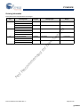
Maximum Ratings
Package Power Dissipation
Capability (TA = 25°C) ................................................... 1.0W
Exceeding maximum ratings may impair the useful life of the
device. These user guidelines are not tested.
Surface Mount Pb Soldering
Temperature (3 Seconds).......................................... +260°C
DC Output Current (1 output at a time, 1s duration) ... 15 mA
Static Discharge Voltage.......................................... > 2001V
(MIL-STD-883, Method 3015)
Supply Voltage on VCC Relative to GND ..........–0.5V to 4.1V
Latch Up Current ................................................... > 200 mA
Voltage Applied to Outputs
in High Z State ....................................... –0.5V to VCC + 0.5V
Operating Range
Input Voltage...........................................–0.5V to Vcc + 0.5V
Range
Transient Voltage (<20 ns) on
Any Pin to Ground Potential .................. –2.0V to VCC + 2.0V
2.7V to 3.6V
es
D
ew
Test Conditions
Min
Commercial
tRC = 25 ns
tRC = 35 ns
tRC = 45 ns
Dependent on output loading and cycle
Industrial
rate. Values obtained without output
loads.
IOUT = 0 mA.
rN
Average VCC Current
0°C to +70°C
–40°C to +85°C
Max
Unit
65
55
50
mA
mA
70
60
55
mA
mA
Average VCC Current
during STORE
All Inputs Do Not Care, VCC = Max
Average current for duration tSTORE
6
mA
ICC3
Average VCC Current at
tAVAV = 200 ns, 3V, 25°C
Typical
WE > (VCC – 0.2V). All other inputs cycling.
Dependent on output loading and cycle rate.
Values obtained without output loads.
10
mA
ICC4
Average VCAP Current
during AutoStore Cycle
All Inputs Do Not Care, VCC = Max
Average current for duration tSTORE
3
mA
ISB
VCC Standby Current
WE > (VCC – 0.2V). All others VIN < 0.2V or
> (VCC–0.2V). Standby current level after nonvolatile
cycle is complete. Inputs are static. f = 0 MHz
3
mA
IIX
Input Leakage Current
–1
+1
μA
IOZ
Off State Output Leakage VCC = Max, VSS < VIN < VCC, CE or OE > VIH
Current
–1
+1
μA
Input HIGH Voltage
2.0
VCC + 0.5
V
VIL
Input LOW Voltage
VSS – 0.5
0.8
V
VOH
Output HIGH Voltage
IOUT = –2 mA
VOL
Output LOW Voltage
IOUT = 4 mA
VCAP
Storage Capacitor
Between VCAP pin and VSS, 5V rated
m
om
ec
R
VCC = Max, VSS < VIN < VCC
N
VIH[10]
en
ICC2
ot
de
d
fo
ICC1
VCC
Industrial
Over the Operating Range (VCC = 2.7V to 3.6V) [8, 9]
Description
Ambient Temperature
Commercial
DC Electrical Characteristics
Parameter
ig
ns
Storage Temperature ................................. –65°C to +150°C
Ambient Temperature with
Power Applied ............................................ –55°C to +125°C
2.4
17
V
0.4
V
120
μF
Notes
8. The HSB pin has IOUT = –10 μA for VOH of 2.4 V, this parameter is characterized but not tested.
9. The INT pin is open drain and does not source or sink current when interrupt register bit D3 is low.
10. VIH changes by 100 mV when VCC > 3.5V.
Document Number: 001-06401 Rev. *J
Page 16 of 29
[+] Feedback
CY14B101K
Data Retention and Endurance
Parameter
Description
Min
Unit
DATAR
Data Retention
20
Years
NVC
Nonvolatile STORE Operations
200
K
Max
Unit
7
pF
Capacitance
These parameters are guaranteed but not tested.
Description
Input Capacitance
COUT
Output Capacitance
Test Conditions
TA = 25°C, f = 1 MHz, VCC = 0 to 3.0 V
ig
ns
Parameter
CIN
7
These parameters are guaranteed but not tested.
ΘJC
Description
Test Conditions
Thermal Resistance (junction to
ambient)
Test conditions follow standard test methods
and procedures for measuring thermal
Thermal Resistance (junction to case) impedance, in accordance with EIA/JESD51.
ew
ΘJA
D
Parameter
es
Thermal Resistance
pF
48-SSOP
Unit
34.85
°C/W
16.35
°C/W
fo
rN
Figure 7. AC Test Loads
R1 577Ω
R1 577Ω
3.0V
For Tri-state Specs
d
3.0V
OUTPUT
de
OUTPUT
R2
789Ω
R2
789Ω
om
AC Test Conditions
5 pF
m
en
30 pF
N
ot
R
ec
Input Pulse Levels ..................................................0 V to 3 V
Input Rise and Fall Times (10% - 90%)........................ <5 ns
Input and Output Timing Reference Levels ................... 1.5 V
Document Number: 001-06401 Rev. *J
Page 17 of 29
[+] Feedback
CY14B101K
AC Switching Characteristics
Parameter
Cypress
Parameter
25 ns
Description
Alt.
Parameter
Min
35 ns
Max
Min
45 ns
Max
Min
Max
Unit
SRAM Read Cycle
Chip Enable Access Time
25
tAVAV, tELEH Read Cycle Time
25
tAA [12]
tAVQV
Address Access Time
tDOE
tGLQV
Output Enable to Data Valid
tOHA [12]
tAXQX
Output Hold After Address Change
3
[13]
tELQX
Chip Enable to Output Active
3
tHZCE [13]
tEHQZ
Chip Disable to Output Inactive
tLZOE [13]
tGLQX
Output Enable to Output Active
tHZOE [13]
tGHQZ
Output Disable to Output Inactive
tPU [14]
tELICCH
Chip Enable to Power Active
tPD [14]
tEHICCL
Chip Disable to Power Standby
35
35
15
3
10
ig
ns
12
3
0
45
ns
20
ns
ns
ns
15
ns
15
ns
45
ns
0
13
0
25
ns
3
0
10
ns
3
13
0
45
45
25
ew
tLZCE
35
es
tRC
tELQV
[11]
D
tACE
ns
0
35
ns
fo
W5&
rN
Figure 8. SRAM Read Cycle 1: Address Controlled [11, 12, 15]
d
$''5(66
de
W $$
en
W2+$
'$7$9$/,'
m
'4'$7$287
om
Figure 9. SRAM Read Cycle 2: CE and OE Controlled [11, 15]
R
W$&(
W3'
W/=&(
W+=&(
N
ot
&(
2(
ec
$''5(66
W5&
W+=2(
W'2(
W/=2(
'4'$7$287
'$7$9$/,'
W 38
,&&
$&7,9(
67$1'%<
Notes
11. WE is HIGH during SRAM Read Cycles.
12. Device is continuously selected with CE and OE both Low.
13. Measured ±200 mV from steady state output voltage.
14. These parameters are guaranteed by design and are not tested.
15. HSB must remain HIGH during READ and WRITE cycles.
Document Number: 001-06401 Rev. *J
Page 18 of 29
[+] Feedback
CY14B101K
AC Switching Characteristics (continued)
Parameter
Cypress
Parameter
25 ns
Description
Alt.
Parameter
Min
35 ns
Max
Min
45 ns
Max
Min
Max
Unit
SRAM Write Cycle
tWC
tAVAV
Write Cycle Time
tPWE
tWLWH, tWLEH
Write Pulse Width
20
25
30
ns
tSCE
tELWH, tELEH
Chip Enable To End of Write
20
25
30
ns
tSD
tDVWH, tDVEH
Data Setup to End of Write
10
12
15
ns
tHD
tWHDX, tEHDX
Data Hold After End of Write
0
0
tAW
tAVWH, tAVEH
Address Setup to End of Write
20
25
tSA
tAVWL, tAVEL
Address Setup to Start of Write
0
0
tHA
tWHAX, tEHAX
Address Hold After End of Write
0
tHZWE [13, 16]
tWLQZ
Write Enable to Output Disable
tWHQX
Output Active After End of Write
45
0
ns
es
ns
0
3
3
D
3
ns
30
0
0
10
ns
ig
ns
35
13
ns
15
ns
ns
ew
tLZWE
[13]
25
tWC
tHA
fo
ADDRESS
rN
Figure 10. SRAM Write Cycle 1: WE Controlled [15, 17]
tSCE
d
CE
de
tAW
tSA
tPWE
en
WE
m
om
DATA IN
DATA VALID
tHZWE
tLZWE
HIGH IMPEDANCE
PREVIOUS DATA
ec
DATA OUT
tHD
tSD
R
Figure 11. SRAM Write Cycle 2: CE Controlled
ot
tWC
N
ADDRESS
CE
WE
tHA
tSCE
tSA
tAW
tPWE
tSD
DATA IN
DATA OUT
tHD
DATA VALID
HIGH IMPEDANCE
Notes
16. If WE is Low when CE goes Low, the outputs remain in the High Impedance State.
17. CE or WE are greater than VIH during address transitions.
Document Number: 001-06401 Rev. *J
Page 19 of 29
[+] Feedback
CY14B101K
AutoStore or Power Up RECALL
Parameter
tHRECALL [18]
Min
Power Up RECALL Duration
[19, 20]
STORE Cycle Duration
VSWITCH
Low Voltage Trigger Level
tVCCRISE
VCC Rise Time
Unit
Max
40
ms
Commercial
12.5
ms
Industrial
15
ms
2.65
V
150
ig
ns
tSTORE
CY14B101K
Description
Figure 12. AutoStore/Power Up RECALL
STORE occurs only
if a SRAM write
has happened
No STORE occurs
without atleast one
SRAM write
D
es
VCC
μs
rN
ew
VSWITCH
d
fo
tVCCRISE
de
AutoStore
tSTORE
POWER-UP RECALL
om
tHRECALL
m
en
tSTORE
N
ot
R
ec
Read & Write Inhibited
tHRECALL
Notes
18. tHRECALL starts from the time VCC rises above VSWITCH.
19. If an SRAM Write does not taken place since the last nonvolatile cycle, no STORE takes place.
20. Industrial Grade Devices require 15 ms Max.
Document Number: 001-06401 Rev. *J
Page 20 of 29
[+] Feedback
CY14B101K
Software Controlled STORE/RECALL Cycles [21, 22]
Alt.
Parameter
Parameter
25 ns
Description
Min
35 ns
Max
Min
45 ns
Max
Min
Max
Unit
tRC
tAVAV
STORE/RECALL Initiation Cycle
Time
25
35
45
ns
tSA
tAVEL
Address Setup Time
0
0
0
ns
tCW
tELEH
Clock Pulse Width
20
25
30
ns
tHA
tEHAX
Address Hold Time
1
1
RECALL Duration
1
170
170
ig
ns
tRECALL
ns
170
μs
Figure 13. CE Controlled Software STORE/RECALL Cycle [22]
tRC
tSA
D
ADDRESS # 6
ew
ADDRESS # 1
ADDRESS
es
tRC
tSCE
rN
CE
fo
tHA
d
OE
de
DATA VALID
en
DATA VALID
DQ (DATA)
t STORE / t RECALL
HIGH IMPEDANCE
om
m
Figure 14. OE Controlled Software STORE/RECALL Cycle [22]
tRC
ADDRESS # 1
OE
tSA
tSCE
tHA
DQ (DATA)
ADDRESS # 6
R
N
ot
CE
ec
ADDRESS
tRC
DATA VALID
t STORE / t RECALL
DATA VALID
HIGH IMPEDANCE
Notes
21. The software sequence is clocked with CE controlled or OE controlled READs.
22. The six consecutive addresses are read in the order listed in the Table 2 on page 7. WE is HIGH during all six consecutive cycles.
Document Number: 001-06401 Rev. *J
Page 21 of 29
[+] Feedback
CY14B101K
Hardware STORE Cycle
Alt.
Parameter
Parameter
tDELAY [25]
tPHSB
tHLHX
CY14B101K
Description
Min
Max
Time Allowed to Complete SRAM Cycle
1
70
Hardware STORE Pulse Width
15
Unit
μs
ns
Figure 15. Hardware STORE Cycle
W6725(
es
W+/%/
+6%287
ig
ns
W3+6%
+/+;
+6%,1
ew
W '(/$<
'$7$9$/,'
'$7$9$/,'
fo
rN
'4'$7$287
+,*+,03('$1&(
D
+,*+,03('$1&(
Soft Sequence Processing Time
CY14B101K
Min
Max
70
en
tSS [22, 24]
Description
de
Parameter
d
Soft Sequence Commands
Unit
μs
m
Figure 16. Soft Sequence Processing [22, 24]
om
6RIW6HTXHQFH
&RPPDQG
$GGUHVV
W6$
$GGUHVV
W66
$GGUHVV
W&:
N
ot
9&&
$GGUHVV
W&:
6RIW6HTXHQFH
&RPPDQG
R
&(
ec
$GGUHVV
W66
Notes
23. This is the amount of time it takes to take action on a soft sequence command. Vcc power must remain HIGH to effectively register command.
24. Commands such as STORE and RECALL lock out I/O until operation is complete which further increases this time. See specific command.
25. Read and Write cycles in progress before HSB are given this amount of time to complete.
Document Number: 001-06401 Rev. *J
Page 22 of 29
[+] Feedback
CY14B101K
RTC Characteristics
Parameter
IBAK
[26]
Description
Test Conditions
RTC Backup Current
Min
Max
Unit
Commercial
300
nA
Industrial
350
nA
RTC Battery Pin Voltage
1.8
3.3
V
VRTCcap
[28]
RTC Capacitor Pin Voltage
1.2
2.7
V
At Min Temperature from Power up or Enable
10
sec
At 25°C Temperature from Power up or Enable
5
sec
tOCS
RTC Oscillator Time to Start
ig
ns
VRTCbat
[27]
Truth Table For SRAM Operations
H
X
X
Inputs and Outputs
Mode
D
OE
High Z
Deselect/Power down
ew
WE
Power
Standby
H
L
Data Out (DQ0–DQ7);
Read
H
H
High Z
Output Disabled
Active
Active
L
L
X
Data in (DQ0–DQ7);
Write
Active
N
ot
R
ec
om
m
en
de
d
fo
L
L
rN
CE
es
HSB should remain HIGH for SRAM Operations.
Notes
26. From either VRTCcap or VRTCbat.
27. Typical = 3.0V during normal operation.
28. Typical = 2.4V during normal operation.
Document Number: 001-06401 Rev. *J
Page 23 of 29
[+] Feedback
CY14B101K
Part Numbering Nomenclature
CY 14 B 101 K - SP 25 X C T
Pb-Free
D
Density:
101 - 1 Mb
rN
ew
Voltage:
B - 3.0V
Speed:
25 - 25 ns
35 - 35 ns
45 - 45 ns
Data Bus:
K - x8 + RTC
es
Package:
SP - 48 SSOP
Temperature:
C - Commercial (0 to 70°C)
I - Industrial (–40 to 85°C)
ig
ns
Option:
T - Tape and Reel
Blank - Std.
d
fo
NVSRAM
14 - AutoStore + Software Store + Hardware Store
N
ot
R
ec
om
m
en
de
Cypress
Document Number: 001-06401 Rev. *J
Page 24 of 29
[+] Feedback
CY14B101K
Ordering Information
These parts are not recommended for new designs.
Speed
(ns)
25
Package
Diagram
Ordering Code
CY14B101K-SP25XC
Operating
Range
Package Type
51-85061
48-pin SSOP
Commercial
51-85061
48-pin SSOP
Industrial
51-85061
48-pin SSOP
Commercial
51-85061
48-pin SSOP
51-85061
48-pin SSOP
51-85061
48-pin SSOP
CY14B101K-SP25XCT
CY14B101K-SP25XI
35
CY14B101K-SP35XC
ig
ns
CY14B101K-SP25XIT
CY14B101K-SP35XCT
45
CY14B101K-SP45XC
CY14B101K-SP45XCT
Commercial
Industrial
ew
CY14B101K-SP45XI
Industrial
es
CY14B101K-SP35XIT
D
CY14B101K-SP35XI
CY14B101K-SP45XIT
N
ot
R
ec
om
m
en
de
d
fo
rN
All these parts are Pb-free. Contact your local Cypress sales representative for availability of these parts.
Document Number: 001-06401 Rev. *J
Page 25 of 29
[+] Feedback
CY14B101K
Package Diagrams
51-85061-*C
N
ot
R
ec
om
m
en
de
d
fo
rN
ew
D
es
ig
ns
Figure 17. 48-Pin Shrunk Small Outline Package (51-85061)
Document Number: 001-06401 Rev. *J
Page 26 of 29
[+] Feedback
CY14B101K
Document History Page
Document Title: CY14B101K 1 Mbit (128K x 8) nvSRAM With Real Time Clock
Document Number: 001-06401
REV.
**
ECN NO.
Submission
Date
Orig. of Change
425138
TUP
See ECN
Description of Change
New data sheet
437321
TUP
See ECN
Show data sheet on External Web
*B
471966
TUP
See ECN
Changed ICC3 from 5 mA to 10 mA
Changed ISB from 2 mA to 3 mA
Changed VIH(min) from 2.2V to 2.0V
Changed tRECALL from 40 ms to 100 ms
Changed Endurance from 1 million Cycles to 500K Cycles
Changed Data Retention from 100 years to 20 years
Added Soft Sequence Processing Time Waveform
Updated Part Numbering Nomenclature and Ordering Information
Added RTC Characteristics Table
Added RTC Recommended Component Configuration
*C
503272
PCI
See ECN
Changed from Advance to Preliminary
Changed the term “Unlimited” to “Infinite”
Changed Endurance from 500K Cycles to 200K Cycles
Added temperature spec. to Data Retention - 20 years at 55×C
Removed Icc1 values from the DC table for 25 ns and 35 ns
Industrial Grade
Changed Icc2 value from 3 mA to 6 mA in the DC Table
Added a footnote on VIH
Added footnote 18 related to using the software command
Changed VSWITCH(min) from 2.55V to 2.45V
Updated Part Nomenclature Table and Ordering Information
Table
*D
597002
TUP
See ECN
*E
688776
VKN
*F
1349963
om
m
en
de
d
fo
rN
ew
D
es
ig
ns
*A
See ECN
Added footnote 7 related to HSB
Added footnote 8 related to INT pin
Changed tGLAX to tGHAX
Removed ABE bit from interrupt register
See ECN
Changed from Preliminary to Final
Added Note 5 regarding the W bit in the Flag register
Updated Ordering Information Table
ec
R
ot
UHA/SFV
Removed VSWITCH(min) specification from the AutoStore/Power
Up RECALL Table
Changed tGLAX specification from 20 ns to 1 ns
Added tDELAY(max) specification of 70 ms in the Hardware STORE
Cycle Table
Removed tHLBL specification
Changed tSS specification form 70 ms (min) to 70 ms (max)
Changed VCAP(max) from 57 mF to 120 mF
1739984
vsutmp8/AESA
See ECN
Added Pinout diagram and Pin definition Table
*H
2427986
GVCH/PYRS
04/23/08
Move to external web
N
*G
Document Number: 001-06401 Rev. *J
Page 27 of 29
[+] Feedback
CY14B101K
Document Title: CY14B101K 1 Mbit (128K x 8) nvSRAM With Real Time Clock
Document Number: 001-06401
ECN NO.
Orig. of Change
Submission
Date
Description of Change
*I
2663934
GVCH/PYRS
02/24/09
Updated Features
Updated pin definition of WE
Removed AutoStore enable/disable section
Added Best practices
Updated “Reading the clock”, “Backup Power”, “Stopping and
starting the Oscillator” and “Alarm” descriptions under RTC
operation
Modified “Figure 4. RTC Recommended Component Configuration”
Added footnotes 4, 5 and 6
Added default values to RTC Register Map” table
Updated flag register description in Register Map Detail” table
Added Industrial specs for 25ns and 35ns speed
Changed VIH from Vcc+0.3 to Vcc+0.5
Added “Data Retention and Endurance” table on page 15
Added Thermal resistance values
Added alternate parameters in the AC switching characteristics
table
Renamed tOH to tOHA
Changed tHRECALL from 20 to 40ms
Changed tRECALL spec from 100μs to 170μs (Including tss of
70us)
Renamed tAS to tSA
Renamed tGHAX to tHA
Updated Figure 13, 14, 15 and 16
Renamed tHLHX to tPHSB
Added truth table for SRAM operations
*J
2815609
GVCH
11/26/09
Added note in the Ordering Information table and watermark to
state that the parts in this data sheet are not recommended for
new designs. Added the Contents page.
N
ot
R
ec
om
m
en
de
d
fo
rN
ew
D
es
ig
ns
REV.
Document Number: 001-06401 Rev. *J
Page 28 of 29
[+] Feedback
CY14B101K
Sales, Solutions, and Legal Information
Worldwide Sales and Design Support
Cypress maintains a worldwide network of offices, solution centers, manufacturer’s representatives, and distributors. To find the office
closest to you, visit us at cypress.com/sales.
Products
PSoC
psoc.cypress.com
clocks.cypress.com
Wireless
wireless.cypress.com
Memories
memory.cypress.com
image.cypress.com
ot
R
ec
om
m
en
de
d
fo
rN
ew
D
es
Image Sensors
ig
ns
Clocks & Buffers
N
© Cypress Semiconductor Corporation, 2006-2009. The information contained herein is subject to change without notice. Cypress Semiconductor Corporation assumes no responsibility for the use
of any circuitry other than circuitry embodied in a Cypress product. Nor does it convey or imply any license under patent or other rights. Cypress products are not warranted nor intended to be used
for medical, life support, life saving, critical control or safety applications, unless pursuant to an express written agreement with Cypress. Furthermore, Cypress does not authorize its products for use
as critical components in life-support systems where a malfunction or failure may reasonably be expected to result in significant injury to the user. The inclusion of Cypress products in life-support
systems application implies that the manufacturer assumes all risk of such use and in doing so indemnifies Cypress against all charges.
Any Source Code (software and/or firmware) is owned by Cypress Semiconductor Corporation (Cypress) and is protected by and subject to worldwide patent protection (United States and foreign),
United States copyright laws and international treaty provisions. Cypress hereby grants to licensee a personal, non-exclusive, non-transferable license to copy, use, modify, create derivative works of,
and compile the Cypress Source Code and derivative works for the sole purpose of creating custom software and or firmware in support of licensee product to be used only in conjunction with a Cypress
integrated circuit as specified in the applicable agreement. Any reproduction, modification, translation, compilation, or representation of this Source Code except as specified above is prohibited without
the express written permission of Cypress.
Disclaimer: CYPRESS MAKES NO WARRANTY OF ANY KIND, EXPRESS OR IMPLIED, WITH REGARD TO THIS MATERIAL, INCLUDING, BUT NOT LIMITED TO, THE IMPLIED WARRANTIES
OF MERCHANTABILITY AND FITNESS FOR A PARTICULAR PURPOSE. Cypress reserves the right to make changes without further notice to the materials described herein. Cypress does not
assume any liability arising out of the application or use of any product or circuit described herein. Cypress does not authorize its products for use as critical components in life-support systems where
a malfunction or failure may reasonably be expected to result in significant injury to the user. The inclusion of Cypress’ product in a life-support systems application implies that the manufacturer
assumes all risk of such use and in doing so indemnifies Cypress against all charges.
Use may be limited by and subject to the applicable Cypress software license agreement.
Document Number: 001-06401 Rev. *J
Revised November 26, 2009
Page 29 of 29
AutoStore and QuantumTrap are registered trademarks of Cypress Semiconductor Corporation. All products and company names mentioned in this document are the trademarks of their respective
holders.
[+] Feedback