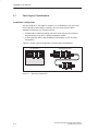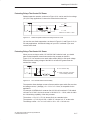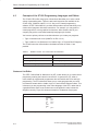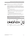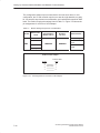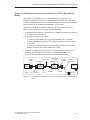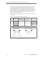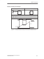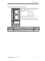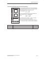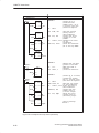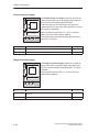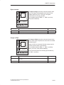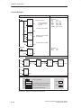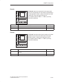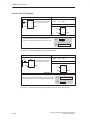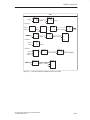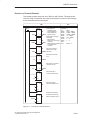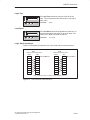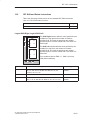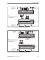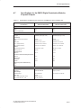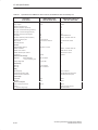
1
Important Notes, Contents SIMATIC S7-200 Programmable Controller System Manual This manual has the order number: 6ES7298-8FA20-8BH0 Introducing the S7-200 Micro PLC Installing an S7-200 Micro PLC Getting Started with an S7-200 Programming System Basic Concepts for Programming an S7-200 CPU 1 CPU Memory: Data Types and Addressing Modes 5 CPU and Input/Output Configuration Setting Up Communications Hardware and Network Communications 6 Conventions for S7-200 Instructions 8 SIMATIC Instructions IEC 1131-3 Instructions S7-200 Specifications Error Codes Special Memory (SM) Bits S7-200 Troubleshooting Guide 3 4 7 9 10 A B C Execution Times for STL Instructions D E F S7-200 Quick Reference Information G S7-200 Order Numbers 03/99 Release 01 2 Index Safety Guidelines This manual contains notices which you should observe to ensure your own personal safety, as well as to protect the product and connected equipment. These notices are highlighted in the manual by a warning triangle and are marked as follows according to the level of danger: ! Danger indicates that death, severe personal injury, or substantial property damage will result if proper precautions are not taken. ! Warning indicates that death, severe personal injury, or substantial property damage can result if proper precautions are not taken. ! Caution indicates that minor personal injury or property damage can result if proper precautions are not taken. Qualified Personnel The device/system may only be set up and operated in conjunction with this manual. Only qualified personnel should be allowed to install and work on this equipment. Qualified persons are defined as persons who are authorized to commission, to ground, and to tag circuits, equipment, and systems in accordance with established safety practices and standards. Correct Usage Note the following: ! Warning This device and its components may only be used for the applications described in the catalog or the technical description, and only in connection with devices or components from other manufacturers which have been approved or recommended by Siemens. This product can only function correctly and safely if it is transported, stored, set up, and installed correctly, and operated and maintained as recommended. Trademarks SiemensRand SIMATICR are registered trademarks of SIEMENS AG. STEP 7 and S7 are trademarks of SIEMENS AG. MicrosoftR, WindowsR, Windows 95R, Windows 98R, and Windows NTR are registered trademarks of Microsoft Corporation. Underwriters LaboratoriesR is a registered trademark of Underwriters Laboratories, Inc. Copyright Siemens AG 1999 All rights reserved Disclaimer of Liability The reproduction, transmission or use of this document or its contents is not permitted without express written authority. Offenders will be liable for damages. All rights, including rights created by patent grant or registration of a utility model or design, are reserved. We have checked the contents of this manual for agreement with the hardware and software described. Since deviations cannot be precluded entirely, we cannot guarantee full agreement. However, the data in this manual are reviewed regularly and any necessary corrections included in subsequent editions. Suggestions for improvement are welcomed. Siemens AG Bereich Automatisierungs- und Antriebstechnik Geschaeftsgebiet Industrie-Automatisierungssysteme Postfach 4848, D-90327 Nuernberg Index-2 Siemens Aktiengesellschaft E Siemens AG 1999 Technical datamanual subject to change. S7-200 Programmable Controller System Manual This has C79000-G7076-C233 the order number: C79000-G7076-C233 Important Notes Purpose The S7-200 series is a line of micro-programmable logic controllers (Micro PLCs) that can control a variety of automation applications. Compact design, low cost, and a powerful instruction set make the S7-200 controllers a perfect solution for controlling small applications. The wide variety of CPU sizes and voltages, and the windows-based programming tool, give you the flexibility you need to solve your automation problems. The S7-200 product line has been redesigned to be smaller, faster, and to have increased functionality. The new S7-200 products are intended to replace the previous products. This manual provides information about installing and programming the S7-200 Micro PLCs. The S7-200 Programmable Controller System Manual includes the following topics: Installing and wiring Understanding the CPU operations, data types and addressing modes, scan cycle, password protection, and network communication Specifications Descriptions of and examples for the SIMATIC and IEC 1131-3 programming instructions Typical execution times for SIMATIC STL instructions Audience This manual is designed for engineers, programmers, installers, and electricians who have a general knowledge of programmable logic controllers. S7-200 Programmable Controller System Manual C79000-G7076-C233-01 iii Important Notes Scope of the Manual The information contained in this manual pertains in particular to the following products: S7-200 CPU models: CPU 221, CPU 222, and CPU 224 STEP 7-Micro/WIN 32, version 3.0, a 32-bit programming software package for Windows 95, Windows 98, and the Windows NT environment Agency Approvals The SIMATIC S7-200 series meets the following regulations: European Community (CE) Low Voltage Directive 73/23/EEC European Community (CE) EMC Directive 89/336/EEC Underwriters Laboratories, Inc.: UL 508 Listed (Industrial Control Equipment) Canadian Standards Association: CSA C22.2 Number 142 Certified (Process Control Equipment) Factory Mutual Research: FM Class I, Division 2, Groups A, B, C, & D Hazardous Locations, T4A Refer to Appendix A for compliance information. Related Information Refer to the following for more detailed information about selected topics: STEP 7-Micro/WIN 32 CD/disk: provides online help, the STEP 7-Micro/WIN Getting Started (a printable online manual). Process Field Bus (PROFIBUS) standard (EN 50170): describes the standard protocol for the S7-200 DP communication capability. TD 200 Operator Interface User Manual: describes how to install and use the TD 200 with an S7-200 programmable logic controller. iv S7-200 Programmable Controller System Manual C79000-G7076-C233-01 Important Notes How to Use This Manual If you are a first-time (novice) user of S7-200 Micro PLCs, you should read the entire S7-200 Programmable Controller System Manual. If you are an experienced user, refer to the manual table of contents or index to find specific information. The S7-200 Programmable Controller System Manual is organized according to the following topics: “Introducing the S7-200 Micro PLC” (Chapter 1) provides an overview of some of the features of the equipment. “Installing an S7-200 Micro PLC” (Chapter 2) provides procedures, dimensions, and basic guidelines for installing the S7-200 CPU modules and expansion I/O modules. “Getting Started with an S7-200 Programming System” (Chapter 3) describes how to set up an S7-200 programming system. “Basic Concepts for Programming an S7-200 CPU” (Chapter 4), “CPU Memory: Data Types and Addressing Modes” (Chapter 5), and “CPU and Input/Output Control” (Chapter 6) provide information about how the S7-200 CPU processes data and executes your program. “Setting Up Communications Hardware and Network Communications” (Chapter 7) provides information about how to install and remove communications hardware and how to connect the S7-200 CPU to different types of networks. “Conventions for S7-200 Instructions” (Chapter 8) provides an overview of the different programming language concepts and terminology. Descriptions and examples of SIMATIC LAD, FBD, and STL programming instructions are provided in Chapter 9. Descriptions and examples of IEC 1131-3 LAD and FBD programming instructions are provided in Chapter 10. Additional information (such as the equipment specifications, error code descriptions, troubleshooting, and STL instruction execution times) are provided in the appendices. Additional Assistance For assistance in answering technical questions, for training on this product, or for ordering, contact your Siemens distributor or sales office. For Internet information about Siemens products and services, technical support, or FAQs (frequently asked questions) and application tips, use the following Internet addresses: http://www.ad.siemens.de http://www.siemens.com/s7-200 S7-200 Programmable Controller System Manual C79000-G7076-C233-01 for general Siemens information for S7-200 product information v Important Notes vi S7-200 Programmable Controller System Manual C79000-G7076-C233-01 Contents 1 2 3 4 Introducing the S7-200 Micro PLC . . . . . . . . . . . . . . . . . . . . . . . . . . . . . . . . . . . . . . . 1-1 1.1 Comparing the Features of the S7-200 Micro PLCs . . . . . . . . . . . . . . . . . . 1-2 1.2 Major Components of the S7-200 Micro PLC . . . . . . . . . . . . . . . . . . . . . . . . 1-4 Installing an S7-200 PLC . . . . . . . . . . . . . . . . . . . . . . . . . . . . . . . . . . . . . . . . . . . . . . . . 2-1 2.1 Panel Layout Considerations . . . . . . . . . . . . . . . . . . . . . . . . . . . . . . . . . . . . . . 2-2 2.2 Installing and Removing an S7-200 Micro PLC or Expansion Module . . . 2-6 2.3 Installing the Field Wiring . . . . . . . . . . . . . . . . . . . . . . . . . . . . . . . . . . . . . . . . . 2-9 2.4 Using Suppression Circuits . . . . . . . . . . . . . . . . . . . . . . . . . . . . . . . . . . . . . . . 2-16 2.5 Power Considerations . . . . . . . . . . . . . . . . . . . . . . . . . . . . . . . . . . . . . . . . . . . . 2-18 Getting Started with an S7-200 Programming System . . . . . . . . . . . . . . . . . . . . . 3-1 3.1 Overview . . . . . . . . . . . . . . . . . . . . . . . . . . . . . . . . . . . . . . . . . . . . . . . . . . . . . . . 3-2 3.2 Quick Start for STEP 7-Micro/WIN 32 . . . . . . . . . . . . . . . . . . . . . . . . . . . . . . 3-3 3.3 How Do I Set Up Communications Using the PC/PPI Cable? . . . . . . . . . . 3-5 3.4 How Do I Go Online With the S7-200 CPU? . . . . . . . . . . . . . . . . . . . . . . . . . 3-9 3.5 How Do I Change the Communications Parameters for My PLC? . . . . . . 3-10 Basic Concepts for Programming an S7-200 CPU . . . . . . . . . . . . . . . . . . . . . . . . . 4-1 4.1 Guidelines for Designing a Micro PLC System . . . . . . . . . . . . . . . . . . . . . . . 4-2 4.2 Concepts of an S7-200 Program . . . . . . . . . . . . . . . . . . . . . . . . . . . . . . . . . . 4-5 4.3 Concepts of the S7-200 Programming Languages and Editors . . . . . . . . . 4-6 4.4 Understanding the Differences between SIMATIC and IEC 1131-3 Instructions . . . . . . . . . . . . . . . . . . . . . . . . . . . . . . . . . . . . . . . . . . 4-10 4.5 Basic Elements for Constructing a Program . . . . . . . . . . . . . . . . . . . . . . . . . 4-18 4.6 Understanding the Scan Cycle of the CPU . . . . . . . . . . . . . . . . . . . . . . . . . . 4-22 4.7 Selecting the Mode of Operation for the CPU . . . . . . . . . . . . . . . . . . . . . . . 4-25 4.8 Creating a Password for the CPU . . . . . . . . . . . . . . . . . . . . . . . . . . . . . . . . . . 4-27 4.9 Debugging and Monitoring Your Program . . . . . . . . . . . . . . . . . . . . . . . . . . . 4-30 4.10 Error Handling for the S7-200 CPU . . . . . . . . . . . . . . . . . . . . . . . . . . . . . . . . 4-36 S7-200 Programmable Controller System Manual C79000-G7076-C233-01 vii Contents 5 6 7 8 viii CPU Memory: Data Types and Addressing Modes . . . . . . . . . . . . . . . . . . . . . . . . 5-1 5.1 Direct Addressing of the CPU Memory Areas . . . . . . . . . . . . . . . . . . . . . . . 5-2 5.2 SIMATIC Indirect Addressing of the CPU Memory Areas . . . . . . . . . . . . . . 5-13 5.3 Memory Retention for the S7-200 CPU . . . . . . . . . . . . . . . . . . . . . . . . . . . . . 5-15 5.4 Using Your Program to Store Data Permanently . . . . . . . . . . . . . . . . . . . . . 5-20 5.5 Using a Memory Cartridge to Store Your Program . . . . . . . . . . . . . . . . . . . 5-22 CPU and Input/Output Configuration . . . . . . . . . . . . . . . . . . . . . . . . . . . . . . . . . . . . . 6-1 6.1 Local I/O and Expansion I/O . . . . . . . . . . . . . . . . . . . . . . . . . . . . . . . . . . . . . . 6-2 6.2 Using the Selectable Input Filter to Provide Noise Rejection . . . . . . . . . . . 6-4 6.3 Pulse Catch . . . . . . . . . . . . . . . . . . . . . . . . . . . . . . . . . . . . . . . . . . . . . . . . . . . . 6-5 6.4 Using the Output Table to Configure the States of the Outputs . . . . . . . . . 6-8 6.5 Analog Input Filter . . . . . . . . . . . . . . . . . . . . . . . . . . . . . . . . . . . . . . . . . . . . . . . 6-9 6.6 High-Speed I/O . . . . . . . . . . . . . . . . . . . . . . . . . . . . . . . . . . . . . . . . . . . . . . . . . 6-10 6.7 Analog Adjustments . . . . . . . . . . . . . . . . . . . . . . . . . . . . . . . . . . . . . . . . . . . . . 6-13 Setting Up Communications Hardware and Network Communications . . . . . . 7-1 7.1 What Are My Communication Choices? . . . . . . . . . . . . . . . . . . . . . . . . . . . . 7-2 7.2 Installing and Removing Communication Interfaces . . . . . . . . . . . . . . . . . . 7-7 7.3 Selecting and Changing Parameters . . . . . . . . . . . . . . . . . . . . . . . . . . . . . . . 7-9 7.4 Communicating With Modems . . . . . . . . . . . . . . . . . . . . . . . . . . . . . . . . . . . . 7-16 7.5 Network Overview . . . . . . . . . . . . . . . . . . . . . . . . . . . . . . . . . . . . . . . . . . . . . . . 7-27 7.6 Network Components . . . . . . . . . . . . . . . . . . . . . . . . . . . . . . . . . . . . . . . . . . . . 7-31 7.7 Using the PC/PPI Cable with Other Devices and Freeport . . . . . . . . . . . . 7-35 7.8 Network Performance . . . . . . . . . . . . . . . . . . . . . . . . . . . . . . . . . . . . . . . . . . . . 7-41 Conventions for S7-200 Instructions . . . . . . . . . . . . . . . . . . . . . . . . . . . . . . . . . . . . . 8-1 8.1 Concepts and Conventions For STEP 7-Micro/WIN 32 Programming . . . 8-2 8.2 Valid Ranges for the S7-200 CPUs . . . . . . . . . . . . . . . . . . . . . . . . . . . . . . . . 8-7 S7-200 Programmable Controller System Manual C79000-G7076-C233-01 Contents 9 10 SIMATIC Instructions . . . . . . . . . . . . . . . . . . . . . . . . . . . . . . . . . . . . . . . . . . . . . . . . . . . 9-1 9.1 SIMATIC Bit Logic Instructions . . . . . . . . . . . . . . . . . . . . . . . . . . . . . . . . . . . . 9-2 9.2 SIMATIC Compare Instructions . . . . . . . . . . . . . . . . . . . . . . . . . . . . . . . . . . . 9-10 9.3 SIMATIC Timer Instructions . . . . . . . . . . . . . . . . . . . . . . . . . . . . . . . . . . . . . . . 9-15 9.4 SIMATIC Counter Instructions . . . . . . . . . . . . . . . . . . . . . . . . . . . . . . . . . . . . . 9-23 9.5 SIMATIC High-Speed Counter Instructions . . . . . . . . . . . . . . . . . . . . . . . . . . 9-27 9.6 SIMATIC Pulse Output Instructions . . . . . . . . . . . . . . . . . . . . . . . . . . . . . . . . 9-49 9.7 SIMATIC Clock Instructions . . . . . . . . . . . . . . . . . . . . . . . . . . . . . . . . . . . . . . . 9-70 9.8 SIMATIC Integer Math Instructions . . . . . . . . . . . . . . . . . . . . . . . . . . . . . . . . 9-72 9.9 SIMATIC Real Math Instructions . . . . . . . . . . . . . . . . . . . . . . . . . . . . . . . . . . . 9-81 9.10 SIMATIC Move Instructions . . . . . . . . . . . . . . . . . . . . . . . . . . . . . . . . . . . . . . . 9-99 9.11 SIMATIC Table Instructions . . . . . . . . . . . . . . . . . . . . . . . . . . . . . . . . . . . . . . . 9-104 9.12 SIMATIC Logical Operations Instructions . . . . . . . . . . . . . . . . . . . . . . . . . . . 9-110 9.13 SIMATIC Shift and Rotate Instructions . . . . . . . . . . . . . . . . . . . . . . . . . . . . . 9-116 9.14 SIMATIC Conversion Instructions . . . . . . . . . . . . . . . . . . . . . . . . . . . . . . . . . . 9-126 9.15 SIMATIC Program Control Instructions . . . . . . . . . . . . . . . . . . . . . . . . . . . . . 9-141 9.16 SIMATIC Interrupt and Communications Instructions . . . . . . . . . . . . . . . . . 9-165 9.17 SIMATIC Logic Stack Instructions . . . . . . . . . . . . . . . . . . . . . . . . . . . . . . . . . 9-192 IEC 1131-3 Instructions . . . . . . . . . . . . . . . . . . . . . . . . . . . . . . . . . . . . . . . . . . . . . . . . . 10-1 10.1 IEC Bit Logic . . . . . . . . . . . . . . . . . . . . . . . . . . . . . . . . . . . . . . . . . . . . . . . . . . . 10-2 10.2 IEC Compare Instructions . . . . . . . . . . . . . . . . . . . . . . . . . . . . . . . . . . . . . . . . 10-7 10.3 IEC Timer Instructions . . . . . . . . . . . . . . . . . . . . . . . . . . . . . . . . . . . . . . . . . . . 10-11 10.4 IEC Counter Instructions . . . . . . . . . . . . . . . . . . . . . . . . . . . . . . . . . . . . . . . . . 10-15 10.5 IEC Math Instructions . . . . . . . . . . . . . . . . . . . . . . . . . . . . . . . . . . . . . . . . . . . . 10-19 10.6 IEC Move Instructions . . . . . . . . . . . . . . . . . . . . . . . . . . . . . . . . . . . . . . . . . . . 10-24 10.7 IEC Logic Instructions . . . . . . . . . . . . . . . . . . . . . . . . . . . . . . . . . . . . . . . . . . . . 10-26 10.8 IEC Shift and Rotate Instructions . . . . . . . . . . . . . . . . . . . . . . . . . . . . . . . . . . 10-29 10.9 IEC Conversion Instructions . . . . . . . . . . . . . . . . . . . . . . . . . . . . . . . . . . . . . . 10-32 S7-200 Programmable Controller System Manual C79000-G7076-C233-01 ix Contents A S7-200 Specifications . . . . . . . . . . . . . . . . . . . . . . . . . . . . . . . . . . . . . . . . . . . . . . . . . . . A-1 A.1 General Technical Specifications . . . . . . . . . . . . . . . . . . . . . . . . . . . . . . . . . . A-2 A.2 Specifications for the CPU 221 . . . . . . . . . . . . . . . . . . . . . . . . . . . . . . . . . . . . A-6 A.3 Specifications for the CPU 222 . . . . . . . . . . . . . . . . . . . . . . . . . . . . . . . . . . . . A-11 A.4 Specifications for the CPU 224 . . . . . . . . . . . . . . . . . . . . . . . . . . . . . . . . . . . . A-16 A.5 Specifications for the EM221 Digital Input Module . . . . . . . . . . . . . . . . . . . . A-21 A.6 Specifications for the EM222 Digital Output Modules . . . . . . . . . . . . . . . . . A-23 A.7 Specifications for the EM223 Digital Combination Modules, 8 Inputs/8 Outputs . . . . . . . . . . . . . . . . . . . . . . . . . . . . . . . . . . . . . . . . . . . . . . . A-25 A.8 Optional Cartridges . . . . . . . . . . . . . . . . . . . . . . . . . . . . . . . . . . . . . . . . . . . . . A-28 A.9 I/O Expansion Cable . . . . . . . . . . . . . . . . . . . . . . . . . . . . . . . . . . . . . . . . . . . . . A-29 A.10 PC/PPI Cable . . . . . . . . . . . . . . . . . . . . . . . . . . . . . . . . . . . . . . . . . . . . . . . . . . . A-30 Error Codes . . . . . . . . . . . . . . . . . . . . . . . . . . . . . . . . . . . . . . . . . . . . . . . . . . . . . . . . . . . . B-1 B.1 Fatal Error Codes and Messages . . . . . . . . . . . . . . . . . . . . . . . . . . . . . . . . . . B-2 B.2 Run-Time Programming Problems . . . . . . . . . . . . . . . . . . . . . . . . . . . . . . . . . B-3 B.3 Compile Rule Violations . . . . . . . . . . . . . . . . . . . . . . . . . . . . . . . . . . . . . . . . . . B-4 C Special Memory (SM) Bits . . . . . . . . . . . . . . . . . . . . . . . . . . . . . . . . . . . . . . . . . . . . . . . C-1 D S7-200 Troubleshooting Guide . . . . . . . . . . . . . . . . . . . . . . . . . . . . . . . . . . . . . . . . . . D-1 E S7-200 Order Numbers . . . . . . . . . . . . . . . . . . . . . . . . . . . . . . . . . . . . . . . . . . . . . . . . . . E-1 F Execution Times for STL Instructions . . . . . . . . . . . . . . . . . . . . . . . . . . . . . . . . . . . . F-1 G S7-200 Quick Reference Information . . . . . . . . . . . . . . . . . . . . . . . . . . . . . . . . . . . . . G-1 B Index . . . . . . . . . . . . . . . . . . . . . . . . . . . . . . . . . . . . . . . . . . . . . . . . . . . . . . . . . . . . . . . . Index-1 x S7-200 Programmable Controller System Manual C79000-G7076-C233-01 Introducing the S7-200 Micro PLC 1 The S7-200 series is a line of micro-programmable logic controllers (Micro PLCs) that can control a variety of automation applications. Figure 1-1 shows an S7-200 Micro PLC. The compact design, expandability, low cost, and powerful instruction set of the S7-200 Micro PLC make a perfect solution for controlling small applications. In addition, the wide variety of CPU sizes and voltages provides you with the flexibility you need to solve your automation problems. Figure 1-1 S7-200 Micro PLC Chapter Overview Section Description Page 1.1 Comparing the Features of the S7-200 Micro PLCs 1-2 1.2 Major Components of the S7-200 Micro PLC 1-4 S7-200 Programmable Controller System Manual C79000-G7076-C233-01 1-1 Introducing the S7-200 Micro PLC 1.1 Comparing the Features of the S7-200 Micro PLCs Equipment Requirements Figure 1-2 shows the basic S7-200 Micro PLC system, which includes an S7-200 CPU, a personal computer, STEP 7-Micro/WIN 32, version 3.0 programming software, and a communications cable. In order to use a personal computer (PC), you must have one of the following: A PC/PPI cable A communications processor (CP) and multipoint interface (MPI) cable A multipoint interface (MPI) card. A communications cable is provided with the MPI card. Computer S7-200 CPU STEP 7-Micro/WIN 32 PC/PPI Cable Figure 1-2 Components of an S7-200 Micro PLC System Capabilities of the S7-200 CPUs The S7-200 family includes a wide variety of CPUs. This variety provides a range of features to aid in designing a cost-effective automation solution. Table 1-1 provides a summary of the major features of the S7-200 CPUs. 1-2 S7-200 Programmable Controller System Manual C79000-G7076-C233-01 Introducing the S7-200 Micro PLC Table 1-1 Summary of the S7-200 CPUs CPU 221 Feature CPU 222 CPU 224 ÁÁÁÁÁÁÁÁÁÁÁÁÁÁÁÁÁÁÁÁÁÁÁÁÁÁÁÁÁ ÁÁÁÁÁÁÁÁÁÁÁÁÁÁÁÁÁÁÁÁÁÁÁÁÁÁÁÁÁ ÁÁÁÁÁÁÁÁÁÁ ÁÁÁÁÁÁÁÁÁÁÁÁÁÁ ÁÁÁÁÁÁÁÁÁÁ ÁÁÁÁÁÁÁ ÁÁÁÁÁÁÁ ÁÁÁÁÁÁÁÁÁÁ ÁÁÁÁÁÁÁÁÁÁÁÁÁÁ ÁÁÁÁÁÁÁÁÁÁ ÁÁÁÁÁÁÁÁÁÁÁÁÁÁ ÁÁÁÁÁÁÁÁÁÁ ÁÁÁÁÁÁÁ ÁÁÁÁÁÁÁ ÁÁÁÁÁÁÁÁÁÁ ÁÁÁÁÁÁÁÁÁÁÁÁÁÁ ÁÁÁÁÁÁÁÁÁÁÁÁÁÁÁÁÁÁÁÁÁÁÁÁÁÁÁÁÁ ÁÁÁÁÁÁÁÁÁÁÁÁÁÁÁÁÁÁÁÁÁÁÁÁÁÁÁÁÁ ÁÁÁÁÁÁÁÁÁÁ ÁÁÁÁÁÁÁÁÁÁÁÁÁÁ ÁÁÁÁÁÁÁÁÁÁ ÁÁÁÁÁÁÁ ÁÁÁÁÁÁÁÁÁÁ ÁÁÁÁÁÁÁÁÁÁÁÁÁÁ ÁÁÁÁÁÁÁ Physical Size of Unit 90 mm x 80 mm x 62 mm 90 mm x 80 mm x 62 mm 120.5 mm x 80 mm x 62 mm Program 2048 words 2048 words 4096 words User data 1024 words 1024 words 2560 words Memory type EEPROM EEPROM EEPROM Memory cartridge EEPROM EEPROM EEPROM Data backup (super capacitor) 50 hours typical 50 hours typical 190 hours typical Local I/O 6 In/4 Out 8 In/6 Out 14 In/10 Out Number of expansion modules none 2 modules 7 modules Digital I/O image size 256 (128 In/128 Out) 256 (128 In/128 Out) 256 (128 In/128 Out) Digital I/O physical size 10 62 128 Analog I/O image size none 16 In/16 Out 16 In/16 Out Analog I/O physical size none 12 In/10 Out 12 In/10 Out Boolean execution speed 0.37 µs/instruction 0.37 µs/instruction 0.37 µs/instruction Internal relays 256 256 256 Counters/Timers 256/256 256/256 256/256 Sequential control relays 256 256 256 For/Next loops Yes Yes Yes Integer math (+ - * /) Yes Yes Yes Real math (+ - * /) Yes Yes Yes Built-in high-speed counter 4 (20 KHz) 4 (20 KHz) 6 (20 KHz) Analog adjustments 1 1 2 Pulse outputs 2 (20 KHz, DC only) 2 (20 KHz, DC only) 2 (20 KHz, DC only) Communication interrupts 1 transmit/2 receive 1 transmit/2 receive 1 transmit/2 receive Timed interrupts 2 (1 ms to 255 ms) 2 (1 ms to 255 ms) 2 (1 ms to 255 ms) Hardware input interrupts 4 4 4 Real-time clock Yes (cartridge) Yes (cartridge) Yes (built-in) Password protection Yes Yes Yes Number of communication ports: 1 (RS-485) 1 (RS-485) 1 (RS-485) Protocols supported Port 0: PPI, MPI slave, Freeport PPI, MPI slave, Freeport PPI, MPI slave, Freeport PROFIBUS peer-to-peer (NETR/NETW) (NETR/NETW) (NETR/NETW) Memory Local I/O Total I/O ÁÁÁÁÁÁÁÁÁÁÁÁÁÁÁÁÁÁÁÁÁÁÁÁÁÁÁÁÁ ÁÁÁÁÁÁÁÁÁÁÁÁÁÁÁÁÁÁÁÁÁÁÁÁÁÁÁÁÁ ÁÁÁÁÁÁÁÁÁÁ ÁÁÁÁÁÁÁ ÁÁÁÁÁÁÁ ÁÁÁÁÁÁÁÁÁÁ ÁÁÁÁÁÁÁÁÁÁÁÁÁÁ ÁÁÁÁÁÁÁÁÁÁ ÁÁÁÁÁÁÁ ÁÁÁÁÁÁÁ ÁÁÁÁÁÁÁÁÁÁ ÁÁÁÁÁÁÁÁÁÁÁÁÁÁ ÁÁÁÁÁÁÁÁÁÁ ÁÁÁÁÁÁÁÁÁÁÁÁÁÁ ÁÁÁÁÁÁÁÁÁÁ ÁÁÁÁÁÁÁÁÁÁÁÁÁÁ ÁÁÁÁÁÁÁÁÁÁ ÁÁÁÁÁÁÁ ÁÁÁÁÁÁÁ ÁÁÁÁÁÁÁÁÁÁ ÁÁÁÁÁÁÁÁÁÁÁÁÁÁ ÁÁÁÁÁÁÁÁÁÁÁÁÁÁÁÁÁÁÁÁÁÁÁÁÁÁÁÁÁ ÁÁÁÁÁÁÁÁÁÁÁÁÁÁÁÁÁÁÁÁÁÁÁÁÁÁÁÁÁ ÁÁÁÁÁÁÁÁÁÁ ÁÁÁÁÁÁÁÁÁÁÁÁÁÁ ÁÁÁÁÁÁÁÁÁÁ ÁÁÁÁÁÁÁÁÁÁÁÁÁÁ ÁÁÁÁÁÁÁÁÁÁ ÁÁÁÁÁÁÁÁÁÁÁÁÁÁ ÁÁÁÁÁÁÁÁÁÁ ÁÁÁÁÁÁÁÁÁÁÁÁÁÁ ÁÁÁÁÁÁÁÁÁÁ ÁÁÁÁÁÁÁÁÁÁÁÁÁÁ ÁÁÁÁÁÁÁÁÁÁ ÁÁÁÁÁÁÁÁÁÁÁÁÁÁ ÁÁÁÁÁÁÁÁÁÁ ÁÁÁÁÁÁÁÁÁÁÁÁÁÁ ÁÁÁÁÁÁÁÁÁÁ ÁÁÁÁÁÁÁÁÁÁÁÁÁÁ ÁÁÁÁÁÁÁÁÁÁÁÁÁÁÁÁÁÁÁÁÁÁÁÁÁÁÁÁÁ ÁÁÁÁÁÁÁÁÁÁÁÁÁÁÁÁÁÁÁÁÁÁÁÁÁÁÁÁÁ ÁÁÁÁÁÁÁÁÁÁ ÁÁÁÁÁÁÁÁÁÁÁÁÁÁ ÁÁÁÁÁÁÁÁÁÁ ÁÁÁÁÁÁÁ ÁÁÁÁÁÁÁ ÁÁÁÁÁÁÁÁÁÁ ÁÁÁÁÁÁÁÁÁÁÁÁÁÁ ÁÁÁÁÁÁÁÁÁÁ ÁÁÁÁÁÁÁÁÁÁÁÁÁÁ Instructions Enhanced Features Communications S7-200 Programmable Controller System Manual C79000-G7076-C233-01 1-3 Introducing the S7-200 Micro PLC 1.2 Major Components of the S7-200 Micro PLC An S7-200 Micro PLC consists of an S7-200 CPU alone or with a variety of optional expansion modules. S7-200 CPU The S7-200 CPU combines a central processing unit (CPU), power supply, and discrete I/O points into a compact, stand-alone device. The CPU executes the program and stores the data for controlling the automation task or process. Additional I/O points can be added to the CPU with expansion modules up to the physical size limits listed in Table 1-1. The power supply provides electrical power for the base unit and for any expansion module that is connected. The inputs and outputs are the system control points: the inputs monitor the signals from the field devices (such as sensors and switches), and the outputs control pumps, motors, or other devices in your process. The communications port allows you to connect the CPU to a programming device or to other devices. Status lights provide visual information about the CPU mode (RUN or STOP), the current state of the local I/O, and whether a system fault has been detected. Some CPUs provide a real-time clock as a built-in feature, while other CPUs require the real-time clock cartridge. A plug-in serial EEPROM cartridge provides a means to store CPU programs and transfer programs from one CPU to another. A plug-in battery cartridge provides extended retention of data memory in RAM. 1-4 S7-200 Programmable Controller System Manual C79000-G7076-C233-01 Introducing the S7-200 Micro PLC Figure 1-3 shows the S7-200 CPU. Status LEDs Top terminal door Power terminal Output terminal Cartridge Front access door RUN STOP switch Potentiometer Expansion I/O connection Communication Port Bottom terminal door Input terminal Sensor power Figure 1-3 S7-200 CPU Expansion Modules The S7-200 CPU provides a certain number of local I/O. Adding an expansion module provides additional input or output points (see Figure 1-4). Figure 1-4 CPU with an Expansion Module S7-200 Programmable Controller System Manual C79000-G7076-C233-01 1-5 Introducing the S7-200 Micro PLC 1-6 S7-200 Programmable Controller System Manual C79000-G7076-C233-01 2 Installing an S7-200 PLC The installation of the S7-200 equipment is designed to be easy. You can use the mounting holes to attach the modules to a panel, or you can use the built-in clips to mount the modules onto a standard (DIN) rail. The small size of the S7-200 allows you to make efficient use of space. This chapter provides guidelines for installing and wiring your S7-200 system. Chapter Overview Section Description Page 2.1 Panel Layout Considerations 2-2 2.2 Installing and Removing an S7-200 Micro PLC or Expansion Module 2-6 2.3 Installing the Field Wiring 2-9 2.4 Using Suppression Circuits 2-16 2.5 Power Considerations 2-18 S7-200 Programmable Controller System Manual C79000-G7076-C233-01 2-1 Installing an S7-200 PLC 2.1 Panel Layout Considerations Installation Configuration You can install an S7-200 either on a panel or on a standard rail. You can mount the S7-200 either horizontally or vertically. You can connect the S7-200 to expansion modules by one of these methods: A flexible ribbon cable with mating connector is built into the I/O module for easy connection to the PLC or another expansion module. An I/O expansion cable is also available to add flexibility to your mounting configuration. Figure 2-1 shows a typical configuration for these types of installations. Panel mounting S7-200 I/O Standard rail mounting I/O S7-200 I/O I/O Figure 2-1 2-2 I/O I/O Mounting Configurations S7-200 Programmable Controller System Manual C79000-G7076-C233-01 Installing an S7-200 PLC Clearance Requirements for Installing an S7-200 PLC Use the following guidelines as you plan your installation: The S7-200 CPU and expansion modules are designed for natural convection cooling. You must provide a clearance of at least 25 mm (1 in.), both above and below the units, for proper cooling. See Figure 2-2. Continuous operation of all electronic products at maximum ambient temperature and load reduces their life. For vertical mounting, the maximum ambient temperature is reduced by 10° C. The CPU should be mounted below any expansion modules. If you are mounting on a vertical DIN rail, you should use the DIN rail stop. Allow 75 mm (3 in.) for mounting depth. See Figure 2-2. Be sure to allow enough space in your mounting design to accommodate the I/O wiring and communication cable connections. 25 mm (1 in.) ÂÂÂÂÂÂÂ ÂÂÂÂÂÂÂ ÂÂÂÂÂÂÂ ÂÂÂÂÂÂÂ ÂÂÂÂÂÂÂ Clearance for cooling 25 mm (1 in.) S7-200 Front View Figure 2-2 I/O Front of the enclosure S7-200 Mounting surface 75 mm (3 in.) Side View Horizontal and Vertical Clearance Requirements for Installing an S7-200 PLC S7-200 Programmable Controller System Manual C79000-G7076-C233-01 2-3 Installing an S7-200 PLC Standard Rail Requirements The S7-200 CPU and expansion modules can be installed on a standard (DIN) rail (DIN EN 50 022). Figure 2-3 shows the dimensions for this rail. 1.0 mm (0.04 in.) 35 mm (1.38 in.) 7.5 mm (0.30 in.) Figure 2-3 Standard Rail Dimensions Panel-Mounting Dimensions S7-200 CPUs and expansion modules include mounting holes to facilitate installation on panels. Figure 2-4 through Figure 2-6 provide the mounting dimensions for the different S7-200 CPUs and expansion modules. 90 mm (3.54 in.) 4 mm (0.16 in.) 82 mm (3.23 in.) 4 mm (0.16 in.) 88 mm (3.46 in.) 96 mm (3.78 in.) 80 mm (3.15 in.) CPU 221 CPU 222 4 mm (0.16 in.) Figure 2-4 2-4 ÁÁ Mounting holes (M4 or No. 8) Mounting Dimensions for CPU 221 and CPU 222 S7-200 Programmable Controller System Manual C79000-G7076-C233-01 Installing an S7-200 PLC 4 mm (0.16 in.) 120.5 mm (4.74 in.) 4 mm (0.16 in.) 112.5 mm (4.43 in.) 88 mm (3.46 in.) 96 mm (3.78 in.) CPU 224 80 mm (3.15 in.) ÁÁ 4 mm (0.16 in.) Figure 2-5 Mounting Dimensions for a CPU 224 Mounting holes (M4 or No. 8) Existing CPU or Expansion Module 4 mm (0.16 in.) ÁÁ ÁÁ Á Á 8-Point Expansion Module ÁÁ ÁÁ Á Á 4 mm (0.16 in.) 96 mm (3.78 in.) 16-Point Expansion Module 88 mm (3.46 in.) 80 mm (3.15 in.) ÁÁ ÁÁ 38 mm (1.50 in.) 9.5 mm* (0.37 in.) 63.2 mm (2.49 in.) 46 mm (1.81 in.) 71.2 mm (2.80 in.) 9.5 mm* (0.37 in.) Figure 2-6 Mounting holes (M4 or No. 8) 4 mm (0.16 in.) 4 mm (0.16 in.) * Minimum spacing between modules when hardmounted with M4 or No. 8 screws to a panel. Mounting Dimensions for Expansion Modules S7-200 Programmable Controller System Manual C79000-G7076-C233-01 2-5 Installing an S7-200 PLC 2.2 Installing and Removing an S7-200 Micro PLC or Expansion Module Mounting an S7-200 Micro PLC or Expansion Module onto a Panel ! Warning Attempts to install or remove S7-200 CPUs or related equipment with power applied could cause electric shock or faulty operation of equipment. Failure to disable all power to the S7-200 and related equipment during installation or removal procedures may result in death or serious personal injury, and/or damage to equipment. Always follow appropriate safety precautions and ensure that power to the S7-200 is disabled before attempting to install or remove S7-200 CPUs or related equipment. Use the following procedure for installing an S7-200 CPU onto a panel: 1. Locate, drill, and tap the mounting holes for DIN M4 or American Standard number 8 screws. Refer to Section 2.1 for mounting dimensions and other considerations. 2. Secure the S7-200 CPUs onto the panel, using DIN M4 or American Standard number 8 screws. To install the expansion module onto a panel, follow these steps: 1. Locate, drill, and tap the mounting holes for DIN M4 or American Standard number 8 screws. Refer to Section 2.1 for mounting dimensions and other considerations. 2. Place the I/O module next to the PLC or expansion module and secure it. 3. Plug the expansion module ribbon cable into the CPU connector under the front access door. The cable is keyed for correct orientation. 4. Installation is complete. 2-6 S7-200 Programmable Controller System Manual C79000-G7076-C233-01 Installing an S7-200 PLC Installing an S7-200 Micro PLC or Expansion Module onto a Standard Rail ! Warning Attempts to install or remove S7-200 CPUs or related equipment when they are powered up could cause electric shock or faulty operation of equipment. Failure to disable all power to the S7-200 CPUs and related equipment during installation or removal procedures may result in death or serious personal injury, and/or damage to equipment. Always follow appropriate safety precautions and ensure that power to the S7-200 is disabled before attempting to install or remove S7-200 CPUs or related equipment. To install the S7-200 CPU onto a standard rail, follow these steps: 1. Secure the rail to the mounting panel every 75 mm (3.0 in.). 2. Snap open the clip (located on the bottom of the S7-200) and hook the back of the S7-200 onto the rail. 3. Snap the clip closed, carefully checking to ensure that the clip has fastened the S7-200 securely onto the rail. To install the expansion module onto a standard rail, use the following steps: 1. Snap open the clip and hook the back of the expansion module onto the rail next to the CPU or expansion module. 2. Snap the clip closed to secure the expansion module to the rail. Carefully check to ensure that the clip has fastened the module securely onto the rail. 3. Plug the expansion module ribbon cable into the CPU connector under the front access door. The cable is keyed for correct orientation. 4. Installation is complete. Note Modules in an environment with high vibration potential or modules that have been installed in a vertical position may require DIN rail stops. S7-200 Programmable Controller System Manual C79000-G7076-C233-01 2-7 Installing an S7-200 PLC Removing the S7-200 Micro PLC or Expansion Module ! Warning Attempts to install or remove S7-200 CPUs or related equipment when they are powered up could cause electric shock or faulty operation of equipment. Failure to disable all power to the S7-200 CPUs and related equipment during installation or removal procedures may result in death or serious personal injury, and/or damage to equipment. Always follow appropriate safety precautions and ensure that power to the S7-200 modules is disabled before installation. To remove the S7-200 CPU or expansion module, follow these steps: 1. Disconnect all the wiring and cabling that is attached to the module that you are removing. See Figure 2-7. Some CPUs and expansion modules have removeable connectors. 2. Open the front access door and disconnect the ribbon cable from the adjacent modules. 3. Unscrew the mounting screws or snap open the clip, and remove the module. ! Warning If you install an incorrect module, the program in the micro PLC could function unpredictably. Failure to replace an expansion module and expansion cable with the same model or in the proper orientation may result in death or serious personal injury, and/or damage to equipment. Replace an expansion module with the same model, and orient it correctly. To remove this unit: Disconnect cable connection here Figure 2-7 2-8 Removing the Expansion Module S7-200 Programmable Controller System Manual C79000-G7076-C233-01 Installing an S7-200 PLC 2.3 ! Installing the Field Wiring Warning Attempts to install or remove S7-200 CPUs or related equipment when they are powered up could cause electric shock or faulty operation of equipment. Failure to disable all power to the S7-200 CPUs and related equipment during installation or removal procedures may result in death or serious personal injury, and/or damage to equipment. Always follow appropriate safety precautions and ensure that power to the S7-200 is disabled before installing field wiring. General Guidelines The following items are general guidelines for designing the installation and wiring of your S7-200 Micro PLC: Ensure that you follow all applicable electrical codes when wiring the S7-200 Micro PLC. Install and operate all equipment according to all applicable national and local standards. Contact your local authorities to determine which codes and standards apply to your specific case. Always use the proper wire size to carry the required current. The S7-200 accepts wire sizes from 1.50 mm2 to 0.50 mm2 (14 AWG to 22 AWG). Ensure that you do not over-tighten the connector screws. The maximum torque is 0.56 N-m (5 inch-pounds). Always use the shortest wire possible (maximum 500 m shielded, 300 m unshielded). Wiring should be run in pairs, with a neutral or common wire paired with a hot or signal-carrying wire. Separate AC wiring and high-energy, rapidly switched DC wiring from low-energy signal wiring. Properly identify and route the wiring to the S7-200, using strain relief for the wiring as required. For more information about identifying the terminals, see the specifications in Appendix A. Install appropriate surge suppression devices for any wiring that is subject to lightning surges. External power should not be applied to an output load in parallel with a DC output point. This may cause reverse current through the output, unless a diode or other barrier is provided in the installation. S7-200 Programmable Controller System Manual C79000-G7076-C233-01 2-9 Installing an S7-200 PLC ! Warning Control devices can fail in an unsafe condition, resulting in unexpected operation of controlled equipment. Such unexpected action could result in death or serious personal injury, and/or equipment damage. Consider using an emergency stop function, electromechanical overrides, or other redundant safeguards that are independent of the programmable controller. Grounding and Circuit Reference Point Guidelines for Using Isolated Circuits The following items are grounding and circuit guidelines for using isolated circuits: You should identify the reference point (0 voltage reference) for each circuit in the installation, and the points at which circuits with possibly different references can connect together. Such connections can result in unwanted current flows that can cause logic errors or can damage circuits. A common cause of different reference potentials is grounds that are physically separated by long distances. When devices with widely separated grounds are connected with a communication or sensor cable, unexpected currents can flow through the circuit created by the cable and the ground. Even over short distances, load currents of heavy machinery can cause differences in ground potential or can directly induce unwanted currents by electromagnetic induction. Power supplies that are improperly referenced with respect to each other can cause damaging currents to flow between their associated circuits. When you connect CPUs with different ground potentials to the same PPI network, you should use an isolated RS-485 repeater. S7-200 products include isolation boundaries at certain points to help prevent unwanted current flows in your installation. When you plan your installation, you should consider where these isolation boundaries are provided, and where they are not provided. You should also consider the isolation boundaries in associated power supplies and other equipment, and where all associated power supplies have their reference points. You should choose your ground reference points and use the isolation boundaries provided to interrupt unneeded circuit loops that could allow unwanted currents to flow. Remember to consider temporary connections which may introduce a new circuit reference, such as the connection of a programming device to the CPU. When locating grounds, you must also consider safety grounding requirements and the proper operation of protective interrupting devices. In most installations, you will have the best noise immunity if you connect the sensor supply M terminal to ground. 2-10 S7-200 Programmable Controller System Manual C79000-G7076-C233-01 Installing an S7-200 PLC The following descriptions are an introduction to general isolation characteristics of the S7-200 family, but some features may be different on specific products. Consult your product specifications in Appendix A for information about which circuits include isolation boundaries and the ratings of the boundaries. Isolation boundaries rated less than 1,500 VAC are designed as functional isolation only, and should not be depended on as safety boundaries. Logic circuit reference is the same as DC sensor supply M. Logic circuit reference is the same as the input power supply M on a CPU with DC power supply. CPU communication ports have the same reference as logic circuit. Analog inputs and outputs are not isolated from logic circuit. Analog inputs are full differential to provide low voltage common mode rejection. Logic circuit is isolated from ground to 500 VAC. DC digital inputs and outputs are isolated from logic circuit to 500 VAC. DC digital I/O groups are isolated from each other by 500 VAC. Relay outputs are isolated from logic circuit to 1,500 VAC. Relay output groups are isolated from each other by 1,500 VAC. AC power supply line and neutral are isolated from ground, the logic circuit, and all I/O to 1,500 VAC. Using the Optional Field Wiring Connector with Units without a Removable Connector The optional field wiring fan-out connector (Figure 2-8) allows for field wiring connections to remain fixed when you remove and re-install the S7-200 unit. Refer to Appendix E for the order number of the fan-out connector. Field Wiring Fan-Out Connector Figure 2-8 Optional Field Wiring Connector S7-200 Programmable Controller System Manual C79000-G7076-C233-01 2-11 Installing an S7-200 PLC Using the Removable Terminal Block Connector The removable terminal block connector (Figure 2-9) allows field wiring connections to remain fixed when you remove and re-install the S7-200 CPU and I/O expansion modules. To remove the terminal block connector from the CPU or expansion module, follow these steps: 1. Raise the top terminal door of the CPU or expansion module. 2. Insert a screwdriver in the notch in the middle of the terminal block as shown in Figure 2-9. 3. Press down firmly and pry out the terminal connector as shown below. To reinstall a terminal block connector in a CPU or expansion module, follow these steps: 1. Raise the top terminal door of the CPU or expansion module. 2. Ensure that the new terminal block connector is properly aligned with the pins on the CPU or expansion module. 3. Press down the terminal block connector into the CPU or expansion module until the connector snaps into place. Figure 2-9 2-12 Removable Terminal Block Connector for the CPU 224 and I/O Expansion Modules. S7-200 Programmable Controller System Manual C79000-G7076-C233-01 Installing an S7-200 PLC Guidelines for AC Installation The following items are general wiring guidelines for AC installations. Refer to Figure 2-10. [a] Provide a single disconnect switch that removes power from the CPU, all input circuits, and all output (load) circuits. [b] Provide overcurrent devices to protect the CPU power supply, the output points, and the input points. You can also fuse each output point individually for greater protection. [c] External overcurrent protection for input points is not required when you use the 24 VDC sensor supply from the Micro PLC. This sensor supply is short-circuit protected. [d] Connect all S7-200 ground terminals to the closest available earth ground to provide the highest level of noise immunity. It is recommended that all ground terminals be connected to a single electrical point. Use 14 AWG or 1.5 mm2 wire for this connection. [e] DC sensor supply from the base unit may be used for base unit inputs, [f] expansion DC inputs, and [g] expansion relay coils. This sensor supply is short-circuit protected. [h] In most installations, you will have the best noise immunity if you connect the sensor supply M terminal to ground. L1 N PE [a] [b] [d] [f] DO DI [g] PST M L+ S7-200 AC/DC/Rly DI EM 221 DC DO EM 222 Rly [h] [e] Figure 2-10 [c] 120 VAC/230 VAC Using a Single Overcurrent Switch to Protect the CPU and Load Wiring S7-200 Programmable Controller System Manual C79000-G7076-C233-01 2-13 Installing an S7-200 PLC Guidelines for DC Installation The following items are general wiring guidelines for DC installations. Refer to Figure 2-11. [a] Provide a single disconnect switch that removes power from the CPU, all input circuits, and all output (load) circuits. [b] Provide overcurrent devices to protect the CPU power supply, [c] the output points, and [d] the input points. You can also fuse each output point individually for greater protection. External overcurrent protection for input points is not required when you use the 24 VDC sensor supply from the Micro PLC. This sensor supply is current limited internally. [e] Ensure that the DC power supply has sufficient surge capacity to maintain voltage during sudden load changes. External capacitance may be required. [f] In most installations, you will have best noise immunity by connecting all DC power supplies to ground. Equip ungrounded DC power supplies with a resistor and a capacitor in parallel [g] from the power source common to protective earth ground. The resistor provides a leakage path to prevent static charge accumulations, and the capacitor provides a drain for high frequency noise. Typical values are 1 MΩ and 4,700 pf. [h] Connect all S7-200 ground terminals to the closest available earth ground to provide the highest level of noise immunity. It is recommended that all ground terminals be connected to a single electrical point. Use 14 AWG or 1.5 mm2 wire for this connection. Always supply 24 VDC circuits from a source that provides safe electrical separation from 120/230 VAC power and similar hazards. The following documents provide standard definitions of safe separation: PELV (protected extra low voltage) according to EN 60204-1 Class 2 or Limited Voltage/Current Circuit according to UL 508 2-14 S7-200 Programmable Controller System Manual C79000-G7076-C233-01 Installing an S7-200 PLC Floating [f] or Grounded [g] [a] L1 N PE AC [h] [g] DC [f] [e] [b] [c] DO DI PS S7-200 DC/DC/DC M DO EM 222 DC DI EM 221 DC [d] 24 VDC Figure 2-11 L+ M DC System Installation S7-200 Programmable Controller System Manual C79000-G7076-C233-01 2-15 Installing an S7-200 PLC 2.4 Using Suppression Circuits General Guidelines Equip inductive loads with suppression circuits that limit voltage rise on loss of power. Use the following guidelines to design adequate suppression. The effectiveness of a given design depends on the application, and you must verify it for a particular use. Be sure all components are rated for use in the application. Protecting DC Transistors The S7-200 DC transistor outputs contain zener diodes that are adequate for many installations. Use external suppression diodes for either large or frequently switched inductive loads to prevent overpowering the internal diodes. Figure 2-12 and Figure 2-13 show typical applications for DC transistor outputs. [a] +VDC [a] IN4001 diode or equivalent Inductor Figure 2-12 Diode Suppression for DC Transistor Outputs +VDC [a] [b] [a] IN4001 diode or equivalent [b] 8.2 V zener, 5W Inductor Figure 2-13 2-16 Zener Diode Suppression for DC Transistor Outputs S7-200 Programmable Controller System Manual C79000-G7076-C233-01 Installing an S7-200 PLC Protecting Relays That Control DC Power Resistor/capacitor networks, as shown in Figure 2-14, can be used for low voltage (30 V) DC relay applications. Connect the network across the load. R+ R C where minimum R = 12 Ω +VDC Inductor Figure 2-14 V DC IL IL C + I LK where K is 0.5 µF/A to 1 µF/A Resistor/Capacitor Network on Relay-Driven DC Load You can also use diode suppression, as shown in Figure 2-12 and Figure 2-13, for DC relay applications. A threshold voltage of up to 36 V is allowed if you use a reverse zener diode. Protecting Relays That Control AC Power When you use a relay to switch 115 VAC/230 VAC inductive loads, you should place resistor/capacitor networks across the relay contacts as shown in Figure 2-15. You can also use a metal oxide varistor (MOV) to limit peak voltage. Ensure that the working voltage of the MOV is at least 20% greater than the nominal line voltage. R R > 0.5 x Vrms for relay MOV C C = 0.002 µF to 0.005 µF for each 10 VA of steady-state load Inductor Figure 2-15 AC Load with Network across Relay The capacitor allows leakage current to flow around the open switch. Be sure that the leakage current, I (leakage) = 2 x 3.14 x f x C x Vrms, is acceptable for the application. For example: A NEMA size 2 contactor lists 183 VA coil inrush and 17 VA sealed coil load. At 115 VAC, the inrush current is 183 VA/115 V = 1.59 A, which is within the 2-A switching capability of the relay contacts. The resistor = 0.5 x 115 = 57.5 W; choose 68 W as a standard value. The capacitor = (17 VA/10) x 0.005 = 0.0085 µF; choose 0.01 µF as the value. The leakage current = 2 x 3.14 x 60 x 0.01 x 10-6 x 115 = 0.43 mA rms. S7-200 Programmable Controller System Manual C79000-G7076-C233-01 2-17 Installing an S7-200 PLC 2.5 Power Considerations The S7-200 base units have an internal power supply that provides power for the base unit, the expansion modules, and other 24 VDC user power requirements. Use the following information as a guide for determining how much power (or current) the base unit can provide for your configuration. Power Requirements Each S7-200 CPU supplies both 5 VDC and 24 VDC power: Each CPU has a 24 VDC sensor supply that can supply 24 VDC for local input points or for relay coils on the expansion modules. If the power requirement for 24 VDC exceeds the power budget of the CPU, you can add an external 24 VDC power supply to provide 24 VDC to the expansion modules. You must manually connect the 24 VDC supply to the input points or relay coils. The CPU also provides 5 VDC power for the expansion modules when an expansion module is connected. If the 5 VDC power requirements for expansion modules exceeds the power budget of the CPU, you must remove expansion modules until the requirement is within the power budget. The specifications in Appendix A provide information about the power budgets of the CPUs and the power requirements of the expansion modules. ! Warning Connecting an external 24 VDC power supply in parallel with the S7-200 DC Sensor Supply can result in a conflict between the two supplies as each seeks to establish its own preferred output voltage level. The result of this conflict can be shortened lifetime or immediate failure of one or both power supplies, with consequent unpredictable operation of the PLC system. Unpredictable operation could result in death or serious injury to personnel, and/or damage to equipment and property. The S7-200 DC Sensor Supply and any external power supply should provide power to different points. A single connection of the commons is allowed. 2-18 S7-200 Programmable Controller System Manual C79000-G7076-C233-01 Installing an S7-200 PLC Calculating a Sample Power Requirement Table 2-1 shows a sample calculation of the power requirements for an S7-200 Micro PLC that includes the following: CPU 224 AC/DC/Relay 3 each EM 223 8 DC In/8 Relay Out 1 each EM 221 8 DC In This installation has a total of 46 inputs and 34 outputs. The CPU in this example provides sufficient 5 VDC current for the expansion modules, but does not provide enough 24 VDC current from the sensor supply for all of the inputs and expansion relay coils. The I/O requires 400 mA and the CPU provides only 280 mA. This installation requires an additional source of at least 120 mA at 24 VDC power to operate all the included 24 VDC inputs and outputs. Table 2-1 Power Budget Calculations for a Sample Configuration CPU Power Budget CPU 224 AC/DC/Relay 5 VDC 24 VDC 660 mA 280 mA 5 VDC 24 VDC minus System Requirements CPU 224, 14 inputs 14 * 4 mA = 56 mA 3 EM 223, 8 inputs each 3 * 8 * 4 mA = 96 mA 3 EM 223, 8 relay coils each 3 * 8 * 9 mA = 216 mA 1 EM 221, 8 inputs each 8 * 4 mA = 3 EM 223, 5 V power required 3 * 80 mA = 240 mA 1 EM 221, 5V power required 1 * 30 mA = 30 mA Total Requirements 32 mA 270 mA 400 mA equals Current Balance Current Balance Total S7-200 Programmable Controller System Manual C79000-G7076-C233-01 5 VDC 24 VDC 390 mA [120 mA] 2-19 Installing an S7-200 PLC Calculating Your Power Requirement Use the table below to determine how much power (or current) the CPU can provide for your configuration. Refer to Appendix A for the power budgets of your CPU and the power requirements of your expansion modules. Power Budget 5 VDC 24 VDC minus System Requirements 5 VDC 24 VDC Base Unit Total Requirements equals Current Balance 5 VDC 24 VDC Current Balance Total 2-20 S7-200 Programmable Controller System Manual C79000-G7076-C233-01 Getting Started with an S7-200 Programming System 3 This chapter describes how to set up an S7-200 programming system. The S7-200 programming system described in this chapter consists of: S An S7-200 CPU S A PC or programming device with STEP 7-Micro/WIN 32 installed S An interconnecting cable Chapter Overview Section Description Page 3.1 Overview 3-2 3.2 Quick Start for STEP 7-Micro/WIN 32 3-3 3.3 How Do I Set Up Communications Using the PC/PPI Cable? 3-5 3.4 How Do I Go Online With the S7-200 CPU? 3-9 3.5 How Do I Change the Communications Parameters for My PLC? 3-10 S7-200 Programmable Controller System Manual C79000-G7076-C233-01 3-1 Getting Started with an S7-200 Programming System 3.1 Overview General Information You will need to base your installation on the following criteria: S The operating system that you are using (Windows 95, Windows 98, or Windows NT 4.0) S The type of hardware you are using, for example: – PC with PC/PPI cable – PC or SIMATIC programming device with communications processor (CP) card – CPU 221, CPU 222, CPU 224 – Modem S The baud rate you are using Recommended Equipment STEP 7-Micro/WIN 32, version 3.0 is a Windows-based software application that supports the 32-bit Windows 95, Windows 98, and Windows NT environments. In order to use STEP 7-Micro/WIN 32, the following equipment is recommended: S A personal computer (PC) with an 80586 or greater processor and 16 Mbytes of RAM, or a Siemens programming device with STEP 7-Micro/WIN 32 installed (such as a PG 740); minimum computer requirement: 80486 processor with 8 Mbytes S One of the following sets of equipment: – A PC/PPI cable connected to your communications port – A communications processor (CP) card S VGA monitor, or any monitor supported by Microsoft Windows S At least 50 Mbytes of free hard disk space S Windows 95, Windows 98, or Windows NT 4.0 S Optional but recommended: any mouse supported by Microsoft Windows STEP 7-Micro/WIN 32 provides extensive online help and an online Getting Started Manual. Use the Help menu command or press F1 to obtain the most current information. 3-2 S7-200 Programmable Controller System Manual C79000-G7076-C233-01 Getting Started with an S7-200 Programming System 3.2 Quick Start for STEP 7-Micro/WIN 32 Pre-Installation Instructions Before running the setup procedure, do the following: S If a previous version of STEP 7-Micro/WIN 32 is installed, back up all STEP 7-Micro/WIN projects to diskette. S Make sure all applications are closed, including the Microsoft Office toolbar. S Be sure the cable between your personal computer and the CPU is connected. See Section 3.3 for instructions. Installing STEP 7-Micro/WIN 32 Use the following procedure to install the STEP 7-Micro/WIN 32 software: 1. Start by inserting the CD or disk in the CD or disk drive of your computer. 2. Click once on the “Start” button to open the Windows menu. 3. Click on the Run... menu item. 4. If you are installing from a: disk: In the Run dialog box, type a:\setup and click on OK or press ENTER. This starts the setup procedure. CD: In the Run dialog box, type e:\setup and click on OK or press ENTER. This starts the setup procedure. 5. Follow the online setup procedure to complete the installation. 6. At the end of the installation, the Setting the PG/PC Interface dialog box appears automatically. Click “Cancel” to bring up the main STEP 7-Micro/WIN 32 window. See Figure 3-1. Review the READMEX.TXT file included on your CD or diskettes for the most recent information about STEP 7-Micro/WIN 32. (In the x position, the letter A = German, B = English, C = French, D = Spanish, E = Italian.) S7-200 Programmable Controller System Manual C79000-G7076-C233-01 3-3 Getting Started with an S7-200 Programming System " Project Edit View PLC Debug Tools Windows Help View Program Block Symbol Table Status Chart Data Block System Block Cross Reference Communications Figure 3-1 View Menu of STEP 7-Micro/WIN 32 Common Problem List for Single Connection User The following situations can cause the communication to fail: 3-4 S Wrong baud rate: Correct the baud rate S Wrong station address: Correct the station address S PC/PPI cable set incorrectly: Check DIP switch settings on PC/PPI cable S Wrong communication port on personal computer: Check comm port S CPU in freeport mode (comm port under control of user program): Put CPU in STOP mode S Conflict with other masters: Disconnect the CPU from the network. S7-200 Programmable Controller System Manual C79000-G7076-C233-01 Getting Started with an S7-200 Programming System 3.3 How Do I Set Up Communications Using the PC/PPI Cable? This section explains how to set up communications between an S7-200 CPU and your personal computer using the PC/PPI cable. This is single master configuration with no other hardware (such as a modem or a programming device) installed. How Do I Connect My Computer to the CPU? Figure 3-2 shows a typical configuration for connecting your personal computer to your CPU with the PC/PPI cable. To establish proper communications between the components, follow these steps: 1. Set the DIP switches on the PC/PPI cable for the baud rate supported by your personal computer. You should also select 11-bit and DCE if these options are supported by your PC/PPI cable. 2. Connect the RS-232 end of the PC/PPI cable (labeled PC) to the communications port of your computer, either COM1 or COM2, and tighten the connecting screws. 3. Connect the RS-485 end of the PC/PPI cable (labeled PPI) to the communications port of the CPU, and tighten the connecting screws. For the technical specifications of the PC/PPI cable, see Appendix A; for its order number, see Appendix E. Computer DIP switch settings (down = 0, up = 1): S7-200 CPU 1 RS-232 0 RS-485 PC/PPI cable Isolated PC/PPI Cable PPI 1 0 Figure 3-2 1 2 3 4 5 Baud Rate 38.4K 19.2K 9.6K 2.4K 1.2K PC 123 SWITCH 4 000 001 010 SWITCH 5 100 101 1 = 10 BIT 0 = 11 BIT 1 = DTE 0 = DCE Communicating with a CPU in PPI Mode S7-200 Programmable Controller System Manual C79000-G7076-C233-01 3-5 Getting Started with an S7-200 Programming System How Do I Verify the Default Parameters for My Interface? You can verify the default parameters for your interface by following the steps below: 1. In the STEP 7-Micro/WIN 32 window, click the Communications icon, or select View > Communications from the menu. The Communications Setup dialog box appears. 2. In the Communications Setup dialog box, double-click on the icon for the PC/PPI cable. The Setting the PG/PC Interface dialog box appears. See Figure 3-3. 3. Select the “Properties” button. The Properties dialog box for the interface appears (see Figure 3-4). Check the properties to ensure that they are correct. The transmission rate should be 9,600 baud. 4. For help in changing the default parameters, see Section 7.3 in Chapter 7. Note If the hardware that you are using does not appear on the list shown in Setting the PG/PC Interface dialog box, then you must install the correct hardware. See Installing and Removing Interfaces in Section 7.2. 3-6 S7-200 Programmable Controller System Manual C79000-G7076-C233-01 Getting Started with an S7-200 Programming System Communications Links Communications Setup PC/PPI cable Address: 0 " DoubleSetting click the icon representing the PLC the PG/PC Interface you wish to communicate with. Access Path Double click the Point module icon to change to Access of Application: communication parameters. Micro/WIN -->PC/PPI cable (PPI) (Standard for Micro/WIN) Double click the modem icon to setup the modem parameters or dial to start modem Interface Parameter set used: communications. Properties... PC/PPI cable (PPI) Communication Parameters MPI-ISA on board (MPI) Remote Address: 2 MPI-ISA on board (PPI) Local Address: 0 MPI-ISA Card (PROFIBUS) Module: PC Adapter PC/PPI (MPI)cable (COM 1) PC Adapter (PROFIBUS)PC/ Protocol: PPI cablePPI (PPI) Transmission Rate: 9.6 bps (Assigning Parameters to a PC/PPI Cable Mode PC/PPI cable (COM 1) for a PPI Network) Copy... Delete Interfaces Install... OK Figure 3-3 Cancel Help Setting the PG/PC Interface Dialog Box S7-200 Programmable Controller System Manual C79000-G7076-C233-01 3-7 Getting Started with an S7-200 Programming System " Setting the PG/PC Interface Access Path Properties - PC/PPI cable (PPI) Local Connection PPI Station Parameters Address: 0 Timeout: 1s Network Parameters Multiple Master Network Transmission Rate: 9.6 kbps Highest Station Address: 31 OK Default Cancel OK Figure 3-4 3-8 Cancel Help Help Properties - PG/PC Interface Dialog Box S7-200 Programmable Controller System Manual C79000-G7076-C233-01 Getting Started with an S7-200 Programming System 3.4 How Do I Go Online With the S7-200 CPU? Once you have installed STEP 7-Micro/WIN 32 software on your PC and set up communications with the PC/PPI cable, you are ready to go online with the S7-200 CPU. (If you are using a programming device, the STEP 7-Micro/WIN 32 is already installed.) Follow the steps below to go online with the S7-200 CPU: 1. In the STEP 7-Micro/WIN 32 screen, click the Communications icon, or select View > Communications from the menu. The Communications Setup dialog box appears and shows that there are no CPUs connected. 2. Double click the refresh icon in the Communications Setup dialog box. STEP 7-Micro/WIN 32 checks for any S7-200 CPUs (stations) that are connected. A CPU icon appears on the Communications Setup dialog box for each connected station. See Figure 3-5. 3. Double click the station that you want to communicate with. You will notice that the communication parameters on the Setup Communications dialog box reflects the parameters for the selected station. 4. You are now online with the S7-200 CPU. Communications Links Communications Setup Double click the icon representing the PLC you wish to communicate with. PC/PPI Address: 0 CPU224 Double click the interface icon to change to communication parameters. Double click the modem icon to setup the modem parameters or dial to start modem communications. Double-Click to Refresh Communication Parameters Remote Address Local Address 0 Module PC/PPI cable (COM 1) Protocol PPI Transmission Rate 9.6 kbps Mode Figure 3-5 11-bit Communications Setup Dialog Box S7-200 Programmable Controller System Manual C79000-G7076-C233-01 3-9 Getting Started with an S7-200 Programming System 3.5 How Do I Change the Communications Parameters for My PLC? Once you are online with the S7-200 CPU, you can verify or change the communications parameters for your PLC. To change the communications parameters follow the steps below: 1. Click the System Block icon on the navigation bar, or select View > System Block from the menu. 2. The System Block dialog box appears. Click on the Port(s) tab (see Figure 3-6). By default, the station address is 2, and the baud rate is 9.6 kbaud. 3. Select “OK” to keep these parameters. If you wish to change the parameters, make your changes, then click the “Apply” button, then click “OK”. 4. Click the Download icon on the toolbar to load the changes into the PLC. 5. Your communications parameters have been accepted. System Block Port(s) Background Time Pulse Catch Bits Analog Input Filters Retentive Ranges Password Port 0 Output Table Defaults Port 1 PLC Address: 2 Highest Address: 31 Input Filters 2 (range 1...126) 31 (range 1...126) 9.6 kbps Baud Rate: 9.6 kbps Retry Count: 3 Gap Update Factor: 10 3 (range 0...8) 10 (range 1...100) Configuration parameters must be downloaded before they take effect. Not all PLC types support every System Block option. Press F1 to see which options are supported by each PLC. OK Figure 3-6 3-10 Cancel Apply Changing the Communications Parameters S7-200 Programmable Controller System Manual C79000-G7076-C233-01 Basic Concepts for Programming an S7-200 CPU 4 Before you start to program your application using the S7-200 CPU, you should become familiar with some of the basic operational features of the CPU. Chapter Overview Section Description Page 4.1 Guidelines for Designing a Micro PLC System 4-2 4.2 Concepts of an S7-200 Program 4-5 4.3 Concepts of the S7-200 Programming Languages and Editors 4-6 4.4 Understanding the Differences between SIMATIC and IEC 1131-3 Instructions 4-10 4.5 Basic Elements for Constructing a Program 4-18 4.6 Understanding the Scan Cycle of the CPU 4-22 4.7 Selecting the Mode of Operation for the CPU 4-25 4.8 Creating a Password for the CPU 4-27 4.9 Debugging and Monitoring Your Program 4-30 4.10 Error Handling for the S7-200 CPU 4-36 S7-200 Programmable Controller System Manual C79000-G7076-C233-01 4-1 Basic Concepts for Programming an S7-200 CPU 4.1 Guidelines for Designing a Micro PLC System There are many methods for designing a Micro PLC system. This section provides some general guidelines that can apply to many design projects. Of course, you must follow the directives of your own company’s procedures and of the accepted practices of your own training and location. Figure 4-1 shows some of the basic steps in the design process. Partition your process or machine. Create the functional specifications of the units. Design the hard-wired safety circuits. Specify the operator stations. Create the PLC configuration drawings. Create a list of symbolic signal-naming conventions (optional). Figure 4-1 Basic Steps for Planning a PLC System Partitioning Your Process or Machine Divide your process or machine into sections that have a level of independence from each other. These partitions determine the boundaries between controllers and influence the functional description specifications and the assignment of resources. 4-2 S7-200 Programmable Controller System Manual C79000-G7076-C233-01 Basic Concepts for Programming an S7-200 CPU Creating the Functional Specifications Write the descriptions of operation for each section of the process or machine. Include the following topics: Input/output (I/O) points Functional description of the operation Permissive states (states that must be achieved before allowing action) for each actuator (solenoids, motors, drives, etc.) Description of the operator interface Interfaces with other sections of the process or machine Designing the Safety Circuits Identify equipment requiring hard-wired logic for safety. Control devices can fail in an unsafe manner, producing unexpected startup or change in the operation of machinery. Where unexpected or incorrect operation of the machinery could result in physical injury to people or significant property damage, consideration should be given to the use of electro-mechanical overrides which operate independently of the CPU to prevent unsafe operations. The following tasks should be included in the design of safety circuits: Identify improper or unexpected operation of actuators that could be hazardous. Identify the conditions that would assure the operation is not hazardous, and determine how to detect these conditions independently of the CPU. Identify how the CPU and I/O affect the process when power is applied and removed, and when errors are detected. This information should only be used for designing for the normal and expected abnormal operation, and should not be relied on for safety purposes. Design manual or electro-mechanical safety overrides that block the hazardous operation independent of the CPU. Provide appropriate status information from the independent circuits to the CPU so that the program and any operator interfaces have necessary information. Identify any other safety-related requirements for safe operation of the process. S7-200 Programmable Controller System Manual C79000-G7076-C233-01 4-3 Basic Concepts for Programming an S7-200 CPU Specifying the Operator Stations Based on the requirements of the functional specifications, create drawings of the operator stations. Include the following items: Overview showing the location of each operator station in relation to the process or machine Mechanical layout of the devices (display, switches, lights, etc.) for the operator station Electrical drawings with the associated I/O of the CPU or expansion module Creating the PLC Configuration Drawings Based on the requirements of the functional specification, create configuration drawings of the control equipment. Include the following items: Overview showing the location of each CPU in relation to the process or machine Mechanical layout of the CPU and expansion I/O modules (including cabinets and other equipment) Electrical drawings for each CPU and expansion I/O module (including the device model numbers, communication addresses, and I/O addresses) Creating a List of Symbolic Names If you choose to use symbolic names for addressing, create a list of symbolic names for the absolute addresses. Include not only the physical I/O signals, but also the other elements to be used in your program. 4-4 S7-200 Programmable Controller System Manual C79000-G7076-C233-01 Basic Concepts for Programming an S7-200 CPU 4.2 Concepts of an S7-200 Program Relating the Program to Inputs and Outputs The basic operation of the S7-200 CPU is very simple: The CPU reads the status of the inputs. The program that is stored in the CPU uses these inputs to evaluate the control logic. As the program runs, the CPU updates the data. The CPU writes the data to the outputs. Figure 4-2 shows a simple diagram of how an electrical relay diagram relates to the S7-200 CPU. In this example, the state of the operator panel switch for opening the drain is added to the states of other inputs. The calculations of these states then determine the state for the output that goes to the solenoid that closes the drain. The CPU continuously cycles through the program, reading and writing data. Opn_Drn_PB Cls_Drn_PB A_Mtr_Fbk E_Stop_On Drain_Sol Drain_Sol S7-200 CPU Output Area Input Area Output Input Areas of Memory in the CPU Figure 4-2 S Drain Solenoid Operator Station Relating the Program to Inputs and Outputs S7-200 Programmable Controller System Manual C79000-G7076-C233-01 4-5 Basic Concepts for Programming an S7-200 CPU 4.3 Concepts of the S7-200 Programming Languages and Editors The S7-200 CPUs offer many types of instructions that allow you to solve a wide variety of automation tasks. There are two basic instruction sets available in the S7-200 CPU: SIMATIC and IEC 1131-3. Also, our PC-based programming software, STEP 7-Micro/WIN 32, provides different editor choices that allow you to create control programs with these instructions. For example, you may prefer to create programs in a more graphical environment, while someone else in your company may prefer a text-based assembly-language style of editor. You have two primary choices to consider whenever you create your programs. Type of instruction set to use (SIMATIC or IEC 1131-3 ) Type of editor to use (Statement List, Ladder Logic, or Function Block Diagram) The S7-200 instruction set and editor combinations shown in Table 4-1 are possible. Table 4-1 SIMATIC and IEC 1131-3 Instruction Set and Editors SIMATIC Instruction Set IEC 1131-3 Instruction Set Statement List (STL) Editor not available Ladder Logic (LAD) Editor Ladder Logic (LAD) Editor Function Block Diagram (FBD) Editor Function Block Diagram (FBD) Editor Statement List Editor The STEP 7-Micro/WIN 32 Statement List (STL) editor allows you to create control programs by entering the instruction mnemonics. In general, the STL editor is more suitable for experienced programmers who are familiar with PLCs and logic programming. The STL editor also allows you to create programs that you could not otherwise create with the Ladder Logic or Function Block Diagram editors. This is because you are programming in the native language of the CPU, rather than in a graphical editor where some restrictions must be applied in order to draw the diagrams correctly. Figure 4-3 shows an example of a statement list program. STL NETWORK LD I0.0 LD I0.1 LD I2.0 A I2.1 OLD ALD = Q5.0 Figure 4-3 4-6 Example of an STL Program S7-200 Programmable Controller System Manual C79000-G7076-C233-01 Basic Concepts for Programming an S7-200 CPU As you can see from Figure 4-3, this text-based concept is very similar to assembly language programming. The CPU executes each instruction in the order dictated by the program, from top to bottom, and then restarts at the top. STL and assembly language are also similar in another sense. S7-200 CPUs use a logic stack to resolve the control logic (see Figure 4-4). The LAD and FBD editors automatically insert the instructions that are necessary to handle the stack operation. In STL, you have to insert these instructions to handle the stack. Bits of the Logic Stack Load (LD) Loads a new value (nv) onto the stack. Before Load iv0 iv1 iv2 iv3 iv4 iv5 iv6 iv7 iv8 After Load nv iv0 iv1 iv2 iv3 iv4 iv5 iv6 iv7 iv8 is lost. S0 S1 S2 S3 S4 S5 S6 S7 S8 Stack 0 Stack 1 Stack 2 Stack 3 Stack 4 Stack 5 Stack 6 Stack 7 Stack 8 - First stack level, or top of the stack Second stack level Third stack level Fourth stack level Fifth stack level Sixth stack level Seventh stack level Eighth stack level Ninth stack level And (A) ANDs a new value (nv) with the initial value (iv) at the top of the stack. Or (O) ORs a new value (nv) with the initial value (iv) at the top of the stack. S0 = iv0 + nv S0 = iv0 * nv Before And After And Before Or After Or iv0 iv1 iv2 iv3 iv4 iv5 iv6 iv7 iv8 S0 iv1 iv2 iv3 iv4 iv5 iv6 iv7 iv8 iv0 iv1 iv2 iv3 iv4 iv5 iv6 iv7 iv8 S0 iv1 iv2 iv3 iv4 iv5 iv6 iv7 iv8 In these examples, “iv0” to “iv7” identify the initial values of the logic stack, “nv” identifies a new value provided by the instruction, and “S0” identifies the calculated value that is stored in the logic stack. Figure 4-4 Logic Stack of the S7-200 CPU The main points to consider when you select the STL editor are: STL is most appropriate for experienced programmers. STL sometimes allows you to solve problems that you cannot solve very easily with the LAD or FBD editor. You can only use the STL editor with the SIMATIC instruction set. While you can always use the STL editor to view or edit a program that was created with the SIMATIC LAD or FBD editors, the reverse is not always true. You cannot always use the SIMATIC LAD or FBD editors to display a program that was written with the STL editor. S7-200 Programmable Controller System Manual C79000-G7076-C233-01 4-7 Basic Concepts for Programming an S7-200 CPU Ladder Logic Editor The STEP 7-Micro/WIN 32 Ladder Logic (LAD) editor allows you to build programs that resemble the equivalent of an electrical wiring diagram. Ladder programming is probably the method of choice for many PLC programmers and maintenance personnel. Basically, the ladder programs allow the CPU to emulate the flow of electric current from a power source, through a series of logical input conditions that in turn enable logical output conditions. The logic is usually separated into small, easy-to-understand pieces that are often called “rungs” or “networks.” The program is executed one network at a time, from left to right and then top to bottom as dictated by the program. Once the CPU has reached the end of the program, it starts over again at the top of the program. Figure 4-5 shows an example of a ladder logic program. Network 1 I0.0 Q5.0 I0.1 I2.0 I2.1 Network 2 MOV_B I2.1 VB50 Figure 4-5 EN ENO IN OUT SWAP EN AC0 AC0 ENO IN Example of LAD Program The various instructions are represented by graphic symbols and include three basic forms. As shown in Figure 4-5, you can connect multiple box instructions in series. Contacts - represent logic “input” conditions analogous to switches, buttons, internal conditions and so on. Coils - usually represent logic “output” results analogous to lamps, motor starters, interposing relays, internal output conditions and so on. Boxes - represent additional instructions such as timers, counters, or math instructions. The main points to consider when you select the LAD editor are: Ladder logic is easy for beginning programmers to use. Graphical representation is often easy to understand, and is popular around the world. The LAD editor can be used with both the SIMATIC and IEC 1131-3 instruction sets. You can always use the STL editor to display a program created with the SIMATIC LAD editor. 4-8 S7-200 Programmable Controller System Manual C79000-G7076-C233-01 Basic Concepts for Programming an S7-200 CPU Function Block Diagram Editor The STEP 7-Micro/WIN 32 Function Block Diagram (FBD) editor allows you to view the instructions as logic boxes that resemble common logic gate diagrams. There are no contacts and coils as found in the LAD editor, but there are equivalent instructions that appear as box instructions. The program logic is derived from the connections between these box instructions. That is, the output from one instruction (such as an AND box) can be used to enable another instruction (such as a timer) to create the necessary control logic. This connection concept allows you to solve a wide variety of logic problems. Figure 4-6 shows an example of a program created with the Function Block Diagram editor. T33 I2.1 V50.0 Figure 4-6 AND AC0 IN PT TON Example of FBD Program The main points to consider when you select the FBD editor are: The graphical logic gate style of representation is good for following program flow. The FBD editor can be used with both the SIMATIC and IEC 1131-3 instruction sets. You can always use the STL editor to display a program created with the SIMATIC FBD editor. S7-200 Programmable Controller System Manual C79000-G7076-C233-01 4-9 Basic Concepts for Programming an S7-200 CPU 4.4 Understanding the Differences between SIMATIC and IEC 1131-3 Instructions SIMATIC Instruction Set Most PLCs offer similar basic instructions, but there are usually small differences in their appearance, operation, etc. from vendor to vendor. The SIMATIC instruction set is designed for the S7-200 PLCs. These instructions may look and operate slightly differently when compared to similar instructions in another brand of PLC. The main points to consider when you select the SIMATIC instruction set are: SIMATIC instructions usually have the shortest execution times. All three editors (LAD, STL, FBD) work with the SIMATIC instruction set. IEC 1131-3 Instruction Set The International Electrotechnical Commission is a worldwide organization that develops global standards for all fields of electrotechnology. Over the last several years, the commission has developed an emerging standard that specifically relates to many aspects of PLC programming. This standard encourages different PLC manufacturers to offer instructions that are the same in both appearance and operation. There are a few key differences between the SIMATIC instruction set and the IEC1131-3 instruction set. The IEC 1131-3 instruction set is restricted to those instructions that are standard among PLC vendors. Some instructions that are normally included in the SIMATIC set are not standard instructions in the IEC 1131-3 specification. (These are still available for use as non-standard instructions, but if you use them, the program is no longer strictly IEC 1131-3 compatible). Some box instructions accept multiple data formats. This concept is often referred to as overloading. For example, rather than have separate ADD_I (Add Integer) and ADD_R (Add Real), math boxes, the IEC 1131-3 ADD instruction examines the format of the data being added, and automatically chooses the correct instruction in the CPU. This can save valuable program design time. When you use the IEC 1131-3 instructions, the instruction parameters are automatically checked for the proper data format. The data format checking is not obvious to the user. For example, if you tried to enter an integer value for an instruction that expected a bit value (on/off), an error results. This feature helps to minimize programming syntax errors. 4-10 S7-200 Programmable Controller System Manual C79000-G7076-C233-01 Basic Concepts for Programming an S7-200 CPU The main points to consider when you select IEC 1131-3 instructions are: It is usually easier to learn how to create programs for different brands of PLCs. Fewer instructions are available (as specified by the standard) but you can always use many of the SIMATIC instructions as well. Some instructions operate differently than their SIMATIC counterparts (timers, counters, multiply, divide, etc.) These instructions may have longer execution times. These instructions can only be used within the LAD and FBD editors. IEC 1131-3 specifies that variables must be declared with a type and supports system checking of data type. SIMATIC and IEC 1131-3 Variable Data Types Every SIMATIC and IEC 1131-3 instruction or parameterized subroutine is identified by a precise definition referred to as a signature. For all standard instructions, the allowable data types for each instruction operand is obtained from the signature. For parameterized subroutines, the signature of the subroutine is created by the user through the Local Variable Table. STEP 7-Micro/WIN 32 implements simple data type checking for the SIMATIC mode, and strong data type checking for the IEC 1131-3 mode. When a data type is specified for either a local or global variable, STEP 7-Micro/WIN 32 ensures that the operand data type matches the instruction signature to the level specified. Table 4-2 defines elementary data types and Table 4-3 shows complex data types available in STEP 7-Micro/WIN 32. Table 4-2 IEC 1131-3 Elementary Data Types Elementary Data Types Description Data Range BOOL Boolean 0 to 1 BYTE Unsigned byte 0 to 255 WORD Unsigned integer 0 to 65,535 INT Signed integer -32768 to +32767 DWORD Unsigned double integer 0 to 232 - 1 DINT Signed double integer -231 to +231 - 1 REAL IEEE 32-bit floating point -1038 to +1038 S7-200 Programmable Controller System Manual C79000-G7076-C233-01 4-11 Basic Concepts for Programming an S7-200 CPU Table 4-3 IEC 1131-3 Complex Data Types Complex Data Types TON1 Description On-Delay Timer Address Range 1 ms T32, T96 10 ms T33 to T36, T97 to T100 100 ms T37 to T63, T101 to T255 TOF Off-Delay Timer 1 ms T32, T96 10 ms T33 to T36, T97 to T100 100 ms T37 to T63, T101 to T255 TP Pulse Timer (See Note 1) 1 ms T32, T96 10 ms T33 to T36, T97 to T100 100 ms T37 to T63, T101 to T255 CTU Up Counter 0 to 255 CTD Down Counter 0 to 255 CTUD Up/Down Counter 0 to 255 SR Set Dominant Bistable -- RS Reset Dominant Bistable -- 1 The pulse timer function block uses TON timers to perform the pulse operation. This will reduce the total number of available TON timers. Data Type Checking There are three levels of data type checking: strong data type checking, simple data type checking, and no data type checking. Strong Data Type Checking In this mode, the parameter data type must match the symbol or variable data type. Each formal parameter has only one data type (except for overloaded instructions). For example, the IN parameter of a SRW (Shift Right Word) instruction has the data type WORD. Only variables that are assigned the WORD data type will compile successfully. Variables that are data typed as INT are not valid for WORD instruction parameters when strong data type checking is enforced. 4-12 S7-200 Programmable Controller System Manual C79000-G7076-C233-01 Basic Concepts for Programming an S7-200 CPU Strong data type checking is performed only within IEC 1131-3 modes. See Table 4-4. Table 4-4 Strong Data Type Checking User Selected and Equivalent Data Types Equivalent Data Type User Selected Data type BOOL BOOL BYTE BYTE WORD WORD INT INT DWORD DWORD DINT DINT REAL REAL Simple Data Type Checking In the simple data type checking mode, when a symbol or a variable is given a data type, it is also automatically assigned all data types that match the bit size of the selected data type. For example, if you select DINT as the data type, the local variable also automatically assigns the data type DWORD because both are 32-bit data types. The data type REAL is not automatically assigned, even though it is also a 32-bit data type. The data type REAL is defined as having no other data type equivalent; it is always unique. Simple data type checking is only performed within SIMATIC modes when you use local variables. See Table 4-5. Table 4-5 Simple Data Type Checking: User Selected and Equivalent Data Types Equivalent Data Type User Selected Data type BOOL BOOL BYTE BYTE WORD WORD, INT INT WORD, INT DWORD DWORD, DINT DINT DWORD, DINT REAL REAL S7-200 Programmable Controller System Manual C79000-G7076-C233-01 4-13 Basic Concepts for Programming an S7-200 CPU No Data Type Checking The no data type checking mode is available only for SIMATIC global variables where the data types are not selectable. In this mode, all data types of equivalent size are automatically assigned to the symbol. For example, a symbol that is assigned the address VD100 is assigned the data types shown in Table 4-6 automatically by STEP 7-Micro/WIN 32. Table 4-6 Size Determined Data Type for SIMATIC Global Symbols Assigned Equivalent Data Type User Selected Address V0.0 BOOL VB0 BYTE VW0 WORD, INT VD0 DWORD, DINT, REAL Advantages of Data Type Checking Data type checking helps you to avoid common programming mistakes. If an instruction supports signed numbers, STEP 7-Micro/WIN 32 will flag the use of an unsigned number for an instruction operand. For example, the relation comparison < I is a signed instruction. -1 is less than 0 for signed data type operands. However, when the < I instruction is allowed to support an unsigned data type, the programmer must ensure that the following never occurs. During run-time program execution, an unsigned value of 40,000 is actually less than 0 for a < I instruction. ! Warning You should ensure that the use of the unsigned number for signed instructions does not cross the positive and negative boundary. Failure to ensure that unsigned numbers for signed instructions do not cross the positive and negative boundary can create unpredictable results in your program or controller operation. Always ensure that the unsigned number for a signed instruction does not cross the positive and negative boundary. In summary, under the IEC 1131-3 editing mode, strong data type checking helps you to identify these errors during compilation by generating errors for data types that are illegal for the instruction. This capability is not available for the SIMATIC editors. 4-14 S7-200 Programmable Controller System Manual C79000-G7076-C233-01 Basic Concepts for Programming an S7-200 CPU Selecting Between SIMATIC and IEC 1131-3 Programming Modes Since IEC 1131-3 is strongly data typed, and SIMATIC is not strongly data typed, STEP 7-Micro/WIN 32 does not allow you to move programs between the two different editing modes. You must choose a preferred editing mode. Overloaded Instructions Overloaded instructions support a range of data types. Strong data type checking is still applied since all of the operand data types must match before the instruction compiles successfully. Table 4-7 shows an example of the IEC overloaded ADD instruction. Table 4-7 Example of IEC Overloaded ADD Instruction Instruction Allowed Data Types (Strong Data Type Checking) Allowed Data Types (Data Type Checking) ADD INT WORD, INT ADD DINT DWORD, DINT ADD REAL REAL Compiled Instruction ADD_I (Add Integer) ADD_D (Add Double Integer) ADD_R (Add Real) When all of the operands have the data type DINT, an Add Double Integer instruction will be generated by the compiler. A compilation error occurs if data types are mixed for the overloaded instruction. What is considered illegal depends on the level of data type checking. The following example will generate a compiler error under strong data type checking, but will pass compile for simple data type checking. ADD IN1 = INT, IN2 = WORD, IN3 = INT Strong data type checking: compile error Data type checking: compiles to ADD_I (Add Integer) Like the relation contact comparison example, the simple data type checking will not prevent common run-time programming errors from occurring. With simple data type checking, the compiler will not catch the following common programming errors: ADD 40000, 1 will be a negative number, not an unsigned 40,001. Using Direct Addressing in IEC for Overloaded Instructions IEC 1131-3 programming modes permit you to use directly represented memory locations as a part of instruction parameter configuration. Both variables and memory locations can be used within parameters. Remember that directly represented memory locations do not contain explicit type information. Also, type information cannot be determined from any of the overloaded IEC instructions, because these instructions accept varying data types. S7-200 Programmable Controller System Manual C79000-G7076-C233-01 4-15 Basic Concepts for Programming an S7-200 CPU Data types for directly represented parameters are determined by examining other typed parameters included within the instruction. When an instruction parameter type is configured to use a variable that is of a specific type, all directly represented parameters will be assumed to be of that type. Table 4-8 and Table 4-9 show examples of data types for directly represented parameters. Table 4-8 Example of Data Types for Direct Addressing Address Name Comment Var1 REAL This is a floating-point variable. Var2 DINT This is a double integer variable. Var3 INT Table 4-9 Var1 %VD100 ADD ENO EN IN1 OUT IN2 Var2 %VD300 EN IN1 IN2 Description %VD200 VD100 and VD200 will be assumed to be of type REAL since Var1 is of type REAL. VD300 and VD400 will be assumed to be of type DINT since Var2 is of type DINT. ADD Var3 %VW500 This is an integer variable. Examples of Direct Addressing in Overloaded Instructions Example ENO OUT %VD400 ADD EN ENO IN1 OUT %VW600 VW500 and VW600 will be assumed to be of type INT since Var3 is of type INT. IN2 EN ADD ENO Var1 IN1 OUT %AC0 IN2 %AC0 %AC0 Data Type EN ADD ENO IN1 OUT AC0 and AC1 will be assumed to be of type REAL since Var1 is of type REAL. %AC1 %AC1 IN2 EN ADD ENO %*AC0 IN1 OUT %*AC0 IN2 %*AC1 This configuration is illegal since the type cannot be determined. The type of data within the accumulators could be any type. This configuration is illegal since the type cannot be determined. The type of data within the accumulator pointers could be any type. Using Conversion Instructions Conversion instructions permit the movement from one data type to another. STEP 7-Micro/WIN 32 supports the conversion instructions shown in Table 4-10 for moving values between the simple data types. 4-16 S7-200 Programmable Controller System Manual C79000-G7076-C233-01 Basic Concepts for Programming an S7-200 CPU Table 4-10 Conversion Instructions Conversion Instruction Strong Data Type Checking Allowed Operands Data Type Checking Allowed Operands BYTE to INT IN: OUT: BYTE INT IN: OUT: BYTE WORD, INT INT to BYTE IN: OUT: INT BYTE IN: OUT: WORD, INT BYTE INT to DINT IN: OUT DINT DINT IN: OUT: WORD, INT DWORD, DINT DINT to INT IN: OUT: DINT INT IN: OUT: DWORD, DINT WORD, INT DINT to REAL IN: OUT: DINT REAL IN: OUT: DWORD, DINT REAL REAL to DINT (ROUND) IN: OUT: REAL DINT IN: OUT: REAL DWORD, DINT Under the IEC 1131-3 editing mode you can use the overloaded Move instruction to convert between INT and WORD, and DINT and DWORD. The Move instruction allows data types of the same size to be moved without the compiler generating errors. See Table 4-11. Table 4-11 Using Overloaded MOVE Instruction. IEC 1131-3 Overloaded Move IN OUT MOVE (INT to WORD) INT WORD MOVE (WORD to INT) WORD INT MOVE (DINT to DWORD) DINT DWORD MOVE (DWORD to DINT) DWORD DINT S7-200 Programmable Controller System Manual C79000-G7076-C233-01 4-17 Basic Concepts for Programming an S7-200 CPU 4.5 Basic Elements for Constructing a Program The S7-200 CPU continuously executes your program to control a task or process. You create this program with STEP 7-Micro/WIN 32 and download it to the CPU. From the main program, you can call different subroutines or interrupt routines. Organizing the Program Programs for an S7-200 CPU are constructed from three basic elements: the main program, subroutines (optional), and interrupt routines (optional). An S7-200 program is structured into the following organizational elements: Main program: The main body of the program is where you place the instructions that control your application. The instructions in the main program are executed sequentially, once per scan of the CPU. Subroutines: These optional elements of your program are executed only when they are called from the main program. Interrupt routines: These optional elements of your program are executed on each occurrence of the interrupt event. Example Program Using Subroutines and Interrupts Following are sample programs for a timed interrupt that can be used for applications such as reading the value of an analog input. In this example, the sample rate of the analog input is set to 100 ms. Figure 4-7 through Figure 4-11 show programs for using a subroutine and an interrupt routine for the various S7-200 programming languages. 4-18 S7-200 Programmable Controller System Manual C79000-G7076-C233-01 Basic Concepts for Programming an S7-200 CPU SIMATIC LAD MAIN PROGRAM OB1 Network 1 SM0.1 SBR0 EN SUBROUTINE 0 Network 1 SM0.0 100 MOV_B EN ENO IN OUT ATCH EN ENO SMB34 0 10 ENI INT EVNT INTERRUPT ROUTINE 0 Network 1 SM0.0 MOV_W EN ENO AIW4 Figure 4-7 IN OUT VW100 SIMATIC LAD Program for Using a Subroutine and an Interrupt Routine Statement List Main Program OB1 Network 1 LD SM0.1 CALL 0 //When first scan cycle //bit comes on //Call subroutine 0. Subroutine 0 Network 1 LD SM0.0 MOVB 100, SMB34 AENO ATCH 0, 10 AENO ENI //Always on memory bit. //Set timed interrupt 0 //interval to 100 ms. //If move is successful, //attach timed interrupt 0 //to interrupt routine 0. //If attach is successful, //then enable Global Interrupt. Interrupt Routine 0 //Begin interrupt routine 0. Network 1 LD SM0.0 MOVW AIW4,VW100 Figure 4-8 //Always on memory bit. //Sample Analog Input 4. SIMATIC STL Program for Using a Subroutine and an Interrupt Routine S7-200 Programmable Controller System Manual C79000-G7076-C233-01 4-19 Basic Concepts for Programming an S7-200 CPU SIMATIC FBD MAIN PROGRAM OB1 Network 1 SM0.1 SBR0 EN SUBROUTINE 0 Network 1 MOV_B EN ENO SM0.0 100 IN OUT ATCH EN ENO SMB34 0 10 ENI INT EVENT INTERRUPT ROUTINE 0 Network 1 SM0.0 AIW4 Figure 4-9 MOV_W EN ENO IN OUT VW100 SIMATIC FBD Program for Using a Subroutine and an Interrupt Routine IEC LAD MAIN PROGRAM Network 1 %SM0.1 SBR0 EN SUBROUTINE 0 Network 1 %SM0.0 MOVE EN ENO 100 IN OUT ATCH EN ENO 0 INT 10 EVNT %SMB34 ENI INTERRUPT ROUTINE 0 Network 1 %SM0.0 MOVE EN ENO %AIW4 Figure 4-10 4-20 IN OUT %VW100 IEC LAD Program for Using a Subroutine and an Interrupt Routine S7-200 Programmable Controller System Manual C79000-G7076-C233-01 Basic Concepts for Programming an S7-200 CPU IEC FBD MAIN PROGRAM OB1 Network 1 %SM0.1 SBR0 EN SUBROUTINE 0 Network 1 %SM0.0 MOVE EN ENO 100 IN OUT ATCH EN ENO %SMB34 0 10 ENI EN INT EVENT INTERRUPT ROUTINE 0 Network 1 %SM0.0 MOVE EN ENO %AIW4 IN OUT Figure 4-11 &VW100 IEC FBD Program for Using a Subroutine and an Interrupt Routine S7-200 Programmable Controller System Manual C79000-G7076-C233-01 4-21 Basic Concepts for Programming an S7-200 CPU 4.6 Understanding the Scan Cycle of the CPU The S7-200 CPU is designed to execute a series of tasks, including your program, repetitively. This cyclical execution of tasks is called the scan cycle. During the scan cycle shown in Figure 4-12, the CPU performs most or all of the following tasks: Reading the inputs Executing the program Processing any communication requests Executing the CPU self-test diagnostics Writing to the outputs One Scan Cycle Writing to the outputs Executing the CPU self-test diagnostics Reading the inputs Executing the program Processing any communications requests Figure 4-12 Scan Cycle of the S7-200 CPU The series of tasks executed during the scan cycle is dependent upon the operating mode of the CPU. The S7-200 CPU has two modes of operation, STOP mode and RUN mode. With respect to the scan cycle, the main difference between STOP and RUN mode is that in RUN mode your program is executed, and in STOP mode your program is not executed. Reading the Digital Inputs Each scan cycle begins by reading the current value of the digital inputs and then writing these values to the process-image input register. The CPU reserves the process-image input register in increments of eight bits (one byte). If the CPU or expansion module does not provide a physical input point for each bit of the reserved byte, you cannot reallocate these bits to subsequent modules in the I/O chain or use them in your program. The CPU resets these unused inputs to zero in the image register at the beginning of every scan. However, if your CPU can accommodate several expansion modules and you are not using this I/O capacity (have not installed the expansion modules), you can use the unused expansion input bits as additional memory bits. 4-22 S7-200 Programmable Controller System Manual C79000-G7076-C233-01 Basic Concepts for Programming an S7-200 CPU The CPU does not update analog inputs as part of the normal scan cycle unless digital filtering of analog inputs is enabled. Digital filtering is provided as a user selectable option and can be individually enabled for each analog input point. Digital filtering is intended for use with low-cost analog modules that do not provide filtering internal to the module. Digital filtering should be used in applications where the input signal varies slowly with time. If the signal is a high-speed signal, then digital filtering should not be enabled. When analog input filtering is enabled for an analog input, the CPU updates that analog input once per scan cycle, performs the filtering function, and stores the filtered value internally. The filtered value is then supplied each time your program accesses the analog input. When analog filtering is not enabled for an analog input, the CPU reads the value of the analog input from the physical module each time your program accesses the analog input. Executing the Program During the execution phase of the scan cycle, the CPU executes your program, starting with the first instruction and proceeding to the end instruction. The immediate I/O instructions give you immediate access to inputs and outputs during the execution of either the program or an interrupt routine. If you use interrupts in your program, the interrupt routines that are associated with the interrupt events are stored as part of the program. (See Section 4.5.) The interrupt routines are not executed as part of the normal scan cycle, but are executed when the interrupt event occurs (which may be at any point in the scan cycle). Processing the Communication Requests During the message-processing phase of the scan cycle, the CPU processes any messages that were received from the communications port. Executing the CPU Self-Diagnostic Test During this phase of the scan cycle, the CPU checks its firmware and your program memory (RUN mode only). It also checks the status of any I/O modules. Writing to the Digital Outputs At the end of every scan cycle, the CPU writes the values stored in the process-image output register to the digital outputs. S7-200 Programmable Controller System Manual C79000-G7076-C233-01 4-23 Basic Concepts for Programming an S7-200 CPU The CPU reserves the process-image output register in increments of eight bits (one byte). If the CPU or expansion module does not provide a physical output point for each bit of the reserved byte, you cannot reallocate these bits to subsequent modules in the I/O chain. When the CPU operating mode is changed from RUN to STOP, the digital outputs are set to the values defined in the Output Table, or are left in their current state (see Section 6.4). Analog outputs remain at the value last written. By default, the digital outputs are turned off. Interrupting the Scan Cycle If you use interrupts, the routines associated with each interrupt event are stored as part of the program. The interrupt routines are not executed as part of the normal scan cycle, but are executed when the interrupt event occurs (which may be at any point in the scan cycle). Interrupts are serviced by the CPU on a first-come-first-served basis within their respective priority assignments. Process-Image Input and Output Registers It is usually advantageous to use the process-image register rather than to directly access inputs or outputs during the execution of your program. There are three reasons for using the image registers: The sampling of all inputs at the top of the scan synchronizes and freezes the values of the inputs for the program execution phase of the scan cycle. The outputs are updated from the image register after the execution of the program is complete. This provides a stabilizing effect on the system. Your program can access the image register much quicker than it can access I/O points, allowing faster execution of the program. I/O points are bit entities and must be accessed as bits, but you can access the image register as bits, bytes, words, or double words. Thus, the image registers provide additional flexibility. Immediate I/O Immediate I/O instructions allow direct access to the actual input or output point, even though the image registers are normally used as either the source or the destination for I/O accesses. The corresponding process-image input register location is not modified when you use an immediate instruction to access an input point. The corresponding process-image output register location is updated simultaneously when you use an immediate instruction to access an output point. The CPU treats analog I/O as immediate data unless digital filtering of analog input is enabled. See Section 6.5. When you write a value to an analog output, the output is updated immediately. 4-24 S7-200 Programmable Controller System Manual C79000-G7076-C233-01 Basic Concepts for Programming an S7-200 CPU 4.7 Selecting the Mode of Operation for the CPU The S7-200 CPU has two modes of operation: STOP: The CPU is not executing the program. You can download a program or configure the CPU when the CPU is in STOP mode. RUN: The CPU is running the program. The status LED on the front of the CPU indicates the current mode of operation. You can change the mode of operation by: Manually changing the mode switch located on the PLC Using the STEP 7-Micro/WIN 32 programming software and setting the CPU mode switch to TERM or RUN Inserting a STOP instruction in your program Changing the Operating Mode with the Mode Switch You can use the mode switch (located under the front access door of the CPU) to manually select the operating mode for the CPU: Setting the mode switch to STOP mode stops the execution of the program. Setting the mode switch to RUN mode starts the execution of the program. Setting the mode switch to TERM (terminal) mode does not change the CPU operating mode, but it does allow the programming software (STEP 7-Micro/WIN 32) to change the CPU operating mode. If a power cycle occurs when the mode switch is set to either STOP or TERM, the CPU goes automatically to STOP mode when power is restored. If a power cycle occurs when the mode switch is set to RUN, the CPU goes to RUN mode when power is restored. S7-200 Programmable Controller System Manual C79000-G7076-C233-01 4-25 Basic Concepts for Programming an S7-200 CPU Changing the Operating Mode with STEP 7-Micro/WIN 32 As shown in Figure 4-13, you can use STEP 7-Micro/WIN 32 to change the operating mode of the CPU. To enable the software to change the operating mode, you must set the mode switch on the CPU to either TERM or RUN. " Project Edit View PLC Debug Tools Windows Help RUN mode Figure 4-13 STOP mode Using STEP 7-Micro/WIN 32 to Change the Operating Mode of the CPU Changing the Operating Mode from the Program You can insert the STOP instruction in your program to change the CPU to STOP mode. This allows you to halt the execution of your program based on the program logic. For more information about the STOP instruction, see Chapter 9 for SIMATIC instructions and Chapter 10 for IEC 1131-3 instructions. 4-26 S7-200 Programmable Controller System Manual C79000-G7076-C233-01 Basic Concepts for Programming an S7-200 CPU 4.8 Creating a Password for the CPU All models of the S7-200 CPU provide password protection for restricting access to specific CPU functions. A password authorizes access to the CPU functions and memory: without a password, the CPU provides unrestricted access. When password protected, the CPU prohibits all restricted operations according to the configuration provided when the password was installed. Restricting Access to the CPU As shown in Table 4-12, S7-200 CPUs provide three levels of restricting access to CPU functions. Each level allows certain functions to be accessible without a password. For all three levels of access, entering the correct password provides access to all of the CPU functions. The default condition for the S7-200 CPU is level 1 (no restriction). Entering the password over a network does not compromise the password protection for the CPU. Having one user authorized to access restricted CPU functions does not authorize other users to access those functions. Only one user is allowed unrestricted access to the CPU at a time. Note After you enter the password, the authorization level for that password remains effective for up to one minute after the programming device has been disconnected from the CPU. If another user immediately connects to the CPU within this time, he may have access to the programming device. Table 4-12 Restricting Access to the S7-200 CPU Task Read and write user data Start, stop and restart the CPU Level 1 Not restricted ti t d Level 2 Not restricted ti t d Level 3 Not restricted ti t d Read and write the time-of-day clock Upload the user program, data, and the configuration Download to the CPU Delete the user program, data, and the configuration Password required Password required i d Force data or single/multiple scan Copy to the memory cartridge Write outputs in STOP mode S7-200 Programmable Controller System Manual C79000-G7076-C233-01 4-27 Basic Concepts for Programming an S7-200 CPU Configuring the CPU Password You can use STEP 7-Micro/WIN 32 to create the password for the CPU. Select the menu command View > System Block and click the Password tab. See Figure 4-14. Enter the appropriate level of access for the CPU, then enter and verify the password for the CPU. System Block Analog Input Filters Ports(s) Pulse Catch Bits Retentive Ranges Background Time Output Table Password Input Filters Full Privileges (Level 1) Partial Privileges (Level 2) Minimum Privileges (Level 3) Password: Verify: Configuration parameters must be downloaded before they take effect. Not all PLC types support every System Block option. Press F1 to see which options are supported by each PLC. OK Figure 4-14 4-28 Cancel Apply Configuring a Password for the CPU S7-200 Programmable Controller System Manual C79000-G7076-C233-01 Basic Concepts for Programming an S7-200 CPU What to Do If You Forget the CPU Password If you forget the CPU password, you must clear the CPU memory and reload your program. Clearing the CPU memory puts the CPU in STOP mode and resets the CPU to the factory-set defaults, except for the CPU address, baud rate, and the time-of-day clock. To clear your program in the CPU, select the PLC > Clear... menu command to display the Clear dialog box. Select all three blocks and confirm your action by clicking the “OK” button. If you have a password configured, a password-authorization dialog box is displayed. Entering the Clear password (clearplc) allows you to continue the Clear All operation. The Clear All operation does not remove the program from a memory cartridge. Since the memory cartridge stores the password along with the program, you must also reprogram the memory cartridge to remove the lost password. ! Warning Clearing the CPU memory causes the outputs to turn off (or in the case of an analog output, to be frozen at a specific value). If the S7-200 CPU is connected to equipment when you clear the CPU memory, changes in the state of the outputs can be transmitted to the equipment. If you had configured the “safe state” for the outputs to be different from the factory settings, changes in the outputs could cause unpredictable operation of your equipment, which could also cause death or serious injury to personnel, and/or damage to equipment. Always follow appropriate safety precautions and ensure that your process is in a safe state before clearing the CPU memory. S7-200 Programmable Controller System Manual C79000-G7076-C233-01 4-29 Basic Concepts for Programming an S7-200 CPU 4.9 Debugging and Monitoring Your Program STEP 7-Micro/WIN 32 provides a variety of tools for debugging and monitoring your program. Using Single/Multiple Scans to Monitor Your Program You can specify that the CPU execute your program for a limited number of scans (from 1 scan to 65,535 scans). By selecting the number of scans for the CPU to run, you can monitor the program as it changes the process variables. Use the menu command Debug > Multiple Scans to specify the number of scans to be executed. Figure 4-15 shows the dialog box for entering the number of scans for the CPU to execute. Execute Scans Program Scan(s) Execute 1 OK Figure 4-15 4-30 Cancel Executing Your Program for a Specific Number of Scans S7-200 Programmable Controller System Manual C79000-G7076-C233-01 Basic Concepts for Programming an S7-200 CPU Using a Status Chart to Monitor and Modify Your Program As shown in Figure 4-16, you can use a Status Chart to read, write, force, and monitor variables while the program is running. Use the menu command View > Status Chart. S The status chart toolbar icons are shown in the STEP 7-Micro/WIN 32 toolbar area. These toolbar icons (Sort Ascending, Sort Descending, Single Read, Write All, Force, Unforce, Unforce All, and Read All Forced) are enabled when you select the status chart. S You can create multiple status charts. S To select a format for a cell, select the cell, then press the right mouse button to enable the drop-down list (Figure 4-16). Status Chart Address 1 “Start_1” 2 “Start_2” 3 “Stop_1” 4 “Stop_2” 5 “High_Level” 6 “Low_Level” 7 “Reset” 8 “Pump_1” 9 “Pump_2” 10 “Mixer_Motor” 11 “Steam_Valve” 12 “Drain_Valve” 13 “Drain_Pump” 14 “Hi_Lev_Reached” 15 “Mix_Timer” 16 “Cycle_Counter” Format Bit Bit Bit Bit Bit Bit Bit Bit Bit Bit Bit Bit Bit Bit Signed Signed Current Value 2#0 2#0 2#0 2#0 2#0 2#0 2#0 2#0 2#0 2#0 2#0 2#0 2#0 2#0 +0 +0 New Value 1 Cut Copy Paste Force Ctrl+X Ctrl+C Ctrl+V Unforce Insert Delete Define Symbol... CHT1 Figure 4-16 Monitoring and Modifying Variables with a Status Chart S7-200 Programmable Controller System Manual C79000-G7076-C233-01 4-31 Basic Concepts for Programming an S7-200 CPU Displaying the Status of the Program in Ladder Logic You can monitor the status of the ladder program by using STEP 7-Micro/WIN 32. STEP 7-Micro/WIN 32 must be displaying ladder logic. Ladder status displays the status of all instruction operand values. See Figure 4-17. All status is based upon the value of these elements that are read at the end of a PLC scan cycle. STEP 7-Micro/WIN 32 acquires the values for the status display across multiple PLC scan cycles and then updates the ladder status screen display. Consequently, the ladder status display does not reflect the actual status of each ladder element of the time of execution. To open the LAD status window, select the status icon from the toolbar (Figure 4-17). LAD Program status (end of scan) Tools Windows Help SIMATIC LAD Name Start Stop High Level Var Type TEMP TEMP TEMP Data Type BOOL BOOL BOOL Comment Network 1 Fill the tank with Paint Ingredient 1 and monitor the tank level. On On On On Off OB1 Figure 4-17 4-32 Displaying the Status of a Program in Ladder Logic S7-200 Programmable Controller System Manual C79000-G7076-C233-01 Basic Concepts for Programming an S7-200 CPU Displaying the Status of the Program in Function Block Diagram You can monitor the status of the FBD program by using STEP 7-Micro/WIN 32. STEP 7-Micro/WIN 32 must be displaying FBD. FBD status displays the status of all instruction operand values. All status is based upon the values of operands that were read at the end of a PLC scan cycle. STEP 7-Micro/WIN 32 acquires the values for the status display across multiple PLC scan cycles and then updates the FBD status screen display. Consequently, the FBD status display does not reflect the actual status of each FBD element at the time of execution. To open the FBD status window, select the status icon from the toolbar (Figure 4-18). FBD Program status (end of scan) Tools Windows Help SIMATIC FBD Name Var Type Data Type TEMP TEMP TEMP Start Stop High Level Comment BOOL BOOL BOOL Network 1 ON OFF AND OFF = OB1 Figure 4-18 Displaying the Status of a Program in Function Block Diagram S7-200 Programmable Controller System Manual C79000-G7076-C233-01 4-33 Basic Concepts for Programming an S7-200 CPU Forcing Specific Values The S7-200 CPU allows you to force any or all of the I/O points (I and Q bits). In addition, you can also force up to 16 internal memory values (V or M) or analog I/O values (AI or AQ). V memory or M memory values can be forced in bytes, words, or double words. Analog values are forced as words only, on even-numbered byte boundaries (such as AIW6 or AQW14). All forced values are stored in the permanent EEPROM memory of the CPU. Because the forced data might be changed during the scan cycle (either by the program, by the I/O update cycle, or by the communications-processing cycle), the CPU reapplies the forced values at various times in the scan cycle. Figure 4-19 shows the scan cycle, highlighting when the CPU updates the forced variables. The Force function overrides an immediate-read or immediate-write instruction. The Force function also overrides an output that was configured to go to a specified value on transition to STOP mode: if the CPU goes to STOP mode, the output reflects the forced value and not the configured value. As shown in Figure 4-20, you can use the Status Chart to force values. To force a new value, enter the value in the New Value column of the Status Chart, then press the Force button on the toolbar. To force an existing value, highlight the value in the Current Value column, then press the Force button. Read the inputs Write the outputs Force values are applied to the inputs as they are read. Force values are applied to the outputs as they are written. Execute the program Force values are applied to all immediate I/O accesses. One Scan Cycle Execute the CPU self-test diagnostics Force values are applied for up to 16 memory values after the program has been executed. Process any communication requests Force values are applied to all read/write communication accesses. Figure 4-19 4-34 Scan Cycle of the S7-200 CPU S7-200 Programmable Controller System Manual C79000-G7076-C233-01 Basic Concepts for Programming an S7-200 CPU Reads the forced values from the CPU. Unforces the current selection. Tools Windows Help Unforces all CPU forced values. Forces the current selection. Status Chart Address 1 “Start_1” 2 “Start_2” 3 “Stop_1” 4 “Stop_2” 5 6 VB100 7 VW100 8 VD100 9 VD100.1 10 11 VD0 12 VD4 13 VB8 14 15 16 Format Bit Bit Bit Bit Signed Current Value 2#0 2#0 2#0 2#0 Hexadecimal Hexadecimal Hexadecimal 16#01 16#0100 16#01000000 2#0 New Value Indicates that this variable is forced. 1 Indicates that only part of this variable is forced. Bit Signed +17789 Signed Floating Point 3.214000 iabcdefghijk*** String 2#1 CHT1 Figure 4-20 Forcing Variables with the Status Chart S7-200 Programmable Controller System Manual C79000-G7076-C233-01 4-35 Basic Concepts for Programming an S7-200 CPU 4.10 Error Handling for the S7-200 CPU The S7-200 CPU classifies errors as either fatal errors or non-fatal errors. You can use STEP 7-Micro/WIN 32 to view the error codes that were generated by the error. Select PLC > Information from the menu bar to view these errors. Figure 4-21 shows the dialog box that displays the error code and the description of the error. Refer to Appendix B for a complete listing of the error codes. In Figure 4-21, the Last Fatal field shows the previous fatal error code generated by the CPU. This value is retained over power cycles if the RAM is retained. This location is cleared whenever all memory of the CPU is cleared, or if the RAM is not retained after a prolonged power outage. The Total Fatal field is the count of fatal errors generated by the CPU since the last time the CPU had all memory areas cleared. This value is retained over power cycles if the RAM is retained. This location is cleared whenever all memory of the CPU is cleared, or when the RAM is not retained after a prolonged power outage. PLC Information Operating Mode: STOP Versions Scan Rates (ms) PLC CPU224 REL 1.00 0 0 0 Firmware 01.00 Minimum ASIC 01.00 Maximum Use the description and the code for troubleshooting the possible cause of the error. Errors Fatal 0 No fatal errors present. Non-Fatal 0 No non-fatal errors present. Last Fatal 0 No non-fatal errors present. Total Fatal 0 Module Type Discrete Points I/O16 In/16 Out Address 10.0 / ... 1 2 3 4 5 Status Not present Not present Not present Not present Not present DP Status... Figure 4-21 4-36 Last Reset Scan Rates Close CPU Information Dialog: Error Status Tab S7-200 Programmable Controller System Manual C79000-G7076-C233-01 Basic Concepts for Programming an S7-200 CPU Responding to Fatal Errors Fatal errors cause the CPU to stop the execution of your program. Depending upon the severity of the fatal error, it can render the CPU incapable of performing any or all functions. The objective for handling fatal errors is to bring the CPU to a safe state from which the CPU can respond to interrogations about the existing error conditions. When a fatal error is detected by the CPU, the CPU changes to the STOP mode, turns on the System Fault LED and the STOP LED, and turns off the outputs. The CPU remains in this condition until the fatal error condition is corrected. Once you have made the changes to correct the fatal error condition, you must restart the CPU. You can restart the CPU by using one of these methods: S Turning the power off and then on S Changing the mode switch from RUN or TERM to STOP S Use STEP 7-Micro/WIN to restart the CPU. STEP 7-Micro/WIN 32 implements the PLC > Power-Up Reset from the main menu bar. This forces the PLC to restart and clear any fatal errors. Restarting the CPU clears the fatal error condition and performs power-up diagnostic testing to verify that the fatal error has been corrected. If another fatal error condition is found, the CPU again sets the fault LED indicating that an error still exists. Otherwise, the CPU begins normal operation. There are several possible error conditions that can render the CPU incapable of communication. In these cases, you cannot view the error code from the CPU. These types of errors indicate hardware failures that require the CPU to be repaired; they cannot be fixed by changes to the program or clearing the CPU memory. S7-200 Programmable Controller System Manual C79000-G7076-C233-01 4-37 Basic Concepts for Programming an S7-200 CPU Responding to Non-Fatal Errors Non-fatal errors can degrade some aspect of the CPU performance, but they do not render the CPU incapable of executing your program or updating the I/O. As shown in Figure 4-21, you can use STEP 7-Micro/WIN 32 to view the error codes that were generated by the non-fatal error. There are three basic categories of non-fatal errors: S Run-time errors. All non-fatal errors detected in RUN mode are reflected in special memory (SM) bits. Your program can monitor and evaluate these bits. Refer to Appendix C for more information about the SM bits used for reporting non-fatal run-time errors. At startup, the CPU reads the I/O configuration and stores this information in the system data memory and in the SM memory. During normal operation, the I/O status is periodically updated and stored in the SM memory. If the CPU detects a difference in the I/O configuration, the CPU sets the configuration-changed bit in the module-error byte; the I/O module is not updated until this bit is reset. For the CPU to reset this bit, the module I/O must again match the I/O configuration stored in the system data memory. S Program-compile errors. The CPU compiles the program as it downloads. If the CPU detects that the program violates a compilation rule, the download is aborted and an error code is generated. (A program that was already downloaded to the CPU would still exist in the EEPROM and would not be lost.) After you correct your program, you can download it again. S Program execution errors. Your program can create error conditions while the program is being executed. For example, an indirect-address pointer that was valid when the program compiled may be modified during the execution of the program to point to an out-of-range address. This is considered a run-time programming error. Use the dialog box shown in Figure 4-21 on page 4-36 to determine what type of error occurred. The CPU does not change to STOP mode when it detects a non-fatal error. It only logs the event in SM memory and continues with the execution of your program. However, you can design your program to force the CPU to STOP mode when a non-fatal error is detected. Figure 4-22 shows a network of a program that is monitoring an SM bit. This instruction changes the CPU to STOP mode whenever an I/O error is detected. Network 5 When an I/O error occurs (SM5.0), go to STOP mode. SM5.0 STOP Figure 4-22 4-38 Designing Your Program to Detect Non-Fatal Error Conditions S7-200 Programmable Controller System Manual C79000-G7076-C233-01 CPU Memory: Data Types and Addressing Modes 5 The S7-200 CPU provides specialized areas of memory to make the processing of the control data faster and more efficient. Chapter Overview Section Description Page 5.1 Direct Addressing of the CPU Memory Areas 5-2 5.2 SIMATIC Indirect Addressing of the CPU Memory Areas 5-13 5.3 Memory Retention for the S7-200 CPU 5-15 5.4 Using Your Program to Store Data Permanently 5-20 5.5 Using a Memory Cartridge to Store Your Program 5-22 S7-200 Programmable Controller System Manual C79000-G7076-C233-01 5-1 CPU Memory: Data Types and Addressing Modes 5.1 Direct Addressing of the CPU Memory Areas The S7-200 CPU stores information in different memory locations that have unique addresses. You can explicitly identify the memory address that you want to access. This allows your program to have direct access to the information. Using the Memory Address to Access Data To access a bit in a memory area, you specify the address, which includes the memory area identifier, the byte address, and the bit number. Figure 5-1 shows an example of accessing a bit (which is also called “byte.bit” addressing). In this example, the memory area and byte address (I = input, and 3 = byte 3) are followed by a period (“.”) to separate the bit address (bit 4). MSB I 3 . 4 LSB 7 6 5 4 3 2 1 0 Bit of byte, or bit number: bit 4 of 8 (0 to 7) Period separates the byte address from the bit number Byte address: byte 3 (the fourth byte) Area identifier (I = input) MSB = most significant bit LSB = least significant bit Figure 5-1 5-2 I I I I I I I I I I I I I I I I 0 1 2 3 4 5 6 7 8 9 10 11 12 13 14 15 Accessing a Bit of Data in the CPU Memory (Byte.bit Addressing) S7-200 Programmable Controller System Manual C79000-G7076-C233-01 CPU Memory: Data Types and Addressing Modes You can access data in many CPU memory areas (V, I, Q, M, S, L, and SM) as bytes, words, or double words by using the byte-address format. To access a byte, word, or double word of data in the CPU memory, you must specify the address in a way similar to specifying the address for a bit. This includes an area identifier, data size designation, and the starting byte address of the byte, word, or double-word value, as shown in Figure 5-2. Data in other CPU memory areas (such as T, C, HC, and the accumulators) are accessed by using an address format that includes an area identifier and a device number. V B 100 MSB 7 VB100 LSB 0 Byte address Access to a byte size VB100 Area identifier (V memory) Least significant byte Most significant byte MSB 15 VW100 8 Byte address Access to a word size LSB 0 7 VB100 V W 100 VB101 Area identifier (V memory) Most significant byte MSB 31 VD100 24 Least significant byte 23 VB100 16 VB101 15 LSB 0 8 7 VB102 VB103 V D 100 MSB = LSB = Figure 5-2 most significant bit least significant bit Byte address Access to a double word size Area identifier (V memory) Comparing Byte, Word, and Double-Word Access to the Same Address S7-200 Programmable Controller System Manual C79000-G7076-C233-01 5-3 CPU Memory: Data Types and Addressing Modes Representation of Numbers Table 5-1 shows the range of integer values that can be represented by the different sizes of data. Real (or floating-point) numbers are represented as 32-bit, single-precision numbers whose format is: +1.175495E-38 to +3.402823E+38 (positive), and -1.175495E-38 to -3.402823E+38 (negative). Real number values are accessed in double-word lengths. Refer to ANSI/IEEE 754-1985 standard for more information about real or floating-point numbers. Table 5-1 Data Size Designations and Associated Integer Ranges Unsigned Integer Range D t Si Data Size Decimal Signed Integer Range Hexadecimal Decimal Hexadecimal B (Byte): 8-bit value 0 to 255 0 to FF -128 to 127 80 to 7F W (Word): 16-bit value 0 to 65,535 0 to FFFF -32,768 to 32,767 8000 to 7FFF D (Double word, Dword): 32-bit value 0 to 4,294,967,295 0 to FFFF FFFF -2,147,483,648 to 2,147,483,647 8000 0000 to 7FFF FFFF Addressing the Process-Image Input Register (I) As described in Section 4.6, the CPU samples the physical input points at the beginning of each scan cycle and writes these values to the process-image input register. You can access the process-image input register in bits, bytes, words, or double words. Format: Bit Byte, Word, Double Word I[byte address].[bit address] I0.1 I[size][starting byte address] IB4 Addressing the Process-Image Output Register (Q) At the end of the scan cycle, the CPU copies the values stored in the process-image output register to the physical output points. You can access the process-image output register in bits, bytes, words, or double words. Format: Bit Byte, Word, Double Word 5-4 Q[byte address].[bit address] Q1.1 Q[size][starting byte address] QB5 S7-200 Programmable Controller System Manual C79000-G7076-C233-01 CPU Memory: Data Types and Addressing Modes Addressing the Variable (V) Memory Area You can use V memory to store intermediate results of operations being performed by the control logic in your program. You can also use V memory to store other data pertaining to your process or task. You can access the V memory area in bits, bytes, words, or double words. Format: Bit Byte, Word, Double Word V[byte address].[bit address] V10.2 V[size][starting byte address] VW100 Addressing the Bit Memory (M) Area You can use the bit memory area (M memory) as control relays to store the intermediate status of an operation or other control information. While the name “bit memory area” implies that this information is stored in bit-length units, you can access the bit memory area not only in bits, but also in bytes, words, or double words. Format: Bit Byte, Word, Double Word M26.7 M[byte address].[bit address] M[size][starting byte address] MD20 Addressing the Sequence Control Relay (S) Memory Area Sequence Control Relay bits (S) are used to organize machine operations or steps into equivalent program segments. SCRs allow logical segmentation of the control program. You can access the S bits as bits, bytes, words, or double words. Format: Bit Byte, Word, Double Word S[byte address].[bit address] S3.1 S[size][starting byte address] SB4 Addressing the Special Memory (SM) Bits The SM bits provide a means for communicating information between the CPU and your program. You can use these bits to select and control some of the special functions of the S7-200 CPU, such as: A bit that turns on for the first scan cycle Bits that toggle at fixed rates Bits that show the status of math or operational instructions For more information about the SM bits, see Appendix C. While the SM area is based on bits, you can access the data in this area as bits, bytes, words, or double words. Format: Bit Byte, Word, Double Word S7-200 Programmable Controller System Manual C79000-G7076-C233-01 SM[byte address].[bit address] SM0.1 SM[size][starting byte address] SMB86 5-5 CPU Memory: Data Types and Addressing Modes Addressing the Local (L) Memory Area The S7-200 PLCs provide 64 bytes of local (L) memory of which 60 can be used as scratchpad memory or for passing formal parameters to subroutines. If you are programming in either LAD or FBD, STEP 7-Micro/WIN 32 reserves the last four bytes of local memory for its own use. If you program in STL, all 64 bytes of L memory are accessible, but it is recommended that you do not use the last four bytes of L memory. Local memory is similar to V memory with one major exception. V memory has a global scope while L memory has a local scope. The term global scope means that the same memory location can be accessed from any program entity (main program, subroutines, or interrupt routines). The term local scope means that the memory allocation is associated with a particular program entity. The S7-200 PLCs allocate 64 bytes of L for the main, 64 bytes for each subroutine nesting level, and 64 bytes for interrupt routines. The allocation of L memory for the main cannot be accessed from subroutines or from interrupt routines. A subroutine cannot access the L memory allocation of the main, an interrupt routine, or another subroutine. Likewise, an interrupt routine cannot access the L memory allocation of the main or of a subroutine. The allocation of L memory is made by the S7-200 PLC on an as-needed basis. This means that while the main portion of the program is being executed, the L memory allocations for subroutines and interrupt routines do not exist. At the time that an interrupt occurs or a subroutine is called, local memory is allocated as required. The new allocation of L memory may reuse the same L memory locations of a different subroutine or interrupt routine. The L memory is not initialized by the PLC at the time of allocation and may contain any value. When you pass formal parameters in a subroutine call, the values of the parameters being passed are placed by the CPU in the appropriate L memory locations of the called subroutine. L memory locations, which do not receive a value as a result of the formal parameter passing step, will not be initialized and may contain any value at the time of allocation. You can access L memory as bits, bytes, words or double words. You can use L memory as a pointer for indirect addressing but you cannot indirectly address L memory. Format: Bit Byte, Word, Double Word 5-6 L [byte address] . [bit address] L [size] [starting byte address] L0.0 LB33 S7-200 Programmable Controller System Manual C79000-G7076-C233-01 CPU Memory: Data Types and Addressing Modes Addressing the Timer (T) Memory Area In the S7-200 CPU, timers are devices that count increments of time. The S7-200 timers have resolutions (time-base increments) of 1 ms, 10 ms, or 100 ms. There are two variables that are associated with a timer: Current value: this 16-bit signed integer stores the amount of time counted by the timer. Timer bit: this bit is set or cleared as a result of comparing the current and the preset value. The preset value is entered as part of the timer instruction. You access both of these variables by using the timer address (T + timer number). Access to either the timer bit or the current value is dependent on the instruction used: instructions with bit operands access the timer bit, while instructions with word operands access the current value. As shown in Figure 5-3, the Normally Open Contact instruction accesses the timer bit, while the Move Word (MOV_W) instruction accesses the current value of the timer. For more information about the S7-200 instructions, see Chapter 9 for SIMATIC instructions and Chapter 10 for IEC 1131-3 instructions. Format: T[timer number] T24 Timer Bits (Read/Write) Current Value T3 Timer number (bit address) Area identifier (timer) MSB 15 MOV_W EN I2.1 T3 IN OUT T0 T1 T2 T3 T0 T1 T2 T3 Current Value of the Timer (Read/Write) VW200 Timer number (current value address) T0 T1 T2 T3 LSB 0 Timer Bits T0 T1 T2 T3 Area identifier (timer) Figure 5-3 Accessing the SIMATIC Timer Data S7-200 Programmable Controller System Manual C79000-G7076-C233-01 5-7 CPU Memory: Data Types and Addressing Modes Addressing the Counter (C) Memory Area In the S7-200 CPU, counters are devices that count each low-to-high transition event on the counter input(s). The CPU provides three types of counters: one type counts up only, one type counts down, and one type counts both up and down. There are two variables that are associated with a counter: Current value: this 16-bit signed integer stores the accumulated count. Counter bit: this bit is set or cleared as a result of comparing the current and the preset value. The preset value is entered as part of the counter instruction. You access both of these variables by using the counter address (C + counter number). Access to either the counter bit or the current value is dependent on the instruction used: instructions with bit operands access the counter bit, while instructions with word operands access the current value. As shown in Figure 5-4, the Normally Open Contact instruction accesses the counter bit, while the Move Word (MOV_W) instruction accesses the current value of the counter. For more information about the S7-200 instruction set, see Chapter 9 for SIMATIC instructions and Chapter 10 for IEC 1131-3 instructions. Format: C[counter number] C20 Counter Bits (Read/Write) C3 Current Value MOV_W EN ENO I2.1 C3 IN OUT C0 C1 C2 C3 C0 C1 C2 C3 Counter number (bit address) Area identifier (counter) Current Value (Read/Write) C0 C1 C2 C3 MSB 15 VW200 Counter number (current value address) LSB 0 Counter Bits C0 C1 C2 C3 Area identifier (counter) Figure 5-4 5-8 Accessing the SIMATIC Counter Data S7-200 Programmable Controller System Manual C79000-G7076-C233-01 CPU Memory: Data Types and Addressing Modes Addressing the Analog Inputs (AI) The S7-200 converts a real-world, analog value (such as temperature or voltage) into a word-length (16-bit) digital value. You access these values by the area identifier (AI), size of the data (W), and the starting byte address. Since analog inputs are words and always start on even-number bytes (such as 0, 2, or 4), you access them with even-number byte addresses (such as AIW0, AIW2, or AIW4), as shown in Figure 5-5. Analog input values are read-only values. Format: AIW[starting byte address] AI W 8 MSB LSB 15 AIW8 8 7 Byte address 0 byte 8 Access to a word-size value byte 9 Most significant byte Figure 5-5 AIW4 Area identifier (analog input) Least significant byte Accessing an Analog Input Addressing the Analog Outputs (AQ) The S7-200 converts a word-length (16-bit) digital value into a current or voltage, proportional to the digital value (such as for a current or voltage). You write these values by the area identifier (AQ), size of the data (W), and the starting byte address. Since analog outputs are words and always start on even-number bytes (such as 0, 2, or 4), you write them with even-number byte addresses (such as AQW0, AQW2, or AQW4), as shown in Figure 5-6. Analog output values are write-only values. Format: AQW[starting byte address] MSB LSB 15 AQW10 8 byte 10 Most significant byte Figure 5-6 7 0 byte 11 Least significant byte AQW4 AQ W 10 Byte address Access to a word-size value Area identifier (analog output) Accessing an Analog Output S7-200 Programmable Controller System Manual C79000-G7076-C233-01 5-9 CPU Memory: Data Types and Addressing Modes Addressing the Accumulators (AC) Accumulators are read/write devices that can be used like memory. For example, you can use accumulators to pass parameters to and from subroutines and to store intermediate values used in a calculation. The CPU provides four 32-bit accumulators (AC0, AC1, AC2, and AC3). You can access the data in the accumulators as bytes, words, or double words. As shown in Figure 5-7, to access the accumulator as bytes or words you use the least significant 8 or 16 bits of the value that is stored in the accumulator. To access the accumulator as a double word, you use all 32 bits. The size of the data being accessed is determined by the instruction that is used to access the accumulator. Format: AC[accumulator number] AC0 Note See Section 9.16, SIMATIC Communications Instructions, in Chapter 9 for information about using the accumulators with interrupt routines. MSB 7 MOV_B EN ENO AC2 IN OUT LSB 0 AC2 (accessed as a byte) VB200 Accumulator number Area identifier (Accumulator) MSB 15 DEC_W EN ENO AC1 IN OUT 8 LSB 0 7 Most significant Least significant Byte 1 Byte 0 AC1 (accessed as a word) VW100 Accumulator number Area identifier (Accumulator) INV_D EN ENO AC3 IN OUT MSB 31 5-10 16 15 Most significant Byte 3 8 7 LSB 0 Least significant Byte 2 Byte 1 Byte 0 VD250 Accumulator number Area identifier (Accumulator) Figure 5-7 24 23 AC3 (accessed as a double word) Addressing the Accumulators S7-200 Programmable Controller System Manual C79000-G7076-C233-01 CPU Memory: Data Types and Addressing Modes Addressing the High-Speed Counters (HC) High-speed counters are designed to count very high-speed events independent of the CPU scan. High-speed counters have a signed, 32-bit integer counting value (or current value). To access the count value for the high-speed counter, you specify the address of the high-speed counter, using the memory type (HC) and the counter number (such as HC0). The current value of the high-speed counter is a read-only value and, as shown in Figure 5-8, can be addressed only as a double word (32 bits). Format: HC[high-speed counter number] HC1 MSB 31 LSB 0 HC2 Most significant Byte 3 Least significant Byte 2 Byte 1 Byte 0 HC 2 High-speed counter number Area identifier (high-speed counter) Figure 5-8 Accessing the High-Speed Counter Current Values S7-200 Programmable Controller System Manual C79000-G7076-C233-01 5-11 CPU Memory: Data Types and Addressing Modes Using Constant Values You can use a constant value in many of the S7-200 instructions. Constants can be bytes, words, or double words. The CPU stores all constants as binary numbers, which can then be represented in decimal, hexadecimal, ASCII or floating point formats. Decimal Format: Hexadecimal Format: ASCII Format: Real or Floating-Point Format: [decimal value] 16#[hexadecimal value] .’[ASCII text]’ ANSI/IEEE 754-1985 The binary format is in the form of: 2#1010_0101_1010_0101 The S7-200 CPU does not support “data typing” or data checking (such as specifying that the constant is stored as an integer, a signed integer, or a double integer). For example, an Add instruction can use the value in VW100 as a signed integer value, while an Exclusive Or instruction can use the same value in VW100 as an unsigned binary value. The following examples show constants for decimal, hexadecimal, ASCII, and floating point format: 5-12 Decimal constant: 20047 Hexadecimal constant: 16#4E4F ASCII constant: ’Text goes between single quotes.’ Real or floating-point format: +1.175495E-38 (positive) -1.175495E-38 (negative) Binary format 2#1010_0101_1010_0101 S7-200 Programmable Controller System Manual C79000-G7076-C233-01 CPU Memory: Data Types and Addressing Modes 5.2 SIMATIC Indirect Addressing of the CPU Memory Areas Indirect addressing uses a pointer to access the data in memory. The S7-200 CPU allows you to use pointers to address the following memory areas indirectly: I, Q, V, M, S, T (current value only), and C (current value only). You cannot address individual bit or analog values indirectly. Creating a Pointer To address a location in memory indirectly, you must first create a pointer to that location. Pointers are double word memory locations that contain the address of another memory location. You can only use V memory locations, L memory locations, or accumulator registers (AC1, AC2, AC3) as pointers. To create a pointer, you must use the Move Double Word (MOVD) instruction to move the address of the indirectly addressed memory location to the pointer location. The input operand of the instruction must be preceded with an ampersand (&) to signify that the address of a memory location, instead of its contents, is to be moved into the location identified in the output operand of the instruction (the pointer). Example: MOVD MOVD MOVD &VB100, VD204 &MB4, AC2 &C4, L6 Using a Pointer to Access Data Entering an asterisk (*) in front of an operand for an instruction specifies that the operand is a pointer. Using the example shown in Figure 5-9, *AC1 specifies that AC1 is a pointer to the word-length value being referenced by the Move Word (MOVW) instruction. In this example, the values stored in both V200 and V201 are moved to accumulator AC0. AC1 V199 address of VW200 V200 12 V201 34 V202 56 V203 78 MOVD &VW200, AC1 AC0 1234 MOVW *AC1, AC0 V204 Figure 5-9 Creates the pointer by moving the address of VB200 (address of VW200’s initial byte) to AC1. Moves the word value pointed to by AC1 to AC0. Using a Pointer for Indirect Addressing S7-200 Programmable Controller System Manual C79000-G7076-C233-01 5-13 CPU Memory: Data Types and Addressing Modes Modifying Pointers You can change the value of a pointer. Since pointers are 32-bit values, use double-word instructions to modify pointer values. Simple mathematical operations, such as adding or incrementing, can be used to modify pointer values. Remember to adjust for the size of the data that you are accessing: When accessing bytes, increment the pointer value by one. When accessing a word or a current value for a timer or counter, add or increment the pointer value by two. When accessing a double word, add or increment the pointer value by four. Figure 5-10 shows an example of how you can create an indirect address pointer, how data is accessed indirectly, and how you can increment the pointer. AC1 V199 address of VW200 V200 12 V201 34 V202 56 V203 78 MOVD &VW200, AC1 AC0 1234 MOVW *AC1, AC0 V204 address of VW202 V200 12 V201 34 V202 56 V203 78 V204 AC0 INCD AC1 Increments the pointer two times to point to the next word location. MOVW *AC1, AC0 Moves the word value pointed to by AC1 (VW202) to AC0. 5678 Figure 5-10 5-14 Moves the word value pointed to by AC1 (VW200) to AC0. INCD AC1 AC1 V199 Creates the pointer by moving the address of VB200 (address of VW200’s initial byte) to AC1. Modifying a Pointer When Accessing a Word Value S7-200 Programmable Controller System Manual C79000-G7076-C233-01 CPU Memory: Data Types and Addressing Modes 5.3 Memory Retention for the S7-200 CPU The S7-200 CPU provides several methods to ensure that your program, the program data, and the configuration data for your CPU are properly retained. See Figure 5-11. The CPU provides an EEPROM to store permanently all of your program, user-selected data areas, and the configuration data for your CPU. The CPU provides a super capacitor that maintains the integrity of the RAM after power has been removed from the CPU. Depending on the CPU, the super capacitor can maintain the RAM for several days. The CPU supports an optional battery cartridge that extends the amount of time that the RAM can be maintained after power has been removed from the CPU. The battery cartridge provides power only after the super capacitor has been drained. This section discusses the permanent storage and retention of the data in RAM under a variety of circumstances. RAM: maintained by the super capacitor and the optional battery cartridge EEPROM: provides permanent storage User program User program CPU configuration CPU configuration V memory V memory (permanent area) M memory Timer and Counter current values Figure 5-11 M memory (permanent area) Storage Areas of an S7-200 CPU Downloading and Uploading Your Project Your project consists of three elements: the user program, the data block (optional), and the CPU configuration (optional). As shown in Figure 5-12, downloading the project stores these elements in the RAM area of the CPU memory. The CPU also automatically copies the user program, data block (DB1), and the CPU configuration to the EEPROM for permanent storage. S7-200 Programmable Controller System Manual C79000-G7076-C233-01 5-15 CPU Memory: Data Types and Addressing Modes User program CPU configuration Data block (DB1): up to the maximum V memory range S7-200 CPU User program User program CPU configuration CPU configuration User program CPU configuration DB1 V memory V memory (permanent area) M memory M memory (permanent area) Timer and counter current values Figure 5-12 RAM EEPROM Downloading the Elements of the Project When you upload a project from the CPU, as shown in Figure 5-13, the CPU configuration is uploaded from the RAM to your computer. The user program and the permanent V memory area are uploaded from the EEPROM to your computer and the CPU configuration is uploaded from the RAM to your computer. CPU configuration S7-200 CPU User program User program CPU configuration CPU configuration V memory DB1 M memory (permanent area) M memory Timer and counter current values Figure 5-13 5-16 V memory (permanent area) RAM EEPROM Uploading the Elements of the Project S7-200 Programmable Controller System Manual C79000-G7076-C233-01 CPU Memory: Data Types and Addressing Modes Automatically Saving the Data from the Bit Memory (M) Area When the CPU Loses Power If the first 14 bytes of M memory (MB0 to MB13) are configured to be retentive, they are permanently saved to the EEPROM when the CPU loses power. As shown in Figure 5-14, the CPU moves these retentive areas of M memory to the EEPROM. In STEP 7-Micro/WIN 32, the default setting is set to off. RAM EEPROM (Permanent) User program User program CPU configuration CPU configuration V memory M memory Timer and counter current values Figure 5-14 First 14 bytes of M memory (MB0 to MB13), if configured to be retentive, are copied to the EEPROM when the CPU loses power. V memory (permanent area) M memory (permanent area) Saving Parts of Bit Memory (M) to EEPROM on Power Off Retaining Memory on Power On At power on, the CPU restores the user program and the CPU configuration from the EEPROM memory. See Figure 5-15. RAM User program CPU configuration EEPROM (Permanent) User program User program CPU configuration CPU configuration V memory V memory (permanent area) M memory M memory (permanent area) Timer and Counter current values Figure 5-15 Restoring the User Program and CPU Configuration on Power On S7-200 Programmable Controller System Manual C79000-G7076-C233-01 5-17 CPU Memory: Data Types and Addressing Modes At power on, the CPU checks the RAM to verify that the super capacitor successfully maintained the data stored in RAM memory. If the RAM was successfully maintained, the retentive areas of RAM are left unchanged. As shown in Figure 5-16, the non-retentive areas of V memory are restored from the corresponding permanent area of V memory in the EEPROM. RAM EEPROM (Permanent) User program User program CPU configuration The corresponding areas of permanent V memory are copied to the non-retentive areas of V memory in RAM. V memory M memory V memory (permanent area) M memory (permanent area) Timer and counter current values Figure 5-16 CPU configuration All other non-retentive areas of memory are set to 0. Restoring Program Data on Power On (Data Was Successfully Maintained in RAM) If the contents of the RAM were not maintained (such as after an extended power failure), the CPU clears the RAM (including both the retentive and non-retentive ranges) and sets the Retentive Data Lost memory bit (SM0.2) for the first scan cycle following power on. As shown in Figure 5-17, the data stored in the permanent EEPROM are then copied to the RAM. RAM EEPROM (Permanent) User program User program CPU configuration V memory (permanent area) V memory M memory CPU configuration V memory (permanent area) M memory (permanent area), if defined as retentive M memory (permanent area) Timer and counter current values All other areas of memory are set to 0. Figure 5-17 5-18 Restoring Program Data on Power On (Data Not Maintained in RAM) S7-200 Programmable Controller System Manual C79000-G7076-C233-01 CPU Memory: Data Types and Addressing Modes Defining Retentive Ranges of Memory You can define up to six retentive ranges to select the areas of memory you want to retain through power cycles (see Figure 5-18). You can define ranges of addresses in the following memory areas to be retentive: V, M, C, and T. For timers, only the retentive timers (TONR) can be retained. In STEP 7-Micro/WIN 32 the default is that M memory is defined as non-retentive. The default disables the power down save feature of the CPU. Note Only the current values for timers and counters can be retained: the timer and counter bits are not retentive. To define the retentive ranges for the memory areas, select the View System Block menu command and click the Retentive Ranges tab. The dialog box for defining specific ranges to be retentive is shown in Figure 5-18. To obtain the default retentive ranges for your CPU, press the Defaults button. System Block Analog Input Filters Port(s) Retentive Ranges Pulse Catch Bits Password Data Area Offset Background Time Output Table Input Filters Number of Elements Defaults Range 0: VB 0 5120 Clear Range 1: VB 0 0 Clear Range 2: T 0 32 Clear Range 3: T 64 32 Clear Range 4: C 0 256 Clear Range 5: MB 14 18 Clear Configuration parameters must be downloaded before they take effect. Not all PLC types support every System Block option. Press F1 to see which options are supported by each PLC. OK Figure 5-18 Cancel Apply Configuring the Retentive Ranges for the CPU Memory S7-200 Programmable Controller System Manual C79000-G7076-C233-01 5-19 CPU Memory: Data Types and Addressing Modes 5.4 Using Your Program to Store Data Permanently You can save a value (byte, word, or double word) stored in V memory to EEPROM. This feature can be used to store a value in any location of the permanent V memory area. A save-to-EEPROM operation typically affects the scan time by up to 5 ms. The value written by the save operation overwrites any previous value stored in the permanent V memory area of the EEPROM. Note The save-to-EEPROM operation does not update the data in the memory cartridge. Copying V Memory to the EEPROM Special Memory Byte 31 (SMB31) and Special Memory Word 32 (SMW32) command the CPU to copy a value in V memory to the permanent V memory area of the EEPROM. Figure 5-19 shows the format of SMB31 and SMW32. Use the following steps to program the CPU to save or write a specific value in V memory: 1. Load the V memory address of the value to be saved in SMW32. 2. Load the size of the data in SM31.0 and SM31.1. (See Figure 5-19.) 3. Set SM31.7 to 1. At the end of every scan cycle, the CPU checks SM31.7; if SM31.7 equals 1, the specified value is saved to the EEPROM. The operation is complete when the CPU resets SM31.7 to 0. Do not change the value in V memory until the save operation is complete. MSB 7 SMB31 The CPU resets SM31.7 after each save operation. sv LSB 0 0 0 0 0 0 s1 s0 Size of value to be saved: 00 - byte 01 - byte 10 - word 11 - double word Save to EEPROM: 0 = No 1 = Yes MSB 15 SMW32 LSB 0 V memory address Specify the V memory address as an offset from V0. Figure 5-19 5-20 Format of SMB31 and SMW32 S7-200 Programmable Controller System Manual C79000-G7076-C233-01 CPU Memory: Data Types and Addressing Modes Limiting the Number of Programmed Saves to EEPROM Since the number of save operations to the EEPROM is limited (100,000 minimum, and 1,000,000 typical), you should ensure that only necessary values are saved. Otherwise, the EEPROM can be worn out and the CPU can fail. Typically, you perform save operations at the occurrence of specific events that occur rather infrequently. For example, if the scan time of the S7-200 is 50 ms and a value was saved once per scan, the EEPROM would last a minimum of 5,000 seconds, which is less than an hour and a half. On the other hand, if a value were saved once an hour, the EEPROM would last a minimum of 11 years. S7-200 Programmable Controller System Manual C79000-G7076-C233-01 5-21 CPU Memory: Data Types and Addressing Modes 5.5 Using a Memory Cartridge to Store Your Program The CPUs support an optional memory cartridge that provides a portable EEPROM storage for your program. The CPU stores the following elements on the memory cartridge: User program Data stored in the permanent V memory area of the EEPROM CPU configuration For more information about the memory cartridge, see Appendix A. Copying to the Memory Cartridge You can copy your program to the memory cartridge from the RAM only when the CPU is powered on, the CPU is in STOP mode, and the memory cartridge is installed. ! Caution Electrostatic discharge can damage the memory cartridge or the receptacle on the CPU. Make contact with a grounded conductive pad and/or wear a grounded wrist strap when you handle the cartridge. Store the cartridge in a conductive container. 5-22 S7-200 Programmable Controller System Manual C79000-G7076-C233-01 CPU Memory: Data Types and Addressing Modes You can install or remove the memory cartridge while the CPU is powered on. To install the memory cartridge, remove the plastic cover from the PLC, and insert the memory cartridge on the PLC. (The memory cartridge is keyed for proper installation.) After the memory cartridge is installed, use the following procedure to copy the program. 1. If the program has not already been downloaded to the CPU, download the program. 2. Use the menu command PLC Program Memory Cartridge to copy the program to the memory cartridge. Figure 5-20 shows the elements of the CPU memory that are stored on the memory cartridge. 3. Remove the memory cartridge (optional). RAM EEPROM (Permanent) User program User program CPU configuration User program CPU configuration CPU configuration V memory V memory (permanent area) M memory M memory (permanent area) Timer and counter current values Memory Cartridge V memory (permanent area) Figure 5-20 Copying the CPU Memory to the Memory Cartridge S7-200 Programmable Controller System Manual C79000-G7076-C233-01 5-23 CPU Memory: Data Types and Addressing Modes Restoring the Program and Memory with a Memory Cartridge To transfer the program from a memory cartridge to the CPU, you must cycle the power to the CPU with the memory cartridge installed. As shown in Figure 5-21, the CPU performs the following tasks after a power cycle (when a memory cartridge is installed): The RAM is cleared. The contents of the memory cartridge are copied to the RAM. The user program, the CPU configuration, and the V memory area are copied to the permanent EEPROM. Note Powering on a CPU with a blank memory cartridge, or a memory cartridge that was programmed in a different model number CPU may cause an error. Memory cartridges that were programmed by a CPU 221 or CPU 222 can be read by a CPU 224. Memory cartridges that were programmed by a CPU 224 will be rejected by a CPU 221 or CPU 222. Remove the memory cartridge and power on again. The memory cartridge can then be inserted and programmed. RAM EEPROM(Permanent) User program User program CPU configuration User program CPU configuration V memory (permanent area) V memory CPU configuration V memory (permanent area) M memory M memory (permanent area) Timer and counter current values All other areas of memory are set to 0. User program CPU configuration Memory Cartridge V memory (permanent area) Figure 5-21 5-24 Restoring Memory on Power On (with Memory Cartridge Installed) S7-200 Programmable Controller System Manual C79000-G7076-C233-01 CPU and Input/Output Configuration 6 The inputs and outputs are the system control points: the inputs monitor the signals from the field devices (such as sensors and switches), and the outputs control pumps, motors, or other devices in your process. You can have local I/O (provided by the CPU) or expansion I/O (provided by an expansion I/O module). The S7-200 CPUs also provide high-speed I/O. Chapter Overview Section Description Page 6.1 Local I/O and Expansion I/O 6-2 6.2 Using the Selectable Input Filter to Provide Noise Rejection 6-4 6.3 Pulse Catch 6-5 6.4 Using the Output Table to Configure the States of the Outputs 6-8 6.5 Analog Input Filter 6-9 6.6 High-Speed I/O 6-10 6.7 Analog Adjustments 6-13 S7-200 Programmable Controller System Manual C79000-G7076-C233-01 6-1 CPU and Input/Output Configuration 6.1 Local I/O and Expansion I/O The inputs and outputs are the system control points: the inputs monitor the signals from the field devices (such as sensors and switches), and the outputs control pumps, motors, or other devices in your process. You can have local I/O (provided by the CPU) or expansion I/O (provided by an expansion I/O module): The S7-200 CPU provides a certain number of digital local I/O points. For more information about the amount of local I/O provided by your CPU, refer to the specifications in Appendix A. The S7-200 CPU 222 and CPU 224 support the addition of both digital and analog expansion I/O. For more information about the capabilities of the different expansion I/O modules, refer to the specifications in Appendix A. Addressing the Local and Expansion I/O The local I/O provided by the CPU provides a fixed set of I/O addresses. You can add I/O points to the CPU by connecting expansion I/O modules to the right side of the CPU, forming an I/O chain. The addresses of the points of the module are determined by the type of I/O and the position of the module in the chain, with respect to the preceding input or output module of the same type. For example, an output module does not affect the addresses of the points on an input module, and vice versa. Likewise, analog modules do not affect the addressing of digital modules, and vice versa. Discrete or digital expansion modules always reserve process-image register space in increments of eight bits (one byte). If a module does not provide a physical point for each bit of each reserved byte, these unused bits cannot be assigned to subsequent modules in the I/O chain. For input modules, the unused bits in reserved bytes are set to zero with each input update cycle. Analog expansion modules are always allocated in increments of two points. If a module does not provide physical I/O for each of these points, these I/O points are lost and are not available for assignment to subsequent modules in the I/O chain. 6-2 S7-200 Programmable Controller System Manual C79000-G7076-C233-01 CPU and Input/Output Configuration Examples of Local and Expansion I/O Figure 6-1 and Figure 6-2 provide examples that show how different hardware configurations affect the I/O numbering. Notice that some of the configurations contain gaps in the addressing that cannot be used by your program. CPU 221 Process-image I/O register assigned to physical I/O: I0.0 I0.1 I0.2 I0.3 I0.4 I0.5 Figure 6-1 Q0.0 Q0.1 Q0.2 Q0.3 I/O Numbering Examples for a CPU 221 Module 0 Module 1 Module 3 4 In / 4 Out 8 In 8 Out CPU 224 Process-image I/O register assigned to physical I/O: I0.0 I0.1 I0.2 I0.3 I0.4 I0.5 I0.6 I0.7 I1.0 I1.1 I1.2 I1.3 I1.4 I1.5 Figure 6-2 Q0.0 Q0.1 Q0.2 Q0.3 Q0.4 Q0.5 Q0.6 Q0.7 Q1.0 Q1.1 I2.0 I2.1 I2.2 I2.3 Q2.0 Q2.1 Q2.2 Q2.3 I3.0 I3.1 I3.2 I3.3 I3.4 I3.5 I3.6 I3.7 Q3.0 Q3.1 Q3.2 Q3.3 Q3.4 Q3.5 Q3.6 Q3.7 I/O Numbering Examples for a CPU 224 S7-200 Programmable Controller System Manual C79000-G7076-C233-01 6-3 CPU and Input/Output Configuration 6.2 Using the Selectable Input Filter to Provide Noise Rejection The S7-200 CPUs allow you to select an input filter that defines a delay time (selectable from 0.2 ms to 12.8 ms) for some or all of the local digital input points. (See Appendix A for information about your particular CPU.) As shown in Figure 6-3, each delay specification applies to groups of four input points. This delay helps to filter noise on the input wiring that could cause inadvertent changes to the states of the inputs. The input filter is part of the CPU configuration data that is downloaded and stored in the CPU memory. To configure the delay times for the input filter, use the menu command View > System Block and click on the Input Filters tab. System Block Analog Input Filters Port(s) Retentive Ranges Background Time Pulse Catch Bits Password I0.0 - I0.3 4.40 ms I0.4 - I0.7 4.40 ms I1.0 - I1.3 4.40 ms I1.4 - I1.5 4.40 ms Output Table Input Filters Defaults Configuration parameters must be downloaded before they take effect. Not all PLC types support every System Block option. Press F1 to see which options are supported by each PLC. OK Figure 6-3 6-4 Cancel Apply Configuring the Input Filters for Rejecting Noise S7-200 Programmable Controller System Manual C79000-G7076-C233-01 CPU and Input/Output Configuration 6.3 Pulse Catch The S7-200 CPUs provide a pulse catch feature for each of the local digital inputs. The pulse catch feature allows you to capture high-going pulses or low-going pulses that are of such a short duration that they would not always be seen when the CPU reads the digital inputs at the beginning of the scan cycle. Pulse catch operation can be individually enabled on each of the local digital inputs. When pulse catch is enabled for an input, a change in state of the input is latched and held until the next input cycle update. In this way a pulse that lasts for a short period of time is caught and held until the CPU reads the inputs, assuring you that the pulse will not be missed. The basic operation of the PLC with and without pulse catch enabled is shown in Figure 6-4. CPU scan n CPU scan n+1 Time Input update Input update Input Pulse catch disabled This pulse is missed because it occurred between the input updates Pulse caught Pulse catch enabled Figure 6-4 PLC Operation With and Without Pulse Catch When using the pulse catch function, you must be sure to adjust the input filter time so that the pulse is not removed by the filter. (The pulse catch function operates on the input after it passes through the input filter.) S7-200 Programmable Controller System Manual C79000-G7076-C233-01 6-5 CPU and Input/Output Configuration A block diagram of the digital input circuit is shown in Figure 6-5. External digital input Optical isolation Pulse catch function Digital input filter Input to CPU Pulse catch enable Figure 6-5 Digital Input Circuit The response of an enabled pulse catch circuit to various input conditions is shown in Figure 6-6. CPU scan n CPU scan n+1 Time Input update Input update Input Pulse catch enabled Input Pulse catch enabled Input Pulse catch enabled Figure 6-6 6-6 Pulse Catch Example S7-200 Programmable Controller System Manual C79000-G7076-C233-01 CPU and Input/Output Configuration To access the pulse catch configuration screen, select the menu command View > System Block from the main menu bar and click on the Pulse Catch Bits tab. Figure 6-7 shows the Pulse Catch configuration screen. The default CPU configuration and the default STEP 7-Micro/WIN 32 configuration are disabled for all inputs. System Block Por(ts) Retentive Ranges Analog Input Filters Password Output Table Background Time Pulse Catch Bits Defaults Select desired inputs 7 6 5 4 Input Filters 3 2 1 0 I0.x I1.x Configuration parameters must be downloaded before they take effect. Not all PLC types support every System Block option. Press F1 to see which options are supported by each PLC. OK Figure 6-7 Cancel Apply Pulse Catch Configuration Screen S7-200 Programmable Controller System Manual C79000-G7076-C233-01 6-7 CPU and Input/Output Configuration 6.4 Using the Output Table to Configure the States of the Outputs The S7-200 CPU provides the capability either to set the state of the digital output points to known values upon a transition to the STOP mode, or to leave the outputs in the state they were in before the transition to the STOP mode. The output table is part of the CPU configuration data that is downloaded and stored in the CPU memory. The configuration of output values applies only to the digital outputs. Analog output values are effectively frozen upon a transition to the STOP mode. The CPU does not update the analog inputs or outputs as a system function. No internal memory image is maintained for these points by the CPU. To access the output table configuration dialog box, select the menu command View > System Block and click on the Output Table tab. See Figure 6-8. You have two options for configuring the outputs: S If you want to freeze the outputs in their last state, choose the Freeze Outputs box and click on “OK.” S If you want to copy the table values to the outputs, then enter the output table values. Click the checkbox for each output bit you want to set to On (1) after a run-to-stop transition, and click on “OK” to save your selections. The default values of the table are all zeroes.The default STEP 7-Micro/WIN 32 configuration and the default CPU configuration are disabled for all outputs. System Block Analog Input Filters Port(s) Retentive Ranges Background Time Pulse Catch Bits Password Output Table Input Filters Defaults Freeze Outputs 7 6 5 4 3 2 1 0 7 6 5 4 3 2 1 0 Q8.x Q0.x Q9. x Q1.x Q10.x Q2.x These outputs Q11.x Q3.x will be on after Q12.x a run-to-stop Q4.x transition. Q13.x Q5.x Q14.x Q6.x Q15.x Q7.x Configuration parameters must be downloaded before they take effect. Not all PLC types support every System Block option. Press F1 to see which options are supported by each PLC. OK Figure 6-8 6-8 Cancel Apply Configuring the State of the Outputs S7-200 Programmable Controller System Manual C79000-G7076-C233-01 CPU and Input/Output Configuration 6.5 Analog Input Filter With the CPU 222 and CPU 224, you can select software filtering on individual analog inputs. The filtered value is the average value of the sum of a preselected number of samples of the analog input. The filter specification (number of samples and dead band) is the same for all analog inputs for which filtering is enabled. The filter has a fast response feature to allow large changes to be quickly reflected in the filter value. The filter makes a step function change to the latest analog input value when the input exceeds a specified change from the average value. This change is called the dead band and is specified in counts of the digital value of the analog input. Note Be sure that analog filtering is appropriate for your application. Otherwise, disable the analog input filter using the STEP 7-Micro/WIN 32 configuration screen shown in Figure 6-9. To access the analog input filter, select the menu command View > System Block and click on the Analog Input Filters tab. Select the analog inputs that you want to filter and click “OK.” See Figure 6-9. The default STEP 7-Micro/WIN 32 configuration is enabled for all inputs. System Block Port(s) Retentive Ranges Password Output Table Background Time Pulse Catch Bits Analog Input Filters Input Filters Defaults Select which Analog Inputs to filter AIW 14- 0 14 12 10 8 6 4 2 0 AIW 30 - 16 30 28 26 24 22 20 18 16 Number of samples Deadband (16 - 4080) 320 0 = No Deadband Configuration parameters must be downloaded before they take effect. 64 Not all PLC types support every System Block option. Press F1 to see which options are supported by each PLC. OK Figure 6-9 Cancel Apply Analog Input Filter S7-200 Programmable Controller System Manual C79000-G7076-C233-01 6-9 CPU and Input/Output Configuration 6.6 High-Speed I/O Your S7-200 CPU provides high-speed I/O for controlling high-speed events. For more information about the high-speed I/O provided by each CPU, refer to the specifications in Appendix A. High-Speed Counters The S7-200 CPUs provide integrated high-speed counter functions that count external events at rates up to 20 kHz without degrading the performance of the CPU. Each of the high-speed counters is described below: HSC0 and HSC4 are versatile counters that can be configured for one of eight different counting modes of operation, including single-phase and two-phase clock inputs. HSC1 and HSC2 are versatile counters that can be configured for one of twelve different counting modes of operation, including single-phase and two-phase clock inputs. HSC3 and HSC5 are simple counters that have one mode of operation (single-phase clock inputs only). Table 6-1 defines the modes of operations supported by high-speed counters HSC0, HSC3, HSC4, and HSC5. All S7-200 CPUs support these high-speed counters. Table 6-1 High-Speed Counters HSC0, HSC3, HSC4, HSC5 HSC0 Mode 6-10 HSC3 HSC4 HSC5 I0.0 I0.1 I0.2 I0.1 I0.3 I0.4 I0.5 I0.4 0 Clk - - Clk Clk - - Clk 1 Clk - Reset - Clk - Reset - 2 - - - - - - - - 3 Clk Direction - - Clk Direction - - 4 Clk Direction Reset - Clk Direction Reset - 5 - - - - - - - - 6 Clk Up Clk Down - - Clk Up Clk Down - - 7 Clk Up Clk Down Reset - Clk Up Clk Down Reset - 8 - - - - - - - - 9 Phase A Phase B - - Phase A Phase B - - 10 Phase A Phase B Reset - Phase A Phase B Reset - 11 - - - - - - - - S7-200 Programmable Controller System Manual C79000-G7076-C233-01 CPU and Input/Output Configuration From this table you can see that if you are using HSC0 in modes 3 through 10 (Clock and Direction or any of the two-phase clocking modes), you cannot use HSC3 because HSC0 and HSC3 both use I0.1. The same is true for HSC4 and HSC5, which both use I0.4. You can use I0.0 through I0.3 for high-speed counter inputs, or you can configure these inputs to provide edge interrupt events. You cannot use these inputs as edge interrupts and as high-speed counter inputs at the same time. The same input cannot be used for two different functions; however, any input not being used by the present mode of its high-speed counter can be used for another purpose. For example, if HSC0 is being used in mode 2 which uses I0.0 and I0.2, I0.1 can be used for edge interrupts or for HSC3. Table 6-2 defines the modes of operations supported by high-speed counters HSC1 and HSC2. Only the CPU 224 supports these high-speed counters. Table 6-2 High-Speed Counters HSC1 and HSC2 HSC1 Mode HSC2 I0.6 I0.7 I1.0 I1.1 I1.2 I1.3 I1.4 I1.5 0 Clk - - - Clk - - - 1 Clk - Reset - Clk - Reset - 2 Clk - Reset Start Clk - Reset Start 3 Clk Direction - - Clk Direction - - 4 Clk Direction Reset - Clk Direction Reset - 5 Clk Direction Reset Start Clk Direction Reset Start 6 Clk Up Clk Down - - Clk Up Clk Down - - 7 Clk Up Clk Down Reset - Clk Up Clk Down Reset - 8 Clk Up Clk Down Reset Start Clk Up Clk Down Reset Start 9 Phase A Phase B - - Phase A Phase B - - 10 Phase A Phase B Reset - Phase A Phase B Reset - 11 Phase A Phase B Reset Start Phase A Phase B Reset Start Each counter has dedicated inputs for clocks, direction control, reset, and start, where these functions are supported. In quadrature modes, an option is provided to select one or four times the maximum counting rates. HSC1 and HSC2 are completely independent of each other and do not affect other high-speed functions. Both counters run at maximum rates without interfering with one another. For more information about using the high-speed counters, see Section 9.5, SIMATIC High-Speed Counter Instructions in Chapter 9. S7-200 Programmable Controller System Manual C79000-G7076-C233-01 6-11 CPU and Input/Output Configuration High-Speed Pulse Output The S7-200 CPUs support high-speed pulse outputs. Q0.0 and Q0.1 can either generate high-speed pulse train outputs (PTO) or perform pulse width modulation (PWM) control. The pulse train function provides a square wave (50% duty cycle) output for a specified number of pulses and a specified cycle time. The number of pulses can be specified from 1 to 4,294,967,295 pulses. The cycle time can be specified in either microsecond or millisecond increments either from 50 µs to 65,535 µs or from 2 ms to 65,535 ms. Specifying any odd number of microseconds or milliseconds (such as 75 ms) causes some duty cycle distortion. The Pulse Train Output (PTO) function can be programmed to produce one train of pulses or it can be programmed to produce a pulse profile consisting of multiple trains of pulses. In the pulse profile mode of operation, the PTO function can be programmed to control a stepper motor through a simple ramp up, run, and ramp down sequence or more complicated sequences. The pulse profile can consist of up to 255 segments with a segment corresponding to the ramp up or run or ramp down operation. The pulse width modulation function provides a fixed cycle time with a variable duty cycle output. The cycle time and the pulse width can be specified in either microsecond or millisecond increments. The cycle time has a range either from 50 µs to 65,535 µs or from 2 ms to 65,535 ms. The pulse width time has a range either from 0 µs to 65,535 µs or from 0 ms to 65,535 ms. When the pulse width is equal to the cycle time, the duty cycle is 100 percent and the output is turned on continuously. When the pulse width is zero, the duty cycle is 0 percent and the output is turned off. For more information about the high-speed outputs, see Section 9.5, SIMATIC High-Speed Counter Instructions in Chapter 9. 6-12 S7-200 Programmable Controller System Manual C79000-G7076-C233-01 CPU and Input/Output Configuration 6.7 Analog Adjustments The analog adjustment potentiometers are located under the front access cover of the module. You can adjust these potentiometers to increase or decrease values that are stored in bytes of Special Memory (SMB28 and SMB29). These read-only values can be used by the program for a variety of functions, such as updating the current value for a timer or a counter, entering or changing the preset values, or setting limits. SMB28 holds the digital value that represents the position of analog adjustment 0. SMB29 holds the digital value that represents the position of analog adjustment 1. The analog adjustment has a nominal range of 0 to 255 and a repeatability of ± 2 counts. You use a small screwdriver to make the adjustments: turn the potentiometer clockwise (to the right) to increase the value, and counterclockwise (to the left) to decrease the value. Figure 6-10 shows an example program using the analog adjustment. LAD I0.0 SMB28 Q0.0 / VW100 T33 Figure 6-10 EN B_I ENO IN OUT IN T33 TON PT Q0.0 VW100 STL Read analog adjustment 0 and save the word-based value in VW100. LD BTI I0.0 SMB28, VW100 LDN TON Q0.0 T33, VW100 LD = T33 Q0.0 Use the word-based value as a preset for a timer. Turn on Q0.0 when T33 reaches preset. Example of Analog Adjustment S7-200 Programmable Controller System Manual C79000-G7076-C233-01 6-13 CPU and Input/Output Configuration 6-14 S7-200 Programmable Controller System Manual C79000-G7076-C233-01 Setting Up Communications Hardware and Network Communications 7 This chapter describes communications using STEP 7-Micro/WIN 32, version 3.0. Previous versions of the software may operate differently. It also tells you how to set up your communications hardware and how to set up an S7-200 communications network. Chapter Overview Section Description Page 7.1 What Are My Communication Choices? 7-2 7.2 Installing and Removing Communication Interfaces 7-7 7.3 Selecting and Changing Parameters 7-9 7.4 Communicating With Modems 7-16 7.5 Network Overview 7-27 7.6 Network Components 7-31 7.7 Using the PC/PPI Cable with Other Devices and Freeport 7-35 7.8 Network Performance 7-41 S7-200 Programmable Controller System Manual C79000-G7076-C233-01 7-1 Setting Up Communications Hardware and Network Communications 7.1 What Are My Communication Choices? You can arrange the S7-200 CPUs in a variety of configurations to support network communications. You can install the STEP 7-Micro/WIN 32 software on a personal computer (PC) that has a Windows 95, Windows 98, or Windows NT operating system, or you can install it on a SIMATIC programming device (such as a PG 740). You can use the PC or the programming device as a master device in any of the following communications configurations: Single Master: A single master device is connected to one or more slave devices. See Figure 7-1. Multiple Master: A single master device is connected to one or more slave devices and one or more master devices. See Figure 7-2. For 11-bit modem users: A single master device is connected to one or more slave devices. This master device is connected by means of 11-bit modems either to one S7-200 CPU functioning as a slave device or to a network of S7-200 CPUs functioning as slave devices. For 10-bit modem users: A single master device is connected to only one S7-200 CPU functioning as a slave device by means of a10-bit modem. Figure 7-1 and Figure 7-2 show a configuration with a personal computer connected to several S7-200 CPUs. STEP 7-Micro/WIN 32 is designed to communicate with one S7-200 CPU at a time; however, you can access any CPU on the network. The CPUs could be either slave or master devices. The TD 200 is a master device. For detailed information on network communications, see Section 7.5. Network Connector Station 0 S7-200 CPU Station 2 PC/PPI Cable RS-485 S7-200 CPU Station 3 RS-232 S7-200 CPU Station 4 Figure 7-1 7-2 Using a PC/PPI Cable for Communicating with Several S7-200 CPUs S7-200 Programmable Controller System Manual C79000-G7076-C233-01 Setting Up Communications Hardware and Network Communications Master devices TD 200 OP15 CPU 224 CP card MPI cable (RS-485) CPU 221 CPU 224 CPU 221 CPU 224 Slave devices Figure 7-2 Example of a CP Card with Master and Slave Devices How Do I Choose My Communication Configuration? Table 7-1 shows the possible hardware configurations and baud rates that STEP 7-Micro/WIN 32 supports. Table 7-1 Hardware Configurations Supported by STEP 7-Micro/WIN 32 Hardware Supported Type PC/PPI cable Cable connector to PC comm port CP 5511 Type II, PCMCIA-card CP 5611 PCI-card (version 3 or greater) MPI Integrated in PG PC ISA-card S7-200 Programmable Controller System Manual C79000-G7076-C233-01 Baud Rate Supported 9.6 kbaud 19.2 kbaud Comments Supports PPI protocol Supports PPI, MPI, and PROFIBUS protocols for notebook PCs 9.6 kbaud 19.2 kbaud 187 5 kbaud 187.5 Su orts PPI, MPI, and PROFIBUS Supports protocols for PCs 7-3 Setting Up Communications Hardware and Network Communications Data Communications Using the CP or MPI Card Siemens offers several network interface cards that you can put into a personal computer or SIMATIC programming device. These cards allow the PC or SIMATIC programming device to act as a network master. These cards contain dedicated hardware to assist the PC or programming device in managing a multiple-master network, and can support different protocols at several baud rates. See Table 7-1. The specific card and protocol are set up using the PG/PC Interface from within STEP 7-Micro/WIN 32. See Section 7.3. When using Windows 95, Windows 98, or Windows NT, you can select any protocol (PPI, MPI, or PROFIBUS) to be used with any of the network cards. Each card provides a single RS-485 port for connection to the PROFIBUS network. The CP 5511 PCMCIA card has an adapter that provides the 9-pin D port. You connect one end of an MPI cable to the RS-485 port of the card and connect the other end to a programming port connector on your network. See Figure 7-2. For more information on the communications processor cards, see the SIMATIC Components for Totally Integrated Automation Catalog ST 70. From What Point Do I Set Up Communications? You can set up communications from the following points in Windows 95, Windows 98, or Windows NT 4.0: During the final step of the installation of your STEP 7-Micro/WIN 32 software Within STEP 7-Micro/WIN 32 7-4 S7-200 Programmable Controller System Manual C79000-G7076-C233-01 Setting Up Communications Hardware and Network Communications How Do I Set Up Communications within STEP 7-Micro/WIN 32? Within STEP 7-Micro/WIN 32, there is a Setup Communications dialog box that you can use to configure your communications setup. You can use one of the following ways to find this dialog box: S Select the menu command View > Communications. S Click the Communications icon on the STEP 7-Micro/WIN 32 screen (see Figure 7-3). " Project Edit View PLC Debug Tools Windows Help View Program Block Symbol Table Status Chart Data Block System Block Cross Reference Communications Figure 7-3 View Menu of STEP 7-Micro/WIN 32 S7-200 Programmable Controller System Manual C79000-G7076-C233-01 7-5 Setting Up Communications Hardware and Network Communications In the Communications Setup dialog box, double-click the top icon on the right-hand side. The Setting the PG/PC Interface dialog box appears. See Figure 7-4. Communications Links Communications Setup PC/PPI cable Address: 0 " DoubleSetting click the icon representing the PLC the PG/PC Interface you wish to communicate with. Access Path Double click the Point module icon to change to Access of Application: communication parameters. Micro/WIN -->PC/PPI cable (PPI) (Standard for Micro/WIN) Double click the modem icon to setup the modem parameters or dial to start modem Interface Parameter set used: communications. Properties... PC/PPI cable (PPI) Communication Parameters Remote Address: 2 MPI-ISA on board (MPI) MPI-ISA on board (PPI) Local Address: 0 MPI-ISA Card (PROFIBUS) Protocol: PC Adapter PPI(MPI) PC Adapter (PROFIBUS)PC/ Transmission Rate: 9.6 bps PPI cable (PPI) Module: PC/PPI cable (COM 1) (Assigning Parameters to a PC/PPI Cable Mode PC/PPI cable (COM 1) for a PPI Network) Copy... Delete Interfaces Install... OK Figure 7-4 7-6 Cancel Help Setting the PG/PC Interface Dialog Box S7-200 Programmable Controller System Manual C79000-G7076-C233-01 Setting Up Communications Hardware and Network Communications 7.2 Installing and Removing Communication Interfaces You can install or remove communications hardware by using the Install/Remove Interfaces dialog box shown in Figure 7-5. On the left side of this dialog box is a list of hardware types that you have not installed yet. On the right side is a list of currently installed hardware types. If you are using the Windows NT 4.0 operating system, there is a “Resources” button under the Installed list box. Installing the Hardware: To install the hardware, follow these steps: 1. In the Setting the PG/PC Interface dialog box (shown in Figure 7-4), press the “Install” button to access the Install/Remove Interfaces dialog box, shown in Figure 7-5. 2. From the Selection list box, select the hardware type that you have. A description of your selection is shown in the lower window. 3. Click the “Install -->” button. 4. When you are finished installing hardware, click the “Close” button. The Setting the PG/PC Interface dialog box appears, and your selections are shown in the Interface Parameter set used list box (see Figure 7-4). Removing the Hardware: To remove hardware, follow these steps: 1. Select the hardware from the Installed list box on the right. 2. Click the “<-- Remove” button. 3. When you are finished removing hardware, click the “Close” button. The Setting the PG/PC Interface dialog box appears, and your selections are shown in the Interface Parameter set used list box (see Figure 7-4). Install/Remove Interfaces Selection: Installed: CPU5412 CPU5511 (Plug & Play) CPU5611 (Plug & Play) MPI-ISA on board PC Adapter (PC/MPI-Cable) PC/PPI cable PC/PPI cable Install --> <-- Remove Resources... This button appears if you are using a Windows NT operating system. PPI Access via Serial Interface Close Figure 7-5 Help Install/Remove Interfaces Dialog Box S7-200 Programmable Controller System Manual C79000-G7076-C233-01 7-7 Setting Up Communications Hardware and Network Communications Special Hardware Installation Information for Windows NT Users Installing hardware modules under the Windows NT operating system is slightly different from installing hardware modules under Windows 95. Although the hardware modules are the same for either operating system, installation under Windows NT requires more knowledge of the hardware that you want to install. Windows 95 tries automatically to set up system resources for you; however, Windows NT does not. Windows NT provides you with default values only. These values may or may not match the hardware configuration. However, these parameters can be modified easily to match the required system settings. When you have installed a piece of hardware, select it from the Installed list box and click the “Resources” button (Figure 7-5). The Resources dialog box appears (Figure 7-6). The Resources dialog box allows you to modify the system settings for the actual piece of hardware that you installed. If this button is unavailable (gray), you do not need to do anything more. At this point you may need to refer to your hardware manual to determine the setting for each of the parameters listed in the dialog box, depending on your hardware settings. You may need to try several different interrupts in order to establish communication correctly. Resources - MPI-ISA Card<Board 1> Memory Range: #000CC000-000CC7FF Input/Output Range: Interrupt Request: #15 Direct Memory Access: # - Current hardware setting * - Possible conflict with other hardware OK Figure 7-6 Cancel Help Resources Dialog Box for Windows NT Note If you are using Windows NT and a PC/PPI cable, no other master can be present on the network. 7-8 S7-200 Programmable Controller System Manual C79000-G7076-C233-01 Setting Up Communications Hardware and Network Communications 7.3 Selecting and Changing Parameters Selecting the Correct Interface Parameter Set and Setting It Up When you have reached the Setting the PG/PC Interface dialog box, be sure that “Micro/WIN” appears in the Access Point of Application list box (see Figure 7-4). The Setting the PG/PC Interface box is common to several different applications, such as STEP 7 and WinCC, so you may need to tell the program the application for which you are setting parameters. When you have selected “Micro/WIN” and have installed your hardware, you need to set the actual properties for communicating with your hardware. The first step is to determine the protocol that you want to use on your network. You should use PPI protocol for all of your CPUs. When you have decided what protocol you want to use, you can choose the correct setup from the Interface Parameter set used list box in the Setting the PG/PC Interface dialog box. This box lists each hardware type that you have installed, along with the protocol type in parentheses. For example, a simple setup might require you to use the PC/PPI cable to communicate with a CPU 222. In this case, you select “PC/PPI cable(PPI).” After you have selected the correct interface parameter set, you must set up the individual parameters for the current configuration. Click the “Properties...” button in the Setting the PG/PC Interface dialog box. This action takes you to one of several possible dialog boxes, depending on the parameter set that you selected (see Figure 7-7). The sections that follow describe each of these dialog boxes in detail. In summary, to select an interface parameter set, follow these steps: 1. In the Setting the PG/PC Interface dialog box (see Figure 7-4), select “Micro/WIN” in the Access Point of Application list box in the Access Path tab. 2. Ensure that your hardware is installed. See Section 7.2. 3. Determine the protocol that you want to use. You should use PPI protocol for all of your CPUs. 4. Select the correct setup from the Interface Parameter Set Used list box in the Setting the PG/PC Interface dialog box. 5. Click the “Properties...” button in the Setting the PG/PC Interface dialog box. From this point, you make selections according to the parameter set that you chose. S7-200 Programmable Controller System Manual C79000-G7076-C233-01 7-9 Setting Up Communications Hardware and Network Communications Setting Up the PC/PPI Cable (PPI) Parameters This section explains how to set up the PPI parameters for the Windows 95, Windows 98, or Windows NT 4.0 operating systems, and for the PC/PPI cable. From the Setting the PG/PC Interface dialog box, if you are using the PC/PPI cable and you click the “Properties...” button, the properties sheet appears for PC/PPI cable (PPI). See Figure 7-7. STEP 7-Micro/WIN 32 defaults to multiple-master PPI protocol when communicating to S7-200 CPUs. This protocol allows STEP 7-Micro/WIN 32 to co-exist with other master devices (TD 200s and operator panels) on a network. This mode is enabled by checking the “Multiple Master Network” check box on the PC/PPI Cable Properties dialog in the PG/PC Interface. Windows NT 4.0 does not support the multiple-master option. STEP 7-Micro/WIN 32 also supports a single-master PPI protocol. When using the single-master protocol, STEP 7-Micro/WIN 32 assumes that it is the only master on the network and does not cooperate to share the network with other masters. Single-master protocol should be used when transmitting over modems or over very noisy networks. The single-master mode is selected by clearing the “Multiple Master Network” check box on the PC/PPI Cable Properties dialog box in the PG/PC Interface. 7-10 S7-200 Programmable Controller System Manual C79000-G7076-C233-01 Setting Up Communications Hardware and Network Communications Follow these steps to set up the PPI parameters: 1. In the PPI tab, in the Station Parameters area, select a number in the Address box. This number indicates where you want STEP 7-Micro/WIN 32 to reside on the programmable controller network. The default station address for the personal computer on which you are running STEP 7-Micro/WIN 32 is station address 0. The default station address for the first PLC on your network is station address 2. Each device (PC, PLC, etc.) on your network must have a unique station address; do not assign the same address to multiple devices. 2. Select a value in the Timeout box. This value represents the length of time that you want the communications drivers to spend to attempt to establish connections. The default value should be sufficient. 3. Determine whether you want STEP 7-Micro/WIN 32 to participate on a network that has multiple masters. You can leave the check mark in the Multiple Master Network box, unless you are using a modem or Windows NT 4.0. In that case, the box cannot be checked because STEP 7-Micro/WIN 32 does not support that functionality. 4. Set the transmission rate at which you want STEP 7-Micro/WIN 32 to communicate over the network. The PPI cable supports 9.6 kbaud and 19.2 kbaud. 5. Select the highest station address. This is the address where STEP 7-Micro/WIN 32 stops looking for other masters on the network. Setting the PG/PC Interface Access Path Properties PC/PPI cable (PPI) Access Point- of Application: PPI Local Connection Station Parameters Address: 0 Timeout: 1s Properties... Network Parameters Copy... 4 Multiple Master Network Transmission Rate: Delete 9.6 kbps Highest Station Address: 31 OK OK Figure 7-7 Default Cancel Cancel Help Help Properties - PC/PPI Cable (PPI) Dialog, PPI Tab S7-200 Programmable Controller System Manual C79000-G7076-C233-01 7-11 Setting Up Communications Hardware and Network Communications 6. Click the Local Connection tab. See Figure 7-8. 7. In the Local Connection tab, select the COM port to which your PC/PPI cable is connected. If you are using a modem, select the COM port to which the modem is connected and select the Use Modem check box. 8. Click the “OK” button to exit the Setting the PG/PC Interface dialog. " Setting the PG/PC Interface Access Path Properties cable (PPI) Access Point- PC/PPI of Application: Micro/WIN cable (I PPI -->PC/PPI Local Connection (Standard for Micro/WIN) Interface Parameter set used: COM port: PC/PPI cable (PPI) 1 Properties... MPI-ISA on board (MPI) Use Modem MPI-ISA on board (PPI) MPI-ISA Card (PROFIBUS) PC Adapter (MPI) PC Adapter (PROFIBUS)PC/ PPI cable (PPI) Copy... Delete (Assigning Parameters to a PC/PPI Cable for a PPI Network) Interfaces OK OK Figure 7-8 Default Cancel Cancel Help Install... Help Properties - PC/PPI Cable (PPI) Dialog, Local Connection Tab Configurations Using a PC with an MPI or CP Card: Multiple-Master Network Many configurations are possible when you use a multipoint interface card or communications processor card. Either card provides a single RS-485 port for connection to the network using an MPI cable. You can have a station running the STEP 7-Micro/WIN 32 programming software (PC with MPI or CP card, or a SIMATIC programming device) connected to a network that includes several master devices. (This is also true of the PC/PPI cable if you have enabled multiple masters.) These master devices include operator panels and text displays (TD 200 units). Figure 7-9 shows a configuration with two TD 200 units added to the network. 7-12 S7-200 Programmable Controller System Manual C79000-G7076-C233-01 Setting Up Communications Hardware and Network Communications Note If you are using the PPI parameter set, STEP 7-Micro/WIN 32 does not support two different applications running on the same MPI or CP card at the same time. Close the other application before connecting STEP 7-Micro/WIN 32 to the network through the MPI or CP card. In this configuration, the communication possibilities are listed below: STEP 7-Micro/WIN 32 (on station 0) can be monitoring the status on programming station 2, while the TD 200 units (stations 5 and 1) communicate with the CPU 224 modules (stations 3 and 4, respectively). Both CPU 224 modules can be enabled to send messages by using network instructions (NETR and NETW). Station 3 can read data from and write data to station 2 (CPU 222) and station 4 (CPU 224). Station 4 can read data from and write data to station 2 (CPU 222) and station 3 (CPU 224). It is possible to connect many master and slave stations to the same network. However, the performance of the network can be adversely affected as more stations are added. Station 0 CPU 222 Station 2 CPU 224 Station 3 CPU 224 Station 4 TD 200 Station 1 TD 200 Station 5 MPI cable (RS-485) Apply termination and bias at stations 2 and 4. These stations are at the extreme ends of the network. The connectors used at stations 2, 3 and 4 have a programming port connector. Figure 7-9 Using an MPI or CP Card to Communicate with S7-200 CPUs S7-200 Programmable Controller System Manual C79000-G7076-C233-01 7-13 Setting Up Communications Hardware and Network Communications Setting Up the CP or MPI Card (PPI) Parameters This section explains how to set up the PPI parameters for the Windows 95, Windows 98 or Windows NT 4.0 operating systems and the following hardware: CP 5511 CP 5611 MPI From the Setting the PG/PC Interface dialog box, if you are using any of the MPI or CP cards listed above along with the PPI protocol, and you click the “Properties...” button, the properties sheet appears for XXX Card (PPI), where “XXX” stands for the type of card you installed, for example, MPI-ISA. See Figure 7-10. Note Use the MPI protocol when you are communicating to an S7-200 CPU 215, port 1. For more information about the CPU 215 and the MPI protocol, see the previous S7-200 Programmable Controller System Manual (order number 6ES7298-8FA01-8BH0). Follow these steps to set up PPI parameters: 1. In the PPI tab, select a number in the Address box. This number indicates where you want STEP 7-Micro/WIN 32 to reside on the programmable controller network. 2. Select a value in the Timeout box. This value represents the length of time that you want the communications drivers to spend to attempt to establish connections. The default value should be sufficient. 3. Set the transmission rate at which you want STEP 7-Micro/WIN 32 to communicate over the network. 4. Select the highest station address. This is the address where STEP 7-Micro/WIN 32 stops looking for other masters on the network. 5. Click the “OK” button to exit the Setting the PG/PC Interface dialog box. 7-14 S7-200 Programmable Controller System Manual C79000-G7076-C233-01 Setting Up Communications Hardware and Network Communications Properties - MPI-ISA Card (PPI) PPI Station Parameters Address: 0 Timeout: 1s Network Parameters 4 Multiple Master Network Transmission Rate: 9.6 kbps Highest Station Address: 31 OK Figure 7-10 Default Cancel Help MPI-ISA Card (PPI) Properties Sheet S7-200 Programmable Controller System Manual C79000-G7076-C233-01 7-15 Setting Up Communications Hardware and Network Communications 7.4 Communicating With Modems Setting Up the Communications Parameters When Using Modems To set up communications parameters between your programming device or PC and the CPU when using modems, you must use the module parameter set for the PC/PPI cable. Otherwise, the Configure Modems function is not available. Ensure that the Configure Modems function is enabled, and then set up the configuration parameters by following these steps: Note STEP 7-Micro/WIN 32 displays predefined modems in the Modem Setup dialog box. These modem types have been tested and verified to work with STEP 7-Micro/WIN 32 at the settings displayed. Setting Up The Local Modem: 1. Select the menu command View > Communications (or click on the Communications icon). In the Communications Setup dialog box, double click on the PC/PPI cable icon, and the Setting the PG/PC Interface dialog box appears. Go on to step 3. If the Communications Setup dialog box does not show the PC/PPI cable icon, double-click the PC card icon or the top icon in the right-hand area. 2. In the Setting the PG/PC Interface dialog box, select PC/PPI cable(PPI). If this selection is not in the list box, you must install it. See Section 7.2. 3. Click the “Properties” button. The PC/PPI cable(PPI) properties sheet for your CPU and modem appears. See Figure 7-8. 4. In the Properties - PC/PPI cable (PPI) sheet, click the Local Connection tab. 5. In the COM Port area, ensure that the Use Modem box contains a check mark. If the box is empty, select it to insert a check mark. See Figure 7-8. 6. Click the “OK” button. The Setting the PG/PC Interface dialog box appears. 7. Click the “OK” button. The Communications Setup dialog box appears. There are now two modem icons and a Connect Modem icon (see Figure 7-11). 7-16 S7-200 Programmable Controller System Manual C79000-G7076-C233-01 Setting Up Communications Hardware and Network Communications Communications Links Communications Setup Double click the icon representing the PLC you wish to communicate with. Double click the interface icon to change to communication parameters. Double click the modem icon to setup the modem parameters or dial to start modem communications. Communication Parameters Remote Address 2 Local Address 0 Module PC/PPI cable (COM 1) Protocol PPI PC/PPI cable Address: 0 Bausch Induline IL 4K4 (11-bit, 9600 Baud, Predefined) Connect Modem (None Selected) Double-Click to Refresh Transmission Rate 9.6 kbps Mode Figure 7-11 11-bit Communications Setup Dialog Box S7-200 Programmable Controller System Manual C79000-G7076-C233-01 7-17 Setting Up Communications Hardware and Network Communications 8. In the Communications Setup dialog box, double-click on the first modem icon. The Modem Setup dialog box for the local modem appears (Figure 7-12). 9. In the Local Modem area, select your modem type. If your modem is not listed, select the Add button to configure your modem. To do this, you must know the AT commands for your modem. Refer to the documentation for your modem. 10.In the Communications Mode area, select the communications mode (either 10-bit or 11-bit). The communications mode that you select depends upon your modem capabilities. (The 10-bit and 11-bit communications modes are described later in this section.) Both the local and the remote modem must have the same communications mode. Click the “Configure” button. Communications Links Communications Setup PC/PPI cable Address: 1 Double click the icon representing the PLC you wish to communicate with. Bausch Induline IL 4K4 (11-bit, 9600 Baud, Predefined) Double click the interface icon to change to communication parameters. Double click the modem icon to setup the Modem Setup or dial to start modem modem parameters communications. Communication Local Modem Parameters Bausch Induline Remote Address: 2 IL 14K4 (11-bit) Remote Modem Local Address: PC/PPI cable (COM 1) Protocol: PPI Add Mode (None Selected) Double-Click to Refresh 0 Module: Transmission Rate: ÂÂ ÂÂ Connect Modem Remove... Configure... 9.6 bps Communications Mode Note: Both Local and Remote Modems must communicate using the same communications mode. 10-Bit Communications 11-Bit Communications OK Figure 7-12 7-18 Cancel Modem Setup Dialog Box for the Local Modem S7-200 Programmable Controller System Manual C79000-G7076-C233-01 Setting Up Communications Hardware and Network Communications 11. The Configure dialog box appears (Figure 7-13). If you are using a predefined modem, the only field that you can edit in this dialog box is the Timeout area. The timeout is the length of time that the local modem attempts to set up a connection to the remote modem. If the time indicated in seconds in the Timeout field elapses before the connection is set up, the attempt to connect fails. If you are not using a predefined modem, you must enter the AT command string for your modem. Refer to the documentation for your modem. 12.If you want to test the configuration of your local modem, click the “Program/Test” button while the modem is connected to your local machine (programming device or PC). This configures the modem to the current protocol and settings, and verifies that the modem accepts the configuration settings. Click ‘‘OK’’ to return to the Communications Setup dialog box. 13.Disconnect your local modem and connect your remote modem to your local machine (programming device or PC). Configure Bausch Induline IL 14K4 (11-bit) Initialization String AT&F0&K0X3&D0 Communication String *W=9600,8,E,1 Prefix Suffix ^M ATDT Hangup String ATH0 Timeout 30 Program/Test Status Advanced... Figure 7-13 OK Cancel Local Modem Configuration S7-200 Programmable Controller System Manual C79000-G7076-C233-01 7-19 Setting Up Communications Hardware and Network Communications Setting Up The Remote Modem: 1. In the Communications Setup dialog box, double-click on the second modem icon (Figure 7-11). The Modem Setup dialog box for the remote modem appears (Figure 7-14). 2. In the Remote Modem area, select your modem type. If your modem is not listed, select the “Add” button to configure your modem. To do this, you must know the AT commands for your modem. Refer to the documentation for your modem. 3. In the Communications Mode area, select the communications mode (either 10-bit or 11-bit). The communications mode that you select depends upon your modem capabilities. (The 10-bit and 11-bit communications modes are described later in this section.) Both the local and the remote modem must have the same communications mode. Click the “Configure” button. 4. The Configure dialog box appears (Figure 7-15). If you are using a predefined modem there are no fields that you can edit. If you are not using a predefined modem, you must enter the AT command string for your modem. Refer to the documentation for your modem. 5. To test the configuration of your remote modem, click the “Program/Test” button while the modem is connected to your local machine (programming device or PC). This action transfers the parameters into a memory chip in the remote modem. 6. Click the “OK” button. The Communications Setup dialog box appears. Modem Setup Local Modem Remote Modem Bausch Induline IL 14K4 (11-bit) Add Remove... Configure... Communications Mode Note: Both Local and Remote Modems must communicate using the same communications mode. 10-Bit Communications 11-Bit Communications OK Figure 7-14 7-20 Cancel Modem Setup Dialog Box for Remote Modem S7-200 Programmable Controller System Manual C79000-G7076-C233-01 Setting Up Communications Hardware and Network Communications Configure Bausch Induline IL 14K4 (11-bit) Initialization String AT&F08K0X3&D0 Communication String *W=9600,8,E,1 Suffix &Y0&W0^M Program/Test Status Advanced... Figure 7-15 OK Cancel Remote Modem Configuration S7-200 Programmable Controller System Manual C79000-G7076-C233-01 7-21 Setting Up Communications Hardware and Network Communications 7. Disconnect your remote modem from your local machine (your programming device or PC). 8. Connect the remote modem to your S7-200 programmable controller. 9. Connect your local modem to your programming device or PC. Connecting the Modems: 1. To connect your modem, double-click on the Connect Modem icon in the Communications Setup dialog box. The Dial dialog box appears. See Figure 7-16. 2. Enter the phone number in the Phone Number field of the Dial dialog box. 3. To connect the local modem to the remote modem, click the “Connect” button. 4. Your modem setup is complete. Communications Links Communications Setup PC/PPI cable Address: 0 Double click the icon representing the PLC you wish to communicate with. Bausch Induline IL 4K4 (11-bit, 9600 Baud, Predefined) Double click the interface icon to change to communication parameters. Double click the modem icon to setup the modem parameters or dial to start modem communications. Dial Communication Parameters 2 Phone Number: Remote Address: Local Address: PC/PPI cable (COM 1) Protocol: PPI Transmission Rate: Figure 7-16 7-22 ÂÂ ÂÂ 0 Module: Mode Connect Modem 9.6 bps Connect (None Selected) Double-Click to Refresh Cancel 11-bit Connecting the Modems S7-200 Programmable Controller System Manual C79000-G7076-C233-01 Setting Up Communications Hardware and Network Communications Using a 10-Bit Modem to Connect an S7-200 CPU to a STEP 7-Micro/WIN 32 Master Using STEP 7-Micro/WIN 32 on a PC with a Windows 95, Windows 98, or Windows NT operating system, or using a SIMATIC programming device (such as a PG 740) as a single-master device, you can connect to only one S7-200 CPU. You can use a Hayes-compatible 10-bit modem to communicate to a single remote S7-200 CPU. You will need the following equipment: A single S7-200 CPU as a slave device. The CPU 221, CPU 222, and CPU 224 support the 10-bit format. Previous S7-200 CPUs do not support the 10-bit format. An RS-232 cable to connect the PC or SIMATIC programming device to a full-duplex,10-bit local modem A 5-switch PC/PPI cable (set to the proper baud rate, 10-bit data communications mode, and DTE mode) to connect the remote modem to the CPU An optional 9-pin to 25-pin adapter (if your modem connector requires it) Note The 4-switch PC/PPI cable does not support the 10-bit format. RS-232 COMx PG/ PC 25-pin to 9-pin Adapter Telephone line Full-duplex Full-duplex RS-232 Note: x = your port number Figure 7-17 10-bit modem 10-bit modem Local Remote 5-Switch PC/PPI cable CPU 224 RS-232 RS-485 S7-200 Data Communications Using a 10-Bit Modem with a 5-Switch PC/PPI Cable S7-200 Programmable Controller System Manual C79000-G7076-C233-01 7-23 Setting Up Communications Hardware and Network Communications This configuration allows only one master device and one slave device. In this configuration, the S7-200 controller requires one start bit, eight data bits, no parity bit, one stop bit, asynchronous communication, and a transmission speed of 9600 baud. The modem requires the settings listed in Table 7-2. Figure 7-18 shows the pin assignments for a 25-Pin to 9-Pin Adapter. Table 7-2 Modem Modem Settings Required for a 10-Bit Modem Data Format in Bits Transmission Speed between Modem and PC Transmission Speed on the Line Other Features 8 data Ignore DTR signal 1 start No hardware flow control 10-Bit 10 Bit 9600 baud 9600 baud 1 stop No software flow control t l no parity 25-Pin to 9-Pin Adapter 25-pin 2 3 4 7 Figure 7-18 7-24 PC/PPI cable 9-pin 2 3 7 5 Pin Assignments for a 25-Pin to 9-Pin Adapter S7-200 Programmable Controller System Manual C79000-G7076-C233-01 Setting Up Communications Hardware and Network Communications Using an 11-Bit Modem to Connect an S7-200 CPU to a STEP 7-Micro/WIN 32 Master Using STEP 7-Micro/WIN 32 on a PC with a Windows 95, Windows 98, or Windows NT operating system, or on a SIMATIC programming device (such as a PG 740) as a single-master device, you can connect to one or more S7-200 CPUs. Most modems are not capable of supporting the 11-bit protocol. Depending on whether you want to connect to only one S7-200 CPU or to a network of them (see Figure 7-19), you need the following: A standard RS-232 cable to connect the PC or SIMATIC programming device to a full-duplex,11-bit local modem One of the following PC/PPI cables: – A 5-switch PC/PPI cable (set to the proper baud rate, the 11- bit data communications mode, and the DTE mode) to connect the remote modem to the CPU – A 4-switch PC/PPI cable (set to the proper baud rate) and a null modem adapter to connect the remote modem to the CPU If there are multiple CPUs connected to the remote modem, you will need a Siemens programming port connector on a PROFIBUS network (see Figure 7-23 for the bias and termination of interconnecting cables). RS-232 COMx PG/ PC 25-pin to 9-pin Adapter Telephone line Full-duplex Full-duplex Figure 7-19 11-bit modem 11-bit modem RS-232 Note: x = your port number Null modem 4-Switch adapter PC/PPI cable Local Remote CPU 224 RS-232 S7-200 Data Communications Using an 11-Bit Modem with a 4-Switch PC/PPI Cable S7-200 Programmable Controller System Manual C79000-G7076-C233-01 7-25 Setting Up Communications Hardware and Network Communications This configuration allows only one master device and supports only the PPI protocol. In order to communicate through the PPI interface, the S7-200 PLC requires that the modem use an 11-bit data string. In this mode, the S7-200 controller requires one start bit, eight data bits, one parity bit (even parity), one stop bit, asynchronous communication, and a transmission speed of 9600 baud. Many modems are not capable of supporting this data format. The modem requires the settings listed in Table 7-3. Figure 7-20 shows the pin assignments for a null modem adapter and a 25-Pin to 9-Pin Adapter. Table 7-3 Modem Settings Required for an 11-Bit Modem Data Format in Bits Modem Transmission Speed between Modem and PC Transmission Speed on the Line 8 data Ignore DTR signal 1 start No hardware flow control 11-Bit 11 Bit 9600 baud 9600 baud 1 stop No software flow control t l 1 parity (even) Null Modem Adapter 25-Pin to 9-Pin Adapter Modem 25-pin 25-pin 25-pin 2 3 4 5 6 7 8 20 2 3 4 7 2 3 4 5 6 7 8 20 Figure 7-20 7-26 Other Features PC/PPI cable 9-pin 2 3 7 5 Pin Assignments for a Null Modem Adapter and a 25-Pin to 9-Pin Adapter S7-200 Programmable Controller System Manual C79000-G7076-C233-01 Setting Up Communications Hardware and Network Communications 7.5 Network Overview Network Masters Figure 7-21 shows a configuration with a personal computer connected to several S7-200 CPUs. STEP 7-Micro/WIN 32 is designed to communicate with one S7-200 CPU at a time; however, you can access any CPU on the network. The CPUs in Figure 7-21 could be either slave or master devices. The TD 200 is a master device. Station 0 S7-200 CPU Station 2 PC/PPI Cable RS-485 S7-200 CPU Station 3 RS-232 S7-200 CPU Station 4 TD 200 Station 5 Figure 7-21 Using a PC/PPI Cable for Communicating with Several S7-200 CPUs with the Multiple Master Option Enabled S7-200 Programmable Controller System Manual C79000-G7076-C233-01 7-27 Setting Up Communications Hardware and Network Communications Network Communication Protocols The S7-200 CPUs support a variety of communication capabilities. Depending on the S7-200 CPU that you use, your network can support one or more of the following communication protocols: Point-to-Point Interface (PPI) Multipoint Interface (MPI) PROFIBUS These protocols are based upon the Open System Interconnection (OSI) seven-layer model of communications architecture. The PPI and MPI protocols are implemented on a token ring network which conforms to the Process Field Bus (PROFIBUS) standard as defined in the European Standard EN 50170. These protocols are asynchronous, character-based protocols with one start bit, eight data bits, even parity, and one stop bit. Communication frames depend upon special start and stop characters, source and destination station addresses, frame length, and a checksum for data integrity. The three protocols can run on a network simultaneously without interfering with each other as long as the baud rate is the same for each of them. The PROFIBUS network uses the RS-485 standard on twisted pair cables. This allows up to 32 devices to be connected together on a network segment. Network segments can be up to 1,200 m (3,936 ft.) in length, depending on the baud rate. Network segments can be connected with repeaters to allow more devices on a network and greater cable lengths. Networks can be up to 9,600 m (31,488 ft.) using repeaters, depending on the baud rate. See Table 7-6. The protocols define two types of network devices: masters and slaves. Master devices can initiate a request to another device on the network. Slave devices can only respond to requests from master devices. Slaves never initiate a request on their own. The protocols support 127 addresses (0 through 126) on a network. There can be up to 32 master devices on a network. All devices on a network must have different addresses in order to be able to communicate. SIMATIC programming devices and PCs running STEP 7-Micro/WIN 32 have the default address of 0. Operator panels such as the TD 200, OP3, and the OP7 default to address 1. The programmable controllers have the default address of 2. 7-28 S7-200 Programmable Controller System Manual C79000-G7076-C233-01 Setting Up Communications Hardware and Network Communications PPI Protocol PPI is a master/slave protocol. In this protocol the master devices (other CPUs, SIMATIC programming devices, or TD 200s) send requests to the slave devices and the slave devices respond. Slave devices do not initiate messages, but wait until a master sends them a request or polls them for a response. All S7-200 CPUs act as slave devices on the network. Some S7-200 CPUs can act as master devices while they are in RUN mode, if you enable PPI master mode in the user program. (See the description of SMB30 in Appendix C.) Once PPI master mode has been enabled, you can read from or write to other CPUs by using the Network Read (NETR) and Network Write (NETW) instructions. See Section 9.16, SIMATIC Communications Instructions in Chapter 9 for a description of these instructions. While acting as a PPI master, the S7-200 CPU still responds as a slave to requests from other masters. PPI has no limit on how many masters can communicate to any one slave CPU, but there can be no more than 32 masters on a network. MPI Protocol MPI may be either a Master/Master protocol or a Master/Slave protocol. Exactly how the protocol operates is based on the type of device. If the destination device is an S7-300 CPU, then a master/master connection is established because all S7-300 CPUs are network masters. If the destination device is an S7-200 CPU, then a master/slave connection is established because the S7-200 CPUs are slave devices. MPI always establishes a connection between the two devices communicating with each other. A connection is like a private link between the two devices. Another master cannot interfere with a connection established between two devices. A master can establish a connection to use for a short period of time, or the connection can remain open indefinitely. Because the connections are private links between devices and require resources in the CPU, each CPU can only support a finite number of connections. Every CPU supports four connections. Each CPU reserves two of its connections; one for a SIMATIC programming device or PC, and one for operator panels. The reserved connection for a SIMATIC programming device or PC enables you to always attach at least one SIMATIC programming device or PC to the CPU. The CPUs also reserve a connection for an operator panel. These reserved connections cannot be used by other types of master devices (such as CPUs). The S7-300 and S7-400 CPUs can communicate with the S7-200 CPUs by establishing a connection on the non-reserved connections of the S7-200 CPU. The S7-300s and S7-400s can read and write data to the S7-200s using the XGET and XPUT instructions (refer to your S7-300 or S7-400 programming manuals). S7-200 Programmable Controller System Manual C79000-G7076-C233-01 7-29 Setting Up Communications Hardware and Network Communications PROFIBUS Protocol The PROFIBUS protocol is designed for high-speed communications with distributed I/O devices (remote I/O). There are many PROFIBUS devices available from a variety of manufacturers. These devices range from simple input or output modules to motor controllers and programmable controllers. PROFIBUS networks usually have one master and several slave I/O devices. The master device is configured to know what types of I/O slaves are connected and at what addresses. The master initializes the network and verifies that the slave devices on the network match the configuration. The master writes output data to the slaves and reads input data from them continuously. When a DP master configures a slave device successfully, it then owns that slave device. If there is a second master device on the network, it has very limited access to the slaves owned by the first master. User-Defined Protocols (Freeport) Freeport communications is a mode of operation through which the user program can control the communication port of the S7-200 CPU. Using Freeport mode, you can implement user-defined communication protocols to interface to many types of intelligent devices. The user program controls the operation of the communication port through the use of the receive interrupts, transmit interrupts, the transmit instruction (XMT) and the receive instruction (RCV). The communication protocol is controlled entirely by the user program while in Freeport mode. Freeport mode is enabled by means of SMB30 (port 0) and is only active when the CPU is in RUN mode. When the CPU returns to STOP mode, Freeport communications are halted and the communication port reverts to normal PPI protocol operation. See Section 9.16, SIMATIC Communications Instructions in Chapter 9 for a description of the Transmit and Receive instructions. 7-30 S7-200 Programmable Controller System Manual C79000-G7076-C233-01 Setting Up Communications Hardware and Network Communications 7.6 Network Components The communication port on each S7-200 enables you to connect it to a network bus. The information below describes this port, the connectors for the network bus, the network cable, and repeaters used to extend the network. Communication Port The communication ports on the S7-200 CPUs are RS-485 compatible on a nine-pin subminiature D connector in accordance with the PROFIBUS standard as defined in the European Standard EN 50170. Figure 7-22 shows the connector that provides the physical connection for the communication port, and Table 7-4 describes the communication port pin assignments. Figure 7-22 Table 7-4 Socket 5 Socket 1 Socket 9 Socket 6 Pin Assignment for the S7-200 CPU Communication Port S7-200 Communication Port Pin Assignments Socket PROFIBUS Designation Port 0 1 Shield Logic common 2 24 V Return Logic common 3 RS-485 Signal B RS-485 Signal B 4 Request-to-Send RTS (TTL) 5 5 V Return Logic common 6 +5 V +5 V, 100 Ω series resistor 7 +24 V +24 V 8 RS-485 Signal A RS-485 Signal A 9 Not applicable 10-bit protocol select (input) Shield Chassis ground Connector shell S7-200 Programmable Controller System Manual C79000-G7076-C233-01 7-31 Setting Up Communications Hardware and Network Communications Network Connectors Siemens offers two types of networking connectors that you can use to connect multiple devices to a network easily. Both connectors have two sets of terminal screws to allow you to attach the incoming and outgoing network cables. Both connectors also have switches to bias and terminate the network selectively. One connector type provides only a connection to the CPU. The other adds a programming port (see Figure 7-23). See Appendix E for ordering information. The connector with the programming port connection allows a SIMATIC programming device or operator panel to be added to the network without disturbing any existing network connections. The programming port connector passes all signals from the CPU through to the programming port. This connector is useful for connecting devices (such as a TD 200 or an OP3) which draw power from the CPU. The power pins on the communication port connector of the CPU are passed through to the programming port. ! Caution Interconnecting equipment with different reference potentials can cause unwanted currents to flow through the interconnecting cable. These unwanted currents can cause communication errors or can damage equipment. Be sure all equipment that you are about to connect with a communication cable either shares a common circuit reference or is isolated to prevent unwanted current flows. See “Grounding and Circuit Reference Point for Using Isolated Circuits” in Section 2.3. 7-32 S7-200 Programmable Controller System Manual C79000-G7076-C233-01 Setting Up Communications Hardware and Network Communications Switch position = On Terminated and biased Switch position = Off No termination or bias On Network connector with programming port Off Ä Ä TxD/RxD + TxD/RxD - A 220 Ω 390 Ω Cable shield Bare shielding (~12 mm or 1/2 in.) must contact the metal guides of all locations. 3 8 5 1 B TxD/RxD + A TxD/RxD Cable shield TxD/RxD + 6 Switch position = On Terminated and biased Figure 7-23 A B AB Interconnecting cable Pin # 390 Ω Ä Ä ABAB Cable must be terminated and biased at both ends. Network connector On Ä Ä ÄÄ ABAB B Switch position = On Terminated and biased Pin # 6 B Network connector A TxD/RxD - 3 8 Network connector 5 1 Cable shield Switch position = Off No termination or bias Bias and Termination of Interconnecting Cable Cable for a PROFIBUS Network Table 7-5 lists the general specifications for a PROFIBUS network cable. See Appendix E for the Siemens order number for PROFIBUS cable meeting these requirements. Table 7-5 General Specifications for a PROFIBUS Network Cable Specification General Features Type Shielded, twisted pair Conductor cross section 24 AWG (0.22 mm2) or larger Cable capacitance < 60 pF/m Nominal impedance 100 Ω to 120 Ω The maximum length of a PROFIBUS network segment depends on the baud rate and the type of cable used. Table 7-6 lists the maximum segment lengths for cable matching the specifications listed in Table 7-5. Table 7-6 Maximum Cable Length of a Segment in a PROFIBUS Network Transmission Rate Maximum Cable Length of a Segment 9.6 kbaud to 19.2 kbaud 1,200 m (3,936 ft.) 187.5 kbaud 1,000 m (3,280 ft.) S7-200 Programmable Controller System Manual C79000-G7076-C233-01 7-33 Setting Up Communications Hardware and Network Communications Network Repeaters Siemens provides network repeaters to connect PROFIBUS network segments. See Figure 7-24. The use of repeaters extends the overall network length, allows you to add devices to a network, and/or provides a way to isolate different network segments. PROFIBUS allows a maximum of 32 devices on a network segment of up to 1,200 m (3,936 ft.) at 9600 baud. Each repeater allows you to add another 32 devices to the network and extend the network another 1,200 m (3,936 ft.) at 9600 baud. Up to 9 repeaters may be used in a network. Each repeater provides bias and termination for the network segment. See Appendix E for ordering information. CPU CPU 32 Devices/1,200 m (3,936 ft.) Figure 7-24 7-34 Repeater CPU CPU Repeater 32 Devices/1,200 m (3,936 ft.) Network with Repeaters S7-200 Programmable Controller System Manual C79000-G7076-C233-01 Setting Up Communications Hardware and Network Communications 7.7 Using the PC/PPI Cable with Other Devices and Freeport You can use the PC/PPI cable and the Freeport communication functions to connect the S7-200 CPUs to many devices that are compatible with the RS-232 standard. There are two different types of PC/PPI cables: An isolated PC/PPI cable with an RS-232 port that has 5 DIP switches for setting baud rate and other configuration items (see Figure 7-26). For technical specifications about the isolated PC/PPI cable, see Appendix A. A non-isolated PC/PPI cable with a RS-232 port that has 4 DIP switches for setting the baud rate. For technical specifications about the non-isolated PC/PPI cable, refer to the previous S7-200 Programmable Controller System Manual (order number 6ES7-298-8FA01-8BH0). Both PC/PPI cables support baud rates between 600 baud and 38,400 baud. Use the DIP switches on the housing of the PC/PPI cable to configure the cable for the correct baud rate. Table 7-7 shows the baud rates and switch positions. Table 7-7 Baud Rate Switch Selections on the PC/PPI Cable Baud Rate Switch (1 = Up) 38400 000 19200 001 9600 010 4800 011 2400 100 1200 101 600 110 The PC/PPI cable is in the transmit mode when data is transmitted from the RS-232 port to the RS-485 port. The cable is in receive mode when it is idle or is transmitting data from the RS-485 port to the RS-232 port. The cable changes from receive to transmit mode immediately when it detects characters on the RS-232 transmit line. The cable switches back to receive mode when the RS-232 transmit line is in the idle state for a period of time defined as the turnaround time of the cable. This time depends on the baud rate selection made on the DIP switches of the cable (see Table 7-8). S7-200 Programmable Controller System Manual C79000-G7076-C233-01 7-35 Setting Up Communications Hardware and Network Communications If you are using the PC/PPI cable in a system where Freeport communication is used, the turnaround time must be comprehended by the user program in the S7-200 CPU for the following situations: The S7-200 CPU responds to messages transmitted by the RS-232 device. After receiving a request message from the RS-232 device, the transmission of a response message by the S7-200 CPU must be delayed for a period of time greater than or equal to the turnaround time of the cable. The RS-232 device responds to messages transmitted from the S7-200 CPU. After receiving a response message from the RS-232 device, the transmission of the next request message by the S7-200 CPU must be delayed for a period of time greater than or equal to the turnaround time of the cable. In both situations, the delay allows the PC/PPI cable sufficient time to switch from transmit mode to receive mode so that data can be transmitted from the RS-485 port to the RS-232 port. Table 7-8 7-36 PC/PPI Cable Turnaround Time (Transmit to Receive Mode) Baud Rate Turnaround Time (in Milliseconds) 38400 0.5 19200 1 9600 2 4800 4 2400 7 1200 14 600 28 S7-200 Programmable Controller System Manual C79000-G7076-C233-01 Setting Up Communications Hardware and Network Communications Using a Modem with a 5-Switch PC/PPI Cable You can use the 5-switch PC/PPI cable to connect the RS-232 communication port of a modem to an S7-200 CPU. Modems normally use the RS-232 control signals (such as RTS, CTS, and DTR) to allow a PC to control the modem. The PC/PPI cable does not monitor any of these signals, but does provide RTS in DTE mode. When you use a modem with a PC/PPI cable, the modem must be configured to operate without these signals. As a minimum, you must configure the modem to ignore DTR. Consult the operator manual supplied with the modem to determine the commands required to configure the modem. The RS-232 port of the 5-switch PC/PPI cable can be set to either the Data Communications Equipment (DCE) or Data Terminal Equipment (DTE) mode. The only signals present on this port are transmit data, Request to Send, receive data, and ground. The 5-switch PC/PPI cable does not use or supply Clear to Send (CTS). See Table 7-9 and Table 7-10 for the PC/PPI cable pin-outs. A modem is classified as Data Communications Equipment (DCE). When you connect a PC/PPI cable to a modem, the RS-232 port of the PC/PPI cable should be set to Data Terminal Equipment (DTE), as selected by the DIP switch 5 on the cable. This eliminates the need for a null modem adapter between the PC/PPI cable and the modem. You may still require a 9-pin to 25-pin adapter (depending on the connector on your modem). See Figure 7-25 for a typical setup and the pin assignment for a 25-pin to 9-pin adapter. RS-232 PC/PPI cable S7-200 Modem 25-pin to 9-pin Adapter 9 pin 2 3 7 5 Figure 7-25 25 pin 2 TD 3 RD 4 RTS 7 GND Pin Assignment for a 5-Switch PC/PPI cable With a Modem S7-200 Programmable Controller System Manual C79000-G7076-C233-01 7-37 Setting Up Communications Hardware and Network Communications To set the mode to Data Communications Equipment (DCE), you should set switch 5 to the 0 or down position (see Figure 7-26). To set the mode to Data Terminal Equipment (DTE), you should set switch 5 to the 1 or up position. Table 7-9 shows the pin numbers and functions for the RS-485 to RS-232 port of the PC/PPI cable in DTE mode. Table 7-10 shows the pin numbers and functions for the RS-485 to RS-232 port of the PC/PPI cable in DCE mode. You should note that the PC/PPI cable supplies RTS only when it is in DTE mode. Computer DIP switch settings (down = 0, up = 1): S7-200 CPU 1 RS-232 0 RS-485 PC/PPI cable Isolated PC/PPI Cable PPI 1 0 Figure 7-26 7-38 1 2 3 4 5 Baud Rate 38.4K 19.2K 9.6K 2.4K 1.2K PC 123 SWITCH 4 000 001 010 SWITCH 5 100 101 1 = 10 BIT 0 = 11 BIT 1 = DTE 0 = DCE Communicating with a CPU in PPI Mode S7-200 Programmable Controller System Manual C79000-G7076-C233-01 Setting Up Communications Hardware and Network Communications Switch 4 of the PC/PPI cable tells the S7-200 CPU to use either a 10-bit protocol or the normal 11-bit PPI protocol. This switch setting has no use if the CPU is not connected to STEP 7-Micro/WIN 32 and should be left in the 11-bit setting for proper operation with other devices. Table 7-9 Pin-outs for RS-485 to RS-232 DTE Connector RS-232 DTE Connector Pin-out1 RS-485 Connector Pin-out Pin Number 1 Signal Description Pin Number Signal Description 1 Ground (RS-485 logic ground) 1 Data Carrier Detect (DCD) (not used) 2 24 V Return (RS-485 logic ground) 2 Receive Data (RD) (input to PC/PPI cable) 3 Signal B (RxD/TxD+) 3 Transmit Data (TD) (output from PC/PPI cable) 4 RTS (TTL level) 4 Data Terminal Ready (DTR) (not used) 5 Ground (RS-485 logic ground) 5 Ground (RS-232 logic ground) 6 +5 V (with 100 Ω series resistor) 6 Data Set Ready (DSR) (not used) 7 24 V Supply 7 Request To Send (RTS) (output from PC/PPI cable) 8 Signal A (RxD/TxD-) 8 Clear To Send (CTS) (not used) 9 Protocol select 9 Ring Indicator (RI) (not used) A conversion from female to male, and a conversion from 9-pin to 25-pin is required for modems Table 7-10 Pin-outs for RS-485 to RS-232 DCE Connector RS-485 Connector Pin-out Pin Number Signal Description RS-232 DCE Connector Pin-out Pin Number Signal Description 1 Ground (RS-485 logic ground) 1 Data Carrier Detect (DCD) (not used) 2 24 V Return (RS-485 logic ground) 2 Receive Data (RD) (output from PC/PPI cable) 3 Signal B (RxD/TxD+) 3 Transmit Data (TD) (input to PC/PPI cable) 4 RTS (TTL level) 4 Data Terminal Ready (DTR) (not used) 5 Ground (RS-485 logic ground) 5 Ground (RS-232 logic ground) 6 +5 V (with 100 Ω series resistor) 6 Data Set Ready (DSR) (not used) 7 24 V Supply 7 Request To Send (RTS) (not used) 8 Signal A (RxD/TxD-) 8 Clear To Send (CTS) (not used) 9 Protocol select 9 Ring Indicator (RI) (not used) S7-200 Programmable Controller System Manual C79000-G7076-C233-01 7-39 Setting Up Communications Hardware and Network Communications Using a Modem with a 4-Switch PC/PPI Cable You can use a 4-switch PC/PPI cable to connect the RS-232 communication port of a modem to an S7-200 CPU. Modems normally use the RS-232 control signals (such as RTS, CTS, and DTR) to allow a PC to control the modem. This PC/PPI cable does not use any of these signals, so when you use a modem with a 4-switch PC/PPI cable, the modem must be configured to operate without these signals. As a minimum, you must configure the modem to ignore RTS and DTR. Consult the operator manual supplied with the modem to determine the commands required to configure the modem. A modem is classified as Data Communications Equipment (DCE). The RS-232 port of the 4-switch PC/PPI cable is also classified as DCE. When you connect two devices of the same class (both DCE), the transmit data and receive data pins must be swapped. A null modem adapter swaps these lines. See Figure 7-27 for a typical setup and the pin assignment for a null modem adapter. PC/PPI cable RS-232 S7-200 Modem Null modem 9-pin to 25-pin adapter 9 pin 2 3 5 Figure 7-27 7-40 25 pin 2 TD 3 RD 4 RTS 5 CTS 6 DSR 8 DCD 20 DTR 7 GND 11-Bit Modem with a Combination Null Modem and a 9-pin to 25-pin Adapter S7-200 Programmable Controller System Manual C79000-G7076-C233-01 Setting Up Communications Hardware and Network Communications 7.8 Network Performance Optimizing Network Performance The two factors which have the greatest effect on network performance are the baud rate and the number of masters. Operating the network at the highest baud rate supported by all devices has the greatest effect on the network. Minimizing the number of masters on a network also increases the performance of the network. Each master on the network increases the overhead requirements of the network. Fewer masters lessen the overhead. The following factors also affect the performance of the network: Selection of master and slave addresses Gap update factor The addresses of the master devices should be set so that all of the masters are at sequential addresses with no gaps between addresses. Whenever there is an address gap between masters, the masters continually check the addresses in the gap to see if there is another master wanting to come online. This checking requires time and increases the overhead of the network. If there is no address gap between masters, no checking is done and so the overhead is minimized. Slave addresses may be set to any value without affecting network performance as long as the slaves are not between masters. Slaves between masters increase the network overhead in the same way as having address gaps between masters. The S7-200 CPUs can be configured to check address gaps only on a periodic basis. This checking is accomplished by setting the gap update factor (GUF) in the CPU configuration for a CPU port with STEP 7-Micro/WIN 32. The GUF tells the CPU how often to check the address gap for other masters. A GUF of one tells the CPU to check the address gap every time it holds the token. A GUF of two tells the CPU to check the address gap once every two times it holds the token. Setting a higher GUF reduces the network overhead if there are address gaps between masters. If there are no address gaps between masters, the GUF has no effect on performance. Setting a large number for the GUF causes long delays in bringing masters online since addresses are checked less frequently. The GUF is only used when a CPU is operating as a PPI master. The highest station address (HSA) defines the highest address at which a master should look for another master. Setting an HSA limits the address gap which must be checked by the last master (highest address) in the network. Limiting the size of the address gap minimizes the time required to find and bring online another master. The highest station address has no effect on slave addresses. Masters can still communicate with slaves which have addresses greater than the HSA. The HSA is only used when a CPU is operating as a PPI master. The HSA can be set in the CPU configuration for a CPU port with STEP 7-Micro/WIN 32. S7-200 Programmable Controller System Manual C79000-G7076-C233-01 7-41 Setting Up Communications Hardware and Network Communications As a general rule, you should set the highest station address on all masters to the same value. This address should be greater than or equal to the highest master address. The S7-200 CPUs default to a value of 31 for the highest station address. Token Rotation In a token-passing network, the station that holds the token is the only station that has the right to initiate communication. Therefore, an important performance figure for a token-passing network is the token rotation time. This is the time required for the token to be circulated to each of the masters (token holders) in the logical ring. In order to illustrate the operation of a multiple-master network, consider the example shown in Figure 7-28. The network in Figure 7-28 has four S7-200 CPUs, and each has its own TD 200. Two CPU 224 modules gather data from all the other CPUs. Note The example provided here is based on a network such as the one shown in Figure 7-28. The configuration includes TD 200 units. The CPU 224 modules are using the NETR and NETW instructions. The formulas for token hold time and token rotation time shown in Figure 7-29 are also based on such a configuration. COM PROFIBUS provides an analyzer to determine network performance. CPU 222 Station 2 CPU 222 Station 4 CPU 224 Station 6 CPU 224 Station 8 TD 200 Station 9 Figure 7-28 7-42 TD 200 Station 7 TD 200 Station 5 TD 200 Station 3 Example of a Token-Passing Network S7-200 Programmable Controller System Manual C79000-G7076-C233-01 Setting Up Communications Hardware and Network Communications In this configuration, the TD 200 (station 3) communicates with the CPU 222 (station 2), TD 200 (station 5) communicates with CPU 222 (station 4), and so on. Also, CPU 224 (station 6) is sending messages to stations 2, 4, and 8, and CPU 224 (station 8) is sending messages to stations 2, 4, and 6. In this network, there are six master stations (the four TD 200 units and the two CPU 224 modules) and two slave stations (the two CPU 222 modules). Sending Messages In order for a master to send a message, it must hold the token. For example: When station 3 has the token, it initiates a request message to station 2 and then it passes the token to station 5. Station 5 then initiates a request message to station 4 and then passes the token to station 6. Station 6 then initiates a message to station 2, 4, or 8, and passes the token to station 7. This process of initiating a message and passing the token continues around the logical ring from station 3 to station 5, station 6, station 7, station 8, station 9, and finally back to station 3. The token must rotate completely around the logical ring in order for a master to be able to send a request for information. For a logical ring of six stations, sending one request message per token hold to read or write one double-word value (four bytes of data), the token rotation time is approximately 900 ms at 9600 baud. Increasing the number of bytes of data accessed per message or increasing the number of stations increases the token rotation time. S7-200 Programmable Controller System Manual C79000-G7076-C233-01 7-43 Setting Up Communications Hardware and Network Communications Token Rotation Time The token rotation time is determined by how long each station holds the token. You can determine the token rotation time for your S7-200 multiple-master network by adding the times that each master holds the token. If the PPI master mode has been enabled (under the PPI protocol on your network), you can send messages to other CPUs by using the Network Read (NETR) and Network Write (NETW) instructions with the CPU. See the description of these instructions in Section 9.16, SIMATIC Communications Instructions in Chapter 9. If you send messages using these instructions, you can use the formula shown in Figure 7-29 to calculate the approximate token rotation time when the following assumptions are true: Each station sends one request per token hold. The request is either a read or write request for consecutive data locations. There is no conflict for use of the one communication buffer in the CPU. There is no CPU that has a scan time longer than about 10 ms. Token hold time (Thold) = (128 overhead + n data char) < 11 bits/char < 1/baud rate Token rotation time (Trot) = Thold of master 1 + Thold of master 2 + . . . + Thold of master m where n is the number of data characters (bytes) and m is the number of masters Solving for the token rotation time using the example shown above, where each of the six masters has the same token hold time, yields: T (token hold time) = (128 + 4 char) < 11 bits/char < 1/9600 bit times/s = 151.25 ms/master T (token rotation time) = 151.25 ms/master < 6 masters = 907.5 ms (One “bit time” equals the duration of one signaling period.) Figure 7-29 7-44 Formulas for Token Hold Time and Token Rotation Time, Using NETR and NETW S7-200 Programmable Controller System Manual C79000-G7076-C233-01 Setting Up Communications Hardware and Network Communications Token Rotation Comparison Table 7-11, Table 7-12, and Table 7-13 show comparisons of the token rotation time versus the number of stations and amount of data at 9.6 kbaud, 19.2 kbaud, and 187.5 kbaud, respectively. The times are figured for a case where you use the Network Read (NETR) and Network Write (NETW) instructions with the CPU or other master devices. Table 7-11 Token Rotation Time versus Number of Stations and Amount of Data at 9.6 kbaud Bytes Transferred per Station at 9.6 kbaud Number of Stations, with Time in Seconds 2 stations 3 stations 4 stations 5 stations 6 stations 7 stations 8 stations 9 stations 10 stations 1 0.30 0.44 0.59 0.74 0.89 1.03 1.18 1.33 1.48 2 0.30 0.45 0.60 0.74 0.89 1.04 1.19 1.34 1.49 3 0.30 0.45 0.60 0.75 0.90 1.05 1.20 1.35 1.50 4 0.30 0.45 0.61 0.76 0.91 1.06 1.21 1.36 1.51 5 0.30 0.46 0.61 0.76 0.91 1.07 1.22 1.37 1.52 6 0.31 0.46 0.61 0.77 0.92 1.07 1.23 1.38 1.54 7 0.31 0.46 0.62 0.77 0.93 1.08 1.24 1.39 1.55 8 0.31 0.47 0.62 0.78 0.94 1.09 1.25 1.40 1.56 9 0.31 0.47 0.63 0.78 0.94 1.10 1.26 1.41 1.57 10 0.32 0.47 0.63 0.79 0.95 1.11 1.27 1.42 1.58 11 0.32 0.48 0.64 0.80 0.96 1.11 1.27 1.43 1.59 12 0.32 0.48 0.64 0.80 0.96 1.12 1.28 1.44 1.60 13 0.32 0.48 0.65 0.81 0.97 1.13 1.29 1.45 1.62 14 0.33 0.49 0.65 0.81 0.98 1.14 1.30 1.46 1.63 15 0.33 0.49 0.66 0.82 0.98 1.15 1.31 1.47 1.64 16 0.33 0.50 0.66 0.83 0.99 1.16 1.32 1.49 1.65 S7-200 Programmable Controller System Manual C79000-G7076-C233-01 7-45 Setting Up Communications Hardware and Network Communications Table 7-12 Token Rotation Time versus Number of Stations and Amount of Data at 19.2 kbaud Bytes Transferred per Station at 19.2 kbaud Number of Stations, with Time in Seconds 2 stations 3 stations 4 stations 5 stations 6 stations 7 stations 8 stations 9 stations 10 stations 1 0.15 0.22 0.30 0.37 0.44 0.52 0.59 0.67 0.74 2 0.15 0.22 0.30 0.37 0.45 0.52 0.60 0.67 0.74 3 0.15 0.23 0.30 0.38 0.45 0.53 0.60 0.68 0.75 4 0.15 0.23 0.30 0.38 0.45 0.53 0.61 0.68 0.76 5 0.15 0.23 0.30 0.38 0.46 0.53 0.61 0.69 0.76 6 0.15 0.23 0.31 0.38 0.46 0.54 0.61 0.69 0.77 7 0.15 0.23 0.31 0.39 0.46 0.54 0.62 0.70 0.77 8 0.16 0.23 0.31 0.39 0.47 0.55 0.62 0.70 0.78 9 0.16 0.24 0.31 0.39 0.47 0.55 0.63 0.71 0.78 10 0.16 0.24 0.32 0.40 0.47 0.55 0.63 0.71 0.79 11 0.16 0.24 0.32 0.40 0.48 0.56 0.64 0.72 0.80 12 0.16 0.24 0.32 0.40 0.48 0.56 0.64 0.72 0.80 13 0.16 0.24 0.32 0.40 0.48 0.57 0.65 0.73 0.81 14 0.16 0.24 0.33 0.41 0.49 0.57 0.65 0.73 0.81 15 0.16 0.25 0.33 0.41 0.49 0.57 0.66 0.74 0.82 16 0.17 0.25 0.33 0.41 0.50 0.58 0.66 0.74 0.83 Table 7-13 Token Rotation Time versus Number of Stations and Amount of Data at 187.5 kbytes Bytes Transferred per Station at 187.5 kbaud 7-46 Number of Stations, with Time in Milliseconds 2 stations 3 stations 4 stations 5 stations 6 stations 7 stations 8 stations 9 stations 10 stations 1 8.68 13.02 17.37 21.71 26.05 30.39 34.73 39.07 43.41 2 8.80 13.20 17.60 22.00 26.40 30.80 35.20 39.60 44.00 3 8.92 13.38 17.83 22.29 26.75 31.21 35.67 40.13 44.59 4 9.03 13.55 18.07 22.59 27.10 31.62 36.14 40.66 45.17 5 9.15 13.73 18.30 22.88 27.46 32.03 36.61 41.18 45.76 6 9.27 13.90 18.54 23.17 27.81 32.44 37.08 41.71 46.35 7 9.39 14.08 18.77 23.47 28.16 32.85 37.55 42.24 46.93 8 9.50 14.26 19.01 23.76 28.51 33.26 38.02 42.77 47.52 9 9.62 14.43 19.24 24.05 28.86 33.67 38.49 43.30 48.11 10 9.74 14.61 19.48 24.35 29.22 34.09 38.95 43.82 48.69 11 9.86 14.78 19.71 24.64 29.57 34.50 39.42 44.35 49.28 12 9.97 14.96 19.95 24.93 29.92 34.91 39.89 44.88 49.87 13 10.09 15.14 20.18 25.23 30.27 35.32 40.36 45.41 50.45 14 10.21 15.31 20.42 25.52 30.62 35.73 40.83 45.84 51.04 15 10.33 15.49 20.65 25.81 30.98 36.14 41.30 46.46 51.63 S7-200 Programmable Controller System Manual C79000-G7076-C233-01 Conventions for S7-200 Instructions 8 The following conventions are used in this chapter to illustrate the equivalent ladder logic, function block diagram, and statement list instructions and the CPUs in which the instructions are available. Chapter Overview Section Description Page 8.1 Concepts and Conventions for STEP 7-Micro/WIN 32 Programming 8-2 8.2 Valid Ranges for the S7-200 CPUs 8-7 S7-200 Programmable Controller System Manual C79000-G7076-C233-01 8-1 Conventions for S7-200 Instructions 8.1 Concepts and Conventions For STEP 7-Micro/WIN 32 Programming The following diagram shows the Micro/WIN 32 instruction format as used throughout this chapter. A description of the components of the instruction format follows the diagram. Add Integer and Subtract Integer L A D ADD_I ENO EN F B D IN1 OUT OUT The Add Integer and Subtract Integer instructions add or subtract two 16-bit integers and produce a 16-bit result (OUT). In LAD and FBD: IN1 + IN2 = OUT IN1 - IN2 = OUT In STL: IN1 + OUT = OUT OUT - IN1 = OUT IN2 SUB_I EN ENO IN1 OUT OUT IN2 S T L Inputs/Outputs Error conditions that set ENO = 0: SM1.1 (overflow), SM4.3 (run-time), 0006 (indirect address) These instructions affect the following Special Memory bits: SM1.0 (zero); SM1.1 (overflow); SM1.2 (negative) +I IN1, OUT -I IN1, OUT 3 3 3 221 222 224 Operands Data Types IN1, IN2 VW, IW, QW, MW, SW, SMW, LW, AIW, T, C, AC, Constant, *VD, *AC, *LD INT OUT VW, IW, QW, MW, SW, SMW, LW, T, C, AC, *VD, *AC, *LD INT 8-2 S7-200 Programmable Controller System Manual C79000-G7076-C233-01 Conventions for S7-200 Instructions Title of the Instruction or Instruction Group: In this example Add Integer and Subtract Integer is the title. Figure Showing the Micro/WIN 32 Instruction: The figure below the instruction title contains a picture of the LAD instruction element, the FBD instruction element and for SIMATIC instructions, the STL instruction mnemonics and operands. In some cases, the picture of the LAD and FBD instructions are the same, and only one box containing both the LAD and FBD picture is shown (this is the case in this example). The SIMATIC STL instruction mnemonics and operands always appear in a separate box. In the example, the LAD/FBD pictures have three inputs (inputs are always on the left side of the picture) and two outputs (outputs are always on the right side of the picture). In LAD there are two basic types of inputs and outputs. The first type of input/output is a power flow input or output. In LAD, which is patterned after Relay Ladder Logic Electrical Drawings, there is a left power rail that is energized. In LAD, contacts that are closed allow energy to flow through them to the next element and contacts that are open block that energy flow. Any LAD element that can be connected to the left or right power rail or to a contact has a power flow input and/or output. In SIMATIC FBD, which does not use the concept of left and right power rails, the term “power flow” is used to express the analogous concept of control flow through the FBD logic blocks. The logic “1” path through FBD elements is called power flow. In LAD a power flow input or output is always exclusively power flow and cannot be assigned to an operand. In FBD the origin of a power flow input and the destination of a power flow output can be assigned directly to an operand. In addition to power flow many, but not all, instructions have one or more input and output operands. The allowed parameters for the operand inputs and outputs are provided in the Inputs/Outputs table beneath the LAD/FBD/STL figure. CPU Type: The instruction figure shows the CPUs that support the instruction. In this example, the instruction is supported by the CPU 221, CPU 222, and CPU 224. Instruction Description: The text to the right of the instruction figure on page 8-2 describes the operation of the instruction(s). In some cases there is a description of the operation of the instruction for each language and in other cases there will be a single description that applies to all three programming languages. Note that IEC terminology is slightly different from SIMATIC terminology. For example, a SIMATIC Count Up (CTU) is called an instruction; an IEC CTU is called a function block. Error Conditions that Set ENO = 0: If the LAD/FBD instructions have an ENO output, this section lists the error conditions that result in ENO being set to a zero. SM Bits Affected: If the instruction affects SM bits as a normal part of executing the instruction, the bits affected and how they are affected are listed in this section. S7-200 Programmable Controller System Manual C79000-G7076-C233-01 8-3 Conventions for S7-200 Instructions Operand Table: Beneath the LAD/FBD/STL figure is a table that lists the allowed operands for each of the inputs and outputs, along with the data types of each operand. The memory ranges of the operands for each CPU are shown in Table 8-3. EN/ENO operands and data types are not shown in the instruction operand table because the operands are the same for all LAD and FBD instructions. Table 8-1 lists these operands and data types for LAD and FBD. These operands apply to all LAD and FBD instructions shown in this manual. Table 8-1 EN/ENO Operands and Data Types for LAD and FBD Language Editor LAD FBD Inputs/Outputs Operands Data Types EN Power Flow BOOL ENO Power Flow BOOL EN I, Q, M, S, SM, T, C, V, L, Power Flow BOOL ENO I, Q, M, S, SM, T, C, V, L, Power Flow BOOL General Conventions of Programming Network: In LAD the program is divided into segments called networks. A network is an ordered arrangement of contacts, coils, and boxes that are all connected to form a complete circuit between the left power rail and the right power rail (no short circuits, no open circuits, and no reverse power flow conditions exist). STEP 7-Micro/WIN 32 allows you to create comments for your LAD program on a network by network basis. FBD programming uses the network concept for segmenting and commenting your program. STL programs do not use networks; however, you can use the NETWORK keyword to segment your program. If you do this, your program can be converted to either LAD or to FBD. Execution Subsections: In LAD, FBD, or STL a program consists of at least one mandatory section and other optional sections. The mandatory section is the Main Program. Optional sections can include one or more subroutines and/or interrupt routines. You can easily move between subsections of the program by selecting or clicking on the subsection tabs displayed by STEP 7-Micro/WIN 32. EN/ENO Definition: EN (Enable IN) is a Boolean input for boxes in LAD and FBD. Power flow must be present at this input for the box instruction to be executed. In STL the instructions do not have an EN input, but the top of stack value must be a logic “1” for the corresponding STL instruction to be executed. ENO (Enable Out) is a Boolean output for boxes in LAD and FBD. If the box has power flow at the EN input and the box executes its function without error, then the ENO output will pass power flow to the next element. If an error is detected in the execution of the box, then power flow is terminated at the box that generated the error. 8-4 S7-200 Programmable Controller System Manual C79000-G7076-C233-01 Conventions for S7-200 Instructions In SIMATIC STL, there is no ENO output, but the STL instructions that correspond to the LAD and FBD instructions with ENO outputs do set a special ENO bit. This bit is accessible with the STL instruction AENO (AND ENO), and may be used to generate the same effect as the ENO bit of a box. Conditional/Unconditional Inputs: In LAD and FBD, a box or a coil that is dependent upon power flow is shown without a connection to any element on the left side. A coil or box that is independent of power flow is shown with a connection directly to the left power rail. Both conditional and unconditional inputs are shown in Figure 8-1. LAD JMP Instruction that is dependent on power flow NEXT Instruction that is independent of power flow FBD JMP NEXT Figure 8-1 LAD Diagram of Conditional and Unconditional Inputs Instructions without Outputs: Boxes that cannot cascade are drawn with no Boolean outputs. These include subroutine calls, JMP, CRET, etc. There are also ladder coils that can only be placed on the left power rail. These include LBL, NEXT, SCR, SCRE, etc. These are shown in FBD as boxes and are distinguished with unlabeled power inputs and no outputs. Compare Instructions: SIMATIC FBD, IEC Ladder, and IEC FBD compare instructions are shown as boxes although the operation is performed as a contact. The compare instruction is executed regardless of the state of power flow. If power flow is false, the output is false. If power flow is true, the output is set depending upon the result of the compare. S7-200 Programmable Controller System Manual C79000-G7076-C233-01 8-5 Conventions for S7-200 Instructions STEP 7-Micro/WIN 32 Conventions: In STEP 7-Micro/WIN 32, the following conventions apply: The ladder editor symbol “--->” is an optional power flow connection. The ladder editor symbol “--->>” is a required power flow connection. Double quotes around a symbol name “var1” indicate that the symbol is of global scope. The pound character in front of a symbol name #var1 indicates that the symbol is of local scope. The operand symbol “?” or “????” indicates a value is required. The symbols “<<” or “>>” indicate that either a value or a power flow can be used. The >| indicates that the output is a ENO output. The % symbol indicates a direct address in IEC modes. Negation Bubbles in FBD: The logical NOT condition of the state of the operand or power flow driving the input is shown by the small circle on the input to an FBD instruction. In Figure 8-2, Q0.0 is equal to the NOT of I0.0 AND I0.1. AND I0.0 Q0.0 I0.1 Figure 8-2 FBD Diagram of the Logical NOT Condition Immediate Indicators in FBD: The immediate condition of of a Boolean operand is shown by the vertical line on the input to an FBD instruction (Figure 8-3). AND I0.0 Q0.0 I0.1 Figure 8-3 FBD Diagram of the Immediate Condition Tab Key in FBD: The tab key moves the cursor from one input to another. The input currently selected becomes red. 8-6 S7-200 Programmable Controller System Manual C79000-G7076-C233-01 Conventions for S7-200 Instructions 8.2 Valid Ranges for the S7-200 CPUs ÁÁÁÁÁÁÁÁÁÁÁÁÁÁÁÁÁÁÁÁÁÁÁÁÁÁÁÁÁÁÁ ÁÁÁÁÁÁÁÁÁÁÁÁÁÁÁÁÁÁÁÁÁÁÁÁÁÁÁÁÁÁÁ ÁÁÁÁÁÁÁÁÁÁÁÁÁÁÁÁÁÁÁÁÁÁÁÁÁÁÁÁÁÁÁ ÁÁÁÁÁÁÁÁÁÁÁÁÁÁÁÁÁÁÁÁÁÁÁÁÁÁÁÁÁÁÁ ÁÁÁÁÁÁÁÁÁÁÁÁÁÁÁÁÁÁÁÁÁÁÁÁÁÁÁÁÁÁÁ ÁÁÁÁÁÁÁÁÁÁÁÁÁÁÁÁÁÁÁÁÁÁÁÁÁÁÁÁÁÁÁ ÁÁÁÁÁÁÁÁÁÁÁÁÁÁÁÁÁÁÁÁÁÁÁÁÁÁÁÁÁÁÁ ÁÁÁÁÁÁÁÁÁÁÁÁÁÁÁÁÁÁÁÁÁÁÁÁÁÁÁÁÁÁÁ ÁÁÁÁÁÁÁÁÁ ÁÁÁÁÁÁÁÁÁÁÁÁÁÁÁÁÁ ÁÁÁÁÁÁÁÁÁÁÁÁÁÁÁ ÁÁÁÁÁÁÁÁÁÁÁÁÁÁ ÁÁÁÁÁÁÁ ÁÁÁÁÁÁÁÁÁÁÁÁÁÁÁÁÁÁÁÁÁÁÁÁÁÁÁÁÁÁÁ ÁÁÁÁÁÁÁÁÁ ÁÁÁÁÁÁÁÁ ÁÁÁÁÁÁÁ ÁÁÁÁÁÁÁ ÁÁÁÁÁÁÁÁÁÁÁÁÁÁÁÁÁÁÁÁÁÁÁÁÁÁÁÁÁÁÁ ÁÁÁÁÁÁÁÁÁ ÁÁÁÁÁÁÁÁ ÁÁÁÁÁÁÁ ÁÁÁÁÁÁÁ ÁÁÁÁÁÁÁÁÁ ÁÁÁÁÁÁÁÁ ÁÁÁÁÁÁÁ ÁÁÁÁÁÁÁ ÁÁÁÁÁÁÁÁÁ ÁÁÁÁÁÁÁÁ ÁÁÁÁÁÁÁ ÁÁÁÁÁÁÁ ÁÁÁÁÁÁÁÁÁ ÁÁÁÁÁÁÁÁÁÁÁÁÁÁÁÁÁ ÁÁÁÁÁÁÁÁÁÁÁÁÁÁÁ ÁÁÁÁÁÁÁÁÁÁÁÁÁÁ ÁÁÁÁÁÁÁ ÁÁÁÁÁÁÁÁÁÁÁÁÁÁÁÁÁÁÁÁÁÁÁÁÁÁÁÁÁÁÁ ÁÁÁÁÁÁÁÁÁÁÁÁÁÁÁÁÁÁÁÁÁÁÁÁÁÁÁÁÁÁÁ ÁÁÁÁÁÁÁÁÁÁÁÁÁÁÁÁÁÁÁÁÁÁÁÁÁÁÁÁÁÁÁ ÁÁÁÁÁÁÁÁÁÁÁÁÁÁÁÁÁÁÁÁÁÁÁÁÁÁÁÁÁÁÁ ÁÁÁÁÁÁÁÁÁÁÁÁÁÁÁÁÁÁÁÁÁÁÁÁÁÁÁÁÁÁÁ ÁÁÁÁÁÁÁÁÁÁÁÁÁÁÁÁÁÁÁÁÁÁÁÁÁÁÁÁÁÁÁ ÁÁÁÁÁÁÁÁÁÁÁÁÁÁÁÁÁÁÁÁÁÁÁÁÁÁÁÁÁÁÁ ÁÁÁÁÁÁÁÁÁ ÁÁÁÁÁÁÁÁ ÁÁÁÁÁÁÁ ÁÁÁÁÁÁÁ ÁÁÁÁÁÁÁÁÁÁÁÁÁÁÁÁÁÁÁÁÁÁÁÁÁÁÁÁÁÁÁ ÁÁÁÁÁÁÁÁÁÁÁÁÁÁÁÁÁÁÁÁÁÁÁÁÁÁÁÁÁ ÁÁÁÁÁÁÁÁÁÁÁÁÁÁÁÁÁÁÁÁÁÁÁÁÁÁÁÁÁ ÁÁÁÁÁÁÁÁÁÁÁÁÁÁÁÁÁÁÁÁÁÁÁÁÁÁÁÁÁ Table 8-2 Summary of S7-200 CPU Memory Ranges and Features Description CPU 221 CPU 222 CPU 224 User program size 2 Kwords 2 Kwords 4 Kwords User data size 1 Kwords 1 Kwords 2.5 Kwords Process-image input register I0.0 to I15.7 I0.0 to I15.7 I0.0 to I15.7 Process-image output register Q0.0 to Q15.7 Q0.0 to Q15.7 Q0.0 to Q15.7 Analog inputs (read only) -- AIW0 to AIW30 AIW0 to AIW30 Analog outputs (write only) -- AQW0 to AQW30 AQW0 to AQW30 Variable memory (V)1 VB0.0 to VB2047.7 VB0.0 to VB2047.7 VB0.0 to VB5119.7 Local memory (L)2 LB0.0 to LB63.7 LB0.0 to LB63.7 LB0.0 to LB63.7 Bit memory (M) M0.0 to M31.7 M0.0 to M31.7 M0.0 to M31.7 Special Memory (SM) SM0.0 to SM179.7 SM0.0 to SM179.7 SM0.0 to SM179.7 SM0.0 to SM29.7 SM0.0 to SM29.7 SM0.0 to SM29.7 256 (T0 to T255) 256 (T0 to T255) 256 (T0 to T255) T0, T64 T0, T64 T0, T64 T1 to T4, T65 to T68 T1 to T4, T65 to T68 T1 to T4, T65 to T68 Retentiveon-delay 100 ms T5 to T31, T69 to T95 T5 to T31, T69 to T95 T5 to T31, T69 to T95 On/Off delay T32, T96 T32, T96 T32, T96 Read only Timers Retentive on-delay 1 ms Retentive on-delay 10 ms 1 ms On/Off delay 10 ms T33 to T36, T97 to T100 T33 to T36, T97 to T100 T33 to T36, T97 to T100 On/Off delay 100 ms T37 to T63, T101 to T255 T37 to T63, T101 to T255 T37 to T63, T101 to T255 Counters C0 to C255 C0 to C255 C0 to C255 High-speed counter HC0, HC3, HC4, HC5 HC0, HC3, HC4, HC5 HC0 to HC5 Sequential control relays (S) S0.0 to S31.7 S0.0 to S31.7 S0.0 to S31.7 Accumulator registers AC0 to AC3 AC0 to AC3 AC0 to AC3 Jumps/Labels 0 to 255 0 to 255 0 to 255 Call/Subroutine 0 to 63 0 to 63 0 to 63 Interrupt routines 0 to 127 0 to 127 0 to 127 PID loops 0 to 7 0 to 7 0 to 7 Port Port 0 Port 0 Port 0 1 All V memory can be saved to permanent memory. 2 LB60 to LB63 are reserved by STEP 7-Micro/WIN 32, version 3.0 or later. S7-200 Programmable Controller System Manual C79000-G7076-C233-01 8-7 Conventions for S7-200 Instructions Table 8-3 S7-200 CPU Operand Ranges Access Method Bit access (byte.bit) Byte access Word access Double word access CPU 221 CPU 224 V 0.0 to 2047.7 V 0.0 to 2047.7 V 0.0 to 5119.7 I 0.0 to 15.7 I 0.0 to 15.7 I 0.0 to 15.7 Q 0.0 to 15.7 Q 0.0 to 15.7 Q 0.0 to 15.7 M 0.0 to 31.7 M 0.0 to 31.7 M 0.0 to 31.7 SM 0.0 to 179.7 SM 0.0 to 179.7 SM 0.0 to 179.7 S 0.0 to 31.7 S 0.0 to 31.7 S 0.0 to 31.7 T 0 to 255 T 0 to 255 T 0 to 255 C 0 to 255 C 0 to 255 C 0 to 255 L 0.0 to 63.7 L 0.0 to 63.7 L 0.0 to 63.7 VB 0 to 2047 VB 0 to 2047 VB 0 to 5119 IB 0 to 15 IB 0 to 15 IB 0 to 15 QB 0 to 15 QB 0 to 15 QB 0 to 15 MB 0 to 31 MB 0 to 31 MB 0 to 31 SMB 0 to 179 SMB 0 to 179 SMB 0 to 179 SB 0 to 31 SB 0 to 31 SB 0 to 31 LB 0 to 63 LB 0 to 63 LB 0 to 63 AC 0 to 3 AC 0 to 3 AC 0 to 3 Constant Constant Constant VW 0 to 2046 VW 0 to 2046 VW 0 to 5118 IW 0 to 14 IW 0 to 14 IW 0 to14 QW 0 to 14 QW 0 to 14 QW 0 to 14 MW 0 to 30 MW 0 to 30 MW 0 to 30 SMW 0 to 178 SMW 0 to 178 SMW 0 to 178 SW 0 to 30 SW 0 to 30 SW 0 to 30 T 0 to 255 T 0 to 255 T 0 to 255 C 0 to 255 C 0 to 255 C 0 to 255 LW 0 to 62 LW 0 to 62 LW 0 to 62 AC 0 to 3 AC 0 to 3 AC 0 to 3 AIW 0 to 30 AIW 0 to 30 AIW 0 to 30 AQW 0 to 30 AQW 0 to 30 AQW 0 to 30 Constant Constant Constant VD 0 to 2044 VD 0 to 2044 VD 0 to 5116 ID 0 to 12 ID 0 to 12 ID 0 to 12 QD 0 to 12 QD 0 to 12 QD 0 to 12 MD 0 to 28 MD 0 to 28 MD 0 to 28 SMD 0 to 176 SMD 0 to 176 SMD 0 to 176 SD 0 to 28 SD 0 to 28 SD 0 to 28 LD 0 to 60 LD 0 to 60 LD 0 to 60 AC 0 to 3 AC 0 to 3 AC 0 to 3 HC 0, 3, 4, 5 HC 0, 3, 4, 5 HC 0 to 5 Constant 8-8 CPU 222 Constant Constant S7-200 Programmable Controller System Manual C79000-G7076-C233-01 9 SIMATIC Instructions This chapter describes the SIMATIC instruction set for the S7-200. Chapter Overview Section Description Page 9.1 SIMATIC Bit Logic Instructions 9-2 9.2 SIMATIC Compare Instructions 9-10 9.3 SIMATIC Timer Instructions 9-15 9.4 SIMATIC Counter Instructions 9-23 9.5 SIMATIC High-Speed Counter Instructions 9-27 9.6 SIMATIC Pulse Output Instructions 9-49 9.7 SIMATIC Clock Instructions 9-70 9.8 SIMATIC Integer Math Instructions 9-72 9.9 SIMATIC Real Math Instructions 9-81 9.10 SIMATIC Move Instructions 9-99 9.11 SIMATIC Table Instructions 9-104 9.12 SIMATIC Logical Operations Instructions 9-110 9.13 SIMATIC Shift and Rotate Instructions 9-116 9.14 SIMATIC Conversion Instructions 9-126 9.15 SIMATIC Program Control Instructions 9-141 9.16 SIMATIC Interrupt and Communications Instructions 9-165 9.17 SIMATIC Logic Stack Instructions 9-192 S7-200 Programmable Controller System Manual C79000-G7076-C233-01 9-1 SIMATIC Instructions 9.1 SIMATIC Bit Logic Instructions Standard Contacts L A D bit bit The Normally Open contact is closed (on) when the bit is equal to 1. / F B D These instructions obtain the referenced value from the memory or process-image register if the data type is I or Q. You can use a maximum of seven inputs to both the AND and the OR boxes. AND The Normally Closed contact is closed (on) when the bit is equal to 0. In LAD, normally open and normally closed instructions are represented by contacts. OR S T L LD A O LDN AN ON bit bit bit bit bit bit 3 3 3 221 222 224 In FBD, normally open instructions are represented by AND/OR boxes. These instructions can be used to manipulate Boolean signals in the same manner as ladder contacts. Normally closed instructions are also represented by boxes. A normally closed instruction is constructed by placing the negation symbol on the stem of the input signal. In STL, the Normally Open contact is represented by the Load, And, and Or instructions. These instructions Load, AND, or OR the bit value of the address bit to the top of the stack. In STL, the Normally closed contact is represented by the Load Not, And Not, and Or Not instructions. These instructions Load, AND, or OR the logical Not of the bit value of the address bit to the top of the stack. Inputs/Outputs Operands Data Types bit (LAD, STL) I, Q, M, SM, T, C, V, S, L BOOL Input (FBD) I, Q, M, SM, T, C, V, S, L, Power Flow BOOL Output (FBD) I, Q, M, SM, T, C, V, S, L, Power Flow BOOL 9-2 S7-200 Programmable Controller System Manual C79000-G7076-C233-01 SIMATIC Instructions Immediate Contacts L A D bit I The immediate instruction obtains the physical input value when the instruction is executed, but the process-image register is not updated. bit /I The Normally Open Immediate contact is closed (on) when the physical input point (bit) is 1. The Normally Closed Immediate contact is closed (on) when the physical input point (bit) is 0. F B D In LAD, normally open and normally closed immediate instructions are represented by contacts. S T L LDI AI OI bit bit bit LDNI ANI ONI bit bit bit 3 3 3 221 222 224 In FBD, normally open immediate instructions are represented by the immediate indicator in front of the operand tic. The immediate indicator may not be present when power flow is used. The instruction can be used to manipulate physical signals in the same manner as ladder contacts. In FBD, normally closed immediate instructions are also represented by the immediate indicator and negation symbol in front of the operand tic. The immediate indicator cannot be present when power flow is used. The normally closed instruction is constructed by placing the negation symbol on the stem of the input signal. In STL, the Normally Open Immediate contact is represented by the Load Immediate, And Immediate, and Or Immediate instructions. These instructions Load, AND, or OR the physical input value to the top of the stack immediately. In STL, the Normally Closed Immediate contact is represented by the Load Not Immediate, And Not Immediate, and Or Not Immediate instructions. These instructions immediately Load, AND, or OR the logical Not of the value of the physical input point to the top of the stack. Inputs/Outputs Operands Data Types bit (LAD, STL) I BOOL Input (FBD) I BOOL S7-200 Programmable Controller System Manual C79000-G7076-C233-01 9-3 SIMATIC Instructions Not L A D NOT F B D In LAD, the NOT instruction is shown as a contact. L A D S T L The NOT contact changes the state of power flow. When power flow reaches the Not contact, it stops. When power flow does not reach the Not contact, it supplies power flow. In FBD, the NOT instruction uses the graphical negation symbol with Boolean box inputs. In STL, the NOT instruction changes the value on the top of the stack from 0 to 1, or from 1 to 0. NOT 3 3 3 221 222 224 Operands: none Data Types: None Positive, Negative Transition L A D The Positive Transition contact allows power to flow for one scan for each off-to-on transition. P The Negative Transition contact allows power to flow for one scan for each on-to-off transition. N F B D In LAD, the Positive and Negative Transition instructions are represented by contacts. P IN OUT N IN S T L Inputs/Outputs OUT In FBD, the instructions are represented by the P and N boxes. In STL, the Positive Transition contact is represented by the Edge Up instruction. Upon detection of a 0-to-1 transition in the value on the top of the stack, the top of the stack value is set to 1; otherwise, it is set to 0. In STL, the Negative Transition contact is represented by the Edge Down instruction. Upon detection of a 1-to-0 transition in the value on the top of the stack, the top of the stack value is set to 1; otherwise, it is set to 0. EU ED 3 3 3 221 222 224 Operands Data Types IN (FBD) I, Q, M, SM, T, C, V, S, L, Power Flow BOOL OUT (FBD) I, Q, M, SM, T, C, V, S, L, Power Flow BOOL 9-4 S7-200 Programmable Controller System Manual C79000-G7076-C233-01 SIMATIC Instructions Contact Examples LAD Network 1 I0.0 I0.1 STL NETWORK 1 LD I0.0 A I0.1 = Q0.0 Q0.0 Network 2 I0.0 NETWORK 2 LD I0.0 NOT = Q0.1 Q0.1 NOT Network 3 I0.1 NETWORK 3 LD I0.1 ED = Q0.2 Q0.2 N FBD Network 1 AND I0.0 Q0.0 I0.1 Network 2 Q0.1 = I0.0 Network 3 N I0.1 IN OUT Q0.2 Timing Diagram I0.0 I0.1 Q0.0 Q0.1 On for one scan Q0.2 Figure 9-1 Examples of Boolean Contact Instructions for SIMATIC LAD, STL, and FBD S7-200 Programmable Controller System Manual C79000-G7076-C233-01 9-5 SIMATIC Instructions Output L A D bit When the Output instruction is executed, the output bit in the process image register is turned on. In LAD and FBD, when the output instruction is executed, the specified bit is set to equal to power flow. F B D bit = S T L In STL, the output instruction copies the top of the stack to the specified bit. = bit 3 3 3 221 222 224 Inputs/Outputs Operands Data Types bit I, Q, M, SM, T, C, V, S, L BOOL Input (LAD) Power Flow BOOL Input (FBD) I, Q, M, SM, T, C, V, S, L, Power Flow BOOL Output Immediate L A D bit I bit =I F B D S T L =I bit 3 3 3 221 222 224 Inputs/Outputs When the Output Immediate instruction is executed, the physical output point (bit or OUT) is set equal to power flow. The “I” indicates an immediate reference; the new value is written to both the physical output and the corresponding process-image register location when the instruction is executed. This differs from the non-immediate references, which write the new value to the process-image register only. In STL, the output immediate instruction copies the top of the stack to the specified physical output point (bit) immediately. Operands Data Types bit Q BOOL Input (LAD) Power Flow BOOL Input (FBD) I, Q, M, SM, T, C, V, S, L, Power Flow BOOL 9-6 S7-200 Programmable Controller System Manual C79000-G7076-C233-01 SIMATIC Instructions Set, Reset (N Bits) bit S N bit R N L A D F B D bit When the Set and Reset instructions are executed, the specified number of points (N) starting at the value specified by the bit or OUT parameter are set (turned on) or reset (turned off). The range of points that can be set or reset is 1 to 255. When using the Reset instruction, if the bit is specified to be either a T- or C-bit, then either the timer or counter bit is reset and the timer/counter current value is cleared. S Error conditions that set ENO = 0: SM4.3 (run-time), 0006 (indirect address), 0091 (operand out of range) EN N bit R EN N S T L S bit, N R bit, N 3 3 3 221 222 224 Inputs/Outputs Operands Data Types bit I, Q, M, SM, T, C, V, S, L BOOL N VB, IB, QB, MB, SMB, SB, LB, AC, Constant,*VD, *AC, *LD BYTE S7-200 Programmable Controller System Manual C79000-G7076-C233-01 9-7 SIMATIC Instructions Set Immediate, Reset Immediate (N Bits) L A D bit SI N bit RI N bit F B D SI EN N bit RI EN The range of points that can be set or reset is 1 to 128. The “I” indicates an immediate reference; the new value is written to both the physical output point and the corresponding process-image register location when the instruction is executed. This differs from the non-immediate references, which write the new value to the process-image register only. Error conditions that set ENO = 0: N SM4.3 (run-time), 0006 (indirect address), 0091 (operand out of range) S T L SI bit, N RI bit, N 3 3 3 221 222 224 Inputs/Outputs bit When the Set Immediate and Reset Immediate instructions are executed, the specified number of physical output points (N) starting at the bit or OUT are immediately set (turned on) or immediately reset (turned off). Operands Data Types Q N BOOL VB, IB, QB, MB, SMB, SB, LB, AC, Constant,*VD, *AC, *LD BYTE No Operation L A D N NOP The No Operation instruction has no effect on the user program execution. The operand N is a number from 0 to 255. Operands: S T L 9-8 NOP N: Constant (0 to 255) Data Types: BYTE N 3 3 3 221 222 224 S7-200 Programmable Controller System Manual C79000-G7076-C233-01 SIMATIC Instructions Output Examples LAD Network 1 I0.0 STL NETWORK 1 LD I0.0 = Q0.0 S Q0.1, 1 R Q0.2, 2 Q0.0 Q0.1 S 1 Q0.2 R 2 FBD Network 1 Q0.0 = AND I0.0 SM0.0 Q0.1 S EN 1 N Q0.2 R EN 2 N Timing Diagram I0.0 Q0.0 Q0.1 Q0.2 Q0.3 Figure 9-2 Examples of Output Instructions for SIMATIC LAD, STL, and FBD S7-200 Programmable Controller System Manual C79000-G7076-C233-01 9-9 SIMATIC Instructions 9.2 SIMATIC Compare Instructions Compare Byte L A D IN1 ==B IN2 The Compare Byte instruction is used to compare two values: IN1 to IN2. Comparisons include: IN1 = IN2, IN1 >= IN2, IN1 <= IN2, IN1 > IN2, IN1 < IN2, or IN1 <> IN2. Byte comparisons are unsigned. F B D ==B In LAD, the contact is on when the comparison is true. In FBD, the output is on when the comparison is true. In STL, the instructions Load, AND, or OR, a 1 with the top of stack when the comparison is true. S T L LDB= IN1, IN2 AB= IN1, IN2 OB= IN1, IN2 LDB<> IN1, IN2 AB<> IN1, IN2 OB<> IN1, IN2 LDB< IN1, IN2 AB< IN1, IN2 OB< IN1, IN2 LDB<= IN1, IN2 AB<= IN1, IN2 OB<= IN1, IN2 LDB> IN1, IN2 AB> IN1, IN2 OB> IN1, IN2 LDB>= AB>= OB>= Inputs/Outputs IN1, IN2 IN1, IN2 IN1, IN2 3 3 3 221 222 224 Operands Data Types Inputs IB, QB, MB, SMB, VB, SB, LB, AC, Constant, *VD, *AC,*LD BYTE Outputs (FBD) I, Q, M, SM, T, C, V, S, L, Power Flow BOOL 9-10 S7-200 Programmable Controller System Manual C79000-G7076-C233-01 SIMATIC Instructions Compare Integer L A D IN1 ==I IN2 The Compare Integer instruction is used to compare two values: IN1 to IN2. Comparisons include: IN1 = IN2, IN1 >= IN2, IN1 <= IN2, IN1 > IN2, IN1 < IN2, or IN1 <> IN2. Integer comparisons are signed (16#7FFF > 16#8000). F B D ==I In LAD, the contact is on when the comparison is true. In FBD, the output is on when the comparison is true. In STL, the instructions Load, AND, or OR a 1 with the top of stack when the comparison is true. S T L LDW= AW= OW= LDW<> AW<> OW<> LDW< AW< OW< LDW<= AW<= OW<= LDW> AW> OW> IN1, IN2 IN1, IN2 IN1, IN2 IN1, IN2 IN1, IN2 IN1, IN2 IN1, IN2 IN1, IN2 IN1, IN2 IN1, IN2 IN1, IN2 IN1, IN2 IN1, IN2 IN1, IN2 IN1, IN2 LDW>= IN1, IN2 AW>= IN1, IN2 OW>= IN1, IN2 3 3 3 221 222 224 Inputs/Outputs Operands Data Types Inputs IW, QW, MW, SW, SMW, T, C, VW, LW, AIW, AC, Constant, *VD, *AC,*LD INT Outputs (FBD) I, Q, M, SM, T, C, V, S, L, Power Flow BOOL S7-200 Programmable Controller System Manual C79000-G7076-C233-01 9-11 SIMATIC Instructions Compare Double Word L A D IN1 ==D IN2 The Compare Double Word instruction is used to compare two values: IN1 to IN2. Comparisons include: IN1 = IN2, IN1 >= IN2, IN1 <= IN2, IN1 > IN2, IN1 < IN2, or IN1 <> IN2. Double word comparisons are signed (16#7FFFFFFF > 16#80000000). F B D ==D In LAD, the contact is on when the comparison is true. In FBD, the output is on when the comparison is true. In STL, the instructions Load, AND, or OR a 1 with the top of stack when the comparison is true. S T L LDD= AD= OD= LDD<> AD<> OD<> LDD< AD< OD< LDD<= AD<= OD<= LDD> AD> OD> IN1, IN2 IN1, IN2 IN1, IN2 IN1, IN2 IN1, IN2 IN1, IN2 IN1, IN2 IN1, IN2 IN1, IN2 IN1, IN2 IN1, IN2 IN1, IN2 IN1, IN2 IN1, IN2 IN1, IN2 LDD>= AD>= OD>= IN1, IN2 IN1, IN2 IN1, IN2 3 3 3 221 222 224 Inputs/Outputs Operands Data Types Inputs ID, QD, MD, SD, SMD, VD, LD, HC, AC, Constant, *VD, *AC, *LD DINT Outputs (FBD) I, Q, M, SM, T, C, V, S, L, Power Flow BOOL 9-12 S7-200 Programmable Controller System Manual C79000-G7076-C233-01 SIMATIC Instructions Compare Real L A D IN1 ==R IN2 Compare Real instruction is used to compare two values: IN1 to IN2. Comparisons include: IN1 = IN2, IN1 >= IN2, IN1 <= IN2, IN1 > IN2, IN1 < IN2, or IN1 <> IN2. Real comparisons are signed. F B D ==R In LAD, the contact is on when the comparison is true. In FBD, the output is on when the comparison is true. In STL, the instructions Load, AND, or OR a 1 with the top of stack when the comparison is true. S T L LDR= IN1, IN2 AR= IN1, IN2 OR= IN1, IN2 LDR<> IN1, IN2 AR<> IN1, IN2 OR<> IN1, IN2 LDR< IN1, IN2 AR< IN1, IN2 OR< IN1, IN2 LDR<= IN1, IN2 AR<= IN1, IN2 OR<= IN1, IN2 LDR> IN1, IN2 AR> IN1, IN2 OR> IN1, IN2 LDR>= AR>= OR>= IN1, IN2 IN1, IN2 IN1, IN2 3 3 3 221 222 224 Inputs/Outputs Operands Data Types Inputs ID, QD, MD,SD, SMD, VD, LD, AC, Constant, *VD, *AC, *LD REAL Outputs (FBD) I, Q, M, SM, T, C, V, S, L, Power Flow BOOL S7-200 Programmable Controller System Manual C79000-G7076-C233-01 9-13 SIMATIC Instructions Comparison Contact Examples LAD Network 4 VW4 >=I VW8 STL NETWORK 4 LDW>= VW4, VW8 = Q0.3 Q0.3 FBD Network 4 >=I VW4 Q0.3 VW8 Timing Diagram VW4 >= VW8 VW4 < VW8 Q0.3 Figure 9-3 9-14 Examples of Comparison Contact Instructions for LAD and STL S7-200 Programmable Controller System Manual C79000-G7076-C233-01 SIMATIC Instructions 9.3 SIMATIC Timer Instructions On-Delay Timer, Retentive On-Delay Timer, Off-Delay Timer L A D Txxx TON IN F B D PT Txxx TONR IN PT Txxx TOF IN The On-Delay timer current value is cleared when the enabling input is OFF, while the current value of the Retentive On-Delay Timer is maintained when the input is OFF. You can use the Retentive On-Delay Timer to accumulate time for multiple periods of the input ON. A Reset instruction (R) is used to clear the current value of the Retentive On-Delay Timer. Both the On-Delay Timer and the Retentive On-Delay Timers continue counting after the Preset is reached, and they stop counting at the maximum value of 32767. PT S T L The On-Delay Timer and Retentive On-Delay Timer instructions count time when the enabling input is ON. When the current value (Txxx) is greater than or equal to the preset time (PT), the timer bit is ON. TON Txxx, PT TONR Txxx, PT TOF Txxx, PT 3 3 3 221 222 224 The Off-Delay Timer is used to delay turning an output OFF for a fixed period of time after the input turns OFF. When the enabling input turns ON, the timer bit turns ON immediately, and the current value is set to 0. When the input turns OFF, the timer counts until the elapsed time reaches the preset time. When the preset is reached, the timer bit turns OFF and the current value stops counting. If the input is OFF for a time shorter than the preset value, the timer bit remains ON. The TOF instruction must see an ON to OFF transition to begin counting. If the TOF timer is inside an SCR region and the SCR region is inactive, then the current value is set to 0, the timer bit is turned OFF, and the current value does not count. Inputs/Outputs Operands Data Types IN (LAD) Power Flow BOOL IN (FBD) I, Q, M, SM, T, C, V, S, L, Power Flow BOOL PT VW, IW, QW, MW, SW, SMW, LW, AIW, T, C, AC, Constant, *VD, *AC, *LD INT S7-200 Programmable Controller System Manual C79000-G7076-C233-01 9-15 SIMATIC Instructions TON, TONR, and TOF timers are available in three resolutions. The resolution is determined by the timer number as shown in Table 9-1. Each count of the current value is a multiple of the time base. For example, a count of 50 on a 10-ms timer represents 500 ms. Table 9-1 Timer Numbers and Resolutions Timer Type TONR TON, TOF Resolution in milliseconds (ms) Maximum Value in seconds (s) Timer Number 1 ms 32.767 s T0, T64 10 ms 327.67 s T1 to T4, T65 to T68 100 ms 3276.7 s T5 to T31, T69 to T95 1 ms 32.767 s T32, T96 10 ms 327.67 s T33 to T36, T97 to T100 100 ms 3276.7 s T37 to T63, T101 to T255 Note You cannot share the same timer numbers for TOF and TON. For example, you cannot have both a TON T32 and a TOF T32. 9-16 S7-200 Programmable Controller System Manual C79000-G7076-C233-01 SIMATIC Instructions Understanding the S7-200 Timer Instructions You can use timers to implement time-based counting functions. The S7-200 instruction set provides three types of timers as shown below. Table 9-2 shows the actions of the different timers. On-Delay Timer (TON) for timing a single interval Retentive On-Delay Timer (TONR) for accumulating a number of timed intervals Off-Delay Timer (TOF) for extending time past a false condition (in other words, such as cooling a motor after it is turned off) Table 9-2 Timer Type Timer Actions Current >= Preset Enabling Input ON Enabling Input OFF Power Cycle/ First Scan TON Timer bit ON, Current continues counting to 32,767 Current value counts time Timer bit OFF, Current value = 0 Timer bit OFF, Current value = 0 TONR Timer bit ON, Current continues counting to 32,767 Current value counts time Timer bit and current value maintain last state Timer bit OFF, Current value may be maintained1 TOF Timer bit OFF, Current = Preset, stops counting Timer bit ON, Current value = 0 Timer counts after ON to OFF transition Timer bit OFF, Current value = 0 1 The retentive timer current value can be selected for retention through a power cycle. See Section 5.3 for information about memory retention for the S7-200 CPU. Note The Reset (R) instruction can be used to reset any timer. The TONR timer can only be reset by the Reset instruction. The Reset instruction performs the following operations: Timer Bit = OFF Timer Current = 0 After a reset, TOF timers require the enabling input to make the transition from ON to OFF in order to restart. S7-200 Programmable Controller System Manual C79000-G7076-C233-01 9-17 SIMATIC Instructions The actions of the timers at different resolutions are explained below. 1-Millisecond Resolution The 1-ms timers count the number of 1-ms timer intervals that have elapsed since the active 1-ms timer was enabled. The execution of the timer instruction starts the timing; however, the 1-ms timers are updated (timer bit and timer current) every millisecond asynchronous to the scan cycle. In other words, the timer bit and timer current are updated multiple times throughout any scan that is greater than 1 ms. The timer instruction is used to turn the timer on, reset the timer, or, in the case of the TONR timer, to turn the timer off. Since the timer can be started anywhere within a millisecond, the preset must be set to one time interval greater than the minimum desired timer interval. For example, to guarantee a timed interval of at least 56 ms using a 1-ms timer, the preset time value should be set to 57. 10-Millisecond Resolution The 10-ms timers count the number of 10-ms timer intervals that have elapsed since the active 10-ms timer was enabled. The execution of the timer instruction starts the timing, however the 10-ms timers are updated at the beginning of each scan cycle (in other words, the timer current and timer bit remain constant throughout the scan), by adding the accumulated number of 10-ms intervals (since the beginning of the previous scan) to the current value for the active timer. Since the timer can be started anywhere within a 10-ms interval, the preset must be set to one time interval greater than the minimum desired timer interval. For example, to guarantee a timed interval of at least 140 ms using a 10-ms timer, the preset time value should be set to 15. 100-Millisecond Resolution The 100-ms timers count the number of 100-ms timer intervals that have elapsed since the active 100-ms timer was last updated. These timers are updated by adding the accumulated number of 100-ms intervals (since the previous scan cycle) to the timer’s current value when the timer instruction is executed. The current value of a 100-ms timer is updated only if the timer instruction is executed. Consequently, if a 100-ms timer is enabled but the timer instruction is not executed each scan cycle, the current value for that timer is not updated and it loses time. Likewise, if the same 100-ms timer instruction is executed multiple times in a single scan cycle, the number of 100-ms intervals are added to the timer’s current value multiple times, and it gains time. 100-ms timers should only be used where the timer instruction is executed exactly once per scan cycle. Since the timer can be started anywhere within a 100-ms interval, the preset must be set to one time interval greater than the minimum desired timer interval. For example, to guarantee a timed interval of at least 2100 ms using a 100-ms timer, the preset time value should be set to 22. 9-18 S7-200 Programmable Controller System Manual C79000-G7076-C233-01 SIMATIC Instructions Updating the Timer Current Value The effect of the various ways in which current time values are updated depends upon how the timers are used. For example, consider the timer operation shown in Figure 9-4. In the case where the 1-ms timer is used, Q0.0 is turned on for one scan whenever the timer’s current value is updated after the normally closed contact T32 is executed and before the normally open contact T32 is executed. In the case where the 10-ms timer is used, Q0.0 is never turned on, because the timer bit T33 is turned on from the top of the scan to the point where the timer box is executed. Once the timer box has been executed, the timer’s current value and its T-bit is set to zero. When the normally open contact T33 is executed, T33 is off and Q0.0 is turned off. In the case where the 100-ms timer is used, Q0.0 is always turned on for one scan whenever the timer’s current value reaches the preset value. By using the normally closed contact Q0.0 instead of the timer bit as the enabling input to the timer box, the output Q0.0 is guaranteed to be turned on for one scan each time the timer reaches the preset value. Wrong T32 300 300 Wrong Correct Figure 9-4 Q0.0 Better Q0.0 / PT T37 IN 3 Q0.0 PT T33 Using a 100-ms Timer T37 IN TON 3 T33 IN TON 30 Q0.0 T37 / Q0.0 Q0.0 / PT T33 PT Corrected Using a 10-ms Timer T33 IN TON 30 T32 TON T32 Q0.0 T33 / IN / PT T32 T37 Q0.0 T32 IN TON / Corrected Using a 1-ms Timer T37 TON PT Q0.0 Example of Automatically Retriggered One Shot Timer S7-200 Programmable Controller System Manual C79000-G7076-C233-01 9-19 SIMATIC Instructions On-Delay Timer Example LAD I2.0 IN 3 FBD T33 TON T33 TON PT I2.0 IN 3 PT STL LD TON I2.0 T33, 3 Timing Diagram I2.0 Maximum value = 32767 PT = 3 PT = 3 T33 (current) T33 (bit) Figure 9-5 9-20 Example of On-Delay Timer Instruction for LAD, FBD, and STL S7-200 Programmable Controller System Manual C79000-G7076-C233-01 SIMATIC Instructions Retentive On-Delay Timer Example LAD I2.1 IN 10 FBD T2 TONR T2 TONR PT I2.1 IN 10 PT STL LD TONR I2.1 T2, 10 Timing Diagram I2.1 Maximum value = 32767 PT = 10 T2 (current) T2 (bit) Figure 9-6 Example of Retentive On-Delay Timer Instruction for LAD, FBD, and STL S7-200 Programmable Controller System Manual C79000-G7076-C233-01 9-21 SIMATIC Instructions Off-Delay Timer Example LAD I0.0 IN 3 FBD T33 TOF I0.0 3 PT T33 TOF IN PT STL LD TOF I0.0 T33, 3 Timing Diagram I0.0 PT = 3 PT = 3 T33 (current) T33 (bit) Figure 9-7 9-22 Example of Off-Delay Timer Instruction for LAD, FBD, and STL S7-200 Programmable Controller System Manual C79000-G7076-C233-01 SIMATIC Instructions 9.4 SIMATIC Counter Instructions Count Up, Count Up/Down, Count Down L A D Cxxx CU CTU F B D R The Count Up instruction counts up to the maximum value on the rising edges of the Count Up (CU) input. When the current value (Cxxx) is greater than or equal to the Preset Value (PV), the counter bit (Cxxx) turns on. The counter is reset when the Reset (R) input turns on. PV Cxxx CU CTUD CD R PV Cxxx CD CTD LD PV The Count Up/Down instruction counts up on rising edges of the Count Up (CU) input. It counts down on the rising edges of the Count Down (CD) input. When the current value (Cxxx) is greater than or equal to the Preset Value (PV), the counter bit (Cxxx) turns on. The counter is reset when the Reset (R) input turns on. The Count Down Counter counts down from the preset value on the rising edges of the Count Down (CD) input . When the current value is equal to zero, the counter bit (Cxxx) turns on. The counter resets the counter bit (Cxxx) and loads the current value with the preset value (PV) when the load input (LD) turns on. The Down Counter stops counting when it reaches zero. Counter ranges: S T L CTU Cxxx, PV CTUD Cxxx, PV CTD Cxxx, PV 3 3 3 221 222 224 Cxxx=C0 through C255 In STL, the CTU Reset input is the top of the stack value, while the Count Up input is the value loaded in the second stack location. In STL, the CTUD Reset input is the top of the stack value, the Count Down input is the value loaded in the second stack location, and the Count Up input is the value loaded in the third stack location. In STL, the CTD Load input is the top of stack, and the Count Down input is the value loaded in the second stack location. Inputs/Outputs Operands Data Types CU, CD (FBD) I, Q, M, SM, T, C, V, S, L, Power Flow BOOL R, LD (FBD) I, Q, M, SM, T, C, V, S, L, Power Flow BOOL PV VW, IW, QW, MW, SMW, LW, AIW, AC, T, C, Constant, *VD, *AC, *LD, SW INT S7-200 Programmable Controller System Manual C79000-G7076-C233-01 9-23 SIMATIC Instructions Understanding the S7-200 Counter Instructions The Up Counter (CTU) counts up from the current value of that counter each time the count-up input makes the transition from off to on. The counter is reset when the reset input turns on, or when the Reset instruction is executed. The counter stops upon reaching the maximum value (32,767). The Up/Down Counter (CTUD) counts up each time the count-up input makes the transition from off to on, and counts down each time the count-down input makes the transition from off to on. The counter is reset when the reset input turns on, or when the Reset instruction is executed. Upon reaching maximum value (32,767), the next rising edge at the count-up input causes the current count to wrap around to the minimum value (-32,768). Likewise on reaching the minimum value (-32,768), the next rising edge at the count-down input causes the current count to wrap around to the maximum value (32,767). The Up and Up/Down counters have a current value that maintains the current count. They also have a preset value (PV) that is compared to the current value whenever the counter instruction is executed. When the current value is greater than or equal to the preset value, the counter bit (C-bit) turns on. Otherwise, the C-bit turns off. The Down counter counts down from the current value of that counter each time the count down input makes the transition from off to on. The counter resets the counter bit and loads the current value with the preset value when the load input turns on. The counter stops upon reaching zero, and the counter bit (C-bit) turns on. When you reset a counter using the Reset instruction, the counter bit is reset and the counter current value is set to zero. Use the counter number to reference both the current value and the C-bit of that counter. Note Since there is one current value for each counter, do not assign the same number to more than one counter. (Up Counters, Up/Down Counters, and Down counters with the same number access the same current value.) 9-24 S7-200 Programmable Controller System Manual C79000-G7076-C233-01 SIMATIC Instructions Counter Examples LAD FBD C50 I3.0 C50 CTD CD I3.0 CD I1.0 LD 3 PV CTD I1.0 LD PV 3 STL LD LD CTD I3.0 I1.0 C50, 3 //Count Down Input //Load Input Timing Diagram I3.0 Down I1.0 Load 3 3 2 C50 (current) 2 1 0 0 C50 (bit) Figure 9-8 Example of CTD Counter Instruction for LAD, FBD, and STL S7-200 Programmable Controller System Manual C79000-G7076-C233-01 9-25 SIMATIC Instructions LAD I4.0 CU FBD C48 CTUD I4.0 CU I3.0 CD I2.0 R C48 CTUD I3.0 CD I2.0 R 4 4 PV PV STL LD LD LD CTUD I4.0 I3.0 I2.0 C48, 4 //Count Up Input //Count Down Input //Reset Input Timing Diagram I4.0 Up I3.0 Down I2.0 Reset 5 4 3 5 4 4 3 2 C48 (current) 1 0 0 C48 (bit) Figure 9-9 9-26 Example of CTUD Counter Instruction for LAD, FBD, and STL S7-200 Programmable Controller System Manual C79000-G7076-C233-01 SIMATIC Instructions 9.5 SIMATIC High-Speed Counter Instructions High-Speed Counter Definition, High-Speed Counter L A D HDEF EN ENO HSC MODE EN HSC ENO The High-Speed Counter Definition instruction assigns a MODE to the referenced high-speed counter (HSC). See Table 9-5. The High-Speed Counter instruction, when executed, configures and controls the operational mode of the high-speed counter, based on the state of the HSC special memory bits. The parameter N specifies the high-speed counter number. CPU 221 and CPU 222 do not support HSC1 and HSC2. N Only one HDEF box may be used per counter. S T L HDEF HSC, MODE HSC HDEF: Error conditions that set ENO = 0: SM4.3 (run-time), 0003 (input point conflict), 0004 (illegal instruction in interrupt), 000A (HSC redefinition) N 3 3 3 221 222 224 HSC: Error conditions that set ENO = 0: SM4.3 (run-time), 0001 (HSC before HDEF), 0005 (simultaneous HSC/PLS) Inputs/Outputs Operands Data Types HSC Constant BYTE MODE Constant BYTE N Constant WORD Understanding the High-Speed Counter Instructions High-speed counters count high-speed events that cannot be controlled at CPU scan rates, and can be configured for up to twelve different modes of operation. The counter modes are listed in Table 9-5. The maximum counting frequency of a high-speed counter is dependent upon your CPU type. See Appendix A for more information about your CPU. Each counter has dedicated inputs for clocks, direction control, reset, and start, where these functions are supported. For the two-phase counters, both clocks may run at their maximum rates. In quadrature modes, an option is provided to select one times (1x) or four times (4x) the maximum counting rates. All counters run at maximum rates without interfering with one another. S7-200 Programmable Controller System Manual C79000-G7076-C233-01 9-27 SIMATIC Instructions Using the High-Speed Counter Typically, a high-speed counter is used as the drive for a drum timer, where a shaft rotating at a constant speed is fitted with an incremental shaft encoder. The shaft encoder provides a specified number of counts per revolution and a reset pulse that occurs once per revolution. The clock(s) and the reset pulse from the shaft encoder provide the inputs to the high-speed counter. The high-speed counter is loaded with the first of several presets, and the desired outputs are activated for the time period where the current count is less than the current preset. The counter is set up to provide an interrupt when the current count is equal to preset and also when reset occurs. As each current-count-value-equals-preset-value interrupt event occurs, a new preset is loaded and the next state for the outputs is set. When the reset interrupt event occurs, the first preset and the first output states are set, and the cycle is repeated. Since the interrupts occur at a much lower rate than the counting rates of the high-speed counters, precise control of high-speed operations can be implemented with relatively minor impact to the overall scan cycle of the programmable logic controller. The method of interrupt attachment allows each load of a new preset to be performed in a separate interrupt routine for easy state control, making the program very straightforward and easy to follow. Of course, all interrupt events can be processed in a single interrupt routine. For more information about the interrupt instructions, see Section 9.16. Understanding the Detailed Timing for the High-Speed Counters The following timing diagrams (Figure 9-10 through Figure 9-16) show how each counter functions according to mode. The operation of the reset and start inputs is shown in a separate timing diagram and applies to all modes that use reset and start inputs. In the diagrams for the reset and start inputs, both reset and start are shown with the active state programmed to a high level. Reset interrupt generated 1 Reset (Active High) 0 +2,147,483,647 Counter Current Value 0 -2,147,483,648 Counter value is somewhere in this range. Figure 9-10 9-28 Operation Example with Reset and without Start S7-200 Programmable Controller System Manual C79000-G7076-C233-01 SIMATIC Instructions Reset interrupt generated Counter Disabled Start (Active High) 1 0 Reset (Active High) 1 0 Counter Enabled Counter Disabled Reset interrupt generated Counter Enabled +2,147,483,647 Counter Current Value Current value frozen 0 Current value frozen -2,147,483,648 Counter value is somewhere in this range. Figure 9-11 Operation Example with Reset and Start Current value loaded to 0, preset loaded to 4, counting direction set to Up. Counter enable bit set to enabled. Clock Internal Direction Control (1 = Up) PV=CV interrupt generated Direction changed within interrupt routine 1 0 1 0 4 3 3 2 Counter Current Value Figure 9-12 1 0 2 1 0 -1 Operation Example of Modes 0, 1, or 2 S7-200 Programmable Controller System Manual C79000-G7076-C233-01 9-29 SIMATIC Instructions Current value loaded to 0, preset loaded to 4, counting direction set to Up. Counter enable bit set to enabled. PV=CV interrupt generated PV=CV interrupt generated and Direction Changed interrupt generated 1 0 Clock 1 External Direction Control (1 = Up) 0 5 4 4 3 3 2 Counter Current Value 2 1 1 0 Figure 9-13 Operation Example of Modes 3, 4, or 5 When you use counting modes 6, 7, or 8 and a rising edge on both the up clock and down clock inputs occurs within 0.3 microseconds of each other, the high-speed counter may see these events as happening simultaneously. If this happens, the current value is unchanged and no change in counting direction is indicated. As long as the separation between rising edges of the up and down clock inputs is greater than this time period, the high-speed counter captures each event separately. In either case, no error is generated and the counter maintains the correct count value. See Figure 9-14, Figure 9-15, and Figure 9-16. Current value loaded to 0, preset loaded to 4, initial counting direction set to Up. Counter enable bit set to enabled. PV=CV interrupt generated Count Up Clock 1 Count Down Clock 1 PV=CV interrupt generated and Direction Changed interrupt generated 0 0 5 4 4 3 3 2 Counter Current Value Figure 9-14 9-30 2 1 1 0 Operation Example of Modes 6, 7, or 8 S7-200 Programmable Controller System Manual C79000-G7076-C233-01 SIMATIC Instructions Current value loaded to 0, preset loaded to 3, initial counting direction set to Up. Counter enable bit set to enabled. PV=CV interrupt generated and Direction Changed interrupt generated PV=CV interrupt generated Phase A 1 Clock 0 Phase B 1 Clock 0 4 3 3 2 Counter Current Value 0 Figure 9-15 2 1 Operation Example of Modes 9, 10, or 11 (Quadrature 1x Mode) Current value loaded to 0, preset loaded to 9, initial counting direction set to Up. Counter enable bit set to enabled. PV=CV interrupt generated Phase A Clock 1 0 Phase B Clock 1 PV=CV interrupt generated Direction Changed interrupt generated 0 12 11 10 9 8 7 6 11 10 9 8 7 6 5 4 3 2 Counter Current Value 0 Figure 9-16 1 Operation Example of Modes 9, 10, or 11 (Quadrature 4x Mode) S7-200 Programmable Controller System Manual C79000-G7076-C233-01 9-31 SIMATIC Instructions Connecting the Input Wiring for the High-Speed Counters Table 9-3 shows the inputs used for the clock, direction control, reset, and start functions associated with the high-speed counters. These input functions and the HSC modes of operation are described in Table 9-5 through Table 9-10. Table 9-3 Dedicated Inputs for High-Speed Counters Inputs Used High-Speed Counter HSC0 I0.0, I0.1, 0.2 HSC1 I0.6, I0.7, I1.0, I1.1 HSC2 I1.2, I1.3, I1.4, I1.5 HSC3 I0.1 HSC4 I0.3, I0.4, I0.5 HSC5 I0.4 There is some overlap in the input point assignments for some high-speed counters and edge interrupts, as shown in the shaded area of Table 9-4. The same input cannot be used for two different functions, however, any input not being used by the present mode of its high-speed counter can be used for another purpose. For example, if HSC0 is being used in mode 2 which uses I0.0 and I0.2, I0.1 can be used for edge interrupts or for HSC3. If a mode of HSC0 is used that does not use input I0.1, then this input is available for use as either HSC3 or edge interrupts. Similarly, if I0.2 is not used in the selected HSC0 mode, this input is available for edge interrupts; and if I0.4 is not used in the selected HSC4 mode, this input is available for HSC5. Note that all modes of HSC0 always use I0.0 and all modes of HSC4 always use I0.3, so these points are never available for other uses when these counters are in use. 9-32 S7-200 Programmable Controller System Manual C79000-G7076-C233-01 SIMATIC Instructions Table 9-4 Input Point Assignments for High-Speed Counters and Edge Interrupts Input Point (I) Element HSC0 0.0 x 0.1 x 0.2 0.3 0.4 0.5 0.6 0.7 1.0 1.1 x x x 1.4 1.5 x HSC2 x HSC3 1.3 x HSC1 x x x x HSC4 x HSC5 x x x Edge Interrupts Table 9-5 1.2 x x x x HSC0 Modes of Operation HSC0 Mode 0 1 3 4 6 Description 10 I0.1 I0.2 Single phase up/down counter with internal direction control SM37.3 SM37 3 = 0, 0 count down SM37.3 = 1, count up Clock Reset Single phase up/down counter with external direction control I0.1 I0 1 = 0, 0 count down I0.1 = 1, count up Two-phase counter with count up and count down clock inputs 7 9 I0.0 Clock Dir. Reset Clock (Up) Clock (Dn) Reset A/B phase quadrature counter, hase A leads B by 90 degrees for clockwise rotation, phase phase B leads A by 90 degrees for counterclockwise rotation S7-200 Programmable Controller System Manual C79000-G7076-C233-01 Clock Clock Ph Phase Ph Phase Reset A B 9-33 SIMATIC Instructions Table 9-6 HSC1 Modes of Operation HSC1 Mode 0 1 Description I0.6 I0.7 I1.0 Single phase up/down counter with internal direction control Clock SM47.3 = 0, count down SM47.3 = 1, count u up Reset 2 3 4 5 6 7 Start Single phase up/down counter with external direction control Cl k Clock I0.7 = 0, count down I0 7 = 1, I0.7 1 count up Di Dir. Reset Start Two-phase counter with count up and count down clock i inputs t Clockk Cl (Up)) (U Clock Cl k (Dn) Reset 8 9 10 11 Table 9-7 I1.1 Start A/B phase quadrature counter, phase A leads B by 90 degrees for clockwise rotation, phase hase B leads A by 90 degrees for counterclockwise rotation Clock Clock Phase Phase Reset A B Start HSC2 Modes of Operation HSC2 Mode 0 1 2 3 4 5 6 Description I1.2 I1.3 I1.4 Single phase up/down counter with internal direction control Cl k Clock SM57.3 = 0, count down SM57 3 = 1, SM57.3 1 count up Reset Start Single phase up/down counter with external direction control Cl k Clock I1.3 = 0, count down I1 3 = 1, I1.3 1 count up Di Dir. Reset Start Two phase counter with count up and count down clock inputs Clockk Cl (Up)) (U 7 Clock Cl k (Dn) Reset 8 9 10 11 9-34 I1.5 Start A/B phase quadrature counter, phase A leads B by 90 degrees for clockwise rotation, phase hase B leads A by 90 degrees for counterclockwise rotation Clock Clock Phase Phase Reset A B Start S7-200 Programmable Controller System Manual C79000-G7076-C233-01 SIMATIC Instructions Table 9-8 HSC3 Modes of Operation HSC3 Mode 0 Description I0.1 Single phase up/down counter with internal direction control Clock SM137.3 = 0, count down SM137.3 = 1, count up Table 9-9 HSC4 Modes of Operation HSC4 Mode 0 1 3 4 6 7 9 10 Description I0.3 I0.4 I0.5 Single phase up/down counter with internal direction control Clock SM147.3 SM147 3 = 0, 0 count down SM147.3 = 1, count up Reset Single phase up/down counter with external direction control Dir. Clock I0.4 I0 4 = 0, 0 count down I0.4 = 1, count up Reset Two phase counter with count up and count down clock inputs Clock (U ) (Up) A/B phase quadrature counter, hase A leads B by 90 degrees for clockwise rotation, phase phase B leads A by 90 degrees for counterclockwise rotation Clock (D ) (Dn) Reset Clock Clock Phase Phase A B Reset Table 9-10 HSC5 Modes of Operation HSC5 Mode 0 Description I0.4 Single phase up/down counter with internal direction control SM157.3 = 0, count down SM157.3 = 1, count up S7-200 Programmable Controller System Manual C79000-G7076-C233-01 Clock 9-35 SIMATIC Instructions Addressing the High-Speed Counters (HC) To access the count value for the high-speed counter, you specify the address of the high-speed counter, using the memory type (HC) and the counter number (such as HC0). The current value of the high-speed counter is a read-only value and can be addressed only as a double word (32 bits), as shown in Figure 9-17. Format: HC[high-speed counter number] MSB 31 HC2 LSB 0 HC2 Most significant Byte 3 Least significant Byte 2 Byte 1 Byte 0 HC 2 High-speed counter number Area identifier (high-speed counter) Figure 9-17 Accessing the High-Speed Counter Current Values Understanding the Different High-Speed Counters All counters function the same way for the same counter mode of operation. There are four basic types of counter modes as shown in Table 9-5. Note that every mode is not supported by every counter. You can use each type: without reset or start inputs, with reset and without start, or with both start and reset inputs. When you activate the reset input, it clears the current value and holds it cleared until you de-activate reset. When you activate the start input, it allows the counter to count. While start is de-activated, the current value of the counter is held constant and clocking events are ignored. If reset is activated while start is inactive, the reset is ignored and the current value is not changed. If the start input becomes active while the reset input is active, and the current value is cleared. You must select the counter mode before a high-speed counter can be used. You can do this with the HDEF instruction (High-Speed Counter Definition). HDEF provides the association between a high-speed counter (HSCx) and a counter mode. You can only use one HDEF instruction for each high-speed counter. Define a high-speed counter by using the first scan memory bit, SM0.1 (this bit is turned on for the first scan and is then turned off), to call a subroutine that contains the HDEF instruction. 9-36 S7-200 Programmable Controller System Manual C79000-G7076-C233-01 SIMATIC Instructions Selecting the Active State and 1x/4x Mode Four counters have three control bits that are used to configure the active state of the reset and start inputs and to select 1x or 4x counting modes (quadrature counters only). These bits are located in the control byte for the respective counter and are only used when the HDEF instruction is executed. These bits are defined in Table 9-11. You must set these control bits to the desired state before the HDEF instruction is executed. Otherwise, the counter takes on the default configuration for the counter mode selected. The default setting of the reset input and the start input are active high, and the quadrature counting rate is 4x (or four times the input clock frequency). Once the HDEF instruction has been executed, you cannot change the counter setup unless you first place the CPU in the STOP mode. Table 9-11 Active Level for Reset, Start, and 1x/4x Control Bits HSC0 HSC1 HSC2 HSC4 Description (used only when HDEF is executed) SM37.0 SM47.0 SM57.0 SM147.0 Active level control bit for Reset: 0 = Reset is active high; 1 = Reset is active low -- Active level control bit for Start: 0 = Start is active high; 1 = Start is active low SM47.1 SM57.1 -- SM37.2 SM47.2 SM57.2 SM147.2 S7-200 Programmable Controller System Manual C79000-G7076-C233-01 Counting rate selection for Quadrature counters: 0 = 4X counting rate; 1 = 1X counting rate 9-37 SIMATIC Instructions Control Byte Once you have defined the counter and the counter mode, you can program the dynamic parameters of the counter. Each high-speed counter has a control byte that allows the counter to be enabled or disabled; the direction to be controlled (modes 0, 1, and 2 only), or the initial counting direction for all other modes; the current value to be loaded; and the preset value to be loaded. Examination of the control byte and associated current and preset values is invoked by the execution of the HSC instruction. Table 9-12 describes each of these control bits. Table 9-12 Control Bits for HSC0, HSC1, and HSC2 HSC4 HSC5 Description SM37.0 SM47.0 SM57.0 SM137.0 SM147.0 SM157.0 Not used after HDEF has been executed (Never used by counters that do not have an external reset input) SM37.1 SM47.1 SM57.1 SM137.1 SM147.1 SM157.1 Not used after HDEF has been executed (Never used by counters that do not have a start input) SM37.2 SM47.2 SM57.2 SM137.2 SM147.2 SM157.2 Not used after HDEF has been executed (Never used by counters that do not support quadrature counting) SM37.3 SM47.3 SM57.3 SM137.3 SM147.3 SM157.3 Counting direction control bit: 0 = count down; 1 = count up SM37.4 SM47.4 SM57.4 SM137.4 SM147.4 SM157.4 Write the counting direction to the HSC: 0 = no update; 1 = update direction SM37.5 SM47.5 SM57.5 SM137.5 SM147.5 SM157.5 Write the new preset value to the HSC: 0 = no update; 1 = update preset SM37.6 SM47.6 SM57.6 SM137.6 SM147.6 SM157.6 Write the new current value to the HSC: 0 = no update; 1 = update current value SM37.7 SM47.7 SM57.7 SM137.7 SM147.7 SM157.7 Enable the HSC: 0 = disable the HSC; 1 = enable the HSC HSC0 HSC1 HSC2 HSC3 Setting Current Values and Preset Values Each high-speed counter has a 32-bit current value and a 32-bit preset value. Both the current and the preset values are signed integer values. To load a new current or preset value into the high-speed counter, you must set up the control byte and the special memory bytes that hold the current and/or preset values. You must then execute the HSC instruction to cause the new values to be transferred to the high-speed counter. Table 9-13 describes the special memory bytes used to hold the new current and preset values. In addition to the control bytes and the new preset and current holding bytes, the current value of each high-speed counter can be read using the data type HC (High-Speed Counter Current) followed by the number (0, 1, 2, 3, 4, or 5) of the counter. Thus, the current value is directly accessible for read operations, but can only be written with the HSC instruction described above. 9-38 S7-200 Programmable Controller System Manual C79000-G7076-C233-01 SIMATIC Instructions Table 9-13 Current and Preset Values of HSC0, HSC1, HSC2, HSC3, HSC4, and HSC5 Value to be Loaded HSC0 HSC1 HSC2 HSC3 HSC4 HSC5 New current SMD38 SMD48 SMD58 SMD138 SMD148 SMD158 New preset SMD42 SMD52 SMD62 SMD142 SMD152 SMD162 Status Byte A status byte is provided for each high-speed counter that provides status memory bits that indicate the current counting direction, and whether the current value is greater or equal to the preset value. Table 9-14 defines these status bits for each high-speed counter. Table 9-14 Status Bits for HSC0, HSC1, HSC2, HSC3, HSC4, and HSC5 HSC0 HSC1 HSC2 HSC3 HSC4 HSC5 Description SM36.0 SM46.0 SM56.0 SM136.0 SM146.0 SM156.0 Not used SM36.1 SM46.1 SM56.1 SM136.1 SM146.1 SM156.1 Not used SM36.2 SM46.2 SM56.2 SM136.2 SM146.2 SM156.2 Not used SM36.3 SM46.3 SM56.3 SM136.3 SM146.3 SM156.3 Not used SM36.4 SM46.4 SM56.4 SM136.4 SM146.4 SM156.4 Not used SM36.5 SM46.5 SM56.5 SM136.5 SM146.5 SM156.5 Current counting direction status bit: 0 = counting down; 1 = counting up SM36.6 SM46.6 SM56.6 SM136.6 SM146.6 SM156.6 Current value equals preset value status bit: 0 = not equal; 1 = equal SM36.7 SM46.7 SM56.7 SM136.7 SM146.7 SM156.7 Current value greater than preset value status bit: 0 = less than or equal; 1 = greater than Note Status bits are valid only while the high-speed counter interrupt routine is being executed. The purpose of monitoring the state of the high-speed counter is to enable interrupts for the events that are of consequence to the operation being performed. S7-200 Programmable Controller System Manual C79000-G7076-C233-01 9-39 SIMATIC Instructions HSC Interrupts All counter modes support an interrupt on current value equal to the preset value. Counter modes that use an external reset input support an interrupt on external reset activated. All counter modes except modes 0, 1, and 2 support an interrupt on a counting direction change. Each of these interrupt conditions may be enabled or disabled separately. For a complete discussion on the use of interrupts, see Section 9.16. Note When you are using the external reset interrupt, do not attempt to load a new current value or disable, then re-enable the high-speed counter from within the interrupt routine attached to that event. A fatal error condition can result. To help you understand the operation of high-speed counters, the following descriptions of the initialization and operation sequences are provided. HSC1 is used as the model counter throughout these sequence descriptions. The initialization descriptions make the assumption that the S7-200 has just been placed in the RUN mode, and for that reason, the first scan memory bit is true. If this is not the case, remember that the HDEF instruction can be executed only one time for each high-speed counter after entering RUN mode. Executing HDEF for a high-speed counter a second time generates a run-time error and does not change the counter setup from the way it was set up on the first execution of HDEF for that counter. 9-40 S7-200 Programmable Controller System Manual C79000-G7076-C233-01 SIMATIC Instructions Initialization Modes 0, 1, or 2 The following steps describe how to initialize HSC1 for Single Phase Up/Down Counter with Internal Direction (Modes 0, 1, or 2): 1. Use the first scan memory bit to call a subroutine in which the initialization operation is performed. Since you use a subroutine call, subsequent scans do not make the call to the subroutine, which reduces scan time execution and provides a more structured program. 2. In the initialization subroutine, load SMB47 according to the desired control operation. For example: SMB47 = 16#F8 produces the following results: Enables the counter Writes a new current value Writes a new preset value Sets the direction to count up Sets the start and reset inputs to be active high 3. Execute the HDEF instruction with the HSC input set to 1 and the MODE input set to 0 for no external reset or start, to 1 for external reset and no start, or to 2 for both external reset and start. 4. Load SMD48 (double word size value) with the desired current value (load with 0 to clear it). 5. Load SMD52 (double word size value) with the desired preset value. 6. In order to capture the current value equal to preset event, program an interrupt by attaching the CV = PV interrupt event (event 13) to an interrupt routine. See Section 9.16 for complete details on interrupt processing. 7. In order to capture an external reset event, program an interrupt by attaching the external reset interrupt event (event 15) to an interrupt routine. 8. Execute the global interrupt enable instruction (ENI) to enable interrupts. 9. Execute the HSC instruction to cause the S7-200 to program HSC1. 10.Exit the subroutine. S7-200 Programmable Controller System Manual C79000-G7076-C233-01 9-41 SIMATIC Instructions Initialization Modes 3, 4, or 5 The following steps describe how to initialize HSC1 for Single Phase Up/Down Counter with External Direction (Modes 3, 4, or 5): 1. Use the first scan memory bit to call a subroutine in which the initialization operation is performed. Since you use a subroutine call, subsequent scans do not make the call to the subroutine, which reduces scan time execution and provides a more structured program. 2. In the initialization subroutine, load SMB47 according to the desired control operation. For example: SMB47 = 16#F8 produces the following results: Enables the counter Writes a new current value Writes a new preset value Sets the initial direction of the HSC to count up Sets the start and reset inputs to be active high 3. Execute the HDEF instruction with the HSC input set to 1 and the MODE input set to 3 for no external reset or start, 4 for external reset and no start, or 5 for both external reset and start. 4. Load SMD48 (double word size value) with the desired current value (load with 0 to clear it). 5. Load SMD52 (double word size value) with the desired preset value. 6. In order to capture the current value equal to preset event, program an interrupt by attaching the CV = PV interrupt event (event 13) to an interrupt routine. See Section 9.16 for complete details on interrupt processing. 7. In order to capture direction changes, program an interrupt by attaching the direction changed interrupt event (event 14) to an interrupt routine. 8. In order to capture an external reset event, program an interrupt by attaching the external reset interrupt event (event 15) to an interrupt routine. 9. Execute the global interrupt enable instruction (ENI) to enable interrupts. 10.Execute the HSC instruction to cause the S7-200 to program HSC1. 11. Exit the subroutine. 9-42 S7-200 Programmable Controller System Manual C79000-G7076-C233-01 SIMATIC Instructions Initialization Modes 6, 7, or 8 The following steps describe how to initialize HSC1 for Two Phase Up/Down Counter with Up/Down Clocks (Modes 6, 7, or 8): 1. Use the first scan memory bit to call a subroutine in which the initialization operations are performed. Since you use a subroutine call, subsequent scans do not make the call to the subroutine, which reduces scan time execution and provides a more structured program. 2. In the initialization subroutine, load SMB47 according to the desired control operation. For example: SMB47 = 16#F8 produces the following results: Enables the counter Writes a new current value Writes a new preset value Sets the initial direction of the HSC to count up Sets the start and reset inputs to be active high 3. Execute the HDEF instruction with the HSC input set to 1 and the MODE set to 6 for no external reset or start, 7 for external reset and no start, or 8 for both external reset and start. 4. Load SMD48 (double word size value) with the desired current value (load with 0 to clear it). 5. Load SMD52 (double word size value) with the desired preset value. 6. In order to capture the current value equal to preset event, program an interrupt by attaching the CV = PV interrupt event (event 13) to an interrupt routine. See Section 9.16 for complete details on interrupt processing. 7. In order to capture direction changes, program an interrupt by attaching the direction changed interrupt event (event 14) to an interrupt routine. 8. In order to capture an external reset event, program an interrupt by attaching the external reset interrupt event (event 15) to an interrupt routine. 9. Execute the global interrupt enable instruction (ENI) to enable interrupts. 10.Execute the HSC instruction to cause the S7-200 to program HSC1. 11. Exit the subroutine. S7-200 Programmable Controller System Manual C79000-G7076-C233-01 9-43 SIMATIC Instructions Initialization Modes 9, 10, or 11 The following steps describe how to initialize HSC1 for A/B Phase Quadrature Counter (Modes 9, 10, or 11): 1. Use the first scan memory bit to call a subroutine in which the initialization operations are performed. Since you use a subroutine call, subsequent scans do not make the call to the subroutine, which reduces scan time execution and provides a more structured program. 2. In the initialization subroutine, load SMB47 according to the desired control operation. For example (1x counting mode): SMB47 = 16#FC produces the following results: Enables the counter Writes a new current value Writes a new preset value Sets the initial direction of the HSC to count up Sets the start and reset inputs to be active high For example (4x counting mode): SMB47 = 16#F8 produces the following results: Enables the counter Writes a new current value Writes a new preset value Sets the initial direction of the HSC to count up Sets the start and reset inputs to be active high 3. Execute the HDEF instruction with the HSC input set to 1 and the MODE input set to 9 for no external reset or start, 10 for external reset and no start, or 11 for both external reset and start. 4. Load SMD48 (double word size value) with the desired current value (load with 0 to clear it). 5. Load SMD52 (double word size value) with the desired preset value. 6. In order to capture the current value equal to preset event, program an interrupt by attaching the CV = PV interrupt event (event 13) to an interrupt routine. See Section 9.16 for complete details on interrupt processing. 7. In order to capture direction changes, program an interrupt by attaching the direction changed interrupt event (event 14) to an interrupt routine. 8. In order to capture an external reset event, program an interrupt by attaching the external reset interrupt event (event 15) to an interrupt routine. 9. Execute the global interrupt enable instruction (ENI) to enable interrupts. 10.Execute the HSC instruction to cause the S7-200 to program HSC1. 11. Exit the subroutine. 9-44 S7-200 Programmable Controller System Manual C79000-G7076-C233-01 SIMATIC Instructions Change Direction in Modes 0, 1, or 2 The following steps describe how to configure HSC1 for Change Direction for Single Phase Counter with Internal Direction (Modes 0, 1, or 2): 1. Load SMB47 to write the desired direction: SMB47 = 16#90 Enables the counter Sets the direction of the HSC to count down SMB47 = 16#98 Enables the counter Sets the direction of the HSC to count up 2. Execute the HSC instruction to cause the S7-200 to program HSC1. Load a New Current Value (Any Mode) The following steps describe how to change the counter current value of HSC1 (any mode): Changing the current value forces the counter to be disabled while the change is made. While the counter is disabled, it does not count or generate interrupts. 1. Load SMB47 to write the desired current value: SMB47 = 16#C0 Enables the counter Writes the new current value 2. Load SMD48 (double word size) with the desired current value (load with 0 to clear it). 3. Execute the HSC instruction to cause the S7-200 to program HSC1. S7-200 Programmable Controller System Manual C79000-G7076-C233-01 9-45 SIMATIC Instructions Load a New Preset Value (Any Mode) The following steps describe how to change the preset value of HSC1 (any mode): 1. Load SMB47 to write the desired preset value: SMB47 = 16#A0 Enables the counter Writes the new preset value 2. Load SMD52 (double word size value) with the desired preset value. 3. Execute the HSC instruction to cause the S7-200 to program HSC1. Disable a High-Speed Counter (Any Mode) The following steps describe how to disable the HSC1 high-speed counter (any mode): 1. Load SMB47 to disable the counter: SMB47 = 16#00 Disables the counter 2. Execute the HSC instruction to disable the counter. Although the above sequences show how to change direction, current value, and preset value individually, you may change all or any combination of them in the same sequence by setting the value of SMB47 appropriately and then executing the HSC instruction. 9-46 S7-200 Programmable Controller System Manual C79000-G7076-C233-01 SIMATIC Instructions High-Speed Counter Example LAD STL MAIN OB1 Network 1 SM0.1 On the first scan, call subroutine 0. SBR0 EN Network 1 LD SM0.1 CALL 0 End of main program. SUBROUTINE 0 Network 1 SM0.0 16#F8 EN MOV_B ENO IN OUT HDEF EN ENO 1 HSC 11 MODE Enable the counter. Write a new current value. Write a new preset value. Set initial direction to count SMB47 up. Set start and reset inputs to be active high. Set 4x mode. HSC1 configured for quadrature mode with reset and start inputs. MOV_DW EN ENO 0 IN OUT SMD48 MOV_DW EN ENO 50 0 13 IN OUT Clear the current value of HSC1. Set HSC1 preset value to 50. SMD52 ATCH ENO EN INT HSC 1 current value = preset value (EVENT 13) attached to interrupt routine 0. EVENT Global interrupt enable. ENI EN 1 Network 1 LD SM0.0 MOVB 16#F8, SMB47 HDEF 1, 11 MOVD 0, SMD48 MOVD 50, SMD52 ATCH 0, 13 ENI HSC 1 HSC ENO Program HSC1. N INTERRUPT 0 Network 1 SM0.0 Clear the current value of HSC1. MOV_DW EN ENO 0 IN OUT SMD48 MOV_B EN ENO 16#C0 IN OUT EN HSC ENO 1 Figure 9-18 Network 1 LD SM 0.0 MOVD 0, SMD48 MOVB 16#C0, SMB47 HSC 1 Write a new current value and enable the counter. SMB47 Program HSC1. N Example of Initialization of HSC1 (LAD and STL) S7-200 Programmable Controller System Manual C79000-G7076-C233-01 9-47 SIMATIC Instructions FBD MAIN OB1 Network 1 SM0.1 On the first scan, call subroutine 0. SBR0 EN End of main program. SUBROUTINE 0 Network 1 SM0.0 1 11 HDEF EN ENO HSC MODE 0 ATCH EN ENO INT MOV_B EN ENO 16#F8 IN OUT SMB47 MOV_DW EN ENO 50 IN OUT SMD52 13 MOV_DW EN ENO 0 IN 1 EN N OUT SMD48 HSC ENO EVENT ENI INTERRUPT 0 Network 1 SM0.0 0 Figure 9-19 9-48 MOV_DW EN ENO IN OUT MOV_B ENO EN SMD48 16#C0 IN OUT EN SMB47 1 HSC ENO N Example of Initialization of HSC1 (FBD) S7-200 Programmable Controller System Manual C79000-G7076-C233-01 SIMATIC Instructions 9.6 SIMATIC Pulse Output Instructions Pulse Output L A D PLS EN ENO F B D Q The Pulse Output instruction examines the special memory bits for the pulse output (Q0.0 or Q0.1). The pulse operation defined by the special memory bits is then invoked. Operands: S T L PLS Q 3 3 3 221 222 224 Q Constant (0 or 1) Data Types: WORD Pulse Output Ranges Q0.0 through Q0.1 Understanding the S7-200 High-Speed Output Instructions The CPUs each have two PTO/PWM generators to output high-speed pulse train and pulse width modulated waveforms. One generator is assigned to digital output point Q0.0 and the other generator is assigned to digital output point Q0.1. The PTO/PWM generators and the process-image register share the use of Q0.0 and Q0.1. When a PTO or PWM function is active on Q0.0 or Q0.1, the PTO/PWM generator has control of the output, and normal use of the output point is inhibited. The output waveform is not affected by the state of the process-image register, the forced value of the point, or execution of immediate output instructions. When the PTO/PWM generator is inactive, control of the output reverts to the process-image register. The process-image register determines the initial and final state of the output waveform, causing the waveform to start and end at a high or low level. Note It is recommended that the process-image register for Q0.0 and Q0.1 be set to a value of zero before enabling PTO or PWM operation. The pulse train (PTO) function provides a square wave (50% duty cycle) output with user control of the cycle time and the number of pulses. The pulse width modulation (PWM) function provides a continuous, variable duty cycle output with user control of the cycle time and the pulse width. Each PTO/PWM generator has a control byte (8 bits), a cycle time value and pulse width value (unsigned 16-bit values), and a pulse count value (unsigned 32-bit value). These values are all stored in designated locations of the special memory (SM) area. Once these special memory bit locations have been set up to select the desired operation, the operation is invoked by executing the Pulse Output instruction (PLS). This instruction causes the S7-200 to read the SM locations and program the PTO/PWM generator accordingly. S7-200 Programmable Controller System Manual C79000-G7076-C233-01 9-49 SIMATIC Instructions You can change the characteristics of a PTO or PWM waveform by modifying the desired locations in the SM area (including the control byte), and then executing the PLS instruction. You can disable the generation of a PTO or PWM waveform at any time by writing zero to the PTO/PWM enable bit of the control byte (SM67.7 or SM77.7), and then executing the PLS instruction. Note Default values for all control bits, cycle time, pulse width, and pulse count values are zero. Note The PTO/PWM outputs must have a minimum load of at least 10% of rated load to provide crisp transitions from off to on, and from on to off. PWM Operation The PWM function provides for variable duty cycle output. The cycle time and the pulse width can be specified in a time base of either microseconds or milliseconds. The cycle time has a range either from 50 microseconds to 65,535 microseconds, or from 2 milliseconds to 65,535 milliseconds. The pulse width time has a range either from 0 microseconds to 65,535 microseconds, or from 0 milliseconds to 65,535 milliseconds. When the pulse width is specified to have a value greater or equal to the cycle time value, the duty cycle of the waveform is 100% and the output is turned on continuously. When the pulse width is specified as 0, the duty cycle of the waveform is 0% and the output is turned off. If a cycle time of less than two time units is specified, the cycle time defaults to two time units. There are two different ways to change the characteristics of a PWM waveform: with a synchronous update and with an asynchronous update. Synchronous Update: If no time base changes are required, then a synchronous update can be performed. With a synchronous update, the change in the waveform characteristics occurs on a cycle boundary, providing for a smooth transition. Asynchronous Update: Typically with PWM operation, the pulse width is varied while the cycle time remains constant. Therefore, time base changes are not required. However, if a change in the time base of the PTO/PWM generator is required, then an asynchronous update is used. An asynchronous update causes the PTO/PWM generator to be disabled momentarily, asynchronous to the PWM waveform. This can cause undesirable jitter in the controlled device. For that reason, synchronous PWM updates are recommended. Choose a time base that will work for all of your anticipated cycle time values. 9-50 S7-200 Programmable Controller System Manual C79000-G7076-C233-01 SIMATIC Instructions The PWM Update Method bit (SM67.4 or SM77.4) in the control byte is used to specify the update type. Execute the PLS instruction to invoke the changes. Be aware that if the time base is changed, an asynchronous update will occur regardless of the state of the PWM Update Method bit. PTO Operation The PTO function provides for the generation of a square wave (50% duty cycle) pulse train with a specified number of pulses. The cycle time can be specified in either microsecond or millisecond increments. The cycle time has a range either from 50 microseconds to 65,535 microseconds, or from 2 milliseconds to 65,535 milliseconds. If the specified cycle time is an odd number, some duty cycle distortion will result. The pulse count has a range from 1 to 4,294,967,295 pulses. If a cycle time of less than two time units is specified, the cycle time defaults to two time units. If a pulse count of zero is specified, the pulse count defaults to one pulse. The PTO Idle bit in the status byte (SM66.7 or SM76.7) is provided to indicate the completion of the programmed pulse train. In addition, an interrupt routine can be invoked upon the completion of a pulse train (see Section 9.16 for information about the interrupt and communication instructions). If you are using the multiple segment operation, the interrupt routine will be invoked upon completion of the profile table. See Multiple Segment Pipelining below. The PTO function allows the chaining or pipelining of pulse trains. When the active pulse train is complete, the output of a new pulse train begins immediately. This allows continuity between subsequent output pulse trains. This pipelining can be done in one of two ways: in single segment pipelining or in multiple segment pipelining. S7-200 Programmable Controller System Manual C79000-G7076-C233-01 9-51 SIMATIC Instructions Single Segment Pipelining In single segment pipelining, you are responsible for updating the SM locations for the next pulse train. Once the initial PTO segment has been started, you must modify immediately the SM locations as required for the second waveform, and execute the PLS instruction again. The attributes of the second pulse train will be held in a pipeline until the first pulse train is completed. Only one entry at a time can be stored in the pipeline. Once the first pulse train is completed, the output of the second waveform will begin and the pipeline is made available for a new pulse train specification. You can then repeat this process to set up the characteristics of the next pulse train. Smooth transitions between pulse trains will occur except in the following situations: If a change in time base is performed If the active pulse train is completed before a new pulse train setup is captured by the execution of the PLS instruction. If you attempt to load the pipeline while it is full, the PTO overflow bit in the status register (SM66.6 or SM76.6) is set. This bit is initialized to zero on entry to RUN mode. If you want to detect subsequent overflows, you must clear this bit manually after an overflow is detected. Multiple Segment Pipelining In multiple segment pipelining, the characteristics of each pulse train segment are read automatically by the CPU from a profile table located in V memory. The only SM locations used in this mode are the control byte and the status byte. To select multiple segment operation, the starting V memory offset of the profile table must be loaded (SMW168 or SMW178). The time base can be specified to be either microseconds or milliseconds, but the selection applies to all cycle time values in the profile table, and cannot be changed while the profile is running. Multiple segment operation can then be started by executing the PLS instruction. Each segment entry is 8 bytes in length, and is composed of a 16-bit cycle time value, a 16-bit cycle time delta value, and a 32-bit pulse count value. 9-52 S7-200 Programmable Controller System Manual C79000-G7076-C233-01 SIMATIC Instructions The format of the profile table is shown in Table 9-15. An additional feature available with multiple segment PTO operation is the ability to increase or decrease the cycle time automatically by a specified amount for each pulse. Programming a positive value in the cycle time delta field increases cycle time. Programming a negative value in the cycle time delta field decreases cycle time. A value of zero results in an unchanging cycle time. If you specify a cycle time delta value that results in an illegal cycle time after a number of pulses, a mathematical overflow condition occurs. The PTO function is terminated, and the output reverts to image register control. In addition, the delta calculation error bit in the status byte (SM66.4 or SM76.4) is set to a one. If you manually abort a PTO profile in progress, the user abort bit in the status byte (SM66.5 or SM76.5) will be set to one as a result. While the PTO profile is operating, the number of the currently active segment is available in SMB166 (or SMB176). Table 9-15 Profile Table Format for Multiple Segment PTO Operation Byte Offset From Profile Table Start Profile Segment Number 0 1 Description of Table Entries Number of segments (1 to 255); a value of 0 generates a non-fatal error. No PTO output is generated. #1 Initial cycle time (2 to 65535 units of the time base) 3 Cycle time delta per pulse (signed value) (-32768 to 32767 units of the time base) 5 Pulse count (1 to 4294967295) 9 #2 Initial cycle time (2 to 65535 units of the time base) 11 Cycle time delta per pulse (signed value) (-32768 to 32767 units of the time base) 13 Pulse count (1 to 4294967295) : : S7-200 Programmable Controller System Manual C79000-G7076-C233-01 : : : : 9-53 SIMATIC Instructions Calculating Profile Table Values The multiple segment pipelining capability of the PTO/PWM generators can be useful in many applications, particularly in stepper motor control. The example shown in Figure 9-20 illustrates how to determine the profile table values required to generate an output waveform that accelerates a stepper motor, operates the motor at a constant speed, and then decelerates the motor. Frequency 10 kHz 2 kHz Time Segment #1 (200 pulses) Segment #2 Segment #3 (400 Pulses) 4,000 pulses Figure 9-20 Example Frequency vs. Time Diagram for Simple Stepper Motor Application For this example, it is assumed that 4,000 pulses are required to achieve the desired number of motor revolutions. The starting and final pulse frequency is 2 kHz and the maximum pulse frequency is 10 kHz. Since profile table values are expressed in terms of period (cycle time) instead of frequency, convert the given frequency values into cycle time values. Therefore, the starting and final cycle time is 500 µs and the cycle time corresponding to the maximum frequency is 100 µs. During the acceleration portion of the output profile, it is desired that the maximum pulse frequency be reached in approximately 200 pulses. It is also assumed that the deceleration portion of the profile should be completed in around 400 pulses. In this example, a simple formula can be used to determine the delta cycle time value that the PTO/PWM generator uses to adjust the cycle time of each pulse: ÁÁÁÁ ÁÁÁ Á ÁÁÁÁÁÁ ÁÁÁ ÁÁÁÁÁÁÁ ÁÁ ÁÁÁÁÁÁÁ ÁÁÁÁ ÁÁÁÁÁÁÁÁÁ Á ÁÁÁÁÁÁÁÁÁÁÁÁÁÁÁÁÁÁÁ ÁÁÁÁÁÁÁÁÁÁÁÁÁÁÁÁÁÁÁÁÁÁÁÁÁ ÁÁÁÁÁÁÁÁÁÁÁÁÁÁÁÁÁÁÁÁÁÁÁÁÁ ÁÁÁÁÁÁÁÁÁÁÁÁÁÁÁÁÁÁÁÁÁÁÁÁÁ ÁÁÁÁ ÁÁÁ Á ÁÁÁ ÁÁÁÁ ÁÁÁÁÁÁÁÁÁ Á ÁÁÁÁÁÁ ÁÁÁÁÁÁÁÁÁÁ ÁÁÁÁÁÁÁÁÁ ÁÁÁÁÁÁÁÁÁ ÁÁÁÁÁÁÁ delta cycle time = | ending cycle time - initial cycle time | / quantity of pulses Using this formula, the delta cycle time for the acceleration portion (or segment #1) is calculated to be -2. Likewise, the delta cycle time for the deceleration portion (or segment #3) is calculated to be 1. Since segment #2 is the constant speed portion of the output waveform, the delta cycle time value for that segment is zero. 9-54 S7-200 Programmable Controller System Manual C79000-G7076-C233-01 SIMATIC Instructions Assuming that the profile table is located in V memory starting at V500, the table values used to generate the desired waveform are shown in Table 9-16. Table 9-16 Profile Table Values V Memory Address VB500 Value 3 (total number of segments) VW501 500 (initial cycle time - segment #1) VW503 -2 (initial cycle time - segment #1) VW505 200 (number of pulses - segment #1) VW509 100 (initial cycle time - segment #2) VW511 0 (delta cycle time - segment #2) VW513 3400 (number of pulses - segment #2) VW517 100 initial cycle time - segment #3) VW519 1 (delta cycle time - segment #3) VD521 400 (number of pulses - segment #3) The values of this table can be placed in V memory by using instructions in your program. An alternate method is to define the values of the profile in the data block. An example containing the program instructions to use the multiple segment PTO operation is shown in Figure 9-23. The cycle time of the last pulse of a segment is not directly specified in the profile, but instead must be calculated (except of course for the case in which the delta cycle time is zero). Knowing the cycle time of a segment’s last pulse is useful to determine if the transitions between waveform segments are acceptable. The formula for calculating the cycle time of a segment’s last pulse is: ÁÁÁÁ ÁÁ Á ÁÁÁÁÁÁ ÁÁÁ ÁÁÁÁÁÁÁ ÁÁÁ ÁÁÁÁÁÁÁ ÁÁÁÁÁÁÁÁÁÁÁÁ Á ÁÁÁÁÁÁÁÁÁÁÁÁÁ ÁÁÁÁÁÁÁ ÁÁÁÁÁÁÁÁÁÁÁÁÁÁÁÁÁÁÁÁÁÁÁÁÁ ÁÁÁÁÁÁÁÁÁÁÁÁÁÁÁÁÁÁÁÁÁÁÁÁÁ ÁÁÁÁ ÁÁÁÁÁÁÁÁ Á ÁÁÁÁÁÁÁÁÁÁÁÁÁ ÁÁÁÁÁÁÁ ÁÁÁÁÁÁÁÁÁÁÁÁ Á ÁÁÁÁÁÁÁÁÁÁÁÁÁ ÁÁÁÁÁÁÁ cycle time of last pulse=initial cycle time + (delta cycle time * (number of pulses - 1)) While the simplified example above is useful as an introduction, real applications may require more complicated waveform profiles. Remember that: The delta cycle time can be specified only as an integer number of microseconds or milliseconds The cycle time modification is performed on each pulse The effect of these two items is that calculation of the delta cycle time value for a given segment may require an iterative approach. Some flexibility in the value of the ending cycle time or the number of pulses for a given segment may be required. S7-200 Programmable Controller System Manual C79000-G7076-C233-01 9-55 SIMATIC Instructions The duration of a given profile segment can be useful in the process of determining correct profile table values. The length of time to complete a given profile segment can be calculated using the following formula: ÁÁÁÁ ÁÁÁ Á ÁÁÁÁÁÁ ÁÁÁ ÁÁÁÁÁÁÁ ÁÁ ÁÁÁÁÁÁÁ ÁÁÁÁ ÁÁÁ Á ÁÁÁÁÁÁ ÁÁÁ ÁÁÁÁÁÁÁ ÁÁ ÁÁÁÁÁÁÁ ÁÁÁÁÁÁÁÁÁÁÁÁÁÁÁÁÁÁÁÁÁÁÁÁÁ ÁÁÁÁ ÁÁÁÁÁÁÁÁÁ ÁÁÁÁÁÁÁÁÁÁÁÁÁÁÁÁÁÁÁ Á ÁÁÁÁÁÁÁÁÁÁÁÁÁÁÁÁÁÁÁÁÁÁÁÁÁ ÁÁÁÁÁÁÁÁÁÁÁÁÁÁÁÁÁÁÁÁÁÁÁÁÁ ÁÁÁÁ ÁÁÁ Á ÁÁÁÁÁÁ ÁÁÁ ÁÁÁÁÁÁÁ ÁÁ ÁÁÁÁÁÁÁ ÁÁÁÁ ÁÁÁÁÁÁÁÁÁ Á ÁÁÁÁÁÁÁÁÁÁÁÁÁÁÁÁÁÁÁ duration = no. of pulses *(initial cycle time + ((delta cycle time / 2) * (no. of pulses-1))) PTO/PWM Control Registers Table 9-17 describes the registers used to control the PTO/PWM operation. You can use Table 9-18 as a quick reference to determine the value to place in the PTO/PWM control register to invoke the desired operation. Use SMB67 for PTO/PWM 0, and SMB77 for PTO/PWM 1. If you are going to load the new pulse count (SMD72 or SMD82), pulse width (SMW70 or SMW80), or cycle time (SMW68 or SMW78), you should load these values as well as the control register before you execute the PLS instruction. If you are using the multiple segment pulse train operation, you also need to load the starting offset (SMW168 or SMW178) of the profile table and the profile table values before you execute the PLS instruction. 9-56 S7-200 Programmable Controller System Manual C79000-G7076-C233-01 SIMATIC Instructions Table 9-17 PTO /PWM Control Registers Q0.0 Q0.1 Status Byte SM66.4 SM76.4 PTO profile aborted due to delta calculation error 0 = no error; 1 = aborted SM66.5 SM76.5 PTO profile aborted due to user command 0 = no abort; 1 = aborted SM66.6 SM76.6 PTO pipeline overflow/underflow 0 = no overflow; 1 = overflow/underflow SM66.7 SM76.7 PTO idle Q0.0 Q0.1 SM67.0 SM77.0 PTO/PWM update cycle time value 0 = no update; 1 = update cycle time SM67.1 SM77.1 PWM update pulse width time value 0 = no update; 1 = update pulse width SM67.2 SM77.2 PTO update pulse count value 0 = no update; 1 = update pulse count SM67.3 SM77.3 PTO/PWM time base select 0 = 1 µs/tick; 1 = 1ms/tick SM67.4 SM77.4 PWM update method: 0 = asynchronous update, 1 = synchronous update SM67.5 SM77.5 PTO operation: 0 = single segment operation 1 = multiple segment operation SM67.6 SM77.6 PTO/PWM mode select 0 = selects PTO; SM67.7 SM77.7 PTO/PWM enable 0 = disables PTO/PWM; 0 = in progress; 1 = PTO idle Control Byte 1 = selects PWM 1 = enables PTO/PWM Q0.0 Q0.1 Other PTO/PWM Registers SMW68 SMW78 PTO/PWM cycle time value (range: 2 to 65535) SMW70 SMW80 PWM pulse width value (range: 0 to 65535) SMD72 SMD82 PTO pulse count value (range: 1 to 4294967295) SMB166 SMB176 Number of segment in progress (used only in multiple segment PTO operation) SMW168 SMW178 Starting location of profile table, expressed as a byte offset from V0 (used only in multiple segment PTO operation) S7-200 Programmable Controller System Manual C79000-G7076-C233-01 9-57 SIMATIC Instructions Table 9-18 PTO/PWM Control Byte Reference Result of executing the PLS instruction Control Register (Hex Enable Value) Select Mode PTO Segment Operation 16#81 Yes PTO Single 1 µs/cycle 16#84 Yes PTO Single 1 µs/cycle Load 16#85 Yes PTO Single 1 µs/cycle Load 16#89 Yes PTO Single 1 ms/cycle 16#8C Yes PTO Single 1 ms/cycle Load 16#8D Yes PTO Single 1 ms/cycle Load 16#A0 Yes PTO Multiple 1 µs/cycle 16#A8 Yes PTO Multiple 1 ms/cycle 16#D1 Yes PWM Synchronous 1 µs/cycle 16#D2 Yes PWM Synchronous 1 µs/cycle Load 16#D3 Yes PWM Synchronous 1 µs/cycle Load 16#D9 Yes PWM Synchronous 1 ms/cycle 16#DA Yes PWM Synchronous 1 ms/cycle Load 16#DB Yes PWM Synchronous 1 ms/cycle Load PWM Update Method Time Base Pulse Count Pulse Width Cycle Time Load Load Load Load Load Load Load Load PTO/PWM Initialization and Operation Sequences Descriptions of the initialization and operation sequences follow. They can help you better understand the operation of PTO and PWM functions. The pulse output Q0.0 is used throughout these sequence descriptions. The initialization descriptions assume that the S7-200 has just been placed in RUN mode, and for that reason the first scan memory bit is true. If this is not the case, or if the PTO/PWM function must be re-initialized, you can call the initialization routine using a condition other than the first scan memory bit. 9-58 S7-200 Programmable Controller System Manual C79000-G7076-C233-01 SIMATIC Instructions PWM Initialization To initialize the PWM for Q0.0, follow these steps: 1. Use the first scan memory bit (SM0.1) to initialize the output to 0, and call the subroutine that you need in order to perform the initialization operations. When you use the subroutine call, subsequent scans do not make the call to the subroutine. This reduces scan time execution and provides a more structured program. 2. In the initialization subroutine, load SMB67 with a value of 16#D3 for PWM using microsecond increments (or 16#DB for PWM using millisecond increments). These values set the control byte to enable the PTO/PWM function, select PWM operation, select either microsecond or millisecond increments, and set the update pulse width and cycle time values. 3. Load SMW68 (word size value) with the desired cycle time. 4. Load SMW70 (word size value) with the desired pulse width. 5. Execute the PLS instruction so that the S7-200 programs the PTO/PWM generator. 6. Load SMB67 with a value of 16#D2 for microsecond increments (or 16#DA for millisecond increments). This preloads a new control byte value for subsequent pulse width changes. 7. Exit the subroutine. Changing the Pulse Width for PWM Outputs To change the pulse width for PWM outputs in a subroutine, follow these steps. (It is assumed that SMB67 was preloaded with a value of 16#D2 or 16#DA.) 1. Call a subroutine to load SMW70 (word size value) with the desired pulse width. 2. Execute the PLS instruction to cause the S7-200 to program the PTO/PWM generator. 3. Exit the subroutine. S7-200 Programmable Controller System Manual C79000-G7076-C233-01 9-59 SIMATIC Instructions PTO Initialization - Single Segment Operation To initialize the PTO, follow these steps: 1. Use the first scan memory bit (SM0.1) to initialize the output to 0, and call the subroutine that you need to perform the initialization operations. This reduces scan time execution and provides a more structured program. 2. In the initialization subroutine, load SMB67 with a value of 16#85 for PTO using microsecond increments (or 16#8D for PTO using millisecond increments). These values set the control byte to enable the PTO/PWM function, select PTO operation, select either microsecond or millisecond increments, and set the update pulse count and cycle time values. 3. Load SMW68 (word size value) with the desired cycle time. 4. Load SMD72 (double word size value) with the desired pulse count. 5. This is an optional step. If you want to perform a related function as soon as the pulse train output is complete, you can program an interrupt by attaching the pulse train complete event (Interrupt Category 19) to an interrupt subroutine, using the ATCH instruction, and executing the global interrupt enable instruction ENI. Refer to Section 9.16 for complete details on interrupt processing. 6. Execute the PLS instruction to cause the S7-200 to program the PTO/PWM generator. 7. Exit the subroutine. Changing the PTO Cycle Time - Single Segment Operation To change the PTO Cycle Time in an interrupt routine or subroutine when using single segment PTO operation, follow these steps: 1. Load SMB67 with a value of 16#81 for PTO using microsecond increments (or 16#89 for PTO using millisecond increments). These values set the control byte to enable the PTO/PWM function, select PTO operation, select either microsecond or millisecond increments, and set the update cycle time value. 2. Load SMW68 (word size value) with the desired cycle time. 3. Execute the PLS instruction to cause the S7-200 to program the PTO/PWM generator. The CPU must complete any PTO that is in process before output of the PTO waveform with the updated cycle time begins. 4. Exit the interrupt routine or the subroutine. 9-60 S7-200 Programmable Controller System Manual C79000-G7076-C233-01 SIMATIC Instructions Changing the PTO Pulse Count - Single Segment Operation To change the PTO Pulse Count in an interrupt routine or a subroutine when using single segment PTO operation, follow these steps: 1. Load SMB67 with a value of 16#84 for PTO using microsecond increments (or 16#8C for PTO using millisecond increments). These values set the control byte to enable the PTO/PWM function, select PTO operation, select either microsecond or millisecond increments, and set the update pulse count value. 2. Load SMD72 (double word size value) with the desired pulse count. 3. Execute the PLS instruction to cause the S7-200 to program the PTO/PWM generator. The CPU must complete any PTO that is in process before output of the waveform with the updated pulse count begins. 4. Exit the interrupt routine or the subroutine. Changing the PTO Cycle Time and the Pulse Count - Single Segment Operation To change the PTO Cycle Time and Pulse Count in an interrupt routine or a subroutine when using single segment PTO operation, follow these steps: 1. Load SMB67 with a value of 16#85 for PTO using microsecond increments (or 16#8D for PTO using millisecond increments). These values set the control byte to enable the PTO/PWM function, select PTO operation, select either microsecond or millisecond increments, and set the update cycle time and pulse count values. 2. Load SMW68 (word size value) with the desired cycle time. 3. Load SMD72 (double word size value) with the desired pulse count. 4. Execute the PLS instruction so that the S7-200 programs the PTO/PWM generator. The CPU must complete any PTO that is in process before output of the waveform with the updated pulse count and cycle time begins. 5. Exit the interrupt routine or the subroutine. S7-200 Programmable Controller System Manual C79000-G7076-C233-01 9-61 SIMATIC Instructions PTO Initialization - Multiple Segment Operation To initialize the PTO, follow these steps: 1. Use the first scan memory bit (SM0.1) to initialize the output to 0, and call the subroutine that you need to perform the initialization operations. This reduces the scan time execution and provides a more structured program. 2. In the initialization subroutine, load SMB67 with a value of 16#A0 for PTO using microsecond increments (or 16#A8 for PTO using millisecond increments). These values set the control byte to enable the PTO/PWM function, select PTO and multiple segment operation, and select either microsecond or millisecond increments 3. Load SMW168 (word size value) with the starting V memory offset of the profile table. 4. Set up the segment values in the profile table. Ensure that the Number of Segment field (the first byte of the table) is correct. 5. This is an optional step. If you want to perform a related function as soon as the PTO profile is complete, you can program an interrupt by attaching the pulse train complete event (Interrupt Category 19) to an interrupt subroutine. Use the ATCH instruction, and execute the global interrupt enable instruction ENI. Refer to Section 9.16 for complete details on interrupt processing. 6. Execute the PLS instruction. The S7-200 programs the PTO/PWM generator. 7. Exit the subroutine. 9-62 S7-200 Programmable Controller System Manual C79000-G7076-C233-01 SIMATIC Instructions Example of Pulse Width Modulation Figure 9-21 shows an example of the Pulse Width Modulation. LAD STL MAIN OB1 Network 1 SM0.1 Q0.1 R 1 On the first scan, set image register bit low, and call subroutine 0. SBR0 Network 2 When pulse width change to 50% duty cycle is required, M0.0 is set. M0.0 P SBR1 . . End of main ladder. Network 1 LD SM0.1 R Q0.1, 1 CALL 0 Network 2 LD M0.0 EU CALL 1 . . SUBROUTINE 0 Start of subroutine 0. Network 1 SM0.0 16#DB EN MOV_B ENO IN OUT MOV_W ENO IN OUT EN 10000 Set up control byte: - select PWM operation - select ms increments SMB77 synchronous updates - set the pulse width and cycle time values - enable the PWM function SMW78 Set cycle time to 10,000 ms. Network 1 LD SM0.0 MOVB 16#DB, SMB77 MOVW 10000, SMW78 MOVW 1000, SMW80 PLS 1 MOVB 16#DA, SMB77 MOV_W 1000 EN ENO IN OUT EN PLS ENO Set pulse width to SMW80 1,000 ms. . . . Invoke PWM operation. PLS 1 => Q0.1 1 Q0.x . . Preload control byte for subsequent pulse width changes. MOV_B EN ENO 16#DA IN OUT EN MOV_W ENO SMB77 SUBROUTINE 1 SM0.0 5000 1 Figure 9-21 OUT SMW80 IN EN Start of subroutine 1 Set pulse width to 5000 ms PLS ENO Network 1 LD SM0.0 MOVW 5000, SMW80 PLS 1 Assert pulse width change. Q0.X Example of High-Speed Output Using Pulse Width Modulation S7-200 Programmable Controller System Manual C79000-G7076-C233-01 9-63 SIMATIC Instructions FBD MAIN OB1 Network 1 Q0.1 AND R EN SM0.1 1 SM0.0 N SBR0 EN Network 2 AND P M0.0 IN SBR1 EN OUT SM0.0 SUBROUTINE 0 Network 1 SM0.0 MOV_B EN ENO 16#DB IN OUT MOV_W SMB77 10000 MOV_W EN ENO IN OUT SMW78 1000 EN ENO IN OUT PLS EN SMW80 1 MOV_B ENO Q0.x 16#DA EN ENO IN OUT SMB77 SUBROUTINE 1 Network 61 SM0.0 5000 MOV_W EN ENO IN OUT EN SMW80 1 PLS ENO Q0.X Timing Diagram Q0.1 10% duty cycle 10% duty cycle 50% duty cycle 50% duty cycle Subroutine 1 executed here (cycle time = 10,000 ms) Figure 9-21 9-64 Example of High-Speed Output Using Pulse Width Modulation (continued) S7-200 Programmable Controller System Manual C79000-G7076-C233-01 SIMATIC Instructions Example of Pulse Train Output Using Single Segment Operation LAD STL MAIN MAIN OB1 OB1 Network 1 Q0.0 R 1 SM0.1 On the first scan, reset image register bit low, and call subroutine 0. SBR0 EN Network 1 LD SM0.1 R Q0.0, 1 CALL 0 SUBROUTINE 0 Network 1 Set up control byte: - select PTO operation - select ms increments SMB67- set the pulse count and cycle time values - enable the PTO function MOV_B EN ENO SM0.0 16#8D IN OUT MOV_W EN ENO 500 Set cycle time to 500 ms. IN OUT SMW68 MOV_DW EN ENO 4 Set pulse count to 4 pulses. IN OUT SMD72 ATCH 3 Network 1 LD SM0.0 MOVB 16#8D, SMB67 MOVW 500, SMW68 MOVD 4, SMD72 ATCH 3, 19 ENI PLS 0 MOVB 16#89, SMB67 Define interrupt routine 3 to be the interrupt for processing PTO complete interrupts. EN ENO INT 19 EVNT ENI PLS EN ENO 0 Invoke PTO operation. PLS 0 => Q0.0 Q0.X MOV_B EN ENO 16#89 IN OUT Figure 9-22 Global interrupt enable. Preload control byte for subsequent cycle time changes. SMB67 Example of a Pulse Train Output Using Single Segment Operation in SM Memory S7-200 Programmable Controller System Manual C79000-G7076-C233-01 9-65 SIMATIC Instructions LAD STL INTERRUPT 3 Network 1 SMW68 ==I 500 MOV_W EN ENO 1000 IN OUT EN PLS ENO If current cycle time is 500 ms, then set cycle time of 1000 ms SMW68 and output 4 pulses. Network LDW= MOVW PLS CRETI 1 SMW68, 500 1000, SMW68 0 If current cycle time is 1000 ms, then set cycle time of 500 ms SMW68 and output 4 pulses. Network LDW= MOVW PLS 2 SMW68, 1000 500, SMW68 0 0 Q RETI Network 2 SMW68 ==I 1000 MOV_W EN ENO 500 IN EN OUT PLS ENO 0 Q0.X Timing Diagram 1 cycle 500 ms 1 cycle 1000 ms Q0.0 4 cycles or 4 pulses 4 cycles or 4 pulses Interrupt 3 occurs Interrupt 3 occurs Figure 9-22 Example of a Pulse Train Output Using Single Segment Operation (continued) 9-66 S7-200 Programmable Controller System Manual C79000-G7076-C233-01 SIMATIC Instructions FBD MAIN OB1 Network 1 Q0.0 R SM0.1 EN 1 IN SBR0 EN ENO SUBROUTINE 0 Network 1 MOV_B SM0.0 16#8D EN IN EN 3 MOV_DW MOV_W ENO OUT SMB67 EN 500 IN ATCH ENO ENO OUT 4 SMW68 EN ENO IN OUT SMD72 ENI INT 19 EVNT EN 0 PLS ENO Q0.X MOV_B EN ENO 16#89 IN OUT SMB67 INTERRUPT 3 Network 1 ==I MOV_W EN ENO SMW68 1000 500 IN OUT EN SMW68 PLS ENO RETI 0 Q0.x Network 2 ==I SMW68 1000 500 MOV_W EN ENO IN OUT SMW68 EN 0 PLS ENO Q0.X Figure 9-22 Example of a Pulse Train Output Using Single Segment Operation (continued) S7-200 Programmable Controller System Manual C79000-G7076-C233-01 9-67 SIMATIC Instructions Example of Pulse Train Output Using Multiple Segment Operation LAD STL MAIN MAIN OB1 OB1 Network 1 Q0.0 R 1 SM0.1 On the first scan, reset image register bit low, and call subroutine 0. SBR0 EN Network 1 LD SM0.1 R Q0.0, 1 CALL 0 SUBROUTINE 0 Network 1 MOV_B EN ENO SM0.0 16#AO IN OUT SMB67 MOV_W EN ENO 500 IN OUT Specify that the start address of the profile table is V500. IN OUT Set number of profile table segments to 3. VB500 Set the initial cycle time for segment #1 to 500 µs MOV_W EN ENO 500 IN OUT VW501 Set the delta cycle time for segment #1 to -2 µs MOV_W EN ENO -2 IN OUT VW503 MOV_D EN ENO 200 Figure 9-23 9-68 Network 1 LD SM0.0 MOVB 16#A0, SMB67 MOVW 500, SMW168 MOVB 3, VB500 MOVW 500, VW501 MOVW -2, VD503 MOVD 200, VD505 SMW168 MOV_B EN ENO 3 Set up control byte: - select PTO operation - select multiple segment operation select µs increments - enable the PTO function IN OUT Set the number of pulses in segment #1 to 200. VD505 Example of a Pulse Train Output Using Multiple Segment Operation S7-200 Programmable Controller System Manual C79000-G7076-C233-01 SIMATIC Instructions LAD Network 1 MOV_W EN ENO 100 IN OUT VW509 MOV_W EN ENO 0 IN OUT Set the delta cycle time for segment #2 to 0 µs. VW511 MOV_D EN ENO 3400 IN OUT IN OUT 100, VW509 0, VW511 3400, VD513 100, VW517 1, VW519 400, VD521 2, 19 0 VD513 Set the initial cycle time for segment #3 to 100 µs. VW517 MOV_W EN ENO 1 MOVW MOVW MOVD MOVW MOVW MOVD ATCH ENI PLS Set the number of pulses in segment #2 to 3400. MOV_W EN ENO 100 IN OUT Set the initial cycle time for segment #2 to 100 µs. STL Set the delta cycle time for segment #3 to 1. VW519 MOV_D EN ENO Set the number of pulses in segment #3 to 400. 400 IN OUT VD521 2 ATCH EN ENO INT Define interrupt routine 2 to process PTO complete interrupts. 19 EVNT ENI PLS EN ENO 0 Global interrupt enable. Invoke PTO operation PLS 0 => Q0.0. QO.X INTERRUPT 2 Network 1 SM0.0 Figure 9-74 Q0.5 Turn on output Q0.5 when PTO output profile is complete. Network 1 LD = SM0.0 Q0.5 Example of Pulse Train Output Using Multiple Segment Operation (continued) S7-200 Programmable Controller System Manual C79000-G7076-C233-01 9-69 SIMATIC Instructions 9.7 SIMATIC Clock Instructions Read Real-Time Clock, Set Real-Time Clock L A D READ_RTC EN ENO F B D T SET_RTC EN ENO The Set Real-Time Clock instruction writes the current time and date loaded in an 8-byte buffer (starting at address T) to the clock. In STL, the TODR and TODW instructions are represented as Time of Day Read (TODR) and Time of Day Write (TODW). T S T L The Read Real-Time Clock instruction reads the current time and date from the clock and loads it in an 8-byte buffer (starting at address T). TODR: Error conditions that set ENO = 0: SM4.3 (run-time), 0006 (indirect address), 000C (clock cartridge not present) TODR T TODW T 3 3 3 221 222 224 TODW: Error conditions that set ENO = 0: SM 4.3 (run-time), 0006 (indirect address), 0007 (TOD data error), 000C (clock cartridge not present) Inputs/Outputs T Operands Data Types VB, IB, QB, MB, SMB, SB, LB, *VD, *AC, *LD BYTE Figure 9-24 shows the format of the time buffer (T). T year Figure 9-24 9-70 T+1 T+2 T+3 T+4 T+5 T+6 month day hour minute second 0 T+7 day of week Format of the Time Buffer S7-200 Programmable Controller System Manual C79000-G7076-C233-01 SIMATIC Instructions The time-of-day clock initializes the following date and time after extended power outages or memory has been lost: Date: Time: Day of Week 01-Jan-90 00:00:00 Sunday The time-of-day clock in the S7-200 uses only the least significant two digits for the year, so for the year 2000, the year will be represented as 00 (it will go from 99 to 00). You must code all date and time values in BCD format (for example, 16#97 for the year 1997). Use the following data formats: Year/Month Day/Hour Minute/Second Day of week yymm ddhh mmss d yy dd mm d- 0 to 99 1 to 31 0 to 59 0 to 7 mm - 1 to 12 hh - 0 to 23 ss - 0 to 59 1 = Sunday 0 = disables day of week (remains 0) Note The S7-200 CPU does not perform a check to verify that the day of week is correct based upon the date. Invalid dates, such as February 30, may be accepted. You should ensure that the date you enter is correct. Do not use the TODR/TODW instruction in both the main program and in an interrupt routine. A TODR/TODW instruction in an interrupt routine which attempts to execute while another TODR/TODW instruction is in process will not be executed. SM4.3 is set indicating that two simultaneous accesses to the clock were attempted (non-fatal error 0007). The S7-200 PLC does not use the year information in any way and will not be affected by the century rollover (year 2000). However, user programs that use arithmetic or compares with the year’s value must take into account the two-digit representation and the change in century. Leap year is correctly handled through year 2096. S7-200 Programmable Controller System Manual C79000-G7076-C233-01 9-71 SIMATIC Instructions 9.8 SIMATIC Integer Math Instructions Add Integer and Subtract Integer L A D ADD_I ENO EN F B D IN1 OUT OUT The Add Integer and Subtract Integer instructions add or subtract two 16-bit integers and produce a 16-bit result (OUT). In LAD and FBD: IN1 + IN2 = OUT IN1 - IN2 = OUT In STL: IN1 + OUT = OUT OUT - IN1 = OUT IN2 SUB_I EN ENO IN1 OUT OUT IN2 S T L Inputs/Outputs Error conditions that set ENO = 0: SM1.1 (overflow), SM4.3 (run-time), 0006 (indirect address) These instructions affect the following Special Memory bits: SM1.0 (zero); SM1.1 (overflow); SM1.2 (negative) +I IN1, OUT -I IN1, OUT 3 3 3 221 222 224 Operands Data Types IN1, IN2 VW, IW, QW, MW, SW, SMW, LW, AIW, T, C, AC, Constant, *VD, *AC, *LD INT OUT VW, IW, QW, MW, SW, SMW, LW, T, C, AC, *VD, *AC, *LD INT 9-72 S7-200 Programmable Controller System Manual C79000-G7076-C233-01 SIMATIC Instructions Add Double Integer and Subtract Double Integer L A D F B D ADD_DI EN ENO The Add Double Integer and Subtract Double Integer instructions add or subtract two 32-bit integers, and produce a 32-bit result (OUT). IN1 OUT OUT In LAD and FBD: IN1 + IN2 = OUT IN1 - IN2 = OUT In STL: IN1 + OUT = OUT OUT - IN1 = OUT IN2 SUB_DI EN ENO IN1 OUT OUT IN2 S T L Error conditions that set ENO = 0: SM1.1 (overflow), SM4.3 (run-time), 0006 (indirect address) These instructions affect the following Special Memory bits: SM1.0 (zero); SM1.1 (overflow); SM1.2 (negative) +D IN1, OUT -D IN1, OUT 3 3 3 221 222 224 Inputs/Outputs Operands Data Types IN1, IN2 VD, ID, QD, MD, SMD, SD, LD, AC, HC, Constant, *VD, *AC, *LD DINT OUT VD, ID, QD, MD, SM, SD, LD, AC, *VD, *AC, *LD DINT S7-200 Programmable Controller System Manual C79000-G7076-C233-01 9-73 SIMATIC Instructions Multiply Integer and Divide Integer L A D MUL_I EN ENO F B D IN1 OUT OUT The Multiply Integer instruction multiplies two 16-bit integers and produces a 16-bit product. The Divide Integer instruction divides two 16-bit integers and produces a 16-bit quotient. No remainder is kept. The overflow bit is set if the result is greater than a word output. IN2 DIV_I EN ENO IN1 OUT OUT In LAD and FBD: IN1<IN2 = OUT IN1 / IN2 = OUT In STL: IN2 S T L *I IN1, OUT /I IN1, OUT 3 3 3 221 222 224 IN1<OUT = OUT OUT / IN1 = OUT Error conditions that set ENO = 0: SM1.1 (overflow), SM1.3 (divide-by-zero), SM4.3 (run-time), 0006 (indirect address) These instructions affect the following Special Memory bits: SM1.0 (zero); SM1.1 (overflow); SM1.2 (negative); SM1.3 (divide-by-zero) If SM1.1 (overflow) is set during a multiply or divide operation, the output is not written and all other math status bits are set to zero. If SM1.3 (divide by zero) is set during a divide operation, then the other math status bits are left unchanged and the original input operands are not altered. Otherwise, all supported math status bits contain valid status upon completion of the math operation. Inputs/Outputs Operands Data Types IN1, IN2 VW, IW, QW, MW, SW, SMW, LW, AIW, T, C, AC, Constant, *VD, *AC, *LD INT OUT VW, QW, IW, MW, SW, SMW, LW, T, C, AC, *VD, *LD, *AC INT 9-74 S7-200 Programmable Controller System Manual C79000-G7076-C233-01 SIMATIC Instructions Multiply Double Integer and Divide Double Integer L A D MUL_DI EN ENO F B D IN1 OUT OUT IN2 DIV_DI EN ENO IN1 OUT OUT IN2 S T L 3 221 The Multiply Double Integer instruction multiplies two 32-bit integers and produces a 32-bit product. The Divide Double Integer instruction divides two 32-bit integers and produces a 32-bit quotient. No remainder is kept. In LAD and FBD: IN1<IN2 = OUT IN1 / IN2 = OUT In STL: IN1<OUT = OUT OUT / IN1 = OUT Error conditions that set ENO = 0: SM1.1 (overflow), SM1.3 (divide-by-zero), SM4.3 (run-time), 0006 (indirect address) *D IN1, OUT /D IN1, OUT 3 3 222 224 These instructions affect the following Special Memory bits: SM1.0 (zero); SM1.1 (overflow); SM1.2 (negative); SM1.3 (divide-by-zero) If SM1.1 (overflow) is set during a multiply or divide operation, the output is not written and all other math status bits are set to zero. If SM1.3 (divide by zero) is set during a divide operation, then the other math status bits are left unchanged and the original input operands are not altered. Otherwise, all supported math status bits contain valid status upon completion of the math operation. Inputs/Outputs Operands Data Types IN1, IN2 VD, ID, QD, MD, SMD, SD, LD, HC, AC, Constant, *VD, *AC, *LD DINT OUT VD, ID, QD, MD, SMD, SD, LD, AC, *VD, *LD, *AC DINT S7-200 Programmable Controller System Manual C79000-G7076-C233-01 9-75 SIMATIC Instructions Multiply Integer To Double Integer and Divide Integer to Double Integer L A D MUL ENO EN F B D IN1 OUT OUT IN2 DIV EN The Divide Integer to Double Integer instruction divides two 16-bit integers and produces a 32-bit result consisting of a 16-bit remainder (most-significant) and a 16-bit quotient (least-significant). ENO IN1 OUT OUT In the STL Multiply instruction, the least-significant word (16 bits) of the 32-bit OUT is used as one of the factors. In the STL Divide instruction, the least-significant word (16 bits) of the 32-bit OUT is used as the dividend. IN2 S T L The Multiply Integer to Double Integer instruction multiplies two 16-bit integers and produces a 32-bit product. MUL IN1, OUT DIV IN1, OUT 3 3 3 221 222 224 In LAD and FBD: IN1<IN2 = OUT IN1 / IN2 = OUT In STL: IN1<OUT = OUT OUT / IN1 = OUT Error conditions that set ENO = 0: SM1.1 (overflow), SM1.3 (divide-by-zero), SM4.3 (run-time), 0006 (indirect address) These instructions affect the following Special Memory bits: SM1.0 (zero); SM1.1 (overflow); SM1.2 (negative); SM1.3 (divide-by-zero) If SM1.3 (divide by zero) is set during a divide operation, then the other math status bits are left unchanged and the original input operands are not altered. Otherwise, all supported math status bits contain valid status upon completion of the math operation. Inputs/Outputs Operands Data Types IN1, IN2 VW, IW, QW, MW, SW, SMW, LW, AC, AIW, T, C, Constant, *VD, *AC, *LD INT OUT VD, ID, QD, MD, SMD, SD, LD, AC, *VD, *LD, *AC DINT 9-76 S7-200 Programmable Controller System Manual C79000-G7076-C233-01 SIMATIC Instructions Math Examples LAD STL Network 1 I0.0 EN ADD_I ENO AC1 IN1 OUT OUT AC0 IN2 EN AC0 MUL ENO IN1 OUT OUT AC1 VW102 VD100 IN2 EN DIV ENO OUT VW202 IN1 OUT VW10 NETWORK 1 LD I0.0 +I AC1, AC0 MUL AC1, VD100 DIV VW10, VD200 VD200 IN2 FBD Network 1 I0.0 ADD_I EN ENO AC1 IN1 OUT OUT AC0 IN2 MUL ENO EN AC0 AC1 IN1 OUT OUT VW102 DIV ENO EN VD100 VW202 VW10 IN2 IN1 OUT OUT VD200 IN2 Application Add AC1 Multiply 4000 AC1 plus AC0 4000 VD200 4000 multiplied by 6000 VD100 200 VD100 800000 equals AC0 Divide divided by VW10 41 equals 10000 equals VD200 23 97 rem. quot. VW200 VW202 Note: VD100 contains VW100 and VW102. VD200 contains VW200 and VW202. Figure 9-25 Examples of Integer Math Instructions for LAD, STL, and FBD S7-200 Programmable Controller System Manual C79000-G7076-C233-01 9-77 SIMATIC Instructions Increment Byte and Decrement Byte L A D F B D INC_B EN ENO The Increment Byte and Decrement Byte instructions add or subtract 1 to or from the input byte (IN) and place the result into the variable specified by OUT. IN Increment and decrement byte operations are unsigned. OUT DEC_B EN ENO IN S T L OUT INCB OUT DECB OUT 3 3 3 221 222 224 Inputs/Outputs In LAD and FBD: IN + 1 = OUT IN - 1 = OUT In STL: OUT+ 1 = OUT OUT - 1 = OUT Error conditions that set ENO = 0: SM1.1 (overflow), SM4.3 (run-time), 0006 (indirect address) These instructions affect the following Special Memory bits: SM1.0 (zero); SM1.1 (overflow) Operands Data Types IN VB, IB, QB, MB, SB, SMB, LB, AC, Constant, *VD, *AC, *LD BYTE OUT VB, IB, QB, MB, SB, SMB, LB, AC,*VD, *AC, *LD BYTE Increment Word and Decrement Word L A D INC_W EN ENO F B D IN S T L Inputs/Outputs OUT The Increment Word and Decrement Word instructions add or subtract 1 to or from the input word (IN) and place the result in OUT. Increment and decrement word operations are signed (16#7FFF > 16#8000). DEC_W EN ENO In LAD and FBD: IN + 1 = OUT IN - 1 = OUT IN In STL: OUT INCW OUT DECW OUT 3 3 3 221 222 224 OUT + 1 = OUT OUT - 1 = OUT Error conditions that set ENO = 0: SM1.1 (overflow), SM4.3 (run-time), 0006 (indirect address) These instructions affect the following Special Memory bits: SM1.0 (zero); SM1.1 (overflow); SM1.2 (negative) Operands Data Types IN VW, IW, QW, MW, SW, SMW, AC, AIW, LW, T, C, Constant, *VD, *AC, *LD INT OUT VW, IW, QW, MW, SW, SMW, LW, AC, T, C, *VD, *AC, *LD INT 9-78 S7-200 Programmable Controller System Manual C79000-G7076-C233-01 SIMATIC Instructions Increment Double Word and Decrement Double Word L A D INC_DW ENO EN F B D IN S T L OUT The Increment Double Word and Decrement Double Word instructions add or subtract 1 to or from the input double word (IN) and place the result in OUT. In LAD and FBD: IN + 1 = OUT IN - 1 = OUT DEC_DW EN ENO Increment and decrement double word operations are signed (16#7FFFFFFF > 16#80000000). IN In STL: OUT INCD OUT DECD OUT 3 3 3 221 222 224 OUT + 1 = OUT OUT - 1 = OUT Error conditions that set ENO = 0: SM1.1 (overflow), SM4.3 (run-time), 0006 (indirect address) These instructions affect the following Special Memory bits: SM1.0 (zero); SM1.1 (overflow); SM1.2 (negative) Inputs/Outputs Operands Data Types IN VD, ID, QD, MD, SD, SMD, LD, AC, HC, Constant, *VD, *AC, *LD DINT OUT VD, ID, QD, MD, SD, SMD, LD, AC, *VD, *AC, *LD DINT S7-200 Programmable Controller System Manual C79000-G7076-C233-01 9-79 SIMATIC Instructions Increment, Decrement Example LAD I4.0 STL INC_W EN ENO AC0 IN OUT LD INCW DECD I4.0 AC0 VD100 AC0 DEC_DW EN ENO VD100 IN OUT VD100 FBD I4.0 AC0 DEC_DW EN ENO INC_W EN ENO IN OUT AC0 VD100 IN OUT VD100 Application Increment Word AC0 125 Decrement Double Word VD100 increment AC0 Figure 9-26 9-80 126 128000 decrement VD100 127999 Example of Increment/Decrement Instructions for LAD, STL, and FBD S7-200 Programmable Controller System Manual C79000-G7076-C233-01 SIMATIC Instructions 9.9 SIMATIC Real Math Instructions Add Real, Subtract Real L A D EN F B D ADD_R ENO IN1 OUT OUT The Add Real and Subtract Real instructions add or subtract two 32-bit real numbers and produce a 32-bit real number result (OUT). In LAD and FBD: IN1 + IN2 = OUT IN1 - IN2 = OUT In STL: IN1 + OUT = OUT OUT - IN1 = OUT IN2 SUB_R EN ENO IN1 OUT OUT IN2 S T L Error conditions that set ENO = 0: SM1.1 (overflow), SM4.3 (run-time), 0006 (indirect address) These instructions affect the following Special Memory bits: SM1.0 (zero); SM1.1 (overflow); SM1.2 (negative) +R IN1, OUT -R IN1, OUT 3 3 3 221 222 224 SM1.1 is used to indicate overflow errors and illegal values. If SM1.1 is set, then the status of SM1.0 and SM1.2 is not valid and the original input operands are not altered. If SM1.1 is not set, then the math operation has completed with a valid result and SM1.0 and SM1.2 contain valid status. Inputs/Outputs Operands Data Types IN1, IN2 VD, ID, QD, MD, SD, SMD, AC, LD, Constant, *VD, *AC, *LD REAL OUT VD, ID, QD, MD, SD, SMD, AC, LD, *VD, *AC, *LD REAL Note Real or floating-point numbers are represented in the format described in the ANSI/IEEE 754-1985 standard (single-precision). Refer to the standard for more information. S7-200 Programmable Controller System Manual C79000-G7076-C233-01 9-81 SIMATIC Instructions Multiply Real, Divide Real L A D MUL_R EN ENO F B D IN1 OUT OUT IN2 The Multiply Real instruction multiplies two 32-bit real numbers, and produces a 32-bit real number result (OUT). The Divide Real instruction divides two 32-bit real numbers, and produces a 32-bit real number quotient. In LAD and FBD: IN1<IN2 = OUT IN1/ IN2 = OUT In STL: IN1<OUT = OUT OUT / IN1 = OUT DIV_R EN ENO IN1 OUT OUT IN2 S T L Error conditions that set ENO = 0: SM1.1 (overflow), SM1.3 (divide-by-zero), SM4.3 (run-time), 0006 (indirect address) *R IN1, OUT /R IN1, OUT 3 3 3 221 222 224 These instructions affect the following Special Memory bits: SM1.0 (zero); SM1.1 (overflow or illegal value generated during the operation or illegal input parameter found); SM1.2 (negative); SM1.3 (divide-by-zero) If SM1.3 is set during a divide operation, then the other math status bits are left unchanged and the original input operands are not altered. SM1.1 is used to indicate overflow errors and illegal values. If SM1.1 is set, then the status of SM1.0 and SM1.2 is not valid and the original input operands are not altered. If SM1.1 and SM1.3 (during a divide operation) are not set, then the math operation has completed with a valid result and SM1.0 and SM1.2 contain valid status. Inputs/Outputs Operands Data Types IN1, IN2 VD, ID, QD, MD, SMD, SD, LD, AC, Constant, *VD, *AC, *LD REAL OUT VD, ID, QD, MD, SMD, SD, LD, AC, *VD, *AC, *LD REAL Note Real or floating-point numbers are represented in the format described in the ANSI/IEEE 754-1985 standard (single-precision). Refer to the standard for more information. 9-82 S7-200 Programmable Controller System Manual C79000-G7076-C233-01 SIMATIC Instructions Math Examples LAD Network 1 I0.0 EN STL NETWORK 1 LD I0.0 +R AC1, AC0 *R AC1, VD100 /R VD10, VD200 ADD_R ENO AC1 IN1 OUT OUT AC0 IN2 AC0 MUL_R EN ENO AC1 VD100 IN1 OUT OUT VD100 IN2 DIV_R EN ENO VD100 VD10 OUT IN1 OUT VD200 IN2 FBD Network 1 I0.0 EN MUL_R EN ENO ADD_R ENO AC1 IN1 OUT OUT AC0 IN2 AC0 AC1 VD100 DIV_R EN ENO IN1 OUT OUT VD100 VD100 VD10 IN2 IN1 OUT OUT VD200 IN2 Application Add AC1 4000.0 Multiply AC1 400.00 plus AC0 6000.0 Figure 9-27 4000.0 VD200 multiplied by VD100 200.0 VD100 800000.0 equals AC0 10000.0 Divide divided by VD10 equals 41.0 equals VD200 97.5609 Examples of Real Math Instructions for LAD, STL, and FBD S7-200 Programmable Controller System Manual C79000-G7076-C233-01 9-83 SIMATIC Instructions PID Loop L A D PID EN ENO F B D TBL LOOP The PID Loop instruction executes a PID loop calculation on the referenced LOOP based on the input and configuration information in Table (TBL). Error conditions that set ENO = 0: SM1.1 (overflow), SM4.3 (run-time), 0006 (indirect address) This instruction affects the following Special Memory bits: SM1.1 (overflow) S T L PID TBL, LOOP 3 3 3 221 222 224 Inputs/Outputs Operands Data Types TBL VB BYTE LOOP Constant (0 to 7) BYTE The PID loop instruction (Proportional, Integral, Derivative Loop) is provided to perform the PID calculation. The top of the logic stack (TOS) must be ON (power flow) to enable the PID calculation. The instruction has two operands: a TABLE address which is the starting address of the loop table and a LOOP number which is a constant from 0 to 7. Eight PID instructions can be used in a program. If two or more PID instructions are used with the same loop number (even if they have different table addresses), the PID calculations will interfere with one another and the output will be unpredictable. The loop table stores nine parameters used for controlling and monitoring the loop operation and includes the current and previous value of the process variable, the setpoint, output, gain, sample time, integral time (reset), derivative time (rate), and the integral sum (bias). To perform the PID calculation at the desired sample rate, the PID instruction must be executed either from within a timed interrupt routine or from within the main program at a rate controlled by a timer. The sample time must be supplied as an input to the PID instruction via the loop table. Using the PID Wizard in STEP 7-Micro/WIN 32 STEP 7-Micro/WIN 32 offers the PID Wizard to guide you in defining a PID algorithm for a closed-loop control process. Select the menu command Tools Instruction Wizard, and then select PID from the Instruction Wizard window. 9-84 S7-200 Programmable Controller System Manual C79000-G7076-C233-01 SIMATIC Instructions PID Algorithm In steady state operation, a PID controller regulates the value of the output so as to drive the error (e) to zero. A measure of the error is given by the difference between the setpoint (SP) (the desired operating point) and the process variable (PV) (the actual operating point). The principle of PID control is based upon the following equation that expresses the output, M(t), as a function of a proportional term, an integral term, and a differential term: ÁÁÁÁ ÁÁ ÁÁÁÁÁÁ ÁÁÁ ÁÁÁÁÁÁÁ ÁÁ ÁÁÁÁÁÁ ÁÁÁÁ ÁÁ ÁÁÁÁÁÁ ÁÁÁ ÁÁÁÁÁÁÁ ÁÁ ÁÁÁÁÁÁ ŕ ÁÁÁÁÁÁÁÁÁÁÁÁ ÁÁÁ ÁÁÁÁÁÁÁ ÁÁÁÁÁÁ ÁÁ ÁÁÁÁÁÁ ÁÁÁ ÁÁÁÁÁÁÁÁÁÁÁÁÁÁÁ ÁÁÁÁ ÁÁ Á ÁÁÁÁÁ Á ÁÁ ÁÁÁÁÁÁÁÁÁÁÁÁÁÁÁÁÁÁÁÁÁÁÁÁÁÁÁÁÁÁ t M(t) = KC * e + K C e dt ) M initial + KC * de/dt + differential term 0 output = proportional term + integral term where: M(t) KC e Minitial is the loop output as a function of time is the loop gain is the loop error (the difference between setpoint and process variable) is the initial value of the loop output In order to implement this control function in a digital computer, the continuous function must be quantized into periodic samples of the error value with subsequent calculation of the output. The corresponding equation that is the basis for the digital computer solution is: ÁÁÁÁ ÁÁ ÁÁÁÁÁÁ ÁÁ ÁÁÁÁÁÁÁÁ ÁÁ ÁÁÁÁÁÁ ȍ ÁÁÁÁ ÁÁ ÁÁÁÁÁÁ ÁÁÁÁÁÁ ÁÁÁÁÁÁÁÁ ÁÁÁÁÁÁÁÁ ÁÁÁÁÁÁÁÁÁÁ ÁÁÁÁÁÁÁÁ ÁÁ ÁÁÁÁÁÁ Á ÁÁÁÁÁÁÁ ÁÁÁÁÁÁÁÁÁÁÁÁÁÁÁÁÁÁÁÁÁÁÁÁÁÁÁÁÁÁ Mn = KC < en + KI < n ) M initial + K D < (e n–e n–1) 1 output = proportional term + integral term + differential term where: Mn KC en en - 1 KI Minitial KD is the calculated value of the loop output at sample time n is the loop gain is the value of the loop error at sample time n is the previous value of the loop error (at sample time n - 1) is the proportional constant of the integral term is the initial value of the loop output is the proportional constant of the differential term From this equation, the integral term is shown to be a function of all the error terms from the first sample to the current sample. The differential term is a function of the current sample and the previous sample, while the proportional term is only a function of the current sample. In a digital computer it is not practical to store all samples of the error term, nor is it necessary. S7-200 Programmable Controller System Manual C79000-G7076-C233-01 9-85 SIMATIC Instructions Since the digital computer must calculate the output value each time the error is sampled beginning with the first sample, it is only necessary to store the previous value of the error and the previous value of the integral term. As a result of the repetitive nature of the digital computer solution, a simplification in the equation that must be solved at any sample time can be made. The simplified equation is: ÁÁÁÁ ÁÁÁÁÁÁÁÁÁÁÁÁÁÁÁÁÁÁÁÁÁÁÁÁÁÁÁ ÁÁÁÁ ÁÁÁ ÁÁÁÁÁÁ ÁÁ ÁÁÁÁÁÁÁÁ ÁÁ ÁÁÁÁÁÁ ÁÁÁÁ ÁÁÁÁÁÁÁÁÁÁÁÁÁÁÁÁÁÁÁÁÁÁÁÁÁÁÁ Mn = KC < en + K I < e n ) MX + K D < (e n–e n–1) output = proportional term + integral term + differential term where: Mn KC en en - 1 KI MX KD is the calculated value of the loop output at sample time n is the loop gain is the value of the loop error at sample time n is the previous value of the loop error (at sample time n - 1) is the proportional constant of the integral term is the previous value of the integral term (at sample time n - 1) is the proportional constant of the differential term The CPU uses a modified form of the above simplified equation when calculating the loop output value. This modified equation is: ÁÁÁÁÁÁÁÁÁÁÁÁÁ ÁÁÁÁÁÁÁÁÁÁÁÁÁÁÁÁÁÁ ÁÁÁÁ ÁÁ ÁÁÁÁÁÁÁ ÁÁÁ ÁÁÁÁÁÁÁ ÁÁ ÁÁÁÁÁÁ ÁÁÁÁÁÁÁÁÁÁÁÁÁ ÁÁÁÁÁÁÁÁÁÁÁÁÁÁÁÁÁÁ Mn = MPn + MIn + MDn output = proportional term + integral term + differential term where: Mn MPn MIn MDn 9-86 is the calculated value of the loop output at sample time n is the value of the proportional term of the loop output at sample time n is the value of the integral term of the loop output at sample time n is the value of the differential term of the loop output at sample time n S7-200 Programmable Controller System Manual C79000-G7076-C233-01 SIMATIC Instructions Proportional Term The proportional term MP is the product of the gain (KC), which controls the sensitivity of the output calculation, and the error (e), which is the difference between the setpoint (SP) and the process variable (PV) at a given sample time. The equation for the proportional term as solved by the CPU is: MPn = KC * (SPn - PVn) where: is the value of the proportional term of the loop output at sample time n is the loop gain is the value of the setpoint at sample time n is the value of the process variable at sample time n MPn KC SPn PVn Integral Term The integral term MI is proportional to the sum of the error over time. The equation for the integral term as solved by the CPU is: MIn = KC * TS / TI * (SPn - PVn) + MX where: MIn KC TS TI SPn PVn MX is the value of the integral term of the loop output at sample time n is the loop gain is the loop sample time is the integration period of the loop (also called the integral time or reset) is the value of the setpoint at sample time n is the value of the process variable at sample time n is the value of the integral term at sample time n - 1 (also called the integral sum or the bias) The integral sum or bias (MX) is the running sum of all previous values of the integral term. After each calculation of MIn, the bias is updated with the value of MIn which may be adjusted or clamped (see the section “Variables and Ranges” for details). The initial value of the bias is typically set to the output value (Minitial) just prior to the first loop output calculation. Several constants are also part of the integral term, the gain (KC), the sample time (TS), which is the cycle time at which the PID loop recalculates the output value, and the integral time or reset (TI), which is a time used to control the influence of the integral term in the output calculation. S7-200 Programmable Controller System Manual C79000-G7076-C233-01 9-87 SIMATIC Instructions Differential Term The differential term MD is proportional to the change in the error. The equation for the differential term: MDn = KC * TD / TS * ((SPn - PVn) - (SPn - 1 - PVn - 1)) To avoid step changes or bumps in the output due to derivative action on setpoint changes, this equation is modified to assume that the setpoint is a constant (SPn = SPn - 1). This results in the calculation of the change in the process variable instead of the change in the error as shown: MDn = KC * TD / TS * (SPn - PVn - SPn + PVn - 1) = KC * TD / TS * (PVn - 1 - PVn) or just: MDn where: MDn KC TS TD SPn SPn - 1 PVn PVn - 1 is the value of the differential term of the loop output at sample time n is the loop gain is the loop sample time is the differentiation period of the loop (also called the derivative time or rate) is the value of the setpoint at sample time n is the value of the setpoint at sample time n - 1 is the value of the process variable at sample time n is the value of the process variable at sample time n - 1 The process variable rather than the error must be saved for use in the next calculation of the differential term. At the time of the first sample, the value of PVn - 1 is initialized to be equal to PVn. Selection of Loop Control In many control systems it may be necessary to employ only one or two methods of loop control. For example only proportional control or proportional and integral control may be required. The selection of the type of loop control desired is made by setting the value of the constant parameters. If you do not want integral action (no “I” in the PID calculation), then a value of infinity should be specified for the integral time (reset). Even with no integral action, the value of the integral term may not be zero, due to the initial value of the integral sum MX. If you do not want derivative action (no “D” in the PID calculation), then a value of 0.0 should be specified for the derivative time (rate). If you do not want proportional action (no “P” in the PID calculation) and you want I or ID control, then a value of 0.0 should be specified for the gain. Since the loop gain is a factor in the equations for calculating the integral and differential terms, setting a value of 0.0 for the loop gain will result in a value of 1.0 being used for the loop gain in the calculation of the integral and differential terms. 9-88 S7-200 Programmable Controller System Manual C79000-G7076-C233-01 SIMATIC Instructions Converting and Normalizing the Loop Inputs A loop has two input variables, the setpoint and the process variable. The setpoint is generally a fixed value such as the speed setting on the cruise control in your automobile. The process variable is a value that is related to loop output and therefore measures the effect that the loop output has on the controlled system. In the example of the cruise control, the process variable would be a tachometer input that measures the rotational speed of the tires. Both the setpoint and the process variable are real world values whose magnitude, range, and engineering units may be different. Before these real world values can be operated upon by the PID instruction, the values must be converted to normalized, floating-point representations. The first step is to convert the real world value from a 16-bit integer value to a floating-point or real number value. The following instruction sequence is provided to show how to convert from an integer value to a real number. XORD MOVW LDW>= JMP NOT ORD LBL DTR AC0, AC0 AIW0, AC0 AC0, 0 0 //Clear the accumulator. //Save the analog value in the accumulator. //If the analog value is positive, //then convert to a real number. //Else, 16#FFFF0000, AC0 //sign extend the value in AC0. 0 AC0, AC0 //Convert the 32-bit integer to a real number. The next step is to convert the real number value representation of the real world value to a normalized value between 0.0 and 1.0. The following equation is used to normalize either the setpoint or process variable value: RNorm = (RRaw / Span) + Offset) where: RNorm RRaw is the normalized, real number value representation of the real world value is the un-normalized or raw, real number value representation of the real world value Offset is 0.0 for unipolar values is 0.5 for bipolar values Span is the maximum possible value minus the minimum possible value = 32,000 for unipolar values (typical) = 64,000 for bipolar values (typical) The following instruction sequence shows how to normalize the bipolar value in AC0 (whose span is 64,000) as a continuation of the previous instruction sequence: /R +R MOVR 64000.0, AC0 0.5, AC0 AC0, VD100 S7-200 Programmable Controller System Manual C79000-G7076-C233-01 //Normalize the value in the accumulator //Offset the value to the range from 0.0 to 1.0 //Store the normalized value in the loop TABLE 9-89 SIMATIC Instructions Converting the Loop Output to a Scaled Integer Value The loop output is the control variable, such as the throttle setting in the example of the cruise control on the automobile. The loop output is a normalized, real number value between 0.0 and 1.0. Before the loop output can be used to drive an analog output, the loop output must be converted to a 16-bit, scaled integer value. This process is the reverse of converting the PV and SP to a normalized value. The first step is to convert the loop output to a scaled, real number value using the formula given below: RScal = (Mn - Offset) * Span where: RScal Mn is the scaled, real number value of the loop output is the normalized, real number value of the loop output Offset is 0.0 for unipolar values is 0.5 for bipolar values Span is the maximum possible value minus the minimum possible value = 32,000 for unipolar values (typical) = 64,000 for bipolar values (typical) The following instruction sequence shows how to scale the loop output: MOVR -R VD108, AC0 0.5, AC0 *R 64000.0, AC0 //Move the loop output to the accumulator. //Include this statement only if the value is //bipolar. //Scale the value in the accumulator. Next, the scaled, real number value representing the loop output must be converted to a 16-bit integer. The following instruction sequence shows how to do this conversion: ROUND AC0 AC0 MOVW AC0, AQW0 //Convert the real number to a 32-bit integer. //Write the 16-bit integer value to the analog //output. Forward- or Reverse-Acting Loops The loop is forward-acting if the gain is positive and reverse-acting if the gain is negative. (For I or ID control, where the gain value is 0.0, specifying positive values for integral and derivative time will result in a forward-acting loop, and specifying negative values will result in a reverse-acting loop.) 9-90 S7-200 Programmable Controller System Manual C79000-G7076-C233-01 SIMATIC Instructions Variables and Ranges The process variable and setpoint are inputs to the PID calculation. Therefore the loop table fields for these variables are read but not altered by the PID instruction. The output value is generated by the PID calculation, so the output value field in the loop table is updated at the completion of each PID calculation. The output value is clamped between 0.0 and 1.0. The output value field can be used as an input by the user to specify an initial output value when making the transition from manual control to PID instruction (auto) control of the output (see discussion in the Modes section below). If integral control is being used, then the bias value is updated by the PID calculation and the updated value is used as an input in the next PID calculation. When the calculated output value goes out of range (output would be less than 0.0 or greater than 1.0), the bias is adjusted according to the following formulas: MX = 1.0 - (MPn + MDn) when the calculated output, Mn > 1.0 MX = - (MPn + MDn) when the calculated output, Mn < 0.0 or where: MX MPn MDn Mn is the value of the adjusted bias is the value of the proportional term of the loop output at sample time n is the value of the differential term of the loop output at sample time n is the value of the loop output at sample time n By adjusting the bias as described, an improvement in system responsiveness is achieved once the calculated output comes back into the proper range. The calculated bias is also clamped between 0.0 and 1.0 and then is written to the bias field of the loop table at the completion of each PID calculation. The value stored in the loop table is used in the next PID calculation. The bias value in the loop table can be modified by the user prior to execution of the PID instruction in order to address bias value problems in certain application situations. Care must be taken when manually adjusting the bias, and any bias value written into the loop table must be a real number between 0.0 and 1.0. A comparison value of the process variable is maintained in the loop table for use in the derivative action part of the PID calculation. You should not modify this value. S7-200 Programmable Controller System Manual C79000-G7076-C233-01 9-91 SIMATIC Instructions Modes There is no built-in mode control for S7-200 PID loops. The PID calculation is performed only when power flows to the PID box. Therefore, “automatic” or “auto” mode exists when the PID calculation is performed cyclically. “Manual” mode exists when the PID calculation is not performed. The PID instruction has a power-flow history bit, similar to a counter instruction. The instruction uses this history bit to detect a 0-to-1 power flow transition, which when detected will cause the instruction to perform a series of actions to provide a bumpless change from manual control to auto control. In order for change to auto mode control to be bumpless, the value of the output as set by the manual control must be supplied as an input to the PID instruction (written to the loop table entry for Mn) before switching to auto control. The PID instruction performs the following actions to values in the loop table to ensure a bumpless change from manual to auto control when a 0-to-1 power flow transition is detected: Sets setpoint (SPn) = process variable (PVn) Sets old process variable (PVn-1) = process variable (PVn) Sets bias (MX) = output value (Mn) The default state of the PID history bits is “set” and that state is established at CPU startup and on every STOP-to-RUN mode transition of the controller. If power flows to the PID box the first time that it is executed after entering RUN mode, then no power flow transition is detected and the bumpless mode change actions will not be performed. Alarm Checking and Special Operations The PID instruction is a simple but powerful instruction that performs the PID calculation. If other processing is required such as alarm checking or special calculations on loop variables, these must be implemented using the basic instructions supported by the CPU. 9-92 S7-200 Programmable Controller System Manual C79000-G7076-C233-01 SIMATIC Instructions Error Conditions When it is time to compile, the CPU will generate a compile error (range error) and the compilation will fail if the loop table start address or PID loop number operands specified in the instruction are out of range. Certain loop table input values are not range checked by the PID instruction. You must take care to ensure that the process variable and setpoint (as well as the bias and previous process variable if used as inputs) are real numbers between 0.0 and 1.0. If any error is encountered while performing the mathematical operations of the PID calculation, then SM1.1 (overflow or illegal value) will be set and execution of the PID instruction will be terminated. (Update of the output values in the loop table may be incomplete, so you should disregard these values and correct the input value causing the mathematical error before the next execution of the loop’s PID instruction.) Loop Table The loop table is 36 bytes long and has the format shown in Table 9-19. Table 9-19 Format of the Loop Table Offset Field Format 0 Process variable (PVn) Double word - real in Contains the process variable, which must be scaled between 0.0 and 1.0. 4 Setpoint (SPn) Double word - real in Contains the setpoint, which must be scaled between 0.0 and 1.0. 8 Output (Mn) Double word - real in/out Contains the calculated output, scaled between 0.0 and 1.0. 12 Gain (KC) Double word - real in Contains the gain, which is a proportional constant. Can be a positive or negative number. 16 Sample time (TS) Double word - real in Contains the sample time, in seconds. Must be a positive number. 20 Integral time or reset (TI) Double word - real in Contains the integral time or reset, in minutes. Must be a positive number. 24 Derivative time or rate (TD) Double word - real in Contains the derivative time or rate, in minutes. Must be a positive number. 28 Bias (MX) Double word - real in/out Contains the bias or integral sum value between 0.0 and 1.0. 32 Previous process variable (PVn-1) Double word - real in/out Contains the previous value of the process variable stored from the last execution of the PID instruction. S7-200 Programmable Controller System Manual C79000-G7076-C233-01 Type Description 9-93 SIMATIC Instructions PID Program Example In this example, a water tank is used to maintain a constant water pressure. Water is continuously being taken from the water tank at a varying rate. A variable speed pump is used to add water to the tank at a rate that will maintain adequate water pressure and also keep the tank from being emptied. The setpoint for this system is a water level setting that is equivalent to the tank being 75% full. The process variable is supplied by a float gauge that provides an equivalent reading of how full the tank is and which can vary from 0% or empty to 100% or completely full. The output is a value of pump speed that allows the pump to run from 0% to 100% of maximum speed. The setpoint is predetermined and will be entered directly into the loop table. The process variable will be supplied as a unipolar, analog value from the float gauge. The loop output will be written to a unipolar, analog output which is used to control the pump speed. The span of both the analog input and analog output is 32,000. Only proportional and integral control will be employed in this example. The loop gain and time constants have been determined from engineering calculations and may be adjusted as required to achieve optimum control. The calculated values of the time constants are: KC is 0.25 TS is 0.1 seconds TI is 30 minutes The pump speed will be controlled manually until the water tank is 75% full, then the valve will be opened to allow water to be drained from the tank. At the same time, the pump will be switched from manual to auto control mode. A digital input will be used to switch the control from manual to auto. This input is described below: I0.0 is manual/auto control; 0 is manual, 1 is auto While in manual control mode, the pump speed will be written by the operator to VD108 as a real number value from 0.0 to 1.0. Figure 9-28 shows the control program for this application. 9-94 S7-200 Programmable Controller System Manual C79000-G7076-C233-01 SIMATIC Instructions LAD STL MAIN OB1 Network 1 SM0.1 Network 1 LD SM0.1 CALL 0 SBR0 EN //On the first scan call //the initialization //subroutine. SUBROUTINE 0 Network 1 EN MOV_R ENO 0.75 IN OUT SM0.0 VD104 MOV_R EN ENO 0.25 IN OUT VD112 MOV_R EN ENO 0.10 IN OUT EN MOV_R ENO 30.0 IN OUT VD116 VD120 Network 1 LD SM0.0 MOVR 0.75, VD104 //Load the loop setpoint. // = 75% full. MOVR 0.25, VD112 //Load the loop gain=0.25. MOVR 0.10, VD116 //Load the loop sample //time = 0.1 seconds. MOVR 30.0, VD120 //Load the integral time //= 30 minutes. // MOVR 0.0, VD124 //Set no derivative action. MOVB 100, SMB34 //Set time interval //(100 ms) for timed //interrupt 0. ATCH 0, 10 //Set up a timed //interrupt to invoke //PID execution. ENI //Enable interrupts. MOV_R EN ENO 0.0 IN OUT VD124 MOV_B EN ENO 100 IN OUT SMB34 ATCH EN ENO 0 INT 10 EVNT ENI //End of subroutine 0 Figure 9-28 Example of PID Loop Control S7-200 Programmable Controller System Manual C79000-G7076-C233-01 9-95 SIMATIC Instructions LAD INTERRUPT 0 Network 1 SM0.0 I_DI EN ENO AIW0 IN OUT STL NETWORK 1 AC0 DI_R EN ENO AC0 IN OUT AC0 DIV_R EN ENO AC0 IN1 32000 IN2 OUT //Convert PV to a //normalized real //number value - PV is //a unipolar input and //cannot be negative. AC0 LD SM0.0 ITD AIW0, AC0 //Save the unipolar //analog value in //the accumulator. DTR AC0, AC0 //Convert the 32-bit //integer to a real //number. /R 32000.0, AC0 //Normalize the value //in the //accumulator. MOVR AC0, VD100 //Store the normalized //PV in the loop TABLE. MOV_R EN ENO AC0 IN OUT VD100 NETWORK 2 Network 2 I0.0 EN VB100 PID ENO VB100, 0 //Convert Mn to a scaled, //sixteen-bit integer. //Mn is a unipolar value //and cannot be negative. IN1 OUT OUT LD SM0.0 MOVR VD108, AC AC0 32000 IN2 ROUND EN ENO AC0 PID NETWORK 3 MUL_R EN ENO VD108 I0.0 TBL 0 LOOP Network 3 SM0.0 LD //Execute the loop when //placed in auto mode. //When auto mode is //entered, //invoke PID execution. IN OUT AC0 //Move the loop output //to the accumulator. *R 32000.0, AC0 //Scale the value in //the accumulator. ROUND AC0, AC0 //Convert the real //number value to //a 32-bit integer. DTI AC0, AQW0 //Write the 16-bit //integer value to //the analog output. DI_I EN ENO AC0 IN OUT //end of Interrupt Routine 0 AQW0 Figure 9-28 Example of PID Loop Control (continued) 9-96 S7-200 Programmable Controller System Manual C79000-G7076-C233-01 SIMATIC Instructions FBD MAIN OB1 Network 1 SBR0 SM0.1 EN SUBROUTINE 0 SM0.0 0.75 MOV_R EN ENO IN OUT MOV_R EN ENO 0.25 IN VD104 MOV_R EN ENO IN 30.0 0 10 OUT OUT MOV_R EN ENO VD112 MOV_R EN ENO VD120 0.0 IN ATCH EN ENO INT OUT 0.10 IN OUT VD116 MOV_B EN ENO VD124 100 IN OUT SMB34 ENI EVNT INTERRUPT 0 Network 1 I_DI SM0.0 EN ENO AIW0 IN OUT DI_R EN ENO AC0 AC0 IN OUT DIV_R EN ENO OUT AC0 AC0 IN1 OUT MOV_R EN ENO AC0 AC0 IN OUT VD100 32000 IN2 Network 2 I0.0 VB100 0 PID EN ENO TBL LOOP Network 3 SM0.0 MUL_R ENO EN VB108 IN1 OUT OUT 32000 IN2 ROUND EN ENO AC0 AC0 IN OUT DI_I EN ENO AC0 AC0 IN OUT AQW0 Figure 9-28 Example of PID Loop Control (continued) S7-200 Programmable Controller System Manual C79000-G7076-C233-01 9-97 SIMATIC Instructions Square Root L A D L A D F B D S T L SQRT EN ENO The Square Root instruction takes the square root of a 32-bit real number (IN) and produces a 32-bit real number result (OUT) as shown in the equation: IN √ IN = OUT SQRT 3 221 3 222 OUT IN, OUT 3 Error conditions that set ENO = 0: SM1.1 (overflow), SM4.3 (run-time), 0006 (indirect address) This instruction affects the following Special Memory bits: SM1.0 (zero); SM1.1 (overflow); SM1.2 (negative). 224 SM1.1 is used to indicate overflow errors and illegal values. If SM1.1 is set, then the status of SM1.0 and SM1.2 is not valid and the original input operands are not altered. If SM1.1 is not set, then the math operation has completed with a valid result and SM1.0 and SM1.2 contain valid status. Inputs/Outputs Operands Data Types IN VD, ID, QD, MD, SMD, SD, LD, AC, Constant, *VD, *AC, *LD REAL OUT VD, ID, QD, MD, SMD, SD, LD,AC, *VD, *AC, *LD REAL 9-98 S7-200 Programmable Controller System Manual C79000-G7076-C233-01 SIMATIC Instructions 9.10 SIMATIC Move Instructions Move Byte, Move Word, Move Double Word, Move Real L A D The Move Byte instruction moves the input byte (IN) to the output byte (OUT). The input byte is not altered by the move. MOV_B EN ENO F B D IN OUT The Move Word instruction moves the input word (IN) to the output word (OUT). The input word is not altered by the move. MOV_W EN ENO IN The Move Double Word instruction moves the input double word (IN) to the output double word (OUT). The input double word is not altered by the move. OUT MOV_DW EN ENO IN The Move Real instruction moves a 32-bit, real input double word (IN) to the output double word (OUT). The input double word is not altered by the move. OUT MOV_R EN ENO IN S T L Move... MOVB MOVW MOVD MOVR OUT IN, OUT IN, OUT IN, OUT IN, OUT 3 3 3 221 222 224 Inputs/Outputs Operands Data Types IN VB, IB, QB, MB, SB, SMB, LB, AC, Constant, *VD, *AC, *LD BYTE OUT VB, IB, QB, MB, SB, SMB, LB, AC, *VD, *AC, *LD BYTE IN VW, IW, QW, MW, SW, SMW, LW, T, C, AIW, Constant, AC *VD, *AC, *LD WORD, INT OUT VW, T, C, IW, QW, SW, MW, SMW, LW, AC, AQW, *VD, *AC, *LD WORD, INT IN VD, ID, QD, MD, SD, SMD, LD, HC, &VB, &IB, &QB, &MB, &SB, &T, &C, AC, Constant, *VD, *AC, *LD DWORD, DINT OUT VD, ID, QD, MD, SD, SMD, LD, AC, *VD, *AC, *LD DWORD, DINT IN VD, ID, QD, MD, SD, SMD, LD, AC, Constant, *VD, *AC, *LD REAL OUT VD, ID, QD, MD, SD, SMD, LD, AC, *VD, *AC, *LD REAL Byte Word Error conditions that set ENO = 0: SM4.3 (run-time), 0006 (indirect address) Double Word Real S7-200 Programmable Controller System Manual C79000-G7076-C233-01 9-99 SIMATIC Instructions Block Move Byte, Block Move Word, Block Move Double Word L A D BLKMOV_B EN ENO F B D IN The Block Move Byte instruction moves the number of bytes (N) from the input address IN to the output address OUT. N has a range of 1 to 255. The Block Move Word instruction moves the number of words (N), from the input address IN to the output address OUT. N has a range of 1 to 255. OUT N BLKMOV_W ENO EN IN The Block Move Double Word instruction moves the number of double words (N), from the input address IN, to the output address OUT. N has a range of 1 to 255. OUT Error conditions that set ENO = 0: SM4.3 (run-time), 0006 (indirect address), 0091 (operand out of range) N BLKMOV_DW EN ENO IN OUT N S T L BMB IN, OUT, N BMW IN, OUT, N BMD IN, OUT, N Block Move... Byte Word Double Word 9-100 3 3 3 221 222 224 Inputs/Outputs Operands Data Types IN, OUT VB, IB, QB, MB,SB, SMB, LB, *VD, *AC, *LD BYTE N VB, IB, QB, MB, SB, SMB, LB, AC, Constant, *VD, *AC, *LD BYTE IN VW, IW, QW, MW, SW, SMW, LW, T, C, AIW, *VD, *AC, *LD WORD N VB, IB, QB, MB, SB, SMB, LB, AC, Constant, *VD, *AC, *LD BYTE OUT VW, IW, QW, MW, SW, SMW, LW, T, C, AQW, *VD, *LD, *AC WORD IN, OUT VD, ID, QD, MD, SD, SMD, LD, *VD, *AC, *LD DWORD N VB, IB, QB, MB, SB, SMB, LB, AC, Constant, *VD, *AC, *LD BYTE S7-200 Programmable Controller System Manual C79000-G7076-C233-01 SIMATIC Instructions Block Move Example LAD STL Move Array 1 (VB20 to VB23) to Array 2 (VB100 to VB103) BLKMOV_B EN ENO I2.1 VB20 4 IN OUT LD BMB I2.1 VB20, VB100, 4 VB100 N FBD BLKMOV_B I2.1 EN ENO VB20 IN OUT 4 VB100 N Application Array 1 VB20 30 VB21 31 VB22 32 VB23 33 block move Array 2 Figure 9-29 VB100 30 VB101 31 VB102 32 VB103 33 Example of Block Move Instructions for LAD, STL, and FBD S7-200 Programmable Controller System Manual C79000-G7076-C233-01 9-101 SIMATIC Instructions Swap Bytes L A D The Swap Bytes instruction exchanges the most significant byte with the least significant byte of the word (IN). SWAP EN ENO F B D IN S T L SWAP Error conditions that set ENO = 0: SM4.3 (run-time), 0006 (indirect address) IN 3 3 3 221 222 224 Inputs/Outputs IN Operands Data Types VW, IW, QW, MW, SW, SMW, LW, T, C, AC, *VD, *AC, *LD WORD Move and Swap Examples LAD STL LD MOVB SWAP MOV_B EN ENO I2.1 VB50 AC0 IN OUT EN SWAP ENO I2.1 VB50, AC0 AC0 AC0 IN FBD I2.1 MOV_B EN ENO VB50 IN EN OUT AC0 SWAP ENO AC0 IN Application Move VB50 C3 Swap AC0 move AC0 Figure 9-30 9-102 C3 D6 C3 swap AC0 C3 D6 Example of Move and Swap Instructions for LAD, STL, and FBD S7-200 Programmable Controller System Manual C79000-G7076-C233-01 SIMATIC Instructions Memory Fill L A D FILL_N EN ENO F B D IN The Memory Fill instruction fills memory starting at the output word (OUT), with the word input pattern (IN) for the number of words specified by N. N has a range of 1 to 255. OUT Error conditions that set ENO = 0: SM4.3 (run-time), 0006 (indirect address), 0091 (operand out of range) N S T L FILL IN, OUT, N 3 3 3 221 222 224 Inputs/Outputs Operands Data Types IN VW, IW, QW, MW, SW, SMW, LW, AIW, T, C, AC, Constant, *VD, *AC, *LD WORD N VB, IB, QB, MB, SB, SMB, LB, AC, Constant, *VD, *AC, *LD BYTE OUT VW, IW, QW, MW, SW, SMW, LW, T, C, AQW, *VD, *AC, *LD WORD Fill Example LAD FILL_N EN ENO I2.1 0 IN 10 N OUT Clear VW200 to VW218 STL LD FILL I2.1 0, VW200, 10 VW200 FBD Application FILL_N ENO I2.1 EN 0 fill 0 IN 10 Figure 9-31 OUT VW200 N VW200 0 VW202 ... 0 VW218 0 Example of Fill Instructions for LAD, STL, and FBD S7-200 Programmable Controller System Manual C79000-G7076-C233-01 9-103 SIMATIC Instructions 9.11 SIMATIC Table Instructions Add to Table L A D AD_T_TBL EN ENO F B D DATA TBL S T L ATT DATA, TABLE 3 3 3 221 222 224 The Add To Table instruction adds word values (DATA) to the table (TBL). The first value of the table is the maximum table length (TL). The second value is the entry count (EC), which specifies the number of entries in the table. (See Figure 9-32.) New data are added to the table after the last entry. Each time new data are added to the table, the entry count is incremented. A table may have up to 100 data entries. Error conditions that set ENO = 0: SM1.4 (table overflow), SM4.3 (run-time), 0006 (indirect address), 0091 (operand out of range) This instruction affects the following Special Memory bits: SM1.4 is set to 1 if you try to overfill the table. Inputs/Outputs Operands Data Types DATA VW, IW, QW, MW, SW, SMW, LW, T, C, AIW, AC, Constant, *VD, *AC, *LD WORD TBL VW, IW, QW, MW, SW, SMW, LW, T, C, *VD, *AC, *LD WORD 9-104 S7-200 Programmable Controller System Manual C79000-G7076-C233-01 SIMATIC Instructions Add to Table Example LAD STL LD ATT AD_T_TBL EN ENO I3.0 VW100 DATA VW200 TBL I3.0 VW100, VW200 FBD I3.0 AD_T_TBL EN ENO VW100 DATA VW200 TBL Application Before execution of ATT VW100 1234 VW200 VW202 VW204 VW206 VW208 VW210 VW212 VW214 0006 0002 5431 8942 xxxx xxxx xxxx xxxx Figure 9-32 TL (max. no. of entries) EC (entry count) d0 (data 0) d1 (data 1) After execution of ATT VW200 VW202 VW204 VW206 VW208 VW210 VW212 VW214 0006 0003 5431 8942 1234 xxxx xxxx xxxx TL (max. no. of entries) EC (entry count) d0 (data 0) d1 (data 1) d2 (data 2) Example of Add To Table Instruction S7-200 Programmable Controller System Manual C79000-G7076-C233-01 9-105 SIMATIC Instructions Table Find L A D TBL_FIND EN ENO F B D SRC PTN INDX CMD S T L FND= SRC, PATRN INDX FND<> SRC, PATRN, INDX FND< SRC, PATRN, INDX FND> SRC, PATRN, INDX 3 3 3 221 222 224 Inputs/Outputs The Table Find instruction searches the table (SRC), starting with the table entry specified by INDX, for the data value (PTN) that matches the search criteria defined by CMD. The command parameter (CMD) is given a numeric value of 1 to 4 that corresponds to =, <>, <, and >, respectively. If a match is found, the INDX points to the matching entry in the table. To find the next matching entry, the INDX must be incremented before invoking the Table Find instruction again. If a match is not found, the INDX has a value equal to the entry count. A table may have up to 100 data entries. The data entries (area to be searched) are numbered from 0 to a maximum value of 99. Error conditions that set ENO = 0: SM4.3 (run-time), 0006 (indirect address), 0091 (operand out of range) Operands Data Types SRC VW, IW, QW, MW, SMW, LW, T, C, *VD, *AC, *LD WORD PTN VW, IW, QW, MW, SW, SMW, AIW, LW, T, C, AC, Constant, *VD, *AC, *LD INT INDX VW, IW, QW, MW, SW, SMW, LW, T, C, AC, *VD, *AC, *LD WORD CMD Constant BYTE Note When you use the Find instructions with tables generated with ATT, LIFO, and FIFO instructions, the entry count and the data entries correspond directly. The maximum-number-of-entries word required for ATT, LIFO, and FIFO is not required by the Find instructions. Consequently, the SRC operand of a Find instruction is one word address (two bytes) higher than the TBL operand of a corresponding ATT, LIFO, or FIFO instruction, as shown in Figure 9-33. Table format for ATT, LIFO, and FIFO VW200 VW202 VW204 VW206 VW208 VW210 VW212 VW214 Figure 9-33 9-106 0006 0006 xxxx xxxx xxxx xxxx xxxx xxxx Table format for TBL_FIND TL (max. no. of entries) EC (entry count) d0 (data 0) d1 (data 1) d2 (data 2) d3 (data 3) d4 (data 4) d5 (data 5) VW202 VW204 VW206 VW208 VW210 VW212 VW214 0006 xxxx xxxx xxxx xxxx xxxx xxxx EC (entry count) d0 (data 0) d1 (data 1) d2 (data 2) d3 (data 3) d4 (data 4) d5 (data 5) Difference in Table Format between Find Instructions and ATT, LIFO, FIFO S7-200 Programmable Controller System Manual C79000-G7076-C233-01 SIMATIC Instructions Table Find Example LAD STL LD FND= I2.1 TBL_FIND EN ENO VW202 16#3130 SRC PTN AC1 1 I2.1 VW202, 16#3130, AC1 FBD When I2.1 is on, search the table for a value equal to 3130 HEX. I2.1 VW202 INDX 16#3130 CMD AC1 1 TBL_FIND EN ENO SRC PTN INDX CMD Application This is the table you are searching. If the table was created using ATT, LIFO, and FIFO instructions, VW200 contains the maximum number of allowed entries and is not required by the Find instructions. VW202 VW204 VW206 VW208 VW210 VW212 VW214 AC1 0 0006 3133 4142 3130 3030 3130 4541 EC (entry count) d0 (data 0) d1 (data 1) d2 (data 2) d3 (data 3) d4 (data 4) d5 (data 5) AC1 must be set to 0 to search from the top of table. Execute table search AC1 contains the data entry number corresponding to the first 2 match found in the table (d2). AC1 AC1 3 Increment the INDX by one, before searching the remaining entries of the table. Execute table search AC1 contains the data entry number corresponding to the second 4 match found in the table (d4). AC1 AC1 5 Increment the INDX by one, before searching the remaining entries of the table. Execute table search AC1 contains a value equal to the entry count. The entire table has 6 been searched without finding another match. AC1 AC1 Figure 9-34 0 Before the table can be searched again, the INDX value must be reset to 0. Example of Find Instructions for LAD, STL, and FBD S7-200 Programmable Controller System Manual C79000-G7076-C233-01 9-107 SIMATIC Instructions First-In-First-Out L A D The First-In-First-Out instruction removes the first entry in the table (TBL), and outputs the value to a specified location (DATA). All other entries of the table are shifted up one location. The entry count in the table is decremented for each instruction execution. FIFO ENO OUT TBL DATA EN F B D S T L Error conditions that set ENO = 0: SM1.5 (empty table), SM4.3 (run-time), 0006 (indirect address), 0091 (operand out of range) FIFO TABLE, DATA 3 3 3 221 222 224 This instruction affects the following Special Memory bits: SM1.5 is set to 1 if you try to remove an entry from an empty table. Inputs/Outputs Operands Data Types TABLE VW, IW, QW, MW, SW, SMW, LW, T, C,*VD, *AC, *LD WORD DATA VW, IW, QW, MW, SW, SMW, LW, AC, AQW, T, C, *VD, *AC, *LD WORD First-In-First-Out Example LAD I4.1 STL FIFO EN ENO VW200 TBL DATA LD FIFO I4.1 VW200, VW400 VW400 FBD I4.1 EN VW200 FIFO ENO TBL DATA VW400 Application Before execution of FIFO VW200 VW202 VW204 VW206 VW208 VW210 VW212 VW214 Figure 9-35 9-108 0006 0003 5431 8942 1234 xxxx xxxx xxxx TL (max. no. of entries) EC (entry count) d0 (data 0) d1 (data 1) d2 (data 2) After execution of FIFO VW400 5431 VW200 VW202 VW204 VW206 VW208 VW210 VW212 VW214 0006 0002 8942 1234 xxxx xxxx xxxx xxxx TL (max. no. of entries) EC (entry count) d0 (data 0) d1 (data 1) Example of First-In-First-Out Instruction S7-200 Programmable Controller System Manual C79000-G7076-C233-01 SIMATIC Instructions Last-In-First-Out L A D LIFO EN ENO F B D OUT DATA TBL The Last-In-First-Out instruction removes the last entry in the table (TBL), and outputs the value to a location specified by DATA. The entry count in the table is decremented for each instruction execution. Error conditions that set ENO = 0: SM1.5 (empty table), SM4.3 (run-time), 0006 (indirect address), 0091 (operand out of range) S T L LIFO TABLE, DATA 3 3 3 221 222 224 This instruction affects the following Special Memory bits: SM1.5 is set to 1 if you try to remove an entry from an empty table. Inputs/Outputs Operands Data Types TABLE VW, IW, QW, MW, SW, SMW, LW, T, C,*VD, *AC, *LD WORD DATA VW, IW, QW, MW, SW, SMW, LW, AQW, T, C, AC, *VD, *AC, *LD WORD Last-In-First-Out Example LAD I4.0 STL LD LIFO LIFO EN ENO VW200 TBL DATA I4.0 VW200, VW300 FBD VW300 I4.0 VW200 EN LIFO ENO TBL DATA VW300 Application Before execution of LIFO VW200 VW202 VW204 VW206 VW208 VW210 VW212 VW214 Figure 9-36 0006 0003 5431 8942 1234 xxxx xxxx xxxx TL (max. no. of entries) EC (entry count) d0 (data 0) d1 (data 1) d2 (data 2) After execution of LIFO VW300 1234 VW200 VW202 VW204 VW206 VW208 VW210 VW212 VW214 0006 0002 5431 8942 xxxx xxxx xxxx xxxx TL (max. no. of entries) EC (entry count) d0 (data 0) d1 (data 1) Example of Last-In-First-Out Instruction S7-200 Programmable Controller System Manual C79000-G7076-C233-01 9-109 SIMATIC Instructions 9.12 SIMATIC Logical Operations Instructions And Byte, Or Byte, Exclusive Or Byte L A D WAND_B EN ENO F B D IN1 OUT IN2 WOR_B EN ENO IN1 OUT The And Byte instruction ANDs the corresponding bits of two input bytes and loads the result (OUT) in a byte. The Or Byte instruction ORs the corresponding bits of two input bytes and loads the result (OUT) in a byte. The Exclusive Or Byte instruction XORs the corresponding bits of two input bytes and loads the result (OUT) in a byte. IN2 Error conditions that set ENO = 0: SM4.3 (run-time), 0006 (indirect address) WXOR_B EN ENO These instructions affect the following Special Memory bits: SM1.0 (zero) IN1 OUT IN2 S T L ANDB IN1, OUT ORB IN1, OUT XORB IN1, OUT 3 3 3 221 222 224 Inputs/Outputs Operands Data Types IN1, IN2 VB, IB, QB, MB, SB, SMB, LB, AC, Constant, *VD, *AC, *LD BYTE OUT VB, IB, QB, MB,SB, SMB, LB, AC, *VD, *AC, *LD BYTE 9-110 S7-200 Programmable Controller System Manual C79000-G7076-C233-01 SIMATIC Instructions And Word, Or Word, Exclusive Or Word L A D WAND_W EN ENO F B D IN1 OUT IN2 WOR_W EN ENO IN1 OUT The And Word instruction ANDs the corresponding bits of two input words and loads the result (OUT) in a word. The Or Word instruction ORs the corresponding bits of two input words and loads the result (OUT) in a word. The Exclusive Or Word instruction XORs the corresponding bits of two input words and loads the result (OUT) in a word. IN2 Error conditions that set ENO = 0: SM4.3 (run-time), 0006 (indirect address) WXOR_W EN ENO These instructions affect the following Special Memory bits: SM1.0 (zero) IN1 OUT IN2 S T L ANDW IN1, OUT ORW IN1, OUT XORW IN1, OUT 3 3 3 221 222 224 Inputs/Outputs Operands Data Types IN1, IN2 VW, IW, QW, MW, SW, SMW, LW, T, C, AIW, AC, Constant, *VD, *AC, *LD WORD OUT VW, IW, QW, MW, SW, SMW, LW, T, C, AC, *VD, *AC, *LD WORD S7-200 Programmable Controller System Manual C79000-G7076-C233-01 9-111 SIMATIC Instructions And Double Word, Or Double Word, Exclusive Or Double Word L A D WAND_DW EN ENO F B D IN1 OUT IN2 WOR_DW EN ENO IN1 OUT The And Double Word instruction ANDs the corresponding bits of two double word inputs and loads the result (OUT) in a double word. The Or Double Word instruction ORs the corresponding bits of two double word inputs and loads the result (OUT) in a double word. The Exclusive Or Double Word instruction XORs the corresponding bits of two double word inputs and loads the result (OUT) in a double word. IN2 Error conditions that set ENO = 0: SM4.3 (run-time), 0006 (indirect address) WXOR_DW EN ENO These instructions affect the following Special Memory bits: SM1.0 (zero) IN1 OUT IN2 S T L Inputs/Outputs ANDD IN1, OUT ORD IN1, OUT XORD IN1, OUT 3 3 3 221 222 224 Operands Data Types IN1, IN2 VD, ID, QD, MD, SMD, AC, LD, HC, Constant, *VD, *AC, SD, *LD DWORD OUT VD, ID, QD, MD, SMD, LD, AC, *VD, *AC, SD, *LD DWORD 9-112 S7-200 Programmable Controller System Manual C79000-G7076-C233-01 SIMATIC Instructions And, Or, and Exclusive Or Instructions Example LAD I4.0 STL WAND_W EN ENO AC1 IN1 AC0 IN2 OUT LD ANDW ORW XORW AC0 I4.0 AC1, AC0 AC1, VW100 AC1, AC0 WOR_W EN ENO AC1 IN1 VW100 IN2 OUT VW100 WXOR_W EN ENO AC1 IN1 AC0 IN2 OUT AC0 FBD I4.0 WOR_W EN ENO WAND_W EN ENO AC1 IN1 AC0 IN2 OUT AC0 AC1 IN1 VW100 IN2 OUT WXOR_W EN ENO VW100 AC1 IN1 AC0 IN2 OUT AC0 Application And Word Or Word AC1 0001 1111 0110 1101 AC1 0001 1111 0110 1101 AND AC0 1101 0011 1110 0110 equals AC0 0001 0011 0110 0100 Figure 9-37 OR VW100 1101 0011 1010 0000 equals VW100 1101 1111 1110 1101 Exclusive Or Word AC1 0001 1111 0110 1101 XOR AC0 0001 0011 0110 0100 equals AC0 0000 1100 0000 1001 Example of the Logical Operation Instructions S7-200 Programmable Controller System Manual C79000-G7076-C233-01 9-113 SIMATIC Instructions Invert Byte, Invert Word, Invert Double Word Instructions L A D INV_B EN ENO F B D IN OUT INV_W EN ENO IN OUT INV_DW EN ENO IN Double Word 9-114 INVB OUT INVW OUT INVD OUT 3 3 3 221 222 224 Inputs/Outputs The Invert Double Word instruction forms the ones complement of the input double word IN, and loads the result in double word value OUT. Error conditions that set ENO = 0: SM4.3 (run-time), 0006 (indirect address) Operands Data Types IN VB, IB, QB, MB,SB, SMB, LB, AC, Constant, *VD, *AC, *LD BYTE OUT VB, IB, QB, MB, SB, SMB, LB, AC,*VD, *AC, *LD BYTE IN VW, IW, QW, MW, SW, SMW, T, C, AIW, LW, AC, Constant, *VD, *AC, *LD WORD OUT VW, IW, QW, MW,SW, SMW, T, C, LW, AC, *VD, *AC, *LD WORD IN VD, ID, QD, MD, SD, SMD, LD, HC, AC, Constant, *VD, *AC, *LD DWORD OUT VD, ID, QD, MD, SD, SMD, LD, AC, *VD, *AC, *LD DWORD Byte Word The Invert Word instruction forms the ones complement of the input word IN, and loads the result in word value OUT. This instruction affects the following Special Memory bits: SM1.0 (zero) S T L Invert... OUT The Invert Byte instruction forms the ones complement of the input byte IN, and loads the result into byte value OUT. S7-200 Programmable Controller System Manual C79000-G7076-C233-01 SIMATIC Instructions Invert Example LAD STL I4.0 EN INV_W ENO LD INVW I4.0 AC0 FBD AC0 IN OUT AC0 I4.0 EN INV_W ENO AC0 IN OUT AC0 Application Invert Word AC0 1101 0111 1001 0101 complement AC0 Figure 9-38 0010 1000 0110 1010 Example of Invert Instruction for LAD and STL S7-200 Programmable Controller System Manual C79000-G7076-C233-01 9-115 SIMATIC Instructions 9.13 SIMATIC Shift and Rotate Instructions Shift Right Byte, Shift Left Byte L A D SHR_B EN ENO F B D IN OUT OUT N SHL_B EN ENO IN OUT OUT N The Shift instructions fill with zeros as each bit is shifted out. If the shift count (N) is greater than or equal to 8, the value is shifted a maximum of 8 times. If the shift count is greater than 0, the overflow memory bit (SM1.1) takes on the value of the last bit shifted out. The zero memory bit (SM1.0) is set if the result of the shift operation is zero. Shift right and shift left byte operations are unsigned. S T L SRB OUT, N SLB OUT, N Error conditions that set ENO = 0: SM4.3 (run-time), 0006 (indirect address) These instructions affect the following Special Memory bits: SM1.0 (zero); SM1.1 (overflow) 3 3 3 221 222 224 Inputs/Outputs The Shift Right Byte and Shift Left Byte instructions shift the input byte (IN) value right or left by the shift count (N), and load the result in the output byte (OUT). Operands Data Types IN, OUT VB, IB, QB, MB, SB, SMB, LB, AC, *VD, *AC, *LD BYTE N VB, IB, QB, MB, SB, SMB, LB, AC, Constant, *VD, *AC, *LD BYTE 9-116 S7-200 Programmable Controller System Manual C79000-G7076-C233-01 SIMATIC Instructions Shift Right Word, Shift Left Word L A D SHR_W EN ENO F B D IN OUT OUT N SHL_W EN ENO IN OUT OUT N S T L The Shift Right Word and Shift Left Word instructions shift the input word (IN) value right or left by the shift count (N), and load the result in the output word (OUT). The Shift instructions fill with zeros as each bit is shifted out. If the shift count (N) is greater than or equal to 16, the value is shifted a maximum of 16 times. If the shift count is greater than 0, the overflow memory bit (SM1.1) takes on the value of the last bit shifted out. The zero memory bit (SM1.0) is set if the result of the shift operation is zero. Shift right and shift left word operations are unsigned. SRW OUT, N SLW OUT, N 3 3 3 221 222 224 Error conditions that set ENO = 0: SM4.3 (run-time), 0006 (indirect address) These instructions affect the following Special Memory bits: SM1.0 (zero); SM1.1 (overflow) Inputs/Outputs Operands Data Types IN VW, IW, QW, MW, SW, SMW, LW, T, C, AIW, AC, Constant, *VD, *AC, *LD WORD N VB, IB, QB, MB, SB, SMB, LB, AC, Constant, *VD, *AC, *LD BYTE OUT VW, IW, QW, MW, SW, SMW, LW, T, C, AC, *VD, *AC, *LD WORD S7-200 Programmable Controller System Manual C79000-G7076-C233-01 9-117 SIMATIC Instructions Shift Right Double Word, Shift Left Double Word L A D SHR_DW EN ENO F B D IN OUT OUT N SHL_DW EN ENO IN OUT OUT N The Shift instructions fill with zeros as each bit is shifted out. If the shift count (N) is greater than or equal to 32, the value is shifted a maximum of 32 times. If the shift count is greater than 0, the overflow memory bit (SM1.1) takes on the value of the last bit shifted out. The zero memory bit (SM1.0) is set if the result of the shift operation is zero. Shift right and shift left double word operations are unsigned. S T L Inputs/Outputs The Shift Right Double Word and Shift Left Double Word instructions shift the input double word value (IN) right or left by the shift count (N), and load the result in the output double word (OUT). SRD OUT, N SLD OUT, N Error conditions that set ENO = 0: SM4.3 (run-time), 0006 (indirect address) These instructions affect the following Special Memory bits: SM1.0 (zero); SM1.1 (overflow) 3 3 3 221 222 224 Operands Data Types IN VD, ID, QD, MD, SD, SMD, LD, AC, HC, Constant, *VD, *AC, *LD DWORD N VB, IB, QB, MB, SB, SMB, LB, AC, Constant, *VD, *AC, *LD BYTE OUT VD, ID, QD, MD, SD, SMD, LD, AC, *VD, *AC, *LD DWORD 9-118 S7-200 Programmable Controller System Manual C79000-G7076-C233-01 SIMATIC Instructions Rotate Right Byte, Rotate Left Byte L A D ROR_B EN ENO F B D IN OUT OUT N ROL_B EN ENO IN OUT OUT N S T L RRB OUT, N RLB OUT, N 3 3 3 221 222 224 The Rotate Right Byte and Rotate Left Byte instructions rotate the input byte value (IN) right or left by the shift count (N), and load the result in the output byte (OUT). If the shift count (N) is greater than or equal to 8, a modulo-8 operation is performed on the shift count (N) before the rotation is executed. This results in a shift count of 0 to 7. If the shift count is 0, a rotate is not performed. If the rotate is performed, the value of the last bit rotated is copied to the overflow bit (SM1.1). If the shift count is not an integer multiple of 8, the last bit rotated out is copied to the overflow memory bit (SM1.1). The zero memory bit (SM1.0) is set when the value to be rotated is zero. Rotate right byte and rotate left byte operations are unsigned. Error conditions that set ENO = 0: SM4.3 (run-time), 0006 (indirect address) These instructions affect the following Special Memory bits: SM1.0 (zero); SM1.1 (overflow) Inputs/Outputs Operands Data Types IN VB, IB, QB, MB, SMB, SB, LB, AC, *VD, *AC, *LD BYTE N VB, IB, QB, MB, SMB, SB, LB, AC, Constant, *VD, *AC, *LD BYTE OUT VB, IB, QB, MB, SMB, SB, LB, AC, *VD, *AC, *LD BYTE S7-200 Programmable Controller System Manual C79000-G7076-C233-01 9-119 SIMATIC Instructions Rotate Right Word, Rotate Left Word L A D ROR_W ENO EN F B D IN OUT OUT N EN ROL_W ENO IN OUT OUT N S T L RRW OUT, N RLW OUT, N 3 3 3 221 222 224 The Rotate Right Word and Rotate Left Word instructions rotate the input word value (IN) right or left by the shift count (N), and load the result in the output word (OUT). If the shift count (N) is greater than or equal to 16, a modulo-16 operation is performed on the shift count (N) before the rotation is executed. This results in a shift count of 0 to 15. If the shift count is 0, a rotation is not performed. If the rotation is performed, the value of the last bit rotated is copied to the overflow bit (SM1.1). If the shift count is not an integer multiple of 16, the last bit rotated out is copied to the overflow memory bit (SM1.1). The zero memory bit (SM1.0) is set when the value to be rotated is zero. Rotate right word and rotate left word operations are unsigned. Error conditions that set ENO = 0: SM4.3 (run-time), 0006 (indirect address) These instructions affect the following Special Memory bits: SM1.0 (zero); SM1.1 (overflow) Inputs/Outputs Operands Data Types IN VW, T, C, IW, MW, SMW, AC, QW, LW, AIW, Constant, *VD, *AC, SW, *LD WORD N VB, IB, QB, MB, SMB, LB, AC, Constant, *VD, *AC, SB, *LD BYTE OUT VW, T, C, IW, QW, MW, SMW, LW, AC, *VD, *AC, SW, *LD WORD 9-120 S7-200 Programmable Controller System Manual C79000-G7076-C233-01 SIMATIC Instructions Rotate Right Double Word, Rotate Left Double Word L A D ROR_DW ENO EN F B D IN OUT OUT N ROL_DW EN ENO IN OUT OUT N S T L RRD OUT, N RLD OUT, N 3 3 3 221 222 224 The Rotate Right Double Word and Rotate Left Double Word instructions rotate the input double word value (IN) right or left by the shift count (N), and load the result in the output double word (OUT). If the shift count (N) is greater than or equal to 32, a modulo-32 operation is performed on the shift count (N) before the rotation is executed. This results in a shift count of 0 to 31. If the shift count is 0, a rotation is not performed. If the rotation is performed, the value of the last bit rotated is copied to the overflow bit (SM1.1). If the shift count is not an integer multiple of 32, the last bit rotated out is copied to the overflow memory bit (SM1.1). The zero memory bit (SM1.0) is set when the value to be rotated is zero. Rotate right double word and rotate left double word operations are unsigned. Error conditions that set ENO = 0: SM4.3 (run-time), 0006 (indirect address) These instructions affect the following Special Memory bits: SM1.0 (zero); SM1.1 (overflow) Inputs/Outputs Operands Data Types IN VD, ID, QD, MD, SMD, LD, AC, HC, Constant, *VD, *AC, SD, *LD DWORD N VB, IB, QB, MB, SMB, LB, AC, Constant, *VD, *AC, SB, *LD BYTE OUT VD, ID, QD, MD, SMD, LD, AC, *VD, *AC, SD, *LD DWORD S7-200 Programmable Controller System Manual C79000-G7076-C233-01 9-121 SIMATIC Instructions Shift and Rotate Examples LAD I4.0 STL LD RRW SLW ROR_W EN ENO AC0 IN 2 N VW200 FBD OUT SHL_W EN ENO IN OUT AC0 I4.0 AC0 ROR_W EN ENO IN OUT AC0 VW200 SHL_W EN ENO IN OUT VW200 VW200 2 3 I4.0 AC0, 2 VW200, 3 N N 3 N Application Rotate Before rotate AC0 0100 0000 0000 0001 After first rotate AC0 1010 0000 0000 0000 After second rotate AC0 0101 0000 0000 0000 Zero Memory Bit (SM1.0) Overflow Memory Bit (SM1.1) Shift Overflow x Before shift VW200 Overflow 1 After first shift VW200 1100 0101 0101 1010 VW200 1000 1010 1011 0100 Overflow 0 After second shift VW200 Overflow 1 Overflow 1 Overflow 0001 0101 0110 1000 Zero Memory Bit (SM1.0) = Overflow Memory Bit (SM1.1) = 9-122 x = 0 = 0 After third shift Figure 9-39 Overflow 1110 0010 1010 1101 1 0 1 Example of Shift and Rotate Instructions for LAD, STL, and FBD S7-200 Programmable Controller System Manual C79000-G7076-C233-01 SIMATIC Instructions Shift Register Bit L A D SHRB EN ENO F B D DATA S_BIT N S T L SHRB DATA, S_BIT, N 3 3 3 221 222 224 The Shift Register Bit (SHRB) instruction shifts the value of DATA into the Shift Register. S_BIT specifies the least significant bit of the Shift Register. N specifies the length of the Shift Register and the direction of the shift (Shift Plus = N, Shift Minus = -N). Each bit shifted out by the SHRB instruction is placed in the overflow memory bit (SM1.1). Error conditions that set ENO = 0: SM4.3 (run-time), 0006 (indirect address), 0091 (operand out of range), 0092 (error in count field) This instruction affects the following Special Memory bit: SM1.1 (overflow) Inputs/Outputs Operands Data Types DATA, S_BIT I, Q, M, SM, T, C, V, S, L BOOL N VB, IB, QB, MB, SMB, LB, AC, Constant, *VD, *AC, SB, *LD BYTE S7-200 Programmable Controller System Manual C79000-G7076-C233-01 9-123 SIMATIC Instructions Understanding the Shift Register Bit Instruction The Shift Register Bit instruction provides an easy method for sequencing and controlling product flow or data. Use the Shift Register Bit instruction to shift the entire register one bit, once per scan. The Shift Register Bit instruction is defined by both the least significant bit (S_BIT) and the number of bits specified by the length (N). Figure 9-41 shows an example of the Shift Register Bit instruction. The address of the most significant bit of the Shift Register (MSB.b) can be computed by the following equation: MSB.b = [(Byte of S_BIT) + ([N] - 1 + (bit of S_BIT)) / 8] . [remainder of the division by 8] You must subtract 1 bit because S_BIT is one of the bits of the Shift Register. For example, if S_BIT is V33.4, and N is 14, then the MSB.b is V35.1, or: MSB.b = V33 + ([14] - 1 +4)/8 = V33 + 17/8 = V33 + 2 with a remainder of 1 = V35.1 On a Shift Minus, indicated by a negative value of length (N), the input data shifts into the most significant bit of the Shift Register, and shifts out of the least significant bit (S_BIT). On a Shift Plus, indicated by a positive value of length (N), the input data (DATA) shifts into the least significant bit of the Shift Register, specified by the S_BIT, and out of the most significant bit of the Shift Register. The data shifted out is then placed in the overflow memory bit (SM1.1). The maximum length of the shift register is 64 bits, positive or negative. Figure 9-40 shows bit shifting for negative and positive values of N. Shift Minus, Length = -14 S_BIT MSB V33 7 V34 7 V35 7 Shift Plus, Length = 14 LSB 4 1 S_BIT MSB 0 V33 7 0 V34 7 0 V35 7 MSB of Shift Register Figure 9-40 9-124 LSB 4 0 0 1 0 MSB of Shift Register Shift Register Entry and Exit for Plus and Minus Shifts S7-200 Programmable Controller System Manual C79000-G7076-C233-01 SIMATIC Instructions Shift Register Bit Example LAD I0.2 STL P SHRB EN ENO I0.3 DATA V100.0 4 LD EU SHRB I0.2 I0.3, V100.0, 4 S_BIT N FBD I0.2 IN P SHRB EN ENO OUT I0.3 V100.0 4 DATA S_BIT N Timing Diagram I0.2 Positive transition (P) I0.3 First shift Second shift MSB 7 Before first shift V100 LSB 0 0 1 0 1 S_BIT I0.3 1 1 S_BIT I0.3 1 0 S_BIT I0.3 Overflow (SM1.1) x After first shift V100 1 0 Overflow (SM1.1) 0 After second shift V100 0 1 Overflow (SM1.1) 1 Figure 9-41 Example of Bit Shift Register Instruction for LAD, STL, and FBD S7-200 Programmable Controller System Manual C79000-G7076-C233-01 9-125 SIMATIC Instructions 9.14 SIMATIC Conversion Instructions BCD to Integer, Integer to BCD L A D BCD_I EN ENO F B D IN OUT I_BCD EN ENO IN S T L OUT BCDI OUT IBCD OUT 3 3 3 221 222 224 Inputs/Outputs The BCD to Integer instruction converts the input Binary-Coded Decimal (IN) to an integer value and loads the result into the variable specified by OUT. The valid range for IN is 0 to 9999 BCD. The Integer to BCD instruction converts the input integer value (IN) to a Binary-Coded Decimal and loads the result into the variable specified by OUT. The valid range for IN is 0 to 9999 integer. Error conditions that set ENO = 0: SM1.6 (BCD error), SM4.3 (run-time), 0006 (indirect address) These instructions affect the following Special Memory bits: SM1.6 (invalid BCD) Operands Data Types IN VW, T, C, IW, QW, MW, SMW, LW, AC, AIW, Constant, *VD, *AC, SW, *LD WORD OUT VW, T, C, IW, QW, MW, SMW, LW, AC, *VD, *AC, SW, *LD WORD Double Integer to Real L A D DI_R EN ENO F B D S T L Inputs/Outputs IN DTR OUT The Double Integer to Real instruction converts a 32-bit, signed integer (IN) into a 32-bit real number and places the result into the variable specified by OUT. Error conditions that set ENO = 0: SM4.3 (run-time), 0006 (indirect address) IN, OUT 3 3 3 221 222 224 Operands Data Types IN VD, ID, QD, MD, SMD, AC, LD, HC, Constant, *VD, *AC, SD, *LD DINT OUT VD, ID, QD, MD, SMD, LD, AC, *VD, *AC, SD, *LD REAL 9-126 S7-200 Programmable Controller System Manual C79000-G7076-C233-01 SIMATIC Instructions Round L A D ROUND EN ENO F B D IN OUT The Round instruction converts the real value (IN) to a double integer value and places the result into the variable specified by OUT. If the fraction portion is 0.5 or greater, the number is rounded up. Error conditions that set ENO = 0: SM1.1 (overflow), SM4.3 (run-time), 0006 (indirect address) S T L ROUND IN, OUT 3 3 3 221 222 224 These instructions affect the following Special Memory bits: SM1.1 (overflow) Inputs/Outputs Operands Data Types IN VD, ID, QD, MD, SMD, AC, LD, HC, Constant, *VD, *AC, SD, *LD REAL OUT VD, ID, QD, MD, SMD, LD, AC, *VD, *AC, SD, *LD DINT Truncate L A D TRUNC EN ENO F B D IN S T L OUT TRUNC IN, OUT 3 221 3 222 3 224 The Truncate instruction converts a 32-bit real number (IN) into a 32-bit signed integer and places the result into the variable specified by OUT. Only the whole number portion of the real number is converted, and the fraction is discarded. If the value that you are converting is not a valid real number or is too large to be represented in the output, then the overflow bit is set and the output is not affected. Error conditions that set ENO = 0: SM1.1 (overflow), SM4.3 (run-time), 0006 (indirect address) This instruction affects the following Special Memory bits: SM1.1 (overflow) Inputs/Outputs Operands Data Types IN VD, ID, QD, MD, SMD, LD, AC, Constant, *VD, *AC, SD, *LD REAL OUT VD, ID, QD, MD, SMD, LD, AC, *VD, *AC, SD, *LD DINT S7-200 Programmable Controller System Manual C79000-G7076-C233-01 9-127 SIMATIC Instructions Double Integer to Integer L A D DI_I EN ENO F B D IN S T L DTI OUT IN, OUT 3 3 3 221 222 224 Inputs/Outputs The Double Integer to Integer instruction converts the double integer value (IN) to an integer value and places the result into the variable specified by OUT. If the value that you are converting is too large to be represented in the output, then the overflow bit is set and the output is not affected. Error conditions that set ENO = 0: SM1.1 (overflow), SM4.3 (run-time), 0006 (indirect address) These instructions affect the following Special Memory bits: SM1.1 (overflow) Operands Data Types IN VD, ID, QD, MD, SMD, AC, LD, HC, Constant, *VD, *AC, SD, *LD DINT OUT VW, IW, QW, MW, SW, SMW, LW, T, C, AC, *VD, *LD, *AC INT Integer to Double Integer L A D I_DI EN ENO F B D IN S T L ITD OUT Error conditions that set ENO = 0: SM4.3 (run-time), 0006 (indirect address) IN, OUT 3 3 3 221 222 224 Inputs/Outputs The Integer to Double Integer instruction converts the integer value (IN) to a double integer value and places the result into the variable specified by OUT. The sign is extended. Operands Data Types IN VW, IW, QW, MW, SW, SMW, LW, T, C, AIW, AC, Constant, *AC, *VD, *LD INT OUT VD, ID, QD, MD, SD, SMD, LD, AC, *VD, *LD, *AC DINT 9-128 S7-200 Programmable Controller System Manual C79000-G7076-C233-01 SIMATIC Instructions Byte to Integer L A D B_I EN ENO F B D IN OUT The Byte to Integer instruction converts the byte value (IN) to an integer value and places the result into the variable specified by OUT. The byte is unsigned, therefore there is no sign extension. Error conditions that set ENO = 0: SM4.3 (run-time), 0006 (indirect address) S T L BTI IN, OUT 3 3 3 221 222 224 Inputs/Outputs Operands Data Types IN VB, IB, QB, MB, SB, SMB, LB, AC, Constant, *AC, *VD, *LD BYTE OUT VW, IW, QW, MW, SW, SMW, LW, T, C, AC, *VD, *LD, *AC INT Integer to Byte L A D F B D S T L EN I_B ENO IN OUT ITB IN, OUT 3 3 3 221 222 224 The Integer to Byte instruction converts the word value (IN) to a byte value and places the result into the variable specified by OUT. Values 0 to 255 are converted. All other values result in overflow and the output is not affected. Error conditions that set ENO = 0: SM1.1 (overflow), SM4.3 (run-time), 0006 (indirect address) These instructions affect the following Special Memory bits: SM1.1 (overflow) Inputs/Outputs Operands Data Types IN VW, IW, QW, MW, SW, SMW, LW, T, C, AIW, AC, Constant, *VD, *LD, *AC INT OUT VB, IB, QB, MB, SB, SMB, LB, AC, *VD, *AC, *LD BYTE S7-200 Programmable Controller System Manual C79000-G7076-C233-01 9-129 SIMATIC Instructions Convert Example LAD Network 1 I0.0 I_DI EN ENO C10 IN OUT DI_R EN ENO STL Clear accumulator 1. Load counter value (number of inches) into AC1. AC1 Network 1 LD I0.0 ITD C10, DTR AC1, MOVR VD0, *R VD4, ROUND VD8, AC1 VD0 VD8 VD8 VD12 Convert to a real number. AC1 IN OUT VD0 VD0 MUL_R EN ENO IN1 OUT VD8 VD4 Multiply by 2.54 to change to centimeters. IN2 ROUND EN ENO Convert back to an integer. VD8 Network 2 I3.0 AC0 IN OUT VD12 Network 2 LD I3.0 BCDI AC0 BCD_I EN ENO IN OUT AC0 FBD Network 1 I_DI I0.0 EN ENO C10 IN OUT AC1 EN DI_R ENO MUL_R EN ENO AC1 IN OUT VD0 IN1 OUT VD0 VD4 IN2 ROUND EN ENO VD8 VD8 IN OUT VD12 Network 2 BCD_I I3.0 EN ENO AC0 IN OUT AC0 Application Double Word Integer to Real and Round C10 BCD to Integer Count = 101 inches VD0 101.0 VD4 2.54 VD8 256.54 V12 257 Figure 9-42 9-130 101 AC0 2.54 constant (inches to centimeters) 256.54 centimeters as real number 1234 BCDI AC0 04D2 257 centimeters as integer Example of Conversion Instructions S7-200 Programmable Controller System Manual C79000-G7076-C233-01 SIMATIC Instructions Decode L A D DECO EN ENO F B D IN OUT The Decode instruction sets the bit in the output word (OUT) that corresponds to the bit number represented by the least significant “nibble” (4 bits) of the input byte (IN). All other bits of the output word are set to 0. Error conditions that set ENO = 0: SM4.3 (run-time), 0006 (indirect address) S T L DECO 3 221 3 222 IN, OUT 3 224 Inputs/Outputs Operands Data Types IN VB, IB, QB, MB, SMB, LB, SB, AC, Constant, *VD, *AC, *LD BYTE OUT VW, IW, QW, MW, SMW, LW, SW, AQW, T, C, AC, *VD, *AC, *LD WORD Encode L A D ENCO EN ENO F B D IN S T L ENCO OUT The Encode instruction writes the bit number of the least significant bit set of the input word (IN) into the least significant “nibble” (4 bits) of the output byte (OUT). Error conditions that set ENO = 0: SM4.3 (run-time), 0006 (indirect address) IN, OUT 3 3 3 221 222 224 Inputs/Outputs Operands Data Types IN VW, T, C, IW, QW, MW, SMW, AC, LW, AIW, Constant, *VD, *AC, SW, *LD WORD OUT VB, IB, QB, MB, SMB, LB, AC, *VD, *AC, SB, *LD BYTE S7-200 Programmable Controller System Manual C79000-G7076-C233-01 9-131 SIMATIC Instructions Decode, Encode Examples LAD I3.1 DECO EN ENO STL LD DECO Set the bit that corresponds to the error code in AC2. I3.1 AC2, VW40 FBD AC2 IN OUT VW40 I3.1 DECO EN ENO AC2 IN OUT VW40 Application AC2 contains the error code 3. The DECO instruction sets the bit in VW40 that corresponds to this error code. 3 AC2 DECO 15 3 0 VW40 0000 0000 0000 1000 Figure 9-43 Example of Setting an Error Bit Using Decode LAD I3.1 ENCO EN ENO AC2 IN OUT STL LD ENCO I3.1 AC2, VB40 Convert the error bit in AC2 to the error code in VB40. FBD VB40 I3.1 ENCO EN ENO AC2 IN OUT VB40 Application 15 AC2 contains the error bit. The ENCO instruction converts the least significant bit set to an error code that is stored in VB40. AC2 9-132 0 ENCO VB40 Figure 9-44 9 1000 0010 0000 0000 9 Example of Converting the Error Bit into an Error Code Using Encode S7-200 Programmable Controller System Manual C79000-G7076-C233-01 SIMATIC Instructions Segment L A D F B D S T L EN SEG ENO IN OUT SEG The Segment instruction uses the character specified by IN to generate a bit pattern (OUT) that illuminates the segments of a seven-segment display. The illuminated segments represent the character in the least significant digit of the input byte (IN). IN, OUT 3 3 3 221 222 224 Error conditions that set ENO = 0: SM4.3 (run-time), 0006 (indirect address) Figure 9-45 shows the seven segment display coding used by the Segment instruction. Inputs/Outputs Operands Data Types IN VB, IB, QB, MB, SMB, LB, AC, Constant, *VD, *AC, SB, *LD BYTE OUT VB, IB, QB, MB, SMB, LB, AC, *VD, *AC, SB, *LD BYTE (IN) LSD Segment Display 0 (OUT) -gfe dcba 0011 (IN) LSD 1111 1 0000 0110 2 0101 1011 3 0100 1111 4 0110 0110 a f g e b c d Segment Display (OUT) -gfe dcba 8 0111 1111 9 0110 0111 A 0111 0111 B 0111 1100 C 0011 1001 5 0110 1101 D 0101 1110 6 0111 1101 E 0111 1001 7 0000 0111 F 0111 0001 Figure 9-45 Seven Segment Display Coding S7-200 Programmable Controller System Manual C79000-G7076-C233-01 9-133 SIMATIC Instructions Segment Example LAD STL LD SEG I3.3 VB48 EN SEG ENO IN OUT I3.3 VB48, AC1 FBD AC1 I3.3 EN SEG ENO VB48 IN OUT AC1 Application VB48 05 SEG AC1 Figure 9-46 9-134 6D (display character) Example of Segment Instruction S7-200 Programmable Controller System Manual C79000-G7076-C233-01 SIMATIC Instructions ASCII to HEX, HEX to ASCII L A D The ASCII to HEX instruction converts the ASCII string of length (LEN), starting at IN, to hexadecimal digits starting at OUT. The maximum length of the ASCII string is 255 characters. ATH ENO EN F B D IN OUT The HEX to ASCII instruction converts the hexadecimal digits, starting with the input byte (IN), to an ASCII string starting at OUT. The number of hexadecimal digits to be converted is specified by length (LEN). The maximum number of the hexadecimal digits that can be converted is 255. LEN EN HTA ENO IN OUT LEN S T L Legal ASCII characters are the hexadecimal values 30 to 39, and 41 to 46. ATH IN, OUT, LEN HTA IN, OUT, LEN 3 3 3 221 222 224 ASCII to Hex: Error conditions that set ENO = 0: SM1.7 (illegal ASCII), SM4.3 (run-time), 0006 (indirect address), 0091 (operand out of range) Hex to ASCII: Error conditions that set ENO = 0: SM4.3 (run-time), 0006 (indirect address), 0091 (operand out of range) These instructions affect the following Special Memory bits: SM1.7 (illegal ASCII) Inputs/Outputs Operands Data Types IN, OUT VB, IB, QB, MB, SMB, LB, *VD, *AC, SB, *LD BYTE LEN VB, IB, QB, MB, SMB, LB, AC, Constant, *VD, *AC, SB, *LD BYTE ASCII to HEX Example LAD I3.2 STL EN ATH ENO VB30 IN OUT LD ATH I3.2 VB30, VB40, 3 VB40 3 LEN Application FBD EN ATH ENO VB30 IN OUT I3.2 VB30 33 45 41 ATH 3 LEN Figure 9-47 VB40 VB40 3E AX Note: The X indicates that the “nibble” (half of a byte) is unchanged. Example of ASCII to HEX Instruction S7-200 Programmable Controller System Manual C79000-G7076-C233-01 9-135 SIMATIC Instructions Integer to ASCII L A D ITA ENO EN F B D IN OUT FMT S T L Inputs/Outputs ITA IN, OUT, FMT 3 3 3 221 222 224 The Integer to ASCII instruction converts an integer word (IN) to an ASCII string. The format (FMT) specifies the conversion precision to the right of the decimal, and whether the decimal point is to be shown as a comma or a period. The resulting conversion is placed in 8 consecutive bytes beginning with OUT. The ASCII string is always 8 characters. Error conditions that set ENO = 0: SM4.3 (run-time), 0006 (indirect address), no output (illegal format) Operands Data Types IN VW, IW, QW, MW, SW, SMW, LW, AIW, T, C, AC, Constant, *VD, *AC, *LD INT FMT VB, IB, QB, MB, SMB, LB, AC, Constant, *VD, *AC, SB, *LD BYTE OUT VB, IB, QB, MB, SMB, LB, *VD, *AC, SB, *LD BYTE 9-136 S7-200 Programmable Controller System Manual C79000-G7076-C233-01 SIMATIC Instructions The format operand (FMT) for the ITA (Integer to ASCII) instruction is defined in Figure 9-48. The size of the output buffer is always 8 bytes. The number of digits to the right of the decimal point in the output buffer is specified by the nnn field. The valid range of the nnn field is 0 to 5. Specifying 0 digits to the right of the decimal point causes the value to be displayed without a decimal point. For values of nnn bigger than 5, the output buffer is filled with ASCII spaces. The c bit specifies the use of either a comma (c=1) or a decimal point (c=0) as the separator between the whole number and the fraction. The upper 4 bits must be zero. The output buffer is formatted in accord with the following rules: 1. Positive values are written to the output buffer without a sign. 2. Negative values are written to the output buffer with a leading minus sign (-). 3. Leading zeros to the left of the decimal point (except the digit adjacent to the decimal point) are suppressed. 4. Values are right-justified in the output buffer. Figure 9-48 gives examples of values that are formatted using a decimal point (c = 0) with three digits to the right of the decimal point (nnn = 011). MSB 7 6 0 0 FMT Example: c = comma (1) or decimal point (0) nnn = digits to right of decimal point Figure 9-48 5 0 4 0 3 c 2 n 1 n LSB 0 n Out Out Out Out Out Out Out Out +1 +2 +3 +4 +5 +6 +7 in=12 in=-123 in=1234 in = -12345 - 0 . 0 1 2 - 0 1 2 3 1 1 2 . . 2 3 3 4 4 5 . FMT Operand for the ITA Instruction S7-200 Programmable Controller System Manual C79000-G7076-C233-01 9-137 SIMATIC Instructions Double Integer to ASCII L A D DTA ENO EN F B D IN OUT FMT S T L Inputs/Outputs The Double Integer to ASCII instruction converts a double word (IN) to an ASCII string. The format (FMT) specifies the conversion precision to the right of the decimal. The resulting conversion is placed in 12 consecutive bytes beginning with OUT. Error conditions that set ENO = 0: SM4.3 (run-time), 0006 (indirect address), no output (illegal format) DTA IN, OUT, FMT 3 3 3 221 222 224 Operands Data Types IN VD, ID, QD, MD, SD, SMD, LD, HC, Constant, AC, *VD, *AC, *LD DINT FMT VB, IB, QB, MB, SMB, LB, AC, Constant, *VD, *AC, SB, *LD BYTE OUT VB, IB, QB, MB, SMB, LB, *VD, *AC, SB, *LD BYTE The format operand (FMT) for the DTA instruction is defined in Figure 9-49. The size of the output buffer is always 12 bytes. The number of digits to the right of the decimal point in the output buffer is specified by the nnn field. The valid range of the nnn field is 0 to 5. Specifying 0 digits to the right of the decimal point causes the value to be displayed without a decimal point. For values of nnn bigger than 5, the output buffer is filled with ASCII spaces. The c bit specifies the use of either a comma (c=1) or a decimal point (c=0) as the separator between the whole number and the fraction. The upper 4 bits must be zero. The output buffer is formatted in accord with the following rules: 1. Positive values are written to the output buffer without a sign. 2. Negative values are written to the output buffer with a leading minus sign (-). 3. Leading zeros to the left of the decimal point (except the digit adjacent to the decimal point) are suppressed. 4. Values are right-justified in the output buffer. 9-138 S7-200 Programmable Controller System Manual C79000-G7076-C233-01 SIMATIC Instructions Figure 9-49 gives examples of values that are formatted using a decimal point (c = 0) with four digits to the right of the decimal point (nnn = 100). MSB FMT 7 0 Example: LSB 6 0 5 0 4 0 3 2 c n 1 n 0 n c = comma (1) or decimal point (0) nnn = digits to right of decimal point Out Out Out Out Out Out Out Out Out Out Out Out +1 +2 +3 +4 +5 +6 +7 +8 +9 +10 +11 . 0 0 1 2 in=-12 - 0 6 7 1 2 3 . 4 5 in=1234567 Figure 9-49 FMT Operand for DTA Instruction Real to ASCII L A D RTA ENO EN F B D IN OUT FMT S T L RTA IN, OUT, FMT 3 3 3 221 222 224 The Real to ASCI instruction converts a floating point value (IN) to an ASCII string. The format (FMT) specifies the conversion precision to the right of the decimal, and whether the decimal point is shown as a decimal point or a period, and the output buffer size. The resulting conversion is placed in an output buffer beginning with OUT. The length of the resulting ASCII string is the size of the output buffer, and can be specified to a size ranging from 3 to 15. Error conditions that set ENO = 0: SM4.3 (run-time), 0006 (indirect address), no output (illegal format or buffer too small) Inputs/Outputs Operands Data Types IN VD, ID, QD, MD, SD, SMD, LD, AC, *VD, *AC, *LD REAL FMT VB, IB, QB, MB, SMB, LB, AC, Constant, *VD, *AC, SB, *LD BYTE OUT VB, IB, QB, MB, SMB, LB, *VD, *AC, SB, *LD BYTE S7-200 Programmable Controller System Manual C79000-G7076-C233-01 9-139 SIMATIC Instructions The format operand (FMT) for the RTA instruction is defined in Figure 9-50. The size of the output buffer is specified by the ssss field. A size of 0, 1, or 2 bytes is not valid. The number of digits to the right of the decimal point in the output buffer is specified by the nnn field. The valid range of the nnn field is 0 to 5. Specifying 0 digits to the right of the decimal point causes the value to be displayed without a decimal point. The output buffer is filled with ASCII spaces for values of nnn bigger than 5 or when the specified output buffer is too small to store the converted value. The c bit specifies the use of either a comma (c=1) or a decimal point (c=0) as the separator between the whole number and the fraction. The output buffer is formatted in accord with the following rules: 1. Positive values are written to the output buffer without a sign. 2. Negative values are written to the output buffer with a leading minus sign (-). 3. Leading zeros to the left of the decimal point (except the digit adjacent to the decimal point) are suppressed. 4. Values to the right of the decimal point are rounded to fit in the specified number of digits to the right of the decimal point. 5. The size of the output buffer must be a minimum of three bytes more than the number of digits to the right of the decimal point. 6. Values are right-justified in the output buffer. Figure 9-50 gives examples of values that are formatted using a decimal point (c=0) with one digit to the right of the decimal point (nnn=001) and a buffer size of six bytes (ssss=0110). MSB 7 s LSB 6 s 5 s 4 s 3 c 2 n 1 n 0 n ssss = size of output buffer c = comma (1) or decimal point (0) nnn = digits to right of decimal point in = 1234.5 in = -0.0004 in = -3.67526 in = 1.95 Figure 9-50 Out Out Out Out Out Out +1 +2 +3 +4 +5 1 2 3 4 5 . - 0 . 0 3 . . 7 2 0 FMT Operand for RTA Instruction Note The floating point format used by the S7-200 CPU supports a maximum of 7 significant digits. Attempting to display more than the 7 significant digits produces a rounding error. 9-140 S7-200 Programmable Controller System Manual C79000-G7076-C233-01 SIMATIC Instructions 9.15 SIMATIC Program Control Instructions End L A D END The Conditional END instruction terminates the main user program based upon the condition of the preceding logic. Operands: F B D END S T L None Data Types: None END 3 3 3 221 222 224 Note You can use the Conditional END instruction in the main program, but you cannot use it in either subroutines or interrupt routines. Note Micro/WIN 32 automatically adds an unconditional end to the main user program. Stop L A D STOP The STOP instruction terminates the execution of your program immediately by causing a transition of the CPU from RUN to STOP mode. Operands: F B D STOP S T L STOP 3 3 3 221 222 224 None If the STOP instruction is executed in an interrupt routine, the interrupt routine is terminated immediately, and all pending interrupts are ignored. Remaining actions in the current scan cycle are completed, including execution of the main user program, and the transition from RUN to STOP mode is made at the end of the current scan. S7-200 Programmable Controller System Manual C79000-G7076-C233-01 9-141 SIMATIC Instructions Watchdog Reset L A D WDR The Watchdog Reset instruction allows the CPU system watchdog timer to be retriggered. This extends the time that the scan is allowed to take without getting a watchdog error. Operands: F B D None WDR S T L WDR 3 3 3 221 222 224 Considerations for Using the WDR Instruction to Reset the Watchdog Timer You should use the Watchdog Reset instruction carefully. If you use looping instructions either to prevent scan completion, or to delay excessively the completion of the scan, the following processes are inhibited until the scan cycle is completed. Communication (except Freeport Mode) I/O updating (except Immediate I/O) Force updating SM bit updating (SM0, SM5 to SM29 are not updated) Run-time diagnostics 10-ms and 100-ms timers will not properly accumulate time for scans exceeding 25 seconds STOP instruction, when used in an interrupt routine Note If you expect your scan time to exceed 300 ms, or if you expect a burst of interrupt activity that may prevent returning to the main scan for more than 300 ms, you should use the WDR instruction to re-trigger the watchdog timer. Changing the switch to the STOP position will cause the CPU to transition to STOP mode within 1.4 seconds. 9-142 S7-200 Programmable Controller System Manual C79000-G7076-C233-01 SIMATIC Instructions Stop, End, and WDR Example LAD Network 1 SM5.0 STL STOP When an I/O error is detected, force the transition to STOP mode. WDR When M5.6 is on, retrigger the Watchdog Reset (WDR) to allow the scan time to be extended. . . . Network 15 M5.6 . . . Network 78 I0.0 END . . . Network 1 LD SM5.0 STOP . . . Network 15 LD M5.6 WDR . . . Network 78 LD I0.0 END When I0.0 is on, terminate the main program. FBD Network 1 STOP SM5.0 When an I/O error is detected, force the transition to STOP mode. Network 15 WDR When M5.6 is on, retrigger the Watchdog Reset (WDR) to allow the scan time to be extended. END When I0.0 is on, terminate the main program. M5.6 Network 78 I0.0 Figure 9-51 Example of Stop, End, and WDR Instructions for LAD, STL, and FBD S7-200 Programmable Controller System Manual C79000-G7076-C233-01 9-143 SIMATIC Instructions Jump to Label, Label L A D The Jump to Label instruction performs a branch to the specified label (n) within the program. When a jump is taken, the top of stack value is always a logical 1. n JMP n LBL F B D The Label instruction marks the location of the jump destination (n). Operands: n JMP JMP n LBL n 3 3 3 221 222 224 0 to 255 Data Types: WORD Both the Jump and corresponding Label must be in the main program, a subroutine, or an interrupt routine. You cannot jump from the main program to a label in either a subroutine or an interrupt routine. Likewise, you cannot jump from a subroutine or interrupt routine to a label outside that subroutine or interrupt routine. n LBL S T L n: Jump to Label Example LAD Network 14 SM0.2 / 4 JMP . . . STL If the retentive data has not been lost, jump to LBL 4. You can use the JMP to LBL instruction in the main program, in subroutines, or in interrupt routines.The JMP and its corresponding LBL must always be located within the same segment of code (either the main program, a subroutine, or an interrupt routine). Network 33 4 LBL Network LDN SM0.2 JMP 4 . . . Network LBL 4 FBD Network 14 . . . . Network 33 Figure 9-52 9-144 4 JMP If the retentive data has not been lost, jump to LBL 4. SM0.2 4 LBL You can use the JMP to LBL instruction in the main program, in subroutines, or in interrupt routines.The JMP and its corresponding LBL must always be located within the same segment of code (either the main program, a subroutine, or an interrupt routine). Example of Jump to Label and Label Instructions for LAD, STL, and FBD S7-200 Programmable Controller System Manual C79000-G7076-C233-01 SIMATIC Instructions Subroutine, Return from Subroutine L A D SBR RET F B D L A D EN SBRn The Call Subroutine instruction transfers control to the subroutine (n). You can use a Call Subroutine instruction with or without parameters. To add a subroutine, select Edit > Insert > Subroutine from the menu. The Conditional Return from Subroutine instruction is used to terminate a subroutine based upon the preceding logic. Operands: n: Constant Data Types: BYTE RET Once the subroutine completes its execution, control returns to the instruction that follows the Call Subroutine. S T L SBR CRET n Figure 9-55 shows an example of the Call Subroutine, and Return from Subroutine instructions. Error conditions that set ENO for Call Subroutine with parameters = 0: 3 3 3 221 222 224 SM4.3 (run-time), 0008 (maximum subroutine nesting exceeded) Note Micro/WIN 32 automatically adds a return from each subroutine. You can nest subroutines (place a subroutine call within a subroutine), to a depth of eight. Recursion (a subroutine that calls itself) is not prohibited, but you should use caution when using recursion with subroutines. When a subroutine is called, the entire logic stack is saved, the top of stack is set to one, all other stack locations are set to zero, and control is transferred to the called subroutine. When this subroutine is completed, the stack is restored with the values saved at the point of call, and control is returned to the calling routine. Accumulators are common to subroutines and the calling routine. No save or restore operation is performed on accumulators due to subroutine use. S7-200 Programmable Controller System Manual C79000-G7076-C233-01 9-145 SIMATIC Instructions Calling a Subroutine With Parameters Subroutines may contain passed parameters. The parameters are defined in the local variable table of the subroutine (Figure 9-53). The parameters must have a symbol name (maximum of 8 characters), a variable type, and a data type. Sixteen parameters can be passed to or from a subroutine. The variable type field in the local variable table defines whether the variable is passed into the subroutine (IN), passed into and out of the subroutine (IN_OUT), or passed out of the subroutine (OUT). The characteristics of the parameter types are as follows: IN: parameters are passed into the subroutine. If the parameter is a direct address (such as VB10), the value at the specified location is passed into the subroutine. If the parameter is an indirect address (such as *AC1), the value at the location pointed to is passed into the subroutine. If the parameter is a data constant (16#1234), or an address (VB100), the constant or address value is passed into the subroutine. IN_OUT: the value at the specified parameter location is passed into the subroutine and the result value from the subroutine is returned to the same location. Constants (such as 16#1234) and addresses (such as &VB100) are not allowed for input/output parameters. OUT: The result value from the subroutine is returned to the specified parameter location. Constants (such as 16#1234) and addresses (such as &VB100) are not allowed as output. TEMP: Any local memory that is not used for passed parameters may be used for temporary storage within the subroutine. To add a parameter entry, place the cursor on the variable type field of the type (IN, IN_OUT<OUT) that you want to add. Click the right mouse button to get a menu of options. Select the Insert option and then the Row Below option. Another parameter entry of the selected type appears below the current entry. Name EN L0.0 IN1 IN2 LB1 LB2.0 IN3 IN4 LD3 LW7 IN/OUT1 OUT1 LD9 Figure 9-53 9-146 Var. Type IN IN IN IN IN IN/OUT OUT TEMP Data Type BOOL BOOL BYTE Comment BOOL DWORD WORD DWORD STEP 7-Micro/WIN 32 Local Variable Table S7-200 Programmable Controller System Manual C79000-G7076-C233-01 SIMATIC Instructions The data type field in the local variable table defines the size and format of the parameter. The parameter types are: Power Flow: Boolean power flow is allowed only for bit (Boolean) inputs. This declaration tells STEP 7-Micro/WIN 32 that this input parameter is the result of power flow based on a combination of bit logic instructions. Boolean power flow inputs must appear first in the local variable table before any other type input. Only input parameters are allowed to be used this way. The enable input (EN) and the IN1 inputs in Figure 9-54 use Boolean logic. Boolean - This data type is used for single bit inputs and outputs. IN2 in Figure 9-54 is a Boolean input. Byte, Word, Dword - These data types identify an unsigned input or output parameter of 1, 2, or 4 bytes respectively. INT, DINT - These data types identify signed input or output parameters of 2 or 4 bytes respectively. Real - This data type identifies a single precision (4 byte) IEEE floating point value. LAD I0.0 STL LD CALL SBR10 EN I0.1 VB10 I1.0 &VB100 *AC1 Figure 9-54 IN1 IN2 IN3 IN4 IN/OUT OUT1 I0.0 10, I0.1, VB10, I1.0, &VB100, *AC1, VD200 VD200 Subroutine Call in LAD and STL Address parameters such as IN4 in Figure 9-54 (&VB100) are passed into a subroutine as a Dword (unsigned double word) value. The type of a constant parameter must be specified for the parameter in the calling routine with a constant describer in front of the constant value. For example, to pass an unsigned double word constant with a value of 12,345 as a parameter, the constant parameter must be specified as DW#12345. If the constant describer is omitted from parameter, the constant may be assumed to be a different type. There are no automatic data type conversions performed on the input or output parameters. For example, if the local variable table specifies that a parameter has the data type Real, and in the calling routine a double word (Dword) is specified for that parameter, the value in the subroutine will be a double word. When values are passed to a subroutine, they are placed into the local memory of the subroutine. The left-most column of the local variable table (see Figure 9-53) shows the local memory address for each passed parameter. Input parameter values are copied to the subroutine’s local memory when the subroutine is called. Output parameter values are copied form the subroutine’s local memory to the specified output parameter addresses when the subroutine execution is complete. S7-200 Programmable Controller System Manual C79000-G7076-C233-01 9-147 SIMATIC Instructions The data element size and type are represented in the coding of the parameters. Assignment of parameter values to local memory in the subroutine is as follows: Parameter values are assigned to local memory in the order specified by the call subroutine instruction with parameters starting at L.0. One to eight consecutive bit parameter values are assigned to a single byte starting with Lx.0 and continuing to Lx.7. Byte, word, and double word values are assigned to local memory on byte boundaries (LBx, LWx, or LDx). In the Call Subroutine instruction with parameters, parameters must be arranged in order with input parameters first, followed by input/output parameters, and then followed by output parameters. If you are programming in STL, the format of the CALL instruction is: CALL subroutine number, parameter 1, parameter 2, ... , parameter Error conditions that set ENO for Call Subroutine with parameters = 0: SM4.3 (run-time), 0008 (maximum subroutine nesting exceeded) 9-148 S7-200 Programmable Controller System Manual C79000-G7076-C233-01 SIMATIC Instructions Subroutine, and Return from Subroutine Example LAD STL MAIN Network 1 SM0.1 SBR10 EN On the first scan: Call SBR10 for initialization. . . SUBROUTINE 10 . . . . Network 6 M14.3 Start of Subroutine 10 RET . . . A conditional return (RET) from Subroutine 10 may be used. Each subroutine is automatically terminated by STEP 7 Micro/WIN 32 3.0. This terminates Subroutine 10. Network 1 LD SM0.1 CALL 10 . . . . Network 6 LD M14.3 CRET . . . FBD MAIN SM0.1 SBR10 EN SUBROUTINE 10 RET M14.3 Figure 9-55 Example of Subroutine Instructions for LAD, FBD, and STL S7-200 Programmable Controller System Manual C79000-G7076-C233-01 9-149 SIMATIC Instructions For, Next L A D FOR ENO EN INDX The NEXT instruction marks the end of the FOR loop, and sets the top of the stack to 1. INIT FINAL NEXT F B D FOR EN ENO INDX INIT FINAL NEXT S T L FOR The FOR instruction executes the instructions between the FOR and the NEXT. You must specify the index value or current loop count (INDX), the starting value (INIT), and the ending value (FINAL). For example, given an INIT value of 1 and a FINAL value of 10, the instructions between the FOR and the NEXT are executed 10 times with the INDX value being incremented: 1, 2, 3, ...10. If the starting value is greater than the final value, the loop is not executed. After each execution of the instructions between the FOR and the NEXT instruction, the INDX value is incremented and the result is compared to the final value. If the INDX is greater than the final value, the loop is terminated. For: Error conditions that set ENO = 0: SM4.3 (run-time), 0006 (indirect address) INDX, INIT FINAL NEXT Inputs/Outputs 3 3 3 221 222 224 Operands Data Types INDX VW, IW, QW, MW, SW, SMW, LW, T, C, AC, *VD, *AC, *LD INT INIT VW, IW, QW, MW, SW, SMW, T, C, AC, LW, AIW, Constant, *VD, *AC, *LD INT FINAL VW, IW, QW, MW, SW, SMW, LW, T, C, AC, AIW, Constant, *VD, *AC, *LD INT 9-150 S7-200 Programmable Controller System Manual C79000-G7076-C233-01 SIMATIC Instructions Here are some guidelines for using the FOR/NEXT loop: If you enable the FOR/NEXT loop, it continues the looping process until it finishes the iterations, unless you change the final value from within the loop itself. You can change the values while the FOR/NEXT is in the looping process. When the loop is enabled again, it copies the initial value into the index value (current loop number). The FOR/NEXT instruction resets itself the next time it is enabled. Use the FOR/NEXT instructions to delineate a loop that is repeated for the specified count. Each FOR instruction requires a NEXT instruction. You can nest FOR/NEXT loops (place a FOR/NEXT loop within a FOR/NEXT loop) to a depth of eight. S7-200 Programmable Controller System Manual C79000-G7076-C233-01 9-151 SIMATIC Instructions For/Next Example LAD Network 1 I2.0 STL When I2.0 comes on, the outside loop indicated by arrow 1 is executed 100 times. FOR VW100 EN INDX 1 INIT 100 Network 10 I2.1 VW225 ENO The inside loop indicated by arrow 2 is executed twice for each execution of the outside loop when I2.1 is on. FINAL FOR EN ENO INDX 1 INIT 2 FINAL 1 Network LD I2.0 FOR VW100, 1, 100 . . . Network LD I2.1 FOR VW225, 1, 2 . . . 2 Network 15 Network NEXT . . Network NEXT NEXT Network 20 NEXT FBD Network 1 FOR ENO I2.0 VW100 EN INDX 1 INIT 100 FINAL Network 10 I2.1 VW225 FOR ENO INDX EN 1 INIT 2 FINAL Network 15 NEXT Network 20 NEXT Figure 9-56 9-152 Example of For/Next Instructions for LAD and STL S7-200 Programmable Controller System Manual C79000-G7076-C233-01 SIMATIC Instructions Sequence Control Relay L A D S bit SCR S bit SCRT SCRE F B D S bit SCR The Load Sequence Control Relay instruction marks the beginning of an SCR segment. When the S bit is on, power flow is enabled to the SCR segment. The SCR segment must be terminated with an SCRE instruction. The Sequence Control Relay Transition instruction identifies the SCR bit to be enabled (the next S bit to be set). When power flows to the coil or FBD box, the referenced S bit is turned on and the S bit of the LSCR instruction (that enabled this SCR segment) is turned off. The Sequence Control Relay End instruction marks the end of an SCR segment. S bit SCRT SCRE S T L LSCR S bit SCRT S bit SCRE 3 3 3 221 222 224 Inputs/Outputs n Operands S Data Types BOOL Understanding SCR Instructions In LAD and STL, Sequence Control Relays (SCRs) are used to organize machine operations or steps into equivalent program segments. SCRs allow logical segmentation of the control program. The LSCR instruction loads the SCR and logic stacks with the value of the S bit referenced by the instruction. The SCR segment is energized or de-energized by the resulting value of the SCR stack. The top of the logic stack is loaded to the value of the referenced S bit so that boxes or output coils can be tied directly to the left power rail without an intervening contact. Figure 9-57 shows the S stack and the logic stack and the effect of executing the LSCR instruction. S7-200 Programmable Controller System Manual C79000-G7076-C233-01 9-153 SIMATIC Instructions LSCR Load the value of Sx.y onto the SCR and logic stacks. BEFORE AFTER S stack initial value of S Figure 9-57 ivs Logic stack iv0 S stack S bit Sx.y Logic stack Sx.y iv1 iv1 iv2 iv2 iv3 iv3 iv4 iv4 iv5 iv5 iv6 iv6 iv7 iv7 iv8 iv8 Effect of LSCR on the Logic Stack The following is true of Sequence Control Relay instructions: All logic between the LSCR and the SCRE instructions make up the SCR segment and are dependent upon the value of the S stack for its execution. Logic between the SCRE and the next LSCR instruction have no dependency upon the value of the S stack. The SCRT instruction sets an S bit to enable the next SCR and also resets the S bit that was loaded to enable this section of the SCR segment. Restrictions Restrictions for using SCRs follow: You cannot use the same S bit in more than one routine. For example, if you use S0.1 in the main program, do not use it in the subroutine. You cannot use the JMP and LBL instructions in an SCR segment. This means that jumps into, within, or out of an SCR segment are not allowed. You can use jump and label instructions to jump around SCR segments. You cannot use the FOR, NEXT, and END instructions in an SCR segment. 9-154 S7-200 Programmable Controller System Manual C79000-G7076-C233-01 SIMATIC Instructions SCR Example Figure 9-58 shows an example of the operation of SCRs. In this example, the first scan bit SM0.1 is used to set S0.1, which will be the active State 1 on the first scan. After a 2-second delay, T37 causes a transition to State 2. This transition deactivates the State 1 SCR (S0.1) segment and activates the State 2 SCR (S0.2) segment. LAD Network 1 SM0.1 Network 2 S0.1 S 1 S0.1 SCR Network 3 SM0.0 Q0.4 S 1 Q0.5 R 2 T37 IN TON 20 Network 4 T37 STL On the first scan, enable State 1. Network 1 LD SM0.1 S S0.1, 1 Beginning of State 1 control region Network 2 LSCR S0.1 Turn on the red light on First Street. Turn off the yellow and green lights on First Street. Network 3 LD SM0.0 S Q0.4, 1 R Q0.5, 2 TON T37, 20 Start a 2-second timer. PT S0.2 SCRT Transition to State 2 after a 2-second delay. Network 5 SCRE End of SCR region for State 1 Network 4 LD T37 SCRT S0.2 Network 5 SCRE (Program continued on next page) Figure 9-58 Example of Sequence Control Relays (SCRs) S7-200 Programmable Controller System Manual C79000-G7076-C233-01 9-155 SIMATIC Instructions LAD STL S0.2 SCR Network 6 Network 7 SM0.0 Q0.2 S 1 IN 250 Network 8 T38 Turn on the green light on Third Street. T38 TON Network 7 LD SM0.0 S Q0.2, 1 TON T38, 250 Start a 25-second timer. PT S0.3 SCRT Transition to State 3 after a 25-second delay. Network 9 End of SCR region for State 2 SCRE . . . FBD Network 1 Network 6 LSCR S0.2 Beginning of State 2 control region Network 8 LD T38 SCRT S0.3 Network 9 SCRE . . . S0.1 SM0.1 1 Network 2 On the first scan, enable State 1. S EN N Beginning of State 1 control region S0.1 SCR Network 3 Q0.4 SM0.0 AND EN 1 SM0.0 S Turn on the red light on First Street. R Turn off the yellow and green lights on First Street. N Q0.5 EN 2 N IN 20 PT T37 TON Start a 2-second timer. Network 4 T37 S0.2 SCRT Transition to State 2 after a 2-second delay. Figure 9-58 Example of Sequence Control Relays (SCRs), continued 9-156 S7-200 Programmable Controller System Manual C79000-G7076-C233-01 SIMATIC Instructions FBD Network 5 End of SCR region for State 1 SCRE Network 6 S0.2 SCRT SCR Beginning of State 2 control region Network 7 Q0.2 SM0.0 AND SM0.0 S EN 1 N IN 250 Turn on the green light on Third Street. T38 TON Start a 25-second timer. PT Network 8 T38 S0.3 SCRT SCRT Transition to State 3 after a 25-second delay. Network 9 End of SCR region for State 2 SCRE Figure 9-58 Example of Sequence Control Relays (SCRs), continued Divergence Control In many applications, a single stream of sequential states must be split into two or more different streams. When a stream of control diverges into multiple streams, all outgoing streams must be activated simultaneously. This is shown in Figure 9-59. State L Transition Condition State M Figure 9-59 State N Divergence of Control Stream S7-200 Programmable Controller System Manual C79000-G7076-C233-01 9-157 SIMATIC Instructions The divergence of control streams can be implemented in an SCR program by using multiple SCRT instructions enabled by the same transition condition, as shown in Figure 9-60. LAD S3.4 SCR Network STL Beginning of State L control region Network ... Network LSCR S3.4 Network . . . Network M2.3 I2.1 S3.5 SCRT Transition to State M S6.5 SCRT Transition to State N SCRE End of SCR region for State L Network Network LD M2.3 A I2.1 SCRT S3.5 SCRT S6.5 Network SCRE FBD Network S3.4 SCR Network M2.3 AND I2.1 S3.5 SCRT S6.5 SCRT Network SCRE Figure 9-60 9-158 Example of Divergence of Control Streams S7-200 Programmable Controller System Manual C79000-G7076-C233-01 SIMATIC Instructions Convergence Control A similar situation arises when two or more streams of sequential states must be merged into a single stream. When multiple streams merge into a single stream, they are said to converge. When streams converge, all incoming streams must be complete before the next state is executed. Figure 9-61 depicts the convergence of two control streams. State L State M Transition Condition State N Figure 9-61 Convergence of Control Streams S7-200 Programmable Controller System Manual C79000-G7076-C233-01 9-159 SIMATIC Instructions The convergence of control streams can be implemented in an SCR program by making the transition from state L to state L’ and by making the transition from state M to state M’. When both SCR bits representing L’ and M’ are true, state N can the enabled as shown in Figure 9-62. LAD Network S3.4 SCR STL Beginning of State L control region. Network LSCR S3.4 Network . . . Network ... Network V100.5 S3.5 SCRT Transition to State L’. Network LD V100.5 SCRT S3.5 SCRE End of SCR region for State L. Network SCRE Beginning of State M control region. Network LSCR S6.4 Network Network S6.4 SCR Network . . . Network ... Network C50 S6.5 SCRT Transition to State M’. Network LD C50 SCRT S6.5 SCRE End of SCR region for State M. Network SCRE S5.0 S 1 Enable State N. S3.5 R 1 Reset State L’. S6.5 R 1 Reset State M’. Network Network S3.5 Figure 9-62 9-160 S6.5 Network LD S3.5 A S6.5 S S5.0, 1 R S3.5, 1 R S6.5, 1 Example of Convergence of Control Streams S7-200 Programmable Controller System Manual C79000-G7076-C233-01 SIMATIC Instructions FBD Network S3.4 SCR Beginning of State L control region. Network V100.5 S3.5 SCRT Transition to State L’. Network End of SCR region for State L. SCRE Network Network C50 S6.4 SCR Beginning of State M control region. S6.5 SCRT Transition to State M’. Network SCRE End of SCR region for State M. Network S5.0 AND EN S3.5 S6.5 1 S Enable State N. N S3.5 EN 1 R Reset State L’. N S6.5 EN 1 R Reset State M’. N Figure 9-62 Example of Convergence of Control Streams, continued S7-200 Programmable Controller System Manual C79000-G7076-C233-01 9-161 SIMATIC Instructions In other situations, a control stream may be directed into one of several possible control streams, depending upon which transition condition comes true first. Such a situation is depicted in Figure 9-63. State L Transition Condition Transition Condition State M Figure 9-63 State N Divergence of Control Stream, Depending on Transition Condition An equivalent SCR program is shown in Figure 9-64. LAD Network S3.4 SCR STL Beginning of State L control region. Network Network . . . ... Network M2.3 Network I3.3 Transition to State M. Network LD M2.3 SCRT S3.5 S6.5 SCRT Transition to State N. Network LD I3.3 SCRT S6.5 SCRE End of SCR region for State L. S3.5 SCRT Network Figure 9-64 9-162 Network LSCR S3.4 Network SCRE Example of Conditional Transitions S7-200 Programmable Controller System Manual C79000-G7076-C233-01 SIMATIC Instructions FBD Network S3.4 SCR Beginning of State L control region. Network M2.3 S3.5 SCRT Transition to State M. Network I3.3 S6.5 SCRT Transition to State N. Network SCRE End of SCR region for State L. Figure 9-64 Example of Conditional Transitions (continued) S7-200 Programmable Controller System Manual C79000-G7076-C233-01 9-163 SIMATIC Instructions ENO S T L AENO 3 221 3 3 222 224 ENO is a Boolean output for boxes in LAD and FBD. If a box has power flow at the EN input and is executed without error, the ENO output passes power flow to the next element. ENO can be used as an enable bit that indicates the successful completion of an instruction. The ENO bit is used with the top of stack to affect power flow for execution of subsequent instructions. STL instructions do not have an EN input; the top of the stack must be a logic 1 for the instruction to be executed. In STL there is no ENO output, but the STL instructions that correspond to LAD and FBD instructions with ENO outputs do set a special ENO bit. This bit is accessible with the And ENO (AENO) instruction. AENO can be used to generate the same effect as the ENO bit of a box. The AENO instruction is only available in STL. AENO will perform a logical AND of the ENO bit and the top of stack. The result of the AND operation is the new top of stack. 9-164 Operands: None Data Types: None S7-200 Programmable Controller System Manual C79000-G7076-C233-01 SIMATIC Instructions 9.16 SIMATIC Interrupt and Communications Instructions Attach Interrupt, Detach Interrupt L A D ATCH EN ENO F B D INT EVNT DTCH EN ENO The Attach Interrupt instruction associates an interrupt event (EVNT) with an interrupt routine number (INT), and enables the interrupt event. The Detach Interrupt instruction disassociates an interrupt event (EVNT) from all interrupt routines, and disables the interrupt event. Attach Interrupt: Error conditions that set ENO = 0: SM4.3 (run-time), 0006 (indirect address) EVNT S T L ATCH INT, EVENT DTCH EVENT 3 221 3 222 3 224 Inputs/Outputs Operands Data Types INT Constant (CPU 222: 0-12, 19-23, 27-33; CPU 224: 0-23, 27-33) BYTE EVNT Constant (CPU 222: 0-12, 19-23, 27-33; CPU 224: 0-23, 27-33) BYTE Understanding Attach and Detach Interrupt Instructions Before an interrupt routine can be invoked, an association must be established between the interrupt event and the program segment that you want to execute when the event occurs. Use the Attach Interrupt instruction (ATCH) to associate an interrupt event (specified by the interrupt event number) and the program segment (specified by an interrupt routine number). You can attach multiple interrupt events to one interrupt routine, but one event cannot be concurrently attached to multiple interrupt routines. When an event occurs with interrupts enabled, only the last interrupt routine attached to this event is executed. When you attach an interrupt event to an interrupt routine, that interrupt is automatically enabled. If you disable all interrupts using the global disable interrupt instruction, each occurrence of the interrupt event is queued until interrupts are re-enabled, using the global enable interrupt instruction. You can disable individual interrupt events by breaking the association between the interrupt event and the interrupt routine with the Detach Interrupt instruction (DTCH). The Detach instruction returns the interrupt to an inactive or ignored state. Table 9-20 lists the different types of interrupt events. S7-200 Programmable Controller System Manual C79000-G7076-C233-01 9-165 SIMATIC Instructions Table 9-20 Interrupt Events Event Number 9-166 Interrupt Description CPU 221 CPU 222 CPU 224 0 Rising edge, I0.0 Y Y Y 1 Falling edge, I0.0 Y Y Y 2 Rising edge, I0.1 Y Y Y 3 Falling edge, I0.1 Y Y Y 4 Rising edge, I0.2 Y Y Y 5 Falling edge, I0.2 Y Y Y 6 Rising edge, I0.3 Y Y Y 7 Falling edge, I0.3 Y Y Y 8 Port 0: Receive character Y Y Y 9 Port 0: Transmit complete Y Y Y 10 Timed interrupt 0, SMB34 Y Y Y 11 Timed interrupt 1, SMB35 Y Y Y 12 HSC0 CV=PV (current value = preset value) Y Y Y 13 HSC1 CV=PV (current value = preset value) Y 14 HSC1 direction changed Y 15 HSC1 external reset Y 16 HSC2 CV=PV (current value = preset value) Y 17 HSC2 direction changed Y 18 HSC2 external reset Y 19 PLS0 pulse count complete interrupt Y Y Y 20 PLS1 pulse count complete interrupt Y Y Y 21 Timer T32 CT=PT interrupt Y Y Y 22 Timer T96 CT=PT interrupt Y Y Y 23 Port 0: Receive message complete Y Y Y 24 Port 1: Receive message complete 25 Port 1: Receive character 26 Port 1: Transmit complete 27 HSC0 direction changed Y Y Y 28 HSC0 external reset Y Y Y 29 HSC4 CV=PV (current value = preset value) Y Y Y 30 HSC4 direction changed Y Y Y 31 HSC4 external reset Y Y Y 32 HSC3 CV=PV (current value = preset value) Y Y Y 33 HSC5 CV=PV (current value = preset value) Y Y Y S7-200 Programmable Controller System Manual C79000-G7076-C233-01 SIMATIC Instructions Return from Interrupt L A D RETI The Conditional Return from Interrupt instruction may be used to return from an interrupt, based upon the condition of the preceding logic. To add an interrupt, select Edit Insert Interrupt from the menu. Operands: None Data Types: None F B D RETI S T L The Return from Interrupt routines are identified by separate program tabs in the STEP 7-Micro/WIN 32 screen. CRETI 3 221 3 222 3 224 Interrupt Routines The interrupt routine is executed in response to an associated internal or external event. Once the last instruction of the interrupt routine has been executed, control is returned to the main program. You can exit the routine by executing a conditional return from interrupt instruction (CRETI). Interrupt Use Guidelines Interrupt processing provides quick reaction to special internal or external events. You should optimize interrupt routines to perform a specific task, and then return control to the main routine. By keeping the interrupt routines short and to the point, execution is quick and other processes are not deferred for long periods of time. If this is not done, unexpected conditions can cause abnormal operation of equipment controlled by the main program. For interrupts, the axiom, ‘‘the shorter, the better,’’ is definitely true. Restrictions You cannot use the DISI, ENI, HDEF, LSCR, and END instructions in an interrupt routine. System Support for Interrupt Because contact, coil, and accumulator logic may be affected by interrupts, the system saves and reloads the logic stack, accumulator registers, and the special memory bits (SM) that indicate the status of accumulator and instruction operations. This avoids disruption to the main user program caused by branching to and from an interrupt routine. S7-200 Programmable Controller System Manual C79000-G7076-C233-01 9-167 SIMATIC Instructions Calling Subroutine From Interrupt Routines You can call one nesting level of subroutines from an interrupt routine. The accumulators and the logic stack are shared between an interrupt routine and a subroutine that is called. Sharing Data Between the Main Program and Interrupt Routines You can share data between the main program and one or more interrupt routines. For example, a part of your main program may provide data to be used by an interrupt routine, or vice versa. If your program is sharing data, you must also consider the effect of the asynchronous nature of interrupt events, which can occur at any point during the execution of your main program. Problems with the consistency of shared data can result due to the actions of interrupt routines when the execution of instructions in your main program is interrupted by interrupt events. There are a number of programming techniques you can use to ensure that data is correctly shared between your main program and interrupt routines. These techniques either restrict the way access is made to shared memory locations, or prevent interruption of instruction sequences using shared memory locations. For an STL program that is sharing a single variable: If the shared data is a single byte, word, or double-word variable and your program is written in STL, then correct shared access can be ensured by storing the intermediate values from operations on shared data only in non-shared memory locations or accumulators. For a LAD program that is sharing a single variable: If the shared data is a single byte, word, or double-word variable and your program is written in LAD, then correct shared access can be ensured by establishing the convention that access to shared memory locations be made using only Move instructions (MOVB, MOVW, MOVD, MOVR). While many LAD instructions are composed of interruptible sequences of STL instructions, these Move instructions are composed of a single STL instruction whose execution cannot be affected by interrupt events. For an STL or LAD program that is sharing multiple variables: If the shared data is composed of a number of related bytes, words, or double-words, then the interrupt disable/enable instructions (DISI and ENI) can be used to control interrupt routine execution. At the point in your main program where operations on shared memory locations are to begin, disable the interrupts. Once all actions affecting the shared locations are complete, re-enable the interrupts. During the time that interrupts are disabled, interrupt routines cannot be executed and therefore cannot access shared memory locations; however, this approach can result in delayed response to interrupt events. 9-168 S7-200 Programmable Controller System Manual C79000-G7076-C233-01 SIMATIC Instructions Enable Interrupt, Disable Interrupt L A D ENI The Enable Interrupt instruction globally enables processing of all attached interrupt events. DISI The Disable Interrupt instruction globally disables processing of all interrupt events. Operands: F B D ENI DISI S T L ENI None Data Types: None When you make the transition to the RUN mode, interrupts are initially disabled. Once in RUN mode, you can enable all interrupts by executing the global Enable Interrupt instruction. The global Disable Interrupt instruction allows interrupts to be queued, but does not allow the interrupt routines to be invoked. DISI 3 221 3 222 3 224 Communication Port Interrupts The serial communications port of the programmable logic controller can be controlled by the LAD or STL program. This mode of operating the communications port is called Freeport mode. In Freeport mode, your program defines the baud rate, bits per character, parity, and protocol. The receive and transmit interrupts are available to facilitate your program-controlled communications. Refer to the transmit/receive instructions for more information. I/O Interrupts I/O interrupts include rising/falling edge interrupts, high-speed counter interrupts, and pulse train output interrupts. The CPU can generate an interrupt on rising and/or falling edges of an input. See Table 9-21 for the inputs available for the interrupts. The rising edge and the falling edge events can be captured for each of these input points. These rising/falling edge events can be used to signify a condition that must receive immediate attention when the event happens. S7-200 Programmable Controller System Manual C79000-G7076-C233-01 9-169 SIMATIC Instructions Table 9-21 Rising/Falling Edge Interrupts Supported I/O Interrupts S7-200 CPU I/O Points I0.0 to I0.3 The high-speed counter interrupts allow you to respond to conditions such as the current value reaching the preset value, a change in counting direction that might correspond to a reversal in the direction in which a shaft is turning, or an external reset of the counter. Each of these high-speed counter events allows action to be taken in real time in response to high-speed events that cannot be controlled at programmable logic controller scan speeds. The pulse train output interrupts provide immediate notification of completion of outputting the prescribed number of pulses. A typical use of pulse train outputs is stepper motor control. You can enable each of the above interrupts by attaching an interrupt routine to the related I/O event. 9-170 S7-200 Programmable Controller System Manual C79000-G7076-C233-01 SIMATIC Instructions Time-Based Interrupts Time-based interrupts include timed interrupts and the Timer T32/T96 interrupts. The CPU can support timed interrupts. You can specify actions to be taken on a cyclic basis using a timed interrupt. The cycle time is set in 1-ms increments from 1 ms to 255 ms. You must write the cycle time in SMB34 for timed interrupt 0, and in SMB35 for timed interrupt 1. The timed interrupt event transfers control to the appropriate interrupt routine each time the timer expires. Typically, you use timed interrupts to control the sampling of analog inputs at regular intervals or to execute a PID loop at a timed interrupt. A timed interrupt is enabled and timing begins when you attach an interrupt routine to a timed interrupt event. During the attachment, the system captures the cycle time value, so subsequent changes do not affect the cycle time. To change the cycle time, you must modify the cycle time value, and then re-attach the interrupt routine to the timed interrupt event. When the re-attachment occurs, the timed interrupt function clears any accumulated time from the previous attachment, and begins timing with the new value. Once enabled, the timed interrupt runs continuously, executing the attached interrupt routine on each expiration of the specified time interval. If you exit the RUN mode or detach the timed interrupt, the timed interrupt is disabled. If the global disable interrupt instruction is executed, timed interrupts continue to occur. Each occurrence of the timed interrupt is queued (until either interrupts are enabled, or the queue is full). See Figure 9-66 for an example of using a timed interrupt. The timer T32/T96 interrupts allow timely response to the completion of a specified time interval. These interrupts are only supported for the 1-ms resolution on-delay (TON) and off-delay (TOF) timers T32 and T96. The T32 and T96 timers otherwise behave normally. Once the interrupt is enabled, the attached interrupt routine is executed when the active timer’s current value becomes equal to the preset time value during the normal 1-ms timer update performed in the CPU. You enable these interrupts by attaching an interrupt routine to the T32/T96 interrupt events. S7-200 Programmable Controller System Manual C79000-G7076-C233-01 9-171 SIMATIC Instructions Understanding the Interrupt Priority and Queuing Interrupts are prioritized according to the fixed priority scheme shown below: Communication (highest priority) I/O interrupts Time-based interrupts (lowest priority) Interrupts are serviced by the CPU on a first-come-first-served basis within their respective priority assignments. Only one user-interrupt routine is ever being executed at any point in time. Once the execution of an interrupt routine begins, the routine is executed to completion. It cannot be pre-empted by another interrupt routine, even by a higher priority routine. Interrupts that occur while another interrupt is being processed are queued for later processing. The three interrupt queues and the maximum number of interrupts they can store are shown in Table 9-22. Table 9-22 Interrupt Queues and Maximum Number of Entries per Queue Queue CPU 221 CPU 222 CPU 224 Communications queue 4 4 4 I/O Interrupt queue 16 16 16 Timed Interrupt queue 8 8 8 Potentially, more interrupts can occur than the queue can hold. Therefore, queue overflow memory bits (identifying the type of interrupt events that have been lost) are maintained by the system. The interrupt queue overflow bits are shown in Table 9-23. You should use these bits only in an interrupt routine because they are reset when the queue is emptied, and control is returned to the main program. Table 9-23 Special Memory Bit Definitions for Interrupt Queue Overflow Bits Description (0 = no overflow, 1 = overflow) 9-172 SM Bit Communication interrupt queue overflow SM4.0 I/O interrupt queue overflow SM4.1 Timed interrupt queue overflow SM4.2 S7-200 Programmable Controller System Manual C79000-G7076-C233-01 SIMATIC Instructions Table 9-24 shows the interrupt event, priority, and assigned event number. Table 9-24 Interrupt Events in Priority Order Event Number Interrupt Description Priority Group Priority in Group 8 Port 0: Receive character 0 9 Port 0: Transmit complete 0 23 Port 0: Receive message complete 24 Port 1: Receive message complete 25 Port 1: Receive character 1 26 Port 1: Transmit complete 1 19 PTO 0 complete interrupt 0 20 PTO 1 complete interrupt 1 0 Rising edge, I0.0 2 2 Rising edge, I0.1 3 4 Rising edge, I0.2 4 6 Rising edge, I0.3 5 1 Falling edge, I0.0 6 3 Falling edge, I0.1 7 5 Falling edge, I0.2 8 7 Falling edge, I0.3 9 12 HSC0 CV=PV (current value = preset value) 10 27 HSC0 direction changed Communications (highest) 0 1 11 Discrete (middle) 28 HSC0 external reset 13 HSC1 CV=PV (current value = preset value) 13 14 HSC1 direction input changed 14 15 HSC1 external reset 15 16 HSC2 CV=PV 16 17 HSC2 direction changed 17 18 HSC2 external reset 18 32 HSC3 CV=PV (current value = preset value) 19 29 HSC4 CV=PV (current value = preset value) 20 30 HSC4 direction changed 21 31 HSC4 external reset 22 33 HSC5 CV=PV (current value = preset value) 23 10 Timed interrupt 0 0 11 Timed interrupt 1 21 Timer T32 CT=PT interrupt 22 Timer T96 CT=PT interrupt S7-200 Programmable Controller System Manual C79000-G7076-C233-01 12 1 Timed (lowest) 2 3 9-173 SIMATIC Instructions Interrupt Examples Figure 9-65 shows an example of the Interrupt Routine instructions. LAD STL MAIN OB1 Network 1 ATCH EN ENO SM0.1 4 INT 0 EVNT ENI Network 2 DTCH EN ENO SM5.0 0 EVNT Network 3 M5.0 DISI On the first scan: Define interrupt routine 4 to be a rising edge interrupt routine for I0.0. Network 1 LD SM0.1 ATCH 4, 0 ENI Globally enable interrupts. If an I/O error is detected, disable the rising edge interrupt for I0.0. (This rung is optional.) Disable all interrupts when M5.0 is on. Network 2 LD SM5.0 DTCH 0 Network 3 LD M5.0 DISI . . . .INTERRUPT 4 . Network 1 SM5.0 RETI I/0 rising edge interrupt subroutine. Conditional return based on I/O error Network 1 LD SM5.0 CRETI End of I0.0 rising edge interrupt routine. FBD MAIN OB1 Network 1 ATCH ENO SM0.1 EN 4 INT 0 EVNT ENI Network 2 SM5.0 0 Network 3 DTCH ENO EN EVNT DISI M5.0 INTERRUPT 4 Network 1 SM5.0 Figure 9-65 9-174 RETI Example of Interrupt Instructions S7-200 Programmable Controller System Manual C79000-G7076-C233-01 SIMATIC Instructions Figure 9-66 shows how to set up a timed interrupt to read the value of an analog input. LAD STL MAIN PROGRAM Network 1 SM0.1 First scan memory bit: Call Subroutine 0. SBR0 Network 1 LD SM0.1 CALL 0 SUBROUTINE 0 Network 1 SM0.0 Begin Subroutine 0. MOV_B EN ENO 100 IN OUT SMB34 ATCH EN ENO 0 10 Always on memory bit: Set timed interrupt 0 interval to 100 ms. Network 1 LD SM0.0 MOVB 100, SMB34 Global Interrupt Enable ATCH Attach timed interrupt 0 to Interrupt routine 0. ENI Begin Interrupt routine 0. Network 1 LD SM0.0 MOVW AIW4, VW100 0, 10 INT EVNT ENI INTERRUPT 0 Network 1 SM0.0 MOV_W EN ENO AIW4 IN OUT Sample AIW4. VW100 Terminate Interrupt routine. FBD MAIN PROGRAM Network 1 SM0.1 SBR0 EN SUBROUTINE 0 Network 1 SM0.0 100 ATCH EN ENO MOV_B EN ENO IN OUT SMB34 0 10 ENI INT EVNT INTERRUPT 0 Network 1 SM0.0 AIW4 Figure 9-66 MOV_W EN ENO IN OUT VW100 Example of How to Set Up a Timed Interrupt to Read the Value of an Analog Input S7-200 Programmable Controller System Manual C79000-G7076-C233-01 9-175 SIMATIC Instructions Network Read, Network Write L A D NETR EN ENO F B D TBL The Network Write instruction initiates a communication operation to write data to a remote device through the specified port (PORT), as defined by the table (TBL). PORT NETW EN ENO TBL PORT S T L The Network Read instruction initiates a communication operation to gather data from a remote device through the specified port (PORT), as defined by the table (TBL). NETR TABLE,PORT NETW TABLE,PORT 3 3 3 221 222 224 The NETR instruction can read up to 16 bytes of information from a remote station, and the NETW instruction can write up to 16 bytes of information to a remote station. You may have any number of NETR/NETW instructions in the program, but only a maximum of eight NETR and NETW instructions may be activated at any one time. For example, you can have four NETRs and four NETWs, or two NETRs and six NETWs active at the same time in a given S7-200. Figure 9-67 defines the table that is referenced by the TBL parameter in the NETR and NETW instructions. NETR: Error conditions that set ENO = 0: SM4.3 (run-time), 0006 (indirect address) NETW: Error conditions that set ENO = 0: SM4.3 (run-time), 0006 (indirect address) Inputs/Outputs Operands Data Types TBL I, Q, M, S, V, VB, MB, *VD, *AC, *LD BYTE PORT Constant BYTE 9-176 S7-200 Programmable Controller System Manual C79000-G7076-C233-01 SIMATIC Instructions Byte Offset 0 D Done (function has been completed): A Active (function has been queued): E Error (function returned an error): 7 0 = not done 0 = not active 0 = no error 1 = done 1 = active 1 = error 0 D A E 0 Error code 1 Remote station address 2 Pointer to the data 3 area in the 4 remote station 5 (I, Q, M, or V) 6 Data length 7 Data byte 0 8 Data byte 1 22 Data byte 15 Remote station address: the address of the PLC whose data is to be accessed. Pointer to the data area in the remote station: an indirect pointer to the data that is to be accessed. Data length: the number of bytes of data that is to be accessed in the remote station (1 to 16 bytes). Receive or transmit data area: 1 to 16 bytes reserved for the data, as described below: For NETR, this data area is where the values that are read from the remote station are stored after execution of the NETR. For NETW, this data area is where the values to be sent to the remote station are stored before execution of the NETW. Error Code Definition 0 1 2 3 4 5 6 7 8 9 A-F No error Time-out error; remote station not responding Receive error; parity, framing or checksum error in the response Offline error; collisions caused by duplicate station addresses or failed hardware Queue overflow error; more than eight NETR/NETW boxes have been activated Protocol violation; attempt execute NETR/NETW without enabling PPI+ in SMB30 Illegal parameter; the NETR/NETW table contains an illegal or invalid value No resource; remote station is busy (upload or download sequence in process) Layer 7 error; application protocol violation Message error; wrong data address or incorrect data length Not used; (reserved for future use) Figure 9-67 Definition of TABLE for NETR and NETW S7-200 Programmable Controller System Manual C79000-G7076-C233-01 9-177 SIMATIC Instructions Example of Network Read and Network Write Figure 9-68 shows an example to illustrate the utility of the NETR and NETW instructions. For this example, consider a production line where tubs of butter are being filled and sent to one of four boxing machines (case packers). The case packer packs eight tubs of butter into a single cardboard box. A diverter machine controls the flow of butter tubs to each of the case packers. Four CPU 221 modules are used to control the case packers and a CPU 222 module equipped with a TD 200 operator interface is used to control the diverter. Figure 9-68 shows the network setup. TD 200 Station 1 Case Packer #1 CPU 221 Station 2 VB100 Control VW101 Status VB100 Case Packer #2 CPU 221 Station 3 VB100 Control VW101 Status f e e e 0 g b VB101 Number of VB102 cases packed Case Packer #3 CPU 221 Station 4 t Case Packer #4 CPU 221 Station 5 VB100 Control VW101 Status VB100 Control VW101 Status VB200 Rcv Buffers VB300 Xmt Buffers VB200 Receive buffer Station 2 VB300 Transmit buffer Station 2 VB210 Receive buffer Station 3 VB310 Transmit buffer Station VB221 Receive buffer Station 4 VB320 Transmit buffer Station 4 VB230 Receive buffer Station 5 VB330 Transmit buffer Station Control Status MSB Diverter CPU 222 Station 6 LSB f fault indicator; f=1, the case packer has detected an error g glue supply is low; g=1, must add glue in the next 30 minutes b box supply is low; b=1, must add boxes in the next 30 minutes t out of butter tubs to pack; t=1, out of butter tubs eee error code identifying the type of fault experienced Figure 9-68 9-178 Example of NETR and NETW Instructions S7-200 Programmable Controller System Manual C79000-G7076-C233-01 SIMATIC Instructions The receive and transmit buffers for accessing the data in station 2 (located at VB200 and VB300, respectively) are shown in detail in Figure 9-69. The CPU 224 uses a NETR instruction to read the control and status information on a continuous basis from each of the case packers. Each time a case packer has packed 100 cases, the diverter notes this and sends a message to clear the status word using a NETW instruction. The program required to read the control byte, the number of cases packed and to reset the number of cases packed for a single case packer (case packer #1) is shown in Figure 9-70. Diverter’s Receive Buffer for reading from Case Packer #1 7 VB200 D Diverter’s Transmit Buffer for clearing the count of Case Packer #1 0 A E 0 Error code 7 VB300 D 0 A E 0 Error Code VB201 Remote station address VB301 Remote station address VB202 Pointer to the VB302 Pointer to the VB203 data area VB303 data area VB204 in the VB304 in the VB205 Remote station = (&VB100) VB305 Remote station = (&VB101) VB206 Data length = 3 bytes VB306 Data length = 2 bytes VB207 Control VB307 0 VB208 Status (MSB) VB308 0 VB209 Status (LSB) Figure 9-69 Sample TABLE Data for NETR and NETW Example S7-200 Programmable Controller System Manual C79000-G7076-C233-01 9-179 SIMATIC Instructions LAD Network 1 SM0.1 Network 2 V200.7 VW20 8==I 100 2 MOV_B EN ENO IN OUT 0 68 FILL_N EN ENO IN OUT N MOV_B EN ENO 2 IN OUT MOV_D EN ENO &VB101 IN OUT STL SMB30 VW200 IN OUT IN OUT NETW EN ENO VB300 0 Network 3 V200.7 TBL PORT MOV_B EN ENO VB207 IN OUT / / MOV_B EN ENO / 2 IN OUT MOV_D EN ENO VB306 3 Reset the number of cases packed by case packer #1. When the Done bit is set, save the control data from VB400 case packer #1. Figure 9-70 9-180 When the NETR is not active and there is no error, VB201 load the station address of case packer #1. Load a pointer to IN OUT VB206 the data to be VB200 TBL 0 PORT Network 2 LD V200.7 AW= VW208, 100 MOVB 2, VB301 MOVD &VB101, VD302 MOVB 2, VB306 MOVW 0, VW307 NETW VB300, 0 VW307 VD202 the data in the NETR EN ENO 0, VW200, 68 Load the data to be transmitted. OUT MOV_B EN ENO &VB100 IN FILL Load the length of the data to be transmitted. Network 4 SM0.1 V200.6 V200.5 Network 1 LD SM0.1 MOVB 2, SMB30 VD302 MOV_W EN ENO 0 Clear all receive and transmit buffers. When the NETR Done bit is set and 100 cases have been packed, load station address VB301 the of case packer #1. Load a pointer to the data in the remote station. MOV_B EN ENO 2 On the first scan, enable the PPI+ protocol. remote station. Network 3 LD V200.7 MOVB VB207, VB400 Network 4 LDN SM0.1 AN V200.6 AN V200.5 MOVB 2, VB201 MOVD MOVB NETR &VB100, VD202 3, VB206 VB200, 0 Load the length of received. Read the control and status data in case packer #1. Example of NETR and NETW Instructions for LAD and STL S7-200 Programmable Controller System Manual C79000-G7076-C233-01 SIMATIC Instructions FBD Network 1 MOV_B EN ENO IN OUT SM0.1 2 FILL_N EN ENO 0 IN OUT 68 N SMB30 VW200 Network 2 AND ==I V200.7 SM0.0 VW208 100 2 MOV_B EN ENO 2 IN OUT MOV_B EN ENO IN OUT MOV_D EN ENO VB301 &VB101 IN OUT MOV_W EN ENO VB306 0 IN OUT VD302 NETW EN ENO VW307 VB300 Network 3 TBL 0 PORT V200.7 VB207 MOV_B EN ENO IN OUT VB400 Network 4 2 IN V200.6 V200.5 3 Figure 9-71 MOV_B EN ENO IN OUT MOV_D EN ENO MOV_B EN ENO AND SM0.1 VB206 OUT VB201 &VB101 IN VB200 0 OUT VD202 NETR EN ENO TBL PORT Example of NETR and NETW instructions for FBD S7-200 Programmable Controller System Manual C79000-G7076-C233-01 9-181 SIMATIC Instructions Transmit, Receive L A D XMT EN ENO F B D TBL The Transmit instruction invokes the transmission of the data buffer (TBL). The first entry in the data buffer specifies the number of bytes to be transmitted. PORT specifies the communication port to be used for transmission. PORT RCV EN ENO The XMT instruction is used in Freeport mode to transmit data by means of the communication port(s). The format of the XMT buffer is: TBL PORT S T L XMT TABLE, PORT RCV TABLE, PORT 3 3 221 222 3 224 The Receive instruction initiates or terminates the Receive Message service. You must specify a start and an end condition for the Receive box to operate. Messages received through the specified port (PORT) are stored in the data buffer (TBL). The first entry in the data buffer specifies the number of bytes received. Transmit: Error conditions that set ENO = 0: SM4.3 (run-time), 0006 (indirect address), 0009 (simultaneous XMT/RCV on port 0), 000B (simultaneous XMT/RCV on port 1) Receive: Error conditions that set ENO = 0: SM86.6 and SM186.6 (RCV parameter error), SM4.3 (run-time), 0006 (indirect address), 0009 (simultaneous XMT/RCV on port 0), 000B (simultaneous XMT/RCV on port 1) Inputs/Outputs TABLE Operands VB, IB, QB, MB, SB, SMB, Data Types BYTE *VD, *AC, *LD PORT 9-182 Constant (0) BYTE S7-200 Programmable Controller System Manual C79000-G7076-C233-01 SIMATIC Instructions Understanding Freeport Mode You can select the Freeport mode to control the serial communication port of the CPU by means of the user program. When you select Freeport mode, the LAD program controls the operation of the communication port through the use of the receive interrupts, the transmit interrupts, the transmit instruction (XMT), and the receive instruction (RCV). The communication protocol is entirely controlled by the ladder program while in Freeport mode. SMB30 (for port 0) and SMB130 (for port 1 if your CPU has two ports) are used to select the baud rate and parity. The Freeport mode is disabled and normal communication is re-established (for example, programming device access) when the CPU is in the STOP mode. In the simplest case, you can send a message to a printer or a display using only the Transmit (XMT) instruction. Other examples include a connection to a bar code reader, a weighing scale, and a welder. In each case, you must write your program to support the protocol that is used by the device with which the CPU communicates while in Freeport mode. Freeport communication is possible only when the CPU is in the RUN mode. Enable the Freeport mode by setting a value of 01 in the protocol select field of SMB30 (Port 0) or SMB130 (Port 1). While in Freeport mode, communication with the programming device is not possible. Note Entering Freeport mode can be controlled using special memory bit SM0.7, which reflects the current position of the operating mode switch. When SM0.7 is equal to 0, the switch is in TERM position; when SM0.7 = 1, the operating mode switch is in RUN position. If you enable Freeport mode only when the switch is in RUN position, you can use the programming device to monitor or control the CPU operation by changing the switch to any other position. S7-200 Programmable Controller System Manual C79000-G7076-C233-01 9-183 SIMATIC Instructions Freeport Initialization SMB30 and SMB130 configure the communication ports, 0 and 1, respectively, for Freeport operation and provide selection of baud rate, parity, and number of data bits. The Freeport control byte(s) description is shown in Table 9-25. Table 9-25 Special Memory Bytes SMB30 and SMB130 Port 0 Port 1 Format of SMB30 Format of SMB130 Description MSB 7 p LSB 0 p d b b b m m Freeport mode control byte SM30.6 and SM30.7 SM130.6 and SM130.7 pp Parity select 00 = no parity 01 = even parity 10 = no parity 11 = odd parity SM30.5 SM130.5 d Data bits per character 0= 8 bits per character 1= 7 bits per character SM30.2 to SM30.4 SM130.2 to SM130.4 bbb Freeport Baud rate 000 = 38,400 baud 001 = 19,200 baud 010 = 9,600 baud 011 = 4,800 baud 100 = 2,400 baud 101 = 1,200 baud 110 = 600 baud 111 = 300 baud SM30.0 and SM30.1 SM130.0 and SM130.1 mm Protocol selection 00 = Point-to-Point Interface protocol (PPI/slave mode) 01 = Freeport protocol 10 = PPI/master mode 11 = Reserved (defaults to PPI/slave mode) Note: One stop bit is generated for all configurations. Using the XMT Instruction to Transmit Data The XMT instruction lets you send a buffer of one or more characters, up to a maximum of 255. An interrupt is generated (interrupt event 9 for port 0 and interrupt event 26 for port 1) after the last character of the buffer is sent, if an interrupt routine is attached to the transmit complete event. You can make transmissions without using interrupts (for example, sending a message to a printer) by monitoring SM4.5 or SM4.6 to signal when transmission is complete. 9-184 S7-200 Programmable Controller System Manual C79000-G7076-C233-01 SIMATIC Instructions The XMT instruction can be used to generate a BREAK condition by setting the number of characters to zero and then executing the XMT instruction. This generates a BREAK condition on the line for 16-bit times at the current baud rate. Transmitting a BREAK is handled in the same manner as transmitting any other message, in that a XMT interrupt is generated when the BREAK is complete and SM4.5 or SM4.6 signal the current status of the XMT. The format of the XMT buffer is shown in Figure 9-72. count M E S S A G E where: count the number of bytes to transmit (byte field) M E ... the message characters Figure 9-72 XMT Buffer Format Using the RCV Instruction to Receive Data The RCV instruction lets you receive a buffer of one or more characters, up to a maximum of 255. An interrupt is generated (interrupt event 23 for port 0 and interrupt event 24 for port 1) after the last character of the buffer is received, if an interrupt routine is attached to the receive message complete event. You can receive messages without using interrupts by monitoring SMB86. SMB86 (or SMB186) will be non-zero when the RCV box is inactive or has been terminated. It will be zero when a receive is in progress. The RCV instruction allows you to select the message start and message end conditions. See Table 9-26 (SM86 through SM94 for port 0, and SM186 through SM194 for port 1) for descriptions of the start and end message conditions.The format of the RCV buffer is shown in Figure 9-73. Note The Receive Message function is automatically terminated by an overrun or a parity error. You must define a start condition (x or z), and an end condition (y, t, or maximum character count) for the Receive Message function to operate. count Figure 9-73 start char M E S S A G E end char RCV Buffer Format S7-200 Programmable Controller System Manual C79000-G7076-C233-01 9-185 SIMATIC Instructions Table 9-26 Special Memory Bytes SMB86 to SMB94, and SMB186 to SMB194 Port 0 Port 1 SMB86 SMB186 Description MSB 7 n LSB 0 r e 0 0 t c p Receive message status byte n: 1 = Receive message terminated by user disable command r: 1 = Receive message terminated: error in input parameters or missing start or end condition e: 1 = End character received t: 1 = Receive message terminated: timer expired c: 1 = Receive message terminated: maximum character count achieved p 9-186 1 = Receive message terminated because of a parity error S7-200 Programmable Controller System Manual C79000-G7076-C233-01 SIMATIC Instructions Table 9-26 Special Memory Bytes SMB86 to SMB94, and SMB186 to SMB194 Port 0 Port 1 SMB87 SMB187 Description MSB 7 n LSB 0 x y z m t 0 0 Receive message control byte n: 0 = Receive Message function is disabled. 1 = Receive Message function is enabled . The enable/disable receive message bit is checked each time the RCV instruction is executed. x: 0 = Ignore SMB88 or SMB188. 1 = Use the value of SMB88 or SMB188 to detect start of message. y; 0 = Ignore SMB89 or SMB189. 1 = Use the value of SMB89 or SMB189 to detect end of message. z: 0 = Ignore SMW90 or SMB190. 1 = Use the value of SMW90 to detect an idle line condition. m: 0 = Timer is an inter-character timer. 1 = Timer is a message timer. t: 0 = Ignore SMW92 or SMW192. 1 = Terminate receive if the time period in SMW92 or SMW192 is exceeded. The bits of the message interrupt control byte are used to define the criteria by which the message is identified. Both start of message and end of message criteria are defined. To determine the start of a message, either of two sets of logically ANDed start of message criteria must be true and must occur in sequence (idle line followed by start character, or break followed by start character). To determine the end of a message, the enabled end of the message criteria is logically ORed. The equations for start and stop criteria are given below: Start of Message = il * sc + bk * sc End of Message = ec + tmr + maximum character count reached Programming the start of message criteria for: 1. Idle line detection: il=1, sc=0, bk=0, SMW90>0 2. Start character detection: il=0, sc=1, bk=0, SMW90 is a don’t care 3. Break Detection: il=0, sc=0, bk=1, SMW90 is a don’t care 4. Any response to a request: il=1, sc=0, bk=0, SMW90=0 (Message timer can be used to terminate receive if there is no response.) 5. Break and a start character: il=0, sc=1, bk=1, SMW90 is a don’t care 6. Idle line and a start character: il=1, sc=1, bk=0, SMW90 >0 7. Idle line and start character (Illegal): il=1, sc=1, bk=0, SMW90=0 Note: Receive will automatically be terminated by an overrun or a parity error (if enabled). SMB88 SMB188 Start of message character SMB89 SMB189 End of message character S7-200 Programmable Controller System Manual C79000-G7076-C233-01 9-187 SIMATIC Instructions Table 9-26 Special Memory Bytes SMB86 to SMB94, and SMB186 to SMB194 Port 0 Port 1 Description SMB90 SMB91 SMB190 Idle line time period given in milliseconds. The first character received SMB191 after idle line time has expired is the start of a new message. SM90 (or SM190) is the most significant byte and SM91 (or SM191) is the least significant byte. SMB92 SMB93 SMB192 Inter-character/message timer time-out value given in milliseconds. If SMB193 the time period is exceeded, the receive message is terminated. SM92 (or SM192) is the most significant byte, and SM93 (or SM193) is the least significant byte. SMB94 SMB194 Maximum number of characters to be received (1 to 255 bytes). Note: This range must be set to the expected maximum buffer size, even if the character count message termination is not used. Using Character Interrupt Control to Receive Data To allow complete flexibility in protocol support, you can also receive data using character interrupt control. Each character received generates an interrupt. The received character is placed in SMB2, and the parity status (if enabled) is placed in SM3.0 just prior to execution of the interrupt routine attached to the receive character event. SMB2 is the Freeport receive character buffer. Each character received while in Freeport mode is placed in this location for easy access from the user program. SMB3 is used for Freeport mode and contains a parity error bit that is turned on when a parity error is detected on a received character. All other bits of the byte are reserved. Use this bit either to discard the message or to generate a negative acknowledge to the message. Note SMB2 and SMB3 are shared between Port 0 and Port 1. When the reception of a character on Port 0 results in the execution of the interrupt routine attached to that event (interrupt event 8), SMB2 contains the character received on Port 0, and SMB3 contains the parity status of that character. When the reception of a character on Port 1 results in the execution of the interrupt routine attached to that event (interrupt event 25), SMB2 contains the character received on Port 1 and SMB3 contains the parity status of that character. 9-188 S7-200 Programmable Controller System Manual C79000-G7076-C233-01 SIMATIC Instructions Receive and Transmit Example This sample program shows the use of Receive and Transmit. This program will receive a string of characters until a line feed character is received. The message is then transmitted back to the sender. LAD STL MAIN (OB1) Network 1 SM0.1 MOV_B EN ENO 16#9 IN OUT MOV_B EN ENO 16#B0 IN OUT MOV_B EN ENO 16#A IN OUT On the first scan: - Initialize freeport - Select 9600 baud - Select 8 data bits SMB30 - Select no parity Initialize RCV message control byte - RCV enabled - Detect end of message character SMB87 - Detect idle line condition as message start condition Set end of message character to hex 0A SMB89 (line feed) Set idle line timeout to 5 ms. MOV_W EN ENO +5 IN OUT SMW90 Set maximum number of characters to 100. MOV_B EN ENO 100 IN OUT ATCH EN ENO 0 INT 23 EVNT ATCH EN ENO 1 INT 9 EVNT EN VB100 0 Figure 9-74 Network 1 LD SM0.1 MOVB 16#9, SMB30 MOVB 16#B0, SMB87 MOVB 16#0A, SMB89 MOVW +5, SMW90 MOVB 100, SMB94 ATCH 0, 23 ATCH 1, 9 ENI RCV VB100, 0 SMB94 Attach interrupt to receive complete event. Attach interrupt to transmit complete event. ENI Enable user interrupts. RCV ENO Enable receive box with buffer at VB100 for port 0. TBL PORT Example of Transmit Instruction S7-200 Programmable Controller System Manual C79000-G7076-C233-01 9-189 SIMATIC Instructions INTERRUPT 0 Network 1 SMB86 MOV_B EN ENO ==B 16#20 10 IN OUT ATCH EN ENO 1 INT 10 EVNT RETI RCV EN ENO NOT VB100 0 Receive complete interrupt. SMB34 If receive status shows receive of end character, then attach a 10 ms timer to trigger a transmit, then return. Network LDB= MOVB ATCH CRETI NOT RCV 1 SMB86, 16#20 10, SMB34 2, 10 VB100, 0 If receive complete for any other reason, then start a new receive. TBL PORT INTERRUPT 1 Network 1 Timer interrupt. DTCH EN ENO SM0.0 10 EVNT XMT EN ENO VB100 0 Detach timer interrupt. Network 1 LD SM0.0 DTCH 10 XMT VB100, 0 TBL Transmit message back to user on port 0. PORT INTERRUPT 2 Network 10 RCV SM0.0 EN ENO VB100 0 Figure 9-74 9-190 Transmit complete interrupt. Network 10 LD SM0.0 RCV VB100, 0 Enable another receive. TBL PORT Example of Transmit Instruction (continued) S7-200 Programmable Controller System Manual C79000-G7076-C233-01 SIMATIC Instructions FBD Network 1 MOV_B EN ENO SM0.1 16#9 IN OUT SMB30 16#B0 IN MOV_W EN ENO +5 IN OUT MOV_B EN ENO MOV_B EN ENO OUT SMB87 16#A 100 IN OUT OUT SMB89 ATCH EN ENO MOV_B EN ENO SMW90 IN SMB94 0 INT 23 EVNT ATCH EN ENI ENO 2 INT 9 EVNT RCV EN VB100 ENO TBL 0 PORT INTERRUPT 0 Network 1 ==B SMB86 16#20 10 MOV_B EN ENO IN OUT SMB34 1 10 ATCH EN ENO INT RETI EVNT RCV EN ENO VB100 0 TBL PORT INTERRUPT 1 DTCH SM0.0 10 XMT EN ENO EN ENO EVNT VB100 0 TBL PORT INTERRUPT 2 SM0.0 RCV EN ENO VB100 TBL 0 Figure 9-74 PORT Example of Transmit Instruction (continued) S7-200 Programmable Controller System Manual C79000-G7076-C233-01 9-191 SIMATIC Instructions 9.17 SIMATIC Logic Stack Instructions And Load S T L ALD 3 221 3 222 3 224 The And Load instruction combines the values in the first and second levels of the stack using a logical And operation. The result is loaded in the top of stack. After the ALD is executed, the stack depth is decreased by one. Operands: none Or Load S T L OLD 3 221 3 222 3 224 The Or Load instruction combines the values in the first and second levels of the stack, using a logical Or operation. The result is loaded in the top of stack. After the OLD is executed, the stack depth is decreased by one. Operands: none Logic Push S T L The Logic Push instruction duplicates the top value on the stack and pushes this value onto the stack. The bottom of the stack is pushed off and lost. LPS 3 221 3 222 3 224 Operands: none Logic Read S T L LRD 3 221 3 222 3 The Logic Read instruction copies the second stack value to the top of stack. The stack is not pushed or popped, but the old top of stack value is destroyed by the copy. 224 Operands: 9-192 none S7-200 Programmable Controller System Manual C79000-G7076-C233-01 SIMATIC Instructions Logic Pop S T L The Logic Pop instruction pops one value off of the stack. The second stack value becomes the new top of stack value. LPP 3 221 3 222 3 Operands: none 224 Load Stack S T L LDS 3 221 3 222 n 3 The Load Stack instruction duplicates the stack bit n on the stack and places this value on top of the stack. The bottom of the stack is pushed off and lost. Operands: n (1 to 8) 224 Logic Stack Operations Figure 9-75 illustrates the operation of the And Load and Or Load instructions. ALD AND the top two stack values Before After iv0 S0 iv1 OLD OR the top two stack values Before After iv0 S0 iv2 iv1 iv2 iv2 iv3 iv2 iv3 iv3 iv4 iv3 iv4 iv4 iv5 iv4 iv5 iv5 iv6 iv5 iv6 iv6 iv7 iv6 iv7 iv7 iv8 iv7 iv8 iv8 x iv8 x S0 = iv0 AND iv1 S0 = iv0 OR iv1 Note: x means the value is unknown (it may be either a 0 or a 1). Figure 9-75 And Load and Or Load Instructions S7-200 Programmable Controller System Manual C79000-G7076-C233-01 9-193 SIMATIC Instructions Figure 9-76 illustrates the operation of the Logic Push, Logic Read, and Logic Pop instructions. LPS Logic Push LRD Logic Read LPP Logic Pop Before iv0 After iv0 Before iv0 After iv1 Before iv0 After iv1 iv1 iv0 iv1 iv1 iv1 iv2 iv2 iv3 iv1 iv2 iv2 iv3 iv2 iv3 iv2 iv3 iv3 iv4 iv4 iv3 iv4 iv4 iv4 iv5 iv5 iv4 iv5 iv5 iv5 iv6 iv6 iv5 iv6 iv6 iv6 iv7 iv7 iv6 iv7 iv7 iv7 iv8 iv8 iv7 iv8 iv8 iv8 x Note: x means the value is unknown (it may be either a 0 or a 1). Upon the LPS execution, iv8 is lost. Figure 9-76 Logic Push, Logic Read, and Logic Pop Instructions Figure 9-77 illustrates the operation of the Load Stack instructions. LDS 3 Load Stack Figure 9-77 Before iv0 After iv3 iv1 iv0 iv2 iv3 iv1 iv2 iv4 iv3 iv5 iv4 iv6 iv5 iv7 iv6 iv8 iv7 Load Stack Instructions Logic Stack Example 9-194 S7-200 Programmable Controller System Manual C79000-G7076-C233-01 SIMATIC Instructions LAD STL Network 1 I0.0 I2.0 NETWORK 1 LD I0.0 LD I0.1 LD I2.0 A I2.1 OLD ALD = Q5.0 Q5.0 I0.1 I2.1 Network 2 I0.0 I0.5 NETWORK 2 LD I0.0 LPS LD I0.5 O I0.6 ALD = Q7.0 LRD LD I2.1 O I1.3 ALD = Q6.0 LPP A I1.0 = Q3.0 Q7.0 I0.6 I2.1 Q6.0 I1.3 I1.0 Figure 9-78 Q3.0 Example of Logic Stack Instructions for LAD and STL FBD Network 1 AND OR AND I2.0 I2.1 Q5.0 I0.0 I0.1 Network 2 AND AND I0.0 Q7.0 SM0.0 I0.5 OR I0.6 AND Q6.0 I2.1 OR I1.3 AND Q3.0 I1.0 Figure 9-79 Example of Logic Stack Instructions for FBD S7-200 Programmable Controller System Manual C79000-G7076-C233-01 9-195 SIMATIC Instructions 9-196 S7-200 Programmable Controller System Manual C79000-G7076-C233-01 10 IEC 1131-3 Instructions This chapter describes the standard IEC 1131-3 instructions. There are some SIMATIC instructions that can be used in an IEC program. These instructions are called non-standard IEC instructions, and are shown at the beginning of each section. Chapter Overview Section Description Page 10.1 IEC Bit Logic Instructions 10-2 10.2 IEC Compare Instructions 10-7 10.3 IEC Timer Instructions 10-11 10.4 IEC Counter Instructions 10-15 10.5 IEC Math Instructions 10-19 10.6 IEC Move Instructions 10-24 10.7 IEC Logic Instructions 10-26 10.8 IEC Shift and Rotate Instructions 10-29 10.9 IEC Conversion Instructions 10-32 S7-200 Programmable Controller System Manual C79000-G7076-C233-01 10-1 IEC 1131-3 Instructions 10.1 IEC Bit Logic Table 10-1 gives page references for the non-standard IEC Bit Logic instructions. Table 10-1 Non-Standard IEC Bit Logic Instructions Description Page Standard Contacts 9-2 Immediate Contacts 9-3 Not Contact 9-4 Positive and Negative Transition 9-4 Output Contact 9-6 Output Immediate 9-6 Set and Reset (N Bits) 9-7 Standard Contacts (non-standard IEC 1131-3) L A D bit bit / F B D The Normally Open contact is closed (on) when the bit value of address (bit) is equal to 1. The Normally Closed contact is closed (on) when the bit value of address (bit) is equal to 0. These instructions obtain the referenced value from memory or from the process image register if the memory type is I or Q. AND OR 3 3 3 221 222 224 In LAD, normally open and normally closed instructions are represented by contacts. In FBD, normally open instructions are represented by AND/OR boxes. These instructions can be used to manipulate Boolean signals in the same manner as ladder contacts. Normally closed instructions are also represented by boxes. A normally closed instruction is constructed by placing the negation symbol on the stem of the input signal. Inputs/Outputs Operands Data Types bit I, Q, M, SM, T, C, V, S, L BOOL Input (FBD) I, Q, M, SM, T, C, V, S, L, Power Flow BOOL Output (FBD) I, Q, M, SM, T, C, V, S, L, Power Flow BOOL 10-2 S7-200 Programmable Controller System Manual C79000-G7076-C233-01 IEC 1131-3 Instructions Positive, Negative Transition The Positive Transition contact allows power to flow for one scan for each off-to-on transition. L A D P The Negative Transition contact allows power to flow for one scan, for each on-to-off transition. N F B D In LAD, the Positive and Negative Transition instructions are represented by contacts. P IN OUT In FBD, the instructions are represented by the POS and NEG boxes. N IN OUT 3 3 3 221 222 224 Inputs/Outputs Operands Data Types IN (FBD) I, Q, M, SM, T, C, V, S, L, Power Flow BOOL OUT (FBD) I, Q, M, SM, T, C, V, S, L, Power Flow BOOL Contact Examples LAD FBD Network 1 Network 1 %I0.0 AND %I0.1 %Q0.0 %I0.0 %Q0.0 %I0.1 Network 2 %I0.0 %Q0.1 Network 2 NOT %Q0.1 = %I0.0 Network 3 %I0.1 %Q0.2 N Network 3 N %I0.1 IN OUT %Q0.2 Timing Diagram I0.0 I0.1 Q0.0 Q0.1 On for one scan Q0.2 Figure 10-1 Examples of Boolean Contact Instructions for LAD and FBD S7-200 Programmable Controller System Manual C79000-G7076-C233-01 10-3 IEC 1131-3 Instructions Output L A D bit When the Output is executed, the output is turned on. In LAD, the Output instruction is represented by a coil. In FBD, the instruction is represented by the = box. bit = F B D 3 3 3 221 222 224 Inputs/Outputs Operands Data Types bit (LAD/FBD) I, Q, M, SM, T, C, V, S, L BOOL Input (LAD) Power flow BOOL Input (FBD) I, Q, M, SM, T, C, V, S, L, Power Flow BOOL Set, Reset bit S L A D When Set and Reset are executed, the value specified by OUT is set or reset. bit R F B D bit S bit R 3 3 3 221 222 224 Inputs/Outputs Operands Data Types bit (LAD, FBD) I, Q, M, SM, T, C, V, S, L BOOL Input (FBD) I, Q, M, SM, T, C, V, S, L BOOL 10-4 S7-200 Programmable Controller System Manual C79000-G7076-C233-01 IEC 1131-3 Instructions Output Examples LAD Network 1 %I0.0 %Q0.0 %Q0.1 S %Q0.2 R %Q0.3 R FBD Network 1 AND %I0.0 %SM0.0 %Q0.0 = %Q0.1 S %Q0.2 R %Q0.3 R Timing Diagram I0.0 Q0.0 Q0.1 Q0.2 Q0.3 Figure 10-2 Examples of Output Instructions for LAD and FBD S7-200 Programmable Controller System Manual C79000-G7076-C233-01 10-5 IEC 1131-3 Instructions Set Dominant Bistable L A D L A D F B D xxx SR S1 OUT The xxx function block parameter specifies the Boolean parameter that is set or reset. The optional output reflects the signal state of the xxx parameter. R 3 221 3 222 The Set Dominant Bistable is a latch where the set dominates. If the set (S1) and reset (R) signals are both true, the output (OUT) will be true. 3 224 Inputs/Outputs Operands Data Types S1, R (LAD) Power Flow BOOL S1, R (FBD) I, Q, M, SM, T, C,V, S, Power Flow BOOL OUT (LAD) Power Flow BOOL OUT (FBD) I, Q, M, SM,T, C, V, S, L, Power Flow BOOL xxx I, Q, M, V, S BOOL Reset Dominant Bistable L A D xxx RS S OUT F B D R1 3 221 3 222 The Reset Dominant Bistable is a latch where the reset dominates. If the set (S) and reset (R1) signals are both true, the output (OUT) will be false. The xxx function block parameter specifies the Boolean parameter that is set or reset. The optional output reflects the signal state of the xxx parameter. 3 224 Inputs/Outputs Operands Data Types S, R1 (LAD) Power Flow BOOL S, R1 (FBD) I, Q, M, SM, T, C, V, S, L, Power Flow BOOL OUT (LAD) Power Flow BOOL OUT (FBD) I, Q, M, SM, T, C,V, S, L, Power Flow BOOL xxx I, Q, M, V, S BOOL 10-6 S7-200 Programmable Controller System Manual C79000-G7076-C233-01 IEC 1131-3 Instructions 10.2 IEC Compare Instructions There are no non-standard IEC Compare instructions. Compare Equal L A D EQ EN OUT IN1 IN2 F B D The Compare Equal function compares IN1 and IN2 with the Boolean result placed in OUT. The input and output data types can vary but must be of the same type. Byte comparisons are unsigned. Integer, double integer, and real comparisons are signed. EQ 3 221 3 222 3 224 Inputs/Outputs Operands Data Types Inputs (LAD & FBD) IB, QB, MB, SB, SMB, VB, LB, IW, QW, MW, SW, SMW, VW, LW, T, C, AIW, ID, QD, MD, SD, SMD, VD, LD, HC, AC, Constant, *VD, *AC, *LD BYTE, INT, DINT REAL OUT (LAD only) Power Flow BOOL OUT (FBD only) I, Q, M, SM, T, C, V, S, L, Power Flow BOOL S7-200 Programmable Controller System Manual C79000-G7076-C233-01 10-7 IEC 1131-3 Instructions Compare Not Equal L A D NE EN OUT IN1 IN2 F B D The Compare Not Equal function compares IN1 and IN2 with the Boolean result placed in OUT. The input and output data types can vary, but must be of the same type. Byte comparisons are unsigned. Integer, double integer, and real comparisons are signed. NE 3 221 3 222 3 224 Inputs/Outputs Operands Data Types Inputs (LAD & FBD) IB, QB, MB, SB, SMB, VB, LB, IW, QW, MW, SW, SMW, VW, LW, T, C, AIW, ID, QD, MD, SD, SMD, VD, LD, HC, AC, Constant, *VD, *AC, *LD BYTE, INT, DINT, REAL OUT (LAD only) Power Flow BOOL OUT(FBD only) I, Q, M, SM, T, C, V, S, L, Power Flow BOOL Compare Less Than L A D LT EN OUT IN1 IN2 The Compare Less Than function compares IN1 less than IN2 with the Boolean result placed in OUT. The input and output data types can vary, but they must be of the same type. Byte comparisons are unsigned. Integer, double integer, and real comparisons are signed. F B D LT 3 221 3 222 3 224 Inputs/Outputs Operands Data Types Inputs (LAD & FBD) IB, QB, MB, SB, SMB, VB, LB, IW, QW, MW, SW, SMW, VW, LW, T, C, AIW, ID, QD, MD, SD, SMD, VD, LD, HC, AC, Constant, *VD, *AC, *LD BYTE, INT, DINT, REAL OUT (LAD only) Power Flow BOOL OUT (FBD only) I, Q, M, SM, V, S, L, Power Flow BOOL 10-8 S7-200 Programmable Controller System Manual C79000-G7076-C233-01 IEC 1131-3 Instructions Compare Less Than or Equal L A D LE EN OUT IN1 IN2 The Compare Less Than or Equal function compares IN1 less than or equal to IN2 with the Boolean result placed in OUT. The input and output data types can vary, but they must be of the same type. Byte comparisons are unsigned. Integer, double integer, and real comparisons are signed. F B D LE 3 221 3 222 3 224 Inputs/Outputs Operands Data Types Inputs (LAD & FBD) IB, QB, MB, SB, SMB, VB, LB, IW, QW, MW, SW, SMW, VW, LW, T, C, AIW, ID, QD, MD, SD, SMD, VD, LD, HC, AC, Constant, *VD, *AC, *LD BYTE, INT, DINT, REAL OUT (LAD only) Power Flow BOOL OUT (FBD only) I, Q, M, SM, V, S, L, Power Flow BOOL Compare Greater Than L A D GT EN OUT IN1 IN2 The Compare Greater Than function compares IN1 greater than IN2 with the Boolean result placed in OUT. The input and output data types can vary, but they must be of the same type. Byte comparisons are unsigned. Integer, double integer, and real comparisons are signed. F B D GT 3 221 3 222 3 224 Inputs/Outputs Operands Data Types Inputs (LAD & FBD) IB, QB, MB, SB, SMB, VB, LB, IW, QW, MW, SW, SMW, VW, LW, T, C, AIW, ID, QD, MD, SD, SMD, VD, LD, HC, AC, Constant, *VD, *AC, *LD BYTE, INT, DINT, REAL OUT (LAD only) Power Flow BOOL OUT (FBD only) I, Q, M, SM, V, S, L, Power Flow BOOL S7-200 Programmable Controller System Manual C79000-G7076-C233-01 10-9 IEC 1131-3 Instructions Compare Greater Than or Equal L A D GE EN OUT IN1 IN2 The Compare Greater Than or Equal function compares IN1 greater than or equal to IN2 with the Boolean result placed in OUT. The input and output data types can vary, but they must be of the same type. Byte comparisons are unsigned. Integer, double integer, and real comparisons are signed. F B D GE 3 221 3 222 3 224 Inputs/Outputs Operands Data Types Inputs (LAD & FBD) IB, QB, MB, SB, SMB, VB, LB, IW, QW, MW, SW, SMW, VW, LW, T, C, AIW, ID, QD, MD, SD, SMD, VD, LD, HC, AC, Constant, *VD, *AC, *LD BYTE, INT, DINT, REAL OUT (LAD only) Power Flow BOOL OUT (FBD only) I, Q, M, SM, V, S, L, Power Flow BOOL 10-10 S7-200 Programmable Controller System Manual C79000-G7076-C233-01 IEC 1131-3 Instructions 10.3 IEC Timer Instructions Table 10-2 gives page references for the non-standard IEC Timer instructions. Table 10-2 Non-Standard IEC Timer Instructions Description Page Retentive On-Delay Timer Instruction 9-15 On-Delay Timer L A D xxx TON IN PT Q ET F B D 3 221 3 222 3 224 The On-Delay Timer function block times up to the preset value when the enabling input (IN) becomes true. When the elapsed time (ET) is greater than or equal to the Preset Time (PT), the timer output bit (Q) turns on. The output bit is reset when the enabling input goes false. When the preset time (PT) is reached, timing stops and the timer is disabled. Inputs/Outputs Operands Data Types IN (LAD) Power Flow BOOL IN (FBD) I, Q, M, SM, T, C, V, S, L, Power Flow BOOL PT (LAD & FBD) VW, IW, QW, MW, SMW, LW, SW, AIW, AC, Constant, *VD, *AC, *LD INT Q (LAD & FBD) I, Q, M, SM, V, S, L BOOL ET (LAD & FBD) VW, IW, QW, MW, SMW, LW, SW, AQW, AC, *VD, *AC, *LD INT xxx refer to Table 10-3 TON S7-200 Programmable Controller System Manual C79000-G7076-C233-01 10-11 IEC 1131-3 Instructions Off-Delay Timer L A D xxx IN TOF Q PT F B D ET 3 221 3 222 The Off-Delay Timer function block is used to delay the setting of an output false for a fixed period of time after the input goes false. It times up to the preset value when the enabling input (IN) goes false. When the elapsed time (ET) is greater than or equal to the preset time (PT), the timer output bit (Q) turns on. 3 224 Once the preset is reached, the timer output bit turns false and the elapsed time is maintained until the enabling input (IN) makes the transition to true. If the enabling input (IN) makes the transition to false for a period of time shorter than the preset time (PT), the output bit remains true. For information about timer numbers and resolutions, refer to Table 10-3. Inputs/Outputs Operands Data Types IN (LAD) Power Flow BOOL IN (FBD) I, Q, M, SM,T, C, V, S, L, Power Flow BOOL PT (LAD & FBD) VW, IW, QW, MW, SMW, LW, SW, AIW, AC, Constant, *VD, *AC, *LD INT Q (LAD & FBD) I, Q, M, SM, V, S, L BOOL ET (LAD & FBD) VW, IW, QW, MW, SMW, LW, SW, AQW, AC,*VD, *AC, *LD INT xxx refer to Table 10-3 TOF Pulse Timer L A D xxx TP Q IN PT F B D ET 3 221 3 222 The Pulse Timer function block is used to generate pulses for a specific duration. As the enabling input (IN) becomes true, the output bit (Q) turns on. The output bit remains true for the pulse specified within the preset time (PT). Once the elapsed time (ET) reaches preset (PT), the output bit (Q) becomes false. 3 224 For information about timer numbers and resolutions, refer to Table 10-3. Inputs/Outputs Operands Data Types IN LAD) Power Flow BOOL IN (FBD) I, Q, M, SM, T, C, V, S, L, Power Flow BOOL PT (LAD & FBD) VW, IW, QW, MW, SMW, LW, SW, AIW, AC, Constant, *VD, *AC, *LD INT Q (LAD & FBD) I, Q, M, SM, S, V, L BOOL ET (LAD & FBD) VW, IW, QW, MW, SW, LW, AQW, AC, *VD, *AC, *LD INT xxx refer to Table 10-3 TP 10-12 S7-200 Programmable Controller System Manual C79000-G7076-C233-01 IEC 1131-3 Instructions Understanding the IEC 1131-3 Timer Instructions TON, TOF and TP timers are available in three resolutions. The resolution is determined by the timer number and is shown in Table 10-3. Each count of the current value is a multiple of the time base. For example, a count of 50 on a 10-ms timer represents 500 ms. Table 10-3 Timer Numbers and Resolutions Resolution in milliseconds (ms) Timer Type TON, TOF, TP Maximum Value in seconds (s) Timer Number 1 ms 32.767 s T32, T96 10 ms 327.67 s T33 to T36, T97 to T100 100 ms 3276.7 s T37 to T63, T101 to T255 Note You cannot share the same timer numbers for TOF, TP, and TON. For example, you cannot have both a TON T32 and a TOF T32. On-Delay Timer Example LAD FBD T33 TON IN Input 3 PT Q ET Input 3 IN PT T33 TON Q Output ET %VW100 Output %VW100 Timing Diagram Input VW100 (current) PT = 3 PT = 3 Output (Q) Figure 10-3 Example of On-Delay Timer for LAD and FBD S7-200 Programmable Controller System Manual C79000-G7076-C233-01 10-13 IEC 1131-3 Instructions Off-Delay Timer Example LAD FBD T33 Input Input IN 3 PT TOF 3 IN PT Q Output ET %VW100 T33 TOF Q Output ET %VW100 Timing Diagram Input VW100 (current) PT = 3 PT = 3 Output (Q) Figure 10-4 Example of Off-Delay Timer for LAD and FBD Pulse Timer Example LAD FBD T33 Input 3 IN PT TP Q ET Output %VW100 Input IN 3 PT T33 TON Q ET Output %VW100 Timing Diagram Input VW100 (current) PT = 3 Output Figure 10-5 10-14 Example of Pulse Timer Instruction for LAD and FBD S7-200 Programmable Controller System Manual C79000-G7076-C233-01 IEC 1131-3 Instructions 10.4 IEC Counter Instructions Table 10-4 gives page references for the non-standard IEC Counter instructions. Table 10-4 Non-Standard IEC Counter Instructions Description Page High-Speed Counter Instruction 9-27 High-Speed Counter Definition Instruction 9-27 Pulse Output Instruction 9-49 Up Counter L A D CU F B D R PV xxx CTU 3 221 3 222 Q CV The Up Counter function block counts up from the current value to the preset value on the rising edges of the Count Up (CU) input. When the current value (CV) is greater than or equal to the preset value (PV), the counter output bit (Q) turns on. The counter is reset when the reset input (R) is enabled. The Up Counter stops counting when it reaches the preset value (PV). 3 224 Note Since there is one current value for each counter, do not assign the same number to more than one counter. (Up Counters, Down Counters, and Up/Down Counters access the same current value.) Inputs/Outputs Operands Data Types CU (FBD only) I, Q, M, SM, V, S, L, T, C, Power Flow BOOL R (FBD only) I, Q, M, SM, V, S, L, T, C, Power Flow BOOL PV (LAD & FBD) VW, IW, QW, MW, SMW, LW, SW, AIW, AC, Constant, *VD, *AC, *LD INT Q (LAD & FBD) I, Q, M, SM, V, S, L BOOL CV (LAD & FBD) VW, IW, QW, MW, SW, SMW, LW, AC, *VD, *AC, *LD INT xxx C0 through C255 CTU S7-200 Programmable Controller System Manual C79000-G7076-C233-01 10-15 IEC 1131-3 Instructions Down Counter L A D CD LD F B D xxx CTD Q CV PV 3 221 3 222 The Down Counter function block counts down from the preset value on the rising edges of the Count Down (CD) input. When the current value (CV) is equal to zero, the counter output bit (Q) turns on. The counter resets and loads the current value (CV) with the preset value (PV) when the load input (LD) is enabled. The Down Counter stops counting when it reaches zero. 3 224 Note Since there is one current value for each counter, do not assign the same number to more than one counter. (Up Counters, Down Counters, and Up/Down Counters access the same current value.) Table 10-5 Count Down Counter Operands and Data Types Operands Inputs/Outputs Data Types CD (FBD) I, Q, M, SM, V, S, L, T, C, Power Flow BOOL LD (FBD) I, Q, M, SM, V, S, L, T, C, Power Flow BOOL PV (LAD, FBD) VW, IW, QW, MW, SMW, LW, SW, AIW, AC, Constant, *VD, *AC, *LD INT Q (LAD & FBD) I, Q, M, SM, V, S, L BOOL CV (LAD & FBD) VW, IW, QW, MW, SW, LW, AC, *VD, *AC, *LD INT xxx C0 through C255 CTD 10-16 S7-200 Programmable Controller System Manual C79000-G7076-C233-01 IEC 1131-3 Instructions Up/Down Counter xxx L A D CTUD CD CU R LD QU PV QD F B D CV 3 221 3 222 3 The Up/Down Counter function block counts up or down from the preset value on the rising edges of the Count Up (CU) or Count Down (CD) input. When the current value (CV) is equal to preset, the output (QU) turns on. When the current value (CV) is equal to zero, the output (QD) turns on. The counter loads the current value (CV) with the preset value (PV) when the load (LD) input is enabled. Similarly, the counter resets and loads the current value (CV) with zero when the reset (R) is enabled. The counter stops counting when it reaches preset or zero. 224 Note Since there is one current value for each counter, do not assign the same number to more than one counter. (Up Counters, Down Counters, and Up/Down Counters access the same current value.) Inputs/Outputs Operands Data Types CD (FBD only) I, Q, M, SM, V ,S ,L, T, C, Power Flow BOOL CU (FBD only) I, Q, M, SM, V, S, L, T, C, Power Flow BOOL R (FBD only) I, Q, M, SM, V, S, L,T, C, Power Flow BOOL LD (FBD only) I, Q, M, SM, V, S, L, T, C, Power Flow BOOL PV (LAD & FBD) VW, IW, QW, MW, SMW, LW, SW, AIW, AC, Constant, *VD, *AC, *LD INT QU (LAD & FBD) I, Q, M, SM, V, S, L BOOL QD (LAD & FBD) I, Q, M, SM, V, S, L BOOL CV (LAD & FBD) VW, T, C, IW, QW, MW, SW, LW, AC, *VD, *AC, *LD INT xxx C0 through C255 CTUD S7-200 Programmable Controller System Manual C79000-G7076-C233-01 10-17 IEC 1131-3 Instructions Counter Example LAD FBD C48 CTUD CU %I4.0 I4.0 C48 CTUD CU I3.0 CD I2.0 R %I3.0 CD %I2.0 R %I1.0 4 LD PV QU QD CV %I1.0 LD 4 PV %Q0.0 %Q0.1 %VW0 QU QD CV %Q0.0 %Q0.1 %VW0 Timing Diagram I4.0 CU-Up I3.0 CD-Down I2.0 R-Reset I1.0 LD-Load 4 3 2 VW0 CV-current 0 4 4 4 3 3 2 1 0 Q0.0 QU-Up QD.1 QD-Down Figure 10-6 10-18 Example of Counter Instruction for LAD and FBD S7-200 Programmable Controller System Manual C79000-G7076-C233-01 IEC 1131-3 Instructions 10.5 IEC Math Instructions Table 10-6 gives page references for the non-standard IEC Math instructions. Table 10-6 Non-Standard IEC Math Instructions Description PID Instruction Page 9-84 Add, Subtract L A D ADD ENO EN F B D IN1 OUT OUT IN2 EN SUB ENO The Add and Subtract functions add or subtract IN1 and IN2 and place the result in OUT. The input and output data types can vary, but must be of the same type. For example, two 16-bit variables can be added or subtracted, but the result must be placed in a 16-bit variable; the result of adding or subtracting two 32-bit variables must be placed in a 32-bit variable. In LAD: IN1 OUT OUT Error conditions that set ENO = 0: SM1.1 (overflow), SM4.3 (run-time), 0006 (indirect address) IN2 3 221 3 222 IN1 + IN2 = OUT IN1 - IN2 = OUT 3 These functions affect the following Special Memory bits: SM1.0 (zero); SM1.1 (overflow); SM1.2 (negative) 224 Operands Inputs/Outputs Data Types IN1, IN2 VW, IW, QW, MW, SW, SMW, LW, AIW, T, C, VD, ID, QD, MD, SMD, SD, LD, HC, AC, Constant, *VD, *AC, *LD INT, DINT, REAL OUT VW, IW, QW, MW, SW, SMW, LW, T, C, VD, ID, QD, MD, SMD, SD, LD, AC, *VD, *AC, *LD INT, DINT, REAL Note Real or floating-point numbers are represented in the format described in the ANSI/IEEE 754-1985 standard (single-precision). Refer to the standard for more information. S7-200 Programmable Controller System Manual C79000-G7076-C233-01 10-19 IEC 1131-3 Instructions Multiply, Divide L A D EN F B D MUL ENO IN1 OUT OUT IN1 OUT OUT IN2 In LAD: EN 221 The Divide function divides IN1 by IN2 and places the result in the variable specified by OUT. The input and output data types can vary, but must be of the same type. For example, the product of multiplying two 16-bit variables must be placed in a 16-bit variable, the product of multiplying two 32-bit variables must be placed in a 32-bit variable. IN2 3 The Multiply function multiplies IN1 and IN2 and places the result in the variable specified by OUT. 3 222 DIV ENO 3 224 IN1<IN2 = OUT IN1 / IN2 = OUT Error conditions that set ENO = 0: SM1.1 (overflow), SM1.3 (divide-by-zero), SM4.3 (run-time), 0006 (indirect address) These functions affect the following Special Memory bits: SM1.0 (zero); SM1.1 (overflow); SM1.2 (negative); SM1.3 (divide-by-zero) If SM1.1 (overflow bit) is set, then the other math status bits are cleared and the output operand is not altered. For integer operations, if SM1.3 is set during a divide operation, the other math status bits are left unchanged and the original input operands are not altered. Otherwise, all supported math status bits contain valid status upon completion of the math operation. Inputs/Outputs Operands Data Types IN1, IN2 VW, IW, QW, MW, SW, SMW, LW, AIW, T, C, VD, ID, QD, MD, SMD, SD, LD, HC, AC, Constant, *VD, *AC, *LD INT, DINT, REAL OUT VW, IW, QW, MW, SW, SMW, T, C, LW, VD, ID, QD, MD, SMD, SD, LD, AC, *VD, *AC, *LD INT, DINT, REAL Note Real or floating-point numbers are represented in the format described in the ANSI/IEEE 754-1985 standard (single-precision). Refer to the standard for more information. 10-20 S7-200 Programmable Controller System Manual C79000-G7076-C233-01 IEC 1131-3 Instructions Math Examples LAD Network 1 %I0.0 EN ADD ENO %AC1 IN1 OUT OUT MUL EN %AC0 %AC1 IN1 OUT OUT %AC0 IN2 DIV ENO EN ENO %VD100 %VW102 IN2 %VW202 IN1 OUT OUT %VW10 %VD200 IN2 FBD Network 1 %I0.0 EN ADD ENO %AC1 IN1 OUT OUT %AC0 IN2 MUL EN %AC0 %AC1 ENO IN1 OUT OUT DIV ENO EN %VD100 %VD200 IN1 OUT OUT %VW102 IN2 %VD200 %VD10 IN2 Application Add AC1 4000 VW90 6000 Multiply AC1 plus Figure 10-7 10000 4000 4000 VD200 multiplied by VD100 200 VD100 800000 equals VW90 Divide divided by VD10 equals 41.0 equals VD200 97.56098 Examples of Math Functions for LAD and FBD S7-200 Programmable Controller System Manual C79000-G7076-C233-01 10-21 IEC 1131-3 Instructions Square Root L A D SQRT EN ENO F B D IN 3 221 3 222 OUT 3 The Square Root function takes the square root of a value provided by IN and places the result in OUT. Error conditions that set ENO = 0: SM1.1 (overflow), SM4.3 (run-time), 0006 (indirect address) This function affects the following Special Memory bits: SM1.0 (zero); SM1.1 (overflow); SM1.2 (negative) 224 If SM1.1 (overflow bit) is set, then the other math status bits are cleared and the output operand is not altered. Inputs/Outputs Operands Data Types IN VD, ID, QD, MD, SMD, SD, LD, AC, Constant, *VD, *AC, *LD REAL OUT VD, ID, QD, MD, SMD, SD, LD, AC, *VD, *AC, *LD REAL Increment, Decrement L A D F B D Inputs/Outputs EN INC ENO IN OUT EN DEC ENO IN OUT 3 3 3 221 222 224 The Increment and Decrement functions add or subtract 1 to or from IN and place the result into OUT. Increment and decrement byte operations are unsigned. Error conditions that set ENO = 0: SM1.1 (overflow), SM4.3 (run-time), 0006 (indirect address) These functions affect the following Special Memory bits: SM1.0 (zero); SM1.1 (overflow), SM1.2 (negative) Operands Data Types IN VB, IB, QB, MB, SB, SMB, LB, VW, IW, QW, MW, SW, SMW, LW, T, C, AIW, VD, ID, QD, MD, SD, SMD, LD, HC, AC, Constant, *VD, *AC, *LD BYTE, INT, DINT OUT VB, IB, QB, MB, SB, SMB, LB, VW, IW, QW, MW, SW, SMW, T, C, LW, VD, ID, QD, MD, SMD, SD, LD, AC,*VD, *AC, *LD BYTE, INT, DINT 10-22 S7-200 Programmable Controller System Manual C79000-G7076-C233-01 IEC 1131-3 Instructions Increment, Decrement Example LAD I4.0 AC0 EN INC ENO IN OUT AC0 VD100 EN DEC ENO IN OUT VD100 FBD I4.0 AC0 INC EN ENO IN OUT DEC EN ENO AC0 VD100 IN OUT VD100 Application Increment Word AC0 125 Decrement Double Word VD100 decrement increment AC0 Figure 10-8 126 128000 VD100 127999 Example of Increment/Decrement Functions for LAD and FBD S7-200 Programmable Controller System Manual C79000-G7076-C233-01 10-23 IEC 1131-3 Instructions 10.6 IEC Move Instructions Table 10-7 gives page references for the non-standard IEC Move instructions. Table 10-7 Non-Standard IEC Move Instructions Description Page Swap Instructions 9-102 Move L A D MOVE EN ENO F B D IN 3 221 3 222 OUT 3 The Move and Assign Values function moves the value IN to the address OUT. This instruction performs an assignment operation. The input parameter is not modified during execution. The input and output data types can vary, but must be of the same type. 224 Error conditions that set ENO = 0: SM4.3 (run-time), 0006 (indirect address) Inputs/Outputs Operands Data Types IN VB, IB, QB, MB, SB, SMB, LB, VW, IW, QW, MW, SM, SMW, LW, T, C, AIW, VD, ID, QD, MD, SMD, SD, LD, HC, &VB, &IB, &QB, &MB, &SB, AC, Constant, *VD, *AC, *LD BYTE, WORD, INT, DWORD, DINT, REAL OUT VB, IB, QB, MB, SB, SMB, LB, VW, IW, QW, MW, SW, SMW, LW, T, C, AQW, VD, ID, QD, MD, SMD, SD, LD, AC, *VD, *AC, *LD BYTE, WORD, INT, DWORD, DINT, REAL 10-24 S7-200 Programmable Controller System Manual C79000-G7076-C233-01 IEC 1131-3 Instructions Block Move L A D BLKMOVE EN ENO F B D IN The Block Move function moves the N number of words specified by the address IN to the address OUT. N has a range of 1 to 255. The input and output data types can vary, but must be of the same type. OUT N Block Move is a non-standard IEC-only function. 3 3 3 221 222 224 Error conditions that set ENO = 0: SM4.3 (run-time), 0006 (indirect address), 0091 (operand out of range) Inputs/Outputs Operands Data Types IN VB, IB, QB, MB, SB, SMB, LB, VW, IW, QW, MW, SM, SMW, LW, T, C, AIW, VD, ID, QD, MD, SMD, SD, LD, HC, &VB, &IB, &QB, &MB, &SB, AC, Constant, *VD, *AC, *LD BYTE, WORD, DWORD OUT VB, IB, QB, MB, SB, SMB, LB, VW, IW, QW, MW, SW, SMW, LW, T, C, AQW, VD, ID, QD, MD, SMD, SD, LD, AC, *VD, *AC, *LD BYTE, WORD, DWORD N VB, IB, QB, MB, SB, SMB, LB, AC, Constant, *VD, *AC, *LD BYTE Move Examples LAD %I2.1 FBD MOVE EN ENO %VB50 %VD100 IN OUT EN SQRT ENO IN OUT %AC0 %VB50 %I2.1 SQRT EN ENO MOVE EN ENO IN OUT %AC0 %VD100 IN OUT %AC1 %AC1 Application Move VB50 C3 Square Root VD100 150.00 move AC0 Figure 10-9 C3 square root AC1 12.247 Example of Move Function for LAD and FBD S7-200 Programmable Controller System Manual C79000-G7076-C233-01 10-25 IEC 1131-3 Instructions 10.7 IEC Logic Instructions There are no non-standard IEC Logic instructions. And, Or, Exclusive Or L A D AND ENO EN F B D IN1 OUT IN2 OR ENO EN IN1 OUT IN2 EN The And function ANDs the corresponding bits of IN1 and IN2 and loads the result into OUT. The Or function ORs the corresponding bits of IN1 with IN2 and loads the result into OUT. The Exclusive Or (XOR) function XORs the corresponding bits of IN1 with IN2 and loads the result into OUT. The input and output data types can vary, but must be of the same type. Error conditions that set ENO = 0: SM4.3 (run-time), 0006 (indirect address) XOR ENO IN1 OUT These instructions affect the following Special Memory bits: SM1.0 (zero) IN2 3 221 Inputs/Outputs 3 222 3 224 Operands Data Types IN1, IN2 VB, IB, QB, MB, SB, SMB, LB, VW, IW, QW, MW, SW, SMW, AIW, T, C, LW, VD, ID, QD, MD, SD, SMD, LD, HC, AC, Constant, *VD, *AC, *LD BYTE, WORD DWORD OUT VB, IB, QB, MB, SB, SMB, LB, VW, IW, QW, MW, SW, SMW, T, C, LW, VD, ID, QD, MD, SD, SMD, LD, AC, *VD, *AC, *LD BYTE, WORD DWORD 10-26 S7-200 Programmable Controller System Manual C79000-G7076-C233-01 IEC 1131-3 Instructions And, Or, and Exclusive Or Example LAD %I4.0 %AC1 %VW90 AND ENO EN IN1 OUT %VW90 IN2 EN OR ENO %AC1 IN1 %VW100 IN2 EN OUT %VW100 XOR ENO %AC1 IN1 %VW200 IN2 OUT %VW200 FBD %I4.0 EN AND ENO %AC1 IN1 %VW90 IN2 OUT OR ENO EN %VW90 %AC1 IN1 %VW100 IN2 OUT EN %VW100 %AC1 %VW200 XOR ENO IN1 OUT %VW200 IN2 Application And Word Or Word AC1 0001 1111 0110 1101 AC1 0001 1111 0110 1101 AND AC0 1101 0011 1110 0110 equals AC0 0001 0011 0110 0100 OR VW100 1101 0011 1010 0000 equals VW100 1101 1111 1110 1101 Exclusive Or Word AC1 0001 1111 0110 1101 XOR AC0 0001 0011 0110 0100 equals AC0 0000 1100 0000 1001 Figure 10-10 Example of And, Or, Exclusive Or Functions S7-200 Programmable Controller System Manual C79000-G7076-C233-01 10-27 IEC 1131-3 Instructions Not L A D F B D 3 221 Inputs/Outputs EN NOT NOT ENO IN OUT 3 222 3 224 The Not function inverts the corresponding bits of IN and loads the result into OUT. The input and output data types can vary, but must be of the same type. Error conditions that set ENO = 0: SM4.3 (run-time), 0006 (indirect address) This instruction affects the following Special Memory bits: SM1.0 (zero) Operands Data Types IN VB, IB, QB, MB, SB, SMB, LB, VW, IW, QW, MW, SW, SMW, AIW, T, C, LW, VD, ID, QD, MD, SD, SMD, LD, HC, AC, Constant, *VD, *AC, *LD BYTE, WORD DWORD OUT VB, IB, QB, MB, SB, SMB, LB, VW, IW, QW, MW, SW, SMW, T, C, LW, VD, ID, QD, MD, SD, SMD, LD, AC,*VD, *AC, *LD BYTE, WORD DWORD 10-28 S7-200 Programmable Controller System Manual C79000-G7076-C233-01 IEC 1131-3 Instructions 10.8 IEC Shift and Rotate Instructions Table 10-8 gives page references for the non-standard IEC Shift instructions. Table 10-8 Non-Standard IEC Instructions Description Page Shift Register Bit Instruction 9-123 Logical Shift Right, Logical Shift Left L A D F B D EN SHR ENO IN OUT N EN SHL ENO IN OUT 3 3 222 The Shift Left function shifts the value specified by the variable IN to the left for the number of locations specified by N. The result is placed into the variable specified by OUT. Each bit is filled with a zero when it is shifted left. Error conditions that set ENO = 0: SM4.3 (run-time), 0006 (indirect address) N 221 The Shift Right function shifts the value specified by the variable IN to the right for the number of locations specified by N. The result is placed into the variable specified by OUT. Each bit is filled with a zero when it is shifted right. 3 224 Inputs/Outputs Operands Data Types IN VB, IB, QB, MB, SB, SMB, LB, VW, IW, QW, MW, SW, SMW, LW, T, C, AIW, VD, ID, QD, MD, SD, SMD, LD, HC, AC, Constant, *VD, *LD, *AC BYTE, WORD DWORD N VB, IB, QB, MB, SB, SMB, LB, AC, Constant, *VD, *LD, *AC BYTE OUT VB, IB, QB, MB, SB, SMB, LB, VW, IW, QW, MW, SW, SMW, LW,T, C, VD, ID, QD, MD, SD, SMD, LD, AC *VD, *LD, *AC BYTE, WORD DWORD S7-200 Programmable Controller System Manual C79000-G7076-C233-01 10-29 IEC 1131-3 Instructions Logical Rotate Right, Logical Rotate Left L A D ROR EN ENO F B D IN OUT OUT N EN ROL ENO IN OUT OUT The Rotate Right and Rotate Left functions rotate the input value (IN) right or left by the shift count (N), and load the result in the output (OUT). The rotate is circular. In ROR, bit zero is rotated to the most significant bit. In ROL, the most significant bit is rotated to bit zero. Error conditions that set ENO = 0: SM4.3 (run-time), 0006 (indirect address) N 3 221 Inputs/Outputs 3 222 3 224 Operands Data Types IN VB, IB, QB, MB, SB, SMB, LB, VW, IW, QW, MW, SW, SMW, LW, T, C, AIW, VD, ID, QD, MD, SD, SMD, LD, HC, AC, Constant, *VD, *LD, *AC BYTE, WORD DWORD N VB, IB, QB, MB, SB, SMB, LB, AC, Constant, *VD, *LD, *AC BYTE OUT VB, IB, QB, MB, SB, SMB, LB, VW, IW, QW, MW, SW, SMW, LW, T, C, VD, ID, QD, MD, SD, SMD, LD, AC, *VD, *LD, *AC BYTE, WORD DWORD 10-30 S7-200 Programmable Controller System Manual C79000-G7076-C233-01 IEC 1131-3 Instructions Shift and Rotate Examples LAD %I4.0 FBD ROR EN ENO %VW100 2 IN OUT %I4.0 EN ROR ENO %VW100 IN OUT %VW100 N SHL EN ENO %VW200 3 IN %VW100 %VW200 3 2 N OUT EN SHL ENO IN OUT %VW200 N %VW200 N Application Rotate Before rotate VW100 0100 0000 0000 0001 After first rotate VW100 1010 0000 0000 0000 After second rotate VW100 0101 0000 0000 0000 Zero Memory Bit (SM1.0) Overflow Memory Bit (SM1.1) Shift Overflow x Before shift VW200 Overflow 1 After first shift VW200 1100 0101 0101 1010 VW200 1000 1010 1011 0100 Overflow 0 Overflow 1110 0010 1010 1101 After second shift x Overflow 1 Overflow 1 = 0 = 0 After third shift VW200 Overflow 0001 0101 0110 1000 Zero Memory Bit (SM1.0) = Overflow Memory Bit (SM1.1) = 1 0 1 Figure 10-11 Example of Shift and Rotate Functions for LAD and FBD S7-200 Programmable Controller System Manual C79000-G7076-C233-01 10-31 IEC 1131-3 Instructions 10.9 IEC Conversion Instructions Table 10-9 gives page references for the non-standard IEC Conversion instructions. Table 10-9 Non-Standard IEC Conversion Instructions Page Description Decode Instruction 9-131 Encode Instruction 9-131 Segment Instruction 9-133 ASCII to Hex, Hex to ASCII Instruction 9-135 Integer to ASCII Instruction 9-136 Double Integer to ASCII Instruction 9-138 Real to ASCII Instruction 9-139 Truncate L A D TRUNC EN ENO F B D IN 3 221 Inputs/Outputs 3 222 OUT 3 224 The Truncate function converts a real number (IN) into a double integer value and places the result in OUT. No rounding is performed. Error conditions that set ENO = 0: SM1.1 (overflow), SM4.3 (run-time), 0006 (indirect address) This function affects the following Special Memory bits: SM1.1 (overflow) Operands Data Types IN VD, ID, QD, MD, SD, SMD, LD, AC, Constant, *VD, *AC,* LD REAL OUT VD, ID, QD, MD, SD, SMD, LD, AC, *VD, *AC, *LD DINT 10-32 S7-200 Programmable Controller System Manual C79000-G7076-C233-01 IEC 1131-3 Instructions Binary Coded Decimal to Integer, Integer to BCD L A D F B D BCD_TO_I EN ENO IN OUT I_TO_BCD EN ENO IN 3 221 3 222 The BCD to Integer function converts the input Binary-Coded Decimal value (IN) to an integer value and loads the result into the variable specified by OUT. OUT 3 The Integer to BCD function converts the input integer value to a Binary-Coded Decimal value and loads the result in OUT. Error conditions that set ENO = 0: SM1.6 (BCD), SM4.3 (run-time), 0006 (indirect address) These functions affect the following Special Memory bits: SM1.6 (invalid BCD) 224 Inputs/Outputs Operands Data Types IN VW, IW, QW, MW, SW, SMW, LW, T, C, AIW, AC, Constant, *VD, *LD, *AC WORD OUT VW, IW, QW, MW, SW, SMW, LW, T, C, AC, *VD, *AC, *LD WORD Double Integer to Real L A D DI_TO_R EN ENO F B D IN 3 221 3 222 OUT The Double Integer to Real function converts a 32-bit, signed integer (IN) into a 32-bit real number loads the result into the variable specified by OUT. Error conditions that set ENO = 0: SM4.3 (run-time), 0006 (indirect address) 3 224 Inputs/Outputs Operands Data Types IN VD, ID, QD, MD,SD, SMD, LD, HC, AC, Constant,*VD,*LD, *AC DINT OUT VD, ID, QD, MD, SD, SMD, LD, AC, *VD, *LD, *AC REAL S7-200 Programmable Controller System Manual C79000-G7076-C233-01 10-33 IEC 1131-3 Instructions Real To Double Integer L A D R_TO_DI EN ENO F B D IN 3 221 3 222 OUT The Real To Double Integer function converts a real value (N) to a double Integer value and loads the result into the variable specified by OUT. Error conditions that set ENO = 0: SM1.1 (overflow), SM4.3 (run-time), 0006 (indirect address) 3 224 Inputs/Outputs Operands Data Types IN VD, ID, QD, MD, SD, SMD, LD, AC, Constant,*VD,*LD, *AC REAL OUT VD, ID, QD, MD, SD, SMD, LD, AC, *VD, *LD, *AC DINT Double Integer To Integer L A D DI_TO_I EN ENO F B D IN 3 221 Inputs/Outputs 3 222 OUT 3 224 The Double Integer to Integer function converts the double integer (IN) to an integer value and loads the result into the variable specified by OUT. Error conditions that set ENO = 0: SM1.1 (overflow), SM4.3 (run-time), 0006 (indirect address) This function affects the following Special Memory bits: SM1.1 (overflow) Operands Data Types IN VD, ID, QD, MD, SD, SMD, LD, HC, AC, Constant,*VD,*LD, *AC DINT OUT VW, IW, QW, MW, SW, SMW, LW, T, C, AC, *VD, *LD, *AC INT 10-34 S7-200 Programmable Controller System Manual C79000-G7076-C233-01 IEC 1131-3 Instructions Integer to Double Integer L A D I_TO_DI EN ENO F B D IN 3 221 3 222 The Integer to Double Integer function converts the integer value specified by IN to a double integer value and loads the result into the variable specified by OUT. OUT 3 Error conditions that set ENO = 0: SM4.3 (run-time), 0006 (indirect address) 224 Inputs/Outputs Operands Data Types IN VW, IW, QW, MW, SW, SMW, LW, T, C, AIW, Constant, AC, *VD,*LD, *AC INT OUT VD, ID, QD, MD, SD, SMD, LD, AC, *VD, *LD, *AC DINT Byte To Integer L A D B_TO_I EN ENO F B D IN 3 221 3 222 OUT The Byte to Integer function converts the byte value (IN) to an integer value and loads the result into the variable specified by OUT. Error conditions that set ENO = 0: SM4.3 (run-time), 0006 (indirect address) 3 224 Inputs/Outputs Operands Data Types IN VB, IB, QB, MB, SB, SMB, LB, AC, Constant, *VD, *LD, *AC BYTE OUT VW, IW, QW, MW, SW, SMW, LW, T, C, AC, *VD, *LD, *AC INT S7-200 Programmable Controller System Manual C79000-G7076-C233-01 10-35 IEC 1131-3 Instructions Integer to Byte L A D The Integer to Byte function converts the integer value (IN) to a byte value and loads the result into the variable specified by OUT. I_TO_B EN ENO F B D IN 3 3 221 222 OUT Error conditions that set ENO = 0: SM1.1 (overflow), SM4.3 (run-time), 0006 (indirect address) 3 This function affects the following Special Memory bits: SM1.1 (overflow). 224 Inputs/Outputs Operands Data Types IN VW, IW, QW, MW, SW, SMW, LW, T ,C, AIW, AC, Constant, *VD, *LD, *AC INT OUT VB, IB, QB, MB, SB, SMB, LB, AC, *VD, *LD, *AC BYTE Conversion Example LAD Network 1 %I0.0 I_TO_DI EN ENO %VW20 IN OUT %AC1 DI_TO_R EN ENO %AC1 IN OUT EN MUL MUL ENO %VD0 IN1 OUT Clear accumulator 1. Load counter value (number of inches) into AC1. Convert to a real number. %VD0 %VD8 Multiply by 2.54 to change to centimeters. %VD4 IN2 ROUND EN ENO %VD8 Network 2 IN %I3.0 BCD_TO_I EN ENO %VW100 IN OUT OUT Convert back to an integer. %VD12 %VW100 Figure 10-12 Example of Real Number Conversion Instruction for LAD 10-36 S7-200 Programmable Controller System Manual C79000-G7076-C233-01 IEC 1131-3 Instructions FBD Network 1 %I0.0 I_TO_DI EN ENO %VW20 IN DI_TO_R EN ENO OUT %AC1 %AC1 IN OUT EN MUL ENO %VD0 %VD0 IN1 OUT %VD4 IN2 ROUND EN ENO %VD8 %VD8 IN OUT %VD12 Network 2 %I3.0 %VW100 BCD_TO-I ENO EN IN OUT %VW100 Application Double Integer Integer to Real and Truncate VW20 101 BCD to Integer Count = 101 inches VD0 101.0 VD4 2.54 VD8 256.54 V12 257 VW100 1234 2.54 constant (inches to centimeters) 256.54 centimeters as real number BCDI VW100 04D2 256 centimeters as integer Figure 10-13 Example of Real Number Conversion Instruction for FBD S7-200 Programmable Controller System Manual C79000-G7076-C233-01 10-37 IEC 1131-3 Instructions 10-38 S7-200 Programmable Controller System Manual C79000-G7076-C233-01 A S7-200 Specifications Chapter Overview Section Description Page A.1 General Technical Specifications A-2 A.2 Specifications for the CPU 221 A-6 A.3 Specifications for the CPU 222 A-11 A.4 Specifications for the CPU 224 A-16 A.5 Specifications for the EM221 Digital Input Module A-21 A.6 Specifications for the EM222 Digital Output Modules A-23 A.7 Specifications for the EM223 Digital Combination Modules, 8 Inputs/8 Outputs A-25 A.8 Optional Cartridges A-28 A.9 I/O Expansion Cable A-29 A.10 PC/PPI Cable A-30 S7-200 Programmable Controller System Manual C79000-G7076-C233-01 A-1 S7-200 Specifications A.1 General Technical Specifications National and International Standards The national and international standards listed below were used to determine appropriate performance specifications and testing for the S7-200 family of products. Table A-1 defines the specific adherence to these standards. Underwriters Laboratories, Inc.: UL 508 Listed (Industrial Control Equipment) Canadian Standards Association: CSA C22.2 Number 142 Certified (Process Control Equipment) Factory Mutual Research: FM Class I, Division 2, Groups A, B, C, & D Hazardous Locations, T4A VDE 0160: Electronic equipment for use in electrical power installations European Community (CE) Low Voltage Directive 73/23/EEC EN 61131-2: Programmable controllers - Equipment requirements European Community (CE) EMC Directive 89/336/EEC Electromagnetic emission standards: EN 50081-1: residential, commercial, and light industry EN 50081-2: industrial environment Electromagnetic immunity standards: EN 50082-2: industrial environment A-2 S7-200 Programmable Controller System Manual C79000-G7076-C233-01 S7-200 Specifications Technical Specifications The S7-200 CPUs and all S7-200 expansion modules conform to the technical specifications listed in Table A-1. Table A-1 Technical Specifications for the S7-200 Family Environmental Conditions — Transport and Storage IEC 68-2-2, Test Bb, Dry heat and IEC 68-2-1, Test Ab, Cold -40° C to +70° C IEC 68-2-30, Test Db, Damp heat 25° C to 55° C, 95% humidity IEC 68-2-31, Toppling 100 mm, 4 drops, unpacked IEC 68-2-32, Free fall 1 m, 5 times, packed for shipment Environmental Conditions — Operating Ambient Temperature Range (Inlet Air 25 mm below unit) 0° C to 55° C horizontal mounting 0° C to 45° C vertical mounting 95% non-condensing humidity IEC 68-2-14, Test Nb 5° C to 55° C, 3° C/minute IEC 68-2-27 Mechanical shock 15 G, 11 ms pulse, 6 shocks in each of 3 axis IEC 68-2-6 Sinusoidal vibration 0.30 mm peak-to-peak 10 to 57 Hz; 2 G panel mount, 1 G DIN rail mount, 57 Hz to 150 Hz; 10 sweeps each axis, 1 octave/minute EN 60529, IP20 Mechanical protection Protects against finger contact with high voltage as tested by standard probes. External protection is required for dust, dirt, water, and foreign objects of less than 12.5 mm in diameter. Electromagnetic Compatibility — Immunity1 per EN50082-21 EN 61000-4-2 (IEC 801-2) Electrostatic discharge 8 kV air discharge to all surfaces and communication port EN 50140 (IEC 801-3) Radiated electromagnetic field 80 MHz to 1 GHz 10 V/m, 80% modulation with 1 kHz signal EN 50141 Conducted disturbances 0.15 to 80 MHz 10 V RMS 80% amplitude modulation at 1kHz EN 50204 Digital telephone immunity 900 MHz ± 5 MHz, 10 V/m, 50% duty cycle, 200 Hz repetition frequency EN 61000-4-4 (IEC 801-4) Fast transient bursts 2 kV, 5 kHz with coupling network to AC and DC system power 2 kV, 5 kHz with coupling clamp to digital I/O and communications EN 61000-4-5 (IEC 801-5) Surge immunity 2 kV asymmetrical, 1 kV symmetrical 5 positive/5 negative pulses 0°, +90°, -90° phase angle (24 VDC circuits require external surge protection) VDE 0160 Non-periodic overvoltage at 85 VAC line, 90° phase angle, apply 390 V peak, 1.3 ms pulse at 180 VAC line, 90° phase angle, apply 750 V peak, 1.3 ms pulse S7-200 Programmable Controller System Manual C79000-G7076-C233-01 A-3 S7-200 Specifications Table A-1 Technical Specifications for the S7-200 Family Electromagnetic Compatibility — Conducted and Radiated Emissions per EN50081 -12 and -2 EN 55011, Class A, Group 1, conducted1 0.15 MHz to 0.5 MHz < 79 dB (µV) Quasi-peak; < 66 dB (µV) Average 0.5 MHz to 5 MHz < 73 dB (µV) Quasi-peak; < 60 dB (µV) Average 5 MHz to 30 MHz < 73 dB (µV) Quasi-peak; < 60 dB (µV) Average EN 55011, Class A, Group 1, radiated1 30 MHz to 230 kHz 30 dB (µV/m) Quasi-peak; measured at 30 m 230 MHz to 1 GHz 37 dB (µV/m) Quasi-peak; measured at 30 m EN 55011, Class B, Group 1, conducted2 0.15 to 0.5 MHz <66 dB (µV) Quasi-peak decreasing with log frequency to 56 dB (µV); < 56 dB (µV) Average decreasing with log frequency to 46 dB (µV) 0.5 MHz to 5 MHz < 56 dB (µV) Quasi-peak; < 46 dB (µV) Average 5 MHz to 30 MHz < 60 dB (µV) Quasi-peak; < 50 dB (µV) Average EN 55011, Class B, Group 1, radiated2 30 MHz to 230 kHz 30 dB (µV/m) Quasi-peak; measured at 10 m 230 MHz to 1 GHz 37 dB (µV/m) Quasi-peak; measured at 10 m High Potential Isolation Test 24 V/5 V nominal circuits 500 VAC (optical isolation boundaries) 115/230 V circuits to ground 1,500 VAC 115/230 V circuits to 115/230 V circuits 1,500 VAC 230 V circuits to 24 V/5 V circuits 1,500 VAC 115 V circuits to 24 V/5 V circuits 1,500 VAC 1 2 Unit must be mounted on a grounded metallic frame with the S7-200 ground connection made directly to the mounting metal. Cables are routed along metallic supports. Unit must be mounted in a grounded metal enclosure. AC input power line must be equipped with a SIEMENS B84115-E-A30 filter or equivalent, 25. cm max. wire length from filters to the S7-200. The 24 VDC supply and sensor supply wiring must be shielded. A-4 S7-200 Programmable Controller System Manual C79000-G7076-C233-01 S7-200 Specifications Relay Electrical Service Life Figure A-1 shows typical performance data supplied by relay vendors. Actual performance may vary depending upon your specific application. 4000 250 VAC resistive load 30 VDC resistive load 1000 500 300 100 250 VAC inductive load (p.f.=0.4) 30 VDC inductive load (L/R=7ms) 0 Figure A-1 1 2 3 4 5 6 7 Rated Operating Current (A) Electrical Service Life S7-200 Programmable Controller System Manual C79000-G7076-C233-01 A-5 S7-200 Specifications A.2 Table A-2 Specifications for the CPU 221 Specifications for CPU 221 DC/DC/DC and CPU 221 AC/DC/Relay Description Order Number CPU 221 DC/DC/DC 6ES7 211-0AA20-0XBO CPU 221 AC/DC/Relay 6ES7 211-0BA20-0XB0 Physical Size Dimensions (W x H x D) 90 mm x 80 mm x 62 mm 90 mm x 80 mm x 62 mm Weight 270 g 310 g Power loss (dissipation) 4W 6W On-board digital inputs 6 inputs 6 inputs On-board digital output 4 outputs 4 outputs 4 High-speed counters 4, each at 20 kHz clock rate 2, each at 20 kHz clock rate 4 High-speed counters 4, each at 20 kHz clock rate 2, each at 20 kHz clock rate Pulse outputs 2 at 20 kHz pulse rate 2 at 20 kHz pulse rate Analog adjustments 1 with 8 bit resolution 1 with 8 bit resolution Timed interrupts 2 with 1 ms resolution 2 with 1 ms resolution Edge interrupts 4 edge up and/or 4 edge down 4 edge up and/or 4 edge down Selectable input filter times 7 ranges from 0.2 ms to 12.8 ms 7 ranges from 0.2 ms to 12.8 ms Pulse catch 6 pulse catch inputs 6 pulse catch inputs Program size (stored permanently) 2048 words 2048 words Data block size: Stored permanently Backed by super capacitor or battery 1024 words 1024 words 1024 words 1024 words 1024 words 1024 words Maximum digital I/O 10 points 10 points Internal memory bits Stored permanently on power down Backed by super capacitor or battery 256 bits 112 bits 256 bits 256 bits 112 bits 256 bits Timers total Backed by super capacitor or battery 1 ms 10 ms 100 ms 256 timers 64 timers 4 timers 16 timers 236 timers 256 timers 64 timers 4 timers 16 timers 236 timers Counters total Backed by super capacitor or battery 256 counters 256 counters 256 counters 256 counters Boolean execution speed 0.37 µs per instruction 0.37 µs per instruction Move Word execution speed 34 µs per instruction 34 µs per instruction Timer/Counter execution speed 50 µs to 64 µs per instruction 50 µs to 64 µs per instruction Single precision math execution speed 46 µs per instruction 46 µs per instruction Real math execution speed 100 µs to 400 µs per instruction 100 µs to 400 µs per instruction Super capacitor data retention time 50 hours, typical, 8 hours min. at 40° C 50 hours, typical, 8 hours min. at 40° C CPU Features High-speed counters (32-bit value) Total No. of single phase counters No. of two phase counters A-6 S7-200 Programmable Controller System Manual C79000-G7076-C233-01 S7-200 Specifications Table A-2 Specifications for CPU 221 DC/DC/DC and CPU 221 AC/DC/Relay Description Order Number CPU 221 DC/DC/DC 6ES7 211-0AA20-0XBO CPU 221 AC/DC/Relay 6ES7 211-0BA20-0XB0 On-board Communication Number of ports 1 port 1 port Electrical interface RS-485 RS-485 Isolation (external signal to logic circuit) Not isolated Not isolated PPI/MPI baud rates 9.6, 19.2, and 187.5 kbaud 9.6, 19.2, and 187.5 kbaud Freeport baud rates 0.3, 0.6, 1.2, 2.4, 4.8, 9.6, 19.2, and 38.4 kbaud 0.3, 0.6, 1.2, 2.4, 4.8, 9.6, 19.2, and 38.4 kbaud Maximum cable length per segment up to 38.4 kbaud 187.5 kbaud 1200 m 1000 m 1200 m 1000 m Maximum number of stations Per segment Per network 32 stations 126 stations 32 stations 126 stations Maximum number of masters 32 masters 32 masters PPI master mode (NETR/NETW) Yes Yes MPI connections 4 total; 2 reserved: 1 for PG and 1 OP 4 total; 2 reserved: 1 for PG and 1 OP Memory cartridge (permanent storage) Program, data, and configuration Program, data, and configuration Battery cartridge (data retention time) 200 days, typical 200 days, typical Clock cartridge (clock accuracy) 2 minutes per month at 25° C 7 minutes per month 0° C to 55° C 2 minutes per month at 25° C 7 minutes per month 0° C to 55° C Line voltage-permissible range 20.4 to 28.8 VDC 85 to 264 VAC 47 to 63 Hz Input current CPU only/max load 70/600 mA at 24 VDC 25/80 mA at 240 VAC 25/180 mA at 120 VAC In rush current (max) 10 A at 28.8 VDC 20 A at 264 VAC Isolation (input power to logic) Not isolated 1500 VAC Hold up time (from loss of input power) 10 ms at 24 VDC 80 ms at 240 VAC, 20 ms at 120 VAC Internal fuse, not user-replaceable 2 A, 250 V, Slow Blow 2 A, 250 V, Slow Blow Voltage range 15.4 to 28.8 VDC 20.4 to 28.8 VDC Maximum current 180 mA 180 mA Ripple noise Same as input line Less than 1 V peak-to-peak (maximum) Current limit 600 mA 600 mA Isolation (sensor power to logic circuit) Not isolated Not isolated Cartridge Options Power Supply 24 VDC Sensor Power Output S7-200 Programmable Controller System Manual C79000-G7076-C233-01 A-7 S7-200 Specifications Table A-2 Specifications for CPU 221 DC/DC/DC and CPU 221 AC/DC/Relay Description Order Number CPU 221 DC/DC/DC 6ES7 211-0AA20-0XBO CPU 221 AC/DC/Relay 6ES7 211-0BA20-0XB0 Input Features Number of integrated inputs 6 inputs 6 inputs Input type Sink/Source (IEC Type 1 sink) Sink/Source (IEC Type 1 sink) Maximum continuous permissible 30 VDC 30 VDC Surge 35 VDC for 0.5 s 35 VDC for 0.5 s Rated value 24 VDC at 4 mA, nominal 24 VDC at 4 mA, nominal Logic 1 signal (minimum) 15 VDC at 2.5 mA, minimum 15 VDC at 2.5 mA, minimum Logic 0 signal (maximum) 5 VDC at 1 mA, maximum 5 VDC at 1 mA, maximum Optical isolation (galvanic) 500 VAC for 1 minute 500 VAC for 1 minute Isolation groups of 4 points/2 points 4 points/2 points 0.2 to 12.8 ms, user-selectable 0.2 to 12.8 ms, user-selectable Logic 1 Level = 15 to 30 VDC 20 kHz 20 kHz Logic 1 Level = 15 to 26 VDC 30 kHz 30 kHz Logic 1 Level = 15 to 30 VDC 10 kHz 10 kHz Logic 1 Level = 15 to 26 VDC 20 kHz 20 kHz 1 mA, maximum 1 mA, maximum Unshielded (not HSC) 300 m 300 m Shielded 500 m 500 m HSC inputs, shielded 50 m 50 m 40 ° C 6 6 55 ° C 6 6 Number of integrated outputs 4 outputs 4 outputs Output type Solid State-MOSFET Relay, dry contact Permissible range 20.4 to 28.8 VDC 5 to 30 VDC or 5 to 250 VAC Rated value 24 VDC - Logic 1 signal at maximum current 20 VDC, minimum - Logic 0 signal with 10 K Ω load 0.1 VDC, maximum - Logic 1 signal 0.75 A 2.00 A Number of output groups 1 2 Number of outputs ON (maximum) 4 4 Per group - horizontal mounting (maximum) 4 3 and 1 Per group - vertical mounting (maximum) 4 3 and 1 Maximum current per common/group 3.0 A 6.0 A Lamp load 5.0 W 30 W DC/200 W AC ON state resistance (contact resistance) 0.3 Ω 0.002 Ω, maximum when new Leakage current per point 10 µA, maximum - Surge current 8 A for 100 ms, maximum 7 A with contacts closed Overload protection No No Input Voltage Isolation (Field Side to Logic Circuit) Input Delay Times Filtered Inputs and Interrupt Inputs HSC Clock Input Rate Single Phase Quadrature Connection of 2-Wire Proximity Sensor (Bero) Permissible leakage current Cable Length Number of Inputs ON Simultaneously Output Features Output Voltage Output Current A-8 S7-200 Programmable Controller System Manual C79000-G7076-C233-01 S7-200 Specifications Table A-2 Specifications for CPU 221 DC/DC/DC and CPU 221 AC/DC/Relay Description Order Number CPU 221 DC/DC/DC 6ES7 211-0AA20-0XBO CPU 221 AC/DC/Relay 6ES7 211-0BA20-0XB0 Isolation Optical isolation (galvanic) 500 VAC for 1 minute Isolation resistance - 100 M Ω, minimum when new Isolation coil to contact - 1500 VAC for 1 minute Isolation between open contacts - 750 VAC for 1 minute In groups of 4 points 3 points and 1 point 1 W, all channels - L+ minus 48 V - 2 µs, maximum - - Inductive Load Clamping Repetitive Energy dissipation < 0.5 LI2 x switching rate Clamp voltage limits Output Delay Off to On (Q0.0 and Q0.1) On to Off (Q0.0 and Q0.1) Off to On (Q0.2 and Q0.3) 10 µs, maximum 15 µs, maximum - 100 µs, maximum - 20 kHz, maximum 1 Hz, maximum Switching delay - 10 ms, maximum Lifetime mechanical (no load) - 10,000,000 open/close cycles Lifetime contacts at rated Load - 100,000 open/close cycles Unshielded 150 m 150 m Shielded 500 m 500 m On to Off (Q0.2 and Q0.3) Switching Frequency (Pulse Train Outputs) Q0.0 and Q0.1 Relay Cable Length S7-200 Programmable Controller System Manual C79000-G7076-C233-01 A-9 S7-200 Specifications 24 VDC Power, Ground and Output Terminals + M L+ Note: 1. Actual component values may vary. 2. Either polarity accepted. 3. Optional ground. 0.0 0.1 0.2 0.3 24 VDC Power Supply Input + M L+DC M L+ 36V 5.6K Ω 1K Ω 1M 0.0 0.1 0.2 0.3 2M 0.4 0.5 Sensor Power Output 24 VDC Common and 24 VDC Input Terminals Figure A-2 + + 24 VDC Connector Terminal Identification for CPU 221 DC/DC/DC Commons and Relay Output Terminals N (-) N (-) L (+) L (+) 1L 0.0 0.1 0.2 120/240 VAC 2L 0.3 2M 0.4 N L1AC M L+ Note: 1. Actual component values may vary. 2. Connect AC line to the L terminal. 3. Either polarity accepted. 4. Optional ground. 1K Ω 5.6K Ω 1M 0.0 0.1 0.2 0.3 0.5 Sensor Power Output 24 VDC Common and 24 VDC Input Terminals Figure A-3 A-10 + + 24 VDC Connector Terminal Identification for CPU 221 AC/DC/Relay S7-200 Programmable Controller System Manual C79000-G7076-C233-01 S7-200 Specifications A.3 Table A-3 Specifications for the CPU 222 Specifications for CPU 222 DC/DC/DC and CPU 222 AC/DC/Relay Description Order Number CPU 222 DC/DC/DC 6ES7 212-1AB20-0XB0 CPU 222 AC/DC/Relay 6ES7 212-1BB20-0XB0 Physical Size Dimensions (W x H x D) 90 mm x 80 mm x 62 mm 90 mm x 80 mm x 62 mm Weight 270 g 310 g Power loss (dissipation) 4W 6W On-board digital inputs 8 inputs 8 inputs On-board digital outputs 6 outputs 6 outputs High-speed counters (32 bit value) Total Single phase counters Two phase counters 4 High-speed counters 4, each at 20 kHz clock rate 2, each at 20 kHz clock rate 4 High-speed counters 4, each at 20 kHz clock rate 2, each at 20 kHz clock rate Pulse outputs 2 at 20 kHz pulse rate 2 at 20 kHz pulse rate Analog adjustments 1 with 8 bit resolution 1 with 8 bit resolution Timed interrupts 2 with 1 ms resolution 2 with 1 ms resolution Edge interrupts 4 edge up and/or 4 edge down 4 edge up and/or 4 edge down Selectable input filter times 7 ranges from 0.2 ms to 12.8 ms 7 ranges from 0.2 ms to 12.8 ms Pulse catch 8 pulse catch inputs 8 pulse catch inputs Program size (stored permanently) 2048 words 2048 words Data block size Stored permanently Backed by super capacitor or battery 1024 words 1024 words 1024 words 1024 words 1024 words 1024 words Number of expansion I/O modules 2 modules 2 modules Maximum digital I/O 256 points 256 points Maximum analog I/O 16 inputs and 16 outputs 16 inputs and 16 outputs Internal memory bits Stored permanently on power down Backed by super capacitor or battery 256 bits 112 bits 256 bits 256 bits 112 bits 256 bits Timers Total Backed by super capacitor or battery 1 ms 10 ms 100 ms 256 timers 64 timers 4 timers 16 timers 236 timers 256 timers 64 timers 4 timers 16 timers 236 timers Counters total Backed by super capacitor or battery 256 counters 256 counters 256 counters 256 counters Boolean execution speed 0.37 µs per instruction 0.37 µs per instruction Move word execution speed 34 µs per instruction 50 µs to 64 µs per instruction 34 µs per instruction Timer/Counter execution speed Single precision math execution speed 46 µs per instruction 100 µs to 400 µs per instruction 46 µs per instruction Real math execution speed Super capacitor data retention time 50 hours, typical, 8 hours minimum at 40° C CPU Features S7-200 Programmable Controller System Manual C79000-G7076-C233-01 50 µs to 64 µs per instruction 100 µs to 400 µs per instruction 50 hours, typical, 8 hours minimum at 40° C A-11 S7-200 Specifications Table A-3 Specifications for CPU 222 DC/DC/DC and CPU 222 AC/DC/Relay Description Order Number CPU 222 DC/DC/DC 6ES7 212-1AB20-0XB0 CPU 222 AC/DC/Relay 6ES7 212-1BB20-0XB0 On-board Communication Number of ports 1 port 1 port Electrical interface RS-485 RS-485 Isolation (external signal to logic circuit) Not isolated Not isolated PPI/MPI baud rates 9.6, 19.2, and 187.5 kbaud 9.6, 19.2, and 187.5 kbaud Freeport baud rates 0.3, 0.6, 1.2, 2.4, 4.8, 9.6, 19.2, and 0.3, 0.6, 1.2, 2.4, 4.8, 9.6, 19.2, and 38.4 kbaud 38.4 kbaud Maximum cable length per segment up to 38.4 kbaud 187.5 kbaud 1200 m 1000 m 1200 m 1000 m Maximum number of stations Per segment Per network 32 stations 126 stations 32 stations 126 stations Maximum number of masters 32 masters 32 masters PPI master mode (NETR/NETW) Yes Yes MPI connections 4 total, 2 reserved: 1 for PG and 1 OP 4 total, 2 reserved: 1 for PG and 1 OP Memory cartridge (permanent storage) Program, Data, and Configuration Program, Data, and Configuration Battery cartridge (data retention time) 200 days, typical 200 days, typical Clock cartridge (clock accuracy) 2 minutes per month at 25° C 7 minutes per month at 0° C to 55° C 2 minutes per month at 25° C 7 minutes per month at 0° C to 55° C Line voltage-permissible range 20.4 to 28.8 VDC 85 to 264 VAC, 47 to 63 Hz Input current CPU only/max load 70/600 mA at 24 VDC 25/80 mA at 240 VAC 25/180 mA at 120 VAC In rush current (maximum) 10 A at 28.8 VDC 20 A at 264 VAC Isolation (input power to logic) Not isolated 1500 VAC Hold up time (from loss of input power) 10 ms at 24 VDC 80 ms at 240 VAC, 20 ms at 120 VAC Internal Fuse, not user-replaceable 2 A, 250 V, Slow Blow 2 A, 250 V, Slow Blow +5 Power for Expansion I/O (max) 340 mA 340 mA Voltage range 15.4 to 28.8 VDC 20.4 to 28.8 VDC Maximum current 180 mA 180 mA Ripple noise Same as input line Less than 1 V peak to peak (maximum) Current limit 600 mA 600 mA Isolation (sensor power to logic circuit) Not isolated Not isolated Cartridge Options Power Supply 24 VDC Sensor Power Output A-12 S7-200 Programmable Controller System Manual C79000-G7076-C233-01 S7-200 Specifications Table A-3 Specifications for CPU 222 DC/DC/DC and CPU 222 AC/DC/Relay Description Order Number CPU 222 DC/DC/DC 6ES7 212-1AB20-0XB0 CPU 222 AC/DC/Relay 6ES7 212-1BB20-0XB0 Input Features Number of integrated inputs 8 inputs 8 inputs Input type Sink/Source (IEC Type 1 sink) Sink/Source (IEC Type 1 sink) Maximum continuous permissible 30 VDC 30 VDC Surge 35 VDC for 0.5 s 35 VDC for 0.5 s Rated value 24 VDC at 4 mA, nominal 24 VDC at 4 mA, nominal Logic 1 signal (minimum) 15 VDC at 2.5 mA, minimum 15 VDC at 2.5 mA, minimum Logic 0 signal (maximum) 5 VDC at 1 mA, maximum 5 VDC at 1 mA, maximum Optical isolation (Galvanic) 500 VAC for 1 minute 500 VAC for 1 minute Isolation groups of 4 points 4 points 0.2 to 12.8 ms, user-selectable 0.2 to 12.8 ms, user-selectable Logic 1 level = 15 to 30 VDC 20 kHz, maximum 20 kHz, maximum Logic 1 level = 15 to 26 VDC 30 kHz, maximum 30 kHz, maximum Logic 1 level = 15 to 30 VDC 10 kHz, maximum 10 kHz, maximum Logic 1 level = 15 to 26 VDC 20 kHz, maximum 20 kHz, maximum 1 mA, maximum 1 mA, maximum Unshielded (not HSC) 300 m 300 m Shielded 500 m 500 m HSC inputs, shielded 50 m 50 m 40 ° C 8 8 55 ° C 8 8 Number of integrated outputs 6 outputs 6 outputs Output type Solid State-MOSFET Relay, dry contact Permissible range 20.4 to 28.8 VDC 5 to 30 VDC or 5 to 250 VAC Rated value 24 VDC - Logic 1 signal at maximum current 20 VDC, minimum - Logic 0 signal with 10 K Ω load 0.1 VDC, maximum - Logic 1 signal 0.75 A 2.00 A Number of output groups 1 2 Number of outputs ON (maximum) 6 6 Per group - horizontal mounting (maximum) 6 3 Per group - vertical mounting (maximum) 6 3 Maximum current per common/group 4.5 A 6A Lamp load 5W 30 W DC/ 200 W AC ON state resistance (contact resistance) 0.3 Ω 0.002 Ω, maximum when new Leakage current per point 10 µA, maximum - Surge current 8 A for 100 ms, maximum 7 A with contacts closed Overload protection No No Input Voltage Isolation (Field Side to Logic Circuit) Input Delay Times Filtered inputs and interrupt inputs HSC Clock Input Rate Single Phase Quadrature Connection of 2 Wire Proximity Sensor (Bero) Permissible leakage current Cable Length Number of Inputs ON Simultaneously Output Features Output Voltage Output Current S7-200 Programmable Controller System Manual C79000-G7076-C233-01 A-13 S7-200 Specifications Table A-3 Specifications for CPU 222 DC/DC/DC and CPU 222 AC/DC/Relay Description Order Number CPU 222 DC/DC/DC 6ES7 212-1AB20-0XB0 CPU 222 AC/DC/Relay 6ES7 212-1BB20-0XB0 Isolation Optical isolation (galvanic) 500 VAC for 1 minute Isolation resistance - 100 M Ω, minimum when new Isolation coil to contact - 1500 VAC for 1 minute Isolation between open contacts - 750 VAC for 1 minute In groups of 6 points 3 points 1 W, all channels - L+ minus 48V - 2 µs, maximum - - Inductive Load Clamping Repetitive energy dissipation < 0.5 LI2 x switching rate Clamp voltage limits Output Delay Off to On (Q0.0 and Q0.1) On to Off (Q0.0 and Q0.1) Off to On (Q0.2 through Q0.5) 10 µs, maximum 15 µs, maximum - 100 µs, maximum - 20 kHz, maximum 1 Hz, maximum Switching delay - 10 ms, maximum Lifetime mechanical (no load) - 10,000,000 open/close cycles Lifetime contacts at rated load - 100,000 open/close cycles Shielded 150 m 150 m Unshielded 500 m 500 m On to Off (Q0.2 through Q0.5) Switching Frequency (Pulse Train Outputs) Q0.0 and I0.1 Relay Cable Length A-14 S7-200 Programmable Controller System Manual C79000-G7076-C233-01 S7-200 Specifications 24 VDC Power, Ground and Output Terminals + + M 24 VDC Power Supply Input L+ Note: 1. Actual component values may vary. 2. Either polarity accepted. 3. Optional ground. 0.0 0.1 0.2 0.3 0.4 0.5 M L+DC 36V 1K Ω 1M 0.0 0.1 0.2 0.3 5.6K Ω 2M 0.4 0.5 0.6 0.7 M L+ Sensor Power Output 24 VDC Common and 24 VDC Input Terminals Figure A-4 + + 24 VDC Connector Terminal Identification for CPU 222 DC/DC/DC Commons and Relay Output Terminals N (-) N (-) L (+) L (+) 1L 0.0 0.1 0.2 120/240 VAC 2L 0.3 0.4 0.5 2M 0.4 0.5 N L1AC M L+ Note: 1. Actual component values may vary. 2. Connect AC line to the L terminal. 3. Either polarity accepted. 4. Optional ground. 1K Ω 5.6K Ω 1M 0.0 0.1 0.2 0.3 0.6 0.7 Sensor Power Output 24 VDC Common and 24 VDC Input Terminals Figure A-5 + + 24 VDC Connector Terminal Identification for CPU 222 AC/DC/Relay S7-200 Programmable Controller System Manual C79000-G7076-C233-01 A-15 S7-200 Specifications A.4 Specifications for the CPU 224 Table A-4 Specifications for CPU 224 DC/DC/DC and CPU 224 AC/DC/Relay Description Order Number CPU 224 DC/DC/DC 6ES7 214-1AD20-0XB0 CPU 224 AC/DC/Relay 6ES7 214-1BD20-0XB0 Physical Size Dimensions (W x H x D) 120.5 mm x 80 mm x 62 mm 120.5 mm x 80 mm x 62 mm Weight 360 g 410 g Power loss (dissipation) 8W 9W On-Board digital inputs 14 inputs 14 inputs On-Board digital outputs 10 outputs 10 outputs High speed counters (32 bit value) Total Single phase counters Two phase counters 6 High-speed counters 6, each at 20 kHz clock rate 4, each at 20 kHz clock rate 6 High-speed counters 6, each at 20 kHz clock rate 4, each at 20 kHz clock rate Pulse outputs 2 at 20 kHz pulse rate 2 at 20 kHz pulse rate Analog adjustments 2 with 8 bit resolution 2 with 8 bit resolution Timed interrupts 2 with 1 ms resolution 2 with 1 ms resolution Edge interrupts 4 edge up and/or 4 edge down 4 edge up and/or 4 edge down Selectable input filter times 7 ranges from 0.2 ms to 12.8 ms 7 ranges from 0.2 ms to 12.8 ms Pulse Catch 14 pulse catch inputs 14 pulse catch inputs Time of Day Clock (clock accuracy) 2 minutes per month at 25° C 7 minutes per month 0° C to 55° C 2 minutes per month at 25° C 7 minutes per month at 0° C to 55° C Program size (stored permanently) 4096 words 4096 words Data block size (stored permanently): Stored permanently Backed by super capacitor or battery 2560 words 2560 words 2560 words 2560 words 2560 words 2560 words Number of expansion I/O modules 7 modules 7 modules Maximum digital I/O 256 points 256 points Maximum analog I/O 16 inputs and 16 outputs 16 inputs and 16 outputs Internal memory bits Stored permanently on power down Backed by super capacitor or battery 256 bits 112 bits 256 bits 256 bits 112 bits 256 bits Timers total Backed by super capacitor or battery 1 ms 10 ms 100 ms 256 timers 64 timers 4 timers 16 timers 236 timers 256 timers 64 timers 4 timers 16 timers 236 timers Counters total Backed by super capacitor or battery 256 counters 256 counters 256 counters 256 counters Boolean execution speed 0.37 µs per instruction 0.37 µs per instruction Move Word execution speed 34 µs per instruction 34 µs per instruction Timer/Counter execution speed 50 µs to 64 µs per instruction 50 µs to 64 per µs instruction Single precision math execution speed 46 µs per instruction 46 µs per instruction Real math execution speed 100 µs to 400 µs per instruction 100 µs to 400 µs per instruction Super capacitor data retention time 190 hours, typical, 120 hours minimum at 40° C 190 hours, typical, 120 hours minimum at 40° C CPU Features A-16 S7-200 Programmable Controller System Manual C79000-G7076-C233-01 S7-200 Specifications Table A-4 Specifications for CPU 224 DC/DC/DC and CPU 224 AC/DC/Relay Description Order Number CPU 224 DC/DC/DC 6ES7 214-1AD20-0XB0 CPU 224 AC/DC/Relay 6ES7 214-1BD20-0XB0 On-board Communication Number of ports 1 port 1 port Electrical interface RS-485 RS-485 Isolation (external signal to logic circuit) Not isolated Not isolated PPI/MPI baud rates 9.6, 19.2, and 187.5 kbaud 9.6, 19.2, and 187.5 kbaud Freeport baud rates 0.3, 0.6, 1.2, 2.4, 4.8, 9.6, 19.2, and 38.4 kbaud 0.3, 0.6, 1.2, 2.4, 4.8, 9.6, 19.2, and 38.4 kbaud Maximum cable length per segment up to 38.4 kbaud 187.5 kbaud 1200 m 1000 m 1200 m 1000 m Maximum number of stations Per segment Per Network 32 stations 126 stations 32 stations 126 stations Maximum number of masters 32 masters 32 masters PPI master mode (NETR/NETW) Yes Yes MPI connections 4 total, 2 reserved: 1 for PG and 1 OP 4 total, 2 reserved: 1 for PG and 1 OP Memory cartridge (permanent storage) Program, Data, and Configuration Program, Data, and Configuration Battery cartridge (data retention time) 200 days, typical 200 days, typical Line voltage-permissible range 20.4 to 28.8 VDC 85 to 264 VAC 47 to 63 Hz Input current CPU only/max load 120/900 mA at 24 VDC 35/100 mA at 240 VAC 35/220 mA at 120 VAC In rush current (maximum) 10 A at 28.8 VDC 20 A at 264 VAC Isolation (input power to logic) Not isolated 1500 VAC Hold up time (from loss of input power) 10 ms at 24 VDC 80 ms at 240 VAC, 20 ms at 120 VAC Internal fuse, not user-replaceable 2 A, 250 V, Slow Blow 2 A, 250 V, Slow Blow +5 Power for Expansion I/O (max) 660 mA 660 mA Voltage range 15.4 to 28.8 VDC 20.4 to 28.8 VDC Maximum current 280 mA 280 mA Ripple noise Same as input line Less than 1 V peak-to-peak (maximum) Current limit 600 mA 600 mA Isolation (sensor power to logic circuit) Not isolated Not isolated Cartridge Options Power Supply 24 VDC Sensor Power Output S7-200 Programmable Controller System Manual C79000-G7076-C233-01 A-17 S7-200 Specifications Table A-4 Specifications for CPU 224 DC/DC/DC and CPU 224 AC/DC/Relay Description Order Number CPU 224 DC/DC/DC 6ES7 214-1AD20-0XB0 CPU 224 AC/DC/Relay 6ES7 214-1BD20-0XB0 Input Features Number of integrated inputs 14 inputs 14 inputs Input type Sink/Source (IEC Type 1) Sink/Source (IEC Type 1) Maximum continuous permissible 30 VDC 30 VDC Surge 35 VDC for 0.5 s 35 VDC for 0.5 s Rated value 24 VDC at 4 mA, nominal 24 VDC at 4 mA, nominal Logic 1 signal (minimum) 15 VDC at 2.5 mA, minimum 15 VDC at 2.5 mA, minimum Logic 0 signal (maximum) 5 VDC at 1 mA, maximum 5 VDC at 1 mA, maximum Optical isolation (galvanic) 500 VAC for 1 minute 500 VAC for 1 minute Isolation groups of 8 points and 6 points 8 points and 6 points 0.2 to 12.8 ms, user-selectable 0.2 to 12.8 ms, user-selectable Logic 1 level = 15 to 30 VDC 20 kHz 20 kHz Logic 1 level = 15 to 26 VDC 30 kHz 30 kHz Logic 1 level = 15 to 30 VDC 10 kHz 10 kHz Logic 1 level = 15 to 26 VDC 20 kHz 20 kHz 1 mA, maximum 1 mA, maximum Unshielded (not HSC) 300 m 300 m Shielded 500 m 50 m HSC inputs, shielded 50 m 50 m 40 ° C 14 14 55 ° C 14 14 Number of integrated outputs 10 outputs 10 outputs Output type Solid state-MOSFET Relay, dry contact Permissible range 20.4 to 28.8 VDC 5 to 30 VDC or 5 to 250 VAC Rated value 24 VDC - Logic 1 signal at maximum current 20 VDC, minimum - Logic 0 signal with 10 K Ω load 0.1 VDC, maximum - Logic 1 signal 0.75 A 2.00 A Number of output groups 2 3 Number of outputs ON (maximum) 10 10 Per group - horizontal mounting (maximum) 5 4/3/3 Per group - vertical mounting (maximum) 5 4/3/3 Maximum current per common/group 3.75 A 8A Lamp load 5W 30 W DC/200 W AC ON state resistance (contact resistance) 0.3 Ω 0.002 Ω, maximum when new Leakage current per point 10 µA, maximum - Surge current 8 A for 100 ms, maximum 7 A with contacts closed Overload protection No No Input Voltage Isolation (Field Side to Logic Circuit) Input Delay Times Filtered inputs and interrupt inputs HSC clock input rate Single Phase Quadrature Connection of 2 Wire Proximity Sensor (Bero) Permissible leakage current Cable Length Number of Inputs ON Simultaneously Output Features Output Voltage Output Current A-18 S7-200 Programmable Controller System Manual C79000-G7076-C233-01 S7-200 Specifications Table A-4 Specifications for CPU 224 DC/DC/DC and CPU 224 AC/DC/Relay Description Order Number CPU 224 DC/DC/DC 6ES7 214-1AD20-0XB0 CPU 224 AC/DC/Relay 6ES7 214-1BD20-0XB0 Isolation (Field Side to Logic) Optical isolation (galvanic) 500 VAC for 1 minute Isolation resistance - 100 M Ω, minimum when new Isolation coil to contact - 1500 VAC for 1 minute Isolation between open contacts - 750 VAC for 1 minute In groups of 5 points 4 points/3 points/3 points 1 W, all channels - L+ minus 48V - 2 µs, maximum - - Inductive Load Clamping Repetitive Energy dissipation < 0.5 LI2 x switching rate Clamp voltage limits Output Delay Off to On (Q0.0 and Q0.1) On to Off (Q0.0 and Q0.1) Off to On (Q0.2 through Q1.1) 10 µs, maximum 15 µs, maximum - 100 µs, maximum - 20 kHz, maximum 1 Hz, maximum Switching delay - 10 ms, maximum Lifetime mechanical (no load) - 10,000,000 open/close cycles Lifetime contacts at rated load - 100,000 open/close cycles Unshielded 150 m 150 m Shielded 500 m 500 m On to Off (Q0.2 through Q1.1) Switching Frequency (Pulse Train Outputs) Q0.0 and I0.1 Relay Cable Length S7-200 Programmable Controller System Manual C79000-G7076-C233-01 A-19 S7-200 Specifications 24 VDCPower 24 VDC Power, Ground and Output Terminals Note: 1. Actual component values may vary. 2. Either polarity accepted. 3. Optional ground. 1M Figure A-6 0.0 0.0 0.1 0.2 0.3 0.4 2M 2L+ 0.5 0.6 0.7 1.0 1.1 + + 1M 1L+ 24 VDC Common and 24 VDC Input Terminals + M L+DC 36V 1K Ω 0.1 0.2 0.3 0.4 0.5 0.6 0.7 + 5.6K Ω 2M 1.0 1.1 1.2 1.3 Sensor Power Output 1.4 1.5 + M L+ 24 VDC Connector Terminal Identification for CPU 224 DC/DC/DC 120/240 VAC Commons and Relay Output Terminals N (-) N (-) N (-) L (+) L (+) L (+) 1L 0.0 0.1 0.2 0.3 2L 0.4 Note: 1. Actual component values may vary. 2. Connect AC line to the L terminal. 3. Either polarity accepted. 4. Optional ground. Figure A-7 A-20 0.6 3L 1K Ω 1M 24VDC Common and 24VDC Input Terminals 0.5 + 0.0 0.1 0.2 0.3 0.4 0.5 0.6 0.7 0.7 1.0 1.1 1.0 + 1.1 1.2 1.3 L1AC Sensor Power Output 5.6K Ω 2M N 1.4 1.5 M L+ 24VDC Connector Terminal Identification for CPU 224 AC/DC/Relay S7-200 Programmable Controller System Manual C79000-G7076-C233-01 S7-200 Specifications A.5 Table A-5 Specifications for the EM221 Digital Input Module Specifications for EM221 24 VDC, 8 Digital Input Module Description Order Number EM221 24 VDC, 8 Input 6ES7 221-1BF20-0XA0 Physical Size Dimensions (W x H x D) 46 x 80 x 62 mm Weight 150 g Power loss (dissipation) 2W Input Features Number of integrated inputs 8 inputs Input type Sink/Source (IEC Type 1 sink) Input Voltage Maximum continuous permissible 30 VDC Surge 35 VDC for 0.5 s Rated value 24 VDC at 4 mA, nominal Logic 1 signal (minimum) 15 VDC at 2.5 mA, minimum Logic 0 signal (maximum) 5 VDC at 1 mA, maximum Isolation Optical isolation (galvanic) 500 VAC for 1 minute Isolation groups of 4 points Input Delay Times Maximum 4.5 ms Connection of 2-Wire Proximity Sensor (Bero) Permissible leakage current 1 mA, maximum Cable Length Unshielded 300 m Shielded 500 m Number of Inputs ON Simultaneously 40 ° C 8 55 ° C 8 Power Consumption From +5 VDC (from I/O bus) S7-200 Programmable Controller System Manual C79000-G7076-C233-01 30 mA A-21 S7-200 Specifications + 24 VDC common and 24 VDC Input Terminals 1M Note: 1. Actual component values may vary. 2. Either polarity accepted. 3. Optional ground. .0 .1 .2 .3 5.6K Ω 1K Ω 2M .4 .5 .6 .7 24 VDC common and 24 VDC Input Terminals Figure A-8 A-22 + Connector Terminal Identification for EM221 Digital Input 8 x 24 VDC S7-200 Programmable Controller System Manual C79000-G7076-C233-01 S7-200 Specifications A.6 Table A-6 Specifications for the EM222 Digital Output Modules Specifications for EM222 24 VDC Output and Relay Output Modules Description Order Number EM222 24 VDC Output 6ES7 222-1BF20-0XA0 EM222 Relay Output 6ES7 222-1HF20-0XA0 Physical Size Dimensions (W x H x D) 46 x 80 x 62 mm 46 x 80 x 62 mm Weight 150 g 170 g Power loss (dissipation) 2W 2W Number of outputs 8 points 8 points Output type Solid state-MOSFET Relay, dry contact Permissible range 20.4 to 28.8 VDC 5 to 30 VDC, or 5 to 250 VAC Rated value 24 VDC - Logic 1 signal at maximum current 20 VDC, minimum - Logic 0 signal with 10 K Ω load 0.1 VDC, maximum - Logic 1 signal 0.75 A 2.00 A Number of outputs groups 2 2 Number of outputs on (maximum) 8 8 Per group - horizontal mounting (maximum) 4 4 Per group - vertical mounting (maximum) 4 4 Maximum current per common/group 3A 8A Lamp load 5W 30 W DC/200 W AC ON state resistance (contact resistance) 0.3 Ω 0.002 Ω, maximum when new Leakage current per point 10 µA, maximum - Surge current 8 A for 100 ms, maximum 7 A with contacts closed Overload protection No No Optical isolation (galvanic) 500 VAC for 1 minute - Isolation resistance - 100 M Ω, minimum when new Isolation coil to contact - 1500 VAC for 1 minute Isolation between open contacts - 750 VAC for 1 minute In groups of 4 points 4 points 1 W, all channels - L+ minus 48 V - 50 µs, maximum - Output Features Output Voltage Output Current Isolation Inductive Load Clamping Repetitive Energy dissipation < 0.5 LI2 x switching rate Clamp voltage limits Output Delay Off to On 200 µs, maximum - Switching delay - 10 ms, maximum Lifetime mechanical (no load) - 10,000,000 open/close cycles Lifetime contacts at rated load - 100,000 open/close cycles Unshielded 150 m 150 m Shielded 500 m 500 m From +5 VDC (from I/O bus) 50 mA 40 mA From L+ - 9 mA per output when ON L+ coil power voltage range - 20.4 to 28.8 VDC On to Off Relay Cable Length Power Consumption S7-200 Programmable Controller System Manual C79000-G7076-C233-01 A-23 S7-200 Specifications + 24 VDC Commons and 24 VDC Output Terminals 1M 1L+ .0 Note: 1. Actual component values may vary. 2. Optional ground. .1 .2 .3 .5 .6 .7 36V 2M 24 VDC Commons and 24 VDC Output Terminals 2L+ .4 + Figure A-9 Connector Terminal Identification for EM222 Digital Output 8 x 24 VDC N (-) L (+) 24 VDC Power Commons and Relay Output Terminals Note: 1. Actual component values may vary. 2. Connect AC line to the L terminal. 3. Optional ground. 4. Relay coil power M must connect to sensor supply M of CPU. M L+ 1L .0 .1 .2 .3 2L .4 .5 .6 .7 Commons and Relay Output Terminals N (-) + L (+) Coil Power Figure A-10 A-24 Connector Terminal Identification for EM222 Digital Output 8 x Relay S7-200 Programmable Controller System Manual C79000-G7076-C233-01 S7-200 Specifications A.7 Table A-7 Specifications for the EM223 Digital Combination Modules, 8 Inputs/8 Outputs Specifications for EM223 24 VDC 8 In/8 Out, and EM223 24 VDC 8 In/8 Relay Out Description Order Number EM223 24VDC In/Out 6ES7 223-1BH20-0XA0 EM223 24VDC In/Relay Out 6ES7 223-1PH20-0XA0 Physical Size Dimensions (W x H x D) 71.2 mm x 80 mm x 62 mm 71.2 mm x 80 mm x 62 mm Weight 200 g 300 g Power loss (dissipation) 3W 3W Number of inputs 8 inputs 8 inputs Input type Sink/Source (IEC Type 1 sink) Sink/Source (IEC Type 1 sink) Maximum continuous permissible 30 VDC 30 VDC Surge 35 VDC for 0.5 s 35 VDC for 0.5 s Rated value 24 VDC at 4 mA, nominal 24 VDC at 4 mA, nominal Logic 1 signal (minimum) 15 VDC at 2.5 mA, minimum 15 VDC at 2.5 mA, minimum Logic 0 signal (maximum) 5 VDC at 1 mA, maximum 5 VDC at 1 mA, maximum Optical isolation (galvanic) 500 VAC for 1 minute 500 VAC for 1 minute Isolation groups of 4 points 4 points 4.5 ms 4.5 ms 1 mA 1 mA Unshielded 300 m 300 m Shielded 500 m 500 m 40 ° C 8 8 55 ° C 8 8 Number of integrated outputs 8 points 8 points Output type Solid State-MOSFET Relay, dry contact Permissible range 20.4 to 28.8 VDC 5 to 30 VDC or 5 to 250 VAC Rated value 24 VDC - Logic 1 signal at maximum current 20 VDC, minimum - Logic 0 signal with 10K Ω load 0.1 VDC, maximum - Input Feature Input Voltage Isolation Input Delay TImes Maximum Connection of 2-Wire Proximity Sensor (Bero) Maximum Cable Length Number of Inputs On Simultaneously Output Feature Output Voltage S7-200 Programmable Controller System Manual C79000-G7076-C233-01 A-25 S7-200 Specifications Table A-7 Specifications for EM223 24 VDC 8 In/8 Out, and EM223 24 VDC 8 In/8 Relay Out Description Order Number EM223 24VDC In/Out 6ES7 223-1BH20-0XA0 EM223 24VDC In/Relay Out 6ES7 223-1PH20-0XA0 Output Current Logic 1 signal 0.75 A 2.00 A Number of outputs groups 2 2 Number of outputs on (maximum) 8 8 Per group - horizontal mounting (maximum) 4 4 Per group - vertical mounting (maximum) 4 4 Maximum current per common/group 2A 8A Lamp load 5W 30 W DC/200 W AC ON state resistance (contact resistance) 0.3 Ω 0.002 Ω, maximum when new Leakage current per point 10 µA, maximum - Surge current 8 A for 100 ms, maximum 7 A with contacts closed Overload protection No No Optical isolation (galvanic) 500 VAC for 1 minute - Isolation resistance - 100 M Ω, minimum when new Isolation coil to contact - 1500 VAC for 1 minute Isolation between open contacts - 750 VAC for 1 minute In groups of 4 points 4 points 1 W, all channels - L+ minus 48V - 50 µs, maximum - Isolation Inductive Load Clamping Repetitive Energy dissipation < 0.5 LI2 x switching rate Clamp voltage limits Output Delay Off to On 200 µs, maximum - Switching delay - 10 ms, maximum Lifetime mechanical (no load) - 100,000,000 open/close cycles Lifetime contacts at rated load - 100,000 open/close cycles Unshielded 150 m 150 m Shielded 500 m 500 m From +5 VDC (from I/O bus) 100 mA 80 mA From L+ - 9 mA per output when On L+ coil power voltage range - 20.4 to 28.8 VDC On to Off Relay Cable Length Power Consumption A-26 S7-200 Programmable Controller System Manual C79000-G7076-C233-01 S7-200 Specifications + 24 VDC Commons and 24VDC Output Terminals 1M Note: 1. Actual component values may vary. 2. Either polarity accepted 3. Optional ground. + 1L+ .0 .1 .2 .3 2M 2L+ .4 .5 .6 .7 .6 .7 36V 470 Ω 5.6 KΩ 1M .0 .1 .2 .3 2M .4 .5 24 VDC Commons and 24 VDC Input Terminals + + Figure A-11 Connector Terminal Identification for EM223 Digital Combination 8 x 24 VDC Inputs/8 x 24 VDC Outputs N (-) L (+) Relay Commons and Relay Output Terminals 1L .0 .1 .2 .3 2L .4 .5 .6 .7 .4 .5 .6 .7 Note: 1. Actual component values may vary. 2. Either polarity accepted 3. DC circuit grounds are optional. 4. Relay coil power M must connect to sensor supply M of CPU. 470 Ω 5.6 KΩ 24 VDC Commons and 24 VDC Input Terminals M Coil Power + L+ 1M + Figure A-12 .0 .1 .2 .3 2M + Connector Terminal Identification for EM223 Digital 8 x 24 VDC Input/8 x Relay Output S7-200 Programmable Controller System Manual C79000-G7076-C233-01 A-27 S7-200 Specifications A.8 Optional Cartridges Order Number Color Cartridge Function 6ES7 291 8GE20 0XA0 Gray User program 6ES7 297 1AA20 0XA0 Blue Real-Time Clock with battery 6ES7 291 8BA20 0XA0 Orange Battery Cartridge Cartridge Options Memory cartridge storage Program, Data, and Configuration Battery cartridge (data retention time) 200 days, typical Clock cartridge accuracy 2 minutes/month @ 25°C 7 minutes/month @ 0°C to 55°C Cartridge Weight 3 g 18 mm 10 mm 18 mm General Features A-28 Battery 3 V, 30 mA hour, Renata CR 1025 Size 9.9 x 2.5 mm Type Lithium < 0.6 g Shelf life 10 years S7-200 Programmable Controller System Manual C79000-G7076-C233-01 S7-200 Specifications A.9 I/O Expansion Cable Order Number: 6ES7 290-6AA20-0XA0 General Features Cable length 0.8 m (32 in.) Weight 25 g (.88 lb.) Connector type 10 pin ribbon Typical Installation of the I/O Expansion Cable Female Connector Male Connector Figure A-13 Typical Installation of an I/O Expansion Cable Note Only one expansion cable should be included in a CPU/expansion module chain. S7-200 Programmable Controller System Manual C79000-G7076-C233-01 A-29 S7-200 Specifications A.10 PC/PPI Cable Order Number: 6ES7 901-3BF20-0XA0 PC/PPI Cable Dimensions 0.1 m (4 in.) 0.3 m (12 in.) 4.6 m (181 in.) 40 mm (1.6 in.) RS-232 COMM RS-485 COMM Isolated PC/PPI Cable PPI 1 0 Figure A-14 Table A-8 Table A-9 A-30 1 2 3 4 5 Baud Rate 38.4K 19.2K 9.6K 2.4K 1.2K PC 123 SWITCH 4 000 001 010 SWITCH 5 100 101 1 = 10 BIT 0 = 11 BIT 1 = DTE 0 = DCE PC/PPI Cable Dimensions Baud Rate Switch Selections on the PC/PPI Cable Baud Rate Switch (1 = Up) 38400 000 19200 001 9600 010 4800 011 2400 100 1200 101 600 110 Modem Operation for PC/PPI Cable Modem Operation Switch (1 = Up) 11-bit modem 0 10-bit modem 1 S7-200 Programmable Controller System Manual C79000-G7076-C233-01 S7-200 Specifications Table A-10 Pin-out of PC/PPI Cable Pinout Switch (1 = Up) DCE 0 DTE 1 Table A-11 Pin-outs for RS-485 to RS-232 DCE Connector RS-485 Connector Pin-out Pin Number Signal Description RS-232 DCE Connector Pin-out Pin Number Signal Description 1 Ground (RS-485 logic ground) 1 Data Carrier Detect (DCD) (not used) 2 24 V Return (RS-485 logic ground) 2 Receive Data (RD) (output from PC/PPI cable) 3 Signal B (RxD/TxD+) 3 Transmit Data (TD) (input to PC/PPI cable) 4 RTS (TTL level) 4 Data Terminal Ready (DTR) (not used) 5 Ground (RS-485 logic ground) 5 Ground (RS-232 logic ground) 6 +5 V (with 100 Ω series resistor) 6 Data Set Ready (DSR) (not used) 7 24 V Supply 7 Request To Send (RTS) (not used) 8 Signal A (RxD/TxD-) 8 Clear To Send (CTS) (not used) 9 Protocol select 9 Ring Indicator (RI) (not used) Table A-12 Pin-outs for RS-485 to RS-232 DTE Connector RS-232 DTE Connector Pin-out1 RS-485 Connector Pin-out Pin Number 1 Signal Description Pin Number Signal Description 1 Ground (RS-485 logic ground) 1 Data Carrier Detect (DCD) (not used) 2 24 V Return (RS-485 logic ground) 2 Receive Data (RD) (input to PC/PPI cable) 3 Signal B (RxD/TxD+) 3 Transmit Data (TD) (output from PC/PPI cable) 4 RTS (TTL level) 4 Data Terminal Ready (DTR) (not used) 5 Ground (RS-485 logic ground) 5 Ground (RS-232 logic ground) 6 +5 V (with 100 Ω series resistor) 6 Data Set Ready (DSR) (not used) 7 24 V Supply 7 Request To Send (RTS) (output from PC/PPI cable) 8 Signal A (RxD/TxD-) 8 Clear To Send (CTS) (not used) 9 Protocol select 9 Ring Indicator (RI) (not used) A conversion from female to male, and a conversion from 9-pin to 25-pin is required for modems S7-200 Programmable Controller System Manual C79000-G7076-C233-01 A-31 S7-200 Specifications A-32 S7-200 Programmable Controller System Manual C79000-G7076-C233-01 B Error Codes The information about error codes is provided to help you identify problems with your S7-200 CPU module. Chapter Overview Section Description Page B.1 Fatal Error Codes and Messages B-2 B.2 Run-Time Programming Problems B-3 B.3 Compile Rule Violations B-4 S7-200 Programmable Controller System Manual C79000-G7076-C233-01 B-1 Error Codes B.1 Fatal Error Codes and Messages Fatal errors cause the CPU to stop the execution of your program. Depending on the severity of the error, a fatal error can render the CPU incapable of performing any or all functions. The objective for handling fatal errors is to bring the CPU to a safe state from which the CPU can respond to interrogations about the existing error conditions. The CPU performs the following tasks when a fatal error is detected: Changes to STOP mode Turns on both the System Fault LED and the Stop LED Turns off the outputs The CPU remains in this condition until the fatal error is corrected. Table B-1 provides a list with descriptions for the fatal error codes that can be read from the CPU. Table B-1 Fatal Error Codes and Messages Read from the CPU Error Code B-2 Description 0000 No fatal errors present 0001 User program checksum error 0002 Compiled ladder program checksum error 0003 Scan watchdog time-out error 0004 Internal EEPROM failed 0005 Internal EEPROM checksum error on user program 0006 Internal EEPROM checksum error on configuration parameters 0007 Internal EEPROM checksum error on force data 0008 Internal EEPROM checksum error on default output table values 0009 Internal EEPROM checksum error on user data, DB1 000A Memory cartridge failed 000B Memory cartridge checksum error on user program. 000C Memory cartridge checksum error on configuration parameters 000D Memory cartridge checksum error on force data 000E Memory cartridge checksum error on default output table values 000F Memory cartridge checksum error on user data, DB1 0010 Internal software error 0011 Compare contact indirect addressing error 0012 Compare contact illegal floating point value 0013 Memory cartridge is blank, or the program is not understood by this CPU S7-200 Programmable Controller System Manual C79000-G7076-C233-01 Error Codes B.2 Run-Time Programming Problems Your program can create non-fatal error conditions (such as addressing errors) during the normal execution of the program. In this case, the CPU generates a non-fatal run-time error code. Table B-2 lists the descriptions of the non-fatal error codes. Table B-2 Run-Time Programming Problems Run-Time Programming Problem (Non-Fatal) Error Code 0000 No error 0001 HSC box enabled before executing HDEF box 0002 Conflicting assignment of input interrupt to a point already assigned to a HSC 0003 Conflicting assignment of inputs to an HSC already assigned to input interrupt or other HSC 0004 Attempted execution of ENI, DISI, or HDEF instructions in an interrupt routine 0005 Attempted execution of a second HSC/PLS with the same number before completing the first (HSC/PLS in an interrupt routine conflicts with HSC/PLS in main program) 0006 Indirect addressing error 0007 TODW (Time-of-Day Write) or TODR (Time-of-Day Read) data error 0008 Maximum user subroutine nesting level exceeded 0009 Execution of a XMT or RCV instruction while a different XMT or RCV instruction is in progress on Port 0 000A Attempt to redefine a HSC by executing another HDEF instruction for the same HSC 000B Simultaneous execution of XMT/RCV instructions on Port 1 000C Clock cartridge not present 000D Attempt to redefine pulse output while it is active 000E Number of PTO profile segment was set to 0 0091 Range error (with address information): check the operand ranges 0092 Error in count field of an instruction (with count information): verify the maximum count size 0094 Range error writing to non-volatile memory with address information 009A Attempt to switch to freeport mode while in a user interrupt S7-200 Programmable Controller System Manual C79000-G7076-C233-01 B-3 Error Codes B.3 Compile Rule Violations When you download a program, the CPU compiles the program. If the CPU detects that the program violates a compile rule (such as an illegal instruction), the CPU aborts the download and generates a non-fatal, compile-rule error code. Table B-3 lists the descriptions of the error codes that are generated by violations of the compile rules. Table B-3 Compile Rule Violations Compile Errors (Non-Fatal) Error Code B-4 0080 Program too big to compile; you must reduce the program size. 0081 Stack underflow; you must split network into multiple networks. 0082 Illegal instruction; check instruction mnemonics. 0083 Missing MEND or instruction not allowed in main program: add MEND instruction, or remove incorrect instruction. 0084 Reserved 0085 Missing FOR; add FOR instruction or delete NEXT instruction. 0086 Missing NEXT; add NEXT instruction or delete FOR instruction. 0087 Missing label (LBL, INT, SBR); add the appropriate label. 0088 Missing RET or instruction not allowed in a subroutine: add RET to the end of the subroutine or remove incorrect instruction. 0089 Missing RETI or instruction not allowed in an interrupt routine: add RETI to the end of the interrupt routine or remove incorrect instruction. 008A Reserved 008B Reserved 008C Duplicate label (LBL, INT, SBR); rename one of the labels. 008D Illegal label (LBL, INT, SBR); ensure the number of labels allowed was not exceeded. 0090 Illegal parameter; verify the allowed parameters for the instruction. 0091 Range error (with address information); check the operand ranges. 0092 Error in the count field of an instruction (with count information); verify the maximum count size. 0093 FOR/NEXT nesting level exceeded. 0095 Missing LSCR instruction (Load SCR) 0096 Missing SCRE instruction (SCR End) or disallowed instruction before the SCRE instruction 0097 User program contains both unnumbered and numbered EU/ED instructions 0098 Run-time edit attempted on a program with unnumbered EU/ED instructions 0099 Too many hidden program segments S7-200 Programmable Controller System Manual C79000-G7076-C233-01 C Special Memory (SM) Bits Special memory bits provide a variety of status and control functions, and also serve as a means of communicating information between the CPU and your program. Special memory bits can be used as bits, bytes, words, or double words. SMB0: Status Bits As described in Table C-1, SMB0 contains eight status bits that are updated by the S7-200 CPU at the end of each scan cycle. Table C-1 Special Memory Byte SMB0 (SM0.0 to SM0.7) SM Bits Description SM0.0 This bit is always on. SM0.1 This bit is on for the first scan cycle. One use is to call an initialization subroutine. SM0.2 This bit is turned on for one scan cycle if retentive data was lost. This bit can be used as either an error memory bit or as a mechanism to invoke a special startup sequence. SM0.3 This bit is turned on for one scan cycle when RUN mode is entered from a power-up condition. This bit can be used to provide machine warm-up time before starting an operation. SM0.4 This bit provides a clock pulse that is on for 30 seconds and off for 30 seconds, for a duty cycle time of 1 minute. It provides an easy-to-use delay, or a 1-minute clock pulse. SM0.5 This bit provides a clock pulse that is on for 0.5 seconds and then off for 0.5 seconds, for a duty cycle time of 1 second. It provides an easy-to-use delay or a 1-second clock pulse. SM0.6 This bit is a scan cycle clock which is on for one scan cycle and then off for the next scan cycle. This bit can be used as a scan counter input. SM0.7 This bit reflects the position of the Mode switch (off is TERM position, and on is RUN position). If you use this bit to enable Freeport mode when the switch is in the RUN position, normal communication with the programming device can be enabled by switching to the TERM position. S7-200 Programmable Controller System Manual C79000-G7076-C233-01 C-1 Special Memory (SM) Bits SMB1: Status Bits As described in Table C-2, SMB1 contains various potential error indicators. These bits are set and reset by instructions at execution time. Table C-2 Special Memory Byte SMB1 (SM1.0 to SM1.7) SM Bits Description SM1.0 This bit is turned on by the execution of certain instructions when the result of the operation is zero. SM1.1 This bit is turned on by the execution of certain instructions either when an overflow results or when an illegal numeric value is detected. SM1.2 This bit is turned on when a negative result is produced by a math operation. SM1.3 This bit is turned on when division by zero is attempted. SM1.4 This bit is turned on when the Add to Table instruction attempts to overfill the table. SM1.5 This bit is turned on when either LIFO or FIFO instructions attempt to read from an empty table. SM1.6 This bit is turned on when an attempt to convert a non-BCD value to binary is made. SM1.7 This bit is turned on when an ASCII value cannot be converted to a valid hexadecimal value. SMB2: Freeport Receive Character SMB2 is the Freeport receive character buffer. As described in Table C-3, each character received while in Freeport mode is placed in this location for easy access from the ladder logic program. Table C-3 Special Memory Byte SMB2 Description SM Byte SMB2 This byte contains each character that is received from Port 0 or Port 1 during Freeport communication. SMB3: Freeport Parity Error SMB3 is used for Freeport mode and contains a parity error bit that is set when a parity error is detected on a received character. As shown in Table C-4, SM3.0 turns on when a parity error is detected. Use this bit to discard the message. C-2 Table C-4 Special Memory Byte SMB3 (SM3.0 to SM3.7) SM Bits Description SM3.0 Parity error from Port 0 or Port 1 (0 = no error; 1 = error was detected) SM3.1 to SM3.7 Reserved S7-200 Programmable Controller System Manual C79000-G7076-C233-01 Special Memory (SM) Bits SMB4: Queue Overflow As described in Table C-5, SMB4 contains the interrupt queue overflow bits, a status indicator showing whether interrupts are enabled or disabled, and a transmitter-idle memory bit. The queue overflow bits indicate either that interrupts are happening at a rate greater than can be processed, or that interrupts were disabled with the global interrupt disable instruction. Table C-5 Special Memory Byte SMB4 (SM4.0 to SM4.7) SM Bits Description SM4.01 This bit is turned on when the communication interrupt queue has overflowed. SM4.11 This bit is turned on when the input interrupt queue has overflowed. SM4.21 This bit is turned on when the timed interrupt queue has overflowed. SM4.3 This bit is turned on when a run-time programming problem is detected. SM4.4 This bit reflects the global interrupt enable state. It is turned on when interrupts are enabled. SM4.5 This bit is turned on when the transmitter is idle (Port 0). SM4.6 This bit is turned on when the transmitter is idle (Port 1). SM4.7 This bit is turned on when something is forced. 1 Use status bits 4.0, 4.1, and 4.2 only in an interrupt routine. These status bits are reset when the queue is emptied, and control is returned to the main program. SMB5: I/O Status As described in Table C-6, SMB5 contains status bits about error conditions that were detected in the I/O system. These bits provide an overview of the I/O errors detected. Table C-6 Special Memory Byte SMB5 (SM5.0 to SM5.7) SM Bits Description SM5.0 This bit is turned on if any I/O errors are present. SM5.1 This bit is turned on if too many digital I/O points have been connected to the I/O bus. SM5.2 This bit is turned on if too many analog I/O points have been connected to the I/O bus. SM5.3 to SM5.6 Reserved. SM5.7 This bit is turned on if a DP standard bus fault is present S7-200 Programmable Controller System Manual C79000-G7076-C233-01 C-3 Special Memory (SM) Bits SMB6: CPU ID Register As described in Table C-7, SMB6 is the CPU identification register. SM6.4 to SM6.7 identify the type of CPU. SM6.0 to SM6.3 are reserved for future use. Table C-7 Special Memory Byte SMB6 Description SM Bits Format MSB 7 x SM6.4 to SM6.7 SM6.0 to SM6.3 LSB 0 x x x xxxx = 0000 = 0010 = 0110 = 1000 = 1001 = r r r r CPU ID register CPU 212/CPU 222 CPU 214/CPU 224 CPU 221 CPU 215 CPU 216 Reserved SMB7: Reserved SMB7 is reserved for future use. C-4 S7-200 Programmable Controller System Manual C79000-G7076-C233-01 Special Memory (SM) Bits SMB8 to SMB21: I/O Module ID and Error Registers SMB8 through SMB21 are organized in byte pairs for expansion modules 0 to 6. As described in Table C-8, the even-numbered byte of each pair is the module-identification register. These bytes identify the module type, the I/O type, and the number of inputs and outputs. The odd-numbered byte of each pair is the module error register. These bytes provide an indication of any errors detected in the I/O for that module. Table C-8 Special Memory Bytes SMB8 to SMB21 Description SM Byte Format Even-Number Byte: Module ID Register Odd-Number Byte: Module Error Register MSB 7 M M: tt: A ii LSB 0 t t A i i Q Q Module present 0 = Present 1 = Not present 00 01 10 11 Non-intelligent I/O module Intelligent module Reserved Reserved I/O type 00 01 10 11 QQ 00 01 10 11 0 = Discrete 1 = Analog No inputs 2 AI or 8 DI 4 AI or 16 DI 8 AI or 32 DI MSB 7 LSB 0 C ie 0 b r P f t C: Configuration error ie intelligent module error 0 = no error 1 = error b: bus fault or parity error r: Out-of-range error P: No user power error f: Blown fuse error t: Terminal block loose error No outputs 2 AQ or 8 DQ 4 AQ or 16 DQ 8 AQ or 32 DQ SMB8 SMB9 Module 0 ID register Module 0 error register SMB10 SMB11 Module 1 ID register Module 1 error register SMB12 SMB13 Module 2 ID register Module 2 error register SMB14 SMB15 Module 3 ID register Module 3 error register SMB16 SMB17 Module 4 ID register Module 4 error register SMB18 SMB19 Module 5 ID register Module 5 error register SMB20 SMB21 Module 6 ID register Module 6 error register S7-200 Programmable Controller System Manual C79000-G7076-C233-01 C-5 Special Memory (SM) Bits SMW22 to SMW26: Scan Times As described in Table C-9, SMW22, SMW24, and SMW26 provide scan time information: minimum scan time, maximum scan time, and last scan time in milliseconds. Table C-9 Special Memory Words SMW22 to SMW26 Description SM Word SMW22 This word provides the scan time of the last scan cycle. SMW24 This word provides the minimum scan time recorded since entering the RUN mode. SMW26 This word provides the maximum scan time recorded since entering the RUN mode. SMB28 and SMB29: Analog Adjustment As described in Table C-10, SMB28 holds the digital value that represents the position of analog adjustment 0. SMB29 holds the digital value that represents the position of analog adjustment 1. Table C-10 Special Memory Bytes SMB28 and SMB29 SM Byte Description SMB28 This byte stores the value entered with analog adjustment 0. This value is updated once per scan in STOP/RUN. SMB29 This byte stores the value entered with analog adjustment 1. This value is updated once per scan in STOP/RUN. SMB30 and SMB130: Freeport Control Registers SMB30 controls the Freeport communication for port 0; SMB130 controls the Freeport communication for port 1. You can read and write to SMB30 and SMB130. As described in Table C-11, these bytes configure the respective communication port for Freeport operation and provide selection of either Freeport or system protocol support. C-6 S7-200 Programmable Controller System Manual C79000-G7076-C233-01 Special Memory (SM) Bits Table C-11 Special Memory Byte SMB30 Port 0 Port 1 Format of SMB30 Format of SMB130 Description MSB 7 p LSB 0 p d b b Freeport mode control byte b m m SM30.6 and SM30.7 SM130.6 and SM130.7 pp Parity select 00 = no parity 01 = even parity 10 = no parity 11 = odd parity SM30.5 SM130.5 d Data bits per character 0= 8 bits per character 1= 7 bits per character SM30.2 to SM30.4 SM130.2 to SM130.4 bbb Freeport Baud rate 000 = 38,400 baud 001 = 19,200 baud 010 = 9,600 baud 011 = 4,800 baud 100 = 2,400 baud 101 = 1,200 baud 110 = 600 baud 111 = 300 baud SM30.0 and SM30.1 SM130.0 and SM130.1 mm Protocol selection 00 = Point-to-Point Interface protocol (PPI/slave mode) 01 = Freeport protocol 10 = PPI/master mode 11 = Reserved (defaults to PPI/slave mode) Note: When you select code mm = 10 (PPI master), the PLC will become a master on the network and allow the NETR and NETW instructions to be executed. Bits 2 through 7 are ignored in PPI modes. SMB31 and SMW32: Permanent Memory (EEPROM) Write Control You can save a value stored in V memory to permanent memory (EEPROM) under the control of your program. To do this, load the address of the location to be saved in SMW32. Then, load SMB31 with the command to save the value. Once you have loaded the command to save the value, you do not change the value in V memory until the CPU resets SM31.7, indicating that the save operation is complete. At the end of each scan, the CPU checks to see if a command to save a value to permanent memory was issued. If the command was issued, the specified value is saved to permanent memory. S7-200 Programmable Controller System Manual C79000-G7076-C233-01 C-7 Special Memory (SM) Bits As described in Table C-12, SMB31 defines the size of the data to be saved to permanent memory and also provides the command that initiates the execution of a save operation. SMW32 stores the starting address in V memory for the data to be saved to permanent memory. Table C-12 Special Memory Byte SMB31 and Special Memory Word SMW32 Description SM Byte Format SMB31: Software command MSB 7 SMW32: V memory address MSB 15 c LSB 0 0 0 0 0 0 s s LSB 0 V memory address SM31.0 and SM31.1 ss: Size of the value to be saved 00 = byte 01 = byte 10 = word 11 = double word SM31.7 c: Save to permanent memory (EEPROM) 0 = No request for a save operation to be performed 1 = User program requests that the CPU save data to permanent memory. The CPU resets this bit after each save operation. SMW32 The V memory address for the data to be saved is stored in SMW32. This value is entered as an offset from V0. When a save operation is executed, the value in this V memory address is saved to the corresponding V memory location in the permanent memory (EEPROM). SMB34 and SMB35: Time Interval Registers for Timed Interrupts As described in Table C-13, SMB34 specifies the time interval for timed interrupt 0, and SMB35 specifies the time interval for timed interrupt 1. You can specify the time interval (in 1-ms increments) from 1 ms to 255 ms. The time-interval value is captured by the CPU at the time the corresponding timed interrupt event is attached to an interrupt routine. To change the time interval, you must reattach the timed interrupt event to the same or to a different interrupt routine. You can terminate the timed interrupt event by detaching the event. Table C-13 Special Memory Bytes SMB34 and SMB35 SM Byte C-8 Description SMB34 This byte specifies the time interval (in 1-ms increments from 1 ms to 255 ms) for timed interrupt 0. SMB35 This byte specifies the time interval (in 1-ms increments from 1 ms to 255 ms) for timed interrupt 1. S7-200 Programmable Controller System Manual C79000-G7076-C233-01 Special Memory (SM) Bits SMB36 to SMB65: HSC0, HSC1, and HSC2 Register As described in Table C-14, SMB36 through SM65 are used to monitor and control the operation of high-speed counters HSC0, HSC1, and HSC2. Table C-14 Special Memory Bytes SMB36 to SMB65 Description SM Byte SM36.0 to SM36.4 Reserved SM36.5 HSC0 current counting direction status bit: 1 = counting up SM36.6 HSC0 current value equals preset value status bit: 1 = equal SM36.7 HSC0 current value is greater than preset value status bit: 1 = greater than SM37.0 Active level control bit for Reset: 0= Reset is active high, 1 = Reset is active low SM37.1 Reserved SM37.2 Counting rate selection for quadrature counters: 0 = 4x counting rate; 1 = 1 x counting rate SM37.3 HSC0 direction control bit: 1 = count up SM37.4 HSC0 update the direction: 1 = update direction SM37.5 HSC0 update the preset value: 1 = write new preset value to HSC0 preset SM37.6 HSC0 update the current value: 1 = write new current value to HSC0 current SM37.7 HSC0 enable bit: 1 = enable SMB38 HSC0 new current value SMB39 SMB38 is most significant byte, and SMB41 is least significant byte. SMB40 SMB41 SMB42 HSC0 new preset value SMB43 SMB42 is most significant byte, and SMB45 is least significant byte. SMB44 SMB45 SM46.0 to SM46.4 Reserved SM46.5 HSC1 current counting direction status bit: 1 = counting up SM46.6 HSC1 current value equals preset value status bit: 1 = equal SM46.7 HSC1 current value is greater than preset value status bit: 1 = greater than SM47.0 HSC1 active level control bit for reset: 0 = active high, 1 = active low SM47.1 HSC1 active level control bit for start: 0 = active high, 1 = active low SM47.2 HSC1 quadrature counter rate selection: 0 = 4x rate, 1 = 1x rate SM47.3 HSC1 direction control bit: 1 = count up SM47.4 HSC1 update the direction: 1 = update direction SM47.5 HSC1 update the preset value: 1 = write new preset value to HSC1 preset SM47.6 HSC1 update the current value: 1 = write new current value to HSC1 current S7-200 Programmable Controller System Manual C79000-G7076-C233-01 C-9 Special Memory (SM) Bits Table C-14 Special Memory Bytes SMB36 to SMB65 SM Byte Description SM47.7 HSC1 enable bit: 1 = enable SMB48 HSC1 new current value SMB49 SMB48 is most significant byte, and SMB51 is least significant byte. SMB50 SMB51 SMB52 to HSC1 new preset value SMB55 SMB52 is most significant byte, and SMB55 is least significant byte. SM56.0 to SM56.4 Reserved SM56.5 HSC2 current counting direction status bit: 1 = counting up SM56.6 HSC2 current value equals preset value status bit: 1 = equal SM56.7 HSC2 current value is greater than preset value status bit: 1 = greater than SM57.0 HSC2 active level control bit for reset: 0 = active high, 1 = active low SM57.1 HSC2 active level control bit for start: 0 = active high, 1 = active low SM57.2 HSC2 quadrature counter rate selection: 0 = 4x rate, 1 = 1x rate SM57.3 HSC2 direction control bit: 1 = count up SM57.4 HSC2 update the direction: 1 = update direction SM57.5 HSC2 update the preset value: 1 = write new preset value to HSC2 preset SM57.6 HSC2 update the current value: 1 = write new current value to HSC2 current SM57.7 HSC2 enable bit: 1 = enable SMB58 HSC2 new current value SMB59 SMB58 is the most significant byte, and SMB61 is the least significant byte. SMB60 SMB61 SMB62 HSC2 new preset value SMB63 SMB62 is the most significant byte, and SMB65 is the least significant byte. SMB64 SMB65 C-10 S7-200 Programmable Controller System Manual C79000-G7076-C233-01 Special Memory (SM) Bits SMB66 to SMB85: PTO/PWM Registers As described in Table C-15, SMB66 through SMB85 are used to monitor and control the pulse train output and pulse width modulation functions. See the information on high-speed output instructions in Section 9.5 in Chapter 9 for a complete description of these bits. Table C-15 Special Memory Bytes SMB66 to SMB85 Description SM Byte SM66.0 to SM66.3 Reserved SM66.4 PTO0 profile aborted; 0 = no error, 1 = aborted due to a delta calculation error SM66.5 PTO0 profile aborted; 0 = not aborted by user command, 1 = aborted by user command SM66.6 PTO0 pipeline overflow (cleared by the system when using external profiles, otherwise must be reset by user); 0 = no overflow, 1 = pipeline overflow SM66.7 PTO0 idle bit: 0 = PTO in progress, 1 = PTO idle SM67.0 PTO0/PWM0 update the cycle time value: 1 = write new cycle time SM67.1 PWM0 update the pulse width value: 1 = write new pulse width SM67.2 PTO0 update the pulse count value: 1 = write new pulse count SM67.3 PTO0/PWM0 time base: 0 = 1 µs/tick, 1 = 1 ms/tick SM67.4 Update PWM0 synchronously: 0 = asynchronous update, 1 = synchronous update SM67.5 PTO0 operation: 0 = single segment operation (cycle time and pulse count stored in SM memory), 1 = multiple segment operation (profile table stored in V memory) SM67.6 PTO0/PWM0 mode select: 0 = PTO, 1 = PWM SM67.7 PTO0/PWM0 enable bit: 1 = enable SMB68 PTO0/PWM0 cycle time value (2 to 65,535 units of time base); SMB69 SMB68 is most significant byte, and SMB69 is least significant byte. SMB70 PWM0 pulse width value (0 to 65,535 units of the time base); SMB71 SMB70 is most significant byte, and SMB71 is least significant byte. SMB72 PTO0 pulse count value (1 to 232 -1); SMB73 SMB72 is most significant byte, and SMB75 is least significant byte. SMB74 SMB75 SM76.0 to SM76.3 Reserved SM76.4 PTO1 profile aborted; 0 = no error, 1 = aborted because of delta calculation error SM76.5 PTO1 profile aborted; 0 = not aborted by user command, 1 = aborted by user command S7-200 Programmable Controller System Manual C79000-G7076-C233-01 C-11 Special Memory (SM) Bits Table C-15 Special Memory Bytes SMB66 to SMB85 SM Byte Description SM76.6 PTO1 pipeline overflow (cleared by the system when using external profiles, otherwise must be reset by the user); 0 = no overflow, 1 = pipeline overflow SM76.7 PTO1 idle bit: 0 = PTO in progress, 1 = PTO idle SM77.0 PTO1/PWM1 update the cycle time value: 1 = write new cycle time SM77.1 PWM1 update the pulse width value: 1 = write new pulse width SM77.2 PTO1 update the pulse count value: 1 = write new pulse count SM77.3 PTO1/PWM1 time base: 0 = 1 µs/tick, 1 = 1 ms/tick SM77.4 Update PWM1 synchronously: 0 = asynchronous update, 1 = synchronous update SM77.5 PTO1 operation: 0 = single segment operation (cycle time and pulse count stored in SM memory), 1 = multiple segment operation (profile table stored in V memory) SM77.6 PTO1/PWM1 mode select: 0 = PTO, 1 = PWM SM77.7 PTO1/PWM1 enable bit: 1 = enable SMB78 PTO1/PWM1 cycle time value (2 to 65,535 units of the time base); SMB79 SMB78 is most significant byte, and SMB79 is least significant byte. SMB80 PWM1 pulse width value (0 to 65,535 units of the time base); SMB81 SMB80 is most significant byte, and SMB81 is least significant byte. SMB82 PTO1 pulse count value (1 to 232 -1); SMB83 SMB82 is most significant byte, and SMB85 is least significant byte. SMB84 SMB85 SMB86 to SMB94, and SMB186 to SMB194: Receive Message Control As described in Table C-16, SMB86 through SMB94 and SMB186 through SMB194 are used to control and read the status of the Receive Message instruction. Table C-16 Special Memory Bytes SMB86 to SMB94, and SMB186 to SMB194 Port 0 Port 1 SMB86 SMB186 Description MSB 7 n LSB 0 r e 0 0 t c p Receive Message status byte n: 1 = Receive message terminated by user disable command r: 1 = Receive message terminated: error in input parameters or missing start or end condition e: 1 = End character received t: 1 = Receive message terminated: timer expired c: 1 = Receive message terminated: maximum character count achieved p C-12 1 = Receive message terminated because of a parity error S7-200 Programmable Controller System Manual C79000-G7076-C233-01 Special Memory (SM) Bits Table C-16 Special Memory Bytes SMB86 to SMB94, and SMB186 to SMB194 Port 0 Port 1 SMB87 SMB187 Description MSB 7 n LSB 0 x y z m t bk 0 Receive Message control byte n: 0 = Receive Message function is disabled. 1 = Receive Message function is enabled. The enable/disable receive message bit is checked each time the RCV instruction is executed. x: 0 = Ignore SMB88 or SMB188. 1 = Use the value of SMB88 or SMB188 to detect start of message. y: 0 = Ignore SMB89 or SMB189. 1 = Use the value of SMB89 or SMB189 to detect end of message. z: 0 = Ignore SMW90 or SMB190. 1 = Use the value of SMW90 to detect an idle line condition. m: 0 = Timer is an inter-character timer. 1 = Timer is a message timer. t: 0 = Ignore SMW92 or SMW192. 1 = Terminate receive if the time period in SMW92 or SMW192 is exceeded. bk: 0 = Ignore break conditions 1 = Use break condition as start of message detection The bits of the message interrupt control byte are used to define the criteria by which the message is identified. Both start of message and end of message criteria are defined. To determine the start of a message, either of two sets of logically ANDed start of message criteria must be true and must occur in sequence (idle line followed by start character, or break followed by start character). To determine the end of a message, the enabled end of the message criteria is logically ORed. The equations for start and stop criteria are given below: Start of Message = il * sc + bk * sc End of Message = ec + tmr + maximum character count reached Programming the start of message criteria for: 1. Idle line detection: il=1, sc=0, bk=0, SMW90>0 2. Start character detection: il=0, sc=1, bk=0, SMW90 is a don’t care 3. Break Detection: il=0, sc=0, bk=1, SMW90 is a don’t care 4. Any response to a request: il=1, sc=0, bk=0, SMW90=0 (Message timer can be used to terminate receive if there is no response.) 5. Break and a start character: il=0, sc=1, bk=1, SMW90 is a don’t care 6. Idle line and a start character: il=1, sc=1, bk=0, SMW90 >0 7. Idle line and start character (Illegal): il=1, sc=1, bk=0, SMW90=0 Note: Receive will automatically be terminated by an overrun or a parity error (if enabled). SMB88 SMB188 Start of message character S7-200 Programmable Controller System Manual C79000-G7076-C233-01 C-13 Special Memory (SM) Bits Table C-16 Special Memory Bytes SMB86 to SMB94, and SMB186 to SMB194 Port 0 Port 1 Description SMB89 SMB189 End of message character SMB90 SMB91 SMB190 Idle line time period given in milliseconds. The first character received SMB191 after idle line time has expired is the start of a new message. SM90 (or SM190) is the most significant byte and SM91 (or SM191) is the least significant byte. SMB92 SMB93 SMB192 Inter-character/message timer time-out value (in milliseconds). If the SMB193 time period is exceeded, the receive message is terminated. SM92 (or SM192) is the most significant byte, and SM93 (or SM193) is the least significant byte. SMB94 SMB194 Maximum number of characters to be received (1 to 255 bytes). Note: This range must be set to the expected maximum buffer size, even if the character count message termination is not used. SMB98 and SMB99 As described in Table C-17, SMB98 and SMB99 give you information about the number of errors on the expansion I/O bus. Table C-17 Special Memory Bytes SMB98 and SMB99 SM Byte SMB98 SMB99 C-14 Description This location is incremented each time a parity error is detected on the expansion I/O bus. It is cleared upon power up, and by the user writing zero. SMB98 is the most significant byte. S7-200 Programmable Controller System Manual C79000-G7076-C233-01 Special Memory (SM) Bits SMB131 to SMB165: HSC3, HSC4, and HSC5 Register As described in Table C-18, SMB131 through SMB165 are used to monitor and control the operation of high-speed counters HSC3, HSC4, and HSC5. Table C-18 Special Memory Bytes SMB130 to SMB165 Description SM Byte SMB131 to SMB135 Reserved SM136.0 to SM136.4 Reserved SM136.5 HSC3 current counting direction status bit: 1 = counting up SM136.6 HSC current value equals preset value status bit: 1 = equal SM136.7 HSC3 current value is greater than preset value status bit: 1 = greater than SM137.0 to SM137.2 Reserved SM137.3 HSC3 direction control bit: 1 = count up SM137.4 HSC3 update direction: 1 = update direction SM137.5 HSC3 update preset value: 1 = write new preset value to HSC3 preset SM137.6 HSC3 enable bit: 1 = enable SM138 to SM141 HSC3 new current value: SM138 is most significant byte and SM141 is least significant byte SM142 to SM145 HSC3 new preset value: SM142 is most significant byte and SM145 is the least significant byte SM146.0 to SM146.4 Reserved SM146.5 HSC4 current counting direction status bit: 1 = counting up SM146.7 HSC4 current value is greater than preset value status bit: 1 = greater than SM147.0 Active level control bit for Reset: 0 = Reset is active high, 1 = Reset is active low SM147.1 Reserved SM147.2 Counting rate selection for quadrature counters: 0 = 4x counting rate, 1 = 1x counting rate SM147.3 HSC4 direction control bit: 1 = count up SM147.4 HSC4 update direction: 1 = update direction SM147.5 HSC4 update preset value: 1 = write new preset value to HSC4 preset SM147.6 HSC4 update current value: 1 = write new current value to HSC4 current SM147.7 HSC4 enable bit: 1 = enable SMB148 to SMB151 HSC4 new current value: SM148 is most significant byte and SM151 is least significant byte SMB152 to SMB155 HSC4 new preset value: SM152 is most significant byte and SM155 is least significant byte S7-200 Programmable Controller System Manual C79000-G7076-C233-01 C-15 Special Memory (SM) Bits Table C-18 Special Memory Bytes SMB130 to SMB165 SM Byte Description SM156.0 to SM156.4 Reserved SM156.5 HSC5 current counting direction status bit: 1 = counting up SM156.6 HSC5 current value equals preset value status bit: 1 = equal SM156.7 HSC5 current value is greater than preset value status bit: 1 = greater than SM157.0 to SM157.2 Reserved SM157.3 HSC5 direction control bit: 1 = count up SM157.4 HSC5 update direction: 1 = update direction SM157.5 HSC5 update preset value: 1 = write new preset value to HSC5 preset SM157.6 HSC5 update current value: 1 = write new current value to HSC5 current SM157.7 HSC5 enable bit: 1 = enable SMB158 to SMB161 HSC5 new current value: SM158 is most significant byte and SM161 is least significant byte SMB162 to SMB165 HSC5 new preset value: SM162 is most significant byte and SM165 is least significant byte SMB166 to SMB194: PTO0, PT1 Profile Definition Table As described in Table C-19, SMB166 through SMB194 are used to show the number of active profile steps and the address of the profile table in V memory. Table C-19 Special Memory Bytes SMB166 to SMB194 Description SM Byte C-16 SMB166 Current entry number of the active profile step for PTO0 SMB167 Reserved SMB168 SMB169 V memory address of the profile table for PTO0 given as an offset from V0. SM168 is the most significant byte of the address offset SMB170 to SMB175 Reserved SMB176 Current entry number of the active profile step for PTO1 SMB177 Reserved SMB178 to SMB179 V memory address of the profile table for PTO1 given as an offset from V0. SM178 is the most significant byte of the address offset SMB180 to SMB194 Reserved S7-200 Programmable Controller System Manual C79000-G7076-C233-01 D S7-200 Troubleshooting Guide Table D-1 S7-200 Troubleshooting Guide Possible Causes Problem Outputs stop working. CPU SF (System Fault) light comes on. Solution The device being controlled has caused an electrical surge that damaged the output. When connecting to an inductive load (such as a motor or relay), a proper suppression circuit should be used. Refer to Section 2.4. User program error Correct user program Wiring loose or incorrect Check wiring and correct Excessive load Check load against point ratings Output forced points Check CPU for forced I/O The following list describes the most common causes: User programming error – 0003 Watchdog error – 0011 Indirect addressing – 0012 Illegal floating point value Read the fatal error code number and refer to Section B.1: For a programming error, check the usage of the FOR, NEXT, JMP, LBL, and Compare instructions. For electrical noise: – Refer to the wiring guidelines in Section 2.3. It is very important that the control panel is connected to a good ground and that high voltage wiring is not run in parallel with low voltage wiring. – Connect the M terminal on the 24 VDC Sensor Power Supply to ground. Electrical noise – 0001 through 0009 Component damage – Power supply damaged. 0001 through 0010 Over-voltage on the power lines coming to the unit. Connect a line analyzer to the system to check the magnitude and duration of the over-voltage spikes. Based on this information, add the proper type arrestor device to your system. Refer to the wiring guidelines in Section 2.3 for information about installing the field wiring. Electrical noise problems Improper grounding Routing on wiring within the control cabinet. Input filters are configured for a speed that is too fast Refer to the wiring guidelines in Section 2.3. It is very important that the control panel is connected to a good ground and that high voltage wiring is not run in parallel with low voltage wiring. Connect the M terminal on the 24 VDC Sensor Power Supply to ground. Increase the input filter delay in the system data block. Refer to Section 5.2. S7-200 Programmable Controller System Manual C79000-G7076-C233-01 D-1 S7-200 Troubleshooting Guide Table D-1 S7-200 Troubleshooting Guide Problem Possible Causes Solution Communication network is damaged when connecting to an external device. The communication cable can provide a path for unwanted currents if all non-isolated devices (such as PLCs, computers or other devices) that are connected to the network do not share the same circuit common reference. The unwanted currents can cause communication errors or damage to the circuits. Refer to the wiring guidelines in Section 2.3, and to the network guidelines in Chapter 7. (Either the port on the computer, the port on the PLC, or the PC/PPI cable is damaged.) Purchase the isolated PC/PPI cable. Purchase the isolated RS-485-to-RS-485 repeater when you connect machines that do not have a common electrical reference. STEP 7-Micro/WIN 32 Communication problems Refer to Chapter 7 for information about network communications. Error Handling Refer to Appendix B for information about error codes. D-2 S7-200 Programmable Controller System Manual C79000-G7076-C233-01 S7-200 Order Numbers CPUs E Order Number CPU 221 DC/DC/DC 6 Inputs/4 Outputs 6ES7 211-0AA20-0XB0 CPU 221 AC/DC/Relay 6 Inputs/4 Outputs 6ES7 211-0BA20-0XB0 CPU 222 DC/DC/DC 8 Inputs/6 Outputs 6ES7 212-1AB20-0XB0 CPU 222 AC/DC/Relay 8 Inputs/6 Outputs 6ES7 212-1BB20-0XB0 CPU 224 DC/DC/DC 14 Inputs/10 Outputs 6ES7 214-1AD20-0XB0 CPU 224 AC/DC/Relay 14 Inputs/10 Outputs 6ES7 214-1BD20-0XB0 Expansion Modules Order Number EM221 24 VDC Digital 8 Inputs 6ES7 221-1BF20-0XA0 EM222 24 VDC Digital 8 Outputs 6ES7 222-1BF20-0XA0 EM222 Relay 8 Outputs 6ES7 222-1HF20-0XA0 EM223 24 VDC Digital Combination 8 Inputs/8 Outputs 6ES7 223-1BH20-0XA0 EM223 24 VDC Digital Combination 8 Inputs/8 Relay Outputs 6ES7 223-1PH20-0XA0 Cartridges and Cables Order Number MC 291, CPU 22x Memory Cartridge 6ES7 291-8GE20-0XA0 CC 292, CPU 22x Clock/Calendar with Battery Cartridge 6ES7 297-1AA20-0XA0 BC 293, CPU 22x Battery Cartridge 6ES7 291-8BA20-0XA0 Cable, I/O Expansion, .8 meters, CPU 22x/EM 6ES7 290-6AA20-0XA0 Cable, PC/PPI, Isolated, 5-switch 6ES7 901-3BF20-0XA0 Programming Software Order Number STEP 7-Micro/WIN 32 (V3.0) Individual License (diskette) 6ES7 810-2BA00-0YX0 STEP 7-Micro/WIN 32 (V3.0) Upgrade License (diskette) 6ES7 810-2BA00-0YX3 STEP 7-Micro/WIN 32 (V3.0) Individual License (CD-ROM) 6ES7 810-2BC00-0YX0 STEP 7-Micro/WIN 32 (V3.0) Upgrade License (CD-ROM) 6ES7 810-2BC00-0YX3 Communications Cards Order Number MPI Card: Short AT ISA 6ES7 793-2AA01-0AA0 CP 5411: Short AT ISA 6GK1 541-1AA00 CP 5511: PCMCIA, Type II 6GK1 551-1AA00 CP 5611: PCI card (version 3.0 or greater) 6GK1 561-1AA00 S7-200 Programmable Controller System Manual C79000-G7076-C233-01 E-1 S7-200 Order Numbers Manuals Order Number TD 200 Operator Interface User Manual 6ES7 272-0AA00-8BA0 S7-200 Point-to-Point Interface Communication Manual (English/German) 6ES7 298-8GA00-8XH0 S7-200 Programmable Controller System Manual (German) 6ES7 298-8FA20-8AH0 S7-200 Programmable Controller System Manual (English) 6ES7 298-8FA20-8BH0 S7-200 Programmable Controller System Manual (French) 6ES7 298-8FA20-8CH0 S7-200 Programmable Controller System Manual (Spanish) 6ES7 298-8FA20-8DH0 S7-200 Programmable Controller System Manual (Italian) 6ES7 298-8FA20-8EH0 Cables, Network Connectors, and Repeaters Order Number MPI Cable 6ES7 901-0BF00-0AA0 PROFIBUS Network Cable 6XVI 830-0AH10 Network Bus Connector with Programming Port Connector, Vertical Cable Outlet 6ES7 972-0BB11-0XA0 Network Bus Connector (No Programming Port Connector), Vertical Cable Outlet 6ES7 972-0BA11-0XA0 CPU 22x/EM Connector Block, 7 Terminal, Removeable 6ES7 292-1AD20-0AA0 CPU 22x/EM Connector Block, 12 Terminal Removeable 6ES7 292-1AE20-0AA0 CPU 22x/EM Connector Block 18 Terminal, Removeable 6ES7 292-1AG20-0AA0 RS-485 Bus Connector with 35° Cable Outlet 6ES7 972-0BA40-0XA0 RS-485 IP 20 Repeater, Isolated 6ES7 972-0AA00-0XA0 Operator Interfaces Order Number TD 200 Operator Interface 6ES7 272-0AA00-0YA0 OP3 Operator Interface 6AV3 503-1DB10 OP7 Operator Interface 6AV3 607-1JC20-0AX1 OP17 Operator Interface 6AV3 617-1JC20-0AX1 Miscellaneous Order Number DIN Rail Stops 12-Position Fan Out Connector (CPU 221, CPU 222) 6ES5 728-8MAll 10-pack Spare Door Kit, contains 4 each of the following: CPU 221/222 EM22x 12 Terminal Block Cover, CPU 224 18 Terminal Block Cover, EM 22x 7 Terminal Block Cover, CPU Access Door, EM Access door E-2 6ES7 290-2AA00-0XA0 6ES7 291-3AX20-0XA0 S7-200 Programmable Controller System Manual C79000-G7076-C233-01 F Execution Times for STL Instructions Effect of Power Flow on Execution Times The calculation of the basic execution time for an STL instruction (Table F-4) shows the time required for executing the logic, or function, of the instruction when power flow is present (where the top-of-stack value is ON or 1). For some instructions, the execution of that function is conditional upon the presence of power flow: the CPU performs the function only when power flow is present to the instruction (when the top-of-stack value is ON or 1). If power flow is not present to the instruction (the top-of-stack value is OFF or 0), use a “no powerflow” execution time to calculate the execution time of that instruction. Table F-1 provides the execution time of an STL instruction with no power flow (when the top-of-stack value is OFF or 0) for each S7-200 CPU module. Table F-1 Execution Time for Instructions with No Power Flow S7-200 CPU Instruction with No Power Flow All STL instructions 3 µs Effect of Indirect Addressing on Execution Times The calculation of the basic execution time for an STL instruction (Table F-4) shows the time required for executing the instruction, using direct addressing of the operands or constants. If your program uses indirect addressing, increase the execution time for each indirectly addressed operand by the figure shown in Table F-2. Table F-2 Additional Time to Add for Indirect Addressing S7-200 CPU Instruction for Indirect Addressing Each indirectly addressed operand S7-200 Programmable Controller System Manual C79000-G7076-C233-01 22 µs F-1 Execution Times for STL Instructions Execution Times Accessing certain memory areas, such as AI, AQ, L, and accumulators, require additional execution time. Table F-3 provides a factor to be added to the basic execution time for each operand access of these memory areas. Table F-3 Execution Time Adder for Accesses to Selected Memory Areas Memory Area S7-200 CPU Analog Inputs (AI) 149 µs Analog Outputs (AQ) 73 µs Local memory (L) 5.4 µs Accumulators (AC) 4.4 µs Basic Execution Times for STL Instructions Table F-4 lists the basic execution times of the STL instructions for each of the S7-200 CPU modules. Table F-4 Execution Times for the STL Instructions (in µs) Instruction S7-200 CPU (in µs) Description = Basic execution time: +D Basic execution time 55 -D Basic execution time 55 *D Basic execution time 92 /D Basic execution time 376 +I Basic execution time 46 -I Basic execution time 47 *I Basic execution time 71 /I Basic execution time 115 =I Basic execution time: +R Basic execution time Maximum execution time 110 163 -R Basic execution time Maximum execution time 113 166 *R Basic execution time Maximum execution time 100 130 /R Basic execution time Maximum execution time 300 360 F-2 I L SM, T, C, V, S, Q, M local output expansion output 0.37 19.2 1.8 29 39 S7-200 Programmable Controller System Manual C79000-G7076-C233-01 Execution Times for STL Instructions Table F-4 Execution Times for the STL Instructions (in µs) Instruction Description A Basic execution time: AB < =, =, >=, >, <, <> Basic execution time 35 AD < =, =, >=, >, <, <> Basic execution time 53 AI Basic execution time: ALD Basic execution time AN Basic execution time: ANDB Basic execution time 37 ANDD Basic execution time 55 ANDW Basic execution time 48 ANI Basic execution time: AR <=, =, >=, >, <, <> Basic execution time 54 ATCH Basic execution time 20 ATH Total = Basic time + (Length)< (Length multiplier) Basic execution time (constant length) Basic execution time (variable length) Length multiplier (LM) 177 186 23 ATT Basic execution time 125 AW < =, =, >=, >, <, <> Basic execution time 45 BCDI Basic execution time 66 BMB Total = Basic time + (Length)< (LM) Basic execution time (constant length) Basic execution time (variable length) Length multiplier (LM) 172 181 11 Total = Basic time + (Length)<(LM) Basic execution time (constant length) Basic execution time (variable length) Length multiplier (LM) 173 183 20 Total = Basic time + (Length)< (LM) Basic execution time (constant length) Basic execution time (variable length) Length multiplier (LM) 172 181 16 BMD BMW S7-200 Programmable Controller System Manual C79000-G7076-C233-01 I L SM, T, C, V, S, Q, M S7-200 CPU (in µs) local input expansion input 0.37 10.8 1.1 27 35 0.37 I L SM, T, C, V, S, Q, M local input expansion input 0.37 10.8 1.1 27 35 F-3 Execution Times for STL Instructions Table F-4 Execution Times for the STL Instructions (in µs) Instruction CALL CRET S7-200 CPU (in µs) Description With no parameters: Execution time With parameters: Total execution time = Basic time + Σ (input operand handling time) Basic execution time Input operand handling time (bit operand) Input operand handling time (byte operand) Input operand handling time (word operand) Input operand handling time (Dword operand) 15 32 23 21 24 27 Total execution time = Basic time + Σ (output operand handling time) Basic execution time Output operand handling time (bit operand) Output operand handling time (byte operand) Output operand handing time (word operand) Output operand handling time (Dword operand) 13 21 14 18 20 CRETI Basic execution time 23 CTD Basic execution time on transition of count input Basic execution time otherwise 48 36 CTU Basic execution time on transition of count input Basic execution time otherwise 53 35 CTUD Basic execution time on transition of count input Basic execution time otherwise 64 45 DECB Basic execution time 30 DECD Basic execution time 42 DECO Basic execution time 36 DECW Basic execution time 37 DISI Basic execution time 18 DIV Basic execution time 119 DTCH Basic execution time 18 DTR Basic execution time Maximum execution time 60 70 ED Basic execution time 15 ENCO Minimum execution time Maximum execution time 39 43 END Basic execution time 0.9 ENI Basic execution time 53 EU Basic execution time 15 FIFO Total = Basic time + (LM)<(Length) Basic execution time Length multiplier (LM) 109 14 F-4 S7-200 Programmable Controller System Manual C79000-G7076-C233-01 Execution Times for STL Instructions Table F-4 Execution Times for the STL Instructions (in µs) Instruction Description S7-200 CPU (in µs) Total = Basic time + (LM) < (Length) Basic execution time (constant length) Basic execution time (variable length) Length multiplier (LM) 156 165 7 Total = Basic time + (LM) < (Length) Basic execution time Length multiplier (LM) 224 12 Total = Basic time + (LM) < (Number of repetitions) Basic execution time Loop multiplier (LM) 73 72 HDEF Basic execution time 35 HSC Basic execution time 37 HTA Total = Basic time + (LM) < (Length) Basic execution time (constant length) Basic execution time (variable length) Length multiplier (LM) 175 184 11 IBCD Basic execution time 114 INCB Basic execution time 29 INCD Basic execution time 42 INCW Basic execution time 37 INT Typical execution time with 1 interrupt 47 INVB Basic execution time 31 INVD Basic execution time 42 INVW Basic execution time 38 JMP Basic execution time 0.9 LBL Basic execution time 0.37 LD Basic execution time: LDB <=, =, >=, >, <, <> Basic execution time 35 LDD <=, =, >=, >, <, <> Basic execution time 52 LDI Basic execution time: Local input Expansion input 26 34 LDN Basic execution time: I L SM, T, C, V, S, Q, M 0.37 10.9 1.1 LDNI Basic execution time: Local input Expansion input 26 34 LDR<=, =, >=, >, <, <> Basic execution time 55 LDS Basic execution time 0.37 FILL FND <, =, >, <> FOR S7-200 Programmable Controller System Manual C79000-G7076-C233-01 I L SM, T, C, V, S, Q, M SM0.0 0.37 10.9 1.1 0.37 F-5 Execution Times for STL Instructions Table F-4 Execution Times for the STL Instructions (in µs) Instruction S7-200 CPU (in µs) Description LDW <=, =, >=, >, <, <> Basic execution time 42 LIFO Basic execution time 121 LPP Basic execution time 0.37 LPS Basic execution time 0.37 LRD Basic execution time 0.37 LSCR Basic execution time 12 MEND Basic execution time 0.5 MOVB Basic execution time 29 MOVD Basic execution time 38 MOVR Basic execution time 38 MOVW Basic execution time 34 MUL Basic execution time 70 NEXT Basic execution time 0 NETR Basic execution time 286 NETW Total = Basic time + (LM)<(Length) Basic execution time Length multiplier (LM) 274 8 NOP Basic execution time 0.37 NOT Basic execution time 0.37 O Basic execution time: OB < =, =, >=, >, <, <> Basic execution time 35 OD < =, =, >=, >, <, <> Basic execution time 53 OI Basic execution time: OLD Basic execution time ON Basic execution time: I L SM, T, C, V, S, Q, M 0.37 10.8 1.1 ONI Basic execution time: Local input Expansion input 27 35 OR<=, =, >=, >, <, <> Basic execution time 55 ORB Basic execution time 37 ORD Basic execution time 55 ORW Basic execution time 48 OW < =, =, >=, >, <, <> Basic execution time 45 F-6 I L SM, T, C, V, S, Q, M Local input Expansion input 0.37 10.8 1.1 27 35 0.37 S7-200 Programmable Controller System Manual C79000-G7076-C233-01 Execution Times for STL Instructions Table F-4 Execution Times for the STL Instructions (in µs) Instruction PID PLS R Description S7-200 CPU (in µs) Basic execution time 750 Adder to recalculate (Kc<Ts/Ti) and (Kc<Td/Ts) prior to the PID calculation. Recalculation occurs if the value of Kc, Ts, Ti, or Ts has changed from the previous execution of this instruction, or on a transition to auto control. 1000 Basic execution time: PWM PTO single segment PTO multiple segment 57 67 92 For length=1 and specified as a constant (e.g. R V0.2,1) Execution time for operand = C Execution time for operand = T Execution time for all other operands 17 24 5 Otherwise, Total execution time=Basic execution time +(LM)*(Length) Basic execution time for operand = C, T Basic execution time for all other operands Length multiplier (LM) for operand = C Length multiplier (LM) for operand = T Length multiplier (LM) for all other operands 19 28 8.6 16.5 0.9 If the length is stored in a variable instead of being specified as a constant, increase the basic execution time by adding: 29 RCV Basic execution time 104 RET Total execution time = Basic time + Σ (output operand handling time) Basic execution time Output operand handling time (bit operand) Output operand handling time (byte operand) Output operand handing time (word operand) Output operand handling time (Dword operand) 13 21 14 18 20 RETI Basic execution time 23 RI Total = Basic time + (LM)<(Length) Basic execution time Length multiplier (local output) Length multiplier (expansion output) 18 22 32 If the length is stored in a variable instead of being a constant, increase the basic execution time by adding: RLB RLD RLW 30 Total = Basic time + (LM)<(Length) Basic execution time Length multiplier (LM) 42 0.6 Total = Basic time + (LM)<(Length) Basic execution time Length multiplier (LM) 52 2.5 Total = Basic time + (LM)<(Length) Basic execution time Length multiplier (LM) 49 1.7 S7-200 Programmable Controller System Manual C79000-G7076-C233-01 F-7 Execution Times for STL Instructions Table F-4 Execution Times for the STL Instructions (in µs) Instruction RRB RRD RRW S S7-200 CPU (in µs) Description Total = Basic time + (LM)<(Length) Basic execution time Length multiplier (LM) 42 0.6 Total = Basic time + (LM)<(Length) Basic execution time Length multiplier (LM) 52 2.5 Total = Basic time + (LM)<(Length) Basic execution time Length multiplier (LM) 49 1.7 For length = 1 and specified as a constant (e.g., S V0.2, 1) Execution time 5 Otherwise, Total execution time=Basic execution time +(LM)*(Length) 27 Basic execution time for all other operands 0.9 Length multiplier (LM) for all other operands If the length is stored in a variable instead of being a constant, increase the basic execution time by adding: 29 SBR Basic execution time 0 SCRE Basic execution time 0.37 SCRT Basic execution time 17 SEG Basic execution time 30 SHRB Total = Basic time + (LM)<(Length) Basic execution time Length multiplier (LM) 140 1.6 Total = Basic time + (LM)<(Length) Basic execution time Length multiplier (LM) (local output) Length multiplier (LM) (expansion output) 18 22 32 SI If the length is stored in a variable instead of being a constant, increase the basic execution time by adding: SLB 30 Total = Basic time + (LM)<(Length) Basic execution time Length multiplier (LM) 43 0.7 Total = Basic time + (LM)<(Length) Basic execution time Length multiplier (LM) 53 2.6 Total = Basic time + (LM)<(Length) Basic execution time Length multiplier (LM) 51 1.3 SQRT Basic execution time Maximum execution time 725 830 SRB Total = Basic time + (LM)<(Length) Basic execution time Length multiplier (LM) 43 0.7 SLD SLW F-8 S7-200 Programmable Controller System Manual C79000-G7076-C233-01 Execution Times for STL Instructions Table F-4 Execution Times for the STL Instructions (in µs) Instruction SRD Description S7-200 CPU (in µs) Total = Basic time + (LM)<(Length) Basic execution time Length multiplier (LM) 53 2.6 Total = Basic time + (LM)<(Length) Basic execution time Length multiplier (LM) 51 1.3 STOP Basic execution time 16 SWAP Basic execution time 32 TODR Basic execution time 2400 TODW Basic execution time 1600 TOF Basic execution time 64 TON Basic execution time 64 TONR Basic execution time 56 TRUNC Basic execution time Maximum execution time 103 178 WDR Basic execution time 16 XMT Basic execution time 113 XORB Basic execution time 37 XORD Basic execution time 55 XORW Basic execution time 48 SRW S7-200 Programmable Controller System Manual C79000-G7076-C233-01 F-9 Execution Times for STL Instructions F-10 S7-200 Programmable Controller System Manual C79000-G7076-C233-01 S7-200 Quick Reference Information G This appendix contains information about the following: Special Memory Bits Descriptions of Interrupt Events Summary of S7-200 CPU Memory Ranges and Features HIgh-Speed Counters HSC0, HSC1, HSC2, HSC3, HSC4, HSC5 S7-200 Instructions Table G-1 Special Memory Bits Special Memory Bits SM0.0 Always On SM1.0 Result of operation = 0 SM0.1 First Scan SM1.1 Overflow or illegal value SM0.2 Retentive data lost SM1.2 Negative result SM0.3 Power up SM1.3 Division by 0 SM0.4 30 s off / 30 s on SM1.4 Table full SM0.5 0.5 s off / 0.5 s on SM1.5 Table empty SM0.6 Off 1 scan / on 1 scan SM1.6 BCD to binary conversion error SM0.7 Switch in RUN position SM1.7 ASCII to hex conversion error S7-200 Programmable Controller System Manual C79000-G7076-C233-01 G-1 S7-200 Quick Reference Information Table G-2 Descriptions of Interrupt Events Event Number G-2 Interrupt Description Priority Group Priority in Group 8 Port 0: Receive character 0 9 Port 0: Transmit complete 0 23 Port 0: Receive message complete 24 Port 1: Receive message complete 25 Port 1: Receive character 1 26 Port 1: Transmit complete 1 0 Rising edge, I0.0 2 Rising edge, I0.1 1 4 Rising edge, I0.2 2 6 Rising edge, I0.3 3 1 Falling edge, I0.0 4 3 Falling edge, I0.1 5 5 Falling edge, I0.2 6 7 Falling edge, I0.3 7 12 HSC0 CV=PV (current value = preset value) 0 27 HSC0 direction changed 16 28 HSC0 external reset/Z phase 2 13 HSC1 CV=PV (current value = preset value) 8 14 HSC1 direction input changed 9 15 HSC1 external reset 10 16 HSC2 CV=PV (current value = preset value) 11 17 HSC2 direction changed 12 18 HSC2 external reset 13 32 HSC3 CV=PV 1 29 HSC4 CV=PV 3 30 HSC4 direction changed 17 31 HSC4 external reset/Z phase 18 33 HSC5 CV=PV 19 19 PTO 0 complete interrupt 14 20 PTO 1 complete interrupt 15 10 Timed interrupt 0 11 Timed interrupt 1 1 21 Timer T32 CT=PT interrupt 2 22 Timer T96 CT=PT interrupt 3 Communications (hi h t) (highest) Discrete (middle) Timed (lowest) 0 1 0 0 S7-200 Programmable Controller System Manual C79000-G7076-C233-01 S7-200 Quick Reference Information ÁÁÁÁÁÁÁÁÁÁÁÁÁÁÁÁÁÁÁÁÁ ÁÁÁÁÁÁÁÁÁÁÁ ÁÁÁÁÁÁÁÁÁÁÁÁÁÁ ÁÁÁÁÁÁÁÁÁÁÁ ÁÁÁÁÁÁÁ ÁÁÁÁÁ ÁÁÁÁÁ ÁÁÁÁÁ ÁÁÁ ÁÁÁÁ ÁÁÁ ÁÁÁ ÁÁÁÁÁÁÁ ÁÁÁÁÁ ÁÁÁÁÁ ÁÁÁÁÁ ÁÁÁ ÁÁÁÁ ÁÁÁ ÁÁÁ ÁÁÁÁÁÁÁÁÁÁÁÁÁÁÁÁÁÁÁÁÁÁÁÁÁÁÁÁÁÁÁÁÁÁÁ ÁÁÁÁÁÁÁÁÁÁÁÁÁÁÁÁÁÁÁÁÁÁ ÁÁÁÁÁÁÁ ÁÁÁÁÁ ÁÁÁÁÁ ÁÁÁÁÁ ÁÁÁ ÁÁÁÁ ÁÁÁ ÁÁÁ ÁÁÁÁÁÁÁÁÁÁÁÁÁÁÁÁÁÁÁÁÁÁÁÁÁÁÁÁÁÁÁÁÁÁÁ ÁÁÁÁÁÁÁÁÁÁÁÁÁÁÁÁÁÁÁÁÁÁÁÁÁÁÁÁÁÁÁÁÁÁÁ ÁÁÁÁÁÁÁÁÁÁÁÁÁ ÁÁÁÁÁÁÁ ÁÁÁÁÁ ÁÁÁÁÁ ÁÁÁÁÁ ÁÁÁÁÁÁÁ ÁÁÁÁÁ ÁÁÁÁÁ ÁÁÁÁÁ ÁÁÁ ÁÁÁÁÁÁÁÁÁÁÁÁÁÁÁÁÁÁÁÁÁÁ ÁÁÁ ÁÁÁÁÁÁÁ ÁÁÁÁÁ ÁÁÁÁÁ ÁÁÁÁÁ ÁÁÁ ÁÁÁÁ ÁÁÁ ÁÁÁ ÁÁÁÁÁÁÁ ÁÁÁÁÁ ÁÁÁÁÁ ÁÁÁÁÁ ÁÁÁ ÁÁÁÁ ÁÁÁ ÁÁÁ ÁÁÁÁÁÁÁÁÁÁÁÁÁÁÁÁÁÁÁÁÁÁÁÁÁÁÁÁÁÁÁÁÁÁÁ ÁÁÁÁÁÁÁÁÁÁÁÁÁÁÁÁÁÁÁÁÁÁÁÁÁÁÁÁÁÁÁÁ ÁÁÁ ÁÁÁÁÁÁ ÁÁÁÁÁÁÁ ÁÁÁÁÁ ÁÁÁÁÁ ÁÁÁÁÁ ÁÁÁ ÁÁÁÁ ÁÁÁÁÁÁÁ ÁÁÁÁÁ ÁÁÁÁÁ ÁÁÁÁÁ ÁÁÁ ÁÁÁÁ ÁÁÁÁÁÁÁ ÁÁÁÁÁ ÁÁÁÁÁ ÁÁÁÁÁ ÁÁÁ ÁÁÁÁ ÁÁÁÁÁÁÁÁÁÁÁÁÁÁÁÁÁÁÁÁÁÁÁÁÁÁÁÁÁÁÁÁ ÁÁÁÁÁÁÁ ÁÁÁÁÁ ÁÁÁÁÁ ÁÁÁÁÁ ÁÁÁ ÁÁÁ ÁÁÁÁÁÁÁ ÁÁÁÁÁÁÁÁÁÁÁÁ ÁÁÁÁÁÁÁÁÁÁ ÁÁÁÁÁÁÁÁÁÁ ÁÁÁÁÁÁÁÁ ÁÁÁ ÁÁÁ ÁÁÁ ÁÁÁÁÁÁÁ ÁÁÁÁÁ ÁÁÁÁÁ ÁÁÁÁÁ ÁÁÁ ÁÁÁ ÁÁÁÁÁÁÁÁÁÁÁÁÁÁÁÁÁÁÁÁÁÁÁÁÁ ÁÁÁ ÁÁÁÁÁÁÁ ÁÁÁÁÁ ÁÁÁÁÁ ÁÁÁÁÁ ÁÁÁ ÁÁÁ ÁÁÁÁÁÁÁÁÁÁÁÁÁÁÁÁÁÁÁÁÁÁÁÁÁ ÁÁÁ ÁÁÁÁÁÁÁÁÁÁÁÁÁÁÁÁÁÁÁÁÁÁÁÁÁ ÁÁÁ ÁÁÁÁÁÁÁÁÁÁÁÁÁÁÁÁÁÁÁÁÁÁÁÁÁ ÁÁÁÁÁÁ ÁÁÁÁÁÁÁ ÁÁÁÁÁ ÁÁÁÁÁ ÁÁÁÁÁ ÁÁÁ ÁÁÁÁÁÁÁÁÁÁÁÁÁÁÁÁÁÁÁÁÁÁÁÁÁÁÁÁÁÁÁÁÁÁÁ ÁÁÁÁÁÁÁÁÁÁÁÁÁÁÁÁÁÁÁÁÁÁÁÁÁÁÁÁÁ ÁÁÁ ÁÁÁ ÁÁÁÁÁÁÁÁÁÁÁÁÁÁÁÁÁÁÁÁÁÁ ÁÁÁÁÁÁÁÁÁÁ ÁÁÁÁÁÁÁÁÁÁÁÁÁÁÁÁÁÁÁÁÁÁ ÁÁÁÁÁÁÁÁÁÁÁÁÁÁÁÁÁÁÁÁÁÁ ÁÁÁÁÁÁÁÁÁÁÁÁÁÁÁÁÁÁÁÁÁÁ ÁÁÁÁÁÁÁÁÁÁÁÁÁÁÁÁÁÁÁÁÁÁ ÁÁÁÁÁÁÁÁÁÁÁÁÁÁÁÁÁÁÁÁÁÁ ÁÁÁÁÁÁÁÁÁÁÁÁÁÁÁÁÁÁÁÁÁÁÁÁÁÁÁÁÁ ÁÁÁÁÁÁÁÁÁÁÁÁÁÁÁÁÁÁÁÁÁÁÁÁÁÁÁÁÁ ÁÁÁÁÁÁÁÁÁÁÁÁÁÁÁÁÁÁÁÁÁÁÁÁÁÁÁÁÁ Table G-3 Summary of S7-200 CPU Memory Ranges and Features Range Limit Description CPU 221 CPU 222 Accessible as ... CPU 224 Bit Byte Word Double Word User program size 2 Kwords 2 Kwords 4 Kwords User data size 1 Kwords 1 Kwords 2.5 Kwords Process-image input register I0.0 to I15.7 I0.0 to I15.7 I0.0 to I15.7 Ix.y IBx IWx IDx Process-image output register Q0.0 to Q15.7 Q0.0 to Q15.7 Q0.0 to Q15.7 Qx.y QBx QWx QDx Analog inputs (read only) -- AIW0 to AIW30 AIW0 to AIW30 AIWx Analog outputs (write only) -- AQW0 to AQW30 AQW0 to AQW30 AQWx Variable memory (V)1 VB0.0 to VB2047.7 VB0.0 to VB2047.7 VB0.0 to VB5119.7 Vx.y VBx VWx VDx Local memory (L)2 LB0.0 to LB63.7 LB0.0 to LB63.7 LB0.0 to LB63.7 Lx.y LBx LWx LDx Bit memory (M) M0.0 to M31.7 M0.0 to M31.7 M0.0 to M31.7 Mx.y MBx MWx MDx Special Memory (SM) SM0.0 to SM179.7 SM0.0 to SM179.7 SM0.0 to SM179.7 SMx.y SMBx SMWx SMDx SM0.0 to SM29.7 SM0.0 to SM29.7 SM0.0 to SM29.7 256 (T0 to T255) 256 (T0 to T255) 256 (T0 to T255) T0, T64 T0, T64 T0, T64 Read only Timers Ret. on-delay 1 ms Ret. on-delay 10 ms T1 to T4, T65 to T68 T1 to T4, T65 to T68 T1 to T4, T65 to T68 Ret. on-delay 100 ms T5 to T31, T69 to T95 T5 to T31, T69 to T95 T5 to T31, T69 to T95 On/Off delay 1 ms T32, T96 T32, T96 T32, T96 On/Off delay 10 ms T33 to T36, T97 to T100 T33 to T36, T97 to T100 T33 to T36, T97 to T100 On/Off delay 100 ms T37 to T63, T101 to T255 T37 to T63, T101 to T255 T37 to T63, T101 to T255 Counters C0 to C255 C0 to C255 C0 to C255 High-speed counter HC0, HC3. HC4, HC5 HC0, HC3, HC4, HC5 HC0 to HC5 Sequential control relays (S) S0.0 to S31.7 S0.0 to S31.7 S0.0 to S31.7 Accumulator registers AC0 to AC3 AC0 to AC3 AC0 to AC3 Jumps/Labels 0 to 255 0 to 255 0 to 255 Call/Subroutine 0 to 63 0 to 63 0 to 63 Interrupt routines 0 to 127 0 to 127 0 to 127 PID loops 0 to 7 0 to 7 0 to 7 Port Port 0 Port 0 Port 0 Tx Tx Cx Cx HCx Sx.y SBx SWx SDx ACx ACx ACx 1 All V memory can be saved to permanent memory. 2 LB60 to LB63 are reserved by STEP 7-Micro/WIN 32, version 3.0 or later. S7-200 Programmable Controller System Manual C79000-G7076-C233-01 G-3 S7-200 Quick Reference Information Table G-4 High-Speed Counters HSC0, HSC3, HSC4, and HSC5 HSC0 Mode HSC3 HSC4 I0.0 I0.1 I0.2 I0.1 I0.3 I0.4 I0.5 I0.4 0 Clk - - Clk Clk - - Clk 1 Clk - Reset - Clk - Reset - 2 - - - - - - - - 3 Clk Direction - - Clk Direction - - 4 Clk Direction Reset - Clk Direction Reset - 5 - - - - - - - - 6 Clk Up Clk Down - - Clk Up Clk Down - - 7 Clk Up Clk Down Reset - Clk Up Clk Down Reset - 8 - - - - - - - - 9 Phase A Phase B - - Phase A Phase B - - 10 Phase A Phase B Reset - Phase A Phase B Reset - 11 - - - - - - - - Table G-5 High-Speed Counters HSC1 and HSC2 HSC1 Mode G-4 HSC5 HSC2 I0.6 I0.7 I1.0 I1.1 I1.2 I1.3 I1.4 I1.5 0 Clk - - - Clk - - - 1 Clk - Reset - Clk - Reset - 2 Clk - Reset Start Clk - Reset Start 3 Clk Direction - - Clk Direction - - 4 Clk Direction Reset - Clk Direction Reset - 5 Clk Direction Reset Start Clk Direction Reset Start 6 Clk Up Clk Down - - Clk Up Clk Down - - 7 Clk Up Clk Down Reset - Clk Up Clk Down Reset - 8 Clk Up Clk Down Reset Start Clk Up Clk Down Reset Start 9 Phase A Phase B - - Phase A Phase B - - 10 Phase A Phase B Reset - Phase A Phase B Reset - 11 Phase A Phase B Reset Start Phase A Phase B Reset Start S7-200 Programmable Controller System Manual C79000-G7076-C233-01 S7-200 Quick Reference Information ÁÁÁÁÁÁÁ ÁÁÁÁÁÁÁÁÁ ÁÁÁÁÁÁ ÁÁÁÁÁÁÁÁÁ ÁÁÁÁÁÁÁ ÁÁÁÁÁÁÁÁÁ ÁÁÁÁÁÁÁÁÁÁÁÁÁÁÁ ÁÁÁÁÁÁÁ ÁÁÁÁÁÁÁÁÁ ÁÁÁÁÁÁÁÁÁÁÁÁÁÁÁ ÁÁÁÁÁÁÁ ÁÁÁÁÁÁÁÁÁ ÁÁÁÁÁÁÁÁÁÁÁÁÁÁÁ ÁÁÁÁÁÁÁ ÁÁÁÁÁÁÁÁÁ ÁÁÁÁÁÁ ÁÁÁÁÁÁÁÁÁ ÁÁÁÁÁÁÁ ÁÁÁÁÁÁÁÁÁ ÁÁÁÁÁÁÁÁÁÁÁÁÁÁÁ ÁÁÁÁÁÁÁ ÁÁÁÁÁÁÁÁÁ ÁÁÁÁÁÁ ÁÁÁÁÁÁÁÁÁ ÁÁÁÁÁÁÁ ÁÁÁÁÁÁÁÁÁ ÁÁÁÁÁÁÁÁÁÁÁÁÁÁÁ ÁÁÁÁÁÁÁÁÁÁÁÁÁÁÁ ÁÁÁÁÁÁÁ ÁÁÁÁÁÁÁÁÁ ÁÁÁÁÁÁÁ ÁÁÁÁÁÁÁÁÁ ÁÁÁÁÁÁÁÁÁÁÁÁÁÁÁ ÁÁÁÁÁÁÁ ÁÁÁÁÁÁÁÁÁ ÁÁÁÁÁÁÁÁÁÁÁÁÁÁÁ ÁÁÁÁÁÁÁÁÁÁÁÁÁÁÁ ÁÁÁÁÁÁÁ ÁÁÁÁÁÁÁÁÁ ÁÁÁÁÁÁÁ ÁÁÁÁÁÁÁÁÁ ÁÁÁÁÁÁÁÁÁÁÁÁÁÁÁ ÁÁÁÁÁÁÁ ÁÁÁÁÁÁÁÁÁ ÁÁÁÁÁÁÁÁÁÁÁÁÁÁÁ ÁÁÁÁÁÁÁÁÁÁÁÁÁÁÁ ÁÁÁÁÁÁÁ ÁÁÁÁÁÁÁÁÁ ÁÁÁÁÁÁÁ ÁÁÁÁÁÁÁÁÁ ÁÁÁÁÁÁ ÁÁÁÁÁÁÁÁÁ ÁÁÁÁÁÁÁ ÁÁÁÁÁÁÁÁÁ ÁÁÁÁÁÁÁÁÁÁÁÁÁÁÁ ÁÁÁÁÁÁÁÁÁÁÁÁÁÁÁ ÁÁÁÁÁÁÁ ÁÁÁÁÁÁÁÁÁ ÁÁÁÁÁÁÁ ÁÁÁÁÁÁÁÁÁ ÁÁÁÁÁÁÁÁÁÁÁÁÁÁÁ ÁÁÁÁÁÁÁ ÁÁÁÁÁÁÁÁÁ ÁÁÁÁÁÁÁÁÁÁÁÁÁÁÁ ÁÁÁÁÁÁ ÁÁÁÁÁÁÁÁÁ ÁÁÁÁÁÁÁ ÁÁÁÁÁÁÁÁÁ ÁÁÁÁÁÁ ÁÁÁÁÁÁÁÁÁ ÁÁÁÁÁÁÁ ÁÁÁÁÁÁÁÁÁ ÁÁÁÁÁÁÁ ÁÁÁÁÁÁÁÁÁ ÁÁÁÁÁÁÁÁÁÁÁÁÁÁÁ ÁÁÁÁÁÁÁÁÁÁÁÁÁÁÁ ÁÁÁÁÁÁÁ ÁÁÁÁÁÁÁÁÁ ÁÁÁÁÁÁÁ ÁÁÁÁÁÁÁÁÁ ÁÁÁÁÁÁÁÁÁÁÁÁÁÁÁ ÁÁÁÁÁÁÁ ÁÁÁÁÁÁÁÁÁ ÁÁÁÁÁÁÁÁÁÁÁÁÁÁÁ ÁÁÁÁÁÁÁ ÁÁÁÁÁÁÁÁÁ ÁÁÁÁÁÁÁÁÁÁÁÁÁÁÁ ÁÁÁÁÁÁÁ ÁÁÁÁÁÁÁÁÁ ÁÁÁÁÁÁ ÁÁÁÁÁÁÁÁÁ ÁÁÁÁÁÁÁ ÁÁÁÁÁÁÁÁÁ ÁÁÁÁÁÁÁÁÁÁÁÁÁÁÁ ÁÁÁÁÁÁÁ ÁÁÁÁÁÁÁÁÁ ÁÁÁÁÁÁ ÁÁÁÁÁÁÁÁÁ ÁÁÁÁÁÁ ÁÁÁÁÁÁÁÁÁ ÁÁÁÁÁÁÁ ÁÁÁÁÁÁÁÁÁ ÁÁÁÁÁÁÁ ÁÁÁÁÁÁÁÁÁ ÁÁÁÁÁÁ ÁÁÁÁÁÁÁ ÁÁÁÁÁÁÁÁÁ ÁÁÁÁÁÁÁÁÁÁÁÁÁÁÁ ÁÁÁÁÁÁÁÁÁ ÁÁÁÁÁÁÁÁÁÁÁÁÁÁÁ ÁÁÁÁÁÁÁ ÁÁÁÁÁÁÁÁÁ ÁÁÁÁÁÁÁ ÁÁÁÁÁÁÁÁÁ ÁÁÁÁÁÁÁÁÁÁÁÁÁÁÁ ÁÁÁÁÁÁÁ ÁÁÁÁÁÁÁÁÁ ÁÁÁÁÁÁÁÁÁÁÁÁÁÁÁ ÁÁÁÁÁÁÁ ÁÁÁÁÁÁÁÁÁ ÁÁÁÁÁÁ ÁÁÁÁÁÁÁÁÁ ÁÁÁÁÁÁÁ ÁÁÁÁÁÁÁÁÁ ÁÁÁÁÁÁÁÁÁÁÁÁÁÁÁ ÁÁÁÁÁÁÁ ÁÁÁÁÁÁÁÁÁ ÁÁÁÁÁÁÁÁÁÁÁÁÁÁÁ Boolean Instructions Math, Increment, and Decrement instructions LD N Load +I IN1, OUT LDI N Load Immediate +D IN1, OUT LDN N Load Not +R IN1, OUT LDNI N Load Not Immediate -I IN1, OUT A N AND -D IN1, OUT Subtract Integer, DWord, or Real AI N AND Immediate -R IN1, OUT OUT-IN1=OUT AN N AND Not MUL IN1, OUT Multiply Integer or Real ANI N AND Not Immediate *R IN1, OUT IN1 * OUT = OUT O N OR *D, *I IN1, OUT OI N OR Immediate Multiply Integer or Double Integer ON N OR Not DIV IN1, OUT Divide Integer or Real OR Not Immediate /R IN1, OUT IN1 / OUT = OUT LDBx N1, N2 Load result of Byte Compare N1 (x:<, <=,=, >=, >, <>) N2 /D, /I IN1, OUT Divide Integer or Double Integer ABx N1, N2 AND result of Byte Compare N1 (x:<, <=,=, >=, >, <>) N2 INCB OBx N1, N2 OR result of Byte Compare N1 (x:<, <=,=, >=, >, <>) N2 INCD OUT LDWx N1, N2 Load result of Word Compare N1 (x:<, <=,=, >=, >, <>) N2 ONI N AWx N1, N2 AND result of Word Compare N1 (x:<, <=,=, >=, >, <>) N2 OWx N1, N2 OR result of Word Compare N1 (x:<, <=,=, >=, >, <>) N2 LDDx N1, N2 ADx ODx N1, N2 SQRT IN, OUT Add Integer, DWord or Real IN1+OUT=OUT Square Root OUT INCW OUT Increment Byte, Word or DWord DECB OUT Decrement Byte, Word, or DWord DECW OUT DECD OUT PID Table, Loop PID Loop Timer and Counter Instructions TON Txxx, PT On-Delay Timer Load result of DWord Compare N1 (x:<, <=,=, >=, >, <>) N2 TOF Txxx, PT Off-Delay Timer AND result of DWord Compare N1 (x:<, <=,=, >=, >, <>) N2 TONR Txxx, PT Retentive On-Delay Timer CTU Cxxx, PV Count Up CTD Cxxx, PV Count Down N1, N2 OR result of DWord Compare N1 (x:<, <=,=, >=, >, <>) N2 LDRx N1, N2 Load result of Real Compare N1 (x:<, <=,=, >=, >, <>) N2 ARx AND result of Real Compare N1 (x:<, <=,=, >=, >, <>) N2 TODW T OR result of Real Compare N1 (x:<, <=,=, >=, >, <>) N2 END Conditional End of Program STOP Transition to STOP Mode WDR WatchDog Reset (300 ms) ORx N1, N2 N1, N2 NOT Stack Negation EU Detection of Rising Edge ED Detection of Falling Edge = =I N N Assign Value Assign Value Immediate S S_BIT, N Set bit Range R S_BIT, N Reset bit Range SI S_BIT, N Set bit Range Immediate RI S_BIT, N Reset bit Range Immediate CTUD Cxxx, PV TODR T Read Time of Day clock Write Time of Day clock Program Control Instructions JMP N Jump to defined Label LBL N Define a Label to Jump to CALL N [N1,...] Call a Subroutine [N1, ... up to 16 optional parameters] CRET Conditional Return from SBR FOR INDX,INIT, FINAL For/Next Loop NEXT LSCR N SCRT N SCRE S7-200 Programmable Controller System Manual C79000-G7076-C233-01 Count Up/Down Real Time Clock Instructions Load, Transition, and End Sequence Control Relay Segment G-5 S7-200 Quick Reference Information ÁÁÁÁÁÁ ÁÁÁÁÁÁÁÁÁ ÁÁÁÁÁÁ ÁÁÁÁÁÁÁÁÁ ÁÁÁÁÁÁÁÁÁÁÁÁÁÁÁ ÁÁÁÁÁÁÁÁÁÁÁÁÁÁÁ ÁÁÁÁÁÁÁÁÁÁÁÁÁÁÁ ÁÁÁÁÁÁÁÁÁÁÁÁÁÁÁ ÁÁÁÁÁÁ ÁÁÁÁÁÁÁÁÁ ÁÁÁÁÁÁ ÁÁÁÁÁÁÁÁÁ ÁÁÁÁÁÁ ÁÁÁÁÁÁÁÁÁ ÁÁÁÁÁÁ ÁÁÁÁÁÁÁÁÁ ÁÁÁÁÁÁÁÁÁÁÁÁÁÁÁ ÁÁÁÁÁÁÁÁÁÁÁÁÁÁÁ ÁÁÁÁÁÁÁÁÁ ÁÁÁÁÁÁÁÁÁÁÁÁÁÁÁ ÁÁÁÁÁÁ ÁÁÁÁÁÁÁÁÁÁÁÁÁÁÁ ÁÁÁÁÁÁÁÁÁÁÁÁÁÁÁ ÁÁÁÁÁÁ ÁÁÁÁÁÁÁÁÁ ÁÁÁÁÁÁ ÁÁÁÁÁÁÁÁÁ ÁÁÁÁÁÁ ÁÁÁÁÁÁÁÁÁ ÁÁÁÁÁÁ ÁÁÁÁÁÁÁÁÁ ÁÁÁÁÁÁ ÁÁÁÁÁÁÁÁÁ ÁÁÁÁÁÁÁÁÁÁÁÁÁÁÁ ÁÁÁÁÁÁÁÁÁ ÁÁÁÁÁÁ ÁÁÁÁÁÁÁÁÁÁÁÁÁÁÁ ÁÁÁÁÁÁÁÁÁ ÁÁÁÁÁÁÁÁÁÁÁÁÁÁÁ ÁÁÁÁÁÁ ÁÁÁÁÁÁ ÁÁÁÁÁÁÁÁÁ ÁÁÁÁÁÁ ÁÁÁÁÁÁÁÁÁ ÁÁÁÁÁÁÁÁÁÁÁÁÁÁÁ ÁÁÁÁÁÁ ÁÁÁÁÁÁÁÁÁ ÁÁÁÁÁÁÁÁÁÁÁÁÁÁÁ ÁÁÁÁÁÁÁÁÁÁÁÁÁÁÁ ÁÁÁÁÁÁÁÁÁÁÁÁÁÁÁ ÁÁÁÁÁÁ ÁÁÁÁÁÁÁÁÁ ÁÁÁÁÁÁÁÁÁÁÁÁÁÁÁ ÁÁÁÁÁÁÁÁÁÁÁÁÁÁÁ ÁÁÁÁÁÁÁÁÁÁÁÁÁÁÁ ÁÁÁÁÁÁ ÁÁÁÁÁÁÁÁÁ ÁÁÁÁÁÁÁÁÁ ÁÁÁÁÁÁÁÁÁÁÁÁÁÁÁ ÁÁÁÁÁÁ ÁÁÁÁÁÁ ÁÁÁÁÁÁÁÁÁ ÁÁÁÁÁÁ ÁÁÁÁÁÁÁÁÁ ÁÁÁÁÁÁ ÁÁÁÁÁÁÁÁÁ ÁÁÁÁÁÁ ÁÁÁÁÁÁÁÁÁ ÁÁÁÁÁÁÁÁÁÁÁÁÁÁÁ ÁÁÁÁÁÁÁÁÁÁÁÁÁÁÁ ÁÁÁÁÁÁÁÁÁÁÁÁÁÁÁ ÁÁÁÁÁÁÁÁÁÁÁÁÁÁÁ ÁÁÁÁÁÁÁÁÁÁÁÁÁÁÁ ÁÁÁÁÁÁÁÁÁÁÁÁÁÁÁ ÁÁÁÁÁÁÁÁÁÁÁÁÁÁÁ ÁÁÁÁÁÁÁÁÁÁÁÁÁÁÁ ÁÁÁÁÁÁÁÁÁÁÁÁÁÁÁ ÁÁÁÁÁÁÁÁÁÁÁÁÁÁÁ ÁÁÁÁÁÁÁÁÁÁÁÁÁÁÁ ÁÁÁÁÁÁÁÁÁÁÁÁÁÁÁ ÁÁÁÁÁÁ ÁÁÁÁÁÁÁÁÁ ÁÁÁÁÁÁ ÁÁÁÁÁÁÁÁÁ ÁÁÁÁÁÁÁÁÁÁÁÁÁÁÁ ÁÁÁÁÁÁÁÁÁÁÁÁÁÁÁ ÁÁÁÁÁÁ ÁÁÁÁÁÁÁÁÁÁÁÁÁÁÁ ÁÁÁÁÁÁÁÁÁÁÁÁÁÁÁ ÁÁÁÁÁÁÁÁÁ ÁÁÁÁÁÁ ÁÁÁÁÁÁÁÁÁ ÁÁÁÁÁÁ ÁÁÁÁÁÁÁÁÁ ÁÁÁÁÁÁ ÁÁÁÁÁÁÁÁÁ ÁÁÁÁÁÁÁÁÁÁÁÁÁÁÁ ÁÁÁÁÁÁÁÁÁÁÁÁÁÁÁ ÁÁÁÁÁÁÁÁÁÁÁÁÁÁÁ ÁÁÁÁÁÁ ÁÁÁÁÁÁÁÁÁ ÁÁÁÁÁÁ ÁÁÁÁÁÁÁÁÁ ÁÁÁÁÁÁ ÁÁÁÁÁÁÁÁÁ ÁÁÁÁÁÁÁÁÁÁÁÁÁÁÁ ÁÁÁÁÁÁÁÁÁÁÁÁÁÁÁ ÁÁÁÁÁÁ ÁÁÁÁÁÁÁÁÁ ÁÁÁÁÁÁ ÁÁÁÁÁÁÁÁÁ ÁÁÁÁÁÁÁÁÁÁÁÁÁÁÁ ÁÁÁÁÁÁÁÁÁÁÁÁÁÁÁ Move, Shift, Rotate, and Fill Instructions Table, Find, and Conversion Instructions MOVB IN, OUT ATT TABLE,DATA MOVW IN, OUT LIFO TABLE,DATA FIFO TABLE,DATA Move Byte, Word, DWord, Real MOVD IN, OUT MOVR IN, OUT BMB Block Move Byte, Word, DWord FND<>SRC,PATRN, INDX SWAP IN Swap Bytes FND< SRC,PATRN, INDX SHRB DATA, S_BIT, N Shift Register Bit FND> SRC,PATRN, INDX IN, OUT, N SRB OUT, N SRW OUT, N SRD Get data from table FND= SRC,PATRN, INDX IN, OUT, N BMW IN, OUT, N BMD Add data to table Find data value in table that matches comparison BCDI OUT Convert BCD to Integer IBCD OUT Convert Integer to BCD OUT, N BTI IN, OUT Convert Byte to Integer SLB OUT, N ITB IN, OUT Convert Integer to Byte SLW OUT, N ITD IN, OUT SLD OUT, N Convert Integer to Double Integer RRB OUT, N DTI IN, OUT Convert Double Integer to Integer DTR IN, OUT Convert DWord to Real RRW OUT, N RRD OUT, N RLB Shift Left Byte, Word, DWord Rotate Right Byte, Word, DWord TRUNC OUT, N RLW OUT, N RLD OUT, N FILL Shift Right Byte, Word, DWord IN, OUT, N Rotate Left Byte, Word, DWord Fill memory space with pattern Logic Operations IN, OUT Convert Real to DWord ROUND IN, OUT Convert Real to Double Integer ATH IN, OUT, LEN Convert ASCII to Hex HTA IN, OUT, LEN Convert Hex to ASCII ITA IN, OUT, FMT Convert Integer to ASCII DTA IN, OUT, FM Convert Double Integer to ASCII RTA IN, OUT, FM Convert Real to ASCII ALD And for combinations OLD Or for combinations LPS Logic Push (stack control) DECO IN, OUT Decode LRD Logic Read (stack control) ENCO IN, OUT Encode LPP Logic Pop (stack control) LDS Load Stack (stack control) AENO And ENO ANDB IN1, OUT ANDW IN1, OUT Logical And of Byte, Word, and DWord ANDD IN1, OUT ORB Logical Or of Byte, Word, and DWord Conditional Return from Int. ENI Enable Interrupts DISI Disable Interrupts OUT INVW OUT OUT Attach Interrupt routine to event Detach event DTCH EVENT Communication Logical XOr of Byte, Word, and DWord XORD IN1, OUT G-6 CRETI IN1, OUT XORW IN1, OUT INVD Generate 7-segment pattern Interrupt ATCH INT, EVENT XORB IN1, OUT INVB IN, OUT IN1, OUT ORW IN1, OUT ORD SEG XMT TABLE,PORT Freeport transmission RCV TABLE,PORT Freeport receive message NETR TABLE,PORT Network Read NETW TABLE,PORT Network Write High-Speed Instructions Invert Byte, Word and DWord HDEF HSC, Mode Define High-Speed Counter mode HSC N Activate High-Speed Counter PLS X Pulse Output (1’s complement) S7-200 Programmable Controller System Manual C79000-G7076-C233-01 Index A AC installation, guidelines, 2-13 AC outputs, 2-17 Access restriction. See Password Accessing direct addressing, 5-2 memory areas & and *, 5-13 indirect addressing, 5-13–5-15 modifying a pointer, 5-14 operand ranges, 8-8 Accumulators, addressing, 5-10 Adapter, null modem, 7-25–7-26, 7-37, 7-40 Add Double Integer instruction, 9-73 Add instruction, 10-19 Add Integer instruction, 9-72 Add Real instruction, 9-81 Add to Table instruction, 9-104 Addressing accumulators, 5-10 analog inputs, 5-9 analog outputs, 5-9 bit memory area, 5-5 byte:bit addressing, 5-2 counter memory area, 5-8 expansion I/O, 6-2 High-Speed Counters, 9-36 high-speed counter memory area, 5-11 indirect (pointers), 5-13–5-15 & and *, 5-13 modifying a pointer, 5-14 local I/O, 6-2 memory areas, 5-2 network devices, 7-28 process-image input register, 5-4 process-image output register, 5-4 sequence control relay memory area, 5-5 special memory bits, 5-5 timer, 5-7 variable memory, 5-5 Agency approvals, iv, A-2 Algorithm for PID loop control, 9-85–9-89 S7-200 Programmable Controller System Manual C79000-G7076-C233-01 Analog adjustment, 6-13 SMB28, SMB29, C-6 Analog expansion module, addressing, 6-2 Analog input filter, 6-9 Analog inputs accessing, 4-22 addressing, 5-9 read value interrupt routine, 9-175 Analog outputs accessing, 4-23 addressing, 5-9 And Byte instruction, 9-110 And Double Word instruction, 9-112 And instruction, 10-26 And Load instruction, 9-192–9-194 And Word instruction, 9-111 ASCII constant, 5-4 ASCII to HEX instruction, 9-135 Assistance, additional, v Attach Interrupt instruction, 9-165 B Battery cartridge, 5-15 order number, E-1 specifications, A-28 Baud rates, switch selections on the PC/PPI cable, 3-5, 7-35, 7-38, A-30 BCD to Integer instruction, 9-126, 10-33 Bias adjustment, PID loop control, 9-91 PID algorithm, 9-87 Biasing, network, 7-32 Bit access, 5-2 CPU 221/222/224, 8-8 Bit memory, 5-2 addressing, 5-5 Bits, special memory, C-1–C-13 Block Move Byte instruction, 9-100 Block Move Double Word instruction, 9-100 Block Move instruction, 10-25 Block Move Word instruction, 9-100 Index-1 Index Boolean contact instructions, example, 9-5, 10-3 Bus connector, removing expansion modules, 2-8 Byte, and integer range, 5-4 Byte access, 5-2 CPU 221/222/224, 8-8 using pointer, 5-14 Byte address format, 5-2 Byte memory, 5-2 Byte to Integer instruction, 9-129, 10-35 C Cables order number, E-2 PC/PPI, setting parameters, 7-10 PROFIBUS network, 7-33 removing modules, 2-8 Calculating power requirements, 2-18, 2-20 Call Subroutine, with parameters, 9-146 Canadian Standards Association (CSA), A-2 CE certification, A-2 Changing a pointer, 5-14 Character interrupt control, 9-188 Clearance requirements, 2-3 Clock, status bits, C-1 Clock cartridge, specifications, A-28 Clock, Real-Time, 9-70 Communication instructions Network Read, 9-176 Network Write, 9-176 Receive, 9-182 Transmit, 9-182 Communication port interrupts, 9-169 pin assignment, 7-31 Index-2 Communications baud rates, 7-26 changing parameters for PLC, 3-10 checking setup, 7-4 connecting computer for, 7-2 connecting PC/PPI cable, 3-5 Freeport mode, 9-183, C-6 hardware installing with Windows NT, 7-8 installing/removing, 3-2–3-4 modem, 7-25–7-30 MPI, 7-29 network components, 7-31 PPI, 7-2, 7-29 processing requests, 4-23 PROFIBUS protocol, 7-30 protocols supported, 7-28 selecting a module parameter set, 7-9–7-10 setup, 7-2–7-19 using a CP card, 7-4–7-5 using modems, 7-16 using the MPI card, 7-4–7-5 Communications processor (CP), order number, E-1 Compare Byte instruction, 9-10 Compare Double Word instruction, 9-12 Compare Equal instruction, 10-7 Compare Greater Than instruction, 10-9 Compare Greater Than or Equal instruction, 10-10 Compare Integer instruction, 9-11 Compare Less Than instruction, 10-8 Compare Less Than or Equal instruction, 10-9 Compare Not Equal instruction, 10-8 Compare Real instruction, 9-13 Comparison, S7-200 CPUs, 1-3 Comparison contact instructions Compare Byte, 9-10 Compare Double Word, 9-12 Compare Equal, 10-7 Compare Greater Than, 10-9 Compare Greater Than or Equal, 10-10 Compare Integer, 9-11 Compare Less Than, 10-8 Compare Less Than or Equal, 10-9 Compare Not Equal, 10-8 Compare Real, 9-13 example, 9-14 S7-200 Programmable Controller System Manual C79000-G7076-C233-01 Index Compiling, errors rule violations, B-4 system response, 4-38 Configuration communications hardware, 3-2, 7-3 creating drawings, 4-4 of PC with CP card and programming device, 7-12 of PC with MPI card and programming device, 7-12 output states, 6-8 retentive ranges of memory, 5-19 Connections, MPI logical, 7-29 Connector terminal identification CPU 221 AC/DC/Relay, A-10 CPU 221 DC/DC/DC, A-10 CPU 222 AC/DC/Relay, A-15 CPU 222 DC/DC/DC, A-15 CPU 224 AC/DC/Relay, A-20 CPU 224 DC/DC/DC, A-20 EM221 Digital Input 8 x 24VDC, A-22 EM222 Digital Output 8 x 24 VDC, A-24 EM222 Digital Output 8 x Relay, A-24 EM223 Digital Combination 8 In/8 Out, A-27 EM223 Digital Combination 8 x 24 VDC/8 x Relay, A-27 Connectors bus expansion port, removing cover, 2-8 network, 7-32 order number, E-2 Considerations hardware installation, 2-2–2-4 high-vibration environment, 2-7 using DIN rail stops, 2-7 using Watchdog Reset instruction, 9-142 vertical installations, 2-7 Constants, 5-12 Contact instructions example, 9-5, 10-3 Negative Transition, 10-3 Not, 9-4 Positive Transition, 10-3 Reset Dominant Bistable, 10-6 Set Dominant Bistable, 10-6 standard contacts, 10-2 Control bits, High-Speed Counter, 9-37 Conventions, Mirco/WIN 32 programming, 8-2 S7-200 Programmable Controller System Manual C79000-G7076-C233-01 Conversion instructions, 4-16 ASCII to HEX, 9-135 BCD to Integer, 9-126, 10-33 Byte to Integer, 9-129, 10-35 Decode, 9-131 Double Integer to ASCII, 9-138 Double Integer to Integer, 9-128, 10-34 Double Integer to Real, 9-126, 10-33 Encode, 9-131 HEX to ASCII, 9-135 Integer to ASCII, 9-136 Integer to BCD, 9-126, 10-33 Integer to Byte, 9-129, 10-36 Integer to Double Integer, 9-128, 10-35 Real to ASCII, 9-139 Real to Double Integer, 10-34 Round, 9-127 Segment, 9-133 Truncate, 9-127, 10-32 Converting integer to real number, 9-89 loop inputs, 9-89 real number to normalized value, 9-89 Count Down Counter instruction, 10-16 Count Up Counter instruction, 10-15 Count Up/Down Counter, 10-17 Counter instructions, 9-24 Count Down, 10-16 Count Up, 10-15 Count Up/Down, 10-17 example, 9-25, 10-18 operation, 10-15, 10-16, 10-17 Counters addressing memory area, 5-8 CPU 221/222/224, 8-7 types, 5-8 variables, 5-8 CP (communications processor) card, 7-4 configuration with PC, 7-12 CP 5511 order number, E-1 setting up the MPI Card (PPI) parameters, 7-14 CP 5611 order number, E-1 setting up the MPI Card (PPI) parameters, 7-14 Index-3 Index CPU basic operation, 4-5 clearing memory, 4-29 error handling, 4-36 fatal errors, B-2 general technical specifications, A-3 going online, 3-9 hardware supported for network communications, 7-3 ID register (SMB6), C-4 memory areas, 5-2 memory ranges, G-3 modem connection, 7-25–7-30 module, 1-5 operand ranges, 8-8 password, 4-27 power requirements, 2-18 scan cycle, 4-22 selecting mode, 4-25 CPU 221 backup, 1-3 comm ports, 1-3 expansion modules, 1-3 features, 8-7 I/O, 1-3 I/O numbering example, 6-3 input filters, 1-3 instructions supported, 1-3 interrupts, maximum, 9-172 interrupts supported, 1-3 memory, 1-3 ranges, 8-7 operand ranges, 8-8 protocols supported, 1-3 summary, 1-3 CPU 221 AC/DC/Relay connector terminal identification, A-10 order number, E-1 specifications, A-6 CPU 221 DC/DC/DC connector terminal identification, A-10 order number, E-1 specifications, A-6 Index-4 CPU 222 backup, 1-3 comm ports, 1-3 expansion modules, 1-3 features, 8-7 I/O, 1-3 input filters, 1-3 instructions supported, 1-3 interrupts, maximum, 9-172 interrupts supported, 1-3 memory, 1-3 ranges, 8-7 operand ranges, 8-8 protocols supported, 1-3 summary, 1-3 CPU 222 AC/DC/Relay connector terminal identification, A-15 order number, E-1 specifications, A-11 CPU 222 DC/DC/DC connector terminal identification, A-15 order number, E-1 specifications, A-11 CPU 224 backup, 1-3 comm ports, 1-3 expansion modules, 1-3 features, 8-7 I/O, 1-3 I/O numbering example, 6-3 input filters, 1-3 instructions supported, 1-3 interrupts, maximum, 9-172 interrupts supported, 1-3 memory, 1-3 ranges, 8-7 memory ranges, 8-7 operand ranges, 8-8 protocols supported, 1-3 summary, 1-3 terminal block connector, 2-12 S7-200 Programmable Controller System Manual C79000-G7076-C233-01 Index CPU 224 AC/DC/Relay connector terminal identification, A-20 order number, E-1 specifications, A-16 CPU 224 DC/DC/DC connector terminal identification, A-20 order number, E-1 specifications, A-16 CPU modules dimensions CPU 221, 2-4 CPU 222, 2-4 CPU 224, 2-5 expansion I/O modules, 2-5 screw sizes for installation, 2-4–2-6 installation procedure, panel, 2-6 procedure, removing, 2-8 screw sizes for installation, 2-4–2-6 Creating a program, example: set up timed interrupt, 4-18 Current time values, updating, 9-19 Cycle time, Pulse train output (PTO) function, 9-60 D Data checking, 5-12 Data types checking, 4-12–4-16 advantages, 4-14 complex, 4-12 elementary, 4-11 Data typing, 5-12 Date, setting, 9-70 DC installation, guidelines, 2-14 DC relay, 2-17 DC transistor, protecting, 2-16 Debugging, program, 4-30–4-32 Decimal constant, 5-4 Decode instruction, 9-131 Decrement Byte instruction, 9-78 Decrement Double Word instruction, 9-79 Decrement instruction, 10-22 Decrement instructions Decrement Byte, 9-78 Decrement Double Word, 9-79 Decrement Word, 9-78 example, 9-80, 10-23 Subtract Double Integer, 9-73 Subtract Integer, 9-72 Decrement Word instruction, 9-78 S7-200 Programmable Controller System Manual C79000-G7076-C233-01 Designing a Micro PLC system, 4-2 Detach Interrupt instruction, 9-165 Differential term, PID algorithm, 9-88 Digital expansion module, addressing, 6-2 Digital inputs and pulse catch, 6-5 reading, 4-22 Digital outputs, writing to, 4-23 Dimensions CPU 221, 2-4 CPU 222, 2-4 CPU 224, 2-5 expansion I/O modules, 2-5 memory cartridge, A-28 screw sizes for installation, 2-4–2-6 DIN rail clearance requirements, 2-3–2-5 dimensions, 2-4 high-vibration installations, 2-7 installation procedure, 2-7 order number, E-2 using DIN rail stops, 2-7 vertical installations, 2-7 Diode suppression, 2-16 DIP switch settings, PC/PPI cable, 3-5, 7-38 Direct addressing, 5-2 for overloaded instructions, 4-15 Disable Interrupt instruction, 9-169 Divide Double Integer instruction, 9-75 Divide instruction, 10-20 Divide Integer instruction, 9-74 Divide Integer to Double Integer instruction, 9-76 Divide Real instruction, 9-82 Documentation, related, iv Double Integer to ASCII instruction, 9-138 Double Integer to Integer instruction, 10-34 Double Integer to Integer instruction, 9-128 Double Integer to Real instruction, 9-126, 10-33 Double word, and integer range, 5-4 Double word access, CPU 221/222/224, 8-8 Index-5 Index Downloading mode requirements, 4-25 program, 5-15 EM223 24VDC Digital Combination 8 In/8 Out, order number, E-1 EN/ENO, guidelines, 4-18 Enable Interrupt instruction, 9-169 Encode instruction, 9-131 End instruction, 9-141 E ENO instructions, 9-164 Editors Environmental specifications, A-3 Function Block Diagram (FBD), 4-9 Equipment requirements Ladder Logic (LAD), 4-8 S7-200, 1-2 Statement List (STL), 4-6 STEP 7-Micro/WIN 32, 3-2 EEPROM, 5-15, 5-17 Error handling copying V memory, 5-20 fatal errors, 4-36, 4-37 error codes, B-2 non-fatal errors, 4-38 saving from V memory, C-7 responding to errors, 4-36 Electric service life, A-5 restarting the CPU after a fatal error, 4-37 Electromagnetic compatibility, S7-200, A-4 Errors Electromagnetic emission standards, A-2 compile rule violations, B-4 Electromagnetic immunity standards, A-2 fatal, B-2 EM221 24 VDC 8 Digital Input Module Network Read/Network Write, 9-176 connector terminal identification, A-22 non-fatal, B-3, B-4 specifications, A-21 PID loop, 9-93 EM221 24 VDC Digital 8 Inputs, order number, run-time programming, B-3 E-1 SMB1, execution errors, C-2 EM222 24 VDC Digital 8 Inputs, order number, European Community (EC) certification, A-2 E-1 Examples EM222 24 VDC Digital Output Module Add to Table, 9-105 connector terminal identification, A-24 analog adjustment, 6-13 specifications, A-23 And, Or, Exclusive Or, 9-113–9-115, EM222 24 VDC Output/Relay Module 10-27–10-29 connector terminal identification, A-24 ASCII to HEX, 9-135 specifications, A-23 block move, 9-101–9-103 EM222 Relay 8 Outputs, order number, E-1 calculating power requirements, 2-18 EM223 24 VDC 8 In/8Out Module call to subroutine, 9-149–9-151 connector terminal identification, A-27 comparison contact instructions, 9-14 specifications, A-25 contact instructions, 9-5, 10-3 EM223 24 VDC 8 In/8 Relay Module Convert and Truncate, 9-130, 10-36 connector terminal identification, A-27 counter, 9-25, 10-18 specifications, A-25 Decode/Encode, 9-132 EM223 24 VDC Digital Combination 8 In/8 decrement, 9-80, 10-23 Relay, order number, E-1 First-In-First-Out, 9-108 For/Next, 9-152–9-154 High-Speed Counter, 9-47 high-speed counter operation of HSC0 Mode 0 and HSC1 or HSC2 Modes 0, 1, or 2, 9-29 operation of HSC1 or HSC2 Modes 3, 4, or 5, 9-30 operation of HSC1 or HSC2, Modes 6, 7 or 8, 9-30 operation of HSC1 or HSC2, Modes 9, 10, or 11, 9-31 Index-6 S7-200 Programmable Controller System Manual C79000-G7076-C233-01 Index operation with Reset and Start, 9-29 operation with Reset and without Start, 9-28 I/O numbering, 6-2, 6-3 increment, 9-80, 10-23 Interrupt Routine instructions, 9-174 Invert, 9-115–9-117 Jump to Label, 9-144–9-146 Last-In-First-Out, 9-109 logic stack, 9-194–9-196 loop control (PID), 9-94–9-96 math, 9-77, 9-83, 10-21 memory fill, 9-103–9-105 move and swap, 9-102–9-104, 10-25–10-27 MPI card with master/slave, 7-4 Network Read/Network Write, 9-178–9-180 on-delay timer, 9-20, 9-21, 10-13, 10-14 output instructions, 9-9, 10-5 Pulse Train Output, 9-65, 9-68 Pulse width modulation, 9-63 Real number conversion instruction, 9-130, 10-36 retentive on-delay timer, 9-22 Segment, 9-134 Sequence Control Relay, 9-155–9-160 conditional transitions, 9-162 convergence control, 9-159–9-162 divergence control, 9-157 set up timed interrupt, 4-18 shift and rotate, 9-122–9-124, 10-31–10-33 shift register bit, 9-125–9-127 Stop, End, and Watchdog Reset, 9-143–9-145 Table Find, 9-107 TD 200s added to network, 7-12 transmit instructions, 9-189 Truncate, 9-130, 10-36 Exclusive Or Byte instruction, 9-110 Exclusive Or Double Word instruction, 9-112 Exclusive Or instruction, 10-26 Exclusive Or Word instruction, 9-111 Execution times, STL instructions, F-1 Expansion cable, specifications and installation, A-29 S7-200 Programmable Controller System Manual C79000-G7076-C233-01 Expansion modules, 1-4, 1-5 addressing I/O points, 6-2 dimensions 8- and 16-point I/O modules, 2-5 CPU 221, 2-4 CPU 222, 2-4 CPU 224, 2-5 screw sizes for installation, 2-4–2-6 flexible ribbon cable, 1-5 ID and error register (SMB8 to SMB21), C-5 installation procedure panel, 2-6 rail, 2-7 removing the bus expansion port connector, 2-6–2-8 order numbers, E-1 power requirements, 2-18 removal procedure, 2-8 screw sizes for installation, 2-4–2-6 terminal block connector, 2-12 F Factory Mutual Research, A-2 Fatal errors, B-2 and CPU operation, 4-37 Field wiring installation procedure, 2-9 optional connector, 2-11 wire sizes, 2-9 Fill instructions example, 9-103–9-105 Memory Fill, 9-103 Find instructions, 9-104–9-109 Add to Table, 9-104 First-In-First-Out, 9-108 Last-In-First-Out, 9-109 Table Find, 9-106 First-In-First-Out instruction, 9-108 Flexible ribbon cable, expansion module, 1-5 Floating-point values, loop control, 9-89 Floating-point values, representing, 5-4 Index-7 Index For instruction, 9-150 Force function, 4-34 Freeport mode and operation modes, 9-183 character interrupt control, 9-188 definition, 9-169 enabling, 9-183 initializing, 9-184 operation, 9-183 SMB2, freeport receive character, C-2 SMB3, freeport parity error, C-2 SMB30, SMB130 freeport control registers, 9-184, C-6 user-defined protocol, 7-30 using the PC/PPI cable, 7-35–7-36 Freeze outputs, 6-8 Function Block Diagram basic elements, 4-6 program status, 4-33 Function Block Diagram Editor, 4-9 G Gap update factor (GUF), 7-41 Grounding and circuit, wiring guidelines, 2-10 GUF. See Gap update factor Guidelines AC installation, 2-13 DC installation, 2-14 designing a PLC system, 4-2–4-4 grounding and circuit, 2-10 high-vibration environment, 2-7 modifying a pointer for indirect addressing, 5-14 suppression circuits, 2-16 AC output, 2-17 DC relay, 2-17 using DIN rail stops, 2-7 vertical installations, 2-7 wiring, 2-9 isolation, 2-10 H Hardware installing in Micro/WIN 32, 7-7 removing in Micro/WIN 32, 7-7 Help. See Online help HEX PTO/PWM Reference Table, 9-56 HEX to ASCII instruction, 9-135 Hexidecimal constant, 5-4 Index-8 High potential isolation test, A-4 High Speed Counter, modes, G-4 High-Speed Counter, SMB36 - SMB 65 HSC register, C-9 High-Speed Counter Definition instruction, 9-27 counter mode, 9-36 High-Speed Output changing pulse width, 6-12 operation, 9-49 PTO/PWM operation, SMB66-SMB85 special memory bytes, C-11 High-Speed Output instructions. See PTO/PWM functions High-vibration environment, using DIN rail stops, 2-7 High-Speed Counter, memory area, addressing, 5-11 High-speed counters, 9-40 Highest station address (HSA), 7-41 High-Speed Counter, 6-10, 9-27–9-46 addressing, 9-36 changing direction, 9-45 control byte, 9-38 disabling, 9-46 examples, 9-28–9-31, 9-47 HSC interrupts, 9-39 initialization modes, 9-41–9-44 input wiring, 9-32 loading new current/preset value, 9-45 modes of operation, 9-33 operation, 9-28 selecting active state, 9-37 setting current and preset values, 9-38 status byte, 9-39 timing diagrams, 9-28–9-31 High-Speed Counter (HSC) box, 9-27 High-Speed Counter Definition (HDEF) box, 9-27 High-Speed Counter instructions, 9-27–9-48 High-Speed Counter Definition, 9-27 High-Speed Counter, 9-27 High-speed I/O, 6-10 High-Speed Pulse Output, 6-10 HSA. See Highest station address HSC register, C-9 HSC3, HSC4, HSC5, SMB130 - SMB165, C-15 I I/O expansion cable, installation, A-29 S7-200 Programmable Controller System Manual C79000-G7076-C233-01 Index I/O status, SMB5, C-3 IEC 1131-3 instruction set, 4-10 IEC 1131-3 variable data typing, 4-11 Immediate contact instructions, 9-3 Immediate I/O, 4-24 Increment Byte instruction, 9-78 Increment Double Word instruction, 9-79 Increment instruction, 10-22 Increment instructions Add Double Integer, 9-73 Add Integer, 9-72 example, 9-80, 10-23 Increment Byte, 9-78 Increment Double Word, 9-79 Increment Word, 9-78 Increment Word instruction, 9-78 Incrementing a pointer, 5-14 Indirect addressing, 5-13–5-15 & and *, 5-13 modifying a pointer, 5-14 Initialization freeport mode, 9-184 High-Speed Counters, 9-41–9-44 PTO/PWM functions, 9-58 Pulse train output (PTO) function, 9-60 PWM function, 9-59 Input filter and pulse catch, 6-5 noise rejection, 6-4 S7-200 Programmable Controller System Manual C79000-G7076-C233-01 Input image register, 4-24 Inputs, basic operation, 4-5 Install/Remove dialog box, 7-7 Installation clearance requirements, 2-3 communications hardware, 3-2–3-4 special instructions for Windows NT users, 7-8 configurations, 2-2 dimensions CPU 221, 2-4 CPU 222, 2-4 CPU 224, 2-5 expansion I/O modules, 2-5 screw sizes for installation, 2-4–2-6 standard rail, 2-4 high-vibration environment, using DIN rail stops, 2-7 I/O expansion cable, A-29 memory cartridge, 5-22 Micro/WIN 32, 3-3 procedure expansion module, 2-6–2-8 panel, 2-6 rail, 2-7 screw sizes for installation, 2-4–2-6 Instruction sets IEC 1131-3, 4-10 SIMATIC, 4-10 Instructions Add, 10-19 Add Double Integer, 9-73 Add Integer, 9-72 Add Real, 9-81 Add to Table, 9-104 And Byte, 9-110 And Double Word, 9-112 And Load, 9-192–9-194 And Word, 9-111 ASCII to HEX, 9-135 Attach Interrupt, 9-165 BCD to Integer, 9-126, 10-33 Block Move, 10-25 Block Move Byte, 9-100 Block Move Double Word, 9-100 Block Move Word, 9-100 Byte to Integer, 9-129, 10-35 Compare Byte, 9-10 Compare Double Word, 9-12 Compare Equal, 10-7 Compare Greater Than, 10-9 Compare Greater Than or Equal, 10-10 Index-9 Index Compare Integer, 9-11 Compare Less Than, 10-8 Compare Less Than or Equal, 10-9 Compare Not Equal, 10-8 Compare Real, 9-13 conversion, 4-16–4-18 Count Down, 10-16 Count Up, 10-15 Count Up/Down, 10-17 counter, 9-24 Decode, 9-131 Decrement, 10-22 Decrement Byte, 9-78 Decrement Double Word, 9-79 Decrement Word, 9-78 Detach Interrupt, 9-165 Disable Interrupt, 9-169 Divide Double Integer, 9-75 Divide Integer, 9-74 Divide Integer to Double Integer, 9-76 Divide Real, 9-82 Double Integer to ASCII, 9-138 Double Integer to Integer, 9-128, 10-34 Double Integer to Real, 9-126, 10-33 Enable Interrupt, 9-169 Encode, 9-131 End, 9-141 ENO, 9-164 Exclusive Or, 10-26 Exclusive Or Byte, 9-110 Exclusive Or Double Word, 9-112 Exclusive Or Word, 9-111 execution times, F-1 Find, 9-104–9-109 First-In-First-Out, 9-108 For, 9-150 HEX to ASCII, 9-135 High-Speed Counter, 9-27–9-48 High-Speed Counter Definition, 9-27 High-Speed Counter (HSC) box, 9-27 High-Speed Counter Definition (HDEF) box, 9-27 High-Speed Output, 6-12, 9-49–9-69 immediate contacts, 9-3 Increment Byte, 9-78 Increment Double Word, 9-79 Increment Word, 9-78 incrementing a pointer, 5-14 Integer to ASCII, 9-136 Integer to BCD, 9-126, 10-33 Integer to Byte, 9-129, 10-36 Integer to Double Integer, 9-128, 10-35 Index-10 Interrupt Routine, 9-167 Invert Byte, 9-114 Invert Double Word, 9-114 Invert Word, 9-114 Jump to Label, 9-144 Last-In-First-Out, 9-109 Load Stck, 9-193–9-195 Logic Pop, 9-193–9-195 Logic Push, 9-192–9-194 Logic Read, 9-192–9-194 Loop Control (PID), 9-84–9-98 Memory Fill, 9-103 modifying a pointer, 5-14 Move and Assign Values, 10-24 Move Byte, 9-99 Move Double Word, 9-99 Move Real, 9-99 Move Word, 9-99 Multiply, 10-20 Multiply Double Integer, 9-75 Multiply Integer, 9-74 Multiply Integer to Double Integer, 9-76 Multiply Real, 9-82 Negative Transition, 9-4, 10-3 Network Read, 9-176 Network Write, 9-176 Next, 9-150 No Operation, 9-8 Not, 9-4, 10-28 Off-Delay Timer, 9-15 Off-Delay Timer, 10-12 On-Delay Timer, 9-15, 10-11 On-Delay Timer Retentive, 9-15 Or, 10-26 Or Byte, 9-110 Or Double Word, 9-112 Or Load, 9-192–9-194 Or Word, 9-111 Output (coil), 9-6, 10-4 Output immediate, 9-6 overloaded, 4-15 PID, 9-84–9-98 Positive Transition, 9-4, 10-3 Pulse (PLS), 6-12 Pulse (PLS) box, 6-12 Pulse Output, 9-49 Pulse Timer, 10-12 Read Real-Time Clock, 9-70 Real to ASCII, 9-139 Real to Double Integer, 10-34 Real-Time Clock, 9-70 Receive, 9-182 S7-200 Programmable Controller System Manual C79000-G7076-C233-01 Index Reset, 9-7 Reset Dominant Bistable, 10-6 Reset Immediate, 9-8 Return from Interrupt Routine, 9-167 Return from Subroutine, 9-145 Rotate Left Byte, 9-119 Rotate Left Double Word, 9-121 Rotate Left Word, 9-120 Rotate Right, 10-30 Rotate Right Byte, 9-119 Rotate Right Double Word, 9-121 Rotate Right Word, 9-120 Round, 9-127 Segment, 9-133 Sequence Control Relay, 9-153 Set, 10-4 Set Dominant Bistable, 10-6 Set Real-Time Clock, 9-70 Shift Left, 10-29 Shift Left Byte, 9-116 Shift Left Double Word, 9-118 Shift Left Word, 9-117 Shift Register Bit, 9-123 Shift Register Bit (SHRB), 9-124 Shift Register Bit (SHRB) box, 9-124 Shift Right, 10-29 Shift Right Byte, 9-116 Shift Right Double Word, 9-118 Shift Right Word, 9-117 Square Root, 9-98, 10-22 standard contacts, 9-2, 10-2 Stop, 9-141 Subtract, 10-19 Subtract Double Integer, 9-73 Subtract Real, 9-81 Swap Bytes, 9-102 Table, 9-104–9-109 Table Find, 9-106 Transmit, 9-182 Truncate, 9-127, 10-32 Watchdog Reset, 9-142–9-144 Integer, converting to real number, 9-89 Integer to ASCII instruction, 9-136 Integer to BCD instruction, 9-126, 10-33 Integer to Byte instruction, 9-129, 10-36 Integer to Double Integer instruction, 9-128, 10-35 Integral term, PID algorithm, 9-87 Interface parameters, verifing default, 3-6 Internet address, Siemens, v Interrupt events, description, G-2 S7-200 Programmable Controller System Manual C79000-G7076-C233-01 Interrupt instructions Attach Interrupt, 9-165 Detach Interrupt, 9-165 Disable Interrupt, 9-169 Enable Interrupt, 9-169 example, 9-174 Interrupt Routine, 9-167 operation, 9-165 Return from Interrupt Routine, 9-167 Interrupt Routine instruction, 9-167 Interrupt routines, guidelines, 4-18 Interrupts and scan cycle, 4-24 bit definitions for queue overflow, 9-172 CPU 221/222/224, 8-7 data shared with main program, 9-168 enabling and disabling, 9-169 event types and numbers CPU 221/222/224, 9-165 priority, 9-173 High-Speed Counters, 9-39 HSC, 9-40 I/O, 9-169 priority, 9-172 queues, 9-172 restrictions for using, 9-167 rising/falling edge, 9-169 routines, 9-167 setting up, 9-165 system support, 9-167 timed, 9-171, C-8 set up to read analog input, 9-175 Invert Byte instruction, 9-114 Invert Double Word instruction, 9-114 Invert Word instruction, 9-114 Isolated DC wiring guidelines, 2-14 J Jump to Label instruction, 9-144 L Label instruction, 9-144 Ladder logic basic elements, 4-6 program status, 4-32 Ladder Logic Editor, 4-8 Last-In-First-Out instruction, 9-109 Load Stack instruction, 9-193–9-195 Index-11 Index Local I/O, addressing, 6-2 Logic Operations instructions And, 10-26 And Byte, 9-110 And Double Word, 9-112 And Word, 9-111 example And, Or, Exclusive Or, 9-113–9-115, 10-27–10-29 Invert, 9-115–9-117 Exclusive Or, 10-26 Exclusive Or Byte, 9-110 Exclusive Or Double Word, 9-112 Exclusive Or Word, 9-111 Invert Byte, 9-114 Invert Double Word, 9-114 Invert Word, 9-114 Not, 10-28 Or, 10-26 Or Byte, 9-110 Or Double Word, 9-112 Or Word, 9-111 Logic Pop instruction, 9-193–9-195 Logic Push instruction, 9-192–9-194 Logic Read instruction, 9-192–9-194 Logic stack, Sequence Control Relays (SCRs), 9-153 Logic Stack instructions And Load, 9-192–9-194 example, 9-194–9-196 Load Stack, 9-193–9-195 Logic Pop, 9-193–9-195 Logic Push, 9-192–9-194 Logic Read, 9-192–9-194 operation, 9-193 Or Load, 9-192–9-194 Logical connections, MPI, 7-29 Loop control adjusting bias, 9-91 converting inputs, 9-89 converting outputs, 9-90 error conditions, 9-93 forward/reverse, 9-90 loop table, 9-93 modes, 9-92 program example, 9-94–9-96 ranges/variables, 9-90 selecting type, 9-88 Loop Control (PID) instructions, 9-84–9-98 example, 9-94–9-96 Loop table, 9-93 Index-12 M Manuals, order number, E-2 Master devices modem, 7-25 MPI protocol, 7-4, 7-29 PPI protocol, 7-29 PROFIBUS protocol, 7-30 Math instructions Add, 10-19 Add Double Integer, 9-73 Add Integer, 9-72 Add Real, 9-81 Decrement, 10-22 Divide, 10-20 Divide Double Integer, 9-75 Divide Integer, 9-74 Divide Integer to Double Integer, 9-76 Divide Real, 9-82 example, 9-77, 9-83, 10-21 Increment, 10-22 Multiply, 10-20 Multiply Double Integer, 9-75 Multiply Integer, 9-74 Multiply Integer to Double Integer, 9-76 Multiply Real, 9-82 Square Root, 9-98, 10-22 Subtract, 10-19 Subtract Double Integer, 9-73 Subtract Integer, 9-72 Subtract Real, 9-81 Memory, clearing, 4-29 Memory areas accessing data, 5-2 bit memory, 5-2 byte memory, 5-2 CPU, 5-2 operand ranges, 8-8 Memory cartridge copying to, 5-22 dimensions, A-28 error codes, B-2 installing, 5-22 order number, E-1 removing, 5-22 restoring the program, 5-24 specifications, A-28 using, 5-22 Memory Fill instruction, 9-103 Memory ranges, G-3 CPU 221/222/224, 8-7 S7-200 Programmable Controller System Manual C79000-G7076-C233-01 Index Memory retention, 5-15–5-20 battery cartridge (optional), 5-15 EEPROM, 5-15, 5-17, 5-20 power-on, 5-17–5-21 ranges, 5-19 super capacitor, 5-15 Messages, token-passing network, 7-43 Micro/WIN 32 equipment requirements, 3-2 installing, 3-3 troublehsooting, 3-4 programming conventions, 8-2 Mode control, PID loops, 9-92 Mode switch, operation, 4-25 Modem 10-bit, 7-23 11-bit, 7-25 cable requirements, 7-25 network communications, 7-25–7-30 null modem adapter, 7-37, 7-40 PC/PG to CPU connection, 7-25–7-26 setting up communication, 7-16 using with the PC/PPI cable, 7-37, 7-40 Modes. See Operation modes Modes of operation, High-Speed Counters, 9-33 Modifying a pointer (indirect addressing), 5-14 Module parameter set MPI Card (PPI), 7-14 PC/PPI Cable (PPI), 7-10–7-11 selecting, 7-9–7-10 Monitoring program, 4-30–4-32 program status, 4-32, 4-33 S7-200 Programmable Controller System Manual C79000-G7076-C233-01 Mounting clearance requirements, 2-3 dimensions CPU 221, 2-4 CPU 222, 2-4 CPU 224, 2-5 expansion I/O modules, 2-5 screw sizes for installation, 2-4–2-6 standard rail, 2-4 high-vibration environment, using DIN rail stops, 2-7 procedure expansion module, 2-6–2-8 panel, 2-6 rail, 2-7 removal procedure, 2-8 screw sizes for installation, 2-4–2-6 vertical positioning, using DIN rail stops, 2-7 Move and Assign Values instruction, 10-24 Move Byte instruction, 9-99 Move Double Word instruction, 9-99 Move instructions Block Move, 10-25 Block Move Byte, 9-100 Block Move Double Word, 9-100 Block Move Word, 9-100 example of block move, 9-101–9-103 example of move and swap, 9-102–9-104, 10-25–10-27 Move, 10-24 Move Byte, 9-99 Move Double Word, 9-99 Move Real, 9-99 Move Word, 9-99 Swap Bytes, 9-102 Move Real instruction, 9-99 MPI (multipoint interface), protocol, 7-29 baud rate, 7-4 MPI card, 7-4 configuration with PC, 7-12 PPI parameters, 7-14 setting up the MPI Card (PPI) parameters, 7-14 MPI communications, 7-29 CP cards, 7-4 MPI logical connections, 7-29 Index-13 Index Multiple master network, 7-4 Multiple Master Network check box, 7-11 Multiply Double Integer instruction, 9-75 Multiply instruction, 10-20 Multiply Integer instruction, 9-74 Multiply Integer to Double Integer instruction, 9-76 Multiply Real instruction, 9-82 N Negative Transition instruction, 9-4, 10-3 Network biasing, 7-32 cable specifications, 7-33 communication port, 7-31 communications setup, 7-2–7-19 components, 7-31 connectors, 7-32 device address, 7-28 gap update factor (GUF), 7-41 highest station address (HSA), 7-41 installing communications hardware, 3-2–3-4 master devices, 7-28 multiple master, 7-4 optimizing performance, 7-41 repeaters, 7-34 segments, 7-28 selecting the parameter set, 7-9 sending messages, 7-43 slave devices, 7-28 terminating, 7-32 token rotation time, 7-44–7-47 Network Read instruction, 9-176 errors, 9-176 example, 9-178–9-180 Network Write instruction, 9-176 errors, 9-176 example, 9-178–9-180 Next instruction, 9-150 No Operation instruction, 9-8 Noise rejection, input filter, 6-4 Non-fatal errors and CPU operation, 4-38 system response, 4-38 Not instruction, 9-4, 10-28 Null modem adapter, 7-25–7-26, 7-37, 7-40 Numbers representation of, 5-4 using constant values, 5-12 Index-14 O Off-Delay Timer instruction, 9-15, 10-12 On-Delay Timer function block, 10-11 On-Delay Timer instruction, 9-15 On-Delay Timer Retentive instruction, 9-15 Online, going online with CPU, 3-9 Online help, STEP 7-Micro/WIN 32, 3-2 Operand ranges, CPU 221/222/224, 8-8 Operation modes and force function, 4-34 and Freeport communication, 9-183 changing, 4-25, 4-26 status bits, C-1 Operator Interface, order number, E-2 Operator stations, specifying, 4-4 Or Byte instruction, 9-110 Or Double Word instruction, 9-112 Or instruction, 10-26 Or Load instruction, 9-192–9-194 Or Word instruction, 9-111 Output (coil) instruction, 9-6, 10-4 Output image register, 4-24 Output immediate instruction, 9-6 Output instructions example, 9-9, 10-5 No Operation, 9-8 Output (coil), 9-6, 10-4 Output immediate, 9-6 Reset, 9-7, 10-4 Reset Immediate, 9-8 Set, 10-4 Output table, configure output states, 6-8 Outputs basic operation, 4-5 freezing, 6-8 high-speed pulse, 6-12 Overloaded instructions, 4-15 P Panel dimensions CPU 221, 2-4 CPU 222, 2-4 expansion modules, 2-5 installation procedure, 2-6 removal procedure, 2-8 S7-200 Programmable Controller System Manual C79000-G7076-C233-01 Index Parameter set, module MPI Card (PPI), 7-14 PC/PPI Cable (PPI), 7-10–7-11 selecting, 7-9–7-10 Password clearing, 4-29 CPU, 4-27 configuring, 4-28 lost, 4-29 privilege level, 4-27 restricting access, 4-27 PC/PPI cable baud rate switch selections, 7-35, A-30 connection procedure, 3-5, 7-38 DIP switch settings, 3-5, 7-38 pin outs, A-31 setting up parameters, 7-10 specifications, A-30 using with a modem, 7-25–7-26, 7-37, 7-40 using with the Freeport communication mode, 7-35–7-36 Peer-to-peer communications, 1-3 Permanent program storage, 5-20 PG/PC Interface dialog box, 7-6 Physical size CPU 221, 2-4 CPU 222, 2-4 CPU 224, 2-5 expansion I/O modules, 2-5 screw sizes for installation, 2-4–2-6 PID algorithm, 9-85–9-89 PID instructions, 9-84–9-98 example, 9-94–9-96 PID Loop instruction history bits, 9-92 modes, 9-92 PID loop table, 9-93 S7-200 Programmable Controller System Manual C79000-G7076-C233-01 PID loops adjusting bias, 9-91 converting inputs, 9-89 converting outputs, 9-90 CPU 221/222/224, 8-7 error conditions, 9-93 forward/reverse, 9-90 loop table, 9-93 modes, 9-92 program example, 9-94–9-96 ranges, variables, 9-90 selecting loop control type, 9-88 Pin assignment, communication port, 7-31 PLC, changing communications parameters, 3-10 Pointers, 5-13–5-15 & and *, 5-13 modifying a pointer, 5-14 Positive Transition instruction, 9-4, 10-3 Potentiometers, and SMB28, SMB29, 6-13 Power requirements calculating, 2-18, 2-20 CPU, 2-18 expansion module, 2-18 sample, 2-19 table for calculating, 2-20 Power-on, memory retention, 5-17–5-21 PPI (point-to-point interface) communications, 7-2, 7-29 protocol, 7-29 Process Field Bus standard, iv Process variable, converting, 9-89 Process-image input register addressing, 5-4 operation, 4-22 Process-image output register, 4-23 addressing, 5-4 PROFIBUS communications, 7-30 network cable specifications, 7-33 network repeaters, 7-34 protocol, 7-30 PROFIBUS standard, pin assignment, 7-31 Index-15 Index Program analog inputs, 4-22 basic elements, 4-18 debugging, 4-30–4-32 downloading, 5-15 executing, 4-23 inputs/outputs, 4-5 monitoring, 4-30–4-32 monitoring status, 4-32, 4-33 restoring from memory cartridge, 5-24 saving permanently, 5-20 storage, 5-15–5-18, 5-22 structure, 4-18 uploading, 5-15 using Status/Force Chart, 4-31 using subroutines, 9-145 Program Control instructions Call, example, 9-149–9-151 End, 9-141 example, 9-143–9-145 ENO, 9-164 For, 9-150 For/Next, example, 9-152–9-154 Jump to Label, 9-144 example, 9-144–9-146 Next, 9-150 Return from Subroutine, 9-145 Sequence Control Relay, 9-153 Stop, 9-141 example, 9-143–9-145 Watchdog Reset, 9-142–9-144 example, 9-143–9-145 Programming concepts, 4-5 Programming language, concepts, 4-6 Programming software, order numbers, E-1 Proportional term, PID algorithm, 9-87 Protocols. See Communications, protocols; Module parameter set PTO, PT1 Profile Definition Table, SMB166 SMB194, C-16 PTO/PWM functions calculating profile table values, 9-54 control bits, 9-57 control register, 9-56 SMB66-SMB85, C-11 control registers, 9-56 cycle time, 9-57 hexadecimal reference table, 9-56 initialization, 9-58 pulse width/pulse count, 9-57 status bit, 9-57 PTO/PWM HEX Reference Table, 9-56 Index-16 Pulse (PLS), 6-12 Pulse (PLS) box, 6-12 Pulse catch, 6-5 Pulse Output instruction, 9-49 Pulse outputs, 6-12 Pulse Timer, 10-12 Pulse train output (PTO) function, 6-12, 9-49 changing cycle time, 9-60 changing cycle time and pulse count, 9-61 changing pulse count, 9-61 example, 9-65, 9-68 initializing, 9-60 operation, 9-51 Pulse width modulation (PWM) function, 6-12, 9-49 changing pulse width, 9-59 example, 9-63 initializing, 9-59 operation, 9-50 R Rail clearance requirements, 2-3–2-5 dimensions, 2-4 high-vibration installations, 2-7 installation procedure, 2-7 using DIN rail stops, 2-7 vertical installations, 2-7 Read Real-Time Clock instruction, 9-70 Real to ASCII instruction, 9-139 Real to Double Integer instruction, 10-34 Real-Time Clock instructions, 9-70 Read Real-Time Clock, 9-70 Set Real-Time Clock, 9-70 Receive instruction, 9-182, 9-185 SMB86-SMB94, SMB186-SMB194, C-12 Relays, resistor/capacitor networks, 2-17 Removal clearance requirements, 2-3 correct orientation of module, 2-8 CPU, 2-8 dimensions CPU 221, 2-4 CPU 222, 2-4 CPU 224, 2-5 expansion I/O modules, 2-5 screw sizes for installation, 2-4–2-6 expansion module, 2-8 memory cartridge, 5-22 screw sizes for installation, 2-4–2-6 S7-200 Programmable Controller System Manual C79000-G7076-C233-01 Index Removing, terminal block connector, 2-12 Repeater, order number, E-2 Repeaters, PROFIBUS network, 7-34 Reset Dominant Bistable instruction, 10-6 Reset Immediate instruction, 9-8 Reset instruction, 9-7, 10-4 Resistor/capacitor networks, relay applications, 2-17 Resources dialog box for Windows NT, 7-8 Restarting the CPU, after a fatal error, 4-37 Retaining memory, 5-15–5-20 Retentive ranges of memory, defining, 5-19 Return from Interrupt Routine instruction, 9-167 Return from Subroutine instruction, 9-145 Rotate instructions example of shift and rotate, 9-122–9-124, 10-31–10-33 Rotate Left Byte, 9-119 Rotate Left Double Word, 9-121 Rotate Left Word, 9-120 Rotate Left, 10-30 Rotate Right, 10-30 Rotate Right Byte, 9-119 Rotate Right Double Word, 9-121 Rotate Right Word, 9-120 Rotate Left Byte instruction, 9-119 Rotate Left Double Word instruction, 9-121 Rotate Left instruction, 10-30 Rotate Left Word instruction, 9-120 Rotate Right Double Word instruction, 9-121 Rotate Right instruction, 10-30 Rotate Right Word instruction, 9-120 Round instruction, 9-127 RUN mode, 4-25 Run-time errors, B-3 system response, 4-38 S7-200 Programmable Controller System Manual C79000-G7076-C233-01 S S7-200 components, 1-4 CPU modules, removal procedure, 2-8 CPU summary, 1-3 dimensions CPU 221, 2-4 CPU 222, 2-4 CPU 224, 2-5 expansion I/O modules, 2-5 screw sizes for installation, 2-4–2-6 electromagnetic compatibility, A-4 environmental conditions, A-3 expansion modules, 1-4 removal procedure, 2-8 installation procedure, panel, 2-6 screw sizes for installation, 2-4–2-6 system components, 1-2 technical specifications, A-3 S7-200 CPU memory ranges, 8-7 operand ranges, 8-8 Safety circuits, designing, 4-3 Saving program permanently, 5-20 value to EEPROM, C-7 Scaling loop outputs, 9-90 Scan cycle and force function, 4-34 and Status/Force Chart, 4-34 interrupting, 4-24 status bits, C-1 tasks, 4-22 Scan time, SMW22 to SMW26), C-6 Screw sizes (for installation), 2-4–2-6 Segment instruction (Conversion instructions), 9-133 Segmentation instructions (SCR instructions), 9-154 Segments, network, 7-28 Sequence Control Relay instructions, 9-153 examples, 9-155–9-159 Sequence control relays addressing memory area, 5-5 CPU 221/222/224, 8-7 Set Dominant Bistable instruction, 10-6 Set instruction, 10-4 Set Real-Time Clock instruction, 9-70 Setpoint, converting, 9-89 Setting the PG/PC interface dialog box, 7-6 Index-17 Index Setting up communications, 7-2–7-19 communications parameters, 7-4 Shift instructions example of shift and rotate, 9-122–9-124, 10-31–10-33 example of shift register bit, 9-125–9-127 Shift Left, 10-29 Shift Left Byte, 9-116 Shift Left Double Word, 9-118 Shift Left Word, 9-117 Shift Register Bit, 9-123 Shift Right, 10-29 Shift Right Byte, 9-116 Shift Right Double Word, 9-118 Shift Right Word, 9-117 Shift Left Byte instruction, 9-116 Shift Left Double Word instruction, 9-118 Shift Left instruction, 10-29 Shift Left Word instruction, 9-117 Shift register, 9-124 Shift Register Bit (SHRB), 9-124 Shift Register Bit (SHRB) box, 9-124 Shift Register Bit instruction, 9-123 Shift Right Byte instruction, 9-116 Shift Right Double Word instruction, 9-118 Shift Right instruction, 10-29 Shift Right Word instruction, 9-117 SIMATIC instruction set, 4-10 Single-phase wiring guidelines, 2-13 Size of the modules CPU 221, 2-4 CPU 222, 2-4 CPU 224, 2-5 expansion I/O modules, 2-5 screw sizes for installation, 2-4–2-6 SM0.2 retentive data lost memory bit, 5-18 SMB0 status bits, C-1 SMB1 status bits, C-2 SMB166 - SMB194: PTO, PT1 Profile Definition Table, C-16 SMB186-SMB194 receive message control, C-12 SMB2 freeport receive character, C-2 character interrupt control, 9-188 SMB28, SMB29 analog adjustment, 6-13, C-6 SMB3 freeport parity error, C-2 character interrupt control, 9-188 SMB30 - SMB165: HSC Register, C-15 Index-18 SMB30, SMB130 freeport control registers, 9-184, C-6 SMB34/SMB35 time-interval registers, C-8 SMB36-SMB65 HSC register, C-9 SMB4 queue overflow, C-3 SMB5 I/O status, C-3 SMB6 CPU ID register, C-4 SMB66-SMB85 PTO/PWM registers, C-11 SMB7 reserved, C-4 SMB8-SMB21 I/O module ID and error registers, C-5 SMB86-SMB94 receive message control, C-12 SMB98 and SMB99, C-14 SMW22-SMW26 scan times, C-6 Special memory bits, C-1–C-13 addressing, 5-5 SMB0 status bits, C-1 SMB1 status bits, C-2 SMB166 - 194: PTO, PT1 Profile Definition Table, C-16 SMB186-SMB194 receive message control, C-12 SMB2 freeport receive character, C-2 SMB28, SMB29 analog adjustment, C-6 SMB3 freeport parity error, C-2 SMB30 - 165: HSC Register, C-15 SMB30, SMB130 freeport control registers, 9-184, C-6 SMB31 permanent memory (EEPROM) write control, C-7 SMB34/SMB35 time interval registers, C-8 SMB36-SMB65 HSC register, C-9 SMB4 queue overflow, C-3 SMB5 I/O status, C-3 SMB6 CPU ID register, C-4 SMB66-SMB85 PTO/PWM registers, C-11 SMB7 reserved, C-4 SMB8-SMB21 I/O module ID and error registers, C-5 SMB86-SMB94 receive message control, C-12 SMB98 and SMB99, C-14 SMW222-SMW26 scan times, C-6 SMW32 permanent memory (EEPROM) write control, C-7 Specifications creating functional, 4-3 S7-200 family, A-3 Square Root instruction, 9-98, 10-22 S7-200 Programmable Controller System Manual C79000-G7076-C233-01 Index Standard contact instructions, 9-2, 10-2 Standard rail clearance requirements, 2-3–2-5 dimensions, 2-4 high-vibration installations, 2-7 installation procedure, 2-7 removal procedure, 2-8 using DIN rail stops, 2-7 vertical installations, 2-7 Standards, national and international, A-2 Statement list, 4-6 Statement List Editor, 4-6 Status bits (SMB0), C-1 Status byte, High-Speed Counter, 9-39 Status/Force Chart and scan cycle, 4-34 modifying program, 4-31 STEP 7-Micro/WIN 32, iv equipment requirements, 3-2 hardware for network communications, 3-2, 7-3 installing communications hardware, 3-2–3-4 modem communications, 7-25–7-30 online help, 3-2 order number, E-1 setting up communications within, 7-5 upgrade order number, E-1 STL instructions execution times, F-1 quick reference, G-5 Stop instruction, 9-141 STOP mode, 4-25 Subroutine adding to program, 9-145 example, 4-18 guidelines, 4-18 with parameters, 9-146 Subtract Double Integer instruction, 9-73 Subtract instruction, 10-19 Subtract Integer instruction, 9-72 Subtract Real instruction, 9-81 Summary of S7-200 CPU, features, 1-3 Super capacitor, 5-15 Suppression circuits, guidelines AC output, 2-17 DC relay, 2-17 DC transistor, 2-16 S7-200 Programmable Controller System Manual C79000-G7076-C233-01 Swap Bytes instruction, 9-102 Symbolic names, creating, 4-4 Synchronous updates, PWM function, 9-59 System design, Micro PLC, 4-2 T Table Find instruction, 9-106 Table instructions, 9-104–9-109 Add to Table, 9-104 First-In-First-Out, 9-108 Last-In-First-Out, 9-109 Table Find, 9-106 TD 200 Operator Interface User Manual, iv TD200, order number, E-2 Technical assistance, requesting, v TERM mode, 4-25 Terminal block connector CPU 224, 2-12 expansion module, 2-12 removing, 2-12 Terminating, network, 7-32 Time-based interrupts, 9-171 Time, setting, 9-70 Timed interrupt example, 4-18, 9-175 SMB34, SMB35, C-8 Timer instructions example of on-delay timer, 9-20, 9-21, 10-13, 10-14 example of retentive on-delay timer, 9-22 Off-Delay Timer, 9-15, 10-12 On-Delay Timer, 9-15, 10-11 On-Delay Timer Retentive, 9-15 Pulse Timer, 10-12 Timer T32/T96, interrupts, 9-171 Timers addressing memory area, 5-7 CPU 221/222/224, 8-7 number, 10-11, 10-12 operation, 10-11, 10-12 resolution, 10-11, 10-12 Timing diagrams, high speed counters, 9-28 Token rotation, and network performance, 7-42 Token rotation comparison, 7-45 Token rotation time, 7-44–7-47 Index-19 Index Transmit instruction, 9-182, 9-184 example, 9-189 Troubleshooting compile errors, B-4 error handling, 4-36 fatal errors, 4-37, B-2 Micro/WIN 32 installation, 3-4 network read/network write errors, 9-176 non-fatal errors, 4-38 password lost, 4-29 PID loop, 9-93 run-time programming errors, B-3 S7-200, D-1 Truncate instruction, 9-127, 10-32 U Uploading, program, 5-15 User-defined protocol, Freeport mode of communication, 7-30 Using pointers, 5-13 & and *, 5-13 modifying a pointer, 5-14 Using subroutines, 9-145 V V memory, copying using EEPROM, 5-20 Valid ranges for CPUs, 8-7 Variable memory area, addressing, 5-5 Variables, forcing, 4-34 VDE 0160, A-2 Vibration potential on installation, using DIN rail stops, 2-7 Index-20 W Watchdog Reset instruction, 9-142–9-144 Watchdog Timer instruction, considerations, 9-142 Windows NT, installing hardware, 7-8 Wiring guidelines, 2-9–2-14 AC installation, 2-13 DC installation, 2-14 inputs, High-Speed Counters, 9-32 optional field wiring connector, 2-11 removing modules, 2-8 suppression circuits, 2-16–2-17 Wiring diagram CPU 221 AC/DC/Relay, A-10 CPU 221 DC/DC/DC, A-10 CPU 222 AC/DC/Relay, A-15 CPU 222 DC/DC/DC, A-15 CPU 224 AC/DC/Relay, A-20 CPU 224 DC/DC/DC, A-20 EM221 Digital Input 8 x 24VDC, A-22 EM222 Digital Output 8 x 24 VDC, A-24 EM222 Digital Output 8 x Relay, A-24 EM223 Digital Combination 8 x 24 VDC/8 x Relay, A-27 EM223 Digital Combination 8In/8Out, A-27 Word, and integer range, 5-4 Word access, 5-2 CPU 221/222/224, 8-8 using pointer, 5-14 Write control, C-7 S7-200 Programmable Controller System Manual C79000-G7076-C233-01 Siemens AG A&D AS E 81 Oestliche Rheinbrueckenstr. 50 D-76181 Karlsruhe Federal Republic of Germany From: Your Name: _ _ _ _ Your Title: _ _ _ _ Company Name: _ Street: _ City, Zip Code_ Country: _ Phone: _ _ _ _ _ _ _ _ _ _ _ _ _ _ _ _ _ _ _ _ _ _ _ _ _ _ _ _ _ _ _ _ _ _ _ _ _ _ _ _ _ _ _ _ _ _ _ _ _ _ _ _ _ _ _ _ _ _ _ _ _ _ _ _ _ _ _ _ _ _ _ _ _ _ _ _ _ _ _ _ _ _ _ _ _ _ _ _ _ _ _ _ _ _ _ _ _ _ _ _ _ _ _ _ _ _ _ _ _ _ _ _ _ _ _ _ _ _ _ _ _ _ _ _ _ _ _ _ _ _ _ _ _ _ _ _ _ _ _ _ _ _ _ _ _ _ _ _ _ _ _ _ _ _ _ _ _ _ _ _ _ _ _ _ _ _ _ _ _ _ _ _ _ _ _ _ $ Please check any industry that applies to you: r Automotive r Pharmaceutical r Chemical r Plastic r Electrical Machinery r Pulp and Paper r Food r Textiles r Instrument and Control r Transportation r Nonelectrical Machinery r Other _ _ _ _ _ _ _ _ _ _ _ r Petrochemical S7-200 Programmable Controller System Manual 6ES7298-8FA20-8BH0-01 1 Remarks Form Your comments and recommendations will help us to improve the quality and usefulness of our publications. Please take the first available opportunity to fill out this questionnaire and return it to Siemens. Please give each of the following questions your own personal mark within the range from 1 (very good) to 5 (poor). 1. Do the contents meet your requirements? 2. Is the information you need easy to find? 3. Is the text easy to understand? 4. Does the level of technical detail meet your requirements? 5. Please rate the quality of the graphics/tables: Additional comments: _ _ _ _ _ _ _ _ _ _ _ _ _ _ _ _ _ _ _ _ _ _ _ _ _ _ _ _ _ _ _ _ _ _ _ _ _ _ _ _ _ _ _ _ _ _ _ _ _ _ _ _ _ _ _ _ _ _ _ _ _ _ _ _ _ _ _ _ _ _ _ _ _ _ _ _ _ _ _ _ _ _ _ _ _ _ _ _ _ _ _ _ _ _ _ _ _ _ _ _ _ _ _ _ _ _ _ _ _ _ _ _ _ _ _ _ _ _ _ _ 2 _ _ _ _ _ _ _ _ _ _ _ _ _ _ _ _ _ _ _ _ _ _ _ _ _ _ _ _ _ _ _ _ _ _ _ _ _ _ _ _ _ _ _ _ _ _ _ _ _ _ _ _ _ _ _ _ _ _ _ _ _ _ _ _ _ _ _ _ _ _ _ _ _ _ _ _ _ _ _ _ _ _ _ _ _ _ _ _ _ _ _ _ _ _ _ _ _ _ _ _ _ _ _ _ _ _ _ _ _ _ _ _ _ _ _ _ _ _ _ _ _ _ _ _ _ _ _ _ _ _ _ _ _ _ _ _ _ _ _ _ _ _ _ _ _ _ _ _ _ _ _ _ _ _ _ _ _ _ _ _ _ _ _ _ _ _ _ _ _ _ _ _ _ _ _ _ _ _ _ _ _ _ _ _ _ _ _ _ _ _ _ _ _ _ _ _ _ _ _ _ _ _ _ _ _ _ _ _ _ _ _ _ _ _ _ _ _ _ _ _ _ _ _ _ _ _ _ _ _ _ _ _ _ _ _ _ _ _ _ _ _ _ _ _ _ _ _ _ _ _ _ _ _ _ _ _ _ _ _ _ _ _ _ _ _ _ _ _ _ _ _ _ _ _ _ _ _ _ _ _ _ _ _ _ _ _ _ _ _ _ _ _ _ _ _ _ _ _ _ _ S7-200 Programmable Controller System Manual 6ES7298-8FA20-8BH0-01