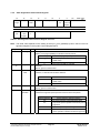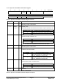
1
ERTEC 200
Enhanced Real-Time Ethernet Controller
PHY Description
Copyright © Siemens AG 2008. All rights reserved.
Technical data subject to change
Page 1
ERTEC 200 PHY
Version 1.0.0
Edition (11/2007)
Disclaimer of Liability
We have checked the contents of this manual for agreement with the hardware and software
described. Since deviations cannot be precluded entirely, we cannot guarantee full agreement.
However, the data in this manual are reviewed regularly. Necessary corrections are included in
subsequent editions. Suggestions for improvement are welcomed.
Copyright
© Siemens AG 2007. All rights reserved
The reproduction, transmission or use of this document or its contents is not permitted without
express written authority. Offenders will be liable for damages. All rights, including rights created
by patent grant or registration of a utility model or design, are reserved.
All product and system names are registered trademarks of their respective owner and must be
treated as such.
Technical data subject to change.
Preface
Target Audience of this Manual
This manual is intended for hardware developers who want to use the ERTEC 200 for new products. It describes
the internal ERTEC PHY’s.
Copyright © Siemens AG 2008. All rights reserved.
Technical data subject to change
Page 2
ERTEC 200 PHY
Version 1.0.0
This manual will be updated as required. You can find the current version of the manual on the Internet at
http://www.siemens.com/comdec.
Guide
To help you quickly find the information you need, this manual contains the following aids:
o
A complete table of contents as well as a list of all figures and tables in the manual are provided at the
beginning of the manual.
o
A glossary containing definitions of important terms used in the manual is located following the appendices.
o
References to other documents are indicated by the document reference number enclosed in slashes (/No./).
The complete title of the document can be obtained from the list of references at the end of the manual.
Additional Support
If you have questions regarding use of the described block that are not addressed in the documentation, please
contact your Siemens representative.
Please send your written questions, comments, and suggestions regarding the manual to the hotline via the email address indicated above.
In addition, you can receive general information, current product information, FAQs, and downloads pertaining to
your application on the Internet at:
http://www.siemens.com/comdec
Technical Contacts for Germany / Worldwide
Siemens AG
Automation &
Drives
Phone:
Phone:
Fax:
E-mail:
0911/750-2736
0911/750-2080
0911/750-2100
[email protected]
ComDeC
Street address:
Mailing address:
Würzburgerstr.121
P.O. Box 2355
90766 Fürth
Federal Republic of
Germany
90713 Fürth
Federal Republic of Germany
Technical Contacts for USA
PROFI Interface Center:
One Internet Plaza
PO Box 4991
Fax:
(423)- 262- 2103
Phone: (423)- 262- 2576
E-mail: [email protected]
Johnson City, TN 37602-4991
Copyright © Siemens AG 2008. All rights reserved.
Technical data subject to change
Page 3
ERTEC 200 PHY
Version 1.0.0
Contents
Multiport Ethernet PHY’s for ERTEC200 ........................................................................................6
1.1 Introduction ............................................................................................................................................ 6
1.2 PHY Interface Pin Functions .................................................................................................................. 7
1.3 Functional Description............................................................................................................................ 8
1.3.1 10BASE-T Operation ..................................................................................................................... 8
1.3.2 100BASE-TX Operation................................................................................................................. 10
1.3.3 100BASE-FX Operation................................................................................................................. 13
1.3.4 Auto Negotiation ............................................................................................................................ 14
1.3.5 Miscellaneous Functions................................................................................................................ 16
1.4 PHY Related Interfaces.......................................................................................................................... 22
1.5 PHY Register Description....................................................................................................................... 25
1.5.1 Basic Control Register ................................................................................................................... 26
1.5.2 Basic Status Register..................................................................................................................... 29
1.5.3 PHY Identifier Register REG2OUIIN.............................................................................................. 32
1.5.4 PHY Identifier Register REG3OUIIN.............................................................................................. 32
1.5.5 Auto Negotiation Advertisment Register ........................................................................................ 33
1.5.6 Auto Negotiation Link Partner Ability Register – Base Page.......................................................... 35
1.5.7 Auto Negotiation Link Partner Ability Register – Next Page........................................................... 38
1.5.8 Auto Negotiation Expansion Register ............................................................................................ 39
1.5.9 Auto Negotiation Next Page Transmit Register ............................................................................. 41
1.5.10 Silicon Revision Register ............................................................................................................... 42
1.5.11 Mode Control/Status Register........................................................................................................ 43
1.5.12 Special Mode Register................................................................................................................... 45
1.5.13 Special Conrol/Status Indication Register...................................................................................... 47
1.5.14 Interrupt Source Flag Register....................................................................................................... 48
1.5.15 Interrupt Mask Register.................................................................................................................. 50
1.5.16 PHY Special Control/Status Register............................................................................................. 50
1.6 Board Design Recommendations........................................................................................................... 52
1.6.1 Supply Voltage Circuitry................................................................................................................. 52
1.6.2 10BASE-T and 100BASE-TX Mode Circuitry................................................................................. 53
1.6.3 100BASE-FX Circuitry ................................................................................................................... 56
2
Miscellaneous.........................................................................................................................57
2.1 References:............................................................................................................................................ 57
Copyright © Siemens AG 2008. All rights reserved.
Technical data subject to change
Page 4
ERTEC 200 PHY
Version 1.0.0
List of Figures
Figure 1: PHY Block Diagram ................................................................................................................................8
Figure 2: MLT-3 Encoding Example....................................................................................................................12
Figure 3: Internal and Remote Loopback Modes...............................................................................................17
Figure 4: Phase Offset Indicator Function .........................................................................................................21
Figure 5: PHY Related Interfaces ........................................................................................................................22
Figure 6: Decoupling Capacitor Usage...............................................................................................................53
Figure 7: 10BASE-T and 100BASE-TX Interface Circuit Example 1 .................................................................53
Figure 8: 10BASE-T and 100BASE-TX Interface Circuit Example 2 .................................................................54
Figure 9: Circuit for Unused 100BASE-FX Mode ...............................................................................................55
Figure 10: 100BASE-FX Interface Example ........................................................................................................56
List of Tables
Table 1: ERTEC 200 Pin function for PHY interface.................................................................................................7
Table 2: 4B/5B Code Table ....................................................................................................................................11
Table 3: Assignment of LED Signals to GPIO Pins ................................................................................................16
Table 4: PHY Interrupt Events ................................................................................................................................20
Table 5: MII (Diagnosis) Interface Signals..............................................................................................................23
Table 6: SMI (Diagnosis) Interface Signals ............................................................................................................23
Table 7: MDI Interface Signals ...............................................................................................................................24
Table 8: Other PHY Related Signals ......................................................................................................................25
Table 9: PHY internal Registers .............................................................................................................................25
Table 10: Initial Parameter Settings for PHYs ........................................................................................................26
Table 11: Basic Control Register Overview ............................................................................................................26
Table 12: Basic Control Register Description .........................................................................................................28
Table 13: Basic Status Register Overview .............................................................................................................29
Table 14: Basic Status Register Description ..........................................................................................................31
Table 15: NEC OUI Composition............................................................................................................................31
Table 16: PHY ID Number Composition .................................................................................................................31
Table 17: PHY Identifier Register REG2OUIIN Overview.......................................................................................32
Table 18: PHY Identifier Register REG2OUIIN Description....................................................................................32
Table 19: PHY Identifier Register REG3OUIIN Overview.......................................................................................32
Table 20: PHY Identifier Register REG3OUIIN Description....................................................................................32
Table 21: Auto-Negotiation Advertisement Register Overview...............................................................................33
Table 22: Auto-Negotiation Advertisement Register Description ............................................................................35
Table 23: Auto-Negotiation Link Partner Ability Register Overview – Base Page ..................................................35
Table 24: Auto-Negotiation Link Partner Ability Register Description – Base Page................................................37
Table 25: Auto-Negotiation Link Partner Ability Register Overview – Next Page ...................................................38
Table 26: Auto-Negotiation Link Partner Ability Register Description – Next Page ................................................38
Table 27: Auto-Negotiation Expansion Register Overview .....................................................................................39
Table 28: Auto-Negotiation Expansion Register Description ..................................................................................40
Table 29: Auto-Negotiation Next Page Transmit Register Overview ......................................................................41
Table 30: Auto-Negotiation Next Page Transmit Register Description ...................................................................41
Table 31: Silicon Revision Register Overview ........................................................................................................42
Table 32: Silicon Revision Register Description .....................................................................................................42
Table 33: Mode Control/Status Register Overview.................................................................................................43
Table 34: Mode Control/Status Register Description..............................................................................................44
Table 35: Special Mode Register Overview............................................................................................................45
Table 36: Special Mode Register Description.........................................................................................................46
Table 37: Special Control/Status Indication Register Overview..............................................................................47
Table 38: Special Control/Status Indication Register Description...........................................................................47
Table 39: Interrupt Source Flag Register Overview................................................................................................48
Table 40: Interrupt Source Flag Register Description.............................................................................................49
Table 41: Interrupt Mask Register Overview ..........................................................................................................50
Table 42: Interrupt Mask Register Description .......................................................................................................50
Table 43: PHY Special Control/Status Register Overview......................................................................................50
Table 44: PHY Special Control/Status Register Description...................................................................................51
Table 45: Generation of PHY-specific Supply Voltages..........................................................................................52
Table 46: Examples for Magnetics Selection..........................................................................................................54
Copyright © Siemens AG 2008. All rights reserved.
Technical data subject to change
Page 5
ERTEC 200 PHY
Version 1.0.0
Multiport Ethernet PHY’s for ERTEC200
1.1
Introduction
ERTEC 200 has integrated a 2 channel multiport Ethernet PHY (Physical Layer Transceiver), that
supports the following transmission modes:
• 10BASE-T
• 100BASE-TX
• 100BASE-FX
It can be connected to unshielded twisted-pair (UTP) cable via external magnetics or to optical fiber
via fiber PMD modules. Internally on the ERTEC 200 it interfaces to the MAC layer through the IEEE
802.3 Standard Media Independent Interface (MII).
The core has a DSP-based architecture for signal equalization and baseline wander correction. This
helps to achieve high noise immunity and to extend UTP cable lengths.The transmission modes can
be configured for each port individually. Beside these basic modes, the following (configurable)
features are supported as well:
• Auto-negotiation
• Auto-MDI/MDIX detection
• Auto polarity
The PHYs comply to the following standards:
• IEEE802.3
• IEEE802.3u
• ANSI X3.263-1995
• ISO/IEC9314
Communication between the integrated PHYs and the integrated Ethernet MACs is realized with onchip MII interfaces. Internal registers of the PHYs can be accessed via the common (on-chip) serial
management interface (SMI). Furthermore certain set-ups for the PHYs can be programmed using the
system control registers that are described in \1\ Chapter 4.8. A couple of output signals per channel
is available to reflect the connection status via LEDs; these signals are shared with GPIO pins. The
PHYs need a 25 MHz clock that can be provided on two alternative ways:
• connect a 25 MHz quartz to the CLKP_A and CLKP_B pins
• connect a 25 MHz oscillator to the CLKP_A pin.
In order to reduce power consumption, the PHYs can be driven to a power down mode either manually
or automatically, if there is no activity on the Ethernet line.
Copyright © Siemens AG 2008. All rights reserved.
Technical data subject to change
Page 6
ERTEC 200 PHY
Version 1.0.0
1.2
PHY Interface Pin Functions
The on-chip PHYs of ERTEC 200 use the following pins:
Pin Name
I/O
Function
Number of pins
P(2:1)TxN
O
Differential transmit data output
2
P(2:1)TxP
O
Differential transmit data output
2
P(2:1)TDxN
O
Differential FX transmit data output
2
P(2:1)TDxP
O
Differential FX transmit data output
2
P(2:1)RxN
I
Differential receive data input
2
P(2:1)RxP
I
Differential receive data input
2
P(2:1)RDxN
I
Differential FX receive data input
2
P(2:1)RDxP
I
Differential FX receive data input
2
P(2:1)SDxN
I
Differential FX signal detect input
2
P(2:1)SDxP
I
Differential FX signal detect input
2
External reference resistor (12.4 kΩ)
1
DVDD(4:1)
I
Digital power supply, 1.5 V
4
DGND(4:1)
I
Digital GND
4
P(2:1)VSSATX(2:1)
I
Analog port GND
4
P(2:1)VDDARXTX
I
Analog port RX/TX power supply, 1.5 V
2
P(2:1)VSSARX
I
Analog port GND
2
VDDAPLL
I
Analog central power supply, 1.5 V
1
VDDACB
I
Analog central power supply, 3.3 V
1
VSSAPLLCB
I
Analog central GND
1
VDD33ESD
I
Analog test power supply, 3.3 V
1
VSS33ESD
I
Analog test GND
EXTRES
I/O
total
1
42
Table 1: ERTEC 200 Pin function for PHY interface
Note that Table 1 includes the specific power supply pins that are needed for operation of the PHYs,
however it does not include the status indication signals that are shared with GPIO pins. For the status
indication signals see /1/
Copyright © Siemens AG 2008. All rights reserved.
Technical data subject to change
Page 7
ERTEC 200 PHY
Version 1.0.0
1.3
Functional Description
This chapter gives a functional description of the integrated PHYs on ERTEC 200 based on the block
diagram shown in Figure 1 . Figure 1 shows a single channel; both channels have identical structure.
The subsequent chapters will frequently refer to signals that are present on the MII interface between
on-chip PHY and on-chip MAC. In these cases the signal names that have been introduced in \1\Table
1.5.7 and 1.5.8 will be used. Note that these signals can be externally monitored when ERTEC 200
has been configured to MII diagnosis mode with the CONFIG(6:1) pins.
Figure 1: PHY Block Diagram
1.3.1
10BASE-T Operation
A 10BASE-T transceiver is implemented for a 10 Mbps CSMA/CD LAN over two pairs of twisted-pair
wires according to the specifications given in clause 14 of the IEEE 802.3 standard. During transmission, 4-bit nibble data comes from the MII interface at a rate of 2.5 MHz and is converted into a
10 Mbps serial data stream. The data stream is then Manchester-encoded and sent to the analog
transmitter which drives a signal to the twisted pair cable via external magnetics.
In order to comply with legacy 10BASE-T MAC/Controllers, the transmitted data is looped back to the
receive path, if the PHY is configured to work in half-duplex mode.
On the receiver side, the receive clock is recovered from the incoming signal. The received Manchester-encoded analog signal from the cable is recovered to the NRZI data stream using the clock. Then
the 10 Mbps serial data stream is again converted to 4-bit data that are passed to the MAC across the
MII interface at a rate of 2.5 MHz.
Copyright © Siemens AG 2008. All rights reserved.
Technical data subject to change
Page 8
ERTEC 200 PHY
Version 1.0.0
The PHY realizes a complete 10BASE-T transceiver function. It includes the receiver, transmitter and
the following functions.
<1>
<2>
<3>
<4>
<5>
<6>
Filter and squelch
Jabber detection
Signal quality error (SQE) message test function
Timing recovery from received data
Manchester encoding/decoding
Full-duplex or Half-duplex mode
In half-duplex mode, the PHY transmits and simultaneously receives in order to provide
loopback of the transmitted signal. (Refer to section 14.2.1.3 of IEEE802.3 )
<7> Collision presence function (half duplex mode only)
<8> Carrier Sense Detection
CRS is asserted only to receive activity for Full-Duplex mode. CRS is asserted
during either packet transmission or reception for half-duplex mode.
(1) Filter and Squelch
The Manchester encoded signal from the cable is fed into the transceiver’s receive path via 1:1 ratio
magnetics (see Chapter 1.6.2 for details of the circuit). It is first filtered to reduce any out-of-band
noise. It then passes through a squelch circuit - a set of amplitude and timing comparators that
normally reject differential voltage levels below 300 mV and detect and recognize differential voltages
above 585 mV.
(2) Jabber detection
Jabber is a condition in which a station transmits for a period of time longer than the maximum permissible packet length - usually due to a fault condition - that results in holding the TX_EN_P(2:1) signal
active for a long period. Special logic is used to detect the jabber state and to abort the transmission to
the line within 45 ms. The maximum time of of unjab is 350 ms. Once TX_EN_P(2:1) is deasserted,
the logic resets the jabber condition. Basic status register 1 indicates that a jabber condition was
detected; details about the register functions are given in Chapter 1.5.
(3) SQE test function
The PHYs on ERTEC 200 support a signal quality error (SQE) test function. This function controls if
data transmission is successful; successful transmission is indicated by activating the COL_P(2:1) signal for 1 µs, 2 µs after TX_EN_P(2:1) has been deasserted. This signal is also referred to as “heartbeat” signal.
If desired, the SQE test function can be disabled by setting the SQEOFF bit in control/status register
27 to 1b. The setting of the SQEOFF bit is irrelevant when the PHY is working in 100BASE-TX or -FX
modes.
(4) Manchester encoding/decoding
When encoding, the 4-bit nibble data, that is coming from the MII interface, is converted to a 10 Mbps
serial NRZI data stream. The 10M PLL locks onto the external clock and produces a 20 MHz clock signal. which is used to Manchester encode the NRZ data stream.
When no data is being transmitted, normal link pulses (NLPs) are output to maintain communications
with the remote link partner.
When decoding, the 10M PLL is locked onto the received Manchester signal and from this, the internal
20 MHz receive clock is generated. Using this clock, the Manchester encoded data is extracted and
converted to a 10 MHz NRZI data stream. This stream is then converted from serial to 4-bit nibble
data.
Copyright © Siemens AG 2008. All rights reserved.
Technical data subject to change
Page 9
ERTEC 200 PHY
Version 1.0.0
1.3.2
100BASE-TX Operation
100BASE-TX specifies operation over two copper media: two pairs of shielded twisted-pair cable
(STP) and two pairs of unshielded twisted-pair cable (Category 5 UTP). 100BASE-TX function
includes the physical coding sub-layer (PCS), the physical medium attachment (PMA) and physical
medium dependent sub-layer (PMD).
When transmitting, 4-bit data nibbles come from the MII interface at a rate of 25 MHz and are
converted to 5-bit encoded data. The data is then serialized and scrambled, subsequently converted
to a NRZI data stream and MLT-3 encoded.
In the receive path the ADC samples the incoming MLT-3 signal at a sampling frequency of 125 MHz.
The resulting MLT-3 signal is reconverted to the NRZI data stream, and then the descrambler
performs the inverse function of the scrambler in the transmit path and parallelizes the data. The
4B/5B decoder completes the processing and supplies the data ready for transmission over the MII
interface.
This section describes the main functions of the 100BASE-TX portion of the PHYs.
<1> Full-duplex or Half-duplex mode
<2> Collision detect indication
<3> Carrier Sense detection
<4> MLT-3 to (from) NRZ Decoding/Encoding
<5> 4B/5B Encoding/Decoding
<6> Scrambler/Descrambler
<7> Adaptive Equalization(DSP)
<8> Baseline Wander Correction
<9> Timing recovery from received data
<10> Support MII, RMII and Symbol interface
(1)
Timing recovery
The 125M PLL locks onto the 25 MHz reference clock and generates an internal 125 MHz clock used
to drive the 125 MHz logic and the 100BASE-TX transmitter. The PLL generates multiple phases of
the 125 MHz clock. A multiplexer, controlled by the timing unit of the DSP block, selects the optimum
phase for sampling the data. This is used as the recovered receive clock, which is then used to extract
the serial data from the received signal.
(2)
Adaptive equalizer
The adaptive equalizer compensates phase and amplitude distortion caused by the physical transmission channel consisting of magnetics, connectors, and CAT-5 cable. Thus, the supported cable length
is increased.
(3)
Baseline wander correction
If the DC content of the signal is such that the low-frequency components fall below the low frequency
pole of the isolation transformer, then the droop characteristics of the transformer will become significant and baseline wander (BLW) on the received signal will result. To prevent corruption of the
received data, the PHY corrects the baseline wander effects using DSP algorithms.
Copyright © Siemens AG 2008. All rights reserved.
Technical data subject to change
Page 10
ERTEC 200 PHY
Version 1.0.0
(4)
4B/5B encoding/decoding
In 100BASE-TX mode, 4B/5B coding is used. The 4B/5B encoder converts 4-bit nibbles coming from
the MII interface to 5-bit symbols that are referred to as “code-groups”. The relation between original
and encoded data is shown in Table 2.
For testing purposes the encoder and decoder can be bypassed with the Enable 4B5B bit in the PHY
special control/status register. In this case the 5th bit of the output pattern reflects the current level of
the TX_ERR_P(2:1) signal of the MII interface.
Code group
Name
11110
01001
10100
10101
01010
01011
01110
01111
10010
10011
10110
10111
11010
11011
11100
11101
0
1
2
3
4
5
6
7
8
9
A
B
C
D
E
F
11111
I
11000
J
10001
K
01101
T
00111
R
00100
H
all others
V
Transmitter
from MAC via MII Interpretation
0000
Data 0
0001
Data 1
0010
Data 2
0011
Data 3
0100
Data 4
0101
Data 5
0110
Data 6
0111
Data 7
1000
Data 8
1001
Data 9
1010
Data A
1011
Data B
1100
Data C
1101
Data D
1110
Data E
1111
Data F
Sent after /T and /R (end of stream)
until TX_EN_P(2:1) is asserted
again
Receiver
Interpretation
to MAC via MII
Data 0
0000
Data 1
0001
Data 2
0010
Data 3
0011
Data 4
0100
Data 5
0101
Data 6
0110
Data 7
0111
Data 8
1000
Data 9
1001
Data A
1010
Data B
1011
Data C
1100
Data D
1101
Data E
1110
Data F
1111
Idle
1st nibble of start of stream data
Sent, when TX_EN_P(2:1) is
(SSD); translates to 0101 if
asserted
received after “idle”; otherwise
RX_ERR_P(2:1) is asserted
2nd nibble of SSD; translates to
Sent after /J
0101 if received after /J; otherwise
RX_ERR_P(2:1) is asserted
1st nibble of end of stream data
(ESD); translates to 1010 and
Sent when TX_EN_P(2:1) is deas
causes deassertion of CRS_P(2:1)
serted
when fol lowed by /R; otherwise
RX_ERR_P(2:1) is asserted
2st nibble of ESD; translates to
1010 and causes deassertion of
Sent after /T
CRS_P(2:1) when preceded by /T;
otherwise RX_ERR_P(2:1) is
asserted
Sent when TX_ERR_P(2:1) is
Transmit error
Undefined
asserted
Invalid code; RX_ERR_P(2:1) is
Invalid code
asserted if received while
RX_DV_P(2:1) is active
Table 2: 4B/5B Code Table
Copyright © Siemens AG 2008. All rights reserved.
Technical data subject to change
Page 11
ERTEC 200 PHY
Version 1.0.0
(5)
Scrambling/Descrambling
Scrambling the data before transmission helps to eliminate large narrow-band signal power peaks for
repeated data patterns, and spreads the signal power more uniformly over the entire channel bandwidth.
The scrambler encodes a plaintext NRZ bit stream by addition (modulo 2) of 2047 bits generated by
the recursive linear function X[n]= X[n-11] + X[n-9] (modulo 2). The scrambler generates the specified
non-zero key stream whenever the active output interface is required to transmit a scrambled data
stream. The seed for the scrambler is generated from the PHY address, ensuring that in multiple-PHY
applications each PHY will have its individual scrambler sequence.
The descrambler descrambles the NRZ ciphertext bit stream coming from the MLT-3 decoder by addition (modulo 2) of a key stream to re-produce a plaintext bit stream. During the reception of IDLE symbols, the descrambler synchronizes its descrambler key to the incoming stream. Once synchronization
is achieved, the descrambler locks on this key and is able to descramble incoming data.
Special logic in the descrambler ensures synchronization with the remote PHY by searching for IDLE
symbols within a window of 4000 bytes (40us). This window ensures that a maximum packet size of
1514 bytes, allowed by the IEEE 802.3 standard, can be received with no interference.
This core has a scrambler and descrambler bypass mode for testing purposes.
(6) MLT3 Encoding/Decoding
In the transmit direction, the serial 125 MHz NRZI data stream is encoded to MLT-3. MLT-3 is a trilevel
code where a change in the logic level represents a code bit “1” and the logic output remaining at the
same level represents a code bit “0”.
In the receive direction, the MLT-3 code is converted to an NRZI data stream. The NRZI to MLT-3 conversion is illustrated in Figure 2.
Figure 2: MLT-3 Encoding Example
Copyright © Siemens AG 2008. All rights reserved.
Technical data subject to change
Page 12
ERTEC 200 PHY
Version 1.0.0
(7)
Receive Data Valid / Receive Error
The receive data valid signal RX_DV_P(2:1) indicates that recovered and decoded nibbles are being
presented on the RXD_P1(3:0) respectively RXD_P2(3:0) outputs synchronous to RX_CLK_P(2:1).
RX_DV_P(2:1) becomes active after the /J/K/ delimiter has been recognized and RXD_P(2:1) is
aligned to nibble boundaries. It remains active until either the /T/R/ delimiter is recognized or link test
indicates failure.
RXDV is asserted when the first nibble of translated /J/K/ is ready for transfer over the Media
Independent Interface (MII).
During a frame, unexpected code-groups are considered as receive errors. Expected code groups are
the data set (0H through FH), and the /T/R/(ESD) symbol pair. When a receive error occurs, the
RX_ERR_P(2:1) signal is asserted and arbitrary data is driven onto the RXD lines. Should an error be
detected during the time that the /J/K/ delimiter is being decoded (bad SSD error), RX_ERR(2:1) is
asserted true and the value 1110b is driven onto the RXD_P(2:1) lines. Note that the valid vata signal
is not yet asserted when the bad SSD error occurs.
1.3.3
100BASE-FX Operation
This section describes main functions within the PHY in 100BASE-FX operation.
<1>
<2>
<3>
<4>
NRZI to(from) NRZ converter
Far End Fault Indication
Timing recovery from received data
Support MII,RMII, SMII and Symbol interface
The 100BASE-FX shares logic with 100BASE-TX; the differences between 100BASE-FX mode and
100BASE-TX mode are following,
<1>
<2>
<3>
<4>
<5>
<6>
(1)
Transmit output/receive input is not scrambled or MLT3 encoded.
All analog circuits except for the PLL are powered-down.
Auto-Negotiation is disabled.
The transmit data is output to a FX transmitter.
The receive data is input to the FX ECL level detector instead of the equalizer.
The FX interface has a signal detect input.
Signal Detect
The signal detect signals P(2:1)SDxP/N are input signals to the PHY from the PMD FX transceiver.
Assertion of P(2:1)SDxP/N indicates a valid FX signal on the fiber. When SD is deactivated, the LINK
goes down and no data is sent to the controller.
(2)
Far End Fault indication
Far End fault indication (FEFI) is a mechanism used to communicate physical status across a fiber
link. Each PHY monitors the status of its receive link using the Signal Detect input. If the PHY detects
a problem with its receive link, it communicates that to its link partner using the FEFI mechanism.
Copyright © Siemens AG 2008. All rights reserved.
Technical data subject to change
Page 13
ERTEC 200 PHY
Version 1.0.0
FEFI consists of a modification to the IDLE code patterns. In this mode, every 16 IDLE code groups
are followed by a data-0 code group. If the PHY detects a FEFI pattern in its receive stream, it deasserts its link status and transmits only IDLE patterns (not FEFI) on its transmit stream.
A full description of the Far End Fault Function is given in Section 24.3.2.1 in the IEEE 802.3 standard.
1.3.4
Auto Negotiation
The objective of the Auto-Negotiation function is to provide the means to exchange information
between two devices that share a link segment and to automatically configure both devices to take
maximum advantage of their abilities.
The auto-negotiation protocol is a purely physical layer activity and proceeds independently of the
MAC controller. The auto-negotiation function sends fast link pulse (FLP) bursts for exchanging
information with its link partner. A FLP burst consists of 33 pulse positions. The 17 odd-numbered
pulse positions shall contain a link pulse and represent clock information. The 16 even-numbered
pulse positions represent data information. The data transmitted by an FLP burst is known as a "Link
Code Word". These are fully defined in clause 28 of the IEEE 802.3 specification.
This core supports auto-negotiation and implements the “Base page”, defined by IEEE 802.3. It
also supports the optional “Next page” function to get the remote fault number code.
(1)
Parallel detection
The parallel detection function allows detection of Link Partners that support 100BASE-TX and/or
10BASE-T, but do not support Auto-Negotiation. The PHY is able to determine the speed of the link
based on either 100M MLT-3 symbols or 10M Normal Link Pulses. If the PHY detects either mode, it
automatically reverts to the corresponding operating mode. In this case the link is presumed to be half
duplex.
If a link is established via parallel detection, then Bit 0 of the Auto-Negotiation Expansion register is
cleared to indicate that the link partner is not capable of auto-negotiation. The controller has access to
this information via the management interface. If a fault occurs during parallel detection, bit 4 of the
Auto-Negotiation Expansion register is set.
The Auto-Negotiation Link Partner Ability register is used to store the link partner ability information,
which is coded in the received FLPs. If the link partner is not auto-negotiation capable, then the AutoNegotiation Link Partner Ability register is updated after completion of parallel detection to reflect the
speed capabilities of the link partner.
(2)
Re-negotiation
Auto-negotiation is started by one of the following events:
<1> H/W reset
<2> S/W reset
<3> setting the Auto-Negotiation Enable bit in the Basic Control register from low to high
When auto-negotiation is enabled, it is re-started by one of the following events:
<1> Link status is down.
<2> Setting the Auto-Negotiation Restart bit in the Basic Control register to high.
Copyright © Siemens AG 2008. All rights reserved.
Technical data subject to change
Page 14
ERTEC 200 PHY
Version 1.0.0
(3)
Priority Resolution
If two Ethernet communication partners negotiate their capabilities, there are four possible matches of
the technology abilities. In the order of priority these are:
• 100M full Duplex (highest priority)
• 100M Half Duplex
• 10M full Duplex
• 10M Half Duplex (lowest priority)
Since two devices (local device and remote device) may have multiple abilities in common, a prioritization scheme exists to ensure that the highest common denominator ability is chosen. Full duplex solutions are always higher in priority than their half duplex counterparts. 10BASE-T is the lowest common
denominator and therefore has the lowest priority.
If a link is formed via parallel detection, then the Link Partner Auto-negotiation Able bit in the Auto
Negotiation Expansion register is cleared to indicate that the link partner is not capable of autonegotiation. The controller has access to this information via the management interface. If a fault
occurs during parallel detection, the Parallel Detection Fault bit in the same register is set. The AutoNegotiation Link Partner Ability register 5 is used to store the link partner’s ability information, which
was decoded from the received FLPs. If the link partner is not auto-negotiation capable, then the AutoNegotiation Link Partner Ability register is updated after completion of parallel detection to reflect the
speed capability of the link partner.
(4)
Next Page function
Additional information, exceeding that required by base page exchange, is also sent via “Next Pages”;
this PHY supports the optional “Next page” function. Next page exchange occurs after the base page
has been exchanged. Next page exchange consists of using the normal Auto-Negotiation arbitration
process to send next page messages. Two kinds of message encodings are defined: Message Pages,
which contain predefined 11 bit codes, and unformatted pages .
Next page transmission ends when both ends of a link segment set their Next Page bits to logic zero,
indicating that neither has anything additional to transmit. It is possible for one device to have more
pages to transmit than the other device. Once a device has completed transmission of its next page
information, it shall transmit message pages with Null message codes and the NP bit set to logic zero
while its link partner continues to transmit valid next pages.
Devices, that are able of auto-negotiation, shall recognize reception of message pages with Null message codes as the end of its link partner’s next page information. The default value of the next page
support is disable (Next Page bit in Auto-Negotiation Advertisement register). To enable next page
support, the Next Page bit should be set to 1b. Auto-Negotiation should be restarted and the message
code to be transmitted to the remote link partner should be written to bit(10:0) of the Auto-Negotiation
Next Page Transmit register .
(5)
Disabling Auto-Negotiation
Auto-negotiation can be disabled by setting the Auto-Negotiation Enable bit in the Basic Control register. When Auto-negotiation is disabled, the speed and duplex mode settings are configured via the
serial management interface.
Copyright © Siemens AG 2008. All rights reserved.
Technical data subject to change
Page 15
ERTEC 200 PHY
Version 1.0.0
1.3.5
Miscellaneous Functions
This chapter summarizes some additional functions of the PHYs.
(1)
LED indicators
Six LED signals are provided per PHY. These provide a convenient means to determine the operation
mode of the PHYs. All LED signals are active low. The LED signals are made available through the
GPIO pins of the ERTEC 200. The functions of the LED signals are as follows:
• 100BASE-TX/FX status
This signal shows, that operation speed is 100Mbps or during Auto-Negotiation; this signal will
go inactive when the operating speed is 10Mbps or during line isolation.
• 10BASE-T status
This signal shows, that operation speed is 10Mbps; this signal will go inactive when the
operating speed is 100Mbps or during line isolation.
• Link status
This signal shows, that the PHY detects a valid link. The use of the 10Mbps or 100Mbps link
test status is determined by the condition of the internally determined speed selection.
• Full/Half Duplex
This signal shows, whether the established link is operating in full or half duplex mode; it is
active in full duplex mode.
• Transmit Activity
This signal shows, that CRS_P(2:1) is active (high) at transmit. When CRS becomes inactive,
the transmit activity LED output is extended by 128ms in order to improve visibility.
• Receive Activity
This signal shows, that CRS_P(2:1) is active (high) at receive. When CRS becomes inactive,
the receive activity LED output is extended by 128ms in order to improve visibility. In loopback
mode, this LED is not active.
Table 3 illustrates how the LED signals are made available at the GPIO pins.
Function
GPIO pin
GPIO0
1
2
3
P1-DUPLEX-LED_N
-
-
GPIO1
P2-DUPLEX-LED_N
-
-
GPIO2
P1-SPEED-100LED_N (TX/FX)
P1-SPEED-10LED_N
-
GPIO3
P2-SPEED-100LED_N (TX/FX)
P2-SPEED-10LED_N
-
GPIO4
P1-LINK-LED_N
-
-
GPIO5
P2-LINK-LED_N
-
-
GPIO6
P1-RX-LED_N
P1-TX-LED_N
P1-ACTIVE-LED_N
GPIO7
P2-RX-LED_N
P2-TX-LED_N
P2-ACTIVE-LED_N
Table 3: Assignment of LED Signals to GPIO Pins
Copyright © Siemens AG 2008. All rights reserved.
Technical data subject to change
Page 16
ERTEC 200 PHY
Version 1.0.0
(2)
MDI/MDI-X crossover detection
The PHYs automatically detect and correct MDI/MDI-X crossover. This function can be disabled by
setting the AutoMDIX_en bit in the Mode Control/Status register to 0b. When it is disabled, crossover
must be corrected manually by setting the MDI mode bit in the same register accordingly.
(3)
Polarity
This core automatically detects and corrects polarity reversal in wiring in 10BASE-T mode. The result
of polarity detection is indicated by the XPOL bit in the Special Control/Status Indications register.
Polarity is checked at end of packets in 10BASE-T. When a packet is corrupted by noise, the PHY
may mis-interprete information inside the packet as end of packet. In this case, the PHY may invert the
polarity and a maximum of three packets is be needed to detect the valid polarity again.
(4)
Loopback mode
This ERTEC 200 PHYs support two loopback modes: internal loopback and remote loopback.
Figure 3 illustrates the differences between these two modes.
Figure 3: Internal and Remote Loopback Modes
(a) Internal loopback
This loopback mode is defined in the IEEE 802.3 specification; it is enabled by setting the Loopback bit in the Basic Control register to 1b. In this mode, the scrambled transmit data is looped
into the receive logic. The COL_P(2:1) signal will be inactive in this mode, unless the Collision
Test bit in the Basic control register is active.
When the internal loopback mode is active, the receive circuitry should be isolated from the network medium. In this mode, the assertion of TX_EN_P(2:1) at the MII interface does not result in
the transmission of data on the network medium, and transmitters are powered down.
(b) Remote loopback
This mode is enabled by setting the FARLOOP BACK bit in the Mode Control/Status register to
1b. This mode can be used only when the PHYs are in 100BASE-TX or 100BASE-FX mode. In
this mode, packets that arrive at the receiver are looped back out to the transmitter. In 100BASETX mode, the data path includes the ADC, DSP, PCS circuits; in 100BASE-FX mode, the data
path includes the PECL logic, clock recovery and PCS logic. As long as no data is received, IDLE
symbols are transmitted.
Copyright © Siemens AG 2008. All rights reserved.
Technical data subject to change
Page 17
ERTEC 200 PHY
Version 1.0.0
In this mode, the complete preamble, SFD and EFD are re-generated by the PHY so that always
complete packets are transmitted, even if received packets lack part of the preamble. The Isolate
bit in the Basic Control register needs to be cleared to work in remote loopback mode.
(5)
Power Down Modes
(a) Hardware power down
This state is entered after a hardware reset of ERTEC 200. The PHYs are switched off and their
power consumption is almost 0 W. This state is left by setting the P1/2_PHY_ENB bits in the
PHY_CONFIG register. All analog and digital blocks in the PHYs are initialized and the predefined configuration in the PHY_CONFIG register is copied to the PHYs. Then, the PHY-internal
registers can be configured as well.
Setting the P1/2_PHY_ENB bits extends the internal reset signal in the PHYs to 5.2 ms in order
to stabilize the PLL and all analog and digital blocks. When the PHYs are ready to operate, this is
automatically indicated in the PHY_STATUS registers with the P1/2_PWRUPRST bits (set to 1b).
(b) Software power down
This state is entered by writing a 1b into the PowerDown bit of the Basic Control register of the
PHYs. The affected PHY will then go into a low power state, where the MDIO interface is still
active, but where no activity is possible on the MII interface. The power consumption of the PHYs
in low power state is around 15 mW per PHY.
The low power mode is left by writing a 0b into the PowerDown bit. The digital parts of the
circuitry are re-initialised, however the start-up configuration, that is stored in the PHY_CONFIG
register, is not copied again into the PHYs and the PHY registers are not set to their initial values.
Leaving the low power state generates an internal reset for the PHYs with a duration of 256 µs
for PLL stabilization.
(c) Automatic power down
The PHYs support an automatic power down mode, that is entered, if there is no activity on the
Ethernet line. To enable this mode, a 1b must be written into the EDPWRDOWN bit of the Mode
Control/Status register of the PHYs. No activity on the line will then automatically drive the PHY
into the low power mode with approximately 15 mW power consumption per PHY. If link pulses or
data packets are detected, the low power mode is automatically left with an internal reset of 256
µs and re-initialization of the circuitry. The first and possibly the second packet may be lost during
the energy detection process. No configuration data is copied from the PHY_CONFIG register to
the PHY at this point.
Automatic power down cannot be used as long as Auto-negotiation is enabled; therefore the
Auto-Negotiation Enable bit in the Basic Control register must be set to 0b for automatic power
down.
(6)
Resetting the PHYs
(a) Hardware reset
There are two methods to issue a hardware reset to the ERTEC 200 on-chip PHYs; the reset
source can be selected using the PHY_RES_SEL bit in the PHY_CONFIG register:
PHY_RES_SEL = 0b
PHY_RES_SEL = 1b
PowerOn reset via RESET_N input resets the PHYs
Internal RES_PHY_N signal from IRT switch resets the PHYs
Copyright © Siemens AG 2008. All rights reserved.
Technical data subject to change
Page 18
ERTEC 200 PHY
Version 1.0.0
If the PowerOn reset is used, the PHYs are active after reset; if RES_PHY_N is used, the PHYs
remain in power down mode after reset and must subsequently be activated with the PowerDown
bit in the Basic Control register. The HW reset must be present for at least 100 µs. These reset
signals are internally extended by 5.2 ms to ensure that the PHY is properly reset. All analog
circuits and all digital logic including management registers are initialized. After initialization, the
respective PWRUPRST signal in the PHY_STATUS register is set.
Notes: 1. During the hardware reset and its extension, the clock signal for the PHYs must be
supplied.
2. A hardware reset is commonly issued to both PHYs.
(b) Software reset
Resetting the PHYs core can also be accomplished by setting the Reset bit in the respective
Basic Control register to 1b. This signal is self-clearing. After the register has been written, the
internal software reset is extended by 256 µs for PLL stabilization before the logic is released
from reset. A software reset affects the PHY registers and resets them to their initial values
except where noted.
Note: A software reset can be issued separately for each PHY.
(c) Reset by software and energy detect power down
When the PHYs come out of software and energy detect power down, they are automatically activated. After exiting the power down mode, the PHY-internal power-down reset is extended by
256 µs for PLL stabilization before logic is released from reset.
Note: This PHY-internal power down reset does not affect the PHY management registers.
(7)
Half/Full Duplex
In half duplex mode, stations contend for the use of the physical medium, using the CSMA/CD algorithms specified. Half duplex mode is required on those media that are not capable of supporting
simultaneous transmission and reception without interference like 10BASE-2 and 100BASE-T4.
The full duplex operation mode can be used when all of the following conditions are fulfilled:
<1> The physical medium is capable of supporting simultaneous transmission and reception without interference.
<2> There are exactly two stations on the LAN. This allows the physical medium to be
treated as a full duplex point-to-point link between the stations.
<3> Both stations on the LAN are capable of and have been configured to use full duplex
operation.
Copyright © Siemens AG 2008. All rights reserved.
Technical data subject to change
Page 19
ERTEC 200 PHY
Version 1.0.0
(8)
Interrupt handling
Each PHY can generate a collective interrupt that can be triggered by several PHY-internal events;
these two interrupts are routed with a wired-OR to the common IRQ9 input of the ERTEC 200 interrupt
controller. Table 4 shows the events that can generate an interrupt from the PHYs:
Interrupt number
Interrupt Event
INT8
not used
INT7
ENERGYON generated
INT6
Auto-negotiation complete
INT5
Remote fault detected
INT4
Link down
INT3
Auto-negotiation LP acknowledge
INT2
Parallel detection fault
INT1
Auto-negotiation page received
Table 4: PHY Interrupt Events
Each of the interrupt events above is described in the protocol of the Interrupt Source Flag register in
the PHYs; it can as well be masked or unmasked individually in the Interrupt Mask register in the
PHYs (see Table 42: Interrupt Mask Register Description).
(9)
Isolate Mode
The PHY data path may be electrically isolated from the MII by setting the Isolate bit in the Basic Control register to 1b. In isolate mode, the internal MII interface of the respective PHY is made inactive.
However the PHYs still respond to management transactions. Isolation provides a means for multiple
PHYs to be connected to the same MII without contention occurring and it is not really required to use
on ERTEC 200. The PHYs are not in isolate mode on power-up.
(10) Link integrity Test
The PHYs perform a link integrity test as outlined in the IEEE 802.3 Link Monitor state diagram. The
link status is multiplexed with the 10Mbps link status to form the reportable Link Status bit in the Basic
Control register 1, and is driven to the P(2:1)-LINK-LED_N output.
The DSP block indicates a valid MLT-3 waveform present on the P(2:1)RxP and P(2:1)RxN inputs as
defined by the ANSI X3.263 TP-PMD standard, to the link monitor state-machine, using an internal
signal called DATA_VALID. When it is asserted the control logic moves into a link-ready state, and
waits for an enable from the auto-negotiation block. When received, the link-up state is entered, and
the transmit and receive logic blocks become active.Should auto-negotiation be disabled, the link
integrity logic moves immediately to the link-up state, when the DATA_VALID signal is asserted.
Note that to allow the link to stabilize, the link integrity logic will wait a minimum of 330 µsec from the
time DATA_VALID is asserted until the link-ready state is entered. Should the DATA_VALID input be
negated at any time, this logic will immediately negate the link signal and enter the link-down state.
When the 10/100 digital block is in 10BASE-T mode, the link status generated from the 10BASE-T
receiver logic.
Copyright © Siemens AG 2008. All rights reserved.
Technical data subject to change
Page 20
ERTEC 200 PHY
Version 1.0.0
(11) Link Lockup Protection
During the reception of 10BASE-T data, the link partner may switch to 100BASE-TX without starting
auto-negotiation. In this case, the PHY must recognize this, de-assert the link status, and switch to
100BASE-TX mode.
To achieve this, a counter is activated at the beginning of every 10BASE-T packet. When the counter
reaches the count of 157 msec and no end of packet was recognized, then the link will be de-asserted
and the PHY will restart either auto-negotiation (if enabled) or try to achieve a 10BASE-T link again.
(12) Phase Offset Indicator
The latency between transmitter and receiver can lead to 5 different phase variations of 125Mbps
received packets against the 25Mbps data on the MII interface (only in 100BASE-TX/FX mode). It corresponds to the system latency between MII TX_EN_P(2:1) and MII RX_DV_P(2:1) and it is measured
based on the first packet after link-up. This value is then stored in the PHASE_OFFSET field of the
Special Controls/Status Indications register. Figure 4 illustrates this function.
Figure 4: Phase Offset Indicator Function
Copyright © Siemens AG 2008. All rights reserved.
Technical data subject to change
Page 21
ERTEC 200 PHY
Version 1.0.0
1.4
PHY Related Interfaces
Like any other peripheral on the ERTEC 200 the PHYs have internal registers that allow control over
their behaviour and that reflect their operation status; however in contrast to the other peripherals, the
PHY control registrs are not memory mapped and not directly accessible for the ARM CPU core or any
other AHB master within ERTEC 200. This is due to the standardized MII/SMI interface between the
PHYs and the MACs that are integrated in the IRT switch. Figure 5 shows the different paths into the
PHYs.
Figure 5: PHY Related Interfaces
The control and communication paths into and out of the PHYs can be categorized in four respectively
five groups.
(1)
MII Interface
The media independent interface (MII) is the data communication interface between MAC and PHY;
each PHY (respectively each MAC) has its own MII interface. The two MII interfaces on ERTEC 200
are on-chip interfaces however they can be externally monitored, if ERTEC 200 is configured to MII
diagnosis mode. LBU interface pins are used for this purpose.
Table 5 lists the signals that belong to the MII diagnosis interface and the “normal” usage of the same
pins for LBU signals.
Copyright © Siemens AG 2008. All rights reserved.
Technical data subject to change
Page 22
ERTEC 200 PHY
Version 1.0.0
PHY
Pin NameNote
Function
TXD_P2(3:0)
O
Transmit data port 2 bits
LBU_D(9:6)
RXD_P23
O
Receive data port 2 bit 3
LBU_A11/PIPESTA2
RXD_P22
O
Receive data port 2 bit 2
LBU_A10/TRACESYNC
RXD_P21
O
Receive data port 2 bit 1
LBU_A9/TRACEPKT0
RXD_P20
O
Receive data port 2 bit 0
LBU_A8/TRACEPKT1
TX_EN_P2
O
Transmit enable port 2
LBU_D10
PHY 2 CRS_P2
PHY1
Alternate FunctionNote
I/O
O
Carrier sense port 2
LBU_A12
RX_ER_P2
O
Receive error port 2
PIPESTA0
TX_ERR_P2
O
Transmit error port 2
LBU_D11
RX_DV_P2
O
Receive data valid port 2
LBU_A14
COL_P2
O
Collision port 2
LBU_A15
RX_CLK_P2
O
Receive clock port 2
LBU_BE1_N
TX_CLK_P2
O
Transmit clock port 2
LBU_RD_N
TXD_P1(3:0)
O
Transmit data port 1 bits
LBU_D(3:0)
RXD_P13
O
Receive data port 1 bit 3
LBU_A3/TRACEPKT6
RXD_P12
O
Receive data port 1 bit 2
LBU_A2/TRACEPKT7
RXD_P11
O
Receive data port 1 bit 1
LBU_A1/ETMEXTIN1
RXD_P10
O
Receive data port 1 bit 0
LBU_A0/ETMEXTOUT
TX_EN_P1
O
Transmit enable port 1
LBU_D4
CRS_P1
O
Carrier sense port 1
LBU_A4/TRACEPKT5
RX_ER_P1
O
Receive error port 1
LBU_A5/TRACEPKT4
TX_ERR_P1
O
Transmit error port 1
LBU_D5
RX_DV_P1
O
Receive data valid port 1
LBU_A6/TRACEPKT3
COL_P1
O
Collision port 1
LBU_A7/TRACEPKT2
RX_CLK_P1
O
Receive clock port 1
LBU_BE0_N
TX_CLK_P1
O
Transmit clock port 1
LBU_WR_N
T
Table 5: MII (Diagnosis) Interface Signals
Note:
MII diagnosis interface pins are alternatively used as local bus interface or trace pins; in this table the I/O
type is listed for the MII diagnosis function
(2)
SMI Interface
The serial management interface (SMI) between MAC and PHY gives access to the PHY’s internal
control registers. There is a common SMI interface for both PHYs; the two PHYs have hardwired
addresses, that are part of the protocol over the SMI interface. The SMI signals can as well be monitored together with the MII signals in MII diagnosis mode.
Table 6 lists the signals that belong to the SMI (diagnosis) interface and the “normal” usage of the
same pins for LBU signals.
Pin NameNote
I/O
Function
Alternate FunctionNote
SMI_MDC
O
Serial management interface clock
LBU_D12
SMI_MDIO
O
Serial management interface data input/output
LBU_D13
Table 6: SMI (Diagnosis) Interface Signals
Copyright © Siemens AG 2008. All rights reserved.
Technical data subject to change
Page 23
ERTEC 200 PHY
Version 1.0.0
Note:
SMI diagnosis interface pins are alternatively used as local bus interface or trace pins; in this table the
I/O type is listed for the SMI diagnosis function
(3)
MDI Interface
The media dependent interface (MDI) is the PHY’s data communication interface to the Ethernet network in 10BASE-T, 100BASE-TX or 100BAE-FX mode. It is partly analog and partly digital; the
circuitry that is connected to the MDI interfaces must be carefully selected. Proposals can be found in
Chapter 1.6.
Table 7 shows the MDI interface signals arranged for the various supported operation modes.
Pin Name
I/O
Function
Operation mode
P(2:1)TxN
O
Differential transmit data output
P(2:1)TxP
O
Differential transmit data output
10BASE-TX
100BASE-TX
P(2:1)RxN
I
Differential receive data input
P(2:1)RxP
I
Differential receive data input
P(2:1)TDxN
O
Differential FX transmit data output
P(2:1)TDxP
O
Differential FX transmit data output
P(2:1)RDxN
I
Differential FX receive data input
P(2:1)RDxP
I
Differential FX receive data input
P(2:1)SDxN
I
Differential FX signal detect input
P(2:1)SDxP
I
Differential FX signal detect input
100BASE-FX
Table 7: MDI Interface Signals
(4)
System control register interface
A few general controls for the PHYs can be directly set via a subset of the system control registers that
are described in \1\Chapter 4.8.
• select the reset source for the PHYs
• enable auto-MDIX mode
• select the initial start up mode of the PHY, after they have been reset
• enable 100BASE-FX mode
• enable PHYs and release them from power down mode
• check operation status of PHYs
(5)
Status LED Outputs
Each PHY provides six status LED outputs; four of these can be made simultaneously available on
GPIO(7:0). The following status can be visualized in parallel:
P1/2_DUPLEX_N
P1/2_SPEED_N
P1/2_LINK_STATUS_N
P1/2_ACTIVITY_N
Half duplex, full duplex
10BASE-T, 100BASE-TX, 100BASE-FX
Link up, link down
Receive activity, transmit activity, no activity
Copyright © Siemens AG 2008. All rights reserved.
Technical data subject to change
Page 24
ERTEC 200 PHY
Version 1.0.0
Table 3 shows the assignment of GPIO pins to these status informations.
(6) Other Signals
There are a few other signals - mainly supply voltages - related to the PHYs summarized in Table 8.
Pin NameNote
RES_PHY_N
EXTRES
I/O
Alternate FunctionNote
Function
O
Reset signal to PHYs
I/O
External reference resistor (12.4 kΩ)
LBU_D14
Note
-
DVDD(4:1)
I
Digital power supply, 1.5 V
-
DGND(4:1)
I
Digital GND
-
P(2:1)VSSATX(2:1)
I
Analog port GND
-
P(2:1)VDDARXTX
I
Analog port RX/TX power supply, 1.5 V
-
P(2:1)VSSARX
I
Analog port GND
-
VDDAPLL
I
Analog central power supply, 1.5 V
-
VDDACB
I
Analog central power supply, 3.3 V
-
VSSAPLLCB
I
Analog central GND
-
VDD33ESD
I
Analog test power supply, 3.3 V
-
VSS33ESD
I
Analog test GND
-
Table 8: Other PHY Related Signals
Note:
1.5
The external resistor must have a maximum tolerance of 1%.
PHY Register Description
Via the SMI interface access is given to the internal registers listed in Table 9. Note that these registers are implemented for each PHY. During write or read accesses the registers are selected using
their register number as an address. The PHY internal registers are not memory mapped.
Register number
Description
0
Basic control register
1
Basic status register
2
PHY identifier 1
3
PHY identifier 2
4
Auto negotiation advertisement register
5
Auto negotiation link partner ability register (base page)
Group
Basic
Extended
Auto negotiation link partner ability register (next page)
6
Auto negotiation expansion register
7
Next page transmit register
8-15
Reserved
16
Silicon revision register
17
Mode control/status register
18
Special mode register
19-26
Reserved
27
Special control/status indication register
28
Reserved
29
Interrupt source register
30
Interrupt mask register
31
PHY special control/status register
-
Vendor specific
Table 9: PHY internal Registers
Copyright © Siemens AG 2008. All rights reserved.
Technical data subject to change
Page 25
ERTEC 200 PHY
Version 1.0.0
During a hardware reset or when the PHYs are driven out of the power down state (by setting the
P1/2_PHY_ENB bits in the PHY_CONFIG register to 1b), a pre-defined configuration is set in the registers. This configuration is partly hardwired and affects the initial settings of PHY-internal registers.
Table 10 shows these settings; the initial configuration can be altered later by writing to the PHY-internal
registers.
Name
Description
P1/2_PHYADDRESS(4:0)
Port 1
PHY address
Port 2
00000b
00001b
P1/2_PHYMODE(2:0)
PHY mode
depends on PHY_CONFIG register setting
P1/2_MIIMODE(1:0)
Interface mode of PHY
permanently set to MII mode
P1/2_SMIISOURCESYNC SMII source mode
permanently set to normal mode
P1/2_FXMODE
100BASE-FX mode
depends on PHY_CONFIG register setting
P1/2_AUTOMDIXEN
Enable AutoMDIX state machine
depends on PHY_CONFIG register setting
P1/2_NPMSGCODE(2:0)
Test of next page function
permanently set to 000b
P1/2_PHYENABLE
Enables the PHYs
depends on PHY_CONFIG register setting
REG2OUIIN(15:0)
Default value for SMII register 2
0033H
REG3OUIIN(15:0)
Default value for SMII register 3
2001H
Table 10: Initial Parameter Settings for PHYs
1.5.1
Basic Control Register
15
14
13
12
11
10
9
8
No.
Initial value
Reset
Loopback
Speed
Auto-
Power
Isolate
Restart
Duplex
0
xxxxHNote
Auto-
Mode
selection Negotiatio
Down
n Enable
Negotiatio
n
7
6
5
4
Collision
3
2
1
0
Reserved
Test
Table 11: Basic Control Register Overview
Note: The initial value depends on the setting of the P(2:1)_PHY_MODE(2:0) bits in the PHY1/2 Configuration Register in the System Control Register block.
Copyright © Siemens AG 2008. All rights reserved.
Technical data subject to change
Page 26
ERTEC 200 PHY
Version 1.0.0
Bit position
Bit name
15
Reset
R/W
Function
R/W Reset
Resets the complete PHY
Reset
Software reset
0b
Normal operation (initial value)
1b
Execute a software reset for the affected PHY
Note: This bit is self-clearing; it is automatically set to 0b by the reset pro
cess.
14
Loopback
R/W Loopback
Controls internal loopback mode
Loopback
13
Speed
selection
Internal loopback mode
0b
Disable internal loopback mode (initial value)
1b
Enable internal loopback mode
R/W Speed selection
Selects either 10 or 100Mbps transmission speed; the setting of this bit is
irrelevant, if auto-negotiation is enabled.
Speed selection
0b
Speed selection function
Select 10Mbps mode
(initial value after device reset)
1b
Select 100Mbps mode
Note: The initial value, after only the PHY has been reset, is selected by the
contents of the Pn_PHY_MODE field in the PHY_CONFIG register.
12
AutoNegotiation
R/W Auto-Negotiation Enable
Controls the auto-negotiation process
Enable
Auto-Negotiation
Auto-negotiation enable selection
Enable
0b
Disable auto-negotiation (initial value after
device reset)
1b
Enable auto-negotiation
The initial value, after only the PHY has been reset, is selected by the con
tents of the Pn_PHY_MODE field in the PHY_CONFIG register.
11
PowerDown
R/W PowerDown
PowerDown
Power down mode control
0b
Normal operation (initial value)
1b
Enter general power down mode
Puts the PHYs into power down mode
Copyright © Siemens AG 2008. All rights reserved.
Technical data subject to change
Page 27
ERTEC 200 PHY
Version 1.0.0
Bit position
Bit name
10
Isolate
Function
R/W
R/W Isolate
Isolates the PHY electrically from MII interface.
Isolate
Isolate mode control
0b
Normal operation (initial value after device reset)
1b
Puts PHY into isolate mode
Note: The initial value, after only the PHY has been reset, is selected by the
contents of the Pn_PHY_MODE field in the PHY_CONFIG register.
9
Restart Auto- R/W Restart Auto-Negotiation
Restarts the auto-negotiation process.
Negotiation
Restart Auto-
Auto-negotiation restart control
Negotiation
0b
Normal operation (initial value)
1b
Restarts the auto-negotiation process
Note: This bit is self-clearing.
8
Duplex Mode R/W Duplex Mode
Configures the PHY to half or full duplex mode; the setting of this bit is irrele
vant, if auto-negotiation is enabled.
Duplex Mode
Duplex mode control
0b
Select half duplex mode (inital value after device
reset)
1b
Select full duplex mode
Note: The initial value, after only the PHY has been reset, is selected by the
contents of the Pn_PHY_MODE field in the PHY_CONFIG register.
7
Collision
R/W Collision Test
Test
Activates collision signal test (on internal MII interface)
Collison Test
6:0
-
R
Collision signal test control
0b
Disable collision signal test (initial value)
1b
Enable collision signal test
Reserved
Write 0b; ignore on read access
Table 12: Basic Control Register Description
Copyright © Siemens AG 2008. All rights reserved.
Technical data subject to change
Page 28
ERTEC 200 PHY
Version 1.0.0
1.5.2
Basic Status Register
15
14
13
12
11
-T4
7
10
9
8
Reserved
10Mb/s
100BASE 100BASE 100BASE 10Mb/s
-TX Full
-TX Half
Full
Half
Duplex
Duplex
Duplex
Duplex
6
5
4
3
2
1
Auto-
Remote
Auto-
Link Sta
Jabber
Extended
Negotiatio
Fault
Negotiatio
tus
Detect
Capability
Reserved
N0.
Initial value
1
7809H
0
n Ability
n
Complete
Table 13: Basic Status Register Overview
Bit position
Bit name
R/W
15
100BASE-T4
R
Function
100BASE-T4
Indicates ability to support 100BASE-T4 mode
100BASE-T4
14
100BASE-
R
TX Full
100BASE-T4 ability indication
0b
No 100BASE-T4 ability (initial value)
1b
100BASE-T4 ability supported
100BASE-TX Full Duplex
Indicates ability to support 100BASE-TX full duplex mode
Duplex
100BASE-TX Full
100BASE-TX full duplex ability indication
Duplex
13
100BASE-
R
TX Half
0b
100BASE-TX full duplex ability
1b
100BASE-TX full duplex supported (initial value)
100BASE-TX Half Duplex
Indicates ability to support 100BASE-TX half duplex mode
Duplex
100BASE-TX Half
100BASE-TX half duplex ability indication
Duplex
12
10Mb/s Full
Duplex
R
0b
100BASE-TX half duplex ability
1b
100BASE-TX half duplex supported (initial value)
10Mb/s Full Duplex
Indicates ability to support 10Mb/s full duplex mode
10Mb/s Full Duplex
Copyright © Siemens AG 2008. All rights reserved.
Technical data subject to change
10Mb/s full duplex ability indication
0b
10Mb/s full duplex ability
1b
10Mb/s full duplex supported (initial value)
Page 29
ERTEC 200 PHY
Version 1.0.0
Bit position
Bit name
R/W
11
10Mb/s Half
R
Duplex
Function
10Mb/s Half Duplex
Indicates ability to support 10Mb/s half duplex mode
10Mb/s Half Duplex
10Mb/s half duplex ability indication
0b
10Mb/s half duplex ability
1b
10Mb/s half duplex supported (initial value)
10:6
-
R
Reserved
5
Auto-
R
Auto-Negotiation Complete
Negotiation
Indicates, if auto-negotiation process has been completed
Complete
Auto-Negotiation
Auto-negotiation completion indication
Complete
0b
Auto-negotiation has not been completed
(initial value)
1b
4
Remote
R
Fault
Auto-negotiation has been completed
Remote Fault
Indicates, if a remote fault has been detected
Remote Fault
0b
Remote fault detection indication
No remote fault condition has been detected
(initial value)
1b
Remote fault condition has been detected
Note: This bit is cleared, when it has been read.
3
Auto
R
Auto-Negotiation Ability
Indicates ability to perform auto-negotiation
Negotiation
Ability
Auto-Negotiation
Auto-negotiation ability indication
Ability
2
Link Status
R
0b
Unable to perform auto-negotiation
1b
Able to perform auto-negotiation (initial value)
Link Status
Indicates, if a valid link has been established
Link Status
Link status indication
0b
Link status is down (initial value)
1b
Link status is up
Note: This bit is cleared, when it has been read.
Copyright © Siemens AG 2008. All rights reserved.
Technical data subject to change
Page 30
ERTEC 200 PHY
Version 1.0.0
Bit position
Bit name
R/W
1
Jabber
R
Function
Jabber Detect
Detect
Indicates, if a jabber condition has been detected
Jabber Detect
Jabber condition detection indication
0b
No jabber condition has been detected
(initial value)
1b
Jabber condition has been detected
Note: This bit is cleared, when it has been read.
0
Extended
R
Extended Capability
Capability
Indicates, if the PHY supports extended register capabilities
Extended Capability
Extended register capabilities indication
0b
Only basic register capabilities supported
1b
Extended register capabilities supported
(initial value)
Table 14: Basic Status Register Description
The PHYs on ERTEC 200 have two registers for storage of a PHY identifier pattern; a part of this pattern
forms the upper 24 bits of the MAC address and a part of these 24 bits is given by the so-called
organizationally unique identifier (OUI).
The information in the REG2/3OUIIN registers is composed respectively interpreted as follows: NEC’s
OUI number is 003013H. This hexadecimal number is mapped into OUI format according to
Table 15.
1
2
3
4
-----
0
0
23 24
0
3
3
1
Bit
Hex format
0b 0b 0b 0b 0b 0b 0b 0b 0b 0b 0b 0b 1b 1b 0b 0b 1b 1b 0b 0b 1b 0b 0b 0b OUI format
Table 15: NEC OUI Composition
The PHY ID number however, is composed of the OUI (bits (24:3)), a 6-bit wide manufacturer model
number and a 4-bit revision number. Table 16 shows the details.
0
0
0
0
0
0
0
0
0
0
1
1
0
0
1
1
0
0
1
0
0
0
OUI[24:3]
Manufacturer Model Number[5:0] 0 0 0 0 0 0
Revision Number[3:0]
0
0
3
3
2
REG2OUIIN
0
0
0
0
0
1
REG3OUIIN
Table 16: PHY ID Number Composition
Copyright © Siemens AG 2008. All rights reserved.
Technical data subject to change
Page 31
ERTEC 200 PHY
Version 1.0.0
1
The setting shown in Table 16 is the initial value, after the PHYs have been reset. As both registers as
writable, the PHY ID number can be changed arbitrarily.
1.5.3
PHY Identifier Register REG2OUIIN
15
14
13
12
11
10
9
8
PHY ID Number
7
6
5
4
3
2
1
No.
Initial value
2
0033H
0
PHY IOD Number
Table 17: PHY Identifier Register REG2OUIIN Overview
Bit position
Bit name
15:0
PHY ID
R/W
Function
R/W PHY ID Number(15:0)
Reflects bits (18:3) of the organizationally unique identifier (OUI) for the
Number
ERTEC 200 (see Table 16 for exact bit assignment)
Table 18: PHY Identifier Register REG2OUIIN Description
1.5.4
PHY Identifier Register REG3OUIIN
15
14
13
12
11
10
PHY ID Number
7
6
5
4
9
8
Model Number
3
2
Model Number
1
N0.
Initial value
3
2001H
0
Revision Number
Table 19: PHY Identifier Register REG3OUIIN Overview
Bit position
Bit name
15:10
REG3OUIIN
R/W
Function
R/W REG3OUIIN(15:0)
Reflects bits (24:19) of the organizationally unique identifier (OUI) for the
ERTEC 200 (see Table 16 for exact bit assignment)
9:4
Model
Number
3:0
Revision
number
R/W Model Number(5:0)
Reflects a manufacturer depending revision number; initial value is 00H
R/W Revision number(3:0)
Reflects a manufacturer depending revision number; initial value is 1H
Table 20: PHY Identifier Register REG3OUIIN Description
Copyright © Siemens AG 2008. All rights reserved.
Technical data subject to change
Page 32
ERTEC 200 PHY
Version 1.0.0
1.5.5
Auto Negotiation Advertisment Register
15
14
13
12
11
Next
Reserved Remote Reserved
Page
Fault
10
Pause Operation
9
8
100BASE 100BASE
-T4
No.
Initial value
4
xxxxHNote
-TX Full
duplex
7
6
5
4
3
100BASE 10BASE- 10BASE-TX
T Full
2
1
0
Selector Field
T
Duplex
Table 21: Auto-Negotiation Advertisement Register Overview
Note: The initial value depends on the setting of the P(2:1)_PHY_MODE(2:0) bits in the PHY1/2 Configuration Register in the System Control Register block.
Bit position
Bit name
15
Next Page
R/W
Function
R/W Next Page
Selects, if next page capablility is indicated to the link partner
Next Page
0b
Next page capability indication
No next page capability is indicated
(initial value)
1b
14
-
13
Remote
R
Next page capability is indicated
Reserved
Write 0b; ignore on read access
R/W Remote Fault
Fault
Indicates, if a remote fault has been detected
Remote Fault
0b
Remote fault detection indication
No remote fault condition has been detected
(initial value)
1b
12
-
R
Remote fault condition has been detected
Reserved
Write 0b; ignore on read access
11:10
Pause
Operation
R/W Pause Operation
Indicates the supported pause operation functions to the link partner
Pause Operation
Pause operation support indication
00b
No pause operation supported (initial value)
01b
Asymmetric pause operation towards link partner
supported
10b
Symmetric pause operation supported
11b
Symmetric pause operation and asymmetric
pause operation towards local device supported
Copyright © Siemens AG 2008. All rights reserved.
Technical data subject to change
Page 33
ERTEC 200 PHY
Version 1.0.0
Bit position
Bit name
R/W
9
100BASE-T4
R
Function
100BASE-T4
Indicates, if 100BASE-T4 operation is supported
100BASE-T4
0b
100BASE-T4 operation support indication
No 100BASE-T4 operation support (initial value
after device reset)
1b
100BASE-T4 operation support
Note: The initial value, after only the PHY has been reset, is selected by the
contents of the Pn_PHY_MODE field in the PHY_CONFIG register.
8
100BASETX Full
R
100BASE-TX Full Duplex
Indicates, if 100BASE-TX full duplex operation is supported
Duplex
100BASE-TX Full
100BASE-TX full duplex operation support
Duplex
0b
No 100BASE-TX full duplex operation support
(initial value after device reset)
1b
100BASE-TX full duplex operation support
Note: The initial value, after only the PHY has been reset, is selected by the
contents of the Pn_PHY_MODE field in the PHY_CONFIG register.
7
100BASETX
R/W 100BASE-TX
Indicates, if 100BASE-TX operation mode is supported
100BASE-TX
0b
100BASE-TX operation support indication
No 100BASE-TX operation support (initial value
after device reset)
1b
100BASE-TX operation support
Note: The initial value, after only the PHY has been reset, is selected by the
contents of the Pn_PHY_MODE field in the PHY_CONFIG register.
6
10BASE-T
Full Duplex
R/W 10BASE-T Full Duplex
Indicates, if 10BASE-T full duplex operation mode is supported
10BASE-T Full
10BASE-T full duplex operation support
Duplex
0b
No 10BASE-T full duplex operation support
(initial value after device reset)
1b
10BASE-T full duplex operation support
Note: The initial value, after only the PHY has been reset, is selected by the
contents of the Pn_PHY_MODE field in the PHY_CONFIG register.
Copyright © Siemens AG 2008. All rights reserved.
Technical data subject to change
Page 34
ERTEC 200 PHY
Version 1.0.0
Bit position
Bit name
5
10BASE-T
R/W
Function
R/W 10BASE-T
Indicates, if 10BASE-T operation mode is supported
10BASE-T
10BASE-T operation support
0b
No 10BASE-T operation support (initial value after
device reset)
1b
10BASE-T operation support
Note: The initial value, after only the PHY has been reset, is selected by the
contents of the Pn_PHY_MODE field in the PHY_CONFIG register.
4:0
Selector
R/W Selector Field
Field
Indicates basic capabilities according to the IEEE802.3 specification
Table 22: Auto-Negotiation Advertisement Register Description
1.5.6
Auto Negotiation Link Partner Ability Register – Base Page
15
14
13
Next
Acknowl
Remote
Page
edge
Fault
12
11
Reserved
10
Pause
9
8
100BASE 100BASE
Operation
-T4
No.
Initial value
5
0001H
-TX Full
duplex
7
6
5
4
100BASE 10BASE- 10BASE-TX
T Full
3
2
1
0
Selector Field
T
Duplex
Table 23: Auto-Negotiation Link Partner Ability Register Overview – Base Page
Copyright © Siemens AG 2008. All rights reserved.
Technical data subject to change
Page 35
ERTEC 200 PHY
Version 1.0.0
Bit position
Bit name
R/W
15
Next Page
R
Function
Next Page
Indicates if additional next page with link information will follow.
Next Page
14
Acknowl
R
edge
Next page indication
0b
No additional next page will follow (initial value)
1b
Additional next page will follow
Acknowledge
Indicates if the link partner’s link code word has been successfully received
Acknowledge
0b
Next page indication
Not successfully received the link partner’s link
code word (initial value)
1b
Successfully received the link partner’s link code
word
13
Remote
R
Fault
Remote Fault
Indicates, if a remote fault has been detected
Remote Fault
0b
Remote fault detection indication
No remote fault condition has been detected
(initial value)
1b
12:11
-
R
10
Pause
R
Remote fault condition has been detected
Reserved
Ignore on read access
Operation
Pause Operation
Indicates, if pause operation functions is supported by the remore link partner
Pause Operation
0b
Pause operation support indication
No pause operation supported by remote link part
ner (initial value)
9
100BASE-T4
R
1b
Pause operation supported by remote link partner
100BASE-T4
Indicates, if 100BASE-T4 operation is supported by the link partner
100BASE-T4
0b
100BASE-T4 operation support indication
100BASE-T4 operation not supported by the link
partner (initial value)
1b
100BASE-T4 operation supported by the link
partner
Copyright © Siemens AG 2008. All rights reserved.
Technical data subject to change
Page 36
ERTEC 200 PHY
Version 1.0.0
Bit position
Bit name
R/W
8
100BASE-
R
Function
100BASE-TX Full Duplex
TX Full
Indicates, if 100BASE-TX full duplex operation is supported by the link
Duplex
partner
100BASE-TX Full
100BASE-TX full duplex operation support
Duplex
0b
100BASE-TX full duplex operation not supported
by the link partner (initial value)
1b
100BASE-TX full duplex operation supported by
the link partner
7
100BASE-
R
TX
100BASE-TX
Indicates, if 100BASE-TX operation is supported by the link partner
100BASE-TX
100BASE-TX operation support indication
0b
No 100BASE-TX operation not supported by the
link partner (initial value)
1b
100BASE-TX operation supported by the link
partner
6
10BASE-T
R
10BASE-T Full Duplex
Indicates, if 10BASE-T full duplex operation is supported by the link partner
Full Duplex
10BASE-T Full
10BASE-T full duplex operation support
Duplex
0b
10BASE-T full duplex operation not supported
by the link partner (initial value)
1b
10BASE-T full duplex operation supported by the
link partner
5
10BASE-T
R
10BASE-T
Indicates, if 10BASE-T operation mode is supported
10BASE-T
10BASE-T operation support
0b
10BASE-T operation not supported by the link
partner (initial value)
1b
10BASE-T operation supported by the link
partner
4:0
Selector
Field
R
Selector Field
Indicates basic capabilities of the link partner according to the IEEE802.3
specification
Table 24: Auto-Negotiation Link Partner Ability Register Description – Base Page
Copyright © Siemens AG 2008. All rights reserved.
Technical data subject to change
Page 37
ERTEC 200 PHY
Version 1.0.0
1.5.7
Auto Negotiation Link Partner Ability Register – Next Page
15
Next
14
13
12
11
Acknowle Message Acknowle
Page
dge
Page
dge 2
7
6
5
4
10
Toggle
9
8
No.
Initial value
5
0000H
Message/Unformatted Code
field
3
2
1
0
Message/Unformatted Code field
Table 25: Auto-Negotiation Link Partner Ability Register Overview – Next Page
Bit position
Bit name
R/W
15
Next Page
R
Function
Next Page
Indicates if additional next page with link information will follow.
Next Page
14
Acknowl
R
edge
Next page indication
0b
No additional next page will follow (initial value)
1b
Additional next page will follow
Acknowledge
Indicates if the link partner’s link code word has been successfully received
Acknowledge
0b
Next page indication
Not successfully received the link partner’s link
code word (initial value)
1b
Successfully received the link partner’s link code
word
13
Message
R
Page
Message Page
Page type indication
Message Page
12
Acknowl
R
edge 2
Page type indication
0b
Next page is an unformatted page (initial value)
1b
Next page is a message page
Acknowledge 2
Indicates if device complies to message
Acknowledge 2
11
Toggle
R
Message compliance indication
0b
Device does not comply to message (initial value)
1b
Device complies to message
Toggle
Indicates, if the toggle bit of the previous page equalled 0b or 1b; this function
is used by the next page arbitration protocol.
Toggle
0b
Toggle bit indication
Toggle bit in the previously transmitted link code
word has been 1b (initial value)
1b
Toggle bit in the previously transmitted link code
word has been 0b
10:0
Message/
Unformatted
Code field
R
Message/Unformatted Code field
Contains a message or unformatted 11-bit code word from the link partner
depending on the setting of the Message Page bit
Table 26: Auto-Negotiation Link Partner Ability Register Description – Next Page
Copyright © Siemens AG 2008. All rights reserved.
Technical data subject to change
Page 38
ERTEC 200 PHY
Version 1.0.0
1.5.8
Auto Negotiation Expansion Register
15
14
13
12
11
10
9
8
No.
Initial value
6
0000H
Reserved
7
6
5
Reserved
4
3
2
1
0
Parallel
Link
Next
Page
Link
Detection Partner Page Able Received
Fault
Partner
Auto-
Next
Negotia
Page Able
tion Able
Table 27: Auto-Negotiation Expansion Register Overview
Bit position
Bit name
R/W
15:5
Reserved
R
Function
Reserved
Ignore on read access
4
Parallel
R
Detection
Parallel Detection Fault
Indicates if a fault occured during parallel detection
Fault
Parallel Detection
Parallel detection fault indication
Fault
0b
No fault has occured during parallel detection
(initial value)
1b
3
Link Partner
R
Next Page
A fault has occured during parallel detection
Link Partner Next Page Able
Indicates, if the link partner is next page able or not
Able
Link Partner Next
Link partner next page ability indication
Page Able
2
Next Page
R
Able
0b
Link partner is not next page able (initial value)
1b
Link partner is next page able
Next Page Able
Indicates if the local device is next page able or not
Next Page Able
1
Page
Received
R
Next page ability indication
0b
Local device is not next page able
1b
Local device is next page able (initial value)
Page Received
Indicates, if a new page has been received
Page Received
Copyright © Siemens AG 2008. All rights reserved.
Technical data subject to change
Page received indication
0b
No new page has been received (initial value)
1b
A new page has been received
Page 39
ERTEC 200 PHY
Version 1.0.0
Bit position
Bit name
0
Link Partner
Auto-
R/W Function
R
Link Partner Auto-Negotiation Able
Indicates if the link partner is auto-negotiation able or not
Negotiation
Able
Link Partner Auto-
Link partner auto-negotiation ability indication
Negotiation Able
0b
Link partner is not auto-negotiation able (initial
value)
1b
Link partner is auto-negotiation able
Table 28: Auto-Negotiation Expansion Register Description
Copyright © Siemens AG 2008. All rights reserved.
Technical data subject to change
Page 40
ERTEC 200 PHY
Version 1.0.0
1.5.9
Auto Negotiation Next Page Transmit Register
15
14
13
12
11
Next
Reserved Message Acknowle
Page
Page
dge 2
5
4
7
6
10
Toggle
9
8
No.
Initial value
7
2001H
Message/Unformatted Code
field
3
2
1
0
Message/Unformatted Code field
Table 29: Auto-Negotiation Next Page Transmit Register Overview
Bit position
Bit name
15
Next Page
R/W
Function
R/W Next Page
Indicates if next page with link information exists.
Next Page
14
-
13
Message
R
Next page indication
0b
No next page exists (initial value)
1b
Next page exists
Reserved
Write 0b; ignore on read access
R/W Message Page
Page type indication
Page
Message Page
12
Acknowl
Page type indication
0b
Next page is an unformatted page
1b
Next page is a message page (initial value)
R/W Acknowledge 2
edge 2
Indicates if device complies to message
Acknowledge 2
11
Toggle
R
Message compliance indication
0b
Device does not comply to message (initial value)
1b
Device complies to message
Toggle
Indicates, if the toggle bit of the previous page equalled 0b or 1b; this function
is used by the next page arbitration protocol.
Toggle
Toggle bit indication
0b
Toggle bit in the previously transmitted link code
word has been 1b (initial value)
1b
Toggle bit in the previously transmitted link code
word has been 0b
10:0
Message/
R/W Message/Unformatted Code field
Unformatted
Contains a message or unformatted 11-bit code word to be transmitted to the
Code field
link partner. The default message, that is stored in this field after reset, is the
Null message (001H).
Table 30: Auto-Negotiation Next Page Transmit Register Description
Copyright © Siemens AG 2008. All rights reserved.
Technical data subject to change
Page 41
ERTEC 200 PHY
Version 1.0.0
1.5.10 Silicon Revision Register
15
14
13
12
11
10
Reserved
7
6
5
4
9
8
No.
Initial value
16
0040H
Silicon Revision
3
Silicon Revision
2
1
0
Reserved
Table 31: Silicon Revision Register Overview
Bit position
Bit name
R/W
15:10
-
R
Function
Reserved
Ignore on read access
9:6
Silicon
R
Revision
5:0
-
Silicon Revision
A 4-bit silicon revision identifier, that is hardwired to 1H
R
Reserved
Ignore on read access
Table 32: Silicon Revision Register Description
Copyright © Siemens AG 2008. All rights reserved.
Technical data subject to change
Page 42
ERTEC 200 PHY
Version 1.0.0
1.5.11 Mode Control/Status Register
15
14
13
Reserved
12
11
10
9
8
No.
Initial value
EDPWR Reserved
LOW
MDPRE
FAR
Reserved
17
xxxxH
DOWN
SQEN
BP
LOOP
BACK
7
6
5
AutoMDIX MDI mode
4
Reserved
_en
3
2
1
0
PHY
Force
ENER
Reserved
ADBP
Good Link GYON
Status
Table 33: Mode Control/Status Register Overview
Bit position
Bit name
15:14
-
13
EDPWR
R/W
Function
R/W Reserved
Write 0b; ignore on read access
DOWN
R/W EDPWRDOWN
Enables the energy detect power down function
EDPWRDOWN
12
-
Energy detect power down enable
0b
Energy detect power down disabled (initial value)
1b
Energy detect power down enabled
R/W Reserved
Write 0b; ignore on read access
11
LOWSQEN
R/W LOWSQEN
Sets a lower threshold for the sqelch function
LOWSQEN
Energy detect power down enable
0b
Higher threshold for squelch function set
(less sensitive, initial value)
1b
Lower threshold for squelch function enabled
(more sensitive)
10
MDPREBP
R/W MDPREBP
Management data preamble bypass
9
FARLOOPB
ACK
MDPREBP
Management data preamble bypass enable
0b
Ignore SMI packets without preamble (initial value)
1b
Detect SMI packets without preamble
R/W FARLOOPBACK
Enables the remote loopback mode in which all received packets are immedi
ately re-transmitted, if the PHY is set to 100BASE-TX or 100BASE-FX mode.
FARLOOPBACK
0b
8
-
Remote loopback mode enable
Remote loopback mode disabled (initial value)
1b
Remote loopback mode enabled
R/W Reserved
Write 0b; ignore on read access
Copyright © Siemens AG 2008. All rights reserved.
Technical data subject to change
Page 43
ERTEC 200 PHY
Version 1.0.0
Bit position
Bit name
7
AutoMDIX_
R/W
Function
R/W AutoMDIX_en
en
Enables the state machine for automatic detection of MDI/MDIX mode
AutoMDIX_en
0b
Automatic MDI/MDIX detection enable
State machine for automatic MDI/MDIX detection
disabled (initial value after device reset)
1b
State machine for automatic MDI/MDIX detection
enabled
Note: The initial value, after only the PHY has been reset, is selected by the
contents of the Pn_AUTOMDIXEN bit in the PHY_CONFIG register.
6
MDI mode
R/W MDI mode
Selects MDI or MDIX mode manually
MDI mode
Manual MDI/MDIX setting
0b
Set MDI mode (initial value)
1b
Set MDIX mode
Note: This bit is only relevant, if the AutoMDIX_en bit is set to 0b.
5:4
-
R/W Reserved
3
PHYADBP
R/W PHYADBP
Write 0b; ignore on read access
Causes the PHY to ignore PHY address during SMI write access; this bit can
be used for simultaneous write access to several PHYs
PHYADBP
PHY address bypass enable
0b
Do not ignore PHY address during SMI write
access (initial value)
1b
2
Force Good
Ignore PHY address during SMI write access
R/W Force Good Link Status
Forces an active 100BASE-X link irrespective of what is happening on
Link Status
the line
Force Good Link
Force active 100BASE-X link
Status
1
ENER
GYON
R
0b
Normal operation (initial value)
1b
Force an active 100BASE-X link
Note: This bit should only be used during laboratory testing
ENERGYON
Indicates wheter energy is detected on the line. If no (respetively too little)
energy is detected for 256ms, this bit automatically goes to 0b.
ENERGYON
0
-
Energy detected indication
0b
No sufficient energy level detected (initial value)
1b
Sufficient energy level detected
R/W Reserved
Write 0b; ignore on read access
Table 34: Mode Control/Status Register Description
Copyright © Siemens AG 2008. All rights reserved.
Technical data subject to change
Page 44
ERTEC 200 PHY
Version 1.0.0
1.5.12 Special Mode Register
15
14
13
MIIMODE
12
11
Reserved
10
9
FX_MOD
8
Reserved
No.
Initial value
18
000xH
E
7
6
5
4
3
PHY_MODE
2
1
0
PHY_ADD
Table 35: Special Mode Register Overview
Bit position
Bit name
R/W
15:13
MIIMODE
R/W MIIMODE
Function
Selects different interface types between PHY and MAC.
MIIMODE
MIIMODE selection
00b
MII interface (initial value)
others
13
-
12:11
-
10
FX_MODE
R
Reserved
Reserved
Ignore on read access
R/W Reserved
Write 0b; ignore on read access
R/W FX_MODE
Enables the 100BASE-FX mode
FX_MODE
0b
100BASE-TX mode enable
FX_MODE disabled (initial value after hardware
reset)
9:8
-
1b
FX_MODE enabled
Notes: 1.
The initial value after a software reset of the PHYs, is
selected by the contents of the Pn_FX_MODE field in the PHY_CONFIG reg
ister.
2.
When FX_MODE is set to 1b, the PHY_MODE field must be set to
either 011b or 010b. A consistent setting of both fields is required; otherwise
proper operation of the PHYs cannot be guaranteed.
R/W Reserved
Write 0b; ignore on read access
Copyright © Siemens AG 2008. All rights reserved.
Technical data subject to change
Page 45
ERTEC 200 PHY
Version 1.0.0
Bit position
7:5
Bit name
R/W
Function
PHY_MODE R/W PHY_MODE
Selects between different operation modes of the PHYs.
PHY_MODE
PHY operation mode
000b
Select 10BASE-T HD, Auto-negotiate disabled,
(initial value after hardware reset)
001b
Select 10BASE-T FD, Auto-negotiate disabled
010b
Select 100BASE-TX/FX HD, Auto-negotiate disabled
011b
Select 100BASE-TX/FX FD, Auto-negotiate disabled
100b
Select 100BASE-TX, HD advertised, Auto-negotiate enabled
101b
Select 100BASE-TX, HD advertised, Auto-negotiate enabled, repeater mode
110b
PHY starts in power down mode
111b
Auto-negotiate enabled, AutoMDIX enabled
Notes: 1. The initial value after a software reset of the PHYs, is selected by
the contents of the Pn_PHY_MODE field in the PHY_CONFIG
register.
2. A consistent setting of both FX_MODE and PHY_MODE fields is
required; otherwise proper operation of the PHYs cannot be guar
anteed
4:0
PHY_ADD
R/W PHY_ADD
Selects the internal PHY address for accesses via the management interface.
PHY_ADD
00000b
PHY address setting
Address for PHY 1 is 00H, address for PHY2 is 01H
(initial value after hardware reset)
00001b
00010b
Address for PHY 1 is 02H, address for PHY2 is 03H
00011b
...
11110b
...
Address for PHY 1 is 1EH, address for PHY2 is 1FH
11111b
Note: The lowest bit of the PHY_ADD fiels is ignored; it is internally hard
wired to 0b for PHY1 and to 1b for PHY2
Table 36: Special Mode Register Description
Copyright © Siemens AG 2008. All rights reserved.
Technical data subject to change
Page 46
ERTEC 200 PHY
Version 1.0.0
1.5.13 Special Conrol/Status Indication Register
15
14
13
Reserved
12
11
10
9
SWRST_ SQEOFF
8
Reserved
No.
Initial value
27
xxxxH
FAST
7
6
Reserved
5
4
3
FEFIEN
XPOL
2
1
0
Reserved
Table 37: Special Control/Status Indication Register Overview
Bit position
Bit name
15:13
-
R/W
Function
R/W Reserved
Write 000b; ignore on read access
12
SWRST_
R/W SWRST_FAST
FAST
Accelerates software reset extension from 256µs to 10µs for production test
SWRST_FAST
11
SQEOFF
Software reset extension acceleration
0b
Software reset is extended to 256µs (initial value)
1b
Software reset is extended to 10µs (initial value)
R/W SQEOFF
Disables the SQE (“heartbeat”) test
SQEOFF
SQE test disable
0b
SQE test is enabled (initial value after HW reset)
1b
SQE test is disabled
Note: The value is unchanged after a software reset of the PHYs.
10:6
-
R/W Reserved
Write 00H; ignore on read access
5
FEFIEN
R/W FEFIEN
Enables far end fault indication.
FEFIEN
Far end fault indication enable
0b
Far end fault indication is disabled (initial value,
when FX_MODE bit is 1b during reset)
1b
Far end fault indication is enabled (initial value,
when FX_MODE bit is 0b during reset)
4
XPOL
R
XPOL
Indicates polarity state of a 10BASE-T link
XPOL
3:0
-
R
10BASE-T link polarity indication
0b
Normal polarity (initial value)
1b
Reversed polarity
Reserved
Ignore on read access
Table 38: Special Control/Status Indication Register Description
Copyright © Siemens AG 2008. All rights reserved.
Technical data subject to change
Page 47
ERTEC 200 PHY
Version 1.0.0
1.5.14 Interrupt Source Flag Register
15
14
13
12
11
10
9
8
No.
Initial value
29
0000H
Reserved
7
6
5
4
3
2
1
0
INT7
INT6
INT5
INT4
INT3
INT2
INT1
Reserved
Table 39: Interrupt Source Flag Register Overview
Bit position
Bit name
R/W
15:8
-
R
Function
Reserved
Ignore on read access
7
INT7
R
INT7
Indicates, if the ENERGYON bit has been set
INT7
6
INT6
R
Energy detection interrupt
0b
No sufficient energy level detected (initial value)
1b
Sufficient energy level detected
INT6
Indicates, if auto-negotiation process has been completed
INT6
0b
Auto-negotiation completion interrupt
Auto-negotiation has not been completed
(initial value)
1b
5
INT5
R
Auto-negotiation has been completed
INT5
Indicates, if a remote fault condition has been detected
INT5
0b
Remote fault detection interrupt
No remote fault condition has been detected
(initial value)
1b
4
INT4
R
Remote fault condition has been detected
INT4
Indicates, if a link down situation has been detected
INT4
0b
Link down interrupt
No link down interrupt has been generated
(initial value)
1b
Copyright © Siemens AG 2008. All rights reserved.
Technical data subject to change
Link down interrupt has been generated
Page 48
ERTEC 200 PHY
Version 1.0.0
Bit position
Bit name
R/W
3
INT3
R
Function
INT3
Indicates, if a link partner acknowledge has been received during the autonegotiation process
INT3
Link partner acknowledge interrupt
0b
No link partner acknowledge interrupt has been
generated (initial value)
1b
Link partner acknowledge interrupt has been
generated
2
INT2
R
INT2
Indicates, if a parallel detection fault has occurred
INT2
Parallel detection fault interrupt
0b
No parallel detection fault interrupt has been gen
erated (initial value)
1b
Parallel detection fault interrupt has been gener
ated
1
INT1
R
INT1
Indicated, if an auto-negotiation page has been received
INT1
Auto-negotiation page receive interrupt
0b
No auto-negotiation page receive interrupt has
been generated (initial value)
1b
Auto-negotiation page receive interrupt has been
generated
0
-
R
Reserved
Ignore on read access
Table 40: Interrupt Source Flag Register Description
Copyright © Siemens AG 2008. All rights reserved.
Technical data subject to change
Page 49
ERTEC 200 PHY
Version 1.0.0
1.5.15 Interrupt Mask Register
15
14
13
12
11
10
9
8
Reserved
7
6
5
4
3
2
1
Mask bits
No.
Initial value
30
0000H
0
Reserved
Table 41: Interrupt Mask Register Overview
Bit position
Bit name
R/W
15:8
-
R
7:1
Mask bits
Function
Reserved
Write 0b; ignore on read access
R/W Mask bits
Mask each interrupt from interrupt flag register separately
Mask bit n (n=1,..., 7)
0b
Interrupt n masking (n=1,..., 7)
Interrupt source n from interrupt flag register is
masked (initial value)
1b
Interrupt source n from interrupt flag register is
enabled
0
-
R
Reserved
Write 0b; ignore on read access
Table 42: Interrupt Mask Register Description
1.5.16 PHY Special Control/Status Register
15
14
13
Reserved
12
11
10
Autodone
7
6
5
Reserved
Enable
Reserved
4
9
8
Reserved
3
2
Speed indication
4B5B
1
No.
Initial value
31
0040H
0
Reserved Scramble
Disable
Table 43: PHY Special Control/Status Register Overview
Copyright © Siemens AG 2008. All rights reserved.
Technical data subject to change
Page 50
ERTEC 200 PHY
Version 1.0.0
Bit position
Bit name
15:13
-
R/W
Function
R/W Reserved
Write 000b; ignore on read access
12
Autodone
R
Autodone
Indicates, if auto-negotiation is done
Autodone
Auto-negotiation done indication
0b
Auto-negotiation is not done or is disabled (initial
value)
1b
11:7
-
Auto-negotiation is done
R/W Reserved
Write 00H; ignore on read access
6
Enable 4B5B R/W Enable 4B5B
Allows to bypass the 4B/5B encoder/decoder.
Enable 4B/5B
5
-
4B/5B encoder/decoder bypass selection
0b
4B/5B encoder/decoder is bypassed
1b
4B/5B encoder/decoder is enabled (initial value)
R/W Reserved
Write 000b; ignore on read access
4:2
Speed
Indication
R
Speed Indication
Indicates Speed and HD/FD mode of the currently established link
Speed Indication
1
-
Current link speed indication
000b
No link (initial value)
001b
10BASE-T half duplex
010b
100BASE-TX half duplex
101b
10BASE-T full duplex
110b
100BASE-TX full duplex
others
Reserved
R/W Reserved
Write 0b; ignore on read access
0
Scramble
Disable
R/W Scramble Disable
Allows to bypass the data scrambler/descrambler blocks.
Scramble Disable
Data scrambler/descrambler bypass selection
0b
Data scrambler/descrambler enabled (initial value)
1b
Data scrambler/descrambler disabled
Table 44: PHY Special Control/Status Register Description
Copyright © Siemens AG 2008. All rights reserved.
Technical data subject to change
Page 51
ERTEC 200 PHY
Version 1.0.0
1.6
Board Design Recommendations
In this chapter some board design recommendations will be given with respect to
• supply voltage circuitry
• “line” interfaces for 10BASE-T, 100BASE-TX and 100BASE-FX
• unused “line” interfaces
1.6.1
Supply Voltage Circuitry
ERTEC 200 works with two operating voltages: VDD Core (1.5 V) and VDD IO (3.3 V). Additionally the
on-chip PLL for the device clock generation requires a supply voltage called PLL_AVDD of 1.5 V, that is
typically a filtered version of VDD Core.
The on-chip PHYs of ERTEC 200 require additional filtered operating voltages as shown in \1\ Table
1.5.8. The subsequent Table 45 illustrates, how these supply voltage are related to the “normal” VDD
Core and VDD IO.
Pin Name
Function
P(2:1)VDDARXTX
Analog port RX/TX power supply, 1.5 V
VDDAPLL
Analog central power supply, 1.5 V
VDDACB
Analog central power supply, 3.3 V
VDD33ESD
Analog test power supply, 3.3 V
DVDD(4:1)
Digital power supply, 1.5 V
Supply Voltage Generation
Must be generated from VDD
Core (1.5 V) via a filter.
Must be generated from VDD IO
(3.3 V) via a filter.
No filter required; just capacitive
decoupling from VDD Core
P(2:1)VSSARX
Analog port GND
Must be generated from GND
Core /IO via a filter or connected
to GND Core/IO at the far end
from ERTEC 200.
P(2:1)VSSATX(2:1)
Analog port GND
VSSAPLLCB
Analog central GND
VSS33ESD
Analog test GND
DGND(4:1)
Digital GND
No filter required; just capacitive
decoupling from GND Core
Table 45: Generation of PHY-specific Supply Voltages
Beside filtering, the PHY-specific supply voltages should be equipped with pairs of decoupling capacitors: 10nF and 22 nF capacitors should be used for DVDD(3:2), VDDESD, VDDAPLL, VDDACB and
P(2:1)VDDARXTX; they should be placed as close as possible to the chip. Additonally pairs of 0.1 and
22µF capacitors should be applied to DVDD4 , DVDD1, VDD3ESD and P(2:1)VDDARXTX.
Figure 6 shows the proposed circuit.
Copyright © Siemens AG 2008. All rights reserved.
Technical data subject to change
Page 52
ERTEC 200 PHY
Version 1.0.0
GN
VDD Core
VDD IO (3.3
Power
Decoupling with 0.1µF
Decoupling with 10nF and 22nF as
close to
DVDD
DGND
DVDD
DGND
P2VDDARXT
P2VSSAR
P2VSSATX
P2VSSATX
VSSAPLLC
VDDAC
VDDAPL
P1VSSATX
P1VSSATX
P1VSSAR
P1VDDARXT
GND33ES
VDD33ES
DGND
DVDD
DVDD
DGND
ERTEC
Figure 6: Decoupling Capacitor Usage
1.6.2
10BASE-T and 100BASE-TX Mode Circuitry
The analog input and output signals are very noise sensitive and PCB layout of these signals should be
done very carefully. P(2:1)TxN, P(2:1)TxP, P(2:1)RxN and P(2:1)RxP must be routed with differential
100 Ω impedance and the trace length must be kept as short as possible. The EXTRES input must be
connected to analog GND with a 12.4 kΩ resistor (1% tolerance). Figure 7 and Figure 8 show typical
circuit examples for 10BASE-T and /or 100BASE-TX operation modes.
3.3 V
10 Ω
•
50 Ω
50 Ω
•
Unmarked resistors:
1/16 W and 1% tolerance
Resistors marked with „•“: 1/8 W and 1% tolerance
P(2:1)TxP
1
P(2:1)TxN
10 nF
75 Ω
50 Ω
5
See Table 46
10 Ω
•
50 Ω
50 Ω
•
2
4
50 Ω
AGND
ERTEC 200
50 Ω
RJ45
P(2:1)RxN
3
P(2:1)TxP
EXTRES
10 nF
12.4k
75 Ω
AGND
AGND
10 nF / 2 kV
50 Ω
6
7
50 Ω
8
50 Ω
Case GND
Figure 7: 10BASE-T and 100BASE-TX Interface Circuit Example 1
Copyright © Siemens AG 2008. All rights reserved.
Technical data subject to change
Page 53
ERTEC 200 PHY
Version 1.0.0
3.3 V
10 Ω
•
50 Ω
50 Ω
•
Unmarked resistors:
1/16 W and 1% tolerance
Resistors marked with „•“: 1/8 W and 1% tolerance
P(2:1)TxP
1
P(2:1)TxN
2
4
10 nF
75 Ω
75 Ω
5
AGND
See Table 46
10 Ω
•
50 Ω
•
50 Ω
ERTEC 200
RJ45
P(2:1)RxN
3
P(2:1)TxP
EXTRES
6
7
10 nF
12.4k
75 Ω
AGND
75 Ω
8
10 nF / 2 kV
Case GND
Figure 8: 10BASE-T and 100BASE-TX Interface Circuit Example 2
Table 46 shows some alternatives for the magnetics used in the previous circuits.
Manufacturer
Type
Pulse Engineering
H1102
Pulse Engineering
HX1188
Pulse Engineering
H1270
Pulse Engineering
HX1294
Remarks
single channel, 0...70°C operating temperature
single channel, -40...85°C operating temperature
dual channel, 0...70°C operating temperature
dual channel, -40...85°C operating temperature
Table 46: Examples for Magnetics Selection
In applications, that do not use the 100BASE-FX mode, the related inputs P(2:1)RDxN, P(2:1)RDxP,
P(2:1)SDxN and P(2:1)SDxP should be connected to analog GND, while the related outputs P(2:1)TDxN
and P(2:1)TDxP should be left open. Figure 9 shows the circuit for this case.
Copyright © Siemens AG 2008. All rights reserved.
Technical data subject to change
Page 54
ERTEC 200 PHY
Version 1.0.0
P(2:1)TDxP
open
P(2:1)TDxN
open
P(2:1)RDxN
ERTEC
P(2:1)RDxP
P(2:1)SDxN
P(2:1)SDxP
GND (PECL)
Figure 9: Circuit for Unused 100BASE-FX Mode
Copyright © Siemens AG 2008. All rights reserved.
Technical data subject to change
Page 55
ERTEC 200 PHY
Version 1.0.0
1.6.3
100BASE-FX Circuitry
In case of 100BASE-FX operation a standard optical transceiver module (like Agilent HFBR-5803) is
connected to the P(2:1)RDxN, P(2:1)RDxP, P(2:1)SDxN, P(2:1)SDxP, P(2:1)TDxN and P(2:1)TDxP pins.
The connection is straight forward and consists mainly of pull-up and pull-down resistors. The signals
between the PHYs and the transceiver module(s) are 100 Ω differential respectively 50 Ω single-ended
signals. This must be taken into account during PCB design. The external resistors should be placed as
close to the ERTEC 200 pins as possible. Figure 10 shows the details of the circuit.
VDD
82 Ω
All resistors: 1/8 W and 1% tolerance
VRef:
VDD (PECL) - 1.3 V
P(2:1)TDxN
150 Ω
TD
140 Ω
150 Ω
82 Ω
P(2:1)TDxP
TD
130 Ω
140 Ω
P(2:1)RDxN
RD
Optical
transceiver
82 Ω
130 Ω
ERTEC 200
P(2:1)RDxP
RD
130 Ω
82 Ω
P(2:1)SDxN
SD
82 Ω
P(2:1)SDxP
VRef
GND
Figure 10: 100BASE-FX Interface Example
Note: The circuitry in the transmit path deviates slightly from the examples that are typically given in
optical transceiver data sheets. However it is required to implement the circuit above in order to
provide pECL-compliant output levels.
In applications that do not use 10BASE-T respectively 100BASE-TX modes, but only the 100BASE-FX
mode, the analog I/Os P(2:1)TxN, P(2:1)TxP, P(2:1)RxN and P(2:1)RxP should be left open. Only
EXTRES must still be connected with the 12.4 kΩ resistor to analog GND.
Copyright © Siemens AG 2008. All rights reserved.
Technical data subject to change
Page 56
ERTEC 200 PHY
Version 1.0.0
2
2.1
/1/
Miscellaneous
References:
ERTEC 200 Manual V1.1.0 (ERTEC200_Manual_V110.pdf);