1
SD Specifications
Part 1
Physical Layer
Simplified Specification
Version 4.10
January 22, 2013
SD Group
Panasonic Corporation
SanDisk Corporation
Toshiba Corporation
Technical Committee
SD Card Association
©Copyright 2001-2013 SD Group (Panasonic, SanDisk, Toshiba) and SD Card Association
Physical Layer Simplified Specification Version 4.10
Revision History
Date
Version
April 3, 2006
1.10
September 25, 2006
May 18, 2010
January 22, 2013
2.00
3.01
4.10
Changes compared to previous issue
Physical Layer Simplified Specification Version 1.10 initial release.
(Supplementary Notes Ver1.00 is applied.)
Physical Layer Simplified Specification Version 2.00
Physical Layer Simplified Specification Version 3.01
Physical Layer Simplified Specification Version 4.10
To the extent this proposed specification, which is being submitted for review under the IP
Policy, implements, incorporates by reference or refers to any portion of versions 1.0 or 1.01
of the SD Specifications (including Parts 1 through 4), adoption of the proposed specification
shall require Members utilizing the adopted specification to obtain the appropriate licenses
from the SD-3C, LLC, as required for the utilization of those portion(s) of versions 1.0 or 1.01
of the SD Specifications.
For example, implementation of the SD Specifications in a host device under versions 1.0 or
1.01 and under the adopted specification requires the execution of a SD Host Ancillary
License Agreement with the SD-3C, LLC; and implementation of the SD Specifications under
versions 1.0 or 1.01 and under the proposed specification in a SD Card containing any
memory storage capability (other than for storage of executable code for a controller or
microprocessor within the SD Card) requires the execution of a SD Memory Card License
Agreement with the SD-3C, LLC.
i
©Copyright 2001-2013 SD Group (Panasonic, SanDisk, Toshiba) and SD Card Association
Physical Layer Simplified Specification Version 4.10
Release of SD Simplified Specification
The following conditions apply to the release of the SD simplified specification ("Simplified
Specification") by the SD Card Association. The Simplified Specification is a subset of the complete SD
Specification which is owned by the SD Card Association.
Conditions for publication
Publisher and Copyright Holder:
SD Card Association
2400 Camino Ramon, Suite 375
San Ramon, CA 94583 USA
Telephone: +1 (925) 275-6615,
Fax: +1 (925) 886-4870
E-mail: [email protected]
Notes:
This Simplified Specification is provided on a non-confidential basis subject to the disclaimers below.
Any implementation of the Simplified Specification may require a license from the SD Card Association
or other third parties.
Disclaimers:
The information contained in the Simplified Specification is presented only as a standard specification
for SD Cards and SD Host/Ancillary products and is provided "AS-IS" without any representations or
warranties of any kind. No responsibility is assumed by the SD Card Association for any damages, any
infringements of patents or other right of the SD Card Association or any third parties, which may result
from its use. No license is granted by implication, estoppel or otherwise under any patent or other rights
of the SD Card Association or any third party. Nothing herein shall be construed as an obligation by the
SD Card Association to disclose or distribute any technical information, know-how or other confidential
information to any third party.
ii
©Copyright 2001-2013 SD Group (Panasonic, SanDisk, Toshiba) and SD Card Association
Physical Layer Simplified Specification Version 4.10
Conventions Used in This Document
Naming Conventions
● Some terms are capitalized to distinguish their definition from their common English meaning. Words
not capitalized have their common English meaning.
Numbers and Number Bases
● Hexadecimal numbers are written with a lower case "h" suffix, e.g., FFFFh and 80h.
● Binary numbers are written with a lower case "b" suffix (e.g., 10b).
● Binary numbers larger than four digits are written with a space dividing each group of four digits, as
in 1000 0101 0010b.
● All other numbers are decimal.
Key Words
• May:
• Shall:
Indicates flexibility of choice with no implied recommendation or requirement.
Indicates a mandatory requirement. Designers shall implement such mandatory
requirements to ensure interchangeability and to claim conformance with the specification.
• Should: Indicates a strong recommendation but not a mandatory requirement. Designers should
give strong consideration to such recommendations, but there is still a choice in
implementation.
Application Notes
Some sections of this document provide guidance to the host implementers as follows:
Application Note:
This is an example of an application note.
iii
©Copyright 2001-2013 SD Group (Panasonic, SanDisk, Toshiba) and SD Card Association
Physical Layer Simplified Specification Version 4.10
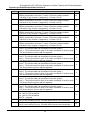
Table of Contents
1. General Description ............................................................................................................ 1
2. System Features ................................................................................................................. 3
3. SD Memory Card System Concept .................................................................................... 5
3.1 Read-Write Property ................................................................................................................... 5
3.2 Supply Voltage............................................................................................................................ 5
3.3 Card Capacity ............................................................................................................................. 5
3.3.1 User Area and Protected Area .............................................................................................. 5
3.3.2 Card Capacity Classification ................................................................................................. 5
3.4 Speed Class ............................................................................................................................... 5
3.5 Bus Topology .............................................................................................................................. 6
3.6 Bus Protocol ............................................................................................................................... 7
3.6.1 SD Bus Protocol ................................................................................................................... 7
3.6.2 SPI Bus Protocol ................................................................................................................ 10
3.6.3 UHS-II Bus Protocol ........................................................................................................... 10
3.7 SD Memory Card–Pins and Registers .......................................................................................11
3.7.1 SD Bus Pin Assignment.......................................................................................................11
3.7.2 UHS-II Pin Assignment ....................................................................................................... 13
3.8 ROM Card ................................................................................................................................ 14
3.8.1 Register Setting Requirements ........................................................................................... 14
3.8.2 Unsupported Commands.................................................................................................... 14
3.8.3 Optional Commands ........................................................................................................... 14
3.8.4 WP Switch .......................................................................................................................... 14
3.9 Ultra High Speed Phase I (UHS-I) Card .................................................................................... 15
3.9.1 UHS-I Card Operation Modes............................................................................................. 15
3.9.2 UHS-I Card Types .............................................................................................................. 15
3.9.3 UHS-I Host and Card Combination ..................................................................................... 16
3.9.4 UHS-I Bus Speed Modes Selection Sequence ................................................................... 17
3.9.5 UHS-I System Block Diagram............................................................................................. 18
3.9.6 Summary of Bus Speed Mode for UHS-I Card ................................................................... 19
3.10 Ultra High Speed Phase II (UHS-II) Card ................................................................................ 20
3.10.1 UHS-II Card Operation Modes .......................................................................................... 20
3.10.2 UHS-II Card Type ............................................................................................................. 20
3.10.3 UHS-II Host and Card Combination .................................................................................. 20
3.10.4 UHS-II Interface Selection Sequence ............................................................................... 21
3.10.5 Summary of Bus Speed Mode for UHS-II Card................................................................. 23
4. SD Memory Card Functional Description ....................................................................... 24
4.1 General..................................................................................................................................... 24
4.2 Card Identification Mode ........................................................................................................... 25
4.2.1 Card Reset ......................................................................................................................... 25
4.2.2 Operating Condition Validation ........................................................................................... 25
4.2.3 Card Initialization and Identification Process ...................................................................... 27
4.2.3.1 Initialization Command (ACMD41).......................................................................................... 29
4.2.4 Bus Signal Voltage Switch Sequence ................................................................................. 30
iv
©Copyright 2001-2013 SD Group (Panasonic, SanDisk, Toshiba) and SD Card Association
Physical Layer Simplified Specification Version 4.10
4.2.4.1 Initialization Sequence for UHS-I ............................................................................................ 30
4.2.4.2 Timing to Switch Signal Voltage .............................................................................................. 31
4.2.4.3 Timing of Voltage Switch Error Detection ............................................................................... 31
4.2.4.4 Voltage Switch Command ....................................................................................................... 31
4.2.4.5 Tuning Command .................................................................................................................... 31
4.2.4.6 An Example of UHS-I System Block Diagram ........................................................................ 32
4.3 Data Transfer Mode .................................................................................................................. 33
4.3.1 Wide Bus Selection/Deselection ......................................................................................... 35
4.3.2 2 GByte Card ..................................................................................................................... 35
4.3.3 Data Read .......................................................................................................................... 35
4.3.4 Data Write .......................................................................................................................... 36
4.3.5 Erase.................................................................................................................................. 38
4.3.6 Write Protect Management ................................................................................................. 38
4.3.7 Card Lock/Unlock Operation............................................................................................... 39
4.3.7.1 General .................................................................................................................................... 39
4.3.7.2 Parameter and the Result of CMD42 ...................................................................................... 41
4.3.7.3 Forcing Erase .......................................................................................................................... 43
4.3.7.3.1 Force Erase Function to the Locked Card ....................................................................... 43
4.3.7.4 Relation Between ACMD6 and Lock/Unlock State ................................................................. 44
4.3.7.5 Commands Accepted for Locked Card ................................................................................... 44
4.3.7.6 Two Types of Lock/Unlock Card.............................................................................................. 45
4.3.8 Content Protection.............................................................................................................. 45
4.3.9 Application-Specific Commands ......................................................................................... 46
4.3.9.1 Application-Specific Command – APP_CMD (CMD55) .......................................................... 46
4.3.9.2 General Command - GEN_CMD (CMD56)............................................................................. 46
4.3.10 Switch Function Command ............................................................................................... 47
4.3.10.1 General .................................................................................................................................. 47
4.3.10.2 Mode 0 Operation - Check Function ..................................................................................... 49
4.3.10.3 Mode 1 Operation - Set Function .......................................................................................... 49
4.3.10.4 Switch Function Status.......................................................................................................... 53
4.3.10.4.1 Busy Status Indication for Functions .............................................................................. 55
4.3.10.4.2 Data Structure Version ................................................................................................... 55
4.3.10.4.3 Function Table of Switch Command ............................................................................... 55
4.3.10.5 Relationship between CMD6 Data and Other Commands ................................................... 57
4.3.10.6 Switch Function Flow Example ............................................................................................. 57
4.3.10.7 Example of Checking ............................................................................................................ 57
4.3.10.8 Example of Switching ............................................................................................................ 57
4.3.11 High-Speed Mode (25 MB/sec interface speed) ................................................................ 58
4.3.12 Command System ............................................................................................................ 58
4.3.13 Send Interface Condition Command (CMD8) ................................................................... 59
4.3.14 Command Functional Difference in Card Capacity Types ................................................. 60
4.4 Clock Control ............................................................................................................................ 61
4.5 Cyclic Redundancy Code (CRC)............................................................................................... 62
4.6 Error Conditions........................................................................................................................ 64
4.6.1 CRC and Illegal Command ................................................................................................. 64
4.6.2 Read, Write and Erase Timeout Conditions ........................................................................ 64
4.6.2.1 Read ........................................................................................................................................ 64
4.6.2.2 Write ........................................................................................................................................ 64
4.6.2.3 Erase ....................................................................................................................................... 65
4.7 Commands ............................................................................................................................... 66
4.7.1 Command Types ................................................................................................................ 66
4.7.2 Command Format .............................................................................................................. 66
v
©Copyright 2001-2013 SD Group (Panasonic, SanDisk, Toshiba) and SD Card Association
Physical Layer Simplified Specification Version 4.10
4.7.3 Command Classes ............................................................................................................. 66
4.7.4 Detailed Command Description .......................................................................................... 69
4.7.5 Difference of SD Commands Definition in UHS-II ............................................................... 77
4.8 Card State Transition Table....................................................................................................... 78
4.9 Responses ............................................................................................................................... 80
4.9.1 R1 (normal response command): ....................................................................................... 80
4.9.2 R1b .................................................................................................................................... 80
4.9.3 R2 (CID, CSD register) ....................................................................................................... 80
4.9.4 R3 (OCR register) .............................................................................................................. 81
4.9.5 R6 (Published RCA response) ............................................................................................ 81
4.9.6 R7 (Card interface condition) .............................................................................................. 82
4.10 Two Status Information of SD Memory Card ........................................................................... 83
4.10.1 Card Status ...................................................................................................................... 83
4.10.2 SD Status ......................................................................................................................... 87
4.11 Memory Array Partitioning ....................................................................................................... 91
4.12 Timings ................................................................................................................................... 92
4.13 Speed Class Specification ...................................................................................................... 93
4.13.1 Speed Class Specification for SDSC and SDHC .............................................................. 93
4.13.1.1 Allocation Unit (AU) ............................................................................................................... 93
4.13.1.2 Recording Unit (RU) .............................................................................................................. 94
4.13.1.3 Write Performance ................................................................................................................ 94
4.13.1.4 Read Performance ................................................................................................................ 95
4.13.1.5 Performance Curve Definition ............................................................................................... 95
4.13.1.6 Speed Class Definition .......................................................................................................... 96
4.13.1.7 Consideration for Inserting FAT Update during Recording ................................................... 97
4.13.1.7.1 Measurement Condition to determine Average TFw ....................................................... 98
4.13.1.7.2 Maximum FAT Write Time .............................................................................................. 98
4.13.1.8 Measurement Conditions and Requirements of the Speed Class........................................ 98
4.13.1.8.1 Measurement Conditions................................................................................................ 98
4.13.1.8.2 Requirements of the Performance Parameters for Each Speed Class ......................... 98
4.13.1.8.3 Requirements of SD File System ................................................................................... 99
4.13.1.9 CMD20 Support..................................................................................................................... 99
4.13.2 Speed Class Specification for SDXC .............................................................................. 100
4.13.2.1 Speed Class Parameters .................................................................................................... 100
4.13.2.1.1 AU ................................................................................................................................. 100
4.13.2.1.2 RU ................................................................................................................................. 100
4.13.2.2 Write Performance .............................................................................................................. 100
4.13.2.2.1 Measurement of Pw...................................................................................................... 100
4.13.2.2.2 Performance Move ....................................................................................................... 101
4.13.2.3 Read Performance .............................................................................................................. 101
4.13.2.4 FAT Update.......................................................................................................................... 101
4.13.2.5 CI (Continuous Information) Update ................................................................................... 101
4.13.2.6 Distinction of Data Type ...................................................................................................... 102
4.13.2.7 Measurement Conditions and Requirements of the Speed Class for SDXC ..................... 102
4.13.2.7.1 Measurement Conditions.............................................................................................. 102
4.13.2.7.2 Requirements of the Performance Parameters for Each Speed Class ....................... 103
4.13.2.7.3 Requirements of SD File System ................................................................................. 103
4.13.2.8 Speed Class Control Command (CMD20).......................................................................... 103
4.13.2.8.1 Definition of Each Function .......................................................................................... 104
4.13.2.8.2 Requirements for Speed Class Host ............................................................................ 104
4.13.2.9 Example of Speed Class Recording Sequence .................................................................. 104
4.13.3 Speed Grade Specification for UHS-I and UHS-II ........................................................... 106
vi
©Copyright 2001-2013 SD Group (Panasonic, SanDisk, Toshiba) and SD Card Association
Physical Layer Simplified Specification Version 4.10
4.13.3.1 Speed Grade Parameters ................................................................................................... 106
4.13.3.1.1 UHS Speed Grade........................................................................................................ 106
4.13.3.1.2 AU (Allocation Unit) ...................................................................................................... 106
4.13.3.1.3 RU (Recording Unit) ..................................................................................................... 106
4.13.3.1.4 Pw (Write Performance) ............................................................................................... 106
4.13.3.1.5 Pm (Performance Move) .............................................................................................. 106
4.13.3.1.6 Pr and TFR(4KB) (Read Performance).......................................................................... 106
4.13.3.1.7 UHS-II Parameters ....................................................................................................... 106
4.13.3.2 Support of Speed Class Control Command (CMD20) ........................................................ 106
4.13.3.3 Speed Grade Measurement Conditions ............................................................................. 107
4.13.3.4 Notes for Preparation Time of UHS-I and UHS-II Card ...................................................... 107
4.13.3.5 Host Operating Frequency .................................................................................................. 107
4.14 Erase Timeout Calculation .................................................................................................... 108
4.14.1 Erase Unit ...................................................................................................................... 108
4.14.2 Case Analysis of Erase Time Characteristics .................................................................. 108
4.14.3 Method for Erase Large Areas ........................................................................................ 109
4.14.4 Calculation of Erase Timeout Value Using the Parameter Registers ............................... 109
4.15 Set Block Count Command.................................................................................................... 110
5. Card Registers ................................................................................................................ 111
5.1 OCR register............................................................................................................................ 111
5.2 CID register .............................................................................................................................113
5.3 CSD Register...........................................................................................................................114
5.3.1 CSD_STRUCTURE ........................................................................................................... 114
5.3.2 CSD Register (CSD Version 1.0) ....................................................................................... 115
5.3.3 CSD Register (CSD Version 2.0) ...................................................................................... 122
5.4 RCA register ........................................................................................................................... 125
5.5 DSR register (Optional) .......................................................................................................... 125
5.6 SCR register ........................................................................................................................... 125
5.7 Function Extension Specification ............................................................................................ 129
5.7.1 Extension Register Space ................................................................................................ 129
5.7.2 Extension Register Commands ........................................................................................ 130
5.7.2.1 Extension Register Read Command (Single Block) ............................................................. 130
5.7.2.2 Extension Register Write Command (Single Block) ............................................................. 132
5.7.2.3 Multiple Block Data Transfer ................................................................................................. 134
5.7.2.4 Extension Register Read Command (Multi-Block) ............................................................... 135
5.7.2.5 Extension Register Write Command (Multi-Block)................................................................ 136
5.7.2.6 Error Status Indication........................................................................................................... 137
5.7.3 General Information .......................................................................................................... 138
5.7.3.1 Common Header Fields ........................................................................................................ 139
5.7.3.1.1 Structure Revision (2-byte) ............................................................................................. 139
5.7.3.1.2 General Information Length (2-byte) .............................................................................. 139
5.7.3.1.3 Number of Extensions (1-byte)....................................................................................... 139
5.7.3.2 Function Fields per Function ................................................................................................. 139
5.7.3.2.1 Standard Function Code (SFC 2-byte) ........................................................................... 139
5.7.3.2.2 Function Capability Code (FCC 2-byte) ......................................................................... 140
5.7.3.2.3 Function Manufacturer Code (FMC 2-byte) ................................................................... 140
5.7.3.2.4 Function Manufacturer Name (FMN 16-byte) ................................................................ 140
5.7.3.2.5 Particular Function Code (PFC 2-byte) .......................................................................... 140
5.7.3.2.6 Function Name (FN 16-byte) .......................................................................................... 140
5.7.3.2.7 Pointer to Next Extension (2-byte) ................................................................................. 140
5.7.3.2.8 Number of Register Sets (1-byte)................................................................................... 140
vii
©Copyright 2001-2013 SD Group (Panasonic, SanDisk, Toshiba) and SD Card Association
Physical Layer Simplified Specification Version 4.10
5.7.3.2.9 Extension Register Set Address (4-byte for each) ......................................................... 140
5.7.4 Revision Management ...................................................................................................... 141
5.8 Application Specification on Function Extension ..................................................................... 142
5.8.1 Power Management Function ........................................................................................... 142
5.8.1.1 Abstract of Power Management Function ............................................................................. 142
(1)
Features of Power Off Notification ......................................................................................... 142
(2)
Features of Power Sustenance .............................................................................................. 142
(3)
Features of Power Down Mode .............................................................................................. 142
5.8.1.2 Extension Register Set for Power Management ................................................................... 142
5.8.1.3 Power Off Notification............................................................................................................ 144
5.8.1.4 Power Sustenance ................................................................................................................ 145
5.8.1.5 Power Down Mode ................................................................................................................ 146
5.8.1.6 General Information of Power Management Function .......................................................... 147
6. SD Memory Card Hardware Interface ............................................................................ 148
6.1 Hot Insertion and Removal ..................................................................................................... 148
6.2 Card Detection (Insertion/Removal) ........................................................................................ 148
6.3 Power Protection (Insertion/Removal)..................................................................................... 148
6.4 Power Scheme ....................................................................................................................... 149
6.4.1 Power Up Sequence for SD Bus Interface ........................................................................ 149
6.4.1.1 Power Up Time of Card ......................................................................................................... 149
6.4.1.2 Power Up Time of Host ......................................................................................................... 150
6.4.1.3 Power On or Power Cycle ..................................................................................................... 150
6.4.1.4 Power Supply Ramp Up ........................................................................................................ 150
6.4.1.5 Power Down and Power Cycle ............................................................................................. 150
6.4.2 Power Up Sequence for UHS-II Interface ......................................................................... 151
6.4.2.1 Power Up Sequence of UHS-II Card .................................................................................... 151
6.4.2.2 Power Up Sequence of UHS-II Host ..................................................................................... 151
6.5 Programmable Card Output Driver (3.3V Single End) (Optional) ............................................ 152
6.6 Bus Operating Conditions for 3.3V Signaling .......................................................................... 152
6.7 Driver Strength and Bus Timing for 1.8V Signaling ................................................................. 152
6.8 Electrical Static Discharge (ESD) Requirement ...................................................................... 152
7. SPI Mode.......................................................................................................................... 153
7.1 Introduction ............................................................................................................................. 153
7.2 SPI Bus Protocol .................................................................................................................... 153
7.2.1 Mode Selection and Initialization ...................................................................................... 154
7.2.2 Bus Transfer Protection .................................................................................................... 156
7.2.3 Data Read ........................................................................................................................ 156
7.2.4 Data Write ........................................................................................................................ 157
7.2.5 Erase & Write Protect Management ................................................................................. 158
7.2.6 Read CID/CSD Registers ................................................................................................. 159
7.2.7 Reset Sequence ............................................................................................................... 159
7.2.8 Error Conditions ............................................................................................................... 159
7.2.9 Memory Array Partitioning ................................................................................................ 159
7.2.10 Card Lock/Unlock ........................................................................................................... 159
7.2.11 Application Specific Commands ...................................................................................... 159
7.2.12 Content Protection Command ........................................................................................ 160
7.2.13 Switch Function Command ............................................................................................. 160
7.2.14 High Speed Mode ........................................................................................................... 160
7.2.15 Speed Class Specification .............................................................................................. 160
viii
©Copyright 2001-2013 SD Group (Panasonic, SanDisk, Toshiba) and SD Card Association
Physical Layer Simplified Specification Version 4.10
7.3 SPI Mode Transaction Packets ............................................................................................... 161
7.3.1 Command Tokens ............................................................................................................ 161
7.3.1.1 Command Format ................................................................................................................. 161
7.3.1.2 Command Classes ................................................................................................................ 161
7.3.1.3 Detailed Command Description ............................................................................................ 163
7.3.1.4 Card Operation for CMD8 in SPI mode ................................................................................ 168
7.3.2 Responses ....................................................................................................................... 169
7.3.2.1 Format R1.............................................................................................................................. 169
7.3.2.2 Format R1b ........................................................................................................................... 169
7.3.2.3 Format R2.............................................................................................................................. 170
7.3.2.4 Format R3.............................................................................................................................. 171
7.3.2.5 Formats R4 & R5................................................................................................................... 171
7.3.2.6 Format R7.............................................................................................................................. 171
7.3.3 Control Tokens ................................................................................................................. 172
7.3.3.1 Data Response Token ........................................................................................................... 172
7.3.3.2 Start Block Tokens and Stop Tran Token .............................................................................. 172
7.3.3.3 Data Error Token ................................................................................................................... 173
7.3.4 Clearing Status Bits .......................................................................................................... 173
7.4 Card Registers........................................................................................................................ 174
7.5 SPI Bus Timing Diagrams ....................................................................................................... 175
7.6 SPI Electrical Interface ........................................................................................................... 175
7.7 SPI Bus Operating Conditions ................................................................................................ 175
7.8 Bus Timing .............................................................................................................................. 175
8. Sections Effective to SD I/F Mode and UHS-II Mode .................................................... 176
Appendix A (Normative) : Reference ................................................................................. 179
A.1 Related Documentation .......................................................................................................... 179
Appendix B (Normative) : Special Terms .......................................................................... 180
B.1 Terminology ............................................................................................................................ 180
B.2 Abbreviations.......................................................................................................................... 180
Appendix C (Informative) : Examples for Fixed Delay UHS-I Host Design .................... 183
Appendix D : UHS-I Tuning Procedure.............................................................................. 184
Appendix E : Host Power Delivery Network (PDN) Design Guide .................................. 185
Appendix F : Application Notes of Extension Function ................................................. 186
F.1 Identification of Function Driver ............................................................................................... 186
ix
©Copyright 2001-2013 SD Group (Panasonic, SanDisk, Toshiba) and SD Card Association
Physical Layer Simplified Specification Version 4.10
Table of Figures
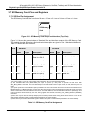
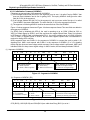
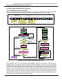
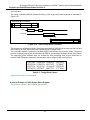
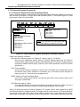
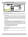
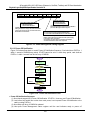
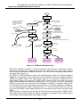
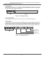
Figure 1-1: SD Specifications Documentation Structure ................................................................................. 1
Figure 3-1: A Blank in the Simplified Specification........................................................................................... 6
Figure 3-2: A Blank in the Simplified Specification........................................................................................... 6
Figure 3-3 : A Blank in the Simplified Specification.......................................................................................... 6
Figure 3-4: "no response" and "no data" Operations ....................................................................................... 7
Figure 3-5: (Multiple) Block Read Operation.................................................................................................... 7
Figure 3-6: (Multiple) Block Write Operation .................................................................................................... 8
Figure 3-7: Command Token Format ............................................................................................................... 8
Figure 3-8: Response Token Format................................................................................................................ 8
Figure 3-9: Data Packet Format - Usual Data.................................................................................................. 9
Figure 3-10: Data Packet Format - Wide Width Data .................................................................................... 10
Figure 3-11: SD Memory Card Shape and Interface (Top View) ................................................................... 11
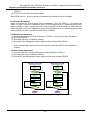
Figure 3-12: SD Memory Card Architecture ................................................................................................... 12
Figure 3-13 : UHS-II Card Shape and Interface (Top View) .......................................................................... 13
Figure 3-14 : UHS-I Card Type Modes of Operation versus Frequency Range............................................ 15
Figure 3-15 : UHS-I Card Type Modes of Operation versus Throughput ...................................................... 16
Figure 3-16 : Command Sequence to Use UHS-I ......................................................................................... 17
Figure 3-17 : A Blank in the Simplified Specification...................................................................................... 18
Figure 3-18 : Throughput of UHS156 UHS-II Card ........................................................................................ 20
Figure 3-19 : UHS-II Interface Detection........................................................................................................ 21
Figure 3-20 : UHS-II Interface Initialization .................................................................................................... 22
Figure 3-21 : UHS-II Interface Deactivation ................................................................................................... 22
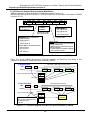
Figure 4-1: SD Memory Card State Diagram (card identification mode) ....................................................... 26
Figure 4-2: Card Initialization and Identification Flow (SD mode) ................................................................. 28
Figure 4-3 : Argument of ACMD41 ................................................................................................................. 29
Figure 4-4 : Response of ACMD41 ................................................................................................................ 29
Figure 4-5 : ACMD41 Timing Followed by Voltage Switch Sequence ........................................................... 30
Figure 4-6 : UHS-I Host Initialization Flow Chart ........................................................................................... 30
Figure 4-7 : A Blank in the Simplified Specification........................................................................................ 31
Figure 4-8 : A Blank in the Simplified Specification........................................................................................ 31
Figure 4-9 : Voltage Switch Command .......................................................................................................... 31
Figure 4-10 : Send Tuning Block Command .................................................................................................. 32
Figure 4-11 : Tuning Block on DAT[3:0] ......................................................................................................... 32
Figure 4-12 : A Blank in the Simplified Specification..................................................................................... 32
Figure 4-13: SD Memory Card State Diagram (data transfer mode) ............................................................. 33
Figure 4-14: Use of Switch Command ........................................................................................................... 48
Figure 4-15: Busy Status of 'Command System' ........................................................................................... 55
Figure 4-16: A Blank in the Simplified Specification....................................................................................... 57
Figure 4-17: A Blank in the Simplified Specification....................................................................................... 57
Figure 4-18: A Blank in the Simplified Specification....................................................................................... 57
Figure 4-19: A Blank in the Simplified Specification....................................................................................... 57
Figure 4-20: CRC7 Generator/Checker ......................................................................................................... 62
Figure 4-21: CRC16 Generator/Checker ....................................................................................................... 63
Figure 4-22: A Blank in the Simplified Specification....................................................................................... 91
Figure 4-23: A Blank in the Simplified Specification....................................................................................... 92
Figure 4-24: A Blank in the Simplified Specification....................................................................................... 92
Figure 4-25: A Blank in the Simplified Specification....................................................................................... 92
Figure 4-26: A Blank in the Simplified Specification....................................................................................... 92
Figure 4-27: A Blank in the Simplified Specification....................................................................................... 92
Figure 4-28: A Blank in the Simplified Specification....................................................................................... 92
x
©Copyright 2001-2013 SD Group (Panasonic, SanDisk, Toshiba) and SD Card Association
Physical Layer Simplified Specification Version 4.10
Figure 4-29: A Blank in the Simplified Specification....................................................................................... 92
Figure 4-30 : A Blank in the Simplified Specification...................................................................................... 92
Figure 4-31: A Blank in the Simplified Specification....................................................................................... 92
Figure 4-32: A Blank in the Simplified Specification....................................................................................... 92
Figure 4-33: A Blank in the Simplified Specification....................................................................................... 92
Figure 4-34: A Blank in the Simplified Specification....................................................................................... 92
Figure 4-35: A Blank in the Simplified Specification....................................................................................... 92
Figure 4-36: A Blank in the Simplified Specification....................................................................................... 92
Figure 4-37 : A Blank in the Simplified Specification...................................................................................... 92
Figure 4-38 : A Blank in the Simplified Specification...................................................................................... 92
Figure 4-39 : A Blank in the Simplified Specification...................................................................................... 92
Figure 4-40 : A Blank in the Simplified Specification...................................................................................... 92
Figure 4-41 : A Blank in the Simplified Specification...................................................................................... 92
Figure 4-42 : A Blank in the Simplified Specification...................................................................................... 92
Figure 4-43 : A Blank in the Simplified Specification...................................................................................... 92
Figure 4-44 : A Blank in the Simplified Specification...................................................................................... 92
Figure 4-45 : Timing of Single Block Read Command in DDR50 Mode ........................................................ 92
Figure 4-46: Overview of Speed Class Specification..................................................................................... 93
Figure 4-47: Definition of Allocation Unit (AU) ............................................................................................... 93
Figure 4-48 : Example of Writing Fragmented AU ......................................................................................... 94
Figure 4-49: Card Performances between 16 RUs........................................................................................ 95
Figure 4-50: Three Performance Curves ....................................................................................................... 97
Figure 4-51: Typical Sequence of FAT Update .............................................................................................. 97
Figure 4-52 : Measurement of Pw (AU size is larger than 4MB) ................................................................. 101
Figure 4-53 : Definition of CMD20................................................................................................................ 103
Figure 4-54 : Definition of CMD20................................................................................................................ 103
Figure 4-55 : Example of Speed Class Recording....................................................................................... 105
Figure 4-56: Example Erase Characteristics (Case 1 TOFFSET=0) ........................................................... 108
Figure 4-57: Example Erase Characteristics (Case 2 TOFFSET=2) ........................................................... 109
Figure 4-58 : Set Block Count Command .................................................................................................... 110
Figure 5-1: ERASE_BLK_EN = 0 Example ................................................................................................. 119
Figure 5-2: ERASE_BLK_EN = 1 Example ................................................................................................. 119
Figure 5-3 : Extension Register Space ........................................................................................................ 129
Figure 5-4 : Read Extension Register Single Block Command (CMD48) ................................................... 130
Figure 5-5 : Extension Register Read Operation by CMD48....................................................................... 131
Figure 5-6 : Data Port Read Operation by CMD48 ...................................................................................... 131
Figure 5-7 : Write Extension Register Single Block Command (CMD49) ................................................... 132
Figure 5-8 : Extension Register Write Operation by CMD49 ....................................................................... 133
Figure 5-9 : Data Port Write Operation by CMD49 ...................................................................................... 134
Figure 5-10 : Read Extension Register Multi-Block Command (CMD58) ................................................... 135
Figure 5-11 : Extension Register and Data Port Read Operation by CMD58 ............................................. 135
Figure 5-12 : Write Extension Register Multi-Block Command (CMD59).................................................... 136
Figure 5-13 : Extension Register and Data Port Write Operation by CMD59 ............................................. 136
Figure 5-14 : General Information for Memory ............................................................................................ 138
Figure 5-15 : Data Structure of General Information ................................................................................... 139
Figure 5-16 : Power Management Revision Register .................................................................................. 143
Figure 5-17 : Power Management Status Register...................................................................................... 143
Figure 5-18 : Power Management Setting Register..................................................................................... 144
Figure 5-19 : Power Off Notification Flow .................................................................................................... 144
Figure 5-20 : Power Sustenance Enabling / Disabling Sequence Flow ...................................................... 145
Figure 5-21 : Power Down Mode Entering / Exiting Sequence Flow........................................................... 147
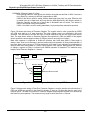
Figure 6-1: Bus Circuitry Diagram ................................................................................................................ 148
Figure 6-2: A Blank in the Simplified Specification....................................................................................... 148
xi
©Copyright 2001-2013 SD Group (Panasonic, SanDisk, Toshiba) and SD Card Association
Physical Layer Simplified Specification Version 4.10
Figure 6-3: A Blank in the Simplified Specification....................................................................................... 148
Figure 6-4: Power-up Diagram of Card ........................................................................................................ 149
Figure 6-5 : Power Up Diagram of Host ...................................................................................................... 150
Figure 6-6 : Power Up Sequence of UHS-II Device..................................................................................... 151
Figure 6-7 : Power Up Sequence of UHS-II Host ........................................................................................ 151
Figure 7-2: SPI Mode Initialization Flow ...................................................................................................... 155
Figure 7-3: Single Block Read Operation .................................................................................................... 156
Figure 7-4: Read Operation - Data Error ..................................................................................................... 157
Figure 7-5: Multiple Block Read Operation .................................................................................................. 157
Figure 7-6: Single Block Write Operation ..................................................................................................... 157
Figure 7-7: Multiple Block Write Operation .................................................................................................. 158
Figure 7-8: 'No data' Operations .................................................................................................................. 158
Figure 7-9: R1 Response Format................................................................................................................. 169
Figure 7-10: R2 Response Format............................................................................................................... 170
Figure 7-11: R3 Response Format ............................................................................................................... 171
Figure 7-12: R7 Response Format............................................................................................................... 171
Figure 7-13: Data Error Token ...................................................................................................................... 173
xii
©Copyright 2001-2013 SD Group (Panasonic, SanDisk, Toshiba) and SD Card Association
Physical Layer Simplified Specification Version 4.10
Table of Tables
Table 3-1: SD Memory Card Pad Assignment ............................................................................................... 11
Table 3-2: SD Memory Card Registers .......................................................................................................... 12
Table 3-3 : UHS-II Interface Pad Assignment ................................................................................................ 13
Table 3-4 : Register Setting Requirements for ROM Card ............................................................................ 14
Table 3-5 : UHS-I Host and Card Combinations ............................................................................................ 16
Table 3-6 : Bus Speed Modes of UHS-I Card ................................................................................................ 19
Table 3-7 : Bus Speed Mode Option / Mandatory .......................................................................................... 19
Table 3-8 : UHS-II Host and Card Combinations ........................................................................................... 20
Table 3-9 : Bus Speed Modes of UHS-II Card ............................................................................................... 23
Table 3-10 : Bus Speed Mode Option / Mandatory ........................................................................................ 23
Table 4-1: Overview of Card States vs. Operation Modes............................................................................. 24
Table 4-2 : A Blank in the Simplified Specification ......................................................................................... 31
Table 4-3 : Tuning Block Pattern .................................................................................................................... 32
Table 4-4: Read Command Blocklen ............................................................................................................. 36
Table 4-5: Write Command Blocklen .............................................................................................................. 36
Table 4-6: Lock Card Data Structure .............................................................................................................. 39
Table 4-7: Lock Unlock Function (Basic Sequence for CMD42).................................................................... 42
Table 4-8: Force Erase Function to the Locked Card (Relation to the Write Protects) ................................. 43
Table 4-9: Relation between ACMD6 and the Lock/Unlock State.................................................................. 44
Table 4-10: Version Difference of Lock/Unlock Functions ............................................................................. 45
Table 4-11: Available Functions of CMD6 ...................................................................................................... 50
Table 4-12 : Power Limit and Current Limit of VDD1 and VDD2 ................................................................... 51
Table 4-13: Status Data Structure .................................................................................................................. 55
Table 4-14: Data Structure Version ................................................................................................................ 55
Table 4-15: Status Code of Mode 0 to Supported Function Group ............................................................... 56
Table 4-16: Status Code of Mode 1 to Supported Function Group ............................................................... 56
Table 4-17: Status Code of Mode 0 and 1 to Unsupported Function Group ................................................. 56
Table 4-18: Format of CMD8 .......................................................................................................................... 59
Table 4-19: A Blank in the Simplified Specification ........................................................................................ 59
Table 4-20: Command Format ....................................................................................................................... 66
Table 4-21: Card Command Classes (CCCs) in SD Mode ............................................................................ 68
Table 4-22: Basic Commands (class 0) ......................................................................................................... 70
Table 4-23: Block-Oriented Read Commands (class 2)................................................................................. 71
Table 4-24: Block-Oriented Write Commands (class 4) ................................................................................. 71
Table 4-25: Block Oriented Write Protection Commands (class 6)................................................................ 72
Table 4-26: Erase Commands (class 5) ......................................................................................................... 72
Table 4-27: Lock Card (class 7) ..................................................................................................................... 73
Table 4-28: Application-Specific Commands (class 8) ................................................................................... 73
Table 4-29: I/O Mode Commands (class 9) ................................................................................................... 73
Table 4-30: Application Specific Commands used/reserved by SD Memory Card........................................ 75
Table 4-31: Switch Function Commands (class 10)....................................................................................... 76
Table 4-32: Function Extension Commands (class 11).................................................................................. 76
Table 4-33 : Difference of SD Commands Definition in UHS-II ..................................................................... 77
Table 4-34: Card State Transition Table ......................................................................................................... 79
Table 4-35: Response R1 ............................................................................................................................... 80
Table 4-36: Response R2 ............................................................................................................................... 80
Table 4-37: Response R3 ............................................................................................................................... 81
Table 4-38: Response R6 ............................................................................................................................... 81
Table 4-39: Response R7 ............................................................................................................................... 82
Table 4-40: Voltage Accepted in R7 ............................................................................................................... 82
Table 4-41: Card Status.................................................................................................................................. 85
xiii
©Copyright 2001-2013 SD Group (Panasonic, SanDisk, Toshiba) and SD Card Association
Physical Layer Simplified Specification Version 4.10
Table 4-42: Card Status Field/Command - Cross Reference ........................................................................ 86
Table 4-43: SD Status ................................................................................................................................... 87
Table 4-44: Speed Class Code Field ............................................................................................................. 88
Table 4-45: Performance Move Field ............................................................................................................. 88
Table 4-46: AU_SIZE Field ............................................................................................................................. 89
Table 4-47: Maximum AU size........................................................................................................................ 89
Table 4-48: Erase Size Field .......................................................................................................................... 89
Table 4-49: Erase Timeout Field .................................................................................................................... 90
Table 4-50: Erase Offset Field ........................................................................................................................ 90
Table 4-51: UHS_ SPEED_GRADE Field ...................................................................................................... 91
Table 4-52: UHS_AU_SIZE Field ................................................................................................................... 91
Table 4-53: A Blank in the Simplified Specification ........................................................................................ 92
Table 4-54: A Blank in the Simplified Specification ........................................................................................ 92
Table 4-55 : A Blank in the Simplified Specification ....................................................................................... 92
Table 4-56: Measurement Condition of Speed Class (SDSC and SDHC) .................................................... 98
Table 4-57: Performance Requirements for Each Class (SDSC and SDHC) ............................................... 99
Table 4-58 : Measurement Conditions of Speed Class (SDXC) .................................................................. 102
Table 4-59 : Performance Requirements for Each Class (SDXC) ............................................................... 103
Table 4-60 : Speed Grade Measurement Conditions for UHS-I and UHS-II ............................................... 107
Table 5-1: OCR Register Definition .............................................................................................................. 112
Table 5-2: The CID Fields............................................................................................................................. 113
Table 5-3: CSD Register Structure ............................................................................................................... 114
Table 5-4: The CSD Register Fields (CSD Version 1.0) .............................................................................. 115
Table 5-5: TAAC Access Time Definition ...................................................................................................... 116
Table 5-6: Maximum Data Transfer Rate Definition ..................................................................................... 116
Table 5-7: Supported Card Command Classes ........................................................................................... 117
Table 5-8: Data Block Length ....................................................................................................................... 117
Table 5-9: DSR Implementation Code Table ................................................................................................ 118
Table 5-10: VDD, min Current Consumption................................................................................................ 118
Table 5-11: VDD, max Current Consumption ............................................................................................... 118
Table 5-12: Multiply Factor for the Device Size ........................................................................................... 119
Table 5-13: R2W_FACTOR .......................................................................................................................... 120
Table 5-14: Data Block Length ..................................................................................................................... 120
Table 5-15: File Formats............................................................................................................................... 121
Table 5-16: The CSD Register Fields (CSD Version 2.0) ............................................................................ 122
Table 5-17: The SCR Fields ......................................................................................................................... 125
Table 5-18: SCR Register Structure Version................................................................................................ 125
Table 5-19: Physical Layer Specification Version ........................................................................................ 126
Table 5-20: CPRM Security Version ............................................................................................................. 127
Table 5-21: SD Memory Card Supported Bus Widths ................................................................................. 128
Table 5-22 : Extended Security .................................................................................................................... 128
Table 5-23 : Command Support Bits ............................................................................................................ 128
Table 5-24 : Field Definition of Extension Register Set Address ................................................................. 141
Table 5-25 : Standard Function Code Assignment Table ............................................................................. 142
Table 5-26 : Power Management Register Set ............................................................................................ 142
Table 5-27 : General Information of Power Management Function ............................................................. 147
Table 7-1: Command Format ....................................................................................................................... 161
Table 7-2: Command Classes in SPI Mode ................................................................................................. 162
Table 7-3: Commands and Arguments......................................................................................................... 166
Table 7-4: Application Specific Commands used/reserved by SD Memory Card - SPI Mode .................... 167
Table 7-5: Card Operation for CMD8 in SPI Mode ...................................................................................... 168
Table 7-6: SPI Mode Status Bits .................................................................................................................. 174
xiv
©Copyright 2001-2013 SD Group (Panasonic, SanDisk, Toshiba) and SD Card Association
Physical Layer Simplified Specification Version 4.10
Table F - 1 : Combination of Codes to Identify a Function Driver ................................................................ 186
xv
©Copyright 2001-2013 SD Group (Panasonic, SanDisk, Toshiba) and SD Card Association
Physical Layer Simplified Specification Version 4.10
1. General Description
SD Memory Card is a memory card that is specifically designed to meet the security, capacity,
performance, and environment requirements inherent in newly emerging audio and video consumer
electronic devices. The SD Memory Card will include a content protection mechanism that complies
with the security of the SDMI standard and will be faster and capable of higher Memory capacity. The
SD Memory Card security system uses mutual authentication and a "new cipher algorithm" to protect
against illegal usage of the card content. A Non-secure access to the user's own content is also
available.
SD memory cards may also support a second security system based on commonly used standards,
such as ISO-7816, which can be used to interface the SD memory card into public networks and other
systems supporting mobile e-commerce and digital signature applications.
In addition to the SD Memory Card, there is the SD I/O (SDIO) Card. The SDIO Card specification is
defined in a separate specification named: "SDIO Card Specification" that can be obtained from the SD
Association. The SDIO Specification defines an SD card that may contain interfaces between various
I/O units and an SD Host. The SDIO card may contain memory storage capability as well as its I/O
functionality. The Memory portion of SDIO card shall be fully compatible to the given Physical Layer
Specification. The SDIO card is based on and compatible with the SD Memory card. This compatibility
includes mechanical, electrical, power, signalling, and software. The intent of the SD I/O card is to
provide high-speed data I/O with low power consumption for mobile electronic devices. A primary goal
is that an I/O card inserted into a non-SDIO aware host will cause no physical damage or disruption of
that device or its software. In this case, the I/O card should simply be ignored. Once inserted into an
SDIO aware host, the detection of the card will be via the normal means described in the given Physical
Layer Specification with some extensions that are described in the SDIO Specification.
The SD Memory Card communication is based on an advanced 9-pin interface (Clock, Command,
4xData and 3xPower lines) designed to operate in at maximum operating frequency of 50 MHz and low
voltage range. The communication protocol is defined as a part of this specification.
The SD Specifications are divided into several documents. The SD Specifications documentation
structure is given in Figure 1-1.
Application Specifications
Part 4 Audio
Part 8 Video
Other Applications
Part 2 File System
Part 3 Security
Part 1 Physical Layer
UHS-II Addendum
Mechanical Addenda
eSD Addendum (Embedded)
Part A1
Advanced
Security SD
Extension
Part E1 SDIO
Figure 1-1: SD Specifications Documentation Structure
• Audio Specification:
This specification, along with other application specifications, describes the specification of a specific
application (in this case - Audio Application) and the requirements to implement it.
• File System Specification:
The specification describes the specification of the file format structure of the data saved in the SD
Memory Card (in User Area and Protected Area).
1
©Copyright 2001-2013 SD Group (Panasonic, SanDisk, Toshiba) and SD Card Association
Physical Layer Simplified Specification Version 4.10
• Security Specification:
The specification describes the content protection mechanism and the application-specific commands
that support it.
• Physical Layer Specification (this document):
The specification describes the physical interface and the command protocol used by the SD Memory
Card. The purpose of the Physical Layer specification is to define the SD Memory Card, its
environment, and handling.
The document is divided into several portions. Chapter 3 gives a general overview of the system
concepts. The common SD Memory Card characteristics are described in Chapter 4. As this description
defines an overall set of card properties, we recommend using the product documentation in parallel.
The card registers are described in Chapter 5.
Chapter 6 defines the electrical parameters of the SD Memory Card's hardware interface.
Mechanical Specification described in Chapter 8 in Version 2.00 is moved to the Standard Size
Mechanical Addendum.
There are three mechanical addenda depend on form factors.
(1) Standard Size Mechanical Addendum
(2) miniSD Mechanical Addendum
(3) microSD Mechanical Addendum
UHS-II Interface Specification is defined by the UHS-II Addendum.
Un-removable memory device for embedded application is defined by the eSD Addendum.
As used in this document, "shall" or "will" denote a mandatory provision of the standard. "Should"
denotes a provision that is recommended but is not mandatory. "May" denotes a feature, which may or
may not be present–at the option of the implementer–and whose presence does not preclude
compliance.
• Mc-EX Interface Specification: (This section was added in version 1.10)
Part A1 of the SD memory card specification (Refer to Figure 1-1) serves as an extension to the SD
card Physical Layer Specification and provides all of the definitions required to transfer the Mobile
Commerce Extension (Mc-EX) command packets from the Mc-EX host to the Mc-EX enabled SD
memory card, and vice versa.
• SDIO Specification
SDIO card and embedded SDIO are specified based on the Physical Layer Specification and
modifications and extensions are described in the Part E1 SDIO Specification.
2
©Copyright 2001-2013 SD Group (Panasonic, SanDisk, Toshiba) and SD Card Association
Physical Layer Simplified Specification Version 4.10
2. System Features
• Targeted for portable and stationary applications
• Capacity of Memory
(1) Standard Capacity SD Memory Card (SDSC): Up to and including 2 GB
(2) High Capacity SD Memory Card (SDHC): More than 2GB and up to and including 32GB
(3) Extended Capacity SD Memory Card (SDXC): More than 32GB and up to and including 2TB
• Voltage range:
High Voltage SD Memory Card – Operating voltage range: 2.7-3.6 V
UHS-II SD Memory Card – Operating voltage range VDD1: 2.7-3.6 V, VDD2: 1.70-1.95V
• Designed for read-only and read/write cards.
• Bus Speed Mode (using 4 parallel data lines)
(1) Default Speed mode: 3.3V signaling, Frequency up to 25 MHz, up to 12.5 MB/sec
(2) High Speed mode: 3.3V signaling, Frequency up to 50 MHz, up to 25 MB/sec
(3) SDR12: UHS-I 1.8V signaling, Frequency up to 25 MHz, up to 12.5MB/sec
(4) SDR25: UHS-I 1.8V signaling, Frequency up to 50 MHz, up to 25MB/sec
(5) SDR50: UHS-I 1.8V signaling, Frequency up to 100 MHz, up to 50MB/sec
(6) SDR104: UHS-I 1.8V signaling, Frequency up to 208 MHz, up to 104MB/sec
(7) DDR50: UHS-I 1.8V signaling, Frequency up to 50 MHz, sampled on both clock edges, up to
50MB/sec
(8) UHS156: UHS-II RCLK Frequency Range 26MHz - 52MHz, up to 1.56Gbps per lane.
• Switch function command supports Bus Speed Mode, Command System, Drive Strength, and
future functions
• Correction of memory field errors
• Card removal during read operation will never harm the content
• Content Protection Mechanism - Complies with highest security of SDMI standard.
• Password Protection of cards (CMD42 - LOCK_UNLOCK)
• Write Protect feature using mechanical switch
• Built-in write protection features (permanent and temporary)
• Card Detection (Insertion/Removal)
• Application specific commands
• Comfortable erase mechanism
3
©Copyright 2001-2013 SD Group (Panasonic, SanDisk, Toshiba) and SD Card Association
Physical Layer Simplified Specification Version 4.10
• Protocol attributes of the communication channel:
SD Memory Card Communication Channel
Six-wire communication channel
(clock, command, 4 data lines)
Error-protected data transfer
Single or Multiple block oriented data transfer
• SD Memory Card Form-factor
There are three Part 1 mechanical addenda as follows:
Standard Size SD Memory Card: Specified in "Part 1 Standard Size SD Card Addendum"
miniSD Memory Card: Specified in "Part 1 miniSD Card Addendum"
microSD Memory Card: Specified in "Part 1 microSD Card Addendum"
• Standard Size SD Memory Card thickness is defined as both 2.1 mm (normal) and 1.4 mm (Thin
SD Memory Card).
4
©Copyright 2001-2013 SD Group (Panasonic, SanDisk, Toshiba) and SD Card Association
Physical Layer Simplified Specification Version 4.10
3. SD Memory Card System Concept
Description here is a blank in the Simplified Specification.
3.1 Read-Write Property
In terms of read-write property, two types of SD Memory Cards are defined:
• Read/Write (RW) cards (Flash, One Time Programmable - OTP, Multiple Time Programmable - MTP).
These cards are typically sold as blank (empty) media and are used for mass data storage, end user
video, audio or digital image recording
• Read Only Memory (ROM) cards. These cards are manufactured with fixed data content. They are
typically used as a distribution media for software, audio, video etc.
3.2 Supply Voltage
In terms of operating supply voltage, two types of SD Memory Cards are defined:
• High Voltage SD Memory Cards that can operate the voltage range of 2.7-3.6 V.
• UHS-II SD Memory Card that can operate the voltage ranges VDD1: 2.7-3.6 V, VDD2: 1.70-1.95V
3.3 Card Capacity
3.3.1 User Area and Protected Area
SD Memory Card has two accessible independent areas: User Area and Protected Area. User Area is
main memory area and Protected Area can be accessed by the authentication defined by the Part 3
Security Specification. Card Capacity means the sum of User Area Capacity and Protected Area
Capacity.
3.3.2 Card Capacity Classification
In terms of card capacity, three types of SD Memory Cards are defined:
• Standard Capacity SD Memory Card (SDSC) supports capacity up to and including 2 G bytes (231
bytes). All versions of the Physical Layer Specifications define the Standard Capacity SD Memory
Card.
• High Capacity SD Memory Card (SDHC) supports capacity more than 2 G bytes (231 bytes) up to 32
G bytes and is defined from the Physical Layer Specification Version 2.00.
• Extended Capacity SD Memory Card (SDXC) supports more than 32 G bytes (235 bytes) up to 2TB.
Note:
The Part 1 Physical Layer Specification Version 3.00 or later and Part 2 File System Specification
Version 3.00 or later allow Standard Capacity SD Memory Cards to have capacity up to and including
2 GB, High Capacity SD Memory Cards to have capacity up to and including 32 GB and Extended
Capacity SD Memory Card to have capacity up to 2 TB.
2. Hosts that can access (read and/or write) SD Memory Cards with a capacity greater than 2 GB and up
to and including 32 GB, shall also be able to access SD Memory Cards with a capacity of 2 GB or
less.
3. Hosts that can access (read and/or write) SD Memory Cards with a capacity greater than 32 GB and
up to 2 TB, shall also be able to access SD Memory Cards with a capacity of 32 GB or less.
1.
3.4 Speed Class
Five Speed Classes are defined and indicate minimum performance of the cards
• Class 0 - These class cards do not specify performance. It includes all the legacy cards prior to
the Physical Layer Specification Version 2.00, regardless of its performance
5
©Copyright 2001-2013 SD Group (Panasonic, SanDisk, Toshiba) and SD Card Association
Physical Layer Simplified Specification Version 4.10
•
•
•
•
Class 2 is more than or equal to 2 MB/sec performance (Default Speed Mode)
Class 4 is more than or equal to 4 MB/sec performance (Default Speed Mode)
Class 6 is more than or equal to 6 MB/sec performance (Default Speed Mode)
Class 10 is more than or equal to 10 MB/sec performance (High Speed Mode)
High and Extended Capacity SD Memory Cards shall support Speed Class Specification and have
performance more than or equal to Class 2.
Note that the unit of performance [MB/sec] indicates 1000x1000 [Byte/sec] while the unit of data size
[MB] indicates 1024x1024 [Byte]. This is because the maximum SD Bus speed is specified by the
maximum SD clock frequency (25 [MB/sec] = 25000000 [Byte/sec] at 50 MHz) and data size is based
on memory boundary (power of 2).
3.5 Bus Topology
This section is a blank in the Simplified Specification
Figure 3-1: A Blank in the Simplified Specification
Figure 3-2: A Blank in the Simplified Specification
Figure 3-3 : A Blank in the Simplified Specification
6
©Copyright 2001-2013 SD Group (Panasonic, SanDisk, Toshiba) and SD Card Association
Physical Layer Simplified Specification Version 4.10
3.6 Bus Protocol
3.6.1 SD Bus Protocol
Communication over the SD bus is based on command and data bit streams that are initiated by a start
bit and terminated by a stop bit.
• Command: a command is a token that starts an operation. A command is sent from the host either
to a single card (addressed command) or to all connected cards (broadcast command). A command
is transferred serially on the CMD line.
• Response: a response is a token that is sent from an addressed card, or (synchronously) from all
connected cards, to the host as an answer to a previously received command. A response is
transferred serially on the CMD line.
• Data: data can be transferred from the card to the host or vice versa. Data is transferred via the
data lines.
from
host
to card(s)
CMD
from
host
to card
from
card
to host
command
command
response
DAT
operation (no response)
operation (no data)
Figure 3-4: "no response" and "no data" Operations
Card addressing is implemented using a session address, assigned to the card during the initialization
phase. The structure of commands, responses and data blocks is described in Chapter 4. The basic
transaction on the SD bus is the command/response transaction (refer to Figure 3-4). This type of bus
transaction transfers their information directly within the command or response structure. In addition,
some operations have a data token.
Data transfers to/from the SD Memory Card are done in blocks. Data blocks are always succeeded by
CRC bits. Single and multiple block operations are defined. Note that the Multiple Block operation mode
is better for faster write operation. A multiple block transmission is terminated when a stop command
follows on the CMD line. Data transfer can be configured by the host to use single or multiple data lines.
from
host
to card
CMD
DAT
from
card
to host
command
stop command
stops data transfer
data from card
to host
command
response
data block crc
data block crc
response
data block crc
data stop operation
block read operation
multiple block read operation
Figure 3-5: (Multiple) Block Read Operation
The block write operation uses a simple busy signaling of the write operation duration on the DAT0 data
line (see Figure 3-6) regardless of the number of data lines used for transferring the data.
7
©Copyright 2001-2013 SD Group (Panasonic, SanDisk, Toshiba) and SD Card Association
Physical Layer Simplified Specification Version 4.10
from
host
to card
CMD
data from
host
to card
from
card
to host
command
crc ok
response
and busy
from
card
to host
stop command
stops data transfer
command
response
data block crc
DAT
busy
data block crc
response
busy
data stop operation
block write operation
multiple block write operation
Figure 3-6: (Multiple) Block Write Operation
Command tokens have the following coding scheme:
transmitter bit:
'1'= host command
Command content: command and address information
or parameter, protected by 7 bit CRC checksum
end bit:
always '1'
start bit:
always'0'
1
0
CONTENT
1
CRC
total length=48 bits
Figure 3-7: Command Token Format
Each command token is preceded by a start bit (0) and succeeded by an end bit (1). The total length is
48 bits. Each token is protected by CRC bits so that transmission errors can be detected and the
operation may be repeated.
Response tokens have one of four coding schemes, depending on their content. The token length is
either 48 or 136 bits. The detailed commands and response definition is given in Chapter 4.7. The CRC
protection algorithm for block data is a 16-bit CCITT polynomial. All allowed CRC types are described in
Chapter 4.5.
transmitter bit:
'0'=card response
Response content: mirrored command and status information (R1 response), OCR register (R3 response) or
RCA (R6), protected by a 7bit CRC checksum
start bit:
always'0'
R1, R3,R6
0
0
CONTENT
end bit:
always '1'
1
end bit:
always '1'
total length=48 bits
R2
0
0
CONTENT=CID or CSD
CRC
1
total length=136 bits
Figure 3-8: Response Token Format
In the CMD line the Most Significant Bit (MSB) is transmitted first, the Least Significant Bit (LSB) is the
last.
When the wide bus option is used, the data is transferred 4 bits at a time (refer to Figure 3-10). Start
and end bits, as well as the CRC bits, are transmitted for every one of the DAT lines. CRC bits are
calculated and checked for every DAT line individually. The CRC status response and Busy indication
will be sent by the card to the host on DAT0 only (DAT1-DAT3 during that period are don't care).
8
©Copyright 2001-2013 SD Group (Panasonic, SanDisk, Toshiba) and SD Card Association
Physical Layer Simplified Specification Version 4.10
There are two types of Data packet format for the SD card.
(1) Usual data (8-bit width): The usual data (8-bit width) are sent in LSB (Least Significant Byte) first,
MSB (Most Significant Byte) last sequence. But in the individual byte, it is MSB (Most Significant
Bit) first, LSB (Least Significant Bit) last.
(2) Wide width data (SD Memory Register): The wide width data is shifted from the MSB bit.
1. Data Packet Format for Usual Data (8-bit width)
b7
b0
End
bit
Start bit
1st Byte
2nd Byte
3rd Byte
.
.
.
DAT0
0
1st Byte
Data
2nd Byte
Data
...
3rd Byte
Data
b7 b6 b5 b4 b3 b2 b1 b0
n th Byte
Data
b7 b6 b5 b4 b3 b2 b1 b0
Data Packet Format for Standard Bus (only DAT0 used)
n th Byte
8bit width Data
Ex
.
[SDIO]
CMD53
[SD memory]
CMD17, CMD18,
CMD24, CMD25,
ACMD18, ACMD25,
etc
1st Byte
Data
Start bit
2nd Byte
Data
3rd Byte
Data
n th Byte
Data
End
bit
DAT3
0
b7
b3 b7 b3
b7 b3
...
b7
b3
CRC
1
DAT2
0
b6
b2 b6 b2
b6 b2
...
b6
b2
CRC
1
DAT1
0
b5
b1 b5 b1
b5 b1
...
b5
b1
CRC
1
DAT0
0
b4
b0 b4 b0
b4 b0
...
b4
b0
CRC
1
Data Packet Format for Wide Bus (all four lines used)
Figure 3-9: Data Packet Format - Usual Data
9
CRC 1
©Copyright 2001-2013 SD Group (Panasonic, SanDisk, Toshiba) and SD Card Association
Physical Layer Simplified Specification Version 4.10
2. Data Packet Format for Wide Width Data (Ex. ACMD13)
b511
b0
Ex. SD Status
End bit
Start bit
Wide Width
Data
DAT0
Ex.
[SD memory]
ACMD13(SD Status),
ACMD51(SCR),
etc
0
b511 b510 b509 b508
...
b1
b0
CRC
1
Data Packet Format for Standard Bus (only DAT0 used)
End bit
Start bit
DAT3
0
b511 b507 b503 b499
DAT2
0
b510 b506 b502 b498
DAT1
0
b509 b505 b501 b497
DAT0
0
b508 b504 b500 b496
...
...
...
...
b7
b3
CRC
1
b6
b2
CRC
1
b5
b1
CRC
1
b4
b0
CRC
1
Data Packet Format for Wide Bus (all four lines used)
Figure 3-10: Data Packet Format - Wide Width Data
3.6.2 SPI Bus Protocol
Details of the SPI Bus protocol are described in Chapter 7.
3.6.3 UHS-II Bus Protocol
UHS-II Bus protocol is defined in the UHS-II Addendum.
10
©Copyright 2001-2013 SD Group (Panasonic, SanDisk, Toshiba) and SD Card Association
Physical Layer Simplified Specification Version 4.10
3.7 SD Memory Card–Pins and Registers
3.7.1 SD Bus Pin Assignment
The SD Memory Card has the form factor 24 mm x 32 mm x 2.1 mm or 24 mm x 32 mm x 1.4 mm.
9
1 2 3 45 678
wp
SD Memory
Card
Figure 3-11: SD Memory Card Shape and Interface (Top View)
Figure 3-11 shows the general shape of Standard Size and interface contacts of the SD Memory Card.
The detailed physical dimensions and mechanical description are given in Part 1 Mechanical Addenda.
Table 3-1 defines the card contacts:
Pin #
SD Mode
Name
SPI Mode
Type1
Type1
Description
Name
CS
I3
Chip Select (neg true)
DI
I
Data In
VSS
VDD
SCLK
VSS2
DO
RSV
RSV
S
S
I
S
O/PP
Supply voltage ground
Supply voltage
Clock
Supply voltage ground
Data Out
1
CD/DAT32 I/O/PP3
2
CMD
I/O/PP
Card Detect/
Data Line [Bit 3]
Command/Response
3
4
5
6
7
8
9
VSS1
VDD
CLK
VSS2
DAT0
DAT14
DAT25
S
S
I
S
I/O/PP
I/O/PP
I/O/PP
Supply voltage ground
Supply voltage
Clock
Supply voltage ground
Data Line [Bit 0]
Data Line [Bit 1]
Data Line [Bit 2]
Description
1) S: power supply; I: input; O: output using push-pull drivers; PP: I/O using push-pull drivers;
2) The extended DAT lines (DAT1-DAT3) are input on power up. They start to operate as DAT lines after
SET_BUS_WIDTH command. The Host shall keep its own DAT1-DAT3 lines in input mode, as well, while they are not
used.
3) At power up this line has a 50KOhm pull up enabled in the card. This resistor serves two functions Card detection and
Mode Selection. For Mode Selection, the host can drive the line high or let it be pulled high to select SD mode. If the host
wants to select SPI mode it should drive the line low. For Card detection, the host detects that the line is pulled high. This
pull-up should be disconnected by the user, during regular data transfer, with SET_CLR_CARD_DETECT (ACMD42)
command
4) DAT1 line may be used as Interrupt Output (from the Card) in SDIO mode during all the times that it is not in use for
data transfer operations (refer to "SDIO Card Specification" for further details).
5) DAT2 line may be used as Read Wait signal in SDIO mode (refer to "SDIO Card Specification" for further details).
Table 3-1: SD Memory Card Pad Assignment
11
©Copyright 2001-2013 SD Group (Panasonic, SanDisk, Toshiba) and SD Card Association
Physical Layer Simplified Specification Version 4.10
Each card has a set of information registers (see also Chapter 5 in the Physical Layer Specification):
Name
Width
CID
128
RCA1
16
DSR
CSD
16
128
SCR
64
OCR
32
SSR
512
CSR
32
Description
Card identification number; card individual number for identification (See 5.2).
Mandatory.
Relative card address; local system address of a card, dynamically suggested by
the card and approved by the host during initialization (See 5.4). Mandatory.
Driver Stage Register; to configure the card's output drivers (See 5.5). Optional.
Card Specific Data; information about the card operation conditions (See 5.3).
Mandatory
SD Configuration Register; information about the SD Memory Card's Special Features capabilities (See 5.6). Mandatory
Operation conditions register (See 5.1). Mandatory.
SD Status; information about the card proprietary features (See 4.10.2).
Mandatory
Card Status; information about the card status (See 4.10.1). Mandatory
(1) RCA register is not used (available) in SPI mode
Table 3-2: SD Memory Card Registers
The host may reset the cards by switching the power supply off and on again. Each card shall have its
own power-on detection circuitry that puts the card into a defined state after the power-on. No explicit
reset signal is necessary. The cards can also be reset by sending the GO_IDLE (CMD0) command.
V DD
CMD
DAT2
CD/DAT3
CLK
Interface driver
DAT0
DAT1
OCR[31:0]
RCA[15:0]
DSR[15:0]
Card
interface
controller
CSD[127:0]
reset
SCR[63:0]
SSR[511:0]
CSR[31:0]
Memory core interface
Power on detection
CID[127:0]
reset
Memory core
Figure 3-12: SD Memory Card Architecture
12
©Copyright 2001-2013 SD Group (Panasonic, SanDisk, Toshiba) and SD Card Association
Physical Layer Simplified Specification Version 4.10
3.7.2 UHS-II Pin Assignment
UHS-II Card shape is the same as SD Cards and UHS-II Interface is assigned to pads on the second
row.
1
2
3 4
5
6 7 8
9
10 1112 13
14 1516 17
SD Memory Card
Figure 3-13 : UHS-II Card Shape and Interface (Top View)
Figure 3-13 shows the shape of Standard Size and interface contacts of the UHS-II SD Memory Card.
The detailed physical dimensions and mechanical description are given in Part 1 Mechanical Addenda.
Table 3-3 defines the contacts for UHS-II. SD bus contacts 7 and 8 Pins are used for RCLK. The first
row contacts in non UHS-II mode are equivalent to Table 3-1. Regarding PHY I/O Type, refer to the
UHS-II Addendum for more details.
Pin #
4
7
8
10
11
12
13
14
15
16
17
Name
VDD1
RCLK+
RCLKVSS3
D0+
D0VSS4
VDD2
D1D1+
VSS5
Type
Supply voltage
Differential Signaling: Input
Differential Signaling: Input
Ground
Differential Signaling: Input (FD) / Bidirectional (HD)
Differential Signaling: Input (FD) / Bidirectional (HD)
Ground
Supply Voltage 2
Differential Signaling: Output (FD) / Bidirectional (HD)
Differential Signaling: Output (FD) / Bidirectional (HD)
Ground
Table 3-3 : UHS-II Interface Pad Assignment
Description
2.7V to 3.6V
Clock Input
Clock Input
Input in default
Input in default
1.70V to 1.95V
Output in default
Output in default
UHS-II Card shall not drive unused lines of SD I/F in UHS-II mode. (CLK, CMD and DAT[3:2]. DAT[2]
may be used as interrupt line in case of UHS-II SDIO Card. In this case, card controls DAT[2] level.)
Host shall not leave these unused lines floating, but keep them at a defined high or low level. How to
keep line level is dependent on host implementation. For example, use pull-up resistor or host drives
the lines to low level without providing pull-up voltage. As DAT[1:0] are used for providing RCLK,
individual line control is required to use pull-up method for CMD and DAT[3:2]. CLK (without pull-up
resistor) should be driven to low.
In case of entering hibernate mode, unused lines shall be set to low before turning off VDD1.
13
©Copyright 2001-2013 SD Group (Panasonic, SanDisk, Toshiba) and SD Card Association
Physical Layer Simplified Specification Version 4.10
3.8 ROM Card
ROM Card is defined as read only memory which meets following requirements. A permanent or
temporary write protected writable SD memory card does not belong to this category.
3.8.1 Register Setting Requirements
Table 3-4 shows register setting requirements for ROM Card.
Register
SD Status
CSD
SCR
Field
Value
Comment
SD_CARD_TYPE
0001h
SD ROM Card
CCC bit 4
0
Class4 block write
CCC bit 5
0
Class5 erase
CCC bit 6
0
Class6 write protection
CCC bit 7
0 or 1
Class7 lock card
PERM_WRITE_PROT 1
Permanent Write Protect
SD_SECURITY
0 or 2 or 3
Security is optional.
Table 3-4 : Register Setting Requirements for ROM Card
3.8.2 Unsupported Commands
The ROM Card shall treat following commands as unsupported and illegal command.
CMD24, CMD25, CMD27, CMD28, CMD29, CMD30, CMD32, CMD33, CMD38
3.8.3 Optional Commands
The ROM Card can support following commands as optional command.
CMD42, security commands
• If CMD42 is not supported, bit 7 of CCC shall be set to 0. CMD42 is treated as illegal command.
• When ROM card supports CMD42, "Unlocking the card" and "Locking the card" functions shall be
supported by presetting the password. LOCK_UNLOCK_FAILED is indicated when receiving the
other unsupported functions of CMD42.
• If security is not supported, SD_SECURITY shall be set to 0. The security commands are treated
as illegal command.
• ROM card does not support write and erase to the protected area. Refer to the Part 3 Security
Specification about security command support of ROM card.
3.8.4 WP Switch
A full-size ROM card does not have WP Switch.
14
©Copyright 2001-2013 SD Group (Panasonic, SanDisk, Toshiba) and SD Card Association
Physical Layer Simplified Specification Version 4.10
3.9 Ultra High Speed Phase I (UHS-I) Card
UHS-I provides up to 104MB/sec performance on 4-bit SD bus with the single end driver interface. Card
form factor is the same and existing connector can be used.
3.9.1 UHS-I Card Operation Modes
• DS - Default Speed up to 25MHz 3.3V signaling
• HS - High Speed up to 50MHz 3.3V signaling
• SDR12 - SDR up to 25MHz 1.8V signaling
• SDR25 - SDR up to 50MHz 1.8V signaling
• SDR50 - SDR up to 100MHz 1.8V signaling
• SDR104 - SDR up to 208MHz 1.8V signaling
• DDR50 - DDR up to 50MHz 1.8V signaling
Note: 1.8V signal timings are different from those of 3.3V.
3.9.2 UHS-I Card Types
UHS-I supports two card Types:
• UHS50
• UHS104
UHS-I is not applied to SDSC card but can be applied to SDHC and SDXC card.
Figure 3-14 and Figure 3-15 show UHS-I supported modes.
DDR50 is mandatory for microSD form factor and optional for Standard size SD form factor
DS: Default Speed Mode
HS: High Speed Mode
DS
UHS50 Card
HS
SDR12
SDR25
Signal Voltage
1.8V
3.3V
SDR50
DDR50
DS
UHS104 Card
HS
SDR12
SDR25
SDR50
SDR104
DDR50
25MHz
50MHz
100MHz
208MHz
Frequency
Figure 3-14 : UHS-I Card Type Modes of Operation versus Frequency Range
15
©Copyright 2001-2013 SD Group (Panasonic, SanDisk, Toshiba) and SD Card Association
Physical Layer Simplified Specification Version 4.10
DS: Default Speed Mode
HS: High Speed Mode
DS
UHS50 Card
HS
SDR12
SDR25
Signal Voltage
3.3V
1.8V
SDR50
DDR50
DS
UHS104 Card
HS
SDR12
SDR25
SDR50
SDR104
DDR50
12MB/s 25MB/s
50MB/s
104MB/s
Throughput
Figure 3-15 : UHS-I Card Type Modes of Operation versus Throughput
3.9.3 UHS-I Host and Card Combination
Host may use SDR50, DDR50 and SDR104 modes with either UHS50 Card or UHS104 Card.
Table 3-5 shows usable UHS performance depends on the combination of host and card. UHS-I for
removable card is presumed that one card is connected to a SD bus. Maximum performance of up to
104MB/s is possible only if host supports SDR104 mode and card is UHS104 Card (supports SDR104
mode). If card is a UHS50 Card or if host doesn't support SDR104 mode, performance is limited to
50MB/s (SDR104 mode cannot be used).
Host may use DDR50 mode with UHS50 Card and UHS104 Card in microSD form factors.
Host types:
SDR-FD – SDR signaling, fixed-delay (can't use tuning)
SDR-VD – SDR signaling, variable-delay (can use tuning)
DDR – DDR signaling
Host type
Card type
UHS50 card
microSD
UHS104 card
microSD
UHS50 card
Full-size SD
UHS104 card
Full-size SD
HOST-SDR-FD
(SDR, fixed-delay)
HOST-SDR-VD
(SDR, variable-delay)
HOST-DDR
(DDR)
SDR50 ≤ 100MHz
SDR50 ≤ 100MHz + tuning
DDR50 ≤ 50MHz
SDR50 ≤ 100MHz
SDR104 ≤ 208MHz +
tuning
DDR50 ≤ 50MHz
SDR50 ≤ 100MHz
SDR50 ≤ 100MHz + tuning
Optional
SDR104 ≤ 208MHz +
Optional
tuning
Table 3-5 : UHS-I Host and Card Combinations
SDR50 ≤ 100MHz
16
©Copyright 2001-2013 SD Group (Panasonic, SanDisk, Toshiba) and SD Card Association
Physical Layer Simplified Specification Version 4.10
3.9.4 UHS-I Bus Speed Modes Selection Sequence
Power on
CMD0
CMD8
Once signal voltage is switched to 1.8V, the card continues 1.8V signaling
regardless of CMD0. Power cycle resets the signal voltage to 3.3V.
After Switching 1.8V singling, the card cannot be changed to SPI mode.
Host requests card to change 1.8V signal voltage by ACMD41.
A status is indicated in the response whether voltage switch is accepted.
ACMD41
CMD11
If voltage switch is accepted by ACMD41, CMD11 invokes voltage switching
sequence. If it is completed, the card enters SDR12 (default).
CMD2
CMD3
CMD7
If the CARD_IS_LOCKED status is set to 1 in the response of CMD7,
CMD42 is required before ACMD6 to unlock the card.
CMD42
UHS-I supports only 4-bit mode. Host shall select 4-bit mode by ACMD6.
ACMD6
CMD6
CMD19
Driver Strength is selected by CMD6 Function Group 3.
Bus Speed Mode is selected by CMD6 Function Group 1.
Current Limit is selected by CMD6 Function Group 4.
CMD19 sends a tuning block to the host to determine sampling point.
UHS50 and UHS104 cards support CMD19 in 1.8V signaling. Sampling clock
tuning is required for UHS104 host and optional for UHS50 host.
Figure 3-16 : Command Sequence to Use UHS-I
Figure 3-16 shows command sequence to use a UHS-I. After power cycle, card is in 3.3V signaling
mode. The first CMD0 selects the bus mode; SD mode or SPI mode. 1.8V signaling mode can be
entered only in SD mode. Once the card enters 1.8V signaling mode, the card cannot be switched to
SPI mode or 3.3V signaling without power cycle. If the card receives CMD0, card returns to Idle state
but still work with SDR12 timing. UHS-I is provided in SD mode but not in SPI mode.
As higher bus speed requires low level signaling, UHS-I adopts 1.8V signaling level for SDR50, DDR50
and SDR104 modes. Still card is supplied with 3.3V by the host and 1.8V signaling level for SDCLK,
CMD and DAT[3:0] lines is converted from 3.3V power line. To avoid voltage mismatch between host
and card, signaling level is changed by voltage switch sequence at the initialization. The host and card
communicate using ACMD41 whether host and card support 1.8V signaling mode. Support of 1.8V
signaling both host and card means UHS-I can be used. CMD11 invokes the voltage switch sequence.
The card enters UHS-I mode and card input and output timings are changed (SDR12 in default) when
the voltage switch sequence is completed successfully. (Refer to Section 4.2.4 for more detail.)
Only 4-bit bus mode is supported in UHS-I except CMD42. If the card is locked, host needs to unlock
the card by CMD42 in 1-bit mode and then needs to issue ACMD6 to change 4-bit bus mode. Operating
in 1-bit mode is not assured.
Host can choose suitable output driver strength by CMD6 Function Group 3.
Host can choose one of UHS-I modes by CMD6 Function Group 1. Each UHS-I mode is specified by
the maximum frequency, sampling edges (rising-only or both) and maximum Power consumption for
compatibility with existing cards. Host can choose one of UHS-I mode depending on capability of
generating SDCLK frequency and capacity of power supply host supported.
CMD19 can be executed in transfer state of 1.8V signaling mode while the card is unlocked. The other
case, CMD19 is treated as illegal command.
17
©Copyright 2001-2013 SD Group (Panasonic, SanDisk, Toshiba) and SD Card Association
Physical Layer Simplified Specification Version 4.10
3.9.5 UHS-I System Block Diagram
This section is a blank in the Simplified Specification.
Figure 3-17 : A Blank in the Simplified Specification
18
©Copyright 2001-2013 SD Group (Panasonic, SanDisk, Toshiba) and SD Card Association
Physical Layer Simplified Specification Version 4.10
3.9.6 Summary of Bus Speed Mode for UHS-I Card
Table 3-6 shows the card requirements regarding Bus Speed modes selected by CMD6 function group
1. The maximum frequency and the maximum power are determined by CMD6.
Bus Speed
*1
Mode
*2
Max. Bus
Speed
Max. Clock
Frequency
Signal
Voltage
Max. Power
[W]
[MB/s]
[MHz]
[V]
SDR104
104
208
1.8
-
SDR50
50
100
1.8
-
1.44
1.44
DDR50
50
50
1.8
-
1.44
1.44
SDR25
25
50
1.8
-
0.72
0.72
SDR12
12.5
25
1.8
-
0.36
High Speed
25
50
3.3
0.72
0.72
Default Speed
12.5
25
3.3
0.36
0.36
*3
SDSC
*4
SDHC
2.88
*6
*5
SDXC
2.88
*6
0.36/0.54
*7
0.72
0.36/0.54
*7
*1: The card supports a UHS-I mode shall support all lower UHS-I modes.
*2: Host may control power by the Power Limit function in CMD6 (Refer to Section 4.3.10.3).
*3: SDSC stands for SD Standard Capacity Memory Card and
*4: SDHC stands for SD High Capacity Memory Card.
*5: SDXC stands for SD Extended Capacity Memory Card.
*6: The actual maximum current may vary from the limit described in this table. It is limited by the
Mechanical Addenda in the sections that define the thermal profile of the device and the connector
profile.
*7: Host may select either maximum power by XPC in ACMD41 (Refer to Section 4.2.3.1).
In SPI mode, XPC is not supported and the power shall be up to 0.36W (100mA at 3.6V on VDD1).
Table 3-6 : Bus Speed Modes of UHS-I Card
DS
- Default Speed up to 25MHz 3.3V signaling
HS
- High Speed up to 50MHz 3.3V signaling
SDR12 - SDR up to 25MHz 1.8V signaling
SDR25 - SDR up to 50MHz 1.8V signaling
SDR50 - SDR up to 100MHz 1.8V signaling
SDR104 - SDR up to 208MHz 1.8V signaling
DDR50 - DDR up to 50MHz 1.8V signaling
Table 3-7 clarifies option / mandatory of bus speed mode for each card capacity type.
Card Classification
DS
HS
SDR50
SDR104
DDR50
SDSC
M
O
N/A
N/A
N/A
Non UHS-I
M
O
N/A
N/A
N/A
UHS50
M
M
M
N/A
O (Standard SD)
SDHC
M (microSD)
UHS104
M
M
M
M
O (Standard SD)
M (microSD)
Non UHS-I
M
O
N/A
N/A
N/A
UHS50
M
M
M
N/A
O (Standard SD)
SDXC
M (microSD)
UHS104
M
M
M
M
O (Standard SD)
M (microSD)
M: Mandatory,
O: Optional,
N/A: Not Available
Table 3-7 : Bus Speed Mode Option / Mandatory
19
©Copyright 2001-2013 SD Group (Panasonic, SanDisk, Toshiba) and SD Card Association
Physical Layer Simplified Specification Version 4.10
3.10 Ultra High Speed Phase II (UHS-II) Card
3.10.1 UHS-II Card Operation Modes
SD Bus Interface Modes
• DS - Default Speed up to 25MHz 3.3V signaling
• HS - High Speed up to 50MHz 3.3V signaling
• SDR12 - SDR up to 25MHz 1.8V signaling
• SDR25 - SDR up to 50MHz 1.8V signaling
• SDR50 - SDR up to 100MHz 1.8V signaling
• SDR104 - SDR up to 208MHz 1.8V signaling (Optional)
• DDR50 - DDR up to 50MHz 1.8V signaling (Optional for Standard Size Card)
UHS-II Interface Modes
• FD156 - Full Duplex mode up to 156MB/s at 52MHz in Range B
• HD312 - Half Duplex with 2 Lanes mode up to 312MB/s at 52MHz in Range B (Optional)
3.10.2 UHS-II Card Type
UHS-II supports one card Type
The performance of UHS-II card is indicated based on in Full Duplex mode because HD312 is optional.
• UHS156: UHS-II Card with data rate up to 1.56Gbps in FD156 mode and up to 312Gbps in HD312
mode (Optional).
Bus mode
Default Speed DS
High Speed
HS
UHS50
SDR50/DDR50
UHS-I
UHS104
SDR104
FD: Full Duplex
HD: Half Duplex
UHS-II FD156
UHS-II
UHS156
UHS-II HD312 (Optional)
0
12
25
39
50
104
78
156
312
Throughput (MB/s)
Figure 3-18 : Throughput of UHS156 UHS-II Card
3.10.3 UHS-II Host and Card Combination
Host type
UHS-II FD156 only
UHS-II HD312
supported
Card type
UHS156 (HD312 not supported)
up to 1.56Gbps
up to 1.56Gbps
UHS156 (HD312 supported)
up to 1.56Gbps
up to 3.12Gbps
Note: HD312 cannot be used in Ring Topology
Table 3-8 : UHS-II Host and Card Combinations
20
©Copyright 2001-2013 SD Group (Panasonic, SanDisk, Toshiba) and SD Card Association
Physical Layer Simplified Specification Version 4.10
3.10.4 UHS-II Interface Selection Sequence
UHS-II supported host shall support Legacy SD Bus Interface (I/F) and UHS-II I/F. Removable UHS-II
card slot shall be connected to both I/Fs. Then UHS-II card may be initialized not only in UHS-II mode
but also in SD Bus I/F mode.
Figure 3-19 shows how to select UHS-II mode. After power up, SD bus I/F and UHS-II I/F of UHS-II
card are enabled. UHS-II supported host provides RCLK and STB.L to D0 lane. Host waits D1 lane to
change EIDL to STB.L. If STB.L is detected on D1 lane, host starts UHS-II initialization. If D1 lane is not
changed to STB.L by 200us timeout, host should initialize the card in SD Bus I/F mode. As 200us for
STB.L detection is defined as per card, host needs to determine total timeout value that depends on
UHS-II bus topology of a system.
VDD1
UHS-II
Host
VDD2
UHS-II
Card
(Device)
Power Up
Supply VDD1, VDD2
RCLK
D0 = STB.L
Host supplies RCLK and
set STB.L on D0
D1
200us Timeout
EIDL to STB.L
Host waits D1=STB.L
D1=STB.L
SD I/F Initialization
Legacy SD Card
SD
I/F
UHS-II Initialization
SD I/F is selected
UHS-II I/F is selected
UHS-II SD
I/F
I/F
UHS-II SD
I/F
I/F
SEL
SEL
BE
BE
BE
Card Controller
Card Controller
Card Controller
Figure 3-19 : UHS-II Interface Detection
Figure 3-20 shows abstract of UHS-II Initialization sequence. The first step is PHY initialization. PLL is
activated and synchronized. Before completing PHY Initialization period, SD Bus I/F is disabled. The
second step is Device Initialization. Backend functions of devices are initialized. The third step is
Enumeration. 4-bit unique Device ID is assigned to each device to be able to select one of devices by a
Device ID. The fourth step is Configuration. UHS-II register is set to be able to use UHS-II devices in
optimized bus sequence. The fifth step is SD-TRAN Initialization. UHS-II emulates SD Commands by the
SD-TRAN. SD-TRAN Initialization is equivalent to SD Bus Initialization but host issues SD Commands in
UHS-II packets. UHS-II card accepts most SD commands except some specific commands. Refer to
Section 4.7.5 about the difference of SD command definition in UHS-II. If CMD0 is received, the UHS-II
card re-starts from SD-TRAN initialization.
Figure 3-21 shows SD Bus I/F Initialization sequence for UHS-II Card. UHS-II card shall disable UHS-II
Interface before execution of ACMD41 is completed. If VDD2 is provided during SD Interface initialization
of UHS-II Card, host shall continue to provide VDD2. VDD2 may be off by power cycle with VDD1 before
starting SD Interface initialization. On detecting non UHS-II card, host may turn off VDD2 anytime.
21
©Copyright 2001-2013 SD Group (Panasonic, SanDisk, Toshiba) and SD Card Association
Physical Layer Simplified Specification Version 4.10
UHS-II Initialization
UHS-II I/F is selected
PHY Initialization
CM-TRAN
Initialization
• PLL Activation
• PLL Synchronization
• Disabling SD I/F
UHS-II SD
I/F
I/F
SEL
BE
Device Initialization
Card Controller
Enumeration
• Set Device ID
Configuration
• Set Parameters
CMD0
(SD-TRAN)
Initialization for SD-TRAN
CMD8
ACMD41
CMD2
CMD3
SD-TRAN
card identification mode
SD-TRAN data transfer mode
Figure 3-20 : UHS-II Interface Initialization
SD I/F Initialization
SD I/F is selected
UHS-II SD
I/F
I/F
SEL
BE
Stop supplying RCLK
Start supplying SDCLK
CMD0
CMD0
CMD8
UHS-II is disabled
before ACMD41 is
completed.
Card Controller
ACMD41
UHS-II I/F Deactivation
Disabling UHS-II I/F
CMD2
CMD3
Figure 3-21 : UHS-II Interface Deactivation
22
©Copyright 2001-2013 SD Group (Panasonic, SanDisk, Toshiba) and SD Card Association
Physical Layer Simplified Specification Version 4.10
3.10.5 Summary of Bus Speed Mode for UHS-II Card
Max. Power*2
[W]
Max. Bus
Speed
Max. Clock
Frequency
Signal
Voltage
[MB/s]
[MHz]
[V]
SDSC*3
SDHC*4
SDXC*5
HD312
312
52
0.4
-
2.88*6
2.88*6
FD156
156
52
0.4
-
2.88*6
2.88*6
SDR104
104
208
1.8
-
2.88*6
2.88*6
SDR50
50
100
1.8
-
1.44
1.44
DDR50
50
50
1.8
-
1.44
1.44
SDR25
25
50
1.8
-
0.72
0.72
Bus Speed
Mode*1
UHS-II I/F*8
SD Bus I/F
SDR12
12.5
25
1.8
-
0.36
0.36/0.54*7
High Speed
25
50
3.3
0.72
0.72
0.72
Default Speed
12.5
25
3.3
0.36
0.36
0.36/0.54*7
*1:
*2:
*3:
*4:
*5:
*6:
The card supports a UHS-I mode shall support all lower UHS-I modes.
Host may control card power by the Power Limit Function of CMD6
SDSC stands for SD Standard Capacity Memory Card.
SDHC stands for SD High Capacity Memory Card.
SDXC stands for SD Extended Capacity Memory Card.
The actual maximum current may vary from the limit described in this table. It is limited by the
Mechanical Addenda in the sections that define the thermal profile of the device and the connector
profile.
*7: Host may select either card power by XPC in ACMD41.
In SPI mode, XPC is not supported and the power shall be up to 0.36W (3.6V 100mA).
*8: Minimum power requirement of host in UHS-II mode is 0.72W and it is applied from PHY
Initialization.
Table 3-9 : Bus Speed Modes of UHS-II Card
Table 3-10 shows Card Types and Supported Bus Speed Modes.
It is recommended that UHS-II hosts implement the UHS-I mode (at least SDR50) to provide backward
compatibility with UHS-I cards.
SPI
M
M
M
DS
M
M
M
HS
O
O
M
SDR50
N/A
N/A
M
SDR104
N/A
N/A
N/A
UHS104
M
M
M
M
M
UHS156
M
M
M
M
O
Non UHS
UHS50
M
M
M
M
O
M
N/A
M
N/A
N/A
UHS104
M
M
M
M
M
UHS156
M
M
M
M
O
Card Classification
SDSC
SDHC
Non UHS
UHS50
SDXC
DDR50
N/A
N/A
O (Standard SD)
M (microSD)
O (Standard SD)
M (microSD)
O (Standard SD)
M (microSD)
N/A
O (Standard SD)
M (microSD)
O (Standard SD)
M (microSD)
FD156
N/A
N/A
N/A
HD312
N/A
N/A
N/A
N/A
N/A
M
O
N/A
N/A
N/A
N/A
N/A
N/A
O (Standard SD)
M (microSD)
M
O
Table 3-10 : Bus Speed Mode Option / Mandatory
23
©Copyright 2001-2013 SD Group (Panasonic, SanDisk, Toshiba) and SD Card Association
Physical Layer Simplified Specification Version 4.10
4. SD Memory Card Functional Description
4.1 General
All communication between host and cards is controlled by the host (master). The host sends commands of two types: broadcast and addressed (point-to-point) commands.
• Broadcast commands
Broadcast commands are intended for all cards. Some of these commands require a response.
• Addressed (point-to-point) commands
The addressed commands are sent to the addressed card and cause a response from this card.
A general overview of the command flow is shown in Figure 4-1 for card identification mode and in
Figure 4-13 for data transfer mode. The commands are listed in the command tables (Table 4-22Table 4-31). The dependencies between current state, received command, and following state are
listed in Table 4-34. In the following sections, the various card operation modes will be described
first. Afterwards, the restrictions for controlling the clock signal are defined. All SD Memory Card
commands, along with the corresponding responses, state transitions, error conditions and timings
are presented in the succeeding sections.
Two operation modes are defined for the SD Memory Card system (host and cards):
• Card identification mode
The host will be in card identification mode after reset and while it is looking for new cards on the
bus. Cards will be in this mode after reset until the SEND_RCA command (CMD3) is received.
• Data transfer mode
Cards will enter data transfer mode after their RCA is first published. The host will enter data
transfer mode after identifying all the cards on the bus.
The following table shows the dependencies between operation modes and card states. Each state in
the SD Memory Card state diagram (see Figure 4-1) is associated with one operation mode:
Card state
Operation mode
Inactive State
inactive
Idle State
card identification mode
Ready State
Identification State
Stand-by State
Transfer State
Sending-data State
data transfer mode
Receive-data State
Programming State
Disconnect State
Table 4-1: Overview of Card States vs. Operation Modes
24
©Copyright 2001-2013 SD Group (Panasonic, SanDisk, Toshiba) and SD Card Association
Physical Layer Simplified Specification Version 4.10
4.2 Card Identification Mode
While in card identification mode the host resets all the cards that are in card identification mode,
validates operation voltage range, identifies cards and asks them to publish Relative Card Address
(RCA). This operation is done to each card separately on its own CMD line. All data communication in
the Card Identification Mode uses the command line (CMD) only.
During the card identification process, the card shall operate in the SD clock frequency of the
identification clock rate fOD.
4.2.1 Card Reset
In SD Mode, the command GO_IDLE_STATE (CMD0) is the software reset command and sets each
card into Idle State regardless of the current card state. Cards in Inactive State are not affected by this
command.
After power-on by the host, all cards are in Idle State, including the cards that have been in Inactive
State before.
After power-on or CMD0, all cards' CMD lines are in input mode, waiting for start bit of the next command. The cards are initialized with a default relative card address (RCA=0x0000) and with a default
driver strength with 400KHz clock frequency. In case of 3.3V signaling, default driver strength is
specified by the Driver Stage Register (DSR) if supported and selected highest driving current capability.
In case of 1.8V signaling, default driver strength is specified by type B driver.
In UHS-II Mode, RCA is not cleared to 0x0000 by CMD0 and kept its Device ID, which is determined by
Enumeration.
4.2.2 Operating Condition Validation
At the start of communication between the host and the card, the host may not know the card supported
voltage and the card may not know whether it supports the current supplied voltage. The host issues a
reset command (CMD0) with a specified voltage while assuming it may be supported by the card. To
verify the voltage, a following new command (CMD8) is defined in the Physical Layer Specification
Version 2.00.
SEND_IF_COND (CMD8) is used to verify SD Memory Card interface operating condition. The card
checks the validity of operating condition by analyzing the argument of CMD8 and the host checks the
validity by analyzing the response of CMD8 (See Chapter 4.3.13). The supplied voltage is indicated by
VHS field in the argument. The card assumes the voltage specified in VHS as the current supplied
voltage. Only 1-bit of VHS shall be set to 1 at any given time. Both CRC and check pattern are used for
the host to check validity of communication between the host and the card.
If the card can operate on the supplied voltage, the response echoes back the supply voltage and the
check pattern that were set in the command argument.
If the card cannot operate on the supplied voltage, it returns no response and stays in idle state. It is
mandatory to issue CMD8 prior to first ACMD41 to initialize SDHC or SDXC Card (See Figure 4-1).
Receipt of CMD8 makes the cards realize that the host supports the Physical Layer Version 2.00 or
later and the card can enable new functions.
SD_SEND_OP_COND (ACMD41) is designed to provide SD Memory Card hosts with a mechanism to
identify and reject cards which do not match the VDD range desired by the host. This is accomplished by
the host sending the required VDD voltage window as the operand of this command (See Chapter 5.1).
Cards which cannot perform data transfer in the specified range shall discard themselves from further
bus operations and go into Inactive State. The levels in the OCR register shall be defined accordingly
(See Chapter 5.1). Note that ACMD41 is application specific command; therefore APP_CMD (CMD55)
shall always precede ACMD41. The RCA to be used for CMD55 in idle_state shall be the card's default
RCA = 0x0000.
After the host issues a reset command (CMD0) to reset the card, the host shall issue CMD8 prior to
ACMD41 to re-initialize the SD Memory card.
25
©Copyright 2001-2013 SD Group (Panasonic, SanDisk, Toshiba) and SD Card Association
Physical Layer Simplified Specification Version 4.10
Figure 4-1 shows State Diagram of card Identification mode for SD I/F. In case of UHS-II mode, refer to
SD-TRAN Section of the UHS-II Addendum.
Power on
CMD0 +
CS Asserted
("0")
SPI Operation
Mode
Idle State
(idle)
CMD0
from all states except (ina)
If card cannot operate under supplied voltage,
card doesn't respond and return to 'Idle State'
CMD8
Inactive
State(ina)
ACMD41
card returns busy (*1) or
host omitted voltage range
It is mandatory for the host compliant
to Physical Spec Version 2.00
to send CMD8 before ACMD41
Ready State
(ready)
No Response
(Non valid command)
Must be a
MultiMediaCard
cards with non compatible
voltage range
CMD11
Start MultiMediaCard
initialization process
starting at CMD1
card executes Voltage
Switch Sequence.
Whether it can be executed
is determined in ACMD41.
CMD2
Identification
State(ident)
card-identification-mode
data-transfer-mode
Card responds with
new RCA
CMD3
Stand-by State
(stby)
CMD3
Card responds with
new RCA
CMD15
from all states in
data-transfer-mode
(*1) Note : Card returns busy when
- Card executes internal initialization process
- Card is High or Extended capacity SD Memory Card and host doesn't support
High or Extended capacity
This means that CMD8 is mandatory to initialize High capacity SD Memory Card.
Figure 4-1: SD Memory Card State Diagram (card identification mode)
By setting the OCR to zero in the argument of ACMD41, the host can query each card and determine
the common voltage range before sending out-of-range cards into the Inactive State (query mode). This
query should be used if the host is able to select a common voltage range or if a notification to the
application of non-usable cards in the stack is desired. The card does not start initialization and ignores
HCS in the argument (refer to Section 4.2.3) if ACMD41 is issued as a query. Afterwards, the host may
choose a voltage for operation and reissue ACMD41 with this condition, sending incompatible cards
into the Inactive State.
During the initialization procedure, the host is not allowed to change the operating voltage range. Refer
to the power up sequence as described in Chapter 6.4.
26
©Copyright 2001-2013 SD Group (Panasonic, SanDisk, Toshiba) and SD Card Association
Physical Layer Simplified Specification Version 4.10
4.2.3 Card Initialization and Identification Process
After the bus is activated the host starts card initialization and identification process (See Figure 4-2).
The initialization process starts with SD_SEND_OP_COND (ACMD41) by setting its operational
conditions and the HCS bit in the OCR. The HCS (Host Capacity Support) bit set to 1 indicates that the
host supports SDHC or SDXC Card. The HCS (Host Capacity Support) bit set to 0 indicates that the
host supports neither SDHC nor SDXC Card.
Receiving of CMD8 expands the ACMD41 function; HCS in the argument and CCS (Card Capacity
Status) in the response. HCS is ignored by cards, which didn't respond to CMD8. However the host
should set HCS to 0 if the card returns no response to CMD8. Standard Capacity SD Memory Card
ignores HCS. If HCS is set to 0, SDHC and SDXC Cards never return ready status (keep busy bit to 0).
The busy bit in the OCR is used by the card to inform the host whether initialization of ACMD41 is
completed. Setting the busy bit to 0 indicates that the card is still initializing. Setting the busy bit to 1
indicates completion of initialization. Card initialization shall be completed within 1 second from the first
ACMD41. The host repeatedly issues ACMD41 for at least 1 second or until the busy bit are set to 1.
The card checks the operational conditions and the HCS bit in the OCR only at the first ACMD41 with
setting voltage window in the argument. While repeating ACMD41, the host shall not issue another
command except CMD0.
If the card responds to CMD8, the response of ACMD41 includes the CCS field information. CCS is
valid when the card returns ready (the busy bit is set to 1). CCS=0 means that the card is SDSC.
CCS=1 means that the card is SDHC or SDXC.
The host performs the same initialization sequence to all of the new cards in the system. Incompatible
cards are sent into Inactive State. The host then issues the command ALL_SEND_CID (CMD2), to
each card to get its unique card identification (CID) number. Card that is unidentified (i.e. which is in
Ready State) sends its CID number as the response (on the CMD line). After the CID was sent by the
card it goes into Identification State. Thereafter, the host issues CMD3 (SEND_RELATIVE_ADDR) asks
the card to publish a new relative card address (RCA), which is shorter than CID and which is used to
address the card in the future data transfer mode. Once the RCA is received the card state changes to
the Stand-by State. At this point, if the host wants to assign another RCA number, it can ask the card to
publish a new number by sending another CMD3 command to the card. The last published RCA is the
actual RCA number of the card.
The host repeats the identification process, i.e. the cycles with CMD2 and CMD3 for each card in the
system.
Initialization of SDXC is identical to SDHC. User area capacity of SDXC card is specified by C_SIZE
and it shall be more than or equal to 32GB.
Figure 4-2 shows Card Initialization and Identification for SD I/F. In case of UHS-II mode, refer to SDTRAN Section of the UHS-II Addendum.
Application Notes:
The host shall set ACMD41 timeout more than 1 second to abort repeat of issuing ACMD41 when
the card does not indicate ready. The timeout count starts from the first ACMD41 which is set
voltage window in the argument.
27
©Copyright 2001-2013 SD Group (Panasonic, SanDisk, Toshiba) and SD Card Association
Physical Layer Simplified Specification Version 4.10
Power-on
CMD0
CMD8
No response
Ver2.00 or later SD Memory Card(voltage mismatch)
or Ver1.X SD Memory Card
or not SD Memory Card
No response
Ver2.00 or later
SD Memory Card
Unusable
Card
Card returns
Card with compatible
busy
Voltage range
Compatible voltage range
and check pattern is correct
If host supports high capacity, HCS is set to 1
ACMD41
with HCS=0or1
cards with non compatible voltage range
or time-out (no response or busy) occurs
Unusable
Card
Card returns
busy
Card is
ready?
Card returns
ready
Not SD Memory Card
Non-compatible voltage range
or check pattern is not correct
Valid
Response?
ACMD41
with HCS=0
Unusable
Card is
ready?
Card
cards with non compatible
voltage range (card goes to
'ina' state) or time-out
(no response or busy) occurs
Card returns response
Card returns ready
CCS in
Response?
CCS=1
CCS=0
Ver1.X
Standard Capacity
SD Memory Card
Ver2.00 or later
Standard Capacity
SD Memory Card
S18R and S18A ?
Ver2.00 or later
High Capacity or
Extended Capacity
SD Memory Card
S18R and S18A are negotiated in ACMD41.
S18A is valid only when card returns ready.
S18R=1&S18A=1
CMD11
S18R=0 or S18A=0
CMD2
CMD3
Figure 4-2: Card Initialization and Identification Flow (SD mode)
28
©Copyright 2001-2013 SD Group (Panasonic, SanDisk, Toshiba) and SD Card Association
Physical Layer Simplified Specification Version 4.10
4.2.3.1 Initialization Command (ACMD41)
Followings are general rules of the argument of ACMD41:
(1) If the voltage window field (bit 23-0) in the argument is set to zero, it is called "inquiry CMD41" that
does not start initialization and is use for getting OCR. The inquiry ACMD41 shall ignore the other
field (bit 31-24) in the argument.
(2) If the voltage window field (bit 23-0) in the argument is set to non-zero at the first time, it is called
"first ACMD41" that starts initialization. The other field (bit 31-24) in the argument is effective.
(3) The argument of following ACMD41 shall be the same as that of the first ACMD41.
Figure 4-3 shows argument format and Figure 4-4 shows response format. Two new fields are added to
the argument of ACMD41.
If a SDXC Card is initialized with XPC=0, the card is operating at up to 0.36W (100mA at 3.6V on
VDD1) in Default Speed or SDR12, and if the card does not support Speed Class, Class 0 is indicated
in SD Status. If a SDXC Card is initialized with XPC=1, the card is operating at up to 0.54W (150mA at
3.6V on VDD1) in Default Speed or SDR12, and the card supports Speed Class. Re-initialization is
required to change XPC selection.
UHS-I supported host sets S18R=1 in the argument of ACMD41 to request the card to switch 1.8V
signaling level. UHS-I card respond with S18A=1 in the response of ACMD41 (if in 3.3V signaling
mode) and then host can issue voltage switch command. Once voltage switch is performed, UHS-I card
indicates S18A=0 to keep current signal voltage. In UHS-II mode, the card always indicates S18A=0.
(1) Argument of ACMD41
47
46
45-40
39
38
37
36
35-33
32
31-16
15-08
07-01
00
S
D
Index
Busy
31
HCS
30
(FB)
29
XPC
28
Reserved
27-25
S18R
24
OCR
23-08
Reserved
07-00
CRC7
E
0
1
101001
0
x
0
x
000
x
xxxxh
0000000
xxxxxxx
1
1
1
6
1
1
1
1
3
1
16
8
7
1
Host Capacity Support
0b: SDSC Only Host
1b: SDHC or SDXC Supported
SDXC Power Control
0b: Power Saving
1b: Maximum Performance
S18R : Switching to 1.8V Request
0b: Use current signal voltage
1b: Switch to 1.8V signal voltage
Note: Fast Boot (Bit 29) is reserved for eSD.
Figure 4-3 : Argument of ACMD41
(2) Response of ACMD41 (R3)
47
46
45-40
39
38
37
36-33
32
31-16
15-08
07-01
00
S
D
Index
Busy
31
CCS
30
UHS-II
29
Reserved
28-25
S18A
24
OCR
23-08
Reserved
07-00
CRC7
E
0
0
111111
x
x
x
0000
x
xxxxh
0000000
1111111
1
1
1
6
1
1
1
4
1
16
8
7
1
Busy Status
0b: On Initialization
1b: Initialization Complete
Card Capacity Status
0b: SDSC
1b: SDHC or SDXC
UHS-II Card Status
0b: Non UHS-II Card
1b: UHS-II Card
S18A : Switching to 1.8V Accepted
0b: Continues current voltage signaling
1b: Ready for switching signal voltage
Figure 4-4 : Response of ACMD41
CCS (Bit 30), UHS-II (Bit 29) and S18A (Bit 24) are valid when Busy (Bit 31) is set to 1.
29
©Copyright 2001-2013 SD Group (Panasonic, SanDisk, Toshiba) and SD Card Association
Physical Layer Simplified Specification Version 4.10
4.2.4 Bus Signal Voltage Switch Sequence
4.2.4.1 Initialization Sequence for UHS-I
Figure 4-5 shows sequence of commands to perform voltage switch and Figure 4-6 shows initialization
flow chart for UHS-I hosts. Red and yellow boxes are new procedure to initialize UHS-I card.
Repeat ACMD41
The Last ACMD41
CMD55
R1
CMD41
R3
CMD55
R1
R3
CMD11
R1
Voltage Switch
CMD2
R2
Bit 31: Ready
Bit 30: CCS=1
Bit 24: S18A=1
Bit 31: Busy
Bit 30: CCS Invalid
Bit 24: S18A Invalid
Bit 30: HCS=1
Bit 24: S18R=1
CMD41
Figure 4-5 : ACMD41 Timing Followed by Voltage Switch Sequence
CMD2
CMD0
CMD3
CMD8
CMD7
ACMD41 HCS=1, S18R=1
CMD42
No Response
D31=0 (busy)
Check busy
D31=1 (Completed)
CCS=0 (SDSC)
Check CCS
CCS=1 (SDHC/SDXC)
S18A=0 (No Switch)
Check S18A
S18A=1 (Switch)
ACMD6
4-bit mode
No
UHS-I Card?
Yes
CMD6
Function Group 3
Driver Strength
CMD11
CMD6
Function Group 1, 4
No Response
Check Resp.
Get Response
UHS-I Mode Power Limit
Voltage Switch Sequence
Switch to SDR12 timing
Switch Error
Yes
Power Cycle
CMD19
Tuning
No
Error?
No
Complete?
1.8V Signal
UHS-I Mode
Yes
Figure 4-6 : UHS-I Host Initialization Flow Chart
When signaling level is 3.3V, host repeats to issue ACMD41 with HCS=1 and S18R=1 until the response
indicates ready. The argument (HCS and S18R) of the first ACMD41 is effective but the all following
ACMD41 should be issued with the same argument. If Bit 31 indicates ready, host needs to check CCS
and S18A. The card indicates S18A=0, which means that voltage switch is not allowed and the host
needs to use current signaling level. S18A=1 means that voltage switch is allowed and host issues
CMD11 to invoke voltage switch sequence. By receiving CMD11, the card returns R1 response and start
voltage switch sequence. No response of CMD11 means that S18A was 0 and therefore host should not
have sent CMD11. Completion of voltage switch sequence is checked by high level of DAT[3:0]. Any bit of
DAT[3:0] can be checked depends on ability of the host.
30
©Copyright 2001-2013 SD Group (Panasonic, SanDisk, Toshiba) and SD Card Association
Physical Layer Simplified Specification Version 4.10
When entering tran state, CARD_IS_LOCKED status in the R1 response should be checked (it is
indicated in the response of CMD7). If the card is locked, CMD42 is required to unlock the card. If the
card is unlocked, CMD42 can be skipped.
In case of UHS-I card, appropriate driver strength is selected by CMD6 Function Group 3 and one of
UHS-I modes is selected by CMD6 Function Group 1.
In SDR50 and SDR104 modes, if tuning of sampling point is required, CMD19 is repeatedly issued until
tuning is completed.
4.2.4.2 Timing to Switch Signal Voltage
This section is a blank in the Simplified Specification.
Table 4-2 : A Blank in the Simplified Specification
Figure 4-7 : A Blank in the Simplified Specification
4.2.4.3 Timing of Voltage Switch Error Detection
This section is a blank in the Simplified Specification.
Figure 4-8 : A Blank in the Simplified Specification
4.2.4.4 Voltage Switch Command
Figure 4-9 shows Voltage Switch Command (CMD11) definition. CMD11 can be executed in ready state
and doesn't change the state. Even if the card is locked, CMD11 can be executed. Returning R1 type
response means the card starts voltage switch sequence. If the host detects no response, power cycle
should be executed.
There are four cases that the card indicates no response to CMD11.
(1) The card does not support voltage switch.
(2) The card supports voltage switch but ACMD41 is received with S18R=0.
(3) The card receives CMD11 not in ready state.
(4) Signaling level is already switched to 1.8V.
For all above cases, CMD11 is treated as an illegal command.
Voltage Switch Command
S T Index
0 1 001011
CMD
CRC7 E
0111011 1
Reserved
all 0
CMD11
R1
DAT[3:0]
Figure 4-9 : Voltage Switch Command
4.2.4.5 Tuning Command
A known data block ("Tuning block") can be used to tune sampling point for tuning required hosts. The
tuning capability of sampling point is mandatory for HOST-SDR-VD and optional for HOST-SDR-FD.
This procedure gives the system optimal timing for each specific host and card combination and
compensates for static delays in the timing budget including process, voltage and different PCB loads
and skews.
CMD19 is defined for Send Tuning Block Command. R1 type response is defined. CMD19 can be
executed in transfer state of 1.8V signaling mode while the card is unlocked. The other case, CMD19 is
treated as illegal command. Data block, carried by DAT[3:0], contains a pattern for tuning sampling
position to receive data on the CMD and DAT[3:0] line. The block length of CMD19 is fixed and CMD16
31
©Copyright 2001-2013 SD Group (Panasonic, SanDisk, Toshiba) and SD Card Association
Physical Layer Simplified Specification Version 4.10
is not required.
The tuning command (CMD19) follows the timing of the single block read command as described in
Figure 4-10.
Send Tuning Block Command
S T Index
0 1 010011
Reserved
all 0
CMD
CRC7 E
1000110 1
CMD19
R1
DAT[3:0]
Data Block
146ck
S
0
128-bit Tuning Block per Line
Tuning Block Pattern
CRC16 E
xxxx 1
Figure 4-10 : Send Tuning Block Command
This sequence is defined as multiple, consecutive executions of CMD19 that are sent from the host and
responded by the card, without any other command mixed between them.
The card shall complete a sequence of 40 times CMD19 executions in no more than 150ms. The tuning
process is normally shorter than 40 executions of CMD19, and therefore should be shorter than 150ms.
The sequence period definition does not include any host processing time. If host needs time to
process CMD19 between executions, the sequence may be longer by this amount of time.
FF0FFF00
FFDFFFDD
FFF0FFF0
FFFDFFFD
FFCCC3CC
FFFBFFFB
0FFCCC3C
DFFFBFFF
C33CCCFF
BFFF7FFF
CC33CCCF
BBFFF7FF
FEFFFEEF
77F7BDEF
FFEFFFEE
F77F7BDE
Table 4-3 : Tuning Block Pattern
A part of this section is not described.
Figure 4-11 : Tuning Block on DAT[3:0]
4.2.4.6 An Example of UHS-I System Block Diagram
This section is a blank in the Simplified Specification.
Figure 4-12 : A Blank in the Simplified Specification
32
©Copyright 2001-2013 SD Group (Panasonic, SanDisk, Toshiba) and SD Card Association
Physical Layer Simplified Specification Version 4.10
4.3 Data Transfer Mode
Until the end of Card Identification Mode the host shall remain at fOD frequency because some cards
may have operating frequency restrictions during the card identification mode. In Data Transfer Mode
the host may operate the card in fPP frequency range. The host issues SEND_CSD (CMD9) to obtain
the Card Specific Data (CSD register), e.g. block length, card storage capacity, etc.
The broadcast command SET_DSR (CMD4) configures the driver stages of all identified cards. It
programs their DSR registers corresponding to the application bus layout (length) and the number of
cards on the bus and the data transfer frequency. The clock rate is also switched from fOD to fPP at that
point. SET_DSR command is an option for the card and the host.
CMD7 is used to select one card and put it into the Transfer State. Only one card can be in the Transfer
State at a given time. If a previously selected card is in the Transfer State its connection with the host is
released and it will move back to the Stand-by State. When CMD7 is issued with the reserved relative
card address "0x0000", all cards are put back to Stand-by State (Note that it is the responsibility of the
Host to reserve the RCA=0 for card de-selection - refer to Table 4-22, CMD7.
SD Memory Card State Diagram in UHS-II is defined by the UHS-II Addendum.
CMD3
CMD0
CMD15
card identification
mode
from all states in
data-transfer-mode
data transfer
mode
CMD13, CMD55
no state transition
in data-transfer-mode
CMD7
Stand-by State
(stby)
CMD4,9,10,3
"operation
complete"
Disconnect
State (dis)
CMD7
"operation
complete"
Sending-data
State (data)
CMD12, or
"operation
complete"
CMD6,17,18,19,30,48,56(r),58
ACMD13,22,51
Transfer
State (tran)
CMD16,23,32,33
ACMD6,42
ACMD23
CMD24,25,26,27,42,49,56(w),59
CMD20, 28,29,38
Receive-data
State (rcv)
CMD7
Programming
State (prg)
CMD7
CMD12 or
"transfer end"
Figure 4-13: SD Memory Card State Diagram (data transfer mode)
This may be used before identifying new cards without resetting other already registered cards. Cards
which already have an RCA do not respond to identification commands (ACMD41, CMD2, see Chapter
4.2.3) in this state. CMD48, CMD49, CMD58 and CMD59 are also available in UHS-II mode.
33
©Copyright 2001-2013 SD Group (Panasonic, SanDisk, Toshiba) and SD Card Association
Physical Layer Simplified Specification Version 4.10
Important Note: The card de-selection is done if certain card gets CMD7 with un-matched RCA. That
happens automatically if selection is done to another card and the CMD lines are common. So, in SD
Memory Card system it will be the responsibility of the host either to work with common CMD line (after
initialization is done) - in that case the card de-selection will be done automatically or if the CMD lines
are separate then the host shall be aware to the necessity to de-select cards.
All data communication in the Data Transfer Mode is point-to point between the host and the selected
card (using addressed commands). All addressed commands get acknowledged by a response on the
CMD line.
The relationship between the various data transfer modes is summarized below.
• All data read commands can be aborted any time by the stop command (CMD12). The data transfer
will terminate and the card will return to the Transfer State. The read commands are such as block
read (CMD17), multiple block read (CMD18), send write protect (CMD30), send SCR (ACMD51)
and general command in read mode (CMD56). (Refer to Figure 4-13 for more details.)
• All data write commands can be aborted any time by the stop command (CMD12). The write
commands shall be stopped prior to deselecting the card by CMD7. The write commands are such
as block write (CMD24 and CMD25), program CSD (CMD27), lock/unlock command (CMD42) and
general command in write mode (CMD56). (Refer to Figure 4-13 for more details.)
• As soon as the data transfer is completed, the card will exit the data write state and move either to
the Programming State (transfer is successful) or Transfer State (transfer failed).
• If a block write operation is stopped and the block length and CRC of the last block are valid, the
data will be programmed.
• The card may provide buffering for block write. This means that the next block can be sent to the
card while the previous is being programmed.
If all write buffers are full, and as long as the card is in Programming State (see SD Memory Card
state diagram Figure 4-13 ), the DAT0 line will be kept low (BUSY).
• There is no buffering option for write CSD, write protection and erase. This means that while the
card is busy servicing any one of these commands, no other data transfer commands will be
accepted. DAT0 line will be kept low as long as the card is busy and in the Programming State.
Actually if the CMD and DAT0 lines of the cards are kept separated and the host keep the busy
DAT0 line disconnected from the other DAT0 lines (of the other cards) the host may access the
other cards while the card is in busy.
• Parameter set commands are not allowed while card is programming.
Parameter set commands are: set block length (CMD16), erase block start (CMD32) and erase
block end (CMD33).
• Read commands are not allowed while card is programming.
• Moving another card from Stand-by to Transfer State (using CMD7) will not terminate erase and
programming operations. The card will switch to the Disconnect State and will release the DAT line.
• A card can be reselected while in the Disconnect State, using CMD7. In this case the card will move
to the Programming State and reactivate the busy indication.
• Resetting a card (using CMD0 or CMD15) will terminate any pending or active programming
operation. This may destroy the data contents on the card. It is the host's responsibility to prevent
this.
• CMD34-37, CMD50 and CMD57 are reserved for SD command system expansion. State transitions
for these commands are defined in each command system specification.
34
©Copyright 2001-2013 SD Group (Panasonic, SanDisk, Toshiba) and SD Card Association
Physical Layer Simplified Specification Version 4.10
4.3.1 Wide Bus Selection/Deselection
Wide Bus (4 bit bus width) operation mode may be selected/deselected using ACMD6. The default bus
width after power up or GO_IDLE (CMD0) is 1 bit bus width.
In order to change the bus width two conditions shall be met:
a) The card is in 'tran state'.
b) The card is not locked
A locked card will responds to ACMD6 as illegal command.
4.3.2 2 GByte Card
To make 2GByte card, the Maximum Block Length (READ_BL_LEN=WRITE_BL_LEN) shall be set to
1024 bytes. However, the Block Length, set by CMD16, shall be up to 512 bytes to keep consistency
with 512 bytes Maximum Block Length cards (Less than and equal 2GByte cards).
4.3.3 Data Read
The DAT bus line level is high by the pull-up when no data is transmitted. A transmitted data block
consists of start bits (1 or 4 bits LOW), followed by a continuous data stream. The data stream contains
the payload data (and error correction bits if an off-card ECC is used). The data stream ends with end
bits (1 or 4 bits HIGH). The data transmission is synchronous to the clock signal. The payload for block
oriented data transfer is protected by 1 or 4 bits CRC check sum (See Chapter 0).
The Read operation from SD Memory Card may be interrupted by turning the power off. The SD
Memory Card ensures that data is not destroyed during all the conditions except write or erase
operations issued by the host even in the event of sudden shut down or removal.
Read command is rejected if BLOCK_LEN_ERROR or ADDRESS_ERROR occurred and no data
transfer is performed.
•
Block Read
Block read is block oriented data transfer. The basic unit of data transfer is a block whose maximum
size is always 512 bytes. Smaller blocks whose starting and ending address are entirely contained
within 512 bytes boundary may be transmitted.
Block Length set by CMD16 can be set up to 512 bytes regardless of READ_BL_LEN.
A CRC is appended to the end of each block ensuring data transfer integrity. CMD17
(READ_SINGLE_BLOCK) initiates a block read and after completing the transfer, the card returns to
the Transfer State. CMD18 (READ_MULTIPLE_BLOCK) starts a transfer of several consecutive blocks.
Blocks will be continuously transferred until a STOP_TRANSMISSION command (CMD12) is issued.
The stop command has an execution delay due to the serial command transmission. The data transfer
stops after the end bit of the stop command.
When the last block of user area is read using CMD18, the host should ignore OUT_OF_RANGE error
that may occur even the sequence is correct.
If the host uses partial blocks whose accumulated length is not block aligned and block misalignment is
not allowed, the card shall detect a block misalignment at the beginning of the first misaligned block, set
the ADDRESS_ERROR error bit in the status register, abort transmission and wait in the Data State for
a stop command.
35
©Copyright 2001-2013 SD Group (Panasonic, SanDisk, Toshiba) and SD Card Association
Physical Layer Simplified Specification Version 4.10
Table 4-4 defines the card behavior when a partial block accesses is enabled.
If the misaligned block is the first data block of the command (i.e. ADDRESS_ERROR was reported in
the actual response to the command), then no data is transferred and the card remains in the TRAN
state.
CSD value
Max block size
READ_BL_LEN
512Bytes
1kBytes
2kBytes
Misalign
Partial
Current
*1
Blocklen
0 (Disable)
0 (Disable)
0 (Disable)
1 (Enable)
1 (Enable)
1 (Enable)
1- 512 bytes
1- 512 bytes
1- 512 bytes
Read CMD
Start Address
*2
Any address is accepted.
*2
Any address is accepted.
*2
Any address is accepted.
*1: "Current Blocklen" size is set or changed by CMD16. If value is less than or equal 512 bytes
(There are no relations with Misalign and Partial option), it is set with no error.
*2: When the Blocklen size data range crosses 512 bytes block boundary, card outputs the data until the 512
bytes block boundary" and then the data becomes invalid and CRC error also may occur. The card will
send "ADDRESS_ERROR" on the next command response. Host should issue CMD12 to recover.
Table 4-4: Read Command Blocklen
4.3.4 Data Write
The data transfer format is similar to the data read format. For block oriented write data transfer, the
CRC check bits are added to each data block. The card performs 1 or 4 bits CRC parity check (See
Chapter 4.5) for each received data block prior to the write operation. By this mechanism, writing of
erroneously transferred data can be prevented.
Write command is rejected if BLOCK_LEN_ERROR or ADDRESS_ERROR occurred and no data
transfer is performed.
•
Block Write
During block write (CMD24 - 27, 42, 56(w)) one or more blocks of data are transferred from the host to
the card with 1 or 4 bits CRC appended to the end of each block by the host. A card supporting block
write shall be required that Block Length set by CMD16 shall be 512 bytes regardless of
WRITE_BL_LEN is set to 1k or 2k bytes.
Table 4-5 defines the card behavior when partial block accesses is disabled (WRITE_BL_PARTIAL = 0).
CSD value
Max block size
WRITE_BL_LEN
512Bytes
1kBytes
2kBytes
Misalign
Partial
Current
*1
Blocklen
0 (Disable)
0 (Disable)
0 (Disable)
0 (Disable)
0 (Disable)
0 (Disable)
512 bytes
*2
512 bytes
*2
512 bytes
*2
Write CMD
Start Address
*3
n * 512 bytes (n: Integer)
*3
n * 512 bytes (n: Integer)
*3
n * 512 bytes (n: Integer)
*1: "Current Blocklen" size is set or changed by CMD16. If value is less than 512 bytes (there are no relations
with Misalign and Partial option), it is set with no error. And then "Current Blocklen" size is tested when
write command execution.
*2: If the current Blocklen is other than this value, the card indicates "BLOCK_LEN_ERROR" on the Write
command response.
*3: If start address is other than this value, the card will send "ADDRESS_ERROR" on the Write command
response.
Table 4-5: Write Command Blocklen
If WRITE_BL_PARTIAL is allowed (=1) then smaller blocks, up to resolution of one byte, can be used
as well. If the CRC fails, the card shall indicate the failure on the DAT line (see below); the transferred
data will be discarded and not be written, and all further transmitted blocks (in multiple block write
36
©Copyright 2001-2013 SD Group (Panasonic, SanDisk, Toshiba) and SD Card Association
Physical Layer Simplified Specification Version 4.10
mode) will be ignored.
Multiple block write command shall be used rather than continuous single write command to make
faster write operation.
If the host uses partial blocks whose accumulated length is not block aligned and block misalignment is
not allowed (CSD parameter WRITE_BLK_MISALIGN is not set), the card shall detect the block
misalignment error and abort programming before the beginning of the first misaligned block. The card
shall set the ADDRESS_ERROR error bit in the status register, and while ignoring all further data
transfer, wait in the Receive-data-State for a stop command.
Note that the first data block is misaligned for write command (i.e. ADDRESS_ERROR is reported in
the actual response of the write command), the card remains in tran state and no data is programmed.
The write operation shall also be aborted if the host tries to write over a write protected area. In this
case, however, the card shall set the WP_VIOLATION bit.
Programming of the CSD register does not require a previous block length setting. The transferred data
is also CRC protected. If a part of the CSD register is stored in ROM, then this unchangeable part shall
match the corresponding part of the receive buffer. If this match fails, then the card will report an error
and not change any register contents.
Some cards may require long and unpredictable times to write a block of data. After receiving a block of
data and completing the CRC check, the card will begin writing and hold the DAT0 line low if its write
buffer is full and unable to accept new data from a new WRITE_BLOCK command. The host may poll
the status of the card with a SEND_STATUS command (CMD13) at any time, and the card will respond
with its status. The status bit READY_FOR_DATA indicates whether the card can accept new data or
whether the write process is still in progress). The host may deselect the card by issuing CMD7 (to
select a different card) which will displace the card into the Disconnect State and release the DAT line
without interrupting the write operation. When reselecting the card, it will reactivate busy indication by
pulling DAT to low if programming is still in progress and the write buffer is unavailable. Actually, the
host may perform simultaneous write operation to several cards with inter-leaving process. The
interleaving process can be done by accessing each card separately while other cards are in busy. This
process can be done by proper CMD and DAT0-3 line manipulations (disconnection of busy cards).
•
Pre-erased Setting prior to a Multiple Block Write Operation
Setting a number of write blocks to be pre-erased (ACMD23) will make a following Multiple Block Write
operation faster compared to the same operation without preceding ACMD23. The host will use this
command to define how many number of write blocks are going to be send in the next write operation. If
the host will terminate the write operation (Using stop transmission) before all the data blocks sent to
the card the content of the remaining write blocks is undefined(can be either erased or still have the old
data). If the host will send more number of write blocks than defined in ACMD23 the card will erase
block one by one(as new data is received). This number will be reset to the default (=1) value after
Multiple Blocks Write operation.
It is recommended using this command preceding CMD25, some of the cards will be faster for Multiple
Write Blocks operation. Note that the host should send ACMD23 just before WRITE command if the
host wants to use the pre-erased feature. If not, pre-erase-count might be cleared automatically when
another commands (ex: Security Application Commands) are executed.
•
Send Number of Written Blocks
Systems that use Pipeline mechanism for data buffers management are, in some cases, unable to
determine which block was the last to be well written to the flash if an error occurs in the middle of a
Multiple Blocks Write operation. The card will respond to ACMD22 with the number of well written
blocks.
37
©Copyright 2001-2013 SD Group (Panasonic, SanDisk, Toshiba) and SD Card Association
Physical Layer Simplified Specification Version 4.10
4.3.5 Erase
It is desirable to erase many write blocks simultaneously in order to enhance the data throughput.
Identification of these write blocks is accomplished with the ERASE_WR_BLK_START (CMD32),
ERASE_WR_BLK_END (CMD33) commands.
The host should adhere to the following command sequence: ERASE_WR_BLK_START,
ERASE_WR_BLK_END and ERASE (CMD38).
If an erase (CMD38) or address setting (CMD32, 33) command is received out of sequence, the card
shall set the ERASE_SEQ_ERROR bit in the status register and reset the whole sequence.
If an out of sequence command (except SEND_STATUS) is received, the card shall set the
ERASE_RESET status bit in the status register, reset the erase sequence and execute the last
command.
If the erase range includes write protected sectors, they shall be left intact and only the non-protected
sectors shall be erased. The WP_ERASE_SKIP status bit in the status register shall be set.
The address field in the address setting commands is a write block address in byte units. The card will
ignore all LSB's below the WRITE_BL_LEN (see CSD) size.
As described above for block write, the card will indicate that an erase is in progress by holding DAT0
low. The actual erase time may be quite long, and the host may issue CMD7 to deselect the card or
perform card disconnection, as described in the Block Write section, above.
The data at the card after an erase operation is either '0' or '1', depends on the card vendor.
The SCR register bit DATA_STAT_AFTER_ERASE (bit 55) defines whether it is '0' or '1'.
4.3.6 Write Protect Management
Three write protect methods are supported in the SD Memory Card as follows:
- Mechanical write protect switch (Host responsibility only)
- Card internal write protect (Card's responsibility)
- Password protection card lock operation.
•
Mechanical Write Protect Switch
A mechanical sliding tablet on the side of the card (refer to the Part 1 Standard Size SD Card
Mechanical Addendum) will be used by the user to indicate that a given card is write protected or not. If
the sliding tablet is positioned in such a way that the window is open it means that the card is write
protected. If the window is close the card is not write-protected.
A proper, matched, switch on the socket side will indicate to the host that the card is write-protected or
not. It is the responsibility of the host to protect the card. The position of the write protect switch is unknown to the internal circuitry of the card.
•
Card's Internal Write Protection (Optional)
This section is a blank in the Simplified Specification.
38
©Copyright 2001-2013 SD Group (Panasonic, SanDisk, Toshiba) and SD Card Association
Physical Layer Simplified Specification Version 4.10
4.3.7 Card Lock/Unlock Operation
4.3.7.1 General
The password protection feature enables the host to lock a card while providing a password, which later
will be used for unlocking the card. The password and its size are kept in a 128-bit PWD and 8-bit
PWD_LEN registers, respectively. These registers are non-volatile so that a power cycle will not erase
them.
Locked cards respond to (and execute) all commands in the "basic" command class (class 0),
ACMD41, CMD16 and "lock card" command class. Thus, the host is allowed to reset, initialize, select,
query for status, etc., but not to access data on the card. If the password was previously set (the value
of PWD_LEN is not 0), the card will be locked automatically after power on.
Similar to the existing CSD register write commands, the lock/unlock command is available in "transfer
state" only. This means that it does not include an address argument and the card shall be selected
before using it.
The card lock/unlock command has the structure and bus transaction type of a regular single block
write command. The transferred data block includes all the required information of the command
(password setting mode, PWD itself, card lock/unlock etc.). Table 4-6 describes the structure of the
command data block. Note that the host compliant to the Physical Specification Version 2.00 or later
shall set reserved bits (Bit7-4) to 0 when issuing CMD42.
Byte #
0
Bit 7
Bit 6
Bit 5
Bit 4
Reserved
(shall be set to 0)
Bit 3
Bit 2
ERASE
LOCK_
UNLOCK
PWDS_LEN
1
2
...
PWDS_LEN + 1
Bit 1
Bit 0
CLR_
PWD
SET_
PWD
Password data
Table 4-6: Lock Card Data Structure
•
•
•
•
•
•
ERASE: 1 Defines Forced Erase Operation. In byte 0, bit 3 will be set to 1 (all other bits shall be
0). All other bytes of this command will be ignored by the card.
LOCK/UNLOCK: 1 = Locks the card. 0 = Unlock the card (note that it is valid to set this bit
together with SET_PWD but it is not allowed to set it together with CLR_PWD).
CLR_PWD: 1 = Clears PWD.
SET_PWD: 1 = Set new password to PWD
PWDS_LEN: Defines the following password(s) length (in bytes). In case of a password
change, this field includes the total password lengths of old and new passwords.
The password length is up to 16 bytes. In case of a password change, the total length of the old
password and the new password can be up to 32 bytes.
Password data: In case of setting a new password, it contains the new password. In case of a
password change, it contains the old password followed by the new password.
The data block size shall be defined by the host before it sends the card lock/unlock command. The
block length shall be set to greater than or equal to the required data structure of the lock/unlock
command. In the following explanation, changing block size by CMD16 is not a mandatory requirement
for the lock/unlock command.
Since block length shall always be even in DDR50 mode, the block length for CMD42 shall always be
rounded up to an even size. If CMD16 is used prior to CMD42 to set the block length, it shall always
specify an even length.
39
©Copyright 2001-2013 SD Group (Panasonic, SanDisk, Toshiba) and SD Card Association
Physical Layer Simplified Specification Version 4.10
The following paragraphs define the various lock/unlock command sequences:
•
Setting the Password
•
•
Select a card (CMD7), if not previously selected.
Define the block length (CMD16), given by the 8-bit card lock/unlock mode, the 8-bits password
size (in bytes), and the number of bytes of the new password. In the case that a password
replacement is done, then the block size shall consider that both passwords-the old and the new
one-are sent with the command.
• Send the Card Lock/Unlock command with the appropriate data block size on the data line
including the 16-bit CRC. The data block shall indicate the mode (SET_PWD), the length
(PWDS_LEN) and the password itself. In the case that a password replacement is done, then
the length value (PWDS_LEN) shall include both passwords (the old and the new one) and the
password data field shall include the old password (currently used) followed by the new password. Note that the card shall handle the calculation of the new password length internally by
subtracting the old password length from PWDS_LEN field.
• In the case that the sent old password is not correct (not equal in size and content), then the
LOCK_UNLOCK_FAILED error bit will be set in the status register and the old password does
not change. In the case that the sent old password is correct (equal in size and content), then
the given new password and its size will be saved in the PWD and PWD_LEN registers,
respectively.
Note that the password length register (PWD_LEN) indicates if a password is currently set. When it
equals 0, there is no password set. If the value of PWD_LEN is not equal to zero, the card will lock itself
after power up. It is possible to lock the card immediately in the current power session by setting the
LOCK/UNLOCK bit (while setting the password) or sending an additional command for card lock.
•
Reset the Password:
•
•
•
•
Select a card (CMD7), if not previously selected.
Define the block length (CMD16), given by the 8-bit card lock/unlock mode, the 8-bit password
size (in bytes), and the number of bytes of the currently used password.
Send the card lock/unlock command with the appropriate data block size on the data line
including the 16-bit CRC. The data block shall indicate the mode CLR_PWD, the length
(PWDS_LEN), and the password itself. If the PWD and PWD_LEN content match the sent
password and its size, then the content of the PWD register is cleared and PWD_LEN is set to
0. If the password is not correct, then the LOCK_UNLOCK_FAILED error bit will be set in the
status register.
Locking the Card:
•
•
Select a card (CMD7), if not previously selected.
Define the block length (CMD16), given by the 8-bit card lock/unlock mode, the 8-bit password
size (in bytes), and the number of bytes of the currently used password.
• Send the card lock/unlock command with the appropriate data block size on the data line
including the 16-bit CRC. The data block shall indicate the mode LOCK, the length
(PWDS_LEN) and the password itself.
If the PWD content is equal to the sent password, then the card will be locked and the card-locked
status bit will be set in the status register. If the password is not correct, then the
LOCK_UNLOCK_FAILED error bit will be set in the status register.
Note that it is possible to set the password and to lock the card in the same sequence. In such a case,
the host shall perform all the required steps for setting the password (as described above) including the
bit LOCK set while the new password command is sent.
If the password was previously set (PWD_LEN is not 0), then the card will be locked automatically after
40
©Copyright 2001-2013 SD Group (Panasonic, SanDisk, Toshiba) and SD Card Association
Physical Layer Simplified Specification Version 4.10
power on reset.
An attempt to lock a locked card or to lock a card that does not have a password will fail and the
LOCK_UNLOCK_FAILED error bit will be set in the status register, unless it was done during a
password definition or change operations.
•
Unlocking the Card:
•
•
Select a card (CMD7), if not previously selected.
Define the block length (CMD16), given by the 8-bit card lock/unlock mode, the 8-bit password
size (in bytes), and the number of bytes of the currently used password.
• Send the card lock/unlock command with the appropriate data block size on the data line
including the 16-bit CRC. The data block shall indicate the mode UNLOCK, the length
(PWDS_LEN) and the password itself.
If the PWD content is equal to the sent password, then the card will be unlocked and the card-locked
status bit will be cleared in the status register. If the password is not correct, then the
LOCK_UNLOCK_FAILED error bit will be set in the status register.
Note that unlocking is done only for the current power session. As long as the PWD is not cleared, the
card will be locked automatically on the next power up. The only way to unlock the card is by clearing
the password.
An attempt to unlock an unlocked card will fail and LOCK_UNLOCK_FAILED error bit will be set in the
status register, unless it was done during a password definition or change operation.
4.3.7.2 Parameter and the Result of CMD42
The block length shall be greater than or equal to the required data structure of CMD42; otherwise, the
result of CMD42 is undefined and the card may be in the unexpected locked state. Table 4-7 clarifies
the behavior of CMD42. The reserved bits in the parameter (bit7-4) of CMD42 shall be don't care. In the
case that CMD42 requires the password, it is assumed that the old password and the new password
are set correctly; otherwise the card indicates an error regardless of Table 4-7. If the password length is
0 or greater than 128 bits, the card indicates an error. If errors occur during execution of CMD42, the
LOCK_UNLOCK_FAILED (Bit24 of Card Status) shall be set to 1 regardless of Table 4-7. The
CARD_IS_LOCKED (Bit25 of Card Status) in the response of CMD42 shall be the same as Current
Card State in Table 4-7. In the field of Card Status, 0 to 1 means the card changes to Locked and 1 to 0
means the card changes to Unlocked after execution of CMD42. It can be seen in the response of
CMD13 after the CMD42. The LOCK_UNLOCK_FAILED (Bit24 of Card Status) as the result of CMD42
can be seen in the response of either CMD42 or the following CMD13.
41
©Copyright 2001-2013 SD Group (Panasonic, SanDisk, Toshiba) and SD Card Association
Physical Layer Simplified Specification Version 4.10
CMD42 Parameter in the data
Bit3: ERASE
Bit2: LOCK_UNLOCK
Bit1: CLR_PWD
Bit0: SET_PWD
Related bits in the Card Status
Bit25: CARD_IS_LOCKED
Bit24: LOCK_UNLOCK_FAILED
CMD42 Parameter
Current PWD_LEN
Card
State and PWD
Bit3 Bit2 Bit1 Bit0
After Power On
Result of the Function
Card Status
Bit25 Bit24
Exist
The card is locked
1
0
Cleared
The card is unlocked
0
0
1
0
0
0
Locked
Exist
Force Erase (Refer to Table 4-8)
1
0
0
0
Unlocked
Exist
Error
0
1
1
0
0
0
Unlocked
Cleared
Error
0
1
0
1
0
0
Locked
Exist
Error
1
1
0
1
0
0
Unlocked
Exist
Lock the card
0 to 1 0
0
1
0
0
Unlocked
Cleared
Error
0
1
0
1
0
1
Locked
Exist
Replace password and the card is still locked
1
0
0
1
0
1
Unlocked
Exist
Replace password and the card is locked
0 to 1 0
0
1
0
1
Unlocked
Cleared
Set Password and lock the card
0 to 1 0
0
0
1
0
Locked
Exist
Clear PWD_LEN and PWD and the card is unlocked 1 to 0 0
0
0
1
0
Unlocked
Exist
Clear PWD_LEN and PWD
0
0
0
0
1
0
Unlocked
Cleared
Error (Note *4 Refer to Table 4-10)
0
1
0
0
0
1
Locked
Exist
Replace password and the card is unlocked
1 to 0 0
0
0
0
1
Unlocked
Exist
Replace password and the card is unlocked
0
0
0
0
0
1
Unlocked
Cleared
Set password and the card is still unlocked
0
0
0
0
0
0
Locked
Exist
Unlock the card
1 to 0 0
0
0
0
0
Unlocked
Exist
Error
0
1
0
0
0
0
Unlocked
Cleared
Error
0
1
Other combinations Don't care Don't care Error (Note *1 Refer to Table 4-10)
Table 4-8
0 or 1 1
Table 4-7: Lock Unlock Function (Basic Sequence for CMD42)
Application Note:
To replace password, the host should consider following cases. When PWD_LEN and password
data exist, the card assumes old and new passwords are set in the data structure. When PWD_LEN
and PWD are cleared, the card assumes only new password is set in the data structure. In this case,
the host shall not set old password in the data structure; otherwise, unexpected password is set.
42
©Copyright 2001-2013 SD Group (Panasonic, SanDisk, Toshiba) and SD Card Association
Physical Layer Simplified Specification Version 4.10
4.3.7.3 Forcing Erase
In the case that the user forgot the password (the PWD content) it is possible to erase all the card data
content along with the PWD content. This operation is called Forced Erase.
• Select a card (CMD7), if not previously selected already.
• Define the block length (CMD16) to 1 byte (8-bit card lock/unlock command). Send the card
lock/unlock command with the appropriate data block of one byte on the data line including the
16 bit CRC. The data block shall indicate the mode ERASE (the ERASE bit shall be the only bit
set).
If the ERASE bit is not the only bit set in the data field, the LOCK_UNLOCK_FAILED error bit will be set
in the status register and the erase request is rejected. If the command was accepted, then ALL THE
CARD CONTENT WILL BE ERASED including the PWD and PWD_LEN register content and the
locked card will be unlocked. An attempt to force erase on an unlocked card will fail and
LOCK_UNLOCK_FAILED error bit will be set in the status register.
4.3.7.3.1 Force Erase Function to the Locked Card
Table 4-8 clarifies the relation between force erase and Write Protection. The force erase does not
erase the secure area. The card shall keep its locked state during the erase execution and change to
the unlocked state after the erase of all user area is completed. Similarly, the card shall keep Temporary
and Group Write Protection during the erase execution and clear Write Protection after the erase of all
user area is completed. In the case of an erase error occurs, the card can continue force erase if the
data of error sectors are destroyed.
Write Protections
PWP: Permanent Write Protect (CSD Bit13)
TWP: Temporary Write Protect (CSD Bit12)
GWP: Group Write Protect (CMD28, CMD29, CMD30)
CMD42 Parameter PWP
TWP
Bit3 Bit2 Bit1 Bit0
GWP
1
0
0
0
Yes
1
0
0
0
No
don't
care
Yes
1
0
0
0
No
No
Result of the Function
Card Status
Bit25
Error (Note *2 Refer to Table 4-10)
1
Execute force erase and clear Temporary Write 1 to 0
Protect and Group Write Protect. (Note *3 Refer to
Table 4-10)
Execute force erase.
1 to 0
Bit24
1
0
0
Table 4-8: Force Erase Function to the Locked Card (Relation to the Write Protects)
43
©Copyright 2001-2013 SD Group (Panasonic, SanDisk, Toshiba) and SD Card Association
Physical Layer Simplified Specification Version 4.10
4.3.7.4 Relation Between ACMD6 and Lock/Unlock State
ACMD6 is rejected when the card is locked and bus width can be changed only when the card is
unlocked. Table 4-9 shows the relation between ACMD6 and the Lock/Unlock state.
Card State
Unlocked
Locked
Unlocked
Locked
Bus Mode Result of the Function
1-bit mode
1-bit mode
4-bit mode
4-bit mode
ACMD6 is accepted
ACMD6 is rejected and still in 1-bit mode
ACMD6 is accepted
ACMD6 is rejected and still in 4-bit mode. CMD0 change to 1-bit mode
Table 4-9: Relation between ACMD6 and the Lock/Unlock State
Application Note:
After power on (in 1-bit mode), if the card is locked, the SD mode host shall issue CMD42 in 1-bit
mode. If the card is locked in 4-bit mode, the SD mode host shall issue CMD42 in 4-bit mode.
4.3.7.5 Commands Accepted for Locked Card
The locked card shall accept commands listed below and return response with setting
CARD_IS_LOCKED.
1)
2)
3)
4)
5)
Basic class (0)
Lock card class (7)
CMD16
ACMD41
ACMD42
All other commands including security commands are treated as illegal commands.
Note: CMD11 (Class 0) and CMD40 (Class 7) are new commands accepted in the locked card state.
CMD40 is reserved for Security Specification.
Application Note:
After power on, the host can recognize the card lock/unlock state by the CARD_IS_LOCKED in
the response of CMD7 or CMD13.
44
©Copyright 2001-2013 SD Group (Panasonic, SanDisk, Toshiba) and SD Card Association
Physical Layer Simplified Specification Version 4.10
4.3.7.6 Two Types of Lock/Unlock Card
There are two types of lock/unlock function-supported cards. The Type 1 is the earlier version of SD
Memory Card and the Type 2 is defined in the Physical Layer Specification Version 1.10 and higher.
Table 4-10 shows the difference between these types of cards. The SD memory cards that support
Lock/Unlock and comply with Version 1.01, can take either Type 1 or Type 2. The SD Memory Cards
that support Lock/Unlock and comply with Version 1.10 and higher, shall take Type 2.
Notes
Type 1 Card (Earlier Version)
Type 2 Card (New Version)
*1 in Table 4-7 Treat CMD42 Parameter=0011b as 0001b.
All results are Error
Treat CMD42 Parameter=0111b as 0101b.
Treat CMD42 Parameter=0110b as 0010b.
Results of other combinations are Error.
*2 in Table 4-8 Execute force erase and set Permanent The result is Error
Write Protect. If force erase is completed, the A priority is given to Permanent Write
CARD_IS_LOCKED is changed from 1 to 0. Protect from force erase.
A priority is given to force erase from
Permanent Write Protect.
*3 in Table 4-8 Execute force erase but Temporary Write Execute force erase and clear
Protect and Group Write Protect are not Temporary Write Protect and Group
cleared. It should be cleared by the host.
Write Protect.
*4 in Table 4-7 CMD42 Parameter=0010 and CMD42 The result is Error. Card status Bit24
Parameter=0110 The result is no error. Card will be 1
status Bit24 will be 0
Table 4-10: Version Difference of Lock/Unlock Functions
Application Note:
The host can use both types of cards without checking the difference by taking account of the
following points.
(1) The host should not set the parameters of CMD42 that return an error listed in Table 4-7.
(For *1)
(2) The host should not issue a force erase command if the Permanent Write Protect is set to 1,
otherwise the Type 1 card can no longer be used even if the user remembers the password.
(For *2)
(3) After the force erase, if the Temporary Write Protect is not cleared, the host should clear it.
(For *3)
4.3.8 Content Protection
This section is a blank in the Simplified Specification.
45
©Copyright 2001-2013 SD Group (Panasonic, SanDisk, Toshiba) and SD Card Association
Physical Layer Simplified Specification Version 4.10
4.3.9 Application-Specific Commands
4.3.9.1 Application-Specific Command – APP_CMD (CMD55)
This command, when received by the card, causes the card to interpret the following command as an
application-specific command, ACMD. The ACMD provides command extension, has the same
structure as that of regular commands and it may have the same CMD number. The card recognizes it
as ACMD by the fact that it appears after APP_CMD.
When an ACMD is not defined, the card treats it as regular command. If, as an example, a card has a
definition for ACMD13 but not for ACMD7, then, command 13 after APP_CMD is interpreted as the
non-regular CMD13 but command 7 after APP_CMD is interpreted as the regular CMD7. In order to
use one of the ACMD's, the host should be:
(1) When sending APP_CMD, the response has the APP_CMD bit set signaling to the host that
ACMD is now expected.
(2) ACMD55 does not exist. If multiple CMD55 are issued continuously, APP_CMD bit in each
response is set to 1. The command issued immediately after the last CMD55 shall be interpreted
as ACMD. When more than one command (except CMD55) is issued directly after CMD55, the
first command is interpreted as ACMD and the following commands are interpreted as regular
commands
(3) If a defined ACMD is send and it is legal, the response has the APP_CMD bit set, indicating that
the accepted command is interpreted as ACMD.
(4) If an undefined ACMD is sent and it is legal, the response has the APP_CMD bit cleared,
indicating that the accepted command is interpreted as normal CMD.
(5) If a defined or undefined ACMD is sent and it is illegal, then it is handled as an illegal command.
Illegal Command Error is indicated in the next R1/R6 response and host should ignore APP_CMD
status in the response. Next command is handled as normal command.
Host shall not use undefined ACMDs as regular commands even if the specification defines it.
The following ACMD numbers are reserved for the SD Memory Card proprietary applications and shall
not be used by any SD Memory Card manufacturer:
ACMD6, ACMD13, ACMD17-26, ACMD38-49, ACMD51.
In above explanation, commands defined in the detailed command description section are "defined"
commands but not defined in the section are "Undefined" commands (Section 4.7.4 or Section 7.3.1.3
depends on bus mode). "Legal" means that a defined or undefined command is accepted at the current
state and "Illegal" means that a defined or undefined command is not accepted at the current state.
Exception in ACMD41
• The response of ACMD41 does not have APP_CMD status. Sending the response of CMD41 in
idle state means the card is accepted as legal ACMD41.
• As APP_CMD status is defined as "clear by read", APP_CMD status, which is set by ACMD41,
may be indicated in the response of next CMD11 or CMD3. However, as ACMD11 and ACMD3 are
not defined, it is not necessary to set APP_CMD status.
• Host should ignore APP_CMD status in the response of CMD11 and CMD3.
4.3.9.2 General Command - GEN_CMD (CMD56)
This section is a blank in the Simplified Specification.
46
©Copyright 2001-2013 SD Group (Panasonic, SanDisk, Toshiba) and SD Card Association
Physical Layer Simplified Specification Version 4.10
4.3.10 Switch Function Command
4.3.10.1 General
Switch function command (CMD6) is used to switch or expand memory card functions. Currently four
function groups are defined:
(1) Access Mode:
Selection of SD bus interface speed modes.
(2) Command System:
A specific function can be extended and controlled by a set of shared commands.
(3) Driver Strength
Selection of suitable output driver strength in UHS-I modes depends on host environment.
(4) Power Limit
Selection to limit the maximum power depends on host power supply capability and heat release
capability. Current Limit is re-defined as Power Limit to account for the two power supply
voltages on UHS II cards.
This was introduced in the Physical Layer Specification Version 1.10. Therefore, cards that are
compatible with earlier versions of the spec do not support it. The host should check the "SD_SPEC"
field in the SCR register to identify what version of the spec the card complies with before using CMD6.
It is also possible to check support of CMD6 by bit10 of CCC in CSD. It is mandatory for an SD memory
card of Version 1.10 and higher to support CMD6.
CMD6 is valid under the "Transfer State". Once selected, via the switch command, all functions only
return to the default function after a power cycle, CMD6 (Mode 1 operation with Function 0 in each
function group) or CMD0. Executing a power cycle or issuing CMD0 will cause the card to reset to the
"idle" state and all the functions to switch back to the default function.
As a response to CMD6, the SD Memory Card will send R1 response on the CMD line and 512 bits of
status on the DAT lines. From the SD bus transaction point of view, this is a standard single block read
transaction and the time out value of this command is 100 ms, the same as in read command. If CRC
error occurs on the status data, the host should issue a power cycle.
CMD6 function switching period is within 8 clocks after the end bit of status data. When CMD6 changes
the bus behavior (i.e. access mode), the host is allowed to use the new functions (increase/decrease
CLK frequency beyond the current max CLK frequency), at least 8 clocks after at the end of the switch
command transaction (see Figure 4-14).
In response to CMD0, the switching period is within 8 clocks after the end bit of CMD0. When CMD6
has changed the bus behavior (i.e. access mode) the host is allowed to start the initialization process,
at least 8 clocks after at the CMD0.
47
©Copyright 2001-2013 SD Group (Panasonic, SanDisk, Toshiba) and SD Card Association
Physical Layer Simplified Specification Version 4.10
Check function
CMD
(Mode=0)
CMD6
DAT
Card internal
execution
Switch function
CMD
DAT
Res
Status Data
Function change timing: within 8
clocks
(Mode=1)
CMD6
Res
Card internal
execution
Status Data
Current function
Switched function
Figure 4-14: Use of Switch Command
CMD6 supports six function groups, and each function group supports sixteen branches (functions).
Only one function can be chosen and active in a given function group. Function 0 in each function
group is the default function (compatible with Spec. 1.01).
CMD6 can be used in two modes:
• Mode 0 (Check function) is used to query if the card supports a specific function or functions.
• Mode 1 (set function) is used to switch the functionality of the card.
48
©Copyright 2001-2013 SD Group (Panasonic, SanDisk, Toshiba) and SD Card Association
Physical Layer Simplified Specification Version 4.10
4.3.10.2 Mode 0 Operation - Check Function
CMD6 mode 0 is used to query which functions the card supports, and to identify the maximum
current/power consumption of the card under the selected functions.
Refer to Table 4-31: Switch function commands (class 10) for the argument definition of CMD6.
A query is done by setting the argument field of the command, as follows:
• Set the Mode bit to 0
• Select only one function in each function group. Selection of default function is done by setting
the function to 0x0. Select a specific function by using appropriate values from Table 4-11.
Selecting 0xF will keep the current function that has been selected for the function group.
• When the function in query is ready, the card returns the inquired function number, if busy, the
card returns the current function number (See Table 4-15).
In response to a query, the switch function will return the following 3 statuses (see Table 4-13):
• The functions that are supported by each of the function groups
• The function that the card will switch to in each of the function groups. This value is identical to
the provided argument if the host made a valid selection or 0xF if the selected function was
invalid.
• Maximum current/power consumption under the selected functions. If one of the selected
functions was wrong, the return value will be 0.
4.3.10.3 Mode 1 Operation - Set Function
CMD6 mode 1 is used to switch the functionality of the card.
Switching to a new functionality is done by:
• Setting the Mode bit to 1
• Selecting only one function in each function group. Selection of default function is done by setting the function to 0x0. It is recommended to specify 0xF (no influence) for all selected
functions, except for functions that need to be changed. Selecting 0xF will keep the current
function for the function group.
• When a function cannot be switched because it is busy, the card returns the current function
number (not returns 0xF), the other functions in the other groups may still be switched.
In response to a set function, the switch function will return the following 3 statuses:
• The functions that are supported by each of the function groups
• The function that is the result of the switch command. In case of invalid selection of one function
or more, all set values are ignored and no change will be done (identical to the case where the
host selects 0xF for all functions groups). The response to an invalid selection of function will be
0xF.
• Maximum current/power consumption under the selected functions. If one of the selected
functions was wrong, the return value will be 0.
49
©Copyright 2001-2013 SD Group (Panasonic, SanDisk, Toshiba) and SD Card Association
Physical Layer Simplified Specification Version 4.10
Arg. Slice
Group No.
[23:20]
6
[19:16]
5
Function name
reserved
reserved
[11:8]
3
Driver
Strength
[7:4]
2
Command
system
[3:0]
1
Access
mode*1
Default*2
Type B
Type A
Default*2
Default*2
/ SDR12
High-Speed
/ SDR25
SDR50
SDR104
DDR50
0x1
Reserved
Reserved
Default*2
0.72W
1.44W
0x2
0x3
0x4
Reserved
Reserved
Reserved
Reserved
Reserved
Reserved
2.16W
2.88W
1.80W
Type C
Type D
Reserved
Reserved
OTP
ASSD
0x5
0x6
0x7
0x8
0x9
0xA
0xB
0xC
0xD
0xE
Reserved
Reserved
Reserved
Reserved
Reserved
Reserved
Reserved
Reserved
Reserved
Reserved
Reserved
Reserved
Reserved
Reserved
Reserved
Reserved
Reserved
Reserved
Reserved
Reserved
Reserved
Reserved
Reserved
Reserved
Reserved
Reserved
Reserved
Reserved
Reserved
Reserved
Reserved
Reserved
Reserved
Reserved
Reserved
Reserved
Reserved
Reserved
Reserved
Reserved
Reserved
Reserved
Reserved
Reserved
Reserved
Reserved
Reserved
(eSD)
Reserved
Vendor
specific
0x0
Default*2
[15:12]
4
Power
Limit*3
0xF
For eC
Reserved
Reserved
Reserved
Reserved
Reserved
Reserved
Reserved
Reserved
Reserved
Reserved
No influence
Note1: Bus Speed Mode is alias of Access Mode.
Note2: "Default" of Function 0 means that a function of just after the card initialized.
Note3: Notes for Power Limit
(1) Function 2 and 3 may be used only for embedded devices.
(2) Allowed power consumption for removable cards shall be up to 1.80W, even though the Power
Limit is set to 2.16W or 2.88W .
Table 4-11: Available Functions of CMD6
Function Group 1 is defined as Bus Speed Mode switch. If the card is initialized in 3.3V signal level,
Default Speed and High Speed are assigned to function 0 and 1. Then support bits of function 2 to 4
(SDR50, SDR104 and DDR50) are set to 0. If the card is initialized in 1.8V signal level, SDR and DDR
modes are assigned from function 0 to function 4.
Function Group 2 is defined for Command System extension. CMD34-37, CMD50 and CMD57 are
reserved for SD command system. OTP and ASSD are added. Refer to Part A1 Advanced Security
Extension (McEX), Part 1 OTP Addendum and Part A3 ASSD Core Specification for more detail.
Function Group 3 is defined as driver strength selection for UHS-I modes. This switch is effective in
1.8V signaling mode.
Function Group 4 is defined as Power Limit switch for total card power consumable. This field is set
50
©Copyright 2001-2013 SD Group (Panasonic, SanDisk, Toshiba) and SD Card Association
Physical Layer Simplified Specification Version 4.10
according to host power supply capability.
For SDIO Combo Cards, refer to SDIO specification to set the total card power consumable.
The Power Limit is defined in accordance with the Mechanical Addenda that define thermal
requirements as a function of total card power consumption.
This Function Group is used for any bus mode including UHS-I and UHS-II modes. The default
value of the Power Limit is 0.72W (minimum setting). In Legacy SD and UHS-I cards that have only
VDD1 and not VDD2, this translates to 200mA at 3.6V.
In UHS-I mode, after selecting one of SDR50, SDR104 or DDR50 mode by Function Group 1, host
needs to change the Power Limit to enable the card to operate in higher performance. In UHS-II
mode, the host needs to change the Power Limit after finishing initialization to enable the card to
operate in higher performance. Total card power is the sum of VDD1 and VDD2 power
consumption.
In the other cases which may consume power by some function operations, such functions should
have a function enable method (it will be defined in each Function Specification). After setting
Power Limit, functions should be enabled by the function initialization. In case a function is not
provided with enough power, it will fail initialization and the function is disabled by the card. If a
function does not have a function enable method, the function shall work in 0.72W.
Power restriction described in Table 3-6, Table 3-9.
Function 0-F
F0
F1
F2
F3
F4
F5-FE
FF
Non UHS Mode
1
X
X
X
X
0 ..... 0
1
UHS Mode
1
1
1
1
1
0 ..... 0
1
Note 1: Same values are assigned to all X's: either 0 or 1.
Note 2: For Card compliant to Ver3.0x, all X are equal to 0 in Non UHS Mode and
the support bit for F4 is set to 0 in UHS Mode.
For example, in UHS-I card, when the maximum power of a card is 1.08W (300mA at 3.6V on VDD1),
the card operates at up to 0.72W (200mA at 3.6V on VDD1) when the Current Limit is set to 0.72W and
up to 1.08W when Power Limit is set to 1.44W, 1.80W (and when Function 3 is selected).
Function Group 4
Power Limit
Function 0
Function 1
Function 2
Function 3
Function 4
Max. Allowed Power
(VDD1 and VDD2)
0.72W
1.44W
2.16W
2.88W
1.80W
Max. Current of
VDD1
200mA
400mA
600mA
800mA
400mA
Max. Current of
VDD2
200mA
200mA
Note 6
Note 6
200mA
Note 1: Max. Allowed Power is defined as total of VDD1 and VDD2 power per card at the maximum
voltage: 3.6V for VDD1 and 1.95V for VDD2.
Note 2: UHS-I Card is up to 1.44W even if one of Function 2, 3 or 4 is selected. 1.80W is defined for
UHS-II mode.
Note 3: Function 2 and 3 cannot be used in UHS-II mode.
Note 4: UHS Host should support power supply capability of 400mA for VDD1 and 200mA for VDD2.
VDD1 only Host should set to Function 0 or 1.
Note 5: Host needs to support VDD2 to use UHS-II or NFC supported cards.
Note 6: Max. Current of VDD2 for embedded device will be provided by device vendor.
Table 4-12 : Power Limit and Current Limit of VDD1 and VDD2
51
©Copyright 2001-2013 SD Group (Panasonic, SanDisk, Toshiba) and SD Card Association
Physical Layer Simplified Specification Version 4.10
Application Notes:
Default setting is 0.72W. In this mode, UHS-I and UHS-II card may not provide the maximum
performance. The Speed Grade performance is defined at 1.44W mode. The maximum
performance of the card is available when setting of this field covers the maximum current (power)
of the card that can be read by CMD6 mode 0.
Host determines setting of this field by the host power supply capability to the card, heat release
capability of host and the maximum current of a connector. Refer to the Mechanical Addenda for
more details.
The followings are requirements in UHS-II mode,
(1) Function Group 1 and 3 are not used.
(2) Support of Function Group 2 is optional.
(3) Support of Function Group 4 is mandatory.
52
©Copyright 2001-2013 SD Group (Panasonic, SanDisk, Toshiba) and SD Card Association
Physical Layer Simplified Specification Version 4.10
4.3.10.4 Switch Function Status
The switch function status is the returned data block that contains function and current consumption
information. The block length is predefined to 512 bits and the use of SET_BLK_LEN command is not
necessary. Table 4-13 describes the status data structure.
The status bits of the response contain the information of the function group. Maximum current
consumption will be used only for the new function added through this command. In this case,
VDD_R_CURR_MIN, VDD_W_CURR_MIN, VDD_R_CURR_MAX and VDD_W_CURR_MAX values in
the CSD register provides the current consumption when all card functions are set to the default state
and can be used by spec 1.01 compatible hosts.
Bits
Description
Width
511:496 Maximum Current/Power Consumption
This field indicates total current/power consumption of the card including
enabled functions selected by the Function Selection ([399:376] bits) dependent
on selected Bus Speed Mode.
The host should check the maximum current consumption by mode 0 operation
and verify that it can supply the necessary current/power before executing
mode 1 operation.
Especially in UHS-I or UHS-II mode, this field is related to Current Limit / Power
Limit setting. CMD6 mode 0 indicates the maximum current/power of a selected
bus speed mode regardless of the setting of Current Limit / Power Limit. CMD6
mode 1 indicates the maximum current/power of a selected bus speed mode
depending on the setting of Current Limit.
Definition for SD I/F Mode
Value
Maximum Current(Power) Consumption at 3.6V
0
Error
1
1mA (3.6mW)
2
2mA (7.2mW)
3
3mA (10.8mW)
......
......
65,535
65,535mA (235926mW)
The voltage to calculate current consumption is defined at 3.6V.
Maximum current consumption is average over 1second.
Definition for UHS-II Mode
For UHS-II Card, this field is defined as Maximum Power Consumption. Total
maximum power consumption of VDD1 and VDD2 is indicated. The definition of
Power Consumption in this field is equivalent to Current Consumption at 3.6V.
Refer to Current Limit / Power Limit in Section 4.3.10.3 about the relation
between power and current of VDD1 and VDD2.
Value
0
1
2
3
......
65,535
Maximum Power Consumption
Error
3.6mW (= 1mA x 3.6V)
7.2mW (= 2mA x 3.6V)
10.8mW (= 3mA x 3.6V)
......
235926mW
53
16
©Copyright 2001-2013 SD Group (Panasonic, SanDisk, Toshiba) and SD Card Association
Physical Layer Simplified Specification Version 4.10
Bits
Description
Width
495:480 Support Bits of Functions in Function Group 6
Each bit corresponds to a function. Function 15 and 0 are always enabled.
16
If a bit 480+i is set, function i is supported (i = Function 15 to 0)
479:464 Support Bits of Functions in Function Group 5
Each bit corresponds to a function. Function 15 and 0 are always enabled.
16
If a bit 464+i is set, function i is supported (i = Function 15 to 0)
463:448 Support Bits of Functions in Function Group 4
Each bit corresponds to a function. Function 15 and 0 are always enabled.
16
If a bit 448+i is set, function i is supported (i = Function 15 to 0)
447:432 Support Bits of Functions in Function Group 3
Each bit corresponds to a function. Function 15 and 0 are always enabled.
16
If a bit 432+i is set, function i is supported (i = Function 15 to 0)
431:416 Support Bits of Functions in Function Group 2
Each bit corresponds to a function. Function 15 and 0 are always enabled.
16
If a bit 416+i is set, function i is supported (i = Function 15 to 0)
415:400 Support Bits of Functions in Function Group 1
Each bit corresponds to a function. Function 15 and 0 are always enabled.
16
If a bit 400+i is set, function i is supported (i = Function 15 to 0)
399:396 Function Selection of Function Group 6
mode 0 - The function which can be switched in function group 6.
4
mode 1 - The function which is result of the switch command, in function group
6. 0xF shows function set error with the argument.
395:392 Function Selection of Function Group 5
mode 0 - The function which can be switched in function group 5.
4
mode 1 - The function which is result of the switch command, in function group
5. 0xF shows function set error with the argument.
391:388 Function Selection of Function Group 4
mode 0 - The function which can be switched in function group 4.
4
mode 1 - The function which is result of the switch command, in function group
4. 0xF shows function set error with the argument.
387:384 Function Selection of Function Group 3
mode 0 - The function which can be switched in function group 3.
4
mode 1 - The function which is result of the switch command, in function group
3. 0xF shows function set error with the argument.
383:380 Function Selection of Function Group 2
mode 0 - The function which can be switched in function group 2.
4
mode 1 - The function which is result of the switch command, in function group
2. 0xF shows function set error with the argument.
379:376 Function Selection of Function Group 1
mode 0 - The function which can be switched in function group 1.
4
mode 1 - The function which is result of the switch command, in function group
1. 0xF shows function set error with the argument.
375:368 Data Structure Version
00h – bits 511:376 are defined
8
01h – bits 511:272 are defined
02h-FFh – reserved
367:352 Reserved for Busy Status of functions in group 6
16
If bit [i] is set, function [i] is busy. This field can be read in mode 0 and mode 1
351:336 Reserved for Busy Status of functions in group 5
16
If bit [i] is set, function [i] is busy. This field can be read in mode 0 and mode 1
54
©Copyright 2001-2013 SD Group (Panasonic, SanDisk, Toshiba) and SD Card Association
Physical Layer Simplified Specification Version 4.10
Bits
Description
335:320 Reserved for Busy Status of functions in group 4
If bit [i] is set, function [i] is busy. This field can be read in mode 0 and mode 1
319:304 Reserved for Busy Status of functions in group 3
If bit [i] is set, function [i] is busy. This field can be read in mode 0 and mode 1
303:288 Busy Status of functions in group 2
If bit [i] is set, function [i] is busy. This field can be read in mode 0 and mode 1
287:272 Reserved for Busy Status of functions in group 1
If bit [i] is set, function [i] is busy. This field can be read in mode 0 and mode 1
271:0 Reserved (All '0')
Width
16
16
16
16
272
Table 4-13: Status Data Structure
4.3.10.4.1 Busy Status Indication for Functions
Each bit [367-272] shows the busy status of corresponding functions; 0 indicates ready and 1 indicates
busy. While the status is busy, the host should not change the corresponding function. Switch command
mode 1 can be applied only to ready functions.
If the function failed to be switched in mode 1 operation and returns the current function number in the
response, the function is considered busy. The mode 1 operation may affect the behavior of a function.
The mode 0 operations should be used to check the busy status of a function because it does not affect
its behavior, especially, for function group 2 as defined below.
303 302 301 300
0
VS
0
0
Note: 0: Ready 1: Busy
299
0
298
0
Function Group 2
297 296 295 294
0
0
0
0
293
0
292
291
ASSD 0
290
0
289
eC
288
0
Figure 4-15: Busy Status of 'Command System'
4.3.10.4.2 Data Structure Version
Data Structure Version indicates effective bit fields of the Switch Function Status. The cards can set
either 00h or 01h. When this field is set to 01, busy status indication is effective.
Data Structure Version
Fields of Status Data Structure
00h
511:376 are defined
01h
511:272 are defined
02h-FFh
Reserved
Table 4-14: Data Structure Version
4.3.10.4.3 Function Table of Switch Command
Table 4-15, Table 4-16 and Table 4-17 shows possible combinations of the function switch.
"Argument" indicates 4-bit code specified in the argument of switch command (bits 23-0). "Busy
Status" indicates the function is busy as defined below.
"Status Code" indicates 4-bit code in the Status Data Structure, bits 399-376.
55
©Copyright 2001-2013 SD Group (Panasonic, SanDisk, Toshiba) and SD Card Association
Physical Layer Simplified Specification Version 4.10
Argument
0
Busy Status Status Code
Don't Care
0
Ready
=Arg.
Busy
Current
Selected
Don't Care
Fh
Supported function
Not Supported function
Fh
Current
Status indicates current selected function
Selected
Table 4-15: Status Code of Mode 0 to Supported Function Group
Don't Care
Argument
0
Busy Status Status Code
Don't Care
0
Ready
=Arg.
Busy
Current
Selected
Don't Care
Fh
Supported function
Not Supported
function
Fh
Comment
Status indicates a default function, which is
always supported.
Status indicates that the function specified in
the argument is supported and can be
switched.
Status indicates that the function specified in
the argument is supported but cannot be
switched because the function is busy.
Status indicates that the function specified in
the argument is not supported.
Comment
Default function can always be switched.
Status indicates the same function number as
specified in the argument, which means
successful function change.
Switch function is canceled and status indicates
current selected function.
If one of the function groups indicates an error
code (Fh), switch requests to all switch functions
are canceled and the rest of the data in the
Status Data Structure should be ignored.
Current
Status indicates current selected function
Selected
Table 4-16: Status Code of Mode 1 to Supported Function Group
Argument
0
Eh-1h
Fh
Don't Care
Busy Status Status Code
Don't Care
Don't Care
Don't Care
0
Fh
0
Comment
Status always indicates 0.
Status always indicates Fh.
Status always indicates 0.
Table 4-17: Status Code of Mode 0 and 1 to Unsupported Function Group
56
©Copyright 2001-2013 SD Group (Panasonic, SanDisk, Toshiba) and SD Card Association
Physical Layer Simplified Specification Version 4.10
4.3.10.5 Relationship between CMD6 Data and Other Commands
This section is a blank in the Simplified Specification.
Figure 4-16: A Blank in the Simplified Specification
Figure 4-17: A Blank in the Simplified Specification
4.3.10.6 Switch Function Flow Example
This section is a blank in the Simplified Specification.
Figure 4-18: A Blank in the Simplified Specification
Figure 4-19: A Blank in the Simplified Specification
4.3.10.7 Example of Checking
This section is a blank in the Simplified Specification.
4.3.10.8 Example of Switching
This section is a blank in the Simplified Specification.
57
©Copyright 2001-2013 SD Group (Panasonic, SanDisk, Toshiba) and SD Card Association
Physical Layer Simplified Specification Version 4.10
4.3.11 High-Speed Mode (25 MB/sec interface speed)
Although the Rev 1.01 SD memory card supports up to 12.5 MB/sec interface speed, the speed of 25
MB/sec is necessary to support increasing performance needs of the host and because memory size
continues to grow.
To achieve the 25 MB/sec interface speed, the clock rate is increased to 50 MHz and CLK/CMD/DAT
signal timing and circuit conditions are reconsidered and changed from the Physical Layer Specification
Version 1.01.
After power up, the SD memory card is in the default speed mode, and by using Switch Function
command (CMD6), the Version 1.10 and higher SD memory card can be placed in High-Speed mode.
The High-Speed function is a function in the access mode group (see Table 4-11). Supporting HighSpeed mode is optional.
Because it is not possible to control two cards or more in the case that each of them has a different
timing mode (Default and High-Speed mode) and in order to satisfy severe timing, the host shall drive
only one card. CLK/CMD/DAT signal shall be connected in 1-to-1 between the host and the card.
4.3.12 Command System
SD commands CMD34-37, CMD50, and CMD57 are reserved for SD command system expansion via
the switch command. Switching between the various functions of the command system function group,
will change the interpretation and associated bus transaction (i.e. command without data transfer, single
block read, multiple block write, etc.) of these commands. Supporting Command system is optional
• When the "standard command set" (default function 0x0) is selected, these commands will not
be recognized by the card and will be considered as illegal commands (as defined in the
Physical Layer Specification Version 1.01)
• When the "vendor specific" (function 0xE) is selected, the behaviors of these commands are
vendor specific. They are not defined by this standard and may change for different card
vendors.
• When the "mobile e-commerce" (function 0x1) is selected, the behavior of these commands is
governed by the SD Specifications Part A1: Mobile Commerce Extension Specification.
When either of these extensions is used, special care should be given to proper selection of the
command set function; otherwise, the host command may be interpreted incorrectly.
All other commands of the SD memory card (not reserved for the switch commands) are always
available and will be executed as defined in this document regardless of the currently selected commands set.
58
©Copyright 2001-2013 SD Group (Panasonic, SanDisk, Toshiba) and SD Card Association
Physical Layer Simplified Specification Version 4.10
4.3.13 Send Interface Condition Command (CMD8)
CMD8 (Send Interface Condition Command) is defined to initialize SD Memory Cards compliant to the
Physical Layer Specification Version 2.00 or later. CMD8 is valid when the card is in Idle state. This
command has two functions.
•
•
Voltage check:
Checks whether the card can operate on the host supply voltage.
Enabling expansion of existing command and response:
Reviving CMD8 enables to expand new functionality to some existing commands by redefining
previously reserved bits. ACMD41 was expanded to support initialization of SDHC Card and
the expansion is also applied to SDXC Card.
Table 4-18 shows the format of CMD8.
Bit position
Width (bits)
Value
Description
47
1
'0'
46
1
'1'
[45:40]
6
'001000'
[39:20]
20
'00000h'
[19:16]
4
x
Voltage
Start Transmission Command Reserved
supplied
bit
bit
index
bits
(VHS)
[15:8]
8
x
[7:1]
7
x
0
1
'1'
Check
pattern
CRC7
End bit
Voltage Supplied
Value Definition
0000b
Not Defined
0001b
2.7-3.6V
0010b
Reserved for Low Voltage Range
0100b
Reserved
1000b
Reserved
Others
Not Defined
Table 4-18: Format of CMD8
When the card is in Idle state, the host shall issue CMD8 before ACMD41. In the argument, 'voltage
supplied' is set to the host supply voltage and 'check pattern' is set to any 8-bit pattern.
The card checks whether it can operate on the host's supply voltage. The card that accepted the
supplied voltage returns R7 response. In the response, the card echoes back both the voltage range
and check pattern set in the argument. If the card does not support the host supply voltage, it shall not
return response and stays in Idle state.
A part of this section is not described.
Table 4-19: A Blank in the Simplified Specification
59
©Copyright 2001-2013 SD Group (Panasonic, SanDisk, Toshiba) and SD Card Association
Physical Layer Simplified Specification Version 4.10
4.3.14 Command Functional Difference in Card Capacity Types
CCS in the response of ACMD41 determines card capacity types: CCS=0 is SDSC and CCS=1 is
SDHC or SDXC.
Memory access commands include block read commands (CMD17, CMD18), block write commands
(CMD24, CMD25), and block erase commands (CMD32, CMD33).
Following are the functional differences of memory access commands between SDSC and SDHC,
SDXC:
•
•
•
•
Command Argument
SDHC and SDXC use the 32-bit argument of memory access commands as block address
format. Block length is fixed to 512 bytes regardless CMD16,
SDSC uses the 32-bit argument of memory access commands as byte address format. Block
length is determined by CMD16,
i.e.:
(a) Argument 0001h is byte address 0001h in the SDSC and 0001h block in SDHC and SDXC
(b) Argument 0200h is byte address 0200h in the SDSC and 0200h block in SDHC and SDXC
Partial Access and Misalign Access
SDHC and SDXC disable Partial access and Misalign access (crossing physical block
boundary) as the block address is used. Access is only granted based on block addressing.
Set Block Length
SDHC and SDXC use 512-byte fixed block length for memory access commands regardless of
the block length set by CMD16. The setting of the block length does not affect the memory
access commands. CMD42 is not classified as a memory access command. The data block
size shall be specified by CMD16 and the block length can be set up to 512 bytes. Setting
block length larger than 512 bytes sets the BLOCK_LEN_ERROR error bit regardless of the
card capacity.
Write Protected Group
SDHC and SDXC do not support write-protected groups. Issuing CMD28, CMD29 and CMD30
generates the ILLEGAL_COMMAND error.
60
©Copyright 2001-2013 SD Group (Panasonic, SanDisk, Toshiba) and SD Card Association
Physical Layer Simplified Specification Version 4.10
4.4 Clock Control
The SD Memory Card bus clock signal can be used by the host to change the cards to energy saving
mode or to control the data flow (to avoid under-run or over-run conditions) on the bus. The host is
allowed to lower the clock frequency or shut it down. For example, in the case that a host with 512
Bytes of data buffer would like to transfer data to a card with 1 KByte write blocks. So, to preserve a
continuous data transfer, from the card's point of view, the clock to the card shall be stopped after the
first 512 Bytes. Then the host will fill its internal buffer with another 512 Bytes. After the second half of
the write block is ready in the host, it will continue the data transfer to the card by re-starting the clock
supply. In such a way, the card does not recognize any interruptions in the data transfer.
There are a few restrictions the host shall consider:
• The bus frequency can be changed at any time (under the restrictions of maximum data transfer
frequency and the identification frequency defined by the specification document).
• An exemption to the above is ACMD41 (SD_APP_OP_COND). After issuing the command
ACMD41, the following 1) or 2) procedures shall be done by the host until the card becomes
ready.
1) Issue continuous clock in the frequency range of 100 KHz-400 KHz.
If the host wants to stop the clock, poll busy bit by ACMD41 command at less than 50 ms intervals.
100KHz-400KHz clocks
CLK
1)
CMD
2nd
1st
3rd
(ACMD 41 )
Polling less than 50ms interval
CLK
< 50ms
2)
CMD
1st
< 50ms
2nd
3rd
(ACMD 41 )
•
•
It is an obvious requirement that the clock shall be running for the card to output data or
response tokens. After the last SD Memory Card bus transaction, the host is required, to provide
8 (eight) clock cycles for the card to complete the operation before shutting down the clock. Following is a list of the various bus transactions:
•A command with no response. 8 clocks after the host command end bit.
•A command with response. 8 clocks after the card response end bit.
•A read data transaction. 8 clocks after the end bit of the last data block.
•A write data transaction. 8 clocks after the CRC status token.
The host is allowed to shut down the clock of a "busy" card. The card will complete the programming operation regardless of the host clock. However, the host shall provide a clock edge for the
card to turn off its busy signal. Without a clock edge, the card (unless previously disconnected
by a deselect command -CMD7) will force the DAT line down forever.
61
©Copyright 2001-2013 SD Group (Panasonic, SanDisk, Toshiba) and SD Card Association
Physical Layer Simplified Specification Version 4.10
4.5 Cyclic Redundancy Code (CRC)
The CRC is intended to protect SD Memory Card commands, responses, and data transfer against
transmission errors on the SD Memory Card bus. One CRC is generated for every command and
checked for every response on the CMD line. For data blocks, one CRC per transferred block is
generated. The CRC is generated and checked as described in the following.
•
CRC7
The CRC7 check is used for all commands, for all responses except type R3, and for the CSD and CID
registers. The CRC7 is a 7-bit value and is computed as follows:
Generator polynomial: G(x) = x7 + x3 + 1.
M(x) = (first bit) * xn + (second bit) * xn-1 +...+ (last bit) * x0
CRC[6...0] = Remainder [(M(x) * x7)/G(x)]
The first bit is the most left bit of the corresponding bit string (of the command, response, CID or CSD).
The degree n of the polynomial is the number of CRC protected bits decreased by one. The number of
bits to be protected is 40 for commands and responses (n = 39), and 120 for the CSD and CID (n =
119).
data out
data in
Figure 4-20: CRC7 Generator/Checker
•
CRC7 Examples
The CRC section of the command/response is bolded.
CMD0 (Argument=0) --> 01 000000 00000000000000000000000000000000 "1001010" 1
CMD17 (Argument=0) --> 01 010001 00000000000000000000000000000000 "0101010" 1
Response of CMD17 --> 00 010001 00000000000000000000100100000000 "0110011" 1
62
©Copyright 2001-2013 SD Group (Panasonic, SanDisk, Toshiba) and SD Card Association
Physical Layer Simplified Specification Version 4.10
•
CRC16
In the case of one DAT line usage, the CRC16 is used for payload protection in block transfer mode.
The CRC check sum is a 16-bit value and is computed as follows:
Generator polynomial G(x) = x16 +x12 +x5 +1
M(x) = (first bit) * xn + (second bit)* xn-1 +...+ (last bit) * x0
CRC[15...0] = Remainder [(M(x) * x16)/G(x)]
The first bit is the first data bit of the corresponding block. The degree n of the polynomial denotes the
number of bits of the data block decreased by one (e.g. n = 4095 for a block length of 512 bytes). The
generator polynomial G(x) is a standard CCITT polynomial. The code has a minimal distance d=4 and
is used for a payload length of up to 2048 Bytes (n <= 16383).
The same CRC16 method shall be used in single DAT line mode and in wide bus mode.
In wide bus mode, the CRC16 is done on each line separately.
data out
data in
Figure 4-21: CRC16 Generator/Checker
•
CRC16 Example
512 bytes with 0xFF data --> CRC16 = 0x7FA1
63
©Copyright 2001-2013 SD Group (Panasonic, SanDisk, Toshiba) and SD Card Association
Physical Layer Simplified Specification Version 4.10
4.6 Error Conditions
4.6.1 CRC and Illegal Command
All commands are protected by CRC (cyclic redundancy check) bits. If the addressed card's CRC
check fails, the card does not respond and the command is not executed. The card does not change its
state, and COM_CRC_ERROR bit is set in the status register.
Similarly, if an illegal command has been received, a card shall not change its state, shall not response
and shall set the ILLEGAL_COMMAND error bit in the status register. Only the non-erroneous state
branches are shown in the state diagrams (see Figure 4-1 and Figure 4-13).
Table 4-34 contains a complete state transition description.
There are different kinds of illegal commands:
• Commands that belong to classes not supported by the card (e.g. write commands in read only
cards).
• Commands not allowed in the current state (e.g. CMD2 in Transfer State).
• Commands that are not defined (e.g. CMD5).
4.6.2 Read, Write and Erase Timeout Conditions
A card shall complete the command within the time period defined as follows or give up and return an
error message. If the host does not get any response with the given timeout it should assume that the
card is not going to respond and try to recover (e.g. reset the card, power cycle, reject, etc.).
4.6.2.1 Read
For a Standard Capacity SD Memory Card, the times after which a timeout condition for read
operations occurs are (card independent) either 100 times longer than the typical access times for
these operations given below or 100 ms (the lower of the two). The read access time is defined as
the sum of the two times given by the CSD parameters TAAC and NSAC (see Chapter 5.3). In the case
of a single read operation, these card parameters define the typical delay between the end bit of the
read command and the start bit of the data block. In the case of a multiple-read operation, they also
define the typical delay between the end bit of a data block and the start bit of next data block.
A High Capacity SD Memory Card and Extended Capacity SD Memory Card indicate TAAC and NSAC
as fixed values. The host should use 100 ms timeout (minimum) for single and multiple read operations
rather than using TAAC and NSAC.
4.6.2.2 Write
For a Standard Capacity SD Memory Card, the times after which a timeout condition for write
operations occurs are (card independent) either 100 times longer than the typical program times for
these operations given below or 250 ms (the lower of the two). The R2W_FACTOR field in the CSD is
used to calculate the typical block program time obtained by multiplying the read access time by this
factor. It applies to all write commands (e.g. SET(CLR)_WRITE_PROTECT, PROGRAM_CSD and the
block write commands). High Capacity SD Memory Card and Extended Capacity SD Memory Card
indicate R2W_FACTOR as a fixed value.
In case of High Capacity SD Memory Card, maximum length of busy is defined as 250ms for all write
operation.
While the card should try to maintain that busy indication of write operation does not exceed 250ms in
the case of SDXC card, if the card is not possible to maintain operations with 250ms busy, the card can
indicate write busy up to 500ms including single and multiple block write in the following scenarios:
a) The last busy in any write operation up to 500ms including single and multiple block write.
b) When multiple block write is stopped by CMD12, the busy from the response of CMD12 is up to
500ms.
c) When multiple block write is stopped by CMD23, the busy after the last data block is up to 500ms.
64
©Copyright 2001-2013 SD Group (Panasonic, SanDisk, Toshiba) and SD Card Association
Physical Layer Simplified Specification Version 4.10
d) Busy indication at block gap in multiple block write is up to 250ms except a following case. When
the card executes consecutive two blocks write (2*512Bytes) and it spans across the physical
block boundary, the busy after the each block can be indicated up to 500ms.
Especially regardless of the above definition, a speed class writing mode specified by CMD20 shall
keep write busy up to 250ms in any case until the end of speed class write is indicated.
There are two types of busies in a multiple block write operation.
(1) Write busy at block gap (without CMD12) is maximum 250ms
(2) Write busy after CMD12 is maximum 250ms (500ms for SDXC)
If CMD12 is issued during a multiple block write operation's busy period, the host timeout counter is
reset and the 250ms (500ms for SDXC) timeout period is measured from the response of CMD12.
In UHS-II mode, data is transferred by the unit of Data Burst. Data Burst consists of one or multiple data
blocks and is determined depends on capability of host and card. Busy is not indicated after every block
but indicated after every Data Burst. The maximum busy length after Data Burst is defined as 1 second.
Refer to UHS-II Addendum about Data Burst for more details.
Application Notes:
The host should use a fixed timeout for write operations rather than using a timeout calculated from
the R2W_FACTOR parameter.
It is strongly recommended for hosts to implement more than 500ms timeout value even if the card
indicates the 250ms maximum busy length.
Even if the card supports Speed Class, any multiple block write operation may indicate a busy
period of up to a maximum of 250ms. The sum of the busy periods over an AU is limited by Speed
Class.
In UHS-II mode, refer to the UHS-II Addendum about host timeout setting.
4.6.2.3 Erase
If the card supports parameters for erase timeout calculation in the SD Status, the host should use
them to determine erase timeout (see Chapter 4.10.2). If the card does not support these parameters,
erase timeout can be estimated by block write delay.
The duration of an erase command can be estimated by the number of write blocks (WRITE_BL) to be
erased multiplied by 250 ms.
65
©Copyright 2001-2013 SD Group (Panasonic, SanDisk, Toshiba) and SD Card Association
Physical Layer Simplified Specification Version 4.10
4.7 Commands
SD Commands applicable to UHS-II are defined in the UHS-II Addendum.
4.7.1 Command Types
There are four kinds of commands defined to control the SD Memory Card:
• Broadcast commands (bc), no response - The broadcast feature is only if all the CMD lines are
connected together in the host. If they are separated, then each card will accept it separately in
its turn.
• Broadcast commands with response (bcr)
response from all cards simultaneously - Since there is no Open Drain mode in SD Memory
Card, this type of command shall be used only if all the CMD lines are separated - the command
will be accepted and responded by every card separately.
• Addressed (point-to-point) commands (ac)
no data transfer on DAT
• Addressed (point-to-point) data transfer commands (adtc)
data transfer on DAT
All commands and responses are sent over the CMD line of the SD Memory Card. The command
transmission always starts with the left bit of the bit string corresponding to the command codeword.
4.7.2 Command Format
All commands have a fixed code length of 48 bits.
Bit position
47
46
[45:40]
[39:8]
Width (bits)
1
1
6
32
Value
'0'
'1'
x
x
Description Start bit Transmission bit
Command index
Argument
Table 4-20: Command Format
[7:1]
7
x
CRC7
0
1
'1'
End bit
A command always starts with a start bit (always 0), followed by the bit indicating the direction of
transmission (host = 1). The next 6 bits indicate the index of the command, this value being interpreted
as a binary coded number (between 0 and 63). Some commands need an argument (e.g. an address),
which is coded by 32 bits. A value denoted by 'x' in the table above indicates this variable is dependent
on the command. All commands are protected by a CRC (see Chapter 4.5 for the definition of CRC7).
Every command codeword is terminated by the end bit (always 1). All commands and their arguments
are listed in Table 4-22 to Table 4-32.
4.7.3 Command Classes
The command set of the SD Memory Card system is divided into several classes (See Table 4-21).
Each class supports a set of card functionalities.
Table 4-21 determines the setting of CCC from the card supported commands. A CCC bit, which
corresponds to a supported command number, is set to 1. A class in CCC includes mandatory
commands is always set to 1. Cards with specific functions may need to support some optional
commands. For example, Combo Card shall support CMD5.
Class 0, 2, 4, 5 and 8 are mandatory and shall be supported by all SD Memory Cards. Class 7 except
CMD40 is mandatory for SDHC and SDXC. The other classes are optional. The supported Card
Command Classes (CCC) are coded as a parameter in the card specific data (CSD) register of each
card, providing the host with information on how to access the card.
If different types of commands are assigned to a Command Class (Class 7, Class 8 and Class 11),
which command supported can be determined by referring command support information in SCR
register.
66
©Copyright 2001-2013 SD Group (Panasonic, SanDisk, Toshiba) and SD Card Association
Physical Layer Simplified Specification Version 4.10
Card Command Class
(CCC)
0
class
description
CMD0
Mandatory
+
CMD2
Mandatory
+
CMD3
Mandatory
+
CMD4
Mandatory
+
CMD5
Optional
CMD6
Mandatory
CMD7
2
+
Mandatory
+
CMD9
Mandatory
+
Mandatory
+
CMD11
Optional
+
CMD12
Mandatory
+
CMD13
Mandatory
+
CMD15
Mandatory
+
CMD16
Mandatory
+
CMD17
Mandatory
+
5
CMD18
Mandatory
+
CMD19
5
Optional
+
CMD20
6
Optional
+
CMD21
5
6
+
10
Optional
CMD24
Mandatory
+
CMD25
1
Mandatory
+
CMD27
1
applicatlock
I/O
exten
ion
switch
card
mode
sion
specific
+
Mandatory
+
+
+
CMD28
Optional
+
CMD29
Optional
+
Optional
+
CMD30
CMD32
1
Mandatory
+
CMD33
1
Mandatory
+
2
CMD34-37
1
CMD40
4
CMD48
CMD49
2
11
+
1
CMD50
9
+
CMD23
CMD42
8
Optional
7
CMD38
7
+
Mandatory
CMD10
4
+
CMD8
3
3
write
reser block reser block erase probasic
ved read ved
write
tection
Supported
commands
2
1
Optional
+
Mandatory
+
Optional
+
(Note 4)
+
Optional
+
Optional
+
Optional
+
67
©Copyright 2001-2013 SD Group (Panasonic, SanDisk, Toshiba) and SD Card Association
Physical Layer Simplified Specification Version 4.10
Card Command Class
(CCC)
0
1
2
3
4
5
6
write
reser block reser block erase probasic
ved read ved
write
tection
7
8
class
description
CMD52
Optional
CMD53
Optional
CMD55
Mandatory
+
Mandatory
+
CMD57
2
11
+
+
Optional
+
CMD58
Optional
CMD59
Optional
ACMD6
Mandatory
+
ACMD13
Mandatory
+
ACMD14
Optional
+
ACMD15
Optional
+
ACMD16
Optional
+
1
Mandatory
+
1
ACMD23
Mandatory
+
ACMD28
Optional
+
ACMD41
Mandatory
+
ACMD42
Mandatory
+
ACMD51
Mandatory
+
ACMD22
10
applicatlock
I/O
exten
ion
switch
card
mode
sion
specific
Supported
commands
CMD56
9
+
+
Note (1): The commands related write and erase are mandatory only for the Writable types of Cards.
Note (2): This command was defined in version 1.10
Note (3): This command is newly defined in version 2.00
Note (4): This command is optional in Version 1.01 and 1.10 and mandatory from Version 2.00
Note (5): Mandatory for UHS-I supported Card
Note (6): Not supported by SDSC. Optional for SDHC and Mandatory for SDXC.
Note (7): Not supported by SDSC. Mandatory for UHS104 card.
Table 4-21: Card Command Classes (CCCs) in SD Mode
68
©Copyright 2001-2013 SD Group (Panasonic, SanDisk, Toshiba) and SD Card Association
Physical Layer Simplified Specification Version 4.10
4.7.4 Detailed Command Description
The following tables describe in detail all SD Memory Card bus commands. The responses R1-R3, R6
are defined in Chapter 4.9. The registers CID, CSD and DSR are described in Chapter 5. The card shall
ignore stuff bits and reserved bits in an argument.
CMD
INDEX
type
argument
CMD0
bc
[31:0] stuff bits
CMD1
reserved
CMD2
bcr
CMD3
resp
abbreviation
command description
-
GO_IDLE_STATE
Resets all cards to idle state
[31:0] stuff bits
R2
ALL_SEND_CID
Asks any card to send the CID numbers on the CMD line (any card that is
connected to the host will respond)
bcr
[31:0] stuff bits
R6
SEND_RELATIVE_
ADDR
Ask the card to publish a new relative
address (RCA)
CMD4
bc
[31:16] DSR
[15:0] stuff bits
-
SET_DSR
Programs the DSR of all cards
CMD5
reserved for I/O cards (refer to the "SDIO Card Specification")
CMD7
ac
[31:16] RCA
[15:0] stuff bits
R1b
SELECT/DESELECT_ Command toggles a card between the
(only
CARD
stand-by and transfer states or
from
between the programming and
the
disconnect states. In both cases, the
selecte
card is selected by its own relative
d card)
address and gets deselected by any
other address; address 0 deselects all.
In the case that the RCA equals 0, then
the host may do one of the following:
- Use other RCA number to perform
card de-selection.
- Re-send CMD3 to change its RCA
number to other than 0 and then use
CMD7 with RCA=0 for card deselection.
CMD8
bcr
[31:12]reserved
bits
[11:8]supply
voltage(VHS)
[7:0]check
pattern
R7
SEND_IF_COND
Sends SD Memory Card interface
condition, which includes host supply
voltage information and asks the card
whether card supports voltage.
Reserved bits shall be set to '0'.
CMD9
ac
[31:16] RCA
[15:0] stuff bits
R2
SEND_CSD
Addressed card sends its card-specific
data (CSD) on the CMD line.
CMD10
ac
[31:16] RCA
[15:0] stuff bits
R2
SEND_CID
Addressed card sends its card identification (CID) on CMD the line.
CMD11
ac
[31:0] reserved
bits (all 0)
R1
VOLTAGE_SWITCH
Switch to 1.8V bus signaling level.
CMD12
ac
[31:0] stuff bits
R1b
STOP_
TRANSMISSION
Forces the card to stop transmission
CMD13
ac
[31:16] RCA
[15:0] stuff bits
R1
SEND_STATUS
Addressed card sends its status
register.
CMD14
reserved
69
©Copyright 2001-2013 SD Group (Panasonic, SanDisk, Toshiba) and SD Card Association
Physical Layer Simplified Specification Version 4.10
CMD
INDEX
CMD15
type
ac
argument
[31:16] RCA
[15:0] reserved
bits
resp
-
abbreviation
GO_INACTIVE_
STATE
command description
Sends an addressed card into the
Inactive State. This command is used
when the host explicitly wants to
deactivate a card. Reserved bits shall
be set to '0'.
Table 4-22: Basic Commands (class 0)
CMD
INDEX
type
argument
resp
abbreviation
command description
CMD16
ac
[31:0] block
length
R1
SET_BLOCKLEN
In the case of a Standard Capacity SD
Memory Card, this command sets the
block length (in bytes) for all following
block commands (read, write, lock).
Default block length is fixed to 512
Bytes. Set length is valid for memory
access commands only if partial block
read operation are allowed in CSD.
In the case of SDHC and SDXC Cards,
block length set by CMD16 command
does not affect memory read and write
commands. Always 512 Bytes fixed
block length is used. This command is
effective for LOCK_UNLOCK command.
In both cases, if block length is set larger
than 512Bytes, the card sets the
BLOCK_LEN_ERROR bit.
In DDR50 mode, data is sampled on
both edges of the clock. Therefore, block
length shall always be even.
CMD17
adtc
[31:0] data
2
address
R1
READ_SINGLE_
BLOCK
In the case of a Standard Capacity SD
Memory Card, this command, this
command reads a block of the size
selected by the SET_BLOCKLEN
1
command.
In case of SDHC and SDXC Cards,
block length is fixed 512 Bytes
regardless of the SET_BLOCKLEN
command.
CMD18
adtc
[31:0] data
2
address
R1
READ_MULTIPLE_
BLOCK
Continuously transfers data blocks from
card to host until interrupted by a
STOP_TRANSMISSION command.
Block length is specified the same as
READ_SINGLE_BLOCK command.
CMD19
adtc
[31:0] reserved
bits (all 0)
R1
SEND_TUNING_
64 bytes tuning pattern is sent for
SDR50 and SDR104.
[31:28]Speed
Class Control
[27:0]Reserved
(all-0)
R1b
CMD20
ac
BLOCK
SPEED_CLASS_CON Speed Class control command. Refer to
TROL
Section 4.13.2.8.
70
©Copyright 2001-2013 SD Group (Panasonic, SanDisk, Toshiba) and SD Card Association
Physical Layer Simplified Specification Version 4.10
CMD
INDEX
type
argument
CMD22
reserved
CMD23
ac
[31:0] Block
Count
resp
R1
abbreviation
command description
SET_BLOCK_COUNT Specify block count for CMD18 and
CMD25.
1) The data transferred shall not cross a physical block boundary unless READ_BLK_MISALIGN is set in the CSD.
2) SDSC Card (CCS=0) uses byte unit address and SDHC and SDXC Cards (CCS=1) use block unit address (512 Bytes
unit).
Table 4-23: Block-Oriented Read Commands (class 2)
CMD
INDEX
type
argument
resp
abbreviation
command description
CMD16
ac
[31:0] block
length
R1
SET_BLOCKLEN
CMD20
ac
[31:28]Speed
Class Control
[27:0]Reserved
(all-0)
R1b
SPEED_CLASS_CON Speed Class control command. Refer to
TROL
Section 4.13.2.8.
CMD23
ac
[31:0] Block
Count
R1
SET_BLOCK_COUNT Specify block count for CMD18 and
CMD25.
CMD24
adtc [31:0] data
2
address
R1
WRITE_BLOCK
CMD25
adtc [31:0] data
2
address
R1
WRITE_MULTIPLE_B Continuously writes blocks of data until
LOCK
a STOP_TRANSMISSION follows.
Block length is specified the same as
WRITE_BLOCK command.
CMD26
Reserved For Manufacturer
CMD27
adtc [31:0] stuff bits
R1
PROGRAM_CSD
See description in Table 4-23
In case of SDSC Card, block length is
set by the SET_BLOCKLEN command1.
In case of SDHC and SDXC Cards,
block length is fixed 512 Bytes
regardless of the SET_BLOCKLEN
command.
Programming of the programmable bits
of the CSD.
1) The data transferred shall not cross a physical block boundary unless WRITE_BLK_MISALIGN is set in the CSD. In
the case that write partial blocks is not supported, then the block length=default block length (given in CSD).
2) SDSC Card (CCS=0) uses byte unit address and SDHC and SDXC Cards (CCS=1) use block unit address (512 bytes
unit).
Table 4-24: Block-Oriented Write Commands (class 4)
71
©Copyright 2001-2013 SD Group (Panasonic, SanDisk, Toshiba) and SD Card Association
Physical Layer Simplified Specification Version 4.10
CMD
INDEX
type
argument
resp
abbreviation
command description
CMD28
ac
[31:0] data
2
address
R1b
SET_WRITE_PROT If the card has write protection features, this command sets the write
protection bit of the addressed group.
The properties of write protection are
coded in the card specific data
(WP_GRP_SIZE).
SDHC and SDXC Cards do not
support this command.
CMD29
ac
[31:0] data
2
address
R1b
CLR_WRITE_PROT If the card provides write protection
features, this command clears the
write protection bit of the addressed
group.
SDHC and SDXC Cards do not
support this command.
CMD30
adtc
[31:0] write
protect data
2
address
R1
SEND_WRITE_
PROT
CMD31
reserved
If the card provides write protection
features, this command asks the card
to send the status of the write
1
protection bits.
SDHC and SDXC Cards do not
support this command.
1) 32 write protection bits (representing 32 write protect groups starting at the specified address) followed by 16 CRC bits
are transferred in a payload format via the data line. The last (least significant) bit of the protection bits corresponds to
the first addressed group. If the addresses of the last groups are outside the valid range, then the corresponding write
protection bits shall be set to 0.
2) Data address is in byte units in a Standard Capacity SD Memory Card.
Table 4-25: Block Oriented Write Protection Commands (class 6)
CMD
INDEX
type
argument
resp
abbreviation
command description
CMD32
ac
[31:0] data
1
address
R1
ERASE_WR_BLK_
START
Sets the address of the first write
block to be erased.
CMD33
ac
[31:0] data
1
address
R1
ERASE_WR_BLK_END Sets the address of the last write
block of the continuous range to be
erased.
CMD38
ac
[31:0] stuff bits
R1b
ERASE
CMD39
reserved
CMD41
reserved
Erases all previously selected write
blocks.
1) SDSC Card (CCS=0) uses byte unit address and SDHC and SDXC Cards (CCS=1) use block unit address (512 bytes
unit).
2) CMD40 is moved to Table 4-27 (Class 7).
Table 4-26: Erase Commands (class 5)
CMD
INDEX
type
argument
resp
abbreviation
72
command description
©Copyright 2001-2013 SD Group (Panasonic, SanDisk, Toshiba) and SD Card Association
Physical Layer Simplified Specification Version 4.10
CMD
INDEX
type
argument
resp
abbreviation
command description
CMD16
ac
[31:0] block
length
R1
SET_BLOCKLEN
See description in Table 4-23
CMD40
adtc Defined by
DPS Spec.
R1
Defined by DPS
Spec.
Single block read type. Available even if
card is locked.
CMD42
adtc [31:0]
R1
Reserved bits
(Set all 0)
LOCK_UNLOCK
Used to set/reset the password or
lock/unlock the card. The size of the data
block is set by the SET_BLOCK_LEN
command.
Reserved bits in the argument and in Lock
Card Data Structure shall be set to 0.
CMD43-47
CMD51
reserved
Table 4-27: Lock Card (class 7)
CMD
INDEX
type
argument
resp
abbreviation
command description
CMD55
ac
[31:16] RCA
R1
[15:0] stuff bits
APP_CMD
Indicates to the card that the next
command is an application specific
command rather than a standard
command
CMD56
adtc [31:1] stuff bits. R1
[0]: RD/WR
GEN_CMD
Used either to transfer a data block to
the card or to get a data block from the
card for general purpose/application
specific commands. In case of a SDSC
Card, block length is set by the
SET_BLOCK_LEN command. In case of
SDHC and SDXC Cards, block length is
fixed to 512 bytes. The host sets
RD/WR=1 for reading data from the
card and sets to 0 for writing data to the
card.
CMD60-63 reserved for manufacturer
Table 4-28: Application-Specific Commands (class 8)
All the application-specific commands (given in Table 4-28) are supported if Class 8 is allowed (mandatory in SD Memory Card).
CMD
INDEX
CMD52-54
type
argument
resp
abbreviation
command description
Commands for SDIO (refer to the "SDIO Card Specification")
Table 4-29: I/O Mode Commands (class 9)
All future reserved commands shall have a codeword length of 48 bits, as well as their responses (if
there are any).
The following table describes all the application-specific commands supported/reserved by the SD
Memory Card. All the following ACMDs shall be preceded with APP_CMD command (CMD55).
73
©Copyright 2001-2013 SD Group (Panasonic, SanDisk, Toshiba) and SD Card Association
Physical Layer Simplified Specification Version 4.10
ACMD
INDEX
type
argument
ACMD1-5
Reserved
ACMD6
ac
ACMD7-12
Reserved
ACMD13
adtc
[31:2] stuff bits
[1:0]bus width
[31:0] stuff bits
resp
abbreviation
command description
R1
SET_BUS_WIDTH
Defines the data bus width ('00'=1bit or
'10'=4 bits bus) to be used for data
transfer. The allowed data bus widths
are given in SCR register.
R1
SD_STATUS
Send the SD Status. The status fields
are given in Table 4-43.
ACMD14-16 Reserved for DPS Specification
ACMD17
Reserved
ACMD18
Reserved for SD security applications1
ACMD19-21 Reserved
ACMD22
adtc
[31:0] stuff bits
R1
SEND_NUM_WR_
BLOCKS
Send the number of the written (without errors) write blocks. Responds with
32bit+CRC data block.
If WRITE_BL_PARTIAL='0', the unit of
ACMD22 is always 512 byte.
If WRITE_BL_PARTIAL='1', the unit of
ACMD22 is a block length which was
used when the write command was
executed.
ACMD23
ac
[31:23] stuff bits
[22:0]Number of
blocks
R1
SET_WR_BLK_
ERASE_COUNT
Set the number of write blocks to be
pre-erased before writing (to be used
for faster Multiple Block WR com2
mand). "1"=default (one wr block) .
ACMD24
Reserved
ACMD25
Reserved for SD security applications
ACMD26
Reserved for SD security applications
ACMD27
Shall not use this command
ACMD28
Reserved for DPS Specification
ACMD29
Reserved
1
1
ACMD30-35 Reserved for Security Specification
ACMD36-37 Reserved
ACMD38
1
Reserved for SD security applications
ACMD39-40 Reserved
74
©Copyright 2001-2013 SD Group (Panasonic, SanDisk, Toshiba) and SD Card Association
Physical Layer Simplified Specification Version 4.10
ACMD
INDEX
type
ACMD41
argument
resp
[31]reserved bit
R3
[30]HCS(OCR[30])
[29]reserved for eSD
[28]XPC
[27:25]reserved bits
[24]S18R
[23:0] VDD Voltage
Window(OCR[23:0])
bcr
abbreviation
command description
SD_SEND_OP_CON
D
Sends host capacity support
information (HCS) and asks the
accessed card to send its operating
condition register (OCR) content in the
response on the CMD line. HCS is
effective when card receives
SEND_IF_COND command.
Sends request to switch to 1.8V
signaling (S18R).
Reserved bit shall be set to '0'. CCS
bit is assigned to OCR[30].
XPC controls the maximum power in
the default speed mode of SDXC
card. XPC=0 means 0.36W (100mA
at 3.6V on VDD1) (max.) but speed
class is not supported. XPC=1
means 0.54W (150mA at 3.6V on
VDD1) (max.) and speed class is
supported.
ACMD42
ac
ACMD43-49
ACMD51
[31:1] stuff bits
[0]set_cd
--
--
adtc
[31:0] stuff bits
R1
SET_CLR_CARD_
DETECT
-R1
Connect[1]/Disconnect[0] the 50 KOhm
pull-up resistor on CD/DAT3 (pin 1) of
the card.
--
Reserved for SD security applications1
SEND_SCR
Reads the SD Configuration Register
(SCR).
ACMD52-54 Reserved for Security Specification
ACMD55
Not exist
Equivalent to CMD55.
Refer to Section 4.3.9.1.
ACMD56-59 Reserved for Security Specification
1) Refer to the "Part3 Security Specification" for a detailed explanation about the SD Security Features
2) Command STOP_TRAN (CMD12) shall be used to stop the transmission in Write Multiple Block whether or not the preerase (ACMD23) feature is used.
Table 4-30: Application Specific Commands used/reserved by SD Memory Card
Table 4-31 was added in version 1.10.
CMD
type
argument
INDEX
CMD6
adtc
resp
[31] Mode
R1
0:Check function
1:Switch function
[30:24] reserved (All '0')
[23:20] reserved for function group 6 (0h or Fh)
[19:16] reserved for function group 5 (0h or Fh)
[15:12] function group 4 for Power Limit
[11:8] function group 3 for Drive Strength
[7:4] function group 2 for Command System
[3:0] function group 1 for Access Mode
abbreviation
SWITCH_FUNC Checks switchable function
(mode 0) and
switch card function (mode 1).
See Chapter
4.3.10.
CMD34 Reserved for each command system set by switch function command (CMD6).
CMD35 Detailed definition is referred to each command system specification.
75
command
description
©Copyright 2001-2013 SD Group (Panasonic, SanDisk, Toshiba) and SD Card Association
Physical Layer Simplified Specification Version 4.10
CMD
INDEX
type
argument
resp
abbreviation
command
description
CMD36
CMD37
CMD50
CMD57
Table 4-31: Switch Function Commands (class 10)
CMD
INDEX
type
argument
resp
abbreviation
command description
CMD21
Reserved for DPS Specification
CMD48
adtc
[31]MIO
0:Memory, 1:I/O
[30:27] FNO
[26] Reserved (=0)
[25:9] ADDR
[8:0] LEN
R1
READ_EXTR_SINGLE Single block read type.
Refer to Section 5.7.2.1.
CMD49
adtc
[31]MIO
0:Memory, 1:I/O
[30:27] FNO
[26] MW
[25:9] ADDR
[8:0] LEN/MASK
R1
WRITE_EXTR_SINGLE Single block write type.
Refer to Section 5.7.2.2.
CMD58
adtc
[31]MIO
0:Memory, 1:I/O
[30:27] FNO
[26] BUS
0:512B, 1:32KB
[25:9] ADDR
[8:0] BUC
R1
READ_EXTR_MULTI
CMD59
adtc
Multi-block read type.
Refer to Section 5.7.2.4.
[31]MIO
R1
WRITE_EXTR_MULTI Multi-block write type.
0:Memory, 1:I/O
Refer to Section 5.7.2.5.
[30:27] FNO
[26] BUS
0:512B, 1:32KB
[25:9] ADDR
[8:0] BUC
Note: CCC bit 11 is set to 1 when any command of class 11 is supported. Supporting of these commands
is indicated in SCR register.
Table 4-32: Function Extension Commands (class 11)
76
©Copyright 2001-2013 SD Group (Panasonic, SanDisk, Toshiba) and SD Card Association
Physical Layer Simplified Specification Version 4.10
4.7.5 Difference of SD Commands Definition in UHS-II
Table 4-33 shows the difference of SD commands definition when the card is in UHS-II mode.
SD-TRAN driver of host should manage the difference of SD commands functions. Not supported
commands should not issue to UHS-II card. CMD13 shall not be issued during data transfer. Normally,
data transfer should be stopped by setting TLEN instead of using CMD12. CMD23 and CMD55
functions are included in UHS-II packet functions.
Command
CMD0
CMD3
CMD4
CMD6
CMD7
CMD13
CMD11
CMD12
CMD15
CMD19
CMD23
CMD55
ACMD6
ACMD42
Description
Terminate SD transaction and reset SD-TRAN state.
Returns Device ID in the response instead of RCA
Illegal
Function Group 1 and 3 are not used.
Device ID is set to the argument instead of RCA
Device operation is up to implementation during data transfer (e.g. CTS).
Illegal
Normally, TLEN (data length) in UHS-II packet is used to stop data transfer.
CMD12 should be used to abort an operation when illegal situation occurs.
Illegal
Illegal
Not Affected. TLEN in UHS-II packet is used to specify data length.
Not Affected. ACMD is set by APP field in UHS-II packet.
Illegal
Illegal
(1) Not Affected means that the command is not executed in any card state, and response is returned
(response type is up to implementation).
(2) Illegal means that card returns response with NACK=1.
(3) As SDHC/SDXC Cards do not support CMD28, 29 and 30, these commands are also illegal in UHS-II
mode.
Table 4-33 : Difference of SD Commands Definition in UHS-II
77
©Copyright 2001-2013 SD Group (Panasonic, SanDisk, Toshiba) and SD Card Association
Physical Layer Simplified Specification Version 4.10
4.8 Card State Transition Table
Table 4-34 defines the card state transitions depend on the received command. State name in the table
is the next state after the command is executed. "-" indicated that the command is treated as illegal
command. In addition, whether a command is executable depends on command class (CCC).
Current State
idle
"Operation Complete"
class 0
CMD0
CMD2
CMD3
CMD4
CMD7, card is addressed
CMD7, card is not addressed
CMD8
CMD9
CMD10
CMD11
CMD12
CMD13
CMD15
class 2
CMD16
CMD17
CMD18
CMD19
CMD20
CMD23
class 4
CMD16
CMD20
CMD23
CMD24
CMD25
CMD27
class 6
CMD28
CMD29
CMD30
class 5
CMD32
CMD33
CMD38
tran
data
rcv
prg
dis
ina
-
ready ident stby
-
-
-
-
tran
-
tran
stby
-
idle
idle
-
idle
ident
ready
-
idle
stby
-
idle
stby
stby
tran
stby
stby
stby
stby
ina
idle
stby
tran
ina
idle
stby
tran
data
ina
idle
prg
rcv
ina
idle
dis
prg
ina
idle
prg
dis
ina
-
-
-
-
-
tran
data
data
data
prg
tran
-
-
-
-
-
-
-
-
-
tran
prg
tran
rcv
rcv
rcv
-
-
-
-
-
-
-
-
-
prg
prg
data
-
-
-
-
-
-
-
-
-
tran
tran
prg
-
-
-
-
-
78
©Copyright 2001-2013 SD Group (Panasonic, SanDisk, Toshiba) and SD Card Association
Physical Layer Simplified Specification Version 4.10
Current State
idle
ready ident stby
tran
data
rcv
prg
dis
ina
data
rcv
-
-
-
-
-
tran
rcv
data
tran
data
data
-
rcv
-
prg
-
dis
-
-
data
tran
-
-
-
-
-
class 7
CMD40
CMD42
-
-
-
-
class 8
CMD55
CMD56; RD/WR = 0
CMD56; RD/WR = 1
ACMD6
ACMD13
ACMD14-16
ACMD22
ACMD23
ACMD28
ACMD18,25,26,38,
43,44,45,46,47,48,49
ACMD41, OCR check is OK
and card is not busy
ACMD41, OCR check is OK
2
and card is busy
ACMD41, OCR check fails
ACMD41, query mode
ACMD42
ACMD51
class 9
CMD52-CMD54
1
class 10
CMD6
CMD34-37,50,57
class 11
CMD21
CMD48
CMD49
CMD58
CMD59
CMD41,CMD43-47
CMD60...CMD63
idle
stby
Refer to DPS Specification
Refer to DPS Specification
Refer to the "Part3 Security
Security Features
ready
-
Specification" for information about the SD
-
-
-
-
-
-
idle
-
-
-
-
-
-
-
-
-
ina
idle
-
-
-
-
tran
data
-
-
-
-
-
data
Refer to each command system specification
-
-
-
-
-
-
Refer to the "SDIO Card Specification"
Refer to DPS Specification
reserved
reserved for manufacturer
data
rcv
data
rcv
-
-
Note (1): Class 10 commands were defined in Version 1.10.
Note (2): Card returns busy in case of following.
- Card executes internal initialization process
- When HCS in the argument is set to 0 to SDHC or SDXC Card.
Table 4-34: Card State Transition Table
The state transitions of the SD Memory Card application-specific commands are given under Class 8,
above.
79
©Copyright 2001-2013 SD Group (Panasonic, SanDisk, Toshiba) and SD Card Association
Physical Layer Simplified Specification Version 4.10
4.9 Responses
All responses are sent via the command line CMD. The response transmission always starts with the
left bit of the bit string corresponding to the response codeword. The code length depends on the
response type.
A response always starts with a start bit (always 0), followed by the bit indicating the direction of
transmission (card = 0). A value denoted by 'x' in the tables below indicates a variable entry. All
responses except the type R3 (see below) are protected by a CRC (see Chapter 4.5 for the definition of
CRC7). Every command codeword is terminated by the end bit (always 1).
There are five types of responses for the SD Memory Card. The SDIO Card supports additional
response types named R4 and R5. Refer to SDIO Card Spec for detailed information on the SDIO
commands and responses. Their formats are defined as follows:
4.9.1 R1 (normal response command):
Code length is 48 bits. The bits 45:40 indicate the index of the command to be responded to, this value
being interpreted as a binary coded number (between 0 and 63). The status of the card is coded in 32
bits. Note that if a data transfer to the card is involved, then a busy signal may appear on the data line
after the transmission of each block of data. The host shall check for busy after data block transmission.
The card status is described in Chapter 4.10.
Bit position
Width (bits)
Value
47
1
'0'
Description
start bit
46
[45:40]
[39:8]
1
6
32
'0'
x
x
transmission
command index
card status
bit
Table 4-35: Response R1
[7:1]
7
x
0
1
'1'
CRC7
end bit
4.9.2 R1b
R1b is identical to R1 with an optional busy signal transmitted on the data line. The card may become
busy after receiving these commands based on its state prior to the command reception. The Host shall
check for busy at the response.
4.9.3 R2 (CID, CSD register)
Code length is 136 bits. The contents of the CID register are sent as a response to the commands
CMD2 and CMD10. The contents of the CSD register are sent as a response to CMD9. Only the bits
[127...1] of the CID and CSD are transferred, the reserved bit [0] of these registers is replaced by the
end bit of the response.
Bit position
Width (bits)
Value
135
1
'0'
Description
start bit
134
[133:128]
[127:1]
1
6
127
'0'
'111111'
x
transmission
CID or CSD register incl.
reserved
bit
internal CRC7
Table 4-36: Response R2
80
0
1
'1'
end bit
©Copyright 2001-2013 SD Group (Panasonic, SanDisk, Toshiba) and SD Card Association
Physical Layer Simplified Specification Version 4.10
4.9.4 R3 (OCR register)
Code length is 48 bits. The contents of the OCR register are sent as a response to ACMD41.
Bit position
Width (bits)
Value
47
1
'0'
Description
start bit
46
[45:40]
[39:8]
1
6
32
'0'
'111111'
x
transmission
reserved
OCR register
bit
Table 4-37: Response R3
[7:1]
7
'1111111'
0
1
'1'
reserved
end bit
4.9.5 R6 (Published RCA response)
Code length is 48 bit. The bits 45:40 indicate the index of the command to be responded to - in that
case, it will be '000011' (together with bit 5 in the status bits it means = CMD3). The 16 MSB bits of the
argument field are used for the Published RCA number.
Bit position
47
Width (bits)
Value
Description
1
'0'
start bit
[39:8]
Argument field
1
6
16
16
'0'
x
x
x
transmission command New
[15:0] card
bit
index
published
status bits:
('000011') RCA [31:16] 23,22,19,12:0
of the card
(see Table 4-41)
Table 4-38: Response R6
46
[45:40]
81
[7:1]
0
7
1
x
'1'
CRC7 end bit
©Copyright 2001-2013 SD Group (Panasonic, SanDisk, Toshiba) and SD Card Association
Physical Layer Simplified Specification Version 4.10
4.9.6 R7 (Card interface condition)
Code length is 48 bits. The card supported voltage information of 3.3V range power pin is sent by the
response of CMD8. Bits 19-16 indicate the voltage range that the card supports. The card that accepted
the supplied voltage returns R7 response. In the response, the card echoes back both the voltage
range and check pattern set in the argument.
Bit position
Width (bits)
Value
Description
47
1
'0'
46
1
'0'
[45:40]
6
'001000'
[39:20]
20
'00000h'
[19:16]
4
x
Start Transmission Command Reserved Voltage
bit
index
bits
accepted
bit
[15:8]
8
x
Echo-back
CRC End
of check
bit
7
pattern
Table 4-39: Response R7
Table 4-40 shows the format of 'voltage accepted' in R7.
Voltage accepted
Value Definition
0000b
Not Defined
0001b
2.7-3.6V
0010b
Reserved for Low Voltage Range
0100b
Reserved
1000b
Reserved
Others
Not Defined
Table 4-40: Voltage Accepted in R7
82
[7:1] 0
7
1
x
'1'
©Copyright 2001-2013 SD Group (Panasonic, SanDisk, Toshiba) and SD Card Association
Physical Layer Simplified Specification Version 4.10
4.10 Two Status Information of SD Memory Card
The SD Memory Card supports two status fields as follows:
- 'Card Status': Error and state information of a executed command, indicated in the response
- 'SD Status': Extended status field of 512 bits that supports special features of the SD Memory Card
and future Application-Specific features.
4.10.1 Card Status
The response format R1 contains a 32-bit field named card status. This field is intended to transmit the
card's status information (which may be stored in a local status register) to the host. If not specified
otherwise, the status entries are always related to the previous issued command.
Table 4-41 defines the different entries of the status. Unused reserved bits shall be set to 0. The type
and clear condition fields in the table are abbreviated as follows:
•
Type:
•E: Error bit.
•S: Status bit.
•R: Detected and set for the actual command response.
•X: Detected and set during command execution. The host can get the status by issuing a command
with R1 response.
•
Clear Condition:
•A: According to the card current state.
•B: Always related to the previous command. Reception of a valid command will clear it (with a delay
of one command).
•C: Clear by read.
83
©Copyright 2001-2013 SD Group (Panasonic, SanDisk, Toshiba) and SD Card Association
Physical Layer Simplified Specification Version 4.10
Bits
Identifier
Type
Value
Description
Clear
Condition
31
OUT_OF_RANGE
E R X '0'= no error
'1'= error
The command's argument was out C
of the allowed range for this card.
30
ADDRESS_ERROR
E R X '0'= no error
'1'= error
A misaligned address which did not C
match the block length was used in
the command.
29
BLOCK_LEN_ERROR
E R X '0'= no error
'1'= error
28
ERASE_SEQ_ERROR
ER
27
ERASE_PARAM
The transferred block length is not C
allowed for this card, or the number
of transferred bytes does not
match the block length.
An error in the sequence of erase C
commands occurred.
An invalid selection of write-blocks C
for erase occurred.
26
WP_VIOLATION
E R X '0'= not protected
'1'= protected
25
CARD_IS_LOCKED
SX
24
LOCK_UNLOCK_FAILED E R X '0' = no error
'1' = error
Set when a sequence or password C
error has been detected in
lock/unlock card command.
23
COM_CRC_ERROR
ER
22
ILLEGAL_COMMAND
ER
'0'= no error
'1'= error
'0'= no error
'1'= error
The CRC check of the previous
B
command failed.
Command not legal for the card B
state
21
CARD_ECC_FAILED
E R X '0'= success
'1'= failure
Card internal ECC was applied but C
failed to correct the data.
20
CC_ERROR
Internal card controller error
C
19
ERROR
E R X '0'= no error
'1'= error
E R X '0'= no error
'1'= error
A general or an unknown error
occurred during the operation.
C
18
reserved
17
16
reserved for DEFERRED_RESPONSE (Refer to eSD Addendum)
CSD_OVERWRITE
E R X '0'= no error
Can be either one of the following
'1'= error
errors:
- The read only section of the CSD
does not match the card content.
- An attempt to reverse the copy
(set as original) or permanent WP
(unprotected) bits was made.
15
WP_ERASE_SKIP
'0'= no error
'1'= error
E R X '0'= no error
'1'= error
Set when the host attempts to write C
to a protected block or to the
temporary or permanent write
protected card.
'0' = card unlocked When set, signals that the card is
'1' = card locked
locked by the host
E R X '0'= not protected
'1'= protected
84
"Set when only partial address
space was erased due to existing
write protected blocks or the
temporary or permanent write
protected card was erased.
A
C
C
©Copyright 2001-2013 SD Group (Panasonic, SanDisk, Toshiba) and SD Card Association
Physical Layer Simplified Specification Version 4.10
Bits
Identifier
Type
Value
Description
Clear
Condition
14
CARD_ECC_DISABLED
SX
'0'= enabled
'1'= disabled
The command has been executed
without using the internal ECC.
A
13
ERASE_RESET
SR
'0'= cleared
'1'= set
12:9 CURRENT_STATE
SX
An erase sequence was cleared
C
before executing because an out of
erase sequence command was
received
The state of the card when receiv- B
ing the command. If the command
execution causes a state change, it
will be visible to the host in the
response to the next command.
The four bits are interpreted as a
binary coded number between 0
and 15.
8
READY_FOR_DATA
SX
0 = idle
1 = ready
2 = ident
3 = stby
4 = tran
5 = data
6 = rcv
7 = prg
8 = dis
9-14 = reserved
15 = reserved for
I/O mode
'0'= not ready
Corresponds to buffer empty
'1'= ready
signaling on the bus
5
APP_CMD
SR
'0' = Disabled
'1' = Enabled
The card will expect ACMD, or an
indication that the command has
been interpreted as ACMD
C
4
reserved for SD I/O Card
3
AKE_SEQ_ERROR
(SD Memory Card app.
spec.)
ER
'0' = no error
'1' = error
Error in the sequence of the
authentication process
C
2
reserved for application specific commands
A
7:6
1, 0 reserved for manufacturer test mode
Table 4-41: Card Status
85
©Copyright 2001-2013 SD Group (Panasonic, SanDisk, Toshiba) and SD Card Association
Physical Layer Simplified Specification Version 4.10
For each command responded by R1 response, following table defines the affected bits in the status
field. An 'x' means the error/status bit may be set in the response to the respective command.
CMD
Number
31
30
29
28
27
26
Response Format Card Status Bit Number
25 24 23 22 21 20 19 18 17 16
1
3
2
6
x
x
x
x
x
x
x
x
x
x
x
x
x
x
x
x
x
x
x
x
x
x
x
x
x
x
x
x
x
x
x
x
x
x
x
x
x
x
x
7
x
x
11
12
x
x
13
x
x
16
x
x
x
15
14
13 12:9 8
x
x
x
x
x
x
x
x
x
x
x
x
x
x
x
x
x
x
x
x
x
x
x
x
x
x
17
x
x
x
x
x
x
x
x
x
x
x
x
x
x
x
x
18
x
x
x
x
x
x
x
x
x
x
x
x
x
x
x
x
19
x
x
x
x
x
x
x
x
x
x
x
x
x
x
x
x
20
x
x
x
x
x
x
x
x
x
x
x
x
x
x
x
x
x
23
x
x
x
x
x
x
x
x
x
x
x
x
x
x
x
x
x
24
x
x
x
x
x
x
x
x
x
x
x
x
x
x
x
x
x
x
25
x
x
x
x
x
x
x
x
x
x
x
x
x
x
x
x
x
x
26
x
x
x
x
x
x
x
x
x
x
x
x
x
x
27
x
x
x
x
x
x
x
x
x
x
x
x
x
x
28
x
x
x
x
x
x
x
x
x
x
x
x
x
x
x
29
x
x
x
x
x
x
x
x
x
x
x
x
x
x
x
30
x
x
x
x
x
x
x
x
x
x
x
x
x
x
x
32
x
x
x
x
x
x
x
x
x
x
x
x
x
x
x
x
33
x
x
x
x
x
x
x
x
x
x
x
x
x
x
x
x
x
x
x
x
x
x
x
x
x
x
x
x
x
x
x
x
x
x
x
x
x
x
x
x
x
x
x
x
x
38
42
5
x
48
x
x
x
x
x
x
x
x
x
x
x
x
x
x
x
x
x
x
49
x
x
x
x
x
x
x
x
x
x
x
x
x
x
x
x
x
x
55
x
x
x
x
x
x
x
x
x
x
x
x
x
x
56
x
x
x
x
x
x
x
x
x
x
x
x
x
x
x
x
x
58
x
x
x
x
x
x
x
x
x
x
x
x
x
x
x
x
x
x
59
x
x
x
x
x
x
x
x
x
x
x
x
x
x
x
x
x
x
ACMD6
x
x
x
x
x
x
x
x
x
x
x
x
x
x
x
x
ACMD13
x
x
x
x
x
x
x
x
x
x
x
x
x
x
x
ACMD22
x
x
x
x
x
x
x
x
x
x
x
x
x
x
x
ACMD23
x
x
x
x
x
x
x
x
x
x
x
x
x
x
x
ACMD42
x
x
x
x
x
x
x
x
x
x
x
x
x
x
x
ACMD51
x
x
x
x
x
x
x
x
x
x
x
x
x
x
x
(1) The response to CMD3 is R6 that includes only bits 23, 22, 19 and 12:9 out of the Card Status
(2) This command was defined in version 1.10
Table 4-42: Card Status Field/Command - Cross Reference
86
©Copyright 2001-2013 SD Group (Panasonic, SanDisk, Toshiba) and SD Card Association
Physical Layer Simplified Specification Version 4.10
4.10.2 SD Status
The SD Status contains status bits that are related to the SD Memory Card proprietary features and
may be used for future application-specific usage. The size of the SD Status is one data block of 512
bit. The content of this register is transmitted to the Host over the DAT bus along with a 16-bit CRC. The
SD Status is sent to the host over the DAT bus as a response to ACMD13 (CMD55 followed with
CMD13). ACMD13 can be sent to a card only in 'tran_state' (card is selected). The SD Status structure
is described in below. Unused reserved bits shall be set to 0.
The same abbreviation for 'type' and 'clear condition' were used as for the Card Status above.
Bits
Identifier
511:510 DAT_BUS_WIDTH
509
508:502
501:496
495:480
479:448
447:440
Type
Value
S R '00'= 1 (default)
'01'= reserved
'10'= 4 bit width
'11'= reserved
S R '0'= Not in the mode
'1'= In Secured Mode
Description
Clear
Shows the currently defined
A
data bus width that was
defined by
SET_BUS_WIDTH command
SECURED_MODE
Card is in Secured Mode of
A
operation (refer to the "Part 3
Security Specification").
Reserved for Security Functions (Refer to Part 3 Security Specification)
reserved
SD_CARD_TYPE
SR '00xxh'= SD Memory Cards In the future, the 8 LSBs will
A
as defined by this document be used to define different
('x'=don't care).
variations of an SD Memory
The following cards are
Card (Each bit will define
currently defined:
different SD Types). The 8
'0000h'= Regular SD
MSBs will be used to define
RD/WR Card.
SD Cards that do not comply
'0001h'= SD ROM Card
with the Physical Layer
'0002h'=OTP
Specification.
SIZE_OF_PROTECTE
SR Size of protected area
(See below)
A
D_AREA
SPEED_CLASS
SR Speed Class of the card
(See below)
A
439:432 PERFORMANCE_MO
VE
431:428 AU_SIZE
427:424 reserved
423:408 ERASE_SIZE
SR
407:402 ERASE_TIMEOUT
SR
401:400 ERASE_OFFSET
SR
399:396
395:392
391:312
311:0
SR
SR
UHS_SPEED_GRADE
SR
UHS_AU_SIZE
SR
reserved
reserved for manufacturer
Performance of move
indicated by 1 [MB/s] step.
Size of AU
(See below)
A
(See below)
A
Number of AUs to be erased
at a time
Timeout value for erasing
areas specified by
UNIT_OF_ERASE_AU
Fixed offset value added to
erase time.
Speed Grade for UHS mode
Size of AU for UHS mode
(See below)
A
(See below)
A
(See below)
A
(See below)
(See below)
A
A
Table 4-43: SD Status
87
©Copyright 2001-2013 SD Group (Panasonic, SanDisk, Toshiba) and SD Card Association
Physical Layer Simplified Specification Version 4.10
•
SIZE_OF_PROTECTED_AREA
Setting this field differs between SDSC and SDHC/SDXC.
In case of SDSC Card, the capacity of protected area is calculated as follows:
Protected Area = SIZE_OF_PROTECTED_AREA_* MULT * BLOCK_LEN.
SIZE_OF_PROTECTED_AREA is specified by the unit in MULT*BLOCK_LEN.
In case of SDHC and SDXC Cards, the capacity of protected area is calculated as follows:
Protected Area = SIZE_OF_PROTECTED_AREA
SIZE_OF_PROTECTED_AREA is specified by the unit in byte.
•
SPEED_CLASS
This 8-bit field indicates the Speed Class. Classes lower than indicated by this field are also effective.
For example, Class 10 is indicated, host should consider Class 2 to 6 is also effective.
SPEED_CLASS
Value Definition
00h
Class 0
01h
Class 2
02h
Class 4
03h
Class 6
04h
Class 10
05h – FFh
Reserved
Table 4-44: Speed Class Code Field
Application Note:
If a Class value indicated in SD Status (including reserved value) is larger than that of host
supported, the host should read as any Class can be used with the card.
•
PERFORMANCE_MOVE
This 8-bit field indicates Pm and the value can be set by 1 [MB/sec] step. If the card does not move
used RUs, Pm should be considered as infinity. Setting to FFh means infinity. The minimum value of
Pm is defined by in Table 4-45. Pm is defined for Class 2 to 6 in Default Speed Mode. When host uses
Class 10, Pm indicated in SD Status shall be ignored and treated as 0.
PERFORMANCE_MOVE
Value Definition
00h
Sequential Write
01h
1 [MB/sec]
02h
2 [MB/sec]
.......
......
FEh
254 [MB/sec]
FFh
Infinity
Table 4-45: Performance Move Field
88
©Copyright 2001-2013 SD Group (Panasonic, SanDisk, Toshiba) and SD Card Association
Physical Layer Simplified Specification Version 4.10
•
AU_SIZE
This 4-bit field indicates AU Size and the value can be selected from 16 KB.
AU_SIZE
Value Definition
0h
Not Defined
1h
16 KB
2h
32 KB
3h
64 KB
4h
128 KB
5h
256 KB
6h
512 KB
7h
1 MB
8h
2 MB
9h
4 MB
Ah
8 MB
Bh
12 MB
Ch
16 MB
Dh
24 MB
Eh
32 MB
Fh
64 MB
Table 4-46: AU_SIZE Field
The maximum AU size, depends on the card capacity, is defined in Table 4-47. The card can set any AU
size specified in Table 4-46 that is less than or equal to the maximum AU size. The card should set
smaller AU size as much as possible.
Card Capacity
Maximum AU Size
up to 64MB
up to 256MB
up to 512MB
512 KB
1 MB
2 MB
Table 4-47: Maximum AU size
up to 32GB
4 MB1
up to 2TB
64MB
Application Notes:
The host should determine host buffer size based on total busy time of 4MB and the card supported
class. The host can treat multiple AUs combined as one unit.
•
ERASE_SIZE
This 16-bit field indicates NERASE. When NERASE numbers of AUs are erased, the timeout value is
specified by ERASE_TIMEOUT (Refer to ERASE_TIMEOUT). The host should determine proper
number of AUs to be erased in one operation so that the host can indicate progress of erase operation.
If this field is set to 0, the erase timeout calculation is not supported.
ERASE_SIZE
0000h
0001h
0002
0003
.......
FFFFh
Value Definition
Erase Time-out Calculation is not supported.
1 AU
2 AU
3 AU
.......
65535 AU
Table 4-48: Erase Size Field
89
©Copyright 2001-2013 SD Group (Panasonic, SanDisk, Toshiba) and SD Card Association
Physical Layer Simplified Specification Version 4.10
•
ERASE_TIMEOUT
This 6-bit field indicates the TERASE and the value indicates erase timeout from offset when multiple AUs
are erased as specified by ERASE_SIZE. The range of ERASE_TIMEOUT can be defined as up to 63
seconds and the card manufacturer can choose any combination of ERASE_SIZE and
ERASE_TIMEOUT depending on the implementation. Once ERASE_TIMEOUT is determined, it
determines the ERASE_SIZE. The host can determine timeout for any number of AU erase by the
Equation (6). Refer to 4.14 for the concept of calculating erase timeout. If ERASE_SIZE field is set to 0,
this field shall be set to 0.
ERASE_TIMEOUT
00
01
02
03
.......
63
•
Value Definition
Erase Time-out Calculation is not supported.
1 [sec]
2 [sec]
3 [sec]
.......
63 [sec]
Table 4-49: Erase Timeout Field
ERASE_OFFSET
This 2-bit field indicates the TOFFSET and one of four values can be selected. The erase offset adjusts the
line by moving in parallel on the upper side. Refer to Figure 4-57 and Equation (6) in 4.14. This field is
meaningless if ERASE_SIZE and ERASE_TIMEOUT fields are set to 0.
ERASE_OFFSET
Value Definition
0h
0 [sec]
1h
1 [sec]
2h
2 [sec]
3h
3 [sec]
Table 4-50: Erase Offset Field
90
©Copyright 2001-2013 SD Group (Panasonic, SanDisk, Toshiba) and SD Card Association
Physical Layer Simplified Specification Version 4.10
•
UHS_SPEED_GRADE
This 4-bit field indicates the UHS mode Speed Grade. Reserved values are for future speed grades
larger than the highest defined value. Host shall treat reserved values (undefined) as highest grade
defined.
UHS_SPEED_GRADE Value Definition
0h
Less than 10MB/sec
1h
10MB/sec and above
2h – Fh
Reserved
Table 4-51: UHS_ SPEED_GRADE Field
•
UHS_AU_SIZE
This 4-bit field indicates AU Size for UHS-I and UHS-II cards. Card should set smaller value as much as
possible. Host shall refer to UHS_AU_SIZE instead of AU_SIZE when the card is operating in UHS-I or
UHS-II bus speed modes.
UHS_AU_SIZE
Value Definition
0h
Not Defined
1h -6h
Not Used
7h
1 MB
8h
2 MB
9h
4 MB
Ah
8 MB
Bh
12 MB
Ch
16 MB
Dh
24 MB
Eh
32 MB
Fh
64 MB
Table 4-52: UHS_AU_SIZE Field
4.11 Memory Array Partitioning
This section is a blank in the Simplified Specification.
Figure 4-22: A Blank in the Simplified Specification
91
©Copyright 2001-2013 SD Group (Panasonic, SanDisk, Toshiba) and SD Card Association
Physical Layer Simplified Specification Version 4.10
4.12 Timings
This section is a blank in the Simplified Specification.
Table 4-53: A Blank in the Simplified Specification
Figure 4-23: A Blank in the Simplified Specification
Figure 4-24: A Blank in the Simplified Specification
Figure 4-25: A Blank in the Simplified Specification
Figure 4-26: A Blank in the Simplified Specification
Figure 4-27: A Blank in the Simplified Specification
Figure 4-28: A Blank in the Simplified Specification
Figure 4-29: A Blank in the Simplified Specification
Figure 4-30 : A Blank in the Simplified Specification
Figure 4-31: A Blank in the Simplified Specification
Figure 4-32: A Blank in the Simplified Specification
Figure 4-33: A Blank in the Simplified Specification
Figure 4-34: A Blank in the Simplified Specification
Figure 4-35: A Blank in the Simplified Specification
Figure 4-36: A Blank in the Simplified Specification
Table 4-54: A Blank in the Simplified Specification
Figure 4-37 : A Blank in the Simplified Specification
Figure 4-38 : A Blank in the Simplified Specification
Figure 4-39 : A Blank in the Simplified Specification
Figure 4-40 : A Blank in the Simplified Specification
Table 4-55 : A Blank in the Simplified Specification
Figure 4-41 : A Blank in the Simplified Specification
Figure 4-42 : A Blank in the Simplified Specification
Figure 4-43 : A Blank in the Simplified Specification
Figure 4-44 : A Blank in the Simplified Specification
Figure 4-45 : Timing of Single Block Read Command in DDR50 Mode
92
©Copyright 2001-2013 SD Group (Panasonic, SanDisk, Toshiba) and SD Card Association
Physical Layer Simplified Specification Version 4.10
4.13 Speed Class Specification
The Speed Class Specification classifies card performance by Speed Class number and offers a
method to calculate performance. The specification enables the host to support AV applications to
perform real time recording to an SD memory card. The following sections describe the Speed Class
specification for the card. Refer to the Application Notes for an example of host implementation.
Figure 4-46 shows an overview of the Speed Class Specification. Class 2, 4 and 6 are defined and
achieve in Default Speed Mode while Class 10 requires High Speed Mode. Speed Grade 1 is defined in
UHS-I and UHS-II modes.
Standard Capacity
SDSC
(AU =<4MB)
Default Speed Mode
SDXC
(Large AU)
SDHC
(AU =<4MB)
Class 2, 4, 6 (0<=r<1)
Logo
Class 2, 4, 6 (r=0)
Class 10 (r=0)
High Speed Mode
Speed Grade 1 (10MB/sec, r=0)
UHS-I and UHS-II
Figure 4-46: Overview of Speed Class Specification
Section 4.13.1 describes Speed Class Specification for SDSC and SDHC.
Section 4.13.2 describes Speed Class Specification for SDXC.
Section 4.13.3 describes Speed Grade Specification for UHS-I and UHS-II Card.
4.13.1 Speed Class Specification for SDSC and SDHC
4.13.1.1 Allocation Unit (AU)
The User Area is divided into units called "Allocation Unit (AU)" (Refer to Figure 4-47). AU is physical
boundary in User Area of a card and is not defined by the file system boundary. Each card has its own
fixed AU Size (SAU) and the maximum AU Size is defined depending on the card's capacity. The host
should manage data areas with the unit of AU. If the first AUs in the card contain file system information
then they should not be used for real time recording. An AV application should start recording from the
first complete AU, to which only user data can be recorded. Note that this specification does not apply
to the Protected Area.
AU1
RU1
AU2
RU2
AU3
User Area
RU3
AU4
Recordable Area
m =NRU = SAU/SRU
.......
.......
RUm
AUn
Figure 4-47: Definition of Allocation Unit (AU)
93
©Copyright 2001-2013 SD Group (Panasonic, SanDisk, Toshiba) and SD Card Association
Physical Layer Simplified Specification Version 4.10
4.13.1.2 Recording Unit (RU)
Each AU is divided into units called "Recording Unit (RU)" (Refer to Figure 4-47). The unit of RU Size
(SRU) is 16KBye. The RU Size is a multiple of 16KByte and shall not span across an AU boundary.
Larger RU size may improve performance. The condition and requirement of the minimum RU Size is
defined by Section 4.13.1.8.1. The number of RUs in an AU (NRU) is calculated from SAU/SRU.
4.13.1.3 Write Performance
Figure 4-48 shows the typical data management of the card when the host writes RUs of an AU. When
the host writes to a fragmented AU, the card prepares a new AU by copying the used RUs and writing
the new RUs.. The location A is at the start of the AU boundary and location B is at the end of the AU
boundary. From A to B, the host shall write data to free RUs contiguously and skip used RUs (shall not
skip any free RU). The card may indicate busy to the host, so the host can wait, during the time the
card controller is writing and moving data. The total write time from A to B can be calculated by
summing up the write time of free RUs and the moving time of the used RUs. The number of used RUs
(Nu) is available by counting it over one AU and number of free RUs is expressed by (NRU – Nu).
AU (Allocation Unit)
A
Existing AU
Free
B
Free
RU
Free
Free
Move
Write Write
New AU
Used
Data1
Data2
Used
Used
Data3
..........
Free
Move Move
Write Write
Used
Free
Write
Data4
Skip
Used
Used
Data5
Write
..........
DataN
Skip
Figure 4-48 : Example of Writing Fragmented AU
The average Performance of a Fragmented AU can be calculated by dividing the number of free RUs
by the total execution time. It is expressed by using Performance Wite (Pw) and Performance Move
(Pm).
S RU ( N RU − Nu )
S RU ( N RU − Nu ) S RU Nu
+
Pw
Pm
( N RU − Nu ) PmPw
..........................(1)
=
( N RU − Nu ) Pm + NuPw
Performance of Fragmented AU: P ( Nu ) =
The Performance Write (Pw) is defined as a minimum average write performance over an AU. It is
calculated by taking the average of all sequential RU write operations to one complete AU, which is not
fragmented. Pw is not influenced even if read operations are inserted between write operations.
The Performance Move (Pm) is defined as a minimum average move performance. It is calculated by
taking the average over sequential RU move operations to one complete AU. A move is an internal
operation of the card, so SD clock frequency does not affect the time of the move operation. In case the
card does not have to move RU, Pm should be considered as infinity (1/Pm = 0). Refer to Table 4-57 for
the values defined for each Speed Class.
Note that a Speed Class that supports Class10 shall not use the Pm value stored in the SD Status to
calculate performance in any fragmented AU. Class 10 performance is defined only for entirely free
AUs.
94
©Copyright 2001-2013 SD Group (Panasonic, SanDisk, Toshiba) and SD Card Association
Physical Layer Simplified Specification Version 4.10
Application Notes:
Performance may increase when larger data is written by one multiple write command. Therefore,
the host may use larger RU sizes and transfer multiple RUs with one multiple-write command.
4.13.1.4 Read Performance
Two kinds of read performances are defined. It is possible to insert either type of read operation during
write operations. All read operations, regardless of read address shall meet this performance
specification.
(1) Read Performance of Stream Data
This is simply called Read Performance (Pr). Pr is defined as minimum average random RU read
performance. The average is measured over 256 random single RU read operations. Each RU is
read by a multiple-read command. Pr shall be greater than or equal to Pw.
(2) FAT and Directory Entry Read Time
TFR(4KB) is defined as the maximum time to read a 4KB FAT and Directory Entry. The FAT and
Directory Entry Read Time (SFR [KB]) is defined using the CEIL function:
S FR
⋅ TFR (4 KB) ...............................................(2)
4 KB
FAT Read Time of SFR [KB]: TFR ( S FR ) =
(: CEIL function - Convert decimal fraction x to the smallest integer greater than or equal to x.)
Refer to Table 4-57 for the values defined for each Speed Class.
4.13.1.5 Performance Curve Definition
Figure 4-49 shows the write performance bar chart of P(Nu) of equitation (1). An AU consists of 16 RUs
in this example. Joining the points of each bar shows the performance curve, which can be determined
from the two parameters, Pw and Pm.
[MB/sec]
Full Performance
Performance Curve
Better Performance
Ratio of Used RU
0
16
1
16
2
16
3
16
4
16
5
16
6
16
7
16
8
16
9
16
10
16
11
16
12
16
13
16
14
16
15 16
16 16
Figure 4-49: Card Performances between 16 RUs
95
©Copyright 2001-2013 SD Group (Panasonic, SanDisk, Toshiba) and SD Card Association
Physical Layer Simplified Specification Version 4.10
The ratio of used RU (r) is defined as:
r=
Nu
,
N RU
Nu = rN RU
The range of r is 0 to 1. (1 – r) means ratio of free RU, r=0 means all RUs are free. r=1 means all RUs
are used and performance indicates zero at this point. By using r, Equation (1) is transformed into
Equation (3).
Performance Curve: P (r ) =
(1 − r ) PwPm
rPw + (1 − r ) Pm
(0 ≤ r ≤ 1)
...........................................(3)
P(Nu) in Equation (1) is a discrete function but P(r) is treated as a continuous function.
4.13.1.6 Speed Class Definition
Figure 4-50 shows three performance curves. Pw indicates the performance of r=0 and Pm determines
the shape of the curve. All performance curves converge at the point (1, 0). Therefore, there is little
difference in performance where r is near to 1. These three curves divide the performance into four
speed classes: Class 0, Class 2, Class4 and Class 6. The Class 0 card provides no guarantee to be
compliant to the Speed Class Specification. It does not report performance parameters even if the
cards can achieve performance of higher speed classes. Class 0 also covers all legacy SD products
prior to the introduction of this specification. The Classes are defined so that an AV application, such as
MPEG2 recording, can support an SD card device. The performance of a Speed Class 2 card shall be
higher than performance curve 2. It is defined for standard TV image quality; approximately 2MB/sec
performance will be required. The performance of a Speed Class 4 card shall be higher than
performance curve 4. Speed Class 4 is defined for HD video quality; approximately 4MB/sec
performance will be required. Higher classes can be added in the future, if required. It is important that
the host shall always accept cards which meet minimum speed class performance.
Note that performance of Class 10 does not conform to the performance curve. Class 10 is supported
only in the case r=0.
Speed Class shall be defined as SD Bus interface level performance, though the performance curve is
derived from only back-end performance analysis in Section 4.13.1.3. SD clock frequency and RU size
are defined as measurement conditions for Speed Classes. Refer to Section 4.13.1.8.
96
©Copyright 2001-2013 SD Group (Panasonic, SanDisk, Toshiba) and SD Card Association
Physical Layer Simplified Specification Version 4.10
Performance
6MB/sec
Performance Curve 6
4MB/sec
Performance Curve 4
Performance Curve 2
2MB/sec
Three performance curves
intersect at (1,0)
Class0
0
r
1
Ratio of Used RU
Figure 4-50: Three Performance Curves
Application Note:
For the convenience of legacy card users, the host should try to use the card that has lower
performance than expected and attempt to record if necessary. When a mode provides operation
only for specific Speed Class cards, one of the other modes should provide operation for lower
Speed Class cards including Class 0.
4.13.1.7 Consideration for Inserting FAT Update during Recording
Figure 4-51 shows the typical sequence of the FAT update cycle for real time recording. FAT updates
can be inserted between any RU accesses. The FAT update cycle consists of 3 write operations. The
FAT1 and FAT2 means two FAT-table writes using one multiple write command for each FAT-table. The
FAT table write can start any 512-byte boundary address and any size up to 16 KBytes. Only modified
parts of FAT should be written. The DIR stands for directory entry write. A directory entry should be
created before recording starts and only the modified parts should be written in the directory entry (512
Bytes). The FAT Write Time (TFW) is defined as the total time of 3 write operations of FAT update cycle.
The host shall take the sequence to be able to calculate degradation of performance by inserting a FAT
update cycle. The card requires higher Card Performance (Pc) than Application Performance (Pa) to
insert FAT update cycle. It is noted that any order of 3 write operations is allowed for FAT update. Figure
4-51 shows an example order.
FAT Write Time: TFW
TFW
….SRU
Number of RUs: NFD
16KB
16KB
512B
FAT1
FAT2
DIR
SRU
SRU
…..
SRU
FAT1
FAT2
FAT Update Period: TFU
Figure 4-51: Typical Sequence of FAT Update
97
DIR SRU….
©Copyright 2001-2013 SD Group (Panasonic, SanDisk, Toshiba) and SD Card Association
Physical Layer Simplified Specification Version 4.10
4.13.1.7.1 Measurement Condition to determine Average TFw
The equation (4) defines Average FAT Write Time (TFW(ave.)), which is the maximum sliding average
of 8 times FAT write cycles.
8
Average FAT Write Time: TFW ( ave.) =
max(∑ TFW (i ))
i =1
8
...............................................(4)
4.13.1.7.2 Maximum FAT Write Time
During a FAT update, the host cannot write data to the card. Therefore, the host should prepare enough
buffers to save the data temporarily. The Maximum FAT Write Time (TFW (max.)) is one of the factors
to determine host buffer size. During 8 times FAT write cycle, occurrence of TFW (max.) should not
appear more than once. On the method of Host Buffer Size estimation, refer to the Implementation
Guideline of the Speed Class Specification.
Maximum FAT Write Time: TFW (max .) ≤ 750ms ...........................................................(5)
4.13.1.8 Measurement Conditions and Requirements of the Speed Class
4.13.1.8.1 Measurement Conditions
Table 4-56 shows measurement conditions for each Speed Class. The Speed Class 10 card shall
support high speed mode. The higher Speed Class may require higher frequency or larger RU size.
These values provide margin for host applications running at maximum speed.
Card Capacity
SDSC
SDHC
~256MB ~512MB
~1GB
~2GB
~32GB
AU Size (max.)
1MB
2MB
4MB
Class2, 4
16KB
32KB
RU Size Class6
64KB
Class 10
Not Supported
512KB
Notes: Class 2 to 6 are measured at 20MHz in Default Speed Mode
Class 10 is measured at 40MHz in High Speed Mode
Table 4-56: Measurement Condition of Speed Class (SDSC and SDHC)
~64MB
512KB
Application Note:
The minimum performance is measured at 100% usage rate of the SD Bus (No idle time is assumed
in accesses). Therefore, writing to the card at intervals decreases performance.
Host needs to use higher frequency clock than that of measurement condition.
4.13.1.8.2 Requirements of the Performance Parameters for Each Speed Class
Table 4-57 identifies the requirement of the parameters for each class under measurement conditions.
All conditions of any Class should apply simultaneously. Any cards having a specific Speed Class shall
also satisfy the requirements and conditions of lower Classes. For example, Class 6 card shall satisfy
Class 4 performance under Class 4 condition. Class 10 card shall satisfy Class 6 performance under
the Class 6 conditions and Class 4 performance under the Class 4 conditions (Class 4 always covers
Class 2 because of using the same conditions).
Regarding Class 10 Card, as Class 10 mode does not support Pm, the minimum requirement of Pm is
more than or equal to 2MB/sec under the Class 4 conditions and 3MB/sec under the Class 6 conditions
even if PERFORMANCE_MOVE in SD Status is set to 0.
98
©Copyright 2001-2013 SD Group (Panasonic, SanDisk, Toshiba) and SD Card Association
Physical Layer Simplified Specification Version 4.10
Pw min.
Pm min.
Pr min.
TFW (ave.)
TFW (max.)
TFR (4KB)
[MB/sec]
[MB/sec]
[MB/sec]
[ms]
[ms]
max. [ms]
Class 2
2
1
2
100
750
12*1
Class 4
4
2
4
100
750
12*1
Class 6
6
3
6
100
750
12*1
Class 10
10
0*2
10
100
750
12*1
Note 1: TFR(4KB) value is changed in Version 3.00
Note 2: Even Class 10 card, Pm may be used for Class 2 to 6 operations by host. In this
case, if Pm=0, host should consider that Pm is half of Pw for Class 2 to 6. If host uses
Class 10 mode, Pm indicated in SD Status shall be ignored and treated as 0.
Table 4-57: Performance Requirements for Each Class (SDSC and SDHC)
4.13.1.8.3 Requirements of SD File System
This specification can be applied only to the SD file system formatted card defined by the File System
Specification Version 3.00. This includes complying with the format parameter calculation specified in
the Appendix C of the File System Specification Ver3.00.
Furthermore, the Number of Hidden Sectors shall be adopted as minimum number that meets
Boundary Unit Recommendation for Data Area.
4.13.1.9 CMD20 Support
SDHC Memory Card may support Speed Class Control Command (CMD20) as optional. Setting SCR
bit 32 to 1 indicates support of CMD20 but use of CMD20 is optional for host. Then even if a card
supports CMD20, the card shall satisfy Speed Class specification without using CMD20. Refer to
Section 4.13.2.8 about CMD20 functions definition.
99
©Copyright 2001-2013 SD Group (Panasonic, SanDisk, Toshiba) and SD Card Association
Physical Layer Simplified Specification Version 4.10
4.13.2 Speed Class Specification for SDXC
Speed Class is defined for SDXC. Though the basic concept is similar to Speed Class for SDSC and
SDHC, there are several differences. Key features of SDXC Speed Class are listed below.
(1) The table of valid AU sizes is updated with five values larger than 4MB. When an AU size
larger than 4MB is used, performance is measured in each of the 4MB sub-unit.
(2) RU sizes are larger and common for each card capacity range.
(3) Speed Class performance is defined only in the case of sequential writes to an entirely free
AU. No move operation is supported.
(4) The FAT Update sequence is based on the exFAT file system for SDXC.
(5) Sequence of updating CI (Continuous Information, defined in Part2 File System Specification
Version 3.00) during stream recording is defined and supported.
(6) Speed Class Control command (CMD20) is introduced to optimize card operation for Speed
Class recording.
4.13.2.1 Speed Class Parameters
4.13.2.1.1 AU
Capacities of up to 2TB and the UHS high speed interface require larger AU sizes.
In the case of SDXC the maximum AU size is increased to 64MB.
To record the stream data, a Speed Class host shall manage the memory area in units of an AU and
use only completely free AUs (zero fragmentation) to record the data.
Note that all AU sizes larger than 4MB are integer multiples of 4MB and performance is measured over
each 4MB sub-unit of an AU.
4.13.2.1.2 RU
The definition of an RU is the same as in SDSC and SDHC. A Speed Class host shall write data in units
of an RU.
The RU sizes are defined in Table 4-58. The same RU size is used for Class 2, 4 and 6. For Class 10,
the RU size is larger to achieve higher performance. The same RU size is applied across the entire
card capacity range (over 32GB~2TB) and varies only for each performance Class.
4.13.2.2 Write Performance
4.13.2.2.1 Measurement of Pw
Pw is measured in the case when data is written in units of RUs, from top to the bottom of an entirely
free AU. There are two cases of how to measure Pw.
1. If the AU size is equal to or smaller than 4MB;
Pw is defined as the minimum average write performance over an AU. This is the same
definition as that for SDSC and SDHC.
2. If the AU size is larger than 4MB (Always a multiple of 4MB);
Pw is defined as the minimum of the average write performance of every 4MB sub-unit in an
AU.
Figure 4-52 shows the measurement of an AU's Pw. In the figure, performance of the measured AU is
defined as the minimum of Pw1, Pw2,...PwN. The card's Pw is defined as the minimum performance of
all AUs in the memory area.
Regardless of its size, an AU is the size of the memory area to which Speed Class host shall write data
sequentially from top to the bottom in units of RU.
100
©Copyright 2001-2013 SD Group (Panasonic, SanDisk, Toshiba) and SD Card Association
Physical Layer Simplified Specification Version 4.10
AU (Multiple of 4MB)
...
Memory area
in the card
RU
...
4MB
4MB
4MB
Speed Class host writes sequentially in an AU in unit of RU
...
Pw1
Pw2
Pw3
PwN
Performance is measured over each 4MB boundary.
Performance of the AU = min (Pw1, Pw2, … PwN)
=> Pw is defined as minimum performance of all AUs in memory area
Figure 4-52 : Measurement of Pw (AU size is larger than 4MB)
4.13.2.2.2 Performance Move
In contrast with Speed Class for SDSC and SDHC, Pm is not supported in SDXC. This means that
Speed Class host shall write data to the entire free AUs so that SDXC card can provide Class
performance. Pm shall be set to 0 in SD Status of SDXC card.
Application Note:
The amount of unwritten memory and the amount of Speed Class recordable memory may be
different. Speed Class hosts can maximize the amount of recordable memory by defragmenting
and freeing AUs for use when Speed Class performance is required.
4.13.2.3 Read Performance
The read performance of an SDXC card has the same definition as that for SDSC and SDHC. Pr is
defined as the minimum average random RU read performance over 256 RUs. Pr shall be greater than
or equal to Pw.
TFR(4KB) is defined as the maximum time to read 4KB data.
4.13.2.4 FAT Update
The SDXC FAT update cycle has almost the same definition as in SDSC and SDHC. The only
difference is the data type and its location. In the case of SDXC, the FAT update cycle consists of three
write operations, FAT, Bitmap and directory entry. The FAT is written starting at any 512-byte boundary
address and with any size up to 16Kbytes. Bitmap is written starting at any 512-byte boundary address
and with any size from 512-byte to 16Kbytes.
A directory entry should be created before starting recording and the same block should be written by
512-byte single block write (either CMD24 or CMD25).
Average and Maximum FAT Write Time ( TFW(ave.) and TFW(max.) ) are the same as defined for SDSC
and SDHC. Average FAT Write time is defined as the maximum sliding average of 8 FAT update cycles.
Note that a Speed Class host can insert FAT update at any RU boundary. Insertion of FAT update never
affects Pw.
4.13.2.5 CI (Continuous Information) Update
CI (Continuous Information) is a new structure used to manage exFAT file fragments. It is newly defined
in the Part2 File System Specification Version 3.00. CI may be updated during Speed Class recording.
Creating CI is optional for the host. The specific feature of CI update is described below.
• CI can be inserted at any RU boundary. The frequency of CI update depends on the host
implementation.
101
©Copyright 2001-2013 SD Group (Panasonic, SanDisk, Toshiba) and SD Card Association
Physical Layer Simplified Specification Version 4.10
•
•
If a host tries to protect recorded data from any error including power failure, it may update CI
frequently.
A cluster is allocated to store CI and when it is filled, a new cluster is allocated. The first update
of CI in a stream recording may be written from any point in an existing cluster. After the existing
cluster is filled, a new cluster is allocated and all subsequent updates are written from the
beginning to the end before a new cluster is allocated.
The address to which CI is written may change during a stream recording. The same address
may be overwritten several times. When the address is changed, it is always increased
sequentially within the cluster. When a CI cluster is filled and a new one is allocated, the CI
cluster address is changed randomly. (Any free cluster can be allocated).
The Speed Class specification for SDXC defines the CI Update sequence and operation time. The
sequence is similar to the directory entry update. CI is always written by a 512-byte single block write
(either CMD24 or CMD25) and preceded by CMD20 Update CI command. The CI update operation
time is maximum 250ms.
Note that Insertion of CI update never affects Pw.
Application Note:
It is recommended that CI be updated after Speed Class recording is finished. In this case, the CI
update is performed outside of Speed Class recording and the host does not need to consider it as
overhead.
4.13.2.6 Distinction of Data Type
During Speed Class recording, several types of data (Stream data, FAT, Bitmap, directory entry and CI)
are written by the host.
To satisfy Class performance, an SDXC card needs to distinguish between each type of data in order to
treat them properly.
For example, directory entry and CI can be distinguished by their data size (always written by 512B), so
the card can store them in separate areas from the stream data.
Locations of the FAT and bitmap are described in Section 4.13.2.7.3.
Since directory entry and CI are written by 512-byte single block write (either CMD24 or CMD25), in
user area, they should be distinguished by CMD20.
4.13.2.7 Measurement Conditions and Requirements of the Speed Class for SDXC
4.13.2.7.1 Measurement Conditions
The measurement conditions of Speed Class for SDXC are defined in Table 4-58. Class 10 card shall
meet Class 6 performance under Class 6 condition.
Card Capacity
SDXC
Over 32GB ~ 2TB
AU Size (max.)
64MB
Unit of Performance Measurement
4MB
RU Size
Class2, 4, 6
256KB
Class 10
512KB
Notes: Class 2 to 6 are measured at 20MHz in Default Speed Mode
Class 10 is measured at 40MHz in High Speed Mode
Table 4-58 : Measurement Conditions of Speed Class (SDXC)
Host needs to use higher frequency clock than that of measurement condition.
102
©Copyright 2001-2013 SD Group (Panasonic, SanDisk, Toshiba) and SD Card Association
Physical Layer Simplified Specification Version 4.10
4.13.2.7.2 Requirements of the Performance Parameters for Each Speed Class
Table 4-59 identifies the requirement of the parameters for each class under measurement conditions.
Pw min.
Pm min.
Pr min.
TFW (ave.)
TFW (max.)
[MB/sec]
[MB/sec]
[MB/sec]
[ms]
[ms]
Class 2
2
0
2
100
750
Class 4
4
0
4
100
750
Class 6
6
0
6
100
750
Class 10
10
0
10
100
750
Table 4-59 : Performance Requirements for Each Class (SDXC)
TFR (4KB)
max. [ms]
20
20
20
20
4.13.2.7.3 Requirements of SD File System
This specification can be applied only to the SD file system formatted card defined by the File System
Specification Version 3.00. This includes complying with the format parameter calculation specified in
the Appendix C of the File System Specification Version 3.00.
Furthermore, the Number of Hidden Sectors shall be adopted as minimum number that meets
Boundary Unit Recommendation for Data Area. And in case of exFAT file system, Allocation Bitmap
shall be stored in the first 4MB of Cluster Heap.
4.13.2.8 Speed Class Control Command (CMD20)
CMD20 is defined to optimize card operation to support Speed Class recording. Figure 4-54 shows the
definition of CMD20 timing and arguments. If any error occurs during the CMD20 busy period, it will be
reported in the R1 response of next command. The host may issue CMD13 to check the occurrence of
an error.
Speed Class Control (SCC) in the argument controls several functions which assist the card in
supporting and meeting Class performance.
The response type of CMD20 is R1b. The maximum busy indication period depends on the function
selected by SCC in the argument.
Error Check
CMD
CMD20
R1b
CMD13
DAT[0]
R1
Busy
if CMD20 does not indicate busy, following
CMD13 is not required.
tBUSY (max.)
Speed Class Control Command (CMD20)
S T Index SCC
0 1 010100 xxxx
Reserved
all 0
CRC7 E
xx
1
Speed Class Control
tBUSY (max.)
0000b: Start Recording
0001b: Update DIR
0010b: Reserved for Multiple Streams Recording
0011b: Reserved for Multiple Streams Recording
0100b: Update CI
others: Reserved
1 second
10ms
10ms
Figure
4-54
: Definition
of of
CMD20
Figure
4-53
: Definition
CMD20
103
©Copyright 2001-2013 SD Group (Panasonic, SanDisk, Toshiba) and SD Card Association
Physical Layer Simplified Specification Version 4.10
Support of CMD20 is mandatory for SDXC card and optional for SDHC card.
SDXC cards can meet Class performance when data is written after receiving CMD20 indicating the
Start Recording function. SDHC cards can meet Class performance without CMD20.
4.13.2.8.1 Definition of Each Function
(1) Start Recording
This function indicates that Speed Class host starts stream recording. When the card receives
CMD20 Start Recording function, the card indicates busy up to 1 second to prepare recording
(Garbage collection, clean-up of internal status, etc).
(2) Update DIR
This function indicates that following write command shall be a directory entry write. On receiving
CMD20 Update DIR function, the card shall recognize and manage the 512-byte area (DIR)
specified by the following single block write command (either CMD24 or CMD25) as a location of
the directory entry updated during the stream recording. The designated area (DIR) shall be written
by single block writes and may be written repeatedly without preceding CMD20 Update DIR. Write
to DIR (even without FAT write) counts in one of 8 times FAT write cycles. This function is always
needed before Start Recording. If this function is issued during the recording, the card recognizes
that the current recording is ended and the following write command is recognized as the directory
entry for the next recording. After that, the host shall issue CMD20 Start Recording to start the next
Speed Class recording. The busy indication of this function is up to 10ms for this function.
(3) Update CI
This function indicates that the following write command is a write to a CI cluster. When the card
receives CMD20 Update CI function during the recording, the card recognizes that following 512byte single block write (either CMD24 or CMD25) is an update to a CI cluster. Busy indication of
CMD20 Update CI is up to 10ms for this function.
4.13.2.8.2 Requirements for Speed Class Host
There are requirements for host to support CMD20
• If host records data to SDXC card, it shall support CMD20 to indicate Start Recording.
• The host shall issue CMD20 Update DIR before Start Recording regardless of updating CI
during the recording.
• If host updates CI during the recording, it shall issue CMD20 Update CI just before the 512-byte
single block write (either CMD24 or CMD25) updating CI.
4.13.2.9 Example of Speed Class Recording Sequence
Figure 4-55 shows example sequence of Speed Class recording.
Even if the write data size after CMD20 Update DIR is wrong (larger than 512-byte), the card accepts
data writes without error but Speed Class performance is not maintained.
The host starts Speed Class recording by CMD20 indicating the Start Recording function and exits by
either CMD20 indicating the Update DIR function or non-Speed Class write command. During the
recording period, allowable write operations are limited to those shown below.
1. Stream data is written by one or more RU
2. FAT Update consists of three write commands, FAT( ≤ 16KB)+Bitmap( ≤ 16KB)+DIR(512-byte)
3. CI Update consists of single block write (512-byte by either CMD24 or CMD25 always preceded
104
©Copyright 2001-2013 SD Group (Panasonic, SanDisk, Toshiba) and SD Card Association
Physical Layer Simplified Specification Version 4.10
by CMD20 Update CI)
Even if the write data size after CMD20 Update CI is wrong (larger than 512-byte), the card accepts
data writes without error but Speed Class performance is not maintained.
The SDXC Speed Class host shall issue CMD20 Update DIR before CMD20 Start Recording so that
the card can distinguish DIR and CI properly. Between Update DIR and Start Recording, data
read/write/erase commands and secure commands are allowed. In addition, read commands of
registers/status are also allowed.
If any other commands are issued, CMD20 Update DIR shall be issued again before CMD20 Start
Recording.
Always preceding the write command updating CI (Write CI)
(Need to be issued just before "Write CI")
Always Issued before
Start Recording
Update
DIR
Write
DIR
Other
Write
Start
Rec
Write
RU
Update
CI
Write
CI
FAT
Update
Write
RU
(DIR address is used in the recording)
Speed Class Recording Period
Write Busy ~ 500ms
Write Busy ~ 250ms
.....
Other
Write
- Non-Speed Class write
- CI may be written after
the recording
Write
CI
Update Write
DIR
DIR
Write Busy ~ 500ms
Figure 4-55 : Example of Speed Class Recording
105
"Update DIR" means
DIR for next stream
©Copyright 2001-2013 SD Group (Panasonic, SanDisk, Toshiba) and SD Card Association
Physical Layer Simplified Specification Version 4.10
4.13.3 Speed Grade Specification for UHS-I and UHS-II
4.13.3.1 Speed Grade Parameters
4.13.3.1.1 UHS Speed Grade
Following grades are defined and indicated by UHS_SPEED_GRADE in SD Status. Speed Grade
may be supported in SDHC and SDXC. In case of UHS-II card supports Speed Grade 1, both UHS-I
mode and UHS-II mode shall support Speed Grade 1.
(1) Speed Grade 0: Performance is less than 10MB/sec
(2) Speed Grade 1: Performance is 10MB/sec and above
4.13.3.1.2 AU (Allocation Unit)
AU size of Speed Grade is specified by UHS_AU_SIZE in SD Status. The maximum AU size is
64MB. Card should indicate smaller AU Size as much as possible. Refer to Section 4.10.2 for more
details.
4.13.3.1.3 RU (Recording Unit)
RU size is 512KB.
4.13.3.1.4 Pw (Write Performance)
The definition of Pw is the same as SDXC. Refer to Section 4.13.2.2.
4.13.3.1.5 Pm (Performance Move)
Pm shall be treated as 0 regardless of the register value.
4.13.3.1.6 Pr and TFR(4KB) (Read Performance)
The definition of Pr and TFR(4KB) are the same as SDXC. Refer to Section 4.13.2.3.
4.13.3.1.7 UHS-II Parameters
Host may use any N_FCU size to use Speed Grade 1.
Speed Grade is not supported in 2L-HD Mode or Low Power Mode.
4.13.3.2 Support of Speed Class Control Command (CMD20)
With regard to Speed Grade 1 supported Host and Card, support of CMD20 is mandatory for SDXC
and optional for SDHC. In order to maintain backward compatibility, Speed Grade 1 SDHC cards
shall support Speed Class and Speed Grade 1 without the host indication of CMD20.
106
©Copyright 2001-2013 SD Group (Panasonic, SanDisk, Toshiba) and SD Card Association
Physical Layer Simplified Specification Version 4.10
4.13.3.3 Speed Grade Measurement Conditions
Speed Grades Measurement Conditions are defined in Table 4-60.
Item
Pw Measurement
Conditions for UHS-I
Definition
Performance is measured the same as Pw under following conditions.
SDCLK=80MHz for SDR and 40MHz for DDR
RU=512KB, Power Limit=1.44W (400mA at 3.6V)
An AU Size is used described in UHS_AU_SIZE (Up to 64MB).
The measurement method of UHS-I performance is the same as SDXC.
If AU size is larger than 4MB, performance is measured in each 4MB
sub-unit.
Pw Measurement
Performance is measured the same as Pw under following conditions.
Conditions for UHS-II
RU=512KB, Power Limit=1.44W (400mA at 3.6V)
An AU Size is used described in UHS_AU_SIZE (Up to 64MB).
RCLK=35MHz, Transmission Speed Range=Range A (x15 Multiplier)
In FD Mode and Fast Mode. N_FCU=1.
The measurement method of UHS-II performance is the same as
SDXC. Performance is measured in each 4MB sub-unit.
FAT Update / CI Update Same as existing Speed Class
Write busy
Each write busy shall be less than or equal to 250ms
Except DIR write of SDXC card may be up to 500ms
Table 4-60 : Speed Grade Measurement Conditions for UHS-I and UHS-II
4.13.3.4 Notes for Preparation Time of UHS-I and UHS-II Card
At the beginning of a recording, the SD Memory Card indicates busy as preparation time to start Speed
Class Recording. The maximum preparation time is considered as 1 second. If CMD20 is received, the
card shall indicate the preparation time in busy of CMD20 Start Recording. If CMD20 is not received,
the card should indicate the preparation time in the busy of write operations, which writes to the first AU.
In this case, the card is not necessary to include preparation time of the first AU in Pw and host should
estimate 1 second preparation time to write the first AU.
4.13.3.5 Host Operating Frequency
In case of Non UHS-II mode, Host needs to use higher frequency clock than that of measurement
condition.
In case of UHS-II mode, as Speed Grade of card is measured at 35MHz Range A, host needs to set
higher bit rate than measurement bit rate to use Speed Grade. That is when UHS-II is used in
Transmission Speed Range A (x15 Multiplier), host needs to provide RCLK more than or equal to
35MHz. When UHS-II card is used in Transmission Speed Range B (x30 Multiplier), any frequency of
RCLK range (26MHz - 52MHz) may be used.
107
©Copyright 2001-2013 SD Group (Panasonic, SanDisk, Toshiba) and SD Card Association
Physical Layer Simplified Specification Version 4.10
4.14 Erase Timeout Calculation
This chapter provides the guideline for long erase and a method to calculate erase timeout value.
4.14.1 Erase Unit
The Speed Class Specification defines a new management unit of AU (Allocation Unit). Erase timeout
calculation is defined as the basis of AU. SD memory card supports block erase but it takes more time
to erase blocks, which are part of AU (partial erase AU). In this case, the host should add 250 ms to the
result of timeout calculated on AU basis. When the start and end blocks are in the same partially erase
AU, 500ms should be added.
4.14.2 Case Analysis of Erase Time Characteristics
Figure 4-56 shows an example of erase characteristics, number of AU erased versus erase time. Erase
time is derived from erasing specified numbers of AUs by one erase command. Assuming that Erase is
performed on AU basis and its erase characteristics can be approximated to a linear line. The line A
illustrated in Figure 4-56 is an example characteristic.
The red line indicates the erase timeout value the host should use. The timeout value can be
determined by line A. If the erase timeout is less than 1 second the host should use 1 second as
timeout. If the timeout is bigger than 1 second the host should use the value determined by Line A.
Register parameters NERASE, TERASE and TOFFSET define the shape of the line. TERASE indicates timeout
for erasing NERASE AUs from TOFFSET. TERASE and NERASE determine the slope of the line. TOFFSET adjusts
the line by moving in parallel on the upper side. The card manufacturer shall determine these
parameters so that the line is always greater than the erase time of any AUs. Actual erase time shall be
always less than erase timeout and the slope of the line shall be less than 3 second per AU.
Erase Timeout [Sec]
TERASE
3
2
Line A
1
Number of AU Erased
TOFFSET
0
1
2
3
NERASE
Figure 4-56: Example Erase Characteristics (Case 1 TOFFSET=0)
108
©Copyright 2001-2013 SD Group (Panasonic, SanDisk, Toshiba) and SD Card Association
Physical Layer Simplified Specification Version 4.10
The line B illustrated in Figure 4-57 shows another example of erase characteristics. The red line
indicates the erase timeout value that the host should use. Since the time-out is bigger than 1 second,
the red line and line B are equivalent.
Erase time of an AU shall be less than 3 second. TOFFSET is mainly used to adjust erase timeout of an
AU.
Erase Timeout [Sec]
TERASE
TOFFSET
3
Line B
2
1
Number of AU Erased
0
1
2
3
NERASE
Figure 4-57: Example Erase Characteristics (Case 2 TOFFSET=2)
4.14.3 Method for Erase Large Areas
The calculated erase timeout for multiple AUs might be too large compared with the actual erase time.
The calculation of erase timeout is not accurate because calculated timeout includes a margin. A
margin per AU accumulates and the result of calculating the timeout for large number of AUs will
include large margins. Such calculations would be meaningless because the range of margin might be
in order of minutes. Therefore, a small number of AUs should be erased at one time. This enables the
host to calculate smaller timeout with fewer errors.
Application Note:
When a large area is erased, the host should divide it into small areas at the AU boundary and
continuously erase the small areas using a small area erase timeout. It may take a long time to erase a
large area, so the host should inform the user about the erase progress, otherwise the user might abort
the execution of the erase.
4.14.4 Calculation of Erase Timeout Value Using the Parameter Registers
Erase Timeout of X AU can be calculated by Equation (6).
Erase Time-out of X AU =
TERASE
⋅ X + TOFFSET ...........................................(6)
N ERASE
Erase timeout is determined by following steps:
(1) Calculate Equation (6).
(2) If the result of (1) is less than 1 second, the timeout is set to 1 second.
(3) 250 ms should be added to the result of (2) for each partial erase AU. When the start and end
blocks are in partially erase AUs, add 500 ms to the result of (2).
109
©Copyright 2001-2013 SD Group (Panasonic, SanDisk, Toshiba) and SD Card Association
Physical Layer Simplified Specification Version 4.10
4.15 Set Block Count Command
CMD12 has been used to stop multiple-block Read / Write operation. However, CMD12 is timing
dependent and it is difficult to control timing to issue CMD12 at exact timing. As UHS104 card has large
delay variation between clock and data, CMD23 is useful for the host to stop multiple read / write
operation instead of CMD12. Host is not necessary to control timing of CMD12. This command is
applicable to always 512-byte block length read/write operation and then SDSC card does not support
this command. Support of CMD23 is mandatory for UHS104 card.
Support of CMD23 is defined in SCR. The response type of CMD23 is R1 and busy is not indicated.
CMD23 is accepted in transfer state and effective to the multiple-block read/write command (CMD18 or
CMD25) just behind CMD23. If another command follows CMD23, set block count is canceled
(including CMD13). If command CRC error occurs, the card does not return R1 response for CMD23. In
this case, Set block count is not valid and retry of CMD23 is required. If multiple CMD23 are issued, the
last one is valid.
Figure 4-58 shows the definition of CMD23. If block count in the argument is set to 0, CMD23 has no
effect. The block count value set by CMD23 is not checked by the card and then CMD23 does not
indicate any error in the response (A previous command error is indicated in the response of CMD23). If
illegal block count is set, out of range error will be indicated during read/write operation (For example,
data transfer is stopped at user area boundary). Host needs to issue CMD12 if any error is detected in
the CMD18 and CMD25 operations. If a CMD25 is aborted and the amount of data transferred is less
than the amount of data indicated by the preceding CMD23, then the area specified by CMD23 that is
unwritten may contain undefined data. If the amount of data transferred is greater than the amount of
data indicated by the preceding CMD23, then the extra data is not written.
Block Count
00000000h: No Effect
00000001h: 1 block
00000002h: 2 blocks
............
FFFFFFFFh: 4294967295 blocks
Set Block Count Command
S T Index
0 1 010111
Block Count
32-bit
CMD
CRC7 E
xx 1
CMD23
No error is indicated by CMD23.
R1
CMD18/25
DAT[0]
Figure 4-58 : Set Block Count Command
110
R1
©Copyright 2001-2013 SD Group (Panasonic, SanDisk, Toshiba) and SD Card Association
Physical Layer Simplified Specification Version 4.10
5. Card Registers
Six registers are defined within the card interface: OCR, CID, CSD, RCA, DSR and SCR. These can be
accessed only by corresponding commands (see Chapter 4.7). The OCR, CID, CSD and SCR registers
carry the card/content specific information, while the RCA and DSR registers are configuration registers
storing actual configuration parameters.
In order to enable future extension, the card shall return 0 in the reserved bits of the registers.
5.1 OCR register
The 32-bit operation conditions register stores the VDD voltage profile of the non UHS-II card and VDD1
voltage profile of the UHS-II card. Additionally, this register includes status information bits. One status
bit is set if the card power up procedure has been finished. This register includes another status bit
indicating the card capacity status after set power up status bit. The OCR register shall be implemented
by the cards.
The 32-bit operation conditions register stores the VDD voltage profile of the card. Bit 7 of OCR is newly
defined for Dual Voltage Card and set to 0 in default. If a Dual Voltage Card does not receive CMD8,
OCR bit 7 in the response indicates 0, and the Dual Voltage Card which received CMD8, sets this bit to
1.
Additionally, this register includes 2 more status information bits.
Bit 31 - Card power up status bit, this status bit is set if the card power up procedure has been finished.
Bit 30 - Card Capacity Status bit, 0 indicates that the card is SDSC. 1 indicates that the card is SDHC
or SDXC. The Card Capacity Status bit is valid after the card power up procedure is completed and the
card power up status bit is set to 1. The Host shall read this status bit to identify SDSC Card or
SDHC/SDXC Card.
111
©Copyright 2001-2013 SD Group (Panasonic, SanDisk, Toshiba) and SD Card Association
Physical Layer Simplified Specification Version 4.10
OCR bit position
0-3
4
5
6
7
8
9
10
11
12
13
14
15
16
17
18
19
20
21
22
23
243
25-28
29
30
31
1)
2)
3)
OCR Fields Definition
reserved
reserved
reserved
reserved
Reserved for Low Voltage Range
reserved
reserved
reserved
reserved
reserved
reserved
reserved
2.7-2.8
2.8-2.9
2.9-3.0
3.0-3.1
3.1-3.2
3.2-3.3
3.3-3.4
3.4-3.5
3.5-3.6
Switching to 1.8V Accepted (S18A)
reserved
UHS-II Card Status
Card Capacity Status (CCS)1
Card power up status bit (busy)2
VDD Voltage
Window
This bit is valid only when the card power up status bit is set.
This bit is set to LOW if the card has not finished the power up routine.
Only UHS-I card supports this bit.
Table 5-1: OCR Register Definition
The supported voltage range is coded as shown in Table 5-1. A voltage range is not supported if the
corresponding bit value is set to LOW. As long as the card is busy, the corresponding bit (31) is set to
LOW.
VDD Voltage Window of OCR indicates VDD1 voltage range in case of UHS-II Card.
UHS-II Card Status bit is added in Bit 29 to indicate whether the card supports UHS-II Interface. Non
UHS-II Card sets Bit 29 to 0 and UHS-II Card sets Bit 29 to 1. This bit is not affected by whether VDD2
is supplied or not.
112
©Copyright 2001-2013 SD Group (Panasonic, SanDisk, Toshiba) and SD Card Association
Physical Layer Simplified Specification Version 4.10
5.2 CID register
The Card IDentification (CID) register is 128 bits wide. It contains the card identification information
used during the card identification phase. Every individual Read/Write (RW) card shall have a unique
identification number. The structure of the CID register is defined in the following paragraphs:
Name
Manufacturer ID
OEM/Application ID
Product name
Product revision
Product serial number
reserved
Manufacturing date
CRC7 checksum
not used, always 1
•
Field
Width CID-slice
MID
8
[127:120]
OID
16
[119:104]
PNM
40
[103:64]
PRV
8
[63:56]
PSN
32
[55:24]
-4
[23:20]
MDT
12
[19:8]
CRC
7
[7:1]
1
[0:0]
Table 5-2: The CID Fields
MID
An 8-bit binary number that identifies the card manufacturer. The MID number is controlled, defined,
and allocated to a SD Memory Card manufacturer by the SD-3C, LLC. This procedure is established to
ensure uniqueness of the CID register.
•
OID
A 2-character ASCII string that identifies the card OEM and/or the card contents (when used as a
distribution media either on ROM or FLASH cards). The OID number is controlled, defined, and allocated to a SD Memory Card manufacturer by the SD-3C, LLC. This procedure is established to ensure
uniqueness of the CID register.
Note: SD-3C, LLC licenses companies that wish to manufacture and/or sell SD Memory Cards, including but not limited
to flash memory, ROM, OTP, RAM, and SDIO Combo Cards.
SD-3C, LLC is a limited liability company established by Panasonic Corporation, SanDisk Corporation and Toshiba
Corporation.
•
PNM
The product name is a string, 5-character ASCII string.
•
PRV
The product revision is composed of two Binary Coded Decimal (BCD) digits, four bits each, representing an "n.m" revision number. The "n" is the most significant nibble and "m" is the least significant
nibble.
As an example, the PRV binary value field for product revision "6.2" will be: 0110 0010b
•
PSN
The Serial Number is 32 bits of binary number.
113
©Copyright 2001-2013 SD Group (Panasonic, SanDisk, Toshiba) and SD Card Association
Physical Layer Simplified Specification Version 4.10
•
MDT
The manufacturing date is composed of two hexadecimal digits, one is 8 bits representing the year(y)
and the other is 4 bits representing the month (m).
The "m" field [11:8] is the month code. 1 = January.
The "y" field [19:12] is the year code. 0 = 2000.
As an example, the binary value of the Date field for production date "April 2001" will be:
00000001 0100.
•
CRC
CRC7 checksum (7 bits). This is the checksum of the CID contents computed as described in Chapter
4.5.
5.3 CSD Register
The Card-Specific Data register provides information regarding access to the card contents. The CSD
defines the data format, error correction type, maximum data access time, whether the DSR register
can be used, etc. The programmable part of the register (entries marked by W or E, see below) can be
changed by CMD27. The types of the entries in the table below are coded as follows: R = readable,
W(1) = writable once, W = multiple writable.
5.3.1 CSD_STRUCTURE
Field structures of the CSD register are different depend on the Physical Layer Specification Version
and Card Capacity.
The CSD_STRUCTURE field in the CSD register indicates its structure version.
Table 5-3 shows the version number of the related CSD structure.
CSD_STRUCTURE
CSD structure version
Card Capacity
0
CSD Version 1.0
Standard Capacity
1
CSD Version 2.0
High Capacity and Extended Capacity
2-3
reserved
Table 5-3: CSD Register Structure
114
©Copyright 2001-2013 SD Group (Panasonic, SanDisk, Toshiba) and SD Card Association
Physical Layer Simplified Specification Version 4.10
5.3.2 CSD Register (CSD Version 1.0)
Name
Field
Width Value
CSD structure
CSD_STRUCTURE
2
00b
reserved
6
00 0000b
data read access-time-1
TAAC
8
xxh
data read access-time-2 in CLK NSAC
8
xxh
cycles (NSAC*100)
max. data transfer rate
TRAN_SPEED
8
32h or 5Ah
card command classes
CCC
12
01x110110101b
max. read data block length
READ_BL_LEN
4
xh
partial blocks for read allowed READ_BL_PARTIAL
1
1b
write block misalignment
WRITE_BLK_MISALIGN
1
xb
read block misalignment
READ_BLK_MISALIGN
1
xb
DSR implemented
DSR_IMP
1
xb
reserved
2
00b
device size
C_SIZE
12
xxxh
max. read current @VDD min VDD_R_CURR_MIN
3
xxxb
max. read current @VDD max VDD_R_CURR_MAX
3
xxxb
max. write current @VDD min VDD_W_CURR_MIN
3
xxxb
max. write current @VDD max VDD_W_CURR_MAX
3
xxxb
device size multiplier
C_SIZE_MULT
3
xxxb
erase single block enable
ERASE_BLK_EN
1
xb
erase sector size
SECTOR_SIZE
7
xxxxxxxb
write protect group size
WP_GRP_SIZE
7
xxxxxxxb
write protect group enable
WP_GRP_ENABLE
1
xb
reserved (Do not use)
2
00b
write speed factor
R2W_FACTOR
3
xxxb
max. write data block length
WRITE_BL_LEN
4
xxxxb
partial blocks for write allowed WRITE_BL_PARTIAL
1
xb
reserved
5
00000b
File format group
FILE_FORMAT_GRP
1
xb
copy flag
COPY
1
xb
permanent write protection
PERM_WRITE_PROTECT 1
xb
temporary write protection
TMP_WRITE_PROTECT
1
xb
File format
FILE_FORMAT
2
xxb
reserved
2
00b
CRC
CRC
7
xxxxxxxb
not used, always'1'
1
1b
Table 5-4: The CSD Register Fields (CSD Version 1.0)
115
Cell
Type
R
R
R
R
R
R
R
R
R
R
R
R
R
R
R
R
R
R
R
R
R
R
R
R
R
R
R
R/W(1)
R/W(1)
R/W(1)
R/W
R/W(1)
R/W
R/W
-
CSD-slice
[127:126]
[125:120]
[119:112]
[111:104]
[103:96]
[95:84]
[83:80]
[79:79]
[78:78]
[77:77]
[76:76]
[75:74]
[73:62]
[61:59]
[58:56]
[55:53]
[52:50]
[49:47]
[46:46]
[45:39]
[38:32]
[31:31]
[30:29]
[28:26]
[25:22]
[21:21]
[20:16]
[15:15]
[14:14]
[13:13]
[12:12]
[11:10]
[9:8]
[7:1]
[0:0]
©Copyright 2001-2013 SD Group (Panasonic, SanDisk, Toshiba) and SD Card Association
Physical Layer Simplified Specification Version 4.10
The following sections describe the CSD fields and the relevant data types. If not explicitly defined
otherwise, all bit strings are interpreted as binary coded numbers starting with the left bit first.
•
TAAC
Defines the asynchronous part of the data access time.
TAAC bit position code
2:0
time unit
0=1ns, 1=10ns, 2=100ns, 3=1µs, 4=10µs,
5=100µs, 6=1ms, 7=10ms
6:3
time value
0=reserved, 1=1.0, 2=1.2, 3=1.3, 4=1.5,
5=2.0,
6=2.5, 7=3.0, 8=3.5, 9=4.0, A=4.5, B=5.0,
C=5.5, D=6.0, E=7.0, F=8.0
7
reserved
Table 5-5: TAAC Access Time Definition
•
NSAC
Defines the worst case for the clock-dependent factor of the data access time. The unit for NSAC is 100
clock cycles. Therefore, the maximal value for the clock-dependent part of the data access time is 25.5
k clock cycles.
The total access time NAC is the sum of TAAC and NSAC. It should be computed by the host for the
actual clock rate. The read access time should be interpreted as a typical delay for the first data bit of a
data block or stream.
•
TRAN_SPEED
The following table defines the maximum data transfer rate per one data line - TRAN_SPEED:
TRAN_SPEED bit
2:0
6:3
7
code
transfer rate unit
0=100kbit/s, 1=1Mbit/s, 2=10Mbit/s,
3=100Mbit/s, 4... 7=reserved
time value
0=reserved, 1=1.0, 2=1.2, 3=1.3, 4=1.5,
5=2.0, 6=2.5, 7=3.0, 8=3.5, 9=4.0, A=4.5,
B=5.0, C=5.5, D=6.0, E=7.0, F=8.0
reserved
Table 5-6: Maximum Data Transfer Rate Definition
Note that for current SD Memory Cards, this field shall be always 0_0110_010b (032h) which is equal to
25 MHz - the mandatory maximum operating frequency of SD Memory Card.
In High-Speed mode, this field shall be always 0_1011_010b (05Ah) which is equal to 50 MHz, and
when the timing mode returns to the default by CMD6 or CMD0 command, its value will be 032h.
116
©Copyright 2001-2013 SD Group (Panasonic, SanDisk, Toshiba) and SD Card Association
Physical Layer Simplified Specification Version 4.10
•
CCC
The SD Memory Card command set is divided into subsets (command classes). The card command
class register CCC defines which command classes are supported by this card. A value of 1 in a CCC
bit means that the corresponding command class is supported. For command class definitions, refer to
Table 4-21.
CCC bit
Supported card command class
0
class 0
1
class 1
......
11
class 11
Table 5-7: Supported Card Command Classes
•
READ_BL_LEN
The maximum read data block length is computed as 2READ_BL_LEN. The maximum block length might
therefore be in the range 512...2048 bytes (Refer to 4.3.3 for details). Note that in an SD Memory Card
the WRITE_BL_LEN is always equal to READ_BL_LEN
READ_BL_LEN Block length
0-8
reserved
9
29 = 512 Bytes
10
210 = 1024 Bytes
11
211 = 2048 Bytes
12-15
reserved
Table 5-8: Data Block Length
•
READ_BL_PARTIAL (always = 1 in SD Memory Card)
Partial Block Read is always allowed in an SD Memory Card. It means that smaller blocks can be used
as well. The minimum block size will be one byte.
• WRITE_BLK_MISALIGN
Defines if the data block to be written by one command can be spread over more than one physical
block of the memory device. The size of the memory block is defined in WRITE_BL_LEN.
WRITE_BLK_MISALIGN=0 signals that crossing physical block boundaries is invalid.
WRITE_BLK_MISALIGN=1 signals that crossing physical block boundaries is allowed.
• READ_BLK_MISALIGN
Defines if the data block to be read by one command can be spread over more than one physical block
of the memory device. The size of the memory block is defined in READ_BL_LEN.
READ_BLK_MISALIGN=0 signals that crossing physical block boundaries is invalid.
READ_BLK_MISALIGN=1 signals that crossing physical block boundaries is allowed.
117
©Copyright 2001-2013 SD Group (Panasonic, SanDisk, Toshiba) and SD Card Association
Physical Layer Simplified Specification Version 4.10
•
DSR_IMP
Defines if the configurable driver stage is integrated on the card. If set, a driver stage register (DSR)
shall be implemented (also see Chapter 5.5).
DSR_IMP
DSR type
0
no DSR implemented
1
DSR implemented
Table 5-9: DSR Implementation Code Table
•
C_SIZE
This parameter is used to compute the user's data card capacity (not include the security protected
area). The memory capacity of the card is computed from the entries C_SIZE, C_SIZE_MULT and
READ_BL_LEN as follows:
memory capacity = BLOCKNR * BLOCK_LEN
Where
BLOCKNR = (C_SIZE+1) * MULT
MULT = 2C_SIZE_MULT+2
(C_SIZE_MULT < 8)
(READ_BL_LEN < 12)
BLOCK_LEN = 2READ_BL_LEN,
To indicate 2 GByte card, BLOCK_LEN shall be 1024 bytes.
Therefore, the maximal capacity that can be coded is 4096*512*1024 = 2 G bytes.
Example: A 32 Mbyte card with BLOCK_LEN = 512 can be coded by C_SIZE_MULT = 3 and C_SIZE =
2000.
The Maximum Data Area size of Standard Capacity SD Card is 4,153,344 sectors (2028MB).
•
VDD_R_CURR_MIN, VDD_W_CURR_MIN
The maximum values for read and write currents at the minimal power supply VDD are coded as follows:
VDD_R_CURR_MIN
Code for Current Consumption @ VDD
VDD_W_CURR_MIN
2:0
0=0.5mA;
1=1mA;
2=5mA;
3=10mA;
4=25mA; 5=35mA; 6=60mA; 7=100mA
Table 5-10: VDD, min Current Consumption
•
VDD_R_CURR_MAX, VDD_W_CURR_MAX
The maximum values for read and write currents at the maximal power supply VDD are coded as follows:
VDD_R_CURR_MAX
Code for Current Consumption @ VDD
VDD_W_CURR_MAX
2:0
0=1mA;
1=5mA;
2=10mA;
3=25mA;
4=35mA; 5=45mA; 6=80mA; 7=200mA
Table 5-11: VDD, max Current Consumption
118
©Copyright 2001-2013 SD Group (Panasonic, SanDisk, Toshiba) and SD Card Association
Physical Layer Simplified Specification Version 4.10
•
C_SIZE_MULT
This parameter is used for coding a factor MULT for computing the total device size (see 'C_SIZE'). The
factor MULT is defined as 2C_SIZE_MULT+2.
C_SIZE_MULT
MULT
0
22 = 4
1
23 = 8
2
24 = 16
3
25 = 32
4
26 = 64
5
27 = 128
6
28 = 256
7
29 = 512
Table 5-12: Multiply Factor for the Device Size
• ERASE_BLK_EN
The ERASE_BLK_EN defines the granularity of the unit size of the data to be erased. The erase
operation can erase either one or multiple units of 512 bytes or one or multiple units (or sectors) of
SECTOR_SIZE (see definition below).
If ERASE_BLK_EN=0, the host can erase one or multiple units of SECTOR_SIZE. The erase will start
from the beginning of the sector that contains the start address to the end of the sector that contains the
end address. For example, if SECTOR_SIZE=31 and the host sets the Erase Start Address to 5 and the
Erase End Address to 40, the physical blocks from 0 to 63 will be erased as shown in Figure 5-1.
Physical Block
(per CSD)
2
1
0
3
4
5
6
0123456789 0123456789 0123456789 0123456789 0123456789 0123456789 0123456789
Host Erase
Address Range
Erase Area
Erase Unit
Size
Figure 5-1: ERASE_BLK_EN = 0 Example
If ERASE_BLK_EN=1 the host can erase one or multiple units of 512 bytes. All blocks that contain data
from start address to end address are erased. For example, if the host sets the Erase Start Address to
5 and the Erase End Address to 40, the physical blocks from 5 to 40 will be erased as shown in Figure
5-2.
Physical Block
(per CSD)
0
1
2
3
4
5
6
0123456789 0123456789 0123456789 0123456789 0123456789 0123456789 0123456789
Host Erase
Address Range
Erase Area
Figure 5-2: ERASE_BLK_EN = 1 Example
119
©Copyright 2001-2013 SD Group (Panasonic, SanDisk, Toshiba) and SD Card Association
Physical Layer Simplified Specification Version 4.10
•
SECTOR_SIZE
The size of an erasable sector. The content of this register is a 7-bit binary coded value, defining the
number of write blocks (see WRITE_BL_LEN). The actual size is computed by increasing this number
by one. A value of zero means one write block, 127 means 128 write blocks.
•
WP_GRP_SIZE
The size of a write protected group. The content of this register is a 7-bit binary coded value, defining
the number of erase sectors (see SECTOR_SIZE). The actual size is computed by increasing this
number by one. A value of zero means one erase sector, 127 means 128 erase sectors.
•
WP_GRP_ENABLE
A value of 0 means no group write protection possible.
•
R2W_FACTOR
Defines the typical block program time as a multiple of the read access time. The following table defines
the field format.
Multiples of read access time
R2W_FACTOR
0
1
1
2 (write half as fast as read)
2
4
3
8
4
16
5
32
6,7
reserved
Table 5-13: R2W_FACTOR
•
WRITE_BL_LEN
The maximum write data block length is computed as 2WRITE_BL_LEN. The maximum block length might
therefore be in the range from 512 to 2048 bytes. Write Block Length of 512 bytes is always supported.
Note that in the SD Memory Card, the WRITE_BL_LEN is always equal to READ_BL_LEN.
WRITE_BL_LEN Block Length
0-8
reserved
9
29 = 512 bytes
10
210 = 1024 Bytes
11
211 = 2048 Bytes
12-15
reserved
Table 5-14: Data Block Length
•
WRITE_BL_PARTIAL
Defines whether partial block sizes can be used in block write commands.
WRITE_BL_PARTIAL=0 means that only the WRITE_BL_LEN block size and its partial derivatives, in
resolution of units of 512 bytes, can be used for block oriented data write.
WRITE_BL_PARTIAL=1 means that smaller blocks can be used as well. The minimum block size is one
byte.
120
©Copyright 2001-2013 SD Group (Panasonic, SanDisk, Toshiba) and SD Card Association
Physical Layer Simplified Specification Version 4.10
•
FILE_FORMAT_GRP
Indicates the selected group of file formats. This field is read-only for ROM. The usage of this field is
shown in Table 5-15 (Refer to FILE_FORMAT).
•
COPY
Defines whether the contents is original (=0) or has been copied (=1). Setting this bit to 1 indicates that
the card content is a copy. The COPY bit is a one time programmable bit except ROM card.
•
PERM_WRITE_PROTECT
Permanently protects the entire card content against overwriting or erasing (all write and erase
commands for this card are permanently disabled). The default value is 0, i.e. not permanently write
protected.
•
TMP_WRITE_PROTECT
Temporarily protects the entire card content from being overwritten or erased (all write and erase
commands for this card are temporarily disabled). This bit can be set and reset. The default value is 0,
i.e. not write protected.
•
FILE_FORMAT
Indicates the file format on the card. This field is read-only for ROM. The following formats are defined:
FILE_FORMAT_GRP
0
0
0
0
1
FILE_FORMAT
0
1
Type
Hard disk-like file system with partition table
DOS FAT (floppy-like) with boot sector only
(no partition table)
2
Universal File Format
3
Others/Unknown
0, 1, 2, 3
Reserved
Table 5-15: File Formats
A more detailed description is given in the File System Specification.
•
CRC
The CRC field carries the check sum for the CSD contents. It is computed according to Chapter 4.5.
The checksum has to be recalculated by the host for any CSD modification. The default corresponds to
the initial CSD contents.
121
©Copyright 2001-2013 SD Group (Panasonic, SanDisk, Toshiba) and SD Card Association
Physical Layer Simplified Specification Version 4.10
5.3.3 CSD Register (CSD Version 2.0)
Table 5-16 shows Definition of the CSD Version 2.0 for the High Capacity SD Memory Card and
Extended Capacity SD Memory Card.
The following sections describe the CSD fields and the relevant data types for SDHC and SDXC Cards.
CSD Version 2.0 is applied to SDHC and SDXC Cards. The field name in parenthesis is set to fixed
value and indicates that the host is not necessary to refer these fields. The fixed values enables host,
which refers to these fields, to keep compatibility to CSD Version 1.0. The Cell Type field is coded as
follows: R = readable, W(1) = writable once, W = multiple writable.
Name
CSD structure
Field
CSD_STRUCTURE
Width Value
2
01b
Cell Type CSD-slice
R
[127:126]
reserved
data read access-time
data read access-time in CLK
cycles (NSAC*100)
max. data transfer rate
card command classes
max. read data block length
partial blocks for read allowed
write block misalignment
read block misalignment
DSR implemented
(TAAC)
(NSAC)
6
8
8
00 0000b
0Eh
00h
R
R
R
(TRAN_SPEED)
CCC
(READ_BL_LEN)
(READ_BL_PARTIAL)
(WRITE_BLK_MISALIGN)
(READ_BLK_MISALIGN)
DSR_IMP
8
12
4
1
1
1
1
32h, 5Ah, 0Bh or 2Bh R
x1x110110101b
9
0
0
0
x
R
R
R
R
R
R
[103:96]
[95:84]
[83:80]
[79:79]
[78:78]
[77:77]
[76:76]
reserved
device size
C_SIZE
6
22
00 0000b
xxxxxxh
R
R
[75:70]
[69:48]
reserved
erase single block enable
erase sector size
write protect group size
write protect group enable
(ERASE_BLK_EN)
(SECTOR_SIZE)
(WP_GRP_SIZE)
(WP_GRP_ENABLE)
1
1
7
7
1
0
1
7Fh
0000000b
0
R
R
R
R
R
[47:47]
[46:46]
[45:39]
[38:32]
[31:31]
reserved
write speed factor
(R2W_FACTOR)
max. write data block length
(WRITE_BL_LEN)
partial blocks for write allowed (WRITE_BL_PARTIAL)
2
3
4
1
00b
010b
9
0
R
R
R
R
[30:29]
[28:26]
[25:22]
[21:21]
reserved
-
5
00000b
R
[20:16]
File format group
copy flag
permanent write protection
temporary write protection
File format
(FILE_FORMAT_GRP)
COPY
PERM_WRITE_PROTECT
TMP_WRITE_PROTECT
(FILE_FORMAT)
1
1
1
1
2
0
x
x
x
00b
R
R/W(1)
R/W(1)
R/W
R
[15:15]
[14:14]
[13:13]
[12:12]
[11:10]
reserved
CRC
not used, always'1'
CRC
-
2
7
1
00b
xxxxxxxb
1
R
R/W
-
[9:8]
[7:1]
[0:0]
Table 5-16: The CSD Register Fields (CSD Version 2.0)
122
[125:120]
[119:112]
[111:104]
©Copyright 2001-2013 SD Group (Panasonic, SanDisk, Toshiba) and SD Card Association
Physical Layer Simplified Specification Version 4.10
•
TAAC
This field is fixed to 0Eh, which indicates 1 ms. The host should not use TAAC, NSAC, and
R2W_FACTOR to calculate timeout and should uses fixed timeout values for read and write operations
(See 4.6.2).
•
NSAC
This field is fixed to 00h. NSAC should not be used to calculate time-out values.
•
TRAN_SPEED
TRAN_SPEED is variable depends on bus speed mode of SD Interface. Definition of this field is same
as in CSD Version1.0 in case of Default and High Speed mode. This field shall be set to 0Bh
(100Mbit/sec) in both SDR50 and DDR50 mode, and shall be set to 2Bh (200Mbit/sec) in SDR104 mode.
When CMD0 is received, this field is reset to 32h.
UHS-II mode is not related to this field.
•
CCC
Definition of this field is same as in CSD Version1.0.
•
READ_BL_LEN
This field is fixed to 9h, which indicates READ_BL_LEN=512 Byte.
•
READ_BL_PARTIAL
This field is fixed to 0, which indicates partial block read is inhibited and only unit of block access is
allowed.
•
WRITE_BLK_MISALIGN
This field is fixed to 0, which indicates that write access crossing physical block boundaries is always
disabled in SDHC and SDXC Cards.
•
READ_BLK_MISALIGN
This field is fixed to 0, which indicates that read access crossing physical block boundaries is always
disabled in SDHC and SDXC Cards.
•
DSR_IMP
Definition of this field is same as in CSD Version1.0.
•
C_SIZE
This field is expanded to 22 bits and can indicate up to 2 TBytes (It is the same as the maximum
memory space specified by a 32-bit block address.)
This parameter is used to calculate the user data area capacity in the SD memory card (not include the
protected area). The user data area capacity is calculated from C_SIZE as follows:
memory capacity = (C_SIZE+1) * 512KByte
The Minimum user area size of SDHC Card is 4,211,712 sectors (2GB + 8.5MB).
The Minimum value of C_SIZE for SDHC in CSD Version 2.0 is 001010h (4112).
The maximum user area size of SDHC Card is (32GB - 80MB)
The maximum value of C_SIZE for SDHC in CSD Version 2.0 is 00FF5Fh (65375).
123
©Copyright 2001-2013 SD Group (Panasonic, SanDisk, Toshiba) and SD Card Association
Physical Layer Simplified Specification Version 4.10
The Minimum user area size of SDXC Card is 67,108,864 sectors (32GB).
The Minimum value of C_SIZE for SDXC in CSD Version 2.0 is 00FFFFh (65535).
•
ERASE_BLK_EN
This field is fixed to 1, which means the host can erase one or multiple units of 512 bytes.
•
SECTOR_SIZE
This field is fixed to 7Fh, which indicates 64 KBytes. This value is not related to erase operation. SDHC
and SDXC Cards indicate memory boundary by AU size and this field should not be used.
•
WP_GRP_SIZE
This field is fixed to 00h. SDHC and SDXC Cards do not support write protected groups.
•
WP_GRP_ENABLE
This field is fixed to 0. SDHC and SDXC Cards do not support write protected groups.
•
R2W_FACTOR
This field is fixed to 2h, which indicates 4 multiples. Write timeout can be calculated by multiplying the
read access time and R2W_FACTOR. Refer to Section 4.6.2 about write time.
•
WRITE_BL_LEN
This field is fixed to 9h, which indicates WRITE_BL_LEN=512 Byte.
•
WRITE_BL_PARTIAL
This field is fixed to 0, which indicates partial block read is inhibited and only unit of block access is
allowed.
•
FILE_FORMAT_GRP
This field is set to 0. Host should not use this field.
•
COPY
Definition of this field is same as in CSD Version1.0.
•
PERM_WRITE_PROTECT
Definition of this field is same as in CSD Version1.0.
•
TMP_WRITE_PROTECT
Definition of this field is same as in CSD Version1.0.
•
FILE_FORMAT
This field is set to 0. Host should not use this field.
•
CRC
Definition of this field is same as in CSD Version1.0.
124
©Copyright 2001-2013 SD Group (Panasonic, SanDisk, Toshiba) and SD Card Association
Physical Layer Simplified Specification Version 4.10
5.4 RCA register
The writable 16-bit relative card address register carries the card address that is published by the card
during the card identification. This address is used for the addressed host-card communication after the
card identification procedure. The default value of the RCA register is 0x0000. The value 0x0000 is
reserved to set all cards into the Stand-by State with CMD7.
In UHS-II mode, Node ID is used as RCA. Refer to SD-TRAN Section of UHS-II Addendum for more
details.
5.5 DSR register (Optional)
The 16-bit driver stage register is described in detail in Chapter 0. It can be optionally used to improve
the bus performance for extended operating conditions (depending on parameters like bus length,
transfer rate or number of cards). The CSD register carries the information about the DSR register
usage. The default value of the DSR register is 0x404.
5.6 SCR register
In addition to the CSD register, there is another configuration register named SD CARD Configuration
Register (SCR). SCR provides information on the SD Memory Card's special features that were
configured into the given card. The size of SCR register is 64 bits. This register shall be set in the
factory by the SD Memory Card manufacturer.
The following table describes the SCR register content.
Description
Field
Width
SCR Structure
SD Memory Card - Spec. Version
data_status_after erases
CPRM Security Support
DAT Bus widths supported
Spec. Version 3.00 or higher
Extended Security Support
Spec. Version 4.00 or higher
Reserved
Command Support bits
reserved for manufacturer usage
SCR_STRUCTURE
SD_SPEC
DATA_STAT_AFTER_ERASE
SD_SECURITY
SD_BUS_WIDTHS
SD_SPEC3
EX_ SECURITY
SD_SPEC4
4
4
1
3
4
1
4
1
6
4
32
CMD_SUPPORT
Table 5-17: The SCR Fields
Cell
Type
R
R
R
R
R
R
R
R
R
R
R
SCR
Slice
[63:60]
[59:56]
[55:55]
[54:52]
[51:48]
[47]
[46:43]
[42]
[41:36]
[35:32]
[31:0]
SCR_STRUCTURE SCR Structure Version
SD Physical Layer Specification Version
0
SCR version 1.0
Version 1.01-4.00
1-15
reserved
Note: SD_SPEC is used to indicate SCR Structure Version instead of this field.
Table 5-18: SCR Register Structure Version
125
©Copyright 2001-2013 SD Group (Panasonic, SanDisk, Toshiba) and SD Card Association
Physical Layer Simplified Specification Version 4.10
• SD_SPEC, SD_SPEC3, SD_SPEC4
The Physical Layer Specification Version is indicated in combination with SD_SPEC, SD_SPEC3 and
SD_SPEC4 as described Table 5-19.
SD_SPEC SD_SPEC3 SD_SPEC4 Physical Layer Specification Version Number
0
1
2
2
2
0
0
0
1
1
Others
0
0
0
0
1
Version 1.0 and 1.01
Version 1.10
Version 2.00
Version 3.0X
Version 4.XX
reserved
(1) Version 2.00 hosts do not recognize SD_SPEC3 and SD_SPEC4.
(2) Version 3.00 hosts do not recognize SD_SPEC4.
Table 5-19: Physical Layer Specification Version
Application Notes:
Hosts recognize Physical Layer Specification Version shall also recognize including future version.
Next version will be defined in SD_SPEC field.
The card manufacturer determines SD_SPEC value by conditions indicated below. All conditions shall
be satisfied for each version. The other combination of conditions is not allowed.
• Essential conditions to indicate Version 1.01 Card (SD_SPEC=0, SD_SPEC3=0 and SD_SPEC4=0)
(1) The card does not support CMD6
(2) The card does not support CMD8
(3) User area capacity shall be up to 2GB
• Essential conditions to indicate Version 1.10 Card (SD_SPEC=1, SD_SPEC3=0 and SD_SPEC4=0)
(1) The card shall support CMD6
(2) The card does not support CMD8
(3) User area capacity shall be up to 2GB
• Essential conditions to indicate Version 2.00 Card (SD_SPEC=2, SD_SPEC3=0 and SD_SPEC4=0)
(1) The card shall support CMD6
(2) The card shall support CMD8
(3) The card shall support CMD42
(4) User area capacity shall be up to 2GB (SDSC) or 32GB (SDHC)
(5) Speed Class shall be supported (SDHC)
• Essential conditions to indicate Version 3.00 Card (SD_SPEC=2, SD_SPEC3=1 and SD_SPEC4=0)
(1) The card shall support CMD6
(2) The card shall support CMD8
(3) The card shall support CMD42
(4) User area capacity shall be up to 2GB (SDSC) or 32GB (SDHC)
User area capacity shall be more than or equal to 32GB and up to 2TB (SDXC)
(5) Speed Class shall be supported (SDHC or SDXC)
• Optional conditions to indicate Version 3.00 Card
A card supports any of following functions shall satisfy essential conditions of Version 3.00 Card
(1) Speed Class supported under the conditions defined in Version 3.00
(2) UHS-I supported card
(3) CMD23 supported card
126
©Copyright 2001-2013 SD Group (Panasonic, SanDisk, Toshiba) and SD Card Association
Physical Layer Simplified Specification Version 4.10
• Essential conditions to indicate Version 4.XX Card (SD_SPEC=2, SD_SPEC3=1 and SD_SPEC4=1)
(1) Same as the essential conditions of Version 3.00 device
(2) Support any of additional functions defined by Version 4.XX:
Followings functions (a) to (c) are defined by Version 4.00.
(a) Support of CMD48 and CMD49
(b) Support of UHS-II mode
(c) Support of DPS
Followings functions (d) to (f) are defined by Version 4.10.
(d) Support of CMD58 and CMD59
(e) Support of Power Management Functions
(f) Support of Speed Grade 1 for UHS-II mode
The requirements of supporting commands mentioned above are for the optional commands, the
support of which depends on versions (SD_SPEC, SD_SPEC3 and SD_SPEC4). Refer to Table 4-21
(and Notes below the table) about the mandatory and optional commands in the card.
• DATA_STAT_AFTER_ERASE
Defines the data status after erase, whether it is 0 or 1 (the status is card vendor dependent).
• SD_SECURITY
This field indicates CPRM Security Specification Version for each capacity card. The definition of
Protected Area is different in each capacity card.
SD_SECURITY
CPRM Security Version
0
No Security
1
Not Used
2
SDSC Card (Security Version 1.01)
3
SDHC Card (Security Version 2.00)
4
SDXC Card (Security Version 3.xx)
5-7
Reserved
Table 5-20: CPRM Security Version
The basic rule of setting this field:
SDSC Card sets this field to 2 (Version 1.01)
SDHC Card sets this field to 3 (Version 2.00).
SDXC Card sets this field to 4 (Version 3.xx).
Note that it is mandatory for a regular writable SD Memory Card to support Security Protocol. For ROM
(Read Only) and OTP (One Time Programmable) types of the SD Memory Card, the security feature is
optional.
127
©Copyright 2001-2013 SD Group (Panasonic, SanDisk, Toshiba) and SD Card Association
Physical Layer Simplified Specification Version 4.10
• SD_BUS_WIDTHS
Describes all the DAT bus widths that are supported by this card.
SD_BUS_WIDTHS
Supported Bus Widths
Bit 0
1 bit (DAT0)
Bit 1
reserved
Bit 2
4 bit (DAT0-3)
Bit 3
reserved
Table 5-21: SD Memory Card Supported Bus Widths
Since the SD Memory Card shall support at least the two bus modes 1-bit or 4-bit width, then any SD
Card shall set at least bits 0 and 2 (SD_BUS_WIDTH="0101").
• EX_SECURITY
This field indicates Extended Security which is defined by the Part A4 Data Protection System
Specification Version 1.00 or will be defined by a later version of the Part 3 Security Specification
Version 3.00.
EX_SECURITY
0000b
Others
Extended Security
Extended Security is not supported.
Extended Security is supported.
SCR[44:43] is defined by the Part A4 Data Protection System
Specification. SCR[46:45] is reserved for future extension.
Table 5-22 : Extended Security
• CMD_SUPPORT
Support bit of new commands are defined to Bit 33-32 of SCR.
SCR Bit Supported Command
35
34
33
32
Command CCC
Remark
Optional.
Extension Register Multi-Block CMD58/59 11
If CMD58/59 is supported,
CMD48/49 shall be supported.
Extension Register Single Block CMD48/49 11
Optional.
Set Block Count
CMD23
2, 4
Mandatory for UHS104 card
Speed Class Control
CMD20
2, 4
Mandatory for SDXC card
Table 5-23 : Command Support Bits
128
©Copyright 2001-2013 SD Group (Panasonic, SanDisk, Toshiba) and SD Card Association
Physical Layer Simplified Specification Version 4.10
5.7 Function Extension Specification
There are demands for adding extension functions in the SD Memory Card. With regard to CMD6, it is
not suitable for active control but suitable for selecting one of functions at initialization. Then new
function extension method suitable for active control is introduced.
Extension Register is introduced to control extension functions. The Extension Register space is
independent to Memory Space accessed by CMD17/18 and CMD24/25. Commands CMD48/49 and
CMD58/59 are defined to access Extension Register Space.
CMD48: Read Extension Register Single Block Command
CMD49: Write Extension Register Single Block Command
CMD58: Read Extension Register Multi-Block Command
CMD59: Write Extension Register Multi-Block Command
There are two types of Extension Register Spaces; Memory Extension Register Space and I/O
Extension Register Space. I/O Extension Register Space is equivalent to the space accessed by
CMD52 and CMD53 as defined by the SDIO Specification.
As most host systems can perform 512byte block basis read/write operation, CMD48/49 are defined as
512 bytes fixed block length commands. "Data Port" can be defined in the Extension Register space to
perform data transfer between host and a function device. Location of Data Port is defined by each
function specification. CMD49 has specific features to perform bit operation without "Read Modify
Write". Multiple blocks data transfer is supported by CMD58/59 to increase performance.
This function extension method also defines "General Information" to realize Plug & Play in a host
system. General Information includes information to find function driver.
Host shall set reserved bits in a defined writable Extension Register to 0. Even if reserved bits were set
to 1, Device is not necessary to set reserved bits to 1.
Function Extension Specification is newly added to the Physical Layer Version 4.00 and is applicable
from the Physical Version 4.00 products. This function may be supported on SDHC and SDXC Card
and is not supported through SPI interface. From the Physical Layer Version 4.10, Multi-Block
commands are supported.
5.7.1 Extension Register Space
Figure 5-3 shows Extension Register Space. The space is divided into 256 pages per a Function
Number. Each page is 512 byte length of fixed address boundary. Function Number is 1 to 15 in case of
Memory Space and 1 to 7 in case of I/O Space. CMD48/49 cannot access data across page boundary.
Embodiment of Extension Register Set is defined anywhere in the Extension Register Space by a
Function Specification. Extension Register Set should be treated as a different type of register from that
shown in Table 3-2.
Extension Register Space consists
of 256 pages per function.
A Page of
Extension
Register
Space
512-byte
Figure 5-3 : Extension Register Space
129
©Copyright 2001-2013 SD Group (Panasonic, SanDisk, Toshiba) and SD Card Association
Physical Layer Simplified Specification Version 4.10
5.7.2 Extension Register Commands
5.7.2.1 Extension Register Read Command (Single Block)
Figure 5-4 shows definition of Read Extension Register Single Block Command (CMD48). Bus timing of
this command is equivalent to a single block read command (CMD17). The response type is R1. Data
block length is fixed to 512-byte length.
47 46
S T
0 1
45-40
INDEX
110000
39
MIO
x
38-35
FNO
xxxx
34
rsv
0
33-17
ADDR
17-bit
Memory or I/O
0b: Memory Extension
1b: I/O Extension
Length
Length (9-bit for Register Access)
000h: 1byte
001h: 2 bytes
002h: 3 bytes
............
1FFh: 512 bytes
Function No.
Memory Space (MIO=0 4-bit Bit38-35)
0000b: Function 0
0001b: Function 1
..............
1111b: Function 15
I/O Space (MIO=1 3-bit Bit38-36, Bit35=0)
000b: Function 0
001b: Function 1
..............
111b: Function 7
16-08
07-01
0
LEN
CRC7 E
xxxxxxxxx xxxxxxx 1
Address (17-bit)
There are two independent spaces; Memory Space (MIO=0)
and I/O Space (MIO=1) up to 128KB for each function.
Figure 5-4 : Read Extension Register Single Block Command (CMD48)
Fields in the argument of CMD48:
MIO: Selection of Memory Space or I/O Space (0: Memory Space, 1: I/O Space)
There are two independent spaces; Memory Extension Register Space and I/O Extension
Register Space. Which space accessed is selected by this bit. I/O Extension Register Space is
equivalent to CMD52/53 SDIO space. (Refer to Part E1 SDIO Specification and Part E7 iSDIO
Specification.)
FNO: Function Number
Unique Function Number is assigned to each function. FNO helps host to distinguish functions
and enables card to check sequence of commands. Up to 15 functions may be assigned for
memory and up to 7 functions may be assigned for I/O.
ADDR: Address of Extension Register Space
Lower 9-bit is used as offset address in a page and upper 8-bit is used as page number. Up to
256 pages is addressable.
LEN: Effective Length of a Page
On accessing Data Port, card ignores this field but host shall set this field to 000h. If access is
not to Data Port, this field is used to set effective data length (byte unit) in a page.
Figure 5-5 shows read timing of Extension Register. The register area for read is specified by ADDR
and LEN and shall be in a page boundary. The register data is set from the top of 512-byte data block
and the rest is filled with dummy data. If data length is specified over a page boundary (512 bytes),
surplus data in next page is not read and not set in the data block. The maximum data access time from
130
©Copyright 2001-2013 SD Group (Panasonic, SanDisk, Toshiba) and SD Card Association
Physical Layer Simplified Specification Version 4.10
the end bit of CMD48 is 1 second.
CMD48
CMD
R1
DAT[3:0]
512-Byte
LEN
CRC
Non Effective Data (don't care)
ADDR, FNO, LEN
Extension Register
ADDR
Effective Data to be read
LEN
Figure 5-5 : Extension Register Read Operation by CMD48
Extension Register can be used to interface a function device. Use of Data Port is useful to perform
data transfer between host and the device. Figure 5-6 shows read timing of Data Port. Data Port can be
defined anywhere in Extension Register space by implementation of the card. If FNO and ADDR are
matched to the Data Port location (1 byte), a data of the function device can be read. Data from the
device is set in the data block of CMD48. Data length is fixed 512 bytes. The maximum data access
time of Data Port from the end bit of CMD48 is 1 second.
CMD
CMD48
R1
DAT[3:0]
512-Byte
CRC
ADDR, FNO
ADDR
1 byte
Function
Device
Data Port
A byte register field is assigned
as Read Data Port
Read Data Port
Figure 5-6 : Data Port Read Operation by CMD48
131
©Copyright 2001-2013 SD Group (Panasonic, SanDisk, Toshiba) and SD Card Association
Physical Layer Simplified Specification Version 4.10
5.7.2.2 Extension Register Write Command (Single Block)
Figure 5-7 shows definition of Write Extension Register Single Block Command (CMD49). Bus timing of
this command is equivalent to a single block write command (CMD24). The response type is R1. Data
block length is fixed to 512-byte length.
47 46
S T
0 1
45-40
INDEX
110001
39
MIO
x
38-35
FNO
xxxx
34
MW
x
33-17
ADDR
17-bit
07-01
CRC7
xxxxxxx
0
E
1
Length / Mask
Length (9-bit when MW=0 for Register Access)
000h: 1byte
001h: 2 bytes
002h: 3 bytes
............
1FFh: 512 bytes
Mask (lower 8-bit when MW=1 for Register Access)
Length is fixed to 1.
Each bit controls write operation
1: Data bits are written
0: Register bits stay unchanged
Memory or I/O
0b: Memory Extension
1b: I/O Extension
Function No.
Memory Space (MIO=0 4-bit Bit38-35)
0000b: Function 0
0001b: Function 1
..............
1111b: Function 15
I/O Space (MIO=1 3-bit Bit38-36, Bit35=0)
000b: Function 0
001b: Function 1
..............
111b: Function 7
16-08
LEN/MASK
xxxxxxxxx
Address (17-bit)
There are two independent spaces; Memory Space (MIO=0)
and I/O Space (MIO=1) up to 128KB for each function.
Mask Write Mode
0b: Mask Disabled (Length is set to 16-08)
1b: Mask Enabled (Mask is set to 15-08)
Length is fixed to 1.
Figure 5-7 : Write Extension Register Single Block Command (CMD49)
Fields in the argument of CMD49:
MIO: Selection of Memory Space or I/O Space (0: Memory Space, 1: I/O Space)
There are two independent spaces; Memory Extension Register Space and I/O Extension
Register Space. Which space accessed is selected by this bit.
FNO: Function Number
Unique Function Number is assigned to each function. FNO helps host to distinguish functions
and enables card to check sequence of commands. Up to 15 functions may be assigned for
memory and up to 7 functions may be assigned for I/O.
MW: Mask Write Operation (0: Mask is disabled, 1: Mask is enabled)
On accessing Data Port, card ignores this field but host shall set this bit to 0. If access is not to
Data Port, this bit determines the meaning of LEN/MASK field.
If this bit is set to 0, LEN/MASK field is used to specify data length.
If this bit is set to 1, LEN/MASK field is used to specify mask data and data length is
considered as 1 byte. Destination in Extension Register is specified by FNO and ADDR. The
first byte in the data block is used for a write data. Bit operation between destination and write
data is dependent on mask data. If a mask bit is set to 0, a bit of the destination correspondent
stays unchanged. If a mask bit is set to 1, a bit of write data correspondent is written to the
destination.
ADDR: Address of Extension Register Space
Lower 9-bit is used as offset address in a page and upper 8-bit is used as page number. Up to
256 pages is addressable.
132
©Copyright 2001-2013 SD Group (Panasonic, SanDisk, Toshiba) and SD Card Association
Physical Layer Simplified Specification Version 4.10
LEN/MASK: Effective Length of a Page
On accessing Data Port, card ignores this field but host shall set this field to 000h. If access is
not to Data Port, meaning of this field is dependent on MW.
If MW=0, this field is used for setting effective data length (byte unit) in a page. Effective data
is started from top of data block and only effective data specified by this length is written to
Extension Register and the rest of block data is discarded and not written. This feature is
useful to avoid read modify write operation.
If MW=1, this field is used for setting mask data (1 byte) and perform mask write operation.
Figure 5-8 shows write timing of Extension Register. The register area for write is specified by ADDR
and LEN, and shall be in a page boundary. The other register area is not affected by this write
operation. The write data is set from the top of 512-byte data block and the rest is filled with dummy
data. The write data is written to Extension Register area specified by FNO and ADDR. If the register
area is specified to across page boundary (512 bytes), data of next page is not written.
Mask write operation is supported to enable bit operation with mask data (MW=1). Data length is
always 1 byte. Host is not necessary to perform read modify write operation by using mask operation. A
byte write data is set in the top of 512-byte data block. 8-bit mask in the argument is corresponded to
the byte write data. Setting Mask to 1 writes a write data bit to the register. Setting Mask to 0 prevents
to change a register bit. Busy is indicated until CMD49 operation is completed. The maximum busy
length to write Extension Register is 1 second.
CMD
CMD49
R1
CRC Status
DAT[3:0]
512-Byte
LEN
CRC
0xxx1
Busy
Non Effective Data (don't care)
ADDR, FNO, LEN
Extension Register
ADDR
Effective Data to be written
LEN
Figure 5-8 : Extension Register Write Operation by CMD49
Figure 5-9 shows write timing of Data Port. Extension Register is used to interface a function device. If
FNO and ADDR are matched to the Data Port location (1 byte), a 512-byte data block is sent to the
function device. The data is not written to Extension Register and Extension Register is not affected by
this Data Port write operation. The maximum busy length to write Data Port is 1 second.
133
©Copyright 2001-2013 SD Group (Panasonic, SanDisk, Toshiba) and SD Card Association
Physical Layer Simplified Specification Version 4.10
CMD
CMD49
R1
CRC Status
DAT[3:0]
512-Byte
CRC
0xxx1
Busy
Addr, FNO
Addr
1 byte
Function
Device
Data Port
A byte register field is assigned
as Write Data Port
Write Data Port
Figure 5-9 : Data Port Write Operation by CMD49
5.7.2.3 Multiple Block Data Transfer
Multi-block data transfer can be supported by using CMD58/59. CMD58/59 are optional and SCR bit 35
is assigned as the support bit of CMD58/59. If CMD58/59 are supported, CMD48/49 shall be supported.
(1) Accessible Location
CMD58/59 are mainly used to transfer multiple pages of data through Data Port and also may be
used to access multiple pages of Extension Register. All 17-bit Address in the argument is
effective to recognize Data Port location. If the address is not Data Port, the address of CMD58/59
should indicate top of page boundary of Extension Register (Card masks Lower 9-bit address to
0). If a target address becomes illegal, operation will stop. For example, if data transfer encounters
a boundary between Data Port and Non Data Port, or function boundary, the card may terminate
the data transfer.
(2) Total Data Length
As there is not enough space in the argument to specify total data length, concept of "Block Unit"
is introduced. Total data length is determined by (Block Unit) x (Block Unit Count).
Two types of Block Units can be selected by Block Unit Select (BUS bit-34 in the argument)
either 512Bytes (BUS=0) for smaller data transfer or 32KBytes (BUS=1) for larger data transfer.
32KBytes is adopted for considering a cluster size of FAT file system. 32KByte Block Unit means
that 64 blocks (64 x 512Bytes) is considered as a data transfer unit. Block Unit Count is assigned
to Bit 16-08 in the argument. Total Data length is calculated as follows:
BUS=0: 512 Byte (Block Unit) x Block Unit Count (BUC)
BUS=1: 32KByte (Block Unit) x Block Unit Count (BUC)
Block Length is fixed to 512 bytes regardless of Block Unit.
(3) Busy Length and Access Time
Maximum busy length for each busy period and maximum data access time for each read data
block are defined as 1 second. Card should follow Function Specification if it defines shorter Busy
Length and Access Time.
(4) Abort Operation
CMD12 is used to force the card to go back to "tran" state. Host may issue CMD12 on detecting
timeout.
134
©Copyright 2001-2013 SD Group (Panasonic, SanDisk, Toshiba) and SD Card Association
Physical Layer Simplified Specification Version 4.10
5.7.2.4 Extension Register Read Command (Multi-Block)
CMD58 is assigned as Read Multi-Block Command as shown in Figure 5-10.
BUS and BUC are explained in Section 5.7.2.3 and the definition of other fields is equivalent to CMD48
in Section 5.7.2.1.
47 46
S T
0 1
45-40
INDEX
111010
39
MIO
x
38-35
FNO
xxxx
Memory or I/O
0b: Memory Extension
1b: I/O Extension
34
BUS
x
33-17
ADDR
17-bit
Block Unit Select
0: 512Bytes
1: 32KBytes
Block Unit Count
000h: 1 Block Unit
001h: 2 Block Units
002h: 3 Block Units
............
1FFh: 512 Block Units
32KBytes means that 64block data (64 x 512B) is
treated as a Block Unit.
Function No.
Memory Space (MIO=0 4-bit Bit38-35)
0000b: Function 0
0001b: Function 1
..............
1111b: Function 15
16-08
07-01
0
BUC
CRC7 E
xxxxxxxxx xxxxxxx 1
Block Size is fixed to 512-Byte
regardless of BUS.
Address (17-bit)
If address points to Data Port, data blocks
are get from Data Port.
CMD58 may use to read multiple pages of
Extension Register.
If neither Data Port nor Extension Register
exists, operation will stop.
I/O Space (MIO=1 3-bit Bit38-36, Bit35=0)
000b: Function 0
001b: Function 1
..............
111b: Function 7
Figure 5-10 : Read Extension Register Multi-Block Command (CMD58)
Figure 5-11 shows CMD58 read timing from Extension Register and Data Port. Bus timing of this
command is equivalent to a multi-block read command (CMD18).
(1) Register Read
CMD
Data Length = (Block Unit) x (Block Unit Count)
CMD58
R1
512-Byte
512-Byte
512-Byte
CRC
DAT[3:0]
CRC
CRC
Extension Register
Arguments (FNO, ADDR, BUS, BUC)
ADDR
Data length
(2) Data Port Read
CMD
CMD58
(Block Unit) x (Block Unit Count)
R1
512-Byte
512-Byte
512-Byte
CRC
DAT[3:0]
CRC
CRC
Extension Register
Arguments (FNO, ADDR, BUS, BUC)
ADDR
Function
BUS (Block Unit Select):
Select 512Byte or 32KBye Block Unit
Data Port
In SD Card
BUC (Block Unit Count):
9-bit count
Figure 5-11 : Extension Register and Data Port Read Operation by CMD58
135
©Copyright 2001-2013 SD Group (Panasonic, SanDisk, Toshiba) and SD Card Association
Physical Layer Simplified Specification Version 4.10
5.7.2.5 Extension Register Write Command (Multi-Block)
CMD59 is assigned for Write Multi-Block Command as shown in Figure 5-12.
BUS and BUC are explained in Section 5.7.2.3 and the definition of other fields is equivalent to CMD49
in Section 5.7.2.2.
47 46
S T
0 1
45-40
INDEX
111011
39
MIO
x
38-35
FNO
xxxx
Memory or I/O
0b: Memory Extension
1b: I/O Extension
34
BUS
x
33-17
ADDR
17-bit
Block Unit Select
0: 512Bytes
1: 32KBytes
Block Unit Count
000h: 1 Block Unit
001h: 2 Block Units
002h: 3 Block Units
............
1FFh: 512 Block Units
32KBytes means that 64block data (64 x 512B) is
treated as a Block Unit.
Function No.
Memory Space (MIO=0 4-bit Bit38-35)
0000b: Function 0
0001b: Function 1
..............
1111b: Function 15
16-08
07-01
0
BUC
CRC7 E
xxxxxxxxx xxxxxxx 1
Block Size is fixed to 512-Byte
regardless of BUS.
Address (17-bit)
If address points to Data Port, data blocks
are get from Data Port.
CMD58 may use to read multiple pages of
Extension Register.
If neither Data Port nor Extension Register
exists, operation will stop.
I/O Space (MIO=1 3-bit Bit38-36, Bit35=0)
000b: Function 0
001b: Function 1
..............
111b: Function 7
Figure 5-12 : Write Extension Register Multi-Block Command (CMD59)
Figure 5-13 shows CMD59 write timing to Extension Register and Data Port. Bus timing of this
command is equivalent to a multi-block write command (CMD25).
(1) Register Write
CMD
Data Length = (Block Unit) x (Block Unit Count)
CMD59
R1
512-Byte
512-Byte
512-Byte
CRC Busy
CRC Busy
DAT[3:0]
CRC
Extension Register
Arguments (FNO, ADDR, BUS, BUC)
ADDR
Data length
(2) Data Port Write
CMD
CMD59
(Block Unit) x (Block Unit Count)
R1
512-Byte
512-Byte
512-Byte
CRC Busy
DAT[3:0]
CRC Busy
CRC
Extension Register
Arguments (FNO, ADDR, BUS, BUC)
ADDR
Function
BUS (Block Unit Select):
Select 512Byte or 32KBye Block Unit
Data Port
In SD Card
BUC (Block Unit Count):
9-bit count
Figure 5-13 : Extension Register and Data Port Write Operation by CMD59
136
©Copyright 2001-2013 SD Group (Panasonic, SanDisk, Toshiba) and SD Card Association
Physical Layer Simplified Specification Version 4.10
5.7.2.6 Error Status Indication
On detecting Illegal Command Error or Command CRC Error, the card indicates the error to the next R1
response. Backend errors of Extension Functions (ex. network error of I/O function, etc.) shall not be
indicated in R1 (backend errors are reserved for memory) and shall be handled by using Error Status
register, which is defined by each function specification. Interface errors (ex. illegal argument of
CMD48/49/58/59) may be indicated to R1 or Error Status register.
137
©Copyright 2001-2013 SD Group (Panasonic, SanDisk, Toshiba) and SD Card Association
Physical Layer Simplified Specification Version 4.10
5.7.3 General Information
Extended Function is supposed to be controlled by a Function Driver on a host system. Host Driver is
responsible to find and load the pre-installed Function Driver to use a function on a SD card. Host
System can use any function by this method. General Information is defined to realize Plug & Play in
Host System.
There are two types of Function Drivers. One is Standard Function Driver for Controlling Standard
Register Set that will be provided by OS vendor or Host System vendor. The other is Particular Function
Driver for Controlling Specific Register Set that is provided by the vendor who made a Function.
Figure 5-14 shows location and size of General Information for Memory (MIO=0). General Information is
located from page 0 of FNO=0 and the length of General Information is variable up to 1024 bytes (up to
page 1) depends on the number of functions supported on a card. The length (in byte) is indicated in a
field of General Information.
00000h-001FFh
Extension Register
Page 0: 512-byte
00200h-003FFh
Page 1: 512-byte
Figure 5-14 : General Information for Memory
Location of General Information for I/O is defined by Part E7 iSDIO Specification Version 1.00. Format
of General Information is same as memory.
Figure 5-15 shows Data Structure of General Information. All fields are defined as little endian format.
Least significant byte is indicated in lower byte.
The first 16 bytes are assigned as header of General Information. After that multiple of Extensions are
described. An Extension is specified by from Standard Function Code field to the last Extension
Address field.
138
©Copyright 2001-2013 SD Group (Panasonic, SanDisk, Toshiba) and SD Card Association
Physical Layer Simplified Specification Version 4.10
Header
Ext. 1
......
Ext. 2
Ext. N
N
Structure Revision
General Information Length
Number of Extensions
Reserved
2 bytes
2 bytes
1 byte
11 byte
Structure Revision of General Information
Length is up to 1024 bytes (2 pages)
The number of extensions supported in a device
Set to all 0 (16 bytes header area)
Extension 1
Standard Function Code (SFC)
Extension 1
Function Capability Code (FCC)
Extension 1
Function Manufacturer Code (FMC)
Extension 1
Function Manufacturer Name (FMN)
Extension 1
Particular Function Code (PFC)
Extension 1
Function Name (FN)
Pointer to Next Extension
2 bytes
Top of Extension 1 Information
An unique code is assigned to a Standard Function.
Capability Code enables host to select an optimized standard
function driver for the Standard Function Code.
Manufacturer Code is assigned by USB-IF.
8-bit JEDEC Manufacturer Code may be used.
Describe manufacturer name or seller name in ASCII
2 bytes
Number of Register Sets (=X)
Reserved
Register Set Address 1
1 byte
1 byte
4 bytes
Particular Function Code is managed by a device manufacturer.
This is used to find a particular function driver.
Describe Function Information by ASCII.
This field is managed by a manufacturer.
Start Address of Next Extension Information (Lower 16-bit)
FNO=000b, Address bit 17 is always treated as 0.
The number of Register Sets described below.
00h
The first Register Set of Extension 1
Register Set Address 2
............
Register Set Address X
Extension 2
Standard Function Code
............
Register Set Address Y
Extension N
Standard Function Code
............
Register Set Address Z
Unused Area
4 bytes
The second Register Set of Extension 1
4 bytes
2 bytes
The Xth Register Set of Extension 1
Top of Extension 2 Information
4 bytes
2 bytes
The Yth Register Set of Extension 2
Top of Extension N Information
4 bytes
The Zth Register Set of Extension N
Set to all 0.
2 bytes
2 bytes
16 bytes
2 bytes
16 bytes
Figure 5-15 : Data Structure of General Information
5.7.3.1 Common Header Fields
5.7.3.1.1 Structure Revision (2-byte)
This field indicates Structure Revision of General Information. If a new field is added and structure
is modified, a value of this field is incremented. A new field is added after the last field of a function.
Driver shall calculate next function location by using Pointer to Next Extension. 0000h is indicated in
this version.
5.7.3.1.2 General Information Length (2-byte)
This field indicates the length of General Information in byte unit. If the length is over 512 bytes, two
pages are used to describe General Information. The maximum length is defined as 1024 bytes.
5.7.3.1.3 Number of Extensions (1-byte)
This field indicates the number of extension functions supported on a card. In case of Memory, the
number of function is 1 to 15. In case of I/O, the number of function is 1 to 7.
5.7.3.2 Function Fields per Function
5.7.3.2.1 Standard Function Code (SFC 2-byte)
This field is used to find a Standard Function Driver. Non Standard Function sets this field to 0000h.
Code assignment is independent between memory and SDIO.
139
©Copyright 2001-2013 SD Group (Panasonic, SanDisk, Toshiba) and SD Card Association
Physical Layer Simplified Specification Version 4.10
5.7.3.2.2 Function Capability Code (FCC 2-byte)
Host Driver uses this field to select one of Standard Function Drivers when different types of
Standard Function Drivers exist to a Standard Function Code. Function Specification may define
options in this field to distinguish driver types. How to use this field is up to host system
implementation. Setting 0000h to this field means that Host Driver selects a Standard Function
Driver by a Standard Function Code without using this field.
5.7.3.2.3 Function Manufacturer Code (FMC 2-byte)
This field indicates a manufacturer code and is used to find a Particular Function Driver. Setting of
this field to 0000h means that a defined standard function is not dependent on vendors.
The FMC field identifies the SDIO Card's manufacturer. A two-byte code (2nd byte as non-zero) is
assigned by the USB Implementers Forum (USB-IF). The code with 2nd byte zero is reserved for
manufacturers who have an eight-bit JEDEC manufacturer code assigned by JEDEC Publication
106. Manufacturers may use their eight-bit JEDEC manufacturer code as the 1st byte of FMC. For
example, if a JEDEC manufacturer code is 89h, its FMC is 0089h. USB-IF has all responsibility for
managing manufacturer code including 2 byte codes which are assigned by the former PCMCIA
organization. Two byte manufacturer codes assigned by USB-IF and by PCMCIA can be used for
FMC. If a manufacturer does not currently have a FMC assigned, they should request assignment of
a new manufacture code from USB-IF by mailing to [email protected].
5.7.3.2.4 Function Manufacturer Name (FMN 16-byte)
This field is used to describe manufacturer name or seller name by ASCII character that is
correspondent to Function Manufacturer Code. Unused area is filled with 00h. Common Name of an
organization may be used.
5.7.3.2.5 Particular Function Code (PFC 2-byte)
This field is used to find a Particular Function Driver and definition of code is managed by a vendor
described in FMC and FMN. If Particular Function Driver is not supported, this filed is set to 0000h.
5.7.3.2.6 Function Name (FN 16-byte)
This field is used to describe Function Description by ASCII character. Unused area is filled with 00h.
5.7.3.2.7 Pointer to Next Extension (2-byte)
This field indicates offset address of next function location from the top of General Information. Lower
10-bit is used to indicate offset and upper 6-bit shall be set to 0.
Driver shall calculate location of next function information by this field because a new field may be
added at the end of function information. Then the current last field may not be the last one in future.
The last function sets this field to 0000h. The last function number N is set to Number of
Extensions field.
5.7.3.2.8 Number of Register Sets (1-byte)
Multiple of register set can be assigned per a function. This field indicates number of register sets in
the function specified by FNO. A list of Extension Register Set Address follows after this field. The
first register set is supposed to be started from top of a function space.
5.7.3.2.9 Extension Register Set Address (4-byte for each)
This field indicates FNO and start address of a register set. Assignment of this 4-byte field is shown
in Table 5-24.
140
©Copyright 2001-2013 SD Group (Panasonic, SanDisk, Toshiba) and SD Card Association
Physical Layer Simplified Specification Version 4.10
31-22
21-18
17
16-00
10-bit
4-bit
1-bit
17-bit
Reserved (0000000000b)
FNO
0
Start Address of a Register Set
Bit 21-18: 4-bit FNO for Memory Space
Bit 21-19: 3-bit FNO for I/O Space. (Bit 18=0).
Table 5-24 : Field Definition of Extension Register Set Address
Refer to Appendix F.1 about how to identify Function Driver.
5.7.4 Revision Management
A function should assign Revision Register in the Function Extension Register Set to indicate the
function revision. Functionality of the function may be extended by increasing the function revision.
Higher revision shall include all functionality of lower revision to keep compatibility. Function Driver has
driver revision which is correspond to the function revision. Any revision of function shall be able to be
used with any revision combination of function driver. By reading the Revision Register, Function Driver
knows usable functionality which is determined by lower revision of either function or driver.
141
©Copyright 2001-2013 SD Group (Panasonic, SanDisk, Toshiba) and SD Card Association
Physical Layer Simplified Specification Version 4.10
5.8 Application Specification on Function Extension
All application specifications defined in this section are assigned to Memory Extension Register Space.
Assignment of Standard Function Code for memory is managed by Table 5-25.
Function Name
Standard Function Code
Power Management Function
0001h
Table 5-25 : Standard Function Code Assignment Table
5.8.1 Power Management Function
5.8.1.1 Abstract of Power Management Function
This Section defines three power management functions on Extension Register.
(1) Features of Power Off Notification
Power Off Notification is defined to ensure higher reliability and safety for data stored in the SD
Memory Card. Host should use Power Off Notification (if card support it) before shut down the card
power to avoid problems likely occurs by sudden power off.
(2) Features of Power Sustenance
Card may request host to sustain card power as much as possible to improve card performance. If
host accept power sustenance, the card may operate even while host does not use the card. Once
host accepts power sustenance, host should keep card power as much as possible until host system
power down.
(3) Features of Power Down Mode
Host may let the card to go into lower power consumption mode while host does not intend to use
the card (Power consumption level is dependent on implementation.). The card can be used again
without re-initialization by retrieving from Power Down Mode (in tran state).
5.8.1.2 Extension Register Set for Power Management
Table 5-26 shows Power Management Register Set consists of 3 bytes registers. Start address of this
register is indicated by General Information.
Offset
0
1
2
Register Name
Power Management Revision
Power Management Status Register
Power Management Setting Register
Type
Read only Register
Read only Register
Read/Write Register
Standard
Standard
Standard
Table 5-26 : Power Management Register Set
Figure 5-16 shows Power Management Revision register. Lower 4-bit is assigned to revision of Power
Management Register Set. The first version is indicated to 0000b. Power Management Functions may
be updated with keeping former versions compatibility. Revision will be incremented for every update. A
driver for controlling Power Management register compares card register revision and own driver
revision to determine which functions can be used. This register is read only type and is not affected to
a write operation.
142
©Copyright 2001-2013 SD Group (Panasonic, SanDisk, Toshiba) and SD Card Association
Physical Layer Simplified Specification Version 4.10
Bit Position
Field Name
Value
7
Rsv
0
6
Rsv
0
5
Rsv
0
4
Rsv
0
3
2
1
Revision
0000b
0
Revision of Power Management Register Set
0000b: The first revision
others: Reserved
Figure 5-16 : Power Management Revision Register
Figure 5-17 shows Power Management Status register. Three supports bits of Power Manage
Functions are defined in the upper 4-bit field. Setting a support bit to 1 means a function is supported by
card. Card supporting Power Management Function shall support at least Power Off Notification.
Support of Power Sustenance and Power Down Mode is optional.
Three status bits of Power Manage Functions are defined in the lower 4-bit field. There statuses will be
changed in response to the setting of Power Management Setting register.
Bit Position
Field Name
Value
7
Rsv
0
6
5
PDMS PSUS
x
x
4
POFS
x
3
Rsv
0
2
PDMR
x
Support bit of each Function
0: Not Supported
1: Supported
0
POFR
x
Power Off Ready
0: Not Ready
1: Ready
If PDMS=1 or PSUS=1, POFS shall be 1.
This bit is always 0 if POFS=0 or POFN=0. If host
sets POFN=1, card indicates ready for power off by
POFR=1. Once POFR=1, it is cleared by power cycle.
The maximum time of setting this bit it 1sec from
setting POFN=1.
Power Down Mode Ready
0: Not in Power Down Mode
1: In Power Down Mode
This bit is always 0 if PDMS=0 or PDMN=0. If host sets
PDMN=1, the card indicates entering Power Down Mode by
PDMR=1.
Power Down Mode is a lower power consumption mode of
card. (Power consumption level depends on implementation.)
This mode is effective in SD Bus Interface mode but not
effective in UHS-II mode (instead Hibernate should be used).
Host needs to supply VDD during Power Down Mode.
The maximum time of setting this bit is 1sec from setting
PDMN=1.
1
PSUR
x
Power Sustenance Request
0: Card does not expect power sustenance
1: Card requests power sustenance
This bit is always 0 if PSUS=0 or PSUN=0. If host sets
PSUN=1, the card may request host to sustain power
supply as much as possible by indicating PSUR=1.
The maximum time settled this bit is 1sec from setting
PSUN=1.
Figure 5-17 : Power Management Status Register
Figure 5-18 shows Power Management Setting register. Three notification bits of Power Manage
Functions are defined in the lower 4-bit field. Host may set each notification bit if correspondent support
bit is set to 1. Card indicates response of notification to the Power Management Status register. Host
requests card to shut down card power by setting POFN=1 and to enter Power Down Mode by setting
PDMN=1. Power Sustenance allows card to consume power to increase memory access performance
while host does not use the card. Then on accepting Power Sustenance by setting PSUN=1, host
should maintain card power as much as possible until host system power down. This register is read
only type and is not affected to a write operation. This register is read/write type.
143
©Copyright 2001-2013 SD Group (Panasonic, SanDisk, Toshiba) and SD Card Association
Physical Layer Simplified Specification Version 4.10
Bit Position
Field Name
Value
7
Rsv
0
6
Rsv
0
5
Rsv
0
4
Rsv
0
3
Rsv
0
2
PDMN
x
1
PSUN
x
0
POFN
x
Power Off Notification
0: Normal Operation
1: Power Off Request
Power Down Mode Notification
0: Normal Operation
1: Power Down Request
If PDMS=1, this bit may be set to 1.
Setting this bit lets a card go into Power Down Mode.
Clearing this bit retrieves the card from Power Down
Mode without re-initialization.
If POFS=1, this bit may be set to 1.
After setting POFN=1, host may use only CMD48 to
poll Power Management Status register.
Power Sustenance Notification
0: Host may not support Power Off Notification
1: Host uses Power Off Notification to shut down power
If PSUS=1, this bit may be set to 1.
PSUN=1 means that host is accepted to sustain power supply
to the card as much as possible.
Once PSUN=1, the host needs to set PSUN=0 and POFN=1
and wait until POFR=1 to shut down card power.
Figure 5-18 : Power Management Setting Register
5.8.1.3 Power Off Notification
Figure 5-19 shows flow chart to control Power Off Notification Sequence. Card should set POFR to 1
within 1 second of CMD49 busy period. If POFR cannot be set to 1 within busy period, card shall set
POFR to 1 within 1 second from end of busy of CMD49.
Start
Host is going to shut down the card power
CMD48 Read POFS
Base + 1
POFS=0
Check POFS
POFS=1
CMD49 Set POFN=1
Base + 2
Wait during Busy
CMD48 Read POFR
Base + 1
POFR=0
Check POFR
POFR=1
Shut Down Card Power
End
Figure 5-19 : Power Off Notification Flow
• Power Off Notification Sequence
(1) Host checks support bit of Power Off Notification. If POFS=1, host may use Power Off Notification.
(2) Just before host would like to shut down card power, host requests Power Off Notification to the
card by setting POFN=1.
(3) Host waits until busy of CMD49 is released.
(4) Host polls Power Management Status register until the card indicates ready to power off
144
©Copyright 2001-2013 SD Group (Panasonic, SanDisk, Toshiba) and SD Card Association
Physical Layer Simplified Specification Version 4.10
(POFR=1).
(5) If POFR=1, host shuts down the card power
Once POFN is set to 1, power cycle and re-initialization are required to use the card again.
5.8.1.4 Power Sustenance
Figure 5-20 shows flow chart to control Power Sustenance. If host set PSUN to 1, card should set
PSUR to 1 within 1 second of CMD49 busy period. If PSUR cannot be set to 1 within busy period, card
shall set PSUR to 1 within 1 second from end of busy of CMD49. If host set PSUN to 0, card should set
PSUR to 0 within 1 second of CMD49 busy period. If PSUR cannot be set to 0 within busy period, card
shall set PSUR to 0 within 1 second from end of busy of CMD49.
• Enabling Power Sustenance
(1) Host checks support bit of Power Sustenance. If PSUS=1, host may use Power Sustenance.
(2) Host sets PSUN to 1.
(3) Host waits until busy of CMD49 is released
(4) Host polls Power Management Status register until the card indicates PSUR=1.
Power Off Notification shall be used to shut down the card power while Power Sustenance is
enabled.
• Disabling Power Sustenance
(1) Host sets PSUN=0 in the Power Management Setting Register if PSUR=1.
(2) Host waits until busy of CMD49 is released
(3) Host polls Power Management Status register until the card indicates PSUR=0.
Enabling Power Sustenance
Disabling Power Sustenance
CMD48 Read PSUS
Base + 1
CMD48 Read PSUR
Base + 1
Check PSUS
PSUR=0
PSUS=0
Check PSUR
PSUS=1
PSUR=1
CMD49 Set PSUN=1
Base + 2
CMD49 Set PSUN=0
Base + 2
Wait during Busy
Wait during Busy
CMD48 Read PSUR
Base + 1
CMD48 Read PSUR
Base + 1
PSUR=1
Check PSUR
PSUR=1
PSUR=0
Check PSUR
PSUR=0
End
End
Figure 5-20 : Power Sustenance Enabling / Disabling Sequence Flow
145
©Copyright 2001-2013 SD Group (Panasonic, SanDisk, Toshiba) and SD Card Association
Physical Layer Simplified Specification Version 4.10
Application Notes for Host designers
1) Once enabling Power Sustenance, Host shall use Power Off Notification sequence to shut
down card power. Card power supply control by monitoring open/close the slot cover is one
of possible safe solutions while in Power Sustenance to avoid sudden card removal.
2) In addition, card-internal program or erase procedures may continue during Power
Sustenance mode even if card is locked by CMD42. If Host is to shut down card power in
this situation, Host shall unlock the card at first and execute Power Off Notification
sequence as mentioned above.
3) While Power Sustenance is enabled, card may consume power for internal operations, even
without Host. So Host who would like to save power while card is unused, should disable
Power Sustenance mode.
4) During Power Sustenance Mode, card may access to memory internally.
5) Assume power consumption during Power Sustenance mode is equivalent to that of normal
command operation. Setting of Power Limit through CMD6, is effective even in Power
Sustenance mode.
6) By enabling Power Sustenance mode, total performance of Card may be noticeably
improved. The actual level of improvement is not specified by the physical spec, and
depends on the card’s implementation.
5.8.1.5 Power Down Mode
This function can be used in SD mode only. In UHS-II mode, Hibernate mode should be used. Always
PDMR=0 in UHS-II mode. In Power Down Mode, card executes at least CMD48/49 for exiting from
Power Down Mode and CMD0. If host set PDMN to 1, card should set PDMR to 1 within 1 second of
CMD49 busy period. If PDMR cannot be set to 1 within busy period, card shall set PDMR to 1 within 1
second from end of busy of CMD49. If host set PDMN to 0, card should set PDMR to 0 within 1 second
of CMD49 busy period. If PDMR cannot be set to 0 within busy period, card shall set PDMR to 0 within
1 second from end of busy of CMD49. The card states retrieved from Power Down Mode is same as
that before entering Power Down Mode.
• Entering Power Down Mode
(1) Host checks support bit of Power Down Mode. If PDMS=1, host may use Power Down Mode.
(2) Host sets PDMN to 1.
(3) Host waits until busy of CMD49 is released.
(4) Host polls Power Management Status register until the card indicates PDMR=1.
(5) Host keeps providing VDD. SD Clock should be stopped.
• Exiting Power Down Mode
(1) Host starts to provide SD Clock.
(2) Host sets PDMN=0 in the Power Management Setting Register if PDMR=1.
(3) Host waits until busy of CMD49 is released.
(4) Host polls Power Management Status register until the card indicates PDMR=0.
• Aborting Power Down Mode
(1) If CMD0 is received, the card exits Power Down Mode and enters idle state.
(2) Initialization is required to use the card.
146
©Copyright 2001-2013 SD Group (Panasonic, SanDisk, Toshiba) and SD Card Association
Physical Layer Simplified Specification Version 4.10
Entering Power Down Mode
Exiting Power Down Mode
CMD48 Read PDMS
Base + 1
CMD48 Read PDMR
Base + 1
Check PDMS
PDMR=0
PDMS=0
Check PDMR
PDMS=1
PDMR=1
CMD49 Set PDMN=1
Base + 2
CMD49 Set PDMN=0
Base + 2
Wait during Busy
Wait during Busy
CMD48 Read PDMR
Base + 1
CMD48 Read PDMR
Base + 1
PDMR=1
Check PDMR
PDMR=1
PDMR=0
Check PDMR
PDMR=0
End
End
Figure 5-21 : Power Down Mode Entering / Exiting Sequence Flow
Application Notes for Host designers
1) The power consumption level during Power Down Mode is not specified and it varies
dependent on Card products.
2) Host designers should consider that recovery time from Power Down Mode is up to 1 second.
5.8.1.6 General Information of Power Management Function
Table 5-27 shows an example of General Information for only Power Management Function is assigned
to Extension 1 ("Number of Extended Functions" is set to 1 and "Pointer to Next Extension" is set to
0000h). Standard Code 0001h for Power Management Function (Defined by Table 5-25) is set to SFC.
FCC is not used (set to 0000h). FMC, FMN and PFC shall be set to 0 because this function is
manufacturer unrelated. FN is set to "PMF" (ASCII code) and filled with 0 for the rest of this field.
000h
002h
004h
Structure Revision
General Information Length
Number of Extensions
2 bytes
2 bytes
1 byte
0000h
0040h
01h
The first revision of General Information
Data Length of this information
Only Power Management Function is implemented
005h-0Fh
Reserved
11 byte
all 0
Set to all 0 (16 bytes header area)
010h
2 bytes
0001h
Code of Power Management Function
2 bytes
0000h
FCC is not used
2 bytes
0000h
Manufacturer unrelated
16 bytes
all 0
Manufacturer unrelated
2 bytes
0000h
Manufacturer unrelated
16 bytes
"PMF"
038h
03Ah
03Bh
03Ch
Extension 1
Standard Function Code (SFC)
Extension 1
Function Capability Code (FCC)
Extension 1
Function Manufacturer Code (FMC)
Extension 1
Function Manufacturer Name (FMN)
Extension 1
Particular Function Code (PFC)
Extension 1
Function Name (FN)
Pointer to Next Extension
Number of Register Sets (=X)
Reserved
Register Set Address 1
2 bytes
1 byte
1 byte
4 bytes
040h-1FFh
Unused Area
0000h
01h
00h
0004_
0000h
all 0
ASCII + all 0
"PMF" = 00000000_00000000_00000000_00464D50h
End of General Information
One Register Set
012h
014h
016h
026h
028h
Top Address of FNO=1
Table 5-27 : General Information of Power Management Function
147
©Copyright 2001-2013 SD Group (Panasonic, SanDisk, Toshiba) and SD Card Association
Physical Layer Simplified Specification Version 4.10
6. SD Memory Card Hardware Interface
A part of this section is not described.
Figure 6-1: Bus Circuitry Diagram
6.1 Hot Insertion and Removal
This section is a blank in the Simplified Specification.
6.2 Card Detection (Insertion/Removal)
This section is a blank in the Simplified Specification.
6.3 Power Protection (Insertion/Removal)
This section is a blank in the Simplified Specification.
Figure 6-2: A Blank in the Simplified Specification
Figure 6-3: A Blank in the Simplified Specification
148
©Copyright 2001-2013 SD Group (Panasonic, SanDisk, Toshiba) and SD Card Association
Physical Layer Simplified Specification Version 4.10
6.4 Power Scheme
The power scheme of the SD Memory Card bus is handled locally in each SD Memory Card and in the
host.
6.4.1 Power Up Sequence for SD Bus Interface
6.4.1.1 Power Up Time of Card
A device shall be ready to accept the first command within 1ms from detecting VDD min.
Device may use up to 74 clocks for preparation before receiving the first command.
Supply voltage
V DD max
Host Supply Voltage
Valid voltage range for
all commands
V DD min
Power up time
Time out value for
initialization process = 1Sec
Supply ramp up time
Initialization sequence
time
End of first ACMD41 to card ready
CMD0
CMD8
ACMD
ACMD
4141
N
NCC
CC
ACMD
ACMD
41
41
NCC
ACMD
ACMD
41
N
NCC CMD2
Optional repetitions of ACMD41
until no cards are responding
with
busy
set
with
busy
bitbit
set
Initialization delay:
The maximum of
1 msec, 74 clock cycles
and supply ramp up time
Figure 6-4: Power-up Diagram of Card
• 'Power up time' is defined as voltage rising time from 0 volt to VDD min (refer to 6.6) and depends on
application parameters such as the maximum number of SD Cards, the bus length and the
characteristic of the power supply unit.
• 'Supply ramp up time' provides the time that the power is built up to the operating level (Host Supply
Voltage) and the time to wait until the SD card can accept the first command,
• The host shall supply power to the card so that the voltage is reached to Vdd_min within 250ms and
start to supply at least 74 SD clocks to the SD card with keeping CMD line to high. In case of SPI
mode, CS shall be held to high during 74 clock cycles.
• After power up (including hot insertion, i.e. inserting a card when the bus is operating) the SD Card
enters the idle state. In case of SD host, CMD0 is not necessary. In case of SPI host, CMD0 shall be
the first command to send the card to SPI mode.
• CMD8 is newly added in the Physical Layer Specification Version 2.00 to support multiple voltage
ranges and used to check whether the card supports supplied voltage. The version 2.00 or later host
shall issue CMD8 and verify voltage before card initialization. The host that does not support CMD8
shall supply high voltage range.
• ACMD41 is a synchronization command used to negotiate the operation voltage range and to poll the
cards until they are out of their power-up sequence. In case the host system connects multiple cards,
the host shall check that all cards satisfy the supplied voltage. Otherwise, the host should select one
of the cards and initialize.
149
©Copyright 2001-2013 SD Group (Panasonic, SanDisk, Toshiba) and SD Card Association
Physical Layer Simplified Specification Version 4.10
6.4.1.2 Power Up Time of Host
Reset level is not described in Figure 6-4 of the Physical Layer Specification Version 2.00. Change of
Figure 6-5 is applied to Figure 6-4 of the Physical Layer Specification.
Host needs to keep power line level less than 0.5V and more than 1ms before power ramp up.
VDD Supply
Voltage
3.6V
VDD max
Stable supply
voltage
Operating supply range
2.7V
0.5V
VDD min
Power on/Cycle
/level/duration
Min.
1msec
Time ( not scaled)
Min. 0.1msec
~ Max. 35msec
Min.
1msec
Power ramp up
Voltage should be as monotonic as possible
CMD0
Host provides at least 74
Clocks before issuing first
command
Figure 6-5 : Power Up Diagram of Host
6.4.1.3 Power On or Power Cycle
Followings are requirements for Power on and Power cycle to assure a reliable SD Card hard reset.
(1) Voltage level shall be below 0.5V
(2) Duration shall be at least 1ms.
6.4.1.4 Power Supply Ramp Up
The power ramp up time is defined from 0.5V threshold level up to the operating supply voltage which is
stable between VDD(min.) and VDD(max.) and host can supply SDCLK.
Followings are recommendation of Power ramp up:
(1) Voltage of power ramp up should be monotonic as much as possible.
(2) The minimum ramp up time should be 0.1ms.
(3) The maximum ramp up time should be 35ms for 2.7-3.6V power supply.
(4) Host shall wait until VDD is stable.
(5) After 1ms VDD stable time, host provides at least 74 clocks before issuing the first command.
6.4.1.5 Power Down and Power Cycle
• When the host shuts down the power, the card VDD shall be lowered to less than 0.5Volt for a
minimum period of 1ms. During power down, DAT, CMD, and CLK should be disconnected or driven
to logical 0 by the host to avoid a situation that the operating current is drawn through the signal lines.
• If the host needs to change the operating voltage, a power cycle is required. Power cycle means the
power is turned off and supplied again. Power cycle is also needed for accessing cards that are
already in Inactive State. To create a power cycle the host shall follow the power down description
before power up the card (i.e. the card VDD shall be once lowered to less than 0.5Volt for a minimum
period of 1ms).
150
©Copyright 2001-2013 SD Group (Panasonic, SanDisk, Toshiba) and SD Card Association
Physical Layer Simplified Specification Version 4.10
6.4.2 Power Up Sequence for UHS-II Interface
6.4.2.1 Power Up Sequence of UHS-II Card
Figure 6-6 shows power up sequence for UHS-II Card. Either power up order of VDD1 and VDD2 should
be expected and card power up is dependent on later one. UHS-II Card shall be ready to start PHY
Initialization within 1ms from detecting later of VDD1 min or VDD2 min.
Supply voltage
VDD1 max
Valid voltage for VDD1
VDD1 min
VDD2 max
Valid voltage for VDD2
VDD2 min
VDD2 Supply ramp up time
VDD2 Power up time
time
VDD1 Supply ramp up time
VDD1 Power up time
Figure 6-6 : Power Up Sequence of UHS-II Device
6.4.2.2 Power Up Sequence of UHS-II Host
Figure 6-7 shows power up sequence for UHS-II Host. Followings are host requirements.
• Power up and ramp up of VDD1 and VDD2 should be monotonic.
• Either power up order is allowed for VDD1 and VDD2.
• Trise shall be 0.1-35ms.
• Host shall wait until both VDD1 and VDD2 are stable.
• After additional 1ms stable time from both VDD1 and VDD2 are stable, host starts to provide RCLK
and then starts PHY Initialization.
• Once VDD2 is supplied, host needs to supply VDD2 until power cycle.
• When power cycle is executed, keep VDD1 less than 0.5V and VDD2 less than 0.2V at least 1ms
before starting power up.
Supply voltage
VDD1 max
Valid voltage for VDD1
VDD1 min
VDD2 max
Valid voltage for VDD2
VDD2 min
0.5V
time
0.2V
VDD2 Power ramp up time
VDD1 Power ramp up time
Trise = 0.1-35msec
1ms (min.)
1ms (min.)
Host provides RCLK before
starting PHY initialization
Figure 6-7 : Power Up Sequence of UHS-II Host
151
©Copyright 2001-2013 SD Group (Panasonic, SanDisk, Toshiba) and SD Card Association
Physical Layer Simplified Specification Version 4.10
6.5 Programmable Card Output Driver (3.3V Single End) (Optional)
This section is a blank in the Simplified Specification.
6.6 Bus Operating Conditions for 3.3V Signaling
This section is a blank in the Simplified Specification.
6.7 Driver Strength and Bus Timing for 1.8V Signaling
This section is a blank in the Simplified Specification.
6.8 Electrical Static Discharge (ESD) Requirement
This section is a blank in the Simplified Specification.
152
©Copyright 2001-2013 SD Group (Panasonic, SanDisk, Toshiba) and SD Card Association
Physical Layer Simplified Specification Version 4.10
7. SPI Mode
7.1 Introduction
The SPI mode consists of a secondary communication protocol that is offered by Flash-based SD
Memory Cards. This mode is a subset of the SD Memory Card protocol, designed to communicate with
a SPI channel, commonly found in Motorola's (and lately a few other vendors') microcontrollers. The
interface is selected during the first reset command after power up (CMD0) and cannot be changed
once the part is powered on.
The SPI standard defines the physical link only, and not the complete data transfer protocol. The SD
Memory Card SPI implementation uses a subset of the SD Memory Card protocol and command set.
The advantage of the SPI mode is the capability of using an off-the-shelf host, hence reducing the
design-in effort to minimum. The disadvantage is the loss of performance of the SPI mode versus SD
mode (e.g. Single data line and hardware CS signal per card).
The commands and functions in SD mode defined after the Version 2.00 are not supported in
SPI mode. The card may respond to the commands and functions even if the card is in SPI
mode but host should not use them in SPI mode.
7.2 SPI Bus Protocol
While the SD Memory Card channel is based on command and data bit streams that are initiated by a
start bit and terminated by a stop bit, the SPI channel is byte oriented. Every command or data block is
built of 8-bit bytes and is byte aligned to the CS signal (i.e. the length is a multiple of 8 clock cycles).
The card starts to count SPI bus clock cycle at the assertion of the CS signal. Every command or data
token shall be aligned to 8-clock cycle boundary.
Similar to the SD Memory Card protocol, the SPI messages consist of command, response and datablock tokens. All communication between host and cards is controlled by the host (master). The host
starts every bus transaction by asserting the CS signal low.
The selected card always responds to the command as opposed to the SD mode.
When the card encounters a data retrieval problem in a read operation, it will respond with an error
response (which replaces the expected data block) rather than by a timeout as in the SD mode.
Additionally, every data block sent to the card during write operations will be responded with a data
response token.
In the case of a Standard Capacity Memory Card, a data block can be as big as one card write block
and as small as a single byte. Partial block read/write operations are enabled by card options specified
in the CSD register.
In case of SDHC and SDXC Cards, block length is fixed to 512 bytes. The block length set by CMD16 is
only used for CMD42 and not used for memory data transfer. So, partial block read/write operations are
also disabled. Furthermore, Write Protected commands (CMD28, CMD29 and CMD30) are not
supported.
153
©Copyright 2001-2013 SD Group (Panasonic, SanDisk, Toshiba) and SD Card Association
Physical Layer Simplified Specification Version 4.10
Power on
In SD Bus mode
from any state except Inactive
SPI Operation
Mode
CMD0+
CS Asserted("0")
In SPI mode from any state
CMD0
It is mandatory for the host compliant to
Physical Spec Version 2.00 to send CMD8
Idle State
(idle)
CMD8
ACMD41
CMD0
SD Bus
Operation Modes
card is busy
CMD8
Non
supported
voltage range
Host shall refrain from
accessing this card
Not Mandatory to send CMD58:
Though it is recommended
to be done in order to get the
supported voltage range of the card.
CMD58
(READ OCR)
card returns busy(1)
(*2)
ACMD41
Not valid command
Host shall issue CMD58 to get
card capacity information(CCS).
CMD58
Not SD Memory Card
(Get CCS)
card-identification mode
data-transfer mode
(*1) Note: Card returns busy when
- Card executes internal initialization process.
- If the card is High capacity SD Memory Card, there are 2 cases
1. CMD8 was not issued before ACMD41
2. ACMD41 is issued with HCS=0
(*2) Note: 2.1mm SD Memory Card can be initialized using CMD1 and Thin (1.4mm) SD Memory Card can be initialized using CMD1 only after
firstly initialized by using CMD0 and ACMD41. In any of the cases CMD1 is not recommended because it may be difficult for the host
to distinguish between MultiMediaCard and SD Memory Card.
If the SD card is initialized by CMD1 and the host treat it as MMC card, not SD card, the Data of the card may be damaged because of
wrong interpretation of CSD and CID registers.
Figure 7-1 : SD Memory Card State Diagram (SPI mode)
7.2.1 Mode Selection and Initialization
The SD Card is powered up in the SD mode. It will enter SPI mode if the CS signal is asserted
(negative) during the reception of the reset command (CMD0). If the card recognizes that the SD mode
is required it will not respond to the command and remain in the SD mode. If SPI mode is required, the
card will switch to SPI and respond with the SPI mode R1 response.
The only way to return to the SD mode is by entering the power cycle. In SPI mode, the SD Card
protocol state machine in SD mode is not observed. All the SD Card commands supported in SPI mode
are always available.
Figure 7-2 shows the initialization sequence of SPI mode.
SEND_IF_COND (CMD8) is used to verify SD Memory Card interface operating condition. The
argument format of CMD8 is the same as defined in SD mode and the response format of CMD8 is
defined in Section 7.3.2.6. The card checks the validity of operating condition by analyzing the
argument of CMD8 and the host checks the validity by analyzing the response of CMD8. The supplied
voltage is indicated by VHS field in the argument. The card assumes the voltage specified in VHS as
the current supplied voltage. Only 1-bit of VHS shall be set to 1 at any given time. Check pattern is
used for the host to check validity of communication between the host and the card.
If the card indicates an illegal command, the card is legacy and does not support CMD8. If the card
supports CMD8 and can operate on the supplied voltage, the response echoes back the supply voltage
and the check pattern that were set in the command argument.
If VCA in the response is set to 0, the card cannot operate on the supplied voltage. If check pattern is
not matched, CMD8 communication is not valid. In this case, it is recommended to retry CMD8
sequence.
154
©Copyright 2001-2013 SD Group (Panasonic, SanDisk, Toshiba) and SD Card Association
Physical Layer Simplified Specification Version 4.10
Power-on
CMD0+
CS Asserted("0")
Not Mandatory to send CMD58:
Though it is recommended
to be done in order to get
the supported voltage range
of the card.
Cards with non
compatible voltage
range Unusable
Card
Illegal Command
CMD8
Card returns response
without illegal command
Ver2.00 or later
SD Memory Card
Ver1.X SD Memory Card
or Not SD Memory Card
Non-compatible voltage range
or check pattern error
Valid
Response?
Unusable
Card
CMD58
(READ OCR)
Card with compatible
Voltage range
Illegal Command
Compatible voltage range
and check pattern is correct
ACMD41
(argument=0x0)
Unusable
Card
CMD58
(READ OCR)
Card is
ready?
Cards with non compatible voltage range
Card returns
'in_idle_state'=1
ACMD41
with HCS=0or1
Not SD Memory Card
Card returns
'in_idle_state=0'
If host supports
SDHC or SDXC,
HCS is set to 1
Card returns
'in_idle_state'=1
Card is
ready?
CMD58
(Get CCS)
CCS in
Response?
CCS=0
Ver1.X
Standard Capacity
SD Memory Card
Card returns
'in_idle_state '=0
CCS=1
Ver2.00 or later
Standard Capacity
SD Memory Card
Ver2.00
Ver2.00ororlater
later
High Capacity or
Extended Capacity
SD Memory Card
Figure 7-2: SPI Mode Initialization Flow
READ_OCR (CMD58) is designed to provide SD Memory Card hosts with a mechanism to identify
cards that do not match the VDD range desired by the host. If the host does not accept voltage range, it
shall not proceed with further initialization sequence. The levels in the OCR register shall be defined
accordingly (See Chapter 5.1).
SD_SEND_OP_COND (ACMD41) is used to start initialization and to check if the card has completed
initialization. It is mandatory to issue CMD8 prior to the first ACMD41. Receiving of CMD8 expands the
CMD58 and ACMD41 function; HCS (High Capacity Support) in the argument of ACMD41 and CCS
(Card Capacity Status) in the response of CMD58. HCS is ignored by the card, which didn't accept
CMD8. Standard Capacity SD Memory Card ignores HCS. The "in idle state" bit in the R1 response of
ACMD41 is used by the card to inform the host if initialization of ACMD41 is completed. Setting this bit
to "1" indicates that the card is still initializing. Setting this bit to "0" indicates completion of initialization.
The host repeatedly issues ACMD41 until this bit is set to "0". The card checks the HCS bit in the OCR
only at the first ACMD41. While repeating ACMD41, the host shall not issue another command except
CMD0.
After initialization is completed, the host should get CCS information in the response of CMD58. CCS is
valid when the card accepted CMD8 and after the completion of initialization. CCS=0 means that the
card is SDSD. CCS=1 means that the card is SDHC or SDXC.
155
©Copyright 2001-2013 SD Group (Panasonic, SanDisk, Toshiba) and SD Card Association
Physical Layer Simplified Specification Version 4.10
7.2.2 Bus Transfer Protection
Every SD Card command transferred on the bus is protected by CRC bits. In SPI mode, the SD
Memory Card offers a CRC ON mode which enables systems built with reliable data links to exclude
the hardware or firmware required for implementing the CRC generation and verification functions.
In the CRC OFF mode, the CRC bits of the command are defined as 'don't care' for the transmitter and
ignored by the receiver.
The SPI interface is initialized in the CRC OFF mode in default. However, the RESET command
(CMD0) that is used to switch the card to SPI mode, is received by the card while in SD mode and,
therefore, shall have a valid CRC field.
Since CMD0 has no arguments, the content of all the fields, including the CRC field, are constants and
need not be calculated in run time. A valid reset command is:
0x40, 0x0, 0x0, 0x0, 0x0, 0x95
After the card is put into SPI mode, CRC check for all commands including CMD0 will be done
according to CMD59 setting.
The host can turn the CRC option on and off using the CRC_ON_OFF command (CMD59). Host should
enable CRC verification before issuing ACMD41.
The CMD8 CRC verification is always enabled. The Host shall set correct CRC in the argument of
CMD8. If CRC error is detected, card returns CRC error in R1 response regardless of command index.
7.2.3 Data Read
The SPI mode supports single block read and Multiple Block read operations (CMD17 or CMD18 in the
SD Memory Card protocol). Upon reception of a valid read command the card will respond with a
response token followed by a data token (Refer to Figure 7-3). In case of Standard Capacity Card, the
size in the data token is determined by the block length set by SET_BLOCKLEN (CMD16). In case of
SDHC and SDXC Cards, block length is fixed to 512 Bytes regardless of the block length set by
CMD16.
from
host
to card
DataIn
DataOut
from
card
to host
data from card
to host
Next
Command
command
command
data block CRC
response
Figure 7-3: Single Block Read Operation
A valid data block is suffixed with a 16-bit CRC generated by the standard CCITT polynomial
x16+x12+x5+1.
The maximum block length is given by 512 Bytes regardless of READ_BL_LEN, defined in the CSD. If
partial block access is enabled in Standard Capacity Card (i.e. the CSD parameter READ_BL_PARTIAL
equals 1), the block length can be any number between 1 and 512 Bytes. The start address can be any
byte address in the valid address range of the card. Every block, however, shall be contained in a single
physical card sector.
If partial block access is disabled, only 512-Byte data length is supported.
SDHC and SDXC Cards only support 512-byte block length. The start address shall be aligned to the
block boundary.
156
©Copyright 2001-2013 SD Group (Panasonic, SanDisk, Toshiba) and SD Card Association
Physical Layer Simplified Specification Version 4.10
In the case of a data retrieval error, the card will not transmit any data. Instead, a special data error
token will be sent to the host. Figure 7-4 shows a data read operation that terminated with an error
token rather than a data block.
from
card
to host
from
host
to card
DataIn
data error token
from card to host
Next
Command
command
command
DataOut
response
data error
Figure 7-4: Read Operation - Data Error
In the case of a multiple block read operation every transferred block has its suffix of 16-bit CRC.
Stop transmission command (CMD12) will actually stop the data transfer operation (the same as in SD
Memory Card operation mode).
from
card
to host
from
host
to card
DataIn
data from card
to host
command
command
response
DataOut
from
card
to host
Stop Transmission
Command
data block CRC
data blockCRC
response
Figure 7-5: Multiple Block Read Operation
7.2.4 Data Write
The SPI mode supports single block and multiple block write commands. Upon reception of a valid write
command (CMD24 or CMD25 in the SD Memory Card protocol), the card will respond with a response
token and will wait for a data block to be sent from the host. CRC suffix, block length and start address
restrictions are (with the exception of the CSD parameter WRITE_BL_PARTIAL controlling the partial
block write option and WRITE_BL_LEN) identical to the read operation (Refer to Figure 7-6).
from
card
to host
from
host
to card
DataIn
DataOut
Start
Block
Token
data from
host
to card
data block
command
Data
response and
busy from
card
new command
from host
command
data_response busy
response
Figure 7-6: Single Block Write Operation
Every data block has a prefix of 'Start Block' token (one byte).
After a data block has been received, the card will respond with a data-response token. If the data block
has been received without errors, it will be programmed. As long as the card is busy programming, a
continuous stream of busy tokens will be sent to the host (effectively holding the DataOut line low).
Once the programming operation is completed, the host should check the results of the programming
using the SEND_STATUS command (CMD13). Some errors (e.g. address out of range, write protect
violation etc.) are detected during programming only. The only validation check performed on the data
block, and communicated to the host via the data-response token, is the CRC and general Write Error
indication.
157
©Copyright 2001-2013 SD Group (Panasonic, SanDisk, Toshiba) and SD Card Association
Physical Layer Simplified Specification Version 4.10
In a Multiple Block write operation, the stop transmission will be done by sending 'Stop Tran' token
instead of 'Start Block' token at the beginning of the next block. In case of Write Error indication (on the
data response) the host shall use SEND_NUM_WR_BLOCKS (ACMD22) in order to get the number of
well written write blocks. The data tokens description is given in Chapter 7.3.3.2.
from
host
to card
DataIn
Start
Block
Token
from
card
to host
data block
command
DataOut
data from
host
to card
Stop
Tran
Token
Data
response and
busy from
card
command
data_response busy
response
new command
from host
busy
Figure 7-7: Multiple Block Write Operation
While the card is busy, resetting the CS signal will not terminate the programming process. The card will
release the DataOut line (tri-state) and continue with programming. If the card is reselected before the
programming is finished, the DataOut line will be forced back to low and all commands will be rejected.
Resetting a card (using CMD0 for SD memory card) will terminate any pending or active programming
operation. This may destroy the data formats on the card. It is in the responsibility of the host to prevent
this for occurring.
7.2.5 Erase & Write Protect Management
The erase and write protect management procedures in the SPI mode are identical to those of the SD
mode. While the card is erasing or changing the write protection bits of the predefined sector list, it will
be in a busy state and hold the DataOut line low. Figure 7-8 illustrates a 'no data' bus transaction with
and without busy signaling.
from
host
to card
DataIn
DataOut
from
card
to host
from
card
to host
from
host
to card
command
command
response
response
Figure 7-8: 'No data' Operations
158
busy
©Copyright 2001-2013 SD Group (Panasonic, SanDisk, Toshiba) and SD Card Association
Physical Layer Simplified Specification Version 4.10
7.2.6 Read CID/CSD Registers
Unlike the SD Memory Card protocol (where the register contents is sent as a command response),
reading the contents of the CSD and CID registers in SPI mode is a simple read-block transaction. The
card will respond with a standard response token (Refer to Figure 7-3) followed by a data block of 16
bytes suffixed with a 16-bit CRC.
The data timeout for the CSD command cannot be set to the cards TAAC since this value is stored in
the card's CSD. Therefore, the standard response timeout value (NCR) is used for read latency of the
CSD register.
7.2.7 Reset Sequence
The SD Memory Card requires a defined reset sequence. The card enters an idle state after power on
reset or reset command (CMD0 for SD memory card). In this state, the only valid host commands are
CMD8 (SEND_IF_COND), ACMD41 (SD_SEND_OP_COND), CMD58 (READ_OCR) and CMD59
(CRC_ON_OFF).
For the Thick (2.1 mm) SD Memory Card - CMD1 (SEND_OP_COND) is also valid - this means that in
SPI mode, CMD1 and ACMD41 have the same behaviors, but the usage of ACMD41 is preferable since
it allows easy distinction between an SD Memory Card and a MultiMediaCard. For the Thin (1.4 mm)
Standard Size SD Memory Card, CMD1 (SEND_OP_COND) is an illegal command during the
initialization that is done after power on. After Power On, once the card has accepted valid
ACMD41, it will be able to also accept CMD1 even if used after re-initializing (CMD0) the card. It
was defined in such way in order to be able to distinguish between a Thin SD Memory Card and a
MultiMediaCard (that supports CMD1 as well).
7.2.8 Error Conditions
Unlike the SD Memory Card protocol, in the SPI mode, the card will always respond to a command.
The response indicates acceptance or rejection of the command. A command may be rejected in any
one of the following cases:
- It is sent while the card is in read operation (except CMD12 which is legal).
- It is sent while the card is in Busy.
- Card is locked and it is other than Class 0 or 7 commands.
- It is not supported (illegal opcode).
- CRC check failed.
- It contains an illegal operand.
- It was out of sequence during an erase sequence.
Note that in case the host sends command while the card sends data in read operation then the
response with an illegal command indication may disturb the data transfer.
7.2.9 Memory Array Partitioning
Same as SD mode.
7.2.10 Card Lock/Unlock
Usage of card lock and unlock commands in SPI mode is identical to SD mode. In both cases, the
command is responded to with an R1b response type. After the busy signal clears, the host should
obtain the result of the operation by issuing a SEND_STATUS command (CMD13). Refer to Chapter
4.3.7 for details.
7.2.11 Application Specific Commands
Identical to SD mode with the exception of the APP_CMD status bit (Refer to Table 4-41), which is not
available in SPI.
159
©Copyright 2001-2013 SD Group (Panasonic, SanDisk, Toshiba) and SD Card Association
Physical Layer Simplified Specification Version 4.10
7.2.12 Content Protection Command
All the special Content Protection ACMDs and security functionality related to the CPRM is the same as
SD mode.
7.2.13 Switch Function Command
Same as for SD mode with two exceptions:
• The command is valid under the "not idle state".
• The switching period is within 8 clocks after the end bit of the R1 response of CMD0.
7.2.14 High Speed Mode
Same as SD mode.
7.2.15 Speed Class Specification
As opposed to SD mode, the card cannot guarantee its Speed Class. In SPI mode, host shall treat the
card as Class 0 no matter what Class is indicated in SD Status.
160
©Copyright 2001-2013 SD Group (Panasonic, SanDisk, Toshiba) and SD Card Association
Physical Layer Simplified Specification Version 4.10
7.3 SPI Mode Transaction Packets
7.3.1 Command Tokens
7.3.1.1 Command Format
All the SD Memory Card commands are 6 bytes long. The command transmission always starts with
the left most bit of the bit string corresponding to the command codeword. All commands are protected
by a CRC (see Chapter 4.5). The commands and arguments are listed in Table 7-3.
Bit position
Width (bits)
Value
Description
47
1
'0'
start bit
46
[45:40]
[39:8]
1
6
32
'1'
x
x
transmission bit command index argument
Table 7-1: Command Format
[7:1]
7
x
CRC7
0
1
'1'
end bit
7.3.1.2 Command Classes
As in SD mode, the SPI commands are divided into several classes (See Table 7-2). Each class supports a set of card functions. A SD Memory Card will support the same set of optional command classes
in both communication modes (there is only one command class table in the CSD register). The
available command classes, and the supported command for a specific class, however, are different in
the SD Memory Card and the SPI communication mode.
Note that except for the classes that are not supported in SPI mode (class 1, 3 and 9), the mandatory
required classes for the SD mode are the same for the SPI mode.
CMD58/59 in SD mode are different from those in SPI mode.
Card Command Class
(CCC)
0
1
2
4
5
6
write
reser block reser block erase probasic
ved read ved
write
tection
Supported
commands
class
description
CMD0
Mandatory
+
CMD1
Mandatory
+
CMD5
Optional
7
8
9
10
Mandatory
CMD8
3
Mandatory
+
CMD9
Mandatory
+
CMD10
Mandatory
+
CMD12
Mandatory
+
CMD13
Mandatory
+
CMD16
Mandatory
+
CMD17
Mandatory
+
CMD18
Mandatory
+
+
+
1
+
1
+
CMD24
Mandatory
CMD25
Mandatory
161
11
applicatlock
I/O
reser
ion
switch
card
mode
ved
specific
+
2
CMD6
3
+
©Copyright 2001-2013 SD Group (Panasonic, SanDisk, Toshiba) and SD Card Association
Physical Layer Simplified Specification Version 4.10
Card Command Class
(CCC)
0
1
2
3
4
5
6
write
reser block reser block erase probasic
ved read ved
write
tection
Supported
commands
class
description
CMD27
Mandatory
CMD28
Optional
+
CMD29
Optional
+
CMD30
Optional
1
CMD32
+
1
+
1
+
CMD34-37
Optional
CMD38
Mandatory
CMD42
4
(Note 4)
CMD50
2
Optional
9
+
+
+
Optional
+
CMD53
Optional
+
CMD55
Mandatory
+
Mandatory
+
CMD57
2
Optional
+
CMD58
Mandatory
+
CMD59
Mandatory
+
ACMD13
Mandatory
+
1
+
1
ACMD22
Mandatory
ACMD23
Mandatory
+
ACMD41
Mandatory
+
ACMD42
Mandatory
+
ACMD51
Mandatory
+
Note (1): The commands related write and erase are mandatory only for the Writable types of Cards.
Note (2): This command was defined in spec version 1.10
Note (3): This command is newly defined in version 2.00
Note (4): This command is optional in Version 1.01 and 1.10 and mandatory from Version 2.00
Table 7-2: Command Classes in SPI Mode
162
11
applicatlock
I/O
reser
ion
switch
card
mode
ved
specific
CMD52
CMD56
10
+
1
Mandatory
2
8
+
Mandatory
CMD33
7
©Copyright 2001-2013 SD Group (Panasonic, SanDisk, Toshiba) and SD Card Association
Physical Layer Simplified Specification Version 4.10
7.3.1.3 Detailed Command Description
The following table provides a detailed description of the SPI bus commands. The responses are
defined in Chapter 7.3.2. Table 7-3 lists all SD Memory Card commands. A "yes" in the SPI mode
column indicates that the command is supported in SPI mode. With these restrictions, the command
class description in the CSD is still valid. If a command does not require an argument, the value of this
field should be set to zero. The reserved commands are reserved in SD mode as well.
The binary code of a command is defined by the mnemonic symbol. As an example, the content of the
command index field is (binary) '000000' for CMD0 and '100111' for CMD39.
The card shall ignore stuff bits and reserved bits in an argument.
CMD
INDEX
CMD0
CMD1
SPI
Argument
Mode
Yes
[31:0] stuff bits
1
Yes
[31]Reserved bit
[30]HCS
[29:0]Reserved
bits
CMD2
CMD3
CMD4
CMD5
CMD68
No
No
No
Reserved for I/O Mode (refer to the "SDIO Card Specification")
Yes
[31] Mode
R1
SWITCH_FUNC Checks switchable function (mode 0)
0:Check function
and switches card function (mode 1).
See Chapter 4.3.10.
1:Switch function
[30:24] reserved
(All '0')
[23:20] reserved
for function group
6 (All '0' or 0xF)
[19:16] reserved
for function group
5 (All '0' or 0xF)
[15:12] reserved
for function group
4 (All '0' or 0xF)
[11:8] reserved
for function group
3 (All '0' or 0xF)
[7:4] function
group 2 for
command system
[3:0] function
group 1 for access
mode
No
CMD7
Resp
R1
R1
Abbreviation
Command Description
GO_IDLE_STATE Resets the SD Memory Card
SEND_OP_
Sends host capacity support
COND
information and activates the card's
initialization process.
HCS is effective when card receives
SEND_IF_COND command.
Reserved bits shall be set to '0'.
163
©Copyright 2001-2013 SD Group (Panasonic, SanDisk, Toshiba) and SD Card Association
Physical Layer Simplified Specification Version 4.10
CMD
INDEX
CMD89
CMD9
CMD10
CMD11
CMD12
CMD13
CMD14
CMD15
CMD16
CMD17
CMD18
CMD19
CMD20
CMD21...
CMD23
CMD24
CMD25
CMD26
CMD27
SPI
Argument
Resp
Abbreviation
Command Description
Mode
Yes [31:12]Reserved
R7
SEND_IF_COND Sends SD Memory Card interface
bits
condition that includes host supply
[11:8]supply
voltage information and asks the
voltage(VHS)
accessed card whether card can
[7:0]check pattern
operate in supplied voltage range.
Reserved bits shall be set to '0'.
Yes
[31:0] stuff bits
R1
SEND_CSD
Asks the selected card to send its
card-specific data (CSD)
Yes
[31:0] stuff bits
R1
SEND_CID
Asks the selected card to send its
card identification (CID)
No
Yes
[31:0] stuff bits
R1b5 STOP_
Forces the card to stop transmission
TRANSMISSION in Multiple Block Read Operation
Yes
[31:0] stuff bits
R2
SEND_STATUS Asks the selected card to send its status register.
reserved
No
Yes
[31:0] block length R1
SET_BLOCKLEN In case of SDSC Card, block length is
set by this command.
In case of SDHC and SDXC Cards,
block length of the memory access
commands are fixed to 512 bytes.
The length of LOCK_UNLOCK
command is set by this command
regardless of card capacity.
Yes
[31:0] data
R1
READ_SINGLE_ Reads a block of the size selected by
address10
BLOCK
the SET_BLOCKLEN command.3
Yes
[31:0] data
R1
READ_MULTIPL Continuously transfers data blocks
address10
E_BLOCK
from card to host until interrupted by a
STOP_TRANSMISSION command.
reserved
No
reserved
Yes
[31:0] data
address10
Yes
[31:0] data
address10
No
Yes
[31:0] stuff bits
R1
R1
R1
WRITE_BLOCK
Writes a block of the size selected by
the SET_BLOCKLEN command.4
WRITE_MULTIPL Continuously writes blocks of data
E_BLOCK
until 'Stop Tran' token is sent (instead
'Start Block').
PROGRAM_CSD Programming of the programmable
bits of the CSD.
164
©Copyright 2001-2013 SD Group (Panasonic, SanDisk, Toshiba) and SD Card Association
Physical Layer Simplified Specification Version 4.10
CMD
INDEX
CMD28
SPI
Argument
Mode
Yes
[31:0] data
address
CMD29
Yes
[31:0] data
address
CMD30
Yes
[31:0] write protect R1
data address
CMD31
CMD32
reserved
Yes
[31:0] data
address10
Yes
[31:0] data
address10
Resp
Abbreviation
R1b5 SET_WRITE_
PROT
R1b5 CLR_WRITE_
PROT
R1
SEND_WRITE_
PROT
Command Description
If the card has write protection features, this command sets the write
protection bit of the addressed group.
The properties of write protection are
coded in the card specific data
(WP_GRP_SIZE).
SDHC and SDXC Cards do not
support this command.
If the card has write protection features, this command clears the write
protection bit of the addressed group.
SDHC and SDXC Cards do not
support this command.
If the card has write protection features, this command asks the card to
send the status of the write protection
bits.6 SDHC and SDXC Cards do not
support this command.
ERASE_WR_BL
K_START_ADDR
ERASE_WR_BL
K_END_ADDR
Sets the address of the first write
block to be erased.
CMD33
R1
Sets the address of the last write
block of the continuous range to be
erased.
8
CMD34-37 Reserved for each command system set by switch function command (CMD6).
Refer to each command system specification for more detail.
CMD38
Yes
[31:0] stuff bits
R1b5 ERASE
Erases all previously selected write
blocks
CMD39
No
CMD40
No
CMD41
Reserved
CMD42
Yes
[31:0] Reserved R1
LOCK_UNLOCK Used to Set/Reset the Password or
bits (Set all 0)
lock/unlock the card. A transferred
data block includes all the command
details - refer to Chapter 4.3.7. The
size of the Data Block is defined with
SET_BLOCK_LEN command.
Reserved bits in the argument and in
Lock Card Data Structure shall be set to
0.
CMD43-49 reserved
CMD51
CMD508
Reserved for each command system set by switch function command (CMD6).
Refer to each command system specification for more detail.
CMD52-54 Reserved for I/O Mode (refer to the "SDIO Card Specification")
165
©Copyright 2001-2013 SD Group (Panasonic, SanDisk, Toshiba) and SD Card Association
Physical Layer Simplified Specification Version 4.10
CMD
INDEX
CMD55
SPI
Argument
Mode
Yes
[31:0] stuff bits
Resp
R1
Abbreviation
Command Description
APP_CMD
Defines to the card that the next command is an application specific command rather than a standard
command
CMD56
Yes
[31:1] stuff bits.
R1
GEN_CMD
Used either to transfer a Data Block to
[0]: RD/WR7
the card or to get a Data Block from
the card for general
purpose/application specific
commands. In case of Standard
Capacity SD Memory Card, the size of
the Data Block shall be defined with
SET_BLOCK_LEN command. In case
of SDHC and SDXC Cards, block
length of this command is fixed to
512-byte.
CMD578
Reserved for each command system set by switch function command (CMD6).
Refer to each command system specification for more detail.
CMD58
Yes
[31:0] stuff bits
R3
READ_OCR
Reads the OCR register of a card.
CCS bit is assigned to OCR[30].
CMD59
Yes
[31:1] stuff bits
R1
CRC_ON_OFF
Turns the CRC option on or off. A '1' in
[0:0] CRC option
the CRC option bit will turn the option
on, a '0' will turn it off
CMD60-63 Reserved For Manufacturer
1. CMD1 is valid command for the Thin (1.4mm) Standard Size SD Memory Card only if used after re-initializing a card
(not after power on reset).
2. The default block length is as specified in the CSD.
3. The data transferred shall not cross a physical block boundary unless READ_BLK_MISALIGN is set in the CSD.
4. The data transferred shall not cross a physical block boundary unless WRITE_BLK_MISALIGN is set in the CSD.
5. R1b: R1 response with an optional trailing busy signal
6. 32 write protection bits (representing 32 write protect groups starting at the specified address) followed
by 16 CRC bits are transferred in a payload format via the data line. The last (least significant) bit of the
protection bits corresponds to the first addressed group. If the addresses of the last groups are outside
the valid range, then the corresponding write protection bits shall be set to zero
7. RD/WR_: "1" the Host shall get a block of data from the card.
"0" the host sends block of data to the card.
8. This command was added in spec version 1.10
9. This command is added in spec version 2.00
10. SDSC Card (CCS=0) uses byte unit address and SDHC and SDXC Cards (CCS=1) use block unit address (512
bytes unit).
Table 7-3: Commands and Arguments
166
©Copyright 2001-2013 SD Group (Panasonic, SanDisk, Toshiba) and SD Card Association
Physical Layer Simplified Specification Version 4.10
The following table describes all the application specific commands supported/reserved by the SD
Memory Card. All the following commands shall be preceded with APP_CMD (CMD55).
CMD
INDEX
ACMD6
ACMD13
SPI
Argument
Mode
No
yes
[31:0] stuff bits
R2
SD_STATUS
Send the SD Status. The status
fields are given in Table 4-43
ACMD17
ACMD18
reserved
yes
--
--
--
Reserved for SD security
applications1
ACMD19ACMD21
ACMD22
reserved
yes
[31:0] stuff bits
R1
ACMD23
yes
[31:23] stuff bits R1
[22:0]Number of
blocks
SEND_NUM_WR_ Send the numbers of the well written
BLOCKS
(without errors) blocks. Responds
with 32-bit+CRC data block.
SET_WR_BLK_
Set the number of write blocks to be
ERASE_COUNT
pre-erased before writing (to be used
for faster Multiple Block WR command). "1"=default (one wr block)(2).
ACMD24
ACMD25
reserved
yes
--
--
--
ACMD26
yes
--
--
--
ACMD38
yes
--
--
--
Resp
ACMD39 - reserved
ACMD40
ACMD41 Yes
[31]Reserved bit R1
[30]HCS
[29:0]Reserved
bits
ACMD42 yes
[31:1] stuff bits
R1
[0]set_cd
ACMD43ACMD49
ACMD51
yes
--
--
yes
[31:0] stuff bits
R1
Abbreviation
Command Description
Reserved for SD security
applications1
Reserved for SD security
applications1
Reserved for SD security
applications1
SD_SEND_OP_
COND
Sends
host
capacity
support
information and activates the card's
initialization process. Reserved bits
shall be set to '0'
SET_CLR_CARD_ Connect[1]/Disconnect[0] the 50
DETECT
KOhm pull-up resistor on CS (pin 1)
of the card. The pull-up may be used
for card detection.
-Reserved for SD security
applications1
SEND_SCR
Reads the SD Configuration
Register (SCR).
(1) Refer to the "Part3 Security Specification" for detailed explanation about the SD Security Features
(2) Stop Tran Token shall be used to stop the transmission in Write Multiple Block whether the pre-erase (ACMD23) feature
is used or not.
Table 7-4: Application Specific Commands used/reserved by SD Memory Card - SPI Mode
167
©Copyright 2001-2013 SD Group (Panasonic, SanDisk, Toshiba) and SD Card Association
Physical Layer Simplified Specification Version 4.10
7.3.1.4 Card Operation for CMD8 in SPI mode
In SPI mode, the card always returns response. Table 7-5 shows the card operation for CMD8.
Index
=8
Not 8
=8
=8
Command Argument Check
VHS
Pattern
Reserved
Don't Care
Don't Care
Don't Care
Don't Care
Don't Care
Don't Care
Don't Care
Mismatch *2
Match *2
Don't Care
Don't Care
Don't Care
CRC
Error
Don't Care
Correct
Correct
R1
09h
01h
01h
Response of Card *1
VCA
Pattern
(R1 only)
Depends on command index
0
0
Echo Back
0
Echo Back Echo Back
Reserved
*1: Response indicates the actual response that the card returns. (It does not include errors during transfer response.)
*2: 'Match' means AND of following condition a) and b). 'Mismatch' is other cases.
a) Only 1 bit is set to '1' in VHS.
b) The card supports the host supply voltage.
Table 7-5: Card Operation for CMD8 in SPI Mode
168
©Copyright 2001-2013 SD Group (Panasonic, SanDisk, Toshiba) and SD Card Association
Physical Layer Simplified Specification Version 4.10
7.3.2 Responses
There are several types of response tokens. As in SD mode, all are transmitted MSB first.
Multiple bytes responses are defined in SPI mode but the card outputs only first byte (equivalent to R1)
when Illegal Command Error or Command CRC Error is indicated in it. In this case, host never reads as
the multiple bytes of response.
7.3.2.1 Format R1
This response token is sent by the card after every command with the exception of SEND_STATUS
commands. It is one byte long, and the MSB is always set to zero. The other bits are error indications,
an error being signaled by a 1. The structure of the R1 format is given in Figure 7-9. The meaning of the
flags is defined as following:
• In idle state: The card is in idle state and running the initializing process.
• Erase reset: An erase sequence was cleared before executing because an out of erase sequence
command was received.
• Illegal command: An illegal command code was detected.
• Communication CRC error: The CRC check of the last command failed.
• Erase sequence error: An error in the sequence of erase commands occurred.
• Address error: A misaligned address that did not match the block length was used in the command.
• Parameter error: The command's argument (e.g. address, block length) was outside the allowed
range for this card.
7
0
0
in idle state
erase reset
illegal command
com crc error
erase sequence error
address error
parameter error
Figure 7-9: R1 Response Format
7.3.2.2 Format R1b
This response token is identical to the R1 format with the optional addition of the busy signal. The busy
signal token can be any number of bytes. A zero value indicates card is busy. A non-zero value
indicates the card is ready for the next command.
169
©Copyright 2001-2013 SD Group (Panasonic, SanDisk, Toshiba) and SD Card Association
Physical Layer Simplified Specification Version 4.10
7.3.2.3 Format R2
This response token is two bytes long and sent as a response to the SEND_STATUS command. The
format is given in Figure 7-10.
1. Byte
2. Byte
7
0
0 7
0
Card is locked
wp erase skip | lock/unlock cmd failed
error
CC error
card ecc failed
wp violation
erase param
out of range | csd overwrite
in idle state
erase reset
illegal command
com crc error
erase sequence error
address error
parameter error
Figure 7-10: R2 Response Format
The first byte is identical to the response R1. The content of the second byte is described in the following:
• Erase param: An invalid selection for erase, sectors or groups.
• Write protect violation: The command tried to write a write-protected block.
• Card ECC failed: Card internal ECC was applied but failed to correct the data.
• CC error: Internal card controller error.
• Error: A general or an unknown error occurred during the operation.
• Write protect erase skip | lock/unlock command failed: This status bit has two functions overloaded. It is set when the host attempts to erase a write-protected sector or makes a sequence or
password errors during card lock/unlock operation.
• Card is locked: Set when the card is locked by the user. Reset when it is unlocked.
170
©Copyright 2001-2013 SD Group (Panasonic, SanDisk, Toshiba) and SD Card Association
Physical Layer Simplified Specification Version 4.10
7.3.2.4 Format R3
This response token is sent by the card when a READ_OCR command is received. The response
length is 5 bytes (see Figure 7-11). The structure of the first (MSB) byte is identical to response type
R1. The other four bytes contain the OCR register.
0
32 31
39
0
R1
OCR
Figure 7-11: R3 Response Format
7.3.2.5 Formats R4 & R5
Those response formats are reserved for I/O mode (refer to the "SDIO Card Specification").
7.3.2.6 Format R7
This response token is sent by the card when a SEND_IF_COND command (CMD8) is received. The
response length is 5 bytes. The structure of the first (MSB) byte is identical to response type R1. The
other four bytes contain the card operating voltage information and echo back of check pattern in
argument and are specified by the same definition as R7 response in SD mode. (Refer to Section 4.9).
39
0
32 31
12 11
28 27
0
8 7
'echo- back'
check pattern
voltage accepted
reserved bits
R1
command version
Figure 7-12: R7 Response Format
171
©Copyright 2001-2013 SD Group (Panasonic, SanDisk, Toshiba) and SD Card Association
Physical Layer Simplified Specification Version 4.10
7.3.3 Control Tokens
Data block transfer is controlled by some tokens.
7.3.3.1 Data Response Token
Every data block written to the card will be acknowledged by a data response token. It is one byte long
and has the following format:
7 6 5 4 3 2 1 0
x x x 0 Status 1
The meaning of the status bits is defined as follows:
'010' - Data accepted.
'101' - Data rejected due to a CRC error.
'110' - Data Rejected due to a Write Error
In case of any error (CRC or Write Error) during Write Multiple Block operation, the host shall stop the
data transmission using CMD12. In case of a Write Error (response '110'), the host may send CMD13
(SEND_STATUS) in order to get the cause of the write problem. ACMD22 can be used to find the
number of well written write blocks.
7.3.3.2 Start Block Tokens and Stop Tran Token
Read and write commands have data transfers associated with them. Data is being transmitted or
received via data tokens. All data bytes are transmitted MSB first.
Data tokens are 4 to 515 bytes long and have the following format:
For Single Block Read, Single Block Write and Multiple Block Read:
• First byte: Start Block
7 6 5 4 3 2 1 0
1 1 1 1 1 1 1 0
• Bytes 2-513 (depends on the data block length): User data
• Last two bytes: 16 bit CRC.
For Multiple Block Write operation:
• First byte of each block:
If data is to be transferred then - Start Block Token
7 6 5 4 3 2 1 0
1 1 1 1 1 1 0 0
If Stop transmission is requested - Stop Tran Token
7 6 5 4 3 2 1 0
1 1 1 1 1 1 0 1
Note that this format is used only for Multiple Block Write. In case of a Multiple Block Read the stop
transmission is performed using STOP_TRAN Command (CMD12).
172
©Copyright 2001-2013 SD Group (Panasonic, SanDisk, Toshiba) and SD Card Association
Physical Layer Simplified Specification Version 4.10
7.3.3.3 Data Error Token
If a read operation fails and the card cannot provide the required data, it will send a data error token
instead. This token is one byte long and has the following format:
7
0 0 0 0
0
Error
CC Error
Card ECC Failed
out of range
Figure 7-13: Data Error Token
The 4 least significant bits (LSB) are the same error bits as in response format R2.
7.3.4 Clearing Status Bits
As described in the previous paragraphs, in SPI mode, status bits are reported to the host in three
different formats: response R1, response R2, and data error token (the same bits may exist in multiple
response types - e.g. Card ECC failed)
As in the SD mode, error bits are cleared when read by the host, regardless of the response format.
State indicators are either cleared by reading or are cleared in accordance with the card state.
The following table summarizes the set and clear conditions for the various status bits:
Identifier
Out of range
Address error
Included
Type1
in resp
R2
DataErr
R1 R2
Erase sequence
error
Erase param
R1 R2
Parameter error
R1 R2
WP violation
R2
Com CRC error
R1 R2
Illegal command
R1 R2
Card ECC failed
R2
DataEr
R2
dataEr
CC error
R2
Value
E R X '0'= no error
'1'= error
E R X '0'= no error
'1'= error
Description
The command argument was out
of the allowed range for this card.
A misaligned address which did not
match the block length was used in
the command.
ER
'0'= no error
An error in the sequence of erase
'1'= error
commands occurred.
EX
'0'= no error
An error in the parameters of the
'1'= error
erase command sequence
E R X '0'= no error
An error in the parameters of the
'1'= error
command
E R X '0'= not protected Attempt to program a write pro'1'= protected
tected block.
ER
'0'= no error
The CRC check of the command
'1'= error
failed.
ER
'0'= no error
Command not legal for the card
'1'= error
state
EX
'0'= success
Card internal ECC was applied but
'1'= failure
failed to correct the data.
E R X '0'= no error
Internal card controller error
'1'= error
173
Clear
Condi
tion2
C
C
C
C
C
C
C
C
C
C
©Copyright 2001-2013 SD Group (Panasonic, SanDisk, Toshiba) and SD Card Association
Physical Layer Simplified Specification Version 4.10
Identifier
Clear
Condi
tion2
E R X '0'= no error
A general or an unknown error
C
'1'= error
occurred during the operation.
E R X '0'= no error
Can be either of the following
C
'1'= error
errors:
- The read only section of the CSD
does not match the card content.
- An attempt to reverse the copy
(set as original) or permanent WP
(unprotected) bits was made.
SX
'0'= not protected Only partial address space was
C
'1'= protected
erased due to existing write protected blocks.
X
'0'= no error
Sequence or password errors durC
'1'= error
ing card lock/unlock operation.
SX
'0' = card is not
Card is locked by a user password.
A
locked
'1' = card is
locked
SR
'0'= cleared
An erase sequence was cleared
C
'1'= set
before executing because an out of
erase sequence command was
received
SR
0 = Card is ready The card enters the idle state after
A
1 = Card is in idle power up or reset command. It will
exit this state and become ready
state
upon completion of its initialization
procedures.
Table 7-6: SPI Mode Status Bits
Included
Type1
in resp
Error
R2
dataEr
CSD_OVERWRITE R2
WP erase skip
R2
Lock/Unlock cmd
failed
Card is locked
R2
Erase reset
R1 R2
In Idle state
R1 R2
R2
Value
Description
1) Type:
E: Error bit.
S: State bit.
R: Detected and set for the actual command response.
X: Detected and set during command execution. The host can get the status by issuing a command
with R1 response.
2) Clear Condition:
A: According to the current state of the card.
C: Clear by read
7.4 Card Registers
In SPI mode, only the RCA register is not accessible. Formats of other registers are identical to the
formats in the SD mode.
174
©Copyright 2001-2013 SD Group (Panasonic, SanDisk, Toshiba) and SD Card Association
Physical Layer Simplified Specification Version 4.10
7.5 SPI Bus Timing Diagrams
This section is a blank in the Simplified Specification.
7.6 SPI Electrical Interface
The electrical interface is identical to SD mode with the exception of the programmable card output
drivers’ option, which is not supported in SPI mode.
7.7 SPI Bus Operating Conditions
Bus operating conditions are identical to SD mode
7.8 Bus Timing
Bus timing is identical to SD mode. The timing of the CS signal is the same as any other card input.
175
©Copyright 2001-2013 SD Group (Panasonic, SanDisk, Toshiba) and SD Card Association
Physical Layer Simplified Specification Version 4.10
8. Sections Effective to SD I/F Mode and UHS-II Mode
Table 8-1 shows the relation of Sections in this document that is effective to Legacy SD I/F mode and
UHS-II mode.
Section
1.
2.
3.
3.1
3.2
3.3
3.3.1
3.3.2
3.4
3.5
3.5.1
3.5.2
3.5.3
3.6
3.6.1
3.6.2
3.6.3
3.7
3.7.1
3.7.2
3.8
3.9
3.10
4.
4.1
4.2
4.2.1
4.2.2
4.2.3
4.2.3.1
4.2.4
4.3
4.3.1
4.3.2
4.3.3
4.3.4
4.3.5
4.3.6
4.3.7
Title
General Description
System Features
SD Memory Card System Concept
Read-Write Property
Supply Voltage
Card Capacity
User Area and Protected Area
Card Capacity Classification
Speed Class
Bus Topology
SD Bus
SPI Bus
UHS-II Bus
Bus Protocol
SD Bus Protocol
SPI Bus Protocol
UHS-II Bus Protocol
SD Memory Card–Pins and Registers
SD Bus Pin Assignment
UHS-II Pin Assignment
ROM Card
Ultra High Speed Phase I (UHS-I) Card
Ultra High Speed Phase II (UHS-II) Card
SD Memory Card Functional Description
General
Card Identification Mode
Card Reset
Operating Condition Validation
Card Initialization and Identification Process
Initialization Command (ACMD41)
Bus Signal Voltage Switch Sequence
Data Transfer Mode
Wide Bus Selection/Deselection
2 GByte Card
Data Read
Data Write
Erase
Write Protect Management
Card Lock/Unlock Operation
176
SD I/F
Yes
Yes
Yes
Yes
Yes
Yes
Yes
Yes
Yes
Yes
Yes
Yes
UHS-II
Yes
Yes
Yes
Yes
Yes
Yes
Yes
Yes
Yes
Yes
Yes
Yes
Yes
Yes
Yes
Yes
Yes
Yes
Yes
Yes
Yes
Yes
Yes
Yes
Yes
Yes
Yes
Yes
Yes
Yes
Yes
Yes
Yes
Yes
Yes
Yes
Yes
Yes
Yes
Yes
Yes
Yes
Yes
Yes
Yes
Yes
Yes
Yes
©Copyright 2001-2013 SD Group (Panasonic, SanDisk, Toshiba) and SD Card Association
Physical Layer Simplified Specification Version 4.10
4.3.7.4
4.3.7.5
4.3.7.6
4.3.8
4.3.9
4.3.10
4.3.11
4.3.12
4.3.13
4.3.14
4.4
4.5
4.6
4.6.1
4.6.2
4.7
4.7.1
4.7.2
4.7.3
4.7.4
4.7.5
4.8
4.9
4.10
4.11
4.12
4.13
4.14
4.15
5.
5.1
5.2
5.3
5.3.1
5.3.2
5.3.3
5.4
5.5
5.6
5.7
5.8
6.
6.1
6.2
6.3
Relation Between ACMD6 and Lock/Unlock State
Commands Accepted for Locked Card
Two Types of Lock/Unlock Card
Content Protection
Application-Specific Commands
Switch Function Command
High-Speed Mode (25 MB/sec interface speed)
Command System
Send Interface Condition Command (CMD8)
Command Functional Difference in Card Capacity Types
Clock Control
Cyclic Redundancy Code (CRC)
Error Conditions
CRC and Illegal Command
Read, Write and Erase Timeout Conditions
Commands
Command Types
Command Format
Command Classes
Detailed Command Description
Difference of SD Commands Definition in UHS-II
Card State Transition Table
Responses
Two Status Information of SD Memory Card
Memory Array Partitioning
Timings
Speed Class Specification
Erase Timeout Calculation
Set Block Count Command
Card Registers
OCR register
CID register
CSD Register
CSD_STRUCTURE
CSD Register (CSD Version 1.0)
CSD Register (CSD Version 2.0)
RCA register
DSR register (Optional)
SCR register
Function Extension Specification
Application Specification on Function Extension
SD Memory Card Hardware Interface
Hot Insertion and Removal
Card Detection (Insertion/Removal)
Power Protection (Insertion/Removal)
177
Yes
Yes
Yes
Yes
Yes
Yes
Yes
Yes
Yes
Yes
Yes
Yes
Yes
Yes
Yes
Yes
Yes
Yes
Yes
Yes
Yes
Yes
Yes
Yes
Yes
Yes
Yes
Yes
Yes
Yes
Yes
Yes
Yes
Yes
Yes
Yes
Yes
Yes
Yes
Yes
Yes
Yes
Yes
Yes
Yes
Yes
Yes
Yes
Yes
Yes
Yes
Yes
Yes
Yes
Yes
Yes
Yes
Yes
Yes
Yes
Yes
Yes
Yes
Yes
Yes
Yes
Yes
Yes
Yes
Yes
Yes
Yes
Yes
Yes
Yes
Yes
Yes
Yes
©Copyright 2001-2013 SD Group (Panasonic, SanDisk, Toshiba) and SD Card Association
Physical Layer Simplified Specification Version 4.10
6.4.1
6.4.2
6.5
6.6
6.6.1
6.6.2
6.6.3
6.6.4
6.6.5
6.6.6
6.6.7
6.7
6.8
7.
8.
A.1
B.1
B.2
D.1
C.1
E.1
E.2
Power Up Sequence for SD Bus Interface
Power Up Sequence for UHS-II Interface
Programmable Card Output Driver (3.3V Single End)
Bus Operating Conditions for 3.3V Signaling
Threshold Level for High Voltage Range
Peak Voltage and Leakage Current
Current Consumption
Bus signal line load
Bus Signal Levels
Bus Timing (Default)
Bus Timing (High-Speed Mode)
Driver Strength and Bus Timing for 1.8V Signaling
Electrical Static Discharge (ESD) Requirement
SPI Mode
Sections Effective to SD I/F Mode and UHS-II Mode
Related Documentation
Terminology
Abbreviations
UHS-I Tuning Procedure
Internal Clock Delay Method
Decoupling Capacitor Connected to Power Line
Decoupling Capacitors
Yes
Yes
Yes
Yes
Yes
Yes
Yes
Yes
Yes
Yes
Yes
Yes
Yes
Yes
Yes
Yes
Yes
Yes
Yes
Yes
Yes
Yes
Table 8-1 : Sections Effective to SD I/F Mode and UHS-II Mode
178
Yes
Yes
Yes
Yes
Yes
Yes
Yes
Yes
Yes
©Copyright 2001-2013 SD Group (Panasonic, SanDisk, Toshiba) and SD Card Association
Physical Layer Simplified Specification Version 4.10
Appendix A (Normative) : Reference
A.1 Related Documentation
•
•
•
•
•
•
•
•
Part 1 UHS-II Addendum Version 1.00 or later
Part 1 Standard Size SD Card Mechanical Addendum Version 4.00 or later
Part 1 miniSD Memory Card Addendum Version 2.01
Part 1 microSD Memory Card Addendum Version 4.00 or later
Part 2 File System Specification Version 3.00
Part 3 Security Specification Version 3.00
Part H2 Host Implementation Guideline Version 1.00
Part H2 Speed Class Implementation Guideline Version 1.00
179
©Copyright 2001-2013 SD Group (Panasonic, SanDisk, Toshiba) and SD Card Association
Physical Layer Simplified Specification Version 4.10
Appendix B (Normative) : Special Terms
B.1 Terminology
block
broadcast
Blocklen
Distributed
Extension Register
Extension
Space
Register
Flash
Fixed Data Window
group
Lumped
open-drain
payload
push-pull
sector
Speed Class
Speed Grade
stuff bit
three-state driver
token
Tuning
Variable Data Window
A number of bytes, basic data transfer unit
A command sent to all cards on the SD bus
Block Length set by CMD16
A signal path between host and card which has a distributed system
effects. As described in transmission line theory.
Register defined by a Function Specification in Extension Register
Space.
Register Spaces accessible by CMD48/49/58/59 with 17-bit ADDR
and FNO. There are two types of spaces: memory space and I/O
space.
A type of multiple time programmable non-volatile memory
There is an overlapped area of valid data window for all delay
variation.
A number of sectors, composite erase and write protect unit
A signal path between host and card which is considerably small
compared to the signal rise time. It is considered as "lumped" system
A logical interface operation mode. An external resistor or current
source is used to pull the interface level to HIGH, the internal
transistor pushes it to LOW
Net data
A logical interface operation mode, a complementary pair of
transistors is used to push the interface level to HIGH or LOW
A number of blocks, basic erase unit
Minimum performance defined in Default and High Speed Modes
Minimum performance defined in UHS-I and UHS-II mode
Filling bits to ensure fixed length frames for commands and
responses
A driver stage which has three output driver states: HIGH, LOW and
high impedance (which means that the interface does not have any
influence on the interface level)
Code word representing a command
Host adjusts sampling clock by Send Tuning Block Command.
An overlapped area of valid data window is not available or too small
for all Process, Voltage and Temperature variations.
B.2 Abbreviations
ACMD6
ACMD41
AU
CID
CLK
CMD
CRC
CSD
CMD0
CMD8
CMD6
CMD11
Set bus width command
Initialization command
Allocation Unit
Card IDentification number register
clock signal
command line or SD bus command (if extended CMDXX)
Cyclic Redundancy Check
Card Specific Data register
Reset command
Voltage check command
Switch command used for selecting one of UHS-I modes
Voltage switch command to change signaling level 3.3V to 1.8V.
180
©Copyright 2001-2013 SD Group (Panasonic, SanDisk, Toshiba) and SD Card Association
Physical Layer Simplified Specification Version 4.10
CMD19
DAT or DAT[3:0]
DDR
DDR50
DS
DSR
ECC
eSD
ESL
ESR
FD156
HD312
Host-SDR-FD
Host-SDR-VD
Host-DDR
HS
LOW, HIGH
MSB, LSB
MLCC
MTP
NERASE
TERASE
TOFFSET
NSAC
OCR
OTP
Pw
Pm
Pr
PDN
RCA
ROM
RU
SDCLK
S18R
S18A
SPI
TAAC
tag
TBD
Tfw
Tfr
tODLY
UHS
UI
SD Bus I/F
SDR
SDR12
SDR25
SDR50
SDR104
UHS50
A new command for sending tuning block
4-bit data line of SD bus
Double data rate signaling
One of UHS modes with double data rate. Up to 50MB/sec at 50MHz
Default Speed Mode
Driver Stage Register
Error Correction Code
Embedded SD Memory Device defined by Part 1 eSD Addendum
Equivalent Series Inductance
Equivalent Series Resistance
UHS-II Full Duplex mode with data transfer rate up to 156MB/s
UHS-II Half Duplex with 2 Lanes mode with data transfer rate up to 312MB/s
One of host types with SDR signaling, fixed-delay (can't use tuning)
One of host types with SDR signaling, variable-delay (can use tuning)
One of host types with DDR signaling
High Speed Mode
Binary interface states with defined assignment to a voltage level
The Most Significant Bit or Least Significant Bit
Multi-Layer Ceramic Capacitor
Multiple Time Programmable memory
The recommended numbers of AUs to be erased in one erase operation.
Timeout value used for erasing multiple AU's as specified by ERASE_SIZE.
Offset time used for calculating erase timeout.
Defines the worst case for the clock rate dependent factor of the data access
time
Operation Conditions Register
One Time Programmable memory
Performance of Write
Performance of Move
Performance of Read
Power Delivery Network
Relative Card Address register
Read Only Memory
Recording Unit
Clock line of SD bus
Switching to 1.8V Request in ACMD41 argument
Switching to 1.8V Accepted in ACMD41 response
Serial Peripheral Interface
Defines the time dependent factor of the data access time
Marker used to select groups or sector to erase
To Be Determined (in the future)
FAT write time
FAT read time
Output Delay from SDCLK under all delay parameters condition.
Ultra High Speed
Unit Interval is one bit nominal time, SDCLK nominal period.
Interface using contact pin numbers 1 to 9.
Single data rate signaling
One of UHS-I modes with single data rate. Up to 12.5MB/sec at 25MHz
One of UHS-I modes with single data rate. Up to 25MB/sec at 50MHz
One of UHS-I modes with single data rate. Up to 50MB/sec at 100MHz
One of UHS-I modes with single data rate. Up to 104MB/sec at 208MHz
One of UHS-I Card Types supporting SDR50
181
©Copyright 2001-2013 SD Group (Panasonic, SanDisk, Toshiba) and SD Card Association
Physical Layer Simplified Specification Version 4.10
UHS104
UHS156
UHS-II I/F
VCA
VHS
VDD
VDD1
VDD2
VSS
X5R/X7R
One of UHS-I Card Types supporting SDR104
UHS-II Generation 1 Card Type supporting FD156 and HD312 (Optional)
Interface using contact pin numbers 7 to 8 and 10 to 17.
Card accepted voltage range
Host supplied voltage range
+ power supply of non UHS-II Card
3.3V range power supply for UHS-II Card (First row)
1.8V range power supply for UHS-II Card (Second row)
Power supply ground
Symbol for dielectric material of capacitors
182
©Copyright 2001-2013 SD Group (Panasonic, SanDisk, Toshiba) and SD Card Association
Physical Layer Simplified Specification Version 4.10
Appendix C (Informative) :
Examples for Fixed Delay UHS-I Host Design
This section is a blank in the Simplified Specification.
183
©Copyright 2001-2013 SD Group (Panasonic, SanDisk, Toshiba) and SD Card Association
Physical Layer Simplified Specification Version 4.10
Appendix D : UHS-I Tuning Procedure
This section is a blank in the Simplified Specification.
184
©Copyright 2001-2013 SD Group (Panasonic, SanDisk, Toshiba) and SD Card Association
Physical Layer Simplified Specification Version 4.10
Appendix E :
Host Power Delivery Network (PDN) Design Guide
This section is a blank in the Simplified Specification.
185
©Copyright 2001-2013 SD Group (Panasonic, SanDisk, Toshiba) and SD Card Association
Physical Layer Simplified Specification Version 4.10
Appendix F :
Application Notes of Extension Function
F.1 Identification of Function Driver
There are two types of function drivers. "Standard Driver" controls a Standard Function, which will be
defined by a Function Specification and it will be provided by OS or Host System vendor. "Particular
Driver" controls a Particular Function and it will be provided by the function developer.
During a function initialization, Host Driver finds and loads a most suitable function driver installed on
Host System referring to 4 codes in the General Information.
SFC (Standard Function Code)
2 byte
FCC (Function Capability Code)
2 byte
FMC (Function Manufacturer Code) 2 byte
PFC (Particular Function Code)
2 byte
Standard Driver is selected by SFC and FCC. SFC>0 and FCC=0 means that there is a unique function
driver for a SFC and Host Driver finds the driver by only SFC. SFC>0 and FCC>0 means that there are
multiple of function drivers to a SFC. These Card Drivers will be installed to Host System with
"Capability Information" which corresponds to FCC. Host Driver selects one driver of which Capability
Information accords with FCC. SFC=0 means that there is no Standard Driver and then Host Driver
finds a Particular Driver which accords with FMC and PFC.
Table F - 1 shows combination of the codes to identify a function driver. If SFC>0, FMC>0 and PFC>0,
the function may use Standard Driver and Particular Driver depends on driver installation to Host
System. Use of Particular Driver is higher priority for supporting higher functionality than use of
Standard Driver
SFC
Non-zero
Non-zero
0000h
Non-zero
FCC
0000h
Non-zero
0000h
any value
FMC
0000h
0000h
Non-zero
Non-zero
PFC
0000h
0000h
Non-zero
Non-zero
Selection of Function Driver
Select a Standard Driver by only SFC
Host selects one of Drivers by FCC
Select Particular Function Driver by FMC and PFC
Select either Particular or Standard Function Driver
Particular Driver has higher priority
Table F - 1 : Combination of Codes to Identify a Function Driver
The Last Page
186