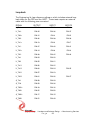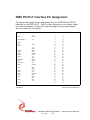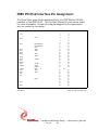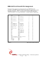
1
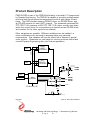
DYNAMIC ENGINEERING
435 Park Dr., Ben Lomond, Calif. 95005
831-336-8891
Fax 831-336-3840
[email protected]
www.dyneng.com
Est. 1988
User Manual
PMC-4U-CACI
Quad UART - Dual Synchronous
Serial Data Interface
PMC Module
Revision OR
Corresponding Hardware: Revision 01
PMC-4U
Quad UART - Dual Synchronous
Serial Data Interface
PMC Module
This document contains information of proprietary
interest to Dynamic Engineering. It has been supplied
in confidence and the recipient, by accepting this
material, agrees that the subject matter will not be
copied or reproduced, in whole or in part, nor its
contents revealed in any manner or to any person
except to meet the purpose for which it was delivered.
Dynamic Engineering
435 Park Drive
Ben Lomond, CA 95005
831-336-8891
831-336-3840 FAX
Dynamic Engineering has made every effort to ensure
that this manual is accurate and complete. Still, the
company reserves the right to make improvements or
changes in the product described in this document at
any time and without notice. Furthermore, Dynamic
Engineering assumes no liability arising out of the
application or use of the device described herein.
The electronic equipment described herein generates,
uses, and can radiate radio frequency energy.
Operation of this equipment in a residential area is
likely to cause radio interference, in which case the
user, at his own expense, will be required to take
whatever measures may be required to correct the
interference.
Dynamic Engineering’s products are not authorized for
use as critical components in life support devices or
systems without the express written approval of the
president of Dynamic Engineering.
This product has been designed to operate with PMC
Module carriers and compatible user-provided
equipment. Connection of incompatible hardware is
likely to cause serious damage.
©2001 by Dynamic Engineering.
Trademarks and registered trademarks are
owned by their respective manufactures.
Manual Revision OR. Revised July 2, 2001.
Hardware and Software Design • Manufacturing Services
P a g e
2
Table of Contents
PRODUCT DESCRIPTION
6
THEORY OF OPERATION
9
ADDRESS MAP
10
PROGRAMMING
12
REGISTER DEFINITIONS
13
PMC4U_BASE
PMC4U_STAT
PMC4U_MSK
PMC4U_SCC_IVEC
PMC4U_DIR_TERM
PMC4U_SW_IN
PMC4U_SCC_A_CNTL
PMC4U_SCC_A_DATA
PMC4U_SCC_B_CNTL
PMC4U_SCC_B_DATA
PMC4U_UART_A
PMC4U_UART_B
PMC4U_UART_C
PMC4U_UART_D
PMC4U_IRUPT/PMC4U_IRUPT_CLR
13
16
16
17
17
18
19
19
19
19
20
20
20
20
21
Interrupts
22
Loop-back
23
PMC PCI PN1 INTERFACE PIN ASSIGNMENT
24
PMC PCI PN2 INTERFACE PIN ASSIGNMENT
25
PMC-4U FRONT PANEL IO PIN ASSIGNMENT
26
PMC PN4 USER INTERFACE PIN ASSIGNMENT
27
APPLICATIONS GUIDE
28
Hardware and Software Design • Manufacturing Services
P a g e
3
Interfacing
28
CONSTRUCTION AND RELIABILITY
29
THERMAL CONSIDERATIONS
29
WARRANTY AND REPAIR
30
SERVICE POLICY
31
OUT OF WARRANTY REPAIRS
31
FOR SERVICE CONTACT:
31
SPECIFICATIONS
32
ORDER INFORMATION
33
SCHEMATICS
33
Hardware and Software Design • Manufacturing Services
P a g e
4
List of Figures
FIGURE 1
FIGURE 2
FIGURE 3
FIGURE 4
FIGURE 5
FIGURE 6
FIGURE 7
FIGURE 8
FIGURE 9
FIGURE 10
FIGURE 11
FIGURE 12
FIGURE 13
PMC-4U BLOCK DIAGRAM
PMC-4U INTERNAL ADDRESS MAP
PMC-4U UART ADDRESS MAP
PMC-4U BASE CONTROL REGISTER BIT MAP
PMC-4U TX CONTROL REGISTER BIT MAP
PMC-4U INTERRUPT MASK REGISTER BIT MAP
PMC-4U DIRECTION TERMINATION CONTROL BIT MAP
PMC-4U SWITCH READ BIT MAP
PMC-4U INTERRUPT STATUS/CLEAR
PMC-4U PN1 INTERFACE
PMC-4U PN2 INTERFACE
PMC-4U FRONT PANEL INTERFACE
PMC-4U PN4 INTERFACE
Hardware and Software Design • Manufacturing Services
P a g e
5
6
10
11
13
16
16
17
18
21
24
25
26
27
Product Description
PMC-4U-CACI is part of the PMC Module family of modular I/O components
by Dynamic Engineering. The PMC-4U is capable of providing multiple serial
protocols both synchronous and asynchronous with a wide range of baud
rates. The CACI interface uses an RS-423 driver, an RS-422 driver, and
an RS-422 receiver for each UART channel. Two enhanced hysteresis MIL
STD 188-114A receivers, a MIL STD 188-114A driver, and an open drain
active low output driver for one synchronous channel and an RS-422 driver
and receiver for the other synchronous channel.
Other variations are possible. Different oscillators can be installed, or
other modifications can be made to accommodate your particular
requirements. That variation will then be offered as a “standard” special
order product. Please see our web page for current products offered and
contact Dynamic Engineering with your custom application.
Quad
UART
XR16C854
CONTROL
DATA
Osc
SCC
Z85X30
2 channels
Osc
+5V
switched
termination
RS485
RS422
Osc
Dip Switch
16
8
Xilinx
XCS40XL
8
RS232
±12V, ±6V selectable RS423
RS188
2
PCI Bus 33/32
GND
± 5V
1V HYSTERISIS
+5V
2
FIGURE 1
PMC-4U BLOCK DIAGRAM
Hardware and Software Design • Manufacturing Services
P a g e
6
An EXAR XR16C854 implements the UART interface. This quad UART
device is compatible with the industry standard 16550 UART, but is
equipped with 128 byte FIFOs, independent Tx and Rx FIFO counters,
automatic hardware/software flow control, and many other enhanced
features. An 18.432 MHz oscillator supplies the reference clock for this
device allowing baud rates up to 1.152 Mbps.
The synchronous interface uses a Zilog Serial Communication Controller,
the Z85C30. This dual channel, multi-protocol device can implement
various bit-oriented and byte-oriented synchronous protocols such as HDLC
and IBM Bisync and handles asynchronous formats as well.
The PMC-4U also has a wide range of IO drivers and receivers to interface
with these two devices. There are 16 differential RS422/485
transceivers that can be configured as either receivers or transmitters,
eight single-ended RS188/232/423 drivers operating at selectable
voltage levels, and eight single-ended receivers capable of up to +/- 25V
input range. There are also two enhanced hysteresis (~1.5V) RS423
receivers for handling noisy input signals and two open drain outputs that
sink up to 65 mA. The differential input signals are selectively terminated
with switched 150Ω terminations. All IO lines have series 33Ω resistors
for circuit protection.
The UART, SCC, and IO lines all interface through the Xilinx FPGA to allow
maximum flexibility of connections. All configuration registers internal to
the Xilinx support read and write operations for software convenience. All
addresses are long word aligned including the UART and SCC internal
registers even though they have only a byte-wide data interface. Please see
the XR16C854 and Z85C30 data sheets and user’s manuals for more
information on register access and functions.
The PMC-4U conforms to the PMC and CMC draft standards. This
guarantees compatibility with multiple PMC Carrier boards. Because the
PMC may be mounted on different form factors, while maintaining plug and
software compatibility, system prototyping may be done on one PMC
Carrier board, with final system implementation on a different one.
PMC-4U uses a 10 mm inter-board spacing for the front panel, standoffs,
and PMC connectors. The 10 mm height is the "standard" height and will
work in most systems with most carriers. If your carrier has non-standard
connectors [height] to mate with the PMC-4U, please let us know. We may
be able to do a special build with a different height connector to
compensate.
Interrupts are supported by the PMC-4U. Each of the four UARTs and the
SCC has a maskable input to the interrupt generation logic in the Xilinx.
Hardware and Software Design • Manufacturing Services
P a g e
7
There is also a master interrupt enable that can be set to gate the
interrupt onto the PCI bus. The interrupt status is still available in a status
register even when the master interrupt enable is off. This facilitates polled
operation of interrupt conditions. The individual interrupt conditions are
specified in the internal registers of the UART and SCC. Please see the
XR16C854 and Z85C30 documentation for more information on interrupt
conditions and configuration.
Hardware and Software Design • Manufacturing Services
P a g e
8
Theory of Operation
The PMC-4U is designed for transferring data from one point to another
with a variety of serial protocols.
The PMC-4U features a Xilinx FPGA. The FPGA contains the general control
and status registers as well as the interface to the quad UART, SCC, and
IO drivers and receivers. Many additional control and status registers
reside in the UART and SCC, which are accessed through the Xilinx
interface.
The PMC-4U is a part of the PMC Module family of modular I/O products.
It meets the PMC and CMC draft Standards. Contact Dynamic Engineering
for a copy of this specification. It is assumed that the reader is at least
casually familiar with this document and logic design. In standard
configuration, the PMC-4U is a Type 1 mechanical with no components on
the back of the board and one slot wide, with 10 mm inter-board height.
The PCI interface to the host CPU is controlled by a logic block within the
Xilinx. The PMC-4U design requires one wait state for read or write cycles
to addresses other than the SCC and UART which require from three for
simple read or write operations to nine for the SCC interrupt
acknowledge/vector read cycle. The wait states refer to the number of
clocks after the PCI core decode before the “terminate with data” state is
reached. Two additional clock periods account for the 1 clock delay to
decode the signals from the PCI bus and to convert the terminate with data
state into the TRDY signal.
The quad UART and dual Serial Communication Controller can handle
multiple asynchronous and synchronous protocols and the IO drivers and
receivers support a range of electrical interface standards.
Each of the serial interfaces has its own oscillator and on-board baud rate
generator to supply a wide range of clock reference frequencies. The SCC
can also operate from external clock sources with separate Rx clock input
and Tx clock input/output pins for each channel.
Please refer to the XR16C854 and Z85C30 documentation for more
information on the operation and capabilities of these devices.
Hardware and Software Design • Manufacturing Services
P a g e
9
Address Map
REGISTER
PMC4U_BASE
PMC4U_STAT
PMC4U_MSK
PMC4U_SCC_IVEC
PMC4U_DIR_TERM
PMC4U_SW_IN
PMC4U_SCC_A_CNTL
PMC4U_SCC_A_DATA
PMC4U_SCC_B_CNTL
PMC4U_SCC_B_DATA
PMC4U_UART_A
PMC4U_UART_B
PMC4U_UART_C
PMC4U_UART_D
PMC4U_IRUPT
PMC4U_IRUPT_CLR
FIGURE 2
OFFSET FUNCTION
0X00
0X04
0X08
0X0C
0X10
0X14
0X18
0X1C
0X20
0X24
0X40
0X60
0X80
0XA0
0XE0
0XE0
TYPE
base control
status read
interrupt mask control
SCC interrupt vector read
direction and termination control
read user switch
SCC channel A control
SCC channel A data
SCC channel B control
SCC channel B data
UART A base offset
UART B base offset
UART C base offset
UART D base offset
interrupt source read
interrupt write clear
read/write
read
read/write
read
read/write
read
read/write
read/write
read/write
read/write
read/write
read/write
read/write
read/write
read
write
PMC-4U INTERNAL ADDRESS MAP
Each UART channel has a number of registers associated with it. These
register offsets and their general functions are given in figure 3. For
details of the bits and functions of each register consult the documentation
for the XR16C854.
The SCC also has a number of internal registers that are accessed in a
two-step process. First the register number is written to the control
address for the respective channel. Then an additional read or write to the
same control address is performed. This causes the data to be read from
or written to the desired register. At the end of this process the register
pointer is reset so that the next access is again to/from the base control
register. For a more complete description of this process, as well as
details of registers and their functions, see the user’s manual for the
Z85C30.
The address map provided is for the local decoding performed within the
PMC-4U. The addresses are all offsets from a base address. The carrier
board that the PMC is installed into provides the base address.
The VendorId = 0x10EE. The CardId = 0x0007. Current revision = 0x00
Hardware and Software Design • Manufacturing Services
P a g e
10
REGISTER
OFFSET
FUNCTION
PMC4U_UART_DATA
0X00
UART read/write data
PMC4U_UART_IEN
0X04
UART write interrupt enable
PMC4U_UART_ISTAT
0X08
UART read interrupt status
PMC4U_UART_FCNTL
0X08
UART write FIFO control
PMC4U_UART_LCNTL
0X0C
UART write line control
PMC4U_UART_MCNTL
0X10
UART write modem control
PMC4U_UART_LSTAT
0X14
UART read line status
PMC4U_UART_MSTAT
0X18
UART read modem status
PMC4U_UART_SPAD
0X1C
UART read/write scratchpad
UART baud rate register defines (enabled when *LCNTL bit-7 = 1)
PMC4U_UART_DLL
0X00
UART read/write LSB divisor
PMC4U_UART_DLM
0X04
UART read/write MSB divisor
UART enhanced register offsets (enabled when *LCNTL = 0xbf)
PMC4U_UART_FTC
0X00
UART FIFO read count/write trigger level
PMC4U_UART_FEAT
0X04
UART write feature control
PMC4U_UART_ENF
0X08
UART read/write enhanced features
PMC4U_UART_XON1
0X10
UART read/write Xon-1 word
PMC4U_UART_XON2
0X14
UART read/write Xon-2 word
PMC4U_UART_XOFF1
0X18
UART read/write Xoff-1 word
PMC4U_UART_XOFF2
0X1C
UART read/write Xoff-2 word
UART EMS registers (enabled when feature control bit-6 = 1)
PMC4U_UART_EMS
0X1C
UART write enhanced mode select
FIGURE 3
PMC-4U UART ADDRESS MAP
Hardware and Software Design • Manufacturing Services
P a g e
11
Programming
Programming the PMC-4U requires only the ability to read and write data
from the host. The base address is determined by the PMC Carrier board.
The base address refers to the first user address for the slot in which the
PMC is installed.
Depending on the software environment it may be necessary to set-up the
system software with the PMC-4U "registration" data. For example in
WindowsNT there is a system registry, which is used to identify the
resident hardware. The PMC-4U VendorId = 0x10EE. The CardId =
0x0007. Current revision = 0x00
The interrupt service routine should be loaded, the interrupt mask set, and
the desired interrupt conditions set up in the UART and SCC. Each of the
four UART channels and the SCC has a separate bit in the interrupt and
interrupt mask registers. When an interrupt occurs this event is latched in
the interrupt register. The interrupt is cleared by writing the bit back as a
one to the same address.
Refer to the Theory of Operation section above, the Register section below,
and the XR16C854 and Z85C30 documentation for more information
regarding the register functions and definitions.
Hardware and Software Design • Manufacturing Services
P a g e
12
Register Definitions
PMC4U_BASE
[0X00] PMC-4U Control Register Port read/write
CONTROL BASE
DATA BIT
DESCRIPTION
31-22
21-20
19
18
17
16
15-0
spare
test mode select
master interrupt enable
force interrupt
SCC reset
UART reset
spare
FIGURE 4
PMC-4U BASE CONTROL REGISTER BIT MAP
All bits are active high and are reset on power-up or reset command.
Test mode select is used to enable different drivers and receivers to allow
thorough testing of the IO circuitry. A value of “00” indicates normal
operational mode. In this mode the connections are as follows (see figure
12 for pin-out information):
Signal Function
Driver/Receiver
UART Tx A
IO_8 (RS422)
OUT_0 (RS423)
IO_0 (RS422)
UART Rx A
UART Tx B
UART Rx B
UART Tx C
UART Rx C
UART Tx D
UART Rx D
IO_9 (RS422)
OUT_1 (RS423)
IO_2 (RS422)
IO_10 (RS422)
OUT_2 (RS423)
IO_4 (RS422)
IO_11 (RS422)
OUT_3 (RS423)
IO_6 (RS422)
Hardware and Software Design • Manufacturing Services
P a g e
13
SCC
SCC
SCC
SCC
Tx A
Rx A
Rx Clk
RTS A
SCC Tx B
SCC Rx B
OUT_4 (188)
AUX_IN_0 (enhanced hysteresis 188)
AUX_IN_1 (enhanced hysteresis 188)
AUX_OUT_0 (open drain)
IO_15 (RS422)
IO_13 (RS422)
When test mode select is “10” the following changes are made (if a signal
is not listed here, its connection remains the same):
Signal Function
Driver/Receiver
UART Rx A
IO_1 (RS422)
UART Rx B
IO_3 (RS422)
UART Rx C
IO_5 (RS422)
UART Rx D
IO_7 (RS422)
SCC RTS A
AUX_OUT_1 (open drain)
SCC Tx B
SCC Rx B
IO_14 (RS422)
IO_12 (RS422)
When test mode select is “11” the following changes are made:
Signal Function
Driver/Receiver
UART Rx A
IN_0 (RS232)
UART Rx B
IN_1 (RS232)
UART Rx C
IN_2 (RS232)
UART Rx D
IN_3 (RS232)
When test mode select is “01” the following changes are made:
Signal Function
Driver/Receiver
UART Rx A
IN_4 (RS232)
UART Rx B
IN_5 (RS232)
Hardware and Software Design • Manufacturing Services
P a g e
14
UART Tx C
UART Rx C
OUT_6 (RS423)
IN_6 (RS232)
UART Tx D
UART Rx D
OUT_7 (RS423)
IN_7 (RS232)
Master interrupt enable when ‘1’ gates all interrupts through to the PCI
host. When ‘0’ the interrupts can be used for status without interrupting
the host.
Force interrupt is used for test and software development purposes to
create an interrupt request. 1 = assert interrupt request. 0 = normal
operation. Useful to stimulate interrupt acknowledge routines for
development.
SCC reset causes a hardware reset of the SCC. In order to accomplish
this, set this bit high and then low. All registers and modes in the SCC will
revert to the reset state.
UART reset causes a hardware reset of the UART. The process is the
same as the SCC.
Hardware and Software Design • Manufacturing Services
P a g e
15
PMC4U_STAT
[0X04] PMC-4U Status Port read only
STATUS
DATA BIT
31-2
1
0
DESCRIPTION
spare
interrupt out
interrupt status
FIGURE 5
PMC-4U TX CONTROL REGISTER BIT MAP
Interrupt out indicates that an interrupt is asserted on the PCI bus.
Interrupt status indicates that an interrupt condition exists, however if the
master interrupt enable is not asserted, then the interrupt will not be
asserted on the PCI bus. This bit can be used to operate the card in polled
mode without interrupting the host.
PMC4U_MSK
[0X08] PMC-4U Interrupt Mask Register Port read/write
INTERRUPT MASK
DATA BIT
31-5
4
3
2
1
0
FIGURE 6
DESCRIPTION
Spare
SCC Interrupt Enable
UART D Interrupt Enable
UART C Interrupt Enable
UART B Interrupt Enable
UART A Interrupt Enable
PMC-4U INTERRUPT MASK REGISTER BIT MAP
The bits in this register enable the individual interrupts from the devices
indicated. The mask bit for a device must be set to a one in order for an
interrupt from that device to affect the PMC-4U interrupt status.
Hardware and Software Design • Manufacturing Services
P a g e
16
PMC4U_SCC_IVEC
[0X0C] PMC-4U SCC Interrupt Acknowledge/Vector Read
A read from this address causes the SCC interrupt acknowledge signal to
be asserted. If an interrupt condition exists in the SCC, it will respond by
placing an interrupt vector on the local data bus. This vector is specified by
the user and, depending on the state set in the SCC registers, may contain
status information about the cause of the interrupt.
PMC4U_DIR_TERM
[0X10] PMC-4U Direction and Termination Port read/write
CONTROL DIR_TERM REGISTER
DATA BIT
DESCRIPTION
31-20
19-16
15-3
2-0
FIGURE 7
spare
TERMination 3-0
spare
DIRection
2-0
1 = terminated
0 = read 1 = drive
PMC-4U DIRECTION TERMINATION CONTROL BIT MAP
The direction and termination for each of the 16 differential pairs is
controlled through this port. The bits default to ‘0’, which corresponds to
tri-stating the drivers with no termination.
CONTROL
DIR0
DIR1
DIR2
CORRESPONDING IO BITS
IO_0..7
IO_8..11
IO_12..13
In this design the direction of IO lines 14 and 15 are controlled by the RTS
line of the SCC channel B to allow this signal to control the SCC Tx B
enable.
Hardware and Software Design • Manufacturing Services
P a g e
17
Parallel termination resistors are supplied on each differential pair along
with a switch to allow the user to select which lines are terminated and
where. In some systems it will make sense to terminate the lines in the
cable and in others it will make sense to use the onboard terminations.
CONTROL
TERM0
TERM1
TERM2
TERM3
CORRESPONDING IO BITS
IO_0..7
IO_8..11
IO_12..13
IO_14..15
PMC4U_SW_IN
[0X14] PMC-4U User Switch Port read only
USER CONTROL SWITCH REGISTER
DATA BIT
5
4
3
2
1
0
FIGURE 8
DESCRIPTION
UB5
UB4
UB3
UB2
UB1
UB0
PMC-4U SWITCH READ BIT MAP
The Switch Read Port has the user bits. The user bits are connected to 6
switch positions. The switches allow custom configurations to be defined
by the user and for the software to “know” how to configure the read/write
capabilities of each IO line. Please note that the lower 6 bits of the switch
are implemented [positions 7 & 8 are unused]. The silk-screen is marked
with the ‘0’ and ‘1’ definitions.
Hardware and Software Design • Manufacturing Services
P a g e
18
PMC4U_SCC_A_CNTL
[0X18] PMC-4U SCC Channel A Control Register read/write
This address is used to access all of the channel A registers. In order to
access a register other than this base register, the register number is first
written to this address. A subsequent read or write will read from or write
to the desired register. After this process is completed, the pointers are
reset so that the base register is once again accessed. See the Z85C30
documentation for more information on this process.
PMC4U_SCC_A_DATA
[0X1C] PMC-4U SCC Channel A Data Register read/write
This address is used to access the channel A data buffers. A write to this
address loads a byte into the channel A transmit buffer, a read removes a
byte from the receive buffer.
PMC4U_SCC_B_CNTL
[0X20] PMC-4U SCC Channel B Control Register read/write
This address is used to access all of the channel B registers. In order to
access a register other than this base register, the register number is first
written to this address. A subsequent read or write will read from or write
to the desired register. After this process is completed, the pointers are
reset so that the base register is once again accessed. See the Z85C30
documentation for more information on this process.
PMC4U_SCC_B_DATA
[0X24] PMC-4U SCC Channel B Data Register read/write
This address is used to access the channel B data buffers. A write to this
address loads a byte into the channel B transmit buffer, a read removes a
byte from the receive buffer.
Hardware and Software Design • Manufacturing Services
P a g e
19
PMC4U_UART_A
[0X40] PMC-4U UART A Base Address
This is the base address for the eight register addresses associated with
UART A. Figure 3 gives an overview of these registers and their functions.
For more details on the access and functions of these registers see the
XR16C854 documentation.
PMC4U_UART_B
[0X60] PMC-4U UART B Base Address
This is the base address for the eight register addresses associated with
UART B. Figure 3 gives an overview of these registers and their functions.
For more details on the access and functions of these registers see the
XR16C854 documentation.
PMC4U_UART_C
[0X80] PMC-4U UART C Base Address
This is the base address for the eight register addresses associated with
UART C. Figure 3 gives an overview of these registers and their functions.
For more details on the access and functions of these registers see the
XR16C854 documentation.
PMC4U_UART_D
[0XA0] PMC-4U UART D Base Address
This is the base address for the eight register addresses associated with
UART D. Figure 3 gives an overview of these registers and their functions.
For more details on the access and functions of these registers see the
XR16C854 documentation.
Hardware and Software Design • Manufacturing Services
P a g e
20
PMC4U_IRUPT/PMC4U_IRUPT_CLR
[0XE0] PMC-4U Interrupt Latch read status/write clear
INTERRUPT STATUS
DATA BIT
4
3
2
1
0
FIGURE 9
DESCRIPTION
SCC interrupt
UART D interrupt
UART C interrupt
UART B interrupt
UART A interrupt
PMC-4U INTERRUPT STATUS/CLEAR
The bits in this register indicate that an interrupt has been received from
the corresponding device. These bits are latched and once set will remain
set until a one is written to the bit to be cleared.
Hardware and Software Design • Manufacturing Services
P a g e
21
Interrupts
PMC-4U interrupts are treated as auto-vectored. When the software
enters into an exception handler to deal with a PMC-4U interrupt the
software must read the interrupt register to determine the cause(s) of the
interrupt, change the interrupt mask, process accordingly to clear the
interrupt condition, and then clear the associated bit in the interrupt
register.
In order to clear the interrupt condition it will be necessary to access
registers in the UART or the SCC to determine the particular cause of the
interrupt, change the device interrupt enables, and service the device to
remove the cause of the interrupt. The SCC can be configured so that the
interrupt cause is read with an interrupt acknowledge/vector read cycle.
The interrupt level seen by the CPU is determined by the rest of the
system. The master interrupt can be disabled or enabled through the
PMC4U_BASE register. The individual enables for the four UART channels
and the SCC are controlled by the PMC4U_MSK register. In addition there
are registers in the UART and SCC that must be configured for the
particular conditions that are desired to generate an interrupt request.
An interrupt that is received from one of the UART channels or the SCC will
be latched into the PMC4U_IRUPT register. This interrupt will only affect
the interrupt status in the PMC4U_STAT register if the appropriate bit is
set in the PMC4U_MSK register. This in turn will only generate a host
interrupt only if the master interrupt enable is set in the PMC_BASE
register.
After the interrupt has been serviced and the interrupting condition no
longer exists the bit latched in the PMC4U_IRUPT register can be cleared
by writing a one to the respective bit. Then the mask bit can be set without
causing another interrupt.
The master enable is a mask that can be used to disable the interrupt from
reaching the CPU, but still leaves the internal interrupt request hardware
active which is useful for polled operation.
Power on initialization will provide a cleared interrupt request and interrupts
disabled.
Hardware and Software Design • Manufacturing Services
P a g e
22
Loop-back
The Engineering kit has reference software, which includes external loopback tests for the SCC and the UART. These tests require an external
cable with the following pins connected.
SIGNAL
OUTPUT
INPUT1
INPUT2
U_TxA+
PIN-11
PIN-2
PIN-3
U_TxA-
PIN-45
PIN-36
PIN-37
U_TxB+
PIN-12
PIN-4
PIN-5
U_TxB-
PIN-46
PIN-38
PIN-39
U_TxC+
PIN-13
PIN-6
PIN-7
U_TxC-
PIN-47
PIN-40
PIN-41
U_TxD+
PIN-14
PIN-8
PIN-9
U_TxD-
PIN-48
PIN-42
PIN-43
U_TxA
PIN-54
PIN-20
U_TxB
PIN-55
PIN-21
U_TxC1
PIN-56
PIN-22
U_TxC2
PIN-60
PIN-24
U_TxD1
PIN-57
PIN-23
U_TxD2
PIN-61
PIN-26
S_TxA
PIN-58
PIN-29
S_TCA
PIN-59
PIN-30
S_TxB1+
PIN-18
PIN-16
S_TxB1-
PIN-52
PIN-50
S_TxB2+
PIN-17
PIN-15
S_TxB2-
PIN-51
PIN-49
PIN-25
PIN-27
Hardware and Software Design • Manufacturing Services
P a g e
23
PMC PCI Pn1 Interface Pin Assignment
The figure below gives the pin assignments for the PMC Module PCI Pn1
Interface on the PMC-4U-IO. See the User Manual for your carrier board
for more information. Unused pins may be assigned by the specification
and not needed by this design.
GND
-12V
INTA#
BUSMODE1#
+5V
GND CLK
GND -
GND
AD28AD25GND AD22AD19
FRAME#GND
DEVSEL#
GND
PAR
AD12AD9GND AD6AD4
AD2GND
FIGURE 10
+5V
AD31
AD27
GND
C/BE3#
AD21
+5V
AD17
GND
IRDY#
+5V
LOCK#
GND
AD15
AD11
+5V
C/BE0#
AD5
GND
AD3
AD1
+5V
1
3
5
7
9
11
13
15
17
19
21
23
25
27
29
31
33
35
37
39
41
43
45
47
49
51
53
55
57
59
61
63
2
4
6
8
10
12
14
16
18
20
22
24
26
28
30
32
34
36
38
40
42
44
46
48
50
52
54
56
58
60
62
64
PMC-4U PN1 INTERFACE
Hardware and Software Design • Manufacturing Services
P a g e
24
PMC PCI Pn2 Interface Pin Assignment
The figure below gives the pin assignments for the PMC Module PCI Pn2
Interface on the PMC-4U-IO. See the User Manual for your carrier board
for more information. Unused pins may be assigned by the specification
and not needed by this design.
+12V
GND
GND
RST#
AD30
GND
AD24
IDSEL
AD18
AD16
GND
TRDY#
GND
PERR#
C/BE1#
AD14
GND
AD8
AD7
BUSMODE3#
BUSMODE4#
GND
AD29
AD26
AD23
AD20
C/BE2#
STOP#
GND
SERR#
GND
43
AD13
AD10
GND
GND
GND
FIGURE 11
1
3
5
7
9
11
13
15
17
19
21
23
25
27
29
31
33
35
37
39
41
2
4
6
8
10
12
14
16
18
20
22
24
26
28
30
32
34
36
38
40
42
44
45
47
49
51
53
55
57
59
61
63
46
48
50
52
54
56
58
60
62
64
PMC-4U PN2 INTERFACE
Hardware and Software Design • Manufacturing Services
P a g e
25
PMC-4U Front Panel IO Pin Assignment
The figure below gives the pin assignments for the PMC Module IO
Interface on the PMC-4U. Also, see the User Manual for your carrier board
for more information. GND* is a plane which is tied to GND through a
1206 0Ω resistor. AC or open are options – contact Dynamic Engineering.
GND*
IO_0+ (UART Rx A)
IO_1+
IO_2+ (UART Rx B)
IO_3+
IO_4+ (UART Rx C)
IO_5+
IO_6+ (UART Rx D)
IO_7+
GND*
IO_8+ (UART Tx A)
IO_9+ (UART Tx B)
IO_10+ (UART Tx C)
IO_11+ (UART Tx D)
IO_12+
IO_13+ (SCC Rx B)
IO_14+
IO_15+ (SCC Tx B)
GND*
IN_0
IN_1
IN_2
IN_3
IN_4
IN_5
IN_6
IN_7
GND*
AUX_IN_0 (SCC Rx A)
AUX_IN_1 (SCC Rx Clk)
GND*
+3.3 V REF
+6.5 V REF
-6.5 V REF
FIGURE 12
GND*
IO_0- (UART Rx A)
IO_1IO_2- (UART Rx B)
IO_3IO_4- (UART Rx C)
IO_5IO_6- (UART Rx D)
IO_7GND*
IO_8- (UART Tx A)
IO_9- (UART Tx B)
IO_10- (UART Tx C)
IO_11- (UART Tx D)
IO_12IO_13- (SCC Rx B)
IO_14IO_15- (SCC Tx B)
GND*
OUT_0 (UART Tx A)
OUT_1 (UART Tx B)
OUT_2 (UART Tx C)
OUT_3 (UART Tx D)
OUT_4 (SCC Tx A)
OUT_5
OUT_6
OUT_7
GND*
AUX_OUT_0 (SCC RTS A)
AUX_OUT_1
GND*
GND*
GND*
GND*
1
2
3
4
5
6
7
8
9
10
11
12
13
14
15
16
17
18
19
20
21
22
23
24
25
26
27
28
29
30
31
32
33
34
35
36
37
38
39
40
41
42
43
44
45
46
47
48
49
50
51
52
53
54
55
56
57
58
59
60
61
62
63
64
65
66
67
68
PMC-4U FRONT PANEL INTERFACE
Hardware and Software Design • Manufacturing Services
P a g e
26
PMC Pn4 User Interface Pin Assignment
The figure provides the pin assignments for the PMC-4U Module routed to
Pn4. Also, see the User Manual for your carrier board for more
information.
GND
IO_0+ (UART Rx A)
IO_1+
IO_2+ (UART Rx B)
IO_3+
IO_4+ (UART Rx C)
IO_5+
IO_6+ (UART Rx D)
IO_7+
GND
IO_8+ (UART Tx A)
IO_9+ (UART Tx B)
IO_10+ (UART Tx C)
IO_11+ (UART Tx D)
IO_12+
IO_13+ (SCC Rx B)
IO_14+
IO_15+ (SCC Tx B)
GND
IN_0
IN_1
IN_2
IN_3
IN_4
IN_5
IN_6
IN_7
GND
AUX_IN_0 (SCC Rx A) AUX_IN_1 (SCC Rx Clk)
GND
+3.3 V REF
+6.5 V REF
-6.5 V REF
GND
IO_0- (UART Rx A)
IO_1IO_2- (UART Rx B)
IO_3IO_4- (UART Rx C)
IO_5IO_6- (UART Rx D)
IO_7GND
IO_8- (UART Tx A)
IO_9- (UART Tx B)
IO_10- (UART Tx C)
IO_11- (UART Tx D)
IO_12IO_13- (SCC Rx B)
IO_14IO_15- (SCC Tx B)
GND
OUT_0 (UART Tx A)
OUT_1 (UART Tx B)
OUT_2 (UART Tx C)
OUT_3 (UART Tx D)
OUT_4 (SCC Tx A)
OUT_5
OUT_6
OUT_7
GND
AUX_OUT_0 (SCC RTS A) AUX_OUT_1
FIGURE 13
1
3
5
8
9
11
13
15
17
19
21
23
25
27
29
31
33
35
37
39
41
43
45
47
49
51
53
55
57
59
61
63
2
4
6
9
10
12
14
16
18
20
22
24
26
28
30
32
34
36
38
40
42
44
46
48
50
52
54
56
58
60
62
64
PMC-4U PN4 INTERFACE
Hardware and Software Design • Manufacturing Services
P a g e
27
Applications Guide
Interfacing
The pin-out tables are displayed with the pins in the same relative order as
the actual connectors. The pin definitions are defined with noise immunity
in mind. The pairs are chosen to match standard SCSI II/III cable pairing to
allow a low cost commercial cable to be used for the interface.
Some general interfacing guidelines are presented below. Do not hesitate
to contact the factory if you need more assistance.
Watch the system grounds. All electrically connected equipment should
have a fail-safe common ground that is large enough to handle all current
loads without affecting noise immunity. Power supplies and powerconsuming loads should all have their own ground wires back to a common
point.
Power all system power supplies from one switch. Connecting external
voltage to the PMC-4U when it is not powered can damage it, as well as
the rest of the host system. This problem may be avoided by turning all
power supplies on and off at the same time. Alternatively, the use of OPTO22 isolation panels is recommended.
Keep cables short. Flat cables, even with alternate ground lines, are not
suitable for long distances. PMC-4U does not contain special input
protection. The connector is pinned out for a standard SCSI II/III cable to
be used. The twisted pairs are defined to match up with the PMC-4Ul pin
definitions. It is suggested that this standard cable be used for most of the
cable run.
Terminal Block. We offer a high quality 68 screw terminal block that
directly connects to the SCSI II/III cable. The terminal block can mount on
standard DIN rails. HDEterm68
[ http://www.dyneng.com/HDEterm68.html ]
We provide the components. You provide the system. Safety and
reliability can be achieved only by careful planning and practice. Inputs can
be damaged by static discharge, or by applying voltage outside of the
particular device’s rated voltages.
Hardware and Software Design • Manufacturing Services
P a g e
28
Construction and Reliability
PMC Modules were conceived and engineered for rugged industrial
environments. The PMC-4U is constructed out of 0.062 inch thick FR4
material.
Through hole and surface mounting of components are used. IC sockets
use gold plated screw machine pins. High insertion and removal forces are
required, which assists in the retention of components. If the application
requires unusually high reliability or is in an environment subject to high
vibration, the user may solder the corner pins of each socketed IC into the
socket, using a grounded soldering iron.
The PMC connectors are rated at 1 Amp per pin, 100 insertion cycles
minimum. These connectors make consistent, correct insertion easy and
reliable.
The PMC secured against the carrier with four screws attached to the 2
stand-offs and 2 locations on the front panel. The four screws provide
significant protection against shock, vibration, and incomplete insertion.
The PMC Module provides a low temperature coefficient of 2.17 W/oC for
uniform heat. This is based upon the temperature coefficient of the base
FR4 material of 0.31 W/m-oC, and taking into account the thickness and
area of the PMC. The coefficient means that if 2.17 Watts are applied
uniformly on the component side, then the temperature difference between
the component side and solder side is one degree Celsius.
Thermal Considerations
The PMC-4U design consists of CMOS circuits. The power dissipation due
to internal circuitry is very low. It is possible to create a higher power
dissipation with the externally connected logic. If more than one Watt is
required to be dissipated due to external loading then forced air cooling is
recommended. With the one degree differential temperature to the solder
side of the board external cooling is easily accomplished.
Hardware and Software Design • Manufacturing Services
P a g e
29
Warranty and Repair
Dynamic Engineering warrants this product to be free from defects in
workmanship and materials under normal use and service and in its
original, unmodified condition, for a period of one year from the time of
purchase. If the product is found to be defective within the terms of this
warranty, Dynamic Engineering's sole responsibility shall be to repair, or at
Dynamic Engineering's sole option to replace, the defective product. The
product must be returned by the original customer, insured, and shipped
prepaid to Dynamic Engineering. All replaced products become the sole
property of Dynamic Engineering.
Dynamic Engineering's warranty of and liability for defective products is
limited to that set forth herein. Dynamic Engineering disclaims and excludes
all other product warranties and product liability, expressed or implied,
including but not limited to any implied warranties of merchandisability or
fitness for a particular purpose or use, liability for negligence in
manufacture or shipment of product, liability for injury to persons or
property, or for any incidental or consequential damages.
Dynamic Engineering’s products are not authorized for use as critical
components in life support devices or systems without the express written
approval of the president of Dynamic Engineering.
Hardware and Software Design • Manufacturing Services
P a g e
30
Service Policy
Before returning a product for repair, verify as well as possible that the
suspected unit is at fault. Then call the Customer Service Department for a
RETURN MATERIAL AUTHORIZATION (RMA) number. Carefully package the
unit, in the original shipping carton if this is available, and ship prepaid and
insured with the RMA number clearly written on the outside of the package.
Include a return address and the telephone number of a technical contact.
For out-of-warranty repairs, a purchase order for repair charges must
accompany the return. Dynamic Engineering will not be responsible for
damages due to improper packaging of returned items. For service on
Dynamic Engineering Products not purchased directly from Dynamic
Engineering, contact your reseller. Products returned to Dynamic
Engineering for repair by other than the original customer will be treated as
out-of-warranty.
Out of Warranty Repairs
Out of warranty repairs will be billed on a material and labor basis. The
current minimum repair charge is $100. Customer approval will be
obtained before repairing any item if the repair charges will exceed one half
of the quantity one list price for that unit. Return transportation and
insurance will be billed as part of the repair and is in addition to the
minimum charge.
For Service Contact:
Customer Service Department
Dynamic Engineering
435 Park Dr.
Ben Lomond, CA 95005
831-336-8891
831-336-3840 fax
[email protected]
Hardware and Software Design • Manufacturing Services
P a g e
31
Specifications
Host Interface:
PCI Mezzanine Card
Serial Interfaces:
Four UART channels each with an RS422 driver and receiver and
an RS423 driver. One synchronous channel with Mil. Std. 188114A Type 1 enhanced hysteresis receivers for clock and data, a
188 driver for Tx data, and an open drain PTT interface on the RTS
line. Another synchronous channel with RS422 driver and receiver.
TX Data rates generated:
Up to 1.152 MHz for the UART channels. Up to 3.072 MHz for
the SCC in synchronous mode. Other rates are available with
different oscillator installations.
Software Interface:
Control Registers, Status Ports, UART, and SCC Interface
Initialization:
Hardware Reset forces all registers to 0, resets UART and SCC.
Access Modes:
LW boundary Space (see memory map)
Wait States:
1 for all addresses except UART and SCC accesses.
Interrupt:
Each UART channel has its own interrupt bit
The SCC has one interrupt bit for both channels
The interrupts generated by these devices depend on the setup
specified in the UART and SCC internal registers
DMA:
No DMA Support implemented at this time
Onboard Options:
All Options are Software Programmable
Interface Options:
68 pin twisted pair cable
68 screw terminal block interface
Dimensions:
Standard Single PMC Module.
Construction:
FR4 Multi-Layer Printed Circuit, Through Hole and Surface Mount
Components. Programmable parts are socketed.
Temperature Coefficient:
0.89 W/oC for uniform heat across PMC
Power:
Max. TBD mA @ 5V
Hardware and Software Design • Manufacturing Services
P a g e
32
Order Information
PMC-4U
PMC Module with 4 UART channels and 2
synchronous/asynchronous serial channels
Programmable baud rates
differential and single ended data inputs and outputs
RS-188, 232, 422, 423, 485 standards supported
32 bit data interface
Eng Kit–PMC-4U
HDEterm68 - 68 position screw terminal adapter
HDEcabl68 - 68 IO twisted pair cable
Technical Documentation,
1. PMC-4U Schematic
2. PMC-4U Reference test software
Data sheet reprints are available from the
manufacturer’s web site
reference software.
Note: The Engineering Kit is strongly recommended for first time PMC-4U buys.
Schematics
Schematics are provided as part of the engineering kit for customer
reference only. This information was current at the time the printed circuit
board was last revised. This revision letter is shown on the front of this
manual as “Corresponding Hardware Revision.” This information is not
necessarily current or complete manufacturing data, nor is it part of the
product specification.
All information provided is Copyright Dynamic Engineering
Hardware and Software Design • Manufacturing Services
P a g e
33