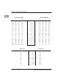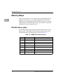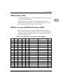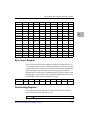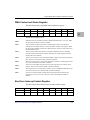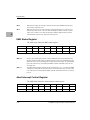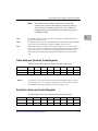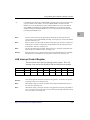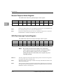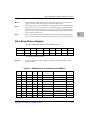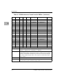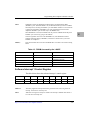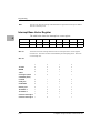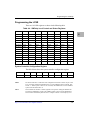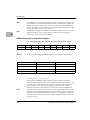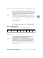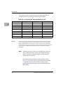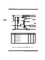
1
MVME147S
MPU VMEmodule User’s
Manual
MVME147S/D3
April 2000 Edition
Notice
While reasonable efforts have been made to assure the accuracy of this document,
Motorola, Inc. assumes no liability resulting from any omissions in this document, or from
the use of the information obtained therein. Motorola reserves the right to revise this
document and to make changes from time to time in the content hereof without obligation
of Motorola to notify any person of such revision or changes.
Electronic versions of this material may be read online, downloaded for personal use, or
referenced in another document as a URL to the Motorola Computer Group website. The
text itself may not be published commercially in print or electronic form, edited, translated,
or otherwise altered without the permission of Motorola, Inc.
It is possible that this publication may contain reference to or information about Motorola
products (machines and programs), programming, or services that are not available in your
country. Such references or information must not be construed to mean that Motorola
intends to announce such Motorola products, programming, or services in your country.
Limited and Restricted Rights Legend
If the documentation contained herein is supplied, directly or indirectly, to the U.S.
Government, the following notice shall apply unless otherwise agreed to in writing by
Motorola, Inc.
Use, duplication, or disclosure by the Government is subject to restrictions as set forth in
subparagraph (b)(3) of the Rights in Technical Data clause at DFARS 252.227-7013 (Nov.
1995) and of the Rights in Noncommercial Computer Software and Documentation clause
at DFARS 252.227-7014 (Jun. 1995).
Motorola, Inc.
Computer Group
2900 South Diablo Way
Tempe, Arizona 85282
Preface
This manual provides general information, hardware preparation, installation instructions,
operating instructions, programming, and functional descriptions for the MVME147S
series MPU VMEmodules.
This manual is intended for anyone who wants to design OEM systems, supply additional
capability to an existing compatible system, or in a lab environment for experimental
purposes.
A basic knowledge of computers and digital logic is assumed. To use this manual, you
should be familiar with the publications listed in Motorola Computer Group Documents on
page 1-6.
Motorola® and the Motorola symbol are registered trademarks of Motorola, Inc.
MVME147bug, VMEmodule, and VMEsystem 1000 are trademarks of Motorola, Inc.
All other products mentioned in this document are trademarks or registered trademarks of
their respective holders.
© Copyright Motorola, Inc. 1989, 1990, 1992, 2000
All Rights Reserved
Printed in the United States of America
2000
Safety Summary
The following general safety precautions must be observed during all phases of operation, service, and repair of this
equipment. Failure to comply with these precautions or with specific warnings elsewhere in this manual violates safety
standards of design, manufacture, and intended use of the equipment. Motorola, Inc. assumes no liability for the
customer’s failure to comply with these requirements.
The safety precautions listed below represent warnings of certain dangers of which Motorola is aware. You, as the user
of the product, should follow these warnings and all other safety precautions necessary for the safe operation of the
equipment in your operating environment.
Ground the Instrument.
To minimize shock hazard, the equipment chassis and enclosure must be connected to an electrical ground. If the
equipment is supplied with a three-conductor AC power cable, the power cable must be plugged into an approved
three-contact electrical outlet, with the grounding wire (green/yellow) reliably connected to an electrical ground
(safety ground) at the power outlet. The power jack and mating plug of the power cable meet International
Electrotechnical Commission (IEC) safety standards and local electrical regulatory codes.
Do Not Operate in an Explosive Atmosphere.
Do not operate the equipment in the presence of flammable gases or fumes. Operation of any electrical equipment in
such an environment constitutes a definite safety hazard.
Keep Away From Live Circuits.
Operating personnel must not remove equipment covers. Only Factory Authorized Service Personnel or other
qualified maintenance personnel may remove equipment covers for internal subassembly or component replacement
or any internal adjustment. Do not replace components with power cable connected. Under certain conditions,
dangerous voltages may exist even with the power cable removed. To avoid injuries, always disconnect power and
discharge circuits before touching them.
Use Caution When Exposing or Handling a CRT.
Breakage of a Cathode-Ray Tube (CRT) causes a high-velocity scattering of glass fragments (implosion). To prevent
CRT implosion, avoid rough handling or jarring of the equipment. Handling of a CRT should be done only by qualified
maintenance personnel using approved safety mask and gloves.
Do Not Substitute Parts or Modify Equipment.
Because of the danger of introducing additional hazards, do not install substitute parts or perform any unauthorized
modification of the equipment. Contact your local Motorola representative for service and repair to ensure that safety
features are maintained.
Observe Dangerous Procedure Warnings.
Warnings, such as the example below, precede potentially dangerous procedures throughout this manual. Instructions
contained in the warnings must be followed. You should also employ all other safety precautions which you deem
necessary for the operation of the equipment in your operating environment.
!
WARNING
Dangerous voltages, capable of causing death, are present in
this equipment. Use extreme caution when handling, testing,
and adjusting.
All Motorola PWBs (printed wiring boards) are manufactured by UL-recognized
manufacturers, with a flammability rating of 94V-0.
!
WARNING
This equipment generates, uses, and can radiate electromagnetic energy. It may cause or be susceptible to electromagnetic interference (EMI) if not installed and used in a
cabinet with adequate EMI protection.
CE Notice (European Community)
!
WARNING
This is a Class A product. In a domestic environment, this
product may cause radio interference, in which case the user
may be required to take adequate measures.
Motorola Computer Group products with the CE marking comply with the EMC Directive
(89/336/EEC). Compliance with this directive implies conformity to the following
European Norms:
EN55022 “Limits and Methods of Measurement of Radio Interference
Characteristics of Information Technology Equipment”; this product tested to
Equipment Class A
EN50082-1:1997 “Electromagnetic Compatibility—Generic Immunity
Standard, Part 1. Residential, Commercial and Light Industry”
System products also fulfill EN60950 (product safety) which is essentially the requirement
for the Low Voltage Directive (73/23/EEC).
Board products are tested in a representative system to show compliance with the above
mentioned requirements. A proper installation in a CE-marked system will maintain the
required EMC/safety performance.
In accordance with European Community directives, a “Declaration of Conformity” has
been made and is on file within the European Union. The “Declaration of Conformity” is
available on request. Please contact your sales representative.
Contents
CHAPTER 1
General Information
Introduction................................................................................................................1-1
Model Designations ...................................................................................................1-1
Features ......................................................................................................................1-2
Specifications .............................................................................................................1-3
Cooling Requirements ........................................................................................1-4
FCC Compliance.................................................................................................1-5
General Description ...................................................................................................1-6
Motorola Computer Group Documents .....................................................................1-6
Related Specifications................................................................................................1-7
Manual Terminology..................................................................................................1-8
CHAPTER 2
Hardware Preparation and Installation
Introduction................................................................................................................2-1
Unpacking Instructions ..............................................................................................2-1
ROM Configuration Select Headers (J1, J2) ......................................................2-4
System Controller Select Header (J3).................................................................2-9
Factory Use Only Headers (J5, J6) .....................................................................2-9
Serial Port 4 Clock Configuration Select Headers (J8, J9)...............................2-10
Installation Instructions............................................................................................2-10
CHAPTER 3
Operating Instructions
Introduction................................................................................................................3-1
Controls and Indicators ..............................................................................................3-1
RESET Switch S2...............................................................................................3-1
Remote Reset Switch Connector (J4) .................................................................3-1
ABORT Switch S1..............................................................................................3-2
FAIL Indicator (DS1)..........................................................................................3-2
STATUS Indicator (DS2) ....................................................................................3-2
RUN Indicator (DS3) ..........................................................................................3-2
SCON Indicator (DS4)........................................................................................3-2
Memory Maps ............................................................................................................3-4
MC68030 Memory Map .....................................................................................3-4
Program and Data Address Spaces .....................................................................3-5
vii
CPU Address Space............................................................................................ 3-7
Coprocessor Register Map .......................................................................... 3-8
Interrupt Acknowledge Map ....................................................................... 3-8
VMEbus Memory Map....................................................................................... 3-9
VMEbus Accesses to MVME147S Onboard DRAM ........................................ 3-9
VMEbus Short I/O Memory Map..................................................................... 3-11
VMEbus Interrupt Acknowledge Map ............................................................. 3-12
CHAPTER 4
Programming
Introduction ............................................................................................................... 4-1
Programming The Peripheral Channel Controller..................................................... 4-1
Table Address Register....................................................................................... 4-1
Data Address Register ........................................................................................ 4-1
32-Bit Registers........................................................................................... 4-2
16-Bit Registers........................................................................................... 4-2
8-Bit Registers............................................................................................. 4-2
Byte Count Register ........................................................................................... 4-3
Data Holding Register ........................................................................................ 4-3
Timer 1 Preload Register .................................................................................... 4-4
Timer 1 Counter Register ................................................................................... 4-4
Timer 2 Preload Register .................................................................................... 4-4
Timer 2 Counter Register ................................................................................... 4-4
Timer 1 Interrupt Control Register ..................................................................... 4-5
Timer 1 Control Register .................................................................................... 4-5
Timer 2 Interrupt Control Register ..................................................................... 4-6
Timer 2 Control Register .................................................................................... 4-7
AC Fail Interrupt Control Register ..................................................................... 4-7
Watchdog Timer Control Register...................................................................... 4-8
Printer Interrupt Control Register....................................................................... 4-8
Printer Control Register...................................................................................... 4-9
DMA Interrupt Control Register ...................................................................... 4-10
DMA Control and Status Register.................................................................... 4-11
Bus Error Interrupt Control Register ................................................................ 4-11
DMA Status Register........................................................................................ 4-12
Abort Interrupt Control Register ...................................................................... 4-12
Table Address Function Code Register ............................................................ 4-13
Serial Port Interrupt Control Register............................................................... 4-13
General Purpose Control Register .................................................................... 4-14
LAN Interrupt Control Register ....................................................................... 4-15
General Purpose Status Register ...................................................................... 4-16
SCSI Port Interrupt Control Register ............................................................... 4-16
viii
Slave Base Address Register ............................................................................4-17
Software Interrupt 1 Control Register...............................................................4-19
Interrupt Base Vector Register ..........................................................................4-20
Software Interrupt 2 Control Register...............................................................4-21
Revision Level Register ....................................................................................4-21
Printer Data Register.........................................................................................4-21
Printer Status Register ......................................................................................4-22
Programming the VMEchip .....................................................................................4-22
Programming the LCSR....................................................................................4-23
System Controller Configuration Register ................................................4-23
VMEbus Requester Configuration Register ..............................................4-24
Master Configuration Register ..................................................................4-25
Slave Configuration Register.....................................................................4-28
Timer Configuration Register....................................................................4-29
Slave Address Modifier Register...............................................................4-30
Master Address Modifier Register ............................................................4-32
Interrupt Handler Mask Register ...............................................................4-32
Utility Interrupt Mask Register..................................................................4-33
Utility Interrupt Vector Register................................................................4-34
Interrupt Request Register .........................................................................4-35
VMEbus Status/ID Register ......................................................................4-37
Bus Error Status Register ..........................................................................4-37
GCSR Base Address Configuration Register ............................................4-37
Programming the GCSR ...................................................................................4-39
Global Register 0 .......................................................................................4-39
Global Register 1 .......................................................................................4-40
General Purpose CSR 0 .............................................................................4-42
General Purpose CSR 1-4..........................................................................4-42
CHAPTER 5
Functional Description
Introduction................................................................................................................5-1
Functional Description...............................................................................................5-1
MC68030 MPU...................................................................................................5-1
MC68882 FPC ....................................................................................................5-2
VMEchip.............................................................................................................5-2
VMEbus System Controller.........................................................................5-2
VMEbus Time-Out ......................................................................................5-2
System Clock Utility ...................................................................................5-3
Arbiter..........................................................................................................5-3
IACK* Daisy-Chain Driver.........................................................................5-3
ix
System Reset Function (SYSRESET*)....................................................... 5-3
VMEbus Interrupter .................................................................................... 5-4
Local Bus Time-Out.................................................................................... 5-4
VMEbus Access Time-Out ......................................................................... 5-4
VMEbus Master Interface ........................................................................... 5-4
VMEbus Requester ..................................................................................... 5-5
VMEbus Slave Interface ............................................................................. 5-6
Peripheral Channel Controller (PCC) ......................................................... 5-6
DMA Channel Controller............................................................................ 5-7
DMAC Initiation Mode............................................................................... 5-7
DMAC Operation States ............................................................................. 5-8
Idle State...................................................................................................... 5-8
Data Transfer State...................................................................................... 5-8
Table Walk State ......................................................................................... 5-8
DMAC Error Conditions............................................................................. 5-9
SCSI Data Bus Converter............................................................................ 5-9
SCSI Reset .................................................................................................. 5-9
SCSI Chip Interface .................................................................................. 5-10
Programmable Tick Timers....................................................................... 5-10
Watchdog Timer........................................................................................ 5-10
Printer Interface......................................................................................... 5-10
Control and Status Registers ..................................................................... 5-10
RESET and ABORT Switches.................................................................. 5-11
Power Up Reset......................................................................................... 5-11
AC Fail Interrupter .................................................................................... 5-11
RAM Refresh Timer ................................................................................. 5-11
Serial Port Interface.......................................................................................... 5-11
Ethernet Interface ............................................................................................. 5-12
SCSI Interface .................................................................................................. 5-13
Data Bus Structure............................................................................................ 5-13
Battery Backed Up RAM and Clock ................................................................ 5-14
ROM/PROM/EPROM/EEPROM..................................................................... 5-14
Device Timing Requirements ................................................................... 5-14
EEPROM Power Up/Power Down Considerations .................................. 5-17
Interrupt Handler .............................................................................................. 5-17
Front Panel Switches and Indicators ................................................................ 5-19
Onboard DRAM ............................................................................................... 5-19
MC68030 DRAM Accesses ...................................................................... 5-20
PCC DRAM Accesses............................................................................... 5-20
VMEbus DRAM Accesses........................................................................ 5-20
LANCE DRAM Accesses......................................................................... 5-21
Refresh ...................................................................................................... 5-21
x
Local Bus Multiport Arbiter .............................................................................5-21
Reset..................................................................................................................5-22
Sources of Bus Error (BERR*).........................................................................5-22
Local Bus Time-Out ..................................................................................5-22
VMEbus Access Time-Out........................................................................5-22
VMEbus BERR* .......................................................................................5-23
Local RAM Parity Error ............................................................................5-23
Bus Error Processing .................................................................................5-23
MVME147S Support of MC68030 Indivisible Cycles.....................................5-24
FIGURES
Figure 2-1. MVME147S Header Locations #............................................................2-3
Figure 5-1. Timings Required by the MVME147S .................................................5-15
Figure 5-2. Timings Guaranteed by MVME147S #ti299202 ..................................5-16
Figure 5-3. MVME147S Block Diagram.................................................................5-26
TABLES
Table 1-1. MVME147S Model Designations ............................................................1-1
Table 1-2. MVME147S Specifications ......................................................................1-3
Table 3-1. Front Panel LEDs and MVME147S Status ..............................................3-3
Table 3-2. MVME147S Address Spaces....................................................................3-4
Table 3-3. MC68030 Main Memory Map..................................................................3-5
Table 3-4. Local I/O Devices .....................................................................................3-6
Table 3-5. MC68882 Register Map............................................................................3-8
Table 3-6. DRAM Address as Viewed from the VMEbus .........................................3-9
Table 3-7. VMEchip GCSR as Viewed from the VMEbus......................................3-11
Table 4-1. PCC Overall View.....................................................................................4-2
Table 4-2. DRAM Address as Viewed from the VMEbus .......................................4-17
Table 4-3. DRAM Accessed by the LANCE ...........................................................4-19
Table 4-4. VMEchip Local Control and Status Registers ........................................4-23
Table 4-5. Determining the Master AM Code .........................................................4-26
Table 4-6. Utility Interrupts and Their Assigned Level ...........................................4-34
Table 4-7. Encoding of the Interrupt ID...................................................................4-35
Table 4-8. Configuring the Interrupt Request Level ................................................4-36
Table 4-9. VMEchip GCSR as Viewed from the VMEbus......................................4-38
Table 4-10. VMEchip GCSR ...................................................................................4-39
Table 5-1. Example DMA Table ................................................................................5-9
Table 5-2. MVME147S Interrupt Sources and Vectors ...........................................5-17
xi
1General Information
1
Introduction
This manual provides general information, preparation for use and
installation, operating instructions, and functional description for the
MVME147S MPU VMEmodule.
Model Designations
The MVME147S is available in several configurations which are
summarized in the following table. The main differences between the
versions are processor speed, and memory size.
Table 1-1. MVME147S Model Designations
Model
Number
Clock
Speed
Memory
Parity
Ethernet
MVME147S-1
25 MHz
4MB
Yes
Yes
MVME147SA-1
25 MHz
8MB
Yes
Yes
MVME147SA-2
32 MHz
8MB
Yes
Yes
MVME147SB-1
25 MHz
16MB
Yes
Yes
MVME147SB-2
32 MHz
16MB
Yes
Yes
MVME147SC-1
25 MHz
32MB
Yes
Yes
MVME147SC-2
32 MHz
32MB
Yes
Yes
MVME147SRF
16 MHz
4MB
No
No
Note
The memory maps change for the 4, 8,16, and 32MB
versions. Refer to Memory Maps in Chapter 3.
1-1
1
General Information
Features
The features of the MVME147S include:
1-2
❏
MC68030 microprocessor
❏
Floating-Point Coprocessor (MC68882)
❏
Shared DRAM with parity (no parity on MVME147SRF)
❏
Four serial ports with RS-232C buffers
❏
Small Computer Systems Interface (SCSI) bus interface with DMA
channel
❏
Time-of-day clock/calendar with battery backup
❏
CMOS RAM, 2K by 8 with battery backup
❏
Four ROM/PROM/EPROM/EEPROM sockets (organized as 16
bits wide)
❏
VMEbus interrupter
❏
VME bus system controller functions
❏
VMEbus master interface (A32/D32,A24/D16 compatible)
❏
VMEbus requester
❏
Status LEDs for SCON, DUAL, FAIL, and STATUS
❏
RESET and ABORT switches
❏
Centronics printer port
❏
Two 16-bit tick timers for periodic interrupts
❏
Watchdog timer
❏
Ethernet transceiver interface (except MVME147SRF)
Computer Group Literature Center Web Site
Specifications
Specifications
The MVME147S specifications are given in the following table.
Table 1-2. MVME147S Specifications
Characteristics
Specifications
Power requirements
(MVME147S with two
EPROMs and MVME712M)
(power must be brought in
from both the
P1 and P2 backplanes or
connectors P1 and P2)
+5 Vdc, 7.0 A max. (6.0 A typical)
Microprocessor
MC68030
Clock signal
16/25/32 MHz to MPU and FPC
+12 Vdc, 1.0 A max. (100 mA max. - no LAN)
-12 Vdc, 100 mA max.
(depends on version)
Addressing
Total address range
4GB
(on and offboard)
EPROM/EEPROM
Four sockets, 32 pin,
for 8K x 8 to 1M x 8 devices
Dynamic RAM
4/8/16/32MB (depends on version)
I/O ports
Serial
Four multiprotocol serial ports
(connected through P2 to transition module)
Parallel
Parallel I/O Centronics printer port
(connected through P2 to transition module)
Timers
Four total
Time-of-day clock
Mostek MK48T02
Watchdog timer
16-bit (tick timer output is watchdog timer
input)
Tick timers
Two 16-bit programmable
http://www.motorola.com/computer/literature
1-3
1
1
General Information
Table 1-2. MVME147S Specifications (Continued)
Characteristics
Specifications
Bus configuration
Data transfer bus master, with
32-bit address (A32) and 32-bit data (D32)
(A24:D16 also supported)
Interrupt handler
Any or all onboard, plus up to seven
VMEbus interrupts
Bus arbitration
Two modes: prioritized mode and
rotating priority mode
Reset
RESET switch which can be enabled/disabled
by software.
If the MVME147S is the system controller,
it also activates SYSRESET* (system reset)
on the VMEbus.
Operating temperature
0 degrees to 55 degrees C at point of entry
of forced air (approximately 490 LFM)
Storage temperature
-40° to 85° C
Relative humidity
-5% to 90% (noncondensing)
Physical characteristics
(excluding front panel)
Height
9.187 inches (233.35 mm)
Depth
6.299 inches (160.0 mm)
Thickness
0.063 inches (1.6 mm)
Cooling Requirements
Motorola VMEmodules are specified, designed, and tested to operate
reliably with an incoming air temperature range from 0 degrees C to 55
degrees C (32 degrees F to 131 degrees F) with forced air cooling.
Temperature qualification is performed in a standard Motorola
VMEsystem 1000 chassis. Twenty-five watt load boards are inserted in the
two card slots, one on each side, adjacent to the board under test to
simulate a high power density system configuration. An assembly of three
1-4
Computer Group Literature Center Web Site
Specifications
axial fans, rated at 100 CFM per fan, is placed directly under the MVME
card cage. The incoming air temperature is measured between the fan
assembly and the card cage where the incoming airstream first encounters
the module under test. Test software is executed as the module is subjected
to ambient temperature variations. Case temperatures of critical, high
power density integrated circuits are monitored to ensure component
vendors specifications are not exceeded.
While the exact amount of airflow required for cooling depends on the
ambient air temperature and the type, number, and location of boards and
other heat sources, adequate cooling can usually be achieved with 10 CFM
flowing over the module. Less air flow is required to cool the module in
environments having lower maximum ambients. Under more favorable
thermal conditions it may be possible to operate the module reliably at
higher than 55 degrees C with increased air flow. It is important to note that
there are several factors, in addition to the rated CFM of the air mover,
which determine the actual volume of air flowing over a module.
FCC Compliance
These VMEmodules (MVME147S) were tested in an FCC-compliant
chassis, and meet the requirements for Class A equipment. FCC
compliance was achieved under the following conditions:
❏
Shielded cables on all external I/O ports
❏
Cable shields connected to earth ground via metal shell connectors
bonded to a conductive module front panel
❏
Conductive chassis rails connected to earth ground
❏
Front panel screws properly tightened
For minimum RF emissions, it is essential that the conditions above be
implemented; failure to do so could compromise the FCC compliance of
the equipment containing the modules.
http://www.motorola.com/computer/literature
1-5
1
1
General Information
General Description
The MVME147S is a double-high VMEmodule and is best utilized in a 32bit VMEbus system with both P1 and P2 backplanes. The module has high
functionality with large onboard shared RAM, serial ports, and Centronics
printer port. The module provides a SCSI bus controller with DMA,
floating-point coprocessor, tick timer, watchdog timer, and time-of-day
clock/calendar with battery backup, 2KB of static RAM with battery
backup, four ROM sockets, and A32/D32 VMEbus interface with system
controller functions are also provided.
The MVME147S can be operated as part of a VMEbus system with other
VMEmodules such as RAM modules, CPU modules, graphics modules,
and analog I/O modules.
Motorola Computer Group Documents
The Motorola publications listed below are referenced in this manual. You
can obtain paper or electronic copies of Motorola Computer Group
publications by:
1-6
❏
Contacting your local Motorola sales office
❏
Visiting Motorola Computer Group’s World Wide Web literature
site, http://www.motorola.com/computer/literature
Document Title
Publication Number
MVME147Bug Debugging Package User’s Manual
MVME147BUG
MVME147 SCSI Firmware User’s Manual
MVME147FW
MC68881/MC68882 Floating-Point Coprocessor
User’s Manual
MC68881UM
MC68030 Enhanced 32-Bit Microprocessor User’s
Manual
MC68030UM
Computer Group Literature Center Web Site
Related Specifications
Document Title
Publication Number
M68000 16/32-Bit Microprocessor Programmer’s
Reference Manual
M68000UM
MVME147S MPU VMEmodule Support
Information
SIMVME147S
MVME712A/MVME712AMMVME712B
Transition Module and MVME127P2 Adapter Board
User’s Manual
MVME712A
MVME712M Transition Module and MVME147P2
Adapter Board User’s Manual
MVME712M
To obtain the most up-to-date product information in PDF or HTML
format, visit http://www.motorola.com/computer/literature.
Related Specifications
For additional information, refer to the following table for related
specifications. As an additional help, a source for the listed document is
provided. Please note that, while these sources have been verified, the
information is subject to change without notice.
ANSI/IEEE Std. 1014-1987 Versatile Backplane Bus: The Institute of
Electrical and Electronics Engineers, Inc., 345 East 47th Street, New York,
NY 10017, USA. (VMEbus Specification), http://standards.ieee.org
Zilog Component Data Book/Z8530A SCC Serial Communications
Controller Data Sheet; Zilog, Inc., Corporate Communications, Building
A, 1315 Dell Ave, Campbell, CA 95008, http://www.zilog.com
SCSI Small Computer System Interface; draft X3T9.2/82-2 - Revision 14;
Computer and Business Equipment Manufacturers Association, 311 First
Street, N. W., Suite 500, Washington D.C. 20001
MK48T02 2K x 8 ZEROPOWER/TIMEKEEPER RAM Data Sheet;
Thompson Components- Mostek Corporation, 1310 Electronics Drive,
Carrollton, TX 75006
WD33C93 SCSI-Bus Interface Controller; WESTERN DIGITAL
Corporation, 2445 McCabe Way, Irvine, CA 92714, http://www.wdc.com
http://www.motorola.com/computer/literature
1-7
1
1
General Information
Local Area Network Controller Am7990 (LANCE), Technical Manual,
order number 06363A, Advanced Micro Devices, Inc., One AMD Place,
P.O Box 3453, Sunnyvale, CA 94088. http://www.amd.com
Manual Terminology
Throughout this manual, a convention has been maintained whereby data
and address parameters are preceded by a character which specifies the
numeric format as follows:
$
dollar
specifies a hexadecimal
number
%
percent
specifies a binary number
&
ampersand
specifies a decimal number
Unless otherwise specified, all address references are in hexadecimal
throughout this manual.
An asterisk (*) following the signal name for signals which are level
significant denotes that the signal is true or valid when the signal is low.
An asterisk (*) following the signal name for signals which are edge
significant denotes that the actions initiated by that signal occur on high to
low transition.
In this manual, assertion and negation are used to specify forcing a signal
to a particular state. In particular, assertion and assert refer to a signal that
is active or true; negation and negate indicate a signal that is inactive or
false. These terms are used independently of the voltage level (high or low)
that they represent.
1-8
Computer Group Literature Center Web Site
2Hardware Preparation and
Installation
2
Introduction
This chapter provides the unpacking, hardware preparation, and
installation instructions for the MVME147S module. The
MVME712A/MVME712AM and MVME712M transition module
hardware preparation is provided in separate manuals.
Unpacking Instructions
Note
If the carton is damaged upon receipt, request carrier’s agent
be present during unpacking/ inspection of equipment.
Unpack equipment from shipping carton. Refer to packing list and verify
that all items are present. Save packing material for storing and reshipping
of the module.
!
Caution
Avoid touching areas of integrated circuitry; static discharge can
damage circuits.are Preparation
To select the desired configuration and ensure proper operation of the
MVME147S module, certain changes may be made before installation.
These changes are made through jumper arrangements on the headers. The
location of the headers, switches, LEDs, and connectors is illustrated in
Figure 2-1. The module has been factory tested and is shipped with
factory-installed jumper configurations that are shown in the following
paragraphs with each header description. The module is operational with
the factory-installed jumpers. The module is configured to provide the
system functions required for a VMEbus system. It is necessary to make
changes in the jumper arrangements for the following conditions:
2-1
Hardware Preparation and Installation
2
2-2
❏
ROM configuration select (J1, J2)
❏
System controller select (J3)
❏
Factory use only (J5, J6)
❏
Serial port 4 clock configuration select (J8, J9)
Computer Group Literature Center Web Site
Unpacking Instructions
2
2
1
A1
B1
C1
DS1
J1
DS2
18 2
17
DS3
P1
J2
DS4
1
2
18
17
J3
S1
S2
A32
B32
C32
1
5
J5
2
6
2
1
F1
1
2
J6
J7
6
5
A1
B1
C1
P2
1
3
J8 J9
1
3
A32
B32
C32
2727 0003
Figure 2-1. MVME147S Header Locations
http://www.motorola.com/computer/literature
2-3
Hardware Preparation and Installation
2
ROM Configuration Select Headers (J1, J2)
The MVME147S supports various sizes of EPROMs and EEPROMs. The
module must be configured for the device type used, as shown below. Each
pair of sockets may be individually configured. Four 32-pin
ROM/PROM/EPROM/ EEPROM sockets are provided on the module.
They are organized as two banks with two sockets per bank. Sockets U22
and U30 form bank 1. Sockets U1 and U15 form bank 2. The banks are
configured as word ports to the MPU with U22 and U1 comprising the
even bytes and U30 and U15 the odd bytes. Each bank can be configured
for 8K x 8, 16K x 8, 32K x 8, 64K x 8, 128K x 8, 256K x 8, 512K x 8, or
1M x 8 ROM/PROM/EPROM devices or for 2K x 8, 8K x 8, or 32K x 8
EEPROM devices.
There are several different algorithms for erasing/writing to EEPROM
devices depending on the manufacturer. The MVME147S supports only
those devices which have a "static RAM" compatible erase/write
mechanism such as Xicor X28256 or X2864H.
J2 - BANK 1
J1 - BANK 2
2
4
6
8
10
12 14 16
18
2
4
6
8
10
12 14 16
18
1
3
5
7
9
11 13 15
17
1
3
5
7
9
11 13 15
17
8K x 8 or 16K x 8 ROM/PROM/EPROM
J2 - BANK 1
J1 - BANK 2
2
4
6
8
10
12 14 16
18
2
4
6
8
10
12 14 16
18
1
3
5
7
9
11 13 15
17
1
3
5
7
9
11 13 15
17
32K x 8 ROM/PROM/EPROM
2-4
Computer Group Literature Center Web Site
Unpacking Instructions
2
J2 - BANK 1
J1 - BANK 2
2
4
6
8
10
12 14 16
18
2
4
6
8
10
12 14 16
18
1
3
5
7
9
11 13 15
17
1
3
5
7
9
11 13 15
17
128K x 8 ROM/PROM/EPROM
J2 - BANK 1
J1 - BANK 2
2
4
6
8
10
12 14 16
18
2
4
6
8
10
12 14 16
18
1
3
5
7
9
11 13 15
17
1
3
5
7
9
11 13 15
17
256K x 8 ROM/PROM/EPROM
J2 - BANK 1
J1 - BANK 2
2
4
6
8
10
12 14 16
18
2
4
6
8
10
12 14 16
18
1
3
5
7
9
11 13 15
17
1
3
5
7
9
11 13 15
17
512K x 8 ROM/PROM/EPROM
J2 - BANK 1
J1 - BANK 2
2
4
6
8
10
12 14 16
18
2
4
6
8
10
12 14 16
18
1
3
5
7
9
11 13 15
17
1
3
5
7
9
11 13 15
17
1M x 8 ROM/PROM/EPROM
http://www.motorola.com/computer/literature
2-5
Hardware Preparation and Installation
2
J2 - BANK 1
J1 - BANK 2
2
4
6
8
10
12 14 16
18
2
4
6
8
10
12 14 16
18
1
3
5
7
9
11 13 15
17
1
3
5
7
9
11 13 15
17
2K x 8 or 8K x EEAPROM
J2 - BANK 1
J1 - BANK 2
2
4
6
8
10
12 14 16
18
2
4
6
8
10
12 14 16
18
1
3
5
7
9
11 13 15
17
1
3
5
7
9
11 13 15
17
32K x 8 EEPROM
The following figures show the definitions of the
ROM/PROM/EPROM/EEPROM socket pins, depending upon the
configuration used. The address lines shown are device address lines not
local bus address lines. Devices with 28 pins are installed with pin 1 of the
device aligned with pin 3 of the socket as shown in the figures below. The
configurations shown in the figures are as follows:
2-6
Configuration
Number
Device Type
1
8K x 8, 16K x 8 EPROM
2
32K x 8 EPROM
3
64K x 8 EPROM
4
2K x 8 (28-pin)
8K x 8 EEPROM
5
128K x 8 EPROM
6
256K x 8 EPROM
Computer Group Literature Center Web Site
Unpacking Instructions
7
512K x 8 EPROM
8
1M x 8 EPROM
9
32K x 8 EEPROM
2
The sockets are installed on the module with pins oriented as shown below:
32
17
1 3
16
Pin 1 for 28-pin devices
CONFIGURATION
1
2
3
CONFIGURATION
4
A17
1
32
2
31
4
3
2
1
+5V
+5V
+5V
+5V
A17
A17
A17
+5V
+5V
A16
3
1
28 30
+5V
+5V
+5V
+5V
A13
A13
A13
A13
4
2
27 29
WE*
A15
A15
WE*
A8
A8
A8
A8
5
3
26 28
A14
A14
A14
A14
A7
A7
A7
A7
6
4
25 27
A9
A9
A9
A9
A6
A6
A6
A6
7
5
24 26
A10
A10
A10
A10
A5
A5
A5
A5
8
6
23 25
A12
A12
A12
A12
A4
A4
A4
A4
9
7
22 24
OE*
OE*
OE*
OE*
A3
A3
A3
A3
10
8
21 23
A11
A11
A11
A11
A2
A2
A2
A2
11
9
20 22
CE*
CE*
CE*
CE*
A1
A1
A1
A1
12 10 19 21
D7
D7
D7
D7
D0
D0
D0
D0
13 11 18 20
D6
D6
D6
D6
D1
D1
D1
D1
14 12 17 19
D5
D5
D5
D5
D2
D2
D2
D2
15 13 16 18
D4
D4
D4
D4
GND
GND
GND
GND
16 14 15 17
D3
D3
D3
D3
http://www.motorola.com/computer/literature
2-7
Hardware Preparation and Installation
2
CONFIGURATION
CONFIGURATION
5
6
7
8
8
7
6
5
+5V
+5V
+5V
A20
1
A17
A17
A17
A17
2
32
+5V
+5V
+5V
+5V
31
A19
A19
+5V
+5V
A16
A16
A16
A16
3
1
28
30
A18
A18
A18
A18
A13
A13
A13
A13
4
2
27
29
A15
A15
A15
A15
A8
A8
A8
A8
A7
A7
A7
A7
5
3
26
28
A14
A14
A14
A14
6
4
25
27
A9
A9
A9
A9
A6
A6
A6
A6
7
5
24
26
A10
A10
A10
A10
A5
A5
A5
A5
8
6
23
25
A12
A12
A12
A12
A4
A4
A4
A4
9
7
22
24
OE*
OE*
OE*
OE*
A3
A3
A3
A3
10
8
21
23
A11
A11
A11
A11
A2
A2
A2
A2
11
9
20
22
CE*
CE*
CE*
CE*
A1
A1
A1
A1
12
10
19
21
D7
D7
D7
D7
D0
D0
D0
D0
13
11
18
20
D6
D6
D6
D6
D1
D1
D1
D1
14
12
17
19
D5
D5
D5
D5
D2
D2
D2
D2
15
13
16
18
D4
D4
D4
D4
GND
GND
GND
GND
16
14
15
17
D3
D3
D3
D3
Configuration 9
2-8
Configuration 9
1
32
2
31
A15
3
1
28 30
+5V
A13
4
2
27 29
WE*
A8
5
3
26 28
A14
A7
6
4
25 27
A9
A6
7
5
24 26
A10
A5
8
6
23 25
A12
A4
9
7
22 24
OE*
A3
10 8
21 23
A11
Computer Group Literature Center Web Site
Unpacking Instructions
Configuration 9
Configuration 9
A2
11 9
20 22
A1
12 10 19 21
D7
D0
13 11 18 20
D6
D1
14 12 17 19
D5
D2
15 13 16 18
D4
GND
16 14 15 17
D3
2
CE*
System Controller Select Header (J3)
Header J3 allows the user to select the MVME147S as system controller.
With the jumper removed, the module is not used as system controller. The
module is shipped with the jumper installed (system controller).
J3
J3
SYSTEM CONTROLLER
NOT SYSTEM CONTROLLER
Factory Use Only Headers (J5, J6)
Headers J5 and J6 are for factory use only and have no user value. The
factory configurations should not be altered. Header J6 is shown below for
information only.
J6
2
4
6
1
3
5
25/32 MHz
http://www.motorola.com/computer/literature
2-9
Hardware Preparation and Installation
2
Serial Port 4 Clock Configuration Select Headers (J8, J9)
Serial port 4 can be configured to use clock signals provided by the
TRXC4 and RTXC4 signal lines. Headers J8 and J9 on the MVME147S
module configure part of the clock signals. The remaining configuration of
the clock lines is accomplished using header J15 on the MVME712M
module. Refer to the MVME712 Transition Module and MVME147P2
Board User’s Manual for header J15 configuration.
J8
J8
J9
J9
1
1
1
1
2
2
2
2
3
3
3
3
DRIVES
RTXC4
RECEIVES
RTXC4
DRIVES
TRXC4
RECEIVES
TRXC4
Installation Instructions
When the MVME147S has been configured as desired by the user, it can
be installed in the system as follows:
1. Turn all equipment power OFF and disconnect power cable from
AC power source.
!
Connecting modules while power is applied may result in
damage to components on the module.
Caution
!
Warning
Dangerous voltages, capable of causing death are present in
this equipment. Use extreme caution when handling, testing,
and adjusting.
2. Remove chassis cover as instructed in the equipment user’s manual.
2-10
Computer Group Literature Center Web Site
Installation Instructions
3. Remove the filler panel(s) from the appropriate card slot(s) at the
front and rear of the chassis (if the chassis has a rear card cage). If
the MVME147S is configured as the system controller, it must be
installed in the left most card slot (slot 1) to correctly initiate the bus
grant daisy-chain. The MVME147S is to be installed in the front of
the chassis and the MVME712A/MVME712AM/
MVME712B/MVME712M may be installed in the front or rear of
the chassis.
Every MVME147S is assigned an Ethernet station address. The
address is $08003E2XXXXX where XXXXX is the unique number
assigned to the module (every MVME147S has a different value for
XXXXX).
Each Ethernet station address is displayed on a label attached to the
back of the MVME147S front panel. In addition, the XXXXX
portion of the Ethernet station address is stored in BBRAM, location
$FFFE0778 as $2XXXXX.
If Motorola networking software is running on an MVME147S, it
uses the 2XXXXX value from BBRAM to complete the Ethernet
station address ($08003E2XXXXX). The user must assure that the
value of 2XXXXX is maintained in BBRAM. If the value of
2XXXXX is lost in BBRAM, the user should use the number on the
front panel label to restore it. Note that MVME147SBug includes
the "LSAD" command for examining and updating the BBRAM
XXXXX value.
If nonMotorola networking software is running on an MVME147S,
it must set up the 7990 so that the Ethernet station address is that
shown on the front panel label to ensure that the module has a
globally unique Ethernet station address.
4. Insert the MVME147S into the selected card slot. Be sure the
module is seated properly into the connectors on the backplane.
Fasten the module in the chassis with the screws provided. For
proper operation, a 32-bit VMEbus backplane should be used. This
insures that power is sufficiently distributed over enough power
pins on connectors P1 and P2.
http://www.motorola.com/computer/literature
2-11
2
Hardware Preparation and Installation
5. Remove IACK and BG jumpers from header on chassis backplane
for the card slot in which the MVME147S is installed (if
applicable).
2
6. Install MVME712A module according to installation instructions in
the MVME712M Transition Module and MVME147P2 Adapter
Board User’s Manual.
7. Turn equipment power ON.
The MVME147S provides +12 Vdc power to the Ethernet transceiver
interface through a 1 amp fuse (F1) located on the MVME147S module.
The fuse is socketed and located near P1. If the Ethernet transceiver fails
to operate, check the fuse. When using the MVME712M module, the
yellow LED (DS1) on the MVME712M front panel, lights when LAN
power is available, indicating that the fuse is good. Note that the yellow
LED may light if any one of the four serial ports is connected on the
MVME712M regardless of the state of F1.
The MVME147S provides SCSI terminator power through a 1 amp fuse
(F1) located on the P2 adapter board. The fuse is socketed. If the fuse is
blown, the SCSI devices may not operate or may function erratically.
When the P2 adapter is used with an MVME712M and the SCSI bus is
connected to the MVME712M, the green LED (DS2) lights when there is
SCSI terminator power. If the LED flickers during SCSI bus operations,
the fuse should be checked.
2-12
Computer Group Literature Center Web Site
3Operating Instructions
3
Introduction
This chapter provides the necessary information to use the MVME147S
module in a system configuration.
Controls and Indicators
The MVME147S module has RESET and ABORT switches, and RUN,
STATUS, FAIL, and SCON indicators, all of which are located on the
front panel of the module. A summary of front panel indicators and status
is listed in Table 3-1.
RESET Switch S2
A front panel RESET switch S2 (if enabled) generates a local reset and (if
system controller) also generates a VMEbus system reset.
If the MVME147S is not the system controller, this switch should not be
used if the local MPU is executing VMEbus cycles.
The Peripheral Channel Controller (PCC) provides the RESET switch
interface. The RESET switch signal is debounced and when it is enabled,
it causes a reset out signal. The RESET switch can be enabled/disabled by
software.
Remote Reset Switch Connector (J4)
Connector J4 allows the front panel reset function to be provided remotely
by a user-supplied/installed switch/cable assembly. Shorting the two pins
has the same effect as pressing the front panel RESET switch.
When the remote switch and cable are installed, the MVME147S can be
reset by either the remote switch or by the front panel switch.
3-1
Operating Instructions
ABORT Switch S1
A software ABORT switch S1 is located on the front panel. The ABORT
switch is normally used to abort program execution and return to the
debugger.
3
The PCC provides the ABORT switch interface. The ABORT switch
signal is debounced and sent to the level 7 interrupter. When enabled, the
ABORT causes a Level 7 interrupt to the MC68030. The interrupter
returns a status/ID vector when requested. The ABORT switch can be
enabled/disabled by software.
FAIL Indicator (DS1)
The red LED FAIL indicator (DS1), located on the front panel, indicates
the status of the BRDFAIL bit in the VMEchip. The FAIL LED is lit when
the BRDFAIL bit is set or when watchdog time-out occurs in the PCC.
Also, if the FAIL LED is lit and SYSFAIL inhibit bit in the VMEchip is
not set, the MVME147S drives SYSFAIL on the VMEbus.
STATUS Indicator (DS2)
The yellow LED STATUS indicator (DS2), located on the front panel, is
lit whenever the MC68030 STATUS* pin is low. When the yellow LED is
fully lit, the processor has halted.
RUN Indicator (DS3)
The green LED RUN indicator (DS3), located on the front panel, is
connected to the MC68030 address strobe (AS*) signal and indicates that
the MPU is executing a bus cycle.
SCON Indicator (DS4)
The green LED SCON indicator (DS4), located on the front panel, is lit
when the MVME147S is the VMEbus system controller.
3-2
Computer Group Literature Center Web Site
Controls and Indicators
Table 3-1. Front Panel LEDs and MVME147S Status
FAIL
STATUS
RUN
DS1
DS2
DS3
Red
Yellow
Green
off
off
off
No power is applied to the module, or the MPU is not the current
local bus master.
off
off
ON
MPU is waiting for a cycle to complete.
off
ON
off
MPU is halted.
off
MPU is executing out of its onchip cache only.
3
MVME147S Status
(bright)
off
ON
(normal)
off
ON
ON
Normal operation.
ON
off
off
MPU is not current local bus master and is not executing out of
onchip cache. Also, [BRDFAIL] has not been cleared since reset
or has been set by software.
ON
off
ON
[BRDFAIL] has not been cleared since reset or has been set by
software. Also, MPU is waiting for a cycle to complete.
ON
ON
off
(bright)
MPU is halted and [BRDFAIL] has not been cleared since reset
or has been set by software.
ON
ON
off
(normal)
[BRDFAIL] has not been cleared since reset or has been set by
software. Also, MPU is executing out of onchip cache only.
ON
ON
ON
[BRDFAIL] has not been cleared since reset or software set
[BRDFAIL].
http://www.motorola.com/computer/literature
3-3
Operating Instructions
Memory Maps
There are two points of view or memory maps on the MVME147S: the
mapping of all resources as viewed by the MC68030 (the MC68030
memory map), and the mapping of MVME147S resources as viewed by
VMEbus masters (VMEbus memory map). (The MVME712 transition
module has no memory-mapped devices.)
3
MC68030 Memory Map
The MC68030 memory map is split into different address spaces by the
function codes. The MVME147S has different groups of devices that
respond depending on the address space as shown in Table 3-2.
Table 3-2. MVME147S Address Spaces
3-4
FC (2-0)
Address Space
MVME147S Devices that Respond
0
Reserved
None (causes local time-out)
1
User data
All except interrupt handler and MC68882
2
User program
All except interrupt handler and MC68882
3
Reserved
None (causes local time-out)
4
Reserved
None (causes local time-out)
5
Supervisor data
All except interrupt handler and MC68882
6
Supervisor program
All except interrupt handler and MC68882
7
CPU (IACK)
Interrupt handler
7
CPU (coproc)
MC68882
Computer Group Literature Center Web Site
Memory Maps
Program and Data Address Spaces
The memory map of devices that respond in user data, user program,
supervisor data, and super prog spaces is shown in the following tables.
The entire map from $00000000 to $FFFFFFFF is shown in the next table.
The I/O devices are further defined in Table 3-4.
Table 3-3. MC68030 Main Memory Map
Address Range Devices
Accessed
Port Size
Size
H/W Cache
Inhibit
Notes
00000000DRAMsize
Onboard
DRAM
D32
4-32MB
No
1,2
DRAMsizeEFFFFFFF
VMEbus
A32/A24
D32
3GB
Yes
3,4
F0000000F0FFFFFF
VMEbus A24
D16
16MB
Yes
F1000000FF7FFFFF
VMEbus A32
D16
232MB
Yes
FF800000FF9FFFFF
ROM/EEPRO
M bank 1
D16
2MB
Yes
FFA00000FFBFFFFF
ROM/EEPRO
M bank 2
D16
2MB
Yes
FFC00000FFFDFFFF
Reserved
N/A
4MB
Yes
FFFE0000FFFE4FFF
Local I/O
devices
D8/D16/D32
20KB
Yes
FFFE5000FFFEFFFF
Reserved
N/A
44KB
Yes
FFFF0000FFFFFFFF
VMEbus short
I/O
D16
64KB
Yes
3
Notes:
http://www.motorola.com/computer/literature
3-5
3
Operating Instructions
Table 3-3. MC68030 Main Memory Map (Continued)
3
Address Range Devices
Accessed
Port Size
Size
H/W Cache
Inhibit
Notes
1.
Onboard ROM/PROM/EPROM/EEPROM bank 1 for first 4 cycles after a
reset, onboard DRAM thereafter.
2.
DRAMsize varies from 4MB to 32MB depending on the specific version of the
MVME147S.
3.
Size is approximate.
4.
This A24 only applies to VMEbus space that falls below $01000000. VMEbus
space below $01000000 only occurs on versions of the MVME147S that have
DRAMsize smaller than 16MB.
The local I/O devices portion of the MC68030 main memory map is shown
in the following table.
Table 3-4. Local I/O Devices
Address Range
Devices Accessed
Port Size
Size
Notes
FFFE0000-FFFE07F7
BB RAM
D8
2040 bytes
3
FFFE07F8-FFFE07FF
BB TOD clock
D8
8 bytes
3
FFFE0800-FFFE0FFF
BB RAM and TOD clock
(repeated)
D8
FFFE1000-FFFE100F
PCC 32-bit registers
D32
16 bytes
FFFE1010-FFFE102F
PCC 16-bit registers
D16
32 bytes
FFFE1030-FFFE17FF
PCC registers (repeated)
D32/D16
FFFE1800-FFFE1803
LANCE (AM7990)
D16
FFFE1804-FFFE1FFF
LANCE (repeated)
D16
FFFE2000-FFFE201F
VMEchip registers
D16
FFFE2020-FFFE27FF
VMEchip registers (repeated) D16
FFFE2800
Printer data (write only)
D8
1 byte
FFFE2800
Printer status (read only)
D8
1 byte
FFFE2801-FFFE2FFF
Printer registers (repeated)
D8
FFFE3000-FFFE3001
Serial 2
D8
2 bytes
1,3
FFFE3002-FFFE3003
Serial 1
D8
2 bytes
1,3
3-6
4 bytes
3,4
32 bytes
Computer Group Literature Center Web Site
Memory Maps
Table 3-4. Local I/O Devices (Continued)
Address Range
Devices Accessed
Port Size
Size
Notes
FFFE3004-FFFE37FF
Serial 2,1 (repeated)
D8
FFFE3800-FFFE3801
Serial 4
D8
2 bytes
2,3
FFFE3802-FFFE3803
Serial 3
D8
2 bytes
2,3
FFFE3804-FFFE3FFF
Serial 4,3 (repeated)
D8
FFFE4000-FFFE401F
SCSI registers (WD33C93)
D8
32 bytes
3,5
FFFE4020-FFFE4FFF
SCSI registers (repeated)
D8
3
5
Notes:
1.
Serial ports 1 and 2 are sections A and B, respectively, of the first
Z8530.
2.
Serial ports 3 and 4 are sections A and B, respectively, of the second
Z8530.
3.
For a complete description of the register bits, refer to the data sheet for
the specific chip.
4.
The LAN chip is not installed on the MVME147SRF. Access to these
addresses results in a local bus time-out.
5.
The WD33C93 is interfaced in nonmultiplexed mode. Only addresses
$FFFE4000 (address/status register) and $FFFE4001 (data register) are
necessary for operation. All accesses to the WD33C93 go through the
PCC.
CPU Address Space
The MVME147S responds to two types of CPU space cycles: coprocessor
and interrupt acknowledge. The MC68030 is capable of generating other
types of CPU space cycles (using breakpoint acknowledge, access level
control, or MOVES instructions), but the MVME147S has no devices that
respond to them.
http://www.motorola.com/computer/literature
3-7
Operating Instructions
Coprocessor Register Map
The MC68882 is the only coprocessor on the MVME147S. The map
decoder selects the MC68882 any time the MPU executes a coprocessor
cycle with Cp-ID of %001 (FC2-FC0 = %111 and A19-A13 = %0010001).
The MC68882 registers are selected by A4-A0 as shown in the following
table.
3
Table 3-5. MC68882 Register Map
A4-A0 (in Binary)
MC68881/MC68882
Register
Comments
Port Size
%0000X
Response
Read only
D16
%0001X
Control
Write only
D16
%0010X
Save
Read only
D16
%0011X
Restore
Read/write
D16
%0100X
Reserved
%0101X
Command
%0110X
Reserved
%0111X
Condition
Write only
D16
%100XX
Operand
Read/write
D32
%1010X
Register select
Read only
D16
%1011X
Reserved
%110XX
Instruction address
Read/write
D32
%111XX
Operand address
Read/write
D32
Note:
Writes to the MC68882 read only registers are ignored and reads to
write only registers return all 1’s. If the MC68882 is not present on the
MVME147S, then accesses to it result in an F line exception.
D16
Write only
D16
D16
D16
Interrupt Acknowledge Map
The MC68030 distinguishes interrupt acknowledge cycles from other
CPU space cycles by placing the binary value %1111 on A19-A16. It also
specifies the level that is being acknowledged using A03-A01. The
interrupt handler selects which device within that level is being
acknowledged. Refer to Interrupt Handler Mask Register in Chapter 4.
3-8
Computer Group Literature Center Web Site
Memory Maps
VMEbus Memory Map
The following paragraphs describe the mapping of MVME147S resources
as viewed by VMEbus masters.
The MVME147S onboard DRAM, VMEchip global registers, and
VMEbus interrupter respond to accesses by VMEbus masters. No other
devices on the MVME147S respond to such accesses.
VMEbus Accesses to MVME147S Onboard DRAM
When a VMEbus master accesses the MVME147S onboard DRAM, it
must do so using the address modifier selected by a control register in the
VMEchip and the base address selected by a control register in the PCC.
Refer to the following table.
Table 3-6. DRAM Address as Viewed from the VMEbus
Beginning
Ending
RBA4 RBA3 RBA2 RBA1 RBA0 Address
Address
0
0
0
0
0
( 1 x DRAMsize)-1
0
0
0
0
1
1 x DRAMsize
( 2 x DRAMsize)-1
1,2
0
0
0
1
0
2 x DRAMsize
( 3 x DRAMsize)-1
1,2
0
0
0
1
1
3 x DRAMsize
( 4 x DRAMsize)-1
1,2
0
0
1
0
0
4 x DRAMsize
( 5 x DRAMsize)-1
1,2
0
0
1
0
1
5 x DRAMsize
( 6 x DRAMsize)-1
1,2
0
0
1
1
0
6 x DRAMsize
( 7 x DRAMsize)-1
1,2
0
0
1
1
1
7 x DRAMsize
( 8 x DRAMsize)-1
1,2
0
1
0
0
0
8 x DRAMsize
( 9 x DRAMsize)-1
1,2
0
1
0
0
1
9 x DRAMsize
(10 x DRAMsize)-1
1,2
0
1
0
1
0
10 x DRAMsize
(11 x DRAMsize)-1
1,2
0
1
0
1
1
11 x DRAMsize
(12 x DRAMsize)-1
1,2
0
1
1
0
0
12 x DRAMsize
(13 x DRAMsize)-1
1,2
0
1
1
0
1
13 x DRAMsize
(14 x DRAMsize)-1
1,2
0
1
1
1
0
14 x DRAMsize
(15 x DRAMsize)-1
1,2
$00000000
http://www.motorola.com/computer/literature
Notes
3-9
3
Operating Instructions
Table 3-6. DRAM Address as Viewed from the VMEbus (Continued)
Beginning
3
Ending
RBA4 RBA3 RBA2 RBA1 RBA0 Address
Address
Notes
0
1
1
1
1
15 x DRAMsize
(16 x DRAMsize)-1
1,2
1
0
0
0
0
16 x DRAMsize
(17 x DRAMsize)-1
1,2
1
0
0
0
1
17 x DRAMsize
(18 x DRAMsize)-1
1,2
1
0
0
1
0
18 x DRAMsize
(19 x DRAMsize)-1
1,2
1
0
0
1
1
19 x DRAMsize
(20 x DRAMsize)-1
1,2
1
0
1
0
0
20 x DRAMsize
(21 x DRAMsize)-1
1,2
1
0
1
0
1
21 x DRAMsize
(22 x DRAMsize)-1
1,2
1
0
1
1
0
22 x DRAMsize
(23 x DRAMsize)-1
1,2
1
0
1
1
1
23 x DRAMsize
(24 x DRAMsize)-1
1,2
1
1
0
0
0
24 x DRAMsize
(25 x DRAMsize)-1
1,2
1
1
0
0
1
25 x DRAMsize
(26 x DRAMsize)-1
1,2
1
1
0
1
0
26 x DRAMsize
(27 x DRAMsize)-1
1,2
1
1
0
1
1
27 x DRAMsize
(28 x DRAMsize)-1
1,2
1
1
1
0
0
$00000000
( 1 x DRAMsize)-1
1,3,4
1
1
1
0
1
( 2 x DRAMsize)-1
1,3,4
1 x DRAMsize
Notes:
1.
DRAMsize = the size of the DRAM. For example, if the 4MB version is used, then
DRAMsize = $400000, and (3 x DRAMsize)-1 = $BFFFFF.
2.
When beginning address is less then 16MB, the DRAM responds to standard or extended
address modifiers. When beginning address is 16MB or greater, the DRAM responds to
extended address modifiers only. Note that bits 4 and 5 in the VMEchip Slave Address
Modifier Register further control response to standard and extended address modifiers.
3.
This combination pertains only to DRAMsize of 16MB or 32MB.
4.
The values shown in the table refer to extended addresses only. In the standard address
range the DRAM responds to $000000 through $7FFFFF.
3-10
Computer Group Literature Center Web Site
Memory Maps
VMEbus Short I/O Memory Map
The VMEchip Global Control and Status Register (GCSR) Set appears at
odd addresses in the VMEbus short I/O memory map. A map decoder in
the VMEchip monitors the address and the address modifier lines and
requests the VMEchip global registers when they are selected. Note that
the GCSR can only be accessed in Supervisor Data Space; no User Mode
accesses are available.
The VMEchip GCSR base address is selected using a control register
(GCSR base address configuration register) in the VMEchip Local Control
and Status Register (LCSR) as shown in the next table. A MVME147S
may access its own VMEchip GCSR via the VMEbus.
The MVME147S (and the MVME147BUG default) powers up with the
GCSR base address programmed with $F. This is intentionally done so that
the GCSR set is not mapped on the VMEbus.
Table 3-7. VMEchip GCSR as Viewed from the VMEbus
LCSR Register Bits
Short I/O Address of GCSR
$0
$0000-000F
$1
$0010-001F
$2
$0020-002F
$3
$0030-003F
$4
$0040-004F
$5
$0050-005F
$6
$0060-006F
$7
$0070-007F
$8
$0080-008F
$9
$0090-009F
$A
$00A0-00AF
$B
$00B0-00BF
http://www.motorola.com/computer/literature
3-11
3
Operating Instructions
Table 3-7. VMEchip GCSR as Viewed from the VMEbus
LCSR Register Bits
3
Short I/O Address of GCSR
$C
$00C0-00CF
$D
$00D0-00DF
$E
$00E0-00EF
$F
Does not respond
VMEbus Interrupt Acknowledge Map
The VMEbus distinguishes interrupt acknowledge cycles from other
cycles by activating the IACK* signal line. It also specifies the level that
is being acknowledged using A03-A01. The VMEchip monitors these
lines and after receiving IACKIN*, it responds by asserting IACKOUT* if
it was not generating an interrupt at the acknowledged level, or by
returning a status/ID vector if it was. The MVME147S may handle a
VMEbus interrupt generated by its own VMEchip.
3-12
Computer Group Literature Center Web Site
4Programming
4
Introduction
This chapter provides the information needed to program the Peripheral
Channel Controller (PCC) and the VMEchip.
Programming The Peripheral Channel
Controller
These sections contain a description of the PCC internal registers and the
bit assignments within each register. All registers may be written or read
as bytes. Some restrictions apply to bit set and clear instructions and they
should not be used, where indicated. An overall view of the PCC is shown
in Table 4-1.
Table Address Register
This 32-bit read/write register points to a table of physical addresses and
byte counts that are used during DMA transfers when table mode is
selected. The table address must be longword aligned because bits 0 and 1
are always zero. If the table address has bit 0 or 1 set, they are truncated
and no error is generated. These bits are not affected by reset. Refer to
Chapter 5 for details on Table Address.
FFFE1000
Table Address
0
0
Data Address Register
This 32-bit read/write register points to the physical address where data is
to be transferred. Data can only be transferred to/from onboard DRAM or
VMEbus memory. These bits are not affected by reset.
FFFE1004
Data Address
4-1
Programming
32-Bit Registers
Table 4-1. PCC Overall View
Address
Register
Function
FFFE1000
Table Address
(bits 1 and 0 are zeroes)
DMA
FFFE1004
Data Address
DMA
FFFE1008
Link 0000 DFC2-0 Byte count
(24 bits)
DMA
FFFE100C
Data holding register
DMA
Address
Register
Function
FFFE1010
Timer 1 preload
Timer 1
FFFE1012
Timer 1 count
Timer 1
FFFE1014
Timer 2 preload
Timer 2
FFFE1016
Timer 2 count
Timer 2
4
16-Bit Registers
8-Bit Registers
Address
Bit 7
Bit 6
Bit 5
Bit 4
FFFE1018 T1ISt
FFFE1019 T1Ovf3
Bit 3
Bit 2
Bit 1
Bit 0
Function
T1IEn
T1IL2
T1IL1
T1IL0
Timer 1
T1Ovf2
T1Ovf1
T1Ovf0
FFFE101B T2Ovf3
T2Ovf2
T2Ovf1
T2Ovf0
FFFE101C AcflISt
AcflSt
FFFE101D WdL3
WdL2
WdL1
WdL0
WdTO
WdRst
WdClr
WdEn
Watchdog
FFFE101E PrISt
PrFltI
PrAckI
PrAckP
PrEn
PrIL2
PrIL1
PrIL0
Printer
FFFE101F
PrinP
PrStb
PrStbT
PrMode
Printer
FFFE1020 DMAISt
DMAIEn DMAIL2
FFFE101A T2ISt
FFFE1021 DMADn
T2IEn
4-2
Timer 1
T2IL2
T2IL1
Timer 2
T2OvfClr
T2CntEn T2En
T2IL0
AcflIEn
DMA8Er TWSzEr
FFFE1022 BErrISt
FFFE1023
T1OvfCLR T1CntEn T1En
DMAInc4 DMAInc3 DMAInc2
DMABEr TWBEr
Timer 2
ACFAIL
MS/SM*
DMAIL1 DMAIL0 DMA
TW
DMAEn
DMA
HRStLM HRStLL
DMA
BErrIEn
DMAInc1 HRStUU HRStUM
BERR Int
Computer Group Literature Center Web Site
Programming The Peripheral Channel Controller
Address
Bit 7
Bit 6
FFFE1024 AbrtISt
Bit 5
Bit 4
AbrtSt
Bit 3
FFFE1026 SerISt
RSDis1
Bit 1
Bit 0
Function
TblFC2
TblFC1
TblFC0
DMA
AbrtEn
FFFE1025
FFFE1027 RSDis2
Bit 2
RSDis0
ABORT
I/E*
SerIEn
SerIL2
SerIL1
SerIL0
Serial
MIntEn
LBTO
WWPar
ParEn1
ParEn0
Control
LANIEn
LANIL2
FFFE1028 LANISt
FFFE1029
FFFE102A ScISt
ScRstE
ScRstL
FFFE102B LANA25 LANA24 WAIT
LANIL1
LANIL0
LANCE
PURst
ParErr
Status
ScRstO
ScIEn
ScIL2
ScIL1
ScIL0
SCSI
RBA4
RBA3
RBA2
RBA1
RBA0
RAM base
Sw1IEn
Sw1IL2
Sw1IL1
Sw1IL0
Soft Int1
Sw2IEn
Sw2IL2
Sw2IL1
Sw2IL0
Soft Int2
RMC
FFFE102C Sw1ISt
FFFE102D IVB7
IVB6
IVB5
IVB4
FFFE102E Sw2ISt
IntVbase
FFFE102F RevL7
RevL6
RevL5
RevL4
RevL3
RevL2
RevL1
RevL0
Chip rev
FFFE2800 PrD7
PrD6
PrD5
PrD4
PrD3
PrD2
PrD1
PrD0
Printer
FFFE2800 PrAck
PrFlt
PrSel
PrPE
PrBsy
BREV1
BREV0
STAT 12
Printer
Byte Count Register
This 32-bit read/write register contains a 24-bit byte counter in bits 0-23,
a 3-bit function code in bits 24-26 and a link bit in bit 31. The byte counter
contains the number of bytes to be transferred. The function code bits are
used when data is transferred. When set in a table entry, the link bit
indicates there are more entries in the DMA table. This bit is cleared in the
last table entry. The link bit is only used in table mode and is never set by
the MC68030. These bits are not affected by reset.
ADDRESS
BIT 31
BIT 30
BIT 29
BIT 28
BIT 27
BIT 26
BIT 25
BIT 24
BITS 23-0
FFFE1008
L
0
0
0
0
DFC2
DFC1
DFC0
Byte count
Data Holding Register
This read only register holds data passing between the SCSI and local
buses. These bits are not affected by reset.
FFFE100C Data Holding Register
http://www.motorola.com/computer/literature
4-3
4
Programming
Timer 1 Preload Register
This 16-bit read/write register holds the tick timer preload value. When the
counter reaches $FFFF, it is loaded with this value and if interrupts are
enabled, an interrupt is generated. When running, the counter is
incremented every 6.25 µs. The equation below should be used to
determine the counter value (n) for a periodic interrupt of time t where t is
in secondµs.
4
FFFE1010
Tick 1 preload
t
n = 65536 -
6.25 x 10** -6
The timer may be programmed to generate interrupts at intervals between
6.25 µs and .4096 seconds. These bits are not affected by reset.
Timer 1 Counter Register
This 16-bit read register is the output of the tick counter. Reads are not
synchronized with counter updates.
FFFE1012
Tick 1 counter
Timer 2 Preload Register
This 16-bit read/write register holds the tick timer preload value. Refer to
the Tick 1 Preload Register section in this chapter.
Timer 2 Counter Register
This 16-bit read register is the output of the tick counter. Reads are not
synchronized with counter updates.
FFFE1016
4-4
Tick 2 counter
Computer Group Literature Center Web Site
Programming The Peripheral Channel Controller
Timer 1 Interrupt Control Register
The table below shows the timer 1 interrupt control register.
Address
Bit7
FFFE1018
Bit 3
Bit 2
Bit 1
Bit 0
Int stat
Enable
IL2
IL1
IL0
R/C
R/W
R/W
R/W
R/W
Note
Bit6
Bit5
Bit4
4
Bit set and clear instructions should not be used on this
interrupt control register. Because an interrupt is cleared by
writing a one to the status bit and the status bit is a one to
indicate a pending interrupt, the read-modify-write sequence
may clear a pending interrupt.
Bits 0-2
These bits program the interrupt level the tick timer generates. Because level 0 does not
generate an interrupt, this level is intended for polling software. These bits are cleared by
reset.
Bit 3
When this bit is high, the interrupt is enabled. The interrupt is disabled when this bit is
low. This bit is cleared by reset.
Bit 7
When this bit is high, a tick timer interrupt is being generated at the level programmed in
bits 0-2. This bit is edge sensitive and it is set by a carry out of the tick timer when
interrupts are enabled. This bit is cleared when a one is written to it or when the interrupt
is disabled. When cleared, it remains cleared until the next carry out. This bit is cleared by
reset.
Timer 1 Control Register
The table below shows the timer 1 control register.
Address
Bit7
Bit6
Bit5
Bit4
FFFE1019
Ovf3
Ovf2
Ovf1
R
R
R
http://www.motorola.com/computer/literature
Bit 3
Bit 2
Bit 1
Bit 0
Ovf0
ClrOvf
EnActr
Enable
R
W
R/W
R/W
4-5
Programming
Bit 0
When this bit is low, the timer is disabled and the counter is loaded with the preload value.
When the bit is high, the counter is enabled and it starts counting up if the counter enable
bit (bit 1) is high. This bit is cleared by reset.
Bit 1
When this bit is low, the counter is stopped. The counter value is not changed when the
counter is stopped and started with this bit. When this bit is high, the counter is enabled.
This bit is cleared by reset.
Bit 2
The overflow counter is cleared by writing a one to this bit.
Bits 4-7
These read only bits are the output of the overflow counter. The overflow counter is
incremented each time the tick timer rolls over. These bits are cleared by reset.
4
Timer 2 Interrupt Control Register
The table below shows the timer 2 interrupt control register.
Address
Bit7
FFFE101A
Bit 3
Bit 2
Bit 1
Bit 0
Int stat
Enable
IL2
IL1
IL0
R/C
R/W
R/W
R/W
R/W
Note
Bit6
Bit5
Bit4
Bit set and clear instructions should not be used on this
interrupt control register. Because an interrupt is cleared by
writing a one to the status bit and the status bit is a one to
indicate a pending interrupt, the read-modify-write sequence
may clear a pending interrupt.
Bits 0-2
These bits program the interrupt level the tick timer generates. Because level 0 does not
generate an interrupt, this level is intended for polling software. These bits are cleared by
reset.
Bit 3
When this bit is high, the interrupt is enabled. The interrupt is disabled when this bit is
low. This bit is cleared by reset.
Bit 7
When this bit is high, a tick timer interrupt is being generated at the level programmed in
bits 0-2. This bit is edge sensitive and it is set by a carry out of the tick timer when
interrupts are enabled. This bit is cleared when a one is written to it or when the interrupt
is disabled. When cleared, it remains cleared until the next carry out. This bit is cleared by
reset.
4-6
Computer Group Literature Center Web Site
Programming The Peripheral Channel Controller
Timer 2 Control Register
The table below shows the timer 2 control register.
Address
Bit7
Bit6
Bit5
Bit4
FFFE101B
Ovf3
Ovf2
Ovf1
R
R
R
Bit 3
Bit 2
Bit 1
Bit 0
Ovf0
ClrOvf
EnActr
Enable
R
W
R/W
R/W
4
Bit 0
When this bit is low, the timer is disabled and the counter is loaded with the preload
value. When the bit is high, the counter is enabled and it starts counting up if the
counter enable bit (bit 1) is high. This bit is cleared by reset.
Bit 1
When this bit is low, the counter is stopped. The counter value is not changed when
the counter is stopped and started with this bit. When this bit is high, the counter is
enabled. This bit is cleared by reset.
Bit 2
The overflow counter is cleared by writing a one to this bit.
Bits 4-7
These read only bits are the output of the overflow counter. The overflow counter is
incremented each time the tick timer over. These bits are cleared by reset.
AC Fail Interrupt Control Register
The table below shows the AC Fail interrupt control register.
Address
Bit7
Bit6
Bit5
Bit4
Bit 3
FFFE101C
Int stat
AC Fail
Enable
R/C
R
R/W
Bit 2
Bit 1
Bit 0
Bit 3
When this bit is high, the interrupt is enabled. The interrupt is disabled when this bit is
low. This bit is cleared by reset.
Bit 6
When this bit is low, the VMEbus ACFAIL* signal is not active. When this bit is high, the
VMEbus ACFAIL* signal is active.
Bit 7
When this bit is high, an AC Fail interrupt is being generated at level 7. This bit is edge
sensitive and it is set on the leading edge of interrupt enable and AC Fail. This bit is
cleared when a one is written to it or when the interrupt is disabled. When cleared, it
remains cleared until the next leading edge of interrupt enable and AC Fail. This bit is
cleared by reset.
http://www.motorola.com/computer/literature
4-7
Programming
Watchdog Timer Control Register
The table below shows the watchdog timer control register.
Address
Bit7
Bit6
Bit5
Bit4
Bit 3
Bit 2
Bit 1
Bit 0
FFFE101D
WDL3
WDL2
WDL1
WDL0
WDTO
WDRst
WDClr
Enable
R/W
R/W
R/W
R/W
R/C
R/W
W
R/W
4
Note
Bit set and clear instructions should not be used on this
control register. Because the WD time-out bit is cleared by
writing a one to it and the status bit is a one to indicate a timeout, the read-modify-write sequence may clear the WD timeout.
Bit 0
When this bit is low, the watchdog timer is disabled. When this bit is high, the watchdog
timer is enabled, and increments each time tick timer 1 rolls over. This bit is cleared by
reset.
Bit 1
The watchdog timer is cleared by writing a one to this bit.
Bit 2
When this bit is low, the watchdog timer does not activate the reset signal if a time-out
occurs. When this bit is high, the watchdog timer activates the reset signal if a time-out
occurs. This bit is cleared by reset. This bit should only be set if the MVME147 is system
controller.
Bit 3
This bit is set if the watchdog timer times out. This bit is cleared by writing a one to it.
This bit is cleared by power up reset.
Bits 4-7
These bits set the watchdog limit. When the watchdog timer value is equal to the
watchdog limit, the WD TOUT bit is set. These bits are cleared by reset.
Printer Interrupt Control Register
The table below shows the printer interrupt control register.
Address
Bit7
Bit6
Bit5
FFFE101E
Int stat
FaltInt
ACKInt
ACKPol
R
R/C
R/C
R/W
4-8
Bit4
Bit 3
Bit 2
Bit 1
Bit 0
Enable
IL2
IL1
IL0
R/W
R/W
R/W
R/W
Computer Group Literature Center Web Site
Programming The Peripheral Channel Controller
Note
Bit set and clear instructions should not be used on this
control register. Because the interrupt is cleared by writing a
one to status bit and the status bit is a one to indicate a
pending interrupt, the read-modify-write sequence may clear
a pending interrupt.
Bits 0-2
These bits program the interrupt level the printer generates. Level 0 does not generate an
interrupt. These bits are cleared by reset.
Bit 3
When this bit is high, the interrupt is enabled. The interrupt is disabled when this bit is
low. This bit is cleared by reset.
Bit 4
When this bit is low, the rising edge of ACK* generates an interrupt. When this bit is high,
the falling edge of ACK* generates an interrupt. This bit is cleared by reset.
Bit 5
When interrupts are enabled, this bit is set by the rising or falling edge of ACK* as
selected by bit 4. This bit is edge sensitive and is cleared by writing a one to it or when
interrupts are disabled.
Bit 6
When interrupts are enabled, this bit is set by the falling edge of FAULT*. This bit is edge
sensitive and is cleared by writing a one to it or when interrupts are disabled.
Bit 7
When this bit is high, a printer interrupt is being generated at the level programmed in bits
0-2. This bit is the OR of bits 5 and 6. This bit is cleared by reset.
Printer Control Register
The table below shows the printer control register.
Address
Bit7
Bit6
Bit5
FFFE101F
Bit4
Bit 3
Bit 2
Bit 1
Bit 0
In Prim
Strobe
Stb Tim
Mode
R/W
R/W
R/W
R/W
Bit 0
This bit selects the auto or manual mode for the printer strobe. When this bit is low, the
printer strobe is generated by a write to the printer data register (auto mode). When this
bit is high, the printer strobe is not generated by a write to the printer data register
(manual mode). This bit is cleared by reset.
Bit 1
This bit controls the printer strobe timing in the auto mode. When this bit is low, the
strobe time in the auto mode is 2 µs. When this bit is high, the strobe time in the auto
mode is 8 µs. The strobe time is also the time delay from the write to the printer data
register to the assertion of the printer strobe. This bit is cleared by reset.
http://www.motorola.com/computer/literature
4-9
4
Programming
STB*
4
<--- 2/8 µs --->
<--- 2/8 µs --->|
Bit 2
This bit controls the printer strobe in the manual mode. In the manual mode, the software
must control the timing. When this bit is low, the printer strobe is not activated. When this
bit is high, the printer strobe is activated. This bit is cleared by reset.
Bit 3
This bit controls the input prime signal. When this bit is low, the input prime signal is not
activated. When this bit is high, the input prime signal is activated. The software must
control the timing of the printer input prime signal. This bit is cleared by reset.
DMA Interrupt Control Register
The table below shows the DMA interrupt control register.
Address
Bit7
FFFE1020
Int stat
Enable
IL2
IL1
IL0
R/C
R/W
R/W
R/W
R/W
Note
Bit6
Bit5
Bit4
Bit 3
Bit 2
Bit 1
Bit 0
Bit set and clear instructions should not be used on this
control register. Because the interrupt is cleared by writing a
one to the status bit and the status bit is a one to indicate a
pending interrupt, the read-modify-write sequence may clear
a pending interrupt.
Bits 0-2
These bits program the interrupt level the DMA controller generates. Level 0 does not
generate an interrupt. These bits are cleared by reset.
Bit 3
When this bit is high, the interrupt is enabled. The interrupt is disabled when this bit is
low. This bit is cleared by reset.
Bit 7
When this bit is high, a DMA interrupt is being generated at the level programmed in bits
0-2. This bit is edge sensitive and it is set on the leading edge of interrupt enable and
DMA DONE. This bit is cleared when a one is written to it or when the interrupt is
disabled. When cleared, it remains cleared until the next leading edge of interrupt enable
and DMA DONE. This bit is cleared by reset.
4-10
Computer Group Literature Center Web Site
Programming The Peripheral Channel Controller
DMA Control and Status Register
The table below shows the DMA control and status register.
Address
Bit7
Bit6
Bit5
Bit4
Bit 3
FFFE1021
DONE
8 Bit E
Tbl Siz
DMA bus Tbl bus
MS/SM* TW
Enable
R
R
R
R
R/W
R/W
R
Bit 2
Bit 1
R/W
Bit 0
4
All bits are cleared by reset.
Bit 0
When this bit is low, the DMA controller is disabled and status bits 3-7 are reset. When
this bit is high, the DMA controller is enabled.
Bit 1
This bit controls the mode of the DMA controller. When this bit is low, the DMA
controller uses the address and byte count in the address and byte count registers. When
this bit is high, the DMA controller uses address and byte counts in a table pointed to by
the table address register.
Bit 2
This bit controls the direction the data is transferred. When this bit is low, the DMA
controller transfers data from the SCSI bus. When this bit is high, the DMA controller
transfers data to the SCSI bus.
Bit 3
This bit is set if a bus error occurred while the DMA controller was accessing the address
table. This bit is reset when the DMA controller is disabled.
Bit 4
This bit is set if a bus error occurred while the DMA controller was transferring data. This
bit is reset when the DMA controller is disabled.
Bit 5
This bit is set if the DMA controller accesses a table entry that is not located in 32-bit
memory. This bit is reset when the DMA controller is disabled.
Bit 6
This bit (8-bit error) is set if the DMA controller receives a handshake indicating the port
was 8 bits. This bit is reset when the DMA controller is disabled.
Bit 7
This bit is set when the DMA controller has stopped because all the data has been
transferred or an error has occurred. This bit is reset when the DMA controller is
disabled.
Bus Error Interrupt Control Register
The table below shows the bus error interrupt control register.
Address
Bit7
FFFE1022
Int stat
Bit6
Bit5
Enable
R/C
R/W
http://www.motorola.com/computer/literature
Bit4
Bit 3
Bit 2
Bit 1
Bit 0
4-11
Programming
Bit 3
When this bit is high, the interrupt is enabled. The interrupt is disabled when this bit is
low. This bit is cleared by reset.
Bit 7
When this bit is high, a bus error interrupt is being generated at Level 7. This bit is set
when the processor receives a bus error and the interrupt is enabled. This bit is cleared
when a one is written to it or when the interrupt is disabled. When cleared, it remains
cleared until the next bus error. This bit is cleared by reset.
4
DMA Status Register
The table below shows the DMA status register.
Address
Bit7
Bit6
Bit5
Bit4
Bit 3
Bit 2
Bit 1
Bit 0
FFFE1023
Inc 4
Inc 3
Inc 2
Inc 1
UU
UM
LM
LL
R
R
R
R
R
R
R
R
Bits 0-3
The PCC has a 32-bit register which is used to hold data that is transferred between the
SCSI bus and the local bus. Bits 0-3 indicate the status of each byte of the holding register.
When a bit is low, the corresponding byte is empty. When a bit is high, the corresponding
byte is full. These bits are cleared when the DMA controller is disabled. These bits are
cleared by reset.
Bits 4-7
The DMA address and byte counters may be incremented by 1, 2, 3, or 4. When the DMA
counters are incremented, the increment value is saved in these bits. Only one of the 4 bits
is set. These bits are cleared when the DMA controller is disabled. These bits are cleared
by reset.
Abort Interrupt Control Register
The table below shows the abort interrupt control register.
Address
Bit7
Bit6
FFFE1024
Int stat
Abort
Enable
R/C
R
R/W
4-12
Bit5
Bit4
Bit 3
Bit 2
Bit 1
Bit 0
Computer Group Literature Center Web Site
Programming The Peripheral Channel Controller
Note
Bit set and clear instructions should not be used on this
control register. Because the interrupt is cleared by writing a
one to the status bit and the status bit is a one to indicate a
pending interrupt, the read-modify-write sequence may clear
a pending interrupt.
Bit 3
When this bit is high, the interrupt is enabled. The interrupt is disabled when this bit is
low. This bit is cleared by reset.
Bit 6
This bit indicates the current state of the ABORT switch. When this bit is low, the ABORT
switch is not pressed. When this bit is high, the ABORT switch is pressed.
Bit 7
When this bit is high, an abort interrupt is being generated at Level 7. This bit is edge
sensitive and it is set on the leading edge of interrupt enable and abort. This bit is cleared
when a one is written to it or when the interrupt is disabled. When cleared, it remains
cleared until the next leading edge of interrupt enable and abort. This bit is cleared by
reset.
Table Address Function Code Register
The table below shows the table address function code register.
Address
Bit7
Bit6
Bit5
Bit4
Bit 3
FFFE1025
Bits 0-2
Bit 2
Bit 1
Bit 0
Tbl FC2
Tbl FC1
Tbl FC0
R/W
R/W
R/W
This function code is placed on the local bus when the DMA address table is accessed.
Note that a value of 1, 2, 5, or 6 must be placed in Tbl FC2-FC0 for proper operation of
the MVME147S during table walking. These bits are cleared by reset.
Serial Port Interrupt Control Register
The table below shows the serial port interrupt control register.
Address
Bit7
FFFE1026
Int stat
R
Bit6
Bit5
http://www.motorola.com/computer/literature
Bit4
Bit 3
Bit 2
Bit 1
Bit 0
Int/Ext
Enable
IL2
IL1
IL0
R/W
R/W
R/W
R/W
R/W
4-13
4
Programming
All bits are cleared by reset.
4
Bits 0-2
These bits program the interrupt level that the serial ports generate. Level 0 does not
generate an interrupt.
Bit 3
When this bit is high, the interrupt is enabled. The interrupt is disabled when this bit is
low.
Bit 4
This bit controls the vector source. When this bit is low, the interrupt status/id vector
comes from the serial chip. When this bit is high, the interrupt status/id vector comes from
the PCC.
Bit 7
When this bit is high, a serial port interrupt is being generated at the level programmed in
bits 0-2. This bit is level sensitive and it is active when interrupt enable and serial port
interrupt are active.
General Purpose Control Register
The table below shows the general purpose control register.
Address
Bit7
Bit6
Bit5
Bit4
Bit 3
Bit 2
Bit 1
Bit 0
FFFE1027
Rs Dis2
Rs Dis1
Rs Dis0
MIntEn
LbToEn
WWPar
ParEn1
ParEn0
R/W(1)
R/W(0)
R/W(1)
R/W
R/W
R/W
R/W
R/W
Bits 0-1
These bits control local RAM parity checking. These bits should not be enabled on the
MVME147SRF. These bits are cleared by reset.
Note
The DRAM parity on the MVME147S is in an undefined
state after power up. Reads to an uninitialized memory with
parity checking enabled cause bus errors. All DRAM
locations should be written to ensure correct parity before
checking is enabled.
0
Local RAM parity checking is disabled.
1
Local RAM parity checking is enabled and BERR is asserted during the current DRAM
access cycle (adds 1 wait cycle).
2
Local RAM parity checking is disabled.
4-14
Computer Group Literature Center Web Site
Programming The Peripheral Channel Controller
3
Local DRAM parity checking is enabled. BERR is asserted on the current cycle (adds 1 wait
cycle) for LANCE, VME, and PCC accesses to DRAM. BERR is asserted on the next
DRAM access cycle for MC68030 accesses to DRAM (adds 0 wait cycles). Note that not
only is BERR asserted during the next MC68030 DRAM access cycle but it is asserted
during all subsequent MC68030 DRAM access cycles. This helps stop the MC68030 from
proceeding when DRAM is bad.
4
Bit 2
This bit is used to test the parity generating and checking logic. When this bit is low,
correct parity is written to the DRAM; when high, incorrect parity is written to the DRAM.
This bit is cleared by reset.
Bit 3
When set, this bit is used to enable the local bus timer that is part of the PCC. Because the
VME chip also contains a local bus timer, this bit should be cleared, turning off the PCC
local bus timer. This bit is cleared by reset.
Bit 4
This bit is the master interrupt enable. When this bit is low, interrupts are disabled; when
high, interrupts are enabled. This bit is cleared by reset.
Bits 5-7
When the pattern %101 is written to these bits, the front panel RESET switch is disabled.
The RESET switch is enabled for any other pattern. These bits are cleared by reset.
LAN Interrupt Control Register
The table below shows the LAN interrupt control register. The LAN
interrupt is not used on the MVME147SRF and should not be enabled.
Address
Bit7
FFFE1028
Bit6
Bit5
Bit4
Bit 3
Bit 2
Bit 1
Bit 0
Int stat
Enable
IL2
IL1
IL0
R
R/W
R/W
R/W
R/W
Bits 0-2
These bits program the interrupt level the LAN chip generates. Level 0 does not generate
an interrupt. These bits are cleared by reset.
Bit 3
When this bit is high, the interrupt is enabled. The interrupt is disabled when this bit is
low. This bit is cleared by reset.
Bit 7
When this bit is high, a LAN port interrupt is being generated at the level programmed in
bits 0-2. This bit is level sensitive and it is active when interrupt enable and LAN interrupt
are active. This bit is cleared by reset.
http://www.motorola.com/computer/literature
4-15
Programming
General Purpose Status Register
The table below shows the general purpose status register.
Address
Bit7
Bit6
Bit5
Bit4
Bit 3
Bit 2
FFFE1029
4
Bit 1
Bit 0
PuReset
ParErr
R/C
R/C
Bit 0
This bit is set when a parity error occurs while the local processor is accessing RAM. This
bit is cleared by writing a one to it. This bit is cleared by reset.
Bit 1
This bit is set when a power up reset occurs. It is cleared by writing a one to it. When the
MVME147BUG is installed, its initialization code clears this bit.
SCSI Port Interrupt Control Register
The table below shows the SCSI port interrupt control register.
Address
Bit7
Bit6
Bit5
Bit4
Bit 3
Bit 2
Bit 1
Bit 0
FFFE102A
Int stat
SCSIRst
SCSIRst
RstSCSI
Enable
IL2
IL1
IL0
R
R/C
R
R/W
R/W
R/W
R/W
R/W
Note
Bit set and clear instructions should not be used on this
control register. Because the interrupt is cleared by writing a
one to status bit and the status bit is a one to indicate a
pending interrupt, the read-modify-write sequence may clear
a pending interrupt.
Bits 0-2
These bits program the interrupt level the SCSI port generates. Level 0 does not generate
an interrupt. These bits are cleared by reset.
Bit 3
When this bit is high, the interrupt is enabled. The interrupt is disabled when this bit is low.
This bit is cleared by reset.
Bit 4
This bit is used to control the reset signal on the SCSI bus. When this bit is low, the SCSI
reset signal is not driven by MVME147S. When this bit is high, the SCSI reset is driven by
MVME147S. This bit is cleared by reset.
4-16
Computer Group Literature Center Web Site
Programming The Peripheral Channel Controller
Bit 5
This bit indicates the state of the SCSI reset signal. When this bit is low, the SCSI reset
signal is not active. When this bit is high, the SCSI reset signal is active.
Bit 6
When this bit is high, a SCSI reset interrupt is being generated at the level programmed in
bits 0-2. This bit is edge sensitive and it is set on the leading edge of interrupt enable and
SCSI reset. This bit is cleared when a one is written to it or when the interrupt is disabled.
When cleared, it remains cleared until the next leading edge of interrupt enable and SCSI
reset. This bit is cleared by reset.
Bit 7
When this bit is high, a SCSI port interrupt is being generated at the level programmed in
bits 0-2. This bit is the OR of bit 6 and the SCSI chip interrupt. This bit is cleared by reset.
Slave Base Address Register
The table below shows the slave base address register.
Address
Bit7
Bit6
Bit5
Bit4
Bit 3
Bit 2
Bit 1
Bit 0
FFFE102B
LANA25
LANA24
WAITRMC RBA4
RBA3
RBA2
RBA1
RBA0
R/W
R/W
R/W
R/W
R/W
R/W
R/W
R/W
All bits are cleared by reset.
These bits set the slave RAM base address, or the address of onboard RAM as viewed
from the VMEbus.
Bits 0-4
Table 4-2. DRAM Address as Viewed from the VMEbus
RBA0
Beginning
Ending
Address
Address
RBA4
RBA3
RBA2
RBA1
0
0
0
0
0
$00000000
( 1 x DRAMsize)-1
0
0
0
0
1
1 x DRAMsize
( 2 x DRAMsize)-1
1,2
0
0
0
1
0
2 x DRAMsize
( 3 x DRAMsize)-1
1,2
0
0
0
1
1
3 x DRAMsize
( 4 x DRAMsize)-1
1,2
0
0
1
0
0
4 x DRAMsize
( 5 x DRAMsize)-1
1,2
0
0
1
0
1
5 x DRAMsize
( 6 x DRAMsize)-1
1,2
0
0
1
1
0
6 x DRAMsize
( 7 x DRAMsize)-1
1,2
0
0
1
1
1
7 x DRAMsize
( 8 x DRAMsize)-1
1,2
0
1
0
0
0
8 x DRAMsize
( 9 x DRAMsize)-1
1,2
http://www.motorola.com/computer/literature
Notes
4-17
4
Programming
Table 4-2. DRAM Address as Viewed from the VMEbus (Continued)
4
Beginning
Ending
Address
Address
Notes
RBA4
RBA3
RBA2
RBA1
RBA0
0
1
0
0
1
9 x DRAMsize
(10 x DRAMsize)-1
1,2
0
1
0
1
0
10 x DRAMsize
(11 x DRAMsize)-1
1,2
0
1
0
1
1
11 x DRAMsize
(12 x DRAMsize)-1
1,2
0
1
1
0
0
12 x DRAMsize
(13 x DRAMsize)-1
1,2
0
1
1
0
1
13 x DRAMsize
(14 x DRAMsize)-1
1,2
0
1
1
1
0
14 x DRAMsize
(15 x DRAMsize)-1
1,2
0
1
1
1
1
15 x DRAMsize
(16 x DRAMsize)-1
1,2
1
0
0
0
0
16 x DRAMsize
(17 x DRAMsize)-1
1,2
1
0
0
0
1
17 x DRAMsize
(18 x DRAMsize)-1
1,2
1
0
0
1
0
18 x DRAMsize
(19 x DRAMsize)-1
1,2
1
0
0
1
1
19 x DRAMsize
(20 x DRAMsize)-1
1,2
1
0
1
0
0
20 x DRAMsize
(21 x DRAMsize)-1
1,2
1
0
0
0
0
16 x DRAMsize
(17 x DRAMsize)-1
1,2
1
0
0
0
1
17 x DRAMsize
(18 x DRAMsize)-1
1,2
1
0
0
1
0
18 x DRAMsize
(19 x DRAMsize)-1
1,2
1
0
0
1
1
19 x DRAMsize
(20 x DRAMsize)-1
1,2
1
0
1
0
0
20 x DRAMsize
(21 x DRAMsize)-1
1,2
Notes
1
DRAMsize = the size of the DRAM. For example, if the 4MB version is used, then
DRAMsize = $400000, and (3 x DRAMsize)-1 = $BFFFFF.
2
When beginning address is less then 16MB, the DRAM responds to standard or
extended address modifiers. When beginning address is 16MB or greater, the DRAM
responds to extended address modifiers only. Note that bits 4 and 5 in the VMEchip
Slave Address Modifier Register further control response to standard and extended
address modifiers.
3
This combination pertains only to DRAMsize of 16MB or 32MB.
4
The values shown in the table refer to extended addresses only. In the standard address
range the DRAM responds to $000000 through $7FFFFF.
4-18
Computer Group Literature Center Web Site
Programming The Peripheral Channel Controller
Bit 5
WAITRMC controls the MVME147S implementation of multiple address RMC
(MARMC) cycles. When WAITRMC is set, the MVME147S always waits for VMEbus
mastership before executing an MARMC cycle. WAITRMC should be set if it is desired
to guarantee indivisibility of MARMC cycles (only guaranteed if the other master
implements MARMC cycles the same way as the MVME147S).
When WAITRMC is cleared, the MVME147S only waits for VMEbus mastership if the
MARMC cycle starts out by going to the VMEbus.
Note that regardless of the state of the WAITRMC bit, if the MVME147S obtains
VMEbus mastership during an MARMC, it maintains it until all of the cycles of the
MARMC are completed.
Bits 6,7
These bits determine the section of local DRAM that is accessible to the LANCE during
DMA.
Table 4-3. DRAM Accessed by the LANCE
Section of DRAM
LANA25
LANA24
Accessible to LANCE
0
0
$00000000-00FFFFFF
0
1
$01000000-01FFFFFF
1
0
$02000000-02FFFFFF
1
1
$03000000-03FFFFFF
Software Interrupt 1 Control Register
The table below shows the software interrupt 1 control register.
Address
Bit7
Bit6
Bit5
Bit4
Bit 3
FFFE102C
Int stat
Enable
R
R/W
Bit 2
Bit 1
Bit 0
IL2
IL1
IL0
R/W
R/W
R/W
Bits 0-2
These bits program the interrupt level that is generated. Level 0 does not generate an
interrupt. These bits are cleared by reset.
Bit 3
When this bit is high, the interrupt is enabled. The interrupt is disabled when this bit is
low. This bit is cleared by reset.
http://www.motorola.com/computer/literature
4-19
4
Programming
Bit 7
This bit is low when the interrupt is disabled and it is high when the interrupt is enabled.
This bit is cleared by reset.
Interrupt Base Vector Register
The table below shows the interrupt base vector register.
4
Address
Bit7
Bit6
Bit5
Bit4
FFFE102D
Ivb 7
Ivb 6
Ivb 5
Ivb 4
R/W
R/W
R/W
R/W
Bits 4-7
Bit 3
Bit 2
Bit 1
Bit 0
These bits set the base interrupt status/id vector for interrupts whose vectors originate
from the PCC. The lower four bits are determined by the interrupting device. These bits
are cleared by reset.
Bits 3-0
3
2
1
0
AC Fail
0
0
0
0
BERR
0
0
0
1
Abort
0
0
1
0
Serial port (when
enabled by PCC)
0
0
1
1
LANCE
0
1
0
0
SCSI port
0
1
0
1
SCSI DMA
0
1
1
0
Printer port
0
1
1
1
Tick timer 1
1
0
0
0
Tick timer 2
1
0
0
1
Software interrupt 1 1
0
1
0
Software interrupt 2 1
0
1
1
4-20
Computer Group Literature Center Web Site
Programming The Peripheral Channel Controller
Software Interrupt 2 Control Register
The table below shows the software interrupt 2 control register.
Address
Bit7
FFFE102E
Bit6
Bit5
Bit4
Bit 3
Bit 2
Bit 1
Bit 0
Int stat
Enable
IL2
IL1
IL0
R
R/W
R/W
R/W
R/W
4
Bits 0-2
These bits program the interrupt level that is generated. Level 0 does not generate an
interrupt. These bits are cleared by reset.
Bit 3
When this bit is high, the interrupt is enabled. The interrupt is disabled when this bit is low.
This bit is cleared by reset.
Bit 7
This bit is low when the interrupt is disabled and it is high when the interrupt is enabled.
This bit is cleared by reset.
Revision Level Register
The table below shows the revision level register.
Address
Bit7
Bit6
Bit5
Bit4
Bit 3
Bit 2
Bit 1
Bit 0
FFFE102F
RevL 7
RevL 6
RevL 5
RevL 4
RevL 3
RevL 2
RevL 1
RevL 0
R
R
R
R
R
R
R
R
Bits 0-7
These bits represent the revision level of the PCC. Initial parts are released as level 0. If
functional changes are required in future parts, the revision level is incremented. This
allows the software to configure itself should functional changes be required in the PCC.
Printer Data Register
The table below shows the printer data register.
Address
Bit7
Bit6
Bit5
Bit4
Bit 3
Bit 2
Bit 1
Bit 0
FFFE2800
PD7
PD6
PD5
PD4
PD3
PD2
PD1
PD0
W/O
W/O
W/O
W/O
W/O
W/O
W/O
W/O
http://www.motorola.com/computer/literature
4-21
Programming
Bits 0-7
These bits form the printer data lines. They are write only. Reading this address accesses
the printer status register. These bits are not affected by reset.
Printer Status Register
4
The table below shows the printer status register.
Address
Bit7
Bit6
Bit5
Bit4
FFFE2800
ACK
FAULT
SELECT PE
R/O
R/O
R/O
Bit 3
R/O
Bit 2
Bit 1
Bit 0
BSY
LOW
STAT12
R/O
R/O
R/O
Bit 0
STAT12 indicates the status of the fused +12V power for Ethernet transceiver power and
for serial port pull up power.
Bit 1
LOW is always 0.
Bit 3
BSY is 1 when the printer is busy and 0 when it is not. This is a read only bit.
Bit 4
PE is 1 when the printer is in the paper empty state and 0 when it is not.
Bit 5
SELECT is 1 when the printer is selected and 0 when it is not.
Bit 6
FAULT is 1 when the printer is in the fault state and 0 when it is not.
Bit 7
ACK is 1 when printer acknowledge is true and 0 when it is not.
These bits are not affected by reset.
Programming the VMEchip
The VMEchip has two groups of registers: the Local Control and Status
Registers (LCSR) and the Global Control and Status Registers (GCSR).
4-22
Computer Group Literature Center Web Site
Programming the VMEchip
Programming the LCSR
There are 14 LCSR registers as shown in the following table.
Table 4-4. VMEchip Local Control and Status Registers
Address Bit 7
Bit 6
Bit 5
Bit 4
FFFE2001
FFFE2003 DWB
DHB
FFFE2005 DDTACK
020
FFFE2007 SLVEN
Bit 3
Bit 2
Bit 1
Bit 0
ROBIN
BRDFAIL
SRESET
SCON
RQLEV1
RQLEV0
RONR
RWD
RNEVER
MASWP
CFILL
MASUAT
MASA16
MASA24
SLVWP
4
MASD16
SLVD16
FFFE2009
ARBTO
VBTO1
VBTO0
ACTO1
ACTO0
LBTO1
LBTO0
FFFE200B SUPER
USER
EXTED
STND
SHORT
BLOCK
PRGRM
DATA
AM 5
AM 4
AM 3
AM 2
AM 1
AM 0
IEN 6
IEN 5
IEN 4
IEN 3
IEN 2
IEN 1
FFFE200D AMSEL
FFFE200F IEN 7
FFFE2011 WPERREN SFIEN
SIGHEN
LMIEN
IACKEN
LM0EN
SIGLEN
FFFE2013 UVB 7
UVB 6
UVB 5
UVB 4
UVB 3
UID 2
UID 1
IL2
IL1
IL0
D06
D05
D04
D03
D02
D01
D00
FFFE2019
RMCERR
VBERR
ACTO
LBTO
FFFE201B
GCSRA7
GCSRA6
GCSRA5
GCSRA4
FFFE2015
FFFE2017 D07
UID 0
System Controller Configuration Register
The table below shows the system controller configuration register.
Address
Bit7
Bit6
Bit5
FFFE2001
Bit4
Bit 3
Bit 2
Bit 1
Bit 0
ROBIN
BRDFAIL
SRESET
SCON
Bit 0
The SCON status bit is a reflection of the configuration of header J3. When J3 pins 1 and
2 are connected, enabling the MVME147S to act as the VMEbus system controller, then
SCON = 1. When J3 pins 1 and 2 are not connected, the MVME147S is not the VMEbus
system controller and SCON = 0.
Bit 1
This bit allows the software to initiate a global reset sequence. Setting the SRESET bit
activates the SYSRESET* signal on the VMEbus which in turn resets the MVME147S.
This bit clears automatically after the reset is complete. This bit is cleared by any reset.
http://www.motorola.com/computer/literature
4-23
Programming
Bit 2
Setting BRDFAIL to one causes the VMEchip to attempt to activate the SYSFAIL* signal
on the VMEbus. The GCSR bit Inhibit SYSFAIL (ISF), in global register 1, enables the
MVME147S to cause SYSFAIL* to be activated as a result of the state of BRDFAIL. In
addition, when the bit is set, the FAIL LED is lit. (A watchdog time-out from the PCC also
lights the FAIL LED.) This bit is set by any reset.
Bit 3
The ROBIN bit configures the VMEbus arbitration mode. ROBIN = 1 forces the roundrobin mode. ROBIN = 0 forces the priority mode. Both modes can be used by the
MVME147S. This bit is cleared by SYSRESET.
4
VMEbus Requester Configuration Register
The table below shows the VMEbus requester configuration register.
Address
Bit7
FFFE2003 DWB
Bits 0-1
Bit6
Bit5
Bit4
Bit 3
DHB
RONR
RWD
RNEVER
Bit 2
Bit 1
Bit 0
RQLEV1 RQLEV0
These control bits configure the VMEbus requester level as shown in the table below:
RQLEV1
RQLEV0
Level
0
0
0
0
1
1
1
0
2
1
1
3
These bits are set to 1, 1 by any reset.
Note that writes to REQLEV1,0 do not change the actual requester level until the
MVME147S goes through the action of having VMEbus mastership and releasing it. This
means that there are times when the value written into REQLEV1,0 do not match the
current requester level (the request level is lagging). During such times, reads to
REQLEV1,0 reflect the actual requester level, not the value written into REQLEV1,0.
Bit 3
4-24
Setting this bit to one prevents the requester from releasing the VMEbus. However, unlike
the DWB control bit, setting the RNEVER bit does not cause the requester to request the
VMEbus. Clearing the RNEVER bit allows the requester to relinquish the VMEbus in
accordance with the other control bits of the requester configuration register. This bit is
cleared by any reset.
Computer Group Literature Center Web Site
Programming the VMEchip
Bit 4
The RWD bit allows software to configure the requester release mode. When the bit is set,
if RNEVER and DWB are both cleared to 0, the requester releases the VMEbus after the
MC68030 completes a VMEbus cycle. When the bit is cleared, if RNEVER and DWB are
both cleared to 0, the requester operates in the Release-On-Request (ROR) mode. After
acquiring control of the VMEbus, it maintains control until it detects another request
pending on the VMEbus. This bit is cleared by any reset.
Bit 5
The RONR bit controls the manner in which the VMEchip requests the VMEbus. When
the bit is set; anytime the MVME147S has bus mastership, then gives it up, the VMEchip
does not request the VMEbus again until it detects the bus request signal BR*, on its level,
negated for at least 150 ns.
When the VMEchip detects BR* negated, it refrains from driving it again for at least 200
ns.
This bit is cleared by any reset.
Bit 6
The DHB status bit is 1 when the MVME147S is VMEbus master and 0 when it is not.
Bit 7
Setting the DWB control bit to 1 causes the VMEchip to request the VMEbus (if not
already bus master). When VMEbus mastership has been obtained, it is not relinquished
until after the DWB and RNEVER bits are both cleared. This bit is cleared by any reset.
Master Configuration Register
The table below shows the master configuration register.
Address
Bit7
Bit6
FFFE2005
DDTACK 020
Bit5
Bit4
Bit 3
Bit 2
Bit 1
Bit 0
MASWP
CFILL
MASUAT MASA16 MASA24 MASD16
Bit 0
Setting the MASD16 bit forces the MVME147S to perform only D8 and D16 data
transfers on the VMEbus. Clearing the MASD16 bit allows D8, D16, and D32 transfer
capability on the VMEbus when the MC68030 accesses in the range below $F0000000.
(Accesses to VMEbus locations above $F0000000 are always restricted to D8/D16
regardless of the MASD16 bit.) This bit is cleared by SYSRESET.
Bit 1
If either the MASA24 bit is set, or the MC68030 accesses the VMEbus in the range
below $1000000, the master drives one of the standard (24-bit) address modifier codes
during VMEbus cycles (unless the master is configured to use the master address
modifier register as described in Master Address Modifier Register in this
chapter). The specific standard AM code is determined from the levels that the MC68030
drives on the three function code lines during the cycle, as shown in the table below. This
bit is cleared by SYSRESET.
http://www.motorola.com/computer/literature
4-25
4
Programming
4
Bit 2
If either the MASA16 bit is set, or the MC68030 accesses the VMEbus in the range
above $FFFF0000, a short (16-bit) AM code is used regardless of the state of the
MASA24 bit (unless the master is configured to use the master address modifier register
as described in Master Address Modifier Register in this chapter). The specific
short AM code is determined from the levels that the MC68030 drives on the three
function code lines during the cycle, as shown in the table below. This bit is cleared by
SYSRESET.
Bit 3
The MASUAT bit allows software to configure the master to provide the UAT data
transfer capability. Setting the MASUAT bit to 1 configures the master to execute
unaligned VMEbus cycles when necessary.
If the bit is cleared, the MC68030 is acknowledged so as to break the unaligned transfer
into multiple aligned cycles. This bit is cleared by SYSRESET.
Note
While making it optional for the master to provide the UAT
data transfer capability, the VMEbus specification requires
that all D32 slaves support it.
Table 4-5. Determining the Master AM Code
M
M
VMEbus Address Modifier
A
A
A
A
S
D
S
D
A
R
A
R
F
F
F
A
A
A
A
A
A
1
1
2
2
C
C
C
M
M
M
M
M
M
6
6
4
4
2
1
0
5
4
3
2
1
0
CODE
0
F
0
F
0
0
1
0
0
1
0
0
1
$09
0
F
0
F
0
1
0
0
0
1
0
1
0
$0A
0
F
0
F
1
0
1
0
0
1
1
0
1
$0D
0
F
0
F
1
1
0
0
0
1
1
1
0
$0E
1
X
X
X
0
0
1
1
0
1
0
0
1
$29
1
X
X
X
0
1
0
1
0
1
0
1
0
$2A
X
T
X
X
0
0
1
1
0
1
0
0
1
$29
X
T
X
X
0
1
0
1
0
1
0
1
0
$2A
1
X
X
X
1
0
1
1
0
1
1
0
1
$2D
1
X
X
X
1
1
0
1
0
1
1
1
0
$2E
X
T
X
X
1
0
1
1
0
1
1
0
1
$2D
4-26
Computer Group Literature Center Web Site
Programming the VMEchip
Table 4-5. Determining the Master AM Code (Continued)
M
M
VMEbus Address Modifier
X
T
X
X
1
1
0
1
0
1
1
1
0
$2E
0
F
1
X
0
0
1
1
1
1
0
0
1
$39
0
F
1
X
0
1
0
1
1
1
0
1
0
$3A
0
F
1
X
1
0
1
1
1
1
1
0
1
$3D
0
F
1
X
1
1
0
1
1
1
1
1
0
$3E
0
F
X
T
0
0
1
1
1
1
0
0
1
$39
0
F
X
T
0
1
0
1
1
1
0
1
0
$3A
0
F
X
T
1
0
1
1
1
1
1
0
1
$3D
0
F
X
T
1
1
0
1
1
1
1
1
0
$3E
4
T = True, F = False, X = Don’t Care
Note that AM2, 1, 0 track FC2, 1, 0
ADR16 = T represents MC68030 accesses to the VMEbus above $FFFF0000.
ADR16 = F represents MC68030 accesses to the VMEbus below $FFFF0000.
ADR24 = T represents MC68030 accesses to the VMEbus below $01000000.
ADR24 = F represents MC68030 accesses to the VMEbus above $01000000.
Bit 4
This bit is cleared by SYSRESET. It should remain cleared.
Bit 5
Setting the MASWP bit speeds up MC68030 writes to the VMEbus. However, it should
be used with caution. When MASWP (Master Write Posting) is set, MC68030 write
cycles to the VMEbus are acknowledged by the VMEchip, before they have actually
finished on the VMEbus. The VMEchip finishes the write cycles on its own, allowing the
MC68030 to continue with new cycles. If the SLVEN bit is cleared (slave disabled), the
VMEchip acknowledges VME writes even before it has obtained VMEbus mastership. If
the SLVEN bit is set, then it waits until it has obtained VMEbus mastership. This bit is
cleared by SYSRESET.
http://www.motorola.com/computer/literature
4-27
Programming
Note
4
The MC68030 is not notified via BERR* if an error occurs
while the VMEchip is finishing a write posted cycle. The
VMEchip can be programmed to interrupt the MC68030 if
such an event occurs. Keep in mind that interrupt notification
could be well after the occurrence of the error.
Bit 6
020 - This bit should always be cleared.
Bit 7
DDTACK - This bit should always be cleared for 25 MHz boards and set for 32 MHz
boards.
Slave Configuration Register
The table below shows the slave configuration register.
Address
Bit7
Bit6
FFFE2007
SLVEN
Note
Bit5
Bit4
Bit 3
Bit 2
SLVWP
Bit 1
Bit 0
SLVD16
The bits in the slave configuration must be changed only
when the VMEchip has control of the VMEbus. The
recommended procedure for changing the slave
configuration is:
1. Set the DWB bit in the requester configuration register to 1.
2. Read the DHB status bit until it is 1.
3. Change the slave configuration register.
4. Clear the DWB bit to 0.
Bit 0
4-28
SLVD16 should always be cleared. Setting SLVD16 to 1 configures the VMEchip slave
to provide only D08 (EO) and D16 data transfer capabilities. It is typically set when the
local bus is only 16 bits wide. Clearing the SLVD16 bit to 0 configures the VMEchip
slave to provide the D08 (EO), D16, and D32/UAT data transfer capabilities. This bit is
cleared by SYSRESET.
Computer Group Literature Center Web Site
Programming the VMEchip
Bit 5
Setting the SLVWP bit speeds up VMEbus writes to the onboard DRAM. When SLVWP
(slave write posting) is set, VMEbus write cycles to the onboard DRAM are
acknowledged by the VMEchip before the data has been written into the DRAM. This
allows the VMEbus master to end its cycle quickly, placing the burden on the VMEchip
to complete the write to onboard DRAM on its own. This bit is cleared by SYSRESET.
Bit 7
Setting SLVEN to 1 enables other VMEbus masters to access the MVME147S onboard
DRAM. This bit is cleared by SYSRESET.
Timer Configuration Register
The table below shows the timer configuration register.
Address
FFFE2009
Bits 0-1
Bit7
Bit6
Bit5
Bit4
Bit 3
Bit 2
Bit 1
Bit 0
ARBT0
VBTO1
VBTO0
ACTO1
ACTO0
LBTO1
LBTO0
These two bits configure the local time-out period. They are set to 1 by any reset.
LBTO1
LBTO0
Time-Out Period
0
0
102 microseconds
0
1
205 microseconds
1
0
410 microseconds
1
1
Timer disabled
The local bus timer activates bus error to the MC68030 when it tries to access
nonexistent locations in the local memory map.
Bits 2-3
These two bits configure the VMEbus access time-out period. They are set to 1 by any
reset.
http://www.motorola.com/computer/literature
4-29
4
Programming
4
ACTO1
ACTO0
Time-Out Period
0
0
102 microseconds
0
1
1.6 millisecond
1
0
51 milliseconds
1
1
Timer disabled
The VMEbus access timer activates bus error to the MC68030 (except on write posted
time-outs) when the VMEchip is unsuccessful in obtaining the VMEbus within the timeout period.
Bits 4-5
These two bits configure the VMEbus global time-out period. VBTO1 is set to 1 and
VBTO0 is cleared to 0 by SYSRESET.
VBTO1
VBTO0
Time-Out Period
0
0
102 microseconds
0
1
205 microseconds
1
0
410 microseconds
1
1
Timer disabled
The VMEbus global timer activates BERR* on the VMEbus.
Bit 6
Setting ARBTO to 1 enables the VMEbus arbitration timer. The VMEbus arbitration timer
activates BBSY* if it is not activated within 410 microseconds after the MVME147S
arbiter issues a bus grant. The timer deactivates BBSY* as specified in the VMEbus
specification. This causes the arbiter to arbitrate any pending requests for the bus. This bit
is set to 1 by SYSRESET.
Slave Address Modifier Register
The table below shows the slave address modifier register.
ADDRESS
BIT 7
BIT 6
BIT 5
BIT 4
BIT 3
BIT 2
BIT 1
BIT 0
FFFE200B
SUPER
USER
EXTED
STND
SHORT
BLOCK
PRGRM
DATA
4-30
Computer Group Literature Center Web Site
Programming the VMEchip
This register allows software to configure which address modifier codes
for the VMEbus masters must use to access the onboard DRAM. The 8 bits
of the register are organized into three groups. At least one of the bits in
each group must be set, otherwise the address modifier used by the master
is ignored.
Bits 0-2
These three bits form the first group which configures the slave AM code. Setting any of
the bits to one enables the slave to respond to cycles as described in the example below.
Note BLOCK should never be set. These bits are cleared by SYSRESET.
Bits 3-5
These three bits form the second group. Setting any of the bits to one enables the slave to
respond to cycles as described in the example below. These bits are cleared by
SYSRESET.
Bits 6-7
These two bits form the third group. Setting any of the bits to one enables the slave to
respond to cycles as described in the example below. These bits are cleared by
SYSRESET.
Example:
If the SUPER, STND, and DATA bits are set, then the only AM code accepted is $3D,
standard supervisor data access. When more than one bit is set in a group, the accepted
AM codes include all permutations of the bits that are set. For example, if the SUPER,
USER, EXTED, PRGRM, and DATA bits are set, the accepted AM codes are $09, $0A,
$0D, and $0E. These are extended user data access, extended user program access,
extended supervisor data access, and extended supervisor program access. The normal
recommended configuration of the bits is all set except for BLOCK ($FB).
Note
Although all bits in the slave address modifier register may
be changed dynamically, they must be changed only when
the VMEchip has control of the VMEbus. The recommended
procedure for changing the slave address modifier is:
1. Set the DWB bit in the requester configuration register to 1.
2. Read the DHB status bit until it is 1.
3. Change the slave address modifier register.
4. Clear the DWB bit to 0.
http://www.motorola.com/computer/literature
4-31
4
Programming
Master Address Modifier Register
The table below shows the master address modifier register.
Address
Bit7
FFFE200D
AMSEL
4
Bit6
Bit5
Bit4
Bit 3
Bit 2
Bit 1
Bit 0
AM5
AM4
AM3
AM2
AM1
AM0
The register allows software to program the address modifier code that is
driven by the MVME147S during a VMEbus cycle.
Bits 0-5
These five bits, in conjunction with AMSEL, allow software to select dynamically the
address space that the master accesses during VMEbus cycles. Setting any of these five
bits to one causes the master to drive the corresponding address modifier line to high (if
the AMSEL bit is set to 1).
Clearing any of the bits to 0 causes the master to drive the corresponding line to low (if the
AMSEL bit is set to 1). These bits are cleared by SYSRESET.
Bit 7
Software uses the AMSEL control bit to define what is the source of the AM code driven
by the master during a VMEbus cycle.
Setting the bit to 1 causes the master to drive the contents of the lower six bits onto the
address modifier lines. No attempt is made to check the value stored in this register for
reserved or illegal address modifiers.
Clearing the AMSEL bit causes the master to determine the AM code dynamically.
AMSEL should normally be cleared to 0. This bit is cleared by SYSRESET.
Interrupt Handler Mask Register
The table below shows the interrupt handler mask register.
Address
Bit7
Bit6
Bit5
Bit4
Bit 3
Bit 2
Bit 1
FFFE200F
IEN7
IEN6
IEN5
IEN4
IEN3
IEN2
IEN1
Bit 0
This register is used to enable the MC68030 to respond to specific
VMEbus interrupt requests. Note that the master interrupt enable bit in the
PCC must also be set for VMEbus IRQs to get through to the MC68030.
Setting any of bits 1 through 7 unmasks an interrupt request from the
VMEbus IRQ signal at the corresponding level. Keep in mind that only
one VMEbus master is allowed to handle each level of VMEbus IRQ. The
software should set these bits accordingly. These bits are cleared by any
reset.
4-32
Computer Group Literature Center Web Site
Programming the VMEchip
Utility Interrupt Mask Register
The table below shows the utility interrupt mask register.
Address
Bit7
Bit6
FFFE2011
WPERREN SFIEN
Bit5
Bit4
SIGHEN LM1EN
Bit 3
Bit 2
IACKEN LM0EN
Bit 1
Bit 0
SIGLEN
This register is used to enable the VMEchip interrupt handler to respond to
specific utility interrupt requests. When the interrupt handler detects an
interrupt request from one of the enabled functions, it responds by
requesting the MC68030 to initiate an interrupt acknowledge cycle if the
master interrupt enable bit is set in the PCC. All the bits in this register are
cleared by any reset.
Bit 1
As described in Programming the GCSR in this chapter, the GCSR provides two
global attention interrupt bits: SIGLP and SIGHP, which allow other VMEbus masters to
interrupt the MC68030 on a low priority (Level 1) and on a high priority (Level 5). Setting
the SIGLEN control bit to 1 unmasks the SIGLP interrupt.
Bit 2
As described in Programming the GCSR in this chapter, the GCSR provides four
location monitors. Two of them, location monitor 0 and 1, cause a local interrupt when the
VMEbus address they are configured to monitor is accessed. The LM0EN control bit
allows software to mask the interrupt requested when an access is detected to the address
monitored by location monitor 0. The level of local interrupt is shown in the following
table. Setting the LM0EN bit to 1 unmasks the interrupt.
Bit 3
The VMEchip allows software to program the interrupt handler to generate a local
interrupt after it concludes a VMEbus IACK cycle. The level of the local interrupt is
shown in the following table. Setting the IACKEN control bit to 1 enables the IACK
interrupt.
This function is intended to be coupled with the use of the VMEchip global interrupt
function. If this bit is set, a local interrupt (to the MC68030) is generated when a VMEbus
IACK cycle acknowledges the interrupt (refer to the Interrupt Request Register section in
this chapter).
Bit 4
As described inProgramming the GCSR in this chapter, the GCSR provides four
location monitors. Two of them, location monitor 0 and 1, cause a local interrupt when the
VMEbus address they are configured to monitor is accessed. The LM1EN control bit
allows software to mask the interrupt requested when an access is detected to the address
monitored by location monitor 1. The level of local interrupt is shown in the following
table. Setting the LM1EN bit to 1 unmasks the interrupt.
Bit 5
As described in Programming the GCSR in this chapter, the GCSR provides a global
high priority attention interrupt bit SIGHP which allows other VMEbus masters to
interrupt the MC68030. The level of the local interrupt is shown in the following table.
Setting the SIGHEN control bit to 1 unmasks the SIGHP interrupt.
http://www.motorola.com/computer/literature
4-33
4
Programming
Bit 6
Setting SFIEN to 1 enables a low level on the VMEbus SYSFAIL* line to cause an
interrupt to the MC68030. The level of the SYSFAIL* interrupt is shown in the table
below.
Bit 7
The VMEchip allows software to configure the VMEbus master to operate in a write
posted mode (i.e., acknowledge the MC68030 VMEbus bound write cycle before it has
actually been executed on the VMEbus). If the VMEchip encounters a VMEbus bus error
as it attempts to complete the write posted cycle, the VMEchip notifies the MC68030 via
Level 7 interrupt if the WPERREN bit is set.
4
Table 4-6. Utility Interrupts and Their Assigned Level
Utility Interrupt
Assigned Priority
SIGLP
Level 1
LM0
Level 2
IACK
Level 3
LM1
Level 4
SIGHP
Level 5
SYSFAIL
Level 6
WPBERR
Level 7
Utility Interrupt Vector Register
The table below shows the utility interrupt vector register.
Address
Bit7
Bit6
Bit5
Bit4
Bit 3
Bit 2
Bit 1
Bit 0
FFFE2013
UVB7
UVB6
UVB5
UVB4
UVB3
UID2
UID1
UID0
The utility interrupt vector register provides the local CPU with a unique
vector for each of the utility interrupts.
Close examination reveals that the assigned level of each of the utility
interrupts, as defined in Utility Interrupt Mask Register, is the same as its
assigned ID. This is implemented by reflecting the state of the address
lines A01-A03, that the local CPU drives when it acknowledges an
interrupt, onto bits 0-2 of the utility vector register. When accessing this
register in the course of a normal CPU read cycle, bit 0-2 yields the register
offset value.
4-34
Computer Group Literature Center Web Site
Programming the VMEchip
Note
The contents of the utility interrupt vector register must not
be changed while one of the utility interrupts is active.
Bits 0-2
The lower three bits of the utility interrupt vector register are encoded by the VMEchip to
uniquely identify the function that caused the utility interrupt request as shown below.
Bits 3-7
UVB3 through UVB7 are utility vector base bits.
The upper five bits of the register are programmable by software to provide a unique base
for the vector provided in the course of acknowledging one of the utility interrupts. These
bits are cleared by any reset.
Table 4-7. Encoding of the Interrupt ID
Utility
Interrupt Source
Bit 2
Bit 1
Bit 0
SIGLP
0
0
1
LM0
0
1
0
IACK
0
1
1
LM1
1
0
0
SIGHP
1
0
1
SYSFAIL
1
1
0
WPBERR
1
1
1
Interrupt Request Register
The table below shows the interrupt request register.
Address
Bit7
Bit6
Bit5
FFFE2015
http://www.motorola.com/computer/literature
Bit4
Bit 3
Bit 2
Bit 1
Bit 0
IL2
IL1
IL0
4-35
4
Programming
This register is used to configure the interrupt request line that the
interrupter activates to request an interrupt on the VMEbus.
Table 4-8. Configuring the Interrupt Request Level
Interrupt Request
4
Line Driven
IL2
IL1
IL0
None
0
0
0
IRQ1*
0
0
1
IRQ2*
0
1
0
IRQ3*
0
1
1
IRQ4*
1
0
0
IRQ5*
1
0
1
IRQ6*
1
1
0
IRQ7*
1
1
1
Bits 0-2
The three interrupt level select lines are encoded as shown in the table above. Writing a
nonzero value to these three bits causes the interrupter to activate the corresponding
VMEbus IRQ line. Because the interrupter operates in the Release-On-Acknowledge
(ROAK) mode, the interrupt request register is cleared, deactivating the IRQ line when the
chip responds to a VMEbus interrupt acknowledge cycle. These bits are cleared by
SYSRESET.
Note
When the bits are set to drive one of the IRQ lines, they must
not be changed. The three bits may be changed only when
they are all cleared, signifying that the previous interrupt
request has been serviced.
An added function provided by setting IACKEN (refer to
Utility Interrupt Mask Register) is provided by the VMEchip
to signal the local processor when the interrupt request
(generated through this register) has been acknowledged on
the VMEbus.
4-36
Computer Group Literature Center Web Site
Programming the VMEchip
VMEbus Status/ID Register
The table below shows the VMEbus status/ID register.
Address
Bit7
Bit6
Bit5
Bit4
Bit 3
Bit 2
Bit 1
Bit 0
FFFE2017
D07
D06
D05
D04
D03
D02
D01
D00
This register allows software to program dynamically the status/ID that the
interrupter provides during an interrupt acknowledge cycle. D00-D03 are
set by SYSRESET, D04-D07 are cleared by SYSRESET.
Bus Error Status Register
The table below shows the bus error status register.
Address
Bit7
Bit6
Bit5
Bit4
FFFE2019
Bit 3
Bit 2
RMCERR VBERR
Bit 1
Bit 0
ACTO
LBTO
This register allows the MC68030 to determine the cause of a bus error
condition flagged by the VMEchip. Reading the register causes all of its
bits to be cleared to 0. The bus error status register is designed to only
indicate the cause of the latest bus error condition (for instance when there
is cause to set any of the bits, all other bits are cleared).
Bit 0
When set, this status bit indicates that the local timer has timed out.
Bit 1
When set, this status bit indicates that the VMEbus access timer has timed out.
Bit 2
When set, this status bit indicates that the VMEbus BERR* signal was activated in the
course of a non write posted cycle that was initiated by the VMEchip. It should be noted
that this bit is not set if the VMEbus global timer timed out in response to a VMEbus cycle
that was initiated by another VMEbus master.
Bit 3
This bit should be ignored.
GCSR Base Address Configuration Register
The table below shows the GCSR base address configuration register.
Address
Bit7
Bit6
Bit5
FFFE201B
http://www.motorola.com/computer/literature
Bit4
Bit 3
Bit 2
Bit 1
Bit 0
GCSRA7 GCSRA6 GCSRA5 GCSRA4
4-37
4
Programming
This register allows software to set the base address of the GCSR set in the
VMEbus supervisor short I/O map.
The value contained in bits 0-3 of this register configures bits 4-7 of the
GCSR base address. Address lines A08-A15 are fixed at $0. Refer to the
table below. Bits 1-3 of the VMEbus address select the specific registers
in the GCSR. These bits are set to 1 by SYSRESET, therefore, unless
otherwise programmed, the GCSR set does not respond to VMEbus
accesses. GCSR functions are not enabled when the GCSR is mapped not
to respond to VMEbus accesses. For example: location monitors SIGHP
and SIGLP.
4
Table 4-9. VMEchip GCSR as Viewed from the VMEbus
GCSRA7-4
Short I/O Address of GCSR
$0
$0000-000F
$1
$0010-001F
$2
$0020-002F
$3
$0030-003F
$4
$0040-004F
$5
$0050-005F
$6
$0060-006F
$7
$0070-007F
$8
$0080-008F
$9
$0090-009F
$A
$00A0-00AF
$B
$00B0-00BF
$C
$00C0-00CF
$D
$00D0-00DF
$E
$00E0-00EF
$F
Does not respond
4-38
Computer Group Literature Center Web Site
Programming the VMEchip
Programming the GCSR
There are eight GCSR registers as shown in the following table.
Table 4-10. VMEchip GCSR
MVME147S VMEbus
Address
Address Bit 7
Bit 6
Bit 5
Bit 4
Bit 3
Bit 2
Bit 1
FFFE2021
00X1
LM3
LM2
LM1
LM0
CHIPID3 CHIPID2 CHIPID1
FFFE2023
00X3
R&H
SCON
ISF
BRD
FAIL
SIGHP
FFFE2025
00X5
BRDID7 BRDID6 BRDID5 BRDID4 BRDID3 BRDID2 BRDID1
FFFE2027
00X7
General Purpose Control and Status Register 0
FFFE2029
00X9
General Purpose Control and Status Register 1
FFFE202B
00XB
General Purpose Control and Status Register 2
FFFE202D
00XD
General Purpose Control and Status Register 3
FFFE202F
00XF
General Purpose Control and Status Register 4
NOTE:
Bit 0
CHIPID0
SIGLP
BRDID0
X denotes the value in the GCSR base address configuration register bits
0-3.
Global Register 0
The table below shows the global register 0.
MVME147S VMEbus
ADDRESS
ADDRESS BIT 7
BIT 6
BIT 5
BIT 4
BIT 3
FFFE2021
00X1
LM2
LM1
LM0
CHIPID3 CHIPID2 CHIPID1 CHIPID0
LM3
BIT 2
BIT 1
BIT 0
Bits 0-3
These bits provide a unique identification number for the VMEchip. The VMEchip
presents a hardwired ID of %0001.
Bit 4 (NOTE)
Location monitor 0 is configured to monitor double-byte accesses to the supervisor short
I/O address $00F0, and single-byte accesses to the short I/O address $00F1. When
cleared, LM0 indicates that an access to address $00F0 or $00F1 was detected. At such a
time, utility interrupt level 2 is requested (if the interrupt is enabled). LM0 is set when the
interrupt is acknowledged or when software writes a 1 to it. This bit is set to 1 by
SYSRESET.
http://www.motorola.com/computer/literature
4-39
4
Programming
4
Bit 5 (NOTE)
Location monitor 1 is configured to monitor double-byte accesses to the supervisor short
I/O address $00F2, and single-byte accesses to the short I/O address $00F3. When
cleared, LM1 indicates that an access to address $00F2 or $00F3 was detected. At such a
time, utility interrupt level 4 is requested (if the interrupt is enabled). LM1 is set when the
interrupt is acknowledged or when software writes a 1 to it. This bit is set to 1 by
SYSRESET.
Bit 6 (NOTE)
Location monitor 2 is configured to monitor double-byte accesses to the supervisor short
I/O address $00F4, and single-byte accesses to the short I/O address $00F5. When
cleared, LM2 indicates that an access to address $00F4 or $00F5 was detected. LM2 is set
when software writes a 1 to it. This bit is set to 1 by SYSRESET.
Bit 7 (NOTE)
Location monitor 3 is configured to monitor double-byte accesses to the supervisor short
I/O address $00F6, and single-byte accesses to the short I/O address $00F7. When
cleared, LM3 indicates that an access to address $00F6 or $00F7 was detected. LM3 is set
when software writes a 1 to it. This bit is set to 1 by SYSRESET.
Note
The GCSR set must respond to VMEbus accesses for this
function to be enabled. The MVME147S module that executes
the location monitor cycle generates the DTACK which terminates
the cycle.
Global Register 1
The table below shows the global register 1.
MVME147S VMEbus
Address
Address
Bit7
Bit6
Bit5
Bit4
FFFE2023
00X3
R&H
SCON
ISF
BRD
FAIL
Bit 0
4-40
Bit 3
Bit 2
Bit 1
Bit 0
SIGHP
SIGLP
The SIGLP control signal allows other VMEbus masters to interrupt the MC68030.
SIGLP can only be set from the VMEbus. It can only be cleared by the MC68030. When
a VMEbus master sets SIGLP to a 1, the VMEchip requests a level 1 interrupt to the
MC68030 (if such interrupts are enabled). The interrupt request remains until the
MC68030 writes a 1 to it. This bit is cleared by SYSRESET. The GCSR set must respond
to VMEbus accesses for this function to be enabled.
Computer Group Literature Center Web Site
Programming the VMEchip
Bit 1
The SIGHP control signal allows other VMEbus masters to interrupt the MC68030.
SIGHP can only be set from the VMEbus. It can only be cleared by the MC68030. When
a VMEbus master sets SIGHP to a 1, the VMEchip requests a level 5 interrupt to the
MC68030 (if such interrupts are enabled). The interrupt request remains until the
MC68030 writes a 1 to it. This bit is cleared by SYSRESET. The GCSR set must respond
to VMEbus accesses for this function to be enabled.
Bit 4
BRDFAIL is a reflection of the BRDFAIL* input/output signal line. The status bit is set to
1 whenever the signal line is activated by either the VMEchip, or by a watchdog timeout
from the PCC. The bit is cleared when the BRDFAIL* signal is deactivated.
Bit 5
The ISF control bit allows other VMEbus masters to cause the VMEchip to release its
contribution to the VMEbus SYSFAIL* line. This is provided so that software can
determine how many boards have failed. It should be noted that the ISF bit has no effect
on the BRDFAIL status bit. Setting the bit to 1 inhibits the VMEchip from activating the
VMEbus SYSFAIL* line. This bit is cleared by SYSRESET.
Bit 6
The SCON status bit is a reflection of the configuration of header J3. When J3 pins 1 and
2 are connected, enabling the MVME147S as system controller, the SCON bit is 1.
Otherwise it is 0.
Bit 7
The R&H bit allows other VMEbus masters to reset the MVME147S. The MVME147S is
held in the reset state for as long as the R&H bit is set. This bit is cleared by SYSRESET.
Note
If the MVME147S sets its own R&H bit, it causes itself to be
maintained in a reset state until some other master clears the
bit to 0.
Software must never activate R&H for shorter than 35
microseconds.
This bit should not be set while the local MPU is executing a
VMEbus cycle. Board Identification Register
The table below shows the board identification register.
MVME147S VMEbus
Address
Address
Bit7
Bit6
FFFE2025
00X5
BRDID7 BRDID6 BRDID5 BRDID4 BRDID3 BRDID2 BRDID1 BRDID0
http://www.motorola.com/computer/literature
Bit5
Bit4
Bit 3
Bit 2
Bit 1
Bit 0
4-41
4
Programming
The MC68030 can both read and write to this register. The VMEbus can
only read it. This register allows the software to uniquely identify boards.
The whole register is cleared by SYSRESET.
General Purpose CSR 0
The table below shows the general purpose CSR 0.
4
MVME147S VMEbus
Address
Address
Bit7
FFFE2027
00X7
General Purpose Control and Status Register 0
Bit6
Bit5
Bit4
Bit 3
Bit 2
Bit 1
Bit 0
General purpose CSR 0 is both readable and writable from the MC68030
and from the VMEbus. All of its bits are set to 1 at SYSRESET.
General Purpose CSR 1-4
The table below shows the general purpose CSR 1-4.
MVME147S VMEbus
Address
Address
Bit7
Bit6
Bit5
Bit4
Bit 3
FFFE2029
00X9
General Purpose Control and Status Register 1
FFFE202B
00XB
General Purpose Control and Status Register 2
FFFE202D
00XD
General Purpose Control and Status Register 3
FFFE202F
00XF
General Purpose Control and Status Register 4
Bit 2
Bit 1
Bit 0
General purpose CSR 1-4 are both readable and writable from the
MC68030 and from the VMEbus. All of their bits are cleared to 0 at
SYSRESET.
4-42
Computer Group Literature Center Web Site
5Functional Description
5
Introduction
This chapter provides the functional description of the MVME147S at
block level. The functional description provides an overview of the
module, followed by a detailed description of each section of the module.
The block diagram of the MVME147S is shown in MVME147S Block
Diagram.
Functional Description
The MVME147S is a complete microcomputer system. The module
contains a MC68030 MPU, 4MB, or more of DRAM (accessible from the
VMEbus), a MC68882 Floating-Point Coprocessor, VMEchip, 2040 bytes
of static RAM (with battery backup), time-of-day clock (with battery
backup), four serial ports with RS- 232C interface, two tick timers,
watchdog timer, four ROM sockets, SCSI bus interface with DMA,
Ethernet transceiver interface, Centronics printer port, A32/D32 VMEbus
interface, and VMEbus system controller as well as numerous control
functions. The Ethernet interface is not included on the MVME147SRF.
MC68030 MPU
The MC68030 is the main processor of the MVME147S. The MC68030
has onchip instruction and data caches. The MVME147S prevents the
MC68030 from caching accesses to any other device than local DRAM by
activating the cache inhibit in pin during the accesses. Also note that cache
bursting by the MC68030 is not a supported feature of the MVME147SA2, the MVME147SB-2, or the MVME147SC-2. If software sets the burst
enable bits in the MC68030 CACR, the MC68030 requests cache bursting,
but the request is ignored and all cycles are run as single cycles. The
MC68030 includes a software reset instruction. The MVME147S does not
support this instruction. Refer to the MC68030 Enhanced 32-Bit
Microprocessor User’s Manual.
5-1
Functional Description
MC68882 FPC
The MC68882 Floating-Point Coprocessor (FPC) is connected to the
MC68030 as a 32-bit port. It runs at the same frequency as the MC68030.
If the MC68882 chip is removed, attempts to access it result in an F-line
exception (no Bus Error (BERR) status bits are set). Refer to the
MC68881/MC68882 Floating-Point Coprocessor User’s Manual for a
detailed description of its operation.
5
VMEchip
The VMEchip is an Application Specific IC (ASIC) device designed to
reduce the real estate required to interface with the VMEbus. It provides
the VMEbus system controller functions, VMEbus interrupt handler,
VMEbus and local time-out functions, MC68030 to VMEbus interface,
and VMEbus control signal drivers and receivers.
VMEbus System Controller
One of the many functions provided by the VMEchip is the VMEbus
system controller function. The system controller includes the VMEbus
global time-out timer, System Clock (SYSCLK*) driver, arbiter, and
Interrupt Acknowledge (IACK*) daisy-chain driver. The system reset
utility is also described here because it is enabled when the MVME147S is
system controller. The system controller function is enabled/disabled by
header J3. When the MVME147S is system controller, the System
Controller (SCON) LED is turned on.
VMEbus Time-Out
The VMEbus timer is started when either Data Strobe (DS0* or DS1*)
goes active and is disabled when they both go inactive. If the timer times
out before the data strobes go inactive, the Bus Error (BERR*) signal is
activated. The time-out period is controlled by the timer interval register
and may be 102 µs, 205 µs, 410 µs, or infinite.
5-2
Computer Group Literature Center Web Site
Functional Description
System Clock Utility
The 16 MHz system clock is driven onto the VMEbus SYSCLK* signal
line by the VMEchip system clock driver.
Arbiter
The VMEchip implements two different arbitration modes. They are
prioritized and round-robin. The mode is software selectable.
In the prioritized mode, the arbiter prioritizes the bus request signals and
responds with grant to the highest priority requester. The arbiter also
informs the current bus master by activating the Bus Clear (BCLR*) signal
when a request from a higher priority master has been received.
In the round-robin mode, the arbiter assigns the bus on a rotating priority
basis. The BCLR* signal is not used in the round-robin mode.
The arbiter also contains a time-out feature. It activates Bus Busy
(BBSY*) on its own if BBSY* is not activated by the requester within the
time-out period. The time-out period is software selectable and may be set
to 410 s or infinite.
IACK* Daisy-Chain Driver
The IACK* daisy-chain driver activates the interrupt acknowledge daisychain whenever an interrupt handler acknowledges an interrupt request.
System Reset Function (SYSRESET*)
Even though SYSRESET* is not a VMEbus system controller function,
the MVME147S enables/disables its SYSRESET* function at the same
time that it enables/disables its system controller functions. When the
MVME147S is system controller, it drives the SYSRESET* signal line
whenever an onboard reset is generated (it does not fully implement the
SYSRESET* timing of a VMEbus power monitor).
http://www.motorola.com/computer/literature
5-3
5
Functional Description
VMEbus Interrupter
The VMEchip incorporates a flexible, multilevel bus interrupter module.
This module can activate an interrupt on the VMEbus at any of the seven
interrupt levels.
The VMEchip interrupter also monitors the VMEbus to determine when an
interrupt acknowledge cycle is in process. When the VMEchip receives an
interrupt-acknowledge-in signal from the VMEbus and it is currently
interrupting at the acknowledge level, it responds with a status/id vector.
Otherwise, it generates an interrupt-acknowledge-out signal to the
VMEbus. The VMEchip is a 8-bit interrupter and consequently responds
to all sizes of interrupt acknowledge cycles.
5
Local Bus Time-Out
The VMEchip provides a time-out function for the MC68030 local bus.
When the timer times out, a bus error signal is sent to the MC68030. The
time-out value is selectable in software for 102 µs, 205 µs, 410 µs, or
infinite.
Note
The local bus timer does not operate during VMEbus bound
cycles. VMEbus bound cycles are timed by the VMEbus
access timer as discussed in VMEbus Access Time-Out and by
the global timer (not necessarily on the module).
VMEbus Access Time-Out
The VMEchip provides a VMEbus access time-out timer. If the
MVME147S is not granted the VMEbus within the selected time period,
the MC68030 receives a bus error signal (unless the cycle is write posted).
The time period is selectable in software for 102 µs, 1.6 µs, 51 µs, or
infinite.
VMEbus Master Interface
The VMEbus master interface is provided by the VMEchip. Depending on
the VMEbus address, the MVME147S master interface may be A32/D32,
A24/D16, or A16/D16. When the MC68030 needs the VMEbus for a read,
5-4
Computer Group Literature Center Web Site
Functional Description
write, read-modify- write, or interrupt acknowledge cycle, it requests the
VMEchip to obtain bus mastership. The VMEchip requests the bus and
after it receives mastership, it activates the VMEbus signals as requested
by the MC68030. When the slave responds, the VMEchip passes this
information to the MC68030.
VMEbus Requester
The VMEbus requester is used to obtain and relinquish mastership of the
VMEbus. Its operation is affected by software programmable bits in the
VMEchip.
The requester requests VMEbus mastership at the programmed level when
the board is not the current VMEbus master and one of the following
happens:
❏
The MC68030 executes a program space cycle that is bound for the
VMEbus
❏
The MC68030 executes a data space cycle that is bound for the
VMEbus
❏
The MC68030 executes an IACK cycle that is bound for the
VMEbus
❏
The MC68030 sets the DWB bit in the VMEchip
❏
The MC68030 executes a “multiple address RMC” cycle that is
bound for the local DRAM and the WAITRMC bit is set in the PCC
Requesting VMEbus mastership is also affected by the RONR bit in the
VMEchip LCSR.
http://www.motorola.com/computer/literature
5-5
5
Functional Description
The requester maintains VMEbus mastership as long as one of the
following conditions is met:
5
❏
The MC68030 is executing a VMEbus cycle
❏
The RWD bit is cleared in the VMEchip and no other VMEbus
master is activating a bus request
❏
The RNEVER bit is set in the VMEchip
❏
The DWB bit is set in the VMEchip
❏
The MC68030 is performing an RMC sequence to the VMEbus
❏
The MC68030 is finishing an RMC sequence that started in local
DRAM while the WAITRMC bit was set in the PCC
VMEbus Slave Interface
The VMEchip provides the VMEbus slave interface for the MVME147S.
When the VMEbus wants to access the DRAM or VMEchip control
registers, the VMEbus map decoder selects the VMEchip. For a DRAM
access, the VMEchip requests the local bus and after obtaining mastership,
the VMEchip activates the proper signals to access the DRAM. The
DRAM notifies the VMEchip and the VMEchip notifies the VMEbus
when the DRAM has completed. Mastership of the local bus is not
required to access the VMEchip Global Control and Status Registers. The
VMEbus cannot access any other resources than DRAM on the
MVME147S.
Peripheral Channel Controller (PCC)
The PCC is an ASIC designed device for the MVME147S to allow the
required functions to fit on a VMEbus double-high form factor board. The
PCC includes the following features:
5-6
❏
DMA channel for SCSI data
❏
8-bit to 32-bit converter for SCSI data
❏
SCSI chip interface
❏
Local processor interrupter/handler
Computer Group Literature Center Web Site
Functional Description
❏
Peripheral chip map decoder
❏
Two programmable tick timers
❏
Watchdog timer.
❏
Parallel (Centronics) printer interface
❏
Control and status registers
❏
RESET and ABORT switch interface
❏
Power up reset interface
❏
AC Fail interrupter
❏
Refresh timer for local DRAM
5
DMA Channel Controller
The PCC includes a DMA Channel Controller (DMAC) to move data
between the SCSI chip and memory. The DMA channel features a 32-bit
address pointer for data transfers, a 32-bit pointer for the command
chaining table, and a 24-bit byte counter. Because of its 8-bit to 32-bit data
bus width conversion, the chip moves SCSI data at rates up to
1.5MB/second while using less than 25 percent of the local bus bandwidth
when doing a DMA to local DRAM.
DMAC Initiation Mode
The DMAC has two initiation modes: direct and command chaining
(scatter- gather). In the direct mode, the data address pointer and the byte
count are loaded into the chip. In the command chaining mode, a table of
data addresses and byte counts is placed in local RAM and the address of
the table is loaded into the chip. The chip walks through the addresses and
byte counts from the local RAM to move each block of data as indicated
by the table. Scatter- gather operations are supported by command
chaining. The PCC can DMA to/from local DRAM and VMEbus memory
only. Any other access results in local bus time- out.
http://www.motorola.com/computer/literature
5-7
Functional Description
DMAC Operation States
The DMAC is always in one of three operational states: idle state, table
walk state, or data transfer state. The DMA sequences through the three
depending upon the contents of the DMA control register which is
initialized by the MPU.
Idle State
The DMAC starts out from reset in the idle state. It stays in the idle state
until the DMAC is enabled (DMAEN set to 1). It returns to the idle state
when the DMAC has completed the requested operations (normally or
with error). It does not leave the idle state again until all error status bits
are cleared and DMAEN is again set to 1.
5
Data Transfer State
When DMAEN is set, the DMAC goes directly to the data transfer state
unless the Table Walk (TW) bit is set. If TW is set, the DMAC table walks
before entering the data transfer state. In either event, when the data
transfer state is entered, the DMAC moves data between local DRAM and
the WD33C93 (SCSI bus interface controller). The DMAC reads/writes
data in local DRAM using the address contained in the data address
register. Data transfers continue until the byte count register reaches 0. At
this point, the DMAC sets the done bit and enters the idle state unless more
table walking is indicated by the link bit in the byte count register.
Table Walk State
The table address and table function code registers point to the table. The
following table shows a sample table. The table has two entries for each
data block: the data address and the byte count. When the DMAC table
walks, it copies the first longword from the table into the table address
register, and the second longword from the table into the byte count
register. It then goes to the data transfer state. If the table walk caused the
link bit to be set, the DMAC table walks again after the data transfer state
has ended.
5-8
Computer Group Literature Center Web Site
Functional Description
Note
The DMAC table must always be placed within 32-bit
memory. The PCC terminates if 8-bit or 16-bit memory is
encountered during a table walk.
Table 5-1. Example DMA Table
Memory Address Data
Comments
$00010000
$00020000
The first block of data starts at $20000
$00010004
$85000100
There are more entries, FC’s = 5, move $100 bytes
$00010008
$00128000
The second block of data starts at $128000
$0001000C
$83001000
There are more entries, FC’s = 3, move $1000 bytes
$00010010
$00045000
The third block of data starts at $45000
$00010014
$03000050
There are no more entries, FC’s = 3, move $50 bytes
DMAC Error Conditions
If any error is encountered during the table walk or the data transfer state,
the DMAC goes immediately to the idle state. In addition, it sets the done
bit and the appropriate error bit.
SCSI Data Bus Converter
The WD33C93 connects to a separate 8-bit data bus on the PCC and not to
the local MC68030 bus. This allows the PCC to collect one longword of
data by transferring one byte at a time from the WD33C93 without using
the processor bus. When a longword is ready, the chip requests the local
bus and transfers it. This scheme lightens the load on the MC68030 local
bus.
SCSI Reset
Because the WD33C93 does not implement SCSI bus Reset (RST), the
PCC has separate signals to sense and drive it.
http://www.motorola.com/computer/literature
5-9
5
Functional Description
SCSI Chip Interface
The PCC provides the interface for MC68030 accesses of the WD33C93.
It uses the nonmultiplexed mode which requires that the software use the
WD33C93 pointer registers to access its internal registers. The WD33C93
registers are accessible indirectly through the address register at
$FFFE4000.
Programmable Tick Timers
5
The PCC features two 16-bit programmable tick timers. A timer generates
a periodic interrupt to the MC68030 at the programmed rate. The period is
6.25 µs to 0.4 seconds in 6.25 µs increments. The timer may also be
disabled. The timer interrupt level is programmable and it provides a
status/id vector when its interrupt is acknowledged.
Watchdog Timer
The PCC includes a watchdog timer function. When enabled by software,
the watchdog timer may be programmed to reset the module if it is system
controller. Whenever the watchdog timer times out, the FAIL LED is lit (in
addition to when the BRDFAIL bit is set in the VMEchip). The watchdog
timer counts outputs from tick timer 1. If the watchdog timer is not reset
by software within the programmed number of ticks, it times out.
Printer Interface
The PCC has a Centronics compatible printer interface. The printer
interface interrupts the MC68030 when it is ready for data or when a fault
occurs. The interrupt level is programmable and it provides a status/id
vector when requested.
Control and Status Registers
The PCC has input and output signal lines for controlling various functions
on the MVME147S. There are control lines for DRAM parity enable,
parity test and parity error status, VMEbus map select, multiple address
RMC mode, and LANCE address select.
5-10
Computer Group Literature Center Web Site
Functional Description
RESET and ABORT Switches
The PCC provides the RESET and ABORT switch interface. The RESET
switch signal is debounced and when it is enabled, it causes a reset out
signal. The RESET switch can be enabled/disabled by software.
The ABORT switch signal is debounced and sent to the level 7 interrupter.
When it is enabled, the ABORT switch causes a level 7 interrupt to the
MC68030. The interrupter returns a status/id vector when requested. The
ABORT switch can be enabled/disabled by software.
Power Up Reset
When the PCC receives a power up reset signal, it generates a reset out
signal and sets the power up bit in the control register. The power up bit
can be used by software to determine when a power up reset has occurred.
AC Fail Interrupter
When the AC Fail interrupt is enabled and the PCC receives an AC Fail
signal, a Level 7 interrupt is sent to the MC68030. The AC Fail interrupt
can be enabled/disabled by software. The AC Fail interrupter provides a
status/id vector when requested.
RAM Refresh Timer
The DRAM used on the MVME147S must be refreshed every 8 ms.
Because there are 512 rows, a row must be refreshed every 15.6 µs. The
PCC provides a refresh signal to the DRAM at least once every 15.6 µs.
Serial Port Interface
The MVME147S uses two Z8530 Serial Communications Controller
(SCC) devices to implement the four serial ports. The 5 MHz P clock is
used to generate the baud rate clock and the serial ports support the
standard baud rates (110 through 19,200). Serial port 4 also supports
synchronous modes of operation.
http://www.motorola.com/computer/literature
5-11
5
Functional Description
The four serial ports on the MVME147S are different functionally because
of the limited number of pins on the P2 connector. Serial port 1 is a
minimum function asynchronous port. It uses RXD, CTS, TXD, and RTS.
Serial ports 2 and 3 are full function asynchronous ports. They use RXD,
CTS, DCD, TXD, RTS, and DTR. Serial port 4 is a full function
asynchronous or synchronous port. It uses RXD, CTS, DCD, TXD, RTS,
and DTR. It also interfaces to the synchronous clock signal lines.
All four serial ports use RS-232C drivers and receivers located on the
MVME147S and all the signal lines are routed to P2. The configuration
headers are located on the MVME147S and the MVME712. An external
I/O transition board such as the MVME712 must be used to convert the P2
pin out to industry standard connectors.
5
Headers on the MVME712 provide jumper selectable options for each RS232C interface to be configured to connect to DTE or DCE.
For additional information on the SCCs, refer to the Zilog literature listed
in Related Specifications.
Ethernet Interface
The Ethernet interface is not used on the MVME147SRF.
The MVME147S uses the AM7990 Local Area Network Controller for
Ethernet (LANCE) and the AM7992 Serial Interface Adapter (SIA) to
implement the Ethernet transceiver interface. The balanced differential
transceiver signal lines from the AM7992 are coupled via an onboard
transformer to signal lines that go to P2 and eventually to the MVME712
transition board where they are connected to an industry standard DB-15
connector.
The AM7990 performs DMA operations to perform its normal functions.
The MVME147S restricts AM7990 DMA to local DRAM only. The
AM7990 cannot access the VMEbus. If the DRAM size is less than 16MB
then it repeats itself in the AM7990 16MB memory map. If it is more
16MB, then the AM7990 accesses the section of DRAM defined by the
LANA24 and LANA25 bits in the PCC RAM base register (bits 6 and 7 of
$FFFE102B.
5-12
Computer Group Literature Center Web Site
Functional Description
Every MVME147S is assigned an Ethernet station address. The address is
$08003E2XXXXX where XXXXX is the unique number assigned to the
module (every MVME147S has a different value for XXXXX).
Each Ethernet station address is displayed on a label attached to the back
of the MVME147S front panel. In addition, the XXXXX portion of the
Ethernet station address is stored in BBRAM, location $FFFE0778 as
$2XXXXX.
If Motorola networking software is running on an MVME147S, it uses the
2XXXXX value from BBRAM to complete the Ethernet station address
($08003E2XXXXX). The user must assure that the value of 2XXXXX is
maintained in BBRAM. If the value of 2XXXXX is lost in BBRAM, the
user should use the number on the front panel label to restore it. Note that
MVME147Sbug includes the “LSAD” command for examining and
updating the BBRAM XXXXX value.
If non-Motorola networking software is running on an MVME147S, it
must set up the 7990 so that the Ethernet station address is that shown on
the front panel label to ensure that the module has a globally unique
Ethernet station address.
SCSI Interface
The MVME147S has a SCSI mass storage bus interface. The SCSI bus is
provided to allow mass storage subsystems to be connected to the
MVME147S. These subsystems may include hard and floppy disk drives,
streaming tape drives, and other mass storage devices. The SCSI interface
is implemented using the WD33C93 controller. DMA to/from the
WD33C93 is implemented through the PCC.
Data Bus Structure
The data bus structure on the MVME147S is arranged to accommodate the
8-bit, 16-bit, 32-bit, and 16/32-bit ports that reside on the board. The 8-bit
ports are connected to D24-D32 of the local bus, 16-bit ports are connected
to D16- D32 of the local bus and 32-bit ports are connected to D00-D32 of
the local bus.
http://www.motorola.com/computer/literature
5-13
5
Functional Description
Battery Backed Up RAM and Clock
The Mostek MK48T02 RAM and clock chip is used on the MVME147S.
This chip provides a time-of-day clock, oscillator, crystal, power fail
detection, memory write protection, 2040 bytes of RAM, and a battery in
one 24-pin package. The clock provides seconds, minutes, hours, day,
date, month, and year in BCD 24-hour format. Corrections for 28, 29 (leap
year) and 30 day months are automatically made. No interrupts are
generated by the clock. The internal battery has a typical life span of 3 to
5 years when the clock is running and a minimum of 10 years when the
clock has not been put in operation.
5
ROM/PROM/EPROM/EEPROM
There are four 32-pin ROM/PROM/EPROM/EEPROM sockets on the
MVME147S. They are organized as 2 banks with two sockets per bank.
The banks are configured as word ports to the MPU. Each bank can be
separately configured for 8K x 8, 16K x 8, 32K x 8, 64K x 8, 128K x 8,
256K x 8, 512K x 8, or 1M x 8 ROM/PROM/EPROM devices or 2K x 8,
8K x 8, or 32K x 8 EEPROM devices.
There are several different algorithms for erasing/writing to EEPROM
devices depending on the manufacturer. The MVME147S supports only
those devices which have a static RAM compatible erase/write mechanism
such as the Xicor X28256 or X2864H.
Device Timing Requirements
The ROM/PROM/EPROM/EEPROM devices must meet the timings
shown in Figure 5-1. The ROM/PROM/EPROM/EEPROM devices are
guaranteed the timings shown in Figure 5-2.
5-14
Computer Group Literature Center Web Site
Functional Description
READ
2.0V
0.8V
A0-A15
2.0V
0.8V
VALID
CE*
tce
5
OE*
toe
tdt
2.0V
0.8V
D0-D7
2.0V
0.8V
VALID
tacc
SYMBOL
DESCRIPTION
toh
MIN.
MAX.
UNIT
t acc
Address valid to data valid.
250
ns
t ce
CE* low to data valid.
250
ns
t oe
OE* low data valid.
250
ns
t oh
Address invalid, CE* or OE* high to data not valid.
t dt
CE* or OE* high to data high impedance.
100
ns
0
2728 0004
Figure 5-1. Timings Required by the MVME147S
http://www.motorola.com/computer/literature
5-15
Functional Description
WRITE
2.0V
0.8V
A0-A15
2.0V
0.8V
VALID
t cs
tah
t ch
CE*
5
twp
t as
WE*
t ds
2.0V
0.8V
D0-D7
VALID
2.0V
0.8V
tdh
t oes
toeh
OE*
SYMBOL
DESCRIPTION
MIN.
MAX.
UNIT
t as
Address valid to WE* low.
50
ns
t cs
CE* low to WE* low.
50
ns
t oes
OE* high to WE* low.
70
ns
t ah
Address invalid after WE* low.
200
ns
t wp
WE* low pulse width.
190
ns
t ds
Data valid to WE* high.
160
ns
t dh
WE* high to data not valid.
5
ns
t oeh
WE* high to OE* low.
100
ns
t ch
WE* high to CE* high.
10
ns
2729 0003
Figure 5-2. Timings Guaranteed by MVME147S #ti299202
5-16
Computer Group Literature Center Web Site
Functional Description
EEPROM Power Up/Power Down Considerations
The MVME147S provides no protection against inadvertent writes to
EEPROM that might happen at power up or power down time. Most
devices provide some level of internal protection. To gain “absolute
protection” devices with additional “software protection” are
recommended.
Interrupt Handler
5
The MC68030 may be interrupted by many sources. All interrupt sources
are software enabled/disabled. Some have software programmable levels
and all interrupt sources supply a vector during an interrupt acknowledge
cycle.
The PCC chip decodes the MC68030 address bus and function codes to
determine when an interrupt cycle is in progress. When the PCC detects an
interrupt acknowledge cycle at the level it is interrupting on, it passes a
status/id vector. Otherwise, it generates an interrupt acknowledge out
signal to the VMEchip. When the VMEchip detects an interrupt
acknowledge in signal from the PCC and it is interrupting at that level, it
passes a status/id vector. Otherwise, it requests mastership of the VMEbus
(if it does not have mastership), and it drives the VMEbus signal lines to
initiate an interrupt acknowledge cycle. The interrupting slave returns a
status/id vector.
Within a level, the interrupts from the PCC have the highest priority
followed by the VMEchip and the VMEbus interrupts have the lowest
priority.
Interrupt sources and vectors are listed in the following table.
Table 5-2. MVME147S Interrupt Sources and Vectors
Interrupt Source
Path
Vector Source Vector
Level
ACFAIL
PCC
PCC
%XXXX0000
7
BERR
PCC
PCC
%XXXX0001
7
ABORT
PCC
PCC
%XXXX0010
7
Serial Ports
PCC
Z8530 devices
See Z8530 Data Prog
Sheet
http://www.motorola.com/computer/literature
5-17
Functional Description
Table 5-2. MVME147S Interrupt Sources and Vectors
5
Interrupt Source
Path
Vector Source Vector
Level
PCC
PCC
%XXXX0011
Prog
LANCE
PCC
PCC
%XXXX0100
Prog
SCSI Port
PCC
PCC
%XXXX0101
Prog
SCSI DMA
PCC
PCC
%XXXX0110
Prog
Printer Port
PCC
PCC
%XXXX0111
Prog
Tick Timer (1)
PCC
PCC
%XXXX1000
Prog
Tick Timer (2)
PCC
PCC
%XXXX1001
Prog
Software int (1)
PCC
PCC
%XXXX1010
Prog
Software int (2)
PCC
PCC
%XXXX1011
Prog
WPBERR
VMEchip
VMEchip
%YYYYY111
7
SYSFAIL
VMEchip
VMEchip
%YYYYY110
6
SIGHP
VMEchip
VMEchip
%YYYYY101
5
LM1
VMEchip
VMEchip
%YYYYY100
4
IACK
VMEchip
VMEchip
%YYYYY011
3
LM0
VMEchip
VMEchip
%YYYYY010
2
SIGLP
VMEchip
VMEchip
%YYYYY001
1
VMEbus IRQ7*
VMEchip
From
interrupting
VMEbus slave
Determined by
VMEbus slave
7
VMEbus IRQ6*
VMEchip
Same as above
Same as above
6
VMEbus IRQ5*
VMEchip
Same as above
Same as above
5
VMEbus IRQ4*
VMEchip
Same as above
Same as above
4
VMEbus IRQ3*
VMEchip
Same as above
Same as above
3
VMEbus IRQ2*
VMEchip
Same as above
Same as above
2
VMEbus IRQ1*
VMEchip
Same as above
Same as above
1
Notes:
5-18
1.
XXXX is the value programmed into the PCC interrupt vector
register (address $FFFE102D) bits 4 through 7.
2.
YYYYY is the value programmed into the VMEchip interrupt
vector register (address $FFFE2013) bits 3 through 7.
Computer Group Literature Center Web Site
Functional Description
Front Panel Switches and Indicators
There are two switches on the front panel of the MVME147S. The
switches are RESET and ABORT. The RESET switch resets all onboard
devices and drives SYSRESET* if the MVME147S is the system
controller. The RESET switch may be disabled by software. Refer to the
RESET and ABORT Switches in this chapter.
The ABORT switch generates a Level 7 interrupt when enabled. It is
normally used to abort program execution and return to the debugger. The
ABORT switch may be disabled by software. Refer to the RESET and
ABORT Switches in this chapter.
There are four LED indicators on the front panel of the MVME147S. The
indicators are RUN, STATUS, FAIL, and SCON. RUN is lit when the
MC68030 Address Strobe (AS*) pin is low. STATUS is lit when the
MC68030 STATUS* pin is low. FAIL is lit when the Board Fail
(BRDFAIL) bit is set in the VMEchip or when watchdog time-out occurs
in the PCC. SCON is lit when the MVME147S is the VMEbus system
controller.
Onboard DRAM
The DRAM is accessible by the MC68030, PCC, LANCE, and VMEbus.
It is specifically optimized for the MC68030.
The parity feature is not implemented on the MVME147SRF.
The MVME147S has parity check which operates in one of three user
selectable modes. In mode 1, no parity checking is performed and the
DRAM operates at maximum speed.
In mode 2, parity checking is performed for all bus masters and the DRAM
operates at maximum speed when the MC68030 is bus master. When a
parity error occurs in mode 2 and the MC68030 is the local bus master, the
bus error signal is not activated during the current cycle. The bus error is
activated during all subsequent MC68030 DRAM cycles. All other bus
masters are notified of parity errors during the current cycle, consequently
their DRAM access time increases by 1 clock.
http://www.motorola.com/computer/literature
5-19
5
Functional Description
In mode 3, parity checking is performed for all bus masters and parity
errors are reported during the current cycle. In this mode, the DRAM
access time is extended by one clock cycle to allow for parity checking.
MC68030 DRAM Accesses
The MC68030 is the default local bus master, therefore it is the local bus
master as long as no other device requests local bus mastership.
5
PCC DRAM Accesses
When the PCC needs to transfer data, it requests local bus mastership from
the multiport arbiter. When the PCC has been granted local bus
mastership, it executes one bus cycle and then releases bus mastership. If
a parity error is detected during a PCC to DRAM read cycle, a bus error is
returned to the PCC.
VMEbus DRAM Accesses
When the VMEbus map decoder detects an onboard DRAM select, the
VMEchip requests local bus mastership form the multiport arbiter. When
the multiport arbiter has granted local bus mastership, a DRAM read or
write cycle happens and the VMEchip activates the DTACK* (or BERR*
if parity is enabled and a parity error occurs) signal on the VMEbus. If the
VMEbus master is executing a read-modify-write cycle (RMC) to the
DRAM, the multiport arbiter allows rearbitration of the local bus between
the read and write portions of the sequence. It does not, however, allow the
MC68030 to regain local bus mastership until both the read and write
cycles have occurred to the DRAM.
When the VMEbus requests local bus mastership and the MC68030 is the
current local bus master and it is executing a cycle that requires the
VMEbus, then a dual port lockup condition occurs and the VMEchip
signals a retry to the MC68030 by activating the BERR* and HALT*
signal lines together. The MC68030 responds by aborting the current
cycle, at which time it relinquishes local bus mastership so that the
multiport arbiter can grant it to the VMEbus. When the VMEbus has
finished with the DRAM, the multiport arbiter returns local bus mastership
to the MC68030 and it retries the cycle that was aborted to allow the dual
port access.
5-20
Computer Group Literature Center Web Site
Functional Description
LANCE DRAM Accesses
When the LANCE needs to access DRAM it requests local bus mastership
from the multiport arbiter. When granted, the LANCE performs up to 16
DRAM accesses, then gives up local bus mastership. If a parity error
occurs while enabled, the DRAM controller indicates it by not activating
LANRDY* to the LANCE. The LANCE sees this as a memory fault and
gives up local bus mastership.
Refresh
5
The DRAM devices require that each of their 512 rows be refreshed once
every 8 ms. To accomplish this, once every 15 µs, the refresh timer
requests that the RAM sequencer perform a Column Address Strobe
(CAS) before Row Address Strobe (RAS) refresh cycle.
Local Bus Multiport Arbiter
Because the local address and data buses are used to access the onboard
DRAM and the VMEbus, any devices that uses these resources must
become the local bus master first. The MC68030 arbitration logic (Bus
Request (BR*), Bus Grant (BG*), Bus Grant Acknowledge (BGACK*)) is
used by the multiport arbiter to transfer local bus mastership from the
current master to the next master. During normal operation the MC68030
is the local bus master.
When the PCC, the LANCE, or the VMEbus requests use of the local bus,
the multiport arbiter activates BR* to the MC68030. The MC68030
responds by activating BG*, finishing its current cycle (if one is in
progress), and giving up local bus mastership. At this point, the multiport
arbiter grants local bus mastership to the highest priority requesting
device. The granted device uses the local bus and then relinquishes local
bus mastership. If another device is requesting local bus mastership at this
time, the multiport arbiter grants it to the device, otherwise the MPU
resumes local bus mastership. The arbitration priority in high order to low
order is: LANCE, PCC, VMEbus, and MPU.
http://www.motorola.com/computer/literature
5-21
Functional Description
Reset
There are five sources of reset on the MVME147S.
5
SYSRESET*
Resets all onboard devices.
Power on Reset
Resets all onboard devices and drives SYSRESET* if this
board is system controller.
Front Panel RESET
Resets all onboard devices and drives SYSRESET* if this
board is system controller.
Remote Reset
When a remote switch is connected to front panel connector J4,
it functions the same as the front panel RESET switch.
Watchdog Time-Out
Resets all onboard devices and drives SYSRESET* if this
board is system controller.
MC68030 RESET
Instruction
Does nothing.
Sources of Bus Error (BERR*)
The devices on the MVME147S that are capable of activating a local bus
error are described below.
Local Bus Time-Out
A Local Bus Time-Out (LBTO) occurs whenever an MPU or PCC access
(outside of the VMEbus range) does not complete within the programmed
time. If the system is configured properly, this should only happen if
software accesses a nonexistent location within the onboard address range.
Whenever an LBTO occurs, the LBTO status bit is set in the VMEchip.
VMEbus Access Time-Out
A VMEbus Access Time-Out (VATO) occurs whenever a PCC or
MC68030 VMEbus bound cycle does not receive a VMEbus BG within
the programmed time. This is usually caused by another bus master
holding the bus for an excessive period of time. When a VATO occurs, the
VATO status bit is set in the VMEchip.
5-22
Computer Group Literature Center Web Site
Functional Description
VMEbus BERR*
The VMEbus BERR* occurs when the BERR* signal line is activated on
the VMEbus while the MC68030 or PCC is the VMEbus master. VMEbus
BERR* should occur only if:
❏
An initialization routine samples to see if a device is present on the
VMEbus and it is not
❏
Bad software accesses a nonexistent device within the VMEbus
range
❏
Bad configuration tries to access a device on the VMEbus
incorrectly (such as driving LWORD* low to a 16-bit board)
❏
A hardware error occurs on the VMEbus
❏
A VMEbus slave reports an access error (such as parity error)
Whenever a VMEbus BERR occurs, the VMEbus BERR status bit is set in
the VMEchip.
Local RAM Parity Error
When parity checking is enabled, the current bus master receives a bus
error (or no LANRDY*, if LANCE) if it is accessing the local DRAM and
a parity error occurs. If the MC68030 is the local bus master when the
parity error occurs, the Parity Error (PE) status bit is set in the PCC status
register. Note that this bit is only useful if mode 3 parity checking is set. If
mode 2 parity checking is set, the MC68030 is not able to read status after
the occurrence of the parity error.
Bus Error Processing
Because different conditions can cause bus error exceptions, the software
must be able to distinguish the source. To aid in this, the MVME147S
provides status bits in the VMEchip and PCC chip.
Generally, the bus error handler can interrogate the status bits and proceed
with the result. However, two conditions can corrupt the status bits:
http://www.motorola.com/computer/literature
5-23
5
Functional Description
1. An interrupt can happen during the execution of the bus error
handler (before an instruction can write to the status register to raise
the interrupt mask). If the interrupt service routine causes a second
bus error, the status that indicates the source of the first bus error
may be lost. The software must be written to deal with this. The
PCC can be programmed to generate a Level 7 interrupt when a bus
error occurs. This may help force the MC68030 to a known place
when a bus error occurs.
2. The PCC can take a VMEbus bound BERR* (which updates the
status bits) between the MC68030 receiving and handling of a bus
error, or vice-versa.
5
MVME147S Support of MC68030 Indivisible Cycles
The MC68030 performs operations that require indivisible cycle
sequences to the local DRAM and to the VMEbus. The MVME147S
requires special circuitry to support these operations. Indivisible accesses
to a single address are called Single Address Read-Modify-Write Cycles
(SARMC). Indivisible accesses to multiple addresses are called Multiple
Address Read-Modify-Write Cycles (MARMC).
SARMC cycles (caused by Test and Set (TAS) and single byte Compare
and Swap (CAS) instructions) are supported fully by the MVME147S.
This is possible because the VMEbus defines such cycles.
MARMC cycles (caused by CAS2 and multi-byte CAS instructions and by
MMU table walking) are conditionally supported by the MVME147S. The
VMEbus does not define these cycles.
The WAITRMC bit in the PCC controls the support of MARMC cycles. If
WAITRMC is cleared, MARMC cycles are not guaranteed to be
indivisible. Furthermore, if MARMC cycles straddle onboard DRAM and
VMEbus memory, the MVME147S malfunctions.
If WAITRMC is set, MARMC cycles are guaranteed to be indivisible only
if the other VMEbus board implements its MARMC cycles the same way
as the MVME147S (with WAITRMC set). Note that setting the
5-24
Computer Group Literature Center Web Site
Functional Description
WAITRMC bit can be a performance penalty. When the bit is set, the
MVME147S waits to become VMEbus master before it executes any
MARMC cycle (even though it may be going only to onboard DRAM).
5
http://www.motorola.com/computer/literature
5-25
5-26
SHEET 28
SHEETS 11 AND 12
SHEET 20
SHEET 10
MPU/NON-MPU
RAM CONTROLLER
RAM PARITY
CHECK
EPROM/EEPROM
AND BBRAM
SHEETS 13-15
SHEETS 16-19
MULTIPORT ARBITER
RAM ARRAY
DRIVERS
SHEET 24
SHEET 23
SLAVE
MAP DECODERS
SHEET 21
VME BUS
GATE ARRAY
SHEET 22
BUFFERS
SHEET 25
SCSI AND PRINTER
INTERFACES
PCC,
RESET AND ABORT
RAM ARRAY
SHEET 30
SHEET 29
SHEET 8
SIA AND
CLOCK GENERATORS
SHEET 27
SERIAL
PORTS 3 AND 4
SHEET 26
LANCE AND
A BUS PULLUPS
SHEET 7
SHEET 9
SERIAL
PORTS 1 AND 2
MAP DECODER
MPU AND LED’S
5
FPC AND DATA
BUS PULLUPS
P1
P2
2730 0003
TO VME BUS
TO VME BUS
AND
PERIPHERALS
Functional Description
Figure 5-3. MVME147S Block Diagram
Computer Group Literature Center Web Site
Index
A
C
ABORT 3-1
Abort Interrupt Control Register 4-12
ABORT switch 3-2, 5-11, 5-19
ABORT Switch (S1) 3-2
AC Fail Interrupt Control Register 4-7
AC Fail Interrupter 5-11
Address Spaces 3-4
address strobe 3-2
Arbiter 5-3
arbitration logic 5-21
arbitration priority 5-21
assert 1-8
asterisk (*) 1-8
CAS 5-24
command chaining (scatter-gather) 5-7
Compare and Swap 5-24
Configuring the Interrupt Request Level 4-36
Control and Status Registers 5-10
Controls and Indicators 3-1
Cooling Requirements 1-4
Coprocessor Register Map 3-8
CPU Address Space 3-7
B
Battery Backed Up RAM and Clock 5-14
BBSY 5-3
BERR 5-2
BG 5-21
BGACK 5-21
Board Identification Register 4-41
BR 5-21
BRDFAIL bit 3-2
Bus Busy 5-3
Bus Error 5-2
Bus Error Interrupt Control Register 4-11
Bus Error Processing 5-23
Bus Error Status Register 4-37
Bus Grant 5-21
Bus Grant Acknowledge 5-21
Bus Request 5-21
Byte Count Register 4-3
D
Data Address Register 4-1
Data Bus Structure 5-13
Data Holding Register 4-3
Data Strobe 5-2
data transfer state 5-8
Device Timing Requirements 5-14
Device Type 2-6
direct 5-7
DMA Channel Controller 5-7
DMA Control and Status Register 4-11
DMA Interrupt Control Register 4-10
DMA Status Register 4-12
DMAC 5-7
DMAC Error Conditions 5-9
DMAC Initiation Mode 5-7
DMAC Operation States 5-8
DRAM Accessed by the LANCE 4-19
DRAM Address as Viewed from the VMEbus 3-9, 4-17
DRAM Addressed from the VMEbus 4-17
DSO or DS1 5-2
IN-1
Index
E
EEPROM Power Up/Power Down Considerations 5-17
Encoding of the Interrupt ID 4-35
erasing writing to EEPROM 5-14
erasing/writing to EEPROM 2-4
Ethernet interface 5-1, 5-12
Ethernet station address 2-11, 5-12
Example DMA table 5-9
F
Factory Use Only Headers J5,J6 2-9
FAIL 3-2, 5-19
FAIL indicator 3-2
FAIL Indicator (DS1) 3-2
FCC Compliance 1-5
Features 1-2
Floating-Point Coprocessor 5-2
FPC 5-2
Front Panel Switches and Indicators 5-19
Functional Description 5-1
fuse (F1) 2-12
G
GCSR 3-11, 4-22
GCSR Base Address Configuration Register
4-37
General Description 1-6
General Purpose Control Register 4-14
General Purpose CSR 0 4-42
General Purpose CSR 1-4 4-42
General Purpose Status Register 4-16
Global Control and Status Register 4-22
Global Register 0 4-39
Global Register 1 4-40
I
N
D
E
X
H
Hardware Preparation 2-1
Header J3 2-9
Header Locations 2-3
Headers J1 and J2 2-4
Headers J5 and J6 2-9
IN-2
Headers J8 and J9 2-10
hexadecimal 1-8
I
IACK 5-2
IACK and BG jumpers 2-12
IACK Daisy-Chain Driver 5-3
IACK signal line 3-12
IACKIN 3-12
IACKOUT 3-12
Idle State 5-8
idle state 5-8
indicator (DS1) 3-2
indicator (DS2) 3-2
indicator (DS3) 3-2
indicator (DS4) 3-2
indivisible cycle sequences 5-24
Installation Instructions 2-10
Interrupt Acknowledge 5-2
Interrupt Acknowledge Map 3-8
Interrupt Base Vector Register 4-20
Interrupt Handler 5-17
Interrupt Handler Mask Register 4-32
Interrupt Request Register 4-35
L
LAN Interrupt Control Register 4-15
LANCE 5-12, 5-21
LANCE DRAM Accesses 5-21
LBTO 5-22
LCSR 3-11, 4-23
LED indicators 5-19
Local Area Network Controller for Ethernet
5-12
Local Bus Multiport Arbiter 5-21
Local Bus Time-Out 5-4, 5-22
Local Control and Status Registers 4-23
Local I/O Devices 3-6
Local RAM Parity Error 5-23
local reset 3-1
Computer Group Literature Center Web Site
M
Manual Terminology 1-8
MARMC 5-24
Master Address Modifier Register 4-32
Master Configuration Register 4-25
MC68030 DRAM Accesses 5-20
MC68030 Main Memory Map 3-5
MC68030 memory map 3-4
MC68030 MPU 5-1
MC68030 to VMEbus interface 5-2
MC68882 FPC 5-2
MC68882 Register Map 3-8
Memory Maps 3-4
memory write protection 5-14
Model Designations 1-1
Multiple Address Read-Modify-Write Cycles
5-24
MVME147S Block Diagram 5-26
MVME147S Interrupt Sources and Vectors
5-17
MVME147S Support of MC68030 Indivisible Cycles 5-24
N
negate 1-8
O
Onboard DRAM 5-19
P
parity 5-19
PCC 3-1, 4-1, 5-6, 5-10, 5-17, 5-21
PCC DRAM Accesses 5-20
PCC Overall View 4-1
Peripheral Channel Controller 3-1, 4-1, 5-6
power fail protection 5-14
Power Up Reset 5-11
Printer Control Register 4-9
Printer Data Register 4-21
Printer Interface 5-10
Printer Interrupt Control Register 4-8
Printer Status Register 4-22
http://www.motorola.com/computer/literature
prioritized 5-3
prioritized mode 5-3
Program and Data Address Spaces 3-5
Programmable Tick Timers 5-10
Programming the GCSR 4-39
Programming the LCSR 4-23
Programming the Peripheral Channel Controller 4-1
Programming the VMEchip 4-22
R
RAM Refresh Timer 5-11
Refresh 5-21
Remote Reset Switch Connector J4 3-1
RESET 3-1
Reset 5-22
RESET and ABORT Switches 5-11
RESET switch 5-11, 5-19
Reset switch 3-1
RESET Switch (S2) 3-1
Revision Level Register 4-21
ROM Configuration Select Headers J1,J2 2-4
ROM/PROM/EPROM/EEPROM 5-14
ROM/PROM/EPROM/EEPROM
sockets
2-4
round-robin 5-3
round-robin mode 5-3
RUN 3-2, 5-19
RUN indicator 3-2
RUN indicator (DS3) 3-2
S
SARMC 5-24
SCC 5-11
SCON 3-2, 5-19
SCON indicator 3-1
SCON Indicator (DS4) 3-2
SCON LED 5-2
SCSI Chip Interface 5-10
SCSI Data Bus Converter 5-9
SCSI Interface 5-13
SCSI Port Interrupt Control Register 4-16
IN-3
I
N
D
E
X
Index
I
N
D
E
X
SCSI Reset 5-9
SCSI terminator power 2-12
Serial Communications Controller 5-11
Serial Interface Adapter 5-12
Serial port 1 5-11
Serial port 2 5-11
Serial port 3 5-11
Serial port 4 5-11
Serial Port 4 Clock Configuration Select
Headers J8,J9 2-10
Serial Port Interface 5-11
Serial Port Interrupt Control Register 4-13
SIA 5-12
Single Address Read-Modify-Write Cycles
5-24
Slave Address Modifier Register 4-30
Slave Base Address Register 4-17
Slave Configuration Register 4-28
Sockets U1 and U15 2-4
Sockets U22 and U30 2-4
Software Interrupt 1 Control Register 4-19
Software Interrupt 2 Control Register 4-21
Sources of Bus Error 5-22
specifications 1-3
specifications, related 1-7
STATUS 3-2, 5-19
STATUS indicator 3-2
STATUS Indicator (DS2) 3-2
switch (S1) 3-2
switch (S2) 3-1
SYSCLK 5-2
SYSFAIL inhibit bit 3-2
SYSRESET 5-3, 5-19, 5-22
System Clock 5-2
system clock driver 5-3
System Clock Utility 5-3
System Control Select Header J3 2-9
system controller 2-9, 2-10, 3-2, 5-2
System Controller Configuration Register
4-23
system controller functions 5-2
System Controller LED 5-2
IN-4
system reset 3-1
System Reset Function 5-3
T
Table Address Function Code Register 4-13
Table Address Register 4-1
Table Walk State 5-8
table walk state 5-8
TAS 5-24
Test and Set 5-24
time-of-day clock 5-14
Timer 1 Control Register 4-5
Timer 1 Counter Register 4-4
Timer 1 Interrupt Control Register 4-5
Timer 1 Preload Register 4-4
Timer 2 Control Register 4-7
Timer 2 Counter Register 4-4
Timer 2 Interrupt Control Register 4-6
Timer 2 Preload Register 4-4
Timer Configuration Register 4-29
Timings Guaranteed by MVME147S 5-15
U
Unpacking Instructions 2-1
Utility Interrupt Mask Register 4-33
Utility Interrupt Vector Register 4-34
V
VATO 5-22
VMEbus Access Timeout 5-22
VMEbus Accesses to MVME147S Onboard
DRAM 3-9
VMEbus and local time-out functions 5-2
VMEbus BERR 5-23
VMEbus control signal drivers and receivers
5-2
VMEbus DRAM Accesses 5-20
VMEbus Interrupt Acknowledge Map 3-12
VMEbus interrupt handler 5-2
VMEbus Interrupter 5-4
VMEbus Master Interface 5-4
VMEbus Memory Map 3-9
Computer Group Literature Center Web Site
VMEbus Requester 5-5
VMEbus Requester Configuration Register
4-24
VMEbus Short I/O Memory Map 3-11
VMEbus Slave Interface 5-6
VMEbus Status/ID Register 4-37
VMEbus System Controller 5-2
VMEbus Time-Out 5-2
VMEchip 4-1, 5-2
VMEchip as Viewed from the VMEbus 4-38
VMEchip GCSR 4-39
VMEchip GCSR as Viewed from the VMEbus 3-11
VMEchip Global Control and Status Register
3-11
VMEchip Local Control and Status Register
3-11
VMEchip Local Control and Status Registers
4-23
W
Wait Read-Modify-Write Cycle 5-24
WAITMRC 5-24
Watchdog Timer 5-10
Watchdog Timer Control Register 4-8
I
N
D
E
X
http://www.motorola.com/computer/literature
IN-5