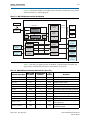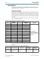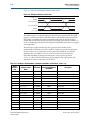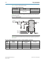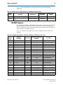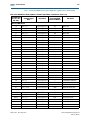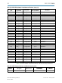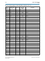
1
Stratix V GX FPGA Development Board Reference Manual 101 Innovation Drive San Jose, CA 95134 www.altera.com MNL-01063-1.5 Feedback Subscribe © 2014 Altera Corporation. All rights reserved. ALTERA, ARRIA, CYCLONE, HARDCOPY, MAX, MEGACORE, NIOS, QUARTUS and STRATIX words and logos are trademarks of Altera Corporation and registered in the U.S. Patent and Trademark Office and in other countries. All other words and logos identified as trademarks or service marks are the property of their respective holders as described at www.altera.com/common/legal.html. Altera warrants performance of its semiconductor products to current specifications in accordance with Altera's standard warranty, but reserves the right to make changes to any products and services at any time without notice. Altera assumes no responsibility or liability arising out of the application or use of any information, product, or service described herein except as expressly agreed to in writing by Altera. Altera customers are advised to obtain the latest version of device specifications before relying on any published information and before placing orders for products or services. October 2014 Altera Corporation ISO 9001:2008 Registered Stratix V GX FPGA Development Board Reference Manual Contents Chapter 1. Overview General Description . . . . . . . . . . . . . . . . . . . . . . . . . . . . . . . . . . . . . . . . . . . . . . . . . . . . . . . . . . . . . . . . . . . . . 1–1 Board Component Blocks . . . . . . . . . . . . . . . . . . . . . . . . . . . . . . . . . . . . . . . . . . . . . . . . . . . . . . . . . . . . . . . . . 1–2 Development Board Block Diagram . . . . . . . . . . . . . . . . . . . . . . . . . . . . . . . . . . . . . . . . . . . . . . . . . . . . . . . . 1–4 Handling the Board . . . . . . . . . . . . . . . . . . . . . . . . . . . . . . . . . . . . . . . . . . . . . . . . . . . . . . . . . . . . . . . . . . . . . . 1–4 Chapter 2. Board Components Board Overview . . . . . . . . . . . . . . . . . . . . . . . . . . . . . . . . . . . . . . . . . . . . . . . . . . . . . . . . . . . . . . . . . . . . . . . . . 2–2 Featured Device: Stratix V GX FPGA . . . . . . . . . . . . . . . . . . . . . . . . . . . . . . . . . . . . . . . . . . . . . . . . . . . . . . . 2–5 I/O Resources . . . . . . . . . . . . . . . . . . . . . . . . . . . . . . . . . . . . . . . . . . . . . . . . . . . . . . . . . . . . . . . . . . . . . . . . 2–5 MAX V CPLD System Controller . . . . . . . . . . . . . . . . . . . . . . . . . . . . . . . . . . . . . . . . . . . . . . . . . . . . . . . . . . 2–6 Configuration, Status, and Setup Elements . . . . . . . . . . . . . . . . . . . . . . . . . . . . . . . . . . . . . . . . . . . . . . . . . 2–12 Configuration . . . . . . . . . . . . . . . . . . . . . . . . . . . . . . . . . . . . . . . . . . . . . . . . . . . . . . . . . . . . . . . . . . . . . . . 2–12 FPGA Programming over On-Board USB-Blaster II . . . . . . . . . . . . . . . . . . . . . . . . . . . . . . . . . . . . . 2–12 FPGA Programming from Flash Memory . . . . . . . . . . . . . . . . . . . . . . . . . . . . . . . . . . . . . . . . . . . . . 2–16 FPGA Programming over External USB-Blaster . . . . . . . . . . . . . . . . . . . . . . . . . . . . . . . . . . . . . . . . 2–17 Status Elements . . . . . . . . . . . . . . . . . . . . . . . . . . . . . . . . . . . . . . . . . . . . . . . . . . . . . . . . . . . . . . . . . . . . . . 2–18 Status LEDs . . . . . . . . . . . . . . . . . . . . . . . . . . . . . . . . . . . . . . . . . . . . . . . . . . . . . . . . . . . . . . . . . . . . . . . 2–18 Setup Elements . . . . . . . . . . . . . . . . . . . . . . . . . . . . . . . . . . . . . . . . . . . . . . . . . . . . . . . . . . . . . . . . . . . . . . 2–19 Board Settings DIP Switch . . . . . . . . . . . . . . . . . . . . . . . . . . . . . . . . . . . . . . . . . . . . . . . . . . . . . . . . . . 2–19 JTAG Control DIP Switch . . . . . . . . . . . . . . . . . . . . . . . . . . . . . . . . . . . . . . . . . . . . . . . . . . . . . . . . . . . 2–20 PCI Express Control DIP Switch . . . . . . . . . . . . . . . . . . . . . . . . . . . . . . . . . . . . . . . . . . . . . . . . . . . . . 2–21 MAX V Reset Push Button . . . . . . . . . . . . . . . . . . . . . . . . . . . . . . . . . . . . . . . . . . . . . . . . . . . . . . . . . . 2–21 Program Load Push Button . . . . . . . . . . . . . . . . . . . . . . . . . . . . . . . . . . . . . . . . . . . . . . . . . . . . . . . . . 2–21 Program Select Push Button . . . . . . . . . . . . . . . . . . . . . . . . . . . . . . . . . . . . . . . . . . . . . . . . . . . . . . . . . 2–22 CPU Reset Push Button . . . . . . . . . . . . . . . . . . . . . . . . . . . . . . . . . . . . . . . . . . . . . . . . . . . . . . . . . . . . . 2–22 Clock Circuitry . . . . . . . . . . . . . . . . . . . . . . . . . . . . . . . . . . . . . . . . . . . . . . . . . . . . . . . . . . . . . . . . . . . . . . . . . 2–23 On-Board Oscillators . . . . . . . . . . . . . . . . . . . . . . . . . . . . . . . . . . . . . . . . . . . . . . . . . . . . . . . . . . . . . . . . . 2–23 Off-Board Clock Input/Output . . . . . . . . . . . . . . . . . . . . . . . . . . . . . . . . . . . . . . . . . . . . . . . . . . . . . . . . 2–25 Memory Clocks . . . . . . . . . . . . . . . . . . . . . . . . . . . . . . . . . . . . . . . . . . . . . . . . . . . . . . . . . . . . . . . . . . . . . . 2–26 General User Input/Output . . . . . . . . . . . . . . . . . . . . . . . . . . . . . . . . . . . . . . . . . . . . . . . . . . . . . . . . . . . . . 2–26 User-Defined Push Buttons . . . . . . . . . . . . . . . . . . . . . . . . . . . . . . . . . . . . . . . . . . . . . . . . . . . . . . . . . . . . 2–26 User-Defined DIP Switches . . . . . . . . . . . . . . . . . . . . . . . . . . . . . . . . . . . . . . . . . . . . . . . . . . . . . . . . . . . . 2–27 User-Defined LEDs . . . . . . . . . . . . . . . . . . . . . . . . . . . . . . . . . . . . . . . . . . . . . . . . . . . . . . . . . . . . . . . . . . . 2–28 General User-Defined LEDs . . . . . . . . . . . . . . . . . . . . . . . . . . . . . . . . . . . . . . . . . . . . . . . . . . . . . . . . . 2–28 HSMC User-Defined LEDs . . . . . . . . . . . . . . . . . . . . . . . . . . . . . . . . . . . . . . . . . . . . . . . . . . . . . . . . . . 2–29 Character LCD . . . . . . . . . . . . . . . . . . . . . . . . . . . . . . . . . . . . . . . . . . . . . . . . . . . . . . . . . . . . . . . . . . . . . . 2–29 Components and Interfaces . . . . . . . . . . . . . . . . . . . . . . . . . . . . . . . . . . . . . . . . . . . . . . . . . . . . . . . . . . . . . . 2–31 PCI Express . . . . . . . . . . . . . . . . . . . . . . . . . . . . . . . . . . . . . . . . . . . . . . . . . . . . . . . . . . . . . . . . . . . . . . . . . 2–31 10/100/1000 Ethernet . . . . . . . . . . . . . . . . . . . . . . . . . . . . . . . . . . . . . . . . . . . . . . . . . . . . . . . . . . . . . . . . 2–34 High-Speed Mezzanine Cards (HSMC) . . . . . . . . . . . . . . . . . . . . . . . . . . . . . . . . . . . . . . . . . . . . . . . . . 2–35 SDI Video Output/Input . . . . . . . . . . . . . . . . . . . . . . . . . . . . . . . . . . . . . . . . . . . . . . . . . . . . . . . . . . . . . . 2–43 40G QSFP Connector . . . . . . . . . . . . . . . . . . . . . . . . . . . . . . . . . . . . . . . . . . . . . . . . . . . . . . . . . . . . . . . . . 2–45 Memory . . . . . . . . . . . . . . . . . . . . . . . . . . . . . . . . . . . . . . . . . . . . . . . . . . . . . . . . . . . . . . . . . . . . . . . . . . . . . . . 2–46 DDR3 . . . . . . . . . . . . . . . . . . . . . . . . . . . . . . . . . . . . . . . . . . . . . . . . . . . . . . . . . . . . . . . . . . . . . . . . . . . . . . 2–46 QDRII+ . . . . . . . . . . . . . . . . . . . . . . . . . . . . . . . . . . . . . . . . . . . . . . . . . . . . . . . . . . . . . . . . . . . . . . . . . . . . . 2–50 RLDRAM II . . . . . . . . . . . . . . . . . . . . . . . . . . . . . . . . . . . . . . . . . . . . . . . . . . . . . . . . . . . . . . . . . . . . . . . . . 2–53 Flash . . . . . . . . . . . . . . . . . . . . . . . . . . . . . . . . . . . . . . . . . . . . . . . . . . . . . . . . . . . . . . . . . . . . . . . . . . . . . . . 2–55 October 2014 Altera Corporation Stratix V GX FPGA Development Board Reference Manual iv ContentsContents Power Supply . . . . . . . . . . . . . . . . . . . . . . . . . . . . . . . . . . . . . . . . . . . . . . . . . . . . . . . . . . . . . . . . . . . . . . . . . . 2–57 Power Distribution System . . . . . . . . . . . . . . . . . . . . . . . . . . . . . . . . . . . . . . . . . . . . . . . . . . . . . . . . . . . . 2–57 Power Measurement . . . . . . . . . . . . . . . . . . . . . . . . . . . . . . . . . . . . . . . . . . . . . . . . . . . . . . . . . . . . . . . . . 2–59 Temperature Sense . . . . . . . . . . . . . . . . . . . . . . . . . . . . . . . . . . . . . . . . . . . . . . . . . . . . . . . . . . . . . . . . . . . . . 2–60 Statement of China-RoHS Compliance . . . . . . . . . . . . . . . . . . . . . . . . . . . . . . . . . . . . . . . . . . . . . . . . . . . . 2–61 Appendix A. Board Revision History Additional Information Document Revision History . . . . . . . . . . . . . . . . . . . . . . . . . . . . . . . . . . . . . . . . . . . . . . . . . . . . . . . . . . . Info–1 How to Contact Altera . . . . . . . . . . . . . . . . . . . . . . . . . . . . . . . . . . . . . . . . . . . . . . . . . . . . . . . . . . . . . . . . Info–3 Typographic Conventions . . . . . . . . . . . . . . . . . . . . . . . . . . . . . . . . . . . . . . . . . . . . . . . . . . . . . . . . . . . . . Info–3 Stratix V GX FPGA Development Board Reference Manual October 2014 Altera Corporation 1. Overview This document describes the hardware features of the Stratix® V GX FPGA development board, including the detailed pin-out and component reference information required to create custom FPGA designs that interface with all components of the board. General Description The Stratix V GX FPGA development board provides a hardware platform for developing and prototyping high-performance and high-bandwidth application designs. The board provides a wide range of peripherals and memory interfaces to facilitate the development of Stratix V GX FPGA designs. Two High-Speed Mezzanine Card (HSMC) connectors are available to add additional functionality via a variety of HSMC cards available from both Altera and various partners. f To see a list of the latest HSMC cards available or to download a copy of the HSMC specification, refer to the Development Board Daughtercards page of the Altera website. Design advancements and innovations, such as the PCI Express hard IP implementation, partial reconfiguration, and programmable power technology ensure that designs implemented in the Stratix V GX FPGAs operate faster, with lower power than in previous FPGA families. f For more information on the following topics, refer to the respective documents: October 2014 ■ Stratix V device family, refer to the Stratix V Device Handbook. ■ PCI Express hard IP implementation, refer to the Stratix V Hard IP for PCI Express User Guide. ■ HSMC Specification, refer to the High Speed Mezzanine Card (HSMC) Specification. Altera Corporation Stratix V GX FPGA Development Board Reference Manual 1–2 Chapter 1: Overview Board Component Blocks Board Component Blocks The board features the following major component blocks: ■ ■ ■ ■ ■ Altera Stratix V FPGA (5SGXEA7K2F40C2N) in the 1517-pin FineLine BGA Package ■ 622,000 LEs ■ 234,720 adaptive logic modules (ALMs) ■ 50-Mbits (Mb) embedded memory ■ 36 transceivers (12.5 Gbps) ■ 174 full-duplex LVDS channels ■ 28 phase locked loops (PLLs) ■ 512 18x18-bit multipliers ■ 900-mV core voltage ■ 696 user I/Os ■ 2 PCI Express hard IP blocks MAX® V CPLD (5M2210ZF256C4) System Controller in the 256-pin FineLine BGA Package ■ 2,210 LEs ■ 203 user I/Os ■ 1.8-V core voltage FPGA Configuration Circuitry ■ MAX II CPLD (EPM570GM100) and Flash Fast Passive Parallel (FPP) configuration ■ On-Board USB-BlasterTM II for use with the Quartus® II Programmer, Nios® II Software Build Tools, and System Console. On-Board Clocking Circuitry ■ 50-MHz, 100-MHz, 125-MHz, and programmable oscillators ■ SMA connector for clock input (LVPECL) Memory devices ■ 1152-Mbyte (MB) DDR3 SDRAM with a 72-bit data bus ■ 72-MB CIO RLDRAM II with a 18-bit data bus ■ 4.5-MB QDRII+ SRAM with a 18-bit data bus (footprint is compatible for 9-Mbyte QDRII with a 18-bit data bus) ■ Two 512-Mb synchronous flash with a 16-bit data bus Stratix V GX FPGA Development Board Reference Manual October 2014 Altera Corporation Chapter 1: Overview Board Component Blocks 1–3 ■ ■ ■ ■ ■ ■ October 2014 Communication Ports ■ PCI Express (PCIe) x8 edge connector ■ Two HSMC ports ■ One universal HSMC port A ■ One DQS-type HSMC port B ■ SMB for SDI input and output ■ QSFP ■ USB 2.0 ■ Gigabit Ethernet ■ LCD header General User I/O ■ 16 user LEDs ■ Two-line character LCD display ■ Six configuration status LEDs ■ One transmit/receive LED (TX/RX) per HSMC interface ■ Five PCI Express LEDs ■ Four Ethernet LEDs Push Buttons and DIP Switches ■ One CPU reset push button ■ Three general user push buttons ■ Two configuration push buttons ■ Eight user DIP switches ■ Four MAX V control DIP switches Power ■ 19-V (laptop) DC input ■ PCI Express edge connector power ■ On-Board power measurement circuitry System Monitoring ■ Power—voltage, current, wattage ■ Temperature—FPGA die, local board Mechanical ■ PCI Express short form factor ■ PCI Express chassis or bench-top operation Altera Corporation Stratix V GX FPGA Development Board Reference Manual 1–4 Chapter 1: Overview Development Board Block Diagram Development Board Block Diagram Figure 1–1 shows the block diagram of the Stratix V GX FPGA Development Board. Figure 1–1. Stratix V GX FPGA Development Board Block Diagram XCVR x6 CLKOUT x3 CLKIN x3 CLKIN x3 JTAG Chain x80 Port B XCVR x8 Port A CLKOUT x3 DQS/Single-Ended On-Board USB- Blaster II and USB Interface x80 Micro-USB 2.0 LVDS/Single-Ended x19 USB Interface QSFP x72 1152 MB DDR3 x18 4.5 MB QDRII+ SRAM x18 72 MB CIO RLDRAM II x4 XCVR REFCLK SMA IN x1 (LVPECL) GigE PHY x1 x4 SDI TX/TX x1 XCVR x4 x8 EPCQ Push Buttons and Switches 5SGXEA7K2F40C2N x32 ADDR x32 Config XCVR x8 x4 x16 Programmable Oscillators 50 MHz, 100 MHz, 148 MHz, 156 MHz x8 Edge CPLD LED x16 x16 512 Mb Flash 512 Mb Flash Handling the Board When handling the board, it is important to observe the following static discharge precaution: c Without proper anti-static handling, the board can be damaged. Therefore, use anti-static handling precautions when touching the board. Stratix V GX FPGA Development Board Reference Manual October 2014 Altera Corporation 2. Board Components This chapter introduces all the important components on the Stratix V GX FPGA Development Board. Figure 2–1 illustrates major component locations and Table 2–1 provides a brief description of all features of the board. 1 A complete set of schematics, a physical layout database, and GERBER files for the development board reside in the Stratix V GX FPGA development kit documents directory. f For information about powering up the board and installing the demo software, refer to the Stratix V GX FPGA Development Kit User Guide. This chapter consists of the following sections: October 2014 ■ “Board Overview” ■ “Featured Device: Stratix V GX FPGA” on page 2–5 ■ “MAX V CPLD System Controller” on page 2–6 ■ “Configuration, Status, and Setup Elements” on page 2–12 ■ “Clock Circuitry” on page 2–23 ■ “General User Input/Output” on page 2–26 ■ “Components and Interfaces” on page 2–31 ■ “Memory” on page 2–46 ■ “Power Supply” on page 2–57 ■ “Statement of China-RoHS Compliance” on page 2–61 Altera Corporation Stratix V GX FPGA Development Board Reference Manual 2–2 Chapter 2: Board Components Board Overview Board Overview This section provides an overview of the Stratix V GX FPGA development board, including an annotated board image and component descriptions. Figure 2–1 provides an overview of the development board features. Figure 2–1. Overview of the Stratix V GX FPGA Development Board Features Stratix V GX FPGA (U15) CPU Reset Push Button (S4) Program Load, Program Select Push Button (S2, S3) User DIP Switch (SW1) General User Push Button Switches (S5, S6, S7) HSMC Port A (J1) HSMC Port B (J2) Program Select LED (D4-D6) Transceiver TX SMA Connectors (J3, J6) MAX V Reset Push Button (S1) Load, Error, Configuration Done LED (D15-D17) DC Input Jack (J4) MAX V CPLD System Controller (U4) DDR3 Memory x8 (U12) x16 (U17, U21, U23, U28) QDRII+ x18 (U5) On-Board USB-Blaster II Connector (J7) Power Switch (SW2) Gigabit Ethernet Port (J9) Flash x32 Memory (U10, U11) JTAG Header (J10) Character LCD (J15) 40G QSFP Connector and Cage Assembly (J12) RLDRAM II x18 Clock Input Memory SMA Connector (U20) (J13, J14) PCI Express Edge Connector (J18) SDI Video Port (J16, J17) Fan Power Header (J11) Table 2–1 describes the components and lists their corresponding board references. Table 2–1. Stratix V GX FPGA Development Board Components (Part 1 of 4) Board Reference Type Description Featured Devices U15 FPGA 5SGXEA7K2F40C2N, 1517-pin BGA. U4 CPLD 5M2210ZF256C4, 256-pin BGA. Configuration, Status, and Setup Elements J10 JTAG header Provides access to the JTAG chain by using an external USB-Blaster cable (disables the on-board USB-Blaster II). J7 On-Board USB-Blaster II Micro-USB 2.0 connector for programming and debugging the FPGA. SW3 JTAG DIP switch Enables and disables devices in the JTAG chain. This switch is located on the back of the board. SW4 FPGA mode select DIP switch Sets the Stratix V MSEL[4:0] pins. Board settings DIP switch Controls the MAX V CPLD System Controller functions such as clock select, clock enable, factory or user design load from flash and FACTORY signal command sent at power up. This switch is located at the bottom of the board. SW5 Stratix V GX FPGA Development Board Reference Manual October 2014 Altera Corporation Chapter 2: Board Components Board Overview 2–3 Table 2–1. Stratix V GX FPGA Development Board Components (Part 2 of 4) Board Reference Type Description SW6 PCI Express DIP switch Controls the PCI Express lane width by connecting prsnt pins together on the PCI Express edge connector. This switch is located at the back of the board. S3 Program select push button Toggles the program LEDs which selects the program image that loads from flash memory to the FPGA. S2 Program load push button Configures the FPGA from flash memory image based on the program LEDs. D4, D5, D6 Program LEDs Illuminates to show the LED sequence that determines which flash memory image loads to the FPGA when you press the program load push button. D17 Configuration done LED Illuminates when the FPGA is configured. D15 Load LED Illuminates during FPGA configuration. D16 Error LED Illuminates when the FPGA configuration from flash fails. D24 Power LED Illuminates when 5-V power is present. D25, D26 System Console TX/RX LEDs Indicate the transmit or receive activity of the System Console USB interface. The TX and RX LEDs would flicker if the link is in use and active. The LEDs are either off when not in use or on when in use but idle. D27, D28 JTAG TX/RX LEDs Indicate the transmit or receive activity of the JTAG chain. The TX and RX LEDs would flicker if the link is in use and active. The LEDs are either off when not in use or on when in use but idle. D29, D30, D31, D32 Ethernet LEDs Indicate the connection speed as well as transmit or receive activity. D3, D13 HSMC port A LEDs You can configure these LEDs to indicate transmit or receive activity. D1 HSMC port A Present LED Illuminates when a daughtercard is plugged into the HSMC port A. D11, D14 HSMC port B LEDs You can configure these LEDs to indicate transmit or receive activity. D2 HSMC port B Present LED Illuminates when a daughtercard is plugged into the HSMC port B. D33, D34 PCI Express Gen2/Gen3 LED You can configure these LEDs to illuminate when PCI Express is in Gen2 or Gen3 mode. D35, D36, D37 PCI Express Link LEDs You can configure these LEDs to display the PCI Express link width (x1, x4, x8). X1 125 M oscillator 125.000-MHz crystal oscillator for Gigabit Ethernet, Serial RapidIO™ (SRIO), or PCI Express. U38 Quad-output oscillator Programmable oscillator with default frequencies of 100 MHz, 156.25 MHz, 625 MHz, and 270 MHz. U46 Quad-output oscillator Programmable oscillator with default frequencies of 125 MHz, 644.53125 MHz, 282.5 MHz, and 125 MHz. X6 148.5 M oscillator 148.500-MHz voltage controlled crystal oscillator for SDI video. This oscillator is programmable to any frequency between 20-810 MHz. 100 M oscillator 100.000-MHz (programmable to any frequency between 20–810 MHz) crystal oscillator for PCI Express or general use such as memories. Multiplex with CLKIN_SMA_P or CLKIN_SMA_N based on CLK_SEL switch value. Clock Circuitry X4 October 2014 Altera Corporation Stratix V GX FPGA Development Board Reference Manual 2–4 Chapter 2: Board Components Board Overview Table 2–1. Stratix V GX FPGA Development Board Components (Part 3 of 4) Board Reference Type Description X3 50 M oscillator 50.000-MHz crystal oscillator for general purpose logic. J13, J14 Clock input SMAs Drives LVPECL-compatible clock inputs into the clock multiplexer buffer. U4 100 M oscillator 100-MHz crystal oscillator for the MAX V CPLD System Controller. General User Input and Output D7-D10, D18-D21 User LEDs Eight bi-color LEDs (green and red) for 16 user LEDs. Illuminates when driven low. SW1 User DIP switch Octal user DIP switches. When the switch is ON, a logic 0 is selected. S1 MAX V reset push button The default reset for the MAX V CPLD System Controller. S4 CPU reset push button The default reset for the FPGA logic. S5, S6, S7 General user push button Three user push buttons. Driven low when pressed. U12, U17, U21, U23, U28 DDR3 x72 A 1152-MB DDR3 SDRAM with a 72-bit data bus. The 72-bit data bus consists of four x16 devices and one x8 device with a single address or command bus. U5 QDRII+ x18 A 4.5-MB QDRII+ SRAM with a 18-bit data bus. The device has a separate 18-bit read and 18-bit write port with DDR signalling at up to 550 MHz. U20 RLDRAM II x18 A 72-MB CIO RLDRAM II with a 18-bit data bus. The 18-bit data bus consists of a single x18 device with a single address or command bus. Flash x32 Two 512-Mb synchronous flash devices with a 16-bit data buses for non-volatile memory. The board supports two flash devices of 16-bit interface each, which combine to allow for 1-Gbyte (GB) synchronous flash with a 32-bit data bus. Memory Devices U10, U11 Communication Ports J18 PCI Express edge connector Made of gold-plated edge fingers for up to ×8 signaling in either Gen1, Gen2, or Gen3 mode. J12 QSFP connector Provides four transceiver channels for a 40G QSFP module. J1 HSMC port A Provides eight transceiver channels and 84 CMOS or 17 LVDS channels per the HSMC specification. J2 HSMC port B Provides four transceiver channels and 84 CMOS or a DQ/DQS interface. J9 Gigabit Ethernet port RJ-45 connector which provides a 10/100/1000 Ethernet connection via a Marvell 88E1111 PHY and the FPGA-based Altera Triple Speed Ethernet MAC MegaCore function in SGMII mode. Video and Display Ports J16, J17 SDI video port Two 75- system management bus (SMB) connectors which provide a full-duplex SDI interface through a LMH0303 driver and LMH0384 cable equalizer. J15 Character LCD header A single 14-pin 0.1" pitch dual-row header which interfaces to the 16 character × 2 line LCD module. Stratix V GX FPGA Development Board Reference Manual October 2014 Altera Corporation Chapter 2: Board Components Featured Device: Stratix V GX FPGA 2–5 Table 2–1. Stratix V GX FPGA Development Board Components (Part 4 of 4) Board Reference Type Description Power Supply J18 PCI Express edge connector Interfaces to a PCI Express root port such as an appropriate PC motherboard. J4 DC input jack Accepts a 19-V DC power supply. SW2 Power switch Switch to power on or off the board when power is supplied from the DC input jack. Featured Device: Stratix V GX FPGA The Stratix V GX FPGA development board features the Stratix V GX FPGA 5SGXEA7K2F40C2N device (U15) in a 1517-pin FineLine BGA package. f For more information about the Stratix V device family, refer to the Stratix V Device Handbook. Table 2–2 describes the features of the Stratix V GX FPGA 5SGXEA7K2F40C2N device. Table 2–2. Stratix V GX FPGA 5SGXEA7K2F40C2N Features ALMs Equivalent LEs Registers M20K Blocks MLAB Blocks (Mb) 18-bit × 18-bit Multipliers PLLs Transceiver Channels (12.5 Gbps) Package Type 234,720 622,000 939,000 2,560 7.16 512 28 36 1517-pin FineLine BGA Table 2–3 lists the Stratix V GX FPGA component reference and manufacturing information. Table 2–3. Stratix V GX FPGA Component Reference and Manufacturing Information Board Reference Manufacturer Manufacturing Part Number Manufacturer Website Altera Corporation 5SGXEA7K2F40C2N www.altera.com Description FPGA, Stratix V GX F1517, 622K LEs, lead free U15 I/O Resources Table 2–4 lists the Stratix V GX FPGA device pin count and usage by function on the development board. Table 2–4. Stratix V GX FPGA Pin Count and Usage (Part 1 of 2) Function I/O Standard I/O Count Special Pins DDR3 1.5-V SSTL 126 1 Diff ×9DQS RLDRAM II 1.8-V SSTL 57 1 Diff ×2 DQS QDRII+ SRAM 1.8-V HSTL 67 1 Diff ×2 DQS MAX V System Controller 1.5-V CMOS 8 — October 2014 Altera Corporation Stratix V GX FPGA Development Board Reference Manual 2–6 Chapter 2: Board Components MAX V CPLD System Controller Table 2–4. Stratix V GX FPGA Pin Count and Usage (Part 2 of 2) Function I/O Standard I/O Count Special Pins 1.8-V CMOS 68 — 2.5-V CMOS + XCVR 43 1 REFCLK Flash PCI Express ×8 HSMC Port A 2.5-V CMOS + LVDS + XCVR 118 1 REFCLK HSMC Port B 2.5-V CMOS + DQS + XCVR 104 1 REFCLK 2.5-V CMOS + LVDS 8 — 1.5-V CMOS 18 — 3.3-V CMOS 1 — SDI Video 2.5-V CMOS + XCVR 8 1 REFCLK QSFP 2.5-V CMOS + XCVR 23 1 REFCLK Buttons 1.8/2.5-V CMOS 4 1 DEV_CLRn Switches 1.8-V CMOS 8 — Character LCD 2.5-V CMOS 11 — 1.8/2.5-V CMOS 16 — 1.8-V CMOS + LVDS 25 9 REFCLK Gigabit Ethernet On-Board USB-Blaster II LEDs Clocks or Oscillators 713 Device I/O Total: MAX V CPLD System Controller The board utilizes the 5M2210ZF256C4 System Controller, an Altera MAX V CPLD, for the following purposes: ■ FPGA configuration from flash memory ■ Power consumption monitoring ■ Temperature monitoring ■ Fan control ■ Control registers for clocks ■ Control registers for remote system update Stratix V GX FPGA Development Board Reference Manual October 2014 Altera Corporation Chapter 2: Board Components MAX V CPLD System Controller 2–7 Figure 2–2 illustrates the MAX V CPLD System Controller's functionality and external circuit connections as a block diagram. Figure 2–2. MAX V CPLD System Controller Block Diagram MAX V System Controller PC JTAG Control Information Register On-Board USB-Blaster II FSM BUS FPGA SLD-HUB Flash Control Register Flash Decoder Virtual-JTAG Encoder PFL Power Measurement Results Temperature Measurement Results GPIO Si570 Programmable Oscillator LTC2418 Controller Si570 Controller LTC2990 Controller Si571 Controller Si571 Programmable Oscillator MAX1619 Controller Si5538 Controller Si5338 Programmable Oscillator Si5338 Programmable Oscillator Table 2–5 lists the I/O signals present on the MAX V CPLD System Controller. The signal names and functions are relative to the MAX V device (U4). Table 2–5. MAX V CPLD System Controller Device Pin-Out (Part 1 of 6) Schematic Signal Name MAX V CPLD Stratix V GX FPGA Pin Number Pin Number I/O Standard Description 5M2210_JTAG_TMS N4 — 2.5-V MAX V JTAG TMS CLK125_EN B9 — 2.5-V 125 MHz oscillator enable CLK50_EN E9 — 2.5-V 50 MHz oscillator enable CLK_CONFIG J5 — 2.5-V 100 MHz configuration clock input CLK_ENABLE A15 — 2.5-V DIP switch for clock oscillator enable CLK_SEL A13 — 2.5-V DIP switch for clock select SMA or oscillator CLKIN_50 J12 AN6 1.8-V 50 MHz clock input CLOCK_SCL C9 — 2.5-V Programmable oscillator I2C clock CLOCK_SDA D9 — 2.5-V Programmable oscillator I2C data CPU_RESETn D10 AM34 2.5-V FPGA reset push button FACTORY_LOAD A2 — 2.5-V DIP - load factory image or user1 image from flash at power-up FACTORY_REQUEST R14 — 1.8-V On-Board USB-Blaster II request to send FACTORY command October 2014 Altera Corporation Stratix V GX FPGA Development Board Reference Manual 2–8 Chapter 2: Board Components MAX V CPLD System Controller Table 2–5. MAX V CPLD System Controller Device Pin-Out (Part 2 of 6) Schematic Signal Name MAX V CPLD Stratix V GX FPGA Pin Number Pin Number I/O Standard Description FACTORY_STATUS N12 — 1.8-V On-Board USB-Blaster II FACTORY command status FLASH_ADVn N7 AP7 1.8-V FM bus flash memory address valid FLASH_CEn0 R5 AV14 1.8-V FM bus flash memory chip enable 0 FLASH_CEn1 M7 AW13 1.8-V FM bus flash memory chip enable 1 FLASH_CLK R6 AM8 1.8-V FM bus flash memory clock FLASH_OEn M6 AJ7 1.8-V FM bus flash memory output enable FLASH_RDYBSYN0 T5 AL6 1.8-V FM bus flash memory chip ready 0 FLASH_RDYBSYN1 R7 AN7 1.8-V FM bus flash memory chip ready 1 FLASH_RESETn P7 AJ6 1.8-V FM bus flash memory reset FLASH_WEn N6 AN8 1.8-V FM bus flash memory write enable FM_A0 E14 AW19 1.8-V FM address bus FM_A1 C14 AV19 1.8-V FM address bus FM_A2 C15 AM16 1.8-V FM address bus FM_A3 E13 AL16 1.8-V FM address bus FM_A4 E12 AF16 1.8-V FM address bus FM_A5 D15 AG16 1.8-V FM address bus FM_A6 F14 AN17 1.8-V FM address bus FM_A7 D16 AM17 1.8-V FM address bus FM_A8 F13 AP16 1.8-V FM address bus FM_A9 E15 AN16 1.8-V FM address bus FM_A10 E16 AT17 1.8-V FM address bus FM_A11 F15 AR17 1.8-V FM address bus FM_A12 G14 AU16 1.8-V FM address bus FM_A13 F16 AU17 1.8-V FM address bus FM_A14 G13 AW16 1.8-V FM address bus FM_A15 G15 AV16 1.8-V FM address bus FM_A16 G12 AW17 1.8-V FM address bus FM_A17 G16 AV17 1.8-V FM address bus FM_A18 H14 AU6 1.8-V FM address bus FM_A19 H15 AT6 1.8-V FM address bus FM_A20 H13 AL17 1.8-V FM address bus FM_A21 H16 AK17 1.8-V FM address bus FM_A22 J13 AE16 1.8-V FM address bus FM_A23 R3 AE17 1.8-V FM address bus FM_A24 P5 AH16 1.8-V FM address bus FM_A25 T2 AP21 1.8-V FM address bus FM_D0 J14 AN21 1.8-V FM data bus FM_D1 J15 AD21 1.8-V FM data bus Stratix V GX FPGA Development Board Reference Manual October 2014 Altera Corporation Chapter 2: Board Components MAX V CPLD System Controller 2–9 Table 2–5. MAX V CPLD System Controller Device Pin-Out (Part 3 of 6) Schematic Signal Name MAX V CPLD Stratix V GX FPGA Pin Number Pin Number I/O Standard Description FM_D2 K16 AD20 1.8-V FM data bus FM_D3 K13 AG21 1.8-V FM data bus FM_D4 K15 AH21 1.8-V FM data bus FM_D5 K14 AE21 1.8-V FM data bus FM_D6 L16 AE20 1.8-V FM data bus FM_D7 L11 AL22 1.8-V FM data bus FM_D8 L15 AK21 1.8-V FM data bus FM_D9 L12 AJ21 1.8-V FM data bus FM_D10 M16 AJ20 1.8-V FM data bus FM_D11 L13 AL21 1.8-V FM data bus FM_D12 M15 AL20 1.8-V FM data bus FM_D13 L14 AN25 1.8-V FM data bus FM_D14 N16 AM25 1.8-V FM data bus FM_D15 M13 AP24 1.8-V FM data bus FM_D16 N15 AN24 1.8-V FM data bus FM_D17 N14 AC24 1.8-V FM data bus FM_D18 P15 AB24 1.8-V FM data bus FM_D19 P14 AF25 1.8-V FM data bus FM_D20 D13 AE25 1.8-V FM data bus FM_D21 D14 AE24 1.8-V FM data bus FM_D22 F11 AD24 1.8-V FM data bus FM_D23 J16 AG24 1.8-V FM data bus FM_D24 F12 AH24 1.8-V FM data bus FM_D25 K12 AK24 1.8-V FM data bus FM_D26 M14 AJ24 1.8-V FM data bus FM_D27 N13 AL24 1.8-V FM data bus FM_D28 R1 AL25 1.8-V FM data bus FM_D29 P4 AW25 1.8-V FM data bus FM_D30 N5 AV25 1.8-V FM data bus FM_D31 P6 AT24 1.8-V FM data bus FPGA_CONF_DONE K1 AH6 2.5-V FPGA configuration done FPGA_CONFIG_D0 D3 AP33 2.5-V FPGA configuration data FPGA_CONFIG_D1 C2 AT33 2.5-V FPGA configuration data FPGA_CONFIG_D2 C3 AR33 2.5-V FPGA configuration data FPGA_CONFIG_D3 E3 AU34 2.5-V FPGA configuration data FPGA_CONFIG_D4 D2 AU33 2.5-V FPGA configuration data FPGA_CONFIG_D5 E4 AN31 2.5-V FPGA configuration data FPGA_CONFIG_D6 D1 AM31 2.5-V FPGA configuration data FPGA_CONFIG_D7 E5 AU32 2.5-V FPGA configuration data October 2014 Altera Corporation Stratix V GX FPGA Development Board Reference Manual 2–10 Chapter 2: Board Components MAX V CPLD System Controller Table 2–5. MAX V CPLD System Controller Device Pin-Out (Part 4 of 6) Schematic Signal Name MAX V CPLD Stratix V GX FPGA Pin Number Pin Number I/O Standard Description FPGA_CONFIG_D8 F3 AT32 2.5-V FPGA configuration data FPGA_CONFIG_D9 E1 AR31 2.5-V FPGA configuration data FPGA_CONFIG_D10 F4 AP31 2.5-V FPGA configuration data FPGA_CONFIG_D11 F2 AW34 2.5-V FPGA configuration data FPGA_CONFIG_D12 F1 AV34 2.5-V FPGA configuration data FPGA_CONFIG_D13 F6 AW31 2.5-V FPGA configuration data FPGA_CONFIG_D14 G2 AV31 2.5-V FPGA configuration data FPGA_CONFIG_D15 G3 AW32 2.5-V FPGA configuration data FPGA_CONFIG_D16 G1 AV32 2.5-V FPGA configuration data FPGA_CONFIG_D17 G4 AJ33 2.5-V FPGA configuration data FPGA_CONFIG_D18 H2 AH33 2.5-V FPGA configuration data FPGA_CONFIG_D19 G5 AL33 2.5-V FPGA configuration data FPGA_CONFIG_D20 H3 AK33 2.5-V FPGA configuration data FPGA_CONFIG_D21 J1 AK32 2.5-V FPGA configuration data FPGA_CONFIG_D22 J2 AJ32 2.5-V FPGA configuration data FPGA_CONFIG_D23 H5 AH31 2.5-V FPGA configuration data FPGA_CONFIG_D24 K2 AG31 2.5-V FPGA configuration data FPGA_CONFIG_D25 K5 AF31 2.5-V FPGA configuration data FPGA_CONFIG_D26 L1 AE31 2.5-V FPGA configuration data FPGA_CONFIG_D27 L2 AJ30 2.5-V FPGA configuration data FPGA_CONFIG_D28 K3 AH30 2.5-V FPGA configuration data FPGA_CONFIG_D29 M2 AR30 2.5-V FPGA configuration data FPGA_CONFIG_D30 L4 AP30 2.5-V FPGA configuration data FPGA_CONFIG_D31 L3 AU30 2.5-V FPGA configuration data FPGA_CVP_CONFDONE N3 AT29 2.5-V FPGA configuration via protocol done FPGA_DCLK J3 AC31 2.5-V FPGA configuration clock FPGA_nCONFIG N1 AK35 2.5-V FPGA configuration active FPGA_nSTATUS J4 AM5 2.5-V FPGA configuration ready status FPGA_PR_DONE H1 AT30 2.5-V FPGA partial reconfiguration done FPGA_PR_ERROR P2 AU29 2.5-V FPGA partial reconfiguration error FPGA_PR_READY E2 AN29 2.5-V FPGA partial reconfiguration ready FPGA_PR_REQUEST F5 AN30 2.5-V FPGA partial reconfiguration request HSMA_PRSNTn B8 AW8 2.5-V HSMC port A present HSMB_PRSNTn A8 AU7 2.5-V HSMC port B present M570_CLOCK P11 — 1.8-V 25-MHz clock to on-board USB-Blaster for sending FACTORY command M570_PCIE_JTAG_EN P12 — 1.8-V A low signal disables the on-board USB-Blaster when PCIe masters the JTAG MAX5_BEN0 P10 U31 1.8-V MAX V byte enable 0 Stratix V GX FPGA Development Board Reference Manual October 2014 Altera Corporation Chapter 2: Board Components MAX V CPLD System Controller 2–11 Table 2–5. MAX V CPLD System Controller Device Pin-Out (Part 5 of 6) Schematic Signal Name MAX V CPLD Stratix V GX FPGA Pin Number Pin Number I/O Standard Description MAX5_BEN1 R11 T31 1.8-V MAX V byte enable 1 MAX5_BEN2 T12 N33 1.8-V MAX V byte enable 2 MAX5_BEN3 N11 M33 1.8-V MAX V byte enable 3 MAX5_CLK T11 E34 1.8-V MAX V clock MAX5_CSN R10 B32 1.8-V MAX V chip select MAX5_OEN M10 A32 1.8-V MAX V output enable MAX5_WEN N10 A34 1.8-V MAX V write enable MAX_CONF_DONE E11 — 1.8-V FPGA configuration done LED MAX_ERROR A4 — 1.8-V FPGA configuration error LED MAX_LOAD A6 — 1.8-V FPGA configuration active LED MAX_RESETn M9 — 1.8-V MAX V reset push button MSEL0 B10 AA9 2.5-V DIP switch for FPGA mode select 0 MSEL1 B3 AA10 2.5-V DIP switch for FPGA mode select 1 MSEL2 C10 AD8 2.5-V DIP switch for FPGA mode select 2 MSEL3 C12 AG8 2.5-V DIP switch for FPGA mode select 3 MSEL4 C6 AH7 2.5-V DIP switch for FPGA mode select 4 OVERTEMP B7 — 2.5-V Temperature monitor fan enable OVERTEMPn C8 — 2.5-V Temperature monitor over-temperature indicator LED PCIE_JTAG_EN C7 — 2.5-V DIP switch to enable the PCIe JTAG master PGM_CONFIG D12 — 2.5-V Loads the flash memory image identified by the PGM LEDs PGM_LED0 B14 — 2.5-V Flash memory PGM select indicator 0 PGM_LED1 C13 — 2.5-V Flash memory PGM select indicator 1 PGM_LED2 B16 — 2.5-V Flash memory PGM select indicator 2 PGM_SEL B13 — 2.5-V Toggles the PGM_LED[0:2] sequence SDI_RX_BYPASS D5 AB30 2.5-V SDI equalization bypass SDI_RX_EN E8 AB28 2.5-V SDI receive enable SDI_TX_EN D11 AK27 2.5-V SDI transmit enable SECURITY_MODE R12 — 1.8-V DIP switch for on-board USB-Blaster II to send FACTORY command at power up. SENSE_CS0n E7 — 2.5-V Power monitor chip select SENSE_SCK A5 — 2.5-V Power monitor SPI clock SENSE_SDI D7 — 2.5-V Power monitor SPI data in SENSE_SDO B6 — 2.5-V Power monitor SPI data out SENSE_SMB_CLK D8 — 2.5-V Temperature monitor SMB clock SENSE_SMB_DATA A7 — 2.5-V Temperature monitor SMB data SI570_EN A10 — 2.5-V Si570 programmable oscillator enable October 2014 Altera Corporation Stratix V GX FPGA Development Board Reference Manual 2–12 Chapter 2: Board Components Configuration, Status, and Setup Elements Table 2–5. MAX V CPLD System Controller Device Pin-Out (Part 6 of 6) Schematic Signal Name MAX V CPLD Stratix V GX FPGA Pin Number Pin Number I/O Standard Description SI571_EN D4 — 2.5-V Si571 programmable VCXO enable TSENSE_ALERTn B5 — 2.5-V Temperature monitor alert Table 2–6 lists the MAX V CPLD System Controller component reference and manufacturing information. Table 2–6. MAX V CPLD EPM2210 System Controller Component Reference and Manufacturing Information Board Reference U4 Description MAX V CPLD 2210 LE 256FBGA LF 1.8V VCCINT Manufacturer Manufacturing Part Number Manufacturer Website Altera Corporation 5M2210ZF256C4N www.altera.com Configuration, Status, and Setup Elements This section describes the board's configuration, status, and setup elements. Configuration This section describes the FPGA, flash memory, and MAX V CPLD System Controller device programming methods that the Stratix V GX FPGA development board supports. The Stratix V GX FPGA development board supports three configuration methods: ■ On-Board USB-Blaster II is the default method for configuring the FPGA at any time using the Quartus II Programmer in JTAG mode with the supplied micro-USB cable. ■ Flash memory download for configuring the FPGA using stored images from the flash memory on either power-up or pressing the program load push button (S2). ■ External USB-Blaster for configuring the FPGA using the external USB-Blaster. FPGA Programming over On-Board USB-Blaster II The on-board USB-Blaster II is implemented using a micro-USB type-B connector (J7), a USB 2.0 PHY device, and an Altera MAX II CPLD EPM570GM100 (U14). This allows the configuration of the FPGA using a USB cable which connects directly between the USB port on the board (J7) and a USB port on a PC running the Quartus II software. The on-board USB-Blaster II normally masters the JTAG chain. f For more information about the on-board USB-Blaster II, refer to the on-board USB-Blaster II page of the Altera Wiki website. Stratix V GX FPGA Development Board Reference Manual October 2014 Altera Corporation Chapter 2: Board Components Configuration, Status, and Setup Elements 2–13 MAX II CPLD EPM570GM100 The MAX II CPLD is dedicated to the on-board USB-Blaster II functionality. The CPLD connects to the CY7C68013A USB 2.0 PHY device on one side and drives the JTAG and System Console direct USB signals out the other side through the general purpose I/O (GPIO) pins. Table 2–7 lists the I/O signals present on the MAX II CPLD EPM570GM100. Table 2–7. MAX II CPLD EPM570GM100 On-Board USB-Blaster II I/O Signals Schematic Signal Name Type Description SC_RX 1.5-V CMOS output USB system console receive LED SC_TX 1.5-V CMOS output USB system console transmit LED JTAG_RX 1.5-V CMOS output USB-Blaster II JTAG receive LED JTAG_TX 1.5-V CMOS output USB-Blaster II JTAG transmit LED C_JTAG_TCK 2.5-V CMOS output GPIO for on-board JTAG chain clock C_JTAG_TMS 2.5-V CMOS output GPIO for on-board JTAG chain mode C_JTAG_TDI 2.5-V CMOS output GPIO for on-board JTAG chain data in C_JTAG_TDO 2.5-V CMOS input GPIO for on-board JTAG chain data out USB_CLK 3.3-V CMOS input USB System Console clock USB_OEn 1.5-V CMOS output USB System Console FPGA output enable USB_RESETn 1.5-V CMOS output USB System Console reset 1.5-V CMOS inout (8 bits) USB System Console FIFO data bus USB_RDn 1.5-V CMOS output USB System Console read from FIFO USB_WRn 1.5-V CMOS output USB System Console write to FIFO USB_EMPTY 1.5-V CMOS input USB System Console FIFO empty USB_FULL 1.5-V CMOS input USB System Console FIFO full USB_DATA(7:0) USB_ADDR(1:0) 1.5-V CMOS input/output USB System Console address bus USB_SCL 1.5-V CMOS input/output USB System Console configuration clock USB_SDA 1.5-V CMOS input/output USB System Console configuration data FACTORY_REQUEST 1.5-V CMOS output Send FACTORY command FACTORY_STATUS 1.5-V CMOS input FACTORY command status M570_CLOCK 1.5-V CMOS output 25-MHz input clock for FACTORY command October 2014 Altera Corporation Stratix V GX FPGA Development Board Reference Manual 2–14 Chapter 2: Board Components Configuration, Status, and Setup Elements JTAG Chain The on-board USB-Blaster II is automatically disabled when you connect an external USB-Blaster to the JTAG chain or when you enable JTAG from the PCI Express edge connector. Figure 2–3 illustrates the JTAG chain. Figure 2–3. JTAG Chain ENABLE TCK DIP Switch DISABLE Level Translator 10-pin JTAG Header PCI Express Edge TDI Connector TDO TMS PCI Express Motherboard JTAG Master GPIO TCK GPIO TCK TMS Cypress GPIO On-Board GPIO USB-Blaster II GPIO TMS Stratix V GX FPGA TDI TDO TDI 2.5 V TDO ALWAYS ENABLED (in chain) JTAG Slave JTAG Master TCK TMS TDI 2.5 V HSMC Port A Installed HSMC Card TDO ENABLE JTAG Slave Analog Switch DIP Switch TCK TMS TDI 2.5 V HSMC Port B Installed HSMC Card TDO ENABLE JTAG Slave Analog Switch DIP Switch TCK TMS TDI MAX V System Controller Flash Memory TDO ENABLE Analog Switch JTAG Slave DIP Switch Each jumper shown in Figure 2–3 is located in the JTAG DIP switch (SW3) on the back of the board. To connect a device or interface in the chain, their corresponding switch must be in the OFF position. Push all the switches in the ON position to only have the FPGA in the chain. Note that the MAX V CPLD System Controller must be in the chain to use some of the GUI interfaces. Stratix V GX FPGA Development Board Reference Manual October 2014 Altera Corporation Chapter 2: Board Components Configuration, Status, and Setup Elements 1 2–15 By default, the on-board USB-Blaster II clocks TCK at 24 MHz. For the on-board USB-Blaster II to function correctly, you must set the Quartus II clock constraint on the internal_tck input signal to 24 MHz. System Console USB Interface The System Console USB interface is a fast parallel interface. Together with the soft logic supplied by Altera, this interface provides a System Console master for debug access. The System Console controls the debug master via signals shown in Table 2–8 to give fast access to an Avalon® Memory-Mapped (Avalon-MM) master bus that the Qsys system integration tool generates. f For more information about the System Console, refer to the Analyzing and Debugging Designs with the System Console chapter in volume 3 of the Quartus II Handbook. Table 2–8 lists the System Console USB interface pin connections relative to the FPGA. Table 2–8. System Console USB Interface Pin Connections Stratix V GX FPGA Device Pin Number Schematic Signal Name Direction Note AV28 usb_clk input 48 MHz H34 usb_reset_n input — G32, G33, F32, E32, A37, A36, C34, A35 usb_data[7:0] bidirectional G32(MSB), A35 (LSB) N34 usb_full output — P34 usb_empty output — J33 usb_wr_n input — K33 usb_rd_n input — E33 usb_oe_n input — G34, K34 usb_addr bidirectional Reserved J34 usb_scl bidirectional — F33 usb_sda bidirectional — Flash Programming Flash programming is possible through a variety of methods using the Stratix V GX FPGA device. The first method is to use the factory design called the Board Update Portal. This design is an embedded web server, which serves the Board Update Portal web page. The web page allows you to select new FPGA designs including hardware, software, or both in an industry-standard S-Record File (.flash) and write the design to the user hardware page (page 1) of the flash over the network. October 2014 Altera Corporation Stratix V GX FPGA Development Board Reference Manual 2–16 Chapter 2: Board Components Configuration, Status, and Setup Elements The secondary method is to use the pre-built PFL design included in the development kit. The development board implements the Altera PFL megafunction for flash programming. The PFL megafunction is a block of logic that is programmed into an Altera programmable logic device (FPGA or CPLD). The PFL functions as a utility for writing to a compatible flash device. This pre-built design contains the PFL megafunction that allows you to write either page 0, page 1, or other areas of flash over the USB interface using the Quartus II software. Use this method to restore the development board to its factory default settings. Other methods to program the flash can be used as well, including the Nios II processor. f For more information on the Nios II processor, refer to the Nios II Processor page of the Altera website. FPGA Programming from Flash Memory On either power-up or by pressing the program load push button (S2), the MAX V CPLD System Controller’s parallel flash loader configures the FPGA from the flash memory. The system controller uses the Altera Parallel Flash Loader (PFL) megafunction which reads 32-bit data from the flash memory and converts it to fast passive parallel (FPP) format. This 32-bit data is then written to the FPGA’s dedicated configuration pins during configuration. After a power-up or reset event, the MAX V CPLD (U4) automatically configures the FPGA in FPP mode with either the pre-installed factory .pof file or a user .pof file depending on the setting of the PGM_SEL push-button (S3). There are three pages reserved for the FPGA configuration data—factory hardware (page 0), user hardware 1 (page 1), and user hardware 2 (page 2). Three green configuration status LEDs, PGM_LED[2:0] (D4, D5, D6) indicates the status of the FPP configuration. Table 2–9 lists the configuration status LEDs settings. Table 2–9. Configuration LED settings (1) LED Design PGM_LED0 PGM_LED1 PGM_LED2 v — — Factory — v — User hardware 1 — — v User hardware 2 Note to Table 2–9: (1) A checkmark (v) indicates that the LED is ON (logic 0) while a dash (—) indicates that the LED is OFF (logic 1). Stratix V GX FPGA Development Board Reference Manual October 2014 Altera Corporation Chapter 2: Board Components Configuration, Status, and Setup Elements 2–17 Figure 2–4 shows the PFL configuration. Figure 2–4. PFL Configuration 2.5 V 2.5 V 56.2 Ω 2.5 V 2.5 V 56.2 Ω 10 kΩ MAX V CPLD System Controller 10 kΩ 2.5 V 50 MHz 1 kΩ 100 MHz ERROR LOAD FACTORY DIP Switch FPGA_INIT_DONE USB-BLASTER FPGA_nSTATUS FPGA_nCONFIG FPGA_CONF_DONE CLK_SEL CLK_ENABLE CONF_DONE USER_PGM FPGA_DATA [0] USB_SELECT FPGA_DCLK MAX_RESETn 2.5 V PGM_CONFIG 56.2 Ω PGM_SEL PGM_LED0 PGM_LED1 MSEL4 MSEL3 MSEL2 MSEL1 MSEL0 INIT_DONE nSTATUS nCONFIG CONF_DONE nCE CONF_DONE LED MSEL[4:0] also connects to MAX V 1 kΩ DATA [0] DCLK FM Bus Interface FLASH_A [25:1] FLASH_D [31:0] FLASH_CEn FLASH_OEn FLASH_WEn FLASH_RYBSYn FLASH_CLK FLASH_RSTn FLASH_ADVn PGM_LED2 CFI Flash 1.8 V FLASH_A [25:0] FLASH_D [15:0] FLASH_CEn FLASH_OEn FLASH_WEn FLASH_RYBSYn FLASH_CLK FLASH_RESETn 10 kΩ FLASH_WPn FLASH_ADVn CFI Flash FLASH_A [25:0] FLASH_D [15:0] FLASH_CEn FLASH_OEn FLASH_WEn FLASH_RYBSYn FLASH_CLK FLASH_RESETn FLASH_WPn FLASH_ADVn 10 kΩ f For more information on the flash memory map storage, refer to the Stratix V GX FPGA Development Kit User Guide. FPGA Programming over External USB-Blaster The JTAG programming header provides another method for configuring the FPGA (U15) using an external USB-Blaster device with the Quartus II Programmer running on a PC. The external USB-Blaster connects to the board through the JTAG header (J10). October 2014 Altera Corporation Stratix V GX FPGA Development Board Reference Manual 2–18 Chapter 2: Board Components Configuration, Status, and Setup Elements f For more information on the following topics, refer to the respective documents: ■ Board Update Portal and PFL Design, refer to the Stratix V GX FPGA Development Kit User Guide. ■ PFL megafunction, refer to AN 386: Using the Parallel Flash Loader with the Quartus II Software. Status Elements The development board includes board-specific status LEDs and switches for enabling and configuring various features on the board, as well as a 16 character × 2 line LCD for displaying board power and temperature measurements. This section describes these status elements. Status LEDs Surface mount LEDs indicate the various status of the board. A logic 0 is driven on the I/O port to turn the LED on while a logic 1 is driven to turn the LED off. Table 2–10 lists the LED board references, names, and functional descriptions. Table 2–10. Board-Specific LEDs (Part 1 of 2) Board Reference LED Name Schematic Signal Name Description D24 POWER — Blue LED. Illuminates when 5.0-V power is active. D15 LOAD MAX_LOAD Green LED. Illuminates when the MAX V CPLD System Controller is actively configuring the FPGA. Driven by the MAX V CPLD System Controller. D16 ERR MAX_ERROR Red LED. Illuminates when the MAX V CPLD System Controller fails to configure the FPGA. Driven by the MAX V CPLD System Controller. D17 CONF DN MAX_CONF_DONE Green LED. Illuminates when the FPGA is successfully configured. Driven by the MAX V CPLD System Controller. D29 TX ENET_LED_TX Green LED. Blinks to indicate Ethernet PHY transmit activity. Driven by the Marvell 88E1111 PHY. D30 RX ENET_LED_RX Green LED. Blinks to indicate Ethernet PHY receive activity. Driven by the Marvell 88E1111 PHY. D31 100 ENET_LED_LINK100 Green LED. Illuminates to indicate Ethernet linked at 100 Mbps connection speed Driven by the Marvell 88E1111 PHY. D32 1000 ENET_LED_LINK1000 Green LED. Illuminates to indicate Ethernet linked at 1000 Mbps connection speed. Driven by the Marvell 88E1111 PHY. D1 HSMC Port A Present HSMA_PRSNTN Green LED. Illuminates when the HSMC port A has a board or cable plugged-in such that pin 160 becomes grounded. Driven by the add-in card. D2 HSMC Port B Present HSMB_PRSNTN Green LED. Illuminates when the HSMC port B has a board or cable plugged-in such that pin 160 becomes grounded. Driven by the add-in card. Stratix V GX FPGA Development Board Reference Manual October 2014 Altera Corporation Chapter 2: Board Components Configuration, Status, and Setup Elements 2–19 Table 2–10. Board-Specific LEDs (Part 2 of 2) Board Reference Schematic Signal Name LED Name The sequence displayed determines if the factory design or a user design is used to configure the FPGA from flash when you press the PGM_LOAD push button. Refer to Table 2–9 for the push button configuration settings. PGM_LED0 D4, D5, D6 PGM_LED PGM_LED1 PGM_LED2 D12 TEMP Description Red LED. Illuminates when a heat sink or fan should be installed. Driven by the MAX1619 thermal sensor OVERTEMPn signal. OVERTEMPn Table 2–11 lists the board-specific LEDs component references and manufacturing information. Table 2–11. Board-Specific LEDs Component References and Manufacturing Information Board Reference D1, D2, D4-D6, D15, D17, D29-D32 Description Manufacturer Part Number Manufacturer Manufacturer Website Green LEDs Lumex Inc. SML-LX1206GC-TR www.lumex.com D16 Red LED Lumex Inc. SML-LX1206USBC-TR www.lumex.com D24 Blue LED Lumex Inc. SML-LX1206USBC-TR www.lumex.com Setup Elements The development board includes several different kinds of setup elements. This section describes the following setup elements: ■ Board settings DIP switch ■ JTAG control DIP switch ■ PCI Express control DIP switch ■ MAX V reset push button ■ Program load push button ■ Program select push button ■ CPU reset push button Board Settings DIP Switch The board settings DIP switch (SW5) controls various features specific to the board and the MAX V CPLD System Controller logic design. Table 2–12 lists the switch controls and descriptions. Table 2–12. Board Settings DIP Switch Controls (Part 1 of 2) Switch Schematic Signal Name 1 CLK_SEL 2 CLK_ENABLE Description ON : SMA input clock select. OFF : Programmable oscillator input clock select (default 100 MHz). ON : On-Board oscillator enabled. October 2014 Altera Corporation Default OFF : On-Board oscillator disabled. OFF ON Stratix V GX FPGA Development Board Reference Manual 2–20 Chapter 2: Board Components Configuration, Status, and Setup Elements Table 2–12. Board Settings DIP Switch Controls (Part 2 of 2) Switch Schematic Signal Name 3 FACTORY_LOAD 4 SECURITY_MODE Description Default ON : Load user 1 design from flash at power up. OFF OFF : Load factory design from flash at power up. ON : Do not send FACTORY command at power-up. ON OFF : Send FACTORY command at power-up. Table 2–13 lists the board settings DIP switch component reference and manufacturing information. Table 2–13. Board Settings DIP Switch Component Reference and Manufacturing Information Board Reference Description SW5 Four-Position slide DIP switch Manufacturer Part Number Manufacturer C & K Components TDA04H0SB1 Manufacturer Website www.ck-components.com JTAG Control DIP Switch The JTAG control DIP switch (SW3) provides you an option to either remove or include devices in the active JTAG chain. However, the Stratix V GX FPGA device is always in the JTAG chain. Table 2–14 shows the switch controls and its descriptions. Table 2–14. JTAG Control DIP Switch Controls Switch Schematic Signal Name 1 5M2210_JTAG_EN 2 HSMA_JTAG_EN 3 HSMB_JTAG_EN 4 PCIE_JTAG_EN Description Default ON : Bypass MAX V CPLD System Controller. OFF OFF : MAX V CPLD System Controller in-chain. ON : Bypass HSMC port A. ON OFF : HSMC port A in-chain. ON : Bypass HSMC port B. ON OFF : HSMC port B in-chain. ON : On-Board USB-Blaster II or external USB-Blaster is the chain master. ON OFF : PCI Express edge connector is the chain master. Table 2–15 lists the JTAG control DIP switch component references and manufacturing information. Table 2–15. JTAG Control DIP Switch Component Reference and Manufacturing Information Board Reference Device Description SW3 Four-Position slide DIP switch Stratix V GX FPGA Development Board Reference Manual Manufacturer C & K Components Manufacturer Part Number TDA04H0SB1 Manufacturer Website www.ck-components.com October 2014 Altera Corporation Chapter 2: Board Components Configuration, Status, and Setup Elements 2–21 PCI Express Control DIP Switch The PCI Express control DIP switch (SW6) can enable or disable different configurations. Table 2–16 shows the switch controls and descriptions. Table 2–16. PCI Express Control DIP Switch Controls Switch Schematic Signal Name Description Default ON : Enable x1 presence detect 1 PCIE_PRSNT2n_x1 2 PCIE_PRSNT2n_x4 3 PCIE_PRSNT2n_x8 4 — ON OFF : Disable x1 presence detect ON : Enable x4 presence detect ON OFF : Disable x4 presence detect ON : Enable x8 presence detect ON OFF : Disable x8 presence detect Unused — Table 2–17 lists the PCI Express control DIP switch component reference and manufacturing information. Table 2–17. PCI Express Control DIP Switch Component Reference and Manufacturing Information Board Reference SW6 Device Description Four-Position slide DIP switch Manufacturer Part Number Manufacturer C & K Components Manufacturer Website TDA04H0SB1 www.ck-components.com MAX V Reset Push Button The MAX V reset push button, MAX_RESETn, is an input to the MAX V CPLD System Controller. This push button is the default logic reset for the CPLD logic. Table 2–19 lists the MAX V reset push button component reference and manufacturing information. Table 2–18. MAX V Reset Push Button Component Reference and Manufacturing Information Board Reference S1 Description Push button Manufacturer Manufacturer Part Number Dawning Precision Co., Ltd. TS-A02SA-2-S100 Manufacturer Website www.dawning2.com.tw Program Load Push Button The program load push button, PGM_CONFIG, is an input to the MAX V CPLD System Controller. The push button forces a reconfiguration of the FPGA from flash memory. The location in the flash memory is based on the settings of the PGM_LED[2:0] which is controlled by the program select push button, PGM_SEL. Table 2–19 lists the program load push button component reference and manufacturing information. Table 2–19. Program Load Push Button Component Reference and Manufacturing Information Board Reference S2 October 2014 Description Push button Altera Corporation Manufacturer Manufacturer Part Number Manufacturer Website Dawning Precision Co., Ltd. TS-A02SA-2-S100 www.dawning2.com.tw Stratix V GX FPGA Development Board Reference Manual 2–22 Chapter 2: Board Components Configuration, Status, and Setup Elements Program Select Push Button The program select push button, PGM_SEL, is an input to the MAX V CPLD System Controller. The push button toggles the PGM_LED[2:0]setting that selects which location in the flash memory is used to configure the FPGA. Refer to Table 2–9 for the configuration settings. Table 2–20 lists the program select push button component reference and manufacturing information. Table 2–20. Program Select Push Button Component Reference and Manufacturing Information Board Reference S3 Description Push button Manufacturer Dawning Precision Co., Ltd. Manufacturer Part Number TS-A02SA-2-S100 Manufacturer Website www.dawning2.com.tw CPU Reset Push Button The CPU reset push button, CPU_RESETn, is an input to the Stratix V GX FPGA DEV_CLRn pin and is an open-drain I/O from the MAX V CPLD System Controller. This push button is the default logic reset for the FPGA logic. The MAX V System Controller also drives this push button during POR. You must enable the CPU_RESETn signal within the Quartus II software for this reset function to work. Otherwise, the CPU_RESETn acts as a regular I/O pin. When you enable the signal in the Quartus II software, and then pulled high on the board, this push button resets every register within the FPGA with a low signal. Table 2–21 lists the CPU reset push button component reference and manufacturing information. Table 2–21. CPU Reset Configuration Push Button Component Reference and Manufacturing Information Board Reference S4 Description Push button Stratix V GX FPGA Development Board Reference Manual Manufacturer Dawning Precision Co., Ltd. Manufacturer Part Number TS-A02SA-2-S100 Manufacturer Website www.dawning2.com.tw October 2014 Altera Corporation Chapter 2: Board Components Clock Circuitry 2–23 Clock Circuitry This section describes the board's clock inputs and outputs. On-Board Oscillators The development board includes a 50-MHz, 100-MHz, 125-MHz, and 156.25-MHz programmable oscillators. Figure 2–5 shows the default frequencies of all external clocks going to the Stratix V GX FPGA development board. Figure 2–5. Stratix V GX FPGA Development Board External Clock Inputs and Default Frequencies SMA 100 MHz CLK3 CLK2 125 MHz SDI (148.5 M / 148.35 M) REFCLK5_QL2_P/N (148.5 MHz) 282.5 MHz Si5388 CLK1 644.53125 MHz CLK0 CLK22 Si571 148.5 MHz Default REFCLK4_QL2_P/N (QSFP) REFCLK2_QL1_P (QSFP) CLK16 CLKINTOP_P/N[1] Si570 (100 MHz Default) CLKINTOP_P/N[0] Buffer (100 MHz Default) SMA REFCLK INPUT 100 MHz REFCLK4_QR2_P/N QL2 QR2 270 MHz CLK3 REFCLK2_QR1_P/N (HSMB) QL1 QR1 REFCLK1_QL0_P/N B4 B3 REFCLK1_QR0_P/N (HSMA) QL0 100 MHz CLK2 Si5388 CLK1 CLK0 QR0 REFCLK0_QR0_P/N (HSMA) 125 MHz 125 M CLK9 CLK6 CLKIN_50 CLKINBOT_P/N[1] CLK0 CLK4 CLK_125_P/N 100 MHz CLKINBOT_P/N[0] PCIE_REF_CLK_P/N Altera Corporation 625 MHz 156.25 MHz 125 MHz 100 MHz October 2014 REFCLK5_QR2_P/N (HSMB) B7 B8 50 M Stratix V GX FPGA Development Board Reference Manual 2–24 Chapter 2: Board Components Clock Circuitry Table 2–22 lists the oscillators, its I/O standard, and voltages required for the development board. Table 2–22. On-Board Oscillators Source Schematic Signal Name Frequency I/O Standard Stratix V GX FPGA Device Pin Number X3 CLKIN_50 50.000 MHz 2.5V CMOS AN6 X2 CLLK_CONFIG 100.000 MHz 2.5V CMOS — X4 X1 X6 REFCLK1_QL0_P AD33 REFCLK1_QL0_N AD34 CLKINBOT_P0 AH22 CLKINBOT_N0 CLKINTOP_P0 100.000 MHz (fanout buffer) J23 J24 REFCLK4_QR2_P V6 REFCLK4_QR2_N V5 CLK_125_P CLK_125_N REFCLK5_QL2_P REFCLK5_QL2_N 125.000 MHz 148.500 MHz 125.000 MHz CLKINTOP_N1 REFCLK4_QL2_P REFCLK4_QL2_N REFCLK2_QL1_P REFCLK2_QL1_N CLKINBOT_P1 282.500 MHz 644.53125 MHz 125.000 MHz CLKINBOT_N1 REFCLK5_QR2_P REFCLK5_QR2_N REFCLK2_QR1_P U38 AJ22 CLKINTOP_N0 CLKINTOP_P1 U46 LVDS REFCLK2_QR1_N REFCLK1_QR0_P 270.000 MHz 625.000 MHz 156.250 MHz REFCLK1_QR0_N REFCLK0_QR0_P REFCLK0_QR0_N Stratix V GX FPGA Development Board Reference Manual 100.000 MHz LVDS AV29 LVDS AW29 LVDS T33 LVDS T34 LVDS N32 LVDS M32 LVDS V34 LVDS V35 LVDS AB34 LVDS AB35 LVDS AF17 LVDS AG17 LVDS T7 LVDS T6 LVDS AB6 LVDS AB5 LVDS AD7 LVDS AD6 LVDS AF6 LVDS AF5 Application Nios II and MAX V Fast FPGA configuration PCI Express host/dual-XTL Bottom edge Top edge—DDR3 HSMC port B 10/100/1000 Ethernet HD-SDI video Top edge QSFP Bottom edge—memory HSMC port B XAUI, 10GbE, HSMC port A HSMC port A October 2014 Altera Corporation Chapter 2: Board Components Clock Circuitry 2–25 Off-Board Clock Input/Output The development board has input and output clocks which can be driven onto the board. The output clocks can be programmed to different levels and I/O standards according to the FPGA device’s specification. Table 2–23 lists the clock inputs for the development board. Table 2–23. Off-Board Clock Inputs I/O Standard Stratix V GX FPGA Device Pin Number CLKIN_SMA_P LVPECL — CLKIN_SMA_N LVPECL — HSMA_CLK_IN0 2.5-V AG28 HSMA_CLK_IN_P1 LVDS/2.5-V AR8 HSMA_CLK_IN_N1 LVDS/LVTTL AT8 HSMA_CLK_IN_P2 LVDS/LVTTL G7 HSMA_CLK_IN_N2 LVDS/LVTTL G6 2.5-V AF29 HSMB_CLK_IN_P1 LVDS/LVTTL U15 HSMB_CLK_IN_N1 LVDS/LVTTL T16 HSMB_CLK_IN_P2 LVDS/LVTTL P16 HSMB_CLK_IN_N2 LVDS/LVTTL N16 PCIE_REFCLK_P LVDS/LVTTL AF34 PCIE_REFCLK_N HCSL AF35 Schematic Signal Name Source SMA Samtec HSMC Samtec HSMC Samtec HSMC Samtec HSMC Samtec HSMC Samtec HSMC PCI Express Edge HSMB_CLK_IN0 Description Input to LVDS fan-out buffer (drives one REFCLK) Single-ended input from the installed HSMC cable or board. LVDS input from the installed HSMC cable or board. Can also support 2x LVTTL inputs. LVDS input from the installed HSMC cable or board. Can also support 2x LVTTL inputs. Single-ended input from the installed HSMC cable or board. LVDS input from the installed HSMC cable or board. Can also support 2x LVTTL inputs. LVDS input from the installed HSMC cable or board. Can also support 2x LVTTL inputs. LVDS input from the PCI Express edge connector. Table 2–24 lists the clock outputs for the development board. Table 2–24. Off-Board Clock Outputs Schematic Signal Name Source Samtec HSMC Samtec HSMC Samtec HSMC Samtec HSMC Samtec HSMC Samtec HSMC October 2014 I/O Standard Stratix V GX FPGA Device Pin Number Description HSMA_CLK_OUT0 2.5V CMOS AJ10 FPGA CMOS output (or GPIO) HSMA_CLK_OUT_P1 LVDS/2.5V CMOS AG9 HSMA_CLK_OUT_N1 LVDS/2.5V CMOS AH9 LVDS output. Can also support 2x CMOS outputs. HSMA_CLK_OUT_P2 LVDS/2.5V CMOS G9 HSMA_CLK_OUT_N2 LVDS/2.5V CMOS G8 LVDS output. Can also support 2x CMOS outputs. HSMB_CLK_OUT0 2.5V CMOS L16 FPGA CMOS output (or GPIO) HSMB_CLK_OUT_P1 LVDS/2.5V CMOS D16 HSMB_CLK_OUT_N1 LVDS/2.5V CMOS C16 LVDS output. Can also support 2x CMOS outputs. HSMB_CLK_OUT_P2 LVDS/2.5V CMOS B16 HSMB_CLK_OUT_N2 LVDS/2.5V CMOS A16 Altera Corporation LVDS output. Can also support 2x CMOS outputs. Stratix V GX FPGA Development Board Reference Manual 2–26 Chapter 2: Board Components General User Input/Output Memory Clocks The development board includes memory clocks which are driven to or received from the on-board memory devices. For more information on the memory clock signals, refer to the section on “Memory” on page 2–46. Table 2–25 lists the crystal oscillators component references and manufacturing information. Table 2–25. Crystal Oscillator Component References and Manufacturing Information Board Reference Description Manufacturer 148.50 MHz LVDS voltage controlled crystal oscillator Epson X2 100 MHz 2.5-V CMOS oscillator X3 50 MHz 1.8-V oscillator X4 Manufacturer Part Number Manufacturer Website EG-2121CA 125.0000M-LGPNL3 www.eea.epson.com ECS, Inc. ECS-3525-1000-B-TR www.ecsxtal.com ECS, Inc. ECS-3518-500-B-xx www.ecsxtal.com 100.00 MHz LVDS programmable crystal oscillator Silicon Labs 570FAB000433DG www.silabs.com X6 125 MHz LVDS saw oscillator Silicon Labs 571FDB000159DG www.silabs.com U38 Programmable LVDS quad-clock 100M, 156.25M, 625M, 270M defaults Silicon Labs Si5338A-A01086-GM www.silabs.com U46 Programmable LVDS quad-clock 125M, 644.53125M, 282.5M, 125M defaults Silicon Labs Si5338A-A01085-GM www.silabs.com X1 General User Input/Output This section describes the user I/O interface to the FPGA. This section describes the following I/O elements: ■ User-defined push buttons ■ User-defined DIP switch ■ User-defined LEDs ■ Character LCD User-Defined Push Buttons The development board includes three user-defined push buttons. Board references S5, S6, and S7 are push buttons that allow you to interact with the Stratix V GX FPGA device. When you press and hold down the push button, the device pin is set to logic 0; when you release the push button, the device pin is set to logic 1. There is no board-specific function for these general user push buttons. Stratix V GX FPGA Development Board Reference Manual October 2014 Altera Corporation Chapter 2: Board Components General User Input/Output 2–27 Table 2–26 lists the user-defined push button schematic signal names and their corresponding Stratix V GX FPGA device pin numbers. Table 2–26. User-Defined Push Button Schematic Signal Names and Functions Board Reference Schematic Signal Name S5 USER_PB2 S6 USER_PB1 S7 USER_PB0 I/O Standard Stratix V GX FPGA Device Pin Number Description C7 2.5-V User-Defined push buttons B7 (Variable S5_VCCIO_HSMB) A7 Table 2–27 lists the user-defined push button component reference and the manufacturing information. Table 2–27. User-Defined Push Button Component Reference and Manufacturing Information Board Reference S5, S6, S7 Description Push button Manufacturer Part Number Manufacturer Website TS-A02SA-2-S100 www.dawning2.com.tw Manufacturer Dawning Precision Co., Ltd. User-Defined DIP Switches Board reference SW1 is an 8-pin DIP switch. The switches are user-defined, and are for additional FPGA input control. There is no board-specific function for these switches. Table 2–28 lists the user-defined DIP switch schematic signal names and their corresponding Stratix V GX FPGA pin numbers. Table 2–28. User-Defined DIP Switch Schematic Signal Names and Functions Stratix V GX FPGA Device Pin Number Board Reference (SW1) Schematic Signal Name 1 USER_DIPSW0 E7 2 USER_DIPSW1 H7 3 USER_DIPSW2 J7 4 USER_DIPSW3 2.5-V K7 5 USER_DIPSW4 (Variable S5_VCCIO_HSMB) M6 6 USER_DIPSW5 N6 7 USER_DIPSW6 P7 8 USER_DIPSW7 N7 I/O Standard Description User-Defined DIP switch connected to FPGA device. When the switch is in the CLOSED or ON position, a logic 0 is selected. When the switch is in the OPEN or OFF position, a logic 1 is selected. Table 2–29 lists the user-defined DIP switch component reference and the manufacturing information. Table 2–29. User-Defined DIP Switch Component Reference and Manufacturing Information Board Reference SW1 October 2014 Description Eight-Position DIP switch Altera Corporation Manufacturer C & K Components Manufacturer Part Number TDA08H0SB1 Manufacturer Website www.ck-components.com Stratix V GX FPGA Development Board Reference Manual 2–28 Chapter 2: Board Components General User Input/Output User-Defined LEDs The development board includes general and HSMC user-defined LEDs. This section describes all user-defined LEDs. For information on board specific or status LEDs, refer to“Status Elements” on page 2–18. General User-Defined LEDs Board references D7 through D10 and D18 through D21 are eight bi-color user LEDs which allow status and debugging signals to be driven to the LEDs from the designs loaded into the Stratix V GX FPGA device. These bi-color LEDs are in red and green, which combines to a total of 16 unique user LEDs. The LEDs illuminate when a logic 0 is driven, and turns off when a logic 1 is driven. There is no board-specific function for these LEDs. Table 2–30 lists the user-defined LED schematic signal names and their corresponding Stratix V GX FPGA pin numbers. Table 2–30. User-Defined LED Schematic Signal Names and Functions Board Reference Schematic Signal Name I/O Standard Stratix V GX FPGA Device Pin Number D21.3 USER_LED_G0 2.5-V J11 D20.3 USER_LED_G1 2.5-V U10 D19.3 USER_LED_G2 2.5-V U9 D18.3 USER_LED_G3 1.8-V AU24 D10.3 USER_LED_G4 2.5-V AF28 D9.3 USER_LED_G5 2.5-V AE29 D8.3 USER_LED_G6 1.8-V AR7 D7.3 USER_LED_G7 2.5-V AV10 D21.4 USER_LED_R0 2.5-V AH28 D20.4 USER_LED_R1 2.5-V AG30 D19.4 USER_LED_R2 1.8-V AL7 D18.4 USER_LED_R3 1.8-V AR24 D10.4 USER_LED_R4 1.8-V AM7 D9.4 USER_LED_R5 1.8-V AW7 D8.4 USER_LED_R6 1.8-V AL23 D7.4 USER_LED_R7 1.8-V AV7 Description User-Defined LEDs. Driving a logic 0 on the I/O port turns the LED ON. Driving a logic 1 on the I/O port turns the LED OFF. Table 2–31 lists the user-defined LED component reference and the manufacturing information. Table 2–31. User-Defined LED Component Reference and Manufacturing Information Board Reference Device Description D7-D10, D18-D21 Bi-color green/red LEDs, 0606, SMT, Clear Lens, 2.1/2.0 V Stratix V GX FPGA Development Board Reference Manual Manufacturer Lite-On, Inc. Manufacturer Part Number LTST-C195GEKT Manufacturer Website www.us.liteon.com October 2014 Altera Corporation Chapter 2: Board Components General User Input/Output 2–29 HSMC User-Defined LEDs The HSMC port A and B have two LEDs located nearby. The LEDs are labeled TX and RX. The LEDs display data flow to and from the connected HSMC cards. The LEDs are driven by the Stratix V GX FPGA device. There are no board-specific functions for the HSMC LEDs. Table 2–32 lists the HSMC user-defined LED schematic signal names and their corresponding Stratix V GX FPGA pin numbers. Table 2–32. HSMC User-Defined LED Schematic Signal Names and Functions Board Reference Schematic Signal Name I/O Standard Stratix V GX FPGA Device Pin Number D3 HSMA_TX_LED 1.8-V AU8 User-Defined LEDs. Labeled TX for HSMC Port A. D13 HSMA_RX_LED 1.8-V AV8 User-Defined LEDs. Labeled RX for HSMC Port A. D11 HSMB_TX_LED 1.8-V AP6 User-Defined LEDs. Labeled TX for HSMC Port B. D14 HSMB_RX_LED 1.8-V AR6 User-Defined LEDs. Labeled RX for HSMC Port B. Description Table 2–33 lists the HSMC user-defined LED component reference and the manufacturing information. Table 2–33. HSMC User-Defined LED Component Reference and Manufacturing Information Board Reference Description Manufacturer Part Number Manufacturer D3, D11, D13, D14 Green LEDs, 0805, SMT, 2.0 V Lumex Inc. Manufacturer Website SML-LXT0805GW-TR www.lumex.com Character LCD The development board contains a single 14-pin 0.1" pitch dual-row header that interfaces to a 16 character × 2 line Lumex LCD display. The LCD has a 14-pin receptacle that mounts directly to the board's 14-pin header, so you can easily remove it to access components under the display. You can also use the header for debugging or other purposes. Table 2–34 summarizes the LCD pin assignments. The signal names and directions are relative to the Stratix V GX FPGA. Table 2–34. LCD Pin Assignments, Schematic Signal Names, and Functions Board Reference (J15) Schematic Signal Name I/O Standard Stratix V GX FPGA Device Pin Number 4 LCD_D_Cn 2.5-V AH10 LCD data or command select 5 LCD_WEn 2.5-V AW10 LCD write enable 6 LCD_CSn 2.5-V AU9 LCD chip select 7 LCD_DATA0 2.5-V AP10 LCD data bus 8 LCD_DATA1 2.5-V AN10 LCD data bus 9 LCD_DATA2 2.5-V AM10 LCD data bus October 2014 Altera Corporation Description Stratix V GX FPGA Development Board Reference Manual 2–30 Chapter 2: Board Components General User Input/Output Table 2–34. LCD Pin Assignments, Schematic Signal Names, and Functions Board Reference (J15) Schematic Signal Name I/O Standard Stratix V GX FPGA Device Pin Number 10 LCD_DATA3 2.5-V AL10 LCD data bus 11 LCD_DATA4 2.5-V AP9 LCD data bus 12 LCD_DATA5 2.5-V AN9 LCD data bus 13 LCD_DATA6 2.5-V AT9 LCD data bus 14 LCD_DATA7 2.5-V AR9 LCD data bus Description Table 2–35 shows the LCD pin definitions, and is an excerpt from the Lumex data sheet. f For more information such as timing, character maps, interface guidelines, and other related documentation, visit www.lumex.com. Table 2–35. LCD Pin Definitions and Functions Pin Number Symbol Function Level 1 VDD — 2 VSS — 3 V0 — 5V Power supply GND (0 V) For LCD drive Register select signal 4 RS H/L H: Data input L: Instruction input 5 R/W 6 E 7–14 1 DB0–DB7 H/L H, H to L H/L H: Data read (module to MPU) L: Data write (MPU to module) Enable Data bus, software selectable 4-bit or 8-bit mode The particular model used does not have a backlight and the LCD drive pin is connected to 5 V for maximum pixel drive. Table 2–36 lists the LCD component references and the manufacturing information. Table 2–36. LCD Component References and Manufacturing Information Board Reference J15 Description 2×7 pin, 100 mil, vertical header Manufacturer Samtec 2×16 character display, 5×8 dot matrix Lumex Inc. Stratix V GX FPGA Development Board Reference Manual Manufacturer Part Number Manufacturer Website SSW-107-01-G-D www.samtec.com LCM-S01602DSR/C www.lumex.com October 2014 Altera Corporation Chapter 2: Board Components Components and Interfaces 2–31 Components and Interfaces This section describes the development board's communication ports and interface cards relative to the Stratix V GX FPGA device. The development board supports the following communication ports: ■ PCI Express ■ 10/100/1000 Ethernet ■ HSMC ■ SDI Video Output ■ 40G QSFP Module PCI Express The Stratix V GX FPGA development board is designed to fit entirely into a PC motherboard with a ×8 PCI Express slot that can accommodate a full height short form factor add-in card. This interface uses the Stratix V GX FPGA device's PCI Express hard IP block, saving logic resources for the user logic application. f For more information on using the PCI Express hard IP block, refer to the IP Compiler for PCI Express User Guide. The PCI Express interface supports auto-negotiating channel width from ×1 to ×4 to ×8 as well as the connection speed of Gen1 at 2.5 Gbps/lane, Gen2 at 5.0 Gbps/lane, or Gen3 at 8.0 Gbps/lane for a maximum of 64 Gbps full-duplex bandwidth. The power for the board can be sourced entirely from the PCI Express edge connector when installed into a PC motherboard. Although the board can also be powered by a laptop power supply for use on a lab bench, it is not recommended to power from both supplies at the same time. Ideal diode power sharing devices have been designed into this board to prevent damages or back-current from one supply to the other. The PCIE_REFCLK_P/N signal is a 100-MHz differential input that is driven from the PC motherboard to the board through the PCI Express edge connector. This signal connects directly to a Stratix V GX FPGA REFCLK input pin pair using DC coupling. This clock is terminated on the motherboard and therefore, no on-board termination is required. This clock can have spread-spectrum properties that change its period between 9.847 ps to 10.203 ps. The I/O standard is High-Speed Current Steering Logic (HCSL). October 2014 Altera Corporation Stratix V GX FPGA Development Board Reference Manual 2–32 Chapter 2: Board Components Components and Interfaces Figure 2–6 shows the PCI Express reference clock levels. Figure 2–6. PCI Express Reference Clock Levels VMAX = 1.15 V REFCLK – VCROSS MAX = 550 mV VCROSS MIN = 250 mV REFCLK + VMIN = –0.30 V The SMB and JTAG are optional signals in the PCI Express specification. The SMB signals are wired to the Stratix V GX FPGA device and the JTAG signals control the JTAG chain if enabled by the JTAG control DIP switch (SW3.4). The PCI Express control DIP switch allows the presence detect grounding to be altered to enable a ×1, ×4, or ×8 width edge connector. The PCI Express control DIP switch does not support auto-negotiation. The PCI Express edge connector also has a presence detect feature for the motherboard to determine if a card is installed. A jumper is provided to optionally connect PRSNT1n to any of the three PRSNT2n pins found within the x8 connector definition. This is to address issues on some PC systems that would base the link-width capability on the presence detect pins versus a query operation. Table 2–37 summarizes the PCI Express pin assignments. The signal names and directions are relative to the Stratix V GX FPGA. Table 2–37. PCI Express Pin Assignments, Schematic Signal Names, and Functions (Part 1 of 2) Board Reference (J18) Schematic Signal Name I/O Standard Stratix V GX FPGA Device Pin Number Description B14 PCIE_RX_P0 1.4-V PCML AV38 Receive bus B15 PCIE_RX_N0 1.4-V PCML AV39 Receive bus B19 PCIE_RX_P1 1.4-V PCML AT38 Receive bus B20 PCIE_RX_N1 1.4-V PCML AT39 Receive bus B23 PCIE_RX_P2 1.4-V PCML AP38 Receive bus B24 PCIE_RX_N2 1.4-V PCML AP39 Receive bus B27 PCIE_RX_P3 1.4-V PCML AM38 Receive bus B28 PCIE_RX_N3 1.4-V PCML AM39 Receive bus B33 PCIE_RX_P4 1.4-V PCML AH38 Receive bus B34 PCIE_RX_N4 1.4-V PCML AH39 Receive bus B37 PCIE_RX_P5 1.4-V PCML AF38 Receive bus B38 PCIE_RX_N5 1.4-V PCML AF39 Receive bus B41 PCIE_RX_P6 1.4-V PCML AD38 Receive bus B42 PCIE_RX_N6 1.4-V PCML AD39 Receive bus B45 PCIE_RX_P7 1.4-V PCML AB38 Receive bus B46 PCIE_RX_N7 1.4-V PCML AB39 Receive bus Stratix V GX FPGA Development Board Reference Manual October 2014 Altera Corporation Chapter 2: Board Components Components and Interfaces 2–33 Table 2–37. PCI Express Pin Assignments, Schematic Signal Names, and Functions (Part 2 of 2) Board Reference (J18) Schematic Signal Name I/O Standard Stratix V GX FPGA Device Pin Number Description A16 PCIE_TX_P0 1.5-V PCML AU36 Transmit bus A17 PCIE_TX_N0 1.5-V PCML AU37 Transmit bus A21 PCIE_TX_P1 1.5-V PCML AR36 Transmit bus A22 PCIE_TX_N1 1.5-V PCML AR37 Transmit bus A25 PCIE_TX_P2 1.5-V PCML AN36 Transmit bus A26 PCIE_TX_N2 1.5-V PCML AN37 Transmit bus A29 PCIE_TX_P3 1.5-V PCML AL36 Transmit bus A30 PCIE_TX_N3 1.5-V PCML AL37 Transmit bus A35 PCIE_TX_P4 1.5-V PCML AG36 Transmit bus A36 PCIE_TX_N4 1.5-V PCML AG37 Transmit bus A39 PCIE_TX_P5 1.5-V PCML AE36 Transmit bus A40 PCIE_TX_N5 1.5-V PCML AE37 Transmit bus A43 PCIE_TX_P6 1.5-V PCML AC36 Transmit bus A44 PCIE_TX_N6 1.5-V PCML AC37 Transmit bus A47 PCIE_TX_P7 1.5-V PCML AA36 Transmit bus A48 PCIE_TX_N7 1.5-V PCML AA37 Transmit bus A5 PCIE_JTAG_TCK 1.4-V PCML — JTAG chain clock A6 PCIE_JTAG_TDI 1.4-V PCML — JTAG chain data in A7 PCIE_JTAG_TDO 1.4-V PCML — JTAG chain data out A8 PCIE_JTAG_TMS 1.4-V PCML — JTAG chain mode select A1 PCIE_PRSNT1N LVTTL — Presence detect DIP switch B17 PCIE_PRSNT2N_X1 LVTTL — Presence detect DIP switch B31 PCIE_PRSNT2N_X4 LVTTL — Presence detect DIP switch B48 PCIE_PRSNT2N_X8 LVTTL — Presence detect DIP switch A14 PCIE_REFCLK_N HCSL AF35 Motherboard reference clock A13 PCIE_REFCLK_P HCSL AF34 Motherboard reference clock B5 PCIE_SMBCLK LVTTL AN33 SMB clock B6 PCIE_SMBDAT LVTTL AL34 SMB data B11 PCIE_WAKEN_R LVTTL AN32 Wake signal A11 PCIE_PERSTN LVTTL AC28 Reset October 2014 Altera Corporation Stratix V GX FPGA Development Board Reference Manual 2–34 Chapter 2: Board Components Components and Interfaces 10/100/1000 Ethernet The development board supports a 10/100/1000 BASE-T Ethernet connection using a Marvell 88E1111 PHY device and the Altera Triple-Speed Ethernet MegaCore MAC function. The device is an auto-negotiating Ethernet PHY with an SGMII interface to the FPGA. The Stratix V GX FPGA device can communicate with the LVDS interfaces at up to 1.25 Gbps. The MAC function must be provided in the FPGA for typical networking applications. The Marvell 88E1111 PHY uses 2.5-V and 1.0-V power rails and requires a 25-MHz reference clock driven from a dedicated oscillator. It interfaces to an RJ-45 with internal magnetics that can be used for driving copper lines with Ethernet traffic. Figure 2–7 shows the SGMII interface between the FPGA (MAC) and Marvell 88E1111 PHY. Figure 2–7. SGMII Interface between FPGA (MAC) and Marvell 88E1111 PHY S_OUT ± MAC S_IN ± 88E1111 Device CAT 5 UTP: - 10BASE-T - 100BASE-TX - 1000BASE-T RJ45 Transformer SGMII Interface Table 2–38 lists the Ethernet PHY interface pin assignments. Table 2–38. Ethernet PHY Pin Assignments, Signal Names and Functions Board Reference (U19) Schematic Signal Name I/O Standard Stratix V GX FPGA Device Pin Number Description 82 ENET_TX_P LVDS AB27 SGMII transmit 81 ENET_TX_N LVDS AC27 SGMII transmit 77 ENET_RX_P LVDS AP34 SGMII receive 75 ENET_RX_N LVDS AR34 SGMII receive 28 ENET_RESETn 2.5-V AA28 Device reset 25 ENET_MDC 2.5-V AA26 Management bus data clock 24 ENET_MDIO 2.5-V AA27 Management bus data 23 ENET_INTn 2.5-V AA29 Management bus Interrupt 74 ENET_LED_LINK100 2.5-V — 100-Mb link LED 73 ENET_LED_LINK1000 2.5-V — 1000-Mb link LED 69 ENET_LED_RX 2.5-V — RX data active LED 68 ENET_LED_TX 2.5-V — TX data active LED Stratix V GX FPGA Development Board Reference Manual October 2014 Altera Corporation Chapter 2: Board Components Components and Interfaces 2–35 Table 2–39 lists the Ethernet PHY interface component reference and manufacturing information. Table 2–39. Ethernet PHY Component Reference and Manufacturing Information Board Reference U19 Description Ethernet PHY BASE-T device Manufacturer Marvel Semiconductor Manufacturing Part Number Manufacturer Website 88E1111-B2-CAAIC000 www.marvell.com High-Speed Mezzanine Cards (HSMC) The development board contains two HSMC interfaces—port A and port B—to provide 8 channels in port A and 4 channels in port B of 10.0 Gbps-capable transceivers. Port A supports a full SPI4.2 interface (17 LVDS channels) and 3 input and output clocks as well as SMBus and JTAG signals. The LVDS channels can be used for CMOS signaling as well as LVDS. For Port B, other than the 3 input and output clocks as well as SMBus and JTAG signals, it also covers the new DQS standard to support daughtercards with external memory devices. For memory support, the VCCIO banks for the HSMC port B is adjustable between 1.2 V, 1.5 V, 1.8 V, and 2.5 V. When the DQS features are not used, these channels can be used for CMOS signaling. The HSMC port A interface supports both single-ended and differential signaling. The HSMC is an Altera-developed open specification, which allows you to expand the functionality of the development board through the addition of daughtercards. The HSMC port B is a new DQS standard to support both single-ended signaling and external memory interfaces. f For more information about the HSMC specification such as signaling standards, signal integrity, compatible connectors, cabling solutions, and mechanical information, refer to the High Speed Mezzanine Card (HSMC) Specification manual. The HSMC connector has a total of 172 pins, including 120 signal pins, 39 power pins, and 13 ground pins. The ground pins are located between two rows of signal and power pins, acting both as a shield and a reference. The HSMC host connector is based on the 0.5 mm-pitch QSH/QTH family of high-speed, board-to-board connectors from Samtec. There are three banks in this connector. Bank 1 has every third pin removed as done in the QSH-DP/QTH-DP series. Bank 2 and bank 3 have all the pins populated as done in the QSH/QTH series. October 2014 Altera Corporation Stratix V GX FPGA Development Board Reference Manual 2–36 Chapter 2: Board Components Components and Interfaces Figure 2–8 shows the bank arrangement of signals with respect to the Samtec connector's three banks. Figure 2–8. HSMC Signal and Bank Diagram Bank 3 Power D(79.40) -orLVDS CLKIN2, CLKOUT2 Bank 2 Power D(39:0) -orD[3:0] + LVDS CLKIN1, CLKOUT1 Bank 1 8 TX Channels CDR 8 RX Channels CDR JTAG SMB CLKIN0, CLKOUT0 The HSMC interface has programmable bi-directional I/O pins that can be used as 2.5-V LVCMOS, which is 3.3-V LVTTL-compatible. You can also use these pins as various differential I/O standards including, but not limited to, LVDS, mini-LVDS, and RSDS with up to 17 full-duplex channels. 1 As noted in the High Speed Mezzanine Card (HSMC) Specification manual, LVDS and single-ended I/O standards are only guaranteed to function when mixed according to either the generic single-ended pin-out or generic differential pin-out. Table 2–40 lists the HSMC port A interface pin assignments, signal names, and functions. Table 2–40. HSMC Port A Pin Assignments, Schematic Signal Names, and Functions (Part 1 of 4) Board Reference (J1) Schematic Signal Name I/O Standard Stratix V GX FPGA Device Pin Number Description 40 HSMA_CLK_IN0 LVDS or 2.5-V AG28 Primary single-ended clock in 98 HSMA_CLK_IN_N1 LVDS or 2.5-V AT8 LVDS or CMOS clock in 1 158 HSMA_CLK_IN_N2 LVDS or 2.5-V G6 LVDS or CMOS clock in 2 96 HSMA_CLK_IN_P1 LVDS or 2.5-V AR8 Secondary differential clock in 156 HSMA_CLK_IN_P2 LVDS or 2.5-V G7 Primary source-synchronous clock in 39 HSMA_CLK_OUT0 LVDS or 2.5-V AJ10 Primary single-ended clock out 97 HSMA_CLK_OUT_N1 LVDS or 2.5-V AH9 LVDS or CMOS clock out 1 157 HSMA_CLK_OUT_N2 LVDS or 2.5-V G8 LVDS or CMOS clock out 2 95 HSMA_CLK_OUT_P1 LVDS or 2.5-V AG9 Secondary differential clock out 155 HSMA_CLK_OUT_P2 LVDS or 2.5-V G9 Primary source-synchronous clock out 30 HSMA_RX_P0 1.4-V PCML AV2 Transceiver receive channel 32 HSMA_RX_N0 1.4-V PCML AV1 Transceiver receive channel Stratix V GX FPGA Development Board Reference Manual October 2014 Altera Corporation Chapter 2: Board Components Components and Interfaces 2–37 Table 2–40. HSMC Port A Pin Assignments, Schematic Signal Names, and Functions (Part 2 of 4) Board Reference (J1) Schematic Signal Name I/O Standard Stratix V GX FPGA Device Pin Number Description 26 HSMA_RX_P1 1.4-V PCML AP2 Transceiver receive channel 28 HSMA_RX_N1 1.4-V PCML AP1 Transceiver receive channel 22 HSMA_RX_P2 1.4-V PCML AM2 Transceiver receive channel 24 HSMA_RX_N2 1.4-V PCML AM1 Transceiver receive channel 18 HSMA_RX_P3 1.4-V PCML AK2 Transceiver receive channel 20 HSMA_RX_N3 1.4-V PCML AK1 Transceiver receive channel 14 HSMA_RX_P4 1.4-V PCML AH2 Transceiver receive channel 16 HSMA_RX_N4 1.4-V PCML AH1 Transceiver receive channel 10 HSMA_RX_P5 1.4-V PCML AF2 Transceiver receive channel 12 HSMA_RX_N5 1.4-V PCML AF1 Transceiver receive channel 6 HSMA_RX_P6 1.4-V PCML AD2 Transceiver receive channel 8 HSMA_RX_N6 1.4-V PCML AD1 Transceiver receive channel 2 HSMA_RX_P7 1.4-V PCML AB2 Transceiver receive channel 4 HSMA_RX_N7 1.4-V PCML AB1 Transceiver receive channel 29 HSMA_TX_P0 1.4-V PCML AU4 Transceiver transmit channel 31 HSMA_TX_N0 1.4-V PCML AU3 Transceiver transmit channel 25 HSMA_TX_P1 1.4-V PCML AN4 Transceiver transmit channel 27 HSMA_TX_N1 1.4-V PCML AN3 Transceiver transmit channel 21 HSMA_TX_P2 1.4-V PCML AL4 Transceiver transmit channel 23 HSMA_TX_N2 1.4-V PCML AL3 Transceiver transmit channel 17 HSMA_TX_P3 1.4-V PCML AJ4 Transceiver transmit channel 19 HSMA_TX_N3 1.4-V PCML AJ3 Transceiver transmit channel 13 HSMA_TX_P4 1.4-V PCML AG4 Transceiver transmit channel 15 HSMA_TX_N4 1.4-V PCML AG3 Transceiver transmit channel 9 HSMA_TX_P5 1.4-V PCML AE4 Transceiver transmit channel 11 HSMA_TX_N5 1.4-V PCML AE3 Transceiver transmit channel 5 HSMA_TX_P6 1.4-V PCML AC4 Transceiver transmit channel 7 HSMA_TX_N6 1.4-V PCML AC3 Transceiver transmit channel 1 HSMA_TX_P7 1.4-V PCML AA4 Transceiver transmit channel 3 HSMA_TX_N7 1.4-V PCML AA3 Transceiver transmit channel 41 HSMA_D0 2.5-V AJ29 Dedicated CMOS I/O bit 0 42 HSMA_D1 2.5-V AK29 Dedicated CMOS I/O bit 1 43 HSMA_D2 2.5-V AR28 Dedicated CMOS I/O bit 2 44 HSMA_D3 2.5-V AP28 Dedicated CMOS I/O bit 3 35 JTAG_TCK 2.5-V — JTAG clock 38 JTAG_FPGA_TDO_RETIMER 2.5-V — JTAG data input 37 HSMA_JTAG_TDO 2.5-V — JTAG data output 36 HSMA_JTAG_TMS 2.5-V — JTAG mode select October 2014 Altera Corporation Stratix V GX FPGA Development Board Reference Manual 2–38 Chapter 2: Board Components Components and Interfaces Table 2–40. HSMC Port A Pin Assignments, Schematic Signal Names, and Functions (Part 3 of 4) Board Reference (J1) Schematic Signal Name I/O Standard Stratix V GX FPGA Device Pin Number Description 160 HSMA_PRSNTn 2.5-V AW8 Presence detect signal 34 HSMA_SCL 2.5-V AM29 Management serial clock line 33 HSMA_SDA 2.5-V AL29 Management serial data line 50 HSMA_RX_D_N0 LVDS or 2.5-V AW11 Data bus 56 HSMA_RX_D_N1 LVDS or 2.5-V AU12 Data bus 62 HSMA_RX_D_N2 LVDS or 2.5-V AR12 Data bus 68 HSMA_RX_D_N3 LVDS or 2.5-V AK12 Data bus 74 HSMA_RX_D_N4 LVDS or 2.5-V AJ12 Data bus 80 HSMA_RX_D_N5 LVDS or 2.5-V AG10 Data bus 86 HSMA_RX_D_N6 LVDS or 2.5-V AE12 Data bus 92 HSMA_RX_D_N7 LVDS or 2.5-V AC10 Data bus 104 HSMA_RX_D_N8 LVDS or 2.5-V R9 Data bus 110 HSMA_RX_D_N9 LVDS or 2.5-V L9 Data bus 116 HSMA_RX_D_N10 LVDS or 2.5-V L8 Data bus 122 HSMA_RX_D_N11 LVDS or 2.5-V G11 Data bus 128 HSMA_RX_D_N12 LVDS or 2.5-V F9 Data bus 134 HSMA_RX_D_N13 LVDS or 2.5-V E8 Data bus 140 HSMA_RX_D_N14 LVDS or 2.5-V E11 Data bus 146 HSMA_RX_D_N15 LVDS or 2.5-V C9 Data bus 152 HSMA_RX_D_N16 LVDS or 2.5-V A10 Data bus 48 HSMA_RX_D_P0 LVDS or 2.5-V AV11 Data bus 54 HSMA_RX_D_P1 LVDS or 2.5-V AT12 Data bus 60 HSMA_RX_D_P2 LVDS or 2.5-V AR11 Data bus 66 HSMA_RX_D_P3 LVDS or 2.5-V AL12 Data bus 72 HSMA_RX_D_P4 LVDS or 2.5-V AH12 Data bus 78 HSMA_RX_D_P5 LVDS or 2.5-V AF10 Data bus 84 HSMA_RX_D_P6 LVDS or 2.5-V AD12 Data bus 90 HSMA_RX_D_P7 LVDS or 2.5-V AB10 Data bus 102 HSMA_RX_D_P8 LVDS or 2.5-V T9 Data bus 108 HSMA_RX_D_P9 LVDS or 2.5-V M9 Data bus 114 HSMA_RX_D_P10 LVDS or 2.5-V M8 Data bus 120 HSMA_RX_D_P11 LVDS or 2.5-V H11 Data bus 126 HSMA_RX_D_P12 LVDS or 2.5-V G10 Data bus 132 HSMA_RX_D_P13 LVDS or 2.5-V F8 Data bus 138 HSMA_RX_D_P14 LVDS or 2.5-V F11 Data bus 144 HSMA_RX_D_P15 LVDS or 2.5-V C8 Data bus 150 HSMA_RX_D_P16 LVDS or 2.5-V B10 Data bus 49 HSMA_TX_D_N0 LVDS or 2.5-V AU11 Data bus Stratix V GX FPGA Development Board Reference Manual October 2014 Altera Corporation Chapter 2: Board Components Components and Interfaces 2–39 Table 2–40. HSMC Port A Pin Assignments, Schematic Signal Names, and Functions (Part 4 of 4) Board Reference (J1) Schematic Signal Name I/O Standard Stratix V GX FPGA Device Pin Number Description 55 HSMA_TX_D_N1 LVDS or 2.5-V AN11 Data bus 61 HSMA_TX_D_N2 LVDS or 2.5-V AL11 Data bus 67 HSMA_TX_D_N3 LVDS or 2.5-V AF11 Data bus 73 HSMA_TX_D_N4 LVDS or 2.5-V AE11 Data bus 79 HSMA_TX_D_N5 LVDS or 2.5-V AE9 Data bus 85 HSMA_TX_D_N6 LVDS or 2.5-V AC9 Data bus 91 HSMA_TX_D_N7 LVDS or 2.5-V AC12 Data bus 103 HSMA_TX_D_N8 LVDS or 2.5-V P8 Data bus 109 HSMA_TX_D_N9 LVDS or 2.5-V N10 Data bus 115 HSMA_TX_D_N10 LVDS or 2.5-V N9 Data bus 121 HSMA_TX_D_N11 LVDS or 2.5-V J9 Data bus 127 HSMA_TX_D_N12 LVDS or 2.5-V H10 Data bus 133 HSMA_TX_D_N13 LVDS or 2.5-V D9 Data bus 139 HSMA_TX_D_N14 LVDS or 2.5-V C10 Data bus 145 HSMA_TX_D_N15 LVDS or 2.5-V A11 Data bus 151 HSMA_TX_D_N16 LVDS or 2.5-V B8 Data bus 47 HSMA_TX_D_P0 LVDS or 2.5-V AT11 Data bus 53 HSMA_TX_D_P1 LVDS or 2.5-V AM11 Data bus 59 HSMA_TX_D_P2 LVDS or 2.5-V AK11 Data bus 65 HSMA_TX_D_P3 LVDS or 2.5-V AG12 Data bus 71 HSMA_TX_D_P4 LVDS or 2.5-V AE10 Data bus 77 HSMA_TX_D_P5 LVDS or 2.5-V AD9 Data bus 83 HSMA_TX_D_P6 LVDS or 2.5-V AB9 Data bus 89 HSMA_TX_D_P7 LVDS or 2.5-V AB12 Data bus 101 HSMA_TX_D_P8 LVDS or 2.5-V R8 Data bus 107 HSMA_TX_D_P9 LVDS or 2.5-V P10 Data bus 113 HSMA_TX_D_P10 LVDS or 2.5-V N8 Data bus 119 HSMA_TX_D_P11 LVDS or 2.5-V K9 Data bus 125 HSMA_TX_D_P12 LVDS or 2.5-V J10 Data bus 131 HSMA_TX_D_P13 LVDS or 2.5-V E9 Data bus 137 HSMA_TX_D_P14 LVDS or 2.5-V D10 Data bus 143 HSMA_TX_D_P15 LVDS or 2.5-V B11 Data bus 149 HSMA_TX_D_P16 LVDS or 2.5-V A8 Data bus October 2014 Altera Corporation Stratix V GX FPGA Development Board Reference Manual 2–40 Chapter 2: Board Components Components and Interfaces Table 2–41 lists the HSMC port B interface pin assignments, signal names, and functions. Table 2–41. HSMC Port B Pin Assignments, Schematic Signal Names, and Functions (Part 1 of 3) Board Reference (J2) Schematic Signal Name I/O Standard Stratix V GX FPGA Device Pin Number Description 30 HSMB_RX_P0 1.4-V PCML F2 Transceiver receive channel 32 HSMB_RX_N0 1.4-V PCML F1 Transceiver receive channel 26 HSMB_RX_P1 1.4-V PCML D2 Transceiver receive channel 28 HSMB_RX_N1 1.4-V PCML D1 Transceiver receive channel 22 HSMB_RX_P2 1.4-V PCML Y2 Transceiver receive channel 24 HSMB_RX_N2 1.4-V PCML Y1 Transceiver receive channel 18 HSMB_RX_P3 1.4-V PCML V2 Transceiver receive channel 20 HSMB_RX_N3 1.4-V PCML V1 Transceiver receive channel 29 HSMB_TX_P0 1.4-V PCML E4 Transceiver transmit channel 31 HSMB_TX_N0 1.4-V PCML E3 Transceiver transmit channel 25 HSMB_TX_P1 1.4-V PCML C4 Transceiver transmit channel 27 HSMB_TX_N1 1.4-V PCML C3 Transceiver transmit channel 21 HSMB_TX_P2 1.4-V PCML W4 Transceiver transmit channel 23 HSMB_TX_N2 1.4-V PCML W3 Transceiver transmit channel 17 HSMB_TX_P3 1.4-V PCML U4 Transceiver transmit channel 19 HSMB_TX_N3 1.4-V PCML U3 Transceiver transmit channel 158 HSMB_CLK_IN_N2 LVDS or 2.5-V N16 LVDS or CMOS clock in 2 96 HSMB_CLK_IN_P1 LVDS or 2.5-V U15 Secondary differential clock in 156 HSMB_CLK_IN_P2 LVDS or 2.5-V P16 Primary source-synchronous clock in 39 HSMB_CLK_OUT0 LVDS or 2.5-V L16 Primary single-ended clock out 97 HSMB_CLK_OUT_N1 LVDS or 2.5-V C16 LVDS or CMOS clock out 1 157 HSMB_CLK_OUT_N2 LVDS or 2.5-V A16 LVDS or CMOS clock out 2 95 HSMB_CLK_OUT_P1 LVDS or 2.5-V D16 Secondary differential clock out 155 HSMB_CLK_OUT_P2 LVDS or 2.5-V B16 Primary source-synchronous clock out 50 HSMB_A0 2.5-V CMOS N17 Memory address bit 54 HSMB_A1 2.5-V CMOS P17 Memory address bit 56 HSMB_A2 2.5-V CMOS H13 Memory address bit 60 HSMB_A3 2.5-V CMOS G14 Memory address bit 62 HSMB_A4 2.5-V CMOS L18 Memory address bit 74 HSMB_A5 2.5-V CMOS L19 Memory address bit 78 HSMB_A6 2.5-V CMOS K19 Memory address bit 80 HSMB_A7 2.5-V CMOS J18 Memory address bit 84 HSMB_A8 2.5-V CMOS A17 Memory address bit 86 HSMB_A9 2.5-V CMOS B17 Memory address bit 104 HSMB_A10 2.5-V CMOS G18 Memory address bit 108 HSMB_A11 2.5-V CMOS C18 Memory address bit Stratix V GX FPGA Development Board Reference Manual October 2014 Altera Corporation Chapter 2: Board Components Components and Interfaces 2–41 Table 2–41. HSMC Port B Pin Assignments, Schematic Signal Names, and Functions (Part 2 of 3) Board Reference (J2) Schematic Signal Name I/O Standard Stratix V GX FPGA Device Pin Number Description 110 HSMB_A12 2.5-V CMOS D18 Memory address bit 114 HSMB_A13 2.5-V CMOS A19 Memory address bit 116 HSMB_A14 2.5-V CMOS B19 Memory address bit 128 HSMB_A15 2.5-V CMOS C19 Memory address bit 43 HSMB_ADDR_CMD0 2.5-V CMOS M18 Memory address or command 132 HSMB_BA0 2.5-V CMOS E18 Memory bank address bit 134 HSMB_BA1 2.5-V CMOS D19 Memory bank address bit 138 HSMB_BA2 2.5-V CMOS F18 Memory bank address bit 140 HSMB_BA3 2.5-V CMOS E19 Memory bank address bit 151 HSMB_C_N 2.5-V CMOS M15 ODT 149 HSMB_C_P 2.5-V CMOS N15 QVLD 44 HSMB_CASN 2.5-V CMOS R16 Memory address or command 150 HSMB_CKE 2.5-V CMOS G19 Memory address or command 40 HSMB_CLK_IN0 LVDS or 2.5-V AF29 Primary single-ended clock in 98 HSMB_CLK_IN_N1 LVDS or 2.5-V T16 LVDS or CMOS clock in 1 152 HSMB_CSN 2.5-V CMOS H19 Memory address or command 48 HSMB_DM0 2.5-V CMOS U11 Data mask 72 HSMB_DM1 2.5-V CMOS J13 Data mask 102 HSMB_DM2 2.5-V CMOS U12 Data mask 126 HSMB_DM3 2.5-V CMOS H14 Data mask 47 HSMB_DQ0 2.5-V CMOS T12 Memory data bus 49 HSMB_DQ1 2.5-V CMOS R12 Memory data bus 53 HSMB_DQ2 2.5-V CMOS N12 Memory data bus 55 HSMB_DQ3 2.5-V CMOS N13 Memory data bus 59 HSMB_DQ4 2.5-V CMOS M12 Memory data bus 61 HSMB_DQ5 2.5-V CMOS L12 Memory data bus 65 HSMB_DQ6 2.5-V CMOS K12 Memory data bus 67 HSMB_DQ7 2.5-V CMOS J12 Memory data bus 71 HSMB_DQ8 2.5-V CMOS G12 Memory data bus 73 HSMB_DQ9 2.5-V CMOS G13 Memory data bus 77 HSMB_DQ10 2.5-V CMOS F12 Memory data bus 79 HSMB_DQ11 2.5-V CMOS E12 Memory data bus 83 HSMB_DQ12 2.5-V CMOS D12 Memory data bus 85 HSMB_DQ13 2.5-V CMOS C12 Memory data bus 89 HSMB_DQ14 2.5-V CMOS B13 Memory data bus 91 HSMB_DQ15 2.5-V CMOS A13 Memory data bus 101 HSMB_DQ16 2.5-V CMOS U13 Memory data bus 103 HSMB_DQ17 2.5-V CMOS T13 Memory data bus October 2014 Altera Corporation Stratix V GX FPGA Development Board Reference Manual 2–42 Chapter 2: Board Components Components and Interfaces Table 2–41. HSMC Port B Pin Assignments, Schematic Signal Names, and Functions (Part 3 of 3) Board Reference (J2) Schematic Signal Name I/O Standard Stratix V GX FPGA Device Pin Number Description 107 HSMB_DQ18 2.5-V CMOS N14 Memory data bus 109 HSMB_DQ19 2.5-V CMOS M14 Memory data bus 113 HSMB_DQ20 2.5-V CMOS U14 Memory data bus 115 HSMB_DQ21 2.5-V CMOS L15 Memory data bus 119 HSMB_DQ22 2.5-V CMOS J14 Memory data bus 121 HSMB_DQ23 2.5-V CMOS J15 Memory data bus 125 HSMB_DQ24 2.5-V CMOS G15 Memory data bus 127 HSMB_DQ25 2.5-V CMOS F14 Memory data bus 131 HSMB_DQ26 2.5-V CMOS F15 Memory data bus 133 HSMB_DQ27 2.5-V CMOS E14 Memory data bus 137 HSMB_DQ28 2.5-V CMOS B14 Memory data bus 139 HSMB_DQ29 2.5-V CMOS A14 Memory data bus 143 HSMB_DQ30 2.5-V CMOS C14 Memory data bus 145 HSMB_DQ31 2.5-V CMOS C15 Memory data bus 68 HSMB_DQS_N0 2.5-V CMOS K13 Memory data strobe (negative) 92 HSMB_DQS_N1 2.5-V CMOS C13 Memory data strobe (negative) 122 HSMB_DQS_N2 2.5-V CMOS P14 Memory data strobe (negative) 146 HSMB_DQS_N3 2.5-V CMOS D15 Memory data strobe (negative) 66 HSMB_DQS_P0 2.5-V CMOS L13 Memory data strobe (positive) 90 HSMB_DQS_P1 2.5-V CMOS D13 Memory data strobe (positive) 120 HSMB_DQS_P2 2.5-V CMOS R14 Memory data strobe (positive) 144 HSMB_DQS_P3 2.5-V CMOS E15 Memory data strobe (positive) 35 JTAG_TCK 2.5-V AA31 38 HSMB_JTAG_TDI 2.5-V — JTAG data input 37 HSMB_JTAG_TDO 2.5-V — JTAG data output 36 HSMB_JTAG_TMS 2.5-V — JTAG mode select 160 HSMB_PRSNTN 2.5-V AU7 Presence detect signal 42 HSMB_RASN 2.5-V CMOS P13 Memory address or command 34 HSMB_SCL 2.5-V CMOS AL30 Management serial clock line 33 HSMB_SDA 2.5-V CMOS AK30 Management serial data line 41 HSMB_WEN 1.4-V PCML M17 Memory address or command Stratix V GX FPGA Development Board Reference Manual JTAG clock October 2014 Altera Corporation Chapter 2: Board Components Components and Interfaces 2–43 Table 2–42 lists the HSMC connector component reference and manufacturing information. Table 2–42. HSMC Connector Component Reference and Manufacturing Information Board Reference J1 and J2 Description HSMC, custom version of QSH-DP family high-speed socket. Manufacturer Manufacturing Part Number Manufacturer Website Samtec ASP-122953-01 www.samtec.com SDI Video Output/Input The serial digital interface (SDI) video port consists of a LMH0303 cable driver and a LMH0384 receiver cable equalizer. The PHY devices from National Semiconductor interface to single-ended 75- SMB connectors. The cable driver supports operation at 270 Mbit standard definition (SD), 1.5 Gbit high definition (HD), and 3.0 Gbit dual-link HD modes. Control signals are allowed for SD and HD modes selections, as well as device enable. The device can be clocked by the 148.5 MHz voltage-controlled crystal oscillator (VCXO) and matched to incoming signals within 50 ppm using the UP and DN voltage control lines to the VCXO. Table 2–43 shows the supported output standards for the SD and HD input. Table 2–43. Supported Output Standards for SD and HD Input SD_HD Input Supported Output Standards Rise TIme 0 SMPTE 424M, SMPTE 292M Faster 1 SMPTE 259M Slower f For more information about the application circuit of the LMH0303 cable driver, refer to the cable driver data sheet at www.national.com. Table 2–44 summarizes the SDI video output interface pin assignments, signal names, and functions. Table 2–44. SDI Video Output Interface Pin Assignments, Schematic Signal Names, and Functions Board Reference (U25) Schematic Signal Name I/O Standard Stratix V GX FPGA Device Pin Number 6 SDI_TX_EN 2.5-V AK27 4 SDI_TX_RSET 3.3-V — 10 SDI_TX_SD_HDn 2.5-V AJ27 High definition select 1 SDI_TX_P 1.4-V PCML E36 SDI video input P 2 SDI_TX_N 1.4-V PCML E37 SDI video input N Description Device enable Device reset The cable equalizer supports operation at 270 Mbit SD, 1.5 Gbit HD, and 3.0 Gbit dual-link HD modes. Control signals are allowed for bypassing or disabling the device, as well as a carrier detect or auto-mute signal interface. October 2014 Altera Corporation Stratix V GX FPGA Development Board Reference Manual 2–44 Chapter 2: Board Components Components and Interfaces Table 2–45 shows the cable equalizer lengths. Table 2–45. SDI Cable Equalizer Lengths Data Rate (Mbps) Cable Type Maximum Cable Length (m) 270 400 1485 Belden 1694A 140 2970 120 Figure 2–9 is an excerpt from the LMH0384 cable equalizer data sheet which shows the SDI cable equalizer. Figure 2–9. SDI Cable Equalizer SDI Adaptive Cable Equalizer 1.0 μF 75 Ω Coaxial Cable SDI SDO To FPGA 1.0 μF SDO SDI 3.9 nH MUTE MUTEREF BYPASS CD AEC– 37.4 Ω AEC+ 75 Ω MUTE MUTEREF CD BYPASS 1.0 μF Table 2–46 summarizes the SDI video input interface pin assignments, signal names, and functions. Table 2–46. SDI Video Input Interface Pin Assignments, Schematic Signal Names, and Functions Board Reference (U24) Schematic Signal Name I/O Standard Stratix V GX FPGA Device Pin Number 7 SDI_RX_BYPASS 2.5-V AB30 Equalizer bypass enable 14 SDI_RX_EN 2.5-V AB28 Device enable 11 SDI_RX_P 1.4-V PCML F38 SDI video output P 10 SDI_RX_N 1.4-V PCML F39 SDI video output N Stratix V GX FPGA Development Board Reference Manual Description October 2014 Altera Corporation Chapter 2: Board Components Components and Interfaces 2–45 Table 2–47 lists the SDI connector component reference and manufacturing information. Table 2–47. HSMC Connector Component Reference and Manufacturing Information Board Reference Description Manufacturer Manufacturing Part Number Manufacturer Website U25 3-Gbps HD/SD SDI cable driver National Semiconductor LMH0303SQ www.national.com U24 3-Gbps HD/SD SDI adaptive cable equalizer National Semiconductor LMH0384SQ www.national.com 40G QSFP Connector The development board has a 40G QSFP connector that uses four transceiver channels from the Stratix V GX FPGA device. These modules takes in serial data from the Stratix V GX FPGA device and transform them to optical signals. The board includes a cage assembly for the QSFP connector. Table 2–48 summarizes the QSFP connector pin assignments, signal names, and functions. Table 2–48. 40G QSFP Pin Assignments, Schematic Signal Names, and Functions (Part 1 of 2) Board Reference (J12) Schematic Signal Name I/O Standard Stratix V GX FPGA Device Pin Number Description 17 QSFP_RX_P0 CML P38 QSFP receiver data 18 QSFP_RX_N0 CML P39 QSFP receiver data 22 QSFP_RX_P1 CML M38 QSFP receiver data 21 QSFP_RX_N1 CML M39 QSFP receiver data 14 QSFP_RX_P2 CML K38 QSFP receiver data 15 QSFP_RX_N2 CML K39 QSFP receiver data 25 QSFP_RX_P3 CML H38 QSFP receiver data 24 QSFP_RX_N3 CML H39 QSFP receiver data 36 QSFP_TX_P0 CML N36 QSFP transmitter data 37 QSFP_TX_N0 CML N37 QSFP transmitter data 3 QSFP_TX_P1 CML L36 QSFP transmitter data 2 QSFP_TX_N1 CML L37 QSFP transmitter data 33 QSFP_TX_P2 CML J36 QSFP transmitter data 34 QSFP_TX_N2 CML J37 QSFP transmitter data 6 QSFP_TX_P3 CML G36 QSFP transmitter data 5 QSFP_TX_N3 CML G37 QSFP transmitter data 28 QSFP_INTERRUPTn 3.3-V LVTTL AE27 QSFP interrupt 31 QSFP_LP_MODE 3.3-V LVTTL AD27 QSFP low power mode 27 QSFP_MOD_PRSn 3.3-V LVTTL AH27 Module present 8 QSFP_MOD_SELn 3.3-V LVTTL AG27 Module select 9 QSFP_RSTn 3.3-V LVTTL AE30 Module reset October 2014 Altera Corporation Stratix V GX FPGA Development Board Reference Manual 2–46 Chapter 2: Board Components Memory Table 2–48. 40G QSFP Pin Assignments, Schematic Signal Names, and Functions (Part 2 of 2) Board Reference (J12) Schematic Signal Name I/O Standard Stratix V GX FPGA Device Pin Number Description 11 QSFP_SCL 3.3-V LVTTL AD30 QSFP serial 2-wire clock 12 QSFP_SDA 3.3-V LVTTL AC30 QSFP serial 2-wire data Table 2–49 lists the QSFP interface component reference and manufacturing information. Table 2–49. QSFP Interface Component Reference and Manufacturing Information Board Reference J12 Manufacturer Manufacturing Part Number Manufacturer Website QSFP cage Tyco Electronics 1888617-1 www.te.com QSFP connector Tyco Electronics 1761987-9 www.te.com Description Memory This section describes the board’s memory interface support, signal names, types, and connectivity relative to the Stratix V GX FPGA device. The board has the following memory interfaces: ■ DDR3 ■ QDRII+ ■ RLDRAM II ■ Flash f For more information about the memory interfaces, refer to the External Memory Interface Handbook page of the Altera website. DDR3 The development board supports a 16Mx72x8 bank DDR3 SDRAM interface for very high-speed sequential memory access. The 72-bit data bus comprises of four x16 devices and one x8 device with a single address or command bus. This interface connects to the vertical I/O banks on the top edge of the FPGA. The DDR3 devices shipped with this board are running at 800 MHz, for a total theoretical bandwidth of over 115.2 Gbps. These devices run at a minimum frequency of 303 MHz. Stratix V GX FPGA Development Board Reference Manual October 2014 Altera Corporation Chapter 2: Board Components Memory 2–47 Table 2–50 lists the DDR3 devices pin assignments, signal names, and functions. Table 2–50. DDR3 Devices Pin Assignments, Schematic Signal Names, and Functions (Part 1 of 4) Board Reference (U12, U17, U21, U23, U28) Schematic Signal Name I/O Standard Stratix V GX FPGA Device Pin Number Description DDR3 x16 / DDR3 x8 pins T3 DDR3_A13 1.5-V SSTL Class I J31 Address bus N7 DDR3_A12 1.5-V SSTL Class I R30 Address bus R7 DDR3_A11 1.5-V SSTL Class I L31 Address bus L7 DDR3_A10 1.5-V SSTL Class I J30 Address bus R3 DDR3_A9 1.5-V SSTL Class I J29 Address bus T8 DDR3_A8 1.5-V SSTL Class I P31 Address bus R2 DDR3_A7 1.5-V SSTL Class I F30 Address bus R8 DDR3_A6 1.5-V SSTL Class I N31 Address bus P2 DDR3_A5 1.5-V SSTL Class I E31 Address bus P8 DDR3_A4 1.5-V SSTL Class I L30 Address bus N2 DDR3_A3 1.5-V SSTL Class I D31 Address bus P3 DDR3_A2 1.5-V SSTL Class I H31 Address bus P7 DDR3_A1 1.5-V SSTL Class I K31 Address bus N3 DDR3_A0 1.5-V SSTL Class I G31 Address bus M3 DDR3_BA2 1.5-V SSTL Class I E30 Bank address bus N8 DDR3_BA1 1.5-V SSTL Class I K30 Bank address bus M2 DDR3_BA0 1.5-V SSTL Class I C31 Bank address bus T2 DDR3_RESETn 1.5-V SSTL Class I G30 Reset J3 DDR3_RASn 1.5-V SSTL Class I B26 Row address select K3 DDR3_CASn 1.5-V SSTL Class I B28 Column address select L2 DDR3_CSn 1.5-V SSTL Class I B31 Chip select L3 DDR3_WEn 1.5-V SSTL Class I C30 Write enable K1 DDR3_ODT 1.5-V SSTL Class I A31 On-die termination enable L8 DDR3_ZQ 1.5-V SSTL Class I — ZQ impedance calibration K9 DDR3_CKE 1.5-V SSTL Class I R31 Clock enable J7 DDR3_CLK_P 1.5-V SSTL Class I N30 Differential output clock K7 DDR3_CLK_N 1.5-V SSTL Class I M30 Differential output clock U28.E3 DDR3_DQ0 1.5-V SSTL Class I A28 Data bus byte lane 0 U28.F7 DDR3_DQ1 1.5-V SSTL Class I E28 Data bus byte lane 0 U28.F2 DDR3_DQ2 1.5-V SSTL Class I B29 Data bus byte lane 0 U28.F8 DDR3_DQ3 1.5-V SSTL Class I F29 Data bus byte lane 0 U28.H3 DDR3_DQ4 1.5-V SSTL Class I D28 Data bus byte lane 0 U28.H8 DDR3_DQ5 1.5-V SSTL Class I H28 Data bus byte lane 0 U28.G2 DDR3_DQ6 1.5-V SSTL Class I C28 Data bus byte lane 0 DDR3 x16 pins October 2014 Altera Corporation Stratix V GX FPGA Development Board Reference Manual 2–48 Chapter 2: Board Components Memory Table 2–50. DDR3 Devices Pin Assignments, Schematic Signal Names, and Functions (Part 2 of 4) Board Reference (U12, U17, U21, U23, U28) Schematic Signal Name I/O Standard Stratix V GX FPGA Device Pin Number Description U28.H7 DDR3_DQ7 1.5-V SSTL Class I G28 Data bus byte lane 0 U28.E7 DDR3_DM0 1.5-V SSTL Class I A29 Write mask byte lane 0 U28.F3 DDR3_DQS_P0 1.5-V SSTL Class I H29 Data strobe P byte lane 0 U28.G3 DDR3_DQS_N0 1.5-V SSTL Class I G29 Data strobe N byte lane 0 U28.D7 DDR3_DQ8 1.5-V SSTL Class I K28 Data bus byte lane 1 U28.C3 DDR3_DQ9 1.5-V SSTL Class I M29 Data bus byte lane 1 U28.C8 DDR3_DQ10 1.5-V SSTL Class I L28 Data bus byte lane 1 U28.C2 DDR3_DQ11 1.5-V SSTL Class I R29 Data bus byte lane 1 U28.A7 DDR3_DQ12 1.5-V SSTL Class I P29 Data bus byte lane 1 U28.A2 DDR3_DQ13 1.5-V SSTL Class I V29 Data bus byte lane 1 U28.B8 DDR3_DQ14 1.5-V SSTL Class I N28 Data bus byte lane 1 U28.A3 DDR3_DQ15 1.5-V SSTL Class I U29 Data bus byte lane 1 U28.D3 DDR3_DM1 1.5-V SSTL Class I J28 Write mask byte lane 1 U28.C7 DDR3_DQS_P1 1.5-V SSTL Class I U30 Data strobe P byte lane 1 U28.B7 DDR3DQS_N1 1.5-V SSTL Class I T30 Data strobe N byte lane 1 U23.E3 DDR3_DQ16 1.5-V SSTL Class I G26 Data bus byte lane 2 U23.F7 DDR3_DQ17 1.5-V SSTL Class I D27 Data bus byte lane 2 U23.F2 DDR3_DQ18 1.5-V SSTL Class I F26 Data bus byte lane 2 U23.F8 DDR3_DQ19 1.5-V SSTL Class I C27 Data bus byte lane 2 U23.H3 DDR3_DQ20 1.5-V SSTL Class I C26 Data bus byte lane 2 U23.H8 DDR3_DQ21 1.5-V SSTL Class I J26 Data bus byte lane 2 U23.G2 DDR3_DQ22 1.5-V SSTL Class I E27 Data bus byte lane 2 U23.H7 DDR3_DQ23 1.5-V SSTL Class I H26 Data bus byte lane 2 U23.E7 DDR3_DM2 1.5-V SSTL Class I A26 Write mask byte lane 2 U23.F3 DDR3_DQS_P2 1.5-V SSTL Class I G27 Data strobe P byte lane 2 U28.G3 DDR3_DQS_N2 1.5-V SSTL Class I F27 Data strobe N byte lane 2 U23.D7 DDR3_DQ24 1.5-V SSTL Class I J27 Data bus byte lane 3 U23.C3 DDR3_DQ25 1.5-V SSTL Class I N27 Data bus byte lane 3 U23.C8 DDR3_DQ26 1.5-V SSTL Class I T27 Data bus byte lane 3 U23.C2 DDR3_DQ27 1.5-V SSTL Class I M27 Data bus byte lane 3 U23.A7 DDR3_DQ28 1.5-V SSTL Class I U26 Data bus byte lane 3 U23.A2 DDR3_DQ29 1.5-V SSTL Class I P28 Data bus byte lane 3 U23.B8 DDR3_DQ30 1.5-V SSTL Class I U27 Data bus byte lane 3 U23.A3 DDR3_DQ31 1.5-V SSTL Class I R27 Data bus byte lane 3 U23.D3 DDR3_DM3 1.5-V SSTL Class I L27 Write mask byte lane 3 U23.C7 DDR3_DQS_P3 1.5-V SSTL Class I U28 Data strobe P byte lane 3 U23.B7 DDR3_DQS_N3 1.5-V SSTL Class I T28 Data strobe N byte lane 3 U21.E3 DDR3_DQ32 1.5-V SSTL Class I B25 Data bus byte lane 4 Stratix V GX FPGA Development Board Reference Manual October 2014 Altera Corporation Chapter 2: Board Components Memory 2–49 Table 2–50. DDR3 Devices Pin Assignments, Schematic Signal Names, and Functions (Part 3 of 4) Board Reference (U12, U17, U21, U23, U28) Schematic Signal Name I/O Standard Stratix V GX FPGA Device Pin Number Description U21.F7 DDR3_DQ33 1.5-V SSTL Class I F24 Data bus byte lane 4 U21.F2 DDR3_DQ34 1.5-V SSTL Class I C25 Data bus byte lane 4 U21.F8 DDR3_DQ35 1.5-V SSTL Class I G24 Data bus byte lane 4 U21.H3 DDR3_DQ36 1.5-V SSTL Class I D24 Data bus byte lane 4 U21.H8 DDR3_DQ37 1.5-V SSTL Class I H25 Data bus byte lane 4 U21.G2 DDR3_DQ38 1.5-V SSTL Class I C24 Data bus byte lane 4 U21.H7 DDR3_DQ39 1.5-V SSTL Class I G25 Data bus byte lane 4 U21.E7 DDR3_DM4 1.5-V SSTL Class I A25 Write mask byte lane 4 U21.F3 DDR3DQS_P4 1.5-V SSTL Class I E24 Data strobe P byte lane 4 U21.G3 DDR3_DQS_N4 1.5-V SSTL Class I E25 Data strobe N byte lane 4 U21.D7 DDR3_DQ40 1.5-V SSTL Class I J25 Data bus byte lane 5 U21.C3 DDR3_DQ41 1.5-V SSTL Class I N26 Data bus byte lane 5 U21.C8 DDR3_DQ42 1.5-V SSTL Class I L26 Data bus byte lane 5 U21.C2 DDR3_DQ43 1.5-V SSTL Class I P26 Data bus byte lane 5 U21.A7 DDR3_DQ44 1.5-V SSTL Class I P25 Data bus byte lane 5 U21.A2 DDR3_DQ45 1.5-V SSTL Class I T25 Data bus byte lane 5 U21.B8 DDR3_DQ46 1.5-V SSTL Class I N25 Data bus byte lane 5 U21.A3 DDR3_DQ47 1.5-V SSTL Class I U25 Data bus byte lane 5 U21.D3 DDR3_DM5 1.5-V SSTL Class I K25 Write mask byte lane 5 U21.C7 DDR3_DQS_P5 1.5-V SSTL Class I R25 Data strobe P byte lane 5 U21.B7 DDR3_DQS_N5 1.5-V SSTL Class I R26 Data strobe N byte lane 5 U17.E3 DDR3_DQ48 1.5-V SSTL Class I H22 Data bus byte lane 6 U17.F7 DDR3_DQ49 1.5-V SSTL Class I B23 Data bus byte lane 6 U17.F2 DDR3_DQ50 1.5-V SSTL Class I G22 Data bus byte lane 6 U17.F8 DDR3_DQ51 1.5-V SSTL Class I G23 Data bus byte lane 6 U17.H3 DDR3_DQ52 1.5-V SSTL Class I D22 Data bus byte lane 6 U17.H8 DDR3_DQ53 1.5-V SSTL Class I H23 Data bus byte lane 6 U17.G2 DDR3_DQ54 1.5-V SSTL Class I C22 Data bus byte lane 6 U17.H7 DDR3_DQ55 1.5-V SSTL Class I A23 Data bus byte lane 6 U17.E7 DDR3_DM6 1.5-V SSTL Class I A22 Write mask byte lane 6 U17.F3 DDR3_DQS_P6 1.5-V SSTL Class I F23 Data strobe P byte lane 6 U17.G3 DDR3_DQS_N6 1.5-V SSTL Class I E23 Data strobe N byte lane 6 U17.D7 DDR3_DQ56 1.5-V SSTL Class I A20 Data bus byte lane 7 U17.C3 DDR3_DQ57 1.5-V SSTL Class I C20 Data bus byte lane 7 U17.C8 DDR3_DQ58 1.5-V SSTL Class I F20 Data bus byte lane 7 U17.C2 DDR3_DQ59 1.5-V SSTL Class I C21 Data bus byte lane 7 U17.A7 DDR3_DQ60 1.5-V SSTL Class I H20 Data bus byte lane 7 U17.A2 DDR3_DQ61 1.5-V SSTL Class I D21 Data bus byte lane 7 October 2014 Altera Corporation Stratix V GX FPGA Development Board Reference Manual 2–50 Chapter 2: Board Components Memory Table 2–50. DDR3 Devices Pin Assignments, Schematic Signal Names, and Functions (Part 4 of 4) Board Reference (U12, U17, U21, U23, U28) Schematic Signal Name I/O Standard Stratix V GX FPGA Device Pin Number Description U17.B8 DDR3_DQ62 1.5-V SSTL Class I G20 Data bus byte lane 7 U17.A3 DDR3_DQ63 1.5-V SSTL Class I E20 Data bus byte lane 7 U17.D3 DDR3_DM7 1.5-V SSTL Class I B20 Write mask byte lane 7 U17.C7 DDR3_DQS_P7 1.5-V SSTL Class I G21 Data strobe P byte lane 7 U17.B7 DDR3_DQS_N7 1.5-V SSTL Class I F21 Data strobe N byte lane 7 U12.B3 DDR3_DQ64 1.5-V SSTL Class I M20 Data bus byte lane 8 U12.C7 DDR3_DQ65 1.5-V SSTL Class I L20 Data bus byte lane 8 U12.C2 DDR3_DQ66 1.5-V SSTL Class I N22 Data bus byte lane 8 U12.C8 DDR3_DQ67 1.5-V SSTL Class I J21 Data bus byte lane 8 U12.E3 DDR3_DQ68 1.5-V SSTL Class I N21 Data bus byte lane 8 U12.E8 DDR3_DQ69 1.5-V SSTL Class I K21 Data bus byte lane 8 U12.D2 DDR3_DQ70 1.5-V SSTL Class I N20 Data bus byte lane 8 U12.E7 DDR3_DQ71 1.5-V SSTL Class I L21 Data bus byte lane 8 U12.B7 DDR3_DM8 1.5-V SSTL Class I M21 Write mask byte lane 8 U12.C3 DDR3_DQS_P8 1.5-V SSTL Class I K22 Data strobe P byte lane 8 U12.D3 DDR3_DQS_N8 1.5-V SSTL Class I J22 Data strobe N byte lane 8 DDR3 x8 pins Table 2–51 lists the DDR3 component reference and manufacturing information. Table 2–51. DDR3 Component Reference and Manufacturing Information Board Reference Description Manufacturer Manufacturing Part Number Manufacturer Website U17, U21, U23, U28 16 M × 16-bit × 8 banks, 800 MHz, CL11 Micron MT41J128M16HA-125 www.micron.com U12 16 M × 8-bit × 8 banks, 800 MHz, CL11 Micron MT41J128M8JP-125 www.micron.com QDRII+ The development board supports a burst-of-4 QDRII+ SRAM memory device for very-high-speed, low-latency memory access. The QDRII+ has a x18 interface, providing addressing to a device of up to a 32 Mb. The QDRII+ has separate read and write data ports with DDR signaling at up to 550 MHz. The pinout and footprint is compatible with a burst-of-2 QDRII SSRAM memory device. Although the FPGA supports up to 350 MHz QDRII data, the fastest RoHS compliant QDRII device being manufactured is only 333 MHz. Stratix V GX FPGA Development Board Reference Manual October 2014 Altera Corporation Chapter 2: Board Components Memory 2–51 Table 2–52 lists the QDRII+ pin assignments, signal names, and functions. Table 2–52. QDRII+ Pin Assignments, Signal Names and Functions (Part 1 of 2) Board Reference (U5) Schematic Signal Name I/O Standard Stratix V GX FPGA Device Pin Number Description A2 QDRII_A20 1.8-V HSTL Class I AA13 Address bus (reserved for 144M) A10 QDRII_A19 1.8-V HSTL Class I AP12 Address bus (reserved for 72M) A3 QDRII_A18 1.8-V HSTL Class I AA12 Address bus A9 QDRII_A17 1.8-V HSTL Class I AN12 Address bus R7 QDRII_A16 1.8-V HSTL Class I AL13 Address bus R5 QDRII_A15 1.8-V HSTL Class I AF14 Address bus R4 QDRII_A14 1.8-V HSTL Class I AC13 Address bus R3 QDRII_A13 1.8-V HSTL Class I AB13 Address bus P8 QDRII_A12 1.8-V HSTL Class I AW14 Address bus P7 QDRII_A11 1.8-V HSTL Class I AM13 Address bus P5 QDRII_A10 1.8-V HSTL Class I AE14 Address bus P4 QDRII_A9 1.8-V HSTL Class I AC14 Address bus N7 QDRII_A8 1.8-V HSTL Class I AJ13 Address bus N6 QDRII_A7 1.8-V HSTL Class I AH13 Address bus N5 QDRII_A6 1.8-V HSTL Class I AD14 Address bus C7 QDRII_A5 1.8-V HSTL Class I AN13 Address bus C5 QDRII_A4 1.8-V HSTL Class I AG13 Address bus B8 QDRII_A3 1.8-V HSTL Class I AT14 Address bus B4 QDRII_A2 1.8-V HSTL Class I AF13 Address bus R8 QDRII_A1 1.8-V HSTL Class I AP13 Address bus R9 QDRII_A0 1.8-V HSTL Class I AU14 Address bus N2 QDRII_D17 1.8-V HSTL Class I AU15 Write data bus M3 QDRII_D16 1.8-V HSTL Class I AR15 Write data bus L3 QDRII_D15 1.8-V HSTL Class I AR14 Write data bus J3 QDRII_D14 1.8-V HSTL Class I AP15 Write data bus G2 QDRII_D13 1.8-V HSTL Class I AT15 Write data bus F3 QDRII_D12 1.8-V HSTL Class I AN14 Write data bus D2 QDRII_D11 1.8-V HSTL Class I AN15 Write data bus C3 QDRII_D10 1.8-V HSTL Class I AM14 Write data bus B3 QDRII_D9 1.8-V HSTL Class I AL15 Write data bus C11 QDRII_D8 1.8-V HSTL Class I AG14 Write data bus D11 QDRII_D7 1.8-V HSTL Class I AD16 Write data bus E10 QDRII_D6 1.8-V HSTL Class I AE15 Write data bus G11 QDRII_D5 1.8-V HSTL Class I AA14 Write data bus J11 QDRII_D4 1.8-V HSTL Class I AA15 Write data bus K10 QDRII_D3 1.8-V HSTL Class I AC15 Write data bus M11 QDRII_D2 1.8-V HSTL Class I AB15 Write data bus October 2014 Altera Corporation Stratix V GX FPGA Development Board Reference Manual 2–52 Chapter 2: Board Components Memory Table 2–52. QDRII+ Pin Assignments, Signal Names and Functions (Part 2 of 2) Board Reference (U5) Schematic Signal Name I/O Standard Stratix V GX FPGA Device Pin Number Description N11 QDRII_D1 1.8-V HSTL Class I AB16 Write data bus P10 QDRII_D0 1.8-V HSTL Class I AD15 Write data bus B6 QDRII_K_P 1.8-V HSTL Class I AK14 Write clock P A6 QDRII_K_N 1.8-V HSTL Class I AL14 Write clock N A4 QDRII_WPSn 1.8-V HSTL Class I AK15 Write port select B7 QDRII_BWSn0 1.8-V HSTL Class I AH15 Write byte write select 0 A5 QDRII_BWSn1 1.8-V HSTL Class I AJ15 Write byte write select 1 P3 QDRII_Q17 1.8-V HSTL Class I AM19 Read data bus N3 QDRII_Q16 1.8-V HSTL Class I AN18 Read data bus L2 QDRII_Q15 1.8-V HSTL Class I AP19 Read data bus K3 QDRII_Q14 1.8-V HSTL Class I AR18 Read data bus G3 QDRII_Q13 1.8-V HSTL Class I AP18 Read data bus F2 QDRII_Q12 1.8-V HSTL Class I AR19 Read data bus E3 QDRII_Q11 1.8-V HSTL Class I AL18 Read data bus D3 QDRII_Q10 1.8-V HSTL Class I AK18 Read data bus B2 QDRII_Q9 1.8-V HSTL Class I AJ19 Read data bus B11 QDRII_Q8 1.8-V HSTL Class I AH19 Read data bus C10 QDRII_Q7 1.8-V HSTL Class I AJ18 Read data bus E11 QDRII_Q6 1.8-V HSTL Class I AH18 Read data bus F11 QDRII_Q5 1.8-V HSTL Class I AG19 Read data bus J10 QDRII_Q4 1.8-V HSTL Class I AG18 Read data bus K11 QDRII_Q3 1.8-V HSTL Class I AE19 Read data bus L11 QDRII_Q2 1.8-V HSTL Class I AD18 Read data bus M10 QDRII_Q1 1.8-V HSTL Class I AE18 Read data bus P11 QDRII_Q0 1.8-V HSTL Class I AD17 Read data bus P6 QDRII_C_P 1.8-V HSTL Class I AT18 Clock P R6 QDRII_C_N 1.8-V HSTL Class I AU18 Clock N A11 QDRII_CQ_P 1.8-V HSTL Class I AN19 Echo clock P A1 QDRII_CQ_N 1.8-V HSTL Class I AF19 Echo clock N A8 QDRII_RPSn 1.8-V HSTL Class I AG15 Read port select H1 QDRII_DOFFn 1.8-V HSTL Class I AV13 DLL enable Table 2–53 lists the QDRII+ component reference and manufacturing information. Table 2–53. QDRII+ Component Reference and Manufacturing Information Board Reference U5 Description QDRII+, 2 M × 18, 550 MHZ Stratix V GX FPGA Development Board Reference Manual Manufacturer Cypress Manufacturing Part Number Manufacturer Website CY7C2263KV18-550BZXI www.cypress.com October 2014 Altera Corporation Chapter 2: Board Components Memory 2–53 RLDRAM II The development board supports a 32Mx18x8 bank CIO RLDRAM II SRAM interface for very-high-speed sequential memory access. The 18-bit data bus comprises of a single x18 device with a single address or command bus. This interface connects to the vertical I/O banks on the bottom edge of the FPGA. The target speed is 533 MHz. Table 2–54 lists the RLDRAM II pin assignments, signal names, and functions. Table 2–54. RLDRAM II Pin Assignments, Signal Names and Functions (Part 1 of 2) Board Reference (U20) Schematic Signal Name I/O Standard Stratix V GX FPGA Device Pin Number Description G12 RLDC_A0 1.8-V HSTL Class I AD22 Address bus G11 RLDC_A1 1.8-V HSTL Class I AW22 Address bus G10 RLDC_A2 1.8-V HSTL Class I AW23 Address bus H12 RLDC_A3 1.8-V HSTL Class I AD23 Address bus H11 RLDC_A4 1.8-V HSTL Class I AE22 Address bus F1 RLDC_A5 1.8-V HSTL Class I AU23 Address bus G2 RLDC_A6 1.8-V HSTL Class I AT23 Address bus G3 RLDC_A7 1.8-V HSTL Class I AT20 Address bus G1 RLDC_A8 1.8-V HSTL Class I AG23 Address bus H2 RLDC_A9 1.8-V HSTL Class I AM23 Address bus M12 RLDC_A10 1.8-V HSTL Class I AM20 Address bus M11 RLDC_A11 1.8-V HSTL Class I AW20 Address bus M10 RLDC_A12 1.8-V HSTL Class I AV20 Address bus L12 RLDC_A13 1.8-V HSTL Class I AG22 Address bus L11 RLDC_A14 1.8-V HSTL Class I AF23 Address bus P1 RLDC_A15 1.8-V HSTL Class I AR21 Address bus M2 RLDC_A16 1.8-V HSTL Class I AP22 Address bus M3 RLDC_A17 1.8-V HSTL Class I AR20 Address bus N1 RLDC_A18 1.8-V HSTL Class I AR22 Address bus N12 RLDC_A19 1.8-V HSTL Class I AN20 Address bus E12 RLDC_A20 1.8-V HSTL Class I AU20 Address bus E1 RLDC_A21 1.8-V HSTL Class I AV23 Address bus D1 RLDC_A22 1.8-V HSTL Class I AV22 Address bus J11 RLDC_BA0 1.8-V HSTL Class I AE23 Bank address bus K11 RLDC_BA1 1.8-V HSTL Class I AF22 Bank address bus H1 RLDC_BA2 1.8-V HSTL Class I AK23 Bank address bus K12 RLDC_CK_N 1.8-V HSTL Class I AU21 Input clock J12 RLDC_CK_P 1.8-V HSTL Class I AT21 Input clock L2 RLDC_CSN 1.8-V HSTL Class I AN23 Chip select K2 RLDC_DK_N 1.8-V HSTL Class I AR25 Data clock K1 RLDC_DK_P 1.8-V HSTL Class I AP25 Data clock P12 RLDC_DM 1.8-V HSTL Class I AB25 Data mask October 2014 Altera Corporation Stratix V GX FPGA Development Board Reference Manual 2–54 Chapter 2: Board Components Memory Table 2–54. RLDRAM II Pin Assignments, Signal Names and Functions (Part 2 of 2) Board Reference (U20) Schematic Signal Name I/O Standard Stratix V GX FPGA Device Pin Number Description B10 RLDC_DQ0 1.8-V HSTL Class I AW26 Write data C10 RLDC_DQ1 1.8-V HSTL Class I AN27 Write data E10 RLDC_DQ2 1.8-V HSTL Class I AN26 Write data F10 RLDC_DQ3 1.8-V HSTL Class I AM26 Write data B3 RLDC_DQ4 1.8-V HSTL Class I AV26 Write data C3 RLDC_DQ5 1.8-V HSTL Class I AU26 Write data D3 RLDC_DQ6 1.8-V HSTL Class I AU27 Write data E3 RLDC_DQ7 1.8-V HSTL Class I AT26 Write data F3 RLDC_DQ8 1.8-V HSTL Class I AT27 Write data N10 RLDC_DQ9 1.8-V HSTL Class I AC25 Write data P10 RLDC_DQ10 1.8-V HSTL Class I AC26 Write data R10 RLDC_DQ11 1.8-V HSTL Class I AD26 Write data T10 RLDC_DQ12 1.8-V HSTL Class I AE26 Write data U10 RLDC_DQ13 1.8-V HSTL Class I AF26 Write data N3 RLDC_DQ14 1.8-V HSTL Class I AA25 Write data P3 RLDC_DQ15 1.8-V HSTL Class I AG26 Write data T3 RLDC_DQ16 1.8-V HSTL Class I AG25 Write data U3 RLDC_DQ17 1.8-V HSTL Class I AH25 Write data D10 RLDC_QK_N0 1.8-V HSTL Class I AR27 Output data clock R3 RLDC_QK_N1 1.8-V HSTL Class I AK26 Output data clock D11 RLDC_QK_P0 1.8-V HSTL Class I AP27 Output data clock R2 RLDC_QK_P1 1.8-V HSTL Class I AJ26 Output data clock F12 RLDC_QVLD 1.8-V HSTL Class I AL26 Data valid L1 RLDC_REFN 1.8-V HSTL Class I AM22 Reference command M1 RLDC_WEN 1.8-V HSTL Class I AN22 Write enable V2 RLDC_ZQ 1.8-V HSTL Class I — Output impedance control Table 2–55 lists the RLDRAM II component reference and manufacturing information. Table 2–55. RLDRAM II Component Reference and Manufacturing Information Board Reference U20 Description 533 MHz CIO RLDRAM II Stratix V GX FPGA Development Board Reference Manual Manufacturer Manufacturing Part Number Manufacturer Website Micron MT49H32M18BM-18 www.micron.com October 2014 Altera Corporation Chapter 2: Board Components Memory 2–55 Flash The development board has two 512-Mb CFI-compatible synchronous flash device for non-volatile storage of FPGA configuration data, board information, test application data, and user code space. Each interface has a 16-bit data bus and the two devices combined allow for x32 FPP configuration. This device is part of the shared flash and MAX (FM) bus, which connects to the flash memory and MAX V CPLD System Controller. Each 16-bit data memory interface can sustain burst read operations at up to 52 MHz for a throughput of 832 Mbps per device. The write performance is 270 µs for a single word and 310 µs for a 32-word buffer. The erase time is 800 ms for a 128 K parameter block. Table 2–56 lists the flash pin assignments, signal names, and functions. Table 2–56. Flash Pin Assignments, Schematic Signal Names, and Functions (Part 1 of 3) Board Reference (U10, U11) Schematic Signal Name I/O Standard Stratix V GX FPGA Device Pin Number Description B8 FM_A26 1.8-V AJ17 Address bus (for pin-compatible 1 Gb devices) B6 FM_A25 1.8-V AP21 Address bus H8 FM_A24 1.8-V AH16 Address bus G1 FM_A23 1.8-V AE17 Address bus A8 FM_A22 1.8-V AE16 Address bus C8 FM_A21 1.8-V AK17 Address bus C7 FM_A20 1.8-V AL17 Address bus B7 FM_A19 1.8-V AT6 Address bus A7 FM_A18 1.8-V AU6 Address bus D8 FM_A17 1.8-V AV17 Address bus D7 FM_A16 1.8-V AW17 Address bus C5 FM_A15 1.8-V AV16 Address bus B5 FM_A14 1.8-V AW16 Address bus A5 FM_A13 1.8-V AU17 Address bus C4 FM_A12 1.8-V AU16 Address bus D3 FM_A11 1.8-V AR17 Address bus C3 FM_A10 1.8-V AT17 Address bus B3 FM_A9 1.8-V AN16 Address bus A3 FM_A8 1.8-V AP16 Address bus C2 FM_A7 1.8-V AM17 Address bus A2 FM_A6 1.8-V AN17 Address bus D2 FM_A5 1.8-V AG16 Address bus D1 FM_A4 1.8-V AF16 Address bus C1 FM_A3 1.8-V AL16 Address bus B1 FM_A2 1.8-V AM16 Address bus A1 FM_A1 1.8-V AV19 Address bus October 2014 Altera Corporation Stratix V GX FPGA Development Board Reference Manual 2–56 Chapter 2: Board Components Memory Table 2–56. Flash Pin Assignments, Schematic Signal Names, and Functions (Part 2 of 3) Board Reference (U10, U11) Schematic Signal Name I/O Standard Stratix V GX FPGA Device Pin Number Description U11.E7 FM_D31 1.8-V AT24 Data bus U11.G7 FM_D30 1.8-V AV25 Data bus U11.H5 FM_D29 1.8-V AW25 Data bus U11.F5 FM_D28 1.8-V AL25 Data bus U11.F4 FM_D27 1.8-V AL24 Data bus U11.F3 FM_D26 1.8-V AJ24 Data bus U11.E3 FM_D25 1.8-V AK24 Data bus U11.E1 FM_D24 1.8-V AH24 Data bus U11.H7 FM_D23 1.8-V AG24 Data bus U11.G6 FM_D22 1.8-V AD24 Data bus U11.G5 FM_D21 1.8-V AE24 Data bus U11.E5 FM_D20 1.8-V AE25 Data bus U11.E4 FM_D19 1.8-V AF25 Data bus U11.G3 FM_D18 1.8-V AB24 Data bus U11.E2 FM_D17 1.8-V AC24 Data bus U11.F2 FM_D16 1.8-V AN24 Data bus U10.E7 FM_D15 1.8-V AP24 Data bus U10.G7 FM_D14 1.8-V AM25 Data bus U10.H5 FM_D13 1.8-V AN25 Data bus U10.F5 FM_D12 1.8-V AL20 Data bus U10.F4 FM_D11 1.8-V AL21 Data bus U10.F3 FM_D10 1.8-V AJ20 Data bus U10.E3 FM_D9 1.8-V AJ21 Data bus U10.E1 FM_D8 1.8-V AK21 Data bus U10.H7 FM_D7 1.8-V AL22 Data bus U10.G6 FM_D6 1.8-V AE20 Data bus U10.G5 FM_D5 1.8-V AE21 Data bus U10.E5 FM_D4 1.8-V AH21 Data bus U10.E4 FM_D3 1.8-V AG21 Data bus U10.G3 FM_D2 1.8-V AD20 Data bus U10.E2 FM_D1 1.8-V AD21 Data bus U10.F2 FM_D0 1.8-V AN21 Data bus E6 FLASH_CLK 1.8-V AM8 Clock U10.B4 FLASH_CEn0 1.8-V AV14 Chip enable U11.B4 FLASH_CEn1 1.8-V AW13 Chip enable F8 FLASH_OEn 1.8-V AJ7 Output enable F6 FLASH_ADVn 1.8-V AP7 Address valid FLASH_RDYBSYn0 1.8-V AL6 Ready U10.F7 Stratix V GX FPGA Development Board Reference Manual October 2014 Altera Corporation Chapter 2: Board Components Power Supply 2–57 Table 2–56. Flash Pin Assignments, Schematic Signal Names, and Functions (Part 3 of 3) Board Reference (U10, U11) I/O Standard Stratix V GX FPGA Device Pin Number FLASH_RDYBSYn1 1.8-V AN7 Ready D4 FLASH_RESETn 1.8-V AJ6 Reset G8 FLASH_WEn 1.8-V AN8 Write enable C6 FLASH_WPn — — Write protect U11.F7 Schematic Signal Name Description Table 2–57 lists the flash memory component reference and manufacturing information. Table 2–57. Flash Memory Component Reference and Manufacturing Information Board Reference U10, U11 Description 512-Mbit synchronous flash Manufacturing Part Number Manufacturer Website PC28F512P30BF www.numonyx.com Manufacturer Numonyx Power Supply The development board’s power is provided through a laptop style DC power input or through the PCI Express edge connector. The DC voltage is stepped down to the various power rails used by the components on the board or components installed into the HSMC connectors. An on-board multi-channel analog-to-digital converter (ADC) measures both the voltage and current for several specific board rails. The power utilization is displayed in a GUI that graphs power consumption versus time. Table 2–58 lists the maximum allowed draws of the power input. Table 2–58. Power Input Maximum Allowed Draws Source 25 W PCI Express edge connector 75 W PCI Express edge connector Laptop Supply—DC input Voltage (V) Current (A) Power (W) 3.3 — — 12.0 — — 3.3 3.00 9.0 12.0 5.50 66.0 19.0 6.30 120.0 Power Distribution System The power tree minimizes power board space for PCI Express board requirements and gives the maximum power under 5.5 A for a 12 V PCI Express input and 3.0 A for a 3.3 V PCI Express rail. The switching regulators are assumed to have 85% of efficiency. Regulator inefficiencies and sharing are reflected in the currents shown, which are conservative absolute maximum levels. October 2014 Altera Corporation Stratix V GX FPGA Development Board Reference Manual 2–58 Chapter 2: Board Components Power Supply Figure 2–10 shows the power distribution system on the development board. Figure 2–10. Power Distribution System Power Sequencing: 1 2 3 4 5 6 VCC/VCCHIP/VCCHSSI VCCPD/VCCPGM/VCCAUX/VCCA_FPLL VCCIO VCCR_GXB/VCCT_GXB VCCA_GXB VCCPT/VCCH_GXB/VCCD_FPLL 12V 1.675A 1.741A 5.0V 1.080A 1.226A LTM4614 Dual 4A Switching Regulator (+/- 2%) RSENSE 1.0V 2.395A 1.2V, 2.395A 1.5V 1.499A 1.6V, 1.499A RSENSE 5.0V LTM4628 Dual 8A Switching Regulator (+/- 3%) 5.0V 0.296A Green text indicates the power requirements for Stratix V ES devices. RSENSE 3.0V LT3021 0.5A LDO (+/ -3%) 5.0V 1.508A 3x LT3080-1 1.1A LDO RSENSE 2.802A DC INPUT 19V 3.3V -- PCI Express Motherboard 3.0A Maximum S5_VCCA_GXB VCCA_GXB 2.5V 0.163A 2 S5_VCCA_FPLL VCCA_FPLL, VCCAUX 2.5V 1.345A 2 S5_VCCPD_PGM VCCPD, VCCPGM 1.5V DDR3 VDD, EZ_USB DDR3_VTT TPS51200 QDR_RLD_VTT 3.934A 1.8V 3.834A 1.8V Flash, QDR_VDD, RLD_VDD, EPM2210, EPCQ 3.3V 3.3V 7.001A 7.001A QDR/ RLD _VREF 1.8V 12V 2.455A 2.599A LTC3880 Switching Regulator (+/- 3%) 12V 0.010A LT3009 20mA LDO RSENSE 0.85V 27.726A 0.9V, 27.726A 12V 9.037A 9.247A 3.195A 12V HSMA, HSMB, Fan 1.0V 0.253A 1.0V ENET_DVDD This regulator varies from LTC3025-1 1.2V/1.5V/1.8V/2.5V 0.5A 2.5V 0.337A Linear Regulator 3.3V 0.725A 3.3V 0.601A LT3022 1.0A LDO 3.3V 1.279A LT3083 3.0A LDO RSENSE RSENSE S5_VCCINT VCC, VCCHIP, VCCHSSI 12V 2.095A 3.3V 0.337A LT3029 Dual 0.5A LDO 1 ADC_MONITOR LT2418 LTC3025-1 0.5A Linear Regulator 3.3V 3.3V HSMA, HSMB, Temp. sense, ICS8543, CLK Buffer, EZ_USB, QSFP, SDI, Oscillator 5.37V 0.010A 3.3V 0.253A RSENSE Stratix V GX FPGA Development Board Reference Manual 5 0.9V 0.10A ideal diode mux LTC3855 Dual Channel Controller 5.0V Character LCD, MAX3378, Regulator Bias 0.75V 0.050A ideal diode mux 12V -- PCI Express Motherboard 5.5A Maximum 1.5V VCCD_FPLL, VCCH_GXB, VCCPT TPS51200 3.3V LTM4628 Dual 8A Switching Regulator (+/- 3%) S5_VCCT_GXB VCCT_GXB 1.5V 2.374A DDR3_VREF 12V 4 0.296A 3.3V, 0.296A BEAD . S5_VCCR_GXB VCCR_GXB 6 5.0V 0.018A 2.03A 2.193A 1.5V 2.424A 4 BEAD 2.5V 0.299A 3 S5_VCCIO_HSMB VCCIO_HSMB 3 S5_VCCIO_2.5V FPGA VCCIO1: 2.5 V Banks 1.5V 0.426A 3 S5_VCCIO_1.5V 1.5V_DDR3 1.8V 0.601A 3 VCCIO_1.8V VCC_RLD_QDR, VDDQ_RLD_QDR 2.5V 1.279A 2.5V Flash VDDQ, ENET VDD, EPM2210 VCCIO2, RLD VEXT, NB6L11S, 6 Oscillators October 2014 Altera Corporation Chapter 2: Board Components Power Supply 2–59 Power Measurement There are 16 power supply rails which have on-board voltage, current, and wattage sense capabilities. These 8-channel differential 24-bit ADC devices and rails are split from the primary supply plane by a low-value sense resistor for the ADC to measure voltage and current. A serial peripheral interface (SPI) bus connects these ADC devices to the MAX V CPLD System Controller as well as the Stratix V GX FPGA. Figure 2–11 shows the block diagram for the power measurement circuitry. Figure 2–11. Power Measurement Circuit On-Board USB-Blaster II To User PC Power GUI USB PHY EPM570G Power Supply Load 0-7 Feedback Supply 0-7 JTAG Chain LTC2418 R SENSE 8 Ch. SPI Bus SCK DSI DSO CSn 5M2210 14-pin 2x16 Character LCD 5GXA7 Table 2–59 lists the targeted rails. The schematic signal name specifies the name of the rail being measured and the device pin specifies the devices attached to the rail. If no subnet is named, the power is the total output power for that voltage. Table 2–59. Power Rail Measurements Based on the GUI Selection (Part 1 of 2) Number 0 1 2 3 4 October 2014 Schematic Signal Name S5_VCCIO_HSMB S5_VCC_GXB S5_VCCIO_1.8V S5_VCCPD_PGM S5_VCCINT Altera Corporation Voltage (V) 1.2/1.5/1.8/2.5 1.1 1.8 2.5 0.90 Device Pin Description VCCIO_7A I/O supply bank 7A VCCIO_7C I/O supply bank 7C (HSMC Port B) VCCIO_7D I/O supply bank 7D (HSMC Port B) VCCR_GXB XCVR analog receive VCCT_GXB XCVR analog transmit VCCIO_3C I/O supply bank 3C (RLDRAM II) VCCIO_3D I/O supply bank 3D (RLDRAM II) VCCIO_4A I/O supply bank 4A VCCIO_4C I/O supply bank 4C (QDR II/+) VCCIO_4D I/O supply bank 4D (QDR II/+) VCCPD I/O pre-drivers VCCPGM Configuration I/O VCCAUX Programmable power tech auxiliary VCCA_FPLL PLL analog power VCC FPGA core and periphery power VCCHIP PCIe Hard IP digital power VCCHSSI PCS power Stratix V GX FPGA Development Board Reference Manual 2–60 Chapter 2: Board Components Temperature Sense Table 2–59. Power Rail Measurements Based on the GUI Selection (Part 2 of 2) Number 5 6 Schematic Signal Name Voltage (V) 1.5 S5_VCC_1p5 2.5 S5_VCCIO_2.5V 7 S5_VCCIO_1.5V 1.5 8 S5_VCCA_GXB 3.3 Device Pin Description VCCD_FPLL PLL digital power VCCH_GXB XCVR block level transmit buffers VCCPT Programmable power tech auxiliary VCCIO_3A I/O supply bank 3A VCCIO_3B I/O supply bank 3B VCCIO_4B I/O supply bank 4B (HSMC Port A) VCCIO_7B I/O supply bank 7B (HSMC Port A) VCCIO_8A I/O supply bank 8A (DDR3 RZQ) VCCIO_8B I/O supply bank 8B (DDR3) VCCIO_8C I/O supply bank 8C (DDR3) VCCIO_8D I/O supply bank 8D (DDR3) VCCA_GXB XCVR TX driver, RX receiver, CDR Table 2–60 lists the power measurement ADC component references and manufacturing information. Table 2–60. Power Measurement ADC Component References and Manufacturing Information Description Manufacturer Manufacturing Part Number Manufacturer Website U52 8-channel differential 24-bit ADC Linear Technology LTC2418CGN#PBF www.linear.com U1 1-channel differential 14-bit ADC Linear Technology LTC2990IMS#PBF www.linear.com Board Reference Temperature Sense Temperature monitoring for the Stratix V GX FPGA die is achieved with a MAX1619 temperature sense device. The MAX1619 device connects to the MAX V CPLD EPM2210 System Controller and the Stratix V GX FPGA device by a 2-wire SMB interface. The MAX1619 device is located at address 0x1. This bus is also routed to a single voltage and power monitor chip for the 12-V power rail at address 0x2. The OVERTEMPn and TSENSE_ALERTn signals are driven by the MAX1619 temperature sense device based on a programmable threshold temperature. The OVERTEMPn signal is driven to the MAX V System Controller, which controls the OVERTEMPn signal. The MAX V System Controller can control fan speed based on a register setting and can also override the MAX1619 device. For more information on this control, refer to the MAX V System Controller source code found in the development board installation directory <install dir>\stratixV_GX_fpga\examples\max5. f For more information on the development board installation directory, refer to the Stratix V FPGA Development Kit User Guide. The remote sense routes to the FPGA's diode pins to measure the voltage drop. For very accurate temperature readings, the I/O adjacent to the FPGA diode sense pins must be halted. Stratix V GX FPGA Development Board Reference Manual October 2014 Altera Corporation Chapter 2: Board Components Statement of China-RoHS Compliance 2–61 Table 2–61 lists the temperature sense interface pin assignments, signal names, and functions. Table 2–61. Temperature Sense Pin Assignments, Schematic Signal Names, and Functions Board Reference (U45) Schematic Signal Name MAX V CPLD I/O System Controller Standard Pin Number Stratix V GX FPGA Device Pin Number Description 14 SENSE_SMB_CLK D8 — SMB clock 12 SENSE_SMB_DATA A7 — SMB data 11 TSENSE_ALERTn B5 — Programmable over temperature alert 9 OVERTEMPn C8 — Fan enable 3 TEMPDIODE_P — R6 Temperature sense diode input 4 TEMPDIODE_N — P5 Temperature sense diode input 2.5-V Table 2–62 lists the temperature sense component reference and manufacturing information. Table 2–62. Temperature Sense Component Reference and Manufacturing Information Board Reference Description Manufacturer Temperature sense, remote and local, programmable alert. U45 Maxim Manufacturing Part Number Manufacturer Website MAX1619MEE+T www.maxim-ic.com Statement of China-RoHS Compliance Table 2–63 lists hazardous substances included with the kit. Table 2–63. Table of Hazardous Substances’ Name and Concentration Notes (1), (2) Lead (Pb) Cadmium (Cd) Hexavalent Chromium (Cr6+) Mercury (Hg) Polybrominated biphenyls (PBB) Polybrominated diphenyl Ethers (PBDE) Stratix V GX development board X* 0 0 0 0 0 19 V power supply 0 0 0 0 0 0 Type USB-A to micro USB-B cable 0 0 0 0 0 0 User guide 0 0 0 0 0 0 Part Name Notes to Table 2–63: (1) 0 indicates that the concentration of the hazardous substance in all homogeneous materials in the parts is below the relevant threshold of the SJ/T11363-2006 standard. (2) X* indicates that the concentration of the hazardous substance of at least one of all homogeneous materials in the parts is above the relevant threshold of the SJ/T11363-2006 standard, but it is exempted by EU RoHS. October 2014 Altera Corporation Stratix V GX FPGA Development Board Reference Manual 2–62 Stratix V GX FPGA Development Board Reference Manual Chapter 2: Board Components Statement of China-RoHS Compliance October 2014 Altera Corporation A. Board Revision History This appendix catalogs revisions to the Stratix V GX FPGA development board. Table A–1 lists the versions of all releases of the Stratix V GX FPGA development board. Table A–1. Stratix V GX FPGA Development Board Revision History Version Production silicon Engineering silicon (ES) October 2014 Altera Corporation Release Date July 2012 August 2011 Description Production device. Initial release. Stratix V GX FPGA Development Board Reference Manual A–2 Stratix V GX FPGA Development Board Reference Manual Appendix A: Board Revision History October 2014 Altera Corporation Additional Information This chapter provides additional information about the document and Altera. Document Revision History The following table shows the revision history for this document. Date Version October 2014 April 2014 July 2012 1.5 1.4 Changes ■ Fixed typos in the Flash Pin Assignments, Schematic Signal Names, and Functions table in Chapter 2. ■ Changed the standard I/O for the transmit bus (PCI Express Pin Assignments, Schematic Signal Names, and Functions) to 1.5-V PCML from 1.4-V. Chapter 2. ■ Corrected ALM amount in Table 2–2 and in the “Board Component Blocks”section. ■ Updated Signal Types in Table 2–7. ■ Corrected Power column title in Table 2–58. ■ Added RLDRAM II support for non-ES kits. ■ Revised the FPGA device pin numbers that connect to the on-board oscillator signals: 1.3 ■ March 2012 October 2014 1.2 Altera Corporation ■ REFCLK2_QL1_P: Changed from AB35 to AB34 ■ REFCLK2_QL1_N: Changed from AB34 to AB35 Converted document to new frame template and made textual and style changes. Updated the DDR3 interface frequency rate to 800 MHz. Stratix V GX FPGA Development Board Reference Manual Info–2 Additional InformationAdditional Information Document Revision History Date October 2011 Version Changes ■ Updated the transceiver speed to 12.5 Gbps. ■ Revised the FPGA device pin numbers that connect to the on-board oscillator signals: ■ CLKINBOT_N0: Changed from AW29 to AJ22 ■ CLK_125_P: Changed from AH22 to AV29 ■ CLK_125_N: Changed from AJ22 to AW29 Revised the FPGA device pin number that connects to the PCI Express SMB clock signal, PCIE_SMBCLK—changed from AP34 to AN33. ■ Revised the FPGA device pin numbers that connect to the Ethernet PHY signals: 1.1 1.0 CLKINBOT_P0: Changed from AV29 to AH 22 ■ ■ August 2011 ■ ■ ENET_RX_P: Changed from AU24 to AP34 ■ ENET_RX_N: Changed from AU25 to AR34 Corrected the FPGA device pin numbers that connect to the SDI video output/input interface signals: ■ SDI_TX_P: Changed from F38 to E36 ■ SDI_TX_N: Changed from F39 to E37 ■ SDI_RX_P: Changed from E36 to F38 ■ SDI_RX_N: Changed from E37 to F39 ■ Updated Figure 2–5. ■ Updated Figure 2–10. Initial release. Stratix V GX FPGA Development Board Reference Manual October 2014 Altera Corporation Additional InformationAdditional Information How to Contact Altera Info–3 How to Contact Altera To locate the most up-to-date information about Altera products, refer to the following table. Contact (1) Technical support Technical training Product literature Contact Method Address Website www.altera.com/support Website www.altera.com/training Email [email protected] Website www.altera.com/literature Nontechnical support (general) Email [email protected] (software licensing) Email [email protected] Note to Table: (1) You can also contact your local Altera sales office or sales representative. Typographic Conventions The following table shows the typographic conventions this document uses. Visual Cue Meaning Bold Type with Initial Capital Letters Indicate command names, dialog box titles, dialog box options, and other GUI labels. For example, Save As dialog box. For GUI elements, capitalization matches the GUI. bold type Indicates directory names, project names, disk drive names, file names, file name extensions, software utility names, and GUI labels. For example, \qdesigns directory, D: drive, and chiptrip.gdf file. Italic Type with Initial Capital Letters Indicate document titles. For example, Stratix IV Design Guidelines. Indicates variables. For example, n + 1. italic type Variable names are enclosed in angle brackets (< >). For example, <file name> and <project name>.pof file. Initial Capital Letters Indicate keyboard keys and menu names. For example, the Delete key and the Options menu. “Subheading Title” Quotation marks indicate references to sections in a document and titles of Quartus II Help topics. For example, “Typographic Conventions.” Indicates signal, port, register, bit, block, and primitive names. For example, data1, tdi, and input. The suffix n denotes an active-low signal. For example, resetn. Courier type Indicates command line commands and anything that must be typed exactly as it appears. For example, c:\qdesigns\tutorial\chiptrip.gdf. Also indicates sections of an actual file, such as a Report File, references to parts of files (for example, the AHDL keyword SUBDESIGN), and logic function names (for example, TRI). r An angled arrow instructs you to press the Enter key. 1., 2., 3., and a., b., c., and so on Numbered steps indicate a list of items when the sequence of the items is important, such as the steps listed in a procedure. ■ ■ Bullets indicate a list of items when the sequence of the items is not important. ■ 1 October 2014 The hand points to information that requires special attention. Altera Corporation Stratix V GX FPGA Development Board Reference Manual Info–4 Additional InformationAdditional Information Typographic Conventions Visual Cue Meaning h The question mark directs you to a software help system with related information. f The feet direct you to another document or website with related information. m The multimedia icon directs you to a related multimedia presentation. c A caution calls attention to a condition or possible situation that can damage or destroy the product or your work. w A warning calls attention to a condition or possible situation that can cause you injury. The envelope links to the Email Subscription Management Center page of the Altera website, where you can sign up to receive update notifications for Altera documents. The feedback icon allows you to submit feedback to Altera about the document. Methods for collecting feedback vary as appropriate for each document. Stratix V GX FPGA Development Board Reference Manual October 2014 Altera Corporation