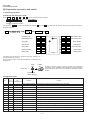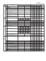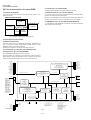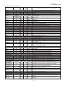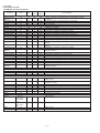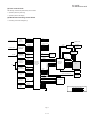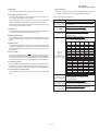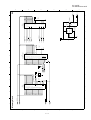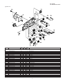
1
UX-470DE FO-880DE/NX-670DE SERVICE MANUAL No. 00ZUX470DESME FACSIMILE UX-470 FO-880 MODEL NX-670 Illustration: UX-470 This service manual UX-470DE/FO-880DE/NX-670DE is to appear only on the place where it is changed from UX-310DE /FO-730DE/NX-530DE, and refer to a service manual UX-310DE/FO-730DE/NX-530DE(00ZUX310DESME) except for it. CONTENTS CHAPTER 1. GENERAL DESCRIPTION [1] Specifications ............................................ 1-1 [2] Operation panel......................................... 1-2 [3] Refer to the service manual of UX-310DE. [4] Refer to the service manual of UX-310DE. [5] Quick reference guide ............................... 1-9 [6] Refer to the service manual of UX-310DE. CHAPTER 5. CIRCUIT DESCRIPTION [1] Circuit description ...................................... 5-1 [2] Circuit description of control PWB ..............5-2 [3] Circuit description of TEL/LIU PWB .......... 5-8 [4] Circuit description of power supply PWB ............................ 5-11 [5] Circuit description of CIS unit ................... 5-11 CHAPTER 2. ADJUSTMENTS [1] Adjustments ............................................... 2-1 [2] Diagnostics and service soft switch .......... 2-2 [3] Troubleshooting ...................................... 2-17 [4] Error code table....................................... 2-18 CHAPTER 6. CIRCUIT SCHEMATICS AND PARTS LAYOUT [1] Control PWB circuit ................................... 6-1 [2] TEL/LIU PWB circuit ................................. 6-9 [3] Power supply PWB circuit ...................... 6-13 [4] Operation panel PWB circuit ................... 6-15 CHAPTER 3. MECHANISM BLOCKS [1] Refer to the service manual of UX-310DE. [2] Refer to the service manual of UX-310DE. CHAPTER 7. OPERATION FLOWCHART [1] Refer to the service manual of UX-310DE. [2] Refer to the service manual of UX-310DE. CHAPTER 4. DIAGRAMS [1] Block diagram ............................................4-1 [2] Wiring diagram .......................................... 4-2 [3] Point-to-point diagram ............................... 4-3 CHAPTER 8. OTHERS [1] Refer to the service manual of UX-310DE. [2] Refer to the service manual of UX-310DE. PARTS GUIDE Parts marked with " " is important for maintaining the safety of the set. Be sure to replace these parts with specified ones for maintaining the safety and performance of the set. SHARP CORPORATION 1-1 This document has been published to be used for after sales service only. The contents are subject to change without notice. UX-470DE FO-880DE/NX-670DE CAUTION FOR BATTERY REPLACEMENT (Danish) ADVARSEL ! Lithiumbatteri-Eksplosionsfare ved fejlagtig håndtering. Udskiftning må kun ske med batteri af samme fabrikat og type. Levér det brugte batteri tilbage til leverandoren. (English) Caution ! Danger of explosion if battery is incorrectly replaced. Replace only with the same or equivalent type recommended by the equipment manufacturer. Discard used batteries according to manufacturer’s instructions. (Finnish) VAROITUS Paristo voi räjähtää, jos se on virheellisesti asennettu. Vaihda paristo ainoastaan laitevalmistajan suosittelemaan tyyppiin. Hävitä käytetty paristo valmistajan ohjeiden mukaisesti. (French) ATTENTION Il y a danger d’explosion s’ il y a remplacement incorrect de la batterie. Remplacer uniquement avec une batterie du même type ou d’un type recommandé par le constructeur. Mettre au rébut les batteries usagées conformément aux instructions du fabricant. (Swedish) VARNING Explosionsfare vid felaktigt batteribyte. Använd samma batterityp eller en ekvivalent typ som rekommenderas av apparattillverkaren. Kassera använt batteri enligt fabrikantens instruktion. (German) Achtung Explosionsgefahr bei Verwendung inkorrekter Batterien. Als Ersatzbatterien dürfen nur Batterien vom gleichen Typ oder vom Hersteller empfohlene Batterien verwendet werden. Entsorgung der gebrauchten Batterien nur nach den vom Hersteller angegebenen Anweisungen. 1–2 UX-470DE FO-880DE/NX-670DE CHAPTER 1. GENERAL DESCRIPTION [1] Specifications Automatic dialing: (UX-470) Rapid Key Dialing: 5 numbers Speed Dialing: 40 numbers Automatic dialing: (FO-880/NX-670) Rapid Key Dialing: 8 numbers Speed Dialing: 80 numbers Imaging film: Initial starter roll (included with fax machine): 10 m roll (approx. 30 A4 pages) Replacement roll: UX-3CR 30 m roll (two rolls in package, one roll yields approx. 95 A4 pages) Memory size* : 512 KB (approx. 30 average pages with no voice messages recorded, or 24 minutes of voice messages (including OGMs) with no documents in memory) Effective scanning width: 210 mm max. Contrast control: Automatic/Dark selectable Copy function: Standard Telephone function: Standard (cannot be used for incoming/outgoing if power fails) Power requirements: 220-230 V AC, 50 Hz Operating temperature: 5 to 35°C Humidity: Maximum: 85 % Power consumption: Stand-by: 3.0 W Maximum: 115 W Dimensions: Width: 343 mm Depth: 313 mm Automatic document feeder: 10 sheets max. Height: 312 mm Modem speed: 9600 bps with automatic fallback to 7200, 4800, or 2400 bps Weight: Transmission time* : Approx. 15 seconds(Sharp special mode) * Display: 16-digit LCD display Reception modes: FAX, TEL, TEL/FAX, A.M. Resolution: Horizontal: 8 dots/mm Vertical: Standard: 3.85 lines/mm Fine/Halftone: 7.7 lines/mm Super fine: 15.4 lines/mm Recording system: Thermal transfer recording Halftone (grayscale): 32 levels Applicable telephone line: Public switched telephone network / PBX Compatibility: ITU-T (CCITT) G3 mode Configuration: Half-duplex, desktop transceiver Compression scheme: MH, MR, Sharp Scanning method: Sheet-feeder CIS (Contact Image Sensor) Effective recording width: 208 mm max. Input document size: Automatic feeding: Width 148 to 210 mm Length 140 to 297 mm Manual feeding: Width 148 to 210 mm Length 140 to 600 mm Approx. 3.4 kg Based on ITU-T (CCITT) Test Chart #1 at standard resolution in Sharp special mode, excluding time for protocol signals (i.e., ITU-T phase C time only). Note: The facsimile machine is Year 2000 compliant. As a part of our policy of continuous improvement, SHARP reserves the right to make design and specification changes for procduct improvement without prior notice. The performance specifications figures indicated are nominal values of production units. There may be some deviation from these values in individual units. 1–1 UX-470DE FO-880DE/NX-670DE [2] Operation panel 5 6 7 8 1 234 TEL 9 10 FAX TEL/FAX ANRUFB. DIGITAL ABC 1 GHI DEF 2 JKL 4 PQRS KURZWAHL ANSWERING SYSTEM AUFN. WIEDERG./VOR. EMPFANGSART 3 MNO 5 AUFLÖSUNG WAHLWDH. 6 8 9 LAUTSTÄRKE LEISE LAUT FUNKTION LÖSCHEN WXYZ TUV 7 ZURÜCK KOPIE/HILFE ALPHAWAHL R STOP SYMBOLE 01 LAUTSPR. 02 03 04 05/ABRUF 0 (UX-470) 15 11 12 13 14 01 04 05 START/SPEICHER 16 17 18 19 02 03 06 07 08/ABRUF (FO-880/NX-670) 12. ALPHAWAL/R (SEARCH/R key) 1. KURZAHL (SPEED DIAL key) Press this key to search for an automatic dialing number, or, if you are on a P.B.X. extension, press this key to Press this key to dial a 2-digit Speed Dial number. 2. WAHLWDH. (REDIAL key) transfer or put the other party on hold. 13. Lautspr. (SPEAKER key) Press this key to automatically redial the last number dialed. 3. ZURÜCK (REPEAT key) Press this key to hear the line and fax tones through the speaker before sending a document, or dialing a voice number. Note: This is not a speakerphone. You must pick up the handset to talk with the other party. Press this key to repeat playback of a message. 4. LCD-Anzeige (Display) This displays messages and prompts during operation and programming. 5. WIEDERG/VOR. (PLAY/SKIP key) 14. AUFN. (REC/MEMO key) Press this key to play recorded messages. During playback, Press this key to record a phone conversation or a message. press it to skip forward to the next message. 6. EMPFANGSART (RECEPTION MODE key) 15. Zielwahltasten (Rapid Dial keys) Press this key to select the reception mode. An arrow in the display will point to the currently selected reception mode. Press one of these keys to dial a fax or voice number automatically. (Note that you must attach the Rapid Key labels.) 7. AUFLÖSUNG (RESOLUTION key) Press this key to adjust the resolution and contrast before sending or copying a document. 16. LÖSCHEN (DELETE key) Press this key to erase recorded message. 8. LAUTSTÄRKE (VOLUME keys) Press these keys to adjust the volume of the speaker when the SPEAKER key has been pressed, or the volume of the ringer at all other times. 17. STOP (STOP key) Press this key to cancel operations before they are completed. 18. START/SPEICHER (START/MEMORY key) 9. FUNKTION (FUNCTION key) Press this key to send or receive a document, or to scan a document into memory before sending it. Press this key to select various special function. 10. BEDIENFELD ENTRIEGELN (Panel release) Grasp this finger hold and pull toward you to open the operation panel. 11. Zifferntasten (Number keys) Use these keys to dial numbers, and enter numbers and letters during number/name storing procedures. 1–2 19. KOPIE/HILFE (COPY/HELP key) When a document is in the feeder, press this key to make a copy. At any other time, press this key to print out the Help List, a quick reference guide to the opeation of your fax. UX-470DE FO-880DE/NX-670DE SETTING THE DATE AND TIME [5] Quick reference guide Note: Imaging film and paper must be loaded to perform the following operation. FUNKTION INSTALLATION Press: 1 2 3 Display shows: DATE & TIME SET Press the START/MEMORY key: 3 START/SPEICHER Enter two digits for the Day (01 through 31). TEL SET. TEL LIN . E Enter two digits for the Month (01 through 12). Enter four digits for the Year (Ex: 1999). Enter two digits for the Hour (01 through 23). Enter two digits for the Minute (00 through 59). STOP When finished, press: 1. Connect the handset as shown. START/SPEICHER 2. Plug the power cord into a earthed, 220 - 230 V outlet. STORING AND CLEARING NUMBERS FOR AUTOMATIC DIALING 3. Plug one end of the telephone line into the TEL. LINE socket on the rear of the fax, and the other end into your telephone wall socket. Note: Imaging film and paper must be loaded to perform the following operation. FUNKTION RECORING AN OUTGOING MESSAGE 1. Press: 1. Press: 3 FUNKTION 0 Display shows: FAX/TEL # MODE Display shows: OGM RECORDING 2. Press 1 to store a number or 2 to clear a number. 3. Enter a 2-digit Speed Dial number (from 01 to 05 for Rapid Key Dialing, or 06 to 45 for Speed Dialing). (If you are clearing a number, go to Step 7.) 2. Press: START/SPEICHER 3. Press 1 (GENERAL) to record an outgoing message for the answering machine. Press 2 (TRANSFER) to record an outgoing message for the Transfer function. 4. Enter the full telephone/fax number. 4. Pick up the handset and speak into it to record your message. 5. Press: START/SPEICHER 5. When finished, press the STOP key or replace the handset. 6. Press: STOP 6. Enter the name of the location by pressing number keys (max. of 20 characters). (Refer to the letter entry table in ENTERING YOUR NAME AND NUMBER.) STOP STOP ENTERING YOUR NAME AND NUMBER 7. Press: Note: Imaging film and paper must be loaded to perform the following operation. 1. Press: START/SPEICHER SENDING DOCUMENTS FUNKTION 3 Display shows: OWN NUMBER SET 2. Press: START/SPEICHER Place your document (up to 10 pages) face down in the document feeder. 3. Enter your fax number (max. of 20 digits) by pressing the number keys. ♦ If you make a mistake, press the SEARCH/R key to move the cursor back to the mistake, then enter the correct number or letter. Normal Dialing 1. Lift the handset or press 4. Press: START/SPEICHER LAUTSPR. 2. Dial the fax number. 5. Enter your name by pressing the appropriate number keys as shown below. 3. Wait for the reception tone (if a person answers, ask them to press their Start key). ♦ To enter two letters in succession that require the same key, press the SPEAKER key after entering the first letter. 4. Press: A= J= S= B= K= T= C= L= U= Rapid Key Dialing Press the appropriate Rapid Key. Transmission will begin automatically. D= M= V= Speed Dialing E= N= W= 1. Press: F= O= X= G= P= Y= H= Q= Z= I= R= SPACE = START/SPEICHER KURZWAHL 2. Enter 2-digit Speed Dial number. 3. Press: START/SPEICHER DEF ABC GHI KURZWAHL Deletes highlighted letter TEL EMPFAMGSART TEL/FAX ANRUFB. TEL 14 FEB 10:30 TEL R FAX 14 FEB 10:30 TEL/FAX ANRUFB. TEL ALPHAWAHL FAX TEL/FAX ANRUFB. Upper/lower case shift key WXYZ TUV FAX 14 FEB 10:30 Press: MNO JKL WAHLWDH. PQRS RECEIVING DOCUMENTS FAX 14 FEB 10:30 Moves cursor to the left TEL/FAX ANRUFB. FAX mode: The fax automatically answers and receives the incoming document. SYMBOLE LAUTSPR. Moves cursor to the right TEL mode: Fax tone Press either key one or more times to select and enter a symbol. RECEIVING STOP 6. When finished, press: START/SPEICHER TEL/FAX mode: The fax machine automatically answers on 1 or 2 rings and receives faxes. Voice calls (including manually dialed fax transmissions) are signalled by a special ringing sound. START/SPEICHER A.M. mode: Select this mode when you go out to receive both voice messages and faxes. 1–9 3 UX-470DE FO-880DE/NX-670DE MEMO 11 –– 11 4 UX-470DE FO-880DE/NX-670DE 2. IC protectors replacement CHAPTER 2. ADJUSTMENTS ICPs (IC Protectors) are installed to protect the motor driver circuit. ICPs protect various ICs and electronic circuits from an overcurrent condition. [1] Adjustments The location of ICPs are shown below: General Since the following adjustments and settings are provided for this model, make adjustments and/or setup as necessary. CNLIUB CNPW CNLIUA 1. Adjustments CONTROL PWB (BOTTOM SIDE) Adjustments of output voltage (FACTORY ONLY) FU100 1. Install the power supply unit in the machine. 2. Set the recording paper and document. 3. When the document is loaded, power is supplied to the output lines. Confirm that outputs are within the limits below. (1) FU100 (ICP-S07) is installed in order to protect IC’s from an overcurrent generated in the motor drive circuit. If FU100 is open, replace it with a new one. Output voltage settings CNLIUA 3. Settings POWER SUPPLY PWB CNLIUB TEL/LIU PWB (1) Dial mode selector DIAL mode (Soft Switch No. SWB4 DATA No. 3) CN1 CNLIUA CNLIUB (step 1) Select "OPTION SETTING". CNPW CONTROL PWB CNTH DISPLAY: OPTION SETTING KEY: CNCIS CNCSW FUNCTION CNSP Output +5V +24V Voltage limits 4.75V ∼ 5.25V 23.3V ∼ 24.7V Connector No. Pin No. 1 2 3 4 5 6 7 8 9 4 PRESS OR # (step 2) Select "DIAL MODE". CNPN CNMT KEY : Push # until " DAIL MODE " is indicated because the number of # s changes by the model. CNPW DISPLAY: MG MG +24V +24V +24V DG +5V DG PSAVE DIAL MODE (step 3) Select, using "1" or "2". KEY: 1 DISPLAY: TONE SELECTED KEY: 2 DISPLAY: PULSE SELECTED (step 4) End, using the "STOP" key. KEY: 2–1 STOP Cursor When initially registering, the mode shows 1=TONE. When registering again, the mode which was registered formerly is shown. 1=TONE, 2=PULSE UX-470DE FO-880DE/NX-670DE [2] Diagnostics and service soft switch 1. Operating procedure (1) Entering the diagnostic mode Press FUNC → 9 → → 8 → # → 7 , and the following display will appear. (FKX0 ) After 2 sec: DIAG MODE ROM Ver. FKW0 FKW0 (UX-470DE) FKX0 (FO-880DE/NX-670DE) Then press the START key. Select the desired item with the key or the # key or select with the rapid key. Enter the mode with the START key. (Diag•specifications) FUNC 9 8 FKW0 FKX0 7 DIAG MODE START Soft switch mode START 1 — START Flash memory clear ROM & RAM check START 2 — START Flash memory check Aging mode START 3 — START Ring & Dial free Panel key test START 4 — START Message print Check pattern START 5 — START Auto feeder mode Signal send mode START 6 — START All black mode Memory clear START 7 8 START Shading mode If the diag mode cannot be set, repeat the diag mode operation, performing the following operation. After the power is turned on and "WAIT A MOMENT" is indicated, press the STOP key. START KEY STOP KEY "Power ON" + In relation with the process response (request from Production Engineering) "WAIT A MOMENT" clock indication may appear depending on STOP key timing. If the STOP key is held down, "MEMORY CLEAR?" appears. Memory clear (Work + Backup) 2. Diagnostic items ITEM No. DIRECT key DIRECT key Contents Function (UX-470) (FO-880/NX-670) 1 1 1 SOFT SWITCH MODE Soft switches are displayed and changed. List can be output. 2 2 2 ROM & RAM CHECK ROM is sum-checked, and RAM is matched. Result list is output. 3 3 3 AGING MODE 10 sheets of check patterns are output every 5 minutes per sheet. 4 4 4 PANEL KEY TEST Panel keys are tested. Result list is output. 5 5 5 CHECK PATTERN Check pattern is output. 6 — 6 SIGNAL SEND MODE Various signals of FAX communication are output. 7 — 7 MEMORY CLEAR Back-up memory is cleared, and is set at delivery. 8 — 8 SHADING MODE Shading compensation is performed in this mode. 9 — — ALL BLACK PRINT To check the print head, whole dots are printed over the interval of 2 m. 10 — — AUTO FEEDER MODE Insertion and discharge of document are tested. 11 — — MESSAGE PRINT The display message of each language is printed out together with the English equivalent. 12 — — RING & DIAL FREE Allows CI detection of 13Hz or more. Eliminates dial tone detection in auto dial. 13 — — FLASH MEMORY CHECK Checks flash memory write/read. 14 — — FLASH MEMORY CLEAR Checks flash memory clearing. 2–2 UX-470DE FO-880DE/NX-670DE 3. 6. Signal send mode 3. Diagnostic items description 3. 1. Soft switch mode This mode is used to send various signals to the circuit during FAX communication. Every push of START key sends a signal in the following sequence. Moreover, the signal sound is also output to the speaker when the line monitor of the soft switch is on. Used to change the soft switch settings. The soft switch which is stored internally is set by using the keys. The available soft switches are SW-A1 to SW-M2. [1] No signal (CML signal turned on) The content of soft switches is shown in page 2-5 to 2-16. [2] 9600bps The contents are set to factory default settings. [3] 7200bps [4] 4800bps 3. 2. ROM & RAM check [5] 2400bps ROM executes the sum check, and RAM executes the matching test. The result will be notified with the number of short sounds of the buzzer as well as by printing the ROM & RAM check list. Number of short sounds of buzzer 0 → No error [6] 300bps (FLAG) [7] 2100Hz (CED) [8] 1100Hz (CNG) 1 → ROM error [9] END 2 → RAM error (32Kbyte) 3. 7. Memory clear 3. 3. Aging mode This mode is used to clear the backup memory and reset to the default settings. If any document is first present, copying will be executed sheet by sheet. If no document is present, the check pattern will be printed sheet by sheet. This operation will be executed at a rate of one sheet per 5minutes, and will be ended at a total of 10 sheets. 3. 8. Shading mode The mode is used for the shooting compensation. For reading, set up the special original paper. 3. 4. Panel key test The shooting compensation memorizes the reference data of white and black for reading. This mode is used to check whether each key operates properly or not. Press the key on the operation panel, and the key will be displayed on the display. Therefore, press all keys. At this time,finally press the STOP key. Moreover, the memorized data is not erased even if memory clear mode is executed. When the STOP key is pressed, the keys which are not judged as "pressed" will be printed on the result list. 3. 9. All black print This mode is used to check the state of the printing head and intentionally overheat it. Whole dots are printed over the interval of 2 m. If it is overheated or the printing sheet is jammed, press STOP key for the end. • LED port of the contact image sensor (CIS) is kept on during the term from when start of the panel test mode to end with the STOP key. 3. 5. Check pattern 3. 10. Auto feeder mode This mode is used to check the state of the printing head. It is ended with the following pattern printed on one printing sheet. In this mode, a document is inserted and discharged to check the auto feed function. 1 Longitudinal stripe 2 Approx. 30 mm After this mode is started, set a document, and the document feed will be automatically tested. 2 black dots and 2 white dots are repeatedly progressed on one line. 2 Full black 3. 11. Message print Approx. 30 mm Used to print the displayed message of communication for translate each language. 1 3. 12. Ring & Dial free 2 Used to reject dial tone check while autodialing is carried out. And used to change the bottom Ring frequency of auto-receiving to 13Hz. 3. 13. Flash memory check Data is written into and read from the flash memory to check the data conformity. When the unit enters this mode, the check is started. 3. 14. Flash memory clear Data in the flash memory is cleared (memory clear). When the unit enters this mode, the check is started. The result is announced by the buzzer beeps. The result of check is printed. Beeps 0 → No error 1 → Memory error 2–3 UX-470DE FO-880DE/NX-670DE 4. How to make soft switch setting To enter the soft switch mode, make the following key entries in sequence. Press FUNCTION DATA No. 9 8 7 START START 1 2 3 4 5 6 7 8 S F T SW-A1 = 0 0 0 0 0 0 0 0 Press FUNCTION key. S F T SW-A1 = 1 0 0 0 0 0 0 0 Press key. Press key. S F T SW-A1 = 1 0 0 0 0 0 0 0 S F T SW-A1 = 1 0 0 0 0 0 0 0 Bit1 - 8 are set. S F T SW-A1 = 1 0 0 0 0 0 0 0 Press START key during setting. S F T SW-A2 = 0 0 0 0 0 0 0 0 Soft SW-A2 - SW-M2 are set. S F T SW-M2 = 0 0 0 0 0 0 0 0 To finish the settings halfway between SW-A1 and SW-M2, press the STOP key. In this case, the setting being done to the SW No. on display will be nullified while settings done to the preceding SW Nos. remain in effect. When the COPY key is pressed, the contents of soft switches are printed. The soft switch mode is terminated. 2–4 UX-470DE FO-880DE/NX-670DE 5. Soft switch description • Soft switch SW DATA NO. NO. SW l A1 1 1 Protect from echo No Yes 2 Forced 4800 BPS reception Yes No 0 3 4 Footer print Length limitation of Yes No limit No Copy/send: 60cm 0 0 copy/send/receive 5 6 CSI transmission DIS receive acknowledgement Non-modulated carrier for V29 transmission modem Yes Transmitted NSF: Once 8 EOL detect timer 25 s 0 13 s V.29 9600 7200 0 V.27 ter 4800 2400 1 No. 1 0 0 0 0 0 2 3 No. 2 No. 3 0 0 0 1 0 1 0 0 0 0 No. 4 1 1 0 0 5 6 Sender’s information transmit H2 mode 7 8 1 No No Yes Yes 0 0 Communication error treatment in No communication Communication error 0 RTN sending mode (reception) CNG transmission error No Yes 0 1 2 1000ms 750ms No. 1 No. 2 1 1 1 0 No 500ms 75ms 0 1 0 0 Yes 0 0 3 MR coding 4 5 Reserved Reserved 0 0 6 Reserved 0 7 8 Reserved Reserved 0 0 1 Signal transmission level 0 Binary input 2 3 No. = 4 0 16 8 1 2 4 3 2 4 1 5 0 0 1 1 1 1 0 1 5 6 Protocol monitor (error print) Printed at com. error Not printed 1 0 7 Protocol monitor Yes No 0 8 Line monitor Digital line equalization setting Yes No 1 SW l A5 0 0 No CED tone signal interval SW l A4 0 DIS: Twice 7 4 (Reception) 2 3 Reserved 4 Reserved 5 Digital cable equalizer setting (Reception for Caller ID) 6 7 8 Error criterion Anti junk fax check Remarks Receive: 1.5m No transmitted Twice Modem speed SW l A3 DE 0 during G3 transmission SW l A2 Initial setting Switch setting and function ITEM 7.2km 0 0km No. 1 1 0 1 No. 2 1 0 1 0 No. 5 7.2km 1 0km 0 0 No. 6 1 0 0 0 10 ~ 20 % Yes 5 ~ 10 % No 2–5 0 0 OPTION UX-470DE FO-880DE/NX-670DE SW DATA NO. NO. SW l A6 Initial setting Switch setting and function ITEM 1 DE 0 1 Auto gain control (MODEM) Enable Disable 2 End Buzzer Yes No 1 3 Disconnect the line when DIS is received in RX mode No Yes 1 4 Equalizer freeze control (MODEM) On Off 0 5 Equalizer freeze control 7200 BPS only No Yes 0 6 CNG transmission in manual TX Yes No 1 7 mode Initial compression scheme for sharp MR mode H2 mode 0 Remarks 1 fax in TX mode SW l B1 8 1 Reserved Reserved 0 0 2 Reserved 0 3 4 Reserved Reserved 0 0 5 Recall times 6 7 No. = 8 SW l B2 1 2 Dial pausing (sec/pause) 4 sec Dial tone detection (before auto dial) No 3 Reserved 4 5 Busy tone detection (after auto dial) Reserved 6 Reserved 7 8 Reserved PBX connection 2 3 SW l B3 SW l B4 2 7 1 8 0 1 0 0 1 0 0 2 sec Yes 1 0 Yes 0 0 0 0 Yes 0 0 No No. 1 No. 0 Earth 1 Flash 1 1 No. 2 0 0 1 1 ID Earth Flash No. 4 0 1 1 0 No. 5 0 0 1 Reserved PBX select 4 0 4 6 No PBX recall function (R key select) 1 Binary input 8 5 OPTION 0 OPTION 5 6 Reserved 0 0 7 Reserved 0 8 1 Reserved Reserved 0 0 2 Reserved 3 4 Dial mode Pulse → Tone change function by OPTION 0 Tone Enable Pulse Disable 1 1 OPTION key 5 6 Reserved Reserved 7 PBX type 8 Reserved 0 0 ISDN NORMAL 0 0 2–6 OPTION UX-470DE FO-880DE/NX-670DE SW DATA NO. NO. SW l B5 SW l B6 1 DTMF signal transmission level (Low) 7 8 1 2 3 4 5 6 Reserved Reserved DTMF signal transmission level (High) Reserved 0 0 1 1 0 0 1 0 7 Reserved 0 8 Reserved Reading slice (Binary) No. = SW l D2 No. = Binary input 16 8 4 2 1 1 2 3 4 5 1 1 0 0 1 0 1 No. 1 1 0 Darker in dark mode 1 2 No. 2 0 0 1 1 0 Light Dark 3 No. 3 Factory setting 0 1 0 Darker in dark mode 1 0 4 5 Line density selection No. 4 Fine 6 Halftone gray scale selection 16 level 7 8 MTF correction in half tone mode Reserved No 1 Number of rings for auto receive No. = 4 Light Dark 0 0 1 Standard 1 0 0 0 OPTION 64 level 0 OPTION Yes 0 0 Binary input 0 8 1 4 2 2 3 0 0 0 0 0 1 4 1 1 Reception after 5 rings No reception 0 6 Automatic switching manual to auto receive mode Reserved 7 8 CI detection Reserved 13 Hz or more As is PTT 0 0 1 Reserved 0 2 3 Reserved Reserved 0 0 4 Reserved 5 6 Caller ID function Reserved 7 Reserved 8 1 Caller ID detect during CI off Tel/Fax Automatic switching mode 5 OPTION 0 0 Yes No 0 0 All times Tel/Fax auto switch Only first Switch to Fax 1 1 OPTION 0 2 3 automatic switching mode 4 5 Number of CNG signal detection at the Twice tel/fax automatic switching mode Reserved 6 7 Reserved Post answer tone (transmit in No. 2 No. 3 No 15sec 60sec 30sec 120sec 0 0 0 1 1 0 1 1 Once OPTION 0 0 1 0 Yes 0 0 Tel/Fax mode) 8 Remarks 1 1 1 0 0 0 Factory setting 0 Pseudo ringing time at phone/fax SW l E1 Binary input 16 8 4 2 1 1 2 3 4 5 1 1 1 0 0 Reserved 2 3 SW l D1 DE 0 1 2 3 4 5 6 Reading slice (Half tone) SW l C1 Initial setting Switch setting and function ITEM Reserved 0 2–7 UX-470DE FO-880DE/NX-670DE SW DATA NO. NO. 1 1 Pseudo ringer sound volume 2 SW l E2 No. = 3 4 1 1 1 0 2 1 3 0 4 1 0 1 0 0 0 Reserved 1 No. 1 2 No. 2 0 80ms 0 100ms 1 120ms 1 0 1 0 1 0 Protection of remote reception (5 ) detect Yes No 0 4 Remote reception with GE Compatible Not compatible 1 5 telephone Remote operation code figures by 6 external TEL (0~9) CNG detection in STAND-BY mode Remarks 0 50ms 0 1 No. = Binary input 0 8 4 2 1 1 5 0 6 1 7 0 8 1 0 1 No 1 Yes Number of CNG detect (AM mode) SW l G3 2 Reserved Reserved 7 8 SW l G2 0 4 Reserved 3 SW l G1 Binary input 8 6 7 DTMF detection time SW l F2 DE 0 5 8 SW l F1 Initial setting Switch setting and function ITEM 2 No. 2 1pulse 0 3 No. 3 0 4 No. 4 1pulse 0 5 No. 5 0 Number of CNG (STAND-BY mode) 2pulses 3pulses 4pulses 0 1 1 1 0 1 2pulses 3pulses 4pulses 0 1 1 1 0 1 0 1 0 1 6 7 Reserved Reserved 0 0 8 Reserved 0 1 2 Reserved Reserved 0 0 3 Reserved 0 4 5 Reserved Reserved 0 0 6 Reserved 0 7 8 Reserved Reserved 0 0 1 Reserved 0 2 3 Reserved Reserved 0 0 4 Reserved 0 5 6 Reserved Reserved 0 0 7 Reserved 0 8 1 Reserved Reserved 0 0 2 Reserved 0 3 4 Reserved Reserved 0 0 5 Reserved 0 6 7 Reserved Reserved 0 0 8 Reserved 0 2–8 OPTION OPTION OPTION UX-470DE FO-880DE/NX-670DE SW DATA NO. NO. Initial setting Switch setting and function ITEM 1 DE 0 1 Reserved 0 2 Reserved 0 3 4 Reserved Busy tone continuous sound detect 5 sec As is PTT 0 1 Remarks time SW l H1 5 Busy tone detect continuation sound No detect during OGM Yes 1 6 Busy tone detect continuation sound No Yes 0 7 detect (during ICM : for internal A.M.) Busy tone detect intermittent sound No Yes 1 Yes 0 during OGM 8 Busy tone detect intermittent sound No detect (during ICM : for internal A.M.) Busy tone detection pulse number 1 2 SW l H2 2pulses 4pulses 6pulses 10pulses No. 1 No. 2 3 Fax switching when A.M. full 4 5 Reserved Reserved 6 Reserved 7 8 AM OGM announce only mode Reserved Yes A.M. quiet time 2 No. 5 No. 6 7 Key input buzzer on/off switch 8 (Two way recording mode) Reserved 1 A.M. quiet detect time On SW l I3 4 Reserved 7 Reserved 8 1 Alarm during two way alarm Max OGM record time 2 Reserved 3 4 0 0 4min 15s 30s 60s 0 0 0 1 1 0 1 1 2s 3s 4s 5s 0 0 0 1 1 0 1 1 0s 1s 2s 3s 0 0 0 1 1 0 1 1 Off No. = 5 6 OPTION OPTION OPTION 0 0 0 0 1 0 0 0 2 3 SW l I2 1 0 0 No No. 3 No. 4 5 6 1 1 0 Yes A.M. quiet time 1 SW l I1 1 0 0 0 No. 1 No. 2 3 4 0 1 No ICM recording time 1 2 0 0 Binary input 0 16 8 4 2 1 1 2 3 4 5 0 1 0 0 1 0 0 0 0 0 0 Yes 15s No 60s 0 0 Two way record function Toll saver Disable Disable Enable Enable 0 0 5 FAX reception in case of detecting Yes No 1 6 no sound detect after ICM recording Reserved 7 Reserved 8 Transfer dial recall 0 0 0 No Yes 2–9 0 OPTION UX-470DE FO-880DE/NX-670DE SW DATA NO. NO. SW l I4 1 AGC maximum gain (line) 2 3 (10~25dB)(1dB step) 1 1 4 1 0 1 1 0 1 0 7 5 8 1 8 1 1 0 1 0 Binary input 0 1 8 4 2 1 0 1 1 2 0 3 0 4 0 0 0 No. = AGC eref access code (line) (-0~-30dB)(2dB step) No. = 3 4 5 6 7 AGC eref access code (Mic) (-0~-30dB)(2dB step) No. = 6 7 Binary input 1 8 5 4 6 2 7 1 8 0 0 1 0 0 0 0 Binary input 8 4 2 1 1 1 3 1 4 1 4 5 1 1 1 1 Binary input 1 1 8 4 2 1 1 5 1 6 1 7 1 8 1 1 1 AGC gain adaptation threshold (line) No. = AGC gain adaptation threshold (Mic) 6 No. = AGC slew rate (line) 1 2 3 4 2 3 Slow No. 1 No. 2 Normal Little fast 0 0 AGC slew rate (Mic) 0 1 Slow No. 3 No. 4 1 1 Normal Little fast 0 0 0 1 0 1 Fast 1 0 1 1 0 1 Reserved 0 6 7 Reserved Reserved 0 0 8 Reserved 1 Activity report print Automatic printout No printout when memory full 0 2 Total communication hours and No Yes 0 3 pages print Sender’s phone number setting Cannot change Change allowed 4 Reserved 5 6 Reserved Summer time setting 0 No Reserved Reserved Polling key 4 Reserved 5 Reserved Speaker volume (5 stages) 0 0 0 Yes No. 7 No. 8 2 3 OPTION 0 Ringer volume 1 Remarks Fast 1 0 5 7 8 SW l J2 2 3 0 AGC maximum gain (Mic) (10~25dB)(1dB step) 7 8 SW l J1 4 2 0 1 2 SW l I7 8 1 Binary input 8 4 2 1 5 6 8 SW l I6 DE 1 0 Binary input No. = 4 2 SW l I5 Initial setting Switch setting and function ITEM Off Low Middle High 0 0 0 1 1 0 1 1 OPTION 1 0 0 Yes 0 0 No OPTION 0 0 Very Low Low Middle High Very High OPTION 6 No. 6 0 0 0 0 1 0 7 8 No. 7 No. 8 0 0 0 1 1 0 1 1 0 0 1 0 2 – 10 UX-470DE FO-880DE/NX-670DE SW DATA NO. NO. 1 2 SW l J3 SW l K1 Initial setting Switch setting and function ITEM 1 DE 0 Automatic cover sheet Communication results printout Yes (Transaction report) No. 2 0 0 0 0 1 1 No. 3 No. 4 0 0 0 1 1 0 1 1 0 0 0 0 3 4 No 0 E/T/M Send only Always No print Err only 5 Reserved 0 6 7 Reserved Reserved 0 0 8 Reserved 1 Entering DIAG mode by pressing SPEED key 2 Reserved 3 4 OGM/ICM output level No 0 0 2 1 0 1 5 3 4 5 6 7 8 0 6 7 0 1 0 0 0 1 0 0 No. = Binary input 32 16 8 4 1 1 2 Reserved Reserved 0 0 3 Reserved 0 4 5 Reserved Cut off mode (COPY mode) Yes No 0 1 6 A4 paper enable Enable Disable 1 7 8 LEGAL & LETTER paper enable 2 IN 1 mode Enable Yes Disable No 0 0 Paper set size 1 2 SW l L2 SW l M1 SW l M2 OPTION OPTION 0 Yes 8 SW l L1 Remarks No.1 No.2 LETTER LEGAL A4 0 0 0 1 1 0 OPTION OPTION 1 0 3 Automatic reduce of receive Auto 100 % 1 OPTION 4 5 Print contrast Reception reduction ratio in case of Light 100 % Normal 93 % 0 0 OPTION OPTION memory full 6 7 Reserved Reserved 0 0 8 Reserved 0 1 2 Reserved Reserved 0 0 3 Reserved 0 4 5 Reserved Reserved 0 0 6 Reserved 0 7 8 Reserved Reserved 0 0 1 Reserved 0 2 3 Reserved Reserved 0 0 4 Reserved 0 5 6 Reserved Reserved 0 0 7 Reserved 0 8 Reserved 0 2 – 11 UX-470DE FO-880DE/NX-670DE • Soft switch function description SW-A2 No. 7 Communication error treatment in RTN sending mode (Reception) SW-A1 No. 1 Protect from echo Used to determine communication error treatment when RTN is sent by occurrence of a received image error in G3 reception. When it is set to "1", communication error is judged as no error. Used to protect from echo in reception. SW-A1 No. 2 Forced 4800BPS reception SW-A2 No. 8 CNG transmission When line conditions warrant that receptions take place at 4800 BPS repeatedly. When set to "0" , this model allows CNG transmission by pressing the Start key in the key pad dialing mode. When set to "1", CNG transmission in the key pad dialing mode cannot be performed. In either case, CNG transmission can be performed in the auto dial mode. It may improve the success of receptions by setting at 4800BPS. This improves the receiving document quality and reduces handshake time due to fallback during training. SW-A3 No. 1, No. 2 CED tone signal interval SW-A1 No. 3 Footer print For international communication, the 2100Hz CED tone may act as an echo suppression switch, causing a communication problem. When set to "1", the date of reception, the sender machine No., and the page No. are automatically recorded at the end of reception. Though SW-A3 No. 1 and No. 2 are normally set to 0, it should be changed this time between the CED tone signal to eliminate the communication problem caused by echo. SW-A1 No. 4 Length limitation of copy/send/receive Used to set the maximum page length. TX To avoid possible paper jam, the page length is normally limited to 0.6 meter for copy or transmit, and 1.5 meters for receive. RX CED It is possible to set it to "No limit" to transmit a long document, such as a computer print form, etc. (In this case, the receiver must also be set to no limit.) T DIS SW-A1 No. 5 CSI transmission (CSI TRANSMISSION) is a switch to set whether the machine sends or does not send the signal (CSI signal) informing its own telephone No. to the remote fax machine when information is received. When "nonsending" is set, the telephone No. is not output on the remote transmitting machine if the remote transmitting machine has the function to display or print the telephone No. of receiving machine, using this CSI signal. SW-A3 No. 3 MR Coding Used to select the MR coding enable or disable. SW-A3 No. 4 ~ No. 8 Reserved Set to "0". SW-A1 No. 6 DIS receive acknowledgment during G3 transmission SW-A4 No. 1 ~ No. 5 Signal transmission level Used to make a choice of whether reception of DIS (NSF) is acknowledged after receiving two DISs (NSFs) or receiving one DIS (two NSFs). It may be useful for overseas communication to avoid an echo suppression problem, if set to 1. Used to control the signal transmission level in the range of-0dB to31dB. The factory setting is at -11dB (MODEM output). SW-A4 No. 6 Protocol monitor (Error print) SW-A1 No. 7 Non-modulated carrier for V29 transmission modem If set to "1", protocol is printed at communication error. Though transmission of a non-modulated carrier is not required for transmission by the V29 modem according to the CCITT recommendation, it may be permitted to a send non-modulated carrier before the image signal to avoid and echo suppression problem. It may be useful for overseas communication to avoid an echo suppression problem, if set to 1. SW-A4 No. 7 Protocol monitor Normally set to "0". If set to "1", communication can be checked, in case of trouble, without using a G3 tester or other tools. When communication FSK data transmission or reception is made, the data is taken into the buffer. When communication is finished, the data is analyzed and printed out. When data is received with the line monitor (SW-A4 No. 8) set to "1" the reception level is also printed out. SW-A1 No. 8 EOL (End Of Line) detect timer Used to make a choice of whether to use the 25-second or 13-second timer for detection of EOL. This is effective to override communication failures with some facsimile models that have longer EOL detection. SW-A4 No. 8 Line monitor Normally set to "0". If set to "1", the transmission speed and the reception level are displayed on the LCD. Used for line tests. SW-A2 No. 1 ~ No. 4 Modem speed SW-A5 No. 1, No. 2 Digital line equalization setting (Reception) Used to set determine the initial modem speed. The default is 9600BPS. It may be necessary to program it to a slower speed when frequent line fallback is encountered, in order to save the time required for fallback procedure. Line equalization when reception is to be set according to the line characteristics. Setting should be made according to distance between the telephone and the telephone company central switching station. SW-A2 No. 5 Sender’s information transmit (SENDER’S INFORMATION TRANSMISSION) is a switch to set the function to print the content of HEADER PRINT described in the passcode list at the front end of receiver’s original when original is sent to the remote machine. SW-A5 No. 3, No. 4 Reserved Set to "0". SW-A5 No. 5, No. 6 Digital cable equalizer setting (Reception for Caller ID) If this switch is set to "NO", the HEADER PRINT is not output at the receiving machine. Line equalization when reception for CALLER ID is to be set according to the line characteristics. Setting should be made according to distance between the telephone and the telephone company central switching station. SW-A2 No. 6 H2 mode Used to determine reception of H2 mode (15 sec transmission mode). When set to OFF, H2 mode reception is inhibited even though the transmitting machine has H2 mode function. SW-A5 No. 7 Error criterion Used to select error criterion for sending back RTN when receiving image data. SW-A5 No. 8 Anti junk fax check When using the Anti junk fax function, set to "1". 2 – 12 UX-470DE FO-880DE/NX-670DE SW-A6 No. 1 Auto gain control (MODEM) SW-B3 No. 4, No. 5 PBX select When this mode is enabled, if the reception signal level is under 31dBm. The modem itself controls the signal gain automatically. Used to select the operation mode of PBX recall in auto dialing. SW-A6 No. 2 End buzzer No. 4=1, No. 5=0: Earth recall is performed before dialing. No. 4=1, No. 5=1: Time break recall (=Flash) is performed before dialing. Setting this bit to 0 will disable the end buzzer (including the error buzzer/ on-hook buzzer). No. 4=0, No. 5=0: The PBX ID digit is automatically added when dialing to external line. PBX ID is up to 3 digits and entered in Option settings mode. SW-A6 No. 3 Disconnect the line when DIS is received in RX mode Bit1= 0: When DIS signal is received during RX mode, disconnected the line is immediately. SW-B3 No. 6 ~ No. 8 Reserved Bit1= 1: When DIS signal is received during RX mode, wait the next signal. SW-B4 No. 1, No. 2 Reserved Set to "0". Set to "0". SW-A6 No. 4 Equalizer freeze control (MODEM) SW-B4 No. 3 Dial mode This switch is used to perform reception operation by fixing the equalizer control of modem for the line which is always in unfavorable state and picture cannot be received. * Usually, the control is executed according to the state of line where the equalizer setting is changed always. When using the pulse dial, set to 0. When using the tone dial, set to 1. SW-B4 No. 4 Pulse → Tone change function by key When setting to 1, the mode is changed by pressing the pulse dial mode to the tone dial mode. SW-A6 No. 5 Equalizer freeze control 7200BPS only key from the SW-B4 No. 5, No. 6 Reserved Setting which specifies SW-A3 No. 6 control only in the condition of 7200BPS modem speed. Set to "0". SW-A6 No. 6 CNG transmission in manual TX mode SW-B4 No. 7 PBX type When set to "1", fax transmit the CNG signal in case of manual transmission mode (User press the START key after waiting the fax answering signal from handset or speaker). Used to select type of PBX "0": NORMAL "1": ISDN SW-A6 No. 7 Initial compression scheme for sharp fax in TX mode SW-B4 No. 8 Reserved When set to "0", if the other fax is Sharp model, fax transmit the document by H2 mode. When set to "1", even if the other fax is Sharp model, fax transmit the document by MR mode. Set to "0". SW-B5 No. 1 ~ No. 5 DTMF signal transmission level (Low) The transmission level of DTMF signal is adjusted. (lower frequency) SW-A6 No. 8 Reserved Set to "0". 00000: 0dBm SW-B1 No. 1 ~ No. 4 Reserved ↓ Set to "0". 11111: -15.5dBm (-0.5dBm x 31) SW-B1 No. 5 ~ No. 8 Recall times SW-B5 No. 6 ~ No. 8 Reserved Choice is made as to how many redials there should be. Set to "0". SW-B2 No. 1 Dialing pause (sec/pause) SW-B6 No. 1 ~ No. 5 DTMF signal transmission level (High) Pauses can be inserted between telephone numbers of direct dial connection. Selection of 4 sec or 2 sec pause is available. The transmission level of DTMF signal is adjusted. (higher frequency) 00000: 0dBm SW-B2 No. 2 Dial tone detection (before auto dial) ↓ Used to set YES/NO of dial tone detection in auto dialing. 11111: -15.5 dBm (-0.5dBm x 31) SW-B2 No. 3 Reserved SW-B6 No. 6 ~ No. 8 Reserved Set to "0". Set to "0". SW-B2 No. 4 Busy tone detection (after auto dial) SW-C1 No. 1, No. 2 Reading slice (Binary) Used to set YES/NO of busy tone detection after auto dialing. SW-B2 No. 5 ~ No. 7 Reserved Used to determine the set value of reading density in standard/fine mode. The standard setting is "00" (Factory setting is "00") Set to "0". SW-C1 No. 3, No. 4 Reading slice (Half tone) SW-B2 No. 8 PBX connection Used to determine the set value of reading density in half tone mode. The standard setting is "00" (Factory setting is "00") Used to select according to the connected line: PBX (Private Branch Exchange). SW-C1 No. 5 Line density selection Used to set the transmission mode which is automatically selected when the Resolution key is not pressed. In the copy mode, however, the fine mode is automatically selected unless the Resolution key is manually set to another mode. SW-B3 No. 1, No. 2 PBX recall function (R key select) Used to set the operation mode of PBX recall when the R key is pressed. Setting is made according to the type of PBX. No. 1=1, No. 2=1: Time break recall (=Flash) is performed. SW-C1 No. 6 Half tone gray scale selection No. 1=1, No. 2=0: Earth recall is performed. Used to determine the reading gray scale in half tone mode. SW-B3 No. 3 Reserved When set to "0", gray scale is 64 levels. Set to "0". When set to "1", gray scale is 16 levels. 2 – 13 UX-470DE FO-880DE/NX-670DE SW-C1 No. 7 MTF correction in half tone mode SW-E1 No. 8 Reserved This allows selection of MTF correction (dimness correction) in the half tone mode. Set to "0". SW-E2 No. 1 ~ No. 4 Pseudo ringer sound volume When "NO" (=1) is selected, the whole image becomes soft and mild. This wording, however, clearness of characters will be reduced. Normally set to "YES" (=0). Used to adjust sound volume of pseudo ringer to the line (ring back tone) generated on selecting TEL/FAX. Setting is the reduce level from -5dBm output level. SW-C1 No. 8 Reserved SW-E2 No. 5 ~ No. 8 Reserved Set to "0". Set to "0". SW-D1 No. 1 ~ No. 4 Number of rings for auto receive SW-F1 No. 1, No. 2 DTMF detect time When the machine is set in the auto receive mode, the number of rings before answering can be selected. It may be set from one to four rings using a binary number. Since the facsimile telephone could be used as an ordinary telephone if the handset is taken off the hook, it should be programmed to the user’s choice. If the soft switch was set to 1, direct connection is made to the facsimile. If a facsimile calling beep was heard when the handset is taken off the hook, press the START key and put the handset on the hook to have the facsimile start receiving. If it was set to 0 accidentally, receive ring is set to 1. NOTE: If the machine is set to answer after a large number of rings, it may not be able to receive faxes successfully. If you have difficulty receiving faxes, reduce the number of rings to a maximum of 5. Used to set detect time of DTMF (Dual Tone Multi Frequency) used in remote reception (5 ). The longer the detect time is, the less the error detection is caused by noises. SW-F1 No. 3 Protection of remote reception (5 Used to set the function of remote reception (5 the remote reception function is disabled. ) detect ). When set to "1", SW-F1 No. 4 Remote reception with GE telephone (Corresponding to TEL made by GE) P. B. X. "1": Compatible with TEL mode by GE SW-D1 No. 5 Automatic switching manual to auto receive mode "0": Not compatible This soft switch is used to select whether the machine should switch to the auto receive mode after 5 rings in the manual receive mode or remain in the same way as SW-D1 No. 1, No. 2, No. 3 and No. 4 "0"1"0"1"(5 rings). • When sending (5 ) for remote reception with a GE manufactured telephone remote reception may not take place because of special specifications in their DTMF. To overcome this, a soft SW is provided to change the modem setting to allow for remote reception. • If this soft SW is set to "1", other telephone sets may be adversely affected. SW-D1 No. 6 Reserved Set to "0". SW-D1 No. 7 CI detection Detection frequency of ring signal for auto reception is set. When set to 1, frequency is set to 13Hz or more. SW-F1 No. 5 ~ No. 8 Remote operation code figures by external TEL (0 ~ 9) SW-D1 No. 8 Reserved Remote operation codes can be changes from 0 through 9. If set to " is not changed. greater than 9, it defaults to 9. The "5 Ex-7 (Default: 5 ) Set to "0". SW-D2 No. 1 ~ No. 4 Reserved SW-F2 No. 1 CNG detection in STAND-BY mode Set to "0". SW-D2 No. 5 Caller ID function When setting to "1", the CNG signal detection function during standby stops. Used for Caller ID function. SW-F2 No. 2, No. 3 Number of CNG detect (AM mode) SW-D2 No. 6, No.7 Reserved Used for detection of CNG in 1 to 4 pulses. Set to "0". SW-F2 No. 4, No. 5 Number of CNG (STAND-BY mode) SW-D2 No. 8 Caller ID detect during CI off Used for detection of CNG in 1 to 4 pulses. Detection of caller ID signal is performed as follows: 0 : First CI OFF only 1 : All of CI OFF SW-F2 No. 6 ~ No. 8 Reserved Set to "0". SW-G1 No. 1 ~ No. 8 Reserved SW-E1 No. 1 Tel/Fax Automatic switching mode Set to "0". Used to set automatic TEL/FAX switching mode or to set the normal fax mode. SW-G2 No. 1 ~ No. 8 Reserved SW-E1 No. 2, No. 3 Pseudo ringing time at the tel/fax automatic switching mode Set to "0". Choice is made as to how long to rumble the dummy ringer on TEL/FAX automatic switching mode. Set to "0". SW-G3 No. 1 ~ No. 8 Reserved SW-H1 No. 1 ~ No. 3 Reserved SW-E1 No. 4 Number of CNG signal detection at the tel/fax automatic switching mode Set to "0". SW-H1 No. 4 Busy tone continuous sound detect time Used for detection of CNG in one tone or two tones in the TEL/FAX automatic switching mode. SW-E1 No. 5, No. 6 Reserved Set detecting time busy tone continuous sound for 5 seconds or as is PTT. Set to "0". SW-H1 No. 5 Busy tone detect continuation sound during OGM SW-E1 No. 7 Post answer tone (transmit in Tel/Fax mode) Used to detect the continuous tone of specific frequency during OGM output. When set to "0", machine send the 800 Hz tones in TEL/FAX auto changeover mode. 2 – 14 UX-470DE FO-880DE/NX-670DE SW-I3 No. 3 Two way record function SW-H1 No. 6 Busy tone detect continuation sound detect (during ICM: for internal A.M.) Used to select detection of the continuous sound of certain frequency. If this switch is set to "1", machine doesn’t work two way recording function. SW-H1 No. 7 Busy tone detect intermittent sound during OGM SW-I3 No. 4 Toll saver Used to detect the intermittent tone of specific frequency during OGM output. Used to turn on the toll saver function. If it is off, the reception frequency in the AM mode is identical with that in the FAX mode. SW-H1 No. 8 Busy tone detect intermittent sound detect (during ICM: for internal A.M.) SW-I3 No. 5 FAX reception in case of detecting no sound detect after ICM recording Used to select detection of the intermittent sound of certain frequency. If this switch is set to "0", machine doesn’t change to FAX reception mode when detect no sound in ICM recording. SW-H2 No. 1, No. 2 Busy tone detection pulse number SW-I3 No. 6, No. 7 Reserved Used to set detection of Busy tone intermittent sounds. Set to "0". SW-H2 No. 3 Fax switching when A.M. full If the answering machine’s memory (tape) is full and there is no response, the machine automatically switches to Fax reception. SW-I3 No. 8 Transfer dial recall SW-H2 No. 4 ~ No. 6 Reserved SW-I4 No. 1 ~ No. 4 AGC maximum gain (Line) (10~25dB)(1dB step) If this switch is set to "1", machine disable redial in Transfer function. Set to "0". The AGC Maximum Gain limits the gain applied by the AGC. Messages with average energy below the AGC Energy Reference Level will have their average energy level increased by no more than the AGC Maximum Gain. The AGC Maximum Gain should average energy of the message with the lowest average energy to the AGC Energy Reference Level. SW-H2 No. 7 AM OGM announce only mode If this switch is set to 1, the machine is not recording ICM. (disconnect the line after OGM output) SW-H2 No. 8 Reserved SW-I4 No. 5 ~ No. 8 AGC maximum gain (Mic) (10~25dB)(1dB step) Set to "0". SW-I1 No. 1, No. 2 ICM recording time The AGC Maximum Gain limits the gain applied by the AGC. Messages with average energy below the AGC Energy Reference Level will have their average energy level increased by no more than the AGC Maximum Gain. The AGC Maximum Gain should average energy of the message with the lowest average energy to the AGC Energy Reference Level. Used to select the incoming message recording time among 15sec/ 30sec/60sec/4min. SW-I1 No. 3, No. 4 A.M. quiet time 1 Used to select four kinds of no sound time (2 sec ~ 5 sec) after reception in the T.A.D. mode until OGM is output. Reception OGM output SW-I5 No. 1 ~ No. 4 AGC eref access code (Line) (-0~-30dB)(2dB step) ICM recording SW-I1 No. 5, No. 6 A.M. quiet time 2 The AGC Energy Reference Level controls the playback level. Any message having average speech energy above the energy reference level has its playback level attenuated, and any level has its playback level increased. It the playback level is too high (low), then decreasing (increasing) the AGC energy Reference level will achieve the desired level. Used to select four kinds of no sound time (0 sec ~ 3 sec) after OGM output in the T.A.D. mode until ICM recording is started. SW-I5 No. 5 ~ No. 8 AGC eref access code (Mic) (-0~-30dBm)(2dB step) 2 sec~ 5 sec ( SW-I1No. 3, No. 4) Reception OGM output The AGC Energy Reference Level controls the playback level. Any message having average speech energy above the energy reference level has its playback level attenuated, and any level has its playback level increased. It the playback level is too high (low), then decreasing (increasing) the AGC energy Reference level will achieve the desired level. ICM recording 0 sec~3 sec (SW-I1 No. 5, No. 6) SW-I1 No. 7 Key input buzzer on/off switch (Two way recording mode) SW-I6 No. 1 ~ No. 4 AGC gain adaptation threshold (Line) The AGC adjusts the amount of gain applied to the incoming message only when the average energy exceeds the AGC Gain Adaptation Threshold. The AGC Gain Adaptation Threshold prevents message background noise from corrupting the gain provided that the AGC Gain Adaptation Threshold is greater than the background noise energy. In the event that a message has background noise energy greater than the AGC Gain Adaptation Threshold, the AGC Gain can be no greater than AGC Maximum Gain. Note that the AGC Gain Adaptation Threshold must always be greater than the RPACS VOX Turn-On Threshold. Used to turn ON/OFF key input buzzer in the TWO-WAY recording mode. SW-I1 No. 8 Reserved Set to "0". SW-I2 No. 1 ~ No. 5 A.M. quiet detect time Used to set no sound time (0 sec ~ 32 sec) during the T.A.D. mode operation. SW-I2 No. 6, No. 7 Reserved SW-I6 No. 5 ~ No. 8 AGC gain adaptation threshold (Mic) Set to "0". The AGC adjusts the amount of gain applied to the incoming message only when the average energy exceeds the AGC Gain Adaptation Threshold. The AGC Gain Adaptation Threshold prevents message background noise from corrupting the gain provided that the AGC Gain Adaptation Threshold is greater than the background noise energy. In the event that a message has background noise energy greater than the AGC Gain Adaptation Threshold, the AGC Gain can be no greater than the AGC Maximum Gain. Note that the AGC Gain Adaptation Threshold must always be greater than the RPACS VOX Turn-On Threshold. SW-I2 No. 8 Alarm during two way alarm When set to "1", alarm sound is given to remote side during two way recording. SW-I3 No. 1 Max OGM record time Used to select the maximum OGM recording time (1=15sec, 0=60sec). SW-I3 No. 2 Reserved Set to "0". 2 – 15 UX-470DE FO-880DE/NX-670DE SW-I7 No. 1, No. 2 AGC slew rate (Line) SW-K1 No. 1 Entering DIAG mode by pressing SPEED key The AGC Slew Rate controls convergence of the message playback level to the desired playback level. A large slew rate will allow faster convergence and a small slew rate will allow slower convergence. A bit which is used in the production process only. When the SPEED key is pressed, the switch is changed from the stand-by state to the DIAG mode. SW-I7 No. 3, No. 4 AGC slew rate (Mic) SW-K1 No. 2 Reserved The AGC Slew Rate controls convergence of the message playback level to the desired playback level. A large slew rate will allow faster convergence and a small slew rate will allow slower convergence. Set to "0". SW-K1 No. 3 ~ No.8 OGM/ICM output level Used to control OGM and ICM output level. SW-I7 No. 5 ~ No. 8 Reserved SW-L1 No. 1 ~ No. 4 Reserved Set to "0". Set to "0". SW-J1 No. 1 Activity report print SW-L1 No. 5 Cut off mode (COPY mode) This soft switch is used to select: whether or not to print out the activity report when the memory is full. An activity report can be printed when the following key entry command is made. Whether the excessive part is printed on the next recording paper or discarded is selected to copy a document which is longer than the recording paper. "FUNCTION", "2", "#", "START" SW-L1 No. 6 A4 Paper enable After producing the activity report, all the data in the memory will be cleared. The use of recording paper of A4 is enabled. When the switch function is set to "0" (no), the data in the memory will be deleted from the oldest as it reaches the maximum memory capacity. SW-L1 No. 7 LEGAL and LETTER paper enable The use of recording paper of LEGAL and LETTER is enabled. SW-J1 No. 2 Total communication hours and pages print SW-L1 No. 8 2 IN 1 mode Used to make a choice of whether the total communication time and pages are recorded in the activity report. A function to print transmitted data of two pages on one sheet. SW-J1 No. 3 Sender’s phone number setting SW-L2 No. 1, No. 2 Paper set size Used to make a choice of whether the registered sender’s phone number can be changed or not. If the switch is set to "1", new registration of the sender’s phone number is disabled to prevent accidental wrong input. At present size of the recording paper. SW-L2 No. 3 Automatic reduce of receive If set to 1, it is reduced automatically when receiving. SW-J1 No. 4, No. 5 Reserved SW-L2 No. 4 Print contrast Set to "0". 0: Normal. 1: Light SW-J1 No. 6 Summer time setting Used to set YES/NO of automatic clock adjustment for European summer time. SW-L2 No. 5 Reception reduction ratio in case of memory full This model is designed so that the print is started according to the setting of SW-L2 No.3 when reception of one page is completed. However, if the memory is filled with data before completion of reception of one page, the print is started with the reduction ratio which is set with this switch. SW-J1 No. 7, No. 8 Ringer volume Used to adjust ringing volume. SW-J2 No. 1, No. 2 Reserved SW-L2 No. 6 ~ No. 8 Reserved Set to "0". Set to "0". SW-J2 No. 3 Polling key SW-M1 No. 1 ~ No. 8 Reserved If this switch is set to 1, the last of Rapid key works as polling key. Set to "0". SW-J2 No. 4, No. 5 Reserved SW-M2 No. 1 ~ No. 8 Reserved Set to "0". Set to "0". SW-J2 No. 6 ~ No. 8 Speaker volume (5 stages) Used to adjust sound volume from a speaker. SW-J3 No. 1 Automatic cover sheet The machine automatically generates a cover sheet and sends it as the last page of each transmission. SW-J3 No. 2 ~ No. 4 Communication result printout (Transaction report) Every communication, the result can be output. As usual, it is set to print the timer sending communication error alone. If No. 2: 0 No. 3: 1 No. 4: 0 are set, printing is always on (printed even if it is normally ended). 000: Error, timer and memory sending/receiving 001: Sending 010: Continuous printing 011: Not printed 100: Communication error SW-J3 No. 5 ~ No. 8 Reserved Set to "0". 2 – 16 UX-470DE FO-880DE/NX-670DE [3] Troubleshooting Refer to the following actions to troubleshoot any of the problems mentioned in 1-4. [1] A communication error occurs. [2] Image distortion produced. [3] Unable to do overseas communication. [4] Communication speed slow due to FALLBACK. • Increase the transmission level SOFT SWITCH A4-1, 2, 3, 4, 5. May be used in case [1] [2] [3]. • Decrease the transmission level SOFT SWITCH A4-1, 2, 3, 4, 5. May be used in case [3]. • Apply line equalization SOFT SWITCH A5-1, 2. May be used in case [1] [2] [3] [4]. • Slow down the transmission speed SOFT SWITCH A2-1, 2, 3, 4. May be used in case [2] [3]. • Replace the TEL/LIU PWB. May be used in all cases. • Replace the control PWB. May be used in all cases. * If transmission problems still exist on the machine, use the following format and check the related matters. TO: ATT: Ref.No. : CC: ATT: Date : Dept : Sign : FM: From: Mr. Our customer Other party Problem mode Name Address Contact person Name Address Contact person Line: Domestic / international Reception / Transmission Frequency: Confirmation item Ref.No.: ***** Facsimile communication problem ***** Fax Tel No.: Our customer Date: Model: G3 Automatic reception / Manual reception Automatic dialing / Manual dialing / Others % ROM version: Other party B1 B2 Tel No. Fax No. Model name Tel No. Fax No. Model name Phase: A, B, C, D. Please mark problem with an X. No problem is: 0. A1 A2 B1 B2 C1 C2 A1 A2 C1 D2 C2 E1 E2 Our service D1 Other party's service Comment Countermeasure **** Please attach the G3 data and activity report on problem. **** * Please complete this report before calling the “TAC” hotline if problem still occurs. 2 – 17 D1 D2 E1 E2 Transmission level setting is ( customer Transmission level ( ) dBm Reception level ( ) dBm By level meter at B1 and B2 ) dB at our UX-470DE FO-880DE/NX-670DE [4] Error code table 1. Communication error code table G3 Transmission Code Final received signal Error Condition (Receiver side) 0 Incomplete signal frame Cannot recognize bit stream after flag 1 NSF, DIS Cannot recognize DCS signal by echo etc. 2 CFR Disconnects line during reception (carrier missing etc) 3 FTT Disconnects line by fall back 4 MCF Cannot recognize NSS signal (FIF code etc) Disconnects line during reception of multi page Cannot recognize NSS, DCS signal in the case of mode change 5 PIP or PIN The line is hung up without replying to telephone request from the receiving party. 6 RTN or RTP Cannot recognize NSS, DCS signal after transmit RTN or RTP signal. 7 8 No signal or DCN − No response in receiver side or DCN signal received* (transmitter side) Owing to error in some page the error could not be corrected although the specified number of error retransmissions were attempted. 11 − 12 − Error occurred just after fallback. 13 − Error occurred after a response to retransmission end command was received. Error occurred after or while reception by the remote (receiving) machine was revealed to be impossible. G3 Reception Code 0 1 Final received signal Incomplete signal frame NSS, DCS Error Condition (Receiver side) Cannot recognize bit stream after flag Cannot recognize CFR or FTT signal Disconnects line during transmission (line error) 2 NSC, DTC Cannot recognize NSS signal (FIF code etc) 3 EOP Cannot recognize MCF, PIP, PIN, RTN, RTP signal 4 5 EOM MPS Cannot recognize MCF, PIP, PIN, RTN, RTP signal in the case of mode change The line is hung up without replying to communication request. 6 7 PR1-Q No signal or DCN Cannot recognize PIP, PIN signal in the case of TALK request No response in transmitter (cannot recognize DIS signal) or DCN signal received* (receiver side) 8 − Error occurred upon completion of reception of all pages. 9 − Error occurred when mode was changed or Transmission/Reception switching was performed. 10 − Error occurred during partial page or physical page reception. 11 − Error occurred after or during inquiry from the remote (transmitting) machine as to whether 12 − Error occurred during or just after fallback. 13 − Error occurred after the retransmission end command was received. reception is possible or not. 2 – 18 UX-470DE FO-880DE/NX-670DE MEMO 2 – 19 4–1 EXT.TEL LINE HANDSET SPEAKER CLOCK 19.66MHz SPEAKER AMPLIFIER SURGE PROTECT/ FILTER AMPLIFIER AMPLIFIER AMPLIFIER/ SELECT SIGNAL MODEM R96V24 CLOCK 24MHz CONTROL PWB UNIT BLOCK CML INV FLASH MEMORY 4Mbit CI TRANSFORMER AMPLIFIER BZ TEL/LIU PWB UNIT CLOCK 32kHz VBT RESET IC ROM 2Mbit SRAM 1Mbit SENSOR I/F WATCHDOG TIMER RTC PIO SURGE TRANS ABSORBER RECTIFIER DIODE TRANSFORMER RECTIFIER REGULATOR +5V PANEL I/F SIO +24V STABILIZER MOTOR I/F TIMER THERMAL HEAD I/F CIS I/F CPU I/F CPU INTERRUPT CONTROLLER 1CHIP FAX ENGINE (FC100-M) FILTER POWER SUPPLY PWB UNIT LCD OPERATION PANEL PANEL FILM SENSOR RELAY DRIVER PM P-IN SENSOR PE SENSOR THERMAL HEAD CONTACT IMAGE SENSOR FRONT SENSOR DOCUMENT SENSOR UX-470DE FO-880DE/NX-670DE CHAPTER 4. DIAGRAMS [1] Block diagram [2] Wiring diagram HANDSET CAM SW TX/RX MOTOR MJTEL 6 2 TEL LINE MJ1/2 14 CNMT EXTERNAL LINE CNCSW TEL/LIU PWB UNIT THERMAL HEAD CNLIUA FG 16 CNLIUA CNTH ARG 4–2 CNLIUB CONTACT IMAGE SENSOR FG CNLIUB CONTROL PWB UNIT 6 7 9 CNCIS CN1 CNPW LCD UNIT CNPN CNSP 14 FG CNLCD OPERATION PANEL PWB NUIT CNPN 15 2 POWER SUPPLY PWB UNIT AC CORD UX-470DE FO-880DE/NX-670DE SPEAKER UX-470DE FO-880DE/NX-670DE [3] Point- to-point diagram CNMT TX/RX MOTOR THERMAL HEAD TPBD TPAD TPBD TPAD VMT VMT VTH VTH STRB1 STRB2 THI N.C. MG MG MG +5V STRB3 STRB4 LATCH PCLK DATA VTH 1 2 3 4 5 6 1 2 3 4 5 6 7 8 9 10 11 12 13 14 15 16 1 2 3 4 5 6 TPBD TPAD TPBD TPAD VMT VMT CNTH VTH 1 VTH 2 STRB1 3 STRB2 4 THI 5 N.C. 6 MG 7 MG 8 MG 9 +5V 10 STRB3 11 STRB4 12 LATCH 13 PCLK 14 DATA 15 VTH 16 CNLIUA TELOUT 1 TELIN 2 TELMUTE 3 CI/CIDIN1 4 CIDIN2/HS 5 PE 6 PIN 7 RHS 8 RXIN 9 TXOUT 10 CML 11 +5V 12 DG 13 +24V 14 CNLIUA TELOUT 1 TELIN 2 3 TELMUTE 4 CI/CIDIN1 5 CIDIN2/HS PE 6 PIN 7 RHS 8 RXIN 9 TXOUT 10 CML 11 +5V 12 DG 13 +24V 14 CNLIUB EXTSIG 1 RLYCNT 2 SIGMUTE/ 3 TXMUTE DPON 4 DPMUTE 5 RCVOL 6 CNLIUB 1 EXTSIG 2 RLYCNT 3 SIGMUTE/ TXMUTE 4 DPON 5 DPMUTE 6 RCVOL CNPW MG 1 MG 2 +24V 3 +24V 4 +24VA 5 DG 6 +5V 7 DG 8 PSAVE 9 CN1 MG 1 MG 2 +24V 3 +24V 4 +24VA 5 DG 6 +5V 7 DG 8 PSAVE 9 TEL/LIU PWB CONTROL PWB OPERATION PANEL PWB CIS CNPN KEN4A 1 KEN3A 2 KEN2A 3 KEN1A 4 DG 5 DG 6 +5V 7 ORGSNS 8 FRSNS 9 E 10 SEN4 11 SEN0 12 SEN1 13 SEN2 14 SEN3 15 VO DG +5V PHIT CISCLK GLED +24V 1 2 3 4 5 6 7 CNPN KEN4A 1 KEN3A 2 KEN2A 3 KEN1A 4 DG 5 DG 6 +5V 7 8 ORGSNS FRSNS 9 E 10 SEN4 11 SEN0 12 SEN1 13 SEN2 14 SEN3 15 CNCIS 1 VO 2 DG 3 +5V 4 PHIT 5 CISCLK 6 GLED 7 +24V CNCSW 1 CSW 2 DG 1 2 CSW DG CAM SWITCH CNSP 1 2 1 2 SP+ SP- SPEAKER SP+ SP- 4–3 POWER SUPPLY PWB UX-470DE FO-880DE/NX-670DE 3. Operational description CHAPTER 5. CIRCUIT DESCRIPTION Operational descriptions are given below: • [1] Circuit description When a document is loaded in standby mode, the state of the document sensor is sensed via the 1 chip fax engine (FC100M). If the sensor signal was on, the motor is started to bring the document into the standby position. With depression of the START key in the offhook state, transmission takes place. Then, the procedure is sent out from the modem and the motor is rotated to move the document down to the scan line. In the scan processor, the signal scanned by the CIS is sent to the internal image processor and the AD converter to convert the analog signal into binary data. This binary data is transferred from the scan processor to the image buffer within the RAM and encoded and stored in the transmit buffer of the RAM. The data is then converted from parallel to serial form by the modem where the serial data is modulated and sent onto the line. 1. General description The compact design of the control PWB is obtained by using ROCKWELL (CONEXANT) fax engine in the main control section and high density printing of surface mounting parts. Each PWB is independent according to its function as shown in Fig. 1. 2. PWB configuration TEL/LIU PWB CIS LCD PWB • CONTROL PWB Receive operation There are two ways of starting reception, manual and automatic. Depression of the START key in the off-hook mode in the case of manual receive mode, or CI signal detection by the LIU in the automatic receive mode. POWER SUPPLY PWB PANEL PWB Transmission operation First, the FC100M controls the procedure signals from the modem to be ready to receive data. When the program goes into phase C, the serial data from the modem is converted to parallel form in the modem interface of the 1 chip fax engine (FC100M) which is stored in the receive buffer of the RAM. The data in the receive buffer is decoded software-wise to reproduce it as binary image data in the image buffer. The data is DMA transferred to the recording processor within the FC100M which is then converted from parallel to serial form to be sent to the thermal head. The data is printed line by line by the FC100M which is assigned to control the motor rotation and strobe signal. AC CORD TX/RX MOTOR Fig. 1 1) Control PWB The control PWB controls peripheral PWBs, mechanical parts, transmission, and performs overall control of the unit. This machine employs a 1-chip modem (R96V24) which is in-stalled on the control PWB. • Copy operation To make a copy on this facsimile, the COPY key is pressed when the machine is in stand-by with a document on the document table and the telephone set is in the on-hook state. 2) TEL/LIU PWB First, depression of the COPY key advances the document to the scan line. Similar to the transmitting operation, the image signal from the CIS is converted to a binary signal in the DMA mode via the 1 chip fax engine (FC100M) which is then sent to the image buffer of the RAM. Next, the data is transferred to the recording processor in the DMA mode to send the image data to the thermal head which is printed line by line. The copying takes place as the operation is repeated. This PWB controls connection of the telephone line to the unit. 3) Power supply PWB This PWB provides voltages of +5V and +24V to the other PWBs. 4) Panel PWB The panel PWB allows input of the operation keys. 5) LCD PWB This PWB controls the LCD display. 5–1 UX-470DE FO-880DE/NX-670DE 3) 27C020 (IC4): pin-32 DIP (ROM) [2] Circuit description of control PWB EPROM of 2Mbit equipped with software for the main CPU. 1. General description 4) W24010S-70LE (IC1): pin-32 SOP (SRAM) Fig. 2 shows the functional blocks of the control PWB, which is composed of 5 blocks. Line memory for the main CPU system RAM area and coding/decoding process. Used as the transmission buffer. MAIN CONTROL BLOCK Memory of recorded data such as daily report and auto dials. When the power is turned off, this memory is backed up by the lithium battery. 5) KM29W040T (IC2): pin-44 TSOP (FLASH MEMORY) (3) ROM MODEM BLOCK (1) FC100M A 4 Mbit NAND FLASH MEMORY to store the voice and image data when using memory functions. (2) MODEM (4) SRAM (5) FLASH MEMORY Fig. 2 Control PWB functional block diagram 2. Description of each block (1) Main control block The main control block is composed of ROCKWELL (CONEXANT) 1 chip fax engine (FC100M), ROM (2Mbit), SRAM (1Mbit), FLASH MEMORY (4Mbit) and Modem (R96V24). Devices are connected to the bus to control the whole unit. 1) FC100M (IC8) : pin-144 QFP (FAX CONTROLLER) 2) R96V24 (IC5) : pin-100 QFP (MODEM) The FAXENGINE Integrated Facsimile Controllers. FC100M, contains an internal 8 bit microprocessor with an external 2 Mbyte address space and dedicated circuitry optimized for facsimile image processing and facsimile machine control and monitoring. MIRQN A[23:0] D[7:0] RDN WRN ROMCSN CSN[1:0] MCSN SYNC REGDMA WAITN RASN CASN[1:0] DWRN MC24 CPU CONTROL IF MC24 MEGACELL(8BIT DATA,24BIT ADDRESS) WATCHDOG TIMER REAL TIME CLOCK CRYSTAL OSCILLATOR BATTERY BACK-UP CIRCUIT INTERRUPT CONTROLLER BUS INTERFACE EXTERNAL CPU BUS CPU BUS DRAM CONTROL INTERNAL & EXTERNAL BUS CONTROL INTERNAL & EXTERNAL DECODE DMA CONTROLLER OPERATOR PANEL IF 32 KEYS 8 LEDS LCD MODULE MOTOR POWER CONTROL RINGER SYNC SERIF 1 TONE GPIO[0] GPIO[1]/SASTXD GPIO[2]/SASRXD GPIO[3]/SASCLK GPIO[4]/CPCIN GPIO[5]/SSCLK2 GPIO[6]/SSTXD2 GPIO[7]/SSRXD2 GPIO[8]/FWRN GPIO[9]/FRDN GPIO[10]/SSSTAT2 GPIO[11]/BE/SERINP GPIO[12]/CS2N GPIO[13]/CS3N GPIO[14]/CS4N GPIO[15]/CS5N GPIO[16]/IRQ8 GPIO[17]/IRQ5N GPIO[18]/IRQ9N GPIO[19]/RDY/SEROUT GPIO[20]/ALTTONE SM[3:0]/GPO[7:4] PM[3:0]/GPO[3:0] GENERAL I/O TONE/ALTTONE GPIO CALLING PARTY CONTROL AUTOBAUD SYNC-ASYNC SASIF SYNC SERIF 2 FLASH MEMORY IF AUTOBAUD SEE "OPIF INPUTS" BELOW SCANNER CONTROL & VIDEO PROCESSING 8-BIT PADC CCD/CIS SCANNER 5 ms,A4/B4 LINES SHADING CORRECTION(1:1,1:8) DITHERING MULTILEVEL B4-A4 REDUCTION ERROR DIFFUSION MTF BI-LEVEL RESOLUTION CONVERSION PROGRAMMABLE REDUCTION & EXPANSION THERMAL PRINTER IF T.4/T.6 CODEC MH,MR,MMR HARDWARE,ALTERNATE COMPRESSION & DECOMPRESSION 5 ms LINE TIME A4/B4 LINES TPH ADC 4 STROBE TPH LATCHLESS TPH EXTEMAL DMA I/F DMA BUS +VREF –VREF VIN SEE "OPIF OUTPUTS" BELOW INTERNAL CPU BUS 2.6kBYTE VIDEO RAM START CLK1 CLK1N CLK2 VIDCTL0/FCS1N VIDCTL1/FCS2N WRPROTN SYSCLK TSTCLK DEBUGN RESETN XIN XOUT PWRDWNN BATRSTN OPIF INPUTS PWR/GND TEST OPI[0]/GPIO[21]/SSRXD1 OPI[1]/GPIO[22]/SSSTAT1 OPI[2]/GPIO[23]/SSCLK1 OPI[3]/GPIO[24] Fig. 3 5–2 OPIF OUTPUTS LEDCTL/GPO[16] LCDCS/GPO[17] OPO[0]/GPO[8]/SINPWR CTRL OPO[1]/GPO[9]/PMPWR CTRL OPO[2]/GPO[10]/RINGER OPO[3]/GPO[11] OPO[4]/GPO[12]/SSTXD1 OPO[5]/GPO[13] OPO[6]/GPO[14] OPO[7]/GPO[15] THADIN PCLK PDAT PLAT STRB[3:0] STRBPOL UX-470DE FO-880DE/NX-670DE FC100M (IC8) Terminal descriptions Pin Name Input Output Pin Description Type Type (Note: Active low signals have an "n" pin name ending.) Pin No. I/O 135 133 130 I I O HU H − O TU I/O TU 123XT RDn WRn ROMCSn CS1n CS0n MCSn SYNC REGDMA WAITn RASn CAS[1:0]n DWRn [1:6][8:13] [15:20][22:27] [136:139] [141:144] 128 127 120 122 57 121 126 124 125 113 [111:112] 109 CPU Control Interface − Modem interrupt, active low. (Hysteresis In, Internal Pullup.) − System clock. (Hysteresis In.) 123XT Test clock. Bus Control Interface 123XT Address bus (24-bit). O O O O O O O O O O O O − − − − − − − − − − − − DEBUGn RESETn TEST 129 131 58 I I/O I XIN XOUT PWRDWNn 59 60 62 I O I BATRSTn WRPROTn 61 110 I O START CLK1 CLK1n CLK2 FCS1n/VIDCTL0 FCS2n/VIDCTL1 101 100 99 98 96 97 O O O O O O 29 30 31 [33:36] 37 O O O O I 47 O 46 O − 2XL 44 O − 2XCT 43 42 O O − − 2XL 2XL Keyboard/LED strobe [3] or GPO[11] Keyboard/LED strobe [4] or GPO[12] or SSTXD1 (for SSIF1) 40 39 38 52 O O O I/O − − − HU 2XL 2XL 2XL 2XC 51 I/O HU 2XC Keyboard/LED strobe [5] or GPO[13] Keyboard/LED strobe [6] or GPO[14] Keyboard/LED strobe [7] or GPO[15] (Pullup, Hysteresis In) Keyboard return [0] or GPIO[21] or SSRXD1 (for SSIF1) (Pullup, Hysteresis In) Keyboard return [1] or GPIO[22] or SSSTAT1 (for SSIF1) MIRQn SYSCLK TSTCLK A[23:0] D[7:0] PCLK/DMAACK PDAT PLAT STRB[3:0] STRBPOL/DMAREQ OPO[0]/GPO[8]/ SMPWRCTRL OPO[1]/GPO[9]/ PMPWRCTRL OPO[2]/GPO[10]/ RINGER OPO[3]/GPO[11] OPO[4]/GPO[12]/ SSTXD1 OPO[5]/GPO[13] OPO[6]/GPO[14] OPO[7]/GPO[15] OPI[0]/GPIO[21]/ SSRXD1 OPI[1]/GPIO[22]/ SSSTAT1 Data bus (8-bit). 123XT Read strobe. 123XT Write strobe. 123XT ROM chip select. 123XT I/O chip select. 123XT SRAM chip select. (Battery powered.) 123XT Modem chip select. 123XT Indicates CPU op code fetch cycle (active high). 123XT Indicates REGSEL cycle and DMA cycle. 123XT Indicates current TSTCLK cycle is a wait state or a halt state. 123XT DRAM row address select. (Battery powered.) 123XT DRAM column address select. (Battery powered.) 123XT DRAM write. (Battery powered.) Prime Power Reset Logic and Test HU − External non-maskable input (NMI). HU 2XO FC100/FC200 Reset. C − Sets Test mode (Battery powered). Battery Power Control and Reset Logic OSC − Crystal oscillator input pin. − OSC Crystal oscillator output pin. H − Used by external system to indicate -to FC100/FC200 - loss of prime power. (Results in NMI) H − Battery power reset input. − 1XC (Battery powered.) Write protect during loss of VDD power. NOTE:The functional logic is powered by battery power, but the output drive is powered by DRAM battery power. Scanner Interface − 2XS Scanner shift gate control. − 2XS Scanner clock. − 2XS Scanner clock-inverted. − 2XS Scanner reset gate control (or clock for CIS scanner). − 2XT Flash memory chip select or Video Control signal. − 2XT Flash memory chip select or Video Control signal. Printer Interface − 3XC Thermal Print Head (TPH) clock, or external DMAACK. − 2XP Serial printing data (to TPH). − 3XP TPH data latch. − 1XP Strobe signals for the TPH. C − Sets strobe polarity, active high/low or external DMA request. Operator Panel Interface − 2XL Keyboard/LED strobe [0] or GPO[8] or Scan Motor Power Control Keyboard/LED strobe [1] or GPO[9] or Print Motor Power Control Keyboard/LED strobe [2] or GPO[10] or RINGER 5–3 UX-470DE FO-880DE/NX-670DE FC100M (IC8) Terminal descriptions Pin Name Pin No. I/O OPI[2]/GPIO[23]/ SSCLK1 OPI[3]/GPIO[24] LEDCTL LCDCS 50 I/O 49 55 54 I/O O O GPIO[0] GPIO[1]/SASTXD GPIO[2]/SASRXD GPIO[3]/SASCLK GPIO[4]/CPCIN GPIO[5]/SSCLK2 GPIO[6]/SSTXD2 GPIO[7]/SSRXD2 GPIO[8]/FWRn 94 93 92 91 90 89 87 86 85 I/O I/O I/O I/O I/O I/O I/O I/O I/O GPIO[9]/FRDn 84 I/O GPIO[10]/SSSTAT2 GPIO[11]/BE/ SERINP GPIO[12]/CS[2]n GPIO[13]/CS[3]n GPIO[14]/CS[4]n GPIO[15]/CS[5]n GPIO[16]/IRQ[8] GPIO[17]/IRQ[5]n GPIO[18]/IRQ[9]n GPIO[19]/RDY/ SEROUT GPIO[20]/ALTTONE 83 82 I/O I/O 80 79 78 77 76 75 74 73 I/O I/O I/O I/O I/O I/O I/O I/O 107 I/O SM[3:0]/GPO[7:4] PM[3:0]/GPO[3:0] TONE [103:106] [115:118] 119 O O O -Vref/CLREF 66 I ADXG 68 I ADGA ADVA ADGD +Vref VIN THADI 69 70 72 71 67 65 I I I VSS(12) VDD(8) VBAT VDRAM 7,21,28,45, 53,56,64,88, 95,108,132, 134 14,32,41,48, 81,102,123, 140 63 114 Input Output Type Type Pin Description Operator Panel Interface 2XC (Pullup, Hysteresis In) Keyboard return [2] or GPIO[23] or SSCLK1 (for SSIF1) HU 2XC (Pullup, Hysteresis In) Keyboard return [3] or GPIO[24] − 4XC Indicates outputs OPO[7:0] are for LEDs. − 1XC LCD chip select. General Purpose I/O H 2XC (Hysteresis In) GPIO[0]. H 2XC (Hysteresis In) GPIO[1] or SASTXD (for SERIF). H 2XC (Hysteresis In) GPIO[2] or SASRXD (for SERIF). H 2XC (Hysteresis In) GPIO[3] or SASCLK (for SERIF). H 2XC (Hysteresis In) GPIO[4] or Calling Party Control Input. H 2XC (Hysteresis In) GPIO[5] or SSCLK2 (for SSIF2). H 2XC (Hysteresis In) GPIO[6] or SSTXD2 (for SSIF2). H 2XC (Hysteresis In) GPIO[7] or SSRXD2 (for SSIF2). H 2XC (Hysteresis In) GPIO[8] or flash write enable signal for NAND-type flash memory. H 2XC (Hysteresis In) GPIO[9] or flash read enable signal for NAND-type flash memory. H 2XC (Hysteresis In) GPIO[10] or SSSTAT2 (for SSIF2). H 1XC (Hysteresis In) GPIO[11] or bus enable or serial port data input for autobaud detection. H 2XC (Hysteresis In) GPIO[12] or I/O chip select [2]. H 2XC (Hysteresis In) GPIO[13] or I/O chip select [3]. H 2XC (Hysteresis In) GPIO[14] or I/O chip select [4]. H 2XC (Hysteresis In) GPIO[15] or I/O chip select [5]. H 1XC (Hysteresis In) GPIO[16] or external interrupt 8. H 1XC (Hysteresis In) GPIO[17] or external interrupt 5. H 1XC (Hysteresis In) GPIO[18] or external interrupt 9. H 1XC (Hysteresis In) GPIO[19] or ready signal or Serial port data output for autobaud detection. H 1XC (Hysteresis In) GPIO[20] or ALTTONE. Miscellaneous − 1XC Programmable: scan motor control pins or GPO pins. − 1XC Programmable: print motor control pins or GPO pins. − 1XC Tone output signal. Power, Reference Voltages, Ground -VR − Negative Reference Voltage for Video A/D or Reference Voltage for the Clamp Circuit. VXG − A/D Internal GND. (NOTE: This pin requires an external 0.22µF decoupling capacitor to ADGA.) VADG A/D Analog Ground VADV A/D Analog Power VADG A/D Digital Ground +VR Positive Reference Voltage for Video A/D. VA − Analog Video A/D input. TA − Analog Thermal A/D input. Power and Ground Digital Ground HU Digital Power Battery Power DRAM Battery Power 5–4 UX-470DE FO-880DE/NX-670DE (2) Panel control block The following controls are performed by the FC100M. • Operation panel key scanning • Operation panel LCD display (3) Mechanism/recording control block • Recording control block diagram (1) PANEL/LCD PWB TELEPHONE LINE TONE/ALTTONE TSTCLK REGDMA WAITN SYNC PWRDWNN STRB[3:0] STRBPOL THADI PDAT PCLK PLAT RXIN TXOUT SPEAKER MICROPHONE CIRCUIT LINE INTERFACE MIC SPKR PRINTER DATA CONTROI & SENSORS TEST BATRSTN RESETN OPO[7:0]* OPI[3:0]* LEDCTL* LCDCS* TXA RXA THERMAL HEAD OPERATOR PANEL, KEYPAD, LEDS & LCD ANALOG SWITCH MOTOR START CLK2 CLK1 CLK1N VIDCTL[1:0] CIS SCANNER VIDEO PREPROCESSING SYNC PORTS (2) (SSIF) GENERAL PURPOSE I/O SYNC/ASYNC SERIAL PORT SYSCLK MIRON MCSN EXTENDED FACSIMILE CONTROLLER FC100M VIN +VREF –VREF SSCLK[2:1]* SSTXD[2:1]* SSRXD[2:1]* SSSTAT[2:1]* GPIO SASCLK SASTXD SASRXD RIN SPKR EXTERNAL BUS SCANNER CONTROLS & SENSORS RTC CRYSTAL SM[3:0]* A[23:0] D[7:0] RDN WRN ROMSCN A[4:0] D[7:0] RDN WRN MONOFAX FACSIMILE MODEM RXDAT TXDAT RMODE TMODE CLKIN SLEEPN GPIO WRPROTN FRDN* FRWN* FCLE* FCS[0:2] DEBUGN VDD VDRAM VBAT VSS XIA GPIO CAS[0,1]N,RASN,DWRN CS[5:0]N* RIN SPKRLO SPKRHI PRINTER & SCANNER MOTOR DRIVERS TXA2 TXA1 XIN XOUT PM[3:0]* DRAM (OPTION) FLASH MEMORY NOTES:*ALTERNATIVE GPO,GPI OR GPIO LINES SPEAKERPHONE ONLY VOICE OR SPEAKERPHONE Fig. 4 5–5 UX-470DE FO-880DE/NX-670DE (4) Modem (R96V24) block FEATURES INTRODUCTION • The ROCKWELL (CONEXANT) R96V24 MONOFAX ® facsimile modem family provides 9600 bps half-duplex capability with options supporting DigiTalk™ voice and ADPCM audio codecs, DigiTalk™ full-duplex speakerphone, and V.23 full-duplex. The modem models are identified in Table 1-1. These functions are supplied in a single VLSI device or two-device set (for speakerphone). The MDP (modem data pump) is packaged in a 100-pin PQFP. The MDP contains an internal integrated analog codec (IIA) and is pin-compatible with the R96V24 MONOFAX modems. This device family enables cost-effective development of a common facsimile machine design with digital answering machine and/or full-duplex speakerphone. The modem can operate at 9600, 7200, 4800, 2400, or 300 bps, and can perform HDLC framing per T.30 at all rates. A programmable DTMF detector, three programmable tone detectors, and Caller ID demodulator are provided. The DigiTalk™ V24 voice coder/decoder (codec) compresses voice at an average rate of 2.9 kbps or at a fixed rate of 4.7 kbps with near toll quality playback. An average rate of 2.9 kbps provides 24 minutes of stored voice messages in 4 Mbits of memory. This voice codec allows the host controller to efficiently store and playback digital incoming messages (ICMs) and outgoing messages (OGMs). The ADPCM audio codec compresses audio signals (e.g., music/voice) at 32 kbps or 24 kbps for highest fidelity coding and reproduction. Selectable error correction coding allows storage in audio grade RAMs (ARAMs). Echo cancellation techniques employed during playback allow DTMF and tone detection during voice/audio codec operation to support user selectable features. The coder can record messages from either the IIA or XIA. Dual/single tone transmission is available when the decoder is disabled. Group 3 facsimile transmission/reception – ITU-T V.29, V.27 ter, T.30, V.21 Channel 2, T.4 – HDLC framing at all speeds – Receive dynamic range: 0 dBm to –43 dBm – Automatic adaptive equalization – Fixed and programmable digital compromise equalization • V.27 ter short train • V.21 channel 2 – DTMF detect and tone detect • Caller ID reception – Compromise equalizer • DigiTalk™ voice codec – 24 minutes of voice storage per 4 Mbit memory – Near toll quality voice recording and playback – Programmable AGCs – Error correction coding allows ARAM usage – DTMF detect, tone detect, and tone transmit – Pitch synchronized fast and slow playback – Near-end echo cancellation • ADPCM audio codec – High fidelity recording and playback of audio signals – 32 kbps and 24 kbps – Programmable AGC – DTMF detect, tone detect, and tone transmit – Near-end echo cancellation • 5–6 8-bit or 16-bit high quality audio mode transmission/reception UX-470DE FO-880DE/NX-670DE R96V24 (IC5) Hardware Interface Signals Pin Signals – 100-Pin PQFP Pin No. Signal Name 1 RS4 2 RS3 3 RS2 4 RS1 5 RS0 6 VDD1 7 D7 8 D6 9 D5 10 D4 11 D3 12 D2 13 D1 14 D0 15 WRITE 16 DGND1 17 RXOUT 18 RMODE 19 TSTROBE 20 TRESET 21 DGNDA1 22 NC 23 TMODE 24 TXDAT 25 AVDD 26 TALK 27 AGND1 28 TXA1 29 TXA2 30 DGNDA2 31 NC 32 NC 33 NC 34 NC 35 VAA1 36 SLEEP 37 AGND2 38 RIN 39 VC 40 VREF 41 NC 42 NC 43 DGNDA3 44 SPKR 45 VAA2 46 OH 47 POR 48 CLKIN 49 NC 50 IACLK 51 NC 52 CS 53 READ 54 GPI2 55 GPI3 56 GPI4 57 GPI5 58 VDD2 59 GPI6 Pin No. Signal Name I/O Type 60 GP17/RINGD IA 61 GPO7 OB 62 GPO6 OB 63 GPO5 OB 64 GPO4 OB 65 GPO3 OB 66 DGND2 GND 67 CTS OA 68 IRQ1 OC 69 GPO2 OB 70 GPO1 OB 71 GPO0 OB 72 RESET OA 73 XTLI I 74 XTLO O 75 XCLK OD 76 YCLK OD 77 VDD3 PWR 78 IRQ2 OC 79 SR3IN MI 80 DGND3 GND 81 DGND4 GND 82 SR4IN MI 83 SR3OUT MI 84 EYESYNC OA 85 EYECLK OA 86 IA1CLK MI 87 SA1CLK MI 88 SR1IO MI 89 EYEXY OA 90 SR4OUT MI 91 NC 92 RLSD OA 93 DCLK OA 94 EN85 IA 95 GPI0 IA 96 RTS IA 97 DGND5 GND 98 GPI1 IA 99 TXD IA 100 RXD OA Notes: I/O type: MI = Modem interconnect. IA, IB, IC, ID = digital input (see Table 2-5). OA, OB, OC, OD = digital output (see Table 2-5). I(DA) = analog input (see Table 2-6). O(DD), O(DF) = analog output (see Table 2-6). NC = No external connection allowed. I/O Type IA IA IA IA IA PWR IA/OB IA/OB IA/OB IA/OB IA/OB IA/OB IA/OB IA/OB IA GND MI MI MI MI GND MI MI PWR OD GND O(DD) O(DD) GND PWR MI GND I(DA) MI MI GND O(DF) PWR OD MI MI MI IA IA IA IA IA IA PWR IA 5–7 UX-470DE FO-880DE/NX-670DE [3] Circuit description of TEL/LIU PWB (1) TEL/LIU block operational description 1) Block diagram TEL/LIU PWB CONTROL PWB E-RLY CML RLYCONT DPON DPMUTE RCVOL RCVOL CML RCVOL2 RCVOL2 DPON DPMUTE DPMUTE CI CI HS HS MODEM (R96V24) TXMUTE TXMUTE TEL VOL C VOL B VOL A L H SIGMUTE CML TXOUT TXOUT TXOUT H LINE L EXT. TEL DPON (MPXB) CI DETECT H L EARTH ~ ~ SIDETONE CANCELER H L + – E-RLY (RCVOL) DPMUTE (MPXC) H L H L GAINC RXIN HS AGC RXIN L RXIN H EXTING L HI GAIN GAINC MONITOR CI H RCVOL TELMUTE HANDSET TEL IN DG TEL OUT TX L H TXCONT TXCONT RHS L RX H HS H L L H HOOK SW ON H HOOK L OFF HOOK DG TEL OUT L SPMUTE DPON BZCONT CML H RHS FC100M TEL IN TEL MUTE VREF RHS PE9 TEL MUTE TEL MUTE SPMUTE BZCONT SPEAKER L BZOUT H L H VOL C VOL B VOL A Fig. 5 3) Block description 2) Circuit description 1. Surge Protection circuit The TEL/LIU PWB is composed of the following 10 blocks. This circuit protects the circuit from the surge voltage occurring on the telephone line. 1. Surge protection circuit 2. Noise filter • 3. Dial pulse generation circuit 4. CML relay 5. Matching transformer 6. Hybrid circuit 7. Signal selection 8. Sensor circuit 9. Cl detection circuit 10. Power supply and bias circuit 5–8 The AR1, AR2 protects the circuit from the 425V or higher line surge voltages. UX-470DE FO-880DE/NX-670DE 2. Noise filter 7. Signal selection The noise filter comprises the RF choke coil, L6, L7 and L8. The following signals are used to control the transmission line of TEL/ LIU signal. For details, refer to the signal selector matrix table. 3. Dial pulse generation circuit The pulse dial generation circuit comprises the photo-coupler PC2, PC3, polarity guard REC1, and resistor R1. [Control signals from output port] Signal Name The photo-coupler PC3 shunts the line current using the DP signal before transmitting the dial signal, then turns off the CML relay. Description Line connecting relay and DP generating relay (The circuit is located H: Line make in the TEL/LIU PWB.) L: Line break CML After the pulse dial signal is transmitted by turning on/off the DP signal, the CML relay is turned on again. 4. CML relay The CML relay switches over connection to the matching transformer T1 while the FAX or built-in telephone is being used. SP MUTE Speaker tone mute control signal H: Muting (Power down mode) L: Muting cancel (Normal operation) TEL MUTE Handset reception mute control signal H: Muting L: Muting cancel 5. Matching transformer Speaker volume control signal, The matching transformer performs electrical insulation from the telephone line and impedance matching for transmitting the TEL/FAX signal. VOL A VOL B VOL C matrix OUTPUT VOL A VOL B VOL C 6. Hybrid circuit The hybrid circuit performs 2-wire-to-4-wire conversion using the IC102 of operational amplifier, transmits the voice transmission signal to the line, and feeds back the voice signal to the voice reception circuit as the side tone. VOL A VOL B VOL C 8. Sensor circuit For the recording paper sensor (PE), when there is recording paper, the photo transistor in the light receiving side is ON and the detection level is LOW. When there is no recording paper, the photo transistor in the light receiving side is OFF and the detection level is HIGH. (The circuit is located in the control PWB.) X0 X1 X2 X3 X4 X5 X6 X7 L L L L H H H H L L H H L L H H L H L H L H L H OUTPUT RINGER BUZZER X0 X1 X2 X3 X4 X5 X6 X7 9. CI detection circuit The CI detection circuit detects the CI signals. A CI signal, which is provided to the photo-coupler PC6 through the C3 (0.68 µF), R3 (1 K), and ZD2 when the ring signal is inputted from the telephone line. 10. Power supply and bias circuits The voltages of +5V and +24VA are supplied from the control PWB unit. TXCONT (The circuit is located in the control PWB.) GAIN-C (The circuit is located in the control PWB.) BZCONT (The circuit is located in the control PWB.) 5–9 HIGH NEW OH-HOOK R Receiving 33K — 75K HIGH 150K MIDDLE1 300K MIDDLE2 510K MIDDLE3 470K — 750K LOW 100K — DTMF ICM/OGM — — — — — HIGH — MIDDLE1 — — MIDDLE2 — MIDDLE3 LOW — — — FIXED FIXED LOW — — — MIDDLE — — Handset transfer mute control signal H: Signal sending, when transmitting L: During reception, transmission mute, (during standby) Reception gain switching signal L: When connected to line, 1: 1 gain H: When not connected to line, HIGH gain Speaker output signal switching H: Buzzer signal output (during stand by) L: When monitoring line signal UX-470DE FO-880DE/NX-670DE [Signals for status recognition according to input signals] Signal Name NO Signal Name (CNLIUA) NO Function RHS CI P-E P-IN Signal Name (CNLIUA) 1 TELOUT 8 RHS H:The handset is in the on-hook state. 2 TELIN 9 RXIN L: The handset is in the off-hook state. 3 TELMUTE 10 TXOUT Incoming call (CI) detection signal CI/CIDIN1 CIDIN2/HS 11 CML H:Recording paper does not exist. 4 5 12 +5V L: Recording paper is set (exists). (Detection of recording paper in printing state) 6 7 P-E P-IN 13 14 DG +24VA H:Recording paper does not exist in case of NO Signal Name (CNLIUB) NO Signal Name (CNLIUB) printing. L: Recording paper exists in case of printing. 1 EXTSIG 4 DPON 2 RLYCNT 5 DPMUTE 3 SIGMUTE/TXMUTE 6 RCVOL (Detection of recording paper in printing state) [Other signals] Signal Name Function TEL IN Receiving signal from line or modem TEL OUT Transfer signal to line Transmission (DTMF) analog signal output TXOUT from modem Reception (DTMF, others) analog signal input RXIN into modem (Example: TEL speaking) TEL/LIU PWB CONTROL PWB E-RLY CML RLYCONT DPON DPMUTE RCVOL RCVOL CML RCVOL2 RCVOL2 DPON DPMUTE DPMUTE CI CI HS HS MODEM (R96V24) TXMUTE TXMUTE TEL VOL C VOL B VOL A L H SIGMUTE CML TXOUT TXOUT TXOUT H LINE L EXT. TEL DPON (MPXB) CI DETECT H L EARTH ~ ~ SIDETONE CANCELER H L + – E-RLY (RCVOL) DPMUTE (MPXC) H L H L GAINC RXIN HS AGC RXIN L RXIN H EXTING L HI GAIN GAINC MONITOR H RCVOL CI TELMUTE HANDSET H L L H TEL IN RX DG TEL OUT TX L H TXCONT TXCONT RHS L H HS HOOK SW ON H HOOK L OFF HOOK DG TEL OUT L SPMUTE DPON BZCONT CML H RHS RHS TEL MUTE VREF PE9 TEL MUTE TEL MUTE SPMUTE BZCONT SPEAKER L BZOUT H L H VOL C VOL B VOL A Fig. 6 5 – 10 FC100M TEL IN UX-470DE FO-880DE/NX-670DE [4] Circuit description of power supply PWB 1. Block diagram F1 1.6A/250V Noise Filter Circuit AC IN Rectifying Smoothing Circuit Switching Circuit (RCC system) F2 1.6A/250V Regulator Circuit +5V GND +24V Circuit +24V Photo Coupler Fig. 7 The overcurrent protection is performed by bringing Q1 to OFF state through detection of voltage increase in the auxiliary winding of T1 by ZD2, R5 and R6. 2-1. Noise filter circuit The input noise filter section is composed of L1, C1 and C15 that reduces normal mode noise from the AC line and common mode noise to the AC line. The overvoltage protection is performed by operating the overcurrent protection circuit through destruction of zener diode ZD4 and shortcircuiting of load. 2-2. Rectifying/smoothing circuit The AC input voltage is rectified by diode D1, 2, 3, 4 and smoothed by capacitor C2 to supply DC voltage to switching circuit section. 2-4. +5V circuit Each DC voltage supplied by rectifying the output of transformer T1 with diode D8 is stabilized by 3-terminal regulator IC1. Power thermistor TH1 suppresses inrush current at power switch-on. 2-3. Switching circuit This circuit employs the self excited ringing choke convertor (RCC) system. In this system, the DC voltage supplied from the rectifying/smoothing section is converted to be the high frequency pulses by ON/OFF repetition of MOS FET Q1. Energy is charged in the primary winding of T1 during ON period of Q1, and discharged to the secondary winding during OFF period of Q1. The output voltage is controlled by adjusting ON period of Q1 which changes charge time of C8 through operation of photo-coupler PC1 from +24V output. [5] Circuit description of CIS unit 1. CIS 2. Waveforms Cis is an image sensor which puts the original paper in close contact with the full-size sensor for scanning, being a monochromatic type with the pixel number of 1,728 dots and the main scanning density of 8 dots/mm. The following clock is supplied from FC100M of the control board, and VO is output. 5ms It is composed of sensor, rod lens, LED light source, light-conductive plate, control circuit and so on, and the reading line and focus are previously adjusted as the unit. Due to the full-size sensor, the focus distance is so short that the set is changed from the light weight type to the compact type. Approx.5V øT 0V 1.6µs CISCLK VO 2V(TYP) (White original paper) Fig. 8 5 – 11 C217 C215 C213 C212 6–1 C193 68P C194 68P C195 68P C196 68P C158 68P C157 68P C174 68P B C RA14 100x 4 C134 1000P C135 1000P C136 1000P C137 1000P RXCONT (6-6A) BZCONT (6-3I) GAINC (6-5A) TXCONT (6-5A) C115 2200P C116 2200P C117 2200P C129 2200P SEN0 SEN1 SEN2 SEN3 SEN4 C142 68P C164 68P C165 68P C144 68P C145 68P DG DG F (5-5F) (5-5F) (5-5F) (5-5F) E TPA TPB TPA TPB D (5-1D) (5-1D) (5-5D) (5-1I) (6-1I) C175 1 DGDGDGDG KEN1A KEN2A KEN3A KEN4A DGDGDGDGDGDG R238 100 +VREF –VREF VIN THADI BZOUT A C211 RA13 470x4 N.M. 118 117 116 RA2 115 470x4 114 +5V DG R235 10M DG DG RESET L107 0 106 SM0 105 SM1 104 SM2 103 SM3 7 ADVA L110 HM601 C124 1 ADXG 52 51 50 49 55 54 47 46 44 43 42 40 39 38 14 69 ADGA 72 ADGD OPI0 OPI1 OPI2 OPI3 LEDCTL LCDCS OPO0 OPO1 OPO2 OPO3 OPO4 OPO5 OPO6 OPO7 C210 22P 1,3,9,13 K DG R252 220K 63 VBAT C188 2200P 62 PWRDWN C185 22P 60 XOUT 1 VDD VDD VDD VDD VDD VDD VDD VDD R239 120 VSS GPO0 GPO1 GPO2 GPO3 VDRAM +5V VSS C125 0.1 VSS IC6 HCU04 VSS 59 71 66 67 65 119 DG DG DG G C232 1 G DG DG 128 127 120 122 57 121 126 124 125 113 112 111 109 110 1 2 3 4 5 6 8 9 10 11 12 13 15 16 17 18 19 20 22 23 24 25 26 27 DG R133 1M R149 150 C138 15P H IC6 HCU04 (2-6A)(3-3A) (2-6A)(3-5A) 1/6 I I (1-6F) SYSCLK (2-4D) (3-3A) (2-3A)(3-3A) (2-4C)(3-3A) (2-4A) N.M. C139 DG L106 Z2104 R150 470 A[18~0] D[7~0] RD WR ROMCS C241 68P CE1 MCS H DGDG R148 68 DG IC6 HCU04 J H I C240 68P R147 100 G R156 100 A B C D N.M. R260 A18 A17 R181 270 A16 R182 270 A15 A14 RA6 270x4 A13 A12 A11 RA8 A10 270x4 A9 A8 A7 A6 RA9 270x4 A5 A4 A3 RA11 A2 270x4 A1 A0 E F C123 15P C231 1 RD WR ROMCS CS1 CS0 MCS SYNC REGDMA WAIT RAS CAS0 CAS1 DWR WRPROT A23 A22 A21 A20 A19 A18 A17 A16 A15 A14 A13 A12 A11 A10 A9 A8 A7 A6 A5 A4 A3 A2 A1 A0 BATRST BATRST 61 L102 120 RA5 270x4 IC8 FC100-M DG XIN +VREF –VREF/CLREF VIN THADI TONE C152 0.1 VSS STRB3 STRB2 STRB1 STRB0 PCLK PDAT PLAT STRBPOL DG TSTCLK SYSCLK MIRQ DEBUG RESET TEST 2 70 D0 D1 D2 D3 D4 D5 D6 D7 CNTH-12 CNTH-11 CNTH-4 CNTH-3 CNTH-14 CNTH-15 CNTH-13 68 VSS CNCIS-5 CNCIS-4 14 32 41 48 81 102 123 140 VSS VIDCTL0 VIDCTL1 CLK1 CLK1 CLK2 START 21 VSS 3 +5V 28 CNLIUA-11 CNLIUA-8 CNLIUA-5 CNLIUA-4 CNLIUA-3 C192 1 45 4 C190 1 53,56 CNLIUB-4 C186 1 64,88 (4-3D) CNLIUB-2 (5-3E) CNPW-9 C191 1000P 95,108 GPIO20 GPIO19 GPIO18 GPIO17 GPIO16 GPIO15 GPIO14 GPIO13 GPIO12 GPIO11 GPIO10 GPIO9 GPIO8 GPIO7 GPIO6 GPIO5 GPIO4 GPIO3 GPIO2 GPIO1 GPIO0 C189 1000P 132 107 73 74 75 76 R207 470 77 VTHON R236 470 R258 10K PSAVE 78 R237 470 MONITOR 79 R200 470 (6-3A) DPON 80 R206 470 SPMUTE 82 R204 470 C228 (6-2I) 100P FREADY 83 R172 R174 (2-4F) 470 10K FRD 84 C238 (2-4F) RA15 FWR 85 100P (2-5F) 270x4 FCLE 86 (2-5F) C218 FALE 87 100P (2-5F) R171 470 CML DG 89 R180 30K RHS 90 HS R179 30K 91 RA7 470x4 R178 30K CI 92 R175 3.3K TELMUTE 93 R170 470 94 LEDON (5-5F) FCS R173 270 96 100Px4 97 (2-4F) 100 99 L108 DG HM601 98 CISCLK R169 150 PHIT 101 R153 470 C109 N.M. C110 RA12 100x4 33 STRB4 34 STRB3 35 STRB2 36 STRB1 L109 0 29 PCLK R212 100 R211 100 30 DATA R210 100 31 LATCH 37 R209 10K C183 1 DG C150 1 7,134 R154 270 R203 30K R201 30K RA10 270x3 R231 30K C187 1000P DG C170 1000P DG C151 1000P C153 1 DG C155 1 (3-3A) (4-4D) (4-3D) C172 1000P C173 1 C154 1000P DG R208 10K C239 1000P F 144 143 142 141 139 138 137 RA3 270 x 4 136 130 SYSCLK 133 MIRQ R132 135 30K 129 R177 10K 131 C171 1000P R176 58 10K RA4 270 x 4 5 DG E D0 D1 D2 D3 D4 D5 D6 D7 C224 100P MDMRST RBNSNS FRSNS ORGSNS RLYCNT C184 1 +5V D C156 1000P C182 0.1 C (1-2I) (3-2A) +5V 6 B [1] Control PWB circuit Main control block A 1 2 3 4 5 6 UX-470DE FO-880DE/NX-670DE CHAPTER 6. CIRCUIT SCHEMATICS AND PARTS LAYOUT X2 19.66MHz VBT (2-1I) X3 32.768kHz CNPN-4 CNPN-3 CNPN-2 CNPN-1 CNPN-10 CNPN-15 CNPN-14 CNPN-13 CNPN-12 CNPN-11 6–2 1 2 3 4 5 6 (1-3I) (1-3I) (1-6I) (1-5I) A RD ROMCS D[7~0] A[18~0] Memory block A A17 A16 A15 A14 A13 A12 A11 A10 A9 A8 A7 A6 A5 A4 A3 A2 A1 A0 B B 30 2 3 29 28 4 25 23 26 27 5 6 7 8 9 10 11 12 A17 A16 A15 A14 A13 A12 A11 A10 A9 A8 A7 A6 A5 A4 A3 A2 A1 A0 21 20 19 18 17 15 14 13 CE 22 OE 24 GND 16 31 PGM 32 VCC 1 VPP D7 D6 D5 D4 D3 D2 D1 D0 IC4 27C020 DG C C127 0.1 R261 0 C DG D7 D6 D5 D4 D3 D2 D1 D0 A18 L103 0 (1-3I) (2-2I) (1-3I) C126 N.M. +5V VBT D CE1 CE2 WR R115 22K D R116 0 A16 A15 A14 A13 A12 A11 A10 A9 A8 A7 A6 A5 A4 A3 A2 A1 A0 R117 0 2 31 3 28 4 25 23 26 27 5 6 7 8 9 10 11 12 22 30 29 24 A16 A15 A14 A13 A12 A11 A10 A9 A8 A7 A6 A5 A4 A3 A2 A1 A0 CS1 CS2 WE OE E VSS VDD N.C. IO8 IO7 IO6 IO5 IO4 IO3 IO2 IO1 16 32 1 21 20 19 18 17 15 14 13 IC1 W24010S-70LET E DG C113 0.1 VBT D7 D6 D5 D4 D3 D2 D1 D0 F F (1-3A) (1-4A) (1-4A) (2-2I) (1-4A) (1-4A) (1-4A) C140 1 +5V FCS FRD 3 1 DG 4 G SUB OUT 2 CE RE R/B WP WE ALE CLE 27 26 25 24 21 20 19 18 1 2 R158 4.7K R159 10K 3 R157 1K 40 GND 1 VSS 22 VSS 44 VCC 23 VCC I/O7 I/O6 I/O5 I/O4 I/O3 I/O2 I/O1 I/O0 IC2 KM29W040 IC7 PST596CNR 5 GND MRST VCC 43 42 41 5 CE2 FREADY 4 3 2 FWR FALE FCLE G Q102 2SC2412K H DG D7 D6 D5 D4 D3 D2 D1 D0 CE2 RESET +5V C114 0.1 DG 150x8 R118 R119 R105 R108 R104 R107 R103 R106 H I (1-1F) (2-5F) 2/6 I 1 2 3 4 5 6 UX-470DE FO-880DE/NX-670DE 6–3 A MAG C DCLK RLSD CTS RXD RTS TXD 94 EN85 36 SLEEP GPO0 GPO1 GPO2 GPO3 GPO4 GPO5 GPO6 GPO7 71 70 69 65 64 63 62 61 C230 100P R124 270 R122 270 R127 270 R126 270 R130 270 R123 270 R134 270 R135 270 D C229 100P EYESYNC 84 85 EYECLK 89 EYEXY C119 5P C131 1000P R120 0 E L104 3.3µH X1 49.92MHz XTLI 68 E–RLY VREFCONT RCVOL DPMUTE TXMUTE VOLA VOLB VOLC B C225 100P VDD1 R143 1000P DGND2 R141 10K 38 25 35 45 21 30 43 27 37 40 39 83 82 44 N.C. N.C. N.C. N.C. N.C. C147 0.1 MAG C149 0.1 C120 5P F G MAG VREF VC SR3OUT SR4IN SPKR 28 TXA1 29 TXA2 46 OH 26 TALK RIN AVDD VAA1 VAA2 DGNDA1 DGNDA2 DGNDA3 AGND AGND2 C148 0.1 R121 470 XTLO 69 DG DG C133 0.01 VDD3 N.M. MAG R145 1000P 72 RESET 47 POR C105 1 G 20 87 19 86 48 50 24 90 17 79 18 23 88 R144 R152 R146 33K IC5 R96V24 C132 1 C106 1 81 DGND4 80 DGND3 TRESET SAICLK TSTROBE IAICLK CLKIN IACLK TXDAT SR4OUT RXOUT SR3IN RMODE TMODE SR1IO 1 MDMRST C146 0.1 +5V F N.C. N.C. N.C. N.C. N.C. 2 (1-5A) R142 10 R129 N.C. 10 CSWI GPI0 GPI1 GPI2 GPI3 GPI4 GPI5 GPI6 GPI7 3 R128 100K R140 39K R139 39K 95 98 54 55 56 57 59 60 VDD2 MCS RD WR MIRQ 6 D7 D6 D5 D4 D3 D2 D1 D0 CS READ WRITE IRQ1 IRQ2 93 92 67 100 96 99 7 8 9 10 11 12 13 14 52 53 15 68 78 C121 1 97 DGND5 16 DGND1 (1-3I) (1-3I) (1-3I) (1-6F) D7 D6 D5 D4 D3 D2 D1 D0 C122 0.1 +5V E 58 RS4 RS3 RS2 RS1 RS0 R113 100K +5V L101 HM601 1 2 3 4 5 R138 10K R136 270 D 66 D[0~7] A4 A3 A2 A1 A0 C214 100P (4-6D) R137 270 L105 HM601 77 (1-6I) A[0~4] C216 100P C 51,91 42,49 34,41 32,33 22,31 4 (1-5I) B (5-4B) (4-5D) CNLIUA-7 CNLIUA-6 CISCHK DRSNS L100 HM601 5 6 Modem block A C5 10/50 C3 10/50 MAG D101 1SS355 D100 1SS355 +5V C6 47/25 R151 15 +5V H TXA1 TXA2 RIN H (6-4D) (6-4D) (6-5A) I 3/6 I 1 2 3 4 5 6 UX-470DE FO-880DE/NX-670DE 76 YCLK 75 XCLK CNLIUB-6 (5-3A) (6-2A) CNLIUB-5 CNLIUB-3 (6-1I) (6-1I) (6-1I) 6–4 1 2 3 4 5 6 B A CNPN-8 CNPN-9 +5V DG CNCSW-1 ORGSNS FRSNS B 2 1 DG DG DG PI1 SG206 R253 220 SW1 DOOR SW CSW C130 2200P C143 2200P DG 4 3 DG DG C128 DG C141 N.M. R114 270 C N.M. N.M. RBNSNS DG C112 DG DG C111 2200P C103 C104 2200P R100 270 N.M. C Sensor/Reset/Power supply block A ORGSNSI FRSNSI RBNSNS DRSNS CSWI (1-5A) (1-5A) (1-5A) (3-6D) (3-6C) D D CNPW-5 CNPW-1 CNPW-2 CNPW-3 CNPW-4 CNPW-6 CNPW-8 CNPW-7 HOLBAT-3 HOLBAT-2 HOLBAT-1 E E BT+ +24VA MG MG +24V +24V DG DG +5V DG BT+ N.M. C237 N.M. BAT1 CR2032 DG R254 100 N.M. R255 F FG C234 0.1 C233 0.1 D103 RB705D DG C9 100/50 C8 22/50 +24V DG +5V R213 5.6K MG C10 47/25 R256 R257 R101 R262 0 0 0 0 C236 0.1 F G +5V <VBT> +24VA C235 1000P +5V G C242 1000P H VBT H DG DG +5V +24V DG DG +5V CNPN-6 CNPN-5 CNPN-7 CNLIUA-14 CNCSW-2 CNLIUA-13 CNLIUA-12 I 4/6 I 1 2 3 4 5 6 UX-470DE FO-880DE/NX-670DE 6–5 1 2 3 4 5 C A (5-5H) (3-1D) CNCIS-1 +5V DG LEDON Q104 B DG E DG C R216 +5V DG DG R234 33K R232 20K +24V R215 +5V (3-6D) Q100 2SA1037 R109 5.1K R214 CISCHK R259 N.M. DG B R102 10K VREFCONT N.M. R125 R111 30K VO <VO> +5V R183 DG C Q105 2SA1037 7 DG DG C101 1000P C108 1 C102 1 IC12 2904 DG R233 5.1K 5 6 +5V C107 1000P <DG> +24V VG D VREF– VREF+ (1-1F) (1-1F) CNCIS-6 CNCIS-7 CNCIS-2 CNCIS-3 (1-1F) R164 0 N.M. GLED Q1 R1 D +5V VIN N.M. C100 <VIN> Video processing/Motor drive / Thermal block B E E (1-5A) (1-3A) (1-1E) (1-1E) (1-1E) (1-1E) VTHON LEDON TPA TPB TPA TPB F F B DG E Q103 DTD114 C +24V MG 1 2 3 4 5 6 7 8 +24V D102 1SS355 COM 1C 2C 3C 4C 5C 6C 7C 9 16 15 14 13 12 11 10 G +5V MG R161 470K FU100 ICPS07 D2 IN4748 +24V C7 10/50 DG H DG DG DG THI THADI +5V MG MG MG VTH VTH VTH LEDON C162 1000P DG VMT VMT TPAD TPBD TPAD TPBD C159 1000P C118 1000P H C163 1000P MG C160 0.1 C161 1000P R162 22K MG MG R160 20K RY1 OJE-SH-124M 1B 2B 3B 4B 5B 6B 7B E IC3 ULN2003A G C246 1000P C245 1000P C244 1000P C243 1000P – + 6 A I CNTH-5 (1-1F) CNTH-10 CNTH-7 CNTH-8 CNTH-9 CNTH-1 CNTH-2 CNTH-16 (5-2A) CNMT-4 CNMT-3 CNMT-2 CNMT-1 CNMT-5 CNMT-6 5/6 I 1 2 3 4 5 6 UX-470DE FO-880DE/NX-670DE 1 2 3 4 5 6 A (6-4D) (3-1D) (6-4D) (1-4A) CNLIUB-1 CNLIUA-9 (1-1D) (3-4H) (1-1E) R242 33K R245 33K DG +5V ALARM RCVOL TXA1a MONITOR R220 20K EXTSIG RXIN GAINC RIN RXCONT C220 1 C180 0.1 R196 R219 3.9K R218 137K B IC11 4053 11 R244 10K DG N.M. R197 R198 0 12 0 11 C222 1 DG C N.C. DG C197 0.1 C208 0.1 R243 1.5K +24VA VREF R230 20K 1 3 0 5 DG IC11 4053 9 DG 4 8 R217 68.1K 1 0 5 1 3 C198 1000P 9 IC14 2902 8 4 C 11 4 C221 1000P 9 – 10 + 2– 3+ IC12 2904 C209 0.1 R246 47K C 4 C IC13 4053 VREF C 14 R199 10K IC13 4053 C201 0.1 13 1 R223 47K 0 12 1 13 C181 0.1 R240 0 VREF 14 C R131 100K N.M. C179 0.1 N.M. R241 C219 0 Analog signal block B 2 3 +24VA R228 68K D IC14 2902 14 TELIN 1 N.M. C207 0.1 (3-3H) (3-3H) (6-3A) (6-2A) (1-1D) R225 10K E 1 1 10 E IC11 4053 +5V C199 1 R155 100K C 15 N.M. C247 R263 0 R167 10K R193 100K R192 750K R194 470K R195 510K R191 300K R188 150K R189 75K 4 2 5 1 12 15 14 13 C205 1 DG F IC13 4053 10 F C168 0.01 X7 X6 X5 X4 X3 X2 X1 X0 X 6 7 8 16 3 DG R168 1.5K DG DG C2 4.7/50 DG G 3 5 R184 150K C177 330P DG DG DG R185 100K IC9 1 7 8 MC34119 + 6 +5V CNLIUA-10 CNMIC-1 4 – C4 1/50 R202 10K 2 TXOUT DG N.M. CNLIUA-1 C1 CNMIC-2 DG VREF TELOUT DG R165 C169 4700P DG DG R166 R187 3K +5V MICIN G +5V R163 R186 100K R205 100K DG C166 0.1 C178 0.1 R247 3.3K C203 R224 N.M. C176 1 R221 0 DG DG 11 A 10 B 9 C VSS VSS VSS VDD IC10 4051 7 R248 91K C223 270P 1 1 0 2 IC14 2902 6 – 5 + 15 C R190 33K R229 10K R249 10K R250 10K R251 150K R222 16K C202 0.047 C227 0.22 TXA1 TXA2 TXA1a C226 0.22 ALARM TXCONT 2 0 VREF CNLIUA-2 IC14 2902 – 13 + 12 C204 2200P R226 5.6K R227 3.3K DG D C206 – 6–6 + A 6 6 VCC 16 DG DG BZOUT VOLC VOLB VOLA SPMUTE SP– SP+ BZCONT 7 VEE 8 GND H ENABLE 16 7 VEE 8 GND IC13 4053 ENABLE VCC IC11 4053 H (1-1D) I (1-1F) (3-1C) (3-1C) (3-1C) (1-4A) CNSP-2 CNSP-1 C200 0.1 +5V C167 0.1 +5V 6/6 I 1 2 3 4 5 6 UX-470DE FO-880DE/NX-670DE UX-470DE FO-880DE/NX-670DE Control PWB parts layout (Top side) 6–7 UX-470DE FO-880DE/NX-670DE Control PWB parts layout (Bottom side) 6–8 6–9 1 A CNHJ-3 CNHJ-2 CNLIUA-3 RX– RX+ TELMUTE TX– C106 2200P L7 R-5C D5 1SS133 B C104 4700P DG Q106 DTC114EK L6 R-5C DG C105 2200P C15 2.2/50 DG 1 +5V C DG R134 150 ZD1 0 DG R153 2.2K R159 3.3K D R160 91K C9 2.2/50 DG DG C13 10/50 DG – 6 5 + C121 2200P N.M. D C111 C118 1000P IC103 2904 7 R139 1.2K G – + REC1 S1ZB60 ~ ~ R1 47(2W) R103 300 C4 0.33 PC1 TLP627 Q105 R138 S D3 1SS131 ZD2 MTZJ30B IC101 2904 VREF 2 – 3 + R122 22K C107 5600P N.M. Q103 2SC2412K D4 1SS133 VREF R120 10K JP107 0 R114 L2 4.7mH C102 0.022 R102 R3 43K 1K(1/2W) L3 4.7mH C101 0.022 JP2 ZD3 0 C3 0.68/250 R113 R110 C110 220P 2 CNHJ-1 TX+ C10 4.7/50 DG R104 L8 R-5C R121 1K 3 8 10 N.M. S-RLY 4 R115 CML R2 9 PC3 TLP627 N.M. R118 R136 8.2K C124 D R158 24K G S PC2 TLP521 E VREF R157 R108 10K R119 13K TEL IN 1 2 SP2 C1 10/50 R116 N.M. F C6 10/50 C123 R161 PC5 R130 R128 3 +24VA R107 15 G R109 15 DG N.M. S Q1 BS108 D VREF-A ZD7 MTZJ3R3B ZD6 MTZJ3R3B ZD4 MTZJ6R8B N.M. C108 CNLIUA-2 CNLIUA-1 TELOUT T1 I2142 N.M. IC103 2904 1 ZD10 MTZJ2R4B Q104 2 – 3 + R154 75K C120 1000P DG C103 0.039 R101 C119 3300P F NOTE: These marks are all safety-cirtical parts. E 1 2 3 N.M. SP1 ZD11 MTZJ2R4B C2 1.0 ZD5 MTZJ30B CNHJ-4 +5V JP1 N.M. L1 5 9 VA1 DSS-301L N.M. R111 S-RLY N.M. PC6 TLP521 DG R124 51K R123 51K +24VA C7 10/50 DG G DG 4 8 +24VA 6 – 5 + IC101 2904 DG R155 30K R135 20K R145 22K R146 N.M. C14 47/25 R156 0 R144 22K R149 20K R125 0 DG DG C122 0.1 DG C127 0.1 IC102 2904 C8 100/25 2 – 3 + IC103 2904 IC102 2904 C113 0.047 N.M. C117 H VREF-A 4 4 N.M. 1 C128 820P ZD9 1/2 I 8 8 +24VA I CNLIUA-7 RXIN VREF-A A VREF-A CNLIUA-10 R127 C114 C131 0.1 13K 0.047 TXOUT H C116 R152 0.1 33K R150 0 N.M. IC102 2904 6 5 R167 56K ZD8 VREF R151 1.3K 2 SP3 + – C115 1200P C129 3 1 DG C5 10/50 7 7 R166 3.3K DG C130 0.047 R148 0 R143 22K R147 1.1K C132 1 R142 620 G VREF-A +5V DG N.M. VREF R106 PC5 R137 1.5K JP106 0 ARG L5B R-5C L5A R-5C JP108 0 JP3 R112 8 10 D R117 PC4 3 N.M. JP5 N.M. JP4 N.M. N.M. L4 C R105 CNLNJ-6 N.M. JP102 JP103 Z2144 JP105 Z2144 JP101 JP104 0 AR2 RA-501P TLJ-1 CNLNJ-5 CNLNJ-4 CNLNJ-3 CNLNJ-2 TLJ-2 [2] TEL/LIU PWB circuit B AR1 RA-501P 4 5 6 A 1 2 3 4 5 6 UX-470DE FO-880DE/NX-670DE 6 – 10 1 2 3 4 5 6 B A +24VA A DG CNLIUA-14 CNLIUA-13 CNLIUA-12 DG PC4 R129 B N.M. R163 R162 1 1 CML D2 D1 1SS131 DG N.M. 12 12 C DG Q101 DG R141 10 DG Q102 DTC114EK C125 0.1 C126 0.1 C Q107 DTC114EK DG S-RLY C109 C11 22/50 C12 47/25 SW1 HOOK SW R168 10 SHORT +5V +24VA DG +5V TEL/LIU PWB circuit A RHS CML D N.M. RLYCNT SIGMUTE CNLIUA-5 R165 R164 HS D DG CNLIUA-11 CNLIUB-2 CNLIUB-3 CNLIUA-8 +24VA +5V E E PC6 TLP521 DG F R140 100K +5V R131 470 R133 470 R132 470 R126 100 C112 0.1 DG PC3 TLP627 PC2 TLP521 PC1 TLP627 PE SG-206 P-IN SG-206 DG DG G DG G Q108 DTC114EK DG Q109 DTC114EK DG Q110 DTC114EK NOTE: These marks are all safety-cirtical parts. F CI DPON DPMUTE E-RLY P-E P-IN CNLIUA-4 CNLIUB-4 CNLIUB-5 CNLIUB-6 CNLIUA-6 CNLIUA-7 H H 2/2 I I 1 2 3 4 5 6 UX-470DE FO-880DE/NX-670DE UX-470DE FO-880DE/NX-670DE TEL/LIU PWB parts layout (Top side) 6 – 11 UX-470DE FO-880DE/NX-670DE TEL/LIU PWB parts layout (Bottom side) 6 – 12 6 – 13 1 A 1 CN2 F1 1.6A/250V V1 470V 2 R1 3.3M(1/2W) C1 0.22 L1 43mH C15 0.1 B F2 1.6A/250V D4 ERA15-06 D2 ERA15-06 C7 3300P R10 0.33(1W) R9 470(1/8W) Q3 2SC1740S C3 470P C2 39/400 C R8 47K (1/8W) ZD1 RD27ESAB Q1 FS5KM-18 C R3 820K(1/8W) R2 820K(1/8W) C5 0.01 L2 RS208 D C17 1000P R7 33(1/8W) R6 10K(1/8W) D5 1SS254 PC1 PC-123YS R5 680(1/8W) PC2 PC-123YS C4 R4 4700P 100(1/2W) D T1 PTTP121 C13 100P D7 S3L20U E C8 330/35 R18 3.9K(1/8W) C11 0.1 D8 SR140 E C10 2200/16 2 TH1 8.2 D3 ERA15-06 D1 ERA15-06 [3] Power supply PWB circuit B Q2 2SC1741AS 3 4 5 6 A F VR1 500 R19 47K (1/8W) Q6 2SC1710 R12 330K (1/8W) ZD5 RD6.2ESAB Q4 2SC1710 N.M. R14 R13 270(1/8W) C9 0.47 Q5 2SC1710 PC1 PC-123YS ZD3 RD20ESAB R11 39(1/8W) F R17 2.4K(1/8W) R16 6.8K(1/8W) R20 4.7K (1/8W) G IC1 NJM2391FO5 ZD4 RD30FB G R21 2.2K (1/2W) C16 100/10 R22 2.2K (1/2W) F3 CCP2E100(4A) H H CN1 9 8 7 6 5 4 3 2 1 PSAVE GND +5V GND +24V +24V +24V GND GND I I 1 2 3 4 5 6 UX-470DE FO-880DE/NX-670DE PC2 PC-123YS ZD2 RD2.0ESAB UX-470DE FO-880DE/NX-670DE Power supply PWB parts layout 6 – 14 B C D E F G [4] Operation panel PWB circuit H I 01 6 02 03 04 05 6 (UX-470) CNLCD-11 CNPN-12 LD4 D3 1SS270 SEN0 FUNC CNLCD-12 5 CNPN-13 CNLCD-13 CNPN-14 LD5 SEN1 CNPN-15 UP 2 3 SPEED 01 02 1 STOP 5 6 REDAIAL 03 04 4 COPY 8 9 HOLD 05 06 7 START 0 # SPEAKER 07 08 5 DOWN LD6 PLAY D2 1SS270 SEN2 RECEPTION CNLCD-14 REC D4 1SS270 LD7 REPEAT D1 1SS270 SEN3 RESOLUTION DELETE (FO-880/NX-670) 4 4 6 – 15 +5V R7 100K R8 100K R5 100K R9 100K R4 100K IC1 HC147 2 11 12 13 1 2 3 4 5 10 R3 100K VCC 9 A0 D1 7 A1 D2 6 A2 D3 14 A3 D4 15 N.C. D5 D6 D7 D8 D9 R10 100K KEN 1A KEN 2A KEN 3A KEN 4A R6 100K 16 CNPN-4 CNPN-3 CNPN-2 CNPN-1 R11 100K 3 3 GND 8 CNPN 1 2 3 4 5 6 7 8 9 10 11 12 13 14 15 DG CNPN-11 CNPN-10 CNPN-7 CNPN-6 CNPN-5 RS E +5V DG R/W SEN4 E +5V DG C2 22/50 C1 2200P ORGSNS R1 6.2K R2 1K 1 CNLCD-4 CNLCD-6 CNLCD-2 CNLCD-1 CNLCD-5 ORGSNS CNPN-8 FRSNS CNPN-9 FRSNS VO CNLCD-3 DG DG KEN4 KEN3 KEN2 KEN1 DG DG +5V ORGSNS FRSNS E SEN4 SEN0 SEN1 SEN2 SEN3 CNLCD GND 1 +5V 2 VO 3 RS 4 R/W 5 E 6 N.C. 7 N.C. 8 N.C. 9 N.C. 10 LD4 11 LD5 12 LD6 13 LD7 14 2 1 Note: Since the parts of PWB can not be supplied, change it as a unit. A B C D E F G H I UX-470DE FO-880DE/NX-670DE A UX-470DE FO-880DE/NX-670DE PARTS GUIDE UX-470 FO-880 MODEL NX-670 CONTENTS 1 Cabinet, etc. 6 Packing material & Accessories 2 Top cover and sub frame 7 Control PWB unit 3 Upper cabinet 8 TEL-Liu PWB unit 4 Document guide upper 9 Power supply PWB unit 5 Drive unit Index Because parts marked with " " is indispensable for the machine safety maintenance and operation, it must be replaced with the parts specifi to the product specification. 1-1 UX-470DE FO-880DE/NX-670DE [1] Cabinet, etc. 85 1 TOP COVER/ SUB FRAME 99 98 48 B2 2 90 36 B7 39 B3 38 B2x2 28 51 84 17 B2x2 8 DOCUMENT GUIDE UPPER 37 34 B3 33 92 89 32 24 7 35 87 101 31 29 102 24 6 5 42 40 50 33 34 89 B2 4 35 43 100 B2 B8 41 47 14 B4 45 20 10 49 19 44 21 88 B5 B2 15 23 18 DRIVE UNIT 50 22 9 97 26 25 95 16 B2x2 27 86 46 86 B2x9 –1– 16 UX-470DE FO-880DE/NX-670DE NO. PARTS CODE PRICE RANK NEW MARK PART RANK N N N N E E E C C C C C C C C D D C C C C C C C C C C C C C C C C C C C C C C C B C C C B E E C C C B C B C D D D C C E C C C C C B D C D B C C C C C C DESCRIPTION [1] Cabinet,etc. 1 2 4 5 6 7 8 9 10 14 ! ! ! ! 15 16 17 18 19 20 21 22 23 24 25 26 27 28 29 31 32 33 34 35 36 37 38 39 40 41 42 43 44 45 46 47 48 49 50 51 84 85 86 87 88 89 90 92 95 97 98 99 100 101 102 B2 B3 B4 B5 B7 B8 DCEKP478BFF07 DCEKP478BFF09 DCEKP478BFF04 QCNW-4935XHZZ MLEVP2297XHZZ MSPRT3069XHFJ NROLR2375XHZZ NSFTP2302XHZZ PGIDM2538XHZZ CCNW-202AFF01 CGERH2444XHY1 GCABB2325FFSC GCABB2325FFSE LANGF2817XHFW LBSHP2088AXZZ MLEVP2290XHZZ MLEVP2292XHZZ MLEVP2294XHZZ MLEVP2295XHZZ MLEVP2296XHZZ MSPRD3082XHFJ MSPRD3073XHFJ MSPRP3054XHFJ MSPRP3055XHFJ NGERH2445XHZZ NROLR2410XHZZ NSFTM2311XHZZ PSHEZ3428XHZZ LFRM-2198XHZZ MSPRC3103XHFJ MSPRC3059XHFJ MSPRC3102XHFJ MSPRC3061XHFJ PGIDM2531XHZZ PGIDM2532XHZZ QCNW-4936XHZZ RHEDZ2058XHZZ PGIDM2529XHZZ PGIDM2530XHZZ QCNW-4850XHZZ RUNTZ2037XHZZ CPWBS3025FF01 DCEKL457BFF22 LPLTM2995XHFW MSPRC3057XHFJ PCOVP2122XHZZ QACCV662AXHZZ QCNW-4971XHZZ RCORF2064XHZZ MLEVP2302XHZZ HPNLH2389XHSY HPNLH2389XHS7 HPNLH2391XHSE GLEGG2063FFZZ PSHEZ3410FFZZ RDENT2137XHZZ PCUSS2120XHZZ PSHEZ3429XHZZ MSPRD3104XHFJ PSHEZ3432XHZZ PSHEZ3425XHZZ RCORF2063XHZZ TLABM4878FFZZ PSHEZ3436XHZZ TLABS4917FFZZ RCORF2103XHZZ XEBSD30P10000 XBBSD30P06000 XBPSN40P06K00 XHBSD30P05000 XEBSD30P08000 XBPSD30P06K00 AN AC AB AL AD AM AF AF AC AC AD AD AD AD AC AB AD AD AB AP AG AE AK AC AC AC AB AD AD AN BR AD AD AG BL N N AS AC AK AZ AD AF AC N N N BL AB AD AC AE AL AF AC AF AA AA AA AA AA AA Operation panel unit Operation panel unit Operation panel unit Panel cable Cover switch lever Cover switch spring Feed roller Feed roller shaft Original paper guide Speaker ass’y BT gear ass’y Lower cabinet Lower cabinet Platen lock bracket Transfer bearing Film sensor lever B PE sensor lever B P-IN sensor lever B Platen lock lever,left Platen lock lever,right Platen lock spring Sensor spring B Panel lock lever spring Speaker holder plate spring Back roller gear PO roller Film guide shaft Sheet A Head frame Head spring F Head spring B Head spring E Head spring D Head guide,left Head guide,right Head cable Thermal head CIS guide,left CIS guide,right CIS cable CIS unit Control PWB unit(Without ROM) TEL-Liu PWB unit Bottom plate CIS spring Head cover AC cord ass’y Head earth cable Core(TRA31) Hook switch lever Decoration panel Decoration panel Decoration panel Rubber leg Jack sheet Power supply PWB unit Head cushion Head guide sheet Film sensor lever spring Bottom plate sheet Shield sheet Core(TRA20) Panel pop label CIS protect sheet BZT label Core Screw(3x10) Screw(3x6) Screw(4x6) Screw(3x5) Screw(3x8) Screw(3x6) –2– [470] [880] [670] [470/670] [880] [470] [880] [670] UX-470DE FO-880DE/NX-670DE [2] Top cover and sub frame 27 33 35 24 29 B2 25 26 16 18 21 19 28 31 B2 12 30 11 2 17 15 1 8 7 34 8 7 9 5 B2 12 3 4 32 B6 20 23 13 10 6 22 14 PARTS CODE NO. PRICE RANK NEW MARK PART RANK DESCRIPTION [2] Top cover and sub frame 1 2 3 4 5 6 7 8 9 10 11 12 13 14 15 16 17 18 19 20 21 22 23 24 25 26 27 28 29 30 31 32 33 34 35 B2 B6 GCOVA2403XHSC GCOVA2403XHSA JKNBP2091XHZZ MSPRC2832XHZZ NGERP2318XHZZ PGIDM2533XHSC PGIDM2533XHSA PGIDM2534XHSC PGIDM2534XHSA MSPRD3065XHFJ NROLP2332XHZZ PGIDM2537XHZZ CROLR2407XH01 NROLR2408XHZZ PGUMR2160XHZZ LBSHP2104XHZZ LBSHP2105XHZZ LFRM-2199XHZZ MLEVP2291XHZZ MLEVP2293XHZZ MSPRC3064XHFJ NGERH2441XHZZ NGERH2442XHZZ NGERH2460XHZZ NROLR2409XHZZ NSFTM2311XHZZ NSFTP2304XHZZ LPLTP2997XHZZ LPLTP2998XHZZ LPLTP3001XHSC LPLTP3001XHSA MSPRC3062XHFJ MSPRC3063XHFJ PSEL-2015SCZZ PSHEZ3293XHZZ PSHEZ3431XHZZ PHOP-2101XHSC PHOP-2101XHSA MSPRD3105XHFJ PGIDM2535XHSC PGIDM2535XHSA XEBSD30P10000 LX-BZ2138XHZZ AN AL AC AC AD AD AD AD AD AB AD AF AN AD AE AC AC AK AD AD AC AC AC AC AW AG AD AD AF AF AH AB AC AB AH AC AH AK AC AC AC AA AB C C C C C C C C C C C C C C C C C C C C C C C C C C C C C C C C C C C C C C C C C C C Top cover Top cover Release knob Hopper spring Pinion gear Hopper guide,left Hopper guide,left Hopper guide,right Hopper guide,right PO pinch roller spring PO pinch roller PO guide PU roller ass’y PO roller PO roller rubber Platen bearing,left Platen bearing,right Sub frame PE sensor lever P-IN sensor lever Tension spring PO gear Platen gear Tension gear Platen roller Film guide shaft PU shaft Separate plate Rotation plate RP release plate RP release plate Separate spring C-spring RP pad Separate plate sheet TC sheet RP hopper RP hopper P-IN sensor lever spring A4 paper guide A4 paper guide Screw(3x10) Screw –3– [470/670] [880] [470/670] [880] [470/670] [880] [470/670] [880] [470/670] [880] [470/670] [880] UX-470DE FO-880DE/NX-670DE [3] Upper cabinet 1 FO-880/ NX-670 ONLY ILLUSTRATION : UX-470 2 9 8 3 7 6 4 5 B1x5 PARTS CODE NO. PRICE RANK NEW MARK PART RANK N N N D D D C C C C C C C C C E E C C C C Upper cabinet Upper cabinet Upper cabinet 12 key 12 key Direct key Direct key Direct key Start key Stop key Mode key Mode key Operation panel PWB unit Operation panel PWB unit Panel cable TAD key TAD key Screw(2x6) E E E Operation panel unit Operation panel unit Operation panel unit DESCRIPTION [3] Upper cabinet 1 2 3 4 5 6 7 8 9 B1 901 GCABA2324XHSX GCABA2324XHS6 GCABA2324XHS4 JBTN-2242XHSC JBTN-2242XHSA JBTN-2243XHSC JBTN-2252XHSA JBTN-2252XHSC JBTN-2244XHSA JBTN-2245XHSA JBTN-2246XHSC JBTN-2246XHSA DCEKP450BXHG3 DCEKP450BXHG4 QCNW-4935XHZZ JBTN-2247XHSC JBTN-2247XHSA XEBSD20P06000 (Unit) DCEKP478BFF07 DCEKP478BFF09 DCEKP478BFF04 AG AG AD AE AE AD AD AD AD AN AE AA N N N N N N N N –4– [470] [880] [670] [470/670] [880] [470] [880] [670] [470/670] [880] [470] [880/670] [470/670] [880] [470] [880] [670] UX-470DE FO-880DE/NX-670DE [4] Document guide upper 2 6 1 5 10 13 8 7 4 11 4 9 9 12 NO. PARTS CODE PRICE RANK NEW MARK PART RANK DESCRIPTION [4] Document guide upper 1 2 4 5 6 7 8 9 10 11 12 13 LPLTG2911XHZZ LPLTP2908XHZZ MSPRC3071XHFJ MSPRP3079XHFJ MSPRT2951XHZZ NBRGP2141XHZZ NGERH2445XHZZ NROLP2334XHZA NROLP2406XHZZ NROLR2411XHZZ NSFTZ2257XHZZ PGIDM2536FFZZ AE AE AB AE AC AH AB AC AD AV AG C C C C C C C C C C C C Separator rubber Separator plate Pinch roller spring Paper feed spring Separate spring Transfer bearing Back roller gear Pinch roller Guide roller Back roller Pinch roller shaft Document guide upper –5– UX-470DE FO-880DE/NX-670DE [5] Drive unit 18 B2 16 12 29 28 13 11 30 1 7 24 14 19 15 21 22 20 27 6 24 17 25 23 24 26 9 PARTS CODE NO. PRICE RANK NEW MARK PART RANK DESCRIPTION [5] Drive unit 1 2 6 7 9 11 12 13 14 15 16 17 18 19 20 21 22 23 24 25 26 27 28 29 30 B2 CGERH2459XH01 CLEVP2298XH01 CLEVP2299XH01 CLEVP2300XH01 CLEVP2303XH01 LFRM-2200XHZZ LPLTM2994XHFW MCAMP2025XHZZ MCAMP2026XHZZ MLEVP2301XHZZ MSPRD3070XHFJ NGERH2280XHZZ NGERH2311XHZZ NGERH2446XHZZ NGERH2447XHZZ NGERH2448XHZZ NGERH2449XHZZ NGERH2450XHZZ NGERH2451XHZZ NGERH2452XHZZ NGERH2454XHZZ NGERH2461XHZZ QCNW-4933XHZZ QSW-F2224SCZZ RMOTZ2145XHZZ XEBSD30P10000 AM AC AC AC AC AB AE AB AB AB AB AC AD AB AB AB AB AB AB AB AB AB AC AE BA AA C C C C C C C C C C C C C C C C C C C C C C C B B C Slip gear ass’y Planet gear lever A ass’y Planet gear lever B ass’y Planet gear lever C ass’y Planet gear lever D ass’y Drive frame Motor plate Cam A Cam B Link lever Cam hold spring Idler gear B Reduction gear C Reduction gear,1 Reduction gear,2 Reduction gear,3 Reduction gear,4 Reduction gear,5 Idler gear,30Z Idler gear,52Z Take up gear Reduction gear,6 Cam switch cable Cam switch Motor Screw(3x10) –6– 2 UX-470DE FO-880DE/NX-670DE [6] Packing material & Accessories 18 22 14 19 16 15 1 TAPE 16 16 12 TAPE 7 13 2 10 TAPE 8 AC CORD 11 R TAPE 4 3 1 (1) 9 17 (3) (2) (4) 5 23 21 6 R NO. PARTS CODE PRICE RANK NEW MARK PART RANK N N N N N N N N N D D D D D D D D D D D E D C C D D D D C C C C C S D E E D D D D 2 DESCRIPTION [6] Packing material & Accessories 1 2 3 4 5 6 7 8 9 10 11 12 13 14 15 16 17 18 19 21 22 23 SPAKC046BFFZZ SPAKC048BFFZZ SPAKC050BFFZZ TLABM4915FFZZ TLABM4918FFZZ TLABM4921FFZZ TINSG3963FFZZ TINSG3964FFZZ TINSG3965FFZZ TLABH4834FFZZ TLABH4880FFZZ CPLTP3002XHB2 TLABH4752XHZZ LPLTP3003XHSA PHOP-2102XHZZ SPAKA490AFFZZ SPAKA489AFFZZ SPAKA481AFFZZ SPAKA480AFFZZ QCNW-4649FFZZ QCNW-3976XHBG QCNW-3976XHOW NGERH2455XHZZ NGERH2456XHZZ PRBNN2015SCZZ SPAKP3385FFZZ DUNTK419BFFBG DUNTK419BFFWH TLABH4835XHZZ TLABM4923FFZZ TLABM4920FFZZ TLABH4899XHZZ AK AB AH AE AK AK AD AC AQ N N Packing case Packing case Packing case Box label Box label Box label Operation manual Operation manual Operation manual Rapid key labels Rapid key labels Imaging film cartridge and label ass’y Film set label Paper tray extension Original document support Pad B Pad A Packing add.,right Packing add.,left Telephone line cord Handset cord Handset cord Imaging film gear A Imaging film gear B Imaging film(Initial starter roll 10m) Vinyl cover Handset Handset Caution label A Pop label Pop label Caution label B –7– [470] [880] [670] [470] [880] [670] [470] [880] [670] [470] [880/670] [470/670] [880] [470/670] [880] [470] [880/670] UX-470DE FO-880DE/NX-670DE NO. PARTS CODE PRICE RANK NEW MARK PART RANK DESCRIPTION [7] Control PWB unit 1 2 3 4 5 6 7 8 9 10 11 12 13 14 15 16 17 18 19 20 21 22 23 24 25 26 27 28 29 30 31 32 33 34 35 36 37 38 39 40 41 42 43 44 45 46 47 48 49 50 51 52 53 54 55 56 57 58 59 60 61 62 63 64 65 66 67 68 69 70 71 72 73 74 75 76 77 78 79 80 UBATL2049SCZZ VCEAGA1HW475M VCEAGA1HW106M VCEAGA1HW105M VCEAGA1HW106M VCEAGA1EW476M VCEAGA1HW106M VCEAGA1HW226M VCEAGA1HW107M VCEAGA1EW476M VCKYTV1HB102K VCKYTV1CF105Z VCKYTV1HB222K VCKYTV1CF105Z VCKYTV1EF104Z VCKYTV1HB102K VCKYTV1CF105Z VCKYTV1HB222K VCKYTV1EF104Z VCKYTV1EF104Z VCKYTV1HB222K VCKYTV1HB222K VCKYTV1HB222K VCKYTV1HB102K VCCCTV1HH5R0C VCCCTV1HH5R0C VCKYTV1CF105Z VCKYTV1EF104Z VCCCTV1HH150J VCKYTV1CF105Z VCKYTV1EF104Z VCKYTV1EF104Z VCKYTV1HB222K VCKYTV1HB222K VCKYTV1HB102K VCKYTV1CF105Z VCKYTV1HB103K VCKYTV1HB102K VCKYTV1HB102K VCKYTV1HB102K VCKYTV1HB102K VCCCTV1HH150J VCKYTV1CF105Z VCCCTV1HH680J VCKYTV1HB222K VCCCTV1HH680J VCCCTV1HH680J VCKYTV1EF104Z VCKYTV1EF104Z VCKYTV1EF104Z VCKYTV1CF105Z VCKYTV1CF105Z VCKYTV1HB102K VCKYTV1EF104Z VCKYTV1CF105Z VCKYTV1HB102K VCKYTV1CF105Z VCKYTV1HB102K VCCCTV1HH680J VCCCTV1HH680J VCKYTV1HB102K VCKYTV1EF104Z VCKYTV1HB102K VCKYTV1HB102K VCKYTV1HB102K VCCCTV1HH680J VCCCTV1HH680J VCKYTV1EF104Z VCKYTV1EF104Z VCKYTV1HB103K VCKYTV1HB472K VCKYTV1HB102K VCKYTV1HB102K VCKYTV1HB102K VCKYTV1CF105Z VCCCTV1HH680J VCKYTV1CF105Z VCKYTV1CF105Z VCKYTV1HB331K VCKYTV1EB104K AF AA AA AB AA AA AA AB AA AA AA AB AA AB AA AA AB AA AA AA AA AA AA AA AA AA AB AA AA AB AA AA AA AA AA AB AB AA AA AA AA AA AB AA AA AA AA AA AA AA AB AB AA AA AB AA AB AA AA AA AA AA AA AA AA AA AA AA AA AB AA AA AA AA AB AA AB AB AA AA B C C C C C C C C C C C C C C C C C C C C C C C C C C C C C C C C C C C C C C C C C C C C C C C C C C C C C C C C C C C C C C C C C C C C C C C C C C C C C C C Battery(CR2032T23) Capacitor(50WV 4.7µF) Capacitor(50WV 10µF) Capacitor(50WV 1µF) Capacitor(50WV 10µF) Capacitor(25WV 47µF) Capacitor(50WV 10µF) Capacitor(50WV 22µF) Capacitor(50WV 100µF) Capacitor(25WV 47µF) Capacitor(50WV 1000PF) Capacitor(16WV 1µF) Capacitor(50WV 2200PF) Capacitor(16WV 1µF) Capacitor(25WV 0.1µF) Capacitor(50WV 1000PF) Capacitor(16WV 1µF) Capacitor(50WV 2200PF) Capacitor(25WV 0.1µF) Capacitor(25WV 0.1µF) Capacitor(50WV 2200PF) Capacitor(50WV 2200PF) Capacitor(50WV 2200PF) Capacitor(50WV 1000PF) Capacitor(50WV 5PF) Capacitor(50WV 5PF) Capacitor(16WV 1µF) Capacitor(25WV 0.1µF) Capacitor(50WV 15PF) Capacitor(16WV 1µF) Capacitor(25WV 0.1µF) Capacitor(25WV 0.1µF) Capacitor(50WV 2200PF) Capacitor(50WV 2200PF) Capacitor(50WV 1000PF) Capacitor(16WV 1µF) Capacitor(50WV 0.01µF) Capacitor(50WV 1000PF) Capacitor(50WV 1000PF) Capacitor(50WV 1000PF) Capacitor(50WV 1000PF) Capacitor(50WV 15PF) Capacitor(16WV 1µF) Capacitor(50WV 68PF) Capacitor(50WV 2200PF) Capacitor(50WV 68PF) Capacitor(50WV 68PF) Capacitor(25WV 0.1µF) Capacitor(25WV 0.1µF) Capacitor(25WV 0.1µF) Capacitor(16WV 1µF) Capacitor(16WV 1µF) Capacitor(50WV 1000PF) Capacitor(25WV 0.1µF) Capacitor(16WV 1µF) Capacitor(50WV 1000PF) Capacitor(16WV 1µF) Capacitor(50WV 1000PF) Capacitor(50WV 68PF) Capacitor(50WV 68PF) Capacitor(50WV 1000PF) Capacitor(25WV 0.1µF) Capacitor(50WV 1000PF) Capacitor(50WV 1000PF) Capacitor(50WV 1000PF) Capacitor(50WV 68PF) Capacitor(50WV 68PF) Capacitor(25WV 0.1µF) Capacitor(25WV 0.1µF) Capacitor(50WV 0.01µF) Capacitor(50WV 4700PF) Capacitor(50WV 1000PF) Capacitor(50WV 1000PF) Capacitor(50WV 1000PF) Capacitor(16WV 1µF) Capacitor(50WV 68PF) Capacitor(16WV 1µF) Capacitor(16WV 1µF) Capacitor(50WV 330PF) Capacitor(25WV 0.1µF) –8– [BAT1] [C2] [C3] [C4] [C5] [C6] [C7] [C8] [C9] [C10] [C101] [C102] [C104] [C105] [C106] [C107] [C108] [C111] [C113] [C114] [C115] [C116] [C117] [C118] [C119] [C120] [C121] [C122] [C123] [C124] [C125] [C127] [C129] [C130] [C131] [C132] [C133] [C134] [C135] [C136] [C137] [C138] [C140] [C142] [C143] [C144] [C145] [C146] [C147] [C148] [C149] [C150] [C151] [C152] [C153] [C154] [C155] [C156] [C157] [C158] [C159] [C160] [C161] [C162] [C163] [C164] [C165] [C166] [C167] [C168] [C169] [C170] [C171] [C172] [C173] [C174] [C175] [C176] [C177] [C178] UX-470DE FO-880DE/NX-670DE NO. PARTS CODE PRICE RANK NEW MARK PART RANK DESCRIPTION [7] Control PWB unit 81 82 83 84 85 86 87 88 89 90 91 92 93 94 95 96 97 98 99 100 101 102 103 104 105 106 107 108 109 110 111 112 113 114 115 116 117 118 119 120 121 122 123 124 125 126 127 128 129 130 131 132 133 134 135 136 137 138 139 140 141 142 143 144 145 146 147 148 149 150 151 152 153 154 155 156 157 158 159 160 VCKYTV1EB104K VCKYTV1EB104K VCKYTV1EB104K VCKYTV1EF104Z VCKYTV1CF105Z VCKYTV1CF105Z VCCCTV1HH220J VCKYTV1CF105Z VCKYTV1HB102K VCKYTV1HB222K VCKYTV1HB102K VCKYTV1CF105Z VCKYTV1HB102K VCKYTV1CF105Z VCCCTV1HH680J VCCCTV1HH680J VCCCTV1HH680J VCCCTV1HH680J VCKYTV1HF104Z VCCSTV1HL102J VCKYTV1CF105Z VCKYTV1EF104Z VCKYTV1EB104K VCKYTV1HB473K VCKYTV1HB222K VCKYTV1CF105Z VCKYTV1EB104K VCKYTV1HF104Z VCKYTV1EB104K VCCCTV1HH220J VCCCTV1HH101J VCCCTV1HH101J VCCCTV1HH101J VCCCTV1HH101J VCCCTV1HH101J VCCCTV1HH101J VCCCTV1HH101J VRS-TS2AD000J VCKYTV1CF105Z VCCSTV1HL102J VCKYTV1CF105Z VCCCTV1HH271J VCCCTV1HH101J VCCCTV1HH101J VCKYTV1CB224K VCKYTV1CB224K VCCCTV1HH101J VCCCTV1HH101J VCCCTV1HH101J VCKYTV1CF105Z VCKYTV1CF105Z VCKYTV1HF104Z VCKYTV1EF104Z VCKYTV1HB102K VCKYTV1EF104Z VCCCTV1HH101J VCKYTV1HB102K VCCCTV1HH680J VCCCTV1HH680J VCKYTV1HB102K VCKYTV1HB102K VCKYTV1HB102K VCKYTV1HB102K VCKYTV1HB102K QCNCM7014SC0G QCNCM2442SC0B QCNCM2575SC1D QCNCM2575SC0F QCNCM7014SC0F QCNCM7014SC1E QCNCM2575SC0I QCNCM2401SC0B QCNCM7014SC1F VHEMPZP4748A1 VHD1SS355//-1 VHD1SS355//-1 VHD1SS355//-1 VHDRB705D//-1 VHVICPS07//-1 VHIW24010S7LE AA AA AA AA AB AB AA AB AA AA AA AB AA AB AA AA AA AA AA AA AB AA AA AA AA AB AA AA AA AA AA AA AA AA AA AA AA AA AB AA AB AA AA AA AC AC AA AA AA AB AB AA AA AA AA AA AA AA AA AA AA AA AA AA AB AB AC AE AB AC AF AA AD AA AB AB AB AD AA AZ C C C C C C C C C C C C C C C C C C C C C C C C C C C C C C C C C C C C C C C C C C C C C C C C C C C C C C C C C C C C C C C C C C C C C C C C C B B B B B B B Capacitor(25WV 0.1µF) Capacitor(25WV 0.1µF) Capacitor(25WV 0.1µF) Capacitor(25WV 0.1µF) Capacitor(16WV 1µF) Capacitor(16WV 1µF) Capacitor(50WV 22PF) Capacitor(16WV 1µF) Capacitor(50WV 1000PF) Capacitor(50WV 2200PF) Capacitor(50WV 1000PF) Capacitor(16WV 1µF) Capacitor(50WV 1000PF) Capacitor(16WV 1µF) Capacitor(50WV 68PF) Capacitor(50WV 68PF) Capacitor(50WV 68PF) Capacitor(50WV 68PF) Capacitor(50WV 0.1µF) Capacitor(50WV 1000PF) Capacitor(16WV 1µF) Capacitor(25WV 0.1µF) Capacitor(25WV 0.1µF) Capacitor(50WV 0.047µF) Capacitor(50WV 2200PF) Capacitor(16WV 1µF) Capacitor(25WV 0.1µF) Capacitor(50WV 0.1µF) Capacitor(25WV 0.1µF) Capacitor(50WV 22PF) Capacitor(50WV 100PF) Capacitor(50WV 100PF) Capacitor(50WV 100PF) Capacitor(50WV 100PF) Capacitor(50WV 100PF) Capacitor(50WV 100PF) Capacitor(50WV 100PF) Resistor(1/10W 0Ω ±5%) Capacitor(16WV 1µF) Capacitor(50WV 1000PF) Capacitor(16WV 1µF) Capacitor(50WV 270PF) Capacitor(50WV 100PF) Capacitor(50WV 100PF) Capacitor(16WV 0.22µF) Capacitor(16WV 0.22µF) Capacitor(50WV 100PF) Capacitor(50WV 100PF) Capacitor(50WV 100PF) Capacitor(16WV 1µF) Capacitor(16WV 1µF) Capacitor(50WV 0.1µF) Capacitor(25WV 0.1µF) Capacitor(50WV 1000PF) Capacitor(25WV 0.1µF) Capacitor(50WV 100PF) Capacitor(50WV 1000PF) Capacitor(50WV 68PF) Capacitor(50WV 68PF) Capacitor(50WV 1000PF) Capacitor(50WV 1000PF) Capacitor(50WV 1000PF) Capacitor(50WV 1000PF) Capacitor(50WV 1000PF) Connector(7pin) Conector(2pin) Connector(14pin) Connector(6pin) Connector(6pin) Connector(15pin) Connector(9pin) Connector(2pin) Connector(16pin) Zener diode(MPZP4748) Diode(1SS355) Diode(1SS355) Diode(1SS355) Diode(RB705D) Varistor(ICP-S07) IC(W24010S-70LE) –9– [C179] [C180] [C181] [C182] [C183] [C184] [C185] [C186] [C187] [C188] [C189] [C190] [C191] [C192] [C193] [C194] [C195] [C196] [C197] [C198] [C199] [C200] [C201] [C202] [C204] [C205] [C207] [C208] [C209] [C210] [C212] [C213] [C214] [C215] [C216] [C217] [C218] [C219] [C220] [C221] [C222] [C223] [C224] [C225] [C226] [C227] [C228] [C229] [C230] [C231] [C232] [C233] [C234] [C235] [C236] [C238] [C239] [C240] [C241] [C242] [C243] [C244] [C245] [C246] [CNCIS] [CNCSW] [CNLIUA] [CNLIUB] [CNMT] [CNPN] [CNPW] [CNSP] [CNTH] [D2] [D100] [D101] [D102] [D103] [FU100] [IC1] UX-470DE FO-880DE/NX-670DE NO. PARTS CODE PRICE RANK NEW MARK PART RANK DESCRIPTION [7] Control PWB unit 161 162 163 166 167 168 169 170 171 172 173 174 175 176 177 178 179 180 181 182 183 184 185 186 187 188 189 190 191 192 193 194 195 196 197 198 199 200 201 202 203 204 205 206 207 208 209 210 211 212 213 214 215 216 217 218 219 220 221 222 223 224 225 226 227 228 229 230 231 232 233 234 235 236 237 238 239 240 VHIKM29W040-1 VHIULN2003ANS QSOCZ0115SC32 VHI27020FKW0B VHI27020FKX0G VHIR96V24FC1M VHITC74HCU04F VHIPST596CMT1 VHIR96V24FC1M VHIMC34119DR2 VHIHCF4051M1T VHIHCF4053M1T VHINJM2904M-1 VHIHCF4053M1T VHINJM2902M-1 RCILZ2145XHZZ RCILZ2145XHZZ VRS-TS2AD121J VRS-TS2AD000J VP-1M3R3J0000 RCILZ2145XHZZ RCILZ2104SCZZ VRS-TS2AD000J RCILZ2145XHZZ VRS-TS2AD000J RCILZ2145XHZZ VHPSG206S//-1 VS2SA1037KS-1 VS2SC2412KR-1 VSDTD114EK/-1 VS2SA1037KS-1 VRS-TS2AD271J VRS-TS2AD000J VRS-TS2AD103J VRS-TS2AD151J VRS-TS2AD151J VRS-TS2AD151J VRS-TS2AD151J VRS-TS2AD151J VRS-TS2AD151J VRS-TS2AD512J VRS-TS2AD303J VRS-TS2AD104J VRS-TS2AD271J VRS-TS2AD223J VRS-TS2AD000J VRS-TS2AD000J VRS-TS2AD151J VRS-TS2AD151J VRS-TS2AD000J VRS-TS2AD471J VRS-TS2AD271J VRS-TS2AD271J VRS-TS2AD271J VRS-TS2AD271J VRS-TS2AD271J VRS-TS2AD104J VRS-TS2AD100J VRS-TS2AD271J VRS-TS2AD104J VRS-TS2AD303J VRS-TS2AD105J VRS-TS2AD271J VRS-TS2AD271J VRS-TS2AD271J VRS-TS2AD271J VRS-TS2AD103J VRS-TS2AD393J VRS-TS2AD393J VRS-TS2AD103J VRS-TS2AD100J VCKYTV1HB102K VCKYTV1HB102K VRS-TS2AD333J VRS-TS2AD101J VRS-TS2AD680J VRS-TS2AD151J VRS-TS2AD471J VRS-TS2AD150J VRS-TS2AD471J AV AE AC BS AE AF BS AH AG AG AE AG AF AF AF AA AA AG AF AK AA AF AA AF AG AB AD AC AB AA AA AA AA AA AA AA AA AA AA AA AA AA AA AA AA AA AA AA AA AA AA AA AA AA AA AA AA AA AA AA AA AA AA AA AA AA AA AA AA AA AA AA AA AA AA AA AA AA N N N N N B B C B B B B B B B B B B B B C C C C C C C C C C C B B B B B C C C C C C C C C C C C C C C C C C C C C C C C C C C C C C C C C C C C C C C C C C C C C C C C C IC(KM29W040T) IC(ULN2003ANS) IC socket(32pin) IC,EPROM(2MB) IC,EPROM(2MB) IC(R96V24)(Within IC5 and IC8 pair) IC(TC74HCU04) IC(PST596CNR) IC(FC100M)(Within IC5 and IC8 pair) IC(MC34119DR2) IC(HCF4051) IC(HCF4053) IC(NJM2904) IC(HCF4053) IC(NJM2902M) Coil(Z2145) Coil(Z2145) Resistor(1/10W 120Ω ±5%) Resistor(1/10W 0Ω ±5%) Coil(3.3µH) Coil(Z2145) Coil(Z2104) Resistor(1/10W 0Ω ±5%) Coil(Z2145) Resistor(1/10W 0Ω ±5%) Coil(Z2145) Photo transistor(SG206S) Transistor(2SA1037KS) Transistor(2SC2412K) Transistor(DTD114EK) Transistor(2SA1037KS) Resistor(1/10W 270Ω ±5%) Resistor(1/10W 0Ω ±5%) Resistor(1/10W 10KΩ ±5%) Resistor(1/10W 150Ω ±5%) Resistor(1/10W 150Ω ±5%) Resistor(1/10W 150Ω ±5%) Resistor(1/10W 150Ω ±5%) Resistor(1/10W 150Ω ±5%) Resistor(1/10W 150Ω ±5%) Resistor(1/10W 5.1KΩ ±5%) Resistor(1/10W 30KΩ ±5%) Resistor(1/10W 100KΩ ±5%) Resistor(1/10W 270Ω ±5%) Resistor(1/10W 22KΩ ±5%) Resistor(1/10W 0Ω ±5%) Resistor(1/10W 0Ω ±5%) Resistor(1/10W 150Ω ±5%) Resistor(1/10W 150Ω ±5%) Resistor(1/10W 0Ω ±5%) Resistor(1/10W 470Ω ±5%) Resistor(1/10W 270Ω ±5%) Resistor(1/10W 270Ω ±5%) Resistor(1/10W 270Ω ±5%) Resistor(1/10W 270Ω ±5%) Resistor(1/10W 270Ω ±5%) Resistor(1/10W 100KΩ ±5%) Resistor(1/10W 10.0Ω ±5%) Resistor(1/10W 270Ω ±5%) Resistor(1/10W 100KΩ ±5%) Resistor(1/10W 30KΩ ±5%) Resistor(1/10W 1.0MΩ ±5%) Resistor(1/10W 270Ω ±5%) Resistor(1/10W 270Ω ±5%) Resistor(1/10W 270Ω ±5%) Resistor(1/10W 270Ω ±5%) Resistor(1/10W 10KΩ ±5%) Resistor(1/10W 39KΩ ±5%) Resistor(1/10W 39KΩ ±5%) Resistor(1/10W 10KΩ ±5%) Resistor(1/10W 10.0Ω ±5%) Capacitor(50WV 1000PF) Capacitor(50WV 1000PF) Resistor(1/10W 33KΩ ±5%) Resistor(1/10W 100Ω ±5%) Resistor(1/10W 68Ω ±5%) Resistor(1/10W 150Ω ±5%) Resistor(1/10W 470Ω ±5%) Resistor(1/10W 15Ω ±5%) Resistor(1/10W 470Ω ±5%) – 10 – [IC2] [IC3] [IC4] [IC4][470] [IC4][880/670] [IC5] [IC6] [IC7] [IC8] [IC9] [IC10] [IC11] [IC12] [IC13] [IC14] [L100] [L101] [L102] [L103] [L104] [L105] [L106] [L107] [L108] [L109] [L110] [PI1] [Q100] [Q102] [Q103] [Q105] [R100] [R101] [R102] [R103] [R104] [R105] [R106] [R107] [R108] [R109] [R111] [R113] [R114] [R115] [R116] [R117] [R118] [R119] [R120] [R121] [R122] [R123] [R124] [R126] [R127] [R128] [R129] [R130] [R131] [R132] [R133] [R134] [R135] [R136] [R137] [R138] [R139] [R140] [R141] [R142] [R143] [R145] [R146] [R147] [R148] [R149] [R150] [R151] [R153] UX-470DE FO-880DE/NX-670DE NO. PARTS CODE PRICE RANK NEW MARK PART RANK DESCRIPTION [7] Control PWB unit 241 242 243 244 245 246 247 248 249 250 251 252 253 254 255 256 257 258 259 260 261 262 263 264 265 266 267 268 269 270 271 272 273 274 275 276 277 278 279 280 281 282 283 284 285 286 287 288 289 290 291 292 293 294 295 296 297 298 299 300 301 302 303 304 305 306 307 308 309 310 311 312 313 314 315 316 317 318 319 320 VRS-TS2AD271J VRS-TS2AD104J VRS-TS2AD101J VRS-TS2AD102J VRS-TS2AD472J VRS-TS2AD103J VRS-TS2AD203J VRS-TS2AD474J VRS-TS2AD223J VRS-TS2AD000J VRS-TS2AD103J VRS-TS2AD152J VRS-TS2AD151J VRS-TS2AD471J VRS-TS2AD471J VRS-TS2AD471J VRS-TS2AD271J VRS-TS2AD103J VRS-TS2AD332J VRS-TS2AD103J VRS-TS2AD103J VRS-TS2AD303J VRS-TS2AD303J VRS-TS2AD303J VRS-TS2AD271J VRS-TS2AD271J VRS-TS2AD154J VRS-TS2AD104J VRS-TS2AD104J VRS-TS2AD302J VRS-TS2AD154J VRS-TS2AD753J VRS-TS2AD333J VRS-TS2AD304J VRS-TS2AD754J VRS-TS2AD104J VRS-TS2AD474J VRS-TS2AD514J VRS-TS2AD000J VRS-TS2AD103J VRS-TS2AD471J VRS-TS2AD303J VRS-TS2AD103J VRS-TS2AD303J VRS-TS2AD471J VRS-TS2AD104J VRS-TS2AD471J VRS-TS2AD471J VRS-TS2AD103J VRS-TS2AD103J VRS-TS2AD101J VRS-TS2AD101J VRS-TS2AD101J VRS-TS2AD562J VRSTS2AD6812F VRSTS2AD1373F VRS-TS2AD392J VRS-TS2AD203J VRS-TS2AD000J VRS-TS2AD163J VRS-TS2AD473J VRS-TS2AD103J VRS-TS2AD562J VRS-TS2AD332J VRS-TS2AD683J VRS-TS2AD103J VRS-TS2AD203J VRS-TS2AD303J VRS-TS2AD203J VRS-TS2AD512J VRS-TS2AD333J VRS-TS2AD106J VRS-TS2AD471J VRS-TS2AD471J VRS-TS2AD101J VRS-TS2AD121J VRS-TS2AD000J VRS-TS2AD333J VRS-TS2AD152J VRS-TS2AD103J AA AA AA AA AA AA AA AA AA AA AA AA AA AA AA AA AA AA AA AA AA AA AA AA AA AA AA AA AA AA AA AA AA AA AA AA AA AG AA AA AA AA AA AA AA AA AA AA AA AA AA AA AA AA AA AA AA AA AA AA AA AA AA AA AA AA AA AA AA AA AA AA AA AA AA AA AA AA AA AA C C C C C C C C C C C C C C C C C C C C C C C C C C C C C C C C C C C C C C C C C C C C C C C C C C C C C C C C C C C C C C C C C C C C C C C C C C C C C C C C Resistor(1/10W 270Ω ±5%) Resistor(1/10W 100KΩ ±5%) Resistor(1/10W 100Ω ±5%) Resistor(1/10W 1KΩ ±5%) Resistor(1/10W 4.7KΩ ±5%) Resistor(1/10W 10KΩ ±5%) Resistor(1/10W 20KΩ ±5%) Resistor(1/10W 470KΩ ±5%) Resistor(1/10W 22KΩ ±5%) Resistor(1/10W 0Ω ±5%) Resistor(1/10W 10KΩ ±5%) Resistor(1/10W 1.5KΩ ±5%) Resistor(1/10W 150Ω ±5%) Resistor(1/10W 470Ω ±5%) Resistor(1/10W 470Ω ±5%) Resistor(1/10W 470Ω ±5%) Resistor(1/10W 270Ω ±5%) Resistor(1/10W 10KΩ ±5%) Resistor(1/10W 3.3KΩ ±5%) Resistor(1/10W 10KΩ ±5%) Resistor(1/10W 10KΩ ±5%) Resistor(1/10W 30KΩ ±5%) Resistor(1/10W 30KΩ ±5%) Resistor(1/10W 30KΩ ±5%) Resistor(1/10W 270Ω ±5%) Resistor(1/10W 270Ω ±5%) Resistor(1/10W 150KΩ ±5%) Resistor(1/10W 100KΩ ±5%) Resistor(1/10W 100KΩ ±5%) Resistor(1/10W 3KΩ ±5%) Resistor(1/10W 150KΩ ±5%) Resistor(1/10W 75KΩ ±5%) Resistor(1/10W 33KΩ ±5%) Resistor(1/10W 300KΩ ±5%) Resistor(1/10W 750KΩ ±5%) Resistor(1/10W 100KΩ ±5%) Resistor(1/10W 470KΩ ±5%) Resistor(1/10W 510KΩ ±5%) Resistor(1/10W 0Ω ±5%) Resistor(1/10W 10KΩ ±5%) Resistor(1/10W 470Ω ±5%) Resistor(1/10W 30KΩ ±5%) Resistor(1/10W 10KΩ ±5%) Resistor(1/10W 30KΩ ±5%) Resistor(1/10W 470Ω ±5%) Resistor(1/10W 100KΩ ±5%) Resistor(1/10W 470Ω ±5%) Resistor(1/10W 470Ω ±5%) Resistor(1/10W 10KΩ ±5%) Resistor(1/10W 10KΩ ±5%) Resistor(1/10W 100Ω ±5%) Resistor(1/10W 100Ω ±5%) Resistor(1/10W 100Ω ±5%) Resistor(1/10W 5.6KΩ ±5%) Resistor(1/10W 68.1KΩ ±1%) Resistor(1/10W 137KΩ ±1%) Resistor(1/10W 3.9KΩ ±5%) Resistor(1/10W 20KΩ ±5%) Resistor(1/10W 0Ω ±5%) Resistor(1/10W 16KΩ ±5%) Resistor(1/10W 47KΩ ±5%) Resistor(1/10W 10KΩ ±5%) Resistor(1/10W 5.6KΩ ±5%) Resistor(1/10W 3.3KΩ ±5%) Resistor(1/10W 68KΩ ±5%) Resistor(1/10W 10KΩ ±5%) Resistor(1/10W 20KΩ ±5%) Resistor(1/10W 30KΩ ±5%) Resistor(1/10W 20KΩ ±5%) Resistor(1/10W 5.1KΩ ±5%) Resistor(1/10W 33KΩ ±5%) Resistor(1/10W 10MΩ ±5%) Resistor(1/10W 470Ω ±5%) Resistor(1/10W 470Ω ±5%) Resistor(1/10W 100Ω ±5%) Resistor(1/10W 120Ω ±5%) Resistor(1/10W 0Ω ±5%) Resistor(1/10W 33KΩ ±5%) Resistor(1/10W 1.5KΩ ±5%) Resistor(1/10W 10KΩ ±5%) – 11 – [R154] [R155] [R156] [R157] [R158] [R159] [R160] [R161] [R162] [R164] [R167] [R168] [R169] [R170] [R171] [R172] [R173] [R174] [R175] [R176] [R177] [R178] [R179] [R180] [R181] [R182] [R184] [R185] [R186] [R187] [R188] [R189] [R190] [R191] [R192] [R193] [R194] [R195] [R198] [R199] [R200] [R201] [R202] [R203] [R204] [R205] [R206] [R207] [R208] [R209] [R210] [R211] [R212] [R213] [R217] [R218] [R219] [R220] [R221] [R222] [R223] [R225] [R226] [R227] [R228] [R229] [R230] [R231] [R232] [R233] [R234] [R235] [R236] [R237] [R238] [R239] [R240] [R242] [R243] [R244] UX-470DE FO-880DE/NX-670DE NO. PARTS CODE PRICE RANK NEW MARK PART RANK DESCRIPTION [7] Control PWB unit 321 322 323 324 325 326 327 328 329 330 331 332 333 334 335 336 337 338 339 340 341 342 343 344 345 346 347 348 349 350 351 352 353 354 355 901 VRS-TS2AD333J VRS-TS2AD473J VRS-TS2AD332J VRS-TS2AD913J VRS-TS2AD103J VRS-TS2AD103J VRS-TS2AD154J VRS-TS2AD224J VRS-TS2AD221J VRS-TS2AD101J VRS-TS2AD000J VRS-TS2AD000J VRS-TS2AD103J VRS-TS2AD000J VRS-TS2AD000J VRS-TS2AD000J RR-TZ3018SCZZ RR-TZ3017SCZZ RR-TZ3017SCZZ RR-TZ3017SCZZ RR-TZ3017SCZZ RR-TZ3018SCZZ RR-TZ3017SCZZ RR-TZ3017SCZZ RR-TZ3017SCZZ RR-TZ3017SCZZ RR-TZ3012SCJ0 RR-TZ3018SCZZ RR-TZ3012SCJ0 RR-TZ3017SCZZ RRLYD3130SCZZ QSW-M2259XHZZ RCRSZ2108SCZZ RCRSQ1005LCZZ RCRSB0297AFZZ (Unit) CPWBS3025FF01 AA AA AA AA AA AA AA AA AA AA AA AA AA AA AA AA AC AC AC AC AC AC AC AC AC AC AB AC AB AC AN AF AQ AE AD N C C C C C C C C C C C C C C C C C C C C C C C C C C C C C C B B B B B Resistor(1/10W 33KΩ ±5%) Resistor(1/10W 47KΩ ±5%) Resistor(1/10W 3.3KΩ ±5%) Resistor(1/10W 91KΩ ±5%) Resistor(1/10W 10KΩ ±5%) Resistor(1/10W 10KΩ ±5%) Resistor(1/10W 150KΩ ±5%) Resistor(1/10W 220KΩ ±5%) Resistor(1/10W 220Ω ±5%) Resistor(1/10W 100Ω ±5%) Resistor(1/10W 0Ω ±5%) Resistor(1/10W 0Ω ±5%) Resistor(1/10W 10KΩ ±5%) Resistor(1/10W 0Ω ±5%) Resistor(1/10W 0Ω ±5%) Resistor(1/10W 0Ω ±5%) Block resistor(470Ωx4) Block resistor(270Ωx4) Block resistor(270Ωx4) Block resistor(270Ωx4) Block resistor(270Ωx4) Block resistor(470Ωx4) Block resistor(270Ωx4) Block resistor(270Ωx4) Block resistor(270Ωx4) Block resistor(270Ωx4) Block resistor(100Ωx4) Block resistor(470Ωx4) Block resistor(100Ωx4) Block resistor(270Ωx4) Relay Cover switch Crystal(49.920MHz) Crystal(19.66MHz) Crystal(32.768KHz) E Control PWB unit(Without ROM) B B C C C C C C C C C C C C C C C C C C C C C C C C C C C C C C C C C C C Varistor(RA-501P-V6-2) Varistor(RA-501P-V6-2) Capacitor(50WV 10µF) Capacitor(250WV 1µF) Capacitor(250WV 0.68µF) Capacitor(50WV 0.33µF) Capacitor(50WV 10µF) Capacitor(50WV 10µF) Capacitor(50WV 10µF) Capacitor(25WV 100µF) Capacitor(50WV 2.2µF) Capacitor(50WV 4.7µF) Capacitor(50WV 22µF) Capacitor(25WV 47µF) Capacitor(50WV 10µF) Capacitor(25WV 47µF) Capacitor(50WV 2.2µF) Capacitor(50WV 0.022µF) Capacitor(50WV 0.022µF) Capacitor(50WV 0.039µF) Capacitor(50WV 4700PF) Capacitor(50WV 2200PF) Capacitor(50WV 2200PF) Capacitor(50WV 5600PF) Capacitor(50WV 220PF) Capacitor(25WV 0.1µF) Capacitor(50WV 0.047µ) Capacitor(50WV 0.047µ) Capacitor(50WV 1200PF) Capacitor(50WV 0.1µF) Capacitor(50WV 1000PF) Capacitor(50WV 3300PF) Capacitor(50WV 1000PF) Capacitor(50WV 2200PF) Capacitor(25WV 0.1µF) Capacitor(25WV 0.1µF) Capacitor(25WV 0.1µF) [R245] [R246] [R247] [R248] [R249] [R250] [R251] [R252] [R253] [R254] [R256] [R257] [R258] [R261] [R262] [R263] [RA2] [RA3] [RA4] [RA5] [RA6] [RA7] [RA8] [RA9] [RA10] [RA11] [RA12] [RA13] [RA14] [RA15] [RY1] [SW1] [X1] [X2] [X3] [8] TEL-Liu PWB unit 1 2 3 4 5 6 7 8 9 10 11 12 13 14 15 16 17 18 19 20 21 22 23 24 25 26 27 28 29 30 31 32 33 34 35 36 37 VHVRA501PV6-1 VHVRA501PV6-1 VCEAGA1HW106M RC-FZ2020SCZZ RC-FZ2025SCZZ VCQYNA1HM334K VCEAGA1HW106M VCEAGA1HW106M VCEAGA1HW106M VCEAGA1EW107M VCEAGA1HW225M VCEAGA1HW475M VCEAGA1HW226M VCEAGA1EW476M VCEAGA1HW106M VCEAGA1EW476M VCEAGA1HW225M VCKYTQ1HB223K VCKYTQ1HB223K VCKYTQ1HB393K VCKYTV1HB472K VCKYTV1HB222K VCKYTV1HB222K VCKYTV1HB562K VCKYTV1HB221K VCKYTV1EF104Z VCKYTV1HB473K VCKYTV1HB473K VCKYTV1HB122K VCKYTQ1HB104K VCKYTV1HB102K VCKYTV1HB332K VCKYTV1HB102K VCKYTV1HB222K VCKYTV1EF104Z VCKYTV1EF104Z VCKYTV1EF104Z AE AE AA AE AE AD AA AA AA AB AA AA AB AA AA AA AA AB AB AA AA AA AA AA AA AA AA AA AB AB AA AA AA AA AA AA AA – 12 – [AR1] [AR2] [C1] [C2] [C3] [C4] [C5] [C6] [C7] [C8] [C9] [C10] [C11] [C12] [C13] [C14] [C15] [C101] [C102] [C103] [C104] [C105] [C106] [C107] [C110] [C112] [C113] [C114] [C115] [C116] [C118] [C119] [C120] [C121] [C122] [C125] [C126] UX-470DE FO-880DE/NX-670DE NO. PARTS CODE PRICE RANK NEW MARK PART RANK DESCRIPTION [8] TEL-Liu PWB unit ! ! ! ! ! ! ! ! ! ! 38 39 40 41 42 43 44 45 46 47 48 49 50 51 52 53 54 55 56 57 58 59 60 61 62 63 64 65 66 67 68 69 70 71 72 73 74 75 76 77 78 79 80 81 82 83 84 85 86 87 88 89 90 91 92 93 94 95 96 97 98 99 100 101 102 103 104 105 106 107 108 109 110 111 112 113 114 115 116 117 VCKYTV1EF104Z VCKYTV1HB821K VCKYTQ1HB473K VCKYTV1EB104K VCKYTQ1EB105K RRLYZ3427SCZZ QJAKZ2070SC0D QCNCW2509SC1D QCNCW2509SC0F QJAKZ2069SCF0 VHDDSS131//-1 VHDDSS131//-1 VHDDSS133//-1 VHDDSS133//-1 VHINJM2904M-2 VHINJM2904M-2 VHINJM2904M-2 RCILZ2144SCZZ VRS-TS2AD000J RCILZ2144SCZZ VRS-TS2AD000J VRS-TS2AD000J VRS-TS2AD000J RCILF2125SCZZ RCILF2125SCZZ RFILN2027XHZZ RFILN2027XHZZ RFILN2027XHZZ RFILN2027XHZZ RFILN2027XHZZ VHPTLP627//-1 VHPTLP521-1BL VHPTLP627//-1 VHPTLP521-1BL VHPSG206S//-1 VHPSG206S//-1 VSBS108////-1 VSDTC114EK/-1 VS2SC2412KR-1 VSDTC114EK/-1 VSDTC114EK/-1 VSDTC114EK/-1 VSDTC114EK/-1 VSDTC114EK/-1 VRS-HT3DA470J VRD-HT2HY102J VRS-TS2AD433J VRS-TS2AD301J VRS-TP2BD150J VRS-TS2AD103J VRS-TP2BD150J VRS-TS2AD133J VRS-TS2AD103J VRS-TS2AD102J VRS-TS2AD223J VRS-TS2AD513J VRS-TS2AD513J VRS-TS2AD000J VRS-TS2AD131J VRS-TS2AD133J VRS-TS2AD471J VRS-TS2AD471J VRS-TS2AD471J VRS-TS2AD151J VRS-TS2AD203J VRS-TS2AD822J VRS-TS2AD152J VRS-TS2AD122J VRS-TS2AD104J VRS-TS2AD100J VRS-TS2AD621J VRS-TS2AD223J VRS-TS2AD223J VRS-TS2AD223J VRS-TS2AD112J VRS-TS2AD000J VRS-TS2AD203J VRS-TS2AD000J VRS-TS2AD132J VRS-TS2AD333J AA AA AA AA AD AN AF AF AD AH AA AA AA AA AG AG AG AA AA AA AA AC AC AC AC AC AH AE AH AE AG AG AE AB AD AB AB AB AB AB AA AA AA AA AA AA AA AA AA AA AA AA AA AA AA AA AA AA AA AA AA AA AA AA AA AA AA AA AA AA AA AA AA AA AA AA C C C C C B C C C C B B B B B B B C C C C C C C C C C C C C B B B B B B B B B B B B B B C C C C C C C C C C C C C C C C C C C C C C C C C C C C C C C C C C C C Capacitor(25WV 0.1µF) Capacitor(50WV 820PF) Capacitor(50WV 0.047µF) Capacitor(25WV 0.1µF) Capacitor(25WV 1µF) Relay Jack Connector(14pin) Connector(6pin) Jack Diode(1SS131) Diode(1SS131) Diode(1SS133) Diode(1SS133) IC(NJM2904M) IC(NJM2904M) IC(NJM2904M) Coil(Z2144) Resistor(1/10W 0Ω ±5%) Coil(Z2144) Resistor(1/10W 0Ω ±5%) Resistor(1/10W 0Ω ±5%) Resistor(1/10W 0Ω ±5%) Coil(4.7mH) Coil(4.7mH) Coil(R-5C) Coil(R-5C) Coil(R-5C) Coil(R-5C) Coil(R-5C) Photo coupler(TLP627) Photo coupler(TLP521) Photo coupler(TLP627) Photo coupler(TLP521) Photo transistor(SG206S) Photo transistor(SG206S) FET(BS108) Transistor(DTC114EK) Transistor(2SC2412K) Transistor(DTC114EK) Transistor(DTC114EK) Transistor(DTC114EK) Transistor(DTC114EK) Transistor(DTC114EK) Resistor(2W 47Ω ±5%) Resistor(1/2W 1.0KΩ ±5%) Resistor(1/10W 43KΩ ±5%) Resistor(1/10W 300Ω ±5%) Resistor(1/8W 15Ω ±5%) Resistor(1/10W 10KΩ ±5%) Resistor(1/8W 15Ω ±5%) Resistor(1/10W 13KΩ ±5%) Resistor(1/10W 10KΩ ±5%) Resistor(1/10W 1KΩ ±5%) Resistor(1/10W 22KΩ ±5%) Resistor(1/10W 51KΩ ±5%) Resistor(1/10W 51KΩ ±5%) Resistor(1/10W 0Ω ±5%) Resistor(1/10W 130Ω ±5%) Resistor(1/10W 13KΩ ±5%) Resistor(1/10W 470Ω ±5%) Resistor(1/10W 470Ω ±5%) Resistor(1/10W 470Ω ±5%) Resistor(1/10W 150Ω ±5%) Resistor(1/10W 20KΩ ±5%) Resistor(1/10W 8.2KΩ ±5%) Resistor(1/10W 1.5KΩ ±5%) Resistor(1/10W 1.2KΩ ±5%) Resistor(1/10W 100KΩ ±5%) Resistor(1/10W 10.0Ω ±5%) Resistor(1/10W 620Ω ±5%) Resistor(1/10W 22KΩ ±5%) Resistor(1/10W 22KΩ ±5%) Resistor(1/10W 22KΩ ±5%) Resistor(1/10W 1.1KΩ ±5%) Resistor(1/10W 0Ω ±5%) Resistor(1/10W 20KΩ ±5%) Resistor(1/10W 0Ω ±5%) Resistor(1/10W 1.3KΩ ±5%) Resistor(1/10W 33KΩ ±5%) – 13 – [C127] [C128] [C130] [C131] [C132] [CML] [CNHJ] [CNLIUA] [CNLIUB] [CNLNJ] [D1] [D3] [D4] [D5] [IC101] [IC102] [IC103] [JP103] [JP104] [JP105] [JP106] [JP107] [JP108] [L2] [L3] [L5A] [L5B] [L6] [L7] [L8] [PC1] [PC2] [PC3] [PC6] [PE] [PIN] [Q1] [Q102] [Q103] [Q106] [Q107] [Q108] [Q109] [Q110] [R1] [R3] [R102] [R103] [R107] [R108] [R109] [R119] [R120] [R121] [R122] [R123] [R124] [R125] [R126] [R127] [R131] [R132] [R133] [R134] [R135] [R136] [R137] [R139] [R140] [R141] [R142] [R143] [R144] [R145] [R147] [R148] [R149] [R150] [R151] [R152] UX-470DE FO-880DE/NX-670DE NO. PARTS CODE PRICE RANK NEW MARK PART RANK DESCRIPTION [8] TEL-Liu PWB unit ! 118 119 120 121 122 123 124 125 126 127 128 129 130 131 132 133 134 135 136 137 138 901 VRS-TS2AD222J VRS-TS2AD753J VRS-TS2AD303J VRS-TS2AD000J VRS-TS2AD243J VRS-TS2AD332J VRS-TS2AD913J VRS-TS2AD332J VRS-TS2AD563J VRS-TS2AD100J VHDS1ZB60//-1 QSW-Z2263XHZZ RTRNI2142XHZZ VHVDSS301L/-U VHEMTZJ300B-1 VHEMTZJ6R8B-1 VHEMTZJ300B-1 VHEMTZJ3R3B-1 VHEMTZJ3R3B-1 VHEMTZJ2R4B-1 VHEMTZJ2R4B-1 (Unit) DCEKL457BFF22 AA AA AA AA AA AA AA AA AA AA AC AG AR AF AA AC AA AB AB N C C C C C C C C C C B B B B B B B B B B B Resistor(1/10W 2.2KΩ ±5%) Resistor(1/10W 75KΩ ±5%) Resistor(1/10W 30KΩ ±5%) Resistor(1/10W 0Ω ±5%) Resistor(1/10W 24KΩ ±5%) Resistor(1/10W 3.3KΩ ±5%) Resistor(1/10W 91KΩ ±5%) Resistor(1/10W 3.3KΩ ±5%) Resistor(1/10W 56KΩ ±5%) Resistor(1/10W 10.0Ω ±5%) Diode bridge(S1ZB60) Hook switch Transformer(I2142) Varistor(DSS301L) Zener diode(MTZJ30B) Zener diode(MTZJ6R8B) Zener diode(MTZJ30B) Zener diode(MTZJ3R3B) Zener diode(MTZJ3R3B) Zener diode(MTZJ2R4B) Zener diode(MTZJ2R4B) E TEL-Liu PWB unit C C C C C C C C C C C C C C C C B B B B B B B A A A B C C C C B B B B B B B B C C C C C C C C C C C C Capacitor(RE224-C) Capacitor(KMF400VB-39M 18x20) Capacitor(DE1407-477SL471J2K) Capacitor(AMZ-472K50) Capacitor(ECQB1H223KM3) Capacitor(DE1410-1E332M-KX) Capacitor(LXJ35VB330(M)) Capacitor(ECQV1H474JL3) Capacitor(16YXG2200M(10X28L)) Capacitor(UP050F104Z-B) Capacitor(DD05-989B101K500) Capacitor(PA104-ZC) Capacitor(KME10VB100(M)) Capacitor(AMZ-102K50) Connector(IMSA-9110S-09L) Base post assy(B 2P3-VH) Diode(ERA15-06) Diode(ERA15-06) Diode(ERA15-06) Diode(ERA15-06) Diode(1SS133) Diode(S3L20U-4004P15) Diode(SR140) Current fuse(21501.6 ME600) Current fuse(21501.6 ME600) Circuit protect chip(CCP2E100) IC(UPC29M05HF) Filter(ELF15N003A) Coil(RS208) Heat sink Heat sink Photo coupler(PC123YS) Photo coupler(PC123YS) FET(FS5KM-18A AN) Transistor(2SC1741AS QR) Transistor(2SC1740S) Transistor(2SC1740S) Transistor(2SC2710) Transistor(2SC2710) Resistor(RD50SS-335J) Resistor(RD50SS-824J) Resistor(RD50SS-824J) Resistor(RD16S 101J) Resistor(RD16S 152J) Resistor(RD16S 223J) Resistor(RD16S 330J) Resistor(RD16S 473J) Resistor(RD16S 471J) Resistor(RSMF1TBR33G) Resistor(RD16S 390J) Resistor(RD16S 334J) [R153] [R154] [R155] [R156] [R158] [R159] [R160] [R166] [R167] [R168] [REC1] [SW1] [T1] [VA1] [ZD2] [ZD4] [ZD5] [ZD6] [ZD7] [ZD10] [ZD11] [9] Power supply PWB unit 1 2 3 4 5 6 7 8 9 10 11 12 13 14 15 16 17 18 19 20 21 22 23 24 25 26 27 28 29 30 31 32 33 34 35 36 37 38 39 40 41 42 43 44 45 46 47 48 49 50 51 0CBUGFM224KR/ 0CBUGZ1186ZZ/ 0CBUGZ1187ZZ/ 0CBUGFF472BQ/ 0CBUGFF223JS/ 0CBUGCM332BJ/ 0CBUGAE331TS/ 0CBUGFF474JA/ 0CBUGZ1188ZZ/ 0CBUGCF104CQ/ 0CBUGCS101AA/ 0CBUGFM104KD/ 0CBUGAB101RV/ 0CBUGFF102BQ/ 0CBPZZ0931ZZ/ 0CBPKZ0194ZZ/ 0CBUBC0125DK/ 0CBUBC0125DK/ 0CBUBC0125DK/ 0CBUBC0125DK/ 0CBUBA0011AL/ 0CBUBC0336AZ/ 0CBUBC0302BZ/ 0CBPJCEJ1601/ 0CBPJCEJ1601/ 0CBPZZ0906ZZ/ 0CBUCB0167AZ/ 0CBUKZ0826ZZ/ 0CBUZZ0156ZZ/ 0CBLRZ6581ZN/ 0CBLRZ6562ZN/ 0CBUDC0163CZ/ 0CBUDC0163CZ/ 0CBUAG0161AC/ 0CBUAC0264AZ/ 0CBUAC0034EZ/ 0CBUAC0034EZ/ 0CBUAC0284BK/ 0CBUAC0284BK/ 0CBUEEC335CF/ 0CBUEEB824CF/ 0CBUEEB824CF/ 0CBUEEB101CT/ 0CBUEEB152CT/ 0CBUEEB223CT/ 0CBUEEB330CT/ 0CBUEEB473CT/ 0CBUEEB471CT/ 0CBUEFDR33DB/ 0CBUEEB390CT/ 0CBUEEB334CT/ AF AL AD AC AC AF AH AF AK AD AD AF AF AD AH AC AD AD AD AD AD AL AE AH AH AH AR AK AN AQ AQ AG AG AQ AD AE AE AF AF AC AC AC AC AC AC AC AC AC AE AC AC – 14 – [C1] [C2] [C3] [C4] [C5] [C7] [C8] [C9] [C10] [C11] [C13] [C15] [C16] [C17] [CN1] [CN2] [D1] [D2] [D3] [D4] [D5] [D7] [D8] [F1] [F2] [F3] [IC1] [L1] [L2] [MT1] [MT2] [PC1] [PC2] [Q1] [Q2] [Q3] [Q4] [Q5] [Q6] [R1] [R2] [R3] [R4] [R5] [R6] [R7] [R8] [R9] [R10] [R11] [R12] UX-470DE FO-880DE/NX-670DE NO. PARTS CODE PRICE RANK NEW MARK PART RANK DESCRIPTION [9] Power supply PWB unit 52 53 54 55 56 57 58 59 60 61 62 63 64 65 66 67 68 ! 901 0CBUEEB472CT/ 0CBUEEB682CT/ 0CBUEEB242CT/ 0CBUEEB392CT/ 0CBUEEB472CT/ 0CBUEEB472CT/ 0CBUEEC272CF/ 0CBUEEC272CF/ 0CB829585032/ 0CBUDC0232AK/ 0CBUEZ0507ZZ/ 0CBUFBA471DB/ 0CBUBDBE270D/ 0CBUBDBE2R0C/ 0CBUBDBE200D/ 0CBUBDBM300D/ 0CBUBDBE6R2C/ (Unit) RDENT2137XHZZ AC AC AC AC AC AC AC AC BE AF AD AD AD AD AD AC AC C C C C C C C C B B B B B B B B B Resistor(RD16S 472J) Resistor(RD16S 682J) Resistor(RD16S 242J) Resistor(RD16S-392J) Resistor(RD16S 472J) Resistor(RD16S 472J) Resistor(RD50SS 272J) Resistor(RD50SS 272J) Transformer(PTTN121-KTT) Thermistor(KL07L8R2TB) Varistor(ERZV07D471-CS) Variable resistor(EVNDJAA03BQ2(471)) Zener diode(RD27ESAB3) Zener diode(RD2.0ESAB2) Zener diode(RD20ESAB3) Zener diode(RD30FB3) Zener diode(RD6.2ESAB2) BL E Power supply PWB unit – 15 – [R13] [R16] [R17] [R18] [R19] [R20] [R21] [R22] [T1] [TH1] [V1] [VR1] [ZD1] [ZD2] [ZD3] [ZD4] [ZD5] UX-470DE FO-880DE/NX-670DE Index PARTS CODE [C] CCNW-202AFF01 CGERH2444XHY1 CGERH2459XH01 CLEVP2298XH01 CLEVP2299XH01 CLEVP2300XH01 CLEVP2303XH01 CPLTP3002XHB2 CPWBS3025FF01 ″ CROLR2407XH01 [D] DCEKL457BFF22 ″ DCEKP450BXHG3 DCEKP450BXHG4 DCEKP478BFF04 ″ DCEKP478BFF07 ″ DCEKP478BFF09 ″ DUNTK419BFFBG DUNTK419BFFWH [G] GCABA2324XHSX GCABA2324XHS4 GCABA2324XHS6 GCABB2325FFSC GCABB2325FFSE GCOVA2403XHSA GCOVA2403XHSC GLEGG2063FFZZ [H] HPNLH2389XHSY HPNLH2389XHS7 HPNLH2391XHSE [J] JBTN-2242XHSA JBTN-2242XHSC JBTN-2243XHSC JBTN-2244XHSA JBTN-2245XHSA JBTN-2246XHSA JBTN-2246XHSC JBTN-2247XHSA JBTN-2247XHSC JBTN-2252XHSA JBTN-2252XHSC JKNBP2091XHZZ [L] LANGF2817XHFW LBSHP2088AXZZ LBSHP2104XHZZ LBSHP2105XHZZ LFRM-2198XHZZ LFRM-2199XHZZ LFRM-2200XHZZ LPLTG2911XHZZ LPLTM2994XHFW LPLTM2995XHFW LPLTP2908XHZZ LPLTP2997XHZZ LPLTP2998XHZZ LPLTP3001XHSA LPLTP3001XHSC LPLTP3003XHSA LX-BZ2138XHZZ [M] MCAMP2025XHZZ MCAMP2026XHZZ MLEVP2290XHZZ MLEVP2291XHZZ MLEVP2292XHZZ MLEVP2293XHZZ MLEVP2294XHZZ MLEVP2295XHZZ MLEVP2296XHZZ MLEVP2297XHZZ No. 1-9 1-10 5-1 5-2 5-6 5-7 5-9 6-5 1-44 7-901 2-10 PRICE NEW PART RANK MARK RANK AF AM AC AC AC AC AK N N AN 1-45 8-901 3-7 3-7 1-1 3-901 1-1 3-901 1-1 3-901 6-19 6-19 N N N N N N N N N N 3-1 3-1 3-1 1-14 1-14 2-1 2-1 1-86 N N N AL AN 1-85 1-85 1-85 N N N C C C C C C C E E E C E E E E E E E E E E E E D D D D D C C C D D D 3-2 3-2 3-3 3-4 3-5 3-6 3-6 3-9 3-9 3-3 3-3 2-2 AG AG AD AD AD AD AD AE AE AE AC C C C C C C C C C C C C 1-15 1-16 2-13 2-14 1-31 2-15 5-11 4-1 5-12 1-46 4-2 2-25 2-26 2-27 2-27 6-7 2-B6 AF AC AC AC AK AK AB AE AE AS AE AD AF AH AF AH AB C C C C C C C C C C C C C C C C C 5-13 5-14 1-17 2-16 1-18 2-17 1-19 1-20 1-21 1-4 AB AB AC AD AD AD AD AD AD AC C C C C C C C C C C N N PARTS CODE MLEVP2301XHZZ MLEVP2302XHZZ MSPRC2832XHZZ MSPRC3057XHFJ MSPRC3059XHFJ MSPRC3061XHFJ MSPRC3062XHFJ MSPRC3063XHFJ MSPRC3064XHFJ MSPRC3071XHFJ MSPRC3102XHFJ MSPRC3103XHFJ MSPRD3065XHFJ MSPRD3070XHFJ MSPRD3073XHFJ MSPRD3082XHFJ MSPRD3104XHFJ MSPRD3105XHFJ MSPRP3054XHFJ MSPRP3055XHFJ MSPRP3079XHFJ MSPRT2951XHZZ MSPRT3069XHFJ [N] NBRGP2141XHZZ NGERH2280XHZZ NGERH2311XHZZ NGERH2441XHZZ NGERH2442XHZZ NGERH2445XHZZ ″ NGERH2446XHZZ NGERH2447XHZZ NGERH2448XHZZ NGERH2449XHZZ NGERH2450XHZZ NGERH2451XHZZ NGERH2452XHZZ NGERH2454XHZZ NGERH2455XHZZ NGERH2456XHZZ NGERH2460XHZZ NGERH2461XHZZ NGERP2318XHZZ NROLP2332XHZZ NROLP2334XHZA NROLP2406XHZZ NROLR2375XHZZ NROLR2408XHZZ NROLR2409XHZZ NROLR2410XHZZ NROLR2411XHZZ NSFTM2311XHZZ ″ NSFTP2302XHZZ NSFTP2304XHZZ NSFTZ2257XHZZ [P] PCOVP2122XHZZ PCUSS2120XHZZ PGIDM2529XHZZ PGIDM2530XHZZ PGIDM2531XHZZ PGIDM2532XHZZ PGIDM2533XHSA PGIDM2533XHSC PGIDM2534XHSA PGIDM2534XHSC PGIDM2535XHSA PGIDM2535XHSC PGIDM2536FFZZ PGIDM2537XHZZ PGIDM2538XHZZ PGUMR2160XHZZ PHOP-2101XHSA PHOP-2101XHSC PHOP-2102XHZZ PRBNN2015SCZZ PSEL-2015SCZZ PSHEZ3293XHZZ No. PRICE NEW PART RANK MARK RANK 5-15 1-84 2-3 1-47 1-33 1-35 2-28 2-29 2-18 4-4 1-34 1-32 2-7 5-16 1-23 1-22 1-92 2-34 1-24 1-25 4-5 4-6 1-5 AB AC AC AC AC AB AB AC AC AB AC AC AB AB AB AC AC AC AD AD AE AC AB C C C C C C C C C C C C C C C C C C C C C C C 4-7 5-17 5-18 2-19 2-20 1-26 4-8 5-19 5-20 5-21 5-22 5-23 5-24 5-25 5-26 6-15 6-16 2-21 5-27 2-4 2-8 4-9 4-10 1-6 2-11 2-22 1-27 4-11 1-28 2-23 1-7 2-24 4-12 AH AC AD AC AC AB AB AB AB AB AB AB AB AB AB AD AC AC AB AD AD AC AD AL AD AW AP AV AG AG AD AD AG C C C C C C C C C C C C C C C C C C C C C C C C C C C C C C C C C 1-48 1-89 1-40 1-41 1-36 1-37 2-5 2-5 2-6 2-6 2-35 2-35 4-13 2-9 1-8 2-12 2-33 2-33 6-8 6-17 2-30 2-31 AK AB AD AD AD AD AD AD AD AD AC AC C C C C C C C C C C C C C C C C C C C S C C – 16 – AF AM AE AK AH AE AQ AB AH PARTS CODE No. PSHEZ3410FFZZ PSHEZ3425XHZZ PSHEZ3428XHZZ PSHEZ3429XHZZ PSHEZ3431XHZZ PSHEZ3432XHZZ PSHEZ3436XHZZ [Q] QACCV662AXHZZ QCNCM2401SC0B QCNCM2442SC0B QCNCM2575SC0F QCNCM2575SC0I QCNCM2575SC1D QCNCM7014SC0F QCNCM7014SC0G QCNCM7014SC1E QCNCM7014SC1F QCNCW2509SC0F QCNCW2509SC1D QCNW-3976XHBG QCNW-3976XHOW QCNW-4649FFZZ QCNW-4850XHZZ QCNW-4933XHZZ QCNW-4935XHZZ ″ QCNW-4936XHZZ QCNW-4971XHZZ QJAKZ2069SCF0 QJAKZ2070SC0D QSOCZ0115SC32 QSW-F2224SCZZ QSW-M2259XHZZ QSW-Z2263XHZZ [R] RC-FZ2020SCZZ RC-FZ2025SCZZ RCILF2125SCZZ ″ RCILZ2104SCZZ RCILZ2144SCZZ ″ RCILZ2145XHZZ ″ ″ ″ ″ RCORF2063XHZZ RCORF2064XHZZ RCORF2103XHZZ RCRSB0297AFZZ RCRSQ1005LCZZ RCRSZ2108SCZZ RDENT2137XHZZ ″ RFILN2027XHZZ ″ ″ ″ ″ RHEDZ2058XHZZ RMOTZ2145XHZZ RR-TZ3012SCJ0 ″ RR-TZ3017SCZZ ″ ″ ″ ″ ″ ″ ″ ″ RR-TZ3018SCZZ ″ ″ RRLYD3130SCZZ RRLYZ3427SCZZ RTRNI2142XHZZ 1-87 1-97 1-29 1-90 2-32 1-95 1-100 1-49 7-152 7-146 7-148 7-151 7-147 7-149 7-145 7-150 7-153 8-46 8-45 6-14 6-14 6-13 1-42 5-28 1-2 3-8 1-38 1-50 8-47 8-44 7-163 5-29 7-352 8-129 8-4 8-5 8-61 8-62 7-182 8-55 8-57 7-176 7-177 7-181 7-184 7-186 1-98 1-51 1-102 7-355 7-354 7-353 1-88 9-901 8-63 8-64 8-65 8-66 8-67 1-39 5-30 7-347 7-349 7-338 7-339 7-340 7-341 7-343 7-344 7-345 7-346 7-350 7-337 7-342 7-348 7-351 8-43 8-130 PRICE NEW PART RANK MARK RANK C C C C C C C AL AE AD AC AE AC AZ AA AB AE AF AC AB AB AC AD AD AF AK AK AG AC AN AN AN AD AH AF AC AE AF AG AE AE AK AF AF AF AF AF AF AF AF AD AE AQ BL BL AC AC AC AC AC BR BA AB AB AC AC AC AC AC AC AC AC AC AC AC AC AN AN AR N N N B C C C C C C C C C C C C C C C C C C C C C C C B B B C C C C C C C C C C C C B B B B B B E E C C C C C B B C C C C C C C C C C C C C C B B B UX-470DE FO-880DE/NX-670DE PARTS CODE RUNTZ2037XHZZ [S] SPAKA480AFFZZ SPAKA481AFFZZ SPAKA489AFFZZ SPAKA490AFFZZ SPAKC046BFFZZ SPAKC048BFFZZ SPAKC050BFFZZ SPAKP3385FFZZ [T] TINSG3963FFZZ TINSG3964FFZZ TINSG3965FFZZ TLABH4752XHZZ TLABH4834FFZZ TLABH4835XHZZ TLABH4880FFZZ TLABH4899XHZZ TLABM4878FFZZ TLABM4915FFZZ TLABM4918FFZZ TLABM4920FFZZ TLABM4921FFZZ TLABM4923FFZZ TLABS4917FFZZ [U] UBATL2049SCZZ [V] VCCCTV1HH101J ″ ″ ″ ″ ″ ″ ″ ″ ″ ″ ″ ″ VCCCTV1HH150J ″ VCCCTV1HH220J ″ VCCCTV1HH271J VCCCTV1HH5R0C ″ VCCCTV1HH680J ″ ″ ″ ″ ″ ″ ″ ″ ″ ″ ″ ″ ″ VCCSTV1HL102J ″ VCEAGA1EW107M VCEAGA1EW476M ″ ″ ″ VCEAGA1HW105M VCEAGA1HW106M ″ ″ ″ ″ ″ ″ ″ VCEAGA1HW107M No. 1-43 PRICE NEW PART RANK MARK RANK BL 6-12 6-11 6-10 6-9 6-1 6-1 6-1 6-18 6-3 6-3 6-3 6-6 6-4 6-21 6-4 6-23 1-99 6-2 6-2 6-22 6-2 6-22 1-101 B N N N N N N AB N N N N N D D D D D D D D D D D D D D D D D D D D D D D 7-1 AF B 7-111 7-112 7-113 7-114 7-115 7-116 7-117 7-123 7-124 7-127 7-128 7-129 7-136 7-29 7-42 7-87 7-110 7-122 7-25 7-26 7-44 7-46 7-47 7-59 7-60 7-66 7-67 7-76 7-95 7-96 7-97 7-98 7-138 7-139 7-100 7-120 8-10 7-6 7-10 8-14 8-16 7-4 7-3 7-5 7-7 8-3 8-7 8-8 8-9 8-15 7-9 AA AA AA AA AA AA AA AA AA AA AA AA AA AA AA AA AA AA AA AA AA AA AA AA AA AA AA AA AA AA AA AA AA AA AA AA AB AA AA AA AA AB AA AA AA AA AA AA AA AA AA C C C C C C C C C C C C C C C C C C C C C C C C C C C C C C C C C C C C C C C C C C C C C C C C C C C PARTS CODE No. VCEAGA1HW225M ″ VCEAGA1HW226M ″ VCEAGA1HW475M ″ VCKYTQ1EB105K VCKYTQ1HB104K VCKYTQ1HB223K ″ VCKYTQ1HB393K VCKYTQ1HB473K VCKYTV1CB224K ″ VCKYTV1CF105Z ″ ″ ″ ″ ″ ″ ″ ″ ″ ″ ″ ″ ″ ″ ″ ″ ″ ″ ″ ″ ″ ″ ″ ″ VCKYTV1EB104K ″ ″ ″ ″ ″ ″ ″ VCKYTV1EF104Z ″ ″ ″ ″ ″ ″ ″ ″ ″ ″ ″ ″ ″ ″ ″ ″ ″ ″ ″ ″ ″ VCKYTV1HB102K ″ ″ ″ ″ ″ ″ ″ ″ ″ ″ 8-11 8-17 7-8 8-13 7-2 8-12 8-42 8-30 8-18 8-19 8-20 8-40 7-125 7-126 7-12 7-14 7-17 7-27 7-30 7-36 7-43 7-51 7-52 7-55 7-57 7-75 7-77 7-78 7-85 7-86 7-88 7-92 7-94 7-101 7-106 7-119 7-121 7-130 7-131 7-80 7-81 7-82 7-83 7-103 7-107 7-109 8-41 7-15 7-19 7-20 7-28 7-31 7-32 7-48 7-49 7-50 7-54 7-62 7-68 7-69 7-84 7-102 7-133 7-135 8-26 8-35 8-36 8-37 8-38 7-11 7-16 7-24 7-35 7-38 7-39 7-40 7-41 7-53 7-56 7-58 – 17 – PRICE NEW PART RANK MARK RANK AA AA AB AB AA AA AD AB AB AB AA AA AC AC AB AB AB AB AB AB AB AB AB AB AB AB AB AB AB AB AB AB AB AB AB AB AB AB AB AA AA AA AA AA AA AA AA AA AA AA AA AA AA AA AA AA AA AA AA AA AA AA AA AA AA AA AA AA AA AA AA AA AA AA AA AA AA AA AA AA C C C C C C C C C C C C C C C C C C C C C C C C C C C C C C C C C C C C C C C C C C C C C C C C C C C C C C C C C C C C C C C C C C C C C C C C C C C C C C C C PARTS CODE No. VCKYTV1HB102K ″ ″ ″ ″ ″ ″ ″ ″ ″ ″ ″ ″ ″ ″ ″ ″ ″ ″ ″ ″ VCKYTV1HB103K ″ VCKYTV1HB122K VCKYTV1HB221K VCKYTV1HB222K ″ ″ ″ ″ ″ ″ ″ ″ ″ ″ ″ ″ VCKYTV1HB331K VCKYTV1HB332K VCKYTV1HB472K ″ VCKYTV1HB473K ″ ″ VCKYTV1HB562K VCKYTV1HB821K VCKYTV1HF104Z ″ ″ VCQYNA1HM334K VHDDSS131//-1 ″ VHDDSS133//-1 ″ VHDRB705D//-1 VHDS1ZB60//-1 VHD1SS355//-1 ″ ″ VHEMPZP4748A1 VHEMTZJ2R4B-1 ″ VHEMTZJ3R3B-1 ″ VHEMTZJ300B-1 ″ VHEMTZJ6R8B-1 VHIHCF4051M1T VHIHCF4053M1T ″ VHIKM29W040-1 VHIMC34119DR2 VHINJM2902M-1 VHINJM2904M-1 VHINJM2904M-2 ″ ″ VHIPST596CMT1 VHIR96V24FC1M 7-61 7-63 7-64 7-65 7-72 7-73 7-74 7-89 7-91 7-93 7-134 7-137 7-140 7-141 7-142 7-143 7-144 7-232 7-233 8-31 8-33 7-37 7-70 8-29 8-25 7-13 7-18 7-21 7-22 7-23 7-33 7-34 7-45 7-90 7-105 8-22 8-23 8-34 7-79 8-32 7-71 8-21 7-104 8-27 8-28 8-24 8-39 7-99 7-108 7-132 8-6 8-48 8-49 8-50 8-51 7-158 8-128 7-155 7-156 7-157 7-154 8-137 8-138 8-135 8-136 8-132 8-134 8-133 7-171 7-172 7-174 7-161 7-170 7-175 7-173 8-52 8-53 8-54 7-168 7-166 PRICE NEW PART RANK MARK RANK AA AA AA AA AA AA AA AA AA AA AA AA AA AA AA AA AA AA AA AA AA AB AB AB AA AA AA AA AA AA AA AA AA AA AA AA AA AA AA AA AA AA AA AA AA AA AA AA AA AA AD AA AA AA AA AD AC AB AB AB AA AB AB AA AA AC AG AG AG AV AH AF AE AG AG AG AF BS N C C C C C C C C C C C C C C C C C C C C C C C C C C C C C C C C C C C C C C C C C C C C C C C C C C C B B B B B B B B B B B B B B B B B B B B B B B B B B B B B UX-470DE FO-880DE/NX-670DE PARTS CODE No. VHIR96V24FC1M VHITC74HCU04F VHIULN2003ANS VHIW24010S7LE VHI27020FKW0B VHI27020FKX0G VHPSG206S//-1 ″ ″ VHPTLP521-1BL ″ VHPTLP627//-1 ″ VHVDSS301L/-U VHVICPS07//-1 VHVRA501PV6-1 ″ VP-1M3R3J0000 VRD-HT2HY102J VRS-HT3DA470J VRS-TP2BD150J ″ VRS-TS2AD000J ″ ″ ″ ″ ″ ″ ″ ″ ″ ″ ″ ″ ″ ″ ″ ″ ″ ″ ″ ″ ″ ″ ″ ″ VRS-TS2AD100J ″ ″ ″ VRS-TS2AD101J ″ ″ ″ ″ ″ ″ VRS-TS2AD102J ″ VRS-TS2AD103J ″ ″ ″ ″ ″ ″ ″ ″ ″ ″ ″ ″ ″ ″ ″ ″ ″ ″ ″ 7-169 7-167 7-162 7-160 7-163 7-163 7-187 8-72 8-73 8-69 8-71 8-68 8-70 8-131 7-159 8-1 8-2 7-180 8-83 8-82 8-86 8-88 7-118 7-179 7-183 7-185 7-193 7-206 7-207 7-210 7-250 7-279 7-299 7-317 7-331 7-332 7-334 7-335 7-336 8-56 8-58 8-59 8-60 8-95 8-113 8-115 8-121 7-218 7-231 8-107 8-127 7-235 7-243 7-291 7-292 7-293 7-315 7-330 7-244 8-91 7-194 7-227 7-230 7-246 7-251 7-258 7-260 7-261 7-280 7-283 7-289 7-290 7-302 7-306 7-320 7-325 7-326 7-333 8-87 8-90 PRICE NEW PART RANK MARK RANK BS AE AE AZ N N N AG AG AG AE AE AH AH AF AA AE AE AG AA AA AA AA AA AA AA AA AA AA AA AA AA AA AA AA AA AA AA AA AA AA AA AA AA AA AA AA AA AA AA AA AA AA AA AA AA AA AA AA AA AA AA AA AA AA AA AA AA AA AA AA AA AA AA AA AA AA AA AA AA AA B B B B B B B B B B B B B B B B B C C C C C C C C C C C C C C C C C C C C C C C C C C C C C C C C C C C C C C C C C C C C C C C C C C C C C C C C C C C C C C C PARTS CODE No. VRS-TS2AD104J ″ ″ ″ ″ ″ ″ ″ ″ VRS-TS2AD105J VRS-TS2AD106J VRS-TS2AD112J VRS-TS2AD121J ″ VRS-TS2AD122J VRS-TS2AD131J VRS-TS2AD132J VRS-TS2AD133J ″ VRS-TS2AD150J VRS-TS2AD151J ″ ″ ″ ″ ″ ″ ″ ″ ″ ″ VRS-TS2AD152J ″ ″ VRS-TS2AD154J ″ ″ VRS-TS2AD163J VRS-TS2AD203J ″ ″ ″ ″ ″ VRS-TS2AD221J VRS-TS2AD222J VRS-TS2AD223J ″ ″ ″ ″ ″ VRS-TS2AD224J VRS-TS2AD243J VRS-TS2AD271J ″ ″ ″ ″ ″ ″ ″ ″ ″ ″ ″ ″ ″ ″ ″ VRS-TS2AD301J VRS-TS2AD302J VRS-TS2AD303J ″ ″ ″ ″ ″ ″ ″ 7-203 7-217 7-220 7-242 7-268 7-269 7-276 7-286 8-106 7-222 7-312 8-112 7-178 7-316 8-105 8-96 8-116 8-89 8-97 7-239 7-195 7-196 7-197 7-198 7-199 7-200 7-208 7-209 7-237 7-253 8-101 7-252 7-319 8-104 7-267 7-271 7-327 7-300 7-247 7-298 7-307 7-309 8-102 8-114 7-329 8-118 7-205 7-249 8-92 8-109 8-110 8-111 7-328 8-122 7-192 7-204 7-212 7-213 7-214 7-215 7-216 7-219 7-223 7-224 7-225 7-226 7-241 7-257 7-265 7-266 8-85 7-270 7-202 7-221 7-262 7-263 7-264 7-282 7-284 7-308 – 18 – PRICE NEW PART RANK MARK RANK AA AA AA AA AA AA AA AA AA AA AA AA AA AA AA AA AA AA AA AA AA AA AA AA AA AA AA AA AA AA AA AA AA AA AA AA AA AA AA AA AA AA AA AA AA AA AA AA AA AA AA AA AA AA AA AA AA AA AA AA AA AA AA AA AA AA AA AA AA AA AA AA AA AA AA AA AA AA AA AA C C C C C C C C C C C C C C C C C C C C C C C C C C C C C C C C C C C C C C C C C C C C C C C C C C C C C C C C C C C C C C C C C C C C C C C C C C C C C C C C PRICE NEW PART RANK MARK RANK PARTS CODE No. VRS-TS2AD303J VRS-TS2AD304J VRS-TS2AD332J ″ ″ ″ ″ VRS-TS2AD333J ″ ″ ″ ″ ″ VRS-TS2AD392J VRS-TS2AD393J ″ VRS-TS2AD433J VRS-TS2AD471J ″ ″ ″ ″ ″ ″ ″ ″ ″ ″ ″ ″ ″ ″ VRS-TS2AD472J VRS-TS2AD473J ″ VRS-TS2AD474J ″ VRS-TS2AD512J ″ VRS-TS2AD513J ″ VRS-TS2AD514J VRS-TS2AD562J ″ VRS-TS2AD563J VRS-TS2AD621J VRS-TS2AD680J VRS-TS2AD683J VRS-TS2AD753J ″ VRS-TS2AD754J VRS-TS2AD822J VRS-TS2AD913J ″ VRSTS2AD1373F VRSTS2AD6812F VSBS108////-1 VSDTC114EK/-1 ″ ″ ″ ″ ″ VSDTD114EK/-1 VS2SA1037KS-1 ″ VS2SC2412KR-1 ″ [X] XBBSD30P06000 XBPSD30P06K00 XBPSN40P06K00 XEBSD20P06000 XEBSD30P08000 XEBSD30P10000 ″ ″ XHBSD30P05000 [0] 0CBLRZ6562ZN/ 8-120 7-274 7-259 7-304 7-323 8-123 8-125 7-234 7-273 7-311 7-318 7-321 8-117 7-297 7-228 7-229 8-84 7-211 7-238 7-240 7-254 7-255 7-256 7-281 7-285 7-287 7-288 7-313 7-314 8-98 8-99 8-100 7-245 7-301 7-322 7-248 7-277 7-201 7-310 8-93 8-94 7-278 7-294 7-303 8-126 8-108 7-236 7-305 7-272 8-119 7-275 8-103 7-324 8-124 7-296 7-295 8-74 8-75 8-77 8-78 8-79 8-80 8-81 7-190 7-188 7-191 7-189 8-76 AA AA AA AA AA AA AA AA AA AA AA AA AA AA AA AA AA AA AA AA AA AA AA AA AA AA AA AA AA AA AA AA AA AA AA AA AA AA AA AA AA AG AA AA AA AA AA AA AA AA AA AA AA AA AA AA AE AB AB AB AB AB AB AC AB AB AD AD C C C C C C C C C C C C C C C C C C C C C C C C C C C C C C C C C C C C C C C C C C C C C C C C C C C C C C C C B B B B B B B B B B B B 1-B3 1-B8 1-B4 3-B1 1-B7 1-B2 2-B2 5-B2 1-B5 AA AA AA AA AA AA AA AA AA C C C C C C C C C 9-31 AQ C UX-470DE FO-880DE/NX-670DE PARTS CODE 0CBLRZ6581ZN/ 0CBPJCEJ1601/ ″ 0CBPKZ0194ZZ/ 0CBPZZ0906ZZ/ 0CBPZZ0931ZZ/ 0CBUAC0034EZ/ ″ 0CBUAC0264AZ/ 0CBUAC0284BK/ ″ 0CBUAG0161AC/ 0CBUBA0011AL/ 0CBUBC0125DK/ ″ ″ ″ 0CBUBC0302BZ/ 0CBUBC0336AZ/ 0CBUBDBE2R0C/ 0CBUBDBE200D/ 0CBUBDBE270D/ 0CBUBDBE6R2C/ No. 9-30 9-24 9-25 9-16 9-26 9-15 9-36 9-37 9-35 9-38 9-39 9-34 9-21 9-17 9-18 9-19 9-20 9-23 9-22 9-65 9-66 9-64 9-68 PRICE NEW PART RANK MARK RANK AQ AH AH AC AH AH AE AE AD AF AF AQ AD AD AD AD AD AE AL AD AD AD AC C A A C A C B B B B B B B B B B B B B B B B B PARTS CODE 0CBUBDBM300D/ 0CBUCB0167AZ/ 0CBUDC0163CZ/ ″ 0CBUDC0232AK/ 0CBUEEB101CT/ 0CBUEEB152CT/ 0CBUEEB223CT/ 0CBUEEB242CT/ 0CBUEEB330CT/ 0CBUEEB334CT/ 0CBUEEB390CT/ 0CBUEEB392CT/ 0CBUEEB471CT/ 0CBUEEB472CT/ ″ ″ 0CBUEEB473CT/ 0CBUEEB682CT/ 0CBUEEB824CF/ ″ 0CBUEEC272CF/ ″ No. 9-67 9-27 9-32 9-33 9-61 9-43 9-44 9-45 9-54 9-46 9-51 9-50 9-55 9-48 9-52 9-56 9-57 9-47 9-53 9-41 9-42 9-58 9-59 PRICE NEW PART RANK MARK RANK AC AR AG AG AF AC AC AC AC AC AC AC AC AC AC AC AC AC AC AC AC AC AC B B B B B C C C C C C C C C C C C C C C C C C PARTS CODE 0CBUEEC335CF/ 0CBUEFDR33DB/ 0CBUEZ0507ZZ/ 0CBUFBA471DB/ 0CBUGAB101RV/ 0CBUGAE331TS/ 0CBUGCF104CQ/ 0CBUGCM332BJ/ 0CBUGCS101AA/ 0CBUGFF102BQ/ 0CBUGFF223JS/ 0CBUGFF472BQ/ 0CBUGFF474JA/ 0CBUGFM104KD/ 0CBUGFM224KR/ 0CBUGZ1186ZZ/ 0CBUGZ1187ZZ/ 0CBUGZ1188ZZ/ 0CBUKZ0826ZZ/ 0CBUZZ0156ZZ/ 0CB829585032/ No. 9-40 9-49 9-62 9-63 9-13 9-7 9-10 9-6 9-11 9-14 9-5 9-4 9-8 9-12 9-1 9-2 9-3 9-9 9-28 9-29 9-60 PRICE NEW PART RANK MARK RANK AC AE AD AD AF AH AD AF AD AD AC AC AF AF AF AL AD AK AK AN BE COPYRIGHT © 1999 BY SHARP CORPORATION ALL RIGHTS RESERVED. No part of this publication may be reproduced, stored in a retrieval system, or transmitted in any form or by any means, electronic, mechanical, photocopying, recording, or otherwise, without prior written permission of the publisher. SHARP CORPORATION Communication Systems Group Quality & Reliability Control Center Higashihiroshima, Hiroshima 739-0192, Japan Printed in Japan 9906-634NS•IS•S C C B B C C C C C C C C C C C C C C C C B