1
SERVICE MANUAL
CODE: 00ZERA460VSME
ELECTRONIC
CASH REGISTER
ER-A460
MODEL ER-A470
MODEL
ER-A460
SRV Key : LKGIM7113RCZZ
PRINTER : DP-730
(For "V" version)
ER-A470
CAUTION
EXTREME CAUTION MUST BE TAKEN WHEN SERVICING THIS MACHINE. EVEN
THOUGH THE MODE SWITCH IS IN THE OFF POSITION, VOLTAGE IS STILL SUPPLIED
TO THE ENTIRE MACHINE.
WHEN WORKING ON THIS MACHINE MAKE SURE THAT THE POWER CORD IS
REMOVED FROM THE WALL OUTLET.
CONTENTS
CHAPTER 1. SPECIFICATIONS . . . . . . . . . . . . . . . . . . . . . . . . . . . . . . . . . . . . . 1
CHAPTER 2. OPTIONS . . . . . . . . . . . . . . . . . . . . . . . . . . . . . . . . . . . . . . . . . . . 6
CHAPTER 3. SRV. RESET AND MASTER RESET . . . . . . . . . . . . . . . . . . . . . . 9
CHAPTER 4. HARDWARE DESCRIPTION . . . . . . . . . . . . . . . . . . . . . . . . . . . 10
CHAPTER 5. TEST FUNCTION . . . . . . . . . . . . . . . . . . . . . . . . . . . . . . . . . . . . 32
CHAPTER 6. DOWN LOAD FUNCTION . . . . . . . . . . . . . . . . . . . . . . . . . . . . . . 39
CHAPTER 7. CIRCUIT DIAGRAM & PWB LAYOUT . . . . . . . . . . . . . . . . . . . . 41
PARTS GUIDE
Parts marked with "! " is important for maintaining the safety of the set. Be sure to replace these parts with specified ones for
maintaining the safety and performance of the set.
SHARP CORPORATION
This document has been published to be used
for after sales service only.
The contents are subject to change without notice.
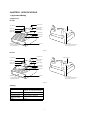
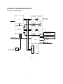
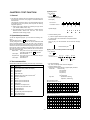
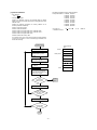
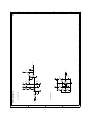
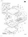
CHAPTER 1. SPECIFICATIONS
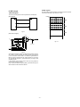
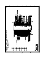
1. Appearance/Rating
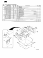
1) Appearance
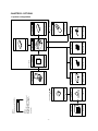
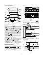
ER-A460
Infrared sensor
Journal window
Printer cover
Customer display
(Pop-up type)
Receipt paper
Operator display
Velidation opening
Ribbon cover
Mode switch
Power switch
Keyboard
Drawer
Drawer lock
* To lock or unlock the drawer,
use the drawer lock key.
Printer cover lock
* To lock or unlock the printer cover,
use the printer cover lock key.
Fig. 1-1
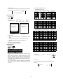
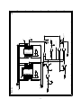
ER-A470
Infrared sensor
Journal window
Printer cover
Customer display
(Pop-up type)
Receipt paper
Operator display
Velidation opening
Ribbon cover
Mode switch
Power switch
Keyboard
Drawer
Drawer lock
* To lock or unlock the drawer,
use the drawer lock key.
Printer cover lock
* To lock or unlock the printer cover,
use the printer cover lock key.
Fig. 1-2
2) Rating
Power source
AC local voltage (±10%) 60Hz
Power consumption
Standby: 7 W
Maximum: 45 W with options installed.
Operating temperature
0˚C~40˚C (32˚F~104˚F)
Operating humidity
10%~90% (RH)
Physical dimensions,
including the drawer
421(W) ✕ 448(D) ✕ 302(H)mm
Weight
13.4 kg
–1–
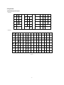
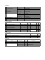
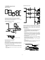
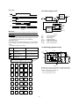
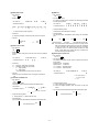
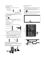
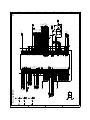
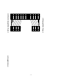
2. Keyboard
1) Standard keyboard layout
1 ER-A460
RECEIPT
JOURNAL
GC
COPY
RCPT
VP
#
NS
%1
%2
7
VAT
1
2
RA
AMT
RF
CASH
#
PLU/SUB
6
12
18 AUTO
CL
5
11
17
EX1
EX2
8
9
4
10
16
CR1
CR2
4
5
6
3
9
15 CH1
CH2
1
2
3
2
8
14
ST
00
1
7
13
TL
0
PO
2 ER-A470
3
RECEIPT
JOURNAL
RCPT
VP
CASH
#
VAT
#
GC
COPY
1
%1
PO
RF
2
%2
RA
6
2
9
5
1
8
4
7
CL
7
4
1
0
8
5
2
00
9
6
3
000
12
11
10
AMT
PLU/
SUB
AUTO
NS
ST
L3
8
16
24
32
40
48
56
64
7
15
23
31
39
47
55
63
6
14
22
30
38
46
54
62
5
13
21
29
37
45
53
61
4
12
20
28
36
44
52
60
3
11
19
27
35
43
51
59
2
10
18
26
34
42
50
58
1
9
17
25
33
41
49
57
L2
L1
CR2
CR1
CH
EX1
TL
Fig. 2-1
–2–
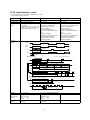
2) Key top name
1 Standard key top
KEY TOP
0 to 9, 00
2 Option key top
ERA460
ERA470
KEY TOP
Numeric keys
|
|
L1
DESCRIPTION
ERA460
ERA470
PLU’s level shift 1 key
|
✕
DESCRIPTION
000 key
✕
|
L2
PLU’s level shift 2 key
|
✕
↑ RECEIPT
Receipt paper feed key
|
|
L3
PLU’s level shift 3 key
|
✕
↑ JOURNAL
Journal paper feed key
|
|
DEPT. 19 ∼ 50
Department 19 ∼ 50 keys
|
✕
Deceimal point key
|
|
DEPT. 13 ∼ 50
Department 13 ∼ 50 keys
✕
|
⊗
Multiplication key
|
|
PLU 1 ∼ 82
Direct PLU 1 to 82 keys
|
✕
CL
Clear key
|
|
PLU 65 ∼ 118
Direct PLU 1 to 118 keys
✕
|
DEPT. 1 ∼ 18
Department 1 ∼ 18 keys
|
✕
VAT SHIFT
Value added tax shift key
|
|
DEPT. 1 ∼ 12
Department 1 ∼ 12 keys
✕
|
%3
Percent 3 key
|
|
PLU 1 ∼ 64
Direct PLU 1 to 64 keys
|
✕
%4
Percent 4 key
|
|
PLU/SUB department key
|
|
$
3
Discount 3 key
|
|
$
4
000
•
PLU/SUB
GC COPY
Guest check copy key
|
|
Discount 4 key
|
|
Value added tax key
|
|
AUTO 2
Automatic sequencing 2 key
|
|
Validation print key
|
|
AUTO 3
Automatic sequencing 3 key
|
|
#
Non-add code entry key
|
|
AUTO 4
Automatic sequencing 4 key
|
|
CASH#
Cashier code entry key
|
|
AUTO 5
Automatic sequencing 5 key
|
|
VAT
VP
Receipt print key
|
|
RA 2
Received on account 2 key
|
|
$
1
Discount 1 key
|
|
PO 2
Paid out 2 key
|
|
$
2
Discount 2 key
|
|
CR3
Credit 3 key
|
|
Automatic sequencing key
|
|
CR4
Credit 4 key
|
|
%1
Percent 1 key
|
|
CH3
Cheque 3 key
|
✕
%2
Percent 2 key
|
|
CH4
Cheque 4 key
|
✕
EX1
Foreign currency exchange 1
key
|
CA2
Cash total 2 key
|
|
Foreign currency exchange 2
key
EX2
✕
|
EX2
|
✕
Foreign currency exchange 2
key
NS
No-sale key
|
|
EX3
Foreign currency exchange 3
key
|
|
EX4
Foreign currency exchange 4
key
|
|
Difference subtotal key
|
|
RCPT
AUTO
|
RA
Received on account key
|
|
PO
Paid out key
|
|
RF
Refund key
|
|
Void key
|
|
CR1
Credit 1 key
|
|
CR2
Credit 2 key
|
|
CH1
Cheque 1 key
|
✕
CH2
Cheque 2 key
|
✕
CH
Cheque key
✕
|
AMT
Amount key
|
|
ST
Subtotal key
|
|
TL
Total (cash total) key
|
|
L1
PLU’s level shift 1 key
✕
|
L2
PLU’s level shift 2 key
✕
|
L3
PLU’s level shift 3 key
✕
|
"
DIFFER ST
–3–
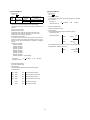
3. Mode switch
No. of positions
Color of display
Character size
SRV
Dot display
12
Green
6.6 (H) ✕ 4.6 (W) mm
7 segment display
10
Green
10.0 (H) ✕ 4.3 (W) mm
MA
2 Customer display
SM.
7
OP
6
5
4
3
2
1
REG
OP X/Z
MGR
X1/Z1
PGM1
X2/Z2
PGM2
ST
(SRV)
TL
/RF
(SRV')
Fig. 4-2
No. of positions
Color of display
Character size
Fig. 3-1
* The key can be removed in the REG or OFF position.
* In the SRV’ mode, key inputs are prohibited and no display is
made.
Lamps
* With the key in the off position power is still supplied to the
main PWB.
Display
contents
L2
L3
CHR.
[Functions]
•
•
•
•
Function for each key position
SRV’:
System reset
SRV:
Service mode (Service programming)
PGM2:
Allows programming of an item that is not changed
frequently, in addition to the PGM1 mode programming.
•
PGM1:
Allows programming of items frequently changed
(e.g. department, PLU pricing, and discount rate setting).
•
•
•
OP/XZ:
Allows X or Z operation by servers or cashiers.
REG:
Allows registrations.
MGR:
Allows the operations, by authorized person such as
a manager (e.g. correction after transaction finished
or cancellation of entry limits), which are not permitted to ordinary cashiers.
•
•
X1/Z1:
Allows reading and resetting of a day’s sales total.
X2/Z2:
Allows reading or resetting sales totals in a specified
period.
•
& :
Switches off the display to prevent keyboard entries.
4. Display
1) Layout
5. Printer (DP-730)
1 Operator display
L3 CHR. SML DC
VP STOCK RCPT ST
OFF
Description
The lamp lights up when PLU level is 2.
The lamp lights up when PLU level is 3.
The lamp lights up when character key sheet mode in
text setting
SML
The lamp lights up when small characters are being
inputted in text setting
DC
The lamp lights up when double width characters are
being inputted in text setting.
ONL
The lamp lights up when the machine is connected to
the online transmission line; and it goes off when the
machine is disconnected from the line. The lamp
blinks during data transmission.
VP
The lamp lights up when Validation print is under
compulsion.
STOCK
The lamp lights up when stock is empty state.
RCPT OFF The lamp lights up when receipt is OFF state.
ST
The lamp lights up when a subtotal is displayed.
→
The lamp lights up when change amount is displayed
after tendering.
TL
The lamp lights up when a transaction is finalized with
CASH, CHECK, CREDIT, or CHARGE key, however,
the lamp does not light up when a transaction is
finalized with an amount tendered entry.
/RF
"
The lamp lights up when the void or refund key is
pressed.
VAT SHIFT The lamp lights up when the vat shift key is pressed.
GC COPY The lamp lights up when the guest check copy mode.
CCD
The lamp lights up when the CCD registration.
(The setting does not turn off the AC
power.)
L2
7
Green
10 (H) ✕ 4.5 (W) mm
1) Specifications
• Part number:
• No. of stations:
• Printing system:
• Direction of printing:
• Printing capacity:
ONL
TL
/RF VAT
GC CCD
SHIFT COPY
Fig. 4-1
–4–
DP-730
2
Mechanical serial dot
Bidirectional
Receipt – 24 characters
Journal – 24 characters
Validation – 55 characters
(one line only)
•
Character size:
2.4 (H) ✕ 1.36 (W) mm
Print pitch:
Column distance 1.59 mm
Row distance
5.08 mm
•
Total number of dots:
Receipt – 108 dots/216 positions
Journal – 108 dots/216 positions
Validation – 248 dots/495 positions
3) Paper
• Paper roll dimensions: 44.5±0.5mm in width, 83mm in diameter
• Paper quality:
Journal
•
Font:
7 ✕ 7 dots (including half dot)
Space between characters – 1 dot (2
positions)
•
•
•
•
Distance between dots:
0.353 mm (H) ✕ 0.353 mm (W)
Journal near end sensor:
Service route option
Print speed:
Approx. 3.0 lines/sec.
Paper feed speed:
Receipt – Approx. 30 lines/sec.
Journal – Approx. 30 lines/sec.
•
Reliability:
•
Bond paper (paper thickness: 0.06 to
0.09mm, paper weight: 52.3 to 64g/m2)
Validation form
Thickness: 0.07 to 0.14mm
Size: 130mm or more (W) ✕
70mm or more (H)
4) Inking
• Ink supply system:
• Form:
• Specification:
• Ribbon life:
• Print color:
MCBF – 400 million lines (excluding
the print head)
Head life – 10,000 characters
(in the case of printing average 2 dots per character per wire
Validation form sensor:
5) Logo stamp
• Material:
• Stamp color:
• Max. stamp size:
• Ink refill:
Not setup
Ink ribbon
Cartridge/Endless ribbon
Material – Nylon
Approx. 6 million characters
Purple (single color)
Porous rubber
Purple (single color)
30(W) × 20(H) mm
Allowed (UINK-1001CCZZ: 5CC)
2) Printing area
6) Cutter
• Method: Manual
Receipt/journal
87.08
6. Drawer
3.56
37.87
3.56
3.56
3.56
37.87
1) Specification
(1) Drawer box and drawer
Model name of the drawer box
Size
Color
Material
Bell
Release lever
4.2
44.5± 0.5
44.5± 0.5
Drawer open sensor
Separation from the main unit
RECEIPT
2) Money case
JOURNAL
Separation from the drawer
Separation of the bill compartments from the coin
compartments
Bill separator
Number of compartments
Unit : mm
Fig. 5-1
Validation form
Allowed
Disallowed
—
4B/8C
87.08 (PRINT AREA)
20
22
70
SK423
420 (W) ✕ 426 (D) ✕ 114 (H)
Light olive gray
Metal
—
Standard equipment;
situated at the bottom
Standard equipment
Allowed with service kit
4B/8C
130 ~ 210
Unit : mm
3) Lock
• Location of the lock:
• Method of locking
Fig. 5-2
and unlocking:
•
–5–
Key no.:
Front
To lock, insert the drawer lock key into the
lock and turn it 90 degrees counterclockwise.
To unlock, insert the drawer lock key and turn
it 90 degrees clockwise.
SK1-1
–6–
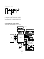
SERVICE OPTION
REMOTE DRAWER
CABLE
3.5 inch FDD
DRAWER COIN CASE
COIN CASE COVER
Fig. 1-1
ER-48CC3
MASTER MACHINE
ER-A460/A470
OPTION RAM
ER-01RA/02RA
ER-02CV1~5
RS-232C I/F
COMPUTER
COMMERCIAL
PRODUCT
ER-A5RS
MAX 2 PORTS
LOCAL PURCHASE
ER-01/02FD
WIRELESS INTERFACE
CE-IR2/IR4
IR comunication
(NOTE2)
The ER-A46R1 is neccessary to work
the option showed by * * * symbol.
The ER-A46R1 is only one ROM on
some options.
(NOTE1)
This symbol shows NEW MODEL
1 HOLE CASHIER SW
ER-A5CL
TEXT PRESET
REMOTE KEY
ER-01RK
IR comunication
OPTION CONT. ROM
ER-A46R1
CHAPTER 2. OPTIONS
1. System configuration
2. Options
NO
NAME
MODEL
1
ONE HOLE CASHIER KEY
ER–A5CL
2
EXPANSION RAM CHIP
ER– 01RA
3
ON-LINE SYSTEM
DESCRIPTION
32K bytes RAM chip
ER– 02RA
128K bytes RAM chip
ER–A5RS
2ports RS-232 I/F
4
CONTROL ROM
ER–A46R1
Control for ER-A5RS
5
PRESETS LOADER
ER–01FD / 02 FD
FD unit
6
KEY TOP KIT (For ER-A460)
E R–11KT7
1 ✕ 1 key top
E R–12KT7
1 ✕ 2 key top
E R–22KT7
2 ✕ 2 key top
E R– 11DK7
1 ✕ 1 dummy key
E R– 51DK7
5 ✕ 1 dummy key
7
PROGRAMMING REMOTE KEYBOARD
E R– 01RK
IR I/F text preset keyboard
8
WIRELESS INTERFACE
C E– I R2 / I R4
For IR communication
9
COIN CASE
E R–48CC2
10
COIN CASE COVER
E R–01CV1~01CV5
3. Service options
NO.
NAME
PARTS CODE
PRICE
RANK
1
SERVICE KEY
L K G I M7 1 1 3 R C Z Z
AK
2
DRIP-PROOF SWITCH COVER
GCOVB7 1 0 8BHZ Z
BA
3
MODE KEY GRIP COVER
L K G I M7 1 2 6 R C Z Z
AL
DESCRIPTION
ERA460
ERA470
|
|
|
|
|
|
For the mode switch
OP key only
4
DRIP-PROOF KEYBOARD COVER
G COVB7 1 0 9 BHZ Z
BF
|
✕
5
JOURNAL NEAR END SENSOR
DUNT – 4 9 4 5 BHZ Z
AY
|
|
6
PROGRAMMING CHARACTER KEYBOARD COVER
GCOVB7 1 1 0BHZ A
BE
|
✕
7
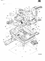
REMOTE DRAWER
CBOXD7 1 3 6BH0 1
BU
|
|
CLERK COVER "B"
GCOVA7 1 0 7BHZ B
AG
|
|
CLERK ANGLE
LANGT 7 5 8 1BHZ Z
AM
|
|
8
For ER-A5CL
4. Service tools
NO.
NAME
PARTS CODE
PRICE
RANK
1
EXPANSION PWB
CKOG– 6 7 0 8RCZ Z
BU
2
RS-232 LOOP BACK CONNECTOR FOR ER-A5RS
UKOG– 6 7 0 5RC Z Z
BU
3
KEY TOP REMOVER (For ER-A460)
UK OG - 6 6 34 RC Z Z
AX
5. Supplies
NO.
NAME
PARTS CODE
PRICE
RANK
DESCRIPTION
1
ROLL PAPER
DPAPR1 0 0 6CSZ Z
AR
2
INK RIBBON
PRBN– 6 6 4 4RCZ Z
AZ
3
INK FOR STAMP
U I NK–1 001CCZ Z
AK
5 cc
4
KEY SHEET (For ER-A470)
PSHEK6 8 3 0 BHZ Z
AU
Programming character sheet
PSHEK6 8 2 9 BHZ Z
AR
Standard character sheet
PSHEK6 8 2 8 BHZ Z
AK
Blank character sheet
–7–
5rolls/pack
6. Options
For installation of the options, refer to the Installation Manual which is
issued separately.
7. How to use service tools
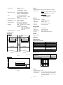
7-1. Expansion PWB: CKOG-6708RCZZ
• External view
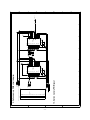
Fig. 7-1
Purpose 1:
Used for servicing and repairing of options (such as the
and the ER-A5RS) which are connected with the main
body option connector.
[Procedure 1]
Use an insulator base as shown in Fig. 7-2 (shaded section) and
perform servicing.
ER-A460/A470
Loop back connectors (2 pcs.):
UKOG-6705RCZZ
Expansion PWB
Main PWB (CKOG-6708RCZZ)
ER-A5RS
PWB
Base
A
Control ROM
Fig. 7-2
To check the option I/F PWB from the solder side, connect the I/F
PWB to OPTCN2. To check from the parts side, connect to OPTCN3.
(Note) The option I/F PWB should be held horizontally so that no
excessive stress is applied to connecting section A in Fig.
7-2.
[Procedure 2]
Pop up
String
ER-A460/A470
Loop back connectors (2 pcs.):
UKOG-6705RCZZ
Expansion PWB
Main PWB (CKOG-6708RCZZ)
ER-A5RS
PWB
Control ROM
Fig. 7-3
Put a string between the pop up and the option PWB, as shown in
Fig. 7-3. Adjust the length of the string so that the CKOG-6708RCZZ
and the option PWB are not binding. Then perform servicing.
–8–
[key setup procedure]
CHAPTER 3. SRV. RESET AND
MASTER RESET
*2
MRS-2
executed
0
Key position set
Free key
0
1. SRV. reset (Program Loop Reset)
*1
Free key setup
complete.
Disable
Used to return the machine back to its operational state after a lockup has occurred.
NOTES:
*1: When the 0 key is pressed, the key of the key number on display
is disabled.
*2: Push the key on the position to be assigned. With this, the key of
the key number on display is assigned to that key position.
Procedure
•
Method 1
1) Unplug the AC cord from the wall outlet.
2) Set the mode switch to (SRV′) position.
Key number
Key name
1
Numeric key "0"
9
Numeric key "8"
2
Numeric key "1"
10
Numeric key "9"
Method 2
3
Numeric key "2"
11
Numeric key "00"
1) Set the mode switch to PGM2 position.
4
Numeric key "3"
13
Decimal point key
2) Turn off the AC switch.
5
Numeric key "4"
14
CL key
3) While holding down JOURNAL FEED key and RECEIPT FEED
key, Turn on the AC switch.
6
Numeric key "5"
15
@/FOR key
7
Numeric key "6"
16
SBTL key
Note: When disassembling and reassembling always power up
using method 1 only. Method 2 will not reset the CKDC6.
8
Numeric key "7"
17
CA/AT key
3) Plug in the AC cord to the wall outlet.
4) Turn to (SRV) position from (SRV′) position.
•
Note: SRV programming job#926-B must be set to "4" to allow PGM
program loop reset.
2. Master reset (All memory clear)
There are two possible methods to perform a master reset.
•
MRS-1
Used to clear all memory contents and return machine back to its
initial settings and return keyboard back to default keyboard.
Procedure
1) Unplug the AC cord from the wall outlet.
2) Set the MODE switch to the (SRV′) position.
3) Plug in the AC cord to the wall outlet.
4) While holding down JOURNAL FEED key, turn to (SRV) position
from (SRV′) position.
•
MRS-2
Used to clear all memory and keyboard contents.
This reset returns all programming back to defaults. The keyboard
must be entered by hand.
This reset is used if an application needs different keyboard layout
other than that supplied by a normal MRS-1.
Procedure
1) Unplug the AC cord from the wall outlet.
2) Set the MODE switch to the (SRV′) position.
3) Plug in the AC cord to the wall outlet.
4) While holding down JOURNAL FEED key and RECEIPT FEED
key, turn to (SRV) position from (SRV′) position.
5) Key position assignment:
* After the execution of MRS-2, only the RECEIPT FEED and
JOURNAL FEED keys can remain effective on key assignment.
Any key can be assigned on any key position on the main keyboard.
–9–
Key number
Key name
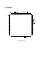
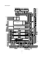
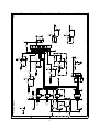
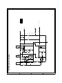
CHAPTER 4. HARDWARE DESCRIPTION
1. Hard ware block diagram
CPU
STANDARD
OPTIONAL
RAM1
RAM2
32KB
MAX.128KB
STANDARD
OPTIONAL
ROM
ROM
256KB
128KB
DRAWER
MAX.2
GATE ARRAY
MPCA6
ER-01RA:32KB
ER-02RA:128KB
ER-A46R1
OPERATER DISPLAY
2 LINE
5 x 7DOT 12DIG
5 x 7SEG 10DIG
CUSTOMER DISPLAY
1 LINE
7SEG 7DIG
PRINTER DP-730
CKDC6
SWITCH
KEY BOARD
ER-01RK
Other ECR
RS232
I/F
2 ports
I/R
UNIT
OPT CN
ER-A5RS
Fig. 1-1
– 10 –
2. Description of main LSI’s
2-1. CPU (HD6415108FX)
STBY
MD2
MD1
MD0
VCC
RFSH
LWR
HWR
RD
AS
E
X
VSS
XTAL
EXTAL
VSS
TXD2
RXD2
TXD1
RXD1
SCK2
IRQ2
IRQ1
IRQ0
VCC
AVCC
P73
AN3
112
111
110
109
108
107
106
105
104
103
102
101
100
99
98
97
96
95
94
93
92
91
90
89
88
87
86
85
1) Pin configuration
20
65
P50/FTCA1
A0
21
64
VSS
A1
22
63
P47
A2
23
62
FTI2
A3
24
61
P45
A4
25
60
FTI1
A5
26
59
P43
A6
27
58
P42
A7
28
57
TMCI
56
P51
VSS
P40
66
55
19
VCC
P52
D15
54
67
P37
18
53
P53
D14
P36
68
52
17
P35
P54
D13
51
69
P34
16
50
FMRS
D12
P33
70
49
15
BREQ
P56
D11
48
71
BACK
14
47
P57/STOP
D10
WAIT
72
46
13
VSS
P60/ER
D9
45
73
A23
12
44
P61/DR
D8
A22
74
43
11
A21
P62/CS
D7
42
75
A20
10
41
P63/CD
D6
A19
76
40
9
A18
P64/RR
D5
39
77
A17
8
38
P65/RS
D4
A16
78
37
7
VSS
P66
D3
36
78
A15
6
35
P67
D2
A14
80
34
5
A13
VSS
D1
33
81
A12
4
32
AVSS
D0
A11
82
31
3
A10
AN0
VSS
30
AN1
83
29
84
2
A9
1
NMI
A8
RES
HD6415108FX pin configuration
Fig. 2-1
– 11 –
D0
D1
D2
D3
D4
D5
D6
D7
D15
D14
D13
D12
D11
D10
D9
D8
2) Block diagram
P27/A23
P26/A22
Data bus
Port 1
P25/A21
Port 2
P24/A20
P23/A19
P22/A18
P21/A17
Clock
oscillator
X
Watch
dog timer
E
MD2
MD1
H8/500 CPU
A15
A14
A13
A12
A11
A10
A9
A8
A7
A6
A5
A4
A3
A2
A1
A0
Address bus
XTAL
Address bus
EXTAL
Data bus (Upper)
Data bus (Lower)
P20/A16
DTC
MD0
RES
STBY
NMI
Interruption controller
AS
P37
RD
P36
HWR
P35
16bit free running
timer x 2ch
Refresh controller
RFSH
P34
Port 3
LWR
P33
BREQ
VCC
Wait state
controller
8bit timer
A/D convertor
Serial
communication
interface x 2ch
BACK
WAIT
VCC
P47
VCC
VSS
P45
FTI1
Port 4
VSS
FTI2
VSS
VSS
P43
VSS
P42
VSS
P41/TMCI
VSS
P40
VSS
AVCC
Fig. 2-2
– 12 –
P50
P51
P52
P53
P54
FMRS
P56
Port 5
STOP/P57
P67
P66
RS/P65
RR/P64
CD/P63
CS/P62
DR/P61
ER/P60
AN0
Port 6
AN1
P73
IRQ0
IRQ1
Port 7
IRQ2
SCK2
RXD1
TXD1
RXD2
TXD2
Port 8
AN2
AVSS
3) Pin description
Pin
No.
1
Symbol
RES
Signal
name
In/
Out
RESET
I/O
Reset input
Pin
No.
Function
Symbol
Signal
name
In/
Out
Function
53
P36
DR2
Out
Remote drawer No.2 open
signal (NU)
54
P37
DR3
Out
Remote drawer No.3 open
signal (NU): GND
2
NMi
NMi
In
Non-maskable interrupt input
for SSP interrupt input.
3
VSS
NU
In
GND
4
D0
Nu
In
GND
55
VCC
VCC
In
+5V
5
D1
Nu
In
GND
56
P40
IFV
In
6
D2
Nu
In
GND
Slip printer (M-240) interface
connect signal (NU)
7
D3
Nu
In
GND
57
TMCi
PTMG
In
Printer (DP-730) timing signal
8
D4
Nu
In
GND
58
P42
TOF
In
Slip printer (M-240)
sensor signal (NU)
TOF
BOF
9
D5
Nu
In
GND
10
D6
Nu
In
GND
59
P43
BOF
In
Slip printer (M-240)
sensor signal (NU)
11
D7
Nu
In
GND
60
FTi1
PRST
In
Printer (DP-730) reset signal
12
D8
D0
I/O
Data bus
61
P45
NEJ
In
Near end sensor journal side
13
D9
D1
I/O
Data bus
14
D10
D2
I/O
Data bus
62
FTi2
SHEN
In
CKDC Interface shift enable
signal
15
D11
D3
I/O
Data bus
63
P47
NER
In
Near end sensor receipt side
16
D12
D4
I/O
Data bus
64
VSS
VSS
In
GND
17
D13
D5
I/O
Data bus
65
P50/FTCA1 TRGI
Out Dot pulse adjust signal
18
D14
D6
I/O
Data bus
66
P51
NU
Out NC
19
D15
D7
I/O
Data bus
67
P52
NU
Out NC
20
VSS
NU
In
GND
68
P53
NU
21
A0
A0
Out Address bus
69
P54
NU
22
A1
A1
Out Address bus
70
FMRS
NU
23
A2
A2
Out Address bus
71
P56
NU
Out NC
24
A3
A3
Out Address bus
72
P57/STOP
STOP
Out System reset output. Normally
25
A4
A4
Out Address bus
73
P60/ER
ERS/ER
Out
26
A5
A5
Out Address bus
27
A6
A6
Out Address bus
74
P61/DR
DRS/DR
In
28
A7
A7
Out Address bus
SIO control signal
(Data set ready) (NU)
29
A8
A8
Out Address bus
75
P62/CS
CSS/CS
In
30
A9
A9
Out Address bus
SIO control signal
(Clear to send) (NU)
31
A10
A10
Out Address bus
76
P63/CD
CDS/CD
In
SIO control signal
(Carrier detect) (NU)
32
A11
A11
Out Address bus
33
A12
A12
Out Address bus
77
P64/RR
RRS/RR
Out
SIO control signal
(Ready to receive) (NU)
34
A13
A13
Out Address bus
78
P65/RS
RSS/RS
Out
35
A14
A14
Out Address bus
SIO control signal
(Request to send) (NU)
36
A15
A15
Out Address bus
79
P66
RCO
In
Remote keyboard input signal
37
VSS
NU
80
P67
HP
In
Printer home position signal
38
A16
A16
Out Address bus
81
VSS
NU
In
GND
39
A17
A17
Out Address bus
82
AVSS
NU
In
GND
AN0
VPJ
In
Validation sensor journal
In
GND
In
GND
Out NC
In
NC
SIO control signal (Equipment
ready) (NU)
40
A18
A18
Out Address bus
83
41
A19
A19
Out Address bus
84
AN1
VPR
In
Validation sensor receipt (NU)
Out Address bus
85
AN3
VPTEST
In
+24V test input
Out Address bus
86
P73
VPPS
In
Validation sense signal (NU)
AVCC
AVCC
In
+5V
42
43
A20
A21
A20
A21
44
A22
A22
Out Address bus
87
45
A23
A23
Out Address bus
88
VCC
VCC
In
+5V
46
VSS
NU
In
GND
89
IRQ0
IRQ0
In
Interrupt signal 0
47
WAIT
WAIT
In
Wait signal
90
IRQ1
IRQ1
In
Interrupt signal 1 (RS-232C)
91
SCK1
UASCK
In
I/R control signal (Shift clock)
92
SCK2
SCK2
In
CKDC Interface sync shift
clock
93
RXD1
/UARX
In
I/R control signal
(Receive data)
94
TXD1
/UATX
Out
I/R control signal
(Transmit data)
48
BACK
BACK
Out
Bus control request
acknowledge
49
BREQ
BREQ
In
Bus control request
50
P33
DOPS
In
Drawer open signal
51
P34
DR0
Out Option drawer open signal
52
P35
DR1
Out
Remote drawer No.1 open
signal
– 13 –
Pin
No.
Symbol
Signal
name
In/
Out
Function
95
RXD2
RXD2
In
CKDC Interface shift input
data
96
TXD2
TXD2
Out
CKDC Interface shift output
data
97
VSS
NU
In
98
EXTAL
EXTAL
In
Crystal oscillator connection
99
XTAL
XTAL
In
Crystal oscillator connection
In
GND
100 VSS
NU
101 X
X
GND
Out System clock
102 E
NU
Out Nu
103 AS
AS
Out Address strobe
104 RD
RD
Out Read
105 HWR
WR
Out Write
106 LWR
LWR
Out Nu
107 RFSH
RFSH
Out Refresh cycle
108 VCC
VCC
In
+5V
109 MD0
MD0
In
+5V (MODE 3)
110 MD1
MD1
In
+5V (MODE 3)
111 MD2
MD2
In
GND (MODE 3)
112 STBY
STBY
In
+5V (Nu)
– 14 –
2-2. G.A (MPCA6)
160
159
158
157
156
155
154
153
152
151
150
149
148
147
146
145
144
143
142
141
140
139
138
137
136
135
134
133
132
131
130
129
128
127
126
125
124
123
122
121
NU
DOTEN
NU
NU
NU
NU
NU
NU
STH2
SCK2
HTS2
SLMTR
SLMTS
SLMTD
RJMTR
RAS3
NU
GND
VCC
NU
NU
NU
NU
RJMTD
RJMTS
DT5
DT6
DT7
GND
DT1
DT2
DT3
DT4
RJTMG
RJRST
RAS1
RAS2
ROS2
ROS1
OPTCS
1) Pin configuration
120
119
118
117
116
115
114
113
112
111
110
109
108
107
106
105
104
103
102
101
100
99
98
97
96
95
94
93
92
91
90
89
88
87
86
85
84
83
82
81
41
42
43
44
45
46
47
48
49
50
51
52
53
54
55
56
57
58
59
60
61
62
63
64
65
66
67
68
69
70
71
72
73
74
75
76
77
78
79
80
1
2
3
4
5
6
7
8
9
10
11
12
13
14
15
16
17
18
19
20
21
22
23
24
25
26
27
28
29
30
31
32
33
34
35
36
37
38
39
40
D3
GND
D4
D5
D6
D7
SSPRQ
RESET
INT2
INT3
RXDI
TXDI
SCKI
IRQ0
A0
A1
A2
A3
A4
A5
GND
VCC
A6
A7
A8
A9
A10
A11
A12
A13
A14
A15
A16
A17
A18
A19
A20
A21
A22
NU
RF
JF
PCUT
FCUT
VF
STAMP
SLF
SLRS
SLMTD
RES
TRG
TRG
POFF
INT1
HTS1
SCK1
STH1
NU
NU
VCC
GND
NU
VRESC
SLTMG
SLRST
AS
RD
WR
PHAI
SDT7
SDT6
SDT5
GND
SDT4
SDT3
SDT2
SDT1
D0
D1
D2
GATE ARRAY (F258016PC)
MPCA5
Fig. 2-3
– 15 –
EXINT0
EXINT1
EXINT2
EXINT3
WRO
RDO
RA15
RA16
GND
RA17
RA18
EXWAIT
WAIT
NU
NU
NU
NU
NU
NU
GND
VCC
NU
NU
NU
NU
NU
NU
NU
NU
NU
NU
TEST
MD0
MD1
IPLON
INT4
PRST
PTMG
TRGI
A23
2) Block diagram
A23~A0
IRLON
ROS1
ROS2
RAS1
RAS2
Address decode
External CS
Internal CS
RASEL
Image
control
SSPRQ
SSP comparison register
BAR.
RAS3
OPTCS
IRTX
IRRX
RCI
ASKRX
I/R Control
D0~D7
Buffer
AS
CHS
serial select
RD
TXDI
SCKI
RXDI
HTS1
SCK1
STH1
HTS2
SCK2
STH2
Multiplexer
WR
RDO
WRO
Φ
Read/write
control
Φ
RESET
INT4
RES
Divider
VRESC
INT1
INT2
POFF
WAIT
EXWAIT
INT3
INTO
control
MD0
MD1
EXINT0
EXINT1
WAIT
control
EXINT2
EXINT3
CAPS
select
IRQ0
Print mode PMD
TEST
MTD
MTD
RJRST
SLRST
*PRST
RJTMG
RJMTR
Motor
drive
Print gate
SLMTS
SLTMG
SLMTR
Printer control port
Print pulse control
PTMG
SLMTD
SLF
SLRS
VF
RF
JF
FCUT
– 16 –
PCUT
Fig. 2-4
STAMP
TRGI
SDT1~7
DT1~9
TRG
DOTEN
TRG
* Output selection with CAPS.
PRST/PTMG.
SLMTD
3) Pin description
Pin
No.
Signal
name
In/
Out
Pin
No.
Function
Signal
name
In/
Out
Function
1
RF
Out
Receipt side paper feed solenoid
50
INT3
In
2
JF
Out
Journal side paper feed solenoid
51
RXD2
Out
8 bit serial port output to CPU
3
PCUT
Out
Printer partial cut signal (NU)
52
TXD2
In
8 bit serial port input from CPU
4
FCUT
Out
Printer auto cut signal (NU)
53
SCK2
In
Serial port shift clock input from CPU.
5
VF
Out
Multi line validation paper feed (NU)
54
IRQ0
Out
6
STAMP
Out
Printer stamp signal (NU)
55
A0
In
Address bus 0
7
SLFS
Out
Slip printer paper feed singnal (NU)
56
A1
In
Address bus 1
8
SLRS
Out
Slip printer release signal (NU)
57
A2
In
Address bus 2
9
SLMTD
Out
Slip printer motor drive signal (NU)
58
A3
In
Address bus 3
10
RES
Out
Peripheral output reset
59
A4
In
Address bus 4
11
TRG
Out
Dot head trigger signal (NU)
60
A5
In
Address bus 5
12
TRG
Out
Dot head trigger signal
61
GND
—
GND
13
POFF
In
Power off signal input
62
VCC
—
+5V
14
INT1
In
Interrupt signal (Key interrupt request)
63
A6
In
Address bus 6
15
HTS1
Out
8 bit serial port output
64
A7
In
Address bus 7
16
SCK1
Out
Serial port shift clock output
65
A8
In
Address bus 8
17
STH1
In
8 bit serial port input
66
A9
In
Address bus 9
18
RAS VZ
—
Chip select (NU)
67
A10
In
Address bus 10
—
Nu
68
A11
In
Address bus 11
19
—
Interrupt signal (Nu)
Interrupt request to CPU
20
VCC
—
+5V
69
A12
In
Address bus 12
21
GND
—
GND
70
A13
In
Address bus 13
22
INTMCR
—
Interrupt (NU)
71
A14
In
Address bus 14
Turns active when reset and power down
is met
72
A15
In
Address bus 15
73
A16
In
Address bus 16
23
VRESC
Out
24
SLTMG
In
Slip printer timing signal (NU)
74
A17
In
Address bus 17
25
SLRST
In
Slip printer reset signal (NU)
75
A18
In
Address bus 18
26
AS
In
Address strobe
76
A19
In
Address bus 19
27
RD
In
Read strobe
77
A20
In
Address bus 20
28
WR
In
Write strobe
78
A21
In
Address bus 21
29
φ
In
(φ) System clock (7.3728 MHz)
79
A22
In
Address bus 22
Slip printer printhead drive signal (dot7)
(NU)
80
LCDC
—
LCD CS (NU)
81
A23
In
Address bus 23
Slip printer printhead drive signal (dot6)
(NU)
82
TRGI
In
Dot pulse control/drive signal
83
PTMG
Out
84
PRST
Out
GND
85
INT4
In
Slip printer printhead drive signal (dot4)
(NU)
86
IPLON
In
To option connector
Out
87
MD1
In
Mode select input (+5V)
Out
Slip printer printhead drive signal (dot3)
(NU)
88
MD0
In
Mode select input (GND)
89
TEST
In
+5V
Out
Slip printer printhead drive signal (dot2)
(NU)
90
MA15
—
Image address 15 (NU)
91
MA18
—
Nu
Out
Slip printer printhead drive signal (dot1)
(NU)
92
MA19
—
Nu
93
RCVRDY1
—
Nu
94
RCVRDY2
—
Nu
95
RC0
—
Remote control encord signal for CPU
96
IRTX
—
I/R output for LED
97
UASCK
—
I/R serial data shift clock
98
UARX
—
I/R serial data for CPU
99
UATX
—
I/R serial data from CPU
100
VCC
—
+5V
101
GND
—
GND
102
IRRX
—
I/R input from I/R unit
103
RCI
—
I/R input from I/R unit
104
DAX1
—
System clock (7.3728MHz)
30
31
32
33
34
35
36
37
SDT7
SDT6
SDT5
GND
SDT4
SDT3
SDT2
SDT1
Out
Out
Out
—
Slip printer printhead drive signal (dot5)
(NU)
38
D0
I/O
Data bus 0
39
D1
I/O
Data bus 1
40
D2
I/O
Data bus 2
41
D3
I/O
Data bus 3
42
43
GND
D4
—
I/0
GND
Data bus 4
44
D5
I/0
Data bus 5
45
D6
I/0
Data bus 6
46
D7
I/0
Data bus 7
47
SPRQ
Out
SSP interrupt request to CPU
48
RESET
In
MPCA reset
49
INT2
In
Interrupt signal (Nu)
– 17 –
Printer timing signal
Printer reset signal
Interrupt signal (NU)
Pin
No.
Signal
name
In/
Out
2-3. CKDC6 (HD404728A91FS)
Function
105
DAX2
—
Nu
1) General description
106
MCR1
—
Nu
107
MCR2
—
Nu
108
WAIT
Out
The CKDC6 is a 4-bit microcomputer developed for the ER-A460/
A470 and provides functions to control the real-time clock, keys, and
displays. The basic functions of the CKDC6 are shown below.
109
EXWAIT
110
RA18
Out
111
RA17
Out
Nu
112
GND
—
GND
113
RA16
Out
Nu
114
RA15
Out
Nu
115
RDO
Out
Expansion RD signal
116
WRO
Out
117
EXINT3
In
Expansion interruption signal 3
118
EXINT2
In
Expansion interruption signal 2
119
EXINT1
In
Expansion interruption signal 1
120
EXINT0
In
Expansion interruption signal 0
121
OPTCS
Out
Chip select base signal for expansion
option
122
ROS1
Out
ROM 1 chip select signal
123
ROS2
Out
ROM 2 chip select signal
124
RAS2
Out
RAM 2 chip select signal
125
RAS1
Out
RAM 1 ship select signal
126
RJRST
In
Printer reset signal
127
RJTMG
In
Printer timing signal
Clock:
Year, month, day of month, day of week, hour, minute
Hour, minute
In
Wait request signal
External wait control input signal
Keys:
The CKDC6 is capable of controlling a maximum of 256
momentary keys. (Sharp 2-key rollover control)
Simultaneous scanning of key and switch
(When a key is scanned, the state of a mode and clerk
switch is also buffered. The host can scan the state of
switch together with the key entry data at the same time
the key is scanned.)
Switches:
Mode switch with 14 positions maximum
8-bit clerk (cashier) switch
2-bit feed switch
1-bit receipt on/off switch
1-bit option switch
4-bit general-purpose switch (1-bit is used for keyboard
select)
Displays:
16-column dot display
12-column 7-segment display (column digit selectable)
All column blink controlled for the dot and 7-segment
display decimal point and indicators
Programmable patterns for 7-segment display:
Four patterns
Internal driver for 7-segment display
Buzzer:
Single tone control
Nu
Expansion WR signal
Option
Option
128
DT4
Out
Printer dot signal 4
Alarm:
129
DT3
Out
Printer dot signal 3
130
DT2
Out
Printer dot signal 2
131
DT1
Out
Printer dot signal 1
Interrupt request (event control):
Detection of key input, switch position change, alarm
issue, and counter overflow
132
GND
—
GND
133
DT7
Out
Printer dot signal 7
134
DT6
Out
Printer dot signal 6
135
DT5
Out
Printer dot signal 5
136
MTD
Out
Printer motor drive signal
137
MTD
Out
Printer motor drive signal
138
DOT9
—
Printer dot signal 9 (NU)
139
DOT8
—
Printer dot signal 8 (NU)
140
SYNC
—
Nu (+5V)
141
ASKRX
—
I/R input from I/R unit
142
VCC
—
+5V
143
GND
—
GND
—
Nu
Out
Nu
144
—
145
RAS3
146
RJMTR
In
Printer motor lock detection signal (NU)
147
SLMTD
In
Nu
148
SLMTS
In
Nu
149
SLMTR
In
GND
150
HTS2
Out
Nu
151
SCK2
Out
Nu
152
STH2
In
Nu
153
—
—
Nu
154
—
—
Nu
155
—
—
Nu
156
—
—
Nu
—
157
—
Nu
158
LCDWT
—
Nu
159
DOTEN
Out
Dot drive enable signal
160
RASP
—
Nu
– 18 –
IRQ
SHEN
STH
HTS
SCK
POFF
STOP
SRES
HOST
SYSTEM
DIG00
DIG15
SEG00
SEG15
DOT-DISPLAY 16DIG
P0,1,4
G1~G7
SA~SG
7SEG-DISPLAY 7DIG
DOT DISP CONT.
M66004FP
P2,3
SRES,DCS,DSCK,DSO
ST0~3
CKDC 6
KEX0,1
DECODER
LS138
DECODER
LS138
CKDCR
KEY BOARD
MAX. 244key
Q
CSFR
MODR
KR0~3
SKRO
DISPSL
BUZZ
DECODER
LS153
DECODER
LS153
BUZZER
Fig. 2-5
2) Pin assignment
Pin
No.
1
2
3
4
5
6
7
8
9
10
11
12
I/O
I/O
I/O
I/O
I/O
I/O
I/O
I/O
I/O
I/O
I/O
I
RESET
State
H-Z
H-Z
H-Z
H-Z
H-Z
H-Z
H-Z
H-Z
H-Z
H-Z
H-Z
I
DP
ID
MODR
O
O
O
O
O
O
O
O
O
O
O
I
RA1
I
I
CFSR
I
14
15
16
R30
R31
R32
I/O
I/O
I/O
H-Z
H-Z
H-Z
KEX0
KEX1
NU
O
O
O
DB4 : SEG-B
DB4 : SEG-C
DB4 : SEG-D
DB4 : SEG-E
DB4 : SEG-F
DB4 : SEG-G
DB7 : 7SEG COM
DB2 : DOT DP
DB3 : DOT COM
DB5 : 7SEG DP
DB5 : 7SEG ID
MODE RETURN
CLEARK, FEED,
SWITCH RETURN
KEY EXCHANGE0
KEY EXCHANGE1
GND
17
R33
I/O
H-Z
NU
O
GND
18
R50
I/O
I
ST0
O
KEY SCAN ST0
19
20
R51
R52
I/O
I/O
I
I
ST1
ST2
O
O
KEY SCAN ST1
KEY SCAN ST2
Port
I/O
R01
R02
R03
R10
R11
R12
R13
R20
R21
R22
R23
RA0
13
Signal
name
SB
SC
SD
SE
SF
SG
I/O
Notes
PULL−UP
−DOWN
PULL-DOWN
PULL-DOWN
PULL-DOWN
PULL-DOWN
PULL-DOWN
PULL-DOWN
PULL-DOWN
PULL-DOWN
PULL-DOWN
PULL-DOWN
PULL-DOWN
PULL-UP
Pin
No.
Port
I/O
RESET
State
Signal
name
I/O
34
35
R73/S02
R80
I/O
I/O
O
O
DS0
SHEN
O
O
36
R81
I/O
O
KRQ
O
KEY REQUEST
37
R90
I
I
KR0
I
KEY RETURN 0
38
39
R91
R92
I
I
I
I
KR1
KR2
I
I
KEY RETURN 1
KEY RETURN 2
40
41
42
R93
RESET
OSC2
I
I
I
I
KR3
CKDCR
I
I
KEY RETURN 3
CKDC IV RESET
4.19 MHz X’tal
43
OSC1
44
GND
GND
PULL-UP
45
46
CL1
CL2
32.768 KHz OSC
47
TEST
I
I
VCKDC
48
D0
D1
D2
D3
D4
D5
D6
D7
D8
D9
D10
D11
D12
D13
D14
D15
R00
I/O
I/O
I/O
I/O
I/O
I/O
I/O
I/O
I/O
I/O
I/O
I/O
I/O
I/O
I/O
I/O
I/O
H-Z
H-Z
H-Z
H-Z
H-Z
H-Z
H-Z
H-Z
H-Z
H-Z
H-Z
H-Z
H-Z
H-Z
H-Z
H-Z
H-Z
G1
G2
G3
G4
G5
G6
G7
G8
G9
G10
NU
NU
NU
NU
NU
NU
SA
21
R53
I/O
I
ST3
O
KEY SCAN ST3
22
23
24
25
26
27
R60/INT0
R61/INT1
R62/INT2
R63/INT3
Vcc
R40/SCK
I/O
I/O
I/O
I/O
I
I
I
I
I
I
O
O
I/O
I
POFF
STOP
DDIG
DCS
VCC
SCK
I
P-OFF
STOP
PULL-UP
+5V
DOT DISPLAY CONT./CS
+5V
SCK
28
R41/SI
I/O
I
HTS
I
HTS
29
R42/S0 I/O
30 R43/PWM I/O
I
I
STH
SDISP
O
I
STH
+5V
31 R70/BUZZ I/O
I
BUZZ
O
BUZZER
32
33
R71/SCK2 I/O
R72/SI2 I/O
I
I
DSCK
SRES
O
O
49
50
51
52
53
54
55
56
57
58
59
60
61
62
63
64
Notes
PULL−UP
−DOWN
DOT DISP CONT. SO
SHEN
5V
O
O
O
I
O
O
O
O
O
O
O
O
O
O
O
O
O
7 SEG DIG 1
7 SEG DIG 2
7 SEG DIG 3
7 SEG DIG 4
7 SEG DIG 5
7 SEG DIG 6
7 SEG DIG 7
7 SEG DIG 8
7 SEG DIG 9
7 SEG DIG 10
PULL-DOWN
PULL-DOWN
PULL-DOWN
PULL-DOWN
PULL-DOWN
PULL-DOWN
PULL-DOWN
PULL-DOWN
PULL-DOWN
PULL-DOWN
PULL-DOWN
DB4 : SEG-A
PULL-DOWN
NOTE 3: Pull-up/down in the table indicates that the lines concerned
require external pull-up/down resistance.
DOT DISP CONT. SCK
SYSTEM RESET
PULL-DOWN
– 19 –
3. Clock generator
4. Reset (POFF) circuit
1) CPU (HD64151010FX)
+24V
+5V
X1
D8
XTAL
1SS133
99
R19
8.2KG
R24
2.7K
R23
14.7456MHz
CPU
(HD64151010FX)
EXTAL
R22
2.7K
56K
R20
15KG
98
5
+
Fig. 3-1
13 54
Basic clock is supplied from a 14.7456MHz ceramic oscillator.
The CPU contains an oscillation circuit from which the basic clock is
internally driven. If the CPU was not operating properly, the signal
does not appear on this line in most cases.
POFF
89
IRQ0
6
C15
1µ 50V
R21
9.1KG
IRQ0
INT0
MPCA6
8
+
B
7
4
ZD5
MTZ5.1A
/POFF
IC2
GL393
C16
1000P
48
1
RESET (FROM CKDC 6)
CPU
72
2) HD404728A91FS CKDC6 oscillation circuit
(Display-PWB)
STOP (TO CKDC 6)
Fig. 4-1
OSC1
43
In order to prevent memory loss at a time of power off and power
supply failure of the ECR, the power supply condition is monitored at
all times. When a power failure is met, the CPU suspends the execution of the current program and immediately executes the power-off
program to save the data in the CPU registers in the external S-RAM
with the signal STOP forced low to prepare for the power-off situation.
The signal STOP is supplied to the CKDC6 as signal RESET to reset
the devices.
This circuit monitors +24V supply voltage.
The voltage at the (–) pin of the comparator GL393 is always maintained to 5.1V by means of the zener diode ZD5, while +24V supply
voltage is divided through the resistors R19, R20, and R21, and is
applied to the (+) pin. When normal +24V is in supply, 6.8V is supplied to the (+) pin, therefore, signal POFF is at a high level. When
+24V supply voltage decreases due to a power off or any other
reason, the voltage at the (+) pin also decreases. When +24V supply
voltage drops, the voltage at the (+) pin drops below +5.1V, which
causes POFF to go low, thus predicting the power-off situation.
X2
4.19MHz
R22
1M
1
2
3
OSC2
42
CKDC 6
CL2
46
X1
32.768KHz
CL1
45
C15
HD404728A91FS
15PCH
C14
15PCH
VRAM
Fig. 3-2
RESETS
RESET
CKDC6
Two oscillators are connected to the CKDC6.
The main clock X2 generates 4.19MHz which is used during power
on.
When power is turned off, the CKDC6 goes into the standby mode
and the main clock stops.
The sub-clock X1 generates 32.768KHz which is primarily used to
update the internal RTC (real time clock). During the standby mode, it
keeps oscillating to update the clock and monitoring the power recovery.
C21
R25
IC3
C22
IC3
STOP
The STOP signal from the CPU is converted into the RESETS signal
by the CKDC6.
The RESETS signal from the CKDC6 is converted into the RESET
signal at the gate backed-up by the VRAM power, performing the
system reset.
– 20 –
5. Memory control
1) Memory map
1 All range memory map
000000H
Internal I/O
External I/O
Memory image area
100000H
(*1)
(*2)
(*3)
•
ROM image area: Image is formed in ROM area address C00000H
C07FFFH. This area is identical to IPL ROM area which will
beseparately developed.
•
RAM image area: Image is formed in RAM area address
1D8000H1DFE7FH. (*Note)
* Note: Image can be formed in lower 32KB of RAS2.
3 ROM area memory map
C00000H
ROS1
(256KB)
RAM area
(10M byte)
800000H
C80000H
C00000H
ROM area
(3M byte)
ROS2
(256KB)
FFFFFFH
Expansion I/O area (1M byte)
Fig. 5-1
(*1)
“Internal I/O” means the registers in the H8/510.
(*2)
“External I/O” means the base system I/O area to be addressed in page 0.
(*3)
"Memory image area" means the lower 32KB of ROM area
which is projected to 000000H ~ 007FFFH for allowing reset
start and other vector addressing, or the lower 32KB of ROM
area which is projected to 008000H ~ 00FE7FH for allowing 0
page addressing of work RAM area.
(*4)
D00000H
NOT USE
EFFFFFH
“Expansion I/O” means expansion I/O device area which
isaddressed to area other than page 0.
Fig. 5-3
These two decode signals decode 512KB space respectively and
canbe used with max. 4MB ROM.
2 0 page memory map
000000H
004000H
* Note: The lower 32KB of ROS1 signal is formed as OR of
image area in 0page.
ROM image area
32KB
008000H
RAM image area
slightly smaller than32KB
00F800H
00FFFFH
RAM image area
00FE80H
NOT USE
1BFFFFH
1FFFFFH
Internal I/O area
00FF80H
RAM area
00FFFFH
External I/O area
(0 page)
Fig. 5-2
– 21 –
4 RAM area memory map
* Note 1: MPCCS signal is the base signal for MPCA6 internal
registerdecoding, and does not exist as an internal signal.
100000H
* Note 2: OPCCS1 and OPCCS2 signals are decoded in the OPC
(optionperipheral controller) using the base signal OPTCS
for optiondecoding. They does not exist as external signals.
NOT USE
2) Block diagram
Data bus
1C0000H
RAS1 32KB
1E0000H
RAS2 128KB
ROS1
200000H
CPU
ROS2
ROM1
ROM2
(OPTION)
RAM1
RAM2
RAS2 (OPTION)
MPCA6
RAS3
(Not used)
Address bus
RAS1
Fig. 5-6
400000H
1 ROM control
C80000H~CFFFFFH
ROS2
NOT USE
C00000H~C7FFFFH
Address
ROS1
BFFFFFH
Address
decorder
A23~A14
000000H~007FFFH
Fig. 5-4
In the three RAM chip select, the following address is decoded.
CS signal
• RAS1
• RAS2
• RAS3
Address
1C0000H~1DFFFFH
(008000H~00FE7FH) * Note
1E0000H~1FFFFFH
(008000H~00FE7FH) * Note
200000H~3FFFFFH
(IPLON)
MPCA5
Fig. 5-7
IPLON:
* Base signal is for 2M.
IPL board detection signal incorporated in the option slot.
Note used in the ER-A460/A470. (Not used)
Access is performed with two ROM chip select signals ROS1 and
ROS2, which decode 512KB address area respectively to
accessmax. 4MB ROM.
* Note: RAS1 signal is formed as OR in the image area of 0 page.j
(Lower 32KB).
RAS2 signal is formed as OR in the image area of 0 page.
(lower32KB).
2 RAM control
5 I/O area memory map
1C0000H~1DFFFFH
00FF80H
RAS1
Address
(*1)
A23~A14
MPCCS
Address
decorder
008000H
00FFA0H
~
00F7FFH
*1
NOT USE
RAS2
1E0000H~1FFFFFH
NOT USE
DOI
D
S8F
CK
Q
00FFC0H
Control register
(*2)
OPCCS1
R
00FFD0H
(*2)
RESET
OPCCS2
MPCA5
00FFE0H
Fig. 5-8
NOT USE
Access is performed with two RAM chip select signals RAS1, RAS2
and RAS3. The control register in MPCA6 allows selection of
pageimage memory area. (RAS1 is selected for initializing.)
00FFF0H
NOT USE
00FFFFH
* : For 0 page image area, selection between RAS1 and RAS2 can
bemade with the control register. The 0 page control
registerperforms initializing at the timing of no stack processimmediately after resetting.
Fig. 5-5
– 22 –
6. SSP circuit
2) SSP register
1) Block diagram
The break address register (BAR) is accessed through direct address
of FFFF00H~FFFFFFH. Entry number is 32 entry.
This is the circuit employed to do the Special Service Preset(SSP).
(Block diagram)
FFFF00
H
NMI
SSPRQ
A0~23
7
0
1
1
2
2
3
3
4
BAR0
4
5
D0~D7
BAR1
6
7
CPU
MPCA6
Fig. 6-1
BAR2
(MPCA6 block diagram)
Comparator
O
BAR 0
Coincide
SSPRQ
(NMI)
D0~
D7
N
BAR N
Coincide
Fig. 6-3
REGCS
SPE
(Enable register)
Decode
A23~
A0
Control signal
ROMCS
Fig. 6-2
As the address detection system, the brake address register comparison system is employed though the mapping system was employed
in the conventional monitor RAM. The address registerlocated in
MPCA is always compared with the system address bus to monitor
and generate NMI signal at a synchronized timing and togo to NMI
exception process.
In the exception process routine service routine, the entry address is
checked to go to SSP sub routine.
Entry to the break address register (BAR) is performed through address FFFF00H or later decoded in MPCA6.
– 23 –
Each BAR is composed of 4 byte address. Bit composition is as
follows:
A19 A18 A17 A16 A15
A8
A7
A2
EN
1
2
3
4
Upper bits
Intermediate bits
Lower bits
Enable register
EN (bit7) = 1 Enable
= 0 Inhibit
Don't care for "-----."
< BAR composition >
Fig. 6-4
4 is the enable register. The entry registers of the break address are
assigned to 1 , 2 , and 3 . Each bit of address corresponds to each
bit position, writing to 1 , 2 , and 3 is performed without shifting. The
corresponding area is 1MB space of ROS1 and ROS2.
3) SSP register access method
Access to SSP break address register is performed through the temporary register as shown below:
A19 A18 A17 A16 A15
A8
A7
A2
EN
Temporary
Temporary
4
WR
1
2
3
WR
Fig. 6-5
Enable flags can be accessed individually.
Though enable register 4 can be accessed individually, writing to
brake address registers 1 and 2 is performed at the same time as
writing to brake address register 3 through the temporary register.
Therefore, set 1 and 2 to temporary, then write into 3 at last.
Since the temporary register is commonly used by BAR sets, thefollowing register setting is performed after completion ofsetting of
each break address register.
The brake signals (NMI) and the above detection data (CMP0~4)
areheld until the above detection data are read. So read should bemade in the NMI sub routine. (Clear by FFFFFFH read.)
* 1: FFFFFFH is not fulldecoded. (FFFF00H~FFFFFFH). Therefore,unnecessary read access in parentheses should not be
performed.
3 SSP control method
Access to the enable register and the brake address register is only
possible when writing to them from the CPU.
bit 7
6
5
0
0
0
4
3
2
1
0
CMP4 CMP3 CMP2 CMP1 CMP0 (FFFFFFH)
Information on which brake register the SSP brake is detected in is
read as binary data by reading address FFFFFFH (*1).
Used in an expanded register.
Normally is a reserve bit. Whenreading, fixed to 0.
If there are 32 break registers, binary expression is made with the
above 5 bits, and 0th is “00000B” and 31st is “11111B.”
When detected simultaneously by two or more break registers,
onewith the smaller BAR number is read as binary data.
– 24 –
4) Printer sensor circuit
7. PRINTER control circuit
+5V
1)Block diagram
+5V
Data
bus
CPU
C82
CPU
Address bus
HP
Q8
R62
+5V
+5V
RECEIVER
PRINTER
(DP-730)
R64
R63
RJTMG
R88
Q9
C3198
C83
DRIVER
MPCA6
R61
R60
HP
DP
R65
+5V
+5V
R68
RJRST
Fig. 7-1
R66
RP
C84
2) General description of the printer controller
+5V
The DP-730 is used as the R/J printer. The printer mechanical timing
control is made by the CPU through MPCA6.
VPS
VPJS(NU)
3) Printer motor drive circuit
MPCA6
Main PWB side
Printer side
+24V
M
C87
MPCA6
Speed limiter
circuit
MTD
COM
MTD
R59
R93
The printer supplies the RP (Reset Pulse) signal, the HP (Home
Position) signal, and the DP (Dot Pulse) signal) to control printing
timing and conduction timing of solenoids. It also supplies the VPJ
signal to detect the presence of validation paper. These sensor are
photo interrupters.
1 RP (RJRST) signal
This signal is outputted once for every reciprocating motion of the
print head. It indicates the reference position of the HP signal.
The rear edge of RP (OFF -- ON) is used as the signal.
DP
R92
Q113
C105
2 HP signal
The pulse signal is outputted from the slit in the disk installed to
the DC motor shaft. It is used as the reference signal for starting
counting of the DP signal. It is generated once for twenty DP
signals. The rear edge of the HP signal (ON -- OFF) immediately
after generation of the RP signal is used as the signal.
DP
3 DP (RJTMG) signal
The pulse signal is outputted from the slit in the disk installed to
the DC motor shaft. It is used as the control signal for the print
solenoid and the paper feed solenoid.
The front edge of the output signal (ON -- OFF) is used as the
signal.
Normal 555µs (516~590µs)
When the MTD is high, the motor rotates.
When the MTD is low, the motor stops.
4 VPJS (VPJ) signal
The presence of a validation card is detected by interruption of the
photo interrupter LED light by the validation card.
<Motor lock protection>
When an abnormal load is applied to the mechanism, the DP (Dot
Pulse) frequency is checked to prevent against the motor burn-out,
the timing belt shift, and gear damage. If the following condition is
made, the CPU stops the motor rotation.
Relation ship among RP/HP/DP
RP
1 When starting the motor: When the cycle from starting to the
100th pulse of DP is 16ms. (The one pulse cycle of DP is normally
555us.)
ON
OFF
1.5ms or above
OFF
HP
ON
+5V
GND
The first HP after turning
OFF/ON RP.
+5V
GND
20 cycles of DP (TYP.11.1ms)
2 During constant rotation of the motor: When one pulse of DP is
1100us or more.
50µs above
DP
+5V
ON
#1 #2 #3 #4
555µs(TYP.)(516~590µS)
* The waveforms are those indicated with arrow in Fig.3-3.
– 25 –
50µs above
OFF
Print area
GND
5) Dot solenoid drive circuit
7) Stamp circuit
+5V
+24V
+24V
R52
F2
R53
Q6
VRESC
RA9
STAMP
STAMP0
DOT1~DOT4
DOT1
~DOT4
MPCA6
IC8
IC10
RA9
DOT5~DOT7
DOT5
~DOT7
The STAMP0 (the stamp solenoid drive signal from the MPCA6) flows
through the driver IC to the solenoid. A +24V voltage is applied to the
solenoid. This operates the stamp.
IC9
MPCA6
8) Caution
The DOT1 ∼ DOT4 (the dot solenoid drive signals from the MPCA6)
are pulled up by the VRESE and converted into LOW by the driver IC.
A +24V voltage is applied to the solenoid. This operates the dot wire.
CAUTION
If fuse F2 should be blown, the dot head solenoid may be shorted. Be
sure to check the head impedance and driver breakdown.
When fuse F2 is blown:
6) Paper feed circuit
1 Remove F2, and perform the service resetting. The set the mode
switch to a position other than SRV and SRV’ and turn off the
power.
+5V
+24V
2 Install fuse F2 (1.5A) and turn on the power.
If the fuse blows with the above operation, driver STA401A may
be shorted.
R52
F2
R53
Q6
VRESC
3 Turn off the power.
IC9
RA9
4 Disconnect the printer cable from the printer. Measure impedance
between the printer body connector pin 5 and the following pins:
1, 3, 9, 11, 13, 21, 25
The impdenace must be 10.5Ω ± 10%.
If impedance is outside the above range, the dot solenoid is bad.
Replace the dot head unit.
PFJ0
PFJ0
IC10
R56
PFR0
PFR0
Q7
+24V
MPCA6
The PFJ0 (the journal paper fed signal from the MPCA6) and the
PFR0 (the receipt paper feed signal) are pulled up by the VRESE and
converted into LOW level. A +24V voltage is applied to the solenoid.
This operates the paper feed solenoid.
DOT1~DOT7
– 26 –
5
VCOM
7
VCOM
17
VCOM
23
VCOM
1
DOT3
3
DOT7
9
DOT5
11
DOT2
13
DOT1
21
DOT4
25
DOT6
8. Drawer drive circuit
VRESC +24V
+24V
51
DR0
DRAW0
52
DR1
DRAW1
Drawer
solenoid
CPU
TD62308F
50
R73 4.7K
DOSP
R72
47K
R74
1K
C86
1000P
Fig. 8-1
The drawer is directly supported by the CPU. No action starts when
the power supply is not steady as the output stage of the driver is
pulled VP by VRESC signal.
Drawer open and close is sensed with the microswitch provided in the
drawer whose signal is level converted with R74 and R73 and directly
read by the CPU.
9. Key, display, timer, buzzer controls
The keys, switches, displays, timer/calendar, and buzzer are controlled by the CKDC-4 on the display PWB.
Pop-up display
DOT-DISPLAY 12DIG
DIG00
DIG11
P0,1,4
DOT DISP CONT.
M66004FP
P2,3
SRES,DCS,DSCK,DSO
ST0~3
CKDC 6
KEX0,1
DECODER
LS138
DECODER
LS138
CKDCR
KEY BOARD
CSFR
MODR
KR0~3
Q
SKRO
BUZZ
DISPSL
HOST
SYSTEM
IRQ
SHEN
STH
HTS
SCK
POFF
STOP
SRES
SA~SG
G1~G10
7SEG-DISPLAY 10DIG
POT00
POT35
7SEG-DISPLAY 7DIG
MAX. 128key
+ Paper feed key
(R and J)
DECODER
HC153
BUZZER
Block diagram
Fig. 9-1
– 27 –
DECODER
HC153
Timing ST
1) Power on/off sequence
12.45ms
ST3
H
ST2
+24V
ST1
A
778µ S
ST0
S15
+5V
S14
POFF
B
ST0
S//
RESET
KEX0
I
KEX1
C
J
10µ S 10µ S 10µ S
80µ S
KR0~KR3
STOP
G
KR0A KR0B
SHEN
D
KR3A KR3B
Fig. 9-3
SCK
E
The mode switch in provided with a special return line MODR, apart
from the above return lines.
In the same manner, the clerk, paper feed key (J/R), and receipt
on/off switches use CFSR as the return line.
F
Fig. 9-2
3) DISPLAY CONTROL
Hatched area indicates logic unstable.
<At power on>
When +24V power rises, the signal POFF is forced high (A), by which
time the +5V supply becomes stable. The CKDC6 monitors the state
of POFF while updating the timer/calendar in the low power standby
mode, and when the high state of POFF is detected, the system reset
signal (RESET) is set high (B), by which time the output lines STOP
and SCK of the CPU and MPCA6 have been initialized to high, respectively (C). Thereafter, the CKDC6 sets SHEN active (low) (D) to
notify the CPU of the command/data communication ready state.
One byte data/command can be transferred with eight SCK pulses
(F). When one byte has been transferred with eight SCK pulses, the
CKDC6 sets SHEN high to initiate internal processing. After completion of the internal processing, when the next byte transfer becomes
ready, the CKDC6 sets SHEN back to a low state to wait for the next
byte transfer (G).
Thereafter, the SHEN and SCK timing described above is repeated to
carry on the communication.
DDIG
Display
controller
RES
SO2
SCK2
DSO
DSCK
DOT-Display
16
DG0~
DG11
M66004
FP
DCS
D0~D35
SDISP
+5V
SA~SG
7SEG-Display
DP,ID
G1~10
CKDC 6
<At power off>
When +24V power drops, POFF goes low (H).
A low on the POFF line causes a low level interrupt request which is
sent the IRQ0 pin of the CPU. Within a maximum of 10msec of the
low level IRQ0 input, the CPU performs software processing necessary for power-off, after which the STOP output is set low (I).
When STOP goes low, the CKDC6 sets RESET low to reset the
whole system (J). And, the +5V supply is held at 4.75V or higher
voltage, after which the voltage drops to a level that the logic circuit
does not operate.
Fig. 9-4
CKDC6 directly drives the 7-segment display unit and the dot display
is driven via M66004FP.
<7-segment display>
976µS x n
976µS
Gm
2) Key and switch scanning
15µS
Strobes ST0 ~ ST3 are decoded on the keyboard by two 74LS138 3to-8 decoders to generate 16 strobe signals of S15 ~ S0.
The key matrix consists of 16 strobe lines and 16 returns lines of
KR0A, KR1A, KR2A, KR3A, KR0B, KR1B, KR2B, and KR3B.
To minimize interfacing lines between the CKDC6 and the keyboard
unit, two multiplexers (74HC153) are used to multiplex signals by the
timing controlled with the signals KEX0 and KEX1 which are sent to
the CKDC6 on the return lines of KR0 ~ KR3.
SA,SB,SC,SD
SE,SF,SG
44.8µS
DP,ID
58µS
Gm+1
Fig. 9-5
– 28 –
<Dot display>
10. Power supply circuit
ENST
ST0~ST3
F1
Noise filter
19.1µ s
Switching
regulator
(STR2024)
+
~
~
-
DGn "h" th digit
F2
display
(h+1) th digit display
DGn+1
Display off
17.2µ s
D0~D35 "h" th didit display pattern
Battery
circuit
(h+1) th didit display pattern
DC-DC
Converter
circuit
Fig. 9-6
IMPORTANT:
The CKDC6 lines are not high voltage resistive ports. Damage may
occur to the CKDC6 if lines are shorted carelessly when using oscilloscope probes.
•
<Dot display control>
The CKDC6 controls the character segment (5 x 7) and the indicator
of the dot display by using the controller (M66004FP) for dot display
control.
1 M66004FP/Dot display control signal
Signal
name
-32V
VF1/VF2
Printer, solenoid power
VCC (Logic power)
Battery charge
Display tube power
Display tube power (AC)
Battery back-uped power
CKDC-4 Back-up power
11. Switching regulator circuit
Contents
Pin/Remark
Serial data output signal
for M66004FP
C-MOS pin
DSCK
Serial shift clock output
signal for M66004FP
C-MOS pin.
Requires to be pulled up
DCS
Chip select output signal
for M66004FP
C-MOS pin
VIN
+28.8V
STR2024
VIN
5
4700µ +
63V
1
L1 220µ H
TR1
ION
+24V
Reference
voltage
circuit
4
R2
3
D1
D2
D3
IOFF
2
: Indicator
D35
D0
+5V
VCKDC
VRAMP
VBAT
Fig. 10-1
+24V:
+5V:
VBAT:
–32V:
VF1, VF2:
VRAM:
VCKDC:
Dot matrix tube
A 4-bit binary output signals (ST0-ST3) from CDKC6 are converted
into the digit drive signal (DG0-DG11) in the M66004FP.
DSO
+24V
C2
Load
2200µ F
35V
D4
Fig. 11-1
D5
D6
D7
D8
By switching VIN (+28.8V) by the transistor TR1 within the STR2024,
DC+24V supply is obtained through the LC network. Stable +24V is
obtained by controlling on/off duty of TR1.
D9
ION: Current when TR1 is on.
IOFF: Current when TR1 is off.
D10
D11
D12
D13
D14
D15
D16
D17
D18
D19
D20
D21
D22
D23
D24
D25
D26
D27
D28
D29
D30
D31
D32
D33
D34
– 29 –
12. I/R communication circuit
•
In the ER-A460/A470, infra-red data transmission of the optical
communication system is performed.
System
IRDA
ASK
REMOTE KEYBOARD
Carrier wave
950 nm
900 ∼ 1050 nm
900 ∼ 950 nm
Sub-carrier wave
(16 times of baud rate clock)
500 kHz±10%
33 ∼ 40 kHz
Modulation
system
"0": HIGH level
"1": LOW level
Only around the center of the bit cycle
in HIGH level, 3/16 of the bit cycle is
set HIGH, and the rest is set LOW.
Pulse modulation:
The pulse array of data code is
modulated by the AM system.
Pulse modulation:
The pulse array is modulated by data
codes in the PPM system.
Primary modulation:
The sub-carrier waveform is
amplitude-modulated with this pulse
array.
Primary modulation:
The sub-carrier waveform is
amplitude-modulated with this pulse
array.
Secondary modulation:
With the sub-carrier waveform which
was modulated in the primary
modulation, infra-red rays are
amplitude-modulated.
Secondary modulation:
With the sub-carrier waveform which
was modulated in the primary
modulation, infra-red rays are
amplitude-modulated.
Modulated
waveform
UART
"0"
"1"
"0"
"1"
Reverse
UART
16-division
IRDA
3/16
ASK
500KHz
<Remote keyboard>
Time is the value for 455kHz oscillation.
58.5~76.5 ms
108 ms
9 ms
108 ms
4.5 ms
Custom Code
Custom Code'
8 bits
8 bits
18 ms~36 ms
13.5 ms
Leader Code
Data Code
8 bits
Data Code
8 bits
27 ms
58.5 ms~76.5 ms
First
time
9 ms
4.5 ms
0.56 ms
1.125 ms
13.5 ms
2.25 ms
0
1
1
0
0
1
Second time and later
(Transmitted only when the key is depressed.)
2.25 ms
9 ms
11.25 ms
0.56 ms
Carrier waveform
8.77µs
26.3µs
9 ms or 0.56 ms
Carrier frequency.....fc=fosc/12=38 khz
Baud rate
2.4 ∼ 115.2 kbps
9.6 ∼ 57.6 kbps (ZR-5000: 9600 bps)
—
Serial
communication
system
Start-stop synchronization system
Data length: 8bit
Parity:
None
Stop bit:
1
Start-stop synchronization system
Data length: 8bit
Parity:
ODD
Stop bit:
1
—
Transmission
distance
About 0.75m: ECR to ECR
Min. 0.65m
About 0.75m: ECR to ECR
Min. 0.65m
– 30 –
About 1m
Reception circuit
The infra-red signals which was transmitted from the transmission
unit through the air is received by the photo diode, and sent through
the two-system circuit to the MPCA6, where they are modulated and
inputted to the CPU.
ASK
Band-pass
filter
Amplifier
PD
Hysteresis
comparator
IRDA
/REMOCON
Bypass
filter
AGC
Amplifier
Hysteresis
comparator
+5V
R69
R68
R70
R54
R67
MPCA6
IC1A
IRDA
/REMOCON
C49
C61
R51
R53
C45
+5V
MPCA6
R67
R68
R69
C50
R56
PD1
R52
R70
R55
Q2
R61
Q2
R59
R57
R56
R56
R65
IC1B
C49
C46
ASK
R64
R66
R62
C48
C47
PD1
R58
R60
R63
Transmission circuit
+5V
R71
LED1
LED2
IRTX
R72
Q2
MPCA6
With the IRTX signal from the MPCA6, Q2 is turned on/off to light
LED1, 2. To strengthen the light intensity, two LED’s are used.
– 31 –
[1] Display test-1
CHAPTER 5. TEST FUNCTION
1 Key operation
100 → TL
1. General
2 Functional description
The following is displayed:
1) This diagnostic program has been developed for diagnosing machine functions in the field. The program is contained within the
ER-A460/A470.
The diagnostic program is stored in the external ROM which will
be executed by the CPU (H8/510) which requires the following
diagnostic operations:
Front display
DOT DISPLAY:
1 2 3 4 5 6 7 8 9 0
7-SEGMENT DISPLAY:
a) Proper power supply voltages are mandatory for logic circuits
(+5V, VRAM, VCKDC, POFF, +24V).
Operator display
b) CPU input/output pins, CPU internal logic, CKDC6, MPCA6,
address decoder, address bus, data bus, and common
ROM/RAM must be working properly.
4 5 6 7 8 9 0
3 Check the following items:
2. Operational procedure
a) Check for proper activation of display elements.
To start the diagnostic program, you must enter the following command.
3-digit test item number → TL key in the SRV mode.
The key assignment must be properly set and the ROM and RAM
must be operating properly to go into this mode. This is necessary
because the control jumps to the program area in the SRV mode. A
master reset must be performed before operating the ECR for the first
time. After any option is installed, a program reset is required. When
the master reset or program reset is performed, be sure to check the
printout on the journal paper.
Master reset: Turn power on in the SRV’ mode and change it
to the SRV mode with the JF key pressed.
Journal print:
MASTER RESET ***
Program reset: Turn power on in the SRV’ mode and change it
to the SRV mode.
Journal print:
PRG. RESET ***
b) Check for blur, uneven illumination, and partial omission.
4 Test termination
Press any key. The test terminates with the test and message
printed.
100
Test termination print
[2] Key, clerk, and switch position code display
1 Key operation
101 → TL
CL K /
DOT DISPLAY:
Person-in-charge
code
3. Test command list
With the SRV mode and the following command entry, the test starts.
Code
*1
K E Y
Display test-1
101
Key and clerk switch position code display
102
R/J printer test
104
Keyboard test
105
Mode switch test
106
Validation sensor and near end sensor test*1
108
Calendar oscillator test
109
SSP test
110
Drawer-1 open and sensor test
111
Drawer-2 open and sensor test
116
Display test-2
117
I/R interface test reception side
118
I/F interface test transmission side
120
Standard RAM test
130
Standard ROM test
150
R/J printer dot pulse width adjustment
200
Option RAM chip test
400
Option ROM chip test
Key position
code
2 Functional description
Key, clerk, and receipt switch codes are displayed.
Description
100
S RV
7-SEGMENT DISPLAY:
3 Check the following items:
Change key and switch positions for proper display activation.
Clerk code:
1 hole clerk key
000 (off state)
001 (Clerk 1)
002 (Clerk 2)
*
255 (Clerk 255)
Key code:
--- (simultaneous two key)
depression, invalid entry)
KEY POSITION CODE
ER-A460 (Normal key) 14 x 6
↑R
005
004
003
002
001
↑J
010
009
008
007
006
016
015
014
013
012
011
022
021
020
019
018
017
028
027
026
025
024
023
034
033
032
031
030
029
040
039
038
037
036
035
046
045
044
043
042
041
052
051
050
049
048
047
058
057
056
055
054
053
064
063
062
061
060
059
070
069
068
067
066
065
076
075
074
073
072
071
082
081
080
079
078
077
054
053
052
051
050
049
048
047
062
061
060
059
058
057
056
055
070
069
068
067
066
065
064
063
078
077
076
075
074
073
072
071
086
085
084
083
082
081
080
079
094
093
092
091
090
089
088
087
102
101
100
099
098
097
096
095
110 118
109 117
108 116
107 115
106 114
105 113
104 112
103 111
ER-A470 (Flat key) 15 x 8
↑R
007
006
005
004
003
002
001
Validation sensor is not used.
– 32 –
↑J
014
013
012
011
010
009
008
022
021
020
019
018
017
016
015
030
029
028
027
026
025
024
023
038
037
036
035
034
033
032
031
046
045
044
043
042
041
040
039
4 Test termination
Change the MODE switch position other than SRV position to
terminate the test. The test termination message is printed.
ER-A460 KEY HARDWARE CODE
1. STANDARD KEY LAYOUT
SUM CHECK DATA = 6F+65+63+00+02+ ⋅⋅⋅⋅⋅ = E61 = 3681
101
Test termination print
↑R ↑J 6F
65
63
00 02 08 0C 0E
7E 7F 77
74 73 71
10 12 16 18 0D
5E 7D 5F
55 54 53
50 52 56 59 2B
[3] R/J printer test
4E 5D 4F
45 44 43
42 46 48 39 0B
1 Key operation
102 → TL
4D
25 24 23
26 28 09
1B
7B 78
3A 2A 2C
TL
2F
3D
37
2 Content
DOT DISPLAY:
7-SEGMENT DISPLAY:
P RI N T
S R V
2. ALL KEY LAYOUT
1 2 3 4 5 6 7 8 9 0
↑R ↑J 6F 67 65 64 63 61 21 00 02 08 0C 0E
7E 7F 77 75 74 73 71 70 11 10 12 16 18 0D
ZZZZZZZZZZZZZZZZZZZZZZZZ
ZZZZZZZZZZZZZZZZZZZZZZZZ
ZZZZZZZZZZZZZZZZZZZZZZZZ
5E 7D 5F 57 55 54 53 51 31 50 52 56 59 2B
ZZZZZZZZZZZZZZZZZZZZZZZZ
ZZZZZZZZZZZZZZZZZZZZZZZZ
ZZZZZZZZZZZZZZZZZZZZZZZZ
4E 5D 4F 47 45 44 43 41 40 42 46 48 39 0B
4D 2D 2F 27 25 24 23 20 22 26 28 09 0A 1B
"Z" is printed in
24 digits x 3 lines.
"Z" is printed in
24 digits x 3 lines.
3D 3F 37 3E 1E 7B 78 79 1A 3A 2A 2C 1C 1D
ER-A470 KEY HARDWARE CODE
1. SUM CHECK DATA = 0F+06+05+04+00+⋅⋅⋅⋅⋅ = 1D0E = 7449
↑R ↑J 0F 06 05 04 00 01 07 0B 0A 09 08 0C 0D
STAMP
4F 46 45 44 40 41 42 43 47 4B 4A 49 48 4C 4D
RECEIPT
3F 36 35 34 30 31 32 33 37 3B 3A 39 38 3C 3D
JOURNAL
2F 26 25 24 20 21 22 23 27 2B 2A 29 28 2C 2D
3 Check content
1F 16 15 14 10 11 12 13 17 1B 1A 19 18 1C 1D
1. Check that the slanted lines of "Z" characters are clearly
printed.
5F 56 55 54 50 51 52 53 57 5B 5A 59 58 5C 5D
6F 66 65 64 60 61 62 63 67 6B 6A 69 68 6C 6D
2. Check that the characters are printed at a uniform density.
7F 76 75 74 70 71 TL 73 77 7B 7A 79 78 7C 7A
3. Check the paper feed operation and the logo print.
2. ALL KEY LAYOUT
4 Termination
This check is terminated automatically.
The termination print is not performed.
↑R ↑J 0F 06 05 04 00 01 07 0B 0A 09 08 0C 0D
[4] Keyboard test
3F 36 35 34 30 31 32 33 37 3B 3A 39 38 3C 3D
1 Key operation
✕✕✕✕104 → TL
XXXX: Sumcheck data
2F 26 25 24 20 21 22 23 27 2B 2A 29 28 2C 2D
4F 46 45 44 40 41 42 43 47 4B 4A 49 48 4C 4D
1F 16 15 14 10 11 12 13 17 1B 1A 19 18 1C 1D
5F 56 55 54 50 51 52 53 57 5B 5A 59 58 5C 5D
6F 66 65 64 60 61 62 63 67 6B 6A 69 68 6C 6D
Standard key layout sumcheck data
ER-A460
3681
ER-A470
7449
7F 76 75 74 70 71 72 73 77 7B 7A 79 78 7C 7D
2 Details of test
Keyboard check is performed with the sum check data of key
code.
For sum check data, data are inputted to the upper four digits
before the diagnostics code. The data are compared with the
added data which are added until the final key (TL) is pressed. If
the data agree with the added data, the end print is made. If not,
the error print is made.
DOT DISPLAY:
K E Y
T E S T
S RV
7-SEGMENT DISPLAY:
Key code
3 Check item
The sum check data is obtained by totalizing all key hardware
codes except for the TL key and converting the total into a decimal figure.
A) Check the display in the test and the content of end print.
4 Test end
Normal end
Error
– 33 –
104
E - - - 104
[5] Mode switch test
[8] SSP test
1 Key operation
105 → TL
1 Key operation
109 → TL
2 Details of test
2 Functional description
If an SSP is programmed, its contents are automatically checked
and the result is printed.
MODE
DOT DISPLAY:
S W
S RV
X
7-SEGMENT DISPLAY:
MODE:
x:
SRV_PGM1/2_TEXT_
0
1
2
7-SEGMENT DISPLAY:
_OP X/Z_REG_X1/Z1_X2/Z2___SRV
(E)
3
4
5
7
S S P
DOT DISPLAY:
T E S T
S RV
1 2 3 4 5 6 7 8 9 0
0
3 Check the following items:
Check printing of the termination message.
"x" must be read in proper sequence.
4 Test termination
The test terminates automatically after printing the termination
print.
3 Check item
A) Check of the display in the test and the content of end print.
4 Test end
109
Normal end
Error
105
E - - - 105
Normal end print
1 Key operation
106 → TL
2 Details of test
Check the state of the paper near end sensor and the validation
sensor.
S E N S OR
7-SEGMENT DISPLAY:
x x
Error print
F–––––
SSP table full print (NOTE)
1 Key operation
110~111 → TL
S R V
2 Functional description
The drawer indicated by the job number is opened to check the
proper action.
Drawer opened: O indicated
Drawer closed: C indicated
110: Drawer-1: Standard drawer
111: Drawer-2: Remote drawer
y y
Near end, receipt side, journal side
Validation, receipt side, journal side
C: Paper present
O: Paper empty
"C" is displayed also when there are no sensors.
DOT DISPLAY:
4 Test end
Press any key to terminate the test. The end print is as follows:
106
D R A WE R Y
x
X: O= Drawer opened
C= Drawer closed
Y: 1 or 2
1 Key operation
108 → TL
Functional description
This program is used to test the calendar oscillator function.
T I ME R
"**
3 Check the following items:
a) Check opening of the specified drawer.
b) Check the display indication when the drawer is open and
closed.
S RV
* *
7-SEGMENT DISPLAY:
S R V
7-SEGMENT DISPLAY:
[7] Calendar oscillator test
DOT DISPLAY:
109
[9] Drawer open sensor test
3 Check item
x, x:
y, y:
109
Note: In this SSP check, set the data for check in the empty area of
SSP entry REG and erase the data for check after completion
of check. Therefore, SSP setting before check is not cleared.
If, therefore, there is no SSP entry REG remained for SSP
check, F-print (SSP entry register full print) is performed to
terminate the program without check.
[6] Printer sensor test
DOT DISPLAY:
E–––––
**
4 Any key depression terminates the test with the termination print.
* * " shows the current time.
11X
Test termination print
2 Check the following items:
i) Testing blinking "–". (500ms ON and OFF)
3 Test termination
Any key depression terminates the test with the termination print.
108
Test termination print
– 34 –
X: 0~1
2 Details of test
[10] Display test-2
1) Machine to be tested
The following data are transmitted in the ASK format.
1 Key operation
116 → TL
2
Transmission data (9600BPS)
Functional description
The display CGs in CKDC6 are checked. The 256 CGs are
grouped into 32 blocks and each 8 characters is displayed on the
dot display.
The check start with CG code 00H - 07H, and the following blocks
are sequentially displayed when any key is pressed.
ABCDEFGH
DOT DISPLAY:
7-SEGMENT DISPLAY:
DOT DISPLAY:
00,11,22,33,44,55,66,77,88,
99,AA,BB,CC,DD,EE,FF
I / R
S E ND
S RV
I / R
RCE V
S RV
7-SEGMENT DISPLAY:
1’) Checker
S RV
1 2 3 4 5 6 7 8 9 0
DOT DISPLAY:
7-SEGMENT DISPLAY:
è : CG display position
3 Check the following items.
1. Check that the display is normal.
2. Check that there is no blur, defects, and unevenness.
After receiving the data, they are transmitted in the ASK format.
4 Test termination
To terminate the test, set the mode key to any mode other than
SRV mode.
DOT DISPLAY:
I / R
S E ND
S RV
I / R
RCE V
S RV
7-SEGMENT DISPLAY:
2) Machine to be tested
116
Test termination print
DOT DISPLAY:
7-SEGMENT DISPLAY:
[11] I/R interface test
For I/R communication test, A460 or A470 is used as the checker.
Machine to be tested
If received data are the same as the transmitted data, it is
normal.
Checker
ASK communication
Normal reception print
Abnormal reception print
ASK reception wait
ASK OK
ASK NG
ASK data
After completion of printing, the following data are sent in the
IRDA format.
ASK reception
ASK transmission
ASK reception wait
Transmission data (9600BPS)
ASK reception
ASK data
IRDA reception wait
IRDA transmission
IRDA data
IRDA reception wait
IRDA reception
DOT DISPLAY:
00,11,22,33,44,55,66,77,88,
99,AA,BB,CC,DD,EE,FF
I / R
S E ND
S RV
I / R
RCE V
S RV
7-SEGMENT DISPLAY:
IRDA reception
IRDA transmission
2’) Checker
IRDA data
DOT DISPLAY:
7-SEGMENT DISPLAY:
After receiving the data, they are sent in the IRDA format.
1 Key operation
Perform key operation of 117 → TL to set the checker side to
the reception wait state.
On the machine to be tested, perform the following key operation.
118 → TL
DOT DISPLAY:
I / R
S E ND
S RV
I / R
RCE V
S RV
7-SEGMENT DISPLAY:
3) Machine to be tested
DOT DISPLAY:
7-SEGMENT DISPLAY:
If received data are the same as the transmitted data, it is
normal.
Normal reception print
Abnormal reception print
IRDA OK
IRDA NG
3 Check item
Check the print contents (both ASK OK and IRDA OK).
4 Test end
The end print is made and the test is automatically terminated.
– 35 –
The following address check is performed further.
Check point address = 1C0000H, 1C0001H
1C0002H, 1C0004H
1C0008H, 1C0010H
1C0020H, 1C0040H
1C0080H, 1C0100H
1C0200H, 1C0400H
1C0800H, 1C1000H
1C2000H, 1C4000H
1C8000H, 1D0000H
[12] Standard RAM test
1 Key operation
120 → TL
2 Functional description
Perform the following check for the standard RAM 32 KByte
SRAM. The memory contents should not be changed before and
after the check.
Perform the following processes for memory address to be
checked (1C0000H~1DFFFFH).
PASS1: Save memory data.
PASS2:
PASS3:
PASS4:
PASS5:
PASS6:
S
DOT DISPLAY:
Write data "0000H."
Read and compare data "00H," write data "55H."
Read and compare data "55H," write data "AAH."
Read and compare data "AAH."
Restore the memory data.
R A M
7-SEGMENT DISPLAY:
If a compare error occurs in the check sequence PASS1-PASS6,
an error print is made. If no error occurs through all address, the
check ends normally.
Operation flow
Check address
table
Initialize the table pointer
START
Read check address from the
address table by pointer
sccess
Table pointer
Save data of check address
to the CPU register
Write data 55H to check
address
END
For check address other than
the current check address,
write AAH after saving 1-byte
data into the register
Is the
current check
address 55H?
NO
YES
Reset operation of saved data
NO
Is the
operation comleted
for the other check
address?
YES
Revise the table pointer
NO
Is the
address table
completed?
YES
End
– 36 –
Address
error
T S
S R V
3 Check the following items:
Check the termination printout.
Dot pulse adjusting method
4 Test termination
The test terminates after printing the termination printout.
Termination printout:
2. Measure the voltage of the VP line between the fuse F1 and GND.
Use a digital voltmeter capable of measuring 100mV steps.
Normal termination
Abnormal termination
1. Turn power on.
3. Set the MODE switch to the SRV position and start the diagnostic
program Job #150 with the next command procedure.
120
120
@@@@@
Ex – – – – –
150 → TL
4. Adjust pulse width of PE at the test point TP1 as shown in the
graph in Fig.3. The pulse width of PE can be adjusted using the
200K pot VR1.
X = 01: Data check error
02: Address check error
Note: When an error occurs, the error print is performed and the
check is terminated. The error occurrence address is shown in
hexadecimal at positions shown with @@@@@ .
5. To terminate the diagnostic program, press any key.
[13] Standard ROM test
1 Key operation
130 → TL
2 Functional description
Sum check of the standard ROM (C00000H - C3FFFFH) is performed. If the lower two digits of SUM is 10H, it is normal.
S
DOT DISPLAY:
R OM
T S
TP1
S R V
VR1
7-SEGMENT DISPLAY:
3 Check the following items:
Check the printout after the test.
FIg. 3-4
4 Test termination
The test automatically terminates with termination message.
130
27020@@@@@
@@@@@
130
27020@@@@@
@@@@@
ROM
Error termination print
E––––
ROM
410
400
390
Transmission width (µs)
Normal termination print
410
420
Note: "@@@@@ " means the ROM version number.
The underlined section (10 bytes) of code table is provided in
the ROM as a standard and the table content is always
printed.
The table position is the upper 10 digits of the ROM address.
The check sum correction address is the last address -0FH.
VR1
200K
2K
TRG
+24V
(2-7D) TRG
R16
2K
R86
3.3K
C14
10000P
26 26.4
Pw
Pd
Pw
4µsec
Pt
1000µsec
Pd is adjusted to 373±3µsec. when Vp is +24.0V.
Fig. 3-6
R15
3.3K
TP
1
PE
(2-2D)
4 GL393
IC2
Q4
C3198
25
PE
62K
8A
24
Pt
R14
3
2
23
Fig. 3-5
+5V
1
D6
ZD3
E102
1SS 2
133
R13
330
340
Drive voltage (V)
The dot pulse width adjust circuit is provided to control the width of
the current applied to the dot head of the printer, according to a
supply voltage fluctuation.
When the circuit is changed with a new one for such as a repair work,
the dot pulse width needs to be adjusted using the 200K pot VR1.
R12
130KF
350
21.6 22
[14] R/J printer dot pulse width adjustment
+24V
360
320
130
27020RAU1A
RAU1A
400
+24V +5V
370
330
Note: In the case of the ER-ROM, the ROM version number is displayed in the upper and the lower stages.
In the case of the MASK-ROM (future specification), the
MASK ROM code is displayed in the upper stage, and the
ROM version number is displayed in the lower stage.
ROM
370
380
ZD4
RD4.3EL1
Fig. 3-3
– 37 –
±3µs
(Allowance)
[15] Option RAM test
[16] Option ROM test
1 Key operation
200 → TL
1 Key operation:
400 → TL
JOB
#NO.
200
Memory to be
checked
RAM NO.
Option RAM
(main)
2 Functional description:
A sum check is done for the option ROM (Address hex C80000H
thru C9FFFFH.)
Address area to be
checked
ER-02RA
1E0000H ∼ 1FFFFFH
ER-01RA
1E0000H ∼ 1E4FFFH
DOT DISPLAY:
2 Content
The following check are performed for the optional RAM.
The following process is performed for memory addresses to be
checked.
Normal termination
ROM
E–––––
ROM
Address to be checked
1E0000H, 1E0001H
1E0002H, 1E0004H
1E0008H, 1E0010H
1E0020H, 1E0040H
1E0080H, 1E0100H
1E0200H, 1E0400H
1E0800H, 1E1000H
1E2000H, 1E4000H
1E8000H, 1F0000H → (For ER-02RA)
RA M
T S
S RV
4 Test termination:
The test terminates after printing the termination printout.
Termination printout
If a compare error is found in the check sequence from PASS1 to
PASS6, error print (error code E1) is performed. If there is no error
found to the end of the last address, the operation is completed
normally.
O
ROM
3 Check the following items:
Check the termination printout.
PASS1: memory data save
PASS2: Data "00H" write
PASS3: Data "00H" read and comparison, data "55H" write
PASS4: Data "55H" read and comparison, data "AAH" write
PASS5: Data "AAH" read and comparison
PASS6: Memory data restore
DOT DISPLAY:
O
7-SEGMENT DISPLAY:
400
27010@@@@@
@@@@@
400
27010@@@@@
@@@@@
The underlined section must be the same as the standard ROM
test specification. (Refer to JOB #130.)
ROM
T S
S RV
7-SEGMENT DISPLAY:
3 Check the following items.
Check the termination print.
4 Test termination
The test terminates after printing the termination printout.
Termination print
E01---01RA
200
(ER-01RA data check error)
E02---01RA
200
(ER-01RA address check error)
E01---02RA
200
(ER-02RA data check error)
E02---02RA
200
(ER-02RA address check error)
E01---01RA
200
(ER-01RA normal end)
E02---02RA
200
(ER-02RA normal end)
– 38 –
400
27010RAO1A
RAO1A
2) Communication sequence
CHAPTER 6. DOWNLOAD
FUNCTION
1 Set the receiving ECR ready to receive.
x
998
TL
: ASK system
ST
: IRDA system
1. General
2 Set the sending ECR.
RAM data can be transmitted in the following two methods.
Save the data before servicing as follows:
All data
1 ECR ↔ ECR
x
996
ECR
TL
: ASK system
ST
: IRDA system
X: SSP data = 0
ECR
3) Transmission status.
Description of error status
1: Application error (Command error)
2: Line error (DTR OFF)
3: Application error (Parity error)
4: Application error (Check sum error)
5: Application error (Data size error)
6: Hard ware error
7: Power off error
10: Time out error
11: Application error (Transmit data size error)
12: Application error (Block sequence error)
13: Memory full error
2 ECR ↔ ER-02FD
CE-IR2 or
CE-IR4
ECR
X
ER-02FD
Note: The ONL lamp on the display blinks during IR transmission.
If the ONL lamp goes off during transmission, it shows that
transmission is interrupted by a shift in the optical axis and
retrying process is being performed. To resume
transmission, adjust the optical axis. If the ON lamp blinks,
transmission is resumed.
4) Service reset the receiving ECR.
2. Communication between ECRs
1) The pop-up display of the ER-A460/A470 is equipped with the IR
interface. Set the distance between IR interfaces within 75cm.
Communication between ECRs is available in the ASK system
and in the IRDA system.
3. Communication between an ECR and
the ER-01FD/02FD
1) The ER-A460/A470 can perform IR communication by connecting
the IR interface (CE-IR2/IR4) to the FD unit (ER-01FD/02FD). The
transmission is made only in the ASK system.
Note: Set the memory size (JOB #971) and the transmission
baud rate (JOB #903) in the receive side and the send side
identically.
•
2) ER-01FD/02FD ROM replacement
To perform IR communication with the ER-01FD or the ER-02FD,
the control ROM must be replaced.
ECR to ECR
| : Enable✕: Disable
Baud rate (bps)
ASK
IrDA
2400
|
|
4800
|
|
9600
|
|
19200
|
|
38400
|
|
57600
|
|
115200
✕
|
New control ROM version for IR communication
x
VHI27256R261C
ER-02FD
RAG1D
VHI27256RAG1D
Connection cable wiring
ER-01FD/02FD side
ABCD
TL
Baud rate setting
1. Baud rate (bps)
Parts code
R261C
3) Connection between the ER-01FD/02FD and the CE-IR2/IR4
Make the connection cable and connect the FD unit and the IR
interface.
0
903
Version No.
ER-01FD
903-A
2400
2
4800
3
9600
4
19200
5
38400
6
57600
7
115200
8
★
Frame Ground
Frame Ground
1
2
SD
TXD
2
3
RD
RXD
3
4
RS
RS
4
5
CS
6
DR
7
Signal Ground
20
ER
DB-25 MALE CONNECTOR
– 39 –
CE-IR2/IR4 side
1
5
6
Signal Ground
7
20
DB-25 MALE CONNECTOR
4) DIP switch setting of the ER-01FD/02FD
1
2
DIP SW1
4
5
3
6
7
8
OFF ON OFF ON OFF OFF OFF ON
RS232c level
1
DIP SW2
2
3
4
X
ON OFF OFF
ON
PC-DOS format
OFF
CCPM format
Note: When performing IR communication with the ER-A460/
A470, the baud rate should be set to 19200 bps only.
The PC-DOS format cannot be used for the ER-01FD.
5) CE-IR2/IR4 setting
1 CE-IR2
The CE-IR2 is used in the ASK mode only, and requires no
setting.
2 CE-IR4
When the power switch of CE-IR4 is turned on, the mode is set
to the ASK mode. The ASK mode is retained until the power
switch is turned off.
6) Saving data
1 Turn on the power switch and insert a floppy disk which has
been formatted.
2 Start the SEND JOB on the ECR side as follows:
All data
996
x
X
TL
X: 0 = SSP
3 Data transmission is started and the green lamp on the ER02FD blinks.
7) Loading data
1 Turn on the power switch and insert the floppy disk which
stores the data.
2 Start the RECEIVE JOB on the ECR side as follows:
998
x
TL
3 Press the SEND key on the FD unit.
4 Data transmission is started and the Green lamp on the ER02FD blinks.
5 Service reset the ECR.
– 40 –
– 41 –
A
B
C
D
7
6
5
+5V
C90
8
0.1u
C91
0.1u
1K
+5V
C92
4.7K
+5V
100P
47P
10K
+5V
100P
10K
+5V
330P
10K
+5V
0.1u
C93
10u10V
C94
7
47u10V
or
33u10V
(2-7C) (5-8B) (7-7B)
CPU (HD6415108)
/WAIT
(2-3B)
/BACK
(7-7B)
/BREQ
(7-7B)
DOPS
(3-5A)
/DR0
(3-7A)
/DR1
(3-7A)
(2-7B) (5-8D) (7-7D)
D(0~7)
1. Main PWB circuit diagram
A(0~23)
C25
C26
C27
C28
C29
C30
C31
C32
6
RA1
10K x8
R80
RA4
10K x8
RA3
10K x8
C58
33
33
33
33
33
33
33
33
C49
C50
C51
C52
C53
C54
C55
C56
C33
C34
C35
C36
C37
C38
C39
C40
C41
C42
C43
C44
C45
C46
C47
C48
R26
R27
R28
R29
R30
R31
R32
R33
/RESET
(2-8B) NMI
RA2
10K x8
(5-4A)
C57
+5V
D0
D1
D2
D3
D4
D5
D6
D7
5
RA5
10K x6
C59
NU
NU
1
2
3
4
5
6
7
8
9
10
11
12
13
14
15
16
17
18
19
20
21
22
23
24
25
26
27
28
29
30
31
32
33
34
35
36
37
38
39
40
41
42
43
44
45
46
47
48
49
50
51
52
53
54
55
56
CHAPTER.7 CIRCUIT DIAGRAM & PWB LAYOUT
8
HD6415108(25X)
RES
NMI
VSS
D0
D1
D2
D3
D4
D5
D6
D7
D8
D9
D10
D11
D12
D13
D14
D15
VSS
A0
A1
A2
A3
A4
A5
A6
A7
A8
A9
A10
A11
A12
A13
A14
A15
VSS
A16
A17
A18
A19
A20
A21
A22
A23
VSS
WAIT
BACK
BREQ
P33
P34
P35
P36 (D R3 )
P37 (D R4 )
VCC
P40
IC6
4
STBY
MD2
MD1
MD0
VCC
RFSH
LWR
HW R
RD
AS
E
PHAI
VSS
XTAL
EXTAL
VSS
TXD2
RXD2
TXD1
RXD1
SCK2
SCK1
IRQ1
IRQ0
VCC
AVCC
VPPS
VPTEST
VPR
VPJ
AVSS
VSS
HP P67
RCO P66
RS P65
RR P64
CD P63
CS P62
DR P61
ER P60
STOP P57
SLIPLMP
FMRS
FVPON
P53
PSTOP
CKDCR2
TRGI
VSS
NER
SHEN
NEJ
PRST
BOF
TOF
PTMG
4
112
111
110
109
108
107
106
105
104
103
102
101
100
99
98
97
96
95
94
93
92
91
90
89
88
87
86
85
84
83
82
81
80
79
78
77
76
75
74
73
72
71
70
69
68
67
66
65
64
63
62
61
60
59
58
57
R40
R41
R42
C65
C66
C67
C68
C64
R89
NU
NU
NU
NU
NU
NU
NU
NU
NU
NU
NU
NU
NU
NU
NU
+5V
R34
R35
R36
3
10KF
3
X1
R39
+24V
R48
R49
R47
14 .7456MHz
C60
C61
C62
33 0P
10K
+5V
12KF
R38
R37
33
33
33
/RFSH
(7-7B)
(2-8B)
(2-8B)
R79
R43 (2-7C) (5-7D)
R44 (2-7C) (5-7D)
R45 (7-7A)
/PTMG
2
(2-2A)
(2-2A)
(2-2A)
(3-5D)
(2-3B)
(3-5B)
/NER
/SHEN
/NEJ
/PRST
TRGI
/STOP
HP
RCO
VPJ
/UATX
(2-3B)
/UARX
(2-3B)
SCK2
(2-8B)
UASCK
(2-3B)
/IRQ1
(7-7B)
/IRQ0
(2-8B)
RXD2
TXD2
/WR
/RD
/AS
2
C63
R46
PHAI
1
1
1/7
A
B
C
D
– 42 –
A
B
C
D
8
C95
0.1u
C96
RXD2
TXD2
SCK2
/IRQO
10u50V
(1-2C)
(1-2C)
(1-2C)
(1-2C)
+5V
(7-7A)
NMI
/RESET
(1-6C)
10K
+5V
(5-4A)
330P
470P
10K
+5V
10K
+5V
C97
0.1u
(1-6B)
(1-7C)
A(0~23)
D(0~7)
/AS
/RD
/WR
#
VRESC
7
(2-3B)
(1-2C) (5-7D)
(4-8C)
TRG
/POFF
/KRQ
HTS
/SCK
STH
(7-7A)
/STAMPO
(7-7A)
(1-2C) (5-7D)
(3-7C)
PFRO
PFJO
/ACUTO
/VPF0
7
C69
0.01u
/RES
(3-8B)
(3-8B)
(3-7A)
(3-7C)
(3-8A)
Gate array (MPCA6)
8
R50
R51
RA6
6-10K
C98
C99
C100
C101
C102
6
6
+5V
NU
NU
NU
NU
NU
NU
NU
NU
NU
NU
NU
NU
NU
NU
NU
NU
1
2
3
4
5
6
7
8
9
10
11
12
13
14
15
16
17
18
19
20
21
22
23
24
25
26
27
28
29
30
31
32
33
34
35
36
37
38
39
40
41
42
43
44
45
46
47
48
49
50
51
52
53
54
55
56
57
58
59
60
61
62
63
64
65
66
67
68
69
70
71
72
73
74
75
76
77
78
79
80
G.A(MPCA6)
VRESC
SLTMG
SLRST
AS
RD
WR
PHAI
SDT7
SDT6
SDT5
VSS
SDT4
SDT3
SDT2
SDT1
D0
D1
D2
D3
VSS
D4
D5
D6
D7
SSPRQ
RESET
INT2
INT3
RXDI
TXDI
SCK1
IRQ0
A0
A1
A2
A3
A4
A5
VSS
VCC
A6
A7
A8
A9
A10
A11
A12
A13
A14
A15
A16
A17
A18
A19
A20
A21
A22
LCDC
INTMCR
SLF
SLRS
SLPMTD
RES
TRG
TRG
INT0
INT1
HTS1
SCK1
STH1
RASVZ
N.U
VCC
VSS
STAMP
RF
JF
PCUT
FCUT
VF
IC7
5
5
MCR1Z
DAX2
DAX1
RCI
IRRX
VSS
VCC
UATX
UARX
UASCK
IRTX
RCO
RCVRDY2
RCVRDY1
MA19
MA18
MA15
TEST
MD0
MD1
IPLON
INT4
PRST
PTMG
TRGI
A23
MCR2Z
RASP
DOTEN
LCDWT
N.U
N.U
N.U
N.U
N.U
STH2
SCK2
HTS2
SLMTR
SLMTS
SLMTD
RJMTR
RAS3
NU
VSS
VCC
SYNC2
SYNC1
DOT8
DOT9
RJMTD
RJMTS
DOT5
DOT6
D0T7
VSS
DOT1
DOT2
DOT3
DOT4
RJTMG
RJRST
RAS1
RAS2
ROS2
ROS1
OPTCS
EXINT0
EXINT1
EXINT2
EXINT3
WR0
RD0
RA15
RA16
VSS
RA17
RA18
EXWAIT
WAIT
4
160
159
158
157
156
155
154
153
152
151
150
149
148
147
146
145
144
143
142
141
140
139
138
137
136
135
134
133
132
131
130
129
128
127
126
125
124
123
122
121
120
119
118
117
116
115
114
113
112
111
110
109
108
107
106
105
104
103
102
101
100
99
98
97
96
95
94
93
92
91
90
89
88
87
86
85
84
83
82
81
4
NU
NU
NU
NU
NU
NU
NU
NU
NU
NU
NU
NU
NU
NU
NU
NU
NU
NU
NU
NU
NU
NU
R77
R78
+5V
(2-7C)
(1-6B)
3
/UATX
(1-2C)
/UARX
(1-2C)
UASCK
(1-2C)
IRTX
RCO
(1-2B)
#
/WAIT
RA7 RA8
(6-12K)X2
C70
C71
C72
C73
C74
C75
C76
C77
C78
C79
C80
3
+5V
J
/PRST
/PTMG
TRGI
/IPLON
C81
100P
10K
(7-7B)
(1-2B)
(1-2A)
(1-2B)
2
Q15
R87
(10K)
VCC
(3-7C)
(3-7C)
(3-7C)
(3-7C)
C104
ASK
A1266
(7-7B)
3.3K
R85
/EXWAIT
RJTMG (3-6D)
(3-6B)
RJRST
RAS1
(5-6B)
RAS2
(5-5B)
/ROS2
(5-3B)
/ROS1
(5-8B)
/OPTCS
(7-7C)
(7-7B)
/EXINI0
/EXINI1
(7-7B)
(7-7B)
/TRQ1
/TRQ2
(7-7B)
/WR0
(7-7D)
/RD0
(7-7D)
(3-5B) (3-5C)
(3-7C)
(3-7C)
(3-7C)
(3-7B)
(3-7B)
(4-5C)
C103
DOT1
DOT2
DOT3
DOT4
/MTD
DOT5
DOT6
DOT7
MTD
DOT8
DOT9
PE
2
IRDA
1
1
2/7
A
B
C
D
– 43 –
A
B
C
D
PFR0
(2-7D)
8
R56
R82
(2-7D)
/VPF0
R83
(2-7D)
/ACUTO
(2-2C) DOT6
(2-2C) DOT7
(2-7D) PFJ0
(2-2C) DOT5
(2-2C) DOT2
(2-2C) DOT3
(2-2C) DOT4
(2-2C) DOT1
Q7
C3198
Q12
C3198
R155
RA9
(1-6B) /DR0
(1-6B) /DR1
2
4
6
8
2
4
6
8
7
1
8
3
6
14
11
4
5
10
10
10
M54567
IC10
1
IC10-1
STA401A
1
IC9
STA401A
1
16
9
2
7
10
15
12
13
3
5
7
9
3
5
7
9
3
5
7
9
/DRAW0
/DRAW1
/STAMP
/PFR0
+24V
/DOT8
/DOT9
/AUTO
/VPF
/DOT5
/DOT6
/DOT7
/PFJ0
/DOT1
/DOT2
/DOT3
/DOT4
(2-7C)
RJTMG(DP)
VRESC
(2-2C)
IC8
STA401A
R53
1K
R52
5.6K
7
R154 2
4
6
8
+5V
Q6
A1270
(2-7D) /STAMP0
Q13
C3198
R84
22K
+24V
(2-2C) DOT8
(2-2C) DOT9
R81
22K
+24V
COM
1K
COM
Printer & Senser
8
6
(2-2C)
C83
1000P
6
C3198
Q9
1
DS 2
/DRAW1 3
+24V
CN3
1
2
/DRAW0 3
+24V
DS
CN2
MTD
+24V
5
R93
27K
HP
103
DOPS
R68
10K
+5V
VPJ
(1-6B)
(1-2B)
0.1µ
M103
C84
R88
10K
R66
5.6K
MTD
R65
3.3K
(2-2C) (3-5B)
R64
2.7K
RJRST(RP)
R63
5.6K
+5V
(1-2B)
5
R72
47K
C85
1000P
R69
5.6K
C105
0.22uF
R92
22K
C82
1000P
1K
R74
4
C86
1000P
R73
4.7K
R70
10K
R71
33K
R61
2.7K
Q113
C3198
C3198
Q8
+5V
C3198
Q11
R60
5.6K
+5V
4
DS
R62
3.3K
1
2
3
4
5
6
7
8
9
10
11
12
13
14
15
16
17
18
19
20
21
22
23
24
25
26
27
28
29
30
3
PRCN
DOT3
M(-)
DOT7
MD
VCOM
HP
VCOM
DP
DOT5
M(+)
DOT2
N.U
DOT1
VPF
DOT9
STAMP
VCOM
AUTO
DOT8
PFJ0
DOT4
PFR0
VCOM
GND
DOT6
RP
N.U
N.U
+5V
VPJS
CN
FUSE
F2
3
C87
M0.1u
10(M+)
+24V
1
NES1
2
GND
CN14
1
NES0
2
GND
CN13
D9
1N4002
2
R76
1K
1K
R75
+5V
R55
1K
1K
R54
+5V
2
C89
1000P
NER
C88
1000P
NEJ
1
1
3/7
A
B
C
D
– 44 –
A
B
C
D
2K
R86
3.3K
8
C15
1u50V
<P-OFF CIRCUIT>
(2-7D) TRG
R16
<DOT PULSE ADJ.>
P-OFF, Dot pulse
8
R19
8.2KG
7
R21
9.1KG
R20
15KG
1
6
5
ZD5
MTZ5.1A
R22
2.7K
B
7
56K
GL393
4 IC2
8
R23
1SS133
D8
A
1
6
/POFF
GL393
4
IC2
8
C16
1000P
R24
2.7K
+5V
2
62K
2K
3
R14
+24V
6
R13
ZD3
E102
ZD4
RD4.3EL1
+24V
1SS133 2
D6
+24V
C14
10000P
Q4
C3198
VR1
200K
R12
130KF
+24V +5V
7
TP
(7-7A)
R15
3.3K
+5V
PE
5
5
(2-2D)
4
4
3
3
2
2
1
1
4/7
A
B
C
D
– 45 –
A
B
C
D
8
(1-2C) (2-7C)
(1-2C) (2-7C)
(2-2C)
/ROS1
D0~D7
A0~A17
(1-7C)
/RESETS
(1-6B)
Memory
8
/RD
/WR
C21
1000P
7
(5-4A)
R25
10K
7
2
1
10u50V
/RESET
MA15
3
C18
C17
ROM
GND
D0
D1
D2
VPP
A16
A15
A12
A7
A6
A5
A4
A3
A2
A1
A0
IC4
0.1u
16
13
14
15
1
2
3
4
5
6
7
8
9
10
11
12
74HC00
IC3
A
+5V
+5V
32
31
30
29
28
27
26
25
21
20
19
18
17
A
5
4
6
B
7
14
VRAM
12
7
14
VRAM
RAS1
74HC00
IC3
(2-2C)
IC12
74HC10
1
2
13
C22
1000P
D7
D6
D5
D4
D3
24
OE
23
A10
22
CE
VCC
A18/PGM
A17
A14
A13
A8
A9
A11
6
6
5
(2-2C)
5
9
13
12
3
4
5
VRAM
D7
D6
D5
D4
D3
OE
A10
CS
VCC
/WE
A13
A8
A9
A11
IC12
74HC10
C
IC12
74HC10
B
/RESET
74HC00
IC3
D
9
10
11
8
C20
C19
RAM(32K)
10u50V
0.1u
GND
D0
D1
D2
A14
A12
A7
A6
A5
A4
A3
A2
A1
A0
IC5
74HC00
IC3
C
/ROS2
RAS2
10
14
11
12
13
1
2
3
4
5
6
7
8
9
10
C24
330P
/RAS3
VRAM
/RAS2
0
(R90)
0
(R91)
(1-6C) (2-8B) (5-7A) (7-7C)
6
8
11
4
19
18
17
16
15
22
21
20
28
27
26
25
24
23
4
/(ROS2.RAS3)
3
(CN11 12P)
(2-2C)
330P
3
2
2
1
1
5/7
A
B
C
D
– 46 –
A
B
C
D
8
+24V
1N4002
D1
CORE
POWER UNIT (V)
CORE
POWER UNIT (U,A)
Power supply
8
C5
Q2
7
100u
50V
7
Q3
C3193
C4153
1
2
CN1
C8
BATTERY
3/170mAH
R10
330
C6
220
AC2
AC1
R9
PS CN
R8
5.6K
CORE
CORE
6
10u
10V
C7
3300P
C1
0.033u
F1
6
T1
3
5
9
8
7
D2
330
5
1N4002
C12
VF2
1N4002
D4
R1
12K
VF1
MTZ5.6A
R11
C11
460u
16V
C10
47U
50V
FB2
FB1
D5
PS102R
D3
C9
3.3u
50V
1SS41B
ZD1
MTZ6.2B
4700u
63V
C2
MODE SW
R95
ZD2
1
DC-DC CVT
6
10
2
4
CP301
BD1
V0
5
10u
50V
100u
16V
Not mounted
C3
R5
4
VBT
VRAM
VCKDC
+5V
-32V
Q14
C1027
3.3K
1W
B881
Q1
C13
330u
16V
R4
33K
R6
10K
R3
2.7K
R2
33K
P-ON
4
5
IC1
3
1
R7
47K
STR2024
2
4
HEAT SINK
3
3
L1
2200u
50V
180uH
C4
+24V
2
2
1
1
6/7
A
B
C
D
– 47 –
A
B
C
D
35
36
37
38
39
40
41
42
43
44
45
46
47
48
49
50
51
52
53
54
55
56
57
58
59
60
61
62
63
64
65
66
67
68
1
2
3
4
5
6
7
8
9
10
11
12
13
14
15
16
17
18
19
20
21
22
23
24
25
26
27
28
29
30
31
32
33
34
8
OPTCN
B
01
02
03
04
05
06
07
08
09
10
11
12
13
14
15
16
17
18
19
20
21
22
23
24
25
26
27
28
29
30
31
32
33
34
CN7
OPTCN
A
01
02
03
04
05
06
07
08
09
10
11
12
13
14
15
16
17
18
19
20
21
22
23
24
25
26
27
28
29
30
31
32
33
34
CN7
+24V
NU
VRAM
+5V
A1
A0
A23
A22
A21
A20
A19
A18
A17
A16
A15
A14
A13
A12
A11
A10
A9
A8
A7
A6
A5
A4
D7
D6
D5
D4
D3
D2
D1
D0
Main PWB connector
8
7
7
A2
/RES
/AS
A3
/POFF
(1-2B)
(1-2C) (2-7C)
(2-7D)
(2-7C) (4-6A)
(1-7C)
(2-2A)
(1-2C)
(1-2C)
(1-6B)
(1-6B)
(2-2B)
(2-2B)
(2-2B)
(2-2B)
D[0..7]
/IPLON
/RFSH
/TRQ2
/TRQ1
/EXINT1
/EXINT0
NU
/IRQ1
/BACK
(2-2C)
(5-4A)
(1-6B)
(2-2B)
(2-2B)
/EXWAIT
/BREQ
/RESET
/OPTCS
A[0..23]
/RD0
/WR0
6
6
C191
1000PF
CN8
5
DISPLAY CN10
/STOP
1
/POFF
2
GND
3
VRAM
4
-32V
5
VF1
6
VF2
7
GND
8
/RESET
9
GND
10
P-ON
11
V0
12
DISPLAY CN9
GND
+5V
STH
HTS
/SCK
/KRQ
/SHEN
1
2
3
4
5
6
7
VBT 1
2
GND
B/T CN
CN1
1
AC1
2
AC2
PSCN
5
4
4
1
2
3
4
5
CN15
CN11
1
2
3
4
5
6
7
8
9
10
11
12
13
14
15
16
17
18
19
20
21
22
23
24
25
26
27
28
29
30
31
32
33
34
35
36
+5V
ASK
IRDA
GND
IRTX
GND
GND
GND
GND
D3
D4
D2
D5
D1
D6
D0
D7
A0
/ROS2
/RAS2
A1
A10
A2
/RD
A3
A11
A4
A9
A5
A8
A6
A13
A7
A14
/WR
A17
A12
A15
A16
+5V
VRAM
OPTION MEM CN
3
3
2
2
1
1
7/7
A
B
C
D
2. Main PWB layout
– 48 –
– 49 –
A
B
C
D
7
(CN4-4)
(CN4-5)
(CN3-2)
(CN3-1)
(CN7-7)
(CN7-6)
8
+5V
VCKDC
/MORD
/CFSR
KEX0
KEX1
VF2
VF1
C5
10u
/10V
C3
0.1u
C1
470p
KEX0
KEX1
/CFSR
/MODR
100K
-32V
VF2
VF1
(CN2-8)
(CN2-7)
(CN2-6)
(CN2-5)
(CN2-4)
(CN2-3)
/STOP
(CN7-1)
C6
0.1u
C7
10u
/16V
/POFF
(CN7-2)
C4
0.1u
ST2
ST3
(CN4-8)
(CN4-9)
R4
R3
4.7K 4.7K
C2
1000p
R1
R2
VF2R
VF1R
STH
HTS
/SCK
7
CN7(DS~MAIN)
1
/STOP
2
/POFF
3
GND
4 VCKDC
5
-32V
6
VF1
7
VF2
8
GND
9 /RESET
10
GND
11
P-ON
12
V0
CN6(DS~MAIN)
1
GND
2
+5V
3
STH
4
HTS
5
/SCK
6
/KRQ
7
/SHEN
(CN6-3)
(CN6-4)
(CN6-5)
/STOP
/POFF
ST0
ST1
47K
47K
1
1
2
3
4
5
6
7
8
9
10
11
12
13
14
15
16
17
18
19
STH
HTS
/SCK
(CN2-9)
(CN2-10)
(CN1-1)
RA1
100K x8
ST2
ST3
(CN4-6)
(CN4-7)
DP
ID
SB
SC
SD
SE
SF
SG
VF2R
VF1R
(DISPLAY-17)
(DISPLAY-18)
3.3
R16
3.3
R15
R14
2K x6
33
CN4(KEY)
1
GND
2
GND
3
+5V
4
/MODR
5
/CFSR
6
ST0
7
ST1
8
ST2
9
ST3
6
/DSCK
CN2(POP UP)
1
DP
2
ID
3
SG
4
SF
5
SE
6
SD
7
SC
8
SB
9
SA
10
VF2R
CN1(POP UP)
1
VF1R
2
PG7
3
PG6
4
PG5
5
PG4
6
PG3
7
PG2
8
PG1
/DCS
51
50
49
48
47
46
45
44
43
42
41
40
39
38
37
36
35
34
33
(CN1-2)
(CN1-3)
(CN1-4)
R6
33
R17
R18
R19
R20
5
R7
33
33
(CN1-5)
(CN1-6)
(CN1-7)
(CN1-8)
ZD1
MTZJ39C
C10
2200p
2.2K
R24
3
1
4
R23
12K
2
(CN3-7)
C15
15p
C14
15p
Q1
C3198
BZ
+5V
(3-B)
(4-B)
D2
1SS133
C23
100p
C20
10u10V
(CN3-3)
(CN6-6)
(CN6-7)
(CN3-4)
(CN3-6)
(CN3-5)
CKDCR
X2
/KR3
/KR2
/KR1
/KR0
/KRQ
/SHEN
/RESETS
DSO
/KR3
/KR2
/KR1
/KR0
/KRQ
/SHEN
C13
0.1uF
4
X1
32.768KHZ
CKDC R
R22
1M
(DISPLAY-28)
(DISPLAY-29)
(DISPLAY-27)
(DISPLAY-26)
-32V
C12
470p
R21
220
C9
470p
BUZZ
C11
470p
1 2 3 4 5
G4
G3
G2
G1
VCKDC
C8
10u
/10V
2K x4
CA1
470p
PG4
PG3
PG2
PG1
VCKDC
5
R8
(DISPLAY-22)
(DISPLAY-23)
(DISPLAY-24)
(DISPLAY-25)
(DISPLAY-21)
(DISPLAY-20)
RA3
100K x4
PG7
PG6
PG5
G10
G9
G8
G7
G6
G5
C16
470p
C17
470p
C18
470p
C19
1000p
.
.
.
.
TEST
CL2
CL1
GND
OSC1
OSC2
RESET
.
.
.
.
.
.
DS0
SRES
2 2 2 2 2 2 2 2 2 2 3 3 3
0 1 2 3 4 5 6 7 8 9 0 1 2
D
D
I
. . . . G
S
D
V
I
C
S
. C. . . P . .
CKDC4
IC1
. . . . . . . . . . . . .
470p
C0
R9
6
6 6 6 6 6 5 5 5 5 5 5 5 5
4 3 2 1 0 9 8 7 6 5 4 3 2
CN3(KEY)
1
KEX1
2
KEX0
3
/KR0
4
/KR1
5
/KR2
6
/KR3
7
CKDCR
8
GND
9
P-ON
10
V0
R5
.
.
.
.
.
.
.
.
.
.
.
.
.
.
.
.
.
.
.
RA2
100 x7
SA
3. Display PWB circuit diagram
8
~
R0
27KG
+5V
3
C22
0.1uF
D35
D34
D33
D32
D31
D30
D29
D28
D27
DG11
DG10
DG9
DG8
DG7
DG6
DG5
DG4
DG3
DG2
DG1
DG0
TUBE
VF1
VF1
VF1
VF1
NC
D33(P35B)
D34(P36B)
SA(P1A)
SB(P2A)
SF(P3A)
SG(P4A)
SC(P5A)
SE(P6A)
SD(P7A)
DP(P8A)
ID(P9A)
NC
G10(10GA)
G9(9GA)
G8(8GA)
G7(7GA)
G6(6GA)
G5(5GA)
(DISPLAY-70)
(DISPLAY-9)
(DISPLAY-8)
(DISPLAY-87)
(DISPLAY-86)
(DISPLAY-85)
(DISPLAY-84)
(DISPLAY-83)
(DISPLAY-82)
C21
0.1uF
/RESETS
(DISPLAY-37)
(DISPLAY-38)
(DISPLAY-39)
(DISPLAY-40)
(DISPLAY-41)
(DISPLAY-36)
(DISPLAY-34)
(DISPLAY-35)
(DISPLAY-33)
(DISPLAY-31)
(DISPLAY-32)
(DISPLAY-30)
DISPLAY
1
2
3
4
5
6
7
8
9
10
11
12
13
14
15
16
17
18
19
20
21
22
23
24
25
3
+5V
-32V
1
2
3
4
5
6
7
8
9
10
11
12
13
14
15
16
17
18
19
20
21
22
23
24
25
26
27
28
29
30
31
32
26
27
28
29
30
31
32
33
34
35
36
37
38
39
40
41
42
43
44
45
46
47
48
49
50
17 P1
18 P0
19 VCC1
20 XOUT
21 XIN
22 VSS
23
24
25
26
27
28
29
30
31
32 VP
16 SDATA
14 CS
15 SCK
13 RESET
1
2
3
4
5
6
7
8
9
10
11
12
IC2
M66004FP
DG10(11GB)
DG9(10GB)
DG8(9GB)
DG7(8GB)
DG6(7GB)
DG5(6GB)
DG4(5GB)
DG3(4GB)
DG2(3GB)
DG1(2GB)
DG0(1GB)
VF2
VF2
VF2
VF2
VF2
VF2
VF2
DG11(12GB)
G4(4GA)
G3(3GA)
G2(2GA)
G1(1GA)
51
52
53
54
55
56
57
58
59
60
61
62
63
64
65
66
67
68
69
70
71
72
73
74
75
2
64
63
62
61
VCC2 60
59
58
57
56
55
54
53
52
51
50
49
48
47
46
45
44
43
42
41
40
39
38
37
36
35
34
33
2
64
63
62
61
60
59
58
57
56
55
54
53
52
51
50
49
48
47
46
45
44
43
42
41
40
39
38
37
36
35
34
33
+5V
VF2
D15(P17B)
D14(P16B)
D13(P15B)
D12(P14B)
D11(P13B)
D10(P12B)
D9(P11B)
D8(P10B)
D7(P9B)
D6(P8B)
D5(P7B)
D4(P6B)
D3(P5B)
D2(P4B)
D1(P3B)
D0(P2B)
D35(P1B)
D16(P18B)
D17(P19B)
D18(P20B)
D19(P21B)
D20(P22B)
D0
D1
D2
D3
D4
D5
D6
D7
D8
D9
D10
D11
D12
D13
D14
D15
D16
D17
D18
D19
D20
D21
D22
D23
D24
D25
D26
76
77
78
79
80
81
82
83
84
85
86
87
88
89
90
91
92
93
94
1
(DISPLAY-79)
(DISPLAY-80)
(DISPLAY-81)
(DISPLAY-78)
(DISPLAY-76)
(DISPLAY-77)
(DISPLAY-75)
(DISPLAY-64)
(DISPLAY-63)
(DISPLAY-62)
(DISPLAY-61)
(DISPLAY-60)
(DISPLAY-59)
(DISPLAY-58)
(DISPLAY-57)
(DISPLAY-56)
(DISPLAY-55)
(DISPLAY-54)
(DISPLAY-71)
(DISPLAY-72)
(DISPLAY-73)
(DISPLAY-74)
(DISPLAY-65)
(DISPLAY-69)
(DISPLAY-68)
(DISPLAY-67)
(DISPLAY-66)
D21(P23B)
D22(P24B)
D23(P25B)
D24(P26B)
D25(P27B)
D26(P28B)
D27(P29B)
D28(P30B)
D29(P31B)
D30(P32B)
D31(P33B)
D32(P34B)
NC
VF1
VF1
VF1
VF1
1
A
B
C
D
– 50 –
4. Display PWB layout
SA
SB
SC
SD
SE
SF
SG
ID
DP
9
8
7
6
5
4
3
2
1
PG2
PG3
PG4
PG5
PG6
PG7
VFR1
7
6
5
4
3
2
1
6. POP-up display PWB layout
CN1
PG1
8
CN2
VF2R
10
11
12
DP
24
30
29
28
27
26
25
Display tube
VFR1
VFR1
PG7
PG6
PG5
PG4
23
22
PG2
PG3
21
PG1
20
19
18
17
16
15
14
13
10
ID
9
8
7
6
5
4
3
2
1
SG
SF
SE
SD
SC
SB
SA
VF2R
VF2R
5. POP-up display PWB circuit diagram
– 51 –
A
B
C
D
7
8
PD1
PD401I
100P
C46
R56
10K
C51
0.1u
5
4
R58
36K
R57
39K
3
2
5
2
6
Q1
R62
10K
1
C45
0.1u
Q2
R54
33K
1
C47
1000P
UMAXQ501
UMAXQ501
R55
22K
7
4
R60
4.3K
3
6
56K
R53
0.01u
C44
C48
2200P
6
R51
100K
100
100
R61
10K
R69
R59
6.2K
6
R68
C52
0.1u
7. IR PWB unit circuit diagram
8
R52
1.8K
R66
33K
C49
20P
R65
62K
C61
20P
R63
39K
R64
820
6
5
2
3
GL393
IC1B
C50
0.1u
C54
10u
4
8
4
8
5
5
GL393
1
IC1A
7
R70
11
R67
3.3K
3
4
Q2
C4405
R67
3.3K
4
1
2
1K
R72
LED2
SIR320ST3N
LED1
SIR320ST3N
R71
15(1/2W)
IRTX
(CN1-5)
ASK
(CN1-2)
9600~56.7KBPS
3
2400~115.2KBPS
IRDA/REMOCON
+5V
3
+5V
ASK
IRDA
GND
IRTX
2
(CN1-3) Infra-red Data Association
CN1
1
2
3
4
5
2
1
1
A
B
C
D
8. IR PWB layout
LHLDZ6835BHZZ(LED HOLDER) x2
PSLDM6637BHZZ
(SHIELD PLATE)
PSPAG
6730BHZZ
(IR SPACER)
LED2 SIR320ST3N LED1 SIR320ST3N
PO1
VHPPD410PI/-1(PHOTO DIODE)
1
5
CN1
C54
10µF/10V OS
QCNCM7179BHOE
(53015-0510)
IR COMM
SHARP
N7460BH-57
– 52 –
– 53 –
A
B
C
D
7
6
A[0..17]
/RD
/WR
8
7
10. Option memory PWB layout
/(ROS2.RAS3)
D[0..7]
(CN201-29)
A14
(CN201-33)
A15
(CN201-5~12)
(CN201-14)
GND
GND
GND
GND
D3
D4
D2
D5
D1
D6
D0
D7
A0
/(ROS2.RAS3)
/RAS2
A1
A10
A2
/RD
A3
A11
A4
A9
A5
A8
A6
A13
A7
A14
/WR
A17
A12
A15
A16
+5V
VRAM
OPTION MEM CN
1
2
3
4
5
6
7
8
9
10
11
12
13
14
15
16
17
18
19
20
21
22
23
24
25
26
27
28
29
30
31
32
33
34
35
36
CN201
(CN 201-13,16,17,18,20,21,22, 23,24,25,26,27,28,29 ,31,32,33,34)
(CN201-19)
(CN201-30)
R101
6
D0
D1
D2
A12
A7
A6
A5
A4
A3
A2
A1
A0
A16
9. Option memory PWB circuit diagram
8
16
13
14
15
1
2
3
4
5
6
7
8
9
10
11
12
10 u/5 0V
C 20 2
C2 01
0. 1u
GND
D0
D1
D2
VPP
A16
A15
A12
A7
A6
A5
A4
A3
A2
A1
A0
IC101
+5V
ROM2
128KB
D7
D6
D5
D4
D3
OE
A10
CE
VCC
A18/PGM
A17
A14
A13
A8
A9
A11
RAM3
5
21
20
19
18
17
24
23
22
32
31
30
29
28
27
26
25
5
+5V
D7
D6
D5
D4
D3
A10
A13
A8
A9
A11
R102
R103
A17
4
/WR
A14
VRAM
4
D0
D1
D2
A16
A14
A12
A7
A6
A5
A4
A3
A2
A1
A0
16
13
14
15
1
2
3
4
5
6
7
8
9
10
11
12
RAM2
128KB
3
10u/50V
C204
C2 03
0. 1u
GND
D0
D1
D2
N.C
A16
A14
A12
A7
A6
A5
A4
A3
A2
A1
A0
IC102
3
VRAM
D7
D6
D5
D4
D3
OE
A10
CS
VCC
A15
CS2
WE
A13
A8
A9
A11
21
20
19
18
17
24
23
22
32
31
30
29
28
27
26
25
A15
D7
D6
D5
D4
D3
A10
A13
A8
A9
A11
VRAM
2
2
/RAS2
1
(CN201-15)
1
A
B
C
D
– 54 –
A
B
C
D
7
6
5
4
/KR1
/KR2
/KR3
(CN3-4)
(CN3-5)
(CN3-6)
8
CN8
1
/C2
2
/C3
3
/CFSR
CLERK SW
CN1
1
/C0
2
/C1
3
/CFSR
CLREK SW
/KR0
KEX1
(CN3-1)
(CN3-3)
KEX0
ST0
ST1
ST2
ST3
(CN3-2)
(CN4-6)
(CN4-7)
(CN4-8)
(CN4-9)
47K
CN2(MODE SW)
P-ON
V0
+5V
1
CKDCR
2
3
/S1
R3
4
5
6
7
8
/KR0B
/KR0A
+5V
74LS138
VCC
A
Y0
B
Y1
C
Y2
G2A
Y3
G2B
Y4
G1
Y5
Y7
Y6
GND
IC2
74LS138
VCC
A
Y0
B
Y1
C
Y2
G2A
Y3
G2B
Y4
G1
Y5
Y7
GND
Y6
R2 47K
1
2
3
4
5
6
7
8
1
2
3
4
5
6
7
8
IC1
16
15
14
13
12
11
10
9
16
15
14
13
12
11
10
9
7
/S2
/S3
/MODR
/S4
/S5
1
2
3
4
5
6
7
8
9
10
11
/S6
/S7
/S8
74HC153
1G
B
1C3
1C2
1C1
1C0
1Y
GND
VCC
2G
A
2C3
2C2
2C1
2C0
2Y
(CN3-7)
(CN4-4)
C1
IC3
/S15
/S8
/S9
/S10
/S11
/S12
/S13
/S14
/S7
/S0
/S1
/S2
/S3
/S4
/S5
/S6
CKDC R
CKDC R
+5V
/MODR
/MODR
(CN3-7)
R1
47K
(CN4-4)
+5V
16
15
14
13
12
11
10
9
C2
R5
R4
+5V
+5V
/KR1B
+5V
6
R7
R6
CN3(IF~DISPLAY)
1
KEX1
6
2
KEX0
7
3
/KR0
8
4
/KR1
9
5
/KR2
10
47K /KR1A
47K
C3
/CFSR
/KR2B
/KR2A
/KR3
CKDC R
GND
P-ON
V0
47K
47K
1
2
3
4
5
6
7
8
1
2
3
4
5
GND
GND
+5V
/MODR
/CFSR
5
6
7
8
9
VCC
2G
A
2C3
2C2
2C1
2C0
2Y
1SS133
16
15
14
13
12
11
10
9
1SS133
D22
1SS133
D21
74HC153
1G
B
1C3
1C2
1C1
1C0
1Y
GND
IC4
/S5
/S4
ST0
ST1
ST2
ST3
+5V
/C3
/C2
/C1
1SS133
D20
/S3
CN4(IF~DISPLAY)
/S13
1SS133
D24
+5V
D24; FLAT K/B
NOT USE
/C0
/RS0
1SS133
D19
D23
/S2
/S12
C4
CN5
1
2
/CFSR
/RS0
4
/KR3A
R9
47K x2
/KR3B
/CFSR
+5V
R8
+5V
M.RESET S/W
C5
10u16V
11. Keyboard I/F PWB unit circuit diagram (ER-A460: Normal keyboard)
8
D1
15
16
17
1SS133
D15
1SS133
D16
1SS133
D17
/S11
/S12
/S13
/S15
RA1
47K x8
+5V
/
K
R
3
B
9
005
009
NU
029
NU
041
035
015
NU
021
027
033
NU
039
045
010
/
K
R
2
B
8
NU
NU
NU
NU
NU
NU
NU
022
NU
028
034
040
NU
046
NU
016
/
K
R
1
B
7
004
008
NU
NU
NU
074
NU
020
068
026
032
038
062
044
056
014
R
005
004
003
002
001
3
J
010
009
008
007
006
016
015
014
013
012
011
022
021
020
019
018
017
028
027
026
025
024
023
034
033
032
031
030
029
Key position code (ER-A460)
1SS133
18
14
1SS133
D14
1SS133
D18
13
1SS133
D13
/S10
/S14
12
1SS133
D12
11
/S9
10
1SS133
D11
/S8
9
8
7
6
5
4
3
2
1
CN5
/S7
1SS133
D9
1SS133
D8
1SS133
D7
D6
1SS133
1SS133
D5
1SS133
D4
D3
1SS133
1SS133
D2
1SS133
D10
/S6
/S5
/S4
/S3
/S2
/S1
/S0
/S11
/S10
3
040
039
038
037
036
035
/
K
R
0
B
6
003
002
NU
NU
NU
NU
067
019
061
025
031
037
055
043
049
013
2
046
045
044
043
042
041
/
K
R
3
A
5
017
001
NU
NU
053
073
NU
011
NU
NU
NU
NU
NU
050
NU
006
KEY BOARD
2
052
051
050
049
048
047
/
K
R
2
A
4
NU
007
065
080
059
NU
060
018
054
024
030
036
048
052
042
012
NU
058
057
056
055
054
053
/
K
R
1
A
3
023
077
071
078
047
NU
075
NU
069
NU
NU
NU
063
051
057
NU
1
070
069
068
067
066
065
47K
R10
064
063
062
061
060
059
/
K
R
0
A
2
082
081
076
079
072
066
070
NU
NU
NU
NU
NU
064
NU
058
JF
RF
076
075
074
073
072
071
CN6
1
082
081
080
079
078
077
1
A
B
C
D
– 55 –
A
B
C
D
7
6
5
4
/KR1
/KR2
/KR3
(CN3-4)
(CN3-5)
(CN3-6)
8
CN8
1
/C2
2
/C3
3
/CFSR
CLERK SW
CN1
1
/C0
2
/C1
/CFSR
3
CLREK SW
/KR0
KEX1
(CN3-1)
(CN3-3)
KEX0
ST0
ST1
ST2
ST3
(CN3-2)
(CN4-6)
(CN4-7)
(CN4-8)
(CN4-9)
VCC
Y0
Y1
Y2
Y3
Y4
Y5
Y6
47K
47K
4
5
6
7
8
/KR0B
/KR0A
+5V
74LS138
VCC
A
Y0
B
Y1
C
Y2
G2A
Y3
G2B
Y4
G1
Y5
Y7
GND Y6
IC2
74LS138
A
B
C
G2A
G2B
G1
Y7
GND
CN2(MODE SW)
P-ON
V0
1
+5V
CKDCR
2
3
/S1
R3
R2
1
2
3
4
5
6
7
8
1
2
3
4
5
6
7
8
IC1
16
15
14
13
12
11
10
9
16
15
14
13
12
11
10
9
7
/S2
/S3
/MODR
/S4
/S5
1
2
3
4
5
6
7
8
C1
9
10
11
74HC153
/S6
/S7
/S8
VCC
2G
A
2C3
2C2
2C1
2C0
2Y
(CN3-7)
(CN4-4)
1G
B
1C3
1C2
1C1
1C0
1Y
GND
IC3
/S15
/S8
/S9
/S10
/S11
/S12
/S13
/S14
/S7
/S0
/S1
/S2
/S3
/S4
/S5
/S6
CKDCR
CKDCR
+5V
/MODR
/MODR
(CN3-7)
R1
47K
(CN4-4)
+5V
16
15
14
13
12
11
10
9
C2
R5
R4
+5V
+5V
/KR1A
/KR1B
+5V
6
CN3(IF~DISPLAY)
1
KEX1
6
2
KEX0
7
3
/KR0
8
4
/KR1
9
5
/KR2
10
47K
47K
C3
/CFSR
R7
R6
/KR2B
/KR2A
47K
/KR3
CKDCR
GND
P-ON
V0
47K
D24
1
2
3
4
5
6
7
8
1
2
3
4
5
GND
GND
+5V
/MODR
/CFSR
5
6
7
8
9
VCC
2G
A
2C3
2C2
2C1
2C0
2Y
1SS133
16
15
14
13
12
11
10
9
1SS133
D22
74HC153
1G
B
1C3
1C2
1C1
1C0
1Y
GND
IC4
/S5
1SS133
D21
ST0
ST1
ST2
ST3
+5V
/C3
/C2
1SS133
D20
/S3
/S4
/C1
1SS133
D19
/S2
CN4(IF~DISPLAY)
/S13
1SS133
+5V
D24; ER-A470
NOT USE
/C0
D23
/S12
/RS0
C4
CN5
1
2
+5V
/CFSR
/RS0
4
/KR3A
R9
47K x2
/KR3B
/CFSR
+5V
R8
M.RESET S/W
12. Keyboard I/F PWB unit circuit diagram (ER-A470: Flat keyboard)
8
C5
10u16V
D1
15
16
17
1SS133
D15
1SS133
D16
1SS133
D17
/S12
/S13
/S15
RA1
47K x8
+5V
/
K
R
3
B
9
NU
111
103
071
079
087
095
063
008
015
023
055
047
039
031
001
/
K
R
2
B
8
NU
112
104
072
080
088
096
064
009
016
024
056
048
040
032
002
R
007
006
005
004
003
002
001
J
014
013
012
011
010
009
008
3
022
021
020
019
018
017
016
015
030
029
028
027
026
025
024
023
038
037
036
035
034
033
032
031
046
045
044
043
042
041
040
039
Key position code (ER-A470)
1SS133
18
14
1SS133
D14
/S11
1SS133
D18
13
1SS133
D13
/S10
/S14
12
1SS133
D12
11
/S9
10
1SS133
D11
/S8
9
8
7
1SS133
D10
1SS133
D9
1SS133
D8
1SS133
D7
D6
6
5
1SS133
D5
1SS133
4
3
2
1
CN5
1SS133
D4
D3
1SS133
D2
1SS133
/S7
/S6
/S5
/S4
/S3
/S2
/S1
/S0
/S11
/S10
3
054
053
052
051
050
049
048
047
/
K
R
1
B
7
NU
113
105
073
081
089
097
065
010
017
025
057
049
041
033
003
062
061
060
059
058
057
056
055
/
K
R
0
B
6
NU
117
109
077
085
093
101
069
014
021
029
061
053
045
037
007
2
070
069
068
067
066
065
064
063
/
K
R
3
A
5
NU
116
108
076
084
092
100
068
013
020
028
060
052
044
036
006
KEY BOARD
2
078
077
076
075
074
073
072
071
/
K
R
2
A
4
NU
115
107
075
083
091
099
067
012
019
027
059
051
043
035
005
086
085
084
083
082
081
080
079
/
K
R
1
A
3
NU
114
106
074
082
090
098
066
011
018
026
058
050
042
034
004
1
102
101
100
099
098
097
096
095
47K
R10
094
093
092
091
090
089
088
087
/
K
R
0
A
2
NU
118
110
078
086
094
102
070
030
038
046
NU
NU
062
054
022
JF
RF
110
109
108
107
106
105
104
103
CN6
1
118
117
116
115
114
113
112
111
1
A
B
C
D
13. Keyboard PWB layout
-56-
ER-A460V
SHARP
PARTS GUIDE
ER=A460
ER-A470
MODEL
(for KA, KB, TQ, TR, TS)
PRINTER: DP-730
CONTENTS
\
Top cabinet etc.[ER-A460]
Display PWB unit
Top cabinet etc.[ER-A470]
IR PWB unit
Bottom cabinet etc.
Pop-up PWB unit
Drawer box unit(SK423 type)
ROM/RAM PWB unit
Articles for consumption
Main PWB unit
❑
❑
Key l/F PWB unit
R
Index
Packing material & Accessories
Service route options & Service tools
/
Because parts marked with ‘~”
is indispensablefor the machine safety maintenanceand operation,it must be
replacedwiththe partsspecificto the productspecification.
Table of destinations
I
SELECTION
CODE
u
A
TS
l-n
iu
m
i
I
I
KB
KA
U.S.A., Guam
Canada
Gemany
SEEG territo~ otherthanGermanv
.
(Stamp:Engl&h)
SEEG territoryotherthan Germany
(Stamp:Spanish)
I U. Kinadom
I Australia
bkLkC I IUN
CODE
K
I
SELECTION
CODE
I
RAl
RA2
RA5
I
COUNTRIES
SE
SG
SH
SHE
SJ
SJ2
SM
SMT
COUNTRIES
I
Korea
Morocco,Algeria,Tunisia,
West Africa
Chile, Uruguay,Peru,
Argentina,Paraguay
Sn Lanka
SB
SBA
Sc
SD
I
COUNTRIES
SELECTION
CODE
SELECTION
CODE
RB3
RB4
RB5
RB6
RB7
RB8
COUNTRIES
Hong Kong
Lebanon,Syria, Greece, Pakistan,Iran, Egypt,Thailand,
Iraq, Mauritius,Seychelles,Tahiti,Jordan,Sudan,Turkey
SouthAfrica(U.S.A.version)
SouthAfrica(Europeversion)
I
I Philippines(Europeversion)
‘ Phiilipplnes(U.S.A. version)
Kuwait,Qatar, Oman, UAE, Malta, Bahrain
Nigeria,Yemen, Kenya
I
COUNTRIES
I
Indonesia
Cyprus
Panama
Barbados
Malaysia(U.S.A. version)
I
{
Saudi Arabia (127V area)
SaudiArabia (220v area)
I Taiwan
Venezuela
J
SELECTION
CODE
RCI
RC2
RC5
COUNTRIES
I
] Malaysia(Europeversion)
[ Singapore
~ DomintcanRepublic,Ecuador
ER-A460V
❑ Top cabinet etc.[ER-A460]
PRICE NEW PART
RANK MARK RANK
AQ
D ~IR filter
AR ~
I D : Pop up cabinet
AS ~ N t D ! Pop up filter
nn
I IR DWR
1,n, +
IF
f’ahla hanA \=l~Gl
(i a rma)
I V“V!G
~ c
AA ;
Ic
Pop up PWB unit
I BG I
. .. I N
Display filter
;
, ,AW
AA
c
Screw (3 X 6)
BC
D
Top cabinet
~Mode SW panel
NId
‘“ ‘ n
AP
ic
I Screw (M3 X 6K}
AA
c
Journal filter
AS
[D
Printer cover
AY
AK
B
Printer cover lock key
I AY !
E
Lock key unit (Printer)
AT
D
Ribbon cover
AA ~
c
Cable holder (5N)
AA
c
Screw (M3 X 8)
AS
Display angle
c
NO.
PARTS CODE
~ PF i LW6942BHZZ
2
3
4
5,
GCA B-72
1 5B HZZ
PF i LW6 943 BHzz
CPWBN7A
~nnun
+
LB ND J2003SCz
Z
56BH0
1
6 ~GPWB F74
7 PF i LW6950BH77 .——
—
8 XBB SC 30 P 06000
. .
1 7BHZZ
Y ti;CABB72
10 HP NLC68Z8BHZZ
O
11 XHPSD30p06K0
$2 PF i LW 695 I BHZZ
13 GiC0VA7
1 0 0 BHZZ
14 LKG i M7‘356
BHZZ
15 DU NT- 1 81 7BHZZ
?6 GC~V A 7‘ 1 03 BHZZ
17 L H LDWO O 08 SC ZZ
8000
18 XEBSD30P0
19 L ANGT 7583
BH Z Z
A K O u,,”
R U A 4,
90 P
Kt7, -?du
v
,~ W~
.,
w ,.
[ . . .
- >782BHZZ
:JBSD30P1
0000
}699BHZZ
24 I L H L D W 6820
BHZ Z
25 ] L H L D W 6
06000
26 XEBSD30P
27 CPWBF 74 5 5 BH03
LKG i M7+ + + RI-177
28 LKG i M7 o Gu”, ,L&
I I/ ~ : M~~7 . . fi m s t 7 9
L n U1
i
[
I
t
Lw
[
““,
I
I
,
t
I
F
nicmln,,
,
i
c
C
-1-v.”y
DWR
..”
T
—-—.—,...
———, _—..
..—.
——.——
(IncludeNo.52’—.— M’I
.—————..—. -.
1
—
I
—,-—.
1
——
i
, ,ni+
,,,
“,
\ Screw (3 X 8 I Screw (M3 X 10)
i Core (BNF-18)
1
AA
BE
AC
:
i
I —
I
I
~ W
u
!1
AA
AA
AU
AE
,“
DESCRIPTION
29] L K G i W O 00 1-B H Z Z
30 I Q C N W-7
31 I L A N G T 7582- HHLL
‘ “-0800
O
32 ‘X UP SD23P
33 QCNW-7753DU
77
PRNGT6
6 3 9 ui-l
‘“7- LL
34
36 JKNBZ6899BHzz
37 JKNBZ6
lJKNBZ69n~RH77
JKNBZ6907BHZZ
JKNBZ6908BHZZ
,JKNBZ6:JKNBZ69
1 1 BHZZ
IJKNBZ69
1 2BHZZ
~ JKN BZ 691 3Bli ZZ
,JKNBZ6914BHzz
KNBZ6915BHZZ
~KNBZ69
1 6B HZZ
/J KNBZ69
1 7BHZZ
—
-—. .
I
I
AS
\
AL
AA
M
I
AD
‘I‘ AD
[ AH
,
I
I
AK
AK
AK
AK
AK
/ AK
I AK
/ AK
AK
AK
I
c
Ic
t
i
——
I
17 BHZZ
40 ] J K N B Z 6896BH2
R hl - GG079Hzz
42 L ,C ,,,.,
W“ s,”
RHzz
43 PiG UMM 6724
44 LPL TM- 66 -98 –
BHZZ
45 CSHEPC 6833
BH01
1
fil-lt,
-J7
46 psHEP683y
DnLL
47 QCNW–
- . .. 777
, , , 1. RM~z
,- CNW-7770BHZZ
46 XEBSD30P1
0000
50 LHLDZ6836BHZz
51 L H L D Z 6 I
52 ] P S L D M 6637
BHZ Z
53 i P S P A G 6730
BHZ Z
54 PSLDM6638BHZZ
101 TLABH 700 I BHZZ
501 DUN TK4939BHZZ
u,,6—
L
I\
AG
I
I
BA
AY
AV
BA
AC
AF
AE
AA
AE
i
AG
AE
AG
AV
BR
I
1
I
c
c
I
c
I
]C
~
I
N
N
D
E
?
Key board(Normal)
1
—.
——
—--——.
1
.——-—.-—,
1
–l–
❑ Top cabinet etc.[ER-A460]
I
/
34
RCPSO082
–2–
“.,
.
.
.
.
.
.
.
,
ER-A460Y’
❑ Top cabinet etc.[ER-A470]
1 !PF i LW6942BHZZ
1 5BHZZ
2 GCA B-72
3 pF i LW6943BHZZ
4 CPWBN7460BH01
5 LBNDJ2003SCZZ
6 CPWBF7456BH01
7 pFi LW6950BHzz
8 XBBSC30P06000
9 GCABB7214BHZZ
10 HPNLC6826BHZZ
11 XHPSD30P06KO0
12 pFi LW6951BHZz
13 .GCUVA71OOBHZZ
14~LKG iM7356BHZZ
15 DUNT–1817BHZZ
16 GCOVA71O3BHZZ
17 LHLDWOO08SCZZ
18 XEBSD30P08000
19 LANGT7583BHZZ
20 CPWBN7459BH01
21 LX-BZ6782BHZZ
22 XJBSD30PIOOO0
23 RC~RF6699BHZZ
77
7A lUlnWGQ9nRU
25 LHLDW6821BHZZ
26 ,XHPSD26P08000
r V1 u r l-oaul~u CcmUm” *
27iCPwnr7”
II
LKGiM7’lllBHZZ
28 LKGiM7129BHZZ
LKGiM7110BHZZ
29 LKGiWOOOIBHZZ
30 QCNW-7754BHZZ
31 LANGT7582BHZZ
32 XUPSD23P08000
33 QCNW-7753BHZZ
34 PRNGT6639BHZZ
3G ccfivk74n*nu77
r
971D.SHFKKR9
QRH77
41
w ~-uw,,-ti
I rti..-..
38~PSHEK6830BliZZ
.-.,
391PSHEK68286HZZ
401GCUVB71
02BHZZ
k.
b
I
t
I
I
w“,-.,-
PRICE
RANK
AQ
AR
As
BB
AA
BG
AW
AA
BC
AP
AA
AS
AY
AK
AY
AT
AA
AA
AS
BW
AA
AA
AU
AC
“L
AD
AA
Dc
PARTS CODE
No. [
k,,kw..
““&””.,G&
.-,
“
,
-,,--
,W,
II
\
I
i:
AE
AE
AS
AP
AL
AA
AP
AB
Rc
AR
A;
. ..
AK
FA
-..
RF
I NEW
I MARK
!
‘N~D
I
N
N
I
ht
II
,
I
I
1
I
I
,
1
PART
RANK
I D l/Rfilter
Pop up cabinet
D
Pop up filter
E
IR PWBunti
C ICableband(Larqe)
I E
I Pop up PWB unit
! D i Display filter
c
Screw (3X6)
Top cabinet
D
D IMode SWpanel
C
!screw(M3x6K)
In,imnl filtnr
r
I Printer cover
Printer cover lock key
i:
E
Lock key unit (Printer)
Ribboncover
D
c
Cabiehoider(5N)
Screw(M3X8)
c
Display angie
c
Display PWB unit
E
c
Screw (3X8KS)
Screw (M3X 10)
c
c
Core (BNF-18)
nfil.m-fit \L,
P
“
1
I w-bta,,,p
c
/C)-clamp(S)
c
/Screw (2.6X8)
w-.. I-IIAJD
I
c
E
{rldt)
Yrvv= ..-:.UIrIL /rl-.\
B
;; key
MA key
B
SMkey
B
B
Mode switch(Body)
Mode SWcable
c
Mode SWangle
c
c
Screw (2.3X8)
IR cable (5P)
c
Keynng
c
A
Ka,,-,-.,,ar
I n
n
I [,=y G“”G,
I n
/Kev Sheet(Standard\
—.—.
——
;]-- Sheet(Programing)
I Blank kev sheet
D
Key cover B
1 v
F
Key board (Flat)
l/F holder
DESCRIPTION
(IncludeN047-49)
I
\
N
;
-“,,1,
:
c
c
I
I
.,rlu
Display sheet
IR shield plate
IR enac-r
–3–
!
ER-A460V
❑ Top cabinet etc.[ER-A470]
RCPSO083
–4–
ER-A460V
~
Bottom cabinet etc.
NO,
2
A ,
A.
-1
PARTS CODE
]QACC L 1 01 8 CCN 1
, c2ACCE3120QCN5
QCNW - 1 035 Cczz
QP L GA O 006 QC Z Z
2 XUBSD 40 P 08000
RTRNP 6880
BHZZ
3}---”:.-::
: 1:..=:
PRICE NEW PART
RANK MARK RANK
IE }
Av 1
B
\ AL
B
AL
c
AQ
.
c,
AA
B
N
BE
——
,
: -–
B
N
c
)
7768
BHZZ
61 XHPSD30P06KO0
cn~n~nfinnn
““,
““”””
. . Rcc77
. v.. -8 L H L D WInnn
O P06 O 00
9 XHPSD3
BHZZ
10 QCNW - 7764
r -----11 K i -0B677~~~77
7xnn
12 XJ P SD’ nnpl
RCZ Z
13 P G U MM 6699
BHO 2
14 CPWBN 7457
BH O 1
15 CPWBN 7458
16 QCNW - 7749
BH ZZ
17 c3C0VA7
1 05 BHZZ
18 GC~VA 71 07 BHZA
19 GCA B A 721 6 BH ZA
- ., - . ----20 LPLTP6~Q7R~77
CCZZ
21 L X - BZ 1085
22 XB B SC 30 P 20000
23 GCOVA 71 04 BHZZ
24 L X- BZ6 782 BHZZ
25 GCOVH 71 06 BHZZ
26 XUP SD4 O P1 2000
27 / R C U R F 6699
BHZ Z
28 L END J6636BHZZ
BH ZZ
30 QCNW - 7752
BHZZ
31 TCAUS 6677
32 L H L DWO O 08 SCZ Z
33 LHL DW682
1 BHZZ
BHZZ
34 R CUR F t6700
35 LB ND J2004BHZZ
36 LCHSM6704BHZZ
37 XHP SD 40P 08 K S O
38 X J B SD 30 P 1 0000
BH ZZ
39 L H L DQ 6839
RCZZ
~ P ST M- t6793
PST M-6798
RCZZ
41 \R CUR F (6696
BHZZ
“
.
1
1
AP
. . .
c
c
.
\Ic d
! c
c
I
I1
I
1
I
N
N
iF
,
i c
c
E
E
c
D
D
D
}
,
,
c-
1
1
1
I
I
i
t
1
1
.
I
I
~
1
:
!
N
,.
.
N
N
N
N
i
I
]
I
D
c
c
c
c
c
i
c
c
c
c
c
. .. . . .
.
v,”-,.
I
tI
.
,.-.
-.”1
—!,
U...
.
~Q,TR,TS]
[KA,KB]
.
I
.
”
“,,
IKAl
~Q,TR,TSl
[KB]
[KB~
, .--,
~
I‘Pnn’’r’’p-’”}
Srrew (2 X 17X)
Printer cushion
Main PWB unit
ROM/RAM PWB unit
Flat cabie
] RONURAM ~se
II ~.lnalrmwcarA
I Bottomcabinet
I Pam er plate (Dot)
, . .-y
Screw (3 X 8)
Screw (3 X 20)
Rear cover
1Screw
I Trans cover
\ Screw (M4 X 12)
I Core (BNF-18)
f[ -R/7, hand
I PS cabie
Caution Iabiei
?r 5N
Cabie holde
)
Q-ciamp (S]#
I Core
I Nylon band
\ Main
~h~~si
.-.
— is
Screw (M4 X 8)
Screw (3 X 10)
-.. .
1S/VVholder
I Stamp(Engiish)
I Stamp(German)
I Core (TC:?8A)
I
\
~
[
I
I
c
c
D
c
D
c
c
c
,
AA
AA
AV
AA
AU
AA
AU
AD
AH
AD
AA
AD
AS
\ AB
I1 ,.,A~
AA
AA
AL
I AU
I AV
I AL
I
—
t
AE
AA
,AA
.. .
AR
..AA
I AK
RY
-.
$
I AR
AB
CC
BK
AP
! AU
AL
BH
I
I
!I
I,
DESCRIPTION
,ACcord (7.5A)
~ACCOrd(250V 2.5A)
IACcord
I Pluq (3A250V)
Screw (4X8)
Power transfoner (AC 220V)
Power transformer(AC 240V)
] Cable band
Earth wire
Screw (M3 X 6K)
Screw (M3 X 8)
Cable holder (3N)
Screw (3 X 6)
i
1
I
I
I
”
[KA,KB,TQ,TR]
ms]
I
I
I
I
–5–
-ER-A460V
.- .
-9
.
\
-6–
/’
RCPSO084
ER-A460V
~
Drawer box unit(SK423 type)
NO.
*
PARTS CODE
I
6/LBFfC-6663BHZZ
7 MSPRT6714BHzZ
8 MLEVF6
9 P
10 SSAKA5004CCZZ
11 PSKR-6628RH77
AA
1 AG
XNESD60-50000
XWSSD60-15000
GDRW–6678BHZZ
GC~VA7036BHZZ
AA
AA
BF
AS
36jMSPRK671
8BHZZ
37 LPLTM6674BHZC
LPLTM6674BHzA
38 SPAKA8
39 XHBSD4nP15nnn
40 MSPRB6
AF
AY
AX
29
30
31
32
682BH6i
682BH03
I
(Iinit}
-..,.
I
~1
t
GBOXD71
34BHZA
-“x”m.-.-,..
lbuuAu/ldbBHu
1.
II
N
BG
BN
AE
CCABM7218BH04
CCABM7172BHZZ
3 PGUMM6695BHZZ
4 NR?31P6
AQ
AE
\
I
I
(
I
AA
I
I
c.
i
.. .
iQ
AV
I
Bellframe unit
Bellframe unfi
N
N
E
E
Drawerboxunit
RemotedrawerboXunfi
{,, ,G,U”C ,.”.c&,c.J-~
,,%.,
-,
!
I
<)
I
1
I
N
E
E
BU
—.
BIJ
I
o
I
!
I
I
o
!
,-
1
NOTE1:
STD:
SRVOP:
Standard parts
OPtional partsasseWice
route
–7–
ER-.446OV
❑ Drawer
box unit(SK423 type)
,————————-—————————————
i
I
52
I
L—————_——————
J
/
i
For optional
remote drawers .!s>.
\
\
-...-.----------------,
#/>!>l I
\
\
22 –
1
...
.. ..- .<.
24
-.
38
“38
I
remote drawers
RCPSO085
-8–
ER-A460V
❑
Packing material& Accessories
——
I
/ Vinylsack (80x 120)
1Lockkey(drawer)(Ipc)
OP key
MA key
?
}n card (Red)
-9–
I
u
r,
,
I
(J
n
I u
‘~
;:
o
0
:
o
:
D
I
ER-A460V
❑ Main PWB unit
NO.
I
PARTS CODE
h,/ .
PRICE NEW
RANK MARK
PART
RANK
An
1.- ..——
—
--
DESCRIPTION
I
LIUdJ
B
I
\ IC (H64151081o)
.- .. -- . ----
– 10–
“.
[IC6]
ER-A460V
❑
Main PWB “nit
I
/
1
❑
I
I
I
I
!
!
I
I
Key l/F PWB unit
\
IUltlo
CPWBF74
55 BH03
CPWBF7455BH
04
~1
I
)
~
I
J
I
N
N
BE
BE
E
E
Key PWB unit(Normal)
Key PWB unit(Flat)
/c
1
I
I
I
I
a
I
I
I
I
Display PWB unit
16 V CC G P U 1 H H 1 50 J
17 VC EA E U 1 CW1 O 6M
18 VCKYPUI
HBI 02K
19 VCKYPU1
HB47 1 K
20 VCKYPUI
HB1 O 1 K
K
21 VCK Y PU 1 H B 222
22 I V S D S C O 01 – B / C C
AA
AA
AA
AA
AA
AA
.. .
! AA
t
II
I
c
c
c
c
c
r
B
%
I I Dvvv
I Ududul[ul
-.. 1[)1I + 1i
‘ bci~dCllL
‘i----”or (50WV 1000PF)
. . (3UVVV
,r n,’ n, 4/ul-’t)
-----Capacitor
CaDacitor (50WV lf)OPF)
--- /
wapaultb (50WV 2200PF)
‘i ‘----”or
,,,-.,,,{
I Tran~i<tc,,
-. -----“- (DSCO:l-B/CC) (2SC3198)
.“
– 11–
,
.
lb {L
[C2,19]
ICO,I ,9,11,12,16,17,18
‘1
r*n,.,
[LZJJ
~clo]
IQI]
ER-A~160v
❑
I *,-
DisDlav
PWB unit
,<
PARTS CODE
23 I V H i H 4728— A 91 F S
24\ VHi M66004;
P–~
25 \ R C R S Z 6644
RCZ Z
26 R CR S P 1 003 CC Z Z
27 RMP T C 41 04 QCK B
28 R MP TC 71 0 4QCKB
29 —-.
RMP
TC8 1 04 QCKB
. .,.,—
R CH Z
301 R MP T E 4471
I
I
PRICE NEW PART
DESCRIPTION
RANK MARK RANK
II .—
IR
I AX II
IC fH4728A91FS\,
1
1
I Ai’
“’”
B I 16 (M66:;4;P) ~R
AD I
I Crvstal [4.19MHz)
\ A?
B I Crystal (32KHz) AC I
IR
,\ Block resistor(1OOK()X 4 l/8W flOO/O)
I1 R
] A;
1Block resistor(1OOW2x 7 l/4w fl 0“/0)
A6 i
I Glock resistor(1OOK) X 8 l/8W ~10°/0)
I i
1 B I Capacitorarray (47opF X 4)
f AD ~
,.=. ..-
1
2003
SCZZ
(Unit)
901 ]C P W B N 7459
B H 01
❑
,
.
““
,
“
AA
c
B
B
c
Rw
F
DisDlavPWB unit
1
I
-u”
Connector(Pop up) (5267-08A)
Connector(l Opin)
Buzzer
Display tube
Cable band (Large)
AQ
BNDJ
!
..- . 1
[ICI ]
[IC2]
[xl ]
[X2]
[RA3]
~RA2]
IRA1]
ICA1] ~
—
,-! . 7 J
ICNI]
[CN2]
[BZ]
1
I
IR PWB unit
– 12-
ER-A460V
❑
Pop-up PWB unit
PARTS CODE
NO.
1 QC N CW 7083
BH O8
2\ QCNCW7 O 8 3BH 1 ()
3 IV VK7MTI
43 Gi - I
4 LB ND J2003SCZZ
(Unit)
56BH 01
901 ,CPWBF74
fi
PART
PRICE NEW
RANK MARK RANK
Connector(8pin)
AM
c
I c
Connector(1Opln)
AP
, Display tube
AX
B
AA
C
!Cabieband(Larqe)
i3G
E
BK
E
DESCRIPTION
[CN1]
[CN2]
\ Pop up PWB unit
ROM/RAM PWB unit
~
(Unit)
B H 01
wl ~C P WB N 7458
ROM/RAM PWB unit
❑ Articles for consumption
NO.
1
I
I
PRICE NEW PART
RANK MARK RANK
AR !
Rollpaper (5 rolldpack)
s
Ink ribbon
Az
s
N
I PrQf aming charactersheet
AU
s
N
AR
I Standardcharactersheet
si
AK I
I Blankcharactersheet
I s
PAR-TS CODE
DPAPR1
026 CSZZ
2 ]PR BN -6644
RCZZ
P SH EK 68 30BH Z Z
BHZZ
3 P SH EK 6829
- - . —.. . - - ———
IF SHEK68
28 BHZZ
EUA460
o
~)
DESCRIPTION
ERA470
:
c)
~,
~
U Service route options& Sewice tools
NO.
{
1-
t
PARTS CODE
LKG i M71 1 3 RCZZ
GC~V B 71 08 BH Z Z
LKG i tv171 26 RCZZ
GC~VB 71 09 BHZZ
D [JN T - A 945
~
BHZZ
GCOV B 71 1 0 Bti ZA
C B~XD 71 36 BHO 1
GCOVA 71 0 7BHZ B
L ANGT 7581
BH ZZ
10 CK OG - 6708 R C Z Z
RC Z Z
11 U K~G - 6705
.- . . .. 9C- . . —- ——
1
2
3
4
5
6
7
8
9
103
104
105
106
107
. -1U8
590 BHZZ
ML EVF6706RH7
- - ----- 7
MS P RC 6 I736 RCZZ
LA NGK7: 547 BHZZ
X BPSD 2 OP 08000
XBPSD40P0400C)
- - . . ... - - — ——
ULNW-
1 { [4
BHLL
PRICE NEW
RANK MARK
AK
N
BA
AL
N
BF
AY
N
I BE
N
BU
N
AG
N
AM
BU
BC
AF
AF
,..
AC
AL
AA
AA
! .—
1 AE
I
I
I
,
PART
RANK
s
s
3
s
s
s
s
s
s
s
s
s
I
u
I
B
L?
,Ir .,
1 I G
c
.
c,
c
c
ERA460
DESCRIPTION
Servicekey
SW cover
Mode key gripcover
..
.
I Normalkey cover
I Near end senser unit
Key cover(Progr
raining)
Remotedrawerbox unit
Clerk coverB
Clerk angle
ExpansionPWB
RS232 loopback connector
,.Gy
L“p
%G$ 1
IUVG1
END switch
End SIW holder
I, –
l-l
~,Id S~ lever
4sensor spring
N/F angle
Screw (M2 X 8)
Screw (M4 X 4)
End SW cable
–13 –
I
(IncludeNo.1O1-108) I
~
o
u
0
o
A~?i
o
o
0
I
I
o
I
(forER-A5CL)
(for ER-A5CL)
(forER-A5RS)
I
I
515
o
:
o
o
o
o
1
I
:
0
0
0
,.
ER-A460v
❑ Index
PARTS CODE
—
[c]
CB~XD71 36 BH O 1
CCABM71 72 BHZZ
CCABM72 18 BH 04
CCAS-6678BHOI
CFRM-6682BH02
CFRM-6~82BH03
CFRM-6683BH01
CLOK-6683BHZB
CLUK-6683BHZC
:PLU-6641BH02
2PWBF7455BH03
2PwBF7455131i04
2PWBF7456BHOI
If
If
:PWBN7457BHo2
{f
>PWBN7458BHOI
fl
;PWBN7459BI-101
/!
/1
;PWBN7460BH01
ff
t
If
:SHEP6833BH01
[D]
)uNT-i;;6Bl-fzz
)UNT-1817BHzz
If
IUNTK4938RCZZ
IUNTK4939BHZZ
[G]
lBaxD7134131-izA
GCAB-7215BHZz
GCABA7;16BHZA
GCABB7214BHZZ
GCA007217BHZZ
GCAS-6678BHzz
GCUVA7036BHZz
GCOVA71OOBHZZ
GCOVA7;03BHZZ
GCUVA7;04BHZZ
GcavA7105aHzz
GCoVA7107BHZA
GCOVB71O1BHZZ
GCUVB7102BHZz
GCUVH7106BHzz
GDRW-6678BHzA
GDRW-6678BHZz
PRICE NEW PART
RANK MARK RANK
NO.
4-901
4- 2
4- 2
4-501
4-504
4-504
4- 16
4-503
4-503
4- 15
1- 27
2- 27
1- 6
2- 6
10-901
3- 14
6-901
3- 15
11-801
1- 20
2- 20
8-901
1- 4
2- 4
9-901
1- 45
BU
BN
BG
BF
AQ
AV
AW
BK
BF
BD
BE
BE
BG
BG
BG
cc
cc
BK
BK
BW
BW
6W
BB
BB
BB
BA
4- 42
1- 15
2- 15
2- 41
1-501
AX
A’f
AY
BE
BR
H PNLC6828BHZz
L
N
N
N
N
N
1- 40
1- 39
1- 37
1- 36
1- 38
1- 38
1- 38
1- 38
1- 38
1-38
1-38
1- 38
1- 38
1- 38
l-%
1- 38
1- 38
1- ~
AG
AG
AH
AH
AK
AK
AK
AL
AK
AK
AK
AK
AK
AK
AK
AK
AK
AK
c
c
BY
E
AL
c
3- 11
1- 31
N
I
,
LHLDW6821BHZZ
r!
.
/?
LKGiM7~2gBHzz
fr
LKGiM7331BHzz
LKGiM7356BHZZ
If
-..
I
-.
I
1
1
,.b
I
MCAMM6633BHzz
MLEVF669!jBHzz
MSPRB6711-
D
c
c
c
c
-
c
c
NR0LP6650BHzz
c
NSFTM6650BHzz
r., %
LNJ
4-
I
I
!!
c
c
c
c
c
c
c
c
c
.rPl. .
I
A
–14“.!
2- 31
1- 19
2- 19
1- 5
2- 5
3- 4
8- 38
o- 4
3- 35
4- 48
1- 24
,2- 24
I
i- 25
I 2- 25
#
I
~
3- 33
93- 31
11- 50
11- 51
2~- 42
11- 28
2- 28
i1-<0
-o
I
2- 2&7
1- 2b
2- 28
4- 35
1- 14
-..
I 2- 14
--
LHLDZ6835BHZZ
LHLDZ6836BHZZ
LHLDZ6837BHZZ
LHLDZ6838BHzz
LKGiM7110BHzz
!/
LKGiM71
1 IBHZZ
c
N,D
N
I
I
PRICE NEW PART
RANK MARK RANK
AL
c
c
I :;
c ,
AA
c!
AA
c
AA
c
~
AA
c
AA
c
AB
c
AD I
c
AQ
c
AY
N
c
AN
c
BA
c
AL
N
c
AB
c
AA
c
AA
c
. . !
I
-1
;;
:
AE
c
AE
c
AD
c
AD
c
AD
c
AL
c
AE
c
AE
c
AD
c
AE
B
,
IRI
I AE I,
,I
A~
B 1I
1
l=
tI AC
I
I
.,
I At I
;
AE
B
AE
B
AK
B
AK
B
AS
B
.t
1 BI
NO.
6
36
22
49
E
D
D
D
D
D
D
D
D
D
D
D
D
D
D
D
D
D
E
N
‘
I,
I
E
E
E
E
E
AP
AP
[L]
LANGT7582BHzz
N
2- 10
1- 10
rKl
89.4
Ki-UB6778Rczz
N
BU
AR
AR
BH
BC
BC
BC
AS
AY
AY
AT
AT
AV
AU
AL
BF
BA
AU
BG
BF
[J]
J KNBZ68g6BHzz
J KNBZ68g7BHzz
J KNBZ68g8BHzz
,J KNBZ68ggBHZz
J KNBZ6g07BHzz
J KNBZ6g08BHzz
J KNBZ6gOgBHzz
JK NBZ6g10BHzz
JK NBZ6911BHzz
JK NBZ6912BHZz
JK NBZ6913BHzz
JK NBZ6g14BHzz
JK NBZ6g15BHzz
JK NBZ6916f3Hzz
JK NBZ6917BHzz
JK NBZ6g18BHzz
JK NBZ6glgBHzz
JK NBZ6920BHzz
LANGT7582BHzz
LANGT7583BI___H77
!!
LBNDJ2003sczz
E
D
D
E
E
E
c
E
E
B
E
E
E
E
E
E
E
E
E
E
E
E
E
E
E
c
4-901
1- 2
2- 2
3- 19
2- 9
1- 9
4- 12
4- 32
1- 13
2- 13
1- 16
2- 16
3- 23
3- 17
3- 18
2- 36
2- 40
3- 25
4-502
4- 31
[H]
H PNLc6826BHzz
N
I
PARTS CODE
pfiLW6942BHzz
/f
pFiLW6943BHzz
/!
pFiLw69$~8Hzz
If
pFiLw6951BHzz
!/
PGuMM66g5BHzz
PGUMM66g6BHzz
PGUMM66ggRczz
PGUMM6724BHzz
PRDAF6654BHzz
PRDAF6656BHzz
7
4- 4
4- 28
4- 45
I
1- 1
1 2- 1
1- 3
2- 3
1- 7
2- 7
1- 12
2- 12
4- 3
4- 25
3- 13
1- 43
6- 70
6- 85
I A=
I
I
I
;;
AD
AQ
AQ
AS
AS
AW
AW
AS
AS
AE
AE
AB
AY
AM
AK
I
I
[
1
I
,
N
N
N
N
b!
c
c
D
D
D
D
D,
D
c
c
D
D
c
c
c
c
1
I
[
i
j
1
ER-A460V
PARTS CODE
PRNGT66 37 BHZZ
PRNGT 6639 BHZZ
I 4- 34
~ 1- 34
2- 34
2- 39
2- 37
~ 2-38
1- 46
2-46
2-43
4- 11
4- 9
1- 52
2- 47
! 9-34
1- 54
2- 49
9- 33
I 1-53
2-48
9- 32
3- 40
3-40
![
PSHEK6828BHZZ
PSHEK6829BHZZ
PSHEK6830BHZz
PSHEP6839BHZZ
!!
PSHEP6840BHzz
PSKR-6628BHZZ
PSKR-6629BHZZ
PSLDM6637BHZZ
f[
1[
PSLDM6638BHzZ
11
II
PSPAG6730BHZZ
II
[[
PSTM-6793RCZZ
PSTM-6798RcZZ
rol
\
QACCE~;;OQCN5
QACCL1018CCNI
QCNCMIIOICCZZ
QCNCM5278NCZZ
QCNCM6865RCOB
QCNCM6865RCOH
(QcNcM6865RclJ
~QcNcM7073Rc.,, :lii-1
QCNCM7176BHOEQCNCM7176BHOG
,QCNCM7176BHOH
QCNCM7176BH0
i
QCNCM7176BHI
I
QCNCM7178BHewlQn
QCNCM7178BH3F
,,”
I
I
I
i
--L.=.,!
I
QCNCW7083BH1O
QCNW-1035CCZZ
QCNW-7632BHZZ
C)CNW-76Q7RH77
---_.
1 —-....
---
QCNW-7749BHLL ,-QCNW-7750BHZZ
QCNW-7751BHZZ
QCNW-7752BHZZ
QCNW-7753BHZZ
3- 1
3- 1
6- 83
6- 84
6-86
8-34
8- 35
6- 87
~.
. CKl
..
6- 88
8- 32
8- 33
GQa
.
wJ
44
II- 4,
6- 91
]
I
nP.NPh~7370nunK
v“””,,””
NO.
~
n
-n
f
KQa
u
““
.d- 15
6- 92
8- 31
3-30
1- 33
2- 33
1- 30
73-
[I
~n
“.
In
2- 45
1-47
2-44
OCNW-7771BHZZ
If
QFS-C2521TAZZ
..
QFSHD2109AFZL -..
QPLGAOO06QCZZ
lQs~CZ2042SC32
//
QSW-M6872BHZZ
.-.
itl J
RALMB6646BHzz
RALML6647BHzz
RC-EZ106ARC1A
ft
/!
fl
RC-EZ476ARCIA
RC-KZ1054CCZZ
1!
1!
II
RCi LC6653BHZZ
II
K- 7Q
-I b- 56
I 3- 1
, G.
. 67
..
11- 2
4- 14
,“
I
MM
I
Am
I
I
.
I
I
G
I
AP
AL
I
AP I
BA
AV
I AH \
AP
I AP
AP
II m,
AD
I
AK I
AE
AE I
I
,
A: ,
1
~ AC
AQ
AE I
I AE
AR
L
I
J
c
I
I
1
I
c
c
c
-
I
ICl
Ic
I
u
I
c
c
c
1
in,
AF
I
c1
Mu
I
I
I
c
I
A
c
c1
c
c
,
i ,. 1
I
,-
I
I
b
I
I
1
I
8- 36
4- 43
6- 47
8- 15
9- 35
11- 3
6- 48
6- 46
6-101
8- 14
11- 4
6- 81
AQ
AR
AD
AD
AD
AD
AF
AB
AB
AB
AB
AS
I
1- 23
2- 23
3- 27
I 4-55
; 3-34
~ 8-26
1 8-25
: 6-82
! 8-27
~ 6-63
8- 28
6- 62
6- 61
8- 29
8-30
4- 15
6- 80
3- 3
3- 3
6- 60
!
4- 38
4- 10
4- 56
4- 52
B
B
c
c
c
c
c
c
c
c
c
c
I
I
\
‘
\
I
I
I
I
\
,
1/
VCKYPUIHB332K
VCKYPU1HB471K
![
VCKYTV1HB103K
VCQYNA1HM1C13K
VCQYNAIUA~~~~U
tIIWGL?~ I
HM333K
~
-.
...,-,
,,,
IVHDDSS133HV–I
,
IN4002G/–l
/-1
vHEMTzJ39c/-l
VHEMTZ5 . lA/–l
VHEMTZ5.
6A/–l
VHERD4.3EL1-1
VHERD6.2EB2–1
vHiHM62256Ll
5
–15–
I AK
AL
AR
, AU
I AU
, AU
Au
I AS
I AT
] AD
1 AG
I AC
AC
AC
~ AD
AD
I AD
, AD
I AZ
~ AM
BE
BE
AL
I
~ AC
I AA
I AA
I AA
c1
c
c’
c !
N
,
1
I
Ic
Ic
c
‘ c
B
B !
B I
B\
B,
B
I B !
BI
B~
!B
IB
IB
,
I
I
I
I
I
~ NIB
; NIB
i
i
B
I
D;
D
D
D
I
3- 31
1-101
ABHToolBHzz
rrs~
LUA
UBATN6639BHZZ
fvl
VCCCCt;&HIOl
J
VCCCPUIHH1
50J
VCCCTV1HH200J
VCCSPU1HL470J
VCEAEU;CW106M
VCEAGA1CW107M
VCEAGAI 1CW337M
VCEAGA1CW477M
VCEAGAIHW1
05M
VCEAGA1HW106M
VCEAGA1HW107M
VCEAGA1HW228M
VCEAGA1 1HW335M
VCEAGA1HW476M
VCEAGU1HW478M
VCKYCYIHB102K
VCKYCY1HB222K
VCKYCYIHFI
04Z
VCKYPUIHBIOIK
If
VCKYPUIHB102K
!1
VCKYPUIHB222K
<PlllMR~~lK
VCK}.
-,,,-u.,,,.
6- 34
3-41
4- 54
!!
I
]B
RC~RF6671BHZZ
RC~RF6696BHZZ
RC~R F 6698 BHZ Z
RC~RF6699BHZZ
!/
fl
!!
RC~RF6700BHZZ
RCRSP1 O03CCZZ
RCRSZ6644RCZZ
RCRSZ6674RCZZ
RMPTC4104QCKB
RMPTC6103QCKB
RMPTC71 04QCKB
RMPTC81 02QCKB
RMPTC8103QCKB
RMPTC81 04QCKB
RMPTE4471RCHZ
RPLU–6639BHZZ
RTRNH6882RCZZ
RTRNP6880BHZZ
RTRNP6881BHZZ
RVR-M2517BI’-IZ.Z
[s1
SPAKA8255BHZZ
SSAKA5004CCZZ
!!
SSAKH3012CCZZ
r-rl
LIA
TCAUS6677BHZZ
TI
!&,.
I
:
MIVI
I
I
I
I
AL
I
I
i;i
A..
I
%
c
AD
I
1
Iu-
,
1
If
--
An
, ..-
, 10- 2
3- 1
4- 50
,QCNW-7754BHZZ
1/
C)FS-C4301CC77
—
---I
PRICE’ NEW PART
RANK IMARK RANK
AA ~
c
AB ;
c
t AB
c 1
i AK
D
I AR
N
D
AU
N I D ~
AC
ICI
AC
!C
AE
c
AG
c
AL
c
AG
c
AG ~
c
AG /
c
AG i
c
AG ~
c
AG
c
AF
I
, ..1 c-1 I
al-,
L
I fit I
j AE I
c
i AU I N
c
Ail
N I :
II
I
I
I
AL
I BI
AV
~B
AB
c
AC
D
AA !
B
AC
c
AC I
,- c 1
~ Ati
c
I
P
I .AP. I
u II
AD
c
AD
cl
I
6-102
AD ;
ID
AV ~ N~D
I
1
I[
BC
B
)
I
~ AA
Ci
I ,.,,
AA I
Il-l w,r
‘A ‘
9- 1
8- 16
9- 2
6- 59
8- 17
6- 45)
AC
6-4;
AB
AR
6-40 )
,n”,
6- 45
AB
6-43
I AA
6- 39
! AA
c. 7C
6-44
AB
i- 57
AB
i
AL
s- 77
9- 3
AA
9- 5
AA
9- 6
AA
6-52
AA
8- 20
I AA
6- 49 - ! AA
8- 18
AA
AA
8- 21
KI
R.
v
~,
AA
* ...
6- 96
AA
6-100
AA
6- 58
AA
6- 53
I AA
8- 19
AA
9- 4
AB
6- 50
AA
6-94
i Ac
I AA
6-54
6- 55
Ii AB
6- 74
AL
6- 27
AA
AA
AR
6- 29
‘ Ai
6- 33
AC
8- 9
AB
6- 32
AC
6- 31
AA
I AA
6- 73
6- 30
1 AB
6- 66
BR
I
I
!
]
I
i;
i
I
c
VI
cl
c
c
P
i
I
/
i
i
/
;
,
\
.:
[c
,--C
,
cc
c
c
c
c
c
c
!
1
f’
I
/c
cl
c
c
c
c
)
Ic
‘
1
‘~
c1
c
B
B
B
R
B
B
B
B
B
B
B
B
!
I
ER-A460V
PARTS CODE
NO.
VliiH4728AglFS
VHiH641510810
VHi iR9393N/-l
8- 23
6- 3
6- 1
9- 7
6- 4
6- 69
8- 24
6- 2
6-68
6- 65
6- 64
9-28
9-29
9- 8
6-36
8- 1
6- 6
6- 5
6- 95
8- 7
8- 12
6- 16
6- 10
If
VHiLZ9AH30/-l
VHiM54567P/-l
VHiM66004FP-1
VHiSN74HCOONS
VHiSTA401A/-l
VHiSTR2024/-l
VHi27020RAUlA
VHPPD410Pi/-l
VHPSiR320ST3N
VRD-RR’
.....-2HY150J
VRD-RC2EYOOOJ
If
VRD-RC2EY102J
VRD-RC2EY103J
/f
VRD-RC2EY105J
VRD-RC2EY123J
VRD-RC2EY153G
VRD-RC2EY202J
PRICE NEw PART
RANK MARK RANK
B
AX
BA
B
AD
B
AD
H
BA
B
AK
B
AY
B
AC
B
AP
B
AR
B
B
N
BD
AE
B
AD
B
AA
c
AA
c
AA
c
AA
c
AA
c
AA
c
AA
c
AA
c
AA
c
AA
c
PARTS CODE
XBPSD3OP1OOOO
XBPSD40P06KO0
XBPSD40P06000
XEBSD30P06000
XEBSD30P08000
1/
/!
XEBSD3OP1OOOO
XHBSD30P12000
XHBSD40P15000
XHPSC30P08000
If
XHPSD26P08000
XHPSD30P06KO0
!?
,,
,,
XHPSD30P06000
XHPSD40P08KS0
XJBSD3OP1OOOO
If
r!
XJPSD30P12XO0
XNESD40-32000
!XNESD60-50000
XRESJ50-06000
XUBSD30P08000
II
XUBSD40P08000
XUPSD23P08000
!?
XUPSD40P12000
XWSSD4O-1OOOO
“,,,---- ----Awaaubu-lauuu
!1
868-
VRD-RC2EY473J
1/
2AD182J
Gi;-Tg2AD223J
VRS-TS2AD332J
VRS-TS2AD333J
VRS-TS2AD363J
VRS-TS2AD3g3G
VRS-TS2AD3g3J
VRS-Ts2AD432J
VRS-Ts2AD!j63J
VRS-TS2AD622J
VRS-TS2AD623G
VRS-TS2AD821J
~SDSCOO )1-B/-l
Y*—D/0c
VSDSCOO,–Dzb
VSUMX5/////-
3
7
2
I
R-19
I
9-14
9: 15
9- 16
9- 17
9- 18
9- 19
9- 20
9- 21
9- 27
9- 22
9- 23
9-26
6- 37
8- 22
AA
AA
AA
AA
AA
AA
AA
AA
AA
AA
[ AA
AA
AA
AA
AA
AA
AA
t AA
AA
AA
AA
AA
AA
AA
AA
AA
AB
AA
AA
AA
LAA
XBBSC30P06000
{f
XBBSC30P20000
XBPSD3nP06r)00
c
c
c
c
!
,
I
:
c
c
c
c
c
c
c
c
c
c
c
c
c
c
c
c
c
c
c
c
c
c
B
B
I
1- 8
2- 8
3-22
6. Q7
AA
AA
AA
c
c
c
AA
c
–16–
NO.
6- 71
4- 44
4- 47
1- 26
1- 18
2- 18
3- 7
1- 49
4- 26
4- 39
4- 41
4-49
2-26
1- 11
2~- 11
3- 6
3- 9
3- 37
1- 22
2- 22
1 ~- 38
0; ~~
1II
4- 24
4-29
4- 20
r5
,
—
4- 53
3- 2
1- 32
2- 32
3- 26
4- 23
-In
I 4- 3U
PRICE NEW PART
RANK MARK RANK
AA
c
AA
c
AA
c
AA
c
AA
c
AA
c
AA
c
AA
c
AA
c
AA
c
AA
c
AA
c
AA
c
AA
c
AA
c
AA
c
AA
c
AA
c
AA
c
AA
c
AA
, c I
i{ AB
AA
c
1-1
‘A”nfi
AA
:
AA
c
AA
c
AA
c
AA
c
AA
c
AA
c
AA
c
AA
c
I
f
i
1
6
1
ER-A460VS
SHARP
COPYRIGHT ~
1995 BY SHARP CORPORATION
All rights reserved.
Printed in Japan.
No part of this publication may be reproduced,
stored in a retrieval system, or transmitted,
in any form or by any means,
electronic, mechanical, photocopying, recording, or otherwise,
without prior written permission
of the publisher.
SHARP CORPORATION
Information Systems Group
Quality & Reliability Control Center
Yamatokoriyama, Nara 639-11, Japan
1995November Printed in Japan @