1
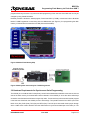
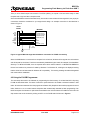
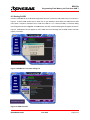
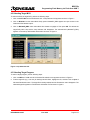
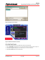
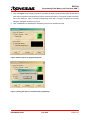
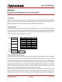
APPLICATION NOTE M16C/26 Programming Flash Memory via Flash-Over-USB™ 1.0 Abstract The following article describes using a synchronous serial port and the FoUSB (Flash-over-USB™) Programmer application to program the user flash memory of the M16C/26 series of microcontrollers. This is referred to in the M16C/26 datasheet as the “Standard Serial I/O Mode 1” method of flash programming. 2.0 Introduction The Renesas M16C/26 is a 16-bit MCU based on the M16C/60 series CPU core. The peripheral set includes 10-bit A/D, UARTs, Timers, DMA, and GPIO. The MCU features include up to 64K bytes of Flash ROM, 2K bytes of RAM, and 4K bytes of virtual EEPROM. The flash memory is divided into several blocks as shown in Figure 1, and so, allows memory to be erased one block at a time. 0F000H Block B: 2KB 0F800H Block A: 2KB RESERVED F0000H Block 3: 32KB F8000H Block 2: 16KB Part No. Block 3 Size Start Address M30262F3-GP M30262F4-GP M30262F6-GP M30262F8-GP 0 KB 0 KB 16KB 32KB N/A N/A F4000H F0000H Part No. Block 2 Size Start Address M30262F3-GP M30262F4-GP M30262F6-GP M30262F8-GP 8KB 16KB 16KB 16KB FA000H F8000H F8000H F8000H FC000H Block 1: 8KB FE000H Block 1: 8KB 8KB User ROM Area Boot ROM Area FFFFFH Figure 1 M16C/26 Flash Memory Map The M16C/26 flash memory can be programmed with a single voltage. Three flash memory modes are available in which to read, program and erase: (1) parallel I/O and (2) serial I/O modes in which the flash memory can be manipulated using a programmer and (3) CPU rewrite mode in which the flash memory can be manipulated by the Central Processing Unit (CPU). The Standard Serial I/O Mode can be further divided into a synchronous mode (Standard Serial I/O Mode 1) and an asynchronous mode (Standard Serial I/O Mode 2). The standard serial I/O mode inputs and outputs the software commands, addresses and data needed to operate (read, program, erase, etc.) the internal flash memory using the serial I/O port UART1. The flash memory is divided into two major blocks, a user program area and a boot ROM area. The user program area is used for user application program and data. The boot ROM area has a control program stored in it when shipped from the factory and can only be accessed when a special hardware reset sequence is initiated. This REU05B0042-0100Z June 2003 Page 1 of 8 M16C/26 Programming Flash Memory via Flash-Over-USB™ program allows asynchronous or synchronous serial programming of the user area of the flash and can only be changed by using Parallel I/O Mode. Renesas provides a Windows based program, Flash-Over-USB™ (FoUSB), to download code to M16C/26 MCUs. FoUSB Programmer is used along with the USB-Monitor (see Figure 3) for reprogramming the flash memory of a M16C/26 microcontroller over USB (Universal Serial Bus). Figure 2 M16C/26 Flash Memory Map Host PC running FoUSB Programmer Figure 3 M16C System Connectivity for FoUSB Programmer 3.0 Hardware Requirements for Synchronous Serial Programming The CNVSS pin on the M16C MCU is the primary control line that determines whether the user area or the boot area of the flash memory is accessed after reset is released. If the CNVSS pin is low the device will always access the user flash area and will start in single chip mode. To execute the synchronous serial rewrite program in the boot area of the flash, the CNVSS pin has to be held high. The operation uses the four UART1 pins of the MCU: CLK1 (P65), RxD1 (P66), TxD1 (P67) and RTS1 (P64). The CLK1 pin is the transfer clock input pin through which a 1MHz clock is fed to the MCU from the USB monitor for synchronous data input to the RxD1 pin. The REU05B0042-0100Z June 2003 Page 2 of 8 M16C/26 Programming Flash Memory via Flash-Over-USB™ TxD1 pin is for CMOS output from the MCU. The RTS1 (BUSY) pin outputs a low level when ready for data reception and a high level when reception starts. Since the USB-Monitor uses the Renesas factory boot code to communicate with the target MCU, the proper pin connections should be considered on your target board design. An example connection for the M16C/26 is shown in Figure 4. 10-Pin Header M30262F Vcc Vcc BUSY CLK RxD CE EPM GND !RESET CNVss TxD 1 2 3 4 5 6 7 8 9 10 Vcc P6_4/RTS1 (Busy) P6_5/CLK1 (SCLK) P6_6/RxD1 (RxD) P8_6/XCout (CE) Vss !RESET CNVss P6_7/TxD1 (TxD) 47K (nominal) Figure 4 A typical M16C/26 target board hardware connection for FoUSB Connectivity When the USB-Monitor is connected to a computer for the first time, Windows will recognize the new hardware and will request for the drivers. The drivers were already installed during the install, for example, if the installation directory is ‘C:\MTOOL\FOUSB’, then the required device driver will be located in ‘C:\MTOOL\FOUSB\Device Drivers\’ and needs to be pointed to if asked by Windows. For Windows XP, a dialog box is displayed warning that the driver has not been tested for Windows XP compatibility. This warning message should be disregarded and continue driver installation. 4.0 Using the FoUSB Programmer The main steps that need to be followed for programming the flash memory of an M16C/26 MCU chip using FoUSB are described below. The name of a button or option that has to be clicked or selected is written in bold italics. All other items extracted from the programmer software GUI (Graphical User Interface) appears in normal italics. Sections 4.1 to 4.4 covers buttons and options that are absolutely essential for flash programming of an MCU. Description of all buttons or options that are available in the various windows of FoUSB can be found in the Help section that can be invoked by clicking on HELP on the FoUSB main GUI shown in Figure 5. REU05B0042-0100Z June 2003 Page 3 of 8 M16C/26 Programming Flash Memory via Flash-Over-USB™ 4.1 Starting FoUSB Connect a USB-Monitor to the M16C/26 target board and then connect the USB cable to the PC as shown in Figure 4. To start FoUSB, double-click on 'fousb' icon on your desktop or select Flash-over-USB from the Start menu (Start > Programs > Renesas-Tools > Flash-over-USB ver. 1.xx > Flash-over-USB). A connection dialog box will appear as shown in Figure 5. Click OK and the main GUI of the FoUSB program will appear as shown in Figure 6. USB Monitor Device appears on the FoUSB main GUI indicating that the USB monitor has been properly connected. Figure 5 USB Monitor connection dialog box Figure 6 FoUSB main GUI REU05B0042-0100Z June 2003 Page 4 of 8 M16C/26 Programming Flash Memory via Flash-Over-USB™ 4.2 Selecting Target MCU To select the firefly as target MCU, perform the following steps. 1. Click on Select MCU on the FoUSB main GUI. A Chip Selection GUI appears as shown in Figure 7. 2. Click on M16C/26 from the Select MCU Family option. M30262F8_DBC appears as a part number in the Select MCU Part Number option. 3. Click on M30262F8_DBC under Select MCU Part Number to highlight it. Then press OK. This selects the target firefly MCU chip and the Chip Selection GUI disappears. The selected MCU (M30262F8_DBC) appears on the start-up GUI besides Select MCU as shown in Figure 6. Figure 7 Chip Selection GUI 4.3 Selecting Target Program To select a target program, perform following steps: 1. Click on OPEN on FoUSB main GUI. Windows file selection menu appears as shown in Figure 8. 2. Find the target file (e.g., xxxx.mot) for loading into MCU flash, highlight the file, and then click on Open of Windows file selection menu. The target file is thereby selected and the file selection menu disappears. The selected target file appears on FoUSB main GUI beside FILE as shown in figure 9. REU05B0042-0100Z June 2003 Page 5 of 8 M16C/26 Programming Flash Memory via Flash-Over-USB™ Figure 8 Dialog box for file selection Figure 9 FoUSB main GUI after file selection 4.4 Loading Target Program To load the selected target program into the MCU flash, perform the following steps: 1. Click on PROGRAM on FoUSB main GUI. The Program Flash dialog box appears as shown in Figure 10. 2. Select Erase->Program->Verify option (the default option) from Choose an Operation. 3. Select Erase All Block option from Erasing Options. REU05B0042-0100Z June 2003 Page 6 of 8 M16C/26 Programming Flash Memory via Flash-Over-USB™ 4. Click on Program of the Program Flash GUI. The loading of target program into MCU flash will start at this point and the progress of flash programming will be shown dynamically by a moving bar located at the lower part of this dialog box. After a successful programming of the flash, a Program Completed Successfully dialog box will appear as shown in Figure 11. 5. Click on OK button and the dialog box disappear (nd back to the FoUSB main GUI). Figure 10 Menu options for programming flash Figure 11 Dialog box after a successful flash programming REU05B0042-0100Z June 2003 Page 7 of 8 M16C/26 Programming Flash Memory via Flash-Over-USB™ 4.5 Exiting FoUSB Programmer To exit from FoUSB, click on EXIT or the X button on the upper right corner of the main GUI. 5.0 Reference Renesas Technology Corporation Semiconductor Home Page http://www.renesas.com E-mail Support [email protected] Data Sheets • M16C/26 datasheet, M30262eds.pdf User’s Manual • MSV30262-SKP Users Manual, Users_Manual_MSV30262.pdf • MSV30262-SKP Quick start guide, Quick_Start_guide_MSV30262.pdf • Flash-Over-USB Help menu REU05B0042-0100Z June 2003 Page 8 of 8 Keep safety first in your circuit designs! • Renesas Technology Corporation puts the maximum effort into making semiconductor products better and more reliable, but there is always the possibility that trouble may occur with them. Trouble with semiconductors may lead to personal injury, fire or property damage. Remember to give due consideration to safety when making your circuit designs, with appropriate measures such as (i) placement of substitutive, auxiliary circuits, (ii) use of nonflammable material or (iii) prevention against any malfunction or mishap. Notes regarding these materials • These materials are intended as a reference to assist our customers in the selection of the Renesas • • • • • • • Technology Corporation product best suited to the customer's application; they do not convey any license under any intellectual property rights, or any other rights, belonging to Renesas Technology Corporation or a third party. Renesas Technology Corporation assumes no responsibility for any damage, or infringement of any third-party's rights, originating in the use of any product data, diagrams, charts, programs, algorithms, or circuit application examples contained in these materials. All information contained in these materials, including product data, diagrams, charts, programs and algorithms represents information on products at the time of publication of these materials, and are subject to change by Renesas Technology Corporation without notice due to product improvements or other reasons. It is therefore recommended that customers contact Renesas Technology Corporation or an authorized Renesas Technology Corporation product distributor for the latest product information before purchasing a product listed herein. The information described here may contain technical inaccuracies or typographical errors. Renesas Technology Corporation assumes no responsibility for any damage, liability, or other loss rising from these inaccuracies or errors. Please also pay attention to information published by Renesas Technology Corporation by various means, including the Renesas Technology Corporation Semiconductor home page (http://www.renesas.com). When using any or all of the information contained in these materials, including product data, diagrams, charts, programs, and algorithms, please be sure to evaluate all information as a total system before making a final decision on the applicability of the information and products. Renesas Technology Corporation assumes no responsibility for any damage, liability or other loss resulting from the information contained herein. Renesas Technology Corporation semiconductors are not designed or manufactured for use in a device or system that is used under circumstances in which human life is potentially at stake. Please contact Renesas Technology Corporation or an authorized Renesas Technology Corporation product distributor when considering the use of a product contained herein for any specific purposes, such as apparatus or systems for transportation, vehicular, medical, aerospace, nuclear, or undersea repeater use. The prior written approval of Renesas Technology Corporation is necessary to reprint or reproduce in whole or in part these materials. If these products or technologies are subject to the Japanese export control restrictions, they must be exported under a license from the Japanese government and cannot be imported into a country other than the approved destination. Any diversion or reexport contrary to the export control laws and regulations of Japan and/or the country of destination is prohibited. Please contact Renesas Technology Corporation for further details on these materials or the products contained therein.