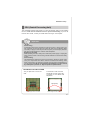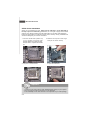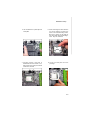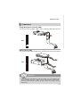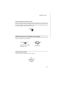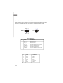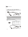
1
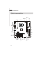
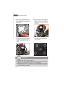
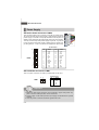
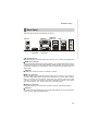
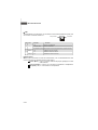
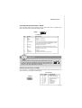
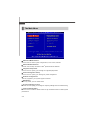
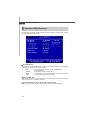
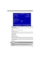
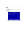
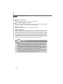
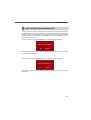
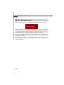
Getting Started
Chapter 1
Getting Started
Thank you for choosing the P6NGM Series (MS-7366
v1.X) Micro-AT X mainboard. The P6NG M Series
mainboards are based on GeForce ® MCP73U/PV/V
chipset for optimal system efficiency. Designed to fit
the advanced Intel ® Pentium 4 LGA775 processor,
the P6NGM Series deliver a high performance and professional desktop platform solution.
1-1
M S-7366 M ainboard
Mainboard Specifications
Processor Support
- Supports Intel ® Core 2 Quad, Core 2 Duo, Pentium, Celeron
processors in the LGA775 package.
Supported FSB
- Supports FSB up to 1333 MHz (for 73U/PV)
- Supports FSB up to 1066 MHz (for 73V)
Chipset
- Nvidia MCP73U/PV/V chipest
M emory Support
- DDR2 533/667/800 SDRAM (240pin/ non-ECC) (for 73U/PV)
- DDR2 533/667 SDRAM (240pin/ non-ECC) (for 73V)
- 2 DDR2 DIMMs (4GB Max)
LAN
- Supports LAN 10/100/1000 Fast Ethernet by Realtek® RTL 8211BL
(for 73U/PV)
- Supports LAN 10/100 Fast Ethernet by Realtek® RTL 8201CL
(for 73V)
IEEE 1394 (optional)
- Chip integrated by JMicron JMB381
Audio
- Chip integrated by Realtek® ALC888
- Supports 5.1 channels audio out
- Compliant with Azalia 1.0 Spec
IDE
- 1 IDE port by MCP73U/PV/V
- Supports Ultra DMA 66/100/133, PIO & Bus Master operation mode
SATA
- 4 SATAII ports support 4 SATA devices
RAID
- SATA1~4 support RAID 0, 1, 5 ,0+1, JBOD (for 73U/PV)
- SATA1~4 support RAID 0, 1, JBOD (for 73V)
Floppy
- 1 floppy port
- Supports 1 FDD with 360KB, 720KB, 1.2MB, 1.44MB and 2.88MB
1-2
Getting Started
Connectors
Back panel
- 1 PS/2 mouse port
- 1 PS/2 keyboard port
- 1 VGA port
- 1 HDMI port (optional)
- 1 DVI port (optional)
- 1 IEEE1394 port (optional)
- 4 USB 2.0 Ports
- 1 LAN jack
- 3 audio jacks
On-Board Pinheaders
- 3 USB 2.0 pinheaders (for 73U/PV)
- 2 USB 2.0 pinheaders (for 73V)
- 1 IEEE1394 pinheader (optional)
- 1 Chassis Intrusion Switch pinheader
- 1 Serial port pinheader
- 1 SPDIF-Out pinheader
- 1 Front Panel Audio pinheader
- 1 CD-In pinheader
- 1 TPM pinheader (optional)
Slots
- 1 PCI Express x16 slot
- 1 PCI Express x1 slot
- 2 PCI slots, support 3.3V/ 5V PCI bus Interface
Form Factor
- M-ATX (24.4cm X 22.0cm)
M ounting
- 6 mounting holes
1-3
M S-7366 M ainboard
Mainboard Layout
Top : mouse
Bottom:
keyboard
FDD 1
CPUFAN
HDMI Port (optional)
Top:VGA Port
Bottom: DVI Port (optional)
PWR1
JCI1
Top:1394 (optional)
Bottom: USB ports
NVIDIA
MCP73U/PV/V
Top: LAN Jack
Bottom: USB ports
SYSFAN1
SATA4
Jmicron
JMB381
(optional)
PCI 1
SATA2
PCI _E2
DIMM2
ALC888
DIMM1
IDE 1
PCI _E1
PWR2
RTL8211BL
/ RTL 8201CL
T:Line-In
M:Line-Out
B:Mic
J1
JAUD1
JSP1
JUSB1
JUSB2
JUSB3(optional)
J1394_1(optional)
JFP1
JFP2
P6NGM Series
(MS-7366 v1.X) ATX Mainboard
1-4
JCOM1
SATA3
JTPM1
(optional)
BATT
+
PCI 2
SATA1
JCD1
Getting Started
Packing Checklist
Motherboard
Power Cable
Driver/Utility CD
SATA Cable
Standard Cable for
IDE Devices
Back IO Shield
User’s Guide
* The pictures are for reference only and may vary from the packing contents of the
product you purchased.
1-5
Chapter 2
Hardware Setup
This chapter tells you how to install the CPU, memory modules,
and expansion cards, as well as how to setup the jumpers on
the mainboard. Also, it provides the instructions on connecting
the peripheral devices, such as the mouse, keyboard, etc.
W hile doing the installation, be careful in holding the components
and follow the installation procedures.
M S-7366 M ainboard
Quick Components Guide
DIMM Slots,
p.2-7
PWR1, p.2-8
CPU, p.2-3
CPUFAN, p.2-12
FDD1,
p.2-12
Back Panel,
p.2-9
JCI1,
p.2-13
PWR2,
p.2-8
IDE1,
p.2-11
PCIE,
p.2-19
SYSFAN1,
p.2-12
SATA1~4,
p.2-12
PCI, p.2-19
JCD1, p.2-13
JAUD1, p.2-15
JTPM1,
p.2-17
JUSB1~3,
p.2-16
2-2
J1394_1,
p.2-16
JSP1,
p.2-13
JCOM1,
p.2-15
JFP1, JFP2,
p.2-14
J1,
p.2-18
Hardware Setup
CPU (Central Processing Unit)
This mainboard supports Intel® Pentium 4 in LGA 775 package. When you are installing
the CPU, make sure to install the cooler to prevent overheating. If you do not
have the CPU cooler, consult your dealer before turning on the computer.
Important
Overheating
Overheating will seriously damage the CPU and system. Always make sure
the cooling fan can work properly to protect the CPU from overheating. Make
sure that you apply an even layer of thermal paste (or thermal tape) between
the CPU and the heatsink to enhance heat dissipation.
Replaceing the CPU
While replacing the CPU, always turn off the ATX power supply or unplug the
power supply’s power cord from the grounded outlet first to ensure the safety
of CPU.
Overclocking
This mainboard is designed to support overclocking. However, please make
sure your components are able to tolerate such abnormal setting, while
doing overclocking. Any attempt to operate beyond product specifications is
not recommended. We do not guarantee the damages or risks caused
by inadequate operation or beyond product specifications.
Introduction to LGA 775 CPU
The pin-pad side of LGA 775
CPU.
Alignment Key
Yellow triangle is the Pin 1 indicator
The surface of LGA 775 CPU.
Remember to apply some thermal paste on it for better heat
dispersion.
Alignment Key
Yellow triangle is the Pin 1 indicator
2-3
M S-7366 M ainboard
CPU & Cooler Installation
W hen you are installing the CPU, make sure the CPU has a cooler attached on
the top to prevent overheating. Meanwhile, do not forget to apply some thermal
paste on CPU before installing the heat sink/cooler fan for better heat dispersion.
Follow the steps below to install the CPU & cooler correctly. W rong installation will
cause the damage of your CPU & mainboard.
1. The CPU socket has a plastic cap
on it to protec t the contac t from
damage. Before you install the CPU,
always cover it to protect the socket
pin.
3. The pins of socket reveal.
2. Remove the cap from lever hinge
side (as the arrow shows).
4. Open the load lever.
Important
1. Confirm if your CPU cooler is firmly installed before turning on your system.
2. Do not touch the CPU socket pins to avoid damaging.
3. The availability of the CPU land side cover depends on your CPU packing.
2-4
Hardware Setup
5. Lift the load lever up and open the
load plate.
6. After confirming the CPU direction
for correct mating, put down the
CPU in the socket housing frame.
Be sure to grasp on the edge of
the CPU base. Note that the alignment keys are matched.
alignment
key
7. Visually ins pect if the CPU is
seated well into the socket. If not,
take out the CPU with pure vertical
motion and reinstall.
8. Cover the load plate onto the
package.
2-5
M S-7366 M ainboard
9. Press down the load lever lightly
onto the load plate, and then secure the lever with the hook under
retention tab.
10. Align the holes on the mainboard
with the heatsink. Push down the
c ooler u nti l i ts f ou r c lip s g et
wedged int o t he holes of t he
mainboard.
11. Press the four hooks down to fasten the cooler. Then rotate the locking switch (refer to the correct direction marked on it) to lock the
hooks.
12. Turn over the mainboard to confirm that the clip-ends are correctly inserted.
locking
switch
Important
1. Read the CPU status in BIOS (Chapter 3).
2. Whenever CPU is not installed, always protect your CPU socket pin with the
plastic cap covered (shown in Figure 1) to avoid damaging.
3. Mainboard photos shown in this section are for demonstration of the CPU/
cooler installation only. The appearance of your mainboard may vary depending on the model you purchase.
2-6
Hardware Setup
Memory
These DIMM slots are used for installing memory modules.
DDR2
240-pin, 1.8V
64x2=128 pin
56x2=112 pin
Installing Memory Modules
1. The memory module has only one notch on the center and will only fit in the right
orientation.
2. Insert the memory module vertically into the DIMM slot. Then push it in until the
golden finger on the memory module is deeply inserted in the DIMM slot.
Important
You can barely see the golden finger if the memory module is properly inserted
in the DIMM slot.
3. The plastic clip at each side of the DIMM slot will automatically close.
Volt
Notch
Important
- DDR2 memory modules are not interchangeable with DDR and the DDR2
standard is not backwards compatible. You should always install DDR2
memory modules in the DDR2 DIMM slots.
- To enable successful system boot-up, always insert the memory modules
into the DIM M1 first.
2-7
M S-7366 M ainboard
Power Supply
ATX 24-Pin Power Connector: PWR2
This connector allows you to connect an ATX 24-pin power supply.
To connect the ATX 24-pin power supply, make sure the plug of the
power supply is inserted in the proper orientation and the pins are
aligned. Then push down the power supply firmly into the connector.
You may use the 20-pin ATX power supply as you like. If you’d like
to use the 20-pin ATX power supply, please plug your power supply along with pin 1 & pin 13 (refer to the image at the right hand).
pin 13
pin 12
Pin Definition
12
24
PWR2
1
13
PIN
SIGNAL
PIN
SIGNAL
1
+3.3V
13
+3.3V
2
3
+3.3V
GND
14
15
-12V
GND
4
5
+5V
GND
16
17
PS-ON#
GND
6
7
+5V
GND
18
19
GND
GND
8
9
PWR OK
5VSB
20
21
NC
+5V
10
11
+12V
+12V
22
23
+5V
+5V
12
+3.3V
24
GND
ATX 12V Power Connector: PWR1
This 12V power connector is used to provide power to the CPU.
Pin Definition
4
2
PWR1
3
1
PIN
SIGNAL
1
GND
2
3
GND
12V
4
12V
Important
1. Make sure that all the connectors are connected to proper ATX power supplies to ensure stable operation of the mainboard.
2. Power supply of 350 watts (and above) is highly recommended for system
stability.
3. ATX 12V power connection should be greater than 18A.
2-8
Hardware Setup
Back Panel
The back panel provides the following connectors:
VGA Port
M ou se
1394 Port
(optional)
LAN
L-In
L-Out
Keyboard
HDMI Port
(optional)
DVI Port
(optional)
USB Ports
Mic
M ouse/Keyboard
The standard PS/2® mouse/keyboard DIN connector is for a PS/2® mouse/keyboard.
HDM I Port (optional)
The High-Definition Multimedia Interface (HDMI) is an all-digital audio/video interface
capable of transmitting uncompressed streams. HDMI supports all TV format, including standard, enhanced, or high-definition video, plus multi-channel digital audio on a
single cable.
VGA Port
The DB15-pin female connector is provided for monitor.
DVI Port (optional)
The DVI (Digital Visual Interface) connector allows you to connect a LCD monitor. It
provides a high-speed digital interconnection between the computer and its display
device. To connect an LCD monitor, simply plug your monitor cable into the DVI
connector, and make sure that the other end of the cable is properly connected to
your monitor (refer to your monitor manual for more information.)
1394 Port (optional)
The IEEE1394 port on the back panel provides connection to IEEE1394 devices.
USB Port
The USB (Universal Serial Bus) port is for attaching USB devices such as keyboard,
mouse, or other USB-compatible devices.
2-9
M S-7366 M ainboard
LAN
The standard RJ-45 LAN jack is for connection to the Local Area Network (LAN). You
can connect a network cable to it.
Activity Indicator
LED
Color
LED State
Off
Left
Orange
On (steady state)
Link Indicator
Condition
LAN link is not established.
LAN link is established.
On (brighter & pulsing) The computer is communicating with another computer on the LAN.
Green
Right
Orange
Off
10 Mbit/sec data rate is selected.
On
100 Mbit/sec data rate is selected.
On
1000 Mbit/sec data rate is selected.
Audio Ports
These audio connectors are used for audio devices. You can differentiate the color
of the audio jacks for different audio sound effects.
Line-In (Blue) - Line In is used for external CD player, tapeplayer or other
audio devices.
Line-Out (Green) - Line Out, is a connector for speakers or headphones.
Mic (Pink) - Mic, is a connector for microphones.
2-10
Hardware Setup
Connectors
Floppy Disk Drive Connector: FDD1
This connector supports 360KB, 720KB, 1.2MB, 1.44MB or 2.88MB floppy disk drive.
FDD1
IDE Connector: IDE1
This connector supports IDE hard disk drives, optical disk drives and other IDE devices.
IDE1
Important
If you install two IDE devices on the same cable, you must configure the
drives separately to Primary / Slave mode by setting jumpers. Refer to IDE
dev ic e’s doc umentation s upplied by the vendors for jumper s etting
instructions.
2-11
M S-7366 M ainboard
Serial ATA Connector: SATA1/ SATA2/ SATA3/ SATA4
This connector is a high-speed Serial ATA interface port. Each connector can connect to one Serial ATA device.
SATA4
SATA2
SATA1
SATA3
Important
Please do not fold the Serial ATA cable into 90-degree angle. Otherwise,
data loss may occur during transmission.
Fan Power Connectors: CPUFAN, SYSFAN1
The fan power connectors support system cooling fan with +12V. W hen connecting
the wire to the connectors, always note that the red wire is the positive and should
be connected to the +12V; the black wire is Ground and should be connected to GND.
If the mainboard has a System Hardware Monitor chipset on-board, you must use a
specially designed fan with speed sensor to take advantage of the CPU fan control.
CONTROL
SENSOR
+1 2V
GND
CPUFAN
SENSOR
+1 2V
GND
SYSFAN1
Important
1. Please refer to the recommended CPU fans at processor’s official website
or consult the vendors for proper CPU cooling fan.
2. Fan cooler set with 3 or 4 pins power connector are both available for
CPUFAN.
2-12
Hardware Setup
Chassis Intrusion Connector: JCI1
This connector connects to the chassis intrusion switch cable. If the chassis is
opened, the chassis intrusion mechanism will be activated. The system will record
this status and show a warning message on the screen. To clear the warning, you
must enter the BIOS utility and clear the record.
CINTRU
GND
1
2
JCI1
S/PDIF-Out Connector: JSP1 (2pin, 3pin optional)
This connector is used to connect S/PDIF (Sony & Philips Digital Interconnect Format)
interface for digital audio transmission.
SPDIFO
GND
VCC
GND
SPDIF
JSP1 (2pin, for HDM I
JSP1 (3pin)
graphics card)
CD-In Connector: JCD1
This connector is provided for external audio input.
GND
L
R
JCD1
2-13
M S-7366 M ainboard
Front Panel Connectors: JFP1, JFP2
These connectors are for electrical connection to the front panel switches and LEDs.
The JFP1 is compliant with Intel® Front Panel I/O Connectivity Design Guide.
Reset HDD
Switch LED
+ - - +
JFP1
9
10
1
2
JFP2
2
1
- +
Power Power
Switch LED
Speaker
+
+ 8
7
Power
LED
JFP1 Pin Definition
PIN
SIGNAL
DESCRIPTION
1
2
HD_LED +
FP PWR/SLP
Hard disk LED pull-up
MSG LED pull-up
3
4
HD_LED FP PWR/SLP
Hard disk active LED
MSG LED pull-up
5
6
RST_SW PWR_SW +
Reset Switch low reference pull-down to GND
Power Switch high reference pull-up
7
8
RST_SW +
PWR_SW -
Reset Switch high reference pull-up
Power Switch low reference pull-down to GND
9
RSVD_DNU
Reserved. Do not use.
JFP2 Pin Definition
2-14
PIN
SIGNAL
DESCRIPTION
1
GND
Ground
2
3
SPKSLED
SpeakerSuspend LED
4
5
BUZ+
PLED
Buzzer+
Power LED
6
7
BUZNC
BuzzerNo connection
8
SPK+
Speaker+
Hardware Setup
Front Panel Audio Connector: JAUD1
This connector allows you to connect the front panel audio and is compliant with
Intel® Front Panel I/O Connectivity Design Guide.
JAUD1
2
1
10
9
Pin Definition
PIN
SIGNAL
DESCRIPTION
1
2
MIC_L
GND
Microphone - Left channel
Ground
3
4
MIC_R
PRESENCE#
Microphone - Right channel
Active low signal-signals BIOS that a High Definition Audio dongle
is connected to the analog header. PRESENCE# = 0 when a
High Definition Audio dongle is connected
5
6
LINE out_R
MIC_JD
Analog Port - Right channel
Jack detection return from front panel microphone JACK1
7
Front_JD
Jack detection sense line from the High Definition Audio CODEC
jack detection resistor network
8
9
NC
LINE out_L
No control
Analog Port - Left channel
10
LINEout_JD
Jack detection return from front panel JACK2
Important
If you don’t want to connect to the front audio header, pins 5 &
6, 9 & 10 have to be jumpered in order to have signal output
directed to the rear audio ports. Otherwise, the Line-Out connector on the back panel will not function.
6
10
5
9
Serial Port Connector: JCOM1
This connector is a 16550A high speed communication port that sends/receives 16
bytes FIFOs. You can attach a serial device.
Pin Definition
PIN
JCOM1
2
1
9
1
2
3
4
5
6
7
8
9
SIGNAL
DESCRIPTION
DCD
SIN
SOUT
DTR
GND
DSR
RTS
CTS
RI
Data Carry Detect
Serial In or Receive Data
Serial Out or Transmit Data
Data Terminal Ready
Ground
Data Set Ready
Request To Send
Clear To Send
Ring Indicate
2-15
M S-7366 M ainboard
Front USB Connector: JUSB1 / JUSB2 / JUSB3(optional)
This connector, compliant with Intel® I/O Connectivity Design Guide, is ideal for connecting high-speed USB interface peripherals such as USB HDD, digital cameras,
M P3 players, printers, modems and the like.
JUSB1/2/3
2
1
10
9
USB 2.0 Bracket
(Optional)
Important
Note that the pins of VCC and GND must be connected correctly to avoid
possible damage.
IEEE1394 Connector: J1394_1(optional)
This connector allows you to connect the IEEE1394 device via an optional IEEE1394
bracket.
Pin Definition
10
9
2
1
J1394_1
PIN
SIGNAL
PIN
SIGNAL
1
TPA+
2
TPA-
3
Ground
4
Ground
5
TPB+
6
TPB-
7
Cable power
8
Cable power
9
Key (no pin)
10
Ground
IEEE1394 Bracket (Optional)
2-16
Hardware Setup
TPM Module connector: JTPM1(optional)
This connector connects to a TPM (Trusted Platform Module) module (optional). Please
refer to the TPM security platform manual for more details and usages.
14 13
JTPM 1
21
Pin
Signal
Description
Pin
Signal
Description
1
3
LCLK
LRST#
LPC clock
LPC reset
2
4
3V dual/3V_STB
VCC3
3V dual or 3V standby power
3.3V power
5
7
LAD0
LAD1
LPC address & data pin0
LPC address & data pin1
6
8
SIRQ
VCC5
Serial IRQ
5V power
9
11
LAD2
LAD3
LPC address & data pin2
LPC address & data pin3
10
12
KEY
GND
No pin
Ground
13
LFRAME#
LPC Frame
14
GND
Ground
2-17
M S-7366 M ainboard
Jumpers
Clear CMOS Jumper: J1
There is a CMOS RAM onboard that has a power supply from an external battery to
keep the data of system configuration. W ith the CMOS RAM, the system can automatically boot OS every time it is turned on. If you want to clear the system configuration,
set the jumper to clear data.
3
1
3
1
J1
1
Keep Data
Clear Data
Important
You can clear CMOS by shorting 2-3 pin while the system is off. Then return
to 1-2 pin position. Avoid clearing the CMOS while the system is on; it will
damage the mainboard.
2-18
Hardware Setup
Slots
PCI (Peripheral Component Interconnect) Express Slots
The PCI Express slot supports the PCI Express interface expansion card.
The PCI Express x 16 supports up to 4.0 GB/s transfer rate.
The PCI Express x 1 supports up to 250 MB/s transfer rate.
PCI Express x16 slot
PCI Express x1 Slot
PCI (Peripheral Component Interconnect) Slots
The PCI slots support LAN cards, SCSI cards, USB cards, and other add-on cards
that comply with PCI specifications. At 32 bits and 33 MHz, it yields a throughput rate
of 133 MBps.
32-bit PCI Slot
Important
When adding or removing expansion cards, make sure that you unplug the
power supply first. Meanwhile, read the documentation for the expansion card
to configure any necessary hardware or software settings for the expansion
card, such as jumpers, switches or BIOS configuration.
PCI Interrupt Request Routing
The IRQ, acronym of interrupt request line and pronounced I-R-Q, are hardware lines
over which devices can send interrupt signals to the microprocessor. The PCI IRQ
pins are typically connected to the PCI bus pins as follows:
Order 1
Order 2
Order 3
Order 4
PCI Slot 1
INT W#
INT X#
INT Y#
INT Z#
PCI Slot 2
INT X#
INT Y#
INT Z#
INT W#
2-19
M S-7366 M ainboard
2-20
BIOS Setup
Chapter 3
BIOS Setup
This chapter provides information on the BIOS Setup
program and allows you to configure the system for
optimum use.
You may need to run the Setup program when:
² An error message appears on the screen during the
system booting up, and requests you to run SETUP.
² You want to change the default settings for customized features.
3-1
M S-7366 M ainboard
Entering Setup
Power on the computer and the system will start POST (Power On Self Test) process.
W hen the message below appears on the screen, press <DEL> key to enter Setup.
Press DEL to enter SETUP
If the message disappears before you respond and you still wish to enter Setup,
restart the system by turning it OFF and On or pressing the RESET button. You may
also restart the system by simultaneously pressing <Ctrl>, <Alt>, and <Delete> keys.
Important
1. The items under each BIOS category described in this chapter are under
continuous update for better system performance. Therefore, the description may be slightly different from the latest BIOS and should be held for
reference only.
2. Upon boot-up, the 1st line appearing after the memory count is the BIOS
version. It is usually in the format:
A7366NMS V1.0 122506 where:
1st digit refers to BIOS maker as A = AMI, W = AWARD, and P =
PHOENIX.
2nd - 5th digit refers to the model number.
6th digit refers to the chipset as I = Intel, N = nVidia, and V = VIA.
7th - 8th digit refers to the customer as MS = all standard customers.
V1.0 refers to the BIOS version.
122506 refers to the date this BIOS was released.
3-2
BIOS Setup
Control Keys
< ->
Move to the previous item
< ¯>
Move to the next item
< ¬>
Move to the item in the left hand
< ®>
Move to the item in the right hand
<Enter>
Select the item
<Esc>
Jumps to the Exit menu or returns to the main menu from a
submenu
<+/PU>
Increase the numeric value or make changes
<-/PD>
Decrease the numeric value or make changes
<F6>
Load Optimized Defaults
<F8>
Load Fail-Safe Defaults
<F10>
Save all the CMOS changes and exit
Getting Help
After entering the Setup menu, the first menu you will see is the Main Menu.
M ain M enu
The main menu lists the setup functions you can make changes to. You can use the
arrow keys ( -¯ ) to select the item. The on-line description of the highlighted setup
function is displayed at the bottom of the screen.
Sub-M enu
If you find a right pointer symbol (as shown in the right
view) appears to the left of certain fields that means a
sub-menu can be launched from this field. A sub-menu
contains additional options for a field parameter. You
can use arrow keys ( -¯ ) to highlight the field and
press <Enter> to call up the sub-menu. Then you can
use the control keys to enter values and move from field to field within a sub-menu.
If you want to return to the main menu, just press the <Esc >.
General Help <F1>
The BIOS setup program provides a General Help screen. You can call up this screen
from any menu by simply pressing <F1>. The Help screen lists the appropriate keys
to use and the possible selections for the highlighted item. Press <Esc> to exit the
Help screen.
3-3
M S-7366 M ainboard
The Main Menu
Standard CM OS Features
Use this menu for basic system configurations, such as time, date etc.
Advanced BIOS Features
Use this menu to setup the items of AMI® special enhanced features.
Integrated Peripherals
Use this menu to specify your settings for integrated peripherals.
Power M anagement Setup
Use this menu to specify your settings for power management.
PnP/PCI Configurations
This entry appears if your system supports PnP/PCI.
H/W M onitor
This entry shows your PC health status.
Frequency/Voltage Control
Use this menu to specify your settings for frequency/voltage control and overclocking.
Load Fail-Safe Defaults
Use this menu to load the default values set by the BIOS vendor for stable system
performance.
3-4
BIOS Setup
Load Optimized Defaults
Use this menu to load the default values set by the mainboard manufacturer specifically for optimal performance of the mainboard.
BIOS Setting Password
Use this menu to set the password for BIOS.
Save & Exit Setup
Save changes to CMOS and exit setup.
Exit Without Saving
Abandon all changes and exit setup.
3-5
M S-7366 M ainboard
Standard CMOS Features
The items in Standard CMOS Features Menu includes some basic setup items. Use
the arrow keys to highlight the item and then use the <PgUp> or <PgDn> keys to select
the value you want in each item.
Date (MM:DD:YY)
This allows you to set the system to the date that you want (usually the current date).
The format is <day><month> <date> <year>.
day
Day of the week, from Sun to Sat, determined by
BIOS. Read-only.
mon th
The month from Jan. through Dec.
date
The date from 1 to 31 can be keyed by numeric function keys.
year
The year can be adjusted by users.
Time (HH:MM :SS)
This allows you to set the system time that you want (usually the current time). The
time format is <hour> <minute> <second>.
Primary IDE Master/ Slave, Serial-ATA 1/2/3/4 Channel
Press <Enter> to enter the sub-menu, and the following screen appears.
3-6
BIOS Setup
Device/Vendor/Size/LBA Mode/Block Mode/PIO M ode/Async DM A/Ultra
DMA/S.M.A.R.T.
These will be showing the device information that you connected to the IDE/
SATA connector.(read only)
Type
Select how to define the HDD parameters.
LBA/Large M ode
This allows you to enable or disable the LBA Mode. Setting to [Auto] enables LBA
mode if the device supports it and the devices is not already formatted with LBA
mode [Disabled].
DM A M ode
Select DMA Mode.
Hard Disk S.M.A.R.T.
This allows you to activate the S.M.A.R.T. (Self-Monitoring Analysis & Reporting
Technology) capability for the hard disks. S.M.A.R.T is a utility that monitors your
disk status to predict hard disk failure. This gives you an opportunity to move
data from a hard disk that is going to fail to a safe place before the hard disk
becomes offline.
Important
Primary IDE M aster/ Slave, Serial-ATA 1/2/3/4 Channel are appearing
when you connect the HD devices to the IDE/ SATA connector on the
mainboard.
3-7
M S-7366 M ainboard
Floppy Drive A
This item allows you to set the type of floppy drives installed. Available options:
[None], [360 KB, 5.25 in.], [1.2 MB, 5.25 in.], [720 KB, 3.5 in.], [1.44 MB, 3.5 in.],
[2.88 MB, 3.5 in.].
System Information
Press <Enter> to enter the sub-menu, and the following screen appears.
This sub-menu shows the CPU information, BIOS version and memory status of your
system (read only).
3-8
BIOS Setup
Advanced BIOS Features
Boot Sector Protection
W hen you enable this item and someone attempt to write data into this area, BIOS will
show a warning message on screen and it will alarm beep.
Full Screen Logo Display
This item enables you to show the company logo on the bootup screen. Settings are:
[Enabled]
Shows a still image (logo) on the full screen at boot.
[Disabled]
Shows the POST messages at boot.
Quick Boot
Setting the item to [Enabled] allows the system to boot within 10 seconds since it will
skip some check items.
Boot Up Num-Lock LED
This setting is to set the Num Lock status when the system is powered on. Setting to
[On] will turn on the Num Lock key when the system is powered on. Setting to [Off]
will allow users to use the arrow keys on the numeric keypad.
IOAPIC Function
This field is used to enable or disable the APIC (Advanced Programmable Interrupt
Controller). Due to compliance with PC2001 design guide, the system is able to run in
APIC mode. Enabling APIC mode will expand available IRQ resources for the system.
3-9
M S-7366 M ainboard
MPS Table Version
This field allows you to select which MPS (Multi-Processor Specification) version to
be used for the operating system. You need to select the MPS version supported by
your operating system. To find out which version to use, consult the vendor of your
operating system.
CPU Feature
Press <Enter> to enter the sub-menu:
Execute Disable Bit
Intel's Execute Disable Bit functionality can prevent certain classes of malicious
"buffer overflow" attacks when combined with a supporting operating system.
This functionality allows the processor to classify areas in memory by where
application code can execute and where it cannot. W hen a malicious worm
attempts to insert code in the buffer, the processor disables code execution,
preventing damage or worm propagation.
Chipset Feature
Press <Enter> to enter the sub-menu:
HPET
The HPET (High Precision Event Timers) is a component that is part of the chipset.
You can to enable it, and will provide you with the means to get to it via the
various ACPI methods.
VGA Share M emory
The system shares memory to the onboard VGA card. This setting controls the
exact memory size shared to the VGA card.
Boot Sequence
Press <Enter> to enter the sub-menu:
1st/ 2nd/ 3rd Boot Device
The items allow you to set the first/ second/ third boot device where BIOS
attempts to load the disk operating system.
Boot From Other Device
Setting the option to [Yes] allows the system to try to boot from other device. if
the system fails to boot from the 1st/ 2nd/ 3rd boot device.
Trusted Computing
Press <Enter> to enter the sub-menu:
TCG/TPM SUPPORT
This setting allows you to enable/disable the TCG/TPM.
3-10
BIOS Setup
Integrated Peripherals
USB Controller
This setting allows you to enable/disable the onboard USB controller.
USB Device Legacy Support
Select [Enabled] if you need to use a USB-interfaced device in the operating system.
Onboard LAN Controller
This item is used to enable/disable the onboard LAN controller.
LAN Option ROM
This item is used to decide whether to invoke the Boot ROM of the LAN controller.
Onboard IEEE 1394 Controller
This setting allows you to enable/disable the onboard IEEE1394 controller.
HD Audio Controller
This setting is used to enable/disable the onboard audio controller.
On-Chip ATA Devices
Press <Enter> to enter the sub-menu:
On-Chip IDE Controller
This item allows you to enable/ disable IDE Controller.
PCI IDE BusMaster
This item allows you to enable/ disable BIOS to used PCI busmastering for
reading/ writing to IDE drives.
3-11
M S-7366 M ainboard
On-Chip SATA Controller
This item allows you to enable or disable the SATA controller.
RAID M ode
This item is used to enable/disable the RAID function for SATA devices.
SATA1 / 2 / 3 / 4 Channel
W hen the RAID Mode sets to RAID, these items will available.These items allow
users to enable or disable the RAID function for each SATA hard disk drive.
I/O Devices
Press <Enter> to enter the sub-menu:
COM Port 1
Select an address and corresponding interrupt for the first serial port.
3-12
BIOS Setup
Power Management Setup
Important
S3-related functions described in this section are available only when your
BIOS supports S3 sleep mode.
ACPI Function
This item is to activate the ACPI (Advanced Configuration and Power Management
Interface) Function. If your operating system is ACPI-aware, such as W indows 2000/
XP, select [Enabled].
ACPI Standby State
This item specifies the power saving modes for ACPI function. If your operating
system supports ACPI, such as W indows 2000/ XP , you can choose to enter the
Standby mode in S1 or S3 fashion through the setting of this field. Settings are:
[S1]
The S1 sleep mode is a low power state. In this state, no
system context is lost (CPU or chipset) and hardware maintains all system context.
[S3]
The S3 sleep mode is a lower power s tate where the in
formation of system configuration and open applications/files
is saved to main memory that remains powered while most
other hardware components turn off to save energy. The
information stored in memory will be used to restore the system when a “wake up” event occurs.
3-13
M S-7366 M ainboard
Power Button Function
This feature sets the function of the power button. Settings are:
[Power Off/On] The power button functions as normal power off button.
[Suspend]
W hen you press the power button, the computer enters the
suspend/sleep mode, but if the button is pressed for more
than four seconds, the computer is turned off.
Restore On AC Power Loss
This item specifies whether your system will reboot after a power failure or interrupt
occurs. Settings are:
[Off]
Always leaves the computer in the power off state.
[On]
Always leaves the computer in the power on state.
[Last State]
Restores the system to the status before power failure
or interrupt occurred.
Wakeup Event Setup
Press <Enter> to enter the sub-menu:
Resume From S3 by USB Device
This setting determines whether the system will be awakened from what power
saving modes when input signal of USB devices are detected.
Resume From S3 By PS/2 Keyboard
This setting determines whether the system will be awakened from what power
saving modes when input signal of the PS/2 keyboard is detected.
Resume From S3 By PS/2 M ouse
This setting determines whether the system will be awakened from what power
saving modes when input signal of the PS/2 mouse is detected.
Resume by PCI Device (PME#)
W hen set to [Enabled], the feature allows your system to be awakened from the
power saving modes through any event on PME (Power Management Event).
Resume by PCI-E Device
W hen set to [Enabled], the feature allows your system to be awakened from the
power saving modes through any event on PCIE device.
Resume by Onboard LAN
W hen set to [Enabled], the feature allows your system to be awakened from the
power saving modes through any event on the onboard LAN.
Resume by RTC Alarm
The field is used to enable or disable the feature of booting up the system on a
scheduled time/date.
3-14
BIOS Setup
PnP/PCI Configurations
This section describes configuring the PCI bus system and PnP (Plug & Play) feature.
PCI, or Peripheral Component Interconnect, is a system which allows I/O devices to
operate at speeds nearing the speed the CPU itself uses when communicating with
its special components. This section covers some very technical items and it is
strongly recommended that only experienced users should make any changes to the
default settings.
Primary Graphic’s Adapter
This setting specifies which graphics card is your primary graphics adapter.
PCI Latency Timer
This item controls how long each PCI device can hold the bus before another takes
over. W hen set to higher values, every PCI device can conduct transactions for a
longer time and thus improve the effective PCI bandwidth. For better PCI performance,
you shall set the item to higher values.
PCI Slot1/ 2 IRQ
These items specify the IRQ line for each PCI slot.
3-15
M S-7366 M ainboard
IRQ Resource Setup
Press <Enter> to enter the sub-menu and the following screen appears.
IRQ 3/4/5/7/9/10/11/14/15
These items specify the bus where the specified IRQ line is used.
The settings determine if AMIBIOS should remove an IRQ from the pool of available IRQs passed to devices that are configurable by the system BIOS. The
available IRQ pool is determined by reading the ESCD NVRAM. If more IRQs must
be removed from the IRQ pool, the end user can use these settings to reserve
the IRQ by assigning an [Reserved] setting to it. Onboard I/O is configured by
AMIBIOS. All IRQs used by onboard I/O are configured as [Available]. If all IRQs
are set to [Reserved], and IRQ 14/15 are allocated to the onboard PCI IDE, IRQ 9
will still be available for PCI and PnP devices.
Important
IRQ (Interrupt Request) lines are system resources allocated to I/O devices.
When an I/O device needs to gain attention of the operating system, it signals this by causing an IRQ to occur. After receiving the signal, when the
operating system is ready, the system will interrupt itself and perform the
service required by the I/O device.
3-16
BIOS Setup
H/W Monitor
Chassis Intrusion
The field enables or disables the feature of recording the chassis intrusion status
and issuing a warning message if the chassis is once opened. To clear the warning
message, set the field to [Reset]. The setting of the field will automatically return to
[Enabled] later.
CPU Smart FAN Target
The mainboard provides the Smart Fan function which can control the CPU fan speed
automatically depending on the current temperature to keep it with in a specific range.
You can select a fan target value here. If the current CPU fan temperature reaches to
the target value, the smart fan function will be activated. It provides several sections
to speed up for cooling down automatically .
PC Health Status
CPU/ System Temperature, CPU FAN/ SYS FAN1 Speed, CPU Vcore,
3.3V, 5V, 12V, 5V SB
These items display the current status of all of the monitored hardware devices/
components such as CPU voltage, temperatures and all fans’ speeds.
3-17
M S-7366 M ainboard
Frequency/Voltage Control
Important
Change these settings only if you are familiar with the chipset.
Current CPU/ FSB/ DRAM Frequency
These items show the current clocks of CPU and Memory speed. Read-only.
Intel EIST
The Enhanced Intel SpeedStep technology allows you to set the performance level of
the microprocessor whether the computer is running on battery or AC power. This
field will appear after you installed the CPU which support speedstep technology.
System Clock Mode
item allows you to select the system front side bus clock frequency (in MHz).
Advance DRAM Configuration
Press <Enter> to enter the sub-menu:
M emory Timings
This field has the capacity to automatically detect all of the DRAM timing. If you
set this field to [Manual], the following fields will be selectable.
3-18
BIOS Setup
tCL (CAS Latency)
W hen the Memory Timings sets to [Manual], the field is adjustable.This controls the CAS latency, which determines the timing delay (in clock cycles) before
SDRAM starts a read command after receiving it.
tRCD
W hen DRAM is refreshed, both rows and columns are addressed separately.
This setup item allows you to determine the timing of the transition from RAS
(row address strobe) to CAS (column address strobe). The less the clock
cycles, the faster the DRAM performance.
tRP
W hen the Memory Timings sets to [Manual], the field is adjustable. This item
controls the number of cycles for Row Address Strobe (RAS) to be allowed to
precharge. If insufficient time is allowed for the RAS to accumulate its charge
before DRAM refresh, refreshing may be incomplete and DRAM may fail to retain
data. This item applies only when synchronous DRAM is installed in the system.
tRAS
W hen the Memory Timings sets to [Manual], the field is adjustable. This setting
determines the time RAS takes to read from and write to a memory cell.
Command Per Clock (CMD)
This field controls the SDRAM command rate. Selecting [1T] makes SDRAM
signal controller to run at 1T (T=clock cycles) rate. Selecting [2T] makes SDRAM
signal controller run at 2T rate.
tRRD
W hen the Memory Timings sets to [Manual], the field is adjustable. Specifies
the active-to-active delay of different banks.
tRC
W hen the Memory Timings sets to [Manual], the field is adjustable. The row
cycle time determines the minimum number of clock cycles a memory row takes
to complete a full cycle, from row activation up to the precharging of the active
r ow.
tWR
W hen the Memory Timings sets to [Manual], the field is adjustable. Minimum
time interval between end of write data burst and the start of a precharge
command. Allows sense amplifiers to restore data to cells.
tWTR
W hen the Memory Timings sets to [Manual], the field is adjustable. Minimum
time interval between the end of write data burst and the start of a column-read
command. It allows I/O gating to overdrive sense amplifiers before read command starts.
3-19
M S-7366 M ainboard
Adjust PCI-E Frequency
This field allows you to select the PCIE frequency (in MHz).
Auto Disabled DIMM /PCI Frequency
W hen set to [Enabled], the system will remove (turn off) clocks from empty DIMM and
PCI slots to minimize the electromagnetic interference (EMI).
M emory Voltage
Adjusting the memory voltage can increase the DDR speed.
Spread Spectrum
W hen the motherboard’s clock generator pulses, the extreme values (spikes) of the
pulses create EMI (Electromagnetic Interference). The Spread Spectrum function
reduces the EMI generated by modulating the pulses so that the spikes of the pulses
are reduced to flatter curves. If you do not have any EMI problem, leave the setting at
Disabled for optimal system stability and performance. But if you are plagued by EMI,
set to Enabled for EMI reduction. Remember to disable Spread Spectrum if you are
overclocking because even a slight jitter can introduce a temporary boost in clock
speed which may just cause your overclocked processor to lock up.
Important
1. If you do not have any EMI problem, leave the setting at [Disabled] for
optimal system stability and performance. But if you are plagued by EMI,
select the value of Spread Spectrum for EMI reduction.
2. The greater the Spread Spectrum value is, the greater the EMI is reduced,
and the system will become less stable. For the most suitable Spread
Spectrum value, please consult your local EMI regulation.
3. Remember to disable Spread Spectrum if you are overclocking because
even a slight jitter can introduce a temporary boost in clock speed which
may just cause your overclocked processor to lock up.
3-20
BIOS Setup
Load Fail-Safe/ Optimized Defaults
The two options on the main menu allow users to restore all of the BIOS settings to
the default Fail-Safe or Optimized values. The Optimized Defaults are the default
values set by the mainboard manufacturer specifically for optimal performance of the
mainboard. The Fail-Safe Defaults are the default values set by the BIOS vendor for
stable system performance.
W hen you select Load Fail-Safe Defaults, a message as below appears:
Select [OK] and press Enter to load the BIOS default values for the most stable,
minimal system performance.
W hen you select Load Optimized Defaults, a message as below appears:
Select [OK] and press Enter to load the default factory settings for optimal system
performance.
3-21
M S-7366 M ainboard
BIOS Setting Password
W hen you select this function, a message as below will appear on the screen:
Type the password, up to six characters in length, and press <Enter>. The password
typed now will replace any previously set password from CMOS memory. You will
be prompted to confirm the password. Retype the password and press <Enter>. You
may also press <Esc> to abort the selection and not enter a password.
To clear a set password, just press <Enter> when you are prompted to enter the
password. A message will show up confirming the password will be disabled. Once
the password is disabled, the system will boot and you can enter Setup without
entering any password.
W hen a password has been set, you will be prompted to enter it every time you try
to enter Setup. This prevents an unauthorized person from changing any part of your
system configuration.
3-22