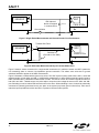
1
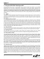
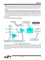
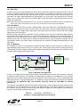
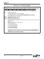
AN217 C8051F35 X D E L TA -S I G M A ADC U S E R ’ S G U I D E Relevant Devices This application note applies to the following devices: C8051F350, C8051F351, C8051F352, C8051F353 1. Introduction Delta-sigma analog-to-digital converters (ADCs) are oversampling ADCs: to reduce noise and analog front-end circuit cost and complexity, they sample signals at very high rates and produce a low-noise, high-resolution output. Oversampling at a “high” rate means sampling a signal at a frequency that is well above the bandwidth of interest’s Nyquist rate and is done to lower in-band noise. The output word rate of the ADC will be close to the bandwidth of interest. Delta-sigma ADCs also add benefit by shaping noise and digitally filtering the information to enhance performance. The oversampling, noise shaping, and digital filtering allow highly linear, high-resolution signal measurements, and reduce the cost and complexity of circuits that must filter the signal at the input of the ADC. Delta-sigma ADCs oversample a signal and produce relatively low output data rates and are best used in applications requiring high precision measurements (16 to 24 bits) of low-bandwidth signals (i.e., typically 20 kHz or less). Example applications include digital phones, temperature measurements, pressure measurements, and weigh-scales. The maximum C8051F35x ADC output word rate is 1 kHz. AV+ Voltage Reference Input Buffers Σ AIN+ PGA Modulator 8-Bit Offset DAC MDCLK Σ AIN- SINC 3 Filter Fast Filter ÷ SYSCLK Figure 1. ADC0 Block Diagram Rev. 0.2 2/05 Copyright © 2005 by Silicon Laboratories AN217 AN217 2. Using the C8051F35x Delta-Sigma ADC Using delta-sigma ADCs require an understanding of how to properly configure the modulator, use of the digital filter/decimator, and the nature of high-precision measurements of small signal voltages. Additionally, the C8051F35x family of devices’ ADC provides functions such as calibration and offset adjustment that should be fully understood when designing with these devices. The following sections describe the signal path from the input signal source, to the ADC input, through the modulator, digital filter, and finally the output result (16- or 24-bit digital output). Calibration of the ADC and circuit board design notes follow. Finally, delta-sigma noise specifications are discussed. 2.1. Signal The C8051F35x ADC is designed for optimal performance with a modulator sample rate of 19.2 kHz. The ADC is designed as an oversampling data converter, so the bandwidth of the input signal should be low (the lower the input signal bandwidth, the better the noise performance will be). The ADC is designed to measure voltages with high precision. 2.1.1. Getting the Signal to the ADC To aid high-precision measurements of small voltage signals, the ADC is best configured to input a differential signal to an AIN+ and AIN– input pin pair. The analog multiplexer (AMUX) can select from eight external channels of input, an on-chip temperature sensor, and an internal analog ground. The signal source (e.g, a transducer) can be directly wired to the ADC’s input. If the input is from a pair of wires, twisted-pairs should be used with shielding to reduce noise where feasible (keep wires as short as possible and away from other signals, especially digital signals). The main idea is to design a system in which noise will be present equally on both AIN+ and AIN– in order to reject common-mode noise. (See Figure 6 on page 12.) 2.1.2. Sensor Excitation Some transducers require an excitation current to generate an output voltage. The C8051F35x devices feature two on-chip current mode digital-to-analog converters (IDACs) for this purpose. See the data sheet for more details. 2.1.3. Analog Front-End The input circuit to the ADC pins typically requires filtering and sometimes buffering and gain. Filtering requirements for a delta-sigma ADC are low, and often the on-chip buffer and programmable gain will suffice. 2.1.4. External Buffer and Gain The input signal must be kept within the dynamic range of the ADC (determined by the voltage reference voltage) and within ground and supply voltage. The best measurement performance is achieved when the input signal’s dynamic range is the same as the dynamic range of the ADC (i.e., voltage reference voltage). When the signal is much smaller than the dynamic range of the ADC it will require amplification. The on-chip programmable gain or an external amplifiercan can be used for this purpose. In many applications, a simple op-amp will suffice, but for best performance choose a low-noise instrumentation or chopper stabilized amplifier. Many sensors have high-impedance output stages and require a high-impedance input to avoid introducing offset error. External amplifiers and op-amps serve this purpose. The C8051F35x devices also have an on-chip input buffer. However, for very high-resolution measurements, the on-chip buffers or external op-amps may not suffice due to drift (i.e., 1/f noise). For the best measurements, consider the use of chopper stabilized amplifiers (best for high-accuracy dc measurements) or a low-noise amplifier. 2.1.5. Analog Input Filter Typically, the only required input circuit needed for a delta-sigma ADC is an RC low-pass filter. While the ADC shapes and filters noise, there is no noise rejection at the sample rate (19.2 kHz and its multiples). The RC time constant should be designed to adequately remove noise at the sample rate frequency bandwidth, but not cause error due to filter settling time as the input signal voltage changes. The ADC samples the signal at a high rate by switching a capacitor. This results in average current flow into the ADC. This switching current can cause several inaccuracies in measurement including gain and offset errors and non-linearity if the input filter is not properly designed. Further, if an input buffer is used (e.g., an op-amp) the switched capacitor could result in amplifier instability. The RC circuit solves these problems by providing isolation (the resistor) and a charge reservoir (the capacitor). 2 Rev. 0.2 AN217 Resistor: The resistor value should be high enough for isolation (i.e., at least 10s of ohms) but not too high to cause settling time problems or gain errors. The gain error can be removed using the ADC’s calibration feature (see the datasheet for details). When making a differential measurement, the input resistors to AIN+ and AIN– must be matched to preserve common-mode rejection. It is typically more difficult to match higher valued resistors. Capacitor: The capacitor acts as a charge reservoir (supplying the switched ADC sample capacitor) and as a noise filter. Further, the ADC capacitor switching can be viewed as an average, steady input current. In reality, the switching creates spikes of charging current that are highly non-linear as the modulator switches the ADC’s sample capacitor. An external capacitor aids in linearizing the measurement. Electrolytic capacitors should not be used because they will introduce distortion. Ceramic capacitors work well and should be sized large enough such that a high valued resistor is not necessary. Typically, capacitors valued in the 1/10th’s of µF’s are used. A corner frequency below the sample rate (19.2 kHz) is typically sufficient (e.g., R = 100 Ω and C = 0.1 µF) for most applications. 2.2. The ADC: Configuring the Delta-Sigma 1. Select 7. Calibrate 5. Configure Voltage Reference Input Buffers AIN+ Σ PGA Modulator Σ SINC3 Filter Fast Filter AIN8-Bit Offset DAC 6. Configure 4. Configure 3. Zero/Tare 2. Gain Figure 2. Configuring The Delta-Sigma ADC To achieve a high-resolution measurement, the delta-sigma ADC consists of two basic subsystems: the modulator and the digital filter. One important concept to understand when configuring a delta-sigma data converter is that the sample rate is much higher than the output rate of the ADC, so each sample does not result in an ADC output. The signal is oversampled and then filtered to achieve the high-resolution measurement with reduced analog front-end circuit requirements. Rev. 0.2 3 AN217 2.2.1. Voltage Reference The voltage reference circuit should be treated as carefully as the measured signal, because noise on the voltage reference degrades ADC performance. The C8051F35x can use its on-chip voltage reference (2.4 V typical) or an externally supplied voltage reference (input to the VREF+ and VREF– pins). For optimal performance, we recommend the use of a high-quality, low-noise external reference. To filter noise, use a 1.0 µF ceramic capacitor connected between VREF+ and VREF–, placed as close to the pins as possible. Note: When using the internal voltage reference, VREF– must be connected to ground externally. This is typically done by connecting the VREF– pin directly to the analog ground plane. 2.2.2. Programmable Gain The goal is to match the input signal dynamic range to the dynamic range that can be measured by the ADC (based on voltage reference voltage). This can be accomplished by scaling the voltage reference (VREF) voltage and by amplifying the signal. A larger VREF voltage improves performance, thus it is better to apply gain to the signal rather than reducing VREF. A signal can be amplified using a combination of an external amplifier and/or the internal programmable gain amplifier. (See “2.1.4. External Buffer and Gain” on page 2.) The C8051F35x devices feature an on-chip programmable gain amplifier (PGA) with eight gain settings. The ADC input gain is selected using the ADC0 Control Register (ADC0CN). ADC0CN[2:0] are the AD0GN bits used to select one of the eight gain settings. (See SFR Definition 2.1.) SFR Definition 2.1. ADC0CN: ADC0 Control Register R R R R/W R/W - - - AD0POL AD0BCE Bit7 Bit6 Bit5 Bit4 Bit3 R/W R/W R/W AD0GN Bit2 Bit1 Reset Value 00010000 Bit0 SFR Address: 0xF4 Bits 7–5: Unused: Read = 000b, Write = don’t care. Bit 4: AD0POL: ADC0 Polarity. 0: ADC operates in Unipolar mode (straight binary result). 1: ADC operates in Bipolar mode (2s compliment result). Bit 3: AD0BCE: ADC0 Burnout Current Source Enable. 0: ADC Burnout current sources disabled. 1: ADC Burnout current sources enabled. Bits 2:0 AD0GN: ADC0 Programmable Gain Setting. 000: PGA Gain = 1. 001: PGA Gain = 2. 010: PGA Gain = 4. 011: PGA Gain = 8. 100: PGA Gain = 16. 101: PGA Gain = 32. 110: PGA Gain = 64. 111: PGA Gain = 128. This SFR can only be modified when ADC0 is in IDLE mode. 4 Rev. 0.2 AN217 2.2.3. Offset DAC The ADC features an internal dedicated DAC that is used to adjust the measurement offset of the ADC. This can be used as a software controlled tare function in the end-product. For example, the offset DAC could be used to remove the platform weight in a weigh scale application in order to measure only the scale contents of interest. The offset DAC can make a signed adjustment to approximately ±1/2 of the ADC’s input range with any PGA gain setting. See the “Offset DAC” section of the ADC0 chapter of the data sheet for complete information on how to configure the offset DAC. Note: Small external system and ADC offset errors are corrected via the ADC’s built-in calibration function. The offset DAC is used to zero or tare a measurement as a function of the end-product and is not intended for calibration. 2.2.4. Input Buffers Two input buffers can be used to provide a high-impedance input to the ADC when a high-impedance sensor is measured (i.e., the sensor will source very little current). One input buffer is used to measure signals with voltages in the upper half of the voltage supply range (“high” input buffer) and one is used for the lower half of the voltage supply range (“low” input buffer). While the on-chip input buffers are adequate for many applications, they may not be sufficient for highly sensitive measurements at the highest resolution (i.e, 24-bits). This is because they introduce 1/f noise, which will appear as voltage “drift” in the measurement. For this reason, the input buffers can be bypassed, and an external buffer or amplifier can be used. The input buffers are software controlled; therefore, they can easily be evaluated. See the “Input Buffers” section of the ADC0 chapter of the data sheet for complete information and specifications for the input buffers. 2.2.5. The Modulator The modulator’s function is to oversample the measured signal, shape the noise such that it is reduced in the signal bandwidth, and produce a series of 1-bit output codes. These output codes will have a density and order of 1s and 0s that are used to produce a high-resolution digital representation of the input signal (the modulator output is digitally filtered to obtain large output words). CLOCK (fs) Analog Input INTEGRATOR + ∑ CLOCK (Kfs) BIT STREAM ∫ 1-BIT DAC +VREF -VREF DIGITAL FILTER DATA LATCHED COMPARATOR (1-BIT ADC) MODULATOR Figure 3. Modulator and Digital Filter In order to oversample the input signal and still obtain a reasonable output word rate, the modulator is configured to operate at a high frequency. The modulator is designed with an integrator in a feedback loop. This integrator shapes the noise so that the digital filter removes the maximum amount of the noise. This is the advantage of the delta-sigma converter. To get this performance, it is important to configure the modulator to operate at its specified frequency. For the C8051F35x ADC, the modulator frequency should be 2.4576 MHz for optimum performance. The modulator clock (MDCLK) is derived from the MCU system clock. To allow flexibility in the use of many system clock sources, the user has access to the divider in the ADC0 Modulator Clock Divisor (ADC0CLK) register (see SFR Definition 2.2). The MDCLK value is set using the ADC0CLK register (see SFR Definition 2.2) to achieve a frequency of 2.4576 MHz according to Equation 1: MDCLK = ( SYSCLK ) ⁄ ( ADC0CLK + 1 ) Equation 1. Configure Modulator Clock Frequency Rev. 0.2 5 AN217 Once the modulator clock is configured, the modulator sample rate of the ADC is also set to MDCLK/128. Therefore, the typical sample rate is 2.4576 MHz/128 = 19.2 kHz. This will be well above the signal bandwidth measured, as the maximum output word rate for the ADC is 1 kHz. SFR Definition 2.2. ADC0CLK: ADC0 Modulator Clock Divisor R/W R/W R/W R/W Bit7 Bit6 Bit5 Bit4 R/W R/W R/W R/W Bit2 Bit1 Bit0 ADC0CLK Bit3 Reset Value 00000000 SFR Address: 0xF7 Bits 7–0: ADC0CLK: ADC0 Modulator Clock Divisor. This register establishes the Modulator Clock (MDCLK), by dividing down the system clock (SYSCLK). The input signal is sampled by the modulator at a frequency of MDCLK / 128. For optimal performance, the divider should be chosen such that the modulator clock is equal to 2.4576 MHz (modulator sampling rate = 19.2 kHz). The system clock is divided according to the equation: MDCLK = SYSCLK / (ADC0CLK + 1) Note: The Modulator Sampling Rate is not the ADC Output Word Rate. 6 Rev. 0.2 AN217 2.2.6. The Digital Filter 0 ATTENUATION (dB) [(SIN x)/x] 3 -100 -200 0 20 40 FREQUENCY (Hz) 60 80 Figure 4. Digital Filter Frequency Response (SINC3) The filter’s function is to convert the 1-bit digital output of the modulator to a large digital output word (16- or 24bits). The series of 1s and 0s input to the filter have a spectral shape that allows the digital filter to remove the maximum amount of noise. The filter decimates the data from the modulator to output words at a lower rate (for the desired bandwidth of interest). The filter’s job is to remove noise from the measurement, and will do so optimally at a high decimation ratio. There is a trade-off between noise performance and the decimation ratio (see Table 1 on page 14). Therefore, the designermust consider the increase in noise if a higher output word rate is desired. To obtain the best performance, the filter’s decimation ratio should be configured to the highest possible value, while still allowing the minimum required output word rate. The decimation ratio is set in the ADC0 Decimation Ratio High and Low registers (ADC0DECH and ADC0DECL). These two registers are used to form an 11-bit decimation ratio value and corresponding output word rate: DECIMATION RATIO = DECI [ 10:1 ] Equation 2. Decimation Ratio Register Value (DECI) Output Rate = MDCLK ⁄ [ 128 × ( DECI + 1 ) ] Equation 3. ADC0 Output Word Rate Rev. 0.2 7 AN217 SFR Definition 2.3. ADC0DECH: ADC0 Decimation Ratio Register High Byte R/W R/W R/W R/W R/W R/W R/W R/W Reset Value - - - - - DECI10 DECI9 DECI8 00000111 Bit7 Bit6 Bit5 Bit4 Bit3 Bit2 Bit1 Bit0 SFR Address: 0x9B Bits 7–3: Unused: Read = 00000b, Write = don’t care. Bits 2–0: DECI[10:8]: ADC0 Decimation Ratio Register, Bits 10–8. This register contains the high bits of the 11-bit ADC Decimation Ratio. The decimation ratio determines the output word rate of ADC0, based on the Modulator Clock (MDCLK). See the ADC0DECL register description for more information. This SFR can only be modified when ADC0 is in IDLE mode. SFR Definition 2.4. ADC0DECL: ADC0 Decimation Ratio Register Low Byte R/W R/W R/W R/W R/W R/W R/W R/W Reset Value DECI7 DECI6 DECI5 DECI4 DECI3 DECI2 DECI1 DECI0 11111111 Bit7 Bit6 Bit5 Bit4 Bit3 Bit2 Bit1 Bit0 SFR Address: 0x9A Bits 7–0: DECI[7:0]: ADC0 Decimation Ratio Register, Bits 7–0. This register contains the low byte of the 11-bit ADC Decimation Ratio. The decimation ratio determines the number of modulator input samples used to generate a single output word from the ADC. The ADC0 decimation ratio is defined as: Decimation Ratio = DECI[10:0] + 1 The corresponding sampling period and output word rate of ADC0 is: ADC0 Conversion Period = [(DECI[10:0] + 1) x 128] / MDCLK ADC0 Output Word Rate = MDCLK / [128 x (DECI[10:0] + 1)] The minimum decimation ratio setting is 20. Any register setting below 19 will automatically be interpreted as 19. Important: When using the fast filter, the decimation ratio must be divisible by 8 (DECI[2:0] = 111b). This SFR can only be modified when ADC0 is in IDLE mode. 8 Rev. 0.2 AN217 The ADC’s digital filter gives two options for output: FAST and SINC3. The FAST filter uses results from only the current conversion cycle or period, while the SINC3 filter uses three conversion cycles. The fast filter output reacts more quickly to changes on the analog input, while the SINC3 filter output produces lower-noise results. Additionally, the SINC3 filter is designed to reject 50 and 60 Hz frequencies (see Figure 4 on page 7). When it is necessary to respond quickly to signal changes or when fast channel switching is required (between different measured signals at the AMUX), the FAST filter should be used. In most cases, the SINC3 filter output is used for best noise performance. Using the FAST Filter: Set the ADC0 Interrupt Select bit (AD0ISEL) bit to 1 in the ADC0 Configuration Register (ADC0CF). This will set the ADC0 end-of-conversion interrupt bit to be set upon a ready result in the FAST filter. The output of the FAST filter is placed in the ADC0FH, ADC0FM, and ADC0FL registers. NOTE: When using the FAST filter, the Decimation Ratio must be divisible by 8. (See SFR Definition 2.4.) Using the SINC3 Filter: Clear the ADC0 Interrupt Select bit (AD0ISEL) bit to 0 in the ADC0 Configuration Register (ADC0CF). This will set the ADC0 end-of-conversion interrupt bit to be set upon a ready result in the SINC3 filter. The output of the SINC3 filter is placed in the ADC0H, ADC0M, and ADC0L registers. 2.2.7. Calibration The C8051F35x family of devices has two, built-in calibration functions: internal and system calibration. Each of these calibration options can calibrate for both offset and gain errors. Offset calibration should be performed prior to gain calibration. Calibration coefficients are stored in special function registers (constants are 24-bits) and are user accessible. However, the calibration adjustments are made automatically by the ADC, and so no further user calibration adjustment is necessary once the ADC calibration function is complete (i.e., the MCU does not have to condition the ADC outputs for calibration). Internal calibrations (offset and gain) require no external signals to the ADC inputs, but do require the voltage reference input. System calibration uses external signals, and is useful for removing errors due to temperatureinduced offset/gain drift, reference voltage drift, offset, and gain errors from the analog front-end circuit. System calibration is performed as follows: Offset: This is done first by applying an external “zero” voltage to the AIN+/AIN– pins. Gain: This is done after offset calibration. A full-scale positive voltage is applied to the AIN+/AIN– pins, for the given current programmable gain amplifier setting. Calibrations are initiated by writing to the ADC0 System Mode Bits (AD0SM) in the ADC0CF register (see SFR Definition 2.5). Section 5.2 of the data sheet details complete information concerning the calibration of the ADC. It is recommended that a full self or system calibration be performed at system start-up. An MCU-scheduled regular calibration can be periodically performed for best performance of the measurement system. Rev. 0.2 9 AN217 SFR Definition 2.5. ADC0MD: ADC0 Mode R/W R R/W R/W R AD0EN - Reserved Reserved - Bit7 Bit6 Bit5 Bit4 Bit3 R/W R/W R/W AD0SM Bit2 Bit1 Reset Value 00000000 Bit0 SFR Address: 0xF3 Bit 7: AD0EN: ADC0 Enable Bit. 0: ADC0 Disabled. ADC is in low-power shutdown. 1: ADC0 Enabled. ADC is active and ready to perform calibrations or conversions. Note: Disabling the ADC automatically resets the AD0SM bits back to the “Idle” state. Bit 6: Unused: Read = 0b, Write = don’t care. Bits 5–4: RESERVED: Must Write to 00b. Bit 3: Unused: Read = 0b, Write = don’t care. Bits 2–0: AD0SM: ADC0 System Mode Select. These bits define the operating mode for the ADC. They are used to initiate all ADC conversion and calibration cycles. 000: Idle 001: Full Internal Calibration (offset and gain). 010: Single Conversion. 011: Continuous Conversion. 100: Internal Offset Calibration. 101: Internal Gain Calibration. 110: System Offset Calibration. 111: System Gain Calibration. Note: Any system mode change by the user during a conversion or calibration will terminate the operation, and corrupt the result. To write to many of the other ADC registers, the AD0SM bits must be set to IDLE mode (000b). 10 Rev. 0.2 AN217 3. Hardware Design Designing a low-noise, high-precision measurement system requires not only proper ADC configuration, but careful circuit board design and interface considerations as well. For an in-depth discussion concerning proper mixed-signal circuit board design, see application note, “AN203: Printed Circuit Design Notes.” AN203 covers many topics concerning proper PCB design such as power supply, decoupling, ground circuit, component placement, and routing of traces (layout guidelines). Also included is a checklist that can be used to ensure all relevant items have been considered for the application. Here is a list of notes concerning the use of the C8051F35x on a circuit board: Use ground planes: Typically a minimum of 4-layers should be used. Connect components’ ground pins directly to the plane. Use copper plane fill between traces on the signal layers, and connect the fill to ground using vias (do not leave “floating” copper). Separate analog and digital ground planes can be used; connect them in one place. Design a few locations for connection so that the best connection can be tested, usually near the ADC or near the power supply to the board. See AN203 for details and recommended layer assignments for ground, power, and signal planes. Avoid ground loops: Unless careful isolation has been designed, all circuit boards and systems must share a common, low-impedance ground connection so they have the same ground potential. This is especially true of the sensor if not on the same board as the ADC. Do not connect a sensor’s ground or negative side wire to a different ground plane than the C8051F35x’s. Connect both sensor wires to AIN+/AIN–, and make another common ground connection between the boards (chassis ground) when applicable. Place components carefully in order to control ground currents: All ground currents from each component must return to the power supply. Place digital, noisy signals and their traces away from analog signals and the analog input circuits connected to the ADC. Avoid ground current return flow in the area of the analog signal path (e.g., digital components placed in such a way that return currents must flow by the anti-alias filters at AIN+ and AIN– pins will degrade performance). See AN203. Keep analog traces away from digital traces: Component placement and orientation will help the designer route digital traces away from the analog signals. Analog traces (including the voltage reference) must be kept as short as possible. Sensor input: The delta-sigma will reject noise (though not at the modulator sample frequency). However, care should be taken to use a simple anti-alias filter and a high-quality amplifier (when applicable). Keep wires as short as possible. Input impedance at AIN+ and AIN– should be matched to preserve common-mode rejection. Reject common-mode and ground noise: Make differential measurements and use twisted wire pairs (shielded if possible). EMI and ground noise that appears equally on both differential inputs to the ADC will not appear in the measurment. Rev. 0.2 11 AN217 SENSOR ADC EMI Induced Noise will appear in measurement V noise C8051F35x Ground Noise Figure 5. Single-Ended Measurements and Ground Circuits: Poor Performance Twisted Wire Pairs SENSOR ADC Shielded (Ground to One Side) C8051F35x Figure 6. Differential Measurements Reject Common-Mode Noise Figure 5 shows a sensor connection for a single-ended measurement, in which the sensor and ADC systems do not necessarily share a common, low-impedance ground connection. This allows more noise due to ground variations and EMI to appear in the ADC measurement. Figure 6 illustrates a method which rejects more noise. The ADC rejects common-mode noise, that is, noise that appears equally on both AIN+ and AIN– in a differential measurement. In effect, EMI-induced and ground noise is better cancelled when a differential measurement is made. The idea is to have all unwanted signals the same on both AIN+ and AIN–. Twisted sensor wire pairs helps to keep the noise voltage the same on the AIN+ and AIN– pins. Shielding is used to reduce EMI-induced noise on the wires. When shielding is used, it should be electrically connected to (chassis) ground and at only one place in the system (to prevent ground current flow). Take care to match the input impedances at AIN+ and AIN– to preserve common mode rejection. 12 Rev. 0.2 AN217 4. Delta-Sigma Noise Specifications Delta-sigma converters make high-precision, high-resolution measurements of signals. Often, the measurement is of a very small signal voltage; therefore, the noise performance is one of the most important specifications. Number of Samples "Bin" that has highest number of samples and is closest to input signal Histogram has a shape that approximates a Gaussian PDF (shown as dashed line) due to white noise mixed with dc input signal voltage Other "bins" receive samples due to noise ... 0 ... 1019 1020 1021 1022 1023 1024 1025 1026 1027 1028 1029 2^N ADC Codes Noise-Free Resolution: 6.6*sigma for 99.9% of all output codes Number of Samples Effective Noise: rms noise is one standard deviation (sigma) ... ... 0 2^N Figure 7. Histogram Analysis of Noise: Effective Noise vs. Noise-Free Resolution Rev. 0.2 13 AN217 4.1. Effective Resolution Many ADC applications measure a dynamic signal in the presence of noise. Noise sources include the ADC itself and external sources, including the voltage reference. Additionally, the analog-to-digital conversion process itself introduces quantization error as the ADC must “choose” from a finite set of output codes to represent an analog voltage input. Quantization error is also viewed as input referred quantization noise. If the noise is white, the collected samples’ distribution will approach a Gaussian distribution for a dc voltage input (or if the inputs are grounded for a noise test); therefore, the rms noise is one standard deviation of the collected samples. (See Figure 7 on page 13.) Delta-sigma converter noise is often specified using rms noise. This noise is typically given for a set of typical ADC configurations as a function of gain and decimation ratio, as an input-referred voltage. Noise specified in this way gives the designer a good idea of the expected ADC noise in a measurement for a given gain and output word rate. This noise information can be used to calculate the effective resolution of the ADC. Noise can be observed in a measurement as the LSBs of the ADC output vary from sample-to-sample. Some may consider these bits to be useless and dismiss them when making a measurment. However, these LSBs do contain useful information and improve performance in many applications. Such applications are those that measure a dynamic or time-varying signal (e.g., audio applications). Often an engineer will average a number of samples to increase the effective resoution by filtering noise (the averaging is a form of digital filtering). 4.2. Noise-Free Resolution While using rms noise to give an effective number of bits is useful, many applications measure a static, dc-like signal such as temperature or pressure for display. In such cases, the designer will be more interested in the peakto-peak or noise-free bits that do not change from sample-to-sample. For example, the designer may want to display a digital temperature readout and needs to determine the number of digits that could be displayed. This is a more stringent requirement and can be calculated from the given rms noise value in the data sheet. The rms noise is one standard deviation (sigma), and 99.9% of all samples within a Gaussian distribution are within 6.6 – sigma. Multiplying sigma by 6.6 will allow the calculation noise-free bits in an ADC for a given configuration. When comparing ADCs, it is important to note which specification is posted in the data sheet so that a meaningful comparison can be made. 4.3. Example: Effective vs. Noise-Free Resolution Table 1. ADC0 SINC3 Filter Input-Referred Typical rms Noise (µV) Decimation Ratio Output Word Rate* 1920 PGA Gain Setting 1 2 4 8 16 32 64 128 10 Hz 2.38 1.23 0.68 0.41 0.24 0.16 0.12 0.11 768 25 Hz 3.90 2.04 1.14 0.68 0.44 0.33 0.28 0.27 640 30 Hz 4.50 2.39 1.31 0.81 0.54 0.42 0.36 0.36 384 50 Hz 6.00 3.21 1.86 1.20 0.86 0.73 0.66 0.66 320 60 Hz 7.26 3.96 2.32 1.51 1.11 0.97 0.89 0.89 192 100 Hz 13.1 7.11 4.24 2.85 2.16 1.91 1.79 1.77 80 240 Hz 93.2 47.7 24.8 13.9 9.34 7.61 6.97 6.67 40 480 Hz 537 267 135 69.5 38.8 25.7 20.9 18.9 20 960 Hz 2974 1586 771 379 196 108 70.0 45.4 *Note: Output Word Rate assuming Modulator Clock = 2.4576 MHz (sampling clock = 19.2 kHz) 14 Rev. 0.2 AN217 Table 1 is a copy of the posted specification of the ADC0’s typical noise table from the C8051F35x family data sheet. This table shows the expected, typical rms noise of the ADC at the output of the SINC3 filter for given decimation ratios and gain settings. If measuring a signal that requires a 10 Hz output word rate with unity gain, we set the decimation ratio for 1920 (remember: use the highest decimation ratio setting possible). This gives an expected VNOISERMS of 2.38 µV (from Table 1). This is the noise number used to predict the expected effective resolution. With a 2.5 V voltage reference, each LSB in a bipolar measurement is as follows: VREF/223 = 2.5 V/223 = 298 nV. Therefore, the standard deviation (rms noise) in terms of codes is as follows: 2.38 µV/298 nV = ~8 LSBs or output codes of noise. In practical terms, if the analog inputs are grounded for a noise test (both AIN+/AIN– are connected to analog ground and a bipolar measurement is made), you could expect to observe a standard deviation of 8 codes. This equates to an effective resolution of 23 bits – 3 bits = 20-bits effective resolution (it takes 3 bits to represent a variation of eight binary output codes, so we subtract 3 bits from the signed 24-bit output word). If concerned with noise-free resolution, we proceed with the same method but instead use the rms noise voltage (one standard deviation) multiplied by 6.6. Multiplying the rms noise by 6.6 results in a noise level in which 99.9% of all codes will be included. This leaves only the bits that will remain constant from sample-to-sample in our noise test. Again, using the 2.38 µV rms noise voltage (from Table 1), 99.9% of all sampled output codes should be contained within 2.38 µV x 6.6 = 15.7 µV. An LSB = 298 nV, and so the total number of noise-varying bits is as follows: 15.7 µV/298 nV = ~53 codes. 53 bits requires 26 or 6-bits of a digital code to represent 53 different output codes, and so 23 bits – 6 bits = 17-bits of noise-free resolution. Rev. 0.2 15 AN217 DOCUMENT CHANGE LIST Revision 0.1 to Revision 0.2 16 Updated text on page 15. Rev. 0.2 AN217 NOTES: Rev. 0.2 17 AN217 CONTACT INFORMATION Silicon Laboratories Inc. 4635 Boston Lane Austin, TX 78735 Tel: 1+(512) 416-8500 Fax: 1+(512) 416-9669 Toll Free: 1+(877) 444-3032 Email: [email protected] Internet: www.silabs.com The information in this document is believed to be accurate in all respects at the time of publication but is subject to change without notice. Silicon Laboratories assumes no responsibility for errors and omissions, and disclaims responsibility for any consequences resulting from the use of information included herein. Additionally, Silicon Laboratories assumes no responsibility for the functioning of undescribed features or parameters. Silicon Laboratories reserves the right to make changes without further notice. Silicon Laboratories makes no warranty, representation or guarantee regarding the suitability of its products for any particular purpose, nor does Silicon Laboratories assume any liability arising out of the application or use of any product or circuit, and specifically disclaims any and all liability, including without limitation consequential or incidental damages. Silicon Laboratories products are not designed, intended, or authorized for use in applications intended to support or sustain life, or for any other application in which the failure of the Silicon Laboratories product could create a situation where personal injury or death may occur. Should Buyer purchase or use Silicon Laboratories products for any such unintended or unauthorized application, Buyer shall indemnify and hold Silicon Laboratories harmless against all claims and damages. Silicon Laboratories and Silicon Labs are trademarks of Silicon Laboratories Inc. Other products or brandnames mentioned herein are trademarks or registered trademarks of their respective holders. 18 Rev. 0.2