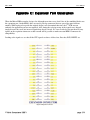
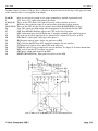
1
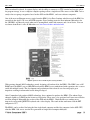
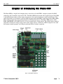
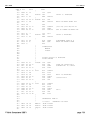
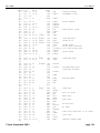
SEPTEMBER 2007
2nd Edition
5392 Cornell Blvd
North Ridgeville, OH 44039
Micro-KIM
Users Manual
All materials, schematics, and hardware designs provided without any warranties. Although this material has been carefully examined,
Briel Computers takes no responsibility for any errors in printing.
Version 2.0
Published by Briel Computers
5392 Cornell Blvd
North Ridgeville, OH 44039
USA
Copyright 2007 Briel Computers. All rights reserved. Printed in the United States of America. Except as permitted under the
Copyright Act of 1976, no part of this publication may be reproduced or distributed in any form or by any means, or stored in a
database or retrieval system, without the prior written permission of the publisher, with the exception that the program listings may be
entered, stored, and executed in a computer system, but they may not be reproduced for publication.
©
Micro-KIM
Users Manual
How the Micro-KIM came to be
For those of you familiar with Briel Computers, you know about the replica 1 computer. In short, it is a single
board computer designed to replicate the Apple 1 computer. For the last 3 years I’ve been searching for a way
to get this computer priced under $100 so more people can enjoy building them. With parts going up in price
I’ve found this to be impossible. So, I went searching for a different platform to replicate.
Why redesign the KIM-1? Why offer it as a kit? Because there are still people out there who like to build and
work with kits like those offered in the 1970’s and 80’s. The KIM-1 has been called the “first single-board
computer” by many and was created by Chuck Peddle of MOS as a development board for the 6502 CPU. What
better computer to replicate than the first computer designed for the 6502?
The major problem with replicating the KIM-1 was the 6530 RRIOT IC’s which have custom ROM’s
embedded in them. These are no longer available and are difficult to locate. The KIM-1 used two and each one
held a section of the monitor program. The solution was to use an external EPROM and a 6532 RIOT which is
very close to the 6530 but with some minor differences. This required a tricky addressing scheme I developed to
replicate the exact addressing as the original KIM-1 so programs would work the same.
The next decision was to drop the second 6530 (6532) to reduce chip count. This was an easy decision because
it can be added later in an expansion. The problem was the 2 nd 6530 on the KIM-1 held 64 bytes of RAM. As
luck would have it, the 6532 has 128 bytes of onboard RAM vs. the 6530 which only has 64 bytes. I decided to
use all 128 bytes available on the 6532 in place of the 128 bytes used in 2 6530’s in the KIM-1.
There is no source for replacement keypads used on the KIM-1 so I decided to just go ahead and put the
keyboard onboard and use tactile switches with silkscreen labels above them for identifying the buttons. This
wasn’t perfect but it really helped with the cost and keeping the Micro-KIM to a small footprint.
The last major decision was difficult to make but I felt it was necessary. The expansion slots on the KIM-1 were
a disaster. They held unnecessary signals, orientated in a difficult setup and spaced far apart on the board. After
debating this one for a long time, I decided to just dump the original interface and create a 40 pin header with
all the major signals needed for expansion. Keeping as much of the original signals as possible, yet getting
everything needed all in a 40 pin setup was difficult. It is very possible to recreate the original expansion
connectors with this setup but there are a few minor signals missing.
Finally I’d like to thank my good friend Rich Dreher for helping me out more than I hoped for on this project.
Not only did he redo the board layout for me and help clean up the schematics, he pushed me to add the TTY
RS232 interface onboard to add value and much needed I/O onboard. Without Rich’s help this project would
not be what it is today.
I hope you enjoy your Micro-KIM and that it brings you as much happiness building and using it as I did
designing it.
Vince Briel
©
Micro-KIM
©
Users Manual
Chapter 1:
Chapter 2:
Chapter 3:
Chapter 4:
Chapter 5:
Chapter 6:
Chapter 7:
Chapter 8:
Chapter 9:
A brief history of the Kim-1
Introducing the Micro-KIM
Unpacking and setting up
Assembling the kit
Installing USB drivers for optional adapter
Using the Micro-KIM
TTY serial Interface
Using the Paper Tape Feature
Troubleshooting your Micro-KIM
5
7
9
12
15
18
19
23
26
Appendix A:
Appendix B:
Appendix C:
Appendix D:
Onboard jumper settings
Micro-KIM/KIM-1 Memory Map
Expansion Port Description
Monitor Listing
27
28
29
31
Micro-KIM
Users Manual
!"# $ %
& %
!
The KIM-1 which stands for Keyboard Input Monitor was a small single-board computer designed by MOS
technologies in 1975 as a development board for their new 6502 processor. The board was originally designed
(by Chuck Peddle creator of the 6502) to be used by engineers as a development board. The KIM-1 was so well
priced at $245 that it attracted more than just engineers; it attracted a whole new growing group of hobbyists
eager to own their own computer.
Figure 1: MOS Technology KIM-1 Advertisement
©
Micro-KIM
Users Manual
With an onboard keyboard, 6 segment display, and the ability to connect to a TTY terminal and cassette player
for program storage, it was a complete computer package all on a single board. The success of the KIM-1 was a
catalyst for user groups, magazines based on the 6502 and the KIM-1, and even software companies.
One of the most well known success stories from the KIM-1 is by Peter Jennings who discovered the KIM-1 in
an article in the April 1976 issue of BYTE magazine. Peter Jennings wrote the now infamous Microchess for
the 1K KIM-1 and showed people what can be accomplished with a little memory and a lot of desire. You can
read more about Peter’s story on Microchess at: http://www.benlo.com/index.html
Figure 2: April 1976 article in BYTE magazine featuring the KIM-1
With growing demand, MOS technology started designing add-on boards for the KIM-1. The KIM-2 was a 4K
RAM board, the KIM-3 was an 8K RAM board and the KIM-4 was a motherboard with expansion slots so users
could add multiple boards. The development and production of these boards was slow and people grew
impatient, resulting in aftermarket boards being developed.
After Commodore had purchased MOS technology, they continued to produce the KIM-1. The onboard logo
changed slightly to C=MOS but the layout was kept intact. There were a few revisions but I’m not sure what the
revisions changed. Meanwhile the creator of the 6502 and the KIM-1, Chuck Peddle was working on an
improved version with QWERTY keyboard and a video display. The result of that work turned out the PET
computer in 1977.
The KIM-1 can be credited for being the first single board computer and the first computer for the 6502 CPU;
what the KIM-1 did was to start the first generation of single board computer hobbyists.
©
'
Micro-KIM
Users Manual
"
The Micro-KIM is a single board computer that is closely based on the KIM-1 computer produced by MOS
technology and Commodore in the mid 1970’s. The Micro-KIM retains much of the original design of the KIM1 with modifications made to allow extinct components to be replaced with more readily available parts. The
addressing scheme was left intact so all the original programs from the KIM-1 should work on the Micro-KIM.
Many of the programs have been tried but there are still many that haven’t. The Micro-KIM consists of 5K
RAM, 2K EPROM, a 6532 RIOT for I/O, a 23 key keyboard and a 6 digit display. The added features include a
simple DC in feature for using a single source power supply such as a wall wart; a RS232 adapter for use with
the monitor terminal program, and a 40 pin expansion header for future expansion.
Figure 3: Micro-KIM computer kit
©
Micro-KIM
Users Manual
As a result of keeping much of the original design and the fact that there are several 7 segment displays, the
Micro-KIM uses a lot of resistors. While resistors don’t add much to the overall cost of the board, the board size
is affected by this. Originally, the goal was to get the Micro-KIM as small as 4” X 4” but because it is a kit with
thru-hole components it was just impossible to get the board down that small.
The onboard RS232 interface is the same circuit used to convert the TTY circuit back in 1976 into a more
common RS232 level format. The original circuit was to use -5V which created a problem since the Micro-KIM
runs off a single 5V source. The circuit allowed for the possibility to use ground instead and with several tests,
the circuit worked with ground. This was huge because if it didn’t work, the TTY/RS232 interface would have
required extra circuitry to generate the -5V required.
The Micro-KIM has an 8K RAM chip onboard but only 5K is used. The reason is simple. The decoding scheme
of the original KIM-1 decoded eight 1K blocks, of which only 1K was used onboard the KIM-1 for RAM and
3K for ROM and I/O. This leaves room for 4K of additional RAM without any further decoding. I simply used
an 8K RAM IC to replace the five 1K blocks available for RAM. This means that 3K of RAM in the onboard
RAM IC is wasted but it is necessary to keep compatibility with the original KIM-1.
The memory decoding scheme of the Micro-KIM is an exact match to the KIM-1, therefore, the system has a
repeating stage of memory every 8K. In other words, the 6502 doesn’t know the difference from $0000 and
$2000. Anything you store in $0000 will show up in $2000 and visa versa. This can be stopped with expansion
by re-decoding memory into 8K blocks and only activating the first 8K when it is directly addressed. For now,
just know that if you see an address such as C12F on the display, that isn’t the actual address being accessed.
The display is controlled by a 6532 RIOT I/O chip and the monitor keeps the current address and data
displayed. When you first power up your Micro-KIM you probably won’t see anything on the display. This is
normal since the microprocessor needs a reset to get running. There is no auto-reset circuit on the KIM-1
therefore there isn’t one on the Micro-KIM either. Pressing RS (RESET) on the keypad performs a system
RESET on the Micro-KIM and starts the system up.
©
(
Micro-KIM
Users Manual
"
*
Before you begin soldering your Micro-KIM kit together you need to inventory all of the parts in the kit. The
following is a list of all the components in the kit and the quantity of each component. If your kit is short any
parts, email me at [email protected] to arrange to get the missing part. Be sure to allow plenty of work space
for assembly.
NOTE: If you have an assembled board, you only need to verify the jumper is on JP1 and off of JP2 to insure
normal operation. You can skip this section and proceed to the next chapter. There is no CN1 connector.
The chips are in static protective sleeves and you may be able to inventory them just by looking through the
plastic.
The sockets are also in a sleeve but mostly for ease of shipping. Use the figure 3 in the previous chapter to help
identify the parts.
The 1 MHz oscillator is identified by its silver color and it looks like a 4 pin chip. Pin 1 is identified as the
pointed corner.
The 7805 voltage regulator can be identified from figure 3 as well as the 6 seven segment displays.
There are 9 transistors in total and they can be identified by the number written on the flat spot on them.
There is only one 47K resistor pack that has 9 pins in a single-inline-package or (SIP).
To identify the different resistors, use the part description below to help you identify each resistor. Group all of
the resistors into different piles according to their colors. There should be 5 different piles when you have
finished.
Figure 4: resistor color chart
©
)
Micro-KIM
Users Manual
Look at the resistor and try and find a gold or silver outer band. Hold the resistor so that band is on the right.
Look at the first color on the left. Using the chart above, calculate the first value. For example, if the first color
band on the left is orange, then the first value is 3. Look at the color band next to the first one, just off to the
right and get that value. Let’ assume the 2nd band is also orange. Now, the 3rd band is the multiplier. Let’s say
that color is red. Red is 2 which means we just put 2 zero’s at the end of the value. So, it goes 3 (orange), 3
(orange), 00 or 3300. Simplify that to 3.3K by dividing by 1000 and now you have calculated the resistor value.
This is a quick explanation on how to calculate the resistor value. There are many web sites out there to help
you out but the parts chart gives you color values to help you out.
There are 3 different types of capacitors on the Micro-KIM. The easiest way to figure them out is just put them
into 3 different piles.
The 1uF looks different than the .1uF caps and the .22uF caps.
The .22uF caps look close to the .1uF but the value on the capacitor is different.
The .22uF should have the number 224 on it but the number scheme on capacitors can vary.
On the .1uF capacitors, they should say 104. On the 1uF it should just have a 1 on it.
The 2 diodes are easy to identify. The 1N4001 is a larger black diode with a silver strip.
The 1N4148 is slightly smaller and looks like it’s made of glass.
It is important to note that diodes are polarized. The white or black stripe tells which way they mount on the
PCB. Pay attention when building your kit to ensure that the diodes are in the correct orientation.
The DB9 connector is your serial port connector and looks like a standard 9 pin connector.
The power supply connector is a male jack that fits many standard power supplies.
The 40 pin header has no incorrect orientation and can be mounted either way. However, one side is shorter and
that is the side that goes into the PCB. Make sure the longer end sticks up when installing on PCB.
There should also be 2 jumper post and 2 shunts. The JP1 on the Micro-KIM is essential for operation but needs
to be removed if an expansion board is used to decode memory differently than what is done on the Micro-KIM.
There are a total of 23 tactile push button switches that are easy to identify.
The power switch will mount next to the power jack on the PCB and has 5 mounting tabs on the bottom.
The SST (single-step) switch is black and sits with the keypad.
There is also a CD containing manuals and text files of some software. This completes your inventory check of
the Micro-KIM single board computer.
©
!
Micro-KIM
Users Manual
QUANTITY
©
PART DESCRIPTION
1
6502 CPU
1
6532 RIOT
1
2764 EPROM
1
6264 SRAM
2
74LS00
1
74LS06
1
74LS38
1
74LS138
2
74LS145
1
NE556
1
1MHz OSCILLATOR
1
7805 VOLTAGE REGULATOR
6
7-SEGMENT DISPLAY
5
14 PIN DIP SOCKET
3
16 PIN DIP SOCKET
2
28 PIN DIP SOCKET
2
40 PIN DIP SOCKET
7
2N4403 PNP TRANSISTOR
2
2N4401 NPN TRANSISTOR
1
47K RESISTOR PAK
7
3.3K RESISTOR ORANGE ORANGE RED
2
47K YELLOW VIOLET ORANGE
11
220 OHM RED RED BROWN
10
1K BROWN BLACK RED
12
100OHM BROWN BLACK BROWN
14
.1uF CAPACITORS
3
.22uF CAPACTORS
1
100uF CAP
1
1uF CAP
1
D1 1N4001 DIODE
1
D2 1N4148 DIODE
1
DB9 RS232 CONNECTOR
1
40 PIN HEADER
1
DC POWER CONNECTOR
1
SST SWITCH
23
TACTILE SWITCHES
1
POWER SWITCH
2
2 PIN JUMPER QTY 2
2
JUMPER SHUNTS (QTY 2)
1
PRINTED CIRCUIT BOARD
1
CD ROM
1
LED lamp
!!
Micro-KIM
Users Manual
"#
$
*
Before you begin your adventure in building your Micro-KIM, make sure you have plenty of room to work
with. You will need the following tools to assemble your kit:
•
•
•
•
•
•
Soldering iron with solder
Needle-nose pliers
Wire cutters
Multi meter or Volt meter
7.5V power supply with 2.1mm connector with positive center connection
Magnifying glass is optional and used to better inspect solder points
The first components to start with are the resistors. By installing these first, this will insure that the resistors will
be flat down on the board. They are not polarized so there is no incorrect way to install them. Here is the list of
the resistors and their color codes. See page 9 figure 4 for a more complete explanation of the color code chart:
There are 7 100 ohm resistors labeled brown black brown
There are 11 220 ohm resistors labeled red red brown
There are 16 1K ohm resistors labeled brown black red
There are 7 3.3K ohm resistors labeled orange orange red
There are 2 47K ohm resistors labeled yellow violet orange
Place each resistor through the holes and bend the leads outward just a little to hold in place. After you have the
resistors in the board, flip the board over and solder the leads. After you have soldered the leads, you can use
the wire cutters to trim as much of the excess lead off as possible without removing any solder.
The next component type to install is the diodes. D1 is a 1N4001 and is a black diode with a white stripe. This
is a polarized component. Match the stripe on the diode with the stripe on the Printed circuit board (PCB). If
this is installed incorrectly, the serial port will not function.
D2 is a 1N4148 and is a little smaller than D1 and is clear with a small black stripe. Match the black stripe with
the stripe on the PCB. Once again, if the diode is installed backwards, the serial port may not function.
The next component to install is the 23 keypad buttons. You can install these one at a time, or all at once with a
simple trick. Find a board or a piece of metal that is very thin but strong. Place all of the buttons into the PCB.
There is only one way they can be installed so you can not install them incorrectly. Next, place the piece of
wood or metal on top of the PCB. Here you can either add a rubber band to hold the two together or just flip the
two over holding them together. Set the PCB on your workbench and make sure the switches are pushed all the
way into the PCB before soldering them in place.
Install the 4.7K resistor pack that is just below the 6502 CPU. Pin one on the PCB is next to the 4.7K label on
the PCB. Pin 1 on the pack has a small dot above it. Do not install this component backward.
Next install the power on/off switch. It is a small slide switch with 5 posts on the bottom and is metal cased.
©
!
Micro-KIM
Users Manual
Install all the sockets, checking that the orientation with the notch in the narrow edge matches the PCB. With tin
leads, make sure all pins come through the holes before soldering the socket into place.
Install SST switch, it is black and has 3 pins. It mounts next to the GO button on the keypad. It can mount either
direction.
Next, install 7805 voltage regulator. It is a surface mount part but just put piece on board and line up 2 pins so
they sit even on the contacts on the PCB then add a little solder between the pad and the post of the 7805. Do
this for both posts and then also around the large flat spot on the 7805 top back area.
Next, install the 1MHz oscillator. Locate the 1 corner on the oscillator that is pointed and place the oscillator on
the PCB so that it matches the pointed outline on the board. The pointed corner is next to the 6502 socket. Trim
the extra lead from the pins after soldering them down.
Install the six 7-segment displays. Depending on the brand of display included in the kit, there may be 1 extra
hole for each segment. This is normal. Because of the pin orientation, you can not install this component
backwards. It is best to put all displays into the PCB, line them up flat, then solder them all in at the same time
to ensure that they fit correctly. Trim the extra leads from the back of the displays.
Next, install the 40 pin expansion header. The shorter side goes into the PCB, and there is no incorrect
orientation. The contacts are a little close here so take your time installing.
After you finish the expansion header, solder in the 2 jumper posts and install a jumper on JP1. You may need
some tape to hold the jumper posts in place while you solder them.
Next install the DC power connector and fold the tabs over.
The next components to install are the 9 transistors.
• Q1-Q7 are 4403’s
• Q8 & Q9 are 4401’s.
The transistors are polarized so make sure you install them the same as the footprint on the PCB. There is a
straight spot on the PCB and the transistor that you should match up prior to soldering. Trim the extra lead from
the transistors when finished soldering.
Next, install the fourteen .1uF capacitors. They are labeled with a “104” on them. They are not polarized so you
can put them in either direction. Be sure to trim the extra lead length when finished.
Next, install the three .22uF capacitors. They have the number 224 on them. They are also not polarized so they
can be mounted either direction. Again, trim the extra lead length off when finished.
The next capacitor is a 1uF capacitor and just has a 1 on it. The longer lead goes closer to the edge of the board.
Now you can install the power LED. There are 2 leads and one lead is slightly longer than the other. This lead is
the positive and goes where the + symbol is.
The last capacitor is a 100uF capacitor. It is polarized and there is an arrow on the capacitor pointing to the
negative pin. The positive pin has a label on the PCB.
©
!
Micro-KIM
Users Manual
Caution: Make sure this capacitor is installed correctly. Failure to do so could cause the capacitor to
explode and may cause injury.
The last piece to solder on is the DB9 connector for the RS232 interface. Install the connector slowly to make
sure all the pins are lined up correctly. You should solder the outer posts so the connector holds better to the
PCB.
The most common error in soldering boards is missing a contact on a socket. I like to take each socket one at a
time and look at each pin with a magnifying lens. Look for missing, cold, or low solder points and correct when
found. Before you insert your chips, you can attach your power supply and power up the Micro-KIM. While it
won’t function, you can make sure the LED comes on. This shows us that voltage is applied to the board.
The last stage of the assembly is installing the chips. The board is clearly labeled showing where all the chips
go. Duel wipe sockets were used for people who have not built kits before. While machine sockets are much
higher quality, they are difficult to insert chips into. For this reason, the duel wipe sockets were chosen.
Be sure to install the chips with pin 1 on the right. See the picture below for an example of where pin 1 is.
Notice the notch at the top, the pin on left is pin 1.
Figure 5: IC s howing pin 1
You may find that the 74LS145 and the 6532 are very close together, almost touching. This is normal. After all
the chips are installed you are ready to test your Micro-KIM. See chapter 6 for operation and chapter 8 for any
troubleshooting that may be required.
NOTE: There is no connector for CN1. It is optional to add if wanted for external keypad operation.
©
!
Micro-KIM
Users Manual
+
If you have the optional USB to serial converter you can install the drivers. If you are using Windows XP you
can plug in the converted and click NEXT when the new hardware found message appears. Select the directory
where the drivers are stored on the CD and click next. When the message appears about the driver testing, click
continue anyway. After the driver is installed you can check the system to verify that you have an additional
com port on your system.
Figure 5: Device Manager in XP showing Prolific USB-to-Serial converter installed as COM18
If you are using a different operating system, follow the USB-to-Serial converter manual for instructions on
how to install on your system. Be sure not to attach the serial connector to the Micro-KIM while power is on as
damage may occur. With the drivers installed you may now attach the USB converter to an M/F DB9 serial
cable and to your Micro-KIM. At this point you are ready to power up your Micro-KIM and follow the
instructions for configuring the serial port in chapter 7.
©
!
Micro-KIM
Users Manual
'"
This chapter will deal with using the Micro-KIM with the 6 digit display and the keypad onboard. Check
chapter 7 for how to use the Micro-KIM with the serial port and Hyper terminal.
The first thing to do is make sure JP1 jumper is connected so that the onboard memory decoding is enabled.
Make sure JP2 is off to use the onboard keypad and 6 digit display. Also be sure the Single-step switch SST is
not in the ON position. Power up the Micro-KIM, and then press the RS button on the keypad. The display
should then come up with an address on the 4 displays on the left and a value to that address in the 2 displays on
the right.
At this point, the Micro-KIM is ready to take input. Here’s how the keypad and display work:
There are two values on the display, the address and the data. There are two keys on the keypad to indicate
which one you want to work with AD and DA. To get to a memory location, press the AD button. Let’s say we
want to look at $200 in memory. Now, that you have pressed the AD button to tell the Micro-KIM you want to
look at an address, type in 0200 into the keypad. The value 0200 will show in four digits on the left and the 2
digits on the right show the value of location $200.
To change the value, all you have to do is tell the Micro-KIM that you want to go to data mode by pressing the
DA button. Now enter in the new value for the location. That’s it; you’ve just changed the location 0200 to your
new value. Press the + key and the memory increments to the next location, so the display will now show 0201
and the value of $201 will be in the 2 right digits.
At this point, you are still in the data mode so you can enter new data if you wish or move on to the next
location. To go back to the address mode, press AD button and enter in the value of the address you wish to
jump to.
The first thing that you should always do when you first power up your Micro-KIM is set the vector locations in
memory. From the keypad type:
AD then type in 17FA press the DA button and type in 00.
Press the + key and the address will change to 17FB. You are still set to program the data so type in 1C.
Press the + key again and the address will change to 17FC, press + again until the display shows 17FE then
press 00. If you went past the address you can press AD and type in 17FE then press DA to change the data.
Press the + one last time and the display should show 17FF. Press DA and enter the value 1C.
This sets the reset and break addresses in the Micro-KIM for proper single step operation.
At this point you are ready to enter a program into memory. What better program as a “HELLO WORLD”
program than a simple clock program? It turns the Micro-KIM into a functional clock. It is rather long to type
by hand but it is a good example of how to enter a program.
©
!'
Micro-KIM
Users Manual
0200 A2
0201 EA
0202 CA
0203 A5
0204 60
0205 85
0206 Fb
0207 A5
0208 61
0209 85
020A FA
020b A5
020C 62
020d 85
020E F9
020F 86
0210 63
0211 84
0212 64
0213 20
0214 1F
0215 1F
0216 A6
0217 63
0218 A4
0219 64
021A E0
021b 00
021C d0
021d E4
021E F8
021F 38
0220 A9
0221 00
0222 65
0223 62
0224 85
0225 62
0226 d8
0227 C9
0228 60
0229 d0
022A d5
022b F8
022C 38
022d A9
022E 00
022F 85
0230 62
0231 65
0232 61
0233 85
0234 61
0235 d8
0236 C9
0237 60
0238 d0
0239 C6
©
!
Micro-KIM
Users Manual
023A F8
023b 38
023C A9
023d 00
023E 85
023F 62
0240 85
0241 61
0242 65
0243 60
0244 85
0245 60
0246 d8
0247 C9
0248 13
0249 d0
024a b5
024b A9
024C 01
024d 85
024E 60
024F C9
0250 01
0251 F0
0252 AD
0253 20
0254 5C
0255 18
You can go back to 0200 and press the + key and double check your data. Once you have the program entered,
you need to set the time. Address 0060 holds the hours, 0061, holds the minutes and 0062 the seconds. Enter the
correct time into those addresses then enter 0200 on the address display and press the GO key to begin the
program. Your Micro-KIM should now be displaying the time.
You can find more programming samples in the First Book of KIM and the KIM-1 Users manual. Since the
Micro-KIM is a replica based closely on the KIM-1 some of the known issues with the KIM-1 may also be in
the Micro-KIM such as multi-key strokes lighting up the display, or pressing ST right after power up may stop
the display on 1 character. These are examples of normal behavior of the Micro-KIM.
If you feel your Micro-KIM is not functioning properly, feel free to email Briel Computers at
[email protected] and ask any concerns you may have.
©
!(
Micro-KIM
Users Manual
",,-
%
The Micro-KIM has the same TTY current loop interface as the KIM-1. The difference is that the RS232
conversion circuit was also included so you could attach a terminal or PC with Hyper Terminal to the MicroKIM for a display interface. It is possible to attach the Micro-KIM to a Mac but since there are many terminal
programs out there, we are just going to focus on a standard PC using Windows XP.
The first step is to run Hyper Terminal and set up a terminal port. We will use the slower 1200 baud rate to
ensure that the system works correctly. Later you can change the baud rate to a higher level and find the highest
value that works with your system.
First, on your PC, click on START, All Programs, Accessories, and Communications and select Hyper
Terminal. A new connection window for Hyper Terminal will come up like this:
Figure 6: Hyper Terminal New Connection
Now you can type in a name for your connection such as, KIM, or Micro-KIM and click on OK. Next, it may
ask for an area code if this is the first time you are using Hyper Terminal. Simply type in your Area code, and
click on OK.
©
!)
Micro-KIM
Users Manual
Figure 7: COM port selection
Next, select the COM port that the Micro-KIM is attached to. In this case, COM18 is my USB-to-serial port.
Click OK to continue.
Figure 8: COM port properties
©
Micro-KIM
Users Manual
Next step is to set up the COM port with your settings. Figure 8 shows 2400 but it might be better to start with
1200 BAUD to ensure connection with out any problems. You can increase the BAUD rate at a later time. You
must also change the Flow control to NONE. If you don’t change this, the PC will not communicate with the
Micro-KIM. With the changes made, select OK. The correct COM port settings are in figure 9 below.
Figure 9: Prope r COM port settings
Your connection is now complete. Make sure your cable is connected to your PC and to the Micro-KIM before
turning on the Micro-KIM. The cable used should be a Male/Female DB9 RS232 extension cable. Do not use a
Null Modem cable as this will not work.
As a last stage, you might want to change the character delay to 5ms and the line delay to 200ms under FILE,
PROPERTIES, SETTINGS tab. Click on the ASCII setup and you can change the values there. This will help
ensure that you don’t lose data.
You can now prep your Micro-KIM for serial communication by placing a jumper shorting block on JP2
located above the Micro-KIM logo on the PCB.
Steps to starting the Micro-KIM in TTY mode:
•
•
•
•
•
©
Place shorting block on JP2
Connect cable to PC
Power on Micro-KIM
Press RS on the keypad
Press Enter on PC keyboard
!
Micro-KIM
Users Manual
At this point, the word KIM will display on Hyper Terminal. If it doesn’t, check your cable and your Hyper
Terminal settings. See figure 10 for a sample of Micro-KIM at power up. The 6 digit display will be blank. This
is normal.
Figure 10: Micro-KIM with RS232 on first powe r up
Before you begin, make sure Caps Lock is on because the monitor does not recognize lower case letters.
There are only a few simple commands in the TTY monitor. To examine an address, type in the address and
press the space bar. The address will be displayed along with the value of that address. The cursor will move to
the right of the value.
To change the value of the current memory location type in the 2 digit HEX value and type in a period “.” to tell
the monitor to change the value. The monitor will respond by displaying the next address automatically.
To run a program type in the address and press space, next type G and the program will begin from the
currently displayed address.
The TTY monitor also has paper tape functions built in to load and store programs from paper tape. Well,
Hyper Terminal can act like a paper tape machine and this gives a great storage means for your Micro-KIM
programs. This is discussed in detail in chapter 8.
Be sure to read the KIM-1 Users Manual for a more in depth explanation on using the TTY interface. The
interface is different for every PC and may require adjusting of the character delay, line delay to get the right
setting for your machine.
©
Micro-KIM
Users Manual
("
.
,
/
The TTY monitor includes a feature to load and store programs from paper tape. But wait, you don’t have a
paper tape machine? Well, yes you do, in a way. Hyper Terminal can act as a paper tape machine to load and
store programs. Let’s take you through the whole process. Read chapter 7 on using the TTY serial interface
before proceeding.
Storing a program:
First step is to power up your Micro-KIM with jumper block on JP2 and press RS on the keypad and Enter on
your PC to bring up the monitor. Next step is to enter your program and make sure it is working correctly. Next,
you need to enter the vector variables for the paper-tape so that it knows where your program ends. 17F7 and
17F8 contains the ending address for your program. So let’s say, your program starts at 0200 and ends at 0300.
Program 17F7 and 17F8 with the following values:
17F7 00.
17F8 03.
17F7 contains the lower byte value of the address and 17F8 contains the upper byte to the address. Next, type in
200 and press the space bar on your PC to bring up the starting address.
In Hyper Terminal you can click on Transfer at the top and Capture Text in the drop down list as show in
figure 11.
Figure 11: Capture Text mode
©
Micro-KIM
Users Manual
Now you can type in the file name to save it to and click on Start button. In Hyper terminal press Q and your
program will dump onto the display in a compressed format and Hyper Terminal will be capturing the text into
your file.
Figure 12: sample file dump to Hyper Terminal using Paper Tape Store Mode Q
After the program finishes dumping; click on Transfer, Capture, and Stop to end the capture process. You
now have a text file of your program that you can load into the Micro-KIM at any time.
Loading a program:
Now that you know how to store a program, you will need to know how to load it into memory. First step is to
power up your Micro-KIM in the TTY monitor. Press RS on your Micro-KIM, followed with Enter on your PC
with Hyper terminal.
Simply press L in Hyper Terminal to load a program. Click on Transfer and Send Text File and select your
program to dump into the Micro-KIM as shown in Figure 13.
©
Micro-KIM
Users Manual
Figure 13: Sending a program to the Micro-KIM with Hype r Terminal
The program dumped looks just like when you stored it in Figure 12. Once your program is finished dumping;
you can run it by typing in the address and pressing space bar to get to the starting address. If the program
works off of the 6 digit display on the Micro-KIM, simply remove JP2 and you can run your program from the
keypad.
©
Micro-KIM
Users Manual
)",
$
&
If you have just built your Micro-KIM or have been using it for some time and are now having problems, there
are a few simple things you can check. Here is a small list of possible problems and fixes. Your problem may
not be on the list. If you can not get your Micro-KIM working, contact Briel Computers for more help. Our
goal is that every Micro-KIM shipped works.
Problem
Dead, nothing on display
Keyboard doesn’t work
Only one digit is displayed and
it is really bright
Voltage regulator is very warm
Nothing happens in
HyperTerminal
USB to Serial not working
Possible solution
Check JP2 and make sure it is off and JP1 is on. When Micro-KIM is first
powered up check that RS is pressed to reset circuit. Make sure all IC’s are
fully seated in the sockets. Verify that power is coming into the MicroKIM. Check that VCC is at least 4V by checking pin 28 of the EPROM or
RAM or pin 14 or 16 on most of the TTL chips. Check 1MHz signal at pin
37 of 6502 to verify that system clock is working.
Check JP2 and make sure it is removed. Check 6532 and 74LS145 just
below 7-segment displays and make sure it is seated properly.
This is normal when display is not multiplexing. This can happen if you
step through the monitor. Press RS to reset system. Display should return
to normal. If not, verify all IC’s are properly seated in their sockets.
The voltage regulator drops voltage down to TTL (5V) level from your
input level. The higher the input level, the hotter the voltage regulator will
get. Do not put more than 9V DC into the Micro-KIM or it could cause the
Micro-KIM to overheat. Recommended input voltage is 7.5V
Make sure you are using a standard DB9 Male/Female cable. Check your
settings in HyperTerminal. Check that JP2 is on to enable RS232 and
disable onboard display/keypad. Verify correct COM port is selected in
HyperTerminal.
Verify that the drivers are installed properly. Make sure correct COM port
is selected in HyperTerminal
If this list of problems and solutions does not help you, feel free to email Briel Computers to help resolve any
problems with your Micro-KIM.
©
'
Micro-KIM
Users Manual
#
#"
#"0 $
1
There are only 2 jumpers on the Micro-KIM but they play a critical role in the operation of the Micro-KIM. If
the jumpers are not selected properly, your Micro-KIM will not function properly, if at all.
JP1 is located directly below the 40 pin expansion header on the left edge of the board. This jumper enables the
onboard memory decoding. This feature is installed to give KIM-1 compatibility to enabling memory decoding
onboard. Future expansion boards will need to enable and disable the onboard memory as needed. Keep this
jumper block on at all times unless an expansion board is installed requiring the removal of this block.
If this jumper is removed without some external decoding in place, the Micro-KIM cannot access the onboard
memory and thus it will not function.
JP2 is located above the Micro-KIM logo on the right side of the board. This jumper is the selector between the
onboard display/keypad and the RS232 interface when in the monitor mode. It does not mean that the keypad
and display will not work when running a program. It only applies to input and output while in the system
monitor.
If this jumper is off while the Micro-KIM is in use, all monitor I/O is handled on the keypad and 6 digit display.
If this jumper is on while the Micro-KIM is in use, all monitor I/O is deferred to the RS232 serial port.
©
Micro-KIM
Users Manual
#
$0000-$03FF
$0400-$07FF
$0800-$0BFF
$0C00-$0FFF
$1000-$13FF
$1400-$16FF
$1700-$173F
$1740-$177F
$1780-$17BF
$17C0-$17FF
$1800-$1BFF
$1C00-$1FFF
$2000-$FFFF
"
Micro-KIM
1024 Bytes of RAM
1024 Bytes of RAM
1024 Bytes of RAM
1024 Bytes of RAM
1024 Bytes of RAM
Optional Memory Area
Optional 2nd 6532 I/O, Timer
6532 I/O and Timer
64 Bytes RAM from 6532
64 Bytes RAM from 6532 *
1024 Bytes of EPROM
1024 Bytes of EPROM
Unused memory
!
$0000-$03FF
$0400-$07FF
$0800-$0BFF
$0C00-$0CFF
$1000-$13FF
$1400-$16FF
$1700-$173F
$1740-$177F
$1780-$17BF
$17C0-$17FF
$1800-$1BFF
$1C00-$1FFF
$2000-$FFFF
&
KIM-1
1024 Bytes of RAM
Optional Memory Area
Optional Memory Area
Optional Memory Area
Optional Memory Area
Optional Memory Area
6530-002 I/O, Timer
6530-003 I/O, Timer
64 Bytes from 6530-003
64 Bytes from 6530-002
1024 Bytes of ROM in 6530-003
1024 Bytes of ROM in 6530-002
Unused memory
* The 6532 has 128 bytes of RAM vs. only 64 bytes on the 6530. The Micro-KIM utilizes all 128 bytes from
the single onboard 6532 so all original memory locations are available.
©
(
Micro-KIM
Users Manual
#
"2
.
3
When the Micro-KIM was under design a lot of thought went into every detail. One of the stumbling blocks was
the expansion port. On the KIM-1 there are two 44 pin edge connectors that are spaced far apart from one
another. While trying to keep with the original design it was determined that since the 2nd 6530 was not
onboard, the application port was not required. Also, during the redesign, many of the signals were dropped
simply because they were just inverted signals that already existed. So, it was decided to just put the necessary
signals on the expansion connector so that it would still be possible to make an actual KIM-1 connector for
compatibility.
Looking at the signals we see that all the CPU signals are there. Address bus, Data bus, R/W, RESET, etc.
Figure 14: Expansion connector
©
)
Micro-KIM
Users Manual
Looking at figure 14, there are 40 pins. Pin 1 is labeled on the board and is near the edge at the upper-left corner
of the connector. Here is a description of the 40 pins
1 and 40
2
3-14, 31-38
11
12-15, 26-29
16
17
18
19
20
21
22
23
24
25
30
39
there are two pins for ground to give proper grounding to optional expansion boards.
VCC, this is a 5V signal which powers the circuit
These are the CPU address lines A0-A15 used to address memory or devices
R/W this is the read/write signal. Low when writing, high when reading memory
These are the CPU data bus. Used to transfer data to/from RAM/EPROM or devices
Sync. This signal goes high during when an instruction is being fetched for the CPU
NMI. Non-Maskable Interrupt signal to the CPU. Active low to generate
DEN, Onboard memory decode Enable line. Control the enabling of the onboard memory
IO3 is the pre-decoded signal for the 2nd optional 6532. Attach to CS1 pin 38 on 6532
PHI1 Phase 1 clock signal. 180 degrees from phase 2
IRQ Interrupt request signal. Active low generates an IRQ.
PB7 is I/O port pin PB7 from 6532 required to complete cassette interface
SST Single step signal used to control CPU with single step
TAPE this signal is used to complete the cassette interface. See figure 15 for future information
RDY used to stop the CPU in single step circuit
PHI2 phase 2 main clock signal to the 6502
RESET 6502 RESET line, when pulled low will reset the 6502
Figure 15: KIM-1 cassette circuit showing removed section and TAPE signal location
©
Micro-KIM
Users Manual
The keypad connector is between the 1MHz oscillator and the keypad. It is there for those who wish to add an
external keypad to their Micro-KIM.
©
!
Micro-KIM
Users Manual
#
CARD # LOC
3
4
5
6
7
8
9
10
11
12
13
14
15
16
17
18
19
20
21
22
23
24
25
26
27
28
29
30
31
32
33
34
35
36
37
38
39
40
41
42
43
44
45
46
47
48
49
50
51
52
©
3"
3"
CODE
4
CARD
;
;
;
;
;
;
;
;
;
;
;
;
;
;
;
;
;
;
;
;
;
;
;
;
;
;
;
;
;
;
;
;
;
;
;
;
;
;
;
;
;
;
;
;
;
;
;
;
;
;
666666
6
6
666666
6
6
6
6
666666
555555
5
5
555555
5
5
666666
333333
3
3
333333
3
3
666666
000000
0
0
0
0
0
0
0
0
0
0
000000
----------------
000000
0
0
0
0
0
0
0
0
0
0
000000
000000
0
0
0
0
0
0
0
0
0
0
000000
333333
3
3
333333
3
3
333333
COPYRIGHT
MOS TECHNOLOGY, INC
DATE: OCT 18, 1975 REV-D
6530-003 I.C. IS AN AUDIO CASSETT TAPE
RECORDER ENTENSION OF THE BASIC
KIM MONITOR
IT FEATURES TWO BASIC ROUTINES
LOADT-LOAD MEM FROM AUDIO TAPE
DUMPT-STOR MEM ONTO AUDIO TAPE
LOADT
ID=00
ID=FF
ID=01-FE
IGNORE ID
IGN. ID USE SA FOR START ADDR
IGN.ID USE ADDRESS ON TAPE
DUMPT
ID=00
ID=FF
ID=01-FE
SAL
SAH
EAL
EAH
SHOULD NOT BE USED
SHOULD NOT BE USED
NORMAL ID RANGE
LSB STARTING ADDRESS OF PROGRAM
MSB
ENDING ADDRESS OF PROGRAM
MSB
Micro-KIM
Users Manual
CARD # LOC
54
55
56
57
58
59
60
61
62
63
64
65
66
67
68
69
0000
70
71
72
00EF
73
00F0
74
00F1
75
00F2
76
00F3
77
00F4
78
00F5
79
80
81
82
00F6
83
00F7
84
00F8
85
00F9
86
00FA
87
00FB
88
00FC
89
00FD
90
00FE
91
00FF
92
93
94
95
0100
96
17E7
97
17E8
98
17E9
99
17EC
100
17F2
101
17F3
102
17F4
103
17F5
104
17F6
105
17F7
106
17F8
107
17F9
108
109
110
111
17FA
©
CODE
CARD
;
;
;
;
SAD
PADD
SBD
PBDD
CLK1T
CLK8T
CLK64T
CLKKT
CLKRDI
CLKRDT
;
;
;
PCL
PCH
PREG
SPUSER
ACC
YREG
XREG
;
;
;
CHKHI
CHKSUM
INL
INH
POINTL
POINTH
TEMP
TMPX
CHAR
MODE
;
;
;
CHKL
CHKH
SAVX
VEB
CNTL30
CNTH30
TIMH
SAL
SAH
EAL
EAH
ID
;
;
;
NMIV
EQUATES
SET UP FOR 6530-002 I/O
=$1740
=$1741
=$1742
=$1743
=$1744
=$1745
=$1746
=$1747
=$1747
=$1746
6530 A DATA
6530 A DATA DIRECTION
6530 B DATA
6530 B DATA DIRECTION
DIV BY 1 TIME
DIV BY 8 TIME
DIV BY 64 TIME
DIV BY 1024 TIME
READ TIME OUT BIT
READ TIME
*=$00EF
MPU REG.
*=*+1
*=*+1
*=*+1
*=*+1
*=*+1
*=*+1
*=*+1
SAVX AREA IN PAGE 0
PROGRAM CNT LOW
PROGRAM CNT HI
CURRENT STATUS REG
CURRENT STACK POINTER
ACCUMULATOR
Y INDEX
X INDEX
KIM FIXED AREA IN PAGE 0
*=*+1
*=*+1
*=*+1
*=*+1
*=*+1
*=*+1
*=*+1
*=*+1
*=*+1
*=*+1
INPUT BUFFER
INPUT BUFFER
LSB OF OPEN CELL
MSB OF OPEN CELL
KIM FIXED AREA IN PAGE 23
*=$17E7
*=*+1
*=*+1
*=*+3
*=*+6
*=*+1
*=*+1
*=*+1
*=*+1
*=*+1
*=*+1
*=*+1
*=*+1
CHKSUM
VOLATILE EXECUTION BLOCK
TTY DELAY
TTY DELAY
LOW STARTING ADDRESS
HI STARTING ADDRESS
LOW ENDING ADDRESS
HI ENDING ADDRESS
TAPE PROGRAM ID NUMBER
INTERRUPT VECTORS
*=*+2
STOP VECTOR (STOP=1C00)
Micro-KIM
Users Manual
CARD # LOC
CODE
112
17FC
113
17FE
114
116
1800
117
118
119
120
121 1800 A9 AD
122 1802 8D EC 17
123 1805 20 32 19
124
125 1808 A9 27
126 180A 8D 42 17
127 180D A9 BF
128 180F 8D 43 17
129
130 1812 A2 64
131 1814 A9 16
132 1816 20 7A 19
133 1819 CA
134 181A D0 F8
135
136
137 181C A9 2A
138 181E 20 7A 19
139
140 1821 AD F9 17
141 1824 20 61 19
142
143 1827 AD F5 17
144 182A 20 5E 19
145 182D AD F6 17
146 1830 20 5E 19
147
148 1833 AD ED 17
149 1836 CD F7 17
150 1839 AD EE 17
151 183C ED F8 17
152 183F 90 24
153
154 1841 A9 2F
155 1843 20 7A 19
156 1846 AD E7 17
157 1849 20 61 19
158 184C AD E8 17
159 184F 20 61 19
160
161
162 1852 A2 02
163 1854 A9 04
164 1856 20 7A 19
165 1859 CA
166 185A D0 F8
167
168 185C A9 00
169 185E 85 FA
170 1860 85 FB
©
RSTV
IRQV
;
CARD
*=*+2
*=*+2
RST VECTOR
IRQ VECTOR (BRK= 1C00)
*=$1800
;
;
;
;
DUMPT
INIT VOLATILE EXECUTION BLOCK
DUMP MEM TO TAPE
LDA
STA
JSR
#$AD
VEB
INTVEB
LOAD ABSOLUTE INST
LDA
STA
LDA
STA
#$27
SBD
#$BF
PBDD
TURN OFF DATAIN PB5
LDX
LDA
JSR
DEX
BNE
#$64
#$16
OUTCHT
100 CHARS
SYNC CHAR'S
LDA
JSR
#$2A
OUTCHT
START CHAR
LDA
JSR
ID
OUTBT
OUTPUT ID
LDA
JSR
LDA
JSR
SAL
OUTBTC
SAH
OUTBTC
OUTPUT STARTING
ADDRESS
LDA
CMP
LDA
SBC
BCC
VEB+1
EAL
VEB+2
EAH
DUMPT4
CHECK FOR LAST
DATA BYTE
LDA
JSR
LDA
JSR
LDA
JSR
#'/
OUTCHT
CHKL
OUTBT
CHKH
OUTBT
OUTPUT END OF DATA CHAR
LDX
LDA
JSR
DEX
BNE
#$02
#$04
OUTCHT
2 CHAR'S
EOT CHAR
LDA
STA
STA
#$00
POINTL
POINTH
;
CONVERT PB7 TO OUTPUT
;
DUMPT1
DUMPT1
;
;
;
;
DUMPT2
;
LAST BYTE HAS BEEN
OUTPUT
NOW OUTPUT
CHKSUM
;
;
DUMPT3
DUMPT3
;
DISPLAY 0000
FOR NORMAL EXIT
Micro-KIM
Users Manual
CARD # LOC
171 1862
172
173 1865
174 1868
175
176 186B
177 186E
178
179
180
181
182 1871
183 1873
184 1875
185 1878
186
187 187B
188 187D
189 1880
190 1883
191 1886
192 1889
193
194 188C
195 188E
196
197 1891
198 1893
199
200 1896
201 1899
202 189C
203 189F
204 18A2
205 18A5
206 18A7
207
208 18A9
209 18AB
210 18AE
211 18B0
212 18B2
213 18B3
214
215
216 18B5
217 18B8
218 18BA
219 18BC
220 18BE
221 18C0
222
223 18C2
224 18C5
225 18C8
226 18CA
227 18CD
228 18CF
©
CODE
4C 4F 1C
20 EC 17
20 5E 19
;
DUMPT4
CARD
JMP
START
JSR
JSR
VEB
OUTBTC
JSR
JMP
INCVEB
DUMPT2
DATA BYTE OUTPUT
;
20 EA 19
4C 33 18
0F
A9
8D
20
19
8D
EC 17
32 19
A9
8D
AD
8D
AD
8D
4C
EF
71
F0
72
F1
;
;
;
;
TAB
LOADT
LOAD MEMORY FROM TAPE
.WORD
LDA
STA
JSR
LOAD12
#$8D
VEB
INTVEB
LDA
STA
LDA
STA
LDA
STA
#$4C
VEB+3
TAB
VEB+4
TAB+1
VEB+5
JUMP TYPE RTRN
LDA
STA
#$07
SBD
RESET PB5=0 (DATA-IN)
LDA
STA
#$FF
SAVX
CLEAR SAVX FOR SYNC CHAR
JSR
LSR
ORA
STA
LDA
CMP
BNE
RDBIT
SAVX
SAVX
SAVX
SAVX
#$16
SYNC1
GET A BIT
SHIFT BIT INTO CHAR
LDX
JSR
CMP
BNE
DEX
BNE
#$0A
RDCHT
#$16
SYNC
TEST FOR 10 SYNC CHARS
JSR
CMP
BEQ
CMP
BNE
BEQ
RDCHT
#$2A
LOAD11
#$16
SYNC
LOADT4
JSR
CMP
BEQ
LDA
CMP
BEQ
RDBYT
ID
LOADT5
ID
#$00
LOADT5
INIT VOLATILE EXECUTION
BLOCK WITH STA ABS.
;
17
18
17
18
17
;
A9 07
8D 42 17
A9 FF
8D E9 17
20
4E
0D
8D
AD
C9
D0
41
E9
E9
E9
E9
16
ED
1A
17
17
17
17
A2
20
C9
D0
CA
D0
0A
24 1A
16
DF
;
SYNC
;
SYNC1
GET NEW CHAR
SYNC CHAR
;
SYNC2
F6
20
C9
F0
C9
D0
F0
24 1A
2A
06
16
D1
F3
20
CD
F0
AD
C9
F0
F3 19
F9 17
0D
F9 17
00
06
;
;
LOADT4
;
LOAD11
IF NOT 10 CHAR, RE-SYNC
SYNC2
LOOK FOR START OF
DATA CHAR
IF NOT , SHOULD BE SYN
READ ID FROM TAPE
COMPARE WITH REQUESTED ID
DEFAULT 00, READ RECORD
ANYWAY
Micro-KIM
Users Manual
CARD # LOC
229 18D1
230 18D3
231 18D5
232
233 18D7
234 18DA
235 18DD
236 18E0
237 18E3
238 18E6
239 18E9
240
241 18EC
242 18EF
243 18F2
244 18F5
245
246
247 18F8
248 18FA
249 18FD
250 18FF
251 1901
252 1904
253 1906
254 1907
255
256 1909
257 190C
258 190F
259 1912
260
261 1915
262 1918
263 191B
264 191D
265 1920
266 1923
267 1925
268 1927
269
270 1929
271 192B
272 192D
273 192F
274
276
277
278
279
280
281 1932
282 1935
283 1938
284 193B
285 193E
286 1940
287 1943
©
CODE
C9 FF
F0 17
D0 9C
20
20
8D
20
20
8D
4C
F3
4C
ED
F3
4C
EE
F8
19
19
17
19
19
17
18
20
20
20
20
F3
4C
F3
4C
19
19
19
19
A2
20
C9
F0
20
D0
CA
D0
02
24 1A
2F
14
00 1A
23
;
LOADT5
;
LOADT6
;
;
LOADT7
LOAD13
F1
CARD
CMP
BEQ
BNE
#$FF
LOADT6
LOADT
DEFAULT FF, IGNORE SA ON
TAPE
JSR
JSR
STA
JSR
JSR
STA
JMP
RDBYT
CHKT
VEB+1
RDBYT
CHKT
VEB+2
LOADT7
GET SA FROM TAPE
JSR
JSR
JSR
JSR
RDBYT
CHKT
RDBYT
CHKT
GET SA BUT IGNORE
LDX
JSR
CMP
BEQ
JSR
BNE
DEX
BNE
#$02
RDCHT
#$2F
LOADT8
PACKT
LOADT9
GET 2 CHARS
GET CHAR (X)
LOOK FOR LAST CHAR
JSR
JMP
JSR
JMP
CHKT
VEB
INCVEB
LOADT7
COMPUTE CHECKSUM
SAVX DATA IN MEMORY
INCREMENT DATA POINTER
JSR
CMP
BNE
JSR
CMP
BNE
LDA
BEQ
RDBYT
CHKL
LOADT9
RDBYT
CHKH
LOADT9
#$00
LOAD10
END OF DATA, COMPARE CHKSUM
LDA
STA
STA
JMP
#$FF
POINTL
POINTH
START
ERROR EXIT
SAVX IN VEB+1,2
CONVERT TO HEX
Y=1 NON-HEX CHAR
LOAD13
;
20
4C
20
4C
4C
EC
EA
F8
19
17
19
18
20
CD
D0
20
CD
D0
A9
F0
F3
E7
0C
F3
E8
04
00
02
19
17
A9
85
85
4C
FF
FA
FB
4F 1C
AD
8D
AD
8D
A9
8D
A9
F5
ED
F6
EE
60
EF
00
LOAD12
;
LOADT8
19
17
17
17
17
17
17
;
LOADT9
LOAD10
;
;
;
;
;
;
INTVEB
NORMAL EXIT
SUBROUTINES FOLLOW
SUB TO MOVE SA TO VEB+1,2
LDA
STA
LDA
STA
LDA
STA
LDA
SAL
VEB+1
SAH
VEB+2
#$60
VEB+3
#$00
MOVE SA TO VEB+1,2
RTS INST
CLEAR CHKSUM AREA
'
Micro-KIM
Users Manual
CARD # LOC
288 1945
289 1948
290 194B
291
292
293
294
295 194C
296 194D
297 194E
298 1951
299 1954
300 1957
301 1959
302 195C
303 195D
304
305
306
307
308 195E
309 1961
310 1962
311 1963
312 1964
313 1965
314 1966
315 1969
316 196A
317 196D
318 196E
319
320
321
322
323 196F
324 1971
325 1973
326 1974
327 1976
328 1978
329
330
331
332
333 197A
334 197D
335 1980
336 1982
337 1985
338 1986
339 1988
340 198B
341 198E
342 1991
343 1994
344 1995
345 1997
©
CODE
8D E7 17
8D E8 17
60
A8
18
6D
8D
AD
69
8D
98
60
;
;
;
;
CHKT
E7
E7
E8
00
E8
17
17
17
17
20 4C 19
A8
4A
4A
4A
4A
20 6F 19
98
20 6F 19
98
60
29
C9
18
30
69
69
8E
8C
A0
20
4A
B0
20
4C
20
20
88
D0
AE
CARD
STA
STA
RTS
;
;
;
;
HEXOUT
0F
0A
02
07
30
E9 17
EA 17
08
9E 19
06
9E
91
C4
C4
;
;
;
;
OUTBTC
OUTBT
19
19
19
19
EB
E9 17
HEX1
;
;
;
;
OUTCHT
CHT1
CHT2
CHT3
CHKL
CHKH
COMPUTE CHKSUM FOR TAPE LOAD
RTN USES Y TO SAVEX A
TAY
CLC
ADC
STA
LDA
ADC
STA
TYA
RTS
CHKL
CHKL
CHKH
#$00
CHKH
OUTPUT ONE BYTE USE Y
TO SAVX BYTE
JSR
TAY
LSR
LSR
LSR
LSR
JSR
TYA
JSR
TYA
RTS
CHKT
A
A
A
A
HEXOUT
HEXOUT
COMPARE CHKSUM
SAVX DATA BYTE
SHIFT OFF LSD
OUTPUT MSD
OUTPUT LSD
CONVERT LSD OF A TO ASCII
OUTPUT TO TAPE
AND
CMP
CLC
BMI
ADC
ADC
#$0F
#$0A
HEX1
#$07
#$30
OUTPUT TO TAPE ONE ASCII
CHAR USE SUB'S ONE + ZRO
STX
STY
LDY
JSR
LSR
BCS
JSR
JMP
JSR
JSR
DEY
BNE
LDX
SAVX
SAVX+1
#$08
ONE
A
CHT2
ONE
CHT3
ZRO
ZRO
CHT1
SAVX
START BIT
GET DATA BIT
DATA BIT=1
DATA BIT=0
Micro-KIM
Users Manual
CARD # LOC
346 199A
347 199D
348
349
340
351
352
353 199E
354 19A0
355 19A1
356 19A4
357 19A6
358 19A8
359 19AB
360 19AD
361 19B0
362 19B3
363 19B5
364 19B7
365 19BA
366 19BC
367 19BF
368 19C0
369 19C2
370 19C3
371
372
373
374
375
376 19C4
377 19C6
378 19C7
379 19CA
380 19CC
381 19CE
382 19D1
383 19D3
384 19D6
385 19D9
386 19DB
387 19DD
388 19E0
389 19E2
390 19E5
391 19E6
392 19E8
393 19E9
394
395
396
397 19EA
398 19ED
399 19EF
400 19F2
401
402
403
©
CODE
AC EA 17
60
A2
48
2C
10
A9
8D
A9
8D
2C
10
A9
8D
A9
8D
CA
D0
68
60
A2
48
2C
10
A9
8D
A9
8D
2C
10
A9
8D
A9
8D
CA
D0
68
60
;
;
;
;
;
ONE
09
47
FB
7E
44
A7
42
47
FB
7E
44
27
42
CARD
LDY
RTS
17
ONE1
17
17
17
ONE2
17
17
DF
;
;
;
;
;
ZRO
06
47
FB
C3
44
A7
42
47
FB
C3
44
27
42
17
ZRO1
17
17
17
ZRO2
17
17
DF
EE ED 17
D0 03
EE EE 17
60
;
;
;
INCVEB
INCVE1
;
;
;
SAVX+1
OUTPUT 1 TO TAPE
9 PULSES, 138 MICROSEC EACH
LDX
PHA
BIT
BPL
LDA
STA
LDA
STA
BIT
BPL
LDA
STA
LDA
STA
DEX
BNE
PLA
RTS
#$09
CLKRDI
ONE1
#126
CLK1T
#$A7
SBD
CLKRDI
ONE2
#126
CLK1T
#$27
SBD
SAVX A
WAIT FOR TIME OUT
SET PB7=1
RESET PB7=0
ONE1
OUTPUT 0 TO TAPE
6 PULSES, 207 MICROSEC EACH
LDX
PHA
BIT
BPL
LDA
STA
LDA
STA
BIT
BPL
LDA
STA
LDA
STA
DEX
BNE
PLA
RTS
#$06
SAVX A
CLKRDI
ZRO1
#$C3
CLK1T
#$A7
SBD
CLKRDI
ZRO2
#195
CLK1T
#$27
SBD
SET PB7=1
RESET PB7=0
ZRO1
RESTORE A
SUB TO INC VEB+1,2
INC
BNE
INC
RTS
VEB+1
INCVE1
VEB+2
SUB TO READ BYTE FROM TAPE
(
Micro-KIM
Users Manual
CARD # LOC
404 19F3
405 19F6
406 19F9
407 19FC
408 19FF
409
410
411
412
413 1A00
414 1A02
415 1A04
416 1A06
417 1A08
418 1A0A
419 1A0C
420 1A0D
421 1A0F
422 1A10
423 1A11
424 1A12
425 1A13
426 1A15
427 1A16
428 1A19
429 1A1A
430 1A1C
431 1A1F
432 1A21
433 1A22
434 1A23
435
436
437
438
439 1A24
440 1A27
441 1A29
442 1A2C
443 1A2F
444 1A32
445 1A35
446 1A36
447
448 1A38
449 1A3B
450 1A3C
451 1A3D
452 1A40
453
454
455
456
457 1A41
458 1A44
459 1A46
460 1A49
461 1A4B
©
20
20
20
20
60
C9
30
C9
10
C9
30
18
69
2A
2A
2A
2A
A0
2A
2E
88
D0
AD
A0
60
C8
60
8E
A2
20
4E
0D
8D
CA
D0
CODE
24 1A
00 1A
24 1A
00 1A
RDBYT
;
;
;
;
PACKT
30
1E
47
1A
40
03
09
PACKT1
04
PACKT2
E9 17
F9
E9 17
00
PACKT3
EB
08
41
EA
EA
EA
17
1A
17
17
17
;
;
;
;
RDCHT
RDCHT1
F1
CARD
JSR
JSR
JSR
JSR
RTS
RDCHT
PACKT
RDCHT
PACKT
PACK A=ASCII INTO SAVX
AS HEX DATA
CMP
BMI
CMP
BPL
CMP
BMI
CLC
ADC
ROL
ROL
ROL
ROL
LDY
ROL
ROL
DEY
BNE
LDA
LDY
RTS
INY
RTS
#$30
PACKT3
#$47
PACKT3
#$40
PACKT1
#$09
A
A
A
A
#$04
A
SAVX
PACKT2
SAVX
#$00
Y=0 VALID HEX CHAR
Y=1 NOT HEX
GET 1 CHAR FROM TAPE AND RETURN
WITH CHAR IN A USE SAVX+1 TO ASM CHAR
STX
LDX
JSR
LSR
ORA
STA
DEX
BNE
SAVX+2
#$08
RDBIT
SAVX+1
SAVX+1
SAVX+1
LDA
ROL
LSR
LDX
RTS
SAVX+1
A
A
SAVX+2
READ 8 BITS
GET NEXT DATA BIT
RIGHT SHIFT CHAR
OR IN SIGN BIT
REPLACE CHAR
RDCHT1
;
AD EA 17
2A
4A
AE EB 17
60
2C
10
AD
A0
8C
42 17
FB
46 17
FF
46 17
;
;
;
;
RDBIT
MOVE CHAR INTO A
SHIFT OFF PARITY
THIS SUB GETS ONE BIT FROM
TAPE AND RETURNS IT IN SIGN OF A
BIT
BPL
LDA
LDY
STY
SBD
RDBIT
CLKRDT
#$FF
CLK64T
WAIT FOR END OF START BIT
GET START BIT TIME
A=256-T1
SET UP TIMER
)
Micro-KIM
Users Manual
CARD # LOC
462
463 1A4E
464 1A50
465 1A51
466
467 1A53
468 1A56
469
470 1A58
471 1A59
472 1A5C
473 1A5E
474
475 1A61
476 1A63
477 1A64
478
479 1A66
480 1A68
481 1A6A
483
484
485
486
487
488
489
490
491
492
493 1A6B
494 1A6D
495 1A70
496 1A72
497
498 1A75
499 1A78
500 1A7A
501 1A7C
502 1A7F
503 1A81
504
505 1A84
506 1A87
507 1A89
508 1A8B
509 1A8E
510 1A90
511 1A93
512
513
514
515
516
517 1BFA
518 1BFC
519 1BFE
520
©
CODE
CARD
;
A0 14
88
D0 FD
RDBIT3
2C 42 17
30 FB
;
RDBIT2
38
ED 46 17
A0 FF
8C 46 17
A0 07
88
D0 FD
RDBIT4
LDY
DEY
BNE
#$14
BIT
BMI
SBD
RDBIT2
SEC
SBC
LDY
STY
CLKRDT
#$FF
CLK64T
DELAY 100 MICROSEC
RDBIT3
LDY
DEY
BNE
#$07
EOR
AND
RTS
#$FF
#$80
WAIT FOR NEXT START BIT
(256-T1)-(256-T2)=T2-T1
SET UP TIMER FOR NEXT BIT
DELAY 50 MICROSEC
RDBIT4
;
49 FF
29 80
60
A9
8D
A9
8D
27
42 17
BF
43 17
2C
10
A9
8D
A9
8D
47 17
FB
9A
44 17
A7
42 17
2C
10
A9
8D
A9
8D
4C
47
FB
9A
44
27
42
75
17
;
;
;
;
;
;
;
;
;
;
PLLCAL
;
PLL1
;
PLL2
17
17
1A
;
;
;
;
6B 1A
6B 1A
6B 1A
NMIP27
RSTP27
IRQP27
;
COMPLEMENT SIGN OF A
MASK ALL EXCEPT SIGN
DIAGNOSTICS
MEMORY
PLLCAL
PLLCAL OUTPUT 166 MICROSEC
PULSE STRING
LDA
STA
LDA
STA
#$27
SBD
#$BF
PBDD
BIT
BPL
LDA
STA
LDA
STA
CLKRDI
PLL1
#154
CLK1T
#$A7
SBD
BIT
BPL
LDA
STA
LDA
STA
JMP
CLKRDI
PLL2
#154
CLK1T
#$27
SBD
PLL1
TURN OFF DATIN PB5=1
CONVERT PB7 TO OUTPUT
WAIT 166 MICROSEC
OUTPUT PB7=1
PB7=0
INTERRUPTS PAGE 27
*=*+$164
RESERVED FOR TEST
.WORD PLLCAL
.WORD PLLCAL
.WORD PLLCAL
Micro-KIM
Users Manual
CARD # LOC
522
523
524
525
526
527
528
529
530
531
532
523
534
535
536
537
538
539
540
541
542
543
545
546
547
548
549
550
551
552
553
554
555
556
557
558
559
560
561
562
563
564
565
566
567
568
569
570
571
572
573
574
575
576
577
578
579
580
©
CODE
CARD
;
;
;
;
;
;
;
;
;
;
;
;
;
;
;
;
;
;
;
;
;
;
;
;
;
;
;
;
;
;
;
;
;
;
;
;
;
;
;
;
;
;
;
;
;
;
;
;
;
;
;
;
;
;
;
;
;
;
666666
6
6
666666
6
6
6
6
666666
555555
5
5
555555
5
5
666666
333333
3
3
333333
3
3
666666
000000
0
0
0
0
0
0
0
0
0
0
000000
----------------
000000
0
0
0
0
0
0
0
0
0
0
000000
000000
0
0
0
0
0
0
0
0
0
0
000000
222222
2
2
222222
2
2
222222
COPYRIGHT
MOS TECHNOLOGY INC.
DATE OCT 13 1975
KIM
REV E
:TTY INTERFACE
:KEYBOARD INTERFACE
:7 SEG 6 DIGIT DISPLAY
TTY CMDS:
G
CR
LF
.
SP
L
Q
RO
GOEXEC
OPEN NEXT CELL
OPEN PREV. CELL
MODIFY OPEN CELL
OPEN NEW CELL
LOAD (OBJECT FORMAT)
DUMP FROM OPEN CELL ADDR TO HI LIMIT
RUB OUT - RETURN TO START (KIM)
((ALL ILLEGAL CHARS ARE IGNORED))
KEYBOARD COMMANDS:
ADDR SETS MODE TO MODIFY CELL ADDRESS
DATA SETS MODE TO MODIFY DATA IN OPEN CELL
STEP INCREMENTS TO NEXT CELL
RST
SYSTEM RESET
RUN
GOEXEC
STOP $1C00 CAN BE LOADED INTO NMIV TO
USE STOP FEATURE
PC
DISPLAY PC
CLOCK IS NOT DISABLED IN SIGMA 1
!
Micro-KIM
Users Manual
CARD # LOC
581
582
584
585
586
587 1C00
588 1C02
589 1C03
590 1C05
591 1C06
592 1C08
593 1C0A
594 1C0B
595 1C0D
596 1C0F
597 1C11
598 1C13
599 1C14
600 1C16
601 1C19
602
603 1C1C
604 1C1F
605
606 1C22
607 1C24
608 1C25
609 1C27
610
611
612 1C2A
613 1C2C
614 1C2F
615 1C31
616 1C34
617 1C36
618 1C38
619 1C3A
620 1C3B
621 1C3D
622 1C3F
623 1C42
624 1C45
625 1C47
626 1C4A
627 1C4C
628
629
630
631
632
633
634
635
636 1C4F
637 1C52
638 1C54
639 1C57
©
CODE
CARD
;
;
*=$1C00
85
68
85
68
85
85
68
85
85
84
86
BA
86
20
4C
;
;
SAVE
F3
F1
EF
FA
F0
FB
F4
F5
F2
88 1E
4F 1C
6C FA 17
6C FE 17
A2 FF
9A
86 F2
20 88 1E
;
NMIT
IRQT
;
RST
STA
PLA
STA
PLA
STA
STA
PLA
STA
STA
STY
STX
TSX
STX
JSR
JMP
ACC
KIM ENTRY VIA STOP (NMI)
OR BRK (IRQ)
JMP
JMP
(NMIV)
(IRQV)
NON-MASKABLE INTERRUPT TRAP
INTERRUPT TRAP
LDX
TXS
STX
JSR
#$FF
KIM ENTRY VIA RST
LDA
STA
LDA
BIT
BNE
BMI
LDA
CLC
ADC
BCC
INC
LDY
BPL
STA
LDX
JSR
#$FF
CNTH30
#$01
SAD
START
DET1
#$FC
PREG
KIM ENTRY VIA JSR (A LOST)
PCL
POINTL
PCH
POINTH
YREG
XREG
SPUSER
INITS
START
SPUSER
INITS
;
;
A9
8D
A9
2C
D0
30
A9
18
69
90
EE
AC
10
8D
A2
20
20
A9
2C
D0
FF
F3 17
01
40 17
19
F9
FC
DET1
DET3
01
03
F3
40
F3
F2
08
6A
17
17
DET2
17
1E
8C 1E
01
40 17
1E
;
;
;
;
;
;
;
;
START
#$01
DET2
CNTH30
SAD
DET3
CNTL30
#$08
GET5
COUNT START BIT
ZERO CNTH30
MASK HI ORDER BITS
TEST
KEYBD SSW TEST
START BIT TEST
THIS LOOP COUNTS
THE START BIT TIME
CHECK FOR END OF START BIT
GET REST OF THE CHAR, TEST CHAR
MAKE TTY/KB SELECTION
JSR
LDA
BIT
BNE
INIT1
#$01
SAD
TTYKB
Micro-KIM
Users Manual
CARD # LOC
640 1C59
641 1C5C
642 1C5E
643 1C61
644
645 1C64
646 1C66
647 1C68
648 1C6A
649 1C6D
650 1C6F
651 1C71
652 1C74
653
654
655
656
657 1C77
658 1C7A
659 1C7C
660 1C7E
661 1C81
662 1C83
663 1C86
664 1C88
665 1C8B
666
667 1C8D
668 1C90
669 1C92
670 1C94
671 1C96
672 1C98
673 1C9A
674 1C9C
675 1C9E
676 1CA0
677 1CA2
678 1CA4
679 1CA6
680 1CA8
681 1CA9
682 1CAA
683 1CAB
684 1CAC
685 1CAE
686 1CB0
687 1CB2
688 1CB4
689 1CB6
690 1CB8
691 1CB9
692 1CBB
693
694 1CBE
695 1CBF
696 1CC1
697 1CC3
©
20
A2
20
4C
CODE
2F 1E
0A
31 1E
AF 1D
A9
85
85
20
C9
F0
20
4C
00
F8
F9
5A 1E
01
06
AC 1F
DB 1D
20
D0
A9
2C
F0
20
F0
20
F0
19
D3
01
40
CC
19
F4
19
EF
1F
20
C9
10
C9
F0
C9
F0
C9
F0
C9
F0
C9
F0
0A
0A
0A
0A
85
A2
A4
D0
B1
06
2A
91
4C
6A 1F
15
BB
14
44
10
2C
11
2C
12
2F
13
31
;
CLEAR
READ
;
;
;
;
TTYKB
TTYKB1
17
1F
1F
;
GETK
DATA
FC
04
FF
0A
FA
FC
DATA1
FA
C3 1C
0A
26 FA
26 FB
CA
;
ADDR
DATA2
CARD
JSR
LDX
JSR
JMP
CRLF
#$0A
PRTST
SHOW1
LDA
STA
STA
JSR
CMP
BEQ
JSR
JMP
#$00
INL
INH
GETCH
#$01
TTYKB
PACK
SCAN
PRT CR LF
TYPE OUT KIM
CLEAR INPUT BUFFER
GET CHAR
MAIN ROUTINE FOR KEY BOARD
AND DISPLAY
JSR
BNE
LDA
BIT
BEQ
JSR
BEQ
JSR
BEQ
SCAND
START
#$01
SAD
START
SCAND
TTYKB1
SCAND
TTYKB1
IF A=0 NO KEY
JSR
CMP
BPL
CMP
BEQ
CMP
BEQ
CMP
BEQ
CMP
BEQ
CMP
BEQ
ASL
ASL
ASL
ASL
STA
LDX
LDY
BNE
LDA
ASL
ROL
STA
JMP
GETKEY
#$15
START
#$14
PCCMD
DISPLAY PC
#$10
ADDR MODE=1
ADDRM
#$11
DATA MODE=1
DATAM
#$12
STEP
STEP
#$13
RUN
GOV
A
SHIFT CHAR INTO HIGH
A
ORDER NIBBLE
A
A
TEMP
STORE IN TEMP
#$04
MODE
TEST MODE 1=ADDR
ADDR
MODE=0 DATA
(POINTL),Y GET DATA
TEMP
SHIFT CHAR
A
SHIFT DATA
(POINTL),Y STORE OUT DATA
DATA2
ASL
ROL
ROL
DEX
A
POINTL
POINTH
SHIFT CHAR
SHIFT ADDR
SHIFT ADDR HI
Micro-KIM
Users Manual
CARD # LOC
698 1CC4
699 1CC6
700
701 1CC8
702 1CCA
703
704 1CCC
705 1CCE
706 1CD0
707
708 1CD3
709 1CD6
710
711 1CD9
712
713
714
715
716
717 1CDC
718 1CDE
719 1CE0
720 1CE2
721 1CE4
722
723
724
725 1CE7
726 1CEA
727 1CEC
728 1CEE
729 1CF0
730 1CF2
731
732 1CF4
733 1CF7
734 1CF8
735
736 1CFB
737 1CFE
738 1D00
739 1D03
740 1D06
741 1D08
742
743 1D0B
744 1D0C
745
746 1D0E
747 1D11
748 1D13
749 1D16
750 1D19
751 1D1A
752 1D1C
753
754 1D1D
755 1D20
©
CODE
D0 EA
F0 08
;
ADDRM
A9 01
D0 02
A9 00
85 FF
4C 4F 1C
20 63 1F
4C 4F 1C
4C C8 1D
A5
85
A5
85
4C
20
C9
D0
A9
85
85
EF
FA
F0
FB
4F 1C
5A 1E
3B
F9
00
F7
F6
;
DATAM
DATAM1
DATAM2
;
STEP
;
GOV
;
;
;
;
;
PCCMD
;
;
;
LOAD
CARD
BNE
BEQ
DATA1
DATAM2
LDA
BNE
#$01
DATAM1
LDA
STA
JMP
#$00
MODE
START
JSR
JMP
INCPT
START
JMP
GOEXEC
DO 4 TIMES
EXIT HERE
DISPLAY PC BY MOVING
PC TO POINT
LDA
STA
LDA
STA
JMP
PCL
POINTL
PCH
POINTH
START
LOAD PAPER TAPE FROM TTY
JSR
CMP
BNE
LDA
STA
STA
GETCH
#$3B
LOAD
#$00
CHKSUM
CHKHI
LOOK FOR FIRST CHAR
SMICOLON
JSR
TAX
JSR
GETBYT
GET BYTE CNT
SAVE IN X INDEX
COMPUTE CHKSUM
JSR
STA
JSR
JSR
STA
JSR
GETBYT
POINTH
CHK
GETBYT
POINTL
CHK
TXA
BEQ
LOAD3
;
20 9D 1F
AA
20 91 1F
CHK
;
20
85
20
20
85
20
9D
FB
91
9D
FA
91
1F
1F
1F
1F
GET ADDRESS HI
GET ADDRESS LO
;
8A
F0 0F
20
91
20
20
CA
D0
E8
9D 1F
FA
91 1F
63 1F
;
LOAD2
F2
20 9D 1F
C5 F6
;
LOAD3
IF CNT=0 DONT
GET ANY DATA
JSR
STA
JSR
JSR
DEX
BNE
INX
GETBYT
GET DATA
(POINTL),Y STORE DATA
CHK
INCPT
NEXT ADDRESS
JSR
CMP
GETBYT
CHKHI
LOAD2
X=1 DATA RECORD
X=0 LAST RECORD
COMPARE CHKSUM
Micro-KIM
Users Manual
CARD # LOC
756 1D22
757 1D24
758 1D27
759 1D29
760
761 1D2B
762 1D2C
763
764 1D2E
765 1D30
766 1D32
767 1D35
768 1D38
769
770 1D3B
771 1D3E
772 1D40
773
774
775
776
777
778 1D42
779 1D44
780 1D46
781 1D48
782 1D4A
783 1D4C
784
785 1D4E
786 1D51
787 1D53
788 1D56
789 1D58
790 1D5B
791 1D5D
792 1D60
793
794 1D62
795 1D64
796 1D67
797 1D6A
798
799 1D6D
800 1D6F
801 1D72
802 1D74
803 1D77
804
805 1D7A
806 1D7C
807 1D7D
808 1D80
809 1D83
810
811 1D86
812 1D88
813 1D8A
©
D0
20
C5
D0
CODE
17
9D 1F
F7
13
CARD
BNE
JSR
CMP
BNE
LOADE1
GETBYT
CHKSUM
LOADER
;
8A
D0 B9
A2
A9
8D
20
4C
0C
27
42 17
31 1E
4F 1C
20 9D 1F
A2 11
D0 EE
;
LOAD7
LOAD8
;
LOADE1
LOADER
;
;
;
;
;
DUMP
A9
85
85
A9
85
85
00
F8
F9
00
F6
F7
20
A9
20
A5
CD
A5
ED
90
2F
3B
A0
FA
F7
FB
F8
18
A9
20
20
20
00
3B 1E
CC 1F
1E 1E
A5
20
A5
20
4C
F6
3B 1E
F7
3B 1E
64 1C
A9
AA
20
20
20
18
DUMP0
TXA
BNE
LOAD
X=0 LAST RECORD
LDX
LDA
STA
JSR
JMP
#$0C
#$27
SBD
PRTST
START
X-OFF KIM
JSR
LDX
BNE
GETBYT
#$11
LOAD8
DUMMY
X-OFF ERR KIM
DISABLE DATA IN
DUMP TO TTY
FROM OPEN CELL ADDRESS
TO LIMHL,LIMHH
LDA
STA
STA
LDA
STA
STA
#$00
INL
INH
#$00
CHKHI
CHKSUM
JSR
LDA
JSR
LDA
CMP
LDA
SBC
BCC
CRLF
#$3B
OUTCH
POINTL
EAL
POINTH
EAH
DUMP4
PRINT CR LF
PRINT SEMICOLON
LDA
JSR
JSR
JSR
#$00
PRTBYT
OPEN
PRTPNT
PRINT LAST RECORD
0 BYTES
LDA
JSR
LDA
JSR
JMP
CHKHI
PRTBYT
CHKSUM
PRTBYT
CLEAR
PRINT CHKSUM
FOR LAST RECORD
LDA
TAX
JSR
JSR
JSR
#$18
PRINT 24 BYTE COUNT
SAVE AS INDEX
LDY
LDA
JSR
#$00
PRINT 24 BYTES
(POINTL),Y GET DATA
PRTBYT
PRINT DATA
CLEAR RECORD COUNT
CLEAR CHKSUM
;
1E
1E
17
17
TEST POINT GT OR ET
HI LIMIT GOTO EXIT
;
;
;
DUMP4
3B 1E
91 1F
1E 1E
A0 00
B1 FA
20 3B 1E
;
DUMP2
PRTBYT
CHK
PRTPNT
Micro-KIM
Users Manual
CARD # LOC
814 1D8D
815 1D90
816 1D93
817 1D94
818
819 1D96
820 1D98
821 1D9B
822 1D9D
823 1DA0
824 1DA2
825 1DA4
826 1DA6
827
828 1DA9
829 1DAC
830 1DAF
831 1DB2
832 1DB5
833 1DB7
834 1DB9
835 1DBC
836 1DBF
837
838 1DC2
839 1DC5
840
841 1DC8
842 1DCA
843 1DCB
844 1DCD
845 1DCE
846 1DD0
847 1DD1
848 1DD3
849 1DD4
850 1DD6
851 1DD8
852 1DDA
853
854 1DDB
855 1DDD
856 1DDF
857 1DE1
858 1DE3
859 1DE5
860 1DE7
861 1DE9
862 1DEB
863 1DED
864 1DEF
865 1DF1
866 1DF3
867 1DF5
868 1DF7
869 1DF9
870 1DFB
871
©
CODE
20 91 1F
20 63 1F
CA
D0 F0
CARD
JSR
JSR
DEX
BNE
CHK
INCPT
COMPUTE CHKSUM
INCREMENT POINT
DUMP2
;
A5
20
A5
20
E6
D0
E6
4C
F6
3B 1E
F7
3B 1E
F8
02
F9
48 1D
20
20
20
20
A0
B1
20
20
4C
CC
2F
1E
9E
00
FA
3B
9E
64
1F
1E
1E
1E
DUMP3
;
SPACE
SHOW
SHOW1
1E
1E
1C
20 63 1F
4C AC 1D
A6
9A
A5
48
A5
48
A5
48
A6
A4
A5
40
F2
C9
F0
C9
F0
C9
F0
C9
F0
C9
F0
C9
F0
C9
F0
C9
F0
4C
20
CA
7F
1B
0D
DB
0A
1C
2E
26
47
D5
51
0A
4C
09
6A 1C
;
RTRN
;
GOEXEC
FB
FA
F1
F5
F4
F3
;
SCAN
LDA
JSR
LDA
JSR
INC
BNE
INC
JMP
CHKHI
PRTBYT
CHKSUM
PRTBYT
INL
DUMP3
INH
DUMP0
JSR
JSR
JSR
JSR
LDY
LDA
JSR
JSR
JMP
OPEN
OPEN NEW CELL
CRLF
PRINT CR LF
PRTPNT
OUTSP
PRINT SPACE
#$00
PRINT DATA SPECIFIED
(POINTL),Y BY POINT AD=LDA EXT
PRTBYT
OUTSP
PRINT SPACE
CLEAR
JSR
JMP
INCPT
SHOW
LDX
TXS
LDA
PHA
LDA
PHA
LDA
PHA
LDX
LDY
LDA
RTI
SPUSER
XREG
YREG
ACC
RESTORE REGS
CMP
BEQ
CMP
BEQ
CMP
BEQ
CMP
BEQ
CMP
BEQ
CMP
BEQ
CMP
BEQ
CMP
BEQ
JMP
#$20
SPACE
#$7F
STV
#$0D
RTRN
#$0A
FEED
#'.
MODIFY
#'G
GOEXEC
#'Q
DUMPV
#'L
LOADV
READ
OPEN CELL
POINTH
PRINT CHKSUM
INCR RECORD COUNT
OPEN NEXT CELL
PROGRAM RUNS FROM
OPEN CELL ADDRESS
POINTL
PREG
RUB OUT (KIM)
NEXT CELL
PREV CELL
MODIFY CELL
GO EXEC
DUMP FROM OPEN CELL TO HI LIMIT
LOAD TAPE
IGNORE ILLEGAL CHAR
;
'
Micro-KIM
Users Manual
CARD # LOC
872 1DFE
873 1E01
874 1E04
875
876 1E07
877 1E08
878 1E0A
879 1E0C
880 1E0E
881 1E10
882 1E12
883
884 1E15
885 1E17
886 1E19
887 1E1B
888
889
891
892
893
894
895
896
897 1E1E
898 1E20
899 1E23
900 1E26
901 1E28
902 1E2B
903 1E2E
904
905
906
907
908 1E2F
909 1E31
910 1E34
911 1E37
912 1E38
913 1E3A
914
915
916
917 1E3B
918 1E3D
919 1E3E
920 1E3F
921 1E40
922 1E41
923 1E44
924 1E46
925 1E49
926 1E4B
927
928 1E4C
929 1E4E
930 1E50
©
CODE
4C 4F 1C
4C 42 1D
4C E7 1C
38
A5
E9
85
B0
C6
4C
FA
01
FA
02
FB
AC 1D
A0
A5
91
4C
00
F8
FA
C2 1D
A5
20
20
A5
20
20
60
A2
BD
20
CA
10
60
85
4A
4A
4A
4A
20
A5
20
A5
60
FB
3B
91
FA
3B
91
STV
DUMPV
LOADV
;
FEED
FEED1
;
MODIFY
;
;
;
;
;
;
;
;
PRTPNT
1E
1F
1E
1F
07
D5 1F
A0 1E
;
;
;
;
CRLF
PRTST
F7
FC
;
;
;
PRTBYT
4C 1E
FC
4C 1E
FC
29 0F
C9 0A
18
;
HEXTA
CARD
JMP
JMP
JMP
START
DUMP
LOAD
SEC
LDA
SBC
STA
BCS
DEC
JMP
POINTL
#$01
POINTL
FEED1
POINTH
SHOW
LDY
LDA
STA
JMP
#$00
GET CONTENTS OF INPUT BUFF
INL
INL AND STORE IN LOC
(POINTL),Y SPECIFIED BY POINT
RTRN
DEC DOUBLE BYTE
AT POINTL AND POINTH
END OF MAIN LINE
SUBROUTINES FOLLOW
SUB TO PRINT POINTL,POINTH
LDA
JSR
JSR
LDA
JSR
JSR
RTS
POINTH
PRTBYT
CHK
POINTL
PRTBYT
CHK
PRINT STRING OF ASCII CHARS FROM
TOP+X TO TOP
LDX
LDA
JSR
DEX
BPL
RTS
#$07
TOP,X
OUTCH
PRTST
STOP ON INDEX ZERO
PRINT 1 HEX BYTE AS TWO ASCII CHAR'S
STA
LSR
LSR
LSR
LSR
JSR
LDA
JSR
LDA
RTS
TEMP
A
A
A
A
HEXTA
TEMP
HEXTA
TEMP
AND
CMP
CLC
#$0F
#$0A
SHIFT CHAR RIGHT 4 BITS
CONVERT TO HEX AND PRINT
GET OTHER HALF
CONVERT TO HEX AND PRINT
RESTORE BYTE IN A AND RETURN
MASK HI 4 BITS
Micro-KIM
Users Manual
CARD # LOC
931 1E51
932 1E53
933 1E55
934 1E57
935
936
937
938
939
940 1E5A
941 1E5C
942 1E5E
943 1E60
944 1E63
945 1E65
946 1E67
947 1E6A
948 1E6D
949 1E70
950 1E72
951 1E74
952 1E76
953 1E78
954 1E7B
955 1E7C
956 1E7E
957
958 1E81
959 1E83
960 1E85
961 1E86
962 1E87
963
964
965
966 1E88
967 1E8A
968
969 1E8C
970 1E8E
971 1E91
972 1E93
973 1E96
974 1E98
975 1E9B
976 1E9C
977 1E9D
978
979
980
981
982
983 1E9E
984 1EA0
985 1EA2
986 1EA4
987 1EA7
988 1EAA
©
30
69
69
4C
86
A2
A9
2C
D0
30
20
20
AD
29
46
05
85
20
CA
D0
20
CODE
02
07
30
A0 1E
FD
08
01
40
22
F9
D4
EB
40
80
FE
FE
FE
D4
17
1E
1E
17
1E
EF
EB 1E
A6 FD
A5 FE
2A
4A
60
A2 01
86 FF
A2
8E
A2
8E
A2
8E
D8
78
60
00
41 17
3F
43 17
07
42 17
A9
85
86
20
AD
29
20
FE
FD
D4 1E
42 17
FE
CARD
BMI
HEXTA1
ADC
#$07
ALPHA HEX
HEXTA1 ADC
#$30
DEC HEX
JMP
OUTCH
PRINT CHAR
;
;
GET 1 CHAR FROM TTY
;
CHAR IN A
;
X IS PRESERVED AND Y RETURNED = FF
;
GETCH
STX
TMPX
SAVE X REG
LDX
#$08
SET UP 8-BIT CNT
LDA
#$01
GET1
BIT
SAD
BNE
GET6
BMI
GET1
WAIT FOR START BIT
JSR
DELAY
DELAY 1 BIT
GET5
JSR
DEHALF
DELAY 1/2 BIT TIME
GET2
LDA
SAD
GET 8 BITS
AND
#$80
MASK OFF LOW ORDER BITS
LSR
CHAR
SHIFT RIGHT CHAR
ORA
CHAR
STA
CHAR
JSR
DELAY
DELAY 1 BIT TIME
DEX
BNE
GET2
GET NEXT CHAR
JSR
DEHALF
EXIT THIS RTN
;
LDX
TMPX
LDA
CHAR
ROL
A
SHIFT OFF PARITY
LSR
A
GET6
RTS
;
;
INITIALIZATION FOR SIGMA
;
INITS
LDX
#$01
SET KB MODE TO ADDR
STX
MODE
;
INIT1
LDX
#$00
STX
PADD
FOR SIGMA USE SADD
LDX
#$3F
STX
PBDD
FOR SIGMA USE SBDD
LDX
#$07
ENABLE DATA IN
STX
SBD
OUTPUT
CLD
SEI
RTS
;
;
PRINT 1 CHAR
CHAR IN A
;
X IS PRESERVED Y RETURNED = FF
;
OUTSP
PRINTS 1 SPACE
;
OUTSP
LDA
#$20
OUTCH
STA
CHAR
STX
TMPX
JSR
DELAY
10/11 BIT CODE SYNC
LDA
SBD
START BIT
AND
#$FE
(
Micro-KIM
Users Manual
CARD # LOC
989 1EAC
990 1EAF
991 1EB2
992 1EB4
993 1EB7
994 1EB9
995 1EBB
996 1EBD
997 1EC0
998 1EC3
999 1EC4
1000 1EC6
1001 1EC9
1002 1ECB
1003 1ECE
1004 1ED1
1005 1ED3
1006
1007
1008
1009
1010 1ED4
1011 1ED7
1012 1EDA
1013 1EDD
1014 1EDE
1015 1EE0
1016 1EE2
1017 1EE5
1018 1EE8
1019 1EEA
1020
1021
1022 1EEB
1023 1EEE
1024 1EF1
1025 1EF4
1026 1EF5
1027 1EF8
1028 1EFA
1029 1EFC
1030
1031
1032
1033
1034
1035
1036
1037 1EFE
1038 1F00
1039
1040 1F02
1041 1F04
1042 1F07
1043 1F08
1044 1F09
1045 1F0C
1046 1F0D
©
8D
20
A2
AD
29
46
69
8D
20
CA
D0
AD
09
8D
20
A6
60
AD
8D
AD
38
E9
B0
CE
AC
10
60
AD
8D
AD
4A
4E
90
09
B0
CODE
42 17
D4 1E
08
42 17
FE
FE
00
42 17
D4 1E
EE
42 17
01
42 17
D4 1E
FD
F3 17
F4 17
F2 17
01
03
F4 17
F4 17
F3
F3 17
F4 17
F2 17
;
;
;
;
DELAY
DE2
DE4
DE3
;
;
DEHALF
F4 17
E3
80
E0
A0 03
A2 01
A9
8E
E8
E8
2D
88
D0
OUT1
FF
42 17
40 17
F5
;
;
;
;
;
;
;
AK
;
ONEKEY
AK1
CARD
STA
JSR
LDX
LDA
AND
LSR
ADC
STA
JSR
DEX
BNE
LDA
ORA
STA
JSR
LDX
RTS
SBD
DELAY
#$08
SBD
#$FE
CHAR
#$00
SBD
DELAY
OUT1
SBD
#$01
SBD
DELAY
TMPX
DATA BIT
STOP BIT
STOP BIT
RESTORE INDEX
DELAY 1 BIT TIME
AS DETERMEND BY DETCPS
LDA
STA
LDA
SEC
SBC
BCS
DEC
LDY
BPL
RTS
CNTH30
TIMH
CNTL30
LDA
STA
LDA
LSR
LSR
BCC
ORA
BCS
CNTH30
TIMH
CNTL30
A
TIMH
DE2
#$80
DE4
THIS LOOP SIMULATES
DETCPS SECTION AND WILL DELAY
1 BIT TIME
#$01
DE3
TIMH
TIMH
DE2
DELAY 1/2 BIT TIME
DOUBLE RIGHT SHIFT OF DELAY
CONSTANT FOR A DIV BY 2
SUB TO DETERMINE IF KEY IS
DEPRESSED OR CONDITION OF SSW
KEY NOT DEP OR TTY MODE
A=0
KEY DEP OR KB MODE
A NOT ZERO
LDY
LDX
#$03
#$01
LDA
STX
INX
INX
AND
DEY
BNE
#$FF
SBD
SAD
3 ROWS
DIGIT 0
OUTPUT DIGIT
GET NEXT DIGIT
INPUT SEGMENTS
AK1
)
Micro-KIM
Users Manual
CARD # LOC
1047
1048 1F0F
1049 1F11
1050
1051 1F14
1052 1F16
1053 1F18
1054
1055
1056
1057 1F19
1058 1F1B
1059 1F1D
1060 1F1F
1061 1F21
1062
1063 1F24
1064 1F26
1065
1066 1F28
1067 1F2B
1068 1F2C
1069 1F2D
1070 1F2E
1071 1F2F
1072 1F32
1073 1F35
1074 1F37
1075 1F3A
1076 1F3B
1077 1F3D
1078 1F40
1079 1F42
1080 1F45
1081
1082
1083
1084
1085 1F48
1086 1F4A
1087 1F4B
1088 1F4E
1089 1F50
1090 1F53
1091 1F56
1092
1093 1F59
1094 1F5B
1095 1F5C
1096
1097 1F5E
1098 1F5F
1099 1F60
1100 1F62
1101
1102
1103
1104 1F63
©
CODE
CARD
;
A0 07
8C 42 17
LDY
STY
#$07
SBD
ORA
EOR
RTS
#$80
#$FF
;
09 80
49 FF
60
A0
B1
85
A9
8D
00
FA
F9
7F
41 17
;
;
;
SCAND
SCANDS
SUB
OUTPUT TO 7-SEGMENT DISPLAY
LDY
LDA
STA
LDA
STA
#$00
GET DATA SPECIFIED
(POINTL),Y BY POINT
INH
SET UP DISPLAY BUFFER
#$7F
CHANGE SEG
PADD
TO OUTPUT
LDX
LDY
#$09
#$03
INIT DIGIT NUMBER
OUTPUT 3 BYTES
LDA
LSR
LSR
LSR
LSR
JSR
LDA
AND
JSR
DEY
BNE
STX
LDA
STA
JMP
INL,Y
A
A
A
A
CONVD
INL,Y
#$0F
CONVD
GET BYTE
GET MSD
;
A2 09
A0 03
B9
4A
4A
4A
4A
20
B9
29
20
88
D0
8E
A9
8D
4C
84
A8
B9
A0
8C
8E
8D
F8 00
;
SCAND1
48 1F
F8 00
0F
48 1F
EB
42 17
00
41 17
FE 1E
;
;
;
;
CONVD
FC
E7
00
40
42
40
1F
17
17
17
SCAND1
SBD
#$00
PADD
AK
OUTPUT CHAR
GET BYTE AGAIN
GET LSD
OUTPUT CHAR
SET UP FOR NXT BYTE
ALL DIGITS OFF
CHANGE SEGMENT
TO INPUTS
GET ANY KEY
CONVERT AND DISPLAY HEX
USED BY SCAND ONLY
STY
TAY
LDA
LDY
STY
STX
STA
TEMP
LDY
DEY
BNE
#$7F
TABLE,Y
#$00
SAD
SBD
SAD
SAVE Y
USE CHAR AS INDEX
LOOKUP CONVERSION
TURN OFF SEGMENTS
OUTPUT DIGIT ENABLE
OUT PUT SEGMENTS
;
A0 7F
88
D0 FD
CONVD1
DELAY 500 CYCLES APPROX.
CONVD1
;
E8
E8
A4 FC
60
E6 FA
INX
INX
LDY
RTS
;
;
;
INCPT
TEMP
GET NEXT DIGIT NUMBER
ADD 2
RESTORE Y
SUB TO INCREMENT POINT
INC
POINTL
Micro-KIM
Users Manual
CARD # LOC
1105 1F65
1106 1F67
1107 1F69
1108
1109
1110
1111
1112
1113
1114 1F6A
1115 1F6C
1116 1F6E
1117 1F71
1118 1F73
1119 1F75
1120 1F77
1121 1F79
1122 1F7A
1123 1F7C
1124 1F7D
1125 1F7F
1126 1F80
1127 1F82
1128 1F83
1129 1F85
1130 1F86
1131 1F87
1132 1F88
1133 1F8A
1134 1F8B
1135 1F8D
1136 1F8E
1137 1F90
1138
1139
1140
1141 1F91
1142 1F92
1143 1F94
1144 1F96
1145 1F98
1146 1F9A
1147 1F9C
1148
1149
1150
1151
1152
1153
1154 1F9D
1155 1FA0
1156 1FA3
1157 1FA6
1158 1FA9
1159 1FAB
1160
1161
1162
©
CODE
D0 02
E6 FB
60
A2
A0
20
D0
E0
D0
A9
60
A0
0A
B0
C8
10
8A
29
4A
AA
98
10
18
69
CA
D0
60
18
65
85
A5
69
85
60
20
20
20
20
A5
60
21
01
02 1F
07
27
F5
15
FF
03
FA
0F
03
07
FA
F7
F7
F6
00
F6
5A
AC
5A
AC
F8
1E
1F
1E
1F
CARD
BNE
INCPT2
INC
POINTH
INCPT2 RTS
;
;
GET KEY FROM KEY BOARD
;
RETURN WITH A=KEY VALUE
;
GT. 15 THEN ILLEGAL OR NO KEY
;
;
GETKEY LDX
#$21
START AT DIGIT 0
GETKE5 LDY
#$01
GET 1 ROW
JSR
ONEKEY
BNE
KEYIN
A=0 NO KEY
CPX
#$27
TEST FOR DIGIT 2
BNE
GETKE5
LDA
#$15
15=NOKEY
RTS
KEYIN
LDY
#$FF
KEYIN1 ASL
A
SHIFT LEFT
BCS
KEYIN2
UNTIL Y=KEY NUM
INY
BPL
KEYIN1
KEYIN2 TXA
AND
#$0F
MASK MSD
LSR
A
DIVIDE BY 2
TAX
TYA
BPL
KEYIN4
KEYIN3 CLC
ADC
#$07
MULT (X-1) TIMES A
KEYIN4 DEX
BNE
KEYIN3
RTS
;
;
SUB TO COMPUTE CHECK SUM
;
CHK
CLC
ADC
CHKSUM
STA
CHKSUM
LDA
CHKHI
ADC
#$00
STA
CHKHI
RTS
;
;
GET 2 HEX CHAR'S AND PACK
;
INTO INL AND INH
;
X PRESERVED Y RETURNED = 0
;
NON HEX CHAR WILL BE LOADED AS NEAREST HEX EQU
;
GETBYT JSR
GETCH
JSR
PACK
JSR
GETCH
JSR
PACK
LDA
INL
RTS
;
;
SHIFT CHAR IN A INTO
;
INL AND INH
!
Micro-KIM
Users Manual
CARD # LOC
1163
1164 1FAC
1165 1FAE
1166 1FB0
1167 1FB2
1168 1FB4
1169 1FB6
1170 1FB8
1171 1FB9
1172 1FBB
1173 1FBC
1174 1FBD
1175 1FBE
1176 1FBF
1177 1FC1
1178 1FC2
1179 1FC4
1180 1FC6
1181 1FC7
1182 1FC9
1183 1FCB
1184
1185 1FCC
1186 1FCE
1187 1FD0
1188 1FD2
1189 1FD4
1190
1191
1192
1194
1195
1196
1197 1FD5
1197 1FD6
1197 1FD7
1197 1FD8
1197 1FD9
1197 1FDA
1197 1FDB
1197 1FDC
1197 1FDD
1198 1FE0
1198 1FE1
1198 1FE2
1198 1FE5
1198 1FE6
1199
1200
1201
1202 1FE7
1202 1FE8
1202 1FE9
1202 1FEA
1202 1FEB
1202 1FEC
1202 1FED
1202 1FEE
©
CODE
C9
30
C9
10
C9
30
18
69
2A
2A
2A
2A
A0
2A
26
26
88
D0
A9
60
30
1B
47
17
40
03
A5
85
A5
85
60
F8
FA
F9
FB
CARD
;
PACK
09
UPDATE
04
UPDAT1
F8
F9
F8
00
UPDAT2
;
OPEN
;
;
;
;
;
;
TOP
00
00
00
00
00
00
0A
0D
4D 49 4B
20
13
52 52 45
20
13
BF
86
DB
CF
E6
ED
FD
87
CMP
BMI
CMP
BPL
CMP
BMI
CLC
ADC
ROL
ROL
ROL
ROL
LDY
ROL
ROL
ROL
DEY
BNE
LDA
RTS
#$30
UPDAT2
#$47
UPDAT2
#$40
UPDATE
LDA
STA
LDA
STA
RTS
INL
POINTL
INH
POINTH
#$09
A
A
A
A
#$04
A
INL
INH
UPDAT1
#$00
CHECK FOR HEX
NOT HEX EXIT
CONVERT TO HEX
SHIFT INTO I/O BUFFER
A=0 IF HEX NUM
MOVE I/O BUFFER TO POINT
TRANSFER INH- POINTH
END OF SUBROUTINES
TABLES
.BYTE $00,$00,$00,$00,$00,$00,$0A,$0D,'MIK'
.BYTE ' ',$13,'RRE',' ',$13
;
;
;
TABLE
TABLE HEX TO 7 SEGMENT
0
1
2
3
4
5
6
7
.BYTE $BF,$86,$DB,$CF,$E6,$ED,$FD,$87
Micro-KIM
Users Manual
CARD # LOC
1203
1204 1FEF
1204 1FF0
1204 1FF1
1204 1FF2
1204 1FF2
1204 1FF4
1204 1FF5
1204 1FF6
1206
1207
1208
1209
1210
1211
1212 1FF7
1213 1FFA
1214 1FFC
1215 1FFE
1269
©
CODE
CARD
;
FF
EF
F7
FC
B9
DE
F9
F1
;
;
;
;
;
;
1C 1C
22 1C
1F 1C
NMIENT
RSTENT
IRQENT
8
9
A
B
C
D
E
F
.BYTE $FF,$EF,$F7,$FC,$B9,$DE,$F9,$F1
INTERRUPT VECTORS
*=$1FFA
.WORD NMIT
.WORD RST
.WORD IRQT
.END
Micro-KIM
Users Manual
5
&
(Applies to factory assembled circuit boards only)
Briel Computers hereby warrants each of its products, and all components
therein contained, to be free from defects in materials and/or workmanship
for a period of thirty (3O) days from date of purchase. In the event of
the occurrence of malfunction or other indication of failure attributable
directly to faulty workmanship and/or material, then, upon return of the
product to Briel Computers, at 5392 Cornell Blvd, North Ridgeville, Ohio
44039 (postage prepaid), Briel Computers will, at its option, repair or
replace said products or components thereof, to whatever extent Briel
Computers shall deem necessary, to restore said product to proper
operating condition. All such repairs or replacements shall be rendered by
Briel Computers, without charge to the customer. The responsibility for
the failure of any Briel Computers product, or component thereof, which,
at the discretion of Briel Computers, shall have resulted either directly
or indirectly from accident, abuse, or misapplication of the product,
shall be assumed by the customer, and the Briel Computers shall assume no
liability as a consequence of such events under the terms of this
warranty. While every effort, on the part of Briel Computers, is made to
provide clear and accurate technical instruction on the use,
implementation, and application of its products, Briel Computers shall
assume no liability in events which may arise from the application of such
technical instruction, nor shall Briel Computers be held liable for the
quality, interconnection, or application of peripheral products, which may
have been recommended by Briel Computers, but which have not been supplied
as part of the product. This warranty contains and embodies the limits of
responsibility of Briel Computers, with regard to its products, and no
other liability is expressed, implied, or should be assumed by the
purchaser, and in no event shall Briel Computers be held liable for the
loss of time, effort, or transportation costs, nor for loss of potential
profits or other consequential losses which might arise from the purchase,
assembly, use, application, or subsequent sale of the products of Briel
Computers, nor from any instructions and/or technical information thereto
related.
©