1
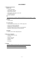
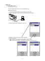
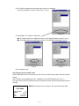
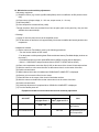
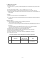
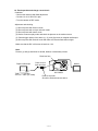
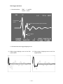
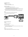
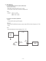
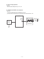
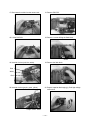
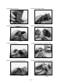
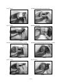
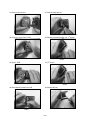
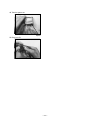
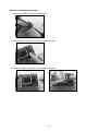
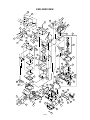
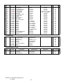
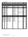
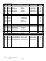
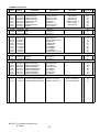
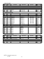
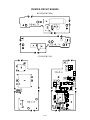
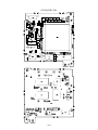
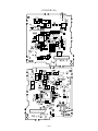
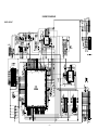
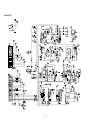
(without price)
QV-5500SX
(KX-712)
MAR. 1999
INDEX
R
Ver.1
Dec / 1999
CONTENTS
SPECIFICATIONS ....................................................................................................................................... 1
BLOCK DIAGRAM ...................................................................................................................................... 3
ADJUSTMENT ............................................................................................................................................ 4
1. Whole unit .......................................................................................................................................... 5
1-1. Loading ADJ program ................................................................................................................. 5
1-2. White balance and Sensitivity adjustment ................................................................................ 7
1-3. White scratch correction ............................................................................................................. 8
1-4. Flash operation and charge current check ............................................................................... 9
1-5. VCOM DC adjustment ................................................................................................................ 11
1-6. Current consumption check ..................................................................................................... 11
2. D-PCB Assy ...................................................................................................................................... 12
2-1. Operation check ......................................................................................................................... 12
3. L,BL PCBs Assy ............................................................................................................................... 13
3-1. VCC2 adjustment and VCC13, VCC7, VEE2 checks ............................................................... 13
3-2. VCC free run frequency adjustment ........................................................................................ 13
3-3. BL drive voltage adjustment ..................................................................................................... 14
3-4. VCOM AC and VCOM DC coarse adjustment .......................................................................... 14
3-5. Brightness voltage setting and contrast adjustment ............................................................. 15
4. L,BL PCBs Assy ............................................................................................................................... 16
4-1. VCC18, VCC15, VEE7 adjustments ........................................................................................... 16
DISASSEMBLY ......................................................................................................................................... 17
EXPLODED VIEW ..................................................................................................................................... 25
PARTS LIST .............................................................................................................................................. 26
PRINTED CIRCUIT BOARDS ................................................................................................................... 32
SCHEMATIC DIAGRAMS ......................................................................................................................... 37
TROUBLESHOOTING .............................................................................................................................. 44
APPENDIX ................................................................................................................................................. 45
1. The distinction method of a model ................................................................................................. 45
SPECIFICATIONS
File Format
Static, Panorama: JPEG standard; Movie: AVI/JPEG (for recording to CompactFlash card)
Recording Medium
CompactFlash card
Standard Memory Capacity/
Static
S (1280 x 960) / 14 (500KB/image)
Number of Image Files/
F (1280 x 960) / 19 (352KB/image)
Computer Output Image Size
N (1280 x 960) / 33 (200KB/image)
E (640 x 480) / 55 (112KB/image)
Movie: File Format AVI
3.2seconds (320x240) / 8sets (896KB / image)
6.4seconds (320x240) / 4sets (1792KB / image)
9.6seconds (320x240) / 3sets (2100KB / image)
3.2seconds (160x120) / 30sets (224KB / image)
6.4seconds (160x120) / 16sets (448KB / image)
9.6seconds (160x120) / 10sets (672KB / image)
Movie: File Format JPEG
3.2seconds (320x240) / 6sets
6.4seconds (320x240) / 3sets
9.6seconds (320x240) / 2sets
3.2seconds (160x120) / 27sets
6.4seconds (160x120) / 13sets
9.6seconds (160x120) / 9sets
*When using 8MB CF card.
Image Deletion
Single image; all images in a folder; all images in memory (with image protection)
Imaging Element
1/3-inch CCD (Total Pixels: 1.31 million, Effective Pixels; 1.25 million)
Lens
f/2.8; f = 5.47mm (equivalent to 36mm lens for 35mm film)
Zoom
Digital 2x, 4x
Focusing
External Phase Difference Auto Focus; manual focus with macro mode and focus lock
Focus Range
0.3m to ∞ for Normal focus; 10cm for macro (approximately 10cm to ∞ with manual focus),
from surface of protective lens filter
Exposure Control
Light Metering: Multi-pattern, center point, spot by CCD
Exposure: Program AE
Exposure Compensation: –2EV to +2EV (1/2EV units)
Shutter
CCD electronic shutter; mechanical shutter, 1/8 to 1/500 second (1 second in Night Scene Mode)
Aperture
f/2.8, 4, 5.6, 8, 11, 16 auto
White Balance
Automatic, fixed (4 modes), manual switching
Self-timer
10 seconds, 2 seconds
Built-in Flash
Flash Modes: AUTO, ON, OFF, Red eye reduction
Flash Range: Approximately 0.7 to 2 meters
Recording Functions
Continuous, quick shutter, AEB, multiple exposure, night scene, single-image, self-timer, movie,
panorama, macro
Monitor
1.8" TFT, low-glare color HAST LCD (122,100 pixels, 555 x 220)
Viewfinder
Monitor or optical viewfinder
Clock
Built-in quartz digital timepiece for time and date recording and storage with image data; auto
calendar up to 2049
Input/Output Terminals
DIGITAL IN/OUT, AC adaptor connector, VIDEO OUT (NTSC, PAL)
—1—
Power Supply
Four AA-size alkaline or lithium batteries
Four AA-size nickel-hydrogen rechargeable batteries (NP-H3)
AC adaptor (AD-C620)
Battery Life
The values noted below indicate the number of hours before battery failure under normal
operating temperature (25°C). These values are for reference only, and do not guarantee that
any particular set of batteries actually will provide the service life indicated. Low temperatures
shorten battery life.
Type of
Operation
AA-size Alkaline
Batteries LR6
AA-size Lithium
Batteries FR6
Continuous
Playback
Approximately 110
minutes
Approximately 210
minutes
Continuous
Approximately 300
Approximately 840
Recording
shots
shots
•The above guidelines are based on the following battery types:
Alkaline:
MX1500 (AA) DURACELL ULTRA
Lithium:
Energizer
•Battery life varies with brand
Continuous recording values show the number of shots without using the flash. The number of
shots depends on use of the flash and whether flash is turned on or off.
Power Consumption
Approximately 7.3W
Dimensions
131(W) x 69(H) x 43(D) mm
Weight
Approximately 250g (excluding batteries)
Standard Accessories
8MB COMPACTFLASH memory card; strap; soft case; lens cap; video cable; data transfer
cable; PC Link CD-ROM; four LR6 alkaline batteries; Owner’s manual
* The camera also has a lithium battery that powers its built-in clock. When the power of this battery becomes weak, take the
camera to your CASIO Service Provider to have it replaced.
* The liquid crystal panel built into this camera is the product of precision engineering, with an effective pixel rate of 99.99%. This
also means, however that 0.01% of the pixels can be expected to fail to light or to remain lit at all times.
* U.S.A model can see a VIDEO OUT picture at the time of REC MODE.
( Other models cannot be carried out.)
—2—
BLOCK DIAGRAM
26pin
Voltage regulator
L-PCB
ST-UNIT
10pin
Photo
sensor
Comparator
Battery voltage
TFT controller
BL-PCB
5.0V
VCC2
10pin
-14.5V
VEE2
3.0V
VDD
6.0V
VIDEO/RGB
SW
10pin
Serial
buffer
B,G
R/VIDEO
CFCOVER
VCC5-1
CSYNC
RIGHT
HD49323AF
CDS/AGC/ADC
DB0
~
V3
V1
DB9
CH3A RSTCCD
CH1A SHP
V4
SHD
V2
CLAMP
CH3B SDI
SUB
SCK
CH1B LOAD
OFDC
H1
RESET H2
ADCK RLED
GLED
H-BAFFER
TK16140
Lens
unit
DRIVER
CPU
COMMAND /FLB
STATUS /LSRT
/SCK
/FLB
/SHATTER
Voltage
detector
20pin
KEY
MODE
DISP
MENU
S/N/F/E
S-TIMER
FLASH
Flash/Mask memory
16Mbit
RTCBATPACT
PLED KOUT0
DGND3KOUT1
VCC3-1
KIN0
KIN1
KIN2
KIN3
Extender I/O
PW0~3
ADPTN
GND5
VCC5-1
SLED
DGND3
VCC3-1
60pin
KEY
POWER
LED
SHUTTER
(+)
(-)
EVCC3
AGND3
VCC3-2
GND
VCC1-3
VCC1-L
20pin
14pin
(C to FPC)
(B to B)
JK-PCB
20pin
10pin
JK-IN
GND
VCC1-ST
VCC5-1
GND
VCC3-3
GND3
DGND
VCC
Back-up capacitor
MSM82C55A
PW-PCB
AGND
5V
PGND
V.PM
VSW
K-PCB
(B to B)
CF
DCAM-101F
15pin
(C FPC C)
LGND
VIDEO
VGND
20pin
VCC1-L
PLAY/REC
LGND
BLCONT BLACTB
PWCONT VCC3-1
SDIPO
DGND3
SDOPO
JKSW
RTC
RS5C348
(C FPC B)
EEPROM
16pin
LCD
ON/OF
F
(B to B)
SOP
SIP
DGND5
DRAM X2
128Mbit(50ns)
SUB
Backlight
Controller
BLGND
BLACTB
Driver
BL-VCC
D-PCB
DRIVER
(B to B)
BLCNT
BL-VCC
VIDEO75Ω
AF-PCB
CL-UNIT
—3—
V-Dr
LR36685
CM7018
RGB interface
1.8"TFT
LCD module
C0D18T1022
51pin
2-color LED
LZ23J3V
CCD
IR3Y26A1
VCC7
GND
VCC1-ST
C-PCB
VCC5-1
Booster
Xe
LAMP
SGND
VA
PREN
LTTRGN/SHUTTER
FBN
12.75V
VCC13
7.5V
(C to F)
VGH RESET OE
VREFH MODE2 CLR
VGL
CS
HCNT BOUT
VREFL VCOM MCLK VDD
GRES VBC MODE1 VSH
GPCK SRTR VSS
GSRT SRTL GOUT
VCC18
VCC5-4
VCC15
GND4
3.3V
VCC3-1
VCC3-2
VCC3-3
3.3V
22V
15V
EVCC3
VCC18
VCC15
-8V
VEE7
Voltage regulator
5.0V
VCC5-1
VCC5-2
VCC5-3
VCC5-4
Timer
LED
Batteries
DC
JACK
VIDEO
JACK
Serial
port
Ajack
ADJUSTMENT
1. Adjustments to be done
(1) Whole unit
1. Loading ADJ program
2. White balance, Sensitivity
3. White scratch correction
4. Flash operation and charge current check
5. VCOM-DC adjustment
6. Current consumption
Note:
When the lens ass'y is replaced, adjustment should be done in order of above 1, 2, and 3.
(2) D-PCB
1. Function check
(3) L and BL PCBs
1. VCC2 adjustment and VCC13, VCC7, VEE2 voltage check
2. VCO free run frequency adjustment
3. Backlight drive voltage adjustment
4. VCOM AC adjustment and VCOM DC coarse adjustment
5. Brightness voltage setting and contrast adjustment
(4) PW-PCB
1. VCC18, VCC15, VEE7 voltage adjustment
2. Necessary equipment
1. PC (OS : Windows 95 or 98)
2. Link cable
3. Digital oscilloscope
4. Voltage regulator
5. Ammeter
6. AC adaptor
3. Caution
Use an AC adaptor for camera's power source unless otherwise specified.
Do not tell outsider about the camera's test program mode.
Do not execute other programs than specified in this manual.
—4—
1. Whole unit
1-1. Loading ADJ program
Camera mode: PLAY mode
Necessary program: adj712f.exe,712_0212.adj and adj712k.exe
Adjustments and Checks
(1) Insert CompactFlash card and turn the camera on for PLAY mode.
(2) Connect the camera‘s 3-pin jack and PC’s RS232C port with a link cable.
PC
QV-5500SX
RS232C port
Link cable
(3) Execute adj712f.exe on Windows 95 or 98. (Fig. 1)
(Fig. 1)
(4) Open "712_0212.adj" file using File/Open command.
(5) Click [Trans] button.
● If the loading is done properly, screen indicates “send ok”. (Fig. 2)
●If the loading was erroneous, “11RcvERR00” will be shown on the screen. (Fig. 3)
(Fig. 2)
—5—
(Fig. 3)
(6) The first ADJ program has been done when “send ok” is displayed.
Close the program then execute “adj712k.exe”. (Fig. 4)
(Fig. 4)
(7) Click [Rgain*=1.07, Bgain*=1.09] button.
● If the program has been completed correctly, screen shows “Replace complete”. (Fig. 5)
● If the program has been erroneously executed, “11RcvERR00” will be shown. (Fig. 6)
(Fig. 5)
(Fig. 6)
(8) The program ends.
ADJ program version number check
Insert CompactFlash in the camera and turn the camera on while pressing down Flash and shutter
buttons.
Check for ADJ version(displayed as; ADJ 99000212) on the TEST MODE screen. (Fig. 7)
Turn the camera off then on again and make sure that the camera records and play backs pictures
normally.
NOTE:The left figure is for a reference. The actual screen may differ.
TEST MODE
WHITE NOISE DATA
NO
LOADER
10
ADj.
99000212
PROG
99.02.13.20.28
GMENU
99.02.05.14.47
(Fig. 7)
—6—
1-2. White balance and sensitivity adjustments
1. Necessary equipment
(1) Simplified viewer (e.g. Kenko Light Box handy5000) which is modified to be DC powered externally.
(2) Power source (Output voltage; 0 ~ 10V over, output current; 0 ~ 1A over)
(3) ND filter (ND20)
(4) Color temperature conversion filter (LA50)
*Though the above filters are provided from Casio as parts (refer to the parts list), they are also
available from camera shops.
2. Settings
(1) Apply 6V from the power source to the simplified viewer.
(2) Turn the viewer on and leave it for approximately 30 minutes to stabilize the intensity and the color
temperature.
3. Adjustment method
(1) Set the camera on Test Mode 2 menu by the following procedures.
• Turn the function switch on REC mode.
• Turn the power on while pressing down Flash and shutter buttons (Test Mode display is shown on
the screen.)
• Press Macro button twice then push MENU button (MENU 2 screen will be displayed.)
• Select 1. CCD ADJUST and press shutter button (SHUT TO START will be shown.)
(2) Place color temperature conversion filter (LA50) on the center of the viewer’s illumination surface.
(3) Stick the camera to color conversion filter so that camera lens is on the center of the filter.
(4) Push the shutter button.
(5) White balance initial value is loaded when “RGB ADJUST COMPLETE” is displayed.
(6) Remove color conversion filter from the viewer.
(7) Place ND filter on the center of the viewer’s illumination surface.
(8) Stick the camera to the ND filter so that camera lens is on the center of the filter.
(9) Push the shutter button.
(10) Sensitivity adjustment is completed when “SENS ADJ COMPLETE” is displayed.
(11) Turn the camera power off.
Equipment needed to execute white balance and sensitivity adjustment
Light source (viewer)
ADJ SOFT
Color temperature
(K) light source 1
No. 1
CCD ADJUST
4400 ± 200
No. 2
CCD SENS ADJUST
Light intensisty
(cd/m2) light source 2
Note
No specified figure for
light intensity
500 ± 80
—7—
No specified figure for
color temperature
1-3. White scratch correction
1. Necessary equipment
(1) Simplified viewer (e.g. Kenko Light Box handy5000) which is modified to be DC powered externally.
(2) Power source (Output voltage; 0 ~ 10V over, output current; 0 ~ 1A over)
(3) Use two ND filter together, one ND10 and one ND20, placing one on the top of the other.
*Though the ND filter is provided from Casio as parts (refer to the parts list), it is also available from
camera shops.
2. Settings
(1) Apply 6V from the power source to the simplified viewer.
(2) Turn the viewer on and leave it for approximately 30 minutes to stabilize the intensity and the color
temperature.
3. Adjustment method
(1) Set the camera on Test Mode 2 menu by the following procedures.
• Turn the function switch on REC mode.
• Turn the power on while pressing down Flash and shutter buttons (Test Mode display is shown on
the screen.)
• Press Macro button twice then push MENU button (MENU 2 screen will be displayed.)
• Select 10. WHITE NOISE DETECT. (do not push the shutter button.)
(2) Place ND filter on the center of the viewer’s illumination surface.
(3) Stick the camera to the ND filter so that camera lens is on the center of the filter.
(4) Push the shutter button and wait for a moment.
(5) Sensitivity adjustment is completed when “SENS ADJ COMPLETE” is displayed.
(6) Turn the camera power off.
Equipment needed to execute white balance and sensitivity adjustment
Light source (viewer)
No. 3
ADJ SOFT
Light intensisty
(cd/m2) light source 2
WHITE NOISE ADJUST
50 ± 5
—8—
Note
No specified figure for
color temperature
1-4. Flash operation and charge current check
Conditions
• Perform the checking after flash adjustment.
• Provide 6.0 ±0.1V from DC in jack.
• Turn the camera on REC mode.
Adjustment and checking
(1) Shoot a picture with flash on mode.
(2) Shoot a picture with red-eye reduction mode.
(3) Shoot a picture with macro mode.
(4) Set the camera on play mode and check the pictures on the monitor screen.
(5) Record trigger pulses of the above (1), (2), and (3) pictures on a digital oscilloscope.
(6) Shoot a picture with flash off mode and make sure that the flash does not light.
Make sure that the DC in 6Vcurrent is less than 1.3A.
Note:
Pictures (1) and (2) should not be whitish, darkish, or abnormally colored.
Flash lens face
Digital oscilloscope
TIME : 1.0 sec/DIV
VOLTS: 1 V/DIV (AC mode)
Probe close to
flash lens face
Monitor
QV-5500SX
Earth of hte probe
Should be hooked as shown above.
—9—
Flash trigger waveform
1. Normal waveform
CH1
TIME : 1 µ sec/DIV
VOLTS : 1 V/DIV
1V
1µV
757µV
UERT
First positive
pulse.
OK if second positive pulse is shown.
First negative
pulse.
ACQUIRE
NORMAL
2
AVS
1
ENVELOPE
REPET SAVE ON
ON | OFF ON | OFF
2. NG waveforms when trigger skipping occurs.
(1) When trigger skipping occurs on the first
positive pulse.
(2) When trigger skipping occurs on the first
negative pulse.
— 10 —
1-5. VCOM DC adjustment
Conditions
1. Test mode 50 % raster image
2. Provide 6.0 ± 0.05V voltage from DC in jack.
Adjustment and checking
(1) Execute 50 PERCENT GRAY on the test mode.
• While pushing down Flash and shutter button, turn the camera on.
• Push the Flash button twice then press MENU button (MENU 1 display will be shown.)
• Select 50 PERCENT GRAY then press the shutter button.
(2) Monitor the photo sensor amplifier output via a low-pass filter of cutoff frequency 60Hz.
Monitoring the oscilloscope screen, adjust VR320 to minimize 60Hz ripple waveform.
Notes:
Perform the adjustment after you replaced the display module.
Use only specified jig for replacing the flash lamp.
Photo diode
S1153
L.P.F
Photo sensor Amp
C2719
Oscilloscope
QV-5500SX
LCD
Minimize the
ripple components
1-6. Current consumption check
Condition
Set the camera on play mode.
Adjustment and checking
(1) Current consumption (DC in = 6.0 ± 0.1V)
(2) Reducing the voltage from 6V, make sure that the battery capacity indicator is changed.
DC in = 4.65 ± 0.05V (Play mode)
Notes:
Maximum current in play mode; 500mA
Reference: maximum current in rec mode; 800mA (flash is not charging)
— 11 —
2. D-PCBAssy
2-1. Operation check
Condition
Set the camera on play mode.
Adjustment and checking
1. Clock pulse frequency
Check if CP400 is 32.768 ± 0.002kHz
2. Procedures
(1) Connect a PC and the camera with a link cable.
(PC; COM port, Camera; 3-pin jack)
(2) Store GP2JPEG test file (8 files) in a CompactFlash card.
Ref.bay / Ref.cb / Ref.cr / Ref.jpg / Ref.y / Refdec.cb / Refdec.cr / Refdec.y
(3) Insert the Compact flash in the camera.
(4) Turn the camera on ( in Play mode).
(5) Double click Dt712.exe.
(6) DOS prompt opens and checking starts automatically.
(7) In the key check mode, push all the keys.
(8) Press space bar of the PC for LED and LCD control check.
(9) When the camera functions correctly, the camera turns itself off then on again after 5 seconds.
NOTE : If you wish to escape D PCB test, press PC's ESC button.
3. DT program
Program to be used; dt712
Check the followings;
(1) Serial data communication
(2) ROM version number
(3) Graphic menu version number
(4) DRAM
(5) CompactFlash memory
(6) Voltage detection (displayed as HIGH)
(vcc1-3 voltage… high; 6.0 ± 0.1V, middle; 4.35 ± 0.05V, low; 3.85 ± 0.05V)
(7) Each operation mode
1) REC/PLAY modes
2) VIDEO jack
3) AC adaptor
(8) EEPROM test
(9) CP2 JPEG test
(10) Button operations
(11) LED1,2,3 on/off
(12) TFT-LCD on/off
(13) Time setting, time function
(14) Timer test
(15) Turn the camera off
4. Make sure that RGB and VIDEO signals are provided.
Check VIDEO output in NTSC and PAL systems.
— 12 —
3. L, BL PCBs Assy
3-1. VCC2 adjustment and VCC13, VCC7, VEE2 checks
Adjustment and checking
Adjust VR151 so that VCC2 (CP172) is 5.0 ± 0.02V.
Turn the power off and make sure that all the voltages are 0V.
Notes :
<Voltages>
VCC7 = 7.0 ~ 8.0V
VCC13 = 11.8 ~ 13.7V
VEE2 = -13.2 ~ -15.4V
3-2. VCC free run frequency adjustment
Condition
1. Connect CP763 (SYF) and CP700 (GND).
Adjustment
Monitoring CP734 (HDB) with frequency counter, adjust VR755 so that the frequency is 15.734 ±
0.1kHz.
Note :
Perform the adjustment in room temperature of 20 ± 10˚C.
L-PCB
Power
Supply
SYF
(CP763)
AGND
(CP700)
— 13 —
HDB
(CP734)
Frequency
counter
3-3. BL drive voltage adjustment
Checking
Make sure that CP900 (BL-VCC) is 5.4 ± 0.2V.
3-4. VCOM AC and VCOM DC coarse adjustment
Adjustment
(1) Check if VCOM output (CP716) amplitude is 6.6± 0.3V.
(2) Adjust VR320 so that High level of VCOM output (CP716) becomes 4.8 ± 0.2V.
High level
4.8 [V]
0 [V]
–1.8 [V]
VCOM
(PC716)
Power
Supply
Oscilloscope
— 14 —
amplitude
6.6 [V]
L-PCB
3-5. Brightness voltage setting and contrast adjustment
Condition
Nature of signal : 10 step (NTSC)
Adjustment
(1) Execute GRAY SCALE (10STEP) on the test mode.
• While pushing down Flash and shutter button, turn the camera on.
• Push the Flash button twice then press MENU button (MENU 1 display will be shown.)
• Select GRAY SCALE (10STEP) then press the shutter button.
(2) Triggering with FRP (CP380) signal, adjust BOUT signal as described below.
(3) Adjust RGB-AMP (VR340) so that pedestal – pedestal voltage becomes 3.5 ± 0.05V.
(4) Adjust contrast VR (VR344) so that contrast terminal (CP376) voltage is 3.0 ± 0.05V temporarily.
(5) Adjust Bright VR (VR381) so that pedestal – 3rd step is 2.20 ± 0.05V.
(6) Adjust Contrast VR (VR344) so that pedestal – 10th step is 2.85 ± 0.05V.
Note :
Make sure that the waveform is not distorted.
L-PCB
Power
Supply
Signal
generator
R, G, B,
CSYNC signal
(1.0 Vp-p)
(CP301)
(CP302)
(CP303)
(CP309)
BOUT
terminal
(CP375)
Digital oscilloscope
Figure 3-1, 3-2
3.5 ± 0.05V
(pedestal-pedestal)
2.85V ± 0.05V
(pedestal-10 step)
3-1
3-2
— 15 —
4. PW PCB Assy
4-1. VCC18, VCC15, VEE7 adjustments
Adjustment
Apply 5.0 ± 0.05V on VCC1-1 and adjust VR120 so that VCC18 (CP121) is 22.0 ± 0.5V.
Adjust VR125 so that VCC15 (CP125) is 15.5 ± 0.2V.
Adjust VR130 so that VEE7 (CP133) is –8.0 ± 0.2V.
Note
Perform VCC15 adjustment after VCC18 adjustment is done.
— 16 —
DISASSEMBLY
1. Take CompactFlash card from the camera.
5. Open the battery cover and unhook the case.
Hook
2. Remove the batteries.
6. Unhook the case using a screw driver.
Hook
3. Remove 2 screws from side body of the camera.
7. Remove the upper case.
Screws
4. Remove 1 screw from the bottom of the camera.
8. Remove the top case.
Screw
— 17 —
9. Open the battery cover and remove 1 screw.
Screw
10. Unhook the battery holder.
13. Remove 3 screws on the key PCB.
Screw
14. Disconnect the flat cable and remove key PCB.
Flat cable
Hook
11. Remove the frame block.
15. Peel off the insulation sheet from the bottom.
Insulation sheet
12. Peel off the insulation sheet on the key PCB.
16. Remove a screw with washer affixing PW PCB.
Screw
Insulation sheet
— 18 —
17. Disconnect the cable from the camera unit.
21. Remove PW PCB.
Cable
18. Lift the PW PCB.
22. Remove 1 screw affixing the flash block.
Screw
19. Unsolder 3 wires (red, blue, white).
23. Remove the flash block.
Blue
White
Red
20. Unsolder 3 wires (purple, green, yellow).
24. Prepare capacitor discharging jig. Peel high voltage
caution seal.
Purple Green Yellow
— 19 —
25. Discharge the capacitor.
Minus terminal
29. Unhook the battery holder.
Plus terminal
26. Remove 2 screws affixing Flash PCB.
Hook
30. Remove the battery holder.
Screws
27. Remove the flash unit.
31. Remove a wire (black) from battery holder.
28. Remove 1 screw affixing battery holder.
32. Remove 3 screws affixing JK PCB. (1 screw)
st
Screw
Screw
— 20 —
nd
33. (2 screw)
37. Disconnect the cable from camera unit.
Screw
rd
34. (3 screw)
38. Remove D PCB.
Screw
st
35. Remove 2 screws from D PCB. (1 screw)
st
39. Remove 2 screws affixing camera unit. (1 screw)
Screw
Screw
nd
36. (2 screw)
nd
40. (2 screw)
Screw
Screw
— 21 —
41. Remove camera unit.
45. Peel the cloth tape off.
Cloth tape
42. Remove 1 screw from L PCB.
st
46. Remove 2 screws from BL unit. (1 screw)
Screw
Screw
nd
47. (2 screw)
43. Open L PCB.
Screw
44. Disconnect the cable from LCD.
48. Remove BL unit.
Cable
— 22 —
49. Take the spacer out.
Spacer
50. Remove LCD.
— 23 —
Cautions in assembly procedures
1. Solder battery holder wire after it is assembled.
2. Use cloth tape so that cases do not catch the LCD flat cable.
3. Position PLAY/REC switch knob so that it catches the switch.
— 24 —
EXPLODED VIEW
64
52
57
61
71
43
2
3
57
23
64
65
57
65
72
64
47
65
21
6
71
57
20
65
4
45
62
42
41
72
45
36
65
75
37
60
24
28
1
31
74
59
65
54
18
33
32
12
53
29
66
22
19
68
46
65
53
38
69
13
25
64
51
67
70
48
44
49
63
7
5
8
34
16
67
9
39
35
58
15
50
30
73
40
14
26
55
10
27
— 25 —
11
17
56
PARTS PRICE LIST
MAIN BODY COMPONENT
N
Item
Code No.
N
1
2
3
4
5
6
7
8
9
10
11
12
13
14
15
16
17
18
19
20
21
22
23
24
24
25
26
27
28
29
30
31
32
33
34
35
36
37
38
39
40
41
42
43
44
45
46
47
48
49
50
6613 8983
6613 1560
6613 1540
6613 1460
6613 8969
6613 9250
6613 1220
6613 9130
6613 4990
6613 9150
6613 9160
6613 2241
6613 9170
6613 1370
6613 9190
6613 1380
6613 9120
6613 0940
6613 8982
6613 8987
6613 8974
6613 8978
6613 8985
6613 8975
1000 5576
6613 1340
6613 9180
6613 8990
6613 1100
2725 1347
6612 8590
6613 1130
6613 1110
6613 1120
6613 1390
6613 1400
6613 2791
3851 2113
6613 9140
6613 9090
6613 0891
6613 9060
6613 1480
6613 1470
6613 1210
6613 3070
6613 9042
6613 8964
6613 9110
6613 9100
6613 0900
N
N
N
N
N
N
N
N
N
N
N
N
N
N
N
N
N
N
N
N
N
N
N
N
N
N
Parts Name
BL ASSY
SPRING/BATTERY
SPRING/BATTERY
SPRING/BATTERY
BATTERY COVER ASSY
HOLDER/BATTERY
LABEL/BATTERY
COVER/CF
LABEL/CF
COVER/DP
COVER/FD
COVER/FD
CASE/FD
PROTECTOR/FINDER
BUTTON/LCD
COVER/LED
COVER/LED
COVER/LED
PCB ASSY/BACK LIGHT
PCB ASSY/JACK
PCB ASSY/KEY
PCB ASSY/LINEAR
PCB ASSY/POWER
PCB ASSY/DIGITAL
PCB ASSY/DIGITAL
SPRING/POWER
KNOB/POWER
KNOB/REC
COVER/STROBE
LCD
TAPE/DOUBLE SIDE
TAPE/DOUBLE SIDE
TAPE/DOUBLE SIDE
TAPE/DOUBLE SIDE
TAPE/DOUBLE SIDE
TAPE/DOUBLE SIDE
TAPE/DOUBLE SIDE
FLUORESCENT LAMP
CASE/UPPER
BUTTON
BUTTON
GRIP
CABLE
CABLE
SCREW/STAND
PLATE/SEALED
CASE/LOWER
CASE/LOWER
SPRING/SHUTTER
BUTTON/SHUTTER
SHAFT
Specification
K341502*1
K441294-1
K441295-1
K441296-1
K341505*1
K341460-1
K441442-1
K341457-1
K441492-1
K140450-2
K140445-2
K441471A-1
K240857-2
K441299-1
K341038-2
K341054-1
K441628-1
K341036-1
K441672*1
K441673*1
K441674*1
K140565*1
K241136*1
K341510*1
K341510*2
K441298-1
K441655-1
K441631-1
K341064-1
COD18T1022RN
K441252-1
K441314-1
K441445-2
K441445-3
K441445-4
K441445-5
K441501A-1
CAS-1.8JS1.8-1
K241096-1
K241094-1
K341041A-1
K140487-2
K140422-1
K240915-1
K341059-1
K441500-1
K140447B-2
K241133*1
K441649-1
K341455-1
K441310-1
NOTES: Q :Quantity used per unit
R :Rank
- 26 -
Applicable
Common
Common
Common
Common
Common
Common
Common
Common
Common
Common
Common
Common
Common
Common
Common
Common
Common
Common
Common
Common
Common
Common
Common
EXCEPT U.S.A. MODEL
For U.S.A.MODEL
Common
Common
Common
Common
Common
Common
Common
Common
Common
Common
Common
Common
Common
Common
Common
Common
Common
Common
Common
Common
Common
Common
Common
Common
Common
Common
Q Price Code R
1
1
1
1
1
1
1
1
1
1
1
1
1
1
1
1
1
1
1
1
1
1
1
1
1
1
1
1
1
1
1
1
1
2
3
2
1
1
1
1
1
1
1
1
1
2
1
1
1
1
1
DA
AB
AB
AC
AY
AE
AA
AD
AA
AK
AD
AN
AA
AC
AB
AA
AB
AB
DA
CZ
DB
DL
DI
EF
EE
AA
AA
AA
AE
DI
AA
AA
AA
AA
AA
AA
AA
AW
AS
AK
AI
AD
BM
AI
AC
AA
AP
DJ
AA
AG
AA
A
X
X
X
A
X
X
X
X
X
X
X
C
X
C
X
X
X
A
A
A
A
A
A
A
X
C
C
X
A
X
X
X
X
X
X
X
A
C
C
C
X
X
X
X
X
C
C
C
C
X
N
N
N
N
N
N
N
N
N
N
Item
Code No.
51
52
53
54
55
55
56
57
58
59
60
61
62
63
64
65
66
67
68
69
70
71
72
73
74
75
6613 1330
1015 1468
6613 3500
6613 0930
6613 9000
1000 5573
6613 9080
6601 1700
6613 9070
6613 1090
6613 9050
6613 8980
6613 8971
5861 3649
5112 0868
5860 0301
5860 2380
5860 3381
5861 3527
5861 3692
5861 3698
5861 3741
6330 5240
2845 6455
1015 1467
5861 3997
Parts Name
Specification
PIN/STRAP
STROBE UNIT
PLATE/INSULATION
COVER/SENSOR
PLATE/RATING
PLATE/RATING
CASE/TOP
PLATE/INSULATION
CASE/BOTTOM
MAGNET
CASE/LOWER
LENS ASSY
LENS ASSY/PANEL
E RING
SCREW
SCREW
SCREW
SCREW
SCREW
SCREW
SCREW
SCREW
SCREW
COVER/CONNECTOR
EJECTOR/CARD
SCREW
R340181-2
CO-712
K441494-8
K341055-1
K441441-2
K441441-3
K140554-1
K4117-3
K140449-2
K441281-1
K140444-2
K341504*1
K341501*1
1.5 JISB2805
BT3 1.7X5 BK
BT3 1.7X3.5 NI
PS3 1.7X3.5 BK
PS3 1.7X4 BK
BT3 1.7X2.5 BK
PS3 1.7X4 NI
PS1 1.7XZ2.0 NI
M1.7X3(BK)D-4H-5
A44797-5
K441670*1
55370-0011
ST1 2X2 NI
CABLE/VIDEO
CF CARD (8 MB)
CASE/SOFT
CABLE/PC-LINK
CD-ROM
CD-ROM
LR6 alkaline batteries
STRAP
CAP/LENS
VC-K723-FC
HB289008C4QV
SC-712
LC9F-DOS-K740-L
CK754CCD01R
CK712DAA01R
LR6G/2ST
ST-K775
K341528-1
Applicable
Common
Common
Common
Common
EXCEPT U.S.A. MODEL
For U.S.A.MODEL
Common
Common
Common
Common
Common
Common
Common
Common
Common
Common
Common
Common
Common
Common
Common
Common
Common
Common
Common
Common
Q Price Code R
1
1
3
1
1
1
1
8
1
1
1
1
1
1
9
9
1
5
1
2
3
2
3
1
1
1
AE
CN
AA
AB
AA
AA
AK
AA
AL
AF
BT
EK
CM
AA
AA
AA
AA
AA
AA
AA
AA
AA
AA
AF
AY
AA
C
A
X
X
X
X
C
X
C
X
C
A
C
X
X
X
X
X
X
X
X
X
X
X
X
X
1
1
1
1
1
1
2
1
1
AR
DH
AW
BX
AM
AL
AG
AF
AC
X
X
X
X
X
X
X
X
X
ACCESSORY
1014 8773
1015 1424
1015 1470
1015 1471
1015 1472
1015 1473
3816 0259
5861 3578
6613 9500
N
N
N
N
N
N
ADJUSTMENT FILTER
N
Item
Code No.
Parts Name
1904 5436 FILTER/ND
1904 5437 FILTER/ND
1904 5440 FILTER/COLOR
Specification
ND10 (50X50)
ND20 (50X50)
LA50 (50X50)
NOTES: Q :Quantity used per unit
R :Rank
- 27 -
Applicable
Q Price Code R
1
1
1
DP
DP
DP
A
A
A
DIGITAL PCB ASS'Y
N
N
N
N
N
N
N
N
N
N
N
Item
Code No.
Parts Name
CONNECTOR
CN578 3502 2441 CONNECTOR
DIODE
D600 2390 1183 DIODE/CHIP
OSCILLATORS
H400 2590 2776 OSCILLATOR
H452 2590 2745 OSCILLATOR
H454 2590 2744 OSCILLATOR
ICS
IC400 2105 6647 IC
IC402 2105 5215 IC
IC404 2105 6650 IC
IC410 2105 6644 IC
IC412 2105 6645 IC
IC414 2105 6629 IC
IC416 2105 6472 IC
IC420 2105 6643 IC
IC427 2105 6649 IC
IC428 2105 6648 IC
IC458 2105 6470 IC
IC460 2105 6646 IC
IC465 2105 6495 IC
IC550 2012 6352 LSI
IC560 2012 6327 LSI
IC561 2012 6327 LSI
FET
Q444 2795 8150 FET/CHIP
TRANSISTORS
Q400 2250 1162 TRANSISTOR/CHIP
Q401 2259 2715 TRANSISTOR/DIGITAL
Q402 7101 5791 TRANSISTOR/CHIP
Q403 2259 2745 TRANSISTOR/DIGITAL
Q404 7101 5791 TRANSISTOR/CHIP
Q440 2259 2745 TRANSISTOR/DIGITAL
Q441 2259 2745 TRANSISTOR/DIGITAL
Q442 2259 2745 TRANSISTOR/DIGITAL
Q443 2259 2745 TRANSISTOR/DIGITAL
Q660 2259 2715 TRANSISTOR/DIGITAL
Q661 2251 0930 TRANSISTOR/CHIP
Specification
Applicable
54154-0209
MA142WK-(TX)
2
AD
X
1
AA
X
1
1
1
AL
AP
AP
C
C
C
(S-80835ANNP-EDZ-T2) 1
1
(TC7S32FU(TE85L))
1
1
(TC7S00FU(TE85L)
1
1
1
1
(S-80842-ANNP-ED6-T2) 1
(S-80837ANNP-ED1-T2) 1
1
(S-80830ANNP-EDT-T2) 1
1
1
1
1
AB
AE
AB
AM
AB
AC
AF
BI
AB
AB
AL
AB
AD
CE
CV
CV
C
C
C
C
C
C
C
C
C
C
C
C
C
C
C
C
1
AA
B
1
1
1
1
1
1
1
1
1
1
1
AA
AA
AA
AA
AA
AA
AA
AA
AA
AA
AB
B
B
B
B
B
B
B
B
B
B
B
(DAN202U-T106)
SSPT6-32KHZ
CX-51F-27.0M
CX-51F-20.0M
R3111Q351A
TC7W74FU(TE12L)
S-75V32ANC-5V4-T2
RS5C348A-E2
S-75V00ANC-5V1-T2
TC7W04FU(TE12L)
TC74AC00FT(EL)
MSM82C55A-2LB
R3111Q421A
R3111Q371A
LM4041CIM3X-1.2
R3111Q301A
TC7SL08FU(TE85L)
LH28F160S3B-025
KM416V4104BC-L6
KM416V4104BC-L6
2SK2035(TE85L)
2SA1576A-T106R
DTC144EE-TL
DTA144EE-TL
DTC143EE-TL
DTA144EE-TL
DTC143EE-TL
DTC143EE-TL
DTC143EE-TL
DTC143EE-TL
DTC144EE-TL
2SB1073-R(TX)
NOTES: Q :Quantity used per unit
R :Rank
- 28 -
Q Price Code R
(2SB1218A-R(TX))
(2SB1386-T100R)
LINEAR PCB ASS'Y
N
Item
D160
D161
D162
D163
D190
D300
D310
D757
D778
FU900
IC150
IC180
IC300
IC302
IC310
IC315
IC340
IC390
IC730
IC900
Q310
Q152
Q155
Q300
Q301
Q900
Q905
SW300
SW310
N
T155
N
N
N
N
N
N
VR151
VR320
VR340
VR344
VR381
VR755
Code No.
Parts Name
DIODES
2390 1820 DIODE/CHIP
2390 1820 DIODE/CHIP
2390 1379 DIODE/SCHOTTKY
2390 1820 DIODE/CHIP
2390 1379 DIODE/SCHOTTKY
2390 1379 DIODE/SCHOTTKY
2390 1379 DIODE/SCHOTTKY
2390 1358 DIODE/VARICAP
2390 1820 DIODE/CHIP
FUSE
2797 5589 FUSE
ICS
2114 5800 IC
2105 4501 IC
2254 0550 IC
2254 0550 IC
2105 6490 IC
2105 5712 IC
2114 5846 IC
2114 5805 IC
2012 5983 LSI
2114 5858 IC
FET
2254 0448 FET/CHIP
TRANSISTORS
2259 2715 TRANSISTOR/DIGITAL
2253 0308 TRANSISTOR/CHIP
2259 2715 TRANSISTOR/DIGITAL
2259 2715 TRANSISTOR/DIGITAL
2253 0308 TRANSISTOR/CHIP
2259 2715 TRANSISTOR/DIGITAL
SWITCHS
3412 1106 SWITCH/SLIDE
2254 0555 SWITCH
CONVERTER
3065 0736 CONVERTER/DC-DC
VARIABLE RESISTOR
2775 3467 RESISTOR/SEMIFIXED/CHIP
2775 3466 RESISTOR/SEMIFIXED/CHIP
2775 3465 RESISTOR/SEMIFIXED/CHIP
2775 3465 RESISTOR/SEMIFIXED/CHIP
2775 3464 RESISTOR/SEMIFIXED/CHIP
2775 3464 RESISTOR/SEMIFIXED/CHIP
Specification
1SS355-TE-17
1SS355-TE-17
MA729-(TX)
1SS355-TE-17
MA729-(TX)
MA729-(TX)
MA729-(TX)
MA329-(TX)
1SS355-TE-17
Applicable
1
1
1
1
1
1
1
1
1
AA
AA
AB
AA
AB
AB
AB
AC
AA
X
X
X
X
X
X
X
X
X
PI-R429.375
1
AC
B
MB3800PFV-G-BND-EF
RN5RL30AA-TR
TC7W66FU-(TE12L)
TC7W66FU-(TE12L)
TK15405MTL
TC7S04FU(TE85L)
IR3Y26A1
NJM3414AV-TE1
CM7018L3-T4N
S-8327B54MC-ESI-T2
1
1
2
2
1
1
1
1
1
AP
AD
AD
AD
AH
AD
BH
AI
AY
AH
C
C
C
C
C
C
C
C
C
C
2SK1580-T1
1
AC
B
DTC144EE-TL
2SD1119-R(TX)
DTC144EE-TL
DTC144EE-TL
2SD1119-R(TX)
DTC144EE-TL
1
1
1
1
1
1
AA
AC
AA
AA
AC
AA
B
B
B
B
B
B
SSSS212-12-B
ESE22MH4
1
1
AC
AC
C
C
CLQ72-01
1
AH
C
1
1
1
1
1
1
AA
AA
AA
AA
AA
AA
C
C
C
C
C
C
POZ2AN-1-502N-T00
POZ2AN-1-102N-T00
POZ2AN-1-503N-T00
POZ2AN-1-503N-T00
POZ2AN-1-203N-T00
POZ2AN-1-203N-T00
NOTES: Q :Quantity used per unit
R :Rank
- 29 -
(MA111-(TX))
(MA111-(TX))
(RB501V-40TE-17)
(MA111-(TX))
(RB501V-40TE-17)
(RB501V-40TE-17)
(RB501V-40TE-17)
Q Price Code R
(MA111-(TX))
(EVM-1XSX50B53)
(EVM-1XSX50B13)
(EVM-1XSX50B54)
(EVM-1XSX50B54)
(EVM-1XSX50B24)
(EVM-1XSX50B24)
POWER PCB ASS'Y
N
Item
D100
D110
D120
D127
D130
D131
D140
D195
FU102
FU103
FU104
IC110
IC115
IC120
IC125
IC127
IC130
IC135
IC137
IC139
IC140
Q110
Q127
Q140
Q111
Q120
Q121
Q122
Q126
Q130
Q131
Q195
VR120
VR125
VR130
Code No.
Parts Name
DIODES
2390 2506 DIODE/CHIP
2390 1883 DIODE/SCHOTTKY
2390 1883 DIODE/SCHOTTKY
2390 1883 DIODE/SCHOTTKY
2390 1379 DIODE/SCHOTTKY
2390 1820 DIODE/CHIP
2390 1883 DIODE/SCHOTTKY
3013 2611 LED/CHIP
FUSES
2797 5612 FUSE
2797 5616 FUSE
2797 5616 FUSE
ICS
2105 6480 IC
2105 6479 IC
2114 5842 IC
2105 6477 IC
2105 6478 IC
2114 5607 IC
2114 5849 IC
2114 5849 IC
2114 5849 IC
2105 6480 IC
FETS
2114 5807 FET/CHIP
2105 6481 FET/CHIP
2114 5807 FET/CHIP
TRANSISTORS
2259 2745 TRANSISTOR/DIGITAL
2251 0847 TRANSISTOR/CHIP
2259 2715 TRANSISTOR/DIGITAL
2259 2758 TRANSISTOR/CHIP
2259 2715 TRANSISTOR/DIGITAL
2259 2715 TRANSISTOR/DIGITAL
2250 1579 TRANSISTOR/CHIP
2259 2715 TRANSISTOR/DIGITAL
VARIABLE RESISTOR
2775 3465 RESISTOR/SEMIFIXED/CHIP
2775 3465 RESISTOR/SEMIFIXED/CHIP
2775 3464 RESISTOR/SEMIFIXED/CHIP
Specification
RB060L-40TE25
RB160L-40TE-25
RB160L-40TE-25
RB160L-40TE-25
MA729-(TX)
1SS355-TE-17
RB160L-40TE-25
SML-010JTT86
Applicable
Q Price Code R
1
4
4
4
1
1
4
1
AD
AC
AC
AC
AB
AA
AC
AB
C
C
C
C
C
C
C
C
PI-R431001
PI-R43101.5
PI-R43101.5
1
1
1
AC
AC
AC
B
B
B
S-8520B33MC-ARS-T2
RN5RL33AA-TR
S-8327E50MC-EKE-T2
LP2951CMX
RH5RH553B-T1
TK11830MTL
TK11250BMCL
TK11250BMCL
TK11250BMCL
S-8520B33MC-ARS-T2
1
1
1
1
1
1
1
1
1
1
AL
AC
AI
AM
AK
AL
AE
AE
AE
AL
C
C
C
C
C
C
C
C
C
C
SI3441DV-T1
SI3442DV-T1
SI3441DV-T1
1
1
1
AK
AH
AK
B
B
B
DTC143EE-TL
2SB1386-T100R
DTC144EE-TL
2SD2150-T100S
DTC144EE-TL
DTC144EE-TL
2SA1774-TLR
DTC144EE-TL
1
1
1
1
1
1
1
1
AA
AD
AA
AB
AA
AA
AA
AA
B
B
B
B
B
B
B
B
1
1
1
AA
AA
AA
C
C
C
POZ2AN-1-503N-T00
POZ2AN-1-503N-T00
POZ2AN-1-203N-T00
NOTES: Q :Quantity used per unit
R :Rank
- 30 -
(MA738-(TX))
(MA738-(TX))
(MA738-(TX))
(RB501V-40TE-17)
(MA111-(TX))
(MA738-(TX))
(EVM-1XSX50B54)
(EVM-1XSX50B54)
(EVM-1XSX50B24)
JACK PCB ASS'Y
N
Item
Code No.
Parts Name
CONNECTOR
CN101 3502 2445 CONNECTOR
FUSE
FU100 2797 5594 FUSE/CHIP
JACKS
JK100 3501 6755 JACK/POWER
JK101 3501 8197 JACK/MINI
JK102 3502 2439 JACK
Specification
Applicable
Q Price Code R
53309-1090
1
AC
C
PI-R429002
1
AC
B
HEC3600-010120
HSJ1169-019010
HSJ1456-01-220
1
1
1
AD
AF
AC
C
C
C
KEYBOARD PCB ASS'Y
N
Item
C810
N
D800
D801
D802
D803
D804
D805
D806
D807
D808
D810
Q800
SW800
SW802
SW803
SW804
SW805
SW806
SW807
SW808
N SW810
Code No.
Parts Name
CAPACITOR
2845 6455 CAPACITOR
DIODES
2390 1820 DIODE/CHIP
2390 1820 DIODE/CHIP
2390 1820 DIODE/CHIP
2390 1820 DIODE/CHIP
2390 1820 DIODE/CHIP
2390 1820 DIODE/CHIP
2390 1820 DIODE/CHIP
2390 1820 DIODE/CHIP
2390 1820 DIODE/CHIP
2370 1412 LED/CHIP
TRANSISTORS
2259 2715 TRANSISTOR/DIGITAL
SWITCHS
3412 2085 SWITCH
3412 1519 SWITCH
3412 1519 SWITCH
3412 1995 SWITCH
3412 1995 SWITCH
3412 1995 SWITCH
3412 1519 SWITCH
3412 1995 SWITCH
3412 2088 SWITCH
Specification
Applicable
EECSOMD473H
Q Price Code R
1
AF
X
1
1
1
1
1
1
1
1
1
1
AA
AA
AA
AA
AA
AA
AA
AA
AA
AA
C
C
C
C
C
C
C
C
C
C
DTC144EE-TL
1
AA
C
SKQAAA-T
SKQMAH-T3
SKQMAH-T3
SKQRAA-T
SKQRAA-T
SKQRAA-T
SKQMAH-T3
SKQRAA-T
ABC1111P
1
1
1
1
1
1
1
1
1
AC
AC
AC
AB
AB
AB
AC
AB
AB
C
C
C
C
C
C
C
C
C
1SS355-TE-17
1SS355-TE-17
1SS355-TE-17
1SS355-TE-17
1SS355-TE-17
1SS355-TE-17
1SS355-TE-17
1SS355-TE-17
1SS355-TE-17
SML-010MTT86
(MA111-(TX))
(MA111-(TX))
(MA111-(TX))
(MA111-(TX))
(MA111-(TX))
(MA111-(TX))
(MA111-(TX))
(MA111-(TX))
(MA111-(TX))
BACK LIGHT PCB ASS'Y
N
Item
Code No.
Parts Name
TRANSISTOR
2259 2744 TRANSISTOR/DIGITAL
N
2259 2789 TRANSISTOR/ARRAY
SWITCH
SW900 3412 1995 SWITCH
TRANSFORMER
N T920 3012 1611 TRANSFORMER/INVERTER
Q921
Q925
Specification
Applicable
Q Price Code R
DTA143EE-TL
IMX17-T110
1
1
AA
AA
B
B
SKQRAA-T
1
AB
C
BLT1.8K712
1
AT
C
NOTES: Q :Quantity used per unit
R :Rank
- 31 -
PRINTED CIRCUIT BOARDS
BL PCB (PCB-712BL)
C PCB (PCB-712C)
— 32 —
D PCB (PCB-712D)
— 33 —
JK PCB (PCB-712JK)
K PCB (PCB-712K)
— 34 —
L PCB (PCB-712L)
— 35 —
PW PCB (PCB-K777PW)
— 36 —
SCHEMATIC DIAGRAMS
DIGITAL CIRCUIT
— 37 —
POWER CIRCUIT
DIGITAL
ANALOG
— 38 —
LINEAR CIRCUIT
— 39 —
C-PCB CIRCUIT
— 40 —
K-PCB CIRCUIT
— 41 —
BL-PCB CIRCUIT
— 42 —
JK-PCB CIRCUIT
JK-IN
to PCB-PW
GND
Imput : DC 6V
to Battery Box
Battery –
— 43 —
TROUBLESHOOTING
1 : Display failure on Video/LCD display is OK.
• Setting of NTSC/PAL is incorrect.
➠ Charge the video setting that is right for the TV (Refer to user’s manual).
• L board failure of JK board failure.
➠ Replace boards.
2 : Flash does not work.
Unable to adjust (White 100 %).
Unable to set to red eye reduction mode (Flashes only once).
• Strobe unit failure.
➠ Replace strobe unit.
3 : No display when in REC mode. Display failure.
• Connection failure of D board connector (CN540).
➠ Reconnect connector.
4 : Unable to focus.
• Dirty lens.
• Lens assy failure.
➠ Clean lens.
➠ Replace lens assy.
5 : The film counter seems incorrect.
➠ The film counter reduces depending on the available memory. If one picture takes a lot of
memory the film counter may reduce by two. In some cases film counter may not change.
The film counter is only a predicted number considering from the remaining memory.
6 : The picture is blurred.
➠ The recording precision is a lot higher than the VGA camera from while ago.
A little bit of dirtiness or movement of the camera may affect the picture.
Clean the lens and press the shutter button slowly.
When it is a bit dark and slow shutter is in operation using a tripod is recommended.
Also make sure that LED of AF is green, and MACRO/NORMAL setting is accurate.
7 : Through display looks smaller and blurry than the PLAY display.
➠ The display is little rougher than the ones before.
This is because there are more pixels now which will take more time to produce picture, so
in order to display the through pictures without waiting their is a preview display. At the same
time thinning out of picture is in operation which results in disturbing lines.
There is no problem with the recorded through picture.
8 : The LCD display disappears when inserting video cord to the video output terminal in
PLAY mode.
➠ When you inset video cord for external display the display on camera will disappear.
9 : 4 to 5 seconds after watching the picture on LCD video the display changes.
➠ QV-5500SX has preview display to show the pictures early. When looking in PLAY mode
preview display is displayed first than the more precise picture after that.
— 44 —
APPENDIX
1. The distinction method of a model.
• A model is Judged on a rated plate.
For U.S.A MODEL
EXCEPT U.S.A MODEL
— 45 —
Ver.1 : The following items were changed
• SPECIFICATIONS (P.2)
• PARTS LIST (P.26,27,28)
The following items are added
• APPENDIX
1. The distinction method of model (P.45)
CASIO TECHNO CO.,LTD.
Overseas Service Division
Nishi-Shinjuku Kimuraya Bldg. 1F
5-25, Nishi-Shinjuku 7-Chome
Shinjuku-ku, Tokyo 160-0023, Japan