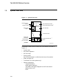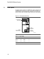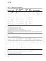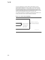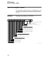
1
VAX 6000 Platform
Technical User’s Guide
Order Number: EK–600EA–TM-001
This manual serves as a reference for field-level repair or programming for
systems based on the VAX 6000 platform. The manual describes the platform
architecture, the XMI system bus, the DWMBB XMI-to-VAXBI adapter, and the
power and cooling systems found in the H9657-CA/CB/CU cabinet.
Digital Equipment Corporation
First Printing, May 1991
The information in this document is subject to change without notice and should not
be construed as a commitment by Digital Equipment Corporation.
Digital Equipment Corporation assumes no responsibility for any errors that may
appear in this document.
The software, if any, described in this document is furnished under a license and may
be used or copied only in accordance with the terms of such license. No responsibility
is assumed for the use or reliability of software or equipment that is not supplied by
Digital Equipment Corporation or its affiliated companies.
Copyright ©1991 by Digital Equipment Corporation
All Rights Reserved.
Printed in U.S.A.
The postpaid READER’S COMMENTS form on the last page of this document
requests the user’s critical evaluation to assist in preparing future documentation.
dt
The following are trademarks of Digital Equipment Corporation:
DEMNA
DEC
DEC LANcontroller
DECnet
DECUS
PDP
ULTRIX
UNIBUS
VAX
VAXBI
VAXcluster
VAXELN
VMS
XMI
This document was prepared using VAX DOCUMENT, Version 1.2
Contents
PREFACE
CHAPTER 1 THE VAX 6000 PLATFORM OVERVIEW
xiii
1–1
1.1
SPECIFICATIONS
1–2
1.2
SYSTEM FRONT VIEW
1–4
1.3
SYSTEM REAR VIEW
1–5
1.4
CONFIGURATIONS
1–6
1.5
XMI BACKPLANE AND CARD CAGE
1–7
1.6
CONSOLE LOAD DEVICE
1–9
1.7
DWMBB I/O ADAPTER
1–10
1.8
I/O CONNECTIONS
1–11
1.9
POWER SYSTEM
1–12
1.10
COOLING SYSTEM
1–14
1.11
OPTIONS
1–15
CHAPTER 2 THE XMI
2–1
2.1
XMI OVERVIEW
2.1.1
XMI System Block Diagram Description
2–2
2–2
iii
Contents
2.1.2
2.1.3
2.1.4
2.1.5
2.1.6
2.1.7
2.1.8
2–4
2–6
2–7
2–9
2–10
2–11
2–11
2.2
XMI ADDRESSING
2–12
2.2.1
XMI Memory Space
2–13
2–14
2.2.2
XMI I/O Space
2.2.2.1
XMI Private Space • 2–14
2.2.2.2
XMI Nodespace • 2–15
2.2.2.3
I/O Address Space • 2–16
2.2.2.4
VAXBI Adapter I/O Address Space • 2–16
2.2.2.5
How to Find a Register in VAXBI Address Space • 2–17
2.3
ARBITRATION CYCLES
2–20
2.4
XMI CYCLES
2.4.1
Function Codes
2.4.2
Command Cycles
2.4.2.1
Command Field • 2–24
2.4.2.2
Mask Field • 2–25
2.4.2.3
Length Field • 2–26
2.4.2.4
Address Field • 2–26
2.4.2.5
Interrupt Priority Level Field • 2–27
2.4.2.6
Node Specifier Field • 2–28
2.4.3
Write Data Cycles
2.4.4
Good Read Data (GRD) and Corrected Read Data (CRD)
Response Cycles
2.4.5
Locked Response Cycle (LOC)
2.4.6
Read Error Response Cycle (RER)
2.4.7
The Null Cycle
2–22
2–22
2–23
XMI TRANSACTIONS
2.5.1
Memory Block State
2.5.2
Read Transaction
2.5.3
Interlock Read Transaction
2.5.4
Ownership Read Transaction
2.5.5
Write Mask Transaction
2–31
2–33
2–34
2–35
2–37
2–38
2.5
iv
XMI Corner
XMI Data Transactions
XMI Terms
Wraparound Reads
2.1.5.1
Octaword Wraparound Read • 2–9
2.1.5.2
Hexword Wraparound Read • 2–9
XMI Interrupt Transactions
Arbitration
Bus Integrity
2–29
2–29
2–30
2–30
2–30
Contents
2.5.6
2.5.7
2.5.8
2.5.9
2.5.10
2.5.11
Unlock Write Mask Transaction
Disown Write Mask Transactions
Tag Bad Data Transactions
Interrupt and Identify Transactions
Implied Vector Interrupt Transactions
Transaction Examples
2.5.11.1
Single Quadword Reads • 2–46
2.5.11.2
Multiple Quadword Reads • 2–48
2.5.11.3
Longword and Quadword Writes • 2–50
2.5.11.4
Multiple Quadword Writes • 2–51
2–40
2–41
2–42
2–43
2–45
2–46
2.6
CACHE COHERENCY
2–52
2.7
XMI INITIALIZATION
2.7.1
Causes of an Initialization
2.7.2
Power-Up
2.7.3
System Reset
2.7.4
Node Reset
2–53
2–54
2–54
2–55
2–55
2.8
XMI REGISTERS
DEVICE REGISTER (XDEV)
BUS ERROR REGISTER (XBER)
FAILING ADDRESS REGISTER (XFADR)
XMI GENERAL PURPOSE REGISTER (XGPR)
NODE-SPECIFIC CONTROL AND STATUS REGISTER
(NSCSR)
XMI CONTROL REGISTER (XCR)
FAILING ADDRESS EXTENSION REGISTER (XFAER)
BUS ERROR EXTENSION REGISTER (XBEER)
2.9
XMI ERRORS
2.9.1
Error Conditions
2.9.1.1
Parity Error • 2–76
2.9.1.2
Inconsistent Parity Error • 2–76
2.9.1.3
Transaction Timeout • 2–77
2.9.1.4
Sequence Error • 2–77
2.9.2
Error Handling
2.9.3
Error Recovery
2.9.4
Error Reporting
2–56
2–57
2–58
2–66
2–68
2–69
2–70
2–72
2–74
2–76
2–76
2–78
2–79
2–79
v
Contents
CHAPTER 3 DWMBB ADAPTER
3.1
DWMBB OVERVIEW
3.2
ADDRESS TRANSLATION
3–4
3.2.1
DWMBA Compatibility Mode
3–8
3.2.1.1
DWMBA Compatibility Mode DMA Write Transaction • 3–9
3.2.1.2
DWMBA Compatibility Mode DMA Read Transaction • 3–9
3–10
3.2.2
40-Bit VAX Address Translation
3.2.3
40-Bit Address Translation (4-Kbyte Page Size)
3–11
3–13
3.2.4
40-Bit Address Translation (8-Kbyte Page Size)
3.2.5
DMA Write Transactions—Extended Address Modes
3–15
3.2.6
DMA Read Transactions—Extended Address Modes
3–15
3.3
I/O TRANSACTIONS
3.3.1
I/O References to DWMBB/A Module Registers
3.3.2
I/O References to the PMRs
3.3.3
I/O References to DWMBB/B Module Registers or to VAXBI
Registers
3–16
3–16
3–17
INTERRUPTS
3.4.1
DWMBB-Detected Error Interrupt Vectors
3.4.2
VAXBI Node Vector
3.4.3
Interprocessor Interrupts
3.4.4
Interrupt Transactions
3.4.4.1
DWMBB Adapter-Generated Interrupts • 3–23
3.4.4.2
VAXBI-Generated Interrupts • 3–23
3.4.4.3
BIIC-Generated VAXBI Interrupts • 3–23
3.4.4.4
Interprocessor-Generated VAXBI Interrupts • 3–24
3.4.4.5
Passive Release of VAXBI Interrupts • 3–24
3.4.5
IDENT Transactions
3.4.6
Return Vector Disable Option
3.4.7
IVINTR Transactions
3–18
3–21
3–21
3–23
3–23
3.5
VAXBI WRAPPED READ TRANSACTIONS
3–26
3.6
LOCKOUT MODES
3.6.1
No Assertion and No Response to XMI Lockout Mode
3.6.2
Respond to XMI Lockout Mode
3.6.3
Assert XMI Lockout Mode
3–28
3–29
3–29
3–29
3.4
vi
3–1
3–2
3–17
3–24
3–24
3–25
Contents
3.6.4
3.6.5
3.6.6
Full XMI Lockout Mode
Programmable Lockout Limit
Lockout Deassertion Timer
3–30
3–31
3–32
3.7
COMMANDER ARBITRATION USING RESPONDER REQUEST
3–33
3.8
PROGRAMMABLE TIMEOUTS
3–34
3.9
PROGRAMMABLE VAXBI I/O WINDOW SPACE
3–36
3.10
ECC PROTECTION ON THE PMR DATA PATH
3.10.1 ECC Errors Detected During I/O PMR Read Accesses
3.10.2 ECC Errors Detected During PMR Accesses for DMA
Address Translation
3–37
3–38
3.11
DWMBB ADAPTER REGISTERS
DEVICE REGISTER (XDEV)
BUS ERROR REGISTER (XBER)
FAILING ADDRESS REGISTER (XFADR)
RESPONDER ERROR ADDRESS REGISTER (AREAR)
ERROR SUMMARY REGISTER (AESR)
INTERRUPT MASK REGISTER (AIMR)
IMPLIED VECTOR INTERRUPT
DESTINATION/DIAGNOSTIC REGISTER (AIVINTR)
DIAGNOSTIC 1 REGISTER (ADG1)
UTILITY REGISTER (AUTLR)
CONTROL AND STATUS REGISTER (ACSR)
RETURN VECTOR REGISTER (ARVR)
FAILING ADDRESS EXTENSION REGISTER (XFAER)
VAXBI ERROR ADDRESS REGISTER (ABEAR)
PAGE MAP REGISTERS (PMRS)
CONTROL AND STATUS REGISTER (BCSR)
ERROR SUMMARY REGISTER (BESR)
INTERRUPT DESTINATION REGISTER (BIDR)
TIMEOUT ADDRESS REGISTER (BTIM)
VECTOR OFFSET REGISTER (BVOR)
VECTOR REGISTER (BVR)
DIAGNOSTIC CONTROL REGISTER 1 (BDCR1)
RESERVED REGISTER (BRSVD)
DEVICE REGISTER (DTYPE)
3.12
3–38
ERROR HANDLING
3.12.1 Error Interrupts
3.12.2 Error Command and Address Logging
3–39
3–43
3–45
3–53
3–54
3–56
3–64
3–72
3–74
3–81
3–86
3–91
3–92
3–94
3–96
3–98
3–100
3–105
3–106
3–107
3–108
3–109
3–111
3–112
3–113
3–114
3–114
vii
Contents
3.12.3
3.12.4
3.12.5
3.12.6
3.12.7
3.12.8
3.13
viii
Multiple Errors
3–115
Address Translation Mode Errors
3–115
3.12.4.1
Invalid VAXBI Address • 3–116
3.12.4.2
Invalid PFN • 3–116
3.12.4.3
ECC Errors on PMR Data During DMA Address
Translation • 3–117
3.12.4.3.1 Uncorrectable ECC Errors • 3–117
3.12.4.3.2 Correctable ECC Errors • 3–117
3.12.4.4
ECC Errors on PMR Data During I/O Reads to PMR • 3–118
3.12.4.4.1 Uncorrectable ECC Errors • 3–118
3.12.4.4.2 Correctable ECC Errors • 3–118
3–119
IBUS Parity Errors
3.12.5.1
DMA Write C/A or INTR C/A IBUS Parity Error • 3–119
3.12.5.2
DMA Write Data IBUS Parity Error • 3–119
3.12.5.3
DMA Read C/A IBUS Parity Error • 3–120
3.12.5.4
I/O Read Data or IDENT Vector IBUS Parity Error • 3–120
3.12.5.5
DMA Read Data IBUS Parity Error • 3–120
3.12.5.6
I/O Write C/A IBUS Parity Error • 3–121
3.12.5.7
I/O Write Data IBUS Parity Error • 3–121
3.12.5.8
I/O Read C/A IBUS Parity Error • 3–121
3.12.5.9
IDENT IBUS Parity Error • 3–122
3.12.5.10 Undecodable I/O C/A with no IBUS Parity Error
Detected • 3–122
3.12.5.11 Undecodable DMA C/A with no IBUS Parity Error
Detected • 3–123
3.12.5.12 Undecodable DMA C/A with an IBUS Parity Error
Detected • 3–123
3–124
XMI Errors
3.12.6.1
DMA Write C/A XMI Error • 3–125
3.12.6.2
DMA Read C/A XMI Error • 3–125
3.12.6.3
DMA Write Data XMI Error • 3–125
3.12.6.4
DMA Read Data XMI Error • 3–125
3.12.6.5
Parity Errors on the XMI • 3–126
3.12.6.6
I/O Read Data and IDENT Vector Errors on the XMI • 3–126
3.12.6.7
I/O Write Data Error on the XMI • 3–126
3.12.6.8
LOC Response on DMA Read Data • 3–126
VAXBI Errors
3–127
3–128
Miscellaneous Errors
3.12.8.1
Impending Power Fail • 3–128
3.12.8.2
Internal Errors • 3–128
3.12.8.3
PMR Initialization Inhibit Error • 3–128
3.12.8.4
DMA Read Data Parity Error during DWMBB/A Module
Loopback • 3–129
3.12.8.5
Cable OK Error • 3–129
DWMBB INITIALIZATION
3.13.1 DWMBB/A Module Initialization Sequence
3.13.2 DWMBB/A Module Gate Array Control Reset
3–130
3–131
3–131
Contents
3.13.3
3.14
DWMBB/B Module Initialization Sequence
DIAGNOSTIC FEATURES
3–133
3.14.1 Internal Loopback Modes
3–134
3.14.1.1
DWMBB/A Module Loopback • 3–134
3.14.1.2
BIIC Loopback • 3–135
3.14.1.3
DMA Loopback • 3–136
3.14.2 DWMBB/A Module Gate Array Transaction Register Files
Testing
3–137
3.14.2.1
Executing DMA Writes and Reads in Loopback Mode • 3–141
3.14.2.2
Transaction Register File in Loopback Mode Using DMA Writes
and Reads • 3–143
3.14.3 Forcing Bad Parity
3–145
3.14.3.1
Forcing Bad Parity on the IBUS • 3–145
3.14.3.2
Forcing Bad Parity on the BCI • 3–146
3.14.4 ECC and the ECC RAMs Testing
3–146
3.14.5 XMI Lockout Testing
3–147
3.14.6 Timeout Testing
3–147
3.14.7 Control Reset
3–147
3.14.8 Diagnostic Read/Write Registers
3–148
3.14.9 Miscellaneous Diagnostic Bits
3–148
3.14.10 Error Conditions in Diagnostic Modes
3–149
CHAPTER 4 POWER AND COOLING SYSTEMS
4.1
POWER
4.1.1
4.1.2
4.1.3
4.1.4
4.1.5
4.1.6
4.1.7
4.1.8
4.2
3–132
SYSTEM
Input Power
H7206-B Power and Logic Unit
H7214 Power Regulator
H7215 Power Regulator
H7242 Power Regulator
XTC Power Sequencer
4.1.6.1
XMI Reset Timing Control Logic • 4–3
4.1.6.2
TOY Circuits • 4–3
4.1.6.3
Console Line Driver and Receiver • 4–4
Power System Signals
H7236-A Battery Backup Unit
COOLING SYSTEM
4–1
4–1
4–2
4–2
4–3
4–3
4–3
4–3
4–5
4–6
4–7
ix
Contents
INDEX
FIGURES
1–1
1–2
1–3
1–4
1–5
1–6
1–7
1–8
1–9
1–10
1–11
2–1
2–2
2–3
2–4
2–5
2–6
2–7
2–8
2–9
2–10
2–11
2–12
2–13
2–14
2–15
2–16
2–17
2–18
2–19
2–20
2–21
2–22
2–23
2–24
2–25
2–26
2–27
2–28
2–29
x
System Front View
System Rear View
System Architecture
XMI
H7242 Inhibit Cable
Booting from an Ethernet-Based CD Server
DWMBB Adapter Block Diagram
Console and Terminal Connectors
Power System (Rear View)
Airflow Pattern
System Options
XMI System Block Diagram
XMI Node Block Diagram Showing the XMI Corner
XMI Memory and I/O Address Space
Address Association
XMI I/O Space Address Allocation
XMI Arbitration Block Diagram
Command Cycle Format for a Data Transaction
Command Cycle Format for an Interrupt Transaction
Mask Field Bit Assignments
XMI Address Interpretation
Node Specifier Field
Read Command
Interlock Read Command
Interlock Granularity/Region
Ownership Read Command
Write Mask Command
Unlock Write Mask Command
Disown Write Mask Command
Tag Bad Data Command
Interrupt Command
Identify Command
Identify Response
Implied Vector Interrupt Command
Read Transaction
Interlock Read Transaction to a Locked Location
Multiple Quadword Reads Command Cycle
Four Longword Reads
Read Quadwords with HOLD
Hexword Read with Single Correctable Read Error
1–4
1–5
1–6
1–7
1–8
1–9
1–10
1–11
1–12
1–14
1–15
2–2
2–4
2–12
2–13
2–14
2–20
2–23
2–23
2–25
2–27
2–28
2–34
2–35
2–36
2–37
2–38
2–40
2–41
2–42
2–43
2–44
2–44
2–45
2–46
2–47
2–48
2–48
2–48
2–49
Contents
2–30
2–31
2–32
2–33
2–34
3–1
3–2
3–3
3–4
3–5
3–6
3–7
3–8
3–9
3–10
3–11
3–12
3–13
3–14
3–15
3–16
3–17
Hexword Data Return with Uncorrectable Read Error
Longword and Quadword Writes
Octaword Write
XMI Initialization Flowchart
Failed Hexword Write Transaction
DWMBB Adapter Block Diagram
VAXBI I/O Address Space for XMI Node 1
DWMBA Compatibility Mode Address
40-Bit Addressing Mode with 512-Byte Page Size
40-Bit Addressing Mode with 4-Kbyte Page Size
40-Bit Addressing Mode with 8-Kbyte Page Size
INTR and IDENT Formats
XMI Vector Format
VAXBI Node Vector Format
IVINTR Command Format
VAXBI Wrapped Read Transactions
Responder Request and XMI SUP L Timing
Page Map Register Organization
DWMBB Loopbacks
DWMBB/A Module Transmit Registers
DWMBB/A Module Receive Registers
Testing the DMA Transmit and Receive Registers
2–50
2–50
2–51
2–53
2–78
3–2
3–4
3–8
3–11
3–12
3–14
3–18
3–21
3–22
3–25
3–26
3–33
3–37
3–133
3–137
3–138
3–143
TABLES
1
2
3
1–1
1–2
1–3
1–4
2–1
2–2
2–3
2–4
2–5
2–6
2–7
2–8
2–9
2–10
2–11
2–12
2–13
VAX 6000 Series Documentation
VAX 6000 Model Level Documentation
Associated Documents
VAX 6000 Platform Differences
VAX 6000 Series System Characteristics
Input Voltage
DC Power Distribution
Usable XMI Bandwidth
Data Transactions Supported by the XMI
XMI Interrupt Transactions
XMI Arbitration Lines
XMI Nodespace Addresses
XMI Registers
VAXBI Nodespace and Window Space Address Assignments
VAXBI Registers
XMI Function Codes
XMI Command Codes
XMI Transaction Length Codes
XMI Transactions
Memory Space Transactions
xiii
xiv
xiv
1–2
1–3
1–12
1–13
2–3
2–6
2–10
2–11
2–15
2–15
2–18
2–19
2–22
2–24
2–26
2–31
2–32
xi
Contents
2–14
2–15
2–16
2–17
3–1
3–2
3–3
3–4
3–5
3–6
3–7
3–8
3–9
3–10
3–11
3–12
3–13
3–14
3–15
3–16
3–17
3–18
3–19
3–20
3–21
3–22
4–1
4–2
xii
I/O Space Transactions
Memory Response
XMI Registers
Abbreviations for Bit Type
VAXBI ADDRESS MAPPING
VAXBI Commands and Corresponding XMI Transactions
XMI Commands and Corresponding VAXBI Transactions
DWMBB Interrupt Levels
VAXBI Wrapped Read Transactions
DWMBB Lockout Limit
Lockout Deassertion Timer Values
DWMBB Timeout Limit
XMI Registers on the DWMBB/A Module
XMI Registers on the DWMBB/B Module
VAXBI Registers
Types of Registers and Bits
Address Translation Bit Mapping (40-bit)
Registers That Log Failing Address and Command Information
VAXBI Valid Address Check
XMI Error Bits
DWMBB/A Register Default Values
DWMBB/B Module Register Default Values
Diagnostic Bits That Test DMA Buffers in Loopback Mode
Diagnostic Bits That Test the Transaction Register File in
Loopbacks
ECC Diagnostic Bits
Lockout Diagnostic Bits
H7206-B LEDs
Power System Signals
2–32
2–33
2–56
2–56
3–5
3–6
3–7
3–20
3–27
3–31
3–32
3–34
3–40
3–41
3–42
3–42
3–97
3–114
3–116
3–124
3–131
3–132
3–138
3–141
3–146
3–147
4–2
4–5
Preface
Intended Audience
This manual is for Digital customer service engineers installing and/or
repairing a VAX 6000 platform in the field and for OEMs who are writing
specialized applications, such as their own operating systems.
Document Structure
This manual has four chapters.
•
Chapter 1 gives you a basic introduction to the VAX 6000 platform
and its parts.
•
Chapter 2 tells you about the XMI system bus and its protocol.
•
Chapter 3 describes the DWMBB adapter, which consists of the
DWMBB/A module and the DWMBB/B module.
•
Chapter 4 explains the components of the power system and the
cooling system.
•
The Index provides additional reference support.
VAX 6000 Series Documents
There are two sets of documentation: manuals that apply to all VAX 6000
series systems and manuals that are specific to one VAX 6000 model.
Table 1 lists the manuals in the VAX 6000 series documentation set.
Table 1 VAX 6000 Series Documentation
Title
Order Number
Operation
VAX 6000 Series Owner’s Manual
EK–600EA–OM
VAX 6000 Series Vector Processor Owner’s Manual
EK–60VAA–OM
VAX 6000 Vector Processor Programmer’s Guide
EK–60VAA–PG
Service and Installation
VAX 6000 Platform Technical User’s Guide
EK–600EA–TM
VAX 6000 Series Installation Guide
EK–600EA–IN
VAX 6000 Installationsanleitung
EK–600GA–IN
VAX 6000 Guide d’installation
EK–600FA–IN
xiii
Preface
Table 1 (Cont.) VAX 6000 Series Documentation
Title
Order Number
Service and Installation
VAX 6000 Guia de instalacion
EK–600SA–IN
VAX 6000 Platform Service Manual
EK–600EA–MG
Options and Upgrades
VAX 6000: XMI Conversion Manual
EK–650EA–UP
VAX 6000: Installing MS65A Memories
EK–MS65A–UP
VAX 6000: Installing the H7236-A Battery Backup Option
EK–60BBA–IN
VAX 6000: Installing the FV64A Vector Option
EK–60VEA–IN
VAX 6000: Installing the VAXBI Option
EK–60BIA–IN
Manuals specific to models are listed in Table 2.
Table 2 VAX 6000 Model Level Documentation
Title
Order Number
Models 200/300/400
VAX 6000 Model 300 and 400 Service Manual
EK–624EA–MG
VAX 6000: Installing Model 200/300/400 Processors
EK–6234A–UP
Model 500
VAX 6000 Model 500 Mini-Reference
EK–650EA–HR
VAX 6000 Model 500 Service Manual
EK–650EA–MG
VAX 6000 Model 500 System Technical User’s Guide
EK–650EA–TM
VAX 6000: Installing Model 500 Processors
EK–KA65A–UP
Associated Documents
Table 3 lists other documents that you may find useful.
Table 3 Associated Documents
Title
Order Number
System Hardware Options
xiv
VAXBI Expander Cabinet Installation Guide
EK–VBIEA–IN
VAXBI Options Handbook
EB–32255–46
Preface
Table 3 (Cont.) Associated Documents
Title
Order Number
System I/O Options
CIBCA User Guide
EK–CIBCA–UG
CIXCD Interface User Guide
EK–CIXCD–UG
DEC LANcontroller 200 Installation Guide
EK–DEBNI–IN
DEC LANcontroller 400 Installation Guide
EK–DEMNA–IN
InfoServer 100 Installation and Owners Guide
EK–DIS1K–IN
KDB50 Disk Controller User’s Guide
EK–KDB50–UG
KDM70 Controller User Guide
EK–KDM70–UG
RRD40 Disc Drive Owner’s Manual
EK–RRD40–OM
RA90/RA92 Disk Drive User Guide
EK–ORA90–UG
SA70 Enclosure User Guide
EK–SA70E–UG
Operating System Manuals
Guide to Maintaining a VMS System
AA–LA34A–TE
Guide to Setting Up a VMS System
AA–LA25A–TE
Introduction to VMS System Management
AA–LA24A–TE
ULTRIX–32 Guide to System Exercisers
AA–KS95B–TE
VMS Upgrade and Installation Supplement: VAX 6000 Series
AA–LB36C–TE
VMS Networking Manual
AA–LA48A–TE
VMS System Manager’s Manual
AA–LA00A–TE
VMS VAXcluster Manual
AA–LA27B–TE
Peripherals
HSC Installation Manual
EK–HSCMN–IN
H4000 DIGITAL Ethernet Transceiver Installation Manual
EK–H4000–IN
Installing and Using the VT320 Video Terminal
EK–VT320–UG
RV20 Optical Disk Owner’s Manual
EK–ORV20–OM
SC008 Star Coupler User’s Guide
EK–SC008–UG
TA78 Magnetic Tape Drive User’s Guide
EK–OTA78–UG
TA90 Magnetic Tape Subsystem Owner’s Manual
EK–OTA90–OM
TK70 Streaming Tape Drive Owner’s Manual
EK–OTK70–OM
TU81/TA81 and TU/81 PLUS Subsystem User’s Guide
EK–TUA81–UG
VAX Manuals
VAX Architecture Reference Manual
EY–3459E–DP
VAX Systems Hardware Handbook — VAXBI Systems
EB–31692–46
VAX Vector Processing Handbook
EC–H0739–46
xv
1
The VAX 6000 Platform Overview
This chapter provides an overview of the H9657-CA/CB/CU cabinet, the
new platform used for VAX 6000 systems. This platform differs from the
earlier platform in that the XMI card cage provides +3.3V.
This chapter includes the following sections:
•
Specifications
•
System Front View
•
System Rear View
•
Configurations
•
XMI Backplane and Card Cage
•
Console Load Device
•
DWMBB I/O Adapter
•
I/O Connections
•
Power System
•
Cooling System
•
Options
1–1
The VAX 6000 Platform Overview
1.1
Specifications
The VAX 6000 platform is designed for growth and can be
configured for many different applications.
Table 1–1 VAX 6000 Platform Differences
Item
XMI-1 Platform
XMI-2 Platform
XMI Backplane
XMI-1
XMI-2
Cabinet Number
70-24900-XX
H9657-CA/CB/CU
XTC
20-29176-01
20-29176-02
Power Regulators
H7214 (+5V, +5VBB,
+13.5V)
H7215 (+12V, -12V,
-5V, -2V)
H7214 (+5V, +13.5V)
H7215 (+12V, -12V, -5V,
-2V)
H7242 (+3.3V, +13.5V)
Power and Logic Unit
H7206-A
H7206-B
Battery Backup Unit
H7231-N
H7236-A
VAXBI
Required
DWMBA adapter
2 6-slot channels
Optional
DWMBB adapter
1 12-slot channel
Console Load Device
TK50 or TK70
TK70 or NI CDROM
Features of the VAX 6000 platform are as follows:
1–2
•
The XMI card cage provides +3.3V, which is required voltage for later
model processors.
•
The +3.3V output by the XMI card cage can be disabled to provide for
older model processors.
•
Two kinds of cacheing are supported.
•
Various kinds of addressing are supported.
•
No in-cabinet console load device is required. Booting over the
Ethernet from a compact disk server is supported.
The VAX 6000 Platform Overview
Table 1–2 VAX 6000 Series System Characteristics
Physical
cm (in)
Height
154 (60.5)
Width
78 (30.5)
Depth
76 (30.0)
Weight
341 kg (750 lbs)
Environmental
Heat dissipation (max)
5440 Btu/hr (5712 KJ/hr)
Operating temperature
10o to 40o C (50o to 104o F)
Operating humidity
10% to 90% relative humidity
Altitude
Nonoperational
0 to 9.1 km (8000 to 30,000 ft)
Operating
0 to 2.4 km (0 to 8000 ft)
Type
Pressurized, with air moving device
Air mover
Dual backward curved blowers
Air source
Filtered ambient air
Cooling System
Electrical
1.4 kW1
AC power consumption
(max)
AC current (max)
Voltage input
60 Hz
8 A (208 V)
50 Hz
4 A (416 V), 4.5 A (380 V)
60 Hz
3-phase 208 V RMS
50 Hz
3-phase 380/416 V RMS
Frequency tolerance
47–63 Hz
Surge current
60 A
1
Not including single-phase power to disks or battery backup unit.
1–3
The VAX 6000 Platform Overview
1.2
System Front View
Figure 1–1 System Front View
*
CONSOLE LOAD
DEVICE
CONTROL PANEL
VAXBI CARD
CAGES
*
XMI POWER REGULATORS
VAXBI POWER REGULATORS
*
XMI CARD CAGE
COOLING SYSTEM
POWER AND
LOGIC BOX
TRANSFORMER
(50 Hz SYSTEMS )
* OPTIONAL
BATTERY BACKUP UNIT
DISKS
*
*
msb-0311-90
Components visible from the inside front of the cabinet are shown in
Figure 1–1.
•
Control panel
•
XMI power regulators
•
XMI card cage
•
Cooling system
One of the two blowers is visible from the front of the cabinet.
•
Power and logic unit
•
Transformer (on 50 Hz systems only)
•
Optional components:
Console load device
VAXBI power regulators
Two VAXBI card cages configured as one 12-slot channel
Battery backup unit
Disks
1–4
The VAX 6000 Platform Overview
1.3
System Rear View
Figure 1–2 System Rear View
XTC POWER
SEQUENCER MODULE
XMI POWER
REGULATORS
XMI
CARD CAGE
COOLING
SYSTEM
VAXBI POWER
REGULATORS
*
VAXBI
CARD CAGES *
ETHERNET AND
CONSOLE TERMINAL
CONNECTORS
POWER AND
LOGIC BOX
BATTERY
BACKUP UNIT *
DISKS *
AC POWER
CONTROLLER
* OPTIONAL
msb-0312-90
Components visible from the rear of the cabinet are shown in Figure 1–2.
•
Power sequencer module (XTC) located on the back of the system
control assembly
•
XMI power regulators
•
I/O bulkhead space
The panel covering the XMI and VAXBI areas is the I/O bulkhead
panel and provides space for additional I/O connections.
•
XMI backplane and cables
•
Ethernet and console terminal connectors
•
Cooling system, with open grid over a blower
•
Power and logic unit
•
AC power controller
•
Optional components:
VAXBI power regulators
VAXBI backplane and cables
Battery backup unit
Disks
1–5
The VAX 6000 Platform Overview
1.4
Configurations
The XMI is the 64-bit system bus that interconnects the processors,
memory modules, and I/O adapters. A system can be easily
upgraded from one model to another. Processor models cannot
be mixed in a system. The MS62A and MS65A memories, however,
can be used together.
Figure 1–3 System Architecture
MEMORY
PROCESSORS
XMI
DWMBB/A
DEMNA
KDM70
CIXCD
DWMBB/B
VAXBI
OPTION
ETHERNET
AND CD SERVER
DISKS
AND TAPES
STAR
COUPLER
msb-0310-90
Refer to Digital’s Systems and Options Catalog for the available
configurations.
The VAX 6000 platform is a 60-inch cabinet that includes one 14-slot highbandwidth internal system bus backplane (XMI). An in-cabinet 12-slot
VAXBI backplane is optional.
1–6
The VAX 6000 Platform Overview
1.5
XMI Backplane and Card Cage
The XMI high-speed system bus interconnects processors, memory
modules, and I/O adapters. The XMI card cage has 14 slots and a
maximum bandwidth of 100 megabytes per second.
Figure 1–4 XMI
XMI CARD CAGE
FRONT
Memory
Processors
XMI
CIXCD
DEMNA
KDM70
msb-0316A-90
The XMI is a limited-length, pended, synchronous bus with centralized
arbitration. The XMI bus can process several transactions simultaneously,
making efficient use of the bus bandwidth. The bus includes the XMI
backplane, the electrical environment of the bus, the protocol that nodes
use on the bus, and the logic to implement this protocol.
The XMI backplane and 14-slot (nodes 1 through E) card cage are located
in the upper third of the cabinet on the right side, as viewed from the front
of the cabinet. A clear latched door protects the components housed in the
XMI card cage and helps to direct the airflow over the modules. Indicator
lights on the XMI modules can be viewed through this clear front door.
1–7
The VAX 6000 Platform Overview
Each slot of the XMI card cage is hardwired to a 4-bit node ID code that
corresponds to the physical slot number in the card cage. The node ID
number of the module is its slot position. The nodes are numbered 1
through E (hex) from right to left, as you view the card cage from the front
of the cabinet.
Figure 1–5 shows a cable used in the H9657 platform that inhibits
the +3.3V. With this cable installed VAX 6000 Models 200, 300, or 400
processors can be installed in this platform.
Figure 1–5 H7242 Inhibit Cable
0
-30
00 00
60 00-4
60
0
-50
00
60
H7215 (10 PIN)
1
2-0
52
-02
17 01
A 3
PN v
00 TI 01
Re te r C 1-B
Da ndo 02-0
Ve -245
36
H7242 Inhibit Cable
H7214 (12 PIN)
H7206-B
H7242 (12 PIN)
INTERLOCK (2 PIN) TO H7215
msb-0449C-90
1–8
The VAX 6000 Platform Overview
1.6
Console Load Device
Several options are available for the console load device. An
optional TK tape drive can be installed in the system cabinet
or a compact disk server can be used that is accessed over the
Ethernet.
The InfoServer 100 is an Ethernet-based compact disk (CD) server that
is part of a local area network. The CD server is used to access CDROMs
for software installation, diagnostics, and on-line documentation. The
InfoServer 100 can be used to boot the VAX Diagnostic Supervisor and the
operating system; it is not needed to load or initialize the system following
installation. The Ethernet-based CD server functions as a read-only
storage device for any system on the Ethernet.
For more information on how to boot VMS over the Ethernet using the CD
server as the console load device, see the VAX 6000 Series Owner’s Manual
or the InfoServer 100 Installation and Owners Guide.
Figure 1–6 Booting from an Ethernet-Based CD Server
SYSTEM TO
BE BOOTED
XMI
DEMNA
CD SERVER
ETHERNET
msb-0480-91
1–9
The VAX 6000 Platform Overview
1.7
DWMBB I/O Adapter
The DWMBB adapter provides an information path between the
XMI bus and I/O devices on the VAXBI bus. The DWMBB consists
of two modules: the DWMBB/A module and the DWMBB/B module.
The DWMBB/A module resides on the XMI bus, and the DWMBB/B
module resides on the VAXBI bus. Four 30-pin cables, which make
up the IBUS, connect the two modules.
Figure 1–7 DWMBB Adapter Block Diagram
VAXBI
CORNER
(BIIC)
DWMBB/A
MODULE
LOGIC
XMI
CORNER
T2018 MODULE
XMI
IBUS
DWMBB/B
MODULE
LOGIC
T1043 MODULE
VAXBI
msb-0062A-90
Figure 1–7 shows the two modules of the DWMBB adapter, which serve as
the interface between the XMI and VAXBI buses. The DWMBB/A and the
DWMBB/B modules are connected by the IBUS, made up of four 30-wire
cables, which transfer data and control information between the two.
The DWMBB uses I/O and DMA transactions to exchange information. I/O
transactions originate from the CPU module(s) and are presented to the
DWMBB from the XMI bus with the processor as the XMI commander and
the DWMBB as the XMI responder.
DMA transactions originate from VAXBI nodes that select the DWMBB
as the VAXBI slave. These are read or write transactions targeted to XMI
memory space or are VAXBI-generated interrupt transactions that target a
CPU module. For DMA transactions, the DWMBB is the XMI commander,
and the memory module is the XMI responder.
1–10
The VAX 6000 Platform Overview
1.8
I/O Connections
I/O connections are installed on the bulkhead tray and the I/O
panel. The I/O tray is located in the rear of the cabinet, between
the cooling system and the power regulators, and covers the XMI
backplane. The I/O panel is just below the right-hand side of the
I/O tray and houses the Ethernet and console terminal ports.
Figure 1–8 Console and Terminal Connectors
REAR
I/O
BULKHEAD
TRAY
I/O PANEL
CONSOLE
TERMINAL
PORT
ETHERNET
PORT
msb-0143A-91
The I/O bulkhead tray is hinged at the bottom and folds out and down for
servicing the card cages and backplanes.
The I/O tray and panel have 30 panel units designed to accommodate a
variety of I/O connectors.
The Ethernet and console terminal connectors are at the bottom of the
I/O panel. The Ethernet port is a 15-pin receptacle located on the bottom
right, and the console terminal port is the 25-pin receptacle on the left.
These connectors are labeled with international symbols, as shown in
Figure 1–8.
1–11
The VAX 6000 Platform Overview
1.9
Power System
The power system consists of an H405-E/F AC power controller, the
H7206-B power and logic unit, power regulators for the XMI and
optional VAXBI, and an H7236-A battery backup unit, also optional.
Figure 1–9 Power System (Rear View)
H7214, H7215, AND
H7242 POWER
REGULATORS
H7206-B
POWER AND
LOGIC UNIT
H7236-A
BATTERY BACKUP
UNIT (OPTIONAL)
H405-E/F
AC POWER
CONTROLLER
msb-0308-90
Table 1–3 Input Voltage
Model No.
Hz
Nominal
Phase
H405-E
60
208V
3
H405-F*
50
380V
3
H405-F
50
416V
3
*Change tap for 380V (nominal) operation.
1–12
The VAX 6000 Platform Overview
Table 1–4 DC Power Distribution
Voltage
Current (Amps)
Min. – Max.
Description
+5V
1 – 130
Main logic supply
+3.3V
1 – 80
Main logic supply
+12V
0 – 4
Communications devices and TK tape drive
–12V
0 – 2.5
Communications devices
–5.2V
0 – 20
ECL supply
–2V
0 – 7
ECL terminator voltage
+5V
1 – 130
Main logic supply
+12V
0 – 4
Communications devices
–12V
0 – 2.5
Communication devices
–5.2V
0 – 20
ECL voltage
–2V
0 – 7
ECL teminator voltage
XMI
VAXBI
H7206-B power and logic module (PAL)
+24V
0 – 4
Blowers and airflow sensor
Ethernet transceivers
+13.5V
0 – 1.5
Power is supplied by three power regulators: H7214, H7215, and H7242.
Two more regulators can be installed for an optional VAXBI (H7214 and
H7215).
The optional H7236-B battery backup unit has a one second "ride-through"
capability that enables the system to function for that second after a power
failure. If power returns within the second, the system simply continues.
If, however, power does not return that quickly, the system ceases to
operate but goes into a warm start state while the battery continues to
power the XMI and all memory, whether in caches or not. The BBU is
capable of maintaining the warm state for 10 minutes and, should power
return during that time, the system will do a warm start. If the power
outage is longer than 10 minutes, the system performs a cold start.
The H7206-B power and logic unit has ten LEDs that are used to indicate
the state of the power system. It also has a reset switch. See the VAX
6000 Platform Service Manual for more information.
1–13
The VAX 6000 Platform Overview
1.10
Cooling System
The cooling system consists of two blowers, an airflow sensor, a
temperature sensor, and an airflow path through the card cages
and up to the power regulators.
Figure 1–10 Airflow Pattern
POWER
REGULATORS
CARD CAGES
BLOWERS
FRONT
EXTERNAL
FRONT VIEW
REAR
INTERNAL
SIDE VIEW
msb-0008-89
The cooling system is designed to keep system components at an optimal
operating temperature. The front and back of the cabinet should be free of
obstructions to maximize air intake.
The blowers, located in the lower half of the cabinet, draw air in through
the doors and push air up through the card cages. The air is directed
through a duct to cool the console load device if there are no VAXBI card
cages in the system. The airflow continues through the top of the card
cages, through the power regulators, and out the top of the front and rear
doors. A fan cools the power and logic box.
The system has safety detectors for the cooling system: an airflow sensor
and a thermostat are installed above the power regulators in the top of the
cabinet. Extreme conditions activate these detectors. Under extreme
temperatures, the thermostat shuts off all output power (including
power at the two unswitched outlets) at the AC power controller. In
this condition the battery backup unit is disabled and will not provide
power. If the airflow to the system is seriously blocked for an extended
period of time, the airflow sensor shuts off the power supply.
1–14
The VAX 6000 Platform Overview
1.11
Options
System options include the VAXBI card cages and power
regulators, battery backup unit, and in-cabinet disks.
Figure 1–11 System Options
VAXBI POWER
REGULATORS
VAXBI CARD
CAGES
BATTERY BACKUP UNIT
DISKS
msb-0398-90
VAXBI Card Cages and Power Regulators
The optional VAXBI I/O interface is a one-channel bus housed in two 6slot VAXBI card cages. Two power regulators supply power to the VAXBI
backplane. Additional VAXBI card cages can be added to a system by
installing a VAXBI expander cabinet.
Battery Backup Unit
The battery backup unit supplies power to sustain the system for up to 10
minutes following a power interruption. Ride-through capability for up to
1 second is provided. The system control panel indicates the status of the
battery backup unit.
Disks
Up to two RA90 or RA92 disk drives can be mounted in the system cabinet.
Each disk drive has its own enclosure and control panel.
1–15
2
The XMI
This chapter describes the XMI system bus, which includes a backplane
and bus interconnect, protocol, and logic.
This chapter includes the following sections:
•
XMI Overview
•
XMI Addressing
•
Arbitration Cycles
•
XMI Cycles
•
XMI Transactions
•
Cache Coherency
•
XMI Initialization
•
XMI Registers
•
XMI Errors
2–1
The XMI
2.1
XMI Overview
The XMI is the primary interconnect for the VAX 6000 platform.
The XMI supports multiple processors, multiple memory modules,
and multiple I/O adapters. Figure 2–1 shows a four-processor
system.
2.1.1
XMI System Block Diagram Description
Figure 2–1 XMI System Block Diagram
CPU
1
CPU
2
CPU
3
CPU
4
+3.3V
XMI
MEM
1
I/O
1
MEM
2
I/O
2
MEM
3−8
VAXBI
msb−p154−89
2–2
The XMI
The XMI consists of the electrical environment of the XMI bus, the protocol
observed by a node on the bus, the backplane, and the logic used to
implement the protocol.
The XMI is a limited length, pended, and synchronous bus with centralized
arbitration. Several transactions can be in progress at a given time,
allowing highly efficient use of the bus bandwidth. Arbitration and data
transfers can occur simultaneously. When the XMI is used as a system
bus, the XMI can support either a writethrough or a writeback cacheing
scheme. The protocols for the two cacheing schemes are different and
therefore cannot be mixed. For certain applications the use of writeback
caches decreases XMI bus write traffic thus increasing the performance of
the system. The bus supports:
•
Quadword-, octaword-, and hexword-length reads and writes to
memory
•
Longword-length read and write operations to I/O space
The longword operations implement byte and word modes required by
certain I/O devices. The XMI has a 64 ns bus cycle. The XMI has a
bandwidth of 125 Mbytes per second; however, the usable bandwidth
depends on transaction length (see Table 2–1).
Table 2–1 Usable XMI Bandwidth
Operation
Bandwidth (Mbytes/second)
Longword (4 bytes) Read
31.25
Quadword (8 bytes) Read
62.50
Octaword (16 bytes) Read
83.30
Hexword (32 bytes) Read
100.00
Longword Write
31.25
Quadword Write
62.50
Octaword Write
83.30
Hexword Write
100.00
2–3
The XMI
2.1.2
XMI Corner
The XMI uses similar, but incompatible, connector and module
technology as the VAXBI bus and, like the VAXBI, XMI modules
have an area with predefined etch with custom components, which
serves as the interface between the module and the XMI bus. This
predefined etch and components is called the XMI Corner.
Figure 2–2 XMI Node Block Diagram Showing the XMI Corner
XMI
Corner
Node−
Specific
Logic
−−−−−−−−−−
XCI bus
−−−−−−−−−−
X
L
A
T
C
H
(7)
XCI
CLOCKS
XL
XCLOCK
CONTROL
| |
| |
| |
| |
| |
| |
|X|
|M|
|I|
| |
|B|
|U|
|S|
| |
| |
| |
| |
| |
| |
msb−p155−89
2–4
The XMI
The custom components in the XMI Corner are called XLATCH and
XCLOCK. Both components are implemented in CMOS and interface
node-specific logic to the XMI Corner components over the XMI Corner
interface (XCI) bus. The XMI Corner, in turn, interfaces directly to the
XMI bus. (See Figure 2–2.)
Each node has a set of three clock signals, which are distributed radially
to each node from a central source on the backplane. These clocks
are received by the XCLOCK chip, which then provides a set of clock
waveforms (XCI clocks) to the node-specific logic and the required control
lines (XL lines) for the seven XLATCH chips. The XLATCH chips provide
the interface to all the XMI lines except those directly interfaced to the
XCLOCK chip.
2–5
The XMI
2.1.3
XMI Data Transactions
The XMI supports various data transactions, as shown in Table 2–2.
Table 2–2 Data Transactions Supported by the XMI
Transaction
Length
I/O Space
Read
Longword
X
Interlock Read
Quadword
X
Octaword
X
Hexword
X
Longword
X
Quadword
X
Octaword
X
Hexword
X
Ownership Read
Hexword
Write Mask
Longword
X
X
Quadword
X
Octaword
X
Hexword
Unlock Write Mask
2–6
Memory Space
Longword
X
X
Quadword
X
Octaword
X
Disown Write Mask
Hexword
X
Tag Bad Data
Hexword
X
The XMI
2.1.4
XMI Terms
The following terms are used to describe XMI transactions:
Term
Definition
Node
A hardware device that connects to the XMI backplane.
Transfer
The smallest quantum of work that occurs on the XMI. An example of a transfer is the
command cycle of a read. Another example is the command cycle for a write, followed by
data cycles.
Cycle
The complete execution of one XMI clock time period.
Transaction
The logical task being performed (such as a read). A transaction is composed of one or
more transfers. As an example of a transaction, the read consists of a command transfer
followed, some time later, by a return data transfer.
Commander
The node that initiated the transaction in progress. For example, the commander initiates
a read transaction while the responder (data source) initiates the read data transfer. The
responder is not the commander for the read data transfer because the transfer was
requested by the commander node.
Responder
The node that responds to the commander in a transaction.
Transmitter
The node that is sourcing the information on the bus. For example, during a read transaction
the commander is the transmitter during the command transfer but is the receiver during the
return data transfer.
Receiver
The node that is the target during a transfer.
Naturally aligned
Describes a data quantity whose address could be specified as an offset, from the beginning
of memory, of an integral number of data elements of the same size. The lower bits of a
naturally aligned data item are zero. All XMI writes transfer a naturally aligned block of data.
Wraparound read
An octaword or hexword read where read data is returned with the specifically addressed
quadword first, independent of alignment. The remaining data in the naturally aligned
block of data containing the addressed quadword is returned in subsequent transfers. See
Section 2.1.5.
Byte
A single 8-bit entity.
63
56 55
byte7
48 47
byte6
40 39
byte5
32 31
byte4
24 23
byte3
16 15
byte2
8 7
byte1
0
byte0
msb−p156−89
Word
A single 16-bit entity.
63
48 47
word 3
32 31
word 2
16 15
word 1
0
word 0
msb−p157−89
2–7
The XMI
Term
Definition
Longword
A single 32-bit entity.
63
32 31
longword 1
0
longword 0
msb−p158−89
Quadword
A single 64-bit entity.
63
0
quadword
msb−p159−89
Octaword
A single 128-bit entity (two quadwords).
127
64
/ /
quadword
/ /
63
0
/ /
quadword
/ /
msb−p160−89
Hexword
A single 256-bit entity (four quadwords).
255
192
/ /
quadword
/ /
191
128
/ /
quadword
/ /
127
64
/ /
quadword
/ /
0
63
/ /
quadword
/ /
msb−p161−89
Block
2–8
A hexword.
The XMI
2.1.5
Wraparound Reads
Read data is returned in a specific pattern referred to as "wraparound
read" for octaword or hexword read operations. In a wraparound read,
the specifically addressed quadword is returned first, independent of
alignment. The remaining data in the naturally aligned block of data
containing the addressed quadword is returned in subsequent transfers.
A naturally aligned octaword is pointed to by an address that ends in 0,
10, 20, 30, and so forth. A naturally aligned hexword is pointed to by an
address that ends in 0, 20, 40, 60, and so forth.
XMI protocol requires that all octaword and hexword reads, both normal
and interlocked, be treated as wraparound reads.
2.1.5.1
Octaword Wraparound Read
The following is an example of an octaword wraparound read at VAX byte
address 00000018 (hex):
F irst quadword
Octaword 00000018
00000010 Second quadword
Notice that the natural octaword boundary is addressed by 00000010, but
the first quadword returned is that addressed by 00000018.
2.1.5.2
Hexword Wraparound Read
A hexword read is decomposed into two octaword reads, with the
addressed octaword read data returned first. Within each of the octawords,
the wrapping order is the same as described for the octaword. Return data
for the second octaword maintains the same wrapping order used in the
first octaword.
The following is an example of a hexword wraparound read at VAX byte
address 00000018 (hex):
00000018 F irst quadword
F irst octaword 00000010
Second quadword
00000008 T hird quadword
Second octaword 00000000
F ourth quadword
The following is an example of a hexword wraparound read at VAX byte
address 00000074 (hex):
00000070 F irst quadword
F irst octaword 00000078
Second quadword
00000060 T hird quadword
Second octaword 00000068
F ourth quadword
In this case the addressed byte is located in the first quadword of the
second octaword of the naturally aligned hexword pointed to by address
00000060 (hex).
2–9
The XMI
2.1.6
XMI Interrupt Transactions
The XMI supports three types of interrupt transactions, listed in
Table 2–3.
Table 2–3 XMI Interrupt Transactions
Type
Mnemonic
Interrupt Request
INTR
Identify (Interrupt Acknowledge)
IDENT
Implied Vector Interrupt
IVINTR
The INTR and IDENT transactions implement device interrupts. An I/O
node issues an INTR transaction to a processor to interrupt the processor
at a specified interrupt priority level (IPL). The processor responds to
the INTR by issuing an IDENT transaction to the interrupting I/O node,
soliciting an interrupt vector.
An INTR transaction can be broadcast to multiple processor nodes. The
first processor to respond with IDENT receives the interrupt vector. All
other processors, upon seeing the IDENT, cease their interrupt-pending
condition.
The IVINTR transaction implements single-cycle interrupt transactions
where the interrupt priority and the interrupt vector value are implied
by bits in the interrupt type field. The IVINTR transaction implements
VAX interprocessor interrupts (IPL = 16 (hex), vector = 80 (hex)) and write
error interrupts (IPL = 1D (hex), vector = 60 (hex)). Since the value of
the interrupt vector is indicated by the value of the IPL field, IVINTR
transactions do not require a corresponding interrupt acknowledge cycle.
See Section 2.5.9 and Section 2.5.10 for more information on interrupt
transactions.
2–10
The XMI
2.1.7
Arbitration
The XMI protocol includes arbitration because, at any time, any or all
of the nodes may desire the use of the XMI. Arbitration determines
which node gains the XMI when more than one node requests the XMI
simultaneously.
Table 2–4 XMI Arbitration Lines
Name
Use
XMI CMD REQ L
Initiates XMI transactions
XMI RES REQ L
Returns data
XMI GRANT L
Indicates which node has been granted the XMI bus for
the next cycle
The VAX 6000 platform supports an XMI bus of 14 nodes. Arbitration
cycles occur in parallel with data transfer cycles, since the XMI has a set
of lines dedicated to arbitration. These lines are listed in Table 2–4.
When a node desires ownership of the bus, it asserts one of its two request
lines (XMI CMD REQ L or XMI RES REQ L) that are connected to the
central arbiter. The XMI CMD REQ L line is used by nodes to initiate
XMI transactions (that is, act as a commander) while the XMI RES REQ
L line is used by nodes to return data to a commander (that is, act as
a responder). The XMI arbiter maintains two independent round-robin
queues, one for each request type. The responder requests are given
higher priority than commander requests.
See Section 2.3 for more information on arbitration.
2.1.8
Bus Integrity
The XMI bus contains a number of features to enhance the integrity and
reliability of the bus:
•
All bus information transfer lines are parity protected.
•
Bus confirmation signals are ECC protected.
•
XMI protocol permits detection and recovery of almost all single-bit
errors on the information transfer lines and bus confirmation signal
lines.
•
XMI protocol defines timeout conditions that are used to detect
failures.
2–11
The XMI
2.2
XMI Addressing
The XMI supports one terabyte (240 bytes) of address space. The
VAX 6000 series systems use a maximum of (232 bytes). These
systems use one of three addressing modes:
•
30-bit mode used by VAX 6000 Models 200 through 500
•
32-bit mode used by VAX 6000 models above 500
•
30-bit mode in a 32-bit environment used by VAX 6000 models
above 500
Figure 2–3 shows how memory and I/O space are divided in the
30-bit and the 32-bit modes.
Figure 2–3 XMI Memory and I/O Address Space
30−BIT
BYTE ADDRESS
0000 0000
32−BIT
BYTE ADDRESS
1FFF FFFF
Physical Mem
Space
(512 Mbytes)
2000 0000
I/O Space
3FFF FFFF
(512 Mbytes)
Physical
Memory
Space
/
/
0000 0000
/
/
(3.5 Gbytes)
DFFF FFFF
I/O
Space
(512 Mbytes)
E000 0000
EFFF FFFF
msb−p390−91
When a VAX 6000 system is in 30-bit mode, the 3 Gbytes of memory space
between address 2000 0000 (hex) and DFFF FFFF are not accessible.
Addressing these locations result in a machine check or hard error
interrupt.
2–12
The XMI
2.2.1
XMI Memory Space
Memory address space is the lower part of the address space no matter
which address mode, 30-bit or 32-bit, is used. The maximum amount of
I/O space available is 512 Mbytes in either mode. Selection of memory
space for a system using a 30-bit address space is dependent upon the
state of bit <29>, the most significant bit in the 30-bit address. If bit <29>
is clear, memory is addressed. If bit <29> is set, I/O space is addressed.
Selection of memory space for a system using a 32-bit address space is
dependent upon the state of bits <31:29>. If any of these bits are clear,
memory is addressed. If all are set, I/O space is addressed.
Figure 2–4 shows how the address corresponds to fields on the XMI D
lines. In the 30-bit case, address bits <29:0> correspond to XMI D lines
<29:0>. In the 32-bit case, XMI D<29> NO LONGER HAS ANYTHING
TO DO WITH COUNTING, instead it is interpreted solely as an I/O bit.
It is set only when bits <31:29> of the address are set. When the I/O bit is
set, only bits <28:0> of the address are relevant and the rest of the address
is ignored. This scheme causes the size of the I/O space to be 512 Mbytes.
Figure 2–4 Address Association
MSB
2
9
0
LSB
30−Bit Address
5 4 4
0 9 8
3 2 2
0 9 8
0
//
XMI D Lines
//
XMI D <29> sets only if
Address bits <31:29> set
32−Bit Address
3 3 2 2
1 0 9 8
0
msb−p167−89
2–13
The XMI
2.2.2
XMI I/O Space
XMI I/O space is divided into private space, nodespace, and ten I/O
adapter address space regions.
Figure 2–5 XMI I/O Space Address Allocation
32−Bit
Byte Address
30−Bit
Byte Address
E000 0000
2000 0000
E180 0000
2180 0000
E200 0000
2200 0000
E400 0000
2400 0000
E600 0000
2600 0000
E800 0000
2800 0000
EA00 0000
2A00 0000
EC00 0000
2C00 0000
F400 0000
3400 0000
F600 0000
3600 0000
F800 0000
3800 0000
FA00 0000
3A00 0000
FC00 0000
3C00 0000
FE00 0000
3E00 0000
Size
XMI Private Space
XMI Nodespace
24 Mbytes
16 x 512 Kbytes
I/O Adapter 1 Address Space
32 Mbytes
I/O Adapter 2 Address Space
32 Mbytes
I/O Adapter 3 Address Space
32 Mbytes
I/O Adapter 4 Address Space
32 Mbytes
I/O Adapter 5 Address Space
32 Mbytes
Non−I/O Space
128 Mbytes
I/O Adapter A Address Space
32 Mbytes
I/O Adapter B Address Space
32 Mbytes
I/O Adapter C Address Space
32 Mbytes
I/O Adapter D Address Space
32 Mbytes
I/O Adapter E Address Space
32 Mbytes
msb−p373A−90
2.2.2.1
2–14
XMI Private Space
References to XMI private space are serviced by resources local to a node,
such as local device CSRs and boot ROM. The references are not broadcast
on the XMI. XMI private space is a 24-Mbyte address region located from
E000 0000 to E17F FFFF (32-bit address) or from 2000 0000 to 217F
FFFF (30-bit address).
The XMI
2.2.2.2
XMI Nodespace
The VAX 6000 platform XMI nodespace is a collection of 16 512-Kbyte
regions located from E180 0000 to E1FF FFFF (32-bit address) or
from 2180 0000 to 21FF FFFF (30-bit address). Nodes 0 and F are not
implemented. Each XMI node is allocated one of the 512-Kbyte regions
for its control and status registers. The starting address of the 512-Kbyte
region associated with a given node is computed as follows:
E180 0000 + Node ID * 80000 (32-bit address)
2180 0000 + Node ID * 80000 (30-bit address)
Table 2–5 XMI Nodespace Addresses
Slot Node Nodespace
I/O Window Space
1
1
1
E188 0000 – E18F FFFF
E200 0000 – E3FF FFFF
2
2
E190 0000 – E197 FFFF
E400 0000 – E5FF FFFF
3
3
E198 0000 – E19F FFFF
E600 0000 – E7FF FFFF
4
4
E1A0 0000 – E1A7 FFFF
E800 0000 – E9FF FFFF
5
5
E1A8 0000 – E1AF FFFF
EA00 0000 – EBFF FFFF
6
6
E1B0 0000 – E1B7 FFFF
N/A2
7
7
E1B8 0000 – E1BF FFFF
N/A
8
8
E1C0 0000 – E1C7 FFFF
N/A
9
9
E1C8 0000 – E1CF FFFF
N/A
10
A
E1D0 0000 – E1D7 FFFF
F400 0000 – F5FF FFFF
11
B
E1D8 0000 – E1DF FFFF
F600 0000 – F7FF FFFF
12
C
E1E0 0000 – E1E7 FFFF
F800 0000 – F9FF FFFF
13
D
E1E8 0000 – E1EF FFFF
FA00 0000 – FBFF FFFF
14
E
E1F0 0000 – E1F7 FFFF
FC00 0000 – FDFF FFFF
1
To convert these 32-bit addresses to 30-bit addresses, change the most significant
byte from E to 2 and from F to 3.
2
Slots in the center of the XMI card cage have no I/O connectors because of the
daughter card’s presence.
Each device on the XMI has its own set of registers. Table 2–6 lists only
those that are required of all XMI devices. Devices that are commanders
or that implement optional registers may be required to implement other
XMI registers. To address any XMI register, take the base address of each
node (the BB) and add the offset of the desired register. The base address
of an XMI node is the address of its first location in nodespace.
Table 2–6 XMI Registers
Register
Mnemonic
Address
Device
XDEV
BB + 00
Bus Error
XBER
BB + 04
Bus Error Extension
XBEER
BB + 34
2–15
The XMI
2.2.2.3
I/O Address Space
I/O adapter address space consists of ten 32-Mbyte address regions used
to access I/O adapters. See documentation for each XMI adapter to
determine how each implements access through I/O space addressing.
The special case of the XMI-to-VAXBI adapter addresssing is covered in
Section 2.2.2.4.
2.2.2.4
VAXBI Adapter I/O Address Space
Longword-length references directed to a VAXBI’s I/O adapter address
space will be reissued on that VAXBI bus. XMI transactions are translated
into a corresponding VAXBI transaction. The VAXBI address of the
transaction is computed from XMI addresses as E000 0000 + offset or
2000 0000 + offset, where offset is the difference between the XMI address
and the start of the appropriate DWMBB/A module’s address space. XMI
devices can only access VAXBI I/O space, as VAXBI memory space is not
accessible to nodes on the XMI.
To calculate the address of the first register in nodespace (the DTYPE
register):
2–16
•
The base address of I/O space is E000 0000 (hex, 32-bit addressing) or
2000 0000 (hex, 30-bit addressing).
•
D<28:25> correspond to the XMI node number of the I/O adapter.
•
D<16:13> correspond to the VAXBI node number if the I/O adapter is
a DWMBB.
The XMI
2.2.2.5
How to Find a Register in VAXBI Address Space
The first part of a VAXBI adapter’s physical XMI address depends on
which XMI slot the DWMBB/A module occupies. The second part of the
address depends on the adapter’s VAXBI node number, which is shown in
the SHOW CONFIGURATION display.
NOTE: VAXBI slot and node numbers are not identical. The placement
of the VAXBI node ID plug on the backplane determines the node
ID, so seeing that a particular option is in a certain slot does
not guarantee that the slot and node number are identical. Use
the VAXBI node identification from the SHOW CONFIGURATION
command.
Determining which XMI slot the DWMBB/A occupies can be done in two
ways:
•
Identify the DWMBB/A module in the XMI card cage and determine
which slot it occupies. (Numbering of slots on the XMI is from right to
left from slot 1 to slot E.)
•
Enter the SHOW CONFIGURATION command at the console.
A typical response is shown below.
>>> SHOW CONFIGURATION
1+
2+
6+
7+
8+
9+
C+
D+
E+
Type
KA65A
KA65A
MS65A
MS65A
MS65A
MS65A
KDM70
DEMNA
DWMBB/A
XBI
1+
4+
6+
E
DWMBB/B (2107) 0007
DMB32
(0109) 210B
TBK70
(410B) 0307
(8080)
(8080)
(4001)
(4001)
(4001)
(4001)
(0C22)
(0C03)
(2002)
Rev
0006
0006
0002
0002
0002
0002
00FF
0601
0002
Assume that you want to examine the Device Register (DTYPE) for the
DMB32, which is node 4 in the VAXBI channel shown above (XBI E).
2–17
The XMI
To get the address for the DMB32 Device Register (DTYPE), do the
following:
1
From Table 2–5 find XMI node E and take the 2-digit prefix for the
start of that node’s window space (FC or 3C depending upon address
mode).
2
From Table 2–7 find VAXBI node 4 and in column 2 you can see that
the starting address for VAXBI node 4 is xx00 8000.
3
Combine this second number with the 2-digit prefix. You now have the
adapter’s base address (FC00 8000) in VAXBI address space, indicated
by lowercase bb.
4
From Table 2–8, VAXBI Registers, you can see that the VAXBI Device
Register (DTYPE) is at bb + 00, which is FC00 8000.
The Device Register for the DMB32 would be examined by:
>>>
>>>
E/L/P FC008000
E/L/P 2C008000
! 32-bit address
! 30-bit address
Table 2–7 VAXBI Nodespace and Window Space Address Assignments
Node
Number
Nodespace Addresses
Starting
Ending
Window Space Addresses
Starting
Ending
0
xx00 0000
xx00 1FFF
xx40 0000
xx43 FFFF
1
xx00 2000
xx00 3FFF
xx44 0000
xx47 FFFF
2
xx00 4000
xx00 5FFF
xx48 0000
xx4B FFFF
3
xx00 6000
xx00 7FFF
xx4C 0000
xx4F FFFF
4
xx00 8000
xx00 9FFF
xx50 0000
xx53 FFFF
5
xx00 A000
xx00 BFFF
xx54 0000
xx57 FFFF
6
xx00 C000
xx00 DFFF
xx58 0000
xx5B FFFF
7
xx00 E000
xx00 FFFF
xx5C 0000
xx5F FFFF
8
xx01 0000
xx01 1FFF
xx60 0000
xx63 FFFF
9
xx01 2000
xx01 3FFF
xx64 0000
xx67 FFFF
A
xx01 4000
xx01 5FFF
xx68 0000
xx6B FFFF
B
xx01 6000
xx01 7FFF
xx6C 0000
xx6F FFFF
C
xx01 8000
xx01 9FFF
xx70 0000
xx73 FFFF
D
xx01 A000
xx01 BFFF
xx74 0000
xx77 FFFF
E
xx01 C000
xx01 DFFF
xx78 0000
xx7B FFFF
F
xx01 E000
xx01 FFFF
xx7C 0000
xx7F FFFF
2–18
The XMI
Table 2–8 VAXBI Registers
Name
Mnemonic
Address1
Device Register
DTYPE
bb+00
VAXBI Control and Status Register
VAXBICSR
bb+04
Bus Error Register
BER
bb+08
Error Interrupt Control Register
EINTRSCR
bb+0C
Interrupt Destination Register
INTRDES
bb+10
IPINTR Mask Register
IPINTRMSK
bb+14
Force-Bit IPINTR/STOP Destination Register
FIPSDES
bb+18
IPINTR Source Register
IPINTRSRC
bb+1C
Starting Address Register
SADR
bb+20
Ending Address Register
EADR
bb+24
BCI Control and Status Register
BCICSR
bb+28
Write Status Register
WSTAT
bb+2C
Force-Bit IPINTR/STOP Command Register
FIPSCMD
bb+30
User Interface Interrupt Control Register
UINTRCSR
bb+40
General Purpose Register 0
GPR0
bb+F0
General Purpose Register 1
GPR1
bb+F4
General Purpose Register 2
GPR2
bb+F8
General Purpose Register 3
GPR3
bb+FC
Slave-Only Status Register
SOSR
bb+100
Receive Console Data Register
RXCD
bb+200
1
The abbreviation "bb" refers to the base address of a VAXBI node (the address of the first location of the
nodespace).
2–19
The XMI
2.3
Arbitration Cycles
The XMI protocol includes arbitration because, at any time, any
or all of the nodes may desire the use of the XMI. Arbitration
determines which node gains the XMI when more than one node
requests the XMI simultaneously. Arbitration cycles occur in
parallel with data transfer cycles, since the XMI has a set of
arbitration-dedicated lines.
Figure 2–6 XMI Arbitration Block Diagram
XMI HOLD L
XMI SUP L
XMI CMD REQ[1] L
XMI RES REQ[1] L
Node
#1
XMI GRANT[1] L
.
.
.
.
.
.
.
.
Central
Arbiter
XMI CMD REQ[14] L
XMI RES REQ[14] L
Node
#E
XMI GRANT[14] L
msb−p168−89
2–20
The XMI
The XMI protocol architecturally supports up to 16 XMI nodes. However,
the VAX 6000 implementation supports 14 nodes. Each node on the XMI
bus has a hexadecimal identification number (1 through E) called the node
ID, which is provided by the node’s hardwired XMI NODE ID<3:0> H
lines. The physical slot number equals the node ID. Slot 1 is the rightmost
slot in the XMI card cage when viewed from the front of the cabinet.
Any or all nodes may desire the use of the XMI at any given time.
Arbitration cycles occur in parallel with data transfer cycles by using
a set of lines dedicated to arbitration. The XMI CMD REQ L line, the
XMI RES REQ L line, and the XMI GRANT L line go between the central
arbiter and each node. The XMI CMD REQ L line is used by nodes to
initiate XMI transactions (to act as a commander), while the XMI RES
REQ L line is used to return data to a commander (to act as a responder).
The XMI arbiter maintains two independent round-robin queues, one for
each of the request types. The responder requests have a higher priority
than commander requests.
During any given cycle, all nodes have the opportunity to request the bus.
The arbiter receives all the requests, decides which node will be granted
the bus, and uses that node’s XMI GRANT L line to tell the node that it
has been selected. In the next cycle, the selected node begins its transfer.
The XMI has two additional arbitration control signals, XMI HOLD L and
XMI SUP L. The assertion of XMI SUP L suppresses all commander
requests but allows responder requests to continue to be serviced.
Assertion of XMI HOLD L guarantees that the current XMI transmitter
will be granted ownership of the bus in the next cycle, independent of
the value of any other outstanding requests. The XMI HOLD L signal
is used for multicycle transfers, allowing the current transmitter to keep
ownership of the bus for consecutive cycles. In general, XMI HOLD L
is used to transfer contiguous quadwords during octaword and hexword
transfers.
A node can temporarily block the start of additional XMI transactions by
asserting the XMI SUP L signal should it have difficulties in keeping up
with bus traffic. Examples of the assertion of XMI SUP L are a memory
command queue becoming full or a CPU invalidate queue backing up
during cache invalidate operations due to XMI writes.
The XMI arbitration scheme consists of three priority classes:
•
Hold, which has the highest priority and guarantees that the current
transmitter will be granted the bus in the next cycle.
•
Responder requests, the next highest priority.
•
Commander requests, the lowest priority.
Within the responder and commander classes, priority is distributed in a
round-robin manner.
2–21
The XMI
2.4
XMI Cycles
The purpose of an XMI cycle is determined by four signal lines on
the XMI backplane, XMI F<3:0> L.
2.4.1
Function Codes
The XMI uses four lines to encode the function being performed on the
bus. Table 2–9 lists the function codes.
Table 2–9 XMI Function Codes
3
2–22
XMI F<3:0> L
Logic Levels
2
1
0
Function
Mnemonic
0
0
0
0
NULL cycle
NULL
0
0
0
1
Command cycle
CMD
0
0
1
0
Write Data cycle
WDAT
0
0
1
1
Reserved (decoded as NULL)
0
1
0
0
Lock Response
LOC
0
1
0
1
Read Error Response
RER
0
1
1
0
Reserved (decoded as NULL)
0
1
1
1
Reserved (decoded as NULL)
1
0
0
0
Good Read Data 0
GRD0
1
0
0
1
Good Read Data 1
GRD1
1
0
1
0
Good Read Data 2
GRD2
1
0
1
1
Good Read Data 3
GRD3
1
1
0
0
Corrected Read Data 0
CRD0
1
1
0
1
Corrected Read Data 1
CRD1
1
1
1
0
Corrected Read Data 2
CRD2
1
1
1
1
Corrected Read Data 3
CRD3
The XMI
2.4.2
Command Cycles
During XMI command cycles, commander nodes initiate XMI
transactions. The commander drives its commander ID on XMI
ID<5:0> L and drives command information on D<63:0> L, as shown
in Figure 2–7 and Figure 2–8.
Figure 2–7 Command Cycle Format for a Data Transaction
6
3
6 5 5 5
0 9 8 7
4 4
8 7
MBZ
3 3 3 2
2 1 0 9
0
MASK
ADDRESS<29:0>
I/O
COMMAND
ADDRESS<39:30>
LENGTH
msb−p169−89
Figure 2–8 Command Cycle Format for an Interrupt Transaction
6
3
6 5
0 9
2 1
0 9
MUST BE ZERO
IPL
1 1
6 5
0
NODE SPECIFIER
COMMAND
msb−p170−89
The fields of the command cycle are discussed in the following subsections:
•
Command field
•
Mask field
•
Length field
•
Address field
•
Interrupt Priority Level field
•
Node Specifier field
2–23
The XMI
2.4.2.1
Command Field
The Command field is XMI D<63:60> L. The Command field specifies the
transaction being initiated in the command cycle. (See Table 2–10.)
Table 2–10 XMI Command Codes
2–24
XMI D<63:60> L
Logic Levels
63
62
61
60
Command
0
0
0
0
Reserved
0
0
0
1
Read
READ
0
0
1
0
Interlock Read
IREAD
0
0
1
1
Ownership Read
OREAD
0
1
0
0
Disown Write Mask
DWMASK
0
1
0
1
Reserved
0
1
1
0
Unlock Write Mask
UWMASK
0
1
1
1
Write Mask
WMASK
1
0
0
0
Interrupt
INTR
1
0
0
1
Identify
IDENT
1
0
1
0
Reserved
1
0
1
1
Tag Bad Data
1
1
0
0
Reserved
1
1
0
1
Reserved
1
1
1
0
Reserved
1
1
1
1
Implied Vector Interrupt
Mnemonic
TBDATA
IVINTR
The XMI
2.4.2.2
Mask Field
The Mask field is XMI D<47:32> L. The Mask field supplies byte-level
mask information for the XMI Write Mask and Unlock Write Mask
transactions. During nonwrite transactions this field is a "don’t care,"
but proper parity is still generated. (See Figure 2–9.)
The maximum length of a write transaction other than a Disown Write
is one octaword. Disown Writes are always hexword writes. Octaword
writes require 16 mask bits in the upper longword of the command. The
mask bits define which bytes of the following write data cycles are to be
written to the specified locations. For longword- and quadword-length
writes, the unused mask bits (D<47:36> L and D<47:40> L, respectively)
are unspecified and are ignored by responders, other than to check parity.
Figure 2–9 Mask Field Bit Assignments
47
46
45
44
43
42
41
40
39
38
37
36
35
34
33
32
15
14
13
12
11
10
9
8
7
6
5
4
3
2
1
0
First QW
b7
b6
b5
b4
b3
b2
b1
b0
63
b7
63
b6
b5
b4
b3
b2
b1
b0
0
Second QW
(if octaword transaction)
0
msb−p171−89
2–25
The XMI
2.4.2.3
Length Field
The Length field is XMI D<31:30> L. The Length field is used to define
the number of words in the XMI data transfer. Table 2–11 shows the
Length field coding. Longword-length transactions are only used in
I/O space. Quadword-, octaword-, and hexword-length transactions are
only used in memory space. Hexword lengths are used for Read, Write,
Ownership Read, Disown Write Mask, Tag Bad Data, and Interlock Read
transactions.
Table 2–11 XMI Transaction Length Codes
2.4.2.4
XMI
D<31:30> L
Logic Levels
31
30
Size
0
0
Hexword
0
1
Longword
1
0
Quadword
1
1
Octaword
Address Field
The Address fields, XMI D<57:48> and XMI D<29:0> L, define the address
of an XMI read or write transaction. If the address of the transaction is
expressed as a 32-bit quantity, then:
•
A<31> = D<32>
•
A<30:29> = D<49:48>
•
A<28:0> = D<28:0>
The number of significant bits in the address depends on the transaction
type and length, as shown in Figure 2–10.
Quadword, octaword, and hexword write transactions are assumed to be
naturally aligned, allowing the lower bits of the address to be "don’t care."
Reads require that the lower bits be significant because memory does
wraparound reads. All wrapped reads need to identify the quadword to be
transferred first.
For longword-length read transactions, A<1:0> are only significant for a
VAXBI word-mode or byte-mode transaction in I/O space. A<1> is required
for word mode, and A<1:0> are required for byte mode.
2–26
The XMI
Figure 2–10 XMI Address Interpretation
A<i>, i= 4 3 2 1 0
Read longword
s s s s s
Read quadword
s s x x x
Read octaword
s s x x x
Read hexword
s s x x x
Write longword
s s s s s
Write quadword
s s x x x
Write octaword
s x x x x
Write hexword
x x x x x
s = significant
x = don’t care
msb−p173−89
The relationship between the high and low words, the state of A<1>, and
the data bits is:
A<1> = XMI D<1> = 1
A<1> = XMI D<1> = 0
)
)
high word ) D<31:16>
low word ) D<15:0>
The data returned on the opposite word of the one specified will have
correct parity, but its data is unspecified.
For a longword-oriented device, A<1> is ignored as an address bit and a
full longword of data is returned for a read operation.
2.4.2.5
Interrupt Priority Level Field
XMI D<19:16> carries the interrupt priority level (IPL) during the
command cycle of an interrupt transaction (INTR, IDENT, or IVINTR).
Each bit corresponds to a priority level, with XMI D<19> the highest
priority of the four, corresponding to IPL 17 on VAX systems, while bits
XMI D<18>, XMI D<17>, and XMI D<16> correspond to IPL 16, 15, and
14, respectively, on VAX systems. One or more of these bits can be set in
any given command cycle.
2–27
The XMI
2.4.2.6
Node Specifier Field
The Node Specifier field is XMI D<15:0> L. During command cycle
interrupt transactions (INTR, IDENT, IVINTR), the Node Specifier field is
used to specify the source or destination of an interrupt. (See Figure 2–8.)
The relationship between bits in the Node Specifier field and the source or
destination of an interrupt transaction is shown in Figure 2–11.
The VAX 6000 uses nodes 1 through E.
Figure 2–11 Node Specifier Field
1 1 1 1 1 1
5 4 3 2 1 0 9 8 7 6 5 4 3 2 1 0
Node
Node
Node
Node
Node
Node
Node
Node
Node
Node
Node
Node
Node
Node
Node
Node
F
E
D
C
B
A
9
8
7
6
5
4
3
2
1
0
msb−p172−89
2–28
The XMI
2.4.3
Write Data Cycles
A function code of 0010 identifies an XMI write data cycle. Write data
cycles immediately follow the XMI command cycle during an XMI write
transfer. During this cycle, the commander drives its ID on XMI ID<5:0>
L and drives write data on D<63:0> L. The full 64 bits of data are used
during quadword-length or larger writes. For longword-length writes, only
the lower longword D<31:0> L is used and the value of the upper longword
is unspecified. In either case, the full 64 bits are used when checking XMI
P<2:0> L.
2.4.4
Good Read Data (GRD) and Corrected Read Data (CRD) Response
Cycles
Function codes 1000 through 1111 are used to identify return data
in response to a Read, Interlock Read, Ownership Read, or IDENT
transaction. The Good Read Data response (GRDn, codes 1000 – 1011)
indicates that the quadword of data is error-free. The Corrected Read Data
response, CRDn, codes 1100 – 1111) indicate that the corresponding
quadword of data stored in memory contained a single-bit error which was
successfully corrected using ECC prior to shipment on the XMI. Both types
of read data responses contain a sequence ID located in XMI F<1:0> L,
which is used to identify when a read data cycle has been lost due to an
XMI parity error.
During a read data response cycle, the responder drives the commander’s
ID on XMI ID<5:0> L and read data on D<63:0> L. All 64 bits of data
are used during quadword-, octaword-, and hexword-length reads. For
longword-length reads, only the lower longword (D<31:0> L) is used. In
this case, the value of the upper longword is unspecified. In either case,
the full 64 bits are used when checking XMI P<2:0> L.
2–29
The XMI
2.4.5
Locked Response Cycle (LOC)
The Locked Response indicates that the location specified in an Interlock
Read or Ownership Read transaction is not accessible at this time. Such a
location is either owned by another node or involved in an interlock pair of
transactions. Therefore, the LOC response is given by memory for one of
the following reasons:
•
The command is an IREAD and the location is currently locked by
another node.
•
The command is either an IREAD or an OREAD and the location is
within a hexword block currently owned by another node.
•
The command is an OREAD and the location is either owned by
another node or is interlocked by another node.
During this cycle the responder drives 0100 on XMI F<3:0> L and the
commander’s ID on XMI ID<5:0> L. The value of the data bits, D<63:0> L,
is unspecified but must be consistent with P<2:0> L. A Locked Response
signals the termination of either an Interlock Read or Ownership Read
transaction. When issued, it is always the first and only read response
to the transaction. Nodes always reattempt a transaction that receives a
LOC response until timeout.
2.4.6
Read Error Response Cycle (RER)
The Read Error Response indicates that a Read, Interlock Read,
Ownership Read, or IDENT transaction completed unsuccessfully due
to an error condition at the responder node. The Read Error Response is
used for an uncorrectable memory error or a reference to a nonexistent
location on the VAXBI. During this cycle the responder drives 0101 on
XMI F<3:0> L and the commander’s ID on XMI ID<5:0> L. The value
of the data bits, D<63:0> L, is unspecified but must be consistent with
XMI P<2:0> L. A Read Error Response signals the termination of the
transaction, and no further read responses are provided.
2.4.7
The Null Cycle
A null cycle is an unused XMI cycle as no node has requested the bus. The
null cycle is ignored by all XMI responders.
2–30
The XMI
2.5
XMI Transactions
XMI transactions are listed in Table 2–12. Table 2–13 and
Table 2–14 summarize XMI transaction behavior.
Table 2–12 XMI Transactions
Name
Mnemonic
Read
READ
Interlock Read
IREAD
Ownership Read
OREAD
Disown Write Mask
DWMASK
Write Mask
WMASK
Unlock Write Mask
UWMASK
Interrupt
INTR
Identify
IDENT
Tag Bad Data
TBDATA
Implied Vector Interrupt
IVINTR
2–31
The XMI
Table 2–13 Memory Space Transactions
Command
Length
Used
By
Command Cycle
Acknowledgments
Request
Type
Flow
Control
Possible Responses
1
Cdr
SUP
GRDx, CRDx,2 RER3
READ
HW, OW,
QW
CPU,
I/O
ACK or NO ACK
IREAD
QW
I/O4
ACK or NO ACK1
Cdr
SUP
GRDx, CRDx,2 LOC,1 RER3
OREAD
HW
CPU
ACK or NO ACK1
Cdr
SUP
GRDx, CRDx,2 LOC,1 RER3
WMASK
HW, OW,
QW
CPU,
I/O4
ACK or NO ACK1
Cdr
SUP
UWMASK
HW, OW,
QW
CPU,
I/O4
ACK or NO ACK1
Cdr
SUP
DWMASK
HW
CPU
ACK or NO ACK1
Cdr,
Res5
SUP6
TBDATA
HW
CPU
ACK or NO ACK1
Cdr,
Res5
SUP6
1
Reattempt transaction until timeout.
2
Done—Set CRD bit and interrupt, if enabled.
3
Done—Set RER bit and interrupt, if enabled.
4
CPUs use this transaction while the cache is disabled.
Responder request is used to perform writebacks if XMI SUP L is asserted.
5
6
Effectively uses NO ACK flow control if the CPUs are writing back using the responder request level while XMI
SUP L is asserted.
Table 2–14 I/O Space Transactions
Used
By
Command Cycle
Acknowledgments
Request
Type
Flow
Control
Possible Responses
Command
Length
READ
LW
CPU,
I/O
ACK or NO ACK1
Cdr
NO ACK2
GRDx, CRDx,3 RER4
IREAD
LW
CPU,
I/O
ACK or NO ACK1
Cdr
NO ACK2
GRDx, CRDx,3 LOC,1 RER4
WMASK
LW
CPU,
I/O
ACK or NO ACK1
Cdr
NO ACK2
UWMASK
LW
CPU,
I/O
ACK or NO ACK1
Cdr
NO ACK2
1
Reattempt transaction until timeout.
2
Memory nodes use XMI SUP L to control the flow of accesses to its I/O space.
3
Done—Set CRD bit and interrupt, if enabled.
4
Done—Set RER bit and interrupt, if enabled.
2–32
The XMI
2.5.1
Memory Block State
A memory block (a hexword) can be in one of the following states at any
given time:
1
Free, indicating that the memory block is neither OWNED nor
INTERLOCKED.
2
Interlocked, indicating that the memory block is INTERLOCKED as
a result of a successful IREAD transaction.
3
Owned, indicating that the memory block is OWNED by a writeback
cache within the system as a result of a successful OREAD transaction.
4
Tagged Bad Data, indicating that the data was corrupted in one
of the nodes and was written back to memory and tagged as a bad
location. This allows the error to be associated with a particular
process since it causes the next read-type transaction to this location
to fail. (Writes, because of their disconnected nature, do not permit an
association with a particular process.)
5
Unknown, indicating that the state bits associated with the memory
block contain an uncorrectable error, and therefore the actual state
cannot be determined.
Table 2–15 shows the memory responses to various XMI transactions given
the state of the memory block.
Table 2–15 Memory Response
Command
Free
READ
GRD
IREAD
OREAD
GRD (Interlocked)
1
1
GRD (Owned)
Interlocked
Owned
Tagged
Bad Data
Unknown
GRD
GRD
RER
RER
LOC
LOC
RER
RER
LOC
LOC
RER
RER
WMASK
Write
Write
Write
Write
Write
UWMASK
Write2
Write (Free)1
Write2
Write2
Write
DWMASK
Write (Free)2
N/A
Write (Free)1
Write2
Write
2
Write
TBDATA
2
Write (Tagged Bad)
2
Write (Tagged Bad)
1
Write (Tagged Bad)
Write
1
The "next state," when it is different from the current state.
2
The "next state," when it is different from the current state. This "next state" represents an error condition.
2–33
The XMI
2.5.2
Read Transaction
Read (READ) transactions (see Figure 2–12) are used to transfer a
longword, quadword, octaword, or hexword of data from the responder
to the commander. The data is naturally aligned and delivered in
wraparound order. Wraparound reads are described in Section 2.1.5. A
Read transaction is initiated by a commander driving the XMI address and
function lines to represent a longword read, quadword read, octaword read,
or hexword read. The Read command cycle is decoded by all responder
nodes. The node that recognizes its own address latches that address and
command. This node is the responder.
Figure 2–12 Read Command
6
3
0001
6 5 5 5
0 9 8 7
MBZ
4 4
8 7
3 3 3 2
2 1 0 9
DON’T CARE
ADDRESS<39:30>
READ COMMAND
0
ADDRESS<29:0>
LENGTH
00
01
10
11
=
=
=
=
Hexword
Longword
Quadword
Octaword
msb−p185−89
When the responder has the requested data, it initiates a return
data transfer. Multiple transfers may be necessary to transfer all the
quadwords in a given octaword or hexword transaction. The commander
monitors the bus traffic waiting for its return data, and then latches the
information. The commander issues its own ID in the ID field during the
command cycle. The responder returns this same ID with the return read
data so that the commander can recognize the return read data it had
requested.
Longword-length transactions can only be used in I/O space while
quadword-, octaword-, and hexword-length transactions can only be used
in memory space. The state of the memory block is transparent to the
commander. The memory controller treats Read commands differently
depending upon whether the memory block is free or owned. If free, the
address is accessed and data is returned with the appropriate GRD, CRD,
or RER response. If the block is owned, the memory controller stores the
command/address field in a deferred queue and waits until the owner of
the blocks disown-writes the data back to memory. As soon as the memory
block becomes disowned, the memory controller executes the deferred Read
command and returns the data with the appropriate response.
2–34
The XMI
2.5.3
Interlock Read Transaction
An Interlock Read (IREAD) transaction (see Figure 2–13), combined with a
corresponding Unlock Write Mask transaction, permits mutually exclusive
access to memory space locations. The effect of an IREAD transaction
depends on the state of the interlock bit and the ownership bit in memory.
If the memory block is not locked or owned, this request "locks" the
memory to further Interlock Read and Ownership Read requests to the
referenced location and provides the data contained in the addressed
location(s) to the commander.
Figure 2–13 Interlock Read Command
6
3
0010
6 5 5 5
0 9 8 7
MBX
4 4
8 7
3 3 3 2
2 1 0 9
DON’T CARE
ADDRESS<39:30>
INTERLOCK READ COMMAND
0
ADDRESS<29:0>
LENGTH
00
01
10
11
=
=
=
=
Hexword
Longword
Quadword
Octaword
msb−p186−89
If the memory block is already locked, due to a previous IREAD or
OREAD, it responds to this read request with a Locked Response (LOC)
and no data is returned. The commander interprets LOC as meaning that
the shared memory block is not available.
Memory has one lock for each hexword on hexword boundaries. If the
memory is already locked, memory responds to IREAD with a Locked
Response, and no data is returned. This tells the commander that the
shared memory structure is not available at this time. The commander
responds to the locked response by repeating the IREAD.
If the memory is not locked, memory locks itself to further IREADs upon
receipt of an IREAD and provides the data contained in the addressed
location(s) to the commander. Unlocking the memory requires a UWMASK
transaction. IREADs to memory are quadword-, octaword-, and hexwordlength; memory locks the appropriate hexword.
Although the primary use of IREAD transactions is to manipulate memory,
the use of this transaction in I/O space is implementation dependent.
Most I/O locations treat an Interlock Read like a regular READ. Only
longword-length transactions can be used in I/O space.
2–35
The XMI
Locks are supported for all XMI memory space locations and are
implementation dependent for XMI I/O space. The minimum memory
space interlock granularity is a hexword (see Figure 2–14). There are
no multiple interlocks within a single naturally aligned hexword. Noninterlock reads (except OREADs) are not affected by the state of the lock,
and they read the specified locations even if the lock is set.
If the IREAD transaction is successfully received and the location is not
already interlocked, then the location becomes interlocked.
Figure 2–14 Interlock Granularity/Region
Hexword or Smaller
Interlock Region
(address range
in which the
Interlock Read
and Unlock
Write pairs
must fall)
Hexword or Greater
Interlock Granularity
(locations locked by
the Interlock Read)
msb−p187−89
2–36
The XMI
2.5.4
Ownership Read Transaction
The Ownership Read (OREAD) transaction (see Figure 2–15) is used with
the Disown Write Mask transaction for the block ownership writeback
protocol.
Figure 2–15 Ownership Read Command
6
3
0011
6 5 5 5
0 9 8 7
MBX
4 4
8 7
3 3 3 2
2 1 0 9
DON’T CARE
ADDRESS<39:30>
OWNERSHIP READ COMMAND
0
ADDRESS<29:0>
LENGTH
00 = Hexword
msb−p188−89
A writeback cache node issues an OREAD to a hexword memory
block whenever it has a cache miss for a location that is likely to
be subsequently written, either because the processor was actually
performing a write to the location or was performing a read with the
"modify intent flag" signal asserted. The memory node’s response to an
OREAD depends on the state of the ownership and interlock bits. The
XMI supports only hexword OREAD transactions. Nodes that work with
a vector module issue a two-cycle OREAD by following the OREAD with
a null cycle because the vector module cannot process invalidates in one
XMI cycle.
2–37
The XMI
2.5.5
Write Mask Transaction
Write Mask (WMASK) transactions (see Figure 2–16) transfer data from
the commander to the responder.
Figure 2–16 Write Mask Command
6
3
0111
6 5 5 5
0 9 8 7
MBX
4 4
8 7
3 3 3 2
2 1 0 9
WRITE MASK
ADDRESS<39:30>
WRITE MASK COMMAND
0
ADDRESS<29:0>
LENGTH
00
01
10
11
=
=
=
=
Hexword
Longword
Quadword
Octaword
msb−p189−89
WMASK transactions transfer a pattern of bytes that fit into a longword,
quadword, octaword, or hexword from the commander to the responder.
The longword, quadword, octaword, or hexword is naturally aligned. The
commander gains the XMI and sends a command cycle specifying the
command code, a byte mask, and the desired address. The commander
immediately follows this with one, two, or four cycles of write data in
consecutive cycles, with no null cycles in between.
For I/O space, all I/O nodes on the XMI decode the address, and the node
that recognizes the address becomes the responder. The responder accepts
the command, address, and data and performs the requested write.
For memory space, all MS65A memory modules on the XMI decode the
address, and the node that recognizes the address becomes the responder.
The MS65A memory module responder accepts the command, address, and
data. As soon as the address is received, it starts a lookup to determine
if the targeted memory block is owned. If the block is owned, the MS65A
memory module writes the data into memory but stores the command,
address, and mask bits in a deferred queue. When the Disown Write Mask
(DWMASK) arrives, the MS65A memory module determines that there
is an entry in the deferred queue and only writes the bytes that have
not been written by the conflicting WMASK command. If the block is not
owned, the MS65A memory module writes the data. In either case the
command considers the write transaction complete once the command and
all data cycles are acknowledged.
For longword-, quadword-, and octaword-length transactions, the mask
field that accompanies each command and address is unrestricted. Each
bit in the 16-bit mask field corresponds to a byte of data in the associated
one or two quadwords. If the bit is zero, then that byte is not written; if
2–38
The XMI
the bit is one, then that byte is written. For hexword-length Write Mask
transactions, the responder ignores the mask and writes all 32 bytes,
unless there is a matching entry in the deferred queue. Then only bytes
that were not updated by the deferred write are updated.
The MS65A memory module is quadword organized, and therefore all
writes that write less than an aligned quadword for each write data cycle
result in the generation of a read/modify/write operation in the memory.
Write Mask transactions in XMI memory space are masked. Write Mask
transactions in I/O space are node-implementation specific. Longwordlength transactions are used in I/O space; quadword- and octaword-length
transactions are only used in memory space.
All controllers that perform hexword Write Mask transactions also
implement a mode where all functions are accomplished without using
either hexword Write Mask or hexword Unlock Write Mask transactions.
The Enable Hexword Write (EHWW) bit in XBER enables the controller’s
use of hexword writes.
2–39
The XMI
2.5.6
Unlock Write Mask Transaction
The Unlock Write Mask (UWMASK) transaction (see Figure 2–17),
combined with a corresponding Interlock Read transaction, is used to
relinquish the locked memory location after an Interlock Read.
Figure 2–17 Unlock Write Mask Command
6
3
0110
6 5 5 5
0 9 8 7
MBZ
4 4
8 7
3 3 3 2
2 1 0 9
WRITE MASK
ADDRESS<39:30>
UNLOCK WRITE MASK COMMAND
0
ADDRESS<29:0>
LENGTH
00
01
10
11
=
=
=
=
Hexword
Longword
Quadword
Octaword
msb−p190−89
After a node successfully gains the lock in memory and finishes the
required access to the shared structure, it then relinquishes the lock
by performing an UWMASK to the memory with appropriate data. The
memory, which has been monitoring the bus traffic, reacts to the Unlock
Write Mask by unlocking memory and writing the data in the request.
UWMASK transactions to I/O space are implementation dependent and
can only be longword length. Quadword- and octaword-length transactions
are only used in memory space.
All controllers that perform hexword Unlock Write Mask transactions also
implement a mode where all functions are accomplished without using
either hexword Write Mask or hexword Unlock Write Mask transactions.
The Enable Hexword Write (EHWW) bit in XBER enables the controller’s
use of hexword writes.
2–40
The XMI
2.5.7
Disown Write Mask Transactions
The Disown Write Mask (DWMASK) transaction (see Figure 2–18) is used
with the Ownership Read transaction to implement the block ownership
writeback protocol. The OREAD and DWMASK commands are used by
the CPU nodes that contain writeback caches.
Figure 2–18 Disown Write Mask Command
6
3
0100
6 5 5 5
0 9 8 7
MBZ
4 4
8 7
3 3 3 2
2 1 0 9
WRITE MASK
ADDRESS<39:30>
DISOWN WRITE MASK COMMAND
0
ADDRESS<29:0>
LENGTH
00 = Hexword
10 = Quadword
11 = Octaword
msb−p191−89
When a CPU needs to free up a cache block that it owns, it uses a
DWMASK transaction to return the block to main memory. A successful
DWMASK transaction results in returning the block to the "free"
state. The XMI supports quadword, octaword, and hexword DWMASK
transactions.
2–41
The XMI
2.5.8
Tag Bad Data Transactions
The Tag Bad Data (TBDATA) transaction (see Figure 2–19) is a write used
in place of a DWMASK transaction to mark bad a cache location that
has supplied corrupted data. Since the XMI processors support ECC for
cache data transfers, it takes a double-bit error to require the use of a
TBDATA transaction. System software associates the bad data with an
actual process by marking the corrupt location as bad, since the first read
reference to this location will fail.
The XMI supports quadword, octaword, and hexword TBDATA
transactions.
Figure 2–19 Tag Bad Data Command
6
3
1011
6 5 5 5
0 9 8 7
MBZ
4 4
8 7
3 3 3 2
2 1 0 9
WRITE MASK
ADDRESS<39:30>
TAG BAD DATA COMMAND
0
ADDRESS<29:0>
LENGTH
00 = Hexword
10 = Quadword
11 = Octaword
msb−p192−89
2–42
The XMI
2.5.9
Interrupt and Identify Transactions
Any I/O device can send an interrupt to one or more processor nodes. A
processor eventually issues an IDENT and then performs the necessary
service routine.
Each processor on the XMI has the capability of handling 64 interrupts,
one interrupt for each of the four interrupt priority levels (IPLs) for each
of the 16 possible XMI nodes.
Any I/O adapter on the XMI can send out an Interrupt (INTR) transaction
to one or more CPU nodes, as designated by a destination mask. One
of the processors eventually issues an Identify (IDENT) transaction at
a selected level <7:4> and chooses one interrupting node to send it to.
That processor then clears that I/O interrupt-pending flag, but other
I/O interrupts (if any) wait to maintain the CPU interrupt request. An
interrupt vector is eventually sent to the CPU that issued the IDENT.
This CPU then performs the interrupt service routine.
If an interrupting node issues multiple interrupts each at a different
IPL, it need not reissue the outstanding interrupts after one has been
serviced. Each CPU monitors the XMI for IDENTs issued by another
node. An IDENT issued by one CPU to an interrupting device causes
the other processor nodes to clear their corresponding interrupt-pending
flag. An interrupting node is not allowed to have more than one interrupt
outstanding at a given level.
If more than one processor issues an IDENT for the same interrupt, the
first processor node to win the XMI processes the interrupt and the other
CPUs clear their corresponding interrupt-pending flags and abort the
IDENT.
The Interrupt command is shown in Figure 2–20; the Identify command
is shown in Figure 2–21; and the Identify response (Good Data Read
Response—function code of 1000) is shown in Figure 2–22.
Figure 2–20 Interrupt Command
6
3
1000
6 5
0 9
4 4
8 7
Reserved
INTR COMMAND
3 3
2 1
2 1 1 1 1 1
0 9 8 7 6 5
Don’t Care
0
NODE ID
IPL 14
IPL 15
IPL 16
1PL 17
INTERRUPT DESTINATION
msb−p193−89
2–43
The XMI
Figure 2–21 Identify Command
6
3
1001
6 5
0 9
4 4
8 7
Reserved
3 3
2 1
2 1 1 1 1 1
0 9 8 7 6 5
Don’t Care
IDENT COMMAND
0
NODE ID
IPL 14
IPL 15
IPL 16
1PL 17
INTERRUPT SOURCE
msb−p194−89
Figure 2–22 Identify Response
6
3
1 1
6 5
Reserved
2 1 0
VECTOR
MBZ
msb−p195−89
2–44
The XMI
2.5.10
Implied Vector Interrupt Transactions
The Implied Vector Interrupt (IVINTR) is a single-cycle transfer used
to implement VAX interprocessor interrupts and write error interrupts
where the interrupt priority and interrupt vector are implied by the type
of interrupt (see Figure 2–23).
Figure 2–23 Implied Vector Interrupt Command
6
3
6 5
0 9
1111
2 1 1 1 1 1
0 9 8 7 6 5
Reserved
IVINTR COMMAND
0
NODE ID
Reserved
Reserved
WRITE ERROR INTERRUPT
INTERPROCESSOR INTERRUPT
INTERRUPT DESTINATION
msb−p196−89
Interprocessor interrupts are issued at IPL 16 (hex) with a vector of 80
(hex). Write error interrupts are issued at IPL 1D (hex) with a vector of 60
(hex). Since the value of the interrupt vector is indicated by the value of
the Type field, IVINTR transactions do not require a corresponding IDENT
(identify or interrupt acknowledge cycle).
The IVINTR transaction contains a 4-bit Type field used to specify the
type of interrupt. Only two bits are used: <16> specifies an interprocessor
interrupt, while <17> specifies a write error interrupt. These bits are
mutually exclusive. The IVINTR transaction also contains a 16-bit
Node Specifier field (one bit per node) indicating which nodes are to be
interrupted. Interprocessor interrupt transactions can be directed to more
than one node. Write error interrupt transactions are directed to only one
node. The XMI FAULT signal can be used to signal an error to multiple
nodes.
2–45
The XMI
2.5.11
Transaction Examples
Examples are found in the following subsections:
2.5.11.1
•
Single Quadword Reads
•
Multiple Quadword Reads
•
Longword and Quadword Writes
•
Multiple Quadword Writes
Single Quadword Reads
The four types of single quadword reads are:
•
Longword Read
•
Longword Interlock Read (IREAD)
•
Quadword Read
•
Quadword Interlock Read
Figure 2–24 Read Transaction
0
FUNCT
DATA
ID
CONF
ARB
1
|
|CMD |
|
|READ|
|
|CMDR|
|
|
|
|
|CMDR|
2
3
|
|
|
|ACK
|
4
|
|
|
|
|
...
5
|
|GRD0|
|
|DATA|
|CMDR|
|
|
|
|
|
|RESP|
6
7
|
|
|
|ACK
|
|
|
|
|
|
ACK = acknowledge; ARB = arbitration winner; DATN = data n;
CMD = command; CMDR = commander; CRDN = corrected read data n;
FUNCT = Function; GRDN = good read data n; RESP = responder:
WDAT = write data; WRTM = write mask
msb−p176−89
2–46
The XMI
The Read transactions consist of a command transfer followed by a
return data transfer, as shown in Figure 2–24. The two transfers are
the command (FUNCT = CMD) and the read data response (FUNCT =
GRD0). The commander arbitrates for the bus in cycle 0 and wins. In
cycle 1, it drives the function, command, address of the read, and its own
ID (for later use to identify the returning data). In cycle 3, the responder
confirms receipt of the information.
Some variable time later, in this example at cycle 4, the return data
transfer begins with the responder arbitration for the bus. Having won it,
the responder drives the function, the data, and the commander’s ID in
cycle 5. The status of the returning data is specified in the read response
function code, either Good Read Data, Corrected Read Data, or Read Error
Response. The commander monitors the bus, checking for an ID match
during read data cycles to indicate that the read data is meant for that
commander.
If the particular transaction requested had been an Interlock Read, and if
the memory was already interlocked, the responder would have provided a
Locked Response (LOC) in place of the returned data. (See Figure 2–25.)
Figure 2–25 Interlock Read Transaction to a Locked Location
0
FUNCT
DATA
ID
CONF
ARB
1
|CMD |
|
|IREAD|
|
|CMDR |
|
|
|
|
|
|CMDR|
2
3
|
|
|
|ACK
|
4
|
|
|
|
|
...
5
6
|
|LOC |
|
|
|
|CMDR|
|
|
|
|
|RESP|
|
7
|
|
|
|ACK
|
|
|
|
|
|
msb−p177−89
2–47
The XMI
2.5.11.2
Multiple Quadword Reads
The four types of multiple quadword reads are:
•
Octaword Read
•
Octaword Interlock Read
•
Hexword Read
•
Hexword Interlock Read
Figure 2–26 Multiple Quadword Reads Command Cycle
0
FUNCT
DATA
ID
CONF
ARB
1
2
3
|
|
|
|ACK
|
|CMD |
|
|READ|
|
|CMDR|
|
|
|
|
|CMDR|
|
|
|
|
|
|
msb−p178−89
Figure 2–27 Four Longword Reads
0
FUNCT
DATA
ID
CONF
ARB
1
2
3
4
5
|GRD1|
|
|DAT1|
|
|CMDR|
|
|ACK |
|
|RESP|
|
|GRD0|
|
|DAT0|
|
|CMDR|
|
|
|
|
|RESP|
|
6
|
|
|
|ACK
|
|
|
|
|
|
msb−p179−89
Figure 2–28 Read Quadwords with HOLD
0
FUNCT
DATA
ID
CONF
ARB
1
2
3
|
|GRD0|GRD1|
|
|DAT0|DAT1|
|
|CMDR|CMDR|
|
|
|
|ACK
|RESP|HOLD|
|
4
|
|
|
|ACK
|
|
|
|
|
|
msb−p180−89
2–48
The XMI
The four multiple quadword Read transactions move either 16 bytes
(octaword) or 32 bytes (hexword) of data from the responder to the
commander. Figure 2–26 is the command transfer of the transaction.
The Interlock Read checks the state of the ownership and lock bits in the
memory and qualifies the request, based on their state. This illustration
applies to both octaword and hexword reads.
Figure 2–27 is a diagram of the return data transfer applicable to octaword
reads. The function field of the bus in cycle 1 indicates "good read data
0" with the ID field identifying the intended receiver (the transaction
commander). Cycle 4 is a Good Read Data 1 cycle. Each cycle provides a
new quadword of read data while the ID remains unchanged.
Read data may be returned in consecutive cycles through the use of HOLD,
as shown in Figure 2–28. The transmitter asserts HOLD in the first cycle
to ensure that it maintains the use of the bus until it completes the
transfer. HOLD is the highest priority arbitration line and guarantees use
for a maximum of four consecutive cycles. The confirmation is returned to
the commander two cycles after the command cycle.
Bus usage during a hexword read with a single correctable read error is
shown in Figure 2–29.
Figure 2–30 illustrates the events during a return data of hexword length
containing an uncorrectable read error. When memory encounters an
uncorrectable read error, it returns a Read Error Response and suppresses
further read responses for that transaction.
Figure 2–29 Hexword Read with Single Correctable Read Error
0
FUNCT
DATA
ID
CONF
ARB
1
2
3
4
5
6
|
|GRD0|GRD1|CRD2|
|GRD3|
|
|DAT0|DAT1|DAT2|
|DAT3|
|
|CMDR|CMDR|CMDR|
|CMDR|
|
|
|
|ACK |ACK |ACK |
|RESP|HOLD|HOLD|
|RESP|
|
7
|
|
|
|ACK
|
|
|
|
|
|
msb−p181−89
2–49
The XMI
Figure 2–30 Hexword Data Return with Uncorrectable Read Error
0
FUNCT
DATA
ID
CONF
ARB
1
2
3
4
|GRD0|GRD1|RER |
|
|DAT0|DAT1|
|
|
|CMDR|CMDR|CMDR|
|
|
|
|ACK |ACK
|
|RESP|HOLD|HOLD|
|
5
|
|
|
|ACK
|
|
|
|
|
|
msb−p182−89
2.5.11.3
Longword and Quadword Writes
Longword and quadword writes can be either Write Mask or Unlock Write
Mask transactions.
Longword and quadword writes move the number of bytes specified by the
Mask field. The commander arbitrates for the XMI bus and, upon winning
it, drives the appropriate write command, the intended address, the data
mask, its own ID, and asserts HOLD to signal that it will need the next
cycle as a write data cycle. It then provides the write data but no ID field,
having identified itself in the command cycle. Cycles 3 and 4 show the
confirmation from the responder.
Figure 2–31 Longword and Quadword Writes
0
FUNCT
DATA
ID
CONF
ARB
1
2
3
|
|CMD |WDAT|
|
|WRTM|DATA|
|
|CMDR|CMDR|
|
|
|
|ACK
|CMDR|HOLD|
|
4
|
|
|
|ACK
|
|
|
|
|
|
msb−p183−89
2–50
The XMI
2.5.11.4
Multiple Quadword Writes
The multiple quadword writes are octaword Write Mask, octaword Unlock
Write Mask, hexword Write Mask, and hexword Unlock Write Mask
transactions.
Multiple quadword writes identify the first cycle of the transfer with the
desired write length. HOLD is asserted while successive cyles provide new
data so that there are no null cycles in between.
Figure 2–32 Octaword Write
1
FUNCT
DATA
ID
CONF
ARB
2
3
4
5
|CMD |WDAT|WDAT|
|
|WRTM|DAT0|DAT1|
|
|CMDR|CMDR|CMDR|
|
|
|
|ACK |ACK
|
|CMDR|HOLD|HOLD|
|
6
|
|
|
|ACK
|
|
|
|
|
|
NOTE: The write data must immediately follow the
command cycle with no intervening null cycles.
msb−p184−89
2–51
The XMI
2.6
Cache Coherency
All cache-resident nodes monitor bus traffic to remain consistent.
XMI processors never generate memory references between an
Interlock Read and the corresponding Unlock Write.
Caches are high-speed local memory subsystems residing between the
processor and main memory. Cache control logic maintains the local copies
of data likely to be used by the processor. This reduces the effective access
time to memory, since a percentage of the processor references are serviced
quickly by the local memory.
The VAX 6000 uses two different cacheing schemes: writeback and write
through. Cache schemes are CPU specific and are described in the System
Technical User’s Guide for each CPU in the VAX 6000 series family.
2–52
The XMI
2.7
XMI Initialization
Regardless of the method used to cause a node to initialize, the
initialization process consists of the same steps.
Figure 2–33 XMI Initialization Flowchart
DC LO asserts
XMI BAD L asserts;
XBER<STF> sets;
Self−test LED off
DC LO deasserts
Node self−test runs
No
Self−test
passes
Self−test LED stays off;
XBER<STF> stays set;
XMI BAD L stays asserted
Yes
XBER<STF> clears;
XMI BAD L clears if
all nodes are good;
XDEV loaded with DTYPE;
Self−test LED on
END
msb−p205−89
2–53
The XMI
2.7.1
Causes of an Initialization
Three causes of XMI initialization are:
2.7.2
•
Power-down/power-up
•
System reset
•
Node reset
Power-Up
On power-up, the XMI AC LO L, XMI DC LO L, and XMI RESET L lines
are sequenced to provide initialization of all nodes in the system. The XMI
initialization flowchart is shown in Figure 2–33.
During normal power-up, a node cannot access XMI-accessible memory
space locations until the deassertion of XMI AC LO L. However, memory
nodes clear memory locations following the deassertion of XMI DC LO L
if a cold start is indicated. During a system reset sequence, it is possible
for the resetting node to access memory prior to the deassertion of XMI
AC LO L, but no other node can access memory prior to the deassertion of
XMI AC LO L.
During brownout power conditions, XMI AC LO may assert and later
deassert without an assertion of XMI DC LO L. The XMI AC LO L signal
remains asserted for a period of time after the deassertion of XMI DC LO
L, allowing a node’s internal initialization signals to be removed before a
power restart interrupt is raised.
During power-down or reset, XMI AC LO L asserts followed by the
assertion of XMI DC LO L, which warns of the impending loss of DC
power and is used for initialization on power-up. The XMI DC LO L
signal is asserted after the assertion of XMI AC LO L, allowing the
power-fail routine to save processor state in memory and to halt. As the
machine comes back up, DC power and the XMI clock become valid before
the deassertion of XMI DC LO L. The result of any XMI transaction in
progress when XMI DC LO L asserts is indeterminate.
In a power outage, first AC power is lost, then (if not restored quickly), DC
power falls below acceptable levels, asserting first XMI AC LO L and then
XMI DC LO L.
During a power outage, the XMI side of the platform can be sustained
by an optional battery backup unit (BBU). After power is restored, the
memory is not reinitialized unless the BBU has been exhausted and
the data in memory is no longer reliable. Memory initialization is what
distinguishes warm starts from cold starts: memory need not be initialized
for warm starts; memory is initialized for cold starts. The XTC power
sequencer monitors the BBU signals and asserts the XMI RESET L line if
the battery was exhausted, thus initiating a cold start.
2–54
The XMI
2.7.3
System Reset
A power-down/power-up sequence can be emulated through the use of
the XMI RESET L line, which causes the sequencing of XMI AC LO
L and XMI DC LO L in the same way as a true power-down/power-up
sequence. This allows all nodes in the system to be returned (or "reset") to
their power-up state without cycling the power supplies. The XTC power
sequencer is used to carry out the reset sequence.
A system reset is caused by:
•
Software that asserts XMI RESET L by writing to IPR55, IORESET,
with an MTPR instruction. For example, the console INITIALIZE
command generates a system reset, if no argument is given, by using
this mechanism.
•
Pushing the control panel Restart button. This causes the assertion of
the XMI RESET L signal.
The XTC power sequencer monitors the XMI RESET L line and drives the
XMI AC LO L, XMI DC LO L, and XMI RESET L lines. Upon detection of
an asserted XMI RESET L line, the XTC power sequencer begins the reset
sequence. If XMI RESET L is asserted while XMI AC LO L and XMI DC
LO L are deasserted, the XTC power sequencer asserts XMI AC LO L first,
then XMI DC LO L, and finally deasserts XMI DC LO L. In response, all
XMI nodes perform self-test and initialization. When the RESET line is
deasserted, the XTC power sequencer deasserts XMI AC LO L, completing
the emulation of the power-down/power-up sequence. If the RESET line
remains asserted until after XMI DC LO L is deasserted, then all memory
nodes reset, including those with battery backup.
2.7.4
Node Reset
A single node in a system can be reset without resetting the entire system
by writing a one to the Node Reset bit (NRST) in the XMI Bus Error
Register of that particular node. The node is inaccessible for the duration
of its initialization and XMI BAD L is asserted. Accessing the node during
self-test may cause a self-test failure. Software drivers that share a node
must agree in advance that a node needs to be reset and lock the selection
of that node.
The console INITIALIZE command generates a node reset if a node ID
argument is provided.
2–55
The XMI
2.8
XMI REGISTERS
This section describes the registers required for various types of
nodes.
Each XMI node is required to have a set of registers in a specified
location within the node’s nodespace, as shown in Table 2–16. Table 2–17
defines the abbreviations used to describe the type of bits in the register
descriptions.
Table 2–16 XMI Registers
Register
Mnemonic
Device Register
XDEV
Bus Error Register
Failing Address Register
1
Address
2
Node Requirements
BB + 0000 0000
All nodes
XBER
BB + 0000 0004
All nodes
XFADR
BB + 0000 0008
Commanders only
XMI General Purpose Register
XGPR
BB + 0000 000C
Commanders only
Node-Specific Control and Status
Register
NSCSR
BB + 0000 001C
All nodes (optional)
XMI Control Register
XCR
BB + 0000 0024
Commanders only (optional)
Failing Address Extension Register
XFAER
BB + 0000 002C
Commanders only
Bus Error Extension Register
XBEER
BB + 0000 0034
All nodes
1
X in the mnemonic indicates that this is an XMI register.
2
BB = base address of a node, which is the address of the first location in nodespace.
Table 2–17 Abbreviations for Bit Type
2–56
Abbreviation
Definition
0
Initialized to logic level zero
1
Initialized to logic level one
X
Initialized to either logic state
RO
Read only
R/W
Read/write
R/W1C
Read/cleared by writing a 1
WO
Write only
MBZ
Must be zero
XMI Registers
Device Register (XDEV)
Device Register (XDEV)
The Device Register contains information to identify the node. Both fields are
loaded during node initialization. A zero value indicates an uninitialized node.
ADDRESS
Nodespace base address + 0000 0000
3
1
1 1
6 5
0
Device Revision
Device Type
Class
1 1 1 1 1 1
5 4 3 2 1 0 9 8 7
Device Type Field
MBZ
0
ID
XCOM Register Present
I/O Device
Bus Window (Memory)
Bus Window (I/O)
Memory Device
CPU Device
msb−p197−89
bits<31:16>
Name:
Device Revision
Mnemonic:
DREV
Type:
R/W, 0
Identifies the functional revision level of the device. The use of the
Device Revision field is implementation dependent.
bits<15:0>
Name:
Device Type
Mnemonic:
DTYPE
Type:
R/W, 0
Identifies the type of node. The Device Type field is broken into two
subfields: Class and ID. The Class field indicates the major category
of the node. The currently defined classes are CPU, memory, and I/O.
The ID field uniquely identifies a particular device within a specified
class.
2–57
XMI Registers
Bus Error Register (XBER)
Bus Error Register (XBER)
The Bus Error Register contains error status on a failed XMI transaction. This
status includes the commander ID, and an error bit that indicates the type of
error that occurred. This status remains locked up until software resets the
error bit(s).
ADDRESS
Nodespace base address + 0000 0004
3 3 2 2 2 2 2 2 2 2 2 2 1 1 1 1 1 1 1 1 1 1
1 0 9 8 7 6 5 4 3 2 1 0 9 8 7 6 5 4 3 2 1 0 9
4 3 2 1 0
FCID
0 0 0 1 0 0 0 0 0 0 0 0 0 0 0 0 0 0 0 0 1 1
0 0 MBZ
Disable XMI Timeout (DXTO)
Enable Hexword Write (EHWW)
Failing Commander ID
Self−Test Fail (STF)
Extended Test Fail (ETF)
Node−Specific Error Summary (NSES)
Commander Errors
Transaction Timeout (TTO)
Reserved; must be zero
Command NO ACK (CNAK)
Read Error Response (RER)
Read Sequence Error (RSE)
No Read Response (NRR)
Corrected Read Data (CRD)
Write Data NO ACK (WDNAK)
Responder Errors
Read/IDENT Data NO ACK (RIDNAK)
Write Sequence Error (WSE)
Parity Error (PE)
Inconsistent Parity Error (IPE)
Miscellaneous
Write Error Interrupt (WEI)
XMI Trigger (XTRIG)
Corrected Confirmation (CC)
XMI BAD (XBAD)
Node Halt (NHALT)
Node Reset (NRST)
Error Summary (ES)
msb−p198−89
2–58
XMI Registers
Bus Error Register (XBER)
bit<31>
Name:
Error Summary
Mnemonic:
ES
Type:
RO, 0
ES represents the logical OR of the error bits in this register.
Therefore, ES asserts when one or more of the following error bits
assert.
XBER Bit
Mnemonic
Name
<27>
CC
Corrected Confirmation
<25>
WEI
Write Error Interrupt
<24>
IPE
Inconsistent Parity Error
<23>
PE
Parity Error
<22>
WSE
Write Sequence Error
<21>
RIDNAK
Read/IDENT Data NO ACK
<20>
WDNAK
Write Data NO ACK
<19>
CRD
Corrected Read Data
<18>
NRR
No Read Response
<17>
RSE
Read Sequence Error
<16>
RER
Read Error Response
<15>
CNAK
Command NO ACK
<13>
TTO
Transaction Timeout
Name:
Node Reset
Mnemonic:
NRST
Type:
R/W, 0
bit<30>
Writing a one to NRST initiates a complete power-up reset similar to
the assertion and deassertion of XMI DC LO L (see note below); the
node performs self-test and asserts XMI BAD L until it is successfully
completed. Like power-up reset, nodes are precluded from accessing
the node from the time it is node reset until it completes self-test (or
the maximum self-test time is exceeded).
NOTE: During the time that a node is responding to node reset, the
node does not access other nodes on the XMI bus. In response
to a real power-up sequence (caused by XMI DC LO L), the
NRST bit will be reset. Following a node reset sequence, it will
remain set allowing the processor to recognize that it should
not attempt to go through the normal boot process.
2–59
XMI Registers
Bus Error Register (XBER)
bit<29>
Name:
Node Halt
Mnemonic:
NHALT
Type:
R/W, 0
Writing a one to NHALT forces the node to go into a "quiet" state
while retaining as much state as possible. The CPU halts and goes
into console mode waiting for console commands.
bit<28>
Name:
XMI BAD
Mnemonic:
XBAD
Type:
R/W, 1
On reads, XBAD indicates the state of the XMI BAD signal. A one
indicates that BAD is asserted. Writes to this location supply the
state to be driven on the wired-OR XMI BAD L line by this node;
writing a one asserts XMI BAD L, while writing a zero releases it.
Only XMI processor nodes are required to implement this bit. If not
implemented, nodes return zero.
bit<27>
Name:
Corrected Confirmation
Mnemonic:
CC
Type:
R/W1C, 0
CC sets when the node detects a single-bit CNF error. Single-bit CNF
errors are automatically corrected by the XCLOCK chip.
bit<26>
Name:
XMI Trigger
Mnemonic:
XTRIG
Type:
R/W1C, 0
Represents the state of the XMI TRIGGER line and is used by Digital
during hardware development.
bit<25>
Name:
Write Error Interrupt
Mnemonic:
WEI
Type:
R/W1C, 0
When set, WEI indicates that the node has received a write error
interrupt transaction. Only XMI processor nodes are required to
implement this bit. If not implemented, nodes return zero.
2–60
XMI Registers
Bus Error Register (XBER)
bit<24>
Name:
Inconsistent Parity Error
Mnemonic:
IPE
Type:
R/W1C, 0
When set, IPE indicates that the node has detected a parity error on
an XMI cycle and the confirmation for the errored cycle was ACK.
This indicates that at least one node (the responder) detected good
parity during the cycle time that this node detected a parity error.
Only XMI processor nodes are required to implement this bit. If not
implemented, nodes return zero.
bit<23>
Name:
Parity Error
Mnemonic:
PE
Type:
R/W1C, 0
When set, PE indicates that the node has detected a parity error on an
XMI cycle.
bit<22>
Name:
Write Sequence Error
Mnemonic:
WSE
Type:
R/W1C, 0
When set, WSE indicates that the node aborted a write transaction
due to missing data cycles. Only XMI responder nodes are required to
implement this bit. If not implemented, nodes return zero.
bit<21>
Name:
Read/IDENT Data NO ACK
Mnemonic:
RIDNAK
Type:
R/W1C, 0
When set, RIDNAK indicates that a Read or IDENT data cycle (GRDn,
CRDn, LOC, RER) transmitted by the node has received a NO ACK
confirmation.
2–61
XMI Registers
Bus Error Register (XBER)
bit<20>
Name:
Write Data NO ACK
Mnemonic:
WDNAK
Type:
R/W1C, 0
When set, WDNAK indicates that a Write data cycle (GRDn,
CRDn, LOC, RER) transmitted by the node has received a NO ACK
confirmation.
bit<19>
Name:
Corrected Read Data
Mnemonic:
CRD
Type:
R/W1C, 0
When set, CRD indicates that the node has received a CRDn read
response. Only XMI commander nodes are required to implement this
bit. If not implemented, nodes return zero.
bit<18>
Name:
No Read Response
Mnemonic:
NRR
Type:
R/W1C, 0
When set, NRR indicates that a transaction initiated by the node
failed due to a read response timeout. Only XMI commander nodes are
required to implement this bit. If not implemented, nodes return zero.
bit<17>
Name:
Read Sequence Error
Mnemonic:
RSE
Type:
R/W1C, 0
When set, RSE indicates that a transaction initiated by the node
failed due to a read sequence error. Only XMI commander nodes
are required to implement this bit. This bit will be set only if the
reattempt fails on commanders implementing error recovery. If this bit
is not implemented, nodes return zero.
bit<16>
Name:
Read Error Response
Mnemonic:
RER
Type:
R/W1C, 0
When set, RER indicates that a node has received a Read Error
Response. Only XMI commander nodes are required to implement this
bit. If not implemented, nodes return zero.
2–62
XMI Registers
Bus Error Register (XBER)
bit<15>
Name:
Command NO ACK
Mnemonic:
CNAK
Type:
R/W1C, 0
When set, CNAK indicates that a command cycle transmitted by the
node has received a NO ACK confirmation caused by either a reference
to a nonexistent memory location or a command cycle parity error.
Only XMI commander nodes are required to implement this bit. If not
implemented, nodes return zero. For commanders implementing error
recovery, this bit is set only if the reattempts fail.
bit<14>
Name:
Reserved
Mnemonic:
None
Type:
R/W, 0
Reserved; must be zero.
bit<13>
Name:
Transaction Timeout
Mnemonic:
TTO
Type:
R/W1C, 0
When set, TTO indicates that a transaction initiated by the node
failed due to a transaction timeout. Only XMI commander nodes are
required to implement this bit. If not implemented, nodes return zero.
For commanders implementing error recovery, this bit is set only if the
reattempts fail.
bit<12>
Name:
Node-Specific Error Summary
Mnemonic:
NSES
Type:
RO, 0
When set, NSES indicates that a node-specific error condition has been
detected. The exact nature of the error is contained in node-specific
registers.
bit<11>
Name:
Extended Test Fail
Mnemonic:
ETF
Type:
R/W1C, 1 (processors), 0 (all others)
When set, ETF indicates that the node has not yet passed its extended
test. This bit clears when the node passes its extended test. Only
processor nodes implement extended test; all other nodes power up
with ETF cleared.
2–63
XMI Registers
Bus Error Register (XBER)
bit<10>
Name:
Selt-Test Fail
Mnemonic:
STF
Type:
R/W1C, 1
When set, STF indicates that the node has not yet passed its self-test.
This bit is cleared by the user interface when the node passes its
self-test.
bits<9:4>
Name:
Failing Commander ID
Mnemonic:
FCID
Type:
RO
This field logs the commander ID of a failing transaction. Only
XMI commander nodes are required to implement this field. If not
implemented, nodes return zero.
Each XMI node (bits<9:6>) is allocated four commander IDs
(bits<5:4>), enabling each node to have up to four transactions in
progress at any given time, as an individual commander ID can have
only one outstanding transaction at any time. The commander IDs
follow:
2–64
Node
I/O Capable
XBER<9:4>
1
Yes
0001XX
2
Yes
0010XX
3
Yes
0011XX
4
Yes
0100XX
5
Yes
0101XX
6
No
0110XX
7
No
0111XX
8
No
1000XX
9
No
1001XX
A
Yes
1010XX
B
Yes
1011XX
C
Yes
1100XX
D
Yes
1101XX
E
Yes
1110XX
XMI Registers
Bus Error Register (XBER)
bit<3>
Name:
Enable Hexword Write
Mnemonic:
EHWW
Type:
RO, 0
EHWW is used to enable/disable the transmission of hexword writes
of all types (Write Mask, Unlock Write Mask, Disown Write Mask)
on those controllers that implement them. When EHWW is set, the
commander is permitted to generate hexword writes; when EHWW is
clear, the commander is restricted from generating hexword writes.
Commanders that do not implement hexword writes have EHWW
as zero. While software sets or clears EHWW at any time, normally
software writes an appropriate value to EHWW after both power-ups
and node resets.
bit<2>
Name:
Disable XMI Timeout
Mnemonic:
DXTO
Type:
RO, 0
DXTO is used to enable/disable the reporting of all XMI timeouts by
a commander. When DXTO is set, the commander never encounters
either a transaction timeout or a no read response and and never
sets the NRR bit (XBER<18>) or the TTO bit (XBER<13>). If a
commander has a current outstanding XMI transaction when DXTO
transitions from zero to one (the TTO or RETO counters are counting),
timeouts are disabled. If a commander has a current outstanding
XMI transaction when DXTO transitions from one to zero (the TTO or
RETO counters are not counting), timeouts are enabled.
bit<1:0>
Name:
Reserved
Mnemonic:
None
Type:
RO, 0
Reserved; must be zero.
2–65
XMI Registers
Failing Address Register (XFADR)
Failing Address Register (XFADR)
The Failing Address Register logs address and length information associated
with a failing transaction. Only XMI commander nodes are required to
implement this register.
XFADR is the lower 32 bits of a 64-bit register formed by concatenating
XFADR and XFAER. The 64-bit register is used to log command, address,
length, and write mask information (in the case of write transactions)
associated with a failing transaction. See the XFAER register for details
on its contents.
XFADR and XFAER latch on the first XMI bus error. The following rules
govern the overwriting of the information in the registers:
•
If no error information is in the registers, they are written on the first hard
or soft error.
•
If soft error information is being latched, the registers are not changed on
subsequent soft errors.
•
If soft error information is being latched, the registers are overwritten by a
hard error.
•
If hard error information is being latched, the information is not changed
on subsequent errors.
Setting of the following XBER bits are hard errors and force the latching of
XFADR and XFAER:
ADDRESS
XBER Bit
Mnemonic
Name
<20>
WDNAK
Write Data NO ACK
<18>
NRR
No Read Response
<17>
RSE
Read Sequence Error
<16>
RER
Read Error Response
<15>
CNAK
Command NO ACK
<13>
TTO
Transaction Timeout
Nodespace base address + 0000 0008
3 3 2
1 0 9
0
Failing Address
Failing Length (FLN)
msb−p199−89
2–66
XMI Registers
Failing Address Register (XFADR)
bits<31:30>
Name:
Failing Length
Mnemonic:
FLN
Type:
RO
FLN logs the value of XMI D<31:30> during the command cycle of a
failing transaction and indicates the length of the transaction.
bits<29:0>
Name:
Failing Address
Mnemonic:
None
Type:
RO
The Failing Address field logs the value of XMI D<29:0> during the
command cycle of a failing transaction. In 30-bit mode the XFADR
contains the entire address. In 32-bit mode address bits <30:29> are
latched in the XFAER as bits <17:16>, and address bit <31> is bit
<29> in the XFADR.
2–67
XMI Registers
XMI General Purpose Register (XGPR)
XMI General Purpose Register (XGPR)
The XGPR is a general purpose register that is visible to the XMI bus. This
register is used during self-test and by the ROM-based diagnostics.
ADDRESS
Nodespace base address + 0000 000C
3
1
0
XMI General Purpose Register (XGPR)
msb−p201−89
bits<31:0>
Name:
XMI General Purpose Register
Mnemonic:
XGPR
Type:
R/W, 0
The general purpose register is used by self-test and during ROMbased diagnostics.
2–68
XMI Registers
Node-Specific Control and Status Register (NSCSR)
Node-Specific Control and Status Register (NSCSR)
This optional register is node-specific.
ADDRESS
Nodespace base address + 0000 001C
3
1
0
Node−Specific Control and Status Register (NSCSR)
msb−p202−89
bits<31:0>
Name:
Reserved
Mnemonic:
None
Type:
Varies
Reserved for node-specific use. See the appropriate chapter for each
module that implements NSCSR.
2–69
XMI Registers
XMI Control Register (XCR)
XMI Control Register (XCR)
The XMI Control Register contains toggles for various XMI and node-specific
functions.
ADDRESS
Nodespace base address + 0000 0024
3
1
9 8 7 6 5 4 3 2 1 0
Node−specific use
MBZ
Corrected Confirmation Interrupt Disable (CCID)
Corrected Read Data Interrupt Disable (CRDID)
Trigger Control (TRIGC)
XMI BAD Drive (XBADD)
Lockout Mode (LOCMOD)
msb−p203−89
bits<31:9>
Name:
Reserved
Mnemonic:
None
Type:
R/W
Reserved for node-specific R/W control bits. RO or R/W1C control bits
are in XBEER.
bits<8:7>
Name:
Reserved
Mnemonic:
None
Type:
RO, 0
Reserved; must be zero.
bit<6>
Name:
Corrected Confirmation Interrupt Disable
Mnemonic:
CCID
Type:
R/W, 0
CCID controls the generation of interrupts caused by corrected
confirmations. A zero enables interrupts; a one disables interrupts.
2–70
XMI Registers
XMI Control Register (XCR)
bit<5>
Name:
Corrected Read Data Interrupt Disable
Mnemonic:
CRDID
Type:
RO, 0
CRDID controls the generation of interrupts caused by corrected read
data. A zero enables interrupts; a one disables interrupts.
)
bits<4:3>
Name:
Trigger Control
Mnemonic:
TRIGC
Type:
RO, 0
TRIGC controls the setting of the XMI TRIGGER L signal. The default
code of zero means that the signal is never asserted. The codes of one,
two, or three are undefined.
bit<2>
Name:
XMI BAD Drive
Mnemonic:
XBADD
Type:
R/W, 1
When read, XBADD shows the state of the module’s driver for the XMI
BAD L signal, which could be different from XBER<XBAD>. When
written to, the value of the write is driven on the wired-OR XMI BAD
L signal by this node. Writing a one to XBADD asserts XMI BAD L; a
zero deasserts the node’s driver for XMI BAD L, which deasserts the
signal if no other nodes are asserting it.
bits<1:0>
Name:
Lockout Mode
Mnemonic:
LOCMOD
Type:
R/W, 0
LOCMOD is used to determine the node’s lockout mode as follows:
Bits
1 0
Definition
0
0
Normal lockout (default)
0
1
Node-specific
1
0
Node-specific
1
1
Lockout disabled
2–71
XMI Registers
Failing Address Extension Register (XFAER)
Failing Address Extension Register (XFAER)
The Failing Address Extension Register logs command, address, and write
mask information (in the case of write transactions) associated with a failing
transaction. Only XMI commander nodes are required to implement this
register.
XFAER is the higher 32 bits of a 64-bit register formed by concatenating
XFADR and XFAER. For detailed information on the low order bits of the
failing address see the XFADR register.
XFADR and XFAER latch on the first XMI bus error. The following rules
govern the overwriting of the information in the registers:
•
If no error information is in the registers, they are written on the first hard
or soft error.
•
If soft error information is being latched, the registers are not changed on
subsequent soft errors.
•
If soft error information is being latched, the registers are overwritten by a
hard error.
•
If hard error information is being latched, the information is not changed
on subsequent errors.
Setting of the following XBER bits are hard errors and force the latching of
XFADR and XFAER:
ADDRESS
XBER Bit
Mnemonic
Name
<20>
WDNAK
Write Data NO ACK
<18>
NRR
No Read Response
<17>
RSE
Read Sequence Error
<16>
RER
Read Error Response
<15>
CNAK
Command NO ACK
<13>
TTO
Transaction Timeout
Nodespace base address + 0000 002C
3
1
2 2 2 2
8 7 6 5
CMD
MBZ
1 1
6 5
Address Extension
0
Mask
msb−p200−89
2–72
XMI Registers
Failing Address Extension Register (XFAER)
bits<31:28>
Name:
Command
Mnemonic:
CMD
Type:
RO
CMD logs the value of XMI D<63:60> during the command cycle of
a failing transaction. The field contains the command code of the
transactions during the command cycle.
bits<27:26>
Name:
Reserved
Mnemonic:
None
Type:
RO, 0
Reserved; must be zero.
bits<25:16>
Name:
Address Extension
Mnemonic:
None
Type:
RO
The Address Extension field logs the value of XMI D<57:48> during
the command cycle of a failing transaction. Address Extension
contains address bits<38:29> of the specified address in read and
write transactions.
bits<15:0>
Name:
Mask
Mnemonic:
None
Type:
RO
The Mask field logs the value of XMI D<47:32> during the command
cycle of a failing transaction. It contains the write mask for write
transactions and is undefined for other transactions.
2–73
XMI Registers
Bus Error Extension Register (XBEER)
Bus Error Extension Register (XBEER)
XBEER is used to capture various XMI node errors.
ADDRESS
Nodespace base address + 0000 0034
3
1
8 7
Node−specific error bits
3 2 1 0
MBZ
Unexpected Read Response (URR)
Only LOC Response (OLR)
Second Error Occurred (SEO)
msb−p204−89
bits<31:8>
Name:
Reserved
Mnemonic:
None
Type:
RO, 0
Reserved for node-specific error bits or RO or R/W1C control bits.
bits<7:3>
Name:
Reserved
Mnemonic:
None
Type:
RO, 0
Reserved; must be zero.
)
bit<2>
Name:
Unexpected Read Response
Mnemonic:
URR
Type:
R/W1C, 0
URR indicates, when set, that the node received a read response
when one was not expected (there were no outstanding reads for the
commander ID in the response). In this context only, a LOC response
is NOT considered a read response, and if it follows a timeout on an
Ownership Read or Interlock Read transaction, it will not set URR.
2–74
XMI Registers
Bus Error Extension Register (XBEER)
bit<1>
Name:
Only LOC Response
Mnemonic:
OLR
Type:
R/W1C, 0
OLR indicates, when set, that the node received only LOC responses
when it tried or retried the read-type transaction.
bit<0>
Name:
Second Error Occurred
Mnemonic:
SEO
Type:
R/W1C, 0
SEO indicates, when set, that a second hard error occurred while
XBER was reporting a hard error. While SEO is set, the bits reporting
the first error are not changed. Soft errors that occur while XBER is
reporting a hard error set their respective error reporting bit, provided
that those bits never report hard errors. Otherwise, the soft error is
ignored. Soft errors are errors that are recovered by automatic retry
or by correction techniques such as ECC.
2–75
The XMI
2.9
XMI Errors
The XMI bus detects all single-bit transmission-related errors on
XMI D<63:0> L, XMI F<3:0> L, XMI ID<5:0> L, XMI P<2:0> L, and
XMI CNF lines. The XMI protocol permits XMI commanders to
recover from all transient memory space read/write transaction
errors as well as from most I/O space read/write transaction errors.
2.9.1
Error Conditions
2.9.1.1
Parity Error
To detect single-bit errors, all nodes monitor parity of the bus. Any XMI
receiver detecting bad parity ignores the cycle and returns a NO ACK
confirmation.
2.9.1.2
Inconsistent Parity Error
Under certain error conditions, such as intermittent connectors, some
nodes might detect bad parity while others compute proper parity. If the
intended target of the transaction computes good parity, then the cycle
may be ACKed (and assumed good by the commander), even if other nodes
ignore the cycle due to bad parity.
For XMI memory-space Write Mask, Unlock Write Mask, and Ownership
Read transactions, this class of error may result in cache coherency
problems due to cached processors failing to perform cache invalidates.
Processors recover from this error by having error recovery software flush
the cache (all "clean" blocks are invalidated and "owned dirty" blocks are
written back to main memory).
For IVINTR transactions, some destinations of the IVINTR transaction
may not receive the interrupt. All other XMI transactions ignore this class
of error.
2–76
The XMI
2.9.1.3
2.9.1.4
Transaction Timeout
The XMI protocol specifies that a timeout of 16 milliseconds be used
by commanders to detect transaction failure. Responders ensure that
transactions do not exceed these timeout values.
•
Response Timeout—An XMI Read, Interlock Read, or IDENT
transaction is considered to have failed if a commander does not
receive all read responses before the timeout cycle value expires. This
does not imply that a responder has "died" since XMI receivers ignore
cycles with bad parity and response timeouts can occur as a result of
ignored cycles.
•
Retry Timeout—An XMI commander needs to reissue an XMI
transaction if it receives a NO ACK or a Locked Response. If the
commander has not successfully completed the transaction within the
timeout period, the transaction has failed.
Sequence Error
Many transactions require that XMI cycles occur in a certain sequence.
When the cycles occur out of sequence, the transaction is in error.
Read, Interlock Read, and IDENT transactions use sequence IDs
embedded in the read data responses (GRDn, CRDn, RER—the sequence
ID for RER is implicitly 0). The required order for read responses is 0
(GRD0) for longwords (including IDENT), 0 (GRD0) for a quadword, 0...1
(GRD0, GRD1) for an octaword, and 0...3 (GRD0, GRD1, GRD2, GRD3) for
hexword length transactions. For example, if the commander detects data
returned out of sequence (such as GRD0, GRD2, GRD3), then it NO ACKs
the out-of-order read response (GRD2) and the subsequent read response
(GRD3) for that transaction.
Correct sequencing of write transactions is determined by the location
of the data cycles relative to the write command cycle rather than using
sequence IDs, which are used with reads. The write command cycle and
associated write data cycles must occur in contiguous timeslots. If a
responder detects missing data cycles in a write transaction, the incorrect
cycle (and subsequent data cycles) are NO ACKed. Figure 2–34 shows
examples of failing hexword write transactions. In both examples there
should be data where XXXX appears.
2–77
The XMI
Figure 2–34 Failed Hexword Write Transaction
Missing First Data Cycle
−−−−−−−−−−−−−−−−−−−−−−−−
FUNCT
DATA
CONF
|CMD |XXXX|WDAT| WDAT | WDAT | WDAT |
|
|WRTM|XXXX|DATA| DATA | DATA | DATA |
|
|
|
|ACK |NO ACK|NO ACK|NO ACK|NO ACK|
Missing Second Data Cycle
−−−−−−−−−−−−−−−−−−−−−−−−−
FUNCT
DATA
CONF
|CMD |WDAT|XXXX|WDAT| WDAT | WDAT |
|
|WRTM|DATA|XXXX|DATA| DATA | DATA |
|
|
|
|ACK |ACK |NO ACK|NO ACK|NO ACK|
msb−p213−89
2.9.2
Error Handling
XMI commanders and responders react to error conditions as follows:
2–78
•
Receivers that detect bad parity ignore the cycle.
•
For WMASK and UWMASK transactions, responders ignore any write
transactions containing a sequence or parity error; that is, none of the
data at the referenced location is modified because the entire write
transaction is ignored.
•
For DWMASK transactions, responders start processing the
transaction as soon as the command is received if the ownership
bit remains set. If the ownership bit does not remain set, all data
cycles are properly received.
•
Responders receiving a NO ACK confirmation to a read response do
not transmit further read responses associated with that transaction
within 10 XMI cycles of the NO ACK.
•
Memory nodes set a lock bit if the command/address cycle of the
IREAD transaction is successfully received.
•
Memory nodes do not clear a lock bit unless all write data cycles
associated with the UWMASK transaction are properly received.
•
Cached processors detecting an inconsistent parity error either flush
their caches or perform a machine check.
The XMI
2.9.3
Error Recovery
Error recovery involves one or more reattempts of the failed transaction
before reporting a hard error. A failed XMI transaction is retried under
the following circumstances:
2.9.4
•
All transactions receiving a NO ACK confirmation for the command
cycle are retried automatically by the hardware. The NO ACK can
result from either a reference to nonexistent memory locations (NXM)
or from bus parity errors. Transactions failing the retry are assumed
to be to an NXM.
•
Failing XMI Write transactions are retried.
•
Failing XMI Read transactions to memory space are retried.
•
XMI IDENT transactions receiving a response timeout may be retried.
Since this may result in a lost interrupt vector, the consequences are
implemented by software.
•
Failing XMI I/O space Write Mask or Unlock Write Mask transactions
are retried.
•
Failing DWMBB I/O space Read or Interlock Read transactions
receiving a response timeout are NOT retried since some I/O devices
might have read side effects.
Error Reporting
Normal transaction-level error reporting mechanisms include NO ACK,
Read Error Response (RER), and timeout.
The XMI bus protocol supports two mechanisms that signal error
conditions to processors if normal transaction-level error reporting cannot
be used. They are:
•
Write error interrupt—This transaction is directed to one or more
CPU nodes, resulting in each targeted CPU taking an IPL 1D (hex)
error interrupt. The CPU then identifies the source of the write error
interrupt.
•
XMI TRIGGER—When XMI TRIGGER is asserted, all XMI CPUs take
an IPL 1D (hex) error interrupt. This is used for diagnostic purposes.
Examples of error conditions include:
•
System integrity problems, such as bus collisions.
•
The DWMBB being unable to complete an XMI-to-VAXBI windowed
write operation. The DWMBB issues a write error IVINTR transaction
to the nodes designated in the WE IVINTR destination register. If the
cause of the error is nonexistent memory (NXM), such as during
configuration, then software tries recovery. Otherwise, software
initiates a system software failure.
2–79
The XMI
•
The DWMBB being unable to complete a VAXBI-to-XMI windowed
write operation. Then the DWMBB issues a write error IVINTR
transaction to the nodes designated in the DWMBB AIVINTR
destination register. This results in system software failure.
Processor nodes also use the memory error interrupt (IPL 1D (hex))
to report other node-specific error conditions, such as potential cache
coherency problems or write buffer errors. Some of these errors might
be recoverable by software, but the processor needs to contain additional
state to identify these conditions.
In an SMP operating system, with processes migrating between processors,
an error condition might not be associated with the related process even
when the error condition can be isolated to a specific processor. Therefore,
many bus-related error conditions result in system software failure.
2–80
3
DWMBB Adapter
The DWMBB XMI-to-VAXBI adapter provides an information path
between the XMI bus and I/O devices on the VAXBI bus.
This chapter contains the following sections:
•
DWMBB Overview
•
Address Translation
•
I/O Transactions
•
Interrupts
•
VAXBI Wrapped Read Transactions
•
Lockout Modes
•
Commander Arbitration Using Responder Request
•
Programmable Timeouts
•
Programmable VAXBI I/O Window Space
•
ECC Protection on the PMR Data Path
•
DWMBB Adapter Registers
•
Error Handling
•
DWMBB Initialization
•
Diagnostic Features
3–1
DWMBB Adapter
3.1
DWMBB Overview
The DWMBB XMI-to-VAXBI adapter provides an information path
between the XMI bus and I/O devices on the VAXBI bus. The
DWMBB consists of two modules: the DWMBB/A XMI module and
the DWMBB/B VAXBI module. The IBUS connects the two modules.
Figure 3–1 shows the DWMBB block diagram.
Figure 3–1 DWMBB Adapter Block Diagram
| |
| |
| |
| |
| |
|X|
|M|
|I|
| |
|b|
|u|
|s|
| |
| |
| |
| |
X
M
I
C
O
R
N
E
R
MODULE
LOGIC
PMRs
DWMBB/A MODULE
T−2018
IBUS
MASTER
AND SLAVE
SEQUENCERS
VAXBI
CORNER
(BIIC)
MODULE LOGIC
| |
| |
| |
| |
| |
|V|
|A|
|X|
|B|
|I|
| |
|b|
|u|
|s|
| |
| |
DWMBB/B MODULE
T−1043
msb−p082−89
3–2
DWMBB Adapter
The DWMBB/A module contains an XMI Corner, register files, XMI
required registers, DWMBB/A module-specific registers, page map
registers, and control sequencers for the XMI interface.
The DWMBB/B module contains a VAXBI Corner, interconnect drivers,
control sequencers to handle the control of the data transfer, status bits
to/from the DWMBB/A module’s register files and the BIIC, DWMBB/B
module-specific registers, decode logic for DMA operations, and VAXBI
clock-generation circuitry.
These two modules are connected by four cables of 30 wires each. The 120
wires make up the IBUS, which transfers data and control information
between the two modules.
The DWMBB uses I/O and DMA transactions to exchange information. I/O
transactions originate from the CPU module(s) and are presented to the
DWMBB from the XMI bus with the CPU as the XMI commander and the
DWMBB as the XMI responder.
DMA transactions originate from VAXBI nodes that select the DWMBB
as the VAXBI slave. These are read or write transactions targeted to XMI
memory space or are VAXBI-generated interrupt transactions that target a
CPU module. For DMA transactions, the DWMBB is the XMI commander
and the memory module is the XMI responder.
Write transactions, whether DMA or I/O, are always disconnected. This
means that as soon as either the CPU or the VAXBI master issues the
write, it waits for an ACK confirmation that the command and write data
was accepted but not necessarily completed at the destination. If the write
fails, a write error Implied Vector Interrupt (IVINTR) is returned.
Processors using the VAX 6000 platform use either a 30- or 32-bit physical
address. Chapter 2 describes the XMI address space. The VAXBI Options
Handbook describes the VAXBI address space. The DWMBB can be
both a master and a slave on the VAXBI. As a master, it carries out I/O
transactions requested by its XMI devices. As a slave, it responds to
VAXBI transactions that select its node.
The DWMBB has several addressing modes, two of which will be discussed
here. The adapter is capable of handling a 40-bit address, which the
XMI supports. For purposes of this book, however, references to 40-bit
addressing will be kept to a minimum to limit confusion.
3–3
DWMBB Adapter
3.2
Address Translation
The DWMBB is an XMI-to-VAXBI adapter for systems that support
30 bits or more of address space. Figure 3–2 shows the VAXBI I/O
address space for XMI node 1.
Figure 3–2 VAXBI I/O Address Space for XMI Node 1
XMI NODE 1
32−bit Addr.
VAXBI
Address (hex)
E200 0000
2000 0000
VAXBI I/O Address Space
Device
8 Kbytes
E200 2000
2000 2000
Device 1
8 Kbytes
E200 4000
2000 4000
Device 2
8 Kbytes
VAXBI Device
Registers
128 Kbytes
.
E201 E000
2001 E000
Device 15
8 Kbytes
E202 0000
2002 0000
Reserved
128 Kbytes
E204 0000
Multicast
Space
2004 0000
Boot ROM Space
256 Kbytes
E206 0000
2006 0000
Reserved
3.5 Mbytes
E240 0000
2040 0000
Adapter
Window
Space 0
256 Kbytes
E244 0000
2044 0000
Adapter
Window
Space 1
256 Kbytes
.
E27C 0000
207C 0000
Adapter
Window
Space 15
256 Kbytes
E280 0000
2080 0000
Assignable Window
Space
E3FF FFFF
21FF FFFF
msb−p083−91
3–4
DWMBB Adapter
DWMBB address translation uses a mapping register scheme. The page
map registers (PMRs) are implemented in RAM and provide 64 K (65,536)
32-bit locations. All mapping register locations are maintained by system
software, which ensures that all required page frame numbers (PFNs)
loaded in the mapping registers are valid before any I/O device initiates a
DMA transaction.
The mapping of a VAXBI address to XMI memory address space is
controlled by the following separate functions:
•
The Starting and Ending Address Registers of the BIIC, which are on
the DWMBB/B module
•
The current address translation mode of the DWMBB/A module
Table 3–1 shows the DWMBB address translation modes with their
maximum amount of VAXBI memory address space that can be mapped to
XMI memory address space.
Table 3–1 VAXBI ADDRESS MAPPING
Addressing Mode
Number of
Mapping
Registers
VAXBI Memory
Address Space
Mapped
DWMBA compatibility (30 bits of VAX address)
N/A
512 Mbytes
40-bit extended VAX address translation
64 K
32 Mbytes
40-bit extended address translation using 4-Kbyte page size
64 K
256 Mbytes
40-bit extended address translation using 8-Kbyte page size
64 K
512 Mbytes
The Map Register Mode Enable field of the DWMBB/A Utility Register
(AUTLR<19:17>) is used to set the address translation mode.
The DWMBA compatibility mode is the default mode, which is in
effect after power-up and XMI node reset. While in this mode, address
translation is disabled and the VAXBI memory address space is directly
mapped into the first 512 Mbytes of XMI memory space. For a VAXBI
device to address memory space greater than 512 Mbytes, the DWMBB
must be set to one of the address translation modes.
When address translation is enabled, the DWMBB performs address
translation only on DMA transactions. The access of XMI I/O address
space from nodes on the VAXBI is restricted. System software maintains
proper memory access by ensuring that valid PFN entries are in the PMRs
for any DMA transaction to be translated.
Some VAXBI transactions do not have corresponding XMI transactions and
are not supported by the DWMBB. Also, some XMI transactions do not
have corresponding VAXBI transactions and are not supported. Table 3–2
and Table 3–3 list the corresponding transactions.
3–5
DWMBB Adapter
Table 3–2 VAXBI Commands and Corresponding XMI Transactions
VAXBI Command
XMI Transaction
Read (READ)
Read
Longword
Quadword (DWMBB returns requested longword to the VAXBI)
Quadword
Quadword
Octaword
Octaword
Interlock Read with Cache Intent (IRCI)
Interlock Read
Longword
Quadword (DWMBB returns requested longword to the VAXBI)
Quadword
Quadword
Octaword
Octaword
Read with Cache Intent (RCI)
Read
Longword
Quadword (DWMBB returns requested longword to the VAXBI)
Quadword
Quadword
Octaword
Octaword
Write (WRITE)
Write Mask
Longword
Quadword (unused longword is Write Masked)
Quadword
Quadword
Octaword
Octaword
Write with Cache Intent (WCI)
Write Mask
Longword
Quadword (unused longword is Write Masked)
Quadword
Quadword
Octaword
Octaword
Unlock Write Mask with Cache Intent (UWMCI)
Unlock Write Mask
Longword
Quadword (unused longword is Write Masked)
Quadword
Quadword
Octaword
Octaword
Write Mask with Cache Intent (WMCI)
Write Mask
Longword
Quadword (unused longword is Write Masked)
Quadword
Quadword
Octaword
Octaword
Interrupt (INTR)
Interrupt
Identify (IDENT)
Not supported (NO ACK to VAXBI)1
Invalidate (INVAL)
Not supported (NO ACK to VAXBI)
1
The DWMBB responds to VAXBI IDENTs that are directed to it under three different conditions. All three conditions
are implemented within the DWMBB/B module’s BIIC. These conditions are as follows:
1. The BIIC detects an error condition that results in a generated interrupt.
2. The user sets the force interrupt bits in the appropriate BIIC register.
3. External logic (such as the Interprocessor Interrupt decode logic) asserts the BCI INT signal (pin <6>) on the
BIIC.
3–6
DWMBB Adapter
Table 3–2 (Cont.) VAXBI Commands and Corresponding XMI Transactions
VAXBI Command
XMI Transaction
Broadcast (BDCST)
Not supported (NO ACK to VAXBI)
Interprocessor Interrupt (IPINTR)
Interrupt at IPL 161
STOP
Not supported (NO ACK to VAXBI)
1
The DWMBB responds to VAXBI IDENTs that are directed to it under three different conditions. All three conditions
are implemented within the DWMBB/B module’s BIIC. These conditions are as follows:
1. The BIIC detects an error condition that results in a generated interrupt.
2. The user sets the force interrupt bits in the appropriate BIIC register.
3. External logic (such as the Interprocessor Interrupt decode logic) asserts the BCI INT signal (pin <6>) on the
BIIC.
Table 3–3 XMI Commands and Corresponding VAXBI Transactions
XMI Command
VAXBI Transaction
Longword Read
Longword Read
Quadword Read
Illegal (NO ACK to XMI)
Octaword Read
Illegal (NO ACK to XMI)
Hexword Read
Illegal (NO ACK to XMI)
Longword Interlock Read
Longword Interlock Read with Cache Intent
Quadword Interlock Read
Illegal (NO ACK to XMI)
Octaword Interlock Read
Illegal (NO ACK to XMI)
Hexword Interlock Read
Illegal (NO ACK to XMI)
Longword Write Mask
Longword Write Mask with Cache Intent
Quadword Write Mask
Illegal (NO ACK to XMI)
Octaword Write Mask
Illegal (NO ACK to XMI)
Hexword Write Mask
Illegal (NO ACK to XMI)
Longword Unlock Write Mask
Longword Unlock Write Mask with Cache Intent
Quadword Unlock Write Mask
Illegal (NO ACK to XMI)
Octaword Unlock Write Mask
Illegal (NO ACK to XMI)
Interrupt Request (INTR)
Illegal (NO ACK to XMI)
Identify (IDENT)
IDENT
Implied Vector Interrupt (IVINTR)
Illegal (NO ACK to XMI)
3–7
DWMBB Adapter
3.2.1
DWMBA Compatibility Mode
There are two different XMI-to-VAXBI adapters, the DWMBA and the
DWMBB. The basic difference is that the DWMBB has a more extensive
address space. The DWMBA compatibility mode is the default mode for
the DWMBB after power-up and XMI node reset. While in this mode the
DWMBB does not perform address translation. This mode requires that
the value loaded into the BIIC’s Starting Address Register be less than the
value of its Ending Address Register. The addressing mode is 30-bit.
The DWMBB detects all transactions from the VAXBI that fall within
the BIIC’s starting and ending address space. All legal transactions
received by the DWMBB are converted into the corresponding XMI
transactions and processed on the XMI. The XMI physical address for
a DMA transaction in DWMBA compatibility mode is identical to the
VAXBI address, VAXBI A<28:0>. The upper address bits of the extended
XMI address format, XMI A<39:29>, are forced to zero.
The DWMBB transforms a VAXBI address to the XMI address format by
first checking that the upper address bit, VAXBI A<29>, is zero and then
generating the XMI address with VAXBI A<28:0> going to XMI A<28:0>
and moving zeros to XMI A<39:29> (see Figure 3–3).
Figure 3–3 DWMBA Compatibility Mode Address
28
0
VAXBI ADDRESS
39
29 28
0
0
XMI PHYSICAL ADDRESS
FORCED TO ZERO BY DWMBB
msb−p084−89
3–8
DWMBB Adapter
3.2.1.1
DWMBA Compatibility Mode DMA Write Transaction
All DMA writes from the VAXBI are performed as disconnected writes.
Therefore, the VAXBI is released once the DMA command/address (C/A)
and write data to the DWMBB is ACKed, even though the DWMBB has
not completed the transaction on the XMI.
The execution of a DMA write transaction starts when the DWMBB/B
module detects a DMA write directed to memory space. The DWMBB/B
module sends the C/A and DMA write data to the DWMBB/A module over
the IBUS.
The DWMBB/A module latches the DMA C/A and write data off the IBUS.
The 30-bit VAXBI C/A is converted to the XMI C/A. Then the DWMBB/A
module arbitrates for the XMI. When a grant is received, the DWMBB/A
module issues the DMA write on the XMI.
No status information is passed back to the VAXBI node so the VAXBI
does not know if the DMA write transaction completes successfully.
3.2.1.2
DWMBA Compatibility Mode DMA Read Transaction
All DMA reads from the VAXBI are performed as connected reads.
Therefore, possession of the VAXBI is maintained during the DMA read
transaction. The VAXBI cannot be used until the DMA read transaction is
completed or terminated.
The execution of a DMA read transaction starts when the DWMBB/B
module detects a DMA read directed to memory space. The DWMBB/B
module sends the C/A to the DWMBB/A module over the IBUS.
The DWMBB/A module latches the DMA C/A off the IBUS. The 30-bit
VAXBI C/A is converted to the XMI C/A. Then the DWMBB/A module
arbitrates for the XMI. When a grant is received, the DWMBB/A module
issues the DMA read on the XMI.
Return DMA read data from the XMI is loaded into the DWMBB/A
module. The DWMBB/A module then signals the DWMBB/B module
that the DMA read data is available. Finally, the DWMBB/B module reads
the data from the DWMBB/A module and transfers it to the appropriate
VAXBI node.
3–9
DWMBB Adapter
3.2.2
40-Bit VAX Address Translation
The 40-bit VAX address translation mode is enabled by setting the Map
Register Enable field in the DWMBB/A Utility Register (AUTLR) bits
<19:18> to one. When in this mode the DWMBB translates the address of
any DMA transaction received from the VAXBI into a 40-bit XMI address.
Although the full 40 bits are not used, the lower 32 are used in VAX 6000
models above 500. In this mode the BIIC’s Starting Address Register (in
the DWMBB/B module) is loaded with a value of zero, and the Ending
Address Register is loaded with the address of the first longword location
of the next 32-Mbyte region, which is 200 0000 (hex). The DWMBB maps
only the first 32 Mbytes of VAXBI memory address space to XMI memory
address space, because there are not enough page map register (PMR)
entries to map all of VAXBI memory space.
This is the mode used for a VAX 6000 system when its physical address is
32 bits in length.
The translation of a VAXBI DMA address uses VAXBI A<24:9> as an
index into the PMRs. These bits select the specific page map register
entry (PMRE) that contains the required PFN. The upper VAXBI address
bits, VAXBI A<29:25>, must be zero since the DWMBB only maps the first
32 Mbytes of VAXBI memory address space. The validity of the selected
PFN is checked and, if good, the PFN is used to complete the DMA address
translation. The 40-bit XMI physical address is obtained by concatenating
the PFN field of the PMRE, bits <29:0>, with VAXBI address bits, VAXBI
A<8:0>.
The steps used for the 40-bit VAX address translation are as follows:
1
Check the upper address bits: VAXBI A<29:25> must all be zero.
2
Access PMR for PMRE: VAXBI A<24:9> is an index into the PMR to
fetch the PMRE.
3
Check PMRE valid bit: If PMRE<31> = 1, then PFN is valid; otherwise
PFN is invalid and the transaction is aborted.
4
ECC check: If no uncorrectable error, then PFN is good; otherwise
PFN is bad and the transaction is aborted.
5
Generate XMI address: Zero ! XMI A<39>; PMRE<29:0>
A<38:9>; VAXBI A<8:0> ! XMI A<8:0>.
!
XMI
Figure 3–4 shows the 40-bit VAX address translation.
The 32-bit address translation is generated using the 40-bit address
translations. The upper eight address bits, A<39:32>, are forced to zero.
3–10
DWMBB Adapter
Figure 3–4 40-Bit Addressing Mode with 512-Byte Page Size
3 3 2 2
1 0 9 8
VAXBI A<31:0>
2 2
5 4
0
LEN 0
9 8
PMR INDEX ADDRESS
0
PAGE OFFSET
Access PMR for PMRE
3 3 2
1 0 9
PMRE
0
PFN
V 0
Check if PFN is valid
3 3
9 8
XMI
A<39:0>
0
9 8
0
XMI PHYSICAL ADDRESS
Bit <39> (the I/O select) is always forced to 0
msb−p085−89
3.2.3
40-Bit Address Translation (4-Kbyte Page Size)
When 40-bit address translation mode with 4-Kbyte page sizes is enabled,
the DWMBB translates the address of any DMA transaction received
into a 40-bit XMI address. Only the first 256 Mbytes of VAXBI memory
address space are mapped, because the 64 K entries are not sufficient
to map all 512 Mbytes of VAXBI memory space. In this mode the value
loaded into the BIIC’s Ending Address Register must be within the first
256 Mbytes, and the value in the Starting Address Register must be less
than the value of the Ending Address Register.
The 40-bit translation of a VAXBI DMA address using 4-Kbyte page sizes
uses VAXBI address bits <27:12> as an index into the PMRs. These bits
select the specific PMRE that contains the required PFN. The upper
address bits of VAXBI A<29:28> must be zero. The validity of the selected
PFN is checked and, if good, the PFN is used to complete the DMA address
translation. The 40-bit XMI physical address is obtained by concatenating
bits PMRE<26:0> of the PFN field with VAXBI address bits A<11:0>.
3–11
DWMBB Adapter
The steps used for the 40-bit address translation using the 4-Kbyte page
sizes are as follows:
1
Check the upper address bits: VAXBI A<29:28> must be zero.
2
Access PMR for PMRE: VAXBI A<27:12> is an index into the PMR to
fetch the PMRE.
3
Check PMRE valid bit: If PMRE<31> = 1, then PFN is valid; otherwise
PFN is invalid and the transaction is aborted.
4
ECC check: If no uncorrectable error, then PFN is good; otherwise
PFN is bad and the transaction is aborted.
5
Generate XMI address: Zero ! XMI A<39>; PMRE<26:0>
A<38:12>; VAXBI A<11:0> ! XMI A<11:0>.
!
XMI
Figure 3–5 shows the 40-bit address translation using 4-Kbyte page sizes.
Figure 3–5 40-Bit Addressing Mode with 4-Kbyte Page Size
3 3 2 2 2
1 0 9 8 7
VAXBI A<31:0>
LEN
0
1 1
2 1
0
PMR INDEX ADDRESS
PAGE OFFSET
Access PMR for PMRE
3 3 2
1 0 9
PMRE
2 2
7 6
0
PFN
V 0
Unused
Check if PFN is valid
1 1
2 1
3 3
9 8
XMI
A<39:0>
0
0
XMI PHYSICAL ADDRESS
Bit <39> (the I/O select) is always forced to 0
msb−p086−89
3–12
DWMBB Adapter
3.2.4
40-Bit Address Translation (8-Kbyte Page Size)
When 40-bit address translation mode with 8-Kbyte page sizes is enabled,
the DWMBB translates the address of any DMA transaction received into
a 40-bit XMI address. All 512 Mbytes of VAXBI memory address space are
mapped, because the 64 K entries are sufficient to map the 512 Mbytes
with 8-Kbyte pages. In this mode the value loaded into the BIIC’s Starting
Address Register must be less than the value of the Ending Address
Register.
The 40-bit translation of a VAXBI DMA address using 8-Kbyte page sizes
uses VAXBI address bits <28:13> as an index into the PMRs. The validity
of the selected PFN is checked and, if good, the PFN is used to complete
the DMA address translation. The 40-bit XMI physical address is obtained
by concatenating bits PMRE<25:0> of the PFN field with VAXBI address
bits <12:0>.
The steps used for the 40-bit address translation using 8-Kbyte page sizes
are as follows:
1
Check the upper address bits: VAXBI A<29> must be zero.
2
Access PMR for PMRE: VAXBI A<28:13> is an index into the PMR to
fetch the PMRE.
3
Check PMRE valid bit: If PMRE<31> = 1, then PFN is valid; otherwise
PFN is invalid and the transaction is aborted.
4
ECC check: If no uncorrectable error, then PFN is good; otherwise
PFN is bad and the transaction is aborted.
5
Generate XMI address: Zero ! XMI A<39>; PMRE<26:0>
A<38:13>; VAXBI A<12:0> ! XMI A<12:0>.
!
XMI
Figure 3–6 shows the 40-bit address translation using 4-Kbyte page sizes.
3–13
DWMBB Adapter
Figure 3–6 40-Bit Addressing Mode with 8-Kbyte Page Size
3 3 2 2
1 0 9 8
VAXBI A<31:0>
LEN 0
1 1
3 2
0
PMR INDEX ADDRESS
PAGE OFFSET
Access PMR for PMRE
3 3 2
1 0 9
PMRE
2 2
6 5
0
PFN
V 0 Unused
Check if PFN is valid
3 3
9 8
XMI
A<39:0>
0
1 1
3 2
0
XMI PHYSICAL ADDRESS
Bit <39> (the I/O select) is always forced to 0
msb−p087−89
3–14
DWMBB Adapter
3.2.5
DMA Write Transactions—Extended Address Modes
All DMA writes from the VAXBI are performed as disconnected writes.
Therefore, the VAXBI is released once the DMA command/address (C/A)
and write data to the DWMBB have been transferred, even though the
DWMBB has not completed the transaction on the XMI.
The execution of a DMA write transaction starts when the DWMBB/B
module detects a DMA write directed to memory space. The DWMBB/B
module sends the C/A and DMA write data to the DWMBB/A module over
the IBUS.
The DWMBB/A module latches the DMA C/A and write data off the IBUS.
The 30-bit VAXBI C/A is translated to the XMI 40-bit C/A using the
enabled translation mode. Then the DWMBB/A module arbitrates for the
XMI. When a grant is received, the DWMBB/A module issues the 40-bit
C/A to the XMI.
No status information is passed back to the originating VAXBI node, so
nodes do not know if the DMA write transaction completes successfully.
3.2.6
DMA Read Transactions—Extended Address Modes
All DMA reads from the VAXBI are performed as connected reads.
Therefore, possession of the VAXBI is maintained during the DMA read
transaction. The VAXBI cannot be used until the DMA read transaction is
completed or terminated.
The execution of a DMA read transaction starts when the DWMBB/B
module detects a DMA read directed to memory space. The DWMBB/B
module sends the C/A to the DWMBB/A module over the IBUS.
The DWMBB/A module latches the DMA C/A off the IBUS. The 30bit VAXBI C/A is translated to the XMI 40-bit C/A using the enabled
translation mode. Then the DWMBB/A module arbitrates for the XMI.
When a grant is received, the DWMBB/A module issues the DMA read on
the XMI.
Return DMA read data from the XMI is loaded into the DWMBB/A
module. The DWMBB/A module then signals the DWMBB/B module
that the DMA read data is available. Finally, the DWMBB/B module reads
the data from the DWMBB/A module and transfers it to the appropriate
VAXBI node.
3–15
DWMBB Adapter
3.3
I/O Transactions
I/O transactions originate from a processor on the XMI and are
independent of the address translation mode.
The DWMBB uses two regions of I/O address space: XMI nodespace and
VAXBI nodespace.
The XMI nodespace, assuming a 32-bit XMI address, has the range (all in
hex) of E180 0000 + (8 0000 * XMI Node ID) through E184 01FC + (8 0000
* XMI Node ID). Not all addresses in this range are used.
The 32-Mbyte region of VAXBI I/O adapter address (or window) space is
used by XMI nodes to access VAXBI I/O address space.
The DWMBB returns a read error response (RER) to the XMI node that
makes an I/O reference to a nonexistent I/O register location. If the
DWMBB/B module receives an illegal write C/A cycle or detects a parity
error on the write C/A cycle, it aborts the transaction and informs the
DWMBB/A module that the I/O write failed. If IVINTRs are enabled, the
DWMBB/A module also issues an IVINTR to the XMI.
3.3.1
I/O References to DWMBB/A Module Registers
The DWMBB/A module latches an XMI I/O read transaction directed to
one of its internal registers when sent by an XMI commander node. Parity
is checked and, if no error is detected, it then arbitrates for the XMI
as a responder. Once the grant is received, it places the contents of the
requested register on the XMI. When the read data is successfully received
by the originating XMI node, the DWMBB/A module clears the appropriate
I/O flags and is ready to accept another I/O transaction.
The DWMBB/A module latches an XMI I/O write transaction and its
associated data directed to one of its internal registers when sent by an
XMI commander. The DWMBB/A module then updates the requested
register with the I/O write data and clears the appropriate I/O flags so
that it is ready to accept another I/O transaction.
3–16
DWMBB Adapter
3.3.2
I/O References to the PMRs
An I/O read transaction directed to a page map register (PMR) is first
latched into the DWMBB/A module. Parity is checked and, if no errors
are detected and no DMA transaction is in progress, the specific PMR is
accessed. If a DMA transaction is in progress, the PMR read is not done
until the DMA transaction completes its PMR access. A PMR read is
complete once the DWMBB/A module validates the 12-bit PMR ECC code,
arbitrates for the XMI, and successfully sends the PMR read data to the
commander. After the DWMBB arbitrates for the XMI as a responder and
sends the I/O read data to the originating XMI commander, the DWMBB
is ready to accept another I/O transaction.
An I/O write transaction directed to a PMR is first latched into the
DWMBB/A module. The transaction is checked for parity errors and, if
none are detected and no DMA transaction is in progress, the specific PMR
is accessed. If a DMA transaction is in progress, the DMA transaction
finishes its PMR access before the I/O write data, with a generated 12-bit
ECC code, is written to the specified PMR. The DWMBB/A module then
completes the transaction by clearing the appropriate I/O flags.
3.3.3
I/O References to DWMBB/B Module Registers or to VAXBI Registers
An I/O transaction directed to the DWMBB/B module or to a VAXBI I/O
register is first latched into the DWMBB/A module. Parity is checked and,
if no errors are detected, the DWMBB/A module informs the DWMBB/B
module that it has an I/O transaction to process. When the DWMBB/B
module is ready, it fetches the I/O transaction (read or write) from the
DWMBB/A module.
When the I/O transaction is a read of a VAXBI I/O device register, the
DWMBB/B issues the transaction onto the VAXBI and waits for the read
data to be returned.
Once the DWMBB/B module has I/O read data (from either a VAXBI node
or one of its internal registers), it loads the read data into the DWMBB/A
module and signals the DWMBB/A module that it has completed the I/O
read transaction. The DWMBB/A module, if not already busy, arbitrates
for the XMI as a responder. When a grant is received, the DWMBB/A
module sends the I/O read data to the originating XMI commander, clears
the appropriate I/O flags, and is ready to accept another I/O transaction.
If the I/O transaction is a write to a VAXBI I/O device register, the
DWMBB/B module issues the transaction onto the VAXBI, waits for
confirmation that the VAXBI node successfully received the transaction,
and informs the DWMBB/A module that it has completed the I/O write.
When the DWMBB/B module detects this confirmation, it clears the
appropriate I/O flags and is ready to accept another I/O transaction.
3–17
DWMBB Adapter
3.4
Interrupts
Interrupt commands are issued by the DWMBB at IPL 17 (hex)
through IPL 14 (hex) to one or more XMI commanders. The
commander(s) designated to receive the interrupt are flagged
by the destination mask in XMI D<15:0>.
Figure 3–7 INTR and IDENT Formats
INTR Command
6
3
6 5
0 9
4 4
8 7
3 3
2 1
2 1
0 9
1 1
6 5
0
CMD
NODE SPEC
MBZ
1000
Don’t Care
MBZ
IPL
Interrupt Destination
IDENT Command
6
3
6 5
0 9
4 4
8 7
3 3
2 1
2 1
0 9
1 1
6 5
1001
0
NODE SPEC
CMD
MBZ
Don’t Care
MBZ
IPL
Interrupt Source
IDENT Response (VECTOR)
6
3
1 1
6 5
MUST BE ZERO
2 1 0
Vector
0
msb−p088−89
3–18
DWMBB Adapter
Both modules of the DWMBB detect conditions that require an interrupt
to be issued, but only the DWMBB/B module issues interrupts. If the
DWMBB/A module detects an interrupt condition, it flags the DWMBB/B
module using an IBUS signal. The DWMBB/B module then issues the
interrupt when it detects this flag.
The XMI commander eventually responds to the INTR command by
issuing an IDENT command to the DWMBB at the same IPL. When the
DWMBB detects the IDENT command, it responds by issuing an interrupt
vector back to the commander that issued the IDENT. If multiple nodes
are targeted in the IDENT command’s destination field, the DWMBB does
not accept the IDENT.
Figure 3–7 shows the Interrupt, IDENT, and Return Vector formats on
XMI D<63:0>.
The interrupts that the DWMBB generates are:
•
DWMBB-detected error interrupts. These are caused by an error in
this node. The interrupt vector returned to the XMI is the contents of
BVR<15:2>.
•
VAXBI node interrupts. These are generated by a VAXBI node or
by the DWMBB/B module’s BIIC. The VAXBI vector<13:9> is always
zero. The DWMBB/B module’s BVOR<15:9> is inserted into VAXBI
vector<15:9> before passing it to the XMI.
•
VAXBI offsettable bus interrupts. These are caused by a VAXBI
interrupt from some bus other than the VAXBI, such as the UNIBUS.
Vector<13:9> is not zero. The DWMBB passes the interrupt from the
VAXBI to the XMI without modification.
•
VAXBI IPINTR interrupts. These are caused by VAXBI interprocessor
interrupts. The vector returned to the XMI is the contents of the
BIIC’s UINTRCSR.
•
Implied vector interrupts (IVINTRs). These are generated by the
DWMBB in response to an error that could result in the corruption
or loss of data. IVINTRs are executed in one XMI cycle and have
no IDENT cycle or vector associated with them. All IVINTRs are
generated by the DWMBB/A module.
Table 3–4 lists the types of interrupts with the vector source that the
DWMBB generates in response to the various VAXBI interrupts or
DWMBB-detected errors.
3–19
DWMBB Adapter
Table 3–4 DWMBB Interrupt Levels
3–20
IPL
Name
Vector
Offset Source
17
DWMBB-Detected Error Interrupt
XMI 7
BVR
17
DWMBB BIIC Level 7 Interrupt,
VAXBI<13:9> equal to 0
VAXBI 7
BVOR
17
DWMBB BIIC Offsettable Level 7
Interrupt,
VAXBI<13:9> not equal to 0
VAXBI 7
None
17
VAXBI Level 7 Interrupt
VAXBI 7
BVOR
17
VAXBI Offsettable Level 7 Interrupt,
VAXBI<13:9> not equal to 0
VAXBI 7
None
16
VAXBI IPINTR 6 Interrupt
UINTRCSR 6
BIIC
16
DWMBB BIIC Level 6 Interrupt,
VAXBI<13:9> equal to 0
VAXBI 6
BVOR
16
DWMBB BIIC Offsettable Level 6
Interrupt,
VAXBI<13:9> not equal to 0
VAXBI 6
None
16
VAXBI Level 6 Interrupt
VAXBI 6
BVOR
16
VAXBI Offsettable Level 6 Interrupt,
VAXBI<13:9> not equal to 0
VAXBI 6
None
15
DWMBB BIIC Level 5 Interrupt,
VAXBI<13:9> equal to 0
VAXBI 5
BVOR
15
DWMBB BIIC Offsettable Level 5
Interrupt,
VAXBI<13:9> not equal to 0
VAXBI 5
None
15
VAXBI Level 5 Interrupt
VAXBI 5
BVOR
15
VAXBI Offsettable Level 5 Interrupt,
VAXBI<13:9> not equal to 0
VAXBI 5
None
14
DWMBB BIIC Level 4 Interrupt,
VAXBI<13:9> equal to 0
VAXBI 4
BVOR
14
DWMBB BIIC Offsettable Level 4
Interrupt,
VAXBI<13:9> not equal to 0
VAXBI 4
None
14
VAXBI Level 4 Interrupt
VAXBI 4
BVOR
14
VAXBI Offsettable Level 4 Interrupt,
VAXBI<13:9> not equal to 0
VAXBI 4
None
DWMBB Adapter
3.4.1
DWMBB-Detected Error Interrupt Vectors
DWMBB-detected error interrupts return vectors from the DWMBB/B
module Vector Register (BVR) in response to an XMI IDENT transaction.
The vectors are in the format shown in Figure 3–8. The operating system
loads a vector value into BVR at system initialization.
Figure 3–8 XMI Vector Format
1
5
2 1 0
VECTOR (BVR)
MBZ
msb−p089−89
3.4.2
VAXBI Node Vector
The VAXBI nodes return an interrupt vector without offsettable vectors.
VAXBI vector <15:9> is always zero. The XMI vector <15:9> is assigned a
value by the operating system during initialization. This nonzero offset,
loaded into the Vector Offset Register (BVOR) by software, is concatenated
with bits <8:2> of the vector returned by the VAXBI node. This new value
is returned to the XMI commander. Figure 3–9 is an example of VAXBI
vectors.
3–21
DWMBB Adapter
Figure 3–9 VAXBI Node Vector Format
15
9 8 7 6 5
MUST BE ZERO
1
S
2 1 0
Node ID
0
VAXBI Node Vector
(<13:9> = zero)
PLUS
15
9
VOR
BVOR
EQUALS
15
9 8
2 1 0
Vector Offset VAXBI Vector<8:2>
0
XMI Vector
msb−p090−89
3–22
DWMBB Adapter
3.4.3
Interprocessor Interrupts
Interprocessor Interrupts (IPINTRs) are generated by VAXBI nodes
targeting the DWMBB. Software must set up the IPINTR Mask Register
and the IPINTREN bit in the BCI Control and Status Register. An
Interprocessor Interrupt puts a level 6 interrupt onto the VAXBI. The
BIIC Interrupt Destination Register causes the interrupt that is received
by the DWMBB/B module as a generic VAXBI level 6 interrupt to be
passed to the XMI with an IPL of 16 (hex). When the DWMBB/B module
receives an IDENT transaction from the XMI, it issues the IDENT on the
VAXBI. If no other level 6 interrupts are pending on the VAXBI, the BIIC
issues the vector from its User Interface Interrupt Control Register.
The interprocessor interrupt vector value written into the UINTRCSR is
treated by the DWMBB as a generic VAXBI interrupt. If bits <13:9> of the
vector are zero, the DWMBB concatenates the contents of the BVOR with
bits <8:0> of the vector.
3.4.4
Interrupt Transactions
Interrupts (INTRs) are generated by the DWMBB when a status change
or error condition occurs. Interrupts are also generated by VAXBI devices
and are translated into the appropriate XMI interrupt transactions as they
pass through the DWMBB to the XMI.
If both DWMBB and VAXBI device interrupts are pending at the same IPL
when an XMI IDENT transaction is issued, the DWMBB returns its vector
first to ensure that DWMBB error interrupts are serviced first.
3.4.4.1
DWMBB Adapter-Generated Interrupts
Errors detected by the DWMBB cause bits to be set in the Bus Error
Register and Error Summary Register (AESR and BESR). If the
corresponding interrupt mask bits are enabled, a level 7 interrupt (IPL 17
(hex)) is requested by the DWMBB. The DWMBB error interrupt request
is cleared when an XMI IDENT transaction is received at IPL 17.
3.4.4.2
VAXBI-Generated Interrupts
Interrupt transactions directed to the DWMBB from the VAXBI are
handled by the BIIC. It logs the acceptance of the interrupt transaction
at the corresponding level and issues an XMI interrupt command. The
interrupt request is cleared when an XMI IDENT transaction is received
at the corresponding IPL.
3.4.4.3
BIIC-Generated VAXBI Interrupts
The BIIC generates interrupt transactions to the VAXBI in response
to errors it detects on the VAXBI. The user controls the generation of
interrupts with the BIIC’s Error Interrupt Control Register. INTRDES is
configured so that the interrupt is received by the DWMBB/B module as
a VAXBI interrupt. This interrupt is passed through the DWMBB to the
XMI to inform an XMI commander of bus errors on the VAXBI.
3–23
DWMBB Adapter
3.4.4.4
Interprocessor-Generated VAXBI Interrupts
The DWMBB/B module receives interprocessor interrupts and translates
them into generic interrupts if the BIIC is enabled for this function. The
generic interrupt is passed onto the XMI with an IPL of 16 (hex).
3.4.4.5
Passive Release of VAXBI Interrupts
If the requesting VAXBI node aborts its interrupt request before the XMI
commander generates an IDENT transaction at that level, the resulting
IDENT on the VAXBI gets NO ACKed. The DWMBB then issues the
contents of the Return Vector Register (ARVR) to the XMI commander if
Return Vector Disable (ACSR<1>) is not asserted.
If Return Vector Disable is asserted, the DWMBB issues a Read Error
Response (RER) instead of the contents of ARVR to the XMI commander.
See Section 3.4.6 for information on the return vector disable option.
3.4.5
IDENT Transactions
When an XMI commander issues an XMI IDENT to the DWMBB, the
DWMBB issues a VAXBI IDENT, providing that the DWMBB does
not have a pending interrupt at that IDENT level. DWMBB-internal
interrupts occur only at VAXBI level 7. When the DWMBB/B module
fetches the IDENT command for the DWMBB/A module, it issues the
IDENT on the VAXBI, and the VAXBI interrupt request is cleared.
When a vector is received from the VAXBI, the DWMBB generates the
proper vector for the type of transaction that caused the interrupt and
the interrupt source. It passes the vector to the DWMBB/A module, and
the DWMBB/A module transmits the vector on XMI D<15:2> during the
IDENT cycle.
If the DWMBB has a VAXBI level 7 interrupt pending when an XMI
IDENT is accepted by the DWMBB/B module, the interrupt vector for
the DWMBB is issued to the XMI, and the DWMBB interrupt request
is cleared. The IDENT does not affect the VAXBI interrupt request, if
pending at the same IPL. Another IDENT transaction is issued by an XMI
processor to service the VAXBI interrupt request.
3.4.6
Return Vector Disable Option
If Return Vector Disable (Control and Status Register (ACSR) bit <1>) is
not set, the DWMBB returns the value loaded in the DWMBB/A module’s
Return Vector Register (ARVR) whenever an unsolicited IDENT is received
by the DWMBB or a failed IDENT vector is detected by the DWMBB. The
IDENT vector that is returned to the XMI is contained in the ARVR.
The DWMBB returns an RER to the XMI if an unsolicited IDENT is
received and Return Vector Disable is set. Return Vector Disable clears on
an XMI power-up or node reset.
3–24
DWMBB Adapter
3.4.7
IVINTR Transactions
Implied Vector Interrupts (IVINTRs) are generated by the DWMBB
whenever it detects a condition indicating a possible loss of data, such
as parity or ECC errors during DMA or I/O writes. The DWMBB also
generates IVINTRs when there is an impending power failure on the
VAXBI.
All IVINTRs commands generated by the DWMBB have the WRT ERROR
INT bit set in the Type field and the target node specified in the Interrupt
Destination field. Figure 3–10 shows the format of the IVINTR command.
Figure 3–10 IVINTR Command Format
6
3
6 5
0 9
1111
2 1
0 9
MBZ
1 1
6 5
0010
0
Target Node ID
Interrupt
Destination
Type = WRT ERROR INT
msb−p092−89
3–25
DWMBB Adapter
3.5
VAXBI Wrapped Read Transactions
Both the XMI and the VAXBI have unique and different ways of
ordering data read from memory. Wrapped read transactions are
used by the DWMBB to order data received from XMI memory to
an order that VAXBI devices expect.
When a VAXBI DMA read command is received with an address that is
not quadword- or octaword-aligned, the DWMBB forces XMI address bits
<2:0> to zero when it issues the command to the XMI. This causes the
read data to be returned in the same order that it resides in memory,
as shown in Figure 3–11. Before the DWMBB issues the data on the
VAXBI, it disassembles it so that the requesting VAXBI node gets only
the data requested and in the order requested. The DWMBB uses the
latched VAXBI address to determine how the Read Return Data is to be
disassembled and issued on the VAXBI, as shown in Figure 3–11 and
Table 3–5.
When a longword Read transaction is received from the VAXBI, the
DWMBB transforms the command to a quadword Read transaction on
the XMI. When the read data is received, only the requested longword is
returned to the VAXBI node; the remaining longword is not issued on the
VAXBI.
Figure 3–11 VAXBI Wrapped Read Transactions
Read data as it resides in XMI memory
63
0
Longword 1
Longword 0
QUADWORD 0 −−−
Longword 3
Longword 2
QUADWORD 1 −−−
OCTAWORD 0
Read data as it is returned to the DWMBB from XMI memory
63
Longword 1
0
Longword 0
QUADWORD 0
msb−p093−89
3–26
DWMBB Adapter
Table 3–5 VAXBI Wrapped Read Transactions
Data
Length
VAXBI
A<3:0>
Order of Returned Data (first-to-last)
Longword
X0XX
LW-0 (LW-1 is discarded)
Longword
X1XX
LW-1 (LW-0 is discarded)
Quadword
X0XX
LW-0, LW-1
Quadword
X1XX
LW-1, LW-0
Octaword
00XX
LW-0, LW-1, LW-2, LW-3
Octaword
01XX
LW-1, LW-2, LW-3, LW-0
Octaword
10XX
LW-2, LW-3, LW-0, LW-1
Octaword
11XX
LW-3, LW-0, LW-1, LW-2
Hexword
Not used on VAXBI
Key:
X = Don’t care
LW-n = Longword n
3–27
DWMBB Adapter
3.6
Lockout Modes
The DWMBB has four lockout modes. Lockout Assert Enable (bit
<8>) and Lockout Response Enable (bit <7>) (both in the ACSR,
Control and Status Register) determine the lockout mode.
The four DWMBB lockout modes are:
•
Mode 0 – The DWMBB ignores the XMI LOCKOUT L signal.
•
Mode 1 – The DWMBB responds to the XMI LOCKOUT L signal but
does not assert it.
•
Mode 2 – DWMBA Compatibility Mode: The DWMBB asserts the
XMI LOCKOUT L signal but does not respond to its assertion from
another XMI node.
•
Mode 3 – Full XMI Lockout (default mode after power-up and XMI
node reset): The DWMBB asserts and responds to the assertion of the
XMI LOCKOUT L signal.
The XMI LOCKOUT L signal is used to prevent lock starvation problems.
When an Interlock Read (IREAD) transaction to a locked memory location
occurs, the XMI memory returns a LOC response.
If the DWMBB receives an IREAD from the VAXBI while XMI LOCKOUT
L is asserted, the IREAD is retried on the VAXBI, enabling a VAXBI node
with a pending Unlock Write transaction to gain access to the XMI to
complete its IREAD–Unlock Write transaction. More than one XMI cycle
is required to retry the IREAD on the VAXBI.
The DWMBB retries on the VAXBI all IREADs that either receive a LOC
response from memory or that are prohibited from being transmitted
on the XMI because of the assertion of XMI LOCKOUT L by another
XMI node. The DWMBB asserts the XMI LOCKOUT L signal when the
number of consecutive IREAD retries equals or exceeds the lockout limit
value. The lockout limit value is specified by the Lockout Limit field of the
Utility Register (AUTLR<31:28>). The default value is 4 (hex).
If the DWMBB reaches its lockout limit but another node has asserted
the XMI LOCKOUT L signal, the DWMBB waits until the other node
deasserts the signal and then it asserts XMI LOCKOUT L.
The DWMBB has a lockout deassertion timer that controls the maximum
time that the XMI LOCKOUT L signal remains asserted. At power-up, the
value of the lockout deassertion timer is 2 to 3 ms.
3–28
DWMBB Adapter
3.6.1
No Assertion and No Response to XMI Lockout Mode
The Mode 0 No Assertion and No Response to XMI Lockout Mode causes
the DWMBB to ignore the XMI LOCKOUT L signal. The DWMBB does
not assert XMI LOCKOUT L when it receives LOC responses to IREAD
transactions. It does not respond to the assertion of XMI LOCKOUT L by
another XMI node and continues to issue all requests it receives from the
VAXBI, including IREADs.
3.6.2
Respond to XMI Lockout Mode
The Mode 1 Respond to XMI Lockout Mode causes the DWMBB to respond
to the assertion of the XMI LOCKOUT L signal from another XMI node
but does not allow the DWMBB to assert the signal.
XMI LOCKOUT L Response
If the DWMBB has an IREAD pending when another node asserts XMI
LOCKOUT L, it can issue, at most, one IREAD transaction after it sees
the assertion of XMI LOCKOUT L. No further IREADS are issued until
XMI LOCKOUT L deasserts.
If XMI LOCKOUT L is asserted by another node while the DWMBB
has an IREAD pending, and if the DWMBB has not passed the point in
its DMA transaction where it checks XMI LOCKOUT L, the DWMBB
prevents the pending IREAD from getting issued on the XMI. Instead, the
DWMBB terminates the IREAD by returning a LOC (RETRY) response
back to the VAXBI.
If XMI LOCKOUT L is asserted by another node while the DWMBB has
an IREAD pending, and if the DWMBB has passed the point in its DMA
transaction process where it checks XMI LOCKOUT L, the DWMBB issues
the pending IREAD on the XMI.
3.6.3
Assert XMI Lockout Mode
The Mode 2 Assert XMI Lockout Mode is the DWMBA compatibility mode
for the DWMBB.
XMI LOCKOUT L Assertion
The DWMBB asserts the XMI LOCKOUT L signal when the number of
consecutive Interlock Read (IREAD) attempts on the VAXBI equals or
exceeds the number in the Lockout Limit field, AUTLR<31:28>, which is
set by software.
XMI LOCKOUT L is held asserted by the DWMBB until:
•
It receives a GRD (Good Read Data), a CRD (Corrected Read Data), or
an RER (Read Error Response) to an IREAD.
3–29
DWMBB Adapter
•
It "times out" with the timeout value that software set in the Lockout
Deassertion field, AUTLR<27:24>. The default is 2 to 3 ms.
•
The DWMBB is reset.
While operating in Mode 2 (DWMBA compatibility mode), the DWMBB
does not respond to the assertion of the XMI LOCKOUT L signal by
another XMI node and continues to issue all requests it receives from the
VAXBI, including IREAD transactions.
3.6.4
Full XMI Lockout Mode
The Mode 3 Full XMI Lockout Mode is the default mode for the DWMBB
at power-up and XMI node reset.
XMI LOCKOUT L Assertion
The DWMBB asserts the XMI LOCKOUT L signal when the number
of consecutive Interlock Read (IREAD) attempts on the VAXBI equals
or exceeds the number software sets in the Lockout Limit field,
AUTLR<31:28>.
XMI LOCKOUT L is held asserted by the DWMBB until:
•
It receives a GRD (Good Read Data), a CRD (Corrected Read Data), or
an RER (Read Error Response) to an IREAD transaction.
•
It "times out" with the timeout value that software set in the Lockout
Deassertion field, AUTLR<27:24>. The default is 2 to 3 ms.
•
The DWMBB is reset.
XMI LOCKOUT L Response
If the DWMBB/B module has an IREAD pending when another node
asserts XMI LOCKOUT L, it can issue (at most) the one pending IREAD
transaction on the XMI after it detects the assertion of XMI LOCKOUT
L. Further IREADs are not issued on the XMI until XMI LOCKOUT L
is deasserted. The DWMBB/B module returns a LOC response (RETRY)
back to the VAXBI when it cannot issue an IREAD on the XMI.
3–30
DWMBB Adapter
3.6.5
Programmable Lockout Limit
Software loads the Lockout Limit field (AUTLR<31:28>) with a value
that determines the number of IREAD transactions attempted by the
DWMBB before it asserts the XMI LOCKOUT L signal. When the number
of consecutive IREAD attempts on the VAXBI equals or exceeds the value
in this field, the DWMBB asserts the XMI LOCKOUT L signal. Table 3–6
lists the values for this field.
Table 3–6 DWMBB Lockout Limit
AUTLR<31:28>
(hex)
IREAD Attempts
0
1
1
1
2
2
3
3
4
4 (default)
5
5
6
6
7
7
8
8
9
9
A
10
B
11
C
12
D
13
E
14
F
15
3–31
DWMBB Adapter
3.6.6
Lockout Deassertion Timer
Software loads the Lockout Deassertion field (AUTLR<27:24>) with a
value that determines the maximum time that the DWMBB asserts the
XMI LOCKOUT L signal. When the DWMBB equals or exceeds this
time, the DWMBB deasserts XMI LOCKOUT L regardless of whether a
successful IREAD was completed. After power-up or an XMI node reset,
the default value is 2 to 3 ms. Table 3–7 lists the values for this field.
Table 3–7 Lockout Deassertion Timer Values
AUTLR<27:24>
(hex)
3–32
Timeout (ms)
0
0 –
1
1
0 –
1
2
1 –
2
3
2 –
3 (default)
4
3 –
4
5
4 –
5
6
5 –
6
7
6 –
7
8
7 –
8
9
8 –
9
A
9 – 10
B
10 – 11
C
11 – 12
D
12 – 13
E
13 – 14
F
14 – 15
DWMBB Adapter
3.7
Commander Arbitration Using Responder Request
Two signals are used for arbitrating for the bus, XMI CMD
REQ[n] L and XMI RES REQ[n] L. The XMI RES REQ[n] L has
a higher priority than the XMI CMD REQ[n] L signal. When the
Commander Arbitration Using Responder Request bit is set in the
ACSR, Control and Status Register bit <4>, the DWMBB adapter
arbitrates for the XMI at a higher priority than XMI commanders.
Figure 3–12 Responder Request and XMI SUP L Timing
XMI Cycle Number
1
Node
recognizes
need to
stop com−
mander
traffic
2
Node
asserts
XMI SUP L
3
DWMBB
issues
command
on XMI
4
DWMBB
blocks
commands
from
being
issued
on XMI
No more
commander
transfers
msb−p094−89
The DWMBB does not issue commands while XMI SUP L is asserted,
preventing the overflow of data queues on the XMI. When XMI SUP L
asserts, not more than one DMA transaction is initiated by the DWMBB
on the XMI. If the DWMBB receives a grant after it sees XMI SUP L
asserted, it completes the current pending transaction but also forces null
cycles on the XMI. This prevents the current pending transaction from
being issued on the XMI. The DWMBB then reissues the transaction when
XMI SUP L is deasserted, as shown in Figure 3–12.
The option is used to prevent timouts on nonpended buses that may be
attached to the VAXBI.
CAUTION: Commander Arbitration Using Responder Request may be
necessary for systems where severe VAXBI latencies cause
excessive timeouts. This option is NOT a standard XMI
recommended feature and should ONLY be used when necessary.
3–33
DWMBB Adapter
3.8
Programmable Timeouts
Two programmable timeout limits (see Table 3–8) are available on
the DWMBB, a normal limit and a short limit. The short limit is
enabled when bit <9> is set in the Control and Status Register.
Table 3–8 DWMBB Timeout Limit
Timeout Limit
(AUTLR<27:24>)
3–34
Normal Timeout
Value (ms)
Short Timeout
Value (s)
0
0 –
1
0 –
64
1
0 –
1
2
1 –
2
64 – 128
0 –
64
3
2 –
3
128 – 192
4
3 –
4
192 – 256
5
4 –
5
256 – 320
6
5 –
6
320 – 384
7
6 –
7
384 – 448
8
7 –
8
448 – 512
9
8 –
9
512 – 576
A
9 – 10
576 – 640
B
10 – 11
640 – 704
C
11 – 12
704 – 768
D
12 – 13
768 – 832
E
13 – 14
832 – 896
F
14 – 15 (default)
896 – 960
DWMBB Adapter
The DWMBB has two programmable timeout limits: a normal timeout
limit that ranges from 0 to 15 ms and a short timeout limit that ranges
from 0 to 960 s. The normal timeout limit of 14 to 15 ms is the default
value at power-up and node reset. The short timeout limit is set by
software. The value is used for both response and retry timeouts, as well
as transaction timeouts while waiting for an XMI grant.
Response Timeout—Occurs when the read responses for a DMA read
transaction (READ or IREAD) have not been received within the timeout
period after the transaction has been issued on the XMI. The timed-out
transaction fails, and an interrupt is issued, if enabled.
Retry Timeout—The DWMBB retries an XMI transaction that receives
a NO ACK confirmation. If the transaction does not successfully complete
within the timeout period, the transaction fails, and an interrupt is issued,
if enabled.
When Disable XMI Timeout (Bus Error Register bit <2>) is set, the
DWMBB ignores the timeout value and retries the XMI transaction until
it successfully completes or the DWMBB is reset.
3–35
DWMBB Adapter
3.9
Programmable VAXBI I/O Window Space
The DWMBB can be programmed so that the location of VAXBI
I/O window space is independent of the XMI node. This feature
is enabled by setting a bit in the Control and Status Register and
loading an address in the Utility Register used to calculate the
base address of the I/O window space.
VAXBI I/O window space is the window for XMI commanders to nodes on
the VAXBI. This is a 32-Mbyte range located in the lower 512 Mbytes of
XMI I/O address space. The base address of this window space normally
depends on the XMI node ID and the VAXBI node ID. At power-up and
node reset, the DWMBB defaults to the following equation to determine if
an I/O request is within its VAXBI I/O window space:
For 32-bit address:
bb = E000 0000 + (200 0000 * XMI Node ID) + (2000 * VAXBI Node ID)
For 30-bit address:
bb = 2000 0000 + (200 0000 * XMI Node ID) + (2000 * VAXBI Node ID)
The DWMBB can select the location of the VAXBI I/O window space in
XMI I/O address space so that it is independent of the XMI node ID.
The software programmable field VAXBI Window Space (AUTLR<13:0>)
enables the VAXBI I/O window space to be moved to any 32-Mbyte aligned
boundary in the 512-Mbyte range of extended XMI I/O address space.
When the VAXBI Window Space Enable bit (ACSR<5>) is set, the DWMBB
uses the value loaded in the VAXBI Window Space field to calculate
the new location for the VAXBI I/O window space, using the following
equation:
For 32-bit address:
bb = E000 0000 + (200 0000 * AUTLR<13:0>) + (2000 * VAXBI Node ID)
For 30-bit address:
bb = 2000 0000 + (200 0000 * AUTLR<13:0>) + (2000 * VAXBI Node ID)
3–36
DWMBB Adapter
3.10
ECC Protection on the PMR Data Path
The DWMBB can correct single-bit errors and detect double-bit
errors on Page Map Registers. If errors come from a single 4-bit
RAM, one to four bits can be corrected.
Figure 3–13 Page Map Register Organization
Error
Correction Code
Page Map Register
0
0
3 4
RAM 1
1 1
1 2
7 8
RAM 2
RAM 3
1 1
5 6
RAM 4
1 2
9 0
RAM 5
2 2
2 3
RAM 6
2 2
6 7
RAM 7
3
1 0
RAM 8
3 4
RAM 9
7 8
1
1
RAM 10 RAM 11
~
~
~
~
~
~
~
~
~
~
~
~
~
~
~
~
~
~
~
~
~
~
~
~
64K
msb−p095−89
The page map registers are organized with eight 4-bit x 64 K RAMs for
the page map data and three 4-bit x 64 K RAMs for the error correction
code (ECC), as shown in Figure 3–13.
Error correction code on the page map register data path allows the
DWMBB/A module to detect and correct from one to four failed bits within
a single 4-bit wide RAM. Up to eight failed bits across two RAMS are
detected but not corrected.
The PMRs are always read or written as 32-bit registers. During PMR
I/O write transactions, the DWMBB/A module generates a 12-bit error
correction code and writes this code, with the 32 data bits, into the PMR
location being addressed.
During PMR I/O read transactions or DMA address translations, the
DWMBB/A module reads the data and ECC bits out of the PMRs. The
data and ECC fields are checked for errors. If an error is detected,
correctable or uncorrectable, it is logged and an interrupt is issued, if
enabled.
3–37
DWMBB Adapter
3.10.1
ECC Errors Detected During I/O PMR Read Accesses
If a correctable ECC error occurs during an I/O read of a PMR, the I/O
read data is corrected and returned to the requesting XMI node with a
CRD function code. The correctable error is logged in AESR and an INTR
is issued, if enabled.
If an uncorrectable ECC error occurs during an I/O read of a PMR, the
uncorrectable I/O read data is sent with good parity and an RER function
code to the XMI node that issued the I/O transaction. The uncorrectable
error is logged in the Error Summary Register (AESR), and an INTR is
issued, if enabled.
3.10.2
ECC Errors Detected During PMR Accesses for DMA Address
Translation
If a correctable ECC error occurs during a DMA address translation, the
PMR data is corrected and used to form the extended XMI address. The
correctable error is logged and an INTR is generated, if enabled.
If an uncorrectable ECC error occurs during a DMA read address
translation, the DMA transaction is aborted, the VAXBI node that is
waiting for the DMA read data is NO ACKed, the uncorrectable error is
logged, and an INTR is generated, if enabled.
If an uncorrectable ECC error occurs during a DMA write address
translation, the DMA transaction is aborted, the uncorrectable error is
logged, and an IVINTR and an INTR are generated, if enabled.
3–38
DWMBB Adapter
3.11
DWMBB Adapter Registers
Two sets of registers are used by the DWMBB: DWMBB registers
(residing on both modules of the DWMBB) and VAXBI registers
(residing in the BIIC). The DWMBB registers include the XMI
required registers and the DWMBB-specific registers.
All I/O address space references to XMI or internal DWMBB registers are
stated as BB + nn, where BB is the nodespace starting address, and is
computed by the equation:
For 32-bit address:
BB = E180 0000 + (8 0000 * XMI Node ID)
For 30-bit address:
BB = 2180 0000 + (8 0000 * XMI Node ID)
All VAXBI I/O window space references are stated as bb + nn, where bb is
the nodespace starting address on the VAXBI, which is computed by the
equation:
For 32-bit address:
bb = E000 0000 + (200 000 * XMI Node ID) + (2000 * VAXBI Node ID)
For 30-bit address:
bb = 2000 0000 + (200 000 * XMI Node ID) + (2000 * VAXBI Node ID)
All DWMBB registers ignore masking information on writes. Masked
writes are treated as longword writes. All DWMBB registers also ignore
masking information on Read Lock and Write Unlock transactions. No
logical locking mechanism is set, and these transactions complete as if
they were generic XMI reads and writes.
All I/O address space references to XMI or DWMBB registers are stated as
BB + nn, where BB is the nodespace starting address, which is computed
by the equation:
For 32-bit address:
BB = E180 0000 + (8 0000 * XMI Node ID)
For 30-bit address:
BB = 2180 0000 + (8 0000 * XMI Node ID)
3–39
DWMBB Adapter
All VAXBI I/O window space references are stated as bb + nn, where bb is
the nodespace starting address on the VAXBI, which is computed by the
equation:
For 32-bit address:
bb = E000 0000 + (200 000 * XMI Node ID) + (2000 * VAXBI Node ID)
For 30-bit address:
bb = 2000 0000 + (200 000 * XMI Node ID) + (2000 * VAXBI Node ID)
If, however, the VAXBI Window Space Enable bit (ACSR<5>) is set, the
equation becomes:
For 32-bit address:
bb = E000 0000 + (200 0000 * AUTLR<13:0>) + (2000 * VAXBI Node ID)
For 30-bit address:
bb = 2000 0000 + (200 0000 * AUTLR<13:0>) + (2000 * VAXBI Node ID)
Table 3–9 lists the XMI registers on the DWMBB/A module. Table 3–10
lists the registers on the DWMBB/B module. Table 3–11 lists the VAXBI
registers. The conventions used for the register descriptions are given in
Table 3–12.
See Chapter 5 of the VAXBI Options Handbook for a description of the
VAXBI registers, except for the VAXBI Device Register. The remainder
of Section 3.11 gives detailed descriptions of the DWMBB registers. The
DWMBB/A module registers are presented first, followed by the mapping
registers, then the DWMBB/B module registers, and finally the VAXBI
Device Register is presented.
Table 3–9 XMI Registers on the DWMBB/A Module
Name
Mnemonic1
Address2
Device Register
XDEV
BB + 0000 0000
Bus Error Register
XBER
BB + 0000 0004
Failing Address Register
XFADR
BB + 0000 0008
Responder Error Address Register
AREAR
BB + 0000 000C
Error Summary Register
AESR
BB + 0000 0010
Interrupt Mask Register
AIMR
BB + 0000 0014
Implied Vector Interrupt Destination/Diagnostic
Register
AIVINTR
BB + 0000 0018
Diagnostic 1 Register
ADG1
BB + 0000 001C
Utility Register
AUTLR
BB + 0000 0020
Control and Status Register
ACSR
BB + 0000 0024
1
The first letter of the mnemonic indicates the following:
X=XMI register, resides on the DWMBB/A XMI module
A=Resides on the DWMBB/A XMI module
B=Resides on the DWMBB/B VAXBI module
2
The abbreviation "BB" refers to the base address of an XMI node (the address of the
first location of the nodespace).
3–40
DWMBB Adapter
Table 3–9 (Cont.) XMI Registers on the DWMBB/A Module
Name
Mnemonic1
Address2
Return Vector Register
ARVR
BB + 0000 0028
Failing Address Extension Register
XFAER
BB + 0000 002C
VAXBI Error Address Register
ABEAR
BB + 0000 0030
Page Map Register (first location)
PMR
BB + 0000 0200
:
:
:
Page Map Register (last location)
PMR
BB + 0004 01FC
Table 3–10 XMI Registers on the DWMBB/B Module
Name
Mnemonic1
Address2
Control and Status Register
BCSR
BB + 0000 0040
Error Summary Register
BESR
BB + 0000 0044
Interrupt Destination Register
BIDR
BB + 0000 0048
Timeout Address Register
BTIM
BB + 0000 004C
Vector Offset Register
BVOR
BB + 0000 0050
Vector Register
BVR
BB + 0000 0054
Diagnostic Control Register 1
BDCR1
BB + 0000 0058
Reserved Register
—
BB + 0000 005C
1
The first letter of the mnemonic indicates the following:
X=XMI register, resides on the DWMBB/A XMI module
A=Resides on the DWMBB/A XMI module
B=Resides on the DWMBB/B VAXBI module
2
The abbreviation "BB" refers to the base address of an XMI node (the address of the
first location of the nodespace).
3–41
DWMBB Adapter
Table 3–11 VAXBI Registers
Name
Mnemonic
Address1
Device Register
DTYPE2
bb + 0000 0000
VAXBI Control and Status Register
VAXBICSR
bb + 0000 0004
Bus Error Register
BER
bb + 0000 0008
Error Interrupt Control Register
EINTRSCR
bb + 0000 000C
Interrupt Destination Register
INTRDES
bb + 0000 0010
IPINTR Mask Register
IPINTRMSK
bb + 0000 0014
Force-Bit IPINTR/STOP Destination Register
FIPSDES
bb + 0000 0018
IPINTR Source Register
IPINTRSRC
bb + 0000 001C
Starting Address Register
SADR
bb + 0000 0020
Ending Address Register
EADR
bb + 0000 0024
BCI Control and Status Register
BCICSR
bb + 0000 0028
Write Status Register
WSTAT
bb + 0000 002C
Force-Bit IPINTR/STOP Command Register
FIPSCMD
bb + 0000 0030
User Interface Interrupt Control Register
UINTRCSR
bb + 0000 0040
General Purpose Register 0
GPR0
bb + 0000 00F0
General Purpose Register 1
GPR1
bb + 0000 00F4
General Purpose Register 2
GPR2
bb + 0000 00F8
General Purpose Register 3
GPR3
bb + 0000 00FC
Slave-Only Status Register
SOSR
bb + 0000 0100
Receive Console Data Register
RXCD
bb + 0000 0200
1
The abbreviation "bb" refers to the base address of a VAXBI node (the address of the
first location of I/O adapter address space).
2
Described in this section.
Table 3–12 Types of Registers and Bits
3–42
Type
Description
0
Initialized to logic level zero
1
Initialized to logic level one
X
Initialized to either logic level
RO
Read only
R/W
Read/write
R/Cleared on W
Read/cleared on write
R/W1C
Read/cleared by writing a one
MBZ
Must be zero
DWMBB/A Module Registers
Device Register (XDEV)
Device Register (XDEV)
The Device Register contains information to identify the node and is loaded
during node initialization. A zero value indicates an uninitialized node.
ADDRESS
XMI nodespace base address + 0000 0000
3
1
1 1
6 5
0
Device Revision
Device Type
(2002)
msb−p100−89
bits<31:16>
Name:
Device Revision
Mnemonic:
DREV
Type:
RO
Identifies the functional revision level of the module in hexadecimal.
The DREV field always reflects the letter revision of the module as
follows:
DWMBB/A Adapter Revision
DREV (decimal)
DREV (hex)
An
1
0001
Bn
2
0002
Cn
3
0003
Dn
4
0004
En
5
0005
Fn
6
0006
Not used
7
0007
Hn
8
0008
Not used
9
0009
Jn
A
000A
Kn
B
000B
Ln
C
000C
Mn
D
000D
Nn
E
000E
Not used
F
000F
3–43
DWMBB/A Module Registers
Device Register (XDEV)
bits<15:0>
Name:
Device Type
Mnemonic:
DTYPE
Type:
RO, 2002 (hex)
Identifies the type of node. DTYPE is 2002 (hex) for the DWMBB/A
module.
3–44
DWMBB/A Module Registers
Bus Error Register (XBER)
Bus Error Register (XBER)
The Bus Error Register contains error status on a failed XMI transaction. This
status includes the failed commander ID and an error bit that indicates the
type of error that occurred. This status remains locked up until software resets
the error bit(s).
ADDRESS
XMI nodespace base address + 0000 0004
3 3 2 2 2 2 2 2 2 2 2 2 1 1 1 1 1 1 1 1 1 1
1 0 9 8 7 6 5 4 3 2 1 0 9 8 7 6 5 4 3 2 1 0 9
1 0 0 0 0 0 0 0 0 0 0 0 0 0 0 0 0 0 0 0 0 1
4 3 2 1 0
FCID
0 0 MBZ
Reserved
Disable XMI Timeout (DXT0)
Reserved
Failing Commander ID
Self−Test Fail (STF)
Reserved
Node−Specific Error Summary (NSES)
Commander Errors
Transaction Timeout (TTO)
Reserved
Command NO ACK (CNAK)
Read Error Response (RER)
Read Sequence Error (RSE)
No Read Response (NRR)
Corrected Read Data (CRD)
Write Data NO ACK (WDNAK)
Responder Errors
Read/IDENT Data NO ACK (RIDNAK)
Write Sequence Error (WSE)
Parity Error (PE)
Inconsistent Parity Error (IPE)
Miscellaneous
Reserved
Reserved
Corrected Confirmation (CC)
Reserved
Reserved
Node Reset (NRST)
Error Summary (ES)
msb−p101−89
3–45
DWMBB/A Module Registers
Bus Error Register (XBER)
bit<31>
Name:
Error Summary
Mnemonic:
ES
Type:
RO, 1
ES represents the logical OR of the error bits in this register.
Therefore, ES asserts whenever any error bit listed below asserts:
XBER Bit
Mnemonic
Name
<27>
CC
Corrected Confirmation
<24>
IPE
Inconsistent Parity Error
<23>
PE
Parity Error
<22>
WSE
Write Sequence Error
<21>
RIDNAK
Read/IDENT Data NO ACK
<20>
WDNAK
Write Data NO ACK
<19>
CRD
Corrected Read Data
<18>
NRR
No Read Response
<17>
RSE
Read Sequence Error
<16>
RER
Read Error Response
<15>
CNAK
Command NO ACK
<13>
TTO
Transaction Timeout
<12>
NSES
Node-Specific Error Summary
<10>
STF
Self-Test Fail
Name:
Node Reset
Mnemonic:
NRST
Type:
R/W, 0
bit<30>
Writing a one to NRST initiates a power-up reset of the node. Reads to
this bit location return zero. When NRST has a one written to it, the
DWMBB:
•
Resets all logic on the DWMBB/A module to an initialized (powerup) state, regardless of what state it is in.
•
Asserts the RESET control signal to the DWMBB/B module,
which causes the assertion of BI AC LO L and BI DC LO L. The
assertion of BI DC LO L causes the DWMBB/B module to reset to
an initialized (power-up) state.
During the time that the DWMBB is performing its node reset, it does
not affect the operation of the XMI bus.
3–46
DWMBB/A Module Registers
Bus Error Register (XBER)
bit<29>
Name:
Node Halt
Mnemonic:
NHALT
Type:
RO, 0
Reserved; must be zero.
bit<28>
Name:
XMI BAD
Mnemonic:
XBAD
Type:
RO, 0
Reserved; must be zero.
bit<27>
Name:
Corrected Confirmation
Mnemonic:
CC
Type:
R/W1C, 0
CC sets when the DWMBB detects a single-bit CNF error. Single-bit
CNF errors are automatically corrected by the XCLOCK chip in the
XMI Corner.
bit<26>
Name:
XMI Trigger
Mnemonic:
XTRIG
Type:
R/W1C, 0
Represents the state of the XMI TRIGGER line and is used by Digital
during development.
bit<25>
Name:
Write Error Interrupt
Mnemonic:
WEI
Type:
RO, 0
Reserved; must be zero.
3–47
DWMBB/A Module Registers
Bus Error Register (XBER)
bit<24>
Name:
Inconsistent Parity Error
Mnemonic:
IPE
Type:
R/W1C, 0
IPE, when set, indicates that the node detected a parity error on an
XMI cycle and that at least one other node (the responder) detected
good parity during the cycle (the confirmation for the cycle was ACK).
This bit sets for all XMI inconsistent parity errors, regardless of
whether the XMI cycle targeted this node.
bit<23>
Name:
Parity Error
Mnemonic:
PE
Type:
R/W1C, 0
When set, PE indicates that the DWMBB detected a parity error on an
XMI cycle.
bit<22>
Name:
Write Sequence Error
Mnemonic:
WSE
Type:
R/W1C, 0
When set, WSE indicates that the DWMBB aborted a write transaction
directed to it due to missing data cycles.
bit<21>
Name:
Read/IDENT Data NO ACK
Mnemonic:
RIDNAK
Type:
R/W1C, 0
When set, RIDNAK indicates that a Read or IDENT data cycle (GRDn,
CRDn, LOC, RER) transmitted by the DWMBB received a NO ACK
confirmation.
bit<20>
Name:
Write Data NO ACK
Mnemonic:
WDNAK
Type:
R/W1C, 0
When set, WDNAK indicates that a Write data cycle (GRDn,
CRDn, LOC, RER) transmitted by the DWMBB received a NO ACK
confirmation.
3–48
DWMBB/A Module Registers
Bus Error Register (XBER)
bit<19>
Name:
Corrected Read Data
Mnemonic:
CRD
Type:
R/W1C, 0
When set, CRD indicates that the DWMBB received a CRDn read
response.
bit<18>
Name:
No Read Response
Mnemonic:
NRR
Type:
R/W1C, 0
When set, NRR indicates that a read transaction initiated by the
DWMBB failed due to a read response timeout.
bit<17>
Name:
Read Sequence Error
Mnemonic:
RSE
Type:
R/W1C, 0
When set, RSE indicates that a transaction initiated by the DWMBB
failed due to a read sequence error.
bit<16>
Name:
Read Error Response
Mnemonic:
RER
Type:
R/W1C, 0
When set, RER indicates that the DWMBB received a Read Error
Response.
3–49
DWMBB/A Module Registers
Bus Error Register (XBER)
bit<15>
Name:
Command NO ACK
Mnemonic:
CNAK
Type:
R/W1C, 0
When set, CNAK indicates that a command/address cycle transmitted
by the DWMBB received a NO ACK confirmation and all reattempts
have failed (retry timeout). This can be caused by either a reference to
a nonexistent memory location or a command cycle parity error. This
bit is set only if all retries fail and TTO sets.
bit<14>
Name:
Reserved
Mnemonic:
None
Type:
RO, 0
Reserved; must be zero.
bit<13>
Name:
Transaction Timeout
Mnemonic:
TTO
Type:
R/W1C, 0
When set, TTO indicates that one of the following has occurred:
3–50
•
The DWMBB did not receive an XMI grant before the timeout limit
was reached.
•
The DWMBB received a NO ACK response to a C/A cycle and all
reattempts have failed (CNAK bit).
•
The DWMBB did not receive read data in response to an ACKed
read command before the timeout limit was reached (NRR bit).
DWMBB/A Module Registers
Bus Error Register (XBER)
bit<12>
Name:
Node-Specific Error Summary
Mnemonic:
NSES
Type:
RO, 0
When set, NSES indicates that a node-specific error condition was
detected. The exact nature of the error is contained in the DWMBB/A
module Error Summary Register (AESR) bits listed:
AESR Bit
Name
<31>
DWMBB Cable OK
<14>
DWMBA/A Multiple Errors
<13>
Correctable PMR ECC Error
<12>
Uncorrectable PMR ECC Error
<11>
Invalid PFN
<10>
Correctable DMA ECC Error
<9>
Uncorrectable DMA ECC Error
<8>
Invalid VAXBI Address
<7>
Internal Error
<6>
I/O Write Failure
<5>
BCI AC LO bit
<4>
IBUS DMAA Data Parity Error
<3>
IBUS DMAA C/A Parity Error
<2>
IBUS DMAB Data Parity Error
<1>
IBUS DMAB C/A Parity Error
<0>
IBUS I/O Read Data Parity Error
bit<11>
Name:
Extended Test Fail
Mnemonic:
ETF
Type:
RO, 0
Reserved; must be zero.
3–51
DWMBB/A Module Registers
Bus Error Register (XBER)
bit<10>
Name:
Selt-Test Fail
Mnemonic:
STF
Type:
R/W1C, 1
When set, STF indicates that the DWMBB has not yet passed its selftest. This bit is cleared by the CPU node that executed the DWMBB
self-test when the DWMBB passes its self-test.
bits<9:4>
Name:
Failing Commander ID
Mnemonic:
FCID
Type:
RO, 0
The Failing Commander ID field logs the commander ID of a failing
transaction. FCID sets only if all reattempts fail.
bit<3>
Name:
Reserved
Mnemonic:
None
Type:
RO, 0
Reserved; must be zero.
bit<2>
Name:
Disable XMI Timeout
Mnemonic:
DXTO
Type:
R/W, 0
When set, the Disable XMI Timeout bit disables the transaction
timeout counter, causing Timeout Limit (AUTLR<23:20>) to be
ignored. The DWMBB either retries a transaction on the XMI or waits
for returning DMA read data in response to a successful XMI read for
an indefinite period. The DWMBB never aborts the transaction or sets
TTO. Other nodes on the VAXBI, however, may time out due to their
own timers.
bits<1:0>
Name:
Reserved
Mnemonic:
None
Type:
RO, 0
Reserved; must be zero.
3–52
DWMBB/A Module Registers
Failing Address Register (XFADR)
Failing Address Register (XFADR)
The Failing Address Register logs address and length information associated
with a failing transaction. The DWMBB locks this register only if the
transaction fails. The error bits that lock this register and XFAER follow:
ADDRESS
•
Write Data NO ACK (WDNAK), XBER<20>
•
No Read Response (NRR), XBER<18>
•
Read Sequence Error (RSE), XBER<17>
•
Command NO ACK (CNAK), XBER<15>
•
Transaction Timeout (TTO), XBER<13>
•
Internal Error, AESR<7>
XMI nodespace base address + 0000 0008
3 3 2
1 0 9
0
Failing Address
Failing Length (FLN)
msb−p102−89
bits<31:30>
Name:
Failing Length
Mnemonic:
FLN
Type:
RO, 0
FLN logs the value of XMI D<31:30> during the command/address
cycle of a failed XMI commander transaction. FLN loads on every
C/A cycle issued by the DWMBB. It locks only after all retries of the
transaction fail and unlocks when the error that caused the lock is
cleared.
bits<29:0>
Name:
Failing Address
Mnemonic:
None
Type:
RO, 0
The Failing Address field logs the value of XMI D<29:0> during the
command cycle of a failing transaction. Failing Address loads on every
C/A cycle issued by the DWMBB. It locks only after all retries of the
transaction fail and unlocks when the error that caused the lock is
cleared.
3–53
DWMBB/A Module Registers
Responder Error Address Register (AREAR)
Responder Error Address Register (AREAR)
AREAR logs the failing address of an I/O write, read, or IDENT from an XMI
commander node directed to the DWMBB or the VAXBI. AREAR is loaded
when the DWMBB ACKs the XMI’s C/A cycle.
AREAR is locked when the DWMBB is unable to complete the requested
operation because of a detected error. The error bits that lock this register
and the Responder Failing ID (AESR<25:20>) and the Responder Failing
Command (AESR<19:16>) follow:
ADDRESS
•
Write Sequence Error (WSE), XBER<22>
•
Read/IDENT Data NO ACK (RIDNAK), XBER<21>
•
PMR Uncorrectable ECC Error, AESR<13>
•
PMR Correctable ECC Error, AESR<12>
•
Internal Error, AESR<7>
•
I/O Write Failure, AESR<6>
•
IBUS I/O Read Data Parity Error, AESR<0>
XMI nodespace base address + 0000 000C
3 3 2
1 0 9
0
Responder
Failing Address
Responder Failing Length (RFLN)
msb−p104−89
bits<31:30>
Name:
Responder Failing Length
Mnemonic:
RFLN
Type:
RO, 0
RFLN loads XMI D<31:30> during the cycle that the DWMBB accepts
the C/A cycle from an XMI commander. It locks only if the transaction
fails and unlocks when all the error conditions clear.
3–54
DWMBB/A Module Registers
Responder Error Address Register (AREAR)
bits<29:0>
Name:
Responder Failing Address
Mnemonic:
None
Type:
RO, 0
XMI D<29:0> is loaded into the DWMBB during the cycle that the
DWMBB accepts the C/A cycle from an XMI commander. It locks only
if the transaction fails and unlocks when all the error conditions clear.
3–55
DWMBB/A Module Registers
Error Summary Register (AESR)
Error Summary Register (AESR)
AESR is used to capture DWMBB/A module-related error conditions.
XMI nodespace base address + 0000 0010
ADDRESS
3 3
1 0
2 2
6 5
MBZ
2 1
0 9
RFID
1 1 1 1 1 1 1
6 5 4 3 2 1 0 9 8 7 6 5 4 3 2 1 0
RFCMD
0
DWMBB Cable OK
Responder Failing Commander ID
Responder Failing Command
DWMBB/A Multiple Errors (ME)
Correctable PMR ECC Error (CORR PMR ECC ERR)
Uncorrectable PMR ECC Error (UNCORR PMR ECC ERR)
Invalid PFN (IPFN)
Correctable DMA ECC Error (CORR DMA ECC ERR)
Uncorrectable DMA ECC Error (UNCORR DMA ECC ERR)
Invalid VAXBI Address (INV BI ADR)
Internal Error (IE)
I/O Write Failure
BCI AC LO
IBUS DMA−A Data Parity Error (IBUS DMA−A DATA PE)
IBUS DMA−A C/A Parity Error (IBUS DMA−A C/A PE)
IBUS DMA−B Data Parity Error (IBUS DMA−B DATA PE)
IBUS DMA−B C/A Parity Error (IBUS DMA−B C/A PE)
IBUS I/O Read Data Parity Error (IBUS I/O RD PE)
msb−p105−89
bit<31>
Name:
DWMBB Cable OK
Mnemonic:
None
Type:
RO, described below
DWMBB Cable OK sets to one on initialization if the four IBUS cables
are correctly connected and if the DWMBB/B module has DC power
from the VAXBI backplane. If DWMBB Cable OK clears and the
DWMBB/B module has VAXBI DC power, then one or more of the
cables is not connected or is incorrectly installed.
bits<30:26>
Name:
Reserved
Mnemonic:
None
Type:
RO, 0
Reserved; must be zero.
3–56
DWMBB/A Module Registers
Error Summary Register (AESR)
bits<25:20>
Name:
Responder Failing ID
Mnemonic:
RFID
Type:
RO, 0
RFID logs the XMI node ID of a failed DWMBB I/O write, I/O read, or
XMI IDENT transaction. The DWMBB loads this field during the C/A
cycle that the DWMBB accepts. RFID locks if the transaction fails and
unlocks when the error condition clears.
bits<19:16>
Name:
Responder Failing Command
Mnemonic:
RFCMD
Type:
RO, 0
RFCMD logs the XMI command of a failed DWMBB I/O write, I/O
read, or XMI IDENT transaction. The DWMBB loads this field
during the C/A cycle that the DWMBB accepts. RFCMD locks if
the transaction fails and unlocks when the error condition clears.
bit<15>
Name:
Reserved
Mnemonic:
None
Type:
RO, 0
Reserved; must be zero.
bit<14>
Name:
DWMBB/A Multiple Errors
Mnemonic:
ME
Type:
R/W1C, 0
ME, when set, indicates that an error(s) occurred in a second
transaction before software acknowledged and cleared the error(s)
from the first transaction. The following bits have no effect on ME:
•
BCI AC LO bit, AESR<5>
•
Self-Test Fail, XBER<10>
3–57
DWMBB/A Module Registers
Error Summary Register (AESR)
bit<13>
Name:
Correctable PMR ECC Error
Mnemonic:
CORR PMR ECC ERR
Type:
R/W1C, 0
CORR PMR ECC ERR indicates, when set, that a correctable ECC
error occurred during an I/O read access to a PMR. The assertion
of this bit locks the Responder Error Address Register (AREAR). If
a PMR location is read during DWMBA compatibility mode and a
correctable error is detected, this bit sets, a CRD response is returned
to the XMI commander, and an interrupt is generated if INTR CORR
ECC ERR (AIMR<10>) is set.
bit<12>
Name:
Uncorrectable PMR ECC Error
Mnemonic:
UNCORR PMR ECC ERR
Type:
R/W1C, 0
UNCORR PMR ECC ERR indicates, when set, that an uncorrectable
ECC error occurred during an I/O read access to a PMR. The assertion
of this bit locks the Responder Error Address Register (AREAR). If
a PMR location is read during DWMBA compatibility mode and an
uncorrectable error is detected, this bit sets, an RER is returned to
the XMI commander, and an interrupt is generated if INTR UNCORR
ECC ERR (AIMR<9>) is set.
bit<11>
Name:
Invalid PFN
Mnemonic:
IPFN
Type:
R/W1C, 0
IPFN indicates, when set, that the Valid bit of a PMRE accessed
during a DMA transaction was not a one. The assertion of IPFN
causes the VAXBI Error Address Register (ABEAR) to lock the VAXBI
address of the failed DMA transaction and an interrupt request is
generated if INTR IPFN (AIMR<11>) is set.
If the transaction was a DMA write, or otherwise might cause a
data loss, an IVINTR is generated if Enable IVINTR Transactions
(AIMR<31>) is set.
3–58
DWMBB/A Module Registers
Error Summary Register (AESR)
bit<10>
Name:
Correctable DMA ECC Error
Mnemonic:
CORR DMA ECC ERR
Type:
R/W1C, 0
CORR DMA ECC ERR indicates, when set, that a fetch from the PMR
during a DMA address translation detected and corrected an error.
The assertion of this bit locks the ABEAR. CORR DMA ECC ERR sets
only when the DWMBB is operating in an address translation mode.
When this bit sets, an interrupt is generated if INTR CORR ECC ERR
(AIMR<10>) is set.
bit<9>
Name:
Uncorrectable DMA ECC Error
Mnemonic:
UNCORR DMA ECC ERR
Type:
R/W1C, 0
UNCORR DMA ECC ERR indicates, when set, that a fetch from the
PMR during a DMA address translation detected an uncorrectable
error. The assertion of this bit locks the ABEAR. UNCORR DMA
ECC ERR sets only when the DWMBB is operating in an address
translation mode. When this bit sets, an interrupt is generated if
INTR UNCORR ECC ERR (AIMR<9>) is set.
If the transaction was a DMA write, or otherwise might cause a
data loss, an IVINTR is generated if Enable IVINTR Transactions
(AIMR<31>) is set.
bit<8>
Name:
Invalid VAXBI Address
Mnemonic:
INV BI ADR
Type:
R/W1C, 0
INV BI ADR indicates, when set, that the VAXBI address for the
requested DMA transaction is invalid (not in memory space).
In DWMBA compatibility mode or 40-bit address translation mode
using 8-Kbyte page size, a DMA transaction is invalid if VAXBI
address bit <29> equals one.
In 40-bit address translation mode using 4-Kbyte page size, a DMA
transaction is invalid if VAXBI address bits <29:28> do not equal zero.
In 40-bit address translation mode, a DMA transaction is invalid if
VAXBI address bits <28:25> do not equal zero.
The assertion of INV BI ADR causes the ABEAR to lock the VAXBI
address of the failed transaction. An interrupt request is generated if
INTR INV BI ADR (AIMR<8>) is set.
3–59
DWMBB/A Module Registers
Error Summary Register (AESR)
If the transaction was a DMA write, or otherwise might cause a
data loss, an IVINTR with WRT ERROR INT set in the Type field is
generated if Enable IVINTR Transactions (AIMR<31>) is set.
bit<7>
Name:
Internal Error
Mnemonic:
None
Type:
R/W1C, 0
The Internal Error bit sets to indicate that an UNEXPLAINED
internal error to the DWMBB/A module gate array was detected,
generally a hardware problem where control logic encountered
UNDEFINED conditions. The DWMBB/A module issues an IVINTR
transaction with WRT ERROR INT set in the Type field, if Enable
IVINTR Transactions (AIMR<31>) is set when Internal Error sets.
The following conditions cause the assertion of Internal Error:
•
A state machine in the DWMBB/A module’s gate array reaches an
illogical state
•
A parity error is detected internal to the gate array on the transfer
of PMR write data for a PMR write request. This means that the
PMR location’s data is corrupt and I/O Write Failure (AESR<6>)
also sets.
•
A parity error is detected on the transfer of write data for a
loopback write command during a loopback mode. This also causes
the loopback write transaction to abort and I/O Write Failure
(AESR<6>) to set.
•
A parity error is detected on the return of DMA read data that is
looped back as CPU read data during a loopback mode. This also
causes the loopback read transaction to abort.
bit<6>
Name:
I/O Write Failure
Mnemonic:
None
Type:
R/W1C, 0
I/O Write Failure sets if the DWMBB/B module is unable to complete
an I/O write transaction to either its register space or to VAXBI
address space. Its assertion causes the generation of an IVINTR
transaction with WRT ERROR INT set in the Type field, if Enable
IVINTR Transactions (AIMR<31>) is set. Software uses this bit
and other error bits to determine the cause of a DWMBB-generated
IVINTR transaction.
When I/O Write Failure sets, the contents of the DWMBB/A’s
Responder Error Address Register lock.
3–60
DWMBB/A Module Registers
Error Summary Register (AESR)
bit<5>
Name:
BCI AC LO
Mnemonic:
None
Type:
R/W1C, 1
The BCI AC LO bit sets when VAXBI power falls below specifications,
as indicated by an asserted BCI AC LO L signal (asserted = one).
The DWMBB issues an IVINTR with WRT ERROR INT set in the
Type field when BCI AC LO asserts, if Enable IVINTR Transactions
(AIMR<31>) is set, so that software can determine the cause of this
IVINTR transaction. Software then clears BCI AC LO as part of the
interrupt service routine that executes as a result of the IVINTR.
The following conditions cause BCI AC LO to set:
•
An XMI power-up sequence.
•
Software sets NRST (XBER<30>) to initiate a node reset.
•
Software sets Control Reset (ACSR<30>) to initiate a diagnostics
node reset.
•
VAXBI power falls below specifications, causing a VAXBI power
failure.
•
Software causes a VAXBI node reset to execute a remote booting
routine.
The bit is cleared by self-test at power-up.
bit<4>
Name:
IBUS DMA-A Data Parity Error
Mnemonic:
IBUS DMA-A DATA PE
Type:
R/W1C, 0
IBUS DMA-A Data Parity Error sets when the DWMBB/A module
detects a parity error on the IBUS when the DWMBB/B module was
loading a DMA-A data buffer location. The DWMBB issues an IVINTR
with WRT ERROR INT set in the Type field when IBUS DMA-A Data
Parity Error asserts, if Enable IVINTR Transactions (AIMR<31>) is
set.
3–61
DWMBB/A Module Registers
Error Summary Register (AESR)
bit<3>
Name:
IBUS DMA-A C/A Parity Error
Mnemonic:
IBUS DMA-A CA PE
Type:
R/W1C, 0
IBUS DMA-A C/A Parity Error sets when the DWMBB/A module
detects a parity error on the IBUS when the DWMBB/B module was
loading a DMA-A data buffer C/A location. The DWMBB issues an
IVINTR with WRT ERROR INT set in the Type field when IBUS
DMA-A C/A Parity Error asserts and the failing DMA transaction is
a write or interrupt. The DWMBB issues an error interrupt if INTR
DMA-A CA PE (AIMR<3>) is set.
bit<2>
Name:
IBUS DMA-B Data Parity Error
Mnemonic:
IBUS DMA-B DATA PE
Type:
R/W1C, 0
IBUS DMA-B Data Parity Error sets when the DWMBB/A module
detects a parity error on the IBUS when the DWMBB/B module was
loading a DMA-B data buffer location. The DWMBB issues an IVINTR
with WRT ERROR INT set in the Type field when IBUS DMA-B Data
Parity Error asserts, if Enable IVINTR Transactions (AIMR<31>) is
set.
bit<1>
Name:
IBUS DMA-B C/A Parity Error
Mnemonic:
IBUS DMA-B CA PE
Type:
R/W1C, 0
IBUS DMA-B C/A Parity Error sets when the DWMBB/A module
detects a parity error on the IBUS when the DWMBB/B module was
loading a DMA-B data buffer C/A location. The DWMBB issues an
IVINTR with WRT ERROR INT set in the Type field when IBUS
DMA-B C/A Parity Error asserts and the failing DMA transaction is
a write. The DWMBB issues an error interrupt if this error bit is set
and INTR DMA-B CA PE (AIMR<1>) is also set.
3–62
DWMBB/A Module Registers
Error Summary Register (AESR)
bit<0>
Name:
IBUS I/O Read Data Parity Error
Mnemonic:
IBUS I/O RD PE
Type:
R/W1C, 0
IBUS I/O Read Data Parity Error sets when the DWMBB/A module
detects a parity error on the IBUS when the DWMBB/B module was
loading the I/O data location during an XMI commander-initiated I/O
read or IDENT. The DWMBB issues a Read Error Response (RER) to
the commander when the error occurs during an I/O read transaction.
If the error occurs during an IDENT transaction, the DWMBB returns
the contents of the Return Vector Register (ARVR) as the vector. The
DWMBB issues an interrupt to the XMI when this bit sets if INTR I/O
RD PE (AIMR<0>) is set.
3–63
DWMBB/A Module Registers
Interrupt Mask Register (AIMR)
Interrupt Mask Register (AIMR)
AIMR enables/disables the generation of an error interrupt transaction when
the corresponding error bit in either the DWMBB/A module’s Bus Error
Register (XBER) or the DWMBB/A module’s Error Summary Register (AESR)
is set.
XMI nodespace base address + 0000 0014
ADDRESS
3 3
1 0
2 2 2
8 7 6
MBZ
MBZ
INTR CC
INTR
INTR
INTR
INTR
INTR
IPE
PE
WSE
RIDNAK
WDNAK
2 2 2 2 2 1 1 1 1 1 1 1 1 1 1
4 3 2 1 0 9 8 7 6 5 4 3 2 1 0 9 8 7 6 5 4 3 2 1 0
0
Enable IVINTR
Transactions
INTR CRD
INTR NRR
INTR RSE
INTR RER
INTR CNAK/NXM
RESERVED
INTR TTO
RESERVED
INTR IPFN
INTR CORR ECC ERR
INTR UNCORR ECC ERR
INTR INV BI ADR
INTR IE
INTR IO WRT FAIL
INTR BCI AC LO
INTR DMAA DATA PE
INTR DMAA CA PE
INTR DMAB DATA PE
INTR DMAB CA PE
INTR I/O RD PE
msb−p106−89
3–64
DWMBB/A Module Registers
Interrupt Mask Register (AIMR)
bit<31>
Name:
Enable IVINTR Transactions
Mnemonic:
None
Type:
R/W, 0
When Enable IVINTR Transactions is set and IVINTR Destination
Register is properly configured, IVINTRs are enabled and can be
issued on the XMI bus. The following error conditions generate
IVINTRs:
•
Invalid PFN, AESR<11>, only if the failing transaction was a DMA
write
•
Uncorrectable DMA ECC error, AESR<9>, only if the failing
transaction was a DMA write
•
Invalid VAXBI address, AESR<8>, only if the failing transaction
was a DMA write
•
Internal Error, AESR<7>
•
I/O Write Failure, AESR<6>
•
BCI AC LO, AESR<5>
•
IBUS DMA-A Data Parity Error, AESR<4>
•
IBUS DMA-A C/A Parity Error, AESR<3>, only if the failing
transaction was a DMA write
•
IBUS DMA-B Data Parity Error, AESR<2>
•
IBUS DMA-B C/A Parity Error, AESR<1>, only if the failing
transaction was a DMA write
•
Transaction Timeout, XBER<13>, only if the failing transaction
was a DMA write
CAUTION: Enable IVINTR Transactions MUST be set to ensure proper
error reporting in the case of asynchronous write failures and
to report the occurrence of a pending VAXBI power failure not
initiated by XMI AC LO, XMI DC LO, or an XMI node reset.
bits<30:28>
Name:
Reserved
Mnemonic:
None
Type:
RO, 0
Reserved; must be zero.
3–65
DWMBB/A Module Registers
Interrupt Mask Register (AIMR)
bit<27>
Name:
Interrupt on Corrected Confirmation
Mnemonic:
INTR CC
Type:
R/W, 0
When Interrupt on Corrected Confirmation is set, the DWMBB
generates an interrupt if Corrected Confirmation (XBER<27>) sets.
bits<26:25>
Name:
Reserved
Mnemonic:
None
Type:
RO, 0
Reserved; must be zero.
bit<24>
Name:
Interrupt on Inconsistent Parity Error
Mnemonic:
INTR IPE
Type:
R/W, 0
When Interrupt on Inconsistent Parity Error is set, the DWMBB
generates an interrupt if Inconsistent Parity Error (XBER<24>) sets.
bit<23>
Name:
Interrupt on Parity Error
Mnemonic:
INTR PE
Type:
R/W, 0
When Interrupt on Parity Error is set, the DWMBB generates an
interrupt if Parity Error (XBER<23>) sets.
bit<22>
Name:
Interrupt on Write Sequence Error
Mnemonic:
INTR WSE
Type:
R/W, 0
When Interrupt on Write Sequence Error is set, the DWMBB generates
an interrupt if Write Sequence Error (XBER<22>) sets.
3–66
DWMBB/A Module Registers
Interrupt Mask Register (AIMR)
bit<21>
Name:
Interrupt on Read/IDENT NO ACK
Mnemonic:
INTR RIDNAK
Type:
R/W, 0
When Interrupt on Read/IDENT NO ACK is set, the DWMBB
generates an interrupt if Read/IDENT NO ACK (XBER<21>) sets.
bit<20>
Name:
Interrupt on Write Data NO ACK
Mnemonic:
INTR WDNAK
Type:
R/W, 0
When Interrupt on Write Data NO ACK is set, the DWMBB generates
an interrupt if Write Data NO ACK (XBER<20>) sets.
bit<19>
Name:
Interrupt on Corrected Read Data
Mnemonic:
INTR CRD
Type:
R/W, 0
When Interrupt on Corrected Read Data is set, the DWMBB generates
an interrupt if Corrected Read Data (XBER<19>) sets.
bit<18>
Name:
Interrupt on No Read Response
Mnemonic:
INTR NRR
Type:
R/W, 0
When Interrupt on No Read Response is set, the DWMBB generates
an interrupt if No Read Response (XBER<18>) sets.
bit<17>
Name:
Interrupt on Read Sequence Error
Mnemonic:
INTR RSE
Type:
R/W, 0
When Interrupt on Read Sequence Error is set, the DWMBB generates
an interrupt if Read Sequence Error (XBER<17>) sets.
3–67
DWMBB/A Module Registers
Interrupt Mask Register (AIMR)
bit<16>
Name:
Interrupt on Read Error Response
Mnemonic:
INTR RER
Type:
R/W, 0
When Interrupt on Read Error Response is set, the DWMBB generates
an interrupt if Read Error Response (XBER<16>) sets.
bit<15>
Name:
Interrupt on Command NO ACK
Mnemonic:
INTR CNAK
Type:
R/W, 0
When Interrupt on Command NO ACK is set, the DWMBB generates
an interrupt if Command NO ACK (XBER<15>) sets.
bit<14>
Name:
Reserved
Mnemonic:
None
Type:
RO, 0
Reserved; must be zero.
bit<13>
Name:
Interrupt on Transaction Timeout
Mnemonic:
INTR TTO
Type:
R/W, 0
When Interrupt on Transaction Timout is set, the DWMBB generates
an interrupt if Transaction Timeout (XBER<13>) sets.
bit<12>
Name:
Reserved
Mnemonic:
None
Type:
RO, 0
Reserved; must be zero.
bit<11>
Name:
Interrupt on Invalid PFN
Mnemonic:
INTR IPFN
Type:
R/W, 0
When Interrupt on Invalid PFN is set, the DWMBB generates an
interrupt if Invalid PFN (AESR<11>) sets.
3–68
DWMBB/A Module Registers
Interrupt Mask Register (AIMR)
bit<10>
Name:
Interrupt on Correctable ECC Error
Mnemonic:
INTR CORR ECC ERR
Type:
R/W, 0
When Interrupt on Correctable ECC Error is set, the DWMBB
generates an interrupt if Correctable PMR ECC Error (AESR<13>)
or Correctable DMA ECC Error (AESR<10>) sets.
bit<9>
Name:
Interrupt on Uncorrectable ECC Error
Mnemonic:
INTR UNCORR ECC ERR
Type:
R/W, 0
When Interrupt on Uncorrectable ECC Error is set, the DWMBB
generates an interrupt if Uncorrectable PMR ECC Error (AESR<12>)
or Uncorrectable DMA ECC Error (AESR<9>) sets.
bit<8>
Name:
Interrupt on Invalid VAXBI Address
Mnemonic:
INTR INV BI ADR
Type:
R/W, 0
When Interrupt on Invalid VAXBI Address is set, the DWMBB
generates an interrupt if Invalid VAXBI Address (AESR<8>) sets.
bit<7>
Name:
Interrupt on Internal Error
Mnemonic:
INTR IE
Type:
R/W, 0
When Interrupt on Internal Error is set, the DWMBB generates an
interrupt if Internal Error (AESR<7>) sets.
bit<6>
Name:
Interrupt on I/O Write Failure
Mnemonic:
INTR IO WRT FAIL
Type:
R/W, 0
When Interrupt on I/O Write Failure is set, the DWMBB generates an
interrupt if I/O Write Failure (AESR<6>) sets.
3–69
DWMBB/A Module Registers
Interrupt Mask Register (AIMR)
bit<5>
Name:
Interrupt on BCI AC LO
Mnemonic:
INTR BCI AC LO
Type:
R/W, 0
When Interrupt on BCI AC LO is set, the DWMBB generates an
interrupt if BCI AC LO (AESR<5>) sets.
bit<4>
Name:
Interrupt on DMA-A Data Parity Error
Mnemonic:
INTR DMA-A DATA PE
Type:
R/W, 0
When the Interrupt on DMA-A Data Parity Error bit is set, the
DWMBB generates an interrupt if IBUS DMA-A Data Parity Error
(AESR<4>) sets.
bit<3>
Name:
Interrupt on IBUS DMA-A C/A Parity Error
Mnemonic:
INTR DMA-A CA PE
Type:
R/W, 0
When the Interrupt on IBUS DMA-A C/A Parity Error bit is set, the
DWMBB generates an interrupt if IBUS DMA-A C/A Parity Error
(AESR<3>) sets.
bit<2>
Name:
Interrupt on DMA-B Data Parity Error
Mnemonic:
INTR DMA-B DATA PE
Type:
R/W, 0
When the Interrupt on DMA-B Data Parity Error bit is set, the
DWMBB generates an interrupt if IBUS DMA-B Data Parity Error
(AESR<2>) sets.
bit<1>
Name:
Interrupt on IBUS DMA-B C/A Parity Error
Mnemonic:
INTR DMA-B CA PE
Type:
R/W, 0
When the Interrupt on IBUS DMA-B C/A Parity Error bit is set, the
DWMBB generates an interrupt if IBUS DMA-B C/A Parity Error
(AESR<1>) sets.
3–70
DWMBB/A Module Registers
Interrupt Mask Register (AIMR)
bit<0>
Name:
Interrupt on IBUS I/O Read Data Parity Error
Mnemonic:
INTR I/O RD PE
Type:
R/W, 0
When the Interrupt on IBUS I/O Read Data Parity Error bit is set, the
DWMBB generates an interrupt if IBUS I/O Read Data Parity Error
(AESR<0>) sets.
3–71
DWMBB/A Module Registers
Implied Vector Interrupt Destination/Diagnostic Register (AIVINTR)
Implied Vector Interrupt Destination/Diagnostic
Register (AIVINTR)
The AIVINTR is used during DWMBB-initiated IVINTR transactions and
diagnostics.
ADDRESS
XMI nodespace base address + 0000 0018
AIVINTR, when used during DWMBB-initiated IVINTR
transactions:
3
1
1 1
6 5
MUST BE ZERO
0
IVINTR Destination
msb−p081−89
bits<31:16>
Name:
Reserved
Mnemonic:
None
Type:
R/W
Reserved; must be zero.
bits<15:0>
Name:
IVINTR Destination
Mnemonic:
None
Type:
R/W, 0
The IVINTR Destination field determines which nodes on the XMI will
be targeted by the DWMBB when it issues an Implied Vector Interrupt
transaction. Each of the 16 bits corresponds to one of the 16 XMI
nodes (only 14 nodes are used in the VAX 6000 platform). When a bit
is set, the selected node will be the target. For example, if bit <12>
becomes set, then XMI node 12 is the node that the DWMBB selects to
participate in the IVINTR transaction. Any number of bits can be set.
3–72
DWMBB/A Module Registers
Implied Vector Interrupt Destination/Diagnostic Register (AIVINTR)
1
AIVINTR, when used during diagnostics:
3
1
0
Diagnostic Read or Write
msb−p080−89
bits<31:0>
Name:
Diagnostic Read or Write
Mnemonic:
None
Type:
R/W
The Diagnostic Read or Write field is used by diagnostic routines
to verify the integrity of the DWMBB/A module’s main data path
inside the DWMBB/A module gate array. When used in this manner,
diagnostics need to raise the processor’s IPL level above IPL 30 so
that, should an error occur causing the DWMBB to issue an IVINTR
transaction, an unexpected interrupt will not occur.
3–73
DWMBB/A Module Registers
Diagnostic 1 Register (ADG1)
Diagnostic 1 Register (ADG1)
Diagnostics use ADG1 to test parity and other features in the DWMBB/A
module and the IBUS.
ADDRESS
XMI nodespace base address + 0000 001C
3 3 2 2 2 2 2
1 0 9 8 7 6 5
1 1 1 1 1
4 3 2 1 0 9 8 7 6 5 4 3 2 1 0
Diagnostic ECC
Force Illegal Command
Force Data NO ACK
Error Summary Test
Transmit Lockout Status
Receive Lockout Status
Auto Retry Disable
Substitute ECC
Latch Check Bits
Force ECC Error
Force TLOCKOUT
DWMBB/A Flip FADDR Bit<1>
DWMBB/A Flip ADDR Bit<29>
DWMBB Loopback Enable
Force Octaword Transfers
Force DMA−A Buffer Busy
Force DMA−B Buffer Busy
Force Bad IBUS Receive Parity
Force Bad IBUS Transmit Parity
Interrupt Sent Status
ECC Disable
msb−p107−89
bit<31>
Name:
Auto Retry Disable
Mnemonic:
ARD
Type:
R/W, 0
Setting Auto Retry Disable disables the reattempts of failed XMI
commander transactions. XMI error indications are immediately
logged in the Bus Error Register, and the appropriate action is taken.
CAUTION: ARD is only used for diagnostic purposes and is not set for
normal operation.
3–74
DWMBB/A Module Registers
Diagnostic 1 Register (ADG1)
bit<30>
Name:
Receive Lockout Status
Mnemonic:
RCV LOCKOUT STATUS
Type:
R/W1C, 0
Receive Lockout Status sets on the first assertion of the XCI RECEIVE
LOCKOUT L signal. It can be cleared only after Force Transmit
Lockout (ADG1<10> is cleared.
bit<29>
Name:
Transmit Lockout Status
Mnemonic:
XMIT LOCKOUT STATUS
Type:
R/W1C, 0
Transmit Lockout Status sets on the first assertion of the XCI
TRANSMIT LOCKOUT L signal.
bit<28>
Name:
Error Summary Test
Mnemonic:
ERR SUM TEST
Type:
R/W, 0
Error Summary Test, when set, disables Self-Test Fail (XBER<10>)
from setting the Error Summary bit (XBER<31>), allowing diagnostic
software to test the Error Summary bit.
bit<27>
Name:
Force Data NO ACK
Mnemonic:
None
Type:
R/W, 0
Force Data NO ACK, when set, forces the DWMBB to receive a NO
ACK confirmation instead of an ACK for DMA write data and I/O
read data cycles and also forces the DWMBB to time out waiting
for return DMA read data. These actions allow diagnostic software
to test RIDNACK (XBER<21>), WDNACK (XBER<20>), and NRR
(XBER<18>).
If Force Data NO ACK is set and either an I/O read command or
IDENT is received by the DWMBB, it is executed normally except
that the DWMBB receives a NO ACK confirmation on its data cycle,
causing RIDNAK to set.
If Force Data NO ACK is set and a DMA write is received by the
DWMBB, the DMA write is executed normally except that the
DWMBB receives a NO ACK confirmation on the last write data
cycle, causing WDNACK to set.
3–75
DWMBB/A Module Registers
Diagnostic 1 Register (ADG1)
If Force Data NO ACK is set and a DMA read is received by the
DWMBB, the DWMBB times out after the DMA read command has
been issued on the XMI and before the DMA read data is returned,
causing NRR to set.
bit<26>
Name:
Force Illegal Command
Mnemonic:
FOR ILL CMD
Type:
R/W, 0
Force Illegal Command, when set, forces an illegal (reserved) function
code of zero to be issued on the IBUS with a command/address cycle
that the DWMBB/A module accepts from the XMI and sends to the
DWMBB/B module, allowing diagnostic software to test Illegal CPU
Command (BESR<3>).
bits<25:14>
Name:
Diagnostic ECC
Mnemonic:
DIAG ECC
Type:
R/W, 0
The contents of Diagnostic ECC, when Substitute ECC (ADG1<13>) is
set, is written to the PMR in place of the generated ECC. Diagnostic
ECC and Substitute ECC are used by diagnostic software to test the
ECC logic.
bit<13>
Name:
Substitute ECC
Mnemonic:
None
Type:
R/W, 0
Substitute ECC, when set, causes the contents of Diagnostic ECC
(ADG1<25:14>) to be substituted for the ECC check bits when writing
to the ECC RAM.
bit<12>
Name:
Latch Check Bits
Mnemonic:
None
Type:
R/W, 0
Latch Check Bits, when set, causes the Control and Status Register,
the ACSR, to log the ECC check bits stored in the RAMs, instead of
the syndrome bits, when an error is detected.
3–76
DWMBB/A Module Registers
Diagnostic 1 Register (ADG1)
bit<11>
Name:
Force ECC Error
Mnemonic:
None
Type:
R/W, 0
Force ECC Error, when set, forces an ECC error to occur on any
transaction that reads the contents of a PMR. The error could be
either correctable or uncorrectable, depending on the data and check
bits stored in the selected PMR location.
bit<10>
Name:
Force Transmit Lockout
Mnemonic:
FORCE TLOCKOUT
Type:
R/W, 0
Force Transmit Lockout, when set, forces the DWMBB/A module
to assert XMI TRANSMIT LOCKOUT L on the XMI, which is then
looped back into the DWMBB/A module as XMI RECEIVE LOCKOUT
L to test, with diagnostic software, the DWMBB/A module’s response
to XMI LOCKOUT L.
bit<9>
Name:
DWMBB/A Flip Failing Address Bit<1>
Mnemonic:
DWMBB/A FLIP FADDR BIT<1>
Type:
R/W, 0
DWMBB/A Flip Failing Address Bit<1>, used together with I/O
Command/Address Bit <2> and Force Octaword Transfers (ADG1
<6>), enables diagnostic software to test all transmit and receive
registers in the DWMBB/A module gate array transaction register file.
This bit only affects accesses made to data buffers in the transmit
registers and not the receive registers. DMA read data is stored in the
receive register in the order it comes off the XMI. This bit also has no
effect when accessing the C/A buffers in the transmit registers, but
only controls which data buffers are used in loopback mode.
Buffer access using DWMBB/A Flip Failing Address Bit<1> and I/O
Address Bit<2> is as follows:
DWMBB/A Flip Failing
Address Bit<1>
ADR Bit<2>
DMA Buffer Selected
0
0
LW1
0
1
LW2
1
0
LW3
1
1
LW4
NOTE: In DWMBB/A module loopback mode, ADR<2> = FADDR<0>.
3–77
DWMBB/A Module Registers
Diagnostic 1 Register (ADG1)
When DWMBB/A Flip Failing Address Bit<1> is used with Force
DMA-A Buffer Busy (ADG1<5>) and Force DMA-B Buffer Busy
(ADG1<4>), both DMA data buffers can be thoroughly tested.
bit<8>
Name:
DWMBB/A Flip Address Bit<29>
Mnemonic:
DWMBB/A FLIP ADDR BIT<29>
Type:
RO
DWMBB/A Flip Address Bit<29> causes I/O C/A bit<29> and the
C/A parity bit to be flipped for I/O transactions sent to the DWMBB
/B module. The transaction loops back to the DWMBB, where it is
processed as a DMA command.
bit<7>
Name:
DWMBB/A Loopback Enable
Mnemonic:
None
Type:
R/W, 0
DWMBB/A Loopback Enable, when set, places the DWMBB/A module
into DWMBB/A module loopback mode. When this bit is used with
DWMBB/A Flip Address Bit<29> (ADG1<8>), I/O commands targeted
for the DWMBB/B module are converted into DMA commands for the
XMI.
When DWMBB/A Loopback Enable is set, the DWMBB/A module does
the following:
•
Ignores the DWMBB/B module control signals
•
Asserts its buffer full signals, preventing the DWMBB/B module
from sending DMA commands to the DWMBB/A module
•
Disables its I/O buffer loaded signal, disabling any I/O commands
from being sent to the DWMBB/B module
•
Disables interrupts
bit<6>
Name:
Force Octaword Transfers
Mnemonic:
FORCE OCTAWORD XFER
Type:
R/W, 0
When Force Octaword Transfers is set, the DWMBB/A module
generates octaword DMA transactions regardless of the length code of
the original DMA transaction issued to the DWMBB. Force Octaword
Transfers is independent of operating modes.
CAUTION: Force Octaword Transfers is only used for diagnostic purposes.
If set during normal operation, undefined results occur.
3–78
DWMBB/A Module Registers
Diagnostic 1 Register (ADG1)
bit<5>
Name:
Force DMA-A Buffer Busy
Mnemonic:
FORCE DMA-A BUSY
Type:
R/W, 0
When set, the Force DMA-A Buffer Busy bit forces the DMA buffer
control logic to place the DMA-A buffer into the busy state, forcing all
DMA traffic through the DMA-B buffer.
CAUTION: If both ADG1<5> and ADG1<4> are set, all legal DMA
transactions stall.
bit<4>
Name:
Force DMA-B Buffer Busy
Mnemonic:
FORCE DMA-B BUSY
Type:
R/W, 0
When set, the Force DMA-B Buffer Busy bit forces the DMA buffer
control logic to place the DMA-B buffer into the BUSY state, forcing
all DMA traffic through the DMA-A buffer.
CAUTION: If both ADG1<5> and ADG1<4> are set, all legal DMA
transactions stall.
bit<3>
Name:
Force Bad IBUS Receive Parity
Mnemonic:
FOR BAD IBUS RCV PAR
Type:
R/W, 0
Force Bad IBUS Receive Parity, when set, causes the received IBUS
parity bit to be a one, regardless of the data. Diagnostics use this bit
along with specific data patterns to force IBUS parity errors on the
DWMBB/A module when the DWMBB/B module loads the IBUS data
into the DWMBB/A module gate array.
bit<2>
Name:
Force Bad IBUS Transmit Parity
Mnemonic:
FOR BAD IBUS XMIT PAR
Type:
R/W, 0
Force Bad IBUS Transmit Parity, when set, causes the parity bit sent
to the DWMBB/B module for IBUS parity to be a one, regardless of the
data that resides in the buffer. Diagnostic routines use this bit and
specific data patterns to force IBUS parity errors when the DWMBB/B
module fetches DMA read data or I/O transactions from the DWMBB/A
module.
3–79
DWMBB/A Module Registers
Diagnostic 1 Register (ADG1)
bit<1>
Name:
Interrupt Sent Status
Mnemonic:
INTR SENT
Type:
R/W1C, 0
Interrupt Sent Status reflects the status of the XMI Error Bit Sent
signal, which is issued to the DWMBB/B module to generate an INTR.
Interrupt Sent Status is used by diagnostics in DWMBB/A module
loopback mode to ensure that the AIMR interrupt enable bits are
working properly. If an error condition occurs and its associated
interrupt enable bit is set in AIMR, Interrupt Sent Status sets.
Diagnostics then reads this bit to check that the interrupt would have
been sent to the DWMBB/B module because interrupts are disabled
during DWMBB/A module loopback mode.
Interrupt Sent Status is zero when not in DWMBB/A module loopback
mode. The DWMBB/A Multiple Errors (AESR<14>) bit is not affected
by the Self-Test Fail bit (XBER<10>).
bit<0>
Name:
ECC Disable
Mnemonic:
None
Type:
R/W, 0
ECC Disable, when set, disables ECC detection and correction. The
four ECC status bits are forced to zero and no INTRs or IVINTRs are
generated. However, Force ECC Error (ADG1<11>) overrides ECC
Disable, so that if Force ECC Error is set, ECC errors are logged and
INTRs or IVINTRs are generated, regardless of the status of ECC
Disable.
NOTE: ECC Disable is for diagnostic purposes only and is not set
during normal operations. If ECC Disable is set during
normal operation, the integrity of DMA address translation
is compromised.
3–80
DWMBB/A Module Registers
Utility Register (AUTLR)
Utility Register (AUTLR)
The Utility Register contains fields for the software programmable selection of
timeout values and for moving the VAXBI Window Address Space to an I/O
address range other than the power-up or reset default value.
ADDRESS
XMI nodespace base address + 0000 0020
3
1
2 2
8 7
2 2
4 3
2 1 1 1
0 9 8 7
1 1
4 3
MBZ
0
VAXBI Window Space
Mapping
Timeout
Lockout
Lockout
Register Mode Enable (MR MD)
Limit (TLIM)
Deassertion (LDEASRT)
Limit (LLIM)
msb−p108−89
bits<31:28>
Name:
Lockout Limit
Mnemonic:
LLIM
Type:
R/W, 4 (hex)
Lockout Limit determines the maximum number of consecutive
IREADs that the DWMBB retries before it asserts the XMI LOCKOUT
L signal. The default value loaded into this field at power-up and at
node reset is 4 (hex). Software can load the field with a value between
0 and F (hex) at system initialization. The values for this field are as
follows:
LLIM (hex)
IREAD Attempts
0
1
1
1
2
2
3
3
4
4 (default)
5
5
6
6
7
7
8
8
9
9
A
10
3–81
DWMBB/A Module Registers
Utility Register (AUTLR)
LLIM (hex)
IREAD Attempts
B
11
C
12
D
13
E
14
F
15
bits<27:24>
Name:
Lockout Deassertion
Mnemonic:
LDEASRT
Type:
R/W, 3 (hex), which corresponds to 2–3 ms
Lockout Deassertion determines the maximum time that the DWMBB
asserts the XMI LOCKOUT L signal. When the DWMBB equals
or exceeds this time, the DWMBB deasserts XMI LOCKOUT L
regardless of whether or not a successful IREAD was completed.
Lockout Deassertion enables the time to vary between 1 to 15 ms. At
power-up and at node reset the default value is 2 to 3 ms. The values
for this field are as follows:
LDEASRT (hex)
3–82
Timeout (ms)
0
0 –
1
1
0 –
1
2
1 –
2
3
2 –
3 (default)
4
3 –
4
5
4 –
5
6
5 –
6
7
6 –
7
8
7 –
8
9
8 –
9
A
9 – 10
B
10 – 11
C
11 – 12
D
12 – 13
E
13 – 14
F
14 – 15
DWMBB/A Module Registers
Utility Register (AUTLR)
bits<23:20>
Name:
Timeout Limit
Mnemonic:
TLIM
Type:
R/W, F (hex), which corresponds to 14–15 ms
Timeout Limit determines the time that the DWMBB retries a
transaction on the XMI or waits for returning read data in response
to a successful XMI read command. When the value is exceeded, the
transaction aborts and Transaction Timeout (XBER<13>) sets.
The DWMBB has two timeout limits, a normal timeout limit that
ranges from 0 to 15 ms, and a short timeout limit that ranges from 0
to 960 s. The value of 14 to 15 ms is the default value at power-up
and at node reset. The value of Short Timeout Enable (ACSR<9>)
determines whether the DWMBB uses the normal or short timeout.
The programmable values of timeout follow:
TLIM
ACSR<9>=0
Normal Timeout
Value (ms)
ACSR<9>=1
Short Timeout
Value (s)
0
0 –
1
0 –
64
1
0 –
1
0 –
64
2
1 –
2
64 – 128
3
2 –
3
128 – 192
4
3 –
4
192 – 256
5
4 –
5
256 – 320
6
5 –
6
320 – 384
7
6 –
7
384 – 448
8
7 –
8
448 – 512
9
8 –
9
512 – 576
A
9 – 10
576 – 640
B
10 – 11
640 – 704
C
11 – 12
704 – 768
D
12 – 13
768 – 832
E
13 – 14
832 – 896
F
14 – 15 (default)
896 – 960
3–83
DWMBB/A Module Registers
Utility Register (AUTLR)
bits<19:18>
Name:
Mapping Register Mode Enable
Mnemonic:
MR MD
Type:
R/W, 0
The Mapping Register Mode Enable field determines the operating
mode of the DWMBB as follows:
MR MD
(hex)
Operating Mode
0
DWMBA compatibility mode (default)
1
40-bit VAX address translation using 512-byte page sizes
2
40-bit address translation using 4-Kbyte page sizes
3
40-bit address translation using 8-Kbyte page sizes
bits<17:14>
Name:
Reserved
Mnemonic:
None
Type:
RO, 0
Reserved; must be zero.
3–84
DWMBB/A Module Registers
Utility Register (AUTLR)
bits<13:0>
Name:
VAXBI Window Space
Mnemonic:
BIWIN
Type:
R/W, 0
VAXBI Window Space enables software to reconfigure the VAXBI I/O
address space to any 32-Mbyte address range within the 512-Mbyte
I/O address space.
The base address of this window space normally depends on the XMI
node ID and the VAXBI node ID. With VAXBI Window Space Enable
(ACSR<5>) clear, the DWMBB defaults to the following equation to
determine if an I/O request is within its VAXBI I/O window space:
For 32-bit addressing:
bb = E00 000 + (200 000 * XMI Node ID) + (2000 * VAXBI Node ID)
For 30-bit addressing:
bb = 200 000 + (200 000 * XMI Node ID) + (2000 * VAXBI Node ID)
When VAXBI Window Space Enable is set, the DWMBB uses the value
loaded in the VAXBI Window Space field to calculate the new location
for the VAXBI I/O window space, using the following equation:
For 32-bit addressing:
bb = E000 000 + (200 000 * AUTLR<13:0>) + (2000 * VAXBI Node ID)
For 30-bit addressing:
bb = 2000 000 + (200 000 * AUTLR<13:0>) + (2000 * VAXBI Node ID)
Since the use of node 0 in VAXBI window space is illegal, the value of
AUTLR<13:0> cannot be zero. Therefore, VAXBI Window Space must
be loaded before asserting VAXBI Window Space Enable.
An I/O command will be NO ACKed by the DWMBB under the
following conditions:
•
The command is not targeted at a DWMBB CSR
•
VAXBI Window Space Enable is asserted and VAXBI Window
Space equals zero
3–85
DWMBB/A Module Registers
Control and Status Register (ACSR)
Control and Status Register (ACSR)
The Control and Status Register contains DWMBB/A module operational
information.
ADDRESS
XMI nodespace base address + 0000 0024
3 3 2 2
1 0 9 8
0
1 1
7 6
ECC Syndrome
1
0 9 8 7 6 5 4 3 2 1 0
MUST BE ZERO
0
0
0
PMR Ready
Control Reset (CTL RESET)
Short Timeout Enable (SHORT TMO ENA)
Lockout Response Enable
Lockout Assert Enable
VAXBI Window Space Enable (BIWIN ENA)
Responder Request Enable (RES REQ ENA)
Multiple Interrupt Enable (ME ENA)
Return Vector Disable (RETURN VECTOR DIS)
msb−p109−89
bit<31>
Name:
Reserved
Mnemonic:
None
Type:
RO, 0
Reserved; must be zero.
3–86
DWMBB/A Module Registers
Control and Status Register (ACSR)
bit<30>
Name:
Control Reset
Mnemonic:
CTL RESET
Type:
WO, 0
Control Reset, when set, causes the DWMBB to execute a control reset
even if it is in a hung state or busy processing another transaction. A
control reset does the following:
•
Resets all logic on the DWMBB/A module except the I/O registers
(including the PMRs) to an initialized (power-up) state. This
allows XMI operation to not be affected by the DWMBB/A module’s
reset.
•
Resets the DWMBB/B module and the VAXBI.
•
Disables IVINTRs by resetting IVINTR Enable (AIMR<31>).
Control Reset is only used for diagnostic purposes.
bit<29>
Name:
PMR Ready
Mnemonic:
None
Type:
RO, 0
PMR Ready, when set, allows access of the PMRs from the XMI and
VAXBI for address translation. PMR control logic requires an 8.4ms period for the PMRs to initialize after power-up and node reset.
During this time, PMR Ready clears to prevent access of the PMRs
from the XMI and the VAXBI, disabling address translation. All I/O
references to the PMRs are NO ACKed when PMR Ready is clear.
System software sets PMR Ready and ensures that the PMRs are
properly set up before address translation is enabled.
bits<28:17>
Name:
ECC Syndrome
Mnemonic:
None
Type:
RO, 0
The ECC Syndrome field is loaded and locked with the ECC syndrome
bits when an ECC error is detected. The field remains locked until
the error conditions are cleared. The ECC Syndrome field is valid if at
least one of the following bits is set:
•
Correctable PMR ECC Error, AESR<13>
•
Uncorrectable PMR ECC Error, AESR<12>
•
Correctable DMA ECC Error, AESR<10>
•
Uncorrectable DMA ECC Error, AESR<9>
3–87
DWMBB/A Module Registers
Control and Status Register (ACSR)
bits<16:10>
Name:
Reserved
Mnemonic:
None
Type:
RO, 0
Reserved; must be zero.
bit<9>
Name:
Short Timeout Enable
Mnemonic:
SHORT TMO ENA
Type:
R/W, 0
Short Timeout Enable, when set, enables the DWMBB to use the
smaller timeout range of from 0 to 960 s instead of the normal
timeout range of from 0 to 15 ms.
bit<8>
Name:
Lockout Response Enable
Mnemonic:
None
Type:
R/W, 1
Lockout Response Enable, when set, enables the DWMBB to respond
to the XMI LOCKOUT L signal. The DWMBB defaults to the Full
XMI Lockout Mode after a power-up or XMI node reset.
)
bit<7>
Name:
Lockout Assert Enable
Mnemonic:
None
Type:
R/W, 1
Lockout Assert Enable, when set, enables the DWMBB to assert
the XMI LOCKOUT L signal. The DWMBB defauts to the full XMI
Lockout Mode after a power-up or a node reset.
bit<6>
Name:
Reserved
Mnemonic:
None
Type:
RO, 0
Reserved; must be zero.
3–88
DWMBB/A Module Registers
Control and Status Register (ACSR)
bit<5>
Name:
VAXBI Window Space Enable
Mnemonic:
BIWIN ENA
Type:
R/W, 0
VAXBI Window Space Enable, when set, enables the VAXBI Window
Space field (AUTLR<13:0>), allowing software to reconfigure the
VAXBI I/O address space into any 32-Mbyte address of the 512-Mbyte
I/O address space.
bit<4>
Name:
Responder Request Enable
Mnemonic:
RES REQ ENA
Type:
R/W, 0
Responder Request Enable, when set, causes the DWMBB to arbitrate
for the XMI as a commander using the XMI RESPONDER REQUEST
L signal instead of the XMI COMMANDER REQUEST L signal. If
the XMI SUP L signal is asserted when the DWMBB wins the XMI, it
aborts the transaction and retries again when the XMI SUP L signal
is deasserted, allowing the DWMBB a higher priority than other XMI
commander nodes.
bit<3>
Name:
Multiple Interrupt Enable
Mnemonic:
ME ENA
Type:
R/W, 0
Multiple Interrupt Enable, when set, allows INTRs to be issued, if
enabled, upon the logging of every error detected by the DWMBB
regardless of the current state of Error Summary (XBER<31>). SelfTest Fail (XBER<10>) does not affect Multiple Interrupt Enable.
The default for Multiple Interrupt Enable is not set, allowing one
interrupt to be issued, if enabled, upon detection of an error if Error
Summary (XBER<31>) is currently clear. If a subsequent error occurs,
a second interrupt is not issued while the first error is outstanding.
Software reads XBER after servicing the interrupt to ensure that all
errors have been detected.
bit<2>
Name:
Reserved
Mnemonic:
None
Type:
RO, 0
Reserved; must be zero.
3–89
DWMBB/A Module Registers
Control and Status Register (ACSR)
bit<1>
Name:
Return Vector Disable
Mnemonic:
RETURN VECTOR DIS
Type:
R/W, 0
Return Vector Disable, when set, prevents the DWMBB from returning
the contents of the Return Vector Register in response to an unsolicited
or failed IDENT. Instead, the DWMBB issues a Read Error Response
to the XMI.
bit<0>
Name:
Reserved
Mnemonic:
None
Type:
RO, 0
Reserved; must be zero.
3–90
DWMBB/A Module Registers
Return Vector Register (ARVR)
Return Vector Register (ARVR)
The DWMBB returns the vector in ARVR<15:2> when the module either
receives an unsolicited IDENT or receives an IDENT that fails on the VAXBI.
This feature of the DWMBB is controlled by the Return Vector Disable bit in
the Control and Status Register (ACSR <1>). When the Return Vector Disable
bit is set, the DWMBB responds with an RER.
ADDRESS
XMI nodespace base address + 0000 0028
3
1
1 1
6 5
MUST BE ZERO
2 1 0
DWMBB Vector
MBZ
msb−p110−89
bits<31:16>
Name:
Reserved
Mnemonic:
None
Type:
RO, 0
Reserved; must be zero.
bits<15:2>
Name:
DWMBB Vector
Mnemonic:
None
Type:
R/W, 0
DWMBB Vector is loaded by software at system initialization. The
same value should be placed in the Vector Register (BVR) on the
DWMBB/B module.
bits<1:0>
Name:
Reserved
Mnemonic:
None
Type:
RO, 0
Reserved; must be zero.
3–91
DWMBB/A Module Registers
Failing Address Extension Register (XFAER)
Failing Address Extension Register (XFAER)
XFAER logs the address extension, command, and mask information
associated with a failed XMI commander transaction. The DWMBB locks
XFAER only if the transaction fails. The error bits that lock this register and
XFADR follow:
ADDRESS
•
Write Data NO ACK (WDNAK), XBER<20>
•
No Read Response (NRR), XBER<18>
•
Read Sequence Error (RSE), XBER<17>
•
Command NO ACK (CNAK), XBER<16>
•
Transaction Timeout (TTO), XBER<13>
•
Internal Error, AESR<7>
XMI nodespace base address + 0000 002C
3
1
2 2 2 2
8 7 6 5
FCMD
1 1
6 5
MBZ
0
Failing Mask
Failing Address Extension
Failing Command
msb−p103−89
bits<31:28>
Name:
Failing Command
Mnemonic:
FCMD
Type:
RO, 0
FCMD logs XMI D<63:60> during the C/A cycle of a failed XMI
commander transaction. FCMD is loaded on every C/A cycle issued by
the DWMBB, but locks only if the transaction fails and unlocks when
the error that caused the lock is cleared.
bits<27:26>
Name:
Reserved
Mnemonic:
None
Type:
RO, 0
Reserved; must be zero.
3–92
DWMBB/A Module Registers
Failing Address Extension Register (XFAER)
bits<25:16>
Name:
Failing Address Extension
Mnemonic:
None
Type:
RO, 0
Failing Address Extension logs XMI D<57:48> during the C/A cycle
of a failed XMI commander transaction or bits<38:29> of the address
specified in the transaction for DMA reads and DMA writes.
Failing Address Extension is loaded on every C/A cycle issued by the
DWMBB, but locks only if the transaction fails and unlocks when the
error that caused the lock is cleared.
bits<15:0>
Name:
Failing Mask
Mnemonic:
None
Type:
RO, 0
Failing Mask logs XMI D<47:32> during the C/A cycle of a failed XMI
commander transaction or the write mask for DMA writes. The field is
undefined for other transactions.
Failing Mask is loaded on every C/A cycle issued by the DWMBB, but
locks only if the transaction fails and unlocks when the error that
caused the lock is cleared.
3–93
DWMBB/A Module Registers
VAXBI Error Address Register (ABEAR)
VAXBI Error Address Register (ABEAR)
ABEAR logs address and length information of failed IBUS DMA and interrupt
transactions that are detected by the DWMBB/A module. The logged
addresses are in VAXBI format. The invalid VAXBI command/address is
logged on the first occurrence of one of the following errors:
•
Invalid PFN, AESR<11>
•
Correctable DMA ECC Error, AESR<10>
•
Uncorrectable DMA ECC Error, AESR<9>
•
Invalid VAXBI Address, AESR<8>
•
Internal Error, AESR<7>
•
IBUS DMA-A Data Parity Error, AESR<4>
•
IBUS DMA-A C/A Parity Error, AESR<3>
•
IBUS DMA-B Data Parity Error, AESR<2>
•
IBUS DMA-B C/A Parity Error, AESR<1>
ABEAR locks the VAXBI address until the error status bit is cleared by
software. Once the error status bit is cleared, another VAXBI error causes the
overwrite of the previous error address.
ADDRESS
XMI nodespace base address + 0000 0030
3 3 2
1 0 9
0
Failing VAXBI Address
VAXBI Failing Address Length (BI FLN)
msb−p111−89
bits<31:30>
Name:
VAXBI Failing Address Length
Mnemonic:
BI FLN
Type:
RO, 0
The VAXBI Failing Address Length field logs IBUS D<31:30> during a
failed IBUS DMA or interrupt transaction.
3–94
DWMBB/A Module Registers
VAXBI Error Address Register (ABEAR)
bits<29:0>
Name:
Failing VAXBI Address
Mnemonic:
None
Type:
RO, 0
The Failing VAXBI Address field logs IBUS D<29:0> during a failed
IBUS DMA or interrupt transaction.
3–95
DWMBB/A Module Registers
Page Map Registers (PMRs)
Page Map Registers (PMRs)
The DWMBB/A module contains 64K page map registers which are used
to store page frame numbers (PFNs) for extended address translation. The
format of the PMRs is identical.
ADDRESS
3 3 2
1 0 9
2 2
6 5
0 *
* *
XMI nodespace address BB + 0000 0200 to BB + 0004
01FC
0
Page Frame Number
MSB for 40−bit Address Translation − 8−Kbyte pages
MSB for 40−bit Address Translation − 4−Kbyte pages
MSB for 40−bit Address Translation − 512−Kbyte pages
Page Map Register Entry Bit 30
Valid (PMR V)
msb−p391−91
bit<31>
Name:
Valid
Mnemonic:
PMR V
Type:
R/W, 0
System software sets this bit when it loads a valid PFN into the PFN
field of the PMR. The bit is used by the DWMBB during address
translation to determine the validity of the PFN stored in the PMR.
bit<30>
Name:
Page Map Register Entry Bit 30
Mnemonic:
PMRE_30
Type:
R/W, 0
PMRE_30 is a read/write bit that is undefined in normal operation.
Diagnostics use this bit to write an entire 32-bit page map register
entry.
3–96
DWMBB/A Module Registers
Page Map Registers (PMRs)
bits<29:0>
Name:
Page Frame Number
Mnemonic:
PFN
Type:
R/W, 0
This field stores a page frame number for address translation for
mapping between the XMI and the VAXBI. When the DWMBB is in
any of the address translation modes, system software must load a
valid PFN entry into this field for the associated PMR of every VAXBI
page it queues for transfer.
How the VAXBI bits concatenate with the appropriate PFN bits to
generate the required XMI address is shown in Table 3–13. Note that
XMI A<39> (the I/O select bit) is always forced to zero.
Table 3–13 Address Translation Bit Mapping (40-bit)
Page Size
XMI Address
512 Bytes
PFN<29:0> + VAXBI A<8:0> = XMI A<38:0>
XMI A<29> = 0
4 Kbytes
PFN<26:0> + VAXBI A<11:0> = XMI A<38:0>
XMI A<29> = 0
8 Kbytes
PFN<25:0> + VAXBI A<12:0> = XMI A<38:0>
XMI A<29> = 0
3–97
DWMBB/B Module Registers
Control and Status Register (BCSR)
Control and Status Register (BCSR)
BCSR contains DWMBB/B module operational control and status bits.
ADDRESS
XMI nodespace base address + 0000 0040
3 3
1 0
5 4 3 2 1 0
MUST BE ZERO
0
VAXBI BAD
VAXBI Interlock Read Failed Mask
VAXBI Power−Up LED
IBUS Parity Error Interrupt Mask
Enable DWMBB Interrupts on the XMI
msb−p113−89
bit<31>
Name:
Enable DWMBB Interrupts
Mnemonic:
None
Type:
R/W, 0
Enable DWMBB Interrupts, when set, enables the DWMBB to
generate XMI interrupt requests in response to DWMBB-generated
or VAXBI-generated interrupts. The appropriate interrupt mask bits
must also be set for interrupts to be generated.
bits<30:5>
Name:
Reserved
Mnemonic:
None
Type:
RO, 0
Reserved; must be zero.
bit<4>
Name:
VAXBI BAD
Mnemonic:
BI BAD
Type:
RO
VAXBI BAD at power-up and node reset reflects the state of the
BI BAD L line on the VAXBI. It is used by console initialization
software and error-handling software to detect faulty VAXBI nodes.
The assertion of BI BAD L on a VAXBI node results in the assertion of
the XMI BAD line.
3–98
DWMBB/B Module Registers
Control and Status Register (BCSR)
VAXBI BAD sets when BI BAD L deasserts to indicate that all VAXBI
nodes have passed self-test, except for the DWMBB/B module, where it
means that the BIIC passed its internal self-test.
bit<3>
Name:
Reserved
Mnemonic:
None
Type:
RO, 0
Reserved; must be zero.
bit<2>
Name:
VAXBI Interlock Read Failed Mask
Mnemonic:
None
Type:
R/W, 0
VAXBI Interlock Read Failed Mask, when set, causes the DWMBB to
generate an error interrupt request if VAXBI Interlock Read Failed
(BESR<2>) is set.
bit<1>
Name:
VAXBI Power-Up LED
Mnemonic:
None
Type:
R/W, 0
VAXBI Power-Up LED is set by the XMI boot processor executing
power-up code when the DWMBB power-up completes without error.
When the VAXBI Power-Up LED bit sets, the self-test LED lights on
the DWMBB/B module.
The VAXBI Power-Up LED bit has no effect on the operation of the
self-test LED on the DWMBB/A module.
bit<0>
Name:
IBUS Parity Error Interrupt Mask
Mnemonic:
None
Type:
R/W, 0
IBUS Parity Error Interrupt Mask, when set, causes the DWMBB
to generate an error interrupt request if DWMBB/B-Detected IBUS
Parity Error (BESR<0>) is set.
3–99
DWMBB/B Module Registers
Error Summary Register (BESR)
Error Summary Register (BESR)
The BESR contains status bits for errors detected by the DWMBB/B module.
ADDRESS
XMI nodespace base address + 0000 0044
3
1
1 1
7 6
1 1 1
3 2 1
8 7 6 5 4 3 2 1 0
MUST BE ZERO
Interrupt Sent Status
DWMBB Interrupt−Pending Status
VAXBI Interrupt−Pending Status
Multiple CPU Errors
Command/Address Fetch Failed
Slave Sequencer Transaction Failed
Master Sequencer Transaction Failed
Illegal CPU Command
VAXBI Interlock Read Failed
IDENT Error
DWMBB/B−Detected IBUS Parity Error
msb−p114−89
bits<31:17>
Name:
Reserved
Mnemonic:
None
Type:
RO, 0
Reserved; must be zero.
bits<16:13>
Name:
Interrupt Sent Status
Mnemonic:
Sent
Type:
RO, 0
The Interrupt Sent Status field corresponds to the 4-bit interrupt
sent flops internal to the gate array, with BESR<16> corresponding
to IPL<17>, BESR<15> corresponding to IPL<16>, and so on. The
interrupt sent status flops and BSER<12:8> determine the current
interrupt-pending status.
3–100
DWMBB/B Module Registers
Error Summary Register (BESR)
bit<12>
Name:
DWMBB Interrupt-Pending Status
Mnemonic:
XBI INT PEND
Type:
RO, 0
DWMBB Interrupt-Pending Status, when set, indicates that a
DWMBB interrupt is pending.
bits<11:8>
Name:
VAXBI Interrupt-Pending Status
Mnemonic:
BR7–BR4
Type:
RO, 0
The VAXBI Interrupt-Pending Status field sets to indicate that one or
more of the VAXBI interrupt-pending flip-flops is set. When asserted,
they indicate that a VAXBI-generated interrupt targeting the DWMBB
was successfully received and that an IDENT at the correct IPL on the
XMI has not yet been received. This field is a direct read of the VAXBI
interrupt-pending flip-flops, with BESR<11> corresponding to IPL<17>
and BESR<8> corresponding to IPL<14>.
bit<7>
Name:
Multiple CPU Errors
Mnemonic:
MULT CPU ERR
Type:
R/W1C, 0
Multiple CPU Errors sets when BESR<3> and BESR<0> were set
during a previous fetch from the DWMBB/B module and a parity
error is detected on the current fetch. Multiple CPU Errors does not
set when both C/A and write data parity errors are detected. Such a
condition is considered the same transaction.
bit<6>
Name:
Command/Address Fetch Failed
Mnemonic:
CAFF
Type:
RO, 0
When both Command/Address Fetch Failed and BESR<0> are set, the
DWMBB/B module detected an IBUS parity error on the C/A fetch
from the CPU C/A buffer.
3–101
DWMBB/B Module Registers
Error Summary Register (BESR)
bit<5>
Name:
Slave Sequencer Transaction Failed
Mnemonic:
None
Type:
RO, 0
Slave Sequencer Transaction Failed, when set with BESR<0>,
indicates that an IBUS parity error occurred while the slave sequencer
had control of the IBUS during a read data fetch from the DWMBB/A
module.
bit<4>
Name:
Master Sequencer Transaction Failed
Mnemonic:
None
Type:
RO, 1
Master Sequencer Transaction Failed sets with BESR<0> to indicate
that an IBUS parity error occurred while the master sequencer had
control of the IBUS and a C/A or write data fetch is executing.
Master Sequencer Transaction Failed sets with every I/O transaction.
It is NOT VALID unless BESR<0> is also set. The transactions that
cause this error are I/O writes (C/A cycles only), I/O reads, and XMI
IDENTs.
bit<3>
Name:
Illegal CPU Command
Mnemonic:
None
Type:
R/W1C, 0
Illegal CPU Command sets to indicate that an illegal CPU command
was decoded by the DWMBB/B module. The error results in the
master sequencer terminating the transaction and signaling the
DWMBB/A module that the transaction failed. The DWMBB/A
module then generates the appropriate error response on the XMI.
The transactions that cause this error are I/O writes (C/A cycles only),
I/O reads, and XMI IDENTs.
3–102
DWMBB/B Module Registers
Error Summary Register (BESR)
bit<2>
Name:
VAXBI Interlock Read Failed
Mnemonic:
None
Type:
R/W1C, 0
VAXBI Interlock Read Failed sets to indicate that a VAXBI-to-XMI
memory Interlock Read operation failed to successfully complete on
the VAXBI. When this error occurs, it is probable that the lock set in
XMI memory will not be unlocked by the VAXBI device that issued
the Interlock Read. Timeout Address Register data is used by the
operating system to determine the locked address in XMI memory. The
operating system can then clear the lock. Clearing VAXBI Interlock
Read Failed also unlocks the Timeout Address Register.
VAXBI Interlock Read Failed sets whenever a VAXBI Interlock Read
command has been decoded and the summary EV code, Illegal CNF
Received for Slave Data (ICRSD) is decoded during a VAXBI Interlock
Read transaction. Setting BI Interlock Read Failed locks the contents
of the Timeout Address Register. Writing a one to VAXBI Interlock
Read Failed clears both the bit and its lock on the register.
When VAXBI Interlock Read Failed is set with its corresponding mask
bit, an error interrupt request is generated.
bit<1>
Name:
IDENT Error
Mnemonic:
IDENT ERR
Type:
R/W1C, 0
IDENT Error sets to indicate that the DWMBB received an XMI
IDENT transaction and no VAXBI nor DWMBB interrupt requests
were pending at the IDENT transaction’s IPL. A set IDENT Error
indicates an error condition on the XMI bus with multiple IDENTs
being issued on the XMI for the same interrupt transaction. (Only
one XMI IDENT is issued on the XMI if a single interrupt targets
multiple CPUs.) All other CPUs that are waiting for an XMI bus grant
to issue their XMI IDENTs will cancel their IDENT transactions if
they see an IDENT transaction that matches the node ID and IPL
of the IDENT that they are waiting to issue. This error causes the
DWMBB/B module to notifiy the DWMBB/A module that the IDENT
failed. The DWMBB/A module then generates the appropriate error
response. IDENT Error does not set on a passive release from the
VAXBI.
3–103
DWMBB/B Module Registers
Error Summary Register (BESR)
bit<0>
Name:
DWMBB/B-Detected IBUS Parity Error
Mnemonic:
B IBUS PE
Type:
R/W1C, 0
DWMBB/B-Detected IBUS Parity Error sets if the DWMBB/B module
detects an IBUS parity error while fetching information from the
DWMBB/A module. The setting of DWMBB/B-Detected IBUS Parity
Error locks BESR<6:4> and, if the fetch was for DMA read return
data, the Timeout Address Register is also locked. When this bit is
cleared, BESR<6:4> and the Timeout Address Register are unlocked.
If IBUS Parity Error Interrupt Mask (BCSR<0>) is set, an error
interrupt is generated.
3–104
DWMBB/B Module Registers
Interrupt Destination Register (BIDR)
Interrupt Destination Register (BIDR)
The Interrupt Destination Register is used in two ways: First the DWMBB
uses the lower sixteen bits to identify which node is to receive an error/status
interrupt. Second, diagnostics use the entire register to verify the data path
integrity of the DWMBB/B module.
ADDRESS
XMI nodespace base address + 0000 0048
3
1
1 1
6 5
Diagnostic Read/Write
0
Interrupt Destination
msb−p115−89
bits<31:0>
Name:
Diagnostic Read/Write
Mnemonic:
None
Type:
R/W, undefined
The Diagnostic Read/Write field is used by diagnostics to verify much
of the data path integrity of the DWMBB/B module gate array. The
entire register is R/W so the diagnostics can use the full 32-bit register
for testing purposes.
bits<15:0>
Name:
Interrupt Destination
Mnemonic:
None
Type:
R/W, 0
The Interrupt Destination field determines the nodes on the XMI that
are targeted by the DWMBB when it issues an interrupt transaction.
Each bit in the 16-bit field corresponds to one of the 16 XMI nodes
(only 14 nodes are used in VAX 6000 systems). When a bit is set to
one, the selected node is the targeted node that the DWMBB will
interrupt. Multiple bits can be set to interrupt as many XMI nodes as
the user desires.
3–105
DWMBB/B Module Registers
Timeout Address Register (BTIM)
Timeout Address Register (BTIM)
The Timeout Address Register is loaded each time a DMA command/address
is latched off the VAXBI. BTIM locks when (1) a VAXBI-to-XMI memory
Interlock Read fails, causing the VAXBI Interlock Read Failed bit (BESR<2>)
to set, or (2) a VAXBI-to-XMI memory read-type fails, causing the IBUS Parity
Error bit (BESR<0>) to be set by the DWMBB/B.
ADDRESS
XMI nodespace base address + 0000 004C
3 3 2
1 0 9
0
VAXBI DMA Failing Address
VAXBI DMA Failing Address Length
msb−p116−89
bits<31:30>
Name:
VAXBI DMA Failing Address Length
Mnemonic:
None
Type:
RO
VAXBI DMA Failing Address length contains the length of the
received VAXBI-to-XMI transaction. The field is loaded on every
DMA command/address cycle received by the DWMBB/B module from
the IBUS. It locks if a failure is detected by the DWMBB/B module.
bits<29:0>
Name:
VAXBI DMA Failing Address
Mnemonic:
None
Type:
RO
The VAXBI DMA Failing Address contains the longword physical
address of the received VAXBI-to-XMI transaction. If no errors are
detected, the register reads back the last VAXBI transaction. The
register logically locks upon error and unlocks when that error clears.
3–106
DWMBB/B Module Registers
Vector Offset Register (BVOR)
Vector Offset Register (BVOR)
The Vector Offset Register contains a value that is concatenated with the
VAXBI device-supplied vector, if bits<13:9> of the VAXBI-supplied vector are
equal to zero.
ADDRESS
XMI nodespace base address + 0000 0050
3
1
1 1
6 5
MUST BE ZERO
9 8
0
MUST BE ZERO
DWMBB/B Vector Offset Register (VOR)
msb−p117−89
bits<31:16>
Name:
Reserved
Mnemonic:
None
Type:
RO, 0
Reserved; must be zero.
bits<15:9>
Name:
DWMBB/B Vector Offset Register
Mnemonic:
VOR
Type:
R/W, 0
The Vector Offset Register field is a 7-bit register loaded by software
upon system initialization. The BVOR contains a value that is
concatenated with the VAXBI device-supplied vector, providing that
bits <13:9> of the VAXBI-supplied vector are equal to zero, ensuring
that multiple DWMBB/VAXBIs with the same devices on each bus will
have a unique entry point into the SCB.
bits<8:0>
Name:
Reserved
Mnemonic:
None
Type:
RO, 0
Reserved; must be zero.
3–107
DWMBB/B Module Registers
Vector Register (BVR)
Vector Register (BVR)
System software loads the BVR with the vector to be transmitted to the node
responding to the DWMBB’s interrupt request.
ADDRESS
XMI nodespace base address + 0000 0054
3
1
1 1
6 5
MUST BE ZERO
2 1 0
DWMBB Vector
MBZ
msb−p118−89
bits<31:16>
Name:
Reserved
Mnemonic:
None
Type:
RO, 0
Reserved; must be zero.
bits<15:2>
Name:
DWMBB Vector
Mnemonic:
None
Type:
R/W, 0
The DWMBB Vector is transmitted to the XMI node that issued
an IDENT when the DWMBB has a pending interrupt request
that matches the interrupt source and IPL sent during the XMI
IDENT transaction. This vector is NOT sent for any VAXBI-generated
interrupts or BIIC interrupts due to error conditions.
bits<1:0>
Name:
Reserved
Mnemonic:
None
Type:
RO, 0
Reserved; must be zero.
3–108
DWMBB/B Module Registers
Diagnostic Control Register 1 (BDCR1)
Diagnostic Control Register 1 (BDCR1)
BDCR1 is used by diagnostics to perform various diagnostic functions on the
DWMBB/B module, ensuring that its hardware operates properly.
ADDRESS
XMI nodespace base address + 0000 0058
3
1
7 6 5 4 3 2 1 0
MUST BE ZERO
DWMBB
DWMBB
Force
Force
0
MBZ
Flip Address FADDR Bit<1>
Flip Bit<29>
BIIC Loopback Mode
BCI Bad Parity
msb−p119−89
bits<31:7>
Name:
Reserved
Mnemonic:
None
Type:
RO, 0
Reserved; must be zero.
bit<6>
Name:
DWMBB/B Flip Failing Address Bit<1>
Mnemonic:
B Flip FADDR 1
Type:
R/W, 0
DWMBB/B Flip Failing Address Bit<1>, used with I/O Address Bit<2>,
enables diagnostics to access and test all the data buffers in the
DWMBB/A module’s transaction register file. Combinations of these
two bits allow the DWMBB/B module to send DMA loopback mode
DMA write data to any one of the write data buffers, or to allow the
DWMBB/B module to read any one of the read data buffers.
3–109
DWMBB/B Module Registers
Diagnostic Control Register 1 (BDCR1)
bit<5>
Name:
Reserved
Mnemonic:
None
Type:
RO, 0
Reserved; must be zero.
bit<4>
Name:
DWMBB/B Flip Address Bit<29>
Mnemonic:
B Flip A29
Type:
R/W, 0
Setting DWMBB/B Flip Address Bit<29> inverts the state of
Address<29> and BCI parity after the I/O C/A has been fetched
and decoded by the DWMBB/B module. The new address, which
now points to XMI memory space, is issued to the VAXBI. The
DWMBB processes this transaction like any other VAXBI-initiated
DMA longword transaction, allowing diagnostic programs executing
on the XMI to issue an I/O transaction to the DWMBB, which then
converts it into a DMA transaction.
bit<3>
Name:
Force BIIC Loopback Mode
Mnemonic:
None
Type:
R/W, 0
All requests to the master port of the BIIC become loopback requests
whenever BIIC loopback mode is set. Thus the master sequencer can
make loopback requests to access BIIC registers. The loopback mode
prevents the BIIC from initiating VAXBI cycles to access the BIIC
registers. When the BIIC is in BIIC loopback mode, it ignores the node
ID portion of the address presented to it.
bit<2>
Name:
Force BCI Bad Parity
Mnemonic:
None
Type:
R/W, 0
When Force BCI Bad Parity is set, bad parity is forced onto the VAXBI
during CPU C/A, CPU data cycles, and DMA read data cycles.
bits<1:0>
Name:
Reserved
Mnemonic:
None
Type:
RO, 0
Reserved; must be zero.
3–110
DWMBB/B Module Registers
Reserved Register (BRSVD)
Reserved Register (BRSVD)
The Reserved Register is an undefined register that is reserved for future use.
Reads to this register return UNDEFINED data with correct parity. Writes to
this register appear to complete successfully.
ADDRESS
XMI nodespace base address + 0000 005C
3
1
0
RESERVED
msb−p120−89
bits<31:0>
Name:
Reserved Register
Mnemonic:
BRSVD
Type:
Undefined
The reserved register bits are reserved for future use.
3–111
VAXBI Registers
Device Register (DTYPE)
Device Register (DTYPE)
The VAXBI Device Register is loaded during self-test by console code with the
DWMBB VAXBI device type and by the revision select logic with the revision
level.
ADDRESS
VAXBI nodespace base address + 0000 0000
3
1
1 1
6 5
0
Device Revision
Device Type (210F)
msb−p121−89
bits<31:16>
Name:
Device Revision
Mnemonic:
DREV
Type:
R/W, 0
Identifies the revision level of the device. The revision level is loaded
by hardware during BCI DC LO. For revision H, the DREV field
contains 7 (hex). There is no revision I. Starting with revision J, the
DREV field reflects the letter revision of the module as follows:
DWMBA/B Revision
DREV (decimal)
DREV (hex)
J0
10
000A
J1
10
000A
K0
11
000B
K1
11
000B
26
001A
.
.
.
Z0
bits<15:0>
Name:
Device Type
Mnemonic:
DTYPE
Type:
R/W, 0
Identifies the type of VAXBI node. The processor’s console code loads
DTYPE with 210F (hex) after successful completion of self-test.
3–112
DWMBB Adapter
3.12
Error Handling
The DWMBB detects errors on the XMI, the VAXBI, the IBUS, and
in the page map register RAMs.
DWMBB error handling accomplishes the following:
•
Captures error information for error analysis
•
Prevents errors from propagating by aborting error-causing
transactions
•
Facilitates software recovery
Error generation and checking is performed on the DWMBB, on both ports
of the CPU, on DMA-A and DMA-B register files, and on the IBUS data
path between the modules.
A specific error is flagged in one of the two Error Summary Registers
(AESR and BESR) so that errors can be traced by software and
diagnostics. When an error occurs, the DWMBB locks its error and
address registers to ensure that a subsequent transaction will not change
any states in the DWMBB until software services the error condition(s).
Even though an error causes the DWMBB/A module to issue a write error
IVINTR, any pending DMA or CPU transactions that are error free are
processed to completion, even if a previous transaction was halted due to
an error.
The DWMBB/B module can nullify the following transactions on the IBUS
if it detects an error and if it is unable to prevent the transfer of that
transaction on the IBUS:
•
DMA transactions
•
I/O read data
•
IDENT vectors
The DWMBB/B module does not prevent the transfer on the IBUS but
informs the DWMBB/A module that the transaction is "nullified." The
DWMBB/A module then aborts the transaction and returns to an idle state
ready to receive a new transaction. When this happens, the DWMBB/B
module issues the necessary interrupts and logs the error.
If the DWMBB/A module detects an error in a DMA cycle and the
transaction is not nullified by the DWMBB/B module, the DWMBB/A
module logs the error, initiates the appropriate error response, aborts
the transaction, and returns to an idle state ready to receive a new
transaction.
3–113
DWMBB Adapter
3.12.1
Error Interrupts
The DWMBB generates either Interrupts (INTRs) or Implied Vector
Interrupts (IVINTRs) in response to detected errors. An INTR is generated
at IPL 17 when INTRs are enabled. These INTRs are serviced before IPL
17 interrupts originating from the VAXBI.
The DWMBB/B module generates all INTRs. If the DWMBB/A module
detects an error condition requiring an INTR and the appropriate
interrupt enable bit is set, it asserts an interrupt error status flag on
the IBUS. When the DWMBB/B module sees the assertion of this flag, it
generates an INTR.
The DWMBB/A module generates IVINTRs, if IVINTRs are enabled,
when it detects errors that have the potential to lose data, such as write
transactions. These IVINTRs have the WRT ERROR INT bit set in the
Type field and the target node specified in the Destination field.
3.12.2
Error Command and Address Logging
Table 3–14 lists the registers that log the command and address of
transactions that fail and other error information needed for error
analysis. The registers are unlocked when associated error bits are
cleared.
Table 3–14 Registers That Log Failing Address and Command
Information
3–114
Register
Field Logged
Bits Locked
XFADR
XMI Failing Address and Length
<31:0>
XFAER
XMI Failing Address Extension, Command, and Mask
<31:0>
AREAR
Responder Failing Address and Length
<31:0>
AESR
Responder Failing Node ID and Command
<25:16>
ABEAR
VAXBI Failing Address and Length
<31:0>
BTIM
VAXBI DMA Failing Address and Length
<31:0>
DWMBB Adapter
3.12.3
Multiple Errors
When an error is detected, the registers listed in Table 3–14 are locked and
cannot be updated until the corresponding error bits have been cleared by
an XMI commander node. If another error occurs before the first error is
processed, a status bit is set to indicate the occurrence of multiple errors.
The multiple error flags are Multiple Errors (AESR<14>) and Multiple
CPU Errors (BESR<7>).
On power-up or node reset, the DWMBB defaults to generating only one
outstanding DWMBB interrupt at a time even though multiple error bits
may be set in its CSRs. Further INTRs are disabled until software clears
all error bits in the CSRs.
If Multiple Interrupt Enable (ACSR<3>) is set, the DWMBB issues an
INTR for every error detected, regardless of the number of previous errors
still logged in the CSRs.
3.12.4
Address Translation Mode Errors
When any address translation mode is enabled, the DWMBB checks for
the following:
•
A valid VAXBI address
•
No detected uncorrectable ECC errors on the page map register data
•
A valid page frame number
If any of these error conditions are detected and the DWMBB/B module
does not nullify the DMA request on the IBUS, then the DWMBB/A
module aborts the DMA request, sets the appropriate error bit(s) in the
AESR, and logs the VAXBI address of the transaction that had the error.
If the error is an uncorrectable ECC error, the ECC syndrome is logged.
If the failed DMA transaction is a read, the DWMBB NO ACKs the
transaction and generates an INTR if interrupts are enabled. If the
failed DMA transaction is a write, the DWMBB generates an IVINTR
if the Enable IVINTR Transactions bit (AIMR<31>) is set. No status
information is transmitted back to the VAXBI node when a DMA write
fails, since writes are performed as disconnected writes.
A correctable ECC error detected during address translation is not a fatal
error. That is, the PMR data in error is corrected, and the transaction
completes. The DWMBB logs the error, the syndrome, and the VAXBI
address of the node generating the transaction. If the appropriate
interrupt enable bit is set in the AIMR, an INTR is also generated.
3–115
DWMBB Adapter
3.12.4.1
Invalid VAXBI Address
An invalid VAXBI address error can occur at any time (while the DWMBB
is in DWMBA compatibility mode as well as in the address translation
modes).
The DWMBB/A module checks the appropriate VAXBI address bits (as
shown in Table 3–15) to determine the validity of the address during a
DMA read or write transaction. These address bits must be zero to be
valid. The following occurs:
•
The DWMBB/A module:
–
Sets Invalid VAXBI Address (AESR<8>)
–
Aborts the DMA request
–
Logs the invalid VAXBI address in ABEAR
–
Generates an INTR if Interrupt on Invalid VAXBI Address
(AIMR<8>) is set
–
Generates an IVINTR if the failed DMA transaction is a write and
Enable IVINTR Transactions (AIMR<31>) is set
Table 3–15 VAXBI Valid Address Check
3.12.4.2
Operating Mode
Address Bit(s)
(MBZ)
DWMBA compatibility (30-bit VAX address)
VAXBI A<29>
40-bit VAX address translation
VAXBI A<29:25>
40-bit address translation using 4-Kbyte pages
VAXBI A<29:28>
40-bit address translation using 8-Kbyte pages
VAXBI A<29>
Invalid PFN
The valid bit of the desired page frame number is checked during address
translation of the DMA command. If the valid bit is not set, meaning that
the PFN is not valid, then:
•
3–116
The DWMBB/A module does the following if Invalid PFN (AESR<11>)
is set:
–
Aborts the DMA request
–
Logs the VAXBI address in ABEAR
–
Generates an INTR if Interrupt on Invalid PFN (AIMR<11>) is
set
–
Generates an IVINTR if the DMA transaction was a write and
Enable IVINTR Transactions (AIMR<31>) is set
DWMBB Adapter
3.12.4.3
ECC Errors on PMR Data During DMA Address Translation
The DWMBB/A module uses ECC to determine if there is an error on the
data being read from the PMR. These ECC errors can be correctable or
uncorrectable.
3.12.4.3.1
Uncorrectable ECC Errors
If an uncorrectable ECC error is detected and the DWMBB/B module does
not nullify the DMA transaction on the IBUS, the DMA Uncorrectable
ECC Error bit (AESR<9>) is set and the DWMBB:
•
Aborts the DMA transaction
•
Logs the ECC syndrome in ACSR<28:17>
•
Logs the VAXBI address in ABEAR
•
Generates an INTR if Interrupt on Uncorrectable ECC Error
(AIMR<9>) is set
•
Generates an IVINTR if the DMA transaction was a write and Enable
IVINTR Transactions (AIMR<31>) is set
If the uncorrectable ECC error is detected while translating a DMA read
address, the DWMBB NO ACKs the transaction.
3.12.4.3.2
Correctable ECC Errors
If a correctable ECC error is detected on the PMR data during a DMA
address translation, the corrected PMR data is used to complete the DMA
transaction and the DWMBB performs the following:
•
Sets DMA Correctable ECC Error (AESR<10>)
•
Logs the ECC syndrome in ACSR<28:17>
•
Logs the VAXBI address in ABEAR
•
Generates an INTR if Interrupt on Correctable ECC Error (AIMR<10>)
is set
3–117
DWMBB Adapter
3.12.4.4
ECC Errors on PMR Data During I/O Reads to PMR
The DWMBB/A module uses ECC to determine if there is an error on the
data being read from the PMR. These ECC errors can be correctable or
uncorrectable.
3.12.4.4.1
Uncorrectable ECC Errors
If an uncorrectable ECC error is found, the DWMBB does the following:
3.12.4.4.2
3–118
•
Returns an RER and the corrupted read data with good parity to the
requesting XMI commander
•
Sets PMR Uncorrectable ECC Error (AESR<12>)
•
Logs the ECC syndrome in ACSR<28:17>
•
Logs the address of the I/O command in AREAR
•
Generates an INTR if Interrupt on Uncorrectable ECC Error
(AIMR<9>) is set
Correctable ECC Errors
If a correctable ECC error is detected on the PMR data during an I/O read,
the DWMBB does the following:
•
Returns the corrected data with a CRD function code to the requesting
XMI commander
•
Sets PMR Correctable ECC Error (AESR<13>)
•
Logs the ECC syndrome in ACSR<28:17>
•
Logs the I/O command address in AREAR
•
Generates an INTR if Interrupt on Correctable ECC Error (AIMR<10>)
is set
DWMBB Adapter
3.12.5
IBUS Parity Errors
The DWMBB detects IBUS parity errors on all cycles.
The DWMBB/A module detects IBUS parity errors on the following cycles:
•
DMA write C/A or INTR C/A
•
DMA write data
•
DMA read C/A
•
I/O read data or IDENT vector
The DWMBB/B module detects IBUS parity errors on the following cycles:
3.12.5.1
3.12.5.2
•
DMA read data
•
I/O write C/A
•
I/O write data
•
I/O read or IDENT C/A
DMA Write C/A or INTR C/A IBUS Parity Error
If an IBUS parity error is detected during a DMA write cycle or an INTR
C/A cycle and the DWMBB/B module does not nullify the transaction, the
DWMBB/A module does the following:
•
Sets either IBUS DMA-A C/A Parity Error (AESR<3>) or IBUS DMA-B
C/A Parity Error (AESR<1>), as appropriate
•
Logs the VAXBI address of the DMA transaction in ABEAR<29:0>
•
Aborts the transaction
•
Generates an IVINTR if Enable IVINTR Transactions (AIMR<31>) is
set
•
Generates an INTR if either INTR DMA-A C/A Parity Error
(AIMR<3>) or INTR DMA-B C/A Parity Error (AIMR<1>), as
appropriate, is set
DMA Write Data IBUS Parity Error
If an IBUS parity error is detected on DMA write data during a DMA write
data cycle and the DWMBB/B module does not nullify the transaction, the
DWMBB/A module does the following:
•
Sets either IBUS DMA-A Data Parity Error (AESR<4>) or IBUS
DMA-B Data Parity Error (AESR<2>), as appropriate
•
Logs the VAXBI address of the DMA transaction in ABEAR<29:0>
•
Aborts the transaction
•
Generates an IVINTR if Enable IVINTR Transactions (AIMR<31>) is
set
3–119
DWMBB Adapter
•
3.12.5.3
3.12.5.4
3.12.5.5
3–120
Generates an INTR if either INTR DMA-A Data Parity Error
(AIMR<4>) or INTR DMA-B Data Parity Error (AIMR<2>), as
appropriate, is set
DMA Read C/A IBUS Parity Error
If an IBUS parity error is detected on the Command/Address during
a DMA read cycle and the DWMBB/B module does not nullify the
transaction, the DWMBB/A module does the following:
•
Sets either IBUS DMA-A C/A Parity Error (AESR<3>) or IBUS DMA-B
C/A Parity Error (AESR<1>), as appropriate
•
Logs the VAXBI address of the DMA transaction in ABEAR<29:0>
•
Aborts the transaction
•
Returns a NO ACK to the VAXBI
•
Generates an INTR if either INTR DMA-A C/A Parity Error
(AIMR<3>) or INTR DMA-B C/A Parity Error (AIMR<1>), as
appropriate, is set
•
Generates an IVINTR if Enable IVINTR Transactions (AIMR<31>) is
set
I/O Read Data or IDENT Vector IBUS Parity Error
If an IBUS parity error is detected when I/O read data or an IDENT vector
is transferred over the IBUS and the DWMBB/B module does not nullify
the transaction, the DWMBB/A module does the following:
•
Sets IBUS I/O Read Data Parity Error (AESR<0>)
•
Logs the address of the I/O command in AREAR<29:0>
•
Returns an RER and the corrupted I/O read data, with good parity, on
the XMI for an I/O read data parity error
•
Returns a GRD0 and the contents of the Return Vector Register
(ARVR) to the requesting XMI commander node for a parity error on
an IDENT vector, unless Return Vector Disable (ACSR<1>) is set
•
Returns an RER to the requesting XMI commander node for a parity
error on an IDENT vector if Return Vector Disable (ACSR<1>) is set
•
Generates an INTR if Interrupt on IBUS I/O Read Data Parity Error
(AIMR<0>) is set
DMA Read Data IBUS Parity Error
If an IBUS parity error is detected on the read data during a DMA read
cycle, the DWMBB/B module does the following:
•
Sets DWMBB/B-Detected IBUS Parity Error (BESR<0>)
•
Sets Slave Sequencer Transaction Failed (BESR<5>)
•
Sets VAXBI Interlock Read Failed (BESR<2>) for DMA Interlock
Reads only
•
Generates an INTR if Enable DWMBB Interrupts (BCSR<31>) is set
DWMBB Adapter
•
3.12.5.6
Generates an IVINTR if Enable IVINTR Transactions (AIMR<31>) is
set
I/O Write C/A IBUS Parity Error
If an IBUS parity error is detected by the DWMBB/B module during an
I/O write C/A cycle, the DWMBB/B module does the following:
•
Sets DWMBB/B-Detected IBUS Parity Error (BESR<0>)
•
Sets Command/Address Fetch Failed (BESR<6>)
•
Sets Master Sequencer Transaction Failed (BESR<4>)
•
Aborts the transaction
•
Informs the DWMBB/A module that the I/O transaction failed
The DWMBB/A module then does the following:
3.12.5.7
•
Sets I/O Write Failure (AESR<6>)
•
Logs the address of the I/O command in AREAR<29:0>
•
Generates an IVINTR if Enable IVINTR Transactions (AIMR<31>) is
set
I/O Write Data IBUS Parity Error
If an IBUS parity error is detected on I/O write data during an I/O write
data cycle by the DWMBB/B module, the DWMBB/B module does the
following:
•
Sets DWMBB/B-Detected IBUS Parity Error (BESR<0>)
•
Sets Master Sequencer Transaction Failed (BESR<4>)
•
Aborts the transaction
•
Informs the DWMBB/A module that the I/O transaction failed
The DWMBB/A module then does the following:
3.12.5.8
•
Sets I/O Write Failure (AESR<6>)
•
Logs the address of the I/O command in AREAR<29:0>
•
Generates an IVINTR if Enable IVINTR Transactions (AIMR<31>) is
set
I/O Read C/A IBUS Parity Error
If an IBUS parity error is detected by the DWMBB/B module during an
I/O read C/A cycle, the DWMBB/B module does the following:
•
Sets DWMBB/B-Detected IBUS Parity Error (BESR<0>)
•
Sets Command/Address Fetch Failed (BESR<6>)
•
Sets Master Sequencer Transaction Failed (BESR<4>)
•
Aborts the transaction
•
Informs the DWMBB/A module that the I/O transaction failed
The DWMBB/A module then returns an RER to the requesting XMI node.
3–121
DWMBB Adapter
3.12.5.9
IDENT IBUS Parity Error
If the DWMBB/B module detects an IBUS parity error during an IDENT
cycle, then it does the following:
•
Sets DWMBB/B-Detected IBUS Parity Error (BESR<0>)
•
Sets Command/Address Fetch Failed (BESR<6>)
•
Sets Master Sequencer Transaction Failed (BESR<4>)
•
Aborts the transaction
•
Informs the DWMBB/A module that the I/O transaction failed
The DWMBB/A module then returns the contents of ARVR to the
requesting XMI node, unless Return Vector Disable (ACSR<1>) is set.
If Return Vector Disable is set and the DWMBB/B module had detected
the IBUS parity error on an IDENT C/A cycle, the DWMBB/A module
returns an RER to the requesting node.
3.12.5.10
Undecodable I/O C/A with no IBUS Parity Error Detected
If a reserved or illegal command is decoded and DWMBB/B-Detected
IBUS Parity Error (BESR<0>) is not set, the DWMBB/B module does the
following:
•
Sets Illegal I/O Command (BESR<3>)
•
Aborts the transaction
•
Informs the DWMBB/A module that the I/O transaction failed
The DWMBB/A module then does the following if its "I/O Read Flag" is not
set:
•
Sets I/O Write Failure (AESR<6>)
•
Logs the address of the I/O command in AREAR<29:0>
•
Generates an IVINTR if Enable IVINTR Transactions (AIMR<31>) is
set
The DWMBB/A module returns an RER to the requesting XMI commander
node, if its "I/O Read Flag" is set.
3–122
DWMBB Adapter
3.12.5.11
Undecodable DMA C/A with no IBUS Parity Error Detected
If all the following occur,
•
A DMA C/A cycle is loaded into the DWMBB/A module.
•
The command field is undecodable.
•
No parity error is detected.
•
The DWMBB/B module does not nullify the DMA transaction.
The DWMBB/A module sets Internal Error (AESR<7>), causing an
IVINTR to be issued, if IVINTRs are enabled, and the DMA address is
logged in ABEAR<29:0>.
If the DWMBB/B module nullifies the transaction, the appropriate error
bits are set in the DWMBB/B module’s control and status registers and
the DWMBB/B module generates an INTR, if INTRs are enabled.
3.12.5.12
Undecodable DMA C/A with an IBUS Parity Error Detected
If all the following occur,
•
A DMA C/A cycle is loaded into the DWMBB/A module.
•
The command field is undecodable.
•
A parity error is detected.
•
The DWMBB/B module does not nullify the transaction.
The DWMBB/A module sets either IBUS DMA-A C/A Parity Error
(AESR<3>) or IBUS DMA-B C/A Parity Error (AESR<1>), as appropriate,
logs the VAXBI address in ABEAR<29:0>, and issues an IVINTR, if
IVINTRs are enabled.
If the DWMBB/B module nullifies the transaction, the appropriate error
bits are set in the DWMBB/B module’s control and status registers and
the DWMBB/B module generates an INTR, if INTRs are enabled.
3–123
DWMBB Adapter
3.12.6
XMI Errors
Table 3–16 lists the error bits and their descriptions for XMI-detected
errors that the DWMBB sets when the error occurs.
Table 3–16 XMI Error Bits
Bit
Location
Description
Transaction Timeout (TTO)
XBER<13>
Sets when a DWMBB-initiated DMA transaction times out
waiting for a response from a responder node, waiting to get an
XMI grant, or until the retry limit is reached. Once TTO sets, the
DMA transaction aborts and XMI error bits latch.
Command NO ACK (CNAK)
XBER<15>
Sets if the DMA transaction times out during an attempted
XMI C/A cycle. Examples of cases that cause CNAK to set
include the DWMBB trying to access nonexistent memory or the
responder node finding a parity error in the C/A cycle.
Read Error Response (RER)
XBER<16>
Sets if the DWMBB receives an RER from the responding XMI
memory node.
Read Sequence Error (RSE)
XBER<17>
Sets when the read data received by the DWMBB has data
cycles missing, if the data cycles are not in the proper sequence,
or if the DWMBB detects a parity error in a read data cycle.
Write Data NO ACK
(WDNAK)
XBER<19>
Sets if the write data is NO ACKed by the XMI memory node,
which could be caused by a parity error on the XMI. The
DWMBB continues to retry the DMA write until it completes
successfully or TTO sets.
Read/IDENT Data NO ACK
(RIDNAK)
XBER<21>
Sets if the read data of an I/O read or IDENT transaction is NO
ACKed by the XMI commander node.
Write Sequence Error (WSE)
XBER<22>
Sets if write data is missing or the DWMBB detects an XMI
parity error on the write data cycle.
Parity Error (PE)
XBER<23>
Sets if a parity error is detected during any XMI cycle, including
null cycles, for any node on the XMI, not just this DWMBB.
Inconsistent Parity Error (IPE)
XBER<24>
Sets if a parity error is detected during an XMI cycle that is
ACKed.
Corrected Confirmation (CC)
XBER<27>
Sets if a single-bit error is detected and corrected on XMI
CNF<2:0>. CC is used as a performance monitor for the system
but does not affect DWMBB performance.
Error Summary (ES)
XBER<31>
Sets if any of the above error bits set.
3–124
DWMBB Adapter
3.12.6.1
DMA Write C/A XMI Error
The DWMBB operates as an XMI commander during a DMA write
transaction. It starts a retry counter as it begins executing the DMA
write by arbitrating for the XMI. Errors encountered while transmitting
the DMA write cause retries until it completes successfully or the retry
counter times out, which causes the DMA write to be considered a failure.
If an error is detected during the C/A cycle of the DMA write transaction,
TTO and CNAK set as appropriate for that error. An IVINTR transaction
is generated if Enable IVINTR Transactions (AIMR<31>) is set. An INTR
transaction is generated if the corresponding interrupt enable bits are set
in AIMR.
3.12.6.2
DMA Read C/A XMI Error
The DWMBB operates as an XMI commander during a DMA read
transaction. It starts a retry counter as it begins executing the DMA
read by arbitrating for the XMI. Errors encountered while transmitting
the DMA read cause retries until it completes successfully or the retry
counter times out, which causes the DMA read to be considered a failure.
If an error is detected during the C/A cycle of the DMA read transaction,
TTO and CNAK set as appropriate for that error. The DWMBB/A module
informs the DWMBB/B module that the DMA read failed, and the VAXBI
node is NO ACKed. An INTR transaction is generated if the corresponding
interrupt enable bits are set in AIMR.
3.12.6.3
DMA Write Data XMI Error
The DWMBB operates as an XMI commander during a DMA write
transaction. It starts a retry counter as it begins executing the DMA
write by arbitrating for the XMI. Errors encountered while transmitting
the DMA write data cause retries until it completes successfully or the
retry counter times out, which causes the DMA write to be considered a
failure.
If an error is detected during a data cycle of the DMA write transaction,
TTO and WDNAK set as appropriate for that error. An IVINTR
transaction is generated if Enable IVINTR Transactions (AIMR<31>)
is set. An INTR transaction is generated if the corresponding interrupt
enable bits are set in AIMR.
3.12.6.4
DMA Read Data XMI Error
The DWMBB operates as an XMI commander during a DMA read
transaction. It starts a retry counter as it begins executing the DMA
read by arbitrating for the XMI.
If an error is detected while receiving a data cycle for the DMA read
transaction, PE, NRR, RER, RSE, and TTO set as appropriate for that
error. The DWMBB/A module does not retry the DMA read transaction
when errors are detected in the read data cycle. The DMA read is
considered a failure if the read data is in error or is not returned within
the timeout window. The DWMBB/A module informs the DWMBB/B
module that the DMA read failed, and the VAXBI node is NO ACKed. An
INTR transaction is generated if the corresponding interrupt enable bits
are set in AIMR.
3–125
DWMBB Adapter
3.12.6.5
Parity Errors on the XMI
The DWMBB sets PE whenever it detects a parity error on an XMI cycle
and sets IPE whenever it detects a parity error on an XMI cycle that is
ACKed. If a parity error is detected on the XMI during an I/O write C/A,
I/O read C/A, I/O write data, or an IDENT cycle, the transaction is NO
ACKed and PE set. An INTR is generated if Interrupt on Parity Error
(AIMR<23>) is set.
If a parity error is detected on returning DMA quadword read data, the
read is NO ACKed and the DMA quadword read eventually fails by timing
out. TTO, NRR, and PE set and an INTR is generated if the appropriate
AIMR bits are enabled.
If a parity error is detected on the first quadword of a DMA octaword
read request and the second read data quadword has no errors, the first
quadword is NO ACKed, the second quadword is ACKed, RSE and PE set,
and the read fails. An INTR is generated if the appropriate AIMR bits are
enabled.
If a parity error is detected on the second quadword, or both quadwords, of
a DMA octaword read request, the quadwords with parity errors are NO
ACKed and the DMA transaction times out. TTO, NRR, and PE set and
an INTR is generated if the appropriate AIMR bits are enabled.
3.12.6.6
I/O Read Data and IDENT Vector Errors on the XMI
The DWMBB is an XMI responder during data cycles of I/O read and
IDENT transactions. If an error is detected at the XMI commander node
during a read data cycle of either of these transactions, the commander
NO ACKs the data, setting RIDNAK and causing the address of the I/O
transaction to be logged in AREAR<29:0>. An INTR is generated if INTR
RIDNAK (AIMR<21>) is set.
3.12.6.7
I/O Write Data Error on the XMI
The DWMBB is an XMI responder during data cycles of I/O write
transactions. If an error is detected during a write data cycle, the
following happen:
3.12.6.8
3–126
•
WSE sets for a write sequence error or PE sets for a parity error.
•
The write data cycle is NO ACKed by the DWMBB.
•
The I/O address is logged in AREAR<29:0> if WSE is set.
•
An INTR is generated if the interrupt enable bits for either of these
errors are set in AIMR.
LOC Response on DMA Read Data
When the DWMBB receives a LOC response in reply to either an
Interlock Read or a Read transaction, it returns a retry to the VAXBI.
The transaction is assumed to be successful. No error bits are set, and no
interrupts are generated.
DWMBB Adapter
3.12.7
VAXBI Errors
VAXBI errors originate on either a VAXBI device or the VAXBI bus. These
errors are detected by the DWMBB/B module’s BIIC and by other VAXBI
devices. Error status bits are set in the BIIC’s Bus Error Register (BER).
If a failure is detected during an I/O write transaction on the VAXBI, it
is considered a disconnected write. The DWMBB/B module informs the
DWMBB/A module that the I/O write failed, causing I/O Write Failure
(AESR<6>) to set, the I/O address to be logged in AREAR<29:0>, and an
IVINTR to be generated if enabled in AIMR.
If a failure is detected during an I/O read transaction on the VAXBI, the
DWMBB/B module informs the DWMBB/A module that the I/O read failed
and an INTR is generated if enabled.
If a VAXBI failure during a DMA write transaction is detected by the BIIC
in time for it to NO ACK the issuing VAXBI node, the DMA write is not
considered a disconnected write and no IVINTR is generated but an INTR
is generated if Interrupt on I/O Write Fail (AIMR<6>) is set. If the BIIC
does not detect the failure in time to NO ACK the transmitting node, the
DMA write is considered a disconnected write, and an IVINTR is issued by
the DWMBB/A module if IVINTRs are enabled.
If the BIIC detects a VAXBI failure during a DMA read transaction, an
INTR is generated by the DWMBB/B module and the transmitting VAXBI
node is NO ACKed.
Other VAXBI errors are handled conventionally.
3–127
DWMBB Adapter
3.12.8
Miscellaneous Errors
These errors originate on the control logic and during DWMBB operation
but do not pertain to the data paths.
3.12.8.1
Impending Power Fail
The BCI AC LO L signal asserts to warn of an impending power fail on the
VAXBI. This sets BCI AC LO (AESR<5>), causing the DWMBB to generate
an IVINTR on the XMI if Enable IVINTR Transactions (AIMR<31>) is set.
The DWMBB completes any current transaction in progress and stops
processing further transactions.
3.12.8.2
Internal Errors
Internal Error (AESR<7>) sets if the DWMBB/A module’s gate array
control logic reaches an illogical state. When Internal Error sets, the
DWMBB generates an IVINTR on the XMI if Enable IVINTR Transactions
(AIMR<31>) is set, aborts any transaction in progress, and returns to an
idle state to receive further requests.
The following conditions set Internal Error:
3.12.8.3
•
A state machine in the DWMBB/A module’s gate array reaches an
illogical state.
•
A parity error is detected internal to the gate array on the transfer of
PMR write data for a PMR write request. This means that the PMR
location’s data is corrupt and I/O Write Fail (AESR<6>) also sets.
•
A parity error is detected on the transfer of write data for a loopback
write command. This also causes the loopback write transaction to
abort and I/O Write Fail (AESR<6>) to set.
•
A parity error is detected on the return of DMA read data that is
looped back as CPU read data during loopback mode. This also causes
the loopback read transaction to abort.
PMR Initialization Inhibit Error
PMR control logic requires an 8.4-ms period for the PMRs to initialize
after a power-up or an XMI node reset. During this time, PMR Ready
(ACSR<29>) clears to prevent access of the PMRs from the XMI and the
VAXBI, disabling address translation. All I/O references to the PMRs are
NO ACKed while PMR Ready is clear.
System software must ensure that hardware has set PMR Ready and
that the PMRs are properly set up before address translation is enabled.
Otherwise, Invalid PFN Entry (AESR<11>) and/or either Uncorrectable
PMR ECC Error (AESR<12>) or Correctable PMR ECC Error (AESR<13>)
are set if address translation is enabled and a DMA request is received
from the DWMBB/B module.
3–128
DWMBB Adapter
3.12.8.4
DMA Read Data Parity Error during DWMBB/A Module Loopback
If an XMI parity error is detected on DMA read data during a loopback
mode, PE and either RSE, NRR, or TTO set. An RER is returned to the
originating XMI node and INTRs are generated if the appropriate enable
bits in AIMR are set.
3.12.8.5
Cable OK Error
Cable OK (AESR<31>) sets to indicate that all four cables connecting the
DWMBB/A module to the DWMBB/B module are correctly installed and
that the DWMBB/B module is receiving DC power. Otherwise, the bit does
not set.
When Cable OK is not set, the DWMBB/A module NO ACKs all I/O
references to either the DWMBB/B module registers or VAXBI I/O space.
I/O references to DWMBB/A module register space are not affected by the
state of Cable OK.
3–129
DWMBB Adapter
3.13
DWMBB Initialization
This section discusses the DWMBB initialization.
The four ways to reset the DWMBB are:
•
Normal Power-Up—When the system is powered up, XMI AC LO L
and XMI DC LO L are sequenced so that all XMI nodes are reset.
•
System Reset—The XMI emulates a power-up sequence by asserting
the XMI RESET L line, causing the power supply to sequence XMI AC
LO L and XMI DC LO L as in a "real" power-up. The XMI does not
differentiate between a "real" power-up and a system reset.
•
Console INITIALIZE command—The console INITIALIZE command
generates a system reset if no argument is supplied to the command.
•
Node Reset—A DWMBB is "node reset" by setting its Node Reset
(XBER<30>) bit. The differences between the node reset and a system
reset are as follows:
— XMI AC LO L is not sequenced during node reset.
— VAXBI "self-test" is not run during node reset.
When initialized, the DWMBB performs as follows:
•
Any transaction currently in progress is aborted.
•
All DWMBB logic resets to a known state.
•
The page map registers are cleared.
•
The DWMBB/B module sequences the BI AC LO and BI DC LO
signals, causing each VAXBI node to reset its logic.
A reset originating on the VAXBI by some node other than the DWMBB/B
module causes an XMI reset, allowing various VAXBI devices to remotely
boot the system.
If the DWMBB/B module and the VAXBI subsystem are powered down,
the DWMBB/A module and the XMI are unaffected. However, operations
involving the DWMBB/B module will not complete. Any attempted I/O
write transaction sets I/O Write Failure (ASER<6>), causing IVINTRs, if
enabled.
After initialization the DWMBB default operating mode is the DWMBA
compatibility mode. The following occurs during this mode:
3–130
•
XMI timeouts are enabled with a default of 14–15 ms.
•
DWMBB window space is determined by the node ID.
•
Address translation is disabled.
DWMBB Adapter
Software, once in DWMBA compatibility mode, loads the appropriate
registers for enabling interrupts and DMA transfers to/from memory.
Software can also change the operating mode to one of the address
translation modes.
3.13.1
DWMBB/A Module Initialization Sequence
When the DWMBB/A module detects a reset condition, it does the
following:
•
Aborts any transaction in progress.
•
Sequences a total initialization of the PMRs by writing all 32 bits of
the 64 K PMRs to zero and NO ACKs any I/O address targeting a
PMR while the initialization is in progress. This takes approximately
8.4 ms.
•
Resets all control logic and registers to their default values, as shown
in Table 3–17.
Table 3–17 DWMBB/A Register Default Values
3.13.2
Location
Name
Status
Value
XBER<2>
XMI Timeout
Enabled
0
AUTLR<23:20>
XMI Timeout Limit
–
14 – 15 ms
ACSR<8>
XMI Lockout Response
Enabled
1
ACSR<7>
XMI Lockout Assert
Enabled
1
AUTLR<31:28>
XMI Lockout Limit
–
4 IREADs
AUTLR<27:24>
Lockout Deassertion Timer
–
2 – 3 ms
ACSR<4>
Responder Arbitration
Request
Disabled
0
ACSR<1>
Return Vector Disable
Disabled
0
ACSR<5>
VAXBI Window Space Enable
Disabled
0
ACSR<9>
Short Timeout Enable
Disabled
0
ADG1<31:0>
Diagnostic Options
Disabled
0
AIMR<31:0>
DWMBB/A-Detected Error
Interrupts
Disabled
0
AUTLR<19:18>
Address Translation
Disabled
0
DWMBB/A Module Gate Array Control Reset
When the Control Reset (ACSR<30>) bit is set, a partial node reset is
initiated, allowing the DWMBB/A module’s CSRs and PMRs to remain
unchanged while all control logic in the gate array and all logic on the
DWMBB/B module, including the VAXBI, initialize to the power-up state.
Any pending XMI I/O requests, VAXBI DMA writes, or INTR requests
3–131
DWMBB Adapter
are lost, permitting the reading of CSRs, which might help determine the
cause of an error. Control Reset is a diagnostic feature that is not to be
used in normal operation.
3.13.3
DWMBB/B Module Initialization Sequence
When the DWMBB/B module detects a reset condition, it does the
following:
•
Aborts any transactions in progress
•
Sets all DWMBB/B module control logic and registers to their default
values, as shown in Table 3–18
Table 3–18 DWMBB/B Module Register Default Values
3–132
Location
Option
Status
Value
BCSR<31:0>
DWMBB/B-Detected Error
Interrupts
Disabled
0
BDCR1<31:0>
Diagnostic Options
Disabled
0
DWMBB Adapter
3.14
Diagnostic Features
The DWMBB diagnostic features provide the capability to observe,
test, and verify logic without the use of test equipment, such as
external loopback connectors. The following sections describe and
explain these features.
Figure 3–14 DWMBB Loopbacks
DWMBB/A MODULE
DWMBB/B MODULE
IBUS
X
M
I
X
M
I
MODULE
LOGIC
B
U
S
C
O
R
N
E
R
PMRs
MASTER
AND SLAVE
SEQUENCERS
VAXBI
CORNER
(BIIC)
MODULE LOGIC
V
A
X
B
I
B
U
S
DWMBB/A MODULE LOOPBACK
IBUS
X
M
I
X
M
I
MODULE
LOGIC
B
U
S
C
O
R
N
E
R
PMRs
MASTER
AND SLAVE
SEQUENCERS
VAXBI
CORNER
(BIIC)
MODULE LOGIC
V
A
X
B
I
B
U
S
BIIC LOOPBACK
IBUS
X
M
I
X
M
I
MODULE
LOGIC
B
U
S
C
O
R
N
E
R
PMRs
MASTER
AND SLAVE
SEQUENCERS
VAXBI
CORNER
(BIIC)
MODULE LOGIC
DMA LOOPBACK
V
A
X
B
I
B
U
S
msb-0732-91
3–133
DWMBB Adapter
3.14.1
Internal Loopback Modes
Loopback modes help isolate a fault to an area of logic by enabling
software to test segments of the main data path. The three types of
DWMBB loopbacks are:
•
DWMBB/A module loopback — Data path to the DWMBB/A module
•
BIIC loopback — Data path includes DWMBB/A module and
DWMBB/B module
•
DMA loopback — Data path includes DWMBB/A module, DWMBB/B
module, and the VAXBI
The three DWMBB loopbacks are illustrated in Figure 3–14.
All loopback transactions originate as longword I/O transactions on the
XMI. DWMBB/A module and DMA loopbacks allow diagnostic programs
executing on the XMI to have I/O transactions to the VAXBI converted
into DMA transactions that access XMI memory. BIIC loopback allows
transactions to be made to BIIC registers without use of the VAXBI data
lines.
When a loopback mode is enabled and an XMI I/O read transaction
directed to a VAXBI node is accepted by the DWMBB, the DWMBB
converts the I/O read into a DMA read. The I/O command is converted
to a quadword (or octaword, if the proper diagnostic bit is enabled) DMA
read. The XMI returns the full quadword (or octaword) of data to the
DWMBB.
During loopback modes, the DWMBB/A module gate array uses a longword
of that returned DMA read data as return read data for the original XMI
I/O read command. The returned longword depends on the value of the
original I/O address and the setting of diagnostic bits, as detailed in
Section 3.14.2.
When either DWMBB/A module or DMA loopback mode is enabled and
an XMI I/O write transaction directed to a VAXBI node is accepted by the
DWMBB, the DWMBB converts the I/O write to a quadword (or octaword,
if the proper diagnostic bit is enabled) DMA write. The longword of write
data from the original I/O write C/A and the contents of the DMA data
buffers of the transmit registers form the quadword (or octaword) of data
that is issued on the XMI.
3.14.1.1
DWMBB/A Module Loopback
During DWMBB/A module loopback, the main data path does not use
the IBUS or the DWMBB/B module. Diagnostic software can then isolate
a failure to the DWMBB/A module and test DWMBB/A module error
conditions faster than if the DWMBB/B module was tested simultaneously.
DWMBB/A module loopback mode requires setting both DWMBB/A
Loopback Enable (ADG1<7>) and DWMBB/A Flip Address Bit<29>
(ADG1<8>). DWMBB/A Flip Address Bit<29> causes address bit<29> and
the parity on the C/A cycle to be flipped so that the address is pointing to
memory space instead of I/O space.
3–134
DWMBB Adapter
While in DWMBB/A module loopback mode, the IBUS drivers are turned
off and I/O commands from the XMI are looped back to the IBUS DMA
input command/address latches in the DWMBB/A module gate array. If a
parity error or PFN error is found during the C/A cycle, the appropriate
bits set in AESR.
I/O write data does not loop back through the gate array transceivers but
is transferred internally in the gate array, taking the same path that the
PMR write data takes. Parity is checked on this internal transfer and, if
a parity error is found, Internal Error (AESR<5>) and I/O Write Failure
(AESR<3>) set.
When I/O read data is returned, it is looped back through the gate array
transceivers. If a parity error occurs on the read data cycle, IBUS I/O
Read Data Parity Error (AESR<0>) sets.
Once the looped back C/A cycle is latched off the IBUS, the address
is decoded and, if DWMBB/A Flip Address Bit<29> was not set with
DWMBB/A Loopback Enable, an illegal address error occurs because the
address is pointing to I/O space instead of XMI memory space. Invalid
VAXBI Address (AESR<8>) sets to verify the logic that detects illegal
VAXBI addresses.
During normal operation the DWMBB/A module clears bits <28:25>
of the I/O command/address when transferring an I/O C/A cycle to the
DWMBB/B module as the DWMBB has only 32 Mbytes of addressable I/O
adapter space. These bits should always be zero during DWMBB/A module
loopback mode because the C/A cycle targeted for the DWMBB/B module
is looped back.
DWMBB/A loopback mode prevents normal DMA transactions and
interrupts. However, Interrupt Sent Status (ADG1<1>) indicates that the
interrupt flag would set if enabled. Examining this bit while forcing error
conditions allows diagnostic software to verify the DWMBB/A module’s
error logic without generating interrupts.
3.14.1.2
BIIC Loopback
When the BIIC is in loopback mode, the main data path includes the
DWMBB/A module, the IBUS, and the DWMBB/B module, but not the
VAXBI. The mode is entered by setting Force BIIC Loopback Mode
(BDCR1<3>). In this mode, longword read and write transactions
targeting the BIIC registers are made without the use of the VAXBI
data lines because the drivers to the VAXBI are turned off. The BIIC
registers are located in the first 256 bytes of the DWMBB/B module’s
VAXBI nodespace.
BIIC loopback mode allows a node to access its nodespace registers without
reference to its node ID because D<29:13> of the address, which select the
node address space, are ignored by the BIIC’s address selection logic except
for parity checking. The BIIC completes the transfer as though D<29:13>
were set to 10 0000 0000 000n nnn, where n nnn is the appropriate node
ID of this node. Loopback mode can then be used during power-up, when
the node’s ID is unknown.
3–135
DWMBB Adapter
D<12:8> are all zeros to indicate that one of the BIIC internal registers
is selected. D<7:0> specify the register, the same as during a VAXBI
transaction.
3.14.1.3
DMA Loopback
During DMA loopback mode, the main data path includes the DWMBB/A
module, the IBUS, the DWMBB/B module, and the VAXBI. The mode is
entered by setting DWMBB/A Flip Address Bit<29> (BDCR1<4>).
In this mode, I/O C/A cycles from the XMI, directed to the DWMBB
I/O window space, have XMI Address Bit<29> and the BCI parity bit
inverted by the master sequencer, so that the transaction looks like a
DMA transaction originating from the VAXBI. The DWMBB is the selected
slave for the transaction and processes the transaction like any other
VAXBI-initiated DMA transaction.
The DWMBB/A module clears I/O command/address bits <28:25> when
transferring an I/O C/A cycle to the DWMBB/B module as the DWMBB
has only 32 Mbytes of addressable I/O adapter space. Therefore, these bits
are zero during DMA loopback mode.
Normal DMA transactions should not be done in DMA loopback mode as
the results are undefined.
3–136
DWMBB Adapter
3.14.2
DWMBB/A Module Gate Array Transaction Register Files Testing
The DWMBB/A module gate array transaction register files (TRF) contain
I/O buffers and DMA buffers. The transaction register files have two
sections: the transmit registers and the receive registers. Both files
represent a total of 17 buffers, as shown in Figure 3–15 and Figure 3–16.
The DWMBB/A module is nonoperational if the I/O buffers fail. DMA
buffer failures are not fatal since there are two sets, the DMA-A buffer and
the DMA-B buffer. The DMA buffers are tested in either DMA loopback
mode or DWMBB/A module loopback mode. The diagnostic bits described
in Table 3–19 are used to test these buffers.
Figure 3–15 DWMBB/A Module Transmit Registers
ADDRESS
BUFFERS
IM FADDR<3:0> = 1
I/O DATA BUFFER
IM FADDR<3:0> = 3
DMA−A
IM FADDR<3:0> = 4
DMA−A LONGWORD DATA 1
IM FADDR<3:0> = 5
DMA−A LONGWORD DATA 2
IM FADDR<3:0> = 6
DMA−A LONGWORD DATA 3
IM FADDR<3:0> = 7
DMA−A LONGWORD DATA 4
IM FADDR<3:0> = B
DMA−B
IM FADDR<3:0> = C
DMA−B LONGWORD DATA 1
IM FADDR<3:0> = D
DMA−B LONGWORD DATA 2
IM FADDR<3:0> = E
DMA−B LONGWORD DATA 3
IM FADDR<3:0> = F
DMA−B LONGWORD DATA 4
C/A BUFFER
C/A BUFFER
msb−p096−89
3–137
DWMBB Adapter
Figure 3–16 DWMBB/A Module Receive Registers
ADDRESS
BUFFERS
IM FADDR<3:0> = 0
I/O C/A BUFFER
IM FADDR<3:0> = 1
I/O DATA BUFFER
IM FADDR<3:0> = 4
DMA−A LONGWORD DATA 1
IM FADDR<3:0> = 5
DMA−A LONGWORD DATA 2
IM FADDR<3:0> = 6
DMA−A LONGWORD DATA 3
IM FADDR<3:0> = 7
DMA−A LONGWORD DATA 4
msb−p097−89
Table 3–19 Diagnostic Bits That Test DMA Buffers in Loopback Mode
Diagnostic Bit
Location
Description
DWMBB/A Loopback
Enable
ADG1<7>
When set, places the DWMBB/A module in DWMBB/A module
loopback mode and disables the IBUS drivers. This bit, when set,
results in an illegal address error unless DWMBB/A Flip Address
Bit<29> is also set. See below.
DWMBB/A Flip Address
Bit<29>
ADG1<8>
When set, converts I/O transactions targeted for the DWMBB/B
module into DWMBB/A module loopback DMA transactions targeted
for XMI memory. This bit must be set with DWMBB/A Loopback
Enable so the transaction looks like a DMA transaction originating
from the VAXBI, preventing an illegal address error.
3–138
DWMBB Adapter
Table 3–19 (Cont.) Diagnostic Bits That Test DMA Buffers in Loopback Mode
Diagnostic Bit
Location
Description
DWMBB/A Flip Failing
Address Bit<1>
ADG1<9>
DWMBB/A Flip Failing Address Bit<1> is used with Force Octaword
Transfer and XMI I/O Command/Address Bit<2> to allow diagnostics
to access and test all the transmit register files and receive register
files. DWMBB/A Flip Failing Address Bit<1> permits the use of the
data buffers that are used for transfers greater than a quadword. This
bit only affects DWMBB/A Failing Address Bit<1> when accesses
are made to data buffers in the transmit registers and not the receive
registers. DMA read data is stored in the receive register in the order
it comes off the XMI. This bit also has no effect when accessing the
C/A buffers in the transmit registers, but only controls which data
buffers are used in loopback mode. Buffer access using DWMBB/A
Flip Failing Address Bit<1> and XMI I/O Address Bit<2> is as follows:
DWMBB/A Flip Failing
Address Bit<1>
XMI I/O
Address<2>
DMA Buffer Selected
0
0
LW1
0
1
LW2
1
0
LW3
1
1
LW4
NOTE: In DWMBB/A module loopback mode, XMI I/O Address<2> =
FADDR<0>.
Force Octaword Transfers
ADG1<6>
When set, forces the length field of DMA transactions to have an
octaword status, allowing the testing of the upper two longwords of the
DMA buffers. When this bit is set, the four DMA buffer locations are
sent to the XMI, forming an octaword write, but only the one longword
selected by the setting of DWMBB/A Flip FADDR Bit<1> and XMI I/O
Address Bit<2> gets written. The mask of the octaword command
is zero for the other three longwords. Setting this bit during normal
operations causes undefined results.
3–139
DWMBB Adapter
Table 3–19 (Cont.) Diagnostic Bits That Test DMA Buffers in Loopback Mode
Diagnostic Bit
Location
Description
Force DMA-A Buffer Busy
Force DMA-B Buffer Busy
ADG1<5>
ADG1<4>
When set, forces the DMA buffer control logic to place either the
DMA-A buffer or the DMA-B buffer into the busy state, forcing all DMA
traffic through the other buffer. Force DMA-A Buffer Busy and Force
DMA-B Buffer Busy ensure that both sets of DMA buffers get tested.
Setting both bits causes no DMA buffer to be available. The DWMBB
NO ACKs all VAXBI DMA transactions directed to it and NO ACKs any
further I/O transactions to it by "hanging." This verifies that a revision
J, or later, version of the DWMBB/B module contains a revision 5B,
or later, version BIIC since the DWMBB should hang after a DMA
loopback transaction with both DMA-A and DMA-B buffers busy.
The various settings follow:
ADG1
<5:4>
DMA Buffer Busy
DMA Buffer Selected
00
None
DMA-A
01
DMA-B
DMA-A
10
DMA-A
DMA-B
11
DMA-A and DMA-B
None
DWMBB/B Flip Address
Bit<29>
BDCR1<4>
Places the DWMBB in DMA loopback mode and converts I/O
transactions into DMA loopback transactions pointing to XMI memory
space.
DWMBB/B Flip Failing
Address Bit<1>
BDCR1<6>
Used with Address Bit<2> of an I/O command to enable diagnostic
software to test all transmit and receive registers in the DWMBB/A
module gate array transaction register file. DWMBB/B Flip Failing
Address Bit<1> permits use of data buffers that would normally be
used only for transfers greater than a quadword.
This bit only affects DWMBB/B Failing Address Bit<1> when the
DWMBB/B module accesses data buffers in the transmit registers;
it does not affect the receive registers. DMA read data is stored in
the receive registers in the order it comes off the XMI. The bit has
no effect when accessing the C/A buffers in the transmit registers. It
controls which data buffers are used in loopback. Buffer access using
DWMBB/B Flip Failing Address Bit<1> and XMI I/O Address Bit<2> is
as follows:
DWMBB/B Flip
Failing Address
Bit<1>
XMI I/O
Address
Bit<2>
DMA Buffer Selected
0
0
LW1
0
1
LW2
1
0
LW3
1
1
LW4
NOTE: In DMA loopback mode, ADR<2> = FADDR<0>
3–140
DWMBB Adapter
3.14.2.1
Executing DMA Writes and Reads in Loopback Mode
Diagnostic software tests all the DMA data and C/A buffers in the
transaction register file by using DMA loopback mode or DWMBB/A
module loopback mode to send DMA write data to any one of the longwordlength locations in either of the DMA data buffers. The data is then
written to XMI memory, where it is checked for accuracy. DMA read
commands are used to verify the data that was sent to XMI memory.
The following are used to test the DMA buffers in the transaction register
file:
•
DMA loopback write/read commands
•
Force DMA-A Buffer Busy and Force DMA-B Buffer Busy (ADG1<5:4>)
•
DWMBB/A Flip Failing Address Bit<1> (ADG1<9>) or DWMBB/B Flip
Failing Address Bit<1> (BDCR1<6>)
•
I/O C/A Address Bit<2> to convert the original I/O command to a DMA
loopback command
Table 3–20 lists the diagnostic bits required to test the transaction register
file in various loopback modes.
Table 3–20 Diagnostic Bits That Test the Transaction Register File in Loopbacks
DWMBB/A
Loopback Mode
DMA Loopback Mode
Transmit Buffer Tested
Diagnostic Bits Used
DMA-A
DMA-B
DMA-A
DMA-B
Force Octaword Transfers
1
1
1
1
DWMBB/A Loopback Enable
1
1
0
0
DWMBB/A Flip Address Bit<29>
1
1
X
X
DWMBB/A Flip Failing Address Bit<1>
1/0
1/0
X
X
Force DMA-A Buffer Busy
0
1
0
1
Force DMA-B Buffer Busy
1
0
1
0
DWMBB/B Flip Address Bit<29>
X
X
1
0
DWMBB/B Flip Failing Address Bit<1>
X
X
1/0
1/0
The DMA-A and DMA-B transaction buffers can be tested in either
DWMBB/A module loopback mode or DMA loopback mode using loopback
DMA writes and reads. The DMA loopback mode cannot be used while
DWMBB/A module loopback mode is enabled because the DWMBB/A
module gate array does not pass any I/O transactions to the DWMBB/B
module while the DWMBB/A module is in loopback mode.
An example of a loopback DMA write followed by a loopback DMA read
follows:
1
Set Force Octaword Transfers to force octaword DMA transactions on
the XMI
3–141
DWMBB Adapter
2
Either
a. Set DWMBB/A Loopback Enable and Flip Address Bit<29> to put
the DWMBB in DWMBB/A module loopback mode and to convert
I/O transactions targeted for the DWMBB/B module or a VAXBI
node into a DMA transaction targeted for XMI memory.
Or
b. Set DWMBB/B Flip Address Bit<29> to put the DWMBB into a
DMA loopback mode and to convert I/O transactions targeted for a
VAXBI node into a DMA transaction targeted for XMI memory.
3
Set either Force DMA-A Buffer Busy or Force DMA-B Buffer Busy to
select the DMA-A or DMA-B buffer by forcing the other buffer busy.
4
Set DWMBB/A Flip Address Bit<1> or DWMBB/B Flip ADDR Bit<1>
to access the desired quadword of the selected octaword DMA buffer of
the transmit registers.
5
Perform an I/O write transaction with the appropriately selected
address bit<2>, so that the looped back DMA transaction uses the
desired longword in the DMA buffer.
6
Perform an I/O read transaction with the same selected address
settings. The looped back DMA command returns the appropriate
data to the DWMBB through the receive registers. The DWMBB then
returns this data back to the XMI as the read data for the original
I/O command that started the looped back DMA read command. The
returning I/O read data should match the data used for the I/O write
command that was converted to the looped back DMA write command.
7
Use the following procedure to test both the DMA-A and DMA-B
buffers:
a. Repeat steps 1 through 6 four times with the DMA-A buffer forced
busy and with the four possible combinations of either DWMBB/A
Flip Failing Address Bit<1> or DWMBB/B Flip Failing Address
Bit<1> and XMI I/O Address Bit<2>.
b. Repeat steps 1 through 6 four times with the DMA-B buffer forced
busy and with the four combinations of either DWMBB/A Flip
Failing Address Bit<1> or DWMBB/B Flip Failing Address Bit<1>
and XMI I/O Address Bit<2>.
3–142
DWMBB Adapter
3.14.2.2
Transaction Register File in Loopback Mode Using DMA Writes and
Reads
Figure 3–17 shows a way diagnostic software can use the diagnostic bits
and DMA loopback write/read pairs to test the DMA transmit and receive
registers as well as most of the control and data path of the DWMBB.
Figure 3–17 Testing the DMA Transmit and Receive Registers
1.
Do an I/O write to ADG1 to put DWMBB in DWMBB/A loopback mode:
I/O write − I/O data
2.
=
0000 0180#16
Do a DMA loopback write/read pair with I/O Address Bit<2> set to zero:
I/O write − I/O address = XX XX00 0000#16 *
− I/O data
=
5555 5555#16
I/O read
− same address as I/O write
* The X’s in the address represent the node ID of the DWMBB.
LOCATIONS TESTED:
TRANSMIT
3.
DMAA C/A <41:0>
00 0000 0000
DMAA LW0 <31:0>
5555 5555
RECEIVE
DMA LW0
5555 5555
Do a DMA loopback write/read pair with I/O Address Bit<2> set to one:
I/O write − I/O address = XX XXFF FFF7#16
=
AAAA AAAA#16
− I/O data
I/O read
− Same address as I/O write
LOCATIONS TESTED:
TRANSMIT
4.
DMAA C/A <41:0>
00 00FF FFF7
DMAA LW1 <31:0>
AAAA AAAA
RECEIVE
DMA LW1
AAAA AAAA
Do an I/O write to ADG1 to set DWMBB/A Flip FADDR<1> and Force Octaword Transfers:
I/O write − I/O data
=
0000 03C0#16
msb−p098−89
Figure 3–17 Cont’d on next page
3–143
DWMBB Adapter
Figure 3–17 (Cont.) Testing the DMA Transmit and Receive Registers
5.
Do a DMA loopback write/read pair with I/O Address Bit<2> set to zero:
I/O write − I/O address = XX XXDE FED0#16
− I/O data
=
1111 1111#16
I/O read
− Same address as I/O write
LOCATIONS TESTED:
TRANSMIT
6.
DMAA C/A <41:0>
00 00DE FED0
DMAA LW2 <31:0>
1111 1111
RECEIVE
DMA LW2
1111 1111
Do a DMA loopback write/read pair with I/O Address Bit<2> set to one:
I/O write − I/O address = XX XX56 1234#16
=
EEEE EEEE#16
− I/O data
I/O read
− Same address as I/O write
LOCATIONS TESTED:
TRANSMIT
7.
DMAA C/A <41:0>
00 0056 1234
DMAA LW3 <31:0>
EEEE EEEE
DMA LW3
EEEE EEEE
Do an I/O write to ADG1 to deassert DWMBB/A Flip FADDR<1> and
Force Octaword Transfers and to set Force DMAA Buffer Busy:
I/O write − I/O data
8.
RECEIVE
=
0000 01A0#16
Repeat steps 2 through 6. Use different address patterns but
maintain the needed status of I/O Address Bit<2> for each step.
Use I/O write data = 0000 03E0#16 when repeating step 4, to
keep Force DMAB Buffer Busy set while also setting DWMBA/A
Flip FADDR<1> and Force Octaword Transfers.
msb−p099−89
3–144
DWMBB Adapter
3.14.3
Forcing Bad Parity
Forcing bad parity is used by diagnostic software to check the integrity
of the data paths by verifying the proper operation of the DWMBB parity
logic.
All data paths in the DWMBB use odd parity except for the XMI, which
uses even parity, and the PMR data path, which has ECC protection.
Parity is propagated on all data cyles and on all C/A cycles except DMA
C/A cycles during address translation, where parity is checked and then
regenerated.
3.14.3.1
Forcing Bad Parity on the IBUS
Forcing bad parity on the IBUS, by using Force Bad IBUS Receive Parity
(ADG1<3>) and Force Bad IBUS Transmit Parity (ADG1<2>), allows
diagnostics to verify the data path between the DWMBB/A module and the
DWMBB/B module.
Force Bad IBUS Receive Parity, when set, causes the IBUS parity bit in
the DWMBB/A module gate array to a one, regardless of the data passing
through the gate array. Bad parity is detected when the DWMBB/B
module loads IBUS bit patterns with an odd number of ones into the gate
array, verifying the parity checker on the IBUS side of the DWMBB/A
module gate array.
Force Bad IBUS Transmit Parity, when set, causes the IBUS parity bit
that is sent to the DWMBB/B module gate array to always be a one,
regardless of the data in the receive registers of the DWMBB/A module
gate array. Bad parity is detected when the DWMBB/B module fetches
either the contents of the receive registers in the DWMBB/A module
gate array or the contents of the I/O buffers in the same gate array and
the IBUS bit patterns have an odd number of ones, verifying the parity
checker on the IBUS side of the DWMBB/B module gate array.
The length field codes that the DWMBB/A module drives on the IBUS
are chosen to reduce the DWMBB/B module’s work. Since the DWMBB/A
has to decode the XMI address and it knows where an I/O is targeted
(PMR, DWMBB/A module CSR, DWMBB/B module CSR, or VAXBI node
CSR), it uses the length code to give this information to the DWMBB/B
module. The DWMBB/B module does not have to do address decoding on
an incoming I/O command from the DWMBB/A module.
An I/O command that gets driven onto the IBUS goes to either a VAXBI
node CSR or a DWMBB/B CSR. An I/O command that is targeted for a
DWMBB/B module CSR has an IBUS length field code of 00 (binary). An
I/O command targeted for a VAXBI node has an IBUS length field code
of 01 (binary), the normal VAXBI or XMI length field code for a longword
command.
3–145
DWMBB Adapter
3.14.3.2
3.14.4
Forcing Bad Parity on the BCI
Forcing bad parity on the BCI, by using Force BCI Bad Parity
(BDCR1<2>), allows diagnostics to verify the BCI data path. When Force
BCI Bad Parity is set, bad parity is forced on the BCI by the DWMBB/B
module gate array. The BIIC logs the error and, if BIIC loopback mode is
disabled, transmits the bad parity to the VAXBI, where it results in a bus
error. This allows diagnostics to verify the BIIC parity checker and the
BCI data path, but does not allow isolation of a parity problem to either
the DWMBB/B module gate array or the BIIC because the DWMBB/B
module gate array does not check parity on the BCI.
ECC and the ECC RAMs Testing
Testing the ECC error detection and correction of the PMR data path uses
the 16 diagnostic bits listed in Table 3–21.
Substitute ECC, Force ECC Error, and Latch Check Bits allow diagnostics
to write test patterns to the ECC RAMs and then verify that the RAMs
contain the correct pattern. The bits also allow diagnostics to write
good ECC with bad data to the RAMs, verifying the ECC detection and
correction logic.
Substitute ECC, Force ECC Error, Latch Check Bits, and ECC Disable
allow diagnostics to verify the RAM even if the ECC logic has failed.
Table 3–21 ECC Diagnostic Bits
Name
Location
Description
Diagnostic ECC<11:0>
ADG1<25:14>
Used as a diagnostic ECC field.
Substitute ECC
ADG1<13>
Enables Diagnostic ECC<11:0> to be written out to the PMRs
instead of the normally generated check bits. This allows
diagnostic software to write any pattern into the ECC RAMs,
thereby forcing correctable and uncorrectable errors to occur,
verifying the ECC logic.
Force ECC Error
ADG1<11>
Forces an ECC error on any transaction that reads good data.
If the data read out of the PMR is good and Force ECC Error is
set, the "ECC Correctable Error" signal is asserted.
Latch Check Bits
ADG1<12>
Forces the ECC bits to be logged in ACSR instead of the
syndrome bits when an ECC error is detected, giving diagnostics
a window into the ECC RAMs.
ECC Disable
ADG1<0>
Disables the detection and correction functions of the ECC logic.
With this bit set, no Interrupts or Implied Vector Interrupts due to
ECC errors can be generated. Force ECC Error overrides ECC
Disable. If both bits are set, errors are forced on accesses to
the PMRs.
3–146
DWMBB Adapter
3.14.5
XMI Lockout Testing
The DWMBB uses a software programmable limit of failed IREAD
attempts before the XMI LOCKOUT L signal is asserted. Lockout Limit
(AUTLR<31:28>), when set to zero, causes the DWMBB to assert the XMI
LOCKOUT L signal after the first failed IREAD attempt.
Table 3–22 lists the bits in ADG1 used to test the four lockout modes. It is
necessary to clear ADG1<10> before clearing ADG1<30>.
Table 3–22 Lockout Diagnostic Bits
3.14.6
Name
Location
Description
Receive Lockout Status
ADG1<30>
Sets when the XMI LOCKOUT L signal asserts. Used with
Lockout Response Enable (ACSR<5>) to test the DWMBB’s
response to the assertion of lockout by another node.
Transmit Lockout Status
ADG1<29>
Sets when the DWMBB asserts the XMI LOCKOUT L signal.
Used with Lockout Assert Enable (ACSR<4>) to test the
DWMBB’s assertion of lockout after the lockout limit is exceeded.
Force Transmit Lockout
ADG1<10>
Forces the DWMBB to assert the XMI LOCKOUT L signal and
a loopback of the signal back into the DWMBB. This allows
diagnostic software to test the DWMBB’s response to the
assertion of the XMI LOCKOUT L signal.
Timeout Testing
Section 3.8 describes the programmable timeout feature of the DWMBB.
Retry timeout can be tested by reducing the timeout limit value to the
smallest time, 64 s, and attempting an access of nonexistent memory.
3.14.7
Control Reset
It is possible to do a reset without losing status information. When
Control Reset (ACSR<30>) is set, a partial node reset is initiated, allowing
the DWMBB/A module’s CSRs and PMRs to remain unchanged while the
control logic in the DWMBB/A module gate array and the DWMBB/B
module reinitialize to their power-up state. The DWMBB/A module CSRs
can then be read to determine the cause of an error.
If Control Reset is set while the DWMBB is performing DMA transactions
and a DMA transaction is interrupted as it is about to be issued or is being
issued on the XMI, the results are undefined.
If the DWMBB detects a write from the XMI to the ACSR with Control
Reset set, it executes the command even if it is currently busy or "hung."
3–147
DWMBB Adapter
3.14.8
Diagnostic Read/Write Registers
The DWMBB has two registers that act as temporary storage registers
for diagnostics routines. They are readable/writable and can be used
in loopback mode to verify the integrity of the main data paths. These
registers follow:
3.14.9
•
AIVINTR<31:0> – Used to verify the IBUS
•
BIDR<31:0> – Used to verify the IBUS and VAXBI
Miscellaneous Diagnostic Bits
Three bits aid in testing the Error Summary, RIDNAK, WDNAK, NRR,
and Illegal CPU Command bits in XBER and BESR. The bits are as
follows:
•
Error Summary Test (ADG1<28>) – Allows diagnostics to test Error
Summary (XBER<31>). When set, Error Summary Test disables
Self-Test Fail (XBER<10>) from setting Error Summary.
•
Force Data NO ACK (ADG1<27>) – Allows diagnostics to test
RIDNAK (XBER<21>) and NRR (XBER<18>). When set, Force Data
NO ACK forces the following:
•
3–148
–
The DWMBB to receive a NO ACK instead of an ACK for DMA
write data and I/O read data cycles
–
The DWMBB to time out waiting for return of DMA read data
Force Illegal Command (ADG1<26>) – Allows diagnostics to test
Illegal CPU Command (BESR<3>). When set, this bit forces an illegal
(reserved) function code of zero to be issued on the IBUS in a C/A cycle
that the DWMBB accepts from the XMI and sends to the DWMBB/B
module.
DWMBB Adapter
3.14.10 Error Conditions in Diagnostic Modes
When diagnostics are being performed, error conditions, such as parity
errors, ECC errors, and illegal DMA address errors, cause the DWMBB to
fail.
While the DWMBB is in BIIC or DMA loopback modes, the DWMBB
handles forced and unforced errors the same as in normal mode. The
error, failing command, and address information, if appropriate, are
logged, and the appropriate error response is taken, if enabled.
Errors that occur in DWMBB/A module loopback mode do not cause the
DWMBB/B module to generate interrupts because the link between the
DWMBB/A module and DWMBB/B module is disabled. However, errors,
failing address, and failing command information are logged and the
interrupt status information is available with Interrupt Sent (ADG1<1>)
even though no interrupt is issued.
3–149
4
Power and Cooling Systems
The power system for the VAX 6000 platform consists of an AC power
controller, the power and logic unit, three DC-to-DC power regulators
(plus two optional power regulators for a VAXBI subsystem), an optional
uninterruptible power supply, and a temperature sensor. The cooling
system consists of two blower units and an airflow sensor, with the airflow
path through the XMI and optional VAXBI card cages. See the VAX 6000
service manuals for more on power components.
4.1
Power System
The power system contains the following components:
•
An H405-E AC power controller for 60 Hz systems; for 50 Hz, an
H405-F and a high-voltage autotransformer
•
An H7206-B power and logic unit (PAL)
•
Two H7215 DC-to-DC power regulators, one for the XMI card cage and
one for the VAXBI card cages
•
Two H7214 DC-to-DC power regulators, one for the XMI card cage and
one for the VAXBI card cages
•
One H7242 DC-to-DC power regulator for the XMI card cage
•
An XTC power sequencer
•
A temperature sensor and an airflow sensor
•
An optional H7236–A battery backup/uninterruptible power supply
(BBU)
4–1
Power and Cooling Systems
4.1.1
Input Power
The input power is five-wire (three-phase AC, neutral, and ground).
208V 60 Hz AC enters the H405-E AC power controller. 380V 50 Hz AC
inputs the H405-F AC power controller and then enters the high-voltage
autotransformer, which reduces the voltage to 208.
The H405 AC power controllers suppress conducted emissions. The AC
power controller has a contactor that closes when the control panel upper
key switch is in any position except "0," allowing AC power to the H7206B, and opens if the cabinet’s temperature sensor detects an excessive
temperature.
4.1.2
H7206-B Power and Logic Unit
The H7206-B:
•
Rectifies the three-phase power into 300V DC for the DC-to-DC power
regulators
•
Develops regulated +14V DC for both internal use and the DC-to-DC
power regulators
•
Develops 110 watts of 24V DC for the cooling system blowers and its
own internal fan
•
Controls the interface between power regulators
•
Controls the interface between the power regulators and the rest of
the system
The nine LEDs in the upper right corner of the H7206-B are explained
in Table 4–1. The green +14V bias LED lights to indicate when the bias
supply on the fan/power module is working.
Table 4–1 H7206-B LEDs
4–2
LED
Color
Meaning
9
Red
Fault (airflow, interlock, overtemperature)
8
Red
XMI-1 module in XMI-2 card cage
7
Red
H7214 or H7242 installed incorrectly
6
Red
VAXBI—H7214 fault
5
Red
VAXBI—H7215 fault
4
Red
XMI—H7242 fault
3
Red
XMI—H7214 fault
2
Red
XMI—H7215 fault
1
Green
+14V logic bias is okay
Power and Cooling Systems
4.1.3
H7214 Power Regulator
The H7214 inputs 300V DC and +14V bias. A 30 kHz clock synchronizes
this to all other power components. Outputs are 130 A of +5V DC and 0.5
A of +13.5V DC for Ethernet transceivers. A green LED on the regulator
lights to indicate that the +5V output is present.
4.1.4
H7215 Power Regulator
The H7215 inputs 300V DC and outputs 20 A of –5V DC, 7 A of –2V DC, 4
A of +12V DC, and 2.5 A of –12V DC. A green LED on the regulator lights
to indicate that the outputs are present. An internal overtemperature
switch asserts the OVERTEMP signal when necessary, which causes an
orderly system shutdown.
4.1.5
H7242 Power Regulator
The H7242 inputs 300V DC and outputs 80 A of +3.3V DC and 0.5 A of
+13.5V DC for Ethernet transceivers. A green LED on the regulator lights
to indicate that the outputs are present.
4.1.6
XTC Power Sequencer
The XTC power sequencer contains:
4.1.6.1
4.1.6.2
•
XMI reset timing control logic
•
Time-of-year (TOY) clock power circuits
•
EIA RS-232/RS-423-compatible console line driver and receiver
XMI Reset Timing Control Logic
The XMI reset timing control logic handles these sequences:
•
Cold start power-up
•
Warm start power-up
•
Loss of AC power followed by a cold start power-up
•
Reset, which mimics a power-down and then a cold start power-up
TOY Circuits
The TOY circuits consist of a battery charger circuit that trickle charges
the TOY clock battery and a voltage-level detection circuit that monitors
the TOY BBU battery voltage.
4–3
Power and Cooling Systems
4.1.6.3
4–4
Console Line Driver and Receiver
The XTC power sequencer contains the system console line driver and
receiver, which are EIA RS-232/RS-423 compatible.
Power and Cooling Systems
4.1.7
Power System Signals
Power system signals are partitioned so that a failure of one power supply
shuts down only the XMI side and a failure of another power supply shuts
down only the VAXBI side.
The power system signals are described in Table 4–2.
Table 4–2 Power System Signals
Name
Origin
Destination
Description
PNL RESET L
Control panel
XTC
Asserts when the control panel Restart button
is pressed. Causes the XTC to start the reset
sequence.
STANDBY CMD L
Control panel
H7206-B
Asserts when the control panel upper key switch
is in any position except "0."
ON CMD L
Control panel
H7206-B
Asserts when the control panel upper key switch
is in either the Enable or Secure position. Applies
DC power to entire system.
PB REQ L
Control panel
H7206-B, then
from H7206B to DEC
power bus
and AC power
controller
Asserts when STANDBY CMD L asserts to close
a contactor in the AC power controller, applying
AC power to H7206-B and DC power to cooling
system and memory. Controls all peripherals tied
to the DEC power bus.
DEC Power Bus
Control panel
H405
Safety Extra Low Voltage (SELV) circuit that
allows the system to turn other equipment on and
off.
DC OK H
H7206-B
XTC
Asserts to indicate that the DC outputs from
the power regulators are OK. The XTC power
sequencer uses this signal to start the power-up,
power-down sequence.
AC OK H
H7206-B
XTC
Asserts to indicate that the AC input voltage is
adequate. It deasserts when the H7206-B’s 300V
DC output level reaches a level that guarantees
4.2 milliseconds of acceptable 300V DC prior to
the deassertion of DC OK H. The XTC power
sequencer uses this signal during the power-up,
power-down sequence.
BBU STATUS
BBU
Control panel
Controls the green Battery LED indicating
condition of the BBU.
MODULE ENABLE L
BBU
H7206-B
Asserts to indicate that the BBU is supplying
power.
BATTERY BACKUP
ENABLE H (BBUE H)
H7206-B
BBU
Asserts before the BBUR H pulse indicating the
need for battery power. Deassertion of this signal
causes the BBU to stop supplying power.
BATTERY BACKUP
AVAILABLE L (BBUA L)
BBU
H7206-B
Asserts to indicate that battery backup is
available to system with a minimum of a 40%
charge level.
4–5
Power and Cooling Systems
Table 4–2 (Cont.) Power System Signals
4.1.8
Name
Origin
Destination
Description
BBU Fail Safe Enable
(BBU FSE L)
H405/H7206-B
BBU
When asserted, the BBU may provide power
to the system. When deasserted, the BBU is
prevented from providing power. The signal
is used during maintenance to prevent the
application of BBU power.
BATTERY BACKUP
REQUEST H (BBUR H)
H7206-B
BBU
Pulses and is asserted when AC OK deasserts,
thus requesting the BBU to start supplying 300V
DC. BBUA L, BBUE H, and BBU FSE L must
all be asserted for the BBU to respond to the
request pulse.
CHANNEL n OK (CH n
OK)
Power regulator n
H7206-B
Asserts to tell the H7206-B that the power
regulator specified by the number n is OK.
OVER TEMPERATURE n
H7215
H7206-B
Asserts to tell the H7206-B that the H7215
temperature is above specification, causing an
orderly system shutdown followed by a latched
inhibit of the appropriate outputs.
INTERLOCK n INHIBIT H
Cabinet
interlock
switch
H7206-B
Asserts to tell the H7206-B that an interlock
switch has been thrown, causing an orderly
system shutdown followed by a latched inhibit of
the appropriate outputs.
BLOWER FAULT H
Cooling
system
H7206-B
Asserts to indicate that the airflow sensor has
detected a loss of airflow. When asserted
for more than 30 seconds, an orderly system
shutdown occurs followed by a latched inhibit of
the outputs.
CHANNEL n INHIBIT
H7206-B
Power regulator n
Asserts to command the respective power
regulator to turn off and reset to a ready state
so that output power restores as the signal
deasserts.
SYNC
H7206-B
Power
regulator
A pulse train used to synchronize dependent
power regulators.
H7236-A Battery Backup Unit
When the system detects a power failure, it signals the H7236-A battery
backup unit (BBU). If the power failure lasts less than one second, the
BBU’s ride-through capability enables the system to function as if nothing
has happened. (Disk drives located in the bottom of the cabinet, however,
are shut down upon detection of the power failure.)
If the power failure lasts longer than one second, Power Fail Interrupt is
signaled and the following actions are initiated:
•
4–6
The H7236-A supplies full power to the XMI card cage for at least
500 milliseconds while the processors write their cache data back to
memory.
Power and Cooling Systems
•
If the system has a VAXBI bus, the operating system stores all current
VAXBI processes during the same 500 millisecond period. Power to the
VAXBI card cage is then disabled.
•
The operating system stops.
•
The H7236-A continues to power the XMI card cage so memory is
refreshed and data is held.
If system power returns within 10 minutes, a warm restart is performed.
The operating system continues from the point at which it stopped.
If the power outage is longer than 10 minutes, the H7236-A shuts off to
prevent the battery from draining. Memory data is lost, since memory is
cleared when power is restored.
4.2
Cooling System
The cooling system consists of two identical blowers, one for the front of
the cabinet, the other for the back. An airflow sensor signals a loss of
airflow.
The H7206-B unit has an internal fan.
4–7
Index
A
ABEAR register • 3–94
See also VAXBI Error Address Register
AC OK H signal • 4–5
AC power controller • 4–2
ACSR register
Battery Backup Fail Safe Enable
See BBU FSE L signal
Battery Backup Request H
See BBUR H signal
Battery backup unit • 1–13, 1–15
BBUE H signal • 4–5
BBUE L signal • 4–5
BBU FSE L signal • 4–6
BBUR H signal • 4–6
BBU STATUS signal • 4–5
BCI AC LO bit • 3–61, 3–128
BCI AC LO L signal • 3–128
BCSR register
See Control and Status Register (DWMBB/A
module)
Address Extension field • 2–73
Addressing • 1–2
Address translation
DWMBB • 3–4 to 3–15
Address Translation field • 3–131
ADG1 register
See Control and Status Register (DWMBB/B
module)
BDCR1 register
See Diagnostic 1 Register
AESR register • 3–56
See Diagnostic Control Register 1
BESR register
See also Error Summary Register
AIMR register
See Interrupt Mask Register • 3–64
Airflow sensor • 1–14
AIVINTR register
See Error Summary Register
B Flip A29
See Implied Vector Interrupt Destination
/Diagnostic Register
Arbitration • 2–11, 2–20
commander • 3–33
ARD bit
See Auto Retry Disable bit
AREAR register • 3–54
See also Responder Error Address Register
ARVR register
See Return Vector Register
AUTLR register
See Utility Register
Auto Retry Disable bit • 3–74
B
Bandwidth • 2–3
Battery Backup Available
See BBUA L signal
Battery Backup Enable H
See BBUE H signal
See DWMBB/B Flip Address Bit<29> bit
B Flip FADDR 1 bit
See DWMBB/B Flip Failing Address Bit<1> bit
BI AC LO signal • 3–130
BI BAD bit
See VAXBI BAD bit
BI BAD L signal • 3–98
B IBUS PE bit
See DWMBB/B-Detected IBUS Parity Error bit
BI DC LO signal • 3–130
BIDR register
See Interrupt Destination Register
BI FLN field
See VAXBI Failing Address Length field
BIIC loopback mode • 3–134
BI INTLCK RD FAIL bit
See VAXBI Interlock Read Failed bit
BI INTLCK RD FAIL MASK bit
See VAXBI Interlock Read Failed Mask bit
BIWIN ENA bit
See VAXBI Window Space Enable bit
BIWIN field
See VAXBI Window Space field
BLOWER FAULT H signal • 4–6
BR7–BR4 field
See VAXBI Interrupt-Pending Status field
Index–1
Index
BRSVD register • 3–111
BTIM register • 3–106
See also Timeout Address Register
Bus Error Extension Register • 2–74
Bus Error Register • 2–58, 3–45
BVOR register
See Vector Offset Register
BVR register
See Vector Register
C
Cable OK bit • 3–56, 3–129
Cache coherency • 2–52
Cacheing • 1–2
C/A Fetch Failed bit • 3–121, 3–122
CAFF bit
See Command/Address Fetch Failed bit
CC bit
See Corrected Confirmation bit
CCID bit
See Corrected Confirmation Interrupt Disable bit
CHANNEL n INHIBIT signal • 4–6
CHANNEL n OK
See CH n OK signal
CH n OK signal • 4–6
CMD field
See Command field
CNAK bit
See Command NO ACK bit
Command/Address Fetch Failed bit • 3–101
Command cycle • 2–23
Commander arbitration • 3–33
Command field • 2–73
Command NO ACK bit • 2–63, 3–50, 3–124
Console load device • 1–9
Control and Status Register (DWMBB/A module) •
3–86
Control and Status Register (DWMBB/B module) •
3–98
Control Reset bit • 3–87, 3–132, 3–147
Cooling system • 1–3, 1–14
CORR DMA ECC ERR bit
See Correctable DMA ECC Error bit
Correctable DMA ECC Error bit • 3–59
Correctable PMR ECC Error bit • 3–58, 3–128
Corrected Confirmation bit • 2–60, 3–47, 3–124
Corrected Confirmation Interrupt Disable bit • 2–70
Corrected Read Data bit • 2–62, 3–30, 3–49
Index–2
Corrected Read Data Interrupt Disable bit • 2–71
CORR PRM ECC ERR bit
See Correctable PMR ECC Error bit
CRD bit
See Corrected Read Data bit
CRDID bit
See Corrected Read Data Interrupt Disable bit
CTL RESET bit
See Control Reset bit
Cycle types • 2–20 to 2–30
D
DC OK H signal • 4–5
DEC Power Bus signal • 4–5
Device Register • 2–57, 3–43
Device Revision field • 2–57, 3–43, 3–112
Device Type field • 2–57, 3–44, 3–112
DIAG ECC bit
See Diagnostic ECC bit
Diagnostic 1 Register • 3–74
Diagnostic Control Register 1 • 3–109
Diagnostic ECC<11:0> field • 3–146
Diagnostic ECC bit • 3–76
Diagnostic Options field • 3–131, 3–132
Diagnostic Read or Write field • 3–73
Diagnostic Read/Write field • 3–105
DIAGNOSTIC R/W field
See Diagnostic Read/Write field
Disable XMI Timeout bit • 2–65, 3–52
Disks, in-cabinet • 1–15
Disown Write Mask transaction • 2–41
DMA Correctable ECC Error bit • 3–117
DMA loopback mode • 3–134
DMA Uncorrectable ECC Error bit • 3–117
DREV field
See Device Revision field
DTYPE field
Device Type field
See Device Type field
DTYPE register • 3–112
DWMASK • 2–41
DWMBA compatibility mode • 3–8
DWMBB adapter • 1–10
DWMBB address translation • 3–4 to 3–15
40-bit address translation mode using a 4-Kbyte
page size • 3–11
40-bit address translation mode using an 8-Kbyte
page size • 3–13
Index
DWMBB address translation (Cont.)
40-bit extended VAX address translation mode •
3–10
DWMBA compatibility mode • 3–8
extended address translation modes • 3–15
DWMBB/A-Detected Error Interrupts field • 3–131
DWMBB/A Flip Address Bit<1> bit • 3–142
DWMBB/A Flip Address Bit<29> bit • 3–78, 3–134,
3–136, 3–138, 3–141, 3–142
DWMBB/A FLIP FADDR BIT<1> bit
See DWMBB/A Flip Failing Address Bit<1> bit
DWMBB/A Flip Failing Address Bit<1> bit • 3–77,
3–139, 3–141, 3–142
DWMBB/A Interrupt Mask Register • 3–64
DWMBB/A Loopback Enable bit • 3–78, 3–134,
3–138, 3–141, 3–142
DWMBB/A module loopback mode • 3–134
DWMBB/A Multiple Errors bit • 3–57
DWMBB/A Vector Offset Register field • 3–107
DWMBB/B-Detected Error Interrupts field • 3–132
DWMBB/B-Detected IBUS Parity Error bit • 3–104,
3–121, 3–122, 3–123
DWMBB/B Flip Address Bit<1> bit • 3–142
DWMBB/B Flip Address Bit<29> bit • 3–110, 3–140,
3–141, 3–142
DWMBB/B Flip Failing Address Bit<1> bit • 3–109,
3–140, 3–141, 3–142
DWMBB Cable OK bit • 3–56
DWMBB Interrupt-Pending Status bit • 3–101
DWMBB Interrupts • 3–18 to 3–27
DWMBB lockout modes • 3–28 to 3–32
DWMBB loopback modes • 3–134 to 3–136
DWMBB registers • 3–39 to 3–113
DWMBB Vector field • 3–91, 3–108
DXTO bit
See Disable XMI Timeout bit
E
ECC
See Error correction code
ECC Disable bit • 3–80, 3–146
ECC Syndrome field • 3–87
EHWW
See Enable Hexword Write bit
Electrical specifications • 1–3
ENABLE DWMBB INT
See Enable DWMBB Interrupts bit
Enable DWMBB Interrupts bit • 3–98, 3–120
Enable Hexword Write bit • 2–39, 2–40, 2–65
Enable IVINTR Transactions bit • 3–65, 3–115, 3–116,
3–117, 3–119, 3–120, 3–121, 3–122, 3–123,
3–125, 3–128
Environmental characteristics • 1–3
Error correction code • 3–37
Error handling • 3–113 to 3–129
Errors
handling • 2–78
inconsistent parity • 2–76
parity • 2–76
recovery • 2–79
reporting • 2–80
sequence • 2–77
timeout • 2–77
Error Summary bit • 2–59, 3–46, 3–124, 3–148
Error Summary Register • 3–56, 3–100
Error Summary Test bit • 3–75, 3–148
ERR SUM TEST bit
See Error Summary Test bit
ES bit
See Error Summary bit
ETF bit
See Extended Test Fail bit
Ethernet-based compact disk server • 1–9
Ethernet port • 1–11
Extended address translation modes • 3–15
Extended Test Fail bit • 2–63, 3–51
F
Failing Address Extension field • 3–93
Failing Address Extension Register • 2–72, 3–92
Failing Address field • 2–67, 3–53
Failing Address Register • 2–66, 3–53
Failing Commander ID field • 2–64, 3–52
Failing Command field • 3–92
Failing Length field • 2–67, 3–53
Failing Mask field • 3–93
FCID field
See Failing Commander ID field
FCMD field
See Failing Command field
FLN field
See Failing Length field
FOR BAD IBUS RCV PAR bit
See Force Bad IBUS Receiver Parity bit
FOR BAD IBUS XMIT PAR bit
See Force Bad IBUS Transmit Parity bit
Force Bad IBUS Receive Parity bit • 3–145
Index–3
Index
Force Bad IBUS Receiver Parity bit • 3–79
Force Bad IBUS Transmit Parity bit • 3–79, 3–145
Force BCI Bad Parity bit • 3–110, 3–146
Force BIIC Loopback Mode bit • 3–110, 3–135
Force Data NO ACK bit • 3–75, 3–148
Force DMA-A Buffer Busy bit • 3–79, 3–140, 3–141,
3–142
FORCE DMA-A BUSY bit
See Force DMA-A Buffer Busy bit
Force DMA-B Buffer Busy bit • 3–79, 3–140, 3–141,
3–142
FORCE DMA-B BUSY bit
See Force DMA-B Buffer Busy bit
Force ECC Error bit • 3–77, 3–146
Force Illegal Command bit • 3–76, 3–148
Force Octaword Transfers bit • 3–78, 3–139, 3–141
FORCE OCTAWORD XFER bit
See Force Octaword Transfers bit
Force Tlockout bit • 3–147
Force Transmit lockout bit • 3–77
FOR ILL CMD bit
See Force Illegal Command bit
G
Good Read Data bit • 3–30
H
H405 AC power controller • 4–2
H7206-B power and logic unit • 4–2
H7236-A battery backup unit • 4–6
operation • 4–6
I
I/O
I/O
I/O
I/O
connections • 1–11
space • 2–13, 2–14
transactions • 3–16 to 3–17
Write Failure bit • 3–60, 3–121, 3–122, 3–127,
3–128, 3–130, 3–135
IBUS • 1–10, 3–2
IBUS DMA-A C/A Parity Error bit • 3–62, 3–119,
3–120, 3–123
IBUS DMA-A CA PE bit
See IBUS DMA-A C/A Parity Error bit
Index–4
IBUS DMA-A Data Parity Error bit • 3–61, 3–119
IBUS DMA-A DATA PE bit
See IBUS DMA-A Data Parity Error bit
IBUS DMA-B C/A Parity Error bit • 3–62, 3–119,
3–120, 3–123
IBUS DMA-B CA PE bit
See IBUS DMA-B C/A Parity Error bit
IBUS DMA-B Data Parity Error bit • 3–62, 3–119
IBUS DMA-B DATA PE bit
See IBUS DMA-B Data Parity Error bit
IBUS I/O RD PE bit
See IBUS I/O Read Data Parity Error bit
IBUS I/O Read Data Parity Error bit • 3–63, 3–120,
3–135
IBUS Parity Error bit • 3–120
IBUS Parity Error Interrupt Mask bit • 3–99
IBUS PE INTR MASK
See IBUS Parity Error Interrupt Mask bit
IDENT ERR bit
See IDENT Error bit
IDENT Error bit • 3–103
Identify transactions
See IDENT
IDENT transactions • 2–43
IL I/O CMD bit
See Illegal CPU Command bit
Illegal CPU Command bit • 3–102, 3–148
Illegal I/O Command bit • 3–122
Implied Vector Interrupt Destination/Diagnostic
Register • 3–72
Implied vector interrupts • 3–114
Implied Vector Interrupt transaction
See IVINTR
Inconsistent Parity Error bit • 2–61, 3–48, 3–124
Inconsistent parity errors • 2–76
InfoServer 100 • 1–9
Initialization • 2–53 to 2–55, 3–130 to 3–132
INTERLOCK n signal • 4–6
Interlock Read transactions • 2–35
Internal Error bit • 3–60, 3–123, 3–128, 3–135
Interrupt Destination field • 3–105
Interrupt Destination Register • 3–105
Interrupt Mask Register • 3–64
Interrupt on BCI AC LO bit • 3–70
Interrupt on Command NO ACK bit • 3–68
Interrupt on Correctable ECC Error bit • 3–69, 3–117,
3–118
Interrupt on Corrected Confirmation bit • 3–66
Interrupt on Corrected Read Data bit • 3–67
Interrupt on DMA-A Data Parity Error bit • 3–70
Interrupt on DMA-B Data Parity Error bit • 3–70
Index
Interrupt on I/O Write Fail bit • 3–127
Interrupt on I/O Write Failure bit • 3–69
Interrupt on IBUS DMA-A C/A Parity Error bit • 3–70
Interrupt on IBUS DMA-B C/A Parity Error bit • 3–70
Interrupt on IBUS I/O Read Data Parity Error bit •
3–71
Interrupt on Inconsistent Parity Error bit • 3–66
Interrupt on Internal Error bit • 3–69
Interrupt on Invalid PFN bit • 3–68, 3–116
Interrupt on Invalid VAXBI Address bit • 3–69, 3–116
Interrupt on No Read Response bit • 3–67
Interrupt on Parity Error bit • 3–66, 3–126
Interrupt on Read Error Response bit • 3–68
Interrupt on Read/IDENT Data NO ACK bit • 3–126
Interrupt on Read/IDENT NO ACK bit • 3–67
Interrupt on Read Sequence Error bit • 3–67
Interrupt on Transaction Timeout bit • 3–68
Interrupt on Uncorrectable ECC Error bit • 3–69,
3–117, 3–118
Interrupt on Write Data NO ACK bit • 3–67
Interrupt on Write Sequence Error bit • 3–66
Interrupt Priority Level field • 2–27
Interrupts • 3–18 to 3–27, 3–114
interprocessor • 2–45
types • 2–10
write error • 2–45, 2–80
Interrupt Sent bit • 3–149
Interrupt Sent Status bit • 3–80, 3–135
Interrupt Sent Status field • 3–100
Interrupt transaction
See INTR
INTR • 2–43
INTR BCI AC LO bit
See Interrupt on BCI AC LO bit
INTR CC bit
See Interrupt on Corrected Confirmation bit
INTR CNAK bit
See Interrupt on Command NO ACK bit
INTR COR ECC ERR bit
See Interrupt on Correctable ECC Error bit
INTR CRD bit
See Interrupt on Corrected Read Data bit
INTR DESTINATION field
See Interrupt Destination field
INTR DMA-A C/A Parity Error bit • 3–119
INTR DMA-A Data Parity Error bit • 3–120
INTR DMA-A DATA PE
See Interrupt on DMA-A Data Parity Error bit
INTR DMA-B C/A Parity Error bit • 3–119
INTR DMA-B Data Parity Error bit • 3–120
INTR DMA-B DATA PE
INTR DMA-B DATA PE (Cont.)
See Interrupt on DMA-B Data Parity Error bit
INTR I/O RD PE
See Interrupt on IBUS I/O Read Data Parity Error
bit
INTR IE bit
See Interrupt on Internal Error bit
INTR INV BI ADR bit
See Interrupt on Invalid VAXBI Address bit
INTR IO WRT FAIL bit
See Interrupt on I/O Write Failure bit
INTR IPE bit
See Interrupt on Inconsistent Parity Error bit
INTR IPFN bit
See Interrupt on Invalid PFN bit
INTR NRR bit
See Interrupt on No Read Response bit
INTR PE bit
See Interrupt on Parity Error bit
INTR RER bit
See Interrupt on Read Error Response bit
INTR RIDNAK bit
See Interrupt on Read/IDENT NO ACK bit
INTR RSE bit
See Interrupt on Read Sequence Error bit
INTR SENT bit
See Interrupt Sent Status bit
INTR TTO bit
See Interrupt on Transaction Timeout bit
INTR UNCOR ECC ERR bit
See Interrupt on Uncorrectable ECC Error bit
INTR WDNAK bit
See Interrupt on Write Data NO ACK bit
INTR WSE bit
See Interrupt on Write Sequence Error bit
Invalid PFN bit • 3–58, 3–116
Invalid PFN Entry bit • 3–128
Invalid VAXBI Address bit • 3–59, 3–116
INV BI ADR bit
See Invalid VAXBI Address bit
INVINTR • 2–76
IPE bit
See Inconsistent Parity Error bit
IPFN bit
See Invalid PFN bit
IREAD • 2–35
IVINTR • 2–45
write error • 2–80
IVINTR Destination field • 3–72
IVINTR Enable bit • 3–87
Index–5
Index
L
N
Latch Check Bits bit • 3–76, 3–146
LDEASRT field
See Lockout Deassertion field
LLIM
See Lockout Limit field
LOCKOUT ASSERT ENA bit
See Lockout Assert Enable bit
Lockout Assert Enable bit • 3–28, 3–88
Lockout Deassertion field • 3–30, 3–32, 3–82
Lockout Deassertion Timer field • 3–131
Lockout Limit field • 3–29, 3–81
Lockout Mode field • 2–71
Lockout modes • 3–28 to 3–32
LOCKOUT RESPONSE ENA bit
See Lockout Response Enable bit
Lockout Response Enable bit • 3–28, 3–88
LOCMOD field
See Lockout Mode field
Loopback modes • 3–134 to 3–136
NHALT bit
See Node Halt bit
Node Halt bit • 2–60, 3–47
Node Reset
See NRST bit
Node Reset bit • 2–59, 3–46, 3–130
Nodespace • 2–15
Node-Specific Control and Status Register • 2–69
Node-Specific Error Summary bit • 2–63, 3–51
Node Specifier field • 2–28
Nonexistent memory locations
M
Mapping Register Mode Enable field • 3–84
Mapping Register Mode field • 3–5
Mask field • 2–73
Master Sequencer Transaction Failed bit • 3–102,
3–121, 3–122
ME bit
See DWMBB/A Multiple Errors bit
ME ENA bit
See Multiple Interrupt Enable bit
Microcode passive release • 2–10, 2–43
MODULE ENABLE L signal • 4–5
MR MD
See Mapping Register Mode Enable field
MS XACT FAIL bit
See Master Sequencer Transaction Failed bit
MULT CPU ERR bit
See Multiple CPU Errors bit
Multiple CPU Errors bit • 3–101, 3–115
Multiple Errors bit • 3–57, 3–115
Multiple Interrupt Enable bit • 3–89, 3–115
Index–6
See NXM
No Read Response bit • 2–62, 3–49, 3–148
NRR bit
See No Read Response bit
NRST bit • 2–53 to 2–55
See Node Reset bit
NSCSR register
See Node-Specific Control and Status Register
NSES bit
See Node-Specific Error Summary bit
NXM • 2–79
O
OLR bit
See Only LOC Response bit
ON CMD L signal • 4–5
Only LOC Response bit • 2–75
OREAD • 2–37
OVER TEMPERATURE n signal • 4–6
Overtemperature switch, H7215 • 4–3
Ownership Read transaction • 2–37
P
Page frame number • 3–5, 3–10, 3–11, 3–13
Page Map Register (PMR) • 3–96
Page map register entry • 3–10, 3–11, 3–13
Page map registers • 3–5, 3–10, 3–11, 3–13, 3–37
Parity Error bit • 2–61, 3–48, 3–124
Parity errors • 2–76
Passive release • 2–10
PB REQ L signal • 4–5
Index
PE bit
See Parity Error bit
PFN
See Page frame number
Platform differences • 1–2
PMR Correctable ECC Error bit • 3–118
PMRE
See Page map register entry • 3–10
PMR Ready bit • 3–87, 3–128
PMR register
See Page Map Register
PMR Uncorrectable ECC Error bit • 3–118
PMR Valid bit • 3–96
PNL RESET L signal • 4–5
Power failure • 4–7
Power sequencer
See XTC
Programmable timeout • 3–34
R
RCV LOCKOUT STATUS bit
See Receive Lockout Status bit
READ • 2–34
Read Error Response bit • 2–62, 3–30, 3–49, 3–124
Read/IDENT Data NO ACK bit • 2–61, 3–48, 3–124,
3–148
Read Sequence Error bit • 2–62, 3–49, 3–124
Read transactions • 2–34, 2–46 to 2–50
Receive Lockout Status bit • 3–75, 3–147
Registers
finding in VAXBI address space • 2–17
VAXBI • 2–19
RER bit
See Read Error Response bit
Reserved Register • 3–111
Responder Arbitration Request bit • 3–131
Responder Error Address Register • 3–54
Responder Failing Address field • 3–55
Responder Failing Command field • 3–57
Responder Failing ID field • 3–57
Responder Failing Length field • 3–54
Responder Request Enable bit • 3–89
Response timeouts • 2–77, 3–35
RES REQ ENA bit
See Responder Request Enable bit
Retry timeouts • 2–77, 3–35
Return Vector Disable bit • 3–24, 3–90, 3–120, 3–122,
3–131
RETURN VECTOR DIS bit
See Return Vector Disable bit
Return Vector Register • 3–24, 3–91, 3–120
RFCMD field
See Responder Failing Command field
RFID field
See Responder Failing ID field
RFLN field
See Responder Failing Length field
RIDNAK bit
See Read/IDENT Data NO ACK bit
RSE bit
See Read Sequence Error bit
S
Safety Extra Low Voltage circuit
See SELV circuit
Second Error Occurred bit • 2–75
Self-Test Fail bit • 2–64, 3–52
SELV circuit • 4–5
Sent field
See Interrupt Sent Status field
SEO bit
See Second Error Occurred bit
Sequence errors • 2–77
Short Timeout Enable bit • 3–88, 3–131
SHORT TMO ENA bit
See Short Timeout Enable bit
Slave Sequencer Transaction Failed bit • 3–102,
3–120
SS XACT FAIL bit
See Slave Sequencer Transaction Failed bit
STANDBY CMD L signal • 4–5
STF • 2–53 to 2–55
STF bit
See Self-Test Fail bit
Substitute ECC bit • 3–76, 3–146
SYNC signal • 4–6
System
airflow sensor • 1–14
thermostat • 1–14
System components
location • 1–4 to 1–5
System physical description • 1–3
Index–7
Index
UNCORR DMA ECC ERR bit (Cont.)
T
Tag Bad Data transaction • 2–42
TBDATA • 2–42
Temperature sensor, cabinet • 4–2
Terminal port • 1–11
Terms defined • 2–7
Timeout Address Register • 3–106
Timeout Disable bit • 3–35
Timeout Limit field • 3–35, 3–83
Timeouts
DWMBB • 3–131
response • 2–77, 3–35
retry • 2–77, 3–35
TLIM field
See Timeout Limit field
TOY • 4–3
Transaction errors • 2–77
Transaction register files • 3–137
Transactions • 2–31 to 2–51
Disown Write Mask • 2–41
Identify • 2–43
Implied Vector Interrupt • 2–45, 2–76
Interlock Read • 2–35
Interrupt • 2–43
Ownership Read • 2–37
Read • 2–34, 2–46 to 2–50
Tag Bad Data • 2–42
terms defined • 2–7
Unlock Write Mask • 2–40
Write Mask • 2–38
Writes • 2–50 to 2–51
Transaction Timeout bit • 2–63, 3–50, 3–124
Transmit Lockout Status bit • 3–75, 3–147
TRF
See Transaction register files
TRIGC field
See Trigger Control field
Trigger bit
See XMI Trigger bit
Trigger Control field • 2–71
TTO bit
See Transactions Timeout bit
See Transaction Timeout bit
U
UNCORR DMA ECC ERR bit
Index–8
See Uncorrectable DMA ECC Error bit
Uncorrectable DMA ECC Error bit • 3–59
Uncorrectable PMR ECC Error bit • 3–58, 3–128
UNCORR PRM ECC ERR bit
See Uncorrectable PMR ECC Error bit
Unexpected Read Response bit • 2–74
Unlock Write Mask transaction • 2–40
URR bit
See Unexpected Read Response bit
Utility Register • 3–81
UWMASK • 2–40
V
VAXBI BAD bit • 3–98
VAXBI card cages • 1–15
VAXBI Device Register
See DTYPE register
VAXBI DMA Failing Address field • 3–106
VAXBI DMA Failing Address Length field • 3–106
VAXBI Error Address Register • 3–94
VAXBI Failing Address field • 3–95
VAXBI Failing Address Length field • 3–94
VAXBI I/O window space • 3–36
VAXBI Interlock Read Failed bit • 3–103, 3–120
VAXBI Interlock Read Failed Mask bit • 3–99
VAXBI Interrupt-Pending Status field • 3–101
VAXBI nodespace and window space address
assignments • 2–18
VAXBI Power-Up LED bit • 3–99
VAXBI registers • 2–19
VAXBI Window Space Enable bit • 3–36, 3–89, 3–131
VAXBI Window Space field • 3–36, 3–85
VAXBI wrapped read transactions • 3–26
Vector Offset Register • 3–107
Vector Register • 3–108
Voltage • 1–12
VOR field
See DWMBB/B Vector Offset Register field
W
WDNAK bit
See Write Data NO ACK bit
WEI bit
See Write Error Interrupt bit
WMASK • 2–38
Index
Write Data NO ACK bit • 2–62, 3–48, 3–124
Write error interrupt • 2–80
Write Error Interrupt bit • 2–60, 3–47
Write Error IVINTR • 2–80
Write Mask transaction • 2–38
Write Sequence Error bit • 2–61, 3–48, 3–124
Write transactions • 2–50 to 2–51
WSE bit
See Write Sequence Error bit
X
XBAD bit
See XMI BAD bit
XBADD bit
See XMI BAD Drive bit
XBEER register
See Bus Error Extension Register
XBER register
See Bus Error Register
XBI INT PEND bit
See DWMBB Interrupt-Pending Status bit
XBI Power-Up LED bit
XCI AC LO L signal • 2–53 to 2–55
XCI DC LO L signal • 2–53 to 2–55
XCR register
XMI F<3:0> L signals • 2–76
XMI Failing Address Extension Register • 3–92
XMI Failing Address Register • 3–53
XMI General Purpose Register • 2–68
XMI GRANT[n] L signals • 2–11, 2–21
XMI HOLD L signal • 2–21
XMI ID<5:0> L signals • 2–76
XMI initialization • 2–53 to 2–55
XMI Lockout Assert bit • 3–131
XMI Lockout Limit field • 3–131
XMI LOCKOUT L signal • 3–28, 3–147
XMI Lockout Response bit • 3–131
XMI NODE ID<3:0> H signals • 2–21
XMI P<2:0> L signals • 2–76
XMI RESET L signal • 2–53 to 2–55
XMI Reset Timing Control Logic • 4–3
XMI RESPONDER REQUEST L signal • 2–21, 3–33
XMI RES REQ L signal • 2–11
XMI SUP L signal • 2–21, 3–33
XMI Timeout bit • 3–131
XMI Timeout Limit field • 3–131
XMIT LOCKOUT STATUS bit
See Transmit Lockout Status bit
XMI Trigger bit • 2–60, 3–47
XTC • 2–54, 4–3
XTC power sequencer
See XTC
See XMI Control Register
XDEV register
See Device Register
XFADR register
See Failing Address Register
XFAER register
See Failing Address Extension Register
XGPR register
See XMI General Purpose Register
XMI-1 platform • 1–2
XMI-2 platform • 1–2
XMI AC LO L signal • 2–53 to 2–55, 3–130
XMI BAD bit • 2–60, 3–47
XMI BAD Drive bit • 2–71
XMI BAD L signal • 2–53 to 2–55, 3–98
XMI card cage • 1–8
XMI CMD REQ L signal • 2–11, 2–21
XMI CNF signal • 2–76
XMI Control Register • 2–70
XMI Corner • 2–4
XMI D<63:0> L signals • 2–76
XMI DC LO L signal • 2–53 to 2–55, 3–130
Index–9