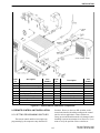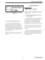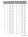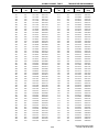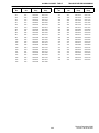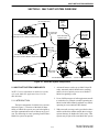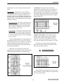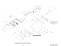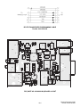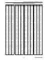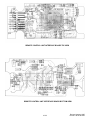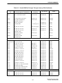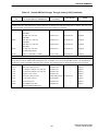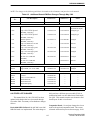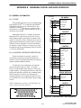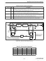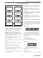
1
SERVICE MANUAL MULTI-NET ® II MOBILE SUMMIT DM 975X/977X 800 or 900 MHZ MOBILE RADIO ® MULTI-NET® II 13.6 VDC, 15 or 30 Watts Part No. 242-97xx-111 Fifth Printing December 2000 Supersedes 001-9750-005, 2/97 MULTI-NET® ® SUMMIT DM 975x/977x 800/900 MHz TRUNKED RADIO 13.6 VDC, 15 or 30/35 Watts, FM 806-821 MHz Tx, 851-866 MHz Rx (975x) 896-902 MHz Tx, 935-941 MHz Rx (977x) Part No. 242-97xx-111 Copyright © 2000 by the E.F. Johnson Company The E.F. Johnson Company designs and manufactures two-way radio equipment to serve a wide variety of communication needs. E.F. Johnson produces equipment for land mobile radio and mobiletelephone services which include business, industrial, government, public safety, and personal users. Viking Head/EF Johnson logo, Summit®, Multi-Net®, LTR®, Viking®, Avenger®, and Call Guard® are registered trademarks of the E.F. Johnson Company. All other company and/ or product names used in this manual are trademarks and/or registered trademarks of their respective manufacturer. Information in this manual is subject to change without notice. TABLE OF CONTENTS TABLE OF CONTENTS 1 GENERAL INFORMATION 3 OPERATION 1.1 1.2 3.1 3.2 1.3 1.4 1.5 1.6 1.7 1.8 1.9 SCOPE OF MANUAL . . . . . . . . . . . . . . . . . . . . 1-1 EQUIPMENT DESCRIPTION . . . . . . . . . . . . . 1-1 General . . . . . . . . . . . . . . . . . . . . . . . . . . . . . . . . 1-1 Programming . . . . . . . . . . . . . . . . . . . . . . . . . . . 1-1 Selectable Systems and Groups . . . . . . . . . . . . . 1-1 Front and Remote Mounting . . . . . . . . . . . . . . . 1-1 NPSPAC Models (800 MHz Only) . . . . . . . . . . 1-2 PART NUMBER BREAKDOWN . . . . . . . . . . .1-2 TRANSCEIVER IDENTIFICATION . . . . . . . .1-2 ACCESSORIES . . . . . . . . . . . . . . . . . . . . . . . . . 1-2 PRODUCT WARRANTY . . . . . . . . . . . . . . . . . 1-5 FACTORY CUSTOMER SERVICE . . . . . . . .1-5 FACTORY RETURNS . . . . . . . . . . . . . . . . . . .1-5 REPLACEMENT PARTS . . . . . . . . . . . . . . . . . 1-6 2 INSTALLATION 2.1 GENERAL. . . . . . . . . . . . . . . . . . . . . . . . . . . . . . 2-1 Scope Of Instructions . . . . . . . . . . . . . . . . . . . . . 2-1 Performance Tests . . . . . . . . . . . . . . . . . . . . . . . 2-1 Transceiver Programming . . . . . . . . . . . . . . . . . 2-2 Power Source . . . . . . . . . . . . . . . . . . . . . . . . . . . 2-2 Selecting A Mounting Location . . . . . . . . . . . . . 2-2 TRANSCEIVER INSTALLATION . . . . . . . . . . 2-2 General . . . . . . . . . . . . . . . . . . . . . . . . . . . . . . . . 2-2 Mounting Transceiver . . . . . . . . . . . . . . . . . . . . 2-2 POWER CABLE INSTALLATION . . . . . . . . . 2-2 ACCESSORY CABLE INSTALLATION . . . . 2-3 General . . . . . . . . . . . . . . . . . . . . . . . . . . . . . . . . 2-3 Internal/External Speaker . . . . . . . . . . . . . . . . . . 2-3 Ignition Sense . . . . . . . . . . . . . . . . . . . . . . . . . . . 2-4 Horn Alert. . . . . . . . . . . . . . . . . . . . . . . . . . . . . . 2-4 External Public Address . . . . . . . . . . . . . . . . . . . 2-4 Input B (Emergency Switch) . . . . . . . . . . . . . . . 2-4 REMOTE CONTROL UNIT INSTALLATION 2-5 Setting Programming Switches . . . . . . . . . . . . . 2-5 Using Setup Mode . . . . . . . . . . . . . . . . . . . . . . . 2-7 Mounting Remote Control UniT . . . . . . . . . . . . 2-7 Using An External Speaker With A Remote Control Unit. . . . . . . . . . . . . . . . . . . . . . . . . . 2-8 Microphone Hanger Sense . . . . . . . . . . . . . . . . . 2-8 INSTALLING OPTION SWITCH KEY CAPS 2-8 INSTALLING DC NOISE FILTER KIT . . . . . . 2-9 TRANSCEIVER MOUNTING TRAY INSTALLATION . . . . . . . . . . . . . . . . . . . . . . 2-10 Description . . . . . . . . . . . . . . . . . . . . . . . . . . . . 2-10 Installation . . . . . . . . . . . . . . . . . . . . . . . . . . . . 2-10 Locking and Unlocking Transceiver . . . . . . . . 2-10 FEATURES . . . . . . . . . . . . . . . . . . . . . . . . . . . . 3-1 FRONT PANEL CONTROLS & DISPLAY. . 3-1 Front Panel Controls . . . . . . . . . . . . . . . . . . . . . . 3-1 Display. . . . . . . . . . . . . . . . . . . . . . . . . . . . . . . . . 3-3 OPERATING MODES . . . . . . . . . . . . . . . . . . . 3-4 Introduction . . . . . . . . . . . . . . . . . . . . . . . . . . . . . 3-4 Multi-Net and LTR Modes . . . . . . . . . . . . . . . . . 3-4 Conventional Mode . . . . . . . . . . . . . . . . . . . . . . . 3-4 Multi-Net and LTR System/Groups . . . . . . . . . . 3-4 SCAN (SYSTEM AND GROUP) . . . . . . . . . . 3-6 Introduction . . . . . . . . . . . . . . . . . . . . . . . . . . . . . 3-6 Multiple- and Single-Site Scan . . . . . . . . . . . . . . 3-6 Scan Resume Delay. . . . . . . . . . . . . . . . . . . . . . . 3-7 Transmitting In The Scan Mode . . . . . . . . . . . . . 3-7 Fixed Transmit In Scan Mode . . . . . . . . . . . . . . . 3-8 Scan List Programming . . . . . . . . . . . . . . . . . . . . 3-8 Group Scan . . . . . . . . . . . . . . . . . . . . . . . . . . . . . 3-8 Scanning The Various Types Of Systems. . . . . . 3-9 OPTION SWITCH AND MENU MODE FUNCTIONS . . . . . . . . . . . . . . . . . . . . . . . . . 3-9 Introduction . . . . . . . . . . . . . . . . . . . . . . . . . . . . . 3-9 A/D (Scan List Programming) . . . . . . . . . . . . . 3-10 Auto-Registration . . . . . . . . . . . . . . . . . . . . . . . 3-10 Auxiliary 1 and 2. . . . . . . . . . . . . . . . . . . . . . . . 3-10 Backlight . . . . . . . . . . . . . . . . . . . . . . . . . . . . . . 3-10 Bank Select . . . . . . . . . . . . . . . . . . . . . . . . . . . . 3-10 Call Guard Squelch Disable . . . . . . . . . . . . . . . 3-11 Emergency. . . . . . . . . . . . . . . . . . . . . . . . . . . . . 3-11 Encryption . . . . . . . . . . . . . . . . . . . . . . . . . . . . . 3-11 External PA . . . . . . . . . . . . . . . . . . . . . . . . . . . . 3-11 Home System/Group . . . . . . . . . . . . . . . . . . . . . 3-11 Horn/Light Alert . . . . . . . . . . . . . . . . . . . . . . . . 3-11 LTR System Search Select . . . . . . . . . . . . . . . . 3-11 Menu Select Switch. . . . . . . . . . . . . . . . . . . . . . 3-11 Monitor Mode Select Switch. . . . . . . . . . . . . . . 3-11 Phone Mode Select . . . . . . . . . . . . . . . . . . . . . . 3-11 Priority. . . . . . . . . . . . . . . . . . . . . . . . . . . . . . . . 3-11 Radio Sounds. . . . . . . . . . . . . . . . . . . . . . . . . . . 3-12 Scan On/Off. . . . . . . . . . . . . . . . . . . . . . . . . . . . 3-12 Scan List Save . . . . . . . . . . . . . . . . . . . . . . . . . . 3-12 Scan Type . . . . . . . . . . . . . . . . . . . . . . . . . . . . . 3-12 Status Select . . . . . . . . . . . . . . . . . . . . . . . . . . . 3-12 Talk-Around . . . . . . . . . . . . . . . . . . . . . . . . . . . 3-12 Viewing Angle . . . . . . . . . . . . . . . . . . . . . . . . . 3-12 GENERAL FEATURES . . . . . . . . . . . . . . . . . 3-12 Time-Out Timer . . . . . . . . . . . . . . . . . . . . . . . . 3-12 Call Indicator . . . . . . . . . . . . . . . . . . . . . . . . . . . 3-12 Proceed (Clear-To-Talk) Tone . . . . . . . . . . . . . 3-13 Horn/Light Alert . . . . . . . . . . . . . . . . . . . . . . . . 3-13 2.2 2.3 2.4 2.5 2.6 2.7 2.8 3.3 3.4 3.5 3.6 i Revised December 2000 Part No. 001-9750-007 TABLE OF CONTENTS (CONT’D) Profile . . . . . . . . . . . . . . . . . . . . . . . . . . . . . . . . 3-14 Banks . . . . . . . . . . . . . . . . . . . . . . . . . . . . . . . . 3-14 Power Turn-Off Delay . . . . . . . . . . . . . . . . . . . 3-15 Emergency Calls. . . . . . . . . . . . . . . . . . . . . . . . 3-15 Programmable Power Output . . . . . . . . . . . . . . 3-16 Automatic Transmitter Thermal Foldback . . . . 3-16 Data System/Groups . . . . . . . . . . . . . . . . . . . . . 3-16 Encryption . . . . . . . . . . . . . . . . . . . . . . . . . . . . 3-16 Phone Mode . . . . . . . . . . . . . . . . . . . . . . . . . . . 3-17 Display Of Software Version . . . . . . . . . . . . . . 3-18 3.7 MULTI-NET MODE FEATURES . . . . . . . . . .3-18 Busy Queuing (Multi-Net) . . . . . . . . . . . . . . . . 3-18 Auto-Registration (Multi-Net) . . . . . . . . . . . . . 3-19 Transmitting Status Information (Multi-Net) . . 3-20 Special Calls (Multi-Net) . . . . . . . . . . . . . . . . . 3-20 Transmit Inhibit . . . . . . . . . . . . . . . . . . . . . . . . 3-22 Access Priority (Multi-Net) . . . . . . . . . . . . . . . 3-22 Camp-On Prevent . . . . . . . . . . . . . . . . . . . . . . . 3-22 3.8 LTR MODE FEATURES . . . . . . . . . . . . . . . . . 3-23 Free System Ringback . . . . . . . . . . . . . . . . . . . 3-23 System Search . . . . . . . . . . . . . . . . . . . . . . . . . 3-23 Transpond . . . . . . . . . . . . . . . . . . . . . . . . . . . . . 3-23 Transmit Inhibit . . . . . . . . . . . . . . . . . . . . . . . . 3-23 3.9 CONVENTIONAL MODE FEATURES . . . .3-23 Transmit Disable On Busy . . . . . . . . . . . . . . . . 3-23 Call Guard Squelch. . . . . . . . . . . . . . . . . . . . . . 3-24 Monitor Mode. . . . . . . . . . . . . . . . . . . . . . . . . . 3-24 Repeater Talk-Around . . . . . . . . . . . . . . . . . . . 3-24 Priority Group Sampling . . . . . . . . . . . . . . . . . 3-25 Receive-Only Groups . . . . . . . . . . . . . . . . . . . . 3-25 3.10 MISCELLANEOUS . . . . . . . . . . . . . . . . . . . . . 3-25 Supervisory Tones . . . . . . . . . . . . . . . . . . . . . . 3-25 Display Messages . . . . . . . . . . . . . . . . . . . . . . . 3-26 3.11 TEST MODE . . . . . . . . . . . . . . . . . . . . . . . . . . .3-28 Introduction . . . . . . . . . . . . . . . . . . . . . . . . . . . 3-28 Receive-Transmit-RSSI . . . . . . . . . . . . . . . . . . 3-28 Power Level 1 Set (Std Band) . . . . . . . . . . . . . 3-29 Power Level 1 Set (Talk-Around Band). . . . . . 3-30 Power Levels 2, 3, 4, 2W . . . . . . . . . . . . . . . . . 3-30 Modulation Balance . . . . . . . . . . . . . . . . . . . . . 3-30 Transmitter Hum and Noise . . . . . . . . . . . . . . . 3-30 DC Voltage Check . . . . . . . . . . . . . . . . . . . . . . 3-30 Display Test . . . . . . . . . . . . . . . . . . . . . . . . . . . 3-30 4 TRANSCEIVER PROGRAMMING 4.1 GENERAL. . . . . . . . . . . . . . . . . . . . . . . . . . . . . . 4-1 Programming Setup . . . . . . . . . . . . . . . . . . . . . . 4-1 Computer Description . . . . . . . . . . . . . . . . . . . . 4-1 Remote Programming Interface (RPI) . . . . . . . . 4-1 EEPROM Data Storage . . . . . . . . . . . . . . . . . . . 4-2 Software Version Number . . . . . . . . . . . . . . . . . 4-2 Computers Running Windows® . . . . . . . . . . . . 4-2 Software Installation. . . . . . . . . . . . . . . . . . . . . . 4-2 4.2 4.3 4.4 4.5 4.6 4.7 ii Hardware Hookup . . . . . . . . . . . . . . . . . . . . . . . . 4-3 Minimum Free Memory Required . . . . . . . . . . . 4-3 Starting The Program . . . . . . . . . . . . . . . . . . . . . 4-3 Header Information . . . . . . . . . . . . . . . . . . . . . . . 4-3 Special Keys . . . . . . . . . . . . . . . . . . . . . . . . . . . . 4-3 MAIN MENU . . . . . . . . . . . . . . . . . . . . . . . . . . . 4-5 Introduction . . . . . . . . . . . . . . . . . . . . . . . . . . . . . 4-5 Set Up New Configuration File. . . . . . . . . . . . . . 4-5 Open Configuration File . . . . . . . . . . . . . . . . . . . 4-5 Modify Current Configuration File . . . . . . . . . . . 4-5 Upload Configuration From Radio . . . . . . . . . . . 4-6 Download Configuration To Radio. . . . . . . . . . . 4-6 Print Current Configuration File . . . . . . . . . . . . . 4-6 Modify Printer/serial Ports . . . . . . . . . . . . . . . . . 4-6 Configuration File Utilities . . . . . . . . . . . . . . . . . 4-6 MODIFY RADIO FILE MENU . . . . . . . . . . . . . 4-7 Introduction . . . . . . . . . . . . . . . . . . . . . . . . . . . . . 4-7 Edit Main Radio Parameters . . . . . . . . . . . . . . . . 4-7 Define Option Buttons. . . . . . . . . . . . . . . . . . . . . 4-7 Setup Menu Functions. . . . . . . . . . . . . . . . . . . . . 4-8 Create/Edit/Copy/Delete System. . . . . . . . . . . . . 4-8 Create/Edit/Copy/Delete Bank . . . . . . . . . . . . . 4-10 Programming Prestored Telephone Numbers . . 4-11 Editing Unique ID Codes . . . . . . . . . . . . . . . . . 4-11 ADDITIONAL PROGRAMMING INFORMATION . . . . . . . . . . . . . . . . . . . . . . 4-11 Repeater Number Programming (Multi-Net and LTR). . . . . . . . . . . . . . . . . . . . . . . . . . . . . . . 4-11 Channel Number Programming. . . . . . . . . . . . . 4-12 Access Priority Programming (Multi-Net Only) 4-12 Site Number Programming (Multi-Net Only) . . 4-12 Specifying RIC-equipped Repeaters . . . . . . . . . 4-12 Wide Area Group Tracking Programming . . . . 4-13 PROGRAMMING ONE TRANSCEIVER WITH ANOTHER (CLONING) . . . . . . . . . . . . . . . 4-13 WRITE-ON FLASH PROGRAMMING . . . . 4-13 Introduction . . . . . . . . . . . . . . . . . . . . . . . . . . . . 4-13 Programming Files . . . . . . . . . . . . . . . . . . . . . . 4-14 Programming “A” Model Transceivers. . . . . . . 4-14 Programming Procedure . . . . . . . . . . . . . . . . . . 4-14 UNIVERSAL INTERFACE PROGRAMMING . . . . . . . . . . . . . . . . . . . . 4-14 Introduction . . . . . . . . . . . . . . . . . . . . . . . . . . . . 4-14 Main Parameters Screen . . . . . . . . . . . . . . . . . . 4-15 System Parameters Screen. . . . . . . . . . . . . . . . . 4-16 Auxiliary and Emergency Switch Programming 4-16 5 MULTI-NET SYSTEM OVERVIEW 5.1 MULTI-NET SYSTEM COMPONENTS . . . . Introduction . . . . . . . . . . . . . . . . . . . . . . . . . . . . . Mobile Transceivers . . . . . . . . . . . . . . . . . . . . . . Repeaters . . . . . . . . . . . . . . . . . . . . . . . . . . . . . . . 5-1 5-1 5-2 5-2 Revised December 2000 Part No. 001-9750-007 TABLE OF CONTENTS (CONT’D) 5.2 5.3 5.4 5.5 5.6 5.7 5.8 Radio Network Terminal (RNT) . . . . . . . . . . . . 5-2 Dispatch Consoles . . . . . . . . . . . . . . . . . . . . . . . 5-2 Public Switched Telephone Network (PSTN) . . 5-2 DEFINITIONS OF MULTI-NET TERMS . . . . 5-3 HOME AND STATUS REPEATERS . . . . . . . 5-4 HOME CHANNEL BACKUP . . . . . . . . . . . . . .5-4 Introduction . . . . . . . . . . . . . . . . . . . . . . . . . . . . 5-4 Selecting Repeater To Monitor . . . . . . . . . . . . . 5-4 Assigning The Status Channel . . . . . . . . . . . . . . 5-4 Detecting Defective Repeaters . . . . . . . . . . . . . . 5-4 MOBILE-REPEATER DATA SIGNALING . .5-5 REPEATER DATA BUS SIGNALING . . . . . . 5-5 STANDARD AND SPECIAL CALLS . . . . . . . 5-6 OTHER MULTI-NET FEATURES . . . . . . . . . . 5-6 Unique ID Codes . . . . . . . . . . . . . . . . . . . . . . . . 5-6 Access and Receive Priority . . . . . . . . . . . . . . . . 5-6 All Call . . . . . . . . . . . . . . . . . . . . . . . . . . . . . . . . 5-7 Interrogate. . . . . . . . . . . . . . . . . . . . . . . . . . . . . . 5-7 Mobile Disable . . . . . . . . . . . . . . . . . . . . . . . . . . 5-7 Dynamic Reprogramming of Group 11 . . . . . . . 5-7 Dynamic Move To New System/group . . . . . . . 5-7 ID Validation . . . . . . . . . . . . . . . . . . . . . . . . . . . 5-7 System Key. . . . . . . . . . . . . . . . . . . . . . . . . . . . . 5-7 Dynamic Channel Assignment . . . . . . . . . . . . . . 5-8 Emergency Calls. . . . . . . . . . . . . . . . . . . . . . . . . 5-8 Auto-registration (Roaming) . . . . . . . . . . . . . . . 5-8 Busy Queuing . . . . . . . . . . . . . . . . . . . . . . . . . . . 5-8 Sending Status Information . . . . . . . . . . . . . . . . 5-8 Transmit Inhibit . . . . . . . . . . . . . . . . . . . . . . . . . 5-8 Voice Encryption . . . . . . . . . . . . . . . . . . . . . . . . 5-9 6 CIRCUIT DESCRIPTION 6.1 GENERAL TRANSCEIVER DESCRIPTION 6-1 Introduction . . . . . . . . . . . . . . . . . . . . . . . . . . . . 6-1 Synthesizer . . . . . . . . . . . . . . . . . . . . . . . . . . . . . 6-1 Receiver . . . . . . . . . . . . . . . . . . . . . . . . . . . . . . . 6-1 Transmitter . . . . . . . . . . . . . . . . . . . . . . . . . . . . . 6-1 Audio/Logic Board . . . . . . . . . . . . . . . . . . . . . . . 6-1 SYNTHESIZER CIRCUIT DESCRIPTION . .6-2 Introduction . . . . . . . . . . . . . . . . . . . . . . . . . . . . 6-2 Voltage-Controlled Oscillator Module. . . . . . . . 6-2 VCO and TCXO Modulation . . . . . . . . . . . . . . . 6-4 Active Filter (Q800), Buffer Amplifier (Q801, Q802) . . . . . . . . . . . . . . . . . . . . . . . . 6-4 Prescaler (U800) . . . . . . . . . . . . . . . . . . . . . . . . . 6-5 Synthesizer Integrated Circuit (U801) . . . . . . . . 6-5 Lock Detect (Q808, Q809) . . . . . . . . . . . . . . . . . 6-6 Charge Pump (Q804-Q807) . . . . . . . . . . . . . . . . 6-7 Voltage Multiplier (CR804A/B, CR805A/B). . . 6-7 RECEIVER CIRCUIT DESCRIPTION . . . . . . 6-7 RF Amplifier (Q290) . . . . . . . . . . . . . . . . . . . . . 6-7 First Mixer (Q205) . . . . . . . . . . . . . . . . . . . . . . . 6-8 6.2 6.3 6.4 6.5 6.6 6.7 7 SERVICING 7.1 GENERAL . . . . . . . . . . . . . . . . . . . . . . . . . . . . . Periodic Checks. . . . . . . . . . . . . . . . . . . . . . . . . . Schematic Diagrams and Component Layouts . . Replacement Parts . . . . . . . . . . . . . . . . . . . . . . . . Configuring Transceiver For Testing . . . . . . . . . Surface-Mounted Components . . . . . . . . . . . . . . CMOS Handling Techniques . . . . . . . . . . . . . . . SYNTHESIZER TROUBLESHOOTING . . . . Introduction . . . . . . . . . . . . . . . . . . . . . . . . . . . . . TCXO (Y800) . . . . . . . . . . . . . . . . . . . . . . . . . . . VCO Module and Prescaler. . . . . . . . . . . . . . . . . Synthesizer (U801) . . . . . . . . . . . . . . . . . . . . . . . Determining Counter Divide Numbers . . . . . . . . RECEIVER TROUBLESHOOTING . . . . . . . . TRANSMITTER TROUBLESHOOTING. . . . AUDIO/LOGIC BOARD TROUBLESHOOTING . . . . . . . . . . . . . . . . Digital Circuits . . . . . . . . . . . . . . . . . . . . . . . . . . Analog Circuits . . . . . . . . . . . . . . . . . . . . . . . . . . SURFACE MOUNTED DEVICES (SMDs) . . Servicing Techniques . . . . . . . . . . . . . . . . . . . . . 7.2 7.3 7.4 7.5 7.6 iii Crystal Filters (Z205, Z206), IF Amplifier . . . . . 6-8 Second Mixer/Detector (U200) . . . . . . . . . . . . . . 6-8 Audio Power Amplifier (U100) . . . . . . . . . . . . . 6-9 13.8-Volt Switch (Q100, Q103, Q106-Q108). . . 6-9 TRANSMITTER CIRCUIT DESCRIPTION. . 6-9 Power Amplifier Module (U500) . . . . . . . . . . . . 6-9 Driver (Q500), Final Amplifier (Q501) . . . . . . . 6-9 Antenna Switch (CR502, CR506, CR507) . . . . . 6-9 Power Control (U504, Q511, Q502, Q506) . . . 6-10 AUDIO/LOGIC BOARD DIGITAL CIRCUIT DESCRIPTION . . . . . . . . . . . . . . . . . . . . . . 6-11 Microprocessor (U401) . . . . . . . . . . . . . . . . . . . 6-11 Memory and I/O Addressing . . . . . . . . . . . . . . . 6-13 Digital Signal Processor (U300-U302) . . . . . . . 6-14 AUDIO/LOGIC BOARD RECEIVE SIGNAL PROCESSING . . . . . . . . . . . . . . . . . . . . . . 6-14 Receive Audio Processing. . . . . . . . . . . . . . . . . 6-14 Receive Data Processing (U606A-D) . . . . . . . . 6-15 Squelch Circuit (U607B, U607C) . . . . . . . . . . . 6-15 RSSI Comparator (U602C) . . . . . . . . . . . . . . . . 6-16 TRANSMIT AUDIO/DATA PROCESSING 6-16 Microphone Amplifier (U603D), Filter (U603B, U603C, U604D) . . . . . . . . . . . . . . . . . . . . . . 6-16 Mute Gate (U609C), Summing Amplifier (U604A) . . . . . . . . . . . . . . . . . . . . . . . . . . . . 6-16 Compressor (U100B), Limiter (U604C) . . . . . . 6-16 Splatter Filter (U604C, U605D), Summing Amplifier (U605A) . . . . . . . . . . . . . . . . . . . 6-17 Transmit Data Circuit (U607D, U607A). . . . . . 6-17 7-1 7-1 7-1 7-1 7-1 7-1 7-1 7-2 7-2 7-2 7-2 7-3 7-5 7-5 7-5 7-5 7-5 7-5 7-5 7-5 Revised December 2000 Part No. 001-9750-007 TABLE OF CONTENTS (CONT’D) Identifying SMD Resistors . . . . . . . . . . . . . . . . . SMD Capacitor Identification . . . . . . . . . . . . . . SMD Inductor Identification . . . . . . . . . . . . . . . Transistor/Diode Identification . . . . . . . . . . . . . 8 8.1 ALIGNMENT PROCEDURE AND PERFORMANCE TESTS RF Board 8.5 8.6 GENERAL. . . . . . . . . . . . . . . . . . . . . . . . . . . . . . 8-1 Introduction . . . . . . . . . . . . . . . . . . . . . . . . . . . . 8-1 Test Cables . . . . . . . . . . . . . . . . . . . . . . . . . . . . . 8-1 FREQUENCY ADJUSTMENT. . . . . . . . . . . . . 8-1 TRANSMITTER TUNEUP . . . . . . . . . . . . . . . . 8-2 C511 Adjustment (30 or 35 Watt Models Only) 8-2 Power Level 1 Adjustment . . . . . . . . . . . . . . . . . 8-2 Power Level 2-4, 2W Adjustment . . . . . . . . . . . 8-3 Modulation Balance . . . . . . . . . . . . . . . . . . . . . . 8-3 Transmit Data Level Adjustment . . . . . . . . . . . . 8-3 Transmit Audio Limiting Adjust . . . . . . . . . . . . 8-3 RECEIVER ALIGNMENT . . . . . . . . . . . . . . . . . 8-4 Front End Alignment . . . . . . . . . . . . . . . . . . . . . 8-4 RSSI Detect Adjust. . . . . . . . . . . . . . . . . . . . . . . 8-4 Squelch Adjust . . . . . . . . . . . . . . . . . . . . . . . . . . 8-4 Local Tone Level Adjust . . . . . . . . . . . . . . . . . . 8-5 RECEIVER PERFORMANCE TESTS . . . . . . 8-6 TRANSMITTER PERFORMANCE TESTS . . 8-6 9 PARTS LIST 8.2 8.3 8.4 RF and PA Board Component Locator Guide 10-5 Audio/Logic Board Comp. Locator Guide. . . 10-8 Interconnect Schematic . . . . . . . . . . . . . . . . 10-11 Display Board Schematic . . . . . . . . . . . . . . . 10-12 Display Board Layout. . . . . . . . . . . . . . . . . . 10-13 7-5 7-6 7-7 7-7 Revised 800 MHz Schematic . . . . . . . . . . . . 800/900 MHz Board Layout. . . . . . . . . . . . . 900 MHz Schematic . . . . . . . . . . . . . . . . . . . Unrevised 800 MHz Schematic . . . . . . . . . . 10-14 10-15 10-16 10-17 PA Board Revised 800 MHz, 35W Schematic . . . . . . . Revised 800 MHz, 15W Schematic . . . . . . . Revised 800 MHz, 15W/35W Board Layout 900 MHz, 30W Schematic . . . . . . . . . . . . . . 900 MHz, 15W Schematic . . . . . . . . . . . . . . 900 MHz/Unrev. 800 MHz Board Layout . . Unrevised 800 MHz, 35W Schematic . . . . . Unrevised 800 MHz, 15W Schematic . . . . . 10-18 10-19 10-20 10-21 10-22 10-23 10-24 10-25 Audio/Logic Board Schematic (Part 1 of 2) . . . . . . . . . . . . . . . . . Schematic (Part 2 of 2) . . . . . . . . . . . . . . . . . Board Layout Top View . . . . . . . . . . . . . . . . Board Layout Bottom View . . . . . . . . . . . . . Revised Compandor Board Schematic. . . . . Revised Compandor Board Layout . . . . . . . 10-26 10-27 10-28 10-29 10-30 10-30 Remote Transceiver RF and PA Boards, Hardware and Miscellaneous 9-1 Audio/Logic Board . . . . . . . . . . . . . . . . . . . . . . . 9-9 Front Panel Assembly. . . . . . . . . . . . . . . . . . . . 9-15 Compandor Kit . . . . . . . . . . . . . . . . . . . . . . . . . 9-16 Hardware and Cable Kit . . . . . . . . . . . . . . . . . . 9-16 Remote Control Unit and Remote Kit . . . . . . . 9-17 Accessory Wire Kit . . . . . . . . . . . . . . . . . . . . . 9-17 Transceiver Mounting Kit . . . . . . . . . . . . . . . . 9-17 Transceiver Exploded View (Part 1) . . . . . . . . 9-19 Transceiver Exploded View (Part 2) . . . . . . . . 9-20 Interconnect Schematic . . . . . . . . . . . . . . . . 10-31 Control Unit Interface Board Schematic . . . 10-32 Control Unit Interface Board Layout . . . . . . 10-33 APPENDIX A A.1 A.2 A.3 10 SCHEMATIC DIAGRAMS AND COMPONENT LAYOUTS A.4 A.5 Miscellaneous Basing Diagrams . . . . . . . . . . . . . . . . . . . . . . Standard Amplified Dynamic Microphone . . Transceiver-To-Transceiver Cloning Cable . RPI (Part No. 023-9800-000) Schematic. . . . RPI-To-Transceiver Programming Cable . . . RPI (Part No. 023-9800-000) Board Layout . A.6 10-1 10-2 10-3 10-3 10-4 10-4 A.7 A.8 iv REVISION SUMMARY INTRODUCTION . . . . . . . . . . . . . . . . . . . . . . . A-1 TRANSCEIVER OPERATING SOFTWARE UPDATES . . . . . . . . . . . . . . . . . . . . . . . . . . . . A-1 REVISION LETTER CHANGES . . . . . . . . . . A-1 Transceiver Revision Letter . . . . . . . . . . . . . . . A-1 Control Unit Revision Letter . . . . . . . . . . . . . . . A-1 PROGRAMMING SOFTWARE CHANGES. A-1 REMOTE CONTROL UNIT COMPATIBILITY . . . . . . . . . . . . . . . . . . . . . . A-3 WIDE AREA GROUP TRACKING PROGRAMMING . . . . . . . . . . . . . . . . . . . . . . A-3 NEW FEATURES . . . . . . . . . . . . . . . . . . . . . . . A-4 Bank Start at Home Feature . . . . . . . . . . . . . . . A-4 Group Proceed Tone Delay . . . . . . . . . . . . . . . . A-4 OTHER LATE CHANGES . . . . . . . . . . . . . . . A-7 Revised December 2000 Part No. 001-9750-007 TABLE OF CONTENTS (CONT’D) APPENDIX B UNIVERSAL DIGITAL AND DATA INTERFACE B.1 B.2 B.3 B.4 B.5 B.6 B.7 B.8 4-6 4-7 4-8 4-9 4-10 5-1 6-1 6-2 7-1 8-1 8-2 8-3 8-4 B-1 B-2 B-3 B-4 GENERAL INFORMATION . . . . . . . . . . . . . . B-1 Scope . . . . . . . . . . . . . . . . . . . . . . . . . . . . . . . . . B-1 Universal Interface Description . . . . . . . . . . . . . B-1 POWER SUPPLY . . . . . . . . . . . . . . . . . . . . . . B-2 RECEIVE AUDIO SIGNALS . . . . . . . . . . . . . B-2 Pin Descriptions . . . . . . . . . . . . . . . . . . . . . . . . . B-2 Receive Audio Gating . . . . . . . . . . . . . . . . . . . . B-2 TRANSMIT AUDIO SIGNALS . . . . . . . . . . . . B-2 Pin Descriptions . . . . . . . . . . . . . . . . . . . . . . . . . B-2 Transmit Audio Programming . . . . . . . . . . . . . . B-2 INPUT CONTROL SIGNALS . . . . . . . . . . . . B-5 OUTPUT CONTROL SIGNALS . . . . . . . . . . B-5 INTERFACING WITH A DATA MODEM . . . B-7 General . . . . . . . . . . . . . . . . . . . . . . . . . . . . . . . . B-7 Modem Control Lines. . . . . . . . . . . . . . . . . . . . . B-7 ARQ Arbitration . . . . . . . . . . . . . . . . . . . . . . . . . B-7 SERIAL BUS PROTOCOL . . . . . . . . . . . . . . B-8 Introduction . . . . . . . . . . . . . . . . . . . . . . . . . . . . B-8 Physical Signal Path . . . . . . . . . . . . . . . . . . . . . . B-9 Character Level Protocol . . . . . . . . . . . . . . . . . . B-9 Message Level Protocol . . . . . . . . . . . . . . . . . . . B-9 Message Supervision Types . . . . . . . . . . . . . . . B-10 Serial Port Command Messages . . . . . . . . . . . . B-10 Response Messages . . . . . . . . . . . . . . . . . . . . . B-15 LIST OF TABLES 1-1 1-2 3-1 3-2 4-1 4-2 4-3 4-4 4-5 4-6 7-1 7-2 A-1 A-2 A-3 B-1 B-3 B-2 B-5 B-4 B-6 B-7 B-8 LIST OF FIGURES 2-1 2-2 2-3 2-4 2-5 2-6 3-1 3-2 3-3 4-1 4-2 4-3 4-4 4-5 Setup Menu Functions Screen . . . . . . . . . . . . . . 4-9 Telephone Numbers Screen. . . . . . . . . . . . . . . 4-11 Setup/Change Unique ID Screen. . . . . . . . . . . 4-11 Main Universal Interface Screen . . . . . . . . . . . 4-15 System Universal Interface Screen . . . . . . . . . 4-16 Multi-Net System Components . . . . . . . . . . . . . 5-1 Transceiver Block Diagram. . . . . . . . . . . . . . . . 6-3 U801 Block Diagram. . . . . . . . . . . . . . . . . . . . . 6-5 Simplified Synthesizer Block Diagram . . . . . . . 7-3 Test Cables . . . . . . . . . . . . . . . . . . . . . . . . . . . . 8-1 Transmitter Test Setup . . . . . . . . . . . . . . . . . . . 8-2 Receiver Test Setup. . . . . . . . . . . . . . . . . . . . . . 8-4 Alignment Point Diagrams . . . . . . . . . . . . . . . . 8-5 Universal Interface Pin Designations . . . . . . . . B-1 Receive Audio Signal Routing . . . . . . . . . . . . . B-3 Transmit Audio Signal Routing . . . . . . . . . . . . B-4 Serial Bus Encode/Decode Diagram . . . . . . . . B-10 97xx Front Mount Installation Components. . . . 2-1 Accessory Jack . . . . . . . . . . . . . . . . . . . . . . . . . . 2-3 Remote Mount Installation Components . . . . . . 2-5 Remote Control Unit Programming Switches . . 2-7 DC Noise FIlter Installation . . . . . . . . . . . . . . . . 2-9 Locking Tray Installation Diagram . . . . . . . . . 2-10 Front Panel Controls. . . . . . . . . . . . . . . . . . . . . . 3-2 Back Panel Jacks And Connectors . . . . . . . . . . . 3-2 Front Panel Display . . . . . . . . . . . . . . . . . . . . . . 3-3 Programming Setup . . . . . . . . . . . . . . . . . . . . . . 4-1 Programming Software Menu Structure. . . . . . . 4-4 Main Menu . . . . . . . . . . . . . . . . . . . . . . . . . . . . . 4-5 Modify Radio File Menu . . . . . . . . . . . . . . . . . . 4-7 Define Option Buttons Screen . . . . . . . . . . . . . . 4-9 v Accessories . . . . . . . . . . . . . . . . . . . . . . . . . . . . . 1-3 E.F. Johnson Multi-Net Transceivers . . . . . . . . . 1-4 Multi-Net Standard & Spec. Call Rx Priority . . 3-6 Menu Mode And Option Switch Functions . . . . 3-9 Main Radio Parameters Screen . . . . . . . . . . . . 4-17 Multi-Net System Parameters . . . . . . . . . . . . . 4-18 LTR System Parameters . . . . . . . . . . . . . . . . . . 4-21 Conventional System Parameters . . . . . . . . . . . 4-23 Create/Edit Bank Screen Parameters . . . . . . . . 4-25 Call Guard (CTCSS/DCS) Codes and Tones . . 4-26 Ceramic SMD Capacitor Identification . . . . . . . 7-6 SMD Inductor Identification . . . . . . . . . . . . . . . 7-7 Operating Software Version Numbers . . . . . . . . A-2 Part Changes Through January 1995 . . . . . . . . . A-4 Additional Changes Through May 1998 . . . . . . A-7 Power Supply Pin Description . . . . . . . . . . . . . . B-2 Receive Audio Programming . . . . . . . . . . . . . . . B-3 Receive Audio Pin Description . . . . . . . . . . . . . B-3 Transmit Audio Programming . . . . . . . . . . . . . . B-4 Transmit Audio Pin Description . . . . . . . . . . . . . B-4 Control Signal Description . . . . . . . . . . . . . . . . . B-5 Serial Bus Pin Description . . . . . . . . . . . . . . . . . B-8 UPDATE_DISPLAY Message Coding . . . . . . B-18 Revised December 2000 Part No. 001-9750-007 GENERAL INFORMATION SECTION 1 GENERAL INFORMATION 1.1 SCOPE OF MANUAL programming software listed in Table 1-1. Transceiver operating parameters are stored in an EEPROM reprogrammable memory. Refer to Section 4 for more programming information. This service manual contains installation, operation, programming, alignment, and service information for the E.F. Johnson Summit® DM 975x and 977x transceivers. The operating code (firmware) for the microprocessor is stored in a flash-type memory device. This allows the operating program to be updated using E.F. Johnson Write-On programming software and the standard transceiver programming setup. This simplifies software updates because the microprocessor or an EPROM does not need to be changed. The latest Write-On software and operating code can be downloaded from the E.F. Johnson ACESSM Bulletin Board System. Refer to Section 4.6 for more information on flash programming. NOTE: The 900 MHz (977x) Summit DM model is no longer available. 1.2 EQUIPMENT DESCRIPTION 1.2.1 GENERAL The 975x/977x are full featured, high performance transceivers that operate in the Multi-Net®, LTR®, and conventional modes. The 975x is an 800 MHz transceiver which operates on the 760 trunked channels from 806-824 MHz (mobile transmit). The receive channels are 45 MHz above these frequencies (851-869 MHz). The 977x is a 900 MHz transceiver which operates on the 479 trunked channels from 896902 MHz (mobile transmit). The receive channels are 39 MHz above these frequencies (935-941 MHz). Standard analog frequency modulation is utilized. 1.2.3 SELECTABLE SYSTEMS AND GROUPS The maximum number of systems that can be programmed is determined by the type of system and the number of groups that are programmed. If only single-group systems are programmed, up to 73 MultiNet, 66 LTR, or 100 conventional systems can be programmed. Then as more groups are programmed, the number of systems decreases. If the maximum number of groups are programmed (11 Multi-Net, 10 LTR/conventional), up to 32 Multi-Net, 30 LTR, or 32 conventional systems can be programmed. When data is being entered using the programming software, there is a running indication of the amount of EEPROM memory left. The last digit of the model number (97x3, 97x4, 97x5, and 97x6) denotes front or remote mounting and power output as shown in Table 1-2. This table also lists other E.F. Johnson Multi-Net transceivers and the distinguishing features of each. Like all E.F. Johnson Multi-Net and LTR transceivers, the 975/977x is digitally synthesized and logic controlled. In the Multi-Net or LTR modes, all the user has to do to make a call is select the desired system and group and press the push-to- talk switch. If a busy or out-of-range condition is not indicated by special tones, the path to the other party is complete and speaking can begin. Channel selection, monitoring before transmitting, and squelch control are all performed by the logic. With conventional operation, each system selects a channel, and the group switch selects the Call Guard (CTCSS or digital) signaling and other parameters on that channel. 1.2.4 FRONT AND REMOTE MOUNTING The 97x3/97x5 transceivers are designed for front mounting within reach of the operator, and the 97x4/ 97x6 are designed for remote mounting in a location such as the trunk (see Table 1-2). The remote control unit cable connects to the remote interface pigtail coming from the back of the transceiver (see Figure 2-3). This pigtail is standard with remote mount transceivers only. 1.2.2 PROGRAMMING Transceiver programming is performed using a dealer-supplied personal computer and the E.F. Johnson RPI (Remote Programming Interface) and 1-1 Revised February 1997 Part No. 001-9750-005 GENERAL INFORMATION 1.5 ACCESSORIES The remote control unit uses the same front panel assembly that is used on front mount transceivers. Therefore, it operates the same as a front-mount transceiver. A Remote Conversion Kit is available which converts the front panel of a front mount transceiver to a remote control unit (see Table 1-1). The remote control unit has an internal 5-watt speaker or an external 15-watt speaker can be used. Dual transceiver controls are also available when the remote control unit is connected to a standard front mount transceiver. The accessories available for this transceiver are listed in Table 1-2. A brief description of several of these accessories follows. Mounting Hardware - The mounting hardware and DC power cable are shown in Figures 2-1 and 2-3 in Section 2. A 22-foot DC power cable is used for both front and remote mount applications. The cable is cut to the required length at installation and any excess discarded. The accessory cable is used to connect such things as an external speaker, public address, ignition sense input, and a horn alert to the transceiver. It includes two 22-foot and three 2-foot wires that are connected as required to external points. The adapter cable is used to connect a 86xx-series power cable to these transceivers. 1.2.5 NPSPAC MODELS (800 MHZ ONLY) All 800 MHz versions of this transceiver meet the stricter specifications established by NPSPAC (National Public Safety Panel Advisory Committee) for public safety frequencies from 821-824 and 866869 MHz. Deviation is less on NPSPAC channels; however, no alignment change is required because it is automatically set for the correct level when a public safety channel is selected (see Appendix A.2). Key Cap Kit - This kit includes key caps labeled for all the functions that can be controlled by the six front panel option switches. Also included are blank key caps for unused switches. An extraction tool for removing the key caps is included in the cable and hardware kit. Refer to Section 2.6 for key cap installation information. 1.3 PART NUMBER BREAKDOWN The following is a breakdown of the part number used to identify this transceiver: Lockable Mounting Tray - This bracket allows the transceiver to be locked in place to guard against theft. In addition, it allows it to be easily unlocked and removed from the vehicle. Refer to Section 2.8 for installation information. 242 - 97 x x - 111 5 = 800 MHz 7 = 900 MHz 3 = 15W, Frt Mt 4 = 15W, Rem Mt 5 = 30/35W, Frt Mt 6 = 30/35W, Rem Mt Microphones and Speaker - The microphones in Table 1-1 have an impedance of 620 ohms. All DTMF microphones are backlighted. The environmentally sealed microphones are sealed against such things as rain, sand, and dust. 1.4 TRANSCEIVER IDENTIFICATION The external 15-watt speaker can be used in place of the internal 5-watt speaker. It is non- amplified and weatherproof. This speaker is connected to pins 1 and 2 of the accessory connector pigtail on the back of the transceiver. The transceiver identification number is printed on a label that is affixed to the bottom cover. The following information is contained in that number: Model 97xx 8th Digit Revision Manufacture Plant Letter Date x A 24 3 Warranty Number A Week No. Remote Kits - The remote conversion kit converts the front panel of a front-mount transceiver to a remote control unit. It includes a blank cover plate with a programming jack for the transceiver, a housing with interface board to form the remote control unit, a remote pigtail cable, and a 17-foot control cable. The remote control unit uses the internal 5-watt speaker or 12345 A= Year 1-2 Revised February 1997 Part No. 001-9750-005 GENERAL INFORMATION Table 1-1 ACCESSORIES Accessory Mounting Accessories [1] Mounting bracket & hardware kit DC power cable & hardware, 22' Accessory cable Key cap kit, Summit Lockable Mounting Tray Adapter cable (to use 86xx-series power cable with 97xx) Part No. Remote conversion kit Remote control unit kit, Summit 250-9701-001 023-9701-002 UD2I universal interface cable Factory installed Field installed 023-9750-001 597-2002-245 Compandor kit Factory installed Field installed 023-9750-002 250-9750-002 Part No. Programming Accessories Remote prog interface (RPI) 023-9800-000 Cable, RPI to transceiver 023-9750-005 Cable, xcvr-xcvr (cloning) 597-2002-268 Cable, RPI to cmptr, 6’ DB9 M - DB9 F 597-5900-002 Cable, RPI to cmptr, 6’ DB25 M - DB9F 597-0005-057 PC Programming software, 3.5” diskette 023-9998-278 [1] Included with all transceivers 585-7000-185 023-9650-006 250-0740-310 587-9650-010 589-0016-028 587-9650-015 587-9650-012 250-0742-011 250-0151-006 Control station power supply 11 amp, 115 VAC, 60 Hz 15 amp, 115 VAC, 60 Hz 11 amp, 230 VAC, 50 Hz 15 amp, 230 VAC, 50 Hz Accessory 023-9750-012 023-9750-010 023-9750-011 587-9650-008 Microphones Standard amplified dynamic Standard, environ sealed DTMF w/o memory DTMF w/o mem, env seal WR805 DTMF w/20 no. mem, envir seal Desk microphone External speaker, 5" 15W 3.2 ohm environmental sealed Encryption kit Factory installed Field installed DC noise filter kit Factory installed Field installed Table 1-1 ACCESSORIES (Continued) the 15W external speaker. The remote control unit kit includes the Summit DM control unit, remote pigtail cable, and 17-ft. control cable. A microphone is not included. Dual transceiver controls are provided by connecting this control unit to a standard front mount transceiver. UD2I Kit - This is the Universal Digital and Data Interface pigtail cable that installs in the transceiver to provide connections to external data equipment. The Validation Key is no longer required to use this interface. Refer to Section 4.7 for more information. Compandor Kit - The compandor kit includes a board which installs in the option slots of the transceiver. This board provides 2:1 compression of the transmit audio and 1:2 expansion of the receive audio to minimize noise in the audio signal. NOTE: Companding is not compatible with encryption, so those features cannot be used together. Encryption Kit - The encryption kit includes an encryption board which installs in the option slots of the transceiver. Voice encryption provides security from unauthorized monitoring of conversation by casual eavesdropping and analog scanners. Refer to Section 5.8.16 for more information on the encryption feature. 023-9750-003 250-9750-003 023-9750-004 542-5010-003 DC Noise Filter Kit - The DC noise filter kit includes a filter choke that installs in the transceiver in the main 13.8-volt supply line. This filter provides additional attenuation of vehicle electrical system noise. Installation is described in Section 2.7. 585-4001-201 585-4001-202 585-4001-203 585-4001-204 1-3 Revised February 1997 Part No. 001-9750-005 GENERAL INFORMATION Table 1-2 E.F. JOHNSON MULTI-NET TRANSCEIVERS M-Net/LTR/ System/ Power Conv Groups Output Operation; Conv [1] Talk-Around Transceiver Freq (MHz) 8160 Avenger SK 8161 Avenger SK 8162 Avenger SK 8163 Avenger SK 800 800 900 900 Portable Portable Portable Portable 1 & 3W 1 & 2W 1 & 2W 1 & 2W 14/11 14/11 14/11 14/11 Yes Yes Yes Yes Small size, Qk Sel Sw Small size, Qk Sel Sw, Intrin Safe Small size, Qk Sel Sw Small size, Qk Sel Sw, Intrin Safe 8585 Viking CM 8586 Viking CM 8587 Viking CM 8588 Viking CM 8590 Viking CM 8591 Viking CM 800 800 800 800 900 900 Portable Portable Portable Portable Portable Portable 1.8/3.0W 1.5/2.5W 1.8/3.0W 1.5/2.5W 1W 1W 14/11 14/11 14/11 14/11 14/11 14/11 Yes Yes Yes Yes Yes Yes Hi Pwr, Quick Select Switch Hi Pwr, Qk Sel Sw, Intrin Safe Hi Pwr, Qk Sel Sw, NPSPAC Hi Pwr, Qk Sel, Intrin Safe, NPSPAC Quick Select Switch Qk Sel Sw, Intrin Safe 8605* 8606* 8615* 8616* 8620* 8621* 8622* 8655* 800 800 800 800 800 800 800 900 Frt Mount Frt Mount Frt Mount Frt Mount Rem Mount Rem Mount Rem Mount Frt Mount 15W 15W 35W 35W 35W 35W 12W 30W 16/11 16/11 16/11 16/11 16/11 16/11 16/11 16/11 Yes Yes Yes Yes Yes Yes Talk-Arnd N/A Yes 9753 Summit DM 9754 Summit DM 9755 Summit DM 9756 Summit DM 9773 Summit DM* 9774 Summit DM* 9775 Summit DM* 9776 Summit DM* 800 800 800 800 900 900 900 900 Frt Mount Rem Mount Frt Mount Rem Mount Frt Mount Rem Mount Frt Mount Rem Mount 15W 15W 35W 35W 15W 15W 30W 30W 32/11 32/11 32/11 32/11 32/11 32/11 32/11 32/11 Yes Yes Yes Yes Yes Yes Yes Yes Type Special Features Low Power Low Power, NPSPAC High Power High Power, NPSPAC High Power, Remote Mount High Pwr, Rem Mt, NPSPAC Full Duplex High Power Hi Spec/Full Feature, Low Pwr Hi Spec/Full Feature, Low Pwr Hi Spec/Full Feature, Hi Pwr Hi Spec/Full Feature, Hi Pwr Hi Spec/Full Feature, Low Pwr Hi Spec/Full Feature, Low Pwr Hi Spec/Full Feature, Hi Pwr Hi Spec/Full Feature, Hi Pwr 9883 800 Frt Mount 15 or 30W 40/16 Yes Full Featured, dual BW, high tier 9896 900 Frt Mount 15 or 30W 40/16 Yes Full Featured, high tier [1] All except 98xx have up to 11 groups per Multi-Net system and up to 10 groups per LTR or conv system (the 98xx can have up to 16 groups with any type of system). The 97xx and 98xx transceiver maximum number of systems is variable. The minimum number is shown and the maximum number depends on the type and number of groups in each (see Section 1.2.3). * Discontinued Models 1-4 Revised February 1997 Part No. 001-9750-005 GENERAL INFORMATION When your call is answered at the E.F. Johnson Company, you will hear a brief message informing you of numbers that can be entered to reach various departments. This number may be entered during or after the message using a tone-type telephone. If you have a pulse-type telephone, wait until the message is finished and an operator will come on the line to assist you. When you enter some numbers, another number is requested to further categorize the type of information you need. You may also enter the 4-digit extension number of the person that you want to reach if you know what it is. Control Station Power Supply - The 11-ampere versions are used with the 15-watt transceivers only, and the 15-ampere models can be used with all models. The transceiver slides into the power supply housing and receives power from banana jacks on the back of the power supply. The standard power cable is used for connecting power, and the internal transceiver speaker provides speaker audio. Programming Hardware and Software - The RPI provides the interface between the programming computer and transceiver. This RPI is used for programming both radio personality information and the Write-On™ flash memory (see Section 1.2.2). If you are calling from outside the continental United States, the Customer Service telephone numbers are as follows: The cables from the RPI to the computer and transceiver are not included with the RPI and must be ordered separately. The transceiver programming software is available for IBM PC or compatible computers only. The operating parameters are programmed using the software listed in Table 1-1, and the Write-On flash memory is programmed using different software available on the ACESSM system (see Section 4.6). The cloning cable allows one transceiver to program another with identical information. Refer to Section 4 for more programming information. Customer Service Department - (507) 835-6911 Customer Service FAX Machine - (507) 835-6969 NOTE: Emergency 24-hour technical support is also available at the 1-800 and preceding numbers during off hours, holidays, and weekends. You may also contact the Customer Service Department by mail. Please include all information that may be helpful in solving your problem. The mailing address is as follows: 1.6 PRODUCT WARRANTY E.F. Johnson Company Customer Service Department 299 Johnson Avenue P.O. Box 1249 Waseca, MN 56093-0514 The warranty statement for this transceiver is available from your product supplier or from the Warranty Department, E.F. Johnson Company, 299 Johnson Avenue, P.O. Box 1249, Waseca, MN 560930514. This information may also be requested from the Warranty Department by phone as described in the next section. The Warranty Department may also be contacted for Warranty Service Reports, claim forms, or any other questions concerning warranties or warranty service. 1.8 FACTORY RETURNS Repair service is normally available through local authorized E.F. Johnson Land Mobile Radio Service Centers. If local service is not available, the equipment can be returned to the factory for repair. However, it is recommended that you contact the Field Service Department before returning equipment. A service representative may be able to suggest a solution to the problem so that return of the equipment would not be necessary. 1.7 FACTORY CUSTOMER SERVICE The Customer Service Department of the E.F. Johnson Company provides customer assistance on technical problems and the availability of local and factory repair facilities. Customer Service hours are 7:30 a.m. - 4:30 p.m. Central Time, Monday - Friday. From within the continental United States, the Customer Service Department can be reached at the following toll-free number: 1-800-328-3911 Be sure to fill out a Factory Repair Request Form #271 for each unit to be repaired, whether it is in or out of warranty. These forms are available free of 1-5 Revised February 1997 Part No. 001-9750-005 GENERAL INFORMATION 1.9 REPLACEMENT PARTS charge by calling the repair lab (see Section 1.7) or by requesting them when you send a unit in for repair. Clearly describe the difficulty experienced in the space provided and also note any prior physical damage to the equipment. Then include a form in the shipping container with each unit. Your phone number and contact name are very important because there are times when the technicians have specific questions that need to be answered in order to completely identify and repair a problem. E.F. Johnson replacement parts can be ordered directly from the Service Parts Department. To order parts by phone, dial the toll-free number as described in Section 1.7. When ordering, please supply the part number and quantity of each part ordered. E.F. Johnson dealers also need to give their account number. If there is uncertainty about the part number, include the designator (C112, for example) and the model number of the equipment the part is from. When returning equipment for repair, it is also a good idea to use a PO number or some other reference number on your paperwork in case you need to call the repair lab about your unit. These numbers are referenced on the repair order and it makes it easier and faster to locate your unit in the lab. You may also send your order by mail or FAX. The mailing address is as follows and the FAX number is shown in Section 1.7. Return Authorization (RA) numbers are not necessary unless you have been given one by the Field Service Department. They require RA numbers for exchange units or if they want to be aware of a specific problem. If you have been given an RA number, reference this number on the Factory Repair Request Form sent with the unit. The repair lab will then contact the Field Service Department when the unit arrives. E.F. Johnson Company Service Parts Department 299 Johnson Avenue P.O. Box 1249 Waseca, MN 56093-0514 1-6 Revised February 1997 Part No. 001-9750-005 GENERAL INFORMATION SUMMIT® DM 975x (800 MHz) SPECIFICATIONS The following are general specifications intended for use in testing and servicing this transceiver. For current advertised specifications, refer to the specification sheet available from the Marketing Department. Specifications are subject to change without notice. GENERAL Operating Modes Frequency Range Systems Groups Mounting Location Transmit/Receive Separation Channel Spacing Channel Increment Frequency Stability Dimensions and Weight Power Requirement Compliance Multi-Net, LTR, and Conventional Transmit - 806-824 MHz Std, 851-869 MHz conv talk-around Receive - 851-869 MHz Variable from 31-100 depending on type and number of groups Up to 11 per system Multi-Net; up to 10 per system LTR and conv 9753/9755 - Dash, convertible to remote mount 9754/9756 - Remote 45 MHz standard, 0 MHz conventional talk-around 25 kHz standard, 12.5 kHz offset 12.5 kHz 1.5 PPM (–30° to +60° C/–22° to +140° F) 2.1" (5.3 cm) H, 7.2" (18.2 cm) W, 8.3" (21.1 cm) L, 5.0 lb (2.3 kg) 13.6 volts, negative ground FCC Parts 15 and 90 RECEIVER Sensitivity (12 dB SINAD) Selectivity Intermodulation Spurious and Image Rejection Maximum Channel Spread Audio Response Audio Power Output/Distortion RF Input Impedance Current Drain (maximum) 0.30 microvolt –75 dB –75 dB –75 dB (–70 dB half IF) 18 MHz 6 dB per octave de-emphasis per TIA 603 specification 12 watts with external 4-ohm speaker, distortion less than 3% 50 ohms 1.0 ampere (standby), 3.0 ampere (rated audio output) TRANSMITTER RF Output Power (20% duty cycle) Power Output Range Spurious and Harmonic Emissions FM Hum and Noise (TIA) Audio Modulation Audio Distortion Audio Frequency Response Maximum Channel Spread Current Drain (maximum) RF Output Impedance Circuit Protection 9753/9754 - 15 watts (12 watts talk-around) 9755/9756 - 35 watts (30 watts talk-around) 1-2 watts or 3 dB below rated (PC programmable) –78 dB (35W), –75 dB (15W) –48 dB 16K0F1D, 16K0F3E, 16K0F3D, 14K0F1D, 14K0F3E, 14K0F3D Less than 3% at 1 kHz 6 dB per octave pre-emphasis per TIA 603 specification 18 MHz (no degradation); 63 MHz (talk-around .75 dB degrad) 9753/9754 (15W) - 8 amperes; 9755/9756 (35W) - 15 amperes 50 ohms 15-ampere fuse in power cable 1-7 Revised February 1997 Part No. 001-9750-005 GENERAL INFORMATION SUMMIT® DM 977x (900 MHz) SPECIFICATIONS The following are general specifications intended for use in testing and servicing this transceiver. For current advertised specifications, refer to the specification sheet available from the Marketing Department. Specifications are subject to change without notice. GENERAL Operating Modes Frequency Range Systems Groups Mounting Location Transmit/Receive Separation Channel Spacing Channel Increment Frequency Stability Dimensions and Weight Power Requirement Compliance Multi-Net, LTR, and Conventional Transmit - 896-902 MHz Std, 935-941 MHz conv talk-around Receive - 935-941 MHz Variable from 31-100 depending on type and number of groups Up to 11 per system Multi-Net; up to 10 per system LTR and conv 9773/9775 - Dash, convertible to remote mount 9774/9776 - Remote 39 MHz standard, 0 MHz conventional talk-around 12.5 kHz 12.5 kHz ± 1.5 PPM (–30° to +60° C/–22° to +140° F) 2.1" (5.3 cm) H, 7.2" (18.2 cm) W, 8.3" (21.1 cm) L, 5.0 lb (2.3 kg) 13.6 volts, negative ground FCC Parts 15 and 90 RECEIVER Sensitivity (12 dB SINAD) Selectivity Intermodulation Spurious and Image Rejection Maximum Channel Spread Audio Response Audio Power Output/Distortion RF Input Impedance Current Drain (maximum) 0.30 microvolt –70 dB –70 dB –75 dB 6 MHz 6 dB per octave de-emphasis per TIA 603 specification 12 watts with external 3-ohm speaker, distortion less than 3% 50 ohms 1.0 ampere (standby), 3.0 ampere (rated audio output) TRANSMITTER RF Output Power (20% duty cycle) Power Output Range Spurious and Harmonic Emissions FM Hum and Noise (TIA) Audio Modulation Audio Distortion Audio Frequency Response Maximum Channel Spread Current Drain (maximum) RF Output Impedance Circuit Protection 9773/9774 - 15 watts (12 watts talk-around) 9775/9776 - 30 watts (25 watts talk-around) 1-2 watts or 3 dB below rated (PC programmable) –67 dB (15-watt models), –70 dB (30-watt models) –45 dB 11K0F3E, 11KOF1D, 11KOF3D Less than 3% at 1 kHz 6 dB per octave pre-emphasis per TIA 603 specification 6 MHz standard and talk-around 9773/9774 (15W) - 10 amperes; 9775/9776 (30W) - 15 amperes 50 ohms 15-ampere fuse in power cable 1-8 Revised February 1997 Part No. 001-9750-005 INSTALLATION SECTION 2 INSTALLATION Item No. Description Item No. Part No. Description Part No. 1 Amplified dynamic mic 250-0740-310 7 Self-drilling screw (4) 575-9077-565 2 Screw, 4-20 x 5/8” thread frmg (3) 575-5604-020 8 Knob (4) 547-0016-005 3 Screw, 4-24 x 1/4” sheet metal (3) 575-3604-008 9 Power cable (22') and hardware 023-9750-010 4 Microphone hanger clip 023-3514-001 10 Accessory wire and hardware 023-9750-011 5 Mic hanger ground wire 023-7171-911 11 5" remote speaker 250-0151-006 6 Transceiver mounting bracket 017-2226-034 --- Butt splice connector (2) 586-9008-061 Figure 2-1 97xx Front Mount Installation Components 2.1 GENERAL 2.1.2 PERFORMANCE TESTS 2.1.1 SCOPE OF INSTRUCTIONS Although each transceiver is carefully aligned and tested at the factory, shipment can alter these settings or damage the transceiver. Therefore, it is good practice to check transceiver performance before it is placed in service. Performance tests are located in Sections 8.5 and 8.6. Since each installation is somewhat unique, the following installation instructions are intended only as a general guide to installing this transceiver. Described are the intended use of the mounting hardware and the electrical connections that should be made. 2-1 Revised February 1997 Part No. 001-9750-005 INSTALLATION 2.1.3 TRANSCEIVER PROGRAMMING 2.2 TRANSCEIVER INSTALLATION The transceiver needs to be programmed before it is placed in service unless it was ordered as factory programmed. Programming instructions are located in Section 4. Transceivers not factory programmed are shipped programmed with test channels and other factory test parameters. 2.2.1 GENERAL Cable and Hardware Kit, Part No. 023-9750-010, includes a 22-foot power cable, microphone hanger, hanger ground wire, splice connectors, and all the hardware (such as screws) that is normally required for installation. Transceiver Mounting Kit, Part No. 0239750-012, includes a mounting bracket with knobs and mounting screws. Accessory Wire Kit, Part No. 0239750-011, includes a wire assembly that is used to connect the ignition sense input and accessories. These components are shown in Figures 2-1 and 2-3. The control unit used with remote-mount models does not require special programming. However, it does have several programming switches that may need to be changed in some circumstances. Refer to Section 2.5 for more information. 2.1.4 POWER SOURCE 2.2.2 MOUNTING TRANSCEIVER This transceiver is designed for installation only in vehicles which have a 12-volt, negative ground electrical system. This type of electrical system has the negative battery terminal connected directly to the vehicle chassis. Other types of electrical systems require a voltage converter. a. Check the area underneath the selected mounting area for wiring, brake and gas lines, or other components that could be damaged when the mounting bracket is installed. Then install the mounting bracket using the included self-drilling screws or other screws if desired. 2.1.5 SELECTING A MOUNTING LOCATION b. Install the transceiver in the bracket using the included knobs. c. With front-mount transceivers, install the microphone hanger in a convenient location using the screws for sheet metal or plastic. The hanger must be connected to chassis ground for proper operation of functions such as monitoring and scan. If required, ground the hanger using the included ground wire. The front-mount transceivers are designed for mounting in a location near the operator such as the dash, console, or transmission hump. The remotemount transceivers are designed for mounting in a location such as the trunk. WARNING 2.3 POWER CABLE INSTALLATION The mounting location of the transceiver or control unit can affect safe operation of the vehicle. Follow these precautions when installing this transceiver: a. Disconnect the negative cable from the battery to prevent damage from accidental short circuits. • Mount it where it does not interfere with operation of the vehicle controls. • Mount it where the operator can easily see the display and reach the controls. NOTE: Both leads of the power cable should be connected directly to the vehicle battery. Connection to other points may result in increased interference from the vehicle's electrical system. If noise is still a problem, an optional DC noise filter is available (see Table 1-1). • Mount it where it will not likely cause additional injury in case of an accident. b. Route the red power cable to the battery. If there is excess cable, cut it off at a convenient location and 2-2 Revised February 1997 Part No. 001-9750-005 INSTALLATION Figure 2-2 Accessory Jack alert, public address, and external emergency switch accessories. then splice it using the included butt splice connectors. You may also need to cut the cable if it must be routed through the firewall and there is no opening large enough to clear the fuseholder. If a hole is drilled in the firewall, be sure to seal it when the installation is complete. Two 8-pin connectors are included. One has a jumper installed from pin 1 to 3 for routing audio to the internal speaker (see next section). Also included are two 22-foot and three 2-foot wires with attached pins that can be used as required. Refer to Figure 2-2 and install this cable as described in the following information. c. Connect the red power cable to the positive (+) terminal of the battery. d. Connect the blue cable to the negative (–) battery terminal. NOTE: The ignition sense input must always be connected because the transceiver does not operate if it is not. In addition, the speaker jumper must be installed to route audio to the internal speaker (except remote-mount models). e. Plug the power cable into the transceiver and reconnect the negative battery cable. f. Install the antenna according to the manufacturer's instructions. The transceiver has an “N” connector. Check VSWR. Reflected power should be less than 4% of forward power (VSWR less than 1.5 to 1). 2.4.2 INTERNAL/EXTERNAL SPEAKER CAUTION 2.4 ACCESSORY CABLE INSTALLATION Do not connect either speaker output to a supply voltage because serious damage to the audio amplifier will result. (The amplifier is designed to withstand momentary grounding of the speaker outputs.) 2.4.1 GENERAL Accessory Cable Kit, Part No. 023-9750-011, is standard with Summit DM transceivers. This cable in this kit plugs into the accessory pigtail coming from the back of the transceiver. It is used for connecting the ignition sense input and the external speaker, horn Internal Speaker To enable the internal speaker of front-mount transceivers, insert the plug with the jumper from pin 1 to 3 into the accessory jack. This routes the audio on 2-3 Revised February 1997 Part No. 001-9750-005 INSTALLATION 2.4.4 HORN ALERT pin 1 back in to the internal speaker connected to pin 3. The other internal speaker terminal is internally connected to pin 2. The horn alert feature enables the vehicle horn or some other type of alert such as the lights when a call is received that is programmed for this feature. For more operation information, refer to Section 2.4.4. External Speaker With front-mount transceivers, 4-ohm, 15-watt external speaker, Part No. 250-0151-006, or equivalent can be connected to pins 1 and 2 of the accessory connector. Proceed as follows: b. If installing the external speaker listed above, the connector pins are already attached to the speaker wires. Insert one pin into the pin 1 location and the other into the pin 2 location. If installing some other speaker, use a 2- or 22-foot wire as required. When the horn alert is enabled, pin 4 of the accessory connector goes low for 0.5 second and then high for 0.5 second for three cycles. It then goes back to the disabled mode which is a high impedance state. Maximum sink current is 500 mA. Some type of dealer-supplied horn alert driver is required to use this output. To connect the horn alert driver circuit to pin 4, use an accessory cable wire. If connecting to the coil of a relay, a diode should be connected across the relay coil with the cathode to the battery side. This protects Q403 on the audio/logic board when the relay deenergizes. Remote-mount Transceivers 2.4.5 EXTERNAL PUBLIC ADDRESS With remote-mount transceivers, two wires coming from the control cable connector are inserted into the pin 1 and 2 slots to apply speaker audio to the remote control unit. Refer to Section 2.5.3 for more information. The speaker and microphone audio signals can be routed to an external public address system. A Public Address option button or menu parameter is required to control this feature. Refer to Section 3.5.10 for operation information. 2.4.3 IGNITION SENSE The public address output is pin 7 of the accessory connector. This AC-coupled output is limited to 300-3000 Hz. The typical output level is 2.2 V P-P, and output impedance is less than 200 ohms. Use an included accessory cable wire assembly to connect this output. a. Locate the connector included in the Accessory Wire Kit that does not have pins 1 and 3 jumpered. This ignition sense line is pin 6 of the accessory connector. It is connected using an included wire assembly. When the ignition sense input is connected to a source switched by the vehicle ignition switch, it provides the following functions. 2.4.6 INPUT B (EMERGENCY SWITCH) a. Power automatically turns on and off with the ignition switch. An emergency switch can be used to set up a high priority call (see Section 3.6.8). A front-panel option button or an external switch such as a foot-operated type can be used. The external emergency switch input is pin 8 of the accessory connector. This input is active low and has an internal pull-up resistor. Therefore, a SPST normally open switch is used with one terminal connected to pin 8 and the other to chassis ground. (Chassis ground is available at pin 5 of the accessory connector.) Use an included accessory cable wire assembly to connect this switch. Refer to Section 4.7 for programming information. b. A turn-off delay can be programmed (see Section 3.6.7). An automatic turn-off delay may prevent accidental discharge of the vehicle battery if the transceiver is left on for extended periods (1 or 2 days). Standby current is approximately 1 ampere. If these features are not used and transceiver power is to be controlled by the front-panel power switch only, the ignition sense input can be connected to an unswitched source. 2-4 Revised February 1997 Part No. 001-9750-005 INSTALLATION Item No. Description Part Number Item No. 1 2 3 4 5 6 7 Amplified dynamic mic Screw, 4-20 x 5/8” thrd frmg (3) Screw, 4-24 x 1/4” sheet metal (3) Microphone hanger clip Mic hanger ground wire Transceiver mounting bracket Self-drilling screw, 1.25" (4) Transceiver 1/4” Control unit #10 250-0740-310 575-5604-020 575-3604-008 023-3514-001 023-7171-911 017-2226-034 8 9 10 11 12 13 14 15 16 575-9077-565 575-9077-545 Part Number Description Knob (4) Power cable (22') and hard Accessory wire and hardware 5" remote speaker (optional) Plastic washer (2) Stainless steel spring washer Knob (2) Control head mounting bracket Control cable (17') 547-0016-005 023-9750-010 023-9750-011 250-0151-006 596-6400-015 596-9260-001 032-0792-015 017-2226-050 597-2002-262 Figure 2-3 Remote Mount Installation Components 2.5 REMOTE CONTROL UNIT INSTALLATION Section 4. However, there are DIP switches on the control unit interface board that configure the control unit for various applications. These switches are factory preset and should not need to be changed when installing a remote-mount transceiver. However, if you want to verify the position of these switches or 2.5.1 SETTING PROGRAMMING SWITCHES The remote control unit does not require any programming by the computer setup described in 2-5 Revised February 1997 Part No. 001-9750-005 INSTALLATION “Disabled” is selected. When “Remote” is selected, the transceiver and control unit volume controls operate in parallel (the volume level is the sum of the levels set by both controls). When “Disabled” is selected, only the transceiver volume control sets the volume level. In the dual control configuration, the levels of the transceiver and control unit internal speakers are the same. program special configurations, refer to the information which follows. The location of these switches is shown in Figure 2-4. NOTE: In the following information, an asterisk (*) indicates the factory default setting. IIC Driver U102 Configuration (S100 1-4) 1 U102 out* U102 in On Off 2 S100 3 Off On The “Local” setting provides a locally controlled audio output that can be routed to a separate audio amplifier. However, in the current configuration, this setting cannot be used because the signal is routed to the microprocessor and improper operation will result. 4 On Off Off On LCD Viewing Angle (S101 4) S100, 1-4 are used to switch IIC bus driver U102 in or out of the circuit. Currently, this driver is not used, so it is always switched out. S101-4 Settable by menu mode* Fixed viewing angle Control Unit Address Programming (S101 5, 6) Address 5 110* Off S101 6 Off S101-4 programs if the LCD viewing angle can be set by the menu mode or is a fixed setting. If it is settable by the menu mode, that mode and the “VIEW ADJUST” parameter must be enabled by transceiver programming. Any change is then permanently stored in the control unit EEPROM memory. The displays of the transceiver or other control units are not affected because they can only be changed locally. R133 In Currently, address information is not used, so any address can be programmed. NOTE: R133 should always be “in” because if it is “out” and TP100 is brought low to enter the setup mode, the control unit EEPROM memory is erased. If “Fixed” is programmed, the factory default viewing angle is selected on power up. This default setting can be changed by the Setup Mode (see Section 2.5.2). If a change is made by the menu mode with “Fixed” programmed, that setting is retained only until power is turned off. Volume Control Configuration (S100 5, 6) S100 5 6 Off Off On On Off Off Off On Backlight On-Off (S101-3) Remote (standard)* Disabled (dual control) Local S101-3 Settable by menu mode* Fixed (factory setting = on) S100, 5 and 6 select which unit controls the volume. With a remote-mount transceiver, the “Remote” configuration is selected so that the control unit volume control adjusts the volume of the internal or external speaker (see Section 2.5.4). Off On S101-5 programs if the backlight can be turned on and off by the menu mode or is fixed. Operation is similar to the LCD viewing angle described in the preceding section. If “Fixed” is programmed, the factory default setting of “on” can be changed by the setup mode. When a control unit is used with a front-mount transceiver to provide dual controls, “Remote” or 2-6 Revised February 1997 Part No. 001-9750-005 INSTALLATION Figure 2-4 Remote Control Unit Programming Switches c. To change the default backlight condition, press the Select switch so that the backlight is either on or off as desired. Keypad and Knob Disable (S101-1, 2) S101-1 Select Knob Enabled Select Knob Disabled Keypad Enabled Keypad Disabled Off On ----- S101-2 d. To change the LCD viewing angle, rotate the Select switch in either direction to achieve the desired sharpness. ----Off On e. When the desired configurations have been selected, exit the setup mode by turning power off and then on again. The selected condition is stored in the EEPROM as it is selected. S101-1 can be used to disable the Select knob and S101-2 can be used to disable the option keys. You may want to disable these controls in applications where the control unit acts as a slave and all control functions are performed by the master at another location. 2.5.3 MOUNTING REMOTE CONTROL UNIT A diagram showing a remote transceiver installation is located in Figure 2-3. A control unit mounting bracket, 17-foot control cable, and mounting hardware are included with remote mount transceivers. Install the control unit as follows: 2.5.2 USING SETUP MODE The control unit has a setup mode that can be selected to program the default setting of the LCD viewing angle and backlight when “Fixed” is selected as described in the preceding information. Proceed as follows: a. Check the area underneath the selected mounting location to make sure there is nothing that will be damaged when the mounting screws are installed. Then install the mounting bracket using the included self-drilling screws or other screws if desired. a. Remove the back cover of the control unit and locate TP100 on the interface board (see Figure 2-4). b. Install the control unit in the bracket using the included plastic washers, spring washers, and knobs as shown in Figure 2-3. b. With control unit power turned on, momentarily ground TP100 to select the setup mode. 2-7 Revised February 1997 Part No. 001-9750-005 INSTALLATION (high) state. This is sensed by the microprocessor which may then initiate such actions as halting scanning or enabling the conventional monitor mode. c. Install the microphone hanger in a convenient location using the screws for sheet metal or plastic. The hanger must be connected to chassis ground for proper operation of functions such as monitoring and scan. If required, ground the hanger using the included ground wire. To prevent this from happening, the transceiver should be programmed as a remote-mount type by selecting “Yes” for the “Remote Trunk Mount” parameter on the Main Radio Parameters screen (see Section 4.3.2). The microprocessor then assumes that the hanger line is always in an on-hook state (low). This is the only special transceiver programming that is required to use the remote control unit. d. Route the control cable from the transceiver to the control unit and plug it into both. e. To route speaker audio to the control unit, insert the two wires on the transceiver end of the control cable into the slots for pins 1 and 2 of the accessory connector (see Figures 2-2 and 2-3). The order of these wires is not important. In dual control applications, the hanger line is controlled by a microphone, so this parameter should be programmed “No”. The hanger line is not used in remote-mount configurations because the microprocessor detects the control unit hanger status from data on the serial data bus. NOTE: If the control unit is being used with a frontmount transceiver to provide dual controls, a jumper must also be connected between pins 1 and 3 of the accessory connector to route audio to the transceiver speaker. 2.5.4 USING AN EXTERNAL SPEAKER WITH A REMOTE CONTROL UNIT 2.6 INSTALLING OPTION SWITCH KEY CAPS A 12-watt external speaker (such as the one listed in Table 1-1) can be used in place of the 5-watt speaker in the control unit. Instead of connecting the two control cable wires to the accessory connector as described in step e above, connect the external speaker to pins 1 and 2 of that connector instead. It is not recommended that an external speaker be used if an internal speaker is also being used such as in dual control applications. A key cap kit included with each transceiver (see Table 1-1). This kit includes key caps labeled for each option that can be programmed and also blank keys for unused positions. A key cap removal tool is included with each transceiver in the cable and hardware kit. This tool is simply a narrow strip of metal. To remove a key with this tool, hold it perpendicular to the front panel and then slide it under the lower side of the key. This releases the key so that it can be pulled out. To install a new key cap, simply press it into the opening. 2.5.5 MICROPHONE HANGER SENSE When the blank front panel is installed on a transceiver, the microphone hanger line goes to an off-hook 2-8 Revised February 1997 Part No. 001-9750-005 INSTALLATION 2.7 INSTALLING DC NOISE FILTER KIT The DC Noise Filter Kit is available as a field or factory installed option as described in Section 1.5. This kit contains filter choke, Part No. 542-5010-005, which is installed in the main 13.8-volt line on the PA board. To install this choke, proceed as follows: a. Remove both the red and blue power cable leads from the PC board as shown in Figure 2-5. This provides the needed access to the front of the choke. b. Prepare the leads of the choke so that they are approximately 1/8” below the lowest part of the choke. c. Install the choke in the PC board holes provided and solder the leads using a soldering iron with a long, narrow tip. Removal of the PA board should not be required. d. Install the blue and red power cable leads in the holes shown in Figure 2-5. Make sure that these wires or the choke leads do not extend too far into the board because a direct short to the chassis could result. Figure 2-5 DC Noise FIlter Installation 2-9 Revised February 1997 Part No. 001-9750-005 INSTALLATION 2.8 TRANSCEIVER MOUNTING TRAY INSTALLATION b. Install lock bracket MP1 using the four self-drilling screws (HW3) and washers (HW5) included. Make sure that there is nothing under the mounting location that will be damaged. 2.8.1 DESCRIPTION Optional Transceiver Locking Tray, Part No. 5857000-185, is a lockable mounting bracket for Summit DM transceivers and other transceivers that use that chassis. This bracket provides theft protection and allows the transceiver to be quickly removed from the vehicle. 2.8.3 LOCKING AND UNLOCKING TRANSCEIVER To insert the transceiver with attached mounting bracket into the locking bracket, set it over the locking bracket and push it rearward slightly if necessary so that it seats. Then pull it forward until it latches. 2.8.2 INSTALLATION Refer to Figure 2-6 and proceed as follows: The lock operates in a manner similar to most glove compartment locks. To release the transceiver, press the button and at the same time push the transceiver rearward. The key locks the button so that it cannot be pressed. a. Install the transceiver in bracket MP2 using the four 10-32 x 1/2” screws (HW2) included. If desired, this mounting bracket can be used to mount the transceiver directly to the vehicle. Figure 2-6 Locking Tray Installation Diagram 2-10 Revised February 1997 Part No. 001-9750-005 OPERATION SECTION 3 OPERATION • • 3.1 FEATURES NOTE: System operator programming determines the availability of some of the preceding features. CONVENTIONAL FEATURES • • • • • • • GENERAL FEATURES • • • • • • • • • • • • • • • • • • • • • Up to 32-100 systems programmable (the maximum varies with type and no. of groups) Each system programmable for Multi-Net, LTR, or conventional operation Up to 11 (Multi-Net) or 10 (LTR and conventional) groups programmable per system Liquid Crystal Display (LCD) with backlight Six programmable option switches System scan Group scan (except some early versions) User programmable system and group scan list Phone mode Horn or light alert to signal when a call is received Call indicator Proceed (clear-to-talk) tone Emergency switch Banks of systems programmable Time-out timer Five different power levels programmable on each system Write-On flash memory for convenient software updates Voice encryption available UD2I universal interface available (later models) Compatible with Summit control unit Cloning ability which allows one transceiver to program another with same information NOTE: The remote control unit front panel is the same as the front panel on front mount transceivers. 3.2.1 FRONT PANEL CONTROLS FRONT PANEL CONTROLS On-Off/Volume - Pressing this knob turns power on and off. The vehicle ignition switch may also control power (see Section 3.6.7). Rotating this control sets the volume level. Select Switch - This switch changes the selected system or group number and is also used at other times, such as in the Menu Mode, to select parameters (see Section 3.5). When it is used to change the selected system or group, turning it clockwise increases the system or group number and turning it counterclockwise decreases the system or group number. Only system/ groups in the current bank can be selected (see Section 3.6.6). After the highest system or group is displayed, the display wraps around to the lowest system or group and vice versa. When wrap-around occurs, a beep sounds. Busy queuing Auto-registration Status message transmission Unique ID calls to specific mobiles Transmit inhibit A bar above the system or group number indicates which is changed by this switch. To switch this bar between the system and group displays, press the Select switch. The transceiver can be programmed so that this bar defaults to either the system or group LTR FEATURES • • Busy indicator Tone (CTCSS) and digital Call Guard squelch Transmit disable on busy Monitor switch Repeater talk-around Priority group sampling Receive-only channels 3.2 FRONT PANEL CONTROLS AND DISPLAY MULTI-NET FEATURES • • • • • Transpond Transmit inhibit Free system ringback System search 3-1 Revised February 1997 Part No. 001-9750-005 OPERATION PTT Switch Optional DTMF Microphone Option Switches (6) Display Transmit Indicator Mic Jack On-Off/Volume Select Switch Speaker Figure 3-1 Front Panel Controls Power Jack - Connection point for the 12-volt, negative ground power source. display. In addition, the return time can be programmed for 1-15 seconds or infinite. (The return time is the time that elapses before the bar goes back to the default position.) Accessory Jack - Connection point for the ignition sense line and also accessories such as an external speaker and horn alert (see Section 2.4). Option Switches - Up to six option switches can be individually programmed to control various functions. The function controlled by a key is indicated by the key cap. Refer to Section 3.5 for more information on the option switches. Remote Control Unit Jack - Connection point for the remote control unit. The pigtail with this jack is optional with front mount transceivers. Transmit Indicator - This red indicator shows when the transmitter is keyed. Microphone Jack - Connection point for the microphone or the programming cable when programming the transceiver (see Section 4). Speaker - There is a 5-watt, 16-ohm speaker located behind the grille. If higher power output is desired, an optional 4-ohm external speaker may be used to provide up to 12 watts of power. The internal speaker is disabled when an external speaker is used (see Sections 2.4.2 and 2.5.4). DC Power Jack Remote Control Unit Jack REAR PANEL JACKS AND CONNECTORS Accessory Jack Antenna Jack Figure 3-2 Back Panel Jacks And Connectors Antenna Jack - Type N jack for connecting antenna. 3-2 Revised February 1997 Part No. 001-9750-005 OPERATION 3.2.2 DISPLAY P1/P2 - When a conventional system is selected, “P1” indicates that a call is being received on a priority 1 group, and “P2” indicates that a call is being received on a priority 2 group. Refer to Section 3.5.17 for more information. Backlight - The display has a backlight which can be programmed to automatically turn on with transceiver power or it can be controlled manually by the BKLHT option switch or Menu Mode “BACKLIGHT” parameter (see Section 3.5.5). Phone Sys/Grp MON Monitor BUSY Alphanumeric Display ON/OF - When the menu mode is selected by the MENU switch, “ON” indicates that the displayed parameter is active, and “OF” indicates that it is inactive. Encryption Enabled - Indicates that the function controlled by the option switch above it is active. For example, this symbol below the Scan switch indicates that the scan mode is enabled. Only certain switches require this indicator. CALL System Status Group Number Display Number - Indicates that the displayed system/group is programmed for telephone or special calls. Figure 3-3 Front Panel Display - Indicates that encryption is enabled. System Number - Indicates the currently selected system number. System numbers up to 99 can be programmed. MON - Indicates that the monitor mode has been enabled by taking the microphone off-hook or pressing the MON switch (conventional systems only). The monitor mode disables Call Guard squelch and scanning so that all messages are heard on the channel. Group Number - Indicates the currently selected group number. Group numbers up to 11 (Multi- Net) or 1 (LTR/conventional) can be programmed. Alphanumeric Display - This 10-character area of the display indicates the unique identification for the selected group. For example, “GAS TRUCK” can be displayed when a certain group is selected. It also displays telephone numbers in the phone mode and various error and status messages. BUSY - Indicates when the selected system/group is busy (conventional systems only). If this indication appears but no message is heard and Call Guard squelch is programmed, a call for someone else was probably detected. - Rotating clock-like symbols in both positions indicate that system scanning is occurring. This is also indicated during programming. CALL - Indicates that a call was received while the user was away from the vehicle. It is turned off by pressing the Select switch, an option switch, or the microphone push-to-talk switch, or by turning power off and then on again. Refer to Section 3.6.2 for more information. - This symbol in the left position indicates that the displayed system is in the scan list. Likewise, this symbol in the right position indicates that the displayed group is in the scan list. “–” - The bars above the system and group digits indicate which display will be changed if the Select switch is turned. Refer to the Select switch description in the preceding section for more information. Status Display - These two characters indicate the following status information: - This symbol in the right position indicates that group scanning is occurring. 3-3 Revised February 1997 Part No. 001-9750-005 OPERATION 3.3 OPERATING MODES are no tones or display messages to indicate busy and out-of-range conditions. 3.3.1 INTRODUCTION Monitoring Before Transmitting Each selectable system can be programmed with a unique set of transceiver operating parameters. One of these parameters is the operating mode which can be Multi-Net, LTR, or conventional. The type or types of operation programmed is determined by the radio equipment that is being accessed by that system. The basic operating differences between these system types are as follows. If the Transmit Disable On Busy feature is programmed (see Section 3.9.1), monitoring is performed automatically. Otherwise, it is performed as follows: • If not scanning, note if “BUSY” is being displayed. If it is not, the channel is free and a message can be transmitted. • If scanning, take the microphone off-hook to halt scanning and enable the monitor mode (indicated by “MON” in display). The monitor mode (see Section 3.9.3) can also be selected by the MON switch if available. This mode disables any squelch control features so that all messages are heard. If no messages are heard, the channel is free and a message can be transmitted. If the transceiver is programmed to not detect an off-hook condition, the MON switch or the Transmit Disable On Busy feature must be used to perform monitoring. 3.3.2 MULTI-NET AND LTR MODES The Multi-Net mode provides the most powerful operating features. Features available only with MultiNet operation include Busy Queuing, Status Messages, Auto-Registration, and special calls (see Sections 5.7 and 5.8). The LTR mode of operation is similar to the Multi-Net mode. The main difference is that the preceding features are not available. The features that are unique to LTR operation are described in Section 3.8. In both the Multi-Net and LTR modes, channel selection and monitoring before transmitting are performed automatically by the transceiver. Telephone calls (if available) can be placed almost as conveniently as with a standard telephone. Busy and out-of-range conditions are indicated by special tones and display messages. 3.3.4 MULTI-NET AND LTR SYSTEM/GROUPS Systems When the system is programmed for Multi-Net or LTR operation, information such as home repeater, all encode and decode ID codes, and call indicator and horn alert operation is programmed. The ID codes can be fixed priority, selectable, and block types. The types of ID codes and the number of ID codes that can be programmed in each category are as follows. Any combination of codes can be programmed and all codes can be different. 3.3.3 CONVENTIONAL MODE General Selecting a conventional system selects a specific radio channel, and selecting a group (if available) selects the type of squelch control used on that channel such as carrier or Call Guard tone (CTCSS) or digital squelch. This selects the specific mobiles or group of mobiles being called and which calls are received on that channel. Decode (Receive) Encode (Transmit) Fixed Priority 2 (M-Net & LTR) Channel selection is performed manually by selecting a system. Monitoring can be performed automatically or manually (see next paragraph) When it is performed automatically, a special tone and display message indicate a busy condition. Otherwise, there --Selectable 11 (Multi-Net) 10 (LTR) 3-4 11 (Multi-Net) 10 (LTR) Revised February 1997 Part No. 001-9750-005 OPERATION immediately drops that call and switches to another repeater to receive the higher priority call. Block Up to all 225 (M-Net) Up to all 250 (LTR) ----- The priority order of the receive ID codes is as follows: Groups 1.Fixed Priority ID Code 1 2.Fixed Priority ID Code 2 3.Selectable ID Codes (with last sel revert prog) 4.Block ID codes Each group switch position selects one of the selectable ID codes. Only the selected ID code is encoded when transmitting because it is not possible to encode more than one code. Group scan programming determines how the selectable ID codes are detected. Without group scan, only the selected ID code is decoded; with group scan, all selectable codes are decoded. For example, if a call is being received on selectable group 4 and a call is detected on priority ID 2, the call on group 4 is immediately dropped and the transceiver switches to the call on priority ID 2. The fixed priority and block ID codes are always decoded regardless of which group is selected or group scan programming (if the system is selected or scanned). When a fixed priority ID code is detected, the selectable groups of that system are checked to see if any are programmed with the same code. If one is the same, the number and unique identification of that group are displayed. If none are programmed with the priority ID code, “PRIORITY 1” or “PRIORITY 2” is displayed and the group number does not change. When a block ID code is detected, the group number never changes and “BLOCK CALL” is displayed. If the system is programmed for Multi-Net operation, incoming call information is received on both the status repeater and the repeater to which a mobile is trunked (refer to Section 5.6). Therefore, a priority call is not missed even if a mobile is not using its home repeater. With LTR operation, call information is received on only the home repeater. Therefore, priority calls are not detected while trunked to some other repeater. Other times when priority calls could be missed with both types of systems are when some other system not programmed with the priority ID is being monitored and while transmitting. The Scan Resume Delay described in Section 3.4.3 determines how long the priority or block group is displayed after the call ends. In addition, if a priority call is received on a selectable group, the “Scan Revert Mode” programming described in Sections 3.4.4 and 3.4.5 determines if a response occurs on the displayed, last selected, or fixed group. With block calls and priority calls not on a selectable group, a response can be made by manually selecting a system/group programmed for that purpose. With Multi-Net operation, certain types of special calls may also interrupt standard or other special calls. Table 3-1 shows which Multi-Net calls can interrupt another type. Multi-Net operation also has an access priority which is discussed in Section 5.8.2. Standard Calls Standard calls are between mobiles or groups of mobiles assigned to the same home repeater. They use the standard group ID codes from 1-225 as described in Section 5.7 (1-250 with LTR calls). A standard call is placed by simply selecting a group programmed with the desired group ID and then pressing the PTT switch. No number is dialed using a keypad as with special calls. To receive a standard call, the mobile must be programmed to decode the group ID code being transmitted. With all Multi-Net calls, unique ID code information is also transmitted by the originating mobile. However, it is not decoded when receiving a standard call. Receive Priority ID Codes The fixed, selectable, and block ID codes have a priority order so that an incoming call with a higher priority ID code can interrupt a lower priority call in progress. One use of receive priority is to allow a dispatcher to interrupt calls in progress with an important “all call” message. If the transceiver detects a call with a higher priority ID than the one it is receiving, it 3-5 Revised February 1997 Part No. 001-9750-005 OPERATION Table 3-1 Multi-Net Standard And Special Call Receive Priority Interrupting Call Call in Progress Standard InterconInterroAuxiliary Group nect gate Kill Reassign Emergency All Call Standard Group [1] [1] [1] Yes Yes Yes Yes Yes Interconnect No No No No Yes Yes Yes Yes Auxiliary No No No No No No Yes Yes Interrogate No No No No No No Yes Yes Kill No No No No No No Yes Yes Reassignment No No No No No No Yes Yes Emergency No No No No No No --Yes All Call No No No No No No [2] -[1] With these calls, the priority order is determined by the type of ID code as described in Section 3.3.4. [2] Since the “All Call” call goes out on all system repeaters, the emergency call is not sent until that call is finished. 3.4 SCAN (SYSTEM AND GROUP) While scanning is occurring (rotating symbols in the status display), the display always indicates the system/group on which a transmission would occur. However, when a call is received, the display changes to the system/group of the call and this may not be where a transmission occurs (see Section 3.5.21). When the delay period expires (see Section 3.4.3), the system/group on which transmissions occur is again displayed. 3.4.1 INTRODUCTION The system scan feature monitors the programmed systems of the current bank. When a message is detected that the transceiver is programmed to receive, scanning stops and the message is received. Shortly after the message is complete, scanning resumes. System scanning is turned on and off by the SCAN option switch (see Section 3.5.19). When system scanning is enabled by an option switch, a triangle ( ∆ ) is indicated in the display below the switch. The microphone must also be on-hook for scanning to occur (unless off-hook detection has been disabled by programming). When system scanning is actually occurring, either “SNGLE SCAN” (singlesite) or “MULTI SCAN” (multi-site) is indicated in the alphanumeric display (see next section). In addition, two rotating symbols are present in the status display between the system and group numbers as described in Section 3.2. 3.4.2 MULTIPLE- AND SINGLE-SITE SCAN Scanning is sequential through the programmed systems in the current bank unless they have been deleted from the scan list or single-site scan is used. The selected system and group can be changed while scanning using the Select switch in the normal manner. Scanning temporarily halts while the change is being made. Single-Site Scan - Calls are detected on only systems in the current bank that are programmed with the site number of the revert system. For example, if System 2 was displayed when scanning was turned on, only systems programmed with the System 2 site number are scanned. For more information on sites, refer to Sections 4.4.4 and 5.4. Each bank can be programmed for either MultiSite or Single-Site scan. This can also be selected by the user if the Menu Mode “SCAN SELCT” parameter is available (see Section 3.5.21). The type of scanning currently selected is indicated by “SNGLE SCAN” or “MULTI SCAN” in the alphanumeric display when scanning is occurring. The single-site type should be used when only Multi-Net systems programmed with the same site number are to be scanned. Otherwise, the multiple-site type should be used. These types of scan operate as follows: 3-6 Revised February 1997 Part No. 001-9750-005 OPERATION Receive Delay If LTR or conventional systems are also programmed, they are skipped in the scan sequence because only Multi-Net systems are scanned. If an attempt is made to enter scanning on with an LTR or conventional system displayed, scanning can be selected only if Multi-Net auto-registration is enabled. Auto-registration then occurs and scanning begins on that site. If auto-registration is not programmed, an error tone sounds, “NOT MULTI” is displayed, and the scan mode is not entered. When a message is received while scanning, there is a programmable delay of 0-7 seconds before scanning resumes (if it has not been disabled, such as by taking the microphone off-hook). This delay is called Receive Delay Time and it prevents another message from being received before a response can be made. This delay is also in effect if a front panel control is changed while scanning such as to select another system/group. This timer is reset if another call is received. The single-site type of scanning is very efficient because only the status repeater of the site is monitored which means that no waiting is required to change channels. The data from the status repeater is checked against the home repeater/group ID codes of all selectable systems programmed with that site number. If there is a match, the transceiver switches to the appropriate repeater and receives the call. Transmit Delay The Receive Delay Time controls the scan delay until the transmitter is keyed and then the Call Delay Time controls the delay. This time is also programmable for 0-7 seconds and it ensures that a response to your message is heard instead of some other message occurring on another system/group. The Call Delay Timer remains active for the remainder of the conversation and controls when normal scanning resumes even if additional responses are received. If no traffic is detected on the status channel for a period of time, the transceiver begins scanning the home repeaters of all systems programmed with the site number being scanned. This ensures that scanning occurs even if the status repeater is not on the air. The status channel also continues to be scanned, and normal scanning of the status channel resumes when messages are again detected. When home repeaters are scanned, data messages are decoded for only as long as necessary to detect all calls on that repeater. Scan Continue Timer There is also a scan continue timer that can be programmed. This timer controls the maximum time that a call is received before scanning resumes. This prevents scanning from being delayed for long periods by lengthy calls. This time can be programmed for 060 seconds in 1-second increments. If “0” is programmed, there is no time limit and the entire message is always received. Multiple-Site Scan - This type of scan is programmed when more than one site is scanned or if LTR or conventional systems are to be scanned. The status channels of Multi-Net systems are scanned as are the home repeater of LTR systems and the channels of conventional systems. As with Single-Site Scan, if the status channel of a particular Multi-Net site is not in service, the home channels are scanned until messages are again detected on that status channel. All system/ groups in the current bank (see Section 3.6.6) are scanned unless they are deleted from the scan list. 3.4.4 TRANSMITTING IN THE SCAN MODE NOTE: If Auto-Registration is used, the revert system may change automatically. Refer to Section 3.7.2 for more information. Programming of the “Scan Revert Mode” radio parameter determines the system/group on which transmissions occur in the scan mode. In addition, if this programming causes the selected system/group to change, it affects the system/group that is selected when the scan mode is exited by pressing the Scan switch. An exception when it does not control the transmit system/group is if the bank is programmed 3.4.3 SCAN RESUME DELAY NOTE: The following timers are also used is some circumstances when not scanning, such as when priority or block calls are received as described in Section 3.3.4. 3-7 Revised February 1997 Part No. 001-9750-005 OPERATION 3.4.6 SCAN LIST PROGRAMMING with a fixed transmit system/group as described in Section 3.4.5. The three programmable configurations are as follows: Systems and groups can be added to or deleted from the scan list if the transceiver is equipped with an A/D (add/delete) option switch. The bar above the system or group indicates which will change when the A/D switch is pressed. To switch this bar between the system and group displays, press the Select switch. Last Selected System/Group - Transmissions always occur on the system/group that was last selected by the Select switch. To respond to a call not on the selected system/group, the scan mode must be exited by pressing the scan switch. If this is done before scanning resumes, the system/group of the call becomes the selected system/group and it is not necessary to change it manually. The system/group of the call is displayed until the microphone is taken off-hook, the PTT switch is pressed, or the scan delay expires. The scan list status of a system or group is indicated in the status display. An next to the system number indicates that the displayed system is in the scan list and scanned normally. Likewise, an next to the group number indicates that the displayed group is in the scan list. When scanning is occurring, the scan list status is not indicated because the rotating scanning indicators are displayed. Last Received - The selected system/group changes to the system/group of a call. Therefore, the user can always respond to a call without having to manually change the system/group. The selected group is always scanned, even if it is deleted. Therefore, if all systems or groups are deleted, the selected group is still scanned. Systems and groups can be deleted from the scan list while listening to a message on the system or group by pressing the A/D key in the normal manner. Scanning resumes shortly after the system or group is deleted. Deleting a system only temporarily deletes the groups associated with that system. Therefore, when a system is added back into the scan list, the original group scan list is again active. Temporary Last Received - The system/group changes to the system/group of a call for only the duration of the scan resume delay period described in Section 3.4.3. Then when the delay expires, the selected system/group is again displayed. Therefore, a response to a call can be made without changing the selected system/group if it occurs before scanning resumes. The transceiver can be programmed to either save or not save changes to the scan list. This programming can be done by the system operator or by the user if the Menu Mode “SCAN SAV” parameter is selectable. Changes are saved when “ON” is selected, and not saved when “OFF” is selected. Therefore, to store a list with the menu mode, select “ON”, program the list, then select “OFF”. When power is cycled, the scan list then returns to the status the existed when “OFF” was selected. If the menu parameter is not selectable, the scan list returns to the last selected status if “ON” is programmed, and to the dealer programmed default state if “OFF” is programmed. NOTE: If a transmit request is received from a data device, the preceding programming is overridden (see Section 3.6.11). 3.4.5 FIXED TRANSMIT IN SCAN MODE If a system and group are entered for the “Fixed System/Group Transmit During Scan” bank parameter, this programming may take precedence over the “Scan Revert Mode” programming described in the preceding section. If the transmitter then is keyed while scanning is occurring (rotating status display), transmissions occur on the programmed fixed system/group. In addition, it becomes the selected system/group. Since taking the microphone off-hook halts scanning unless off-hook detection is disabled, the transmitter must usually be keyed with the microphone on-hook. If the transmitter is keyed with scanning halted or when no system/group is programmed for this parameter, the programming described in the preceding section takes precedence. 3.4.7 GROUP SCAN Each system can be programmed for Group Scan using the programming software. There is no switch for selecting this feature. Group scanning occurs whenever a system programmed for group scan is selected or scanned with the microphone on-hook (the scan mode 3-8 Revised February 1997 Part No. 001-9750-005 OPERATION Table 3-2 Menu Mode And Option Switch Functions FUNCTION A/D (Scn List Prg) Auto-Registration Auxiliary 1 Auxiliary 2 Backlight Bank Select Call Guard Disable Emergency Encryption Ext PA (Mic audio) Ext PA (Rx audio) Home Sys/Grp Horn/Light Alert MENU OPTION SWITCH ITEM SWITCH LABEL X X X X X X X X X X A/D X X X X X X X X X X X AUX 1 AUX 2 BKLHT BANK CG EMER ENCPT PA-MC PA-RX HOME HORN FUNCTION MENU OPTION SWITCH ITEM SWITCH LABEL LTR System Search Menu Mode Select Monitor Phone Mode Select Priority Radio Tones Scan On/Off Scan List Save Scan Type Siren (see Aux 1/2) Status Select Talk-Around Viewing Angle Adj X X X X X X X X MENU MON PHONE PRI X SCAN X X X SIREN STAT TA X X X X X are received regardless of which group is selected or group scan programming (if the system is selected or scanned). does not need to be selected). If off-hook detection is disabled by programming, group scanning is always enabled if it is programmed. Group scanning is indicated when all the segments of the status display adjacent to the group number are on. There is no group scan indicator when system scanning because rotating symbols appear in both locations of the status display. Conventional Systems Group scan programming also determines whether calls are received on all groups or only the last selected group of conventional systems. Call Guard squelch is detected on the selectable groups of conventional systems if the monitor mode is not enabled (see Section 3.9.3). If the monitor mode is enabled, all calls occurring on a system (channel) are received. When group scan is occurring, calls are received on all selectable groups of a system regardless of which is selected. In addition, the display automatically changes to the group on which a call is received. Without group scan, calls are received on only the last selected group of each system. The group scan list can be programmed as described in the preceding section. In addition, the scan resume delay information described in Section 3.4.3 also applies to group scanning. Priority groups can also be sampled when scanning conventional systems. This feature ensures that important calls on the priority group or groups are not missed while listening to calls on non-priority groups. See Section 3.5.17 for more information. 3.4.8 SCANNING THE VARIOUS TYPES OF SYSTEMS 3.5 OPTION SWITCH AND MENU MODE FUNCTIONS Scanning Multi-Net and LTR Systems 3.5.1 INTRODUCTION Group scan programming described in the preceding section controls whether all groups or only the last selected group of Multi-Net and LTR systems are scanned. If fixed priority or block ID codes (see Section 3.3.4) or Multi-Net ID codes 236 or 237 (see Table 4-2) are programmed, calls on those ID codes This transceiver can be equipped with up to six option switches. The functions which can be controlled by these switches are indicated in Table 3-2 by an “X” in the “OPTION SWITCH” column. 3-9 Revised February 1997 Part No. 001-9750-005 OPERATION If the transceiver is equipped with a MENU option switch, the Menu Mode can also be selected to control various functions. The functions that can be controlled by the Menu Mode are indicated in Table 3-2 by an “X” in the “MENU ITEM” column. which is changed. To move this bar between the system and group, press the Select switch. An asterisk in the status display next to the system or group indicates that it is in the scan list. Refer to Section 3.4.6 for more information. System operator programming controls which functions are displayed in the Menu Mode and also which option switches are available. Therefore, a function can be fixed by system operator programming by disabling that menu item, programming the default condition, and not programming an option switch to control it. Refer to Section 3.6.5 for more information on creating a radio profile. If a function is assigned to an option switch, it is not available as a menu item. 3.5.3 AUTO-REGISTRATION This Menu mode feature is indicated by “MN AUTOREG”, and it is used to turn Multi-Net autoregistration on and off (see Section 3.7.2). 3.5.4 AUXILIARY 1 AND 2 Up to two auxiliary functions can be turned on and off by the Menu Mode “AUX 1” and “AUX 2” parameters or the AUX 1 and AUX 2 option switches. (There is also a SIREN key cap that can be used for these switches.) When a switch is used, the on condition is indicated by a triangle in the display under the switch. The output lines for these functions come from optional universal interface connector J601. Auxiliary 1 is pin 14 (AUX 1), and Auxiliary 2 is pin 16 (OUTPUT B). These outputs are active high. Refer to Section 4.7 for programming information. If a call is received or transmitted while in the Menu Mode, the Menu Mode is exited and any changes are saved. The menu mode is selected as follows. The Menu Mode and option switch functions are described in the following sections. Selecting The Menu Mode a. Press the MENU switch to select the Menu Mode. Then turn the Select switch to select the parameter to be modified. An appropriate driver circuit is required to utilize these outputs. Maximum source current of AUX 1 is 50 mA and the output voltage is 8 VDC ±10%. OUTPUT B is a TTL output that can provide approximately 10 mA of drive current. b. If the parameter has only on/off choices, the current status is shown as “ON” or “OF” in the status display (located between the system and group numbers). To change the status, press the Select switch. 3.5.5 BACKLIGHT c. If the parameter has several choices, the current status is displayed by pressing the Select switch and changed by rotating the switch. The Menu Mode “BACKLIGHT” parameter or the BKLHT option switch can be used to turn the display backlight on and off. This light allows the display and option keys to be seen in low-light conditions. If this feature is not controlled by the Menu mode or option switch, it is usually programmed “Enabled” so that it turns on with transceiver power. d. The Menu mode is exited and the changes saved by pressing the MENU switch or if a call is received or the transmitter keyed. Changes are automatically saved and the Menu mode exited 2 seconds after changing a parameter or 10 seconds after no activity. 3.5.6 BANK SELECT 3.5.2 A/D (SCAN LIST PROGRAMMING) If banks of systems have been programmed, the Menu Mode “BANK SELCT” parameter or the BANK option key is used to enable the bank select mode. The Select switch is then turned to move to the desired bank and then pressed to select that bank. Refer to Section 3.6.6 for more information. The A/D option switch is used to add system/ groups to or delete them from the scan list. Pressing this switch changes the status of either the displayed system or group. The bar above the number indicates 3-10 Revised February 1997 Part No. 001-9750-005 OPERATION 3.5.7 CALL GUARD SQUELCH DISABLE HOME option switch. This function can also be used in the scan mode (scanning halts for the length of the receive scan delay). The CG option switch is used to disable both transmit and receive Call Guard squelch on the selected conventional system/group (if it has been programmed). It does not affect Call Guard squelch operation on other system/groups. The disable mode is indicated by a triangle in the display under the switch. See Section 3.6.2 for more information. 3.5.12 HORN/LIGHT ALERT An external alert such as the vehicle's horn or lights can be used to signal a call. The Menu Mode “HORN/LIGHT” parameter or the HORN option switch can be used to turn this alert on or off. The on condition of the switch is indicated by a triangle in the display under the switch. See the Horn Alert description in Section 3.6.4 for more information. 3.5.8 EMERGENCY This switch is normally the switch on the left side of the display. It can also be an external type such as a foot-operated switch. The Emergency switch is pressed to transmit a high priority message. Refer to Section 3.6.8 for more information. 3.5.13 LTR SYSTEM SEARCH SELECT The Menu Mode “LTR SEARCH” parameter enables or disables the LTR system search feature (refer to Section 3.5.13). If it is enabled, the transceiver automatically searches for an in-range system whenever an out-of-range condition occurs when making an LTR telephone call. 3.5.9 ENCRYPTION The ENCYPT option switch or “ENCRYPTION” Menu Mode parameter allows the user to override the system operator programming on the group. The triangle/circle symbol indicates when encryption is enabled. Refer to Section 3.6.12 for more information. 3.5.14 MENU SELECT SWITCH The MENU option switch selects the Menu mode described in Section 3.5. 3.5.10 EXTERNAL PA If the vehicle is equipped with a public address system, this feature allows the transceiver microphone to be used to speak over that system. Either the Menu Mode “EXTERNL PA” or the PA-MC option switch can be used to activate this feature. When this feature is active, the transmitter is disabled and the alphanumeric display indicates “MIC TO PA”. The PA output is pin 7 of the accessory cable (see Section 2.4.5). 3.5.15 MONITOR MODE SELECT SWITCH The MON option switch is used to select the monitor mode described in Section 3.9.3. 3.5.16 PHONE MODE SELECT The receive audio signal can also be heard on the public address system (as well as from the regular speaker). Either the Menu Mode “EXTERNL PA” parameter or the PA-RX option switch can be used to activate this feature. The alphanumeric display indicates “RCV AUD PA” when this feature is active. The output for this function is also pin 7 of the accessory cable. The PHONE option switch or “TELEPHONE” menu parameter is used to select the phone mode which is used to place telephone calls. Refer to Section 3.6.13 for more information on this mode. 3.5.17 PRIORITY The PRI option switch or Menu Mode “PRIORITY” parameter enables or disables priority group sampling on conventional systems if priority groups are programmed. Refer to Section 3.5.17 for more information. 3.5.11 HOME SYSTEM/GROUP Each bank can be programmed with a “home” system/group that can be selected by pressing the 3-11 Revised February 1997 Part No. 001-9750-005 OPERATION 3.5.18 RADIO SOUNDS that condition. Refer to Section 3.7.3 for more information. The Menu Mode “RADIO SNDS” parameter selects the tones that are heard when switches are pressed or busy or out-of-range conditions exist. If this menu item is not enabled, the tones that sound are fixed by system operator programming. The four available conditions are as follows: 3.5.23 TALK-AROUND The Menu Mode “TALKAROUND” parameter or TA option switch is used to turn talk-around on and off on conventional groups. Refer to Section 3.9.4 for more information. Silent - No tones at all sound. Key Beeps Only- Only the option switch and Select switch beeps sound. Alert Tones Only - The proceed, busy, and intercept tones sound, but not the key beeps. All Tones - All tones sound. 3.5.24 VIEWING ANGLE The Menu Mode “VIEW ADJ” parameter sets the viewing angle of the display. This provides optimal intensity when the Liquid Crystal Display (LCD) is viewed from the selected viewing angle. If you have trouble viewing information in the display, especially in low-light conditions, try changing this parameter. 3.5.19 SCAN ON/OFF The SCAN option switch can be used to turn the system scan feature on and off (see Section 3.4). The on condition is indicated by a triangle under the switch. Without this switch, scanning is not available. Viewing angles represented by 0-15 can be selected. “0” = -45° and “15” = +45° . Note that when toggling from “15” to “0”, the display may appear to indicate all 8's. However, this is not what is actually being displayed because the correct information is indicated when it is viewed from -45° . 3.5.20 SCAN LIST SAVE The Menu Mode “SCAN SAV” parameter selects if changes to the scan list are saved when power is turned off. If “ON” is selected they are saved, and if “OF” is programmed they are not saved. Refer to Section 3.4.6 for more information. 3.6 GENERAL FEATURES 3.6.1 TIME-OUT TIMER The Time-Out Timer automatically disables the transmitter if it is keyed continuously for longer than the programmed time. It is programmable using the programming software for 0.5-5 minutes in halfminute increments. It can also be disabled by programming “disabled”. When the timer times out, the transmitter is automatically disabled, the intercept tone sounds, and “TX TIMEOUT” is displayed. Five seconds before time-out occurs, a warning beep sounds. The timer is reset by releasing the PTT switch. This feature prevents a channel from being kept continuously busy by an accidentally keyed transmitter. It also prevents possible transmitter damage caused by transmitting for extended periods. 3.5.21 SCAN TYPE The Menu Mode “SCAN SELCT” parameter selects the type of system scanning that occurs when it is enabled by the SCAN switch. Either “MULTI SITE” or “SNGLE SITE” can be selected. The type of scanning is indicated in the alphanumeric display when scanning is occurring. Refer to Section 3.4.2 for more information. 3.5.22 STATUS SELECT The Menu Mode “STATUS” parameter or STAT option switch is used to display or change the status message that is being transmitted each time the transmitter is keyed with a Multi-Net system selected. Up to eight status messages may be programmed by the programming software. The Select switch is rotated to choose the desired condition and then pressed to select 3.6.2 CALL INDICATOR The call indicator is the word “CALL” in the display. The purpose of this indicator is to show when a call is received while the user was away from the 3-12 Revised February 1997 Part No. 001-9750-005 OPERATION individually enabled or disabled on each dispatch group (a fixed delay of approximately 500 ms occurs with interconnect and auxiliary calls). This feature can be used to delay speaking with calls which have a longer setup time. This delay is available only with transceiver software, Version 222 or later, and programming software, Version 206 or later. vehicle. To turn this indicator off, change any front panel control, take the microphone off-hook, press the PTT switch, or turn power off and then on again. The call indicator operates in both the scan and non-scan modes. It is disabled during the scan delay periods described in Section 3.4.3. With Multi-Net and LTR operation, the call indicator can be programmed to activate on specific fixed priority and selectable ID codes. It does not activate when calls are received on block ID codes. With conventional operation, the call indicator can be programmed to activate on each group. If a group is programmed for carrier squelch or if the monitor mode is enabled, it turns on when a carrier is detected. If Call Guard squelch is used, it turns on when the Call Guard tone or code is detected. 3.6.4 HORN/LIGHT ALERT General This feature activates an external alert such as the vehicle's horn or lights when calls are received on groups or priority ID codes programmed for this feature. When enabled as described in this section, the alert turns on for 0.5 second and off for 0.5 second for three cycles (3 seconds). It then goes back to the disabled state. Installation is described in Section 2.4.4. 3.6.3 PROCEED (CLEAR-TO-TALK) TONE NOTE: In early 1996, a new version of transceiver software began shipping that allows two modes of horn alert operation to be programmed. New programming software is also required to program the additional mode. The transceiver software is Version 213 or later (see Appendix A), and the programming software is Version 204 or later (see Section 4.1.5). Another change occurred with Version 214 software to make Mode A totally manual (Mode A-1 described below is then no longer available). This is a short tone that sounds when the PTT switch is pressed. It indicates that the radio system has been successfully accessed (data handshake completed) and speaking can begin. It is available on LTR and Multi-Net systems without any special programming and can be enabled or disabled on conventional systems. This and other tones can also be enabled or disabled by the Radio Sounds parameter described in Section 3.5.18. When making any type of Multi-Net or LTR call, if the busy tone sounds and “SYSTEM BSY” is displayed when the PTT switch is pressed, the system is busy. If the PTT switch is held down, the system is accessed and the proceed tone sounds when it is available. If an out-of-range or some other error condition exists, the intercept tone sounds and the error condition is displayed. Operation in Mode A and B Horn alert operation of earlier models (versions prior to 213) is always Mode A-1. The revised transceiver software and programming software are required to program Mode B. A power-off delay can be programmed to occur when power is turned off by the ignition switch (see Section 3.6.7). If the ignition switch does not control power, only the front panel power switch affects operation in the following modes. Once transceiver power is turned off by the power or ignition switch or turnoff delay, the horn alert is no longer functional. If the proceed tone has been programmed on conventional systems, it does not sound if the channel is busy, but does sound even if an out-of-range condition exists. This occurs because there is no handshake that can be used to detect this condition. The channel should still be monitored manually because the transmitter always keys when the PTT switch is pressed (unless the Transmit Disable On Busy feature is being used). Mode A-1 (Automatic Off/Manual On) (Transceiver Software Version 213 and earlier) With later models, a proceed tone delay of 125 1875 ms can be programmed on each system and then Ignition Switch - The horn alert always turns off when the ignition switch is turned on (with the power switch 3-13 Revised February 1997 Part No. 001-9750-005 OPERATION on) but does not automatically turn back on again when the ignition switch is turned off. Therefore, it must be manually turned on after starting the vehicle. Mode A2 - If the horn alert is to be always enabled when transceiver power is on, this mode could be used. Power Switch - The current horn alert mode does not change when power is turned on and off using the front panel power switch. Mode B - This mode could be used if the ignition switch controls power. The horn alert is then always disabled when the ignition switch is on and enabled during the turn-off delay. However, if the ignition switch does not control power, it cannot be used because the horn alert turns off the first time power is turned on and there is no way to turn it back on. Mode A-2 (Manual On and Off) (Transceiver Software Version 214 and later) The current horn alert mode does not change when power is turned on and off by either the power or ignition switch. 3.6.5 PROFILE Mode B (Automatic Off and On) (Transceiver Software Version 213 and later) When programming the menu described in Section 3.5, a default setting for most items can also be selected. This default setting can establish the power-on profile of the transceiver. For example, the backlight could be on when power is turned on. Ignition Switch - The horn alert is always off when the ignition switch is turned on, and always turns on when the ignition switch is turned off (if there is a power-off delay programmed). However, if an item can be changed by the user in the Menu Mode or by an option switch, it returns to the condition that was last selected by the user. Therefore, the default setting is fixed only if the parameter is not controlled by the Menu Mode or an option switch. The functions that can be programmed in the profile are as follows. If a function is not programmable, it returns to the last selected state or the state it was in when power was turned off. Power Switch - The horn alert is always off when the power switch is turned on. Option Switch and Menu Mode Control The HORN option switch or Menu Mode “HORN/LIGHT” parameter (see Section 3.5.12) can be used to change the current condition. However, the automatic operation described in the preceding modes overrides an on or off condition that may have been selected by the switch or menu parameter. Auto-Registration Auxiliary 1 and 2 Backlight Control Bank Select Encryption External PA LTR System Search Permanently Enabling Horn Alert The profile programming for the horn alert in the Menu screen (see next section) is in effect only until the first time it is manually or automatically changed. If neither an option switch or menu parameter is programmed and the default is set to “disabled”, operation is as follows: Priority Radio Sounds Scan List Save Scan Type Select Talk-around Status View Angle Adjust 3.6.6 BANKS Banks of systems can be programmed to allow the transceiver to operate with different radio personalities. For example, one bank could be programmed for operation in Chicago and another for operation in St. Louis. Each bank can contain any of the systems that have been programmed, and they can be numbered differently. Only the systems in the currently selected bank can be selected or scanned. Mode A1 - If the ignition switch controls power, this mode cannot be used because the horn alert automatically turns off the first time the ignition switch is turned on and there is then no way to turn it back on. If the ignition switch does not control power, the horn alert is always enabled when transceiver power is on. 3-14 Revised February 1997 Part No. 001-9750-005 OPERATION The general operation of Emergency Calls is described in Section 5.8.11. The two basic operating modes of the emergency switch are Manual Transmit and Automatic Transmit. Multi-Net systems can be programmed for either type; LTR and conventional systems can be programmed for the manual type only. To initiate changing from one bank to another, the BANK option switch or Menu mode “BANK SELCT” parameter is used. The Select switch is then turned to move to the desired bank and pressed to select that bank. The current bank is identified by the unique identification which temporarily appears in the alphanumeric display when the switch is pressed or the menu parameter selected. For example, “CHICAGO” and “ST LOUIS” could be displayed to identify the banks used for those cities. When the Emergency switch is pressed, “EMERGENCY” and the group identification are alternately displayed (unless the display of this message has been disabled by programming). The transceiver then looks at the emergency call information programmed in the currently selected system (or revert system if system scanning). If there is no emergency information programmed in that system, it looks at the default emergency information programmed for that bank. It then switches to the specified emergency system/ group. Operation from this point is controlled by Manual/Automatic programming. Operation in those modes is as follows: Each bank can be programmed so that either the last selected or home system/group is displayed when the bank is selected or power is turned on. To have this feature, transceiver software Version 216 or later and programming software Version 205 or later are required. With earlier versions, the last selected system/group is always displayed. 3.6.7 POWER TURN-OFF DELAY Manual Transmit The transceiver can be programmed so that the vehicle ignition switch as well as the front-panel power switch controls transceiver power. With transceiver operating software Version 205 or earlier (see Appendix A), turn-off delays of Immediate, 10, 20, 30, 60, 120, or 240 minutes or Forever (no turn off) can be programmed. With Version 206 or later, delays of Immediate, 10 or 30 minutes, 1, 8, 10, or 12 hours or Forever can be programmed. The delay can be canceled at any time by turning power off using the front-panel switch or turning the ignition switch back on. Automatic transmissions do not occur in the manual mode. However, this mode minimizes, as much as possible, the chance that the system will be busy when a call is placed. The transceiver locks on the emergency system/group (other system/groups cannot be selected), scanning is disabled, and all transmissions occur at access priority 1 (except on LTR and conventional systems which do not use access priority). The only calls received are those occurring on the emergency system/group or “all calls”. Calls on the selectable, fixed priority, and block ID codes of that system are not received. A delay allows features such as the horn alert and call indicator to remain active for the programmed delay time after the ignition switch is turned off. At the same time, advantages of ignition switch control can be utilized such as preventing battery discharge that may result if the transceiver is accidentally left on. Other mobiles may also join in the conversation, either by selecting the emergency mode or selecting that system/group. In this case, all rules of normal transmission and reception apply. To exit the emergency mode and resume normal transceiver operation after the emergency call is completed, transceiver power is turned off and then on again. 3.6.8 EMERGENCY CALLS Introduction Automatic Transmit The EMER (emergency) option switch is used to manually or automatically place a high-priority call. When this switch is programmed, it is the switch on the left side of the display because that switch is designed to make it less likely to be pressed accidentally. An external switch, such as a foot-actuated type, can also be used (see Section 2.4.6). When the Emergency switch is activated with Automatic Transmit programmed, system and group selection and scanning are disabled and the transceiver begins automatically transmitting the Emergency Alert call. This call is transmitted on the programmed emer- 3-15 Revised February 1997 Part No. 001-9750-005 OPERATION If temperature continues to increase at the 2-watt level to the point where more serious damage could occur (this should seldom happen), the transmitter is disabled, a warning tone sounds, and “NO POWER” is displayed. The transmitter remains disabled until temperature decreases to the first temperature limit. Power output is then produced at the 2-watt level. The temperature limits are fixed in hardware. gency system/group every 10 seconds using access priority 1. When the emergency call is received by the dispatcher, a warning tone sounds and the mobile's unique ID and other information is displayed on the console. The dispatcher then acknowledges the call by transmitting an Emergency Answer call. When this call is detected by the mobile, it halts automatic transmissions. However, system and group selection and scanning remain disabled until the emergency call sequence ends. In addition, any further transmissions occur at the access priority programmed for the group selected by the emergency switch. 3.6.11 DATA SYSTEM/GROUPS When digital equipment such as a mobile data terminal is connected to the transceiver, the transceiver can be programmed so that data transmissions occur on a data system/group. Data transmissions can be enabled or disabled on each Multi-Net, LTR, and conventional group by programming. The emergency call sequence ends and normal transceiver operation resumes when the dispatcher transmits an Emergency Termination call or transceiver power is turned off and then on again. If the push-to-talk switch is pressed before the Emergency Acknowledge call is received, the Emergency Alert transmissions continue only until the push-to-talk switch is released. If the selected system/group is not programmed for data transmissions, the first data group in the current system is selected. If there is no data group programmed in the current system, the bank data system/group is selected. If there is no data system/ group programmed in the current bank, “NO DAT GRP” is displayed, an error tone sounds, and the original system/group continues to be displayed. Data transmissions are initiated by a signal on pin 1 of Universal Interface connector J601. 3.6.9 PROGRAMMABLE POWER OUTPUT One of five power output levels can be programmed for each Multi-Net, LTR, and conventional system. The actual power output at each level is set in the test mode (see Section 3.11). For example, the power output could be programmed as follows: 3.6.12 ENCRYPTION 1 = Rated Power 2 = 25 watts 3 = 20 watts 4 = 15 watts 2W = 2 watts NOTE: Encryption is not compatible with companding; therefore, those features cannot be used together. As described in Section 1.5, voice encryption provides protection from casual eavesdropping and analog scanners. Each Multi-Net, LTR, or conventional group can be individually programmed by the system operator for encryption. Then when one of those groups is selected, encryption is automatically enabled or disabled. 3.6.10 AUTOMATIC TRANSMITTER THERMAL FOLDBACK The temperature of the power amplifier is monitored by the control logic when transmitting. If a temperature is detected that could damage the power amplifier module or other devices, power is automatically cut back to the 2-watt level (no message is displayed). After sufficient cooling occurs, power output returns to the full output level. This provides hysteresis so that power is not cut back again after only a short transmission. Encryption can also be manually enabled or disabled by the ENCPT option switch or the Menu Mode “ENCRYPTION” parameter. This allows the user to override the group encryption programming if desired. Selecting another system or group causes this feature to revert to the dealer programmed state for that group. When encryption is enabled on the selected 3-16 Revised February 1997 Part No. 001-9750-005 OPERATION The identification could include, for example, up to ten digits of the number being dialed or the name of the person or place being called. group (by dealer programming or the user), the circle/ triangle symbol shown in Figure 3-3 is displayed. If the transceiver has Version 206 or earlier software (see Appendix A), encryption must be enabled to transmit or receive an encrypted call. With Version 207 or later software, the transceiver can be programmed so that encrypted calls are received even if encryption is not enabled (encryption must be enabled only to transmit an encrypted call). To have this operation, the encryption parameter on the “Main Radio Parameters” screen must be programmed “Yes”. The outputs which control encryption are J601, pin 15 of the universal interface cable and wire-out 7 (Output A). To use the Phone Mode, proceed as follows: a. Press the PHONE switch or select the TELEPHONE menu parameter. This displays the first RIC system/group in the current bank. If none are programmed, “NO RIC” is displayed. The status display indicates “PH” until a system/group is selected. b. To scroll through the available telephone system/ groups, turn the Select switch. RIC system/groups are indicated by the handset symbol in the display. When the desired system/ group is displayed, select it by pressing the Select switch. 3.6.13 PHONE MODE c. The alphanumeric display then indicates “SELECT NBR”. If you wish to manually dial the telephone number using a DTMF microphone, momentarily press the PTT switch to obtain a dial tone and then dial the number using a DTMF keypad. Proceed to step g. NOTE: The phone mode is available in transceivers which have Version 203 or later software (see Appendix A). The Phone Mode is selected by the PHONE option key or the Menu Mode “TELEPHONE” parameter. This mode makes placing telephone calls more convenient by displaying systems and groups programmed for RIC telephone calls. It also can be used to recall and dial prestored telephone numbers. Only RIC-type calls can be placed using this mode. d. If you wish to recall a prestored number, rotate the Select switch to scroll through the programmed numbers. The unique identification programmed with each number is indicated in the alphanumeric display. When the select switch is turned in the Phone Mode, Multi-Net and LTR system/groups and conventional systems in the current bank that are programmed for RIC calls are displayed. RIC calls can be placed on conventional systems with this transceiver if the repeater being accessed is equipped for RIC calls. e. When the desired number is displayed, select that number by pressing the Select switch. f. To transmit the displayed number, momentarily press the PTT switch to obtain a dial tone and then momentarily press it again to transmit the number. Up to ten 29-digit telephone numbers can be prestored by system operator programming. These numbers can then be recalled and dialed by the user without the need for a DTMF microphone. This limits calls to only the prestored numbers if desired. Calls can also be placed to other numbers using a DTMF microphone. g. To terminate the call by sending the # character and exit the Phone Mode, press the PHONE switch or if using the Menu Mode, press the MENU switch. The transceiver then returns to the system/group that was selected before the Phone Mode was entered. A unique identification of up to ten characters is stored with each number. This identification is then displayed when the number is recalled (the actual telephone number that is transmitted is not displayed). There is also a 10-second timer that is active in the phone mode until the number is transmitted. If no activity is detected for 10 seconds, the Phone Mode is automatically exited. 3-17 Revised February 1997 Part No. 001-9750-005 OPERATION 3.6.14 DISPLAY OF SOFTWARE VERSION access is completed. When the access is successful, a beep (standard and auxiliary calls) or a dial tone (telephone calls) sounds and the call can then be placed in the normal manner. When transceiver power is turned on, the transceiver software version number and other information is briefly displayed as shown in the following illustration. Currently, all Summit transceivers are Tier 3. The operating software can be updated by Write-On Flash programming as described in Section 4.6. Refer to Appendix A for information on the various versions that have been released. Freq Band When auto-registration is active (see next section) and the transceiver software is Version 206 or later (see Section 3.6.14), the queue status is maintained even if registration on another site occurs. With earlier versions of software, the queue is suspended if this occurs. When the access is successfully completed by the transceiver as described, the repeater hangtime indicator is set. This holds the repeater for the length of the hangtime programmed by the System Management Module. If no call is made by the user during this hangtime, the queue mode is exited and the transceiver returns to normal operation. Software Version Tier Number 3.7 MULTI-NET MODE FEATURES Exiting The Queue Mode 3.7.1 BUSY QUEUING (MULTI-NET) When the queue mode is exited, “IN QUEUE” is no longer displayed. This mode can be exited at any time by momentarily pressing the PTT switch (except if responding to a call on another group). It is also exited if any of the following occur. Introduction Busy queuing places the call in a queue if the system is busy when the PTT switch is pressed. Then, when the system becomes available, the user is alerted by a tone and the call can be placed if desired. An available system is determined in the normal manner by the access priority of the selected group and the current access priority being transmitted by the repeater (see Section 5.8.2). Busy queuing is a system parameter, so it is enabled or disabled on each Multi-Net system. It functions with both standard and special calls on Multi-Net systems only. The queue mode is entered automatically when the PTT switch is released with the busy tone sounding. The busy tone then stops sounding and “IN QUEUE” is displayed in the alphanumeric display. • A call is received on the selected group • Any of the front panel switches are changed or the PTT switch is pressed while no call is being received • A Reassign Select command is received Receiving Calls In The Queue Mode While in the queue mode, calls are received normally. In addition, if group scanning is programmed on the selected system, calls are received on the other selectable groups. However, since system scanning is temporarily disabled, calls are not received on other programmed systems. If a call is received while in queue, the user can respond to the call in the usual manner and then normal queuing of a call resumes shortly after the call is finished. The length of the delay before queuing resumes is set by the receive scan delay timer. When the system becomes available, the transceiver waits a random time and accesses the repeater. This random delay minimizes the chance of collisions with other mobiles in queue. If an access attempt is unsuccessful, another access is attempted after a random time delay. This continues until a successful 3-18 Revised February 1997 Part No. 001-9750-005 OPERATION 3.7.2 AUTO-REGISTRATION (MULTI-NET) Revert group selection is determined by the programming of the bank “Wide Area Group Tracking” parameter. If this parameter is programmed “Yes”, the revert group does not change (it is the same as it was before registration on the new site occurred). If this parameter is “No”, the revert group is the group that was displayed when that system was last selected. Refer to Section 4.4.6 for more information on proper wide area group tracking programming. Introduction Auto-registration is also described briefly in Section 5.8.12. This feature permits telephone and unique ID calls to be automatically routed to the site in which a mobile is operating. Standard calls can also be routed if the Site Tracking Module (STM) in the RNT is configured appropriately. To utilize auto-registration, it must be enabled by system operator programming and system scanning must be enabled by the SCAN switch. In addition, it must be enabled by the Menu Mode “MN AUTOREG” parameter if it can be selected. NOTE: The preceding “Wide Area Group Tracking” parameter is available only if the transceiver has software Version 206 or later (see Appendix A). With earlier versions, the “No” condition is always selected. Scanning With Auto-Registration Auto-registration effectively controls the revert (selected) system when scanning (refer to Section 3.4.4). Therefore, auto-registration can be used with the “Last Selected” and “Temporary” modes but not “Last Received”. Auto-registration functions with both single- and multiple-site scan (see Section 3.4.2) and scanning continues in the normal manner. However, if LTR or conventional systems are scanned in addition to MultiNet systems, registration occurs only on Multi-Net systems. Upon entering the scan mode or if the signal from the currently registered site is weak, the transceiver begins checking all programmed status channels to locate one with suitable signal strength. When one is located, a registration message is sent to the repeater. The repeater then forwards the information to the RNT. The location of the mobile is then known and when a call to that mobile is placed, it is automatically routed to the correct site. Scan Dropout Criteria The point at which registration on another site occurs is controlled by the percentage of good data messages that must be received over a 10-second period to stay on the current site. With this transceiver, this percentage can be programmed for 50-100% on each Multi-Net site. The default is 75% (33 good messages out of 44). The higher the percentage, the sooner auto-registration occurs. When the mobile is searching for a site on which to register, “AUTO REG” and the scan message are alternately displayed. If a user wants to maintain communication on a site regardless of signal strength, auto-registration or scanning can be turned off. This permits communication with a group in marginal signal conditions. Wide Area Coverage Enhancements With software Version 206 or later, the following enhancements have been made to provide better wide area coverage. The programming of the bank “Wide Area Group Tracking” parameter does not affect these features. (That parameter controls only the revert group that is selected after registration occurs.) Revert System/Group After Registration After registration occurs, “AUTO REG” is no longer displayed and the revert system is the next higher system with a different site number that could be accessed (wrap-around occurs after the highest system is checked). For example, if System 3 was selected and System 5 is the next system with a different site number, that system becomes the revert system if it can be accessed. • 3-19 The transceiver registers on a site even when not actively scanning (such as when the microphone is off-hook). Other requirements are that the singlesite type of scanning must be selected and scanning must be enabled by the Scan switch. Revised February 1997 Part No. 001-9750-005 OPERATION • The transceiver can exit a site while receiving a call, register on a new site, and then continue receiving the call on the new site. • A call can be received on a new site before registration occurs. Auxiliary - These calls allow a mobile to communicate with any individual mobile or a group of mobiles at the same site or another Multi-Net site (when several Multi-Net systems form a network). Calls to specific mobiles are called Unique ID calls, and calls to groups are called Directed Group calls. Directed Group calls allow communication with groups that are otherwise not accessible because no selectable system has been programmed with the home repeater or group ID of those mobiles. Directed Group calls can be made to any home repeater on any group ID from 1-225. 3.7.3 TRANSMITTING STATUS INFORMATION (MULTI-NET) Status messages can be transmitted whenever the PTT switch is pressed with a Multi-Net system selected. The Menu Mode “STATUS” parameter or the STAT option switch is used to display or change the current status condition that is transmitted (see Section 3.5.22). When the status select mode is enabled using either of these methods, the current status condition is momentarily indicated in the alphanumeric display. The Select switch is then rotated to cycle through the available choices and pressed to select the desired choice. Transceiver Programming For Special Calls To originate a special call, the transceiver must have one of its selectable group positions programmed for the special call being made (Interconnect or Auxiliary) as shown in the following chart. ID code 236 programs Auxiliary calls and ID code 237 programs Interconnect calls. This chart also shows which ID must be programmed to hear a response or receive a special call. These IDs may be fixed or selectable as described in Section 3.3.4. For example, status conditions such as “AT SITE”, “LEVNG SITE”, or “UNLOADING” can be programmed. The status condition is then displayed on the dispatcher's console along with the mobile's ID number whenever the transmitter is keyed. The transmission of status messages is also described briefly in Section 5.8.14. Type of Call Interconnect Auxiliary Unique ID Dir Group 3.7.4 SPECIAL CALLS (MULTI-NET) Originating Mobile Encode ID Receiving Mobile Decode ID Interconnect Interconnect Auxiliary Auxiliary Auxiliary Group ID NOTE: Auxiliary Calls = ID Code 236; Interconnect (Telephone) Calls = ID Code 237 Introduction NOTE: Even if ID codes 236 and 237 are selectable codes, they are treated like fixed codes when calls are received. Therefore, calls on those codes are received regardless of which group is selected or group scan programming (as long as the system is selected or scanned). Refer to Section 3.3.4 for more information. Special calls use the special call group ID codes from 226-254 as described in Section 5.7. The special calls usually originated by a mobile are Interconnect and Auxiliary calls. Most other special calls such as Interrogate, Mobile Disable, and Reassignment are originated by the system operator or a dispatcher. The mobile-originate calls are described in the following information and the other special calls are described in Section 5. It can be seen from the chart that with special Directed Group calls, the auxiliary ID is encoded to place the call, and the specified group ID is decoded to receive the call. This is because the call is converted to a standard group call by the RNT. In addition, when a landside call is made to a specific mobile, it is always classified as an interconnect call even though the unique ID of the mobile may be specified (refer to “Landside-Originate Special Calls” which follows). Mobile-Originate Special Calls Interconnect - These are telephone calls to or from a mobile made through the Public Switched Telephone Network (PSTN). 3-20 Revised February 1997 Part No. 001-9750-005 OPERATION Special Call Authorization Directed Group Call (Current Site) When a mobile is programmed to make Interconnect calls, system authorization is needed before service is available. This authorization is performed by the system operator using the System Management Module of the RNT. This authorization also determines what type of service is available. For example, a mobile may be authorized to dial local numbers only. This authorization is keyed to the mobile's unique ID which is transmitted when any call is made. 2-digit home repeater number + 3-digit group ID Directed Group Call (Directed Site) 3-digit site number + 2-digit home repeater number + 3-digit group ID e. Release the PTT switch if it was pressed to dial the number. A beep should then sound which indicates that the number was accepted by the system. If this beep does not sound, an unauthorized number may have been dialed or a dialing mistake may have been made. With all Auxiliary calls, no special authorization is required. All that is needed is proper programming of the mobiles originating and receiving the call. Therefore, a Unique ID call can be made to any mobile in the same site or some other site that is programmed for Auxiliary calls. The same applies to Directed Group calls except that the mobile receiving the call does not need to be programmed for Auxiliary calls, just the standard group ID being transmitted. f. Interconnect Call - The normal landside ringing or busy tone is then heard. After the party answers, press the PTT switch and respond. Unique ID Call - A “ringing” tone is heard which indicates that the mobile is being rung. If there is no answer, the ringing stops after several rings and the call is automatically terminated by the system. When the party answers, press the PTT switch and respond. Placing a Special Call The procedure for placing a special call is as follows. Directed Group Call - A second beep sounds which indicates that the path to the mobile is complete and speaking can begin (no ringing of the other mobile occurs). a. Select the group programmed for Interconnect or Auxiliary calls, whichever is to be made. NOTE: It is not possible to talk and listen at the same time because this transceiver operates halfduplex. b. Momentarily press the PTT switch until the proceed tone sounds. A dial tone should be returned. c. If an Interconnect call is being made, dial the telephone number of the landside party you are calling. g. When the call is finished, terminate it by pressing the # key. Three rapid beeps indicate that the call has been terminated. d. If an Auxiliary call is being made, dial the 4-8 digit number which specifies the destination of the call. The digits dialed for each type of call are as follows: Receiving Special Calls Unique ID Call (Current Site) When an Interconnect or Unique ID call is received, “ringing” is heard from the speaker. The call is then answered in the normal manner. If it is a Directed Group call, only the voice of the calling party is heard because no ringing occurs. The originating party usually terminates the call when it is finished. If the three beeps which indicate that the call has terminated are not heard, press the # key to terminate the call. 4-digit unique ID of mobile/dispatcher Unique ID Call (Directed Site) 3-digit site ID + 4-digit unique ID of mobile/dispatcher 3-21 Revised February 1997 Part No. 001-9750-005 OPERATION To make another call attempt, the PTT switch must be released and then pressed again. However, it is a good idea to wait a few seconds because the 5second timer does not count down while the PTT switch is pressed. It is not possible to complete the call by keeping the PTT switch pressed with the intercept tone sounding. Landside-Originate Special Calls Calls can be also be made from any landside telephone to specific mobiles (Interconnect calls) or groups (Directed Group calls). Calls can also be placed to other sites in a manner similar to when they are mobile dialed. One use of this feature is to prevent the accidental interruption of a call in progress. This could happen when the other transmitting party unkeys or if an ID code with a higher priority is transmitted. Another use of this feature could be to provide an audible indication that the party being called is busy. This feature is available only on Multi-Net and LTR systems. A similar Transmit Disable On Busy feature is available on conventional systems. If the system has DID lines, the landside caller can dial a mobile directly because each mobile that can receive these calls is given its own phone number. If the system has standard trunk lines, the telephone number of the system is dialed. Then when the system answers, a short tone sounds to indicate that the digits specifying the destination of the call should be dialed. The same digits are dialed as when the call is mobile originated as described in “Placing a Special Call”. The landside telephone must generate DTMF tones to dial these digits. 3.7.6 ACCESS PRIORITY (MULTI-NET) After these digits are dialed, a beep is heard which indicates that the number was accepted by the system. Ringing then indicates that the mobile is being rung unless it is a Directed Group call. With those calls, no ringing of the mobile occurs and another beep is heard which indicates the path is complete and speaking should begin. Refer to Section 5.8.2. 3.7.7 CAMP-ON PREVENT This feature prevents a user from “camping on” a channel by continuously pressing the PTT switch while a message is being received. When the CampOn Prevent feature is programmed and the user presses the PTT switch while a message is being received, the transmitter is disabled, “TX DIS BSY” is displayed, and the dial tone sounds until the PTT switch is released. Therefore, accesses can be attempted only by pressing the PTT switch during quiet times. After the mobile answers, the landside party should respond in the normal manner. Remember that the mobile is operating half duplex and cannot hear the landside party while transmitting. When the call is finished, it should be terminated by one of the parties by pressing the # key. Three beeps indicate that the call has terminated. This feature is available only when placing MultiNet standard (mobile-to-mobile) calls. In addition, the selected encode ID must be the same as the ID on which the call is being received. It is not available with Multi-Net special calls or any type of LTR or conventional call. In addition, transceiver software, Version 223 or later and programming software, Version 207 or later, must are required. 3.7.5 TRANSMIT INHIBIT This feature prevents the transmitter from keying if the party being called is busy with another call. To enable this feature, the transceiver is programmed with a block of transmit inhibit ID codes that can include up to all 225 standard ID codes with Multi-Net operation, or up to all 250 ID codes with LTR operation. If a code within this block has been detected up to 5 seconds before the PTT switch is pressed, the transmitter does not key, the intercept tone sounds, and “TX INHIBIT” is indicated in the alphanumeric display. When this feature is not used and the PTT switch is pressed while a message is being received, the message continues to be received normally and access is automatically attempted as soon as the message is complete. If a large number of mobiles do this during busy periods, collisions may occur and the “camping” mobiles may have a better chance getting a free channel. 3-22 Revised December 2000 Part No. 001-9750-007 OPERATION 3.8 LTR MODE FEATURES and a dial tone sounds. If the number is not dialed within a few seconds, normal operation resumes. This mode can be canceled at any time by activating any user control. 3.8.1 FREE SYSTEM RINGBACK If a busy condition exists when making an LTR telephone call, the Free System Ringback feature automatically signals when the system is no longer busy. If the busy tone sounds and “SYSTEM BSY” is displayed when the PTT switch is pressed, this feature is automatically selected when the PTT switch is released. A confirmation tone then sounds and “RINGBACK” is indicated in the alphanumeric display. 3.8.3 TRANSPOND Each of the selectable ID codes of an LTR system can be programmed for transpond. This feature allows the person making a call to determine if the mobile being called is in service. If a call is received on an ID code programmed for transpond, the transceiver waits until the originating transceiver unkeys. It then automatically transmits two data messages with the second containing the turn-off code. This causes the transceiver originating the call to briefly unsquelch. If the originating transceiver has a call indicator, it will also turn on if the ID code has been programmed for a call indicator. Transpond is not available on the fixed priority and block IDs. When a RIC-equipped repeater becomes available, a ringing tone sounds followed by a dial tone when the handshake is completed. The call should then go through if it is tried again. This mode can be canceled at any time by activating any user control. If scanning is enabled, it continues in the normal manner when the Free System Ringback mode is exited. No special programming is required to enable this feature, and it functions on LTR telephone calls only. RICequipped repeaters must be specified as described in Section 4.4.5 for proper operation of this feature. 3.8.4 TRANSMIT INHIBIT The LTR Transmit Inhibit feature operates the same as the Multi-Net Transmit Inhibit feature described in Section 3.7.5. 3.8.2 SYSTEM SEARCH 3.9 CONVENTIONAL MODE FEATURES If an out-of-range condition exists when attempting an LTR telephone call, this feature automatically searches for a system within range. The system search feature is available only with LTR telephone calls and only if it has been enabled by dealer programming or the user with the Menu mode “LTR SYSTEM SEARCH” parameter (see Section 3.5.13). If this feature is enabled and the intercept tone sounds when the PTT switch is pressed, it is automatically selected when the PTT switch is released. A confirmation tone sounds and “SYS SEARCH” is indicated in the display. 3.9.1 TRANSMIT DISABLE ON BUSY This feature disables the transmitter if the channel is busy (carrier present) when the PTT switch is pressed. When the transmitter is disabled by this feature, the busy tone sounds and “TX DIS BSY” is indicated in the alphanumeric display. It is not possible to access a channel by holding down the PTT switch until the channel is no longer busy. If this feature is disabled, the transmitter can be keyed even if the channel is busy. The transceiver then attempts to access, in succession, other systems that have a RIC ID programmed in any group position. As each system is searched, a beep sounds. Each system is accessed only once. If no system could be accessed, the intercept tone sounds, “NO RIC FND” is displayed, the feature deactivates, and the system/group does not change. If a system is accessed, the new system/group is selected This feature can be enabled or disabled on each conventional group by dealer programming. Some repeaters may have delayed drop-out (hang time) which would cause this feature to disable the transmitter even if no busy condition exists. To key the transmitter in this situation, release the PTT switch and press it again within 1 second. 3-23 Revised February 1997 Part No. 001-9750-005 OPERATION 3.9.2 CALL GUARD SQUELCH each second. When the data is decoded, 23-bit samples are taken and then the bits are rotated to determine if a valid code was received. Tone (CTCSS), digital, or inverted digital Call Guard squelch can be programmed on each conventional transmit and receive group in any order desired. A tone Call Guard reverse burst and digital Call Guard turn-off code can also be programmed to eliminate the squelch tail (noise burst) in the receiving transceiver when the PTT switch is released. The reverse burst and turn-off code are always detected by this transceiver on receive groups programmed with Call Guard squelch. Digital Call Guard squelch can be programmed as normal or inverted. The only difference is that the wave-form is inverted when “IDCG” is selected. The inverted type may need to be programmed if the signal is inverted by the repeater or another transceiver. If standard noninverted digital Call Guard squelch does not function, try changing to the other type. 3.9.3 MONITOR MODE The Call Guard squelch feature eliminates distracting messages intended for others using the channel. This is done by using a subaudible tone or digital code to control the squelch. This tone or code is unique to an individual user or user group on that channel. This tone or code is transmitted with the voice signal, but is not heard because it is in the subaudible range and is attenuated by a filter. Call Guard squelch must be used in both the transmitting and receiving transceiver to be functional. The monitor mode allows all activity on a channel to be monitored when Call Guard squelch or other types of decoders are used to control the squelch. The monitor mode disables these features so that all messages on the channel are heard. To select the monitor mode, take the microphone off-hook or press the MON option switch if available. The monitor mode is indicated by “MON” in the display. If off-hook detection has been disabled by programming, the MON switch must always be used to select the monitor mode or the Transmit Disable On Busy feature should be programmed. If scanning is occurring, the MON switch is not detected and monitoring is enabled only by taking the microphone offhook if the selected (revert) system is a conventional system (and off-hook detection has not been disabled). Tone-type Call Guard squelch utilizes subaudible tones from 67-250.3 Hz. Although there are 38 tones assigned, the top five are normally not used because of their close proximity to the voice band which starts at 300 Hz. A reverse burst can be transmitted when the push-to-talk switch is released to eliminate the squelch tail (noise burst) in the receiving transceiver. The reverse burst is a 180-degree phase reversal for a length of time determined by the tone frequency. Call Guard squelch can also be disabled on the selected system/group by the Call Guard option switch if available (see Section 3.5.7). This switch disables both transmit and receive Call Guard signaling, while the monitor mode disables only receive Call Guard signaling. Digital Call Guard squelch uses digital data instead of subaudible tones to control the squelch. This data consists of continuous repetitions of 23-bit words. No bit or word synchronization information is used. When the push-to-talk switch is released, a turn-off code can be transmitted. This eliminates the squelch tail similar to the reverse burst with tone-type Call Guard squelch. 3.9.4 REPEATER TALK-AROUND Normally, all transmissions go through a repeater. However, there may be times when the user is out of range of the repeater system and is unable to talk to anyone even though the mobile being called is a short distance away. In this situation, the repeater talkaround feature can be used to transmit on the receive frequency so that transmissions do not have to go through a repeater. Any conventional group can be programmed for talk-around (unless it has been Although there are thousands of possible code combinations with 23 bits, only 83 are unique with the data scheme used. The number specified when the code is programmed is actually a seed for a special algorithm used to generate the 23-bit data word. The data is transmitted at a rate of 134.4 bits per second. Therefore, approximately six words are transmitted 3-24 Revised February 1997 Part No. 001-9750-005 OPERATION detected on the first priority group but is detected on the second priority group if is programmed. If the PRI option switch or the Menu mode “PRIORITY” parameter is available (see Section 3.5.17), priority sampling can be turned on and off. disabled at the system level). Talk-around is then enabled by simply selecting one of those groups. The unique identification can be used to identify which groups are programmed with this feature. If talk-around has not been disabled on the system by system operator programming, the Menu Mode “TALKAROUND” parameter or the TA option switch (see Section 3.5) can be used to turn talkaround on and off. In the Menu mode, talk-around is enabled when “ON” is indicated in the status display. With an option switch, a triangle is indicated under the switch if it is enabled by the switch or programmed on the selected system/group. If the switch is pressed with talk-around disabled, “NO TALK” is displayed. Changing the selected system or group causes the programmed default talk-around condition to be selected. 3.9.6 RECEIVE-ONLY GROUPS Conventional groups can be programmed so that transmitting is disabled (monitor only). This is done using the TX DIS parameter on the group screen. If the PTT switch is pressed with one of these groups selected, the intercept tone sounds and “TX DISABLE” is displayed. 3.10 MISCELLANEOUS 3.10.1 SUPERVISORY TONES 3.9.5 PRIORITY GROUP SAMPLING There are supervisory tones that are heard at various times when operating the transceiver. Some or all of these tones can be enabled and disabled by system operator programming or by the user if the Menu Mode “RADIO SNDS” parameter is enabled (see Section 3.5.18). These tones are as follows and they are heard in only the Multi-Net and LTR modes unless stated otherwise. Priority group sampling ensures that messages on conventional priority groups are not missed while listening to messages on other conventional groups. Both a first and second priority group can be designated in each bank by system operator programming. When a message is received on a priority 1 group, “P1” is indicated in the status display, and when a message is received on a priority 2 group, “P2” is indicated. Busy Tone - This tone is similar to the standard telephone busy tone, and it indicates that the radio system is currently busy. It consists of combined 480 Hz and 620 Hz tones switched on and off at approximately a 2 Hz rate. It sounds with all types of Multi-Net and LTR calls and also when the Multi-Net Busy Queuing feature is used. “SYSTEM BSY” is also displayed when this tone sounds. Priority group sampling occurs only when system scanning is enabled. In addition, it must be the “Multiple-Site” type as described in Section 3.4.2. The first priority system/group is sampled while listening to a message on the second priority group but not vice versa. The transceiver can be programmed so that the first priority group is sampled every 0.5, 1, or 2 seconds or not at all if “Disabled” is programmed. The second priority group is always sampled every 2 seconds. When a first priority system/group is sampled while listening to a message on some other system/ group, a series of “ticks” are heard. These ticks are brief interruptions of the audio signal that occur when sampling takes place. Intercept Tone - This is a siren-like tone consisting of 700 Hz and 900 Hz tones alternating at approximately a 2 Hz rate. This tone indicates the following out-ofrange or other error conditions: • This feature is available only on conventional systems. In addition, sampling does not occur while listening to a Multi-Net or LTR call or when transmitting any type of call. Call Guard squelch is not 3-25 When this tone sounds 2-3 seconds after pressing the PTT switch and “OUT-OF-RNG” is also displayed, the data handshake with the repeater could not be completed. The usual cause of this is an out of radio range condition. Twelve attempts are made on Multi-Net systems and six access attempts are made on LTR systems before this tone sounds. No more Revised February 1997 Part No. 001-9750-005 OPERATION number of the system and then when the system answers, a number specifying the mobile being called. This tone sounds to indicate when the number of the mobile should be entered. access attempts are then made until the push-to-talk switch is released and then pressed again. • • • If this tone sounds after the transmitter has been keyed for an extended time and the transmitter turns off and “TX TIMEOUT” is displayed, the transmitter has been disabled by the Time-Out Timer feature (see Section 3.6.1). LTR TELEPHONE CALL TONES NOTE: The following tones are produced by the LTR RIC interconnect equipment and are heard only when placing LTR telephone calls. If this tone sounds as soon as the push-to-talk switch is pressed with a conventional channel selected and “TX DIS BSY” is displayed, the channel is busy and the transmitter was disabled by the Transmit Disable On Busy feature (see Section 3.9.1). If “TX DISABLE” is displayed instead, a conventional receive-only channel is selected (see Section 3.9.6). Reorder Tone - Three beeps which indicate that the call has been terminated by the system. Return Time Warning Tone - Two beeps which warn that you have not transmitted for an extended period. If you do not transmit within 5 seconds, the call is automatically terminated by the system. The time between transmissions is one of the parameters used by the system to detect the end of a call when the # character is not sent. If the push-to-talk switch is pressed while receiving an LTR call, this tone sounds and “TX DIS BSY” is displayed. Proceed (Clear-To-Talk) Tone - This is a 20 millisecond burst of the 700 Hz tone which sounds after the push-to-talk switch is pressed to indicate when talking can begin (see Section 3.6.3). Conversation Time-Out Tone - Calls are limited to a certain length by the system. Thirty seconds before this time is reached, a “tick” begins sounding each second. When the 30-second time expires, the call is automatically terminated by the system. Key Press Tone - This is a 30 millisecond burst of the 700 Hz tone that sounds to indicate when a key or the Select switch is pressed or turned. Turn-Around Tone - This is a single beep which may be used to indicate to the landside party when to respond to your transmission. It sounds when you release the PTT switch, and you may partially hear this tone. MULTI-NET SPECIAL CALL TONES NOTE: The following tones are produced by the MultiNet RNT and are heard only when placing special calls. Proceed Tone - This tone consists of two beeps and it tells the landside caller when to enter the five-digit number specifying the mobile being called. Dialing of this number must be started within 5 seconds of hearing this tone, and a tone-type telephone must be used. Confirmation Tone - A short tone which sounds when the number dialed is accepted by the system. Call Proceed Tone - With Multi-Net Directed Group calls, ringing does not occur after the number is dialed. Instead, this short tone sounds after the confirmation tone to indicate that the audio path is complete and speaking can begin. 3.10.2 DISPLAY MESSAGES The following messages may appear in the tencharacter alphanumeric display. End Call Tone - Three beeps which sound when the end of the call has been detected by the system. ALL CALL - Indicates that the Multi-Net “All Call” special call is being received. This is a high priority call to all mobiles assigned to a site. If another call is being received, it is dropped to receive this call. Proceed Dialing Tone - When placing a landsideoriginate call to a mobile, the caller may dial the 3-26 Revised February 1997 Part No. 001-9750-005 OPERATION AUTO REG - Indicates that the transceiver is attempting to register on another system. Refer to “Auto-Registration” description on Section 3.7.2. NO TALK - Indicates that talk-around has been disabled on the selected conventional system by programming (refer to Section 3.9.4). BLOCK CALL - Indicates that the call is being received on a Multi-Net or LTR block ID code (refer to Section 3.3.4). NOT MULTI - Indicates that an attempt was made to enable a Multi-Net feature on an LTR or conventional system. CLONING - Indicates that one transceiver is programming another using the cloning feature described in Section 4.5. NOT ON CONV - Indicates that an attempt was made to enable a conventional mode feature on a Multi-Net or LTR system. EMERGENCY - Indicates that the emergency switch has been pressed (refer to Section 3.6.8). OUT-OF-LOK - Indicates that the synthesizer is unlocked. The transceiver is nonfunctional until lock is re-established. Troubleshoot the synthesizer if this indication persists for an extended period. GPSCN DSBL - Indicates that an attempt was made to delete a group from the scan list with group scanning disabled. HI BATTERY - The transceiver senses the battery voltage and if it rises to a point where transceiver damage may result (above 18.5 VDC), the intercept tone sounds and this message is displayed. NO ACCESS - Indicates the inability to access the system, perhaps because of an out-of-range condition. Once this indication appears, no more access attempts are made until the PTT switch is released and then pressed again. IN QUEUE - Indicates that the call has been placed in a queue by the Multi-Net Busy Queuing feature (refer to Section 3.7.1). PRIORITY 1 OR 2 - Indicates that a Multi-Net or LTR call is being received on one of the fixed priority ID codes (refer to Section 3.3.4). MIC TO PA - Indicates that the microphone audio is being routed to the public address system (refer to Section 3.5.10). PROG ERROR - Indicates an EEPROM read error. Check the transceiver programming or EEPROM if this indication persists. MULTI-SCAN - Indicates that multiple-site scanning is occurring (refer to Section 3.4.2). PROG MODE - Indicates that the transceiver is being programmed. NO DAT GRP - Indicates that no valid data group could be found for the data transmission (refer to Section 3.6.11). RCV AUD PA - Indicates that the receive audio signal is being routed to the public address system (refer to Section 3.5.10). NO NUMBERS - Indicates that the Phone Mode is selected and no telephone numbers have been preprogrammed (refer to Section 3.6.13). REM ERROR - Indicates that a non-Summit or early control unit is being used (see Appendix A.A.5). RING BACK - Indicates that the LTR Free System Ringback mode has been entered (refer to Section 3.8.1). NO POWER - Indicates that the transmitter temperature is excessive and the transmitter has been shut down (refer to Section 3.6.10). SELECT NBR - Displayed in the Phone Mode to indicate that a preprogrammed telephone number should be selected or the number should be dialed manually (refer to Section 3.6.13). NO RIC FND - Indicates that no RIC system/groups could be found in the Phone Mode (refer to Section 3.6.13). 3-27 Revised February 1997 Part No. 001-9750-005 OPERATION The various test functions are selected by pressing or rotating the front panel Select switch. The display indicates the mode that is currently selected and also such things as the selected frequency, power level, or operating mode. While in the test mode, the front panel option switches function as follows: SNGLE SCAN - Indicates that the single-site type of scanning is occurring (refer to Section 3.4.2. SUMMIT 8 or 9 V 2xx X - This message is displayed for an instant when transceiver power is turned on. “SUMMIT” is the model of the transceiver, “8” indicates an 800 MHz mode, and “9” indicates a 900 MHz model. The number after “V” indicates the version of software being used by the transceiver, and the last digit indicates the tier level of the transceiver (refer to Section 3.6.14). Center Switch - Selects the test channel bank as described in the next section. Left Switch - The switch to the left of the display turns monitoring on and off. SYS SEARCH - Indicates that the LTR System Search mode has been entered (refer to Section 3.5.13). All Other Option Switches - Adjust the display viewing angle. SYSTEM BSY - Indicates that the radio system is currently busy. The eight test functions that can be selected are as follows. These functions are described in more detail in the Sections 3.11.2 - 3.11.9. • Receive-Transmit-RSSI • Power Level 1 Set (Std band) • Power Level 1 Set (T/A band) • Power Levels 2, 3, 4, 2W Set • Balance Adjust • Transmit Hum and Noise • DC Voltage Check • Display Test TYPE ERROR - Indicates that an attempt was made to clone two different types of transceivers. TX DISABLE - Indicates that the selected conventional system is programmed for monitoring only (refer to Section 3.9.6). TX DIS BSY - Indicates that the transmitter has been disabled by the conventional Transmit Disable On Busy feature (refer to Section 3.9.1). This also indicates that the transmitter has been keyed while receiving an LTR call. NOTE: The alignment procedure in Section 8 describes how these test functions are used to make transceiver adjustments. TX INHIBIT - Indicates that the transmitter has been disabled by the LTR/Multi-Net Transmit Inhibit feature (refer to Section 3.7.5). 3.11.2 RECEIVE-TRANSMIT-RSSI TX TIMEOUT - Indicates that the transmitter has been disabled by the Time-Out Timer (refer to Section 3.6.1). 3.11.1 INTRODUCTION The RX-TX-RSSI function is used to align the transmitter and receiver and set the RSSI detect level. This is the only test function in which both the microphone audio and transmit data signals are enabled. The data signal generated is the 151.4 Hz tone Call Guard frequency. The receiver squelch is controlled by noise only. This transceiver has a test mode that is used to perform testing and alignment. This mode is enabled by turning transceiver power on with the RxD and TxD lines of the microphone connector shorted together (P2, pins 10 and 13). When the test mode is entered, the display indicates “RX-TX-RSSI” which is the first test function. If the transceiver has Version 207 or later software (see Appendix A), a total of 18 test channels, arranged as three banks of six channels each, can be selected (see list on next page). With earlier software, only the channels in Bank 0 can be selected. The test channels are fixed and cannot be reprogrammed using the programming software. 3.11 TEST MODE 3-28 Revised February 1997 Part No. 001-9750-005 OPERATION 800 MHz TEST FREQUENCIES Prog Ch No. Rx Freq 900 MHz TEST FREQUENCIES Tx Freq Prog Ch No. Block 0 001 381 920 004 [TA] 379 [TA] 918 [TA] 851.0125 MHz 860.5125 MHz 869.9875 MHz 851.0875 MHz 860.4625 MHz 869.9625 MHz 851.0625 MHz 860.3125 MHz 869.7750 MHz 851.1625 MHz 860.3625 MHz 869.8875 MHz 806.0125 MHz 815.5125 MHz 824.9875 MHz 851.0875 MHz 860.4625 MHz 869.9625 MHz 001 240 479 006 [TA] 246 [TA] 473 [TA] 851.2125 MHz 860.5625 MHz 869.8000 MHz 851.2625 MHz 860.4125 MHz 869.9125 MHz 935.0125 MHz 938.0000 MHz 940.9875 MHz 935.0750 MHz 938.0750 MHz 940.9125 MHz 896.0125 MHz 899.0000 MHz 901.9875 MHz 935.0750 MHz 938.0750 MHz 940.9125 MHz Block 1 806.0625 MHz 815.3125 MHz 824.7750 MHz 851.1625 MHz 860.3625 MHz 869.8875 MHz 003 242 475 008 [TA] 250 [TA] 469 [TA] Block 2 009 383 905 011 [TA] 377 [TA] 914 [TA] Tx Freq Block 0 Block 1 003 373 903 007 [TA] 375 [TA] 912 [TA] Rx Freq 935.0375 MHz 938.0250 MHz 940.9375 MHz 935.1000 MHz 938.1250 MHz 940.8625 MHz 896.0375 MHz 899.0250 MHz 901.9375 MHz 935.1000 MHz 938.1250 MHz 940.8625 MHz Block 2 806.2125 MHz 815.5625 MHz 824.8000 MHz 851.2625 MHz 860.4125 MHz 869.9125 MHz 005 244 477 009 [TA] 252 [TA] 471 [TA] 935.0625 MHz 938.0500 MHz 940.9625 MHz 935.1125 MHz 938.1500 MHz 940.8875 MHz 896.0625 MHz 899.0500 MHz 901.9625 MHz 935.1125 MHz 938.1500 MHz 940.8875 MHz [TA] = Talk-around channels (transmit frequency is the same as the receive frequency). [TA] = Talk-around channels (transmit frequency is the same as the receive frequency). The test channel block should be selected while one of the eight test functions listed above is displayed. This is done by pressing the center option switch above the display. The selected block (0, 1, 2) is indicated by the right-most character of the display. channel number. When a carrier is being detected, HI is indicated, and when no carrier is being detected, LO is indicated. 3.11.3 POWER LEVEL 1 SET (STD BAND) The desired test frequency is then selected by pressing the Select switch with “RX-TX-RSSI” in the display and then turning the switch. The display indicates the channel that is selected. Talk-around channels are indicated by “TA” after the channel number. To return to the function select mode, press the Select switch. The PWR SET function is used to set the maximum power output level for the standard (non talk-around) band. Two different power levels are set. PWR SET 1 sets the power output for the low end of the band (channel 1) and PWR SET 2 sets it for the high end of the band (channel 918 or 479). These settings allow the microprocessor to maintain arelatively constant power output over the entire operating band. When the system power level is programmed (see Section 4.3.5), this is the power level selected by Level 1. The state of the RSSI detect line (U412, pin 7) is indicated in the display immediately to the right of the 3-29 Revised February 1997 Part No. 001-9750-005 OPERATION (see Section 8). The 2W setting can also be in this range or 1-2 watts. Microphone audio, data, and the receiver are all disabled by this function. Power is adjusted by rotating the Select switch with the PTT switch pressed. The display indicates the relative set point from 0-127 (127 is maximum power). 3.11.6 MODULATION BALANCE The BAL ADJUST function is used to set modulation balance over the entire standard and talk-around frequency bands. This allows the microprocessor to compensate for any changes that occur across the band. This function generates a 67 Hz square wave that is applied to the modulation circuitry. The microphone audio signal and receiver are disabled. To exit this mode, the power setting of both PWR SET 1 and PWR SET 2 must be checked by pressing the PTT switch. The settings are saved in memory when the mode is exited. The triangle/circle (encryption) symbol indicates if the current setting has been checked. The maximum power output that can be set is the rated power for the model of transceiver and the type of channel (standard or talk-around). Refer to Section 8 for more information. To enable the balance adjust function, press the Select switch when BAL ADJUST is displayed. BAL ADJ 1 is then displayed which indicates the first channel. The demodulated signal is viewed on the CRT of a communications monitor and the Select switch is rotated with the PTT switch pressed to achieve the best square wave. 3.11.4 POWER LEVEL 1 SET (TALK-AROUND BAND) The TA PWR SET function is used to set the maximum power output for talk-around band. The procedure is the same as for standard channels described in Section 3.11.3 except that talk-around channels on each end of the band are selected. The balance for the other channels is set by pressing the Select switch to select the next channel and then repeating this adjustment. BAL ADJ 1 - BAL ADJ 6 correspond to the six channels listed in Section 3.11.2. To exit this mode, all six channels must be checked. The triangle/circle (encryption) symbol indicates that the current channel has been checked. The settings are saved in memory when the mode is exited. 3.11.5 POWER LEVELS 2, 3, 4, 2W The PWR LEVELS function is used to set power levels 2, 3, 4, and 2W that can be selected for each system when programming the transceiver. These power levels apply to both standard and talk-around channels. Power level 1 is set by the PWR SET and TA PWR SET functions described in the preceding and following sections. When this function is selected, the data and microphone audio signals are disabled, and only channel 381 (800 MHz) or 240 (900 MHz) is selected. 3.11.7 TRANSMITTER HUM AND NOISE This function is used to check transmitter hum and noise. The six channels in Section 3.11.2 are selected by the Select switch, and the transmit audio signal and receiver are disabled. To change the power levels, press the Select switch when PWR LEVELS is displayed. PWR LVL 2 - PWR LVL 4 and 2W PWR LVL are then selected by turning the Select switch. To change the power of the displayed parameter, turn the Select switch with the PTT switch pressed. The relative power output is indicated by 0-127 as described in Section 3.11.3. The settings are saved in memory when this mode is exited. 3.11.8 DC VOLTAGE CHECK This function displays the voltage of the 13.8V power supply. Transmit channel 1 is selected, and both microphone audio and transmit data are disabled. 3.11.9 DISPLAY TEST This function tests all segments of the display in sequence. If the PTT switch is pressed, all segments are enabled but no power output is produced. The power levels that can be set can be any power in the minimum to maximum range for that transceiver 3-30 Revised February 1997 Part No. 001-9750-005 TRANSCEIVER PROGRAMMING SECTION 4 TRANSCEIVER PROGRAMMING Remote Programming Interface (RPI) Cable Part No. 023-9800-000 Part No. 023-9750-005 To Battery To Antenna To Ign Sense Figure 4-1 Programming Setup 4.1 GENERAL The cables from the RPI to the computer and transceiver are not included with the RPI. The 9800 RPI has a female DB9 connector for the computer connection. Since most computers have a male DB9 or DB25 connector, a male DB9 to female DB9 or DB25 cable is usually required. Earlier RPIs such as the 9750 have a female DB25 connector. These are standard cables available at most computer supply stores or suitable cables are listed in Table 1-1. 4.1.1 PROGRAMMING SETUP The following items are required to program the transceiver and control unit. The part numbers of this equipment are shown in Section 1-1 in Section 1. A programming set-up is shown above. • • • • IBM® PC or compatible personal computer E.F. Johnson Rem Prog Interface (RPI) Cables from the RPI to the computer and transceiver or control unit E.F. Johnson Summit programming software. The cable from the RPI to the transceiver or control unit (remote versions) has a connector which plugs into the microphone jack. The cable for this application is also listed in Table 1-1. 4.1.2 COMPUTER DESCRIPTION 4.1.3 REMOTE PROGRAMMING INTERFACE (RPI) The programming software is designed to run on an IBM PC or compatible computer that meets the following minimum requirements: • • • • The RPI provides the required interface between the computer and transceiver. It converts the RS-232 logic levels from the computer to the TTL logic levels required by the transceiver microprocessor and vice versa. This RPI (P.N. 023-9800-000) programs standard personality information and also the Write-On flash memory (see next section). A 3-1/2” disk drive and hard disk drive 640K of memory MS-DOS version 3.0 or higher An unused serial port 4-1 Revised December 2000 Part No. 001-9750-007 TRANSCEIVER PROGRAMMING With Summit DM and Viking® HT/GT transceivers, the switch on the RPI selects either the standard or Flash programming mode. The indicator is green when the standard mode is selected and red when the Flash mode is selected. Version 204 - Became available in early 1996. This version has an additional parameter on the “Main Radio Parameters” screen for specifying the horn alert operating mode (see Section 3.6.4). 4.1.4 EEPROM DATA STORAGE Version 205 - Became available mid 1997. This version added an additional “Start At Home” parameter on the Create/Edit Bank screen (see Section 3.6.6). Information which changes from transceiver to transceiver is stored by EEPROM U406 on the audio/ logic board. This type of device stores data indefinitely without the need for a constant power supply. The transceiver can be removed from the vehicle or even stored on a shelf indefinitely without affecting programming. Since an EEPROM is also reprogrammable, a new device is not needed if programming must be changed. Version 206 - Became available in late 2000. This version added an additional proceed tone delay time screen that is selectable by pressing the F6 key from a group programming screen (see Section 3.6.3). The operating program of the transceiver is stored by Flash memory U404 on the audio/logic board. If this program needs to be updated, reprogramming is performed using the same programming setup. However, special programming software is required. The procedure for reprogramming the Flash memory is located in Section 4.7. This programming software is backward compatible which means it can also program all transceivers with early versions of software. However, added features are not available unless the transceiver software is also updated. The files generated by an earlier programming software version are automatically converted to a new format hen they are opened and then saved or downloaded. Once a file is converted to the new format, it cannot be used by an earlier version. Refer to Appendix A.4 for more information on software revisions. 4.1.5 SOFTWARE VERSION NUMBER 4.1.6 COMPUTERS RUNNING WINDOWS® NOTE: All transceivers with operating software Version 206 or later (see Appendix A) must be programmed using Version 202 or later programming software. Failure to do so may result in erratic transceiver operation. The Summit DM programming software is a DOS program that is not designed to run in Windows. Therefore, if applicable, Windows must be exited and the program run in the DOS mode. 4.1.7 SOFTWARE INSTALLATION This section describes programming software Version 206 which became available in late 2000. The main features of this and earlier releases are as follows: When you receive the programming software, make a backup copy and store the master in a safe place. You may want to create a separate directory for programming. For example, to create a directory called RADIOPRG on drive C: using DOS, type C: (Enter) to make it the current directory if necessary. Then type MD \RADIOPRG (Enter). To change to that directory, type CD \RADIOPRG. Version 202 - Had additional screens for programming the UD2I (universal interface) and has an additional parameter in the bank screen for programming “Wide Area Group Tracking”. Refer to Appendix A.4 for more information. The programming software is shipped in a compressed format. The name of the compressed file is SUMMIT2.EXE and unpacks into two files called SUMMIT.EXE and DM_PGMR.HLP. These files are approximately 454K and 78K in size, respectively. Version 203 - Became available in January 1995. This version has an additional question on the “Main Radio Parameters” screen for specifying if encryption is installed. See Section 3.6.12 for more information. 4-2 Revised December 2000 Part No. 001-9750-007 TRANSCEIVER PROGRAMMING 4.1.11 HEADER INFORMATION To unpack these files so that they can be used, first make sure that the current directory is destination directory for these files. For example, if hard drive C: is the destination, make it the current directory (if required) by typing C: (Enter). Then if using a subdirectory, type CD as just described. Then insert the program disk in the computer and type A:SUMMIT2 (or B:SUMMIT2 if drive B: is being used). The two program files are then automatically unpacked into the current directory. The following information is contained in the header area at the top of the screen. Free Space - Displays the amount of space remaining in the transceiver EEPROM if it was programmed with the current information. The maximum number of systems that can be programmed is determined by the system type and the number of groups that are programmed in each system. 4.1.8 HARDWARE HOOKUP Radio Model - Displays the transceiver model and frequency range of the file being edited. This information is specified when a new file is created and cannot be changed later. The extension of the file name (xxxxxxxx.ext) indicates the model. For example, “.SM8” indicates that the file is for a Summit DM 800 MHz transceiver. To display the radio serial number, press the F7 key when in the Main menu (see Section 4.3). The programming setup is shown in Figure 4-1. The cable from the RPI to the transceiver is connected to the microphone jack of the transceiver with front mount models. With remote mount models, it can be connected to either the microphone jack of the control unit or the programming jack on the blank front panel of the transceiver. The RPI has a switch which must be in the correct position. Make sure that the standard mode, indicated by a green light, is selected. File Name - Displays the name of the transceiver configuration file that is currently being edited. If a new file is created and it has not yet been saved, it is called “NEW”. 4.1.9 MINIMUM FREE MEMORY REQUIRED Approximately 525K of free conventional memory is required to run this program (use the CHKDSK or MEM command to display the amount of free memory). If you have at least 640K of memory and not enough is available, there may be other programs that are also being loaded into conventional memory. Refer to your MS-DOS® manual for information on how these programs can be moved or disabled to make more space available. 4.1.12 SPECIAL KEYS Escape - The Escape key is pressed to go back to the preceding screen. If information was changed in the current screen, the changes on that screen are saved in a buffer but not to a disk file. Return - Pressing the Return key (or ENTER on some keyboards) usually executes the changes made to a parameter or screen. The change is saved in a buffer but not to a disk file. 4.1.10 STARTING THE PROGRAM Arrow Keys - The arrow keys are usually used to move the cursor or highlight bar to the next or previous parameter. Turn the computer on as described in the computer instruction manual. Once the DOS prompt has been obtained, start the program by typing SUMMIT and pressing Enter. The SUMMIT.EXE and DM_PGMR.HLP files should be in the current directory as described in Section 4.1.10. Numbers/Letters Preceding Description - An alternative method for quickly selecting screens or functions is to press the number or letter key preceding the description when applicable. NOTE: The program automatically detects most video cards. If it does not operate properly with a monochrome monitor, try starting it in the monochrome mode by typing SUMMIT M. F1 (Help Select) - Displays help information on the selected parameter. 4-3 Revised December 2000 Part No. 001-9750-007 TRANSCEIVER PROGRAMMING Figure 4-2 Programming Software Menu Structure 4-4 Revised December 2000 Part No. 001-9750-007 TRANSCEIVER PROGRAMMING F2 (Help Screen) - Displays help information on the displayed screen. F3, F8 - Not used. F4 - F6 - Use varies according to the screen that is selected. Refer to the separate screen descriptions for more information. F7 - When in the main menu, displays the serial number of the transceiver being programmed (see next section). F9 (Prev Menu) - Returns to the previous menu or screen. Figure 4-3 Main Menu F10 (Exit Program) - Exits the program and returns to the operating system. Before exit occurs, a prompt appears to allow the current file to be saved. If it is not saved in this manner or has not been previously saved using “Configuration File Utilities” screen, all changes will be lost. F7 (Show SN) - Displays the serial number of the transceiver. This number is the same as the identification number described in Section 1.4, and it is stored in memory and cannot be changed. 4.2 MAIN MENU 4.2.2 SET UP NEW CONFIGURATION FILE 4.2.1 INTRODUCTION This function is used to create a new configuration file. The type of radio is selected and then the Modify Radio File menu described in Section 4.3 is displayed. The radio type specified for a file cannot be changed after it is selected. Therefore, it is not possible to copy a file of one radio type and then edit it for use as another type. The Main Menu appears when the program is started. This menu is used to select the function to be performed. It selects if a new configuration file is to be created, an old file edited, or the current file is to be printed, saved or downloaded to a radio. It is also used to upload a file from a radio, and to copy, rename, or delete a disk file. This menu is shown in Figure 4-3, and the parameters in it are described in the following information. A block diagram showing the structure of the program is shown in Figure 4-2. 4.2.3 OPEN CONFIGURATION FILE This function is selected to open a configuration file stored on disk and load it into memory. The files in the current directory are displayed and then the arrow and Return keys are used to select the desired file. If the file is in another directory, press the Escape key and then F5 to change the current directory (see Section 4.2.1). After the file is opened, it can be edited, downloaded, printed, saved, copied, or renamed using the functions described in the next sections. The following function keys perform special functions in this menu. Other function keys that are active in this menu are described in the preceding section. F5 (Change Dir) - Displays the screen that changes the current directory. When a configuration file is loaded from or saved to disk, it is always from or to the current directory. Therefore, if you need to change this directory, select this screen. 4.2.4 MODIFY CURRENT CONFIGURATION FILE F6 (Show Files) - Displays the names of all radio configuration files that are in the current directory. This function is selected to edit the file currently residing in memory. This file must have been previ- 4-5 Revised December 2000 Part No. 001-9750-007 TRANSCEIVER PROGRAMMING ously loaded from disk as described in the preceding section or from a transceiver as described in the next section. If there is no file currently in memory, a message is displayed. This function displays the Modify Radio File menu described in Section 4.3. When the program is started, the last file edited is automatically loaded if it is in the current directory. 4.2.5 UPLOAD CONFIGURATION FROM RADIO This function is selected to copy (upload) a file stored in a transceiver into the computer memory. It can be used to check transceiver programming or use the data stored in one transceiver as a basis for programming another transceiver. The screen displayed by this function is shown below. 4.2.8 MODIFY PRINTER/SERIAL PORTS This function is used to specify the computer port used by the printer and RPI (see Section 4.1.3). The printer can be connected to either parallel port LPT1 or LPT2 (a serial port cannot be used). The RPI can be connected to serial port COM1 or COM2. There is also an option to either save or not save the selected configuration for the next time that the program is run. The screen displayed by this function is shown below. Use the arrow keys and spacebar to display the desired configuration and then press Return with “Save Changes” highlighted to select that configuration. 4.2.6 DOWNLOAD CONFIGURATION TO RADIO This function is selected to program the transceiver with the configuration file that is currently in memory. Follow the instructions on the screen. If some data is incorrect or has not been entered, a message is displayed and the file is not downloaded. When programming is occurring, “PROG MODE” and the rotating scan indicators are displayed. 4.2.9 CONFIGURATION FILE UTILITIES 4.2.7 PRINT CURRENT CONFIGURATION FILE This function is selected to save, copy, rename, or delete a radio configuration file. The “Save” function saves the current configuration file to disk. This function should be used periodically while editing a file to ensure that all data is not lost if a power failure occurs or program execution is interrupted for some other reason. This function is selected to print the information in the current file. The computer port used for the printer can be selected as described in the next section. The file information can also be printed to a disk file instead of the printer. It is always printed to a file called PRINTOUT.PRN. Therefore, if there is already a file by that name in the current directory, it will be overwritten. The screen displayed by this function follows. The copy, rename, and delete functions are performed on disk files. The files in the current direc- 4-6 Revised December 2000 Part No. 001-9750-007 TRANSCEIVER PROGRAMMING Number/Letters Preceding The Parameter - An alternate method for quickly selecting these screens is to press the number or letter key preceding the description. For example, to select the Setup Menu screen, press “3”. tory are listed and then the arrow and Return keys are used to select the file. When copying a file, it must be given a new name and/or destination in the destination box. The screen displayed by this function follows. F5 (Show Banks) - Displays the alpha tag of each bank programmed in the current radio file. F6 (Show Systems) - Displays the alpha tag and type of all systems programmed in the current radio file. “M” = Multi-Net, “L” = LTR, and “C” = conventional. 4.3.2 EDIT MAIN RADIO PARAMETERS This function selects the Main Radio Parameters screen which is used to program transceiver parameters that are the same for all banks and systems. This screen and the parameters it programs are described in Section 4-1. 4.3 MODIFY RADIO FILE MENU 4.3.1 INTRODUCTION The Status Definitions section of the screen is used to program the status conditions that are displayed by the STAT option switch or Menu Mode “STATUS” parameter. Status information is transmitted in the Multi-Net mode only (see Section 3.7.3). The Modify Radio File menu is used to select the screens which program the various types of radio configuration information. This menu is shown in Figure 4-4, and the screens selected by this menu are described in the following information. The Main Menu functions described in Sections 4.2.2 and 4.2.4 select this menu. The Universal Interface (UD2I) Options screen is selected by pressing the F4 key while the Main Radio Parameters screen is displayed. If the Universal Interface feature is used, this screen programs the parameters that are the same for all systems. The Universal Interface parameters that can be different for each system are programmed by the screen displayed by pressing key from the system programming screen. Refer to Section 4.7 for more information on Universal Interface Programming. 4.3.3 DEFINE OPTION BUTTONS The Define Option Buttons screen shown in Figure 4-5 programs the six option buttons on the front panel of the transceiver or control unit. The arrow keys select the button to be programmed and the Return key is pressed to move to the box on the right which lists the available choices for that button. Use the arrow and PgUp/PgDn keys to move the highlight block to the desired choice and select that choice by pressing the Return key. Figure 4-4 Modify Radio File Menu The following keys have special functions in this menu. Other special keys are described in Section 4.1.12. 4-7 Revised December 2000 Part No. 001-9750-007 TRANSCEIVER PROGRAMMING An on-off indicator is available in the display for only the first three keys. Since some functions require this indicator, they are not displayed for the keys that do not have an indicator. Refer to Section 3.5 for more information on the option switches. edited is selected from a list of the current systems that is displayed. The arrow and Return keys are used to select the desired system. The Multi-Net, LTR, and conventional Create/ Edit System screens and descriptions of the parameters they program are located in the following tables: 4.3.4 SETUP MENU FUNCTIONS Multi-Net Screen - Table 4-2 LTR Screen - Table 4-3 Conventional Screen - Table 4-4 The Setup Menu screen is shown in Figure 4-6. This screen specifies which menu items can be selected by the user. Some functions are also controllable by an option switch. If an option switch has been programmed, the function cannot be enabled in the menu. Copy System If an item is programmed as not selectable (INCL = No), it is fixed in the condition displayed in the Default column (if an option switch is not programmed). For example, if Backlight Control = No and Default = Enabled, the BACKLIGHT menu parameter is not selectable by the user and the backlight is always on when power is on. This screen is used to create a new system by copying information from another. The system to be copied is selected from a list and then the alpha tag for the new system is entered. This function does not copy anything to a disk file; it only copies to a new system in the buffer. If a menu item is selectable, the default condition exists only until that function is changed by the user (the last selected and not this default condition is selected when power is turned on). Use the arrow keys and spacebar to select the desired parameter in each column. Refer to Section 3.5 for more information on Menu Mode parameters. Delete System This screen is used to delete a current system. The system to be deleted is selected from a list. This function does not delete anything on disk; it only deletes the selected system in the buffer. Programming Group Information 4.3.5 CREATE/EDIT/COPY/DELETE SYSTEM The group parameter screen is displayed from the system screen by pressing F6. With LTR systems, this screen is also used to program channel information. The group screens and descriptions are shown in the tables listed in the preceding “Edit System” section. To return to the system screen, press the F9 or Escape key. Create System The Create System functions are used to create new LTR, Multi-Net, or conventional systems. The alpha tag for the new system is entered and then the Create/Edit System screen is displayed. The system alpha tag can be up to ten characters long, similar to the bank alpha tag. The system alpha tag is used only for programming and is not displayed by the transceiver. To program the PTT (proceed) tone delay time, press the F6 key from the applicable group screen. The following screen is then displayed to program the delay time for the system and select the group on which the delay is active. Numbers from 1-15 can be entered, with each number representing a delay of 125 ms. For example, entering “4” programs a delay of 4 x 125 or 500 ms. Edit System The Edit System function is used to change the parameters of a current system. The system to be 4-8 Revised December 2000 Part No. 001-9750-007 TRANSCEIVER PROGRAMMING Figure 4-5 Define Option Buttons Screen Figure 4-6 Setup Menu Functions Screen 4-9 Revised December 2000 Part No. 001-9750-007 TRANSCEIVER PROGRAMMING 4.3.6 CREATE/EDIT/COPY/DELETE BANK Create Bank This Create Bank function is used to create a new bank. At least one bank must be created even if banks are not going to be selected. Banks are identified by alpha tag and selected by the BANK option switch or “Bank Select” Menu Mode parameter. An alpha tag can have up to ten characters. Most printable ASCII characters can be used except the following: PTT Tone Delay Programming Screen # & ( ) , . : ; [ ] After the alpha tag is entered, the Create/Edit Bank screen is displayed. This screen is used to edit information unique to a bank. This screen and the parameters it programs are described in Table 4-5. Linking Systems To A Bank A system can be linked to a previously created bank from the Create/Edit System screen as follows or from the Create/Edit Bank screen described in Section 4.3.6. To do this, proceed as follows: Edit Bank The Edit Bank function is used to change parameters of previously created banks. The bank to be edited is selected from a list of the current banks, and the arrow and Return keys are used to select the desired bank. The Create/Edit Bank screen is then displayed (see preceding “Create Bank” description). a. When system information is being programmed, the current banks are displayed on the right side of the screen. If the current system is in a bank, there is a system number to the right of the bank name. If it is not in the bank, “xx” is indicated. b. To add or delete the current system, press the F5 key and then use the arrow keys to highlight the desired bank. To add the current system to that bank, press the “A” key; to delete it from that bank, press the “D” key. Copy Bank This screen is used to create a new bank by copying information from another bank. The bank to be copied is selected from a list and then the alpha tag for the new bank is entered. This does not copy anything to a disk file; only to another bank in the buffer. c. If a system was added, the highlight bar moves to the system number column. This column programs the number of that system in the displayed bank. Enter the desired number from 1-99. Press the Return key once to make the change and press it again to go back to editing system information. Delete Bank This function is used to delete a current bank. The bank to be deleted is selected from a list. This does not delete anything on disk; only the selected bank in the buffer. Programming System Universal Interface Options Linking Systems To A Bank To display the screen that programs the Universal Interface parameters for the system, press the F4 key. Refer to Section 4.7 for more information on Universal Interface programming. Systems are created using the Create System screen or Copy System functions. The programmed systems can then be linked to a bank from either the 4-10 Revised December 2000 Part No. 001-9750-007 TRANSCEIVER PROGRAMMING 4.3.8 EDITING UNIQUE ID CODES System programming screen (see Section 4.3.5) or the Create/Edit Bank screen. The unique ID code programmed for each MultiNet system can be edited by selecting the “Setup/ Change Unique ID” parameter in the Modify Radio File menu (see Figure 4-4). This displays the screen shown in Figure 4-8. This screen allows all Multi-Net unique ID's to be conveniently edited without having to display each system screen. Systems are identified by alpha tags, and numbers are assigned when a system is linked to a bank. Different system numbers can be assigned in each bank even if identical systems are used in the banks. To link a system to a bank from the Create/Edit Bank screen, proceed as follows: a. When bank information is being programmed, the current systems are displayed on the right side of the screen. If a system is in the current bank, there is a system number to the right of the bank name. If it is not in the bank, “xx” is indicated. b. To add or delete a system, press the F6 key and then use the arrow keys to highlight the desired system. To add that system to the current bank, press the “A” key; to delete it from that bank, press the “D” key. c. If a system was added, the highlight bar moves to the system number column. This programs the number of that system in the current bank. Enter the desired number from 1-99. Press the Return key once to make the change and press it again to go back to editing bank information. Figure 4-7 Telephone Numbers Screen 4.3.7 PROGRAMMING PRESTORED TELEPHONE NUMBERS If the PHONE option switch or “TELEPHONE” menu parameter is programmed, the Phone Mode can be selected to place telephone calls (see Section 3.6.13). The Telephone Numbers screen shown in Figure 4-7 can then be used to prestore up to ten telephone numbers. This screen is selected by the “Setup Prestored Telephone Numbers” parameter in the Modify Radio File menu (see Figure 4-4). Figure 4-8 Setup/Change Unique ID Screen 4.4 ADDITIONAL PROGRAMMING INFORMATION 4.4.1 REPEATER NUMBER PROGRAMMING (MULTI-NET AND LTR) The alpha tag and not the telephone number is displayed when a number is recalled. This alpha tag can include any ten characters except the ones listed in Section 4.3.6. Telephone numbers up to 29 digits long can be programmed. Do not enter dashes. The “*” and “#” characters program the DTMF tone for those characters. If “Assigned” is “No”, the telephone number cannot be recalled by the user. Each Multi-Net repeater site can have up to 30 repeaters, and each LTR repeater site can have up to 20 repeaters. The repeaters at the same site are assigned a unique number from 1-30 or 1-20. With Multi-Net systems, these numbers can be assigned arbitrarily as long as no two repeaters have the same number. 4-11 Revised December 2000 Part No. 001-9750-007 TRANSCEIVER PROGRAMMING priority number being transmitted is greater than the priority number assigned to the ID code being transmitted, the system cannot be accessed at that time. There are various schemes that the repeater may use to determine the current system priority. Refer to the setup section of the repeater service manual for more information. With LTR systems, they can also be assigned arbitrarily. However, for maximum system efficiency, a scheme should be used which equalizes, as much as possible, the gaps between numbers. For example, a five-repeater system should use numbers 1, 5, 9, 13, and 17. The number assigned to a repeater is programmed in the repeater, the mobiles assigned to that home repeater, and the System Management Module (Multi-Net only). 4.4.4 SITE NUMBER PROGRAMMING (MULTI-NET ONLY) 4.4.2 CHANNEL NUMBER PROGRAMMING Each Multi-Net repeater site must be assigned a number from 1-255. A repeater site is defined as a group of repeaters which share the same high-speed data bus (refer to Section 5.6). The site number programmed in the mobile is used for controlling scanning. A site number is also transmitted in the form of DTMF tones when a special call is made by a mobile to a different site. The System Management Module uses the site information to route the call. Refer to Section 5.7 for more information on special calls. With LTR operation, the mobile transceiver is programmed with the channel number of each repeater it can access. With Multi-Net operation, this is not necessary because the mobile transceiver receives “go to” channel information over the air. The only channels that are programmed in Multi-Net systems are the home and status channels. This allows channels to be added to the system without reprogramming the mobiles. If there is only one site that can be accessed by the mobiles, the site number of the repeater system can be selected arbitrarily. Each selectable system of the mobile is then programmed with that site number. If there are several sites that can be accessed, each site must be assigned a unique number. Each selectable system of the mobile is then programmed with the number of the site that is accessed by that system. Each Multi-Net system can be programmed with a different home repeater number if desired. However, systems with the same site number must be programmed with the same status channel number. Refer to Section 4.4.4 for more information on site numbers. The channel numbers used to program this transceiver are listed at the end of this section. The channels used for programming channels 1-600 are the same as the FCC channel numbers. However, for channels above 600, a special programming channel number is used because some frequencies were skipped by the FCC scheme. A –12.5 kHz offset can be specified for channels 1-600 because they have a 25 kHz spacing. This offset does not apply to channels above 600 because they already have a 12.5 kHz spacing. 4.4.5 SPECIFYING RIC-EQUIPPED REPEATERS 4.4.3 ACCESS PRIORITY PROGRAMMING (MULTI-NET ONLY) When programming the channel numbers of LTR systems, you can specify if the repeater is equipped with an E.F. Johnson RIC (repeater interconnect) controller. If a system with a transmit ID code programmed for RIC is then selected, the transceiver will attempt to access only repeaters specified as equipped with repeater interconnect. This allows both RIC and non-RIC repeaters to be programmed in each system. Each Multi-Net encode (transmit) ID code is programmed with an access priority number from 1-5. As stated in Section 5.8.2, this access priority and the current system priority being transmitted by the repeater determine if the system can be accessed. If the Without this feature, the transceiver may trunk to a repeater not equipped with a RIC drawer when a RIC call is made. No dial tone or other supervision is then returned when the PTT switch is released which may be confusing to the user. 4-12 Revised December 2000 Part No. 001-9750-007 TRANSCEIVER PROGRAMMING 4.4.6 WIDE AREA GROUP TRACKING PROGRAMMING 4.5 PROGRAMMING ONE TRANSCEIVER WITH ANOTHER (CLONING) When Wide Area Group Tracking is enabled with Multi-Net Auto-Registration (see Section 3.7.2), the same group remains selected when auto-registration on another system occurs. This allows a companion group to be automatically selected in the new system. For example, the transceiver can be programmed so that if a telephone group is selected and auto-registration occurs on a new system, a telephone group is also selected on the new system. Without wide area group tracking, the last selected group of the new system is selected. One transceiver can be used to program another with identical information. One use of this type of programming may be to reprogram a transceiver in the field where a computer is not available. Transceivers of different types cannot be used. For example, do not use an 800 MHz model to program a 900 MHz model. Proceed as follows: a. Turn the power of both transceivers off. Connect Cloning Cable, Part No. 597-2002-268, between the microphone connectors of the transceivers. b. Turn the power of the master (source) transceiver on. Then turn the power of the slave (destination) transceiver on. With this type of operation, it is important that the same groups in all systems be programmed. If autoregistration occurs on a system that does not have the group programmed (ASN = No), the next higher programmed group is selected and displayed. The selected group then changes by one or more which is probably not the desired operation. This occurs because all groups that are higher in number are pulled down to fill the empty position(s). Therefore, the group also changes when auto-registration occurs on that system with a group selected that is higher than the unprogrammed group. c. Programming is indicated by “CLONING” in the alphanumeric display and the rotating scanning indicators in the status display of both transceivers. In addition, the system and group number are displayed by the master transceiver. d. When programming is finished, the displays return to normal. 4.6 WRITE-ON FLASH PROGRAMMING 4.6.1 INTRODUCTION Therefore, when programming wide area group tracking, observe the following rules: • Assign companion groups in sequence starting with Group 1 and make sure that the same groups are programmed in each participating system. The E.F. Johnson Write-On flash programming feature allows the transceiver operating software (firmware) to be updated without replacing the microcomputer or a memory device such as an EPROM. • If groups are programmed that are not companions with groups in other systems, program them above the companion range. Then do not leave one of those groups selected after using it for a call because if auto-registration occurs, an unexpected group may be selected. This reprogramming of the operating software should not be confused with the programming of operating parameters described in the preceding sections. Although both programming procedures use essentially the same programming setup, the software and procedures are different. When the transceiver is programmed, the programming software does not allow the transceiver to be programmed if all programmed systems do not have the same number of programmed groups. However, it does not check to make sure that the same groups are programmed in each system. Currently, the Write-On flash programming software is available only by downloading it from the E.F. Johnson ACES® Bulletin Board System. To access this system, dial toll-free from the U.S. and Canada 800-227-3997 (N, 8, 1, ANSI). From other countries, dial 507-835-8607. If you do not know your login ID 4-13 Revised December 2000 Part No. 001-9750-007 TRANSCEIVER PROGRAMMING 023-9750-000 or 023-9800-000, can be used (the earlier 023-5810-000 model will not work). or have questions about accessing the ACES system, call 800-328-3911, extension 7 (USA and Canada) or 507-835-6222, extension 2100 (international). NOTE: The RPI must always be connected to the front panel jack of the transceiver (it cannot be connected to the microphone jack of a remote control unit). 4.6.2 PROGRAMMING FILES The files required to flash program a transceiver are contained in a compressed self-extracting file called DMFLASH.EXE. This file is located in the MNFLASH download area of the ACES system. Once this file is downloaded, simply type DMFLASH (Enter) at the DOS prompt to extract the following files: File Name b. Set the switch on the RPI so that it is toward the LED. c. Start the program by typing DM_LOAD (Enter) at the DOS prompt. When the opening screen is displayed, turn transceiver power on. If power is already on, cycle power off and then on. The transceiver display should be blank and the RPI LED should be amber. Description DM_LOAD.EXE READ.ME BOOTLOAD.S19 PREBOOT.S19 Flash loader program Programming instructions Flash loader hex file Flash loader hex file SUMMIT_1.S19 SUMMIT_2.S19 Radio software hex file Radio software hex file d. Highlight the first selection in the loader program's menu and then press the Enter key to begin the data transfer. Programming requires approximately 90 seconds. e. Disconnect the programming cable from the transceiver and cycle power off and on. Verify that the new revision number is displayed momentarily when power is turned on (see Section 3.6.14). The SUMMIT_x.S19 files contain the actual code that is loaded into the transceiver by the program. These are the files that are changed when the radio operating software is updated. 4.7 UNIVERSAL INTERFACE PROGRAMMING 4.6.3 PROGRAMMING “A” MODEL TRANSCEIVERS 4.7.1 INTRODUCTION The UD2I™ (Universal Digital and Data Interface) feature is available on all Summit DM transceivers that have Version 207 or later operating software (see Appendix A). Optional universal interface pigtail cable assembly, Part No. 597-2002-245, is required to utilize this interface (Validation Key, Part No. 250-9750-050, is no longer required). This cable provides a female 25-pin D-type connector for interfacing with the data equipment. NOTE: Before any Summit DM “A” revision letter transceiver and also “B” revision letter 9755 transceivers can be connected to the RPI module, pin 1 of power amplifier module U500 must be desoldered and lifted from the board. If this is not done with these transceivers, the transmitter may erroneously key when the RPI switch is moved to the flash position. This may result in excessive current draw that could damage the antenna switching circuitry. Diodes CR506 and CR507 and RF amplifier Q290 could be destroyed. Fuse F500 may also blow if the power supply can produce enough current. This problem has been corrected in later models, so this modification is not required. This is a non-proprietary interface that can be used to connect various types of data equipment such as modems and data terminals to the transceiver. A detailed description on the operation of this interface is located in Appendix B. This information can be used to design and set up equipment for use with this interface. 4.6.4 PROGRAMMING PROCEDURE Various aspects of this interface are programmable using the standard transceiver programming software (Version 202 or later). The parameters that a. Connect the programming hardware listed in setup as described in Section 4.1.1. Only RPI, Part No. 4-14 Revised December 2000 Part No. 001-9750-007 TRANSCEIVER PROGRAMMING Audio Circuit States Audio_Rx - Modes 1*, 2, 3, 4 Audio_Tx - Modes 1*, 2, 3, 4 can be programmed and configurations that can be selected for each are described in the following information. Since the specific configuration of these parameters is determined by the equipment being used, detailed programming instructions are not included in this manual (this information should be provided by the equipment manufacturer). NOTE: The system level programming described in the next section overrides the preceding Audio Rx/Tx programming except if “Undefined” is programmed. Inputs NOTE: All interface parameters should be left in the default condition (indicated by *) unless instructed otherwise in the installation information provided with the data equipment. Failure to do so may result in improper transceiver operation. PTT_Request_N - PTT_Request_N_Std* PTT_Request_N_Inh PTT_Request_N_Data PTT_Request_N_Data_R Undefined Input_A - Call_Indicator* Mic_Mute Horn Data_ARQ Undefined Input_B - Emergency* Mic_Mute Horn Call_Indicator Undefined Outputs PTT - PTT_Tx_Sense* PTT_Standard PTT_Tx_Sense Undefined BSY_Out - Bsy_Out_Access_Denied* Busy_Out_RSSI Undefined Output_A - Clear_Code* Clear-To_Send Monitor_Hanger Tx_Audio_En Aux2 Undefined Output_B - Aux2* Rx_Data_Group Clear_to_Send Monitor_Hanger Tx_Audio_En Undefined Figure 4-9 Main Universal Interface Screen 4.7.2 MAIN PARAMETERS SCREEN Universal interface parameters that are the same for all systems are programmed using the main Universal Interface Options screen shown in Figure 4-9. This screen is selected by pressing the F4 key from the Main Radio Parameters screen (see Section 4.3.2). The parameters that can be programmed using this screen and the available choices are as follows: NOTE: For more information on the configuration selected by each option, refer to Appendix B. MAIN PARAMETERS * Default condition. Do not select “Undefined” because improper operation may result. Disable UI Bus - Yes, No* 4-15 Revised December 2000 Part No. 001-9750-007 TRANSCEIVER PROGRAMMING SYSTEM PARAMETERS Audio Circuit States Audio_Rx - Modes 1-4, Undefined* Audio_Tx - Modes 1-4, Undefined* * Default condition. If “Undefined” is selected, the radio-level parameter programmed in the preceding section is in effect. Figure 4-10 System Universal Interface Screen 4.7.4 AUXILIARY AND EMERGENCY SWITCH PROGRAMMING When the Auxiliary 2 function is programmed, it uses the OUTPUT B line of the universal interface (see Section 3.5.4). For proper operation of this switch, OUTPUT B must be programmed for the default condition of AUX2. Universal interface programming does not affect the Auxiliary 1 function. 4.7.3 SYSTEM PARAMETERS SCREEN There are also two parameters that can be different for each system. These parameters are programmed using the system Universal Interface Options screen shown in Figure 4-10. This screen is selected from the applicable system programming screen by pressing the F4 key. The parameters that can be programmed using this screen and the available choices are as follows: NOTE: The problem of the Auxiliary 2 output always going to the active state at power-up has been corrected with Version 206 and later transceiver operating software. When an external emergency switch is used, it is connected to INPUT B of the universal interface (see Section 2.4.6). For proper operation of this switch, INPUT B must be programmed for the default condition of EMERGENCY. NOTE: For more information on the configuration selected by each of the following parameters, refer to Appendix B. 4-16 Revised December 2000 Part No. 001-9750-007 TRANSCEIVER PROGRAMMING Table 4-1 Main Radio Parameters Screen Parameter Receive Delay Time Call Delay Time Scan Continue Time Acceptable Responses 0, 1, 2, 3, 4, 5, 6, or 7 seconds 0, 1, 2, 3, 4, 5, 6, or 7 seconds 0-60 seconds Description Time before scanning resumes after a message is received (Section 3.4.3). Time before scanning resumes after message is transmitted (Section 3.4.3). Maximum time that a call is monitored before scanning resumes (Section 3.4.3). Scan Revert Mode Temporary, Last Selects the system/group that is selected when the transmitter is keyed in Received, Last Selected the scan mode or the scan mode is exited (Sections 3.4.4 and 3.4.5). Ignition Sense Delay Forever, Immediate, 10, Selects power turn-off delay (Sections 2.4.3 and 3.6.7). If a transceiver Time 30 minutes, 1, 8, 10, 12 with Version 205 or earlier operating software is programmed, the times hours are 10, 20, 30 minutes, 1, 2, or 4 hours. Conv Proceed to Talk Enabled, Disabled Enables or disables the proceed-to-talk tone on conventional systems. It is Tone always enabled on Multi-Net and LTR systems (Section 3.6.3). Transmit Time-Out 0.5-5 minutes in 0.5 min Programs the Time-Out Timer (Section 3.6.1). Time steps, Disabled Mic Hanger Enabled, Disabled When “Disabled” is programmed, taking the microphone off-hook does not enable the monitor mode or disable system and group scanning. Display Emergency Yes, No When “No” is programmed, the display does not indicate “EMERGENCY” when the Emergency switch is pressed (Section 3.6.8). Priority 1 Sampling Disabled, 500 ms, 1 or 2 Selects how often the Priority 1 system/group (if programmed) is sampled Time seconds on conventional systems (Section 3.5.17). Select Knob Default Systems or Groups Programs if the bar in the next parameter goes to the system or group display when power is turned on or the return time expires. 4-17 Revised December 2000 Part No. 001-9750-007 TRANSCEIVER PROGRAMMING Table 4-1 Main Radio Parameters Screen (Continued) Parameter Select Knob Return Time Remote Trunk Mount Radio Has Encryption Installed Horn Honk Mode Radio Can Be Disabled (MN Only) Radio Can Be Interrogated (MN Only) Status Definitions Dispatch Tx Camp-On Acceptable Responses Description 0-15 seconds in 1-sec steps Programs the delay after a change is made before the bar returns to the default display programmed above. “0” programs no return. This bar indicates which display will be changed by the Select switch (Section 3.2). Yes, No Programs the transceiver as a front or remote mount type. This is required for proper operation of the microphone hanger (seeSection 2.5.5). Yes, No “Yes” is programmed if encryption is installed. This routes all receive audio to the encryption module so that encrypted calls are received even if encryption is disabled (Section 3.6.12). Mode A or Mode B Programs the horn alert operating mode (Section 3.6.4). Yes, No Selects if the transceiver can be disabled by the Multi-Net Mobile Disable message (Section 5.8.5). Yes, No Selects if the transceiver can be interrogated to determine its status (Section 5.8.4). Up to 10 characters (A-Z, Programs the message that is displayed for up to eight status conditions 0-9, etc.) (Section 3.7.3). Yes, No Selecting “No” disables camp-on. Then if the PTT switch is pressed while receiving a call, the transmitter is disabled and the busy tone sounds until the PTT switch is released (Section 3.7.7). Table 4-2 Multi-Net System Parameters Parameter Acceptable Responses Alpha Tag Any keyboard character Site 1-255 Description Changes the 10-character alpha tag for the selected system. The system alpha tag is used only for programming and is not displayed by the transceiver. Programs the site number of the system (Section 4.4.4). 4-18 Revised December 2000 Part No. 001-9750-007 TRANSCEIVER PROGRAMMING Table 4-2 Multi-Net System Parameters (Continued) Parameter Offset Acceptable Responses Description Yes, No Programs if channels are offset 12.5 kHz on the low side. This applies to channels 1-600 only (Section 4.4.2). Home Repeater 1-30 Programs the number of the home repeater of the transceiver (Section Number 4.4.1). Home Repeater 1-920 (800 MHz) Programs the channel number of the home repeater (Section 4.4.2). ChanChannel 1-479 (900 MHz) nel numbers are shown in the table at the end of this section. Status Repeater Chan- 1-920 (800 MHz) Programs the channel number of the status repeater (Section 5.3). Channel nel 1-479 (900 MHz) numbers are shown in the table at the end of this section. Transmit Inhibit ID 1-225 Programs the block of transmit inhibit ID codes up to all 225. If an ID code within this block is decoded up to 5 seconds before the PTT switch is pressed, the transmitter does not key (Section 3.7.5). Block Decode 1-225 Programs a block of ID codes up to all 225 that are decoded regardless of the group selected (Section 3.3.4). Key --This is a number unique to your system assigned by the E.F. Johnson Company (Section 5.8.9). Unique ID 1-8163 Programs the unique ID of the mobile (Section 5.8.1). Each Multi-Net system can be programmed with a different unique ID if necessary. Emergency System/ Any programmed system/ Programs the system/group on which emergency calls are made when the Group; Automatic group; Auto = Yes or No emergency switch is pressed, if applicable. Auto specifies if automatic transmitting occurs (Section 3.6.8). Power Level 1, 2, 3, 4, 2W Programs the output power selected by this system. The power output produced by these numbers is set in the test mode. See Section 3.6.9 for more information. Queue Enabled, Disabled Programs if busy queuing occurs on the system (Section 3.7.1). Group Scan Enabled, Disabled Programs if group scanning occurs on the system (Section 3.4.7). Scan List Yes, No Programs if the system is scanned (Section 3.4.6). Companding Yes, No Programs if companding is used on the system (Section 1.5). Scan Dropout 50-100% Programs the percentage of good data messages that must be detected to Criteria stay on the current site with auto-registration. The default is 75% (Section 3.7.2). Priority 1/2 Decode 1-225, 236, 237 [1] Programs the priority decode (receive) ID codes (Section 3.3.4). Call Light Yes, No Programs if the Call indicator lights when a call is received on that ID code (Section 3.6.2). Horn Yes, No Programs if the horn sounds when a call is received on that ID code (Section 3.6.4). Encryption Yes, No Programs if encryption is used on calls received on that ID code (Section 3.6.12). 4-19 Revised December 2000 Part No. 001-9750-007 TRANSCEIVER PROGRAMMING Table 4-2 Multi-Net System Parameters (Continued) MULTI-NET GROUP PARAMETERS (The Group Parameter screen is selected by pressing F6) Parameter Asn Alpha Tag Acceptable Responses Description Yes, No A-Z, 0-9, etc. Specifies if the group will be selectable. Specifies the 10-character alpha tag that is displayed when the group is selected. Group Enc/Dec 1-225, 236, 237 [1] Specifies the encode (transmit) and decode (receive) ID codes for that selectable group. Call Light Enabled, Disabled Programs if the Call indicator lights when a call is received on that group (Section 3.6.2). Horn Enabled, Disabled Programs if the horn sounds when a call is received on that group (Section 3.6.4). Encrypt Enabled, Disabled Programs if encryption is used on calls received and transmitted on that group (Section 3.6.12). Scan List Yes, No Programs if that group is scanned by the group scan feature (Section 3.4.7). Pri (Priority) 1-5 Programs the transmit access priority for that group. “1” is the highest priority and “5” the lowest priority (Section 5.8.2). Data Yes, No Programs if that group can be used for data transmissions (Section 3.6.11). [1] 236 = Auxiliary Calls, 237 = Telephone (Interconnect) Calls. See Section 3.7.4. 4-20 Revised December 2000 Part No. 001-9750-007 TRANSCEIVER PROGRAMMING Table 4-3 LTR System Parameters Parameter Alpha Tag Acceptable Responses Description Any keyboard character Changes the 10-character alpha tag for the selected system. The system alpha tag is used only for programming and is not displayed by the transceiver. Home Repeater 1-20 Programs the number of the home repeater of the transceiver (Section 4.4.1). Area 0, 1 Selects the area of the LTR system. “0” is usually programmed unless two systems are close enough to interfere with each other. One is then programmed “0” and the other “1”. Repeater Interconnect 1-250 Programs the block of Repeater Interconnect (RIC) ID codes up to all 250. If an ID code within this block is selected or decoded, the transceiver enters the RIC operating mode and telephone calls can be placed or received. Transmit Inhibit ID 1-250 Programs the block of transmit inhibit ID codes up to all 250. If an ID code within this block is decoded up to 5 seconds before the PTT switch is pressed, the transmitter does not key (Section 3.7.5). Block Decode 1-250 Programs a block of ID codes up to all 250 that are decoded regardless of the group selected (Section 3.3.4). Emergency System/ Any programmed system/ Programs the system/group on which emergency calls are made when the Group; Auto group; Auto = Yes or No emergency switch is pressed, if applicable. With LTR systems, automatic transmission are not available, so “Auto” = “No” (Section 3.6.8). Power Level 1, 2, 3, 4, 2W Programs the output power selected by this system. The power output produced by these numbers is set in the test mode (Section 3.6.9). Group Scan Enabled, Disabled Programs if group scanning occurs on the system (Section 3.4.7). Scan List Yes, No Programs if the system is scanned (Section 3.4.6). Companding Yes, No Programs if companding is used on the system (Section 1.5). Priority 1/2 Decode 1-250 Programs the priority decode (receive) ID codes (Section 3.3.4). Call Light Yes, No Programs if the Call indicator lights when a call is received on that ID code (Section 3.6.2). 4-21 Revised December 2000 Part No. 001-9750-007 TRANSCEIVER PROGRAMMING Table 4-3 LTR System Parameters (Continued) Parameter Acceptable Responses Horn Yes, No Encrypt Yes, No Asn Alpha Tag Group Enc/Dec Call Light Horn Encrypt Scan List Transpond Data Repeater Channel Number (Chn) Ofst (Offset) RIC Description Programs if the horn sounds when a call is received on that ID code (Section 3.6.4). Programs if encryption is used on calls received on that ID code (Section 3.6.12). LTR GROUP PARAMETERS (The Group Parameter screen is selected by pressing F6) Yes, No Specifies if the group will be selectable. A-Z, 0-9, etc. Specifies the 10-character alpha tag that is displayed when the group is selected. 1-250 Specifies the encode (transmit) and decode (receive) ID codes for that selectable group. Enabled, Disabled Programs if the Call indicator lights when a call is received on that group (Section 3.6.2). Enabled, Disabled Programs if the horn sounds when a call is received on that group (Section 3.6.4). Enabled, Disabled Programs if encryption is used on calls received and transmitted on that ID code (Section 3.6.12). Yes, No Programs if that group is scanned by the group scan feature (Section 3.4.7). Enabled, Disabled Programs if transponding occurs when a call is received on that group (Section 3.8.3). Yes, No Programs if that group can be used for data transmissions (Section 3.6.11). 1-920 (800 MHz) Programs the channel number of each of the repeaters at the site (Section 1-479 (900 MHz) 4.4.2). Channel numbers are shown in the table at the end of this section. Yes, No Programs if channels are offset 12.5 kHz on the low side. This can be programmed for channels 1-600 only (Section 4.4.2). Yes, No Programs if the repeater is equipped with a RIC drawer (Section 4.4.5). 4-22 Revised December 2000 Part No. 001-9750-007 TRANSCEIVER PROGRAMMING Table 4-4 Conventional System Parameters Parameter Alpha Tag Acceptable Responses Description Any keyboard character Changes the 10-character alpha tag for the selected system. The system alpha tag is used only for programming and is not displayed by the transceiver. Channel Number 1-920 (800 MHz) Programs the channel number of that system. Channel numbers are shown 1-479 (900 MHz) in the table at the end of this section. Offset Yes, No Programs if the channel is offset 12.5 kHz on the low side. This is programmable for 800 MHz channels 1-600 only (Section 4.4.2). Alpha Tag Any keyboard character Changes the 10-character alpha tag for the selected system. The system alpha tag is used only for programming and is not displayed by the transceiver. RIC Yes, No Programs if the repeater is equipped with RIC interconnect. Scan List Yes, No Programs if the system is scanned (Section 3.4.6). Group Scan Enabled, Disabled Programs if group scanning occurs on the system (Section 3.4.7). Emergency System/ Any programmed system/ Programs the system/group on which emergency calls are made when the Group; Auto group; Auto = Yes or No emergency switch is pressed, if applicable. On conventional systems, automatic transmission are not available, so “Auto” = “No” (Section 3.6.8). Power Level 1, 2, 3, 4, 2W Programs the output power selected by this system. The power output produced by these numbers is set in the test mode (Section 3.6.10). Companding Yes, No Programs if companding is used on the system (Section 1.5). Talk-Around Allowed Yes, No Programs if talk-around can be programmed on any of the groups in that system (Section 3.9.4). 4-23 Revised December 2000 Part No. 001-9750-007 TRANSCEIVER PROGRAMMING Table 4-4 Conventional System Parameters (Continued) CONVENTIONAL GROUP PARAMETERS (The Group Parameter screen is selected by pressing F6) Parameter Asn Alpha Tag Acceptable Responses Description Yes, No A-Z, 0-9, etc. Specifies if the group will be selectable. Specifies the 10-character alpha tag that is displayed when the group is selected. Tx CG None, CG, DCG, IDCG, Programs the type of transmit Call Guard squelch for the indicated group EXT (Section 3.6.2). CG = Tone (CTCSS), DCG = digital, IDCG = Inverted digital, EXT = External decoder (not supported) CG Value Tone number or digital If CG was selected, the tone number from 1-38 is entered. If digital was code selected, the digital code is selected. These numbers are listed in Table 4-6. Rx CG None, CG, DCG, IDCG, Programs the type of Receive Call Guard squelch for the indicated group EXT (Section 3.6.2). CG Value Tone number or digital If CG was selected, the tone number from 1-38 is entered. If digital was code selected, the digital code is selected. These numbers are listed in Table 4-6. Send TO (Transmit Yes, No If “yes” is programmed, the Call Guard turn-off code is sent when the PTT Turn-Off Code) switch is released (Section 3.6.2). Talk-Around Yes, No If “yes” is programmed, transmission is on the receive frequency (Table 3.9.4). “NA” is displayed if talk-around was disabled on the system screen. Call Light Yes, No Programs if the Call indicator lights when a call is received on that group (Section 3.6.2). Horn Yes, No Programs if the horn sounds when a call is received on that group (Section 3.6.4). Encryption Yes, No Programs if encryption is used on calls received and transmitted on that group (Section 3.6.12). Disable-Busy Yes, No Programs if Transmit Disable On Busy feature is active on that group (Section 3.9.1). Transmit Disable Yes, No Programs if group is receive-only (Section 3.9.6). 4-24 Revised December 2000 Part No. 001-9750-007 TRANSCEIVER PROGRAMMING Table 4-4 Conventional System Parameters (Continued) Parameter Acceptable Responses Scan List Yes, No Data Yes, No Description Programs if that group is scanned by the group scan feature (Section 3.4.7). Programs if that group can be used for data transmissions (Section 3.6.11) Table 4-5 Create/Edit Bank Screen Parameters Parameter Acceptable Responses Alpha Tag A-Z, 0-9, etc. Number of Systems in --Bank Home System/ Group Any system/group in selected bank Priority 1 System/ Any conventional system/ Group group in selected bank Priority 2 System/ Any conventional system/ Group group in selected bank Emergency System/ Any system/group in the Group Default current configuration file Emergency Automatic Yes, No Fixed System/ Group Any system/group in Transmit During Scan selected bank Description Changes the alpha tag for the selected bank. The number of systems that have been assigned to that bank. Systems are assigned by pressing F6 (see Section 4.3.6). Programs the system/group that is selected when the HOME key is pressed (Section 3.5.11). Programs the priority 1 system/group when priority group sampling is used on conventional systems (Section 3.5.17). Programs the priority 2 system/group (if used) when priority group sampling is used on conventional systems (Section 3.5.17). Programs the default system/group that is selected if no emergency system/group is programmed in the selected system (Section 3.6.8). Programs if manual or automatic transmit occurs when the emergency switch is pressed on Multi-Net systems (Section 3.6.8). If a system/group is entered, it has precedence over the Scan Revert Mode parameter in the General Radio Parameters Screen when this bank is selected. Transmissions in the scan mode then always occur on this system/group (Section 3.4.5). 4-25 Revised December 2000 Part No. 001-9750-007 TRANSCEIVER PROGRAMMING Table 4-5 Create/Edit Bank Screen Parameters (Continued) Parameter Data System/Group Scan Type Wide Area Group Tracking (MN only) Start At Home Acceptable Responses Description Any system/group in Programs the default system/group that is selected for a data transmission selected bank if the selected group is not programmed for data (Section 3.6.11). Multi-Site or Single-Site Programs the type of scanning that occurs when the scan mode is selected (Section 3.4.2). This can also be changed by the user by the SCAN SELCT menu item (Section 3.5.19). Yes, No If “Yes” is programmed, the selected group does not change when registration occurs. If “No” is programmed, it changes to the last selected group of the new system (Section 3.7.2). Yes, No If “Yes” is programmed, the bank home system/group is always selected when power is turned on or the bank is selected. If “No” is programmed, the last selected system/group is always displayed (Section 3.5.11). Table 4-6 Call Guard (CTCSS/DCS) Codes and Tones Recommended Tone Call Guard Codes Code Freq Code Freq Code Freq Code Freq 09 91.5 18 123.0 27 167.9 01 67.0 10 94.8 19 127.3 28 173.8 02 71.9 11** 97.4 20 131.8 29 179.9 03 74.4 12 100.0 21 136.5 30 186.2 04 77.0 13 103.5 22 141.3 31 192.8 05 79.7 14 107.2 23 146.2 32 203.5 06 82.5 15 110.9 24 151.4 33 210.7 07 85.4 16 114.8 25 156.7 34* 218.1 08 88.5 17 118.8 26 162.2 35* 225.7 * These tones normally are not used because of their close proximity to the voice frequencies ** This tone is normally not used because it may cause interference with adjacent tones. Code Freq 36* 37* 38* 39** 40** 41** 42** 233.6 241.8 250.3 69.3 206.5 229.1 254.1 654 662 664 703 712 723 731 732 734 743 754 Recommended Digital Call Guard Codes 023 025 026 031 032 043 047 051 054 065 071 072 073 074 114 115 116 125 131 132 134 143 152 155 156 162 165 172 174 205 223 226 243 244 245 251 261 263 265 271 306 311 315 331 343 346 351 364 365 371 411 412 413 423 4-26 431 432 445 464 465 466 503 506 516 532 546 565 606 612 624 627 631 632 Revised December 2000 Part No. 001-9750-007 800 MHz CHANNEL TABLE Prog Chan. FCC Chan. No. No. 1 2 3 4 5 6 7 8 9 10 11 12 13 14 15 16 17 18 19 20 21 22 23 24 25 26 27 28 29 30 31 32 33 34 35 36 37 38 39 40 41 42 43 44 45 46 47 48 49 50 51 52 53 54 1 2 3 4 5 6 7 8 9 10 11 12 13 14 15 16 17 18 19 20 21 22 23 24 25 26 27 28 29 30 31 32 33 34 35 36 37 38 39 40 41 42 43 44 45 46 47 48 49 50 51 52 53 54 Mobile Rx Freq. Mobile Tx Freq 851.0125 851.0375 851.0625 851.0875 851.1125 851.1375 851.1625 851.1875 851.2125 851.2375 851.2625 851.2875 851.3125 851.3375 851.3625 851.3875 851.4125 851.4375 851.4625 851.4875 851.5125 851.5375 851.5625 851.5875 851.6125 851.6375 851.6625 851.6875 851.7125 851.7375 851.7625 851.7875 851.8125 851.8375 851.8625 851.8875 851.9125 851.9375 851.9625 851.9875 852.0125 852.0375 852.0625 852.0875 852.1125 852.1375 852.1625 852.1875 852.2125 852.2375 852.2625 852.2875 852.3125 852.3375 806.0125 806.0375 806.0625 806.0875 806.1125 806.1375 806.1625 806.1875 806.2125 806.2375 806.2625 806.2875 806.3125 806.3375 806.3625 806.3875 806.4125 806.4375 806.4625 806.4875 806.5125 806.5375 806.5625 806.5875 806.6125 806.6375 806.6625 806.6875 806.7125 806.7375 806.7625 806.7875 806.8125 806.8375 806.8625 806.8875 806.9125 806.9375 806.9625 806.9875 807.0125 807.0375 807.0625 807.0875 807.1125 807.1375 807.1625 807.1875 807.2125 807.2375 807.2625 807.2875 807.3125 807.3375 TRANSCEIVER PROGRAMMING Prog Chan. FCC Chan. No. No. 55 56 57 58 59 60 61 62 63 64 65 66 67 68 69 70 71 72 73 74 75 76 77 78 79 80 81 82 83 84 85 86 87 88 89 90 91 92 93 94 95 96 97 98 99 100 101 102 103 104 105 106 107 108 4-27 55 56 57 58 59 60 61 62 63 64 65 66 67 68 69 70 71 72 73 74 75 76 77 78 79 80 81 82 83 84 85 86 87 88 89 90 91 92 93 94 95 96 97 98 99 100 101 102 103 104 105 106 107 108 Mobile Rx Freq. Mobile Tx Freq 852.3625 852.3875 852.4125 852.4375 852.4625 852.4875 852.5125 852.5375 852.5625 852.5875 852.6125 852.6375 852.6625 852.6875 852.7125 852.7375 852.7625 852.7875 852.8125 852.8375 852.8625 852.8875 852.9125 852.9375 852.9625 852.9875 853.0125 853.0375 853.0625 853.0875 853.1125 853.1375 853.1625 853.1875 853.2125 853.2375 853.2625 853.2875 853.3125 853.3375 853.3625 853.3875 853.4125 853.4375 853.4625 853.4875 853.5125 853.5375 853.5625 853.5875 853.6125 853.6375 853.6625 853.6875 807.3625 807.3875 807.4125 807.4375 807.4625 807.4875 807.5125 807.5375 807.5625 807.5875 807.6125 807.6375 807.6625 807.6875 807.7125 807.7375 807.7625 807.7875 807.8125 807.8375 807.8625 807.8875 807.9125 807.9375 807.9625 807.9875 808.0125 808.0375 808.0625 808.0875 808.1125 808.1375 808.1625 808.1875 808.2125 808.2375 808.2625 808.2875 808.3125 808.3375 808.3625 808.3875 808.4125 808.4375 808.4625 808.4875 808.5125 808.5375 808.5625 808.5875 808.6125 808.6375 808.6625 808.6875 Revised December 2000 Part No. 001-9750-007 800 MHz CHANNEL TABLE Prog Chan. FCC Chan. No. No. 109 110 111 112 113 114 115 116 117 118 119 120 121 122 123 124 125 126 127 128 129 130 131 132 133 134 135 136 137 138 139 140 141 142 143 144 145 146 147 148 149 150 151 152 153 154 155 156 157 158 159 160 161 162 109 110 111 112 113 114 115 116 117 118 119 120 121 122 123 124 125 126 127 128 129 130 131 132 133 134 135 136 137 138 139 140 141 142 143 144 145 146 147 148 149 150 151 152 153 154 155 156 157 158 159 160 161 162 Mobile Rx Freq. Mobile Tx Freq 853.7125 853.7375 853.7625 853.7875 853.8125 853.8375 853.8625 853.8875 853.9125 853.9375 853.9625 853.9875 854.0125 854.0375 854.0625 854.0875 854.1125 854.1375 854.1625 854.1875 854.2125 854.2375 854.2625 854.2875 854.3125 854.3375 854.3625 854.3875 854.4125 854.4375 854.4625 854.4875 854.5125 854.5375 854.5625 854.5875 854.6125 854.6375 854.6625 854.6875 854.7125 854.7375 854.7625 854.7875 854.8125 854.8375 854.8625 854.8875 854.9125 854.9375 854.9625 854.9875 855.0125 855.0375 808.7125 808.7375 808.7625 808.7875 808.8125 808.8375 808.8625 808.8875 808.9125 808.9375 808.9625 808.9875 809.0125 809.0375 809.0625 809.0875 809.1125 809.1375 809.1625 809.1875 809.2125 809.2375 809.2625 809.2875 809.3125 809.3375 809.3625 809.3875 809.4125 809.4375 809.4625 809.4875 809.5125 809.5375 809.5625 809.5875 809.6125 809.6375 809.6625 809.6875 809.7125 809.7375 809.7625 809.7875 809.8125 809.8375 809.8625 809.8875 809.9125 809.9375 809.9625 809.9875 810.0125 810.0375 TRANSCEIVER PROGRAMMING Prog Chan. FCC Chan. No. No. 163 164 165 166 167 168 169 170 171 172 173 174 175 176 177 178 179 180 181 182 183 184 185 186 187 188 189 190 191 192 193 194 195 196 197 198 199 200 201 202 203 204 205 206 207 208 209 210 211 212 213 214 215 216 4-28 163 164 165 166 167 168 169 170 171 172 173 174 175 176 177 178 179 180 181 182 183 184 185 186 187 188 189 190 191 192 193 194 195 196 197 198 199 200 201 202 203 204 205 206 207 208 209 210 211 212 213 214 215 216 Mobile Rx Freq. Mobile Tx Freq 855.0625 855.0875 855.1125 855.1375 855.1625 855.1875 855.2125 855.2375 855.2625 855.2875 855.3125 855.3375 855.3625 855.3875 855.4125 855.4375 855.4625 855.4875 855.5125 855.5375 855.5625 855.5875 855.6125 855.6375 855.6625 855.6875 855.7125 855.7375 855.7625 855.7875 855.8125 855.8375 855.8625 855.8875 855.9125 855.9375 855.9625 855.9875 856.0125 856.0375 856.0625 856.0875 856.1125 856.1375 856.1625 856.1875 856.2125 856.2375 856.2625 856.2875 856.3125 856.3375 856.3625 856.3875 810.0625 810.0875 810.1125 810.1375 810.1625 810.1875 810.2125 810.2375 810.2625 810.2875 810.3125 810.3375 810.3625 810.3875 810.4125 810.4375 810.4625 810.4875 810.5125 810.5375 810.5625 810.5875 810.6125 810.6375 810.6625 810.6875 810.7125 810.7375 810.7625 810.7875 810.8125 810.8375 810.8625 810.8875 810.9125 810.9375 810.9625 810.9875 811.0125 811.0375 811.0625 811.0875 811.1125 811.1375 811.1625 811.1875 811.2125 811.2375 811.2625 811.2875 811.3125 811.3375 811.3625 811.3875 Revised December 2000 Part No. 001-9750-007 800 MHz CHANNEL TABLE Prog Chan. FCC Chan. No. No. 217 218 219 220 221 222 223 224 225 226 227 228 229 230 231 232 233 234 235 236 237 238 239 240 241 242 243 244 245 246 247 248 249 250 251 252 253 254 255 256 257 258 259 260 261 262 263 264 265 266 267 268 269 270 217 218 219 220 221 222 223 224 225 226 227 228 229 230 231 232 233 234 235 236 237 238 239 240 241 242 243 244 245 246 247 248 249 250 251 252 253 254 255 256 257 258 259 260 261 262 263 264 265 266 267 268 269 270 Mobile Rx Freq. Mobile Tx Freq 856.4125 856.4375 856.4625 856.4875 856.5125 856.5375 856.5625 856.5875 856.6125 856.6375 856.6625 856.6875 856.7125 856.7375 856.7625 856.7875 856.8125 856.8375 856.8625 856.8875 856.9125 856.9375 856.9625 856.9875 857.0125 857.0375 857.0625 857.0875 857.1125 857.1375 857.1625 857.1875 857.2125 857.2375 857.2625 857.2875 857.3125 857.3375 857.3625 857.3875 857.4125 857.4375 857.4625 857.4875 857.5125 857.5375 857.5625 857.5875 857.6125 857.6375 857.6625 857.6875 857.7125 857.7375 811.4125 811.4375 811.4625 811.4875 811.5125 811.5375 811.5625 811.5875 811.6125 811.6375 811.6625 811.6875 811.7125 811.7375 811.7625 811.7875 811.8125 811.8375 811.8625 811.8875 811.9125 811.9375 811.9625 811.9875 812.0125 812.0375 812.0625 812.0875 812.1125 812.1375 812.1625 812.1875 812.2125 812.2375 812.2625 812.2875 812.3125 812.3375 812.3625 812.3875 812.4125 812.4375 812.4625 812.4875 812.5125 812.5375 812.5625 812.5875 812.6125 812.6375 812.6625 812.6875 812.7125 812.7375 TRANSCEIVER PROGRAMMING Prog Chan. FCC Chan. No. No. 271 272 273 274 275 276 277 278 279 280 281 282 283 284 285 286 287 288 289 290 291 292 293 294 295 296 297 298 299 300 301 302 303 304 305 306 307 308 309 310 311 312 313 314 315 316 317 318 319 320 321 322 323 324 4-29 271 272 273 274 275 276 277 278 279 280 281 282 283 284 285 286 287 288 289 290 291 292 293 294 295 296 297 298 299 300 301 302 303 304 305 306 307 308 309 310 311 312 313 314 315 316 317 318 319 320 321 322 323 324 Mobile Rx Freq. Mobile Tx Freq 857.7625 857.7875 857.8125 857.8375 857.8625 857.8875 857.9125 857.9375 857.9625 857.9875 858.0125 858.0375 858.0625 858.0875 858.1125 858.1375 858.1625 858.1875 858.2125 858.2375 858.2625 858.2875 858.3125 858.3375 858.3625 858.3875 858.4125 858.4375 858.4625 858.4875 858.5125 858.5375 858.5625 858.5875 858.6125 858.6375 858.6625 858.6875 858.7125 858.7375 858.7625 858.7875 858.8125 858.8375 858.8625 858.8875 858.9125 858.9375 858.9625 858.9875 859.0125 859.0375 859.0625 859.0875 812.7625 812.7875 812.8125 812.8375 812.8625 812.8875 812.9125 812.9375 812.9625 812.9875 813.0125 813.0375 813.0625 813.0875 813.1125 813.1375 813.1625 813.1875 813.2125 813.2375 813.2625 813.2875 813.3125 813.3375 813.3625 813.3875 813.4125 813.4375 813.4625 813.4875 813.5125 813.5375 813.5625 813.5875 813.6125 813.6375 813.6625 813.6875 813.7125 813.7375 813.7625 813.7875 813.8125 813.8375 813.8625 813.8875 813.9125 813.9375 813.9625 813.9875 814.0125 814.0375 814.0625 814.0875 Revised December 2000 Part No. 001-9750-007 800 MHz CHANNEL TABLE Prog Chan. FCC Chan. No. No. 325 326 327 328 329 330 331 332 333 334 335 336 337 338 339 340 341 342 343 344 345 346 347 348 349 350 351 352 353 354 355 356 357 358 359 360 361 362 363 364 365 366 367 368 369 370 371 372 373 374 375 376 377 378 325 326 327 328 329 330 331 332 333 334 335 336 337 338 339 340 341 342 343 344 345 346 347 348 349 350 351 352 353 354 355 356 357 358 359 360 361 362 363 364 365 366 367 368 369 370 371 372 373 374 375 376 377 378 Mobile Rx Freq. Mobile Tx Freq 859.1125 859.1375 859.1625 859.1875 859.2125 859.2375 859.2625 859.2875 859.3125 859.3375 859.3625 859.3875 859.4125 859.4375 859.4625 859.4875 859.5125 859.5375 859.5625 859.5875 859.6125 859.6375 859.6625 859.6875 859.7125 859.7375 859.7625 859.7875 859.8125 859.8375 859.8625 859.8875 859.9125 859.9375 859.9625 859.9875 860.0125 860.0375 860.0625 860.0875 860.1125 860.1375 860.1625 860.1875 860.2125 860.2375 860.2625 860.2875 860.3125 860.3375 860.3625 860.3875 860.4125 860.4375 814.1125 814.1375 814.1625 814.1875 814.2125 814.2375 814.2625 814.2875 814.3125 814.3375 814.3625 814.3875 814.4125 814.4375 814.4625 814.4875 814.5125 814.5375 814.5625 814.5875 814.6125 814.6375 814.6625 814.6875 814.7125 814.7375 814.7625 814.7875 814.8125 814.8375 814.8625 814.8875 814.9125 814.9375 814.9625 814.9875 815.0125 815.0375 815.0625 815.0875 815.1125 815.1375 815.1625 815.1875 815.2125 815.2375 815.2625 815.2875 815.3125 815.3375 815.3625 815.3875 815.4125 815.4375 TRANSCEIVER PROGRAMMING Prog Chan. FCC Chan. No. No. 379 380 381 382 383 384 385 386 387 388 389 390 391 392 393 394 395 396 397 398 399 400 401 402 403 404 405 406 407 408 409 410 411 412 413 414 415 416 417 418 419 420 421 422 423 424 425 426 427 428 429 430 431 432 4-30 379 380 381 382 383 384 385 386 387 388 389 390 391 392 393 394 395 396 397 398 399 400 401 402 403 404 405 406 407 408 409 410 411 412 413 414 415 416 417 418 419 420 421 422 423 424 425 426 427 428 429 430 431 432 Mobile Rx Freq. Mobile Tx Freq 860.4625 860.4875 860.5125 860.5375 860.5625 860.5875 860.6125 860.6375 860.6625 860.6875 860.7125 860.7375 860.7625 860.7875 860.8125 860.8375 860.8625 860.8875 860.9125 860.9375 860.9625 860.9875 861.0125 861.0375 861.0625 861.0875 861.1125 861.1375 861.1625 861.1875 861.2125 861.2375 861.2625 861.2875 861.3125 861.3375 861.3625 861.3875 861.4125 861.4375 861.4625 861.4875 861.5125 861.5375 861.5625 861.5875 861.6125 861.6375 861.6625 861.6875 861.7125 861.7375 861.7625 861.7875 815.4625 815.4875 815.5125 815.5375 815.5625 815.5875 815.6125 815.6375 815.6625 815.6875 815.7125 815.7375 815.7625 815.7875 815.8125 815.8375 815.8625 815.8875 815.9125 815.9375 815.9625 815.9875 816.0125 816.0375 816.0625 816.0875 816.1125 816.1375 816.1625 816.1875 816.2125 816.2375 816.2625 816.2875 816.3125 816.3375 816.3625 816.3875 816.4125 816.4375 816.4625 816.4875 816.5125 816.5375 816.5625 816.5875 816.6125 816.6375 816.6625 816.6875 816.7125 816.7375 816.7625 816.7875 Revised December 2000 Part No. 001-9750-007 800 MHz CHANNEL TABLE Prog Chan. FCC Chan. No. No. 433 434 435 436 437 438 439 440 441 442 443 444 445 446 447 448 449 450 451 452 453 454 455 456 457 458 459 460 461 462 463 464 465 466 467 468 469 470 471 472 473 474 475 476 477 478 479 480 481 482 483 484 485 486 433 434 435 436 437 438 439 440 441 442 443 444 445 446 447 448 449 450 451 452 453 454 455 456 457 458 459 460 461 462 463 464 465 466 467 468 469 470 471 472 473 474 475 476 477 478 479 480 481 482 483 484 485 486 Mobile Rx Freq. Mobile Tx Freq 861.8125 861.8375 861.8625 861.8875 861.9125 861.9375 861.9625 861.9875 862.0125 862.0375 862.0625 862.0875 862.1125 862.1375 862.1625 862.1875 862.2125 862.2375 862.2625 862.2875 862.3125 862.3375 862.3625 862.3875 862.4125 862.4375 862.4625 862.4875 862.5125 862.5375 862.5625 862.5875 862.6125 862.6375 862.6625 862.6875 862.7125 862.7375 862.7625 862.7875 862.8125 862.8375 862.8625 862.8875 862.9125 862.9375 862.9625 862.9875 863.0125 863.0375 863.0625 863.0875 863.1125 863.1375 816.8125 816.8375 816.8625 816.8875 816.9125 816.9375 816.9625 816.9875 817.0125 817.0375 817.0625 817.0875 817.1125 817.1375 817.1625 817.1875 817.2125 817.2375 817.2625 817.2875 817.3125 817.3375 817.3625 817.3875 817.4125 817.4375 817.4625 817.4875 817.5125 817.5375 817.5625 817.5875 817.6125 817.6375 817.6625 817.6875 817.7125 817.7375 817.7625 817.7875 817.8125 817.8375 817.8625 817.8875 817.9125 817.9375 817.9625 817.9875 818.0125 818.0375 818.0625 818.0875 818.1125 818.1375 TRANSCEIVER PROGRAMMING Prog Chan. FCC Chan. No. No. 487 488 489 490 491 492 493 494 495 496 497 498 499 500 501 502 503 504 505 506 507 508 509 510 511 512 513 514 515 516 517 518 519 520 521 522 523 524 525 526 527 528 529 530 531 532 533 534 535 536 537 538 539 540 4-31 487 488 489 490 491 492 493 494 495 496 497 498 499 500 501 502 503 504 505 506 507 508 509 510 511 512 513 514 515 516 517 518 519 520 521 522 523 524 525 526 527 528 529 530 531 532 533 534 535 536 537 538 539 540 Mobile Rx Freq. Mobile Tx Freq 863.1625 863.1875 863.2125 863.2375 863.2625 863.2875 863.3125 863.3375 863.3625 863.3875 863.4125 863.4375 863.4625 863.4875 863.5125 863.5375 863.5625 863.5875 863.6125 863.6375 863.6625 863.6875 863.7125 863.7375 863.7625 863.7875 863.8125 863.8375 863.8625 863.8875 863.9125 863.9375 863.9625 863.9875 864.0125 864.0375 864.0625 864.0875 864.1125 864.1375 864.1625 864.1875 864.2125 864.2375 864.2625 864.2875 864.3125 864.3375 864.3625 864.3875 864.4125 864.4375 864.4625 864.4875 818.1625 818.1875 818.2125 818.2375 818.2625 818.2875 818.3125 818.3375 818.3625 818.3875 818.4125 818.4375 818.4625 818.4875 818.5125 818.5375 818.5625 818.5875 818.6125 818.6375 818.6625 818.6875 818.7125 818.7375 818.7625 818.7875 818.8125 818.8375 818.8625 818.8875 818.9125 818.9375 818.9625 818.9875 819.0125 819.0375 819.0625 819.0875 819.1125 819.1375 819.1625 819.1875 819.2125 819.2375 819.2625 819.2875 819.3125 819.3375 819.3625 819.3875 819.4125 819.4375 819.4625 819.4875 Revised December 2000 Part No. 001-9750-007 800 MHz CHANNEL TABLE Prog Chan. FCC Chan. No. No. 541 542 543 544 545 546 547 548 549 550 551 552 553 554 555 556 557 558 559 560 561 562 563 564 565 566 567 568 569 570 571 572 573 574 575 576 577 578 579 580 581 582 583 584 585 586 587 588 589 590 591 592 593 594 541 542 543 544 545 546 547 548 549 550 551 552 553 554 555 556 557 558 559 560 561 562 563 564 565 566 567 568 569 570 571 572 573 574 575 576 577 578 579 580 581 582 583 584 585 586 587 588 589 590 591 592 593 594 Mobile Rx Freq. Mobile Tx Freq 864.5125 864.5375 864.5625 864.5875 864.6125 864.6375 864.6625 864.6875 864.7125 864.7375 864.7625 864.7875 864.8125 864.8375 864.8625 864.8875 864.9125 864.9375 864.9625 864.9875 865.0125 865.0375 865.0625 865.0875 865.1125 865.1375 865.1625 865.1875 865.2125 865.2375 865.2625 865.2875 865.3125 865.3375 865.3625 865.3875 865.4125 865.4375 865.4625 865.4875 865.5125 865.5375 865.5625 865.5875 865.6125 865.6375 865.6625 865.6875 865.7125 865.7375 865.7625 865.7875 865.8125 865.8375 819.5125 819.5375 819.5625 819.5875 819.6125 819.6375 819.6625 819.6875 819.7125 819.7375 819.7625 819.7875 819.8125 819.8375 819.8625 819.8875 819.9125 819.9375 819.9625 819.9875 820.0125 820.0375 820.0625 820.0875 820.1125 820.1375 820.1625 820.1875 820.2125 820.2375 820.2625 820.2875 820.3125 820.3375 820.3625 820.3875 820.4125 820.4375 820.4625 820.4875 820.5125 820.5375 820.5625 820.5875 820.6125 820.6375 820.6625 820.6875 820.7125 820.7375 820.7625 820.7875 820.8125 820.8375 TRANSCEIVER PROGRAMMING Prog Chan. FCC Chan. No. No. 595 596 597 598 599 600 601 602 603 604 605 606 607 608 609 610 611 612 613 614 615 616 617 618 619 620 621 622 623 624 625 626 627 628 629 630 631 632 633 634 635 636 637 638 639 640 641 642 643 644 645 646 647 648 4-32 595 596 597 598 599 600 601 602 603 604 605 606 607 608 609 610 611 612 613 614 615 616 617 618 619 620 621 622 623 624 625 626 627 628 629 630 631 632 633 634 635 636 637 638 639 640 641 642 643 644 Mobile Rx Freq. Mobile Tx Freq 865.8625 865.8875 865.9125 865.9375 865.9625 865.9875 866.0000 866.0125 866.0250 866.0375 866.0500 866.0625 866.0750 866.0875 866.1000 866.1125 866.1250 866.1375 866.1500 866.1625 866.1750 866.1875 866.2000 866.2125 866.2250 866.2375 866.2500 866.2625 866.2750 866.2875 866.3000 866.3125 866.3250 866.3375 866.3500 866.3625 866.3750 866.3875 866.4000 866.4125 866.4250 866.4375 866.4500 866.4625 866.4750 866.4875 866.5000 866.5125 866.5250 866.5375 866.5500 866.5625 866.5750 866.5875 820.8625 820.8875 820.9125 820.9375 820.9625 820.9875 821.0000 821.0125 821.0250 821.0375 821.0500 821.0625 821.0750 821.0875 821.1000 821.1125 821.1250 821.1375 821.1500 821.1625 821.1750 821.1875 821.2000 821.2125 821.2250 821.2375 821.2500 821.2625 821.2750 821.2875 821.3000 821.3125 821.3250 821.3375 821.3500 821.3625 821.3750 821.3875 821.4000 821.4125 821.4250 821.4375 821.4500 821.4625 821.4750 821.4875 821.5000 821.5125 821.5250 821.5375 821.5500 821.5625 821.5750 821.5875 Revised December 2000 Part No. 001-9750-007 800 MHz CHANNEL TABLE Prog Chan. FCC Chan. No. No. 649 650 651 652 653 654 655 656 657 658 659 660 661 662 663 664 665 666 667 668 669 670 671 672 673 674 675 676 677 678 679 680 681 682 683 684 685 686 687 688 689 690 691 692 693 694 695 696 697 698 699 700 701 702 645 646 647 648 649 650 651 652 653 654 655 656 657 658 659 660 661 662 663 664 665 666 667 668 669 670 671 672 673 674 675 676 677 678 679 680 681 682 683 684 685 686 687 688 689 690 691 692 693 694 695 696 Mobile Rx Freq. Mobile Tx Freq 866.6000 866.6125 866.6250 866.6375 866.6500 866.6625 866.6750 866.6875 866.7000 866.7125 866.7250 866.7375 866.7500 866.7625 866.7750 866.7875 866.8000 866.8125 866.8250 866.8375 866.8500 866.8625 866.8750 866.8875 866.9000 866.9125 866.9250 866.9375 866.9500 866.9625 866.9750 866.9875 867.0000 867.0125 867.0250 867.0375 867.0500 867.0625 867.0750 867.0875 867.1000 867.1125 867.1250 867.1375 867.1500 867.1625 867.1750 867.1875 867.2000 867.2125 867.2250 867.2375 867.2500 867.2625 821.6000 821.6125 821.6250 821.6375 821.6500 821.6625 821.6750 821.6875 821.7000 821.7125 821.7250 821.7375 821.7500 821.7625 821.7750 821.7875 821.8000 821.8125 821.8250 821.8375 821.8500 821.8625 821.8750 821.8875 821.9000 821.9125 821.9250 821.9375 821.9500 821.9625 821.9750 821.9875 822.0000 822.0125 822.0250 822.0375 822.0500 822.0625 822.0750 822.0875 822.1000 822.1125 822.1250 822.1375 822.1500 822.1625 822.1750 822.1875 822.2000 822.2125 822.2250 822.2375 822.2500 822.2625 TRANSCEIVER PROGRAMMING Prog Chan. FCC Chan. No. No. 703 704 705 706 707 708 709 710 711 712 713 714 715 716 717 718 719 720 721 722 723 724 725 726 727 728 729 730 731 732 733 734 735 736 737 738 739 740 741 742 743 744 745 746 747 748 749 750 751 752 753 754 755 756 4-33 697 698 699 700 701 702 703 704 705 706 707 708 709 710 711 712 713 714 715 716 717 718 719 720 721 722 723 724 725 726 727 728 729 730 731 732 733 734 735 736 737 738 739 740 741 742 743 744 745 746 747 748 Mobile Rx Freq. Mobile Tx Freq 867.2750 867.2875 867.3000 867.3125 867.3250 867.3375 867.3500 867.3625 867.3750 867.3875 867.4000 867.4125 867.4250 867.4375 867.4500 867.4625 867.4750 867.4875 867.5000 867.5125 867.5250 867.5375 867.5500 867.5625 867.5750 867.5875 867.6000 867.6125 867.6250 867.6375 867.6500 867.6625 867.6750 867.6875 867.7000 867.7125 867.7250 867.7375 867.7500 867.7625 867.7750 867.7875 867.8000 867.8125 867.8250 867.8375 867.8500 867.8625 867.8750 867.8875 867.9000 867.9125 867.9250 867.9375 822.2750 822.2875 822.3000 822.3125 822.3250 822.3375 822.3500 822.3625 822.3750 822.3875 822.4000 822.4125 822.4250 822.4375 822.4500 822.4625 822.4750 822.4875 822.5000 822.5125 822.5250 822.5375 822.5500 822.5625 822.5750 822.5875 822.6000 822.6125 822.6250 822.6375 822.6500 822.6625 822.6750 822.6875 822.7000 822.7125 822.7250 822.7375 822.7500 822.7625 822.7750 822.7875 822.8000 822.8125 822.8250 822.8375 822.8500 822.8625 822.8750 822.8875 822.9000 822.9125 822.9250 822.9375 Revised December 2000 Part No. 001-9750-007 800 MHz CHANNEL TABLE Prog Chan. FCC Chan. No. No. 757 758 759 760 761 762 763 764 765 766 767 768 769 770 771 772 773 774 775 776 777 778 779 780 781 782 783 784 785 786 787 788 789 790 791 792 793 794 795 796 797 798 799 800 801 802 803 804 805 806 807 808 809 810 749 750 751 752 753 754 755 756 757 758 759 760 761 762 763 764 765 766 767 768 769 770 771 772 773 774 775 776 777 778 779 780 781 782 783 784 785 786 787 788 789 790 791 792 793 794 795 796 797 798 799 800 Mobile Rx Freq. Mobile Tx Freq 867.9500 867.9625 867.9750 867.9875 868.0000 868.0125 868.0250 868.0375 868.0500 868.0625 868.0750 868.0875 868.1000 868.1125 868.1250 868.1375 868.1500 868.1625 868.1750 868.1875 868.2000 868.2125 868.2250 868.2375 868.2500 868.2625 868.2750 868.2875 868.3000 868.3125 868.3250 868.3375 868.3500 868.3625 868.3750 868.3875 868.4000 868.4125 868.4250 868.4375 868.4500 868.4625 868.4750 868.4875 868.5000 868.5125 868.5250 868.5375 868.5500 868.5625 868.5750 868.5875 868.6000 868.6125 822.9500 822.9625 822.9750 822.9875 823.0000 823.0125 823.0250 823.0375 823.0500 823.0625 823.0750 823.0875 823.1000 823.1125 823.1250 823.1375 823.1500 823.1625 823.1750 823.1875 823.2000 823.2125 823.2250 823.2375 823.2500 823.2625 823.2750 823.2875 823.3000 823.3125 823.3250 823.3375 823.3500 823.3625 823.3750 823.3875 823.4000 823.4125 823.4250 823.4375 823.4500 823.4625 823.4750 823.4875 823.5000 823.5125 823.5250 823.5375 823.5500 823.5625 823.5750 823.5875 823.6000 823.6125 TRANSCEIVER PROGRAMMING Prog Chan. FCC Chan. No. No. 811 812 813 814 815 816 817 818 819 820 821 822 823 824 825 826 827 828 829 830 831 832 833 834 835 836 837 838 839 840 841 842 843 844 845 846 847 848 849 850 851 852 853 854 855 856 857 858 859 860 861 862 863 864 4-34 801 802 803 804 805 806 807 808 809 810 811 812 813 814 815 816 817 818 819 820 821 822 823 824 825 826 827 828 829 830 - Mobile Rx Freq. Mobile Tx Freq 868.6250 868.6375 868.6500 868.6625 868.6750 868.6875 868.7000 868.7125 868.7250 868.7375 868.7500 868.7625 868.7750 868.7875 868.8000 868.8125 868.8250 868.8375 868.8500 868.8625 868.8750 868.8875 868.9000 868.9125 868.9250 868.9375 868.9500 868.9625 868.9750 868.9875 869.0000 869.0125 869.0250 869.0375 869.0500 869.0625 869.0750 869.0875 869.1000 869.1125 869.1250 869.1375 869.1500 869.1625 869.1750 869.1875 869.2000 869.2125 869.2250 869.2375 869.2500 869.2625 869.2750 869.2875 823.6250 823.6375 823.6500 823.6625 823.6750 823.6875 823.7000 823.7125 823.7250 823.7375 823.7500 823.7625 823.7750 823.7875 823.8000 823.8125 823.8250 823.8375 823.8500 823.8625 823.8750 823.8875 823.9000 823.9125 823.9250 823.9375 823.9500 823.9625 823.9750 823.9875 824.0000 824.0125 824.0250 824.0375 824.0500 824.0625 824.0750 824.0875 824.1000 824.1125 824.1250 824.1375 824.1500 824.1625 824.1750 824.1875 824.2000 824.2125 824.2250 824.2375 824.2500 824.2625 824.2750 824.2875 Revised December 2000 Part No. 001-9750-007 800 MHz CHANNEL TABLE Prog Chan. FCC Chan. No. No. 865 866 867 868 869 870 871 872 873 874 875 876 877 878 879 880 881 882 883 884 885 886 887 888 889 890 891 892 - Mobile Rx Freq. Mobile Tx Freq 869.3000 869.3125 869.3250 869.3375 869.3500 869.3625 869.3750 869.3875 869.4000 869.4125 869.4250 869.4375 869.4500 869.4625 869.4750 869.4875 869.5000 869.5125 869.5250 869.5375 869.5500 869.5625 869.5750 869.5875 869.6000 869.6125 869.6250 869.6375 824.3000 824.3125 824.3250 824.3375 824.3500 824.3625 824.3750 824.3875 824.4000 824.4125 824.4250 824.4375 824.4500 824.4625 824.4750 824.4875 824.5000 824.5125 824.5250 824.5375 824.5500 824.5625 824.5750 824.5875 824.6000 824.6125 824.6250 824.6375 TRANSCEIVER PROGRAMMING Prog Chan. FCC Chan. No. No. 893 894 895 896 897 898 899 900 901 902 903 904 905 906 907 908 909 910 911 912 913 914 915 916 917 918 919 920 4-35 - Mobile Rx Freq. Mobile Tx Freq 869.6500 869.6625 869.6750 869.6875 869.7000 869.7125 869.7250 869.7375 869.7500 869.7625 869.7750 869.7875 869.8000 869.8125 869.8250 869.8375 869.8500 869.8625 869.8750 869.8875 869.9000 869.9125 869.9250 869.9375 869.9500 869.9625 869.9750 869.9875 824.6500 824.6625 824.6750 824.6875 824.7000 824.7125 824.7250 824.7375 824.7500 824.7625 824.7750 824.7875 824.8000 824.8125 824.8250 824.8375 824.8500 824.8625 824.8750 824.8875 824.9000 824.9125 824.9250 824.9375 824.9500 824.9625 824.9750 824.9875 Revised December 2000 Part No. 001-9750-007 900 MHz CHANNEL TABLE Prog Chan. FCC Chan. No. No. 1 2 3 4 5 6 7 8 9 10 11 12 13 14 15 16 17 18 19 20 21 22 23 24 25 26 27 28 29 30 31 32 33 34 35 36 37 38 39 40 41 42 43 44 45 46 47 48 49 50 51 52 53 54 1 2 3 4 5 6 7 8 9 10 11 12 13 14 15 16 17 18 19 20 21 22 23 24 25 26 27 28 29 30 31 32 33 34 35 36 37 38 39 40 41 42 43 44 45 46 47 48 49 50 51 52 53 54 Mobile Rx Freq. Mobile Tx Freq 935.0125 935.0250 935.0375 935.0500 935.0625 935.0750 935.0875 935.1000 935.1125 935.1250 935.1375 935.1500 935.1625 935.1750 935.1875 935.2000 935.2125 935.2250 935.2375 935.2500 935.2625 935.2750 935.2875 935.3000 935.3125 935.3250 935.3375 935.3500 935.3625 935.3750 935.3875 935.4000 935.4125 935.4250 935.4375 935.4500 935.4625 935.4750 935.4875 935.5000 935.5125 935.5250 935.5375 935.5500 935.5625 935.5750 935.5875 935.6000 935.6125 935.6250 935.6375 935.6500 935.6625 935.6750 896.0125 896.0250 896.0375 896.0500 896.0625 896.0750 896.0875 896.1000 896.1125 896.1250 896.1375 896.1500 896.1625 896.1750 896.1875 896.2000 896.2125 896.2250 896.2375 896.2500 896.2625 896.2750 896.2875 896.3000 896.3125 896.3250 896.3375 896.3500 896.3625 896.3750 896.3875 896.4000 896.4125 896.4250 896.4375 896.4500 896.4625 896.4750 896.4875 896.5000 896.5125 896.5250 896.5375 896.5500 896.5625 896.5750 896.5875 896.6000 896.6125 896.6250 896.6375 896.6500 896.6625 896.6750 TRANSCEIVER PROGRAMMING Prog Chan. FCC Chan. No. No. 55 56 57 58 59 60 61 62 63 64 65 66 67 68 69 70 71 72 73 74 75 76 77 78 79 80 81 82 83 84 85 86 87 88 89 90 91 92 93 94 95 96 97 98 99 100 101 102 103 104 105 106 107 108 4-36 55 56 57 58 59 60 61 62 63 64 65 66 67 68 69 70 71 72 73 74 75 76 77 78 79 80 81 82 83 84 85 86 87 88 89 90 91 92 93 94 95 96 97 98 99 100 101 102 103 104 105 106 107 108 Mobile Rx Freq. Mobile Tx Freq 935.6875 935.7000 935.7125 935.7250 935.7375 935.7500 935.7625 935.7750 935.7875 935.8000 935.8125 935.8250 935.8375 935.8500 935.8625 935.8750 935.8875 935.9000 935.9125 935.9250 935.9375 935.9500 935.9625 935.9750 935.9875 936.0000 936.0125 936.0250 936.0375 936.0500 936.0625 936.0750 936.0875 936.1000 936.1125 936.1250 936.1375 936.1500 936.1625 936.1750 936.1875 936.2000 936.2125 936.2250 936.2375 936.2500 936.2625 936.2750 936.2875 936.3000 936.3125 936.3250 936.3375 936.3500 896.6875 896.7000 896.7125 896.7250 896.7375 896.7500 896.7625 896.7750 896.7875 896.8000 896.8125 896.8250 896.8375 896.8500 896.8625 896.8750 896.8875 896.9000 896.9125 896.9250 896.9375 896.9500 896.9625 896.9750 896.9875 897.0000 897.0125 897.0250 897.0375 897.0500 897.0625 897.0750 897.0875 897.1000 897.1125 897.1250 897.1375 897.1500 897.1625 897.1750 897.1875 897.2000 897.2125 897.2250 897.2375 897.2500 897.2625 897.2750 897.2875 897.3000 897.3125 897.3250 897.3375 897.3500 Revised December 2000 Part No. 001-9750-007 900 MHz CHANNEL TABLE Prog Chan. FCC Chan. No. No. 109 110 111 112 113 114 115 116 117 118 119 120 121 122 123 124 125 126 127 128 129 130 131 132 133 134 135 136 137 138 139 140 141 142 143 144 145 146 147 148 149 150 151 152 153 154 155 156 157 158 159 160 161 162 109 110 111 112 113 114 115 116 117 118 119 120 121 122 123 124 125 126 127 128 129 130 131 132 133 134 135 136 137 138 139 140 141 142 143 144 145 146 147 148 149 150 151 152 153 154 155 156 157 158 159 160 161 162 Mobile Rx Freq. Mobile Tx Freq 936.3625 936.3750 936.3875 936.4000 936.4125 936.4250 936.4375 936.4500 936.4625 936.4750 936.4875 936.5000 936.5125 936.5250 936.5375 936.5500 936.5625 936.5750 936.5875 936.6000 936.6125 936.6250 936.6375 936.6500 936.6625 936.6750 936.6875 936.7000 936.7125 936.7250 936.7375 936.7500 936.7625 936.7750 936.7875 936.8000 936.8125 936.8250 936.8375 936.8500 936.8625 936.8750 936.8875 936.9000 936.9125 936.9250 936.9375 936.9500 936.9625 936.9750 936.9875 937.0000 937.0125 937.0250 897.3625 897.3750 897.3875 897.4000 897.4125 897.4250 897.4375 897.4500 897.4625 897.4750 897.4875 897.5000 897.5125 897.5250 897.5375 897.5500 897.5625 897.5750 897.5875 897.6000 897.6125 897.6250 897.6375 897.6500 897.6625 897.6750 897.6875 897.7000 897.7125 897.7250 897.7375 897.7500 897.7625 897.7750 897.7875 897.8000 897.8125 897.8250 897.8375 897.8500 897.8625 897.8750 897.8875 897.9000 897.9125 897.9250 897.9375 897.9500 897.9625 897.9750 897.9875 898.0000 898.0125 898.0250 TRANSCEIVER PROGRAMMING Prog Chan. FCC Chan. No. No. 163 164 165 166 167 168 169 170 171 172 173 174 175 176 177 178 179 180 181 182 183 184 185 186 187 188 189 190 191 192 193 194 195 196 197 198 199 200 201 202 203 204 205 206 207 208 209 210 211 212 213 214 215 216 4-37 163 164 165 166 167 168 169 170 171 172 173 174 175 176 177 178 179 180 181 182 183 184 185 186 187 188 189 190 191 192 193 194 195 196 197 198 199 200 201 202 203 204 205 206 207 208 209 210 211 212 213 214 215 216 Mobile Rx Freq. Mobile Tx Freq 937.0375 937.0500 937.0625 937.0750 937.0875 937.1000 937.1125 937.1250 937.1375 937.1500 937.1625 937.1750 937.1875 937.2000 937.2125 937.2250 937.2375 937.2500 937.2625 937.2750 937.2875 937.3000 937.3125 937.3250 937.3375 937.3500 937.3625 937.3750 937.3875 937.4000 937.4125 937.4250 937.4375 937.4500 937.4625 937.4750 937.4875 937.5000 937.5125 937.5250 937.5375 937.5500 937.5625 937.5750 937.5875 937.6000 937.6125 937.6250 937.6375 937.6500 937.6625 937.6750 937.6875 937.7000 898.0375 898.0500 898.0625 898.0750 898.0875 898.1000 898.1125 898.1250 898.1375 898.1500 898.1625 898.1750 898.1875 898.2000 898.2125 898.2250 898.2375 898.2500 898.2625 898.2750 898.2875 898.3000 898.3125 898.3250 898.3375 898.3500 898.3625 898.3750 898.3875 898.4000 898.4125 898.4250 898.4375 898.4500 898.4625 898.4750 898.4875 898.5000 898.5125 898.5250 898.5375 898.5500 898.5625 898.5750 898.5875 898.6000 898.6125 898.6250 898.6375 898.6500 898.6625 898.6750 898.6875 898.7000 Revised December 2000 Part No. 001-9750-007 900 MHz CHANNEL TABLE Prog Chan. FCC Chan. No. No. 217 218 219 220 221 222 223 224 225 226 227 228 229 230 231 232 233 234 235 236 237 238 239 240 241 242 243 244 245 246 247 248 249 250 251 252 253 254 255 256 257 258 259 260 261 262 263 264 265 266 267 268 269 270 217 218 219 220 221 222 223 224 225 226 227 228 229 230 231 232 233 234 235 236 237 238 239 240 241 242 243 244 245 246 247 248 249 250 251 252 253 254 255 256 257 258 259 260 261 262 263 264 265 266 267 268 269 270 Mobile Rx Freq. Mobile Tx Freq 937.7125 937.7250 937.7375 937.7500 937.7625 937.7750 937.7875 937.8000 937.8125 937.8250 937.8375 937.8500 937.8625 937.8750 937.8875 937.9000 937.9125 937.9250 937.9375 937.9500 937.9625 937.9750 937.9875 938.0000 938.0125 938.0250 938.0375 938.0500 938.0625 938.0750 938.0875 938.1000 938.1125 938.1250 938.1375 938.1500 938.1625 938.1750 938.1875 938.2000 938.2125 938.2250 938.2375 938.2500 938.2625 938.2750 938.2875 938.3000 938.3125 938.3250 938.3375 938.3500 938.3625 938.3750 898.7125 898.7250 898.7375 898.7500 898.7625 898.7750 898.7875 898.8000 898.8125 898.8250 898.8375 898.8500 898.8625 898.8750 898.8875 898.9000 898.9125 898.9250 898.9375 898.9500 898.9625 898.9750 898.9875 899.0000 899.0125 899.0250 899.0375 899.0500 899.0625 899.0750 899.0875 899.1000 899.1125 899.1250 899.1375 899.1500 899.1625 899.1750 899.1875 899.2000 899.2125 899.2250 899.2375 899.2500 899.2625 899.2750 899.2875 899.3000 899.3125 899.3250 899.3375 899.3500 899.3625 899.3750 TRANSCEIVER PROGRAMMING Prog Chan. FCC Chan. No. No. 271 272 273 274 275 276 277 278 279 280 281 282 283 284 285 286 287 288 289 290 291 292 293 294 295 296 297 298 299 300 301 302 303 304 305 306 307 308 309 310 311 312 313 314 315 316 317 318 319 320 321 322 323 324 4-38 271 272 273 274 275 276 277 278 279 280 281 282 283 284 285 286 287 288 289 290 291 292 293 294 295 296 297 298 299 300 301 302 303 304 305 306 307 308 309 310 311 312 313 314 315 316 317 318 319 320 321 322 323 324 Mobile Rx Freq. Mobile Tx Freq 938.3875 938.4000 938.4125 938.4250 938.4375 938.4500 938.4625 938.4750 938.4875 938.5000 938.5125 938.5250 938.5375 938.5500 938.5625 938.5750 938.5875 938.6000 938.6125 938.6250 938.6375 938.6500 938.6625 938.6750 938.6875 938.7000 938.7125 938.7250 938.7375 938.7500 938.7625 938.7750 938.7875 938.8000 938.8125 938.8250 938.8375 938.8500 938.8625 938.8750 938.8875 938.9000 938.9125 938.9250 938.9375 938.9500 938.9625 938.9750 938.9875 939.0000 939.0125 939.0250 939.0375 939.0500 899.3875 899.4000 899.4125 899.4250 899.4375 899.4500 899.4625 899.4750 899.4875 899.5000 899.5125 899.5250 899.5375 899.5500 899.5625 899.5750 899.5875 899.6000 899.6125 899.6250 899.6375 899.6500 899.6625 899.6750 899.6875 899.7000 899.7125 899.7250 899.7375 899.7500 899.7625 899.7750 899.7875 899.8000 899.8125 899.8250 899.8375 899.8500 899.8625 899.8750 899.8875 899.9000 899.9125 899.9250 899.9375 899.9500 899.9625 899.9750 899.9875 900.0000 900.0125 900.0250 900.0375 900.0500 Revised December 2000 Part No. 001-9750-007 900 MHz CHANNEL TABLE Prog Chan. FCC Chan. No. No. 325 326 327 328 329 330 331 332 333 334 335 336 337 338 339 340 341 342 343 344 345 346 347 348 349 350 351 352 353 354 355 356 357 358 359 360 361 362 363 364 365 366 367 368 369 370 371 372 373 374 375 376 377 378 325 326 327 328 329 330 331 332 333 334 335 336 337 338 339 340 341 342 343 344 345 346 347 348 349 350 351 352 353 354 355 356 357 358 359 360 361 362 363 364 365 366 367 368 369 370 371 372 373 374 375 376 377 378 Mobile Rx Freq. Mobile Tx Freq 939.0625 939.0750 939.0875 939.1000 939.1125 939.1250 939.1375 939.1500 939.1625 939.1750 939.1875 939.2000 939.2125 939.2250 939.2375 939.2500 939.2625 939.2750 939.2875 939.3000 939.3125 939.3250 939.3375 939.3500 939.3625 939.3750 939.3875 939.4000 939.4125 939.4250 939.4375 939.4500 939.4625 939.4750 939.4875 939.5000 939.5125 939.5250 939.5375 939.5500 939.5625 939.5750 939.5875 939.6000 939.6125 939.6250 939.6375 939.6500 939.6625 939.6750 939.6875 939.7000 939.7125 939.7250 900.0625 900.0750 900.0875 900.1000 900.1125 900.1250 900.1375 900.1500 900.1625 900.1750 900.1875 900.2000 900.2125 900.2250 900.2375 900.2500 900.2625 900.2750 900.2875 900.3000 900.3125 900.3250 900.3375 900.3500 900.3625 900.3750 900.3875 900.4000 900.4125 900.4250 900.4375 900.4500 900.4625 900.4750 900.4875 900.5000 900.5125 900.5250 900.5375 900.5500 900.5625 900.5750 900.5875 900.6000 900.6125 900.6250 900.6375 900.6500 900.6625 900.6750 900.6875 900.7000 900.7125 900.7250 TRANSCEIVER PROGRAMMING Prog Chan. FCC Chan. No. No. 379 380 381 382 383 384 385 386 387 388 389 390 391 392 393 394 395 396 397 398 399 400 401 402 403 404 405 406 407 408 409 410 411 412 413 414 415 416 417 418 419 420 421 422 423 424 425 426 427 428 429 430 431 432 4-39 379 380 381 382 383 384 385 386 387 388 389 390 391 392 393 394 395 396 397 398 399 400 401 402 403 404 405 406 407 408 409 410 411 412 413 414 415 416 417 418 419 420 421 422 423 424 425 426 427 428 429 430 431 432 Mobile Rx Freq. Mobile Tx Freq 939.7375 939.7500 939.7625 939.7750 939.7875 939.8000 939.8125 939.8250 939.8375 939.8500 939.8625 939.8750 939.8875 939.9000 939.9125 939.9250 939.9375 939.9500 939.9625 939.9750 939.9875 940.0000 940.0125 940.0250 940.0375 940.0500 940.0625 940.0750 940.0875 940.1000 940.1125 940.1250 940.1375 940.1500 940.1625 940.1750 940.1875 940.2000 940.2125 940.2250 940.2375 940.2500 940.2625 940.2750 940.2875 940.3000 940.3125 940.3250 940.3375 940.3500 940.3625 940.3750 940.3875 940.4000 900.7375 900.7500 900.7625 900.7750 900.7875 900.8000 900.8125 900.8250 900.8375 900.8500 900.8625 900.8750 900.8875 900.9000 900.9125 900.9250 900.9375 900.9500 900.9625 900.9750 900.9875 901.0000 901.0125 901.0250 901.0375 901.0500 901.0625 901.0750 901.0875 901.1000 901.1125 901.1250 901.1375 901.1500 901.1625 901.1750 901.1875 901.2000 901.2125 901.2250 901.2375 901.2500 901.2625 901.2750 901.2875 901.3000 901.3125 901.3250 901.3375 901.3500 901.3625 901.3750 901.3875 901.4000 Revised December 2000 Part No. 001-9750-007 900 MHz CHANNEL TABLE Prog Chan. FCC Chan. No. No. 433 434 435 436 437 438 439 440 441 442 443 444 445 446 447 448 449 450 451 452 453 454 455 456 433 434 435 436 437 438 439 440 441 442 443 444 445 446 447 448 449 450 451 452 453 454 455 456 Mobile Rx Freq. Mobile Tx Freq 940.4125 940.4250 940.4375 940.4500 940.4625 940.4750 940.4875 940.5000 940.5125 940.5250 940.5375 940.5500 940.5625 940.5750 940.5875 940.6000 940.6125 940.6250 940.6375 940.6500 940.6625 940.6750 940.6875 940.7000 901.4125 901.4250 901.4375 901.4500 901.4625 901.4750 901.4875 901.5000 901.5125 901.5250 901.5375 901.5500 901.5625 901.5750 901.5875 901.6000 901.6125 901.6250 901.6375 901.6500 901.6625 901.6750 901.6875 901.7000 TRANSCEIVER PROGRAMMING Prog Chan. FCC Chan. No. No. 457 458 459 460 461 462 463 464 465 466 467 468 469 470 471 472 473 474 475 476 477 478 479 4-40 457 458 459 460 461 462 463 464 465 466 467 468 469 470 471 472 473 474 475 476 477 478 479 Mobile Rx Freq. Mobile Tx Freq 940.7125 940.7250 940.7375 940.7500 940.7625 940.7750 940.7875 940.8000 940.8125 940.8250 940.8375 940.8500 940.8625 940.8750 940.8875 940.9000 940.9125 940.9250 940.9375 940.9500 940.9625 940.9750 940.9875 901.7125 901.7250 901.7375 901.7500 901.7625 901.7750 901.7875 901.8000 901.8125 901.8250 901.8375 901.8500 901.8625 901.8750 901.8875 901.9000 901.9125 901.9250 901.9375 901.9500 901.9625 901.9750 901.9875 Revised December 2000 Part No. 001-9750-007 MULTI-NET SYSTEM OVERVIEW SECTION 5 MULTI-NET SYSTEM OVERVIEW REPEATERS (UP TO 30 PER RNT) OTHER RNT'S AND SYSTEMS AUDIO AND DATA LINK MULTI-NET 856x/7x/8x/9x, 8605/15/22/55, RADIO NETWORK TERMINAL (RNT) SUMMIT DM 975x/977x MOBILE TRANSCEIVERS MULTI-NET PUBLIC SWITCHED TELEPHONE NETWORK (PSTN) AUDIO AND DATA LINK LTR 98xx, 8600/04, 856x/857x, 5876, 86xx, VIKING GT/HT 965x/967x MOBILE TRANSCEIVERS LTR DISPATCHER CONSOLE AUDIO AND DATA LINK CONVENTIONAL 98xx, 5876, 71x6/718x CONVENTIONAL SYSTEM MANAGEMENT MODULE USAGE ACCOUNTING SYSTEM Figure 5-1 Multi-Net System Components 5.1 MULTI-NET SYSTEM COMPONENTS 1. Advanced features such as up to 8000 Unique ID codes, automatic mobile identification, roaming, and five levels of priority access are available if Multi-Net signaling is used. NOTE: For more information on Multi-Net systems, refer to the Multi-Net Application Note, Part No. 009-3039-003. 2. Users of different types of radio equipment can talk to each other. For example, a mobile operating on a Multi-Net 800 MHz channel could talk to a mobile operating on a conventional UHF channel. 5.1.1 INTRODUCTION The basic components of a Multi-Net system are shown in Figure 5-1. Because of the built-in adaptability of a Multi-Net system, one can be designed to meet the communication needs of almost any type of user. The following are some operating features that a Multi-Net system can provide: 3. Wide area radio coverage can be provided so that a mobile could talk to another mobile that is using a repeater that may be hundreds of miles away. That repeater may be part of the same Multi-Net system 5-1 Revised February 1997 Part No. 001-9750-005 MULTI-NET SYSTEM OVERVIEW 5.1.4 RADIO NETWORK TERMINAL (RNT) or another Multi-Net system. Phone lines or some other type of link can be used to provide a communication path. The RNT along with the SMM (System Management Module) control the Multi-Net system. The SMM is an IBM® PC or compatible computer that is running Multi-Net software. This computer connects to the RNT and is used by the system manager to control the system. The SMM also continuously monitors RNT operation and maintains usage information which can be monitored by the Usage Accounting System. Such activities as dynamic reprogramming of mobiles and disabling of lost or stolen mobiles are also performed by the SMM. Multi-Net systems are not restricted to a certain type of signaling. For example, an entire Multi-Net system could be designed using conventional channels which use tone or digitally controlled squelch. The various types of signaling can also be mixed in a system. For example, there could be ten channels using Multi-Net signaling, ten channels using LTR signaling, and ten channels using conventional signaling. Your E.F. Johnson representative can provide more information on the capabilities of MultiNet systems. A single RNT can control up to 30 repeaters which is the maximum allowed by the FCC at one site. The RNT is configured with one Channel Interface Module (CIM) for each repeater it controls and an Intelligent Dispatch Module (IDM) for each E.F. Johnson Dispatch Console. It also contains a Telephone Interface Module (TIM) for each telephone line used for interconnect calls and other modules. The following information describes the MultiNet components shown in Figure 5-1. 5.1.2 MOBILE TRANSCEIVERS The mobile and handheld transceivers used in a Multi-Net system must be compatible with the type of signaling being used (Multi-Net, LTR, or conventional) and also the frequency range of the system (800 or 900 MHz). E.F. Johnson mobile transceivers that can be programmed for Multi-Net signaling are listed in Table 1-2. All Multi-Net transceivers are triple mode which means that they can be programmed for Multi-Net, LTR, and conventional (non-trunked) operation. There are also many other E.F. Johnson transceivers available that can be programmed for LTR and/or conventional operation. 5.1.5 DISPATCH CONSOLES One or more E.F. Johnson Dispatch Consoles or other consoles can be connected to the RNT using direct connection, phone lines, or other types of links. Depending on the capabilities of the particular console, the dispatcher can perform such functions as placing calls to specific mobiles, placing calls to other dispatchers, patching mobiles together so they can talk to each other, and monitoring status messages from mobiles. 5.1.3 REPEATERS 5.1.6 PUBLIC SWITCHED TELEPHONE NETWORK (PSTN) The specific E.F. Johnson Summit® QX repeater model that is used in a Multi-Net system is determined by frequency range and desired RF power output. Models are available for the 800 and 900 MHz frequency ranges and with standard or high power output. One repeater is required for each RF channel. When telephone (interconnect) calls are placed by transceivers, the RNT routes the call to the PSTN. The specific transceivers which can place calls and other interconnect parameters are controlled by the system manager through the SMM and also by the programming of the transceivers. The Summit QX contains a main processor card which controls signaling on that channel. This card also allows the RNT to control the repeater. The specific card that is used is determined by the type of signaling used (Multi-Net, LTR, or conventional). The option to route telephone calls through a Private Automatic Branch Exchange (PABX) is available. The calling features of the PABX can then be utilized. 5-2 Revised February 1997 Part No. 001-9750-005 MULTI-NET SYSTEM OVERVIEW 5.2 DEFINITIONS OF MULTI-NET TERMS Radio Network Terminal (RNT) - The RNT together with the System Management Module provide control of a Multi-Net system. The RNT can interconnect several different forms of communication to form a communication network. Refer to Section 5.1.4 for more information. Conventional System - A type of radio system that is licensed to operate on only a single channel. There is no automatic access to several channels. Home Repeater - All Multi-Net mobiles have one of the site repeaters assigned as their “home” repeater. When standard dispatch (group) calls are placed, the home repeater and group ID code identify the mobile or group of mobiles that receive the call. Selectable Group - Each selectable system can be programmed with several selectable groups. Each selectable group contains ID codes which specify the mobile or group of mobiles being called, which calls are received, and other call information (see Section 3.3.4). Logic Trunked Radio (LTR) - This E.F. Johnson radio system provides the basis for the Multi-Net radio system. Both LTR and Multi-Net systems utilize a channel management concept called trunking (see “Trunked Radio System” which follows). Logic circuitry in the mobile transceivers and repeaters controls trunking. It continually monitors the system and generates data messages which update the mobiles and repeaters as to which repeaters are free and which mobiles are receiving calls. Selectable System - This usually refers to one of the systems selectable by the transceiver System Select function. Each selectable system can be programmed with a unique set of operating parameters such as home repeater, group ID codes, and unique ID (see Section 3.3.4). Site - Repeaters that are physically located together and connected to the same high-speed data bus. Mobile - This term refers to a transceiver mounted in a vehicle but it can also be applied to other types of transceivers because they all operate basically the same. The other types of transceivers are portables and control stations. A control station is essentially a mobile transceiver used at a stationary location such as at an office site. Specialized Mobile Radio System (SMRS) - A conventional or trunked radio system owned by an entrepreneur who makes a profit by selling service on the system. The entrepreneur is licensed for a base/ mobile relay facility and all users of mobiles or control stations on his system are licensed as SMRS “users”. The entrepreneur can also be licensed as a user on his own system. An SMRS may provide service to any of the radio services in the Public Safety and Industrial/ Land Transportation (PSIT) categories. In addition, the Federal Government and individuals may be licensed to use an SMRS. Monitor Repeater - This is the repeater that a mobile is currently monitoring for update messages. This repeater may be either the mobile's home repeater or the site status repeater. When a mobile is not receiving a call, it continually monitors the update messages for incoming call and free repeater information. When making a call, the mobile may be trunked to any of the site repeaters that are not busy. Status Repeater - One Multi-Net repeater at a site is designated to transmit update information for all calls occurring at that site. This repeater is also available for voice traffic, but is not assigned as a home repeater for any mobiles because none of its mobiles would have home channel backup (see Sections 5.3 and 5.4). Multi-Net System - An advanced radio system which provides enhanced operating features such as autoregistration (roaming), busy queuing, emergency messages, and priority access. It utilizes trunking similar to an LTR system. Trunked Radio System - A radio system which utilizes multiple radio channels and automatic channel switching to allow all system uses to access any channel that is not in use. This results in minimum waiting to make a call and maximum utilization of system channels. Public Safety - A radio service used by the Local Government, Police, Fire, Highway Maintenance, Forestry Conservation, and Special Emergency Radio services. 5-3 Revised February 1997 Part No. 001-9750-005 MULTI-NET SYSTEM OVERVIEW 5.3 HOME AND STATUS REPEATERS repeater became inoperative, all the mobiles assigned to that home repeater would not be able to place or receive calls. To prevent this from happening, each site utilizing Multi-Net signaling has a repeater called a status repeater which transmits update messages for all calls occurring at the site. All mobiles assigned to the site can receive update messages from either the status or home repeater. Therefore, if a home repeater fails, the status repeater can still be monitored for the information needed to place and receive calls. When a mobile transceiver is programmed, it is assigned “home” and “status” repeaters. The status repeater is used by a mobile as its primary source of incoming call and free repeater information. When a mobile is not receiving a call, it is continually monitoring its status or home repeater for this information. In addition, the home repeater and group ID code are used to identify mobiles when standard group calls are placed. 5.4.2 SELECTING REPEATER TO MONITOR One repeater at a site is designated as the status repeater. This repeater transmits update information for all calls occurring at that site. The status repeater is also available for voice traffic, but is usually not assigned as a home repeater for any mobiles. The reason for this is that mobiles assigned to the status repeater would not have home channel backup. However, no degradation in system calling efficiency occurs if this is done. Each selectable Multi-Net system of a mobile is programmed with the channel numbers of the status and home repeaters. When transceiver power is turned on, it checks the status repeater. If valid data is detected, that repeater becomes the monitor repeater. If valid data is not detected, the home repeater is monitored. The monitor repeater does not change unless valid data is no longer detected or a system programmed for a different site is selected. Transceiver performance is not affected by which repeater is being monitored. The status repeater transmits continuous update messages at all times. A home repeater transmits continuous update messages when it is in use or if any of its mobiles are trunked out to another repeater. During idle times, non-status repeaters transmit update messages every 10 seconds. Therefore, a mobile just coming into service quickly receives information as to which channel to use. 5.4.3 ASSIGNING THE STATUS CHANNEL Each selectable system of a mobile is programmed with a status channel and also the number of the site that is accessed by that system. For proper mobile operation, the same status channel must be programmed in all systems which access that site. For example, if systems 1, 3, and 4 access site 128, those systems must be programmed with the same status channel. If the home repeater is being monitored and it is not busy, it is used to make a call. Otherwise, the transceiver may be trunked to any repeater at the site to make a call. The repeater to which a mobile is trunked is selected randomly. 5.4.4 DETECTING DEFECTIVE REPEATERS Group ID codes 1-225 are assignable on each home repeater for standard dispatch calls. For example, if the system has ten channels, up to 2250 different group ID codes can be assigned. Group ID codes specify the specific mobile or group of mobiles being called and the mobile or group of mobiles from which calls are received. If a repeater is defective, it is important that it is taken off the air as quickly as possible to ensure that all transceivers are receiving quality service. To detect improper operation, calls can be periodically placed through an optional test mobile by the System Analyzer. A test mobile is simply a transceiver located off-site that has attenuated power output. 5.4 HOME CHANNEL BACKUP These calls use the Interrogate special call described in Section 5.8.4, and they are placed through each repeater in the site. This call exercises the repeater RF receive, RF transmit, and logic circuitry. If the proper response is not received from the repeater 5.4.1 INTRODUCTION If mobiles were limited to just their home repeater to receive update information and that 5-4 Revised February 1997 Part No. 001-9750-005 MULTI-NET SYSTEM OVERVIEW If it is a home repeater, these messages are for its assigned mobiles that are being trunked to other repeaters. If it is the status repeater, messages to all mobiles currently using the site are transmitted. If it has assigned mobiles, this includes messages to those mobiles. For example, assume that five different transceivers are making calls. If all have Repeater 1 as their home repeater, the data message order on Repeater 1 is as follows: 1 2 3 1 4 5 1 2 3 and so on. Therefore, in this case, the maximum number of data messages that would occur before repeating is six. by the RNT, the SMM alerts the system operator. The faulty repeater may then be automatically or manually shut down by the SMM. 5.5 MOBILE-REPEATER DATA SIGNALING The setup and control of a call is performed by exchanging data messages between the mobile and repeater. This data signaling occurs continuously with voice because it is at the subaudible frequency of 150 Hz. This allows operation without a dedicated control channel. Therefore, all channels can be used for voice communication. The calls that can be placed and received are determined by the ID codes programmed into the transceiver by the system operator. Therefore, other users in the system cannot eavesdrop on conversations of other groups. Although traffic can be monitored by a receiver tuned to the channels being used, that may even be difficult because a complete conversation may include several exchanges occurring on various channels. When a mobile initiates a call, a data “handshake” occurs with the repeater. This handshake occurs in only half a second, and it tells the mobile that the system has been successfully accessed and that the signal is not occurring on the wrong channel because of intermodulation. One advantage of using a handshake to access a channel is that it prevents a mobile with a stronger signal from capturing a channel in use. Since Multi-Net and LTR signaling is different, the mobile must be programmed for the type of signaling being used. For example, if the selectable system of the mobile is programmed for Multi-Net operation, it cannot be selected to place calls on an LTR system and vice versa. However, since all current Multi-Net transceivers can be programmed for MultiNet, LTR, and conventional operation, all the user has to do to place a different type of call is select another system. Data messages are continuously transmitted to the repeater by the calling mobile while a conversation is in progress. A repeater is held for only the duration of the transmission with standard dispatch (mobile-tomobile) calls. Some special calls, such as telephone and unique ID, hold the repeater for the duration of the call. 5.6 REPEATER DATA BUS SIGNALING When a mobile is trunked to another repeater to receive a call, additional data messages are transmitted continuously by that mobile's home repeater, the status repeater (see Section 5.4), and the repeater to which the mobile was trunked. The messages on the home and status repeaters tell mobiles just coming into service which repeater to switch to in order to receive the call. Messages on the repeater being used by the transceiver keep it updated on what calls are being received by other mobiles assigned to its home repeater. Therefore, calls with a higher receive priority are not missed even when trunked to another repeater. A single-line, high-speed serial data bus interconnects the control logic of the repeaters at a site. Control information is exchanged between repeaters via this bus. Repeaters in a Multi-Net system utilize a logic control technique called distributive processing in which the logic of each repeater performs all the control functions on that channel. This eliminates the need for a separate controller at each site. When a repeater is in use, it places information on this data bus which includes the home repeater number and the group and unique ID code of the mobile using the channel. This information is monitored by the other repeaters at the site so that they can determine which repeaters are free and also if any of their assigned mobiles are trunked to other repeaters. The sequence of data messages transmitted on a home or status repeater follows: Every third data message is the message to the mobile using that repeater. Then alternating between those messages are the messages to the other mobiles receiving calls. 5-5 Revised February 1997 Part No. 001-9750-005 MULTI-NET SYSTEM OVERVIEW 5.8 OTHER MULTI-NET FEATURES With Multi-Net signaling, repeater data bus synchronization is done distributively. Therefore, no single repeater is responsible for data bus synchronization. If any of the repeaters at the site become inoperative, the others continue to operate normally. 5.8.1 UNIQUE ID CODES Each selectable system of a transceiver is programmed with a unique ID code in addition to the group ID codes. Unique ID codes are assigned on a site-wide basis, not on a repeater basis as with group IDs. Up to 8000 unique ID codes can be assigned per RNT. 5.7 STANDARD AND SPECIAL CALLS Introduction The two types of calls that can be made with Multi-Net signaling are Standard (dispatch) and Special. Group ID codes 1-225 are used for Standard calls, and group ID codes 226-255 are used for Special Calls. The following information describes these calls. Whenever a transceiver makes a call, it always transmits the unique ID programmed in the system in addition to the selected group ID. Any control point equipped with a console that can receive the call then displays the ID of the calling unit. This provides automatic identification of transceivers making calls. Standard Calls Unique IDs also permit individual mobile units to be called. This is done using the special calls described in the preceding section. Calls can also be made to individual transceivers using standard call group IDs 1-225 if an ID code is assigned to only one transceiver. As stated earlier, up to 225 group ID codes are assignable on each Multi-Net home repeater. When a transceiver monitors its home or status repeater, it receives data messages containing a home repeater number, group ID, and unique ID code (see Section 5.8.1). When it detects its home repeater and a group ID from 1-225 that it is programmed to decode, it unsquelches and the call is received. The correct unique ID code does not need to be detected to receive a Standard Call. 5.8.2 ACCESS AND RECEIVE PRIORITY The priority access feature allows users that have a greater need to communicate, access to the system first. There are five levels of priority, with 1 the highest priority and 5 the lowest priority. Each repeater determines the current priority level using an algorithm that is selected by the programming of the main processor card. The access priority information is then transmitted in the data messages to the mobiles monitoring that repeater. Standard Calls can be placed only to mobiles assigned to the same home repeater. However, each selectable system of a transceiver can be programmed with a different home repeater which allows calls to mobiles assigned to other repeaters. Refer to Section 3.3.4 for more information on standard calls. Special Calls When a transceiver is programmed, a priority level between 1 and 5 is assigned to each group ID that is encoded (transmitted). If the priority level transmitted by the repeater is higher than that programmed for the selected group, a busy indication is produced when the PTT switch is pressed and the call cannot be placed at that time. If a group ID from 226-255 is received, a Special Call is indicated and the transceiver responds according to the type of call. Special calls are used to perform many of the special Multi-Net features described later in this section. The special calls usually originated by a mobile are Interconnect and Auxiliary. Most other special calls such as Interrogate, Mobile Disable, and Reassignment are originated by the system operator or a dispatcher. Generally, a transceiver must decode its unique ID code to respond to a Special Call. Refer to Section 3.7.4 for more information on special calls. There is also a priority order when receiving messages if the selected system of the transceiver is programmed with two or more receive group ID codes. This permits a call with a higher priority ID code to interrupt a call with a lower priority ID code. Receive priority occurs only with standard group calls. 5-6 Revised February 1997 Part No. 001-9750-005 MULTI-NET SYSTEM OVERVIEW Telephone and other special calls cannot be interrupted by standard calls. Refer to Section 3.7.4 for more information. group reprogrammable in this manner prevents the transceiver from becoming inoperative because of a programming error caused by a poor RF signal. 5.8.3 ALL CALL Dynamic reprogramming is performed by the system manager. The data transmitted to the mobile includes the selectable system to be changed, the new encode and decode ID codes, and the access priority of the encode code. One use of this feature is to allow a transceiver to place or receive calls for which it was not originally programmed. “All Call” is another of the special calls described earlier. This call goes out to all mobiles assigned to the site. It can be transmitted by the system operator or by a dispatcher that is authorized to do so. It is received by all mobiles assigned to the site because it goes out to all repeaters simultaneously and has the highest priority. Therefore, all calls in progress are dropped to receive it. If a mobile is turned on, the only time that this message can be missed is while it is in the transmit mode. 5.8.7 DYNAMIC MOVE TO NEW SYSTEM/ GROUP The dynamic reprogramming feature just described does not change the currently selected group of the transceiver. This can be done using the dynamic move to system/group special call. The procedure is similar to that used for dynamic reprogramming. When this message is detected by the mobile, it automatically switches to the system and group number contained in the message. One use of this feature is to make sure that mobiles are set to the correct system/ group to receive an important “all call” message. It can also be used in conjunction with the dynamic reprogramming command to send a special message. 5.8.4 INTERROGATE A dispatcher with the proper authority can interrogate any mobile unit in the field. A special interrogate message is sent that contains the unique ID code of the affected mobile. If that mobile is turned on, it will automatically transmit a message back to the dispatcher that identifies it and sends one of eight status indications which are then displayed at the dispatch point (see Section 5.8.14). This feature can be used for such things as determining if a transceiver is in service or assisting in the recovery of lost or stolen units. It is also used to detect defective repeaters (see Section 5.4.4). 5.8.8 ID VALIDATION ID validation is the process of making sure that only the mobiles authorized service on the system can use it. This function is performed by the System Management Module. Both group and unique ID codes are checked. If an ID code is detected that is not authorized for service, a turn-off code is transmitted to the mobile or mobiles receiving the call. This effectively disables the unauthorized mobile because its calls are not received. 5.8.5 MOBILE DISABLE If a transceiver is lost or stolen or is being used to interfere with communications or monitor sensitive transmissions, it can be temporarily or permanently disabled by the system manager using the Mobile Disable special call. After this call is sent, verification is returned by the transceiver indicating that it has been successfully disabled. To make a permanently disabled transceiver operational again, it must be returned for reprogramming. 5.8.9 SYSTEM KEY The system repeaters and all mobiles are programmed with a unique System Key. The function of the System Key is to ensure that only authorized users can access a Multi-Net system. The repeater System Key is programmed at the factory, and the mobile system key is programmed into the transceiver by the system operator. The System Key is a number that is used by both the repeaters and the mobiles to encode the data stream. If both are not programmed 5.8.6 DYNAMIC REPROGRAMMING OF GROUP 11 Group 11 of each selectable system can be dynamically reprogrammed over the air. That group is the only one that can be reprogrammed over the air and also by the PC programmer. Making only one 5-7 Revised February 1997 Part No. 001-9750-005 MULTI-NET SYSTEM OVERVIEW Most Multi-Net transceivers also have a programmable parameter called Auto-Registration Dropout Criteria. This parameter determines the point at which the mobile attempts to register on another site. This is controlled by the percentage of good data messages that the mobile receives over a 10-second period. If it is programmable, it can be set for 50-100%. If it is not, it is fixed at 50%. This percentage sets the number of good messages that must be received to stay on the current site. Therefore, the higher the percentage, the sooner auto-registration occurs. with the proper key, communication is not possible. The System Key is provided to the system operator by the E.F. Johnson Company. 5.8.10 DYNAMIC CHANNEL ASSIGNMENT When channels (repeaters) are added to a MultiNet system, mobiles do not have to be brought back in for reprogramming because they are informed over the air as to which channel number to use to place or receive a call. The only channel numbers programmed into the mobiles are the home and status channels. 5.8.11 EMERGENCY CALLS 5.8.13 BUSY QUEUING An emergency switch is available with all MultiNet transceivers. This switch can be used in emergency situations to quickly place calls or transmit an emergency code. The transceiver can be programmed so that the emergency message is transmitted either automatically or manually. The busy queuing feature places the call in a queue if the system is busy when the PTT switch is pressed. Then when the system becomes available, the user is alerted by a tone and the call can be placed if desired. An available system is determined in the normal manner by the access priority of the selected group and the current access priority being transmitted by the repeater. Refer to Section 3.7.1 for more information on this feature. When automatic operation is programmed, the transceiver automatically transmits the emergency code on the designated system/group until an acknowledgment is received from the dispatcher. When manual operation is programmed, the transceiver goes to the designated system/group but no message is automatically transmitted. This ensures that when the user does transmit the message, it is transmitted at the highest priority. Refer to Section 3.6.8 for more information. 5.8.14 SENDING STATUS INFORMATION One of up to eight preprogrammed status conditions can be transmitted to the dispatcher. Conditions such as “AT SCENE” or “IN PURSUIT” can be selected by the user. Then when the transmitter keys, a number representing that status is transmitted and a message along with the mobile's unique ID are displayed on the dispatcher's console. Refer to Section 3.7.3 for more information. 5.8.12 AUTO-REGISTRATION (ROAMING) Auto-registration (roaming) can be used to automatically track the location of mobiles in multi-site systems. Calls can then be automatically routed to the correct site. This eliminates the need to enter the site of the mobile when placing a call. 5.8.15 TRANSMIT INHIBIT The Transmit Inhibit feature prevents the transmitter from keying if the mobile being called is busy with another call. The transceiver is programmed with a block of transmit inhibit ID codes that can include up to all 225. If a code within this block is detected up to 5 seconds before the push-to-talk switch is pressed, the transmitter does not key and the user is alerted by a tone and message in the display if applicable. Refer to Section 3.7.5 for more information. Auto-registration occurs only when the mobile is in the system scanning mode. If the mobile moves out of radio range of the site in which it is currently registered, it begins searching for another site. When one is found, it automatically registers on the new site. When the transceiver is searching for a new site, the user is alerted by a message in the display. Refer to Section 3.7.2 for more information. 5-8 Revised February 1997 Part No. 001-9750-005 MULTI-NET SYSTEM OVERVIEW 5.8.16 VOICE ENCRYPTION Encryption can be used with Multi-Net, LTR, and conventional operation. Each group can be programmed for encryption and then when that group is selected, encryption is automatically enabled. The user can also manually turn encryption on and off. The encryption mode is indicated in the display or by a front-panel indicator. NOTE: Voice encryption is currently not available for E.F. Johnson 900 MHz transceivers. Optional voice encryption provides security from unauthorized monitoring of conversations by casual eavesdropping and analog scanners. Multi-Net encryption employs Continuous Sync™ technology to provide fast synchronization and decoding of messages. This means that calls can be received even if the transceiver is turned on in the middle of a message or if a call is entered from the scan mode. NOTE: Encryption is not compatible with companding; therefore, those features cannot be used together. An OTAR (Over-The-Air-Reprogramming) system is available which allows the system operator to periodically change part of the encryption code and certain other parameters. This system uses a speciallyequipped mobile transceiver, modem, IBM® PC or compatible computer, and special OTAR software. Encryption encodes the audio signal using a special code sequence. Over five-billion different codes are available, and only other mobiles with the same code sequence can receive a call. Encryption is available on both group and telephone calls (either mobile- and landside-originated). With telephone calls, dialing is normally completed before encryption is enabled. ™ Continuous Sync is a trademark of Transcrypt International 5-9 Revised February 1997 Part No. 001-9750-005 MULTI-NET SYSTEM OVERVIEW 5-10 Revised February 1997 Part No. 001-9750-005 CIRCUIT DESCRIPTION SECTION 6 CIRCUIT DESCRIPTION 6.1 GENERAL TRANSCEIVER DESCRIPTION 6.1.3 RECEIVER 6.1.1 INTRODUCTION The receiver is a double-conversion type with intermediate frequencies of 52.950 MHz and 450 kHz. Receiver selectivity is enhanced by two 52.950 MHz crystal filters and a 450 kHz ceramic filter. Two bandpass filters in the front end attenuate the image, half IF, injection, and other frequencies which could degrade receiver performance. The Summit 97xx transceiver contains the following PC board assemblies: RF, PA (power amplifier), audio/logic, and display. The RF board contains the synthesizer and receiver sections, and the PA board contains the transmitter section. The audio/logic board contains the digital control and audio and data processing circuitry. The display board is used in front-mount models and the remote control unit of remote-mount models. General descriptions follow and more detailed descriptions are located in Sections 6.2-6.7. A transceiver block diagram is shown in Figure 6-1. 6.1.4 TRANSMITTER The transmitter amplifies the +10 dBm synthesizer signal to produce a power output of 15 or 30/35 watts, depending on model. All data and audio modulation of the transmit signal occurs in the synthesizer. The power control circuit allows the microprocessor to directly control transmitter power output. This permits each selectable system to be programmed with a different setting if desired. The ambient temperature of 30/35-watt models is also monitored by the microprocessor so that power can be cut back if temperature becomes excessive. Circuit protection is provided by a 15-ampere fuse in the power cable and a 4-ampere fuse on the PA board and also by regulators which automatically limit current. The fuse on the PA board protects low-power circuits such as the audio power amplifier and the 5-, 8-, and 9-volt regulators. The power cable fuse protects the high-power circuits in the transmitter such as the driver and final. 6.1.5 AUDIO/LOGIC BOARD Microprocessor-based logic on the audio/logic board controls such functions as synthesizer programming, scan, data encoding and decoding, and the display. In addition to the digital control circuitry, the audio/logic board contains analog circuits which provide amplification, filtering, and other processing of the audio, data, and Call Guard signals. 6.1.2 SYNTHESIZER The synthesizer output signal is the transmit frequency in the transmit mode and the receive first injection frequency in the receive mode. This signal is routed by a switching circuit to either first mixer Q206 on the RF board or power amplifier module U500 on the PA board. Information which changes from transceiver to transceiver such as channels to be selected and various operating parameters is programmed into the transceiver by a personal computer connected to the frontpanel microphone jack. This information is stored in EEPROM U406. Since this type of memory device is nonvolatile and reprogrammable, battery backup or extra PROMs are not required. Channels are selected by programming the counters in synthesizer chip U801 to divide by a certain number. This data comes from microprocessor U401 located on the audio/logic board. The frequency stability of the synthesizer is determined by the stability of TCXO (temperature compensated crystal oscillator) A800. The stability of A800 is ±1.5 PPM for both 800 and 900 MHz from –22° to +140° F (–30° to +60° C). The operating program is stored in flash EPROM U404. This type of memory can be reprogrammed by 6-1 August 1993 Part No. 001-9750-001 CIRCUIT DESCRIPTION transmit frequency in the transmit mode and 52.950 MHz below the receive frequency in the receive mode. Therefore, its operating band is approximately 798869 MHz (800 MHz models) or 882-941 MHz (900 MHz models). Transistor bias is provided by R920 and R921, and stabilization is provided by R922. L921 is an RF choke and C926 is a bypass capacitor. C922, C923, and R924 provide feedback to start and maintain oscillation and also match the oscillator to the tank circuit. the microprocessor similar to an EEPROM. This allows the operating program to be updated using the standard programming setup and special software. This eliminates the need to change a ROM or the microprocessor to update software. 6.2 SYNTHESIZER CIRCUIT DESCRIPTION 6.2.1 INTRODUCTION A block diagram of the synthesizer is shown in Section 6-1. The synthesizer output signal is produced by a VCO (voltage-controlled oscillator) located on a separate module. The frequency of this oscillator is controlled by a DC voltage produced by the phase detector in synthesizer chip U801. The phase detector senses the phase and frequency of two input signals and if they are not the same, the VCO control voltage increases or decreases until they are synchronized. The VCO is then “locked” on frequency. The tank circuit consists of a section of microstrip; varactor diodes CR901, CR903, and CR904; capacitors C920, C921, C901, C903, C905, C909; and several other components. The microstrip is a shortened half-wave line which provides series inductance and shunt capacitance. The output signal on the collector of Q920 is coupled by C932 to buffer amplifier Q930/Q940. This is a shared-bias amplifier which provides amplification and also isolation between the VCO and the stages which follow. The signal is coupled from Q930 to Q940 by C935. The resistors in this circuit provide biasing and stabilization, and C931 and C934 are bypass capacitors. C932, C933, and C937 provide impedance matching and DC blocking. One input to the phase detector is the reference frequency (fR) derived from the TCXO. The TCXO frequency is divided by 1400 by the reference counter in U801 to produce a reference frequency of 12.5 kHz. This frequency is the same for all channels. In addition, the third harmonic of the TCXO frequency is used to lock the receiver second injection oscillator on frequency. Frequency Control and Modulation The other input signal to the phase detector (fV) is derived from the VCO signal. The VCO signal is divided by prescaler U800 and the N counter in U801 to produce this signal. The prescaler and N counter are programmed for each channel to produce an input frequency to the phase detector that is the same as the fR input when the VCO is oscillating on the correct frequency. The VCO frequency is controlled in part by the DC voltage applied across varactor diode CR901. As the voltage across a reverse-biased varactor diode increases, its capacitance decreases. The result is that the VCO frequency increases as the control voltage increases and vice versa. The control line is isolated from tank circuit RF by choke L901 and decoupling capacitor C902. The amount of frequency change produced by CR901 is set by series capacitor C901. 6.2.2 VOLTAGE-CONTROLLED OSCILLATOR MODULE The VCO frequency is modulated in a similar manner. The transmit audio/data signal is applied across varactor diode CR903. This varies the VCO frequency at an audio rate. The amount of modulation is set by C903 along with varactor diode CR904 and capacitor C912 (see next paragraph). R901 provides a DC ground on the anodes of CR903 and CR904, and isolation is provided by R900, C904, and C852. NOTE: The VCO module is not repairable because it is a hybrid with many of the components printed on a ceramic substrate. VCO (Q920), Buffer Amplifier (Q930, Q940) Q920 is a bipolar transistor configured as a common collector oscillator. It oscillates on the 6-2 August 1993 Part No. 001-9750-001 CIRCUIT DESCRIPTION Figure 6-1 Transceiver Block Diagram 6-3 August 1993 Part No. 001-9750-001 CIRCUIT DESCRIPTION The capacitive leg is formed by C905, PIN diode CR905, and C906. When the Q6 output of U802 is a high level and the Q7 output is a low level, CR905 is forward biased and C905 and C906 are effectively connected to the tank circuit. This decreases the resonant frequency of the tank circuit. L905/L906 and C907/C908 provide isolation. The inductive leg is formed by C909, a section of microstrip (which provides series inductance), and by C910. When this leg is switched into the tank circuit, the resonant frequency increases. The DC voltage applied across CR904 provides compensation to keep modulation relatively flat over the entire bandwidth of the VCO. This compensation is required because modulation tends to increase as the VCO frequency gets higher (capacitance of CR901 gets lower). CR904 also balances the modulation signals applied to the VCO and TCXO (see next section). The DC voltage applied across CR904 comes from a D/A converter on the audio/logic board. This D/A converter is formed by a resistor network controlled by shift register U450 and the microprocessor. As the VCO frequency increases, this DC voltage also increases which lowers the amount of capacitance applied to the tank circuit and therefore the amount of modulation produced. R802 applies a DC biasing voltage to CR903; C834 provides DC blocking; and C850 attenuates AC signals applied through R802. RF isolation is provided by C912, R902, C846, and R805. 6.2.3 VCO AND TCXO MODULATION Both the VCO and TCXO are modulated to achieve the required frequency response. If only the VCO was modulated, the phase detector in U801 would sense the frequency change and increase or decrease the VCO control voltage to counteract the change, especially at the lower audio frequencies. If only the TCXO was modulated, the VCO frequency would not change fast enough, especially at the high audio frequencies. Modulating both the VCO and TCXO produces a flat response. One function of the DC voltage applied to J200, pin 20 is to balance these signals so that modulation of the VCO is equal to that of the TCXO. The other is frequency compensation described in the preceding section. VCO Frequency Shift The VCO must be capable of producing frequencies from approximately 798-869 MHz (800 MHz models) or 882-941 (900 MHz models) to produce the required receive injection, transmit, and repeater talkaround frequencies. If this large of a shift was achieved by varying the VCO control voltage, the VCO gain would be undesirably high. Therefore, capacitance and inductance is switched in and out of the tank circuit to provide a coarse shift in frequency. 6.2.4 ACTIVE FILTER (Q800), BUFFER AMPLIFIER (Q801, Q802) Q800 functions as a capacitance multiplier to provide a filtered 8-volt supply to the VCO module and shift register U802. R801 provides bias and C802 provides the capacitance that is multiplied. If a noise pulse or other voltage change appears on the collector, the base voltage does not change significantly because of C802. Therefore, base current does not change and the voltage on the emitter remains constant. R800 provides isolation, and C800, C801, and C836 decouple RF. This switching is controlled by shift register U802 and PIN diodes CR905 and CR909. When a PIN diode is forward biased, it presents a very low impedance to RF; and when it is reverse biased, it presents a very high impedance. The capacitive and inductive legs of the tank circuit are switched as follows: Mode Transmit Receive Talk-Around Switching Neither switched in C leg switched in L leg switched in The output signal on pin 2 of the VCO module is at a level of approximately 0 dBm and is applied to the base of Q801. This stage amplifies the signal to approximately 12 dBm and also provides additional isolation. Impedance matching between the VCO module and Q801 is provided by a section of microstrip and C808. Q802 provides a Q801 bias current that NOTE: The C and L legs are never switched in at the same time. 6-4 August 1993 Part No. 001-9750-001 CIRCUIT DESCRIPTION Figure 6-2 U801 Block Diagram receiver, and CR902 presents a high-impedance into the transmitter. L800/C841 and L803/C813 neutralize the slight capacitance of the diode when it is reverse biased to improve isolation. remains stable over changes in temperature. flows so that the voltage drop across R809 equals the drop across R815 and the base- emitter junction of Q802. Impedance matching with the RF coupler on the output of Q801 is provided by an inductor formed by microstrip and by C810. R807 across the section of microstrip lowers the gain of Q801 so that it remains stable. C811 and C812 are RF decoupling capacitors. 6.2.5 PRESCALER (U800) U800 is a dual-modulus prescaler. A prescaler is a counter capable of operating at high frequencies, and dual modulus refers to the two divide numbers, 128 and 129. This counter divides an input signal in the 800 MHz range down to the 6 MHz range so that it is within the operating range of the counters in U801. The prescaler divides by 128 when the control input (pin 6) is high, and by 129 when it is low. The RF coupler on the input couples the forward power component of the synthesizer signal. Other parts on the input of U800 provide impedance matching and the required input level. The circuit on the output of the coupler switches the synthesizer signal to either the receiver or transmitter. In the transmit mode, the Q4 output of shift register U802 is high and the Q3 output is low. Current then flows through R812, L803, CR802, CR803, and R813 which forward biases both diodes. The quarter-wave line between the two diodes is then effectively AC grounded through CR803 and C815. When one end of a quarter-wave line is grounded, the other end presents a high impedance to the quarterwave frequency. This effectively blocks the RF signal from the receiver, and CR802 provides a low-impedance path through C814 to the transmitter. 6.2.6 SYNTHESIZER INTEGRATED CIRCUIT (U801) Introduction In the receive mode, the Q4 and Q3 outputs of U802 are the opposite states, so both diodes are reverse biased. The quarter-wave line is then no longer grounded and provides a low-impedance path to the A block diagram of synthesizer U801 is shown in Figure 6-2. This device contains reference (R), N, and A counters; phase and lock detectors, and counter 6-5 August 1993 Part No. 001-9750-001 CIRCUIT DESCRIPTION counter reaches zero. Both counters then reset and the cycle is repeated. The A counter is always programmed with a smaller number than the N counter. While the A counter is counting down, the modulus control output to the prescaler (pin 12) is low and the prescaler divides by 129. Then when the A counter is halted, the modulus control output is high and the prescaler divides by 128. programming circuitry. The basic operation was described in Section 6.2.1. Channel Programming Channels are selected by programming the R, N, and A counters in U801 to divide by a certain number. The programming of these counters is performed by the microprocessor using data stored in EEPROM U406. These counters are programmed as follows: To illustrate the operation of the prescaler, N, and A counters, a example will be used. Assume a transmit frequency of 813.4875 (800 MHz channel 300) is selected. Since the VCO oscillates on the transmit frequency in the transmit mode, this is the frequency that must be produced by the VCO. To produce this frequency, the N and A counters are programmed as follows: N = 508 A = 55 Data to be loaded into U801 is first clocked through shift register U802. It is fed into U801 on the DATA input (pin 10) and clocked in a bit at a time by a low-to-high transition on the CLOCK input (pin 9). Data is first loaded into the 1-bit register (see Figure 6-2) and then into the 7-, 10-, and 14-bit registers. The last bit is present in the 1-bit register, and it determines which counter will be programmed. If this bit is a 1, the data is latched by all three counters when the latch ENABLE input (pin 11) goes high. If it is a 0, it is latched by only the A and N counters. To determine the overall divide number of the prescaler, the number of input pulses required to produce one N counter output pulse can be counted. In this example, the prescaler divides by 129 for 129 x 55 or 7095 input pulses. It then divides by 128 for 128 x (508 - 55) or 57,984 input pulses. The overall divide number K is therefore 57,984 + 7095 or 65,079. The VCO frequency of 813.4875 MHz divided by 65,079 equals 12.5 kHz which is equal to the fR input to the phase detector. U801 Operation As stated earlier, the divide numbers of the counters in U801 are chosen so that when the VCO is operating on the correct frequency, the fR and fV phase detector inputs are the same frequency. The overall divide number K can also be determined by the following formula: The fR input is produced by dividing the 17.500 MHz TCXO frequency on pin 1 by 1400. This produces an fR frequency of 12.5 kHz. Using this frequency allows channels to be changed in 12.5 kHz steps. A 12.5 kHz fR frequency is used for all channels. The TCXO frequency is buffered and then fed out of U801 again on pin 14 to the voltage multiplier and second injection circuits. The stability of the TCXO frequency determines the stability of the transmit and receive signals. K = 128N + A Where: N = N counter divide number A = A counter divide number NOTE: The formula for determining the N and A counter divide numbers is described in Section 7.2.5. The fV input is produced by dividing the VCO frequency using prescaler U800 and the N counter in U801. As described in Figure 6.2.5, the prescaler divides by 128 or 129. This divide number is controlled by the N and A counters as follows: 6.2.7 LOCK DETECT (Q808, Q809) When the synthesizer is locked on frequency, the lock detect output on U801, pin 7 is basically a high voltage because only very narrow negative-going pulses are present. If the synthesizer is out-of-lock, the negative-going pulses widen as the difference between fR and fV increases. Both the N and A counters begin counting down from the number that they were programmed with. When the A counter reaches zero, it halts until the N 6-6 August 1993 Part No. 001-9750-001 CIRCUIT DESCRIPTION 6.2.9 VOLTAGE MULTIPLIER (CR804A/B, CR805A/B) This lock detect signal is integrated by Q808 and Q809. C831 charges through R830 and R832 and discharges through C831 and Q808. When the negative-going lock detect pulses widen, C831 discharges to the turn-off point of Q809. The collector of Q809 then goes high and this signal is applied to the 5D pin of input latch U411 on the audio/logic board. The voltage multiplier circuit provides a supply voltage of approximately 25 volts to the charge pump circuit. This supply voltage is required so that the charge pump can provide the required voltage swing to the VCO. The AC input signal to the multiplier is the buffered 17.500 MHz TCXO signal from pin 14 of U801. This signal is approximately 8 volts P-P and is coupled by C822 to CR805A which provides rectification. This results in a voltage across C823 of approximately 9 volts. Also applied to C823 is a 9-volt supply fed through R814 and CR805B. Therefore, the voltage across C823 is the sum of these two 9-volt signals minus the voltage drop of the diodes or approximately 16 volts. Therefore, a high signal indicates an out-of- lock condition and a low signal a locked condition. When an out-of-lock condition is detected by the microprocessor, transmitting is inhibited so that an improper frequency is not transmitted. 6.2.8 CHARGE PUMP (Q804-Q807) The charge pump circuit charges and discharges C805, C806, and C807 in the loop filter to produce the VCO control voltage. Pulses which control the charge pump are fed out of U801 on pins 15 and 16. When both inputs to the phase detector are in phase, the output signals on pins 15 and 16 are high except for a very short period when both pulse low in phase. If the frequency of the fR input to the phase detector is higher than that of the fV input (or if the phase of fR leads fV), the VCO frequency is too low. The negative-going pulses on the UP output (pin 16) then become much wider and the DOWN output (pin 15) stays essentially high. If the frequency of fV is higher than that of fR (VCO frequency is high), the opposite occurs. CR804A/B, C821, and C824 form another voltage adder circuit similar to the one just discussed. The voltage across C824 is the 16-volt supply from C823 plus the 9-volt supply rectified by C821 and CR804A. 6.3 RECEIVER CIRCUIT DESCRIPTION 6.3.1 RF AMPLIFIER (Q290) NOTE: Bandpass filter Z290 and RF amplifier Q290 are located on the PA board. The receive signal is fed from the antenna jack through the harmonic filter and antenna switch (see Section 6.4.3) to bandpass filter Z290. With 800 MHz models, this is a three-pole filter with a center frequency of 860 MHz and bandwidth of 18 MHz. With 900 MHz models, it is a two-pole filter with a center frequency of 938 MHz and a bandwidth of 6 MHz. This filter attenuates the image and other unwanted frequencies and also prevents the injection signal from being fed back to the antenna. C803 provides DC blocking to enhance balanced operation of the charge pump. Q805 and Q806 are level translators which make the 5-volt levels of U801 compatible with the 9- and 25-volt supplies to Q804 and Q807. When a negative-going pulse appears on pin 16, Q805 turns on which turns Q804 on. The loop filter capacitors then charge through Q804 and R819 which increases the VCO control voltage. When a negative-going pulse occurs on pin 15, Q806 turns on which turns Q807 on. The loop filter capacitors then discharge through Q807 and R828 which decreases the control voltage. From Z290 the signal is fed to RF amplifier Q290. This stage amplifies the receive signal to recover filter loses and improve sensitivity. Impedance matching between Z290 and Q290 is provided by two sections of microstrip and C297. Diode CR290 protects the base-emitter junction of Q290 from damage caused by high-level input signals. A constant bias current is provided by Q291. Transistor Q290 is The loop filter formed by C805-C807, R806, R845, and C836 provides low-pass filtering of the signal from the charge pump. This filtering controls synthesizer stability and lock-up time and suppresses the reference frequency (12.5 kHz). 6-7 August 1993 Part No. 001-9750-001 CIRCUIT DESCRIPTION biased so that the voltage drop across R297 is equal to the drop across R294 and the base- emitter of Q291. This arrangement provides a bias that remains stable as changes occur in temperature. in Section 6.3.1. The output of the IF amplifier is applied to a 6 dB pad and then to crystal filter Z206. This is a two-pole filter with a bandwidth of 18 kHz (800 MHz) or 10 kHz (900 MHz) at the –3 dB points. Impedance matching with filter Z201 on the RF board is provided by a section of microstrip and C296. R295 lowers the gain of Q290 so that it remains stable. C293, C294, C291, C292, and C298 decouple various RF signals. 6.3.4 SECOND MIXER/DETECTOR (U200) U200 contains second mixer and oscillator, limiter, detector, audio preamplifier, squelch, and RSSI stages. The second injection signal is 450 kHz below the 52.950 MHz IF signal or 52.500 MHz. Coarse frequency adjustment for the internal oscillator in U200 is provided by L206 and C239. Fine adjust is provided by the third harmonic of the TCXO frequency (17.500 MHz x 3 = 52.500 MHz). A twopole filter formed by C240-C244, L208, and L200 is tuned to that frequency, and the output locks the oscillator to 52.500 MHz. 6.3.2 FIRST MIXER (Q205) Bandpass filter Z201 on the RF board is similar to Z290 and provides additional filtering of the receive signal. The output of Z201 is applied to a 50-ohm, 3dB pad formed by R203-R204. This pad is used to set the input level to mixer Q206. Impedance matching between the pad and Q206 is provided by a section of microstrip and C204. Q206 is biased using the same method as used with Q290. The injection signal is applied to the emitter of Q206 and is at a level of approximately 10 dBm. It is 52.950 MHz below the receive frequency in order to produce a first IF of 52.950 MHz. Filtering of the injection signal is provided by Z202. This is a two-pole bandpass filter with a center frequency of 807 MHz and a bandwidth of 18 MHz (800 MHz models) or a center frequency of 885 MHz and a bandwidth of 6 MHz (900 MHz models). The 450 kHz output of the internal doublebalanced mixer is fed out on pin 19 and back in again on pin 17. It is then applied to another mixer which is used in this application for amplification only. The output of this mixer is fed out on pin 6 and applied to a four-pole ceramic filter which is used to attenuate wideband noise. The 450 kHz signal is then fed back into U200 on pin 7 and applied to a limiter/amplifier stage. This limiter amplifies the 450 kHz signal and then limits it to a specific value. This eliminates amplitude variations present in the signal. From the limiter the signal is fed to the quadrature detector. An external phase shift network connected to pin 12 shifts the phase of one of the detector inputs 90 degrees at 450 kHz (the other inputs are unshifted in phase). When modulation occurs, the frequency of the IF signal changes at an audio rate as does the phase of the shifted signal. The detector, which has no output with a 90-degree phase shift, converts this phase shift into an audio signal. T204 is tuned to provide maximum undistorted output from the detector. The 52.950 MHz output of Q205 is matched by L203, C201, and C202 to a 50-ohm, 3-dB pad formed by R215, R217, and R218. R210 is used to lower the Q of L203. Matching between the pad and crystal filter Z205 is provided by C221, C207, and L202. 6.3.3 CRYSTAL FILTERS (Z205, Z206), IF AMPLIFIER (Q203) Z205 is a four-pole crystal filter with a –3 dB bandwidth of 15 kHz (800 MHz) or 8 kHz (900 MHz). This filter attenuates wideband noise, adjacent channels, frequencies resulting from inter modulation, and other undesired frequencies. The detected audio signal is fed out of U200 on pin 13 and amplified by U201A which has a gain of approximately three at 800 MHz or six at 900 MHz. R207 and R213 provide a bias voltage of approximately 3.0 volts. The output of this stage is fed to the receive audio processing circuitry on the audio/logic board. The output of this filter is applied to IF amplifier Q203. Matching between this stage and filter Z205 is provided by C220, L205, and C217. A constant bias current is provided by Q202 similar to Q291 described 6-8 August 1993 Part No. 001-9750-001 CIRCUIT DESCRIPTION 6.4 TRANSMITTER CIRCUIT DESCRIPTION Pin 10 of U200 is the output of an internal RSSI (receive signal strength indicator) circuit. It provides a high-impedance current sink that increases in conduction in proportion to increases in the IF signal level. The result is that the voltage on pin 10 decreases as the IF signal strength increases and vice versa. This signal is buffered by U201B and then fed to comparator U602C on the audio/logic board. The microprocessor uses this indication and the noise squelch indication to control receiver muting and data detection. NOTE: RF amplifier Q290 is described in Section 6.3.1. 6.4.1 POWER AMPLIFIER MODULE (U500) The RF input signal to the transmitter on J501, pin 18, is at a level of approximately +10 dBm. This signal is applied to a 11 dB pad formed by R506R508 which sets the correct input level to U500. Power amplifier module U500 amplifies this signal to approximately 6 watts. VS1, VCTRL, and VS2 are supply inputs to separate amplifier stages in U500. Controlling the voltage on the VCTRL input controls the power output of the transmitter. Various capacitors on these supply inputs isolate the supply from various AC signals present in U500. 6.3.5 AUDIO POWER AMPLIFIER (U100) The audio signal from the front panel volume control (front mount) or digital volume control U600 on the audio/logic board (remote mount) is applied to amplifier U100. This is a bridge amplifier which provides up to 12 watts of power into a 4-ohm speaker. CR100, R109, R110, and C115 provide the biasing voltage, and the output is stabilized by R107/C118 and R108/C119. When an external speaker is used, it is connected by a wire harness to J101, pins 1 and 2. When the internal 16-ohm speaker is used, a jumper is installed between pins 1 and 3 of J101 and the speaker is connected to J100. R120 limits power to this speaker to approximately 5 watts to prevent damage to the speaker. 6.4.2 DRIVER (Q500), FINAL AMPLIFIER (Q501) Driver Q500 amplifies a 6-watt input signal to approximately 20 watts. C558, C559, and C519 provide impedance matching with U500. Inductor L500 provides self biasing of Q500. Supply current to Q500 flows through R587, and the voltage drop across this resistor is monitored by U504B in the power control circuit (see Section 6.4.4). L501 is an RF choke, and C517, C518, and C555 isolate the supply voltage from AC signals present in Q500. 6.3.6 13.8-VOLT SWITCH (Q100, Q103, Q106Q108) If the transceiver is a 15-watt model, the output signal from Q500 is applied to the directional coupler and Q501 is not used. If it is a 30/35-watt model, final amplifier Q501 amplifies the Q500 output signal to approximately 35/40 watts. Impedance matching between Q500 and Q501 is provided by L501, C539, and three sections of microstrip. L503 provides self biasing of Q501. Capacitors and a section of microstrip on the collector of Q501 provide impedance matching with the directional coupler. The 13.8-volt switch circuit is controlled by the front panel or remote control unit power switch. When power is turned on, the power switch grounds the emitter of Q402 on the audio/logic board. Then if this transistor is turned on by the ignition sense line or the 4Q output of latch U409, a low voltage is applied to the base of Q103 on the RF board. The 13.8-volt switch circuit is then turned on and approximately 13 volts appear on the collector of series-pass transistor Q100. 6.4.3 ANTENNA SWITCH (CR502, CR506, CR507) The 0.8-volt drop of this circuit provides about 30 dB attenuation of noise pulses less than 1.6-volt P-P that are present in the 13.8-volt supply from the vehicle. This lessens the amount of vehicle noise in circuits powered by the 13.8-volt supply such as audio amplifier U100. The output signal of Q501 is fed through the directional coupler (next section) and then applied to an antenna switching network. This network connects the antenna to the receiver in the receive mode and the transmitter in the transmit mode. 6-9 August 1993 Part No. 001-9750-001 CIRCUIT DESCRIPTION power levels that can be programmed using the test mode (see Section 3.11). Power output is controlled by varying the supply voltage to one of the amplifier stages in power amplifier module U500. The microprocessor also monitors transmitter temperature and if it is not in the normal range, power is automatically cut back to prevent damage. In the transmit mode, Q507 and Q514 are turned on. Current then flows through Q507, L506, CR506, and shunt networks CR507/L508/R514 and CR502/ L507/ R528. Diodes CR502, CR506, and CR507 are PIN diodes. This type of diode has a very low impedance to RF when forward biased and a very high impedance to RF when reverse biased. Therefore, in the transmit mode the RF signal has a low-impedance path through CR506 to the antenna. Directional Coupler, Forward/Reverse Power Amplifiers The sections of microstrip connected to the cathode of CR507 are quarter-wave lines. In the transmit mode, one end of these lines is effectively grounded by CR502/C532 and CR507/C531. When one end of a quarter-wave line is grounded, the other end presents a high impedance to the quarter-wave frequency. Therefore, there is a high-impedance path into the receiver for the transmit signal. Two quarterwave sections are used to provide the required isolation. L506-L508 and the 39 pF and 0.01 µF capacitors isolate the supply voltage from RF signals. R528 and R514 provide current limiting. A directional coupler is used to sense the forward and reverse power components of the RF signal. A sample of the forward power signal is rectified by CR505. Current flows through R538, R539, CR505, R541, and R566. RF in the DC signal is attenuated by R541, C571 and C552. Frequency compensation is provided by C544. The reverse power component is detected in a similar manner. U504A and U504C are configured as noninverting amplifiers. Therefore, an increase in the level of the forward or reverse power causes the output to increase. U504A has unity gain and U504C has a gain of approximately four. C542 and C536 attenuate RF frequencies by causing them to be applied to both inputs. They then become common mode signals that are not amplified. In the receive mode, Q507 and Q514 are off, so the PIN diodes are reverse biased. Therefore, the receive signal has a high-impedance path into the transmitter and a low-impedance path into the receiver because the quarter-wave lines are no longer grounded. L510 and C561 neutralize the small capacitance of CR506 in the receive mode to improve isolation. Summing Amplifier (U504D), Current Sense (U504B) The output of U504D is the sum of the input signals from the forward and reverse power amplifiers. Since this is also a non-inverting amplifier, the output increases as the input increases. The gain is set at about two by R563 and R500. A harmonic filter is formed by a section of microstrip and C549, C502, C500, and C567. This is a low-pass filter which attenuates frequencies above the transmit band. R527 dissipates any static electricity that may build up on the antenna. Current to driver Q500 is sensed by detecting the voltage drop across R587. U504B is a differential amplifier with a gain of ten set by R568/R561 and R585/R586. As current to Q500 increases, the output of U504B increases and vice versa. 6.4.4 POWER CONTROL (U504, Q511, Q502, Q506) General Amplifiers (Q511, Q502, Q506), Shift Register (U503) The power control circuit senses forward and reverse power and also current to driver Q500 to control transmitter power output. Instead of using a potentiometer to provide a fixed power output, a D/A converter is used so that it can be controlled by the microprocessor. Each selectable system can be programmed for a different power level. There are five Q511 is a series-pass transistor which controls the supply voltage to an amplifier stage in U500. Transistor Q502 provides drive to Q511. The emitter voltage of Q502 is controlled by R580 and summing 6-10 August 1993 Part No. 001-9750-001 CIRCUIT DESCRIPTION amplifier U504D. The base voltage of Q502 is controlled by current sense amplifier Q506 and a D-A converter formed by shift register U503 and a resistor network. the data bus (AD0-AD7) to be used for memory addressing as well as data input and output. For more information, see “Address/Data Bus” description which follows. As the voltage from the D-A converter increases, Q502 and Q511 turn on more which causes power output to increase. If current becomes excessive, Q506 turns on more which lowers the base voltage of Q502 and lowers power output. If forward or reverse power increase, the output of summing amplifier U504D increases. This increases the emitter voltage of Q502 which then turns off more and lowers power output. C584 delays power output for a few milliseconds to stabilize the power control loop. C540 provides negative feedback to stabilize the circuit. The operating speed of the microprocessor is set by crystal Y300. The 8 MHz frequency of this crystal is divided by four by an internal divider to produce as internal operating frequency of 2 MHz. Memory The operating program is stored in external flash EPROM U404. This is a 128K x 8 memory device which contains the instructions used by the microprocessor to provide transceiver control. The use of a flash EPROM allows the operating program to be updated using the standard programming setup and special software. This eliminates the need to remove the transceiver and change a ROM or the microprocessor to update software. When reprogramming of this EPROM occurs, the MODA/ MODB inputs of the microprocessor are pulled low to put it in a special bootstrap mode. In addition, a 12 VDC Vpp voltage generated by the RPI is applied to U404. Shift register U503 controls the output voltage to the power control circuit by changing the logic levels applied to the resistor network connected to the O0-O6 pins. It also controls transmit switch Q507/Q514 which is connected to the Q7 pin. R558 and C565 form an RC network which prevents momentary power output when transceiver power is turned on. These components hold the OE (output enable) input low for a short time which disables the O0-O7 outputs. Information which changes from transceiver to transceiver is stored in EEPROM (electrical erasable memory) U406. This device contains the information loaded into the transceiver by the personal computer programming described in Section 4. An EEPROM can be reprogrammed by the microprocessor many times, and it maintains stored data without the need for a continuous power supply. 6.5 AUDIO/LOGIC BOARD DIGITAL CIRCUIT DESCRIPTION 6.5.1 MICROPROCESSOR (U401) General The control logic for this transceiver is based on an MC68HCP11A0 eight-bit microprocessor. This particular device has an internal 256-byte static RAM but no internal ROM or EEPROM. Therefore, all program memory is stored in external memory devices. Besides several general purpose inputs and outputs, this device has an eight-channel A/D (analogto-digital) converter and synchronous and asynchronous serial ports. The A/D converter allows it to monitor analog voltages such as the 13.8-volt supply and the transmitter temperature. CAUTION: EEPROM U406 is not replaceable because it is cemented to the PC board. Attempting to remove this part may seriously damage the board. Temporary data storage is provided by RAM U405. This device is used as a “scratchpad” by the microprocessor while it is controlling the transceiver. This is a static-type RAM which means that it does not require periodic refreshing to maintain its contents. However, the data is lost when transceiver power is turned off. The microprocessor operates in the expanded mode which is selected by a high level on the MODA and MODB pins. This mode allows external memory and peripheral devices to be accessed by a multiplexed address/data bus. Multiplexing allows the eight pins of Reset The microprocessor is reset when transceiver power is turned on and also when the 5-volt supply 6-11 August 1993 Part No. 001-9750-001 CIRCUIT DESCRIPTION This voltage decreases as power amplifier temperature increases. drops below the normal range. Reset clears several internal registers and restarts the operating program. This prevents improper operation resulting from lowvoltage conditions. PE1 - Analog DC voltage of 0-5 volts from the directional coupler on the PA board that increases with the reflected power. This and the PE2 input are currently not used. Power-on reset occurs automatically for 4064 clock cycles whenever power is applied to the VDD input of the microprocessor. Low-voltage reset is initiated by low-voltage sensor U400. When the 5-volt supply drops below the normal range, the output applied to the RESET input goes low. This resets the microprocessor and also inhibits operation for as long as it is low. The microprocessor also has internal reset circuits which cause reset if problems occur with the clock signal, illegal op codes, or a watchdog timer circuit. PE2 - Analog DC voltage of 0-5 volts from the directional coupler on the PA board that increases with forward power. PE3 - Analog DC voltage of 0-5 volts that senses the 13.8 VDC battery voltage. This voltage is divided down to the 0-5 volt range by R781 and R793, and noise is attenuated by C822. PE4 - Analog DC voltage of 0-5 volts from the remote control unit volume control. The microprocessor senses this level to digitally control speaker volume using volume control IC U600. R785 pulls this input low when a remote control unit is not used so that the output level of U600 is minimum. R792 and C621 attenuate noise on the line. This input is not used with front-mount transceivers because volume is controlled by the front panel volume control. Address/Data Bus A/D0-A/D7 - To minimize the number of pins required, the lower eight bits of the sixteen-bit address are multiplexed with the eight data bits. During the first half of a bus cycle, address bits A0-A7 are present, and during the second half, the bus is used as a bi-directional data bus. The eight address bits are latched by address latch U402 when a pulse occurs on the AS pin. PE5, PE6, PE7 - Not used. AS (Address Strobe) - The address information on AD0-AD7 is latched by U402 when a high-to-low transition occurs on this output. Serial IIC Interface The serial IIC port provides data communication with the front panel and the remote control unit. With the front panel, data communication is only one-way (towards the panel). With the remote control unit, it is bi-directional. Whenever the front panel or remote control unit requires service from the microprocessor, it issues a request on the SRV REQ RM N (remote) or SRV REQ FP N (front panel) input of latch U411. E - This output is used to enable external devices during the second half of the bus cycle. It goes high when the external device can place data on the data bus. R/W - This output indicates the direction of data on the data bus. It is high for read operations and low for write operations. PA5 (IIC SCL) - Buffered clock output to front panel and remote control unit. A/D Converter Inputs VREFH/VREFL - These inputs provide the reference voltages for the A/D converter circuitry. R403 and C402 attenuate noise present in the 5-volt supply applied to VREFH. PA6 (IIC SDA Out) - Data output to front panel and remote control unit. PE0 - Analog DC voltage of 0-5 volts from thermistor RT500 on the PA board (30/35-watt models only). PA0 (IIC SDA In) - Data input from remote control unit. PA7 - See “Serial Peripheral Interface” description. 6-12 August 1993 Part No. 001-9750-001 CIRCUIT DESCRIPTION the digital signal processor circuit in the slave configuration. Serial RS-232 Interface The serial RS-232 port has three functions. First, it provides data communication with the computer used to program the transceiver. Connection is made via the microphone connector on either the front panel or remote control unit. PD5 (SS) - In the slave configuration, this is the slave select input and the master forces it low when it is ready to transfer data. In the master configuration, it can be used as a general-purpose output. Second, it is used for reprogramming the flash memory (see preceding “Memory” description). This type of programming can be done only from the microphone jack of front-mount units or the jack on the front panel of remote-mount units. (It cannot be done from the microphone jack of the remote control unit.) PA7 - Slave select input. Software Serial Bus A serial bus created using general purpose outputs and controlled by software provides programming data for shift registers U450-U452 and volume control U600 on the audio/logic board, shift register U802 and synthesizer U801 on the RF board, and shift register U503 on the PA board. The data is latched by these devices by strobe pulses on the 1Q, 2Q, and 3Q outputs of latch U408. This allows three different destinations to be programmed. Third, it provides communication via the universal interface. This allows external equipment to control transceiver functions. Communication can not occur simultaneously with both sources. This port is an asynchronous full-duplex type using a standard NRZ (nonreturn-to-zero) data format (one start bit, eight or nine data bits, and one stop bit). PA3 - Serial clock output. Data on PA4 is clocked through the shift registers by low-to-high transitions on this line. PD0 (RxD) - Serial data input. PA4 - Serial data output. PD1 (TxD) - Serial data output. Serial Peripheral Interface 6.5.2 MEMORY AND I/O ADDRESSING This serial port is used for communication with the digital signal processor circuit. This is a synchronous port which means that a separate clock signal is used to indicate when data on the data line is valid. Either a master or slave configuration may be used. In the master configuration, the microprocessor generates the clock and other control signals. In the slave configuration, these signals are generated by the digital signal processor circuit. Several memory devices (U404-U406) and other input/output devices (U408-U412) are connected to the parallel data bus of the microprocessor (AD0AD7). To direct data on this bus to or from the desired device, the specific device involved must be selected. This is done using a memory mapping technique. Not all of the 128K of memory addressable by sixteen bits (A0-A15) plus a page bit (PA3) is used by 128K EPROM U404. This allows the unused addresses to be used for chip select. PD2 (MISO), PD3 (MOSI) - These pins are used for transmitting and receiving the serial data. MOSI stands for Master Out Slave In and MISO stands for Master In Slave Out. When this port is configured as a master, MISO is the data input and MOSI is the data output. When the port is configured as a slave, the role of these pins is reversed. Decoding of chip select information on the address bus is performed by PALs U403 and U407. A PAL (programmable array logic) device is custom programmed to provide the desired outputs when specific inputs are applied. U403 decodes the chip select signals for the memory chips and also generates write enable and output enable signals. U407 decodes the chip select signals for the latches. In addition, it provides reset protected chip select for EEPROM PD4 (SCK) - This pin is the serial clock output in the master configuration and the serial clock input from 6-13 August 1993 Part No. 001-9750-001 CIRCUIT DESCRIPTION U406. This prevents inadvertent writing to that device. The F7 output of U407 is not used. pin 2. If the RX LOOP signal is high, the opposite occurs. 6.5.3 DIGITAL SIGNAL PROCESSOR (U300U302) R644, R645, and C639 are used to minimize the “click” heard when the gate opens and closes. R625 and C638 attenuate noise present in the logic signal. Diode CR601 closes both U608A and U608C whenever mute gate U608B is closed. This improves isolation. The digital signal processor circuit is not used in early units. It is used to generate DTMF tones when telephone numbers are recalled and transmitted in the Phone Mode. It is not used to generate tone (CTCSS) or digital Call Guard signaling. High-Pass and Low-Pass Filtering U300 is a special microprocessor optimized for math-type operations. A digital signal processor circuit converts an analog input to digital data, performs digital processing on this data, and then converts to digital data back into an analog output. PAL U302 is used to control serial data communication with microprocessor U401. A/D converter U304 converts the input tones to digital data, and latch U301 and the resistor network provide the D/A conversion. U305A and U305B provide low-pass filtering of the input and output tones. A six-pole high-pass filter consisting of U601B, U601C, and U602D attenuates LTR data, Call Guard tones or data, and other frequencies below 300 Hz that are present in the receive audio signal. The overall gain of this filter is approximately unity. The signal is then fed to U601A which provides 6 dB per octave deemphasis of the signal. This removes the pre-emphasis that was put in when it was transmitted. The signal is then fed to U602A which provides three poles of lowpass filtering. This attenuates noise and other frequencies above 3 kHz. 6.6 AUDIO/LOGIC BOARD RECEIVE SIGNAL PROCESSING Expander (U100A) NOTE: The compandor board is optional. 6.6.1 RECEIVE AUDIO PROCESSING The demodulated receive audio signal from the RF board is fed onto the audio/logic board on J300, pin 11. The signal is fed to the following circuits: (1) receive audio circuit, (2) receive data circuit, (3) squelch circuit, (4) digital signal processing circuit, and (5) universal interface (J403, pin 1). The following information describes the receive audio circuit and later sections describe the other circuits. If optional companding is used, jumper R634 is removed and the compandor board is installed. Companding is the compressing and then expanding of the audio signal to reduce noise. This also increases the dynamic range of the audio signal which is otherwise limited by channel spacing. The signal undergoes a 2:1 compression in the transmitter and then a 1:2 expansion in the receiver to return it to the original condition. For example, a +1 dB change in audio level at the input of the expander produces a +2 dB change on the output. A gating circuit consisting of U608A and U608C routes either the audio signal from the receiver or from J403, pin 2 of the universal interface to the high-pass filter. Normally, the RX LOOP signal applied to inverter Q600 is low. Q600 is then off and an 8 volt level is applied to the control input (pin 13) of gate U608A. The gate then passes the receiver signal to the filter. The low level on the control input of gate U608C causes that gate to block the signal from J403, Gates U102C and U102D bypass expander U100A when companding is not used on a selectable system or when performing testing. U101B provides buffering, and C111 couples the signal to pin 3 of U100A which is the input of an internal variable gain stage. Likewise, C110 couples the signal to pin 2 which is the input of an internal rectifier. The output of this rectifier is averaged across C109 and then used to control the gain of the variable gain stage. Gating Circuit (U608A, U608C) 6-14 August 1993 Part No. 001-9750-001 CIRCUIT DESCRIPTION This channel of U600 is normally not used with front-mount transceivers and is programmed for maximum attenuation because the PE4 input is pulled low by R785. An exception may be when a remote control unit is used with a front-mount transceiver to provide dual controls. The volume controls of both units can then operate in parallel so that the volume is the sum of both controls (see Section 2.5.1). The second channel of U600 is not used at this time. The value of C109 controls the rate at which gain changes in response to changes in the input level. Pin 5 is the inverting input of an internal operational amplifier and pin 7 is the output of this amplifier. R108 sets amplifier gain, and C108 minimizes distortion in the expander. Mute Gate (U608B), Summing Amplifier (U602B) 6.6.2 RECEIVE DATA PROCESSING (U606A-D) Gate U608B mutes the receive audio signal when no signal is being received or if the message is intended for someone else. This gate is controlled by the Q6 output of shift register U451. The microprocessor has total control over receiver squelch because there is no control input from the squelch circuit. The line to CR601 closes gates U608A and U608C when U608B is closed. This improves isolation in the squelched mode. The receive audio signal on J300, pin 11 is also fed to a receive data processing circuit consisting of U606A-U606D. U606D and U606A form a four-pole low-pass filter which attenuates voice and harmonic frequencies above the data band. The passband of this filter is controlled by Q610. When LTR data, digital Call Guard data, or low frequency tone Call Guard tones are received, Q610 is turned on and the cut-off frequency is approximately 150 Hz. Then when a high-frequency tone Call Guard tone is received, Q610 is turned off and the cut-off frequency is approximately 220 Hz. Turning Q610 on switches additional capacitance into the circuit. Summing amplifier U602B amplifies the following signals: (1) receive audio, (2) supervisory tones 1 and 2 from latch U409, (3) receive audio from the universal interface, and (4) tones from the digital signal processor circuit. The gain of the amplifier is controlled by R640 and R639. U606B and U606C form a DC restoration circuit which converts the data from AC floating at half supply to a digital signal at 0- and 5-volt levels which can be detected by the microprocessor. U606B is a standard noninverting amplifier with the gain set by R726 and R786 (R726 is AC grounded by C710). Diodes CR610A/B charge and discharge C710 to establish a DC reference on U606C, pin 9 and U606B, pin 6. This reference is the average of the positive- and negative-going alternations of the data signal. Volume Control (U600), Summing Amplifier (U801D) With front-mount transceivers, volume is controlled by the front panel volume control in the standard manner. The output of summing amplifier U602B is fed to the top of the volume connected to J401, pin 21 and then back in on J401, pin 19 from the wiper. This signal is then coupled by C624 to pin 13 of summing amplifier U601D. The output signal from U606B is applied to U606C which functions as a comparator. When pin 10 rises above the reference on pin 9, the output on pin 8 goes to a high level. Conversely, when the level on pin 10 falls below the reference, the output goes to a low level. R728 and R729 provide 0- and 5-volt output levels to the logic. With remote-mount transceivers, the volume is controlled by integrated circuit U600. The output signal of summing amplifier U602B is coupled by C600 to pin 2 which is the input of one of the channels of U600. The controlled output is fed out on pin 8 and coupled by C625 to pin 13 of the summing amplifier. 6.6.3 SQUELCH CIRCUIT (U607B, U607C) The volume control of the remote control unit actually controls a DC voltage applied to the microprocessor on PE4 (pin 44). The microprocessor then programs U600 for the desired volume level using the serial bus on the PA3 and PA4 pins. The microprocessor uses inputs from this circuit and the RSSI circuit to determine when to mute or unmute the receive audio and also to determine when 6-15 August 1993 Part No. 001-9750-001 CIRCUIT DESCRIPTION valid data may be present. The squelch circuit is controlled by the amount of noise present in the receive audio signal. When no signal or a weak signal is being received by the receiver, there is a large amount of noise present. Conversely, when a strong signal is being received, there is very little noise present. If the remote control unit is used, a 600-ohm balanced line is used to apply the audio signal to differential amplifier U603A. Using a balanced line minimizes the affect of common mode noise signals picked up by the cable to the control unit. R660/ R661 provide a 600-ohm input impedance, C662/C663 provide DC blocking, and R662-R666 set the gain. Part of the receive audio signal on J300, pin 11 is fed to a squelch circuit consisting of U607B and U607C. This filter attenuates voice, LTR data, and Call Guard frequencies so that only noise frequencies from 7-8 kHz are passed. The output of this filter is applied across a resistor network which sets the input level to the rectifier. Potentiometer R748 sets the threshold level of the circuit, and RT600 provides temperature compensation. The output of the microphone amplifier is fed to J403, pin 5 of the universal interface and also to transmit loop gate U609A. That gate and gate U609B route either the microphone or the universal interface/ wire-out 4 transmit audio signal to U603B. The microphone signal is enabled when TX LOOP is low, and the other signal is enabled when it is high. A four-pole high-pass filter formed by U603B and U603C attenuates frequencies less than 300 Hz that could cause interference with LTR data and Call Guard signals that are in that band. The signal is then fed to U604D which is a three-pole low- pass filter which attenuates noise and harmonics. The output of this filter is fed to mute gate U609C and also to the external PA switching circuit. C722 and C723 charge through R765 and CR620A. The discharge path of C722 is through CR620B, and the discharge path of C723 is through R751. When the voltage across C723 rises above the reference on U607C, pin 10 the output on pin 8 goes low. Conversely, when the voltage across C723 falls below the reference on pin 10, the output goes high. R754 provides hysteresis to the triggering level to prevent an intermittent squelch signal when receiving a weak or fading signal. 6.7.2 MUTE GATE (U609C), SUMMING AMPLIFIER (U604A) Gate U609C is used to block the microphone audio signal when other signals are being transmitted such as DTMF tones. A high level on the control input (pin 6) passes the signal and a low level blocks the signal. 6.6.4 RSSI COMPARATOR (U602C) The RSSI (receive signal strength indicator) signal is applied to comparator U602C. The level of this signal is inversely proportional to receive signal strength. Therefore, it decreases as signal strength increases. The reference level on U602C, pin 10 is set to be a resistor network. Potentiometer U758 sets the threshold level of the circuit. When the level of the received signal rises so that the RSSI voltage drops to the threshold level, the output of U602C goes high. The microphone audio signal is then applied to summing amplifier U604A. Other inputs to this amplifier are the transmit audio signal from the digital signal processor circuit and the ECD (external coded data) signal from J403, pin 7 of the universal interface. The ECD signal is passed when the TX ECD ENABLE signal on the control input of gate U609D is a high level. The relative gain of these inputs is set by a series resistor and by R683. The ECD input provides an input point after the filter and before the limiter for data from external sources. 6.7 TRANSMIT AUDIO/DATA PROCESSING 6.7.1 MICROPHONE AMPLIFIER (U603D), FILTER (U603B, U603C, U604D) 6.7.3 COMPRESSOR (U100B), LIMITER (U604C) The signal from the microphone of front- mount transceivers is coupled by C661 to summing amplifier U603D. R655, R656, and C660 provide a bias supply to the microphone. NOTE: The compandor board is an optional accessory. 6-16 August 1993 Part No. 001-9750-001 CIRCUIT DESCRIPTION provided by R708 and R709. The output of the summing amplifier is fed to the synthesizer on the RF board. If optional companding is used, jumper R690 is removed and the compandor board is installed. Companding is the compressing and then expanding of the audio signal to reduce noise. This also increases the dynamic range of the audio signal which is otherwise limited by channel spacing. The signal undergoes a 2:1 compression in the transmitter and then a 1:2 expansion in the receiver to return it to the original condition. For example, a +2 dB change in audio level at the input of the compressor produces a +1 dB change on the output. The wideband data input from J403, pin 8 of the universal interface allows data to be injected after the limiter circuit. If DC coupling is desired, jumper resistors R707 and R705 can be installed and R706 removed. Data injected at this point is gated by U606C which passes the signal when the control input (pin 12) is a high level. A DC bias of 2.5 VDC ±2% (50 mV) must be applied to the wideband data input (J403-8) if DC coupling is used. This bias keeps the TCXO on frequency since this input is a direct coupled path to the TCXO. The TCXO frequency may also need to be readjusted if DC coupling is used. Gates U102A and U102B bypass expander U100B when companding is not used on a selectable system or when performing testing. U101A provides buffering, and C101 couples the signal to pin 11 of U100B which is the input of an internal summing point. Pin 10 of U100B is the output of an internal operational amplifier, and pin 12 is the inverting input of this amplifier. NOTE: The use of the wideband data input requires that the user provide modulation limiting and splatter filter circuitry and then obtain FCC reapproval of the transmitter. A portion of the output signal is coupled by C103 to pin 15, and by C104 to pin 14. Pin 15 is the input of an internal rectifier, and pin 14 is the input of an internal variable gain stage. The output of the rectifier is averaged across C106 and then used to control the gain of the variable gain stage. The value of C106 controls the rate at which the gain changes in response to changes in the input level. C107 minimizes distortion in the compressor. 6.7.5 TRANSMIT DATA CIRCUIT (U607D, U607A) The transmit LTR data and Call Guard tone/data signal is generated by the microprocessor on the 7Q and 8Q outputs of output latch U409. The four logic combinations possible on these two lines are applied to a resistor network formed by R732-R735. This network produces a four-step approximation of a sine wave which is then applied to a low-pass filter formed by U607D and U607A. This filter attenuates harmonics present in the sine wave which provides smoothing of the stepped sine wave. The output of the compressor is applied to U604B which provides limiting and 6 dB per octave preemphasis. Limiting prevents over-modulation caused by high-level input signals. This stage is an amplifier which limits by saturating. R692 sets the gain of this amplifier. R693 and R694 set the input level to the next stage, and C685 provides DC blocking. The passband of this filter is controlled by Q612. When LTR data, digital Call Guard data, or lowfrequency tone Call Guard tones are transmitted, Q612 is turned on and the cut-off frequency is approximately 150 Hz. Then when a high-frequency tone Call Guard tone is transmitted, Q612 is turned off and the cut-off frequency is approximately 220 Hz. Turning Q612 on switches additional capacitance into the circuit. 6.7.4 SPLATTER FILTER (U604C, U605D), SUMMING AMPLIFIER (U605A) U604C and U605D form a five-pole low-pass splatter filter which attenuates frequencies over 3 kHz. This prevents adjacent channel interference caused by harmonic frequencies produced by amplitude limiting. U610B provides gating of the data signal. When the control input (pin 5) of this gate is a high level, the data signal is passed to summing amplifier U605A. Test gate U610A is used in the test mode to bypass the data around the data filter so that modulation balance can be set. Summing amplifier U605A amplifies the sum of the transmit audio, transmit data, and wideband data signals. The audio and data modulation levels are adjusted by R701 and R703. A 2.5-volt bias voltage is 6-17 August 1993 Part No. 001-9750-001 CIRCUIT DESCRIPTION 6-18 August 1993 Part No. 001-9750-001 SERVICING SECTION 7 SERVICING 7.1 GENERAL mode is especially useful when the transceiver is programmed for LTR operation because the logic inhibits operation until a handshake is completed with a repeater. 7.1.1 PERIODIC CHECKS This transceiver should be put on a regular maintenance schedule to ensure that it continues to operate properly. Important checks are receiver sensitivity and transmitter frequency, deviation, and power output. Performance tests for checking these and other parameters are located in Sections 8.5 and 8.6. 7.1.5 SURFACE-MOUNTED COMPONENTS Surface-mounted components are used extensively in this transceiver. Because of the small size of these components and PC board traces on which they are mounted, special care must be used when replacing surface-mounted devices. Multi-leaded components such as integrated circuits must usually be removed using a heat gun or some other type of heat source that heats the entire component. Care must then be used so that any nearby heat-sensitive components are not damaged. Surface-mounted components should not be reused since they may be damaged by the unsoldering process. For information on identifying surfacemounted components, refer to Section 7.6. 7.1.2 SCHEMATIC DIAGRAMS AND COMPONENT LAYOUTS Schematic diagrams and component layouts for the various PC boards used in this transceiver are located in the back of this manual. There are schematics for the RF, power amplifier, audio/logic, and display boards. There is also an interconnect schematic which shows the interconnections between these boards. The component layouts permit easy location of components and measurement points. A component locator guide and PC board grid are also provided to aid in locating components on the RF, PA, and audio/ logic boards. This guide lists the grid location of the parts on these boards. 7.1.6 CMOS HANDLING TECHNIQUES Several of the integrated circuits used in this transceiver, including the microprocessor, are CMOS devices. The part number of CMOS integrated circuits usually has a “3” as the fourth digit (544-3xxx-xxx). CMOS devices have a very high open circuit impedance, so are particularly susceptible to damage from static charges. Damaging static charges may be present even if no static arcs are observed. In addition, damage may not be immediately apparent because the device may only be weakened. Therefore, when handling CMOS devices, observe the following precautions: 7.1.3 REPLACEMENT PARTS A replacement parts list for this transceiver is located in Section 9. The parts for all PC boards and the chassis are combined together in one listing. Parts are listed alphanumerically according to designator. For information on ordering parts, refer to Section 1.9. Also included at the end of Section 9 are exploded views which show the location of the mechanical parts. 7.1.4 CONFIGURING TRANSCEIVER FOR TESTING This transceiver has a test mode which is selected to perform testing. This test mode is described in Section 3.11 and it permits the transceiver to be operated like a standard dispatch transceiver. The test 7-1 • Before touching the transceiver or a CMOS device, discharge any built-up static charge on your body by touching a good earth ground. • Ground all test equipment and make sure that the soldering iron tip is grounded. • Connect ground leads before test probes. Leave the CMOS device in its conductive shipping container until it is inserted in the PC board. Revised January 1995 Part No. 001-9750-003 SERVICING Once the device is installed in the PC board, it is protected by internal diode protection circuits, so the chance of damage is reduced. A service bench protection kit, Part No. 299-0026-001, can be ordered from the Service Parts Department. This kit includes a conductive mat, wrist strap, and grounding strap with a 1 megohm resistor to eliminate static build-up on the body. 7.2.3 VCO MODULE AND PRESCALER 7.2 SYNTHESIZER TROUBLESHOOTING The output level of the VCO module can be measured at pin 2 of the module. Use an RF voltmeter or some other type of high-impedance meter. The minimum output level at this point should be 0 dBm. Supply Voltage The supply voltage on pin 4 of the VCO modules should be 8.0 VDC. Output Level 7.2.1 INTRODUCTION When there is a synthesizer malfunction, the VCO is usually not locked on frequency. When the VCO is unlocked, the collector of Q809 on the RF board goes high and this signal is applied to the 5D of input latch U411 on the audio/logic board. When an unlocked condition is detected by the logic, transmitting and receiving are disabled and “OUT-OF-LOK” is indicated in the alphanumeric display. Control Voltage Check the DC voltage at pin 12 of the VCO module with a channel near the center of the band selected. If the VCO is locked on frequency, it should be a steady DC voltage near 9.5 volts ± 2.0 volts. If it is not locked on frequency, it should be near the lower or upper end of its range (3 or 18 volts). When the VCO is unlocked, the fR and fV inputs to the phase detector are usually not the same frequency (refer to Figure 6-1). The phase detector in U801 then causes the VCO control voltage to go to the high or low end of its operating range. This in turn causes the VCO to oscillate at the high or low end of its frequency range. Frequency Shift Circuit The levels on pins 5, 6, 7, and 8 of the VCO module should be as follows for the various operating modes: As shown in Figure 7-1, a loop is formed by VCO Q920, prescaler U800, and the N counter and phase detector in U801. Therefore, if any of these components begin to operate improperly, improper signals appear throughout the loop. However, correct operation of the counters can still be verified by measuring the input and output frequencies to check the divide number. Proceed as follows to check the input and output signals of the synthesizer to determine if it is operating properly. Mode Pin 5 Pin 6 Pin 7 Pin 8 Transmit Receive Talk-Around L L H H H L H L H L H L Prescaler (U800) 7.2.2 TCXO (Y800) Since the VCO frequency is in the 800 or 900 MHz range, it may be difficult to measure. However, the output frequency of prescaler U800 can be checked to see if it is in the correct range. If it is not, the prescaler or the VCO module may be defective. Check the signal at pin 5 of TCXO (temperature compensated crystal oscillator) Y800. It should be 17.500 MHz at a level of approximately 1.5 V P-P. If this signal is not present replace the TCXO because it is not serviceable. The VCO frequency in the receive mode should be in the 798-817 MHz range (800 MHz models) or in the 882-888 MHz range (900 MHz models). (The VCO frequency in receive mode is 52.950 MHz less than the channel frequency.) The prescaler divide 7-2 Revised January 1995 Part No. 001-9750-003 SERVICING Figure 7-1 Simplified Synthesizer Block Diagram channel you have selected is calculated as described in Section 7.2.5. The input and output frequencies can be measured as follows: number can be determined as follows (calculation of A and N is described in Section 7.2.5). Prescaler Div No. = 128 + A/N U801, pin 8 Frequency = N Counter Div No. U803, pin 3 Frequency For example, for 800 MHz channel 300 (transmit), Prescaler Div No. = 128 + 55/508 or 128.108. For example, the N counter divide number for 800 MHz channel 300 (transmit) is 508. If the VCO is locked on frequency, the following frequencies should be measured. If the VCO is not locked on frequency, the input and output frequencies may be different, but the divide number should be the same. 7.2.4 SYNTHESIZER (U801) Reference Counter - If the reference oscillator checked out okay in Section 7.2.2, the reference counter in U801 can be checked. The reference counter divides by 1400 for all channels (17.500 MHz ÷1400 = 12.5 kHz). 6.350 MHz = 508 12.5 kHz The fR frequency can be measured at U801, pin 13 (see Figure 6-2), and it should be present even if the VCO is not locked on frequency. If the reference oscillator frequency is correct and the frequency on pin 13 is not correct, U803 may be defective or the control logic may be programming the reference counter with the wrong divide number. NOTE: If a changing control voltage is causing the VCO frequency to be unstable, temporarily ground the control line which is pin 12 of the VCO module. The preceding frequencies may not be exactly as calculated due to counter accuracy and resolution limitations. If the divide number is not correct, U801 may be defective or the control logic may be programming the N counter with the wrong number. If the N Counter - To check the operation of the N counter, the input and output frequencies can be measured to check the divide number. The divide number for the 7-3 Revised January 1995 Part No. 001-9750-003 SERVICING Lock Detector - When the VCO is locked on frequency, the waveform at U801, pin 7 should be as follows. The lock detect signal on the collector of Q809 should then be low. When the VCO is unlocked, the negative-going pulses should be much wider than those shown and the signal on the collector of Q809 should be high (5V). divide number is correct, continue the checks which follow. Phase Detector - When the VCO is not locked on frequency, the fR and fV inputs to the phase detector are probably not the same frequency. Measure the frequency at fR (pin 13) and fV (pin 3) and then check the phase detector outputs (DOWN and UP pins). If the phase detector is operating properly, these outputs should be as follows: fV greater than fR - The negative-going pulses on the DOWN output (pin 15) should be much wider than the negative-going pulses on the UP output (pin 16). The DC voltage on pin 12 of the VCO module should be near 1 volt. fV less than fR - The negative-going pulses on the UP output (pin 16) should be much wider than the negative-going pulses on the DOWN output (pin 15). The DC voltage on pin 12 of the VCO should be near 20 volts. Modulus Control Signal - The frequency of the modulus control output on U801, pin 12 should be equal to the N counter output frequency on pin 3 (either in or out of lock). When the VCO is in lock, this frequency should be the fR frequency (12.5 kHz). If the preceding phase detector output signals are not measured when the VCO is out of lock, U801 or the charge pump circuit may be defective. If the phase detector and charge pump are operating properly, check the lock detector and prescaler as described in the following information. The duty cycle of the modulus control signal determines the divide number of the prescaler. The duty cycle should be as follows: When the VCO is locked on frequency, the following waveforms should be observed at the points indicated (all pulses should occur simultaneously). A counter divide number T1 = N counter divide number T2 If the modulus control signal is not correct, U801 may be defective or the logic may not be programming the correct divide number. 7-4 Revised January 1995 Part No. 001-9750-003 SERVICING 7.2.5 DETERMINING COUNTER DIVIDE NUMBERS 7.5 AUDIO/LOGIC BOARD TROUBLESHOOTING The R, N, and A counter divide numbers can be determined as follows: 7.5.1 DIGITAL CIRCUITS Because of the complexity of the digital portion of the audio/logic board, troubleshooting may be difficult. Special test equipment and a thorough understanding of the operating software may be needed to isolate a problem. Therefore, if a problem is suspected with the digital circuitry, verify that the 5-volt and 8volt supply voltages are correct and then replace the audio/logic board. R (Reference) Counter R = 17.500 MHz ÷12.5 kHz or 1400 (all channels) N Counter First, determine overall divide number Nt: 7.5.2 ANALOG CIRCUITS Nt = VCO Freq ÷ 12.5 kHz Then determine N as follows: The analog circuits on the audio/logic board can be checked by measuring the AC and DC voltages shown on Part 2 of the audio/logic board schematic diagram. N = Integer (whole number) Nt ÷ 128 For example, for 800 MHz transmit channel 300 the VCO oscillates at 813.4875 MHz. Nt = 813.4875 ÷ 128 or 65,079. N = 65,079 ÷ 128 or 508.43. Integer of 508.43 = 508. 7.6 SURFACE MOUNTED DEVICES (SMDs) 7.6.1 SERVICING TECHNIQUES A Counter Most of the components used in this transceiver are the surface mounted type. Since these components and the circuit traces on which they are mounted are very small in size, special care must be used when they are replaced. Multi-leaded components such as integrated circuits must usually be removed using a heat gun or some other type of heat source that heats the entire device. Take care so that nearby components are not damaged. Surface mounted components should not be reused since they may be damaged by the unsoldering process. A = Nt – (128 x N) For example, for channel 300, 128 x N = 128 x 508 or 65,024. A = 65,079 – 65,024 or 55. 7.3 RECEIVER TROUBLESHOOTING To isolate a receiver problem to a defective section, check the DC and RF voltages shown on the schematic diagram. 7.6.2 IDENTIFYING SMD RESISTORS The value of resistors is indicated by a number printed on the resistor. A three-digit number is used to identify ±5% and ±10% resistors, and a four-digit number is used to identify ±1% resistors. Refer to the following information. 7.4 TRANSMITTER TROUBLESHOOTING To isolate a transmitter problem to a defective section, check the DC and RF voltages shown on the schematic diagram. ± 5% And ± 10% Resistors (P.N. 569-0115-XXX) NOTE: With 30/35-watt transceivers, make sure that the leads of thermistor RT500 do not loop near Q502 or Q511 because spurious breakup may result. The three-digit number used to identify ±5% and ±10% resistors corresponds to the last three digits of the E.F. Johnson part number. This number is derived 7-5 Revised January 1995 Part No. 001-9750-003 SERVICING Table 7-1 Ceramic SMD Capacitor Identification as follows. For example, “273” indicates a 27k ohm resistor and “339” indicates a 3.3 ohm resistor. American EIA Standard Japanese EIA Standard X X X Value in ohms Multiplier 0=0 1 = 10 2 = 100 3 = 1000 4 = 10,000 5 = 100,000 6 = 1,000,000 7 = 10,000,000 8 = .01 9 = .1 ± 1% Resistors (P.N. 569-0111-xxx) Some resistors with a ±1% tolerance are identified by a four-digit number and others may not have a marking. When identified with a four-digit number, the first three digits are the value and the fourth is the multiplier. For example, “5761” indicates a 5.76k ohm resistor. 7.6.3 SMD CAPACITOR IDENTIFICATION Ceramic SMD Capacitors (P.N. 510-36xx-xxx) Ceramic SMD capacitors are identified using either an American or Japanese EIA standard. The American standard uses a single letter or number to indicate the value, and the color of this letter or number to indicate the multiplier. The Japanese standard uses a letter to indicate the value followed by a number to indicate the multiplier. The values for both standards are shown in the following table. For example, if there is a single black “E” on the capacitor, it uses the American standard and its value is 15 pF. The same value is identified with the Japanese standard by “E1”. XX = N150 XX = N220 XX = N330 XX = N470 XX = N750 Value (pF) First Letter/ Number Value (pF) A B C D E H I J K L N O R S T V W X Y Z 3 4 7 9 10 11 12 13 15 16 18 20 22 24 27 30 33 36 39 43 47 51 56 62 68 75 82 91 A B C D E F G H J K L M N P Q R S T U V W X Y Z 1.0 1.1 1.2 1.3 1.5 1.6 1.8 2.0 2.2 2.4 2.7 3.0 3.3 3.6 3.9 4.3 4.7 5.1 5.6 6.2 6.8 7.5 8.2 9.1 Color Multiplier Second Number Multiplier 0.1 1 10 100 1000 10,000 0 1 2 3 4 5 1 10 100 1000 10,000 100,000 Orange Black Green Blue Violet Red The Japanese standard may also utilize a bar to indicate the temperature coefficient. The following coefficients are indicated by this bar. For example, “A2” indicates a 100 pF NPO capacitor. XX = NPO First Letter/ Number Tantalum SMD Capacitors (P.N. 510-26xx-xxx) Tantalum SMD capacitor identification varies with vendor and physical size of the capacitor. The positive (+) end is usually indicated by a colored band or beveled edge. The value and voltage may be indicated by printing on the capacitor or by using a special code. |XX = X7R 7-6 Revised January 1995 Part No. 001-9750-003 SERVICING Table 7-2 SMD Inductor Identification 7.6.4 SMD INDUCTOR IDENTIFICATION SMD inductors (P.N. 542-9000-xxx) use three colored dots to indicate the value. The two dots on the left side indicate the first and second digits of the value in nanohenries, and the single dot on the right side indicates the multiplier (see Table 7-2). For example, brown, black, and red dots indicate a value of 10 nH x 100 which is 1000 nH (1.0 µH). The last three digits of the part number are also the value and multiplier. 7.6.5 TRANSISTOR/DIODE IDENTIFICATION Surface mounted transistors and diodes are identified by a special number. Refer to page 10-1 for more information. 7-7 Color 1st Digit 2nd Digit Black Brown Red Orange Yellow Green Blue Violet Gray White 0 1 2 3 4 5 6 7 8 9 0 1 2 3 4 5 6 7 8 9 Multiplier (Last PN Digit) 1 (7) 10 (8) 100 (9) 1000 (0) 10,000 (1) 100,000 (2) ------0.1 (6) Revised January 1995 Part No. 001-9750-003 SERVICING 7-8 Revised January 1995 Part No. 001-9750-003 ALIGNMENT PROCEDURE AND PERFORMANCE TESTS SECTION 8 ALIGNMENT PROCEDURE AND PERFORMANCE TESTS 8.1 GENERAL 8.1.1 INTRODUCTION The following alignment should be performed if repairs are made that could affect the factory alignment. Performance tests are located in Sections 8.5 and 8.6, and it is recommended that these tests be run on transceivers before they are placed in service. To perform this alignment, the test mode described in Section 3.11 must be selected. This mode configures the transceiver as required to perform the various adjustments. A special test mode is required because the transceiver does not unsquelch or key up in the LTR mode until the proper data handshake occurs. The test mode is selected by turning power on with the RxD and TxD lines of the microphone connector shorted together (P2, pins 10 and 13). When the test mode is selected, “RX-TX-RSSI” (the first test function) is displayed continuously. The Bank 0 test channels should be used for this alignment. See Section 3.11.2 for more information. Cable End of Jack 8.1.2 TEST CABLES CAUTION Figure 8-1 Test Cables Applying a positive DC voltage to either audio amplifier output (even momentarily) will seriously damage the device. Momentarily grounding an output should not result in damage. NOTE: Transceivers with Version 207 or later software have three banks of test channels. Select Bank 0 for this alignment (see Section 3.11.2). Two test cables are required to perform transceiver alignment. One cable connects to the accessory pigtail and the other connects to the microphone jack. These cables are shown in Figure 8-1. 8.2 FREQUENCY ADJUSTMENT For transceiver power to turn on, the ignition sense input of the accessory pigtail (J100, pin 6) must be connected to 13.8 volts. To perform receiver alignment, a 4.0-ohm, 15-watt speaker load must be connected to the external speaker outputs of this cable (pins 1 and 2). The microphone cable is required to select the test mode, inject the transmit audio signal, and key the transmitter. * Setting with 900 MHz models a. Connect the test setup shown in Figure 8-2. Select the test mode and Ch 381 (860.5125) or Ch 240* (938.0000) of the RX-TX-RSSI function (see Section 3.11.2). b. Connect a DC voltmeter to the wire-out on the collector of Q804/Q807 on the RF board (see alignment points diagram in Figure 8-4). 8-1 Revised January 1995 Part No. 001-9750-003 ALIGNMENT PROCEDURE AND PERFORMANCE TESTS Refer to Section 8.3.2 for information on how to make these adjustments. c. The meter reading should be 9.5V ± 2.0V. Also check the other receive test channels. The voltage should be 3-18 VDC. If this voltage is not within these ranges, there is a problem with the synthesizer (the VCO control voltage is not adjustable). NOTE: A tuning tool with a 0.030" square tip (JCM 4193) is required to adjust C511 in the next step. This tool is available from the Service Parts Dept. by ordering P.N. 721-0015-171. d. Key the transmitter and monitor the transmit signal with a communications monitor set to the transmit frequency (815.5125 or 899.0000* MHz). Adjust the capacitor in TCXO Y800 for the transmit frequency ± 150 Hz. c. Key the transmitter and adjust C511 for maximum power output. d. Rotate the Select switch until the display indicates Ch 918 TA (869.9625) or Ch 473 TA* (940.9125) to select the talk-around mode. Key the transmitter and power output should be greater than the following levels. If not, readjust C511. 800 MHz 900 MHz 32W 27W 8.3.2 POWER LEVEL 1 ADJUSTMENT This adjustment sets the power level 1 power output. Both POWER SET and TA PWR SET are selected. POWER SET sets the power output on the low and high ends of the standard band, and TA PWR SET sets it on the high and low ends of the talk-around band. This parameter should always be set to the rated power output because it is used to adjust the power level across the band. Figure 8-2 Transmitter Test Setup 8.3 TRANSMITTER TUNEUP 8.3.1 C511 ADJUSTMENT (30 OR 35 WATT MODELS ONLY) a. Press and rotate the Select switch to select the POWER SET function of the test mode (see Section 3.11.3). Press the Select switch to display PWR SET 1. NOTE: Do not key the transmitter for extended periods when performing the following adjustments. b. Key the transmitter and rotate the Select switch to set the power output for the following level (several rotations may be required). The relative power output is indicated by 0-127 in the display (127 is maximum power). Unkey the transmitter to store the setting. NOTE: For accurate power measurement at 800 and 900 MHz, use a minimum number of connectors with a teflon or better dielectric. If coaxial cable is used, it should be a minimum length of a low-loss type. a. Connect the test setup shown in Figure 8-2. Select the test mode and Ch 001 (851.0125) or Ch 001* (935.0125) of the RX-TX-RSSI function (see Section 3.11.2). An alignment points diagram is located in Figure 8-4. 15W Models 800 MHz 900 MHz 35W 30W c. Rotate the Select switch to display PWR SET 2 and repeat the preceding adjustment. b. The test mode POWER SET and TA PWR SET functions must be preset for maximum power (127). * Setting with 900 MHz models 15W 15W 30/35W Models 8-2 Revised January 1995 Part No. 001-9750-003 ALIGNMENT PROCEDURE AND PERFORMANCE TESTS a. Press and rotate the Select switch to select the BAL ADJUST function of the test mode (see Section 3.11.6). Press the Select switch to display BAL ADJ 1. d. Press and rotate the Select switch to select the TA PWR SET function (see Section 3.11.4). Press the Select switch to display TA PWR 1. e. Key the transmitter and rotate the Select switch to set the power output for the following level. Unkey the transmitter to store the setting. 15W Models 800 MHz 900 MHz 12W 12W b. Key the transmitter and view the demodulated signal on the CRT of a communications monitor. Adjust R703 on the audio/logic board for a deviation of 3 - 5 kHz (800 MHz) or 2 - 3 kHz (900 MHz). 30/35W Models c. Rotate the Select switch so that the demodulated signal is a square wave with no tilt or overshoot. Unkey the transmitter to store the setting. 30W 25W f. Rotate the Select switch to obtain TA PWR SET 2 and repeat the preceding adjustment. d. Repeat the preceding adjustment for BAL ADJ 2 through BAL ADJ 6. 8.3.3 POWER LEVEL 2-4, 2W ADJUSTMENT 8.3.5 TRANSMIT DATA LEVEL ADJUSTMENT This adjustment sets the power levels selected when the system is programmed for power levels 2-4 or 2W. The rated power output level is shown in step b of the preceding section. a. Press and rotate the Select switch to select the RXTX-RSSI function (see Section 3.11.2). Press and rotate the Select switch to display Ch 918TA (869.9625) or Ch 473TA* (940.9125). a. Press and rotate the Select switch to select the POWER LEVELS function of the test mode (see Section 3.11.5). Press the Select switch to display PWR LVL 2. b. Key the transmitter and monitor the transmit signal with a communications monitor. Adjust R703 on the audio/logic board for a deviation of 1.0 kHz ± 50 Hz (800 MHz) or 800 Hz ± 50 Hz (900 MHz). b. Key the transmitter and turn the Select switch to obtain the desired power output for that level. Any power level from half rated to rated can be selected. Unkey the transmitter to store the setting. 8.3.6 TRANSMIT AUDIO LIMITING ADJUST c. Rotate the Select switch to display PWR LVL 3 and set the power output for the desired level from half rated to rated. Unkey the transmitter to store the setting. a. Inject a 1 kHz, 2V rms signal at pin 11 of microphone jack P2. (The test channel is the same as that used in the preceding section.) b. Adjust R701 on the audio/logic board so that total deviation (data + audio) is as follows. See Section 1.2.5 for more NPSPAC information. d. Rotate the Select switch to display PWR LVL 4 and set the power output the desired level from half rated to rated. Unkey the transmitter to store the setting. e. Rotate the Select switch to display 2W PWR LVL and set the power output for 1.8 watts (or other levels from 1-2 W if desired). Unkey the transmitter to store the setting. Total Deviation 800 MHz Std and NPSPAC Models 900 MHz Models 4.7 kHz ± 100 Hz 2.3 kHz ± 50 Hz 8.3.4 MODULATION BALANCE c. Check deviation on the other test frequencies. It must be within the preceding ranges. If it is not, readjust R701. This adjustment sets modulation balance across the standard and talk-around frequency bands. * Setting with 900 MHz models 8-3 Revised January 1995 Part No. 001-9750-003 ALIGNMENT PROCEDURE AND PERFORMANCE TESTS 8.4 RECEIVER ALIGNMENT i. Tune L202, L205, and L209 for a maximum IF level. Repeat if necessary. Remove the oscilloscope or voltmeter. 8.4.1 FRONT END ALIGNMENT CAUTION j. Tune L201 for minimum audio distortion which should be 3% or less. Do not transmit with the signal generator connected because severe generator damage could result. 8.4.2 RSSI DETECT ADJUST a. Connect the test setup shown in Figure 8-3. Select the test mode and Ch 001 (851.0125) or Ch 001* (935.0125) of the RX-TX-RSSI function (see Section 3.11.2). An alignment points diagram is located in Figure 8-4. a. With the signal generator and test mode setting used in the preceding section, adjust the generator output level for 6 dB SINAD. b. Observe the area of the display immediately to the right of the frequency. Either LO or HI is indicated to show the status of the carrier detect line. b. Connect the RF signal generator to the antenna jack. Set it to the channel frequency with an output level which provides –50 dBm (700 mV) at the transceiver. c. If necessary, adjust R758 on the audio/logic board counterclockwise so that LO is indicated. Then slowly turn R758 clockwise until HI is displayed continuously. c. Adjust the transceiver volume control for approximately 1/3 volume. If necessary, unsquelch the receiver by adjusting R748 on the audio/logic board clockwise. The option button to the left of the display can also be used to unsquelch the transceiver in the test mode. d. Remove the signal generator input signal. The display should change to LO. If RSSI trip points do not occur at these levels, repeat steps a-c. 800 MHz Models d. Set the generator modulation for 1 kHz at 3 kHz deviation. Tune Z204 on the RF board for maximum audio output. e. Tune L201, L202, and L205 for minimum distortion. Repeat if necessary. (L201 is not used in later models; see Appendix A.) f. Retune L201 for best SINAD sensitivity (if applicable). Do not readjust L202 or L205. Distortion should remain below 3%. Figure 8-3 Receiver Test Setup 8.4.3 SQUELCH ADJUST 900 MHz Models g. Set the generator modulation for 1 kHz at 1.5 kHz deviation. Tune Z204 on the RF board for maximum audio output. a. With the signal generator and test mode setting used in the preceding section, adjust the generator output level for 5 dB SINAD. h. Connect an oscilloscope or RF voltmeter (that is capable of responding to 53 MHz signals) to the IF test point which is the Q203, collector wire-out (see Figure 8-4). b. The receiver should be unsquelched (audio enabled). If not, rotate R748 clockwise. Then slowly turn R748 counterclockwise until the audio just squelches (mutes). * Setting with 900 MHz models 8-4 Revised January 1995 Part No. 001-9750-003 ALIGNMENT PROCEDURE AND PERFORMANCE TESTS 8.4.4 LOCAL TONE LEVEL ADJUST c. Increase the generator output until the receiver unsquelches. This should occur by 9 dB SINAD ± 2 dB. Then decrease the output until the receiver squelches. This should occur by 5 dB ± 2 dB. If not, repeat the preceding step. R643 adjusts the level of the tone which indicates such things as when a key is pressed. To enable this tone, press a front panel key or turn the Select switch. Adjust R643 for the desired tone level (approximately midrange). Figure 8-4 Alignment Point Diagrams 8-5 Revised January 1995 Part No. 001-9750-003 ALIGNMENT PROCEDURE AND PERFORMANCE TESTS PERFORMANCE TESTS 8.5 RECEIVER PERFORMANCE TESTS 8.6 TRANSMITTER PERFORMANCE TESTS CAUTION NOTE: For accurate power measurement at 800 and 900 MHz, use a minimum number of connectors with a teflon or better dielectric. If coaxial cable is used, it should be a minimum length of a low-loss type. Do not transmit with the signal generator connected because severe generator damage could result. a. Connect the test cables shown in Figure 8-1 to the microphone and accessory jacks. Connect the test setup shown in Figure 8-2. Applying a positive DC voltage to either audio amplifier output (even momentarily) will seriously damage the device. Grounding an output should not result in damage. b. Select the test mode RX-TX-RSSI function as described in Section 8.1.1. Press and turn the Select switch to select Ch 381 (860.5125) or Ch 240* (938.0000). a. Connect the test cables shown in Figure 8-1 to the microphone and accessory jacks. Connect the test setup shown in Figure 8-3. c. Key the transmitter and note the power output on the six test channels. Power output on the three standard channels should be as indicated in Section 8.3.2, step b and power output on the talk-around channels should be as indicated in step e of that section. (Talk-around channels have “TA” after the channel number or frequency.) b. Select the test mode RX-TX-RSSI function as described in Section 8.1.1. Press and turn the Select switch to select Ch 381 (860.5125) or Ch 240* (938.0000). c. Connect the RF signal generator to the antenna jack. Set it to the channel frequency with an output of –47 dBm (1000 mV) modulated with 1 kHz at 3 kHz deviation (800 MHz) or 1.5 kHz deviation (900 MHz). d. If some systems are to be programmed for less than standard power output, check power levels 2-4 and 2W as described in Section 8.3.3. e. Select Ch 381 (860.5125) or Ch 240* (938.0000) and monitor the transmit signal with a communications monitor set to 815.5125 or 899.0000* MHz. The transmit frequency should be within ± 1.5 PPM (800 and 900 MHz). (At room temperature, it should be within ± 150 Hz.) This also checks the receive frequency. d. Adjust the volume control for an audio output level of 6.9V rms across a 4-ohm load (12W). Distortion should be less than 3%. e. Decrease the generator output to obtain 12 dB SINAD. The generator output should be –111 dBm (0.63 mV) maximum (with a 6 dB pad). f. With no microphone audio input signal, monitor the transmit data signal. Deviation should be 1 kHz ± 50 Hz (800 MHz) or 800 Hz ± 50 Hz (900 MHz). f. Also check the channels at the low and high ends of the band. g. Inject a 2V rms 1 kHz signal at pin 11 of microphone jack P2. Total deviation (audio + data) should be as indicated in Section 8.3.6, step b. Also check the other test channels. * Setting with 900 MHz models 8-6 Revised January 1995 Part No. 001-9750-003 PARTS LIST SECTION 9 PARTS LIST Ref No. Description Ref No. Part No. C 206 C 207 C 208 RF AND PA BOARDS, HARDWARE AND MISCELLANEOUS A 001 Stabilization board, 800 MHz PA 0.01 µF X7R ±10% 50V cer smd 0.01 µH smd inductor Pigtail cable, remote/accessory (standard w/remote mount) Pigtail cable, accessory only (standard w/front mount) 023-9884-533 510-3606-103 542-9001-107 597-2002-250 Pigtail cable, universal interface 597-2002-245 VCO assembly, 800 MHz VCO assembly, 900 MHz 023-9650-911 023-9670-911 C 100 C 101 C 102 C 103 C 104 C 105 C 106 C 107 C 108 C 109 C 110 C 111 C 112 C 113 C 114 C 115 C 116 C 117 C 118 C 119 C 120 C 121 15 µF 20V tantalum smd .1 µF ±10% X7R 50V cer smd .01 µF X7R ±10% 50V cer smd .1 µF ±10% X7R 50V cer smd 10 µF 16V tantalum smd 1.0 µF 16V tantalum smd 10 µF 16V tantalum smd 10 µF 16V tantalum smd .01 µF X7R ±10% 50V cer smd 10 µF 16V tantalum smd 10 µF 16V tantalum smd .01 µF X7R ±10% 50V cer smd 39 pF ±5% NPO 0805 smd 10 µF 16V tantalum smd .1 µF ±10% X7R 50V cer smd 10 µF 16V tantalum smd 1.0 µF 16V tantalum smd 10 µF 16V tantalum smd .22 µF ±10% X7R 50V cer smd .22 µF ±10% X7R 50V cer smd 39 pF ±5% NPO 50V cer smd 10 µF 16V tantalum smd 510-2626-150 510-3607-104 510-3605-103 510-3607-104 510-2625-100 510-2625-109 510-2625-100 510-2625-100 510-3605-103 510-2625-100 510-2625-100 510-3605-103 510-3615-390 510-2625-100 510-3607-104 510-2625-100 510-2625-109 510-2625-100 510-3607-224 510-3607-224 510-3615-390 510-2625-100 C 200 C 201 C 202 C 204 C 205 100 pF ±5% NPO 50V cer smd 33 pF ±5% NPO cer smd 33 pF ±5% NPO cer smd 100 pF ±5% NPO 50V cer smd 39 pF ±5% NPO 50V cer smd 510-3601-101 510-3601-330 510-3601-330 510-3601-101 510-3601-390 A 301 A 902 C 210 C 212 C 213 C 215 C 217 597-2002-230 C 220 C 221 C 222 C 223 C 225 C 229 C 230 C 231 C 232 C 233 C 234 C 235 C 237 C 239 C 240 C 241 C 242 9-1 Description 1.0 µF 16V tantalum smd 39 pF ±5% NPO cer smd 6.8 pF ±5% NPO 50V cer smd (900 MHz only) .01 µF X7R ±10% 50V cer smd 39 pF ±5% NPO 50V cer smd 6.8 pF ±5% NPO 50V cer smd 100 pF ±5% NPO 50V cer smd 12 pF ±5% NPO 50V cer smd (800 MHz) 10 pF ±5% NPO 50V cer smd (900 MHz) 39 pF ±5% NPO 50V cer smd 10 pF ±5% NPO 50V cer smd (800 MHz) 7.5 pF ±5% NPO 50V cer smd (900 MHz) .01 µF X7R ±10% 50V cer smd .01 µF X7R ±10% 50V cer smd 39 pF ±5% NPO 50V cer smd 5.6 pF ±5% NPO 50V cer smd (w/Z206, see Table A-2) .001 µF ±5% NPO cer smd (w/o Z206, see Table A-2) .001 µF ±5% NPO 50V cer smd 2.7 pF ±5% NPO 50V cer smd (800 MHz) 4.7 pF ±5% NPO 50V cer smd (900 MHz) 8.2 pF ±5% NPO 50V cer smd (800 MHz) 6.8 pF ±5% NPO 50V cer smd (900 MHz) 15 pF ±5% NPO 50V cer smd 1.0 µF 16V tantalum smd .001 µF ±5% NPO cer smd (w/o Z206, see Table A-2) .01 µF X7R ±10% 50V cer smd 15 pF ±5% NPO 50V cer smd 15 pF ±5% NPO 50V cer smd 10 pF ±5% NPO 50V cer smd 10 pF ±5% NPO 50V cer smd Part No. 510-2625-109 510-3601-390 510-3601-689 510-3605-103 510-3615-390 510-3601-689 510-3601-101 510-3601-120 510-3601-100 510-3601-390 510-3601-100 510-3601-759 510-3605-103 510-3605-103 510-3615-390 510-3601-569 510-3601-102 510-3601-102 510-3601-279 510-3601-479 510-3601-829 510-3601-689 510-3601-150 510-2625-109 510-3601-102 510-3605-103 510-3601-150 510-3601-150 510-3601-100 510-3601-100 Revised December 2000 Part No. 001-9750-007 PARTS LIST RF and PA Boards, Misc Ref No. C 243 C 244 C 246 C 247 C 248 C 249 C 251 C 253 C 254 C 255 C 256 C 257 C 258 C 259 C 260 C 291 C 292 C 293 C 294 C 296 C 297 C 298 C 500 C 501 C 502 C 504 Description Part No. Ref No. 10 pF ±5% NPO 50V cer smd 15 pF ±5% NPO 50V cer smd 4.7 pF ±5% NPO 50V cer smd .01 µF X7R ±10% 50V cer smd .01 µF X7R ±10% 50V cer smd .001 µF ±5% NPO 50V cer smd .01 µF X7R ±10% 50V cer smd .1 µF ±10% X7R 50V cer smd .1 µF ±10% X7R 50V cer smd .1 µF ±10% X7R 50V cer smd .1 µF ±10% X7R 50V cer smd .01 µF X7R ±10% 50V cer smd .01 µF X7R ±10% 50V cer smd 39 pF ±5% NPO 50V cer smd 22 pF ±5% NPO 50V cer smd 39 pF ±5% NPO 50V cer smd .01 µF X7R ±10% 50V cer smd .01 µF X7R ±10% 50V cer smd .01 µF X7R ±10% 50V cer smd 2.7 pF ±5% NPO 50V cer smd (800 MHz) 2.2 pF ±5% NPO 50V cer smd (900 MHz) 8.2 pF ±5% NPO 50V cer smd (800 MHz) 5.6 pF ±5% NPO 50V cer smd (900 MHz) 39 pF ±5% NPO 50V cer smd 510-3601-100 510-3601-150 510-3601-479 510-3605-103 510-3605-103 510-3601-102 510-3605-103 510-3607-104 510-3607-104 510-3607-104 510-3607-104 510-3605-103 510-3605-103 510-3615-390 510-3601-220 510-3615-390 510-3605-103 510-3605-103 510-3605-103 510-3615-279 C 505 C506 510-3601-229 C 512 C 513 2.7 pF ±5% NPO 50V cer smd (800 MHz) 2.2 pF ±5% NPO 50V cer smd (900 MHz) .1 µF ±10% X7R 50V cer smd (800 MHz) .001 µF ±5% NPO 50V cer smd (900 MHz) 2.7 pF ±5% NPO 50V cer smd (800 MHz) 2.2 pF ±5% NPO 50V cer smd (900 MHz) .1 µF ±10% X7R 50V cer smd (800 MHz) .001 µF ±5% NPO 50V cer smd (900 MHz) 510-3615-279 C 507 C 508 C 509 C 510 C 511 510-3615-829 C 514 C 515 C 516 C 517 C 518 C 519 510-3601-569 510-3615-390 510-3601-229 Description Part No. 39 pF ±5% NPO 50V cer smd 12 pF hi q cer smd (30/35W models only) 12 pF hi q cer smd (30/35W models only) 20 pF 250V mini mica (800 MHz 35W models) 15 pF 250V mini mica (900 MHz 30W models) 18 pF 250V mini mica (800 MHz 35W models) 15 pF 250V mini mica (900 MHz, 30W models) 2.7 pF ±5% NPO 50V cer smd 3.3 pF ±5% NPO 50V cer smd (800 MHz, 35W revised board) 1.0 -4.5 pF variable capacitor (800 MHz, 35W unrevised board) 1.0 to 4.5 pF smd variable (900 MHz, 30W models) 510-3615-390 510-3663-120 510-3663-120 510-0020-200 510-0020-150 510-0020-180 510-0020-150 510-3615-279 510-3602-339 187-0103-175 512-1008-001 .01 µF X7R ±10% 50V cer smd 39 pF ±5% NPO 50V cer smd (900 MHz only) 470 µF 25V electrolytic .01 µF X7R ±10% 50V cer smd 39 pF ±5% NPO 50V cer smd 39 pF ±5% NPO 50V cer smd .01 µF X7R ±10% 50V cer smd 4.3 pF ±5% NPO 50V cer smd (800 MHz) 4.7 pF ±5% NPO 50V cer smd (900 MHz) 510-3605-103 510-3615-390 39 pF ±5% NPO 50V cer smd .01 µF X7R ±10% 50V cer smd 39 pF ±5% NPO 50V cer smd .01 µF X7R ±10% 50V cer smd .01 µF X7R ±10% 50V cer smd 39 pF ±5% NPO 50V cer smd 2.7 pF ±5% NPO 50V cer smd (30/35W only) .01 µF X7R ±10% 50V cer smd 39 pF ±5% NPO 50V cer smd 39 pF ±5% NPO 50V cer smd 510-3615-390 510-3605-103 510-3615-390 510-3605-103 510-3605-103 510-3615-390 510-3615-279 510-4064-471 510-3605-103 510-3615-390 510-3615-390 510-3605-103 510-3615-439 510-3615-479 510-3607-104 C 520 C 521 C 522 C 523 C 524 C 525 C 526 510-3602-102 510-3615-279 510-3601-229 510-3607-104 C 527 C 528 C 529 510-3602-102 9-2 510-3605-103 510-3615-390 510-3615-390 Revised December 2000 Part No. 001-9750-007 PARTS LIST RF and PA Boards, Misc Ref No. C 530 C 531 C 532 C 533 C 534 C 535 C 536 C 537 C 538 C 539 C 540 C 541 C 542 C 543 C 544 C 545 C 546 C 547 C 548 C 549 Description 2.7 pF ±5% NPO 50V cer smd (800 MHz 15W) 4.3 pF ±5% NPO 50V cer smd (800 MHz 35W) 1 pF ±5% NPO 50V cer smd (900 MHz 30W) 5.6 pF ±5% NPO 50V cer smd (800 MHz) 4.7 pF 250V mini mica (900 MHz) 4.7 pF ±5% NPO 50V cer smd (800 MHz) 3.3 pF ±5% NPO 50V cer smd (900 MHz) .01 µF X7R ±10% 50V cer smd 1.2 pF ±5% NPO 50V cer smd 39 pF ±5% NPO 50V cer smd 39 pF ±5% NPO 50V cer smd 39 pF ±5% NPO 50V cer smd 39 pF ±5% NPO 50V cer smd 15 pF ±5% NPO 50V cer smd (800 MHz 15W) 6.8 pF ±5% NPO 50V cer smd (800 MHz 35W) 6.8 pF ±10% 50V high Q smd (900 MHz 15W) 3.9 pF ±5% NPO 50V cer smd (900 MHz 30W) .1 µF ±10% X7R 50V cer smd 39 pF ±5% NPO 50V cer smd 39 pF ±5% NPO 50V cer smd 39 pF ±5% NPO 50V cer smd 1.2 pF ±5% NPO 50V cer smd .01 µF X7R ±10% 50V cer smd 2.7 pF ±5% NPO 50V cer smd (800 MHz 15W) 3.9 pF ±5% NPO 50V cer smd (900 MHz 15W) 39 pF ±5% NPO 50V cer smd (30/35W) 39 pF ±5% NPO 50V cer smd 3.9 pF ±5% NPO 50V cer smd (800 MHz) 3.3 pF ±5% NPO 50V cer smd (900 MHz) Part No. Ref No. Description Part No. 510-3615-279 C 550 C 551 C 552 C 553 510-3615-439 510-3615-109 510-3615-569 C 554 C 555 C 556 510-3615-479 510-3615-479 C 557 C 558 510-3615-339 510-3605-103 510-3615-129 510-3615-390 510-3615-390 510-3615-390 510-3615-390 510-3615-150 C 559 C 560 C 561 C 562 510-3615-689 510-3663-689 510-3615-399 510-3607-104 510-3615-390 510-3615-390 510-3615-390 510-3615-129 510-3605-103 510-3615-279 C 563 C 564 C 565 C 567 510-3614-399 510-3615-390 C 568 510-3615-390 510-3615-399 .01 µF X7R ±10% 50V cer smd 2200 µF 25V electrolytic .01 µF X7R ±10% 50V cer smd .047 µF ±5% 100V polyester (900 MHz 15W only) 4.7 µF 20V tantalum smd 4.7 µF 20V tantalum smd 3.9 pF ±5% NPO 50V cer smd (900 MHz 15W) 39 pF ±5% NPO 50V cer smd 12 pF ±5% NPO 50V cer smd (800 MHz) 5.6 pF ±5% NPO 50V cer smd (900 MHz) 12 pF ±5% NPO 50V cer smd (800 MHz) 10 pF ±5% NPO 50V cer smd (900 MHz 15W) 6.8 pF ±5% NPO 50V cer smd (900 MHz 30W) 22 µF 16V tantalum smd 39 pF ±5% NPO 50V cer smd 9.1 pF ±10% 50V high Q smd (800 MHz 15W) 15 pF ±10% 50V high Q smd (30/35W) 12 pF ±10% 50V high Q smd (900 MHz 15W) 15 pF ±10% 50V high Q smd (All except following) 12 pF ±10% 50V high Q smd (900 MHz 15W) .01 µF X7R ±10% 50V cer smd .01 µF X7R ±10% 50V cer smd 3.9 pF ±5% NPO 50V cer smd (800 MHz) 3.3 pF ±5% NPO 50V cer smd (900 MHz) 56 pF ±10% 50V high Q smd (800 MHz, 35W) 39 pF ±5% NPO 50V cer smd (900 MHz, 30W) 510-3605-103 510-4064-222 510-3605-103 510-1031-473 510-2626-479 510-2626-479 510-3614-399 510-3601-390 510-3614-120 510-3614-569 510-3614-120 510-3614-100 510-3614-689 510-2625-220 510-3615-390 510-3663-919 510-3663-150 510-3663-120 510-3663-150 510-3663-120 510-3605-103 510-3605-103 510-3615-399 510-3615-339 510-3663-560 510-3615-390 510-3615-339 9-3 Revised December 2000 Part No. 001-9750-007 PARTS LIST RF and PA Boards, Misc Ref No. C 569 C 570 C 571 C 572 C 579 C 584 C 586 C 590 C 593 C 594 C 595 C 596 C 800 C 801 C 802 C 803 C 805 C 806 C 807 C 808 C 809 C 810 C 811 C 812 C 813 C 814 C 815 C 818 C 819 C 820 C 821 C 822 C 823 C 824 C 826 C 827 Description 56 pF ±10% 50V high Q smd (800 MHz, 35W) 39 pF ±5% NPO 50V cer smd (900 MHz, 30W) 39 pF ±5% NPO 50V cer smd 39 pF ±5% NPO 50V cer smd 1.0 µF ±10% X7R 50V cer smd 4.7 µF 20V tantalum smd 47 µF 20V tantalum smd (revised 800 MHz PA boards) .047 µF ±10% X7R 50V cer smd 39 pF ±5% NPO 50V cer smd 39 pF ±5% NPO 50V cer smd 820 pF ±5% NPO 50V cer smd 820 pF ±5% NPO 50V cer smd 47 µF 20V tantalum smd 0.1 µF ±10% X7R 50V cer smd .001 µF ±5% NPO 50V cer smd .001 µF ±5% NPO 50V cer smd 22 µF 16V tantalum smd 1.0 µF 35V tantalum smd .01 µF ±5% 63V polyester .22 µF ±5% 63V polyester .001 µF ±5% 63V polyester 10 pF ±5% NPO 50V cer smd .01 µF X7R ±10% 50V cer smd 2.2 pF ±5% NPO 50V cer smd (800 MHz) 1.5 pF ±5% NPO 50V cer smd (900 MHz) 39 pF ±5% NPO 50V cer smd .001 µF ±5% NPO 50V cer smd 10 pF ±5% NPO 50V cer smd 39 pF ±5% NPO 50V cer smd 4.7 pF ±5% NPO 50V cer smd .001 µF ±5% NPO 50V cer smd 4.7 pF ±5% NPO 50V cer smd 10 pF ±5% NPO 50V cer smd .01 µF X7R ±10% 50V cer smd .01 µF X7R ±10% 50V cer smd 1.0 µF 35V tantalum smd 1.0 µF 35V tantalum smd 2.2 pF ±5% NPO 50V cer smd .001 µF ±5% NPO cer smd Part No. Ref No. 510-3663-560 C 828 C 829 C 831 C 832 C 834 C 836 C 837 C 838 C 839 C 840 C 841 C 842 C 843 C 844 C 846 C 850 C 852 C 853 510-3615-390 510-3615-390 510-3615-390 510-3606-105 510-2626-479 510-2624-470 510-3606-473 510-3615-390 510-3615-390 510-3601-821 510-3601-821 510-2624-470 510-3606-104 510-3601-102 510-3601-102 510-2625-220 510-2628-109 510-1033-103 510-1033-224 510-1033-102 510-3601-100 510-3605-103 510-3601-229 510-3601-159 510-3615-390 510-3601-102 510-3601-100 510-3615-390 510-3601-479 510-3601-102 510-3601-479 510-3601-100 510-3605-103 510-3605-103 510-2628-109 510-2628-109 510-3601-229 510-3601-102 9-4 Description .001 µF ±5% NPO cer smd .001 µF ±5% NPO cer smd .01 µF X7R ±10% 50V cer smd 27 pF ±5% NPO cer smd .22 µF ±10% X7R 50V cer smd .001 µF ±5% NPO cer smd .001 µF ±5% NPO cer smd .001 µF ±5% NPO cer smd .001 µF ±5% NPO cer smd .001 µF ±5% NPO cer smd 10 pF ±5% NPO 50V cer smd .001 µF ±5% NPO 50V cer smd .01 µF X7R ±10% 50V cer smd 5.6 pF ±5% NPO 50V cer smd 39 pF ±5% NPO 50V cer smd 1.0 µF 35V tantalum smd 39 pF ±5% NPO 50V cer smd 39 pF ±5% NPO 50V cer smd Part No. 510-3601-102 510-3601-102 510-3605-103 510-3601-270 510-3607-224 510-3601-102 510-3601-102 510-3601-102 510-3601-102 510-3601-102 510-3601-100 510-3601-102 510-3605-103 510-3601-569 510-3615-390 510-2628-109 510-3615-390 510-3615-390 CH 101 Chassis, black 015-0905-021 CR 100 CR 101 CR 102 CR 103 CR 290 CR 500 CR 502 CR 503 CR 504 CR 505 CR 506 CR 507 CR 508 CR 509 CR 802 CR 803 CR 804 CR 805 Switching diode SOT-23 Switching diode SOT-23 6.2V zener ±5% SOT Switching diode SOT-23 Switching diode SOT-23 Switching diode SOT-23 Switching diode SOT-23 Transient suppressor HC diode SOT-23 HC diode SOT-23 PIN diode PIN diode Switching diode SOT-23 Switching diode SOT-23 Switching diode SOT-23 Switching diode SOT-23 Dual switching diode SOT-23 Dual switching diode SOT-23 523-1504-002 523-1504-002 523-2016-629 523-1504-002 523-1504-002 523-1504-002 523-1504-001 523-2906-001 523-1504-016 523-1504-016 523-1504-032 523-1504-032 523-1504-002 523-1504-002 523-1504-001 523-1504-001 523-1504-023 523-1504-023 EP 205 Miniature crystal pin insulator EP 500 .37 x .37 ferrite bead 010-0345-280 517-2002-003 F 500 534-0009-040 Fuse, 4-amp subminiature Revised December 2000 Part No. 001-9750-007 PARTS LIST RF and PA Boards, Misc Ref No. Description HW 001 Captive screw, covers HW 002 Screw, 6-32 x 5/16” Torx HW 003 Plug, option cable hole HW 004 Heat sink clip HW 005 O-ring 1/8”x 1/4” HW 006 Washer, .16 ID nylon HW 007 1/8” ID rub split grommet HW 008 Rubber bumper HW 008 Ground clip (900 MHz, 30W only) HW 009 Flat steel washer, .167 x .277 HW 015 Grommet HW 016 Grommet HW 017 Plug, accessory cable hole HW 150 Screw, 4-40 x .3125 pan head HW 300 Bottom shield snubber HW 500 Socket, fuse 537-9007-045 575-0006-010 032-0792-075 017-2226-030 574-2002-001 596-4408-015 574-0002-015 574-1008-002 017-2226-040 J 002 J 003 J 200 J 201 J 501 RF board to PA board connector 20-pin RF to A/L board header 20-pin connector 20-pin connector 20-pin connector 515-9006-110 515-7181-025 515-7111-230 515-7111-230 515-7111-230 L 200 L 201 L 202 L 203 L 204 L 205 L 206 L 207 L 208 L 209 0.39 µH smd inductor 0.9 µH variable inductor 0.9 µH variable inductor 0.39 µH smd inductor 0.047 µH smd inductor 0.9 µH variable inductor 0.39 µH smd inductor .39 µH smd inductor 0.39 µH smd inductor .9 µH variable inductor (900 MHz only) 8T 22 AWG smd inductor (800 MHz) 6T 22 AWG smd inductor (900 MHz) 8T 22 AWG smd inductor (All except the following) 4T 22 AWG smd inductor (900 MHz, 15W) 8T 22 AWG smd inductor (800 MHz 35W) 542-9001-398 542-1012-008 542-1012-008 542-9001-398 542-9001-477 542-1012-008 542-9001-398 542-9001-398 542-9001-398 542-1012-008 L 500 L 501 L 503 Ref No. Part No. L 504 L 506 596-9408-009 574-0002-007 574-0002-007 032-0792-075 575-0604-010 018-1134-135 515-5006-002 L 507 L 508 L 510 L 520 L 800 L 801 L 803 MP 000 MP 002 MP 003 MP 156 MP 157 MP 200 MP 300 MP 500 MP 501 MP 502 MP 503 MP 504 MP 505 MP 506 542-0016-008 542-0015-006 MP 508 MP 509 MP 510 MP 990 MP 991 NP 008 542-0016-008 542-0015-004 542-0016-008 9-5 Description Part No. 6T 22 AWG smd inductor (900 MHz 30W) 4T 22 AWG smd inductor (800 MHz 35W) 2T 22 AWG smd inductor (900 MHz 30W) 6T 22 AWG smd inductor (800 MHz 15W) 8T 22 AWG smd inductor (All others) 6T 22 AWG smd inductor (800 MHz 15W) 542-0015-006 8T 22 AWG smd inductor (800 MHz 35W) 5T 22 AWG smd inductor (900 MHz) 6T 22 AWG smd inductor 6T 22 AWG smd inductor 70 µH 15A filter choke .047 µH smd inductor .01 µH smd inductor .047 µH smd inductor 542-0016-008 Keycap set, Summit Top cover, black Bottom cover, black Top cover gasket Bottom cover gasket Insulator, filter Z201 Foam tape Shield, low-pass filter Shield, coax ground Transistor ground tab Transistor ground tab Transistor ground tab Transistor ground tab Jumper strap, 15W (15W only) Transistor ground tab Transistor ground tab Module shield Mic gasket Seal, mic connector Summit DM label 587-9650-008 015-0905-026 015-0905-031 032-0792-060 032-0792-064 018-1132-095 574-3002-013 017-2226-036 017-2226-017 017-2225-527 017-2225-527 017-2225-527 017-2225-527 017-2224-340 542-0015-004 542-0015-002 542-0015-006 542-0016-008 542-0015-006 542-0015-005 542-0015-006 542-0015-006 542-5010-003 542-9001-477 542-9001-107 542-9001-477 017-2225-527 017-2225-527 017-2226-019 574-3002-121 032-0792-129 559-9001-334 Revised December 2000 Part No. 001-9750-007 PARTS LIST RF and PA Boards, Misc Ref No. P 100 P 101 Description 2-pin header 3-pin header 515-9031-201 515-9031-202 PC 210 PC board, RF PC 500 PC board, PA unrevised PC board, PA revised 035-9650-210 035-9650-510 035-9650-530 Q 100 Q 101 Q 102 Q 103 Q 104 Q 106 Q 107 Q 108 Q 200 Q 201 Q 202 Q 203 Q 205 Q 290 Q 291 Q 500 576-0002-057 576-0001-300 576-0002-603 576-0003-657 576-0001-300 576-0003-658 576-0001-300 576-0001-300 576-0003-650 576-0006-020 576-0003-650 576-0003-634 576-0003-649 576-0003-649 576-0003-650 576-0004-805 Q 501 Q 502 Q 503 Q 504 Q 506 Q 507 Q 510 Q 511 Q 514 Q 800 Q 801 Q 802 Q 804 Q 805 Q 806 PNP TO-220 NPN low-noise amp PNP 6-amp power PNP low-noise amp NPN low-noise amp NPN amplifier NPN low-noise amp NPN low-noise amp PNP low-noise amp P-channel JFET PNP low noise amp NPN VHF/UHF amp NPN wideband amp NPN wideband amp PNP low noise amp NPN 20W 870 MHz amp (800 MHz) NPN 20W 900 MHz amp (900 MHz) NPN 45W 870 MHz amp (800 MHz 35W) NPN 45W 896-940 MHz amp (900 MHz 30W) NPN low-noise amp NPN low-noise amp NPN low-noise amp NPN low-noise amp NPN amplifier PNP switching PNP 6-amp power PNP switching NPN low-noise amp NPN wideband amp PNP low noise amp PNP low noise amp PNP low-noise RF amp PNP low-noise RF amp Ref No. Part No. 576-0004-901 576-0004-817 576-0004-818 576-0001-300 576-0001-300 576-0001-300 576-0001-300 576-0003-658 576-0003-612 576-0002-603 576-0003-612 576-0001-300 576-0003-649 576-0003-650 576-0003-650 576-0003-608 576-0003-608 Part No. Q 807 Q 808 Q 809 NPN low-noise amp PNP low noise amp PNP low noise amp 576-0001-300 576-0003-650 576-0003-650 R 100 R 101 R 102 R 103 R 104 R 105 R 106 R 107 R 108 R 109 R 110 R 111 R 112 R 113 R 114 R 115 R 116 R 117 R 118 R 120 100k ohm ±5% 1/8W smd 10k ohm ±5% 1/8W smd 1.0k ohm ±5% 1/8W smd 220 ohm ±5% 1/8W smd 27k ohm ±5% 1/8W smd 220 ohm ±5% 1/8W smd 10k ohm ±5% 1/8W smd 2.7 ohm ±5% 1/8W smd 33 ohm ±5% 1/8W smd 100k ohm ±5% 1/8W smd 100k ohm ±5% 1/8W smd 33k ohm ±5% 1/8W smd 33k ohm ±5% 1/8W smd 54.9k ohm ±1% 1/8W smd 100k ohm ±1% 1/8W smd 1.0k ohm ±5% 1/8W smd 17.8k ohm ±1% 1/8W smd 100k ohm ±5% 1/8W smd 7.5k ohm ±1% 1/8W smd 2.2 ohm ±5% 1W smd 569-0105-104 569-0105-103 569-0105-102 569-0105-221 569-0105-273 569-0105-221 569-0105-103 569-0105-279 569-0105-330 569-0105-104 569-0105-104 569-0105-333 569-0105-333 569-0111-472 569-0111-501 569-0105-102 569-0111-425 569-0105-104 569-0111-385 569-0175-229 R 200 R 201 R 202 R 203 R 204 R 205 2.2k ohm ±5% 1/8W smd 4.7k ohm ±5% 1/8W smd 18 ohm ±5% 1/8W smd 270 ohm ±5% 1/8W smd 270 ohm ±5% 1/8W smd 91k ohm ±5% 1/8W smd (800 MHz) 56k ohm ±5% 1/8W smd (900 MHz) 270k ohm ±5% 1/8W smd 10k ohm ±5% 1/8W smd 100 ohm ±5% 1/8W smd 10k ohm ±5% 1/8W smd 560 ohm ±5% 1/8W smd 4.7k ohm ±5% 1/8W smd 100 ohm ±5% 1/8W smd 4.7k ohm ±5% 1/8W smd (800 MHz) 3.9k ohm ±5% 1/8W smd (900 MHz) 569-0105-222 569-0105-472 569-0105-180 569-0105-271 569-0105-271 569-0105-913 R 206 R 207 R 208 R 209 R 210 R 211 R 212 R 213 9-6 Description 569-0105-563 569-0105-274 569-0105-103 569-0105-101 569-0105-103 569-0105-561 569-0105-472 569-0105-101 569-0105-472 569-0105-392 Revised December 2000 Part No. 001-9750-007 PARTS LIST RF and PA Boards, Misc Ref No. R 214 R 215 R 216 R 217 R 218 R 220 R 221 R 222 R 223 R 224 R 225 R 226 R 230 R 232 R 234 R 235 R 236 R 237 R 290 R 291 R 294 R 295 R 297 R 500 R 501 R 503 R 506 R 507 R 508 R 510 R 511 R 512 R 513 R 514 R 515 R 516 R 517 R 519 R 521 Description 100 ohm ±5% 1/8W smd 270 ohm ±5% 1/8W smd 0 ohm jumper (900 MHz only) 18 ohm ±5% 1/8W smd 270 ohm ±5% 1/8W smd 330 ohm ±5% 1/8W smd 10k ohm ±5% 1/8W smd 1.8k ohm ±5% 1/8W smd 100 ohm ±5% 1/8W smd 150 ohm ±5% 1/8W smd 33 ohm ±5% 1/8W smd 150 ohm ±5% 1/8W smd 10k ohm ±5% 1/8W smd 1.0k ohm ±5% 1/8W smd 39k ohm ±5% 1/8W smd 330k ohm ±5% 1/8W smd 10k ohm ±5% 1/8W smd 10k ohm ±5% 1/8W smd 4.7k ohm ±5% 1/8W smd 10k ohm ±5% 1/8W smd 4.7k ohm ±5% 1/8W smd 220 ohm ±5% 1/8W smd 100 ohm ±5% 1/8W smd 10k ohm ±5% 1/8W smd 10k ohm ±5% 1/8W smd 10k ohm ±5% 1/8W smd 91 ohm ±5% 1/8W smd 82 ohm ±5% 1/8W smd 91 ohm ±5% 1/8W smd 330 ohm ±5% 1W smd (All except 900 MHz 15W) 100k ohm ±5% 1/8W smd 1.0k ohm ±5% 1/8W smd 47k ohm ±5% 1/8W smd (Unrevised PA board) 68k ohm ±5% 1/8W smd (Revised PA board) 100 ohm 3/4W smd 10k ohm ±5% 1/8W smd 10k ohm ±5% 1/8W smd 10k ohm ±5% 1/8W smd 100k ohm ±5% 1/8W smd 10k ohm ±5% 1/8W smd Ref No. Part No. 569-0105-101 569-0105-271 569-0105-001 R 522 R 525 R 526 R 527 R 528 R 531 R 534 R 536 R 537 R 538 R 539 R 540 R 541 R 543 R 544 R 545 R 546 R 547 R 548 R 550 R 551 R 552 R 553 R 554 R 555 R 558 R 559 R 560 R 561 R 563 R 564 R 565 R 566 R 568 569-0105-180 569-0105-271 569-0105-331 569-0105-103 569-0105-182 569-0105-101 569-0105-151 569-0105-330 569-0105-151 569-0105-103 569-0105-102 569-0105-393 569-0105-334 569-0105-103 569-0105-103 569-0105-472 569-0105-103 569-0105-472 569-0105-221 569-0105-101 569-0105-103 569-0105-103 569-0105-103 569-0105-910 569-0105-820 569-0105-910 569-0175-331 569-0105-104 569-0105-102 569-0105-473 R 571 R 575 R 576 569-0105-683 569-0135-101 569-0105-103 569-0105-103 569-0105-103 569-0105-104 569-0105-103 9-7 Description 1.0k ohm ±5% 1/8W smd 1.0k ohm ±5% 1/8W smd 20k ohm ±5% 1/8W smd 100k ohm ±5% 1/8W smd 470 ohm ±5% 1/8W smd 10k ohm ±5% 1/8W smd 10k ohm ±5% 1/8W smd 330 ohm ±5% 1/8W smd 100 ohm 3/4W smd 100 ohm 3/4W smd 330 ohm ±5% 1/8W smd 1.0k ohm ±5% 1/8W smd 1.0k ohm ±5% 1/8W smd 20k ohm ±5% 1/8W smd 20k ohm ±5% 1/8W smd 20k ohm ±5% 1/8W smd 20k ohm ±5% 1/8W smd 20k ohm ±5% 1/8W smd 20k ohm ±5% 1/8W smd 10k ohm ±5% 1/8W smd 10k ohm ±5% 1/8W smd 10k ohm ±5% 1/8W smd 10k ohm ±5% 1/8W smd 20k ohm ±5% 1/8W smd 10k ohm ±5% 1/8W smd 1M ohm ±5% 1/8W smd 100k ohm ±5% 1/8W smd 10k ohm ±5% 1/8W smd 10k ohm ±5% 1/8W smd 10k ohm ±5% 1/8W smd 10k ohm ±5% 1/8W smd 1.0k ohm ±5% 1/8W smd 10k ohm ±5% 1/8W smd 10k ohm ±5% 1/8W smd (800 MHz 15W) 1.0k ohm ±5% 1/8W smd (All others) 10k ohm ±5% 1/8W smd 1.0k ohm ±5% 1/8W smd 100 ohm ±5% 1/8W smd (All 800 MHz) 43 ohm ±5% 1/8W smd (900 MHz 15W) 39 ohm ±5% 1/8W smd (900 MHz 30W) Part No. 569-0105-102 569-0105-102 569-0105-203 569-0105-104 569-0105-471 569-0105-103 569-0105-103 569-0105-331 569-0135-101 569-0135-101 569-0105-331 569-0105-102 569-0105-102 569-0105-203 569-0105-203 569-0105-203 569-0105-203 569-0105-203 569-0105-203 569-0105-103 569-0105-103 569-0105-103 569-0105-103 569-0105-203 569-0105-103 569-0105-105 569-0105-104 569-0105-103 569-0105-103 569-0105-103 569-0105-103 569-0105-102 569-0105-103 569-0105-103 569-0105-102 569-0105-103 569-0105-102 569-0105-101 569-0105-430 569-0105-390 Revised December 2000 Part No. 001-9750-007 PARTS LIST RF and PA Boards, Misc Ref No. R 577 R 580 R 585 R 586 R 587 R 589 R 590 R 591 R592 R 800 R 801 R 802 R 803 R 805 R 806 R 807 R 808 R 809 R 810 R 811 Description 1.0k ohm ±5% 1/8W smd (800 MHz 15W) 1.5k ohm ±5% 1/8W smd (800 MHz 35W) 330 ohm ±5% 1/8W smd (900 MHz, 15W) 680 ohm ±5% 1/8W smd (900 MHz 30W) 220 ohm ±5% 1/8W smd 10k ohm ±5% 1/8W smd (800 MHz 15W) 1.0k ohm ±5% 1/8W smd (All others) 10k ohm ±5% 1/8W smd .03 ohm ±5% 2W smd 10k ohm ±5% 1/8W smd 1.0k ohm ±5% 1/8W smd 10k ohm ±5% 1/8W smd 0 ohm jumper 10 ohm ±5% 1/8W smd 1.8k ohm ±5% 1/8W smd 47k ohm ±5% 1/8W smd (800 MHz, w/-500 Y800) 39k ohm ±5% 1/8W smd (900 MHz, w/-500 Y800) 100k ohm ±5% 1/8W smd (all w/-521 Y800, see Table A-2) 470k ohm ±5% 1/8W smd (800 MHz, w/-500 Y800) 220k ohm ±5% 1/8W smd (800 MHz, w/-521 Y800, see Table A-2) 820k ohm ±5% 1/8W smd (900 MHz, w/-500 Y800) 560k ohm ±5% 1/8W smd (900 MHz, w/-521 Y800, see Table A-2) 1.0k ohm ±5% 1/8W smd 18k ohm ±5% 1/8W smd 180 ohm ±5% 1/8W smd 68k ohm ±5% 1/8W smd 100 ohm ±5% 1/8W smd 4.7k ohm ±5% 1/8W smd 150 ohm ±5% 1/8W smd Part No. Ref No. 569-0105-102 R 812 R 813 R 814 R 815 R 819 569-0105-152 569-0105-331 569-0105-681 569-0105-221 569-0105-103 R 820 569-0105-102 R 821 R 822 R 823 R 824 R 826 R 827 569-0105-103 569-2019-307 569-0105-103 569-0105-102 569-0105-103 569-0105-001 569-0105-100 569-0105-182 569-0105-473 R 828 569-0105-393 R 829 Description 1.0k ohm ±5% 1/8W smd 1.0k ohm ±5% 1/8W smd 100 ohm ±5% 1/8W smd 33k ohm ±5% 1/8W smd 1.0k ohm ±5% 1/8W smd (800 MHz) 220 ohm ±5% 1/8W smd (900 MHz) 820 ohm ±5% 1/8W smd (800 MHz) 910 ohm ±5% 1/8W smd (900 MHz) 100k ohm ±5% 1/8W smd 10k ohm ±5% 1/8W smd 3.3k ohm ±5% 1/8W smd 3.3k ohm ±5% 1/8W smd 10k ohm ±5% 1/8W smd 820 ohm ±5% 1/8W smd (800 MHz) 910 ohm ±5% 1/8W smd (900 MHz) 1.0k ohm ±5% 1/8W smd (800 MHz) 220 ohm ±5% 1/8W smd (900 MHz) 10k ohm ±5% 1/8W smd Part No. 569-0105-102 569-0105-102 569-0105-101 569-0105-333 569-0105-102 569-0105-221 569-0105-821 569-0105-911 569-0105-104 569-0105-103 569-0105-332 569-0105-332 569-0105-103 569-0105-821 569-0105-911 569-0105-102 569-0105-221 569-0105-103 569-0105-104 R 830 R 831 R 832 R 833 R 834 R 835 R 836 R 837 R 838 R 840 R 842 R 843 R 844 R 845 569-0105-474 569-0105-224 569-0105-824 569-0105-564 569-0105-102 569-0105-183 569-0105-181 569-0105-683 569-0105-101 569-0105-472 569-0105-151 R 846 9-8 220k ohm ±5% 1/8W smd 1.0k ohm ±5% 1/8W smd 150k ohm ±5% 1/8W smd 10k ohm ±5% 1/8W smd 150 ohm ±5% 1/8W smd 2.0k ohm ±5% 1/8W smd 10k ohm ±5% 1/8W smd 68k ohm ±5% 1/8W smd 10 ohm ±5% 1/8W smd 10k ohm ±5% 1/8W smd 100k ohm ±5% 1/8W smd 1.0k ohm ±5% 1/8W smd 1.0k ohm ±5% 1/8W smd 47k ohm ±5% 1/8W smd (800 MHz) 100k ohm ±5% 1/8W smd (900 MHz) 1.0k ohm ±5% 1/8W smd 569-0105-224 569-0105-102 569-0105-154 569-0105-103 569-0105-151 569-0105-202 569-0105-103 569-0105-683 569-0105-100 569-0105-103 569-0105-104 569-0105-102 569-0105-102 569-0105-473 569-0105-104 569-0105-102 Revised December 2000 Part No. 001-9750-007 PARTS LIST RF and PA Boards, Misc Ref No. R 847 R 848 R 849 R 851 RT 500 Description 1.0k ohm ±5% 1/8W smd 10k ohm ±5% 1/8W smd 10k ohm ±5% 1/8W smd 10k ohm ±5% 1/8W smd Thermistor, 10k ohm (30/35W) Part No. Ref No. 569-0105-102 569-0105-103 569-0105-103 569-0105-103 569-3012-001 Z 206 Z 290 U 100 U 101 U 102 U 200 U 201 U 500 U 503 U 504 U 800 U 801 U 802 W 003 W 150 W 501 W 502 Y 800 Z 200 Z 201 Z 202 Z 204 Z 205 Audio amp, 20W 7240A Regulator, 5V, 0.5A 78M05 Regulator, +8V 1.5A 7808 FM IF system 3362 Op amp, dual 532 Power amp module 6W (800 MHz, unrevised PA) Power amp module 6W (800 MHz, revised PA) Power amp module 6W (900 MHz) Shift register, 8-stage 4094 Op amp, quad 224 Prescaler ÷128/129 MC12052 Synthesizer 145158 Shift register, 8-stage 4094 544-2006-018 544-2003-079 544-2003-009 544-2026-016 544-2019-004 544-4001-047 Remote control cable, 17 ft. Prog jack/cable assy (rem xcvr) PA deck DC power cable assembly PA deck RF cable assembly TCXO 17.500 MHz 1.5 PPM (Later models, see Table A-2) 450 kHz 15 kHz ceramic filter (800 MHz) 450 kHz 9 kHz ceramic filter (900 MHz) 860 MHz 20 MHz bw 3P filter (800 MHz) 938 kHz 6 MHz bw 3P filter (900 MHz) 807 MHz 18 MHz bw 2P filter (800 MHz) 885 kHz 6 MHz bw 2P filter (900 MHz) 455 kHz variable inductor w/cap 52.95 MHz 15 kHz bw 4P filter (800 MHz) 597-2002-262 023-2002-266 597-2002-235 597-2002-240 518-7009-521 Ref No. 544-4001-048 544-4001-049 Description 52.95 MHz 8 kHz bw 4P filter (900 MHz) 52.95 MHz 18 kHz bw 2P filter (800 MHz) 52.95 MHz 10 kHz bw 2P filter (900 MHz) 860 MHz 20 MHz bw 3P filter (800 MHz) 938 MHz 6 MHz bw 2P filter (900 MHz) Description Part No. 532-0009-011 532-0009-010 532-0009-012 532-2007-011 532-2006-015 Part No. AUDIO/LOGIC BOARD 544-3016-094 544-2020-014 544-3954-040 544-3016-058 544-3016-094 C 300 C 302 C 303 C 304 C 305 C 306 C 400 C 401 C 402 C 403 C 404 C 405 C 406 C 407 C 408 C 409 C 410 C 411 C 412 C 413 C 415 C 416 C 417 C 418 C 600 C 601 532-2006-032 532-2006-034 532-2007-011 532-2007-012 532-2006-011 532-2006-014 542-1012-010 532-0009-009 9-9 .1 µF ±10% X7R 50V cer smd 470 pF ±5% NPO cer smd 470 pF ±5% NPO cer smd 470 pF ±5% NPO cer smd .1 µF ±10% X7R 50V cer smd 470 pF ±5% NPO cer smd 30 pF ±5% NPO cer smd 30 pF ±5% NPO cer smd .1 µF ±10% X7R 50V cer smd 10 µF 16V tantalum smd .1 µF ±10% X7R 50V cer smd .001 µF X7R ±10% 50V cer smd .1 µF ±10% X7R 50V cer smd .1 µF ±10% X7R 50V cer smd .1 µF ±10% X7R 50V cer smd .1 µF ±10% X7R 50V cer smd .1 µF ±10% X7R 50V cer smd .1 µF ±10% X7R 50V cer smd .1 µF ±10% X7R 50V cer smd .1 µF ±10% X7R 50V cer smd 1.0 µF 16V tantalum smd 10 µF 16V tantalum smd 39 pF ±5% NPO cer smd .1 µF ±10% X7R 50V cer smd 1.0 µF 16V tantalum smd 1.0 µF 16V tantalum smd 510-3607-104 510-3601-471 510-3601-471 510-3601-471 510-3607-104 510-3601-471 510-3601-300 510-3601-300 510-3607-104 510-2625-100 510-3607-104 510-3605-102 510-3607-104 510-3607-104 510-3607-104 510-3607-104 510-3607-104 510-3607-104 510-3607-104 510-3607-104 510-2625-109 510-2625-100 510-3601-390 510-3607-104 510-2625-109 510-2625-109 Revised December 2000 Part No. 001-9750-007 PARTS LIST Audio/Logic Board Ref No. C 602 C 603 C 604 C 605 C 606 C 607 C 608 C 609 C 610 C 611 C 612 C 613 C 614 C 615 C 616 C 617 C 618 C 619 C 620 C 621 C 622 C 624 C 625 C 626 C 627 C 628 C 629 C 630 C 631 C 632 C 633 C 634 C 635 C 636 C 638 C 639 C 640 C 641 C 642 C 643 C 644 C 645 C 646 C 647 C 648 Description .22 µF ±10% X7R 50V cer smd .22 µF ±10% X7R 50V cer smd 1.0 µF 16V tantalum smd 1.0 µF 16V tantalum smd 10 µF 16V tantalum smd .01 µF X7R ±10% 50V cer smd .01 µF ±10% X7R 50V cer smd .01 µF ±10% X7R 50V cer smd .01 µF ±10% X7R 50V cer smd .01 µF ±10% X7R 50V cer smd .01 µF ±10% X7R 50V cer smd .01 µF ±10% X7R 50V cer smd .01 µF ±10% X7R 50V cer smd .001 µF ±10% X7R 50V cer smd .1 µF ±10% X7R 50V cer smd .1 µF ±10% X7R 50V cer smd 39 pF ±5% NPO cer smd 39 pF ±5% NPO cer smd 39 pF ±5% NPO cer smd 1.0 µF 16V tantalum smd 1.0 µF 16V tantalum smd 1.0 µF 16V tantalum smd .22 µF ±10% X7R 50V cer smd .22 µF ±10% X7R 50V cer smd .0022 µF X7R ±10% 50V cer .0068 µF X7R ±10% 50V cer .015 µF X7R ±10% 50V cer smd .0082 µF X7R ±10% 50V cer .0068 µF X7R ±10% 50V cer .0033 µF X7R ±10% 50V cer .0068 µF X7R ±10% 50V cer .0068 µF X7R ±10% 50V cer .0056 µF X7R ±10% 50V cer .0068 µF X7R ±10% 50V cer .015 µF X7R ±10% 50V cer smd 4.7 µF 10V tantalum smd .015 µF X7R ±10% 50V cer smd .039 µF ±10% X7R 50V cer smd .0022 µF X7R 50V cer smd 4.7 µF 10V tantalum smd .015 µF X7R ±10% 50V cer smd .22 µF ±10% X7R 50V cer smd 100 pF ±5% NPO 50V cer smd 1.0 µF 16V tantalum smd .0068 µF X7R 50V cer smd Part No. Ref No. 510-3607-224 510-3607-224 510-2625-109 510-2625-109 510-2625-100 510-3605-103 510-3606-103 510-3606-103 510-3606-103 510-3606-103 510-3606-103 510-3606-103 510-3606-103 510-3606-102 510-3607-104 510-3607-104 510-3601-390 510-3601-390 510-3601-390 510-2625-109 510-2625-109 510-2625-109 510-3607-224 510-3607-224 510-3605-222 510-3605-682 510-3605-153 510-3605-822 510-3605-682 510-3605-332 510-3605-682 510-3605-682 510-3605-562 510-3605-682 510-3605-153 510-2624-479 510-3605-153 510-3606-393 510-3605-222 510-2624-479 510-3605-153 510-3607-224 510-3601-101 510-2625-109 510-3605-682 C 650 C 651 C 652 C 653 C 660 C 661 C 662 C 663 C 664 C 665 C 666 C 667 C 668 C 669 C 670 C 671 C 672 C 673 C 674 C 675 C 676 C 677 C 678 C 679 C 680 C 681 C 682 C 683 C 684 C 685 C 686 C 687 C 688 C 689 C 690 C 691 C 692 C 693 C 694 C 695 C 696 C 697 C 698 C 705 C 706 9-10 Description .01 µF X7R ±10% 50V cer smd .047 µF ±10% X7R 50V cer smd 4.7 µF 10V tantalum smd .047 µF ±10% X7R 50V cer smd 4.7 µF 20V tantalum smd .047 µF ±10% X7R 50V cer smd .047 µF ±10% X7R 50V cer smd .047 µF ±10% X7R 50V cer smd .047 µF ±10% X7R 50V cer smd .015 µF X7R ±10% 50V cer smd .22 µF ±10% X7R 50V cer smd .001 µF X7R ±10% 50V cer smd 680 pF ±5% NPO 50V cer smd .001 µF X7R ±10% 50V cer smd .01 µF X7R ±10% 50V cer smd .0068 µF X7R 50V cer smd .01 µF X7R ±10% 50V cer smd .015 µF X7R ±10% 50V cer smd .039 µF ±10% X7R 50V cer smd .0022 µF X7R 50V cer smd 4.7 µF 10V tantalum smd .015 µF X7R ±10% 50V cer smd .047 µF ±10% X7R 50V cer smd 4.7 µF 20V tantalum smd 4.7 µF 20V tantalum smd 4.7 µF 10V tantalum smd .015 µF X7R ±10% 50V cer smd .22 µF ±10% X7R 50V cer smd .0012 µF X7R 50V cer smd 4.7 µF 10V tantalum smd .0033 µF X7R 50V cer smd 560 pF ±5% NPO cer smd .0047 µF X7R ±10% 50V smd 56 pF ±5% NPO cer smd 4.7 µF 10V tantalum smd 4.7 µF 10V tantalum smd 4.7 µF 10V tantalum smd 1.0 µF 16V tantalum smd .015 µF X7R ±10% 50V cer smd 4.7 µF 10V tantalum smd .047 µF ±10% X7R 50V cer smd .047 µF ±10% X7R 50V cer smd 4.7 µF 10V tantalum smd .01 µF X7R ±5% cer smd .01 µF X7R ±5% cer smd Part No. 510-3605-103 510-3606-473 510-2624-479 510-3606-473 510-2626-479 510-3606-473 510-3606-473 510-3606-473 510-3606-473 510-3605-153 510-3607-224 510-3605-102 510-3601-681 510-3605-102 510-3605-103 510-3605-682 510-3605-103 510-3605-153 510-3606-393 510-3605-222 510-2624-479 510-3605-153 510-3606-473 510-2624-479 510-2624-479 510-2624-479 510-3605-153 510-3607-224 510-3605-122 510-2624-479 510-3605-332 510-3601-561 510-3605-472 510-3601-560 510-2624-479 510-2624-479 510-2624-479 510-2625-109 510-3605-153 510-2624-479 510-3606-473 510-3606-473 510-2624-479 510-3609-103 510-3609-103 Revised December 2000 Part No. 001-9750-007 PARTS LIST Audio/Logic Board Ref No. C 707 C 708 C 709 C 710 C 711 C 712 C 713 C 714 C 715 C 716 C 717 C 719 C 720 C 721 C 722 C 723 C 730 C 731 C 732 C 733 C 734 C 735 C 736 C 783 C 786 C 788 Description Part No. 0.1 µF X7R ±5% 50V cer smd .0033 µF X7R ±5% cer smd .0022 µF X7R ±5% cer smd 10 µF 16V tantalum smd .015 µF X7R ±10% 50V cer smd .01 µF X7R ±5% cer smd .01 µF ±10% X7R 50V cer smd 0.1 µF X7R ±5% 50V cer smd .0033 µF X7R ±5% cer smd .0022 µF X7R ±5% cer smd .015 µF X7R ±10% 50V cer smd .01 µF X7R ±5% cer smd 1200 pF X7R ±10% 50V cer smd 1200 pF X7R ±10% 50V cer smd .01 µF X7R ±10% 50V cer smd .22 µF ±10% X7R 50V cer smd .015 µF X7R ±10% 50V cer smd 4.7 µF 10V tantalum smd 4.7 µF 10V tantalum smd .015 µF X7R ±10% 50V cer smd .01 µF X7R ±10% 50V cer smd .01 µF X7R ±10% 50V cer smd .22 µF ±10% X7R 50V cer smd 4.7 µF 10V tantalum smd 4.7 µF 20V tantalum smd .015 µF X7R ±10% 50V cer smd 510-3610-104 510-3609-332 510-3609-222 510-2625-100 510-3605-153 510-3609-103 510-3606-103 510-3610-104 510-3609-332 510-3609-222 510-3605-153 510-3609-103 510-3605-122 510-3605-122 510-3605-103 510-3607-224 510-3605-153 510-2624-479 510-2624-479 510-3605-153 510-3605-103 510-3605-103 510-3607-224 510-2624-479 510-2624-479 510-3605-153 CR 400 Dual switching, common cathode CR 401 Switching diode CR 500- 18V ±5% zener diode CR516 CR 600 Dual switching, common anode CR 601 Dual switching, common cathode CR 610 Dual sw diode (unrevised bd) UHF/VHF band sw diode (rev bd) CR 611 UHF/VHF band sw diode (rev bd) CR 620 Dual switching diode 523-1504-024 523-1504-022 523-1504-023 523-1504-012 523-1504-012 523-1504-023 J 001 J 002 J 300 J 400 J 401 J 402 J 403 586-3502-002 586-3502-002 515-7111-230 515-7111-254 515-7111-283 515-7111-262 515-7111-262 Solderless pin Solderless pin 20-pin connector 5-pin connector 30-pin zif connector 13-pin connector 13-pin connector Ref No. J 404 J 405 523-1504-022 523-1504-017 523-2016-180 9-11 Description 12-pin connector 6-pin connector Part No. 515-7111-261 515-7111-255 PC 313 PC board, audio/logic 035-9750-320 Q 300 Q 400 Q 401 Q 402 Q 403 Q 404 Q 450 Q 451 Q 452 Q 600 Q 601 Q 602 Q 610 Q 612 NPN amplifier SOT-23 PNP digital w/res SOT-23 NPN amplifier SOT-23 NPN amplifier SOT-23 N-channel MOSFET enhanc mode NPN dual digital w/res SOT-25 NPN amplifier SOT-23 PNP switching SOT-23 PNP digital w/res SOT-23 NPN amplifier SOT-23 NPN amplifier SOT-23 NPN low noise amplifier NPN amplifier SOT-23 NPN amplifier SOT-23 576-0003-616 576-0003-621 576-0003-616 576-0003-616 576-0006-114 576-0003-626 576-0003-616 576-0003-612 576-0003-621 576-0003-616 576-0003-616 576-0001-300 576-0003-616 576-0003-616 R 300 R 301 R 302 R 303 R 304 R 305 R 306 R 307 R 308 R 309 R 310 R 311 R 312 R 313 R 314 R 315 R 316 R 317 R 318 R 319 R 320 R 321 R 322 R 323 R 324 11k ohm ±5% 1/8W smd 22k ohm ±5% 1/8W smd 22k ohm ±5% 1/8W smd 11k ohm ±5% 1/8W smd 22k ohm ±5% 1/8W smd 11k ohm ±5% 1/8W smd 22k ohm ±5% 1/8W smd 11k ohm ±5% 1/8W smd 22k ohm ±5% 1/8W smd 11k ohm ±5% 1/8W smd 22k ohm ±5% 1/8W smd 11k ohm ±5% 1/8W smd 22k ohm ±5% 1/8W smd 11k ohm ±5% 1/8W smd 22k ohm ±5% 1/8W smd 11k ohm ±5% 1/8W smd 22k ohm ±5% 1/8W smd 470k ohm ±5% 1/8W smd 100k ohm ±5% 1/8W smd 2.2k ohm ±5% 1/8W smd 82k ohm ±5% 1/8W smd 82k ohm ±5% 1/8W smd 2.2k ohm ±5% 1/8W smd 11k ohm ±5% 1/8W smd 22k ohm ±5% 1/8W smd 569-0105-113 569-0105-223 569-0105-223 569-0105-113 569-0105-223 569-0105-113 569-0105-223 569-0105-113 569-0105-223 569-0105-113 569-0105-223 569-0105-113 569-0105-223 569-0105-113 569-0105-223 569-0105-113 569-0105-223 569-0105-474 569-0105-104 569-0105-222 569-0105-823 569-0105-823 569-0105-222 569-0105-113 569-0105-223 Revised December 2000 Part No. 001-9750-007 PARTS LIST Audio/Logic Board Ref No. R 325 R 326 R 400 R 401 R 402 R 403 R 404 R 405 R 406 R 407 R 408 R 409 R 410 R 411 R 412 R 413 R 414 R 415 R 416 R 417 R 418 R 419 R 420 R 422 R 423 R 424 R 425 R 426 R 427 R 428 R 429 R 430 R 431 R 432 R 433 R 434 R 435 R 436 R 437 R 438 R 439 R 440 R 441 R 442 R 444 Description 11k ohm ±5% 1/8W smd 3.3k ohm ±5% 1/8W smd 11k ohm ±5% 1/8W smd 10M ohm ±5% 1/8W smd 11k ohm ±5% 1/8W smd 11k ohm ±5% 1/8W smd 11k ohm ±5% 1/8W smd 11k ohm ±5% 1/8W smd 11k ohm ±5% 1/8W smd 11k ohm ±5% 1/8W smd 100k ohm ±5% 1/8W smd 11k ohm ±5% 1/8W smd 11k ohm ±5% 1/8W smd 11k ohm ±5% 1/8W smd 11k ohm ±5% 1/8W smd 11k ohm ±5% 1/8W smd 11k ohm ±5% 1/8W smd 11k ohm ±5% 1/8W smd 11k ohm ±5% 1/8W smd 11k ohm ±5% 1/8W smd 11k ohm ±5% 1/8W smd 11k ohm ±5% 1/8W smd 11k ohm ±5% 1/8W smd 11k ohm ±5% 1/8W smd 11k ohm ±5% 1/8W smd 11k ohm ±5% 1/8W smd 11k ohm ±5% 1/8W smd 11k ohm ±5% 1/8W smd 11k ohm ±5% 1/8W smd 11k ohm ±5% 1/8W smd 11k ohm ±5% 1/8W smd 11k ohm ±5% 1/8W smd 11k ohm ±5% 1/8W smd 11k ohm ±5% 1/8W smd 11k ohm ±5% 1/8W smd 11k ohm ±5% 1/8W smd 11k ohm ±5% 1/8W smd 11k ohm ±5% 1/8W smd 11k ohm ±5% 1/8W smd 11k ohm ±5% 1/8W smd 11k ohm ±5% 1/8W smd 11k ohm ±5% 1/8W smd 11k ohm ±5% 1/8W smd 11k ohm ±5% 1/8W smd 100k ohm ±5% 1/8W smd Part No. Ref No. 569-0105-113 569-0105-332 569-0105-113 569-0105-106 569-0105-113 569-0105-113 569-0105-113 569-0105-113 569-0105-113 569-0105-113 569-0105-104 569-0105-113 569-0105-113 569-0105-113 569-0105-113 569-0105-113 569-0105-113 569-0105-113 569-0105-113 569-0105-113 569-0105-113 569-0105-113 569-0105-113 569-0105-113 569-0105-113 569-0105-113 569-0105-113 569-0105-113 569-0105-113 569-0105-113 569-0105-113 569-0105-113 569-0105-113 569-0105-113 569-0105-113 569-0105-113 569-0105-113 569-0105-113 569-0105-113 569-0105-113 569-0105-113 569-0105-113 569-0105-113 569-0105-113 569-0105-104 R 445 R 446 R 447 R 448 R 449 R 450 R 451 R 452 R 453 R 454 R 455 R 456 R 457 R 458 R 459 R 460 R 461 R 462 R 463 R 464 R 465 R 466 R 467 R 468 R 469 R 470 R 471 R 472 R 473 R 474 R 475 R 480 R 481 R 482 R 483 R 484 R 485 R 486 R 487 R 488 R 489 R 490 R 492 R 493 R 494 9-12 Description 11k ohm ±5% 1/8W smd 11k ohm ±5% 1/8W smd 11k ohm ±5% 1/8W smd 11k ohm ±5% 1/8W smd 100k ohm ±5% 1/8W smd 22k ohm ±5% 1/8W smd 22k ohm ±5% 1/8W smd 11k ohm ±5% 1/8W smd 22k ohm ±5% 1/8W smd 11k ohm ±5% 1/8W smd 22k ohm ±5% 1/8W smd 11k ohm ±5% 1/8W smd 22k ohm ±5% 1/8W smd 11k ohm ±5% 1/8W smd 22k ohm ±5% 1/8W smd 11k ohm ±5% 1/8W smd 22k ohm ±5% 1/8W smd 11k ohm ±5% 1/8W smd 11k ohm ±5% 1/8W smd 4.7k ohm ±5% 1/8W smd 11k ohm ±5% 1/8W smd 4.7k ohm ±5% 1/8W smd 11k ohm ±5% 1/8W smd 11k ohm ±5% 1/8W smd 11k ohm ±5% 1/8W smd 15k ohm ±5% 1/8W smd 4.7k ohm ±5% 1/8W smd 11k ohm ±5% 1/8W smd 2.2k ohm ±5% 1/8W smd 11k ohm ±5% 1/8W smd 150 ohm ±5% 1/8W smd 100 ohm ±5% 1/8W smd 100 ohm ±5% 1/8W smd 11k ohm ±5% 1/8W smd 11k ohm ±5% 1/8W smd 11k ohm ±5% 1/8W smd 11k ohm ±5% 1/8W smd 220 ohm ±5% 1/8W smd 220 ohm ±5% 1/8W smd 220 ohm ±5% 1/8W smd 220 ohm ±5% 1/8W smd 100 ohm ±5% 1/8W smd 6.8k ohm ±5% 1/8W smd 6.8k ohm ±5% 1/8W smd 11k ohm ±5% 1/8W smd Part No. 569-0105-113 569-0105-113 569-0105-113 569-0105-113 569-0105-104 569-0105-223 569-0105-223 569-0105-113 569-0105-223 569-0105-113 569-0105-223 569-0105-113 569-0105-223 569-0105-113 569-0105-223 569-0105-113 569-0105-223 569-0105-113 569-0105-113 569-0105-472 569-0105-113 569-0105-472 569-0105-113 569-0105-113 569-0105-113 569-0105-153 569-0105-472 569-0105-113 569-0105-222 569-0105-113 569-0105-151 569-0105-101 569-0105-101 569-0105-113 569-0105-113 569-0105-113 569-0105-113 569-0105-221 569-0105-221 569-0105-221 569-0105-221 569-0105-101 569-0105-682 569-0105-682 569-0105-113 Revised December 2000 Part No. 001-9750-007 PARTS LIST Audio/Logic Board Ref No. R 500 R 501 R 502 R 503 R 601 R 602 R 606 R 607 R 608 R 609 R 610 R 612 R 613 R 614 R 615 R 616 R 617 R 618 R 619 R 620 R 621 R 622 R 623 R 624 R 625 R 627 R 628 R 630 R 631 R 632 R 633 R 634 R 635 R 636 R 637 R 639 R 640 R 641 R 642 R 643 R 644 R 645 R 646 R 647 R 648 Description 10k ohm ±5% 1/8W smd 1k ohm ±5% 1/8W smd Zero ohm jumper 1k ohm ±5% 1/8W smd 6.8k ohm ±5% 1/8W smd 5.1k ohm ±5% 1/8W smd 10k ohm ±5% 1/8W smd 68k ohm ±5% 1/8W smd 68k ohm ±5% 1/8W smd 27k ohm ±5% 1/8W smd 2.2k ohm ±5% 1/8W smd 47k ohm ±5% 1/8W smd 820k ohm ±5% 1/8W smd 1k ohm ±5% 1/8W smd 2.2k ohm ±5% 1/8W smd 2.7k ohm ±5% 1/8W smd 1M ohm ±5% 1/8W smd 2.2k ohm ±5% 1/8W smd 12k ohm ±5% 1/8W smd 560k ohm ±5% 1/8W smd 2.2k ohm ±5% 1/8W smd 18k ohm ±5% 1/8W smd 68k ohm ±5% 1/8W smd 2.2k ohm ±5% 1/8W smd 4.7k ohm ±5% 1/8W smd 11k ohm ±5% 1/8W smd 27k ohm ±5% 1/8W smd 3.9k ohm ±5% 1/8W smd 3.9k ohm ±5% 1/8W smd 3.9k ohm ±5% 1/8W smd 1.0k ohm ±5% 1/8W smd Zero ohm ±5% 1/8W smd 100k ohm ±5% 1/8W smd 100k ohm ±5% 1/8W smd 47k ohm ±5% 1/8W smd 68k ohm ±5% 1/8W smd 68k ohm ±5% 1/8W smd 1k ohm ±5% 1/8W smd 100k ohm ±5% 1/8W smd 220k ohm smd trimmer 100k ohm ±5% 1/8W smd 100k ohm ±5% 1/8W smd 470k ohm ±5% 1/8W smd 11k ohm ±5% 1/8W smd 100k ohm ±5% 1/8W smd Part No. Ref No. 569-0105-103 569-0105-102 569-0105-001 569-0105-102 569-0105-682 569-0105-512 569-0105-103 569-0105-683 569-0105-683 569-0105-683 569-0105-222 569-0105-473 569-0105-824 569-0105-102 569-0105-222 569-0105-272 569-0105-105 569-0105-222 569-0105-123 569-0105-564 569-0105-222 569-0105-183 569-0105-683 569-0105-222 569-0105-472 569-0105-113 569-0105-273 569-0105-392 569-0105-392 569-0105-392 569-0105-102 569-0105-001 569-0105-104 569-0105-104 569-0105-473 569-0105-683 569-0105-683 569-0105-102 569-0105-104 562-0130-224 569-0105-104 569-0105-104 569-0105-474 569-0105-113 569-0105-104 R 650 R 655 R 656 R 657 R 658 R 659 R 660 R 661 R 662 R 663 R 664 R 665 R 666 R 667 R 668 R 669 R 670 R 671 R 672 R 673 R 674 R 675 R 676 R 677 R 678 R 679 R 680 R 681 R 682 R 683 R 684 R 685 R 686 R 687 R 688 R 689 R 690 R 691 R 692 R 693 R 694 R 695 R 696 R 697 R 698 9-13 Description 47k ohm ±5% 1/8W smd 620 ohm ±5% 1/8W smd 620 ohm ±5% 1/8W smd 150k ohm ±5% 1/8W smd 470k ohm ±5% 1/8W smd 620k ohm ±5% 1/8W smd 620 ohm ±5% 1/8W smd 620 ohm ±5% 1/8W smd 110k ohm ±5% 1/8W smd 110k ohm ±5% 1/8W smd 220k ohm ±5% 1/8W smd 220k ohm ±5% 1/8W smd 110k ohm ±5% 1/8W smd 4.7k ohm ±5% 1/8W smd 470k ohm ±5% 1/8W smd 68k ohm ±5% 1/8W smd 11k ohm ±5% 1/8W smd 180k ohm ±5% 1/8W smd 820k ohm ±5% 1/8W smd 7.5k ohm ±5% 1/8W smd 560k ohm ±5% 1/8W smd 1.2k ohm ±5% 1/8W smd 3.9k ohm ±5% 1/8W smd 3.9k ohm ±5% 1/8W smd 3.9k ohm ±5% 1/8W smd 47k ohm ±5% 1/8W smd 100k ohm ±5% 1/8W smd 100k ohm ±5% 1/8W smd 100k ohm ±5% 1/8W smd 100k ohm ±5% 1/8W smd 470k ohm ±5% 1/8W smd 100k ohm ±5% 1/8W smd 100k ohm ±5% 1/8W smd 47k ohm ±5% 1/8W smd 27k ohm ±5% 1/8W smd 47k ohm ±5% 1/8W smd Zero ohm ±5% 1/8W smd 15k ohm ±5% 1/8W smd 560k ohm ±5% 1/8W smd 390 ohm ±5% 1/8W smd 680 ohm ±5% 1/8W smd Zero ohm ±5% 1/8W smd 39k ohm ±5% 1/8W smd 82k ohm ±5% 1/8W smd 68k ohm ±5% 1/8W smd Part No. 569-0105-473 569-0105-621 569-0105-621 569-0105-154 569-0105-474 569-0105-624 569-0105-621 569-0105-621 569-0105-114 569-0105-114 569-0105-224 569-0105-224 569-0105-114 569-0105-472 569-0105-474 569-0105-683 569-0105-113 569-0105-184 569-0105-824 569-0105-752 569-0105-564 569-0105-122 569-0105-392 569-0105-392 569-0105-392 569-0105-473 569-0105-104 569-0105-104 569-0105-104 569-0105-104 569-0105-474 569-0105-104 569-0105-104 569-0105-473 569-0105-273 569-0105-473 569-0105-001 569-0105-153 569-0105-564 569-0105-391 569-0105-681 569-0105-001 569-0105-393 569-0105-823 569-0105-683 Revised December 2000 Part No. 001-9750-007 PARTS LIST Audio/Logic Board Ref No. Description Part No. R 699 150k ohm ±5% 1/8W smd 569-0105-154 R 700 R 701 R 702 R 703 R 704 82k ohm ±5% 1/8W smd 470k ohm smd trimmer 3.3k ohm ±5% 1/8W smd 220k ohm smd trimmer 47k ohm ±5% 1/8W smd (w/-500 Y800, see Table A-2) 18k ohm ±5% 1/8W smd (w/-521 Y800, see Table A-2) 0 ohm jumper smd 470k ohm ±5% 1/8W smd 0 ohm jumper smd 1.50k ohm ±1% 1/8W smd 1.50k ohm ±1% 1/8W smd 2.2k ohm ±5% 1/8W smd 47k ohm ±5% 1/8W smd 47k ohm ±5% 1/8W smd 33k ohm ±5% 1/8W smd 2.2k ohm ±5% 1/8W smd 1.0k ohm ±5% 1/8W smd 1.0k ohm ±5% 1/8W smd 1.0k ohm ±5% 1/8W smd 470k ohm ±5% 1/8W smd 3.3k ohm ±5% 1/8W smd 100k ohm ±5% 1/8W smd 100k ohm ±5% 1/8W smd 47k ohm ±5% 1/8W smd 47k ohm ±5% 1/8W smd 330k ohm ±5% 1/8W smd 100k ohm ±5% 1/8W (unrev bd) 75k ohm ±5% 1/8W (rev bd) 270k ohm ±5% 1/8W smd 11k ohm ±5% 1/8W smd 22k ohm ±5% 1/8W smd 47k ohm ±5% 1/8W smd 47k ohm ±5% 1/8W smd 11k ohm ±5% 1/8W smd 47k ohm ±5% 1/8W smd 1.50k ohm ±1% 1/8W smd 1.50k ohm ±1% 1/8W smd 100k ohm ±5% 1/8W smd 100k ohm ±5% 1/8W smd 47k ohm ±5% 1/8W smd 47k ohm ±5% 1/8W smd 569-0105-823 562-0130-474 569-0105-332 562-0130-224 569-0105-473 R 705 R 706 R 707 R 708 R 709 R 710 R 711 R 712 R 713 R 714 R 715 R 716 R 717 R 718 R 719 R 720 R 721 R 722 R 723 R 724 R 726 R 727 R 728 R 729 R 730 R 731 R 732 R 733 R 734 R 735 R 736 R 737 R 738 R 739 Ref No. R 740 R 745 R 746 R 747 R 748 R 749 R 751 R 752 R 753 R 754 R 755 R 756 R 757 R 758 R 759 R 760 R 761 R 763 R 764 R 765 R 767 R 768 R 770 R 771 R 772 R 773 R 774 R 775 R 776 R 777 R 778 R 779 R 780 R 781 R 782 R 785 R 786 R 789 R 790 R 791 R 792 R 793 R 795 R 796 569-0105-183 569-0105-001 569-0105-474 569-0105-001 569-0111-318 569-0111-318 569-0105-222 569-0105-473 569-0105-473 569-0105-333 569-0105-222 569-0105-102 569-0105-102 569-0105-102 569-0105-474 569-0105-332 569-0105-104 569-0105-104 569-0105-473 569-0105-473 569-0105-334 569-0105-104 569-0105-753 569-0105-274 569-0105-113 569-0105-223 569-0105-473 569-0105-473 569-0105-113 569-0105-473 569-0111-318 569-0111-318 569-0105-104 569-0105-104 569-0105-473 569-0105-473 9-14 Description 330k ohm ±5% 1/8W smd 15k ohm ±5% 1/8W smd 1.0k ohm ±5% 1/8W smd 270k ohm ±5% 1/8W smd 10k ohm smd trimmer Zero ohm ±5% 1/8W smd 180k ohm ±5% 1/8W smd 68k ohm ±5% 1/8W smd 820 ohm ±5% 1/8W smd 33k ohm ±5% 1/8W smd 8.2k ohm ±5% 1/8W smd 22k ohm ±5% 1/8W smd 3.3k ohm ±5% 1/8W smd 1k ohm smd trimmer Zero ohm jumper smd 56k ohm ±5% 1/8W smd 2.2k ohm ±5% 1/8W smd 11k ohm ±5% 1/8W smd 22k ohm ±5% 1/8W smd 0 ohm jumper 1.2k ohm ±5% 1/8W smd 1.0k ohm ±5% 1/8W smd 47k ohm ±5% 1/8W smd 47k ohm ±5% 1/8W smd 100k ohm ±5% 1/8W smd 100k ohm ±5% 1/8W smd 100k ohm ±5% 1/8W smd 100k ohm ±5% 1/8W smd 47k ohm ±5% 1/8W smd 47k ohm ±5% 1/8W smd 68k ohm ±5% 1/8W smd 68k ohm ±5% 1/8W smd 68k ohm ±5% 1/8W smd 11.0k ohm 1% 1/8W smd 2.2k ohm ±5% 1/8W smd 470k ohm ±5% 1/8W smd 220k ohm ±5% 1/8W smd 1.0k ohm ±5% 1/8W smd 1.0k ohm ±5% 1/8W smd 1.0k ohm ±5% 1/8W smd 1.0k ohm ±5% 1/8W smd 3.4k ohm ±1% 1/8W smd 11k ohm ±5% 1/8W smd 620k ohm ±5% 1/8W smd (900 MHz only) Part No. 569-0105-334 569-0105-153 569-0105-102 569-0105-274 562-0130-103 569-0105-001 569-0105-184 569-0105-683 569-0105-821 569-0105-333 569-0105-822 569-0105-223 569-0105-332 562-0130-102 569-0105-001 569-0105-563 569-0105-222 569-0105-113 569-0105-223 569-0105-001 569-0105-122 569-0105-102 569-0105-473 569-0105-473 569-0105-104 569-0105-104 569-0105-104 569-0105-104 569-0105-473 569-0105-473 569-0105-683 569-0105-683 569-0105-683 569-0101-405 569-0105-222 569-0105-474 569-0105-224 569-0105-102 569-0105-102 569-0105-102 569-0105-102 569-0101-352 569-0105-113 569-0105-624 Revised December 2000 Part No. 001-9750-007 PARTS LIST Audio/Logic Board Ref No. Description RT 600 Thermistor 1k ohm Part No. Ref No. Description Part No. FRONT PANEL ASSEMBLY 569-3013-002 (Both Front and Remote Models) U 300 Microprocessor, DSP TMS320C17 544-5003-150 U 301 Latch, 3-state 74HC573 544-3766-573 U 302 Prgmble array logic I/O custom 544-9017-005 U 304 Serial A/D converter 145040 544-2034-003 U 305 Op amp, dual 532 544-2019-004 U 400 Low voltage sensor 33164 544-2003-074 U 401 Microprocessor, 8-bit 68HC11 544-5011-301 U 402 Latch, 3-state, octal 74HC573 544-3766-573 U 403 Prg array logic, address decoder 544-9017-003 U 404 EPROM 128K x 8 flash 28F010 544-5011-589 (flash reprogramming required after replacement) U 405 Static RAM 8K x 8 4464 544-5002-115 Not Replaceable U 406 EEPROM 8K x 8 28C64 (return radio to E.F. Johnson Depot Repair for service) U 407 Prgrmble array logic I/O decoder 544-9017-004 U 408 D F-F 3-state, octal 74HC574 544-3766-574 U 409 D F-F 3-state, octal 74HC574 544-3766-574 U 410 Latch, 3-state, octal 74HC573 544-3766-573 U 411 Latch, 3-state, octal 74HC573 544-3766-573 U 412 Latch, 3-state, octal 74HC573 544-3766-573 U 413 Buffer, hex open drain 74C906 544-3716-906 U 414 Buffer, hex open drain 74C906 544-3716-906 U 415 Regulator, 5V 0.5A 78M05 544-2003-079 U 450 Shift register, 8-stage 4094 544-3016-094 U 451 Shift register, 8-stage 4094 544-3016-094 U 452 Shift register, 8-stage 4094 544-3016-094 U 600 Volume control, 2-channel 87032 544-0004-208 U 601 Op amp, quad 224 544-2020-014 U 602 Op amp, quad 224 544-2020-014 U 603 Op amp, quad 224 544-2020-014 U 604 Op amp, quad 224 544-2020-014 U 605 Op amp, quad 224 544-2020-014 U 606 Op amp, quad 224 544-2020-014 U 607 Op amp, quad 224 544-2020-014 U 608 Analog switch, quad 4066 544-3016-066 U 609 Analog switch, quad 4066 544-3016-066 U 610 Analog switch, quad 4066 544-3016-066 X 401 Y 300 Socket, 32-pin 8.0 MHz crystal 515-5020-002 521-0008-001 9-15 A 151 Front panel assembly, black C 101 4.7 µF 10V tantalum smd DS 100 Liquid crystal display assembly DS 101- LED, green smd DS 120 DS 121- LED, green smd DS 126 DS 127 LED, red smd HW 010 Washer HW 011 Spanner nut, 3/8” x 7mm 587-9650-002 510-2624-479 549-4501-010 549-4003-011 549-4101-001 596-9410-010 013-1313-018 J 101 J 102 J 103 LS 001 18-pin connector Elastomeric connector 2-pin connector, speaker wire Speaker, 2 x 3” 16-ohm 515-7111-266 515-9900-002 515-9031-281 589-1015-006 MP 101 MP 102 MP 103 MP 108 MP 151 MP 152 MP 153 MP 154 MP 155 MP 158 MP 161 MP 162 Display bezel Display gasket Light pipe Support, keypad Gasket, front lens Control knob Control knob Speaker membrane Pad, display board Front panel lens Keypad, standard Speaker retainer 017-2226-046 018-1136-120 032-0792-032 017-2226-090 018-1136-108 032-0792-010 032-0792-010 018-1136-112 018-1136-122 032-0792-034 032-0792-030 016-2187-250 NP 007 P 002 PC100 PC150 Q 101 Johnson label 13-pin microphone connector PC board, display Flex circuit PNP low noise amp 559-9001-310 515-1009-025 035-9650-110 035-9650-150 576-0003-650 R 101 R 102 R 103 R 105 R 106 R 107 R 108 100k ohm ±5% 1/8W smd 100k ohm ±5% 1/8W smd 180k ohm ±5% 1/8W smd 62 ohm 3/4W smd 62 ohm 3/4W smd 62 ohm 3/4W smd 62 ohm 3/4W smd 569-0105-104 569-0105-104 569-0105-184 569-0135-620 569-0135-620 569-0135-620 569-0135-620 549-4001-145 Revised December 2000 Part No. 001-9750-007 PARTS LIST Ref No. Description Part No. S 154 S 155 10k ohm volume pot/push-on sw Switch, rotary and push 562-0018-075 583-2042-001 U101 U102 LCD driver 8576 LCD driver 8676 544-2027-010 544-2027-010 Ref No. Description Ref No. Part No. COMPANDOR KIT Part No. 250-9750-002 C 100 C 101 C 102 C 103 C 104 C 105 C 106 C 107 C 108 C 109 C 110 C 111 C 112 C 113 C 114 .22 µF ±10% X7R 50V cer smd 4.7 µF 10V tantalum smd .015 µF X7R ±10% 50V cer smd 10 µF 16V tantalum smd 10 µF 16V tantalum smd 1.0 µF 16V tantalum smd 10 µF 16V tantalum smd 220 pF ±5% NPO 50V cer smd 220 pF ±5% NPO 50V cer smd 1.0 µF 16V tantalum smd 1.0 µF ±10% X7R 16V cer smd 1.0 µF ±10% X7R 16V cer smd .015 µF ±10% X7R 50V cer smd .015 µF ±10% X7R 50V cer smd 1.0 µF 16V tantalum smd DS 100 LED, green HW 001 Foam strip J 001 Socket, 7-pin female J 100 Terminal strip, 7-pin PC 100 PC board, compandor Q 100 NPN general purpose R 100 R 101 R 102 R 103 R 104 R 105 R 106 R 107 R 108 100k ohm ±5% 1/8W smd 220k ohm ±5% 1/8W smd 2.2k ohm ±5% 1/8W smd 15k ohm ±5% 1/8W smd 15k ohm ±5% 1/8W smd 270k ohm ±5% 1/8W smd 560k ohm ±5% 1/8W smd 2.2k ohm ±5% 1/8W smd 33k ohm ±5% 1/8W smd 510-3607-224 510-2624-479 510-3605-153 510-2625-100 510-2625-100 510-2625-109 510-2625-100 510-3601-221 510-3601-221 510-2625-109 510-3606-105 510-3606-105 510-3605-153 510-3605-153 510-2625-109 Description Part No. R 109 R 110 R 111 R 112 R 113 R 114 R 115 R 116 R 117 68k ohm ±5% 1/8W smd 68k ohm ±5% 1/8W smd 390 ohm ±5% 1/8W smd 6.8k ohm ±5% 1/8W smd 5.1k ohm ±5% 1/8W smd 1.5k ohm ±5% 1/8W smd 1.5k ohm ±5% 1/8W smd 1.5k ohm ±5% 1/8W smd 1.5k ohm ±5% 1/8W smd 569-0105-683 569-0105-683 569-0105-391 569-0105-682 569-0105-512 569-0105-682 569-0105-682 569-0105-682 569-0105-682 U 100 U 101 U 102 Compandor SO-16 SA571D Op amp (dual) 532 Analog switch 4066B 544-2022-005 544-2019-004 544-3016-066 HARDWARE AND CABLE KIT Part No. 023-9750-010 A 001 Fused DC power cable 023-9650-008 (see separate listing which follows) A 002 Mic clip ground wire 023-7171-911 EP 002 Ring terminal, 3/4” 10-12 AWG 586-0001-036 EP 003 Ring terminal, 3/8” 10-12 AWG 586-0001-019 F 101 Fuse, 15 amp 32V 534-0016-015 HW 000 Key extraction tool 017-2226-000 HW 001 Butt splice insulated (2) 586-9008-061 HW 002 Screw, 4-40 x 3/8” pan head (1) 575-0604-012 HW 003 Screw, 4-24 x 5/16” phil (3) 575-3604-010 HW 004 Screw, 4-20 x 5/8” phil (3) 575-5604-020 MP 001 Heavy-duty mic clip 023-3514-001 549-4003-011 042-0361-342 515-5006-280 515-7110-440 035-9750-010 576-0003-616 Fused DC Power Cable Part No. 023-9650-008 EP 101 Female crimp pin FH 001 Fuse holder in-line includes: Contact Body Knob Spring HW 101 Wire seal ML 001 Neg ative ground warning tag ML 002 Jump start warning label P 101 2-pin female power connector W 101 Wire, 12 AWG stranded blue W 102 Wire, 12 AWG stranded red 569-0105-104 569-0105-224 569-0105-222 569-0105-153 569-0105-153 569-0105-274 569-0105-274 569-0105-222 569-0105-683 9-16 515-9032-540 534-1004-037 534-1004-031 534-1004-032 534-1004-035 574-9025-035 559-4014-001 559-4057-010 515-9032-535 597-7021-206 597-7021-202 Revised December 2000 Part No. 001-9750-007 PARTS LIST Ref No. Description Ref No. Part No. ACCESSORY WIRE KIT C 300 4.7 µF 10V tantalum smd C 301 .047 µF ±10% X7R 50V cer smd C 302 4.7 µF 10V tantalum smd C 303 .015 µF ±10% X7R 50V cer smd C 304 4.7 µF 10V tantalum smd C 305 .015 µF ±10% X7R 50V cer smd F 200 Fuse, 0.6A smd HW 001 Screw, self drill #10 HW 002 Screw, captive .75 HW 005 Polyethylene washer .937 HW 006 Washer, spring ss 3/4" OD J 001 Solderless pin J 002 Solderless pin J 100 Connector, 16-pin J 200 Connector, 30-pin J 300 Connector, 3-pin MP 001 Housing, control head black MP 002 Mounting bracket, control head MP 003 Gasket, transceiver block-off nil MP 004 Block-off fort panel, xcvr black MP 005 Seal, mic connector MP 006 Knob, control unit mounting MP 007 Rear cover, control unit black MP 010 Gasket, control unit rear cover NP 008 Johnson label P 100 8-pin receptacle housing PC 100 PC board, remote interface Q 100 NPN amplifier SOT-23 Q 101 PNP digital w/res SOT-23 Q 102 NPN dual digital w/res SOT-25 Q 103 PNP switching SOT-23 R 100 10k ohm ±5% 1/8W smd R 101 10k ohm ±5% 1/8W smd R 102 10k ohm ±5% 1/8W smd R 103 10k ohm ±5% 1/8W smd R 104 10k ohm ±5% 1/8W smd R 105 10k ohm ±5% 1/8W smd R 106 10k ohm ±5% 1/8W smd R 107 10k ohm ±5% 1/8W smd R 108 10k ohm ±5% 1/8W smd R 109 10k ohm ±5% 1/8W smd R 110 10k ohm ±5% 1/8W smd R 111 10k ohm ±5% 1/8W smd R 112 10k ohm ±5% 1/8W smd R 113 10k ohm ±5% 1/8W smd Part No. 023-9750-011 Fuseholder components: EP 001 Contact F 001 Fuse, 1A 250V FB AGC MP001 Fuseholder body MP002 Fuseholder knob MP003 Fuseholder spring HW 001 Pin contact, crimp type P 101 8-pin receptacle housing 586-9004-001 534-0003-020 534-1004-031 534-1004-032 534-1004-035 515-1501-055 515-1501-050 TRANSCEIVER MOUNTING KIT Part No. 023-9750-012 HW 001 Self-drilling screw 1/4” (4) HW 002 Self-drilling screw #10 (4) MP 101 Knob 10-32 1/2” MP 201 Transceiver mounting bracket Ref No. Description 575-9077-565 575-9077-545 547-0016-003 017-2226-034 Part No. REMOTE CONTROL UNIT AND REMOTE KIT A 000 C 100 C 101 C 102 C 103 C 200 C 201 C 202 C 203 C 204 C 205 C 206 C 207 C 208 C 209 C 210 C 211 C 212 C 213 C 214 C 215 C 216 Front panel assembly (See separate listing) .015 µF X7R ±10% 50V cer smd 18 pF ±5% NPO cer smd 18 pF ±5% NPO cer smd 4.7 µF 10V tantalum smd 15 µF 20V tantalum smd 15 µF 20V tantalum smd .015 µF X7R ±10% 50V cer smd 10 µF 16V tantalum smd .015 µF X7R ±10% 50V cer smd 39 pF ±5% NPO 50V cer smd .015 µF X7R ±10% 50V cer smd 10 µF 16V tantalum smd .015 µF X7R ±10% 50V cer smd 39 pF ±5% NPO 50V cer smd .015 µF X7R ±10% 50V cer smd 10 µF 16V tantalum smd .015 µF X7R ±10% 50V cer smd 39 pF ±5% NPO 50V cer smd 560 pF ±5% NPO cer smd 4.7 µF 10V tantalum smd .01 µF ±10% X7R 50V cer smd Description 510-3605-153 510-3601-180 510-3601-180 510-2624-479 510-2626-150 510-2626-150 510-3605-153 510-2625-100 510-3605-153 510-3615-390 510-3605-153 510-2625-100 510-3605-153 510-3615-390 510-3605-153 510-2625-100 510-3605-153 510-3615-390 510-3601-561 510-2624-479 510-3606-103 9-17 Part No. 510-2624-479 510-3606-473 510-2624-479 510-3606-153 510-2624-479 510-3606-153 534-5001-002 575-9077-545 575-9606-018 596-6400-015 596-9260-001 586-3502-002 586-3502-002 515-7000-668 515-7111-283 515-7000-643 032-0792-130 017-2226-050 032-0792-068 032-0792-007 032-0792-129 032-0792-015 032-0792-135 032-0792-066 559-9001-310 515-1501-050 035-9701-100 576-0003-616 576-0003-621 576-0003-626 576-0003-612 569-0105-103 569-0105-103 569-0105-103 569-0105-103 569-0105-103 569-0105-103 569-0105-103 569-0105-103 569-0105-103 569-0105-103 569-0105-103 569-0105-103 569-0105-103 569-0105-103 Revised December 2000 Part No. 001-9750-007 PARTS LIST Remote Control Unit/Remote Kit Ref No. R 114 R 115 R 116 R 117 R 118 R 119 R 120 R 121 R 122 R 123 R 124 R 125 R 126 R 127 R 128 R 129 R 130 R 131 R 132 R 133 R 134 R 135 R 136 R 137 R 138 R 139 R 140 R 141 R 142 R 143 R 144 R 145 R 146 R 147 R 148 R 149 R 150 R 151 R 152 R 153 R 155 R 157 R 158 R 159 R 162 R 163 Description 10k ohm ±5% 1/8W smd 10k ohm ±5% 1/8W smd 10k ohm ±5% 1/8W smd 10k ohm ±5% 1/8W smd 10k ohm ±5% 1/8W smd 10k ohm ±5% 1/8W smd 10k ohm ±5% 1/8W smd 10k ohm ±5% 1/8W smd 10k ohm ±5% 1/8W smd 10k ohm ±5% 1/8W smd 10k ohm ±5% 1/8W smd 10k ohm ±5% 1/8W smd 330k ohm ±5% 1/8W smd 10k ohm ±5% 1/8W smd 10k ohm ±5% 1/8W smd 10k ohm ±5% 1/8W smd 10m ohm ±5% 1/8W smd 10k ohm ±5% 1/8W smd 10k ohm ±5% 1/8W smd Jumper 10k ohm ±5% 1/8W smd 4.7k ohm ±5% 1/8W smd 10k ohm ±5% 1/8W smd 4.7k ohm ±5% 1/8W smd 10k ohm ±5% 1/8W smd 10k ohm ±5% 1/8W smd 10k ohm ±5% 1/8W smd 15k ohm ±5% 1/8W smd 4.7k ohm ±5% 1/8W smd 10k ohm ±5% 1/8W smd 10k ohm ±5% 1/8W smd 10k ohm ±5% 1/8W smd 10k ohm ±5% 1/8W smd 10k ohm ±5% 1/8W smd 10k ohm ±5% 1/8W smd 620 ohm ±5% 1/8W smd 2.2k ohm ±5% 1/8W smd 10k ohm ±5% 1/8W smd 560 ohm ±5% 1/8W smd 560 ohm ±5% 1/8W smd 5.6k ohm ±5% 1/8W smd 5.6k ohm ±5% 1/8W smd 10k ohm ±5% 1/8W smd 10k ohm ±5% 1/8W smd 10k ohm ±5% 1/8W smd 10k ohm ±5% 1/8W smd Part No. Ref No. 569-0105-103 569-0105-103 569-0105-103 569-0105-103 569-0105-103 569-0105-103 569-0105-103 569-0105-103 569-0105-103 569-0105-103 569-0105-103 569-0105-103 569-0105-334 569-0105-103 569-0105-103 569-0105-103 569-0105-106 569-0105-103 569-0105-103 569-0105-001 569-0105-103 569-0105-472 569-0105-103 569-0105-472 569-0105-103 569-0105-103 569-0105-103 569-0105-153 569-0105-472 569-0105-103 569-0105-103 569-0105-103 569-0105-103 569-0105-103 569-0105-103 569-0105-621 569-0105-222 569-0105-103 569-0105-561 569-0105-561 569-0105-562 569-0105-562 569-0105-103 569-0105-103 569-0105-103 569-0105-103 9-18 Description Part No. R 164 R 200 R 201 R 202 R 203 R 204 R 205 R 206 R 207 R 208 R 209 R 210 R 300 R 301 R 302 R 303 R 304 R 305 R 306 R 307 R 308 R 309 R 310 R 311 R 312 R 313 R 314 R 315 150 ohm ±5% 1/8W smd Jumper Jumper Jumper Jumper 39 ohm ±5% 1/8W smd 1 ohm ±10% cer smd 2.7 ohm ±5% 1/8W smd 6.8k ohm ±5% 1/8W smd 4.7k ohm ±5% 1/8W smd Jumper Jumper 620 ohm ±5% 1/8W smd 620 ohm ±5% 1/8W smd 470k ohm ±5% 1/8W smd 100k ohm ±5% 1/8W smd 100k ohm ±5% 1/8W smd 150k ohm ±5% 1/8W smd 470k ohm ±5% 1/8W smd 4.7k ohm ±5% 1/8W smd 100k ohm ±5% 1/8W smd 100k ohm ±5% 1/8W smd 620 ohm ±5% 1/8W smd 150k ohm ±5% 1/8W smd 150k ohm ±5% 1/8W smd 4.7k ohm ±5% 1/8W smd 620 ohm ±5% 1/8W smd 2.2 ohm ±5% 1W smd 569-0105-151 569-0105-001 569-0105-001 569-0105-001 569-0105-001 569-0115-390 569-0115-109 569-0115-279 569-0105-682 569-0105-472 569-0105-001 569-0105-001 569-0105-621 569-0105-621 569-0105-474 569-0105-104 569-0105-104 569-0105-154 569-0105-474 569-0105-472 569-0105-104 569-0105-104 569-0105-621 569-0105-154 569-0105-154 569-0105-472 569-0105-621 569-0175-229 S 100 S 101 U 100 U 101 U 102 U 103 U 200 U 201 U 202 U 300 U 301 DIP switch 6-position 583-5100-106 DIP switch 6-position 583-5100-106 Microprocessor w/Summit rem soft 023-9998-324 Low voltage sensor MC33164D 544-2003-074 IIC bidirectional xcvr P828715TD 544-5001-329 Buffer, open drain 744C906 544-3716-906 Regulator, 5V 100 mA LM78l05 544-2603-039 Regulator, 8V 500 mA 78M08 544-2003-081 Regulator, 8V 500 mA 78M08 544-2003-081 Op amp, dual SO-8 532 544-2019-004 Analog switch 4066 544-3016-066 W 002 W 003 W 150 X 100 Y 100 Control head pigtail cable Control cable, 17 ft. Prog jack/cable assy (xcvr) Socket, PLCC 44-pin smd Crystal, 4.0 MHz 597-2002-264 597-2002-262 597-2002-266 515-5020-004 521-0004-002 Revised December 2000 Part No. 001-9750-007 TRANSCEIVER EXPLODED VIEW (PART 1) 9-19 Revised December 2000 Part No. 001-9750-007 Remote Control Parts TRANSCEIVER EXPLODED VIEW (PART 2) 9-20 Revised January 1995 Part No. 001-9750-003 SCHEMATIC DIAGRAMS AND COMPONENT LAYOUTS SECTION 10 SCHEMATIC DIAGRAMS AND COMPONENT LAYOUTS BASING DIAGRAMS TRANSISTORS Part Number 576-0001-300 576-0002-057 576-0003-603 576-0003-608 576-0003-612 576-0003-616 576-0003-618 576-0003-621 576-0003-626 576-0003-634 576-0003-650 576-0003-657 576-0003-658 576-0004-805 576-0004-817 576-0004-818 576-0004-901 576-0006-114 Basing Diagram Identification 1 2 3 1 1 1 4 1 5 1 1 1 6 6 6 6 7 1R 7F 2T 10 3B 2A 1A - Number on Schematic DIODES 523-1504-001 523-1504-002 523-1504-012 523-1504-016 523-1504-017 523-1504-022 523-1504-023 523-1504-024 523-1504-032 - 4D 5A A2 5F 5D 5B A7 A1 - 10-1 Revised January 1995 Part No. 001-9750-003 SCHEMATIC DIAGRAMS AND COMPONENT LAYOUTS STANDARD AMPLIFIED DYNAMIC MICROPHONE Part No. 250-0740-310 Ref No. Description Part No. Ref No. Amplified Dynamic Microphone Part No. 250-0740-310 C 001 C 002 EP002 EP004 HW001 HW004 MK001 MP001 MP002 MP003 MP004 MP005 3.3 µF 16V tantalum chip 220 pF ±5% NPO 50V cer chip Mic cord w/Hirose connector Terminal (on hanger) Screw 4-20 x 3/8 Screw 2-56 x 3/8 Dynamic mic cartridge Case front black Case back black Actuator black Cartridge gasket Blast filter MP006 MP007 MP008 MP009 MP010 MP011 MP012 MP020 NP001 PC001 Q 001 R 001 R 002 S 001 510-2625-339 510-3602-221 597-2002-255 022-0069-011 575-5604-012 575-1602-012 589-1011-003 032-0426-100 032-0427-100 032-0428-050 032-0429-075 018-1033-002 10-2 Description Part No. Switch bracket Hanger button Crimp retainer Rubber bumper Backing plate Strain relief, mic cord Shim support, rubber bumper Foam support Nameplate PC board, amplifier NPN amplifier SOT-23 51k ohm ±5% 1/8W chip 18 ohm ±5% 1/8W chip Leaf switch SPST 017-1885-030 013-1216-005 017-2222-006 018-0798-009 015-0876-026 032-0429-086 017-2222-007 018-0798-012 559-0039-026 035-0441-020 576-0003-658 569-0115-513 569-0115-180 583-1004-031 Revised May 1998 Part No. 001-9750-006 TRANSCEIVER-TO-TRANSCEIVER CLONING CABLE PART NO. 597-2002-268 P3 RS - 232 / TTL CONVERTER HANGER 1 3 5 1 OUT GND 4, 5 R19 1 J4 7 5 3 1 10 8 6 4 2 IN C15 4.7 R25 10K 2, 3, 6, 7 NC 6 B TO TRANSCEIVER T1 IN R1 IN V POS V NEG R12 10k J2 DCD 15 TxD 13 RxD 6 C2 POS C1 POS 4 + + 3 9 4 5 C1 NEG C2 NEG R2 OUT R2 IN C16 + 10 C14 4.7 SG DSR 8 RTS 7 T2 IN CTS T2 OUT VCC R23 4 C13 1 CR6 R13 10K 4 SOURCE VCC 22k C6 .1 + C10 10 OUT 6 7 8 9 1 3 J7 IN + 2 J3 DC POWER JACK CR1 1 GND C4 .1 4 5 10k 2 U1 MC78M05 3 3 P5 5V REGULATOR R24 SI 1 2 C18 10 C11 10 + C5 .1 CR2 CR4 VCC CR3 RXD R27 1k GND CURRENT LIMITER MIC AUDIO OUT HANGER 4 GND SERIAL PORT CR7 14 BATTERY 3 5 R1 OUT 10 Q1 3658 2 1 8 CR8 J5 C17 10 + + 12V VPP 10 TI OUT J6 DTR GND 9 VCC 2 VCC TxD 8 1 12 U3 LM7L12 GND 7 A 16 R21 470 12V REGULATOR BATTERY 6 9 R20 10k 11 NC 1 VCC GND 4 2 2 U004 MAX232 R22 470 RxD P4 3 4 VCC GND 2 TO TRANSCEIVER C3 .1 DB9 TO COMPUTER J4 20V PROG R26 1 CR9 Q3 6026 4 R1 22k R2 22k L1 20nH RX AUDIO IN R14 100k 1 62 CR10 + C17 22k C8 47 Q2 3657 TxD 2 R8 47.5k 5 J5 C7 .01 A123456B R16 22k R18 1k RED U2 MC33063 R15 CR5 BATTERY R9 1k DC - DC CONVERTER R7 3.01k 3 SC VCC SE IS CI DC TC GND DS1 6 GRN R4 7 8 R11 180 4 C9 .001 1 R5 S1 + C12 4.7 R10 1k J8 RX AUDIO OUT 1 R6 1 J1 MIC AUDIO IN NOTES: 1. All Resistors Are In Ohms and All Capacitors Are In Microfarads Unless Otherwise Specified. 2. DCE (Default) 2-4, 1-3 DTE - 1-2, 3-4 3. J7, 1-2 Jumper Normally Not Installed. This Jumper Is Used Only When The RPI Power Supply Must Provide The Battery Supply To The External Device Connected To J4 or J5. 4. R2, R23, And R24 Can Provide These Options: Option 1 (Default) - R2, R25 In, R23, R24 Out Option 2 - R23 In, R2, R24, R25 Out Option 3 - R24, R25 In, R2, R23 Out RPI (PART NO. 023-9800-000) SCHEMATIC 10-3 Revised December 2000 Part No. 001-9750-007 Q2 C B C4 U1 Q3 E 2 J1 B C E R17 C7 R18 R16 C10 CR7 C5 C18 J8 R12 J4 R27 C CR10 9 R15 R14 10 CR9 R26 RPI-TO-TRANSCEIVER PROGRAMMING CABLE Part No. 023-9750-005 C11 1 1 C16 L1 CR5 2 J6 4 3 1 R11 8 3 R6 S1 R5 C9 U2 R4 5 C12 J5 1 3 8 U3 4 5 6 8B R19 1 C13 4 1 CR8 R13 J2 9 5 CR1 J3 R2 R24 R1 6 C15 C17 1 16 J7 C8 1 C14 U4 R7 5 C 2 C6 7A 8 R8 4 Q1 E 1 8 C3 7 9 R25 R20 R21 R22 CR6 R23 R9 B DS1 1 R10 CR2 CR4 CR3 RPI (PART NO. 023-9800-000) BOARD LAYOUT 10-4 Revised December 2000 Part No. 001-9750-007 SCHEMATIC DIAGRAMS AND COMPONENT LAYOUTS RF AND PA BOARD COMPONENT LOCATOR GUIDE The following guide can be used to locate components on the RF and PA boards. Refer to the grid around the board to determine the approximate location of a component. Com A 902 C 100 C 101 C 102 C 103 C 104 C 105 C 106 C 107 C 108 C 109 C 110 C 111 C 112 C 113 C 114 C 115 C 116 C 117 C 118 C 119 C 120 C 121 C 200 C 201 C 202 C 204 C 205 C 206 C 207 C 208 C 210 C 212 C 213 C 215 C 217 C 220 C 221 C 222 C 223 Loc A2 C1 C3 B1 C1 C2 B1 C1 B1 B5 C3 A5 C3 C3 C3 C2 C2 C2 C2 C2 C2 C3 C3 B6 C6 C6 C6 B6 B5 C6 C6 B6 B6 C5 C6 B6 B6 C6 C6 C5 Board RF RF RF RF RF RF RF RF RF RF RF RF RF RF RF RF RF RF RF RF RF RF RF RF RF RF RF RF RF RF RF RF RF RF RF RF RF RF RF RF Com C 225 C 229 C 230 C 231 C 232 C 233 C 237 C 239 C 240 C 241 C 242 C 243 C 244 C 246 C 247 C 248 C 249 C 251 C 253 C 254 C 255 C 256 C 257 C 258 C 259 C 260 C 291 C 292 C 293 C 294 C 296 C 297 C 298 C 500 C 501 C 502 C 504 C 505 C 506 C 507 Loc C6 B6 B6 A6 A6 A6 B6 A6 A5 A5 A5 A5 A5 A5 A6 A5 A5 A5 B5 B5 A5 B6 B6 B6 B6 A5 B4 B4 B5 B5 A4 A5 B5 D6 C6 D6 B6 D2 D4 C4 Board RF RF RF RF RF RF RF RF RF RF RF RF RF RF RF RF RF RF RF RF RF RF RF RF RF RF PA PA PA PA PA PA PA PA PA PA PA PA PA PA Com C 508 C 509 C 510 C 511 C 512 C 513 C 514 C 515 C 516 C 517 C 518 C 519 C 520 C 521 C 522 C 523 C 524 C 525 C 526 C 527 C 528 C 529 C 530 C 531 C 532 C 533 C 534 C 535 C 536 C 537 C 538 C 539 C 540 C 541 C 542 C 543 C 544 C 545 C 546 C 547 10-5 Loc D4 C4 B6 C5 C7 A5 A1 C2 C2 C4 C4 D3 C7 D5 D5 C2 B2 B4 C5 C7 C6 B6 C4 B7 A6 B6 C5 B6 C6 B3 B2 C4 C5 C2 C6 B6 C6 B6 C4 C5 Board PA PA PA PA PA PA PA PA PA PA PA PA PA PA PA PA PA PA PA PA PA PA PA PA PA PA PA PA PA PA PA PA PA PA PA PA PA PA PA PA Com C 548 C 549 C 550 C 551 C 552 C 553 C 554 C 555 C 556 C 558 C 559 C 560 C 561 C 562 C 563 C 564 C 565 C 567 C 568 C 569 C 570 C 571 C 579 C 584 C 586 C 590 C 800 C 801 C 802 C 803 C 805 C 806 C 807 C 808 C 809 C 810 C 811 C 812 C 813 C 814 Loc D1 D7 C6 B1 C6 C3 D5 C3 C4 D3 C3 B3 C7 C3 D3 C5 B3 D5 D7 D7 C6 C6 B3 B4 B6 D3 B1 A1 B1 A4 C2 C2 B2 B3 B3 B3 B3 B3 C3 C3 Board PA PA PA PA PA PA PA PA PA PA PA PA PA PA PA PA PA PA PA PA PA PA PA PA PA PA RF RF RF RF RF RF RF RF RF RF RF RF RF RF Revised January 1995 Part No. 001-9750-003 SCHEMATIC DIAGRAMS AND COMPONENT LAYOUTS RF and PA Board Component Locator Guide (Cont’d) Com Loc C 815 C 818 C 819 C 820 C 821 C 822 C 823 C 824 C 826 C 827 C 828 C 829 C 831 C 832 C 834 C 836 C 837 C 838 C 839 C 840 C 841 C 842 C 843 C 844 C 846 C 850 C 852 C 853 CR 100 CR 101 CR 102 CR 103 CR 290 CR 500 CR 502 CR 503 CR 504 CR 505 CR 506 CR 507 CR 508 CR 509 CR 802 CR 803 CR 804 C5 A4 B4 B4 A4 A4 A4 A4 B3 B4 B4 B4 C4 B4 B3 B1 A3 A3 A3 A3 C4 B3 B4 B4 B2 B2 B2 B2 C2 C1 B1 C1 B5 B5 B6 B1 C6 C6 D7 B7 C6 B6 C3 C5 A4 Board RF RF RF RF RF RF RF RF RF RF RF RF RF RF RF RF RF RF RF RF RF RF RF RF RF RF RF RF RF RF RF RF PA PA PA PA PA PA PA PA PA PA RF RF RF Com Loc Board Com CR 805 EP 205 EP 500 F 500 J 002 J 003 J 200 J 201 J 501 L 200 L 201 L 202 L 203 L 204 L 205 L 206 L 207 L 208 L 209 L 500 L 501 L 503 L 504 L 506 L 507 L 508 L 510 L 520 L 800 L 801 L 803 MP502 MP503 MP504 MP505 MP506 P 100 P 101 Q 100 Q 101 Q 102 Q 103 Q 104 Q 106 Q 107 A4 A6\C6 D1 A2 C3/A3 B5 B5 C3 A3 A5 A6 C6 C6 C6 B6 A6 B6 A5 B6 D3 C4 D4 D5 C7 B6 B7 C7 C1 C5 B3 C3 B2 D2 D3 C3 C4 B3 C3 C1 C1 B1 C1 C1 C1 C1 RF RF PA PA RF/PA RF RF RF PA RF RF RF RF RF RF RF RF RF RF PA PA PA PA PA PA PA PA PA RF RF RF PA PA PA PA PA RF RF RF RF RF RF RF RF RF Q 108 Q 200 Q 202 Q 203 Q 205 Q 290 Q 291 Q 500 Q 501 Q 502 Q 503 Q 504 Q 506 Q 507 Q 510 Q 511 Q 514 Q 800 Q 801 Q 802 Q 804 Q 805 Q 806 Q 807 Q 808 Q 809 R 001 R 002 R 100 R 101 R 102 R 103 R 104 R 105 R 106 R 107 R 108 R 109 R 110 R 111 R 113 R 114 R 115 R 116 R 117 10-6 Loc C1 B6 B6 B6 C6 A5 B5 D3 C4 B5 B3 B5 B5 B5 B6 B4 B5 B1 B3 B3 B3 B4 B3 B3 C4 C4 D1 D1 C1 C1 C1 C1 B1 C1 B1 C2 C2 C2 C2 C2 C1 C1 C1 C2 C2 Board RF RF RF RF RF PA PA PA PA PA PA PA PA PA PA PA PA RF RF RF RF RF RF RF RF RF PA PA RF RF RF RF RF RF RF RF RF RF RF RF RF RF RF RF RF Com R 118 R 120 R 200 R 201 R 202 R 203 R 204 R 205 R 206 R 207 R 208 R 209 R 210 R 211 R 212 R 213 R 214 R 215 R 216 R 217 R 218 R 220 R 221 R 222 R 223 R 224 R 225 R 226 R 232 R 234 R 235 R 236 R 237 R 290 R 291 R 294 R 295 R 297 R 500 R 501 R 503 R 506 R 507 R 508 R 510 Loc C2 C3 B6 B5 C6 C6 C6 B6 B6 B6 C6 B6 C6 C6 C6 B5 B5 C6 C6 C6 C6 B6 B6 B6 B6 B6 B6 B6 A5 B5 B5 A6 A6 B5 B5 B5 B5 B5 C5 B5 B5 B3 B3 B3 C3 Board RF RF RF RF RF RF RF RF RF RF RF RF RF RF RF RF RF RF RF RF RF RF RF RF RF RF RF RF RF RF RF RF RF PA PA PA PA PA PA PA PA PA PA PA PA Revised January 1995 Part No. 001-9750-003 SCHEMATIC DIAGRAMS AND COMPONENT LAYOUTS RF and PA Board Component Locator Guide (Cont’d) Com R 511 R 512 R 513 R 514 R 515 R 516 R 517 R 519 R 521 R 522 R 525 R 526 R 527 R 528 R 531 R 534 R 536 R 537 R 538 R 539 R 540 R 541 R 543 R 544 R 545 R 546 R 547 R 548 R 550 R 551 R 552 Loc C5 C6 C6 B6 C6 C5 B5 C5 C6 B3 B3 B4 D7 B6 B5 B4 C6 C5 C6 C6 C6 C6 B4 B4 B4 B4 B3 B4 B4 B4 B4 Board PA PA PA PA PA PA PA PA PA PA PA PA PA PA PA PA PA PA PA PA PA PA PA PA PA PA PA PA PA PA PA Com R 553 R 554 R 555 R 558 R 559 R 560 R 561 R 563 R 564 R 565 R 566 R 568 R 571 R 575 R 576 R 577 R 580 R 585 R 586 R 587 R 589 R 590 R 591 R 800 R 801 R 802 R 803 R 805 R 806 R 807 R 808 Loc B4 B4 B3 B3 A3 B3 B6 B5 B5 B5 C6 C6 B5 B5 B5 B5 B5 B6 B6 C3 B5 C5 B6 B1 B1 B2 B2 B2 B1 A3 B3 Board PA PA PA PA PA PA PA PA PA PA PA PA PA PA PA PA PA PA PA PA PA PA PA RF RF RF RF RF RF RF RF Com R 809 R 810 R 811 R 812 R 813 R 814 R 815 R 819 R 820 R 821 R 822 R 823 R 824 R 826 R 827 R 828 R 829 R 830 R 831 R 832 R 833 R 834 R 835 R 836 R 837 R 838 R 840 R 842 R 843 R 844 R 845 10-7 Loc B3 B3 C3 C3 C4 A4 B3 B3 B3 B4 B4 B4 B3 B3 B3 B3 C3 C4 C4 C4 C4 B4 B3 B4 B4 B4 A3 A3 A3 A3 B2 Board RF RF RF RF RF RF RF RF RF RF RF RF RF RF RF RF RF RF RF RF RF RF RF RF RF RF RF RF RF RF RF Com Loc R 846 R 847 R 848 R 849 R 851 RT 500 RT 501 RT 502 U 100 U 101 U 102 U 200 U 201 U 500 U 503 U 504 U 800 U 801 U 802 W 501 W 502 Y 800 Z 200 Z 201 Z 202 Z 204 Z 205 Z 206 Z 290 A3 A3 A3 A3 B4 C4 B5 B5 C2 C4 C2 A5 B5 C2 B4 C6 B4 A4 A3 D1 D5 A4 B5 C5 C5 B5 C6 A6 A5 Board RF RF RF RF RF PA PA PA RF RF RF RF RF PA PA PA RF RF RF PA PA RF RF RF RF RF RF RF PA Revised January 1995 Part No. 001-9750-003 SCHEMATIC DIAGRAMS AND COMPONENT LAYOUTS AUDIO/LOGIC BOARD COMPONENT LOCATOR GUIDE The following guide can be used to locate components on the audio/logic board. Refer to the grid around the board to determine the approximate location of a component. Comp C 300 C 302 C 303 C 304 C 305 C 306 C 400 C 401 C 402 C 403 C 404 C 405 C 406 C 407 C 408 C 409 C 410 C 411 C 412 C 413 C 415 C 416 C 417 C 418 C 600 C 601 C 602 C 603 C 604 C 605 C 606 C 607 C 608 C 609 C 610 C 611 C 612 C 613 C 614 C 615 C 616 C 617 Loc Top/Bot B4 D4 D4 D4 D5 D4 D3 D3 E2 B4 B3 B3 D1 B1 D1 C2 B3 B2 B2 B2 E5 A1 A1 D2 D8 C8 D7 D7 E6 D6 A4 A4 A4 A4 A6 A7 B8 D7 D8 D6 E5 B4 TOP BOT BOT BOT BOT BOT TOP TOP TOP TOP TOP TOP TOP BOT TOP BOT TOP BOT TOP BOT TOP BOT BOT TOP BOT BOT TOP TOP TOP TOP BOT BOT TOP BOT TOP TOP TOP TOP BOT BOT TOP TOP Comp C 618 C 619 C 620 C 621 C 622 C 624 C 625 C 626 C 627 C 628 C 629 C 630 C 631 C 632 C 633 C 634 C 635 C 636 C 638 C 639 C 640 C 641 C 642 C 643 C 644 C 645 C 646 C 647 C 648 C 650 C 651 C 652 C 653 C 660 C 661 C 662 C 663 C 664 C 665 C 666 C 667 C 668 Loc Top/Bot B4 D8 D1 E2 B3 C7 C7 B7 D7 C7 B7 B7 B7 B8 B8 B7 D6 B7 B7 D4 C7 D7 C7 B7 B8 C7 D7 D7 D7 B7 D7 E6 C8 B4 A4 B4 B4 A4 A6 B6 B5 A5 TOP TOP BOT TOP BOT TOP TOP BOT TOP TOP BOT BOT BOT TOP TOP BOT TOP BOT BOT BOT BOT TOP BOT BOT BOT TOP TOP BOT BOT TOP TOP TOP TOP TOP TOP BOT TOP BOT BOT BOT BOT TOP Comp C 669 C 670 C 671 C 672 C 673 C 674 C 675 C 676 C 677 C 678 C 679 C 680 C 681 C 682 C 683 C 684 C 685 C 686 C 687 C 688 C 689 C 690 C 691 C 692 C 693 C 694 C 695 C 696 C 697 C 698 C 705 C 706 C 707 C 708 C 709 C 710 C 711 C 712 C 713 C 714 C 715 C 716 10-8 Loc Top/Bot B5 A5 A5 A5 A5 A5 A5 A5 A5 A6 B6 B6 A6 B5 A6 A4 A7 A6 A7 A7 A7 A7 B7 C6 B6 C6 C7 B7 A7 A7 D7 D7 C7 C7 C7 D7 B6 B5 A6 A5 B6 B6 BOT TOP BOT TOP BOT BOT BOT TOP BOT TOP TOP BOT TOP BOT BOT BOT TOP TOP BOT BOT BOT TOP BOT BOT TOP BOT BOT TOP TOP TOP BOT BOT BOT BOT BOT BOT BOT BOT TOP TOP TOP TOP Comp C 717 C 719 C 720 C 721 C 722 C 723 C 730 C 731 C 732 C 733 C 734 C 735 C 736 C 783 C 786 C 788 CR 400 CR 401 CR 500 CR 501 CR 502 CR 503 CR 504 CR 505 CR 506 CR 507 CR 508 CR 509 CR 510 CR 511 CR 5 12 CR 513 CR 514 CR 515 CR 516 CR 600 CR 601 CR 610 CR 620 J 001 J 002 J 300 Loc Top/Bot A7 B5 B6 B6 B5 B5 A6 A6 A6 A6 A7 A7 D4 A4 E3 D7 E5 E2 A1 A2 A3 C5 A3 D1 A2 A2 D5 D3 A3 E4 E4 D5 D5 D5 A1 B8 B6 D6 B5 A4 A2 C5 BOT BOT TOP TOP TOP TOP TOP BOT BOT BOT TOP BOT BOT BOT BOT TOP TOP BOT TOP TOP TOP BOT TOP BOT TOP TOP BOT TOP TOP TOP BOT BOT BOT BOT BOT BOT BOT BOT TOP BOT BOT TOP Revised January 1995 Part No. 001-9750-003 SCHEMATIC DIAGRAMS AND COMPONENT LAYOUTS Audio/Logic Board Component Locator Guide (Cont’d) Comp J 400 J 401 J 402 J 403 J 404 J 405 Q 300 Q 400 Q 401 Q 402 Q 403 Q 404 Q 450 Q 451 Q 452 Q 600 Q 601 Q 602 Q 610 Q 612 R 300 R 301 R 302 R 303 R 304 R 305 R 306 R 307 R 308 R 309 R 310 R 311 R 312 R 313 R 314 R 315 R 316 R 317 R 318 R 319 R 320 R 321 R 322 R 323 R 324 R 325 Loc Top/Bot E4 A3 D5 C8 D6 A1 C3 D3 D3 E5 E5 E5 B4 B3 B3 B6 A6 B7 C7 C7 B4 B3 B3 B3 B3 C3 C3 C3 C3 C3 C3 C3 C3 C3 C3 C3 C3 C4 D4 C4 D4 D4 D5 D3 B3 D3 TOP TOP TOP TOP TOP TOP TOP TOP TOP TOP TOP TOP BOT BOT BOT BOT BOT TOP BOT BOT TOP BOT BOT BOT BOT BOT BOT BOT BOT BOT BOT BOT BOT BOT BOT BOT BOT BOT BOT BOT BOT BOT BOT TOP TOP BOT Comp R 326 R 400 R 401 R 402 R 403 R 404 R 405 R 406 R 407 R 408 R 409 R 410 R 411 R 412 R 413 R 414 R 415 R 416 R 417 R 418 R 419 R 420 R 422 R 423 R 424 R 425 R 426 R 427 R 428 R 429 R 430 R 431 R 432 R 433 R 434 R 435 R 436 R 437 R 438 R 439 R 440 R 441 R 442 R 44=i R 4:15 R 446 Loc Top/Bot B3 D1 D3 D1 E3 B2 C1 C1 C1 C2 A2 A2 A3 A3 A3 A3 A2 A2 A3 A2 A3 B3 B1 B1 B1 E4 E4 E4 E4 B1 B1 B1 A1 A1 A1 A1 A1 E4 E3 E4 E4 E4 E3 D7 E2 E5 TOP TOP TOP TOP TOP BOT BOT BOT BOT BOT BOT BOT BOT BOT BOT BOT BOT BOT BOT BOT BOT TOP TOP TOP TOP TOP TOP TOP TOP TOP TOP TOP TOP TOP TOP TOP TOP BOT TOP TOP BOT BOT TOP TOP TOP TOP Comp R 447 R 448 R 449 R 450 R 451 R 452 R 453 R 454 R 455 R 456 R 457 R 458 R 459 R 460 R 461 R 462 R 463 R 464 R 465 R 466 R 467 R 468 R 469 R 470 R 471 R 472 R 473 R 474 R 475 R 480 R 481 R 482 R 483 R 484 R 485 R 486 R 487 R 488 R 489 R 490 R 492 R 493 R 494 R 500 R 501 R 502 10-9 Loc Top/Bot B2 B3 E5 D6 D6 D6 D6 D6 D6 D6 D6 D6 D6 E6 D5 E6 E4 E4 E4 E4 E4 E4 E4 E4 E4 E4 B4 B3 B3 B3 A3 E3 D6 D5 E3 D5 D5 C5 C5 A2 A3 B3 B3 E4 A2 B1 BOT BOT TOP BOT BOT BOT BOT BOT BOT BOT BOT BOT BOT BOT BOT BOT BOT BOT BOT BOT BOT BOT BOT BOT BOT BOT BOT BOT BOT BOT BOT BOT BOT BOT BOT BOT BOT BOT BOT BOT BOT BOT BOT TOP TOP TOP Comp R 503 R 601 R 602 R 606 R 607 R 608 R 609 R 610 R 612 R 613 R 614 R 615 R 616 R 617 R 618 R 619 R 620 R 621 R 622 R 623 R 624 R 625 R 627 R 628 R 630 R 631 R 632 R 633 R 634 R 635 R 636 R 637 R 639 R 640 R 641 R 642 R 643 R 644 R 645 R 646 R 647 R 648 R 650 R 655 R 656 R 657 Loc Top/Bot A1 A4 A4 C7 C7 C7 C7 C6 B7 B8 D6 D4 C6 C7 C7 B8 B7 B7 B7 D6 D6 B6 D7 D7 C7 C7 B7 E7 C7 C8 B7 B7 C7 D7 E7 B6 E7 D4 D4 C8 B6 D7 C6 A4 A4 A4 TOP BOT BOT TOP TOP TOP TOP TOP BOT TOP TOP BOT TOP TOP TOP TOP TOP TOP BOT TOP TOP BOT TOP TOP BOT BOT BOT TOP TOP TOP BOT BOT TOP TOP TOP BOT TOP BOT BOT TOP BOT TOP TOP TOP TOP TOP Revised January 1995 Part No. 001-9750-003 SCHEMATIC DIAGRAMS AND COMPONENT LAYOUTS Audio/Logic Board Component Locator Guide (Cont’d) Comp R 658 R 659 R 660 R 661 R 662 R 663 R 664 R 665 R 666 R 667 R 668 R 669 R 670 R 671 R 672 R 673 R 674 R 675 R 676 R 677 R 678 R 679 R 680 R 681 R 682 R 683 R 684 R 685 R 686 R 687 R 688 R 689 R 690 R 691 R 692 R 693 R 694 R 695 R 696 R 697 R 698 R 699 R 700 R 701 R 702 R 703 R 704 Loc Top/Bot A4 A4 D6 D6 A4 A5 A4 A5 A4 A5 B5 B5 B6 B5 A5 A5 A5 A7 A4 A5 A5 A5 A5 A6 A6 B6 A6 A6 A6 B5 A6 A6 B6 A6 B6 A7 B6 A7 A6 A6 A7 A7 A8 B8 A7 B7 A7 BOT TOP BOT BOT BOT TOP TOP TOP TOP BOT BOT BOT BOT BOT TOP TOP TOP TOP TOP BOT BOT BOT TOP TOP TOP TOP TOP TOP TOP BOT BOT BOT TOP BOT TOP TOP TOP TOP TOP TOP BOT BOT TOP TOP BOT TOP BOT Comp R 705 R 706 R 707 R 708 R 709 R 710 R 711 R 712 R 713 R 714 R 715 R 716 R 717 R 718 R 719 R 720 R 721 R 722 R 723 R 724 R 726 R 727 R 728 R 729 R 730 R 731 R 732 R 733 R 734 R 735 R 736 R 737 R 738 R 739 R 740 R 745 R 746 R 747 R 748 R 749 R 751 R 752 R 753 R 754 R 755 R 756 R 757 Loc Top/Bot B7 B7 B7 B6 B8 A7 C6 B8 B8 A5 A5 A5 A6 C4 A6 D7 B7 C7 C7 C7 D6 D7 D6 D6 B6 A6 B5 B5 B5 B5 B5 B5 A5 A5 B6 B6 B6 A6 B5 B5 B5 B5 B6 B5 B5 B5 C7 BOT BOT BOT TOP TOP TOP BOT TOP TOP BOT TOP BOT TOP BOT TOP BOT BOT BOT BOT BOT BOT BOT BOT BOT BOT BOT BOT BOT BOT BOT BOT BOT TOP TOP TOP TOP TOP TOP TOP TOP TOP TOP TOP TOP TOP BOT TOP Comp R 758 R 759 R 760 R 761 R 762 R 763 R 764 R 765 R 766 R 767 R 768 R 770 R 771 R 772 R 773 R 774 R 775 R 776 R 777 R 778 R 779 R 780 R 781 R 782 R 785 R 786 R 789 R 790 R 791 R 792 R 793 R 795 RT 600 U 300 U 302 U 304 U 305 U 400 U 401 U 402 U 403 U 404 U 405 U 406 U 407 U 408 U 409 10-10 Loc Top/Bot C7 C7 C7 C8 C8 C7 C8 B5 C6 B7 B7 A6 A6 A7 A7 A6 A7 A6 A6 A7 A7 B7 B3 E4 E2 D6 E2 E2 E2 E2 B3 E2 B5 C4 D4 D3 D4 D1 D2 D2 B1 C2 C1 C3 E3 D3 C2 TOP BOT BOT BOT BOT BOT BOT TOP TOP TOP TOP TOP BOT B07 BOT BOT B07 TOP TOP BOT BO7 TOP BOT BOT TOP B0T TOP TOP TOP TOP BOT TOP TOP TOP TOP BOT BOT BOT TOP BOT BOT TOP TOP TOP TOP BOT BOT Comp U 410 U 411 U 412 U 413 U 414 U 415 U 450 U 451 U 452 U 600 U 601 U 602 U 603 U 604 U 605 U 606 U 607 U 608 U 609 U 610 Y 300 WO 001 WO 002 WO 003 WO 004 WO 005 WO 006 WO 007 WO 008 WO 009 WO 010 WO 011 WO 012 WO 013 WO 014 WO 015 WO 016 WO 017 WO 018 WO 019 WO 020 WO 021 WO 022 WO 023 Loc Top/Bot B2 B2 E3 B2 E3 A1 E5 E5 B4 D8 C7 D7 A4 A6 B7 D7 B6 B7 A5 A6 D2 B8 B8 B8 B8 B6 B6 B6 B6 A8 C8 B8 B8 B8 B8 B8 B5 B8 A8 C8 E7 E7 E7 A7 BOT TOP BOT BOT BOT BOT BOT BOT BOT BOT TOP TOP TOP TOP TOP BOT TOP BOT BOT BOT TOP TOP TOP TOP TOP TOP TOP TOP TOP TOP TOP TOP TOP TOP TOP TOP TOP TOP TOP TOP TOP TOP TOP TOP Revised January 1995 Part No. 001-9750-003 10-11 INTERCONNECT SCHEMATIC Revised January 1995 Part No. 001-9750-003 DISPLAY BOARD SCHEMATIC 10-12 Revised January 1995 Part No. 001-9750-003 DISPLAY BOARD TOP VIEW DISPLAY BOARD BOTTOM VIEW 10-13 Revised January 1995 Part No. 001-9750-003 RF BOARD SCHEMATIC (REVISED 800 MHZ) 10-14 Revised January 1995 Part No. 001-9750-003 RF BOARD BOARD LAYOUT (ALL 800/900 MHZ) 10-15 Revised January 1995 Part No. 001-9750-003 RF BOARD BOARD SCHEMATIC (900 MHZ) 10-16 Revised January 1995 Part No. 001-9750-003 RF BOARD BOARD SCHEMATIC (UNREVISED 800 MHZ) 10-17 Revised January 1995 Part No. 001-9750-003 8V SHIFT REGISTER (D/A CONVERTER) R522 1k RT500 10k Part of J501 Not Used 14 U503 4094 8V R525 1k C525 39pF Q503 1300 R559 100k 16 VDD R558 1M R560 10k O6 12 15 OE PA Enable 1 Strobe 6 Data 2 Data 15 Clock 3 Clock 11 Reverse Pwr 8 Forward Pwr O7 Gnd R552 10k 2 + 3 C596 0.1 CURRENT SENSE C543 R568 39pF 1k C504 0.1 AMPLIFIER Q506 1300 8V U504B 224 R586 10k CR509 BATT 19 C516 39pF 16 8V In 18 Tx RF In R507 82 R506 91 1 POWER AMP MODULE SOURCE 8V 1 In 2 Vctrl U500 C519 4.3 L500 C518 0.01 R510 330 1W L501 C517 + 39pF C555 4.7 C590 39pF C521 0.01 C554 4.7 + C558 12pF C539 6.8pF Q500 4805 C559 12pF C562 15pF C563 15pF FINAL AMP C530 4.3pF L503 C290 39pF C514 470 C292 0.01 R297 100 BIASING Q291 3650 SOURCE BATT EP500 + C551 + 2200 C548 39pF C593 820pF C505 39pF C294 0.01 R295 220 C296 2.7pF Rx RF Out Power Connector C536 39pF + 12 U504C 224 0.01 uH C522 39pF R565 1k R294 4.7k CR503 24V RF R290 AMP 4.7k Q290 3649 Q507 1300 R517 10k C550 0.01 R521 10k C570 39pF L504 Q501 4818 R540 1k R541 1k CR504 CR505 C507 12pF C509 18pF REVERSE C511 1-4.5 pF C526 2.7pF 8V R575 1k R564 10k R539 330 FORWARD A500 L510 C544 1.2pF A502 CR506 C561 39pF C568 56pF C549 3.9pF C569 56pF C502 2.7pF C500 2.7pF HARMONIC FILTER C567 3.9pF ANTENNA JACK W502 R527 100k ANTENNA SWITCH C520 39pF R514 100 R531 10k R291 10k R538 100 R536 330 L506 C512 0.01 C571 39pF R537 100 C534 1.2pF 0.01 uF TRANSMIT SWITCH C297 8.2pF CR290 A001 Stabilization Bd C508 20pF 8V C298 39pF C506 12pF Filter Cap + 12 BATT C515 0.01 F500 4A C293 0.01 8V CR508 DRIVER 2 20 11 R589 10k C552 0.01 10 3 Vss Out 4 R508 91 Fused Batt Out 13 14 R590 1k C545 0.01 R577 1.5k R576 100 R587 0.03 17 Q510 3612 8V R519 100k R511 100k R516 10k R591 10k R503 10k Q504 1300 R566 10k C579 47 + 13 TO RF BOARD U504A 224 CR500 9 C538 39pF REVERSE POWER AMP 7 4 C524 0.01 R512 1k C501 0.1 R561 100k 5 + R585 1k C537 39pF 9 8 C535 39pF 6 3 11 4 C542 39pF + 10 R580 220 C572 1 10 R515 10k PA B+ SWITCH BATT C564 0.01 C584 0.047 R554 20k 8 R500 10k R592 0 R553 10k R543 20k O0 4 C557 39pF FORWARD POWER AMP POWER CONTROL U504D 224 1 Q502 1300 R551 10k R544 20k O1 5 Q511 2603 R555 10k R545 20k O2 6 SUMMING AMPLIFIER R563 10k C595 47 R550 10k R546 20k O3 7 C594 820pF + R571 10k R547 20k O4 14 C565 0.01 AMPLIFIER 8V R534 10k R548 20k O5 13 5 7 R526 20k Q514 3612 C529 39pF TX 8V SWITCH R528 470 R501 10k C533 0.01 L508 C527 0.01 C528 39pF C531 5.6pF C532 4.7pF L507 C586 39pF CR507 CR502 C510 2.7pF Z290 PA BOARD BOARD SCHEMATIC (REVISED 800 MHZ, 35W) 10-18 Revised December 2000 Part No. 001-9750-007 8V SHIFT REGISTER (D/A CONVERTER) R522 1k Part of J501 Not Used 14 U503 4094 8V R525 1k C525 39pF Q503 1300 R559 100k 16 VDD R558 1M R560 10k O6 12 15 OE 5 6 Data 2 Data 15 Clock 3 Clock 11 Reverse Pwr 8 Forward Pwr O0 4 O7 Gnd 2 + 3 C584 0.047 R554 20k C596 0.1 CURRENT SENSE C543 R568 39pF 10k C501 0.1 R561 100k 4 C504 0.1 R586 10k CR509 BATT 19 C516 39pF 16 8V In U504B 224 18 Tx RF In R506 91 1 2 Vctrl 1 In C517 39pF + C555 4.7 C519 4.3 L500 C558 12pF R510 330 1W L501 Q500 FINAL AMP 4805 0.01 uF C562 9.1pF C559 12pF 8V C590 39pF C521 0.01 C522 C554 39pF + 4.7 C293 0.01 C514 470 C292 0.01 C298 39pF R297 100 BIASING Q291 3650 SOURCE BATT EP500 + Power Connector C551 + 2200 C548 39pF C593 820pF C505 39pF C294 0.01 R295 220 C296 2.7pF Rx RF Out CR503 24V R517 10k C550 0.01 R577 1k R576 100 C552 0.01 C570 39pF R540 1k R541 1k CR504 CR505 C539 15pF 10 R538 100 R536 330 REVERSE MP506 R565 1k R294 4.7k Q507 1300 RF R290 AMP 4.7k Q290 3618 C530 2.7pF L506 C512 0.01 8V R575 1k R564 10k L510 C561 39pF C568 39pF C549 3.9pF C569 39pF C502 2.7pF C500 2.7pF HARMONIC FILTER C567 3.9pF W502 R527 100k ANTENNA SWITCH C520 39pF R514 100 R531 10k R291 10k C544 1.2pF A502 C546 2.7pF TRANSMIT SWITCH C297 8.2pF CR290 R539 330 FORWARD A500 C563 15pF C571 39pF R537 100 C534 1.2pF 0.01 uH Filter Cap C291 39pF 8V R521 10k CR506 F500 4A Fused Batt Out + 12 C518 0.01 Out 4 R508 91 2 20 C515 0.01 3 Vss U500 C545 0.01 C536 39pF + 12 U504C 224 A001 Stabilization Board POWER AMP MODULE R507 82 13 14 R590 1k R589 10k CR508 R587 0.03 17 Q510 3612 8V R519 100k R511 100k 11 R591 10k R503 10k Q504 1300 R566 10k C579 47 + 13 SOURCE 8V R516 10k AMPLIFIER Q506 1300 8V 9 TO RF BOARD U504A 224 CR500 5 + C538 39pF R512 1k REVERSE POWER AMP 7 R585 10k C524 0.01 9 C564 0.01 3 C537 39pF 4 C542 39pF 8 C535 39pF 6 10 R515 10k PA B+ SWITCH BATT + 10 R580 220 C572 1 11 R500 10k R592 0 R553 10k 8 FORWARD POWER AMP POWER CONTROL 1 C557 39pF R552 10k R543 20k U504D 224 Q502 1300 R551 10k R544 20k O1 5 Q511 2603 R555 10k R545 20k O2 6 1 Strobe SUMMING AMPLIFIER R563 10k C595 47 R550 10k R546 20k O3 7 C594 820pF + R571 10k R547 20k O4 14 C565 0.01 AMPLIFIER 8V R534 10k R548 20k O5 13 PA Enable 7 R526 20k Q514 3612 C529 39pF TX 8V SWITCH R528 470 R501 10k L508 C527 0.01 C533 0.01 C528 39pF C531 5.6pF C532 4.7pF L507 C586 39pF CR507 CR502 C510 2.7pF Z290 PA BOARD BOARD SCHEMATIC (REVISED 800 MHZ, 15W) 10-19 Revised December 2000 Part No. 001-9750-007 2 3 A001 Stabilization Board (15W Versions) DC Power Cable Blue 4 5 6 A001 Stabilization Board (30W Versions) With 15W Version, These Components Deleted and Q501 Replaced by Jumper MP506 7 Coax To Antenna Jack C549 D C534 C521 R1 R2 C502 C567 C590 C505 D C500 Red L500 C522 1 R527 EP500 C1 L503 20 + 11 R503 R591 R586 E Z290 L510 C520 C512 C150 CR502 C297 R541 Q514 B R564 C532 C293 R291 C298 B L507 R528 C C586 R575 R501 R294 C294 R290 C CR509 C C571 R539 C504 C531 C543 C545 E R585 R563 C503 Q504 R517 R580 R576 R577 Q507 Q502 R297 Q290 RT502 E B Q510 B B E Q291 CR290 R295 E B E R565 R531 C594 C584 R554 R552 C596 R548 R547 C C296 C514 C E RT501 C292 C291 R551 R546 8 1 C290 R545 E B R553 R544 U503 R559 C Q503 R506 R508 R560 B R543 C535 C B CR500 B C Q506 B 9 16 C565 R507 R558 1 R526 E Q511 R589 E C R571 R534 C C572 R592 R525 R555 R522 C551 C557 C537 R550 C579 + B C524 C538 CR503 C525 R536 R568 7 C595 2 CR508 U504 CR507 1 8 C C527 R500 R512 C528 14 C540 C542 L508 R511 R590 C518 C533 C517 R587 L506 C544 R566 R514 C564 R519 C555 R538 R521 R561 U500 C534 C552 C550 C529 R537 RT500 R505 C R540 L501 R510 C515 C501 C516 C509 CR505 C570 B C530 C561 CR504 C507 3 R515 C562 C Q501 CR506 C569 C511 E R513 C559 C593 C506 C536 C539 L504 R516 Q500 L520 C591 C592 C563 C558 C568 C508 B C519 4 C526 C548 A F500 A J501 10 1 1 2 3 4 5 6 7 PA BOARD BOARD LAYOUT (REVISED 800 MHZ, 15W/35W) 15W MODELS 10-20 Revised December 2000 Part No. 001-9750-007 PA BOARD SCHEMATIC (900 MHZ, 30W) 10-21 Revised January 1995 Part No. 001-9750-003 PA BOARD SCHEMATIC (900 MHZ, 15W) 10-22 Revised January 1995 Part No. 001-9750-003 15W MODELS PA BOARD BOARD LAYOUT (900 MHZ/UNREVISED 800 MHZ, 15W/30W/35W) 10-23 Revised January 1995 Part No. 001-9750-003 PA BOARD SCHEMATIC (UNREVISED 800 MHZ, 35W) 10-24 Revised January 1995 Part No. 001-9750-003 PA BOARD SCHEMATIC (UNREVISED 800 MHZ, 15W) 10-25 Revised January 1995 Part No. 001-9750-003 AUDIO/LOGIC BOARD SCHEMATIC (PART 1 OF 2) 10-26 Revised January 1995 Part No. 001-9750-003 AUDIO/LOGIC BOARD SCHEMATIC (PART 2 OF 2) 10-27 Revised January 1995 Part No. 001-9750-003 AUDIO/LOGIC BOARD LAYOUT (TOP VIEW) 10-28 Revised January 1995 Part No. 001-9750-003 AUDIO/LOGIC BOARD LAYOUT (BOTTOM VIEW) 10-29 Revised January 1995 Part No. 001-9750-003 Part of J100 6 BYPASS GATE Rx Audio In U102D MC14066 11 10 12 EXPANDER 7 C102 .015 6 SOURCE 8V 5 2 U101B 2904 Rx Audio Out R107 2.2k VREF C109 1 + SOURCE VREF R112 6.8k + C114 1 6 8V Thd Trim 1 Rect Cap R111 390 8 C113 0.015 Rx Audio Out 5 3 2 U102A 14066 4 R109 68k R117 1.3k U102B 14066 2 Compandor Enable C112 0.015 COMPRESSOR Audio Out R101 220k C101 4.7 + R100 100k + 3 + R102 2.2k 11 Res R1 R116 1.5k Output 10 Rect In 15 16 Rect Cap AG In 14 C107 220pF 9 Thd Trm Inv In 12 C103 10 C104 10 + VREF C105 1 U100B SA5710 + 2 U101A 2904 1 DS100 Q100 3616 1 C100 0.22 R104 15k R103 15k + 1 R115 1.5k 9 C108 22pF 13 3 R108 33k Inv In 5 8 R110 68k R113 5.1k 4 7 Output 3 AG In 5 + U102C 14066 R114 1.5k Res R1 6 Rect In C111 0.1 7 R105 270k U100A SA5710 C110 0.1 R106 560k Rx Audio Out Ground C106 10 REVISED COMPANDOR BOARD SCHEMATIC REVISED COMPANDOR BOARD LAYOUT 10-30 Revised December 2000 Part No. 001-9750-007 REMOTE TRANSCEIVER INTERCONNECT SCHEMATIC 10-31 Revised January 1995 Part No. 001-9750-003 REMOTE CONTROL UNIT INTERFACE BOARD SCHEMATIC 10-32 Revised January 1995 Part No. 001-9750-003 REMOTE CONTROL UNIT INTERFACE BOARD TOP VIEW REMOTE CONTROL UNIT INTERFACE BOARD BOTTOM VIEW 10-33 Revised January 1995 Part No. 001-9750-003 REVISION SUMMARY APPENDIX A REVISION SUMMARY A.1 INTRODUCTION “C” (all except 9755), “D” (9755) - These models have Version 204 software that supports the horn alert feature for interconnect and Multi-Net unique ID calls (see Table A-1). This appendix describes the changes that have been made to the Summit DM transceivers and programming software through May 1998. The component changes that have been made through January 1995 are listed in Table A-2, and additional component changes made through May 1998 are listed in Table A-3. “E” (all models) - These models have the Version 206 software described in Table A-1. In addition, they have a small add-on board which provides static protection diodes on certain accessory cable lines. (Revision letter “D” was skipped on all but 9755 so that all models would have the same revision letter.) A.2 TRANSCEIVER OPERATING SOFTWARE UPDATES “F” (all models) - These models have an audio/logic board that is upgraded with static protection diodes CR500-CR515 to eliminate the need for the add-on board implemented with “E” models. There have been several updates to the transceiver operating software since the Summit DM transceivers began shipping. The version number of the software is briefly displayed when power is turned on (see Section 3.6.14). “G” (all models) - These models have the Version 214 software described in Table A-1. In addition, diode CR601 on the audio/logic board has been deleted. The operating software can be updated in the field by Write-On™ Flash Programming as described in Section 4.7. The transceiver operating software should not be confused with the programming software described in the rest of Section 4. Table A-1 lists the versions of transceiver operating software that have been released and describes the main changes that occurred with each. “H” (all models) - These models have the Version 215 software described in Table A-1. No hardware changes occurred. A.3.2 CONTROL UNIT REVISION LETTER The changes that occurred with each control unit revision letter change are as follows: A.3 REVISION LETTER CHANGES “B” - These models include U102 (IIC buffer). “A” models do not include this part because it was not available. Currently, this device is not used. A.3.1 TRANSCEIVER REVISION LETTER The transceiver revision letter is part of the identification number described in Section 1.4. The changes that occurred with each revision letter change are as follows: “C” - These models have upgraded software to make them compatible with Summit transceivers which have Version 206 or later operating software. Refer to Section A-5 for more information. “B” (9755 only) - These models have an updated PA board that eliminated the need to cut a pad to install the optional DC line filter. This was never required on other models. A.4 PROGRAMMING SOFTWARE CHANGES Version 202 Software “B” (all except 9755), “C” (9755) - These models have an updated PA board that eliminated the need to lift the lead of U500, pin 1 before flash programming (see Section 4.7). Version 202 of the programming software was released in November 1994. This or a later version is required to program transceivers with Version 206 or A-1 Revised December 2000 Part No. 001-9750-007 REVISION SUMMARY Table A-1 Operating Software Version Numbers Approx Version Release Number Date Description NOTES 201 9/93 Original release 202 11/93 Added automatic NPSPAC deviation adjust and fixed various minor problems. 203 2/94 Added telephone mode and provided NPSPAC deviation in test mode. Also fixed various minor problems. 204 3/94 Added horn alert for interconnect and unique ID calls. Revision letter* changed to “C” except for 9755 Fixed minor problems. which changed to “D”. 205 4/94 Fixed various minor problems. 206 11/94 Changed power turn-off delay times, added auto-reg- Version 202 or later programming software istration wide area group tracking features, and fixed must be used. In addition, only Summit control various minor problems. units with a revision letter of “C” or later can be used. Transceiver revision letter changed to “E” (all models). 207 1/95 Added UD2I (universal interface) features and addi- Version 203 or later programming software tional channels to test mode. Also added the ability to must be used to have the new encryption feature. decode encrypted calls even if encryption is not enabled. 208 6/95 Fixed several minor problems. 209 7/95 Fixed several minor problems. 210 9/95 Added UD2I validation indication and fixed minor problems. 211, 212 --- These revision numbers were skipped. 213 4/96 Added horn alert modes and fixed minor problems. 214 12/96 Added UD2I support for the Status Message Unit (SMU), changed Mode A horn alert operation, and fixed several minor problems. Revision letter* to “G”. When transceivers with revision letter “F” or earlier are upgraded with this software and the UD2I feature is used, diode CR601 must be removed for proper operation of that interface. 215 1/97 Fixed a minor problem. Transceiver revision letter to “H”. 216 5/97 Added “Start At Home” bank feature (see Section 7) Programming software Version 205 or later is and fixed minor problems. required to program this feature. 217 7/97 Changed UD2I lockout commands to allow a system number to be specified and fixed several minor problems. 218 9/97 Fixed a minor ignition sense problem. 219 2/98 Fixed Data PTT/ARQ arbitration problem and several minor UD2I and other problems. 220 5/98 Fixed a minor conventional scanning problem. 221 6/98 Fixed a minor problem with transmit keying during time out period. 222 9/00 Added per group variable proceed tone delay and fixed other minor problems. Programming software Version 206 or later is required to the program variable delay feature. * Refer to Section 1.4 for revision letter information. A-2 Revised December 2000 Part No. 001-9750-007 REVISION SUMMARY to Section 3.6.4 for more information on horn alert operation. later operating software (see Section A.2). If the earlier version (201) is used to program those transceivers, erratic operation will result. Version 205 Software The Version 202 software has added screens for programming the UD2I universal interface features that became available with these transceivers. Other enhancements are a unique ID programming screen and system key verification before Multi-Net system data can be uploaded from a transceiver (see Section 4.1.5). It also has new times for the turn-off delay. Version 205 of the programming software was released mid 1997. The only change to this software is an additional question on the Create/Edit Bank screen to program the “Start At Home” feature added to the transceiver. Refer to Section 7 for more information. This software is backward compatible which means it can be used to program earlier model transceivers. The unique interface and wide area group tracking programming are ignored by earlier transceivers. The new power turn-off delay times are determined by the transceiver software and not the programming software (see following). Version 206 Software If the transceiver has Version 205 or earlier operating software, the programming software times of 10 or 30 minutes and 1, 8, 10, or 12 hours actually program times of 10, 20, or 30 minutes and 1, 2, or 4 hours, respectively. (For example, 1 hour programs 30 minutes.) A.5 REMOTE CONTROL UNIT COMPATIBILITY Version 206 of the programming software was released in October 2000. The only change was to add the variable delay programming screen. This screen is displayed by pressing the F6 key when a group programming screen is displayed (see Section 4.3.5). As indicated in Table A-1, if the transceiver has Version 206 or later operating software, it will operate only with Summit control units that have a revision letter of “C” or later. If an earlier control unit is used, it displays “RMT ERROR” on power up and is nonfunctional. The new “C” or later Summit control units will also work with earlier Summit transceivers. Files generated by Version 201 programming software are automatically converted to a new format when they are loaded and then saved or downloaded by the new software. Once a file is converted to the new format, it cannot be used by the Version 201 software. Refer to Section 4.1.5 for more information. To use earlier “A” or “B” control units with this software, microcomputer U100 in the control unit must be replaced with a new device containing the upgraded software. The new part number of U100 is 023-9998-324. Version 203 Software NOTE: If a transceiver with Version 205 or earlier software is flash programmed with newer software, the remote control unit software must also be updated (if applicable). Version 203 of the programming software was released in January 1995. The only change to this software is an additional question on the Main Radio Parameters screen which asks if the encryption option is installed. Refer to Section 3.6.12 for more information on encryption operation. Version 204 Software A.6 WIDE AREA GROUP TRACKING PROGRAMMING Version 204 of the programming software was released in early 1996. The only change to this software is an additional question on the Main Radio Parameters screen to select the horn alert mode. Refer When Wide Area Group Tracking is enabled with Multi-Net Auto-Registration (see Section 3.7.2), the same group remains selected when auto-registration on another system occurs. This allows a companion A-3 Revised December 2000 Part No. 001-9750-007 REVISION SUMMARY group to be automatically selected in the new system. For example, the transceiver can be programmed so that if a telephone group is selected and auto-registration occurs on a new system, a telephone group is also selected on the new system. Without wide area group tracking, the last selected group of the new system is selected. With this type of operation, it is important that the same groups in all systems be programmed. Refer to Section 4.4.6 for more information. displayed when the bank is selected or power is turned on. Conversely, if it is programmed “NO”, the last selected system/group is displayed. A.7 NEW FEATURES A.7.2 GROUP PROCEED TONE DELAY A.7.1 BANK START AT HOME FEATURE A proceed tone delay time programmable on each system and selectable on a per group basis was added with the release of Version 222 transceiver software in September 2000. Programming software, Version 206 or later is required to program this feature. Refer to Section 3.6.3 for more information. Programming software Version 205 or later is required to program this feature (see Section 4). If earlier versions of the transceiver or programming software are used, the “NO” configuration is always selected. The bank “Start At Home” feature was added with the release of Version 216 transceiver software in May of 1997 (see Table A-1). When this feature is programmed “Yes”, the bank home system/group is Table A-2 Summit DM Part Changes Through January 1995 Component No. Old Description (New Description of Added Parts) Old Part No. (Location) New Part No. Action RF AND PA BOARDS, HARDWARE/MISCELLANEOUS C 234 C 260 C 557 5.6 pF ±5% NPO 50V cer smd 10 pF ±5% NPO 50V cer smd (800 MHz) 9.1 pF ±5% NPO 50V cer smd (900 MHz) 9.1 pF ±5% NPO 50V smd (900 MHz) 6.8 pF ±5% NPO smd (800 MHz) 6.2 pF ±5% NPO smd (900 MHz) 47 pF ±5% NPO 50V smd (800 MHz) 15 pF ±5% NPO 50V cer smd (800 MHz) 1 µF 16V tantalum 10 pF ±5% NPO cer smd 39 pF ±5% NPO cer smd HW 8 Rubber bumper C 208 C 217 C 221 C 229 C 230 C 233 510-3601-569 510-3601-100 510-3601-689 510-3601-120 Changed Changed 510-3601-919 510-3601-100 Changed 510-3601-919 510-3601-759 Changed 510-3601-689 510-3601-569 Changed 510-3601-629 510-3601-569 Changed 510-3601-470 510-3601-102 Changed (Z206) 510-3601-150 Added (U201A, pin 2) 510-3601-100 (Q511, C) 510-2625-109 510-3601-220 510-3601-390 Changed Changed Added 574-1008-002 Added --- A-4 Revised December 2000 Part No. 001-9750-007 REVISION SUMMARY Table A-2 Summit DM Part Changes Through January 1995 (Continued) Component No. Old Description (New Description of Added Parts) Old Part No. (Location) New Part No. Action HW 8 HW 9 Ground clip (900 MHz only) .167 x .277 steel flat washer --(cover screws) 017-2226-040 596-9408-009 Added Added L 207 L 501 1.0 µH smd inductor (800 MHz) 8T 22 AWG smd inductor (900 MHz, 15W only) Shield, coax ground P-channel JFET 542-9001-109 542-0015-008 542-9001-398 542-0016-004 Changed Changed --(U201A, pin 1) 017-2226-017 576-0006-020 Added Added 33k ohm ±5% 1/8W smd 10k ohm ±5% 1/8W smd 430 ohm ±5% 1/8W smd (900 MHz, 15W) Thermistor, 10k ohm (900 MHz only) Thermistor, 1k ohm (900 MHz only) (Near U100, pin 3) (U802, pin 6) 569-0105-431 569-0105-333 569-0105-103 569-0105-331 Added Added Changed MP501 Q 201 R 112 R 230 R 577 RT501 RT502 569-3013-007 --- Deleted 569-3013-002 --- Deleted AUDIO/LOGIC BOARD C 630 CR500-CR516 R 500 R 501 R 502 R 503 R 602 R 606 R 643 R 694 R 701 R 703 R 748 R 758 R 767 R 768 R 796 U 300 U 403 U 407 .0068 µF X7R ±10% 50V cer smd 510-3605-682 --18V zener ±5% SOT 10k ohm ±5% 1/8W smd (J400, pin 3) 1k ohm ±5% 1/8W smd (J300, pin 8) Zero ohm jumper smd (U404, pin 24) 1k ohm ±5% 1/8W smd (J401, pin 9) 4.7k ohm ±5% 1/8W smd 569-0105-472 569-0105-472 4.7k ohm ±5% 1/8W smd 220k ohm smd trimmer 562-0138-224 390 ohm ±5% 1/8W smd 569-0105-391 470k ohm smd trimmer 562-0138-474 220k ohm smd trimmer 562-0138-224 10k ohm smd trimmer 562-0138-103 1k ohm smd trimmer 562-0138-102 1.5k ohm ±5% 1/8W smd 569-0105-152 1.5k ohm ±5% 1/8W smd 569-0105-152 (U603D, pin 13) 620k ohm ±5% 1/8W smd (900 MHz) Microprocessor, DSP 544-5003-101 Prog array logic, address decoder 023-9998-271 Prog array logic, I/O decoder 023-9998-272 FRONT PANEL ASSEMBLY 510-3605-822 523-2016-180 569-0105-103 569-0105-102 569-0105-001 569-0105-102 576-0105-512 569-0105-103 562-0130-224 569-0105-681 562-0130-474 562-0130-224 562-0130-103 562-0138-102 569-0105-122 569-0102-102 569-0105-624 023-9998-309 544-9017-003 544-9017-004 Changed Added Added Added Added Added Changed Changed Changed Changed Changed Changed Changed Changed Changed Changed Added Changed Changed Changed MP108 R 101 R 102 Support, keypad 10k ohm ±5% 1/8W smd 10k ohm ±5% 1/8W smd 017-2226-090 569-0105-104 569-0105-104 Added Changed Changed --569-0105-103 569-0105-103 A-5 Revised December 2000 Part No. 001-9750-007 REVISION SUMMARY Table A-2 Summit DM Part Changes Through January 1995 (Continued) Component No. Old Description (New Description of Added Parts) Old Part No. (Location) New Part No. Action TCXO CHANGE In early 1995, a running change was made to the TCXO of all models. When the new TCXO is used (the part number is printed on the case), the value of three resistors must also be changed. The parts that changed are as follows. The new (-521) TCXO can also be used with early models because no PC board change was required. R 802 47k ohm ±5% 1/8W smd 569-0105-473 569-0105-104 Changed (800 MHz) 39k ohm ±5% 1/8W smd 569-0105-393 569-0105-104 Changed (900 MHz) R 803 470k ohm ±5% 1/8W smd 569-0105-474 569-0105-224 Changed (800 MHz) 820k ohm ±5% 1/8W smd 569-0105-824 569-0105-564 Changed (900 MHz) R 704 47k ohm ±5% 1/8W smd 569-0105-473 569-0105-183 Changed (on audio/logic board) Y 800 TCXO, 17.500 MHz, 1.5 PPM 518-7217-500 518-7009-521 Changed Z206 FILTER CHANGE Also in early 1995, a running change was made to 2-pole crystal filter Z206 in the receiver of 800 MHz models. This filter is being deleted in all 800 MHz Summit DM transceivers (it continues to be used in all 900 MHz models). No degradation in performance results at 800 MHz when this filter is deleted. The following parts are changed when this filter is not used: C 229 5.6 pF ±5% 50V cer smd 510-3601-569 510-3601-102 Changed C 230 .001 µF ±5% NPO 50V smd 510-3601-102 --Deleted 510-3601-x79 --Deleted C 231 2.7 (800)/4.7 (900) pF ±5% NPO smd C 232 8.2 (800)/6.8 (900) pF ±5% NPO smd 510-3601-xx9 --Deleted C 233 15 pF ±5% 50V cer smd 510-3601-150 --Deleted (C229-U200, pin 24) 510-3601-102 Added C 235 .001 µF ±5% NPO 50V smd L 201 0.9 µH variable inductor 542-1012-008 --Deleted L 207 .39 µH smd inductor 542-9001-398 --Deleted Z 206 52.95 MHz 2-pole filter 532-0009-01x --Deleted (Summit DM 800 MHz only) A-6 Revised December 2000 Part No. 001-9750-007 REVISION SUMMARY NOTE: The changes in the following table have been made to the schematics and parts list in this manual. Table A-3 Additional Summit DM Part Changes Through May 1998 Component No. New Description New Part No. Old Part No. Action Same Error on schematic (10 pF should be 22 pF) Changed type RF AND PA BOARDS C 260 22 pF ±5% NPO 50V cer smd C 506 12 pF ±10% 50V hi Q smd 510-3663-120 510-3614-120 (800 MHz, 35W only) 12 pF ±10% 50V hi Q smd 510-3663-120 510-3614-120 (800 MHz, 35W only) Variable capacitor 187-0103-175 512-1008-001 (800 MHz, 35W only) 39 pF ±5% NPO 50V cer smd --510-3615-390 (800 MHz, 35W only) 56 pF ±10% 50V high Q smd 510-3663-560 510-3615-390 (800 MHz, 35W only) 56 pF ±10% 50V high Q smd 510-3663-560 510-3615-390 (800 MHz, 35W only) 56k ohm ±5% 1/8W smd 569-0105-563 569-0105-473 (900 MHz) 47k ohm ±5% 1/8W smd --569-0105-473 (800 MHz, 35W only) HARDWARE AND CABLE KIT (Part No. 023-9750-010) C 507 C 511 C 547 C 568 C 569 R 205 R 513 EP 002 EP 003 510-3601-220 Changed type Changed Deleted Changed Changed Changed Deleted Ring terminal, 3/4” 10-12 AWG 586-0001-036 586-0007-022 Ring terminal, 3/8” 10-12 AWG 586-0001-019 586-0007-010 ACCESSORY WIRE KIT (Part No. 023-9750-011) Changed Changed EP 001 F 001 MP001 MP002 MP003 Fuseholder includes: Contact 586-9004-001 -Fuse, 1A 250V FB AGC 534-0003-020 --Fuseholder body 534-1004-031 --Fuseholder knob 534-1004-032 --Fuseholder spring 534-1004-035 --TRANSCEIVER MOUNTING KIT (Part No. 023-9750-012) Added fuse and holder ---------- MP101 Knob 10-32 x 1.18 Changed 547-0016-007 A.8 OTHER LATE CHANGES 574-0016-003 this board was a different power module (U500). A stabilization board was also added across final amplifier Q501. This manual contains new schematics and board layout for this revised board. This manual (Part No. 001-9750-007) has been updated with changes that have been made through November 2000. A summary of late hardware changes follows. Compandor Board - Several part changes have been made to the optional compandor board. The current schematic and board layout are shown on page 10-20. Revised 800 MHz PA Board - In mid 2000 a new 800 MHz PA board was implemented. The main change to A-7 Revised December 2000 Part No. 001-9750-007 UNIVERSAL DIGITAL AND DATA INTERFACE APPENDIX B UNIVERSAL DIGITAL AND DATA INTERFACE B.1 GENERAL INFORMATION DB25 Connector J601 7 B.1.1 SCOPE This appendix describes the Universal Digital and Data Interface (UD2I™) as it functions with Summit® DM Multi-Net® transceivers. This interface is also available for Viking® HT. However, operation with this transceiver is slightly different (the logic levels of some lines are inverted). RX AUDIO Rx Demod Out 8 Rx Demod In 9 Rx Filt Out 10 Rx Aud In TX AUDIO Although this interface is available for Summit DM transceivers with software Version 207 or later, this description applies specifically to operation with software Version 214 or later. Therefore, there may be slight operation differences with the earlier versions of software. Refer to Appendix A for more information on software revisions. Transceiver software can easily be updated using Flash programming. Refer to Section 4.7 for more information. 11 Tx Mic Out 12 Tx Mic In 13 Tx ECD In 20 Tx WB In CONTROL B.1.2 UNIVERSAL INTERFACE DESCRIPTION The universal interface provides a means of conveniently connecting external equipment to the transceiver. Types of equipment that may be connected include modems and data terminals. To utilize the Universal Interface, the optional universal interface cable (see Table 1-1) must be factory or field installed in the transceiver. This cable is approximately 1-foot long and connects to J403 and J404 on the audio/logic board. It has a standard female DB-25 connector (see below) for connecting the external equipment. Also required is transceiver software Version 207 or later as described in the preceding section. 1 PTT Request N 2 Squelch Req N 3 Input A 4 Input B 5 PTT 6 Busy Out 14 Aux 1 15 Output A 16 Output B 21 RSSI SERIAL DATA BUS NOTE: Validation Key, Part No. 250-9750-050, is no longer required to use this interface. . 17 TxD TTL U 18 RxD TTL U SUPPLY 22 Sw Batt 23 8 VDC 19 GND 24 GND Figure B-1 Universal Interface Pin Designations B-1 Revised May 1998 Part No. 001-9750-006 UNIVERSAL DIGITAL AND DATA INTERFACE CAUTION: The DB25 universal interface connector is a non-standard port. Therefore, do not connect any equipment to this port not specially designed for this interface because equipment damage may result. • Normally, there is no need to make internal modifications to the transceiver because connection points commonly used are available at the connector and programmable internal gating circuits provide the required routing of audio signals. The programming of the universal interface functions is performed using the same software used to program the transceiver as described in Section 4. Universal interface programming is described in Section 4.8. B.3.1 PIN DESCRIPTIONS Internal accessories installed in the option slots such as encryption or compandor modules. B.3 RECEIVE AUDIO SIGNALS Descriptions of the receive audio pins are located in Table 2, and a block diagram showing how these signals are internally routed to the receive audio processing and gating circuitry is shown in Figure 2. B.3.2 RECEIVE AUDIO GATING The receive audio gating circuitry has been designed to provide several choices for receive audio routing (such as injecting before or after filtering and de-emphasis). The receive audio routing for the universal interface can be programmed for the four modes shown in Table 3. Each mode enables and disables the gates (indicated by “Mx”) so that the audio output signal from the external equipment (indicated by “Device x”) is routed to the desired filtering circuit. These modes are programmed for each selectable system as described in Section 4.8.3. The desired mode can also be selected by data on the Serial Data Bus (see Section B.8). Gating of the receive and transmit audio signals in Figure 1 is programmable on a system by system basis (each selectable system can be programmed for a different configuration) and are also controllable dynamically by the Serial Data Bus. The control functions are programmable only on a radio-wide basis (they are the same for all selectable systems and groups). Refer to Sections B.3, B.4, and B.5 for more information on the audio and control signals. B.2 POWER SUPPLY Table B-1 Power Supply Pin Description Function Pin B.4 TRANSMIT AUDIO SIGNALS Description B.4.1 PIN DESCRIPTIONS Switched Battery 22 Standard battery voltage fused by 4ampere fuse F500 on the PA board. Maximum source current is 300mA. 8 volts DC 23 Regulated 8-volt supply (±5%). Maximum source current is 300mA. Ground 19, Radio chassis ground. 24 Descriptions of the transmit audio pins are located in Table 4, and a block diagram showing how these signals are internally routed to the transmit audio filtering and gating circuitry is shown in Figure 3. B.4.2 TRANSMIT AUDIO PROGRAMMING A description of the power supply lines is located in Table 1. Since the Switched Battery and 8-volt power sources used by the universal interface also provide power to other accessories, the total power consumption of all accessories must not exceed the limits stated in Table 1. Other accessories which use the universal interface power sources are as follows: • As with the receive audio circuitry, the transmit audio circuitry has been designed to provide several choices for routing (such as injecting before or after bandpass the bandpass filter). The transmit audio routing can be programmed for the four modes shown in Table 5. These modes are programmed for each selectable system as described in Section 4.8.3. The desired mode can also be selected by data on the Serial Data Bus (see Section B.8). Equipment connected to the remote interface (J402) such as a remote control unit. B-2 Revised May 1998 Part No. 001-9750-006 UNIVERSAL DIGITAL AND DATA INTERFACE Table B-2 Receive Audio Pin Description Pin Description Rx Demod Out Function 7 Rx Filt Out 9 Rx Demod In 8 Rx Aud In 10 Buffered discriminator output before any filtering. DC coupled with 3.8-volt DC bias. Output impedance less than 600 ohms. Output level 1V P-P at 60% system deviation. Response +1/-3 dB DC - 5 kHz. This output is shared with internal option wire-out 1. Output from 300-3000 Hz bandpass filter and de-emphasis circuits. AC coupled with 3.2-volt DC bias. Output impedance less than 600 ohms. Output level 2.0V P-P at 60% system deviation. Response 300-3000 Hz TIA. This output is shared with internal option wire-out 13. Input to 300-3000 Hz bandpass filter and de-emphasis circuits. AC coupled with input impedance greater than 25k ohms. Input level 1-volt P-P nominal. Signal is subjected to 300-3000 Hz TIA filter and de-emphasis. This input is shared with internal option wire-out 2. Input to final audio amplifier chain after the mute gate and filtering but before volume control. AC coupled with input impedance greater than 10k ohms. Input level 0.7-volt P-P nominal. Rx Demod M3 M1 Bandpass Filter De-Emphasis Rx Mute Gate M2 Rx Demod Out Rx Audio In Rx Filt Out Rx Demod In Device A Device B NOTES: 1. “Rx Audio In” is hard wired in at all times. 2. Gates M1 and M2 are complementary only and cannot be controlled independently. Methods of Connecting External Devices To Universal Interface Device C Device D Figure B-2 Receive Audio Signal Routing Table B-3 Receive Audio Programming Device Mode M1 M2 M3 (Default) Device A Device B Device C Device D 1 2 3 4 4 Closed Open Closed Open Open Open Closed Open Closed Closed Squelch Ctrl Closed Open Open Open B-3 Revised May 1998 Part No. 001-9750-006 UNIVERSAL DIGITAL AND DATA INTERFACE Table B-4 Transmit Audio Pin Description Pin Description Tx Mic Out Function 11 Tx Mic In 12 Tx ECD In 13 Tx WB In 20 Buffered single-ended microphone signal before any filtering. DC coupled with 3.2-volt DC bias. Output impedance less than 200 ohms. Output level 1V P-P nominal. This output is shared with internal option wire-out 3. Input before 300-3000 Hz TIA bandpass filtering, pre-emphasis, and limiting. Therefore, this input signal will pass through these circuits. The input impedance is greater than 24k ohms, and the nominal input level is 1-volt P-P at 60% system deviation. This input is shared with internal option wire-out 4. This External Coded Data input bypasses bandpass filtering but not pre-emphasis and limiting. It could be used for modems and other equipment that produce signaling in the 4 Hz - 3000 Hz range. AC coupled with input impedance greater than 20k ohms, and nominal input level is 1-volt P-P at 60% system deviation. This wideband data input permits direct modulation of the transmit signal since it is after the filtering and deviation limiting circuitry. When the standard DC coupling is used, a DC bias of 2.5 volts ±2% (50 mV) must be applied to this input. This keeps the TCXO on frequency since there is then a DC path directly to the TCXO modulation input. The TCXO frequency may need to be readjusted when DC coupling is used. Nominal input level is 1-volt P-P at 60% system deviation. Optional AC coupling is available by removing jumper R707 on the audio/logic board. AC coupled input impedance is greater than 20k ohms. Frequency response is DC - 4800 Hz (DC coupled) or 4 Hz - 4800 Hz (AC coupled). NOTE: Since signals on this input bypass the deviation limiting circuitry, the user assumes all responsibility for FCC compliance when this port is used. M4 Bandpass Filter Tx Mic Out Device A Pre-Emphasis/ Limiter Splatter Filter To Synthesizer M5 M6 M7 Tx Mic In Tx ECD In Tx WB In Device B Methods of Connecting External Devices To Universal Interface Device C Device D Device E NOTES: 1. Gates M4 and M5 are complementary only, and cannot be controlled independently. 2. M4/M5 - Tx Loop Enable, M6 - Tx ECD Enable, M7 - Tx WB Enable Figure B-3 Transmit Audio Signal Routing Table B-5 Transmit Audio Programming Device Mode M4 M5 M6 M7 (Default) Device A Device B Device C Device D Device E 1 2 3 4 3 4 Closed Open Open Open Open Open Open Closed Closed Closed Closed Closed Open Open Closed Open Closed Open Open Open Open Closed Open Closed B-4 Revised May 1998 Part No. 001-9750-006 UNIVERSAL DIGITAL AND DATA INTERFACE B.5 INPUT CONTROL SIGNALS B.6 OUTPUT CONTROL SIGNALS The universal interface has four input control signals. Two of these signals are dedicated to push-totalk and squelch functions, and the other two (Input A/ B) are user programmable for various functions. All programmable control input functions are set on a radio-wide basis (they are the same for all selectable systems and groups). The universal interface has six output control signals. One of these signals is an analog output dedicated to the RSSI (Received Signal Strength Indicator) function, three are digital outputs dedicated to special functions, and two are user programmable functions. All programmable control output functions are set on a radio-wide basis. All control inputs are CMOS and are internally pulled to 5-volts by 11k-ohm resistors. Also, all operate without any switch debounce. Refer to the first part of Table 6 for a description of the input control signals. Programming of these signals is described in Section 4.8.2. All outputs except RSSI and AUX1 are CMOS outputs. Therefore, they have a 220-ohm output impedance and can source 20 mA maximum. Refer to the last part of Table 6 for a description of the output control signals. Programming of these signals is described in Section 4.8.2. Table B-6 Control Signal Description Function Pin Description INPUTS PTT Req N 1 Active low input which allows external control of transmitter keying. This line is shared with option wire-out 6. This input has four programmable options as follows: Squelch Req N 2 Input A 3 Standard (default) - Standard PTT operation like that of the microphone PTT signal. Inhibit - When activated, the radio ignores the microphone PTT signal. Data - When used in conjunction with the INPUT A “DATA ARQ” option, the radio goes to the data priority system/group and waits for activity on the DATA ARQ input. Microphone audio is muted. Upon completion of the transmission, that radio remains on the system/group on which the data transmission occurred. Refer to Section 7.3 for more information on ARQ arbitration. Data R (Revert) - Same as the preceding function except that upon completion of the transmission, the radio returns to the previous system/group. Active low input which mutes the receive audio. Activation of this input mutes the receive audio immediately, regardless of its current state. This input has no programmable options. Active low multi-purpose input line programmable for the following functions: 4 Call Indicator (default) - When activated, the call indication “CALL” is displayed. It is turned off by pressing a front panel key or taking the microphone off-hook. This function is also programmable for Input B. Mic Mute - When activated, the microphone audio signal is muted regardless of the current status. This function is also programmable for Input B. Horn - When activated, the horn alert output of the accessory interface is enabled for three cycles and then goes to the disabled state in the normal manner described in Section 3.6.4. This function is also programmable for Input B. Data ARQ - When used in conjunction with the preceding PTT Req N “Data” option, the radio uses this line to arbitrate data packet transmission and reception on an LTR or Multi-Net system. Refer to Section 7.3 for more information on ARQ arbitration. Active low multi-purpose input line programmable for the following functions: Input B Emergency (default) - When activated, produces the same result as pressing the front panel emergency switch. Mic Mute - Same as the preceding Input A function. Horn - Same as the preceding Input A function. Call Indicator - Same as the preceding Input A function. B-5 Revised May 1998 Part No. 001-9750-006 UNIVERSAL DIGITAL AND DATA INTERFACE Table B-6 Control Signal Description (Continued) Function Pin Description OUTPUTS RSSI Out 21 AUX1 14 PTT 5 Busy Out Output A Output B 6 15 16 Direct analog RSSI (Received Signal Strength Indicator) output. The DC voltage of this output decreases from 8 - 0 volts as signal strength increases. Output impedance is greater than 100k ohms. Active high output which is controlled by the AUX 1 option switch or menu parameter (see Section 3.5.4). This output can be used to control an external accessory. The output levels are 0 and 8 volts DC ±10%. Maximum source current is 50 mA. Therefore, a driver circuit of some type may be required. This output is shared with the option wire-out 8. Active low output which provides the PTT signal to an external device. This output is shared with the option wire-out 9. Programmable options are as follows. (With the Viking HT, this signal is active high.) Tx Sense (default) - Indicates that the transmitter is currently activated. Standard - Indicates that the microphone PTT switch is pressed (the transmitter may or may not be activated, depending on the current mode). This output which provides channel/system information to an external device. Programmable options are as follows: Access Denied (default) - When accessing the system/channel, this output indicates a busy or out-of-range condition. This output is active low. RSSI - Output from the RSSI (Receive Signal Strength Indicator) circuit. This is a logic output that reacts faster than noise squelch. Therefore, it is also subject to more falsing. Typical noise squelch response at -116 dB is 50 ms with 6 dB of hysteresis, and typical RSSI response at this level is 5 ms with 4 dB hysteresis. This output is active high. Multi-purpose output programmable for the following functions. This is a CMOS output that can source up to 20 mA as described in Section 6. It is shared with option wire-out 7. NOTE: When the encryption option is installed, this option is dedicated to the Clear Code function and the other options are not available. Clear Code (default) - Active high output that indicates that the transmit audio signal is to be encrypted. Clear-to-Send - Active low output that indicates that a trunking channel has been accessed and all overhead activities completed. This function is also programmable for Output B. Monitor Hanger - Active low output that indicates that the microphone is on-hook (a high indicates that it is off-hook). This function is also programmable for Output B. Tx Audio Enable - Active high output that indicates that the internal transmit audio signal is muted. This function is also programmable for Output B. Auxiliary 2 - Same as the following Output B function. Multi-purpose output programmable for the following functions. This is a CMOS output that can source up to 20 mA as described in Section 6. Auxiliary 2 (default) - Active high output which is controlled by the AUX2 option switch or menu parameter (see Section 3.5.4). This output can be used to control an external accessory. The preceding Output A parameter can also be programmed for this function. Rx Data Group - Active low output that indicates that a call is being received on a group programmed for data signaling (see Section 3.6.11). Clear-to-Send - Same as preceding Output A function. Monitor Hanger - Same as preceding Output A function. Tx Audio Enable - Same as preceding Output A function. B-6 Revised May 1998 Part No. 001-9750-006 UNIVERSAL DIGITAL AND DATA INTERFACE B.7 INTERFACING WITH A DATA MODEM B.7.3 ARQ ARBITRATION B.7.1 GENERAL Introduction The following information describes how an external data modem can be connected to the universal interface. Described are the lines that are used and how they should be programmed for proper modem operation. ARQ is used on all LTR and Multi-Net data channels, but not on conventional channels. Its purpose is to provide an efficient scheme for ACK/NACK responses to each block of a multi-block message. It eliminates the normal repeater handshake interval usually required to change transmitting stations. The scheme takes advantage of a repeater time-out that terminates repeater transmission after a 1 second (minimum) interruption of the repeater received subaudible data stream. B.7.2 MODEM CONTROL LINES The following control lines should be programmed as indicated in parentheses for proper modem operation. For more information on these lines, refer to Sections B.5 and B.6 and Table 6. To use this facility, the transmitting modem, on reaching end-of-block, briefly pauses the radio RF transmission (for less than 1 second) to listen for the ACK/NACK response. The receiving modem, on detecting end-of-block, inserts its RF transmitted ACK/NACK response. The transmitting modem resumes transmission with the next data block. This sequence is repeated for each data block in the multiblock message. PTT Request N (Data) - This input is used for transmit/receive arbitration. Input A (Data ARQ) - This input is also used for transmit/receive arbitration. To implement this feature it is necessary for the modem to operate two radio input signals rather than the single “DATA PTT” signal that might be expected. This is necessary in order to define the various state changes that the radio must execute. Therefore, if LTR or Multi-Net data channels are used, both radio input signals must be operated even if the ACK/NACK feature is not used. PTT (Tx Sense) - This output indicates to the data modem the current state of the power amplifier (if it is keyed or not). Output A (Clear-to-Send) - This output may be programmed if desired to indicate to the modem when the transmit channel is connected and available for data transmission. Note that this function is restricted to the Clear Code function when encryption is used (see description in Table 6). The DATA ARQ and DATA PTT lines must be used to set up a data transmission when operating in the LTR or Multi-Net modes (this protocol does not apply to conventional operation). Data transmissions cannot be set up using any of the other lines. Output B (Rx Data Group) - This output indicates to the modem that a call is occurring on a “data” group. Busy Out (Access Denied or RSSI) - This output can be programmed for either of the available options. If “Access Denied” is programmed, it indicates to the modem that an access failure has occurred because of a busy or out-of-range condition. If “RSSI” is programmed, this output can be used to indicate to the modem a busy condition on a conventional channel. This can be used to determine channel availability in the receive mode. When a block of data is received, ARQ arbitration can also be used to provide a quick acknowledgment without the overhead of a repeater handshake. LTR and Multi-Net repeaters monitor for embedded data from the transmitting mobile and stop transmitting if this data is not detected for a fixed time (1 second minimum). The ARQ protocol utilizes this time-out delay to send a short acknowledgment to the B-7 Revised May 1998 Part No. 001-9750-006 UNIVERSAL DIGITAL AND DATA INTERFACE 2. The modem must then activate (ground) the DATA PTT (PTT REQ N) line for the transmission of any ACKs or NACKs. During this time, the radio does not encode any subaudible data. transmitting mobile. Normal embedded data flow then resumes before time-out occurs. Modem Initiated Transmission 3. For the reception of any more data, the modem must release the DATA PTT line. During this time, the radio decodes subaudible data. 1. A data transmission is initiated by the modem by activating (grounding) the DATA PTT (PTT REQ N) line followed by activating (grounding) the DATA ARQ (INPUT A) line. The DATA PTT signal must lead the DATA ARQ signal by at least 3 ms (5 ms typical), and the DATA PTT line must remain active for the entire data transmission/acknowledge session. 4. For all subsequent high-to-low transitions on the DATA PTT line, the radio transmits without decoding subaudible data. 5. For all subsequent low-to-high transitions on the DATA PTT line, the radio receives and decodes subaudible data. 2. After successfully accessing the system/channel, the modem must release the DATA ARQ line and then transmit a data block. A successful access is indicated by a high signal on the CLEAR-TO-SEND (OUTPUT A) line. 6. The data session is completed by releasing the DATA ARQ line (the DATA PTT line must be released first if not already in that state). 3. When ACKs or NACKs are expected, the modem must activate (ground) the DATA ARQ line. During this time the radio receives, but does not decode, subaudible data. B.8 SERIAL BUS PROTOCOL 4. For all subsequent low-to-high transitions on the DATA ARQ line, the radio transmits modem data and encodes subaudible data. B.8.1 INTRODUCTION The information which follows defines the serial bus command and response protocol supported by the universal interface of the Summit® DM transceiver. (The protocol for the Viking® HT is different.) 5. For all subsequent high-to-low transitions on the DATA ARQ line, the radio receives ACKs or NACKs without decoding subaudible data. Table B-7 Serial Bus Pin Description 6. The data session is completed by releasing the DATA PTT line (the DATA ARQ line must be released first if not already in that state). At this time the radio transmits the turn-off code and returns to the idle state. Function Rx D TTL U Tx D TTL U Modem Initiated Reception Pin Description 18 Serial receive data line (unbuffered). TTL voltage levels are used. 17 Serial transmit data line (unbuffered). TTL voltage levels are used. The serial bus is a component of the universal interface which also includes the discrete signals described earlier in this appendix. The serial bus provides direct control of various transceiver functions and also duplicates most of the functions provided by the discrete lines. Therefore, a very dynamic and flexible interface is provided by using only the serial bus and appropriately conditioning audio input and output signals. 1. A data reception is initiated by the modem by activating (grounding) the DATA ARQ (INPUT A) line while receiving a call on a data group. A call on a data group is indicated by a low signal on the RX DATA GROUP (OUTPUT B) line. The DATA ARQ signal must lead the DATA PTT signal by at least 3 ms (5 ms typical), and the DATA ARQ signal must remain active for the entire data transmission/acknowledge session. B-8 Revised May 1998 Part No. 001-9750-006 UNIVERSAL DIGITAL AND DATA INTERFACE a common format. The following is a description of the message elements. This serial bus is the same bus that is used for transceiver programming and remote control. It is available on the following connectors: Sync Supervision Length Message Checksum 1 byte 1 byte 1 byte 0 to N bytes 1 byte Universal Interface (J601) - TxD TTL U, RxD TTL U Remote Interface (J600) - TxD TTL R, RxD TTL R Sync - The first message character of each command or response is a unique sync character (0x7E). If the sync character or the escape character appear at any other position in the message format, it must be preceded by an inserted escape character (0x81). Microphone Jack (J2) - TxD TTL, RxD TTL Flash Programming Jack (J405) - TxD TTL, RxD TTL B.8.2 PHYSICAL SIGNAL PATH Supervision - The second character of each message contains the command or response Supervision Type. The electrical characteristics of the signals which implement the serial bus are described in the preceding table. These characteristics apply to the serial bus signals on all four connectors described in the preceding section. The serial interface is a fullduplex asynchronous serial port providing a standard NRZ format at standard baud rates. Timing conforms to the standard RS-232 protocol, but the levels are TTL only. Length - The third character is the message length of the entire command/response message, not counting the initial sync or any inserted escape characters that must be sent for embedded sync/escape characters. The checksum character is, however, included in the length calculation. No message length can exceed 32 bytes. Message - The next block of characters is the event message data which is sent to or from the radio. This character block contains the event message and always begins with an Event Type character. Each Event Type is associated with a fixed format and length for the remainder of the message data block. B.8.3 CHARACTER LEVEL PROTOCOL The character level protocol for data exchange between the radio and an external device has the following characteristics: Checksum - The last message character is the two’s compliment of the sum of characters of the entire message. Excluded are inserted escape characters that must be sent for embedded sync characters. A message is considered complete when all the bytes have been received. 1. The character format is one start bit, 8 data bits, one stop bit, no parity. 2. Transmission speed is 9600 baud. Distinguishing Embedded Sync and Escape Characters 3. No hardware or software flow control is used. 4. All data exchange is binary using a sync escape protocol. General Figure 4 illustrates the encoding/decoding process described in the preceding information. The following example list shows how embedded sync and escape characters are distinguished from the primary use of these characters (see preceding “Sync” description). The message level information exchange protocol uses a variable length command and response message structure. All commands and responses share <ESCAPE> <SYNC> - Embedded sync character in the data stream. The first escape character is absorbed and only the sync remains. B.8.4 MESSAGE LEVEL PROTOCOL B-9 Revised May 1998 Part No. 001-9750-006 UNIVERSAL DIGITAL AND DATA INTERFACE Serial Port Command Messages Message to be Sent Message Received Checksum Added Checksum Verified Escape Inserted as Required Escapes Deleted as Required Sync Added To Front ACK (0x01) - This message tells the external device that the previous message was received correctly. NACK (0x02) - This command tells the external device that the previous message as received contained errors. UI_CMD (0x10) - This command tells the radio that the specified event (and data, if any) has occurred and the radio should respond to it. UI_RSP (0x0D) - This command is response to a UI_CMD or it informs an external device that an event has occurred. Sync Removed From Front B.8.6 SERIAL PORT COMMAND MESSAGES Serial Link The following events must have the Supervision of <UI_CMD> (0x10). The first byte of the data field contains the command subcode. The data field of each command subcode is shown. Serial Link AUDIO_GATE Figure B-4 Serial Bus Encode/Decode Diagram <ESCAPE> <ESCAPE> - Embedded escape character in the data stream. The first escape character is absorbed and only the second escape remains. AUDIO_GATE 1 byte <ESCAPE> <ESCAPE> <ESCAPE> <SYNC> Embedded escape character followed by another embedded sync character. The first and third escapes are absorbed and the original data remains. Gate 1 byte State 1 byte This tells the radio to open or close the specified audio gate (see Sections 3 and 4). Transmit gate changes are ignored if not in the transmit mode, and the gates revert to the previous state when the transmit mode is exited. <NON ESCAPE> <SYNC> - This is the normal end of one message and the start of another. AUDIO_GATE = 0x01 Gate = Gate (M) number 0x01 - 0x07 State = New state (0 = closed, non 0 = open) <SYNC> <NON SYNC> - This is the normal start of a message. AUDIO_PA <NON ESCAPE> <NON SYNC> - This is normal data. AUDIO_PA 1 byte State 1 byte B.8.5 MESSAGE SUPERVISION TYPES NOTE: The last two digits of the number in parentheses are the hexadecimal code for the message. For example, 0x20 is equal to decimal 32. This tells the radio to route the receive or transmit audio to the external PA port or to mute the external PA. The following commands have been defined for the universal interface. AUDIO_PA = 0x03 State = New state (0 = mute, 1 = rx audio, 2 = tx audio) B-10 Revised May 1998 Part No. 001-9750-006 UNIVERSAL DIGITAL AND DATA INTERFACE Serial Port Command Messages (Cont’d) CALL_IND = 0x06 State = New state (0 = off, non 0 = on) AUDIO_PATH AUDIO_PATH 1 byte Mode 1 byte Path 1 byte CHANGE_SYS_GRP CHANGE_SYS_GRP 1 byte This tells the radio to set the specified receive or transmit audio path mode (see Sections 3 and 4). Transmit audio path changes are ignored if not in the transmit mode, and the gates revert to the previous state when the transmit mode is exited. System 1 byte Group 1 byte This tells the radio to change to the specified system and group. The radio responds with the SYS_GRP response message AUDIO_PATH = 0x04 Mode = Mode being set (1 = rx path, 2 = tx path) Path = Path being set for mode 0x01 - 0x06 CHANGE_SYS_GRP = 0x07 System = New system number Group = New group number BLOCK_DECODE CLEAR_LOCKOUT_GID BLOCK_DECODE 1 byte State 1 byte CLEAR_LOCKOUT_GID 1 byte This directs the radio to disable block decoding. If the radio is in a call, this function will not go into effect until the current call has ended. This command is global with all non-conventional systems. System No. 1 byte This tells the radio to clear the lock out of a selected GID (group ID) from block decoding. This reverses the action of a SET_LOCKOUT_GID. If the ID is not locked out, no action is taken. BLOCK_DECODE = 0x1A State = New state (1 = off, 0 = on) CLEAR_LOCKOUT_GID = 0x1E Decode ID = Group decode ID to lock out of the block decode range System Number = System of group ID to be cleared. This parameter is available with Version 217 and later software. System number 255 (0xFF) is a wild card and matches any system. With old format messages, the system number defaults to 255 for backwards compatibility. BUTTON_PRESSED BUTTON_PRESSED 1 byte Decode ID 1 byte Button 1 byte This tells the radio to simulate that the specified button has been pressed. DISPLAY_MESSAGE BUTTON_PRESSED = 0x05 Button = Button number 0x01-0x05 (left to right) Display_Message 1 byte String 10 bytes CALL_IND CALL_IND 1 byte This tells the radio to display the specified message. Note that the string must be 10 bytes when included or garbage characters will appear on the radio’s display. Only upper case or numeral ASCII characters should be sent. A message displayed in this manner will not be preempted until one of the following occurs: State 1 byte This tells the radio to turn the call indicator on or off. B-11 Revised May 1998 Part No. 001-9750-006 UNIVERSAL DIGITAL AND DATA INTERFACE Serial Port Command Messages (Cont’d) • • • This tells the radio that the mic hanger has been placed on or off hook. This message is ignored if the microphone is actually off-hook. An operator action occurs An operator action is simulated A DISPLAY_MESSAGE is sent with no string (the data field contains only the sub-op code DISPLAY_MESSAGE) MIC_HANGER = 0x09 State = New state (0 = off-hook, non 0 = on-hook) DISPLAY_MESSAGE = 0x08 String = 10-character string to display INTERCEPT_TONE GET_DISPLAY_UPDATE INTERCEPT_TONE 1 byte State 1 byte GET_DISPLAY_UPDATE 1 byte This tells the radio to turn the intercept tone on or off. Note that the tone is generated by the radio’s microprocessor and can be distorted if the radio is commanded to perform another action while the tone is turned on. This requests an UPDATE_DISPLAY response be sent with the current display contents. GET_DISPLAY_UPDATE = 0x20 INTERCEPT_TONE = 0x0A State = New state (0 = off, non 0 = on) GET_LOCKOUT_GID NOTIFY_ENABLE_FLAGS GET_LOCKOUT_GID 1 byte NOTIFY_EVENT Event Event Event Event _FLAGS Group 1 Group2 Group3 Group4 1 byte 1 byte 1 byte 1 byte 1 byte This tells the radio to send a LOCKOUT_GID message containing the block decode IDs that are currently locked out from the receive mode. This message controls which, if any, asynchronous notification messages are to be enabled. When enabled, radio events such as button pushes are reported in the <UI_RSP> RADIO_NOTIFY message. A logic 1 enables reporting and a logic 0 disables reporting. Refer to the UI_DISCONNECT message description for information on how it affects the flags. GET_LOCKOUT_GID = 0x1F GET_RADIO_STATUS GET_RADIO_STATUS 1 byte NOTIFY_ENABLE_FLAGS = 0x0B Event Group 1-3 = Refer to RADIO_NOTIFY message description for definitions. This tells the radio to send a RADIO_STATUS message containing the current status of several radio options. PTT_EVENT GET_RADIO_STATUS = 0x23 PTT Event 1 byte MIC_HANGER Mic Hanger 1 byte State 1 byte State 1 byte This tells the radio that the PTT switch has been pressed or released. B-12 Revised May 1998 Part No. 001-9750-006 UNIVERSAL DIGITAL AND DATA INTERFACE Serial Port Command Messages (Cont’d) RETURN_SYS_GRP PTT_EVENT = 0x0C State = New state (0 = released, non 0 = pressed) RETURN_SYS_GRP 1 byte RESET RESET 1 byte This tells the radio to reply with the radio’s current system and group using the SYS_GRP response message. This tells the radio to configure event flags, I/O options, and audio path options to default states. RETURN_SYS_GRP = 0x10 RESET = 0x0D RETURN_UNIQUE_ID RETURN_GRP_ID RETURN_UNIQUE_ID 1 byte RETURN_GRP_ID 1 byte This tells the radio to reply with the Unique ID (or UID) of the current Multi-Net system using a UNIQUE_ID message. This tells the radio to reply with the current Group ID data items using the GRP_ID response message. RETURN_UNIQUE_ID = 0x22 RETURN_GRP_ID = 0x0E SELECT_KNOB_EVENT RETURN_LAST_RX_GROUP SELECT_KNOB_EVENT Knob Event 1 byte 1 byte RETURN_LAST RX_GROUP 1 byte This tells the radio that the select knob has been rotated up, rotated down, or pushed. This tells the radio to reply with the Group Decode ID and Home Repeater Number for the last received call using the LAST_RX_GROUP response message. SELECT_KNOB_EVENT = 0x11 Knob Event = 0 = down, 1 = up, 2 = push SEND_DTMF_DIGITS RETURN_LAST_RX_GROUP = 0x1C RETURN_RX_UNIQUE_ID SEND_DTMF_DIGITS 1 byte Digits 2 to 28 bytes RETURN_RX_UNIQUE_ID 1 byte This tells the radio to send the specified DTMF digits (approximately 70 ms on, 70 ms off). This tells the radio to reply with the Unique ID (or UID) of the current or most recent call using the RX_UNIQUE_ID response message. SEND_DTMF_DIGITS = 0x12 Digits = 1 to 27 digits followed by a NULL byte. Digits are encoded as the ASCII characters “0” to “9”, “*”, and “#”. RETURN_RX_UNIQUE_ID = 0x0F B-13 Revised May 1998 Part No. 001-9750-006 UNIVERSAL DIGITAL AND DATA INTERFACE Serial Port Command Messages (Cont’d) SET_RX_TX_GROUP_ID SET_AUTO_DISPLAY SET_AUTO_DISPLAY 1 byte Status 1 byte SET_RX_TX_GROUP_ID 1 byte SET_AUTO_DISPLAY = 0x24 Status = New status (0 = off, 1 = on) SET_LOCKOUT_GID Decode ID 1 byte Encode ID 1 byte This tells the radio to set the Group Decode ID (used for received calls) and Group Encode ID (used for transmit calls) to the specified values. If the radio is scanning, this command is ignored. If the radio is involved in a call, the changes take effect when the call is concluded. Priority calls are not affected. If scanning is enabled after this command has been sent, the specified values are in effect for all nonconventional systems. If either of the parameter values is zero, this command has the effect of canceling any previous SET_RX_TX_GROUP_ID commands. This tells the radio to send and UPDATE_ DISPLAY message whenever the contents of the radio display change. SET_LOCKOUT_GID 1 byte Decode ID 1 byte System No. 1 byte SET_RX_TX_GROUP_ID = 0x1B Decode ID = New decode ID (0 = reset to programmed value) Encode ID = New encode ID (0 = reset to programmed value) This tells the radio to lock out a selected GID (group ID) from block decoding. A LOCKOUT_GID_ RSP message is sent in response to this message. Up to five decode IDs may be locked out at any time. SET_STATUS_FIELD SET_LOCKOUT_GID = 0x1D Decode ID = Group decode ID to lock out of the block decode range System Number = System of group ID to be locked out. This parameter is available with Version 217 and later software. System number 255 (0xFF) is a wild card and matches any system. With old format messages, the system number defaults to 255 for backwards compatibility. SET_STATUS_FIELD 1 byte Status 1 byte This tells the radio to display the specified message in the two digit status field. SET_STATUS_FIELD = 0x15 State = Displayed status value SET_PTT SET_PTT 1 byte SOUND_BEEP Option 1 byte SOUND_BEEP 1 byte This tells the radio to set the specified PTT_ REQUEST_N input option. This tells the radio to sound a beep. SET_PTT = 0x14 Option = PTT_REQUEST_N option: 0 = Standard PTT operation 1 = Inhibit PTT operation 2 = Data PTT (no revert operation) 3 = Data PTT (revert operation) 4 = Release serial override (return to programmed operation) 15 = Undefined (disable signal) SOUND_BEEP = 0x16 SOUND_HORN SOUND_HORN 1 byte B-14 Revised May 1998 Part No. 001-9750-006 UNIVERSAL DIGITAL AND DATA INTERFACE Serial Port Response Messages (Cont’d) B.8.7 RESPONSE MESSAGES This tells the radio to enable its internal horn switch (pulse on for 0.5 second and off for 0.5 second for 3 cycles). Note that many internal actions can cancel this operation including many serial commands. Once sent, no other serial commands should be sent for three seconds to allow the sequence to complete. The following responses must have a Supervision of <UI_RSP> (0x0D). The first byte of the data field contains the response subcode. The data field of each response subcode is shown. DTMF_DIGITS_SENT SOUND_HORN = 0x17 DTMF_DIGITS_SENT 1 byte SOUND_RING SOUND_RING 1 byte This is a response to a SEND_DTMF_ DIGITS<digits> message, and it informs an external device that the requested DTMF digits have been sent. This tells the radio to produce a 1 second ringing tone. Several internal operations can cause this tone to be distorted since it is produced directly by the microprocessor, so no serial commands should be sent during the one second period that this tone sounds. DTMF_DIGITS_SENT = 0x01 GRP_ID GRP_ID Tx Encode ID Rx Decode ID Home Rptr 1 byte 1 byte 1 byte 1 byte SOUND_RING = 0x18 TOGGLE_BACKLIGHT This is a response to a RETURN_GRP_ID message, and it provides the external device with information on the requested Group ID data items. If the radio is scanning when this message is sent, information on the revert system and group is returned. TOGGLE_BACKLIGHT 1 byte This tells the radio to toggle the backlight. Note that the current backlight status can be retrieved in the response to a GET_RADIO_STATUS message. TOGGLE_BACKLIGHT = 0x21 GRP_ID = 0x03 Tx encode ID = Encode ID that was set Rx decode ID = Decode ID that was set Home Rptr = Home repeater that was set UI_DISCONNECT LAST_RX_GROUP LAST_RX_GROUP Rx Encode ID 1 byte 1 byte UI_DISCONNECT 1 byte This tells the radio that the external device will be disconnecting itself from the radio after sending this message. This command causes all RADIO_ ENABLE_NOTIFY flags to be returned to the poweron default configuration (all flags set to zero). Any pending outgoing messages are purged. Home Rptr 1 byte This is a response to a RETURN_LAST_RX_ GROUP message. LAST_RX_GROUP = 0x0A Rx decode ID = Decode ID of last non-conventional call received Home Rptr = Home repeater number of last nonconventional call received UI_DISCONNECT = 0x19 B-15 Revised May 1998 Part No. 001-9750-006 UNIVERSAL DIGITAL AND DATA INTERFACE Serial Port Response Messages (Cont’d) PTT_RESULT = 0x04 Result = Result of PTT press (1 = success, 2 = busy, 3 = out of range) LOCKOUT_GID LOCKOUT_GID Count 1 byte 1 byte Decode IDs Count bytes System No. 1 byte RADIO_READY This is a response to a GET_LOCKOUT_GID message. RADIO_READY 1 byte LOCKOUT_GID = 0x0D Count = Number of decode IDs in this message Decode ID = Decode IDs that are now locked out (0 indicates an empty lockout slot) System Number = System of each locked out group ID. This parameter is available with Version 217 and later software. System number 255 (0xFF) is a wild card and matches any system. With old format messages, the system number defaults to 255 for backwards compatibility. Also for compatibility, this message contains all (count) decode IDs followed by all (count) system numbers in the same order. This is a response to a RESET<–> message informing an external device that the radio is reset and ready for universal interface operation. RADIO_READY = 0x05 RADIO_NOTIFY RADIO_NOTIFY Event Event Event Event Group 1 Group2 Group3 Group4 1 byte 1 byte 1 byte 1 byte 1 byte LOCKOUT_GID_RSP LOCKOUT_GID_RSP 1 byte Decode ID 1 byte This is a response to a radio event. The message is transmitted only if the enable flag associated with the event has been enabled (see NOTIFY_ENABLE_ FLAGS command). A “1” bit indicates the associated event occurred and a “0” bit indicates the inactive state. System No. 1 byte This is a response to a LOCKOUT_GID message. RADIO_NOTIFY = 0x06 LOCKOUT_GID_RSP = 0x0E Decode ID = Decode ID that is now locked out (0 indicates failed to lockout requested ID) System Number = System of the locked out group ID. This parameter is available with Version 217 and later software. System number 255 (0xFF) is a wild card and matches any system. With old format messages, the system number defaults to 255 for backwards compatibility. Event group 1 = Bit field (Bit 0 = LSB) Bit 0 = Button 1 pressed (left) Bit 1 = Button 2 pressed Bit 2 = Button 3 pressed Bit 3 = Button 4 pressed Bit 4 = Button 5 pressed Bit 5 = Button 6 pressed Bit 6 = ZERO (reserved) Bit 7 = ZERO (reserved) PTT_RESULT PTT_RESULT 1 byte Event group 2 = bit field (Bit 0 = LSB) Bit 0 = Select knob rotate down Bit 1 = Select knob rotate up Bit 2 = Select knob push Bit 3 = PTT pressed Bit 4 = PTT released This is a response to a PTT_EVENT (pressed), informing an external device that the attempt to access the channel/system has succeeded or failed because the channel/system was busy or out of range. B-16 Revised May 1998 Part No. 001-9750-006 UNIVERSAL DIGITAL AND DATA INTERFACE Serial Port Response Messages (Cont’d) Bit 3 = Encryption Bit 4 = System Bit 5 = Transmitting Bit 6 = Phone Group Bit 7 = Backlight Bit 5 = Rx valid call started Bit 6 = Rx valid call ended Bit 7 = ZERO (reserved) Event group 3 = Bit field (Bit 0 = LSB) Status 3 = Bit field (Bit 0 = LSB) Bit 0 = Rx on data group started Bit 1 = Rx on data group ended Bit 2 = Tx audio mute Bit 3 = Tx audio unmute Bit 4 = Mic off hook Bit 5 = Mic on hook Bit 6 = Clear to send asserted Bit 7 = Clear to send released Bit 0 = Rx Valid Call Bit 1 = Group scan active Bit 2 = System scan active Bits 3 - 7 = (Reserved) RX_UNIQUE_ID Event group 4 = Bit field (Bit 0 = LSB) RX_UNIQUE_ID 1 byte Bit 0 = System scan started Bit 1 = System scan stopped Bit 2 = Group scan started Bit 3 = Group scan stopped Bits 4 - 7 = Zero (reserved) This is a response to a RETURN_RX_UNIQUE _ID message, informing an external device of the last received Unique ID (UID). RX_UNIQUE_ID = 0x07 UID high byte = High order byte of the UID UID low byte = Low order byte of the UID RADIO_STATUS RADIO_STATUS 1 byte UID High Byte UID Low Byte 1 byte 1 byte Status 1 1 byte Status 2 1 byte Status 3 1 byte SYS_GRP SYS_GRP 1 byte This is a response to a GET_RADIO_STATUS message. Note that many of these bits reflect the current status of a physical universal interface connector signal. System 1 byte Group 1 byte This is a response to RETURN_SYS_GRP and CHANGE_SYS_GRP messages, informing an external device of the currently active system and group numbers. If the radio is scanning when this message is sent, the revert system and group is returned. RADIO_STATUS = 0x0C Status 1 = Bit field (Bit 0 = LSB) Bit 0 = PTT_REQ_IN Bit 1 = SQUELCH_REQ_IN Bit 2 = INPUT_A Bit 3 = INPUT_B Bit 4 = BSY_OUT Bit 5 = PTT Bit 6 = OUTPUT_A Bit 7 = OUTPUT_B SYS_GRP = 0x08 System = Currently active system number Group = Currently active group number SYS_GRP_INVALID SYS_GRP_INVALID 1 byte Status 2 = Bit field (Bit 0 = LSB) System 1 byte Group 1 byte This is a response to a CHANGE_SYS_GRP message, informing an external device that the requested system/group does not exist. The parameter Bit 0 = Scanning Enabled Bit 1 = MIC On Hook Bit 2 = Call Light B-17 Revised May 1998 Part No. 001-9750-006 UNIVERSAL DIGITAL AND DATA INTERFACE Serial Port Response Messages (Cont’d) This is a response to either a GET_DISPLAY_ UPDATE or SET_AUTO_DISPLAY message which is used to display the specified information in the 10character alphanumeric and 2-character status display. field includes the requested system and group numbers. SYS_GRP_INVALID = 0x09 System = Currently active system number Group = Currently active group number UPDATE_DISPLAY = 0x0B The Compressed String is a series of three 3-byte message blocks as shown in Table 8 which follows. Each block contains four display characters in a compressed ASCII format. The display characters in the message are as follows: UNIQUE_ID UNIQUE_ID 1 byte UID High Byte UID Low Byte 1 byte 1 byte ADx = Alphanumeric display characters. AD0 is the left-most character and AD9 is the right-most character. This is a response to a RETURN_UNIQUE_ID message, informing an external device of the current system’s Unique ID (UID). The returned ID is 0xFFFF if the current system is not a Multi-Net system. SDx = Status display characters. SD0 is the left character and SD1 the right character. UNIQUE_ID = 0x0F UID high byte = High order byte of the UID UID low byte = Low order byte of the UID The character to be displayed is in a compressed ASCII format encoded as follows: UPDATE_DISPLAY Compressed Code = ASCII code – (minus) 0x20 UPDATE_DISPLAY 1 byte NOTE: The two digits after the “x” in 0x20 above are the hexadecimal code. For example, 0x20 is equal to decimal 32. Compressed String 9 bytes Table B-8 UPDATE_DISPLAY Message Coding Message Block 0 Byte Bit 1 1 2 3 4 5 AD0 Character 6 7 2 3 8 9 10 11 12 13 14 15 16 17 18 19 20 21 22 23 24 AD1 Character AD2 Character AD3 Character Message Block 1 Byte 4 5 6 Bit 25 26 27 28 29 30 31 32 33 34 35 36 37 38 39 40 41 42 43 44 45 46 47 48 AD4 Character AD5 Character AD6 Character AD7 Character Message Block 2 Byte 7 8 9 Bit 49 50 51 52 53 54 55 56 57 58 59 60 61 62 63 64 65 66 67 68 69 70 71 72 AD8 Character AD9 Character SD0 Character SD1 Character B-18 Revised May 1998 Part No. 001-9750-006 Part Number 001-9750-007 12-00 hph Printed in U.S.A.