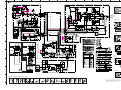
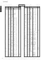
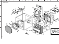
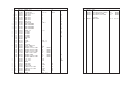
1
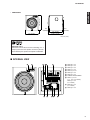
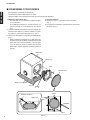
YST-RSW300
SERVICE MANUAL
Status indicator
IMPORTANT NOTICE
This manual has been provided for the use of authorized YAMAHA Retailers and their service personnel.
It has been assumed that basic service procedures inherent to the industry, and more specifically YAMAHA Products, are already known and understood by the users,
and have therefore not been restated.
WARNING:
Failure to follow appropriate service and safety procedures when servicing this product may result in personal injury, destruction of expensive
components, and failure of the product to perform as specified. For these reasons, we advise all YAMAHA product owners that any service required
should be performed by an authorized YAMAHA Retailer or the appointed service representative.
IMPORTANT: The presentation or sale of this manual to any individual or firm does not constitute authorization, certification or recognition of any applicable
technical capabilities, or establish a principle-agent relationship of any form.
The data provided is believed to be accurate and applicable to the unit(s) indicated on the cover. The research, engineering, and service departments of YAMAHA are
continually striving to improve YAMAHA products. Modifications are, therefore, inevitable and specifications are subject to change without notice or obligation to
retrofit. Should any discrepancy appear to exist, please contact the distributor's Service Division.
WARNING:
Static discharges can destroy expensive components. Discharge any static electricity your body may have accumulated by grounding yourself to the
ground buss in the unit (heavy gauge black wires connect to this buss).
IMPORTANT: Turn the unit OFF during disassembly and part replacement. Recheck all work before you apply power to the unit.
■ CONTENTS
TO SERVICE PERSONNEL .......................................... 2
REAR PANELS .......................................................... 3–4
SPECIFICATIONS ...................................................... 4–5
INTERNAL VIEW ........................................................... 5
DISASSEMBLY PROCEDURES ............................... 6–7
CHECKS AND ADJUSTMENTS ................................ 8–9
101052
BLOCK DIAGRAM ....................................................... 10
PRINTED CIRCUIT BOARDS ................................ 11–12
SCHEMATIC DIAGRAM .............................................. 13
REPLACEMENT PARTS LIST .............................. 15–19
2007
All rights reserved.
This manual is copyrighted by YAMAHA and may not be copied or
redistributed either in print or electronically without permission.
P.O.Box 1, Hamamatsu, Japan
'07.04
YST-RSW300
SUBWOOFER SYSTEM
YST-RSW300
■ TO SERVICE PERSONNEL
WALL
OUTLET
YST-RSW300
1. Critical Components Information
Components having special characteristics are marked s
and must be replaced with parts having specifications equal
to those originally installed.
2. Leakage Current Measurement (For 120V Models Only)
When service has been completed, it is imperative to verify
that all exposed conductive surfaces are properly insulated
from supply circuits.
●
Meter impedance should be equivalent to 1500 ohms shunted
by 0.15µF.
EQUIPMENT
UNDER TEST
AC LEAKAGE
TESTER OR
EQUIVALENT
INSULATING
TABLE
●
●
Leakage current must not exceed 0.5mA.
Be sure to test for leakage with the AC plug in both polarities.
For U model
“CAUTION”
“F1: FOR CONTINUED PROTECTION AGAINST RISK OF FIRE, REPLACE ONLY WITH SAME TYPE 6A,
125V FUSE.”
For C model
CAUTION
F1: REPLACE WITH SAME TYPE 6A, 125V FUSE.
ATTENTION
F1: UTILISER UN FUSIBLE DE RECHANGE DE MÉME TYPE DE 6A, 125V.
WARNING: CHEMICAL CONTENT NOTICE!
The solder used in the production of this product contains LEAD. In addition, other electrical/electronic and/or plastic (where
applicable) components may also contain traces of chemicals found by the California Health and Welfare Agency (and
possibly other entities) to cause cancer and/or birth defects or other reproductive harm.
DO NOT PLACE SOLDER, ELECTRICAL/ELECTRONIC OR PLASTIC COMPONENTS IN YOUR MOUTH FOR ANY REASON WHATSOEVER!
Avoid prolonged, unprotected contact between solder and your skin! When soldering, do not inhale solder fumes or expose
eyes to solder/flux vapor!
If you come in contact with solder or components located inside the enclosure of this product, wash your hands before
handling food.
About lead free solder
All of the P.C.B.s installed in this unit and solder joints are soldered using the lead free solder.
Among some types of lead free solder currently available, it is recommended to use one of the following types for the repair
work.
• Sn + Ag + Cu (tin + silver + copper)
• Sn + Cu (tin + copper)
• Sn + Zn + Bi (tin + zinc + bismuth)
Caution:
As the melting point temperature of the lead free solder is about 30°C to 40°C (50°F to 70°F) higher than that of the lead solder, be sure
to use a soldering iron suitable to each solder.
2
YST-RSW300
■ REAR PANELS
R model
K model
A model
YST-RSW300
U, C models
3
YST-RSW300
YST-RSW300
B, G models
L model
■ SPECIFICATIONS
Type ....... Advanced Yamaha Active Servo Technology II
Output Power (100 Hz, 5 ohms, 10% T.H.D.) ...... 250 W
Dynamic Power (5 ohms) ...................................... 270 W
Input Sensitivity (50 Hz, 250 W/5 ohms, L+R)
INPUT1 (SP) .......................................................... 1.0 V
INPUT2 (PJ) ......................................................... 50 mV
Power Consumption ............................................... 80 W
Input Impedance
INPUT1 (SP) ................................................ 2.2 k-ohms
INPUT2 (PJ) .................................................. 12 k-ohms
Standby Power Consumption
................................................. 0.5 W (Reference data)
Frequency Response ........................... 20 Hz to 160 Hz
Dimensions (W x H x D)
..... 372 x 400 x 428.2 mm (14-5/8" x 15-3/4" x 16-7/8")
Driver ........................................ 25 cm (10") cone woofer,
Magnetic shielding type
Weight ............................................... 20 kg (44 lbs. 1oz.)
Input Section
INPUT1 ............................................... Speaker terminal
INPUT2 ..................................................... RCA pin jack
Operation Section
Front panel ....................................... STANDBY/ON key
VOLUME control
HIGH CUT control
Status indicator
Rear panel .................................. POWER ON/OFF key
AUTO STANDBY (HIGH / LOW / OFF) key
PHASE (NORM / REV) key
VOLTAGE SELECTOR key (R, L models)
4
Power Supply
U, C models ........................................ AC 120 V, 60 Hz
R, L models ........ AC 110/120/220/230-240 V, 50/60 Hz
K model ............................................... AC 220 V, 60 Hz
A model ............................................... AC 240 V, 50 Hz
B, G models ........................................ AC 230 V, 50 Hz
Finish
Cherry color .................... U, C, R, K, A, B, G, L models
Black color ...................... U, C, R, K, A, B, G, L models
Accessories ........................................... Nonskid pad x 4
* Specifications are subject to change without notice due to product improvements.
U ........... U.S.A. model
R ........... General model
A ........... Australian model
G ........... European model
C ...........
K ...........
B ...........
L ...........
Canadian model
Korean model
British model
Singapore model
YST-RSW300
YST-RSW300
400 (15-314")
• DIMENSIONS
29.6
(1-3/16")
26.6
(1-1/16")
372 (14-5/8")
372 (14-5/8")
428.2 (16-7/8")
Unit: mm (inch)
Advanced YST II
Advanced Yamaha Active Servo Technology II is a
unique system to let the speaker unit have a perfectly
linear motion by the speaker and amplifier combination.
■ INTERNAL VIEW
1
2
3 45
A
0
6
9 8
1
2
3
4
5
6
7
8
9
MAIN (8) P.C.B.
MAIN (4) P.C.B.
MAIN (2) P.C.B.
MAIN (1) P.C.B.
MAIN (10) P.C.B.
MAIN (3) P.C.B.
MAIN (6) P.C.B.
POWER TRANSFORMER
MAIN (11) P.C.B.
(U, C, K, A, B, G models)
MAIN (7) P.C.B.
(R, L models)
0 MAIN (9) P.C.B.
(R, L models)
A MAIN (5) P.C.B.
7
5
YST-RSW300
YST-RSW300
■ DISASSEMBLY PROCEDURES
(Remove parts in the order as numbered.)
Disconnect the power cable from the AC outlet.
Spread a rubber sheet and cloth, then place the main unit upside down on it.
2. Removal of Driver
a. Remove 4 screws (1)and then remove the driver.
(Fig. 1)
b. Disconnect the connector connected to the terminal of
the driver. (Fig. 1)
1. Removal of Front Grille Ass’y
* The front grille ass’y is fixed to the cabinet with dowels at 5 locations.
As a flatblade screwdriver is used for removal, use
special care not to cause damage to the cabinet
ass’y.
a. Using the flatblade screwdriver inserted in the gap between the front grille ass’y and the cabinet ass’y (bottom side first), push up the front grille ass’y. (Fig. 1)
b. Remove the front grille ass’y by lifting a metalblade up.
(Fig. 1)
* When installing the front grille ass’y, apply quick-drying bond or the like to dowels and then fit them into
dowel holes for secure installation. (The front grille
ass’y will come off easily if its dowels are fitted into
dowel holes without applying quickdrying bond or
the like.)
Bottom side
Cabinet ass'y
Driver
1
Front grille ass'y
Rubber sheet and cloth
Connector
Terminal
Terminal
Dowels
Flatblade screwdriver
Bottom side
Metalblade
Dowels
6
Fig. 1
YST-RSW300
3. Removal of Rear Panel Ass'y
a. Remove 8 screws (2). (Fig. 2)
* Screws (2) are identified with arrow marks ( ).
b. Pull out the rear panel ass'y together with the cover.
(Fig. 2)
c. Remove bush. (Fig. 2)
* The bush once removed cannot be reused. Be sure
to use a new bush for replacement.
d. Remove 2 screws (3). (Fig. 2)
* Screws (3) are identified with arrow marks ( ).
e. Remove the cover. (Fig. 2)
f. Disconnect the connectors (CB9 and CB10). (Fig. 2)
Front panel
Knob hole
CB9
Cable
Switch cover ass'y
Bush
L-shaped metal part
or the like
Front panel
5
Bottom side
Knob
4
Fig. 3
Cover
Bush
Rear panel ass'y
to CB10
to CB4
2
When Checking the P.C.B.:
• Connect all the connectors removed during disassembly back to the original positions.
• Spread cloth first and place the rear panel ass'y and
switch cover ass’y on it. (Fig. 4)
3
Rubber sheet and cloth
to CB9
3
2
Fig. 2
4. Removal of Front Panel Ass’y
* The front panel once removed cannot be reused.
Be sure to use a new front panel for replacement.
Before installing the new front panel, be sure to remove
the double sided adhesive tape remaining from the old
front panel completely.
a. Remove 2 knobs (4). (Fig. 3)
b. Insert L-shaped metal parts or the like into the volume
knob hole and high-cut knob hole in the front panel and
pull the panel gradually away from the cabinet to remove it.
Switch cover ass'y
c. Remove 2 screws (5). (Fig. 3)
d. Pull out the switch cover ass’y. (Fig. 3)
e. Remove bush. (Fig. 3)
* The bush once removed cannot be reused. Be sure
to use a new bush for replacement.
f. Remove the switch cover ass’y together with the cable/
CB9. (Fig. 3)
Rear panel ass'y
Rubber sheet and cloth
Fig. 4
7
YST-RSW300
■ CHECKS AND ADJUSTMENTS
● Confirmation of power amplifier operation
For the power amplifier which has been repaired, it is absolutely necessary to confirm that a correct waveform is obtained
at points indicated by A and B in the schematic diagram according to the following procedure.
Devices required
Signal generator
8-ohm or 6-ohm load resistor
Oscilloscope (dual trace type)
Connection
1) Connect the output signal from the signal generator to the input terminal of the main unit.
2) Disconnect the connector terminal connected to
the speaker unit and reconnect it to the load resistor.
3) Connect the HOT side of the oscilloscope CH1
probe to the point A or B indicated in the figure and
the GND side to the GND of the main unit. (Fig. 1)
4) Connect the oscilloscope CH2 input to the red side
of the connector cable, which is connected with the
load resistor.
At this time, the GND terminal of CH2 must be left
unconnected.
Setting
1) Set the signal generator to the sine wave, 100 Hz
and minimum output level settings.
2) Set the volume of the main unit to the minimum position.
3) Turn on the power to the main unit.
4) Adjust the output level of the signal generator and
the volume of the main unit so that the output level
observed at oscilloscope CH2 is 26 Vp-p to 28 Vp-p.
● Idling adjustment
To stabilize operation of the amplifier, turn ON the power with no input signal and wait for 2 to 3 minutes in non loaded
condition before the adjustment.
Confirm that the voltage across the terminals TP1 and TP2 is 20 mV to 350 mV.
If it exceeds 350 mV, open (cut off) R136.
Attention:
If the idling current exceeds 350 mV after a power amplifier repair, check for a defective component before cutting the
resistor.
MAIN (1) P.C.B.
R136
Waveform observation
With the settings made as described above, observe
the waveform obtained at CH1 for judgment.
PS AMP
POWER
DRIVE
A
PS
AMP
D29
D30
DRIVER
WOOFER
Point B (Anode of D27/D28)
V: 20 V/div H: 2 msec/div
DC range
1 : 1 probe
Point A (Cathode of D29/D30)
V: 20 V/div H: 2 msec/div
DC range
1 : 1 probe
D28
TP2
PS AMP
D27
PS
AMP
POWER
DRIVE
B
26-28 Vp-p
TP1
DC 20 mV to 350 mV
26-28 Vp-p
A
GND
TP1
D28
D27
DC 20 mV to 350 mV
B
D29
D30
TP2
R136
Fig. 1
8
YST-RSW300
● Confirmation of AUTO STANDBY operation setting
1) Turn off the “POWER ON/OFF” key located on the rear panel.
2) In order to shorten the time required for operation check; connect a 10 k-ohms resistor at both ends of R45 on the
MAIN (2) P.C.B.. (Fig. 2)
3) Connect the output signal from the signal generator to the INPUT 2 / L/MONO terminal of the main unit.
4) Set the signal generator for the sine wave of 100 Hz, 8 mV.
5) Turn on the “POWER ON/OFF” key located on the rear panel.
Confirmation
1) Set the “AUTO STANDBY” key to the LOW position.
4) Set the “AUTO STANDBY” key to the HIGH position.
2) Turn on the “STANDBY/ON” key.
The status indicator lights up (green) and its color
changes to red after 2 to 8 seconds.
3) Turn off the “STANDBY/ON” key.
The status indicator goes off.
5) Turn on the “STANDBY/ON” key.
The status indicator lights up (green) and its color
remains unchanged even after time have elapsed.
6) Turn off the “STANDBY/ON” key.
The status indicator goes off.
After confirmation
1) Turn off the “POWER ON/OFF” key.
2) Disconnect the 10 k-ohms resistor connected to both ends of R45.
R45
10 k-ohms
10 k-ohms
R45
9
A
B
C
D
E
F
G
H
I
J
YST-RSW300
1
■ BLOCK DIAGRAM
+
L
3
–
2
INPUT 1
IC11A
1
6
5
SW1
PHASE
SELECT
NORM
IC11B
7
7
6
+B
IC10A
IC7A
6
+
8
7
8
5k-ohms
L.P.F.
6dB/oct
R
L.P.F.
12dB/oct
POWER DRIVE
Q17A, Q17C
PRE DRIVE
Q3-15
IC7B
4
+
2
3
REV
+
2
VR1
VOLUME
DRIVER
WOOFER
PS AMP Q22C, Q24A
RY1
H.P.F.
12dB/oct
–
+
+
–
PS AMP Q22A, Q24C
–
-B
A.N.I.C.
IC8
HIGH CUT
40-140Hz
VR2
+
0.1
L
LIMITER
Q10, Q12
–
3
OUTPUT
+
AUTO STANDBY
SW2
OFF
8
R
4
–
LOW
TIMER 3
IC201
HIGH
Q26-28
Q16, Q19
6
PROTECTION
7
L/
MONO
4
INPUT 2
OFF
LOW
POWER SUPPLY
D25
+
MUSIC
SENSOR
IC4
C27
+B
Q1
POWER
TRANSFORMER
+
C76
R
+
C77
HIGH
PROTECTION
-B
D202
Q30-33
POWER SUPPLY
D2
AUTO STANDBY CIRCUIT
+
C45
5
+
C46
-12
REGULATOR
IC6
+12
RY2
F1
+
C40
AC IN
+
C41
IC1
D203
R60
(U, C, K, A, B, G models)
Q13
SUB
POWER SUPPLY
D3
RY2
6
REGULATOR
REGULATOR
IC202
Q5, Q8
STANDBY/ON
SW4
D201
7
G
10
R
STATUS
INDICATOR
POWER ON/OFF
SW5
(R, L models)
T1
A
B
C
D
E
F
G
H
I
J
YST-RSW300
■ PRINTED CIRCUIT BOARDS
MAIN (3) P.C.B.
MAIN (10) P.C.B.
CB9
CB3
IC10
1
IC4
-
INPUT1/OUTPUT
L
+
9
1
IC11
R
-
8
F6
Q6
F6
Q7
F6
Q9
F6
Q10
E5
Q11
G6
E
RYRY+
SP
OCD
-12
+12
MAIN
E
BE
W6A1
BL
IC1
IC6
IN COM OUT COM IN OUT
W6A2
BE
W6A3
Q12
E5
Q14
G6
MAIN (6)
Q15
F6
(W6B1, W6B2, W6B3)
Q16
I2
Q17A
E4
Q17C
H4
Q19
I2
Q20
F4
Q21
G5
Q22A
F5
Q22C
H5
Q24A
G4
Q24C
F4
Q26
G3
Q27
G3
Q28
G3
Q29
F3
Q30
F3
Q31
G3
Q32
H3
Q33
F3
MAIN (1) P.C.B.
(W5B1, W5B2, W5B3)
8
Q4
MAIN (6)
INPUT 2
5
1
L /MONO / R
OFF
4
LOW
HIGH
NORM
PHASE
AUTO
STANDBY
Ref no. Location
PJ1
4
5
CB1
REV
W3
IC201
3
1
W2
+V1
PWS
E
TOVL
+12
-12
2
9
+V1
PWS
E
TOVL
+12
-12
MAIN (2) (W1)
TOVL
E
MAIN
+V2
+12
-12
PWS
VCC
MAIN (4) (CB4)
VCC
+V1
E
1
RE
BL
+
DRIVER
WOOFER
•
+
SP+
-
SP-
CB10
6
RE
9
1
IC8
Semiconductor Location
Ref no. Location Ref no. Location Ref no. Location Ref no. Location Ref no. Location
I3
D14
E6
D22
F6
D31
G3
IC4
D4
E3
D15
H6
D23
F6
D32
E6
IC6
I3
D5
F6
D16
F6
D24
F6
D33
E6
IC8
E6
D6
E5
D17
H5
D25
J5
D34
E6
IC10
B2
D8
E5
D18
F6
D27
G6
D202
H3
IC11
B5
D10
H6
D19
H6
D28
G6
D203
H3
IC201
C3
D11
H6
D20
H6
D29
G6
D204
H3
Q1
C3
D13
E5
D21
H6
D30
G6
IC1
I3
Q3
F6
B4
CB11
E
RYRY+
SP
OCD
-12
+12
MAIN
E
7
D2
11
A
B
C
D
E
F
G
H
I
J
YST-RSW300
1
MAIN (2) P.C.B.
MAIN (4) P.C.B.
R, L models
MAIN (5) P.C.B.
MAIN (10) (CB9)
•
Semiconductor Location
Ref no. Location Ref no. Location
D1
E3
IC202
B2
D3
C2
Q2
E2
D7
C2
Q5
C2
D9
C2
Q8
C2
D201
I6
Q13
B2
IC7
F2
1
CB4
E1
LEDG
LEDR
PWS
VCC
W4A
W12B
W11B
OR
GY
CB8
7
IC7
2
POWER
ON/OFF
TOVL
E
MAIN
+2V
+12
-12
PWS
VCC
IC202
MAIN (10) (CB1)
W1
E
+1V
VCC
W11A
40Hz 140Hz
HIGH CUT
W8A
W12A
W9A
CB7
3
0 10
VOLUME
BE
WH
AC IN
GY
OR
4
MAIN (6) P.C.B.
MAIN (7) P.C.B.
MAIN (9) P.C.B.
MAIN (6) P.C.B.
MAIN (11) P.C.B.
R, L models
R, L models
R, L models
U, C, K, A, B, G models
U, C, K, A, B, G models
MAIN (8) P.C.B.
5
BL
W8B
STATUS INDICATOR
W7A
W13A
BL
RE
WH
VOLTAGE
SELECTOR
Voltage
230-240V
220V
110V
20V
Select
1-2, 5-6
2-3, 6-7
3-4, 7-8
4-5, 8-9
BE
MAIN (10)
(W6A1,W6A2, W6A3)
W9B
W13B
W14B
W15B
W16B
W7B
W10B
W9B
BE
VCC
PWS
LEDR
LEDG
E1
W4B
RE
W15A
BE
W6B1
POWER
TRANSFORMER
BL
W6B2
BL
RE
W6B3
12
YE
RE
W10A
W5B1
7
BR
YE
W5B2
(W6A1, W6A2, W6A3)
GR
STANDBY/ON
GR
W16A
BE
W6B1
MAIN (10)
W6B2
BE
W6B3
BL
BE
BR
6
BE
MAIN (2)
(W5A1,W5A2, W5A3)
W5B3
W5B1
RE
W5B2
BL
CB5
W14A
W5B3
RE
CB6
BE
W8B
MAIN (2)
(W5A1, W5A2, W5A3)
WH
G
POWER
TRANSFORMER
R
A
B
C
D
E
F
G
H
I
J
L
K
M
N
YST-RSW300
SCHEMATIC DIAGRAM
MAIN
1
MAIN (3)
MAIN (1)
67.6
COMMON
67.6
11.9
0
0 IC11
0
67.0
R
67.3
L
67.0
0
-11.9
66.9
0 IC10
POWER
DRIVE
66.4
0
66.4
0.8
1.2
2
L
11.9
0 IC11
0
-2.6
REV
OFF
HIGH
LOW
0
PS AMP
CB10
0.1
0.2
+
0.1
–
5.4
6.3
CB3
-67.0
The voltages are measured
with AUTO STANDBY OFF.
AUTO STANDBY
TIMER
6.3
8.1
AUTO STANDBY CIRCUIT
W3
0
0.1
0.8
0.8
0
5.7
0.1
NORM
0
0
0.1
0.1
INPUT
0
5.3
5.7
67.5
0.5
L.P.F.
R
67.3
67.3
67.5
PRE DRIVE
0
0 IC10
-11.9
INPUT 2
67.3
0
67.6
0
0
67.6
1.2
MAIN (10)
PHASE
OUTPUT
67.0
OUTPUT/
INPUT 1
IC1: NJM79M12FA
Voltage regulator
DRIVER
WOOFER
-5.5
-67.0
0.1
0.5
0
IC201
0
0
0
0
-5.1
-67.8
-1.0
-67.1
8.1
6.7
0
3
1.4
-5.5
-67.0
0
IC4, 7, 8, 10: µPC4570HA-A
Dual operational amplifier
-67.6
0
-67.6
-66.5
0.1
8.1
IC4
-67.1
-67.0
6.3
-67.7
-67.1
-67.7
6.9
4.0
6.8
IC4
4.0
0
-67.8
-67.5 -67.1
-67.1
V+
R1
Q7
Q5
Q14
Q11
0
II
-67.8
Q1
MUSIC SENSOR
R6
0.1
W4B
4
R5
A.N.I.C.
W4A
0.1
0.1
-11.9
0.1
0.1
0.1
0.1
IC8
0.1
0.1
C2
Q16
R9
Q12
Q15
Q4
C1
OUT
Q10
R3
D
R10
R4
V-
11.9
0.1
0.9
Q3
R2
0.1
R8
Q6
0.1
MAIN (4)
R7
Q9
Q2
IN
STANDBY/ON
Q13
Q8
0
1.4
IC8
0.1
0.1
0.1
0.3
0.1
0.1
LIMITER
0.3
1
0
1
2
+
3
4
IN1
V+ OUT1 II1
STATUS
INDICATOR
36.1
35.8
2
-
+
-
5
6
7
V-
IN2
8
9
II2 OUT2 V+
23.7
23.7
7.5
8.1
0.3
0.3
0.3
2.1
W2
CB11
6.7
-11.9
IC7
0.1
MAIN (8)
0.1
IC7
0.1
0.1
INPUT
W5A1
11.0
5
IC6: NJM78M12FA
Voltage regulator
0.1
6.1
CB4
0
CB9
AC 98.4
0.1
L.P.F.
0.1
-67.8
HIGH CUT
40 to 140Hz
H.P.F.
OUTPUT
67.6
VOLUME
W5A2
0
COMMON
W5A3
U, C, K, A, B, G models
R, L models
6.7
5.6
PROTECTION
6.8
6.8
IC11: NJM4558L
Dual operational amplifier
W6B
W5B
6
W6B
W5B
6.1
6.7
-17.2
0.1
0
6.7
0
V+
0.3
MAIN (6)
8
0
0.7
MAIN (6)
0
PROTECTION
2, 6
0
1, 7
–INPUT
0
OUTPUT
+INPUT
3, 5
-17.2
-17.3
0.9
-16.5
1.4
W6A1
POWER
TRANSFORMER
POWER
TRANSFORMER
AC 26.7
REGULATOR
0
0.1
0.8
2
3
+
-
4
5
6
7
8
-11.9
IC201: LB8555D
General purpose timer
CB1
W10A
W7A
W16A
W15A
W14A
+
0
-17.5
IC1
W13A
-
0
1
W6A3
MAIN (9)
R
0
W9B
W10B
W7B
W16B
W15B
W14B
W8B
W13B
W9B
MAIN (7)
A
0
0
W6A2
1. A OUTPUT
2. A-INPUT
3. A+INPUT
4. V5. B+INPUT
6. B-INPUT
7. B OUTPUT
8. V+
0
11.9
7
4
0.8
-2.6
17.5
17.5
-17.5
W8B
0
IC6
1.3
MAIN (11)
V–
0.1
1.8
-12.8
1.4
0.4
1.4
W1
CB8
TRIGGER 2
8.1
11.2
R
S
Q
3 OUTPUT
-
CB6
7 DISCHARGE
+
IC202
CB7
CB5
W9A
CONTROL 5
VOLTAGE
-
8
REGULATOR
THRESHOLD 6
+
VOLTAGE
SELECTOR
Vcc 8
0
W9A
RESET 4
1
GND
W8A
W8A
54.6
230V-240V
1-2, 5-6
220V
2-3, 6-7
110V
3-4, 7-8
120V
4-5, 8-1
AC
46.5
POWER
ON/OFF W11B
W12B
11.2
54.6
W11A
11.2
11.7
24.4
W12A
11.2
11.2
54.6
24.7
MAIN (2)
AC IN
8
Vcc
2
7
DISCHARGE
OUTPUT
3
6
THRESHOLD
RESET
4
5
CONTROL VOL.
0.1
0
0
0.7
MAIN (5)
AC IN
1
0.1
0
9
GND
TRIGGER
180mm
180mm
200mm
180mm
180mm
200mm
IC202: NJM78L08A-T3
Voltage regulator
MAIN (2)
VIN
VOUT
GND
10
PIN CONNECTION DIAGRAM OF TRANSISTORS, DIODES AND ICS.
2SA970
2SA1015
2SA1145
2SC2240
2SC2705
2SC2878
2SC4449
2SC1815
2SA1837
2SC4793
2SC4688
STD03P
STD03N
4
1
3
1SS133
1SS176
MTZJ12C
MTZJ24B
MTZJ5.6B
Anode
1SR139
1SR400
EL02ZLF
S2L20U
D5BA20-4001 6A
E
CB
BC
E
E
CB
B
C
E
23
1
5
45
3
23
2
45
5
Cathode
Cathode
G/R LED (SPR-39MVWF)
LB8555D
NJM4558L
NJM78L08A-T3
NJM78M12FA
NJM79M12FA
µPC4570HA-A
Anode
1
1
S1NB20 1A 200V
+
AC
AC
-
1
4
4
2
1
3
ANODE
(Green)
3
3
2
32
1
1
ANODE
(Red)
2
CATHODE
9
8
4
8
1
1
12
3
1: OUTPUT
2: GND
3: INPUT
3: COM
3: IN
2: COM
1: OUT
2: IN
1: OUT
★ All voltages are measured with a 10MΩ/V DC electronic voltmeter.
★ Components having special characteristics are marked s and must be replaced
with parts having specifications equal to those originally installed.
★ Schematic diagram is subject to change without notice.
1
13
YST-RSW300
■ REPLACEMENT PARTS LIST
YST-RSW300
• ELECTRICAL COMPONENT PARTS
WARNING
● Components having special characteristics are marked s and must be replaced with parts having specifications
equal to those originally installed.
● The chip resistor is not supplied as a replacement part.
* When a chip resistor is necessary, use the following part.
AAX60720: CHIP RESISTOR SAMPLE BOOK
ABBREVIATIONS IN THIS LIST ARE AS FOLLOWS:
C.A.EL.CHP
C.CE
C.CE.ARRAY
C.CE.CHP
C.CE.ML
C.CE.M.CHP
C.CE.SAFTY
C.CE.TUBLR
C.CE.SMI
C.EL
C.MICA
C.ML.FLM
C.MP
C.MYLAR
C.MYLAR.ML
C.PAPER
C.PLS
C.POL
C.POLY
C.PP
C.TNTL
C.TNTL.CHP
C.TRIM
CN
CN.BS.PIN
CN.CANNON
CN.DIN
CN.FLAT
CN.POST
COIL.MX.AM
COIL.AT.FM
COIL.DT.FM
COIL.MX.FM
COIL,OUTPT
DIOD.ARRAY
DIODE.BRG
DIODE.CHP
DIODE.VAR
DIOD.Z.CHP
DIODE.ZENR
DSCR.CE
FER.BEAD
FER.CORE
FET.CHP
FL.DSPLY
FLTR.CE
FLTR.COMB
FLTR.LC.RF
GND.MTL
GND.TERM
HOLDER.FUS
IC.PRTCT
JUMPER.CN
JUMPER.TST
L.DTCT
:
:
:
:
:
:
:
:
:
:
:
:
:
:
:
:
:
:
:
:
:
:
:
:
:
:
:
:
:
:
:
:
:
:
:
:
:
:
:
:
:
:
:
:
:
:
:
:
:
:
:
:
:
:
:
CHIP ALUMI.ELECTROLYTIC CAP
CERAMIC CAP
CERAMIC CAP ARRAY
CHIP CERAMIC CAP
MULTILAYER CERAMIC CAP
CHIP MULTILAYER CERAMIC CAP
RECOGNIZED CERAMIC CAP
CERAMIC TUBULAR CAP
SEMI CONDUCTIVE CERAMIC CAP
ELECTROLYTIC CAP
MICA CAP
MULTILAYER FILM CAP
METALLIZED PAPER CAP
MYLAR FILM CAP
MULTILAYER MYLAR FILM CAP
PAPER CAPACITOR
POLYSTYRENE FILM CAP
POLYESTER FILM CAP
POLYETHYLENE FILM CAP
POLYPROPYLENE FILM CAP
TANTALUM CAP
CHIP TANTALUM CAP
TRIMMER CAP
CONNECTOR
CONNECTOR,BASE PIN
CONNECTOR,CANNON
CONNECTOR,DIN
CONNECTOR,FLAT CABLE
CONNECTOR,BASE POST
COIL,AM MIX
COIL,FM ANTENNA
COIL,FM DETECT
COIL,FM MIX
OUTPUT COIL
DIODE ARRAY
DIODE BRIDGE
CHIP DIODE
VARACTOR DIODE
CHIP ZENER DIODE
ZENER DIODE
CERAMIC DISCRIMINATOR
FERRITE BEADS
FERRITE CORE
CHIP FET
FLUORESCENT DISPLAY
CERAMIC FILTER
COMB FILTER MODULE
LC FILTER,EMI
GROUND PLATE
GROUND TERMINAL
FUSE HOLDER
IC PROTECTOR
JUMPER CONNECTOR
JUMPER,TEST POINT
LIGHT DETECTING MODULE
L.EMIT
LED.DSPLY
LED.INFRD
MODUL.RF
PHOT.CPL
PHOT.INTR
PHOT.RFLCT
PIN.TEST
PLST.RIVET
R.ARRAY
R.CAR.
R.CAR.CHP
R.CAR.FP
R.FUS
R.MTL.CHP
R.MTL.FLM
R.MTL.OXD
R.MTL.PLAT
RSNR.CE
RSNR.CRYS
R.TW.CEM
R.CEMENT
SCR.BND.HD
SCR.BW.HD
SCR.CUP
SCR.TERM
SCR.TR
SUPRT.PCB
SURG.PRTCT
SW.TACT
SW.LEAF
SW.LEVER
SW.MICRO
SW.PUSH
SW.RT.ENC
SW.RT.MTR
SW.RT
SW.SLIDE
TERM.SP
TERM.WRAP
THRMST.CHP
TR.CHP
TR.DGT
TR.DGT.CHP
TRANS
TRANS.PULS
TRANS.PWR
TUNER.AM
TUNER.FM
TUNER.PK
VR
VR.MTR
VR.SW
VR.SLIDE
VR.TRIM
:
:
:
:
:
:
:
:
:
:
:
:
:
:
:
:
:
:
:
:
:
:
:
:
:
:
:
:
:
:
:
:
:
:
:
:
:
:
:
:
:
:
:
:
:
:
:
:
:
:
:
:
:
:
:
LIGHT EMITTING MODULE
LED DISPLAY
LED,INFRARED
MODULATOR,RF
PHOTO COUPLER
PHOTO INTERRUPTER
PHOTO REFLECTOR
PIN,TEST POINT
PLASTIC RIVET
RESISTOR ARRAY
CARBON RESISTOR
CHIP RESISTOR
FLAME PROOF CARBON RESISTOR
FUSABLE RESISTOR
CHIP METAL FILM RESISTOR
METAL FILM RESISTOR
METAL OXIDE FILM RESISTOR
METAL PLATE RESISTOR
CERAMIC RESONATOR
CRYSTAL RESONATOR
TWIN CEMENT FIXED RESISTOR
CEMENT RESISTOR
BIND HEAD B-TIGHT SCREW
BW HEAD TAPPING SCREW
CUP TIGHT SCREW
SCREW TERMINAL
SCREW,TRANSISTOR
SUPPORT,P.C.B.
SURGE PROTECTOR
TACT SWITCH
LEAF SWITCH
LEVER SWITCH
MICRO SWITCH
PUSH SWITCH
ROTARY ENCODER
ROTARY SWITCH WITH MOTOR
ROTARY SWITCH
SLIDE SWITCH
SPEAKER TERMINAL
WRAPPING TERMINAL
CHIP THERMISTOR
CHIP TRANSISTOR
DIGITAL TRANSISTOR
CHIP DIGITAL TRANSISTOR
TRANSFORMER
PULSE TRANSFORMER
POWER TRANSFORMER ASS’Y
TUNER PACK,AM
TUNER PACK,FM
FRONT-ENDTUNER PACK
ROTARY POTENTIOMETER
POTENTIOMETER WITH MOTOR
POTENTIOMETER WITH ROTARY SW
SLIDE POTENTIOMETER
TRIMMER POTENTIOMETER
15
YST-RSW300
YST-RSW300
P.C.B. MAIN
Ref. No.
*
*
*
CB1
CB3
CB4
CB5-6
CB7-8
CB9
CB10
CB11
C1
C2
C3-5
C6
C7
C8
C9
C10
C11
C12
C13
C14
C15
C16
C17
C18
C19
C20-21
C22
C23
C25
C26
C27
C28
C29
s C30
C31
s C32
C33-34
C35
C36
C37
C38
C39
C40-41
C42
C44
C45-46
C47
C48
C49
C50
C51
Part No.
WK224400
WK224500
WK224600
VB389900
VB390200
VB390400
WC050700
WC050700
VB390400
LB932020
VB390500
UA654470
UA654470
UR867100
VE326400
FG612220
FG644100
UA654390
FG652100
UR838100
UR867100
VE326400
FG613100
UR867100
FG612220
UR867100
VE326200
VE327000
UR867100
VE326000
UR866100
UR837470
UA654100
UR838330
UR838220
FG644100
V7682500
FG644220
V6185300
UA655820
FG644100
UR838100
UA653100
UR778470
UR897100
UR848470
UR897100
VE326800
UR838100
UR867100
UA654270
UR749100
UA654220
UA653680
✻ New Parts
16
Description
P.C.B.
P.C.B.
P.C.B.
CN.BS.PIN
CN.BS.PIN
CN.BS.PIN
CLIP.FUSE
CLIP.FUSE
CN.BS.PIN
CN.BS.PIN
CN.BS.PIN
C.MYLAR
C.CE
C.EL
C.MYLAR
C.CE
C.CE
C.MYLAR
C.CE
C.EL
C.EL
C.MYLAR
C.CE
C.EL
C.CE
C.EL
C.MYLAR
C.MYLAR
C.EL
C.MYLAR
C.EL
C.EL
C.MYLAR
C.EL
C.EL
C.CE
C.CE.SAFTY
C.CE
C.CE.SAFTY
C.MYLAR
C.CE
C.EL
C.MYLAR
C.EL
C.EL
C.EL
C.EL
C.MYLAR
C.EL
C.EL
C.MYLAR
C.EL
C.MYLAR
C.MYLAR
MAIN
MAIN
MAIN
3P
6P
8P
EYF-52BCY
EYF-52BCY
8P
2P
9P
0.047uF
0.047uF
10uF
0.22uF
220pF
0.01uF
0.039uF
100pF
100uF
10uF
0.22uF
1000pF
10uF
220pF
10uF
0.15uF
0.68uF
10uF
0.1uF
1uF
47uF
0.01uF
330uF
220uF
0.01uF
1500pF
0.022uF
0.01uF
0.82uF
0.01uF
100uF
1000pF
470uF
10uF
470uF
10uF
0.47uF
100uF
10uF
0.027uF
1000uF
0.022uF
6800pF
Markets
Ref. No.
UC
RL
KABG
RL
50V J
50V
50V
50V
50V
50V
50V J
50V
16V
50V
50V
50V
50V
50V
50V
50V
50V
50V
50V
50V
16V
50V J
16V
16V
50V
250V
50V
275V
50V J
50V
16V
50V J
63V
100V
25V
100V
50V
16V
50V
50V J
25V
50V J
50V J
s
s
RL
s
s
s
RL
UCKABG
C52
C53
C54
C55
C57
C58
C60
C61-62
C63-64
C65-66
C67-68
C69-70
C71-72
C73-74
C75
C76-77
C80-81
C82
C83
C84
C85-86
C87
C88-89
C90
C91
C92
D1
D2-3
D4-6
D7
D8-11
D13-14
D15-16
D17-18
D19-24
D25
D27-30
D31
D32
D33
D34
D201
D202-203
D204
F1
F1
F2
G2-4
G6
IC1
IC4
IC6
IC7-8
IC10
Part No.
FG644100
UA653680
UA653220
UR867100
UR867100
UA654220
VE326000
UA654220
UR877470
UA654100
WB540200
VE326300
V5058000
VE326400
UR867100
V6092500
UR798330
UR867220
UR838100
WE101700
UR867100
UR867100
UR847470
UR838100
VE326000
FG613100
VD631600
VR253700
VD631600
VG440300
VD631600
VD631600
VU264100
VG437700
V6934100
VQ111400
VP779200
VD631600
VG437700
VG442500
VG437700
VS079300
VU264100
VD631600
WG410500
KB001660
KB001660
V7235100
V5995800
XD343A00
XB247A00
XJ602A00
XB247A00
XB247A00
✻ New Parts
Description
C.CE
C.MYLAR
C.MYLAR
C.EL
C.EL
C.MYLAR
C.MYLAR
C.MYLAR
C.EL
C.MYLAR
C.POL.MTL
C.MYLAR
C.MYLAR
C.MYLAR
C.EL
C.EL
C.EL
C.EL
C.EL
C.PP
C.EL
C.EL
C.EL
C.EL
C.MYLAR
C.CE
DIODE
DIODE.BRG
DIODE
DIODE.ZENR
DIODE
DIODE
DIODE
DIODE.ZENR
DIODE
DIODE.BRG
DIODE
DIODE
DIODE.ZENR
DIODE.ZENR
DIODE.ZENR
LED
DIODE
DIODE
FUSE
FUSE
FUSE
CN.GND
PLATE.GND
IC
IC
IC
IC
IC
0.01uF
50V
6800pF
50V J
2200pF
50V J
10uF
50V
10uF
50V
0.022uF 50V J
0.1uF
50V
0.022uF 50V J
47uF
63V
0.01uF
50V J
0.1uF
250V
0.18uF
50V
4.7uF
250V
0.22uF
50V
10uF
50V
8200uF
80V
330uF
100V
22uF
50V
100uF
16V
1000pF
100V
10uF
50V
10uF
50V
47uF
25V
100uF
16V
0.1uF
50V
1000pF
50V
1SS133,176
S1NB20
1A 200V
1SS133,176
MTZJ12C 12V
1SS133,176
1SS133,176
1SR139,400
MTZJ5.6B 5.6V
EL02ZLF-H5K
D5SBA20-4001 6A
S2L20U
1SS133,176
MTZJ5.6B 5.6V
MTZJ24B 24V
MTZJ5.6B 5.6V
RED/GREEN
1SR139,400
1SS133,176
6A
125V
T1.6A 250V
T1.6A 250V
JG-11-T
NJM79M12FA
uPC4570HA-A
NJM78M12FA
uPC4570HA-A
uPC4570HA-A
Markets
RL
KABG
RL
UCRL
KABG
RL
YST-RSW300
P.C.B. MAIN
Ref. No.
*
*
*
*
IC11
IC201
IC202
PJ1
PN1
Q1-2
Q3
Q4
Q5
Q6
Q7
Q8
Q9-10
Q11
Q12
Q13
Q14
Q15
Q16
Q17
Q19
Q20
Q21
Q22
Q24
Q26-27
Q28-29
Q30
Q31-33
R5-11
R12-13
R52
R53-54
R57
R59
R60
R63
R66
R73
R75
R76
R77-78
R82-83
R84
R86
R88-89
R94
R102-103
R104-105
R106
R107-108
R120
R122
R135
Part No.
XM922A00
X2020A00
X4472A00
V6415800
WB543700
iC224030
iA097040
iC1815I0
iC224030
iC1815I0
iA097030
VK801200
iA097040
iA1015I0
WF612700
iC224030
VE198700
VE198800
iC224030
WK192900
iA097030
V5876900
iA097030
VQ116600
WK192900
iC287820
iC224030
iA097030
iC224030
HV756220
HV756470
HB026390
HV753100
HV755220
HV755560
HV753220
HV755220
HV754330
HB028100
HV755330
HV755220
HV753220
VG730500
HV756390
HV756120
HV753100
HV754100
HV754220
VC753800
HV753470
HV755220
VR860900
WK542600
HV753220
✻ New Parts
Description
IC
IC
IC
JACK.PIN
PIN
TR
TR
TR
TR
TR
TR
TR
TR
TR
TR
TR
TR
TR
TR
TR.PAIR
TR
TR
TR
TR.PAIR
TR.PAIR
TR
TR
TR
TR
R.CAR.FP
R.CAR.FP
R.MTL.FLM
R.CAR.FP
R.CAR.FP
R.CAR.FP
R.CAR.FP
R.CAR.FP
R.CAR.FP
R.MTL.FLM
R.CAR.FP
R.CAR.FP
R.CAR.FP
R.MTL.OXD
R.CAR.FP
R.CAR.FP
R.CAR.FP
R.CAR.FP
R.CAR.FP
R.MTL.OXD
R.CAR.FP
R.CAR.FP
R.MTL.OXD
R.WW
R.CAR.FP
NJM4558L
LB8555D
NJM78L08A-T3
2P
WB54370 L=70 #18
2SC2240 GR,BL
2SA970 GR
2SC1815 Y
2SC2240 GR,BL
2SC1815 Y
2SA970 GR,BL
2SC4688 R,O
2SA970 GR
2SA1015 Y
2SC2240 GR
2SC2240 GR,BL
2SA1145 O,Y
2SC2705 O,Y
2SC2240 GR,BL
STD03P/STD03N
2SA970 GR,BL
2SC4449 E,F
2SA970 GR,BL
2SA1837/C4793 O,Y
STD03P/STD03N
2SC2878 A,B
2SC2240 GR,BL
2SA970 GR,BL
2SC2240 GR,BL
2.2KΩ
1/4W
4.7KΩ
1/4W
3.9KΩ
1/4W
1Ω
1/4W
220Ω
1/4W
560Ω
1/4W
2.2Ω
1/4W
220Ω
1/4W
33Ω
1/4W
100KΩ
1/4W
330Ω
1/4W
220Ω
1/4W
2.2Ω
1/4W
0.15Ω
3W
3.9KΩ
1/4W
1.2KΩ
1/4W
1Ω
1/4W
10Ω
1/4W
22Ω
1/4W
1Ω
2W
4.7Ω
1/4W
220Ω
1/4W
1.5kΩ
3W
0.1Ω
3W
2.2Ω
1/4W
Markets
Ref. No.
s
s
RL
RL
Carbon Resistors
s
s
s
* s
s
*
*
R136
RY1
RY2
ST1
SW1
SW2
SW4
SW5
SW6
T1
T1
T1
TE1-2
TE3
TP1-2
VR1
VR2
Part No.
HV755820
VU161600
V6017400
V4040500
VQ545800
VD179500
VS066500
WG803400
WB493700
XW606A00
X8843A00
XW608A00
VT658100
V9065900
VT969000
WC595500
WK126500
WK126700
WE983600
UCKABG
✻ New Parts
Description
R.CAR.FP
RELAY
RELAY
SCR.TERM
SW.SLIDE
SW.SLIDE
SW.PUSH
SW.PUSH
VOLT.SELCT
TRANS.PWR
TRANS
TRANS.PWR
TERM.WRAP
TERM.SP
PIN.TEST
VR
VR
HOLDER.LED
SCR.BND.HD
820Ω
1/4W
DC OSA-SS-224DM3
DC SDT-S-112LMR2
M3
SSSF04
SSSU12
SPPH13-W
PS4E-A-040-NP
R8140246
352-TX119
MSP-108V-01 PBSN
IRS-2049
A 5KΩ
C 10kΩ
LDT-142G
3x8
MFZN2B3
Markets
RL
UC
RL
KABG
Value
1.0 Ω
1.8 Ω
2.2 Ω
3.3 Ω
4.7 Ω
5.6 Ω
10 Ω
15 Ω
22 Ω
27 Ω
33 Ω
39 Ω
47 Ω
56 Ω
68 Ω
75 Ω
82 Ω
91 Ω
100 Ω
110 Ω
120 Ω
150 Ω
160 Ω
180 Ω
200 Ω
220 Ω
270 Ω
330 Ω
390 Ω
430 Ω
470 Ω
510 Ω
560 Ω
680 Ω
820 Ω
910 Ω
1.0 kΩ
1.2 kΩ
1.5 kΩ
1.8 kΩ
2.0 kΩ
2.2 kΩ
2.4 kΩ
2.7 kΩ
3.0 kΩ
3.3 kΩ
3.6 kΩ
3.9 kΩ
4.7 kΩ
5.1 kΩ
5.6 kΩ
6.8 kΩ
8.2 kΩ
9.1 kΩ
1/4W Type Part No. 1/6W Type Part No.
HJ35 3100
HF85 3100
HJ35 3180
❊
HJ35 3220
HF85 3220
HJ35 3330
HF85 3330
HJ35 3470
HF85 3470
HJ35 3560
HF85 3560
HF45 4100
HF45 4100
HJ35 4150
HF85 4150
HF45 4220
HF45 4220
HJ35 4270
HF85 4270
HF45 4330
HF45 4330
HJ35 4470
HF85 4390
HF45 4470
HF45 4470
HF45 4560
HF45 4560
HF45 4680
HF45 4680
HF45 4750
HF45 4750
HF45 4820
HF45 4820
HF45 4910
HF45 4910
HF45 5100
HF45 5100
HJ35 5110
HF85 5110
HF45 5120
HF45 5120
HF45 5150
HF45 5150
HJ35 5160
❊
HF45 5180
HF45 5180
HF45 5200
HF45 5200
HF45 5220
HF45 5220
HF45 5270
HF45 5270
HF45 5330
HF45 5330
HF45 5390
HF45 5390
HF45 5430
HF45 5430
HF45 5470
HF45 5470
HF45 5510
HF45 5510
HF45 5560
HF45 5560
HF45 5680
HF45 5680
HF45 5820
HF45 5820
HF45 5910
HF45 5910
HF45 6100
HF45 6100
HF45 6120
HF45 6120
HF45 6150
HF45 6150
HF45 6180
HF45 6180
HJ35 6200
HF85 6200
HF45 6220
HF45 6220
HJ35 6240
HF85 6240
HF45 6270
HF45 6270
HF45 6300
HF45 6300
HF45 6330
HF45 6330
HJ35 6360
HF85 6360
HF45 6390
HF45 6390
HF45 6470
HF45 6470
HF45 6510
HF45 6510
HF45 6560
HF45 6560
HF45 6680
HF45 6680
HF45 6820
HF45 6820
HF45 6910
HF45 6910
Value
10 kΩ
11 kΩ
12 kΩ
13 kΩ
15 kΩ
18 kΩ
22 kΩ
24 kΩ
27 kΩ
30 kΩ
33 kΩ
36 kΩ
39 kΩ
47 kΩ
51 kΩ
56 kΩ
62 kΩ
68 kΩ
82 kΩ
91 kΩ
100 kΩ
110 kΩ
120 kΩ
150 kΩ
180 kΩ
220 kΩ
270 kΩ
300 kΩ
330 kΩ
390 kΩ
470 kΩ
560 kΩ
680 kΩ
820 kΩ
1.0 MΩ
1.2 MΩ
1.5 MΩ
1.8 MΩ
2.2 MΩ
3.3 MΩ
3.9 MΩ
4.7 MΩ
1/4W Type Part No. 1/6W Type Part No.
HF45 7100
HF45 7100
HF45 7110
HF45 7110
HJ35 7120
HF85 7120
HF45 7130
HF45 7130
HF45 7150
HF45 7150
HF45 7180
HF45 7180
HF45 7220
HF45 7220
HF45 7240
HF45 7240
HJ35 7270
HF85 7270
HF45 7300
HF45 7300
HF45 7330
HF45 7330
HF45 7360
HF45 7360
HF45 7390
HF45 7390
HF45 7470
HF45 7470
HF45 7510
HF45 7510
HF45 7560
HF45 7560
HF45 7620
HF45 7620
HF45 7680
HF45 7680
HF45 7820
HF45 7820
HF45 7910
HF45 7910
HF45 8100
HF45 8100
HF45 8110
HF45 8110
HF45 8120
HF45 8120
HF45 8150
HF45 8150
HF45 8180
HF45 8180
HJ35 8220
HF85 8220
HF45 8270
HF45 8270
HF45 8300
HF45 8300
HF45 8330
HF45 8330
HJ35 8390
HF85 8390
HF45 8470
HF45 8470
HJ35 8560
HF85 8560
HJ35 8680
HF85 8680
HJ35 8820
HF85 8820
HF45 9100
HF45 9100
HJ35 9120
❊
HJ35 9150
HF85 9150
HJ35 9180
HF85 9180
HJ35 9220
HF85 9220
HJ35 9330
HF85 9330
HJ35 9390
❊
HJ35 9470
HF85 9470
1/4W Type
HF45
1/4W Type
HJ35
1/6W Type
HF85
10mm
5mm
❊ : Not available
17
A
B
C
D
E
F
G
H
I
J
YST-RSW300
1
•
OVERALL ASS’Y
5 (3)
4-32
15
8
4-35
2
4-22
5 (10)
5 (8)
4-35
27
5 (4)
12
11
24
26
4-37
4-38
5 (1)
4-29
27
3
10
7
4-32
4-33
4-34
4-31
4-35
4-33
4-32
4-23
4-35
4
4-35
4-32
4-37
5 (6)
4-32
4-3
4-20
2
4-4
4-35
4-5
4-19
4-19
25
3
5
24
5 (11) U, C, K, A,
B, G models
(7) R, L models
4-11
5 (2)
4-16
5 (5)
R, L models
4-32
6
4-8
4-21
1
4-36
6
4-11
4-18
5 (9)
202
7
18
4-19
4-19
YST-RSW300
Ref. No. Part No.
*
*
s
s
s
s
s
s
*
*
*
*
*
*
*
*
*
*
*
*
*
*
*
*
*
*
*
*
*
*
s
s
s
s
s
1
1
2
3
4-3
4-3
4-3
4-3
4-3
4-3
4-4
4-5
4-5
4-5
4-5
4-5
4-8
4-11
4-11
4-11
4-11
4-11
4-16
4-18
4-19
4-20
4-21
4-22
4-23
4-29
4-31
4-32
4-33
4-34
4-35
4-36
4-37
4-38
5
5
5
6
7
7
8
10
10
11
11
12
WK217100
WK217000
X4457D00
WH695000
V9436300
WD042000
V8012900
WC883100
WC906500
V9436400
CB072750
X8219A00
X8220A00
X8809A00
X8727A00
X8221A00
WG886600
WJ991200
WJ991300
WJ991600
WJ991400
WJ991500
WA217100
WB249900
WB377300
WB377400
WC690300
WB279400
WJ951100
VV849300
WE994800
WE774400
WE962000
WF268000
WF002600
WE983600
WE981100
WF303900
WK224400
WK224500
WK224600
V9467400
WJ956100
WK175600
WJ955800
WJ981900
WK175400
WJ981600
WK175500
WK235100
✻ New Parts
Description
CABINET ASS'Y
CABINET ASS'Y
DRIVER WOOFER
FRONT GRILLE ASS'Y
POWER CABLE
POWER CABLE
POWER CABLE
POWER CABLE
POWER CABLE
POWER CABLE
CORD STOPPER
POWER TRANSFORMER
POWER TRANSFORMER
POWER TRANSFORMER
POWER TRANSFORMER
POWER TRANSFORMER
BINDING TIE
REAR PANEL
REAR PANEL
REAR PANEL
REAR PANEL
REAR PANEL
POWER KNOB
COVER
PACKING
PACKING E
BUSH
REAR COVER
SUPPORT TRANSISTOR
RADIATION SHEET
BIND HEAD S-TIGHT SCREW
BIND HEAD B-TIGHT SCREW
BIND HEAD B-TIGHT SCREW
BIND HEAD P-TIGHT SCREW
PW HEAD B-TIGHT SCREW
BIND HEAD SCREW
BIND HEAD P-TIGHT SCREW
BIND HEAD BONDING SCREW
P.C.B. ASS'Y
P.C.B. ASS'Y
P.C.B. ASS'Y
EMBLEM
FRONT PANEL
FRONT PANEL
SWITCH COVER
VOLUME/HIGH CUT KNOB
VOLUME/HIGH CUT KNOB
POWER KNOB
POWER KNOB
PACKING
Remarks
25cm
Markets
CH
BL
2564B
6Ω
2m
2m
2m
2m
2m
2m
SR-4N-4
UC
R
K
A
B
GL
Ref. No. Part No.
Description
15
24
25
26
27
WC736000
WG405400
WF459800
WF683300
WF268000
BUSH
BIND
BIND
FLAT
BIND
202
WB365800
ACCESSORY
NONSKID PAD
HEAD
HEAD
HEAD
HEAD
TAPPING SCREW
TAPPING SCREW #1
WOOD SCREW
P-TIGHT SCREW
Remarks
4x35
4x25
3.1x16
3x10
MFZN2B3
MFZN2B3
MFZN2W3
MFZN2B3
M32 t2
4pcs/set
Markets
UC
RL
K
A
BG
CT-100
UC
RL
K
A
BG
276x6 t=1
100x85 t=2
4P
19x24
4x8
3x8
4x8
3x10
3x8
3x8
4x12
3x6
MAIN
MAIN
MAIN
MFZN2B3
MFZN2B3
MFZN2B3
MFZN2B3
MFZN2W3
MFZN2B3
MFZN2B3
MFZN2B3
RL
UC
RL
KABG
BLACK
SILVER
CH
BL
BLACK
SILVER
BLACK
SILVER
145x3 t=1.0
CH
BL
CH
BL
✻ New Parts
19
YST-RSW300