1
INVERTER
A800
FR-A800
PLC FUNCTION
PROGRAMMING MANUAL
INVRERTER
PLC FUNCTION PROGRAMMING MANUAL
IB(NA)-0600492ENG-B(1405)MEE Printed in Japan
Specifications subject to change without notice.
B
PLC Function
1
CC-Link communication
2
Sequence program
3
Error code list
4
CONTENTS
7
1.1
Applicable inverter model ....................................................................................... 8
1.2
Function block diagram .......................................................................................... 8
1.3
Operation panel indication...................................................................................... 9
1.4
PLC function specifications.................................................................................. 10
1.5
System configuration ............................................................................................ 11
1.6
Operations of PLC function (Pr.414, Pr.415, Pr.498, Pr.1150 to Pr.1199) ......... 12
1.7
Prior to creating sequence programs .................................................................. 13
1.7.1
Precautions for creating sequence programs............................................................................... 13
1.7.2
The main functions of FR Configurator2 (Developer) ................................................................... 13
1.7.3
Sequence program execution....................................................................................................... 14
1.7.4
Setting the communication parameter .......................................................................................... 15
1.7.5
Writing sequences programs ........................................................................................................ 16
1.8
Device map ............................................................................................................. 17
1.8.1
I/O device map ............................................................................................................................. 17
1.8.2
Internal relay (M) device map ....................................................................................................... 19
1.8.3
Data register (D) device map........................................................................................................ 19
1.8.4
Special relay ................................................................................................................................. 19
1.8.5
Special register............................................................................................................................. 22
1.9
Special registers to monitor and control inverter status ................................... 30
1.9.1
Always readable data ................................................................................................................... 30
1.9.2
Data read by controlling read command (from OFF to ON) ......................................................... 34
1.9.3
Data writing method by controlling write command (from OFF to ON) ......................................... 36
1.9.4
Inverter operating status control ................................................................................................... 40
1.9.5
Inverter parameter access error (SD1150) ................................................................................... 42
1.9.6
Inverter status (SD1151) .............................................................................................................. 42
1.9.7
User-defined error (SD1214) ........................................................................................................ 43
1.9.8
Monitor setting selection (SD1215 to SD1218) ............................................................................ 43
1.10 Read/Write method of inverter parameters ......................................................... 44
1.10.1 Reading inverter parameters ........................................................................................................ 44
1.10.2 Writing inverter parameters .......................................................................................................... 45
1.11 User area reading/writing ...................................................................................... 46
1.12 Analog I/O function ................................................................................................ 47
1.12.1 Analog input.................................................................................................................................. 47
1.12.2 Analog output ............................................................................................................................... 47
1.13 Pulse train input function...................................................................................... 48
CONTENTS
1
CONTENTS
1 PLC Function
1.14 PID control .............................................................................................................. 49
1.15 Clearing the flash memory of the PLC function .................................................. 50
1.16 Constant scan......................................................................................................... 51
2 CC-Link communication
2.1
System configuration............................................................................................. 54
2.1.1
System configuration example...................................................................................................... 54
2.1.2
Function block diagram................................................................................................................. 55
2.2
CC-Link parameter ................................................................................................. 56
2.2.1
2.3
CC-Link extended setting (Pr.544) ............................................................................................... 56
CC-Link I/O specifications..................................................................................... 57
2.3.1
I/O signals when one station in the CC-Link Ver.1 is occupied (Pr.544 = "100").......................... 57
2.3.2
I/O signals when the double setting is set in CC-Link Ver.2 (Pr.544 = "112") .............................. 59
2.3.3
I/O signals when the quadruple setting is set in CC-Link Ver.2 (Pr. 544 = "114") ........................ 61
2.3.4
I/O signals when the octuple setting is set in CC-Link Ver.2 (Pr. 544 = "118")............................. 62
2.4
Buffer memory........................................................................................................ 64
2.4.1
Remote output signals (master station to inverter (FR-A8NC)) .................................................... 64
2.4.2
Remote input signals Pr.544 = "100" (inverter (FR-A8NC) to master station) .............................. 65
2.4.3
Remote registers Pr.544 = "100" (master station to inverter (FR-A8NC)) .................................... 66
2.4.4
Remote registers Pr.544 = "100" (inverter (FR-A8NC) to master station) .................................... 67
3 Sequence program
3.1
69
Overview ................................................................................................................. 70
3.1.1
Overview of operation................................................................................................................... 70
3.2
RUN/STOP operation ............................................................................................. 72
3.3
Program configuration........................................................................................... 72
3.4
Programming language ......................................................................................... 73
3.4.1
Relay symbolic language (ladder mode) ...................................................................................... 73
3.4.2
Function block (FB)....................................................................................................................... 75
3.5
Operation processing method of the PLC function ............................................ 76
3.6
I/O processing method .......................................................................................... 77
3.6.1
Refresh method ............................................................................................................................ 77
3.6.2
Response delay in refresh mode .................................................................................................. 78
3.7
2
53
Scan time ................................................................................................................ 79
CONTENTS
Values that can be used in sequence programs................................................. 80
3.8.1
BIN (binary) .................................................................................................................................. 81
3.8.2
HEX (hexadecimal)....................................................................................................................... 82
3.9
Explanation of devices .......................................................................................... 83
3.9.1
Device list ..................................................................................................................................... 83
3.9.2
I/O X and Y ................................................................................................................................... 84
3.9.3
Internal relay M ............................................................................................................................. 85
3.9.4
Timer T ......................................................................................................................................... 86
3.9.5
100 ms timer, 10 ms timer, and 100 ms retentive timer ............................................................... 86
3.9.6
Processing and accuracy of timers............................................................................................... 87
3.10 Counter C................................................................................................................ 89
3.10.1 Count process in refresh mode .................................................................................................... 90
3.10.2 Maximum counting speed of counter............................................................................................ 90
3.11 Data register D ....................................................................................................... 91
3.12 Special relays and special registers .................................................................... 92
3.13 Function list............................................................................................................ 93
3.14 RUN/STOP method of PLC function from an external source (remote RUN/
STOP) ...................................................................................................................... 94
3.15 Watchdog timer (watchdog error supervision timer) ......................................... 96
3.16 Self-diagnostic function ........................................................................................ 97
3.16.1 Operation mode when there is an operation error........................................................................ 97
3.17 Registering file password ..................................................................................... 98
3.18 Output (Y) status settings when STOP status → RUN status............................ 99
3.19 Structure of instructions ..................................................................................... 100
3.20 Bit device processing method ............................................................................ 101
3.20.1 1-bit processing .......................................................................................................................... 101
3.20.2 Digit specification processing ..................................................................................................... 101
3.21 Handling of numerical values ............................................................................. 104
3.22 Operation error..................................................................................................... 105
3.23 Sequence instructions list .................................................................................. 106
3.23.1 How to view the instruction list table........................................................................................... 106
3.23.2 Sequence instructions list........................................................................................................... 108
3.23.3 Basic instructions........................................................................................................................ 110
3.23.4 Application instructions............................................................................................................... 114
3.23.5 Display instruction ...................................................................................................................... 115
3.24 How to view instructions..................................................................................... 116
CONTENTS
3
CONTENTS
3.8
3.25 Sequence instructions......................................................................................... 117
3.25.1 Contact instruction:
operation start, series connection, parallel connection ... LD, LDI, AND, ANI, OR, ORI ............ 117
3.25.2 Association instruction: ladder block series connection, parallel connection ... ANB, ORB ....... 119
3.25.3 Association instruction:
operation results, push, read, pop ... MPS, MRD, MPP ............................................................. 121
3.25.4 Output instruction: bit device, timer, counter ... OUT.................................................................. 124
3.25.5 Output instruction: device set, reset ... SET, RST ...................................................................... 126
3.25.6 Output instruction: rising, falling differential output ... PLS, PLF................................................. 128
3.25.7 Shift instruction: bit device shift ... SFT, SFTP ........................................................................... 130
3.25.8 Master control instruction: master control set, reset ... MC, MCR .............................................. 132
3.25.9 Termination instruction: termination of main program ... FEND.................................................. 135
3.25.10 Termination instruction: sequence program termination ... END ................................................ 135
3.25.11 Other instructions: non-processing ... NOP, NOPLF, PAGE n ................................................... 136
3.26 Basic instruction (16-bit) ..................................................................................... 139
3.26.1 Comparison operation instruction ............................................................................................... 139
3.26.2 Comparison operation instruction:
16-bit data comparison ... =, <>, >, <=, <, >= ............................................................................. 140
3.26.3 Arithmetic operation instruction .................................................................................................. 142
3.26.4 Arithmetic operation instruction:
BIN 16-bit addition/subtraction ... +, +P, -, -P ............................................................................. 143
3.26.5 Arithmetic operation instruction:
BIN 16-bit multiplication/division ... *, *P, /, /P ............................................................................ 146
3.26.6 Arithmetic operation instruction:
BIN 16-bit data increment/decrement ... INC, INCP, DEC, DECP.............................................. 149
3.26.7 Data transfer instruction.............................................................................................................. 150
3.26.8 Data transfer instruction:
16-bit data transfer ... MOV, MOVP............................................................................................ 150
3.26.9 Data conversion instruction:
2’s complements of BIN 16-bit data ... NEG, NEGP................................................................... 151
3.26.10 Data conversion instructions:
BIN 16-bit data BCD conversions ... BCD, BCDP ...................................................................... 153
3.26.11 Data conversion instructions:
BIN 16-bit data BIN conversions ... BIN, BINP ........................................................................... 154
3.27 Basic instruction (32-bit) ..................................................................................... 155
3.27.1 Comparison operation instruction ............................................................................................... 155
3.27.2 Comparison operation instruction:
32-bit data comparison ... D=, D<>, D>, D<=, D<, D>=.............................................................. 156
3.27.3 Arithmetic operation instruction .................................................................................................. 158
3.27.4 Arithmetic operation instruction:
BIN 32-bit addition/subtraction ... D+, D+P, D-, D-P................................................................... 158
3.27.5 Arithmetic operation instruction:
BIN 32-bit multiplication/division ... D*, D*P, D/, D/P .................................................................. 161
3.27.6 Arithmetic operation instruction:
BIN 32-bit data increment/decrement ... DINC, DINCP, DDEC, DDECP ................................... 164
4
CONTENTS
3.27.7 Data transfer instruction ............................................................................................................. 165
3.27.9 Data conversion instruction:
2's complements of BIN 32-bit data ... DNEG, DNEGP.............................................................. 167
3.27.10 Data conversion instructions:
BIN 32-bit data BCD conversions ... DBCD, DBCDP ................................................................. 168
3.27.11 Data conversion instructions:
BIN 32-bit data BIN conversions ... DBIN, DBINP...................................................................... 169
3.28 Application instructions (16-bit) ......................................................................... 170
3.28.1 Logical operation instructions ..................................................................................................... 170
3.28.2 Logical operation instruction:
BIN 16-bit logical AND ... WAND, WANDP ................................................................................ 171
3.28.3 Logical operation instruction:
BIN 16-bit logical OR ... WOR, WORP ....................................................................................... 174
3.28.4 Logical operation instruction:
BIN 16-bit data exclusive OR ... WXOR, WXORP...................................................................... 176
3.28.5 Logical operation instruction:
BIN 16-bit data exclusive NOR ... WXNR, WXNRP ................................................................... 178
3.29 Application instructions (32-bit) ......................................................................... 180
3.29.1 Logical operation instructions ..................................................................................................... 180
3.29.2 Logical operation instruction:
BIN 32-bit logical AND ... DAND, DANDP .................................................................................. 181
3.29.3 Logical operation instruction:
BIN 32-bit logical OR ... DOR, DORP......................................................................................... 184
3.29.4 Logical operation instruction:
BIN 32-bit data exclusive OR ... DXOR, DXORP ....................................................................... 187
3.29.5 Logical operation instruction:
BIN 32-bit data exclusive NOR ... DXNR, DXNRP ..................................................................... 190
3.30 Display instruction............................................................................................... 192
3.30.1 Character string data transfer ... $MOV, $MOVP ....................................................................... 192
3.30.2 Character string output ... G. PRR, GP.PRR, UMSG ................................................................. 193
4 Error code list
4.1
197
How to read error codes...................................................................................... 198
APPENDIX
201
Appendix 1 Instruction processing time..................................................................... 202
CONTENTS
5
CONTENTS
3.27.8 Data transfer instruction:
32-bit data transfer ... DMOV, DMOVP ...................................................................................... 165
About the related manuals
The manuals related to A800 PLC function are shown below. The download of the latest manuals is free at the Mitsubishi
Electric FA Global Website.
Related manuals
Manual name
6
Manual number
FR-A800 Instruction Manual (Startup)
IB-0600493
FR-A800 Instruction Manual (Detailed)
IB-0600503ENG
FR Configurator2 Instruction Manual
IB-0600516ENG
GX Works2 Version 1 Operating Manual (Common)
SH-080779ENG
CONTENTS
1
PLC Function
This instruction manual explains the functions and devices required for programming.
1.1
1.2
1.3
1.4
1.5
1.6
1.7
1.8
1.9
1.10
1.11
1.12
1.13
1.14
1.15
1.16
Applicable inverter model ..............................................................................
Function block diagram .................................................................................
Operation panel indication.............................................................................
PLC function specifications...........................................................................
System configuration .....................................................................................
Operations of PLC function (Pr.414, Pr.415, Pr.498, Pr.1150 to Pr.1199) ..
Prior to creating sequence programs ...........................................................
Device map ......................................................................................................
Special registers to monitor and control inverter status ............................
Read/Write method of inverter parameters ..................................................
User area reading/writing...............................................................................
Analog I/O function.........................................................................................
Pulse train input function...............................................................................
PID control.......................................................................................................
Clearing the flash memory of the PLC function...........................................
Constant scan .................................................................................................
8
8
9
10
11
12
13
17
30
44
46
47
48
49
50
51
1
PLC Function
7
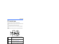
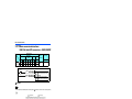
Applicable inverter model
1.1
Applicable inverter model
This manual explains the PLC function of the FR-A800 series.
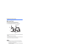
1.2
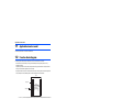
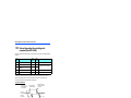
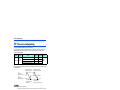
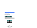
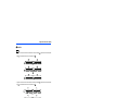
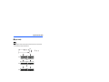
Function block diagram
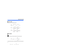
The following function blocks explain I/O information flow to and from the inverter in the PLC function.
• I/O information can be read or written by accessing the inverter with special relays, special registers, etc. using
predetermined methods.
• It is possible to operate the inverter and read and write parameters using input information from control input terminals
according to created sequence programs (saved in the inverter).
Output signals are also be output from control output terminals, not only as status signals of the inverter but as signals to
turn the pilot lamp ON and OFF, interlock signals, and other control signals set by users as desired.
Output signal ∗1
8
I/O data
Special relays,
special registers,
etc.
CPU
Input signal ∗1
Sequence program
Inverter
Set "9999" in any of Pr.178 to Pr.189 (input terminal function assignment) and Pr.190 to Pr.196 (output terminal function selection) to use
terminals as general-purpose I/O terminals. For details on Pr.178 to Pr.189 and Pr.190 to Pr.196, refer to the Instruction Manual of the inverter.
PLC Function
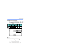
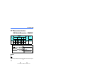
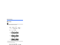
Operation panel indication
1.3
Operation panel indication
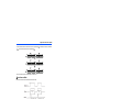
When a sequence program is running, the following indicators are displayed on the operation panel and parameter unit.
P.RUN appears on the
display when the PLC
function is enabled.
PLC function indicator
P.RUN
Output frequency
−−−
PREV
FR-DU08
12:34
P.RUN
60.00 Hz
STF FWD PU
0. 00 Hz
STOP
SET
PU
NEXT
FR-LU08
FR-PU07
P.RUN state
Indication
FR-DU08 (LED)
Status
FR-DU08 (LCD)
FR-PU07 (LCD)
Off
Normal indication
Sequence program stopped
On
Inverted indication
Sequence program running
Flickering
Inverted and flickering
Sequence error occurring
NOTE
• While the offline auto tuning is being activated by FR-PU07, P.RUN is not displayed even during PLC function operation.
1
PLC Function
9
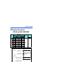
PLC function specifications
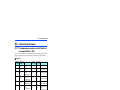
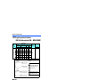
1.4
PLC function specifications
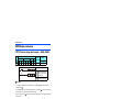
The following table shows the program capacity and devices of the PLC function.
Item
A800 PLC function specifications
Control method
I/O control mode
Programming language
Sequence instructions
Basic instructions
Application instructions
Processing speed
No. of
instructions
Number of I/O device points
Number of analog I/O points
Input
Output
Pulse train I/O
Watchdog timer
Program capacity
Internal relay (M)
Latch relay (L)
Number of points
Timer (T)
Device
Specifications
Number of points
Counter (C)
Specifications
Data register (D)
Special relay (SM)
Special register (SD)
Repeated operation (by stored program)
Refresh
Relay symbolic language (ladder)
Function block
25
84
37
Sequence instructions 1.9 μs to 12 μs/step
128 (input: 64 points, output: 64 points)
19 points built-in (input: 12 points, output: 7 points)
FR-A8AX (input: 16 points)
FR-A8AY (output: 6 points)
FR-A8AR (output: 3 points)
3 input points built-in (Terminals 1, 2, and 4)
2 output points built-in (Terminals FM/CA and AM), FR-A8AY: 2 output
points (AM0 and AM1)
Terminal JOG (maximum input pulse: 100k pulses/s)
Terminal FM (maximum output pulse: 50k pulses/s)
10 to 2000 ms
6K steps (24k bytes) (0 to 6144 steps can be set), contained in one
program
128 (M0 to M127)
Not used (Can be set with parameters but will not latch)
16 (T0 to T15)
100 ms timer: 0.1 to 3276.7 s can be set
10 ms timer: 0.01 to 327.67 s can be set
100 ms retentive timer: 0.1 to 3276.7 s can be set
16 (C0 to C15)
Normal counter: Setting range 1 to 32767
Interrupt program counter: Not used
256 (D0 to D255)
2048 (SM0 to SM2047) with limited functions
2048 (SD0 to SD2047) with limited functions
The scan time is approximately 40 ms for 1K steps as inverter control is also performed in actual operations.
The signals same as the ones assigned to the inverter I/O terminals are used.
One point is always required for a sequence start (RUN/STOP).
The Pr.291 Pulse train I/O selection setting is required. The pulse train output is only available for the FM type inverter.
There is no device latch function for power failures.
Use the Pr.1150 to Pr.1199 PLC function user parameters 1 to 50 (D206 to D255) to store device values in the EEPROM. (Refer to page 46.)
NOTE
• There is no buffer memory.
10
PLC Function
System configuration
1.5
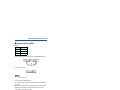
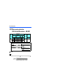
System configuration
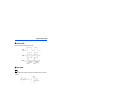
For writing sequence programs to the inverter, use FR Configurator2 (Developer) on the personal computer connected to the
inverter via RS-485 communication. The inverter and the personal computer are connected via USB communication or RS485 communication.
The following figure shows the system configuration for use of the PLC function.
<System configuration example>
USB connector
Serial port
USB cable
Personal computer
(FR Configurator2)
or
USB connector
Serial cable
Personal computer
(FR Configurator2)
USB mini B connector
RS-232C RS-485
converter
USB cable
USB RS-485
converter
Inverter
PU connector
Inverter
Serial port
Serial cable
Inverter
RS-232C RS-485
converter
RS-422/485
Personal computer
(FR Configurator2)
PU connector
RS-485 terminal
block
Up to 32
inverters can
be connected.
Inverter
Commercially available products (as of February 2012)
• RS-232C RS-485 conversion cable
Model
Interface embedded cable dedicated for inverter
DINV-CABV
Manufacturer
Diatrend Corp.
The conversion cable cannot connect multiple inverters. (The computer and inverted are connected in a 1:1 pair.) This product is a RS-232C
RS-485 conversion cable that has a built-in converter. No additional cable or connector is required. For the product details, contact the
manufacturer.
• USB RS-485 conversion cable
Model
DINV-U4
Manufacturer
Diatrend Corp.
• Recommended USB cable for connection between the personal computer and the inverter
Model
MR-J3USBCBL3M (cable length: 3 m)
1
Manufacturer
Mitsubishi Electric Corporation
POINT
• FR Configurator2 (Developer) is a programming tool for designing and debugging of the sequence programs on the Windows
personal computer. To use the PLC function of the inverter, write sequence programs to the inverter using FR Configurator2
(Developer). (For the details, refer to the Instruction Manual of FR Configurator2.)
NOTE
• For details on wiring, refer to the Instruction Manual of the inverter.
• For the specifications of the FR Configurator2 (Developer) and personal computers on which FR Configurator2 (Developer)
runs, refer to the Instruction Manual of FR Configurator2.
• Programming tools other than FR Configurator2 (Developer) cannot be used. (Tools such as GX Developer and GX Works
cannot be used.)
PLC Function
11
Operations of PLC function (Pr.414, Pr.415, Pr.498, Pr.1150 to Pr.1199)
1.6
Operations of PLC function (Pr.414, Pr.415,
Pr.498, Pr.1150 to Pr.1199)
I/O information can be read or written by accessing the inverter with special relays, special registers, etc. using
predetermined methods.
It is possible to operate the inverter and read and write parameters using input information from control input terminals
according to created sequence programs (saved in the inverter).
Output signals are also be output from control output terminals, not only as status signals of the inverter but as signals
to turn the pilot lamp ON and OFF, interlock signals, and other control signals set by users as desired.
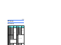
Parameter
number
Initial
value
Name
Setting range
Refer to page
414
PLC function operation selection
0
0 to 2
14
415
Inverter operation lock mode setting
0
0, 1
14
498
PLC function flash memory clear
0
0, 9696 (0 to 9999)
50
1150 to 1199
PLC function user parameters 1 to 50
0
0 to 65535
46
12
PLC Function
Prior to creating sequence programs
1.7
Prior to creating sequence programs
1.7.1
Precautions for creating sequence programs
POINT
• Writing and access to other stations are not possible while a sequence program is running.
Also, reading and writing the program from and to other stations cannot be performed.
• To avoid accidentally erasing the created sequence programs, use FR Configurator2 (Developer) to regularly save the data in
a personal computer, etc.
If a sequence program contains instructions (refer to page 106) or devices (refer to page 10) that cannot be used with the
PLC function, an instruction code error occurs at the execution of that instruction.
Error code
SD0 = 4000
Error information SD5 to SD26
Error flag
SM0: ON
NOTE
• For the error codes, refer to page 33.
1.7.2
The main functions of FR Configurator2
(Developer)
• Reading and writing parameter and sequence programs
• Ladder monitor
• Device batch monitor
• Present value change
• Remote RUN/STOP
NOTE
• Present values can be changed using FR Configurator2 (Developer) ([Debug] -> [Present value change]). Even if changes
are made to the devices corresponding to the control terminal signals (STF, STR, etc.), such changes are not applied to the
inverter operation. (Device present values of the sequence programs are changed.)
1
PLC Function
13
Prior to creating sequence programs
1.7.3
Sequence program execution
Parameter
number
PLC function operation
selection
414
Initial
value
Name
0
Setting
range
0
PLC function disabled
1
PLC
function
enabled
2
Inverter operation lock
mode setting
415
Description
The SQ signal is enabled by input from a
command source (external input terminal/
communication).
The SQ signal is enabled by input from an
external input terminal
0
The start signal of the inverter is enabled regardless of
execution instruction of the sequence program.
1
The start signal of the inverter is enabled only when
the sequence program is in RUN state. (The SQ signal
is ON.)
When the sequence program is in STOP state (the SQ
signal is OFF), the inverter will not start even if the
start signal STF or STR is turned ON. (If the state is
changed from RUN to STOP during operation, the
inverter decelerates and stops.)
0
Reset the inverter after configuring settings to enable the PLC function.
PLC function operation selection (Pr.414)
• To enable the PLC function, set "1" or "2" in Pr.414 PLC function operation selection. When Pr.414 = "1", the command
source for the sequence start (SQ) signal is determined by Pr.338 Communication operation command source. When
"2" is set in Pr.414, SQ signal from the external input terminal is valid regardless of the setting of the Pr.338.
• Switch the execution key (RUN/STOP) of the sequence program by turning the SQ signal ON/OFF. The sequence program
can be executed by turning the SQ signal ON. To input the SQ signal, set "50" in any of Pr.178 to Pr.189 (input terminal
function selection) to assign the function to a terminal.
• Remote RUN/STOP of the PLC function can be executed in any of the following methods:
• Using the PLC function parameters (contact)
• Using FR Configurator2 (Developer)
• Via CC-Link communication (refer to page 56.)
NOTE
• Turn OFF (STOP) the SQ signal when creating a sequence program.
• The RUN state output (Y) is internally stored and all outputs (Y) are turned off by turning the SQ signal OFF (STOP) after
sequence program execution (SQ signal ON).
The other devices retain the data prior to STOP. To clear the remaining device data, power OFF or reset (RES signal ON (0.1
s)OFF) the inverter.
Inverter operation lock mode setting (Pr.415)
• When "1" is set in Pr.415 Inverter operation lock mode setting, the inverter can be operated only when the sequence
program is set to the "RUN" status. By changing the PLC program status from RUN to STOP during inverter operation, the
motor decelerates to stop.
POINT
• To run the inverter without using the PLC function, set Pr.415 = "0" (initial value) (the start signal of the inverter is enabled).
NOTE
• This parameter cannot be written during inverter operation, regardless of the Pr.77 setting.
• During automatic operation using SD1148 (or SM1200 to SM1211) in the sequence program, the inverter stops operation if
the sequence program is in the STOP state while Pr.415 = "1". However, when Pr.415 = "0", the device data is retained and
the operating status does not change (the inverter continues operation) even if the sequence program is in the STOP state.
• Pr.415 setting is also enabled for the start signals of the operation panel.
14
PLC Function
Prior to creating sequence programs
1.7.4
Setting the communication parameter
POINT
• For RS-485 communication between the inverter and FR Configurator2, communication cannot be established when the
inverter communication parameter settings and the FR Configurator2 communication settings differ.
• Set "9999" in Pr.122 PU communication check time interval for communication using the PU connector, and set "9999"
in Pr.336 RS-485 communication check time interval for communication with RS-485 terminals.
• Use the same settings for the inverter communication parameters (Pr.118 to Pr.120, Pr.124, Pr.332 to Pr.334, and Pr.341)
and the FR Configurator2 communication settings.
• Initial values are shown below.
FR Configurator2
initial value
Item
Communication speed
19200(bps)
Data length/Stop bit
Data length : 8 bits
Stop bit : 2 bits
Parity
Even
Communication check
time interval
-
Delimiter
CR
Inverter communication parameters
Pr.
Parameter name
Initial value
118
PU communication speed
192 (19200 bps)
332
RS-485 communication speed
96 (9600 bps)
119
PU communication stop bit length /
data length
333
RS-485 communication stop bit length
/ data length
120
PU communication parity check
334
RS-485 communication parity check
selection
122
PU communication check time interval
9999 (without
communication check)
336
RS-485 communication check time
interval
0 (Changing to NET
operation mode disabled)
124
PU communication CR/LF selection
341
RS-485 communication CR/LF
selection
1 (data length: 8 bits,
stop bit: 2 bits)
2 (with even parity check)
1 (CR)
NOTE
• Use the operation panel to change the settings of the inverter parameters.
The operation panel and FR Configurator2 (personal computer) cannot be connected to the PU connector simultaneously.
• For details on each inverter communication parameter, refer to the Instruction Manual (Detailed) of the inverter. For the
setting method of the [Detailed setting] of the [System setting] window of FR Configurator2, refer to the Instruction Manual of
FR Configurator2.
• Parameter clear/All parameter clear clears communication parameter settings and may disable the communication with FR
Configurator2 (Developer).
1
PLC Function
15
Prior to creating sequence programs
1.7.5
Writing sequences programs
POINT
• Sequence programs can be written in any operation mode (External operation mode, PU operation mode and Network
operation mode). For the operation modes, refer to the Instruction Manual (Detailed) of the inverter.
Check the following points when rewriting the PLC function parameters and sequence programs using FR Configurator2
(Developer):
• The sequence program execution status is in the STOP (SQ signal OFF) (refer to page 14).
• The inverter is stopped.
• The communication specifications setting parameters (Pr.117 to Pr.124) are correctly set. Communication with FR
Configurator2 (Developer) is not possible if these parameter setting values are incorrect.
• The PLC series setting and sequence program capacity are correctly set with FR Configurator2 (Developer) parameters.
(Refer to page 11.)
Refer to the FR Configurator2 manual and write sequence programs.
NOTE
• A sequence program cannot be written with its steps specified. The sequence program does not run if written in this way.
(The program outside the specified range is initialized.)
• To read the PLC function parameters and sequence programs from the inverter, such information must be written to the
inverter using FR Configurator2 (Developer) in advance. Always write the PLC function parameters and sequence program at
least once as the inverter does not have valid data.
• There is a limitation on the number of times writing can be done (approximately 100,000 times) as the PLC function
parameters and sequence program are written to the flash memory.
• A program with more than 6k steps (24k bytes) cannot be written.
16
PLC Function
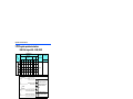
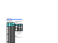
Device map
1.8
Device map
1.8.1
I/O device map
External input/output
Device
number
Name
Remarks
Name
X00
Terminal STF
Y00
Terminal RUN
X01
Terminal STR
Y01
Terminal SU
X02
Terminal RH
Y02
Terminal IPF
X03
Terminal RM
Y03
Terminal OL
X04
Terminal RL
Y04
Terminal FU
X05
Terminal JOG
Y05
Terminal ABC1
X06
Terminal RT
Y06
Terminal ABC2
X07
Terminal AU
Y07
X08
Terminal CS
Y08
X09
Terminal MRS
Y09
X0A
Terminal STP (STOP)
Y0A
X0B
Terminal RES
Y0B
External terminal
X0C
X0D
X0E
Remarks
External terminal
Empty (for temporary retention)
Y0C
Vacant (for temporary retention)
X0F
Plug-in option I/O
Device
number
Y0D
Y0E
Y0F
X10
Terminal X0
Y10
Terminal DO0
X11
Terminal X1
Y11
Terminal DO1
X12
Terminal X2
Y12
Terminal DO2
X13
Terminal X3
Y13
Terminal DO3
X14
Terminal X4
Y14
Terminal DO4
X15
Terminal X5
Y15
Terminal DO5
X16
Terminal X6
Y16
Terminal DO6
Y17
Terminal RA1
Y18
Terminal RA2
Terminal RA3
16 bits
digital input
FR-A8AX
X17
Terminal X7
X18
Terminal X8
X19
Terminal X9
Y19
X1A
Terminal X10
Y1A
X1B
Terminal X11
Y1B
X1C
Terminal X12
Y1C
X1D
Terminal X13
Y1D
X1E
Terminal X14
Y1E
X1F
Terminal X15
Y1F
Digital output
FR-A8AY
Relay output
FR-A8AR
Empty (for temporary retention)
PLC Function
1
17
Device map
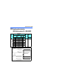
CC-Link I/O Remote I/O
System I/O
Device
number
18
Name
Remarks
Device
number
Name
Remarks
X20
Operation mode setting
read complete
SD1140
Y20
Operation mode setting
read command
SD1140
X21
Set frequency read
complete (RAM)
SD1141
Y21
Set frequency read
command (RAM)
SD1141
X22
Set frequency read
complete (EEPROM)
SD1142
Y22
Set frequency read
command (EEPROM)
SD1142
X23
Operation mode setting
write complete
SD1143
Y23
Operation mode setting
write command
SD1143
X24
Set frequency write
complete (RAM)
SD1144
Y24
Set frequency write
command (RAM)
SD1144
X25
Set frequency write
complete (EEPROM)
SD1145
Y25
Set frequency write
command (EEPROM)
SD1145
X26
Fault record batch clear
complete
SD1146
Y26
Fault record batch clear
command
SD1146
X27
Parameter clear
complete
SD1147
Y27
Parameter clear
command
SD1147
X28
Parameter read
complete (RAM)
Y28
Parameter read
request (RAM)
X29
Parameter write
complete (RAM)
Y29
Parameter write
request (RAM)
X2A
Parameter read
complete (EEPROM)
Y2A
Parameter read
request (EEPROM)
X2B
Parameter write
complete (EEPROM)
Y2B
Parameter write
request (EEPROM)
X2C
User parameter read
complete (RAM)
Y2C
User parameter read
(RAM)
X2D
User parameter write
complete (RAM)
Y2D
User parameter write
(RAM)
X2E
User parameter read
complete (EEPROM)
Y2E
User parameter read
(EEPROM)
X2F
User parameter write
complete (EEPROM)
Y2F
User parameter write
(EEPROM)
X30
RY0
Y30
RX0
X31
RY1
Y31
RX1
X32
RY2
Y32
RX2
X33
RY3
Y33
RX3
X34
RY4
Y34
RX4
X35
RY5
Y35
RX5
X36
RY6
Y36
RX6
X37
RY7
Y37
RX7
X38
RY8
Y38
RX8
X39
RY9
Y39
RX9
X3A
RYA
Y3A
RXA
X3B
RYB
Y3B
RXB
X3C
RYC
Y3C
RXC
X3D
RYD
Y3D
RXD
X3E
RYE
Y3E
RXE
X3F
RYF
Y3F
RXF
PLC Function
SD1241, SD1242,
SD1234
SD1243, SD1244,
SD1235
D206 to D255
(Pr.1150 to Pr.1199)
FR-A8NC
SD1241, SD1242,
SD1234
SD1243, SD1244,
SD1235
D206 to D255
(Pr.1150 to Pr.1199)
FR-A8NC
Device map
1.8.2
Internal relay (M) device map
Device number
M0 to M127
1.8.3
Description
Available for users.
Data register (D) device map
Device number
Refer to
page
Description
D0 to D205
Available for users.
-
D206 to D255
Pr.1150 to Pr.1199
Parameters for user setting. Available for users.
46
1.8.4
Special relay
Special relay is an internal relay whose application is already determined in the PLC function. Therefore, do not turn ON/OFF
the special relay in the program.
Device number
Name
Description
SM0
Diagnostic error
Turned ON when a diagnostic error has been detected.
ON status is retained even after the condition becomes normal.
SM1
Self-diagnostic error
Turned ON when an error is detected by self diagnosis.
ON status is retained even after the condition becomes normal.
SM5
Common error information
When SM5 is turned ON, common error information (SD5 to SD15) is
stored.
SM16
Individual error information
When SM16 is turned ON, individual error information (SD16 to SD26) is
stored.
SM56
Operation error flag
Turned ON when an operation error is detected during instruction
execution.
ON status is retained even after the condition becomes normal.
SM210
Clock data setting request
At OFF to ON of SM210, the clock data stored in SD210 to SD213 are
written to the inverter.
SM211
Clock data error
Turned ON when the clock data (SD210 to SD213) has an error or is not a
BCD value.
SM213
Clock data read request
Clock data is read and stored as BCD value in SD210 to SD213 when this
relay is turned ON.
The process is not executed when the relay is OFF.
SM400
Always ON
SM401
Always OFF
SM402
ON only for one scan after
RUN
SM403
OFF only for one scan after
RUN
SM1200
Inverter operating status
control flag (STF)
Flag used for controlling the inverter terminal STF.
SM1201
Inverter operating status
control flag (STR)
Flag used for controlling the inverter terminal STR.
SM1202
Inverter operating status
control flag (RH)
Flag used for controlling the inverter terminal RH.
SM1203
Inverter operating status
control flag (RM)
Flag used for controlling the inverter terminal RM.
SM1204
Inverter operating status
control flag (RL)
Flag used for controlling the inverter terminal RL.
SM400 and SM401 are respectively turned ON and OFF regardless of the
STOP and RUN statuses.
1
SM402 and SM403 change depending on the STOP and RUN statuses.
In the cases other than STOP:
SM402 is ON only for one scan.
SM403 is OFF only for one scan.
PLC Function
19
Device map
Device number
Name
Description
SM1205
Inverter operating status
control flag (JOG)
Flag used for controlling the inverter terminal JOG.
SM1206
Inverter operating status
control flag (RT)
Flag used for controlling the inverter terminal RT.
SM1207
Inverter operating status
control flag (AU)
Flag used for controlling the inverter terminal AU.
SM1208
Inverter operating status
control flag (CS)
Flag used for controlling the inverter terminal CS.
SM1209
Inverter operating status
control flag (MRS)
Flag used for controlling the inverter terminal MRS.
SM1210
Inverter operating status
control flag STP (STOP)
Flag used for controlling the inverter terminal STP (STOP).
SM1211
Inverter operating status
control flag (RES)
Flag used for controlling the inverter terminal RES.
SM1216
Inverter status (RUN)
Inverter running
SM1217
Inverter status (FWD)
Forward rotation
SM1218
Inverter status (REV)
Reverse rotation
SM1219
Inverter status (SU)
Up to frequency
SM1220
Inverter status (OL)
Overload alarm
SM1221
Inverter status (IPF)
Instantaneous power failure/undervoltage
SM1222
Inverter status (FU)
Output frequency detection
SM1223
Inverter status (ALM)
Fault output
SM1224
Inverter status (LF)
Warning output
SM1225
Inverter status (DO0)
Stores the operating status of an output terminal function assigned by
Pr.313.
SM1226
Inverter statusDO1)
Stores the operating status of an output terminal function assigned by
Pr.314.
SM1227
Inverter status (DO2)
Stores the operating status of an output terminal function assigned by
Pr.315.
SM1228
Inverter status (DO3)
Stores the operating status of an output terminal function assigned by
Pr.316.
SM1229
Inverter status (DO4)
Stores the operating status of an output terminal function assigned by
Pr.317.
SM1230
Inverter status (DO5)
Stores the operating status of an output terminal function assigned by
Pr.318.
SM1231
Inverter status (DO6)
Stores the operating status of an output terminal function assigned by
Pr.319.
SM1232
Inverter status (RA1)
Stores the operating status of an output terminal function assigned by
Pr.320.
SM1233
Inverter status (RA2)
Stores the operating status of an output terminal function assigned by
Pr.321.
SM1234
Inverter status (RA3)
Stores the operating status of an output terminal function assigned by
Pr.322.
SM1235
Safety monitor (terminal SO)
The safety monitor (terminal SO) status is stored.
This is turned ON when no internal safety circuit failure has occurred.
SM1255
Inverter operating status
control selection
Select the inverter operating status of SM1200 to SM1211 and SD1148.
OFF: Special relay selection
ON: Special register selection
SM1256
2-word parameter access
notice
Turned ON when parameter read for the inverter is executed using X28 to
X2B, Y28 to Y2B, and the object was 2-word parameter.
OFF: Read is completed as 1-word parameter.
ON: Read is completed as 2-word parameter.
20
PLC Function
Device map
Device number
Name
Description
SM1257
2-word parameter access
setting
Set the object as 2 word parameter when inverter parameter write is
executed using X28 to X2B, Y28 to Y2B.
OFF: Carries out writing as 1-word parameter.
ON: Carries out writing as 2-word parameter.
SM1258
Clock data setting
completion flag
Turned ON when the clock data is set using an external peripheral device,
parameter, or SM210. This is turned OFF when SM213 is turned ON.
Even if the FR-A8AY or FR-A8AR is not installed, Pr.313 to Pr.322 are accessible during PLC function operation, and the operating status of the
output terminal (virtual output terminal) function is stored in each device.
1
PLC Function
21
Device map
1.8.5
Special register
Special register is a data register in which the application is already determined in the PLC function. Therefore, do not write
data into the special register on the program.
Device number
SD0
Name
Self-diagnostic error
Description
Page
Error code is stored when an error is detected by self diagnosis.
33
Stores the category codes that show the type of error information
stored in the common information (SD5 to SD15) and the
individual information (SD16 to SD26).
b15
to
b8
b7
to
b0
Individual error information Common error information
The following codes are stored in the common information
category code.
Value
SD4
Error information category
Code
0
Not used
2
File name/drive name
3
Time (setting value)
4
Program error location
-
The following codes are stored in the individual information
category code.
Special register
Value
Code
0
Not used
3
Time (actual measurement value)
5
Parameter number
When the common information category code is 2, the file name
or drive name are stored in SD5 to SD11.
Number
SD5
Description
Drive name.
SD6
SD7
SD5 to SD15
File name
(ASCII code: 8 characters)
SD8
Common error information
-
SD9
2EH(.)
SD10
Extension
SD11
(ASCII code: 3 characters)
SD12 to
SD15
Empty
The step numbers where errors occurred are stored in SD14 and
SD15.
When the common information category code is 3, the time
(setting value) is stored in SD5 and SD6.
Number
SD5 to SD15
22
Common error information
PLC Function
Description
SD5
Time: in 1 μs increments (0 to 999 μs)
SD6
Time: in 1 ms increments (0 to 65535 ms)
SD7 to
SD15
Empty
-
Device map
Device number
Name
Description
Page
When the common information category code is 4, the program
error location is stored in SD5 to SD15.
Number
Description
SD5
SD6
File name MAIN
(ASCII code: 8 characters)
SD7
SD8
SD5 to SD15
Common error information
2EH(.)
SD9
Extension
SD10
QPG
SD11
Always 0
SD12
Always 0
SD13
Always 0
SD14
Sequence step No.(L)
Sequence step No.(H)
SD15
(ASCII code: 3 characters)
-
Always "MAIN". After "MAIN", four space (20H) characters are
stored.
The step numbers where errors occurred are stored in SD14 and
SD15.
When the individual information category code is 3, the time
(actual measured data) is stored in SD16 and SD17.
Special register
Number
SD16 to SD26 Individual error information
Description
SD16
Time: in 1 μs increments (0 to 999 μs)
SD17
Time: in 1 ms increments (0 to 65535 ms)
SD18 to
SD26
Empty
-
When the individual information category code is 5, the parameter
number is stored in SD16.
Number
SD203
CPU module operating
status
Description
SD16
Parameter number
SD17 to
SD26
Empty
bit
Item
b3 to b0
CPU module
operating status
b7 to b4
STOP/RUN
factor
Value
-
0
RUN
1
STOP
0
Switch
1
Remote contact
Remote operation from
the peripheral S/W for
the programmable
controller
Error
2
4
1
Description
-
PLC Function
23
Device map
Device number
Name
Description
Page
Year (the last two digits of the year) is stored in BCD code.
SD210
Clock data
Last two digits of the year
Month
Date and hour are stored in BCD code.
SD211
Clock data
Day of the week
Hour
Minute and second are stored in BCD code.
SD212
Clock data
Minute
Second
Year (the first two digits of the year) and day of the week are
stored in BCD code.
Clock data
Special register
SD213
First two digits of the year
SD520
Current scan time
SD521
SD524
Minimum scan time
SD525
SD526
Maximum scan time
SD527
24
Day
Sunday
Monday
Tuesday
Wednesday
Thursday
Friday
Saturday
Scan time is stored at every END, and is constantly updated.
(Measured in 100 μs increments)
SD520: Stores the millisecond places (Stored range: 0 to 65535)
SD521: Stores the microsecond places (Stored range: 0 to 900)
-
Minimum scan time is stored at every END.
(Measured in 100 μs increments)
SD524: Stores the millisecond places (Stored range: 0 to 65535)
SD525: Stores the microsecond places (Stored range: 0 to 900)
-
Maximum scan time is stored at every END.
(Measured in 100 μs increments)
SD526: Stores the millisecond places (Stored range: 0 to 65535)
SD527: Stores the microsecond places (Stored range: 0 to 900)
-
SD1062 to
SD1093
Remote register
Special register for communicating with the master station in CCLink.
SD1133
Output frequency monitor
Present output frequency is stored. The increment is 0.01 Hz.
SD1134
Output current monitor
Present output current is stored. The increment is 0.01 A.
SD1135
Output voltage monitor
Present output voltage is stored. The increment is 0.1 V.
PLC Function
-
-
-
57
30
Device map
Special register for control
Device number
Name
SD1136
Faults history 1, 2
SD1137
Faults history 3, 4
SD1138
Faults history 5, 6
SD1139
Faults history 7, 8
SD1140
Description
Page
Faults in the inverter are stored in the order of occurrence.
31
Operation mode setting
read
Stores the present operation mode.
34
SD1141
Set frequency read (RAM)
Reads and stores the set frequency (RAM).
35
SD1142
Set frequency read
(EEPROM)
Reads and stores the set frequency (EEPROM).
35
SD1143
Operation mode setting
write
Sets the operation mode to be changed.
37
SD1144
Set frequency write (RAM)
Sets the running frequency (RAM).
37
SD1145
Set frequency write
(EEPROM)
Sets the running frequency (EEPROM).
38
SD1146
Fault record batch clear
Clears the faults history when H9696 is written.
39
Parameter clear
H9696 write: parameter clear
H9966 write: all clear
H5A5A write: parameter clear except for communication
parameters
H55AA write: all clear except for communication parameters
While communicating with FR Configurator2, clear the parameters
using H5A5A or H55AA.
39
SD1147
Turn ON/OFF the corresponding bit to control the inverter
operating status.
All initial values are set as "0". When SM1255 is OFF, this function
is disabled.
b15
SD1148
Inverter operating status
control
b12 b11
Invalid
b8 b7
b4 b3
b0
0:OFF
1:ON
STF
STR
RH
RM
RL
JOG
RT
AU
CS
MRS
STP (STOP)
RES
SD1149
Inverter operating status
control
enable/disable setting
The inverter operating status control by SD1148 and SM1200 to
SM1211 can be enabled/disabled by turning ON/OFF the
corresponding bit.
The bit table is the same as SD1148.
All initial values are set to "0" (invalid).
Input through external terminals is always enabled for the SQ
signal. (The SQ signal cannot be controlled with SD1149 bits.)
SD1150
Inverter parameter access
error
Stores the error number generated when parameter or data stored
in the special register was not successfully reflected to the
inverter.
PLC Function
40
41
42
1
25
Device map
Device number
Name
Description
Page
Operating status of the inverter is stored.
b15
b8 b7
b4 b3
b0
Inverter running(RUN)
Forward running
Reverse running
Up to frequency(SU)
Overload alarm(OL)
Instantaneous power failure
/undervoltage(IPF)
Output frequency
detection(FU)
Fault output(ALM)
Alarm output(LF)
Terminal SO status
Special register for control
0:OFF
1:ON
SD1151
Inverter status
42
SD1152
Frequency setting value
0.01 Hz increments
-
SD1153
Running speed
1 (0.1) r/min increments
Pr.811 Set resolution switchover enables 0.1 r/min unit
indication
-
SD1154
Motor torque
0.1% increments
-
SD1155
Converter output voltage
0.1 V increments
-
SD1156
Regenerative brake duty
0.1% increments
-
SD1157
Electric thermal relay load
factor
0.1% increments
-
SD1158
Output power peak value
0.01 A increments
-
SD1159
Converter output voltage
peak value
0.1 V increments
-
SD1160
Input power
0.01 kW increments
-
SD1161
Output power
0.01 kW increments
-
Details of input terminal status
b15
SD1162
b12 b11
b8 b7
b4 b3
b0
0:OFF
1:ON
STF
STR
AU
RT
RL
RM
RH
JOG
MRS
STP (STOP)
RES
CS
Input terminal status
-
Details of output terminal status
b15
26
b7
b4 b3
b0
0:OFF
1:ON
RUN
SU
IPF
OL
FU
ABC1
ABC2
SD1163
Output terminal status
SD1164
Load meter
0.1% increments
-
SD1165
Motor excitation current
0.01 A increments
-
SD1166
Position pulse
Stores the encoder position pulse
-
SD1167
Cumulative energization
time
1 hour increments
-
SD1169
Orientation status
Stores the orientation status.
-
SD1170
Actual operation time
1 hour increments
-
SD1171
Motor load factor
0.1% increments
-
SD1172
Cumulative power
1 kWh increments
-
SD1173
Position command (lower
16 bits)
Stores the position command setting value (lower 16 bits).
-
PLC Function
-
Device map
Special register for control
Device number
Name
Description
Page
SD1174
Position command (upper
16 bits)
Stores the position command setting value (upper 16 bits).
-
SD1175
Feedback pulse (lower 16
bits)
Stores the feedback pulse value (lower 16 bits).
-
SD1176
Feedback pulse (upper 16
bits)
Stores the feedback pulse value (upper 16 bits).
-
SD1177
Droop pulse (lower 16 bits)
Stores the droop pulse value (lower 16 bits).
-
SD1178
Droop pulse (upper 16 bits) Stores the droop pulse value (upper 16 bits).
-
SD1179
Torque command
0.1% increments
-
SD1180
Torque current command
0.1% increments
-
SD1181
Motor output
0.1 kW increments
-
SD1182
Feedback pulse
Stores the feedback pulse quantity.
-
SD1184
Station number (PU
connector)
Stores the station number (PU connector).
-
SD1185
Station number (RS-485
terminal block)
Stores the station number (RS-485 terminal block).
-
SD1186
Communication station
number (CC-Link)
Stores the communication station number (CC-Link).
-
SD1187
Remote output 1
Stores the analog remote output setting value 1.
-
SD1188
Remote output 2
Stores the analog remote output setting value 2.
-
SD1189
Remote output3
Stores the analog remote output setting value 3.
-
SD1190
Remote output 4
Stores the analog remote output setting value 4.
-
SD1191
PTC thermistor resistance
value
Stores the PTC thermistor resistance value.
-
SD1197
Energy saving effect
SD1198
Cumulative energy saving
SD1199
PID set point
Stores the PID set point. The increment is 0.1%.
-
SD1200
PID measured value
Stores the PID measured value. The increment is 0.1%.
-
SD1201
PID deviation
Stores the PID deviation. The increment is 0.1%.
-
SD1202
Second PID set point
Stores the second PID set point. The increment is 0.1%.
-
SD1203
Second PID measured
value
Stores the second PID measured value. The increment is 0.1%.
-
SD1204
Second PID deviation
Stores the second PID deviation. The increment is 0.1%.
-
-
According to the parameter settings.
-
Stores the input status of the FR-A8AX.
All are OFF (0) when there are no options installed.
b15
SD1205
SD1206
Option input terminal status
1
b12 b11
b8 b7
b4 b3
b0
SD1205
0:OFF
1:ON
X0
X1
X2
X3
X4
X5
X6
X7
X8
X9
X10
X11
X12
X13
X14
X15
Option input terminal status
2
b15
SD1206
b12 b11
b8 b7
b4 b3
b0
-
1
-
0:OFF
1:ON
DY
PLC Function
27
Device map
Device number
Name
Description
Page
Stores the output status of the FR-A8AY or FR-A8AR.
All are OFF (0) when there are no options installed.
Special register for control
b15
b8 b7
b4 b3
b0
0:OFF
1:ON
SD1207
Option output terminal
status
SD1211
Dancer main speed setting
Stores the dancer main speed setting.
-
SD1212
PID manipulated amount
Stores the PID manipulated amount. The increment is 0.1%.
-
SD1213
PID measured value 2
Stores the PID measured value. The increment is 0.1%.
(Monitoring can be performed even when PID control is disabled.)
SD1214
User definition error
An inverter fault is initiated by setting the values of "16 to 20" in
SD1214.
43
SD1215
Monitor setting selection
Set SD1215 to display the monitor set in SD1216 to SD1218.
43
SD1216
Monitor 1 setting value
SD1217
Monitor 2 setting value
43
SD1218
Monitor 3 setting value
The first to the third monitors on the operation panel can be
changed by setting the value "40 to 42" in Pr.774 to Pr.776.
SD1220
Motor thermal load factor
Stores the motor thermal load factor.
-
SD1221
Inverter thermal load factor
Stores the inverter thermal load factor.
-
SD1222
Second PID manipulated
amount
Stores the second PID manipulated amount. The increment is
0.1%.
-
SD1223
Second PID measured
value 2
Stores the second PID measured value. The increment is 0.1%.
(Monitoring can be performed even when PID control is disabled.)
SD1224
32-bit cumulative power
(Lower 16 bits)
1 kWh
-
SD1225
32-bit cumulative power
(Upper 16 bits)
1 kWh
-
SD1226
32-bit cumulative power
(Lower 16 bits)
0.01 kWh/0.1 kWh
-
SD1227
32-bit cumulative power
(Upper 16 bits)
0.01 kWh/0.1 kWh
-
SD1229
Trace status
Stores the trace status.
-
SD1234
Second parameter change
(RAM)
SD1235
Second parameter change
(EEPROM)
When setting a calibration parameter (bias/gain)
H00: Frequency (torque)
H01: Analog value set by parameters
H02: Analog value input from terminals
44,
45
28
b12 b11
Y0
Y1
Y2
Y3
Y4
Y5
Y6
RA1
RA2
RA3
-
Settings differ according to the inverter capacity. (FR-A820-03160(55K) or lower and FR-A840-01800(55K) or lower, FR-A820-03800(75K) or
higher and FR-A840-02160(75K) or higher)
PLC Function
Device map
Special register for control
Device number
Name
Description
Page
SD1236
Pulse train input sampling
pulse
The number of pulses counted in count cycle is stored. (0 to
32767)
SD1237
Pulse train input cumulative
count value L
SD1238
Pulse train input cumulative
count value H
SD1239
Reset request of pulse train
input count
The sampling pulses and cumulative count value are cleared.
Automatically changes to "0" after reset. (1: count clear)
SD1240
Count start of the pulse train
input
Start counting the sampling pulses and cumulative count value.
(0: count stop, 1: count start)
SD1241
Parameter number (RAM)
Set the parameter number to read from/write to the inverter.
SD1242
Parameter detail (RAM)
Stores the inverter parameter content (RAM value) specified by
SD1241. Input the parameter setting value when writing the
parameters.
SD1243
Parameter number
(EEPROM)
Set the parameter number to read from/write to the inverter.
SD1244
Parameter content
(EEPROM)
Stores the inverter parameter content (EEPROM value)
specified by SD1243. Input the parameter setting value when
writing the parameters.
SD1245
Terminal 1 input
Stores the analog input value (0.1% increments) to terminal 1.
SD1246
Terminal 2 input
Stores the analog input value (0.1% increments) to terminal 2.
SD1247
Terminal 4 input
Stores the analog input value (0.1% increments) to terminal 4.
SD1248
PID control set point/
deviation
Set the PID set point or PID deviation. (0.01% increments)
SD1249
PID control measured value
Set the PID measured value. (0.01% increments)
SD1250
PID control manipulated
amount
Stores the PID manipulated amount. (0.01% increments)
SD1251
Terminal FM/CA output
When Pr.54="70", analog output can be performed from the
terminal FM/CA. (0.1% increments)
SD1252
Terminal AM output
When Pr.158= "70", analog output can be performed from
terminal AM. (0.1% increments)
SD1253
AM0 output
SD1254
AM1 output
SD1255
PID operation control
Sets the start/stop of PID operation.
Set "1" to start PID control.
SD1308
Second PID control set
point/deviation
Set the second PID set point or the second PID deviation.
(0.01% increments)
SD1309
Second PID control
measured value
Set the second PID measured value. (0.01% increments)
SD1310
Second PID control
manipulated amount
Stores the second PID manipulated amount. (0.01%
increments)
SD1320
Read parameter content
(2-word parameter: L)
SD1321
Read parameter content
(2-word parameter: H)
When the parameter to be written is 2 words, storage locations
are as follows:
SD1320: Lower 1 word
SD1321: Upper 1 word
SD1322
Write parameter content
(2-word parameter: L)
SD1323
Write parameter content
(2-word parameter: H)
The cumulative value of the number of sampling pulses is
stored. (0 to 99999999)
48
44, 45
47
49
47
Analog output can be performed from terminals AM0 and AM1
of the FR-A8AY. (0.1% increments)
When the parameter to be read is 2 words, storage locations
are as follows:
SD1322: Lower 1 word
SD1323: Upper 1 word
PLC Function
49
1
-
29
Special registers to monitor and control inverter status
1.9
Special registers to monitor and control
inverter status
Read from and write to user sequences are possible by assigning the data to monitor and change the operating status of the
inverter from SD1133 to SD1147. (For the list of registers, refer to page 22.)
1.9.1
Always readable data
The following data is always readable. They are refreshed on every END instruction automatically.
Operation monitor
These are the data devices by which the output frequency, output current, and output voltage of the inverter can be monitored,
and which are always readable (write is disabled). Pay attention to the setting increments.
Device
number
Name
Setting
increments
Data example
SD1133
Output frequency monitor
0.01 Hz
Device content 600060.00 Hz
SD1134
Output current monitor
0.01 A
Device content 2002.00 A
SD1135
Output voltage monitor
0.01 V
Device content 100010.0 V
Data access condition
Always accessible
NOTE
• Setting frequency can be set in increments of 0.01 Hz, but operates at 0.1 Hz increments in actual operation.
30
PLC Function
Special registers to monitor and control inverter status
Faults history (error code and error definition)
When the inverter fails, it stores error codes.
A maximum of eight faults are stored with error codes in the order shown below, and they are always readable (write is
disabled).
<Error code storing method details>
b15 to b8
b7 to b0
SD1136 Faults history 2 Faults history 1
SD1137 Faults history 4 Faults history 3
SD1138 Faults history 6 Faults history 5
SD1139 Faults history 8 Faults history 7
Error
code
Fault record
H00
No failure
H10
E.OC1
H11
E.OC2
H12
E.OC3
H20
E.OV1
H21
E.OV2
H22
E.OV3
H30
E.THT
H31
E.THM
H40
E.FIN
H50
E.IPF
H51
E.UVT
H52
E.ILF
H60
E.OLT
H61
E.SOT
H70
E.BE
Error
code
Newer
Older
Fault record
Error
code
Fault record
Error
code
Fault record
H80
E.GF
HC2
E.P24
HDA
E.MB6
H81
E.LF
HC4
E.CDO
HDB
E.MB7
H90
E.OHT
HC5
E.IOH
HDC
E.EP
H91
E.PTC
HC6
E.SER
HE1
E.IAH
HA0
E.OPT
HC7
E.AIE
HE4
E.LCI
HA1
E.OP1
HC8
E.USB
HE5
E.PCH
HA4
E.16
HC9
E.SAF
HE6
E.PID
HA5
E.17
HCA
E.PBT
HF1
E.1
HA6
E.18
HD0
E.OS
HF2
E.2
HA7
E.19
HD1
E.OSD
HF3
E.3
HA8
E.20
HD2
E.ECT
HF5
E.5
HB0
E.PE
HD3
E.OD
HF6
E.6
HB1
E.PUE
HD5
E.MB1
HF7
E.7
HB2
E.RET
HD6
E.MB2
HFB
E.11
HB3
E.PE2
HD7
E.MB3
HFD
E.13
HC0
E.CPU
HD8
E.MB4
HC1
E.CTE
HD9
E.MB5
For details of fault records, refer to the Instruction Manual of the inverter.
<Program example for reading a fault record>
The following description is of a program that reads out the latest fault record of the inverter and stores to D0.
Faults history read request
SD1136
Stores only the lower 8 bits
of fault history 1, 2 (SD1136)
into D0.
1
(The latest fault information
is stored into D0.)
PLC Function
31
Special registers to monitor and control inverter status
Fault clear signal (X51 signal)
When an inverter fault occurs, X51 signal clears the fault without resetting the inverter.
By using the X51 signal, the inverter fault can be cleared with the PLC function still operating.
Set "51" in Pr.178 to Pr.189 (Input terminal function selection) in advance to enable the X51 signal.
If a fault occurs while the X51 signal has
been ON, the fault is not cleared.
Fault occurs
Fault status
(terminal ABC)
X51 signal
OFF
ON
OFF
Fault is cleared by turn
ON of X51 signal.
ON
If a fault occurs while the X51
signal has been ON, turn OFF
the X51 signal once, then turn it
ON again.
OFF
ON
Fault is cleared by
turn ON of X51 signal.
• The fault clear function using the X51 signal does not function while the retry function is operating (including during the retry
waiting time).
(The X51 signal operates when the retry count is exceeded (E.RET).
• When the fault is cleared, start commands from PU and communication are also cleared. (All commands except the start
command from communication are maintained in the status before the fault is cleared.)
NOTE
• E.CPU, E.P24, E.CTE, E.1 to E.3, E.5 to E.7, E.13, E.16 to E.20, E.SAF and E.PE2 are not cleared by X51 signal.
• When a fault is cleared, the accumulated heat values of the electronic thermal O/L relay and regenerative brake are not
cleared. Faults including E.THM, E.THT, and E.BE may occur again.
• The inverter remains in the stop status immediately after a fault is cleared. However, the inverter starts operating again after
the fault is cleared if the start command is ON.
• When an error occurs, the normal reset function operates when the STOP/RESET key on the operation panel or parameter
unit is pushed. Be careful not to push the key by mistake.
• Changing terminal assignment by using Pr.178 to Pr.189 (input terminal function selection) may affect the other functions.
Set parameters after confirming the function of each terminal.
32
PLC Function
Special registers to monitor and control inverter status
Self-diagnostic error, error number and details
When an operation error occurs during execution of sequence programs, the following error numbers are stored in SD0.
When a self-diagnostic error occurs, the "P.RUN" indicator (LED) blinks.
Error No.
Error name
Details
1010
END NOT EXECUTE
END command was not executed.
2200
MISSING PARA.
No parameter file.
2502
CAN'T EXE.PRG
The program file is not correct.
Or the content of the file is not a program.
3000
PARAMETER ERR
The content of the parameter indicated by the individual error
information (SD16) is incorrect.
3003
PARAMETER ERR
The number of device points set in the PLC parameter device
setting is not within the usable range.
4000
INSTRCT. CODE ERR
An undecodable instruction code is included in the program.
An unusable instruction is included in the program.
4010
MISSING END INS.
No END (FEND) instruction in the program.
4100
OPERATION ERROR
Data that cannot be used in instructions is included.
5001
WDT ERROR
The program scan time exceeded the watchdog timer value set in
the PLC RAS setting of the PLC parameter.
5010
PRG.TIME OVER
The program scan time exceeded the constant scan time set in the
PLC RAS setting of the PLC parameter.
NOTE
• Operation at error stop
Output (Y) is cleared.
Other devices remain in the status before the error stop occurred.
To clear the statuses, turn OFF or reset (turn RES signal ON (0.1 s) and then OFF) the inverter.
1
PLC Function
33
Special registers to monitor and control inverter status
1.9.2
Data read by controlling read command (from
OFF to ON)
The operation mode and set frequency of the inverter can be read.
Device
number
Name
Read
instruction
Read
completion
SD1140
Operation mode setting read
Y20
X20
SD1141
Set frequency read (RAM)
Y21
X21
SD1142
Set frequency read (EEPROM)
Y22
X22
Data access condition
Always accessible
For the data devices above, data is stored when the read command switches from OFF to ON and read completion switches
from OFF to ON.
Data is not refreshed while the read command is ON. (Data is not updated.)
Data is refreshed by turning the read command OFF and ON again.
Time chart of each data read
1) Read command is turned
ON in user sequence.
3) In user sequence, ON of read completion
is confirmed and data is read from special
register and processed.
4) After completion of read,
read command is turned OFF.
Y2n(n=0 to 2)
Read command
X2n(n=0 to 2)
Read completion
SD114n(n=0 to 2)
Read data
User sequence
processing
2) Inverter CPU stores inverter data
into special register and turns ON
read completion.
5) Inverter CPU confirms that
read command is OFF and
turns OFF read completion.
Operation mode setting read (SD1140)
Data content
Operation mode
H0000
NET operation mode
H0001
External operation mode
H0002
PU operation mode
NOTE
• When Pr.79 Operation mode selection"0", the setting is applied. However, if Pr.79 = "3 or 4", "H0002" (PU operation
mode) is applied.
<Program example of reading operation mode settings>
The following description is of a program that reads out the operation mode data to D0.
Operation mode read setting request
SD1140
34
PLC Function
Turns ON operation mode
read request pulse.
Stores operation mode data to D0
when operation mode setting read
completion signal turns ON.
Turns ON operation mode setting
read command. (Until operation
mode setting read completion
signal turns ON)
Special registers to monitor and control inverter status
Set frequency read (RAM) (SD1141)
The frequency set in RAM can be read out from SD1141. Its increment is 0.01 Hz.
(For example, "6000" means 60.00 Hz.)
If the rotation rate is set, the increment is 1 r/min or 0.1 r/min. (According to the setting value of Pr.811)
<Program example of reading the set frequency (RAM)>
The following description is of a program that reads out the set frequency (RAM) to D0.
Set frequency read (RAM) setting request
SD1141
Turns ON set frequency
read (RAM) request pulse.
Stores data to D0 when set
frequency read (RAM)
completion signal turns ON.
Turns ON set frequency read (RAM)
command. (Until set frequency read
(RAM) completion signal turns ON)
NOTE
• The frequency to be read is not the command value of an external signal.
Set frequency read (EEPROM) (SD1142)
The frequency set in EEPROM can be read from SD1142. Its increment is 0.01 Hz.
(For example, "6000" means 60.00 Hz.)
If the rotation rate is set, the increment is 1 r/min or 0.1 r/min. (According to the setting value of Pr.811)
<Program example of reading the set frequency (EEPROM)>
The following description is of a program that reads out the set frequency (EEPROM) to D0.
The following program reads the set frequency (EEPROM) to D0.
SD1142
Set frequency read
(EEPROM) setting request
Stores data to D0 when set frequency
read (EEPROM) completion signal
turns ON.
Turns ON set frequency read (EEPROM)
command. (Until set frequency read
(EEPROM) completion signal turns ON)
NOTE
• The frequency to be read is not the command value of an external signal.
1
PLC Function
35
Special registers to monitor and control inverter status
1.9.3
Data writing method by controlling write
command (from OFF to ON)
Writing of an operation mode and setting frequency to the inverter, a batch clear of fault records, and all parameter clear can
be executed.
Device
number
Name
Write
instruction
Write
completion
Data access condition
SD1143
Writing the operation mode setting
Y23
X23
Pr.79=0, 2
SD1144
Writing the setting frequency (RAM)
Y24
X24
SD1145
Writing the setting frequency
(EEPROM)
Y25
X25
PU operation mode or NET operation
mode
SD1146
Batch clearing of fault records
Y26
X26
Always accessible
SD1147
All parameter clear
Y27
X27
According to the setting of Pr.77
The data above is written at the point when write completion turns ON after the write command turns from OFF to ON.
(Written at clear completion of SD1146 executed for fault record batch clear and SD1147 for all parameter clear.)
To write again, the write command must be turned OFF and then ON again.
Time charts of a data write
1) In user sequence, user
data is stored into write
data area (SD114n).
2) In user sequence, write
command is turned ON.
4) After confirmation of write
completion, write command
is turned OFF.
Y2n(n=3 to 7)
Write command
X2n(n=3 to 7)
Write completion
SD114n(n=3 to 7)
Write data
User data
3) Turns ON when inverter CPU completes data
5) Inverter CPU confirms that
write to inverter.
write command is OFF and
Faults history clear and parameter
turns OFF write completion.
clear turn ON at completion of clear.
"0" written to SD1150 indicates normal completion.
Any value other than 0 indicates abnormal completion.
36
PLC Function
Special registers to monitor and control inverter status
Writing operation mode settings (SD1143)
Data content:
Data content
Operation mode
H0000
NET operation mode
H0001
External operation mode
H0002
PU operation mode
The method for changing operation modes is shown in the following chart when Pr.79 Operation mode selection = "0".
NET operation
mode (CC-Link)
H0001 External
operation mode
H0000
H0002 PU operation
mode
H0001
H0002
H0000
When Pr.79 = "2", the chart is as follows.
NET
H0001 External
operation mode
operation mode
H0000
NOTE
• When Pr.79 "0", the mode is fixed.
There are no limiting conditions for operation mode transitions.
When the operation mode settings are completed normally, write completion signal (X23) turns ON at the same time as
SD1150 is set to "0".
Writing any setting value other than H0000 to H0002 or executing writing while the inverter is operating causes the write
completion signal (X23) to turn ON at the same time as setting HFFFF in SD1150, resulting in error completion.
If an error completion occurs, the operation mode is not changed.
<Program example of writing operation mode settings>
The following description is of the program that changes the operation mode to NET operation mode.
Operation mode write setting request
SD1150
SD1150
Turns ON operation mode
setting write request pulse.
Check whether operation mode
Normal write setting write completion signal
turned ON to judge whether write
Abnormal write was performed normally or not.
Stores 0 (NET operation mode)
to SD1143 and turns ON operation
SD1143
mode setting write command.
(Until completion signal turns ON)
1
Setting frequency write (RAM) (SD1144)
The content of SD1144 is written to the RAM as setting frequency. Its increment is 0.01 Hz.
(For example, 60.00 Hz is written as "6000".)
If the rotation speed is set, the increment is 1 r/min or 0.1 r/min. (According to the setting value of Pr.811)
The frequency can be set within the range of 0 to 12000 (0 to 120.00 Hz).
When frequency settings are written normally, the write completion signal (X24) turns ON at the same time as SD1150 is set
to "0".
Executing writing with any value that is outside the specified range causes the write completion signal (X24) to turn ON at the
same time as setting HFFFF in SD1150, resulting in error completion. If an error completion occurs, the setting frequency is
not changed.
PLC Function
37
Special registers to monitor and control inverter status
POINT
• This can be set in PU operation mode and NET operation mode. Refer to the Instruction Manual of the inverter.
<Program example of writing the setting frequency (RAM)>
The following description is of a program that changes the setting frequency (RAM) to 30 Hz.
Set frequency write (RAM) setting request
SD1150
SD1150
Turns ON set frequency
write (RAM) command pulse.
Check whether set frequency
Normal write write (RAM) completion signal is
turned ON to judge whether write
Abnormal write was performed normally or not.
Stores 3000 (30Hz) into SD1144,
and turns ON set frequency write
SD1144
(RAM) command.
(Until completion signal turns ON)
Setting frequency write (EEPROM) (SD1145)
The content of SD1145 is written to EEPROM as setting frequency. Its increment is 0.01 Hz.
(For example, 60.00 Hz is written as "6000".)
If the rotation rate is set, the increment is 1 r/min or 0.1 r/min. (According to the setting value of Pr.811)
The frequency can be set within the range of 0 to 12000 (0 to 120.00 Hz).
When frequency settings are written normally, the write completion signal (X25) turns ON at the same time as SD1150 is set
to "0".
Executing writing with any value that is outside the specified range causes the write completion signal (X25) to turn ON at the
same time as setting HFFFF in SD1150, resulting in error completion. If an error completion occurs, the setting frequency is
not changed.
POINT
• This can be set in PU operation mode and NET operation mode. Refer to the Instruction Manual of the inverter.
<Program example of writing setting frequency (EEPROM)>
The following description is of a program that changes the setting frequency (EEPROM) to 10 Hz.
Set frequency write (EEPROM) setting request
SD1150
Turns ON set frequency write
(EEPROM) request pulse.
Check whether set frequency
write (EEPROM) completion signal is
turned ON to judge whether write
Abnormal write was performed normally or not.
Stores 1000 (10Hz) into SD1145,
and turns ON set frequency write
SD1145
1000
(EEPROM) command.
(Until completion signal turns ON)
Normal write
SD1150
NOTE
• When set frequencies need to be changed often, use the device SD1144 "set frequency (RAM)". There is a limitation on the
number of times EEPROM can be written to. (Approximately 100,000 times)
38
PLC Function
Special registers to monitor and control inverter status
Batch clear of fault records (SD1146)
When H9696 is written to SD1146, fault records are cleared in a batch.
When clearing is completed, the write completion signal (X26) turns ON at the same time as SD1150 is set to "0".
Executing writing with any value that is outside the specified range or writing while the inverter is running causes the write
completion signal (X26) to turn ON at the same time as setting HFFFF in SD1150, resulting in error completion. In the case of
error completion, the fault records are not cleared.
<Program example of batch clearing of fault records>
The following description is of the program that batch clears fault records.
Faults history batch clear request
Turns ON faults history
batch clear request pulse.
Check whether faults history
Normal write batch clear signal is turned ON to
judge whether write was
Abnormal write performed normally or not.
Stores H9696 (batch clear code)
to SD1146 and turns ON faults
SD1146
history batch clear command.
(Until completion signal turns ON)
SD1150
SD1150
Parameter clear (SD1147)
When H9696 or H9966 is written to SD1147, all parameters are cleared. When H5A5A or H55AA is written to SD1147,
parameters except the communication parameters are cleared. (Refer to the Instruction Manual of the inverter.)
Setting
value
Device No.
SD1147
Communication
parameters
Other
parameters
Details
H9696
Terminal functions are not cleared.
H9966
Terminal functions are cleared.
H5A5A
Terminal functions are not cleared.
H55AA
Terminal functions are cleared.
: Clear, : Not clear
When clearing is complete, the write completion signal (X27) turns ON at the same time as SD1150 is set to "0".
Executing writing with any value that is outside the specified range or writing while the inverter is running causes the write
completion signal (X27) to turn ON at the same time as setting HFFFF in SD1150, resulting in error completion. In the case of
an error completion, the parameters are not cleared.
NOTE
• Identify the terminal function parameters and communication parameters in the parameter list. (Refer to the Instruction
Manual of the inverter.)
1
POINT
• This can be set in the PU operation mode and NET operation mode. Refer to the Instruction Manual of the inverter.
PLC Function
39
Special registers to monitor and control inverter status
<Program example of clearing all parameters>
The following description is of the program that clears all parameters.
All parameter clear request
Turns ON all parameter
clear request pulse.
Check whether all parameter
Normal write clear signal is turned ON to judge
whether write was performed
Abnormal write normally or not.
Stores H9696 (all parameter
clear code) to SD1147 and turns
SD1147
ON faults history batch clear
command.
(Until completion signal turns ON)
SD1150
SD1150
NOTE
• When parameter clear/all clear is executed, communication parameters are also cleared. Thus communication with FR
Configurator2 (Developer) becomes impossible.
Related device
Device SD1150: inverter parameter access error (refer to page 42)
1.9.4
Inverter operating status control
Device
number
Name
Data access condition
SD1148
Inverter operating status control
SD1149
Inverter operating status control
enable/disable
Always accessible.
However, this is only active in External/NET operation mode.
(Disabled in PU operation mode)
Inverter operating status control (SD1148)
SD1148 is a device for controlling the operating status of the inverter. The inverter operation can be controlled by turning the
bits b0 to b11 of SD1148 ON/OFF (1,0).
All initial values are "0".
Example) When SD1148 is set to "5", the bits b0 and b2 are turned to 1(ON) and thus STF and RH are turned ON, creating
the fast forward rotation command.
b15
b12 b11
b8 b7
b4 b3
b0
0 0 0 0 0 0 0 0 0 1 0 1
Invalid
0:OFF
1:ON
STF (Pr.178)
STR (Pr.179)
RH (Pr.182)
RM (Pr.181)
RL (Pr.180)
JOG (Pr.185)
RT (Pr.183)
AU (Pr.184)
CS (Pr.186)
MRS (Pr.187)
STP (STOP) (Pr.188)
RES (Pr.189)
NOTE
• The functions of SD1148 bits are assigned by Pr.178 to Pr.189 in the same way as for the external input terminal. Note that
SQ signal (setting value: 50) cannot be assigned.
• Turn ON SM1255 (special register selection) before using SD1148. (Refer to page 20.)
40
PLC Function
Special registers to monitor and control inverter status
Inverter operating status control enable/disable setting (SD1149)
The inverter operating status control by SD1148 and SM1200 to SM1211 can be enabled/disabled. Control of the bits of
SD1148 and SM1200 to SM1211 are enabled by turning the corresponding bits b0 to b11 of SD1149 ON/OFF (1, 0). All initial
values are "0".
Example) When SD1149 is set to H1F, the bits b0 to b11 change to 1 (ON) disabling all inputs through external terminals, thus
enabling operation control by the inverter operation control (SD1148) and inverter operating status control flag (SM1200 to
SM1211).
b15
b12 b11
b8 b7
b4 b3
b0
1 1 1 1 1 1 1 1 1 1 1 1
0:OFF
1:ON
Invalid
STF (Pr.178)
STR (Pr.179)
RH (Pr.182)
RM (Pr.181)
RL (Pr.180)
JOG (Pr.185)
RT (Pr.183)
AU (Pr.184)
CS (Pr.186)
MRS (Pr.187)
STP (STOP) (Pr.188)
RES (Pr.189)
NOTE
• When SD1148 and SM1200 to SM1211 are enabled by SD1149, control by external terminal input or CC-Link remote input
are disabled for the bits that are enabled. (Same as setting Pr.178 to Pr.189 to "no function".)
• When terminals are enabled by PLC function, the control through external terminals is disabled.
• Input through external terminals is always enabled for SQ signal.
(Control of SQ signal cannot be performed from each SD1149 bit.)
<Program example of operation command settings>
Program example of operating the inverter in fast forward rotation.
Operation start
Turns ON operation start pulse.
SM400
HFFF
SD1149
Enables all inverter operation status
control enable/disable bits, and
disables external terminal inputs.
SD1148
Self-holds operation start, and turns
ON bits 0 (STF) and 2 (RH) of inverter
operation status control, SD1148.
SD1148
Operation stop
At input of stop signal, clears inverter
operation status control, SD1148,
to 0 and decelerates inverter to stop.
1
PLC Function
41
Special registers to monitor and control inverter status
1.9.5
Inverter parameter access error (SD1150)
Device
number
Name
SD1150
Data access condition
Inverter parameter access error
Always accessible
When an out-of-range setting value is written to a parameter or an out-of-range frequency is set using sequence programs, or
when writing is attempted while writing is disabled, a write error occurs and an error code is stored in SD1150.
<Parameters>
Parameter number + H8000 is stored to SD1150.
Example) If an error occurs when Pr.0 Torque boost is written, H8000 (H0 + H8000) is stored to SD1150.
If an error occurs when Pr.10 DC injection brake operation frequency is written, H800A is stored to SD1150.
<Operation mode, setting frequency, batch clear of fault records, and all parameter clear>
HFFFF is stored to SD1150. (The initial values is "0".)
POINT
• The error code stored after the error occurrence will be cleared by writing "0" in SD1150. (The error code is retained until "0"
is written in SD1150.)
1.9.6
Inverter status (SD1151)
Device
number
SD1151
Name
Data access condition
Inverter status
Always accessible
Operating status of the inverter is stored.
Each bit is set according to the status of the inverter.
b15
b8 b7
Terminal SO status
42
PLC Function
b4 b3
b0
0:OFF
1:ON
Inverter running(RUN)
Forward running
Reverse running
Up to frequency(SU)
Overload alarm(OL)
Instantaneous power failure
/undervoltage(IPF)
Output frequency
detection(FU)
Fault output(ALM)
Alarm output(LF)
Special registers to monitor and control inverter status
1.9.7
User-defined error (SD1214)
By setting the values "16 to 20" in SD1214, alarms for the inverter can be created. When an alarm occurs, the inverter stops.
Values other than "16 to 20" are invalid. Furthermore, this function is disabled when Pr.414 = "0".
The created alarms are recognized as E.16 to E.20 by the inverter.
1.9.8
Monitor setting selection (SD1215 to SD1218)
Monitor names and units need to be set in SD1216, SD1217, and SD1218 by using G.PRR, GP.PRR, UMSG instruction (refer
to page 193).
To display the monitor names and units set in SD1216 to SD1218 on the parameter unit (FR-PU07), set "40 to 42" in Pr.774 to
Pr.776. (For details of Pr.774 to Pr.776, refer to the Instruction Manual (Detailed) of the inverter.)
Monitor
description
Device
Pr.774 to Pr.776 setting
SD1216
User monitor 1
40
SD1217
User monitor 2
41
SD1218
User monitor 3
42
To display the monitors set in SD1216 to SD1218 to decimal places, set SD1215 as follows.
<Setting of SD1215>
b15
b12 b11
b8 b7
b4 b3
b0
Select the displayed decimal point for the SD1216 monitor.
Select the displayed decimal point for the SD1217 monitor.
Select the displayed decimal point for the SD1218 monitor.
Ignore bits other than those above.
<Decimal point display setting>
bn + 1
bn
Increment
0
0
1 increment (no decimals)
0
1
0.1 increment
1
0
0.01 increment
1
1
0.001 increment
1
Setting example:
1. To display SD1216 without decimals
• Set H0000 in SD1215.
• Set "40" in Pr.774.
2. To display SD1216 in 0.1 increment, and SD1218 in 0.001 increment.
• Set H3100 in SD1215.
• Set "40" in Pr.774 and "42" in Pr.775.
PLC Function
43
Read/Write method of inverter parameters
1.10 Read/Write method of inverter parameters
1.10.1 Reading inverter parameters
Device
number
Name
SD1241
Parameter number (RAM)
SD1242
Parameter content (RAM)
SD1234
Second parameter change (RAM)
SD1243
Parameter number (EEPROM)
SD1244
Parameter content (EEPROM)
SD1235
Second parameter change (EEPROM)
Command
Y28
Completion
Data access condition
(Operation mode)
X28
Always allowed
Y2A
X2A
To read a parameter, store the parameter number in SD1241 (SD1243) and turn ON Y28 (Y2A). The parameter content will be
stored in SD1242 (SD1244). After the reading is complete, X28 (X2A) turns ON to notify of the completion. (Use the device
numbers in parentheses to read a parameter setting value from EEPROM.)
When reading a calibration parameter (Pr.902 to Pr.935), set a value listed below in SD1234 (SD1235) to read each
calibration value.
0: Setting value (frequency)
1: Analog value by parameter setting
2: Analog value input from terminal
If an access error such as non-existent parameter occurs, the value of the specified parameter number plus 8000H is stored
in SD1150. (Refer to page 42.)
Inverter parameter data read timing chart
3) In user sequence program, ON of read completion
is confirmed and data are read from data
register SD1242(SD1244) and processed.
1) Read command is turned
4) After completion of read,
ON in user sequence program.
read command is turned OFF.
Y28(Y2A)
Parameter read
command
X28(X2A)
Parameter read
completion
Inverter
parameter
SD1242(SD1244)
Parameter
read data
User sequence
processing
2) Inverter CPU stores inverter parameter
data into data register SD1242(SD1244),
and turns ON read completion.
44
PLC Function
5) Inverter CPU confirms that read
command is OFF and turns OFF
read completion.
Read/Write method of inverter parameters
1.10.2 Writing inverter parameters
Device
number
Name
SD1241
Parameter number (RAM)
SD1242
Parameter content (RAM)
SD1234
Second parameter change (RAM)
SD1243
Parameter number (EEPROM)
SD1244
Parameter content (EEPROM)
SD1235
Second parameter change (EEPROM)
Command
Y29
Completion
Data access condition
(Operation mode)
X29
PU or NET operation mode
(depending on Pr.77)
Y2B
X2B
To write to a parameter, store the parameter number in SD1241 (SD1243) and the value to be written in SD1242 (SD1244),
and turn ON Y29 (Y2B) to execute writing. After the writing completes, X29 (X2B) turns ON to notify of the completion. (Use
the device numbers in parentheses to write a parameter setting value to EEPROM.)
When writing to a calibration parameter (Pr.902 to Pr.935), set a value listed below in SD1234 (SD1235) to write each
calibration value.
0: Setting value (frequency)
1: Analog value by parameter setting
2: Analog value input from terminal
When the inverter parameter write completion signal (X29 (RAM) or X2B (EEPROM)) turns ON with normal completion,
SD1150 is set to 0.
If an error in access to a parameter such as setting an out-of-range value and writing during inverter operation occurs, the
write completion signal (X29 (RAM) or X2B (EEPROM)) turns ON and the value of the parameter number plus H8000 is set in
SD1150 as soon as the write completion signal (X29 (RAM) or X2B (EEPROM)) is turned ON, resulting in error completion.
When an error completion occurs, the parameter is not written. (For example, if an error occurs in Pr.0 Torque boost, H8000
is written to SD1150.)
For details on whether inverter parameter writing is allowed, refer to Pr.77 Parameter write selection.
POINT
• Inverter parameter writing must be performed in PU operation mode or NET operation mode. (Refer to the Instruction Manual
of the inverter.)
Inverter parameter data write timing chart
1) In user sequence program, user data
are stored into parameter write 2) Write command is turned
data area (SD1242(SD1244)).
ON in user sequence.
4) After confirmation of write
completion, write command
is turned OFF.
Y29(Y2B)
Parameter
write command
1
X29(X2B)
Parameter
write completion
Inverter parameter
SD1242(SD1244)
Parameter write
data
User sequence
data
3) Turns ON when inverter CPU completes inverter
parameter data write.
"0" written to SD1150 indicates normal completion.
Any value other than "0" indicates abnormal completion.
5) Inverter CPU confirms
that write command is
OFF and turns OFF write
completion.
PLC Function
45
User area reading/writing
1.11 User area reading/writing
Inverter parameters Pr.1150 to Pr.1199 can be used as user parameters.
Since this parameter area and the devices D206 to D255 used in PLC function are accessible to each other, values set in
Pr.1150 to Pr.1199 are available in sequence programs. In addition, operation results in sequence programs can be
monitored with Pr.1150 to Pr.1199.
Device
number
Parameter
number
D206 to D255
Pr.1150 to
Pr.1199
Name
Command
User parameter read (RAM)
User parameter write (RAM)
User parameter read (EEPROM/RAM)
User parameter write (EEPROM/RAM)
Y2C
Y2D
Y2E
Y2F
Completion
X2C
X2D
X2E
X2F
Data
access
Always
allowed
Turn the read/write instruction from OFF to ON and then turn the read/write completion ON to read/write the user parameters
from RAM and EEPROM.
After confirmation of completion,
read/write command is turned OFF.
Read/write command is turned
ON in user sequence program
Y2n
User parameter
read/write command
X2n
User parameter
read/write completion
Inverter CPU confirms that
read/write command
is OFF and turns OFF write completion.
Turns ON when inverter CPU
completes user parameter
data read/write.
POINT
• Application example of user parameter
Operation timings can be adjusted by assigning a timer in D206 and varying the value set in the timer. Values can be set to
the timer with the Pr.1150 setting without changing the program.
The user parameters (Pr.1150 to Pr.1199) and the devices (D206 to D255) can be freely read and written. Data transfer
between Pr.1150 to Pr.1199 and D206 to D255 is automatically executed.
1) Writing of user parameter and devices
When values are written to Pr.1150 to Pr.1199 via the operation panel, a parameter unit, or communication, they are written to
the RAM area and the EEPROM area for parameter storage and also to D206 to D255 at the same time.
2) Reading user parameters and devices
When values are written to D206 to D255 using the PLC function, they are written to the RAM area for storing parameters
(Pr.1150 to Pr.1199) and read via the operation panel, a parameter unit, or communication. (Since they are not written to
EEPROM, resetting the power restores the previous values.)
3) Process at inverter reset or power restoration
When the inverter is reset, the values of Pr.1150 to Pr.1199 stored in EEPROM are transferred to the RAM area and to D206
to D255.
Operation panel or
communication
(CC-Link, RS-485, etc.)
1) RAM write
1) RAM read
Pr.1150 to Pr.1199
(RAM)
2) RAM read
3) EEPROM read
1) EEPROM write
D206 to D255
2) RAM write
1) 3) EEPROM read
Pr.1150 to Pr.1199
(EEPROM)
NOTE
• If EEPROM is read after writing a parameter directly (to RAM), the values in RAM are replaced by the values in EEPROM.
• When Pr.342 Communication EEPROM write selection = "1", RAM values are read or written.
46
PLC Function
Analog I/O function
1.12 Analog I/O function
1.12.1 Analog input
Analog input values from terminals 1, 2, and 4 can be read from SD1245 to SD1247.
Device number
Terminal name
Setting increments
SD1245
Terminal 1 input
0.1%
SD1246
Terminal 2 input
0.1%
SD1247
Terminal 4 input
0.1%
Data access condition
Always allowed
The actual reading is performed at END processing of the sequence program.
NOTE
• The full scale value of analog input depends on the setting values of Pr.73 Analog input selection and Pr.267 Terminal 4
input selection. Refer to the Instruction Manual of the inverter.
1.12.2 Analog output
Write values from SD1251 to SD1254 to enable analog output from respective terminals.
Write "70" to the output signal selection parameter of each terminal (Terminal FM/CA: Pr.54, Terminal AM: Pr.158, FR-A8AY
Terminal AM0, AM1: Pr.306, Pr.310) to enable output from PLC function.
Device number
Terminal name
Setting increments
SD1251
Terminal FM/CA
0.1%
SD1252
Terminal AM
0.1%
SD1253
Terminal AM0 (FR-A8AY)
0.1%
SD1254
Terminal AM1 (FR-A8AY)
0.1%
Data access condition
Always allowed
The actual reading is performed at END processing of the sequence program.
1
PLC Function
47
Pulse train input function
1.13 Pulse train input function
Pulse train input values from terminal JOG can be read with the PLC function.
To read pulse train input values with the PLC function, set the terminal JOG by setting Pr.291 Pulse train I/O selection = "1,
11, 21, or 100" and Pr.384 Input pulse division scaling factor = "0 (initial value)".
After setting terminal JOG, set SD1240 to "1" to start counting the number of sampling pulses and accumulated count values.
Pulse train (the number of sampling pulses) from terminal JOG is stored to SD1236.
When the sampling pulses overflow, make adjustment with the setting of Pr. 416 and Pr. 417.
The number of sampling pulses
= the number of input pulses per count cycle pre-scale setting value (Pr. 417) increments scaling factor (Pr. 416)
Parameter
291
Initial
value
Name
Pulse train I/O selection
0
Setting range
0, 10, 20
Description
Terminal JOG
1, 11, 21, 100 Pulse train input
416
Pre-scale function selection
0
0 to 5
Pre-scale function selection
(increments scaling factor)
0: No function
1: 1
2: 0.1
3: 0.01
4: 0.001
5: 0.0001
417
Pre-scale setting value
1
0 to 32767
Set the pre-scale value to calculate the number of
sampling pulse when inputting the pulse train.
Device
number
SD1236
Name
Pulse train input sampling pulse
SD1237
Pulse train input cumulative count value L
SD1238
Pulse train input cumulative count value H
SD1239
Reset request of pulse train input count
SD1240
Count start of the pulse train input
48
PLC Function
Setting range
Description
0 to 32767
The number of pulses counted in count cycle is
stored.
0 to 99999999
The cumulative value of the number of
sampling pulses is stored.
0
Not clear
1
Count clear
0
Stop counting
1
Start counting
PID control
1.14 PID control
Set Pr.128 (Pr.753) to enable setting of set point/ deviation and measured value for PID control with PLC function.
PID operation is performed using the value of SD1248 (SD1308) as the set point/deviation, and the value of SD1249
(SD1309) as the measured value. The manipulated amount will be stored in SD1250 (SD1310).
To perform PID control using the PLC function, set "1" in SD1255 instead of X14 signal.
When Pr.128 = "70, 71, 80, or 81", PID operation is performed after the start. Thus, even if "1" is set in SD1255, the
manipulated amount of SD1250 remains the same and the value of SD1250 is unchanged from "0".
When Pr.128 = "90, 91, 100, or 101" and "1" is set in SD1255, PID operation is performed and the operation result is applied
to the manipulated amount SD1250.
Set Pr.753 to enable the second PID control (SD1308 to SD1310).
PID set point/ SD1248
PID deviation (SD1308)
PID control
PID measurement SD1249
value
(SD1309)
Parameter
128
753
Name
PID action
selection
Device number
Initial
value
0
PID manipulated variable SD1250 (SD1310)
or
Inverter frequency setting
Setting range
Description
0
PID control disabled
10, 11, 20, 21,
40 to 43, 50, 51,
60, 61, 1000,
1001, 1010, 1011,
2000, 2001, 2010,
2011
For details, refer to the Instruction Manual of the inverter.
70
PID reverse action
71
PID forward action
80
PID reverse action
81
PID forward action
90
PID reverse action
91
PID forward action
100
PID reverse action
101
PID forward action
Name
Deviation signal input (PLC function)
Measured value and set point input (PLC
function)
Deviation signal input (PLC function)
Not applied to inverter output frequency.
Measured value and set point input (PLC
function)
Not applied to inverter output frequency.
Setting range
Description
SD1248
PID control set point/
deviation
Set the PID set point or the PID deviation (in 0.01%
Set point: 0 to 100%
Deviation: -100 to 100% increments).
SD1249
PID control measured
value
0 to 100%
Set the PID measured value (in 0.01%
increments).
SD1250
PID control manipulated
amount
-100 to 100%
Stores the PID manipulated amount (in 0.01%
increments).
SD1255
PID operation control
0
Stops PID control.
1
Starts PID control.
SD1308
Second PID control set
point/deviation
Set the second PID set point or the second PID
Set point: 0 to 100%
Deviation: -100 to 100% deviation (in 0.01% increments).
SD1309
Second PID control
measured value
0 to 100%
Set the second PID measured value (in 0.01%
increments).
SD1310
Second PID control
manipulated amount
-100 to 100%
Stores the second PID manipulated amount (in
0.01% increments).
1
When both Pr.934 and Pr.935 are set to values other than "9999", the set point of SD1248 (SD1308) and the measured value of SD1249
(SD1309) are set as coefficients. The setting range is from the smaller coefficient to the larger one set in Pr.934 and Pr.935.
(For details of Pr.934 and Pr.935, refer to the Instruction Manual of the inverter.)
PLC Function
49
Clearing the flash memory of the PLC function
NOTE
• Depending on the setting value of Pr.128 (Pr.753), SD1248 (SD1308) automatically switches between set point and
deviation.
• When Pr.128 (Pr.753) is set to deviation input "70, 71, 90, or 91", the value set as the measured value in (SD1249 (SD1309))
becomes invalid.
• If an out-of-range value is set, the maximum value (or the minimum value) of the setting range is used for operation.
1.15 Clearing the flash memory of the PLC
function
Set Pr.498 to "9696" to clear the flash memory used for the PLC function.
Parameter
Initial
value
Name
Setting
range
Description
0: Clears the flash memory fault display (no
operation after writing while the flash memory is in
normal operation).
PLC function flash
memory clear
498
0
0, 9696
(0 to
9999)
9696: Clears the flash memory (no operation after
writing during flash memory fault).
Write
Other than 0 and 9696: Outside of the setting range
0: Normal display
1: The flash memory has not been cleared because
the PLC function is enabled.
Read
9696: During flash memory clearing operation or
flash memory fault
• If the file password (registered by FR Configurator2 (Developer)) of the PLC function has been forgotten, use Pr.498 to
clear the flash memory and unlock the file password.
• The flash memory can only be cleared when the PLC function is disabled (Pr.414 ="0").
• Setting Pr.498 = "9696" clears the flash memory. It takes approximately 30 s at the maximum to clear the flash memory.
• When the flash memory clearing is completed, the Pr.498 value changes to "0" to notify the completion.
• Check if Pr.498 = "0" before turning OFF the inverter power or performing an inverter reset after the flash memory is
cleared.
• When the inverter power is turned OFF or an inverter reset is performed during the flash memory clearing operation, the
flash memory is not cleared properly. The read value of Pr.498 becomes "9696" when the flash memory clearing has not
been completed properly due to turning OFF of the power or the inverter reset. If the read value of Pr.498 becomes "9696",
clear the flash memory according to the following procedure.
- FR-DU08
Set Pr.498 = "0". Then, set Pr.498 = "9696" again to retry clearing.
- FR-LU08 or FR-PU07
Set Pr.498 = "9696" again to retry clearing.
NOTE
• Executing this function clears the PLC function program and all parameters of the PLC function. Create the program and set
the parameters of the PLC function again.
• While the PLC function is enabled (Pr.414 = "1 or 2"), setting Pr.498 = "9696" does not clear the flash memory. When the
flash memory clearing is attempted while the PLC function is enabled, the Pr.498 value changes to "1" to notify that the PLC
function is enabled. Disable the PLC function (Pr.414 = "0"). After the inverter is reset, retry clearing.
• If a value other than "0 or 9696" is set in Pr.498, Er1 (write disable error) will occur.
50
PLC Function
Constant scan
1.16 Constant scan
A constant scan time can be maintained for the sequence programs.
Configure the setting using FR Configurator2 (Developer).
PLC parameter
PLC RAS setting
Name
Constant scan setting
Initial value
None
Setting range
0.5 ms to 2000 ms
• A waiting time is automatically set so that the sum of the execution time of the sequence programs and the waiting time is
equal to the set constant scan time.
• PLC parameter: Although the setting range of PLC RAS setting is 0.5 ms to 2000 ms, the actual set constant scan time is a
minimum of 10 ms. (Increments: 10 ms)
Setting value
Set constant scan time
0.5 ms to 10.0 ms
10 ms
10.5 ms to 20.0 ms
20 ms
...
...
1990.5 ms to 2000.0 ms
2000 ms
• I/O timing
After END processing is completed, a waiting time is automatically set as shown below.
Program execution
END processing
Waiting time
Constant scan: operation when set to 7 ms.
NOTE
• Processes other than the PLC function are executed even during the waiting time.
• The set constant scan time must meet the following condition:
Set watchdog timer time > set constant scan time > maximum scan time of program.
• If a scan time is longer than the set constant scan time, "PRG.TIME OVER Error code: 5010" occurs. In this case, the
constant scan setting is ignored in the operation.
• If a scan time is longer than the set watchdog timer time, a watchdog timer error is detected and execution of the sequence
program stops. (Refer to page 33.)
• Only the "Execute it while waiting for constant scan setting" is enabled for the service processing setting.
Settings other than "Execute it while waiting for constant scan setting" are ignored and no error occurs even if they are set.
• Scan time monitoring in FR Configurator2 (Developer) monitors the actual scan time excluding the waiting time for constant
scan.
PLC Function
51
1
MEMO
52
2
2.1
2.2
2.3
2.4
CC-Link
communication
System configuration .....................................................................................
CC-Link parameter..........................................................................................
CC-Link I/O specifications .............................................................................
Buffer memory ................................................................................................
54
56
57
64
2
CC-Link communication
53
System configuration
2.1
System configuration
2.1.1
System configuration example
• Programmable controller side
Mount the "CC-Link system master/local module" on the main base unit or extension base unit that uses the programmable
controller CPU as the master station.
• Use the CC-Link dedicated cable to connect the CC-Link programmable controller module (master station) to the inverter.
Inverter
Master station
QJ61BT11N,
etc.
Inverter
Up to 42
units can be
connected
when only
inverters are
connected
Terminating
resistor
Power
CC-Link dedicated cable supply
Motor
Power
supply
Terminating
resistor
Motor
Remote device station
NOTE
• For details on CC-Link communication wiring and the CC-Link cable, refer to the Instruction Manual of the FR-A8NC.
54
CC-Link communication
System configuration
2.1.2
Function block diagram
The following function blocks explain the I/O information flow to and from the inverter in CC-Link.
• Link refresh between the master station of CC-Link system and the inverter is continuously performed at 3.5 to 18 ms (512
points).
• I/O refresh and the sequence program of the master station are executed asynchronously.
• Data read from the inverter is read from the buffer memory of the CC-Link system master/local module using FROM
instruction.
• Data to be written to the inverter is written to the buffer memory of the CC-Link system master/local module using TO
instruction.
Buffer
memory
3)
4)
Input signal
5)
CPU
CC-Link interface
C PU
CC-Link interface
2)
Interface with PLC
PLC CPU
1)
Sequence program
Inverter
CC-Link master module
Output signal
1)
CC-Link module I/O
signals
I/O signals assigned to the CC-Link system master/local module. These signals are for
communication between the programmable controller CPU and the CC-Link system master/
local module.
2)
Reading from/writing
to the buffer memory
Information that is input to the inverter can be read, and output information can be written.
FROM/TO instruction of the sequence program enables reading from/writing to the buffer
memory. For details on the buffer memory, refer to page 64.
3)
CC-Link dedicated
cable
The PLC link start instruction is sent from the sequence program. After PLC link starts, link
refresh is continuously performed asynchronously with execution of the sequence program.
4)
Sequence program
The sequence program exchanges I/O information between the CC-Link system master/local
module and the inverter CPU.
5)
I/O information
The CC-Link system master/local module and the inverter CPU exchange I/O information.
(When CC-Link is not used, only 5) is performed and 1) to 4) are not related to the operation.)
NOTE
• Programs cannot be read or written via CC-Link communication.
POINT
• The differences between the normal CC-Link communication (Pr.544 = "1, 2, 12, 14, or 18") and the CC-Link communication
with the PLC function (Pr.544 = "100, 112, 114, or 118") are shown below.
Inverter
RW w RWr
Parameter read/write, monitor, operation commands,
etc. have been assigned in advance.
FR-A8NC
I/O
(RX, RY)
Sequence
program
CPU
I/O (RX, RY)
PLC CPU
FR-A8NC
CC-Link master module
Pr.544=100,112,114,118
CPU
PLC CPU
CC-Link master module
Inverter
Pr.544=0,1,12,14,18
RW w RWr
User
assignment
2
The user must assign parameters, monitors, etc. using sequence programs.
Other data read/write, etc. can be assigned freely as user areas.
∗Operation and speed commands have been assigned in advance.
CC-Link communication
55
CC-Link parameter
2.2
CC-Link parameter
2.2.1
CC-Link extended setting (Pr.544)
The functions of the remote register can be extended.
Parameter
number
Initial
value
Name
Setting
range
0
CC-Link version
1
1 station occupied
12
1 station occupied, double
2
0
100
1
118
2
1 station occupied,
quadruple
(PLC function)
1 station occupied, octuple
(PLC function)
The program used for the conventional series inverter option (FR-A5NC) can be used.
When using the double, quadruple, or octuple settings of the CC-Link Ver.2, station data of the master station must be set to double, quadruple,
or octuple. (If the master station is CC-Link Ver.1, this setting is not available.)
NOTE
• The setting becomes valid after inverter reset.
56
1 station occupied
(PLC function)
1 station occupied, double
(PLC function)
112
114
1 station occupied,
quadruple
1 station occupied, octuple
18
544
1 station occupied
(FR-A5NC compatible)
1
14
CC-Link
extended setting
Description
CC-Link communication
CC-Link I/O specifications
2.3
CC-Link I/O specifications
2.3.1
I/O signals when one station in the CC-Link Ver.1
is occupied (Pr.544 = "100")
The number of device points available in CC-Link communication are 32 input (RX) points (16 points for the PLC function), 32
output (RY) points (16 points for the PLC function), 4 remote register (RWr) points, and 4 remote register (RWw) points.
Remote I/O
PLC function
device number
Remote output
device number
PLC function
device number
Remote input
device number
X30
RYn0
Forward rotation
command
Y30
RXn0
Forward rotating
X31
RYn1
Reverse rotation
command
Y31
RXn1
Reverse rotating
X32
RYn2
High-speed operation
command
(Terminal RH function)
Y32
RXn2
Running
(Terminal RUN function)
Signal name
Signal name
X33
RYn3
Middle-speed operation
command
(Terminal RM function)
Y33
RXn3
Up to frequency
(Terminal SU function)
X34
RYn4
Low-speed operation
command
(Terminal RL function)
Y34
RXn4
Overload alarm
(Terminal OL function)
Y35
RXn5
Instantaneous power
failure
(Terminal IPF function)
Frequency detection
(Terminal FU function)
X35
RYn5
JOG operation
command
(Terminal JOG function)
X36
RYn6
Second function
selection
(Terminal RT function)
Y36
RXn6
X37
RYn7
Current input selection
(Terminal AU function)
Y37
RXn7
Selection of automatic
restart after
instantaneous power
failure
(Terminal CS function)
Y38
RYn9
Output stop
Y39
RXn9
Pr.313 assignment
function (DO0)
X3A
RYnA
Start self-holding
selection
(Terminal STP (STOP)
function)
Y3A
RXnA
Pr.314 assignment
function (DO1)
X3B
RYnB
Y3B
RXnB
Pr.315 assignment
function (DO2)
Y3C
RXnC
Y3D
RXnD
Y3E
RXnE
Y3F
RXnF
RX (n + 1) 0
to
RX (n + 1) 7
X38
X39
RYn8
Reset
(Terminal RES function)
RXn8
RYnC
X3D
RYnD
X3E
RYnE
X3F
RYnF
RY (n + 1) 0
to
RY (n + 1) 7
General-purpose remote
input for PLC function
Reserved
—
(Terminal ABC2 function)
X3C
Fault
(Terminal ABC1 function)
2
General-purpose remote
input for PLC function
Reserved
CC-Link communication
57
CC-Link I/O specifications
PLC function
device number
Remote output
device number
PLC function
device number
Remote input
device number
RY (n + 1) 8
Unused
(Initial data process
completion flag)
RX (n + 1) 8
Unused
(Initial data process
request flag)
RY (n + 1) 9
Unused
(Initial data process
request flag)
RX (n + 1) 9
Unused
(Initial data process
completion flag)
RY (n + 1) A
Error reset request flag
RX (n + 1) A
Error status flag
RX (n + 1) B
Remote station ready
RX (n + 1) C
to
RX (n + 1) F
Reserved
RY (n + 1) B
to
RY (n + 1) F
Signal name
Reserved
Signal name
("n" indicates a value determined by the station number setting.)
These signal names are initial values. The functions of input signals can be changed using Pr.180 to Pr.186, Pr.188, and Pr.189.
The signals of RYn0, RYn1, and RYn9 cannot be changed. Signals changed using Pr.178, Pr.179, and Pr.187 are invalid.
For details on Pr.178 to Pr.189, refer to the Instruction Manual of the inverter.
These signal names are initial values. The functions of output signals can be changed using Pr.190 to Pr.196.
For details on Pr.190 to Pr.196, refer to the Instruction Manual of the inverter.
Output signals can be assigned using Pr.313 to Pr.315.
For details on the signals, refer to the description of Pr.190 to Pr.196 in the Instruction Manual of the inverter.
Remote register
PLC function
device number
SD1062
Address
Description
RWwn
SD1063
RWwn + 1
SD1064
RWwn + 2
SD1065
RWwn + 3
Registers for reading data
received from the master
station.
PLC function
device number
Address
SD1078
RWrn
SD1079
RWrn + 1
SD1080
RWrn + 2
SD1081
RWrn + 3
Description
Registers for writing data
to be sent to the master
station.
("n" indicates a value determined by the station number setting.)
I/O figure
Devices for CC-Link (station No. 1)
FR-A800 series
Devices for built-in PLC function
Master
station
RY00 to 0F
X30 to 3F
RX00 to 0F
Y30 to 3F
RWw0
RWw2
SD1062
SD1063
SD1064
RWw3
SD1065
RWr0
SD1078
RWr1
SD1079
SD1080
RWw1
RWr2
RWr3
SD1081
Automatically refreshed at every END.
NOTE
• All remote registers are user areas and can be used freely.
58
CC-Link communication
CC-Link I/O specifications
2.3.2
I/O signals when the double setting is set in CCLink Ver.2 (Pr.544 = "112")
The number of device points available in CC-Link communication are 32 input (RX) points (12 points for the PLC function), 32
output (RY) points (12 points for the PLC function), 4 remote register (RWr) points, and 4 remote register (RWw) points.
Remote I/O
PLC function
device number
Remote output
device number
PLC function
device number
Remote input
device number
X30
RYn0
Forward rotation
command
Y30
RXn0
Forward rotating
X31
RYn1
Reverse rotation
command
Y31
RXn1
Reverse rotating
X32
RYn2
High-speed operation
command
(Terminal RH function)
Y32
RXn2
Running
(Terminal RUN function)
Signal name
Signal name
X33
RYn3
Middle-speed operation
command
(Terminal RM function)
Y33
RXn3
Up to frequency
(Terminal SU function)
X34
RYn4
Low-speed operation
command
(Terminal RL function)
Y34
RXn4
Overload alarm
(Terminal OL function)
Y35
RXn5
Instantaneous power
failure
(Terminal IPF function)
Frequency detection
(Terminal FU function)
X35
RYn5
JOG operation
command
(Terminal JOG function)
X36
RYn6
Second function
selection
(Terminal RT function)
Y36
RXn6
X37
RYn7
Current input selection
(Terminal AU function)
Y37
RXn7
Selection of automatic
restart after
instantaneous power
failure
(Terminal CS function)
Y38
RYn9
Output stop
Y39
RXn9
Pr.313 assignment
function (DO0)
X3A
RYnA
Start self-holding
selection
(Terminal STP (STOP)
function)
Y3A
RXnA
Pr.314 assignment
function (DO1)
X3B
RYnB
Y3B
RXnB
Pr.315 assignment
function (DO2)
X38
X39
RYn8
Reset
(Terminal RES function)
Fault
(Terminal ABC1 function)
RXn8
—
(Terminal ABC2 function)
RYnC
Monitor command
RXnC
Monitoring
RYnD
Frequency setting
command (RAM)
RXnD
Frequency setting
completion (RAM)
RYnE
Frequency setting
command
(RAM, EEPROM)
RXnE
Frequency setting
completion (RAM,
EEPROM)
RYnF
Instruction code
execution request
RXnF
Instruction code
execution completion
CC-Link communication
2
59
CC-Link I/O specifications
PLC function
device number
Remote output
device number
PLC function
device number
Remote input
device number
RY (n + 1) 0
to
RY (n + 1) 7
Reserved
RX (n + 1) 0
to
RX (n + 1) 7
Reserved
RY (n + 1) 8
Unused
(Initial data process
completion flag)
Unused
(Initial data process
request flag)
RY (n + 1) 9
Unused
(Initial data process
request flag)
RX (n + 1) 9
Unused
(Initial data process
completion flag)
RY (n + 1) A
Error reset request flag
RX (n + 1) A
Error status flag
RX (n + 1) B
Remote station ready
RY (n + 1) B
to
RY (n + 1) F
RX (n + 1) C
to
RX (n + 1) F
Reserved
Signal name
Reserved
Signal name
("n" indicates a value determined by the station number setting.)
These signal names are initial values. The functions of input signals can be changed using Pr.180 to Pr.186, Pr.188, and Pr.189.
The signals of RYn0, RYn1, and RYn9 cannot be changed. Signals changed using Pr.178, Pr.179, and Pr.187 are invalid.
For details on Pr.178 to Pr.189, refer to the Instruction Manual of the inverter.
These signal names are initial values. The functions of output signals can be changed using Pr.190 to Pr.196.
For details on Pr.190 to Pr.196, refer to the Instruction Manual of the inverter.
Output signals can be assigned using Pr.313 to Pr.315.
For details on the signals, refer to the description of Pr.190 to Pr.196 in the Instruction Manual of the inverter.
Remote register
PLC function
device number
Address
Description
Upper 8 bits
Lower 8 bits
Monitor code
1
RWwn
Monitor code
2
RWwn + 1
PLC function
device number
Address
Description
Upper 8 bits Lower 8 bits
RWrn
First monitor value
Set frequency/torque
command
(0.01 Hz increments)
RWrn + 1
Second monitor value
RWwn + 2
Link
parameter
extended
setting
RWrn + 2
Reply
code 2
RWwn + 3
Write data
RWrn + 3
Read data
SD1062
RWwn + 4
SD1078
RWrn + 4
SD1079
RWrn + 5
SD1080
RWrn + 6
SD1081
RWrn + 7
SD1063
RWwn + 5
SD1064
RWwn + 6
SD1065
RWwn + 7
Instruction
code
Registers for reading data
received from the master
station.
("n" indicates a value determined by the station number setting.)
60
Under vector control (torque control) (Pr.804 = "3, 5")
CC-Link communication
Reply
code 1
Registers for writing data
to be sent to the master
station.
CC-Link I/O specifications
2.3.3
I/O signals when the quadruple setting is set in
CC-Link Ver.2 (Pr. 544 = "114")
The number of device points available in CC-Link communication are 32 input (RX) points (12 points for the PLC function), 32
output (RY) points (12 points for the PLC function), 8 remote register (RWr) points, and 8 remote register (RWw) points.
Remote I/O
Same as when Pr.544 = "112". (Refer to page 59.)
Remote register
PLC function
device number
Address
Description
Upper 8 bits
Lower 8 bits
Monitor code
1
RWwn
Monitor code
2
RWwn + 1
PLC function
device number
Address
Description
Upper 8 bits
Lower 8 bits
RWrn
First monitor value
Set frequency/torque
command
(0.01 Hz increments)
RWrn + 1
Second monitor value
RWwn + 2
Link
parameter
extended
setting
RWrn + 2
Reply
code 2
RWwn + 3
Write data
RWrn + 3
Read data
RWwn + 4
Monitor code 3
RWrn + 4
Third monitor value
RWwn + 5
Monitor code 4
RWrn + 5
Fourth monitor value
RWwn + 6
Monitor code 5
RWrn + 6
Fifth monitor value
RWwn + 7
Monitor code 6
RWrn + 7
Sixth monitor value
SD1062
RWwn + 8
SD1078
RWrn + 8
SD1063
RWwn + 9
SD1079
RWrn + 9
SD1064
RWwn + A
SD1080
RWrn + A
SD1065
SD1081
RWrn + B
SD1082
RWrn + C
SD1067
RWwn + B Registers for reading data
received from the master
RWwn + C station.
RWwn + D
SD1083
RWrn + D
SD1068
RWwn + E
SD1084
RWrn + E
SD1069
RWwn + F
SD1085
RWrn + F
SD1066
Instruction
code
Reply
code 1
Registers for writing data to
be sent to the master station.
("n" indicates a value determined by the station number setting.)
Under vector control (torque control) (Pr.804 = "3, 5")
2
CC-Link communication
61
CC-Link I/O specifications
2.3.4
I/O signals when the octuple setting is set in CCLink Ver.2 (Pr. 544 = "118")
The number of device points available in CC-Link communication are 32 input (RX) points (12 points for the PLC function), 32
output (RY) points (12 points for the PLC function), 16 remote register (RWr) points, and 16 remote register (RWw) points.
Remote I/O
Same as when Pr.544 = 112. (Refer to page 59.)
Remote register
PLC function
device number
Address
Description
Upper 8 bits
Lower 8 bits
Monitor code
1
RWwn
Monitor code
2
RWwn + 1
PLC function
device number
Address
Description
Upper 8 bits
Lower 8 bits
RWrn
First monitor value
Set frequency
(0.01 Hz increments)
RWrn + 1
Second monitor value
RWwn + 2
Link
parameter
extended
setting
RWrn + 2
Reply
code 2
RWwn + 3
Write data
RWrn + 3
Read data
RWwn + 4
Monitor code 3
RWrn + 4
Third monitor value
RWwn + 5
Monitor code 4
RWrn + 5
Fourth monitor value
RWwn + 6
Monitor code 5
RWrn + 6
Fifth monitor value
RWwn + 7
Monitor code 6
RWrn + 7
Sixth monitor value
RWwn + 8
Fault record
number
RWrn + 8
Fault record
number
RWwn + 9
PID set point
(0.01% increments)
RWrn + 9
Fault record
(Output frequency)
RWwn + A
PID measured value
(0.01% increments)
RWrn + A
Fault record
(Output current)
RWwn + B
PID deviation
(0.01% increments)
RWrn + B
Fault record
(Output voltage)
RWwn + C Reserved
RWrn + C
Fault record
(Energization time)
RWwn + D
RWrn + D
RWwn + E H00 (Empty)
RWrn + E
RWwn + F
RWrn + F
62
Instruction
code
H00
Valid when Pr.128 = "40, 41, 60, 61, 140, or 141".
Valid when Pr.128 = "60 or 61".
Valid when Pr.128 = "50 or 51".
CC-Link communication
H00 (Empty)
Reply
code 1
Fault record
data
CC-Link I/O specifications
PLC function
device number
Description
Address
Upper
8 bits
Lower
8 bits
PLC function
device number
Description
Address
SD1062
RWwn + 10
SD1078
RWrn + 10
SD1063
RWwn + 11
SD1079
RWrn + 11
SD1064
RWwn + 12
SD1080
RWrn + 12
SD1065
RWwn + 13
SD1081
RWrn + 13
SD1066
RWwn + 14
SD1082
RWrn + 14
SD1067
RWwn + 15
SD1083
RWrn + 15
SD1068
RWwn + 16
SD1084
RWrn + 16
SD1085
RWrn + 17
SD1086
RWrn + 18
Registers for reading data
received from the master
station.
SD1069
RWwn + 17
SD1070
RWwn + 18
SD1071
RWwn + 19
SD1087
RWrn + 19
SD1072
RWwn + 1A
SD1088
RWrn + 1A
SD1073
RWwn + 1B
SD1089
RWrn + 1B
SD1074
RWwn + 1C
SD1090
RWrn + 1C
SD1075
RWwn + 1D
SD1091
RWrn + 1D
SD1076
RWwn + 1E
SD1092
RWrn + 1E
SD1077
RWwn + 1F
SD1093
RWrn + 1F
Upper
8 bits
Lower
8 bits
Registers for writing data to
be sent to the master
station.
("n" indicates a value determined by the station number setting.)
2
CC-Link communication
63
Buffer memory
2.4
Buffer memory
2.4.1
Remote output signals (master station to inverter
(FR-A8NC))
• Input statuses to the remote device station are stored.
• Each station uses two words.
(Do not use address 16n (n = 2 (X - 1) + 1, X = station number).)
FR-A800 series
Master Station
Remote device station
(Station No. 1: 1 station occupied)
Remote inputs (RY)
Addresses
For station 160H RY F to RY 0
No.1
161H RY 1F to RY 10
For station
No.2
For station
No.3
For station
No.4
For station
No.5
For station
No.6
For station
No.7
For station
No.8
For station
No.9
For station
No.63
For station
No.64
162H
163H
164H
165H
166H
167H
168H
169H
16AH
16BH
16CH
16DH
16EH
16FH
170H
171H
172H
to
1DBH
1DCH
1DDH
1DEH
1DFH
RY 0F to RY 00
Inverter
X3F to X30
RY 2F to RY 20
RY 3F to RY 30
RY 4F to RY 40
RY 5F to RY 50
RY 6F to RY 60
RY 7F to RY 70
RY 8F to RY 80
RY 9F to RY 90
RY AF to RY A0
RY BF to RY B0
RY CF to RY C0
RY DF to RY D0
RY EF to RY E0
RY FF to RY F0
RY10F to RY100
RY11F to RY110
to
RY7CF to RY7C0
RY7DF to RY7D0
RY7EF to RY7E0
RY7FF to RY7F0
Correspondence table of buffer memory addresses and station numbers of the master station
Station
number
Buffer memory
address
Station
number
Buffer memory
address
Station
number
Buffer memory
address
Station
number
Buffer memory
address
1
160H
17
180H
33
1A0H
49
1C0H
2
162H
18
182H
34
1A2H
50
1C2H
3
164H
19
184H
35
1A4H
51
1C4H
4
166H
20
186H
36
1A6H
52
1C6H
5
168H
21
188H
37
1A8H
53
1C8H
6
16AH
22
18AH
38
1AAH
54
1CAH
7
16CH
23
18CH
39
1ACH
55
1CCH
8
16EH
24
18EH
40
1AEH
56
1CEH
9
170H
25
190H
41
1B0H
57
1D0H
10
172H
26
192H
42
1B2H
58
1D2H
11
174H
27
194H
43
1B4H
59
1D4H
12
176H
28
196H
44
1B6H
60
1D6H
13
178H
29
198H
45
1B8H
61
1D8H
14
17AH
30
19AH
46
1BAH
62
1DAH
15
17CH
31
19CH
47
1BCH
63
1DCH
16
17EH
32
19EH
48
1BEH
64
1DEH
64
CC-Link communication
Buffer memory
2.4.2
Remote input signals Pr.544 = "100" (inverter (FRA8NC) to master station)
• Input statuses from the remote device station are stored.
• Each station uses two words.
(Do not use address En (n = 2 (X - 1) + 1, X = station number).)
FR-A800 series
Master station
Addresses
For station
No.1
For station
No.2
For station
No.3
For station
No.4
For station
No.5
For station
No.6
For station
No.7
For station
No.8
For station
No.9
For station
No.63
For station
No.64
Remote device station
(Station No. 1: 1 station occupied)
Remote inputs (RX)
E0H RX F to RX 0
E1H RX 1F to RX 10
E2H RX 2F to RX 20
E3H RX 3F to RX 30
E4H RX 4F to RX 40
E5H RX 5F to RX 50
E6H RX 6F to RX 60
E7H RX 7F to RX 70
E8H RX 8F to RX 80
E9H RX 9F to RX 90
EAH RX AF to RX A0
EBH RX BF to RX B0
ECH RX CF to RX C0
EDH RX DF to RX D0
EEH RX EF to RX E0
EFH RX FF to RX F0
F0H RX10F to RX100
F1H RX11F to RX110
F2H
to
to
15BH
15CH RX7CF to RX7C0
15DH RX7DF to RX7D0
15EH RX7EF to RX7E0
15FH RX7FF to RX7F0
RX 0F to RX 00
Inverter
Y3F to Y30
Correspondence table of buffer memory addresses and station numbers of the master station
Station
number
Buffer memory
address
Station
number
Buffer memory
address
Station
number
Buffer memory
address
Station
number
Buffer memory
address
1
E0H
17
100H
33
120H
49
140H
2
E2H
18
102H
34
122H
50
142H
3
E4H
19
104H
35
124H
51
144H
4
E6H
20
106H
36
126H
52
146H
5
E8H
21
108H
37
128H
53
148H
6
EAH
22
10AH
38
12AH
54
14AH
7
ECH
23
10CH
39
12CH
55
14CH
8
EEH
24
10EH
40
12EH
56
14EH
9
F0H
25
110H
41
130H
57
150H
10
F2H
26
112H
42
132H
58
152H
11
F4H
27
114H
43
134H
59
154H
12
F6H
28
116H
44
136H
60
156H
13
F8H
29
118H
45
138H
61
158H
14
FAH
30
11AH
46
13AH
62
15AH
15
FCH
31
11CH
47
13CH
63
15CH
16
FEH
32
11EH
48
13EH
64
15EH
CC-Link communication
2
65
Buffer memory
2.4.3
Remote registers Pr.544 = "100" (master station
to inverter (FR-A8NC))
• Data to be sent to remote registers (RWw) of the remote device station are stored.
• Each station uses four words.
FR-A800 series
Remote device station
(Station No. 1: 1 station occupied)
Master station
Addresses
For station
No.1
For station
No.2
For station
No.3
For station
No.4
Remote registers (RWw)
RWW 0
1E0H
RWW 1
1E1H
RWW 2
1E2H
RWW 3
1E3H
RWW 4
1E4H
RWW 5
1E5H
RWW 6
1E6H
RWW 7
1E7H
RWW 8
1E8H
RWW 9
1E9H
RWW A
1EAH
1EBH
RWW B
RWW C
1ECH
1EDH
RWW D
RWW E
1EEH
RWW F
1EFH
1F0H
to
2DBH
2DCH
For station 2DDH
No.64
2DEH
2DFH
RWW
RWW
RWW
RWW
0
1
2
3
Inverter
SD1062
SD1063
SD1064
SD1065
to
RWW
RWW
RWW
RWW
FC
FD
FE
FF
Correspondence table of buffer memory addresses and station numbers of the master station
Station
number
Buffer memory
address
Station
number
Buffer memory
address
Station
number
Buffer memory
address
Station
number
Buffer memory
address
1
1E0H to 1E3H
17
220H to 223H
33
260H to 263H
49
2A0H to 2A3H
2
1E4H to 1E7H
18
224H to 227H
34
264H to 267H
50
2A4H to 2A7H
3
1E8H to 1EBH
19
228H to 22BH
35
268H to 26BH
51
2A8H to 2ABH
4
1ECH to 1EFH
20
22CH to 22FH
36
26CH to 26FH
52
2ACH to 2AFH
5
1F0H to 1F3H
21
230H to 233H
37
270H to 273H
53
2B0H to 2B3H
6
1F4H to 1F7H
22
234H to 237H
38
274H to 277H
54
2B4H to 2B7H
7
1F8H to 1FBH
23
238H to 23BH
39
278H to 27BH
55
2B8H to 2BBH
8
1FCH to 1FFH
24
23CH to 23FH
40
27CH to 27FH
56
2BCH to 2BFH
9
200H to 203H
25
240H to 243H
41
280H to 283H
57
2C0H to 2C3H
10
204H to 207H
26
244H to 247H
42
284H to 287H
58
2C4H to 2C7H
11
208H to 20BH
27
248H to 24BH
43
288H to 28BH
59
2C8H to 2CBH
12
20CH to 20FH
28
24CH to 24FH
44
28CH to 28FH
60
2CCH to 2CFH
13
210H to 213H
29
250H to 253H
45
290H to 293H
61
2D0H to 2D3H
14
214H to 217H
30
254H to 257H
46
294H to 297H
62
2D4H to 2D7H
15
218H to 21BH
31
258H to 25BH
47
298H to 29BH
63
2D8H to 2DBH
16
21CH to 21FH
32
25CH to 25FH
48
29CH to 29FH
64
2DCH to 2DFH
66
CC-Link communication
Buffer memory
2.4.4
Remote registers Pr.544 = "100" (inverter (FRA8NC) to master station)
• Data sent from the remote registers (RWr) of the remote device station are stored.
• Each station uses four words.
FR-A800 series
Remote device station
(Station No. 1: 1 station occupied)
Master station
Remote registers (RWr)
RWR 0
2E0H
For station 2E1H
RWR 1
No.1
RWR 2
2E2H
2E3H
RWR 3
RWR 4
2E4H
RWR 5
For station 2E5H
No.2
RWR 6
2E6H
RWR 7
2E7H
RWR 8
2E8H
RWR 9
For station 2E9H
No.3
RWR A
2EAH
2EBH
RWR B
RWR C
2ECH
For station 2EDH
RWR D
No.4
RWR E
2EEH
RWR F
2EFH
2F0H
Inverter
Addresses
to
3DBH
3DCH
For station 3DDH
No.64
3DEH
3DFH
RWR
RWR
RWR
RWR
SD1078
SD1079
SD1080
SD1081
0
1
2
3
to
RWR
RWR
RWR
RWR
FC
FD
FE
FF
Correspondence table of buffer memory addresses and station numbers of the master station
Station
number
Buffer memory
address
Station
number
Buffer memory
address
Station
number
Buffer memory
address
Station
number
Buffer memory
address
1
2E0H to 2E3H
17
320H to 323H
33
360H to 363H
49
3A0H to 3A3H
2
2E4H to 2E7H
18
324H to 327H
34
364H to 367H
50
3A4H to 3A7H
3
2E8H to 2EBH
19
328H to 32BH
35
368H to 36BH
51
3A8H to 3ABH
4
2ECH to 2EFH
20
32CH to 32FH
36
36CH to 36FH
52
3ACH to 3AFH
5
2F0H to 2F3H
21
330H to 333H
37
370H to 373H
53
3B0H to 3B3H
6
2F4H to 2F7H
22
334H to 337H
38
374H to 377H
54
3B4H to 3B7H
7
2F8H to 2FBH
23
338H to 33BH
39
378H to 37BH
55
3B8H to 3BBH
8
2FCH to 2FFH
24
33CH to 33FH
40
37CH to 37FH
56
3BCH to 3BFH
9
300H to 303H
25
340H to 343H
41
380H to 383H
57
3C0H to 3C3H
10
304H to 307H
26
344H to 347H
42
384H to 387H
58
3C4H to 3C7H
11
308H to 30BH
27
348H to 34BH
43
388H to 38BH
59
3C8H to 3CBH
12
30CH to 30FH
28
34CH to 34FH
44
38CH to 38FH
60
3CCH to 3CFH
13
310H to 313H
29
350H to 353H
45
390H to 393H
61
3D0H to 3D3H
14
314H to 317H
30
354H to 357H
46
394H to 397H
62
3D4H to 3D7H
15
318H to 31BH
31
358H to 35BH
47
398H to 39BH
63
3D8H to 3DBH
16
31CH to 31FH
32
35CH to 35FH
48
39CH to 39FH
64
3DCH to 3DFH
CC-Link communication
2
67
MEMO
68
3
3.1
3.2
3.3
3.4
3.5
3.6
3.7
3.8
3.9
3.10
3.11
3.12
3.13
3.14
3.15
3.16
3.17
3.18
3.19
3.20
3.21
3.22
3.23
3.24
3.25
3.26
3.27
3.28
3.29
3.30
Sequence program
Overview .......................................................................................................... 70
RUN/STOP operation ...................................................................................... 72
Program configuration ................................................................................... 72
Programming language.................................................................................. 73
Operation processing method of the PLC function..................................... 76
I/O processing method ................................................................................... 77
Scan time ......................................................................................................... 79
Values that can be used in sequence programs.......................................... 80
Explanation of devices ................................................................................... 83
Counter C......................................................................................................... 89
Data register D ................................................................................................ 91
Special relays and special registers ............................................................. 92
Function list..................................................................................................... 93
RUN/STOP method of PLC function from an external source (remote RUN/
STOP) ............................................................................................................... 94
Watchdog timer (watchdog error supervision timer) .................................. 96
Self-diagnostic function ................................................................................. 97
Registering file password .............................................................................. 98
Output (Y) status settings when STOP status → RUN status
99
Structure of instructions ................................................................................ 100
Bit device processing method....................................................................... 101
Handling of numerical values ........................................................................ 104
Operation error................................................................................................ 105
Sequence instructions list ............................................................................. 106
How to view instructions................................................................................ 116
Sequence instructions ................................................................................... 117
Basic instruction (16-bit)................................................................................ 139
Basic instruction (32-bit)................................................................................ 155
Application instructions (16-bit).................................................................... 170
Application instructions (32-bit).................................................................... 180
Display instruction.......................................................................................... 192
3
Sequence program
69
Overview
3.1
Overview
3.1.1
Overview of operation
The following description is of the overview of processing performed after the inverter is turned ON and through to execution
of a sequence program.
PLC function processing can roughly be classified into the following three types.
Initial processing
Initial processing is pre-processing to execute sequence operations and is performed only once when the inverter is
turned ON or reset.
• Resets to initialize the input and output.
• Initializes the data memory (bit devices are turned OFF and word devices are set to 0).
• Performs self-diagnostic checks on such items as PLC function parameter settings and operation circuits.
NOTE
• PLC function can be checked via FR Configurator2 (Developer). (Refer to the Instruction Manual of FR Configurator2.)
Sequence program operation
Executes a sequence program written in the PLC function from step 0 through the END instruction.
END processing
End processing is post-processing to end operation processing of a sequence program once and return execution to step
0 in the sequence program.
• Performs a self-diagnostic check.
• Updates timers and counters to the present values and turns contacts on/off.
70
Sequence program
Overview
Power ON
Initial processing
·I/O initialization
·Data memory initialization
·Self-diagnostic checks
I/O refresh processing
Sequence program
operation processing
Step 0
to
Until execution of END instruction
END processing
·Self-diagnostic checks
·Updating of timer and counter present values
and ON/OFF of their contacts
3
Sequence program
71
RUN/STOP operation
3.2
RUN/STOP operation
The PLC function has two operating statuses, a RUN state and a STOP state.
The following description is of operation processing of the PLC function in each state.
RUN state operation
In the RUN state, the PLC function operates a sequence program in the sequence of step 0END (FEND)
instructionstep 0 repeatedly when the SQ signal is turned ON. (P.RUN is ON)
The output suspended in the STOP state is executed according to the PLC function parameter output mode set for
STOPRUN switching (refer to page 99) when the PLC function enters the RUN state.
STOP state operation
In the STOP state, the PLC function stops operating a sequence program when the SQ signal is turned OFF or the
inverter is stopped remotely. (P.RUN is OFF)
The PLC function saves the output status and turns off all output points when it enters the STOP state. Data other than the
output (Y) is retained in the memory.
POINT
• The PLC function performs I/O refresh processing in both RUN and STOP states. Therefore, input/output can be monitored
and tested from peripheral devices even in the STOP state.
3.3
Program configuration
Program classification
Programs that can be used in the PLC function are main sequence programs only. Microcomputer programs, interrupt
programs, and SFC programs cannot be used.
Program capacity
The program capacity is the memory capacity that stores programs and is 6k steps (24k bytes). Set the program capacity
using PLC function parameters (PLC parameters).
72
Sequence program
Programming language
3.4
Programming language
Programming the PLC function can be performed through two methods. One uses figures and the other uses dedicated
instructions.
• Programming with figures is performed by using the relay symbolic language. (Programming in FR Configurator2
(Developer) is performed in "ladder mode.")
• Programming with dedicated instructions is performed by using the logic symbolic language. (Programming that uses FR
Configurator2 (Developer) is performed in "list mode.")
The same program is created with both the relay symbolic language and the logic symbolic language.
3.4.1
Relay symbolic language (ladder mode)
The relay symbolic language is based on the concept of relay control circuits.
This language allows programming through expressions similar to sequential circuits in relay control.
Ladder block
A ladder block is the smallest elements for the sequence program operation, and starts at a vertical rail on the left side and
ends at the one on the right side.
Left hand side vertical bus
Right hand
side vertical
bus
Step number
Ladder
blocks
∗1 X0 to X5: Indicate inputs.
Y10 to Y14: Indicate outputs.
3
Sequence program
73
Programming language
Sequence program operation method
The sequence program is operated repeatedly from the ladder block at step 0 through the END instruction.
A ladder block is operated from the left vertical rail to the right vertical rail and from top down.
Beginning of one
ladder block
Operation
from top
to bottom
Execution
returns to
step 0 when
END
instruction is
executed.
Beginning of
one ladder block
Operation
from top
to bottom
Operation from left to right
10)
1)
2)
3)
4)
7)
8)
5)
6)
11)
13)
14) Operation from left to right
12)
17)
∗1 1) to 17) indicate the sequence of program operation.
Sequence program
15)
16)
END
74
End of one
ladder block
9)
End of one
ladder block
Programming language
3.4.2
Function block (FB)
A function block (FB) is a repeatedly used ladder blocks that is treated as a component so that it can also be used in other
sequence programs.
<Without FBs>
Project A
<With FBs>
Project A
Program 1
Program 1
FB
Program 2
Program 2
Repeatedly-used
circuit blocks are
treated as a block
and treated as
one component.
FB
Reuse
FB
Project B
Program 3
Project B
FB
Program 3
3
Sequence program
75
Operation processing method of the PLC function
3.5
Operation processing method of the PLC
function
The PLC function uses the repetitive operation method of stored programs.
Stored program method
• The stored program method stores a sequence program to be operated in the internal memory in advance.
• At execution of the sequence program, the sequence program stored in the PLC function is read to the CPU by each
instruction in order to execute operations, and that result is used to control each device status.
Repetitive operation method
The repetitive operation method executes a sequence of operations repeatedly.
The PLC function executes the following process repeatedly.
• The PLC function executes a sequence program stored in the internal memory in sequence from step 0.
• The PLC function performs internal processing such as updating timers/counters to the present values and performing
self-diagnostic checks after executing the END instruction, and returns to step 0 in the sequence program.
Step 0
Step 1
Step 2
Built-in sequence function repeats
this operation.
END
·Timer/counter present
value updating
·Self-diagnostic
checks, etc.
NOTE
• Processing from step 0 to the next step 0 or END to the next END is called a scan.
Therefore, a single scan time is the total time to process a user-created program (step 0 through END) and the time for
internal processing of the PLC function.
76
Sequence program
I/O processing method
3.6
I/O processing method
The control method is a refresh method.
3.6.1
Refresh method
The refresh method stores changes in the control input terminals to the CPU input data memory in batch before every scan is
executed and uses the data stored in this input data memory for operation execution.
Program operation results of the output (Y) are output to the output data memory every time, and contents stored in the output
data memory are output in batch from the control output terminals after the END instruction is executed.
PLC function area
CPU
(Central Processing Unit)
3)
X0
Input (X) data
memory
4)
Y22
Y20
5)
Output (Y)
data memory
At input refresh
1)
At output refresh
2)
Control input
terminal
Control output
terminal
• Input refresh
Input information is read 1) in batch from the PLC function area and stored in the input data memory (X) before executing
step 0.
• Output refresh
Output information 2) stored in the output data memory (Y) is output in batch to the PLC function area before executing
step 0.
• When executing a contact instruction for the input
Input information is read 3) from the input data memory (X) to execute a sequence program.
• When executing a contact instruction for the output
Output information is read 4) from the output data memory (Y) to execute a sequence program.
• When executing an OUT instruction for the output
Operation result of the sequence program 5) is stored in the output data memory (Y).
3
Sequence program
77
I/O processing method
3.6.2
Response delay in refresh mode
The following description is about the output delay for the varied inputs.
As shown in the figures below, change in the output lags behind that in the input by up to two scans.
Ladder example
In this ladder, output Y1E turns ON when input
X5 turns ON.
When Y1E turns ON at the earliest timing
Input refresh
Input refresh
0
END
Output refresh
0 56
END
0
ON
Control input
terminal
X5
Y1E
Control output
terminal
OFF
ON
OFF
ON
OFF
ON
OFF
Delay
(Minimum 1 scan)
The Y1E output turns ON at the earliest timing when the control input terminal turns ON immediately before the refresh. In
this case, X5 turns ON at input refresh, Y1E turns ON at step 0, and then the control output terminal turns ON at output
refresh after END instruction execution.
Therefore, change in the control output terminal occurs one scan behind that in the control input terminal.
When Y1E turns ON at the latest timing
Input refresh
Output refresh
Input refresh
0
END
0 56
END
0
ON
Control input
terminal
X5
Y1E
Control output
terminal
OFF
ON
OFF
ON
OFF
ON
OFF
Delay
(Maximum 2 scans)
The Y1E output turns ON at the latest timing when the control input terminal turns ON immediately after the refresh. In this
case, X5 turns ON at the next input refresh, Y1E turns ON at step 0, and then the control output terminal turns ON at the
output refresh after END instruction execution.
Therefore, change in the control output terminal occurs two scans behind that in the control input terminal.
78
Sequence program
Scan time
3.7
Scan time
Scan time
Scan time is the time period from operation execution of a sequence program from step 0 until executing the next step 0.
The scan time is not constant in every scan but differs according to whether instructions used are executed or not.
Scan time
END
0
END
0
Sequence program
END processing
Timer/counter count processing
Self-diagnostic checks
Scan time check
The scan time from the END instruction to the next END instruction is measured inside the programmable controller and
stored in special registers SD520 (SD521), SD524 (SD525), and SD526 (SD527).
Device number
Name
Current scan time
The scan time is stored at every END and is constantly updated.
SD520: Stores the ms places (Stored range: 0 to 65535)
SD521: Stores the μs places (Stored range: 0 to 900)
Minimum scan time
The minimum scan time is stored at every END.
SD524: Stores the ms places (Stored range: 0 to 65535)
SD525: Stores the μs places (Stored range: 0 to 900)
Maximum scan time
The maximum scan time is stored at every END.
SD526: Stores the ms places (Stored range: 0 to 65535)
SD527: Stores the μs places (Stored range: 0 to 900)
SD520
SD521
SD524
SD525
SD526
SD527
Description
• Scan time accuracy
The accuracy of the scan time observed inside the programmable controller is ±2 ms.
For example, the actual scan time is within the range of 3 ms to 7 ms when data stored in SD520 is 5.
3
Sequence program
79
Values that can be used in sequence programs
3.8
Values that can be used in sequence
programs
For the PLC function, data such as values and alphabetical characters are represented in two statuses, 0 (OFF) and 1 (ON).
Data represented with 0 and 1 is called BIN (binary).
The PLC function can also use HEX (hexadecimal), which represents four bits of BIN data together.
The following table shows the numeric representations in BIN (binary), HEX (hexadecimal), and DEC (decimal).
DEC (decimal)
0
1
2
3
.
.
.
.
.
.
9
10
11
12
13
14
15
16
17
.
.
.
.
.
.
47
80
Sequence program
HEX (hexadecimal)
0
1
2
3
.
.
.
.
.
.
9
A
B
C
D
E
F
10
11
.
.
.
.
.
.
2F
BIN (binary)
0
1
10
11
.
.
.
.
.
.
1001
1010
1011
1100
1101
1110
1111
10000
10001
.
.
.
.
.
.
101111
Values that can be used in sequence programs
3.8.1
BIN (binary)
Binary
BIN represents a value with 0 (OFF) and 1 (ON).
In decimal notation, when a value increases from 0 to 9, a carry occurs and the next value becomes 10.
In BIN (binary) notation, a carry is generated after 0 and 1, and the next value becomes 10 (2 in decimal notation).
The following table shows the binary and decimal numeric representations.
DEC (decimal)
BIN (binary)
0
0000
1
0001
2
0010
3
0011
4
0100
5
0101
6
0110
7
0111
8
1000
9
1001
10
1010
11
1011
Carry
Carry
Carry
Numeric representation in BIN (binary)
Each register (such as a data register) used for the PLC function consists of 16 bits.
• Most significant bit is 0 ... Positive
• Most significant bit is 1 ... Negative
The following figure shows the numeric representation of each register used for the PLC function.
Most significant bit (for judgment of positive/negative)
Bit name
b15 b14 b13 b12 b11 b10 b9 b8 b7 b6 b5 b4 b3 b2 b1 b0
2 15 2 14 2 13 2 12 2 11 2 10 2 9
Decimal value
28
27
26
25
24
23
22
21
20
-32768 16384 8192 4096 2048 1024 512 256 128 64
32
16
8
4
2
1
Value is negative if most significant bit is 1.
Numerical data that can be used for the PLC function
In the numeric representation shown in the figure above, values can be represented in the range from -32768 to 32767.
Therefore, each register used for the PLC function can store a value between -32768 and 32767.
3
Sequence program
81
Values that can be used in sequence programs
3.8.2
HEX (hexadecimal)
HEX
HEX represents four bits of binary data with one digit.
BIN uses 4 bits to represent the 16 values from 0 to 15.
HEX uses the letter A to represent the bit next to 9 (10) and B to represent 11, and then a carry occurs after F (15).
For the numeric representations of BIN, HEX, and DEC, refer to page 80.
Numeric representation in HEX
Each register (such as a data register) used for the PLC function consists of 16 bits.
Therefore, the value that can be stored in each register can be represented in the range from 0 to HFFFF in HEX.
82
Sequence program
Explanation of devices
3.9
Explanation of devices
3.9.1
Device list
The following list shows device names and ranges that can be used for the PLC function.
Classification
Category
Bit device
Internal user
device
•Bit device
(contact/coil)
•Word device
(present value)
Range of use
Input (X)
64 points
X0 to X3F <12 points installed>
HEX
Output (Y)
64 points
Y0 to Y3F <12 points installed>
HEX
Internal relay (M)
128 points
M0 to M127
DEC
Latch relay (L)
-
(Can be set with PLC function
parameters but will not latch)
-
16 points
T0 to T15
100 ms timer: 0.1 to 3276.7 s can be set
10 ms timer: 0.01 to 327.67 s can be set
100 ms retentive timer: 0.1 to 3276.7 s
can be set
DEC
16 points
C0 to C15
Normal counter: Setting range 1 to
32767
Interrupt program counter: Not used
DEC
Timer (T)
Counter (C)
Internal system
device
Number of
points
Device name
Word device
Data register (D)
256 points
D0 to D255
DEC
Bit device
Special relay (SM)
2048 points
SM0 to SM2047 (with limited functions)
DEC
Word device
Special register
(SD)
2048 points
SD0 to SD2047 (with limited functions)
DEC
3
Sequence program
83
Explanation of devices
3.9.2
I/O X and Y
The input and output are devices that are used for communication between the inverter and external devices.
The input is given ON/OFF information externally to the control input terminals. Information is used as contacts (NO contact
and NC contact) and source data of basic instructions in programs. On the other hand, the output is used to output program
operation results from the control output terminals.
·Pushbutton switch
Inverter
Signal lamp
·Select switch
Inputs (X)
Outputs (Y)
Sequence
operation
Contactor
·Digital switch
1
Input X
• The input allows external devices, such as push-button switches, selection switches, limit switches, and digital
switches, to give commands and data to the inverter (PLC function).
• Assuming that the PLC function has internal virtual relays (Xn), the NO contacts and NC contacts of those Xn are used
in programs.
Virtual relay
PB1
X0
Sequence
function
X0
LS2
X1
X1
Input circuit (external devices)
Program
• There is no limit on the number of NO contacts and NC contacts of Xn used in a program.
No restrictions
on the number
of used contacts.
When the inverter is used without connecting any external device to the control input terminal, "X" can be substituted for
internal relay "M".
84
Sequence program
Explanation of devices
Output Y
• The output performs output of program control results to external devices (signal lights, digital Human Machine
Interfaces (HMI), electromagnetic switches (such as contactors and solenoids)).
• Output information can be output through a single NO contact or an equivalent device.
• There is no limit on the number of NO contacts and NC contacts of output Yn used in a program as long as it is within
the range of the program capacity.
Sequence
function
No restrictions on the number of used contacts.
Load
M11
Program
Output circuit
(external devices)
When the inverter is used without connecting the control input terminals to external devices, "Y" can be substituted for internal
relay "M".
3.9.3
Internal relay M
Internal relays are auxiliary relays that are used in the PLC function internally. These relays cannot latch (power failure
retention).
Performing any of the following turns all internal relays OFF.
• When the power supply was turned ON
• When resetting
There is no limit on the number of contacts (NO contact and NC contact) to be used in a program.
Use the output (Y) to output sequence program operation results.
No restrictions on the number of
used contacts.
When X0 turns from OFF to ON, M0
(internal relay) is set (turned ON).
M0 may only be turned ON in
sequence function and cannot be
output to outside.
ON/OFF data of M0 is output to
outside.
3
Sequence program
85
Explanation of devices
3.9.4
Timer T
The PLC function uses up-timing timers.
The up-timing timer starts measuring a present value when the timer's coil turns ON, and then the timer's contact turns ON
when the present value reaches a setting value.
3.9.5
100 ms timer, 10 ms timer, and 100 ms retentive
timer
100 ms timer and 10 ms timer
The timer starts measuring a present value when the timer's coil turns on, and then the present value returns to 0 and the
timer's contact turns OFF when the coil turns OFF.
Ladder example
When input X5 turns ON, T2 coil turns ON
and timer times 5s. (T2 is 100ms timer.)
Timing chart
ON
X5
OFF
ON
OFF
T2 coil
OFF
OFF
ON
ON
OFF
OFF
Setting
Timer present
value
5s
ON
T2 contact
OFF
OFF
NOTE
• Changing between the 100 ms timer, 10 ms timer, and 100 ms retentive timer can be done using PLC function parameters.
(The initial setting is the 100 ms timer.)
86
Sequence program
Explanation of devices
100 ms retentive timer
• The 100 ms retentive timer is a timer that measures the time period during which its coil is ON.
It starts measuring a present value when its coil turns ON and retains the present value and its contact ON/OFF status
even when the coil turns OFF.
It resumes measurement from the retained present value when the coil turns ON again.
• Use the RST T
instruction to clear the present value and turn OFF the contact.
Ladder example
Counts the X5 ON time period for 20s.
Resets T5 contact and clears
present value when X6 turns ON.
Timing chart
ON
X5
OFF
T5 coil
OFF
ON
OFF
OFF
ON
ON
OFF
OFF
Setting
Timer present
value
5s
15s
ON
T5 contact
3.9.6
OFF
OFF
Processing and accuracy of timers
Processing
When the OUT T instruction is executed, the on/off switching of the timer coil, current value update, and on/off switching
of the contact are performed. In the END processing, the current timer value is not updated and the contact is not turned
on/off.
[Program example]
[Processing at execution of OUT T0 instruction]
END
OUT T0
END
Processing
Coil ON/OFF
Current value update
Contact ON/OFF
3
Sequence program
87
Explanation of devices
Accuracy
The value obtained by the END instruction is added to the current value when the OUT T instruction is executed. The
current value is not updated while the timer coil is off even if the OUT T instruction is executed.
Timer limit setting=10ms, Setting value of T0=8 (10ms 8=80ms), Scan time=25ms
K8
X0
T0
END
processing
END
processing
END
processing
END
processing
END
processing
END
processing
Program
1
2
3
2
1
1
2
2
1
3
1
2
1
2
3
10ms counting
Count at
execution of the
END instruction
Current value
of T0
2
3
2
0+2=2
3
2+3=5
2
5+2=7
3
7+3=
ON
External input
to X0
OFF
Inverter X0
OFF
Coil of T0
OFF
Contact of T0
OFF
ON
ON
ON
Scan time
25ms
25ms
25ms
25ms
25ms
25ms
Accuracy from when the coil of the timer turns on until
when the contact of the timer turns on
- (1 scan time + timer limit setting) to (1 scan time)
Timing when the coil of the timer turns on
Input reading timing
Accuracy of the timer response that is from reading input (X) to output the data are up to
"2-scan time + timer limit setting".
88
Sequence program
Counter C
3.10 Counter C
The PLC function uses up-timing counters.
The up-timing counter turns its contact ON when the count value reaches a setting value.
Count processing
• The counter's coil turns on/off at execution of the OUT C
instruction, and then the counter's present value is updated
and its contact turns ON after the END instruction is executed.
• The counter detects the coil's rise (OFFON) and then starts counting. Therefore, it will not start counting if the coil
remains ON.
Counter reset
• The count value is not cleared even when the coil turns OFF. Use the RST C
instruction to clear the count value and
turn the contact OFF.
• If the counter is reset with the RST instruction, the counter's present value and contact are cleared at execution of the
RST instruction.
Ladder example
Input condition
C0 counts on leading edge (OFF to ON)
of input X5.
Resets C0 when input X6 turns ON.
3
Sequence program
89
Counter C
3.10.1 Count process in refresh mode
The counter counts at the rise of the counter's input conditions stored at input refresh.
Ladder example
When OFF to ON of X5 is counted
twice, C3 contact turns ON.
Counting method
Does not count since X5 remains ON.
Input (X) refresh
OUT
C3 END
END
OUT
C3 END
OUT
C3 END
OUT
C3 END
OUT
C3 END
ON
X5
OFF
ON
X5 (Image) OFF
C3 coil
C3 present
value
C3 contact
ON
OFF
0
1
2
ON
OFF
NOTE
• For the maximum counting speed of the counter, refer to page 90.
3.10.2 Maximum counting speed of counter
The maximum counting speed of the counter is determined by scan time, and counting is possible only when the ON/OFF
time specified in the input conditions is longer than the scan time.
Maximum counting speed Cmax =
n
×
100
1
[times/s]
ts
n : Duty (%)
ts : Scan time [s]
NOTE
• Duty n is a ratio between the ON and OFF time of count input signals and is represented as a percentage (%).
When T1 T2
n=
When T1>T2 n =
T1
T1 + T2
T2
T1 + T2
100[%]
100[%]
T1
ON
Count input signal
90
Sequence program
OFF
T2
Data register D
3.11 Data register D
• Data registers are memories that can store numerical data (from -32768 to 32767 or from H0000 to HFFFF) within the PLC
function.
Each data register consists of 16 bits; therefore, data can be read and written in 16-bit increments.
D
Data register No.
b15
to
b0
16 bits
• Data stored during execution of a sequence program is retained until overwritten with new data.
• Unused timers (T) and counters (C) can be substituted for data registers if the number of data registers is insufficient.
3
Sequence program
91
Special relays and special registers
3.12 Special relays and special registers
Special relays and special registers are internal relays and data registers, respectively, whose applications are already
determined in the PLC function.
The following are the main applications of special relays and special registers.
Sequence operation check
The following special relays and special registers can be used for checking sequence program operations.
• Operating status (RUN/STOP) check
• Error detection through self-diagnostic function
• Operation error detection
• Scan time check
Timing contact
The following items are special relays with different operating statuses that can be used for sequence programs.
• Always ON/OFF flag
• RUN flag (OFF for one scan)
• Initial processing flag (ON for one scan)
NOTE
• For special relays and special registers that can be used in the PLC function, refer to page 17.
Item
Special
relay
number
Application/description
Diagnostic error
SM0
Turned ON when a diagnostic error has been detected.
ON status is retained even after the condition becomes normal.
Self-diagnostic error
SM1
Turned ON when an error is detected by self-diagnosis.
ON status is retained even after the condition becomes normal
Common error information
SM5
When SM5 is turned ON, common error information (SD5 to SD15) is stored.
Individual error information
SM16
When SM16 is turned ON, error individual information (SD16 to SD26) is
stored.
Operation error flag
SM56
Turned ON when an operation error is detected during instruction execution.
ON status is retained even after the condition becomes normal.
Clock data read request
SM213
Clock data is read in BCD value to SD210 to SD213 when this relay is turned
ON. The process is not executed when the relay is OFF.
Always ON
SM400
Always OFF
SM401
ON only for one scan after
RUN
SM402
OFF only for one scan after
RUN
SM403
92
Sequence program
SM400 and SM401 are respectively turned ON and OFF regardless of the
STOP and RUN states.
SM402 and SM403 change depending on the STOP and RUN states.
In the cases other than STOP:
SM402 is ON only for one scan.
SM403 is OFF only for one scan.
Function list
3.13 Function list
Function
Description
Remote RUN/STOP
This function executes remote RUN/STOP from an external source when the SQ signal is ON
(PLC function RUN state (P.RUN is ON)).
Watchdog timer variable
(10 to 2000 ms)
This is a PLC function internal timer for detecting errors in the hardware or programs. Its
setting value can be changed.
Self-diagnostic function
This function diagnoses the presence of an error within the PLC function itself, and performs
error detection, display and stoppage of the PLC function.
Output settings for
STOPRUN
The output (Y) status when the state changes from the STOP state to the RUN state.
Keyword registration
This setting prevents reading/writing of programs (parameter and main/sub programs) and
comments.
NOTE
• The following functions cannot be used.
Constant scan, latch (retention at power failure), PAUSE, status latch, sampling trace, step operation, clock, interrupt
processing, comment, microcomputer mode, print title entry, annunciator display mode, ERROR LED priority settings.
3
Sequence program
93
RUN/STOP method of PLC function from an external source (remote RUN/STOP)
3.14 RUN/STOP method of PLC function from an
external source (remote RUN/STOP)
The PLC function RUN/STOP is executed by ON/OFF of the SQ signal.
Remote RUN/STOP is performed by RUN/STOP of the PLC function from an external source when the SQ signal remains in
the ON state (RUN state).
Application of remote RUN/STOP
Remote RUN/STOP can be performed by remote control using remote RUN/STOP in the following types of cases.
• When the inverter is out of reach
• When executing RUN/STOP for the inverter in an enclosure from an external source
Operation at remote RUN/STOP
The operations of the sequence program that performs remote RUN/STOP are as follows.
• Remote STOP:
The sequence program is executed up to the END instruction, and enters the STOP state.
• Remote RUN:
If remote RUN is executed when the inverter has been switched to the "STOP state" by remote STOP, the state
changes to RUN state again, and the sequence program is executed from step 0.
Remote RUN/STOP method
The following methods can be used for remote RUN/STOP.
• Setting using the PLC function parameters (by contact)
Remote RUN/STOP can be executed by turning the remote RUN contact OFF/ON.
For example, this can be used to STOP the PLC function at the emergency stop contact.
(The state is "RUN" when the remote RUN contact is OFF, and "STOP" when the remote RUN contact is ON.)
Step 0
END
SQ terminal
Remote RUN contact
(External input terminal)
Built-in sequence
function:
RUN/STOP status
ON
OFF
STOP
RUN
POINT
• PLC function parameter settings for the remote RUN contact
X0 to X1F can be set for the remote RUN contact.
(For details, refer to the Instruction Manual of FR Configurator2)
94
Sequence program
Step 0
STOP status
END
0
RUN/STOP method of PLC function from an external source (remote RUN/STOP)
• Using FR Configurator2 (Developer)
RUN/STOP can be performed by operating remote RUN/STOP from FR Configurator2 (Developer).
For example, this can be used to STOP the inverter in order to rewrite the sequence program when it is installed in an
out of reach location.
Step 0
END
Step 0
Remote STOP
command
FR Configurator2 (Developer)
Remote RUN
command
RUN/STOP
status
END
0
ON
OFF
ON
OFF
STOP
RUN
STOP status
Note
Note the following points because the PLC function has priority on STOP.
• The PLC function switches to the STOP state when remote STOP is executed from any source such as the remote
RUN contact or FR Configurator2 (Developer), etc.
• After switching the PLC function to the STOP state with remote STOP, all external factors (remote RUN contact, FR
Configurator2 (Developer), etc.) that executed the remote STOP must be RUN in order to switch the PLC function back
to the RUN state.
NOTE
• In the RUN state, the sequence program step 0 to the END instruction are executed repeatedly.
In the STOP state, all sequence program operations are stopped, and all outputs (Y) are OFF.
3
Sequence program
95
Watchdog timer (watchdog error supervision timer)
3.15 Watchdog timer (watchdog error
supervision timer)
Watchdog timer
The watchdog timer is a PLC function internal timer for detecting errors in the hardware or sequence program. Use FR
Configurator2 (Developer). Select the [PC parameter] window, [PC RAS setting] tab, and set the watchdog timer.
PLC function
parameter
PLC RAS setting
Name
WDT (Watchdog timer)
setting
Initial value
Minimum setting
increments
Setting range
200 ms
10 to 2000 ms
10 ms
Watchdog timer reset
The PLC function resets the watchdog timer before step 0 is executed (after the END processing is executed).
When the PLC function operates normally and the END instruction is executed by the sequence program within the setting
value, the watchdog timer does not output the signal.
When a PLC function hardware failure occurs or if the END instruction of the scan time could not be executed well within
the setting value, the watchdog timer outputs the signal.
Sequence program
Internal
processing time
0
END
Excess of scan time over setting
results in watchdog timer error.
0
Watchdog timer resetting
(Internal processing)
Process when the watchdog timer reaches the setting value
If the scan time exceeds the setting value of the watchdog timer, a watchdog timer error occurs and the PLC function is as
follows.
• All outputs of the PLC function turn OFF.
• The P.RUN LED blinks.
• SM1 turns on, and an error code is stored in SD0. (Refer to page 33.)
96
Sequence program
Self-diagnostic function
3.16 Self-diagnostic function
The self-diagnostic function diagnoses the presence of an error within the PLC function itself.
Self-diagnostic timing
The self-diagnostic is executed at power-on, at reset, when each instruction is executed and when the END instruction is
executed.
• At power-on, at reset.
Diagnoses whether the operation can be executed.
• When each instruction is executed
An error occurs if the operation of each instruction of the sequence program could not be executed.
• When the END instruction is executed
Watchdog error supervision is performed.
Operation mode when an error is detected
There are two types of PLC function operations for when an error is detected by self-diagnosis; the operation stops or
operation continues.
Even if the operation is set to continue, some errors can cause operation stop with the PLC function settings. (Refer to
page 97.)
• If an operation-stop error is detected by the self diagnosis, the operation is stopped as soon as the error is detected,
and all the outputs (Y) turn OFF.
• If an operation-continued error is detected, the faulty program area is skipped, and the operation continues from the
next step.
Confirmation of fault record
When an operation error occurs, SM0 (self-diagnosis error) turns ON and an error code is stored in SD0 (self-diagnosis
error). Particularly when the operation is set to be continued, use in the program and to prevent a malfunction in the
machine system.
For details on the fault record detected by self-diagnosis, refer to the error code list on page 198.
3.16.1 Operation mode when there is an operation error
The PLC function can be set to either stop or continue operation of the sequence program when an operation error occurs.
The setting of whether to stop or continue operation is set in the PLC function parameters.
• The initial status of the operation mode and PLC function status when there is an operation error are as shown in the
following table.
PLC function status
Error definition
Operation
Initial status
Operation
error
An error such as an
attempting BCD conversion
on a value that exceeds 0 to
9999 (or 0 to 99999999)
occurred in the sequence
program.
Continue
Special relay
turned ON
SM0
Special
register for
data storage
SD0
Self-diagnostic
error number
(SD0)
50
P.RUN LED
ON
3
Sequence program
97
Registering file password
3.17 Registering file password
This function sets write password and read password for each file stored in the inverter so that files are protected against
tampering and theft by unauthorized persons. To set up a file password, select [Online] of FR Configurator2 (Developer),
[Password/key word], and then [Registration/change].
File A ca
n
the pass be read since
word m
atches.
Read password
"XYZ98756" is authenticated.
FR Configurator2
(Developer)
File A
Write password: AbcDEF12
Read password: XYZ98756
Write password
"1234abCD" is authenticated.
FR Configurator2
(Developer)
Inverter
n since
e writte
match.
annot b
File A c ord does not
w
s
s
a
p
the
A write password and read
password can be set individually.
File protection timing
File protection is enabled immediately after the passwords are registered, and it is disabled immediately after the
passwords are deleted.
Password target files
A password can be set to the following files.
• Program
• Device comment
• Initial device value
• Parameter
• Source information
Operations that are controlled and the number of characters
A password can be set to the following operations. A password can be 4 to 32 alphanumeric characters (capital or
lowercase letters).
• Reading files
• Writing files
• Reading/writing files
Online operations that require password authentication
Authentication is required to execute the following operations to password-protected files.
• Write to PLC (data writing)
• Read from PLC (data reading)
• Online change (data writing)
• Change TC setting value (data writing)
• Verify with PLC (data reading)
• Create/Change or Delete of a password (data reading and writing)
• Delete PLC data (data writing)
NOTE
• For the procedure and precaution on the password change, cancellation, and unlock, refer to the GX Works2 Version1
Operating Manual (Common).
• Even when the password function (Pr.296, Pr.297) is enabled, FR Configurator2 can be used to read/write the inverter
parameter settings. To use the password function and PLC function at the same time, register keywords and lock reading/
writing of the ladder program.
• The purpose of the file password is different from that of the inverter password function (Pr.296, Pr.297).
• If the password has been forgotten, clear the flash memory. However, doing so will also clear the PLC function programs and
the parameters for the PLC function. (Refer to page 50)
98
Sequence program
Output (Y) status settings when STOP status → RUN status
3.18 Output (Y) status settings when STOP
status → RUN status
When changing from a state such as the RUN state to the STOP state, the RUN state output (Y) is stored in the PLC function.
When changing from the STOP state to the RUN state, the PLC function parameter settings can be configured to either reoutput the output (Y) or to output after operation execution.
"Output the output (Y) status before STOP"
After outputting the output (Y) status directly before the STOP state, the sequence program operation is executed.
"Clear the output (Y) (output after 1 scan)"
After clearing all outputs (Y) and executing the sequence program operation, the output (Y) is output.
STOP status to RUN status
Is output (Y) status at
STOP to be output?
NO
YES
Output (Y) status at the time of
entering the STOP status is output.
Output (Y) status is cleared.
Sequence program operation is executed.
3
Sequence program
99
Structure of instructions
3.19 Structure of instructions
Most of the instructions can be divided between the instruction section and device, and the applications are as follows.
• Instruction section
Indicates the functions of the instruction.
• Device
Indicates the data used by the instruction.
The structure of instructions based on a combination of the instruction section and device can be broadly divided into the
following categories.
• Instruction section
Instructions that do not change the device status, and mainly perform program controls.
Example END
• Instruction section
+ Device
Controls device ON/OFF, controls the execution condition according to the device ON/OFF status, and performs
program branching, etc.
Example LD
X0
Device
Instruction part
• Instruction section
+ Source device
+ Destination device
Performs operation on the destination data and source data, and stores the operation result in the destination.
Example
MOV K100 D0
Destination device
Source device
Instruction part
• Others
Combinations other than those above.
Source (S)
A source is the data used in the operation.
It is as shown below depending on the specified device.
• Constant
Specifies the value used in the operation. It is a fixed value that cannot be changed when the program is being executed
because it is set when the program is created.
• Bit device, word device
Specifies the device in which the data used in the operation is stored. Therefore, the data needs to be stored in the
specified device before the operation is executed. The data used in the instruction can be changed by changing the
data stored in the specified device while the program is being executed.
Destination (D)
The data after operation is stored in the destination.
However, when instructions are constructed of a combination of Instruction section
Destination device
+ Source device
, the data to be used in the operation needs to be stored in the destination before the operation.
The device in which data is to be stored must be specified in the destination.
NOTE
• In this manual, the source and destination shall be indicated as the following abbreviations.
Source: S , Source 1: S1 , Source 2: S2 , Destination: D , Destination 1: D1
100
+
Sequence program
Bit device processing method
3.20 Bit device processing method
Processing methods available for when a bit device (X, Y, M) is specified are 1-bit processing, and 16-bit and 32-bit
processing which are accompanied by digit specification.
3.20.1 1-bit processing
When sequence instructions are used, the device that is the operation processing target is 1 bit (1 point) of the bit device, and
multiple bits cannot be specified.
Example LD X0, OUT Y20
3.20.2 Digit specification processing
When basic instructions or application instructions are used, there are situations in which the bit device that is the operation
processing target needs to be specified with digit specification. When the processing increment of this digit specification is a
16-bit instruction, up to 16 points can be specified in 4-point increments.
16-bit instruction: K1 to 4 (4 to 16 points)
Example
Setting range from 16-bit data digit specification of X0 to F
Designation range
of K1
(4 points)
Designation range of K2
(8 points)
Designation range of K3
(12 points)
Designation range of K4
(16 points)
• When there is a digit specification on the source (S) side, the values that can be handled as source data are indicated in
the table below.
Specified number of digits
16-bit instruction
K1 (4-point)
0 to 15
K2 (8-point)
0 to 255
K3 (12-point)
0 to 4095
K4 (16-point)
-32768 to 32767
Ladder example
Process
16-bit instruction
3
Change to 0.
Source (S) data
Sequence program
101
Bit device processing method
• When there is a digit specification on the destination (D) side, the number of points from the digit specification is applied
to the destination side.
Ladder example
Process
When source (S)
data is values
Destination (D) side
Remain unchanged.
When source (S)
data is a word device
Destination (D) side
Remain unchanged.
32-bit instruction: K1 to 8 (4 to 32 points)
Example
Setting range X0 to 1F by 32-bit data digit specification
X18 X17
X1CX1B
X1F
X14X13
X10 XF
XC XB
X4 X3
X8 X7
X0
Specification
range of K1
(4 points)
Specification range of K2
(8 points)
Specification range of K3
(12 points)
Specification range of K4
(16 points)
Specification range of K5
(20 points)
Specification range of K6
(24 points)
Specification range of K7
(28 points)
Specification range of K8
(32 points)
• When there is a digit specification on the source (S) side, the values that can be handled as source data are indicated in
the table below.
Specified number
of digits
32-bit instruction
Specified number
of digits
32-bit instruction
K1 (4-point)
0 to 15
K5 (20-point)
0 to 1048575
K2 (8-point)
0 to 255
K6 (24-point)
0 to 16777215
K3 (12-point)
0 to 4095
K7 (28-point)
0 to 268435455
K4 (16-point)
0 to 65535
K8 (32-point)
-2147483648 to
2147483647
Ladder example
Process
32-bit instruction
K1X0
X010
P
DMOV
K1
X000
Change to 0.
D0
b4 b3 b2
b15
D0
Source (S) data
D1
0
0
0
0
0
0
0
0
0
0
0
0
0
0
0
0
0
0
0
0
0
0
0
0
Change to 0.
Sequence program
b1 b0
X3 X2 X1 X0
0
0
0
0
b16
b31
102
X3 X2 X1 X0
Bit device processing method
• When there is a digit specification on the destination (D) side, the number of points from the digit specification is applied
to the destination side.
Ladder example
Process
When source (S) data
is values
H78123456
0
0
1
1
0
1
3
0
X010
P
DMOV
H
78123456
K5
M0
1
0
0
1
1
1
0
7
1
0
0
0
0
0
8
1
0
1
0
1
0
6
0
1
0
0
2
1
M8 M7
0
1
1
0
1
0
0
0
M0
1
0
M31
Destination (D) side
1
5
K5M0
M15
0
0
4
1
1
0
1
0
M16
M20 M19
0
0
1
0
Remain unchanged.
When source (S) data
is a word device
b8 b7
b15
D0
1
1
1
0
0
1
0
P
DMOV
D0
K5
M10
D1
0
0
1
1
0
1
0
1
1
0
0
1
0
1
b0
1
0
1
1
1
0
0
1
0
M41
0
1
b0
0
0
1
0
1
1
1
0
1
1
1
0
M18 M17
M25
Destination (D) side
0
b8 b7
b15
X010
0
1
M10
0
1
M26
M30 M29
1
1
1
Remain unchanged.
NOTE
• When 32-bit data is stored in word devices, it is stored in two consecutive word devices. An error does not occur even if the
stored data exceeds the range of the corresponding device, but the content of devices outside of the range is changed. When
storing data, check beforehand that the amount of devices required for storage can be allocated.
3
Sequence program
103
Handling of numerical values
3.21 Handling of numerical values
The PLC function has an instruction for handling values indicated in 16 bits and 32 bits.
The most significant bit of the 16 bits and 32 bits is used to judge positive or negative. Therefore, the values that can be
handled are as follows.
16-bit: -32768 to 32767
32-bit: -2147483648 to 2147483647
POINT
• Value setting method
1) Decimal
10 is stored into D10 in BIN.
-10 is stored into D10 in BIN.
2) Hexadecimal
10 is stored into D10 in
hexadecimal.
Decimal and hexadecimal displays are supported as shown below.
• 16 bits
• 32 bits
Hexadecimal
display
Decimal display
Hexadecimal
display
Decimal display
32767
H7FFF
2147483647
H7FFFFFFF
to
to
to
to
5
H0005
5
H00000005
4
H0004
4
H00000004
3
H0003
3
H00000003
2
H0002
2
H00000002
1
H0001
1
H00000001
0
H0000
0
H00000000
-1
HFFFF
-1
HFFFFFFFF
-2
HFFFE
-2
HFFFFFFFE
-3
HFFFD
-3
HFFFFFFFD
-4
HFFFC
-4
HFFFFFFFC
-5
HFFFB
-5
HFFFFFFFB
to
to
to
to
-32768
H8000
-2147483648
H80000000
104
Sequence program
Operation error
3.22 Operation error
An operation error occurs in the basic instruction in the following cases.
When an error listed in the description of each instruction occurs.
POINT
• Note that an operation error does not occur when the device specified range exceeds the corresponding device range, and
data is written to devices other than the specified device.
M50 to M65 are the targets, but actual
setting range is M0 to M63, and error occurs
since M64 and M65 do not exist.
Error processing
If an operation error occurs when a basic instruction is executed, SM0 turns ON and an error code is stored in SD0.
(SM0 remains ON even if subsequent processing is normal.)
• The error code of the instruction in which the operation error occurred when SM0 changed from OFF to ON is stored in
SD0. Therefore, the content of SD0 does not change when SM0 remains ON.
• The following type of program resets SD0 and SM0.
Reset command
RST
SM0
Resets (turns off) SM0.
RST
SD0
Resets SD0.
(Clears SD0 to 0.)
Reset command
• When an operation error occurs, the choice of whether to stop or continue sequence processing can be made in the
PLC function parameter settings. For details, refer to page 97.
3
Sequence program
105
Sequence instructions list
3.23 Sequence instructions list
3.23.1 How to view the instruction list table
Classification
Instruction
symbol
Process
description
Symbol
MOV
MOV S
Execution
condition
D
Transfer
(S)(D)
MOVP
1)
S
MOVP
2)
Number of
steps
5
D
3)
4)
5)
6)
1): Instructions are classified according to application.
2): Indicates the instruction symbol used in the program.
Instruction symbols are based on 16-bit instructions.
• Change the instruction symbols for 32-bit instructions as shown below.
32-bit instructions: Add a D to the start of the instruction.
+
Example
16-bit command
D+
32-bit command
• Change the instruction symbol so that the start execution command is output when the signal is ON, as shown below.
Add a P to the end of the instruction that is executed only at the leading edge of OFF to ON.
Example MOV
MOVP
Instruction executed during ON
Instruction executed only at the leading edge of OFF to ON
3): Indicates the symbol diagram on the ladder.
MOV
S
D
WAND S1
S2
D
Indicates destination.
Indicates destination.
Indicates source.
Indicates instruction symbol.
Indicates source.
Indicates instruction symbol.
Destination: Indicates the destination of the data after operation.
Source: Stores the data before operation.
106
Sequence program
Sequence instructions list
4): Indicates the process description of each instruction.
(D + 1, D) + (S + 1, S)
(D) + (S)
(D)
Indicates 16 bits
16 bits
(D + 1, D)
16 bits
Indicates 32 bits
D
+1
Upper 16 bits Lower 16 bits
D
5): Details of the execution conditions for each instruction are as follows.
Symbol
Blank
Execution condition
An always executed instruction. It is always executed irrespective of whether the
instruction prior condition is ON/OFF.
When the prior condition is OFF, the instruction executes the OFF process.
The instruction is executed only while the prior condition of the instruction is ON.
When the prior condition is OFF, the instruction is not executed and is not processed.
The instruction is executed one time only at the leading edge of the prior condition (OFF to
ON), and is not executed or processed even when any subsequent conditions are ON.
The instruction is executed only while the prior condition of the instruction is OFF. When
the prior condition is ON, the instruction is not executed and is not processed.
The instruction is executed one time only at the trailing edge of the prior condition (ON to
OFF), and is not executed or processed even when any subsequent conditions are OFF.
6): Indicates the number of program steps required for each instruction.
3
Sequence program
107
Sequence instructions list
3.23.2 Sequence instructions list
Classification
Instruction
symbol
Symbol
Process description
LD
Logical operation start
(NO contact operation start)
LDI
Logical NOT operation start
(NC contact operation start)
AND
Logical AND
(NO contact series connection)
ANI
Logical AND NOT
(NC contact series connection)
OR
Logical OR
(NO contact parallel connection)
ORI
Logical OR NOT
(NC contact parallel connection)
ANB
AND between logical blocks
(Series connection between blocks)
ORB
OR between logical blocks
(Parallel connection between blocks)
MPS
Stores operation results
Contact
Link
Execution
Condition
Refer
to page
117
119
MPS
MRD
MPP
Reads operation results stored in MPS
MRD
121
Reads and resets operation results stored
in MPS
MPP
OUT
Device output
SET
SET
D
Device set
RST
RST
D
Device reset
PLS
PLS
D
Pulses of 1 program cycle are generated at
the leading edge of input signal
Pulses of 1 program cycle are generated at
the trailing edge of input signal
124
126
Output
PLF
PLF
D
SFT
SFT
D
SFTP
D
Shift
Device 1-bit shift
SFTP
MC
Master
control
MC
n
D
130
Master control start
132
MCR
FEND
MCR
n
FEND
Program end
END
108
128
Sequence program
END
Master control release
Termination of main program
135
Always placed at the end of a sequence
program to return to step 0.
135
Sequence instructions list
Classification
Instruction
symbol
NOP
Nonprocessing
Symbol
Refer
to page
Non-processing.
For program erasure or spacing.
-
NOPLF
PAGE
Execution
Condition
Process description
NOPLF
PAGE
n
Non-processing.
New line instruction for printer output.
136
Ignored (Subsequent programs will be
controlled from step 0 of page n)
3
Sequence program
109
Sequence instructions list
3.23.3 Basic instructions
Classification
16-bit data
comparison
Instruction
symbol
Symbol
LD=
=
S1
S2
AND=
=
S1
S2
OR=
=
S1
S2
LD<>
<>
S1
S2
AND<>
<>
S1
S2
OR<>
<>
S1
S2
LD>
>
S1
S2
AND>
>
S1
S2
OR>
>
S1
S2
LD<=
<=
S1
S2
AND<=
<=
S1
S2
OR<=
<=
S1
S2
LD<
<
S1
S2
AND<
<
S1
S2
OR<
<
S1
S2
LD>=
>=
S1
S2
AND>=
>=
S1
S2
OR>=
>=
S1
S2
ANDD=
ORD=
110
Execution
condition
Refer
to page
When (S1) = (S2), conductive.
When (S1) (S2), non-conductive.
When (S1) (S2), conductive.
When (S1) = (S2), non-conductive.
When (S1) > (S2), conductive.
When (S1) (S2), non-conductive.
140
LDD=
32-bit
data
comparison
Process description
LDD=
S1
ANDD= S1
ORD=
Sequence program
S1
When (S1) (S2), conductive.
When (S1) > (S2), non-conductive.
When (S1) < (S2), conductive.
When (S1) (S2), non-conductive.
When (S1) (S2), conductive.
When (S1) < (S2), non-conductive.
S2
S2
S2
When (S1+1, S1) = (S2+1, S2),
conductive.
When (S1+1, S1) (S2+1, S2),
non-conductive.
156
Sequence instructions list
Classification
Instruction
symbol
LDD<>
LDD<> S1
Process description
ANDD<> S1
S2
ORD<>
ORD<> S1
S2
ANDD>
LDD>
S1
S2
When (S1+1, S1) > (S2+1, S2),
conductive.
When (S1+1, S1) (S2+1, S2),
non-conductive.
S2
ORD>
ORD> S1
S2
LDD<=
LDD<=
S2
S1
ANDD<=
ANDD<= S1
S2
ORD<=
ORD<= S1
S2
LDD<
Refer
to page
When (S1+1, S1) (S2+1, S2),
conductive.
When (S1+1, S1) = (S2+1, S2),
non-conductive.
ANDD> S1
LDD<
Execution
condition
S2
ANDD<>
LDD>
32-bit
data
comparison
Symbol
S1
When (S1+1, S1) (S2+1, S2),
conductive.
When (S1+1, S1) > (S2+1, S2),
non-conductive.
156
S2
When (S1+1, S1) < (S2+1, S2),
conductive.
When (S1+1, S1) (S2+1, S2),
non-conductive.
ANDD<
ANDD< S1
S2
ORD<
ORD<
S1
S2
LDD>=
LDD>= S1
S2
ANDD>=
ANDD>= S1
S2
ORD>=
ORD>= S1
S2
When (S1+1, S1) (S2+1, S2),
conductive.
When (S1+1, S1) < (S2+1, S2),
non-conductive.
+
+
S
D
+P
+P
S
D
+
+
S1 S2
D
+P
S1 S2
D
(S) + (D)(D)
(S1) + (S2)(D)
BIN
16-bit
addition/
subtraction
+P
143
-
-
S
D
(S) - (D)(D)
-P
-P
-
-
S1 S2
D
-P
S1 S2
D
S
D
(S1) - (S2)(D)
-P
3
Sequence program
111
Sequence instructions list
Classification
BIN
32-bit
addition/
subtraction
Instruction
symbol
Symbol
D+
D+
S
D
D+P
D+P
S
D
D+
D+
D+P
Process description
Execution
condition
Refer
to page
(D+1, D) + (S+1, S)
(D+1, D)
S1 S2
D
D+P S1 S2
D
(S1+1, S1) + (S2+1, S2)
(D+1, D)
158
D-
D-
S
D
D-P
D-P
S
D
D-
D-
S1 S2
D
D-P
S1 S2
D
*
S1 S2
D
D-P
*
(D+1, D) - (S+1, S)
(D+1, D)
(S1+1, S1) - (S2+1, S2)
(D+1, D)
(S1) (S2)(D+1, D)
BIN
16-bit
multiplication/
division
BIN
32-bit
multiplication/
division
*P
*P
S1 S2
D
/
/
S1 S2
D
/P
/P
S1 S2
D
D*
D*
S1 S2
D
D*P
D*P
S1 S2
D
146
(S1)/(S2)quotient(D),
remainder (D+1)
(S1+1, S1) (S2+1, S2)
(D+3, D+2, D+1, D)
161
D/
D/
S1 S2
D
D/P
D/P
S1 S2
D
INC
INC
D
INCP
INCP
D
DEC
DEC
D
(S1+1, S1)/(S2+1, S2)
quotient (D+1, D),
remainder (D+3, D+2)
(D)+1(D)
BIN 16-bit
data
increment/
decrement
149
(D) - 1(D)
DECP
DECP
D
DINC
DINC
D
(D+1, D)+1(D+1, D)
BIN 32-bit
data
increment/
decrement
DINCP
DINCP D
DDEC
DDEC D
164
(D+1, D) - 1(D+1, D)
DDECP
112
Sequence program
DDECP D
Sequence instructions list
Classification
16-bit
transfer
32-bit
transfer
Instruction
symbol
Symbol
MOV
MOV
S
D
MOVP
MOVP
S
D
DMOV
DMOV
S
D
DMOVP
BIN 16-bit
2's
complement
NEG
DMOVP S
D
NEGP
NEGP
D
BIN 32-bit
2's
complement
DNEG
DNEG
D
DNEGP
D
BIN 16-bit
BCD
conversions
BCD
BCDP
BCDP
S
D
BIN 32-bit
BCD
conversions
DBCD
DBCD
S
D
BCD
S
150
(S+1, S)(D+1, D)
165
0 - (D)(D)
151
0 - (D+1, D)(D+1, D)
167
D
BCD conversions
(D)
BIN (0 to 9999)
(S+1, S)
DBCDP
DMOVP S
D
BIN 16-bit
BIN
conversions
BIN
BINP
BINP
S
D
BIN 32-bit
BIN
conversions
DBIN
DBIN
S
D
BIN
S
D
(S)
DBINP
S
D
BCD conversions
(D+1, D)
BIN (0 to 99999999)
BIN conversions
(D)
BCD (0 to 9999)
(S+1, S)
DBINP
Refer
to page
(S)(D)
(S)
DBCDP
Execution
condition
D
NEG
DNEGP
Process description
BIN conversions
(D+1, D)
BCD (0 to 99999999)
153
168
154
169
3
Sequence program
113
Sequence instructions list
3.23.4 Application instructions
Classification
Instruction
symbol
Symbol
WAND
WAND
WANDP
WANDP
S
Process description
Execution
condition
Refer
to page
D
(D) AND (S)(D)
BIN 16-bit
logical AND
S
D
171
WAND
WAND S1
S2
D
WANDP S1
S2
D
(S1) AND (S2)(D)
WANDP
DAND
DAND
S
D
(D+1, D) AND (S+1, S)(D+1, D)
BIN 32-bit
logical AND
DANDP
DANDP
S
D
181
DAND
DAND S1
S2
D
DANDP
DANDP S1
S2
D
WOR
WOR
WORP
WORP S
S
(S1+1, S1) AND (S2+1, S2)
(D+1, D)
D
(D) OR (S)(D)
BIN 16-bit
logical OR
D
174
WOR
WOR S1 S2
D
(S1) OR (S2)(D)
WORP
WORP S1 S2
DOR
DOR
S
DORP
DORP
S
D
D
(D+1, D) OR (S+1, S)(D+1, D)
BIN 32-bit
logical OR
D
184
DOR
DORP
WXOR
DOR S1 S2
D
DORP S1 S2
D
WXOR
S
(S1+1, S1) OR (S2+1, S2)
(D+1, D)
D
(D) XOR (S)(D)
BIN 16-bit
exclusive OR
WXORP
WXORP
S
D
176
WXOR
WXOR S1 S2
D
WXORP
WXORP S1 S2
D
DXOR
DXOR
(S1) XOR (S2)(D)
S
D
(D+1, D) XOR (S+1, S)(D+1, D)
BIN 32-bit
exclusive OR
114
DXORP
DXORP
S
D
187
DXOR
DXOR S1 S2
D
DXORP
DXORP S1 S2
D
Sequence program
(S1+1, S1) XOR (S2+1, S2)
(D+1, D)
Sequence instructions list
Classification
Instruction
symbol
WXNR
Symbol
WXNR
S
D
WXNRP
S
D
Execution
condition
Process description
Refer
to page
(D) XOR (S)(D)
BIN 16-bit
exclusive
NOR
WXNRP
178
WXNR
WXNR S1 S2
D
(S1) XOR (S2)(D)
WXNRP
DXNR
BIN 32-bit
exclusive
NOR
DXNRP
WXNRP S1 S2
DXNR
S
D
DXNRP
S
D
D
(D+1, D) XOR (S+1, S)
(D+1, D)
190
DXNR
DXNR S1 S2
D
DXNRP
DXNRP S1 S2
D
(S1+1, S1) XOR (S2+1, S2)
(D+1, D)
3.23.5 Display instruction
Classification
Character
string data
transfer
Character
string output
Instruction
symbol
$MOV
$MOVP
Symbol
$MOV
Character string specified with (S) is
transferred to devices after that specified
with (D).
D
S
D
G.PRR
G.PRR n
S
D
GP.PRR
GP.PRR n
S
D
UMSG
S
UMSG
$MOVP
S
Execution
condition
Process description
Data stored in the device specified with
(S) is sent to PU.
(n, (D) are dummies)
Refer
to page
192
193
Data stored in the device specified with
(S) is sent to PU.
3
Sequence program
115
How to view instructions
3.24 How to view instructions
The subsequent descriptions shall be in the following format.
3)
Sequence instructions
1)
4)
3.25.4 Output instruction: device set, reset ... SET, RST
Applicable device
Word (16-bit)
device
Bit device
X
2)
SET
D
RST
Y
M
T
C
Constant
D
K
H
Digit
specification
Level
N
Error flag
(SM0)
SET input
5)
6)
SET
RST
RST input
D
Device number to set (ON)
Device number to reset
Function
SET
• When SET input is turned ON, the specified device turns ON.
• A device that was turned ON remains ON even if the SET input is turned OFF. It can be turned OFF with the RST
instruction.
SET input
RST input
• When the SET input is OFF, the device state does not change.
7)
Execution condition
The SET and RST instructions are executed for each scan.
NOTE
• The number of steps is three when the following devices are used.
SET instruction ... Special relay (M)
RST instruction ... Special relay (M), all word devices
8)
Program example
SET
, RST
• Program that sets Y8 (ON) when X8 turns ON, and resets Y8 (OFF) when X9 turns ON.
Coding
Description
1) Indicates the item number, instruction overview and instruction symbol.
2) Devices that can be used by instructions are marked with .
3) When a bit device is used, this indicates digit specifications that can be set in the instruction required by the digit
specification.
4) When an operation error occurs, instructions whose error flags turn ON are marked with .
5) Indicates the format in ladder mode.
6) Describes the instruction.
7) Indicates the execution conditions of the instruction.
8) Indicates the program example in ladder mode and list mode.
116
Sequence program
Sequence instructions
3.25 Sequence instructions
Sequence instructions are used in relay control circuits, etc.
3.25.1 Contact instruction:
operation start, series connection, parallel
connection ... LD, LDI, AND, ANI, OR, ORI
Applicable device
Word (16-bit)
device
Bit device
X
Y
M
T
C
Constant
D
K
Level
H
Digit
specification
N
Error flag
(SM0)
X1
Device number
LD
X1
LDI
X2
AND
X2
ANI
OR
X3
ORI
X3
Function
LD, LDI
• LD is the NO contact operation start instruction and LDI is the NC contact operation start instruction. They import the ON/
OFF information of the specified device as the operation result.
AND, ANI
• AND is the NO contact series connection instruction, and ANI is the NC contact series connection. They import the ON/OFF
information of the specified device to perform the AND operation with the operation result up to this point and take the
resulting value as the operation result.
• There are no usage limitations on AND and ANI, but the following limitations exist in ladder mode.
• Write: When AND or ANI are connected in a series, a ladder with a maximum of 21 steps can be created.
• Read: When AND or ANI are connected in a series, a ladder with a maximum of 24 steps can be displayed.
If the ladder exceeds 24 steps, steps up to the 24th step are displayed.
OR, ORI
• OR is the parallel connection instruction with a single NO contact, and ORI is the parallel connection instruction with a
3
single NC contact. They import the ON/OFF information of the specified device to perform the OR operation with the
operation result up to this point and take the resulting value as the operation result.
• There are no usage limitations on OR and ORI, but the following limitations exist in ladder mode.
• Write: A ladder that contains 23 OR or ORI continually linked can be created.
• Read: A ladder that contains 23 OR or ORI continually linked can be displayed. Ladders that contains more than 23 OR
or ORI cannot be displayed correctly.
Sequence program
117
Sequence instructions
Execution condition
The instructions explained in this section are executed every scan irrespective of the device ON/OFF status or the operation
result directly prior to the execution.
Program example
LD
, LDI
, AND , ANI
, OR
, ORI
Coding
Coding
ORB
ANB
Coding
118
Sequence program
Sequence instructions
3.25.2 Association instruction: ladder block series
connection, parallel connection ... ANB, ORB
Applicable device
Word (16-bit)
device
Bit device
X
Y
M
T
C
Constant
D
K
Block A
H
Level
Digit
specification
Error flag
N
(SM0)
Block B
Block A
Block B
Use OR or ORI to connect
a contact in parallel.
Function
ANB
• The AND operation is executed for the A block and B block to produce the operation result.
• The AND symbol is a connection symbol, not a contact symbol.
• A maximum of 7 instructions (8 blocks) can be written continuously for ANB.
If more ANB instructions than indicated above are written continuously, the PLC function cannot operate correctly.
ORB
• The OR operation is executed for the A block and B block to produce the operation result.
• ORB creates parallel connections with ladder blocks that have two or more contacts. Use OR or ORI to create parallel
connections with ladder blocks that only have one contact, there is no need to use ORB.
Coding
3
• The ORB symbol is a connection symbol, not a contact symbol.
• A maximum of 7 instructions (8 blocks) can be written continuously for ORB.
If more ORB than indicated above are written continuously, the PLC function cannot operate correctly.
Sequence program
119
Sequence instructions
Program example
ANB
The following two types of program coding are available for continuous series connection of ladder blocks. However, the
coding example 1 should be applied.
Coding example 1
Coding example 2
ORB
The following two types of program coding are available for continuous parallel connection of ladder blocks. However, the
coding example 1 should be applied.
Coding example 1
120
Sequence program
Coding example 2
Sequence instructions
3.25.3 Association instruction:
operation results, push, read, pop ... MPS, MRD,
MPP
Applicable device
Word (16-bit)
device
Bit device
X
Y
M
T
C
Constant
D
K
H
Level
Digit
specification
N
Error flag
(SM0)
MPS, MRD and MPP do not appear in ladder display.
Function
MPS
• The operation result (ON/OFF) directly prior to the MPS instruction is stored.
• The MPS instruction can be used continuously up to 12 times.
However, it can only be used up to 11 times when created with ladder mode.
When the MPP instruction is used during the program, the number of the MPS instructions to be used is reduced by 1.
MRD
• The operation result stored by the MPS instruction is read, and the operation of the following step is continued by this
operation result.
MPP
• The operation result stored by the MPS instruction is read, and the operation of the following step is continued by this
operation result.
• The operation result stored by the MPS instruction is cleared.
3
Sequence program
121
Sequence instructions
POINT
• The ladder is as shown below when MPS, MRD and MPP are used and when they are not used.
Ladder when MPS, MRD and MPP are used
Ladder when MPS, MRD and MPP are not used
• Be sure to match the number of MPS and MPP instructions. The following will occur if the number used is different.
If the number of MPS instructions is greater, the ladder is changed and the PLC function executes operations on the changed
ladder.
Before change
Coding
When MPP is replaced by NOP
After change
Coding
If the number of MPP instructions is greater, a ladder creation failure occurs for that ladder block and the PLC function cannot
execute operations normally.
122
Sequence program
Sequence instructions
Program example
MPS , MRD , MPP
• Program using MPS, MRD and MPP
Coding
1)
1)
2)
3)
4)
5)
2)
3)
4)
6)
7)
5)
8)
6)
9)
10)
7)
8)
9)
10)
3
Sequence program
123
Sequence instructions
3.25.4 Output instruction: bit device, timer, counter ...
OUT
Applicable device
Word (16-bit)
device
Bit device
X
Bit device
Y
Device
Timer
M
T
C
D
K
Level
H
N
Device
Setting
value
Y15
OUT
(Y, M)
Device number
K50
T0
OUT
T0
K50
Setting Any of 1 to 32767 is
valid
C0
OUT
(C)
Setting Any of 1 to 32767 is
valid
Device number (T0 to 15)
Setting Any of data register
contents 1 to 32767
is valid
Device number (T0 to 15)
D10
(T)
D10
C1
Device number (C0 to 15)
Setting Any of data register
contents 1 to 32767
is valid
Device number (C0 to 15)
Function
OUT (Y, M)
• Operation results up to the OUT instruction are output to the specified device.
OUT instruction
Operation result
Coil
Contact
NO contact
NC contact
OFF
OFF
Non-conduction
Conduction
ON
ON
Conduction
Non-conduction
NOTE
• The OUT instruction repuires 3 steps when a special relay (M) is used.
124
Digit
specification
Setting
value
Counter
Constant
Sequence program
Error flag
(SM0)
Sequence instructions
OUT(T)
• When the operation result up to the OUT instruction is ON, the timer coil turns ON and counts up the value up to the setting
value. When the coil's timer reaches the setting value (counted value setting value), the contacts enter the following
states:
NO contact Conduction
NC contact Non-conduction
• When the operation result up to the OUT instruction changes from ON to OFF, the following occurs.
Type of timer
100 ms timer
10 ms timer
100 ms retentive timer
Timer
coil
Present value
of timer
Before the time up
After the time up
NO contact
NC contact
NO contact
NC contact
OFF
0
Nonconduction
Conduction
Nonconduction
Conduction
OFF
Retention of
present value
Nonconduction
Conduction
Conduction
Nonconduction
• After the timer reaches the setting value, the state of the retentive timer contact does not change until the RST instruction is
executed.
• Negative values (-32768 to -1) cannot be set for the setting value.
• The timer's setting value becomes infinity, if its setting value is set to "0". For this reason, the timer does not time up.
• For details on the counting method of the timer, refer to page 87.
OUT (C)
• If the operation result changes from OFF to ON up to the OUT instruction, +1 is added to the present value (count value),
and when counting reaches the setting value (present value = setting value), the contact is as follows.
NO contact Conduction
NC contact Non-conduction
• The timer will not start counting if the operation result remains ON. (Count input does not need to be converted into pulse
form.)
• After a count-up, the count value and state of the contact do not change until the RST instruction is executed.
• Negative values (-32768 to -1) cannot be set for the setting value. Furthermore, if the setting value is 0, the same process
as for a setting value of 1 is performed.
• For details on the counting method of the counter, refer to page 89.
Execution condition
The OUT instruction is executed for each scan irrespective of the operation result up to the instruction.
Program example
OUT
• Program that outputs to the output module.
Coding
3
• Program that turns X0 ON, and then 10 seconds later turns Y10 and Y14 ON.
Coding
Sequence program
125
Sequence instructions
3.25.5 Output instruction: device set, reset ... SET, RST
Applicable device
Word (16-bit)
device
Bit device
X
SET
RST
D
Y
M
T
C
Constant
D
K
H
Level
Digit
specification
N
Error flag
(SM0)
SET input
Setting data
SET
RST
RST input
D
Device number to set (ON)
Device number to reset
Function
SET
• When SET input is turned ON, the specified device turns ON.
• A device that was turned ON remains ON even if the SET input is turned OFF. It can be turned OFF with the RST
instruction.
SET input
RST input
• When the SET input is OFF, the device state does not change.
RST
• When the RST input is turned ON, the specified device is as follows.
Device
Status
Y, M
The coil and contact are turned OFF.
T, C
The present value is set to 0, and the coil and contact are turned OFF.
D
The content is set to 0.
• When the RST input is OFF, the device state does not change.
• The RST (D) function is identical to the following ladder.
RST input
RST input
Device number
(D)
126
Sequence program
Device number
(D)
Sequence instructions
Execution condition
The SET and RST instructions are executed for each scan.
NOTE
• The number of steps is three when the following devices are used.
SET instruction ... Special relay (M)
RST instruction ... Special relay (M), all word devices
Program example
SET
, RST
• Program that sets Y8 (ON) when X8 turns ON, and resets Y8 (OFF) when X9 turns ON.
Coding
X8 (SET input)
X9 (RST input)
Operations of SET and RST instructions
• Program that sets the data register content to 0.
Stores X10 to 1F contents into D8 when X0
turns ON.
Resets D8 contents to 0 when X5 turns ON.
Coding
3
Sequence program
127
Sequence instructions
3.25.6 Output instruction: rising, falling differential
output ... PLS, PLF
Applicable device
Word (16-bit)
device
Bit device
X
D
Y
M
T
C
Constant
D
K
H
Level
Error flag
Digit
specification
N
(SM0)
PLS command
Setting data
D
Device number to convert
into pulse form
PLF command
Function
PLS
• The specified device is turned ON when the PLS command changes from OFF to ON, and OFF at all times other than when
the PLS command is turned OFF to ON (OFF to OFF, ON to ON, ON to OFF).
If there is one PLS instruction for the device specified by D during one scan, the specified device is turned ON for one
scan.
Do not execute the PLS instruction of the same device multiple times during one scan.
1 scan
1 scan
• After the PLS instruction is executed, it will not be executed again even if STOP is executed and RUN is executed again.
PLF
• The specified device is turned ON when the PLF command changes from ON to OFF, and OFF at all times other than when
the PLS command is turned ON to OFF (OFF to OFF, OFF to ON, ON to ON).
If there is one PLF instruction for the device specified by D during one scan, the specified device is turned ON for one
scan.
Do not execute the PLF instruction of the same device multiple times during one scan.
1 scan
1 scan
• After the PLF instruction is executed, it will not be executed again even if STOP is executed and RUN is executed again.
128
Sequence program
Sequence instructions
Program example
PLS
Program that executes the PLS instruction when X9 is turned ON.
Coding
1 scan
PLF
Program that executes the PLF instruction when X9 is turned OFF.
Coding
1 scan
3
Sequence program
129
Sequence instructions
3.25.7 Shift instruction: bit device shift ... SFT, SFTP
Applicable device
Word (16-bit)
device
Bit device
X
D
Y
M
T
C
Constant
D
K
H
Level
Digit
specification
N
Error flag
(SM0)
SFT commands
Setting data
D
Device number to shift
Function
• The ON/OFF status is shifted to the device immediately prior to the device specified with D , and the prior device is set to
OFF.
• Use the SET instruction to turn ON the start device to be shifted.
• When SFT or SFTP are used continuously, start programming from larger device numbers.
Shift range
Shift input
1)
X02 ON
2)
After first shift input
3)
After second shift input
4)
X02 ON
5)
5)
After third shift input
6)
6)
After fourth shift input
7)
7)
After fifth shift input
∗1 At M8 to 15, 1 indicates ON and 0 indicates OFF.
130
Sequence program
Sequence instructions
Program example
SFT
• Program that shifts Y7 to YB when X8 turns ON.
Executes shifts when X8 turns ON.
Program in order of larger to smaller device
numbers.
Turns on Y7 when X7 turns on.
Coding
X8
X7
Y7
Y8
Y9
YA
YB
3
Sequence program
131
Sequence instructions
3.25.8 Master control instruction: master control set,
reset ... MC, MCR
Applicable device
Word (16-bit)
device
Bit device
X
Y
M
T
C
Constant
D
n
K
H
Error flag
Digit
specification
Level
N
(SM0)
D
Setting data
MC ON/OFF command
n
D
Device
Nesting (N0 to 14)
Device number to be
turned ON
Nesting (N0 to 14)
Function
• This instruction is for creating an efficient ladder switching sequence program by opening and closing the common bus
of the ladder using the master control instruction. The following ladders use the master control.
Display in ladder mode of GPP
Actual operation ladder
Y7
YF
Executed
only when
X0 is ON.
Y10
MC
• When the MC ON/OFF instruction is turned ON at the start of master control, the operation results from MC to MCR are as
per the instruction (ladder).
• Even when the MC instruction is OFF, the scan time is not shortened because the scan is executed between the MC
instruction and MCR instruction.
Also, when the MC instruction is OFF, the operation results of MC and MCR are as follows.
100 ms, 10 ms timer
100 ms retentive timer, counter
Device currently under OUT instruction
SET, RST or SFT, or devices currently
executing basic or application instructions
The count value becomes 0, and both coil and contact turn OFF.
The coil turns OFF, but the count value and contact both retain the current
state.
All turn OFF.
Retain the current state.
• The MC instruction can use the same nesting (N) number any number of times by changing the D device.
• When the MC instruction is ON, the coil of the device specified by D is ON. Furthermore, as a double coil occurs when
the same device is used by instructions such as the OUT instruction, do not use a device specified by D when it is
executing a different instruction.
132
Sequence program
Sequence instructions
MCR
• The master control release instruction that indicates the end of the master control range.
• Do not add a contact instruction to the front of the MCR instruction.
Program example
• The master control instruction can be used as a nesting structure. Each master control area is separated by nesting (N). N0
to N14 can be used for nesting.
A ladder in which the program execution conditions are limited successively can be created by using the nesting structure.
A ladder that uses a nesting structure is as follows.
A
ñ ˜H[ ƒ
‰
‚ƒ
hin ladder
‚Å ‚Ì •\ ¦Ž
Display
mode
Actual operation ladder
Executed
when A
turns ON.
B
Executed
when A
and B
turn ON.
C
Executed
when A, B
and C
turn ON.
Executed
when A
and B
turn ON.
Executed
when A
turns ON.
No affected by
A, B and C.
3
Sequence program
133
Sequence instructions
Take note of the following points when using a nesting structure.
• A maximum of 15 nests (N0 to 14) can be used. When applying nesting, MC uses numbers from the lower nesting (N)
numbers upwards, whereas MCR uses numbers from the higher numbers downwards. If the order is reversed, the
structure is not a nesting structure and the PLC function cannot operate normally.
A
Display in ladder mode
Actual operation ladder
B
Nesting numbers of MCR are
opposite.
Since buses cross each other, normal
master control ladder cannot be created.
• If the nesting structure consists of MCR instructions collected in one location, the single lowest nesting (N) number can be
used to terminate all master controls.
134
Sequence program
Sequence instructions
3.25.9 Termination instruction: termination of main
program ... FEND
Applicable device
Word (16-bit)
device
Bit device
X
Y
M
T
C
Constant
D
K
Level
H
Digit
specification
Error flag
N
(SM0)
FEND
Function
• Execution of the FEND instruction will cause the CPU module to terminate the program it was executing.
• Even sequence programs following the FEND instruction can be displayed in ladder display at a peripheral device.
(Peripheral devices continue to display ladders until encountering the END instruction.)
Sequence program
FEND
3.25.10Termination instruction: sequence program
termination ... END
Applicable device
Word (16-bit)
device
Bit device
X
Y
M
T
C
Constant
D
K
H
Level
Digit
specification
N
Error flag
(SM0)
END
Function
• Indicates the end of a program. Scanning terminates with this step, and returns to step 0.
Sequence program
3
• The END instruction cannot be used during the sequence program.
NOTE
• An operation error occurs if there is no END instruction during the program, and the PLC function does not operate.
Sequence program
135
Sequence instructions
3.25.11Other instructions: non-processing ... NOP,
NOPLF, PAGE n
Applicable device
Word (16-bit)
device
Bit device
X
Y
M
T
C
Constant
D
K
H
Level
Error flag
Digit
specification
N
(SM0)
NOP does not appear in ladder display.
NOPLF
PAGE
n
Function
NOP
Non-processing instructions do not have an effect on previously executed operations.
NOP are used in the following situations.
• Creating space for sequence program debugging.
• Deleting instructions without changing the number of steps. (Replaced by NOP)
• Temporarily deleting instructions.
NOPLF
This is a no operation instruction that has no impact on any operations up to that point.
The NOPLF instruction is used when printing from a peripheral device to force a page change at any desired location.
• When printing ladders
• A page break will be inserted between ladder blocks with the presence of the NOPLF instruction.
• The ladder cannot be displayed correctly if an NOPLF instruction is inserted in the midst of a ladder block.
• Do not insert an NOPLF instruction in the midst of a ladder block.
• When printing instruction lists
• The page will be changed after the printing of the NOPLF instruction.
Refer to the Operating Manual for the peripheral device in use for details of printouts from peripheral devices.
PAGE n
This is a no operation instruction that has no impact on any operations up to that point.
No processing is performed at peripheral devices with this instruction.
136
Sequence program
Sequence instructions
Program example
NOP
• Contact short-circuit (AND, ANI)
Before change
Coding
Replaced by NOP.
After change
Coding
• Contact short-circuit (LD, LDI)
Caution is required because the ladder completely changes if LD or LDI are replaced by NOP.
Before change
Coding
Replaced by NOP.
After change
Before change
Replaced
by NOP.
Coding
Replaced by LD T3.
After change
NOPLF
Coding
3
Sequence program
137
Sequence instructions
• Printing the ladder will result in the following:
0
X0
MOV
K1
D30
MOV
K2
D40
5
NOPLF
NOPLF instruction,
inserted as a delimiter
of ladder blocks,
causes print out page to
be changed forcibly.
X1
6
Y30
8
END
• Printing an instruction list with the NOPLF instruction will result in the following:
0
LD
X0
1
MOV
K1
D30
3
MOV
K2
D40
5
NOPLF
6
LD
X1
7
OUT
Y30
8
END
Changes print output page
after printing NOPLF.
PAGE n
Coding
NOP
138
Sequence program
Basic instruction (16-bit)
3.26 Basic instruction (16-bit)
The basic instruction (16-bit) can handle 16 bits of numeric data.
3.26.1 Comparison operation instruction
• Comparison operation instructions execute size comparisons (=, >, < etc.) of two data, and instructs a contact to turn ON
when the conditions are met.
• The usage method of comparison operation instructions is the same as the contact instructions of sequence instructions,
and is as follows.
• LD, LDI: LD=
• AND, ANI: AND=
• OR, ORI: OR=
• There are 18 types of comparison operation instruction as shown below.
For details, refer to page 140.
Classification
Instruction
symbol
Classification
LD=
Classification
LD>
AND=
=
Instruction
symbol
>
Instruction
symbol
LD<
AND>
<
AND<
OR=
OR>
OR<
LD<>
LD<=
LD>=
AND<>
AND<=
AND>=
OR<=
OR<>
OR>=
• The conditions for turning comparison operation instructions ON are as follows.
98
99
100
101
102
Dn = K100
OFF
ON
OFF
Dn
K100
ON
OFF
ON
Dn
K100
OFF
ON
Dn
K100
ON
OFF
Dn
K100
ON
OFF
Dn
K100
OFF
ON
NOTE
• The comparison instruction assumes the specified data as a BIN value for comparison. For this reason, when performing
hexadecimal comparison, when the value whose most significant bit (b15) is 1 (8 to F), the BIN value is assumed as a
negative number for the comparison.
Example
Comparison of HEX / 4-digit value
3
Regarded Regarded
as -32767 as 1384
in BIN.
in BIN.
Therefore, -32767 < 1384, and Y10 does not turn ON.
Sequence program
139
Basic instruction (16-bit)
3.26.2 Comparison operation instruction:
16-bit data comparison ... =, <>, >, <=, <, >=
Applicable device
Bit device
X
Y
Word (16-bit) device
M
T
C
D
Constant
K
H
S1
S2
Error flag
Digit
specification
Level
N
(SM0)
K1 to K4
Instruction symbol inside
=, <>, >, <=, <, >=
Setting data
S1
S2
Start number of the
comparison data or the
device in which the
comparison data is stored
Function
• 16-bit comparison operation is handled as NO contact.
• Comparison operation results are as follows.
Instruction
Comparison
operation
results
Condition
symbol inside
Instruction
symbol inside
Condition
=
S1 = S2
=
S1 S2
<>
S1 S2
<>
S1 = S2
>
S1 > S2
>
S1 S2
Conducted
<=
S1 S2
<=
S1 > S2
<
S1 < S2
<
S1 S2
>=
S1 S2
>=
S1 < S2
Comparison
operation
results
Not conducted
Execution condition
The execution conditions for LD
Instruction
, AND
and OR
are as follows.
Execution condition
LD
Each scan execution
AND
Executed when the previous contact instruction is ON
OR
Each scan execution
NOTE
• When the digit setting of a bit device is other than K4 and a start bit device value is other than a multiple of 8, the number of
steps is 7.
140
Sequence program
Basic instruction (16-bit)
Program example
=
Program that compares the X0 to F data with D3 data.
Coding
<>
Program that compares the BCD value 100 with D3 data.
Coding
>
Program that compares the BIN value 100 with D3 data.
Coding
<=
Program that compares the D0 with D3 data.
Coding
3
Sequence program
141
Basic instruction (16-bit)
3.26.3 Arithmetic operation instruction
An arithmetic operation instruction instructs the addition, subtraction, multiplication or division for two BIN data, or operation of
increment or decrement.
BIN arithmetic operation (binary)
• If the operation result of an addition instruction exceeds 32767, the value is negative.
• If the operation result of a subtraction instruction is smaller than -32768, the value is positive.
• Operations of positive values and negative values are as follows.
5 + 8 13
5 - 8 -3
5 3 15
-5 3 -15
-5 (-3) 15
-5 3 -1 remainder -2
5 (-3) -1 remainder 2
-5 (-3) 1 remainder -2
142
Sequence program
Basic instruction (16-bit)
3.26.4 Arithmetic operation instruction:
BIN 16-bit addition/subtraction ... +, +P, -, -P
Applicable device
Bit device
X
S
D
Y
Word (16-bit) device
M
T
C
D
Constant
K
H
S1
S2
D1
Addition/subtraction commands
Error flag
Digit
specification
Level
N
(SM0)
K1 to K4
Instruction symbol inside
+, Setting data
Addition/subtraction commands
S
D
S1
S2
D1
Start number of the addition/
subtraction data or the device in
which the addition/subtraction data
is stored
Start number of the device in which
the added/subtracted data is
stored
Start number of the added/
subtracted data or the device in
which the added/subtracted data is
stored
Start number of the addition/
subtraction data or the device in
which the addition/subtraction data
is stored
Start number of the device in which
the addition/subtraction results are
stored
3
Sequence program
143
Basic instruction (16-bit)
Function
+
• Executes addition of the BIN data specified with D and BIN data specified with S , and stores the addition results in the
device specified with D .
• Executes addition of the BIN data specified with S1 and BIN data specified with S2 , and stores it in the device specified
with D1 .
• -32768 to 32767 (BIN 16-bit) can be specified in S , S1 , S2 or D .
• Positive/negative judgment of the S , S1 , S2 and D data is performed by the most significant bit (b15).
(0: positive, 1: negative)
• The carry flag does not turn ON for the 0-bit underflow. The carry flag does not turn ON for the 15th bit overflow. (There is
no carry flag)
Function
• Executes subtraction of the BIN data specified with D and BIN data specified with S , and stores the subtraction results
in the device specified with D .
• Executes subtraction of the BIN data specified with S1 and BIN data specified with S2 , and stores it in the device specified
with D1 .
• -32768 to 32767 (BIN 16-bit) can be specified in S , S1 , S2 or D .
• Positive/negative judgment of the S , S1 , S2 and D data is performed by the most significant bit (b15).
(0: Positive, 1: negative)
• The carry flag does not turn ON for the 0-bit underflow. The carry flag does not turn on for the 15th bit overflow.
(There is no carry flag)
144
Sequence program
Basic instruction (16-bit)
Execution condition
Addition/subtraction instruction
Addition/subtraction
command
Executed every
scan.
Executed only once.
Executed every
scan.
Executed only once.
Program example
Program that adds the content of D3 to the content of D0 when X5 turns ON, and outputs the results to Y38 to 3F.
Coding
D0
D0
3
Sequence program
145
Basic instruction (16-bit)
3.26.5 Arithmetic operation instruction:
BIN 16-bit multiplication/division ... *, *P, /, /P
Applicable device
Bit device
X
Y
Word (16-bit) device
M
T
C
D
Constant
K
H
S1
S2
D
Multiplication/division commands
Level
Error flag
Digit
specification
N
(SM0)
K1 to K4
Instruction symbol inside
*, /
Setting data
S1
S2
D
146
Sequence program
Start number of the multiplied/
divided data or the device in
which the multiplied/divided data
is stored
Start number of the multiplication/
division data or the device in
which the multiplication/division
data is stored
Start number of the device in
which the multiplication/division
results are stored
Basic instruction (16-bit)
Function
*
• Executes multiplication of the BIN data specified with S1 and BIN data specified with S2 , and stores the multiplication
results in the device specified with D .
• When D is a bit device, specify from the lower bits.
Example
K1: Lower 4 bits (b0 to 3)
K4: Lower 16 bits (b0 to 15)
• -32768 to 32767 (BIN 16-bit) can be specified in S1 or S2 .
• Positive/negative judgment of the data is performed by the most significant bit (b15) for S1 and S2 , and (b31) for D .
(0: Positive, 1: negative)
/
• Executes division of the BIN data specified with S1 and BIN data specified with S2 , and stores the division results in the
device specified with D .
Quotient
Remainder
• The division results are stored as the quotient and remainder using 32 bits for a word device, or stored as only the quotient
using 16 bits for a bit device.
Quotient: Stored in the lower 16 bits.
Remainder: Stored in the upper 16 bits. (Only stored for word devices.)
• -32768 to 32767 (BIN 16-bit) can be specified in S1 or S2 .
• Positive/negative judgment of the S1 , S2 , D and D +1 data is performed by the most significant bit (b15).
(Both quotient and remainder have a sign.)
(0: positive, 1: negative)
3
Sequence program
147
Basic instruction (16-bit)
Execution condition
The execution conditions for multiplication/division instructions are as follows.
Multiplication/division
command
Executed every
scan.
Executed only once.
Executed every
scan.
Executed only once.
Operation error
An operation error occurs in the following cases, and the error flag turns on.
• When A1 or V are specified for D .
• When the divisor S2 is 0.
Program example
*
• Program that stores the multiplication results of BIN 5678 and 1234 in D3 and 4 when X5 turns on.
Coding
/
Program that outputs the results of dividing the X8 to F data by 3.14 to Y30 to 3F when X3 turns on.
Coding
148
Sequence program
Basic instruction (16-bit)
3.26.6 Arithmetic operation instruction:
BIN 16-bit data increment/decrement ... INC,
INCP, DEC, DECP
Applicable device
Bit device
X
INC,
INCP,
DEC,
DECP
D
Y
Word (16-bit) device
M
T
C
D
Constant
K
H
Level
Error flag
Digit
specification
N
(SM0)
K1 to K4
Instruction symbol inside
INC, DEC
Setting data
Command
D
P
Start number of devices for INC
(+1)/DEC (-1) operation (BIN 16
bits)
D
Command
D
Function
INC
• Adds 1 to the device designated by D (16-bit data).
D
b15
D
b0
b15
5678 (BIN)
b0
5679 (BIN)
• When INC/INCP operation is executed for the device designated by D , whose content is 32767, the value -32768 is
stored at the device designated by D .
DEC
• Subtracts 1 from the device designated by D (16-bit data).
D
b15
D
b0
5678 (BIN)
b15
1
b0
5677 (BIN)
• When DEC/DECP operation is executed for the device designated by , whose content is -32768, the value 32767 is stored
at the device designated by D .
Program Example
The following is a down counter program.
3
Coding
Transfers 100 to D8 when X7 goes ON.
In the state M38=OFF, decrement at D8 (D8 - 1) is
executed when X8 goes from OFF to ON.
At D8=0, M38 goes ON.
Sequence program
149
Basic instruction (16-bit)
3.26.7 Data transfer instruction
The data transfer instruction is an instruction that executes the transfer of data.
Data transferred by the data transfer instruction is retained until new data is transferred.
3.26.8 Data transfer instruction:
16-bit data transfer ... MOV, MOVP
Applicable device
Bit device
X
MOV,
MOVP
S
D
Y
Word (16-bit) device
M
T
C
D
Constant
K
H
Error flag
Digit
specification
Level
N
(SM0)
K1 to K4
Transfer commands
Setting data
MOV
S
D
Start number of the transfer
source data or the device in
which the data is stored
Start number of transfer
destination device
MOVP
Function
MOV
16-bit data from the device specified with S is transferred to the device specified with D .
16 bits
Before
transfer
Transfer
After
transfer
Execution condition
The execution conditions for transfer instructions are as follows.
Transfer
command
MOV
MOVP
Executed every
scan.
Executed every
scan.
Executed only once.
Program example
MOV
• Program that stores 155 as a binary value in D8 when X8 turns ON.
Coding
150
Sequence program
Executed only once.
Basic instruction (16-bit)
3.26.9 Data conversion instruction:
2’s complements of BIN 16-bit data ... NEG, NEGP
Applicable device
Bit device
X
NEG
Y
D
Word (16-bit) device
M
T
C
Constant
D
K
Level
H
Error flag
Digit
specification
N
(SM0)
K1 to K4
Setting data
2's complement execution commands
D
NEG
Start number of the device in
which the data that executes
two's complement is stored
NEGP
Function
• Invert the sign of the 16-bit device specified with D , and store the device specified with D .
16 bits
Before
execution
Sign
conversion
After
execution
• This is used when inverting the positive/negative signs.
Execution condition
2's complement
execution command
NEG
NEGP
Executed every
scan.
Executed only once.
Executed every
scan.
Executed only once.
3
Sequence program
151
Basic instruction (16-bit)
Program example
NEG
• Program that calculates D10 to D20 when XA is turned ON, and calculates the absolute value when this result is negative.
ON.
ON,
152
Sequence program
Basic instruction (16-bit)
3.26.10Data conversion instructions:
BIN 16-bit data BCD conversions ... BCD, BCDP
Applicable device
Word (16-bit)
device
Bit device
X
BCD
BCDP
Y
M
T
C
Constant
D
S
D
K
H
BCD
S
D
BCDP
S
D
N
(SM0)
Command
Error flag
Digit
specification
Level
K1 to K4
Setting data
Command
BIN data or start number of the
devices where the BIN data is stored
(BIN 16 bits)
Start number of the devices where
BCD data will be stored (BCD 4 digits)
S
D
Function
BCD
• Converts BIN data (0 to 9999) at the device designated by S to BCD data, and stores it at the device designated by D .
-32768 16384 8192 4096 2048 1024 512
S BIN 9999
0
0
1
0
0
1
1
256
128
64
32
16
8
4
2
1
1
0
0
0
0
1
1
1
1
Must always be "0".
8000 4000 2000 1000 800
D BCD 9999 1
0
0
1
1
BCD conversion
400
200
100
80
40
20
10
8
4
2
1
0
0
1
1
0
0
1
1
0
0
1
Thousands digits Hundreds digits
Tens digits
Ones digits
3
Sequence program
153
Basic instruction (16-bit)
3.26.11Data conversion instructions:
BIN 16-bit data BIN conversions ... BIN, BINP
Applicable device
Word (16-bit)
device
Bit device
X
BIN
BINP
Y
M
T
C
Constant
D
S
D
K
H
Error flag
Digit
specification
Level
N
(SM0)
K1 to K4
Setting data
Command
BIN
S
D
BINP
S
D
BCD data or start number of the
devices where the BCD data is stored
(BCD 4 digits)
Start number of the devices where
BIN data will be stored (BIN 16 bits)
S
Command
D
Function
BIN
• Converts BCD data (0 to 9999) at device designated by S to BIN data, and stores at the device designated by D .
8000 4000 2000 1000 800
S
BCD 9999
1
0
0
1
1
400
200
100
80
40
20
10
8
4
2
1
0
0
1
1
0
0
1
1
0
0
1
Thousands digits Hundreds digits
Tens digits
Ones digits
BIN conversion
32768 16384 8192 4096 2048 1024 512
D BIN 9999
0
0
1
0
0
1
1
Always filled with 0s.
154
Sequence program
256
128
64
32
16
8
4
2
1
1
0
0
0
0
1
1
1
1
Basic instruction (32-bit)
3.27 Basic instruction (32-bit)
The basic instruction (32-bit) is an instruction that can handle numeric data that is expressed in 32 bits.
3.27.1 Comparison operation instruction
• Comparison operation instructions execute size comparisons (D=, D>, D< etc.) of two data, and instructs the contact to turn
ON when the conditions are met.
• The usage method of comparison operation instructions is the same as the contact instructions of sequence instructions,
and is as follows.
• LD, LDI.......LDD=
• AND, ANI...ANDD=
• OR, ORI.....ORD=
• There are 18 types of comparison operation instruction as shown below.
For details, refer to page 156.
Classification
Instruction
symbol
Instruction
symbol
Classification
LDD=
LDD>
ANDD=
=
Classification
ANDD>
>
Instruction
symbol
LDD<
ANDD<
<
ORD=
ORD>
ORD<
LDD<>
LDD<=
LDD>=
ANDD<>
ANDD<=
ANDD>=
ORD<=
ORD<>
ORD>=
• The conditions for turning comparison operation instructions ON are as follows.
98
99
100
101
102
Dn = K100
OFF
ON
OFF
Dn
K100
ON
OFF
ON
Dn
K100
OFF
ON
Dn
K100
ON
OFF
Dn
K100
ON
OFF
Dn
K100
OFF
ON
NOTE
• The comparison instruction assumes the specified data as a BIN value for comparison. For this reason, when performing
hexadecimal comparison, when the value whose most significant bit (b31) is 1 (8 to F), the BIN value is assumed as a
negative number for the comparison.
Example
Comparison of HEX/8 digit value
D> H8000 H0000 H7FFF HFFFF
Regarded
as -2147483648
in BIN.
3
Y10
Regarded
as 2147483647
in BIN.
Therefore, -2147483648 < -2147483647, and Y10 does not turn ON.
Sequence program
155
Basic instruction (32-bit)
3.27.2 Comparison operation instruction:
32-bit data comparison ... D=, D<>, D>, D<=, D<,
D>=
Applicable device
Bit device
X
Y
Word (16-bit) device
M
T
C
Constant
D
K
H
S1
S2
Error flag
Digit
specification
Level
N
(SM0)
K1 to K8
Instruction symbol inside
D=, D<>, D>, D<=, D<, D>=
Setting data
S1
S2
Start number of the
comparison data
or the device in which
the data is stored
Function
• 32-bit comparison operation handled as NO contact.
• Comparison operation results are as follows.
Instruction
symbol inside
Comparison
operation results
Condition
Instruction
symbol inside
Condition
D=
S1 = S2
D=
S1 S2
D<>
S1 S2
D<>
S1 = S2
D>
S1 > S2
D>
S1 S2
Conducted
D<=
S1 S2
D<=
S1 > S2
D<
S1 < S2
D<
S1 S2
D>=
S1 S2
D>=
S1 < S2
Comparison
operation results
Not conducted
Execution condition
The execution conditions for LD
Instruction
, AND
and OR
are as follows.
Execution condition
LD
Each scan execution
AND
Executed when the previous contact instruction turns ON.
OR
Each scan execution
NOTE
• When the digit setting of a bit device is other than K8 and a start bit device value is other than a multiple of 8, the number of
steps is 7.
156
Sequence program
Basic instruction (32-bit)
Program example
D=
Program that compares the M0 to 31 data with D3 and D4 data.
K8
M0
D=
0
( Y0
D3
)
Coding
0 LDD=
11 OUT
12 END
K8M0
Y0
D3
D<>
Program that compares the BCD value 18000 with D3 and D4 data.
Coding
M3
D<>
0
H
00018000
D3
( Y0
)
0
1
12
13
LD
M3
ANDD<> H00018000
OUT
Y0
END
D3
D>
Program that compares the BIN value -80000 with D3 and D4 data.
Coding
M3
K80000
D>
0
D3
( Y0
)
M8
0
1
12
13
14
15
LD
LDD>
OR
ANB
OUT
END
M3
K-80000
M8
D3
Y0
D<=
Program that compares D0 and D1 with D3 and D4 data.
Coding
M3
M8
( Y0
0
D<=
D0
D3
)
0
1
2
13
14
LD
AND
ORD<=
OUT
END
M3
M8
D0
Y0
D3
3
Sequence program
157
Basic instruction (32-bit)
3.27.3 Arithmetic operation instruction
An arithmetic operation instruction instructs the addition, subtraction, multiplication or division for two BIN data, or operation of
increment or decrement.
BIN arithmetic operation (binary)
• If the operation result of an addition instruction exceeds 2147483647, the value is negative.
• If the operation result of a subtraction instruction is smaller than -2147483648, the value is positive.
• Operations of positive values and negative values are as follows.
5 + 8 13
5 - 8 -3
5 3 15
-5 3 -15
-5 (-3) 15
-5 3 -1 remainder -2
5 (-3) -1 remainder 2
-5 (-3) 1 remainder -2
3.27.4 Arithmetic operation instruction:
BIN 32-bit addition/subtraction ... D+, D+P, D-, D-P
Applicable device
Bit device
X
S
D
Y
Word (16-bit) device
M
T
C
D
Constant
K
H
S
S2
D1
S2
Addition/subtraction commands
Error flag
Digit
specification
Level
N
(SM0)
K1 to K8
Instruction symbol inside
D+, DSetting data
S
Addition/subtraction commands
D
S1
S2
D1
158
Sequence program
Start number of the addition/
subtraction data or the device in which
the addition/subtraction data is stored
Start number of the device in which the
added/subtracted data is stored
Start number of the added/subtracted
data or the device in which the added/
subtracted data is stored
Start number of the addition/
subtraction data or the device in which
the addition/subtraction data is stored
Start number of the device in which the
addition/subtraction results are stored
Basic instruction (32-bit)
Function
D+
• Executes addition of the BIN data specified with D and BIN data specified with S , and stores the addition results in the
device specified with D .
D +1
D
b31 b16 b15 b0
567890 (BIN)
S +1
+
S
b31 b16 b15 b0
123456 (BIN)
D +1
D
b31 b16 b15 b0
691346 (BIN)
• Executes addition of the BIN data specified with S1 and BIN data specified with S2 , and stores the addition results in the
device specified with D1 .
S1
+1
S1
b31 b16 b15 b0
567890 (BIN)
S2
+
+1
S2
b31 b16 b15 b0
123456 (BIN)
D1
+1
D1
b31 b16 b15 b0
691346 (BIN)
• -2147483648 to 2147483647 (BIN 32-bit) can be specified in S , S1 , S2 or D .
• Positive/negative judgment of the S , S1 , S2 and D data is performed by the most significant bit (b31).
(0: positive, 1: negative)
• The carry flag does not turn ON for the 0-bit underflow. The carry flag does not turn ON for the 31st bit overflow. (There is
no carry flag)
Function
D• Executes subtraction of the BIN data specified with D and BIN data specified with S , and stores the subtraction results
in the device specified with D .
D +1
D
b31 b16 b15 b0
567890 (BIN)
S +1
-
S
b31 b16 b15 b0
123456 (BIN)
D +1
D
b31 b16 b15 b0
444434 (BIN)
• Executes subtraction of the BIN data specified with S1 and BIN data specified with S2 , and stores the subtraction results
in the device specified with D1 .
S1
+1
S1
b31 b16 b15 b0
567890 (BIN)
S2
-
+1
S2
b31 b16 b15 b0
123456 (BIN)
D1
+1
D1
b31 b16 b15 b0
444434 (BIN)
3
• -2147483648 to 2147483647 (BIN 32-bit) can be specified in S , S1 , S2 or D .
• Positive/negative judgment of the S , S1 , S2 and D data is performed by the most significant bit (b31).
(0: positive, 1: negative)
• The carry flag does not turn ON for the 0-bit underflow. The carry flag does not turn ON for the 31st bit overflow. (There is
no carry flag)
Sequence program
159
Basic instruction (32-bit)
Execution condition
Addition/subtraction instruction
Addition/subtraction
command
Executed every
scan.
Executed every
scan.
Executed only once.
Executed only once.
Program example
D+
Program that adds the X10 to X2B 28-bit data to the D9 and D10 data when X0 turns ON, and outputs the results to M0 to
M27.
X000
0
P K7
D+
X010
D9
K7
M0
Coding
0 LD
1 D+P
12 END
X000
K7X010
D9
K7M0
DProgram that subtracts the M0 to M23 data from the D0 and D1 data when X0 turns ON, and stores the results in D10 and
D11.
Coding
X0
0
160
P
D-
Sequence program
D0
K6
M0
D10
0
1
12
LD
D-P
END
X0
D0
K6M0
D10
Basic instruction (32-bit)
3.27.5 Arithmetic operation instruction:
BIN 32-bit multiplication/division ... D*, D*P, D/, D/
P
Applicable device
Bit device
X
Y
Word (16-bit) device
M
T
C
Constant
D
K
H
S1
S2
D
Level
Error flag
Digit
specification
N
(SM0)
K1 to K8
Instruction symbol inside
Multiplication/division commands
D*, D/
Setting data
Start number of the multiplied/divided data or
S1 the device in which the multiplied/divided data
is stored
Start number of the multiplication/division data
S2 or the device in which the multiplication/
division data is stored
Start number of the device in which the
D
multiplication/division results are stored
Function
D*
• Executes multiplication of the BIN data specified with S1 and BIN data specified with S2 , and stores the results in the
device specified with D
S1 +1
S2 +1
S1
b31 b16 b15 b0
567890 (BIN)
*
S2
b31 b16 b15 b0
123456 (BIN)
D +3
D +2
D +1
D
b63 b48 b47 b32 b31 b16 b15
70109427840 (BIN)
b0
• When D is a bit device, specify from the lower bits.
Example
K1: Lower 4 bits (b0 to 3)
K4: Lower 16 bits (b0 to 15)
K8: Lower 32 bits (b0 to 31)
• -2147483648 to 2147483647 (BIN 32-bit) can be specified in S1 or S2 .
• Positive/negative judgment of the data is performed by the most significant bit (b31) for S1 and S2 , and (b63) for D .
(0: positive, 1: negative)
Sequence program
161
3
Basic instruction (32-bit)
D/
• Executes division of the BIN data specified with S1 and BIN data specified with S2 , and stores the results in the device
specified with D .
Remainder
Quotient
S1 +1
S2 +1
S1
b31 b16 b15 b0
567890 (BIN)
/
D +1
S2
b31 b16 b15 b0
123456 (BIN)
D
b31 b16 b15
4 (BIN)
D +3
D +2
b0 b31 b16 b15 b0
74066 (BIN)
• The division results are stored as the quotient and remainder using 64 bits for a word device, or stored as only the quotient
using 32 bits for a bit device.
Quotient: Stored in the lower 32 bits.
Remainder: Stored in the upper 32 bits. (Only stored for word devices.)
• -2147483648 to 2147483647 (BIN 32-bit) can be specified in S1 or S2 .
• Positive/negative judgment of the S1 , S2 , D and D +2 data is performed by the most significant bit (b31).
(Both quotient and remainder have a sign.)
(0: positive, 1: negative)
Execution condition
The execution conditions for multiplication/division instructions are as follows.
Multiplication/division
command
Executed every
scan.
Executed only once.
162
Sequence program
Executed every
scan.
Executed only once.
Basic instruction (32-bit)
Operation error
An operation error occurs in the following cases, and the error flag turns ON.
• When A1 or V is specified in S1 or S2 , or A0, A1, Z or V are specified in D .
• When the divisor S2 is 0.
Program example
D*
Program that stores the results of multiplying D7 and D8 BIN data with D18 and D19 BIN data in D1 to D4 when X5 turns ON.
X005
0
D*
P
D7
D18
Coding
0 LD
1 D*P
12 END
D1
X005
D7
D18
D1
D/
Program that outputs the result of multiplying M0 to 7 by 3.14 to D3 when X3 turns ON.
X003
*
0
D/
P
P K2
M0
D0
K
314
K
100
P
MOV D2
D0
D2
D3
Coding
0 LD
1 *P
8 D/P
19 MOVP
24 END
X003
K2M0
D0
D2
K314
D0
K100
D2
D3
3
Sequence program
163
Basic instruction (32-bit)
3.27.6 Arithmetic operation instruction:
BIN 32-bit data increment/decrement ... DINC,
DINCP, DDEC, DDECP
Applicable device
Bit device
X
DINC,
DINCP,
DDEC,
DDECP
D
Y
Word (16-bit) device
M
T
C
D
Constant
K
H
Level
Error flag
Digit
specification
N
(SM0)
K1 to K4
Instruction symbol inside
DINC, DDEC
Setting data
Command
D
Command
P
D
D
Start number of devices
for DINC(+1) or DDEC(-1)
operation (BIN 32 bits)
Function
DINC
• Adds 1 to the device designated by D (32-bit data).
D +1
D
D +1
b31 b16 b15 b0
73500 (BIN)
D
b31 b16 b15 b0
73501 (BIN)
• When DINC/DINCP operation is executed for the device designated by D , whose content is 2147483647, the value
-2147483648 is stored at the device designated by D .
DDEC
• Subtracts -1 from the device designated by D (32-bit data).
D +1
D
b31 b16 b15 b0
73500 (BIN)
D +1
1
D
b31 b16 b15 b0
73499 (BIN)
• When DDEC/DDECP operation is executed for the device designated by D , whose content is 0, the value -1 is stored at
the device designated by D .
Program example
• The following program adds 1 to the data at D0 and D1 when X0 is ON.
Coding
• The following program subtracts 1 from the data at D0 and D1 when X0 goes ON.
Coding
164
Sequence program
Basic instruction (32-bit)
3.27.7 Data transfer instruction
The data transfer instruction is an instruction that executes the transfer of data.
Data transferred by the data transfer instruction is retained until new data is transferred.
3.27.8 Data transfer instruction:
32-bit data transfer ... DMOV, DMOVP
Applicable device
Bit device
X
DMOV,
DMOVP
S
D
Y
Word (16-bit) device
M
T
C
Constant
D
K
H
Level
Error flag
Digit
specification
N
(SM0)
K1 to K8
Setting data
Transfer commands
DMOV
S
D
Start number of the transfer
source data or the device in
which the data is stored
Start number of transfer
destination device
DMOVP
Function
DMOV
32-bit data from the device specified with S is transferred to the device specified with D .
32 bits
Before transfer
S
Transfer
After transfer
D
Execution condition
The execution conditions for transfer instructions are as follows.
Transfer
command
DMOV
DMOVP
Executed every
scan.
Executed only once.
3
Executed every
scan.
Executed only once.
Sequence program
165
Basic instruction (32-bit)
Program example
DMOV
• Program that stores the input D2 to D3 data in D0 and D1.
Coding
M32
0
P
DMOV
D2
D0
0
1
8
M32
L
DMOVP D2
END
D0
• Program that stores M0 to M31 data in D0 and D1.
0
166
M32
Sequence program
DMOV
K8
M0
Coding
D0
0
1
8
LD
M32
DMOVP K8M0 D0
END
Basic instruction (32-bit)
3.27.9 Data conversion instruction:
2's complements of BIN 32-bit data ... DNEG,
DNEGP
Applicable device
Word (16-bit)
device
Bit device
X
DNEG(P)
Y
D
M
T
Constant
C
D
K
H
Error flag
Digit
specification
Level
N
(SM0)
K1 to K8
Setting data
2's complement execution commands
D
DNEG
Start number of the device in
which the data that executes
two's complement is stored
DNEGP
Function
• Invert the sign of the 32-bit device specified with D , and store the device specified with D .
32 bit
b31
1 1
Before
execution D
1
Sign
conversion -
After
execution D
1
1
1
1
1
0
1
0
0
1
0
b0
0
0
0
0
0
0
0
0
0
0
0
0
0
0
0
1
1
1
1
1
1
1
0
1
0
0
1
0
0
b31
0 0
0
0
0
0
0
1
0
1
1
1
0
b0
0
-218460
218460
• This is used when inverting the positive/negative signs.
Execution condition
2's complement
execution command
DNEG
DNEGP
Executed every
scan.
Executed only once.
Executed every
scan.
3
Executed only once.
Sequence program
167
Basic instruction (32-bit)
3.27.10Data conversion instructions:
BIN 32-bit data BCD conversions ... DBCD, DBCDP
Applicable device
Word (16-bit)
device
Bit device
X
DBCD
DBCDP
Y
M
T
C
Constant
D
S
D
K
Level
H
Error flag
Digit
specification
N
(SM0)
K1 to K8
Setting data
Command
DBCD
S
D
S
Command
DBCDP
S
D
D
BIN data or start number of the
devices where the BIN data is stored
(BIN 32 bits)
Start number of the devices where
BCD data will be stored (BCD 8 digits)
Function
DBCD
• Converts BIN data (0 to 99999999) at the device designated by S to BCD data, and stores it at the device designated by
D.
S (Lower 16 bits)
231
230
229
228
227
226
225
224
223
222
221
220
219
218
217
216
215
214
213
212
211
210
29
28
27
26
25
24
23
22
21
20
S +1 (Upper 16 bits)
0 0 0 0 0 1 0 1 1 1 1 1 0 1 0 1 1 1 1 0 0 0 0 0 1 1 1 1 1 1 1 1
100
101
102
104
105
106
BCD conversion
8
4
2
1
8
4
2
1
8
4
2
1
8
4
2
1
8
4
2
1
8
4
2
1
8
4
2
1
8
4
2
1
10
7
Must always be "0" (upper 5 digits).
103
S BIN 99999999
D BCD 99999999 1 0 0 1 1 0 0 1 1 0 0 1 1 0 0 1 1 0 0 1 1 0 0 1 1 0 0 1 1 0 0 1
Ten
millions
digits
Millions
digits
Hundred
thousands
digits
Ten
Thousands Hundreds
thousands digits
digits
digits
D +1 (Upper 4 digits)
168
Sequence program
Tens
digits
D (Lower 4 digits)
Ones
digits
Basic instruction (32-bit)
3.27.11Data conversion instructions:
BIN 32-bit data BIN conversions ... DBIN, DBINP
Applicable device
Word (16-bit)
device
Bit device
X
DBIN
DBINP
Y
M
T
C
Constant
D
S
D
K
Level
H
Error flag
Digit
specification
N
(SM0)
K1 to K8
Setting data
Command
DBIN
S
D
DBINP
S
D
S
Command
D
BCD data or start number of the
devices where the BCD data is stored
(BCD 8 digits)
Start number of the devices where
BIN data will be stored (BIN 32 bits)
Function
DBIN
• Converts BCD data (0 to 99999999) at the device designated by S to BIN data, and stores at the device designated by
D.
100
101
102
103
104
105
106
S
8
4
2
1
8
4
2
1
8
4
2
1
8
4
2
1
8
4
2
1
8
4
2
1
8
4
2
1
8
4
2
1
107
S +1
S BCD 99999999 1 0 0 1 1 0 0 1 1 0 0 1 1 0 0 1 1 0 0 1 1 0 0 1 1 0 0 1 1 0 0 1
Ten
millions
digits
Millions
digits
Hundred
thousands
digits
Ones
digits
231
230
229
228
227
226
225
224
223
222
221
220
219
218
217
216
215
214
213
212
211
210
29
28
27
26
25
24
23
22
21
20
D +1
Ten
Thousands Hundreds Tens
thousands digits
digits
digits
digits
BIN conversion
D
D BIN 99999999
0 0 0 0 0 1 0 1 1 1 1 1 0 1 0 1 1 1 1 0 0 0 0 0 1 1 1 1 1 1 1 1
Always filled with 0s.
3
Sequence program
169
Application instructions (16-bit)
3.28 Application instructions (16-bit)
Application instructions (16-bit) are used when special processing is required.
3.28.1 Logical operation instructions
• Logical operation instructions are instructions that execute logical operations such as logical OR or logical AND.
• There are 10 types of logical operation instruction as shown below.
Classification
Instruction
symbol
WAND
Logical AND
Exclusive OR
WANDP
WOR
Logical OR
Classification
Exclusive NOR
WORP
Instruction
symbol
WXOR
WXORP
Classification
2's complement
(code reversed)
Instruction
symbol
NEG
NEGP
WXNR
WXNRP
NOTE
• Logical operation instructions execute the following processes in increments of bits.
Classification
Logical AND
Logical OR
Exclusive OR
Exclusive NOR
170
Process
Set 1 when the inputs of both A and B are 1.
Set 0 in all other cases.
Set 0 when the inputs of both A and B are 0.
Set 1 in all other cases.
Set 0 when the inputs of both A and B are equal.
Set 1 when they are different.
Set 1 when the inputs of both A and B are equal.
Set 0 when they are different.
Sequence program
Formula
Y=AB
Y=A+B
Y=AB+AB
Y = (A + B) (A + B)
Example
A
B
Y
0
0
0
0
1
0
1
0
0
1
1
1
0
0
0
0
1
1
1
0
1
1
1
1
0
0
0
0
1
1
1
0
1
1
1
0
0
0
1
0
1
0
1
0
0
1
1
1
Application instructions (16-bit)
3.28.2 Logical operation instruction:
BIN 16-bit logical AND ... WAND, WANDP
Applicable device
Bit device
X
S
D
WAND
Y
Word (16-bit) device
M
T
C
D
Constant
K
H
S1
S2
D1
Operation
commands
Level
Error flag
Digit
specification
N
(SM0)
K1 to K4
Setting data
WAND
WANDP
S
S1 Start number of the data that executes
the logical AND or the device in which
S2 the data is stored
Operation
commands
D
WAND
Start number of the device in which
D1 the logical AND results are stored
WANDP
3
Sequence program
171
Application instructions (16-bit)
Function
WAND
• Logical AND is executed for each bit of the 16-bit data of the device specified with D and 16-bit data of the device
specified with S , and the results are stored in the device specified with D .
16 bits
Before
execution
After
execution
• Logical AND is executed for each bit of the 16-bit data of the device specified with S1 and 16-bit data of the device
specified with S2 , and the results are stored in the device specified with D1 .
16 bits
Before
execution
After
execution
• Bits of the bit device higher than the specified digit are operated as 0.
Execution condition
The execution conditions for logical AND instructions are as follows.
Operation
command
WAND
WANDP
Executed every
scan.
Executed every
scan.
Executed only once.
Executed only once.
Program example
WAND
• Program that masks the tenth digit (the second digit from the bottom) of the BCD 4 digits when XA turns ON.
(D10)=1234
1204
Coding
172
Sequence program
Application instructions (16-bit)
• Program that executes logical AND for X10 to 1B data and D33 data when XA turns ON, and outputs the results to Y0 to B.
ANDs X10-1B data and D33 data
and stores result to D33.
Outputs D33 data to Y0-F.
Coding
b15 b14 b13 b12 b11 b10
b9
b8
b7
b6
b5
b4
b3
b2
b1
b0
D33
X1B X1A X19 X18 X17 X16 X15 X14 X13 X12 X11 X10
X1B to 10
Regarded as 0(s).
D33
Turn to 0(s).
3
Sequence program
173
Application instructions (16-bit)
3.28.3 Logical operation instruction:
BIN 16-bit logical OR ... WOR, WORP
Applicable device
Bit device
X
S
D
WOR
Y
Word (16-bit) device
M
T
C
D
Constant
K
H
S1
S2
D1
Operation
commands
Level
Error flag
Digit
specification
N
(SM0)
K1 to K4
Setting data
WOR
S
Start number of the data that
WORP
S1 executes the logical OR or the
device in which the data is
S2 stored
Operation
commands
WOR
D
Start number of the device in
D1 which the logical OR results are
WORP
stored
Function
WOR
• Logical OR is executed for each bit of the 16-bit data of the device specified with D and 16-bit data of the device specified
with S , and the results are stored in the device specified with D .
16 bits
Before
execution
After
execution
• Logical OR is executed for each bit of the 16-bit data of the device specified with S1 and 16-bit data of the device specified
with S2 , and the results are stored in the device specified with D1 .
16 bits
Before
execution
After
execution
• Bits of the bit device higher than the specified digit are operated as 0.
174
Sequence program
Application instructions (16-bit)
Execution condition
• The execution conditions for logical OR instructions are as follows.
Operation
command
WOR
WORP
Executed every
scan.
Executed every
scan.
Executed only once.
Executed only once.
Program example
WOR
• Program that executes logical OR for D10 and D20 data when XA turns ON, and stores the results in D10.
Coding
• Program that executes logical OR for X10 to 1B data and D33 data when XA turns ON, and outputs the results to Y0 to B.
Coding
3
Sequence program
175
Application instructions (16-bit)
3.28.4 Logical operation instruction:
BIN 16-bit data exclusive OR ... WXOR, WXORP
Applicable device
Bit device
X
S
D
WXOR
Y
Word (16-bit) device
M
T
C
D
Constant
K
H
S1
S2
D1
Operation
commands
Error flag
Digit
specification
N
(SM0)
K1 to K4
Setting data
WXOR
WXORP
Operation
commands
Level
S
S1 Start number of the data that executes
the exclusive OR or the device in
S2 which the data is stored
D
WXOR
Start number of the device in which
D1 the exclusive OR results are stored
WXORP
Function
WXOR
• Exclusive OR is executed for each bit of the 16-bit data of the device specified with D and 16-bit data of the device
specified with S , and the results are stored in the device specified with D .
16 bits
Before
execution
After
execution
• Exclusive OR is executed for each bit of the 16-bit data of the device specified with S1 and 16-bit data of the device
specified with S2 , and the results are stored in the device specified with D1 .
16 bits
Before
execution
After
execution
• Bits of the bit device higher than the specified digit are operated as 0.
176
Sequence program
Application instructions (16-bit)
Execution condition
The execution conditions for exclusive OR instructions are as follows.
Operation
command
WXOR
WXORP
Executed every
scan.
Executed only once.
Executed every
scan.
Executed only once.
Program example
WXOR
• Program that executes exclusive OR for D10 and D20 data when XA turns ON, and stores the results in D10.
• Program that executes exclusive OR for X10 to 1B data and D33 data when XA turns ON, and outputs the results to Y30 to
3B.
3
Sequence program
177
Application instructions (16-bit)
3.28.5 Logical operation instruction:
BIN 16-bit data exclusive NOR ... WXNR, WXNRP
Applicable device
Bit device
X
S
D
WXNR
Y
Word (16-bit) device
M
T
C
D
Constant
K
H
S1
S2
D1
Operation
commands
Level
Error flag
Digit
specification
N
(SM0)
K1 to K4
Setting data
WXNR
WXNRP
S
S1 Start number of the data that executes
the exclusive NOR or the device in
S2 which the data is stored
Operation
commands
D
WXNR
Start number of the device in which the
D1 exclusive NOR results are stored
WXNRP
Function
WXNR
• Exclusive NOR is executed for the 16-bit data of the device specified with D and 16-bit data of the device specified with
S , and the results are stored in the device specified with D .
16 bits
Before
execution
After
execution
• Exclusive NOR is executed for the 16-bit data of the device specified with S1 and 16-bit data of the device specified with
S2 , and the results are stored in the device specified with D1 .
16 bits
Before
execution
After
execution
• Bits of the bit device higher than the specified digit are operated as 0.
178
Sequence program
Application instructions (16-bit)
Execution condition
The execution conditions for exclusive NOR instructions are as follows.
Operation
command
WXNR
WXNRP
Executed every
scan.
Executed only once.
Executed every
scan.
Executed only once.
Program example
WXNR
• Program that executes exclusive NOR for the 16-bit data of X30 to 3F and D99 data when X0 turns ON, and stores the
results in D7.
3
Sequence program
179
Application instructions (32-bit)
3.29 Application instructions (32-bit)
Application instructions (32-bit) are used when special processing is required.
3.29.1 Logical operation instructions
• Logical operation instructions are instructions that execute logical operations such as logical OR or logical AND.
• There are 10 types of logical operation instruction as shown below.
Classification
Instruction
symbol
DAND
Logical AND
Exclusive OR
DANDP
DOR
Logical OR
Classification
Exclusive NOR
DORP
Instruction
symbol
DXOR
DXORP
Classification
2's complement
(code reversed)
Instruction
symbol
DNEG
DNEGP
DXNR
DXNRP
NOTE
• Logical operation instructions execute the following processes in increments of bits.
Classification
Logical AND
Logical OR
Exclusive OR
Exclusive NOR
180
Process
Set 1 when the inputs of both A and B are 1.
Set 0 in all other cases.
Set 0 when the inputs of both A and B are 0.
Set 1 in all other cases.
Set 0 when the inputs of both A and B are equal.
Set 1 when they are different.
Set 1 when the inputs of both A and B are equal.
Set 0 when they are different.
Sequence program
Formula
Y=AB
Y=A+B
Y=AB+AB
Y = (A + B) (A + B)
Example
A
B
Y
0
0
0
0
1
0
1
0
0
1
1
1
0
0
0
0
1
1
1
0
1
1
1
1
0
0
0
0
1
1
1
0
1
1
1
0
0
0
1
0
1
0
1
0
0
1
1
1
Application instructions (32-bit)
3.29.2 Logical operation instruction:
BIN 32-bit logical AND ... DAND, DANDP
Applicable device
Word (16-bit)
device
Bit device
X
S
D
DAND
(P)
Y
M
T
C
Constant
D
K
H
S1
S2
D1
Operation
commands
Level
Error flag
Digit
specification
N
(SM0)
K1 to K8
Setting data
DAND
DANDP
S
S1 Start number of the data that executes
the logical AND or the device in which
S2 the data is stored
Operation
commands
D
DAND
Start number of the device in which
D1 the logical AND results are stored
DANDP
3
Sequence program
181
Application instructions (32-bit)
Function
DAND
• Logical AND is executed for each bit of the 32-bit data of the device specified with D and 32-bit data of the device
specified with S , and the results are stored in the device specified with D .
D
D +1
b31
1 1
D
1
1
1
1
b16 b15
0 0 1
1
DAND
b31
0 1
0
1
1
0
b16 b15
0 1 0
1
b31
0 1
0
1
b0
1
0
0
0
b0
1
0
0
0
b0
1
D
D +1
D
0
S
S +1
S
0
1
0
1
b16 b15
0 0 0
1
• Logical AND is executed for each bit of the 32-bit data of the device specified with S1 and 32-bit data of the device
specified with S2 , and the results are stored in the device specified with D1 .
S1 + 1
S1
b31
1 1
1
1
S1
1
1
b16 b15
0 0 1
0
0
1
b0
1
0
0
0
b0
1
0
0
b0
1
1
DAND
S2 + 1
S2
b31
0 1
D1
b31
0 1
0
1
S2
b16 b15
0 1 0
1
0
1
b16 b15
0 0 0 0
1
D1 + 1
0
1
D1
1
0
• Bits of the bit device higher than the specified digit are operated as 0.
Execution condition
The execution conditions for logical AND instructions are as follows.
Operation
command
DAND
DANDP
182
Sequence program
Executed every
scan.
Executed only once.
Executed every
scan.
Executed only once.
Application instructions (32-bit)
Program example
DAND
• The following program performs a logical product operation on the data at D99 and D100, and the 24-bit data between X20
and X37 when X8 is ON, and stores the results at D99 and D100.
20
Coding
20
b31 b30b29 b28 b27 b26 b25b24 b23 b22
D100, D99 1 1 1 1 1 1 1 1 1 1
X37 to X20
0
0
0
0
0
0
0
DAND
X37X36
0 1 1
b3 b2 b1 b0
1 1 1 1
X23 X22 X21X20
0 1 0 1
Regarded as 0s.
b31 b30 b29 b28 b27b26 b25b24 b23 b22
D100, D99 0 0 0 0 0 0 0 0 1 1
b3 b2 b1 b0
0 1 0 1
3
Sequence program
183
Application instructions (32-bit)
3.29.3 Logical operation instruction:
BIN 32-bit logical OR ... DOR, DORP
Applicable device
Word (16-bit)
device
Bit device
X
S
DOR
(P)
D
Y
M
T
C
Constant
D
K
H
S1
S2
D1
Operation
commands
Error flag
Digit
specification
N
(SM0)
K1 to K8
Setting data
DOR
DORP
Operation
commands
Level
S
Start number of the data that
S1 executes the logical OR or the
device in which the data is
S2 stored
DOR
D
Start number of the device in
DORP
184
Sequence program
D1 which the logical OR results are
stored
Application instructions (32-bit)
Function
DOR
• Logical OR is executed for each bit of the 32-bit data of the device specified with D and 32-bit data of the device specified
with S , and the results are stored in the device specified with D .
D +1
D
b31
1 1
1
D
1
0
0
b16 b15
0 0 0
0
0
0
1
b0
1
0
0
1
b0
1
0
0
1
b0
1
DOR
S
S +1
S
b31
1 0
0
1
0
b16 b15
0 0 1 1
0
b16 b15
0 0 1 1
1
D
D +1
b31
D 1 1
1
1
1
• Logical OR is executed for each bit of the 32-bit data of the device specified with S1 and 32-bit data of the device specified
with S2 , and the results are stored in the device specified with D1 .
S1 + 1
S1
b31
0 0
1
1
S1
0
0
b16 b15
1 1 0
0
DOR
b31
0 0
1
0
b16 b15
0 0 0
1
1
1
b16 b15
1 1 1 0
0
D1 + 1
b31
D1 0 0
1
1
1
0
b0
0
1
1
1
b0
1
1
1
1
b0
1
S2
S2 + 1
S2
1
D1
0
• Bits of the bit device higher than the specified digit are operated as 0.
Execution condition
• The execution conditions for logical OR instructions are as follows.
Operation
command
DOR
DORP
Executed every
scan.
Executed only once.
Executed every
scan.
Executed only once.
3
Sequence program
185
Application instructions (32-bit)
Program example
DOR
• The following program performs a logical sum operation on the 32-bit data from X0 to X1F, and on the hexadecimal value
FF00FF00H when XB is turned ON, and stores the results at D66 and D67.
Coding
S
S +1
X1F
X0
X1F
1 0
1
X1C
0
0
0
X10 XF
0 0 0
DOR
D +1
FF00FF00H
b31
1 1
1
X3
1
0
1
0
b16 b15
0 0 1 1
0
b16 b15
0 0 1 1
1
1
X0
0
0
0
0
b0
0
1
0
1
b0
0
D
1
D
D +1
b31
D67,D66 1 1
0
1
1
• The following program performs a logical sum operation on the 32-bit data at D0 and D1, and the 24-bit data from X20 to
X37, and stores the results at D23 and D24 when M8 is ON.
Coading
S +1
D1, D0
b31
1 1
1
S
b28 b27
1 0 0
0
b24 b23 b22b21
0 1 1 0
b3 b2 b1 b0
0 1 1 1
DOR
X37 to X20 0
0
0
0
0
0
0
0
X37X36X35
1 0 0
X23X22X21X20
1 0 0 1
Regarded as 0s.
D +1
b31
D24, D23 1 1
186
Sequence program
1
1
0
D
0
b16 b15
0 0 1 1
0
1
1
1
b0
1
Application instructions (32-bit)
3.29.4 Logical operation instruction:
BIN 32-bit data exclusive OR ... DXOR, DXORP
Applicable device
Word (16-bit)
device
Bit device
X
S
DXOR
(P)
D
Y
M
T
C
Constant
D
K
H
S1
S2
D1
Operation
commands
Error flag
Digit
specification
N
(SM0)
K1 to K8
Setting data
DXOR
DXORP
Operation
commands
Level
S
S1 Start number of the data that executes
the exclusive OR or the device in
S2 which the data is stored
D
DXOR
Start number of the device in which
D1 the exclusive OR results are stored
DXORP
3
Sequence program
187
Application instructions (32-bit)
Function
DXOR
• Exclusive OR is executed for each bit of the 32-bit data of the device specified with D and 32-bit data of the device
specified with S , and the results are stored in the device specified with D .
D
D +1
D
b31
0 1
0
0
1
1
b16 b15
0 1 0
1
0
1
0
b0
1
0
1
1
b0
0
0
0
1
b0
1
DXOR
S
S +1
S
b31
0 1
1
0
0
1
b16 b15
1 0 1
0
D
D +1
D
b31
0 0
1
1
0
0
b16 b15
1 1 1
1
• Exclusive OR is executed for each bit of the 32-bit data of the device specified with S1 and 32-bit data of the device
specified with S2 , and the results are stored in the device specified with D1 .
S1 + 1
b31
S1 1 1
1
S1
0
1
b16 b15
0 0 0 0
0
1
1
1
b0
1
1
1
0
b0
0
0
0
1
b0
1
DXOR
S2 + 1
b31
S2 1 1
1
1
S2
1
b16 b15
0 1 0 1
1
b16 b15
0 1 0 1
0
D1 + 1
b31
D1 0 0
0
0
D1
0
• Bits of the bit device higher than the specified digit are operated as 0.
Execution condition
The execution conditions for exclusive OR instructions are as follows.
Operation
command
DXOR
DXORP
188
Sequence program
Executed every
scan.
Executed only once.
Executed every
scan.
Executed only once.
Application instructions (32-bit)
Program example
DXOR
• The following program conducts an exclusive OR operation on the data at D20 and D21, and the data at D30 and D31
when X10 is turned ON, and stores the results at D40 and D41.
Coding
S1 + 1
b31
D21,D20 1 1
0
0
S1
1
0
0
0
1
DXOR
S2 + 1
b31
D31,D30 0 0
b16 b15
1 0 1
b16 b15
0 0 0
1
1
0
b16 b15
1 1 0 1
0
0
0
1
b0
1
0
1
0
b0
1
0
1
1
b0
0
S2
1
D +1
b31
D41,D40 1 1
0
D
0
3
Sequence program
189
Application instructions (32-bit)
3.29.5 Logical operation instruction:
BIN 32-bit data exclusive NOR ... DXNR, DXNRP
Applicable device
Word (16-bit)
device
Bit device
X
S
DXNR
(P)
D
Y
M
T
C
Constant
D
K
H
S1
S2
D1
Operation
commands
Error flag
Digit
specification
Level
N
(SM0)
K1 to K8
Setting data
DXNR
S
S1 Start number of the data that executes
DXNRP
the exclusive NOR or the device in
S2 which the data is stored
Operation
commands
D
DXNR
Start number of the device in which the
D1 exclusive NOR results are stored
DXNRP
Function
DXNR
• Exclusive NOR is executed for the 32-bit data of the device specified with D and 32-bit data of the device specified with
S , and the results are stored in the device specified with D .
D +1
D
b31
1 1
0
0
D
0
0
b16 b15
0 0 0
0
0
0
1
b0
1
1
1
0
b0
0
0
0
0
b0
0
DXNR
S +1
b31
S 1 1
1
1
S
0
b16 b15
0 0 0 1
1
b16 b15
1 1 1 0
1
D +1
b31
D 1 1
190
Sequence program
0
0
D
0
Application instructions (32-bit)
• Exclusive NOR is executed for the 32-bit data of the device specified with S1 and 32-bit data of the device specified with
S2 , and the results are stored in the device specified with D1 .
S1 + 1
b31
S1 0 0
1
1
S1
0
b16 b15
0 1 1 1
1
0
0
1
b0
1
0
1
0
b0
1
1
0
0
b0
1
DXNR
S2 + 1
b31
S2 0 1
0
1
S2
0
b16 b15
1 0 1 0
1
D1 + 1
D1
b31
1 0
0
1
D1
1
0
b16 b15
0 1 0
1
• Bits of the bit device higher than the specified digit are operated as 0.
Execution condition
The execution conditions for exclusive NOR instructions are as follows.
Operation
command
DXNR
Executed every
scan.
Executed every
scan.
DXNRP
Executed only once.
Executed only once.
Program example
DXNR
• The following program performs an exclusive NOR operation on the 32-bit data at D20 and D21 and the data at D10 and
D11 when X10 is turned ON, and stores the result to D40 and D41.
Coding
S +1
b31
D21,D20 0 1
0
1
S
1
b16 b15
0 1 0 1
0
0
1
0
b0
1
1
1
0
b0
0
1
b0
1 0
DXNR
S +1
b31
D11,D10 0 1
1
0
S
0
1
b16 b15
0 1 1
0
D +1
b31
D41,D40 1 1
0
0
3
D
0
b16 b15
0 0 0 1
1
0
Sequence program
191
Display instruction
3.30 Display instruction
3.30.1 Character string data transfer ... $MOV, $MOVP
Applicable device
Bit device
X
Y
Word (16-bit) device
M
T
D
C
Constant
D
K
Level
H
Error flag
Digit
specification
N
(SM0)
Setting data
Command
$MOV
D
S
S
Command
$MOVP
S
D
D
Transferred character string
(Maximum character string: 32
characters (up to 16 characters
can be transferred))
Start number of the device in
which the ASCII code is stored
Function
• The character string data enclosed in double-quotation marks (" ") specified with S are transferred after the device
number specified in D .
• Only character string data that is enclosed in double-quotation marks (" ") can be set in S . A device can also be input, but
doing so results in an error at execution (INSTRCT. CODE ERR: 4000).
• Only word devices can be set in D . Bit devices can also be input, but doing so results in an error (INSTRCT. CODE ERR:
4000) at execution.
• A maximum of 32 characters can be set in S . (Up to 16 characters can be transmitted from S to D . The 17th character
or later are invalid.)
D
"Character string
(16 characters maximum)"
D +1
D +2
D +7
b15
b8 b7
b0
2nd character
1st character
4th character
3rd character
6th character
5th character
16th character
15th character
• If the set number of characters is less than 16, the content of D in the sections without corresponding characters remains
unchanged.
b15
D +1
D +2
b8 b7
b0
H42 (B)
H41 (A)
H44 (D)
H43 (C)
6th character
5th character
D +7
16th character
D
"ABCD"
192
Sequence program
15th character
The contents of
the devices remain
unchanged.
Display instruction
3.30.2 Character string output ... G. PRR, GP.PRR, UMSG
G.PRR, GP.PRR
Applicable device
Bit device
X
Y
Word (16-bit) device
M
T
C
Constant
D
K
Level
H
Error flag
Digit
specification
N
n
(SM0)
S
D
Others
U
Setting data
Command
G.PRR
n
S
D
GP.PRR
n
S
D
n
Command
S
D
Not used, but U is specified
Character string that is
displayed on the display unit or
the start number of the devices
containing the character string to
be displayed
Not used, but Y is specified
UMSG
Applicable device
Bit device
X
Y
Word (16-bit) device
M
S
T
C
D
Constant
K
Level
H
Error flag
Digit
specification
N
(SM0)
Setting data
Command
UMSG
S
S
Character string that is
displayed on the display unit or
the start number of the devices
containing the character string to
be displayed
Function
G.PRR, GP.PRR
n is not used, but specify U.
Register the data to be displayed on the LCD operation panel (FR-LU08) or the parameter unit (FR-PU07) in the device
specified with S .
D is not used, but specify Y.
UMSG
3
Register the data to be displayed on the LCD operation panel (FR-LU08) or the parameter unit (FR-PU07) in the device
specified with S .
Sequence program
193
Display instruction
Setting data: For user monitor name
Set the monitor name as shown below when SD1216 to 1218 are monitored by the LCD operation panel (FR-LU08) or the
parameter unit (FR-PU07).
Upper 8 bits
S +0 ****
2nd character
4th character
6th character
8th character
10th character
12th character
14th character
S +8 16th character
Lower 8 bits
Set the corresponding monitor number to the upper 8 bits, and 01 to the lower 8 bits.
01
1st character Monitor name: Character start
3rd character
5th character
7th character
9th character
11th character
13th character
15th character
• Set 01 to the lower 8 bits of S +0.
• Set the monitor description number to replace the user monitor name display in the upper 8 bits of S +0.
The monitor description number is as shown below.
Monitor description number
40
41
42
Monitor description
User monitor 1: SD1216 description
User monitor 2: SD1217 description
User monitor 3: SD1218 description
• When the upper 8 bits of S +0 are values other than those in the table above, an operation error (OPERATION
ERROR: 4100) is generated.
• When the 7th bit of S +0 is executed as 1 (lower 8 bits as H81), the registered data is cleared and the monitor display
returns to normal.
• Settings can be made up to the 16th character. (Data from S +1 to S +8 are effective as characters.)
• Up to 12 characters can be displayed on the FR-LU08 or the FR-PU07. When the number of characters exceeds 12,
the 13th character or later will not appear.
NOTE
• To display the monitor above on the parameter unit (FR-PU07), set "40, 41, 42" in Pr.774 to Pr.776 in advance. (For details
on Pr.774 to Pr.776, refer to the Instruction Manual (Detailed) of the inverter.)
Setting data: For user-defined error name
Set the user-defined error name as shown below to display the user-defined error on the LCD operation panel (FR-LU08)
or the parameter unit (FR-PU07). (A user defined error occurs when values 16 to 20 are set in SD1214.)
Upper 8 bits
S +0
S +8
Lower 8 bits
Set the corresponding error number to the upper 8 bits, and 02 to the lower 8 bits.
****
02
2nd character
4th character
6th character
8th character
10th character
12th character
14th character
1st character
Error name: Character start
3rd character
5th character
7th character
9th character
11th character
13th character
16th character 15th character
• Set an error number that corresponds to the upper 8 bits of S +0. The setting range is from 16 to 20.
• When the upper 8 bits of S +0 are values other than 16 to 20, an operation error (OPERATION ERROR: 4100) is
generated.
• When the 7th bit of S +0 is executed as 1 (lower 8 bits as H82), the registered data is cleared.
• Settings can be made up to the 16th character. (Data from S +1 to S +8 are effective as characters.)
• Up to 12 characters can be displayed on the FR-LU08 or the FR-PU07. When the number of characters exceeds 12,
the 13th character or later will not appear.
194
Sequence program
Display instruction
Setting data: For user parameter name
Set the parameter name as shown below to display the read user parameters Pr.1150 to Pr.1159 on the LCD operation panel
(FR-LU08).
Upper 8 bits
S +0
S +8
Lower 8 bits
Set the corresponding parameter number to the upper 8 bits, and 03 to the lower 8 bits.
****
03
2nd character
4th character
6th character
8th character
10th character
12th character
14th character
1st character
Parameter name: Character start
3rd character
5th character
7th character
9th character
11th character
13th character
16th character 15th character
• Set the corresponding parameter number the upper 8 bits of S +0.
Parameter number
Setting value
1150
01
1151
02
1152
03
1153
04
1154
05
1155
06
1156
07
1157
08
1158
09
1159
10
• When the upper 8 bits of S +0 are values other than those in the table above, an operation error (OPERATION ERROR:
4101) is generated.
• When the 7th bit of S +0 is executed as 1 (lower 8 bits as H83), the registered data is cleared.
• Settings can be made up to the 16th character. (Data from S +1 to S +8 are effective as characters)
• Up to 9 characters can be displayed on the FR-LU08. When the number of characters exceeds 9, the 10th character or
later will not appear.
3
Sequence program
195
Display instruction
Setting data: For unit names
This function sets up the increment for the user monitors SD1216 to SD1218 or the user parameters Pr.1150 to Pr.1159
using the LCD operation panel (FR-LU08) or the parameter unit (FR-PU07).
Upper 8 bits
S +0
****
Lower 8 bits
04
2nd character 1st character
Set the corresponding user monitor number to the upper 8 bits, and 04 to the
lower 8 bits.
Unit name: Character start
3rd character
S +2
• Set 04 to the lower 8 bits of S +0.
• To replace the unit displayed, set the number corresponding to the target monitor or parameter in the upper 8 bits of
S +0.
Numbers that can be specified are shown in the following table.
Number of unit name
Item to add unit
01
Unit corresponding to Pr.1150
02
Unit corresponding to Pr.1151
03
Unit corresponding to Pr.1152
04
Unit corresponding to Pr.1153
05
Unit corresponding to Pr.1154
06
Unit corresponding to Pr.1155
07
Unit corresponding to Pr.1156
08
Unit corresponding to Pr.1157
09
Unit corresponding to Pr.1158
10
Unit corresponding to Pr.1159
40
User monitor 1: Unit corresponding to the description of SD1216
41
User monitor 2: Unit corresponding to the description of SD1217
42
User monitor 3: Unit corresponding to the description of SD1218
• When the upper 8 bits of S +0 are values other than those in the table above, an operation error (OPERATION
ERROR: 4100) is generated.
• When the 7th bit of S +0 is executed as 1 (lower 8 bits as H84), the registered data is cleared.
• Settings can be made up to the 3rd character. ( S +1 to S +2: Data up to the lower 8 bits are effective as characters.)
Quantity that can be set
Setting data
Quantity
User monitor (Refer to page 194)
Up to 3
User definition error (Refer to page 194)
Up to 5
User parameter (Refer to page 195)
Up to 10
Unit name (Refer to page 196)
Up to 13
If any of the setting quantities is exceeded, an operation error (OPERATION ERROR: 4100) occurs at the point when the exceeded setting is
executed. Furthermore, an operation error (OPERATION ERROR: 4100) also occurs if the lower 8 bits of
S
+0 are set to values other than 01
to 04, or H81 to H84.
NOTE
• An error does not occur even if the stored data exceeds the range of the corresponding device, but the content of devices
outside of the range is changed. When storing data, check beforehand that the amount of devices required for storage can be
allocated.
• Do not change any of the device data while it is being displayed because the data stored in the device is used in actual
communication. Changing such data will change the transmitted data.
• If the ASCII data is other than 0x20 to 0x7A that can be displayed on the FR-LU08 or the FR-PU07, it can be replaced with
0x20 (space).
• [ ^ ] (H5E), [ _ ] (H5F) and [ ' ] (H60) cannot be displayed by the FR-PU07.
196
Sequence program
4
4.1
Error code list
How to read error codes................................................................................. 198
4
Error code list
197
How to read error codes
If an error occurs when PLC function is RUN or during RUN, an error indication is generated by the self-diagnostic function,
and an error code and error step are stored in the special register. The error description and corrective action are as follows:
4.1
How to read error codes
When an error occurs, the error code can be read using a peripheral device.
For details on the operation method, refer to the operating manual of the peripheral device.
The error code, error name, error description possible cause, and corrective actions are as follows.
Error codes are stored in SD0, and the error steps are stored in SD4 to SD26.
Error code
(SD0)
Error name
Error description possible cause
Corrective action
1010
END NOT EXECUTE
All programs in the program capacity
are executed without executing the
END instruction.
• After the END instruction was
executed, a different instruction
code was read due to noise, etc.
• The END instruction has changed to
a different instruction code for some
reason.
• Take measures against noise.
• Perform an inverter reset and go to the RUN
state again.
• If the same error is displayed again, a CPU
hardware error has occurred. Please contact
your sales representative and explain the
failure symptom.
2200
MISSING PARA.
• There are no parameter files.
• Set a parameter file.
2502
CAN'T EXE. PRG.
• The program file is not correct, or
the content of the file is not a
program.
• Check that the program file type is ***.QPG,
and check that the file content is a program.
• The content of the parameter
indicated by the error individual
information (SD16) is incorrect.
• Read the error individual information with a
programming tool, check the parameter items
that correspond to the values (parameter
number) and correct them.
• Re-write the corrected parameters, reset the
power or reset the inverter.
• If the same error is displayed again, a CPU
hardware error has occurred. Please contact
your sales representative and explain the
failure symptom.
• The number of device points set in
the PLC parameter device setting is
not within the usable range.
• Read the error individual information with a
programming tool, check the parameter items
that correspond to the values (parameter
number) and correct them.
• If the error occurs again after correcting the
parameter, a memory error has occurred in
the program memory. Please contact your
sales representative and explain the failure
symptom.
• An undecodable instruction code is
included in the program.
• An unusable instruction is included
in the program.
• Read the common error information with a
programming tool, check the error step that
corresponds to the value (program error
location) and correct it.
• No END (FEND) instruction in the
program.
• Read the common error information with a
programming tool, check the error step that
corresponds to the value (program error
location) and correct it.
• Data that cannot be used in
instructions is included.
• Read the common error information with a
programming tool, check the error step that
corresponds to the value (program error
location) and correct it.
3000
3003
4000
4010
4100
198
PARAMETER ERROR
PARAMETER ERROR
INSTRCT. CODE ERR
MISSING END INS.
OPERATION ERROR
Error code list
How to read error codes
Error code
(SD0)
5001
5010
Error name
Error description possible cause
Corrective action
• The program scan time exceeded
the watchdog timer value set in the
PLC RAS setting of the PLC function
parameter.
• Read the error individual information with the
programming tool, check the values (time)
and shorten the scan time.
• Change the initial execution monitoring time
or watchdog setting values with the PLC RAS
settings of the PLC function parameter.
• Delete the infinite loop from the jump
transition.
• Check the number of executions of the
interrupt program with a programming tool,
and reduce the number of interrupt
occurrences.
• The program scan time exceeded
the constant scan time set in the
PLC RAS setting of the PLC function
parameter.
• Review the constant scan time setting.
• Review the PLC parameter constant scan
time and low-speed program execution time
in order to secure sufficient remaining time for
the constant scan.
WDT ERROR
PRG. TIME OVER
4
Error code list
199
MEMO
200
APPENDIX
Appendix 1 Instruction processing time........................................................................... 202
201
Instruction processing time
Appendix 1
Instruction processing time
Basic instructions
Sequence instructions
Classification
Contact
Link
Output
Instruction
Condition
(device)
Comparison operation instructions
Processing
time (μs)
LD
1.9
LDI
1.9
AND
1.9
ANI
1.9
OR
2.0
ORI
2.0
ORB
1.3
ANB
1.3
MPS
1.4
MRD
1.4
MPP
1.4
OUT
Y,M,SM
2.4
OUT
T
7.6
OUT
C
7.9
SET
Y,M,SM
2.6
RST
Y,M,SM
2.6
RST
T
9.2
RST
C
10.0
RST
D
4.3
PLS
3.4
PLF
3.4
SFT
3.4
SFTP
4.2
MC
3.8
MCR
1.3
Program end
END,FEND
0.8
Nonprocessing
NOP
1.3
Shift
Master control
Classification
Condition
(device)
Subset
BIN
16-bit
data
comparison
BIN
32-bit
data
comparison
202
Instruction
Processing
time (μs)
Other
than
subset
LD=
S1 S2
8.0
9.9
LD<>
S1 S2
8.0
9.9
LD<
S1 S2
8.0
9.9
LD>
S1 S2
8.0
9.9
LD<=
S1 S2
8.1
10.0
LD>=
S1 S2
8.1
10.0
AND=
S1 S2
8.2
9.6
AND<>
S1 S2
8.2
9.7
AND<
S1 S2
8.4
9.8
AND>
S1 S2
8.3
9.7
AND<=
S1 S2
8.3
9.7
AND>=
S1 S2
8.3
9.7
OR=
S1 S2
8.7
9.8
OR<>
S1 S2
8.6
9.8
OR<
S1 S2
8.6
9.8
OR>
S1 S2
8.6
9.8
OR<=
S1 S2
8.8
9.9
OR>=
S1 S2
8.8
9.9
LDD=
S1 S2
8.8
11.1
LDD<>
S1 S2
8.8
11.1
LDD<
S1 S2
8.8
11.1
LDD>
S1 S2
8.8
11.1
LDD<=
S1 S2
8.8
11.1
LDD>=
S1 S2
8.8
11.1
ANDD=
S1 S2
9.2
11.0
ANDD<>
S1 S2
9.2
11.0
ANDD<
S1 S2
9.2
11.0
ANDD>
S1 S2
9.2
11.0
ANDD<=
S1 S2
9.2
11.0
ANDD>=
S1 S2
9.2
11.0
ORD=
S1 S2
9.4
9.9
ORD<>
S1 S2
9.4
9.9
ORD<
S1 S2
9.4
9.9
ORD>
S1 S2
9.4
9.9
ORD<=
S1 S2
9.4
9.9
ORD>=
S1 S2
9.4
9.9
Instruction processing time
Arithmetic operation instructions
Classification
Instruction
Condition
(device)
Processing
time (μs)
Subset
BIN
16-bit
addition/
subtraction
BIN
32-bit
addition/
subtraction
SD
8.4
13.5
+P
SD
11.0
14.3
-
SD
8.4
13.5
-P
SD
11.0
14.3
+
S1S2 D
8.4
13.6
+P
S1S2 D
11.0
14.5
-
S1S2 D
8.4
13.6
-P
S1S2 D
11.0
14.5
D+
SD
9.6
15.6
D+P
SD
12.0
16.4
D-
SD
9.6
15.6
D-P
SD
12.0
16.4
D+
S1S2 D
9.6
15.7
D+P
S1S2 D
12.0
16.5
D-
S1S2 D
9.5
15.7
D-P
S1S2 D
12.0
16.5
S1S2 D
8.7
13.9
S1S2 D
11.2
14.7
S1S2 D
8.9
14.2
S1S2 D
11.5
15.0
S1S2 D
9.7
15.7
S1S2 D
12.2
16.5
S1S2 D
10.1
15.9
S1S2 D
12.6
16.7
INC
D
5.8
11.1
INCP
D
7.6
11.8
DEC
D
5.8
11.1
DECP
D
7.6
11.9
DINC
D
6.5
12.6
DINCP
D
8.2
13.4
DDEC
D
6.5
12.6
DDECP
D
8.2
13.4
D*
BIN
D*P
32-bit
multiplication D/
/division
D/P
Data
increment/
decrement
Other
than
subset
+
*
BIN
*P
16-bit
multiplication /
/division
/P
Data transfer instructions
Classification
Instruction
Condition
(device)
Processing
time (μs)
Subset
Other
than
subset
16-bit
transfer
MOV
5.8
13.5
MOVP
7.6
14.2
32-bit
transfer
DMOV
6.4
15.6
DMOVP
8.3
16.4
Data conversion instructions
Classification
Instruction
Condition
(device)
Processing
time (μs)
Subset
NEG
D
8.8
11.1
D
9.5
11.8
D
8.8
12.6
DNEGP
D
9.6
13.4
BCD
SD
5.8
13.7
BCDP
SD
8.3
14.5
DBCD
SD
7.8
16.9
DBCDP
SD
9.6
17.7
BIN
SD
5.9
13.7
BINP
SD
7.6
14.6
DBIN
SD
6.8
16.1
DBINP
SD
8.5
16.9
NEGP
2's
complement DNEG
BCD
conversion
BIN
conversion
Other
than
subset
When all the devices used in the instruction satisfy one of the
following conditions, they are regarded as a subset.
• All the devices used are word devices.
• When the devices used are bit devices, the specified
number of bits is the multiple of 16, or the digits are
specified as K4 (word data) or K8 (double word data).
• The devices used are constants.
NOTE
• During inverter control, reading 1000 steps takes a
scan time of about 40 ms.
203
Instruction processing time
Application instructions
Logical operation instructions
Classification
Instruction
Condition
(device)
Processing
time (μs)
Subset
Logical OR
Logical
AND
Exclusive
OR
Exclusive
NOR
204
Other
than
subset
WOR
SD
8.6
13.6
WORP
SD
11.2
14.4
WOR
S1 S2 D
8.6
13.6
WORP
S1 S2 D
11.2
14.4
DOR
SD
9.7
15.7
DORP
SD
12.2
16.5
DOR
S1 S2 D
9.7
15.7
DORP
S1 S2 D
12.2
16.5
WAND
SD
8.6
13.6
WANDP
SD
11.2
14.4
WAND
S1 S2 D
8.6
13.6
WANDP
S1 S2 D
11.2
14.4
DAND
SD
9.7
15.7
DANDP
SD
12.2
16.5
DAND
S1 S2 D
9.7
15.7
DANDP
S1 S2 D
12.2
16.5
WXOR
SD
8.6
13.6
WXORP
SD
11.2
14.4
WXOR
S1 S2 D
8.6
13.6
WXORP
S1 S2 D
11.2
14.4
DXOR
SD
9.7
15.7
DXORP
SD
12.2
16.5
DXOR
S1 S2 D
9.7
15.7
DXORP
S1 S2 D
12.2
16.5
WXNR
SD
8.6
13.6
WXNRP
SD
11.2
14.4
WXNR
S1 S2 D
8.6
13.6
WXNRP
S1 S2 D
11.2
14.4
DXNR
SD
9.7
15.7
DXNRP
SD
12.2
16.5
DXNR
S1 S2 D
9.7
15.7
DXNRP
S1 S2 D
12.2
16.5
Instructions regarding the message
display on PU
Condition
(device)
Processing
time (μs)
Classification
Instruction
Character
string data
transfer
$MOV
12.6
$MOVP
13.3
G.PRR
8.7
GP.PRR
9.6
UMSG
5.3
Character
string output
When all the devices used in the instruction satisfy one of the
following conditions, they are regarded as a subset.
• All the devices used are word devices.
• When the devices used are bit devices, the specified
number of bits is the multiple of 16, or the digits are
specified as K4 (word data) or K8 (double word data).
• The devices used are constants.
NOTE
• During inverter control, reading 1000 steps takes a
scan time of about 40 ms.
MEMO
205
REVISIONS
*The manual number is given on the bottom left of the back cover.
Print date
Aug. 2013
*Manual number
IB(NA)-0600492ENG-A
Revision
First edition
Modification
May. 2014
IB(NA)-0600492ENG-B
• USB communication and RS-485 communication (RS-485 terminals) with FR
Configurator2 (Developer) supported
Addition
• FR-A806 error code (E.IAH)
206
IB(NA)-0600492ENG-B
INVERTER
A800
FR-A800
PLC FUNCTION
PROGRAMMING MANUAL
INVRERTER
PLC FUNCTION PROGRAMMING MANUAL
IB(NA)-0600492ENG-B(1405)MEE Printed in Japan
Specifications subject to change without notice.
B
PLC Function
1
CC-Link communication
2
Sequence program
3
Error code list
4