1
MF1046-03
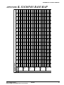
CMOS 4-BIT SINGLE CHIP MICROCOMPUTER
S5U1C60N03D Manual
(Development Software Tool for S1C60N03)
NOTICE
No part of this material may be reproduced or duplicated in any form or by any means without the written permission of Seiko
Epson. Seiko Epson reserves the right to make changes to this material without notice. Seiko Epson does not assume any
liability of any kind arising out of any inaccuracies contained in this material or due to its application or use in any product or
circuit and, further, there is no representation that this material is applicable to products requiring high level reliability, such
as medical products. Moreover, no license to any intellectual property rights is granted by implication or otherwise, and there
is no representation or warranty that anything made in accordance with this material will be free from any patent or copyright
infringement of a third party. This material or portions thereof may contain technology or the subject relating to strategic
products under the control of the Foreign Exchange and Foreign Trade Law of Japan and may require an export license from
the Ministry of International Trade and Industry or other approval from another government agency.
MS-DOS, Windows, Windows 95, Windows 98 and Windows NT are registered trademarks of Microsoft Corporation, U.S.A.
PC-DOS, PC/AT, PS/2, VGA, EGA and IBM are registered trademarks of International Business Machines Corporation, U.S.A.
NEC PC-9800 Series and NEC are registered trademarks of NEC Corporation.
All other product names mentioned herein are trademarks and/or registered trademarks of their respective owners.
© SEIKO EPSON CORPORATION 2001 All rights reserved.
The information of the product number change
Starting April 1, 2001, the product number will be changed as listed below. To order from April 1,
2001 please use the new product number. For further information, please contact Epson sales
representative.
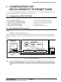
Configuration of product number
Devices
S1
C
60N01
F
0A01
00
Packing specification
Specification
Package (D: die form; F: QFP)
Model number
Model name (C: microcomputer, digital products)
Product classification (S1: semiconductor)
Development tools
C
60R08
S5U1
D1
1
00
Packing specification
Version (1: Version 1 ∗2)
Tool type (D1: Development Tool ∗1)
Corresponding model number (60R08: for S1C60R08)
Tool classification (C: microcomputer use)
Product classification
(S5U1: development tool for semiconductor products)
∗1: For details about tool types, see the tables below. (In some manuals, tool types are represented by one digit.)
∗2: Actual versions are not written in the manuals.
Comparison table between new and previous number
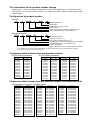
S1C60 Family processors
Previous No.
E0C6001
E0C6002
E0C6003
E0C6004
E0C6005
E0C6006
E0C6007
E0C6008
E0C6009
E0C6011
E0C6013
E0C6014
E0C60R08
New No.
S1C60N01
S1C60N02
S1C60N03
S1C60N04
S1C60N05
S1C60N06
S1C60N07
S1C60N08
S1C60N09
S1C60N11
S1C60N13
S1C60140
S1C60R08
S1C62 Family processors
Previous No.
E0C621A
E0C6215
E0C621C
E0C6S27
E0C6S37
E0C623A
E0C623E
E0C6S32
E0C6233
E0C6235
E0C623B
E0C6244
E0C624A
E0C6S46
New No.
S1C621A0
S1C62150
S1C621C0
S1C6S2N7
S1C6S3N7
S1C6N3A0
S1C6N3E0
S1C6S3N2
S1C62N33
S1C62N35
S1C6N3B0
S1C62440
S1C624A0
S1C6S460
Previous No.
E0C6247
E0C6248
E0C6S48
E0C624C
E0C6251
E0C6256
E0C6292
E0C6262
E0C6266
E0C6274
E0C6281
E0C6282
E0C62M2
E0C62T3
New No.
S1C62470
S1C62480
S1C6S480
S1C624C0
S1C62N51
S1C62560
S1C62920
S1C62N62
S1C62660
S1C62740
S1C62N81
S1C62N82
S1C62M20
S1C62T30
Comparison table between new and previous number of development tools
Development tools for the S1C60/62 Family
Previous No.
ASM62
DEV6001
DEV6002
DEV6003
DEV6004
DEV6005
DEV6006
DEV6007
DEV6008
DEV6009
DEV6011
DEV60R08
DEV621A
DEV621C
DEV623B
DEV6244
DEV624A
DEV624C
DEV6248
DEV6247
New No.
S5U1C62000A
S5U1C60N01D
S5U1C60N02D
S5U1C60N03D
S5U1C60N04D
S5U1C60N05D
S5U1C60N06D
S5U1C60N07D
S5U1C60N08D
S5U1C60N09D
S5U1C60N11D
S5U1C60R08D
S5U1C621A0D
S5U1C621C0D
S5U1C623B0D
S5U1C62440D
S5U1C624A0D
S5U1C624C0D
S5U1C62480D
S5U1C62470D
Previous No.
DEV6262
DEV6266
DEV6274
DEV6292
DEV62M2
DEV6233
DEV6235
DEV6251
DEV6256
DEV6281
DEV6282
DEV6S27
DEV6S32
DEV6S37
EVA6008
EVA6011
EVA621AR
EVA621C
EVA6237
EVA623A
New No.
S5U1C62620D
S5U1C62660D
S5U1C62740D
S5U1C62920D
S5U1C62M20D
S5U1C62N33D
S5U1C62N35D
S5U1C62N51D
S5U1C62560D
S5U1C62N81D
S5U1C62N82D
S5U1C6S2N7D
S5U1C6S3N2D
S5U1C6S3N7D
S5U1C60N08E
S5U1C60N11E
S5U1C621A0E2
S5U1C621C0E
S5U1C62N37E
S5U1C623A0E
Previous No.
EVA623B
EVA623E
EVA6247
EVA6248
EVA6251R
EVA6256
EVA6262
EVA6266
EVA6274
EVA6281
EVA6282
EVA62M1
EVA62T3
EVA6S27
EVA6S32R
ICE62R
KIT6003
KIT6004
KIT6007
New No.
S5U1C623B0E
S5U1C623E0E
S5U1C62470E
S5U1C62480E
S5U1C62N51E1
S5U1C62N56E
S5U1C62620E
S5U1C62660E
S5U1C62740E
S5U1C62N81E
S5U1C62N82E
S5U1C62M10E
S5U1C62T30E
S5U1C6S2N7E
S5U1C6S3N2E2
S5U1C62000H
S5U1C60N03K
S5U1C60N04K
S5U1C60N07K
CONTENTS
PREFACE
This manual mainly explains the outline of the development support tool for the 4-bit Single Chip Microcomputer S1C60N03.
Refer to the "S1C62 Family Development Tool Reference Manual" for the details (common to all models) of
each development support tool. Manuals for hardware development tools are separate, so you should also
refer to the below manuals.
Development tools
☞
S1C62 Family Development Tool Reference Manual
S5U1C62N37E Manual
S5U1C60N03K Manual
S5U1C62000H Manual (S1C60/62 Family In-Circuit Emulator)
Device (S1C60N03)
☞
☞
S1C60N03 Technical Manual
Instructions
∗
S1C6200/6200A Core CPU Manual
In this manual, "ICE" and "evaluation board" indicate S5U1C62000H and S5U1C62N37E, respectively.
CONTENTS
1 COMPOSITION OF DEVELOPMENT SUPPORT TOOL _____________ 1
1.1
1.2
1.3
1.4
Configuration of S5U1C60N03D ............................................................................. 1
Developmental Environment .................................................................................... 1
Development Flow .................................................................................................... 2
Installation ................................................................................................................ 3
2 CROSS ASSEMBLER ASM6003 __________________________________ 4
2.1
2.2
2.3
ASM6003 Outline ..................................................................................................... 4
S1C60N03 Restrictions ............................................................................................. 4
ASM6003 Quick Reference ....................................................................................... 5
3 FUNCTION OPTION GENERATOR FOG6003 ______________________ 7
3.1
3.2
3.3
3.4
3.5
FOG6003 Outline ..................................................................................................... 7
S1C60N03 Option List .............................................................................................. 7
Option Specifications and Selection Message .......................................................... 9
FOG6003 Quick Reference ..................................................................................... 15
Sample File .............................................................................................................. 17
4 SEGMENT OPTION GENERATOR SOG6003 _______________________ 19
4.1
4.2
4.3
4.4
4.5
SOG6003 Outline .................................................................................................... 19
Option List ............................................................................................................... 19
Segment Ports Output Specifications ...................................................................... 20
SOG6003 Quick Reference ...................................................................................... 21
Sample Files ............................................................................................................ 23
5 ICE CONTROL SOFTWARE ICS6003 _____________________________ 24
5.1
5.2
5.3
ICS6003 Outline ...................................................................................................... 24
ICS6003 Restrictions ............................................................................................... 24
ICS6003 Quick Reference ....................................................................................... 25
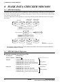
6 MASK DATA CHECKER MDC6003 _______________________________ 28
6.1
6.2
MDC6003 Outline ................................................................................................... 28
MDC6003 Quick Reference ..................................................................................... 28
S5U1C60N03D MANUAL
(DEVELOPMENT SOFTWARE TOOL FOR S1C60N03)
EPSON
i
CONTENTS
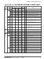
APPENDIX A. S1C60N03 INSTRUCTION SET _______________________ 31
B. S1C60N03 RAM MAP _______________________________ 35
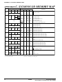
C. S1C60N03 I/O MEMORY MAP _______________________ 36
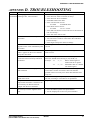
D. TROUBLESHOOTING ______________________________ 37
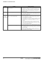
E. DEBUGGING FOR 1/2 DUTY DRIVE
ON EVALUATION BOARD __________________________ 39
White
ii
EPSON
S5U1C60N03D MANUAL
(DEVELOPMENT SOFTWARE TOOL FOR S1C60N03)
1 COMPOSITION OF DEVELOPMENT SUPPORT TOOL
1 COMPOSITION OF
DEVELOPMENT SUPPORT TOOL
Here we will explain the composition of the software for the development support tools, developmental envilonment and how to generate the execution disk.
1.1 Configuration of S5U1C60N03D
The below software are included in the product of the S1C60N03 development support tool S5U1C60N03D.
1.
2.
3.
4.
5.
Cross Assembler ASM6003 ..........................................
Function Option Generator FOG6003 ...........................
Segment Option Generator SOG6003 ..........................
ICE Control Software ICS6003 ......................................
Mask Data Checker MDC6003 ......................................
Cross assembler for program preparation
Function option data preparation program
Segment option data preparation program
ICE control program
Mask data preparation program
1.2 Developmental Environment
The software product of the development support tool S5U1C60N03D operates on the following host
systems:
• IBM PC/AT (at least PC-DOS Ver. 2.0)
When developing the S1C60N03, the above-mentioned host computer, editor, P-ROM writer, printer, etc.
must be prepared by the user in addition to the development tool which is normally supported by Seiko
Epson.
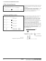
S1C60N03 Development Tool
Host computer
(IBM PC/AT)
S5U1C62000A
Software tools
S5U1C60N03D
ASM6003
FOG6003
SOG6003
PC-DOS
Editor
ICS6003
MDC6003
Target board
ICE
RS-232C
Hardware tools
Evaluation Board
S5U1C62000H
• P-ROM writer
• Printer
S5U1C62N37E
To be prepared by the user
Fig. 1.2.1 System configuration
Note
The S5U1C60N03D system requires a host computer with a RAM capacity of about 140K bytes.
Since the ICE (S5U1C62000H) is connected to the host computer with a RS-232C serial interface,
adapter board for asynchronous communication will be required depending on the host computer
used.
S5U1C60N03D MANUAL
(DEVELOPMENT SOFTWARE TOOL FOR S1C60N03)
EPSON
1
1 COMPOSITION OF DEVELOPMENT SUPPORT TOOL
1.3 Development Flow
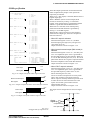
Figure 1.3.1 shows the development flow through the S5U1C60N03D.
*1
*1
Determination of
software specifications
Determination of
hardware specifications
*2, *3
*3, *4
Flow chart generation
and coding
Function option list
generation
Function
option
list
Coding
sheet
*1, *5
Creation of
target board
Segment
option
list
Source file generation
by using editor
Source file generation
by using editor
C003XXX
.DAT
*3, *4
Segment option list
generation
Program
source file
C003XXX
.SEG
*3, *4
*3, *4
Cross Assembler
ASM6003 execution
Function Option Generator
FOG6003 execution
Segment option
source file
*3, *4
Segment Option Generator
SOG6003 execution
C003XXX
.PRN
Assembly list
C003XXXL Object file
.HEX
C003XXXH
.HEX
C003XXXF
.DOC
C003XXXS
.DOC
Function option
document file
Segment option
document file
Function
Segment
C003XXXF option
.HEX
HEX file
C003XXXF option
.HEX
HEX file
Segment
option ROM
(two)
Function
option ROM
(one)
Target board
*3, *4
Debugging with
ICE Control Software
ICS6003
ICE
Evaluation Board
S5U1C62000H
S5U1C62N37E
*3, *6
*5
Debugging
completion
*3, *4
Mask Data Checker
MDC6003 execution
C6003XXX File for
submission
.PAn
Fig. 1.3.1 S5U1C60N03D development flow
SEIKO EPSON
Concerning file names
All the input-output file name for the each development support tool commonly use "C003XXX". In principle
each file should be produced in this manner. Seiko Epson will designate the "XXX" for each customer.
☞ Reference Manual
*1 S1C60N03 Technical Manual
*2 S1C6200/6200A Core CPU Manual
*3 S1C62 Family Development Tool Reference Manual
2
*4 S5U1C60N03D Manual (this manual)
*5 S5U1C62N37E Manual
*6 S5U1C62000H Manual
EPSON
S5U1C60N03D MANUAL
(DEVELOPMENT SOFTWARE TOOL FOR S1C60N03)
1 COMPOSITION OF DEVELOPMENT SUPPORT TOOL
1.4 Installation
The S5U1C60N03D tools are included on the CD-ROM of the S5U1C62000A (S1C60/62 Family Assembler
Package), and they can be installed in your hard disk using the installer (Setup.exe) on the CD-ROM.
Refer to the "S5U1C62000A Manual" for how to install the S5U1C60N03D tools.
S5U1C60N03D MANUAL
(DEVELOPMENT SOFTWARE TOOL FOR S1C60N03)
EPSON
3
2 CROSS ASSEMBLER ASM6003
2 CROSS ASSEMBLER ASM6003
2.1 ASM6003 Outline
The ASM6003 cross assembler is an assembler program
for generating the machine code used by the S1C60N03
4-bit, single-chip microcomputers. The Cross Assembler ASM6003 will assemble the program source files
which have been input by the user's editor and will
generate an object file in Intel-Hex format and assembly list file.
In this assembler, program modularization has been
made possible through macro definition functions and
programming independent of the ROM page structure
has been made possible through the auto page set
function. In addition, consideration has also been given
to precise error checks for program capacity (ROM
capacity) overflows, undefined codes and the like, and
for debugging of such things as label tables for assembly list files and cross reference table supplements.
☞
A>EDLIN C003XXX.DAT
Create the source file
C003XXX
.DAT
A>ASM6003 C003XXX
Execute the cross assembler
Error
message
C003XXX
.PRN
C003XXXL
.HEX
Assembly
listing file
Error
message
C003XXXH
.HEX
Object file
Fig. 2.1.1 ASM6003 execution flow
The format of the source file and its operating method are same as for the S1C62 Family. Refer to the
"S1C62 Family Development Tool Reference Manual" for details.
2.2 S1C60N03 Restrictions
Note the following when generating a program by the S1C60N03:
■ ROM area
The capacity of the S1C60N03
ROM is 768 steps (0000H to
02FFH).
Therefore, the specification
range of the memory setting
pseudo-instructions and PSET
instruction is restricted.
■ RAM area
Memory configuration:
Bank: Only bank 0, Page: 3 pages (0 to 2H), each 256 steps
Significant specification range:
ORG pseudo-instruction:
PAGE pseudo-instruction:
BANK pseudo-instruction:
PSET
The following instructions have
not been defined in the
S1C60N03 instruction sets.
4
00H to 02H
Example: LD
X,050H
50H is loaded into the IX register, but an
unused area has been specified so that the
memory accessible with the IX register
(MX) is invalid.
LD
Y,0C7H
C7H is loaded into the IY register, but an
unused area has been specified so that the
memory accessible with the IY register
(MY) is invalid.
The capacity of the S1C60N03
RAM is 64 words (000H to
03FH, and 0E0H to 0EFH, 4
bits/word). Memory access is
invalid when the unused area of
the index register is specified.
■ Undefined codes
instruction:
0000H to 02FFH
00H to 02H
Only 0H
SLP
PUSH
POP
LD
LD
XP
XP
XP,r
r,XP
EPSON
PUSH
POP
LD
LD
YP
YP
YP,r
r,YP
S5U1C60N03D MANUAL
(DEVELOPMENT SOFTWARE TOOL FOR S1C60N03)
2 CROSS ASSEMBLER ASM6003
2.3 ASM6003 Quick Reference
_ indicates a blank.
■ Starting command and input/output files
indicates the Return key.
A parameter enclosed by [ ] can be omitted.
Execution file:
ASM6003.EXE
Starting command:
ASM6003_ [drive-name:] source-file-name [.shp]_ [-N]
.shp
s
h
p
Option:
-N
Specifies the file I/O drives.
Specifies the drive from which the source file is to be input. (A–P, @)
Specifies the drive to which the object file is to be output. (A–P, @, Z)
Specifies the drive to which the assembly listing file is to be output. (A–P, @, Z)
@: Current drive, Z: File is not generated
The code (FFH) in the undefined area of program memory is not created.
Input file:
C003XXX.DAT
Output file:
C003XXXL.HEX (Object file, low-order)
C003XXXH.HEX (Object file, high-order)
C003XXX.PRN (Assembly listing file)
(Source file)
■ Display example
*** ASM6003 CROSS ASSEMBLER. --- Ver 1.00 ***
EEEEEEEEEE
EEEEEEEEEE
EEE
EEE
EEEEEEEEEE
EEEEEEEEEE
EEE
EEE
EEEEEEEEEE
EEEEEEEEEE
PPPPPPPP
PPPPPPPPPP
PPP
PPP
PPP
PPP
PPPPPPPPPP
PPPPPPPP
PPP
PPP
PPP
PPP
SSSSSSS
SSS
SSSS
SSS
SSS
SSS
SSSSSS
SSSS
SSS
SSS
SSS
SSSS
SSS
SSSSSSS
OOOOOOOO
OOO
OOO
OOO
OOO
OOO
OOO
OOO
OOO
OOO
OOO
OOO
OOO
OOO
OOO
OOO
OOO
OOOOOOOO
NNN
NNN
NNNN
NNN
NNNNN
NNN
NNNNNN NNN
NNN NNN NNN
NNN NNNNNN
NNN
NNNNN
NNN
NNNN
NNN
NNN
NNN
NN
(C) COPYRIGHT 1997 SEIKO EPSON CORP.
SOURCE FILE NAME IS " C003XXX.DAT "
THIS SOFTWARE MAKES NEXT FILES.
C003XXXH.HEX
C003XXXL.HEX
C003XXX .PRN
...
...
...
HIGH BYTE OBJECT FILE.
LOW BYTE OBJECT FILE.
ASSEMBLY LIST FILE.
DO YOU NEED AUTO PAGE SET? (Y/N) Y
. . . (1)
DO YOU NEED CROSS REFERENCE TABLE? (Y/N) Y
. . . (2)
When ASM6003 is started, the start-up
message is displayed.
At (1), select whether or not the auto-pageset function will be used.
Use ........................ Y
Not use ................. N
If the assembly listing file output is
specified, message (2) is displayed. At this
stage, cross-reference table generation may
be selected.
Generating ............ Y
Not generating ...... N
When the above operation is completed,
ASM6003 assembles the source file.
To suspend execution, press the "CTRL"
and "C" keys together at stage (1) or (2).
■ Operators
Arithmetic operators
+a
Monadic positive
-a
Monadic negative
a+b
Addition
a-b
Subtraction
a*b
Multiplication
a/b
Division
a_MOD_b Remainder of a/b
a_SHL_b Shifts a b bits to the left
a_SHR_b Shifts a b bits to the right
HIGH_a
Separates the high-order eight bits from a
LOW_a
Separates the low-order eight bits from a
S5U1C60N03D MANUAL
(DEVELOPMENT SOFTWARE TOOL FOR S1C60N03)
Logical operators
a_AND_b Logical product
a_OR_b Logical sum
a_XOR_b Exclusive logical sum
Logical negation
NOT_a
Relational operators
True when a is equal to b
a_EQ_b
True when a is not equal to b
a_NE_b
True when a is less than b
a_LT_b
True when a is less than or equal to b
a_LE_b
True when a is greater than b
a_GT_b
True when a is greater than or equal to b
a_GE_b
EPSON
5
2 CROSS ASSEMBLER ASM6003
■ Pseudo-instructions
Pseudo-instruction
Meaning
Example of use
EQU
(Equation)
To allocate data to label
SET
(Set)
DW
(Define Word)
To allocate data to label
(data can be changed)
To define ROM data
ORG
(Origin)
To define location counter
PAGE
(Page)
To define boundary of page
SECTION
(Section)
To define boundary of section
EQU
EQU
SET
SET
DW
DW
ORG
ORG
PAGE
PAGE
SECTION
END
(End)
To terminate assembly
END
MACRO
(Macro)
To define macro
LOCAL
(Local)
ENDM
(End Macro)
To make local specification of label
during macro definition
To end macro definition
ABC
BCD
ABC
ABC
ABC
BCD
CHECK
LOCAL
LOOP
9
ABC+1
0001H
0002H
'AB'
0FFBH
100H
256
1H
2
MACRO
LOOP
CP
JP
ENDM
DATA
CHECK
1
MX,DATA
NZ,LOOP
■ Error messages
Error message
S
U
M
O
(Syntax Error)
(Undefined Error)
(Missing Label)
(Operand Error)
P
R
(Phase Error)
(Range Error)
Explanation
An unrecoverable syntax error was encountered.
The label or symbol of the operand has not been defined.
The label field has been omitted.
A syntax error was encountered in the operand, or the operand could
not be evaluated.
The same label or symbol was defined more than once.
• The location counter value exceeded the upper limit of the program
memory, or a location exceeding the upper limit was specified.
• A value greater than that which the number of significant digits of the
operand will accommodate was specified.
• Memory areas overlapped because of a "PAGE" or "ORG" pseudoinstruction or both.
FILE NAME ERROR
The source file name was longer than 8 characters.
FILE NOT PRESENT
The specified source file was not found.
DIRECTORY FULL
No space was left in the directory of the specified disk.
FATAL DISK WRITE ERROR
The file could not be written to the disk.
The number of defined labels and symbols exceeded the label table
LABEL TABLE OVERFLOW
capacity (4000).
CROSS REFERENCE TABLE OVERFLOW The label/symbol reference count exceeded the cross-reference table
capacity (only when the cross-reference table is generated).
!
6
(Warning)
EPSON
S5U1C60N03D MANUAL
(DEVELOPMENT SOFTWARE TOOL FOR S1C60N03)
3 FUNCTION OPTION GENERATOR FOG6003
3
FUNCTION OPTION GENERATOR
FOG6003
3.1 FOG6003 Outline
With the 4-bit single-chip S1C60N03 microcomputers,
the customer may select 10 hardware options. By
modifying the mask patterns of the S1C60N03 according to the selected options, the system can be customized to meet the specifications of the target system.
The Function Option Generator FOG6003 is a software
tool for generating data files used to generate mask
patterns. It enables the customer to interactively select
and specify pertinent items for each hardware option.
From the data file created with FOG6003, the
S1C60N03 mask pattern is automatically generated by
a general purpose computer.
The HEX file for the evaluation board (S5U1C62N37E)
hardware option ROM is simultaneously generated
with the data file.
☞
The operating method is same as for the S1C62
Family. Refer to the "S1C62 Family Development
Tool Reference Manual" for details.
Option list
generation
Start FOG6003
Set function
option
C003XXXF
.HEX
Evaluation
board
C003XXXF
.DOC
EPROM
Seiko Epson
Floppy disk
Fig. 3.1.1 FOG6003 execution flow
3.2 S1C60N03 Option List
Multiple specifications are available in each option item as indicated in the Option List. Using "3.3 Option
Specifications and Selection Message" as reference, select the specifications that meet the target system. Be
sure to record the specifications for unused ports too, according to the instructions provided.
1. DEVICE TYPE
■ 1. E0C6003
■ 2. E0C60L03
(Normal Type <S1C60N03>)
(Low Power Type <S1C60L03>)
2. LCD SPECIFICATION
• BIAS SELECTION ................................ ■ 1. 1/3 Bias By Voltage Divider
■ 2. 1/2 Bias By Voltage Divider
■ 3. 1/2 Bias By Doubler/Halver
• DUTY SELECTION ............................. ■ 1. 1/4 Duty
■ 2. 1/3 Duty
■ 3. 1/2 Duty
3. OSC1 SYSTEM CLOCK
■ 1. Crystal
■ 2. CR
4. MULTIPLE KEY ENTRY RESET
• COMBINATION .................................. ■
■
■
■
1. Not Use
2. Use K00, K01
3. Use K00, K01, K02
4. Use ALL K00–K03
5. INTERRUPT NOISE REJECTOR
• K00–K03 ................................................. ■ 1. Use
■ 2. Not Use
S5U1C60N03D MANUAL
(DEVELOPMENT SOFTWARE TOOL FOR S1C60N03)
EPSON
7
3 FUNCTION OPTION GENERATOR FOG6003
6. TIMER INTERRUPT FREQUENCY
• INTERRUPT FREQUENCY ................ ■ 1. 32/16/2 Hz Interrupt
■ 2. 64/16/2 Hz Interrupt
7. INPUT PORT PULL DOWN RESISTOR
• K00
• K01
• K02
• K03
.........................................................
.........................................................
.........................................................
.........................................................
■
■
■
■
■
■
■
■
1. With Resistor
1. With Resistor
1. With Resistor
1. With Resistor
2. Gate Direct
2. Gate Direct
2. Gate Direct
2. Gate Direct
8. R00 SPECIFICATION
• OUTPUT TYPE ..................................... ■ 1. DC Output
■ 2. Buzzer Inverted Output (R00 Control)
■ 3. FOUT Output
• FOUT OUTPUT SPACIFICATION
F1 ...... ■
■
■
■
■
F2 ...... ■
■
■
■
■
F3 ...... ■
■
■
■
■
F4 ...... ■
■
■
■
■
1.
2.
3.
4.
5.
1.
2.
3.
4.
5.
1.
2.
3.
4.
5.
1.
2.
3.
4.
5.
256[Hz]
512[Hz]
1,024[Hz]
2,048[Hz]
4,096[Hz]
512[Hz]
1,024[Hz]
2,048[Hz]
4,096[Hz]
8,192[Hz]
1,024[Hz]
2,048[Hz]
4,096[Hz]
8,192[Hz]
16,384[Hz]
2,048[Hz]
4,096[Hz]
8,192[Hz]
16,384[Hz]
32,768[Hz]
• OUTPUT SPECIFICATION ................ ■ 1. Complementary
■ 2. Pch-Open Drain
9. R01 SPECIFICATION
• OUTPUT TYPE ..................................... ■ 1. DC Output
• OUTPUT SPECIFICATION ................ ■ 1. Complementary
■ 2. Buzzer Output
■ 2. Pch-Open Drain
10.R02, R03 SPECIFICATION
• R02 OUTPUT SPECIFICATION ........ ■ 1. Complementary
• R03 OUTPUT SPECIFICATION ........ ■ 1. Complementary
8
EPSON
■ 2. Pch-Open Drain
■ 2. Pch-Open Drain
S5U1C60N03D MANUAL
(DEVELOPMENT SOFTWARE TOOL FOR S1C60N03)
3 FUNCTION OPTION GENERATOR FOG6003
3.3 Option Specifications and Selection Message
Screen that can be selected as function options set on the S1C60N03 are shown below, and their specifications are also described.
1 Device type
*** OPTION
Select the chip specification.
There are two models: E0C6003 (S1C60N03) (3 V
supply voltage) and E0C60L03 (S1C60L03) (1.5 V
supply voltage, low-power specification).
NO.1 ***
--- DEVICE TYPE --1. E0C6003
2. E0C60L03
PLEASE SELECT NO.(1) ? 2
2. E0C60L03
SELECTED
2 LCD specification
*** OPTION
NO.2 ***
--- LCD SPECIFICATION --BIAS SELECTION
1. 1/3 BIAS BY VOLTAGE DIVIDER
2. 1/2 BIAS BY VOLTAGE DIVIDER
3. 1/2 BIAS BY DOUBLER/HALVER
PLEASE SELECT NO.(1) ? 1
DUTY SELECTION
1. 1/4 DUTY
2. 1/3 DUTY
3. 1/2 DUTY
PLEASE SELECT NO.(1) ? 1
BIAS SELECTION
DUTY SELECTION
1. 1/3 BIAS BY VOLTAGE DIVIDER
1. 1/4 DUTY
SELECTED
SELECTED
Table 3.3.1 Common duty selection standard
Number of segments
1–30
31–45
46–60
Common duty
1/2
1/3
1/4
S5U1C60N03D MANUAL
(DEVELOPMENT SOFTWARE TOOL FOR S1C60N03)
Select the common (drive) duty and bias.
When 1/2 duty is selected, up to 30 segments of LCD
panel can be driven with 2 COM terminals and 15
SEG terminals. When 1/3 duty is selected, up to 45
segments can be driven with 3 COM terminals, and
when 1/4 duty is selected, up to 60 segments with 4
COM terminals.
When 1/2 duty is selected, the COM0 and COM1
terminals are effective for COM output and the
COM2 and COM3 terminals always output an off
signal. When 1/3 duty is selected, the COM0 to
COM2 terminals are effective and the COM3
terminal always outputs an off signal.
Refer to Table 3.3.1 for common duty selection.
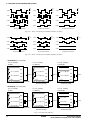
Figures 3.3.1 and 3.3.2 show the drive waveforms of
1/3 bias driving and 1/2 bias driving, respectively.
For the LCD drive bias, either 1/3 bias (drives LCD
with 4 levels, VDD, VL1, VL2 and VL3) or 1/2 bias
(drives LCD with 3 levels, VDD, VL1=VL2 and VL3)
can be selected.
See Figure 3.3.3 for the external elements according
to the bias to be selected.
EPSON
9
3 FUNCTION OPTION GENERATOR FOG6003
VDD
VL1
VL2
VL3
COM0
VDD
VL1
VL2
VL3
COM0
COM1
COM1
COM1
COM2
COM2
COM2
COM3
COM3
COM3
1/4 duty drive waveform
VDD
VL1
VL2
VL3
COM0
1/3 duty drive waveform
1/2 duty drive waveform
Fig. 3.3.1 Drive waveform from COM terminals (1/3 bias)
VDD
VL1, VL2
VL3
COM0
VDD
VL1, VL2
VL3
COM0
COM1
COM1
COM1
COM2
COM2
COM2
COM3
COM3
COM3
1/4 duty drive waveform
VDD
VL1, VL2
VL3
COM0
1/3 duty drive waveform
1/2 duty drive waveform
Fig. 3.3.2 Drive waveform from COM terminals (1/2 bias)
• S1C60N03 (3 V LCD panel)
1/4, 1/3, 1/2 duty
1/2 bias (A)
1/4, 1/3, 1/2 duty
1/3 bias
VDD
VL1 = 1/3·VSS
VDD
VS2
VL1 = 1/2·VSS
CA
VL2 = 2/3·VSS
VL3
1/4, 1/3, 1/2 duty
1/2 bias (B)
VDD
VS2
VL1 = 1/2·VSS
CA
3.0 V
CB
VL2 = 1/2·VSS
VL3
VSS
Note: VL3 is shorted to VSS internally.
VS2
CA
3.0 V
CB
VL2 = 1/2·VSS
VL3
VSS
Note: VL3–VSS and VL1–VL2 are
shorted internally.
3.0 V
CB
VSS
Note: VL3–VSS and VL1–VL2 are
shorted internally.
• S1C60L03 (3 V LCD panel)
1/4, 1/3, 1/2 duty
1/2 bias (A)
1/4, 1/3, 1/2 duty
1/3 bias
VDD
VL1 = 1/3·VS2
VDD
VS2
VL1 = 1/2·VS2
CA
VL2 = 2/3·VS2
VL3 = 2·VSS
1/4, 1/3, 1/2 duty
1/2 bias (B)
VDD
VS2
VL1 = VSS
CA
1.5 V
CB
VSS
Note: VL3 is shorted to VSS internally.
VL2 = 1/2·VS2
VL3 = 2·VSS
VS2
CA
1.5 V
CB
VL2 = VSS
VL3 = 2·VSS
VSS
Note: VL3–VS2 and VL1–VL2 are
shorted internally.
1.5 V
CB
VSS
Note: VL3–VS2 and VL1–VL2 are
shorted internally.
Fig. 3.3.3 External elements
10
EPSON
S5U1C60N03D MANUAL
(DEVELOPMENT SOFTWARE TOOL FOR S1C60N03)
3 FUNCTION OPTION GENERATOR FOG6003
3 OSC1 system clock
*** OPTION
Select oscillation circuit that uses OSC1 and OSC2.
To minimize external components, CR oscillation
circuit would be suitable; to obtain a stable oscillation frequency, crystal oscillation circuit would be
suitable.
When CR oscillation circuit is selected, only resistors
are needed as external components since capacities
are built-in.
On the other hand, when crystal oscillation circuit is
selected, crystal oscillator and trimmer capacitor are
needed as external components. Although when
crystal oscillation circuit is selected, it is fixed at
32.768 kHz, when CR oscillation circuit is selected,
frequency may be modified to a certain extent
depending on the resistance of external components.
NO.3 ***
--- OSC1 SYSTEM CLOCK --1. CRYSTAL
2. CR
PLEASE SELECT NO.(1) ? 1
1. CRYSTAL
SELECTED
4 Multiple key entry reset
*** OPTION
The reset function is set when K00 through K03 are
entered.
When "NOT USE" is selected, the reset function is
not activated even if K00 through K03 are entered.
When "USE K00, K01" is selected, the system is
reset immediately the K00 and K01 inputs go high at
the same time. Similarly, the system is reset as soon
as the K00 through K02 inputs or the K00 through
K03 inputs go high.
However, the system is reset when a high signal is
input for more than a rule time (1–3 sec).
The system reset circuit is shown in Figure 3.3.4.
NO.4 ***
--- MULTIPLE KEY ENTRY RESET --COMBINATION
PLEASE SELECT
1.
2.
3.
4.
NOT USE
USE K00,K01
USE K00,K01,K02
USE ALL K00–K03
NO.(1) ? 2
COMBINATION
2. USE
OSC1
OSC2
K00,K01
f
Oscillation
circuit
SELECTED
Oscillation
detection
Mask option
circuit
K00
K01
K02
K03
RESET
Fig. 3.3.4
System reset circuit
Vss
5 Interrupt noise rejector
*** OPTION
Select whether noise rejector will be supplemented to
the input interrupter of K00–K03. When "USE" is
selected, the entry signal will pass the noise rejector,
and occurrence of interrupt errors due to noise or
chattering can be avoided. Note, however, that
because the noise rejector performs entry signal
sampling at 4 kHz, "NOT USE" should be selected
when high speed response is required.
NO.5 ***
--- INTERRUPT NOISE REJECTOR --K00-K03
1. USE
2. NOT USE
PLEASE SELECT NO.(1) ? 1
K00-K03
1. USE
SELECTED
S5U1C60N03D MANUAL
(DEVELOPMENT SOFTWARE TOOL FOR S1C60N03)
EPSON
11
3 FUNCTION OPTION GENERATOR FOG6003
6 Timer interrupt frequency
*** OPTION
NO.6 ***
--- TIMER INTERRUPT FREQUENCY --INTERRUPT FREQUENCY
1. 32/16/2 HZ INTERRUPT
2. 64/16/2 HZ INTERRUPT
PLEASE SELECT NO.(1) ? 1
INTERRUPT FREQUENCY
1. 32/16/2 HZ INTERRUPT
SELECTED
Select timer interrupt frequencies. Either 32 Hz or 64
Hz can be selected for one of among three interrupt
frequencies.
The EIT32 interrupt mask register (0F4H•D0) is used
for controlling the 32 Hz or 64 Hz interrupt.
When a 32 Hz or 64 Hz interrupt occurs, the IT32
interrupt factor flag (0F6H•D0) is set.
7 Input ports pull down resistor
*** OPTION
Select whether input ports (K00–K03) will each be
supplemented with pull down resistors or not.
When "GATE DIRECT" is selected, see to it that
entry floating state does not occur. Select "WITH
RESISTOR" pull down resistor for unused ports.
Moreover, the input port status is changed from "H"
level (VDD) to "L" level (VSS) with pull down
resistors, a delay of approximately 1 msec in
waveform fall time will occur depending on the pull
down resistor and entry load time constant. Because
of this, when input reading is to be conducted, ensure
the appropriate wait time with the program.
The configuration of the pull down resistor circuit is
shown in Figure 3.3.5.
NO.7 ***
--- INPUT PORT PULL DOWN RESISTOR --K00
1. WITH RESISTOR
2. GATE DIRECT
PLEASE SELECT NO.(1) ? 1
K01
1. WITH RESISTOR
2. GATE DIRECT
PLEASE SELECT NO.(1) ? 1
K02
1. WITH RESISTOR
2. GATE DIRECT
PLEASE SELECT NO.(1) ? 1
K03
1. WITH RESISTOR
2. GATE DIRECT
PLEASE SELECT NO.(1) ? 1
K00
K01
K02
K03
1.
1.
1.
1.
WITH
WITH
WITH
WITH
RESISTOR
RESISTOR
RESISTOR
RESISTOR
SELECTED
SELECTED
SELECTED
SELECTED
VDD
Data bus
K
Read signal
Fig. 3.3.5
Configuration of pull down resistor
12
EPSON
VSS
S5U1C60N03D MANUAL
(DEVELOPMENT SOFTWARE TOOL FOR S1C60N03)
3 FUNCTION OPTION GENERATOR FOG6003
8 R00 specification
*** OPTION
Select the output specification for the R00 terminal.
Either complementary output or Pch open drain
output may be selected.
When "D.C." (DC output) is selected, R00 becomes a
regular output port.
When "/BZ R00" (buzzer inverted output, R00
control) is selected, by writing "1" to the R00
register, clock with frequency specified through the
software is generated from the R00 terminal.
When FOUT is selected, clock with frequency
selected from the R00 terminal is generated by
writing "1" to the R00 register.
When the DC output or buzzer inverted output is
selected as the output type, the FOUT frequencies
cannot be selected.
NO.8 ***
--- R00 SPECIFICATION --OUTPUT TYPE
1. D.C.
2. /BZ R00
3. FOUT
PLEASE SELECT NO.(3) ? 3
F1
1.
2.
3.
4.
5.
256
512
1024
2048
4096
[HZ]
[HZ]
[HZ]
[HZ]
[HZ]
1.
2.
3.
4.
5.
512
1024
2048
4096
8192
[HZ]
[HZ]
[HZ]
[HZ]
[HZ]
1. 1024
2. 2048
3. 4096
4. 8192
5. 16384
[HZ]
[HZ]
[HZ]
[HZ]
[HZ]
PLEASE SELECT NO.(4) ? 4
F2
PLEASE SELECT NO.(4) ? 4
F3
• When DC output is selected
When the R00 register is set to "1", the R00
terminal output goes high (VDD), and goes low
(VSS) when set to "0".
Output waveform is shown in Figure 3.3.6.
PLEASE SELECT NO.(4) ? 4
F4
1. 2048 [HZ]
2. 4096 [HZ]
3. 8192 [HZ]
4. 16384 [HZ]
5. 32768 [HZ]
PLEASE SELECT NO.(4) ? 4
OUTPUT SPECIFICATION
1. COMPLEMENTARY
2. PCH-OPENDRAIN
PLEASE SELECT NO.(1) ? 1
OUTPUT TYPE
F1
F2
F3
F4
OUTPUT SPECIFICATION
3. FOUT
SELECTED
4. 2048 [HZ]
SELECTED
4. 4096 [HZ]
SELECTED
4. 8192 [HZ]
SELECTED
4. 16384 [HZ]
SELECTED
1. COMPLEMENTARY
SELECTED
VDD
R00 output
R00 register
0
1
0
VSS
Fig. 3.3.6 Output waveform at DC output selection
VDD
Buzzer inverted output
VSS
R00 register
0
1
0
Fig. 3.3.7 Output waveform at buzzer inverted output selection
VDD
FOUT output
VSS
R00 register
0
1
• When buzzer inverted output (R00 control) is
selected
When the R00 register is set to "1", 50% duty and
VDD–VSS amplitude square wave is generated at
the specified frequency by the software. When set
to "0", the R00 terminal goes low (VSS). The clock
phase when buzzer drive signal is output from R00
terminal is antiphase to that of the R01 terminal.
Output waveform is shown in Figure 3.3.7.
• When FOUT output is selected
When the R00 register is set to "1", 50% duty and
VDD–VSS amplitude square wave is generated at
the specified frequency. When set to "0", the
FOUT terminal goes low (VSS).
The F1 to F4 FOUT frequencies are set by mask
option. One of them is used by the software.
FOUT output is normally utilized to provide clock
to other devices but since hazard occurs at the
square wave breaks, great caution must be
observed when using it.
Output waveform is shown in Figure 3.3.8.
The output circuit configuration is shown in Figure
3.3.9.
0
VDD
Fig. 3.3.8 Output waveform at FOUT output selection
Output
register
R
Complementary
Pch open drain
Fig. 3.3.9
Configuration of output circuit
S5U1C60N03D MANUAL
(DEVELOPMENT SOFTWARE TOOL FOR S1C60N03)
EPSON
VSS
13
3 FUNCTION OPTION GENERATOR FOG6003
9 R01 specification
*** OPTION
NO.9 ***
--- R01 SPECIFICATION --OUTPUT TYPE
1. D.C.
2. BZ OUTPUT
PLEASE SELECT NO.(1) ? 2
OUTPUT SPECIFICATION
1. COMPLEMENTARY
2. PCH-OPENDRAIN
PLEASE SELECT NO.(1) ? 1
OUTPUT TYPE
OUTPUT SPECIFICATION
2. BZ OUTPUT
SELECTED
1. COMPLEMENTARY
SELECTED
VDD
R01 output
R01 register
0
1
0
VSS
Fig. 3.3.10 Output waveform at DC output selection
VDD
Buzzer output
R01 register
0
1
0
VSS
Fig. 3.3.11 Output waveform at buzzer output selection
Select the output specification for the R01 terminal.
Either complementary output or Pch open drain
output may be selected.
When "D.C." (DC output) is selected, R01 becomes a
regular output port.
When "BZ OUTPUT" (buzzer output) is selected, by
writing "1" to the R01 register, clock with frequency
specified through the software is generated from the
R01 terminal.
• When DC output is selected
When the R01 register is set to "1", the R01
terminal output goes high (VDD), and goes low
(VSS) when set to "0".
Output waveform is shown in Figure 3.3.10.
• When buzzer output is selected
When the R01 register is set to "1", 50% duty and
VDD–VSS amplitude square wave is generated at
the specified frequency by the software. When set
to "0", the R01 terminal goes low (VSS). The clock
phase when buzzer drive signal is output from the
R01 terminal is antiphase to that of the R00
terminal.
Output waveform is shown in Figure 3.3.11.
10 R02, R03 specification
*** OPTION
Select the output specification for the R02 and R03
terminals.
Either complementary output or Pch open drain
output may be selected.
NO.10 ***
--- R02, R03 OUTPUT SPECIFICATION --R02 OUTPUT SPECIFICATION
1. COMPLEMENTARY
2. PCH-OPENDRAIN
PLEASE SELECT NO.(1) ? 1
R03 OUTPUT SPECIFICATION
1. COMPLEMENTARY
2. PCH-OPENDRAIN
PLEASE SELECT NO.(1) ? 1
R02 OUTPUT SPECIFICATION
R03 OUTPUT SPECIFICATION
14
1. COMPLEMENTARY
1. COMPLEMENTARY
SELECTED
SELECTED
EPSON
S5U1C60N03D MANUAL
(DEVELOPMENT SOFTWARE TOOL FOR S1C60N03)
3 FUNCTION OPTION GENERATOR FOG6003
3.4 FOG6003 Quick Reference
■ Starting command and input/output files
Execution file:
FOG6003.EXE
Starting command:
FOG6003
Input file:
C003XXXF.DOC (Function option document file, when modifying)
Output file:
C003XXXF.DOC (Function option document file)
C003XXXF.HEX (Function option HEX file)
indicates the Return key.
■ Display example
***
E0C6003 FUNCTION OPTION GENERATOR. --- Ver 1.00
EEEEEEEEEE
EEEEEEEEEE
EEE
EEE
EEEEEEEEEE
EEEEEEEEEE
EEE
EEE
EEEEEEEEEE
EEEEEEEEEE
PPPPPPPP
PPPPPPPPPP
PPP
PPP
PPP
PPP
PPPPPPPPPP
PPPPPPPP
PPP
PPP
PPP
PPP
SSSSSSS
SSS
SSSS
SSS
SSS
SSS
SSSSSS
SSSS
SSS
SSS
SSS
SSSS
SSS
SSSSSSS
OOOOOOOO
OOO
OOO
OOO
OOO
OOO
OOO
OOO
OOO
OOO
OOO
OOO
OOO
OOO
OOO
OOO
OOO
OOOOOOOO
***
NNN
NNN
NNNN
NNN
NNNNN
NNN
NNNNNN NNN
NNN NNN NNN
NNN NNNNNN
NNN
NNNNN
NNN
NNNN
NNN
NNN
NNN
NN
(C) COPYRIGHT 1997 SEIKO EPSON CORP.
THIS SOFTWARE MAKES NEXT FILES.
C003XXXF.HEX
C003XXXF.DOC
...
...
Start-up message
When FOG6003 is started, the start-up
message is displayed.
For "STRIKE ANY KEY.", press any key
to advance the program execution.
To suspend execution, press the "CTRL"
and "C" keys together: the sequence returns
to the DOS command level.
FUNCTION OPTION HEX FILE.
FUNCTION OPTION DOCUMENT FILE.
STRIKE ANY KEY.
Date input
Enter the 2-digit year, month, and day of the
month by delimiting them with a slash ("/").
When not modifying the date, press the
RETURN key " " to continue.
*** E0C6003 USER'S OPTION SETTING. --- Ver 1.00 ***
CURRENT DATE IS 1997/03/03
PLEASE INPUT NEW DATE :
1997/03/03
Operation selection menu
Enter a number from 1 to 3 to select a
subsequent operation.
1. To set new function options.
2. To modify the document file.
3. To terminate FOG6003.
*** OPERATION SELECT MENU ***
1. INPUT NEW FILE
2. EDIT FILE
3. RETURN TO DOS
PLEASE SELECT NO.?
*** OPERATION SELECT MENU ***
1. INPUT NEW FILE
2. EDIT FILE
3. RETURN TO DOS
PLEASE SELECT NO.? 1
PLEASE INPUT FILE NAME? C0030A0
PLEASE INPUT USER'S NAME? SEIKO EPSON CORP.
PLEASE INPUT ANY COMMENT
(ONE LINE IS 50 CHR)? FUJIMI PLANT
? 281 FUJIMI SUWA-GUN NAGANO-KEN 399-0293
? TEL 0266-61-1211
? FAX 0266-61-1273
?
PLEASE
EXISTS
PLEASE
PLEASE
. . (1)
. . (2)
. . (3)
JAPAN
INPUT FILE NAME? C0030A0
OVERWRITE(Y/N)? N
INPUT FILE NAME? C0030B0
INPUT USER'S NAME?
S5U1C60N03D MANUAL
(DEVELOPMENT SOFTWARE TOOL FOR S1C60N03)
EPSON
Setting new function options
Select "1" on the operation selection menu.
(1) Enter the file name.
(2) Enter the customer's company name.
(3) Enter any comment.
(Within 50 characters x 10 lines)
Next, start function option setting from
option No. 1.
In case a function option document file with
the same name as the file name specified in
the current drive exists, the user is asked
whether overwrition is desired. Enter "Y" or
"N" accordingly.
15
3 FUNCTION OPTION GENERATOR FOG6003
*** OPERATION SELECT MENU ***
1. INPUT NEW FILE
2. EDIT FILE
3. RETURN TO DOS
PLEASE SELECT NO.? 2
*** SOURCE FILE(S) ***
C0030A0
C0030B0
PLEASE INPUT
PLEASE INPUT
PLEASE INPUT
(ONE LINE IS
PLEASE INPUT
:
. . (1)
C0030C0
. . (2)
. . (3)
FILE NAME? C0030A0
USER'S NAME?
ANY COMMENT
50 CHR)?
EDIT NO.? 4
. . (4)
. . (5)
(Modifying function option settings)
:
PLEASE INPUT EDIT NO.? E
In step (1), if no modifiable source exists, the following message is
displayed and the sequence returns to the operation selection menu.
*** SOURCE FILE(S) ***
FUNCTION OPTION DOCUMENT FILE IS NOT FOUND.
Modifying function option settings
Select "2" on the operation selection menu.
(1) Will display the files on the current drive.
(2) Enter the file name.
(3) Enter the customer's company name.
(4) Enter any comment.
Previously entered data can be used by pressing
the RETURN key " " at (3) and (4).
(5) Enter the number of the function option to be
modified. When selection of one option is
complete, the system prompts entry of another
function option number. Repeat selection until
all options to be modified are selected.
Enter "E " to end option setting. Then, move
to the confirmation procedure for HEX file
generation.
In step (2), if the function option document file is not in the current drive,
the following message is displayed, prompting entry of other file name.
PLEASE INPUT FILE NAME? C0030N0
FUNCTION OPTION DOCUMENT FILE IS NOT FOUND.
PLEASE INPUT FILE NAME?
*** OPTION
Option selection
The selections for each option correspond one to
one to the option list. Enter the selection number.
The value in parentheses ( ) indicates the default
value, and is set when only the RETURN key " "
is pressed.
In return, the confirmation is displayed.
When you wish to modify previously set function
options in the new setting process, enter "B " to
return 1 step back to the previous function option
setting operation.
NO.4 ***
--- MULTIPLE KEY ENTRY RESET --COMBINATION
PLEASE SELECT
1.
2.
3.
4.
Not Use
Use K00,K01
Use K00,K01,K02
Use All K00–K03
NO.(1) ? 2
COMBINATION
2. Use
K00,K01
END OF OPTION SETTING.
DO YOU MAKE HEX FILE (Y/N) ? Y
SELECTED
. . (1)
*** OPTION EPROM SELECT MENU ***
1.
2.
3.
4.
27C64
27C128
27C256
27C512
. . (2)
PLEASE SELECT NO.? 3
3. 27C256
SELECTED
MAKING FILE(S) IS COMPLETED.
*** OPERATION SELECT MENU ***
1. INPUT NEW FILE
2. EDIT FILE
3. RETURN TO DOS
PLEASE SELECT NO.?
16
EPROM selection
When setting function options setting is completed,
the following message is output to ask the operator
whether to generate the HEX file.
(1) When debugging the program with the
evaluation board, HEX file is needed, so enter
"Y ". If "N " is entered, no HEX file is
generated and only document file is generated.
(2) For the option ROM selection menu displayed
when "Y " is entered in Step (1), select the
EPROM to be used for setting evaluation board
options.
When a series of operations are complete, the
sequence returns to the operation selection menu.
EPSON
S5U1C60N03D MANUAL
(DEVELOPMENT SOFTWARE TOOL FOR S1C60N03)
3 FUNCTION OPTION GENERATOR FOG6003
3.5 Sample File
■ Example of function option document file
*
*
*
*
*
*
*
*
*
*
*
*
*
*
*
E0C6003 FUNCTION OPTION DOCUMENT
V 1.00
FILE NAME
USER’S NAME
INPUT DATE
C0030A0F.DOC
SEIKO EPSON CORP.
1997/03/03
COMMENT
FUJIMI PLANT
281 FUJIMI SUWA-GUN NAGANO-KEN 399-0293 JAPAN
TEL 0266-61-1211
FAX 0266-61-1273
OPTION NO.1
< DEVICE TYPE >
E0C60L03
--------------------
SELECTED
OPT0101 02
*
* OPTION NO.2
* < LCD SPECIFICATION >
*
BIAS SELECTION
1/3 BIAS BY VOLTAGE DIVIDER - SELECTED
*
DUTY SELECTION
1/4 DUTY -------------------- SELECTED
OPT0201 01
OPT0202 01
*
* OPTION NO.3
* < OSC1 SYSTEM CLOCK >
*
CRYSTAL --------------------- SELECTED
OPT0301 01
*
* OPTION NO.4
* < MULTIPLE KEY ENTRY RESET >
*
KEY COMBINATION
USE ALL K00–K03 ------------ SELECTED
OPT0401 04
*
* OPTION NO.5
* < INTERRUPT NOISE REJECTOR >
*
K00–K03
USE ------------------------- SELECTED
OPT0501 01
*
* OPTION NO.6
* < TIMER INTERRUPT FREQUENCY >
*
INTERRUPT FREQUENCY
32/16/2 HZ INTERRUPT -------- SELECTED
OPT0601 01
*
* OPTION NO.7
* < INPUT PORT PULL DOWN RESISTOR >
*
K00
WITH RESISTOR --------------- SELECTED
*
K01
WITH RESISTOR --------------- SELECTED
*
K02
WITH RESISTOR --------------- SELECTED
*
K03
WITH RESISTOR --------------- SELECTED
OPT0701 01
OPT0702 01
OPT0703 01
OPT0704 01
*
* OPTION NO.8
* < R00 SPECIFICATION >
*
OUTPUT TYPE
FOUT ------------------------ SELECTED
*
F1 FREQUENCY SELECTION 512 HZ ---------------------- SELECTED
*
F2 FREQUENCY SELECTION 1024 HZ --------------------- SELECTED
*
F3 FREQUENCY SELECTION 2048 HZ --------------------- SELECTED
*
F4 FREQUENCY SELECTION 4096 HZ --------------------- SELECTED
*
OUTPUT SPECIFICATION
COMPLEMENTARY --------------- SELECTED
OPT0801 03
OPT0802 02
OPT0803 02
OPT0804 02
S5U1C60N03D MANUAL
(DEVELOPMENT SOFTWARE TOOL FOR S1C60N03)
EPSON
17
3 FUNCTION OPTION GENERATOR FOG6003
OPT0805 02
OPT0806 01
*
* OPTION NO.9
* < R01 SPECIFICATION >
*
OUTPUT TYPE
BZ OUTPUT ------------------*
OUTPUT SPECIFICATION
COMPLEMENTARY --------------OPT0901 02
OPT0902 01
*
* OPTION NO.10
* < R02, R03 OUTPUT SPECIFICATION >
*
R02 OUTPUT SPECIFICATION COMPLEMENTARY --------------*
R03 OUTPUT SPECIFICATION COMPLEMENTARY --------------OPT1001 01
OPT1002 01
*
*
*
* SEIKO EPSON’S AREA
*
*
*
* OPTION NO.11
OPT1101 01
OPT1102 01
*
* OPTION NO.12
OPT1201 01
*
* OPTION NO.13
OPT1301 01
*
* OPTION NO.14
OPT1401 01
\\END
Note
18
SELECTED
SELECTED
SELECTED
SELECTED
End mark "¥¥END" may be used instead of "\\END" depending on the PC used.
(The code of \ and ¥ is 5CH.)
EPSON
S5U1C60N03D MANUAL
(DEVELOPMENT SOFTWARE TOOL FOR S1C60N03)
4 SEGMENT OPTION GENERATOR SOG6003
4 SEGMENT OPTION GENERATOR SOG6003
4.1 SOG6003 Outline
With the 4-bit single-chip S1C60N03 microcomputers, the
customer may select the LCD segment options. By
modifying the mask patterns of the S1C60N03 according
to the selected options, the system can be customized to
meet the specifications of the target system.
The Segment Option Generator SOG6003 is a software
tool for generating data file used to generate mask
patterns. From the data file created with SOG6003, the
S1C60N03 mask pattern is automatically generated by a
general purpose computer.
The HEX file for the evaluation board (S5U1C62N37E)
segment option ROM is simultaneously generated with
the data file.
☞
A>EDLIN C003XXX.SEG
Segment source file generation
C003XXX
.SEG
A>SOG6003
Execute the segment option generator
Error
message
Error
message
The operating method is same as for the S1C62
Family. Refer to the "S1C62 Family Development Tool
Reference Manual" for details.
C003XXXS
.HEX
Segment option
HEX file
C003XXXS
.DOC
Segment option
document file
for evaluation board use
Fig. 4.1.1 SOG6003 execution flow
4.2 Option List
TERMINAL
NAME
COM0
H L D
ADDRESS
COM1
COM2
H L D H L D
H
COM3
L D
SEG0
SEG1
SEG2
SEG3
SEG4
SEG5
SEG6
SEG7
SEG8
SEG9
SEG10
SEG11
SEG12
SEG13
SEG14
Legend:
<ADDRESS>
H: High order address, L: Low order address
D: Data bit
OUTPUT SPECIFICATION
SEG output
DC output
C
P
SEG output
DC output
C
P
SEG output
DC output
C
P
SEG output
DC output
C
P
SEG output
DC output
C
P
SEG output
DC output
C
P
SEG output
DC output
C
P
SEG output
DC output
C
P
<OUTPUT SPECIFICATION>
C: Complementary output
P: Pch open drain output
Note:
1. Even if there are unused areas, set "---" (hyphens) such that there are no blank columns.
2. When DC output is selected, the display memory of the COM0 column becomes effective.
S5U1C60N03D MANUAL
(DEVELOPMENT SOFTWARE TOOL FOR S1C60N03)
EPSON
19
4 SEGMENT OPTION GENERATOR SOG6003
4.3 Segment Ports Output Specifications
For the output specification of the segment output ports SEG0–SEG14, segment output and DC output can
be selected in units of two terminals. When used for liquid crystal panel drives, select segment output;
when used as regular output port, select DC output. When DC output is selected, either complementary
output or Pch open drain output may further be selected.
However, for segment output ports that will not be used, select segment output.
Refer to the "S1C62 Family Development Tool Reference Manual" for the segment option source file
creation.
■ When segment output is selected
The segment output port has a segment decoder built-in, and the data bit of the optional address in the
segment memory area (0E0H–0EFH) can be allocated to the optional segment. With this, up to 60
segments (45 segments when 1/3 duty is selected or 30 segments when 1/2 duty is selected) of liquid
crystal panel could be driven.
The segment memory may be allocated only one segment and multiple setting is not possible.
The allocated segment displays when the bit for this segment memory is set to "1", and goes out when
bit is set to "0".
Segment allocation is set to H for high address (E), to L for low address (0–F), and to D for data bit (0–3)
and are recorded in their respective column in the option list. For segment ports that will not be used,
write "---" (hyphen) in the H, L, and D columns of COM0–COM3.
Examples
• When 1/4 duty is selected
0 E00 E01 E02 E03
1 E10 E11 E12 E13
S
S
• When 1/3 duty is selected
0 E00 E01 E02 --1 E10 E11 E12 ---
S
S
• When 1/2 duty is selected
0 E00 E01 --- --1 E10 E11 --- ---
S
S
■ When DC output is selected
The DC output can be selected in units of two terminals and up to 15 terminals may be allocated for DC
output. Also, either complementary output or Pch open drain output is likewise selected in units of two
terminals. When the bit for the selected segment memory is set to "1", the segment output port goes
high (VDD), and goes low (VSS) when set to "0". Segment allocation is the same as when segment output
is selected but for the while the segment memory allocated to COM1–COM3 becomes ineffective. Write
three hyphens ("---") in the COM1–COM3 columns in the option list.
Example
• When complementary output is set to SEG10 and SEG11, and Pch open drain output is set to SEG12 and SEG13.
10 E00 --- --- --- C
11 E10 --- --- --- C
12 E21 --- --- --- P
13 E31 --- --- --- P
Note
20
Only complementary output is enabled as the DC output of the SEG ports of the evaluation board.
Therefore, complementary output is enabled even if Pch open drain output is selected. Respond to it
by adding external circuits as required.
EPSON
S5U1C60N03D MANUAL
(DEVELOPMENT SOFTWARE TOOL FOR S1C60N03)
4 SEGMENT OPTION GENERATOR SOG6003
4.4 SOG6003 Quick Reference
■ Starting command and input/output files
_ indicates a blank.
indicates the Return key.
A parameter enclosed by [ ] can be omitted.
Execution file:
SOG6003.EXE
Starting command:
SOG6003_ [-H]
Option:
-H: Specifies the segment option document file for input file of SOG6003.
Input file:
C003XXX.SEG (Segment option source file)
C003XXXS.DOC (Segment option document file, when -H option use)
Output file:
C003XXXS.DOC (Segment option document file)
C003XXXS.HEX (Segment option HEX file)
■ Display example
***
E0C6003 SEGMENT OPTION GENERATOR. --- Ver 1.00
EEEEEEEEEE
EEEEEEEEEE
EEE
EEE
EEEEEEEEEE
EEEEEEEEEE
EEE
EEE
EEEEEEEEEE
EEEEEEEEEE
PPPPPPPP
PPPPPPPPPP
PPP
PPP
PPP
PPP
PPPPPPPPPP
PPPPPPPP
PPP
PPP
PPP
PPP
SSSSSSS
SSS
SSSS
SSS
SSS
SSS
SSSSSS
SSSS
SSS
SSS
SSS
SSSS
SSS
SSSSSSS
OOOOOOOO
OOO
OOO
OOO
OOO
OOO
OOO
OOO
OOO
OOO
OOO
OOO
OOO
OOO
OOO
OOO
OOO
OOOOOOOO
***
NNN
NNN
NNNN
NNN
NNNNN
NNN
NNNNNN NNN
NNN NNN NNN
NNN NNNNNN
NNN
NNNNN
NNN
NNNN
NNN
NNN
NNN
NN
(C) COPYRIGHT 1997 SEIKO EPSON CORP.
SEGMENT OPTION SOURCE FILE NAME IS " C003XXX.SEG "
Start-up message
When SOG6003 is started, the start-up
message is displayed.
For "STRIKE ANY KEY.", press any key
to advance the program execution.
To suspend execution, press the "CTRL"
and "C" keys together: the sequence returns
to the DOS command level.
THIS SOFTWARE MAKES NEXT FILES.
C003XXXS.HEX
C003XXXS.DOC
...
...
SEGMENT OPTION HEX FILE.
SEGMENT OPTION DOCUMENT FILE.
STRIKE ANY KEY.
Date input
Enter the 2-digit year, month, and day of the
month by delimiting them with a slash ("/").
When not modifying the date, press the
RETURN key " " to continue.
*** E0C6003 USER'S OPTION SETTING. --- Ver 1.00 ***
CURRENT DATE IS 97/03/26
PLEASE INPUT NEW DATE :
97/03/28
*** SOURCE FILE(S) ***
C0030A0
PLEASE INPUT
PLEASE INPUT
PLEASE INPUT
(ONE LINE IS
C0030B0
. . (1)
C0030C0
SEGMENT OPTION FILE NAME? C0030A0
. . (2)
USER'S NAME? SEIKO EPSON CORP.
. . (3)
ANY COMMENT
50 CHR)? FUJIMI PLANT
. . (4)
? 281 FUJIMI SUWA-GUN NAGANO-KEN 399-0293 JAPAN
? TEL 0266-61-1211
? FAX 0266-61-1273
?
*** SOURCE FILE(S) ***
SEGMENT OPTION SOURCE FILE IS NOT FOUND.
. . (5) -H option not use
*** SOURCE FILE(S) ***
SEGMENT OPTION DOCUMENT FILE IS NOT FOUND.
. . (6) -H option use
PLEASE INPUT SEGMENT OPTION SOURCE FILE NAME? C0030N0
SEGMENT OPTION SOURCE FILE IS NOT FOUND.
. . (7) -H option not use
PLEASE INPUT SEGMENT OPTION DOCUMENT FILE NAME? C0030N0
SEGMENT OPTION DOCUMENT FILE IS NOT FOUND.
. . (8) -H option use
S5U1C60N03D MANUAL
(DEVELOPMENT SOFTWARE TOOL FOR S1C60N03)
EPSON
Input file selection
(1) Will display the files on the current drive.
(2) Enter the file name.
(3) Enter the customer's company name.
(4) Enter any comment.
(Within 50 characters x 10 lines)
Then, move to the confirmation procedure
for HEX file generation.
In step (1), if no modifiable source exists,
an error message (5) or (6) will be displayed and the program will be terminated.
In step (2), if the specified file name is not
found in the current drive, an error message
(7) or (8) is displayed, prompting entry of
other file name.
21
4 SEGMENT OPTION GENERATOR SOG6003
END OF OPTION SETTING.
DO YOU MAKE HEX FILE (Y/N) ? Y
. . (1)
*** OPTION EPROM SELECT MENU ***
1.
2.
3.
4.
27C64
27C128
27C256
27C512
. . (2)
PLEASE SELECT NO.? 3
3. 27C256
SELECTED
MAKING FILE IS COMPLETED.
EPROM selection
When selecting file is completed, the following
message is output to ask the operator whether to
generate the HEX file.
(1) When debugging the program with the
evaluation board, HEX file is needed, so enter
"Y ". If "N " is entered, no HEX file is
generated and only document file is generated.
(2) For the option ROM selection menu displayed
when "Y " is entered in Step (1), select the
EPROM to be used for setting evaluation board
options.
When a series of operations are complete, the
SOG6003 generates files. If no error is committed
while setting segment options, "MAKING FILE IS
COMPLETED" will be displayed and the
SOG6003 program will be terminated.
■ Error messages
Error message
S
N
R
D
(Syntax Error)
(Segment No. Select Error)
(RAM Address Select Error)
(Duprication Error)
Out Port Set Error
22
Explanation
The data was written in an invalid format.
The segment number outside the specificable range was specified.
The segment memory address or data bit outside the specificable range was specified.
The same data (SEG port No., segment memory address, or data bit) was specified
more then once.
The output specifications were not set in units of two ports.
EPSON
S5U1C60N03D MANUAL
(DEVELOPMENT SOFTWARE TOOL FOR S1C60N03)
4 SEGMENT OPTION GENERATOR SOG6003
4.5 Sample Files
■ Example of segment option source file
; C0030A0.SEG, VER.1.00
; LCD SEGMENT DECODE TABLE
;
0
E00 E01 E02 E03 S
1
E10 E11 E12 E13 S
2
E20 E21 E22 E23 S
3
E30 E31 E32 E33 S
4
E40 E41 E42 E43 S
5
E50 E51 E52 E53 S
6
E60 E61 E62 E63 S
7
E70 E71 E72 E73 S
8
E80 E81 E82 E83 S
9
E90 E91 E92 E93 S
10
EA0 EA1 EA2 EA3 S
11
EB0 EB1 EB2 EB3 S
12
EC0 EC1 EC2 EC3 S
13
ED0 ED1 ED2 ED3 S
14
EE3 --- --- --- C
■ Example of segment option document file
*
*
*
*
*
*
*
*
*
*
*
*
*
*
*
*
*
E0C6003 SEGMENT OPTION DOCUMENT
FILE NAME
USER’S NAME
INPUT DATE
COMMENT
V 1.00
C0030A0S.DOC
SEIKO EPSON CORP.
97/03/26
FUJIMI PLANT
281 FUJIMI SUWA-GUN NAGANO-KEN 399-0293 JAPAN
TEL 0266-61-1211
FAX 0266-61-1273
OPTION NO.11
< LCD SEGMENT DECODE TABLE >
SEG COM0 COM1 COM2 COM3 SPEC
0
1
2
3
4
5
6
7
8
9
10
11
12
13
14
\\END
E00
E10
E20
E30
E40
E50
E60
E70
E80
E90
EA0
EB0
EC0
ED0
EE3
E01
E11
E21
E31
E41
E51
E61
E71
E81
E91
EA1
EB1
EC1
ED1
EE0
E02
E12
E22
E32
E42
E52
E62
E72
E82
E92
EA2
EB2
EC2
ED2
EE1
E03
E13
E23
E33
E43
E53
E63
E73
E83
E93
EA3
EB3
EC3
ED3
EE2
S
S
S
S
S
S
S
S
S
S
S
S
S
S
C
Note
S5U1C60N03D MANUAL
(DEVELOPMENT SOFTWARE TOOL FOR S1C60N03)
End mark "¥¥END" may be used instead of "\\END"
depending on the PC used. (The code of \ and ¥ is 5CH.)
EPSON
23
5 ICE CONTROL SOFTWARE ICS6003
5 ICE CONTROL SOFTWARE ICS6003
5.1 ICS6003 Outline
The In-Circuit Emulator (S5U1C62000H) connects the target board produced by the user via the evaluation
board (S5U1C62N37E) and performs real time target system evaluation and debugging by passing through
the RS-232C from the host computer and controlling it. The operation on the host computer side and ICE
(S5U1C62000H) control is done through the ICE Control Software ICS6003.
The ICS6003 has a set of numerous and highly functional emulation commands which provide sophisticated break function, on-the-fly data display, history display, etc., and so perform a higher level of
debugging.
Host computer
(IBM PC/AT)
Target board
RS-232C
ICE
Evaluation Board
S5U1C62000H
S5U1C62N37E
Fig. 5.1.1 Debugging system using ICE
☞
The functions of the ICE and commands are same as for the S1C62 Family. Refer to the "S1C62
Family Development Tool Reference Manual" for details.
5.2 ICS6003 Restrictions
Take the following precautions when using the ICS6003.
■ ROM Area
The ROM area is limited to a maximum address of 2FFH. Assigning data above the 2FFH address
causes an error.
■ RAM Area
The RAM area is limited to a maximum address of 0EFH. However, as the following addresses are in
the unused area, designation of this area with the ICE commands produces an error.
Unused area: 040H to 0DFH
Memory 0E0H to 0EFH is display memory; 0F0H to 0FFH is I/O memory.
(Refer to the "S1C60N03 Technical Manual" for details.)
■ Undefined Code
The instructions below are not specified for the S1C60N03 and so cannot be used.
SLP
PUSH
PUSH
XP
YP
POP
POP
XP
YP
LD
LD
XP,r
YP,r
LD
LD
r,XP
r,YP
■ OPTLD Command
In the ICS6003, OPTLD command cannot be used.
24
EPSON
S5U1C60N03D MANUAL
(DEVELOPMENT SOFTWARE TOOL FOR S1C60N03)
5 ICE CONTROL SOFTWARE ICS6003
5.3 ICS6003 Quick Reference
■ Starting command and input/output files
indicates the Return key.
Execution file:
ICS6003B.BAT (ICS6003W.EXE)
Starting command:
ICS6003B (ICS6003W)
Input file:
C003XXXL.HEX
C003XXXH.HEX
C003XXXD.HEX
C003XXXC.HEX
(Object file, low-order)
(Object file, high-order)
(Data RAM file)
(Control file)
Output file:
C003XXXL.HEX
C003XXXH.HEX
C003XXXD.HEX
C003XXXC.HEX
(Object file, low-order)
(Object file, high-order)
(Data RAM file)
(Control file)
■ Display example
Start-up message
*** E0C6003 ICE CONTROL SOFTWARE. --- Ver 1.00 ***
EEEEEEEEEE
EEEEEEEEEE
EEE
EEE
EEEEEEEEEE
EEEEEEEEEE
EEE
EEE
EEEEEEEEEE
EEEEEEEEEE
PPPPPPPP
PPPPPPPPPP
PPP
PPP
PPP
PPP
PPPPPPPPPP
PPPPPPPP
PPP
PPP
PPP
PPP
SSSSSSS
SSS
SSSS
SSS
SSS
SSS
SSSSSS
SSSS
SSS
SSS
SSS
SSSS
SSS
SSSSSSS
OOOOOOOO
OOO
OOO
OOO
OOO
OOO
OOO
OOO
OOO
OOO
OOO
OOO
OOO
OOO
OOO
OOO
OOO
OOOOOOOO
NNN
NNN
NNNN
NNN
NNNNN
NNN
NNNNNN NNN
NNN NNN NNN
NNN NNNNNN
NNN
NNNNN
NNN
NNNN
NNN
NNN
NNN
NN
(C) COPYRIGHT 1997 SEIKO EPSON CORP.
* ICE POWER ON RESET *
* DIAGNOSTIC TEST OK *
#
When ICS6003 is started, the start-up
message is displayed, and a self-test is
automatically performed. ICS6003
commands are awaited when the program
is properly loaded and the # mark is
displayed.
Debugging can be done by entering
command after the # mark.
The ICS6003 program is terminated by
entering the Q (Quit) command.
Note
Confirm that the cables connected properly, then operate
the ICS6003.
■ Error messages
Error message
Meaning
Recover procedure
* COMMUNICATION ERROR ICE is disconnected or power
OR ICE NOT READY * is OFF.
* TARGET DOWN (1) *
Evaluation board is disconnected.
(Check at power ON)
* TARGET DOWN (2) *
Evaluation board is disconnected.
(Check at command execution)
* UNDEFINED PROGRAM
Undefined code is detected in the
Switch OFF the host power supply, connect cable, and
reapply power. Or switch ON power to ICE.
Switch OFF power to ICE, and connect the evaluation
board. Then, apply power to ICE.
Switch OFF power to ICE, and connect the evaluation
board. Then, apply power to ICE.
Convert ROM and FD data with the cross assembler,
CODE EXIST *
* COMMAND ERROR *
(No response after power on)
then restart the ICE.
Reenter the proper command.
Switch OFF the host power supply, connect cable,
and reapply power.
program loaded from ROM or FD.
A miss occurs by command input.
The ICE-to-HOST cable is
disconnected on the host side.
S5U1C60N03D MANUAL
(DEVELOPMENT SOFTWARE TOOL FOR S1C60N03)
EPSON
25
5 ICE CONTROL SOFTWARE ICS6003
■ Command list
Item No.
Function
1
2
3
Assemble
Disassemble
Dump
4
Fill
5
Set
Run Mode
6
Trace
7
Break
Command Format
#A,a
#L,a1,a2
#DP,a1,a2
#DD,a1,a2
#FP,a1,a2,d
#FD,a1,a2,d
#G,a
#TIM
#OTF
#T,a,n
#U,a,n
#BA,a
#BAR,a
#BD
#BDR
#BR
#BRR
#BM
#BMR
8
Move
#BRES
#BC
#BE
#BSYN
#BT
#BRKSEL,REM
#MP,a1,a2,a3
#MD,a1,a2,a3
26
9
Data Set
10
Change CPU
Internal
Registers
#SP,a
#SD,a
#DR
#SR
#I
#DXY
#SXY
Outline of Operation
Assemble command mnemonic code and store at address "a"
Contents of addresses a1 to a2 are disassembled and displayed
Contents of program area a1 to a2 are displayed
Content of data area a1 to a2 are displayed
Data d is set in addresses a1 to a2 (program area)
Data d is set in addresses a1 to a2 (data area)
Program is executed from the "a" address
Execution time and step counter selection
On-the-fly display selection
Executes program while displaying results of step instruction
from "a" address
Displays only the final step of #T,a,n
Sets Break at program address "a"
Breakpoint is canceled
Break condition is set for data RAM
Breakpoint is canceled
Break condition is set for evaluation board CPU internal registers
Breakpoint is canceled
Combined break conditions set for program data RAM address
and registers
Cancel combined break conditions for program data ROM
address and registers
All break conditions canceled
Break condition displayed
Enter break enable mode
Enter break disable mode
Set break stop/trace modes
Set BA condition clear/remain modes
Contents of program area addresses a1 to a2 are moved to
addresses a3 and after
Contents of data area addresses a1 to a2 are moved to addresses
a3 and after
Data from program area address "a" are written to memory
Data from data area address "a" are written to memory
Display evaluation board CPU internal registers
Set evaluation board CPU internal registers
Reset evaluation board CPU
Display X, Y, MX and MY
Set data for X and Y display and MX, MY
EPSON
S5U1C60N03D MANUAL
(DEVELOPMENT SOFTWARE TOOL FOR S1C60N03)
5 ICE CONTROL SOFTWARE ICS6003
Item No.
11
Function
History
Command Format
#HSW,a
#HSR,a
#RF,file
#RFD,file
#VF,file
#VFD,file
#WF,file
#WFD,file
#CL,file
#CS,file
#CVD
#CVR
#RP
#VP
#ROM
#Q
Display history data for pointer 1 and pointer 2
Display upstream history data
Display 21 line history data
Display history pointer
Set history pointer
Sets up the history information acquisition before (S),
before/after (C) and after (E)
Sets up the history information acquisition from program area
a1 to a2
Sets up the prohibition of the history information acquisition
from program area a1 to a2
Indicates history acquisition program area
Retrieves and indicates the history information which executed
a program address "a"
Retrieves and indicates the history information which wrote or
read the data area address "a"
Move program file to memory
Move data file to memory
Compare program file and contents of memory
Compare data file and contents of memory
Save contents of memory to program file
Save contents of memory to data file
Load ICE set condition from file
Save ICE set condition to file
Indicates coverage information
Clears coverage information
Move contents of ROM to program memory
Compare contents of ROM with contents of program memory
Set ROM type
Terminate ICE and return to operating system control
#HELP
Display ICE instruction
#CHK
Report results of ICE self diagnostic test
#H,p1,p2
#HB
#HG
#HP
#HPS,a
#HC,S/C/E
#HA,a1,a2
#HAR,a1,a2
#HAD
#HS,a
12
File
13
Coverage
14
ROM Access
15
Terminate
ICE
Command
Display
Self
Diagnosis
16
17
Outline of Operation
means press the RETURN key.
S5U1C60N03D MANUAL
(DEVELOPMENT SOFTWARE TOOL FOR S1C60N03)
EPSON
27
6 MASK DATA CHECKER MDC6003
6 MASK DATA CHECKER MDC6003
6.1 MDC6003 Outline
The Mask Data Checker MDC6003 is a software tool which checks the program data (C003XXXH.HEX and
C003XXXL.HEX) and option data (C003XXXF.DOC and C003XXXS.DOC) created by the user and creates
the data file (C6003XXX.PAn) for generating mask patterns. The user must send the file generated through
this software tool to Seiko Epson.
Moreover, MDC6003 has the capability to restore the generated data file (C6003XXX.PA0) to the original
file format.
Object files
C003XXXH
.HEX
Function option
document file
Segment option
document file
C003XXXF
.DOC
C003XXXS
.DOC
C003XXXL
.HEX
MDC6003
Mask Data Checker execution (pack)
File for submission
SEIKO EPSON
C6003XXX
.PAn
MDC6003
Mask Data Checker execution (unpack)
C003XXXH
.PAn
C003XXXL
.PAn
C003XXXF
.PAn
C003XXXS
.PAn
Unpacked files
☞
Fig. 6.1.1
MDC6003 execution flow
The operating method is same as for the S1C62 Family. Refer to the "S1C62 Family Development
Tool Reference Manual" for details.
6.2 MDC6003 Quick Reference
■ Starting command and input/output files
Execution file:
MDC6003.EXE
Starting command:
MDC6003
Input file:
C003XXXL.HEX
C003XXXH.HEX
C003XXXF.DOC
C003XXXS.DOC
C6003XXX.PAn
(Object file, low-order)
(Object file, high-order)
(Function option document file)
(Segment option document file)
(Packed file)
C6003XXX.PAn
C003XXXL.PAn
C003XXXH.PAn
C003XXXF.PAn
C003XXXS.PAn
(Packed file)
(Object file, low-order)
(Object file, high-order)
(Function option document file)
(Segment option document file)
Output file:
28
indicates the Return key.
EPSON
When packing
When unpacking
When packing
When unpacking
S5U1C60N03D MANUAL
(DEVELOPMENT SOFTWARE TOOL FOR S1C60N03)
6 MASK DATA CHECKER MDC6003
■ Display examples
*** E0C6003 PACK / UNPACK PROGRAM Ver 1.000 ***
EEEEEEEEEE
EEEEEEEEEE
EEE
EEE
EEEEEEEEEE
EEEEEEEEEE
EEE
EEE
EEEEEEEEEE
EEEEEEEEEE
PPPPPPPP
PPPPPPPPPP
PPP
PPP
PPP
PPP
PPPPPPPPPP
PPPPPPPP
PPP
PPP
PPP
PPP
SSSSSSS
SSS
SSSS
SSS
SSS
SSS
SSSSSS
SSSS
SSS
SSS
SSS
SSSS
SSS
SSSSSSS
OOOOOOOO
OOO
OOO
OOO
OOO
OOO
OOO
OOO
OOO
OOO
OOO
OOO
OOO
OOO
OOO
OOO
OOO
OOOOOOOO
NNN
NNN
NNNN
NNN
NNNNN
NNN
NNNNNN NNN
NNN NNN NNN
NNN NNNNNN
NNN
NNNNN
NNN
NNNN
NNN
NNN
NNN
NN
Start-up message
When MDC6003 is started, the start-up
message and operation menu are displayed.
Here, the user is prompted to select
operation options.
(C) COPYRIGHT 1997 SEIKO EPSON CORP.
--- OPERATION MENU --1. PACK
2. UNPACK
PLEASE SELECT NO.?
--- OPERATION MENU --1. PACK
2. UNPACK
. . . (1)
PLEASE SELECT NO.? 1
C003XXXH.HEX --------+
|
C003XXXL.HEX --------+
|-------- C6003XXX.PAn (PACK FILE)
C003XXXF.DOC --------+
|
C003XXXS.DOC --------+
PLEASE INPUT PACK FILE NAME (C6003XXX.PAn) ?
C60030A0.PA0
. . . (2)
C0030A0H.HEX --------+
|
C0030A0L.HEX --------+
|-------- C60030A0.PA0
C0030A0F.DOC --------+
|
C0030A0S.DOC --------+
Note
Packing of data
(1) Select "1.PACK" in the operation menu.
(2) Enter the file name.
After submitting the data to Seiko
Epson and there is a need to re-submit
the data, increase the numeric value of
"n" by one when the input is made.
(Example: When re-submitting data
after "C6003XXX.PA0" has been
submitted, the pack file name should be
entered as "C6003XXX.PA1".)
With this, the mask file (C6003XXX.PAn)
is generated, and the MDC6003 program
will be terminated.
Submit this file to Seiko Epson.
Don’t use the data generated with the -N option of the Cross Assembler (ASM6003) as program
data. If the program data generated with the -N option of the Cross Assembler is packed, undefined
program area is filled with FFH code. In this case, following message is displayed.
WARNING: FILLED <file_name> FILE WITH FFH.
--- OPERATION MENU --1. PACK
2. UNPACK
. . . (1)
PLEASE SELECT NO.? 2
PLEASE INPUT PACKED FILE NAME (C6003XXX.PAn) ?
+-------|
+-------C60030A0.PA0 --------|
+-------|
+--------
C60030A0.PA0
C0030A0H.PA0
C0030A0L.PA0
C0030A0F.PA0
C0030A0S.PA0
S5U1C60N03D MANUAL
(DEVELOPMENT SOFTWARE TOOL FOR S1C60N03)
. . . (2)
Unpacking of data
(1) Select "2.UNPACK" in the operation
menu.
(2) Enter the packed file name.
With this, the mask data file
(C6003XXX.PAn) is restored to the
original file format, and the MDC6003
program will be terminated.
Since the extension of the file name
remains as "PAn", it must be renamed back
to its original form ("HEX" and "DOC") in
order to re-debug or modify the restored
file.
EPSON
29
6 MASK DATA CHECKER MDC6003
■ Error messages
Program data error
Error Message
1.
2.
3.
4.
5.
6.
7.
8.
9.
HEX
HEX
HEX
HEX
HEX
HEX
HEX
HEX
HEX
DATA
DATA
DATA
DATA
DATA
DATA
DATA
DATA
DATA
ERROR
ERROR
ERROR
ERROR
ERROR
ERROR
ERROR
ERROR
ERROR
:
:
:
:
:
:
:
:
:
Explanation
NOT COLON.
DATA LENGTH. (NOT 00-20h)
ADDRESS.
RECORD TYPE. (NOT 00)
DATA. (NOT 00-FFh)
TOO MANY DATA IN ONE LINE.
CHECK SUM.
END MARK.
DUPLICATE.
There is no colon.
The data length of 1 line is not in the 00–20H range.
The address is beyond the valid range of the program ROM.
The record type of 1 line is not 00.
The data is not in the range between 00H and 0FFH.
There are too many data in 1 line.
The checksum is not correct.
The end mark is not : 00000001FF.
There is duplicate definition of data in the same address.
Function option data error
Error Message
1.
2.
3.
4.
OPTION
OPTION
OPTION
OPTION
DATA
DATA
DATA
DATA
ERROR
ERROR
ERROR
ERROR
:
:
:
:
START MARK.
OPTION NUMBER.
SELECT NUMBER.
END MARK.
Explanation
The start mark is not "\OPTION". (during unpacking) *
The option number is not correct.
The option selection number is not correct.
The end mark is not "\\END" (packing) or "\END" (unpacking).*
Segment option data error
Error Message
1.
2.
3.
4.
5.
SEGMENT
SEGMENT
SEGMENT
SEGMENT
SEGMENT
DATA
DATA
DATA
DATA
DATA
ERROR
ERROR
ERROR
ERROR
ERROR
:
:
:
:
:
START MARK.
DATA.
SEGMENT NUMBER.
SPEC.
END MARK.
Explanation
The start mark is not "\SEGMENT". (during unpacking) *
The segment data is not correct.
The SEG No. is not correct.
The output specification of the SEG terminal is not correct.
The end mark is not "\\END" (packing) or "\END" (unpacking).*
File error
Error Message
Explanation
1. <File_name> FILE IS NOT FOUND.
The file is not found or the file number set in CONFIG.SYS
2. PACK FILE NAME (File_name) ERROR.
is less than 10.
The packed input format for the file name is wrong.
The unpacked input format for the file name is wrong.
3. PACKED FILE NAME (File_name) ERROR.
System error
Error Message
1. DIRECTORY FULL.
2. DISK WRITE ERROR.
Explanation
The directory is full.
Writing on the disk is failed.
* \ sometimes appears as ¥, depending on the personal computer being used.
30
EPSON
S5U1C60N03D MANUAL
(DEVELOPMENT SOFTWARE TOOL FOR S1C60N03)
APPENDIX A. S1C60N03 INSTRUCTION SET
APPENDIX A.
S1C60N03 INSTRUCTION SET
Operation Code
Flag
MneClassification monic Operand
Clock
B A 9 8 7 6 5 4 3 2 1 0 I D Z C
Branch
1 1 1 0 0 1 0 p4 p3 p2 p1 p0
5
NBP ← p4, NPP ← p3~p0
s
0 0 0 0 s7 s6 s5 s4 s3 s2 s1 s0
5
PCB ← NBP, PCP ← NPP, PCS ← s7~s0
C, s
0 0 1 0 s7 s6 s5 s4 s3 s2 s1 s0
5
PCB ← NBP, PCP ← NPP, PCS ← s7~s0 if C=1
NC, s 0 0 1 1 s7 s6 s5 s4 s3 s2 s1 s0
5
PCB ← NBP, PCP ← NPP, PCS ← s7~s0 if C=0
Z, s
PSET p
instructions JP
Operation
0 1 1 0 s7 s6 s5 s4 s3 s2 s1 s0
5
PCB ← NBP, PCP ← NPP, PCS ← s7~s0 if Z=1
NZ, s 0 1 1 1 s7 s6 s5 s4 s3 s2 s1 s0
5
PCB ← NBP, PCP ← NPP, PCS ← s7~s0 if Z=0
JPBA
1 1 1 1 1 1 1 0 1 0 0 0
5
PCB ← NBP, PCP ← NPP, PCSH ← B, PCSL ← A
CALL s
0 1 0 0 s7 s6 s5 s4 s3 s2 s1 s0
7
M(SP-1) ← PCP, M(SP-2) ← PCSH, M(SP-3) ← PCSL+1
CALZ s
0 1 0 1 s7 s6 s5 s4 s3 s2 s1 s0
7
SP ← SP-3, PCP ← NPP, PCS ← s7~s0
M(SP-1) ← PCP, M(SP-2) ← PCSH, M(SP-3) ← PCSL+1
SP ← SP-3, PCP ← 0, PCS ← s7~s0
RET
1 1 1 1 1 1 0 1 1 1 1 1
7
RETS
1 1 1 1 1 1 0 1 1 1 1 0
12
PCSL ← M(SP), PCSH ← M(SP+1), PCP ← M(SP+2)
SP ← SP+3
PCSL ← M(SP), PCSH ← M(SP+1), PCP ← M(SP+2)
SP ← SP+3, PC ← PC+1
PCSL ← M(SP), PCSH ← M(SP+1), PCP ← M(SP+2)
RETD l
0 0 0 1 l7 l6 l5 l4 l3 l2 l1 l0
12
System
NOP5
1 1 1 1 1 1 1 1 1 0 1 1
5
No operation (5 clock cycles)
control
NOP7
1 1 1 1 1 1 1 1 1 1 1 1
7
No operation (7 clock cycles)
instructions HALT
1 1 1 1 1 1 1 1 1 0 0 0
5
Halt (stop clock)
SP ← SP+3, M(X) ← l 3~ l 0, M(X+1) ← l 7~l 4, X ← X+2
X
1 1 1 0 1 1 1 0 0 0 0 0
5
X ← X+1
operation
Y
1 1 1 0 1 1 1 1 0 0 0 0
5
Y ← Y+1
instructions LD
X, x
1 0 1 1 x7 x6 x5 x4 x3 x2 x1 x0
5
XH ← x7~x4, XL ← x3~x0
Y, y
1 0 0 0 y7 y6 y5 y4 y3 y2 y1 y0
5
YH ← y7~y4, YL ← y3~y0
XH, r 1 1 1 0 1 0 0 0 0 1 r1 r0
5
XH← r
XL, r 1 1 1 0 1 0 0 0 1 0 r1 r0
5
XL ← r
YH, r 1 1 1 0 1 0 0 1 0 1 r1 r0
5
YH← r
YL, r 1 1 1 0 1 0 0 1 1 0 r1 r0
5
YL ← r
r, XH 1 1 1 0 1 0 1 0 0 1 r1 r0
5
r ← XH
r, XL 1 1 1 0 1 0 1 0 1 0 r1 r0
5
r ← XL
r, YH 1 1 1 0 1 0 1 1 0 1 r1 r0
5
r ← YH
r, YL 1 1 1 0 1 0 1 1 1 0 r1 r0
5
r ← YL
XH, i 1 0 1 0 0 0 0 0 i3 i2 i1 i0
↑↓ ↑↓ 7
XH← XH+i3~i0+C
XL, i 1 0 1 0 0 0 0 1 i3 i2 i1 i0
↑↓ ↑↓ 7
XL ← XL+i3~i0+C
YH, i 1 0 1 0 0 0 1 0 i3 i2 i1 i0
↑↓ ↑↓ 7
YH← YH+i3~i0+C
YL, i 1 0 1 0 0 0 1 1 i3 i2 i1 i0
↑↓ ↑↓ 7
YL ← YL+i3~i0+C
Index
INC
ADC
S5U1C60N03D MANUAL
(DEVELOPMENT SOFTWARE TOOL FOR S1C60N03)
EPSON
31
APPENDIX A. S1C60N03 INSTRUCTION SET
Operation Code
Flag
MneClassification monic Operand
Clock
B A 9 8 7 6 5 4 3 2 1 0 I D Z C
Operation
XH, i 1 0 1 0 0 1 0 0 i3 i2 i1 i0
↑↓ ↑↓ 7
XH-i3~i0
operation
XL, i 1 0 1 0 0 1 0 1 i3 i2 i1 i0
↑↓ ↑↓ 7
XL-i3~i0
instructions
YH, i 1 0 1 0 0 1 1 0 i3 i2 i1 i0
↑↓ ↑↓ 7
YH-i3~i0
YL, i 1 0 1 0 0 1 1 1 i3 i2 i1 i0
↑↓ ↑↓ 7
YL-i3~i0
Index
CP
r, i
1 1 1 0 0 0 r1 r0 i3 i2 i1 i0
5
r ← i3~i0
transfer
r, q
1 1 1 0 1 1 0 0 r1 r0 q1 q0
5
r ←q
instructions
A, Mn 1 1 1 1 1 0 1 0 n3 n2 n1 n0
5
A ← M(n3~n0)
B, Mn 1 1 1 1 1 0 1 1 n3 n2 n1 n0
5
B ← M(n3~n0)
Mn, A 1 1 1 1 1 0 0 0 n3 n2 n1 n0
5
M(n3~n0) ← A
Mn, B 1 1 1 1 1 0 0 1 n3 n2 n1 n0
5
M(n3~n0) ← B
LDPX MX, i 1 1 1 0 0 1 1 0 i3 i2 i1 i0
5
M(X) ← i3~i0, X ← X+1
1 1 1 0 1 1 1 0 r1 r0 q1 q0
5
r ← q, X ← X+1
LDPY MY, i 1 1 1 0 0 1 1 1 i3 i2 i1 i0
Data
LD
r, q
5
M(Y) ← i3~i0, Y ← Y+1
1 1 1 0 1 1 1 1 r1 r0 q1 q0
5
r ← q, Y ← Y+1
LBPX MX, l 1 0 0 1 l 7 l 6 l 5 l 4 l 3 l 2 l 1 l 0
5
M(X) ← l 3~ l 0, M(X+1) ← l 7~ l 4, X ← X+2
r, q
Flag
SET
F, i
1 1 1 1 0 1 0 0 i3 i2 i1 i0 ↑ ↑ ↑ ↑ 7
F ← F i3~i0
operation
RST
F, i
1 1 1 1 0 1 0 1 i3 i2 i1 i0 ↓ ↓ ↓ ↓ 7
F ← F i3~i0
instructions SCF
1 1 1 1 0 1 0 0 0 0 0 1
↑ 7
C← 1
RCF
1 1 1 1 0 1 0 1 1 1 1 0
↓ 7
C← 0
SZF
1 1 1 1 0 1 0 0 0 0 1 0
↑
7
Z← 1
RZF
1 1 1 1 0 1 0 1 1 1 0 1
↓
7
Z← 0
SDF
1 1 1 1 0 1 0 0 0 1 0 0
↑
7
D← 1 (Decimal Adjuster ON)
RDF
1 1 1 1 0 1 0 1 1 0 1 1
↓
7
D← 0 (Decimal Adjuster OFF)
EI
1 1 1 1 0 1 0 0 1 0 0 0 ↑
7
I ← 1 (Enables Interrupt)
1 1 1 1 0 1 0 1 0 1 1 1 ↓
7
I ← 0 (Disables Interrupt)
Stack
INC
SP
1 1 1 1 1 1 0 1 1 0 1 1
5
SP ← SP+1
operation
DEC
SP
1 1 1 1 1 1 0 0 1 0 1 1
5
SP ← SP-1
1 1 1 1 1 1 0 0 0 0 r1 r0
5
SP ← SP-1, M(SP) ← r
XH
1 1 1 1 1 1 0 0 0 1 0 1
5
SP ← SP-1, M(SP) ← XH
XL
1 1 1 1 1 1 0 0 0 1 1 0
5
SP ← SP-1, M(SP) ← XL
YH
1 1 1 1 1 1 0 0 1 0 0 0
5
SP ← SP-1, M(SP) ← YH
YL
1 1 1 1 1 1 0 0 1 0 0 1
5
SP ← SP-1, M(SP) ← YL
F
1 1 1 1 1 1 0 0 1 0 1 0
5
SP ← SP-1, M(SP) ← F
r
1 1 1 1 1 1 0 1 0 0 r1 r0
5
r ← M(SP), SP ← SP+1
XH
1 1 1 1 1 1 0 1 0 1 0 1
5
XH← M(SP), SP ← SP+1
XL
1 1 1 1 1 1 0 1 0 1 1 0
5
XL ← M(SP), SP ← SP+1
DI
instructions PUSH r
POP
32
EPSON
S5U1C60N03D MANUAL
(DEVELOPMENT SOFTWARE TOOL FOR S1C60N03)
APPENDIX A. S1C60N03 INSTRUCTION SET
Operation Code
Flag
MneClassification monic Operand
Clock
B A 9 8 7 6 5 4 3 2 1 0 I D Z C
Operation
YH
1 1 1 1 1 1 0 1 1 0 0 0
5
YH← M(SP), SP ← SP+1
operation
YL
1 1 1 1 1 1 0 1 1 0 0 1
5
YL ← M(SP), SP ← SP+1
instructions
F
1 1 1 1 1 1 0 1 1 0 1 0 ↓↑ ↓↑ ↓↑ ↑↓ 5
Stack
POP
LD
Arithmetic
F ← M(SP), SP ← SP+1
SPH, r 1 1 1 1 1 1 1 0 0 0 r1 r0
5
SPH ← r
SPL, r 1 1 1 1 1 1 1 1 0 0 r1 r0
5
SPL ← r
r, SPH 1 1 1 1 1 1 1 0 0 1 r1 r0
5
r ← SPH
r, SPL 1 1 1 1 1 1 1 1 0 1 r1 r0
5
r ← SPL
r, i
1 1 0 0 0 0 r1 r0 i3 i2 i1 i0
★ ↓↑ ↑↓ 7
r ← r+i3~i0
r, q
1 0 1 0 1 0 0 0 r1 r0 q1 q0
★ ↓↑ ↑↓ 7
r ← r+q
r, i
1 1 0 0 0 1 r1 r0 i3 i2 i1 i0
★ ↓↑ ↑↓ 7
r ← r+i3~i0+C
r, q
1 0 1 0 1 0 0 1 r1 r0 q1 q0
★ ↓↑ ↑↓ 7
r ← r+q+C
SUB
r, q
1 0 1 0 1 0 1 0 r1 r0 q1 q0
★ ↓↑ ↑↓ 7
r ← r-q
SBC
r, i
1 1 0 1 0 1 r1 r0 i3 i2 i1 i0
★ ↓↑ ↑↓ 7
r ← r-i3~i0-C
r, q
1 0 1 0 1 0 1 1 r1 r0 q1 q0
★ ↓↑ ↑↓ 7
r ← r-q-C
r, i
1 1 0 0 1 0 r1 r0 i3 i2 i1 i0
↓↑
7
r ← r i3~i0
r, q
1 0 1 0 1 1 0 0 r1 r0 q1 q0
↓↑
7
r← r q
r, i
1 1 0 0 1 1 r1 r0 i3 i2 i1 i0
↓↑
7
r ← r i3~i0
r, q
1 0 1 0 1 1 0 1 r1 r0 q1 q0
↓↑
7
r← r q
r, i
1 1 0 1 0 0 r1 r0 i3 i2 i1 i0
↓↑
7
r ← r i3~i0
r, q
1 0 1 0 1 1 1 0 r1 r0 q1 q0
↓↑
7
r← r q
r, i
1 1 0 1 1 1 r1 r0 i3 i2 i1 i0
↓↑ ↑↓ 7
r-i3~i0
r, q
1 1 1 1 0 0 0 0 r1 r0 q1 q0
↓↑ ↑↓ 7
r-q
r, i
1 1 0 1 1 0 r1 r0 i3 i2 i1 i0
↓↑
7
r i3~i0
7
r q
ADD
instructions
ADC
AND
OR
XOR
CP
FAN
r, q
1 1 1 1 0 0 0 1 r1 r0 q1 q0
↓↑
RLC
r
1 0 1 0 1 1 1 1 r1 r0 r1 r0
↓↑ ↑↓ 7
d3 ← d2, d2 ← d1, d1 ← d0, d0 ←C, C ← d3
RRC
r
1 1 1 0 1 0 0 0 1 1 r1 r0
↓↑ ↑↓ 5
d3 ← C, d2 ← d3, d1 ← d2, d0 ← d1, C ← d0
INC
Mn
1 1 1 1 0 1 1 0 n3 n2 n1 n0
↓↑ ↑↓ 7
M(n3~n0) ← M(n3~n0)+1
DEC
Mn
M(n3~n0) ← M(n3~n0)-1
1 1 1 1 0 1 1 1 n3 n2 n1 n0
↓↑ ↑↓ 7
ACPX MX, r 1 1 1 1 0 0 1 0 1 0 r1 r0
★ ↓↑ ↑↓ 7
M(X) ← M(X)+r+C, X ← X+1
ACPY MY, r 1 1 1 1 0 0 1 0 1 1 r1 r0
★ ↓↑ ↑↓ 7
M(Y) ← M(Y)+r+C, Y ← Y+1
SCPX MX, r 1 1 1 1 0 0 1 1 1 0 r1 r0
★ ↓↑ ↑↓ 7
M(X) ← M(X)-r-C, X ← X+1
SCPY MY, r 1 1 1 1 0 0 1 1 1 1 r1 r0
★ ↓↑ ↑↓ 7
M(Y) ← M(Y)-r-C, Y ← Y+1
NOT
r
1 1 0 1 0 0 r1 r0 1 1 1 1
S5U1C60N03D MANUAL
(DEVELOPMENT SOFTWARE TOOL FOR S1C60N03)
↓↑
EPSON
7
r ←r
33
APPENDIX A. S1C60N03 INSTRUCTION SET
Abbreviations used in the explanations have the following meanings.
Symbols associated with registers and memory
Symbols associated with program counter
A
B
X
NBP
NPP
PCB
PCP
PCS
PCSH
PCSL
A register
B register
XHL register
(low order eight bits of index register IX)
Y
YHL register
(low order eight bits of index register IY)
XH
XH register
(high order four bits of XHL register)
XL
XL register
(low order four bits of XHL register)
YH
YH register
(high order four bits of YHL register)
YL
YL register
(low order four bits of YHL register)
SP
Stack pointer SP
SPH
High-order four bits of stack pointer SP
SPL
Low-order four bits of stack pointer SP
MX, M(X) Data memory whose address is specified
with index register IX
MY, M(Y) Data memory whose address is specified
with index register IY
Mn, M(n) Data memory address 000H–00FH
(address specified with immediate data n of
00H–0FH)
M(SP)
Data memory whose address is specified
with stack pointer SP
r, q
Two-bit register code
r, q is two-bit immediate data; according to
the contents of these bits, they indicate
registers A, B, and MX and MY (data
memory whose addresses are specified with
index registers IX and IY)
r
q
Register
r1
r0
q1
q0 specified
0
0
0
0
A
0
1
0
1
B
1
0
1
0
MX
1
1
1
1
MY
34
New bank pointer
New page pointer
Program counter bank
Program counter page
Program counter step
Four high order bits of PCS
Four low order bits of PCS
Symbols associated with flags
F
C
Z
D
I
↓
↑
↕
Flag register (I, D, Z, C)
Carry flag
Zero flag
Decimal flag
Interrupt flag
Flag reset
Flag set
Flag set or reset
Associated with immediate data
p
s
l
i
Five-bit immediate data or label 00H–1FH
Eight-bit immediate data or label 00H–0FFH
Eight-bit immediate data 00H–0FFH
Four-bit immediate data 00H–0FH
Associated with arithmetic and other operations
+
∧
∨
∀
★
EPSON
Add
Subtract
Logical AND
Logical OR
Exclusive-OR
Add-subtract instruction for decimal
operation when the D flag is set
S5U1C60N03D MANUAL
(DEVELOPMENT SOFTWARE TOOL FOR S1C60N03)
S5U1C60N03D MANUAL
(DEVELOPMENT SOFTWARE TOOL FOR S1C60N03)
EPSON
F
E
3
2
L
LSB
LSB
NAME
MSB
LSB
NAME
MSB
LSB
NAME
MSB
LSB
NAME
MSB
LSB
NAME
MSB
NAME
MSB
K03
K02
K01
K00
0
R03
R02
R01
R00
1
TM3
TM2
TM1
TM0
2
EIK03
EIK02
EIK01
EIK00
3
TMRST
EIT2
EIT16
EIT32
4
–
–
–
IK0
5
–
IT2
IT16
IT32
6
8
XBZR
LON
–
–
–
XFOUT1
XFOUT0 CSDC
7
–
–
–
–
9
–
–
–
–
A
–
–
–
–
B
–
–
–
–
C
–
–
–
–
D
–
–
–
–
E
–
–
–
–
F
APPENDIX
1
P H
0 0
PROGRAM NAME:
APPENDIX B. S1C60N03 RAM MAP
B. S1C60N03 RAM MAP
35
APPENDIX C. S1C60N03 I/O MEMORY MAP
APPENDIX
Address
C. S1C60N03 I/O MEMORY MAP
Register
Comment
1
0
Name Init ∗1
K03
– ∗2 High
Low
K03
K02
K01
K00
K02
– ∗2 High
Low
0F0H
K0 input port data
– ∗2 High
K01
Low
R
– ∗2 High
K00
Low
R03
0
High
Low R03 output port data
R00
R01
R02
0
High
Low R02 output port data
R03
R02
FOUT
0
High
Low R01 output port data
BUZZER BUZZER R01
0F1H
BUZZER
Buzzer output On/Off control
0
On
Off
R00
0
High
Low R00 output port data
R/W
FOUT
FOUT output On/Off control
0
On
Off
Buzzer inverted output On/Off control
BUZZER
0
On
Off
TM3
Clock timer data (2 Hz)
– ∗2
TM3
TM2
TM1
TM0
– ∗2
TM2
Clock timer data (4 Hz)
0F2H
– ∗2
TM1
Clock timer data (8 Hz)
R
– ∗2
TM0
Clock timer data (16 Hz)
EIK03
0
Enable Mask Interrupt mask register (K03)
EIK03 EIK02 EIK01 EIK00
EIK02
0
Enable Mask Interrupt mask register (K02)
0F3H
EIK01
0
Enable Mask Interrupt mask register (K01)
R/W
EIK00
0
Enable Mask Interrupt mask register (K00)
TMRST∗3 Reset Reset
Clock timer reset
–
TMRST EIT2
EIT16 EIT32
EIT2
0
Enable Mask Interrupt mask register (clock timer 2 Hz)
0F4H
EIT16
0
Enable Mask Interrupt mask register (clock timer 16 Hz)
W
R/W
EIT32
0
Enable Mask Interrupt mask register (clock timer 32 Hz)
0 ∗3
– ∗2
Unused
–
–
0
0
0
IK0
0 ∗3
– ∗2
Unused
–
–
0F5H
0 ∗3
– ∗2
Unused
–
–
R
IK0 ∗4
0
Interrupt factor flag (K00–K03)
Yes
No
0 ∗3
– ∗2
Unused
–
–
0
IT2
IT16
IT32
IT2 ∗4
0
Interrupt factor flag (clock timer 2 Hz)
Yes
No
0F6H
IT16 ∗4
0
Interrupt factor flag (clock timer 16 Hz)
Yes
No
R
IT32 ∗4
0
Interrupt factor flag (clock timer 32 Hz)
Yes
No
XBZR
0
2 kHz 4 kHz Buzzer frequency control
XBZR
0
XFOUT1 XFOUT0
0 ∗3
Unused
– ∗2
–
–
0F7H
XFOUT1
0
FOUT frequency control
R/W
R
R/W
XFOUT0
0
0: F1, 1: F2, 2: F3, 3: F4
LON
LCD power and display On/Off conrol
0
On
Off
LON
0
0
CSDC
0 ∗3
Unused
– ∗2
–
–
0F8H
0 ∗3
– ∗2
Unused
–
–
R/W
R
R/W
CSDC
0
Static Dynamic LCD drive switch
∗1 Initial value at initial reset
∗3 Always "0" being read
∗2 Not set in the circuit
∗4 Reset (0) immediately after being read
36
D3
D2
D1
D0
EPSON
S5U1C60N03D MANUAL
(DEVELOPMENT SOFTWARE TOOL FOR S1C60N03)
APPENDIX D. TROUBLESHOOTING
APPENDIX
Tool
ICE
S5U1C62000H
D. TROUBLESHOOTING
Problem
Nothing appears on the screen, or
nothing works, after activation.
The ICE fuse cut immediately after
activation.
<ILLEGAL VERSION ICE6200>
appears on the screen immediately after
activation.
<ILLEGAL VERSION PARAMETER
FILE> appears on the screen immediately after activation.
Immediate values A (10) and B (11)
cannot be entered correctly with the A
command.
<UNUSED AREA> is displayed by the
SD command.
SOG6003
You can not do a real-time run in
break-trace mode.
Output from the evaluation board is
impossible when data is written to the
I/O memory for Buzzer and Fout
output with the ICE command.
An R error occurs although the address
is correctly set in the segment source
file.
S5U1C60N03D MANUAL
(DEVELOPMENT SOFTWARE TOOL FOR S1C60N03)
Remedy measures
Check the following and remedy if necessary:
• Is the RS-232C cable connected correctly?
• Is the RS-232C driver installed?
• Is MODE.COM on the disk?
• Is the execution file correct?
PC-DOS
ICS6003W.EXE
• Is the DOS version correct?
PC-DOS
Ver. 2.1 or later
• Is the DIP switches that set the baud rate of the main ICE
unit set correctly?
• Is the fuse of the ICE cut off?
Check the following and remedy if necessary:
• Are connectors F1 and F5 connected to the evaluation
board correctly?
• Is the target board power short-circuiting?
The wrong version of ICE is being used. Use the latest
version.
The wrong version of ICS6003P.PAR is being used. Use the
latest version.
The A and B registers are reserved for the entry of A and B.
Write 0A and 0B when entering A (10) and B (11).
Example: LD
A, B
Data in the B register is
loaded into the A register.
LD
B, 0A
Immediate value A is loaded
into the B register.
This message is output when the address following one in
which data is written is unused. It does not indicates
problem. Data is correctly set in areas other than the readonly area.
Since the CPU stops temporarily when breaking conditions
are met, executing in a real-time is not performed.
Output is possible only in the real-time run mode.
Check the following and remedy if necessary:
• Does the address symbol use capital letters?
• Are the output ports set for every two terminals?
EPSON
37
APPENDIX D. TROUBLESHOOTING
Tool
Problem
ASM6003
An R error occurs although the final
page is passed.
MDC6003
Activation is impossible.
Evaluation The evaluation board does not work
when it is used independently.
board
S5U1C62N37E
Target segment does not light.
38
Remedy measures
The cross assembler is designed to output "R error" every
time the page is changed. Use a pseudo-instruction to set
the memory, such as ORG or PAGE, to change the page.
See "Memory setting pseudo-instructions" in the cross
assembler manual.
Check the following and remedy if necessary:
• Is the number of files set at ten or more in OS environment file CONFIG.SYS?
Check the following and remedy if necessary:
• Has the EPROM for F.HEX and S.HEX been replaced
by the EPROM for the target?
• Is the EPROM for F.HEX and S.HEX installed correctly?
• Is the appropriate voltage being supplied? (5V DC, 3A,
or more)
• Are the program ROMs (H and L) installed correctly?
• Is data written from address 4000H? (When the 27C256
is used as the program ROM)
• Is the EN/DIS switch on the evaluation board set to EN?
Check the following and remedy if necessary:
• Is an EPROM with an access time of 250 ns or less being
used for S.HEX.
• Has the VADJ VR inside the evaluation board top cover
been turned to a lower setting?
EPSON
S5U1C60N03D MANUAL
(DEVELOPMENT SOFTWARE TOOL FOR S1C60N03)
APPENDIX E. DEBUGGING FOR 1/2 DUTY DRIVE ON EVALUATION BOARD
APPENDIX
E. DEBUGGING FOR 1/2 DUTY
DRIVE ON EVALUATION BOARD
The evaluation board (S5U1C62N37E) is used to debug S1C60N03 systems. However, the evaluation board
cannot output 1/2 duty signal to drive LCD. When debugging a S1C60N03 system that uses a 1/2 duty
drive, it should be done with the following procedure.
1. Set 1/3 duty function option using the FOG6003.
2. Assign the segments using the SOG6003.
Since only the COM0 and COM1 signals are used for 1/2 duty drive, assign the RAM addresses to be
used to COM0 and COM1.
;< LCD SEGMENT DECODE TABLE >
;SEG COM0 COM1 COM2 COM3
0
E00
E01
----1
E02
E03
----2
E10
E11
----3
E12
E13
----4
E20
E21
----:
:
:
13
EA0
EB0
----14
EC0
EC1
-----
SPEC
S
S
S
S
S
S
S
RAM addresses
that are used for 1/2 duty drive
3. Debug with the evaluation board and check whether the segment assignment is correct or not.
Be aware that the LCD drive waveform is different and the LCD corresponding to COM2 goes on.
Creating Mask Data
1. Edit the function option data (option No. 2) using the FOG6003 to change the 1/3 duty setting to the 1/2
duty setting.
2. It is unnecessary to change the segment assignment by the SOG6003.
Note: The evaluation board does not support the 1/2 bias LCD drive method. The LCD drive waveform is a
1/3 bias waveform.
S5U1C60N03D MANUAL
(DEVELOPMENT SOFTWARE TOOL FOR S1C60N03)
EPSON
39
International Sales Operations
AMERICA
ASIA
EPSON ELECTRONICS AMERICA, INC.
EPSON (CHINA) CO., LTD.
- HEADQUARTERS -
28F, Beijing Silver Tower 2# North RD DongSanHuan
ChaoYang District, Beijing, CHINA
Phone: 64106655
Fax: 64107319
150 River Oaks Parkway
San Jose, CA 95134, U.S.A.
Phone: +1-408-922-0200
Fax: +1-408-922-0238
SHANGHAI BRANCH
4F, Bldg., 27, No. 69, Gui Jing Road
Caohejing, Shanghai, CHINA
Phone: 21-6485-5552
Fax: 21-6485-0775
- SALES OFFICES West
1960 E. Grand Avenue
EI Segundo, CA 90245, U.S.A.
Phone: +1-310-955-5300
Fax: +1-310-955-5400
Central
101 Virginia Street, Suite 290
Crystal Lake, IL 60014, U.S.A.
Phone: +1-815-455-7630
Fax: +1-815-455-7633
Northeast
301 Edgewater Place, Suite 120
Wakefield, MA 01880, U.S.A.
Phone: +1-781-246-3600
Fax: +1-781-246-5443
EPSON HONG KONG LTD.
20/F., Harbour Centre, 25 Harbour Road
Wanchai, Hong Kong
Phone: +852-2585-4600 Fax: +852-2827-4346
Telex: 65542 EPSCO HX
EPSON TAIWAN TECHNOLOGY & TRADING LTD.
10F, No. 287, Nanking East Road, Sec. 3
Taipei
Phone: 02-2717-7360
Fax: 02-2712-9164
Telex: 24444 EPSONTB
HSINCHU OFFICE
Southeast
3010 Royal Blvd. South, Suite 170
Alpharetta, GA 30005, U.S.A.
Phone: +1-877-EEA-0020 Fax: +1-770-777-2637
13F-3, No. 295, Kuang-Fu Road, Sec. 2
HsinChu 300
Phone: 03-573-9900
Fax: 03-573-9169
EPSON SINGAPORE PTE., LTD.
No. 1 Temasek Avenue, #36-00
Millenia Tower, SINGAPORE 039192
Phone: +65-337-7911
Fax: +65-334-2716
EUROPE
EPSON EUROPE ELECTRONICS GmbH
SEIKO EPSON CORPORATION KOREA OFFICE
- HEADQUARTERS Riesstrasse 15
80992 Munich, GERMANY
Phone: +49-(0)89-14005-0
Fax: +49-(0)89-14005-110
SALES OFFICE
Altstadtstrasse 176
51379 Leverkusen, GERMANY
Phone: +49-(0)2171-5045-0
Fax: +49-(0)2171-5045-10
UK BRANCH OFFICE
Unit 2.4, Doncastle House, Doncastle Road
Bracknell, Berkshire RG12 8PE, ENGLAND
Phone: +44-(0)1344-381700
Fax: +44-(0)1344-381701
50F, KLI 63 Bldg., 60 Yoido-dong
Youngdeungpo-Ku, Seoul, 150-763, KOREA
Phone: 02-784-6027
Fax: 02-767-3677
SEIKO EPSON CORPORATION
ELECTRONIC DEVICES MARKETING DIVISION
Electronic Device Marketing Department
IC Marketing & Engineering Group
421-8, Hino, Hino-shi, Tokyo 191-8501, JAPAN
Phone: +81-(0)42-587-5816
Fax: +81-(0)42-587-5624
ED International Marketing Department Europe & U.S.A.
FRENCH BRANCH OFFICE
1 Avenue de l' Atlantique, LP 915 Les Conquerants
Z.A. de Courtaboeuf 2, F-91976 Les Ulis Cedex, FRANCE
Phone: +33-(0)1-64862350
Fax: +33-(0)1-64862355
BARCELONA BRANCH OFFICE
Barcelona Design Center
Edificio Prima Sant Cugat
Avda. Alcalde Barrils num. 64-68
E-08190 Sant Cugat del Vallès, SPAIN
Phone: +34-93-544-2490
Fax: +34-93-544-2491
421-8, Hino, Hino-shi, Tokyo 191-8501, JAPAN
Phone: +81-(0)42-587-5812
Fax: +81-(0)42-587-5564
ED International Marketing Department Asia
421-8, Hino, Hino-shi, Tokyo 191-8501, JAPAN
Phone: +81-(0)42-587-5814
Fax: +81-(0)42-587-5110
S5U1C60N03D Manual
(Development Software Tool for S1C60N03)
ELECTRONIC DEVICES MARKETING DIVISION
EPSON Electronic Devices Website
http://www.epson.co.jp/device/
First issue December, 1997
Printed April, 2001 in Japan M A