1
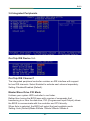
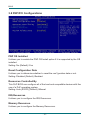
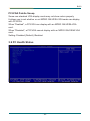
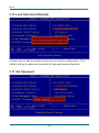
SBX-5363
AMD Geode 3.5" Embedded Board
User's Manual
Version 1.0
2009.10
Index
Table of Contents
Chapter 1 Introduction ............................................. 1
1.1 Copyright Notice ........................................................
1.2 About this User's Manual .............................................
1.3 Warning .....................................................................
1.4 Replacing the lithium battery .......................................
1.5 Technical Support .......................................................
1.6 Warranty ....................................................................
1.7 Packing List ...............................................................
1.8 Ordering Information ..................................................
1.9 Specification ..............................................................
1.10 Board Dimensions ....................................................
2
2
2
3
3
4
5
5
6
7
Chapter 2 Installation ............................................... 9
2.1 Jumpers Quick Reference ............................................ 10
2.1.1 CMOS Jumper Settings....................................... 10
2.1.2 CF Card Master&Slave Select .............................. 10
2.1.3 Serial Port Select................................................ 11
2.1.4 Voltage Select.................................................... 11
2.2 Connectors Quick Reference ....................................... 12
2.2.1 Ethernet Connector............................................. 13
2.2.2 Power Connector................................................ 13
2.2.3 Enhanced IDE Connector..................................... 14
2.2.4 Flat Panel Connector........................................... 15
2.3 Peripheral Ports .......................................................... 17
2.3.1 Parallel Port ....................................................... 17
2.3.2 USB Ports .......................................................... 17
2.3.3 PS/2 Keyboard & Mouse ...................................... 18
2.3.4 CRT Display Connector ....................................... 18
2.3.5 COM1 Port with RS-232C Mode ....................
18
2.3.6 COM2 Port with RS-232C/422/485 Mode .............. 19
2.3.7 Audio Interface Port (AUDIO) .............................. 20
2.3.8 16-bit General Purpose I/O (DIO) ...........................20
2.4 Switches and Indicators .............................................. 20
2.5 CFD1: Compact Flash II Socket ................................... 21
-i-
Index
Chapter 3 BIOS ......................................................... 22
3.1 BIOS Introduction ....................................................... 23
3.2 BIOS Setup ................................................................ 23
3.3 Standard CMOS Features ............................................ 24
3.4 Advanced BIOS Features ............................................. 26
3.5 Advanced Chipset Features ......................................... 28
3.6 Integrated Peripherals ................................................. 30
3.7 Power Management Setup ........................................... 35
3.8 PNP/PCI Configurations .............................................. 37
3.9 PC Health Status ......................................................... 38
3.10 Load Optimized Defaults ............................................ 39
3.11 Set Password ............................................................ 39
3.12 Save & Exit Setup ...................................................... 40
3.13 Exit Without Saving ................................................... 41
3.14 BIOS Beep Sound code list ........................................ 41
3.15 BIOS memory mapping .............................................. 42
3.16 Award BIOS Post Codes ............................................ 42
Chapter 4 Appendix .................................................. 48
4.1 I/O Port Address Map .................................................. 49
4.2 Interrupt Request Lines (IRQ)....................................... 51
- ii -
Introduction
1
Chapter 1
Introduction
-1-
Introduction
1.1 Copyright Notice
All Rights Reserved. The information in this document is subject to change
without prior notice in order to improve the reliability, design and function. It
does not represent a commitment on the part of the manufacturer. Under no
circumstances will the manufacturer be liable for any direct, indirect, special,
incidental, or consequential damages arising from the use or inability to use
the product or documentation, even if advised of the possibility of such
damages. This document contains proprietary information protected by
copyright. All rights are reserved. No part of this manual may be reproduced
by any mechanical, electronic, or other means in any form without prior
written permission of the manufacturer.
1.2 About this User's Manual
This User's Manual is intended for experienced users and integrators with
hardware knowledge of personal computers. If you are not sure about any
description in this User's Manual, please consult your vendor before further
handling.
1.3 Warning
Single Board Computers and their components contain very delicate
Integrated Circuits (IC). To protect the Single Board Computer and its
components against damage from static electricity, you should always follow
the following precautions when handling it :
1 Disconnect your Single Board Computer from the power source when
you want to work on the inside
2 Hold the board by the edges and try not to touch the IC chips, leads or
circuitry
3 Use a grounded wrist strap when handling computer components.
4 Place components on a grounded antistatic pad or on the bag that came
with the Single Board Computer, whenever components are separated from
the system
-2-
Introduction
1.4 Replacing the lithium battery
Incorrect replacement of the lithium battery may lead to a risk of explosion.
The lithium battery must be replaced with an identical battery or a battery
type recommended by the manufacturer.
Do not throw lithium batteries into the trashcan. It must be disposed of in
accordance with local requlations concerning special waste.
1.5 Technical Support
-3-
Introduction
1.6 Warranty
This product is warranted to be in good working order for a period of two
years from the date of purchase. Should this product fail to be in good
working order at any time during this period, we will, at our option, replace or
repair it at no additional charge except as set forth in the following terms.
This warranty does not apply to products damaged by misuse, modifications,
accident or disaster.
Vendor assumes no liability for any damages, lost profits, lost savings or any
other incidental or consequential damage resulting from the use, misuse of,
or inability to use this product. Vendor will not be liable for any claim made
by any other related party.
Vendors disclaim all other warranties, either expressed or implied, including
but not limited to implied warranties of merchantibility and fitness for a
particular purpose, with respect to the hardware, the accompanying
product's manual(s) and written materials, and any accompanying hardware.
This limited warranty gives you specific legal rights.
Return authorization must be obtained from the vendor before returned
merchandise will be accepted. Authorization can be obtained by calling or
faxing the vendor and requesting a Return Merchandise Authorization (RMA)
number. Returned goods should always be accompanied by a clear problem
description.
-4-
Introduction
1.7 Packing List
1 xSBX-5363
AMD Geode LX800 3.5" Embedded Board
1 x CPU Heat Sink
1 x CDROM (for Driver Used)
If any of the above items is damaged or missing, contact your vendor
immediately.
1.8 Ordering Information
SBX-5363-R/ Lx800
AMD Geode LX800(500MHz) 3.5 Embedded
Board with onboard 256MB DDR SDRAM
SBX-5363-S/Lx800
AMD Geode LX800(500MHz) 3.5 Embedded
Board with 1x200Pin SO-DIMM
Cable kits
7-in-1 Cable kits for SBX-5363
-5-
Introduction
1.9 Specification
Product Name
Form Factor
Processor
Chipset
System Memory
SBX-5363
3.5" Embedded Board
AMD Geode LX [email protected] 500MHz
AMD GeodeTM CS5536
SBX-5363 Onboard 256MB DDR SODRAM
SBX-5363 1*200PIN SO-DIMM up to 1GB
DDR SDRAM
2D Graphics Controller integrated in AMD Geode
LX800
VGA/ LCD Controller
CRT: 1920 x 1440 (85Hz)
LCD: 18/24 bit TTL up to 1600 x 1200 (60Hz);
18 bit LVDS up to 1600 x 1200 (60Hz)
Ethernet
1 x RTL8100CL 10/100 Base-T Fast Ethernet LAN
BIOS
Phoenix-Award BIOS
Realtek ALC203 AC'97 Codec, MIC-in/Line-in/
Audio
Line-out
IDE Interface
1 x Ultra DMA 33/66/100, supports 2 IDE drives
Two COM ports:
Serial Port
COM 1: RS-232; COM 2:RS-232/422/485
Parallel Port/ Floppy
SPP/EPP/ECP mode shared with Floppy
K/B and Mouse
Standard PS/2 K/B&MS
Universal Serial Bus
4 x USB 2.0
GPIO
16-bit GPIO (8-bit Input / Output)
1 x CF II
Expansion Interface
1 x PC/104
Hardware Monitor Chip Integrated in W83627HF
RTC
Built-in AMD CS5536 with lithium battery
Operation Temp.
0 ~ 60OC
Watchdog Timer
255-level Reset
Dimension (L x W)
145 x 102 mm (5.7" x 4")
-6-
Introduction
1.10 Board Dimensions
-7-
Introduction
USB1
LAN
KB/MS
RES
JBAT1 VGA
USB2
COM1 AUDIO HDD LED
Power LED
AMD
Cs5536
PC/104
DDR
SDRAM
AMD
Lx800
DIO
LPD/FDD
JCF1/JVLCD1
COM2
Main Power
.ATX1 JRS1 INV1
FRT
LCD
IDE
LVDS
SD-DIMM1
CFD1
-8-
Installation
2
Chapter 2
Installation
-9-
Installation
2.1 Jumpers Quick Reference
Jumpers
Label
JBAT1
JCF1
JRS1
JVLCD1
Function
Clear CMOS
CF master or slave selected
RS-232 / 422 / 485 Selection
LCD Voltage Selected
2.1.1 CMOS Jumper Settings
Type: Onboard 3-pin header (JBAT1)
CMOS Setup (JBAT1)
Keep CMOS (default setting)
Clear CMOS
JBAT1
1-2 ON
2-3 ON
JBAT1
2.1.2 CF Card Master&Slave Select
Type: Onboard 3-pin header (JCF1)
JCF1
1-2 (default setting)
2-3
Master
Slave
- 10 -
JCF1
Installation
2.1.3 Serial Port Select
RS-232C/422/485 Mode select (JRS1)
RS-232C/422/485 Mode on COM2
The onboard COM2 port can be configured to operate in RS-422 or RS-485
modes. RS-422 modes differ in the way RX/TX is being handled. Jumper
JRS1 switches between RS-232 or RS-422/485 mode. When JRS1 is set to
RS-422 or 485 mode, there will be only +12V output left while JRS1 is set. All
of the RS232/422/485 modes are available on COM2.
COM2
Pin Defined
Pin1
Pin2
Pin8
Pin9
RS232
DCD
RXD
CTS
RI
JRS1 Selection
RS232 (default setting)
RS422
RS485
RS422
Tx+
TxRx+
Rx1-2
Close
Open
Open
RS485
RTx+
RTxx
x
3-4
Open
Close
Open
COM2
5-6
Open
Open
Close
JRS1
2.1.4 LVDS Panel Voltage Select (JVLCD1)
Type: Onboard 3-pin header (JVLCD1)
JVLCD1
1-2(default setting)
2-3
LCD Voltage
5.0V
3.3V
- 11 -
JVLCD1
Installation
2.2 Connectors Quick Reference
Connectors
Label
ATX1
AUDIO1
CFD1
COM1
COM2
GPIO
FDD1
IDE1
INV1
JFRT1
KBM1(PS/2)
LAN1
LCD1
LVDS1
LPT1
PC104
PWR1
SW1
USB1
USB2
VGA1
Function
ATX Feature Connector
Audio Interface Connector
Compact Flash Disk
Serial Port: COM1
Serial Port: COM2
16-bit GPIO
Share with LPT Connector
Enhanced IDE Connector
LCD Inverter Connector
Front Panel Connector
PS/2 Keyboard & Mouse Connector
10/100M LAN1Connector
LCD Connector for TTL
LCD Connector for LVDS
Parallel Port
ISA PC-104 Interface
Power Connector
Reset Connector
USB Port 1,2
USB Port 3,4
CRT SVGA Connector
- 12 -
Installation
2.2.1 Ethernet Connector
Connector: LAN1
Type: One external RJ-45 on bracket
Pin
1
3
5
7
Description
Tx+
Rx+
NC
NC
Pin
2
4
6
8
Description
TxNC
RxNC
2.2.2 Power Connector
ATX Feature Connector: ATX1
Type: Onboard 1x3pin Wafer Header
Pin
1
2
3
Description
#PS-ON
GND
5VSB
ATX1
ATX Power Connector: PWR1
Type: Onboard 1x4pin Header
Pin
1
2
3
4
Description
+5V
GND
GND
+12V
PWR1
- 13 -
LAN1
Installation
2.2.3 Enhanced IDE Connector
Connector: IDE1
Type: One onboard 2x22pin Header
Pin
1
3
5
7
9
11
13
15
17
19
21
23
25
27
29
31
33
35
37
39
41
43
Description
IDE RESET
D7
D6
D5
D4
D3
D2
D1
D0
GND
REQ
IO RWITE
IO READ
IO READY
DACK
IRQ14
ADDR1
ADDR0
CS#2
IDEACTP
+5V
GND
Pin
2
4
6
8
10
12
14
16
18
20
22
24
26
28
30
32
34
36
38
40
42
44
IDE1
Description
GND
D8
D9
D10
D11
D12
D13
D14
D15
NC
GND
GND
GND
IDESEL
GND
NC
ATA66 DETECT
ADDR2
CS#3
GND
+5V
NC
- 14 -
Installation
2.2.4 Flat Panel Connector
LCD Interface Connector
LCD1 connector is defined for TTL panel supporting up to 24-bit.
LCD2 connector is defined for LVDS panel supporting 18-bit only.
Connector: LCD1
Type: One onboard DF13-40DS Header
Pin
1
3
5
7
9
11
13
15
17
19
21
23
25
27
29
31
33
35
37
39
Description
VDD
GND
3.3V
BIASON
LPD0
LPD2
LPD4
LPD6
LPD8
LPD10
LPD12
LPD14
LPD16
LPD18
LPD20
LPD22
GND
LCD_DOTCLK
LEDMOD
DISPEN
Pin
2
4
6
8
10
12
14
16
18
20
22
24
26
28
30
32
34
36
38
40
Description
VDD
GND
3.3V
GND
LPD1
LPD3
LPD5
LPD7
LPD9
LPD11
LPD13
LPD15
LPD17
LPD19
LPD21
TX2D3GND
FP_VS
FP_HS
LCD_ENVDD
- 15 -
LCD1
Installation
Connector: LVDS1
Type: One onboard DF13-30DS Header
Pin
1
3
5
7
9
11
13
15
17
19
21
23
25
27
29
Description
VDD
LVDS CLK+
LVDS CLKGND
LVDS TX0+
LVDS TX0GND
LVDS TX1+
LVDS TX1GND
LVDS TX2+
LVDS TX2GND
LVDS TX3+
LVDS TX3-
Pin
2
4
6
8
10
12
14
16
18
20
22
24
26
28
30
Description
NC
NC
NC
NC
NC
NC
NC
NC
NC
NC
NC
NC
NC
NC
NC
LVDS1
LVDS Panel Inverter Connector: INV1
Type: One onboard 1x5pin Wafer Header
Pin
1
2
3
4
5
Description
+12V
GND
Backlight on/off
Brightness control
GND
INV1
- 16 -
Installation
2.3 Peripheral Ports
2.3.1 Parallel Port (Share with FDD)
Connector: LPT1
Type: One onboard 2x10Pin Header
Pin
1
3
5
7
9
11
13
15
17
19
Description
#STB
PD0
PD1
PD2
PD3
PD4
PD5
PD6
PD7
#ACK
Pin
2
4
6
8
10
12
14
16
18
20
Description
#AFD
#ERR
#INIT
#SLIN
GND
GND
NC
BUSY
PE
SLCT
LPT1
2.3.2 USB Ports
Connector: USB1
Type: Onboard two USB ports
Pin
1
3
5
7
Description
+5V
USBD1+
+5V
USBD0+
Pin
2
4
6
8
Description
USBD1GND
USBD0GND
Connector: USB2
Type: One onboard 2x5pin Header
Pin
1
3
5
7
9
Description
+5V
USBD2USBD2+
GND
GND
Pin
2
4
6
8
10
Description
+5V
USBD3USBD3+
GND
NC
- 17 -
USB2
Installation
2.3.3 PS/2 Keyboard & Mouse
Connector: KBM1
Type: One external 6-pin Mini DIN connector on bracket
Pin
1
3
5
Description
KB_DATA
GND
KB_CLK
Pin
2
4
6
Description
MS_DATA
+5V
MS-CLK
2.3.4 CRT Display Connector
Connector: VGA1
Type: One external 15-pin D-sub female connector on bracket
Pin
1
3
5
7
9
11
13
15
Description
RED
BLUE
GND
GND
VCC
NC
HSYNC
VDCLK
Pin
2
4
6
8
10
12
14
Description
GREEN
NC
GND
GND
GND
VDDAT
VSYNC
2.3.5 COM1 Port with RS-232C Mode
Connector: COM1
Type: One onboard 9-pin D-sub male connector
Pin
1
3
5
7
9
Description
DCD
TXD
GND
RTS
RI
Pin
2
4
6
8
10
Description
RXD
DTR
DSR
CTS
NC
- 18 -
Installation
2.3.6 COM2 Port with RS-232C/422/485 Mode
1 RS-232C Mode
Connector: COM2
Type: One onboard 10-pin header
Pin
1
3
5
7
9
Description
DCD
TXD
GND
RTS
RI
Pin
2
4
6
8
10
Description
RXD
DTR
DSR
CTS
NC
2 RS-422 Mode
Connector: COM2
Type: One onboard 10-pin header
Pin
1
3
5
7
9
Description
TX+
NC
NC
NC
RX-
Pin
2
4
6
8
10
Description
TXNC
NC
RX+
NC
3 RS-485 Mode
Data+ of RS-485 is connected by pin-1
Data- of RS-485 is connected by pin-2
- 19 -
COM2
Installation
2.3.7 Audio Interface Port
Connector: AUDIO1
Type: One onboard 2x5pin Box Header
Pin
1
3
5
7
9
Description
LINEL
MIC
GND
AGND
LOUT-L
Pin
2
4
6
8
10
Description
LINER
GND
NC
AGND
LOUT-R
AUDIO1
2.3.8 16-bit General Purpose I/O (DIO)
Connector: DIO
Type: One onboard 2x10pin Header
Pin
1
3
5
7
9
11
13
15
17
19
Description
DO0
DO2
DO4
DO6
GND
DI0
DI2
DI4
DI6
+5V
Pin
2
4
6
8
10
12
14
16
18
20
Description
DO1
DO3
DO5
DO7
GND
DI1
DI3
DI5
DI7
+12V
DIO
Output Port I/O Based Address : 208hex~20Fh; Pin1~Pin8 Input Port
I/O Based Address : 200hex~207h; Pin11~Pin18
2.4 Switches and Indicators
Connector: JFRT1
Type: One onboard 2x5pin Header
Pin
1
3
5
7
9
Description
RESET +
Power LED+
HD LED+
Speak+
PSON+
Pin
2
4
6
8
10
Description
RESET Power LEDHD LEDSpeakPSON- 20 -
JFRT1
Installation
2.5 CFD1: Compact Flash II Socket
Connector: CFD1
Pin
1
3
5
7
9
11
13
15
17
19
21
23
25
27
29
31
33
35
37
39
41
43
45
47
49
Description
GND
DATA4
DATA6
CS#1
GND
GND
+5V
GND
GND
ADDR1
DATA0
DATA2
GND
DATA11
DATA13
DATA15
GND
IO WRITE
IRQ15
CSEL
IDE RESET
NC
DASP
DATA8
DATA10
Pin
2
4
6
8
10
12
14
16
18
20
22
24
26
28
30
32
34
36
38
40
42
44
46
48
50
Description
DATA3
DATA5
DATA7
GND
GND
GND
GND
GND
ADDR2
ADDR0
DATA1
NC
GND
DATA12
DATA14
CS#3
IO READ
+5V
+5V
NC
IO READY
+5V
DIAG
DATA9
GND
Note:
1.After hot-swapping CF II, you must restart your system for device detecting
2.CF II and ATA channel are alternative
3.CF II Socket supports up to 4GB
- 21 -
BIOS
3
Chapter 3
BIOS
- 22 -
BIOS
3.1 BIOS Introduction
The Award BIOS (Basic Input/Output System) installed in your computer
system's. The BIOS provides for a standard device such as disk drives, serial
ports and parallel ports. It also adds password protection as well as special
support for detailed fine-tuning of the chipset controlling the entire system.
3.2 BIOS Setup
The Award BIOS provides a Setup utility program for specifying the system
configurations and settings. The BIOS ROM of the system stores the Setup
utility. When you turn on the computer, the Award BIOS is immediately
activated. Pressing the <Del> key immediately allows you to enter the Setup
utility. If you a little bit late press the <Del> key, POST (Power On Self Test)
will continue with its test routines, thus preventing you from invoking the
Setup. If you still wish to enter Setup, restart the system by pressing the
"Reset" button or simultaneously pressing the <Ctrl>, <Alt> and <Delete>
keys. You can also restart by turning the system Off and back On again. The
following message will appear on the screen:
Press <DEL> to Enter Setup
In general, you press the arrow keys to highlight items, <Enter> to select, the
<PgUp> and <PgDn> keys to change entries, <F1> for help and <Esc> to
quit. When you enter the Setup utility, the Main Menu screen will appear on
the screen. The Main Menu allows you to select from various setup functions
and exit choices.
- 23 -
BIOS
3.3 Standard CMOS Features
"Standard CMOS Features" allows you to record some basic hardware
configurations in your computer system and set the system clock and error
handling. If the CPU card is already installed in a working system, you will
not need to select this option. You will need to run the Standard CMOS
option, however, if you change your system hardware configurations, such
as onboard battery fails, or the configuration stored in the CMOS memory
was lost or damaged.
Date
The date format is:
Day : Sun to Sat
Month : 1 to 12
Date : 1 to 31
Year : 1999 to 2099
Time
The time format is:
Hour : 00 to 23
Minute : 00 to 59
Second : 00 to 59
To set the date & time, highlight the "Date" & "Time" and use the <PgUp>/
<PgDn> or +/- keys to set the current time.
- 24 -
BIOS
IDE Primary HDDs / IDE Secondary HDDs
The onboard PCI IDE connectors provide Primary and Secondary channels
for connecting up to four IDE hard disks or other IDE devices.
Each channel can support up to two hard disks; the first is the "Master" and
the second is the "Slave".
Press <Enter> to configure the hard disk. The selections include Auto,
Manual, and None. Select 'Manual' to define the drive information manually.
You will be asked to enter the following items.
Cylinder: Number of cylinders
Head: Number of read/write heads
Precomp: Write precompensation
Landing Zone: Landing zone
Sector: Number of sectors
The Access Mode selections are as follows:
CHS (HD < 528MB)
LBA (HD > 528MB and supports Logical Block Addressing)
Large (for MS-DOS only)
Auto
Drive A
It identifies the type of floppy disk drive A that has been installed in the
computer. The available specifications are:
None
360K, 5.25 in.
1.2M, 5.25 in.
720K, 3.5 in.
1.44M, 3.5 in.
2.88M, 3.5 in.
Video
This field, selects the type of video display card installed in your system. You
can choose the following video display cards:
EGA/VGA For EGA, VGA, SEGA, SVGA or PGA monitor adapters.
(default)
CGA 40
Power up in 40 column mode.
CGA 80
Power up in 80 column mode.
MONO
For Hercules or MDA adapters.
- 25 -
BIOS
Halt On
This field determines whether or not the system will halt if an error is detected
during power up.
All errors (default)
Whenever the BIOS detects a non-fatal error, the
system will stop and you will be prompted.
No errors
The system boot will not be halted for any error that
may be detected.
All, But Keyboard
The system boot will not be halted for a keyboard
error; it will stop for all other errors.
All, But Diskette
The system boot will not be halted for a disk error; it
will stop for all other errors.
All, But Disk/Key
The system boot will not be halted for a keyboard or
disk error; it will stop for all others.
3.4 Advance BIOS Features
Quick Power On Self Test
This BIOS feature allows you to decrease the time it takes to boot up the
computer by shortening or skipping certain standard booting procedures.
Setting: Disabled/Enabled (Default).
- 26 -
BIOS
First/ Second/Third Boot Device
These fields determine the drive that the system searches first for an
operating system. The options available include Setting:
Floppy, LS-120, HDD-0, SCSI, CDROM, HDD-1, ZIP100,
USB-FDD, USB-ZIP, USB-CDROM, USB-HDD, LAN and Disabled.
Boot Other Device
It allows the system to search for an OS from other devices other than the
ones selected in the First/ Second/ Third Boot Device.
Setting: Disabled/ Enabled (Default).
Boot Up NumLock Status
It allows you to activate the NumLock function after you power up the
system.
Setting: Off/On (Default).
Security Option
It allows you to limit access to the System and Setup.
When you select System, the system prompts for the User Password every
time you boot up.
When you select Setup, the system always boots up and prompts for the
Supervisor Password only when the Setup utility is called up.
Setting: Setup (Default)/System.
Cyrix 6x86/MII CPUID
When a Cyrix 6x86/MII CPU is used, this option should be enabled to use
the MMX instructions. However, if you are using NetWare 5.0, you must
disable this option.
Setting: Disabled/Enabled (Default).
- 27 -
BIOS
3.5 Advanced Chipset Features
CAS Latency
It allows CAS latency time in HCLKs. The system board designer should set
the values in this field, depending on the DRAM installed. Do not change the
values in this field unless you change specifications of the installed DRAM or
CPU. Setting: Auto (Default)/1.5/2.0/2.5/3.0/3.5.
Interleave Select
It allows you to Use the Interleave Select option to specify how the cache
memory is interleaved.
Setting: LOI (Default)/HOI.
XOR BA0
Setting: Disabled (Default)/Enabled.
XOR BA1
Setting: Disabled (Default)/Enabled.
XOR MB0
Setting: Disabled (Default)/Enabled.
- 28 -
BIOS
XOR Bit Select
Setting: 18(Default)/19/20/21.
Video Memory Size
In order to determine how much memory is allocated to the video graphics
device.
Setting: None/8M(Default)/16M/32M/64M/128M/254M.
Output display
In order to specify the display devices the system is connected to.
Setting: Flat Panel/CRT (Default)/Panel & CRT.
Flat Panel Configuration
It allows you to open the Flat Panel Configuration menu.
Memory Hole At 15M-16M
In order to improve performance, certain space in memory can be reserved
for ISA cards. This memory must be mapped into the memory space below
16 MB.
Setting: Disabled (Default)/Enabled.
- 29 -
BIOS
3.6 Integrated Peripherals
On-Chip IDE Device >>>
On-Chip IDE Channel 1
The integrated peripheral controller contains an IDE interface with support
for two IDE channels. Select Enabled to activate each channel separately.
Setting: Disabled/Enabled (Default).
Master/Slave Drive PIO Mode
It allows your system HDD controller to run faster.
Rather than having the BIOS issue with a series of commands that
transferring to or from the disk drive, PIO (Programmed Input/Output) allows
the BIOS to communicate with the controller and CPU directly.
When Auto is selected, the BIOS will select the best available mode.
Setting: Auto (Default)/Mode 0/Mode 1/Mode 2/Mode 3/Mode 4.
- 30 -
BIOS
IDE Primary Master/Slave UDMA
It allows your system to improve disk I/O throughput to 33MB/sec with the
Ultra DMA33 feature.
Setting: Disabled/Auto (Default).
IDE DMA Transfer Access
Setting: Disabled, Enabled (Default).
IDE HDD Block Mode
It allows HDD controller to use the fast block mode to transfer data to and
from HDD.
Setting: Disabled/Enabled (Default).
Super IO Device>>>
External FDD Controller
Select "Enabled" if your system has a floppy disk controller (FDC) installed
and you wish to use it. Select "Disabled" if your system has an add-in FDC
or has no floppy drive.
Setting: Disabled/Enabled (Default).
- 31 -
BIOS
Onboard Serial/Parallel Port
It allows you to select the onboard serial and parallel ports with their
addresses.
Setting:
Serial Port 1
3F8/IRQ4 (Default)
Serial Port 2
2F8/IRQ3 (Default)
Parallel Port
378/IRQ7 (Default)
UART Mode Select
It determines the UART 2 mode in your computer.
Setting: IrDA/ASKIR/Normal (Default).
RxD, TxD Active
Setting: Hi, Hi/Hi, Lo (Default)/Lo, Hi /Lo, Lo.
IR Transmission Delay
Setting: Disabled/Enabled (Default).
UR2 Duplex Mode
Setting: Full/Half (Default).
Use IR Pins
Setting: RxD2,TxD2 / IR-Rx2Tx2 (Default).
Parallel Port Mode
Setting: SPP (Default) /EPP /ECP /ECP+EPP /Normal
EPP Mode Select
Setting: EPP1.9/EPP1.7 (Default)
ECP Mode Use DMA
Setting: 1/3 (Default).
- 32 -
BIOS
Serial Port 3 Use IRQ
Setting: IRQ10 (Default)/IRQ11.
Serial Port 4 Use IRQ
Setting: IRQ10 /IRQ11 (Default).
IT8888 ISA Decode IO >>>
It allows you to use the IT8888 ISA Decode IO menu to set the IO memory
range for the onboard ISA.
Decode I/O Space 0/ 1/ 2/ 3/ 4/ 5
It allows you to allocate system resources to the ISA bridge and to enable
the function correctly.
Setting: Disabled, Enabled (Default).
Decode I/O Speed 0/ 1/ 2/ 3/ 4/ 5
It allows you to specify the speed of the ISA bus.
Setting: Subtractive Speed, Slow Speed, Medium Speed, Fast Speed.
Decode I/O Address 0/ 1/ 2/ 3/ 4/ 5 [15:4]
It allows you to allocate an address to the ISA bus. The address may range
from 0001 to 0FFF.
- 33 -
BIOS
Decode I/O Size 0/ 1/ 2/ 3/ 4/ 5
It allows you to specify the size of the ISA bus.
Setting: 1 Byte, 2 Bytes, 4 Bytes, 8 Bytes, 16 Bytes, 32 Bytes, 64 Bytes,
128 Bytes.
IT8888 ISA Decode Memory >>>
It allows you to use the IT8888 ISA Decode Memory to set the resources for
the onboard ISA bus.
Decode Memory Space 0/ 1/ 2/ 3
It allows you to allocate memory resources to the ISA bridge and to enable
the function correctly.
Setting: Disabled (Default), Enabled.
Decode Memory Speed 0/ 1/ 2/ 3
It allows you to specify the memory speed of the ISA bus.
Setting: Subtractive Speed, Slow Speed, Medium Speed, Fast Speed.
Decode Memory Addr. 0/ 1/ 2/ 3 [23:
It allows you to allocate a memory address to the ISA bus. The address may
range from 0001 to 0FFF.
Decode Memory Size 0/ 1/ 2/ 3
It allows you to specify the memory size of the ISA bus.
Setting: 16 KB, 32 KB, 64 KB, 128 KB, 256 KB, 512 KB, 1MB, 2MB.
- 34 -
BIOS
IT8888 DDMA >>>
Suppose that the ISA bus card is required DMA1 & DMA5.
Set "DDMA1 Support" & "DDMA5Support" to "Enabled".
Onboard Audio
Setting: Enabled (Default), Disabled.
3.7 Power Management Setup
ACPI Function
It supports ACPI (Advance Configuration and Power Interface).
Setting: Enabled (Default) /Disabled.
- 35 -
BIOS
Power Management
It allows you to select the type of power saving management modes.
Setting: APM Advanced power management (APM)
ACPI (Default) Advanced Configuration and Power Interface (ACPI)
Modem Use IRQ
It sets the IRQ used by the Modem.
Setting: N/A (Default)/3/4/5/7/9/10/11.
PME Event Function
Setting: Disabled/Enabled (Default).
Soft-Off by PWR-BTTN
It defines the power-off mode when using an ATX power supply.
In the Instant Off mode, It allows powering off immediately upon pressing the
power button.
In the Delay 4 Sec mode, the system powers off when the power button is
pressed for more than 4 seconds or enters the suspend mode when pressed
for less than 4 seconds.
Setting: Instant-off (Default)/Delay 4 Sec.
IRQ Wakeup Events
The HDD, FDD, COM, LPT Ports, and PCI PIRQ are I/O events that can
prevent the system from entering a power saving mode or can awaken the
system from such a mode. When an I/O device wants to gain the attention
of the operating system, it signals this by causing an IRQ to occur. When the
operating system is ready to respond to the request, it interrupts itself and
performs the service.
- 36 -
BIOS
3.8 PNP/PCI Configurations
PNP OS Installed
It allows you to enable the PNP OS Install option if it is supported by the OS
installed.
Setting: No (Default) /Yes.
Reset Configuration Data
It allows you to determine whether to reset the con?guration data or not.
Setting: Disabled (Default) /Enabled.
Resources Controlled By
This PnP BIOS can configure all of the boot and compatible devices with the
use of a PnP operating system.
Setting: Auto (ESCD) (Default) /Manual.
IRQ Resources
It allows you to configure the IRQ Resources.
Memory Resources
It allows you to configure the Memory Resources.
- 37 -
BIOS
PCI/VGA Palette Snoop
Some non-standard VGA display cards may not show colors properly.
It allows you to set whether or not MPEG ISA/VESA VGA cards can display
with PCI/VGA.
When "Enabled", a PCI/VGA can display with an MPEG ISA/VESA VGA
card.
When "Disabled", a PCI/VGA cannot display with an MPEG ISA/VESA VGA
card.
Setting: Disabled (Default) /Enabled.
3.9 PC Health Status
- 38 -
BIOS
3.10 Load Optimized Defaults
It allows you to load the default values to your system configuration. The
default setting is optimal and enabled all high performance features.
3.11 Set Password
- 39 -
BIOS
Useing Password to set a password that will be used exclusively on the
system. To specify a password, highlight the type you want and press
<Enter>. The Enter Password: message prompts on the screen. Type the
password, up to eight characters in length, and press <Enter>. And the
system confirms your password by asking you to type it again. After setting a
password, the screen automatically returns to the main screen. To disable a
password, just press the <Enter> key when you are prompted to enter the
password. A message will confirm the password to be disabled. Once the
password is disabled, the system will boot, then you can enter BIOS Setup
freely.
3.12 Save & Exit Setup
Typing "Y", you will quit the setup utility and save all the changes into the
CMOS memory.
Typing "N", you will return to Setup utility.
- 40 -
BIOS
3.13 Exit Without Saving
Typing 'Y" will quit the Setup utility without saving the modifications.
Typing "N" will return you to Setup utility.
3.14 BIOS Beep Sound code list
Beep Sound
1 short (Beep)
2 short (Beep)
1 long - 1 short (Beep)
1 long - 2 short (Beep)
1 long - 3 short (Beep)
1 long - 9 short (Beep)
Long (Beep) continuous
Short (Beep) continuous
Message
System booting is normally
CMOS setting error
DRAM error
Display card or monitor connected error
Keyboard error
ROM error
DRAM hasn't inset correctly
POWER supply has problem
- 41 -
BIOS
3.15 BIOS memory mapping
Address Device
E000:0000h - F000:FFFFh
D000:2000h - D000:FFFFh
D000:0000h - D000:1FFFh
C000:E000h - CF00:FFFFh
C000:0000h - C000:DFFFh
A000:0000h - B000:FFFFh
0000:0000h - 9000:FFFFh
Description
System BIOS Area
Free space
LAN ROM
Free space
VGA BIOS
VGA RAM
DOS 640K
3.16 Award BIOS Post Codes
CFh Test CMOS read/write functionality
C0h Early chipset initialization: Disable shadow RAM, L2 cache
(socket 7 and below), program basic chipset registers
C1h Detect memory: Auto detection of DRAM size, type and ECC, auto
detection of L2 cache (socket 7 and below)
C3h Expand compressed BIOS code to DRAM
C5h Call chipset hook to copy BIOS back to E000 & F000 shadow RAM
01h Expand the Xgroup codes located in physical memory address
1000:0
02h Reserved
03h Initial Superio_Early_Init switch
04h Reserved
05h Blank out screen; Clear CMOS error ?ag
06h Reserved
07h Clear 8042 interface; Initialize 8042 self test
08h Test special keyboard controller for Winbond 977 series Super I/O
chips; Enable keyboard interface
09h Reserved
0Ah Disable PS/2 mouse interface (optional); Auto detect ports for
keyboard & mouse followed by a port & interface swap (optional);
Reset keyboard for Winbond 977 series Super I/O chips
0Bh Reserved
0Ch Reserved
0Dh Reserved
- 42 -
BIOS
0Eh Test F000h segment shadow to see whether it is read/write capable
or not. If test fails, keep beeping the speaker
0Fh Reserved
10h Auto detect flash type to load appropriate flash read/write codes into
the run time area in F000 for ESCD & DMI support
11h Reserved
12h Use walking 1's algorithm to check out interface in CMOS circuitry.
Also set real time clock power status and then check for overrride
13h Reserved
14h Program chipset default values into chipset. Chipset default values
are MODBINable by OEM customers
15h Reserved
16h Initial Early_Init_Onboard_Generator switch
17h Reserved
18h Detect CPU information including brand, SMI type (Cyrix or Intel) and
CPU level (586 or 686)
19h Reserved
1Ah Reserved
1Bh Initial interrupts vector table. If no special specified, all H/W interrupts
are directed to SPURIOUS_INT_HDLR & S/W interrupts to
SPURIOUS_soft_HDLR
1Ch Reserved
1Dh Initial EARLY_PM_INIT switch
1Eh Reserved
1Fh Load keyboard matrix (notebook platform)
20h Reserved
21h HPM initialization (notebook platform)
22h Reserved
23h Check validity of RTC value; Load CMOS settings into BIOS stack.
If CMOS checksum fails, use default value instead; Prepare BIOS
resource map for PCI & PnP use. If ESCD is valid, take into
consideration of the ESCD's legacy information; Onboard clock
generator initialization. Disable respective clock resource to empty
PCI & DIMM slots; Early PCI initialization - Enumerate PCI bus
number, assign memory & I/O resource, search for a valid VGA
device & VGA BIOS, and put it into C000:0
- 43 -
BIOS
24h
25h
26h
27h
28h
29h
2Ah
2Bh
2Ch
2Dh
Eh
2Fh
30h
31h
32h
33h
34h
35h
36h
37h
38h
39h
3Ah
3Bh
3Ch
3Dh
3Eh
3Fh
40h
41h
42h
43h
44h
Reserved
Reserved
Reserved
Initialize INT 09 buffer
Reserved
Program CPU internal MTRR (P6 & PII) for 0-640K memory address;
Initialize the APIC for Pentium class CPU; Program early chipset
according to CMOS setup; Measure CPU speed; Invoke video BIOS
Reserved
Reserved
Reserved
Initialize multilanguage; Put information on screen display, including
Award title, CPU type, CPU speed, etc...
Reserved
Reserved
Reserved
Reserved
Reserved
Reset keyboard except Winbond 977 series Super I/O chips
Reserved
Reserved
Reserved
Reserved
Reserved
Reserved
Reserved
Reserved
Test 8254
Reserved
Test 8259 interrupt mask bits for channel 1
Reserved
Test 9259 interrupt mask bits for channel 2
Reserved
Reserved
Test 8259 functionality
Reserved
- 44 -
BIOS
45h
46h
47h
48h
49h
4Ah
4Bh
4Ch
4Dh
4Eh
4Fh
50h
51h
52h
53h
54h
55h
56h
57h
58h
59h
5Ah
5Bh
5Ch
5Dh
5Eh
5Fh
60h
61h
Reserved
Reserved
Initialize EISA slot
Reserved
Calculate total memory by testing the last double last word of each
64K page; Program writes allocation for AMD K5 CPU
Reserved
Reserved
Reserved
Reserved
Program MTRR of M1 CPU; initialize L2 cache for P6 class CPU &
program cacheable range; Initialize the APIC for P6 class CPU; On
MP platform, adjust the cacheable range to smaller one in case the
cacheable ranges between each CPU are not identical
reserved
Initialize USB
Reserved
Test all memory (clear all extended memory to 0)
Reserved
Reserved
Display number of processors (multi-processor platform)
Reserved
Display PnP logo; Early ISA PnP initialization and assign CSN to
every ISA PnP device
Reserved
Initialize the combined Trend Anti-Virus code
Reserved
Show message for entering AWDFLASH.EXE from FDD
(optional feature)
Reserved
Initialize Init_Onboard_Super_IO switch; Initialize Init_Onboard_
AUDIO switch
Reserved
Reserved
Okay to enter Setup utility
Reserved
- 45 -
BIOS
62h
63h
64h
65h
66h
67h
68h
69h
6Ah
6Bh
6Ch
6Dh
6Eh
6Fh
70h
71h
72h
73h
74h
75h
76h
77h
78h
79h
7Ah
7Bh
7Ch
7Dh
7Eh
7Fh
Reserved
Reserved
Reserved
Initialize PS/2 mouse
Reserved
Prepare memory size information for function call: INT 15h ax=E820h
Reserved
Turn on L2 cache
Reserved
Program chipset registers according to items described in Setup &
Auto-Configuration table
Reserved
Assign resources to all ISA PnP devices; Auto assign ports to
onboard COM ports if the corresponding item in Setup is set to
"AUTO"
Reserved
Initialize floppy controller; Setup floppy related fields in 40:hardware
Reserved
Reserved
Reserved
Enter AWDFLASH.EXE if: AWDFLASH.EXE is found in floppy dive
and ALT+F2 is pressed
Reserved
Detect and install all IDE devices: HDD, LS120, ZIP, CDROM...
Reserved
Detect serial ports and parallel ports
Reserved
Reserved
Detect and install coprocessor
Reserved
Reserved
Reserved
Reserved
Switch back to text mod if full screen logo is supported: if errors
occur, report errors & wait for keys, if no errors occur or F1 key is
pressed continue - Clear EPA or customization logo
- 46 -
BIOS
Reserved
Reserved
Call chipset power management hook: Recover the text fond usedby
EPA logo (not for full screen logo), If password is set, ask for
password
83h Save all data in stack back to CMOS
84h Initialize ISA PnP boot devices
85h Final USB initialization; NET PC: Build SYSID structure; Switch
screen back to text mode; Set up ACPI table at top of memory;
Invoke ISA adapter ROM's; Assign IRQ's to PCI devices; Initialize
APM; Clear noise of IRQ's
86h Reserved
87h Reserved
88h Reserved
89h Reserved
90h Reserved
91h Reserved
92h Reserved
93h Read HDD boot sector information for Trend Anti-Virus code
94h Enable L2 cache; Program boot up speed; Chipset final initialization;
Power management final initialization; Clear screen and display
summary table; Program K^ write allocation; Program P6 class write
combining
95h Program daylight saving; Update keyboard LED and typematic rate
96h Build MP table; Build and update ESCD; Set CMOS century to 20h
or 19h; Load CMOS time into DOS timer tick; Build MSIRQ routing
table
FFh Boot attempt (INT 19h)
80h
81h
82h
- 47 -
Appendix
4
Chapter 4
Appendix
- 48 -
Appendix
4.1 I/O Port Address Map
Each peripheral device in the system is assigned a set of I/O port addresses
which also becomes the identity of the device.
The following table lists the I/O port addresses used.
Address Device
EE000000 - EEFFFFFF
Description
Advanced Micro Devices Win 2K/XP Graphics
Driver
EFD00000 - EFDFFFFF PCI standard PCI-to-PCI bridge
PCI standard PCI-to-PCI bridge
EFE00000 - EFEFFFFF
EFFC0000 - EFFDFFFF Intel(R) PRO/100 M Desktop Adapter
EFFE8000 - EFFEBFFF Advanced Micro Devices Win 2K/XP Graphics
Driver
Advanced Micro Devices Win 2K/XP Graphics
EFFEC000 -EFFEFFFF
Driver
Advanced Micro Devices Win 2K/XP Graphics
EFFF0000 - EFFF3FFF
Driver
Geode LX AES Crypto Driver
EFFF4000 - EFFF7FFF
Advanced Micro Devices Win 2K/XP Graphics
EFFF8000 - EFFFBFFF
Driver
Standard Enhanced PCI to USB Host Controller
EFFFD000 -EFFFDFFF
EFFFE000 - EFFFEFFF Standard OpenHCD USB Host Controller
Intel(R) PRO/100 M Desktop Adapter
EFFFF000 - EFFFFFFF
PCI bus
000A0000 - 000BFFFF
Advanced Micro Devices Win 2K/XP Graphics
000A0000 - 000BFFFF
Driver
PCI bus
000C8000 - 000DFFFF
PCI bus
0F7C0000 - FEBFFFFF
PCI bus
00000000 - 00000CF7
ISAPNP Read Data Port
00000000 - FFFFFFFF
Standard 101/102-Key or Microsoft Natural
00000060 - 00000060
PS/2 Keyboard
00000064 - 00000064 Standard 101/102-Key
00000064 - 00000064
or Microsoft Natural PS/2 Keyboard
System CMOS/real time clock
00000070 - 00000073
- 49 -
Appendix
00000170 - 00000177
000001F0 - 000001F7
00000274 - 00000277
00000279 - 00000279
000002F8 - 000002FF
00000376 - 00000376
00000378 - 0000037F
000003B0 - 000003BA
000003C0 - 000003DF
000003F0 - 000003F5
000003F6 - 000003F6
000003F7 - 000003F7
000003F8 - 000003FF
00000778 - 0000077B
00000D00 - 0000AC17
0000AC20 - 0000FFFF
0000E000 - 0000EFFF
0000FD00 - 0000FD7F
0000FE00 - 0000FE0F
0000FF00 - 0000FF3F
Secondary IDE Channel
Primary IDE Channel
ISAPNP Read Data Port
ISAPNP Read Data Port
Communications Port
Secondary IDE Channel
Printer Port
Advanced Micro Devices Win 2K/XP Graphics
Driver
Advanced Micro Devices Win 2K/XP Graphics
Driver
Standard floppy disk controller
Primary IDE Channel
Standard floppy disk controller
Communications Port
Printer Port
PCI bus
PCI bus
PCI standard PCI-to-PCI bridge
GeodeLX Audio Driver (WDM)
Standard Dual Channel PCI IDE Controller
Intel(R) PRO/100 M Desktop Adapter
- 50 -
Appendix
4.2 Interrupt Request Lines (IRQ)
Peripheral devices use interrupt request lines to notify CPU for the service
required. The following table shows the IRQ used by the devices on board.
Level
IRQ 01
IRQ 03
IRQ 04
IRQ 05
IRQ 05
IRQ 06
IRQ 08
IRQ 09
IRQ 10
IRQ 10
IRQ 11
IRQ 11
IRQ 12
IRQ 14
Function
Standard 101/102-Key or Microsoft Natural PS/2 Keyboard
Communications Port
Communications Port
Standard Enhanced PCI to USB Host Controller
Standard OpenHCD USB Host Controller
Standard ?oppy disk controller
System CMOS/real time clock
Microsoft ACPI-Compliant System
Advanced Micro Devices Win 2K/XP Graphics Driver
Geode LX AES Crypto Driver
Intel(R) PRO/100 M Desktop Adapter
GeodeLX Audio Driver (WDM)
PS/2 Compatible Mouse
Primary IDE Channel
- 51 -