1
MELSEC System Q
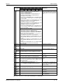
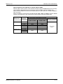
Programmable Logic Controllers
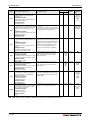
User’s Manual
Hardware Description
Art. No.
10 03 2011
Version F
INDUSTRIAL AUTOMATION
About this manual
The texts, illustrations, diagrams and examples in this manual are provided for
information purposes only. They are intended as aids to help explain the
installation, operation, programming and use of the MELSEC System Q modules.
If you have any questions about the installation and operation of any of the products
described in this manual please contact your local sales office or distributor (see
back cover). You can find the latest information and answers to frequently asked
questions on our website at www.mitsubishi-automation.com.
MITSUBISHI ELECTRIC EUROPE B.V. reserves the right to make changes to this
manual or the technical specifications of its products at any time without notice.
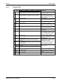
User’s Manual
MELSEC Q Series Modules
Art. No.:
Version
A
06/2001
B
02/2002
C
D
E
F
Changes / Additions / Corrections
First edition
Additions:
CPU modules: Q00JCPU, Q00CPU, Q01CPU
Power supply modules: Q62P and Q64P
Base units: Q52B and Q55B
Extension cable: QC05B
Digital input modules: QX40, QX40-S1, QX41, QX42
Digital output modules: QY40P, QY41P, QY42P, QY50, QY68A
Additions:
CPU modules: Q12PHCPU and Q25PHCPU
Digital input modules: QX41-S1, QX42-S1, QX82 and Q82-S1
Memory card: Q2MEM-2MBS
Sections 4.3.6 and 4.4
10/2003
Partial correction:
Sections 6.2, 10.3.1 and 11.3
Additions:
Combined I/O modules: QH42P and QX48Y57
CPU module battery: Q7BAT (page 3-3, sections 5.2.1, 5.2.2, 10.3.1, 10.3.2)
Notes on devices FX and FY (table 4-1)
Footnote fig. 9-5
09/2004
Partial corrections:
Section 4.3.4
Notes on troubleshooting (pages 11-12 and 11-13)
Error codes (section 11.2.1) added
Additions:
CPU modules: Q12PRHCPU, Q25PRHCPU, Q06CCPU
Power supply modules: Q63RP and Q64RP
Base units: Q38RB-E and Q68RB
02/2006
03/2011
akl
Partial corrections:
MT-series modules deleted (Overview, section 3.2.1)
ST-series modules addad (Overview, section 3.2.1)
Additions:
CPU modules: Universal model QCPU, Process CPUs Q02PHCPU and
Q06PHCPU
Power supply modules: Q61P, Q61P-D, Q61SP and Q64RN
Base units: Q32SB, Q33SB, Q35SB, Q38DB, Q321DB, Q65WRB
Digital input modules: QX10-TS, QX40-TS, QX80-TS
Digital output modules: QY10-TS, QY40-TS, QY80-TS
Memory cards: Q3MEM-4MBS and Q3MEM-8MBS
Partial corrections:
Error code list (section 11.3)
Notes on troubleshooting (section 11.4.1); new section 11.4.2
Safety guidelines
For use by qualified staff only
This manual is only intended for use by properly trained and qualified electrical technicians who
are fully acquainted with the relevant automation technology safety standards. All work with the
hardware described, including system design, installation, configuration, maintenance, service
and testing of the equipment, may only be performed by trained electrical technicians with
approved qualifications who are fully acquainted with all the applicable automation technology
safety standards and regulations. Any operations or modifications to the hardware and/or
software of our products not specifically described in this manual may only be performed by
authorised Mitsubishi Electric staff.
Proper use of the products
The MELSEC System Q modules are only intended for the specific applications explicitly
described in this manual. All parameters and settings specified in this manual must be observed.
The products described have all been designed, manufactured, tested and documented in strict
compliance with the relevant safety standards. Unqualified modification of the hardware or
software or failure to observe thewarnings on the products and in this manual may result in
serious personal injury and/or damage to property. Only peripherals and expansion equipment
specifically recommended and approved by MITSUBISHI ELECTRIC may be used with the
programmable logic controllers of the MELSEC System Q.
All and any other uses or application of the products shall be deemed to be improper.
Relevant safety regulations
All safety and accident prevention regulations relevant to your specific application must be
observed in the system design, installation, setup, maintenance, servicing and testing of these
products. The regulations listed below are particularly important in this regard.
This list does not claim to be complete; however, you are responsible for knowing and applying
the regulations applicable to you in your location:
● VDE Standards
– VDE 0100
Regulations for the erection of power installations with rated voltages below 1000 V
– VDE 0105
Operation of power installations
– VDE 0113
Electrical installations with electronic equipment
– VDE 0160
Electronic equipment for use in power installations
– VDE 0550/0551
Regulations for transformers
– VDE 0700
Safety of electrical appliances for household use and similar applications
– VDE 0860
Safety regulations for mains-powered electronic appliances and their accessories for
household use and similar applications.
● Fire safety regulations
● Accident prevention regulation
– VBG No. 4
Electrical systems and equipment
MELSEC System Q, Hardware
5
Safety warnings in this manual
In this manual special warnings that are important for the proper and safe use of the products
are clearly identified as follows:
6
P
DANGER:
E
CAUTION:
Personnel health and injury warnings. Failure to observe the safety warnings identified
with this symbol can result in health and injury hazards for the user.
Equipment and property damage warnings. Failure to observe the safety warnings
identified with this symbol can result in damage to the equipment or other property.
General safety information and precautions
The following safety precautions are intended as a general guideline for using PLC systems together with other equipment. These precautions must always be observed in the design, installation and operation of all control systems.
P
DANGER:
● Observe all safety and accident prevention regulations applicable to your specific
application. Always disconnect all power supplies before performing installation
andwiringwork or opening any of the assemblies,components and devices.
● Assemblies, components and devicesmust always be installed in a shockproof
housing fitted with a proper cover and fuses or circuit breakers.
● Devices with a permanent connection to the mains power supply must be integrated
in the building installations with an all-pole disconnection switch and a suitable
fuse.
● Check power cables and lines connected to the equipment regularly for breaks and
insulation damage. If cable damage is found immediately disconnect the equipment
and the cables from the power supply and replace the defective cabling.
● Before using the equipment for the first time check that the power supply rating
matches that of the local mains power.
● You are responsible for taking the necessary precautions to ensure that programs
interrupted by brownouts and power failures can be restarted properly and safely.
In particular, you must ensure that dangerous conditions cannot occur under any
circumstances, even for brief periods. EMERGENCY OFF must be switched forcibly,
if necessary.
● EMERGENCY OFF facilities conforming to EN 60204/IEC 204 and VDE 0113 must
remain fully operative at all times and in all control system operating modes.The
EMERGENCY OFF facility reset function must be designed so that it cannot ever
cause an uncontrolled or undefined restart.
● You must implement both hardware and software safety precautions to prevent the
possibility of undefined control system states caused by signal line cable or core
breaks.
MELSEC System Q, Hardware
7
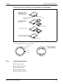
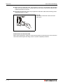
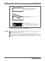
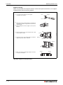
Symbols used in the manual
Use of instructions
Instructions concerning important information are marked separately and are displayed as follows:
NOTE
Text of instruction
Use of numbering in the figures
Numbering within the figures is displayed by white numbers within black circles and is explained
in a table following it using the same number, e.g.:
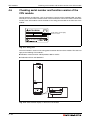
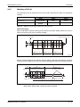
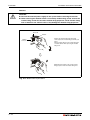
Use of handling instructions
Handling instructions are steps that must be carried out in their exact sequence during startup,
operation, maintenance and similar operations.
They are numbered consecutively (black numbers in white circles):
Text.
Text.
Text.
Use of footnotes in tables
Instructions in tables are explained in footnotes underneath the tables (in superscript). There is
a footnote character at the appropriate position in the table (in superscript).
If there are several footnotes for one table then these are numbered consecutively underneath
the table (black numbers in white circle, in superscript):
�
Text
Text
�
Text
�
8
Contents
Contents
1
Introduction
2
Basics
2.1
Features of the MELSEC System Q . . . . . . . . . . . . . . . . . . . . . . . . . . . . . . . . . . . . . 2-1
2.2
Specification comparison of CPU. . . . . . . . . . . . . . . . . . . . . . . . . . . . . . . . . . . . . . . . 2-5
2.2.1
Basic model QCPU Q00JCPU, Q00CPU, Q01CPU and Q02CPU. . . . . . . . 2-5
2.2.2
High performance model QCPU (H types) . . . . . . . . . . . . . . . . . . . . . . . . . . 2-6
2.2.3
Universal model QCPU. . . . . . . . . . . . . . . . . . . . . . . . . . . . . . . . . . . . . . . . . 2-7
2.2.4
Process CPU . . . . . . . . . . . . . . . . . . . . . . . . . . . . . . . . . . . . . . . . . . . . . . . . 2-9
2.2.5
Redundant CPU . . . . . . . . . . . . . . . . . . . . . . . . . . . . . . . . . . . . . . . . . . . . . 2-10
2.2.6
Motion CPU . . . . . . . . . . . . . . . . . . . . . . . . . . . . . . . . . . . . . . . . . . . . . . . . 2-11
2.2.7
PC CPU module . . . . . . . . . . . . . . . . . . . . . . . . . . . . . . . . . . . . . . . . . . . . . 2-13
2.2.8
C-Controller CPU . . . . . . . . . . . . . . . . . . . . . . . . . . . . . . . . . . . . . . . . . . . . 2-14
3
System configuration
3.1
Overall configuration . . . . . . . . . . . . . . . . . . . . . . . . . . . . . . . . . . . . . . . . . . . . . . . . . 3-1
3.2
Overall system . . . . . . . . . . . . . . . . . . . . . . . . . . . . . . . . . . . . . . . . . . . . . . . . . . . . . . 3-6
3.2.1
Modules of MELSEC System Q . . . . . . . . . . . . . . . . . . . . . . . . . . . . . . . . . . 3-6
3.2.2
Outline of system configuration . . . . . . . . . . . . . . . . . . . . . . . . . . . . . . . . . 3-19
4
CPU modules
4.1
Devices . . . . . . . . . . . . . . . . . . . . . . . . . . . . . . . . . . . . . . . . . . . . . . . . . . . . . . . . . . . 4-1
4.1.1
Basic model QCPU . . . . . . . . . . . . . . . . . . . . . . . . . . . . . . . . . . . . . . . . . . . . 4-1
4.1.2
High performance model QCPU . . . . . . . . . . . . . . . . . . . . . . . . . . . . . . . . . . 4-3
4.1.3
Universal model QCPU. . . . . . . . . . . . . . . . . . . . . . . . . . . . . . . . . . . . . . . . . 4-5
4.1.4
Process CPU . . . . . . . . . . . . . . . . . . . . . . . . . . . . . . . . . . . . . . . . . . . . . . . 4-13
4.1.5
Redundant CPU . . . . . . . . . . . . . . . . . . . . . . . . . . . . . . . . . . . . . . . . . . . . . 4-15
4.2
Memory capacity . . . . . . . . . . . . . . . . . . . . . . . . . . . . . . . . . . . . . . . . . . . . . . . . . . . 4-17
4.3
Notes for handling . . . . . . . . . . . . . . . . . . . . . . . . . . . . . . . . . . . . . . . . . . . . . . . . . . 4-21
MELSEC System Q, Hardware
9
Contents
4.4
4.5
4.4.1
Part names of CPU modules . . . . . . . . . . . . . . . . . . . . . . . . . . . . . . . . . . . 4-22
4.4.2
DIP switches . . . . . . . . . . . . . . . . . . . . . . . . . . . . . . . . . . . . . . . . . . . . . . . . 4-29
4.4.3
Transfer of a program with a programming device . . . . . . . . . . . . . . . . . . . 4-30
4.4.4
Latch clear operation . . . . . . . . . . . . . . . . . . . . . . . . . . . . . . . . . . . . . . . . . 4-31
4.4.5
Data transfer from memory card to standard ROM. . . . . . . . . . . . . . . . . . . 4-31
Part names and settings of universal CPU modules . . . . . . . . . . . . . . . . . . . . . . . . 4-32
4.5.1
Part names of CPU modules . . . . . . . . . . . . . . . . . . . . . . . . . . . . . . . . . . . 4-32
4.5.2
Transfer of a program with a programming device . . . . . . . . . . . . . . . . . . . 4-41
4.5.3
Reset operation . . . . . . . . . . . . . . . . . . . . . . . . . . . . . . . . . . . . . . . . . . . . . 4-42
4.5.4
Latch clear operation . . . . . . . . . . . . . . . . . . . . . . . . . . . . . . . . . . . . . . . . . 4-43
4.6
Checking serial number and function version of the CPU module. . . . . . . . . . . . . . 4-44
5
Memory cards and batteries
5.1
Memory card . . . . . . . . . . . . . . . . . . . . . . . . . . . . . . . . . . . . . . . . . . . . . . . . . . . . . . . 5-1
5.2
10
Part names and settings of Qn(P)(R)(H)CPUs . . . . . . . . . . . . . . . . . . . . . . . . . . . . 4-22
5.1.1
Specifications . . . . . . . . . . . . . . . . . . . . . . . . . . . . . . . . . . . . . . . . . . . . . . . . 5-2
5.1.2
Handling the memory card . . . . . . . . . . . . . . . . . . . . . . . . . . . . . . . . . . . . . . 5-4
5.1.3
Installing and removing a memory card . . . . . . . . . . . . . . . . . . . . . . . . . . . . 5-5
5.1.4
Setting the write protect switch . . . . . . . . . . . . . . . . . . . . . . . . . . . . . . . . . . . 5-9
Batteries . . . . . . . . . . . . . . . . . . . . . . . . . . . . . . . . . . . . . . . . . . . . . . . . . . . . . . . . . . 5-10
5.2.1
Battery specifications . . . . . . . . . . . . . . . . . . . . . . . . . . . . . . . . . . . . . . . . . 5-10
5.2.2
Battery installation . . . . . . . . . . . . . . . . . . . . . . . . . . . . . . . . . . . . . . . . . . . 5-10
5.2.3
Battery installation into the memory card . . . . . . . . . . . . . . . . . . . . . . . . . . 5-12
5.2.4
Handling instructions . . . . . . . . . . . . . . . . . . . . . . . . . . . . . . . . . . . . . . . . . 5-13
6
Input and output modules
6.1
Selecting I/O modules . . . . . . . . . . . . . . . . . . . . . . . . . . . . . . . . . . . . . . . . . . . . . . . . 6-1
6.2
Part names. . . . . . . . . . . . . . . . . . . . . . . . . . . . . . . . . . . . . . . . . . . . . . . . . . . . . . . . . 6-5
Contents
7
Power supply modules
7.1
Overview . . . . . . . . . . . . . . . . . . . . . . . . . . . . . . . . . . . . . . . . . . . . . . . . . . . . . . . . . . 7-1
7.2
Selecting the power supply module . . . . . . . . . . . . . . . . . . . . . . . . . . . . . . . . . . . . . . 7-2
7.2.1
Base unit that can be used in combination with power supply module. . . . . 7-2
7.2.2
Output currents of the power supplies . . . . . . . . . . . . . . . . . . . . . . . . . . . . . 7-2
7.2.3
Life detection power supply module Q61P-D . . . . . . . . . . . . . . . . . . . . . . . . 7-3
7.3
Part names. . . . . . . . . . . . . . . . . . . . . . . . . . . . . . . . . . . . . . . . . . . . . . . . . . . . . . . . . 7-4
7.4
Wiring of power supply modules . . . . . . . . . . . . . . . . . . . . . . . . . . . . . . . . . . . . . . . . 7-7
8
Base units
8.1
Overview . . . . . . . . . . . . . . . . . . . . . . . . . . . . . . . . . . . . . . . . . . . . . . . . . . . . . . . . . . 8-1
8.1.1
Extension base units that can be combined with the main base unit . . . . . . 8-1
8.1.2
Precautions on using the base units Q52B and Q55B . . . . . . . . . . . . . . . . . 8-2
8.2
Extension cable . . . . . . . . . . . . . . . . . . . . . . . . . . . . . . . . . . . . . . . . . . . . . . . . . . . . . 8-3
8.3
Part names and settings . . . . . . . . . . . . . . . . . . . . . . . . . . . . . . . . . . . . . . . . . . . . . . 8-4
8.3.1
Part names . . . . . . . . . . . . . . . . . . . . . . . . . . . . . . . . . . . . . . . . . . . . . . . . . . 8-4
8.3.2
Setting the extension stage number . . . . . . . . . . . . . . . . . . . . . . . . . . . . . . . 8-9
8.3.3
Connection and disconnection of extension cable . . . . . . . . . . . . . . . . . . . 8-11
8.4
I/O Number assignment . . . . . . . . . . . . . . . . . . . . . . . . . . . . . . . . . . . . . . . . . . . . . . 8-13
9
Installation
9.1
Safety guidelines . . . . . . . . . . . . . . . . . . . . . . . . . . . . . . . . . . . . . . . . . . . . . . . . . . . . 9-1
9.2
General specifications . . . . . . . . . . . . . . . . . . . . . . . . . . . . . . . . . . . . . . . . . . . . . . . . 9-6
9.3
Calculating heat generation of programmable controller . . . . . . . . . . . . . . . . . . . . . . 9-7
9.4
Mounting the base unit. . . . . . . . . . . . . . . . . . . . . . . . . . . . . . . . . . . . . . . . . . . . . . . . 9-9
9.4.1
Direct mounting. . . . . . . . . . . . . . . . . . . . . . . . . . . . . . . . . . . . . . . . . . . . . . 9-11
9.4.2
Mounting a DIN rail . . . . . . . . . . . . . . . . . . . . . . . . . . . . . . . . . . . . . . . . . . . 9-13
9.5
Installation and removal of module . . . . . . . . . . . . . . . . . . . . . . . . . . . . . . . . . . . . . 9-17
9.6
Wiring . . . . . . . . . . . . . . . . . . . . . . . . . . . . . . . . . . . . . . . . . . . . . . . . . . . . . . . . . . . . 9-19
9.6.1
Wiring precautions . . . . . . . . . . . . . . . . . . . . . . . . . . . . . . . . . . . . . . . . . . . 9-19
MELSEC System Q, Hardware
11
Contents
10
Maintenance and inspection
10.1 Daily inspection . . . . . . . . . . . . . . . . . . . . . . . . . . . . . . . . . . . . . . . . . . . . . . . . . . . . 10-1
10.2 Periodic inspection . . . . . . . . . . . . . . . . . . . . . . . . . . . . . . . . . . . . . . . . . . . . . . . . . . 10-2
10.3 Battery life and replacement procedure . . . . . . . . . . . . . . . . . . . . . . . . . . . . . . . . . . 10-3
10.3.1 Battery life . . . . . . . . . . . . . . . . . . . . . . . . . . . . . . . . . . . . . . . . . . . . . . . . . . 10-4
10.3.2 Replacement procedure of the CPU module battery . . . . . . . . . . . . . . . . 10-16
10.3.3 SRAM card CPU module battery replacement procedure . . . . . . . . . . . . 10-20
10.4 Resuming operation of CPU after storage . . . . . . . . . . . . . . . . . . . . . . . . . . . . . . . 10-22
11
Troubleshooting
11.1 Troubleshooting basics . . . . . . . . . . . . . . . . . . . . . . . . . . . . . . . . . . . . . . . . . . . . . . 11-1
11.2 Troubleshooting . . . . . . . . . . . . . . . . . . . . . . . . . . . . . . . . . . . . . . . . . . . . . . . . . . . . 11-2
11.2.1 ERR. terminal (negative logic) has turned off (opened) . . . . . . . . . . . . . . . 11-4
11.2.2 The MODE LED does not turn on . . . . . . . . . . . . . . . . . . . . . . . . . . . . . . . . 11-6
11.2.3 When the MODE LED is flickering . . . . . . . . . . . . . . . . . . . . . . . . . . . . . . . 11-7
11.2.4 When the POWER LED has turned off . . . . . . . . . . . . . . . . . . . . . . . . . . . 11-8
11.2.5 When the POWER LED is flickering in orange . . . . . . . . . . . . . . . . . . . . . 11-10
11.2.6 When the POWER LED has turned on in red . . . . . . . . . . . . . . . . . . . . . . 11-10
11.2.7 When the LIFE LED has turned off or turned on in red/is flickering in red 11-10
11.2.8 When the RUN LED has turned off . . . . . . . . . . . . . . . . . . . . . . . . . . . . . 11-11
11.2.9 When the RUN LED is flickering . . . . . . . . . . . . . . . . . . . . . . . . . . . . . . . . 11-12
11.2.10 When the ERR. LED has turned on or is flickering . . . . . . . . . . . . . . . . . 11-12
11.2.11 When the USER LED has turned on . . . . . . . . . . . . . . . . . . . . . . . . . . . . 11-13
11.2.12 When the BAT.ARM LED has turned on. . . . . . . . . . . . . . . . . . . . . . . . . . 11-13
11.2.13 When the BOOT LED is flickering. . . . . . . . . . . . . . . . . . . . . . . . . . . . . . . 11-13
11.2.14 When the LEDs of the output module do not turn on . . . . . . . . . . . . . . . . 11-14
11.2.15 When output load of the output module does not turn on . . . . . . . . . . . . 11-15
11.2.16 When unable to read a program . . . . . . . . . . . . . . . . . . . . . . . . . . . . . . . . 11-16
11.2.17 When unable to write a program into the CPU module. . . . . . . . . . . . . . . 11-17
11.2.18 When program is rewritten unintentionally . . . . . . . . . . . . . . . . . . . . . . . . 11-18
11.2.19 When unable to perform boot operation from the memory card . . . . . . . . 11-19
11.2.20 When "UNIT VERIFY ERR." has occurred . . . . . . . . . . . . . . . . . . . . . . . . 11-20
11.2.21 When "CONTROL BUS ERR." has occurred . . . . . . . . . . . . . . . . . . . . . . 11-21
11.2.22 When the CPU module does not start . . . . . . . . . . . . . . . . . . . . . . . . . . . 11-22
11.2.23 When the CPU cannot communicate with
GX Developer/GX IEC Developer. . . . . . . . . . . . . . . . . . . . . . . . . . . . . . . 11-23
12
Contents
11.3 Error code list . . . . . . . . . . . . . . . . . . . . . . . . . . . . . . . . . . . . . . . . . . . . . . . . . . . . . 11-25
11.3.1 Error code list (1000 to 1999) . . . . . . . . . . . . . . . . . . . . . . . . . . . . . . . . . . 11-26
11.3.2 Error code list (2000 to 2999) . . . . . . . . . . . . . . . . . . . . . . . . . . . . . . . . . . 11-37
11.3.3 Error code list (3000 to 3999) . . . . . . . . . . . . . . . . . . . . . . . . . . . . . . . . . . 11-54
11.3.4 Error code list (4000 to 4999) . . . . . . . . . . . . . . . . . . . . . . . . . . . . . . . . . . 11-69
11.3.5 Error code list (5000 to 5999) . . . . . . . . . . . . . . . . . . . . . . . . . . . . . . . . . . 11-83
11.3.6 Error code list (6000 to 6999) . . . . . . . . . . . . . . . . . . . . . . . . . . . . . . . . . . 11-85
11.3.7 Error code list (7000 to 10000) . . . . . . . . . . . . . . . . . . . . . . . . . . . . . . . . . 11-93
11.4 I/O circuit troubleshooting . . . . . . . . . . . . . . . . . . . . . . . . . . . . . . . . . . . . . . . . . . . 11-97
11.4.1 Input circuit troubleshooting . . . . . . . . . . . . . . . . . . . . . . . . . . . . . . . . . . . 11-97
11.4.2 Output circuit troubleshooting . . . . . . . . . . . . . . . . . . . . . . . . . . . . . . . . 11-100
12
Specifications
12.1 General specifications . . . . . . . . . . . . . . . . . . . . . . . . . . . . . . . . . . . . . . . . . . . . . . . 12-1
12.2 Hardware specifications of the CPU modules . . . . . . . . . . . . . . . . . . . . . . . . . . . . . 12-2
12.2.1 Basic model QCPU . . . . . . . . . . . . . . . . . . . . . . . . . . . . . . . . . . . . . . . . . . . 12-2
12.2.2 High performance model QCPU . . . . . . . . . . . . . . . . . . . . . . . . . . . . . . . . . 12-3
12.2.3 Universal model QCPU. . . . . . . . . . . . . . . . . . . . . . . . . . . . . . . . . . . . . . . . 12-4
12.2.4 Process CPU . . . . . . . . . . . . . . . . . . . . . . . . . . . . . . . . . . . . . . . . . . . . . . . 12-6
12.2.5 Redundant CPU . . . . . . . . . . . . . . . . . . . . . . . . . . . . . . . . . . . . . . . . . . . . . 12-7
12.3 Input/output module specifications. . . . . . . . . . . . . . . . . . . . . . . . . . . . . . . . . . . . . . 12-8
12.3.1 Digital input module QX10 . . . . . . . . . . . . . . . . . . . . . . . . . . . . . . . . . . . . . 12-8
12.3.2 Digital input module QX10-TS . . . . . . . . . . . . . . . . . . . . . . . . . . . . . . . . . . 12-9
12.3.3 Digital input module QX28 . . . . . . . . . . . . . . . . . . . . . . . . . . . . . . . . . . . . 12-10
12.3.4 Digital input module QX40 . . . . . . . . . . . . . . . . . . . . . . . . . . . . . . . . . . . . 12-11
12.3.5 Digital input module QX40-TS . . . . . . . . . . . . . . . . . . . . . . . . . . . . . . . . . 12-12
12.3.6 Digital input module QX40-S1 . . . . . . . . . . . . . . . . . . . . . . . . . . . . . . . . . 12-13
12.3.7 Digital input module QX41 . . . . . . . . . . . . . . . . . . . . . . . . . . . . . . . . . . . . 12-14
12.3.8 Digital input module QX41-S1 . . . . . . . . . . . . . . . . . . . . . . . . . . . . . . . . . 12-15
12.3.9 Digital input module QX42 . . . . . . . . . . . . . . . . . . . . . . . . . . . . . . . . . . . . 12-17
12.3.10 Digital input module QX42-S1 . . . . . . . . . . . . . . . . . . . . . . . . . . . . . . . . . 12-19
12.3.11 Digital input module QX70 . . . . . . . . . . . . . . . . . . . . . . . . . . . . . . . . . . . . 12-21
12.3.12 Digital input module QX71 . . . . . . . . . . . . . . . . . . . . . . . . . . . . . . . . . . . . 12-22
12.3.13 Digital input module QX72 . . . . . . . . . . . . . . . . . . . . . . . . . . . . . . . . . . . . 12-23
12.3.14 Digital input module QX80 . . . . . . . . . . . . . . . . . . . . . . . . . . . . . . . . . . . . 12-25
12.3.15 Digital input module QX80-TS . . . . . . . . . . . . . . . . . . . . . . . . . . . . . . . . . 12-26
12.3.16 Digital input module QX81 . . . . . . . . . . . . . . . . . . . . . . . . . . . . . . . . . . . . 12-27
MELSEC System Q, Hardware
13
Contents
12.3.17 Digital input module QX82 . . . . . . . . . . . . . . . . . . . . . . . . . . . . . . . . . . . . 12-28
12.3.18 Digital input module QX82-S1 . . . . . . . . . . . . . . . . . . . . . . . . . . . . . . . . . 12-30
12.3.19 Relay output module QY10 . . . . . . . . . . . . . . . . . . . . . . . . . . . . . . . . . . . 12-32
12.3.20 Relay output module QY10-TS . . . . . . . . . . . . . . . . . . . . . . . . . . . . . . . . 12-33
12.3.21 Relay output module QY18A . . . . . . . . . . . . . . . . . . . . . . . . . . . . . . . . . . 12-34
12.3.22 Triac output module QY22 . . . . . . . . . . . . . . . . . . . . . . . . . . . . . . . . . . . . 12-35
12.3.23 Transistor output module QY40P . . . . . . . . . . . . . . . . . . . . . . . . . . . . . . . 12-36
12.3.24 Transistor output module QY40P-TS . . . . . . . . . . . . . . . . . . . . . . . . . . . . 12-37
12.3.25 Transistor output module QY41P . . . . . . . . . . . . . . . . . . . . . . . . . . . . . . . 12-38
12.3.26 Transistor output module QY42P . . . . . . . . . . . . . . . . . . . . . . . . . . . . . . . 12-39
12.3.27 Transistor output module QY50 . . . . . . . . . . . . . . . . . . . . . . . . . . . . . . . . 12-41
12.3.28 Transistor output module QY68A . . . . . . . . . . . . . . . . . . . . . . . . . . . . . . . 12-42
12.3.29 Transistor output module QY70 . . . . . . . . . . . . . . . . . . . . . . . . . . . . . . . . 12-43
12.3.30 Transistor output module QY71 . . . . . . . . . . . . . . . . . . . . . . . . . . . . . . . . 12-44
12.3.31 Transistor output module QY80 . . . . . . . . . . . . . . . . . . . . . . . . . . . . . . . . 12-45
12.3.32 Transistor output module QY80-TS . . . . . . . . . . . . . . . . . . . . . . . . . . . . . 12-46
12.3.33 Transistor output module QY81P . . . . . . . . . . . . . . . . . . . . . . . . . . . . . . . 12-47
12.3.34 Combined I/O module QH42P . . . . . . . . . . . . . . . . . . . . . . . . . . . . . . . . . 12-49
12.3.35 Combined I/O module QX48Y57 . . . . . . . . . . . . . . . . . . . . . . . . . . . . . . . 12-52
12.3.36 Dummy module QG60 . . . . . . . . . . . . . . . . . . . . . . . . . . . . . . . . . . . . . . . 12-53
12.4 Power supply module specifications . . . . . . . . . . . . . . . . . . . . . . . . . . . . . . . . . . . 12-54
12.5 Base unit specifications . . . . . . . . . . . . . . . . . . . . . . . . . . . . . . . . . . . . . . . . . . . . . 12-61
14
A
Appendix
A.1
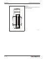
External dimensions. . . . . . . . . . . . . . . . . . . . . . . . . . . . . . . . . . . . . . . . . . . . . . . . . . A-1
A.1.1
CPU modules . . . . . . . . . . . . . . . . . . . . . . . . . . . . . . . . . . . . . . . . . . . . . . . . A-1
A.1.2
Power supply modules . . . . . . . . . . . . . . . . . . . . . . . . . . . . . . . . . . . . . . . . A-5
A.1.3
Main base units and extension base units . . . . . . . . . . . . . . . . . . . . . . . . . . A-6
A.1.4
I/O modules and dummy module . . . . . . . . . . . . . . . . . . . . . . . . . . . . . . . . . A-7
Introduction
1
Introduction
This manual describes the following modules and units of the MELSEC System Q:
● CPU modules (→ Chapter 4),
● Memory cards (→ Chapter 5),
● Input and output modules (→ Chapter 6),
● Power supply modules (→ Chapter 7) and
● Base units (→ Chapter 8).
The manual comprises also detailed descriptions of:
● Installation (→ Chapter 9),
● Maintenance and Inspection (→ Chapter 10) and
● Troubleshooting (→ Chapter 11).
The MELSEC System Q is user-friendly and offers a wide range of communications facilities.
NOTES
For further information about programming of the programmable logic controllers refer to the
programming manual of MELSEC System Q and MELSEC A/Q series (Art. No. 87432).
For further information about application and operating of intelligent function function modules of MELSEC System Q refer to the User’s Manual of the modules.
Chapter 3 of this manual describes examples, when using the CPU in independant systems.
The CPU can also be used in other system configurations (Data-Link systems or Computer-Link
systems). These systems are described in different manuals.
MELSEC System Q, Hardware
1–1
Introduction
1–2
Features of the MELSEC System Q
Basics
2
Basics
2.1
Features of the MELSEC System Q
CPU modules
The MELSEC System Q offers a wide range of CPU modules:
● Basic model QCPU
– Q00JCPU
– Q00CPU
– Q01CPU
● High performance model QCPU
– Q02CPU
– Q02HCPU
– Q06HCPU
– Q12HCPU
– Q25HCPU
● Universal model QCPU
– Q00UJCPU
– Q00UCPU
– Q01UCPU
– Q02UCPU
– Q03UDCPU
– Q03UDECPU
– Q04UDHCPU
– Q04UDEHCPU
– Q06UDHCPU
– Q06UDEHCPU
– Q10UDHCPU
– Q10UDEHCPU
– Q13UDHCPU
– Q13UDEHCPU
– Q20UDHCPU
– Q20UDEHCPU
– Q26UDHCPU
– Q26UDEHCPU
● Process CPU
– Q02PHCPU
– Q06PHCPU
– Q12PHCPU
– Q25PHCPU
● Redundant CPU
– Q12PRHCPU
NOTE
– Q25PRHCPU
Talking in this manual about Q-CPU means, that all mentioned CPUs are of MELSEC System Q.
MELSEC System Q, Hardware
2–1
Basics
Features of the MELSEC System Q
Base units
The Q00JCPU and Q00UJCPU include power supply, CPU and main base unit with five slots.
All other CPUs have to be mounted on a main base unit. Additionally one or two power supplies
can be mounted and up to twelve modules.
Extension base units can be connected to the main base unit via bus cable. The extension base
units are available with or without slots for a separate power supply and with slots for up to twelve
modules.
The Q00JCPU and Q00UJCPU can adress max. 16 modules on one main base unit and two
extension base units.
The CPU modules Q00CPU, Q01CPU, Q00UCPU, Q01UCPU and Q02UCPU are extendable
with up to four extension base units and totally 24 modules (36 modules with Q02UCPU).
Except for Q12PRHCPU and Q25PRHCPU, all other CPU types can be extended with seven
extension base units with maximum 64 slots total. The maximum distance between main base
unit and last extension base unit is 13.2 m, so that the base units can be mounted inside the cabinet with some distance between each other.
● Connecting extension base units to a redundant PLC system
It is not possible to connect an extension base unit to a main base unit with a redundant
CPU up to serial no. 09012... The expansion can be done by remote I/O station via
MELSECNET/H network.
It is possible to connect a main base unit with a redundant Q12PRHCPU or Q25PRHCPU
beginning at serial no. 09012… up to maximum seven extension base units with totally
63 modules.
The first extension base unit must be the type Q65WRB, the second to seventh unit can be
of type Q68RB.
Up to 8192 inputs and outputs
The CPU types Q02(H) to Q25H, the universal model CPUs from Q03UD(E)CPU on, all process
CPUs and redundant CPUs can address up to 4096 in/outputs directly on the base unit.
Together with remote I/Os these CPUs can address up to 8192 I/O points.
A Q02UCPU can address up to 2048 in/outputs directly and up to 8192 I/Os totally.
The Q00JCPU and Q00UJCPU address 256 I/O points directly. The Q00CPU, Q00UCPU,
Q01CPU or Q01UCPU addresses 1024 I/O points. With these CPU types the number is
extended to 2048 points and to 8192 points with the universal model PLC CPUs by remote I/Os.
2–2
Features of the MELSEC System Q
Basics
High speed program processing
CPU types with an additional "H" (like Q12HCPU, Q25HCPU or Q12PHCPU) do a faster
processing of the program. The operation time for the LD instruction (load) by the Q02CPU is
79 ns. The same instruction is done in 34 ns by the H type CPU.
An universal model PLC CPU increases the processing speed additionally. The operation time
of the above mentioned LD instruction takes only 20 ns with the Q03UDCPU and only 9.5 ns with
CPU modules from Q04UDCPU on.
With the new MELSEC System Q main base units with integrated memory and processor the
data transfer to I/O modules, intelligent function modules and network modules is much faster
compared to the previous base units. The access of the Q02HCPU to an intelligent function
module is with 20 µs per word 7 times faster than with the Q2ASHCPU. The refresh cycle of the
MELSECNET/10 network is around 4.3 times faster compared to the Q02HCPU and needs only
4.6 ms for 8 kwords.
Multi CPU operation
Except Q00JCPU all CPU modules of System Q are suitable für multi-CPU operation. Up to four
CPU modules can be mounted on one main base unit to which the mounted I/O and intelligent
function modules are assigned. The data transfer between the CPU modules can run automatical and cyclic. Also mixed configurations are possible with PLC CPU, Motion Controller CPU
and Q PC. But Q00CPU and Q01CPU can’t be combined with H type CPUs.
By multi-CPU operation the cycle time is decreased, the performance is increased and the application is wider.
Redundant operation
The operation of a redundant system is continued, even if single components have a failure. This
increases performance and outage and shutdown times are minimized.
The redundant PLC of MELSEC System Q consists of two controllers with identical configurations (power supply, Q12PRHCPU or Q25PRHCPU, network modules, etc.), which are connected by a so called tracking cable. One PLC controls the system, while the other one is in
standby mode. In case of an error the system switches from the control system to the standby
system and the process continues without any interruption.
Also a PLC with a standard CPU can be protected with two redundant power supplies against
failures. Therefore a main base unit and an extension base unit with two types of power supply
are available, one with 24 V DC input and one with 100–240 V AC input.
Range of instructions
Instructions for a Q-CPU are divided into two categories, basic instructions and comprehensive
dedicated instructions. The process CPUs and redundant CPUs have additionally 52 process
control instructions. Therefore these CPU types are particularly suitable for applications of process technology.
The capacity for the PLC programm is between 8 and 252 k steps depending on the CPU type.
MELSEC System Q, Hardware
2–3
Basics
Features of the MELSEC System Q
Memory
In addition to the internal memory (RAM and FlashROM) all CPU types (except Q00(U)JCPU,
Q00(U)CPU and Q01(U)CPU) have an extension slot for a RAM or a ROM memory card. The
RAM card is protected against data loss with a battery. ROM memory cards are available with
capacities up to 32 Mbyte for permanent storage of programs and other data.
Programming
The instructions in MELSEC System Q for programming of the CPU are according IEC1131 and
there are additional MELSEC instructions depending on the programming tools.
Fast data transfer with programming devices
The connection of the programming device to the CPU module is done by USB interface except
the basic model CPUs Q00JCPU, Q00CPU and Q01CPU. The datatransfer speed is then
12 Mbps.
For the Q-CPUs the datatransfer speed via RS232 interface is 115.2 kBaud.
Mounting
The base unit can be mounted directly by screws or on a DIN rail by adapter. The small dimensions of the modules of System Q allow, that the needed space for system mounting is reduced
by 60 % compared with the MELSEC AnS series.
Direct connection to the ETHERNET
The universal model PLC CPUs (modules with an "E" in the model name like Q10UDEHCPU)
are equipped with an ETHERNET interface allowing the direct connection of the PLC to the
ETHERNET network.
Compatibiliy
Concerning the general programming all the modules of MELSEC System Q are compatible to
the other Systems of the MELSEC PLC familiy. For information about programming of intelligent
function modules refer to the User's Manual of the module.
2–4
Specification comparison of CPU
2.2
Basics
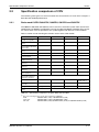
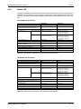
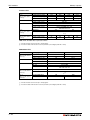
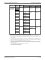
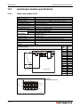
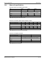
Specification comparison of CPU
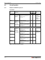
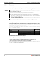
The following table gives an overview about the characteristics of each CPU. Chapter 4
describes the detailed performance.
2.2.1
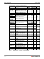
Basic model QCPU Q00JCPU, Q00CPU, Q01CPU and Q02CPU
The Q00CPU, Q01CPU and Q02CPU can be used in a multi-CPU system from version B on.
Combinations of Q00CPU and Q01CPU are only possible with Motion Controller CPUs and QPC. These CPUs can’t be operated in one system together with other PLC CPU modules.
Refer to section 4.6 for checking the function version of the CPU module.
Q00JCPU
Q00CPU
Q01CPU
Q02CPU
No. of I/O device points
(usable on program)
2048
2048
2048
8192
No. of I/O device points
(Hex)
X/Y000 to 7FF
X/Y000 to 7FF
X/Y000 to 7FF
X/Y000 to 1FFF
No. of I/O points
(accessible to the actual
I/O module)
256
1024
1024
4096
No. of I/O device points
(Hex)
X/Y00 to FF
X/Y000 to 3FF
X/Y000 to 3FF
X/Y000 to FFF
SFC (MELSAP-3)
Possible
Possible
Possible
Possible
Processing speed
(LD instruction)
200 ns
160 ns
100 ns
79 ns
Processing speed
(MOV instruction)
700 ns
560 ns
350 ns
237 ns
Program memory
(Drive 0)
8 k steps
8 k steps
14 k steps
28 k steps
Standard RAM
(Drive 3)
—
64 kByte
64 kByte
64 kByte
Standard ROM
(Drive 4)
56 kByte
94 kByte
240 kByte
112 kByte
8 kByte
8 kByte
8 kByte
Shared memory for multi- —
CPU operation
Shared memory for high
speed data transfer in
multi-CPU operation
—
Memory cards
Not usable
Not usable
Not usable
RAM, Flash card
and ATA cards �
Power consumption
(5 V DC)
0.22 A
0.25 A
0.27 A
0.60 A
0.13 kg
0.20 kg
Weight
0.66 kg
0.13 kg
Dimensions (HxWxD)
[mm]
98x245x98
98x27.4x89.3
Tab. 2-1: Specification comparison of Q00J, Q00, Q01 and Q02
One of the following memory cards can be installed for a Q02CPU:
RAM:
Q02MEM-1MBS (1 MB) or Q02MEM-2MBS (2 MB)
Flash card:
Q02MEM-2MBF (2 MB) or Q02MEM-4MBF (4 MB)
ATA card:
Q02MEM-8MBA (8 MB), Q02MEM-16MBA (16 MB) and Q02MEM-32MBA (32 MB)
MELSEC System Q, Hardware
2–5
Basics
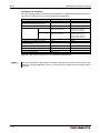
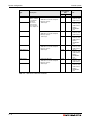
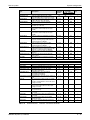
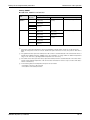
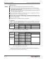
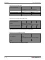
2.2.2
Specification comparison of CPU
High performance model QCPU (H types)
All of the following CPU modules can be used in a multi-CPU system.
Q02HCPU
No. of I/O device points
(usable on program)
8192
No. of I/O device points
(Hex)
X/Y000 to 1FFF
No. of I/O points
(accessible to the actual
I/O module)
4096
No. of I/O device points
(Hex)
X/Y000 to FFF
SFC (MELSAP-3)
Possible
Processing speed
(LD instruction)
34 ns
Processing speed
(MOV instruction)
102 ns
Program memory
(Drive 0)
28 k steps
Standard RAM
(Drive 3)
64 kByte
Standard ROM
(Drive 4)
112 kByte
Q06HCPU
Q12HCPU
Q25HCPU
60 k steps
124 k steps
252 k steps
256 kByte
256 kByte
496 kByte
1008 kByte
240 kByte
Shared memory for multi- 8 kByte
CPU operation
Shared memory for high
speed data transfer in
multi-CPU operation
—
Memory cards
RAM:
Q02MEM-1MBS (1 MB)
Q02MEM-2MBS (2 MB)
Flash card:
Q02MEM-2MBF (2 MB)
Q02MEM-4MBF (4 MB)
ATA card:
Q02MEM-8MBA (8 MB)
Q02MEM-16MBA (16 MB)
Q02MEM-32MBA (32 MB)
Power consumption
(5 V DC)
0.64 A
Weight [kg]
0.20
Dimensions (HxWxD)
[mm]
98x27.4x89.3
Tab. 2-2: Specification comparison of Q02(H), Q06H, Q12H and Q25H
2–6
Specification comparison of CPU
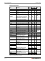
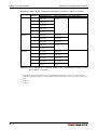
2.2.3
Basics
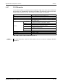
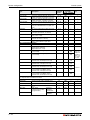
Universal model QCPU
All of the following CPU modules can be used in a multi-CPU system.
Q00UJCPU, Q00UCPU, Q01UCPU, Q02UCPU and Q03U(E)CPU
Q00UJCPU
Q00UCPU
Q01UCPU
Q02UCPU
Q03UCPU
Q03UECPU No. of I/O device points
(usable on program)
8192
No. of I/O device points
(Hex)
X/Y000 to 1FFF
No. of I/O points
(accessible to the actual
I/O module)
256
1024
1024
2048
4096
No. of I/O device points
(Hex)
X/Y00 to FF
X/Y000 to 3FF
X/Y000 to 3FF
X/Y000 to 7FF
X/Y000 to FFF
SFC (MELSAP-3)
Possible
Processing speed
(LD instruction)
120 ns
80 ns
60 ns
40 ns
20 ns
Processing speed
(MOV instruction)
240 ns
160 ns
120 ns
80 ns
40 ns
Program memory
(Drive 0)
10 k steps
10 k steps
15 k steps
20 k steps
30 k steps
Standard RAM
(Drive 3)
—
128 kByte
192 kByte
Standard ROM
(Drive 4)
256 kByte
512 kByte
1024 kByte
8 kByte
8 kByte
Shared memory for multi- —
CPU operation
Shared memory for high
speed data transfer in
multi-CPU operation
—
8 kByte
Memory cards
Not usable
Power consumption
(5 V DC)
0.37 A
0.33 A
0.33 A
0.23 A
Q03UCPU:
0.33 A
Q03UECPU:
0.46 A
Weight
0.70 kg
0.15 kg
0.15 kg
0.20 kg
Q03UCPU:
0.20 kg
Q03UECPU:
0.22 kg
Dimensions (HxWxD)
[mm]
98x245x98
98x27.4x89.3
RAM, Flash card, ATA card �
Q03UCPU:
98x27.4x89.3
Q03UECPU:
98x27.4x115
Tab. 2-3: Specification comparison of Q00UJ, Q00U, Q01U, Q02U and Q03U(E)
One of the following memory cards can be installed for a Q02UCPU or Q03U(E)CPU:
RAM:
Q02MEM-1MBS (1 MB), Q02MEM-2MBS (2 MB), Q03MEM-4MBS (4 MB),
Q03MEM-8MBS (8 MB)
Flash card:
Q02MEM-2MBF (2 MB) or Q02MEM-4MBF (4 MB)
ATA cards:
Q02MEM-8MBA (8 MB), Q02MEM-16MBA (16 MB) or Q02MEM-32MBA (32 MB)
The universal model PLC CPUs modules with an "E" in the model name are equipped with an Ethernet interface.
MELSEC System Q, Hardware
2–7
Basics
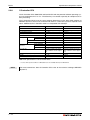
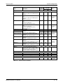
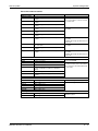
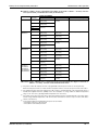
Specification comparison of CPU
Q04UD(E)CPU to Q26UD(E)CPU*
Q04UDHCPU Q06UDHCPU Q10UDHCPU Q13UDHCPU Q20UDHCPU Q26UDHCPU
Q04UDEHCPU Q06UDEHCPU Q10UDEHCPU Q13UDEHCPU Q20UDEHCPU Q26UDEHCPU
No. of I/O device points
(usable on program)
8192
No. of I/O device points
(Hex)
X/Y000 to 1FFF
No. of I/O points
(accessible to the actual
I/O module)
4096
No. of I/O device points
(Hex)
X/Y000 to FFF
SFC (MELSAP-3)
Possible
Processing speed
(LD instruction)
9.5 ns
Processing speed
(MOV instruction)
19 ns
Program memory
(Drive 0)
40 k steps
60 k steps
100 k steps
Standard RAM
(Drive 3)
256 kByte
768 kByte
1024 kByte
1280 kByte
Standard ROM
(Drive 4)
512 kByte
1024 kByte
2048 kByte
4096 kByte
130 k steps
200 k steps
260 k steps
Shared memory for multi- 8 kByte
CPU operation
Shared memory for high
speed data transfer in
multi-CPU operation
32 kByte
Memory cards
RAM:
Q02MEM-1MBS (1 MB)
Q02MEM-2MBS (2 MB)
Q03MEM-4MBS (4 MB)
Q03MEM-8MBS (8 MB)
Flash card:
Q02MEM-2MBF (2 MB)
Q02MEM-4MBF (4 MB)
ATA card:
Q02MEM-8MBA (8 MB)
Q02MEM-16MBA (16 MB)
Q02MEM-32MBA (32 MB)
Power consumption
(5 V DC)
Weight
Q04UDH-, Q06UDH-, Q10UDH-, Q013UDH-, Q20UDH-, Q26UDHCPU: 0.39 A
Q04UDEH-, Q06UDEH-, Q10UDEH-, Q013UDEH-, Q20UDEH-, Q26UDEHCPU: 0.49 A
Dimensions (HxWxD)
[mm]
Q04UDH-, Q06UDH-, Q10UDH-, Q013UDH-, Q20UDH-, Q26UDHCPU:
98x27.4x89.3
Q04UDEH-, Q06UDEH-, Q10UDEH-, Q013UDEH-, Q20UDEH-, Q26UDEHCPU:
98x27.4x115
Q04UDH-, Q06UDH-, Q10UDH-, Q013UDH-, Q20UDH-, Q26UDHCPU: 0.20 kg
Q04UDEH-, Q06UDEH-, Q10UDEH-, Q013UDEH-, Q20UDEH-, Q26UDEHCPU: 0.22 kg
Tab. 2-4: Specification comparison of Q04UD(E)CPU to Q26UD(E)CPU
*
2–8
The universal model PLC CPUs modules with an "E" in the model name are equipped with an Ethernet interface.
Specification comparison of CPU
2.2.4
Basics
Process CPU
All of the following CPU modules can be used in a multi-CPU system.
Q02PHCPU
No. of I/O device points
(usable on program)
8192
No. of I/O device points
(Hex)
X/Y000 to 1FFF
No. of I/O points
(accessible to the actual
I/O module)
4096
No. of I/O device points
(Hex)
X/Y000 to FFF
SFC (MELSAP-3)
Possible
Processing speed
(LD instruction)
34 ns
Processing speed
(MOV instruction)
102 ns
Program memory
(Drive 0)
28 k steps
Standard RAM
(Drive 3)
128 kByte
Standard ROM
(Drive 4)
112 kByte
Q06PHCPU
Q12PHCPU
Q25PHCPU
60 k steps
124 k steps
252 k steps
256 kByte
240 kByte
496 kByte
1008 kByte
Shared memory for multi- 8 kByte
CPU operation
Shared memory for high
speed data transfer in
multi-CPU operation
—
Memory cards
RAM:
Q02MEM-1MBS (1 MB)
Q02MEM-2MBS (2 MB)
Flash card:
Q02MEM-2MBF (2 MB)
Q02MEM-4MBF (4 MB)
ATA card:
Q02MEM-8MBA (8 MB)
Q02MEM-16MBA (16 MB)
Q02MEM-32MBA (32 MB)
Power consumption
(5 V DC)
0.64 A
Weight
0.20 kg
Dimensions (HxWxD)
[mm]
98x27.4x89.3
Tab. 2-5: Specification comparison of Q02PH, Q06PH, Q12PH and Q25PH
MELSEC System Q, Hardware
2–9
Basics
2.2.5
Specification comparison of CPU
Redundant CPU
It is not possible to connect an extension base unit to a main base unit with redundant CPU. The
expansion can be done by remote I/O station via MELSECNET/H network.
A standard main base unit of MELSEC System Q can be used, if you don’t need redundant
power supplies.
The redundant CPU modules Q12PRHCPU and Q25PRHCPU can’t be used with a multi-CPU
system.
Q12PRHCPU
No. of I/O device points
(usable on program)
8192
No. of I/O device points
(Hex)
X/Y000 to 1FFF
No. of I/O points
(accessible to the actual
I/O module)
4096
No. of I/O device points
(Hex)
X/Y000 to FFF
Q25HCPU
SFC (MELSAP-3)
Possible
Processing speed
(LD instruction)
34 ns
Processing speed
(MOV instruction)
102 ns
Data transfer time to the
Standby system
Device memory 48 k words: 10 ms
Device memory 100 k words: 15 ms
The cycle time increases by the data tranfer time to the Standby system.
Program memory
(Drive 0)
124 k steps
252 k steps
Standard RAM
(Drive 3)
256 kByte
256 kByte
Standard ROM
(Drive 4)
496 kByte
1008 kByte
Shared memory for multi- —
CPU operation
Shared memory for high
speed data transfer in
multi-CPU operation
—
Memory cards
RAM:
Q02MEM-1MBS (1 MB)
Q02MEM-2MBS (2 MB)
Flash card:
Q02MEM-2MBF (2 MB)
Q02MEM-4MBF (4 MB)
ATA card:
Q02MEM-8MBA (8 MB)
Q02MEM-16MBA (16 MB)
Q02MEM-32MBA (32 MB)
Power consumption
(5 V DC)
0.64 A
0.64 A
Weight
0.3 kg
0.3 kg
Dimensions (HxWxD)
[mm]
98x52.2x89.3
Tab. 2-6: Specification comparison of Q12PRH and Q25PRH
NOTE
2 – 10
For more informations about redundant CPU modules refer to the technical catalogue
MELSEC System Q and to the User's Manual of the module.
Specification comparison of CPU
2.2.6
Basics
Motion CPU
The motion controller CPU of System Q controls extensive movements by the connected servo
amplifiers and servo motors. They only work in a multi-CPU system together with minimum one
PLC CPU. Therefore maximum three Motion CPU modules can be mounted on one main base
unit.
Q172CPUN and Q173CPUN
Q172CPUN
Q173CPUN
No. of I/O device points (usable on program)
8192
8192
Real I/O points
(I/O in Main and Extension Base Units)
256
256
No. of control axes
8
32
Operation cycle
With software SV13 0.88 ms (1 to 8 axes)
0.88 ms (1 to 8 axes)
1.77 ms (9 to 16 axes)
3.55 ms (17 to 32 axes)
With software SV22 0.88 ms (1 to 4 axes)
1.77 ms (5 to 8 axes)
0.88 ms (1 to 4 axes)
1.77 ms (5 to 12 axes)
3.55 ms (13 to 24 axes)
7.11 ms (25 to 32 axes)
Program memory
14 k steps
14 k steps
Shared memory for multi-CPU operation
8 kByte
8 kByte
Shared memory for high speed data transfer in
multi-CPU operation
—
—
Memory cards
Not usable
Not usable
Power consumption (5 V DC)
1.14 A
1.25 A
Weight
0.22 kg
0.23 kg
Dimensions (HxWxD) [mm]
98x27.4x114.3
Tab. 2-7: Specification comparison of Q172CPUN and Q173CPUN
Q172HCPU and Q173HCPU
Q172HCPU
Q173HCPU
No. of I/O device points (usable on program)
8192
8192
Real I/O points
(I/O in Main and Extension Base Units)
256
256
No. of control axes
8
32
Operation cycle
With software SV13 0.44 ms (1 to 3 axes)
0.88 ms (4 to 8 axes)
0.44 ms (1 to 3 axes)
0.88 ms (4 to 10 axes)
1.77 ms (11 to 20 axes)
3.55 ms (21 to 32 axes)
With software SV22 0.88 ms (1 to 5 axes)
1.77 ms (6 to 8 axes)
0.88 ms (1 to 5 axes)
1.77 ms (6 to 14 axes)
3.55 ms (15 to 28 axes)
7.11 ms (29 to 32 axes)
Program memory
14 k steps
14 k steps
Shared memory for multi-CPU operation
8 kByte
8 kByte
Shared memory for high speed data transfer in
multi-CPU operation
—
—
Memory cards
Not usable
Not usable
Power consumption (5 V DC)
1.14 A
1.25 A
Weight
0.22 kg
0.23 kg
Dimensions (HxWxD) [mm]
104.6x27.4x114.3
Tab. 2-8: Specification comparison of Q172HCPU and Q173HCPU
MELSEC System Q, Hardware
2 – 11
Basics
Specification comparison of CPU
Q172DCPU and Q173DCPU
It is only possible to mount a Q172DCPU or Q173DCPU on a Q38DB or Q312DB type main base
unit. The PLC CPU must be an universal model CPU (QnUD(H)).
Q172DCPU
Q173DCPU
No. of I/O device points (usable on program)
8192
8192
Real I/O points
(I/O in Main and Extension Base Units)
256
256
No. of control axes
8
32
Operation cycle
With software SV13 0.44 ms (1 to 6 axes)
0.88 ms (7 and 8 axes)
0.44 ms (1 to 6 axes)
0.88 ms (7 to 18 axes)
1.77 ms (19 to 32 axes)
With software SV22 0.44 ms (1 to 4 axes)
0.88 ms (5 to 8 axes)
0.44 ms (1 to 4 axes)
0.88 ms (5 to 12 axes)
1.77 ms (13 to 28 axes)
3.55 ms (29 to 32 axes)
Program memory
14 k steps
14 k steps
Shared memory for multi-CPU operation
8 kByte
8 kByte
Shared memory for high speed data transfer in
multi-CPU operation
14 kByte
14 kByte
Memory cards
Not usable
Not usable
Power consumption (5 V DC)
1.14 A
1.25 A
Weight
0.33 kg
0.33 kg
Dimensions (HxWxD) [mm]
98x27.4x119.3
Tab. 2-9: Specification comparison of Q172DCPU and Q173DCPU
NOTE
2 – 12
For more informations about motion controllers and operating system software refer to the
technical catalogue MELSEC System Q and to the User's Manual of the module and the
software.
Specification comparison of CPU
2.2.7
Basics
PC CPU module
The PC CPU module is a compact personal computer of high value which can be installed on
the main base unit. Combinations with other CPU modules in a multi-CPU system are possible.
Besides typical functions of a PC, the PC CPU can also handle PLC functions.
PC-CPU
CPU
Ultra low voltage Intel쏐 Celereon쏐 M processor
Processing frequency
600 MHz
Memory
512 MB (main)/2 x 32 kB L1 (cache), 1 x 512 kB L22 (cache)
Video
Integrated graphics board for a maximum resolution of 1280x1024
pixels, 16 mio. colours
Serial (RS232C)
2 (1 integrated 9-pin D-SUB connector and 1 optional interface at
the extension box which is connnected to "EX I/F")
Parallel
1
USB
4 (3 integrated 9-pin D-SUB connector and 1 optional interface at the
extension box which is connnected to "EX I/F")
Keyboard/mouse
1 x PS/2 connector (keyboard and mouse can be used at the same
time with the Y junction cable)
Interfaces
Connections for drives
LAN
1 x ETHERNET interface (100BASE-TX/10BASE-T)
Monitor
1 x 15-pin H-DSUB
1 x disk drive, 2 x hard disk (silicon hard disks are supported)
PC card slots
2 PCMCIA, CardBus
Dimensions (HxWxD) [mm]
98x55.2x115
Tab. 2-10: PC CPU module of MELSEC System Q
NOTE
For more informations about PC CPU modules refer to the technical catalogue MELSEC
System Q.
MELSEC System Q, Hardware
2 – 13
Basics
2.2.8
Specification comparison of CPU
C-Controller CPU
The C-Controller CPUs Q06CCPU and Q12DCCPU with the powerful VxWorks operating system are programmed in C or C++. Therefore they are suitable especially for complex tasks in
data processing.
The C-Controller CPUs have the same compact dimensions as the other CPU modules of
MELSEC System Q and can be combined with them in a multi-CPU system or operate stand
alone. Additionally the C-Controller CPUs are compatible with CoDeSys.
Q06CCPU-V-H01
Q12DCCPU-V
CPU
SH-4
SH-4A
Operating system
VxWorks 5.4 (preinstalled))
VxWorks 6.4 (preinstalled))
Programming language
C or C++
C or C++
Development tool
Tornado 2.1*
Workbench 2.6.1
No. of I/Os
4096 (X/Y0 to X/YFFF)
4096 (X/Y0 to X/YFFF)
RAM
—
3 MB
ROM
6 MB
—
Work RAM
64 MB
128 MB
Battery-backed-up RAM
128 kB
128 kB
1
1
USB
—
1
LAN
1 x 100BASE-TX/10BASE-T
2 x 100BASE-TX/10BASE-T
PC card slots
1 slot for a TYPE I CF쏐-Card;
Max. 1 GB CF쏐 card is supported
1 slot for a TYPE I CF쏐-Card;
Max. 8 GB CF쏐 card is supported
Power consumption (5 V DC)
0.71 A
0.93 A
Weight
0.17 kg
0.24 kg
Dimensions (HxWxD) [mm]
98x27.4x89.3
98x27.4x115
Memory
User area
Serial (RS232C)
Interfaces
Tab. 2-11: Specifications of C-Controller CPUs
*
NOTE
2 – 14
Licenses with special conditions for Mitsubishi users are available directly from Wind River
For more informations about C-Controller CPUs refer to the technical catalogue MELSEC
System Q.
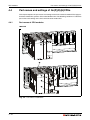
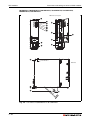
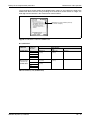
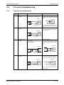
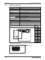
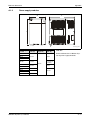
Overall configuration
System configuration
3
System configuration
3.1
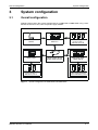
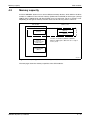
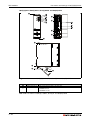
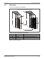
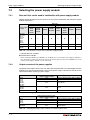
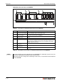
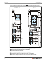
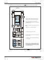
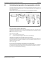
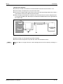
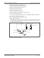
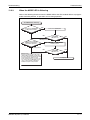
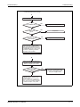
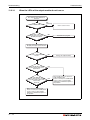
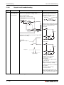
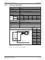
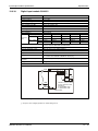
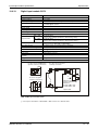
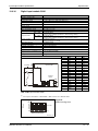
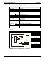
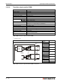
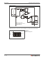
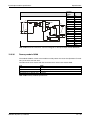
Overall configuration
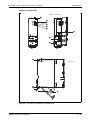
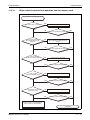
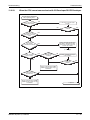
Following figure shows the system configuration for a Q00JCPU or Q00UJCPU using a combination of main base unit, CPU and power supply module.
Battery
(Q6BAT)
Q00JCPU
Q00UJCPU
I/O module and Special
function module of
MELSEC System Q
Extension base unit
Q52B or Q55B
Extension cable
(QC05B, QC06B, QC12B,
QC30B, QC50B, QC100B)
Extension base unit
(Q63B, Q65B, Q68B,
Q68RB, Q612B)
I/O module and Special
function module of
MELSEC System Q
Power supply module, I/O
module and Special function
module of MELSEC System Q
QH00075C
Fig. 3-1: System configuration for Q00JCPU and Q00UJCPU
MELSEC System Q, Hardware
3–1
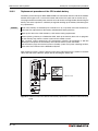
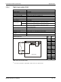
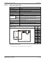
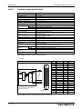
System configuration
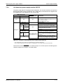
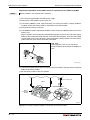
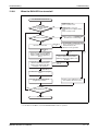
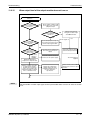
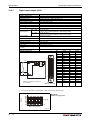
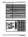
Overall configuration
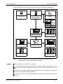
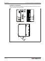
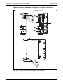
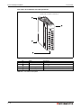
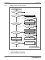
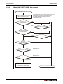
Following figure shows the system configuration for a Q00CPU, Q01CPU, Q00UCPU or
Q01UCPU (all without slots for a memory card).
LITHIUM BATTERY
MITSUBISHI
Extension base unit
Q52B or Q55B
I/O module and Special
function module of MELSEC
System Q
Q-CPU:
Q00, Q01, Q00U, Q01U
Battery
(Q6BAT)
Main base units
(Q33SB, Q35SB, Q38SB,
Q33B, Q35B, Q38B, Q312B,
Q38DB, Q312DB, Q38RB)
Power supply module, I/O
module and Special function
module of MELSEC System Q
Connection cable
(QC05B, QC06B, QC12B,
QC30B, QC50B, QC100B)
Extension base unit
(Q63B, Q65B, Q68B, Q68RB
or Q612B)
Power supply module, I/O
module and Special function
module of MELSEC System Q
QH00074C
Fig. 3-2: System configuration for Q00CPU, Q01CPU, Q00UCPU and Q01UCPU
NOTES
It is only possible to mount the redundant power supplies Q63RP and Q64RP on a main
base unit of type Q38RB and Q68RB. Each base unit has two slots for redundant power supplies.
The slim type main base units Q32SB, Q33SB and Q35SB can’t be connected to extension
base unit.
3–2
Overall configuration
System configuration
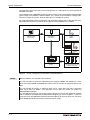
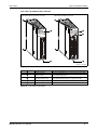
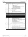
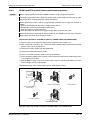
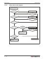
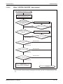
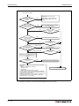
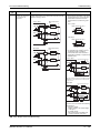
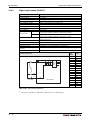
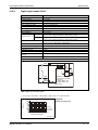
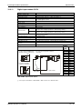
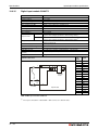
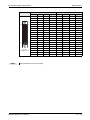
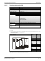
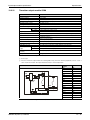
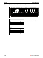
System configuration for CPU types Q02(P)(H) to Q25(P)H and Q02U to Q26UD(E)H:
MITSUBISHI
LITH IUM BA TTER Y
MITSUBISHI
SRAM/Flash/ATAMemory card
Q-CPU:
Q02(H) to Q25H,
Q02U to Q26UD(E)H,
Q02PH to Q25PH
Battery
(Q6BAT)
L ITHIU M B AT TER Y
MITSUBISHI
Battery
Battery
holder
(Q7BAT)
Q7BAT-SET
Extension base unit
Q52B or Q55B
Main base unit
(Q33SB, Q35SB, Q38SB,
Q33B, Q35B, Q38B, Q312B,
Q38DB, Q312DB, Q38RB)
Power supply module, I/O module and Special function module
of MELSEC System Q
Connection cable
(QC05B, QC06B, QC12B,
QC30B, QC50B, QC100B)
Extension base unit
(Q63B, Q65B, Q68B, Q68RB or
Q612B)
I/O module and Special function
module of MELSEC System Q
Power supply module, I/O module and Special function module
of MELSEC System Q
QH00001C
Fig. 3-3: System configuration for CPUs Q02(H) to Q25H, Universal CPUs Q02U to
Q26UD(E)H and Process CPUs Q02PH to Q25PH
NOTES
Battery Q7BAT is not available in EU countries.
It is only possible to mount the redundant power supplies Q63RP and Q64RP on a main
base unit of type Q38RB and Q68RB. Each base unit has two slots for redundant power supplies.
The process CPU modules Q02PHCPU to Q25PHCPU can’t be mounted on the slim type
main base units Q32SB, Q33SB and Q35SB.
The slim type main base units Q32SB, Q33SB and Q35SB can’t be connected to extension
base unit.
MELSEC System Q, Hardware
3–3
System configuration
Overall configuration
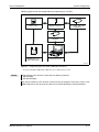
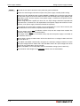
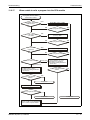
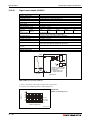
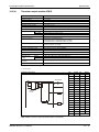
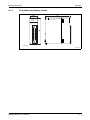
The following figure shows the system configuration of a redundant PLC with Q12PRH or
Q25PRH CPU types.
The redundant PLC of MELSEC System Q consists of two systems with identical configurations
(power supply, CPU module, network modules, etc.), which are connected by tracking cable.
One PLC controls the system, while the other one is in standby for reserve.
For more informations about configuration and applicable modules refer to the technical catalogue MELSEC System Q and to the User's Manual of the redundant PLC module.
MITSUBISHI
L ITHIU M B ATTER Y
MITSUBISHI
SRAM/Flash/ATA
Memory card
Q12PRHCPU,
Q25PRHCPU
Battery
(Q6BAT)
LI THIUM B AT TE RY
MI TSUBISHI
Battery
(Q7BAT)
Q7BAT-SET
Battery holder
Main base unit
(Q33B, Q35B, Q38B, Q38RB,
Q312B)
Power supply module, I/O module and Special function module
of MELSEC System Q
Fig. 3-4: System configuration for Q12PRH- and Q25PRHCPU
NOTES
Battery Q7BAT is not available in EU countries.
It is only possible to mount the redundant power supplies Q63RP and Q64RP on a main
base unit of type Q38RB and Q68RB. Each base unit has two slots for redundant power supplies.
It is not possible to connect an extension base unit to a main base unit with a redundant
CPU up to serial no. 09012... The expansion can be done by remote I/O station via
MELSECNET/H network.
It is possible to connect up to maximum seven extension base units with totally 63 modules
with a redundant Q12PRHCPU or Q25PRHCPU beginning at serial no. 09012… In the first
stage the base unit Q65WRB should be connected directly to the main base unit. The base
units Q68RB should be used for the second to seventh stage.
3–4
Overall configuration
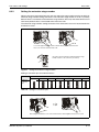
System configuration
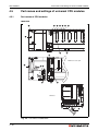
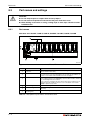
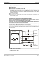
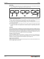
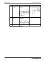
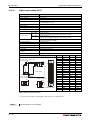
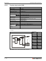
Following figure shows the configuration for programming of a Q-CPU:
MITSUBISHI
SRAM/Flash/ATA
Memory card*
PLC CPU module of
MELSEC System Q
USB cable
(not for Q00J-, Q00-, Q01and Q02CPU)
RS232 cable
(QC30R2)
PCMCIA Adapter unit
Q2MEM-ADP, not for
Q00J, Q00 and Q01
Personal computer with
programming software
QH00002C
Fig. 3-5: Programming the PLC CPU of MELSEC System Q
*
NOTES
The basic model QCPU, Q00U(J)CPU, Q01UCPU do not support memory cards.
Programming of the Q-CPUs is done with the following software:
- GX Developer
- GX IEC Developer
For special functions of the Q-CPUs and for transfer of programs to memory cards or over
USB cable please refer to the User’s Manuals of GX IEC Developer and GX Developer.
MELSEC System Q, Hardware
3–5
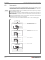
System configuration
Overall system
3.2
Overall system
3.2.1
Modules of MELSEC System Q
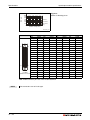
CPU modules
Type
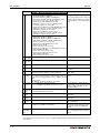
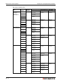
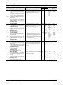
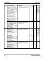
Power
consumption
(mA)
Description
5 V DC
24 V DC
200
—
Note
Basic model QCPU
Q00JCPU
Q00CPU
Q01CPU
Combination of 2048 total I/O points
base unit, power 256 direct accessible I/O points
supply module
Memory capacity:
and CPU
8 k steps
CPU modules;
suitable for
multi-CPU operation;
also refer to
CPU performance specifications chapter 12
2048 total I/O points
5 slots for I/O
modules
Power supply
specification:
Input:
100-240 V AC
Output:
5 V DC, 3 A
250
—
270
—
600
—
Slot for
memory card
640
—
Slot for
memory card
1024 direct accessible I/O points
Memory capacity:
8 k steps
2048 total I/O points
1024 direct accessible I/O points
Memory capacity:
14 k steps
High performance model QCPU
Q02CPU
Q02HCPU
Q06HCPU
CPU modules;
suitable for
multi-CPU operation;
also refer to
CPU performance specifications chapter 12
8192 total I/O points
4096 direct accessible I/O points
Memory capacity:
28 k steps
8192 total I/O points
4096 direct accessible I/O points
USB interface
Memory capacity:
28 k steps
8192 total I/O points
640
—
640
—
640
—
4096 direct accessible I/O points
Memory capacity:
60 k steps
Q12HCPU
8192 total I/O points
4096 direct accessible I/O points
Q25HCPU
Memory capacity:
124 k steps
8192 total I/O points
4096 direct accessible I/O points
Memory capacity:
252 k steps
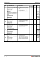
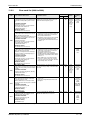
Tab. 3-1: Overview of the CPU modules
3–6
Overall system
System configuration
Type
Power
consumption
(mA)
Description
5 V DC
24 V DC
370
—
Note
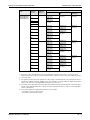
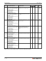
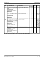
Universal model QCPU
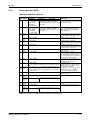
Q00UJCPU
Q00UCPU
Q01UCPU
Q02UCPU
Combination of 8192 total I/O points
base unit, power 256 direct accessible I/O points
supply module
Memory capacity:
and CPU;
10 k steps
suitable for
multi-CPU operation
Universal model
QCPU; suitable
for multi-CPU
operation;
also refer to
CPU performance specifications chapter 12
8192 total I/O points
5 slots for I/O
modules
USB interface
Power supply
specification:
Input:
100-240 V AC
Output:
5 V DC, 3 A
330
—
330
—
230
—
USB interface
1024 direct accessible I/O points
Memory capacity:
10 k steps
8162 total I/O points
1024 direct accessible I/O points
Memory capacity:
15 k steps
8192 total I/O points
2048 direct accessible I/O points
Slot for
memory card
USB interface
Memory capacity:
20 k steps
Q03UDCPU
8192 total I/O points
330
—
Q03UDECPU
4096 direct accessible I/O points
460
—
Memory capacity:
30 k steps
Slot for
memory card
USB interface
Built-in
ETHERNET
port
Q04UDHCPU
8192 total I/O points
390
—
Slot for
memory card
490
—
USB interface
Slot for
memory card
4096 direct accessible I/O points
Q04UDEHCPU
Memory capacity:
40 k steps
USB interface
Built-in
ETHERNET
port
Q06UDHCPU
8192 total I/O points
390
—
Slot for
memory card
490
—
Slot for
memory card
4096 direct accessible I/O points
Q06UDEHCPU
Memory capacity:
60 k steps
USB interface
USB interface
Built-in
ETHERNET
port
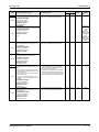
Tab. 3-1: Overview of the CPU modules
MELSEC System Q, Hardware
3–7
System configuration
Type
Overall system
Power
consumption
(mA)
Description
5 V DC
24 V DC
390
—
490
—
Note
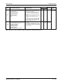
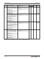
Universal model QCPU (continued)
Q10UDHCPU
Q10UDEHCPU
Q13UDHCPU
Universal model
QCPU; suitable
for multi-CPU
operation;
also refer to
CPU performance specifications chapter 12
8192 total I/O points
4096 direct accessible I/O points
Memory capacity:
100 k steps
USB interface
Slot for
memory card
USB interface
Built-in
ETHERNET
port
8192 total I/O points
390
—
490
—
4096 direct accessible I/O points
Q13UDEHCPU
Slot for
memory card
Memory capacity:
130 k steps
Slot for
memory card
USB interface
Slot for
memory card
USB interface
Built-in
ETHERNET
port
Q20UDHCPU
8192 total I/O points
390
—
490
—
4096 direct accessible I/O points
Q20UDEHCPU
Memory capacity:
200 k steps
Slot for
memory card
USB interface
Slot for
memory card
USB interface
Built-in
ETHERNET
port
Q26UDHCPU
8192 total I/O points
390
—
490
—
4096 direct accessible I/O points
Q26UDEHCPU
Memory capacity:
260 k steps
Slot for
memory card
USB interface
Slot for
memory card
USB interface
Built-in
ETHERNET
port
Tab. 3-1: Overview of the CPU modules
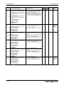
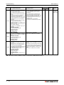
3–8
Overall system
System configuration
Type
Power
consumption
(mA)
Description
5 V DC
24 V DC
640
—
Note
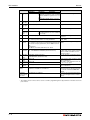
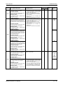
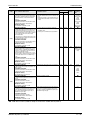
Process CPU
8192 total I/O points
Q02PHCPU
4096 direct accessible I/O points
USB interface
Memory capacity:
28 k steps
Q06PHCPU
Q12PHCPU
CPU modules;
suitable for
multi-CPU operation;
also refer to
CPU performance specifications chapter 12
8192 total I/O points
640
—
640
—
640
—
640
—
4096 direct accessible I/O points
Additional
process control
instructions
Memory capacity:
60 k steps
8192 total I/O points
4096 direct accessible I/O points
Memory capacity:
124 k steps
8192 total I/O points
Q25PHCPU
Slot for
memory card
4096 direct accessible I/O points
Memory capacity:
252 k steps
Redundant CPU
Q12PRHCPU
Q25PRHCPU
Redundant
CPU;
Multi-CPU operation is not possible
8192 total I/O points
Redundant
CPU;
Multi-CPU operation is not possible
8192 total I/O points
4096 direct accessible I/O points
USB interface
Memory capacity:
124 k steps
4096 direct accessible I/O points
Memory capacity:
252 k steps
Slot for
memory card
640
—
Additional
process control
instructions
For setting up
a redundant
system
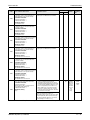
Tab. 3-1: Overview of the CPU modules
MELSEC System Q, Hardware
3–9
System configuration
Overall system
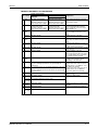
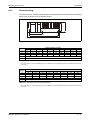
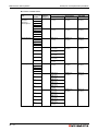
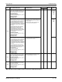
Standard modules of System Q
Type
No. of
occupied I/O
points
Description
Power
consumption (mA)
5 V DC
Note
24 V DC
Power supply modules
Q61P
5 V DC; 6 A
Input:
100–240 V AC
Q61P-A1
Input:
100–120 V AC
Q61P-A2
Input:
200–240 V AC
Q61P-D
Input:
100–240 V AC
With life detection
function
For slim type
main base unit
Q3SB only
Q61SP
5 V DC; 2 A
Input:
100–240 V AC
Q62P
5 V DC; 3 A
24 V DC; 0.6 A
Input:
100–240 V AC
Q63P
5 V DC; 6 A
Input:
24 V DC
Q63RP
5 V DC; 8.5 A
Input:
24 V DC
Q64P
5 V DC; 8.5 A
Input:
100–120 V AC
200–240 V AC
Q64PN
Q64RP
—
—
—
Redundant power
supply module
Input:
100–240 V AC
5 V DC; 8.5 A
Input:
100–120 V AC
200–240 V AC
Redundant power
supply module
Digital input modules
QX10
16 Input points, 100–120 V AC; 50/60 Hz
16
50
—
QX28
8 Input points, 100–240 V AC; 50/60 Hz
16
50
—
QX40
16 Input points, 24 V DC
16
50
—
QX10-TS
AC voltage
QX40-TS
QX40-S1
16 Input points, 24 V DC
16
60
—
QX41
32 Input points, 24 V DC
32
75
—
QX41-S1
32 Input points, 24 V DC
32
75
—
QX42
64 Input points, 24 V DC
64
90
—
QX42-S1
64 Input points, 24 V DC
64
90
—
QX70
16 Input points, 5–12 V DC
16
55
—
QX71
32 Input points, 5–12 V DC
32
70
—
QX72
64 Input points, 5–12 V DC
64
85
—
QX80
16 Input points, 24 V DC
16
50
—
QX81
32 Input points, 24 V DC
32
75
—
QX82
64 Input points, 24 V DC
64
90
—
QX82-S1
64 Input points, 24 V DC
64
90
—
Positive common
type
Negative or positive common type
QX80-TS
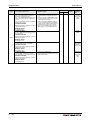
Tab. 3-2: Standard modules of System Q
3 – 10
Negative common type
Overall system
System configuration
Type
Description
No. of
occupied I/O
points
Power
consumption (mA)
5 V DC
24 V DC
Note
Digital output modules
QY10
Relay output module, 16 Output points
24 V DC/240 V AC, 2 A
16
430
—
QY18A
Relay output module, 8 Output points
24 V DC/240 V AC, 2 A
16
430
—
QY22
Triac output module, 16 Output points
100–240 V AC, 0.6 A
16
250
—
QY40P
Transistor output module, 16 Output points
12/24 V DC, 0.1 A
16
65
10
QY41P
Transistor output module, 32 Output points
12/24 V DC, 0.1 A
32
105
20
QY42P
Transistor output module, 64 Output points
12/24 V DC, 0.1 A
64
150
20
QY50
Transistor output module, 16 Output points
12/24 V DC, 0.5 A
16
80
20
QY68A
Transistor output module, 8 Output points
5/12/24 V DC, 0.5 A
8
110
—
QY70
Transistor output module, 16 Output points
5/12 V DC, 0.016 A
16
95
90
(12 V DC)
QY71
Transistor output module, 32 Output points
5/12 V DC 0.016 A
32
150
170
(12 V DC)
QY80
Transistor output module, 16 Output points
12/24 V DC 0.5 A
16
80
20
Transistor output module, 32 Output points
12/24 V DC 0.1 A
32
95
40
QY10-TS
QY40P-TS
QY80-TS
QY81P
—
sink type
source/sink type
sink type
source type
Combined I/O modules
QH42P
32 Input points, 24 V DC
32 Transistor outputs 12/24 V DC, 0.1 A
32
130
15
QX48Y57
8 Input points, 24 V DC
7 Transistor outputs 12/24 V DC, 0.5 A
16
80
10
16
(vacant)
—
—
Inputs:
positive common
type
Outputs:
sink type
Dummy module
QG60
Dummy module for unused slots
—
Tab. 3-2: Standard modules of System Q
MELSEC System Q, Hardware
3 – 11
System configuration
Overall system
Special function modules
Type
Description
No. of
occupied I/O
points
Power consumption (mA)
5 V DC
24 V DC
Note
High-Speed counter modules
QD62
2 Inputs (5/12/24 V DC); counting range
32 Bit and max. counting frequency
200 kHz
16
300
—
QD62E
2 Inputs (5/12/24 V DC); Counting range
32 Bit and max. counting frequency
200 kHz
16
330
—
QD62D
2 differential inputs (5/12/24 V DC);
Counting range 32 Bit and max. counting
frequency 500 kHz
16
380
—
QD60P8-G
8 Inputs (5/12/24 V DC); Counting range
16/32 Bit and max. counting frequency
30 kHz
32
580
—
—
Q63P6
6 Inputs (5 V DC); Counting range 32 Bit
and max. counting frequency 200 kHz
32
590
—
—
QD70P4
4 axis positioning module with pulse output
32
550
65
—
QD70P8
8 axis positioning module with pulse output
32
740
120
—
QD75D1
1 axis positioning module with pulse output
32
520
—
—
QD75P1
1 axis positioning module with pulse output
32
400
—
—
QD75D2
2 axis positioning module with differential
driver output
32
560
—
—
QD75P2
2 axis positioning module with pulse output
32
460
—
—
QD75D4
4 axis positioning module with differential
driver output
32
820
—
—
QD75P4
4 axis positioning module with pulse output
32
580
—
—
QD75M1
1 axis positioning module, SSCNET
32
400
—
QD75M2
2 axis positioning module, SSCNET
32
400
—
QD75M4
4 axis positioning module, SSCNET
32
400
—
16
220
—
Outputs sink
type
Outputs
source type
Outputs sink
type
Positioning modules
SSCNET
interface
Analog input/output modules
Q62AD-DGH
Analog input module with 2 inputs
(4 to 20 mA)
Q64AD
Analog input modules with 4 inputs
(0 to 20 mA; –10 to +10 V DC)
Q64AD-GH
16
630
—
—
16
890
—
—
Q66AD-DG
Analog input module with 6 inputs
(0 to 20 mA or 4 to 20 mA)
16
420
360
Q68AD-G
Analog input modules with 8 inputs
(0 to 20 mA; –10 to +10 V DC)
16
460
—
Q68ADV
Analog input module with 8 inputs
(–10 to +10 V DC)
16
640
—
—
Q68ADI
Analog input module with 8 inputs
(0 to 20 mA)
16
640
—
—
ME1AD8HAI-Q
Analog input module with 8 inputs
(0 to 20 mA or 4 to 20 mA) and function of a
HART-Master station
32
320
300
—
Q62DA
Analog output modules with 2 outputs
(0 to 20 mA; –10 to +10 V DC)
Q62DA-FG
Q62DAN
Q64DA
Q64DAN
Analog output module with 4 outputs
(0 to 20 mA; –10 to +10 V DC)
16
330
120
370
300
16
330
150
—
16
340
180
—
16
340
240
16
620
220
Analog output module with 6 outputs
(0 to 22 mA; –12 to +12 V DC)
Q68DAV
Analog output module with 8 outputs
(–10 to +10 V DC)
16
390
190
16
380
200
Analog output module with 8 outputs
(0 to 20 mA)
16
16
380
380
280
270
Q68DAI
Q68DAIN
Tab. 3-3:
Special function modules
Isolated
channels
16
Q66DA-G
Q68DAVN
3 – 12
—
—
Isolated
channels
Isolated
channels
—
—
Overall system
System configuration
Type
Description
No. of
occupied I/O
points
Power consumption (mA)
5 V DC
24 V DC
Note
Temperature control modules
Q64TCRT
Temperature control module with 4 channels
1 transistor output and 1 Pt100 input per
channel
16
550
—
Q64TCRTBW
Temperature control module with 4 channels
1 transistor output and 1 Pt100 input per
channel
Broken wire detection
32
640
—
Q64TCTT
Temperature control module with 4 channels
1 transistor output and
1 thermocouple input per channel
16
550
—
Q64TCTTBW
Temperature control module with 4 channels
1 transistor output and
1 thermocouple input per channel
Broken wire detection
32
640
—
—
occupies 2
slots
—
occupies 2
slots
Temperature acquisition modules
Q64TD
Temperature acquisition modules with 4
channels
1 thermocouple input per channel
Q64TDV-GH
16
500
—
16
500
—
—
Isolated
channels
Q68TD-G-H01/H02
Temperature acquisition module with 8
channels
1 thermocouple input per channel
16
490
—
Q64RD
Temperature acquisition module with 4
channels
1 Pt100- or JPt100 input per channel
16
600
—
Q64RD-G
Temperature acquisition module with 4
channels
1 Pt100-, JPt100 or Ni100 input per channel
16
620
—
Q68RD3-G
Temperature acquisition module with 4
channels
1 Pt100-, JPt100 or Ni100 input per channel
16
540
—
Loop control module with 2 channels,
1 thermocouple input, 1 voltage (–100 to
+100 mV DC; –10 to +10 V DC) or current
(0 to 20 mA DC) input per channel
1 current output (4 to 20 mA) per channel
16
270
70
—
16
480
—
—
Module for status logging of PLC devices
32
460
—
—
Interrupt module with 16 inputs
16
60
—
Positive common type
—
Isolated
channels
Loop control module
Q62HLC
Load cell input module
Q61LD
Module for direct connection of load cells
High speed data logger module
QD81DL96
Interrupt module
QI60
Tab. 3-3:
Special function modules
MELSEC System Q, Hardware
3 – 13
System configuration
Overall system
Communication- , interface- and remote modules
Type
Description
Q series Ethernet interface module
QJ71E71-B5
ETHERNET module (Client/Server) with
10BASE5 interface
QJ71E71-B2
ETHERNET module (Client/Server) with
10BASE2 interface
QJ71E71-100
ETHERNET module (Client/Server) with
10BASE-T- and 100BASE-TX interface
Q series MELSECNET/10 and MELSECNET/H network module
QJ71BR11
MELSECNET/H module (Master/local station), token bus, coaxial bus system
QJ71LP21-25
MELSECNET/H module (Floating Master)
Token ring, optical ring system
QJ71LP21G
QJ71LP21GE
QJ72LP25-25
MELSECNET/H module (Slave module)
Token-Ring, optical ring system
QJ72LP25G
QJ72LP25GE
Q80BD71BR11
Power consumption (mA)
Note
5 V DC 24 V DC
32
500
—
32
700
—
32
500
32
750
—
32
550
—
32
850
—
—
670
—
Up to 4
modules per
CPU
Up to 4
modules per
CPU
Q80BD71LP21G
Q80BD71LP21-25
Q80BD71LP21GE
CC-Link communication modules
QJ61BT11N
CC-Link Master/local station
—
—
—
450
460
450
—
—
—
PC boards
32
460
—
Up to 4
modules per
CPU
A80BDE-J61BT11
—
400
—
—
400
—
8
—
16
—
60
—
16
—
60
—
16
—
16
—
32
—
32
—
16
—
16
—
8
—
8
—
16
—
16
—
32
115
A80BDE-J61BT13
AJ65SBTB1-8D
AJ65BTB1-16D
AJ65BTB2-16D
AJ65SBTB1-16D1
AJ65FBTA4-16DE
AJ65BTC1-32D
AJ65SBTB1-32D1
AJ65BTB1-16DT
AJ65FBTA42-16DTE
AJ65SBTB1-8TE
AJ65SBTB2N-8R
AJ65BTB1-16T
AJ65SBTB2N-16R
AJ65BTC1-32T
Tab. 3-4:
3 – 14
Interface board for personal computer
Token bus, coaxial bus system
Interface boards for personal computer
Token ring, optical ring system
No. of occupied I/O
points
Interface board for personal computer
CC-Link Master/local station
Interface board for personal computer
CC-Link local station
Remote module with 8 digital inputs
(24 V DC)
Remote module with 16 digital inputs
(24 V DC)
Remote module with 16 digital inputs
(24 V DC)
Remote module with 16 digital inputs
(24 V DC)
Remote module with 16 digital inputs
Remote module with 32 digital inputs
(24 V DC)
Remote module with 32 digital inputs
(24 V DC)
Remote module with 8 digital inputs
(24 V DC) and 8 digital outputs
(24 V DC; 0.5 A/channel, 4 A total)
Remote module with 8 digital inputs and 8
digital outputs
Remote module with 8 digital outputs
(12/24 V DC; 0.1 A/channel)
Remote module with 8 relay outputs
(24 V DC/240 V AC; 2A)
Remote module with 16 digital outputs
(12/24 V DC; 0.5 A/channel, 4 A total)
Remote module with 16 relay outputs
(24 V DC/240 V AC; 2 A)
Remote module with 32 digital outputs
(12/24 V DC; 0.1 A/channel, 2 A total)
Communication- , interface- and remote modules
PC boards
—
—
70
Protection
IP67
—
—
70
—
Protection
IP67
—
—
80
—
—
—
—
Overall system
System configuration
Type
Description
CC-Link communication modules (continued)
AJ65BTB2-16R
Remote module with 16 relay outputs
(24 V DC/240 V AC; 2 A/channel, 8 A total)
AJ65BT-64AD
Remote analog input module with 4 inputs
(–20 to 20 mA; –10 to 10 V DC)
AJ65BT-64DAV
Remote analog output module with
4 outputs (–10 to +10 V DC)
AJ65BT-64DAI
Remote analog output module with
4 outputs (4 to 20 mA)
AJ65BT-64RD3
Remote module for temperature measurement with 4-channel input (3-wire-type
Pt100)
AJ65BT-64RD4
Remote module for temperature measurement with 4-channel input (4-wire-type
Pt100)
AJ65BT-68TD
Remote module for temperature measurement with 8-channel thermocouple input
AJ65BT-D62
Remote High speed counter module
2 Inputs; Counting range 23 Bit and max.
counting frequency 200 kHz
AJ65BT-D62D
Remote High speed counter module
2 Inputs; Counting range 23 Bit and max.
counting frequency 400 kHz
AJ65BT-D62D-S1
Remote High speed counter module
2 differential inputs; Counting range 23 Bit
and max. counting frequency 400 kHz
AJ65BT-R2
Remote interface module with RS232C
interface
AJ65BT-D75P2-S3
Remote 2 axis positioning module with
pulse output
FR-A5NC
CC-Link interface for frequency inverters
FR-E5NC
FR-A500 and FR-E500
DeviceNet communication module
QJ71DN91
Master for DeviceNet
PROFIBUS communication modules
QJ71PB92D
Master for PROFIBUS/DP
QJ71PB92V
Master for PROFIBUS/DP (V1/V2 protocol)
QJ71PB93D
Slave for PROFIBUS/DP
AJ95FPBA2-16TE
PROFIBUS/DP slave with 16 outputs
(24 V DC; 1 A/channel)
AJ95TB32-16DT
PROFIBUS/DP slave with 8 inputs
(24 V DC) and 8 outputs
(24 V DC; 0.8 A/channel)
AJ95FPBA42-16DTE PROFIBUS/DP slave with 8 inputs and 8 outputs
ST1PSD
ST series power supply module for supplying 5 V DC to the head station and to other
modules and distribution of 24 V DC; input
voltage: 24 V DC
ST1PDD
ST series power supply module for supplying the I/O modules with 24 V DC; input
voltage: 24 V DC
ST1H-PB
PROFIBUS/DP slave, ST series base module (head station)
ST1X2-DE1
ST series input module with 2 digital inputs
(24 V DC)
ST1X4-DE1
ST series input module with 4 digital inputs
(24 V DC)
ST1X16-DE1
ST series input module with 16 digital
inputs (24 V DC)
ST1Y2-TE2
ST series output module with 2 transistor
outputs (24 V DC; 0.5 A/output; 1 A total)
Tab. 3-4:
No. of occupied I/O
points
Power consumption (mA)
Note
5 V DC 24 V DC
16
85
—
—
2 Stat.
—
120
—
2 Stat.
—
180
—
2 Stat.
—
270
—
4 Stat.
—
170
—
4 Stat.
—
170
—
4 Stat.
—
81
—
4 Stat.
—
70
—
4 Stat.
—
100
—
4 Stat.
—
120
—
1 Stat.
—
110
—
4 Stat.
—
300
—
1 Stat.
—
—
—
32
170
—
—
32
32
32
16
570
570
360
—
—
—
—
—
8+8
—
18
8+8
—
2+2
—
—
—
2+2
—
—
—
—
530
—
—
2+2
85
—
—
4+4
95
—
—
16 + 16
120
—
—
2+2
90
—
—
—
Protection
IP67
—
—
Communication- , interface- and remote modules
MELSEC System Q, Hardware
3 – 15
System configuration
Overall system
Type
Description
PROFIBUS communication modules (continued)
ST1Y16-TE2
ST series output module with 16 transistor
outputs (24 V DC; 0.5 A/output; 4 A total)
ST1Y2-TPE3
ST series output module with 2 transistor
outputs (24 V DC; 1 A/output; 2 A total)
ST1Y16-TPE3
ST series output module with 16 transistor
outputs (24 V DC; 1 A/output; 4 A total)
ST1Y2-R2
ST series output module with 2 relay outputs (24 V DC/240 V AC; 2 A/output; 4 A
total)
ST1AD2-V
ST series analog input module with 2 voltage inputs (–10 to +10 V)
ST1AD2-I
ST series analog input module with 2 current inputs (0 to 20 mA, 4 to 20 mA)
ST1DA2-V
ST series output module with 2 voltage outputs (–10 to +10 V)
ST1DA2-I
Analog output module with 2 current outputs (0 to 20 mA, 4 to 20 mA)
ST1TD2
ST series analog temperature input module
with 2-channel thermocouple input
AS-I communication modules
QJ71AS92
Master for AS-I
MC-ASI-PS
AS-I bus power supply module
(Input voltage: 230 V AC
Output 30.5 V DC, 2.8 A)
MC-ASI X4M12
AS-I module with 4 digital inputs
(12–24 V DC)
MC-ASI X8M12
AS-I module with 8 digital inputs
(12–24 V DC)
No. of occupied I/O
points
Power consumption (mA)
Note
5 V DC 24 V DC
16 + 16
150
—
—
2+2
95
—
—
16 + 16
160
—
—
2+2
90
—
—
4+4
95
—
—
4+4
95
—
—
4+4
95
—
—
4+4
95
—
—
4+4
95
—
—
32
—
570
—
—
—
—
—
4
—
8
—
max.
250
max.
250
MC-ASI Y4M12-05
The stated
power consumption is
valid with a
supply voltage of 26.5
to 31.6 V.
AS-I module with 4 digital outputs
4
—
max.
(Ub–0.8 V DC, 0.5 A/output; 2 A total)
50
MC-ASI Y4M12-2
AS-I module with 4 digital outputs
4
—
max.
(Ub–0.8 V DC, 2 A/output; 4 A total)
50
MC-ASI Y8M12
AS-I module with 8 digital outputs
8
—
max.
(Ub–0.8 V DC, 0.5 A/output; 4 A total)
50
see below
MC-ASI X2Y2M12
AS-I module with 2 digital inputs
4
—
max.
(12–24 V DC) and 2 digital outputs
250
(Ub–0.8 V DC, 2 A/output; 4 A total)
MC-ASI X4Y4M12
AS-I module with 4 digital inputs
—
max.
(12–24 V DC) and 4 digital outputs
250
(Ub–0.8 V DC, 0.5 A/output; 2 A total)
The stated power consumption of the modules is valid with a supply voltage of 26.5 to 31.6 V. The output voltage of
the output modules is maximum Ub–0.8 V.
Interface modules
QJ71C24N
Interface module with 1 RS232C and 1
32
280
—
—
RS422/485 interface
QJ71C24N-R2
Interface module with 2 RS232C interfaces
32
240
—
—
QJ71C24N-R4
Interface module with 2 RS422/485 inter32
390
—
—
faces
QD51-R24
High speed
Interfaces:
32
310
—
—
communication module 1 RS232C
(programmable)
1 RS422/485
32
260
—
—
QD51
Interfaces:
2 RS232C
Tab. 3-4:
3 – 16
Communication- , interface- and remote modules
Overall system
System configuration
Base units and accessories
Type
Description
Note
Q32SB
For power supply module, CPU and up to 2
modules
Slim type main base unit
Q33SB
For power supply module, CPU and up to 3
modules
Q35SB
For power supply module, CPU and up to 5
modules
Q33B-E
For power supply module, CPU and up to 3
modules
Q35B-E
For power supply module, CPU and up to 5
modules
Q38B-E
For power supply module, CPU and up to 8
modules
Q38DB
For power supply module, CPU and up to 8
modules
Main base units
It is not possible to connect an extension base unit.
Connection of extension base units
possible
Connection of extension base units
possible
Multiple CPU high speed transmission
base unit
Q38RB-E
For 2 redundant power supply modules, CPU and
up to 8 modules
Q312B-E
For power supply module, CPU and up to 12
modules
Q312DB
For power supply module, CPU and up to 8
modules
Connection of extension base units
possible
Connection of extension base units
possible
Multiple CPU high speed transmission
base unit
Extension base units
Q52B
For up to 2 modules
Q55B
For up to 5 modules
Q63B
For up to 3 modules
Q65B
For up to 5 modules
Q65WRB
For 2 redundant power supply modules and up to 5
modules (redundant local I/O of a redundant
system)
Q68B
For power supply module and up to 8 modules
Q68RB-E
For 2 redundant power supply modules and up to 8
modules
Q612B
For power supply module and up to 12 modules
Without power supply, connect only
with cable QC05B
Depending on the CPU type are up to
7 extension base units connectible to
the main base unit with maximum 64
slots totally.
Connection cable
QC05B
Cable length: 0.45 m
For connecting Q52B and Q55B only
QC06B
Cable length: 0.6 m
For connecting the base units
QC12B
Cable length: 1.2 m
QC30B
Cable length: 3 m
QC50B
Cable length: 5 m
QC100B
Cable length: 10 m
Tracking cable
QC10TR
Cable length: 1 m
QC30TR
Cable length: 3 m
For connecting the 2 CPU modules of a
redundant system.
Tab. 3-5: Base units and accessories
MELSEC System Q, Hardware
3 – 17
System configuration
Type
Overall system
Description
Note
Memory cards
Q2MEM-1MBS
1 MByte SRAM
Q2MEM-2MBS
2 MByte SRAM
Q3MEM-4MBS
4 MByte SRAM
—
—
For Universal model QCPU only
Q3MEM-8MBS
8 MByte SRAM
Q2MEM-2MBF
2 MByte Flash card
—
Q2MEM-4MBF
4 MByte Flash card
—
Q2MEM-8MBA
8 MByte ATA memory card
—
Q2MEM-16MBA
16 MByte ATA memory card
—
Q2MEM-32MBA
32 MByte ATA memory card
—
Memory card adapter
Q2MEM-ADP
Memory card adapter for PCMCIA slot
Batteries
Q6BAT
Buffer battery for CPU module
Q2MEM-BAT
Memory card Q2MEM-1MBS buffer battery
The battery is shipped together with the
CPU.
—
Connector disconnection prevention holder for RS232 cable
Q6HLD-R2
Mechanical fixing device for connector
Tab. 3-5: Base units and accessories
3 – 18
This is recommended, when a cable is
connected permanently to the RS232
interface, e. g. for connection to a GOT.
Overall system
3.2.2
System configuration
Outline of system configuration
System configuration
The figure shows a configuration with one main base unit and extension base units of the MELSEC System Q. A
High performance model CPU (Q02(H)- to Q25HCPU), a Universal model CPU (Q02U- to Q26UD(E)HCPU) or a
Process CPU (Q02PH- to Q25PHCPU) is used.
0 1 2 3 4 5 6 7 8 9 10 11 Slot
Extension cable
O
U
T
C 00 20 40 60 80 A0 C0 E0 100 120 140 160
P
U 1F 3F 5F 7F 9F BF DF FF 11F 13F 15F 17F
Main base units
(Q312B)
Power supply module
1st extension
12 13 14 15 16 17 18 19 20 21 22 23
O
IU
NT
180 1A0 1C0 1E0 200 220 240 260 280 2A0 2C0 2E0
Extension base unit
(Q612B)
19F 1BF 1DF 1FF 21F 23F 25F 27F 29F 2BF2DF2FF
Power supply module
2nd extension
24 25 26 27 28 29 30 31
O
IU
NT
300 320 340 360 380 3A0 3C0 3E0
Extension base unit
(Q68B)
31F 33F 35F 37F 39F 3BF 3DF3FF
Power supply module
3rd extension
32 33 34 35 36 37 38 39
O
IU
NT
400 420 440 460 480 4A0 4C0 4E0
Extension base unit
(Q68B)
41F 43F 45F 47F 49F 4BF 4DF4FF
Power supply module
4th extension
40 41 42 43 44
O
IU
NT
500 520 540 560 580
Extension base unit
(Q65B)
51F 53F 55F 57F 59F
Power supply module
5th extension
45 46 47 48 49 50 51 52
O
IU
NT
5A05C0 5E0 600 620 640 660 680
Extension base unit
(Q68B)
5BF5DF5FF 61F 63F 65F 67F 69F
Power supply module
6th extension
53 54 55 56 57 58 59 60
O
IU
NT
6A06C0 6E0 700 720 740 760 780
Extension base unit
(Q68B)
6BF 6DF6FF 71F 73F 75F 77F 79F
Power supply module
7th extension
61 62 63
O
IU
NT
7A07C0 7E0
Extension base unit
(Q65B)
7BF7DF7FF
Power
supply
module
These slots can’t be used, because 64
modules are already mounted.
Tab. 3-6: System configuration
MELSEC System Q, Hardware
3 – 19
System configuration
Overall system
System configuration
Maximum number of extension
stages
Q00JCPU, Q00UJCPU
: 2 extension stages
Q00CPU, Q01CPU, Q00UCPU, Q01UCPU, Q02UCPU: 4 extension stages
Q02(H)CPU, Q06HCPU, Q12HCPU, Q25HCPU
: 7 extension stages
Q03UD(E)CPU, Q04UD(E)HCPU, Q06UD(E)HCPU
Q10UD(E)HCPU, Q13UD(E)HCPU; Q20UD(E)HCPU
Q26UD(E)HCPU, Q02PHCPU, Q06PHCPU,
Q12PHCPU, Q25HCPU
Maximum number of mountable
I/O modules
Q00JCPU, Q00UJCPU
Q00CPU, Q01CPU, Q00UCPU, Q01UCPU
Q02UCPU
Q02(H)CPU, Q06HCPU, Q12HCPU, Q25HCPU
Q03UD(E)CPU, Q04UD(E)HCPU, Q06UD(E)HCPU
Q10UD(E)HCPU, Q13UD(E)HCPU; Q20UD(E)HCPU
Q26UD(E)HCPU, Q02PHCPU, Q06PHCPU,
Q12PHCPU, Q25HCPU
:
:
:
:
16
24
36
64
Number of occupied I/O points
Q00JCPU, Q00UJCPU
Q00CPU, Q01CPU, Q00UCPU, Q01UCPU
Q02UCPU
Q02(H)CPU, Q06CPU, Q12HCPU, Q25HCPU
Q03UD(E)CPU, Q04UD(E)HCPU, Q06UD(E)HCPU
Q10UD(E)HCPU, Q13UD(E)HCPU; Q20UD(E)HCPU
Q26UD(E)HCPU, Q02PHCPU, Q06PHCPU,
Q12PHCPU, Q25HCPU
:
:
:
:
256
1024
2048
4096
Main base units
Q32SB, Q33SB, Q35SB
Q33B, Q35B, Q38B, Q312B
Q38DB, Q312DB
Q38RB
Extension base units
Q52B, Q55B
Q63B, Q65B, Q68B, Q612B
Q68RB
Extension cable
Notes
QC05B (0.45 m), QC06B (0.6 m), QC12B (1.2 m), QC30B (3.0 m),
QC50B (5.0 m), QC100B (10.0 m)
Note the maximum number of extension base units, which are connectable to
the main base unit.
Depending on the CPU type, 16, 24, 36 or 64 modules can be mounted on
the main and on the extension base units. An error occurs, when the maximum number of modules is exceeded.
The overall length of extension cables must not be longer than 13.2 m.
Connect the OUT connector of an extension base unit and the IN connector
of the adjacent extension base unit by an extension cable.
Do not lay tracking cables close together or close to main circuit power lines,
high-voltage power lines, or load lines.
Set the extension stage numbers consecutively. Set an unique number for
each extension base.
The extension base units Q38RB, Q68RB have slots for two redundant power
supplies Q63RP or Q64RP.
The slim type main base units Q32SB, Q33SB and Q35SB can’t be connected to extension base unit.
The process CPU modules Q02PH-, Q06PH-, Q12PH- and Q25PHCPU can’t
be mounted on the slim type main base units Q32SB, Q33SB and Q35SB.
Tab. 3-6: System configuration
3 – 20
Devices
CPU modules
4
CPU modules
4.1
Devices
The names and data ranges of devices which can be used in the CPU module are shown in the
following tables.
4.1.1
Basic model QCPU
Device name
X Input
Y Output
M Special
relay
Internal
relay*
L Latch
relay*
Range (total number)
Q00JCPU
Q00CPU
Q01CPU
X0–7FF
X0–7FF
(No. of I/O device (total number of I/O points: 2048)
points: 2048)
X0–3FF
X0–FF (direct
(I/O points accessible via base units:
accessible: 256)
1024)
Y0–7FF
Y0–7FF
(No. of I/O device (total number of I/O points: 2048)
points: 2048)
Y0–3FF
Y0–FF (direct
(I/O points accessible via base units:
accessible: 256)
1024)
SM0–1023 (1024)
M0–8191 (8192)
Explanation
Input of external signals to the PLC,
e. g. by key switch, rotary switch, limit
switch, binary switch
Output of signals for control of external
devices by program like magnetic
valves, magnetic contactors, lamps,
digital displays etc.
Predefined devices for special applications and additional functions of the
PLC.
Auxiliary devices of the PLC
L0–2047 (2048)
Auxiliary devices of the PLC
Latch relays are buffered at power shut
down
S Step relay S0–2047 (2048)
Application like M device, e. g. for
marking one step number in a program
for step operation of a process.
B Link
B0–3FF (1024)
Bit devices in a network, which can’t be
relay*
output directly
F Annuncia- F0–1023 (1024)
Flag for marking of an error.
tor*
If the error flag is set by an error recognition program during RUN operation,
the corresponding error code will be
stored in the special relay SD.
V Edge
V0–2047 (2048)
This relay is set by the negativ or posirelay*
tiv edge of the operation result,
depending on the instruction.
T Timer*
T0–511 (512)
Incremental timer
The low- and high-speed timers are specified by the instruc- Measurement unit of the low-speed
tions.
retentive timers: 1 to 1000 ms, 1 ms
unit (100 ms by default)
T Retentive Max. 512
Measurement unit of the high-speed
(ST) timer*
The retentive timers are specified by parameters
retentive timers: 0.1 to 100.0 ms,
(preset to 0)
The low- and high-speed retentive timers are specified by 0.1 ms unit (10.0 ms by default)
the instructions.
C Counter* C0–511 (512)
Incremental counter for normal or interrupt processing
Interrupt Max. 128
Counter* (0 point by default, setting by parameters)
D Data reg- D0–11135 (11136)
Register for data storage
ister*
SD Special
SD0–1023 (1024)
Predefined register for storage of speregister
cial data
Tab. 4-1: Device list for Q00JCPU, Q00CPU and Q01CPU
MELSEC System Q, Hardware
4–1
CPU modules
Devices
Range (total number)
Q00JCPU
Q00CPU
Q01CPU
Link reg- W0–7FF (2048)
ister*
File regis- —
R0–32767 (32768)
ter
ZR0–32767 (32768)
Link spe- SB0–3FF (1024)
cial relay
Link spe- SW0–3FF (1024)
cial register
Index reg- Z0–9 (10)
ister
Nesting N0–14 (15 Steps)
Device name
W
R
SB
SW
Z
N
Explanation
Register for Link data in a network
Extension of the data register area
Bit devices in a network
Register for Link data
Register for indexing of devices
Displays the nesting of Master control
processes
P Pointer
P0–299 (300)
Target of a jump instruction (CJ, SCJ,
The common pointer address is set by parameters.
CALL, JMP)
I Interrupt I0–127 (128)
Pointer for branching of interrupt proPointer
The cyclic interval of system interrupt pointers I28 to 31 can grams
be set up by parameters (2 to 1000 ms, 1 ms unit).
Default values:
I28: 100 ms; I29: 40 ms; I30: 20 ms; I31: 10 ms
K Decimal K -32768–32767 (16 bit instructions)
For specification of command values
constant K -2147483648–2147483647 (32 bit instructions)
for timer and counter, pointer, interrupt
pointer, number of bit devices and
instruction values
H Hexadeci- H0–FFFF (16 bit instruction)
For specification of instruction values
mal con- H0–FFFFFFFF (32 bit instruction)
stant
FX Function FX0–F (16)
Devices for the status of input or output
input
bits for subroutines.
Only FX0 to FX4 and FY0 to FY4 can
FY Function FY0–F (16)
be used in a program.
output
FD Function FD0–4 (5)
register
Link direct
Specified form: J\X, J\Y, J\W,
device
J\B, J\SW, J\SB
Intelligent
Specified form: U\G
function module device
Status register for the input and output
bits for subroutines
Device for accessing the link device
directly. Exclusively used for CC-Link
IE controller network and MELSECNET/H.
Device for accessing the buffer memory of the intelligent function module
directly.
Tab. 4-1: Device list for Q00JCPU, Q00CPU and Q01CPU
*
4–2
The address areas for these devices can be set with a programming device by parameters. The table shows the
preset values.
Devices
4.1.2
CPU modules
High performance model QCPU
Device name
X Input
Y Output
M Special
relay
Internal
relay*
L Latch
relay*
S Step relay
B Link relay*
F Annunciator*
V Edge
relay*
T Timer*
T Retentive
(ST) timer*
C Counter*
Interrupt
Counter*
D Data
register*
SD Special
register
W Link
register*
Range (total number)
Explanation
Q02CPU Q02HCPU Q06HCPU Q12HCPU Q25HCPU
X0–1FFF (total number of I/O points: 8192)
Input of external signals to the PLC,
X0–0FFF (I/O points accessible via base units: 4096)
e. g. by key switch, rotary switch, limit
switch, binary switch
Y0–1FFF (total number of I/O points: 8192)
Output of signals for control of external
Y0–0FFF (I/O points accessible via base units: 4096)
devices by program like magnetic
valves, magnetic contactors, lamps,
digital displays etc.
SM0–2047 (2048)
Predefined devices for special applications and additional functions of the
PLC.
M0–8191 (8192)
Auxiliary devices of the PLC
L0–8191 (8192)
Auxiliary devices of the PLC
Latch relays are buffered at power shut
down
S0–8191 (8192)
Application like M device, e. g. for
marking one step number in a program
for step operation of a process.
B0–1FFF (8192)
Bit devices in a network, which can’t be
output directly
F0–2047 (2048)
Flag for marking of an error.
If the error flag is set by an error recognition program during RUN operation,
the corresponding error code will be
stored in the special relay SD.
V0–2047 (2048)
This relay is set by the negativ or positiv edge of the operation result,
depending on the instruction.
T0–2047 (2048)
Incremental timer
The low- and high-speed timers are specified by the
Measurement unit of the low-speed
instructions.
retentive timers: 1 to 1000 ms, 1 ms
Max. 2048, The retentive timers are specified by parame- unit (100 ms by default)
Measurement unit of the high-speed
ters (preset to 0)
The low- and high-speed retentive timers are specified by retentive timers: 0.1 to 100.0 ms,
0.1 ms unit (10.0 ms by default)
the instructions.
C0–1023 (1024)
Max. 256
(0 point by default, setting by parameters)
D0–12287 (12288)
SD0–2047 (2048)
W0–1FFF (8192)
Incremental counter for normal or
interrupt processing
Register for data storage
Predefined register for storage of
special data
Register for Link data in a network
Tab. 4-2: Device list for Q02(H)-, Q06H-, Q12H- and Q25HCPU
MELSEC System Q, Hardware
4–3
CPU modules
Devices
Range (total number)
Q02CPU Q02HCPU Q06HCPU Q12HCPU Q25HCPU
R File regis- When using the internal RAM:
ter
R0–32767 (32768) for Q02CPU,
R0–65535 (65536) for Q02H- and Q06HCPU,
R0–131071 (131072) for Q12H- and Q25HCPU with
block conversion in steps of 32768 registers
When using a 1 MB SRAM memory card:
With block conversion in steps of 32768 registers,
517120 file registers are accessible.
When using a 2 MB Flash or 2 MB SRAM memory card:
With block conversion in steps of 32768 registers,
1041408 file registers are accessible.
When using a 4 MB Flash memory card:
With block conversion in steps of 32768 registers,
1042432 file registers are accessible.
When using the internal RAM:
ZR0–32767 (32768) for Q02CPU,
ZR0–65535 (65536) for Q02H- and Q06HCPU,
ZR0–131071 (131072) for Q12H- and Q25HCPU
(Block conversion is not necessary)
When using a 1 MB SRAM memory card:
ZR0–517119 (517120),
Block conversion is not necessary.
When using a 2 MB Flash- or 2 MB SRAM memory card:
ZR0–1041407 (1041408),
Block conversion is not necessary.
When using a 4 MB Flash memory card:
ZR0–1042431 (1042432),
Block conversion is not necessary.
SB Link spe- SB0–7FF (2048)
cial relay
SW Link spe- SW0–7FF (2048)
cial register
Z Index reg- Z0–15 (16)
ister
N Nesting
N0–14 (15 Steps)
Device name
Explanation
Extension of the data register area
When using a Flash memory card only
reading of the file registers is possible.
It’s not possible to use an ATA memory
card.
Bit devices in a network
Register for Link data
Register for indexing of devices
Displays the nesting of Master control
processes
P Pointer
P0–4095 (4096)
Target of a jump instruction (CJ, SCJ,
The common pointer address is set by parameters.
CALL, JMP)
I Interrupt I0–255 (256)
Pointer for branching of interrupt proPointer
The constant cyclic interval of system interrupt pointers I28 grams
to 31 can be set up by parameters (0.5 to 1000 ms, 0.5 ms
unit).
Default values:
I28: 100 ms; I29: 40 ms; I30: 20 ms; I31: 10 ms
K Decimal
K -32768–32767 (16 bit instructions)
For specification of command values
constant K -2147483648–2147483647 (32 bit instructions)
for timer and counter, pointer, interrupt
pointer, number of bit devices and
instruction values
For specification of instruction values
H Hexadeci- H0–FFFF (16 bit instruction)
mal con- H0–FFFFFFFF (32 bit instruction)
stant
FX Function FX0–F (16)
Device for the status of input bits for
input
subroutines.
FY Function FY0–F (16)
Device for the status of output bits for
output
subroutines.
FD Function FD0–4 (5)
Status register for the input and output
register
bits for subroutines
Link direct
Specified form: J\X, J\Y, J\W,
Device for accessing the link device
device
J\B, J\SW, J\SB
directly. Exclusively used for CC-Link
IE controller network and MELSECNET/H.
Intelligent func- Specified form: U\G
Device for accessing the buffer memtion module
ory of the intelligent function module
device
directly.
Tab. 4-2: Device list for Q02(H)-, Q06H-, Q12H- and Q25HCPU
*
4–4
The address areas for these devices can be set with a programming device by parameters. The table shows the
preset values.
Devices
4.1.3
CPU modules
Universal model QCPU
Q00UJCPU, Q00UCPU, Q01UCPU
Device name
X Input
Y Output
M Special
relay
Internal
relay*
L Latch
relay*
Range (total number)
Q00UJCPU
Q00UCPU
Q01UCPU
X0–1FFF
X0–1FFF
(No. of I/O device (total number of I/O points: 8192)
points: 8192)
X0–3FF (I/O points accessible via base
X0–FF (direct
units: 1024)
accessible: 256)
Y0–7FF
Y0–7FF
(No. of I/O device (total number of I/O points: 2048)
points: 2048)
Y0–3FF (I/O points accessible via base
Y0–FF (direct
units: 1024)
accessible: 256)
SM0–2047 (2048)
M0–8191 (8192)
Explanation
Input of external signals to the PLC,
e. g. by key switch, rotary switch, limit
switch, binary switch
Output of signals for control of external
devices by program like magnetic
valves, magnetic contactors, lamps,
digital displays etc.
Predefined devices for special applications and additional functions of the
PLC.
Auxiliary devices of the PLC
L0–8191 (8192)
Auxiliary devices of the PLC
Latch relays are buffered at power shut
down
S Step relay S0–8191 (8192)
Application like M device, e. g. for
marking one step number in a program
for step operation of a process.
B Link
B0–1FFF (8192)
Bit devices in a network, which can’t be
relay*
output directly
F Annuncia- F0–2047 (2048)
Flag for marking of an error.
tor*
If the error flag is set by an error recognition program during RUN operation,
the corresponding error code will be
stored in the special relay SD.
V Edge
V0–2047 (2048)
This relay is set by the negativ or posirelay*
tiv edge of the operation result,
depending on the instruction.
T Timer*
T0–2047 (2048)
Incremental timer
The low- and high-speed timers are specified by the instruc- Measurement unit of the low-speed
tions.
retentive timers: 1 to 1000 ms, 1 ms
T Retentive The retentive timers are specified by parameters (preset to unit (100 ms by default)
Measurement unit of the high-speed
(ST) timer*
0).
The low- and high-speed retentive timers are specified by retentive timers: 0.1 to 100.0 ms,
0.1 ms unit (10.0 ms by default)
the instructions.
C Counter* C0–1023 (1024)
D Data reg- D0–12287 (12288)
ister*
Extended
Specified by parameters (preset to 0).
data register*
SD Special
SD0–2047 (2048)
register
W Link reg- W0–1FFF (8192)
ister*
Extended
Specified by parameters (preset to 0).
link regis—
ter*
Incremental counter for normal or interrupt processing
Register for data storage
Predefined register for storage of special data
Register for Link data in a network
Tab. 4-3: Device list for Q00UJCPU, Q00UCPU and Q01UCPU
MELSEC System Q, Hardware
4–5
CPU modules
Devices
Range (total number)
Explanation
Q00UJCPU
Q00UCPU
Q01UCPU
R File regis- —
R0–32767 (32768)
Extension of the data register area
ter
With block conversion in steps of 32768
registers, 65536 file registers are accessible.
ZR0–65535 (65536); Block conversion
is not necessary.
SB Link spe- SB0–7FF (2048)
Bit devices in a network
cial relay
SW Link spe- SW0–1FF (2048)
Register for Link data
cial register
Z Index reg- Z0–19 (20)
Register for indexing of devices
ister
32 Bit—
Z0–18 (10)
Index reg(Two index registers are each combined
ister
in one word)
N Nesting N0–14 (15 Steps)
Displays the nesting of Master control
processes
P Pointer
P0–511 (512)
Target of a jump instruction (CJ, SCJ,
The common pointer address is set by parameters.
CALL, JMP)
I Interrupt I0–127 (128)
Pointer for branching of interrupt proPointer
The constant cyclic interval of system interrupt pointers I28 grams
to 31 can be set up by parameters (0.5 to 1000 ms, 0.5 ms
unit).
Default values:
I28: 100 ms; I29: 40 ms; I30: 20 ms; I31: 10 ms
K Decimal K -32768–32767 (16 bit instructions)
For specification of command values
constant K -2147483648–2147483647 (32 bit instructions)
for timer and counter, pointer, interrupt
pointer, number of bit devices and
instruction values
H Hexadeci- H0–FFFF (16 bit instruction)
For specification of instruction values
mal con- H0–FFFFFFFF (32 bit instruction)
stant
FX Function FX0–F (16)
Devices for the status of input or output
input
bits for subroutines.
Only FX0 to FX4 and FY0 to FY4 can
FY Function FY0–F (16)
be used in a program.
output
FD Function FD0–4 (5)
Status register for the input and output
register
bits for subroutines
Link direct
Specified form: J\X, J\Y, J\W,
Device for accessing the link device
directly. Exclusively used for CC-Link
device
J\B, J\SW, J\SB
IE controller network and MELSECNET/H.
Intelligent
Specified form: U\G
Device for accessing the buffer memfunction modory of the intelligent function module
ule device
directly.
Device name
Tab. 4-3: Device list for Q00UJCPU, Q00UCPU and Q01UCPU
*
4–6
The address areas for these devices can be set with a programming device by parameters. The table shows the
preset values.
Devices
CPU modules
Q02UCPU, Q03UDCPU and Q03UDECPU
Range (total number)
Device name
X Input
Y Output
M Special
relay
Internal
relay*
L Latch
relay*
S Step relay
B Link relay*
F Annunciator*
V Edge
relay*
T Timer*
T Retentive
(ST) timer*
C Counter*
Q03UDCPU
Q03UDECPU
X0–1FFF (total number
X0–1FFF (total number
of I/O points: 8192)
of I/O points: 8192)
X0–07FF (I/O points acces- X0–0FFF (I/O points accessible via base units: 2048)
sible via base units: 4096)
Y0–1FFF (total number
Y0–1FFF (total number
of I/O points: 8192)
of I/O points: 8192)
Y0–07FF (I/O points acces- Y0–0FFF (I/O points accessible via base units: 2048)
sible via base units: 4096)
SM0–2047 (2048)
Q02UCPU
M0–8191 (8192)
Explanation
Input of external signals to the PLC,
e. g. by key switch, rotary switch, limit
switch, binary switch
Output of signals for control of external
devices by program like magnetic
valves, magnetic contactors, lamps,
digital displays etc.
Predefined devices for special applications and additional functions of the
PLC.
Auxiliary devices of the PLC
L0–8191 (8192)
Auxiliary devices of the PLC
Latch relays are buffered at power shut
down
S0–8191 (8192)
Application like M device, e. g. for
marking one step number in a program
for step operation of a process.
B0–1FFF (8192)
Bit devices in a network, which can’t be
output directly
F0–2047 (2048)
Flag for marking of an error.
If the error flag is set by an error recognition program during RUN operation,
the corresponding error code will be
stored in the special relay SD.
V0–2047 (2048)
This relay is set by the negativ or positiv edge of the operation result,
depending on the instruction.
T0–2047 (2048)
Incremental timer
The low- and high-speed timers are specified by the
Measurement unit of the low-speed
instructions.
retentive timers: 1 to 1000 ms, 1 ms
The retentive timers are specified by parameters (preset to unit (100 ms by default)
Measurement unit of the high-speed
0).
The low- and high-speed retentive timers are specified by retentive timers: 0.1 to 100.0 ms,
0.1 ms unit (10.0 ms by default)
the instructions.
C0–1023 (1024)
D Data regis- D0–12287 (12288)
ter*
Extended Specified by parameters (preset to 0).
data register*
SD Special
SD0–2047 (2048)
register
W Link regis- W0–1FFF (8192)
ter*
Extended Specified by parameters (preset to 0).
link register*
Incremental counter for normal or interrupt processing
Register for data storage
Predefined register for storage of special data
Register for Link data in a network
Tab. 4-4: Device list of Q02UCPU, Q03UDCPU and Q03UDECPU
MELSEC System Q, Hardware
4–7
CPU modules
Devices
Range (total number)
Device name
Q03UDCPU
Q03UDECPU
R File regis- When using the internal RAM:
ter
R0–32767 (32768) with block conversion in steps of
32768 registers, 65536 (for Q02UCPU) resp. 98304 (for
Q03UD(E)CPU) file registers are accessible.
Q02UCPU
When using a 1 MB SRAM memory card:
With block conversion in steps of 32768 registers,
517120 file registers are accessible.
Explanation
Extension of the data register area
When using a Flash memory card only
reading of the file registers is possible.
It’s not possible, to use an ATA memory
card.
When using a 2 MB Flash or 2 MB SRAM memory card:
With block conversion in steps of 32768 registers,
1040384 file registers are accessible.
When using a 4 MB Flash or 4 MB SRAM memory card:
With block conversion in steps of 32768 registers,
2087936 file registers are accessible.
When using a 8 MB SRAM memory card:
With block conversion in steps of 32768 registers,
4184064 file registers are accessible.
When using the internal RAM:
ZR0–65535 (65536) for Q02UCPU,
ZR0–98303 (98304) for Q03UD(E)CPU
(Block conversion is not necessary.)
When using a 1 MB SRAM memory card:
ZR0–517119 (517120),
Block conversion is not necessary.
When using a 2 MB Flash or 2 MB SRAM memory card:
ZR0–1041407 (1041408),
Block conversion is not necessary.
When using a 4 MB Flash or 4 MB SRAM memory card:
ZR0–2087935 (2087936),
Block conversion is not necessary.
SB Link special relay
SW Link special register
Z Index register
32 BitIndex register
N Nesting
P
I
K
H
FX
FY
FD
When using a 8 MB SRAM memory card:
ZR0–4184063 (4184064),
Block conversion is not necessary.
SB0–7FF (2048)
Bit devices in a network
SW0–7FF (2048)
Register for Link data
Z0–19 (20)
Register for indexing of devices
Z0–18 (10)
(Two index registers are each combined in one word)
N0–14 (15 Steps)
Displays the nesting of Master control
processes
Pointer
P0–4095 (4096)
Target of a jump instruction (CJ, SCJ,
The common pointer address is set by parameters.
CALL, JMP)
Interrupt I0 –255 (256)
Pointer for branching of interrupt proPointer
The constant cyclic interval of system interrupt pointers I28 grams
to 31 can be set up by parameters (0.5 to 1000 ms, 0.5 ms
unit).
Default values:
I28: 100 ms; I29: 40 ms; I30: 20 ms; I31: 10 ms
K -32768–32767 (16 bit instructions)
Decimal
For specification of command values
constant K -2147483648–2147483647 (32 bit instructions)
for timer and counter, pointer, interrupt
pointer, number of bit devices and
instruction values
Hexadeci- H0–FFFF (16 bit instruction)
For specification of instruction values
mal con- H0–FFFFFFFF (32 bit instruction)
stant
Function FX0–F (16)
Device for the status of input bits for
input
subroutines.
Function FY0–F (16)
Device for the status of output bits for
output
subroutines.
Function FD0–4 (5)
Status register for the input and output
register
bits for subroutines
Tab. 4-4: Device list of Q02UCPU, Q03UDCPU and Q03UDECPU
4–8
Devices
CPU modules
Range (total number)
Device name
Link direct
device
Q03UDCPU
Q03UDECPU
Specified form: J\X, J\Y, J\W,
J\B, J\SW, J\SB
Q02UCPU
Intelligent func- Specified form: U\G
tion module
device
Explanation
Device for accessing the link device
directly. Exclusively used for CC-Link
IE controller network and MELSECNET/H.
Device for accessing the buffer memory of the intelligent function module
directly.
Tab. 4-4: Device list of Q02UCPU, Q03UDCPU and Q03UDECPU
*
The address areas for these devices can be set with a programming device by parameters. The table shows the
preset values.
MELSEC System Q, Hardware
4–9
CPU modules
Devices
Q04UD(E)HCPU, Q06UD(E)HCPU, Q10UD(E)HCPU, Q13UD(E)HCPU, Q20UD(E)HCPU and
Q26UD(E)CPU
Device name
X Input
Y Output
M Special
relay
Internal
relay*
L Latch
relay*
S Step relay
B Link relay*
F Annunciator*
V Edge
relay*
T Timer*
T Retentive
(ST) timer*
C Counter*
Range (total number)
Q04UDH Q06UDH Q10UDH Q13UDH Q20UDH Q26UDH Explanation
Q04UDEH Q06UDEH Q10UDEH Q13UDEH Q20UDEH Q26UDEH
X0–1FFF (total number of I/O points: 8192)
Input of external signals to the PLC,
X0–0FFF (I/O points accessible via base units: 4096)
e. g. by key switch, rotary switch, limit
switch, binary switch
Y0–1FFF (total number of I/O points: 8192)
Output of signals for control of external
Y0–0FFF (I/O points accessible via base units: 4096)
devices by program like magnetic
valves, magnetic contactors, lamps,
digital displays etc.
SM0–2047 (2048)
Predefined devices for special applications and additional functions of the
PLC.
M0–8191 (8192)
Auxiliary devices of the PLC
L0–8191 (8192)
Auxiliary devices of the PLC
Latch relays are buffered at power shut
down
S0–8191 (8192)
Application like M device, e. g. for
No. of step relays can be changed in the parameters for
marking one step number in a program
CPUs beginning at serial no. 10042... .
for step operation of a process.
B0–1FFF (8192)
Bit devices in a network, which can’t be
output directly
F0–2047 (2048)
Flag for marking of an error.
If the error flag is set by an error recognition program during RUN operation,
the corresponding error code will be
stored in the special relay SD.
V0–2047 (2048)
This relay is set by the negativ or positiv edge of the operation result,
depending on the instruction.
T0–2047 (2048)
Incremental timer
The low- and high-speed timers are specified by the
Measurement unit of the low-speed
instructions.
retentive timers: 1 to 1000 ms, 1 ms
The retentive timers are specified by parameters (preset to unit (100 ms by default)
Measurement unit of the high-speed
0).
The low- and high-speed retentive timers are specified by retentive timers: 0.1 to 100.0 ms, 0.1
ms unit (10.0 ms by default)
the instructions.
C0–1023 (1024)
D Data regis- D0–12287 (12288)
ter*
Extended Specified by parameters (preset to 0).
data register*
SD Special
SD0–2047 (2048)
register
W Link regis- W0–1FFF (8192)
ter*
Extended Specified by parameters (preset to 0).
link register*
Incremental counter for normal or interrupt processing
Register for data storage
Predefined register for storage of special data
Register for Link data in a network
Tab. 4-5: Device list of CPU types Q04UD(E)H to Q26UD(E)H
4 – 10
Devices
CPU modules
Range (total number)
Q04UDH Q06UDH Q10UDH Q13UDH Q20UDH Q26UDH Explanation
Q04UDEH Q06UDEH Q10UDEH Q13UDEH Q20UDEH Q26UDEH
R File regis- When using the internal RAM: R0–32767 (32768)
Extension of the data register area
ter
with block conversion in steps of 32768 registers,
When using a Flash memory card only
131072 (for Q04UD(E)HCPU),
reading of the file registers is possible.
393216 (for Q06UD(E)CPU),
It’s not possible, to use an ATA memory
524288 (for Q10UD(E)CPU and Q13UD(E)CPU) or
card.
655360 (for Q20UD(E)CPU and Q26UD(E)CPU)
file registers are accessible.
When using a 1 MB SRAM memory card: with block conversion in steps of 32768 registers, 517120 file registers
are accessible.
When using a 2 MB Flash or 2 MB SRAM memory card:
with block conversion in steps of 32768 registers,
1041408 file registers are accessible.
When using a 4 MB Flash or 4 MB SRAM memory card:
with block conversion in steps of 32768 registers,
2087936 file registers are accessible.
When using a 8 MB SRAM memory card: with block conversion in steps of 32768 registers, 4184064 file registers are accessible.
When using the internal RAM:
ZR0–131071 (131072) for Q04UD(E)HCPU,
ZR0–393215 (393216) for Q06UD(E)HCPU,
ZR0–524287 (524288) for Q10UD(E)-/ Q13UD(E)CPU
ZR0–655359 (655359) for Q20UD(E)-/ Q26UD(E)CPU
Block conversion is not necessary.
When using a 1 MB SRAM memory card: ZR0–517119
(517120), Block conversion is not necessary.
When using a 2 MB Flash or 2 MB SRAM memory card:
ZR0–1041408 (1041407), Block conversion is not necessary.
When using a 4 MB Flash or 4 MB SRAM memory card:
ZR0–2087935 (2087936), Block conversion is not necessary.
When using a 8 MB SRAM memory card: ZR0–4184063
(4184064), Block conversion is not necessary.
SB Link spe- SB0–7FF (2048)
Bit devices in a network
cial relay
SW Link spe- SW0–7FF (2048)
Register for Link data
cial register
Z Index reg- Z0–19 (20)
Register for indexing of devices
ister
32 BitZ0–18 (10)
Index reg- (Two index registers are each combined in one word)
ister
N Nesting
N0–14 (15 Steps)
Displays the nesting of Master control
processes
P Pointer
P0–4095 (4096)
Target of a jump instruction (CJ, SCJ,
The common pointer address is set by parameters.
CALL, JMP)
I Interrupt I0 –255 (256)
Pointer for branching of interrupt proPointer
The constant cyclic interval of system interrupt pointers I28 grams
to 31 can be set up by parameters (0.5 to 1000 ms, 0.5 ms
unit). Default values:
I28: 100 ms; I29: 40 ms; I30: 20 ms; I31: 10 ms
K Decimal
K -32768–32767 (16 bit instructions)
For specification of command values
constant K -2147483648–2147483647 (32 bit instructions)
for timer and counter, pointer, interrupt
pointer, number of bit devices and
instruction values
For specification of instruction values
H Hexadeci- H0–FFFF (16 bit instruction)
mal con- H0–FFFFFFFF (32 bit instruction)
stant
FX Function FX0–F (16)
Device for the status of input bits for
input
subroutines.
FY Function FY0–F (16)
Device for the status of output bits for
output
subroutines.
FD Function FD0–4 (5)
Status register for the input and output
register
bits for subroutines
Device name
Tab. 4-5: Device list of CPU types Q04UD(E)H to Q26UD(E)H
MELSEC System Q, Hardware
4 – 11
CPU modules
Devices
Range (total number)
Q04UDH Q06UDH Q10UDH Q13UDH Q20UDH Q26UDH Explanation
Q04UDEH Q06UDEH Q10UDEH Q13UDEH Q20UDEH Q26UDEH
Link direct
Specified form: J\X, J\Y, J\W,
Device for accessing the link device
device
J\B, J\SW, J\SB
directly. Exclusively used for CC-Link
IE controller network and MELSECNET/H.
Intelligent func- Specified form: U\G
Device for accessing the buffer memtion module
ory of the intelligent function module
device
directly.
Device name
Tab. 4-5: Device list of CPU types Q04UD(E)H to Q26UD(E)H
The address areas for these devices can be set with a programming device by parameters. The
table shows the preset values.
4 – 12
Devices
4.1.4
CPU modules
Process CPU
Device name
X Input
Range (total number)
Q02PHCPU Q06PHCPU Q12PHCPU Q25PHCPU
X0–1FFF (total number of I/O points: 8192)
X0–0FFF (I/O points accessible via base units: 4096)
Y Output
Y0–1FFF (total number of I/O points: 8192)
Y0–0FFF (I/O points accessible via base units: 4096)
M Special
relay
SM0–2047 (2048)
Internal
relay*
L Latch
relay*
M0–8191 (8192)
S Step relay
B Link relay*
F Annunciator*
V Edge
relay*
T Timer*
T Retentive
(ST) timer*
Explanation
Input of external signals to the PLC,
e. g. by key switch, rotary switch, limit
switch, binary switch
Output of signals for control of external
devices by program like magnetic
valves, magnetic contactors, lamps,
digital displays etc.
Predefined devices for special applications and additional functions of the
PLC.
Auxiliary devices of the PLC
L0–8191 (8192)
Auxiliary devices of the PLC
Latch relays are buffered at power shut
down
S0–8191 (8192)
Application like M device, e. g. for
marking one step number in a program
for step operation of a process.
B0–1FFF (8192)
Bit devices in a network, which can’t be
output directly
F0–2047 (2048)
Flag for marking of an error.
If the error flag is set by an error recognition program during RUN operation,
the corresponding error code will be
stored in the special relay SD.
V0–2047 (2048)
This relay is set by the negativ or positiv edge of the operation result,
depending on the instruction.
T0–2047 (2048)
Incremental timer
The low- and high-speed timers are specified by the
Measurement unit of the low-speed
instructions.
retentive timers: 1 to 1000 ms, 1 ms
Max. 2048, The retentive timers are specified by parame- unit (100 ms by default)
Measurement unit of the high-speed
ters (preset to 0)
The low- and high-speed retentive timers are specified by retentive timers: 0.1 to 100.0 ms,
0.1 ms unit (10.0 ms by default)
the instructions.
C Counter*
Interrupt
Counter*
C0–1023 (1024)
Max. 256
The interrupt counters are specified by parameters (preset
to 0).
D Data regis- D0–12287 (12288)
ter*
SD Special
SD0–2047 (2048)
register
W Link regis- W0–1FFF (8192)
ter*
Incremental counter for normal or interrupt processing
Register for data storage
Predefined register for storage of special data
Register for Link data in a network
Tab. 4-6: Device list of Q02PH-, Q06PH-, Q12PH- and Q25PHCPU
MELSEC System Q, Hardware
4 – 13
CPU modules
Devices
Range (total number)
Q02PHCPU Q06PHCPU Q12PHCPU Q25PHCPU
R File regis- When using the internal RAM: R0–65535 (65536) for
ter
Q02PH- and Q06PHCPU, R0–131071 (131072) for
Q12PH- and Q25HCPU with block conversion in steps of
32768 registers
Device name
Explanation
Extension of the data register area
When using a Flash memory card only
reading of the file registers is possible.
It’s not possible to use an ATA memory
When using a 1 MB SRAM memory card: with block con- card
version in steps of 32768 registers, 517120 file registers
are accessible.
When using a 2 MB Flash- or 2 MB SRAM memory card:
with block conversion in steps of 32768 registers,
1041408 file registers are accessible.
When using a 4 MB Flash memory card: with block conversion in steps of 32768 registers, 1042432 file registers are accessible.
When using the internal RAM:
ZR0–65535 (65536) for Q02PH- and Q06PHCPU,
ZR0–131071 (131072) for Q12PH- and Q25PHCPU
(Block conversion is not necessary.)
When using a 1 MB SRAM memory card: ZR0–517119
(517120), Block conversion is not necessary.
When using a 2 MB Flash- or 2 MB SRAM memory card:
ZR0–1041407 (1041408), Block conversion is not necessary.
When using a 4 MB Flash memory card: ZR0–1042431
(1042432), Block conversion is not necessary.
SB0–7FF (2048)
Bit devices in a network
SB Link special relay
SW Link spe- SW0–7FF (2048)
cial register
Z Index reg- Z0–15 (16)
ister
N Nesting
N0–14 (15 Steps)
Register for Link data
Register for indexing of devices
Displays the nesting of Master control
processes
P Pointer
P0–4095 (4096)
Target of a jump instruction (CJ, SCJ,
The common pointer address is set by parameters.
CALL, JMP)
I Interrupt I0–255 (256)
Pointer for branching of interrupt proPointer
The constant cyclic interval of system interrupt pointers I28 grams
to 31 can be set up by parameters (0.5 to 1000 ms, 0.5 ms
unit). Default values:
I28: 100 ms; I29: 40 ms; I30: 20 ms; I31: 10 ms
K Decimal
K -32768–32767 (16 bit instructions)
For specification of command values
constant K -2147483648–2147483647 (32 bit instructions)
for timer and counter, pointer, interrupt
pointer, number of bit devices and
instruction values
H Hexadeci- H0–FFFF (16 bit instruction)
For specification of instruction values
mal con- H0–FFFFFFFF (32 bit instruction)
stant
FX Function FX0–F (16)
Device for the status of input bits for
input
subroutines.
FY Function FY0–F (16)
Device for the status of output bits for
output
subroutines.
FD Function FD0–4 (5)
Status register for the input and output
register
bits for subroutines
Link direct
Specified form: J\X, J\Y, J\W,
Device for accessing the link device
directly. Exclusively used for CC-Link
device
J\B, J\SW, J\SB
IE controller network and MELSECNET/H.
Intelligent func- Specified form: U\G
Device for accessing the buffer memtion module
ory of the intelligent function module
device
directly.
Tab. 4-6: Device list of Q02PH-, Q06PH-, Q12PH- and Q25PHCPU
*
4 – 14
The address areas for these devices can be set with a programming device by parameters. The table shows the
preset values.
Devices
4.1.5
CPU modules
Redundant CPU
Device name
X Input
Range (total number)
Q12PRHCPU
Q25PRHCPU
X0–1FFF (total number of I/O points: 8192)
X0–0FFF (I/O points accessible via base units: 4096)
Y Output
Y0–1FFF (total number of I/O points: 8192)
Y0–0FFF (I/O points accessible via base units: 4096)
M Special
relay
SM0–2047 (2048)
Internal
relay*
L Latch
relay*
M0–8191 (8192)
S Step relay
B Link relay*
F Annunciator*
V Edge
relay*
T Timer*
T Retentive
(ST) timer*
Explanation
Input of external signals to the PLC,
e. g. by key switch, rotary switch, limit
switch, binary switch
Output of signals for control of external
devices by program like magnetic
valves, magnetic contactors, lamps,
digital displays etc.
Predefined devices for special applications and additional functions of the
PLC.
Auxiliary devices of the PLC
L0–8191 (8192)
Auxiliary devices of the PLC
Latch relays are buffered at power shut
down
S0–8191 (8192)
Application like M device, e. g. for
marking one step number in a program
for step operation of a process.
B0–1FFF (8192)
Bit devices in a network, which can’t be
output directly
F0–2047 (2048)
Flag for marking of an error.
If the error flag is set by an error recognition program during RUN operation,
the corresponding error code will be
stored in the special relay SD.
V0–2047 (2048)
This relay is set by the negativ or positiv edge of the operation result,
depending on the instruction.
T0–2047 (2048)
Incremental timer
The low- and high-speed timers are specified by the
Measurement unit of the low-speed
instructions.
retentive timers: 1 to 1000 ms, 1 ms
Max. 2048, The retentive timers are specified by parame- unit (100 ms by default)
Measurement unit of the high-speed
ters (preset to 0)
The low- and high-speed retentive timers are specified by retentive timers: 0.1 to 100.0 ms,
0.1 ms unit (10.0 ms by default)
the instructions.
C Counter* C0–1023 (1024)
Interrupt Max. 256
Counter* (0 point by default, setting by parameters)
D Data regis- D0–12287 (12288)
ter*
SD Special
SD0–2047 (2048)
register
W Link regis- W0–1FFF (8192)
ter*
Incremental counter for normal or interrupt processing
Register for data storage
Predefined register for storage of special data
Register for Link data in a network
Tab. 4-7: Device list of Q12PRH- and Q25PRHCPU
MELSEC System Q, Hardware
4 – 15
CPU modules
Devices
Range (total number)
Explanation
Q12PRHCPU
Q25PRHCPU
R File regis- When using the internal RAM: R0–131071 (131072) with Extension of the data register area
ter
block conversion in steps of 32768 registers
When using a Flash memory card only
When using a 1 MB SRAM memory card: with block con- reading of the file registers is possible.
version in steps of 32768 registers, 517120 file registers It’s not possible to use an ATA memory
card
are accessible.
Device name
When using a 2 MB Flash- or 2 MB SRAM memory card:
with block conversion in steps of 32768 registers,
1041408 file registers are accessible.
When using a 4 MB Flash memory card: with block conversion in steps of 32768 registers, 1042432 file registers are accessible.
When using the internal RAM: ZR0–131071 (131072)
(Block conversion is not necessary.)
When using a 1 MB SRAM memory card: ZR0–517119
(517120), Block conversion is not necessary.
When using a 2 MB Flash- or 2 MB SRAM memory card:
ZR0–1041407 (1041408), Block conversion is not necessary.
When using a 4 MB Flash memory card: ZR0–1042431
(1042432), Block conversion is not necessary.
SB0–7FF (2048)
Bit devices in a network
SB Link special relay
SW Link spe- SW0–7FF (2048)
cial register
Z Index reg- Z0–15 (16)
ister
N Nesting
N0–14 (15 Steps)
Register for Link data
Register for indexing of devices
Displays the nesting of Master control
processes
P Pointer
P0–4095 (4096)
Target of a jump instruction (CJ, SCJ,
The common pointer address is set by parameters.
CALL, JMP)
I Interrupt I0–255 (256)
Pointer for branching of interrupt proPointer
The constant cyclic interval of system interrupt pointers I28 grams
to 31 can be set up by parameters (0.5 to 1000 ms, 0.5 ms
unit). Default values:
I28: 100 ms; I29: 40 ms; I30: 20 ms; I31: 10 ms
K Decimal
K -32768–32767 (16 bit instructions)
For specification of command values
constant K -2147483648–2147483647 (32 bit instructions)
for timer and counter, pointer, interrupt
pointer, number of bit devices and
instruction values
H Hexadeci- H0–FFFF (16 bit instruction)
For specification of instruction values
mal con- H0–FFFFFFFF (32 bit instruction)
stant
FX Function FX0–F (16)
Device for the status of input bits for
input
subroutines.
FY Function FY0–F (16)
Device for the status of output bits for
output
subroutines.
FD Function FD0–4 (5)
Status register for the input and output
register
bits for subroutines
Link direct
Specified form: J\X, J\Y, J\W,
Device for accessing the link device
directly. Exclusively used for CC-Link
device
J\B, J\SW, J\SB
IE controller network and MELSECNET/H.
Intelligent func- Specified form: U\G
Device for accessing the buffer memtion module
ory of the intelligent function module
device
directly.
Tab. 4-7: Device list of Q12PRH- and Q25PRHCPU
*
4 – 16
The address areas for these devices can be set with a programming device by parameters. The table shows the
preset values.
Memory capacity
4.2
CPU modules
Memory capacity
A CPU of MELSEC System Q can access different memory devices, which differ in the drive
number. In addition to the internal memory (RAM and FlashROM) all CPU types (except
Q00(U)JCPU, Q00(U)CPU and Q01(U)CPU) have an extension slot for a memory card.
Depending on the type of memory card, the access to this slot is by drive 1 or drive 2.
CPU module
Program memory
(Drive 0)
Standard RAM
(Drive 3)
Unavailable for Q00JCPU
and Q00UJCPU
Memory card
Memory card (RAM)
(Drive 1)
Memory card (ROM)
(Drive 2)
The Basic model QCPU (Q00JCPU, Q00CPU,
Q01CPU), Q00U(J)CPU, Q01UCPU do not support
memory cards.
Standard ROM
(Drive 4
BLOCKD~1
Fig. 4-1: Memory configuration of MELSEC System Q-CPU modules
The next pages show the memory capacities of the CPU modules.
MELSEC System Q, Hardware
4 – 17
CPU modules
Memory capacity
Basic model QCPU and High performance model QCPU
Drive
Memory type
Q00J
Q00
No. 0
(CPU module built-in
memory)
Program memory [Steps]
8k
8k
Program memory [kByte]
58
No. 1
Memory card (RAM)
Storable number of files
Q01
Q02
Q02H
Q06H
Q12H
Q25H
14 k
28 k
60 k
124k
252 k
112
240
496
1008
28
60
124
252 94
6
—
max. 2 MB
—
max. 4 MB
Storable number of files
No. 2
max. 287
Flash card (ROM)
ATA card
max. 32 MB
Storable number of files
No. 3
(CPU module built-in
memory)
RAM [kByte]
Flash card (ROM): max. 288
ATA card: max. 512
—
64
128 Storable number of files
—
64
Q02:
64
128 Q02H:
64
(128 )
1
256
2
3
No. 4
(CPU module built-in
memory)
Standard ROM [kByte]
Storable number of files
58
94
6
112
240
496
1008
28
60
124
252
Tab. 4-8: Storable data and storage locations of Basic model QCPU and High performance
model QCPU
4 – 18
Each of parameter, PLC parameter, sequence program, SFC program, device comment, and device initial value
files can be stored.
The CPU module can execute up to 124 programs.
For CPU modules with function version B (serial No. (first 5 digits) is 04122 or later).
For CPU modules with function version B (serial No. (first 5 digits) is 04012 or later).
Memory capacity
CPU modules
Universal model QCPU
● Q00UJCPU, Q00UCPU, Q01UCPU, Q02UCPU and Q03U(E)CPU
Q01U
Q02U
Q03U
Q03UE
10 k
15 k
20 k
30 k
40
60
80
120
64
124
Drive
Memory type
Q00UJ
Q00U
No. 0
(CPU module built-in
memory)
Program memory [Steps]
Program memory [kByte]
Storable number of files
32
No. 1
Memory card (RAM)
—
max. 8 MB
—
max. 4 MB
Storable number of files
No. 2
max. 319
Flash card (ROM)
ATA card
max. 32 MB
Storable number of files
Flash card (ROM):
max. 288
ATA card: max. 511
No. 3
(CPU module built-in
memory)
RAM [kByte]
—
128
128
192
Storable number of files
—
1
3
3
No. 4
(CPU module built-in
memory)
Standard ROM [kByte]
256
512
1024
128
256
512
Storable number of files
128
Tab. 4-9: Storable data of Universal model QCPUs Q00UJ, Q00U, Q01U, Q02U and
Q03U(E)
● Q04UD(E)CPU to Q26UD(E)CP
Q04UDH Q06UDH Q10UDH Q13UDH Q20UDH Q26UDH
Q04UDEH Q06UDEH Q10UDEH Q13UDEH Q20UDEH Q26UDEH
Drive
Memory type
No. 0
(CPU module built-in
memory)
Program memory [Steps]
40 k
60 k
100 k
130 k
200 k
260 k
Program memory [kByte]
160
240
400
520
800
1040
No. 1
Storable number of files
252
124
Memory card (RAM)
max. 8 MB
Storable number of files
No. 2
max. 319
Flash card (ROM)
max. 4 MB
ATA card
max. 32 MB
Storable number of files
No. 3
(CPU module built-in
memory)
RAM [kByte]
No. 4
(CPU module built-in
memory)
Standard ROM [kByte]
Flash card (ROM): max. 288
ATA card: max. 511
256
768
Storable number of files
Storable number of files
1024
1280
3
512
1024
2048
4098
256
Tab. 4-10: Storable data of Universal model QCPUs Q04UD(E)CPU to Q26UD(E)CP
The CPU module can execute up to 124 programs.
MELSEC System Q, Hardware
4 – 19
CPU modules
Memory capacity
Process CPU
Drive
Memory type
Q02PH
Q06PH
Q12PH
Q25PH
No. 0
(CPU module built-in
memory)
Program memory [Steps]
28 k
60 k
124k
252 k
Program memory [kByte]
112
240
496
1008
Storable number of files
28
60
124
252 No. 1
Memory card (RAM)
max. 2 MB
Storable number of files
No. 2
max. 287
Flash card (ROM)
max. 4 MB
ATA card
max. 32 MB
Storable number of files
No. 3
(CPU module built-in
memory)
No. 4
(CPU module built-in
memory)
Flash card (ROM): max. 288
ATA card: max. 512
RAM [kByte]
128
256
Storable number of files
2
3
Standard ROM [kByte]
112
240
496
1008
Storable number of files
28
60
124
252
Tab. 4-11: Storable data of process CPUs
The CPU module can execute up to 124 programs.
For CPU modules with function version B (serial No. (first 5 digits) is 04122 or later).
Redundant CPU
Drive
Memory type
Q12PRHCPU
Q25PRHCPU
No. 0
(CPU module built-in
memory)
Program memory [Steps]
124k
252 k
Program memory [kByte]
496
1008
Storable number of files
124
252 No. 1
Memory card (RAM)
max. 2 MB
Storable number of files
No. 2
max. 287
Flash card (ROM)
max. 4 MB
ATA card
Storable number of files
max. 32 MB
Flash card (ROM): max. 288
ATA card: max. 512
No. 3
(CPU module built-in
memory)
RAM [kByte]
256
No. 4
(CPU module built-in
memory)
Standard ROM [kByte]
496
1008
Storable number of files
124
252
Storable number of files
2
3
Tab. 4-12: Storable data of Redundant CPUs
4 – 20
The CPU module can execute up to 124 programs.
For CPU modules with function version B (serial No. (first 5 digits) is 04122 or later).
Notes for handling
4.3
CPU modules
Notes for handling
Precautions
Do not drop the module case or subject it to heavy impact since it is made of resin. Do not remove
the printed-circuit board of each module from its case.
When drilling screw holes or wiring, cutting chips or wire chips should not enter ventilation slits.
NOTE
E
Fixing the module with a screw
The modules of MELSEC System Q can be secured with an additional screw (M3×12) to the
base unit. Under normal conditions this screw is not needed. But it is recommended to use the
screw, if large vibration is expected.
Tighten the module fixing screws within the specified tightening torque range of 36 to 48 Ncm.
CAUTION:
● Do not open the case of a module. Do not modify a module. This may cause fire,
injuries or malfunction.
● Use the product in the environment within the general specifications described in
the Hardware Manual of MELSEC System Q. Never use the product in areas with
dust, oily smoke, conductive dusts, corrosive or flammable gas, vibrations or
impacts, or expose it to high temperature, condensation, or wind and rain.
● Cut off all phases of the power source externally before starting the installation or
wiring work. Not doing so may cause failure or malfunction of the module.
● Do not drop or apply shock to the battery to be installed in the module. Doing so
may damage the battery, causing the battery fluid to leak inside the battery. If the
battery is dropped or any shock is applied to it, dispose of it without using.
● After the first use of the product, do not mount or remove the module to or from
the base unit, and the terminal block to or from the module more than 50 times (IEC
61131-2 compliant) respectively. Exceeding this limit may cause malfunction.
● Before handling modules, touch a grounded metal object to discharge the static
electricity from the human body.
MELSEC System Q, Hardware
4 – 21
CPU modules
4.4
Part names and settings of Qn(P)(R)(H)CPUs
Part names and settings of Qn(P)(R)(H)CPUs
This chapter explains the part names and settings of the PLCs with basic model CPU, high performance model CPU, process CPU and redundant CPU. The following section 4.5 is about the
part names and settings of the PLCs with universal model CPU.
4.4.1
Part names of CPU modules
Q00JCPU
QH00086C
Fig. 4-2: Part names of Q00JCPU
4 – 22
Part names and settings of Qn(P)(R)(H)CPUs
No.
CPU modules
Name
Application
POWER LED
Power indicator LED for 5 V DC. Turns on in green during normal output of
5 V DC.
RUN LED
Indicates the operating status of the CPU module.
ON: During operation with the RUN/STOP/RESET switch set to "RUN".
Executes sequence program operation.
OFF: During stop with the RUN/STOP/RESET switch set to "STOP".
When an error that stops operation is detected.
FLICKER: When parameters/program is written during STOP and the RUN/
STOP/RESET switch is moved from "STOP" to "RUN". The CPU is not in
"RUN" mode.
To turn on the RUN LED after writing the program/parameters, perform the following operations.
- Perform reset with the RUN/STOP/RESET switch.
- Set the RUN/STOP/RESET switch from "STOP" to "RUN".
To turn on the RUN LED after writing the program/parameters without performing a reset, perform the following operation:
- Set the RUN/STOP/RESET switch from "STOP" to "RUN" to "STOP" to
"RUN".
ERR. LED
Error indication
ON: When the self-diagnostic error that will not stop operation is detected
(continuation of operation at error detection must be set in the parameter).
OFF: Normal
FLICKER: When an error is detected that stops operation.
Base mounting hole This hole is for fixing the Q00JCPU with a screw.
Battery
Backup battery for use of the program memory, standard RAM, clock function
and backup power time function.
Battery connector
pin
For connection of the battery lead wires.
Lead wires are disconnected from the connector when shipping to prevent the
battery from consuming.
RUN/STOP/RESET
switch
RUN: Executes sequence program operation.
STOP: Stops sequence program operation.
RESET: Performs hardware reset, operation error reset, operation initialization or like.
RS232 connector
Connector for connecting a programming device (peripheral device) by RS232.
Tab. 4-13: Part names of Q00JCPU
MELSEC System Q, Hardware
4 – 23
CPU modules
Part names and settings of Qn(P)(R)(H)CPUs
Q00CPU and Q01CPU
BAT.
RESET L.CLR
STOP
E000
Fig. 4-3: Part names of Q00CPU and Q01CPU
4 – 24
Part names and settings of Qn(P)(R)(H)CPUs
No.
CPU modules
Name
Application
Module fixing hook
Hook used to fix the module to the base unit.
RUN LED
Indicates the operating status of the CPU module.
ON: During operation with the RUN/STOP/RESET switch set to "RUN". Executes sequence program operation.
OFF: During stop with the RUN/STOP/RESET switch set to "STOP". When an
error that stops operation is detected.
FLICKER: When parameters/program is written during STOP and the RUN/
STOP/RESET switch is moved from "STOP" to "RUN". The CPU is not in
"RUN" mode.
To turn on the RUN LED after writing the program/parameters, perform the following operations.
- Perform reset with the RUN/STOP/RESET switch.
- Set the RUN/STOP/RESET switch from "STOP" to "RUN".
To turn on the RUN LED after writing the program/parameters without performing a reset, perform the following operation:
- Set the RUN/STOP/RESET switch from "STOP" to "RUN" to "STOP" to
"RUN".
ERR. LED
Error indication
ON: When the self-diagnostic error that will not stop operation is detected
(continuation of operation at error detection must be set in the parameter).
OFF: Normal
FLICKER: When an error is detected that stops operation.
Module mounting
lever
This spring loaded lever simplifies disassembling of the module from the base
unit.
Battery
Backup battery for use of the program memory, standard RAM, clock function
and backup power time function.
Battery connector
pin
For connection of the battery lead wires. Lead wires are disconnected from the
connector when shipping to prevent the battery from consuming.
RUN/STOP/RESET
switch
Switch for setting the operation mode
RUN: Executes sequence program operation.
STOP: Stops sequence program operation.
RESET: Performs hardware reset, operation error reset, operation initialization or like.
RS232 connector
Connector for connecting a programming device (peripheral device) by RS232.
Module fixing screw
hole
Hole for the screw used to fix to the base unit. (M3x12 screw)
Module fixing latch
Latch used to fix the module to the base unit.
Tab. 4-14: Part names of Q00CPU and Q01JCPU
MELSEC System Q, Hardware
4 – 25
CPU modules
Part names and settings of Qn(P)(R)(H)CPUs
Q02(P)(H)CPU, Q06(P)HCPU, Q12(P)HCPU and Q25(P)HCPU
EJECT
MODE
RUN
ERR.
USER
BAT.
BOOT.
ON SW
1
C
A
R
D
2
3
4
5
STOP RUN
RESET
L.CLR
Fig. 4-4: Part names of Q02(P)(H)-, Q06(P)H-, Q12(P)H- and Q25(P)HCPU
No.
Name
Module fixing hook
Application
Hook used to fix the module to the base unit.
MODE LED
Indicates the mode of the CPU module:
GREEN: Q mode
ORANGE: A mode
Tab. 4-15: Part names of Q02(H)-, Q06H-, Q12(P)H- and Q25(P)HCPU
4 – 26
Part names and settings of Qn(P)(R)(H)CPUs
No.
CPU modules
Name
RUN LED
ERR. LED
USER LED
BAT. LED
BOOT LED
Module mounting
lever
Memory card
EJECT button
Memory card install- Connector used for installing the memory card to the CPU module.
ing connector
USB connector
Connector for connection with USB-compatible programming device.
(Not available for Q02CPU)
RS232 connector
Connector for connecting a programming device (peripheral device) by RS232.
DIP switches
(System settings)
RUN/STOP switch
RESET/L.CLR
switch
Module fixing screw
hole
Module fixing latch
Battery
Battery connector
pin
Application
Indicates the operating status of the CPU module.
ON: During operation with the RUN/STOP switch set to "RUN". Executes
sequence program operation.
OFF: During stop with the RUN/STOP switch set to "STOP". When an error
that stops operation is detected.
FLICKER: Parameters or programs are written with the RUN/STOP switch set
to "STOP" and then the RUN/STOP switch is turned from "STOP" to "RUN".
The CPU is not in "RUN" mode.
To turn on the RUN LED after writing the program, perform the following
operations:
- Set the RUN/STOP switch from "RUN" to "STOP" to "RUN".
- Reset with the RESET/L.CLR switch.
- Restart the programmable controller power.
To turn on the RUN LED after writing the parameters, perform the following
operations.
- Reset with the RESET/L.CLR switch.
- Restart the programmable controller power.
(If the RUN/STOP switch is set from "RUN" to "STOP" to "RUN" after changing the parameters, intelligent function module parameters will not be
updated.)
Error indication
ON: When the self-diagnostic error that will not stop operation is detected
(continuation of operation at error detection must be set in the parameter).
OFF: Normal
FLICKER: When an error is detected that stops operation. (Flickers together
with the BOOT LED when automatic write to standard ROM is completed normally.)
Display of user messages:
ON: Error detected by CHK instruction or annunciator (F) turned ON
OFF: Normal
FLICKER: Execution of latch clear
Displays the status of the battery
ON: Battery error due to reduction in battery voltages of CPU module or
memory card.
OFF: Normal
Indication of boot operation
ON: Start of boot operation.
OFF: Non-execution of boot operation.
FLICKER: When automatic write to standard ROM is completed normally.
(The ERR. LED flashes too)
This spring loaded lever simplifies disassembling of the module from the base
unit.
Used to eject the memory card from the CPU module.
Used to set the items for operation of the CPU module. For the system protection and the valid parameter drives of the DIP switches, refer to section 4.4.2.
Switch for setting the operation mode
RUN: Executes sequence program operation.
STOP: Stops sequence program operation.
Switch for resetting the CPU and clearing the latches
RESET: Performs hardware reset, operation error reset, operation initialization or like. After performing reset, always return this switch to the neutral
position.
L.CLR: Latch Clear, used to turn "Off" or clear to "zero" all latch area data set
in the parameter.
Hole for the screw used to fix to the base unit (M3x12 screw). (optional).
Latch used to fix the module to the base unit.
Backup battery for use of program memory, standard RAM, clock function and
the backup power time function.
For connection of the battery lead wires. Lead wires are disconnected from the
connector when shipping to prevent the battery from consuming.
Tab. 4-15: Part names of Q02(H)-, Q06H-, Q12(P)H- and Q25(P)HCPU
MELSEC System Q, Hardware
4 – 27
CPU modules
Part names and settings of Qn(P)(R)(H)CPUs
Q12PRHCPU and Q25PRHCPU
Compared to the QnHCPU the redundant CPU moduls have additional controls (refer to fig. 4-5),
which are explained in the following section.
EJECT
MODE
RUN
ERR.
USER
BAT.
BOOT.
ON SW
1
C
A
R
D
2
3
4
5
STOP RUN
RESET
Fig. 4-5: Part names of Q12PRHCPU and Q25PRHCPU
4 – 28
L.CLR
Part names and settings of Qn(P)(R)(H)CPUs
No.
CPU modules
Name
Application
BACKUP LED
Indicates the backup or separate mode while the system is running normally:
GREEN: Backup mode
RED:
Status in which control (RUN) cannot be continued by system
switching.
ORANGE: Separate mode
OFF:
Debug mode (e. g. for optimising the program or trouble shooting)
The LED indication is as follows when the memory copy from control system to
standby system is executed:
– LED of the standby system flickers (red or orange) during execution of
memory copy, and is on after normal completion.
– BACKUP LED of the control system is on (red or yellow) during execution
of memory copy and after completion.
CONTROL LED
Indicates the CPU module operates as control system or standby system.
ON: Control system (the standby system is normal and system switching is
available); Debug mode
SYSTEM A LED
System assignment
ON: System A or debug mode.
OFF: Standby system
FLICKER: When the tracking cable is disconnected while the system runs
normally as the system A (keeps on flickering until the system A side tracking
cable is connected).
OFF: System B (LED "SYSTEM B" LED turns on)
SYSTEM B LED
System assignment
ON: System B or debug mode.
FLICKER: When the tracking cable is disconnected while the system runs
normally as the system B (keeps on flickering until the system B side tracking
cable is connected).
OFF: System A ("SYSTEM A" LED turns on.)
TRACKING
connector
For data transfer both redundant PLCs are connected with a tracking cable.
Tab. 4-16: Part names of Q12PRHCPU and Q25PRHCPU
4.4.2
DIP switches
The DIP switches are used for setting the system protection and the valid parameter drives for
CPU types Q02, Q02H, Q06H, Q12H, Q12P(R)H, Q25H and Q25P(R)H. All switches are preset
to off as factory default. Switches SW4 and SW5 must not be used (without function).
DIP switches
ON SW
1
2
3
4
5
SW1
SW2
System protection
OFF: No protection
Parameter-valid drive
Parameters cannot be stored in standard RAM (Drive 3)
ON: Protection
SW3
SW2
SW3
Parameter drive:
OFF
OFF
Program memory (Drive 0)
ON
OFF
SRAM card (Drive 1)
OFF
ON
Flash card/ATA card (Drive 2)
ON
ON
Standard ROM (Drive 4)
QH00025C
Tab. 4-17: DIP switches
MELSEC System Q, Hardware
4 – 29
CPU modules
4.4.3
NOTE
Part names and settings of Qn(P)(R)(H)CPUs
Transfer of a program with a programming device
Before writing a program to the CPU module, set the system protect setting switch (DIP
switch: SW1) of the CPU module to off (not protected). Enter the correct password, if the
CPU is password secured.
When writing a program with CPU module set to "STOP"
When writing a program with the CPU placed in the STOP status, operate the switches in the following procedure:
● To set to RUN status with device memory data cleared:
Set the RESET/L.CLR switch resp. the RUN/STOP/RESET switch to the RESET position
once and return it to the original neutral position.
Set the mode switch to RUN position.
The CPU module is placed in the RUN status (RUN LED: On).
● To set to RUN status with device memory data not cleared (held):
Set the mode switch (RUN/STOP switch or RUN/STOP/RESET switch) to RUN position.
The RUN LED flashes.
Set the mode switch to "STOP" position.
Set the mode switch to "RUN" position again.
The CPU module is placed in the RUN status (RUN LED: On).
NOTES
When a program was written to the program memory during boot operation, also write the
program to the boot source memory. If the program is not written to the boot source memory,
the old program will be executed at the next boot operation.
If the CPU is stopped and restarted by the programming device after program transfer, no
operation is needed for the switches of the CPU module.
When writing a a program while CPU module is running
When a program is written while CPU module is running, no operation is needed for the switches
of the CPU module.
At this time, the device memory data are not cleared.
NOTE
4 – 30
While the CPU module is running (RUN status) program changes are done in the program
memory.
When a program was written to the program memory while CPU module is running, also
write the program to the boot source memory. If the program is not written to the boot source
memory, the old program will be executed at the next boot operation.
Part names and settings of Qn(P)(R)(H)CPUs
4.4.4
CPU modules
Latch clear operation
Latch clear (switch off or set to 0) can be performed for stored Latch data set by parameters.
NOTE
The valid/invalid for latch clear in the clear range of latch clear operation can be set for each
device. The setting can be mode in the device setting of the PLC parameter.
Q00JCPU, Q00CPU and Q01CPU
The CPU modules Q00J, Q00 and Q01 are not equipped with a switch for latch clear operation.
Latch clear can only be performed by the remote latch clear operation of GX (IEC) Developer.
Q02CPU, Q02HCPU, Q06HCPU, Q12(P)(R)HCPU, Q25(P)(R)HCPU
To perform latch clear, operate the switches in the following procedure:
Set the RUN/STOP switch to "STOP".
Set the RESET/L.CLR switch to the L.CLR position several times until the USER LED flashes
(ready for latch clear).
Set the RESET/L.CLR switch to the L.CLR position one more time.
The USER LED turns off (latch clear complete).
NOTE
4.4.5
In addition to the way of using the RESET/L.CLR switch for latch clear, remote latch clear
may be performed from GX (IEC) Developer.
Data transfer from memory card to standard ROM
Power off the programmable controller.
Insert the memory card that contains the parameters and programs to be booted onto the
CPU module.
Set the DIP switches on the CPU module (section 4.4.2) so that the valid parameter drive
is matched with the memory card to be installed.
When a SRAM card is installed: SW2: On, SW3: Off
When a Flash card/ATA card is installed: SW2: Off, SW3: On
Power on the programmable controller.
The BOOT LED will flash when automatic write to standard ROM is completed.
Turn off the programmable controller.
Remove the memory card, and then set the valid parameter drive to the standard ROM with
the CPU module's DIP switches.
Standard ROM: SW2: On, SW3: On
The parameters and programs will be booted from the standard ROM to the program memory
when the programmable controller is turned on to enable actual operations.
NOTE
The Data transfer from memory card to standard ROM can be selected in the programming
software GX Developer or GX IEC Developer.
MELSEC System Q, Hardware
4 – 31
CPU modules
Part names and settings of universal CPU modules
4.5
Part names and settings of universal CPU modules
4.5.1
Part names of CPU modules
Q00UJCPU
With front cover open
Side face
Fig. 4-6: Part names of Q00UJCPU
4 – 32
Part names and settings of universal CPU modules
No.
CPU modules
Name
Application
Cover for extension
cable connector
Protective cover for extension cable connector.
Remove this cover when connecting an extension base unit.
Base mounting hole
(∅ 5 mm)
Fixing holes (M4) for the base unit when not mounting on a DIN rail.
POWER LED
Power indicator LED for 5 V DC.
Turns on in green during normal output of 5 V DC.
MODE LED
Indicates the mode of the CPU module
ON: Q mode
OFF:
– Executional conditioned device test in process
– Forced on/off of external devices in process
RUN LED
Indicates the operating status of the CPU module.
ON: The PLC operates the program with cyclic processing (RUN status).
OFF: During stop with the RUN/STOP/RESET switch set to "STOP". When an
error that stops operation is detected.
FLICKER: When parameters or a program is written during STOP and the
RUN/STOP/RESET switch is moved from "STOP" to "RUN". The CPU is not
in "RUN" mode.
To turn on the RUN LED after writing the program, perform the following operations:
– Shift the RUN/STOP/RESET switch from "RUN" to "STOP" to "RUN".
– Perform reset with the RUN/STOP/RESET switch (refer to section 4.5.3).
– Power on the programmable controller again.
To turn on the RUN LED after writing the parameters, perform the following
operations.
– Perform reset with the RUN/STOP/RESET switch.
– Power on the programmable controller again.
(If the RUN/STOP/RESET switch is shifted from "STOP" to "RUN" to "STOP"
to "RUN" after changing the parameter values, the new values are not reflected on the parameters related to the intelligent function module, such as the
network parameters.)
ERR. LED
Error indication
ON: When the self-diagnostic error that will not stop operation is detected
(continuation of operation at error detection must be set in the parameter).
OFF: Normal
FLICKER:
– When an error that stops operation is detected.
– When reset operation is performed with the RUN/STOP/RESET switch.
USER LED
Display of user messages:
ON: Annunciator (F) turned on.
BAT. LED
Display of user messages:
ON (green): Turned on for 5 seconds after restoring of data backed up to the
standard ROM by the latch data backup is completed.
OFF: Normal
FLICKER (green): Flashes when backup of data to the standard ROM by
latch data backup is completed.
FLICKER (yellow): Battery error due to voltage drop of the CPU module battery.
OFF: Normal
Module connector
Connector used for mounting an I/O or intelligent function module.
To the connector of the spare space where no module is mounted, fit the accessory connector cover or the blank cover module (QG60) to prevent dust from
entering)
DIN rail adapter
mounting holes
Holes for mounting a DIN rail adapter.
Extension cable
connector
Connector for transferring signals to or from the extension base unit. Connect an
extension cable.
LG terminal
Power filter ground
FG terminal
Ground terminal connected with the shield pattern of the printed circuit board.
RUN/STOP/RESET
switch
RUN: Executes sequence program operation.
STOP: Stops sequence program operation.
RESET: Performs hardware reset, operation error reset, operation initialization or like.
Tab. 4-18: Part names of Q00UJCPU
MELSEC System Q, Hardware
4 – 33
CPU modules
Part names and settings of universal CPU modules
No.
Name
Application
Power input terminals
Power input terminals for connection of a 100 V AC to 240 V AC power supply.
RS232 connector
Connector for connecting a programming device (peripheral device) by RS232.
USB connector
Connector for connection with USB-compatible programming device.
Battery
Backup battery for use of the program memory, standard RAM, clock function
and backup power time function.
Battery connector
pin
For connection of the battery lead wires. Lead wires are disconnected from the
connector when shipping to prevent the battery from consuming.
Tab. 4-18: Part names of Q00UJCPU
4 – 34
Part names and settings of universal CPU modules
CPU modules
Q00UCPU and Q01UCPU
With front cover open
37+27
Side face
Fig. 4-7: Part names of Q00UCPU and Q01UCPU
MELSEC System Q, Hardware
4 – 35
CPU modules
Part names and settings of universal CPU modules
No.
Name
Application
Module fixing hook
Hook used to fix the module to the base unit.
MODE LED
Indicates the mode of the CPU module
ON: Q mode
OFF:
– Executional conditioned device test is in process
– Forced on and off function for external I/O is in process.
– Data backup and restore to/from memory card after exchange of the CPU.
RUN LED
Indicates the operating status of the CPU module.
ON: The PLC operates the program with cyclic processing (RUN status).
OFF: During stop with the RUN/STOP/RESET switch set to "STOP". When an
error that stops operation is detected.
FLICKER: When parameters or a program is written during STOP and the
RUN/STOP/RESET switch is moved from "STOP" to "RUN". The CPU is not
in "RUN" mode.
To turn on the RUN LED after writing the program, perform the following operations:
– Shift the RUN/STOP/RESET switch from "RUN" to "STOP" to "RUN".
– Perform reset with the RUN/STOP/RESET switch (refer to section 4.5.3).
– Power on the programmable controller again.
To turn on the RUN LED after writing the parameters, perform the following
operations.
– Perform reset with the RUN/STOP/RESET switch.
– Power on the programmable controller again.
(If the RUN/STOP/RESET switch is shifted from "STOP" to "RUN" to "STOP"
to "RUN" after changing the parameter values, the new values are not reflected on the parameters related to the intelligent function module, such as the
network parameters.)
ERR. LED
Error indication
ON: When the self-diagnostic error that will not stop operation is detected
(continuation of operation at error detection must be set in the parameter).
OFF: Normal
FLICKER:
– When an error that stops operation is detected.
– When reset operation is performed with the RUN/STOP/RESET switch.
USER LED
Display of user messages:
ON: Annunciator (F) turned on.
BAT. LED
Display of user messages:
ON (yellow): Battery error due to battery voltage drop of the memory card.
OFF: Normal
FLICKER (yellow): Battery error due to voltage drop of the CPU module battery.
ON (green): Turned on for 5 seconds after restoring of data backed up to the
standard ROM by the latch data backup is completed.
FLICKER (green): Flashes when backup of data to the standard ROM by
latch data backup is completed.
OFF: Normal
USB connector
Connector for connection with USB-compatible programming device.
RS232 connector
Connector for connecting a programming device (peripheral device) by RS232.
RUN/STOP/RESET
switch
RUN: Executes sequence program operation.
STOP: Stops sequence program operation.
RESET: Performs hardware reset, operation error reset, operation initialization or like.
Module fixing holes
Hole for the screw used to fix to the base unit. (M3x12 screw)
Module fixing hook
Hook used to fix the module to the base unit.
Module mounting
lever
This spring loaded lever simplifies disassembling of the module from the base
unit.
Battery
Backup battery for use of the program memory, standard RAM, clock function
and backup power time function.
Battery connector
pin
For connection of the battery lead wires. Lead wires are disconnected from the
connector when shipping to prevent the battery from consuming.
Tab. 4-19: Part names of Q00UCPU and Q01UCPU
4 – 36
Part names and settings of universal CPU modules
CPU modules
Q02UCPU, Q03UDCPU, Q04UDHCPU, Q06UDHCPU, Q10UDHCPU, Q13UDHCPU,
Q20UDHCPU, Q26UDHCPU
With front cover open
Side face
Fig. 4-8: Part names of Q02UCPU, Q03UDCPU or QUDHCPU
For the description of the part names please refer to page 4-39.
MELSEC System Q, Hardware
4 – 37
CPU modules
Part names and settings of universal CPU modules
Q03UDECPU, Q04UDEHCPU, Q06UDEHCPU, Q10UDEHCPU, Q13UDEHCPU,
Q20UDEHCPU, Q26UDEHCPU
With front cover open
Side face
Fig. 4-9: Part names of Q03UDECPU or QUDEHCPU
4 – 38
Part names and settings of universal CPU modules
No.
Name
Application
Module fixing hook
Hook used to fix the module to the base unit.
MODE LED
Indicates the mode of the CPU module
ON: Q mode
CPU modules
OFF:
– Executional conditioned device test is in process
– Forced on and off function for external I/O is in process
– CPU module change function with memory card is in process
RUN LED
Indicates the operating status of the CPU module.
ON: The PLC operates the program with cyclic processing (RUN status).
OFF: During stop with the RUN/STOP/RESET switch set to "STOP". When an
error that stops operation is detected.
FLICKER: When parameters or a program is written during STOP and the
RUN/STOP/RESET switch is moved from "STOP" to "RUN". The CPU is not
in "RUN" mode.
To turn on the RUN LED after writing the program, perform the following operations:
– Shift the RUN/STOP/RESET switch from "RUN" to "STOP" to "RUN".
– Perform reset with the RUN/STOP/RESET switch (refer to section 4.5.3).
– Power on the programmable controller again.
To turn on the RUN LED after writing the parameters, perform the following
operations.
– Perform reset with the RUN/STOP/RESET switch.
– Power on the programmable controller again.
(If the RUN/STOP/RESET switch is shifted from "STOP" to "RUN" to "STOP"
to "RUN" after changing the parameter values, the new values are not reflected on the parameters related to the intelligent function module, such as the
network parameters.)
ERR. LED
Error indication
ON: When the self-diagnostic error that will not stop operation is detected
(continuation of operation at error detection must be set in the parameter).
OFF: Normal
FLICKER:
FLICKER:
– When an error that stops operation is detected.
– When reset operation is performed with the RUN/STOP/RESET switch.
USER LED
Display of user messages:
ON: Annunciator ( F) turned on
BAT. LED
Display of user messages:
ON (yellow): Battery error due to battery voltage drop of the memory card.
OFF: Normal
FLICKER (yellow): Battery error due to voltage drop of the CPU module battery.
ON (green): Turned on for 5 seconds after restoring of data backed up to the
standard ROM by the latch data backup is completed.
FLICKER (green): Flashes when backup of data to the standard ROM by
latch data backup is completed.
OFF: Normal
BOOT LED
Indication of boot operation
ON: Start of boot operation
100M LED
Transfer speed display of the ETHERNET interface
ON: Connected at 100 Mbps
OFF: Non-execution of boot operation
OFF:
– Connected at 10 Mbps
– Not connected
SD/RD LED
Memory card
EJECT button
Memory card install- Connector used for installing the memory card to the CPU module.
ing connector
Status display of the ETHERNET interface
ON: Data being sent/received
OFF: No data being sent/received
Used to eject the memory card from the CPU module.
Tab. 4-20: Part names of Q02UCPU, Q03UD(E)CPU and QUD(E)HCPU
MELSEC System Q, Hardware
4 – 39
CPU modules
Part names and settings of universal CPU modules
No.
Name
Application
USB connector
Connector for connection with USB-compatible programming device.
RS232 connector
Connector for connecting a programming device (peripheral device) by RS232.
Ethernet connector
10BASE-T/100BASE-TX-Connection (RJ45-Connector)
RUN/STOP/RESET
switch
RUN: Executes sequence program operation.
STOP: Stops sequence program operation.
RESET: Performs hardware reset, operation error reset, operation initialization or like.
Module fixing screw
hole
Module fixing hook
Hook used to fix the module to the base unit.
Module mounting
lever
This spring loaded lever simplifies disassembling of the module from the base
unit.
Battery
Backup battery for use of the program memory, standard RAM, clock function
and backup power time function.
Battery connector
pin
For connection of the battery lead wires. Lead wires are disconnected from the
connector when shipping to prevent the battery from consuming.
Hole for the screw used to secure to the base unit. (M3x12 screw)
Tab. 4-20: Part names of Q02UCPU, Q03UD(E)CPU and QUD(E)HCPU
4 – 40
Part names and settings of universal CPU modules
4.5.2
CPU modules
Transfer of a program with a programming device
When writing a program with CPU module set to "STOP"
When writing a program with the CPU placed in the STOP status, operate the switches in the following procedure:
● To set to RUN status with device memory data cleared:
Set the RUN/STOP/RESET switch to the RESET position once (approx. 1 second) and
return it to the STOP position.
Set the mode switch to RUN position.
The CPU module is placed in the RUN status (RUN LED: On).
● To set to RUN status with device memory data not cleared (held):
Set the mode switch (RUN/STOP/RESET switch) to RUN position.
The RUN LED flashes.
Set the mode switch to "STOP" position.
Set the mode switch to "RUN" position again.
The CPU module is placed in the RUN status (RUN LED: On).
NOTES
When a program was written to the program memory during boot operation, also write the
program to the boot source memory. If the program is not written to the boot source memory,
the old program will be executed at the next boot operation.
If the CPU is stopped and restarted by the programming device after program transfer, no
operation is needed for the switches of the CPU module.
When writing a a program while CPU module is running
When a program is written while CPU module is running, no operation is needed for the switches
of the CPU module.
At this time, the device memory data are not cleared.
NOTE
While the CPU module is running (RUN status) program changes are done in the program
memory.
When a program was written to the program memory while CPU module is running, also
write the program to the boot source memory. If the program is not written to the boot source
memory, the old program will be executed at the next boot operation.
MELSEC System Q, Hardware
4 – 41
CPU modules
4.5.3
Part names and settings of universal CPU modules
Reset operation
For the Universal model QCPU, the RUN/STOP/RESET switch of the CPU module is used to
switch between the RUN status and STOP status and to perform RESET operation. Moving the
RUN/STOP/RESET switch to the reset position will not reset it immediately.
NOTES
Hold the RUN/STOP/RESET switch in the RESET position until reset processing is complete
(the flashing ERR. LED turns off).
If you release your hand from the RUN/STOP/RESET switch during reset processing (the
ERR. LED is flashing), the switch will return to the STOP position and reset processing cannot be completed.
Operate the RUN/STOP/RESET switch with your fingertips. To prevent the switch from being
damaged, do not use any tool such as screw driver.
Perform reset operation with the RUN/STOP/RESET switch as shown in following figure:
Start
Hold the RUN/STOP/RESET switch in
the "RESET" position.
RESET
.......................
Reset operation is started using the
RUN/STOP/RESET switch.
.......................
Reset is accepted and reset processing
is performed.
RUN
STOP
RUN/STOP/
RESET switch
The ERR. LED flickers several times
(3 to 4 times) rapidly.
MODE
Flickers
RUN
ERR.
USER
BAT.
BOOT
The "ERR. LED" goes off .
MODE
.......................
Reset is completed.
.......................
Reset is cancelled.
Goes off
RUN
ERR.
USER
BAT.
BOOT
Return the RUN/STOP/RESET switch
to the "STOP" position.
(Release switch)
RESET
RUN
STOP
RUN/STOP/
RESET switch
End
Fig. 4-10: Reset operation for Universal model QCPU
4 – 42
Part names and settings of universal CPU modules
4.5.4
CPU modules
Latch clear operation
Latch clear (switch off or set to 0) can be performed for stored Latch data set by parameters.
NOTE
The valid/invalid for latch clear in the clear range of latch clear operation can be set for each
device. The setting can be mode in the device setting of the PLC parameter.
The Universal model QCPUs are not equipped with a switch for latch clear operation.
Latch clear can only be performed by the remote latch clear operation of GX (IEC) Developer.
MELSEC System Q, Hardware
4 – 43
CPU modules
4.6
Checking serial number and function version of the CPU module
Checking serial number and function version of the
CPU module
Certain functions and features, such as the memory capacity of the standard RAM, are determined by the serial number and the function version of the CPU. The serial number and function
version of the CPU module can be checked on the rating plate located on the side face of the
module:
MITSUBISHI
PASSED
MODEL
Serial number (first 5 digits)
Function version
SERIAL 020920000000000-B
R
LISTED 80M1
IND. CONT. EQ. C
MADE IN JAPAN
R
QH00090C
Fig. 4-11: Rating plate
The serial number is shown on the rating plate located on the front of the module. This does not
apply to the following CPU modules:
● Modules manufactured in mid-September 2007 or earlier.
● Redundant CPUs and Q00JCPU.
090911090910001-B
Serial number
Fig. 4-12: Serial number display on the front of the module
4 – 44
Checking serial number and function version of the CPU module
CPU modules
The informations may also be checked using a programming device and the programming software GX Developer (Version 6 or later) or GX IEC Developer during CPU operation. To display
the screen for checking the serial number and function version, select [Diagnostics] [System
monitor] and click the Product Inf. List button.
Serial number
Function version
QH00089B_UK
Fig. 4-13: Product information list
On the screen, the serial number and function version of intelligent function modules can also
be checked.
MELSEC System Q, Hardware
4 – 45
Checking serial number and function version of the CPU module
MELSEC System Q, Hardware
CPU modules
4 – 46
Memory card
Memory cards and batteries
5
Memory cards and batteries
5.1
Memory card
All CPU types of MELSEC System Q except Q00(U)JCPU, Q00(U)CPU and Q01(U)CPU are
equipped with a memory card slot. There are battery buffered RAM Memory cards (reading and
writing by CPU) and permanent ROM memory cards (only readible by CPU) available.
CPU module
Basic model QCPU and
High performance model
QCPU
Memory card
Q00JCPU
Q00CPU
Q01CPU
Q02CPU
Q02HCPU
Q06HCPU
Q12HCPU
Q25HCPU
Process CPU
Redundant
CPU
Q02PHCPU
Q06PHCPU Q12PRHCPU
Q12PHCPU Q25PRHCPU
Q25PHCPU
Q2MEM-1MBS
Q2MEM-2MBS
Q3MEM-4MBS
Q3MEM-8MBS
Q2MEM-2MBF
Q2MEM-8MBA
Q2MEM-8MBA
Q2MEM-16MBA
Q2MEM-32MBA
Q2MEM-4MBF
Universal model QCPU
Q00UJCPU
Q00UCPU
Q01UCPU
Q02UCPU
Q03UD(E)CPU
Q04UD(E)HCPU
Q06UD(E)HCPU
Q10UD(E)HCPU
Q13UD(E)HCPU
Q20UD(E)HCPU
Q26UD(E)HCPU
Tab. 5-1: Memory cards and applicable CPU modules
: Not usable
: Usable
MELSEC System Q, Hardware
5–1
Memory cards and batteries
5.1.1
Memory card
Specifications
Specifications
Memory card
Type of
memory
Memory size [kByte]
Memory size [Files]
External
dimensions
(HxWxD) [mm]
Weight
[g]
Q2MEM-1MBS
SRAM
1011.5
255
45x42.8x3.3
15
2034
287
Q2MEM-2MBS
Q3MEM-4MBS
4078
319
Q3MEM-8MBS
8172
319
Q2MEM-2MBF
Flash card
Q2MEM-4MBF
Q2MEM-8MBA
ATA card
(ROM)
2035
288
4079
288
7940 7948 7982 512
(511 for Universal
model QCPU)
Q2MEM-16MBA
15932 15948 15982 Q2MEM-32MBA
31854
74x42.8x8.1
30
31
45x42.8x3.3
15
45x42.8x3.3
15
Tab. 5-2: Memory card specifications
after formatting
For ATA card when the manufacturer control number is D or earlier
For ATA card when the manufacturer control number is E
For ATA card when the manufacturer control number is F or later
The manufacturer control number of ATA cards
The manufacturer control number of the ATA card is written on the label on the back of the ATA
card. When character string including the manufacturer control number is 4 digits, the third digit
from the leftmost is the manufacturer control number.
Fig. 5-1:
Manufacturer control number of ATA cards
Manufacturer
control number
When character string is 3 digits, the manufacturer control number is "B".
5–2
Memory card
Memory cards and batteries
ATA card memory size indication in special register SD603
When the ATA card is used, the value stored in the special register SD603 indicates the memory
size and differs depending on the manufacturer control number and CPU module type.
When the CPU module is the Universal model QCPU, the ATA card size is stored in SD603 in
units of K bytes.
When the module is not the Universal model QCPU, 8000, 16000, or 32000 is stored in SD603
and the value depends on the manufacturer control number and CPU module type
Value stored in special register SD603
Memory card
Manufacturer control No.
High performance model QCPU, Process CPU
and Redundant CPU
Serial No. (first 5 digits) Serial No. (first 5 digits)
is 09011 or earlier
is 09012 or later
Q2MEM-8MBA
Q2MEM-16MBA
Q2MEM-32MBA
"D" or earlier
8000
"E"
16000
8000
"F" or later
32000
16000
"D" or earlier
16000
16000
"E"
16000
16000
"F" or later
32000
32000
32000
32000
Universal model QCPU
8000
ATA card size
[kByte]
"D" or earlier
"E"
"F" or later
Tab. 5-3: Memory size indication in special register SD603
MELSEC System Q, Hardware
5–3
Memory cards and batteries
5.1.2
Memory card
Handling the memory card
Formatting of memory card
Any SRAM or ATA card must have been formatted to use in the CPU module. Since the SRAM
or ATA card purchased is not yet formatted, format it using GX (IEC) Developer before use.
Formatting is not necessary for Flash cards.
NOTE
Do not format an ATA card other than by GX Developer or GX IEC Developer.
(If formatted using format function of Microsoft® Windows®, the ATA card may not be usable
in a CPU module.)
SRAM card battery
A battery used to backup for power failure is supplied with the SRAM cards Q2MEM-1MBS,
Q2MEM-2MBS, Q3MEM-4MBS and Q3MEM-8MBS.
Before using the SRAM card, install the battery.
NOTES
The battery of the CPU does not buffer the SRAM memory card, when the power supply is
shut off. Use a separate battery for the memory card.
The battery of the memory card does not buffer the data of the program memory and internal RAM of the CPU, when the power supply is shut off. Install a separate battery, to buffer
these memory areas.
Types of files which can be stored on memory card
For the types of the files that can be stored on each memory card, refer to the manuals of the
CPU modules used.
Errors when the installation of the memory card is wrong
Poor insertion of the memory card may result in "ICM.OPE.ERROR".
If the CPU module operation for an error is set to "Stop" in the Parameters, the CPU module
stops its operation upon the occurrence of "ICM.OPE.ERROR".
Increase of scanning time when the memory card is installed
When the memory card is installed, the scanning time is increased by several 10 ms max. 1 scan
is only added, when the CPU module executes mount processing.
5–4
Memory card
5.1.3
Memory cards and batteries
Installing and removing a memory card
Memory cards Q2MEM-1MBS and Q2MEM-2MBS
● Installation
The installation of the memory card is possible, when the power supply of the CPU is on.
Install the memory card into the CPU module, while paying attention to the orientation of
the memory card. Insert the memory card securely into the connector until the height of the
memory card reaches that of the memory card EJECT button (refer to sections 4.4.1 and
4.5.1).
Memory card EJECT button
CPU module
Memory card
Insert the memory card in that way, that the type label and the
printed warning point to the left side.
QH00027C
Fig. 5-2:
Install the memory card
● Removal
When removing the memory card from the CPU module, press the memory card EJECT
button to pull out the memory card (refer to sections 4.4.1 and 4.5.1). Using plastic tweezers
to pull out the memory card is effective when the memory card cannot be removed smoothly.
Press the memory card EJECT button
CPU module
Remove the memory card
QH00028C
Fig. 5-3:
Remove the memory card
MELSEC System Q, Hardware
5–5
Memory cards and batteries
Memory card
Memory cards Q3MEM-4MBS and Q3MEM-8MBS
● Installation
After installation the memory cards Q3MEM-4MBS and Q3MEM-8MBS stick out of the CPU
module main body. Therefore the lid of the CPU module must be removed and a memory
card protective cover has to be set to the CPU module after installation.
Turn OFF power supply of the CPU module and remove the lid of the CPU module main
body.
Slightly bend the center of a lid to make space between
a projection and a mounting hole and remove the lid.
CPU module
Projection
Fig. 5-4:
Remove the lid
Install a memory card to a memory card slot of the CPU module main body.
Memory card EJECT button
CPU module
Memory card
Insertion direction check
( mark)
Fig. 5-5:
Installing a memory card
Set a memory card protective cover to the CPU module
CPU module
5–6
Fig. 5-6:
The cover protects the ATA memory
card, sticking out of the CPU module
main body.
Memory card
Memory cards and batteries
● Removal
When removing a memory card Q3MEM-4MBS or Q3MEM-8MBS from the CPU module
main body, the memory card protective cover must be removed.
Turn OFF power supply of the CPU module and remove a memory card protective cover
from the CPU module.
Press
CPU module
Remove
cover
Fig. 5-7:
To remove a memory card protective
cover, press fixing claws of top/
bottom.
Press
Press the EJECT button to eject a memory card (refer to sections 4.4.1 and 4.5.1).
Memory card EJECT button
Push
CPU module
Fig. 5-8:
MELSEC System Q, Hardware
Removing a memory card
5–7
Memory cards and batteries
Memory card
To remove the memory card during power on
Special relays of the CPU indicate, if a memory card is installed and if it can be removed:
● SM600 = 1: Memory card can be used.
SM600 = 0: Memory card cannot be used.
The special relay SM600 is set by the system, when the memory card is installed and ready
to use.
● SM604 = 1: Memory card is being used.
SM604 = 0: Memory card is not being used.
When accessing the memory card by the CPU module the system sets or resets the special
relay SM604.
● SM605 = 1: Memory card removal/insertion prohibited.
SM605 = 0: Memory card removal/insertion allowed.
SM605 is turned on/off by the user.
● SM609 = 1: Memory card is being removed.
SM609 = 0: Memory card removal prohibited.
SM609 has to be set by the user before removing the memory card and will be reset by the
operating system of the CPU after removing the memory card.
Keep the following sequence when removing the memory card with power supply on:
Turn off "SM605" if it is on.
Turn on the special relay "SM609" using the sequence program or the programming device.
Check the special relays SM600 and SM604 with the programming device, if they are reset.
Remove the memory card.
NOTE
5–8
Note that the data in the memory card may be damaged if the above mentioned procedures
are not performed correctly.
Poor insertion of the memory card may result in "ICM.OPE.ERROR". Also, if the CPU module operation for an error is set to "Stop" in the Parameters, the CPU module stops its operation upon the occurrence of "ICM.OPE.ERROR".
Memory card
5.1.4
Memory cards and batteries
Setting the write protect switch
The data of the SRAM and FlashROM memory card can be protected aginst erasing with the
write protect switch.
After shipping, the write protection of the memory card is switched off, so that changing of data
is possible all the time.
Q3MEM-
Write protect switch
Write protect ON
Write protect ON
Write protect
switch
Fig. 5-9: Write protect switch of memory cards
MELSEC System Q, Hardware
5–9
Memory cards and batteries
5.2
Batteries
Batteries
The specified life of the battery does not depend on the current consumption. Replace the battery always after this time even if there was no voltage failure during this time (refer to section
10.3.1).
5.2.1
Battery specifications
Item
Classification
Initial voltage
Capacity
Battery life when
stored
Application
Lithium content
Q6BAT
Q7BAT*
Manganese dioxide lithium primary battery
3.0 V
3.0 V
1800 mAh
5000 mAh
5 years (at 20 °C)
For data retention of the program memory,
standard RAM, and latch device during
power failure
0.49 g
1.52 g
Q2MEM-BAT
Q3MEM-BAT
3.0 V
48 mAh
3.0 V
550 mAh
Power failure backup
for SRAM card
Q2MEM-
0.014 g
Power failure backup
for SRAM card
Q3MEM-
0.15 g
Tab. 5-4: Battery specifications
*
5.2.2
Battery Q7BAT is not available in EU countries.
Battery installation
The battery of the Q00JCPU, Q00CPU and Q01CPU is behind the upper front cover of the CPU
module. At all other PLC CPU models of MELSEC System Q mounting of the battery is done
from the bottom side.
When shipping, the battery connector is disconnected, to prevent discharge or short circuit of
the battery during transport and storage.
Connect the battery before start up.
Q6BAT battery installation procedure
Open the CPU module front cover (for basic model QCPU) or the module bottom cover (for other
modules) and confirm that the battery is loaded correctly.
Insert the battery connector into the connector pin on the case. Be sure that the insertion direction is correct.
At those modules where the battery is mounted from the bottom side, check if the connector is
properly inserted into the respective holder inside the battery case.
CPU module
Connector
5 – 10
Fig. 5-10:
Location of battery for Basic model QCPU
Batteries
Memory cards and batteries
Fig. 5-11:
Location of the battery at the bottom side of
the module
Connector
Connector
stopper
Battery
CPU module
Q7BAT-SET battery installation procedure
NOTE
Battery Q7BAT is not available in EU countries.
The following description of mounting the battery Q7BAT is for operation of the MELSEC
PLC in a non EU country and for increasing the battery capacity.
For dimensions of the CPU modules with mounted battery Q7BAT refer to the appendix.
The standard battery can be replaced by the battery Q7BAT with considerable higher capacity,
except for basic model CPUs Q00JCPU, Q00CPU and Q01CPU. The Q7BAT is not inserted into
the battery holder of the CPU module, but mounted with a separate housing under the CPU module.
Open the CPU module bottom cover.
Disconnect the connector connecting the Q6BAT to the CPU module.
Remove the Q6BAT and cover from the CPU module.
Connect the Q7BAT-SET (Battery Q7BAT and battery holder) to the battery connector of the
CPU module and set it into the connector holder of the battery holder.
Mount the battery holder to the CPU module. The same notches are for fixing as for the
cover of the battery case.
CPU module front
QCPU
CPU module bottom
Q7BAT-SET
Connector
QH00100C
Fig. 5-12: Q7BAT-SET battery installation procedure
MELSEC System Q, Hardware
5 – 11
Memory cards and batteries
5.2.3
Batteries
Battery installation into the memory card
The battery is not mounted into the battery holder to prevent discharge or short circuit during
transport and storage.
Insert the buffer battery into the memory card before start up.
Battery installation into the SRAM cards Q2MEM-1MBS and Q2MEM-2MBS
Set the battery holder's locking switch to the "RELEASE"
position.
Side with "product
name"
Battery holder's locking switch
RELEASE position
Remove the battery holder
"+" sign
Set the battery onto the
battery holder with the "plus"
face up.
The battery holder's locking switch
is set automatically to the "LOCK"
position when the battery holder is
removed. In this position, insert the
battery holder firmly.
Insert the battery holder
Confirm that the battery
holder's locking switch is set to
the "LOCK" position.
LOCK
Fig. 5-13: Battery installation into memory cards Q2MEM-
NOTE
Insert or remove the battery in the horizontal direction along the battery holder fixing guide.
Failure to do so may damage the latches of the battery holder.
Battery holder latches
Battery fixing
guide
Battery holder
5 – 12
Batteries
Memory cards and batteries
Battery installation into the SRAM cards Q3MEM-4MBS and Q3MEM-8MBS
Set the battery holder's
lokking switch to the
"RELEASE" position and
remove battery holder
RELEASE position
Battery holder position
fixing switch
"+" sign*
Set the battery onto the
battery holder with the
"plus" face up.
Battery holder
Insert the battery holder
Set the battery holder fixing
switch to the LOCK position.
LOCK position
Fig. 5-14: Battery installation into memory cards Q3MEM-
*
The following figure shows the direction of a battery.
Maker name
Manufacturer number
(varies depending on
date of manufacturing)
Model
Polarity
Voltage
"+" side
5.2.4
"–" side
Handling instructions
● Do not short circuit
● Do not open the battery
● Do not place in fire
● Do not heat the battery
● Do not solder the battery
MELSEC System Q, Hardware
5 – 13
Memory cards and batteries
5 – 14
Batteries
Selecting I/O modules
Input and output modules
6
Input and output modules
6.1
Selecting I/O modules
Triac outputs
It is recommended to use triac output modules instead of relay output modules if:
● The outputs should be switched in fast sequence on and off
● A load with high inductance or low power factor should be switched
When using relays for these applications, the life of relay contacts is reduced considerably.
On and off times when switching inductive loads
The on and off time for switching an inductive loads must be minimum 1 s.
Inrush current
When controlling external counters or time switches with DC/DC converters, problems can
occur at the output module by periodical current peaks, when only the mean value of the current
was taken into consideration for selecting the module.
A resistor or an inductance in series to the load can reduce current peaks. Alternatively select
an output module for switching higher load currents.
Input response time
The response time of input modules can be set by parameters. Increase the response time for
example to disable short noise pulses, which be recognised with short response time as a set
input.
On the other hand "real" input pulses may not be recognised, if the response time is set too long.
The following table shows the response time and the corresponding minimum recognisable
pulse width.
Response time setting [ms]
Minimum value of pulse width that may be imported [ms]
1
0.3
5
3
10
6
20
12
70
45
Tab. 6-1: Recognisable pulses
MELSEC System Q, Hardware
6–1
Input and output modules
Selecting I/O modules
Overload protective function
Fuses installed in output modules cannot be replaced. They are designed to protect external wiring if the module outputs are shorted.
Therefore, output modules may not be protected from a short circuit.
If an output module becomes faulty due to any cause other than a short circuit, its fuse may not
function.
Overload and overheat protective functions for QY81P
If an overcurrent keeps flowing due to overload, heat is generated to activate the overheat protective function. This protective function is designed to protect the internal elements of the module, not the external equipment.
The overload protective function is activated in 1 point increments in terms of 1 A to 3 A/point.
The overload protective function returns operation to normal when the load becomes a rated
load.
The overheat protective function is activated in 2 point increments (Y0/Y1, Y2/Y3, etc.) and
when overheat protection is activated, that of 2 points is activated simultaneously. By high temperature of one output circuit the overload protection of other outputs may be activated.
If an output turns ON at the activation of the overheat protective function, the actual output voltage oscillates between 0 V and load voltage.
At the load voltage of 24 V, the average voltage during oscillation is approx. 7 V.
If the output is switched off by the overload protective function, no voltage is output.
To ensure that the output is turned OFF at the activation of the overheat protective function, use
an external load which switches OFF at 7 V or more.
The overheat protective function automatically returns operation to normal when heat reduces.
6–2
Selecting I/O modules
Input and output modules
Number of simultaneously set inputs
The number of signals, which can be turned ON simultaneously in an input module, varies
according to the input voltage and ambient temperature. The number of inputs, which can be
turned ON simultaneously is shown in the following diagrams.
QX10, QX10TS
QX42, QX42-S1 QX82, QX82-S1
Number of inputs simultaneously ON (%)
Number of inputs simultaneously ON (%)
%
100
90
80
70
60
50
40
%
100
90
80
70
60
50
40
120 V AC
132 V AC
0
10
20
30
40
50 55 [°C]
Ambient temperature
24 V DC
26.4 V DC
28.8 V DC
0
10
20
30
40
50 55 [°C]
Ambient temperature
QX28
Number of inputs simultaneously ON (%)
%
100
90
80
70
60
50
40
100 % 45 °C
100 % 55 ° C (240 V)
87.5 % 55 °C (264 V)
0
10
20
30
40
50 55 [°C]
Ambient temperature
QX41, QX41-S1, QX81, QH42P
Number of inputs simultaneously ON (%)
%
100
90
80
70
60
50
40
28.8 V DC
0
10
20
30
40
50 55 [°C]
Ambient temperature
QH00032C, QH00033C_UK, QH00034C_UK, QH00080C_UK
Fig. 6-1: Maximum number of inputs simultaneously ON
MELSEC System Q, Hardware
6–3
Input and output modules
Selecting I/O modules
Service value of relay life
The following chart shows the actual service value of relay life for a relay output module QY10
or QY10-TS.
600
500
Switching life ( x 10000 times)
200
100
50
20
10
30 V DC
t= 0 ms
5
100 V DC
t= 7 ms
100 V AC COS ø= 0,7
200 V AC COS ø= 0,7
100 V AC COS ø= 0,35
24 V DC
t= 7 ms
2
1
0,1
0,5
1
2
200 V AC COS ø= 0,35
5
10
Switching current (A)
QH00035C
Fig. 6-2: Service value of relay life depending on switching current
Screws tightening torque range
Screw location
Module fixing screw (M3x12)
36 to 48 Ncm
I/O module terminal block screw (M3)
42 to 58 Ncm
I/O module terminal block mounting screw (M3)
66 to 89 Ncm
Tab. 6-2: Screws tightening torque range
6–4
Tightening torque range
Part names
6.2
Input and output modules
Part names
Part names of I/O modules with terminal block
Module with removable terminal block and terminal cover
QH00046c
Fig. 6-3: Part names of I/O modules with terminal block
No.
Name
Description
I/O indicator LED
Indicates the ON/OFF status of I/O and lit when I/O is ON.
Terminal block
Used to connect power and I/O signal wires.
Terminal cover
The cover protects the terminals against touching.
Module fixing screw hole
Used to fix the module to the base unit (M3x12 screw)
Module loading lever
Used to load the module into the base unit.
Tab. 6-3: Part names description
MELSEC System Q, Hardware
6–5
Input and output modules
Part names
Part names of I/O modules with spring terminals
Module with removable terminal block
QY80-TS
01234567
8 9 A B CDE F
FUSE
1
2
3
4
5
6
7
8
9
10
11
12
13
14
15
16
17
18
Fig. 6-4: Part names of I/O modules with spring terminals
No.
Name
Description
I/O indicator LED
Indicates the ON/OFF status of I/O and lit when I/O is ON.
Terminal block
Spring clamp terminal block for input and output signals and
power supply.
Module fixing screw hole
Used to fix the module to the base unit (M3x12 screw)
Module loading lever
Used to load the module into the base unit.
Tab. 6-4: Part names description
6–6
Part names
Input and output modules
Part names of modules with connector
I/O module with 37-pin D-sub connector
I/O module with 40-pin connector
QH00047C, QH00088C
Fig. 6-5: Part names of modules with connector
No.
Name
Description
I/O indicator LED
Indicates the ON/OFF status of I/O and lit when I/O is ON.
37-pin D-sub connector
40-pin connector
Designed for 32- or 64-point module and used to connect
power and I/O signal wires.
Indication selector switch
(64-point modules only)
Used to switch the LED indications between the first-half 32
points and latter-half 32 points of a 64-point module.
Module fixing screw hole
Used to fix the module to the base unit (M3x12 screw)
Module loading lever
Used to load the module into the base unit.
Tab. 6-5: Part names description
MELSEC System Q, Hardware
6–7
Input and output modules
6–8
Part names
Overview
Power supply modules
7
Power supply modules
7.1
Overview
Observe the input voltage, output current and the power consumption of the mounted modules
when selecting the power supply.
For information about power consumption of the different modules refer to chapter 3 and chapter
12.
Redundant power supply
To continue the operation of a PLC system or remote I/O station, when a power supply failure
occurs, two of each power supply Q63RP or Q64RP can be mounted on a base unit Q38RB,
Q68RB or Q65WRB.
During normal operation (no power supply failure) the base unit is supplied by both power supplies. If a failure of one power supply occurs, the other power supply takes over the total supply
of the base unit. The LED of the failed power supply changes its colour from green to red.
Replacement of the module is possible, during system operation.
In case of a failure the total supply is done by one power supply. Therefore the current of the base
unit and of the mounted modules must not exceed 8.5 A.
When connecting the uninterruptive power supply (UPS)
In case of connecting the power supplies to an UPS (uninterruptable power supply), the input
voltage of the power supplies may go maximum 5 % below the rated voltage.
Notes on handling
E
CAUTION:
● Note the different input voltages of the power supplies.
● Do not drop the devices or subject them to heavy impact.
● Do not remove the printed-circuit board of the device from its case.
● When drilling screw holes or wiring, cutting chips or wire chips should not enter
ventilation slits.
● Tighten the fixing screws using torque within the ranges of the table 7-1.
Screw
Tightening torque range (Ncm)
Terminal screw (M3.5x7)
66 to 89
Module fixing screw (M3x12)
36 to 48
Tab. 7-1: Tightening torque range
MELSEC System Q, Hardware
7–1
Power supply modules
Selecting the power supply module
7.2
Selecting the power supply module
7.2.1
Base unit that can be used in combination with power supply module
Following table describes the base unit that can be used in combination with the power supply
module respectively.
Base unit
Main base unit
Q33B
Q35B
Q38B
Q312B
Q32SB
Q33SB
Q35SB
Q61P-A1
Q61P-A2
Q61P
Q61P-D
Q62P
Q63P
Q64P
Q64PN
Q61SP
Q63RP
Q64RP
Power supply
module
Extension base unit
Q38RB
Q38DB
Q312DB
Q52B
Q55B
Q63B
Q65B
Q68B
Q612B
Q68RB
Q65WRB
*
Tab. 7-2: Combinations of base units and power supply modules
: Combination not available
: Combination available
*
7.2.2
When mounting the Q64RP to the Q65WRB, use the Q64RP whose serial number (first six digits) is "081103" or
later. The vibration condition described in the general specifications may not be met if the the Q64RP whose serial
number (first six digits) is "081102" or earlier is mounted.
Output currents of the power supplies
The power consumption of the base unit and of the mounted CPU, I/O and intelligent function
modules must not exceed maximum current of the power supply. Calculate the overall current
consumption before selecting a power supply.
Main base unit
Q33B
Q35B
Q38B
Q312B
Q38DB
Q312DB
Rated output current of power
supply module at 5 V DC
Power supply module
3.0 A
Q61P-A1, Q61P-A2, Q61P, Q61P-D, Q63P
6.0 A
Q62P
8.5 A
Q64P, Q64PN
Q32SB
Q33SB
Q35SB
2.0 A
Q61SP
Q38RB
8.5 A
Q63RP, Q64RP
Tab. 7-3: Selecting the power supply modules for main base units
Extension base unit
Q63B
Q65B
Q68B
Q612B
Q68RB
Q65WRB
Rated output current of power
supply module at 5 V DC
3.0 A
Power supply module
Q61P-A1, Q61P-A2, Q61P, Q61P-D, Q63P
6.0 A
Q62P
8.5 A
Q64P, Q64PN
8.5 A
Q63RP, Q64RP
Tab. 7-4: Selecting the power supply modules for extension base units
7–2
Selecting the power supply module
7.2.3
Power supply modules
Life detection power supply module Q61P-D
The power supply Q61P-D is equipped with life detection. This function estimates the remanent
life time of the power supply and indicates it by a LED and by an isolated contact. Together with
the POWER LED, failure diagnostics are also possible.
LED located on the
front of the module
POWER
LIFE OUT terminal
Module status
LIFE
AC power is not input
OFF
OFF
OFF
Power failure (including momentary power failure for 20 ms or more)
Power supply module failure
ON (green)
ON (orange)
Flicker
(orange)
ON
ON: 5 s
OFF: 1 s
ON: 0.5 s
OFF: 0.5 s
OFF
ON: 1 s
OFF: 1 s
OFF
ON (orange)
Normal operation
(Remaining life approx. 6 months)*
Life expired
Ambient temperature is out of range (Ambient
temperature is exceeding the specification)
ON (red)
Flicker
(red)
Normal operation (Remaining life approx. 50 %)*
Normal operation (Remaining life approx. 1 year)*
Replacement of the module is recommended
OFF
ON (green)
Normal operation
Function failure (Normal processing is not availaTurns off and on three ble due to a failure of the life diagnostics circuit in
times at intervals of 1
second and then off the module)
Ambient temperature is out of range (Ambient
temperature is exceeding the specification and
also the life detection function has stopped.)
OFF
Watchdog timer error in the module
Tab. 7-5: Indication of remaining life (power supply module Q61P-D)
*
The remaining life of the module varies depending on the ambient temperature.
(If the ambient temperature rises by 10 쎶C, the remaining life of the module will be shortened by half.)
Connect the terminal LIFE OUT to an external lamp or to an PLC input for monitoring by the
sequence program to recognise a shorted lifetime.
MELSEC System Q, Hardware
7–3
Power supply modules
7.3
Part names
Part names
Main differences between the power supplies are their input voltages. The output voltage of 5 V
is directly input to the base unit and not accessible by terminals.
Besides the 5 V output, the Q62P has an additional output with 24 V/0.6 A.
Q61P-A1, Q61P-A2, Q61P, Q61P-D, Q61SP, Q62P, Q63P, Q64P, Q64PN
Q61P-A1, Q61P-A2, Q61P, Q62P, Q64P, Q64PN
Q63P
Q61P-D
Q61SP
Q61SP
INPUT
Q61SP
100-240VAC
MITSUBISHI
Fig. 7-1: Part names of power supply modules
7–4
Part names
Power supply modules
No.
Name
Application
POWER LED
Operation indication:
ON (green): Normal (5 V DC output)
OFF:
– DC power supply is not on
– blown fuse
– Power failure (including an momentary power failure longer than the
allowable momentary power failure period)
– DC power supply is on but the power supply module is out of order.
(5 V DC error, overload, internal circuit failure)
ERR terminal
Error output (max. 24 V, 0.5 A)
Turns on when the entire system operates normally.
Turns off (opens) when
a stop error (including reset) occurs in the CPU module
AC power is not supplied
the fuse is blown.
In a multiple CPU system, turns off when a stop error occurs in any of the CPU
modules.
Normally off when mounted on an extension base unit.
FG terminal
Ground terminal connected to the shield pattern of the printed circuit board.
LG terminal
Grounding for the power supply filter.
Power input terminals
Terminals for input voltage of the power supply
Terminal screw
M3.5x7
Terminal cover
Protective cover of the terminal block
Module fixing screw
hole
Used to secure the module to the base unit.
M3x12 screw (user-prepared)
Module mounting
lever
This spring loaded lever simplifies disassembling of the module from the base
unit.
24 V DC terminal
Used to supply 24 V DC/0.6 A power to inside the output module (Q62P only)
LIFE LED
Indication of life detection function:
ON (green): When operation has started
ON (orange): Remaining life of the module approx. 50 %
Flash (orange):
On for 5 seconds and off for 1 second: Module remaining life is approx. 1 year.
At intervals of 0.5 seconds: Module remaining life is approx. 6 months
Flash (red): Function failure
ON (red): Ambient temperature out of range (Ambient temperature of the
module is exceeding the specification)
OFF:
– Module life expired. (Turns on red for 1 second after power-on)
– Ambient temperature is out of range (Ambient temperature of the module is
exceeding the specification and also the life detection function is stopped.)
LIFE OUT terminal
Output signal of the terminal turns off (opens) when
module remaining life is 1 year or less
the watchdog timer error is detected in the module (in this case POWER LED
is on in orange).
The output signal of the terminal turns off and on at intervals of one second for
three times and then off (opens) when
the ambient temperature is detected out of range
the life diagnostics error (including detection error) is detected
The above operations are also available when the module Q61P-D is mounted
on an extension base unit. (In this case the POWER LED of the Q61P-D on the
extension base unit may turn on in dull red when the module is turned off. Note
that this does not indicate an error.)
Tab. 7-6: Description for part names of power supply modules
MELSEC System Q, Hardware
7–5
Power supply modules
Part names
Q63RP and Q64RP
Q63RP
Q64RP
Fig. 7-2: Part names of power supply modules Q63RP and Q64RP
No.
Name
Application
POWER LED
Operation indication:
ON (green): Normal operation (5 V DC output)
ON (red): DC power is input but the power supply module is faulty (5 V DC
error, overload, or internal circuit failure)
OFF:
– DC power not input, power failure (including momentary power failure
longer than the allowable momentary power failure period)
– blown fuse
ERR terminal
Error output (max. 24 V, 0.5 A)
When power supply is mounted on redundant power main base unit
(Q3RB): Turns on when the system on the redundant power main base unit
operates normally. Turns off (open) when
– the power supply module fails
– the DC power supply is not input
– a CPU module stop error (including a reset) occurs
– or the fuse is blown.
Turns off (open) when a stop error occurs in any of the CPU modules in a multiple CPU system.
When power supply is mounted on redundant power extension base unit
(Q6RB): Turns on when the power supply module operates normally
Turns off (open) when
– the power supply module fails
– the DC power supply is not input
– or the fuse is blown.
FG terminal
Ground terminal connected to the shield pattern of the printed circuit board.
LG terminal
Grounding for the power supply filter.
Power input
terminals
Terminals for input voltage of the power supply
Terminal screw
M3.5x7
Terminal cover
Protective cover of the terminal block
Module fixing screw
hole
Screw hole for securing a module to the base unit.
M3x12 screw (user-prepared)
Module mounting
lever
This spring loaded lever simplifies disassembling of the module from the base
unit.
Tab. 7-7: Description for part names of power supply modules
7–6
Wiring of power supply modules
7.4
Power supply modules
Wiring of power supply modules
The following figure shows the schematic wiring of the different power supply types.
Q63P, Q63RP
Q61P, Q61P-A1, Q61P-A2, Q61SP, Q64P,
Q64PN, Q64RP
Coupling relay,
lamp, etc.
24V DC 0,5 A
Terminal
ERR
ERR common
Description
Turned OFF
(opened) when
a stop error
occurs in the
CPU module.
Coupling relay,
lamp, etc.
24V DC 0,5 A
ERR common
Description
Turned OFF
(opened) when
a stop error
occurs in the
CPU module.
FG
FG
Ground
terminal
Ground
terminal
LG
LG
+ 24 V
N 100–120 V AC
Rated input
voltage
Terminal
ERR
(200-240 V AC) Power input
terminals
L (100-240 V AC)
Power input
terminals
24 V G
100–140 V AC for Q61P-A1,Q64P and Q64RP
200–240 V AC for Q61P-A2 and Q64P
100–240 V AC for Q61P, Q61SP, Q64PN and Q64RP
Q61P-D
Q62P
Coupling relay,
lamp, etc.
24V DC 0,5 A
Terminal
ERR
ERR common
Description
Turned OFF
(opened) when
a stop error
occurs in the
CPU module.
Coupling relay,
lamp, etc.
24V DC 0,5 A
FG
LG
24V DC 0,5 A
N 100-240 V AC
L 100-240 V AC
+ 24 V DC
24 V G
ERR common
LIFE OUT
Ground
terminal
100–240 V AC
Terminal
ERR
LIFE OUT
common
Description
Turned OFF
(opened) when
a stop error
occurs in the
CPU module.
When the remaining life is
approx. 1
year, the contact turns off.
FG
Power input
terminals
LG
Output
voltage
24 V DC
0.6 A
Ground
terminal
N 100-240 V AC
100–240 V AC
L 100-240 V AC
Power input
terminals
Fig. 7-3: Wiring of power supply modules
MELSEC System Q, Hardware
7–7
Power supply modules
NOTES
Wiring of power supply modules
Ground the LG and FG terminals to the protective ground conductor.
Check the rated voltage and terminal layout of the power supply carefully, before wiring.
When one of the redundant power supplies Q63RP or Q64RP fails or when the input voltage
of one power supply shuts off, the other one takes over the whole power supply. Specify your
redundant system, that the capacity of one power supply is sufficient for the power consumtion of all modules.
When using two power supplies per base unit, the input voltage should be separated with
separate fuses, contactors etc. For replacement of one power supply due to failure or maintenance, each power supply should be switched off separately.
The internal fuse of the power supplies can’t be replaced by the user. Please contact your
local Mitsubishi service center or representative for replacing.
Use the output contact ERR to indicate a failure. Only wire this output when needed. The
maximum cable length must not exceed 30 m.
The output contact ERR has no function (always off) when the power supply is mounted on
an extension base unit.
Do not input a voltage of 200 to 240 V AC into the Q61P-A1 or a voltage of 100 to 120 V AC
into the Q61P-A2.
The Q64P and Q64RP automatically recognize the rated input voltage waveform to switch
the input voltage between 100 to 120 V AC and 200 to 240 V AC. Input voltages from 85 to
132 V AC and 170 to 264 V AC are possible.
Q64P and Q64RP are not compatible with the intermediate voltage (133 to 169 V AC).
The maximum cable length for the LIFE OUT contact must not exceed 30 m.
7–8
Overview
Base units
8
Base units
8.1
Overview
The MELSEC System Q offers a wide variety of main and extension base units. Up to four CPU
modules, one power supply, input/output modules and intelligent function modules can be
mounted on the main base units Q33B-E, Q35B-E, Q38B-E and Q312B-E. Two redundant
power supplies Q63RP or Q64RP can be mounted on the main base unit Q38RB-E, so that system performance is increased. This main base unit has additionally 8 slots for up to four CPU
moduls and I/O or intelligent function modules.
The compact dimensions of the main base units Q32SB, Q33SB and Q35SB allow to build
space saving PLC systems.*
The extension base units Q52B and Q55B have no power supply slot and are supplied by the
power supply of the main base unit over the extension cable.
Input, output and intelligent function modules can be mounted on the extension base units
Q63B, Q65B, Q68B and Q612B. It has its own power supply for the modules. Use the extension
base unit Q68RB for two redundant power supplies Q63RP or Q64RP, to continue operation
while one power supply fails.
The base units are connected by extension cable.
*
8.1.1
The main base units Q32SB, Q33SB and Q35SB have no connector for an extension base unit. Therefore the
connection of extension base units or GOTs is not possible via the extension bus.
Extension base units that can be combined with the main base unit
The following table shows the possible combinations of main and extension base units of
MELSEC System Q.
Extension base unit
Q52B
Q55B
Q63B
Q65B
Q68B
Q612B
Q68RB
Q65WRB Q00JCPU Q00UJCPU Q33B
Q35B
Q38B
Q312B
Q32SB
Q33SB
Q35SB
Q38RB
Q38DB
Q312DB
Main base unit
Tab. 8-1: Combination of base units
: Combination not available
: Combination available
Combination of base unit, power supply module and CPU
Applicable only in a redundant system.
MELSEC System Q, Hardware
8–1
Base units
8.1.2
Overview
Precautions on using the base units Q52B and Q55B
When extension base unit Q52B or Q55B is used, a power of 5 V DC is supplied from the power
supply module on the main base unit through an extension cable.
Observe the following points, when specifying a PLC system with the base units Q52B and
Q55B:
● The power consumption of the modules mounted on the main base unit and on the base
units Q52B and Q55B must not exceed the output current of the main base unit power supply.
● When using the Q52B or Q55B, make sure that the "IN" connector of the Q52B or Q55B is
supplied with 4.75 V DC or higher.
● The Q5B can be used if the voltage drop caused by extension cable is 0.15 V DC or lower.
You can calculate the voltage drop occuring at extension cables by multiplying the extension
cable conductor resistance (refer to section 8.2) with the power consumption of the extension
base unit. Load large current consumption modules on the main base unit.
● For connection of extension base unit Q52B and QQ55B the use of cable Q05B is strongly
recommended.
8–2
Extension cable
8.2
Base units
Extension cable
The extension cables are connected to transfer signals between a main base unit and an extension base unit or between extension base units.
QC05B
QC06B
QC12B
QC30B
QC50B
QC100B
Cable length
Item
m
0.45
0.6
1.2
3.0
5.0
10.0
Conductor resistance value
Ω
0.044
0.051
0.082
0.172
0.273
0.530
Weight
kg
0.15
0.16
0.22
0.40
0.60
1.11
Tab. 8-2: Extension cable specifications
E
CAUTION:
When the extension cables are used in combination, overall distance of the combined
cable must be 13.2 m or less.
MELSEC System Q, Hardware
8–3
Base units
8.3
E
8.3.1
Part names and settings
Part names and settings
CAUTION:
● Do not drop the parts or subject them to heavy impact.
● Do not remove the printed-circuit board of the parts from their cases.
● When drilling screw holes or wiring, cutting chips or wire chips should not enter
ventilation slits.
Part names
Main base units Q33B-E, Q35B-E, Q38B-E, Q38RB-E, Q312B-E, Q38DB, Q312DB
QH00049C
Fig. 8-1: Part names of main base units Q3B, Q3RB and Q3DB
No.
Name
Application
Extension cable
connector
Connector for connecting an extension cable (for signal communications
with the extension base unit).
Base cover
Do not remove the whole cover. Before an extension cable is connected, the
area of the base cover surrounded by the groove under the word "OUT" on
the base cover must be removed with a tool such as nippers.
Module connector
Connectors for installing the Q series power supply module (two redundant
power supply modules for the Q38RB-E), up to four CPU modules, I/O modules, and intelligent function modules.
To the connectors located in the spare space where these modules are not
installed, attach the supplied connector cover or the blank cover module
(QG60) to prevent entry of dirt.
Module fixing screw hole Screw hole for fixing the module to the base unit. Screw size: M3x12
Base mounting hole
Hole for mounting this base unit onto the panel such as a control panel (for
M4 screw)
DIN rail adapter
mounting hole
Hole for mounting DIN rail adapter.
Tab. 8-3: Description for part names of main base units
8–4
Part names and settings
Base units
Main base units Q32SB, Q33SB and Q35SB
5/
Fig. 8-2: Part names of main base units Q3SB
No.
Name
Application
Module fixing screw hole Screw hole for fixing the module to the base unit. Screw size: M3x12
Base mounting hole
Hole for mounting this base unit onto the panel such as a control panel (for
M4 screw)
DIN rail adapter
mounting hole
Hole for mounting DIN rail adapter.
Module connector
Connectors for installing the Q series power supply module, CPU modules,
I/O modules, and intelligent function modules.
To the connectors located in the spare space where these modules are not
installed, attach the supplied connector cover or the blank cover module
(QG60) to prevent entry of dirt.
Tab. 8-4: Description for part names of main base units Q3SB
MELSEC System Q, Hardware
8–5
Base units
Part names and settings
Extension base units Q52B and Q55B
IN
OUT
Q55B
Fig. 8-3: Part names of extension base units Q52B and Q55B
No.
Name
Application
Extension cable
connector (IN)
Connector for connecting an extension cable (IN) (for signal communications
with the main base unit or other extension base unit)
Extension cable
connector (OUT)
Connector for connecting an extension cable (OUT) (for signal communications with another extension base unit).
Base cover of cable
connectors
Protective cover of extension cable connector.
Stage No. setting
connector
Connector for setting the number of bases of the extension base unit.
7 extension stages can be set.
Module connector
Connectors for installing the I/O modules and intelligent function modules.
To the connectors located in the spare space where these modules are not
installed, attach the supplied connector cover or the blank cover module
(QG60) to prevent entry of dirt.
Module fixing screw hole Screw hole for fixing the module to the base unit. Screw size: M3x12
Base mounting hole
Hole for mounting this base unit onto the panel such as a control panel (for
M4 screw)
DIN rail adapter
mounting hole
Hole for mounting DIN rail adapter.
Tab. 8-5: Description for part names of extension base units Q52B and Q55B
8–6
Part names and settings
Base units
Extension base units Q63B, Q65B, Q68B Q68RB and Q612B
QH00050C
Fig. 8-4: Part names of extension base units
No.
Name
Application
Extension cable
connector (IN)
Connector for connecting an extension cable (IN) (for signal communications
with the main base unit or other extension base unit)
Extension cable
connector (OUT)
Connector for connecting an extension cable (OUT) (for signal communications with another extension base unit).
Base cover of cable
connectors
Protective cover of extension cable connector.
Stage No. setting
connector
Connector for setting the number of bases of the extension base unit.
7 extension stages can be set.
Module connector
Connectors for installing the power supply module (two redundant power
supply modules for the Q38RB), I/O modules, and intelligent function modules.
To the connectors located in the spare space where these modules are not
installed, attach the supplied connector cover or the blank cover module
(QG60) to prevent entry of dirt.
Module fixing screw hole Screw hole for fixing the module to the base unit. Screw size: M3x12
Base mounting hole
Hole for mounting this base unit onto the panel such as a control panel (for
M4 screw)
DIN rail adapter
mounting hole
Hole for mounting DIN rail adapter.
Tab. 8-6: Description for part names of extension base units
MELSEC System Q, Hardware
8–7
Base units
Part names and settings
Redundant extension base unit Q65WRB
Fig. 8-5: Part names of redundant extension base unit Q65WRB
No.
Name
Application
Extension cable
Connector for connecting an extension cable (for signal communications
connectors (IN1 and IN2) with the redundant system of the main base unit).
Extension cable
connectors (OUT)
Connector for connecting an extension cable (OUT) (for signal communications with an extension base unit Q68RB).
Connectors for power
supply modules
Connectors for installing two redundant power supply modules Q63RP or
Q64RP.
Module fixing screw hole Screw hole for fixing the module to the base unit. Screw size: M3x12
Module connector
Connectors for installing the I/O modules, and intelligent function modules.
To the connectors located in the spare space where these modules are not
installed, attach the supplied connector cover or the blank cover module
(QG60) to prevent entry of dirt.
Base cover of cable
connectors
Protective cover of extension cable connector.
DIN rail adapter
mounting hole
Hole for mounting DIN rail adapter.
Base mounting hole
Hole for mounting this base unit onto the panel such as a control panel (for
M4 screw)
Tab. 8-7: Description for part names of redundant extension base unit Q65WRB
NOTE
8–8
It’s only possible to use the extension base unit Q65WRB in a redundant system as the first
extension stage (direct connection to the main base unit).
Extension base No. setting (refer to following section 8.3.2) is not possible and not required
for the Q65WRB.
Part names and settings
8.3.2
Base units
Setting the extension stage number
When using two or more extension base units, the extension stage number must be set with their
extension stage number setting connectors. The extension stage number is set to 1 by factory
default. There is no need to set the extension stage number, when only one extension base unit
with factory default status is connected to the main base unit.
The extension stage number setting connector of the extension base unit is located under the
IN side base cover.
Loosen the upper and lower screws in the IN side base cover and remove the
base cover from the extension base unit.
Insert the connector pin in the required extension stage
number location of the connector (see below).
QH00011C
Fig. 8-6: Setting the extension stage number
Setting of connector pins for extension bases:
Number setting for extension stages
1
2
3
4
5
6
7
Setting of
connector
pins
Tab. 8-8: Settings of connector pins
After setting install the base cover to the extension base unit and tighten the base cover screw.
Fig. 8-7: Base cover removal procedure
MELSEC System Q, Hardware
8–9
Base units
Part names and settings
NOTES
Please note, that the maximum number of extension base units, which can be connected to
the main base unit is depending on the CPU type:
Q00JCPU, Q00UJCPU:
2
Q00CPU, Q00UCPU, Q01CPU, Q01UCPU, Q02UCPU:
4
Q02CPU, Q02HCPU, Q06HCPU, Q12HCPU, Q25HCPU:
7
Q02PHCPU, Q06PHCPU, Q12PHCPU, Q25PHCPU:
7
Q03UD(E)CPU, Q04UD(E)HCPU, Q06UD(E)HCPU, Q10UD(E)HCPU,
Q13UD(E)HCPU, Q20UD(E)HCPU, Q26UD(E)HCPU:
7
Q12PRH and Q25PRH:
7 (refer to following note)
The extension base unit cannot be connected when the serial number (first five digits) of the
redundant CPU Q12PRH- or Q25PRHCPU is "09011" or earlier.
For a main base unit with redundant Q12PRHCPU or Q25PRHCPU from serial number
09012… on, the extension is possible with up to seven base units and maximum 63 modules.
Connect the Q65WRB to the first extension base. Since the Q65WRB is fixed to the first
extension base, base number setting is not required. Use the Q68RB for the second extension base to the seventh extension base. Set the extension stage number as described
above.
If a prohibited extension stage number is set, "BASE LAY ERROR" (error code: 2010)
occurs.
E
8 – 10
CAUTION:
● Never set more than one jumper on the connector pins of the extension base unit.
● Set the extension stage number for extension base units in the order of connecting,
starting from the one connected to the main base unit. The same jumper setting for
more than one extension base unit or a missing jumper causes malfunction.
Part names and settings
8.3.3
NOTE
Base units
Connection and disconnection of extension cable
Always plug the OUT side connector of a base unit and the IN side connector of the next
base unit with an extension cable.
The system will not operate properly if the extension cable is connected in the form of IN to
IN, OUT to OUT or IN to OUT.
Instructions for handling an extension cable:
● Connect the extension cable to the base unit with the base cover installed to the base unit.
After you have set the extension number to the extension base unit, reinstall and screw the
base cover.
To connect an extension cable to the main base unit, remove the portion under the OUT
characters on the base cover. This also applies to a case where an extension cable is
connected to the OUT side connector of the extension base unit.
Remove the cover from the IN connector of the extension base unit.
Main base unit
Extension base unit
OUT side
Remove the cover
from the IN
connector
Open the base cover with
a flat blade screwdriver
● Do not squeeze the extension cable.
● When connecting or disconnecting an extension cable, do not hold the ferrite cores mounted
at both ends of the cable. Only hold the connector part of the cable (refer to the following
figure). Holding the ferrite core may cause a cable disconnection in the connector.
Also, if the ferrite core position is shifted, the characteristic will change. When handling the
cable, do not to shift the ferrite core position.
Fig. 8-8:
Hold the connector part of the extension
cable
MELSEC System Q, Hardware
8 – 11
Base units
Part names and settings
● When laying an extension cable, secure 55 mm or more as the minimum cable bending
radius. If it is less than 55 mm, a malfunction may occur due to characteristic deterioration,
cable disconnection or the like.
● After fitting the extension cable, always tighten the extension cable connector fixing screws.
(Tightening torque: 0.2 Nm.)
Fig. 8-9:
Connection of extension cable connector
with screws
Disconnection of extension cable
When disconnectiong the extension cable, hold and pull the connector part of the extension
cable after confirming that the fixing screws have been completely removed.
8 – 12
I/O Number assignment
8.4
Base units
I/O Number assignment
A CPU of the MELSEC System Q automatically recognises the slots available in main and extension base units and assigns addresses to the inputs and outputs accordingly.
The assignment can also be done by the user. Thus slots can be left empty or addresses can be
reserved for future extensions.
The following figure shows examples for I/O assignment:
Auto mode
O
U
T
Power supply
module
0
Power supply
module
O
U
T
2
3
4
C X/Y X/Y X/Y X/Y X/Y
P 0 20 40 60 80
U
5
I
N
1
6
7
8
9
10 11 12
X/Y X/Y X/Y X/Y X/Y X/Y X/Y X/Y
A0 C0 E0 100 120 140 160 180
Extension stage 1
O
U
T
Power supply
module
13 14 15 16 17 18 19 20
I
N
X/Y X/Y X/Y X/Y X/Y X/Y X/Y X/Y
1A0 1C0 1E0 200 220 240 260 280
Extension stage 2
O
U
T
Power supply
module
21 22 23 24 25
I
N
X/Y X/Y X/Y X/Y X/Y
2A0 2C0 2E0 300 320
Extension stage 3
Detail mode
3
5
6
7
8
Main base unit Q35B
4 user specific slots
9
X/Y X/Y X/Y X/Y X/Y X/Y
80 A0 C0 E0 100 120
Vacant
2
Vacant
O
U
T
Power supply
module
4
I
N
1
Vacant
O
U
T
Power supply
module
0
C X/Y X/Y X/Y X/Y
P 0 20 40 60
U
Extension stage 1:
Extension base unit Q68B
6 user specific slots
O
U
T
Power supply
module
10 11 12 13 14 15 16 17
I
N
X/Y X/Y X/Y X/Y X/Y X/Y X/Y X/Y
140 160 180 1A0 1C0 1E0 200 220
O
U
T
Power supply
module
18 19 20
I
N
Extension stage 2:
Extension base unit Q68B
8 user specific slots
21 22 23 24 25 26 27
X/Y X/Y X/Y X/Y X/Y X/Y X/Y X/Y X/Y X/Y
240 260 280 2A0 2C0 2E0 300 320 340 360
Extension stage 3:
Extension base unit Q65B
10 user specific slots
The addresses of slots 23 to 27 are reserved
for future extensions.
QH00053C
Fig. 8-10: I/O number assignment example
MELSEC System Q, Hardware
8 – 13
Base units
8 – 14
I/O Number assignment
Safety guidelines
9
Installation
9.1
Safety guidelines
P
Installation
DANGER:
● Outputs may remain on or off due to a failure of an output module relay or transistor.
Configure an external circuit for monitoring output signals that could cause a
serious accident.
● In an output module, when a load current exceeding the rated current or an
overcurrent caused by a load short-circuit flows for a long time, it may cause smoke
and fire. To prevent this, configure an external safety circuit, such as a fuse.
● Malfunction may occour if an external power supply or the programmable controller
is faulty. To prevent any malfunction which may affect the whole system and in a
fail-safe viewpoint, provide an external circuit to the areas which can result in
machine breakdown and accidents (e.g. emergency stop, protective and interlock
circuits) must be constructed outside the programmable controller.
When the programmable controller is powered on and off, normal control output may not be
done momentarily due to a delay or a start-up time difference between the programmable controller power supply and the external power supply (DC in particular) for the control target.
For example, if the external power supply for the controlled object is switched on in a DC output
module and then the programmable controller power supply is switched on, the DC output module may provide false output instantaneously at power-on of the programmable controller.
Therefore, it is necessary to make up a circuit that can switch on the programmable controller
power supply first.
Malfunction may occour if an external power supply or the programmable controller is faulty. To
prevent any malfunction which may affect the whole system and in a fail-safe viewpoint, provide
an external circuit to the areas which can result in machine breakdown and accidents (e.g. emergency stop, protective and interlock circuits) must be constructed outside the programmable
controller.
The following page give examples of system designing in the above viewpoint.
MELSEC System Q, Hardware
9–1
Installation
Safety guidelines
System design circuit example (when not using ERR. terminal of power supply module):
PLC: AC
Outputs: DC
PLC and Outputs: AC
CPU
SM52
SM52
Ym
DC power
Ym
SM403
SM403
Yn
Yn
Programm
XM
TM
TM
RA1
MC
MC
M10
N0
M10
N0
Stop
Start
MC1
Programm
Start
RA1
Input module
MC
MC
Stop
Input module
RA2
Output module
Yn
RA1
MC
MC
RA 2
XM
Ym
Output module
Ym
Yn
Output module
RA1
MC
Output module
MC2
MC1
MC1
MC2
MC
MC2
MC1
MC1
MC2
QH00039C
Fig. 9-1: System design circuit example (when not using ERR. terminal)
MC is switched by RA1 when the CPU is in mode RUN.
Low battery alarm (Lamp or buzzer).
RA1 is switched by SM403 when the CPU is in mode RUN.
! The outputs are switched off by MC when the CPU is in mode STOP.
" When the DC voltage is switched on, RA2 starts the timer TM via input XM.
9–2
Safety guidelines
Installation
# The DC power supply for the input signals is switched on, when the timer TM stops and the
DC voltage is present.
$ Interlock circuits as necessary. Provide external interlock circuits for conflicting operations,
such as forward rotation and reverse rotation, and for parts that could damage the machine
or cause accidents if no interlock were used.
The power-on procedure is as follows:
● For AC:
– Turn power on.
– Set CPU to RUN.
– Turn on the start switch.
– When the magnetic contactor (MC) comes on, the output equipment is powered and may
be driven by the program.
● For AC/DC:
– Turn power on.
– Set CPU to RUN.
– When DC power is established, RA2 goes ON.
– Timer (TM) times out after the DC power reaches 100 %. (The TM set value must be the
period of time from when RA2 goes ON to the establishment of 100 % DC voltage. Set
this value to approximately 0.5 seconds.) If a voltage relay is used at RA2, no timer (TM)
is required in the program.
– Turn on the start switch.
– When the magnetic contactor (MC) comes on, the output equipment is powered and may
be driven by the program.
MELSEC System Q, Hardware
9–3
Installation
Safety guidelines
System design circuit example (when using ERR. terminal of power supply module):
PLC: AC
Outputs: DC
SM52
DC power
Ym
SM403
Yn
Set the command value for TM so that the DC
voltage is present for 100 % after elapse of time.
XM
TM
TM
M10
MC1
The DC power supply for the input signals is
switched on, when the timer TM stops and the DC
voltage is present.
N0
M10
N0
Programm
Start
RA1
MC
MC
MC is switched by RA1 when the CPU is in mode
RUN.
Stop
Input module
Voltage relay is recommended at RA2
RA2
RA 2
XM
Output module
Ym
ERR
Low battery alarm (Lamp or buzzer)
RA1 switches on if there is no error message from
the power supply.
RA1
MC
Output module
MC2
MC1
MC1
MC2
MC
The outputs are switched off by MC when the CPU
is in mode STOP
Interlock circuits as necessary. Provide external
interlock circuits for conflicting operations, such as
forward rotation and reverse rotation, and for parts
that could damage the machine or cause accidents
if no interlock were used.
QH00040C
Fig. 9-2: System design circuit example (when using ERR. terminal of power supply module)
9–4
Safety guidelines
Installation
The power-ON procedure is as follows:
● Turn power on.
● Set CPU to RUN.
● When DC power is established, RA2 goes ON.
● Timer (TM) times out after the DC power reaches 100 %. (The TM set value must be the
period of time from when RA2 goes ON to the establishment of 100 % DC voltage. Set this
value to approximately 0.5 seconds.) If a voltage relay is used at RA2, no timer (TM) is
required in the program.
● Turn on the start switch.
● When the magnetic contactor (MC) comes on, the output equipment is powered and may
be driven by the program.
Fail-safe measures against failure of the programmable controller
Failure of a CPU module or memory can be detected by the self-diagnosis function. However,
failure of I/O control area may not be detected by the CPU module.
In such cases, all I/O points turn on or off depending on a condition of problem, and normal operating conditions and operating safety cannot be maintained.
Though Mitsubishi programmable controllers are manufactured under strict quality control, they
may cause failure or abnormal operations due to unspecific reasons.
To prevent the abnormal operation of the whole system, machine breakdown, and accidents, the
fail-safe circuitry against failure of the programmable controller can be constructed as shown in
the following figure.
T1
Internal program
On delay timer
Y00
1s
SM412 (Q-CPU)
T2
Y00
Off delay timer
1s
MC
Y01
The outputs are
switched on by
MC.
Y0F
Y00
24 V
0.5 s 0.5 s
24 V DC
+
0V
CPU module
Output module MC
T1
T2
MC will be
switched on, when
Y00 is faultless.
QH00041C_UK
Fig. 9-3: Fail-safe circuit example
Y00 will be switched on and off in intervals of 0.5 s by SM412. Therefore use a contactless output
module with transistor outputs.
MELSEC System Q, Hardware
9–5
Installation
9.2
General specifications
General specifications
Do not use or store the modules of MELSEC System Q in an environment as follows:
● Operating ambient temperature exceeding 0 to +55 °C
● Storage ambient temperature exceeding –20 bis +75 °C
● Operating ambient humidity exceeding 5 % bis 95 %
● Operating areas with air condensing by sudden temperature changes.
● Areas with flammable gas
● Areas with conductive dust (iron filings, oily smoke, dust, corrosive gas or organic solvent)
● Operating areas with direct solar irradiation
● Operating areas with high magnetic or high voltage fields
● Operating areas with high vibration impact or sound waves affecting the PLC
Keep a distance of minimum 25 cm to the PLC when using mobile phones.
9–6
Calculating heat generation of programmable controller
9.3
Installation
Calculating heat generation of programmable controller
The ambient temperature inside the panel storing the programmable controller must be suppressed to an ambient temperature of 55 °C. The heat generated by the system should be lead
off by ventilation devices.
Following figure shows the power consuming parts of the programmable controller:
Power supply 5 V DC
I5V
AC power supply
Power
supply
module
CPU
Link
module
I24V
External
power
supply
24 V DC
Power supply
24 V DC
Output
module
Relay/
Transistor
Power supply
module
Input current
IIN x VIN
Output current
IOUT x Vdrop
AC
Intelligent
function
module
Input
module
Output
current
IOUT
Load
DC
AC
DC
Input
current
IIN
AC
DC
E000305C
Fig. 9-4: Calculation of the power consumption
Power consumption of power supply module
The power conversion efficiency of the power supply module is approx. 70 %, while 30 % of the
output power is consumed as heat. As a result, 3/7 of the output power is the power consumption.
The calculation formula is as follows:
WPW = 3/7 (I5V x 5 V) [W]
WPW:
Heat capacity of the power supply
I5V:
Current consumption of logic 5 V DC circuit of each module [A]
Total power consumption for 5 V DC logic circuits of all modules
The power consumption of the 5 V DC output circuit section of the power supply module is the
power consumption of each module (including the current consumption of the base unit) multiplied by the 5 V power supply.
W5V = I5V x 5 V [W]
A total of 24 V DC average power consumption of the output modules
The sum of all currents, flowing into the output moduls with all outputs switched on, multiplied by
the voltage of the external power supply results in the total power consumption at 24 V DC .
W24V = I24V x 24 V x Simultaneous ON rate [W]
MELSEC System Q, Hardware
9–7
Installation
Calculating heat generation of programmable controller
Average power consumption due to voltage drop in the output section of the output
module
WOUT = IOUT x Vdrop x n x OS [W]
IOUT:
Output current (Current in actual use)
Vdrop:
Voltage drop in each output module
n:
Number of outputs
O S:
Simultaneous ON rate (specifies how many outputs are switched on simultaneously,
OS = 1: all outputs simultaneously ON)
Average power consumption of the input section of the input module
WIN = IIN x VIN x n x IS [W]
IIN:
Input current (Effective value for AC)
VIN:
Input voltage (Voltage in actual use)
n:
Number of input points
IS:
Simultaneous ON rate (specifies how many inputs are switched on simultaneously,
IS = 1: all inputs simultaneously ON)
Power consumption of the external power supply section of the intelligent function
module
The calculation formula for the power consumption of intelligent function modules is as follows:
WS = I5V x 5 V + I24V x 24 V+ I100V x 100 V [W]
Overall power consumption of the programmable controller system
The total of the power consumption values calculated for each block becomes the power consumption of the overall sequencer system:
W = WPW + W5V + W24V + WOUT + WIN + WS [W]
From this overall power consumption (W), calculate the heating value and a rise in ambient temperature inside the panel. The outline of the calculation formula for a rise in ambient temperature
inside the panel is shown below.
T = W / (U x A) [°C]
W:
Power consumption of overall sequencer system
A:
Surface area inside the panel (m2)
U:
6, when the ambient temperature inside the panel is uniformed by a fan
4, when air inside the panel is not circulated
NOTES
If the temperature inside the panel has exceeded the specified range (55 °C), it is recommended to install a fan, a heat exchanger or chiller to the panel to lower the temperature.
Fans should always be equipped with appropriate dust filters and sufficient protection.
9–8
Mounting the base unit
9.4
Installation
Mounting the base unit
● Keep the clearances shown in following figure between the top/bottom faces of the module
and other structures or parts to ensure good ventilation and facilitate module replacement.
Indicates the panel top,
wiring duct or any part position
30 mm or more �
Main base unit
30 mm or more Wiring duct
50 mm or more
30 mm or more �
�
Extension base unit
30 mm or more
Fig. 9-5: Module mounting position
For wiring duct with 50 mm or less height.
40 mm or more for other cases.
Depending on length of extension cable.
45 mm or more when the Q7BAT is mounted.
● Do not mount the devices vertical or flat because the ventilation is not sufficient in this case.
Do not mount the base unit vertically or horizontally
Orientation in which modules can be mounted
QH00006C
Fig. 9-6: Module mounting orientation
● Mount the base unit on a flat surface. If the mounting surface is not even, this may strain the
printed circuit boards and cause malfunctions.
MELSEC System Q, Hardware
9–9
Installation
Mounting the base unit
● Avoid mounting base unit in proximity to vibration sources such as large magnetic contactors
and no-fuse circuit breakers; mount these on a separate panel or at a distance.
● Install wiring ducts with sufficient dimensions.
If the wiring duct is mounted above the PLC, the depth of the wiring duct should be maximum
50 mm, so that the ventilation is not affected.
Keep enough distance to the controller that cables and modules can be easy replaced in
future.
If the wiring duct is mounted below the PLC, give enough space for the power supply input
cables (100/230 V AC) and for the cables to the I/O modules.
● In order to avoid the effects of radiated noise and heat inside the cabinet, provide a clearance
of minimum 100 mm between the PLC and devices that generate noise or heat (contactors
and relays). The device could be mounted on the internal side of the cabinet. The required
clearance of the device on the right and left side of the PLC is minimum 50 mm.
Panel top
Contactor, relay, etc.
PLC
100 mm or more
E000308C
Fig. 9-7: Distances from the other devices in the panel
9 – 10
Mounting the base unit
9.4.1
Installation
Direct mounting
The main base units can be mounted directly on the backside panel of the cabinet. The following
tables show the distances of the mounting holes.
H
H1
B2
B1
B
Fig. 9-8: Base units external dimensions
Value
External dimensions [mm]
Q33B
Q35B
Q38B
Q312B
Q32SB
Q33SB
Q35SB
Q38DB
Q312DB
Q38RB
B
189
245
328
439
114
142
194
328
439
439
B1
169
224.5
308
419
101
129
184.5
308
419
419
B2
—
—
170*
170*
—
—
—
170
170
170
H
98
H1
80
Tab. 9-1: Main base units external dimensions
*
Base units with 4 or 5 base mounting holes are available. This value applies for base units with 5 base mounting
holes only.
Value
External dimensions [mm]
Q52B
Q55B
Q63B
Q65B
Q68B
Q612B
Q68RB
Q65WRB
B
106
189
189
245
328
439
439
439
B1
83.5
167
167
222.5
306
417
417
417
B2
—
—
—
—
190*
190*
170
170
H
98
H1
80
Tab. 9-2: Main base units external dimensions
*
Base units with 4 or 5 base mounting holes are available. This value applies for base units with 5 base mounting
holes only.
MELSEC System Q, Hardware
9 – 11
Installation
Mounting the base unit
Fit the two base unit top mounting screws into the
enclosure (e. g. on the backside panel).
Do not yet tighten the mounting screws.
Place the right-hand side notch of the base unit onto
the right-hand side screw.
Place the left-hand side pear-shaped hole onto the lefthand side screw.
Fit the mounting screws into the holes at the bottom of the
base unit, and then retighten the all mounting screws.
Fig. 9-9: Installing a main base unit, or a Q00U(J)CPU
NOTES
Install the main base unit with Q00UCPU or Q00UJCPU to the panel of a cabinet, with no
module mounted in the rightmost slot.
Remove the base unit from the panel after removing the module from the rightmost slot.
The mounting screws (cross recessed head bind screw M4x12) provided with the slim type
main base unit Q32DB, Q33SB and Q35SB differ from those provided with other types of the
base unit.
9 – 12
Mounting the base unit
9.4.2
Installation
Mounting a DIN rail
For mounting of main or extension base unit on a DIN rail with 35 mm width, use appropriate
adapters.
DIN rail mounting adapters
Application
Q6DIN1
Q6DIN2
Q6DIN3
Main base unit
Q38B, Q38DB, Q38RB,
Q312B, Q312DB
Q35B
Q33B, Q32SB, Q33SB,
Q35SB
Extension base unit
Q68B, Q612B, Q68RB,
Q65WRB
Q65B
Q52B, Q55B, Q63B
Tab. 9-3: Adapters for mounting a DIN rail to the base unit
DIN rail mounting
When using DIN rail, DIN rail mounting screws must be inserted in 200 mm distances or less in
order to ensure that the rail has sufficient strength.
DIN rail
DIN rail mounting screw
35 mm
200 mm or less
200 mm or less
200 mm or less
QH00005C
Fig. 9-10: DIN rail mounting
When installing the DIN rail in a frequent vibration and/or shock prone environment, insert the
mounting screws in 200 mm intervals or less by the following method shown in the figures below.
B
DIN rail
A
B
Mounting screws
(included with adapters)
Square washers necessary
Mounting screws
(obtained by user)
No square washers
35 mm
Stopper
Stopper
200 mm or less
200 mm or less
200 mm or less
Fig. 9-11: DIN rail mounting for Q00JCPU or Q00UJCPU and the base units Q33B, Q35B,
Q65B, Q52B, Q55B, Q63B, Q32SB, Q33SB and Q35SB
MELSEC System Q, Hardware
9 – 13
Installation
Mounting the base unit
B
A
B
Mounting screws
(included with adapters)
Square washers necessary
DIN rail
Mounting screws
(obtained by user)
No square washers
35 mm
Stopper
200 mm or less
Stopper
200 mm or less
200 mm or less
200 mm or less
Fig. 9-12: DIN rail mounting for the base units Q38B, Q312B, Q68B, Q612B, Q38RB, Q68RB,
Q65WRB, Q38DB and Q312DB
Screw the DIN rail in two places using the mounting screws and square washers included with
the adapters in ‘Position A’ (bottom of base unit).
Screw the DIN rail with mounting screws (obtained by user) in ‘Position B’ (where the base unit
is not installed).
The following shows where to position the square washers and the mounting screws included
with adapters.
Square washer
Mounting
screws
DIN rail
DIN rail
Side view A
Square washer
Mounting side
(e. g. Control panel)
Mounting screws (M5x10)
Top view
Side view A
Fig. 9-13: DIN rail mounting, when there is large vibration or impact
NOTES
Use the DIN rail that is compatible with M5 size screws.
Use only one washer for each mounting screw. Use only the square washers supplied with
the adapters.
If two or more washers are used together for one mounting screw, the screw may interfere
with the base unit.
Make sure to align the square washer sides with the DIN rail.
Square washer
9 – 14
DIN rail
Square washer
DIN rail
Mounting the base unit
Installation
Adapter installation method
The way to install the adapters for mounting a DIN rail to the base unit is given in following figure.
Push the top of the
adapter (small) far
enough until it "clicks".
Base unit rear
Führen
Siethe
denhook
Winkel
Place
of des
the kleinen
adapter
Adapterstückes
in diehole.
untere
(small) in the lower
Öffnung ein.
Insert the adapter (large) into the grooves of the
base unit from below.
Push the bottom of the adapter (large) far
enough until it "clicks".
QH00004C
Fig. 9-14: Adapter installation method
MELSEC System Q, Hardware
9 – 15
Installation
Mounting the base unit
Stopper mounting
When using the DIN rail in frequent vibration and/or shock prone environment, use stoppers
included with the DIN rail mounting adapter.
Loosen the screw at the top of the stopper.
(2 stoppers are needed)
Hook
Stopper
Hook
Hitch the lower hook of the stopper to the bottom of
the DIN rail. Install the stopper with the arrowhead
side facing up.
Hitch the upper hook of the stopper to the top of the
DIN rail.
Slide the stopper to the end of the base unit so that
they are fully in contact.
Tighten the screw of the stopper with a screwdriver.
(Tightening torque 1.00 to 1.35 Nm).
Stopper
DIN rail
(Left side)
Stopper
DIN rail
(Right side)
Stopper
Make sure that the left and right stoppers are fixed
securely to the DIN rail.
Fig. 9-15: Stopper mounting procedure
9 – 16
Stopper
Installation and removal of module
9.5
E
Installation
Installation and removal of module
CAUTION:
● Shut off the external power supply for the system in all phases before mounting or
removing the module.
● Always insert the module fixing latch of the module into the module fixing hole.
Forcing the hook into the hole will damage the module connector and module.
Installation
● Shut off the external power supply!
● Securely insert the module fixing projection into the module fixing hole so that the latch is
not misaligned.
● Using the module fixing hole as a supporting point, push the module in the direction of arrow
until it clicks.
● When using the programmable controller in an environment of frequent vibration or impact,
secure the CPU module to the base unit using screws (module fixing screw M3x12, userprepared).
Base unit
Base unit
Module
Module
connector
Module fixing hole
Module fixing
projection
Module fixing
projection
Module mounting lever
QH0007C
Fig. 9-16: Module mounting procedure
MELSEC System Q, Hardware
9 – 17
Installation
Installation and removal of module
Removal
E
CAUTION:
● Shut off the external power supply for the system before removing the module.
● When removing the module which is secured by module fixing screw, remove the
module fixing screw first and then module fixing projection off the module fixing
hole of the base unit. Failure to do so may damage the module fixing projection.
Base unit
Module
Module
connector
Support the module with both hands and
securely press the module fixing hook with your
finger.
Pull the module based on the supporting point
of module bottom while pressing the module
fixing hook.
While lifting the module, take off the module
fixing projection from the module fixing hole.
QH00008C
Fig. 9-17: Module removal procedure
9 – 18
Wiring
Installation
9.6
Wiring
9.6.1
Wiring precautions
Wiring power supply lines
● Wire the power supply lines for programmable controller, I/O devices, and other equipment
separately.
PLC
Voltage
I/O equipment
PLC
Voltage
I/O
I/O equipment
Other equipment
E000315C
Fig. 9-18: Separate power supplies for PLC and peripheral equipment
MELSEC System Q, Hardware
9 – 19
Installation
Wiring
● Power supply cables (110 V AC, 230 V AC) and DC cables should be bundled in separated
strings. Bundling can be done by cable twisting or wire straps. Connect the modules with
the shortest distance.
● To reduce the voltage drop to the minimum, use the thickest wires possible (max. 2 mm2)
for 110 V AC, 230 V AC and 24 V DC wires.
● Do not bundle the 110 V AC and 24 V DC wires with, or run them close to, the main circuit
(high voltage, large current) and I/O signal lines (including common line). Reserve a distance
of at least 100 mm from adjacent wires.
● As measures against surge (e.g. caused by lightning), connect a surge absorber for lightning:
PLC
AC
I/O devices
E2
QH00043C_UK
Fig. 9-19: Connecting a lightning surge absorber
E
9 – 20
CAUTION:
● Separate the ground of the surge absorber for lightning (E1) from that of the
programmable controller (E2).
● Select a surge absorber for lightning whose power supply voltage does not exceed
the maximum allowable circuit voltage even at the time of maximum power supply
voltage elevation.
Wiring
Installation
Wiring of I/O equipment
● The wires used for connection to the terminal block must be 0.3 to 0.75 mm2 in core.
● Run the input and output lines away from each other.
● Do not lay I/O signal cables close to the main circuit and high-voltage power lines. Keep a
safe distance of more than 100 mm from the above.
● When the input and output lines cannot be run away from the main circuit and power lines,
use a batch-shielded cable. Normally the shield of the shielded cable must be grounded on
the module side.
PLC
Input
Shielded cable
LOAD
Output
DC
E000318C
Fig. 9-20: Wiring of I/O equipment
● Where wiring runs through piping, ground the piping.
● Run the 24 V DC input line away from the 110 V AC and 230 V AC lines.
NOTE
Wiring of 200 m or longer will raise current leakage due to the line capacity, resulting in a
fault.
MELSEC System Q, Hardware
9 – 21
Installation
Wiring
Grounding
● Use a dedicated grounding wire as far as possible (see fig. 9-21, left example). Grounding
is done according class 3 (grounding resistance 100 Ω or less).
PLC
Other
equipment
PLC
Other
equipment
PLC
Other
equipment
MT00063C
Fig. 9-21: Grounding procedures
● When a dedicated grounding cannot be provided, use common grounding as shown in the
center of Fig. 9-21. Do not use the grounding as shown in the right example.
● If failures occur during operation due to grounding, cut the LG and FG terminals of the main
base unit from ground.
● For grounding a cable, use the cable of 2 mm2 or more. Position the ground-contact point
as close as possible to the programmable controller (length of the grounding cable 30 cm
or less).
Shielding
For the communication of a MELSEC system with peripheral equipment shielded data lines
have to be used only. At best, the shielding is made of twisted copper. The density of the braiding
determines the effectiveness of the shielding. Make sure to follow the bending instructions of the
cable manufacturer, otherwise the shielding might fan out. Connect the shielding of the data line
only at one side to ground. Do not solder any wires with the shielding.
Analogue signal transmission
Use 2-wire shielded cables for low frequency analogue transmission over short distances.
Between sensor and receiver could occur potential differences on the reference conductor.
Therefore use isolating components like transformers, opto couplers etc.
Digital signal transmission
Follow the specifications of the interface concerning transfer rate and transfer distance, for an
error free digital signal transmission.
9 – 22
Wiring
Installation
Connecting to the power supply module
E
CAUTION:
● Use the thickest possible (max. 2 mm2) wires for the 110/230 V AC and 24 V DC
power cables. Twist these wires starting at the connection terminals. To prevent
short-circuit due to loosening screws, use the solderless terminals with insulation
sleeves.
● When LG and FG terminals are connected, ground the wires. Connect both terminals only with ground. If LG and FG terminals are connected without grounding the
wires, the programmable controller may become susceptible to noise. Since the
LG terminal is not isolated there is the danger of an electrical shock, when touching
conducting parts or surfaces.
The following figure shows the wiring example of lines such as power lines and grounding lines
to the main base unit and extension base units. Please refer to the notes for wiring the power
supplies in section 7.4.
Transformator, refer to section 9.6.
Main base unit Q38B
CPU
FG
SG
230 V AC
Power supply
module
Input (230 V AC)
24 V DC
Extension cable
24 V DC power
supply of I/O
modules
Extension base unit Q68B
I/O
FG
SG
Grounding
Input (230 V AC)
QH00051C
Fig. 9-22: Single power supply system wiring example
MELSEC System Q, Hardware
9 – 23
Installation
9 – 24
Wiring
Daily inspection
10
Maintenance and inspection
Maintenance and inspection
In order to use the programmable controller in normal and optimal condition at all times, this section describes items that must be maintained or inspected daily or at regular intervals.
10.1
Daily inspection
The items that must be inspected daily are listed in the following table:
Inspection item
Inspection
Judgment criteria
Measures
Installation of base unit
Check that fixing screws
are not loose and the
cover is not dislocated.
The screws and cover must be
installed securely
Retighten the screws.
Installation of I/O module
Check that the module is The module fixing hook must
not dislocated and the
be engaged and installed
unit fixing hook is
securely.
engaged securely.
Securely engage the
module fixing hook.
Connecting conditions
Check for loose terminal
screws.
Screws must not be loose.
Retighten the terminal
screws.
Check for distance
between solderless terminals.
The proper clearance must be
provided between solderless
terminals.
Correct.
Check that the cable
connector is not loose.
Connections must not be loose. Retighten the connector
fixing screws.
POWER
LED
Check that the LED is
on.
The LED must be on (green).
(Error if the LED is off or on
(red)).
RUN LED
Check that the LED is on The LED must be on. (Error if
in the RUN status.
the LED is off/flickering.)
refer to sections 11.2.8
and 11.2.9
ERR.LED
Check that the LED is
off.
The LED must be off. (Error
detected if the LED is on.)
refer to sections 11.2.10
and 11.2.11
BAT. LED
Check that the LED is
off.
The LED must be off. (Error if
the LED is on.)
refer to section 11.2.12
Input LED
Check that the LED turns The LED must be on when the refer to section 11.4
on and off.
input power is turend on. The
LED must be off when the input
power is turned off.
(Error if the LED does not turn
on or turn off as indicated
above.)
Output LED
Check that the LED turns The LED turns on when the
on and off.
output power is turned on. The
LED must be off when the output power is turned off.
(Error if the LED does not turn
on or turn off as indicated
above.)
Module indication LED
refer to section 11.2.4
refer to section 11.2.15
Tab. 10-1: Daily inspection
MELSEC System Q, Hardware
10 – 1
Maintenance and inspection
10.2
Periodic inspection
Periodic inspection
The items that must be inspected one or two times every 6 months to 1 year are listed below.
When the equipment has been relocated or modified, or wiring layout has been changed, perform this inspection.
Inspection item
Inspection
Judgment criteria
Measures
Ambient
environment
Measure with a thermometer and a hygrometer. Measure corrosive
gas.
0 to 55 °C
When the sequencer is
used in the board, the
ambient temperature in
the board is relevant.
Ambient
temperature
Ambient
humidity
Atmosphere
Power voltage
Installation
of modules
Connections
5 to 95 % RH
Corrosive gas must not be
present.
Measure the voltage
between the terminals
(power supply module)
85 to 132 V AC
170 to 264 V AC
15.6 to 31.2 V DC
Change the power supply or replace the transformer
Looseness,
rattling
Move the module to
check for looseness and
rattling.
The module must be installed
securely.
Retighten the screws. If
the CPU, I/O, or power
supply module is loose,
fix it with screws.
Adhesion of
dirt and foreign matter
Check visually.
Dirt and foreign matter must
not be present.
Remove and clean.
Looseness
of terminal
screws
Check for loose terminal
screws.
Screws must not be loose.
Retighten the terminal
screws.
Proximity of
solderless
terminals to
each other
Check visually.
Solderless terminals must be
positioned at proper intervals.
Correct.
Looseness
of connectors
Check visually.
Connectors must not be loose.
Retighten the connector
fixing screws.
Check the BAT. LED at
the front side of the CPU
module.
The LED must be off.
Replace the battery
when the BAT. LED is
on.
Battery
Check the length of term Must not be used more than 5
after purchasing the bat- years.
tery.
Check status of SM51
and SM52
Must be turned off (refer to sec- Replace the battery
tion 10.3.1)
when SM51 or SM52 is
on.
The special registers
SD51 and SD52 indicate the specific battery
of the memory of which
voltage is lowered.
PLC diagnostics
Check the Error log.
The Error log must not be
updated.
Maximum scan time
Check the values of
Maximum scan time must be
SD526 and SD527 using within the allowable range
a programming device
given in the specification of the
system.
Tab. 10-2: Periodic inspection
10 – 2
Replace the battery if it
has been used more
than 5 years (even if
there is no voltage drop).
refer to section 11.3
Specify factors that
increase the scan time.
(Check the operation
status of the trigger signal that passes through
a loop if loop positions
exist in the sequence
program.)
Battery life and replacement procedure
10.3
Maintenance and inspection
Battery life and replacement procedure
The batteries installed in the CPU module and SRAM card are used for data retention of the program memory, standard RAM, and latch device during the power failure. Special relays SM51
and SM52 turn on due to the battery voltage drop. Even if the special relays turn on, the program
and retained data are not deleted immediately (refer to section 10.3.1). But if the special relays
are not observed, the contents of the buffered memory may be lost.
NOTE
After relay SM51 turns on, replace the battery as quickly as possible.
When the battery-low special relay SM52 turns on, immediately change the battery.
SM51 and SM52 turn on when the battery voltage of the CPU module or SRAM card is lowered.
To identify the specific battery of the memory of which voltage is lowered, check the contents of
the special registers SD51 and SD52.
Special registers SD51 and SD52
Bit 2
Status indication for
Bit 1
Bit 0
Battery for SRAM card
Battery for CPU module
Tab. 10-3: Bit pattern SD51 and SD52
The cases for memory retention by the CPU module battery and the SRAM card battery are
described below. The important points are:
– The CPU module battery cannot retain the SRAM card memory.
– The SRAM card battery cannot retain the CPU module memory.
Power supply
module
Voltage of buffer battery
for CPU
Sufficient
On
Too low
Sufficient
Off
Too low
Memory retention
Voltage of buffer battery
for SRAM memory card
CPU
SRAM card
Sufficient
Too low
Sufficient
Too low
Sufficient
Too low
—
Sufficient
—
Too low
—
—
Tab. 10-4: Memory retention
= retained
— = not retained
MELSEC System Q, Hardware
10 – 3
Maintenance and inspection
10.3.1
Battery life and replacement procedure
Battery life
Buffer battery for CPU
The battery life depends on the CPU type. From Q02CPU on, the battery life is also determined
by the CPU version (serial number). Refer to section 4.6 for checking the CPU serial number.
NOTES
When the battery (Q6BAT) is not connected to the CPU module, its service life is five years.
Replace the battery after this time.
Do not use the battery exceeding the guaranteed value of the battery life.
If the battery life for data buffering has expired the guaranteed time of the following table,
– store program and data into a ROM, so that the data don’t get lost, if the PLC is powered
down or the battery voltage is low,
– during the time given in the right column of the following table, save program and data on
a PC, after special relay SM52 is set.
When the battery-low special relay SM52 turns on, immediately change the battery.
Extending the battery life with the universal model CPU
The universal model CPU has a pro-longing function to extend the battery life. When setting
"switch 3" of the intelligent function module switch setting on the tab "I/O assignment", to the
value 0001H, only the internal clock is buffered by the battery. All other data, which are normally
buffered by the battery get lost during power shut off.
The current supplied by the battery for these CPU modules, what means the battery consumption, is divided in four categories:
Factors of battery consumption
Battery life-prolonging
function
Size of file register file in standard RAM (SR)
Battery consumption category
Set
—
Not set
No file registers or 0 k words < SR ≤ 128 k words
1
2
128 k words < SR ≤ 384 k words
3
384 k words < SR
4
Tab. 10-5: Factors influencing the battery life time
The following describes measures for reducing battery consumption:
– Enable the battery life-prolonging function.
– When storing a file register in standard the RAM, minimize the file register file.
– By performing the latch data backup function (to standard ROM).
If not powering on the programmable controller for a long period of time for shipment or other reason, back up the data to the standard ROM.
10 – 4
Battery life and replacement procedure
Maintenance and inspection
Battery Q6BAT
● Q00JCPU, Q00CPU and Q01CPU
CPU
Q00JCPU
Q00CPU
Power-on
time ratio �
Battery life (Q6BAT)
Guaranteed value �
Actual service value � After SM52 turned on
0%
26000 hours
(2.96 years)
43800 hours
(5 years)
710 hours (30 days)
30 %
37142 hours
(4.23 years)
50 %
43800 hours
(5 years)
420 hours (18 days)
70 %
100 %
Q01CPU
0%
5600 hours
(0.63 years)
25175 hours
(2.87 years)
30 %
8000 hours
(0.91 years)
35964 hours
(4.10 years)
50 %
11200 hours
(1.27 years)
43800 hours
(5 years)
70 %
18666 hours
(2.13 years)
100 %
43800 hours
(5 years)
Tab. 10-6: Battery (Q6BAT) lives of Q00JCPU, Q00CPU or Q01CPU
The power-on time ratio indicates the ratio of programmable controller power-on time to one day (24 hours).
When the total power-on time is 12 hours and the total power-off time is 12 hours, the power-on time ratio is
50 %.
The guaranteed value represents a battery life at 70 °C, which is calculated based on the characteristic values of
manufacturer-supplied memories (SRAM) and on the assumption of storage within the ambient temperature
range of –25 °C to 75 °C (operating ambient temperature of 0 °C to 55 °C).
The actual service value (reference value) represents a battery life that is calculated based on the values measured at storage ambient temperature of 40 °C. This value is intended for reference only, as it varies with characteristics of the memory.
In the following status, the backup time after power off is 3 minutes:
– The battery connector is disconnected.
– The lead wire of the battery is broken.
MELSEC System Q, Hardware
10 – 5
Maintenance and inspection
Battery life and replacement procedure
● Q02(H)-, Q06H-, Q12H- or Q25HCPU (first digits of serial No. is "05010..." or earlier)
CPU
Power-on
time ratio �
Battery life (Q6BAT)
Guaranteed value �
Actual service value � After SM52 turned on
Q02CPU
0%
5433 hours
(0.62 years)
43800 hours
(5 years)
120 hours (5 days)
30 %
7761 hours
(0.88 years)
50 %
10866 hours
(1.24 years)
70 %
18110 hours
(2.06 years)
100 %
43800 hours
(5 years)
0%
2341 hours
(0.26 years)
14550 hours
(1.66 years)
120 hours (5 days)
30 %
3344 hours
(0.38 years)
20786 hours
(2.37 years)
50 %
4682 hours
(0.53 years)
29100 hours
(3.32 years)
70 %
7803 hours
(0.89 years)
43800 hours
(5 years)
100 %
43800 hours
(5 years)
0%
1260 hours
(0.14 years)
6096 hours
(0.69 years)
30 %
1800 hours
(0.20 years)
8709 hours
(0.99 years)
50 %
2520 hours
(0.28 years)
12192 hours
(1.39 years)
70 %
4200 hours
(0.47 years)
20320 hours
(2.31 years)
100 %
43800 hours
(5 years)
43800 hours
(5 years)
Q02HCPU
Q06HCPU
Q12HCPU
Q25HCPU
48 hours (2 days)
Tab. 10-7: Battery (Q6BAT) lives of Q02(H)-, Q06H-, Q12H- or Q25HCPU (first digits of serial
No. is "05010..." or earlier)
10 – 6
The power-on time ratio indicates the ratio of programmable controller power-on time to one day (24 hours).
When the total power-on time is 12 hours and the total power-off time is 12 hours, the power-on time ratio is
50 %.
At 70 °C.
At 40 °C.
Battery life and replacement procedure
Maintenance and inspection
● Q02(H)-, Q06H-, Q12H- or Q25HCPU (first digits of serial No. is "05011..." or later), Process
CPU (QPHCPU) and Redundant CPU (QPRHCPU)
CPU
Power-on
time ratio �
Battery life (Q6BAT)
Guaranteed value �
Actual service value � After SM52 turned on Q02CPU
0%
30000 hours
(3.42 years)
43800 hours
(5 years)
120 hours (5 days)
30 %
42887 hours
(4.89 years)
50 %
43800 hours
(5 years)
120 hours (5 days)
70 %
100 %
Q02HCPU
Q06HCPU
Q02PHCPU
Q06PHCPU
0%
2341 hours
(0.26 years)
18364 hours
(2.09 years)
30 %
3344 hours
(0.38 years)
26234 hours
(2.99 years)
50 %
4682 hours
(0.53 years)
36728 hours
(4.19 years)
70 %
7803 hours
(0.89 years)
43800 hours
(5 years)
100 %
43800 hours
(5 years)
0%
1897 hours
(0.21 years)
14229 hours
(1.62 years)
30 %
2710 hours
(0.30 years)
20327 hours
(2.32 years)
50 %
3794 hours
(0.43 years)
28458 hours
(3.25 years)
70 %
6323 hours
(0.72 years)
43800 hours
(5 years)
100 %
43800 hours
(5 years)
1260 hours
(0.14 years)
7755 hours
(0.88 years)
1800 hours
(0.20 years)
11079 hours
(1.26 years)
2520 hours
(0.28 years)
15510 hours
(1.77 years)
70 %
4200 hours
(0.47 years)
28850 hours
(2.95 years)
100 %
43800 hours
(5 years)
43800 hours
(5 years)
0%
Q12HCPU
Q25HCPU
Q12PHCPU
30 %
Q25PHCPU
Q12PRHCPU
Q25PRHCPU 50 %
96 hours (4 days)
48 hours (2 days)
Tab. 10-8: Battery (Q6BAT) lives of High performance model QCPU (first digits of serial No. is
"05011..." or later), Process CPU and Redundant CPU
The power-on time ratio indicates the ratio of programmable controller power-on time to one day (24 hours).
When the total power-on time is 12 hours and the total power-off time is 12 hours, the power-on time ratio is 50 %.
The guaranteed value represents a battery life at 70 °C, which is calculated based on the characteristic values of
manufacturer-supplied memories (SRAM) and on the assumption of storage within the ambient temperature
range of –25 °C to 75 °C (operating ambient temperature of 0 °C to 55 °C).
The actual service value (reference value) represents a battery life that is calculated based on the values measured at storage ambient temperature of 40 °C. This value is intended for reference only, as it varies with characteristics of the memory.
In the following status, the backup time after power off is 3 minutes:
– The battery connector is disconnected.
– The lead wire of the battery is broken.
MELSEC System Q, Hardware
10 – 7
Maintenance and inspection
Battery life and replacement procedure
● Universal model QCPU
CPU
Q00U(J)CPU
Q01UCPU
Q02UCPU
Q03UD(E)CPU
Power-on
time ratio �
Battery con- Battery life (Q6BAT)
sumption
category Guaranteed value
0%
30100 hours
(3.44 years)
30 %
1
50 %
Actual service value After SM52
turned on 43800 hours
(5 years)
600 hours
(25 days)
43800 hours
(5 years)
600 hours
(25 days)
43800 hours
(5 years)
600 hours
(25 days)
384 hours
(16 days)
43000 hours
(4.91 years)
43800 hours
(5 years)
70 %
100 %
0%
25300 hours
(2.89 years)
30 %
2
50 %
36100 hours
(4.12 years)
43800 hours
(5 years)
70 %
100 %
Q04UD(E)HCPU
0%
30100 hours
(3.44 years)
30 %
1
50 %
43000 hours
(4.91 years)
43800 hours
(5 years)
70 %
100 %
0%
4300 hours
(0.49 years)
32100 hours
(3.66 years)
30 %
6100 hours
(0.70 years)
43800 hours
(5 years)
50 %
Q06UD(E)HCPU
2
8600 hours
(0.98 years)
70 %
14300 hours
(1.63 years)
100 %
43800 hours
(5 years)
0%
25300 hours
(2.89 years)
30 %
1
50 %
43800 hours
(5 years)
600 hours
(25 days)
384 hours
(16 days)
36100 hours
(4.12 years)
43800 hours
(5 years)
70 %
100 %
0%
4200 hours
(0.48 years)
32100 hours
(3.66 years)
30 %
6000 hours
(0.68 years)
43800 hours
(5 years)
50 %
2
8400 hours
(0.96 years)
70 %
14000 hours
(1.60 years)
100 %
43800 hours
(5 years)
0%
2300 hours
(0.26 years)
19200 hours
(2.19 years)
30 %
3200 hours
(0.37 years)
27400 hours
(3.13 years)
4600 hours
(0.53 years)
38400 hours
(4.38 years)
70 %
7600 hours
(0.87 years)
43800 hours
(5 years)
100 %
43800 hours
(5 years)
50 %
3
Tab. 10-9: Battery (Q6BAT) lives of the Universal model QCPU
10 – 8
192 hours
(8 days)
Battery life and replacement procedure
CPU
Power-on
time ratio �
Q10UD(E)HCPU
Q13UD(E)HCPU
Q20UD(E)HCPU
Q26UD(E)HCPU
0%
Maintenance and inspection
Battery con- Battery life (Q6BAT)
sumption
category Guaranteed value
22600 hours
(2.58 years)
30 %
1
50 %
Actual service value After SM52
turned on 43800 hours
(5 years)
600 hours
(25 days)
384 hours
(16 days)
32200 hours
(3.68 years)
43800 hours
(5 years)
70 %
100 %
0%
4100 hours
(0.47 years)
26200 hours
(2.99 years)
30 %
5800 hours
(0.66 years)
37400 hours
(4.27 years)
8200 hours
(0.94 years)
43800 hours
(5 years)
50 %
2
70 %
13600 hours
(1.55 years)
100 %
43800 hours
(5 years)
0%
2300 hours
(0.26 years)
18600 hours
(2.12 years)
30 %
3200 hours
(0.37 years)
26500 hours
(3.03 years)
4600 hours
(0.53 years)
37200 hours
(4.25 years)
70 %
7600 hours
(0.87 years)
43800 hours
(5 years)
100 %
43800 hours
(5 years)
0%
1500 hours
(0.17 years)
13800 hours
(1.58 years)
30 %
2100 hours
(0.24 years)
19700 hours
(2.25 years)
3000 hours
(0.34 years)
27600 hours
(3.15 years)
70 %
5000 hours
(0.57 years)
43800 hours
(5 years)
100 %
43800 hours
(5 years)
50 %
50 %
3
4
192 hours
(8 days)
144 hours
(6 days)
Tab. 10-9: Battery (Q6BAT) lives of the Universal model QCPU
The power-on time ratio indicates the ratio of programmable controller power-on time to one day (24 hours).
When the total power-on time is 12 hours and the total power-off time is 12 hours, the power-on time ratio is 50 %.
refer to Tab. 10-5
The guaranteed value represents a battery life at 70 °C, which is calculated based on the characteristic values of
manufacturer-supplied memories (SRAM) and on the assumption of storage within the ambient temperature
range of –25 °C to 75 °C (operating ambient temperature of 0 °C to 55 °C).
The actual service value (reference value) represents a battery life that is calculated based on the values measured at storage ambient temperature of 40 °C. This value is intended for reference only, as it varies with characteristics of the memory.
In the following status, the backup time after power off is 3 minutes:
– The battery connector is disconnected.
– The lead wire of the battery is broken.
MELSEC System Q, Hardware
10 – 9
Maintenance and inspection
Battery life and replacement procedure
Battery Q7BAT
NOTES
When the battery (Q7BAT) is not connected to the CPU module, its service life is five years.
Replace the battery after this time.
Battery Q7BAT is not available in EU countries.
The battery Q7BAT is not available for the Basic model QCPU (00JCPU, Q00CPU and
Q01CPU).
● Q02(H)-, Q06H-, Q12H- or Q25HCPU (first digits of serial No. is "05010..." or earlier)
CPU
Power-on
time ratio �
Battery life (Q7BAT)
Guaranteed value �
Actual service value � After SM52 turned on
Q02CPU
0%
13000 hours
(1.48 years)
43800 hours
(5 years)
240 hours (10 days)
30 %
18571 hours
(2.11 years)
50 %
26000 hours
(2.96 years)
70 %
43333 hours
(4.94 years)
100 %
43800 hours
(5 years)
0%
5000 hours
(0.57 years)
38881 hours
(4.43 years)
240 hours (10 days)
30 %
7142 hours
(0.81 years)
43800 hours
(5 years)
50 %
10000 hours
(1.14 years)
70 %
16666 hours
(1.90 years)
100 %
43800 hours
(5 years)
0%
2900 hours
(0.33 years)
16711 hours
(1.90 years)
30 %
4142 hours
(0.47 years)
23873 hours
(2.72 years)
50 %
5800 hours
(0.66 years)
33422 hours
(3.81 years)
70 %
9666 hours
(1.10 years)
43800 hours
(5 years)
100 %
43800 hours
(5 years)
Q02HCPU
Q06HCPU
Q12HCPU
Q25HCPU
96 hours (4 days)
Tab. 10-10:Battery (Q7BAT) lives of Q02(H)-, Q06H-, Q12H- or Q25HCPU (first digits of serial
No. is "05010..." or earlier)
10 – 10
The power-on time ratio indicates the ratio of programmable controller power-on time to one day (24 hours).
When the total power-on time is 12 hours and the total power-off time is 12 hours, the power-on time ratio is 50 %.
At 70 °C.
At 40 °C.
Battery life and replacement procedure
Maintenance and inspection
● Q02(H)-, Q06H-, Q12H- or Q25HCPU (first digits of serial No. is "05011..." or later), Process
CPU (QPHCPU) and Redundant CPU (QPRHCPU)
CPU
Power-on
time ratio �
Battery life (Q7BAT)
Guaranteed value �
Actual service value � After SM52 turned on Q02CPU
0%
43800 hours
(5 years)
43800 hours
(5 years)
240 hours (10 days)
0%
5000 hours
(0.57 years)
43800 hours
(5 years)
240 hours (10 days)
30 %
7142 hours
(0.81 years)
50 %
10000 hours
(1.14 years)
70 %
16666 hours
(1.90 years)
100 %
43800 hours
(5 years)
0%
4051 hours
(0.46 years)
38727 hours
(4.42 years)
192 hours (8 days)
30 %
5787 hours
(0.66 years)
43800 hours
(5 years)
50 %
8102 hours
(0.92 years)
70 %
13503 hours
(1.54 years)
100 %
43800 hours
(5 years)
30 %
50 %
70 %
100 %
Q02HCPU
Q06HCPU
Q02PHCPU
Q06PHCPU
2900 hours
(0.33 years)
21107 hours
(2.40 years)
4142 hours
(0.47 years)
30153 hours
(3.44 years)
5800 hours
(0.66 years)
42214 hours
(4.81 years)
70 %
9666 hours
(1.10 years)
43800 hours
(5 years)
100 %
43800 hours
(5 years)
0%
Q12HCPU
Q25HCPU
Q12PHCPU
30 %
Q25PHCPU
Q12PRHCPU
Q25PRHCPU 50 %
96 hours (4 days)
Tab. 10-11:Battery (Q7BAT) lives of High performance model QCPU (first digits of serial No. is
"05011..." or later), Process CPU and Redundant CPU
The power-on time ratio indicates the ratio of programmable controller power-on time to one day (24 hours).
When the total power-on time is 12 hours and the total power-off time is 12 hours, the power-on time ratio is 50 %.
The guaranteed value represents a battery life at 70 °C, which is calculated based on the characteristic values of
manufacturer-supplied memories (SRAM) and on the assumption of storage within the ambient temperature
range of –25 °C to 75 °C (operating ambient temperature of 0 °C to 55 °C).
The actual service value (reference value) represents a battery life that is calculated based on the values measured at storage ambient temperature of 40 °C. This value is intended for reference only, as it varies with characteristics of the memory.
In the following status, the backup time after power off is 3 minutes:
– The battery connector is disconnected.
– The lead wire of the battery is broken.
MELSEC System Q, Hardware
10 – 11
Maintenance and inspection
Battery life and replacement procedure
● Universal model QCPU
CPU
Power-on
time ratio �
Q00U(J)CPU
Q01UCPU
Q02UCPU
Q03UD(E)CPU
30 %
Battery con- Battery life (Q7BAT)
sumption
category Guaranteed value
Actual service
value After SM52
turned on 43800 hours
(5 years)
43800 hours
(5 years)
600 hours
(25 days)
43800 hours
(5 years)
43800 hours
(5 years)
600 hours
(25 days)
43800 hours
(5 years)
43800 hours
(5 years)
600 hours
(25 days)
0%
11700 hours
(1.34 years)
43800 hours
(5 years)
600 hours
(25 days)
30 %
16700 hours
(1.91 years)
0%
50 %
1
70 %
100 %
0%
30 %
50 %
2
70 %
100 %
Q04UD(E)HCPU
0%
30 %
50 %
1
70 %
100 %
50 %
Q06UD(E)HCPU
2
23400 hours
(2.67 years)
70 %
39000 hours
(4.45 years)
100 %
43800 hours
(5 years)
0%
43800 hours
(5 years)
43800 hours
(5 years)
600 hours
(25 days)
0%
11400 hours
(1.30 years)
43800 hours
(5 years)
600 hours
(25 days)
30 %
16200 hours
(1.85 years)
43800 hours
(5 years)
600 hours
(25 days)
30 %
50 %
1
70 %
100 %
50 %
2
22800 hours
(2.60 years)
70 %
38000 hours
(4.34 years)
100 %
43800 hours
(5 years)
0%
5000 hours
(0.57 years)
30 %
7100 hours
(0.81 years)
50 %
3
10000 hours
(1.14 years)
70 %
16600 hours
(1.89 years)
100 %
43800 hours
(5 years)
Tab. 10-12:Battery (Q7BAT) lives of the Universal model QCPU
10 – 12
Battery life and replacement procedure
CPU
Power-on
time ratio �
Q10UD(E)HCPU
Q13UD(E)HCPU
Q20UD(E)HCPU
Q26UD(E)HCPU
30 %
Maintenance and inspection
Battery con- Battery life (Q7BAT)
sumption
category Guaranteed value
Actual service
value After SM52
turned on 43800 hours
(5 years)
43800 hours
(5 years)
600 hours
(25 days)
0%
11100 hours
(1.27 years)
43800 hours
(5 years)
600 hours
(25 days)
30 %
15800 hours
(1.80 years)
43800 hours
(5 years)
600 hours
(25 days)
432 hours
(18 days)
0%
50 %
1
70 %
100 %
50 %
2
22000 hours
(2.53 years)
70 %
37000 hours
(4.22 years)
100 %
43800 hours
(5 years)
0%
5000 hours
(0.57 years)
30 %
7100 hours
(0.81 years)
50 %
3
10000 hours
(1.14 years)
70 %
16600 hours
(1.89 years)
100 %
43800 hours
(5 years)
0%
3700 hours
(0.42 years)
36100 hours
(4.12 years)
30 %
5200 hours
(0.59 years)
43800 hours
(5 years)
50 %
4
7400 hours
(0.84 years)
70 %
12300 hours
(1.40 years)
100 %
43800 hours
(5 years)
Tab. 10-12:Battery (Q7BAT) lives of the Universal model QCPU
The power-on time ratio indicates the ratio of programmable controller power-on time to one day (24 hours).
When the total power-on time is 12 hours and the total power-off time is 12 hours, the power-on time ratio is 50 %.
refer to Tab. 10-5
The guaranteed value represents a battery life at 70 °C, which is calculated based on the characteristic values of
manufacturer-supplied memories (SRAM) and on the assumption of storage within the ambient temperature
range of –25 °C to 75 °C (operating ambient temperature of 0 °C to 55 °C).
The actual service value (reference value) represents a battery life that is calculated based on the values measured at storage ambient temperature of 40 °C. This value is intended for reference only, as it varies with characteristics of the memory.
In the following status, the backup time after power off is 3 minutes:
– The battery connector is disconnected.
– The lead wire of the battery is broken.
MELSEC System Q, Hardware
10 – 13
Maintenance and inspection
Battery life and replacement procedure
SRAM card battery
NOTES
Do not use the battery exceeding the guaranteed value of the battery life.
If the battery life for data buffering has expired the guaranteed time of the following table,
– store program and data into a ROM, so that the data don’t get lost, if the PLC is powered
down or the battery voltage is low,
– during the time given in the right column of the following table, save program and data on
a PC, after special relay SM52 is set.
Note that the SRAM card battery is consumed even while the programmable controller is
powered ON with the CPU module battery connected.
When the battery-low special relay SM52 turned on, immediately change the battery. Even if
an alarm has not yet occurred, it is recommended to replace the battery periodically according to the operating condition.
The SRAM card is not available for the Basic model QCPU.
● Q2MEM-BAT
The life time of the battery Q2MEM-BAT depends on the used memory board and on the time,
the CPU is switched ON. Additionally it depends on the serial number (version) of the CPU.
SRAM card
Q2MEM-1MBS
Q2MEM-2MBS
Power-on
time ratio �
Battery life
Guaranteed value
Actual service value After SM51 turned on
0%
690 hours
(28 days)
6336 hours
(0.72 years)
8 hours
100 %
11784 hours
(1.34 years)
13872 hours
(1.58 years)
8 hours
Tab. 10-13:Battery life (Q2MEM-BAT) when the SRAM card is installed in CPU modules with
the serial No. (first digits) is "04011" or earlier
SRAM card
Q2MEM-1MBS
(Manufacturing
control No. A)
Q2MEM-1MBS
(Manufacturing
control No. B)
Q2MEM-2MBS
Power-on
time ratio �
Battery life
Guaranteed value
Actual service value
After SM52 turned on
8 hours
0%
690 hours
(28 days)
6336 hours
(0.72 years)
100 %
11784 hours
(1.34 years)
13872 hours
(1.58 years)
0%
2400 hours
(0.27 years)
23660 hours
(2.7 years)
30 %
2880 hours
(0.32 years)
31540 hours
(3.6 years)
50 %
4320 hours
(0.49 years)
39420 hours
(4.5 years)
70 %
6480 hours
(0.73 years)
43800 hours
(5 years)
100 %
43800 hours
(5 years)
43800 hours
(5 years)
20 hours
50 hours
Tab. 10-14:Battery life (Q2MEM-BAT) when the SRAM card is installed in CPU modules with
the serial No. (first digits) is "04012" or later
10 – 14
The power-on time ratio indicates the ratio of programmable controller power-on time to one day (24 hours).
When the total power-on time is 12 hours and the total power-off time is 12 hours, the power-on time ratio is 50 %.
The actual value may vary depending on ambient temperature.
Battery life and replacement procedure
Maintenance and inspection
The manufacturer control number of the SRAM card is written on the label on the back of the
SRAM card. When character string including the manufacturer control number is 4 digits, the
third digit from the leftmost is the manufacturer control number.
Manufacturer control number (Version)
("A" in this example)
Q2MEM-2MBS.jpg
Fig. 10-1: Indication of version of SRAM card
● Q3MEM-BAT
SRAM card
Power-on
time ratio �
Q3MEM-4MBS
0%
Battery life
Guaranteed value
Actual service
value 43800 hours
(5 years)
43800 hours
(5 years)
50 hours
0%
36300 hours
(4.1 years)
43800 hours
(5 years)
50 hours
30 %
43800 hours
(5 years)
30 %
After SM52 turned on
50 %
70 %
100 %
Q2MEM-1MBS
(Manufacturing
control No. B)
Q2MEM-2MBS
50 %
70 %
100 %
Tab. 10-15:Battery life (Q3MEM-BAT)
MELSEC System Q, Hardware
10 – 15
Maintenance and inspection
10.3.2
Battery life and replacement procedure
Replacement procedure of the CPU module battery
The battery of the CPU types Q00J, Q00 and Q01 are mounted on the front side of the module.
All other CPU types have a case on the bottom side of the CPU (also refer to section 5.2.2).
The programmable controller power must be on for 10 minutes or longer before dismounting the
battery, so that the capacitor is sufficiently charged for backing up the memory data during battery replacement.
NOTES
Data in the memory are backed up for 3 minutes max. by a capacitor even after the battery is
removed. The replacement of the battery should be done during this time.
Back up the data in the CPU module by a PC before starting replacement.
When replacing a battery of a Redundant CPU, back up the memory data such as programs
by the memory copy from the control system to the standby system.
Do a manual system switching by the programming software GX Developer or GX IEC
Developer and replace the CPU battery of the former control system afterwards.
For the memory copy from control system to standby system and system switching function,
refer to the User's Manual of the Redundant System.
After replacing a battery, write the date for next battery replacement on the sticker on the back
side of the front cover. Write the proper date by checking the battery life.
Label for notes
Fig. 10-2: Label for notes of the date for next battery replacement on the back side of the front
cover
10 – 16
Battery life and replacement procedure
Maintenance and inspection
Replacement procedure of the Q6BAT battery
Turn off the programmable controller power supply.
Remove the CPU module from the base unit.
Open the battery cover of the CPU
Disconnect the battery connector.
Remove the old battery from its holder.
Insert a new battery into the holder in the correct direction.
Connect the lead to the connector.
% Insert the battery holder into the CPU module (not for Q00JCPU, Q00CPU and Q01CPU).
& Install the CPU module into the base unit.
' Turn on the programmable controller power supply.
( Monitor SM51 to verify on/off.
If the special relay is still set, indicating with SD52 a low CPU battery voltage, retry the
replacement. Check the battery voltage. If it is too low for the memory card, the battery must
be replaced (refer to section 10.3.3).
QCPU
CPU module front
CPU module bottom
Battery Q6BAT
Connector
Holder for connector
QH00029C
Fig. 10-3: Location of battery Q6BAT
MELSEC System Q, Hardware
10 – 17
Maintenance and inspection
Battery life and replacement procedure
Replacement procedure of the Q7BAT battery or replacement of a Q6BAT by Q7BAT
NOTE
Battery Q7BAT is not available in EU countries.
Turn off the programmable controller power supply.
Remove the CPU module from the base unit.
If the battery Q6BAT is used, open the battery case of the CPU. When a battery Q7BAT is
installed, remove the battery holder at the bottom of the CPU module.
Disconnect the battery connector.
If the Q6BAT should be replaced by Q7BAT, remove the battery Q6BAT and the cover of the
battery case.
When a Q7BAT is to be replaced by a Q7BAT, disengage the catch on one side of the battery
holder to disassemble the holder into two, and remove the old battery. Insert the new Q7BAT
into the holder in the correct direction, and reassemble the battery holder so that the battery
cable comes out of the hole in the holder connection.
Fig. 10-4:
Disengage the catch on one side of the
battery holder to disassemble the holder into
two.
Battery
holder
Q7BAT
Battery holder
QH00101c_UK
Connect the Q7BAT to the battery connector of the CPU module, and set it into the connector
holder of the battery holder.
Set the battery holder to the CPU module.
CPU module front
QCPU
CPU module bottom
Battery
holder with
Q7BAT
Connector
QH00100C
Fig. 10-5: Location of battery Q7BAT at the bottom of the CPU module
10 – 18
Battery life and replacement procedure
Maintenance and inspection
% Install the CPU module into the base unit.
& Turn on the programmable controller power supply.
' Monitor SM51 to verify on/off.
If the special relay is still set, indicating with SD52 a low CPU battery voltage, retry the
replacement. Check the battery voltage. If it is too low for the memory card, the battery must
be replaced (refer to next section 10.3.3).
MELSEC System Q, Hardware
10 – 19
Battery life and replacement procedure
10.3.3
NOTES
Maintenance and inspection
SRAM card CPU module battery replacement procedure
Before replacing battery back up the SRAM card data using a programming device.
The battery replacement at the CPU must be done with power supply ON. Observe all safety
precaution when working with power supply switched on:
When replacing the battery with the programmable controller power supply off, proceed as
follows:
- Back up the SRAM card data using a programming device.
- Remove the memory card and replace the battery.
- Insert the memory card into the CPU.
- Write the backed up data from the programming device to the memory card.
When dismounting or mounting the battery holder on the SRAM card, take care so that the
battery does not come out of the battery holder.
Replacement procedure of SRAM card battery Q2MEM-1MBS and Q2MEM-2MBS
Open the front cover while the programmable controller power supply is on.
With a flat-blade screwdriver, etc., remove the battery holder locking switch from the LOCK
position (also refer to section 5.2.3).
Remove the battery holder from the SRAM card.
Remove the old battery from its holder.
Insert a new battery into the holder in the correct direction.
Insert the battery holder to the memory card and check that the battery holder fixing switch
is set to the LOCK position.
Monitor SM52 to verify on/off. If the special relay is still set, indicating with SD52 a low CPU
battery voltage, retry the replacement.
The following figure shows some of the steps for replacing the battery.
Release
direction
Remove battery holder
Remove battery
Release battery holder
locking switch
Insert new battery
+ (positive)
Insert battery holder
Fig. 10-6: Replacing SRAM card batteries Q2MEM-1MBS and Q2MEM-2MBS
MELSEC System Q, Hardware
10 – 20
Battery life and replacement procedure
NOTE
Maintenance and inspection
Insert or remove the battery in the horizontal direction along the battery holder fixing guide.
Failure to do so may damage the latches of the battery holder.
Battery holder latches
Battery
fixing guide
Battery holder
Replacement procedure of SRAM card battery Q3MEM-4MBS and Q3MEM-8MBS
Remove a memory card protective cover of the CPU module at power-on status of the
programmable controller (refer to section 5.1.3).
With a flat-blade screwdriver, etc., remove the battery holder locking switch from the LOCK
position (also refer to section 5.2.3).
Remove the battery holder from the SRAM card.
Remove the old battery from its holder.
Insert a new battery into the holder in the correct direction.
Insert the battery holder into the SRAM card.
Set the battery holder fixing switch to the LOCK position.
% Set the memory card protective cover on the CPU module.
& Monitor SM52 to verify on/off. If the special relay is still set, indicating with SD52 a low CPU
battery voltage, retry the replacement.
The following figure shows some of the steps for replacing the buffer battery,
Remove memory card protective cover
Remove battery holder
+ (positive)
Insert new battery
Fig. 10-7: Replacing SRAM card batteries Q3MEM-4MBS and Q3MEM-8MBS
MELSEC System Q, Hardware
10 – 21
Maintenance and inspection
10.4
Resuming operation of CPU after storage
Resuming operation of CPU after storage
The content of the memory is kept by the battery, even if the CPU or memory card is stored or
if the power supply of the PLC hasn’t been switched on over a long time. Refer to section 10.3.1
for the life time of the batteries. (The power-on time ratio is 0 %, when the power supply is
switched off or during storage.)
Data may be lost,
– if the CPU or memory card is stored witout battery.
– if a battery is installed, but the battery voltage falls under the minimum value during storage.
Buffer battery of the CPU
If the CPU battery is missing or discharged, format the following memory areas by the programming software GX Developer or GX IEC Developer, before operating the CPU:
– Program memory
– Standard RAM.
To format a program memory during boot operation, select the "Clear program memory" checkbox in the Boot file tab of the PLC parameter dialog box.
Buffer battery of the SRAM memory card
If the SRAM memory card battery is missing or discharged, format the memory card, before
operating the CPU too.
NOTES
Data in the CPU standard ROM and in Flash and ATA memory cards don’t need battery buffering. The data will not be lost even after demounting or at battery failure.
When using the function of storing latch data into the standard ROM with the universal
model CPU PLC, these data will not be lost even after demounting or at battery failure.
Save all data from the CPU and from the memory card by the programming software GX
Developer or GX IEC Developer, before storage or shutting off the power supply of the PLC.
When the programmable controller is powered on or the CPU module is reset, the CPU
module initializes all of the following data if an error is detected:
– Program memory data
– Standard RAM data
– Error history
– Latch data (latch relay (L), devices in latch setting range set in the parameter, special
relay SM900 to SM999, special register SD900 to SD900)
– Sampling trace data
10 – 22
Troubleshooting basics
11
Troubleshooting
Troubleshooting
This chapter describes errors that may occur during system operation, how to locate the errors,
and measures against the errors.
11.1
Troubleshooting basics
In order to increase the reliability of the system, resuming the system operation promptly after
correcting a problem is one of the important factors as well as using reliable device. To promptly
start up the system, the trouble cause must be located and eliminated correctly.
The basic three points to be followed in the troubleshooting are as follows:
Visual inspection
● Behavior of the programmable controller and other connected devices (in STOP mode or in
operation)
● Applicability of the power supply
● States of input and output devices
● Installation states of the power supply module, CPU module, I/O module, intelligent function
module, and extension cables
● Wiring (Cables including input and output cables)
● Display status of all indicators such as "POWER", "RUN", "ERR.", and "I/O" LEDs
● Setting status of all switches such as the number of extension base units and data retention
time during power failure
After checking above points, connect a programming device and monitor the operating status
and programs of the programmable controller.
Error checking
Check how the error status changes by operating the following to the programmable controller.
● Set the mode switch to STOP.
● Clear the Latch area with the L.CLR switch or with the programming device.
● Power on and off.*
*
Resetting and powering off clears the error codes stored in the completion status area for the dedicated
instruction and the buffer memory states of intelligent function modules. Before resetting or powering off,
backup the error codes and buffer memory states that are relevant to the error.
Narrowing down the scope for identifying trouble cause
Estimate the troubled part in accordance with above items (visual inspection, error checking).
Trouble causes could occur in:
● Programmable controller or external devices
● I/O module or others
● Sequence program
The troubleshooting flowcharts on following pages provide more help for identifying trouble
causes.
MELSEC System Q, Hardware
11 – 1
Troubleshooting
11.2
Troubleshooting
Troubleshooting
Troubleshooting flowchart
Error description
ERR. terminal has turned off (opened)
MODE LED does not turn on
refer to section 11.2.2
MODE LED is flickerin
refer to section 11.2.3
POWER LED has turned off
refer to section 11.2.4
POWER LED of the Life detection power
supply module is flickering in orange.
refer to section 11.2.5
POWER LED of the redundant power supply
module has turned on in red.
refer to section 11.2.6
LIFE LED of the Life detection power supply
module has turned on
refer to section 11.2.7
RUN LED has turned off
refer to section 11.2.8
RUN LED is flickering
refer to section 11.2.9
ERR. LED has turned on or is flickering
refer to section 11.2.10
USER LED has turned on
refer to section 11.2.11
BAT.ARM LED has turned on
refer to section 11.2.12
BOOT LED is flickering
refer to section 11.2.13
LEDs of the output module do not turn on
refer to section 11.2.14
(to be continued next page)
11 – 2
refer to section 11.2.1
Troubleshooting
Troubleshooting
(continued from the previous page)
I/O modules do not operate normally
refer to section 11.2.15
Unable to read a program
refer to section 11.2.16
Unable to write a program
refer to section 11.2.17
Program is rewritten unintentionally
refer to section 11.2.18
Unable to perform boot operation
from memory card
refer to section 11.2.19
UNIT VERIFY ERR. has occurred
refer to section 11.2.20
CONTROL BUS ERR. has occurred
refer to section 11.2.21
CPU module does not start
refer to section 11.2.22
CPU module cannot communicate with
GX (IEC) Developer
refer to section 11.2.23
MELSEC System Q, Hardware
11 – 3
Troubleshooting
11.2.1
Troubleshooting
ERR. terminal (negative logic) has turned off (opened)
The ERR. contact (error output) of the power supplies is closed in normal operation (refer to sections 7.3 and 7.4).
● If the ERR. terminal has turned off (opened), check first: How is the ERR. LED of the CPU
module? If the ERR. LED is flickering (CPU module is in stop error), check error details and
take action according to the details (refer to section 11.2.10).
● If the ERR. LED of the CPU is not flickering, check the following:
Is power supplied? Is the power supply voltage proper?
If not, supply power of proper voltage.
● If the power supply voltage is proper, check the MODE LED of the CPU*. If it‘s on (green),
the corresponding power supply module is faulty (replace it with a normal power supply
module).
*
Q00J-, Q00- or Q01CPU do not have a MODE LED. In this case continue troubleshooting with the next point.
● If the MODE LED is off, remove the corresponding power supply module, and mount it to
the normal base unit. (Do not mount any modules other than the power supply module.)
If the POWER LED of the power supply module is on (red), the corresponding power supply
module is faulty (replace it with a normal power supply module).
● If the POWER LED of the power supply module turned on (green), mount the corresponding
power supply module to the original system again, and remove all modules other than the
power supply module from the base unit.
If the POWER LED of the power supply module is off, the base unit that includes the
corresponding power supply module is faulty and must be replaced.
● If the POWER LED of the power supply module is on (green), (when mounted to the original
system again), check the sum of internal current consumptions of the modules that comprise
the system.
– If the total current exceeds the rated current consumption of one power supply module,
Reexamine the system configuration to make the total current less than the rated current
consumption of one power supply module.
– If the total current does not exceed the rated current consumption of one power supply
module, a hardware fault may have occurred in one of the modules. Execute operation
checks in due order, starting with the minimum system. For the module that does not
operate, please contact your local Mitsubishi service center or representative, explaining
a detailed description of the problem.
NOTE
11 – 4
If a CPU module stop error occurs during use of two redundant power supply modules, the
error is output from the ERR. terminals of the two redundant power supply modules. (Both
ERR. terminals are opened.)
Troubleshooting
Troubleshooting
Errors that can be detected by the ERR. terminal
Detected errors
Power supply module
used on
Basic model QCPU *
High performance model
QCPU
Universal model QCPU*
Main base unit
Q33B
Q35B
Q38B
Q312B
Q38DB
Q312DB
AC power not input
Q32SB
Q33SB
Q35SB
AC power not input
Process CPU
Redundant CPU
Power supply module fuse blown
CPU module stop error
CPU RESET
Power supply module
fuse blown
(Cannot be combined)
CPU module stop error
CPU RESET
Q38RB
Power supply module failure
AC power not input
Power supply module fuse blown
CPU module stop error
CPU RESET
Extension base
unit
Q63B
Q65B
Q68B
Q612B
Q68RB
(two
power
supply
modules
used)
Errors cannot be detected (always off)
Power supply module failure
AC power not input
(Cannot be added)
Power supply module fuse blown
Tab. 11-1: Errors that can be detected by the ERR. terminal
*
Excluding the Q00JCPU and Q00UJCPU (without ERR. terminal)
MELSEC System Q, Hardware
11 – 5
Troubleshooting
11.2.2
Troubleshooting
The MODE LED does not turn on
Refer to the following flowchart when the MODE LED of the CPU module does not turn on at programmable controller power-on.
The MODE LED has not turned on
Is the POWER LED
of the power supply
module green?
POWER LED off:
refer to section 11.2.4
NO
POWER LED on (red) (redundant
power supply modules only):
refer to section 11.2.6
YES
Are all the power supply
modules powered on? Is the wiring
of the power supply
module correct?
NO
Check the wiring and power on all
the power supply modules.
NO
YES
YES
Can MODE
LED turn on?
Connect programming device and CPU module
Can the CPU
communicate with the programming device?
YES
Carry out PLC diagnostics, and perform
troubleshooting according to the diagnostics result.
NO
Is the extension cable
connected properly?
(OUT -> IN)
NO
NO
YES
Is the CPU module
RESET/L.CLR switch in
the neutral position?
RESET position
NO
Neutral position
Replace the power supply module and
confirm that the "POER" LED is turned on
green.
Can MODE
LED turn on?
Connect the extension cable properly
YES
YES
Can MODE
LED turn on?
Set the RESET/L.CLR switch to
the neutral position.
YES
Can MODE
LED turn on?
Hardware fault of power supply module
NO
A hardware fault may have occurred in
any of the following modules:
Main base unit, extension base unit
Extension cable
CPU module
I/O module or intelligent function
module
Perform operations in due order, starting with the minimum system where the
power supply module and CPU module
are mounted on the main base unit.
For the module that does not operate,
please consult your local Mitsubishi service center or representative, explaining
a detailed description of the problem.
11 – 6
Completed
Troubleshooting
11.2.3
Troubleshooting
When the MODE LED is flickering
Refer to the following flowchart when the MODE LED of the CPU module flickers at programmable controller poweron, at operation start or during operation.
The MODE LED is flickering.
YES
Have the forced ON/OFF
settings been made?
Cancel forced ON/OFF
NO
NO
YES
Can MODE
LED turn on?
RESET position
Is the CPU module
RESET/L.CLR switch in
the neutral position?
the
RESET/L.CLR
Set
switchto
the
neutral position.
Neutral position
NO
$ # ! "#
!
Hardware fault
Execute operation checks in due order,
starting with the minimum system where
the power supply module and CPU module
are mounted on the main base unit.
For the module that does not operate, please contact your local Mitsubishi service
center or representative, explaining a
detailed description of the problem.
MELSEC System Q, Hardware
Can MODE
LED turn on?
YES
Completed
11 – 7
Troubleshooting
11.2.4
Troubleshooting
When the POWER LED has turned off
The POWER LED turned off
Is the MODE
LED of the CPU module on
in green?
NO
YES
refer to (A) on the next page
Is the power being supplied?
NO
YES
Supply power
YES (green)
NO
Is the POWER LED on?
YES (red) refer to section 11.2.6
Is the power voltage within
the specification? NO
YES
Adjust the voltage within the specification
YES (green)
NO
Is the POWER LED on?
YES (red) refer to section 11.2.6
Is the power supply module
mounted securely?
NO
YES
Mount the power supply module securely
NO
YES (red) Remove all the modules except for
the power supply module from the
base unit.
Is the POWER LED
turned on?
YES (green)
Is the POWER LED on?
refer to section 11.2.6
NO
The base unit that includes the
power supply module is faulty.
(Replace the base unit.)
YES (green)
refer to (B) on the next page
11 – 8
Specified voltage range:
Rated input voltage 100–120 V AC: 85 to 132 V AC,
Rated input voltage 200–240 V AC: 170 to 264 V AC,
Rated input voltage 24 V DC:
15.6 to 31.2 V DC
Applicable only to the redundant power supply module
Completed
Troubleshooting
Troubleshooting
(continued from the previous page)
A
Power on the programmable controller again
YES
Is the POWER LED off?
Replace the faulty module
NO
YES
Is the POWER LED on in
green?
Completed
NO
NO
Is the POWER LED flickering in orange?
Replace the faulty module
YES
If this problem occurs frequently,
replace the power supply module.
If the same problem still remains after
the replacement, please consult your
local Mitsubishi service center or representative, explaining a detailed
description of the problem.
NO
B
Check the total internal current consumption (5 V DC) of the modules
that are configuring the system.
Is the total current
exceeding the rated output current
of the power supply
module?
NO
YES
Reexamine the system configuration not to let the total current
exceed the rated output current of
the power supply module.
Hardware fault
Check the operation starting from the
smallest system.
For the module that does not operate,
please consult your local Mitsubishi service center or representative, explaining
a detailed description of the problem.
MELSEC System Q, Hardware
11 – 9
Troubleshooting
11.2.5
Troubleshooting
When the POWER LED is flickering in orange
When the POWER LED of the Life detection power supply module Q61P-D flickers in orange at
power-on or during operation of the programmable controller, power on the programmable controller again.
● If the POWER LED is flickering again, the corresponding power supply module is faulty and
must be replaced.
● If the POWER LED is on in green after powering on, there is no error.
● If the POWER LED is off after powering on, refer to the flowchart for when the POWER LED
turned off in section 11.2.4.
11.2.6
When the POWER LED has turned on in red
● When the POWER LED of the redundant power supply module has turned on in red at
power-on or during operation of the programmable controller, remove the corresponding
redundant power supply module, and mount it onto the normal redundant base unit. (At this
time, do not mount any modules other than the redundant power supply module.)
If the POWER LED of the redundant power supply module is off or on in red, the
corresponding redundant power supply module is faulty. (Replace it with a normal one.)
● If the POWER LED of the redundant power supply module is on in green, return the
corresponding redundant power supply module to the original system, and remove all
modules other than the redundant power supply module from the redundant base unit.
If the POWER LED of the redundant power supply module is off, the redundant base unit
that includes the corresponding redundant power supply module is faulty. (Replace it with
a normal redundant base unit.)
● If the POWER LED of the redundant power supply module is on in green (when returned to
the original system), check the sum of internal current consumptions of the modules that
comprise the system.
– If the total current exceeds the rated output current of the power supply module,
reexamine the system configuration to make the total current less than the rated current
consumption of one redundant power supply module.
– If the total current does not exceed the rated output current of the power supply module,
a hardware fault may have occurred in one of the modules. Execute operation checks in
due order, starting with the minimum system. For the module that does not operate,
please consult your local Mitsubishi service center or representative, explaining a
detailed description of the problem.
11.2.7
When the LIFE LED has turned off or turned on in red/is flickering in red
When the LIFE LED of the Life detection power supply module Q61P-D turned off or turned on
in red/is flickering in red at power-on or during operation of the programmable controller, refer to
section 7.2.3 for possible causes.
11 – 10
Troubleshooting
11.2.8
Troubleshooting
When the RUN LED has turned off
The RUN LED has turned off
POWER LED is off:
refer to section 11.2.4
Is the POWER LED
of the power supply module on
in green?
NO
POWER LED is on in red:
(redundant power supply modules
only):
refer to section 11.2.6
YES
Is ERR. LED on/flickering?
YES
refer to section 11.2.10 (ERR. LED
has turned on or is flickering)
NO
Reset the CPU module
RUN LED is
on
1) Programmable controller part fault/
poor connection between the
module and base unit
2) Excessive noise generatio
RUN LED is
off
Set the CPU module's RUN/STOP
switch* to STOP and write END to
address 0 with the programming
device.
Set the CPU module's RUN/STOP
switch* to RUN and enter to the
monitor mode with the GX (IEC)
Developer to be operated.
case of
1)
case of
2)
Please consult your local Mitsubishi
service center or representative,
explaining a detailed description of the
problem.
RUN" LED does not
turn on
RUN LED is on
Possible cause is a sequence program
error.
Check the program and modify the
program error location.
Connect a surge suppression circuit,
such as CR, to the noise source.
NO
Can RUN LED turn on?
YES
Completed
*
For the Basic model QCPU, use the RUN/STOP/RESET switch for operation.
MELSEC System Q, Hardware
11 – 11
Troubleshooting
11.2.9
Troubleshooting
When the RUN LED is flickering
When the programs or parameters are written into the CPU module during the STOP status and
then the RUN/STOP switch* is set from STOP to RUN, the RUN LED of the CPU module flickers.
Although this status does not mean the CPU module error, the CPU module stops the operation.
Reset the CPU after changing the program or parameters in STOP mode. Afterwards select the
RUN mode by setting the RUN/STOP switch* to RUN.
If the CPU should restart without reset, after changing the program or parameters in STOP
mode, set the RUN/STOP switch* from STOP to RUN, afterwards to STOP and then again to
RUN.
11.2.10
When the ERR. LED has turned on or is flickering
ERR. LED is on/flickering
NO
Special relay
SM1 on?
YES
Hardware fault
Check error code and take
corresponding measures
Error cause
Set the RUN/STOP switch*
to STOP
YES
Can error be
corrected?
NO
Correct error
(refer to section 11.3)
Eliminate error cause
Reset the CPU module
Set the RUN/STOP switch*
to RUN
YES
Is ERR. LED
on/flickering?
NO
Completed
*
11 – 12
For the Basic model QCPU, use the RUN/STOP/RESET switch for operation.
Please consult your local
Mitsubishi service center
or representative.
Troubleshooting
11.2.11
Troubleshooting
When the USER LED has turned on
The USER LED turns on when an error is detected by the CHK instruction or the annunciator (F)
turns on. Monitor the corresponding special relays in the monitor mode of a programming device
(CHK instruction = SM80, SD80; annunciator F = SM62, SD62 to SD79).
The USER LED can be turned off by:
• Resetting with the RESET/L.CLR switch or
• Executing the LEDR instruction in the sequence program.
NOTE
11.2.12
When the RESET/L.CLR switch is tilted to L.CLR several times for latch clear operation, the
USER LED flickers to indicate that the latch clear processing is in process.
When the RESET/L.CLR switch is further tilted to L.CLR while the USER LED flickering, the
USER LED turns off and terminates the latch clear processing.
When the BAT.ARM LED has turned on
The BAT.ARM LED turns on when a low battery capacity (CPU module battery or SRAM card
battery) is detected.
Monitor the special relays and special registers (SM51, SM52, SD51 and SD52) in the monitor
mode of a programming device.
After checking, replace the battery with a new one, and reset the CPU module or run the LEDR
instruction, and the BAT.ARM LED will turn off.
11.2.13
When the BOOT LED is flickering
● When the BOOT LED of the CPU module flickers at programmable controller power-on, at
operation start, or during operation, power off the programmable controller.
● Remove the memory card.
● Move the DIP switches SW2 and SW3 of the CPU module to ON (refer to section 4.4.2).
● Power on the programmable controller.
If the BOOT LED turns on, the automatic write from memory card to standard ROM is completed.
Perform boot operation from standard ROM.
If the BOOT LED does not turn on, a hardware fault may have occurred in the CPU module.
Please consult your local Mitsubishi service center or representative, explaining a detailed
description of the problem.
MELSEC System Q, Hardware
11 – 13
Troubleshooting
11.2.14
Troubleshooting
When the LEDs of the output module do not turn on
The output module LED has not
turned on
Is the MODE LED on?
NO
(Flickering)
refer to section 11.2.3
YES
Is the LED on when the
output module is monitored on
GX (IEC) Developer?
NO
Reexamine the program
YES
Check the input/output number on the
GX (IEC) Developer system monitor
Does the output number
match?
NO
Change the output number
YES
Does the LED turn on when
another output module is forcibly turned on?
NO
YES
Does the LED turn on
when the output module is changed
for another output module, which
is then forcibly
turned on?
YES
Output module hardware fault.
Please consult your local Mitsubishi
service center or representative,
explaining a detailed description of
the problem.
11 – 14
NO
CPU module, base unit, extension
cable hardware fault.
Please consult your local Mitsubishi
service center or representative,
explaining a detailed description of
the problem.
Troubleshooting
11.2.15
Troubleshooting
When output load of the output module does not turn on
The output load has not
turned on.
Is the operation
indicator of output module
turned on?
NO
Check output conditions with
the monitor mode of the GX
(IEC) Developer.
YES
Is the operation
indicator of input module
turned on?
NO
Voltage measurement
among the modules input
and COM terminals.
YES
0V
Monitor signal off
Set the GX (IEC) Developer in
the monitor mode and check
that the input signal is OFF.
Is voltage for
the power supply load
added?
YES
NO
Check the power supply load
wire and recover the power
supply.
What is the
voltage among the various
output COM terminals of the
output module?
Check the external wiring
and external input devices.
0V
The rated
voltage is
supplied.
Check the load wire and load,
and recover the power supply.
Output module failure.
Replace the output module.
Failures could be caused by
too high inrush currents.
Confirm rush current that
flows to the load when the
maximum number of outputs
turns on simultaneously.
NG
Change the output relay
number and let the load
maximum simultaneous on
current to within the
specification.
The rated voltage is
supplied.
Please consult your local Mitsubishi service center or representative.
OK
NOTE
For the trouble in which input signal to the input module does not turn off: refer to section
11.4.
MELSEC System Q, Hardware
11 – 15
Troubleshooting
11.2.16
Troubleshooting
When unable to read a program
A program cannot be read.
Is the memory
to be read correct?
NO
Select the correct memory
YES
Is the
connection cable connected properly?
NO
NO
YES
Connect the connection cable
properly.
NO
Can a
program be read after
replacing the connection cable?
Can a program be read?
Can a program be read?
YES
YES
NO
Which connection
type is used?
USB
RS232
Is the
USB driver installed
in the personal
computer?
YES
NO
Install the USB driver into the
personal computer.
Can a program be read?
YES
Please consult your local
Mitsubishi service center
or representative.
NO
Can a program
be read by lowering the
baud rate?
YE
NO
Please consult your local
Mitsubishi service center or
representative.
11 – 16
Completed
Troubleshooting
11.2.17
Troubleshooting
When unable to write a program into the CPU module
A program cannot be written
into the CPU module.
RUN
RUN/STOP switch in
STOP position?
RUN/STOP switch -> STOP
STOP
NO
NO
Is the Dip switch SW1
set to OFF?
Can a program be written?
YES
Turn the DIP switch SW1 (system
protect) to OFF.
YES
NO
YES
Can a program be written?
YES
Has the password
registered?
NO
Cancel the password
NO
Transfer to which memory?
Memory card
Can a program be written?
YES
Confirm whether the writeprotect switch is off or not.
Confirm if it is formatted.
Confirm the writing destination
specification.
Program memory
Organize file.
Confirm memory space.
Confirm the writing destination
specification.
Can a program be
written?
NO
Can a program be
written?
YES
YES
Completed
Format program memory.
Can a program be written?
Completed
Completed
Please consult your local Mitsubishi
service center or representative.
MELSEC System Q, Hardware
11 – 17
Troubleshooting
11.2.18
Troubleshooting
When program is rewritten unintentionally
When a program is unintentionally rewritten at power-on or reset of the programmable controller,
check special relay SM660.
● When SM660 is OFF ("Program memory execution"): A hardware fault may have occurred.
Please consult your local Mitsubishi service center or representative, explaining a detailed
description of the problem.
● When SM660 is ON ("During boot operation"): After formatting the program memory that is
performing boot operation from the standard ROM, write data to the standard ROM.
Invalidate the "Perform boot from standard ROM" check box in the boot file setting of the
PLC parameter dialog box. Write the parameters and sequence program to the program
memory.
Power on the programmable controller/perform reset operation.
If the program is rewritten a hardware fault may have occurred. Please consult your local
Mitsubishi service center or representative, explaining a detailed description of the problem.
If the program is not rewritten, troubleshooting is completed.
11 – 18
Troubleshooting
11.2.19
Troubleshooting
When unable to perform boot operation from the memory card
Boot operation cannot be performed.
Has a CPU error occurred?
NO
Is the parametervalid
drive specified by the DIP
switches?
YES
NO
NO
Remove the cause of the error
Can boot operation be performed?
YES
Set the DIP switch SW2 and 3 to the
drive in which the parameter file is
stored.
YES
NO
Is a file set with
parameter boot file setup?
YES
Is a file set with
parameter program setup?
YES
Is boot operation file stored in
the memory card?
YES
NO
NO
NO
NO
NO
NO
YES
Can boot operation be performed?
Set a file to boot file setup.
Can boot operation be performed?
YES
Set a file to program setup.
Can boot operation be performed?
YES
Write a file to the memory card.
Can boot operation be performed?
YES
Please consult your local Mitsubishi
service center or representative.
Completed
MELSEC System Q, Hardware
11 – 19
Troubleshooting
11.2.20
Troubleshooting
When "UNIT VERIFY ERR." has occurred
The UNIT VERIFY ERR. has occured.
Check the slot where error occurred
with the programming device.
Is the module of
the applicable slot
mounted properly?
YES
If the module on the corresponding slot has been removed/
mounted during operation, reset the CPU module.
If the ERR. LED has not turned off, replace the
corresponding module.
NO
Mount the module properly.
YES
Are all the extension
cables of the base unit
connected properly?
Is the ERR. LED of the CPU on?
Connect the extension cable properly.
YES
Is the ERR. LED of the CPU on?
Replace the
corresponding module.
NO
NO
Normal operation
Error detection
Normal operation
Replace the CPU module.
Error detection
Normal operation
Replace the applicable base unit.
Error detection
Hardware fault.
Please consult your local Mitsubishi
service center or representative.
Completed
11 – 20
Troubleshooting
11.2.21
Troubleshooting
When "CONTROL BUS ERR." has occurred
The CONTROL BUS ERR. has occured.
Check the slot where error occurred
with the programming device.
Is the module of the
applicable slot mounted properly?
Is the extension cable of the applicable
base unit connected
properly?
YES
NO
Mount the module and extension cable properly.
YES
NO
Is the ERR. LED of the CPU on?
Are all the extension
cables of the base unit connected
properly?
Connect the extension cables properly.
YES
Is the ERR. LED of the CPU on?
NO
Error detection*
Replace the corresponding
module.
Normal operation
Error detection
Normal operation
Replace the CPU module.
Error detection
Normal operation
Replace the applicable base unit.
Error detection
Hardware fault.
Please consult your local Mitsubishi
service center or representative.
*
Completed
May be the failure could be caused by electromagnetic noise. Refer to the notes concerning the wiring in section
9.6.
MELSEC System Q, Hardware
11 – 21
Troubleshooting
11.2.22
Troubleshooting
When the CPU module does not start
Refer to the following flowchart when the CPU module does not start upon power-on.
The CPU module does not start.
Is the POWER LED
of the power supply module
lit (green)?
POWER LED off:
refer to section 11.2.4
NO
POWER LED on (red) (redundant power supply modules
only):
refer to section 11.2.6
YES
Are all power supply
modules turned on? Is the
power supply module
connected correctly?
NO
Check the wiring and turn ON all power
supply modules.
NO
YES
YES
Does the CPU
module start?
Connect programming device.
NO
Is communication
with programming device
successful?
YES
Perform PLC diagnostics and troubleshoot according to the results of the diagnosis.
NO
Is the direction of
the exension cable correct?
(OUT –> IN)
NO
NO
YES
Position of the
RESET/L.CLR switch* of
the CPU
Correct the connection of the extension
RESET position
other than RESET position
NO
YES
Does the CPU
module start?
Cancel the RESET position.
Does the CPU
module start?
YES
Change the power supply module and
check if the LED lights up (green).
Does the CPU
module start?
YES
Hardware error of power supply module.
NO
A hardware fault may have occurred in
any of the following modules:
Main base unit/extension base unit
Extension cable
CPU module
I/O Module or intelligent function
module
Perform operations in due order, starting with the minimum system where the
power supply module and CPU module
are mounted on the main base unit.
For the module that does not operate,
please consult your local Mitsubishi service center or representative, explaining
a detailed discription of the problem.
*
11 – 22
For the Basic model QCPU, check the RUN/STOP/RESET switch of CPU module
Completed
Troubleshooting
11.2.23
Troubleshooting
When the CPU cannot communicate with GX Developer/GX IEC Developer
The CPU cannot communicate
with programming device.
NO
Is the connection cable
connected properly?
Connect the connection cable
properly.
YES
NO
Can the CPU
communicate after
replacing the connection
cable?
YES
Communication
enabled?
YES
NO
Replace the
CPU module;
Communication enabled?
Replace the replaced CPU module with the original CPU module
and check to see if the CPU module starts up normally.
YES
NO
Which connection
type is used?
(To next page)
USB
Is the USB driver
installed in the personal
computer?
NO
Install the USB driver into the personal computer.
YES
RS232
Communication
enabled?
YES
Please consult your local Mitsubishi service center or representative.
Can the CPU
communicate by lowering
the baud rate?
YES
NO
Please consult your local Mitsubishi service center or representative.
MELSEC System Q, Hardware
Completed
11 – 23
Troubleshooting
Troubleshooting
(From previous page)
POWER LED off: section 11.2.4
POWER LED on (red):(redundant
power supply modules only): section
11.2.6
NO
Is the POWER LED of
the power supply module lit
(green)?
YES
Are all the power
supply modules powered on?
Is the wiring of the power supply
module correct?
NO
YES
NO
YES
Communication
enabled?
NO
Is the extension cable connected properly?
(OUT -> IN)
Connect the extension cable properly.
YES
Position of the
RESET/L.CLR switch*
of the CPU
Check the wiring and power on all the
power supply modules.
NO
YES
Communication
enabled?
RESET position
Cancel the RESET.
Other than RESET position NO
YES
Communication
enabled?
Replace the power supply module and
confirm that the POWER LED is turned
on green.
Communication
enabled?
YES
Hardware fault of power supply module.
NO
A hardware fault may have occurred in any of the following
modules:
Main base unit/extension base unit
Extension cable
CPU module
I/O Module or intelligent function module
Perform operations in due order, starting with the minimum
system where the power supply module and CPU module are
mounted on the main base unit.
For the module that does not operate, please consult your local
Mitsubishi service center or representative, explaining a
detailed discription of the problem.
*
11 – 24
Completed
For the Basic model QCPU, check the RUN/STOP/RESET switch of CPU module
Error code list
11.3
Troubleshooting
Error code list
The LED on the front side of the CPU indicates an error, recognised by the self diagnostics function of the CPU during transition to RUN mode or during PLC operation. At the same time an
error code is saved into special register SD0, which can be displayed together with the appropriate error message by the error diagnostics function of the programming software GX Developer or GX IEC Developer.
The special registers SD5 to SD15 contain general information and the special registers SD16
to SD26 the specific information about the error (refer to column "Error contents and cause" in
the error code lists of sections 11.3.1 to 11.3.7).
The sign "" in the last column of the error code list indicates, that the error code is valid for all
CPU types of MELSEC System Q. If a CPU type is mentioned there, this means, that the error
code is only valid for this special CPU type.
– Qn(H) = High performance model QCPU Q02-, Q02H-, Q06H-, Q12H- and Q25HCPU
– QnPH = Process CPU module Q02PH-, Q06PH-, Q12PH- and Q25PHCPU
– QnPRH = Redundant CPU module Q12PRH- and Q25PRHCPU
– QnU = Universal model QCPU
The relation between the error detection pattern, error detection location and error code is
shown in the following table.
Error detection pattern
Detection by the self diagnostics function of CPU
module
Detection at communication with CPU module
Error detection location
Error code
Reference
1000 to 1299 CPU module
CPU module
1300 to 10000
Sections 11.3.1 to 11.3.7
4000H to 4FFFH
Serial communication mod- 7000H to 7FFFH
ule
CC-Link module
B000H to BFFFH
ETHERNET module
C000H to CFFFH
CC-Link IE controller network
E000H to EFFFH
MELSECNET/H network
module
F000H to FFFFH
The CPU module returns the
error code to the request
source.
Manual of corresponding module
Tab. 11-2: Error codes
Major error: errors that may cause the CPU module to stop the operation.
Minor or moderate error: Errors that may allow the CPU module to continue the operation, e.g., battery error or
errors that may cause the CPU module to stop the operation, e.g., WDT error. For determination of the error level
(i.e. whether the operation can be continued or stopped) refer to column "CPU status" in the error code lists of
sections 11.3.1 to 11.3.7).
MELSEC System Q, Hardware
11 – 25
Troubleshooting
11.3.1
Error
code
1000
Error code list
Error code list (1000 to 1999)
LED status
Corresponding
CPU
Error contents and cause
Corrective action
RUN
ERR.
CPU
status
MAIN CPU DOWN
– Take noise reduction measures.
– Reset the CPU module and RUN it again. If the
same error is displayed again, this suggests a
CPU module hardware fault.
Contact your local Mitsubishi representative.
OFF
Flicker
Stop
– Take noise reduction measures.
– Reset the CPU module and RUN it again. If the
same error is displayed again, this suggests a
CPU module hardware fault.
Contact your local Mitsubishi representative.
– Universal model QCPU only:
Check the devices specified by BMOV, FMOV,
and DFMOV instructions and correct the
device settings.
OFF
Flicker
Stop
– Take noise reduction measures.
– Reset the CPU module and RUN it again. If the
same error is displayed again, this suggests a
CPU module hardware fault.
Contact your local Mitsubishi representative.
OFF
Flicker
Stop
– Take noise reduction measures.
– Reset the CPU module and RUN it again. If the
same error is displayed again, this suggests a
CPU module hardware fault.
Contact your local Mitsubishi representative.
OFF
Flicker
Stop
Qn(H)
QnPH
QnPRH
Reset the CPU module and RUN it again. If the
same error is detected again, it is considered
that the power supply module, CPU module,
main base unit, extension base unit or extension
cable is faulty. Replace the defective component.
Contact your local Mitsubishi representative.
OFF
Flicker
Stop
Q00J/Q00/Q01
(Function
version is B or
later)
Qn(H) (first 5
digits of serial
No. is 04101 or
later)
QnPH
QnPRH
QnU
Runaway or failure of CPU module or failure of
main CPU
– Malfunctioning due to noise or other reason
– Hardware fault
Collateral information
Common Information: —
Individual Information: —
Diagnostic Timing
Always
MAIN CPU DOWN
1001
Runaway or failure of CPU module or failure of
main CPU
– Malfunctioning due to noise or other reason
– Hardware fault
– Universal model QCPU only:
Accessed to outlying devices with the device
range checks disabled (SM237 = 1). This
error occurs only when BMOV, FMOV, and
DFMOV instructions are executed.
Collateral information
Common Information: —
Individual Information: —
Diagnostic Timing
Always
1002
1003
1004
MAIN CPU DOWN
Runaway or failure of CPU module or failure of
main CPU
– Malfunctioning due to noise or other reason
– Hardware fault
Collateral information
Common Information: —
Individual Information: —
Diagnostic Timing
Always
1005
1006
1007
1008
MAIN CPU DOWN
Runaway or failure of CPU module or failure of
main CPU
– Malfunctioning due to noise or other reason
– Hardware fault
Collateral information
Common Information: —
Individual Information: —
Diagnostic Timing
Always
MAIN CPU DOWN
1009
A failure is detected on the power supply
module, CPU module, main base unit, extension
base unit or extension cable.
When using the redundant base unit, the redundant power supply module failure in both
systems and/or the redundant base unit failure
are detected.
Collateral information
Common Information: —
Individual Information: —
Diagnostic Timing
Always
Tab. 11-3: Error code list (1000 to 1999) for PLC CPUs of MELSEC System Q
11 – 26
Error code list
Error
code
Troubleshooting
LED status
ERR.
CPU
status
OFF
Flicker
Stop
OFF
Flicker
Stop
Q00J/Q00/Q01
(Function
version is B or
later)
QnPH
QnU
– Take noise reduction measures.
– Reset the CPU module and RUN it again. If the
same error is displayed again, this suggests a
CPU module hardware fault.
Contact your local Mitsubishi representative.
OFF
Flicker
Stop
QnU
– Take noise reduction measures.
The sequence program storing program memory – Reset the CPU module and RUN it again. If the
same error is displayed again, this suggests a
in the CPU module is faulty.
CPU module hardware fault.
Collateral information
Contact your local Mitsubishi representative.
Common Information: —
Individual Information: —
OFF
Flicker
Stop
)
OFF
Flicker
Stop
Corrective action
END NOT EXECUTE
1010
Corresponding
CPU
)
RUN
Error contents and cause
– Take noise reduction measures.
Entire program was executed without the execu- – Reset the CPU module and RUN it again. If the
same error is displayed again, this suggests a
tion of an END instruction.
CPU module hardware fault.
– When the END instruction is executed it is
Contact your local Mitsubishi representative.
read as another instruction code, e.g. due to
noise.
– The END instruction has been changed to
another instruction code somehow.
Collateral information
Common Information: —
Individual Information: —
Diagnostic Timing
When an END instruction executed
SFCP. END ERROR
1020
– Take noise reduction measures.
The SFC program cannot be normally terminated – Reset the CPU module and RUN it again. If the
same error is displayed again, this suggests a
due to noise or other reason.
CPU module hardware fault.
Collateral information
Contact your local Mitsubishi representative.
Common Information: —
Individual Information: —
Diagnostic Timing
When SFC program is executed
MAIN CPU DOWN
1035
Runaway or failure of CPU module or failure of
main CPU
– Malfunctioning due to noise or other reason
– Hardware fault
Collateral information
Common Information: —
Individual Information: —
Diagnostic Timing
Always
RAM ERROR
1101
Diagnostic Timing
At power ON/ At Reset/ When an END instruction
executed
RAM ERROR
– The work area RAM in the CPU module is
faulty.
– The standard RAM and extended RAM in the
CPU module are faulty.
1102
Collateral information
Common Information: —
Individual Information: —
Diagnostic Timing
At power ON/ At Reset/ When an END instruction
executed
Tab. 11-3: Error code list (1000 to 1999) for PLC CPUs of MELSEC System Q
MELSEC System Q, Hardware
11 – 27
Troubleshooting
Error
code
Error code list
LED status
Error contents and cause
Corrective action
RAM ERROR
– Take noise reduction measures.
– When indexing is performed, check the value
of index register to see if it is within the device
range.
– Reset the CPU module and RUN it again. If the
same error is displayed again, this suggests a
CPU module hardware fault.
Contact your local Mitsubishi representative.
The device memory in the CPU module is faulty.
Collateral information
Common Information: —
Individual Information: —
Diagnostic Timing
At power ON/ At reset
RUN
ERR.
CPU
status
OFF
Flicker
Stop
Qn(H) (first 5
digits of serial
No. is 08032 or
later)
QnPH (first 5
digits of serial
No. is 08032 or
later)
QnPRH (first 5
digits of serial
No. is 09012 or
later)
RAM ERROR
1103
– The device memory in the CPU module is
faulty.
– The device out of range is accessed due to
indexing, and the device for system is overwritten.
Collateral information
Common Information: —
Individual Information: —
Diagnostic Timing
At power ON/ At reset/When an END instruction
executed
RAM ERROR
The address RAM in the CPU module is faulty.
1104
Collateral information
Common Information: —
Individual Information: —
Corresponding
CPU
)
– Take noise reduction measures.
– Reset the CPU module and RUN it again. If the
same error is displayed again, this suggests a
CPU module hardware fault.
Contact your local Mitsubishi representative.
OFF
Flicker
Stop
)
– Take noise reduction measures.
– Reset the CPU module and RUN it again. If the
same error is displayed again, this suggests a
CPU module hardware fault. Contact your
local Mitsubishi representative.
OFF
Flicker
Stop
Q00J
Q00
Q01
QnU
Diagnostic Timing
At power ON/ At reset
RAM ERROR
The CPU memory in the CPU module is faulty.
1105
Collateral information
Common Information: —
Individual Information: —
Diagnostic Timing
AT POWER ON/ AT RESET
RAM ERROR
Qn(H) (first 5
digits of serial
No. is 04101 or
later)
QnPH
QnPRH
QnU
The CPU shared memory in the CPU module is
faulty.
Collateral information
Common Information: —
Individual Information: —
Diagnostic Timing
At power ON/ At reset
RAM ERROR
– The battery is dead.
– The program memory in the CPU module is
faulty.
1106
Collateral information
Common Information: —
Individual Information: —
– Check the battery to see if it is dead or not. If
dead, replace the battery.
– Take noise reduction measures.
– Format the program memory, write all files to
the PLC, then reset the CPU module and RUN
it again. If the same error is displayed again,
this suggests a CPU module hardware fault.
Contact your local Mitsubishi representative.
OFF
Diagnostic Timing
STOP –> RUN/When an END instruction executed
Tab. 11-3: Error code list (1000 to 1999) for PLC CPUs of MELSEC System Q
11 – 28
Flicker
Stop
Qn(H)
QnPH (first 5
digits of serial
No. is 07032 or
later)
QnPRH
Error code list
Troubleshooting
LED status
Error
code
Error contents and cause
1107
RAM ERROR
1108
Corrective action
This suggests a CPU module hardware fault.
The work area RAM in the CPU module is faulty. Contact your local Mitsubishi representative.
RUN
ERR.
CPU
status
OFF
Flicker
Stop
Corresponding
CPU
QnPRH
Collateral information
Common Information: —
Individual Information: —
Diagnostic Timing
At power ON/ At reset
This suggests a CPU module hardware fault.
Contact your local Mitsubishi representative.
OFF
Flicker
Stop
Qn(H) (first 5
digits of serial
No. is 08032 or
later)
QnPH (first 5
digits of serial
No. is 08032 or
later)
QnPRH (first 5
digits of serial
No. is 09012 or
later)
QnPRH
– Start after checking that the tracking cable is
connected. If the same error is displayed
again, the cause is the hardware fault of the
tracking cable or CPU module.
Contact your local Mitsubishi representative.
– Confirm the redundant system startup procedure, and execute a startup again. For details,
refer to the manual of the redundant system.
OFF
Flicker
Stop
QnPRH
This suggests a CPU module hardware fault.
Contact your local Mitsubishi representative.
OFF
Flicker
Stop
QnPRH
RAM ERROR
The work area RAM in the CPU module is faulty.
1109
Collateral information
Common Information: —
Individual Information: —
Diagnostic Timing
Always
TRK. CIR. ERROR
A fault was detected by the initial check of the
tracking hardware.
1110
Collateral information
Common Information: —
Individual Information: —
Diagnostic Timing
Always
TRK. CIR. ERROR
A tracking hardware fault was detected.
1111
Collateral information
Common Information: —
Individual Information: —
Diagnostic Timing
At power ON/ At reset
1112
1113
TRK. CIR. ERROR
A tracking hardware fault was detected during
running.
– The tracking cable was disconnected and
reinserted without the standby system being
powered off or reset.
– The tracking cable is not secured by the connector fixing screws.
– The error occurred at a startup since the
redundant system startup procedure was not
followed.
Collateral information
Common Information: —
Individual Information: —
Diagnostic Timing
During running
TRK. CIR. ERROR
A fault was detected by the initial check of the
tracking hardware.
1115
Collateral information
Common Information: —
Individual Information: —
Diagnostic Timing
At power ON/ At reset
Tab. 11-3: Error code list (1000 to 1999) for PLC CPUs of MELSEC System Q
MELSEC System Q, Hardware
11 – 29
Troubleshooting
Error
code
1116
Error code list
LED status
ERR.
CPU
status
– Start after checking that the tracking cable is
connected. If the same error is displayed
again, the cause is the hardware fault of the
tracking cable or CPU module.
Contact your local Mitsubishi representative.
– Confirm the redundant system startup procedure, and execute a startup again. For details,
refer to the manual of the redundant system.
OFF
Flicker
Stop
– Take noise reduction measures.
– Reset the CPU module and RUN it again. If the
same error is displayed again, this suggests a
CPU module hardware fault.
Contact your local Mitsubishi representative.
OFF
Flicker
Stop
QnU (except
Q00UJ-, Q00U-,
Q01U- and
Q02UCPU)
– Take noise reduction measures.
– Format the program memory, write all files to
the PLC, then reset the CPU module, and RUN
it again.
If the same error is displayed again, this suggests a CPU module hardware fault.
Contact your local Mitsubishi representative.
OFF
Flicker
Stop
)
OFF
Flicker
Stop
Q10UD(E)H-,
Q13UD(E)H-,
Q20UD(E)H-,
Q26UD(E)HCPU
Corrective action
TRK. CIR. ERROR
A tracking hardware fault was detected during
running.
– The tracking cable was disconnected and
reinserted without the standby system being
powered off or reset.
– The tracking cable is not secured by the connector fixing screws.
– The error occurred at a startup since the
redundant system startup procedure was not
followed.
Corresponding
CPU
QnPRH
RUN
Error contents and cause
Collateral information
Common Information: —
Individual Information: —
Diagnostic Timing
During running
RAM ERROR
The memory of the CPU module in the Multiple
CPU high speed transmission area is faulty.
1150
Collateral information
Common Information: —
Individual Information: —
Diagnostic Timing
At power ON/ At reset
RAM ERROR
The program memory in the CPU module is
overwritten.
1160
Collateral information
Common Information: —
Individual Information: —
Diagnostic Timing
At program execution
RAM ERROR
The data of the device memory built in the CPU
module is overwritten.
1161
Collateral information
– Take noise reduction measures.
If the same error is displayed again, this suggests a CPU module hardware fault.
Contact your local Mitsubishi representative.
Common Information: —
Individual Information: —
Diagnostic Timing
At program execution
RAM ERROR
The error of the data held by the battery in the
CPU module is detected. (It occurs when the
automatic format is not set.)
1162
Collateral information
Common Information: —
Individual Information: —
– Take noise reduction measures.
– Change the CPU main body or SRAM card
battery.
If the same error is displayed again, this suggests a CPU module hardware fault.
Contact your local Mitsubishi representative.
Diagnostic Timing
At power ON/ At reset
RAM ERROR
The destruction of the data stored in the standard RAM is detected.
1164
Collateral information
Take noise reduction measures.
If the same error is displayed again, this suggests a CPU module hardware fault.
Contact your local Mitsubishi representative.
Common Information: —
Individual Information: —
Diagnostic Timing
When instruction executed
Tab. 11-3: Error code list (1000 to 1999) for PLC CPUs of MELSEC System Q
11 – 30
Error code list
Error
code
RUN
LED status
ERR.
CPU
status
This suggests a CPU module hardware fault.
Contact your local Mitsubishi representative.
OFF
Flicker
Stop
Corresponding
CPU
)
This suggests a CPU module hardware fault.
Contact your local Mitsubishi representative.
OFF
Flicker
Stop
QnPRH
OFF/ON
Flicker/
ON
Stop/
Continue
(CPU operation can
be set in
the parameters at
error
occurrence)
Qn(H)
QnPH
QnPRH
QnU
Error contents and cause
Corrective action
OPE. CIRCUIT ERR.
The operation circuit for index modification in
the CPU module does not operate normally.
1200
Troubleshooting
Collateral information
Common Information: —
Individual Information: —
Diagnostic Timing
At power ON/ At reset
OPE. CIRCUIT ERR.
The hardware (logic) in the CPU module does
not operate normally.
1201
Collateral information
Common Information: —
Individual Information: —
Diagnostic Timing
At power ON/ At reset
OPE. CIRCUIT ERR.
The operation circuit for sequence processing in
the CPU module does not operate normally.
1202
Collateral information
Common Information: —
Individual Information: —
Diagnostic Timing
At power ON/ At reset
OPE. CIRCUIT ERR.
The operation circuit for index modification in
the CPU module does not operate normally.
1203
Collateral information
Common Information: —
Individual Information: —
Diagnostic Timing
When an END instruction executed
OPE. CIRCUIT ERR.
The hardware (logic) in the CPU module does
not operate normally.
1204
Collateral information
Common Information: —
Individual Information: —
Diagnostic Timing
When an END instruction executed
OPE. CIRCUIT ERR.
The operation circuit for sequence processing in
the CPU module does not operate normally.
1205
Collateral information
Common Information: —
Individual Information: —
Diagnostic Timing
When an END instruction executed
FUSE BREAK OFF
There is an output module with a blown fuse.
Collateral information
Common Information:
Module No.(Slot No.); For Remote I/O network: Network No./Station No.
Individual Information: —
1300
Diagnostic Timing
Always
– Check FUSE LED of the output modules and
replace the module whose LED is lit.
(The module with a blown fuse can also be
identified using GX (IEC) Developer. Check the
special registers SD1300 to SD1331 to see if
the bit corresponding to the module is "1".)
– When a GOT is bus-connected to the main
base unit or extension base unit, check the
connection status of the extension cable and
the earth status of the GOT.
Check ERR. LED of the output modules and
replace the module whose LED is lit.
(The module with a blown fuse can also be identified using GX (IEC) Developer. Check the special registers SD130 to SD137 to see if the bit
corresponding to the module is "1".)
Q00J/Q00/Q01
Tab. 11-3: Error code list (1000 to 1999) for PLC CPUs of MELSEC System Q
MELSEC System Q, Hardware
11 – 31
Troubleshooting
Error
code
LED status
RUN
ERR.
CPU
status
Any of the mounted modules is experiencing a
hardware fault. Therefore, check the mounted
modules and change the faulty module.
Contact your local Mitsubishi representative.
OFF
Flicker
Stop
Take action so that an interrupt will not be issued
from other than the interrupt module.
OFF
Flicker
Stop
Error contents and cause
Corrective action
I/O INT ERROR
An interruption has occurred although there is
no interrupt module.
1310
Error code list
Collateral information
Corresponding
CPU
)
Common Information: –
Individual Information: —
Diagnostic Timing
During interrupt
I/O INT ERROR
An interrupt request from other than the interrupt module was detected.
Collateral information
Common Information: —
Individual Information: —
Q00J/Q00/Q01
(Function
version is B or
later)
QnU
Diagnostic Timing
During interrupt
I/O INT ERROR
1311
An interrupt request from the module where
interrupt pointer setting has not been made in
the PLC parameter dialog box was detected.
Collateral information
Common Information: —
Individual Information: —
Diagnostic Timing
During interrupt
1320
LAN CTRL.DOWN
The H/W self-diagnostics detected a LAN controller failure.
1321
Q00J/Q00/Q01
(Version A)
QnPRH
QnU
– Correct the interrupt pointer setting in the
PLC system setting of the PLC parameter dialog box.
– Take measures so that an interrupt is not
issued from the module where the interrupt
pointer setting in the PLC system setting of
the PLC parameter dialog box has not been
made.
Correct the interrupt setting of the network
parameter.
Correct the interrupt setting of the intelligent
function module buffer memory.
Correct the basic program of the QD51.
This suggests a CPU module hardware fault.
Contact your local Mitsubishi representative.
OFF
Flicker
Stop
QnU (with Builtin Ethernet
port)
OFF/ON
Flicker/
ON
Stop/
Continue
(can be
selected for
each intelligent function module
by the
parameters)
)
Collateral information
Common Information: —
Individual Information: —
Diagnostic Timing
At power ON/ At reset
SP. UNIT DOWN
1401
– When the unsupported module is mounted,
remove it.
– There was no response from the intelligent
function module/special function module in
– When the corresponding module is supthe initial processing.
ported, this suggests a hardware fault of the
intelligent function module/special function
– The size of the buffer memory of the intellimodule, CPU module and/or base unit.
gent function module/special function module
Contact your local Mitsubishi representative.
is invalid.
– An unsupported module is mounted.
Collateral information
Common Information: Module No. (Slot No.)
Individual Information: —
Diagnostic Timing
At power ON/ At reset/When intelligent function
module is accessed
SP. UNIT DOWN
The intelligent function module/special function
module was accessed in the program, but there
was no response.
1402
This suggests a hardware fault of the intelligent
function module/special function module, CPU
module and/or base unit.
Contact your local Mitsubishi representative.
Collateral information
Common Information: Module No. (Slot No.)
Individual Information: Program error location
Diagnostic Timing
When an intelligent function module access
instruction is executed
Tab. 11-3: Error code list (1000 to 1999) for PLC CPUs of MELSEC System Q
11 – 32
Error code list
Error
code
LED status
Error contents and cause
Corrective action
SP. UNIT DOWN
– When the unsupported module is mounted,
remove it.
– When the corresponding module is supported, this suggests a hardware fault of the
intelligent function module/special function
module, CPU module and/or base unit.
Contact your local Mitsubishi representative.
Contact your local Mitsubishi representative.
An unsupported module is mounted.
Collateral information
Common Information: Module No. (Slot No.)
Individual Information: —
Diagnostic Timing
When an END instruction is executed
SP. UNIT DOWN
1403
Troubleshooting
– There was no response from the intelligent
function module/special function module
when the END instruction is executed.
– An error is detected at the intelligent function
module/special function module.
– The I/O module (intelligent function module/
special function module) is nearly removed,
completely removed, or mounted during running.
CPU
status
Corresponding
CPU
)
RUN
ERR.
OFF/ON
Flicker/
ON
Stop/
Continue
(can be
selected for
each intelligent function module
by the
parameters)
Reset the CPU module and RUN it again. If the
same error is displayed again, the intelligent
function module/special function module, CPU
module or base unit is faulty.
Contact your local Mitsubishi representative.
OFF
Flicker
Stop
)
Reset the CPU module and RUN it again. If the
same error is displayed again, the intelligent
function module/special function module, CPU
module or base unit is faulty.
Contact your local Mitsubishi representative.
OFF
Flicker
Stop
)
– Remove the CPU module incompatible with
the multiple CPU system from the main base
unit, or replace the CPU module with a CPU
module compatible with the multiple CPU
system.
– The intelligent function module, CPU module
or base unit is faulty.
Contact your local Mitsubishi representative.
OFF
Flicker
Stop
Q00J/Q00/Q01
(Function
version is B or
later)
Qn(H)
(Function
version is B or
later)
QnPH
The CPU module, base module and/or the intelligent function module/special function module
that was accessed is experiencing a hardware
fault.
Contact your local Mitsubishi representative.
Collateral information
Common Information: Module No. (Slot No.)
Individual Information: —
Diagnostic Timing
Always
CONTROL-BUS ERR.
1411
When performing a parameter I/O allocation the
intelligent function module/special function
module could not be accessed during initial
communications.
(On error occurring, the head I/O number of the
corresponding intelligent function module/special function module is stored in the common
information.)
Collateral information
Common Information: Module No. (Slot No.)
Individual Information: —
Diagnostic Timing
At power ON/ At reset
CONTROL-BUS ERR.
1412
The FROM/TO instruction is not executable, due
to a control bus error with the intelligent function
module/special function module.
(On error occurring, the program error location
is stored in the individual information.)
Collateral information
Common Information: Module No. (Slot No.)
Individual Information: Program error location
Diagnostic Timing
During execution of FROM/TO instruction set
CONTROL-BUS ERR.
In a multiple CPU system, a CPU module incompatible with the multiple CPU system is mounted.
1413
Collateral information
Common Information: —
Individual Information: —
Diagnostic Timing
Always
CONTROL-BUS ERR.
An error is detected on the system bus.
Collateral information
Common Information: —
Individual Information: —
Reset the CPU module and RUN it again. If the
same error is displayed again, the intelligent
function module, CPU module or base unit is
faulty.
Contact your local Mitsubishi representative.
)
Diagnostic Timing
Always
Tab. 11-3: Error code list (1000 to 1999) for PLC CPUs of MELSEC System Q
MELSEC System Q, Hardware
11 – 33
Troubleshooting
Error
code
LED status
Error contents and cause
Corrective action
CONTROL-BUS ERR.
– Remove the CPU module incompatible with
the multiple CPU system from the main base
unit, or replace the CPU module with a CPU
module compatible with the multiple CPU
system.
– Reset the CPU module and RUN it again. If the
same error is displayed again, the intelligent
function module, CPU module or base unit is
faulty.
Contact your local Mitsubishi representative.
– Fault of a loaded module was detected.
– In a multiple CPU system, a CPU module
incompatible with the multiple CPU system is
mounted.
1414
Error code list
Collateral information
Common Information: Module No. (Slot No.)
Individual Information: —
Diagnostic Timing
RUN
ERR.
CPU
status
OFF
Flicker
Stop
Always
CONTROL-BUS ERR.
An error is detected on the system bus.
Collateral information
Common Information: Module No. (Slot No.)
Individual Information: —
Reset the CPU module and RUN it again. If the
same error is displayed again, the intelligent
function module, CPU module or base unit is
faulty.
Contact your local Mitsubishi representative.
Diagnostic Timing
Always
CONTROL-BUS ERR.
Fault of the main or extension base unit was
detected.
Collateral information
Common Information: Module No. (Slot No.)
Individual Information: —
Reset the CPU module and RUN it again. If the
same error is displayed again, the intelligent
function module, CPU module or base unit is
faulty.
Contact your local Mitsubishi representative.
OFF
Flicker
Stop
Diagnostic Timing
When an END instruction executed
1415
Q00J/Q00/Q01
(Function
version is B or
later)
Qn(H)
QnPH
QnPRH
QnU
Q00J/Q00/Q01
Qn(H)
(Function
version is B or
later)
QnPH
QnPRH
QnU
Qn(H) (first 5
digits of serial
No. is 08032 or
later)
QnPH (first 5
digits of serial
No. is 08032 or
later)
CONTROL-BUS ERR.
Fault of the main or extension base unit was
detected.
Corresponding
CPU
Q00J/Q00/Q01
(Function
version is B or
later)
Qn(H)
(Function
version is B or
later)
QnPH
QnU
Collateral information
Common Information: Module No. (Slot No.)
Individual Information: —
Diagnostic Timing
At power ON/ At reset/When an END instruction
executed
CONTROL-BUS ERR.
System bus fault was detected at power-on or
reset.
1416
Collateral information
Common Information: Module No. (Slot No.)
Individual Information: —
Reset the CPU module and RUN it again. If the
same error is displayed again, the intelligent
function module, CPU module or base unit is
faulty.
Contact your local Mitsubishi representative.
OFF
Flicker
Stop
Qn(H)
(Function
version is B or
later)
QnPH
QnU
Diagnostic Timing
At power ON/ At reset
Q00/Q01
(Function
version is B or
later)
QnU
CONTROL-BUS ERR.
In a multiple CPU system, a bus fault was detected at power-on or reset.
Collateral information
Common Information: Module No. (Slot No.)
Individual Information: —
Diagnostic Timing
At power ON/ At reset
CONTROL-BUS ERR.
A reset signal error was detected on the system
bus.
1417
Collateral information
Common Information: —
Individual Information: —
Reset the CPU module and RUN it again. If the
same error is displayed again, the intelligent
function module, CPU module or base unit is
faulty.
Contact your local Mitsubishi representative.
OFF
Diagnostic Timing
Always
Tab. 11-3: Error code list (1000 to 1999) for PLC CPUs of MELSEC System Q
11 – 34
Flicker
Stop
QnPRH
Error code list
Error
code
1418
Troubleshooting
LED status
Error contents and cause
Corrective action
CONTROL-BUS ERR.
Reset the CPU module and RUN it again. If the
same error is displayed again, the CPU module,
the Q6WRB, or hardware of extension cable is
faulty.
Contact your local Mitsubishi representative.
In the redundant system, at power-on/reset or
switching system, the control system cannot
access the extension base unit since it failed to
acquire the access right.
Corresponding
CPU
QnPRH (first 5
digits of serial
No. is 09012 or
later)
RUN
ERR.
CPU
status
OFF
Flicker
Stop
OFF
Flicker
Stop
QnU (except
Q00UJ-, Q00U-,
Q01U- and
Q02UCPU)
OFF
Flicker
Stop
QnU (except
Q00UJ-, Q00U-,
Q01U- and
Q02UCPU)
Collateral information
Common Information: —
Individual Information: —
Diagnostic Timing
At power ON/ At reset/At Switching execution
MULTI-C.BUS ERR.
1430
Reset the CPU module and RUN it again. If the
The error of host CPU is detected in the Multiple same error is displayed again, the CPU module
has hardware failure.
CPU high speed bus.
Contact your local Mitsubishi representative.
Collateral information
Common Information: —
Individual Information: —
Diagnostic Timing
At power ON/ At reset
MULTI-C.BUS ERR.
– Take noise reduction measures.
– Reset the CPU module and RUN it again. If the
same error is displayed again, the CPU module has hardware failure.
Collateral information
Contact your local Mitsubishi representative.
Common Information: Module No. (CPU No.)
Individual Information: —
The communication error with other CPU is
detected in the Multiple CPU high speed bus.
1431
Diagnostic Timing
At power ON/ At reset
MULTI-C.BUS ERR.
The communication time out with other CPU is
detected in the Multiple CPU high speed bus.
1432
Collateral information
Reset the CPU module and RUN it again. If the
same error is displayed again, the CPU module
has hardware failure.
Contact your local Mitsubishi representative.
Common Information: Module No. (CPU No.)
Individual Information: —
Diagnostic Timing
At power ON/ At reset
1433
1434
1435
MULTI-C.BUS ERR.
– Take noise reduction measures.
– Check the main base unit mounting status of
the CPU module.
Collateral information
– Reset the CPU module and RUN it again. If the
same error is displayed again, the CPU mod Common Information: Module No. (CPU No.)
ule has hardware failure.
Individual Information: —
Contact your local Mitsubishi representative.
The communication error with other CPU is
detected in the Multiple CPU high speed bus.
Diagnostic Timing
Always
MULTI-C.BUS ERR.
1436
1437
The error of the Multiple CPU high speed main
base unit is detected. (The error of the Multiple
CPU high speed bus is detected.)
Collateral information
Common Information: —
Individual Information: —
Diagnostic Timing
At power ON/ At reset
MULTI-C.BUS ERR.
Reset the CPU module and RUN it again. If the
same error is displayed again, the CPU module
has hardware failure.
Contact your local Mitsubishi representative.
– Take noise reduction measures.
– Check the main base unit mounting status of
the CPU module.
– Reset the CPU module and RUN it again. If the
same error is displayed again, the CPU module has hardware failure.
Contact your local Mitsubishi representative.
Reset the CPU module and RUN it again. If the
same error is displayed again, the CPU module
An error of the multiple CPU high speed main
base unit was detected. (An error of the multiple has hardware failure.
Contact your local Mitsubishi representative.
CPU high speed bus was detected.)
1439
Collateral information
Common Information: —
Individual Information: —
Diagnostic Timing
At power ON/ At reset
Tab. 11-3: Error code list (1000 to 1999) for PLC CPUs of MELSEC System Q
MELSEC System Q, Hardware
11 – 35
Troubleshooting
Error
code
Error code list
LED status
Error contents and cause
Corrective action
AC DOWN
Check the power supply.
Corresponding
CPU
)
RUN
ERR.
CPU
status
ON
OFF
Continue
ON
ON
Continue
Qn(H) (first 5
digits of serial
No. is 04101 or
later)
QnPH (first 5
digits of serial
No. is 04101 or
later)
QnPRH
QnU (except
Q00UJ-, Q00Uand Q01UCPU)
ON
OFF
Continue
)
ON
ON
Continue
QnU
A momentary power supply interruption has
occurred.
1500
Collateral information
Common Information: —
Individual Information: —
Diagnostic Timing
Always
SINGLE PS. DOWN
Check the power supplied to the redundant
power supply modules mounted on the redunDie Versorgungsspannung eines redundanten
Netzteils auf einem redundanten Baugruppenträ- dant base unit.
ger ist eingebrochen.
1510
Collateral information
Common Information: Base No. / Nr. des
Netzteils
Individual Information: —
Diagnostic Timing
Always
SINGLE PS. ERROR
Hardware fault of the redundant power supply
Ein redundantes Netzteils auf einem redundanten module.
Contact your local Mitsubishi representative.
Baugruppenträger ist defekt.
1520
Collateral information
Common Information: Base No. / Nr. des
Netzteils
Individual Information: —
Diagnostic Timing
Always
BATTERY ERROR
1600
– Change the battery.
– The battery voltage in the CPU module has
– If the battery is for program memory, standdropped below stipulated level.
ard RAM or for the back-up power function,
install a lead connector.
– The lead connector of the CPU module battery
is not connected.
– Check the lead connector of the CPU module
for looseness. Firmly engage the connector if
Collateral information
it is loose.
Common Information: Drive Name
Individual Information: —
NOTE:
Diagnostic Timing
Always
When this error occurs, the BAT. LED of the CPU
module is lit too.
BATTERY ERROR
1601
Change the battery.
Voltage of the battery on memory card has dropNOTE:
ped below stipulated level.
When this error occurs, the BAT. LED of the CPU
Collateral information
module is lit too.
Common Information: Drive Name
Individual Information: —
Diagnostic Timing
Always
FLASH ROM ERROR]
1610
Change the CPU module.
The number of writing to flash ROM (standard
ROM and system securement area) exceeds
100,000 times.
(Number of writings = 100,000 times max.)
Collateral information
Common Information: —
Individual Information: —
Diagnostic Timing
When writing to ROM
Tab. 11-3: Error code list (1000 to 1999) for PLC CPUs of MELSEC System Q
11 – 36
Error code list
11.3.2
Error
code
Troubleshooting
Error code list (2000 to 2999)
LED status
Error contents and cause
Corrective action
UNIT VERFIY ERR.
Replace the CPU module incompatible with the
In a multiple CPU system, a CPU module incom- multiple CPU system with a CPU module compatible with the multiple CPU system.
patible with the multiple CPU system is mounted.
RUN
ERR.
OFF/ON
Flicker/
ON
Collateral information
Common Information:
Module No. (Slot No.); For Remote I/O network: Network No./Station No.
Individual Information: —
Corresponding
CPU
Stop/
Qn(H)
Continue
(Function
(can be set version is B or
in the
later)
parameters
QnPH
at error
occurrence)
CPU
status
Diagnostic Timing
When an END instruction executed
UNIT VERFIY ERR.
–
The I/O module status is different from the I/O
module information at power ON.
I/O module (or intelligent function module) is not
–
installed properly or installed on the base unit.
2000
Collateral information
Common Information:
Module No. (Slot No.); For Remote I/O network: Network No./Station No.
Individual Information: —
Q00J/Q00/Q01
Read the error common information at the GX
(IEC) Developer, and check and/or change the
module that corresponds to the numerical
value (module number) there.
Alternatively, monitor special registers SD150
to SD157 using GX (IEC) Developer, and
check and replace the module where the bit of
its data is "1".
Diagnostic Timing
When an END instruction executed
UNIT VERFIY ERR.
The I/O module status is different from the I/O
module information at power ON.
I/O module (or intelligent function module/special function module) not installed properly or
installed on the base unit.
Collateral information
Common Information:
Module No. (Slot No.); For Remote I/O network: Network No./Station No.
Individual Information: —
Qn(H)
QnPH
QnPRH
QnU
– Read the error common information at the GX
(IEC) Developer, and check and/or change the
module that corresponds to the numerical
value (module number) there.
– Alternatively, monitor special registers
SD1400 to SD1431 using GX (IEC) Developer
and change the output module whose bit has
a value of "1".
– When a GOT is bus-connected to the main
base unit or extension base unit, check the
connection status of the extension cable and
the grounding status of the GOT.
Diagnostic Timing
When an END instruction executed
UNIT VERFIY ERR.
During operation, do not mount a module on the
During operation, a module was mounted on the slot where the empty setting of the CPU module
slot where the empty setting of the CPU module was made.
was made.
2001
OFF/ON
Flicker/
ON
Stop/
Continue
(can be set
in the
parameters
at error
occurrence)
Q00J/Q00/Q01
(Function
version is B or
later)
QnU
OFF
Flicker
Stop
Q00J/Q00/Q01
(Function
version is B or
later)
QnPRH
Q00UJ-, Q00U-,
Q01U- and
Q02UCPU)
OFF
Flicker
Stop
Q00J/Q00/Q01
(Function
version is B or
later)
QnPH
QnPRH
QnU
Collateral information
Common Information: Module No. (CPU No.)
Individual Information: —
Diagnostic Timing
When an END instruction executed
BASE LAY ERROR
2010
– Use the allowable number of extension base
units or less.
– More than applicable number of extension
base units have been used.
– Power on the Progammable Controller and
GOT again.
– When a GOT was bus-connected, the CPU
module was reset while the power of the GOT
was OFF.
Collateral information
Common Information: Base No.
Individual Information: —
Diagnostic Timing
At power ON/ At reset
2011
BASE LAY ERROR
The QA1S6B, QA6B or QA6ADP+A5B/
A6B was used as the base unit.
Collateral information
Common Information: Base No.
Individual Information: —
Diagnostic Timing
Do not use the QA1S6B, QA6B and
QA6ADP+A5B/A6B as the base unit.
At power ON/ At reset
Tab. 11-4: Error code list (2000 to 2999) for PLC CPUs of MELSEC System Q
MELSEC System Q, Hardware
11 – 37
Troubleshooting
Error
code
2012
Error code list
LED status
Error contents and cause
Corrective action
BASE LAY ERROR
– Remove a bus connection cable for GOT connection connected to the main base unit.
– Use the Q6WRB (fixed to the extension
stage No.1)
– Use the CPU module compatible with the
extension base unit for the other system.
– Do not use the Q5B, QA1S6B, QA6B or
QA6ADP+A5 B/A6B for the base unit.
– Use the main base unit which has the same
number of slots.
– Hardware failure of the Q6WRB.
Contact your local Mitsubishi representative.
– The GOT is bus-connected to the main base
unit of the redundant system.
The following errors are detected in the CPU
redundant system compatible with the extension
base unit.
– The base unit other than the Q6WRB is connected to the extension stage No.1.
– The base unit is connected to any one of the
extension stages No.2 to No.7, although the
Q6WRB does not exist in the extension
stage No.1 .
– The other system CPU module is incompatible with the extension base unit.
– The QA1S6B, QA6B or QA6ADP+A5B/
A6B is connected.
– The number of slots of the main base unit for
both systems is different.
– Information of the Q6WRB cannot be read
correctly.
RUN
ERR.
CPU
status
OFF
Flicker
Stop
Collateral information
Common Information: Base No.
Individual Information: —
Diagnostic Timing
At power ON/ At reset
BASE LAY ERROR
Hardware failure of the Q6WRB.
Stage number of the Q6WRB is recognized as Contact your local Mitsubishi representative.
other than extension stage No.1 in the redundant
system.
2013
Collateral information
Common Information: Base No.
Individual Information: —
Diagnostic Timing
At power ON/ At reset
EXT.CABLE ERR.]
2020
The following errors are detected in the redundant system.
– At power-on/reset, the standby system has
detected the error in the path between the
control system and the Q6WRB.
– The standby system has detected the error in
the path between the host system CPU and
the Q6WRB at END processing.
Collateral information
Check to see if the extension cable between the
main base unit and the Q6WRB is connected
correctly.
If not, connect it after turning OFF the main base
unit where the extension cable will be connected.
If the cable is connected correctly, hardware of
the CPU module, Q6WRB, or extension cable
is faulty.
Contact your local Mitsubishi representative.
Common Information: —
Individual Information: —
Diagnostic Timing
At power ON/ At reset/When an END instruction
executed
Tab. 11-4: Error code list (2000 to 2999) for PLC CPUs of MELSEC System Q
11 – 38
Corresponding
CPU
QnPRH
(first 5 digits of
serial No. is
09012 or later)
Error code list
Error
code
Troubleshooting
LED status
Error contents and cause
Corrective action
SP. UNIT LAY ERR.
Make setting again to match the PLC parameter
I/O assignment with the actual loading status.
The slot to which the QI60 is mounted is set to
other than Inteli (intelligent function module) or
Interrupt (interrupt module) in the I/O assignment of PLC parameter.
RUN
ERR.
CPU
status
OFF
Flicker
Stop
Collateral information
Corresponding
CPU
Qn(H)
(Function
version is B or
later)
QnPH
QnPRH
Common Information: Module No. (Slot No.)
Individual Information: —
Diagnostic Timing
At power ON/ At reset
Qn(H)
QnPH
QnPRH
QnU
SP. UNIT LAY ERR.
2100
– Make the PLC parameter’s I/O assignment
setting again so it is consistent with the actual
Wrong I/O assignment setting of PLC parameter:
status of the intelligent function module and
– In the I/O assignment setting of PLC paramethe CPU module.
ter, Inteli (intelligent function module) was
– Delete the switch setting in the I/O assignallocated to an I/O module or vice versa.
ment setting of the PLC parameter.
– In the I/O assignment setting of PLC parameter, a module other than CPU (or nothing) was
allocated to the location of a CPU module or
vice versa.
– In the I/O assignment setting of the PLC
parameter, switch setting was made to the
module that has no switch setting.
– In the I/O assignment setting of the PLC
parameter dialog box, the number of points
assigned to the intelligent function module is
less than the number of points of the
mounted module.
Collateral information
Common Information: Module No. (Slot No.)
Individual Information: —
Diagnostic Timing
At power ON/ At reset
Q00J/Q00/Q01
SP. UNIT LAY ERR.
Reset the parameter I/O allocation setting to conWrong I/O assignment setting of PLC parameter: form to the actual status of the intelligent func– In the I/O assignment setting of PLC parame- tion module and the CPU module.
ter, Inteli (intelligent function module) was
allocated to an I/O module or vice versa.
– In the I/O assignment setting of PLC parameter, a module other than CPU (or nothing) was
allocated to the location of a CPU module or
vice versa.
– In the I/O assignment setting of the PLC
parameter dialog box, the number of points
assigned to the intelligent function module is
less than the number of points of the
mounted module.
Collateral information
Common Information: Module No. (Slot No.)
Individual Information: —
Diagnostic Timing
At power ON/ At reset
SP. UNIT LAY ERR.
Reduce the A series special function modules
(except the A1SI61) that can make an interrupt
13 or more A-series special function modules
(except for the A1SI61) that can initiate an inter- start to the CPU module to 12 or less.
rupt to the CPU module have been installed.
2101
OFF
Flicker
Stop
Qn(H)
OFF
Flicker
Stop
Qn(H)
Collateral information
Common Information: Module No. (Slot No.)
Individual Information: —
Diagnostic Timing
At power ON/ At reset
SP. UNIT LAY ERR.
Keep the number of A1SD51S to six or fewer.
Seven or more A1SD51S have been installed.
2102
Collateral information
Common Information: Module No. (Slot No.)
Individual Information: —
Diagnostic Timing
At power ON/ At reset
Tab. 11-4: Error code list (2000 to 2999) for PLC CPUs of MELSEC System Q
MELSEC System Q, Hardware
11 – 39
Troubleshooting
Error
code
Error code list
LED status
Error contents and cause
Corrective action
SP. UNIT LAY ERR.
– Reduce the number of QI60/A1SD51S modules mounted in the single CPU system to
– Two or more QI60/A1SD51S modules are
one.
mounted in a single CPU system.
– Two or more QI60/A1SD51S modules are set – Change the number of QI60/A1SD51S modules set to the same control CPU to only one
to the same control CPU in a multiple CPU
in the multiple CPU system.
system.
– Two or more A1SD51S modules are loaded in – Reduce the number of A1SD51S modules to
only one in the multiple CPU system. When
a multiple CPU system.
using an interrupt module with each QCPU in
Collateral information
a multiple CPU system, replace it with the
Common Information: Module No. (Slot No.)
QI60. (Use one A1SI61 module + max. three
QI60 modules or only the QI60 modules.)
Individual Information: —
RUN
ERR.
CPU
status
OFF
Flicker
Stop
Corresponding
CPU
Qn(H)
(Function
version is B or
later)
QnPH
Diagnostic Timing
At power ON/ At reset
SP. UNIT LAY ERR.
Install only one QI60, A1SD51S module.
Two or more QI60, A1SD51S interrupt modules
have been mounted.
2103
Qn(H)
QnPRH
Collateral information
Common Information: Module No. (Slot No.)
Individual Information: —
Diagnostic Timing
At power ON/ At reset
SP. UNIT LAY ERR.
Install only one QI60 module.
Two or more QI60 modules are mounted.
Collateral information
Common Information: Module No. (Slot No.)
Individual Information: —
Q00J/Q00/Q01
(first 5 digits of
serial No. is
04101 or later)
Diagnostic Timing
At power ON/ At reset
SP. UNIT LAY ERR.
– Install only one QI60 module.
Two or more QI60 modules where interrupt
– Make interrupt pointer setting to the second
QI60 module and later.
pointer setting has not been made are mounted.
Collateral information
Common Information: Module No. (Slot No.)
Individual Information: —
Diagnostic Timing
At power ON/ At reset
Tab. 11-4: Error code list (2000 to 2999) for PLC CPUs of MELSEC System Q
11 – 40
Q00J/Q00/Q01
(Function
version is B or
later)
QnU
Error code list
Error
code
Troubleshooting
LED status
Corresponding
CPU
Q00UJ
RUN
ERR.
CPU
status
– Reduce the number of MELSECNET/H modules to one.
– Reduce the number of CC-Link IE controller
network modules to one.
– Reduce the number of Ethernet modules to
one.
OFF
Flicker
Stop
– Reduce the number of MELSECNET/H and
CCLink IE controller network modules to four
or less in total in the entire system.
– Reduce the number of MELSECNET/H modules to one in the entire system.
– Reduce the number of CC-Link IE controller
network modules to one in the entire system.
– Reduce the number of Ethernet modules to
one in the entire system.
OFF
Flicker
Stop
Q00U/Q01U
– Reduce the MELSECNET/H and CC-Link IE
controller network modules up to two or less
– Three or more MELSECNET/H and CC-Link IE
in the entire system.
controller network modules in total are
mounted in the entire system.
– Reduce the Ethernet interface modules up to
two or less in the entire system.
– Three or more Ethernet interface modules are
mounted in the entire system.
OFF
Flicker
Stop
Q02U
– Reduce the MELSECNET/H and CC-Link IE
controller network modules up to four or less
in the entire system.
– Reduce the Ethernet interface modules up to
four or less in the entire system.
OFF
Flicker
Stop
QnU (except
Q00UJ-, Q00U-,
Q01U and,
Q02UCPU)
– Reduce the CC-Link IE controller network
modules up to two or less in the entire system.
– Reduce the total number of the MELSECNET/
H and CC-Link IE controller network modules
up to four or less in the entire system.
OFF
Flicker
Stop
OFF
Flicker
Stop
Qn(H) (first 5
digits of serial
No. is 10042 or
later)
QnPH (first 5
digits of serial
No. is 10042 or
later)
QnPRH (first 5
digits of serial
No. is 10042 or
later)
Qn(H)
QnPH
QnPRH
Error contents and cause
Corrective action
SP. UNIT LAY ERR.
– Two or more MELSECNET/H modules are
mounted.
– Two or more CC-Link IE controller network
modules are mounted.
– Two or more Ethernet modules are mounted.
Collateral information
Common Information: Module No.
Individual Information: —
Diagnostic Timing
At power ON/ At reset
SP. UNIT LAY ERR.
– Five or more MELSECNET/H and CC-Link IE
controller network modules in total are
mounted in the entire system.
– Two or more MELSECNET/H modules are
mounted in the entire system.
– Two or more CC-Link IE controller network
modules are mounted in the entire system.
– Two or more Ethernet modules are mounted
in the entire system.
Collateral information
Common Information: Module No.
Individual Information: —
Diagnostic Timing
At power ON/ At reset
SP. UNIT LAY ERR.
2106
Collateral information
Common Information: Module No.
Individual Information: —
Diagnostic Timing
At power ON/ At reset
SP. UNIT LAY ERR.
– Five or more MELSECNET/H and CC-Link IE
controller network modules in total are
mounted in the entire system.
– Five or more Ethernet interface modules are
mounted in the entire system.
Collateral information
Common Information: Module No.
Individual Information: —
Diagnostic Timing
At power ON/ At reset
SP. UNIT LAY ERR.
– Three or more CC-Link IE controller network
modules are mounted in the entire system.
– Five or more MELSECNET/H and CC-Link IE
controller network modules in total are
mounted in the entire system.
Collateral information
Common Information: Module No.
Individual Information: —
Diagnostic Timing
At power ON/ At reset
SP. UNIT LAY ERR.
– Reduce the number of MELSECNET/H modules to four or less.
– Five or more MELSECNET/H modules have
been installed.
– Reduce the number of Ethernet modules to
four or less.
– Five or more Ethernet interface modules have
been installed.
Collateral information
Common Information: Module No. (Slot No.)
Individual Information: —
Diagnostic Timing
At power ON/ At reset
Tab. 11-4: Error code list (2000 to 2999) for PLC CPUs of MELSEC System Q
MELSEC System Q, Hardware
11 – 41
Troubleshooting
Error
code
Error code list
LED status
ERR.
CPU
status
OFF
Flicker
Stop
– Check the network number and station
number.
OFF
Flicker
Stop
Q00J/Q00/Q01
Qn(H)
QnPH
QnPRH
Make the PLC parameter’s I/O assignment setting again so it is consistent with the actual status of the intelligent function module/special
function modules.
OFF
Flicker
Stop
)
SP. UNIT LAY ERR.
Replace the network module for the A2USCPU or
Network module A1SJ71LP21, A1SJ71BR11, the network module for the Q2ASCPU with the
OFF
Flicker
Stop
Qn(H)
OFF/ON
Flicker/
ON
Stop/
Continue
(can be set
in the
parameters
at error
occurrence)
Q00J/Q00/Q01
Qn(H)
(Function
version is B or
later)
QnPH
QnPRH
QnU
Corrective action
SP. UNIT LAY ERR.
– Reduce the MELSECNET/H modules to one.
– Two or more MELSECNET/H modules were
– Reduce the Ethernet modules to one.
installed.
– Reduce the CC-Link modules to two or less.
– Two or more Ethernet modules were installed.
– Three or more CC-Link modules were
installed.
2106
Corresponding
CPU
Q00J/Q00/Q01
RUN
Error contents and cause
Collateral information
Common Information: Module No. (Slot No.)
Individual Information: —
Diagnostic Timing
At power ON/ At reset
SP. UNIT LAY ERR.
– The same network number or same station
number is duplicated in the MELSECNET/H
network system.
Collateral information
Common Information: Module No.
(Steckplatz)
Individual Information: —
Diagnostic Timing
At power ON/ At reset
SP. UNIT LAY ERR.
The start X/Y set in the PLC parameter’s I/O
assignment settings is overlapped with the one
for another module.
2107
Collateral information
Common Information: Module No. (Slot No.)
Individual Information: —
Diagnostic Timing
At power ON/ At reset
2108
A1SJ71AP21, A1SJ71AR21, or A1SJ71AT21B MELSECNET/H module.
dedicated for the A2USCPU has been
installed.
• Network module A1SJ71QLP21 or
A1SJ71QBR11 dedicated for the Q2ASCPU
has been installed.
Collateral information
Common Information: Module No. (Slot No.)
Individual Information: —
Diagnostic Timing
At power ON/ At reset
SP UNIT ERROR
2110
– Read the individual information of the error
using the GX (IEC) Developer, check the
– The location designated by the FROM/TO
FROM/TO instruction that corresponds to that
instruction set is not the intelligent function
numerical value (program error location), and
module/special function module.
correct when necessary.
– The module that does not include buffer
memory has been specified by the FROM/TO – The intelligent function module/special function module that was accessed is experiencinstruction.
ing a hardware fault. Therefore, change the
– The intelligent function module/special funcfaulty module. Alternatively, contact your local
tion module, Network module being accessed
Mitsubishi representative.
is faulty.
– Station not loaded was specified using the
instruction whose target was the CPU share
memory.
Collateral information
Common Information: Module No. (Slot No.)
Individual Information: Program error location
Diagnostic Timing
When instruction executed
Tab. 11-4: Error code list (2000 to 2999) for PLC CPUs of MELSEC System Q
11 – 42
Error code list
Error
code
Troubleshooting
LED status
Error contents and cause
Corrective action
SP UNIT ERROR
2111
– Read the individual information of the error
using the GX (IEC) Developer, check the
– The location designated by a link direct device
FROM/TO instruction that corresponds to that
(J\) is not a network module.
numerical value (program error location), and
– The I/O module (intelligent function module/
correct when necessary.
special function module) was nearly removed,
completely removed, or mounted during run- – The intelligent function module/special function module that was accessed is experiencning.
ing a hardware fault. Therefore, change the
Collateral information
faulty module. Alternatively, contact your local
Common Information: Module No. (Slot No.)
Mitsubishi representative.
Individual Information: Program error location
CPU
status
RUN
ERR.
OFF/ON
Flicker/
ON
Stop/
Continue
(can be set
in the
parameters
at error
occurrence)
OFF/ON
Flicker/
ON
Stop/
Continue
(can be set
in the
parameters
at error
occurrence)
Corresponding
CPU
)
Diagnostic Timing
When instruction executed.
SP UNIT ERROR
2112
– The module other than intelligent function
module/special function module is specified
by the intelligent function module/special
function module dedicated instruction. Or, it is
not the corresponding intelligent function
module/special function module.
– There is no network No. specified by the network dedicated instruction. Or the relay target
network does not exist.
Read the individual information of the error
using the GX (IEC) developer, and check the special function module /special function module
dedicated instruction (network instruction) that
corresponds to the value (program error part) to
make modification.
)
Collateral information
Common Information: Module No. (Slot No.)
Individual Information: Program error location
Diagnostic Timing
When instruction executed/STOP → RUN
Qn(H)
QnPH
SP UNIT ERROR
The module other than network module is specified by the network dedicated instruction.
2113
Collateral information
Common Information: FFFFH (fixed)
Individual Information: Program error location
Diagnostic Timing
When instruction executed/STOP → RUN
SP UNIT ERROR
Read the individual information of the error
using the GX (IEC) Developer, check the program
An instruction, which on execution specifies
other stations, has been used for specifying the corresponding that value (program error locahost CPU. (An instruction that does not allow the tion), and make correction.
host CPU to be specified).
2114
OFF/ON
Flicker/
ON
Stop/
Continue
Q00J/Q00/Q01
(Function
version is B or
later)
Qn(H)
(Function
version is B or
later)
QnPH
QnU
OFF/ON
Flicker/
ON
Stop/
Continue
Q00J/Q00/Q01
(Function
version is B or
later)
Qn(H)
(Function
version is B or
later)
QnPH
Collateral information
Common Information: Module No. (Slot No.)
Individual Information: Program error location
Diagnostic Timing
When instruction executed/STOP → RUN
SP UNIT ERROR
An instruction, which on execution specifies the
host CPU, has been used for specifying other
CPUs. (An instruction that does not allow other
stations to be specified).
2115
Read the individual information of the error
using the GX (IEC) Developer, check the program
corresponding that value (program error location), and make correction.
Collateral information
Common Information: Module No. (Slot No.)
Individual Information: Program error location
Diagnostic Timing
When instruction executed/STOP → RUN
Tab. 11-4: Error code list (2000 to 2999) for PLC CPUs of MELSEC System Q
MELSEC System Q, Hardware
11 – 43
Troubleshooting
Error
code
Error code list
LED status
Error contents and cause
ERR.
CPU
status
OFF/ON
Flicker/
ON
Stop/
Continue
OFF/ON
Flicker/
ON
Stop/
Continue
OFF/ON
Flicker/
ON
Stop/
Continue
Qn(H)
(Function
version is B or
later)
QnPH
QnU (except
Q00UJ-, Q00U-,
Q01U and
Q02UCPU)
Check the location of the base unit.
OFF
Flicker
Stop
Q00J/Q00/Q01
(Version A)
Qn(H)
QnPH
Check the loading position of the CPU module
and reinstall it at the correct slot.
OFF
Flicker
Stop
Qn(H)
QnPH
OFF
Flicker
Stop
Qn(H)
QnPH
QnPRH
SP UNIT ERROR
2116
Corresponding
CPU
Q00J/Q00/Q01
(Function
version is B or
later)
Qn(H)
(Function
version is B or
later)
QnPH
QnU
RUN
Corrective action
Read the individual information of the error
– An instruction that does not allow the intelli- using the GX (IEC) Developer, check the program
gent function module under the control of
corresponding that value (program error locaanother CPU to be specified is being used for tion), and make correction.
a similar task.
– Instruction was executed for the A or QnA
module under control of another CPU.
Collateral information
Common Information: Module No. (Slot No.)
Individual Information: Program error location
Diagnostic Timing
When instruction executed/STOP → RUN
SP UNIT ERROR
Read the individual information of the error
using the GX (IEC) Developer, check the program
A CPU module that cannot be specified in the
instruction dedicated to the multiple CPU system corresponding that value (program error location), and make correction.
was specified.
2117
Collateral information
Common Information: Module No. (Slot No.)
Individual Information: Program error location
Diagnostic Timing
When instruction executed/STOP → RUN
SP UNIT ERROR
2118
–
When the online module change setting is set to
be "enabled" in the PLC parameter in a multiple
CPU system, intelligent function module controlled by other CPU using the FROM/TO instruc–
tions is specified.
Collateral information
Common Information: Module No. (Slot No.)
Individual Information: Program error loca-
When performing the online module change
in a multiple CPU system, correct the program so that access will not be made to the
intelligent function module controlled by the
other CPU.
When accessing the intelligent function module controlled by the other CPU in a multiple
CPU system, set the online module change
setting to be "disabled" by parameter.
tion
Diagnostic Timing
When instruction executed
SP. UNIT LAY ERR.
The locations of an extrension base unit is
improper.
2120
Collateral information
Common Information: —
Individual Information: —
Diagnostic Timing
At power ON/ At reset
SP. UNIT LAY ERR.
The CPU module is installed to other than the
CPU slot and slots 0 to 2.
2121
Collateral information
Common Information: —
Individual Information: —
Diagnostic Timing
At power ON/ At reset
2122
SP. UNIT LAY ERR.
The QA1S6B/QA6B or QA6ADP+A5B/
A6B are used for the main base unit.
Collateral information
Common Information: —
Individual Information: —
Diagnostic Timing
Replace the main base unit with a usable one (for
MELSEC System Q).
At power ON/ At reset
Tab. 11-4: Error code list (2000 to 2999) for PLC CPUs of MELSEC System Q
11 – 44
Error code list
Error
code
Troubleshooting
LED status
Error contents and cause
Corrective action
SP. UNIT LAY ERR.
– Remove the module mounted on the 65th slot
or later slot.
– A module is mounted on the 65th slot or later
slot.
– Remove the module mounted on the slot
whose number is greater than the number of
– A module is mounted on the slot whose
slots specified at [Slots] in [Standard setting]
number is greater than the number of slots
of the base setting.
specified at [Slots] in [Standard setting] of
the base setting.
– Remove the module mounted on the slot
whose number of I/O points exceeds 4096
– A module is mounted on the slot whose
points.
number of I/O points exceeds 4096 points.
– Replace the module with the one whose
– A module is mounted on the slot whose
number of occupied points does not exceed
number of I/O points strides 4096 points.
4096 points.
Corresponding
CPU
Qn(H)
QnPH
QnPRH
QnU (except
Q00UJ-, Q00U-,
Q01U and
Q02UCPU)
RUN
ERR.
CPU
status
OFF
Flicker
Stop
OFF
Flicker
Stop
Q00UJ
Q00U/Q01U
OFF
Flicker
Stop
Q02U
OFF
Flicker
Stop
Q00J
Q00/Q01
Collateral information
Common Information: —
Individual Information: —
Diagnostic Timing
At power ON/ At reset
SP. UNIT LAY ERR.
– Remove the module mounted on after the
25th (or after the 17th slot for the
– A module is mounted on after the 25th slot
Q00UJCPU).
(or after the 17th slot for the Q00UJCPU).
– Remove the module mounted on the slot
– A module is mounted on the slot whose
whose number is later than the one set in the
number is later than the one set in the "Base
"Base setting" on the I/O assignment tab of
setting" on the I/O assignment tab of PLC
PLC parameter in GX (IEC) Developer.
parameter in GX (IEC) Developer.
– A module is mounted on the slot for which I/O – Remove the module mounted on the slot for
which I/O points greater than 1024 (greater
points greater than 1024 (greater than 256 for
than 256 for the Q00UJCPU) is assigned.
the Q00UJCPU) is assigned.
– A module is mounted on the slot for which I/O – Replace the end module with the one whose
number of occupied points is within 1024
points is assigned from less than 1024 to
(within 256 for the Q00UJCPU).
greater than 1024 (from less than 256 to
greater than 256 for the Q00UJCPU).
2124
Collateral information
Common Information: —
Individual Information: —
Diagnostic Timing
At power ON/ At reset
SP. UNIT LAY ERR.
– Remove the module mounted on the 37th slot
or later slot.
– A module is mounted on the 37th slot or later
slot.
– Remove the module mounted on the slot
whose number is greater than the number of
– A module is mounted on the slot whose
slots specified at [Slots] in [Standard setting]
number is greater than the number of slots
of the base setting.
specified at [Slots] in [Standard setting] of
the base setting.
– Remove the module mounted on the slot
whose number of I/O points exceeds 2048
– A module is mounted on the slot whose
points.
number of I/O points exceeds 2048 points.
– Replace the module with the one whose
– A module is mounted on the slot whose
number of occupied points does not exceed
number of I/O points strides 2048 points
2048 points.
Collateral information
Common Information: —
Individual Information: —
Diagnostic Timing
At power ON/ At reset
SP. UNIT LAY ERR.
– Remove the module mounted on the 25th slot
or later slot. (The 17th slot or later slot for the
– A module is mounted on the 25th slot or later
Q00JCPU.)
slot. (The 17th slot or later slot for the
Q00JCPU.)
– Remove the module mounted on the slot
whose number is greater than the number of
– A module is mounted on the slot whose
slots specified at [Slots] in [Standard setting]
number is greater than the number of slots
of the base setting.
specified at [Slots] in [Standard setting] of
the base setting.
– Remove the module mounted on the slot
whose number of I/O points exceeds 1024
– A module is mounted on the slot whose
points. (256 points for the Q00J.)
number of I/O points exceeds 1024 points.
(256 points for the Q00JCPU.)
– Replace the module with the one whose
number of occupied points does not exceed
– A module is mounted on the slot whose
1024 points. (256 points for the Q00J.) übernumber of I/O points strides 1024 points.
schreitet, gegen eines mit weniger E/As
(256 points for the Q00JCPU.)
Collateral information
Common Information: —
Individual Information: —
Diagnostic Timing
At power ON/ At reset
Tab. 11-4: Error code list (2000 to 2999) for PLC CPUs of MELSEC System Q
MELSEC System Q, Hardware
11 – 45
Troubleshooting
Error
code
Error code list
LED status
ERR.
CPU
status
OFF
Flicker
Stop
– Install a usable module
(for MELSEC System Q).
– The intelligent function module/special function module is experiencing a hardware fault.
OFF
Flicker
Stop
)
– Mount modules on the available slots so that
the empty slots will be located on the rightCPU module locations in a multiple CPU system
hand side of the CPU module.
are either of the following.
– There are empty slots between the QCPU and – Remove the module mounted on the left-hand
side of the High performance model QCPU/
QCPU/motion controller.
Process CPU, and mount the High perform– A module other than the High performance
ance model QCPU/Process CPU on the empty
model QCPU/Process CPU (including the
slot. Mount the motion CPU on the right-hand
motion controller) is mounted on the leftside of the High performance model QCPU/
hand side of the High performance model
Process CPU.
QCPU/Process CPU.
OFF
Flicker
Stop
Qn(H)
(Function
version is B or
later)
QnPH
Remove the unusable module from the extension
base unit.
OFF
Flicker
Stop
QnPRH (first 5
digits of serial
No. is 09012 or
later)
– Change the intelligent function module for the
one compatible with the multiple CPU system.
In a multiple CPU system, the control CPU of the
intelligent function module incompatible with the – Change the setting of the control CPU of the
intelligent function module incompatible with
multiple CPU system is set to other than CPU
the multiple CPU system to CPU No.1.
No.1.
OFF
Flicker
Stop
Q00J/Q00/Q01
QnPH
QnU (except
Q00UJCPU)
OFF
Flicker
Stop
QnPRH
Corrective action
SP. UNIT LAY ERR.
Don‘t use more than 4 extension base units (2
5 or more extension base units were added. (3 or extension base units for Q00JCPU).
more base units for Q00JCPU)
2124
Corresponding
CPU
Q00J/Q00/Q01
(Version A)
RUN
Error contents and cause
Collateral information
Common Information: —
Individual Information: —
Diagnostic Timing
At power ON/ At reset
SP. UNIT LAY ERR.
– A module which the QCPU cannot recognise
has been installed.
– There was no response form the intelligent
function module/special function module.
2125
Collateral information
Common Information: Module No. (Slot No.)
Individual Information: —
Diagnostic Timing
At power ON/ At reset
SP. UNIT LAY ERR.
2126
Collateral information
Common Information: Module No. (Slot No.)
Individual Information:
Diagnostic Timing
At power ON/ At reset
SP. UNIT LAY ERR.
An unusable module is mounted on the extension base unit in the redundant system.
2128
Collateral information
Common Information: Module No.
Individual Information:
Diagnostic Timing
At power ON/ At reset
SP.UNIT VER. ERR.
2150
Collateral information
Common Information: Module No. (Slot No.)
Individual Information: —
Diagnostic Timing
At power ON/ At reset/At writing to progurammable controller
SP. UNIT LAY ERR.
2151
Use a module compatible with the redundant
system.
Either of the following modules incompatible
with the redundant system has been mounted in
a redundant system.
CC-Link IE controller network modules
MELSECNET/H modules
Ethernet modules
Collateral information
Common Information: Module No. (Slot No.)
Individual Information:
Diagnostic Timing
At power ON/ At reset/At writing to progurammable controller
Tab. 11-4: Error code list (2000 to 2999) for PLC CPUs of MELSEC System Q
11 – 46
Error code list
Error
code
Troubleshooting
LED status
Error contents and cause
Corrective action
MISSING PARA.
– Check and correct the valid parameter drive
settings made by the DIP switches.
– Set the parameter file to the drive specified as
valid parameter drive by the DIP switches.
There is no parameter file in the drive specified
as valid parameter drive by the DIP switches.
Collateral information
RUN
ERR.
CPU
status
OFF
Flicker
Stop
Corresponding
CPU
Qn(H)
QnPH
QnPRH
Common Information: Drive name
Individual Information: —
Diagnostic Timing
At power ON/At reset/STOP → RUN
MISSING PARA.
There is no parameter file at the program
memory.
2200
Q00J/Q00/Q01
– Set the parameter file to the program memory.
Collateral information
Common Information: Drive name
Individual Information: —
Diagnostic Timing
At power ON/At reset/STOP → RUN
MISSING PARA.
QnU
– Set a parameter file in a drive to be valid.
Parameter file does not exist in all drives where
parameters will be valid.
Collateral information
Common Information: Drive name
Individual Information: —
Diagnostic Timing
At power ON/At reset/STOP → RUN
BOOT ERROR
Check the boot setting.
OFF
Flicker
Stop
– Reboot.
– CPU module hardware fault.
Contact your local Mitsubishi representative.
OFF
Flicker
Stop
OFF
Flicker
Stop
The contents of the boot file are incorrect.
2210
Collateral information
Common Information: Drive name
Individual Information: —
Diagnostic Timing
At power ON/ At reset
BOOT ERROR
File formatting is failed at a boot.
2211
Collateral information
Q00J/Q00/Q01
(Function
version is B or
later)
Qn(H)
QnPH
QnPRH
QnU
Qn(H)
QnPRH
QnU
Common Information: Drive name
Individual Information: —
Diagnostic Timing
At power ON/ At reset
RESTORE ERROR
2220
– Set the number of device points at the time of
backup to the device point setting in [PLC
The device information (number of points) backparameter]. Then, turn ON from OFF power
uped by the device data backup function is diffesupply, or reset the CPU and cancel reset.
rent from the number of device points of the PLC
– Delete the backuped data, and turn ON from
parameter.
OFF power supply, or reset the CPU and canAfter this error occurred, perform restore per
cel reset.
power-on/reset until the number of device points
is identical to the number of device points in the
PLC parameter, or until the backup data is deleted.
QnU
Collateral information
Common Information: File name/Drive name
Individual Information: —
Diagnostic Timing
At power ON/ At reset
Tab. 11-4: Error code list (2000 to 2999) for PLC CPUs of MELSEC System Q
MELSEC System Q, Hardware
11 – 47
Troubleshooting
Error
code
2221
Error code list
LED status
Error contents and cause
Corrective action
RESTORE ERROR
Reset the CPU module and run it again.
RUN
ERR.
CPU
status
OFF
Flicker
Stop
OFF/ON
Flicker/
ON
Stop/
Continue
(can be set
in the
parameters
at error
occurrence)
Corresponding
CPU
QnU
The device information backuped by the device
data backup function is incomplete. (Turning
power supply OFF or reset is suspected.)
Do not return the data when this error occurs.
Also, delete the incomplete device information at
the time of this error occurrence.
Collateral information
Common Information: File name/Drive name
Individual Information: —
Diagnostic Timing
At power ON/ At reset
RESTORE ERROR
The model name of the restoration destination
CPU module is different from the one of the
backup source CPU module.
2225
Execute a restore for the CPU module whose
name is same as the backup source CPU module.
Collateral information
Common Information: —
Individual Information: —
Diagnostic Timing
At power ON/ At reset
RESTORE ERROR
2226
– Execute a restore of other backup data
because the backup data may be destructed.
– The backup data file is destroyed. (The content of the file is different from the check
– Set the write protect switch of the SRAM card
code.
to off (write enabled).
– Reading the backup data from the memory
card is not successfully completed.
– Since the write protect switch of the SRAM
card is set to on (write inhibited), the checked
"Restore for the first time only" setting cannot
be performed.
Collateral information
Common Information: —
Individual Information: —
Diagnostic Timing
At power ON/ At reset
RESTORE ERROR
Execute a restore for the other CPU module too
Writing the backup data to the restoration desti- because the CPU module may be damaged.
nation drive is not successfully completed.
2227
Collateral information
Common Information: —
Individual Information: —
Diagnostic Timing
At power ON/ At reset
ICM. OPE. ERROR
2300
– Remove memory card after placing the memory card in/out switch OFF.
– A memory card was removed without switching the memory card in/out switch OFF.
– Turn on the card insert switch after inserting a
memory card.
– The memory card in/out switch is turned ON
although a memory card is not actually
installed.
Collateral information
Common Information: Drive name
Individual Information: —
Diagnostic Timing
When memory card is inserted or removed
Tab. 11-4: Error code list (2000 to 2999) for PLC CPUs of MELSEC System Q
11 – 48
Qn(H)
QnPH
QnPRH
QnU (except
Q00UJ-, Q00Uand Q01UCPU)
Error code list
Error
code
Troubleshooting
LED status
Error contents and cause
Corrective action
ICM. OPE. ERROR
– Format memory card.
– The memory card has not been formatted.
– Reformat memory card.
– Memory card format status is incorrect.
– Write the QCPU file to the Flash card
– The QCPU file does not exist in the Flash card.
RUN
ERR.
OFF/ON
Flicker/
ON
Collateral information
Common Information: Drive name
Individual Information: —
Corresponding
CPU
Stop/
Qn(H)
Continue
QnPH
(can be set
QnPRH
in the
QnU (except
parameters
Q00UJ-, Q00Uat error
and Q01UCPU)
occurrence)
CPU
status
Diagnostic Timing
When memory card is inserted or removed.
2301
ICM. OPE. ERROR
– SRAM card failure is detected. (It occurs
when automatic format is not set.)
– Writing parameters was performed during
setting file registers.
QnU (except
Q00UJ-, Q00Uand Q01UCPU)
– Format SRAM card after changing battery of
SRAM card.
– Write a parameter, which sets the file register
at "Not available", in CPU, and then perform
the operation.
Collateral information
Common Information: Drive name
Individual Information: —
Diagnostic Timing
When memory card is inserted or removed.
ICM. OPE. ERROR
– A memory card that cannot be used with the
CPU module has been installed.
2302
Collateral information
– Format memory card.
– Reformat memory card.
– Check memory card.
OFF/ON
Flicker/
ON
Stop/
Continue
(can be set
in the
parameters
at error
occurrence)
Qn(H)
QnPH
QnPRH
QnU (except
Q00UJ-, Q00Uand Q01UCPU)
OFF
Flicker
Stop
Qn(H)
(Function
version is B or
later)
QnPH
QnPRH
Common Information: Drive name
Individual Information: —
Diagnostic Timing
When memory card is inserted or removed.
FILE SET ERROR
– Execute automatic write to standard ROM on
the CPU module which is compatible with
Automatic write to standard ROM was perforautomatic write to standard ROM.
med on the CPU module that is incompatible
– Using GX (IEC) Developer, perform write of
with automatic write to standard ROM.
parameters and programs to standard ROM.
(Memory card where automatic write to standard
ROM was selected in the boot file was fitted and – Change the memory card for the one where
automatic write to standard ROM has not
the parameter enable drive was set to the
been set, and perform boot operation from
memory card.)
the memory card.
2400
Collateral information
Common Information: File name/Drive name
Individual Information: Parameter No.
Diagnostic Timing
At power ON/ At reset/At writing to programmable controller
FILE SET ERROR
The file designated at the PLC file settings in the
parameters cannot be found.
Collateral information
Common Information: File name/Drive name
Individual Information: Parameter No.
– Read the individual information of the error
using GX (IEC) Developer, check to be sure
that the parameter drive name and file name
correspond to the numerical values there
(parameter number), and correct.
– Create a file created using parameters, and
load it to the CPU module.
)
Diagnostic Timing
At power ON/ At reset/At writing to programmable controller
Tab. 11-4: Error code list (2000 to 2999) for PLC CPUs of MELSEC System Q
MELSEC System Q, Hardware
11 – 49
Troubleshooting
Error
code
Error code list
LED status
Error contents and cause
Corrective action
FILE SET ERROR
– Check and correct the parameters (boot setting).
Program memory capacity was exceeded by per– Delete unnecessary files in the program memforming boot operation or automatic write to
ory.
standard ROM.
– Choose "Clear program memory" for boot in
Collateral information
the parameter so that boot is started after the
Common Information: File name/Drive name
program memory is cleared.
Individual Information: Parameter No.
RUN
ERR.
CPU
status
OFF
Flicker
Stop
Corresponding
CPU
Qn(H)
(Function
version is B or
later)
QnPH
QnPRH
Diagnostic Timing
At power ON/ At reset/At writing to programmable controller
QnU
FILE SET ERROR
Program memory capacity was exceeded by performing boot operation.
Collateral information
Common Information: File name/Drive name
Individual Information: Parameter No.
Diagnostic Timing
At power ON/ At reset/At writing to programmable controller
FILE SET ERROR
2401
The file specified by parameters cannot be
created.
Collateral information
Common Information: File name/Drive name
Individual Information: Parameter No.
– Read the individual information of the error
using GX (IEC) Developer, check to be sure
that the parameter drive name and file name
correspond to the numerical values there
(parameter number), and correct.
– Check the space remaining in the memory
card.
OFF
Flicker
Stop
)
Secure the empty capacity of the standard ROM.
OFF
Flicker
Stop
QnU
– Read the individual information of the error
using GX (IEC) Developer, check to be sure
that the program corresponds to the numerical values there (program location), and correct.
– Create a file created using parameters, and
load it to the CPU module.
– In case a specified file does not exist, write
the file to a target memory and/or check the
file specified with the instruction again.
OFF/ON
Flicker/
ON
Stop/
Continue
(can be set
in the
parameters
at error
occurrence)
Qn(H)
QnPH
QnPRH
QnU
Diagnostic Timing
At power ON/ At reset/At writing to programmable controller
FILE SET ERROR
– Although setting is made to use the device
data storage file, there is no empty capacity
required for creating the device data storage
file in the standard ROM.
– When the latch data backup function (to
standard ROM) is used, there is no empty
capacity required for storing backup data in
standard ROM. (The parameter number
"FFFFH" is displayed for the error individual
information.)
Collateral information
Common Information: File name/Drive name
Individual Information: Parameter No.
Diagnostic Timing
At power ON/ At reset/At writing to programmable controller
FILE OPE. ERROR
2410
– The specified program does not exist in the
program memory.
This error may occur when the ECALL,
EFCALL, PSTOP, PSCAN, POFF or PLOW
instruction is executed.
– The specified file does not exist.
Collateral information
Common Information: File name/Drive name
Individual Information: Program error location
Diagnostic Timing
When instruction executed
Tab. 11-4: Error code list (2000 to 2999) for PLC CPUs of MELSEC System Q
11 – 50
Error code list
Error
code
2411
Troubleshooting
LED status
Error contents and cause
Corrective action
FILE OPE. ERROR
Corresponding
CPU
Stop/
Qn(H)
Continue
QnPH
(can be set
QnPRH
in the
QnU
parameters
at error
occurrence)
CPU
status
RUN
ERR.
Read the individual information of the error
using GX (IEC) Developer, check to be sure that
the program corresponds to the numerical values there (program location), and correct.
OFF/ON
Flicker/
ON
Read the individual information of the error
The SFC program file is one that cannot be desi- using GX (IEC) Developer, check to be sure that
the program corresponds to the numerical valgnated by the sequence program.
ues there (program location), and correct.
Collateral information
Common Information: File name/Drive name
Individual Information: Program error location
OFF/ON
Flicker/
ON
Stop/
Continue
(can be set
in the
parameters
at error
occurrence)
Qn(H)
QnPH
QnPRH
QnU
– Read the individual information of the error
using GX (IEC) Developer, check to be sure
that the program corresponds to the numerical values there (program location), and correct.
– Check to ensure that the designated file has
not been write protected.
OFF/ON
Flicker/
ON
Stop/
Continue
(can be set
in the
parameters
at error
occurrence)
Qn(H)
QnPH
QnPRH
Read the common information of the error using
GX (IEC) Developer, check to be sure that the
parameter device allocation setting and the program file device allocation correspond to the
numerical values there (file name), and correct if
necessary.
OFF
Flicker
Stop
)
When the index modification of the PLC parameter is changed, batch-write the parameter and
program file into the PLC.
OFF
Flicker
Stop
QnU
– The file is one which cannot be specified by
the sequence program (such as comment
file).
– The specified program exists in the program
memory, but has not been registered in the
program setting of the Parameter dialog box.
This error may occur when the ECALL,
EFCALL, PSTOP, PSCAN or POFF instruction
is executed.
Collateral information
Common Information: File name/Drive name
Individual Information: Program error location
Diagnostic Timing
When instruction executed
FILE OPE. ERROR
2412
Diagnostic Timing
When instruction executed
FILE OPE. ERROR
Check to ensure that the designated file has not
been write protected.
2413
Collateral information
Common Information: File name/Drive name
Individual Information: Program error location
Diagnostic Timing
When instruction executed
CAN’T EXE. PRG.
– There is a program file that uses a device that
is out of the range set in the PLC parameter
device setting.
– After the PLC parameter setting is changed,
only the parameter is written into the PLC.
2500
Collateral information
Common Information: File name/Drive name
Individual Information: —
Diagnostic Timing
At power ON/At reset/STOP → RUN
CAN’T EXE. PRG.
After the index modification of the PLC parameter is changed, only the parameter is written to
the PLC.
Collateral information
Common Information: File name/Drive name
Individual Information: —
Diagnostic Timing
At power ON/At reset/STOP → RUN
Tab. 11-4: Error code list (2000 to 2999) for PLC CPUs of MELSEC System Q
MELSEC System Q, Hardware
11 – 51
Troubleshooting
Error
code
Error code list
LED status
Error contents and cause
ERR.
CPU
status
OFF
Flicker
Stop
OFF
Flicker
Stop
Q00J/Q00/Q01
OFF
Flicker
Stop
)
Create a program using GX Developer, GX IEC
Developer or PX Developer for which the PLC
type has been set to the redundant CPU
(Q12PRH/Q25PRH), and write it to the CPU
module.
OFF
Flicker
Stop
QnPRH
– Check program configuration.
– Check parameters and program configuration.
OFF
Flicker
Stop
)
– Check program configuration.
– Check parameters and program configuration.
OFF
Flicker
Stop
Qn(H)
QnPH
QnPRH
QnU
Reduce the SFC programs to one.
OFF
Flicker
Stop
Q00J/Q00/Q01
(Function
version is B or
later)
CAN’T EXE. PRG.
– Edit the PLC parameter program setting to
"yes".
There are multiple program files although "none"
has been set at the PLC parameter program set- – Alternatively, delete unneeded programs.
tings.
2501
Corresponding
CPU
Qn(H)
QnPH
QnPRH
QnU
RUN
Corrective action
Collateral information
Common Information: File name/Drive name
Individual Information: —
Diagnostic Timing
At power ON/At reset/STOP → RUN
CAN’T EXE. PRG.
– There are three or more program files.
– The program name differs from the program
contents.
– Delete unnecessary program files.
– Match the program name with the program
contents.
Collateral information
Common Information: File name/Drive name
Individual Information: —
Diagnostic Timing
At power ON/At reset/STOP → RUN
CAN’T EXE. PRG.
Check whether the program version is ***.QPG,
and check the file contents to be sure they are for
– The program file is incorrect.
– Alternatively, the file contents are not those of a sequence program.
a sequence program.
Collateral information
Common Information: File name/Drive name
Individual Information: —
Diagnostic Timing
At power ON/At reset/STOP → RUN
2502
CAN’T EXE. PRG.
The program file is not the one for the redundant
CPU.
– Alternatively, the file contents are not those of
a sequence program.
Collateral information
Common Information: File name/Drive name
Individual Information: —
Diagnostic Timing
At power ON/At reset/STOP → RUN
CAN’T EXE. PRG.
There are no program files at all.
2503
Collateral information
Common Information: File name/Drive name
Individual Information: —
Diagnostic Timing
At power ON/At reset/STOP → RUN
CAN’T EXE. PRG.
Two or more SFC normal programs or control
programs have been designated.
2504
Collateral information
Common Information: File name/Drive name
Individual Information: —
Diagnostic Timing
At power ON/At reset/STOP → RUN
CAN’T EXE. PRG.
There are two or more SFC programs.
Collateral information
Common Information: File name/Drive name
Individual Information: —
Diagnostic Timing
At power ON/At reset/STOP → RUN
Tab. 11-4: Error code list (2000 to 2999) for PLC CPUs of MELSEC System Q
11 – 52
Error code list
Error
code
Troubleshooting
LED status
Error contents and cause
Corrective action
Check for illegal accesses. If any illegal access is
The count of remote password mismatches rea- identified, take actions such as disabling communication of the connection.
ched the upper limit.
If no illegal access is identified, clear the error
Collateral information
and perform the following. (Clearing the error
Common Information: —
also clears the count of remote password mis Individual Information: —
matches.)
Diagnostic Timing
– Check if the remote password sent is correct.
Always
– Check if the remote password has been
locked.
– Check if concurrent access was made from
multiple devices to one connection by UDP.
– Check if the upper limit of the remote password mismatch count is too low.
REMOTE PASS.FAIL
2700
SNTP OPE.ERROR
2710
– Check if the time setting function is set up
correctly.
Time setting failed when the programmable con– Check if the specified SNTP server is operattroller was powered ON or reset.
ing normally, or if any failure has occurred on
Collateral information
the network connected to the specified SNTP
Common Information: —
server computer.
Individual Information: —
RUN
ERR.
CPU
status
ON
ON
Continue
OFF/ON
Flicker/
ON
Stop/
Continue
Corresponding
CPU
QnU with Builtin Ethernet port
Diagnostic Timing
When time setting function is executed.
Tab. 11-4: Error code list (2000 to 2999) for PLC CPUs of MELSEC System Q
MELSEC System Q, Hardware
11 – 53
Troubleshooting
11.3.3
Error
code
Error code list
Error code list (3000 to 3999)
LED status
Error contents and cause
Corrective action
PARAMETER ERROR
– Specify the head I/O number of the intelligent
function module under control of the host
In a multiple CPU system, the intelligent function
CPU.
module under control of another CPU is speci– Delete the interrupt pointer setting of the
fied in the interrupt pointer setting of the PLC
parameter.
parameter.
RUN
ERR.
CPU
status
OFF
Flicker
Stop
Collateral information
Common Information: File name/Drive name
Individual Information: Parameter No.
Corresponding
CPU
Qn(H)
(Function
version is B or
later)
QnPH
QnU
(except
Q00UJCPU)
Diagnostic Timing
At power ON/At reset/STOP → RUN/At writing to
programmable controller
PARAMETER ERROR
– Read the individual information of the error
using GX (IEC) Developer, check the parameThe PLC parameter settings for timer time limit
ter item corresponding to the numerical value
setting, the RUN-PAUSE contact, the common
(parameter No.), and correct it.
pointer number, general data processing, num– Rewrite corrected parameters to the CPU
ber of empty slots, system interrupt settings,
module, reload the CPU power supply and/or
baud rate setting, and service processing setting
reset the module.
are outside the range that can be used by the
– If the same error occurs, it is thought to be a
CPU module.
hardware error.
Collateral information
Contact your local Mitsubishi representative.
Common Information: File name/Drive name
Individual Information: Parameter No.
)
Diagnostic Timing
At power ON/At reset/STOP → RUN/At writing to
programmable controller
PARAMETER ERROR
3000
In a program memory check, the check capacity
has not been set within the range applicable for
the CPU module.
Collateral information
QnPH
QnPRH (first 5
digits of serial
No. is 07032 or
later)
Common Information: File name/Drive name
Individual Information: Parameter No.
Diagnostic Timing
At power ON/At reset/STOP → RUN/At writing to
programmable controller
PARAMETER ERROR
)
The parameter settings in the error individual
information (special register SD16) are illegal.
Collateral information
Common Information: File name/Drive name
Individual Information: Parameter No.
Diagnostic Timing
At power ON/At reset/STOP → RUN/At writing to
programmable controller
PARAMETER ERROR
The ATA card is set to the memory card slot
when the specified drive for the file register is set
to "memory card (ROM)" and [Use the following
file] or [Use the same file name as the program]
(either one is allowed) is set in the PLC file setting.
Collateral information
Common Information: File name/Drive name
Individual Information: Parameter No.
Diagnostic Timing
At power ON/At reset/STOP → RUN/At writing to
programmable controller
Tab. 11-5: Error code list (3000 to 3999) for PLC CPUs of MELSEC System Q
11 – 54
QnU (except
Q00UJ-, Q00Uand Q01UCPU)
Error code list
Error
code
Troubleshooting
LED status
RUN
ERR.
CPU
status
– Read the individual information of the error
using GX (IEC) Developer, check the parameter item corresponding to the numerical value
Collateral information
(parameter No.), and correct it.
Common Information: File name/Drive name
– Rewrite corrected parameters to the CPU
Individual Information: Parameter No.
module, reload the CPU power supply and/or
reset the module.
Diagnostic Timing
At power ON/At reset/STOP → RUN/At writing to – If the same error occurs, it is thought to be a
hardware error.
programmable controller
Contact your local Mitsubishi representative.
OFF
Flicker
Stop
PARAMETER ERROR
OFF
Flicker
Stop
Error contents and cause
Corrective action
PARAMETER ERROR
Corresponding
CPU
)
The parameter settings are corrupted.
3001
– Read the individual information of the error
using GX (IEC) Developer, check the parameWhen "Use the following file" is selected for the
ter item corresponding to the numerical value
file register in the PLC file setting of the PLC
(parameter No.), and correct it.
parameter dialog box, the specified file does not
exist although the file register capacity has been – Rewrite corrected parameters to the CPU
module, reload the CPU power supply and/or
set.
reset the module.
Collateral information
– If the same error occurs, it is thought to be a
Common Information: File name/Drive name
hardware error.
Contact your local Mitsubishi representative.
Individual Information: Parameter No.
Qn(H)
QnPH
QnPRH
Diagnostic Timing
At power ON/At reset/STOP → RUN/At writing to
programmable controller
QnU (except
Q00UJCPU)
PARAMETER ERROR
3002
When "Use the following file" is set for the file
register in the PLC file setting of the PLC parameter dialog box and the capacity of file register
is not set, the file register file does not exist in
the specified target memory.
Collateral information
Common Information: File name/Drive name
Individual Information: Parameter No.
Diagnostic Timing
At power ON/At reset/STOP → RUN/At writing to
programmable controller
QnU
PARAMETER ERROR
When "Use the following file" is set for the device
data storage file in [PLC file] of [PLC parameter],
and [Capacity] is not set, the device data storage
file does not exist in the target memory.
Collateral information
Common Information: File name/Drive name
Individual Information: Parameter No.
Diagnostic Timing
At power ON/At reset/STOP → RUN/At writing to
programmable controller
PARAMETER ERROR
Change the file register file for the one refreshenThe automatic refresh range of the multiple CPU abled in the whole range.
system exceeded the file register capacity.
OFF
Collateral information
Common Information: File name/Drive name
Individual Information: Parameter No.
Diagnostic Timing
When an END instruction executed
3003
PARAMETER ERROR
The number of devices set at the PLC parameter
device settings exceeds the possible CPU
module range.
Collateral information
Common Information: File name/Drive name
Individual Information: Parameter No.
Diagnostic Timing
– Read the individual information of the error
using GX (IEC) Developer, check the parameter item corresponding to the numerical value
(parameter No.), and correct it.
– If the error is still generated following the correction of the parameter settings, the possible
cause is the memory error of the CPU module's program memory or the memory card.
Contact your local Mitsubishi representative.
Flicker
Stop
Qn(H)
(Function
version is B or
later)
QnPH
QnU
(except
Q00UJCPU)
)
At power ON/At reset/STOP → RUN/At writing to
programmable controller
Tab. 11-5: Error code list (3000 to 3999) for PLC CPUs of MELSEC System Q
MELSEC System Q, Hardware
11 – 55
Troubleshooting
Error
code
LED status
Corresponding
CPU
)
RUN
ERR.
CPU
status
Check whether the parameter file version is
***.QPA, and check the file contents to be sure
they are parameters.
OFF
Flicker
Stop
– Read the individual information of the error
using GX (IEC) Developer, check the parameter item corresponding to the numerical value
(parameter No.), and correct it.
– Write the modified parameter items to the
CPU module again, and power-on the Programmable Controller or reset the CPU module.
– When the same error occurs again, the hardware is faulty.
Contact your local Mitsubishi representative.
OFF
Flicker
Stop
– Delete the setting of the Q02CPU' s high
speed interrupt. To use high speed interrupts,
– The high speed interrupt is set in a Q02CPU.
change the CPU module to one of the Q02H/
– The high speed interrupt is set in a multiple
Q06H/Q12H/Q25HCPU.
CPU system.
– The high speed interrupt is set for a not appli- – To use a multiple CPU system, delete the setting of the high-speed interrupt. To use high
cable base unit.
speed interrupts, change the system to a sin– No module is installed at the I/O address desgle CPU system.
ignated by the high speed interrupt.
– Use applicable base units.
Collateral information
– Re-examine the I/O address designated by the
Common Information: File name/Drive name
high speed interrupt setting.
Individual Information: Parameter No.
OFF
Flicker
Stop
OFF
Flicker
Stop
QnPRH
OFF
Flicker
Stop
Qn(H)
(Function
version is B or
later)
OFF
Flicker
Stop
Qn(H)
(Function
version is B or
later)
QnPH
Error contents and cause
Corrective action
PARAMETER ERROR
The parameter file is incorrect. Alternatively, the
contents of the file are not parameters.
3004
Error code list
Collateral information
Common Information: File name/Drive name
Individual Information: Parameter No.
Diagnostic Timing
At power ON/At reset/STOP → RUN/At writing to
programmable controller
PARAMETER ERROR
The contents of the parameter are damaged.
3005
Collateral information
Common Information: File name/Drive name
Individual Information: Parameter No.
Diagnostic Timing
At power ON/At reset/STOP → RUN
PARAMETER ERROR
3006
Qn(H) (first 5
digits of serial
No. is 09012 or
later)
QnPH (first 5
digits of serial
No. is 10042 or
later)
QnPRH (first 5
digits of serial
No. is 10042 or
later)
Qn(H) (first 5
digits of serial
No. is 04012 or
later)
Diagnostic Timing
At power ON/At reset/STOP → RUN/At writing to
programmable controller
MISSING PARA.
The parameter file in the drive specified as valid
parameter drive by the DIP switches is inapplicable for the CPU module.
3007
Create parameters using GX (IEC) Developer, and
write them to the drive specified as valid parameter drive by the DIP switches.
Collateral information
Common Information: File name/Drive name
Individual Information: Parameter No.
Diagnostic Timing
At power ON/At reset/STOP → RUN/At writing to
programmable controller
PARAMETER ERROR
Re-set the parameter I/O assignment to control
In a multiple CPU system, the modules for AnS, them under one CPU module. Change the
A, Q2AS and QnA have been set to multiple con- parameters of all CPUs in the multiple CPU system.
trol CPUs.
3009
Collateral information
Common Information: File name/Drive name
Individual Information: Parameter No.
Diagnostic Timing
At power ON/At reset/STOP → RUN/At writing to
programmable controller
PARAMETER ERROR
The parameter-set number of CPU modules differs from the actual number in a multiple CPU
system.
3010
Match the number of (CPU modules in multiple
CPU setting) - (CPUs set as empty in I/O assignment) with that of actually mounted CPU modules.
Collateral information
Common Information: File name/Drive name
Individual Information: Parameter No.
Diagnostic Timing
At power ON/At reset/STOP → RUN/At writing to
programmable controller
Tab. 11-5: Error code list (3000 to 3999) for PLC CPUs of MELSEC System Q
11 – 56
Error code list
Error
code
LED status
RUN
ERR.
CPU
status
Match the multiple CPU setting or control CPU
setting in the PLC parameter with that of the reference CPU (CPU No.1) settings.
OFF
Flicker
Stop
Check the following in the multiple CPU auto
refresh setting and make correction.
– When specifying the bit device, specify 0 or a
multiple of 16 for the refresh starting device.
– Specify the device that may be specified for
the refresh device.
– Set the number of send points to an even
number.
OFF
Flicker
Stop
Error contents and cause
Corrective action
PARAMETER ERROR
Multiple CPU setting or control CPU setting differs from that of the reference CPU settings in a
multiple CPU system.
3012
Troubleshooting
Collateral information
Common Information: File name/Drive name
Individual Information: Parameter No.
Diagnostic Timing
At power ON/At reset/STOP → RUN/At writing to
programmable controller
PARAMETER ERROR
In a multiple CPU system, the multiple CPU auto
refresh setting is any of the following:
– When a bit device is specified as a refresh
device, a number other than a multiple of 16
is specified for the refresh-starting device.
– The device specified is other than the one that
may be specified.
– The number of send points is an odd number.
Corresponding
CPU
Q00/Q01
(Function
version is B or
later)
Qn(H)
(Function
version is B or
later)
QnU
Qn(H)
(Function
version is B or
later)
QnPH
Collateral information
Common Information: File name/Drive name
Individual Information: Parameter No.
Diagnostic Timing
At power ON/At reset/STOP → RUN/At writing to
programmable controller
Q00/Q01
(Function
version is B or
later)
PARAMETER ERROR
Check the following in the multiple CPU auto
In a multiple CPU system, the multiple CPU auto refresh setting and make correction.
– The total number of transmission points is
refresh setting is any of the following:
within the maximum number of refresh
– The total number of transmission points is
points.
greater than the maximum number of refresh
points.
3013
Collateral information
Common Information: File name/Drive name
Individual Information: Parameter No.
Diagnostic Timing
At power ON/At reset/STOP → RUN/At writing to
programmable controller
PARAMETER ERROR
In a multiple CPU system, the multiple CPU auto
refresh setting is any of the following:
– The device specified is other than the one that
may be specified.
– The number of send points is an odd number.
– The total number of send points is greater
than the maximum number of refresh points.
– The setting of the refresh range crosses over
the boundary between the internal user device
and the extended data register (D) or
extended link register (W).
Collateral information
QnU
(except Q00UJ)
Check the following in the multiple CPU auto
refresh setting and make correction.
– Specify the device that may be specified for
the refresh device.
– Set the number of send points to an even
number.
– Set the total number of send points within the
range of the maximum number of refresh
points.
– Set the refresh range so that it does not cross
over the boundary between the internal user
device and the extended data register (D) or
extended link register (W).
Common Information: File name/Drive name
Individual Information: Parameter No.
Diagnostic Timing
At power ON/At reset/STOP → RUN/At writing to
programmable controller
PARAMETER ERROR
3014
– In a multiple CPU system, the online module
change parameter (multiple CPU system
parameter) settings differ from those of the
reference CPU 1.
– In a multiple CPU system, the online module
change setting is enabled although the CPU
module mounted does not support online
module change.
– Match the online module change parameter
with that of the reference CPU 1.
– If the CPU module that does not support
online module change is mounted, replace it
with the CPU module that supports online
module change.
OFF
Flicker
Stop
Qn(H)
QnPH
QnU (except
Q00UJ-, Q00U-,
Q01U- and
Q02UCPU)
Collateral information
Common Information: File name/Drive name
Individual Information: Parameter No.
Diagnostic Timing
At power ON/At reset/STOP → RUN/At writing to
programmable controller
Tab. 11-5: Error code list (3000 to 3999) for PLC CPUs of MELSEC System Q
MELSEC System Q, Hardware
11 – 57
Troubleshooting
Error
code
Error code list
LED status
Error contents and cause
ERR.
CPU
status
OFF
Flicker
Stop
OFF
Flicker
Stop
QnU (except
Q00UJ-, Q00U-,
Q01U- and
Q02UCPU)
With GX (IEC) Developer, write [PLC parameter/
Network parameter/Remote password] to a valid
drive then reload the power supply for system
and/or reset the CPU module. If the same error
occurs, it is thought to be a hardware error.
Contact your local Mitsubishi representative.
OFF
Flicker
Stop
With GX (IEC) Developer, write [Intelligent function module parameter] to a valid drive then
reload the power supply for system and/or reset
the CPU module. If the same error occurs, it is
thought to be a hardware error.
Contact your local Mitsubishi representative.
OFF
Flicker
Stop
Qn(H) (first 5
digits of serial
No. is 07032 or
later)
QnPH (first 5
digits of serial
No. is 07032 or
later)
QnPRH (first 5
digits of serial
No. is 07032 or
later)
With GX (IEC) Developer, write [PLC parameter/Network parameter/Remote password] to
a valid drive then reload the power supply for
system and/or reset the CPU module. If the
same error occurs, it is thought to be a hardware error.
Contact your local Mitsubishi representative.
– When a valid drive for parameter is set to
other than [program memory], set the parameter file (PARAM) at the boot file setting to be
able to transmit to the program memory.
With GX (IEC) Developer, write [PLC parameter/Network parameter/Remote password] to
a valid drive then reload the power supply for
system and/or reset the CPU module. If the
same error occurs, it is thought to be a hardware error.
Contact your local Mitsubishi representative.
OFF
Flicker
Stop
PARAMETER ERROR
3015
Corresponding
CPU
QnU (except
Q00UJ-, Q00U-,
Q01U- and
Q02UCPU)
RUN
Corrective action
Read the individual information of the error
In a multiple CPU system configuration, the CPU using GX (IEC) Developer, check the parameter
verified is different from the one set in the para- item corresponding to the numerical value
(parameter No./CPU No.) and parameter of tarmeter setting.
get CPU, and correct them.
Collateral information
Common Information: File name/Drive name
Individual Information:
Parameter No./CPU No.
Diagnostic Timing
At power ON/At reset/STOP → RUN/At writing to
programmable controller
PARAMETER ERROR
Delete the CPU module incompatible with multiThe CPU module incompatible with multiple CPU ple CPU synchronized boot-up from the setting.
synchronized boot-up is set as the target for the
synchronized boot-up in the [Multiple CPU synchronous startup setting].
3016
Collateral information
Common Information: File name/Drive name
Individual Information:
Parameter No./CPU No.
Diagnostic Timing
At power ON/At reset/At writing to programmable controller
PARAMETER ERROR
The parameter file is damaged.
3040
Collateral information
Common Information: —
Individual Information: —
Diagnostic Timing
At power ON/At reset
PARAMETER ERROR
Parameter file of intelligent function module is
damaged.
3041
Collateral information
Common Information: —
Individual Information: —
Diagnostic Timing
At power ON/At reset
PARAMETER ERROR
The system file that stored the remote password
setting information is damaged.
3042
Collateral information
Common Information: —
Individual Information: —
Diagnostic Timing
At power ON/At reset
Tab. 11-5: Error code list (3000 to 3999) for PLC CPUs of MELSEC System Q
11 – 58
Error code list
Error
code
Troubleshooting
LED status
RUN
ERR.
CPU
status
– Delete the network parameter of the CC-Link
IE controller network module controlled by
another CPU.
– Change the setting to the head I/O number of
the CC-Link IE controller network module
controlled by host CPU.
OFF
Flicker
Stop
Reset the CPU module.
OFF
Flicker
Stop
– Check the network parameters and actual
mounting status, and if they differ, make them
match.
When network parameters are modified, write
them to the CPU module.
– Check the setting of extension base unit stage
number.
– Check the connection status of extension
base unit and extension cables. When the
GOT is busconnected to the main base unit or
extension base unit, also check its connection
status.
If the error occurs even after the above checks,
the possible cause is a hardware fault.
Contact your local Mitsubishi representative.
OFF
Flicker
Stop
OFF
Flicker
Stop
OFF
Flicker
Stop
Error contents and cause
Corrective action
LINK PARA. ERROR
In a multiple CPU system, the CC-Link IE controller network module controlled by another
CPU is specified as the head I/O number of the
CC-Link IE controller network module.
Collateral information
Common Information: File name/Drive name
Individual Information: Parameter No.
Diagnostic Timing
Corresponding
CPU
Qn(H) (first 5
digits of serial
No. is 09012 or
later)
QnPH (first 5
digits of serial
No. is 10042 or
later)
QnU
At power ON/At reset/STOP → RUN
LINK PARA. ERROR
The network parameter of the CC-Link IE controller network operating as the normal station is
overwritten to the control station.
Or, the network parameter of the CC-Link IE controller network operating as the control station is
overwritten to the normal station.
(The network parameter is updated on the module by resetting.)
Collateral information
Common Information: File name/Drive name
Individual Information: Parameter No.
Diagnostic Timing
Qn(H) (first 5
digits of serial
No. is 09012 or
later)
QnPH (first 5
digits of serial
No. is 10042 or
later)
QnPRH (first 5
digits of serial
No. is 10042 or
later)
QnU
At power ON/At reset/STOP → RUN
LINK PARA. ERROR
3100
– The number of modules actually mounted is
different from that is set in Network parameter for CC-Link IE controller network.
– The head I/O number of the actually mounted
module is different from the one set in the
network parameter of the CC-Link IE controller network.
– Data cannot be handled in the parameter
existing.
– The network type of CC-Link IE controller network is overwritten during power-on. (When
changing the network type, switch RESET to
RUN.)
Collateral information
Common Information: File name/Drive name
Individual Information: Parameter No.
Diagnostic Timing
At power ON/At reset/STOP → RUN
LINK PARA. ERROR
– The CC-Link IE controller network module is
specified for the head I/O number of network
parameter in the MELSECNET/H.
– The MELSECNET/H module is specified for
the head I/O number of network parameter in
the CC-Link IE controller network.
Collateral information
Common Information: File name/Drive name
Individual Information: Parameter No.
Diagnostic Timing
At power ON/At reset/STOP → RUN
LINK PARA. ERROR
– Although the CC-Link IE controller network
module is mounted, network parameter for
the CCLink IE controller network module is
not set.
– Although the CC-Link IE controller network
and MELSECNET/H modules are mounted,
network parameter for the MELSECNET/H
module is not set.
Collateral information
Common Information: File name/Drive name
Individual Information: Parameter No.
Diagnostic Timing
At power ON/At reset/STOP → RUN
Tab. 11-5: Error code list (3000 to 3999) for PLC CPUs of MELSEC System Q
MELSEC System Q, Hardware
11 – 59
Troubleshooting
Error
code
Error code list
LED status
Error contents and cause
RUN
ERR.
CPU
status
OFF
Flicker
Stop
Reset the CPU module.
OFF
Flicker
Stop
– Check the network parameters and actual
mounting status, and if they differ, make them
match.
When network parameters are modified, write
them to the CPU module.
– Check the setting of extension base unit stage
number.
– Check the connection status of extension
base unit and extension cables. When the
GOT is busconnected to the main base unit or
extension base unit, also check its connection
status.
If the error occurs even after the above checks,
the possible cause is a hardware fault.
Contact your local Mitsubishi representative.
– Set the mode switch of MELSECNET/H module (for module with first 5 digits of serial No.
is "07032" or later) within the range.
OFF
Flicker
Stop
Corrective action
LINK PARA. ERROR
– Delete the MELSECNET/H network parameter
of the MELSECNET/H under control of
In a multiple CPU system, the MELSECNET/H
another CPU.
under control of another CPU is specified as the
head I/O number in the network setting parame- – Change the setting to the head I/O number of
the MELSECNET/H under control of the host
ter of the MELSECNET/H.
CPU.
Collateral information
Common Information: File name/Drive name
Individual Information: Parameter No.
Diagnostic Timing
At power ON/At reset/STOP → RUN
LINK PARA. ERROR
The network parameter of the MELSECNET/H
operating as the normal station is overwritten to
the control station.
Or, the network parameter of the MELSECNET/H
operating as the control station is overwritten to
the normal station. (The network parameter is
updated on the module by resetting.)
3100
Corresponding
CPU
Q00/Q01
(Function
version is B or
later)
Qn(H)
(Function
version is B or
later)
QnPH
QnU (except
Q00UJCPU)
Qn(H)
(Function
version is B or
later)
QnPH
QnPRH
QnU
Collateral information
Common Information: File name/Drive name
Individual Information: Parameter No.
Diagnostic Timing
At power ON/At reset/STOP → RUN
LINK PARA. ERROR
– The number of modules actually mounted is
different from that is set in Network parameter for MELSECNET/H.
– The head I/O number of actually installed
modules is different from that designated in
the network parameter of MELSECNET/H.
– Some data in the parameters cannot be handled.
– The network type of MELSECNET/H is overwritten during power-on. (When changing the
network type, switch RESET to RUN.)
– The mode switch of MELSECNET/H module
(for module with first 5 digits of serial No. is
"07032" or later) is outside the range .
Collateral information
Common Information: File name/Drive name
Individual Information: Parameter No.
Diagnostic Timing
At power ON/At reset/STOP → RUN
Tab. 11-5: Error code list (3000 to 3999) for PLC CPUs of MELSEC System Q
11 – 60
)
Error code list
Error
code
Troubleshooting
LED status
Corresponding
CPU
Qn(H)
(Function
version is B or
later)
QnPH
QnPRH
QnU (except
Q00UJCPU)
RUN
ERR.
CPU
status
Change the file register file for the one that enables entire range refresh.
OFF
Flicker
Stop
Correct the type or station number of the
– When the station number of the MELSECNET/ MELSECNET/H module in the network parameter
H module is 0, the PLC-to-PLC network
to meet the used system.
parameter has been set.
– When the station number of the MELSECNET/
H module is other than 0, the remote master
parameter setting has been made.
OFF
Flicker
Stop
Qn(H)
(Function
version is B or
later)
QnPH
QnPRH
– Check the network parameters and actual
mounting status, and if they differ, make them
match.
When network parameters are modified, write
them to the CPU module.
– Check the setting of extension base unit stage
number.
– Check the connection status of extension
base unit and extension cables. When the
GOT is busconnected to the main base unit or
extension base unit, also check its connection
status.
If the error occurs even after the above checks,
the possible cause is a hardware fault.
Contact your local Mitsubishi representative.
OFF
Flicker
Stop
OFF
Flicker
Stop
Qn(H) (first 5
digits of serial
No. is 09012 or
later)
QnPH (first 5
digits of serial
No. is 10042 or
later)
QnPRH (first 5
digits of serial
No. is 10042 or
later)
QnU
)
Use a module that supports a multi-remote I/O
network.
OFF
Flicker
Stop
QnPH
OFF
Flicker
Stop
QnPRH
Error contents and cause
Corrective action
LINK PARA. ERROR
The link refresh range exceeded the file register
capacity.
Collateral information
Common Information: File name/Drive name
Individual Information: Parameter No.
Diagnostic Timing
When an END instruction executed
LINK PARA. ERROR
Collateral information
Common Information: File name/Drive name
Individual Information: Parameter No.
Diagnostic Timing
At power ON/At reset/STOP → RUN
LINK PARA. ERROR
The refresh parameter for the CC-Link IE controller network is outside the range.
Collateral information
Common Information: File name/Drive name
Individual Information: Parameter No.
Diagnostic Timing
At power ON/At reset/STOP → RUN
LINK PARA. ERROR
3101
– The network No. specified by a network
parameter is different from that of the actually
mounted network.
– The head I/O No. specified by a network
parameter is different from that of the actually
mounted I/O unit.
– The network class specified by a network
parameter is different from that of the actually
mounted network.
– The network refresh parameter of the
MELSECNET/H, MELSECNET/10 is out of the
specified area.
Collateral information
Common Information: File name/Drive name
Individual Information: Parameter No.
Diagnostic Timing
At power ON/At reset/STOP → RUN
LINK PARA. ERROR
A multi-remote I/O network was configured
using a module that does not support a multiremote I/O network.
Collateral information
Common Information: File name/Drive name
Individual Information: Parameter No.
Diagnostic Timing
At power ON/At reset/STOP → RUN
LINK PARA. ERROR
– Set the system A of the MELSECNET/H
remote master station to Station No. 0.
– The system A of the MELSECNET/H remote
master station has been set to other than Sta- – Set the system B of the MELSECNET/H
tion No. 0.
remote master station to any of Station No. 1
to 64.
– The system B of the MELSECNET/H remote
master station has been set to Station No. 0.
Collateral information
Common Information: File name/Drive name
Individual Information: Parameter No.
Diagnostic Timing
At power ON/At reset/STOP → RUN
Tab. 11-5: Error code list (3000 to 3999) for PLC CPUs of MELSEC System Q
MELSEC System Q, Hardware
11 – 61
Troubleshooting
Error
code
Error code list
LED status
Error contents and cause
Corrective action
LINK PARA. ERROR
Set the refresh parameter of the MELSECNET/H
Since the number of points of the B/W device set in accordance with the number of points of B/W
devices set in [Device] of the PLC parameter.
in [Device] of the PLC parameter is lower than
the number of B/W refresh device points when
parameters of the MELSECNET/H are not set, the
refresh between the CPU module and the MELSECNET/H cannot be performed.
3101
ERR.
CPU
status
OFF
Flicker
Stop
OFF
Flicker
Stop
)
OFF
Flicker
Stop
OFF
Flicker
Stop
Qn(H) (first 5
digits of serial
No. is 09012 or
later)
QnPH (first 5
digits of serial
No. is 10042 or
later)
QnPRH (first 5
digits of serial
No. is 10042 or
later)
QnU
)
OFF
Flicker
Stop
QnPRH
Number of B/W refresh device points when parameters of the MELSECNET/H are not set:
– 1 network module mounted
B: 8192; W: 8192
– 2 network modules mounted
B: 8192 (4096x2); W: 8192 (4096x2)
– 3 network modules mounted
B: 6144 (2048x3); W: 6144 (2048x3)
– 4 network modules mounted
B: 8192 (2048x4); W: 8192 (2048x4)
Corresponding
CPU
Qn(H) (first 5
digits of serial
No. is 09012 or
later)
QnPH (first 5
digits of serial
No. is 09012 or
later)
QnPRH (first 5
digits of serial
No. is 09012 or
later)
QnU
RUN
Collateral information
Common Information: File name/Drive name
Individual Information: Parameter No.
Diagnostic Timing
At power ON/At reset/STOP → RUN
LINK PARA. ERROR
Set the network refresh range so that it does not
The setting of the network refresh range crosses cross over the boundary between the internal
user device and the extended data register (D) or
over the boundary between the internal user
extended link register (W).
device and the extended data register (D) or
extended link register (W).
Collateral information
Common Information: File name/Drive name
Individual Information: Parameter No.
Diagnostic Timing
At power ON/At reset/STOP → RUN
LINK PARA. ERROR
A CC-Link IE controller network parameter error
was detected.
Collateral information
– Correct and write the network parameters.
– If the error occurs after correction, it suggests
a hardware fault.
Contact your local Mitsubishi representative.
Common Information: File name/Drive name
Individual Information: Parameter No.
Diagnostic Timing
At power ON/At reset/STOP → RUN
LINK PARA. ERROR
The network module detected a network parameter error.
3102
Collateral information
Common Information: File name/Drive name
Individual Information: Parameter No.
Diagnostic Timing
At power ON/At reset/STOP → RUN
LINK PARA. ERROR
Refer to the troubleshooting of the network module, and if the error is due to incorrect pairing
The station No. specified in pairing setting are
setting, reexamine the pairing setting of the netnot correct.
– The stations are not numbered consecutively. work parameter.
– Pairing setting has not been made for the CPU
module at the normal station.
Collateral information
Common Information: File name/Drive name
Individual Information: Parameter No.
Diagnostic Timing
At power ON/At reset/STOP → RUN
Tab. 11-5: Error code list (3000 to 3999) for PLC CPUs of MELSEC System Q
11 – 62
Error code list
Error
code
Troubleshooting
LED status
Error contents and cause
Corrective action
LINK PARA. ERROR
The CC-Link IE controller network module whose
The CC-Link IE controller network module whose first 5 digits of serial No. is "09041" or earlier is
first 5 digits of serial No. is "09041" or earlier is mounted.
mounted.
RUN
ERR.
CPU
status
OFF
Flicker
Stop
OFF
Flicker
Stop
Corresponding
CPU
QnU
Collateral information
Common Information: File name/Drive name
Individual Information: Parameter No.
Diagnostic Timing
At power ON/At reset/STOP → RUN
LINK PARA. ERROR
Group cyclic function in CC-Link IE controller
network that does not correspond to group
cyclic function is set.
Set group cyclic function in function version D or
later of CC-Link IE controller network.
QnU (first 5
digits of serial
No. is 10042 or
later)
Collateral information
Common Information: File name/Drive name
Individual Information: Parameter No.
Diagnostic Timing
At power ON/At reset/STOP → RUN
LINK PARA. ERROR
3102
Pairing setting in CC-Link IE controller network
modules installed in CPUs except for redundant
CPUs was performed.
Examine the pairing setting for the network
parameter in the control staion.
OFF
Flicker
Stop
OFF
Flicker
Stop
Collateral information
Common Information: File name/Drive name
Individual Information: Parameter No.
Diagnostic Timing
At power ON/At reset/STOP → RUN
LINK PARA. ERROR
Examine the network range assignments for the
– LB/LW own station send range at LB/LW4000 network parameter in the control station.
or later was set.
– LB/LW setting (2) was performed.
Q00J/Q00/Q01
Qn(H) (first 5
digits of serial
No. is 10042 or
later)
QnPH (first 5
digits of serial
No. is 10042 or
later)
QnU (first 5
digits of serial
No. is 10042 or
later)
Q00J/Q00/Q01
Collateral information
Common Information: File name/Drive name
Individual Information: Parameter No.
Diagnostic Timing
At power ON/At reset/STOP → RUN
Tab. 11-5: Error code list (3000 to 3999) for PLC CPUs of MELSEC System Q
MELSEC System Q, Hardware
11 – 63
Troubleshooting
Error
code
Error code list
LED status
Error contents and cause
ERR.
CPU
status
OFF
Flicker
Stop
– Correct and write the network parameters.
If the error occurs after correction, it suggests
a hardware fault.
Contact your local Mitsubishi representative.
OFF
Flicker
Stop
– Correct and write the network parameters.
If the error occurs after correction, it suggests
a hardware fault.
Contact your local Mitsubishi representative.
OFF
Flicker
Stop
QnPRH (first 5
digits of serial
No. is 09012 or
later)
– Correct and write the network parameters.
If the error occurs after correction, it suggests
a hardware fault.
Contact your local Mitsubishi representative.
OFF
Flicker
Stop
)
LINK PARA. ERROR
– Delete the Ethernet network parameter of
Ethernet interface module under control of
In a multiple CPU system, Ethernet interface
another station.
module under control of another station is specified to the start I/O number of the Ethernet net- – Change the setting to the start I/O number of
Ethernet interface module under control of the
work parameter.
host station.
Collateral information
Common Information: File name/Drive name
Individual Information: Parameter No.
Diagnostic Timing
At power ON/At reset/STOP → RUN
LINK PARA. ERROR
3103
– Although the number of modules has been set
to one or a greater number in the Ethernet
module count parameter setting, the number
of actually mounted module is zero.
– The start I/O No. of the Ethernet network
parameter differs from the I/O No. of the actually mounted module.
Corresponding
CPU
Q00/Q01
(Function
version is B or
later)
Qn(H)
(Function
version is B or
later)
QnPH
QnU (except
Q00UJCPU)
)
RUN
Corrective action
Collateral information
Common Information: File name/Drive name
Individual Information: Parameter No.
Diagnostic Timing
At power ON/At reset/STOP → RUN
LINK PARA. ERROR
– Ethernet module whose network type is set to
"Ethernet (main base)" is mounted on the
extension base unit in the redundant system.
– Ethernet module whose network type is set to
"Ethernet (extension base)" is mounted on the
main base unit in the redundant system.
Collateral information
Common Information: File name/Drive name
Individual Information: Parameter No.
Diagnostic Timing
At power ON/At reset/STOP → RUN
LINK PARA. ERROR
3104
– The Ethernet, MELSECNET/H and MELSECNET/10 use the same network number.
– The network number, station number or
group number set in the network parameter is
out of range.
– The specified I/O number is outside the range
of the used CPU module.
– The Ethernet-specific parameter setting is not
normal.
Collateral information
Common Information: File name/Drive name
Individual Information: Parameter No.
Diagnostic Timing
At power ON/At reset/STOP → RUN
Tab. 11-5: Error code list (3000 to 3999) for PLC CPUs of MELSEC System Q
11 – 64
Error code list
Error
code
Troubleshooting
LED status
ERR.
CPU
status
– Delete the CC-Link network parameter of the
CC-Link module under control of another station.
– Change the setting to the start I/O number of
the CC-Link module under control of the host
station.
OFF
Flicker
Stop
– Correct and write the network parameters.
If the error occurs after correction, it suggests
a hardware fault.
Contact your local Mitsubishi representative.
OFF
Flicker
Stop
OFF
Flicker
Stop
QnPRH (first 5
digits of serial
No. is 09012 or
later)
OFF
Flicker
Stop
Qn(H)
(Function
version is B or
later)
QnPH
QnPRH
QnU
Corrective action
LINK PARA. ERROR
In a multiple CPU system, the CC-Link module
under control of another station is specified as
the head I/O number of the CC-Link network
parameter.
Collateral information
Common Information: File name/Drive name
Individual Information: Parameter No.
Diagnostic Timing
At power ON/At reset/STOP → RUN
LINK PARA. ERROR
3105
– Though the number of CC-Link modules set in
the network parameters is one or more, the
number of actually mounted modules is zero.
– The start I/O number in the common parameters is different from that of the actually
mounted module.
– The station type of the CC-Link module count
setting parameters is different from that of the
actually mounted station.
Corresponding
CPU
Q00/Q01
(Function
version is B or
later)
Qn(H)
(Function
version is B or
later)
QnPH
QnU (except
Q00UJCPU)
)
RUN
Error contents and cause
Collateral information
Common Information: File name//Drive name
Individual Information: Parameter No.
Diagnostic Timing
At power ON/At reset/STOP → RUN
LINK PARA. ERROR
– CC-Link module whose station type is set to
"master station (compatible with redundant
function)" is mounted on the extension base
unit in the redundant system.
– CC-Link module whose station type is set to
"master station (extension base)" is mounted
on the main base unit in the redundant system.
Collateral information
Common Information: File name/Drive name
Individual Information: Parameter No.
Diagnostic Timing
At power ON/At reset/STOP → RUN
LINK PARA. ERROR
The CC-Link link refresh range exceeded the file
register capacity.
Change the file register file for the one refreshenabled in the whole range.
Collateral information
Common Information: File name/Drive name
Individual Information: Parameter No.
Diagnostic Timing
When an END instruction executed
LINK PARA. ERROR
Check the parameter setting.
)
The network refresh parameter for CC-Link is out
of range.
3106
Collateral information
Common Information: File name
Individual Information: Parameter No.
Diagnostic Timing
At power ON/At reset/STOP → RUN
LINK PARA. ERROR
Set the network refresh range so that it does not
The setting of the network refresh range crosses cross over the boundary between the internal
user device and the extended data register (D) or
over the boundary between the internal user
extended link register (W).
device and the extended data register (D) or
extended link register (W).
QnU
Collateral information
Common Information: File name
Individual Information: Parameter No.
Diagnostic Timing
At power ON/At reset/STOP → RUN
Tab. 11-5: Error code list (3000 to 3999) for PLC CPUs of MELSEC System Q
MELSEC System Q, Hardware
11 – 65
Troubleshooting
Error
code
Error code list
LED status
Error contents and cause
Corrective action
LINK PARA. ERROR
Check the parameter setting.
Corresponding
CPU
)
RUN
ERR.
CPU
status
OFF
Flicker
Stop
OFF
Flicker
Stop
Q00J/Q00/Q01
(Function
version is B or
later)
QnPH
QnPRH
QnU
OFF
Flicker
Stop
Qn(H)
QnPH
QnPRH
OFF
Flicker
Stop
Qn(H)
QnPH
QnPRH
OFF
Flicker
Stop
Qn(H)
QnPH
QnPRH
QnU
OFF
Flicker
Stop
)
– The CC-Link parameter setting is incorrect.
– The set mode is not allowed for the version of
the mounted CC-Link module.
3107
Collateral information
Common Information: File name
Individual Information: Parameter No.
Diagnostic Timing
At power ON/At reset/STOP → RUN
SFC PARA. ERROR
3200
Read the common information of the error using
GX (IEC) Developer, check error step correThe parameter setting is illegal.
sponding to its numerical value (program error
Though Block 0 was set to "Automatic start" in
the SFC setting of the PLC parameter dialog box, location), and correct the problem.
Block 0 does not exist.
Collateral information
Common Information: File name
Individual Information: Parameter No.
Diagnostic Timing
STOP → RUN
SFC PARA. ERROR
The block parameter setting is illegal.
3201
Collateral information
Common Information: File name
Individual Information: Parameter No.
Diagnostic Timing
STOP → RUN
SFC PARA. ERROR
Read the common information of the error using
The number of step relays specified in the device GX (IEC) Developer, check error step corresponding to its numerical value (program error
setting of the PLC parameter dialog box is less
location), and correct the problem.
than that used in the program.
3202
Collateral information
Common Information: File name
Individual Information: Parameter No.
Diagnostic Timing
STOP → RUN
SFC PARA. ERROR
Read the common information of the error using
The execution type of the SFC program specified GX (IEC) Developer, check error step correin the program setting of the PLC parameter dia- sponding to its numerical value (program error
location), and correct the problem.
log box is other than scan execution.
3203
Collateral information
Common Information: File name
Individual Information: Parameter No.
Diagnostic Timing
At power ON/At reset/STOP → RUN (The diagnostic timing of CPU modules except for Universal
QCPU can be performed only when switching the
CPU modules to run.)
SP. PARA. ERROR
Check the parameter setting.
The start I/O number in the intelligent function
module parameter set on GX Configurator differs
from the actual I/O number.
3300
Collateral information
Common Information: File name
Individual Information: Parameter No. (gained
by dividing the head I/O number of parameter
in the intelligent function module set by GX
Configurator by 10H)
Diagnostic Timing
At power ON/At reset/STOP → RUN
Tab. 11-5: Error code list (3000 to 3999) for PLC CPUs of MELSEC System Q
11 – 66
Error code list
Error
code
Troubleshooting
LED status
Error contents and cause
Corresponding
CPU
Q00J/Q00/Q01
Qn(H)
(Function
version is B or
later)
QnPH
QnPRH
QnU
RUN
ERR.
CPU
status
OFF
Flicker
Stop
OFF
Flicker
Stop
)
OFF
Flicker
Stop
QnU
Check the parameter setting.
OFF
Flicker
Stop
)
– Delete the automatic refresh setting or other
parameter setting of the intelligent function
module under control of another CPU.
– Change the setting to the automatic refresh
setting or other parameter setting of the intelligent function module under control of the
host CPU.
OFF
Flicker
Stop
Q00J/Q00/Q01
(Function
version is B or
later)
Qn(H)
(Function
version is B or
later)
QnPH
QnU (except
Q00UJCPU)
Corrective action
SP. PARA. ERROR
– Change the file register file for the one which
allows refresh in the whole range.
– The refresh setting of the intelligent function
module exceeded the file register capacity.
– Check the parameter setting.
– The intelligent function module set in GX Configurator differs from the actually mounted
module.
Collateral information
Common Information: File name
Individual Information: Parameter No. (gained
by dividing the head I/O number of parameter
in the intelligent function module set by GX
Configurator by 10H)
Diagnostic Timing
At power ON/At reset/STOP → RUN/At writing to
programmable controller
SP. PARA. ERROR
Check the parameter setting.
The intelligent function module's refresh parameter setting is outside the available range.
3301
Collateral information
Common Information: File name
Individual Information: Parameter No. (gained
by dividing the head I/O number of parameter
in the intelligent function module set by GX
Configurator by 10H)
Diagnostic Timing
At power ON/At reset/STOP → RUN/At writing to
programmable controller
SP. PARA. ERROR
Set the refresh parameter range so that it does
not cross over the boundary between the internal
The setting of the refresh parameter range
crosses over the boundary between the internal user device and the extended data register (D) or
user device and the extended data register (D) or extended link register (W).
extended link register (W).
Collateral information
Common Information: File name
Individual Information: Parameter No. (gained
by dividing the head I/O number of parameter
in the intelligent function module set by GX
Configurator by 10H)
Diagnostic Timing
At power ON/At reset/STOP → RUN/At writing to
programmable controller
SP. PARA. ERROR
The intelligent function module's refresh parameter are abnormal.
3302
Collateral information
Common Information: File name
Individual Information: Parameter No. (gained
by dividing the head I/O number of parameter
in the intelligent function module set by GX
Configurator by 10H)
Diagnostic Timing
At writing to programmable controller
SP. PARA. ERROR
In a multiple CPU system, the automatic refresh
setting or other parameter setting was made to
the intelligent function module under control of
another station.
3303
Collateral information
Common Information: File name/Drive name
Individual Information: Parameter No.
Diagnostic Timing
At power ON/At reset/STOP → RUN/At writing to
programmable controller
Tab. 11-5: Error code list (3000 to 3999) for PLC CPUs of MELSEC System Q
MELSEC System Q, Hardware
11 – 67
Troubleshooting
Error
code
Error code list
LED status
Error contents and cause
Corrective action
REMOTE PASS. ERROR
Change the head I/O number of the target modThe head I/O number of the target module of the ule to be within the 0H to 0FF0H range.
remote password is set to other than 0H to
0FF0H.
RUN
ERR.
CPU
status
OFF
Flicker
Stop
Collateral information
Common Information: —
Individual Information: —
Diagnostic Timing
At power ON/At reset/STOP → RUN
REMOTE PASS. ERROR
Change the head I/O number of the target modThe head I/O number of the target module of the ule to be within the 0H to 07E0H range.
remote password is set to other than 0H to
07E0H.
3400
Corresponding
CPU
Qn(H)
(Function
version is B or
later)
QnPH
QnPRH
QnU (first 5
digits of serial
No. is 09012 or
later)
Q02U
Collateral information
Common Information: —
Individual Information: —
Diagnostic Timing
At power ON/At reset/STOP → RUN
REMOTE PASS. ERROR
The head I/O number of the target module of the
remote password is outside the following range:
Q00JCPU: 0H to 1E0H
Q00CPU/Q01CPU: 0H to 3E0H
Q00J/Q00/Q01
(Function
version is B or
later)
Change the head I/O number of the target module of the remote password for the number
within the following range:
– BQ00JCPU: 0H to 1E0H
– Q00CPU/Q01CPU: 0H to 3E0H
Collateral information
Common Information: —
Individual Information: —
Diagnostic Timing
At power ON/At reset/STOP → RUN
REMOTE PASS. ERROR
Mount serial communication module, modem
Position specified as the head I/O number of the interface module or Ethernet module of function
remote password file is incorrect due to one of version B or later in the position specified in the
head I/O No. of the remote password file.
the following reasons:
– Module is not loaded.
– Other than a the intelligent function module (I/
O module)
– Intelligent function module other than serial
communication module, modem interface
module or Ethernet module
– Serial communication module or Ethernet
module of function version A
OFF
Flicker
Stop
Qn(H)
(Function
version is B or
later)
QnPH
QnPRH
QnU
OFF
Flicker
Stop
Q00J/Q00/Q01
(Function
version is B or
later)
OFF
Flicker
Stop
Qn(H)
(Function
version is B or
later)
QnPH
QnU (except
Q00UJCPU)
Collateral information
Common Information: —
Individual Information: —
Diagnostic Timing
At power ON/At reset/STOP → RUN
REMOTE PASS. ERROR
3401
Any of the following modules is not mounted on
the slot specified for the head I/O number of the
remote password:
– Serial communication module of function version B or later
– Ethernet module of function version B or later
– Modem interface module of function version
B or later
Collateral information
Common Information: —
Individual Information: —
Diagnostic Timing
At power ON/At reset/STOP → RUN
REMOTE PASS. ERROR
– Change it for the Ethernet module of function
version B or later connected by the host CPU.
Serial communication module, modem interface
module or Ethernet module of function version B – Delete the remote password setting.
or later controlled by another CPU was specified
in a multiple CPU system.
Collateral information
Common Information: —
Individual Information: —
Diagnostic Timing
At power ON/At reset/STOP → RUN
Tab. 11-5: Error code list (3000 to 3999) for PLC CPUs of MELSEC System Q
11 – 68
Error code list
11.3.4
Error
code
Troubleshooting
Error code list (4000 to 4999)
LED status
RUN
ERR.
OFF
Flicker
Stop
OFF
Flicker
Stop
Q00J/Q00/Q01
(Function
version is B or
later)
Qn(H)
QnPH
QnPRH
QnU
Read the common information of the error using
GX (IEC) Developer, check error step corresponding to its numerical value (program error
location), and correct the problem.
OFF
Flicker
Stop
)
Read the common information of the error using
The number of devices for the dedicated instruc- GX (IEC) Developer, check error step corresponding to its numerical value (program error
tion specified by the program is incorrect.
location), and correct the problem.
Collateral information
Common Information: Program error location
Individual Information: —
OFF
Flicker
Stop
)
OFF
Flicker
Stop
)
OFF
Flicker
Stop
)
Corrective action
INSTRCT CODE. ERR.
Read the common information of the error using
GX (IEC) Developer, check error step corre– The program contains an instruction code
that cannot be decoded.
sponding to its numerical value (program error
– An unusable instruction is included in the pro- location), and correct the problem.
gram.
4000
Corresponding
CPU
)
CPU
status
Error contents and cause
Collateral information
Common Information: Program error location
Individual Information: —
Diagnostic Timing
At power ON/At reset/STOP → RUN/
When instruction executed
INSTRCT CODE. ERR.
4001
Read the common information of the error using
The program contains a dedicated instruction for GX (IEC) Developer, check error step corresponding to its numerical value (program error
SFC although it is not an SFC program.
location), and correct the problem.
Collateral information
Common Information: Program error location
Individual Information: —
Diagnostic Timing
At power ON/At reset/STOP → RUN/
When instruction executed
INSTRCT CODE. ERR.
– The name of dedicated instruction specified
by the program is incorrect.
– The dedicated instruction specified by the
program cannot be executed by the specified
module.
4002
Collateral information
Common Information: Program error location
Individual Information: —
Diagnostic Timing
At power ON/At reset/STOP → RUN/
When instruction executed
INSTRCT CODE. ERR.
4003
Diagnostic Timing
At power ON/At reset/STOP → RUN/
When instruction executed
INSTRCT CODE. ERR.
Read the common information of the error using
The device which cannot be used by the dedica- GX (IEC) Developer, check error step correted instruction specified by the program is speci- sponding to its numerical value (program error
location), and correct the problem.
fied.
4004
Collateral information
Common Information: Program error location
Individual Information: —
Diagnostic Timing
At power ON/At reset/STOP → RUN/
When instruction executed
MISSING END INS.
There is no END (FEND) instruction in the program.
4010
Collateral information
Read the common information of the error using
GX (IEC) Developer, check error step corresponding to its numerical value (program error
location), and correct the problem.
Common Information: Program error location
Individual Information: —
Diagnostic Timing
At power ON/At reset/STOP → RUN
Tab. 11-6: Error code list (4000 to 4999) for PLC CPUs of MELSEC System Q
MELSEC System Q, Hardware
11 – 69
Troubleshooting
Error
code
Error code list
LED status
Error contents and cause
ERR.
CPU
status
OFF
Flicker
Stop
Read the common information of the error using
GX (IEC) Developer, check error step corresponding to its numerical value (program error
location), and correct the problem.
OFF
Flicker
Stop
)
Read the common information of the error using
GX (IEC) Developer, check error step corresponding to its numerical value (program error
location), and correct the problem.
OFF
Flicker
Stop
)
Read the common information of the error using
GX (IEC) Developer, check error step corresponding to its numerical value (program error
location), and correct the problem.
OFF/ON
Flicker/
ON
Stop/
Continue
(can be set
in the
parameters
at error
occurrence)
)
CAN’T SET (P)
Read the common information of the error using
The total number of internal file pointers used by GX (IEC) Developer, check error step correthe program exceeds the number of internal file sponding to its numerical value (program error
location), and correct the problem.
pointers set in the parameters.
4020
Corresponding
CPU
Qn(H)
QnPH
QnPRH
QnU
RUN
Corrective action
Collateral information
Common Information: Program error location
Individual Information: —
Diagnostic Timing
At power ON/At reset/STOP → RUN
CAN’T SET (P)
The common pointer Nos. assigned to files
overlap.
The local pointer Nos. assigned to files over4021
lap.
Collateral information
Common Information: Program error location
Individual Information: —
Diagnostic Timing
At power ON/At reset/STOP → RUN
CAN’T SET (I)
The allocation pointer Nos. assigned by files
overlap.
4030
Collateral information
Common Information: Program error location
Individual Information: —
Diagnostic Timing
At power ON/At reset/STOP → RUN
OPERATION ERROR
The instruction cannot process the contained
data.
Collateral information
Common Information: Program error location
Individual Information: —
Diagnostic Timing
When instruction executed
OPERATION ERROR
Access error of ATA card occurs by SP.FREAD/
SP.FWRITE instructions.
4100
Collateral information
Common Information: Program error location
Individual Information: —
– Take noise reduction measures.
– Reset and restart the CPU module.
When the same error is displayed again, the
ATA card has hardware failure.
Contact your local Mitsubishi representative.
Qn(H)
QnPH
QnPRH
QnU (except
Q00UJ-, Q00Uand Q01UCPU)
– Stop the file accessed with other functions to
execute SP.FWRITE instruction.
– Stop the access with other functions and the
SP.FWRITE instruction execution at the same
time.
QnU (except
Q00UJ-, Q00Uand Q01UCPU)
Diagnostic Timing
When instruction executed
OPERATION ERROR
The file being accessed by other functions was
accessed with SP.FWRITE instruction.
Collateral information
Common Information: Program error location
Individual Information: —
Diagnostic Timing
When instruction executed
Tab. 11-6: Error code list (4000 to 4999) for PLC CPUs of MELSEC System Q
11 – 70
Error code list
Error
code
Troubleshooting
LED status
Error contents and cause
OPERATION ERROR
Corrective action
Read the common information of the error using
GX (IEC) Developer, check error step corre– The number of setting data dealt with the
instruction exceeds the applicable range.
sponding to its numerical value (program error
location), and correct the problem.
– The storage data and constant of the device
specified by the instruction exceeds the applicable range.
– When writing to the host CPU shared memory, the write prohibited area is specified for
the write destination address.
– The range of storage data of the device specified by the instruction is duplicated.
– The device specified by the instruction
exceeds the range of the number of device
points.
– The interrupt pointer No. specified by the
instruction exceeds the applicable range.
RUN
ERR.
OFF/ON
Flicker/
ON
CPU
status
Stop/
Continue
(can be set
in the
parameters
at error
occurrence)
Corresponding
CPU
)
Collateral information
Common Information: Program error location
Individual Information: —
Diagnostic Timing
When instruction executed
4101
OPERATION ERROR
– The storage data of file register specified by
the instruction exceeds the applicable range.
– Or, file register is not set.
QnU (except
Q00UJCPU)
Collateral information
Common Information: Program error location
Individual Information: —
Diagnostic Timing
When instruction executed
OPERATION ERROR
QnU
Block data that crosses over the boundary
between the internal user device and the
extended data register (D) or extended link register is specified (including 32-bit binary, real
number (single precision, double precision),
indirect address, and control data).
Collateral information
Common Information: Program error location
Individual Information: —
Diagnostic Timing
When instruction executed
Tab. 11-6: Error code list (4000 to 4999) for PLC CPUs of MELSEC System Q
MELSEC System Q, Hardware
11 – 71
Troubleshooting
Error
code
Error code list
LED status
Error contents and cause
Corrective action
OPERATION ERROR
– Delete from the program the link direct device
which specifies the network module under
control of another CPU.
– Using the link direct device (J\), specify
the network module under control of the host
CPU.
In a multiple CPU system, the link direct device
(J\), was specified for the network module
under control of another station.
Collateral information
Common Information: Program error location
Individual Information: —
RUN
ERR.
OFF/ON
Flicker/
ON
Diagnostic Timing
When instruction executed
Corresponding
CPU
Stop/
Q00/Q01
Continue
(Function
(can be set version is B or
in the
later)
parameters
Qn(H)
at error
(Function
occurversion is B or
rence)
later)
QnPH
QnU (except
Q00UJCPU)
CPU
status
)
OPERATION ERROR
4102
Read the common information of the error using
GX (IEC) Developer, check error step corre– The network No. or station No. specified for
the dedicated instruction is wrong.
sponding to its numerical value (program error
– The link direct device (J\) setting is incor- location), and correct the problem.
rect.
– The module No./ network No./number of
character strings exceeds the range that can
be specified.
Collateral information
Common Information: Program error location
Individual Information: —
Diagnostic Timing
When instruction executed
OPERATION ERROR
The specification of character string (" ") specified by dedicated instruction cannot be used for
the character string.
QnU
Read the common information of the error using
GX (IEC) Developer, check error step corresponding to its numerical value (program error
location), and correct the problem.
Collateral information
Common Information: Program error location
Individual Information: —
Diagnostic Timing
When instruction executed
Read the common information of the error using
GX (IEC) Developer, check error step corresponding to its numerical value (program error
location), and correct the problem.
OFF/ON
Flicker/
ON
Stop/
Continue
(can be set
in the
parameters
at error
occurrence)
Q00J/Q00/Q01
(Function
version is B or
later)
Qn(H)
QnPRH
QnU
– Delete the program memory check setting.
PLOADP/PUNLOADP/PSWAPP instructions were – When using the program memory check,
delete PLOADP/PUNLOADP/PSWAPP instrucexecuted while setting program memory check.
tions.
Collateral information
OFF/ON
Flicker/
ON
Stop/
Continue
(can be set
in the
parameters
at error
occurrence)
QnPH (first 5
digits of serial
No. is 07032 or
later)
OFF/ON
Flicker/
ON
Stop/
Continue
(can be set
in the
parameters
at error
occurrence)
Q00/Q01
(Function
version is B or
later)
Qn(H)
(Function
version is B or
later)
QnPH
Q00U/Q01U/
Q02U
OPERATION ERROR
The configuration of the PID dedicated instruction is incorrect.
4103
Collateral information
Common Information: Program error location
Individual Information: —
Diagnostic Timing
When instruction executed
OPERATION ERROR
4105
Common Information: Program error location
Individual Information: —
Diagnostic Timing
When instruction executed
OPERATION ERROR
33 or more multiple CPU dedicated instructions
were executed from one CPU module.
4107
Collateral information
Using the multiple CPU dedicated instruction
completion bit, provide interlocks to prevent one
CPU module from executing 33 or more multiple
CPU dedicated instructions.
Common Information: Program error location
Individual Information: —
Diagnostic Timing
When instruction executed
Tab. 11-6: Error code list (4000 to 4999) for PLC CPUs of MELSEC System Q
11 – 72
Error code list
Error
code
LED status
Error contents and cause
Corrective action
OPERATION ERROR
Corresponding
CPU
Stop/
Qn(H) (first 5
Continue
digits of serial
(can be set No. is 04012 or
in the
later)
parameters
at error
occurrence)
CPU
status
RUN
ERR.
Delete the high-speed interrupt setting. When
using high-speed interrupt, delete the PR, PRC,
UDCNT1, UDCNT2, PLSY and PWM instructions.
OFF/ON
Flicker/
ON
Read the common information of the error using
GX (IEC) Developer, check error step corresponding to its numerical value (program error
location), and correct the problem.
OFF/ON
Flicker/
ON
Stop/
Continue
(can be set
in the
parameters
at error
occurrence)
Q00/Q01
(Function
version is B or
later)
QnU
Read the common information of the error using
GX (IEC) Developer, check error step corresponding to its numerical value (program error
location), and correct the problem.
OFF/ON
Flicker/
ON
Stop/
Continue
(can be set
in the
parameters
at error
occurrence)
Q00/Q01
(Function
version is B or
later)
QnU (except
Q00UJCPU)
– Check that the number of execution of the
SP.DEVST instruction is proper.
– When the SP.DEVST instruction is executed,
the number of writing to the standard ROM of – Execute the SP.DEVST instruction again the
the day exceeds the value specified by SD695.
following day or later day. Or, arrange the
value of SD695.
– A value outside the specified range is set to
SD695.
– Correct the value of SD695 so that it does not
exceed the range.
Collateral information
OFF/ON
Flicker/
ON
Stop/
Continue
(can be set
in the
parameters
at error
occurrence)
QnU
OFF/ON
Flicker/
ON
Stop/
Continue
(can be set
in the
parameters
at error
occurrence)
QnPRH
OFF/ON
Flicker/
ON
Stop/
Continue
(can be set
in the
parameters
at error
occurrence)
QnPRH
With high speed interrupt setting PR, PRC,
UDCNT1, UDCNT2, PLSY or PWM instruction is
executed.
4109
Troubleshooting
Collateral information
Common Information: Program error location
Individual Information: —
Diagnostic Timing
When instruction executed
OPERATION ERROR
4111
An attempt was made to perform write/read to/
from the CPU shared memory write/read
disabled area of the host station CPU module
with the instruction.
Collateral information
Common Information: Program error location
Individual Information: —
Diagnostic Timing
When instruction executed
OPERATION ERROR
A CPU module that cannot be specified with the
multiple CPU dedicated instruction was specified.
4112
Collateral information
Common Information: Program error location
Individual Information: —
Diagnostic Timing
When instruction executed
OPERATION ERROR
4113
Common Information: Program error location
Individual Information: —
Diagnostic Timing
When instruction executed
OPERATION ERROR
4120
To execute control system switching by the SP.
Since the manual system switching enable flag CONTSW instruction, turn ON the manual sys(special register SM1592) is OFF, manual system tem switching enable flag (special register
SM1592).
switching cannot be executed by the control
system switching instruction (SP. CONTSW).
Collateral information
Common Information: Program error location
Individual Information: —
Diagnostic Timing
When instruction executed
OPERATION ERROR
4121
– Reexamine the interlock signal for the
SP.CONTSW instruction, and make sure that
the SP.CONTSW instruction is executed in the
control system only. (Since the SP. CONTSW
instruction cannot be executed in the standby
system, it is recommended to provide an
interlock using the operation mode signal or
like. Refer to the manual of the redundant sys Collateral information
tem).
Common Information: Program error location – As the SP. CONTSW instruction cannot be
executed in the debug mode, reexamine the
Individual Information: —
interlock signal related to the operation mode.
– In the separate mode, the control system
switching instruction (SP. CONTSW) was executed in the standby system CPU module.
– In the debug mode, the control system
switching instruction (SP. CONTSW) was executed.
Diagnostic Timing
When instruction executed
Tab. 11-6: Error code list (4000 to 4999) for PLC CPUs of MELSEC System Q
MELSEC System Q, Hardware
11 – 73
Troubleshooting
Error
code
Error code list
LED status
Error contents and cause
Corrective action
OPERATION ERROR
4122
– Delete the dedicated instruction for the module mounted on the extension base unit.
– The dedicated instruction was executed to the
module mounted on the extension base unit – Delete the instruction for accessing the intelliin the redundant system.
gent function module mounted on the extension base unit from the standby system.
– The instruction for accessing the intelligent
function module mounted on the extension
base unit from the standby system at separate
mode was executed.
Corresponding
CPU
Stop/
QnPRH (first 5
Continue
digits of serial
(can be set No. is 09012 or
in the
later)
parameters
at error
occurrence)
CPU
status
RUN
ERR.
OFF/ON
Flicker/
ON
OFF/ON
Flicker/
ON
Stop/
Continue
(can be set
in the
parameters
at error
occurrence)
Qn(H) (first 5
digits of serial
No. is 07012 or
later)
QnPH (first 5
digits of serial
No. is 07032 or
later)
QnPRH
OFF/ON
Flicker/
ON
Stop/
Continue
(can be set
in the
parameters
at error
occurrence)
QnU
OFF/ON
Flicker/
ON
Stop/
Continue
(can be set
in the
parameters
at error
occurrence)
QnU
OFF/ON
Flicker/
ON
Stop/
Continue
(can be set
in the
parameters
at error
occurrence)
QnU
OFF
Flicker
Stop
)
OFF
Flicker
Stop
)
Collateral information
Common Information: Program error location
Individual Information: —
Diagnostic Timing
When instruction executed
OPERATION ERROR
4130
Instructions to read SFC step comment
(S(P).SFCSCOMR) and SFC transition condition
comment (S(P).SFCTCOMR) are executed for
the comment file in ATA card.
Target comment file has to be other than the
comment file in ATA card.
Collateral information
Common Information: Program error location
Individual Information: —
Diagnostic Timing
When instruction executed
OPERATION ERROR
– Check the SFC program specified by the
instruction.
The SFC program is started up by an instruction
– Or, check the executing status of the SFC prowhile another SFC program has not yet been
gram.
completed.
4131
Collateral information
Common Information: Program error location
Individual Information: —
Diagnostic Timing
When instruction executed
OPERATION ERROR
Read the common information of the error using
GX (IEC) Developer, check error step correOperation with non-allowed input data ("-0",
unnormalized number, nonnumeric, 앧앝) is per- sponding to its numerical value (program error
location), and correct the problem.
formed.
4140
Collateral information
Common Information: Program error location
Individual Information: —
Diagnostic Timing
When instruction executed
OPERATION ERROR
Read the common information of the error using
GX (IEC) Developer, check error step corresponding to its numerical value (program error
Collateral information
Common Information: Program error location location), and correct the problem.
Individual Information: —
Overflow occurs at operation.
4141
Diagnostic Timing
When instruction executed
FOR NEXT ERROR
4200
Read the common information of the error using
No NEXT instruction was executed following the GX (IEC) Developer, check error step corresponding to its numerical value (program error
execution of a FOR instruction.
Alternatively, there are fewer NEXT instructions location), and correct the problem.
than FOR instructions.
Collateral information
Common Information: Program error location
Individual Information: —
Diagnostic Timing
When instruction executed
FOR NEXT ERROR
4201
A NEXT instruction was executed although no
FOR instruction has been executed.
Alternatively, there are more NEXT instructions
than FOR instructions.
Read the common information of the error using
GX (IEC) Developer, check error step corresponding to its numerical value (program error
location), and correct the problem.
Collateral information
Common Information: Program error location
Individual Information: —
Diagnostic Timing
When instruction executed
Tab. 11-6: Error code list (4000 to 4999) for PLC CPUs of MELSEC System Q
11 – 74
Error code list
Error
code
Troubleshooting
LED status
Corresponding
CPU
)
RUN
ERR.
CPU
status
Keep nesting levels at 16 or under.
OFF
Flicker
Stop
Read the common information of the error using
GX (IEC) Developer, check error step corresponding to its numerical value (program error
location), and correct the problem.
OFF
Flicker
Stop
)
Read the common information of the error using
The CALL instruction is executed, but there is no GX (IEC) Developer, check error step corresponding to its numerical value (program error
subroutine at the specified pointer.
location), and correct the problem.
Collateral information
Common Information: Program error location
Individual Information: —
OFF
Flicker
Stop
)
Read the common information of the error using
GX (IEC) Developer, check error step corresponding to its numerical value (program error
location), and correct the problem.
OFF
Flicker
Stop
)
Read the common information of the error using
GX (IEC) Developer, check error step corresponding to its numerical value (program error
location), and correct the problem.
OFF
Flicker
Stop
)
Keep nesting levels at 16 or under.
OFF
Flicker
Stop
)
Read the common information of the error using
GX (IEC) Developer, check error step corresponding to its numerical value (program error
location), and correct the problem.
OFF
Flicker
Stop
)
Read the common information of the error using
GX (IEC) Developer, check error step corresponding to its numerical value (program error
location), and correct the problem.
OFF
Flicker
Stop
)
Error contents and cause
Corrective action
FOR NEXT ERROR
More than 16 nesting levels are programmed.
4202
Collateral information
Common Information: Program error location
Individual Information: —
Diagnostic Timing
When instruction executed
FOR NEXT ERROR
A BREAK instruction was executed although no
FOR instruction has been executed prior to that.
4203
Collateral information
Common Information: Program error location
Individual Information: —
Diagnostic Timing
When instruction executed
CAN’T EXECUTE (P)
4210
Diagnostic Timing
When instruction executed
CAN’T EXECUTE (P)
There was no RET instruction in the executed
subroutine program.
4211
Collateral information
Common Information: Program error location
Individual Information: —
Diagnostic Timing
When instruction executed
CAN’T EXECUTE (P)
The RET instruction exists before the FEND
instruction of the main routine program.
4212
Collateral information
Common Information: Program error location
Individual Information: —
Diagnostic Timing
When instruction executed
CAN’T EXECUTE (P)
More than 16 nesting levels are programmed.
4213
Collateral information
Common Information: Program error location
Individual Information: —
Diagnostic Timing
When instruction executed
CAN’T EXECUTE (I)
Though an interrupt input occurred, the corresponding interrupt pointer does not exist.
4220
Collateral information
Common Information: Program error location
Individual Information: —
Diagnostic Timing
When instruction executed
CAN’T EXECUTE (I)
An IRET instruction does not exist in the executed interrupt program.
4221
Collateral information
Common Information: Program error location
Individual Information: —
Diagnostic Timing
When instruction executed
Tab. 11-6: Error code list (4000 to 4999) for PLC CPUs of MELSEC System Q
MELSEC System Q, Hardware
11 – 75
Troubleshooting
Error
code
Error code list
LED status
Error contents and cause
Corrective action
CAN’T EXECUTE (I)
Read the common information of the error using
GX (IEC) Developer, check error step corresponding to its numerical value (program error
location), and correct the problem.
The IRET instruction exists before the FEND
instruction of the main routine program.
Collateral information
RUN
ERR.
CPU
status
OFF
Flicker
Stop
Corresponding
CPU
)
Common Information: Program error location
Individual Information: —
Diagnostic Timing
When instruction executed
4223
QnU
CAN’T EXECUTE (I)
– The IRET instruction was executed in the fixed
scan execution type program.
– The STOP instruction was executed in the
fixed scan execution type program.
Collateral information
Common Information: Program error location
Individual Information: —
Diagnostic Timing
When instruction executed
OFF
Flicker
Stop
QnPRH (first 5
digits of serial
No. is 09012 or
later)
OFF
Flicker
Stop
Qn(H)
QnPH
Read the common information of the error using
GX (IEC) Developer, check error step corresponding to its numerical value (program error
location), and correct the problem.
OFF
Flicker
Stop
)
Read the common information of the error using
The configuration of the check conditions for the GX (IEC) Developer, check error step corresponding to its numerical value (program error
CHK instruction is incorrect.
Alternatively, a CHK instruction has been used in location), and correct the problem.
a low speed execution type program.
OFF
Flicker
Stop
Qn(H)
QnPH
CAN’T EXECUTE (I)
Delete the setting of interrupt pointer for the
The interrupt pointer for the module mounted on module mounted on the extension base unit,
since it cannot be used.
the extension base unit is set in the redundant
system.
4225
Collateral information
Common Information: Program error location
Individual Information: —
Diagnostic Timing
When instruction executed
INST. FORMAT ERR
4230
Read the common information of the error using
The number of CHK and CHKEND instructions is GX (IEC) Developer, check error step corresponding to its numerical value (program error
not equal.
location), and correct the problem.
Collateral information
Common Information: Program error location
Individual Information: —
Diagnostic Timing
When instruction executed
INST. FORMAT ERR
The number of IX and IXEND instructions is not
equal.
4231
Collateral information
Common Information: Program error location
Individual Information: —
Diagnostic Timing
When instruction executed
INST. FORMAT ERR
4235
Collateral information
Common Information: Program error location
Individual Information: —
Diagnostic Timing
When instruction executed
Tab. 11-6: Error code list (4000 to 4999) for PLC CPUs of MELSEC System Q
11 – 76
Error code list
Error
code
Troubleshooting
LED status
ERR.
CPU
status
OFF
Flicker
Stop
OFF
Flicker
Stop
QnU (except
Q00UJ-, Q00U-,
Q01U- and
Q02UCPU)
Read the common information of the error using
GX (IEC) Developer, check error step corresponding to its numerical value (program error
location), and correct the problem.
OFF
Flicker
Stop
QnU (except
Q00UJ-, Q00U-,
Q01U- and
Q02UCPU)
Read the common information of the error using
The device which cannot be used for the multiple GX (IEC) Developer, check error step correCPU high-speed transmission dedicated instruc- sponding to its numerical value (program error
location), and correct the problem.
tion specified by the program is specified.
OFF
Flicker
Stop
QnU (except
Q00UJ-, Q00U-,
Q01U- and
Q02UCPU)
OFF
Flicker
Stop
QnU (except
Q00UJ-, Q00U-,
Q01U- and
Q02UCPU)
Corrective action
MULTI-COM.ERROR
4350
Corresponding
CPU
QnU (except
Q00UJ-, Q00U-,
Q01U- and
Q02UCPU)
RUN
Error contents and cause
Read the common information of the error using
GX (IEC) Developer, check error step corre– The multiple CPU high-speed transmission
dedicated instruction used in the program
sponding to its numerical value (program error
specifies the wrong CPU module. Or, the set- location), and correct the problem.
ting in the CPU module is incompatible with
the multiple CPU high-speed transmission
dedicated instruction.
– The reserved CPU is specified.
– The uninstalled CPU is specified.
– The head I/O number of the target CPU/16
(n1) is outside the range of 3EH to 3E3H.
– The CPU module where the instruction cannot
be executed is specified.
– The instruction is executed in a single CPU
system.
– The host CPU is specified.
– The instruction is executed without setting the
"Use multiple CPU high speed communication".
Collateral information
Common Information: Program error location
Individual Information: —
Diagnostic Timing
When instruction executed
MULTI-COM.ERROR
4351
Read the common information of the error using
GX (IEC) Developer, check error step corre– The multiple CPU high-speed transmission
dedicated instruction specified by the prosponding to its numerical value (program error
gram cannot be executed to the specified tar- location), and correct the problem.
get CPU module.
– The instruction name is wrong.
– The instruction unsupported by the target
CPU module is specified.
Collateral information
Common Information: Program error location
Individual Information: —
Diagnostic Timing
When instruction executed
MULTI-COM.ERROR
The number of devices for the multiple CPU
highspeed transmission dedicated instruction
specified by the program is wrong.
4352
Collateral information
Common Information: Program error location
Individual Information: —
Diagnostic Timing
When instruction executed
MULTI-COM.ERROR
4353
Collateral information
Common Information: Program error location
Individual Information: —
Diagnostic Timing
When instruction executed
MULTI-COM.ERROR
Read the common information of the error using
The character string which cannot be handled by GX (IEC) Developer, check error step correthe multiple CPU high-speed transmission dedi- sponding to its numerical value (program error
location), and correct the problem.
cated instruction is specified.
4354
Collateral information
Common Information: Program error location
Individual Information: —
Diagnostic Timing
When instruction executed
Tab. 11-6: Error code list (4000 to 4999) for PLC CPUs of MELSEC System Q
MELSEC System Q, Hardware
11 – 77
Troubleshooting
Error
code
4355
Error code list
LED status
ERR.
CPU
status
Read the common information of the error using
GX (IEC) Developer, check error step corresponding to its numerical value (program error
location), and correct the problem.
OFF
Flicker
Stop
Write the program to the CPU module again
using GX (IEC) Developer.
OFF
Flicker
Stop
Qn(H)
QnPH
QnPRH
Write the program to the CPU module again
using GX (IEC) Developer.
OFF
Flicker
Stop
Q00J/Q00/Q01
(Function
version is B or
later)
Qn(H)
QnPRH
QnU
Write the program to the CPU module again
using GX (IEC) Developer.
OFF
Flicker
Stop
Write the program to the CPU module again
using GX (IEC) Developer.
OFF
Flicker
Stop
Write the program to the CPU module again
using GX (IEC) Developer.
OFF
Flicker
Stop
Write the program to the CPU module again
using GX (IEC) Developer.
OFF
Flicker
Stop
Corrective action
MULTI-COM.ERROR
The number of read/write data (number of
request/receive data) for the multiple CPU highspeed transmission dedicated instruction specified by the program is not valid.
Corresponding
CPU
QnU (except
Q00UJ-, Q00U-,
Q01U- and
Q02UCPU)
RUN
Error contents and cause
Collateral information
Common Information: Program error location
Individual Information: —
Diagnostic Timing
When instruction executed
SFCP. CODE ERROR
No SFCP or SFCPEND instruction in SFC program.
4400
Collateral information
Common Information: Program error location
Individual Information: —
Diagnostic Timing
STOP → RUN
CAN’T SET (BL)
The block number designated by the SFC program exceeds the range.
4410
Collateral information
Common Information: Program error location
Individual Information: —
Diagnostic Timing
STOP → RUN
CAN’T SET (BL)
Block number designations overlap in SFC program.
4411
Collateral information
Common Information: Program error location
Individual Information: —
Diagnostic Timing
STOP → RUN
CAN’T SET (S)
A step number designated in an SFC program
exceeds the range.
4420
Collateral information
Common Information: Program error location
Individual Information: —
Diagnostic Timing
STOP → RUN
CAN’T SET (S)
Total number of steps in all SFC programs
exceed the maximum.
4421
Collateral information
Common Information: Program error location
Individual Information: —
Diagnostic Timing
STOP → RUN
CAN’T SET (S)
Step number designations overlap in SFC program.
4422
Collateral information
Common Information: Program error location
Individual Information: —
Diagnostic Timing
STOP → RUN
Tab. 11-6: Error code list (4000 to 4999) for PLC CPUs of MELSEC System Q
11 – 78
Q00J/Q00/Q01
(Function
version is B or
later)
Qn(H)
QnPRH
QnU
Error code list
Error
code
LED status
Corresponding
CPU
Q00J/Q00/Q01
(Function
version is B or
later)
QnU
RUN
ERR.
CPU
status
Correct the total number of step relays so that it
does not exceed the total number of (maximum
step No.+1) of each block.
OFF
Flicker
Stop
– Write the program to the CPU module again
using GX (IEC) Developer.
– After correcting the setting of the SFC data
device, write it to the CPU module.
– After correcting the device setting range set in
the PLC parameter, write it to the CPU module.
OFF
Flicker
Stop
OFF
Flicker
Stop
Write the program to the CPU module again
using GX (IEC) Developer.
OFF
Flicker
Stop
Write the program to the CPU module again
The numbers of BLOCK and BEND instructions in using GX (IEC) Developer.
an SFC program are not equal.
OFF
Flicker
Stop
Qn(H)
QnPH
QnPRH
OFF
Flicker
Stop
Qn(H)
QnPH
QnPRH
Error contents and cause
Corrective action
CAN’T SET (S)
The total number of (maximum step No.+1) of
each block exceeds the total number of step
relays.
4423
Troubleshooting
Collateral information
Common Information: Program error location
Individual Information: —
Diagnostic Timing
STOP → RUN
SFC EXE. ERROR
4430
The SFC program cannot be executed.
– The data of the block data setting is illegal.
– The SFC data device of the block data setting
is beyond the device setting range set in the
PLC parameter.
Collateral information
Common Information: File name/Drive name
Individual Information: —
Diagnostic Timing
STOP → RUN
SFC EXE. ERROR
Write the program to the CPU module again
The SFC program cannot be executed. The block using GX (IEC) Developer.
parameter setting is abnormal.
4431
Collateral information
Common Information: File name/Drive name
Individual Information: —
Diagnostic Timing
STOP → RUN
SFC EXE. ERROR
The SFC program cannot be executed.
The structure of the SFC program is illegal.
4432
Collateral information
Common Information: File name/Drive name
Individual Information: —
Diagnostic Timing
STOP → RUN
SFCP. FORMAT ERR.
4500
Collateral information
Common Information: Program error location
Individual Information: —
Diagnostic Timing
STOP → RUN
SFCP. FORMAT ERR.
Write the program to the CPU module again
using GX (IEC) Developer.
The configuration of the STEP* to TRAN* to
TSET to SEND instructions in the SFC program is
incorrect.
4501
Collateral information
Common Information: Program error location
Individual Information: —
Diagnostic Timing
STOP → RUN
Tab. 11-6: Error code list (4000 to 4999) for PLC CPUs of MELSEC System Q
MELSEC System Q, Hardware
11 – 79
Troubleshooting
Error
code
Error code list
LED status
Error contents and cause
Corrective action
SFCP. FORMAT ERR.
Write the program to the CPU module again
using GX (IEC) Developer.
The structure of the SFC program is illegal.
STEPI* instruction does not exist in the block of
the SFC program.
4502
RUN
ERR.
CPU
status
OFF
Flicker
Stop
OFF
Flicker
Stop
OFF
Flicker
Stop
OFF
Flicker
Stop
OFF
Flicker
Stop
Collateral information
Common Information: Program error location
Individual Information: —
Corresponding
CPU
Q00J/Q00/Q01
(Function
version is B or
later)
Qn(H)
QnPRH
QnU
Diagnostic Timing
STOP → RUN
SFCP. FORMAT ERR.
4503
– Write the program to the CPU module again
using GX (IEC) Developer.
The structure of the SFC program is illegal:
– Read the common information of the error
– The step specified in the TSET instruction
using GX (IEC) Developer, check error step
does not exist.
corresponding to its numerical value (pro– In jump transition, the host step number was
gram error location), and correct the problem.
specified as the destination step number.
Collateral information
Common Information: Program error location
Individual Information: —
Diagnostic Timing
STOP → RUN
SFCP. FORMAT ERR.
The structure of the SFC program is illegal.
The step specified in the TAND instruction does
not exist.
4504
Write the program to the CPU module again
using GX (IEC) Developer.
Collateral information
Common Information: Program error location
Individual Information: —
Diagnostic Timing
STOP → RUN
SFCP. FORMAT ERR.
4505
Read the common information of the error using
GX (IEC) Developer, check error step correThe structure of the SFC program is illegal.
sponding to its numerical value (program error
In the operation output of a step, the SET Sn/
BLmSn or RST Sn/BLmSn instruction was speci- location), and correct the problem.
fied for the host step.
Collateral information
Common Information: Program error location
Individual Information: —
Diagnostic Timing
STOP → RUN
SFCP. FORMAT ERR.
Read the common information of the error using
GX (IEC) Developer, check error step correThe structure of the SFC program is illegal.
In a reset step, the host step number was speci- sponding to its numerical value (program error
location), and correct the problem.
fied as the destination step.
4506
Collateral information
Common Information: Program error location
Individual Information: —
Diagnostic Timing
STOP → RUN
Tab. 11-6: Error code list (4000 to 4999) for PLC CPUs of MELSEC System Q
11 – 80
Q00J/Q00/Q01
(Function
version is B or
later)
QnU
Error code list
Error
code
LED status
Error contents and cause
Corrective action
SFCP. OPE. ERROR
Corresponding
CPU
Stop/
Qn(H)
Continue
QnPH
(can be set
QnPRH
in the
parameters
at error
occurrence)
CPU
status
RUN
ERR.
Read the common information of the error using
GX (IEC) Developer, check error step corresponding to its numerical value (program error
location), and correct the problem.
OFF/ON
Flicker/
ON
Read the common information of the error using
GX (IEC) Developer, check error step corresponding to its numerical value (program error
location), and correct the problem.
OFF/ON
Flicker/
ON
Stop/
Continue
(can be set
in the
parameters
at error
occurrence)
Read the common information of the error using
The START instruction in an SFC program is pre- GX (IEC) Developer, check error step corresponding to its numerical value (program error
ceded by an END instruction.
location), and correct the problem.
Collateral information
Common Information: Program error location
Individual Information: —
OFF/ON
Flicker/
ON
Stop/
Continue
(can be set
in the
parameters
at error
occurrence)
ON
ON
Continue
Qn(H)
QnPH
QnPRH
ON
ON
Continue
Qn(H)
QnPH
QnPRH
Read the common information of the error using
GX (IEC) Developer, check error step corresponding to its numerical value (program error
location), and correct the problem.
OFF
Flicker
Stop
Qn(H)
QnPH
QnPRH
– Read the common information of the error
using GX (IEC) Developer, check error step
corresponding to its numerical value (program error location), and correct the problem.
– Turn ON if the special relay SM321 is OFF.
OFF
Flicker
Stop
Q00J/Q00/Q01
(Function
version is B or
later)
Qn(H)
QnPH
QnPRH
QnU
Read the common information of the error using
GX (IEC) Developer, check error step corresponding to its numerical value (program error
location), and correct the problem.
OFF
Flicker
Stop
Qn(H)
QnPH
QnPRH
The SFC program contains data that cannot be
processed.
4600
Troubleshooting
Collateral information
Common Information: Program error location
Individual Information: —
Diagnostic Timing
When instruction executed
SFCP. OPE. ERROR
Exceeds device range that can be designated by
the SFC program.
4601
Collateral information
Common Information: Program error location
Individual Information: —
Diagnostic Timing
When instruction executed
SFCP. OPE. ERROR
4602
Diagnostic Timing
When instruction executed
SFCP. EXE. ERROR
Read the common information of the error using
GX (IEC) Developer, check error step corresponding to its numerical value (program error
location), and correct the problem.
Collateral information
Common Information: Program error location The program is automatically subjected to an
initial start.
Individual Information: —
The active step information at presumptive start
of the SFC program is incorrect.
4610
Diagnostic Timing
STOP → RUN
SFCP. EXE. ERROR
4611
Read the common information of the error using
GX (IEC) Developer, check error step correKey-switch was reset during RUN when presumptive start was designated for SFC program. sponding to its numerical value (program error
location), and correct the problem.
Collateral information
Common Information: Program error location The program is automatically subjected to an
initial start.
Individual Information: —
Diagnostic Timing
STOP → RUN
BLOCK EXE. ERROR
Startup was executed at a block in the SFC program that was already started up.
4620
Collateral information
Common Information: Program error location
Individual Information: —
Diagnostic Timing
When instruction executed
BLOCK EXE. ERROR
Startup was attempted at a block that does not
exist in the SFC program.
4621
Collateral information
Common Information: Program error location
Individual Information: —
Diagnostic Timing
When instruction executed
STEP EXE. ERROR
Startup was executed at a block in the SFC program that was already started up.
4630
Collateral information
Common Information: Program error location
Individual Information: —
Diagnostic Timing
When instruction executed
Tab. 11-6: Error code list (4000 to 4999) for PLC CPUs of MELSEC System Q
MELSEC System Q, Hardware
11 – 81
Troubleshooting
Error
code
LED status
Corresponding
CPU
Q00J/Q00/Q01
(Function
version is B or
later)
Qn(H)
QnPH
QnPRH
QnU
RUN
ERR.
CPU
status
Read the common information of the error
using GX (IEC) Developer, check error step
corresponding to its numerical value (program error location), and correct the problem.
Turn ON if the special relay SM321 is OFF.
OFF
Flicker
Stop
Read the common information of the error using
There were too many simultaneous active steps GX (IEC) Developer, check error step correin blocks that can be designated by the SFC pro- sponding to its numerical value (program error
location), and correct the problem.
gram.
OFF
Flicker
Stop
Qn(H)
QnPH
QnPRH
QnU
OFF
Flicker
Stop
Qn(H)
QnPH
QnPRH
QnU
Error contents and cause
STEP EXE. ERROR
4631
Error code list
Corrective action
–
– Startup was attempted at the step that does
not exist in the SFC program.
Or, the step that does not exist in the SFC program was specified for end.
–
– Forced transition was executed based on the
transition condition that does not exist in the
SFC program.
Or, the transition condition for forced transition that does not exist in the SFC program
was cancelled.
Collateral information
Common Information: Program error location
Individual Information: —
Diagnostic Timing
When instruction executed
STEP EXE. ERROR
4632
Collateral information
Common Information: Program error location
Individual Information: —
Diagnostic Timing
When instruction executed
STEP EXE. ERROR
There were too many simultaneous active steps
in all blocks that can be designated.
4633
Collateral information
Read the common information of the error using
GX (IEC) Developer, check error step corresponding to its numerical value (program error
location), and correct the problem.
Common Information: Program error location
Individual Information: —
Diagnostic Timing
When instruction executed
Tab. 11-6: Error code list (4000 to 4999) for PLC CPUs of MELSEC System Q
11 – 82
Error code list
11.3.5
Error
code
Troubleshooting
Error code list (5000 to 5999)
LED status
Error contents and cause
RUN
ERR.
CPU
status
OFF
Flicker
Stop
Corresponding
CPU
Qn(H)
QnPH
QnPRH
QnU
OFF
Flicker
Stop
QnPRH
Read the individual information of the error
from GX (IEC) Developer, check its value
(time), and shorten the scan time.
Change the initial execution monitoring time
or the WDT value in the PLC RAS setting of
the PLC parameter.
– Resolve the endless loop caused by jump
transition.
OFF
Flicker
Stop
)
– Since power-off of the standby system
increases the control system scan time, reset
the WDT value, taking the increase of the control system scan time into consideration.
– When the tracking cable is disconnected during operation, securely connect it and restart
the CPU module. If the same error is displayed again, the tracking cable or CPU module has a hardware fault.
Contact your local Mitsubishi representative.
OFF
Flicker
Stop
QnPRH
Corrective action
WDT ERROR
– Read the individual information of the error
from GX (IEC) Developer, check its value
The scan time of the initial execution type pro(time), and shorten the scan time.
gram exceeded the initial execution monitoring
time specified in the PLC RAS setting of the PLC – Change the initial execution monitoring time
or the WDT value in the PLC RAS setting of
parameter.
the PLC parameter.
Collateral information
– Resolve the endless loop caused by jump
Common Information: Time (value set)
transition.
Individual Information: Time (value actually
measured)
Diagnostic Timing
Always
5000
WDT ERROR
– The power supply of the standby system is
turned OFF.
– The tracking cable is disconnected or connected without turning off or resetting the
standby system.
– The tracking cable is not secured by the connector fixing screws.
Collateral information
Common Information: Time (value set)
Individual Information: Time (value actually
– Since power-off of the standby system
increases the control system scan time, reset
the WDT value, taking the increase of the control system scan time into consideration.
– When the tracking cable is disconnected during operation, securely connect it and restart
the CPU module. If the same error is displayed again, the tracking cable or CPU module has a hardware fault.
Contact your local Mitsubishi representative.
measured)
Diagnostic Timing
Always
WDT ERROR
–
The scan time of the program exceeded the WDT
value specified in the PLC RAS setting of the PLC
–
parameter.
Collateral information
Common Information: Time (value set)
Individual Information: Time (value actually
measured)
Diagnostic Timing
Always
WDT ERROR
5001
– The power supply of the standby system is
turned OFF.
– The tracking cable is disconnected or connected without turning off or resetting the
standby system.
– The tracking cable is not secured by the connector fixing screws.
Collateral information
Common Information: Time (value set)
Individual Information: Time (value actually
measured)
Diagnostic Timing
Always
Tab. 11-7: Error code list (5000 to 5999) for PLC CPUs of MELSEC System Q
MELSEC System Q, Hardware
11 – 83
Troubleshooting
Error
code
Error code list
LED status
Error contents and cause
Corrective action
PRG. TIME OVER
– Review the constant scan setting time.
– Review the constant scan setting time and
low speed program execution time in the PLC
parameter so that the excess time of constant
scan can be fully secured.
The program scan time exceeded the constant
scan setting time specified in the PLC RAS setting of the PLC parameter.
Collateral information
Common Information: Time (value set)
Individual Information: Time (value actually
RUN
ERR.
CPU
status
ON
ON
Continue
Corresponding
CPU
Qn(H)
QnPH
QnPRH
QnU
measured)
Diagnostic Timing
Always
Qn(H)
QnPH
QnPRH
PRG. TIME OVER
The low speed program execution time specified
in the PLC RAS setting of the PLC parameter
exceeded the excess time of the constant scan.
5010
Collateral information
Common Information: Time (value set)
Individual Information: Time (value actually
measured)
Diagnostic Timing
Always
PRG. TIME OVER
The program scan time exceeded the constant
scan setting time specified in the PLC RAS setting of the PLC parameter.
Q00J/Q00/Q01
– Review the constant scan setting time in the
PLC parameter so that the excess time of constant scan can be fully secured.
Collateral information
Common Information: Time (value set)
Individual Information: Time (value actually
measured)
Diagnostic Timing
Always
PRG. TIME OVER
The scan time of the low speed execution type
program exceeded the low speed execution
watch time specified in the PLC RAS setting of
the PLC parameter dialog box.
5011
Collateral information
Common Information: Time (value set)
Individual Information: Time (value actually
– Read the individual information of the error
using GX (IEC) Developer, check the numerical value (time) there, and shorten scan time
if necessary.
– Change the low speed execution watch time in
the PLC RAS setting of the PLC parameter
dialog box.
ON
measured)
Diagnostic Timing
Always
Tab. 11-7: Error code list (5000 to 5999) for PLC CPUs of MELSEC System Q
11 – 84
ON
Continue
Qn(H)
QnPH
Error code list
11.3.6
Error
code
Troubleshooting
Error code list (6000 to 6999)
LED status
Error contents and cause
Corrective action
FILE DIFF.
6000
– Match the programs and parameters of the
control system and standby system.
In a redundant system, the control system and
standby system do not have the same programs – Verify the systems by either of the following
procedures 1), 2) to clarify the differences
and parameters.
between the files of the two systems, then
The file type detected as different between the
correct a wrong file, and execute "Write to
two systems can be checked by the file name of
PLC" again.
the error common information.
1) After reading the programs/parameters of
System A using GX (IEC) Developer or PX
– The program is different.
Developer, verify them with those of Sys(File name = ********.QPG)
tem B.
– The PLC parameters/network parameters/
2) Verify the programs/parameters of GX
redundant parameters are different.
(IEC) Developer or PX Developer saved in
(File name = PARAM.QPA)
the offline environment with those written
– The remote password is different.
to the CPU modules of both systems.
(File name = PARAM.QPA)
– When the capacity of each write destination
– The intelligent function module parameters
within the CPU for online change of multiple
are different.
program blocks is different between the two
(File name = IPARAM.QPA)
systems, take corrective action 1) or 2).
1) Using the memory copy from control sys– The device initial values are different.
tem to standby system, copy the program
(File name = ********.QDI)
memory from the control system to the
– The capacity of each write destination within
standby system.
the CPU for online pchange of multiple pro2) Format the CPU module program memogram blocks is different.
ries of both systems. (For the capacity of each
(File name = MBOC.QMB)
write destination within the CPU for online
(This can be detected from the standby syschange of multiple program blocks, set the
tem of the redundant system.)
same value to both systems.)
RUN
ERR.
CPU
status
OFF
Flicker
Stop
Corresponding
CPU
QnPRH
OFF
Flicker
Stop
QnPRH
ON
ON
Continue
QnPRH
OFF
Flicker
Stop
QnPRH
Collateral information
Common Information: File name
Individual Information: —
Diagnostic Timing
At power ON/At reset/At tracking cable connection/At changing to backup mode/At completion
of write during RUN/At Switching execution/At
switching both systems into RUN
FILE DIFF.
Match the valid parameter drive settings (SW2,
In a redundant system, the valid parameter drive SW3) by the DIP switches of the control system
settings (SW2, SW3) made by the DIP switches and standby system.
are not the same.
6001
Collateral information
Common Information: —
Individual Information: —
Diagnostic Timing
At power ON/At reset/At tracking cable connection/At operation mode change
OPE. MODE DIFF.
6010
Synchronise the operation statuses of the conThe operational status of the control system and trol system and standby system.
standby system in the redundant system is not
the same.
(This can be detected from the standby system
of the redundant system.)
Collateral information
Common Information: —
Individual Information: —
Diagnostic Timing
Always
OPE. MODE DIFF.
6020
At power ON/reset, the RUN/STOP switch settings of the control system and standby system
are not the same in a redundant system. (This
can be detected from the control system or
standby system of the redundant system.)
Set the RUN/STOP switches of the control system and standby system to the same setting.
Collateral information
Common Information: —
Individual Information: —
Diagnostic Timing
At power ON/At reset
Tab. 11-8: Error code list (6000 to 6999) for PLC CPUs of MELSEC System Q
MELSEC System Q, Hardware
11 – 85
Troubleshooting
Error
code
Error code list
RUN
LED status
ERR.
CPU
status
OFF
Flicker
Stop
Corresponding
CPU
QnPRH
OFF
Flicker
Stop
QnPRH
OFF
Flicker
Stop
QnPRH
OFF
Flicker
Stop
QnPRH
Match the memory card types of the control system and standby system.
OFF
Flicker
Stop
QnPRH
Execute the function in the debug mode or operThe function inexecutable in the debug mode or ation mode (backup/separate mode).
operation mode (backup/separate mode) was
executed.
(This can be detected from the control system or
standby system of the redundant system.)
ON
ON
Continue
QnPRH
Error contents and cause
Corrective action
UNIT LAY. DIFF.
6030
– Match the module configurations of the control system and standby system.
– In a redundant system, the module configuration differs between the control system and
– In the redundant setting of the network
standby system.
parameter dialog box, match the mode setting
of System B to that of System A.
– The network module mode setting differs
between the two systems.
(This can be detected from the control system or
standby system of the redundant system.)
Collateral information
Common Information: Module No.
Individual Information: —
Diagnostic Timing
At power ON/At reset/At tracking cable connection/At operation mode change
UNIT LAY. DIFF.
6035
In a redundant system, the CPU module model
name differs between the control system and
standby system.
(This can be detected from the standby system
of the redundant system.)
Match the model names of the control system
and standby system.
Collateral information
Common Information: —
Individual Information: —
Diagnostic Timing
At power ON/At reset/At tracking cable connection/At operation mode change
UNIT LAY. DIFF.
6036
Check the network cables of the MELSECNET/H
multiplexed remote I/O network for disconnecA difference in the remote I/O configuration of
the MELSECNET/H multiplexed remote I/O net- tion.
work between the control system and standby
system of a redundant system was detected.
(This can be detected from the control system or
standby system of the redundant system.)
Collateral information
Common Information: Module No.
Individual Information: —
Diagnostic Timing
Always
CARD TYPE DIFF.
Match the memory card installation statuses
In a redundant system, the memory card instal- (installed/not installed) of the control system and
standby system.
lation status (installed/not installed) differs
between the control system and standby system.
6040
Collateral information
Common Information: —
Individual Information: —
Diagnostic Timing
At power ON/At reset
CARD TYPE DIFF.
In a redundant system, the memory card type
differs between the control system and standby
system.
6041
Collateral information
Common Information: —
Individual Information: —
Diagnostic Timing
At power ON/At reset
CAN'T EXE. MODE.
6050
Collateral information
Common Information: —
Individual Information: —
Diagnostic Timing
Always
Tab. 11-8: Error code list (6000 to 6999) for PLC CPUs of MELSEC System Q
11 – 86
Error code list
Error
code
6060
Troubleshooting
RUN
LED status
ERR.
CPU
status
Match the operation modes of the control system and standby system.
OFF
Flicker
Stop
Corresponding
CPU
QnPRH
Match the operation modes of the control system and standby system.
OFF
Flicker
Stop
QnPRH
OFF
Flicker
Stop
QnPRH
ON
ON
Continue
QnPRH
ON
ON
Continue
QnPRH
Error contents and cause
Corrective action
CPU MODE DIFF.
In a redundant system, the operation mode
(backup/separate) differs between the control
system and standby system.
(This can be detected from the standby system
of the redundant system.)
Collateral information
Common Information: —
Individual Information: —
Diagnostic Timing
At power ON/At reset/At tracking cable connection/
CPU MODE DIFF.
6061
In a redundant system, the operation mode
(backup/separate) differs between the control
system and standby system.
(This can be detected from the standby system
of the redundant system.)
Collateral information
Common Information: —
Individual Information: —
Diagnostic Timing
When an END instruction executed
CPU MODE DIFF.
Power the CPU module (System B) which
Both System A and B are in the same system sta- resulted in a stop error, OFF and then ON.
tus (control system).
(This can be detected from the system B of the
redundant system.)
6062
Collateral information
Common Information: —
Individual Information: —
Diagnostic Timing
At power ON/At reset/At tracking cable connection/
TRK. TRANS. ERR.
6100
– Check the CPU module or tracking cable. If
the error still occurs, this indicates the CPU
– An error (e.g. retry limit exceeded) occurred
module or tracking cable is faulty.
in tracking data transmission.
Contact your local Mitsubishi representative.
(This error may be caused by tracking cable
removal or other system power-off (including – Confirm the redundant system startup procereset).)
dure, and execute a startup again.
– The error occurred at a startup since the
redundant system startup procedure was not
followed.
Collateral information
Common Information: Tracking transmission
data classification
Individual Information: —
Diagnostic Timing
Always
TRK. TRANS. ERR.
6101
– Check the CPU module or tracking cable. If
the error still occurs, this indicates the CPU
– A timeout error occurred in tracking (data
module or tracking cable is faulty.
transmission).
Contact your local Mitsubishi representative.
(This error may be caused by tracking cable
removal or other system power-off (including – Confirm the redundant system startup procereset).)
dure, and execute a startup again.
– The error occurred at a startup since the
redundant system startup procedure was not
followed.
(This can be detected from the control system or
standby system of the redundant system.)
Collateral information
Common Information: Tracking transmission
data classification
Individual Information: —
Diagnostic Timing
Always
Tab. 11-8: Error code list (6000 to 6999) for PLC CPUs of MELSEC System Q
MELSEC System Q, Hardware
11 – 87
Troubleshooting
Error
code
Error code list
RUN
LED status
ERR.
CPU
status
Check the CPU module or tracking cable. If
the error still occurs, this indicates the CPU
module or tracking cable is faulty.
Contact your local Mitsubishi representative.
Confirm the redundant system startup procedure, and execute a startup again.
ON
ON
Continue
Corresponding
CPU
QnPRH
– Check the CPU module or tracking cable. If
the error still occurs, this indicates the CPU
– A data error (other than sum value error)
module or tracking cable is faulty.
occurred in tracking (data reception).
Contact your local Mitsubishi representative.
(This error may be caused by tracking cable
removal or other system power-off (including – Confirm the redundant system startup procereset).)
dure, and execute a startup again.
– The error occurred at a startup since the
redundant system startup procedure was not
followed.
(This can be detected from the control system or
standby system of the redundant system.)
ON
ON
Continue
QnPRH
ON
ON
Continue
QnPRH
ON
ON
Continue
QnPRH
ON
ON
Continue
QnPRH
Error contents and cause
Corrective action
TRK. TRANS. ERR.
6102
–
A data sum value error occurred in tracking (data
reception).
(This can be detected from the control system or
–
standby system of the redundant system.)
Collateral information
Common Information: —
Individual Information: —
Diagnostic Timing
Always
TRK. TRANS. ERR.
6103
Collateral information
Common Information: —
Individual Information: —
Diagnostic Timing
Always
TRK. TRANS. ERR.
6105
– Check the CPU module or tracking cable. If
the error still occurs, this indicates the CPU
– An error (e.g. retry limit exceeded) occurred
module or tracking cable is faulty.
in tracking (data transmission).
Contact your local Mitsubishi representative.
(This error may be caused by tracking cable
removal or other system power-off (including – Confirm the redundant system startup procereset).)
dure, and execute a startup again.
– The error occurred at a startup since the
redundant system startup procedure was not
followed.
(This can be detected from the control system
or standby system of the redundant system.)
Collateral information
Common Information: Tracking transmission
data classification
Individual Information: —
Diagnostic Timing
Always
TRK. TRANS. ERR.
6106
– Check the CPU module or tracking cable. If
the error still occurs, this indicates the CPU
– A timeout error occurred in tracking (data
module or tracking cable is faulty.
transmission).
Contact your local Mitsubishi representative.
(This error may be caused by tracking cable
removal or other system power-off (including – Confirm the redundant system startup procereset).)
dure, and execute a startup again.
– The error occurred at a startup since the
redundant system startup procedure was not
followed.
(This can be detected from the control system or
standby system of the redundant system.)
Collateral information
Common Information: Tracking transmission
data classification
Individual Information: —
Diagnostic Timing
Always
TRK. TRANS. ERR.
6107
–
A data sum value error occurred in tracking (data
reception).
(This can be detected from the control system or
–
standby system of the redundant system.)
Collateral information
Check the CPU module or tracking cable. If
the error still occurs, this indicates the CPU
module or tracking cable is faulty.
Contact your local Mitsubishi representative.
Confirm the redundant system startup procedure, and execute a startup again.
Common Information: —
Individual Information: —
Diagnostic Timing
Always
Tab. 11-8: Error code list (6000 to 6999) for PLC CPUs of MELSEC System Q
11 – 88
Error code list
Error
code
Troubleshooting
LED status
Error contents and cause
RUN
ERR.
CPU
status
ON
ON
Continue
Corresponding
CPU
QnPRH
ON
ON
Continue
QnPRH
ON
ON
Continue
QnPRH
Switch to the file registers of which capacity is
greater than the file registers specified in the
tracking settings.
ON
ON
Continue
QnPRH
Make a start after connecting the tracking cable.
If the same error still occurs, this indicates the
tracking cable or CPU module side tracking
transmission hardware is faulty.
Contact your local Mitsubishi representative.
OFF
Flicker
Stop
QnPRH
Corrective action
TRK. TRANS. ERR.
6108
– Check the CPU module or tracking cable. If
the error still occurs, this indicates the CPU
– A data error (other than sum value error)
module or tracking cable is faulty.
occurred in tracking (data reception).
Contact your local Mitsubishi representative.
(This error may be caused by tracking cable
removal or other system power-off (including – Confirm the redundant system startup procereset).)
dure, and execute a startup again.
– The error occurred at a startup since the
redundant system startup procedure was not
followed.
(This can be detected from the control system or
standby system of the redundant system.)
Collateral information
Common Information: —
Individual Information: —
Diagnostic Timing
Always
TRK. SIZE ERROR
Reexamine the tracking capacity.
The tracking capacity exceeded the allowed
range.
(This can be detected from the control system or
standby system of the redundant system.)
6110
Collateral information
Common Information: Tracking capacity
excess error factor
Individual Information: —
Diagnostic Timing
When an END instruction executed
TRK. SIZE ERROR
6111
Switch to the file registers of which capacity is
greater than the file registers specified in the
The control system does not have enough file
register capacity for the file registers specified in tracking settings.
the tracking settings.
(This can be detected from the control system or
standby system of the redundant system.)
Collateral information
Common Information: —
Individual Information: —
Diagnostic Timing
When an END instruction executed
TRK. SIZE ERROR
6112
File registers greater than those of the standby
system were tracked and transmitted from the
control system.
(This can be detected from the standby system
of the redundant system.)
Collateral information
Common Information: —
Individual Information: —
Diagnostic Timing
When an END instruction executed
TRK. CABLE ERR.
6120
– A start was made without the tracking cable
being connected.
– A start was made with the tracking cable
faulty.
– As the tracking hardware on the CPU module
side was faulty, communication with the other
system could not be made via the tracking
cable.
(This can be detected from the control system or
standby system of the redundant system.)
Collateral information
Common Information: —
Individual Information: —
Diagnostic Timing
At power ON/At reset
Tab. 11-8: Error code list (6000 to 6999) for PLC CPUs of MELSEC System Q
MELSEC System Q, Hardware
11 – 89
Troubleshooting
Error
code
Error code list
LED status
Error contents and cause
ERR.
CPU
status
ON
ON
Continue
OFF
Flicker
Stop
QnPRH
—
ON
OFF
No error
QnPRH
—
ON
OFF
No error
QnPRH
TRK. DISCONNECT
6130
– If the tracking cable was removed, connect
the tracking cable to the connectors of the
– The tracking cable was removed.
CPU modules of the two systems.
– The tracking cable became faulty while the
– When the error is not resolved after connectCPU module is running.
ing the tracking cable to the connectors of the
– The CPU module side tracking hardware
CPU modules of the two systems and resetbecame faulty.
ting the error, the tracking cable or CPU mod(This can be detected from the control system or
ule side tracking hardware is faulty.
standby system of the redundant system.)
Contact your local Mitsubishi representative.
Corresponding
CPU
QnPRH
RUN
Corrective action
Collateral information
Common Information: —
Individual Information: —
Diagnostic Timing
Always
TRK.INIT. ERROR
6140
– Power the corresponding CPU module OFF
and then ON again, or reset it and then unre– The other system did not respond during iniset. If the same error still occurs, this inditial communication at power ON/reset.
cates the CPU module is faulty.
– The error occurred at a startup since the
Contact your local Mitsubishi representative.
redundant system startup procedure was not
– Confirm the redundant system startup procefollowed.
dure, and execute a startup again.
(This can be detected from the control system or
standby system of the redundant system.)
Collateral information
Common Information: —
Individual Information: —
Diagnostic Timing
At power ON/At reset
CONTROL EXE.
6200
The standby system has been switched to the
control system in a redundant system. (Detected
by the CPU that was switched from the standby
system to the control system). Since this error
code does not indicate the error information of
the CPU module but indicates its status, the
error code and error information are not stored
into SD0 to SD26, but are stored into the error
log every system switching. (Check the error
information by reading the error log using GX
(IEC) Developer.)
Collateral information
Common Information: Reason(s) for system
switching
Individual Information: —
Diagnostic Timing
Always
STANDBY
6210
The control system has been switched to the
standby system in a redundant system.
(Detected by the CPU that was switched from the
standby system to the control system). Since
this error code does not indicate the error information of the CPU module but indicates its status, the error code and error information are not
stored into SD0 to SD26, but are stored into the
error log every system switching. (Check the
error information by reading the error log using
GX (IEC) Developer.)
Collateral information
Common Information: Reason(s) for system
switching
Individual Information: —
Diagnostic Timing
Always
Tab. 11-8: Error code list (6000 to 6999) for PLC CPUs of MELSEC System Q
11 – 90
Error code list
Error
code
Troubleshooting
LED status
Error contents and cause
RUN
ERR.
CPU
status
ON
ON
No error
Corresponding
CPU
QnPRH
ON
ON
Continue
QnPRH
– The standby system exists but the control
system does not exist.
– Check whether the system other than the
standby system is on or not, and if it is not
on, power it on.
– Check whether the system other than the
standby system has been reset or not, and if it
is has been reset, unreset it.
– Check whether the system other than the
standby system has developed a stop error or
not, and if has developed the error, remove
the error factor, set the control system and
standby system to the same operating status,
and restart.
– When the CPU module in the debug mode
was connected to the control system operating in the backup mode, make connection so
that the control system and control system
are combined correctly.
– Confirm the redundant system startup procedure, and execute a startup again.
OFF
Flicker
Stop
QnPRH
– Replace the tracking cable.
If the same error still occurs, this indicates
the CPU module is faulty.
Contact your local Mitsubishi representative.
– Confirm the redundant system startup procedure, and execute a startup again.
OFF
Flicker
Stop
QnPRH
Corrective action
CAN'T SWITCH
6220
– Check the status of the standby system and
resolve the error.
System switching cannot be executed due to
– Complete the online module change.
standby system error/ tracking cable error/
online module change in execution at separate
mode.
Causes for switching system at control system
are as follows:
– System switching by SP. CONTSW instruction
– System switching request from network module
Collateral information
Common Information: Reason(s) for system
switching
Individual Information: Reason(s) for system
switching failure
Diagnostic Timing
At switching execution
STANDBY SYS. DOWN
6300
– Check whether the standby system is on or
not, and if it is not on, power it on.
Any of the following errors was detected in the
– Check whether the standby system has been
backup mode.
reset or not, and if it has been reset, unreset
– The standby system has not started up in the
it.
redundant system.
– Check whether the standby system has devel– The standby system has developed a stop
oped a stop error or not, and if it has develerror in the redundant system.
oped the error, remove the error factor and
– The CPU module in the debug mode was conrestart it.
nected to the operating control system.
(This can be detected from the control system of – When the CPU module in the debug mode
was connected to the control system operatthe redundant system.)
ing in the backup mode, make connection so
Collateral information
that the control system and standby system
are combined correctly.
Common Information: —
Individual Information: —
Diagnostic Timing
Always
CONTROL SYS. DOWN
6310
Any of the following errors was detected in the
backup mode.
– The control system has not started up in the
redundant system.
– The control system has developed a stop
error in the redundant system.
– The CPU module in the debug mode was connected to the operating standby system.
– The error occurred at a startup since the
redundant system startup procedure was not
followed.
(This can be detected from the standby system
of the redundant system.)
Collateral information
Common Information: —
Individual Information: —
Diagnostic Timing
Always
6311
6312
CONTROL SYS. DOWN
– As consistency check data have not been
transmitted from the control system in a
redundant system, the other system cannot
start as a standby system.
– The error occurred at a startup since the
redundant system startup procedure was not
followed.
(This can be detected from the standby system
of the redundant system.)
Collateral information
Common Information: —
Individual Information: —
Diagnostic Timing
At power ON/At reset
Tab. 11-8: Error code list (6000 to 6999) for PLC CPUs of MELSEC System Q
MELSEC System Q, Hardware
11 – 91
Troubleshooting
Error
code
Error code list
RUN
LED status
ERR.
CPU
status
OFF
Flicker
Stop
Corresponding
CPU
QnPRH
After the memory copy from control system to
standby system is completed, switch power OFF
and then ON, or make a reset.
OFF
Flicker
Stop
QnPRH
After the memory copy from control system to
standby system is completed, switch power OFF
The memory copy from control system to
and then ON, or make a reset.
standby system was executed.
(This can be detected from the control system of
the redundant system.)
ON
ON
Continue
QnPRH
OFF
Flicker
Stop
QnPRH
OFF
Flicker
Stop
QnPRH
Error contents and cause
Corrective action
CONTROL SYS. DOWN
Restart the system after checking that the conThe control system detected the error of the sys- nection between base unit and the system contem configuration and informed the standby sys- figuration (type/number/parameter of module)
are correct.
tem (host system) in the redundant system.
6313
Collateral information
Common Information: —
Individual Information: —
Diagnostic Timing
At power ON/At reset
PRG. MEM. CLEAR
The memory copy from control system to
standby system was executed, and the program
memory was cleared.
6400
Collateral information
Common Information: —
Individual Information: —
Diagnostic Timing
At execution of the memory copy from control
system to standby system
MEM.COPY EXE]
6410
Collateral information
Common Information: —
Individual Information: —
Diagnostic Timing
At execution of the memory copy from control
system to standby system
TRK. PARA. ERROR
Read the individual information of the error
The file register file specified in the tracking set- using GX (IEC) Developer, and check and correct
the drive name and file name.
ting of the PLC parameter dialog box does not
Create the specified file.
exist.
6500
Collateral information
Common Information: File name/Drive name
Individual Information: Parameter No.
Diagnostic Timing
At power ON/At reset
TRK. PARA. ERROR
6501
Read the individual information of the error
using GX (IEC) Developer, and increase the file
The file register range specified in the device
register capacity.
detail setting of the tracking setting of the PLC
parameter dialog box exceeded the specified file
register file capacity.
Collateral information
Common Information: File name/Drive name
Individual Information: Parameter No.
Diagnostic Timing
At power ON/At reset
Tab. 11-8: Error code list (6000 to 6999) for PLC CPUs of MELSEC System Q
11 – 92
Error code list
11.3.7
Error
code
Troubleshooting
Error code list (7000 to 10000)
LED status
Error contents and cause
Corrective action
MULT CPU DOWN
– Read the individual information of the error
using GX (IEC) Developer, identify the error of
– In the operating mode of a multiple CPU systhe CPU module, and remove the error.
tem, a CPU error occurred at the CPU where
"All station stop by stop error of CPU " was
– Remove the CPU module incompatible with
selected.
the multiple CPU system from the main base
unit.
– In a multiple CPU system, a CPU module
incompatible with the multiple CPU system
– Check the mounting status of CPU modules
was mounted.
other than CPU No.1 and whether the CPU
modules were reset.
– CPU modules other than CPU No.1 were
removed from the base unit in operation, or
reset.
7000
RUN
ERR.
CPU
status
OFF
Flicker
Stop
OFF
Flicker
Stop
Collateral information
Corresponding
CPU
Q00/Q01
(Function
version is B or
later)
Qn(H)
(Function
version is B or
later)
QnPH
QnU (except
Q00UJCPU)
Common Information: Module No. (CPU No.)
Individual Information: —
Diagnostic Timing
Always
MULT CPU DOWN
Read the individual information of the error
In a multiple CPU system, CPU other than CPU using GX (IEC) Developer, identify the error of
the CPU module, and remove the error.
No.1 cannot be started up due to stop error of
the CPU No.1 at power-on, which occurs to CPU
No.2 to No.4.
Collateral information
Common Information: Module No. (CPU No.)
Individual Information: —
Diagnostic Timing
At power ON/At reset
MULT CPU DOWN
– There is no response from the target CPU
module in a multiple CPU system during initial communication.
– In a multiple CPU system, a CPU module
incompatible with the multiple CPU system
was mounted.
7002
Collateral information
Common Information: Module No. (CPU No.)
Individual Information: —
– Reset the CPU module and RUN it again. If the
same error is displayed again, this suggests
the hardware fault of any of the CPU modules.
Contact your local Mitsubishi representative.)
– Remove the CPU module incompatible with
the multiple CPU system from the main base
unit.
Or, replace the CPU module incompatible with
the multiple CPU system with the compatible
one.
Q00/Q01
(Function
version is B or
later)
Qn(H)
(Function
version is B or
later)
QnPH
Diagnostic Timing
At power ON/ At reset
MULT CPU DOWN
There is no response from the target CPU module in a multiple CPU system during initial communication.
QnU (except
Q00UJCPU)
Reset the CPU module and RUN it again. If the
same error is displayed again, this suggests the
hardware fault of any of the CPU modules.
Contact your local Mitsubishi representative.
Collateral information
Common Information: Module No. (CPU No.)
Individual Information: —
Diagnostic Timing
At power ON/ At reset
MULT CPU DOWN
There is no response from the target CPU
module in a multiple CPU system at initial communication stage.
7003
Reset the CPU module and RUN it again. If the
same error is displayed again, this suggests the
hardware fault of any of the CPU modules.
Contact your local Mitsubishi representative.
OFF
Flicker
Stop
Q00/Q01
(Function
version is B or
later)
Qn(H)
(Function
version is B or
later)
QnPH
– Check the system configuration to see if modules are mounted in excess of the number of
I/O points.
– When there are no problems in the system
configuration, this indicates the CPU module
hardware is faulty.
Contact your local Mitsubishi representative.
OFF
Flicker
Stop
Q00/Q01
(Function
version is B or
later)
Qn(H)
(Function
version is B or
later)
Collateral information
Common Information: Module No. (CPU No.)
Individual Information: —
Diagnostic Timing
At power ON/ At reset
MULT CPU DOWN
In a multiple CPU system, a data error occurred
in communication between the CPU modules.
7004
Collateral information
Common Information: Module No. (CPU No.)
Individual Information: —
Diagnostic Timing
Always
Tab. 11-9: Error code list (7000 to 10000) for PLC CPUs of MELSEC System Q
MELSEC System Q, Hardware
11 – 93
Troubleshooting
Error
code
Error code list
LED status
Error contents and cause
Corrective action
MULTI EXE. ERROR
– Read the individual information of the error
using GX (IEC) Developer, and replace the
– In a multiple CPU system, a faulty CPU modfaulty CPU module.
ule was mounted.
– Replace the CPU module with the one com– In a multiple CPU system, a CPU module
patible with the multiple CPU system.
incompatible with the multiple CPU system
was mounted. (The CPU module compatible – Do not reset any of the No. 2 to 4 CPU modwith the multiple CPU system was used to
ules.
detect an error.)
– Reset CPU No. 1 and restart the multiple CPU
– In a multiple CPU system, any of the CPU No.
system.
2 to 4 was reset with power ON. (The CPU
whose reset state was cancelled was used to
detect an error.)
RUN
ERR.
CPU
status
OFF
Flicker
Stop
Corresponding
CPU
Q00/Q01
(Function
version is B or
later)
Qn(H)
(Function
version is B or
later)
QnPH
QnU (except
Q00UJCPU)
Collateral information
Common Information: Module No. (CPU No.)
Individual Information: —
Diagnostic Timing
At power ON/ At reset
Q00/Q01
(Function
version is B or
later)
MULTI EXE. ERROR
Change the version of the PC CPU module-comThe PC CPU module-compatible software pack- patible software package (PPC-DRV-01) to 1.07
age (PPC-DRV-01) whose version is 1.06 or ear- or later.
lier is used in a multiple CPU system.
7010
Collateral information
Common Information: Module No. (CPU No.)
Individual Information: —
Diagnostic Timing
At power ON/ At reset
MULTI EXE. ERROR
The Q172(H)CPU(N) or Q173(H)CPU(N) is
mounted on the multiple CPU high-speed main
base unit (Q3DB).
(This may result in a module failure.)
Replace the Q172(H)CPU(N) and
Q173(H)CPU(N) with the Motion CPU compatible with the multiple CPU high-speed main base
unit.
Qn(H) (first 5
digits of serial
No. is 09082 or
later)
QnPH (first 5
digits of serial
No. is 09082 or
later)
Check the QCPU and Motion CPU that can be
used in a multiple CPU system, and change the
system configuration.
Qn(H) (first 5
digits of serial
No. is 09082 or
later)
QnPH (first 5
digits of serial
No. is 09082 or
later)
Collateral information
Common Information: Module No. (CPU No.)
Individual Information: —
Diagnostic Timing
At power ON/ At reset
MULTI EXE. ERROR
The Universal model QCPU (except Q02UCPU)
and Q172(H)CPU(N) are mounted on the same
base unit.
(This may result in a module failure.)
Collateral information
Common Information: Module No. (CPU No.)
Individual Information: —
Diagnostic Timing
At power ON/ At reset
MULTI EXE. ERROR
7011
Correct the settings.
OFF
Either of the following settings was made in a
multiple CPU system.
– Multiple CPU automatic refresh setting was
made for the inapplicable CPU module.
– "I/O sharing when using multiple CPUs" setting was made for the inapplicable CPU module.
Collateral information
Common Information: Module No. (CPU No.)
Individual Information: —
Diagnostic Timing
At power ON/ At reset
Tab. 11-9: Error code list (7000 to 10000) for PLC CPUs of MELSEC System Q
11 – 94
Flicker
Stop
Q00/Q01
(Function
version is B or
later)
QnU (except
Q00UJCPU)
Error code list
Error
code
7011
Troubleshooting
RUN
LED status
ERR.
CPU
status
– Change the system configuration to meet the
conditions for using the Multiple CPU high
speed transmission function.
– Set the send range of CPU, that does not correspond to multiple CPU compatible area, at 0
point, when performing automatic refreshing
in multiple CPU compatible area.
OFF
Flicker
Stop
Corresponding
CPU
QnU (except
Q00UJ-, Q00U-,
Q01U- and
Q02UCPU)
– Check the QCPU and Motion CPU that can be
used in a multiple CPU system, and change
the system configuration.
– Remove the Motion CPU incompatible with
the multiple CPU system.
OFF
Flicker
Stop
QnU
Read the individual information of the error
In the operating mode of a multiple CPU system, using GX (IEC) Developer, check the error of the
CPU module resulting in CPU module fault, and
an error occurred in the CPU where "system
remove the error.
stop" was not selected.
(The CPU module where no error occurred was
used to detect an error.)
ON
ON
Continue
Q00/Q01
(Function
version is B or
later)
Qn(H)
(Function
version is B or
later)
QnPH
QnU (except
Q00UJCPU)
– Set the same value to the number of CPU
modules specified in the multiple CPU setting
of the PLC parameter dialog box and the
number of mounted CPU modules (including
CPU (empty)).
– Make the type specified in the I/O assignment
setting of the PLC parameter dialog box consistent with the CPU module configuration.
OFF
Flicker
Stop
Q00J/Q00/Q01
(Function
version is B or
later)
QnU
OFF
Flicker
Stop
Q00/Q01
(Function
version is B or
later)
QnU (except
Q00UJCPU)
Error contents and cause
Corrective action
MULTI EXE. ERROR
The system configuration for using the Multiple
CPU high speed transmission function is not
met.
– The QnUCPU is not used for the CPU No.1.
– The Multiple CPU high speed main base unit
Q3BD is not used.
– Points other than 0 is set to the send range
for the CPU module incompatible with the
multiple CPU high speed transmission function.
– Points other than 0 is set to the send range
for the CPU module incompatible with the
multiple CPU.
Collateral information
Common Information: Module No. (CPU No.)
Individual Information: —
Diagnostic Timing
At power ON/ At reset
MULTI EXE. ERROR
The Q172(H)CPU(N) or Q173(H)CPU(N) is
mounted to the CPU slot or slots 0 to 2.
(The module may break down.)
7013
Collateral information
Common Information: Module No. (CPU No.)
Individual Information: —
Diagnostic Timing
At power ON/ At reset
MULTI CPU ERROR
7020
Collateral information
Common Information: Module No. (CPU No.)
Individual Information: —
Diagnostic Timing
Always
CPU LAY. ERROR
7030
An assignment error occurred in the CPU-mountable slot (CPU slot, I/O slot 0, 1) in excess of the
number of CPU modules specified in the multiple
CPU setting of the PLC parameter dialog box.
Collateral information
Common Information: Module No. (CPU No.)
Individual Information: —
Diagnostic Timing
At power ON/ At reset
CPU LAY. ERROR
An assignment error occurred within the range
of the number of CPUs specified in the multiple
CPU setting of the PLC parameter dialog box.
7031
Collateral information
Common Information: Module No. (CPU No.)
Individual Information: —
Diagnostic Timing
At power ON/ At reset
CPU LAY. ERROR
7032
Configure a system so that the number of
The number of CPU modules mounted in a mul- mountable modules of each CPU module does
not exceed the maximum number of mountable
tiple CPU system is wrong.
modules specified in the specification.
Collateral information
Common Information: Module No. (CPU No.)
Individual Information: —
Diagnostic Timing
At power ON/ At reset
Tab. 11-9: Error code list (7000 to 10000) for PLC CPUs of MELSEC System Q
MELSEC System Q, Hardware
11 – 95
Troubleshooting
Error
code
Error code list
LED status
ERR.
CPU
status
OFF
Flicker
Stop
OFF
Flicker
Stop
QnU (except
Q00UJ-, Q00U-,
Q01U- and
Q02UCPU)
OFF
Flicker
Stop
QnU
ON
ON/OFF
USER
LED:
ON
Continue
)
ON
OFF
USER
LED:
ON
Continue
Qn(H)
QnPH
QnPRH
Use the DIP switches to set the valid parameter
drive to the standard ROM. Then, switch power
on again, and perform boot operation from the
standard ROM.
OFF
Flicker
Stop
Qn(H)
(Function
version is B or
later)
QnPH
QnPRH
Check the details of the generated error by conIn the multiple CPU system, an error occurred in necting to the corresponding CPU module.
the CPU module other than the Process CPU/
High performance model QCPU.
OFF
Flicker
Continue
Qn(H)
(Function
version is B or
later)
QnPH
Corrective action
CPU LAY. ERROR
Mount the CPU module on the applicable slot.
The CPU module has been mounted on the
inapplicable slot.
7035
Corresponding
CPU
Q00J/Q00/Q01
(Function
version is B or
later)
QnPRH
QnU
RUN
Error contents and cause
Collateral information
Common Information: Module No. (CPU No.)
Individual Information: —
Diagnostic Timing
At power ON/ At reset
CPU LAY. ERROR
7036
– Mount the mounting slot of the CPU module
correctly.
The host CPU No. set by the multiple CPU setting
and the host CPU No. determined by the moun- – Correct the host CPU No. set by the multiple
CPU setting to the CPU No. determined by the
ting position of the CPU module are not the
mounting position of the CPU module.
same.
Collateral information
Common Information: Module No. (CPU No.)
Individual Information: —
Diagnostic Timing
At power ON/ At reset
INCORRECT FILE
8031
Write the file shown as SD17 to SD22 of individThe error of stored file (enabled parameter file) is ual information to the drive shown as SD16(L) of
individual information, and turn ON from OFF the
detected.
power supply of the CPU module or cancel the
Collateral information
reset.
Common Information: —
Individual Information: File diagnostic infor- If the same error is displayed again, this indicates the CPU module hardware is faulty.
mation
Contact your local Mitsubishi representative.
Diagnostic Timing
At power ON/ At reset/STOP → RUN/
At writing to programmable controller
F****
Read the individual information of the error
using GX (IEC) Developer, and check the program corresponding to the numerical value
Collateral information
Common Information: Program error location (annunciator number).
Individual Information: Annunciator number
Annunciator (F) was set ON.
9000
Diagnostic Timing
When instruction executed
<CHK> ERR ***_***
Read the individual information of the error
using GX (IEC) Developer, and check the program corresponding to the numerical value
Collateral information
Common Information: Program error location (error number).
Individual Information: Error number
Error detected by the CHK instruction.
9010
Diagnostic Timing
When instruction executed
BOOT OK
Storage of data onto ROM was completed normally in automatic write to standard ROM.
(BOOT LED also flickers.)
9020
Collateral information
Common Information: —
Individual Information: —
Diagnostic Timing
At power ON/At reset
CONT.UNIT ERROR
10000
Collateral information
Common Information: —
Individual Information: —
Diagnostic Timing
Always
Tab. 11-9: Error code list (7000 to 10000) for PLC CPUs of MELSEC System Q
11 – 96
I/O circuit troubleshooting
Troubleshooting
11.4
I/O circuit troubleshooting
11.4.1
Input circuit troubleshooting
Example
1
Condition
Cause
Corrective action
Input signal is not
turned off.
Leakage current of input switch
(e.g. drive by non-contact switch).
Connect an appropriate CR so that the
voltage across the terminals of the input
module becomes lower than the off voltage.
AC input
AC input
Leakage current
Power supply
2
Input signal is not
turned off.
C
Input
module
Input
module
It is recommended to use 0.1 to 47 μF
+47 to 120 Ω (1/2 W) for the CR constant.
Drive by a limit switch with neon lamp. Same as Example 1 or
AC input
Leakage current
Provide an independent display circuit separately.
Input
module
Power supply
3
Input signal is not
turned off.
Leakage current due to line capacity
of wiring cable.
(Line capacity C of twisted pair wire is
approx. 100 pF/m).
Same as Example 1.
(However, leakage current is not generated when the power supply is located
in the input equipment side as shown
below.)
AC input
AC input
Leakage
current
Input
module
Input
module
Power supply
Power supply
4
Input signal is not
turned off.
Drive by a switch with LED display.
Connect an appropriate resistor so that
the current across the input module
becomes lower than the off current.
DC input
DC input
Leakage current
Input
module
R
Input
module
* A calculation example of the resistance to be connected is shown on the
following page.
Tab. 11-1: Input circuit troubleshooting
MELSEC System Q, Hardware
11 – 97
Troubleshooting
I/O circuit troubleshooting
Example
5
Condition
Cause
Corrective action
Input signal is not
turned off.
Sneak path due to the use of two
power supplies.
Use only one power supply.
Connect a sneak path prevention diode.
Input
module
Input
module
U1
U1
U2
U2
U1 > U2
6
Input signal is not
turned on (AC input
module)
Stepwise distortion as shown below
appears to the zero cross voltage of
input signal (AC).
Improve input signal waveform by using
the online system etc.
Zero cross
voltage
7
False input due to
noise
Depending on response time setting,
noise is imported as input.
Tab. 11-1: Input circuit troubleshooting
11 – 98
Change the response time setting.
Example: 1 ms to 5 ms
I/O circuit troubleshooting
Troubleshooting
Calculation example of the resistance to be connected in Example 4
Connecting a switch with LED display, in which a maximum 4.0 mA leakage current flows when
24 V DC is supplied to the QX80.
QX80
Input module
Leakage current 4.0 mA
3.6 kΩ
24 V DC
QH00045C
Fig. 0-1: Signal input switch to module input
In this case, the circuit does not satisfy the condition that the off current of the QX80 is 1.7 mA
or less. Connect a resistance as follows.
QX80
I = 4 mA
IR = 2.3 mA
3.6 kΩ
R
IZ = 1.7 mA
Input
impedance
Z = 5.6 kΩ
24 V DC
QH00045C
Fig. 0-2: Resistor R parallel to input
The current flowing through the resistor R must be minimum 2.3 mA.
IR = I – IZ = 4 mA – 1.7 mA = 2.3 mA
The ratio of the resistors is equivalent to the reverse ratio of the currents:
IR / IZ = Z / R
The result for resistor R is:
R = (IZ / IR) x Z = (1.7 mA / 2.3 mA) x 5.6 kΩ = 4.14 kΩ
The nearest resistor value of the E12 resistor series is 3.9 kΩ . The electric power W of the resistance R can be calculated by the following formula:
W = (Input voltage)2 / R = 28.82 V / 3.9 kΩ = 0.2 W
The power dissipation of the resistor should be for safety reasons 3 to 5 times higher, as the real
value.
Therefore select a resistor 3.9 kΩ / 1 W for this example.
MELSEC System Q, Hardware
11 – 99
Troubleshooting
11.4.2
Example
1
I/O circuit troubleshooting
Output circuit troubleshooting
Condition
Cause
Corrective action
When the external
power supply turns
on, the load is turned
on for a moment.
Erroneous output due to the stray capacitance (C)
between collector and emitter of photocoupler.
(An erroneous output may occur at high sensitivity load
(such as solid state relay).
When turning on or off the external
power, check that the external power
supply rising edge is 10 ms or more,
and switch S to the primary side of
external power supply.
Output module, Combined module
Primary side
Secondary side
Photocoupler
External power
supply
C
Tr1
To PLC
Y0
L
IC
S
If the external power supply should be
switched on the secondary side, the rise
time of the voltage should be extended
by RC-circuit to minimum 10 ms.
Sink output
12/24VDC
Constant
voltage circuit
COM
S
24 V
If the external power supply is turned on precipitously, IC
current flows to the next stage of transistor Tr1 gate and Y0
output turns on by 100 µs.
Load
Switch S ON
(External power supply at
On)
Source output
울 10 ms
Load
Output Y0
approx. 100 µs
Calculation of the components:
R1: Several tens of Ohms;
Power capacity
= (external power supply current)2
x R1 x (3 to 5)
C1:
Several hundreds of microfarads, 50 V
Example: R1= 40 Ω, C1 = 300 µF
Use the below expression to calculate a
time constant:
T = C1 x R1 = 300 x 10-6 x 40
= 12 x 10-3 = 12 ms
Measures will not be effective to the
Output module QY81P due to the characterictic of external power supply circuit.
Tab. 11-1: Output circuit troubleshooting
11 – 100
I/O circuit troubleshooting
Example
2
Troubleshooting
Condition
Cause
Corrective action
The load which was
turned off is turned on
for a moment at
power-off.
The load [2] which was turned OFF may be turned ON due Take either of the following measure:
To prevent the generation of the back
to back electromotive force at the time of power-off if an
electromotive force, connect diode in
inductive load [1] is used.
parallel with load where the back
electromotive force has been generSource output
ated.
Back electromotive
ON
Y0
force
+
Source output
Back electromotive force
Load 1
Load
OFF
Y1
Load 2
Shut off
Sink putput
COM
Back electromotive force
0V
Load
Sink output
+
Back electromotive
force
-
ON
Y0
Load 1
OFF
Y1
Load 2
Connect diode between (+) and (–) of
the external power supply so that a
sneak path circuit is porvided.
Connect the diode to C1 and R1 in
parallel when example 1 is performed
simultaneously.
Source output
Back electromotive force
-
Shut off
ON
Y0
OFF
Y1
+
Load 1
COM
12/24VDC
Load 2
Shut off
COM
D1
C1 R1
0V
Example 1
* Measures will not be effective to the Output module
QY81P due to the characterictic of external power
supply circuit.
Sink output
Back electromotive force
+
Load 1
ON
Y0
OFF
Y1
-
Load 1
Load 2
Shut off
COM
12/24VDC
D1
C1 R1
Example 1
As for D1, choose a diode with following
specifications:
– Reverse current:
Approx. 10 times the rated voltage
of the spec.
– Forward current:
More than 2 times the Max. load
current (common) of the spec.
Tab. 11-1: Output circuit troubleshooting
MELSEC System Q, Hardware
11 – 101
Troubleshooting
Example
I/O circuit troubleshooting
Condition
Cause
3
Excessive voltage is
applied to load when
output turns off.
(Triac output)
The load (e. g. magnetic valve) contains a rectifier for one Connect a resistor of several ten kΩ to
way (diode). The internal capacitor of the output module is several hundred kΩ at both ends of the
charged by this diode during one sine halfwave. The
load.
resulting voltage at the diode during the other halfwave is
the voltage of the power supply plus the charged voltage of
the capacitor.
(This usage does not pose problems to the output components but may deteriorate the diode built in the load, causing burnout, etc.)
4
Load does not turn
off. (Triac output)
Leakage current due to the built-in surge suppressor
5
Load does not turn
off. (Triac output)
The load current is lower than the minimum load current of Connect a resistor to both ends of a
the output module.
load so that the load current is higher
than the minimum load current.
Tab. 11-1: Output circuit troubleshooting
11 – 102
Corrective action
Connect a resistor at both ends of the
load. (If the wiring from the output module to the load is long, be careful since
there may be a leakage current due to
the line capacity.)
General specifications
Specifications
12
Specifications
12.1
General specifications
Item
Specification
Operating ambient temperature
0 to +55 °C
Storage ambient temperature
–25 to +75 °C
Ambient relative humidity
(Operating and Storage)
5 to 95 % (non-condensing)
Under intermittent vibration
Vibration resistance
Frequency
Compliant
with
JIS B 3502
and
IEC61131-2
Shock resistance
Sweep count
Acceleration
Amplitude
5 to 9 Hz
—
3.5 mm
9 to 150 Hz
9.8 m/s2 (1 g)
—
10 times each
in X, Y, Z
directions
—
Under continuous vibration
5 to 9 Hz
—
1.75 mm
9 to 150 Hz
4.9 m/s2 (0.5 g)
—
Compliant with JIS B 3502 and IEC61131-2:
147 m/s2 (15 g), 3 times in each of 3 directions X, Y, Z
Operating ambience
No corrosive gases etc.
Insulation resistance
≥ 10 MΩ
Noise durability
By noise simulator (peak value of noise voltage: 500 V �,
noise width: 1 μs, noise frequency: 25 to 60 Hz)
Operating altitude
2000 m max.
Installation location
Inside control panel
Overvoltage category �
II max.
Pollution level �
2 max.
Cooling system
Self cooling
Tab. 12-1: General specifications
P
With the models QX10, QX10-TS, QX28, QY10, QY10-TS, QY18A and QY22 the peak value of the noise voltage
is 1500 V.
This indicates the section of the power supply to which the equipment is assumed to be connected between the
public electrical power distribution network and the machinery within premises. Category II applies to equipment
for which electrical power is supplied from fixed facilities. The surge voltage withstand level for up to the rated
voltage of 300 V is 2500 V.
This index indicates the degree to which conductive material is generated in terms of the environment in which
the equipment is used. Pollution level 2 is when only non-conductive pollution occurs. A temporary conductivity
caused by condensing must be expected occasionally.
CAUTION:
Do not use or store the programmable controller under pressure higher than the
atmospheric pressure of altitude 0 m. Doing so can cause a malfunction.
When using the programmable controller under pressure, please contact your sales
representative.
MELSEC System Q, Hardware
12 – 1
Specifications
Hardware specifications of the CPU modules
12.2
Hardware specifications of the CPU modules
12.2.1
Basic model QCPU
Item
Q00JCPU
Control method
Stored program repeat operation
Q00CPU
Q01CPU
I/O control mode
Refresh mode
Program language
Ladder (LD), Instruction (IN), Sequential function chart (SFC), Function block
(FB), Structured text (ST)
Processing speed (sequence instruction) [ns/step]
LD:
200
MOV:
No. of I/O points
160
100
700
560
350
Usable on
program
2048
2048
Accessible to
the actual I/O
module
256
1024
Constant scan (Function for keep- 1 to 2000 ms (Setting available in 1 ms unit.)
ing regular scan time)
Program memory
No. of program steps
(Drive 0)
8k
8k
14 k
Memory size
refer to sections 2.2.1and 4.2
Devices
refer to section 4.1.1
Self diagnostic
Plausibility of program, Watch Dog Timer (WDT monitor), battery monitor,
memory check, CPU check, line voltage monitor, fuse monitor, etc.
RUN/PAUSE contact
One contact can be set up in X000 to 7FFF for each of RUN and PAUSE
Operation mode in case of error
Stop or continue (set by parameters)
Output status after switching from
STOP to RUN
The outputs keep their status at the time, when the CPU stops, or they are
refreshed to the current process status with a delay time of one cycle.
Clock function
Year, month, date, hour, minute, second and day of the week (Automatic leap year detection)
Accuracy:
–3.2 to +5.27 s (Typ. +1.98 s)/d at 0 °C
–2.57 to +5.2 7 s (Typ. +2.22 s)/d at 25 °C
–11.68 to +3.65 s (Typ. -2.64 s)/d at 55 °C
Allowable momentary power failure time
20 ms or less
Varies depending on the power supply module
Current consumption (5 V DC)
0.26 A 0.66 kg
0.25 A
0.27 A
0.13 kg
0.13 kg
Weight
Tab. 12-2: Performance specifications of CPU types Q00J, Q00 and Q01
12 – 2
Current consumption of base unit, power supply module and CPU module
Hardware specifications of the CPU modules
12.2.2
Specifications
High performance model QCPU
Item
Q02
Control method
Stored program repeat operation
Q02H
Q06H
Q12H
Q25H
I/O control mode
Refresh mode
Program language
Ladder (LD), Instruction (IN), Sequential function chart (SFC), Function block
(FB), Structured text (ST)
Processing speed (sequence instruction) [ns/step]
LD:
79
34
MOV:
237
102
No. of I/O points
Usable on
program
8192
Accessible to
the actual I/O
module
4096
Constant scan (Function for keep- 0.5 to 2000 ms (Setting available in 0.5 ms unit.)
ing regular scan time)
Program memory
No. of program steps
(Drive 0)
28 k
28 k
60 k
124 k
252 k
Memory size
refer to sections 2.2.1, 2.2.2 and 4.2
Devices
refer to section 4.1.2
Self diagnostic
Plausibility of program, Watch Dog Timer (WDT monitor), battery monitor,
memory check, CPU check, line voltage monitor, fuse monitor, etc.
RUN/PAUSE contact
One contact can be set up in X000 to 7FFF for each of RUN and PAUSE
Operation mode in case of error
Stop or continue (set by parameters)
Output status after switching from
STOP to RUN
The outputs keep their status at the time, when the CPU stops, or they are
refreshed to the current process status with a delay time of one cycle.
Clock function
Year, month, date, hour, minute, second and day of the week (Automatic leap year detection)
Accuracy:
–3.18 to +5.25 s (Typ. +2.12 s)/d at 0 °C
–3.93 to +5.2 5 s (Typ. +1.90 s)/d at 25 °C
–14.69 to +3.53 s (Typ. -3.67 s)/d at 55 °C
Allowable momentary power failure time
Varies depending on the power supply module
Current consumption (5 V DC)
0.6 A
Weight
0.20 kg
0.64 A
0.64 A
0.64 A
0.64 A
Tab. 12-3: Performance specifications of CPU types Q02(H), Q06H, Q12H and Q25H
MELSEC System Q, Hardware
12 – 3
Specifications
12.2.3
Hardware specifications of the CPU modules
Universal model QCPU
Q00UJCPU, Q00UCPU, Q01UCPU, Q02UCPU and Q03U(E)CPU
Q00U
Q01U
Q02U
Q03U
Q03UE Item
Q00UJ
Control method
Stored program repeat operation
I/O control mode
Refresh mode
Program language
Ladder (LD), Instruction (IN), Sequential function chart (SFC), Function block
(FB), Structured text (ST)
Processing speed (sequence instruction) [ns/step]
LD:
120
80
60
40
MOV:
240
160
120
80
40
Usable on
program
8192
8192
8192
8192
8192
Accessible to
the actual I/O
module
256
1024
1024
2048
4096
No. of I/O points
20
Constant scan (Function for keep- 0.5 to 2000 ms (Setting available in 0.5 ms unit.)
ing regular scan time)
Program memory
No. of program steps
(Drive 0)
10 k
10 k
15 k
20 k
30 k
Memory size
refer to sections 2.2.3 and 4.2
Devices
refer to section 4.1.3
Self diagnostic
Plausibility of program, Watch Dog Timer (WDT monitor), battery monitor,
memory check, CPU check, line voltage monitor, fuse monitor, etc.
RUN/PAUSE contact
One contact can be set up in X000 to 7FFF for each of RUN and PAUSE
Operation mode in case of error
Stop or continue (set by parameters)
Output status after switching from
STOP to RUN
The outputs keep their status at the time, when the CPU stops, or they are
refreshed to the current process status with a delay time of one cycle.
Clock function
Year, month, date, hour, minute, second and day of the week (Automatic leap year detection)
Accuracy:
–2.96 to +3.74 s (Typ. +1.24 s)/d at 0 °C
–2.34 to +3.74 s (Typ. +1.63 s)/d at 25 °C
–11.48 to +2.12 s (Typ. -3.67 s)/d at 55 °C
–2.96 to +3.74 s/d at 0 °C
(Typ. +1.42 s/d)
–3.18 to +3.74 s/d at 25 °C
(Typ. +1.50 s/d)
–13.20 to +2.12 s/d at 55 °C
(Typ. -3.54 s/d)
Allowable momentary power failure time
20 ms or less
Varies depending on the power supply module
Current consumption (5 V DC)
0.37 A 0.33 A
0.33 A
0.23 A
Q03UCPU:
0.33 A
Q03UECPU:
0.46 A
Weight
0.70 kg
0.15 kg
0.15 kg
0.20 kg
Q03UCPU:
0.20 kg
Q03UECPU:
0.22 kg
Tab. 12-4: Performance specifications of CPU types Q00UJ, Q00U, Q01U, Q02U and
Q03U(E)
12 – 4
With built-in ETHERNET port
Current consumption of base unit, power supply module and CPU module
Hardware specifications of the CPU modules
Specifications
Q04UD(E)CPU to Q26UD(E)CPU*
Item
Q04UDH
Q04UDEH
Q06UDH
Q06UDEH
Q10UDH
Q10UDEH
Q13UDH
Q13UDEH
Q20UDH
Q20UDEH
Q26UDH
Q26UDEH
Control method
Stored program repeat operation
I/O control mode
Refresh mode
Program language
Ladder (LD), Instruction (IN), Sequential function chart (SFC), Function block
(FB), Structured text (ST)
Processing speed (sequence instruction) [ns/step]
LD:
9.5
MOV:
19
No. of I/O points
Usable on
program
8192
Accessible to
the actual I/O
module
4096
Constant scan (Function for keep- 0.5 to 2000 ms (Setting available in 0.5 ms unit.)
ing regular scan time)
Program memory
No. of program steps
(Drive 0)
40 k
60 k
100 k
130 k
200 k
260 k
Memory size
refer to sections 2.2.3 and 4.2
Devices
refer to section 4.1.3
Self diagnostic
Plausibility of program, Watch Dog Timer (WDT monitor), battery monitor,
memory check, CPU check, line voltage monitor, fuse monitor, etc.
RUN/PAUSE contact
One contact can be set up in X000 to 7FFF for each of RUN and PAUSE
Operation mode in case of error
Stop or continue (set by parameters)
Output status after switching from
STOP to RUN
The outputs keep their status at the time, when the CPU stops, or they are
refreshed to the current process status with a delay time of one cycle.
Clock function
Year, month, date, hour, minute, second and day of the week (Automatic leap year detection)
Accuracy:
–2.96 to +3.74 s (Typ. +1.42 s)/d at 0 °C
–3.18 to +3.74 s (Typ. +1.50 s)/d at 25 °C
–13.20 to +2.12 s (Typ. -3.54 s)/d at 55 °C
Allowable momentary power failure time
Varies depending on the power supply module
Current consumption (5 V DC)
Modules without integrated ETHERNET interface: 0.39 A
Modules with integrated ETHERNET interface: 0.49 A
Weight
Modules without integrated ETHERNET interface: 0.20 kg
Modules with integrated ETHERNET interface: 0.22 kg
Tab. 12-5: Performance specifications of CPU types Q04UD(E)H to Q26UD(E)H
*
The universal model PLC CPU modules with an "E" in the model name are equipped with an Ethernet interface.
MELSEC System Q, Hardware
12 – 5
Specifications
12.2.4
Hardware specifications of the CPU modules
Process CPU
Item
Q02PH
Control method
Stored program repeat operation
Q06PH
Q12PH
Q25PH
I/O control mode
Refresh mode
Program language
Ladder (LD), Instruction (IN), Sequential function chart (SFC), Function block
(FB), Structured text (ST)
Processing speed (sequence instruction) [ns/step]
LD:
34
MOV:
102
No. of I/O points
Usable on
program
8192
Accessible to
the actual I/O
module
4096
Constant scan (Function for keep- 0.5 to 2000 ms (Setting available in 0.5 ms unit.)
ing regular scan time)
Program memory
No. of program steps
(Drive 0)
28 k
60 k
124 k
252 k
Memory size
refer to sections 2.2.4 to 4.2
Devices
refer to section 4.1.4
Self diagnostic
Plausibility of program, Watch Dog Timer (WDT monitor), battery monitor,
memory check, CPU check, line voltage monitor, fuse monitor, etc.
RUN/PAUSE contact
One contact can be set up in X000 to 7FFF for each of RUN and PAUSE
Operation mode in case of error
Stop or continue (set by parameters)
Output status after switching from
STOP to RUN
The outputs keep their status at the time, when the CPU stops, or they are
refreshed to the current process status with a delay time of one cycle.
Clock function
Year, month, date, hour, minute, second and day of the week (Automatic leap year detection)
Accuracy:
–3.18 to +5.25 s (Typ. +2.12 s)/d at 0 °C
–3.93 to +5.2 5 s (Typ. +1.90 s)/d at 25 °
–14.69 to +3.53 s (Typ. -3.67 s)/d at 55 °C
Allowable momentary power failure time
Varies depending on the power supply module
Current consumption (5 V DC)
0.6 A
Weight
0.20 kg
0.64 A
0.64 A
0.64 A
Tab. 12-6: Performance specifications of CPU types Q02PH, Q06PH, Q12PH and Q25PH
12 – 6
Hardware specifications of the CPU modules
12.2.5
Specifications
Redundant CPU
Item
Q12PRH
Control method
Stored program repeat operation
Q25PRH
I/O control mode
Refresh mode
Program language
Ladder (LD), Instruction (IN), Sequential function chart (SFC), Function block
(FB), Structured text (ST)
Processing speed (sequence instruction) [ns/step]
LD:
34
MOV:
102
No. of I/O points
Usable on
program
8192
Accessible to
the actual I/O
module
4096
Constant scan (Function for keep- 0.5 to 2000 ms (Setting available in 0.5 ms unit.)
ing regular scan time)
Program memory
No. of program steps
(Drive 0)
124 k
252 k
Memory size
refer to sections 2.2.5 and 4.2
Devices
refer to section 4.1.5
Self diagnostic
Plausibility of program, Watch Dog Timer (WDT monitor), battery monitor,
memory check, CPU check, line voltage monitor, fuse monitor, etc.
RUN/PAUSE contact
One contact can be set up in X000 to 7FFF for each of RUN and PAUSE
Operation mode in case of error
Stop or continue (set by parameters)
Output status after switching from
STOP to RUN
The outputs keep their status at the time, when the CPU stops, or they are
refreshed to the current process status with a delay time of one cycle.
Clock function
Year, month, date, hour, minute, second and day of the week (Automatic leap year detection)
Accuracy:
–3.2 to +5.27 s (Typ. +2.07 s)/d at 0 °C
–2.77 to +5.2 7 s (Typ. +2.22 s)/d at 25 °C
–12.14 to +3.65 s (Typ. -2.89 s)/d at 55 °C
Allowable momentary power failure time
Varies depending on the power supply module
Current consumption (5 V DC)
0.89 A
Weight
0.3 kg
Tab. 12-7: Performance specifications of CPU types Q12PRH and Q25PRH
MELSEC System Q, Hardware
12 – 7
Specifications
Input/output module specifications
12.3
Input/output module specifications
12.3.1
Digital input module QX10
Item
Number of input points
Isolation method
Rated input voltage
Rated input current
Max. simultaneously ON
Inrush current
ON voltage/ON current
OFF voltage/OFF current
Input impedance
OFF → ON
Response time
ON → OFF
Groups of input
Input status display
Dielectric withstand voltage
External connections
Applicable wire size
Internal current consumption
(5 V DC)
Weight
QX10
16
Photocoupler
110–120 V AC (+10/–15 %), 50/60 Hz (± 3 Hz), distortion within 5 %
approx. 7 mA (at 100 V AC, 50 Hz); approx. 8 mA (at 100 V AC, 60 Hz)
Refer to the derating chart
max. 200 mA within 1 ms (at 132V AC)
≥ 80 V AC / ≥ 5 mA (50 Hz / 60 Hz)
≤ 30 V AC / ≤ 1.7 mA (50 Hz / 60 Hz)
approx. 15 kΩ at 50 Hz, approx. 12 kΩ at 60 Hz
≤ 15 ms (100 V AC, 50 Hz / 60 Hz)
≤ 20 ms (100 V AC, 50 Hz / 60 Hz)
1; 16 points/common
(common terminal: TB17)
One LED per input
1780 V AC rms/3 cycles (altitude 2000 m)
18-point removable terminal block with screws (M3 x 6 screws)
0.3 to 0.75 mm2 core (outside diameter: 2.8 mm max.)
50 mA (all input points ON)
0.17 kg
External Connections
LED
TB1
Internal
circuit
TB16
TB17
Input module
100–120 V AC
ON ratio
Tab. 12-8: Input module QX10
%
100
90
80
70
60
50
40
Fig.12-1:
QX10 Derating chart
120 V AC
132 V AC
0
10 20 30 40 50 55 [°C]
Ambient temperature
QH00032C
12 – 8
Terminal
block
number
TB1
TB2
TB3
TB4
TB5
TB6
TB7
TB8
TB9
TB10
TB11
TB12
TB13
TB14
TB15
TB16
TB17
TB18
Signal
X00
X01
X02
X03
X04
X05
X06
X07
X08
X09
X0A
X0B
X0C
X0D
X0E
X0F
COM
Vacant
Input/output module specifications
12.3.2
Specifications
Digital input module QX10-TS
Item
QX10-TS
Number of input points
16
Isolation method
Photocoupler
Rated input voltage
110–120 V AC (+10/–15 %), 50/60 Hz (± 3 Hz), distortion within 5 %
Rated input current
approx. 7 mA (at 100 V AC, 50 Hz); approx. 8 mA (at 100 V AC, 60 Hz)
Max. simultaneously ON
Refer to the derating chart
Inrush current
max. 200 mA within 1 ms (at 132V AC)
ON voltage/ON current
≥ 80 V AC / ≥ 5 mA (50 Hz / 60 Hz)
OFF voltage/OFF current
≤ 30 V AC / ≤ 1 mA (50 Hz / 60 Hz)
Input impedance
approx. 15 kΩ at 50 Hz, approx. 12 kΩ at 60 Hz
OFF → ON
Response time
ON → OFF
≤ 15 ms (100 V AC, 50 Hz / 60 Hz)
≤ 20 ms (100 V AC, 50 Hz / 60 Hz)
Groups of input
1; 16 points/common
(common terminal: 17)
Input status display
One LED per input
Dielectric withstand voltage
1780 V AC rms/3 cycles (altitude 2000 m)
External connections
Removable terminal block with spring terminals
Applicable wire size
Core cable 0.3 to 2.0 mm2, (outside diameter: 1.45 mm max.)
Internal current consumption
(5 V DC)
50 mA (all input points ON)
Weight
0.17 kg
External connections
LED
1
Internal
circuit
16
17
Input module
100–120 V AC
Terminal
block
number
Signal
1
X00
2
X01
3
X02
4
X03
5
X04
6
X05
7
X06
8
X07
9
X08
10
X09
11
X0A
12
X0B
13
X0C
14
X0D
15
X0E
16
X0F
17
COM
18
Vacant
ON ratio
Tab. 12-9: Input module QX10-TS
%
100
90
80
70
60
50
40
Fig.12-2:
QX10-TS Derating chart
120 V AC
132 V AC
0
10 20 30 40 50 55 [°C]
Ambient temperature
QH00032C
MELSEC System Q, Hardware
12 – 9
Specifications
12.3.3
Input/output module specifications
Digital input module QX28
Item
QX28
Number of input points
8
Isolation method
Photocoupler
Rated input voltage
110–240 V AC (+10/–15 %), 50/60 Hz (± 3 Hz), distortion within 5 %
Rated input current
approx. 7 mA (at 100 V AC, 50 Hz); approx. 8 mA (at 100 V AC, 60 Hz)
approx. 14 mA (at 200 V AC, 50 Hz); approx. 17 mA (at 200 V AC, 60 Hz
Max. simultaneously ON
refer to the derating chart
Inrush current
max. 500 A within 1 ms (at 264 V AC)
ON voltage/ON current
≥ 80 V AC / ≥ 5 mA (50 Hz / 60 Hz)
OFF voltage/OFF current
≤ 30 V AC / ≤ 1 mA (50 Hz / 60 Hz)
Input impedance
approx. 15 kΩ at 50 Hz, approx. 12 kΩ at 60 Hz
OFF → ON
Response time
ON → OFF
≤ 10 ms (100 V AC, 50 Hz / 60 Hz)
≤ 20 ms (100 V AC, 50 Hz / 60 Hz)
Groups of input
1; 8 points/common
(common terminal: TB17)
Input status display
One LED per input
Dielectric withstand voltage
1780 V AC rms/3 cycles (altitude 2000 m)
External connections
18-point removable terminal block with screws (M3x6 screws)
Applicable wire size
0.3 to 0.75 mm2 core (outside diameter: 2.8 mm max.)
Internal current consumption
(5 V DC)
50 mA (all input points ON)
Weight
0.2 kg
Terminal
block
number
External connections
LED
Internal
circuit
TB1
TB15
TB17
Input module
110 to 240 V AC
ON ratio
Tab. 12-10: Input module QX28
%
100
90
80
70
60
50
40
100 % 45 °C
100 % 55 ° C (240 V)
87.5 % 55 °C (264 V)
0
10
20
30
40
50 55 [°C]
Ambient temperature
QH00034_UK
12 – 10
Fig.12-3:
QX28 Derating chart
Signal
TB1
X00
TB2
Vacant
TB3
X01
TB4
Vacant
TB5
X02
TB6
Vacant
TB7
X03
TB8
Vacant
TB9
X04
TB10
Vacant
TB11
X05
TB12
Vacant
TB13
X06
TB14
Vacant
TB15
X07
TB16
Vacant
TB17
COM
TB18
Vacant
Input/output module specifications
12.3.4
Specifications
Digital input module QX40
Item
QX40
Number of input points
16
Isolation method
Photocoupler
Rated input voltage
24 V DC (+20/–15 %, ripple ratio within 5 %)
Rated input current
approx. 4 mA
Max. simultaneously ON
All inputs can be switched on simultaneously.
Inrush current
—
ON voltage/ON current
≥ 19 V DC / ≥ 3 mA
OFF voltage/OFF current
≤ 11 V DC / ≤ 1.7 mA
Input impedance
approx. 5.6 kΩ
Response time
OFF → ON
1, 5, 10, 20, 70 ms
(Response time setting by parameters, initial setting: 10 ms) �
ON → OFF
1, 5, 10, 20, 70 ms
(Response time setting by parameters, initial setting: 10 ms) �
Groups of input
1; 16 points/common
(common terminal: TB17)
Input status display
One LED per input
Dielectric withstand voltage
560 V AC rms/3 cycles (altitude 2000 m)
External connections
18-point removable terminal block with screws (M3x6 screws)
Applicable wire size
0.3 to 0.75 mm2 core (outside diameter: 2.8 mm max.)
Internal current consumption
(5 V DC)
50 mA (all input points ON)
Weight
0.16 kg
External connections
TB1
Internal
circuit
LED
TB16
TB17
24 V DC
Input module
Terminal
block
number
Signal
TB1
X00
TB2
X01
TB3
X02
TB4
X03
TB5
X04
TB6
X05
TB7
X06
TB8
X07
TB9
X08
TB10
X09
TB11
X0A
TB12
X0B
TB13
X0C
TB14
X0D
TB15
X0E
TB16
X0F
TB17
COM
TB18
Vacant
Tab. 12-11: Input module QX40
The response times OFF –> ON and ON –> OFF can’t be set to different values.
MELSEC System Q, Hardware
12 – 11
Specifications
12.3.5
Input/output module specifications
Digital input module QX40-TS
Item
QX40-TS
Number of input points
16
Isolation method
Photocoupler
Rated input voltage
24 V DC (+20/–15 %, ripple ratio within 5 %)
Rated input current
approx. 4 mA
Max. simultaneously ON
All inputs can be switched on simultaneously.
Inrush current
—
ON voltage/ON current
≥ 19 V DC / ≥ 3 mA
OFF voltage/OFF current
≤ 11 V DC / ≤ 1.7 mA
Input impedance
approx. 5.6 kΩ
Response time
OFF → ON
1, 5, 10, 20, 70 ms
(Response time setting by parameters, initial setting: 10 ms) �
ON → OFF
1, 5, 10, 20, 70 ms
(Response time setting by parameters, initial setting: 10 ms) �
Groups of input
1; 16 points/common
(common terminal: 17)
Input status display
One LED per input
Dielectric withstand voltage
560 V AC rms/3 cycles (altitude 2000 m)
External connections
Removable terminal block with spring terminals
Applicable wire size
0.3 to 2.0 mm2, core (outside diameter: 1.45 mm max.)
Internal current consumption
(5 V DC)
50 mA (all input points ON)
Weight
0.16 kg
External connections
1
Internal
circuit
LED
16
+
17
24 V DC
Input module
Tab. 12-12: Input module QX40-TS
12 – 12
The response times OFF –> ON and ON –> OFF can’t be set to different values.
Terminal
block
number
Signal
1
X00
2
X01
3
X02
4
X03
5
X04
6
X05
7
X06
8
X07
9
X08
10
X09
11
X0A
12
X0B
13
X0C
14
X0D
15
X0E
16
X0F
17
COM
18
Vacant
Input/output module specifications
12.3.6
Specifications
Digital input module QX40-S1
Item
QX40-S1
Number of input points
16
Isolation method
Photocoupler
Rated input voltage
24 V DC (+20/–15 %, ripple ratio within 5 %)
Rated input current
approx. 6 mA
Max. simultaneously ON
All inputs can be switched on simultaneously.
Inrush current
—
ON voltage/ON current
≥ 19 V DC / ≥ 4 mA
OFF voltage/OFF current
≤ 11 V DC / ≤ 1.7 mA
Input impedance
approx. 3.9 kΩ
Set value �
Response
time
OFF → ON typ.
max.
ON → OFF typ.
max.
Groups of input
0.1 ms
0.2 ms
0.4 ms
0.6 ms
1 ms
0.05 ms
0.15 ms
0.30 ms
0.55 ms
1.05 ms
0.10 ms
0.20 ms
0.40 ms
0.60 ms
1.20 ms
0.15 ms
0.20 ms
0.35 ms
0.60 ms
1.10 ms
0.2 ms
0.30 ms
0.50 ms
0.70 ms
1.30 ms
1; 16 points/common
(common terminal: TB17)
Input status display
One LED per input
Dielectric withstand voltage
560 V AC rms/3 cycles (altitude 2000 m)
External connections
18-point removable terminal block with screws (M3x6 screws)
Applicable wire size
0.3 to 0.75 mm2 core (outside diameter: 2.8 mm max.)
Internal current consumption
(5 V DC)
60 mA (all input points ON)
Weight
0.20 kg
External connections
TB1
Internal
circuit
LED
TB16
TB17
24 V DC
Input module
Terminal
block
number
Signal
TB1
X00
TB2
X01
TB3
X02
TB4
X03
TB5
X04
TB6
X05
TB7
X06
TB8
X07
TB9
X08
TB10
X09
TB11
X0A
TB12
X0B
TB13
X0C
TB14
X0D
TB15
X0E
TB16
X0F
TB17
COM
TB18
Vacant
Tab. 12-13: Input module QX40-S1
Response time setting by parameters. Initial setting: 0.2 ms
MELSEC System Q, Hardware
12 – 13
Specifications
12.3.7
Input/output module specifications
Digital input module QX41
Item
Number of input points
Isolation method
Rated input voltage
Rated input current
Max. simultaneously ON
Inrush current
ON voltage/ON current
OFF voltage/OFF current
Input impedance
OFF → ON
Response time
ON → OFF
Groups of input
Input status display
Dielectric withstand voltage
External connections
Applicable wire size
Accessories
Internal current consumption
(5 V DC)
Weight
External connections
0.15 kg
B20
A20
B1
A1
Internal
circuit
B20
QX41
32
Photocoupler
24 V DC (+20/–15 %, ripple ratio within 5 %)
approx. 4 mA
refer to the derating chart
—
≥ 19 V DC / ≥ 3 mA
≤ 11 V DC / ≤ 1.7 mA
approx. 5.6 kΩ
1, 5, 10, 20, 70 ms
(Response time setting by parameters, initial setting: 10 ms) �
1, 5, 10, 20, 70 ms
(Response time setting by parameters, initial setting: 10 ms) �
1; 32 points/common
(common terminal: B01, B02)
One LED per input
560 V AC rms/3 cycles (altitude 2000 m)
40-pin connector
0.3 mm2
External wiring connector
75 mA (all input points ON)
A05
-
B02
+ B01
24 V DC
Please note, that the connector is
no D-sub type.
Pin-Outs
(Module front view)
Pin
B20
B19
B18
B17
B16
B15
B14
B13
B12
B11
B10
B09
B08
B07
B06
B05
B04
B03
B02
B01
Signal
X00
X01
X02
X03
X04
X05
X06
X07
X08
X09
X0A
X0B
X0C
X0D
X0E
X0F
Vacant
Vacant
COM
COM
Tab. 12-14: Input module QX41
The response times OFF –> ON and ON –> OFF can’t be set to different values.
ON ratio
%
100
90
80
70
60
50
40
Fig.12-4:
QX41 Derating chart
28,8 V DC
0
10 20 30 40 50 55 [°C]
Ambient temperature
QH00033C
12 – 14
Pin
A20
A19
A18
A17
A16
A15
A14
A13
A12
A11
A10
A09
A08
A07
A06
A05
A04
A03
A02
A01
Signal
X10
X11
X12
X13
X14
X15
X16
X17
X18
X19
X1A
X1B
X1C
X1D
X1E
X1F
Vacant
Vacant
Vacant
Vacant
Input/output module specifications
Digital input module QX41-S1
Item
Number of input points
Isolation method
Rated input voltage
Rated input current
Max. simultaneously ON
Inrush current
ON voltage/ON current
OFF voltage/OFF current
Input impedance
Set value �
OFF → ON typ.
Response
max.
time
ON → OFF typ.
max.
Groups of input
Input status display
Dielectric withstand voltage
External connections
Applicable wire size
Accessories
Internal current consumption
(5 V DC)
Weight
External connections
B20
QX41-S1
32
Photocoupler
24 V DC (+20/-15 %, ripple ratio within 5 %)
approx. 4 mA
refer to the derating chart
—
≥ 19 V DC / ≥ 3 mA
≤ 11 V DC / ≤ 1.7 mA
approx. 5.6 kΩ
0.1 ms
0.2 ms
0.4 ms
0.05 ms
0.15 ms
0.30 ms
0.10 ms
0.20 ms
0.40 ms
0.15 ms
0.20 ms
0.35 ms
0.20 ms
0.30 ms
0, 50 ms
1; 32 points/common
(common terminal: B01, B02)
One LED per input
560 V AC rms/3 cycles (altitude 2000 m)
40-pin connector
0.3 mm2
Connector A6CON
1.0 ms
1.05 ms
1.20 ms
1.10 ms
1.30 ms
0.15 kg
B20
A20
B1
A1
A05
-
0.6 ms
0.55 ms
0.60 ms
0.60 ms
0.70 ms
Assembled cable Q40-CBL-3M/5M with 40 pin plug
75 mA (all input points ON)
Internal
circuit
12.3.8
Specifications
B02
+ B01
24 V DC
Please note, that the connector is no
D-sub type.
Pin-Outs
(Module front view)
Pin
B20
B19
B18
B17
B16
B15
B14
B13
B12
B11
B10
B09
B08
B07
B06
B05
B04
B03
B02
B01
Signal
X00
X01
X02
X03
X04
X05
X06
X07
X08
X09
X0A
X0B
X0C
X0D
X0E
X0F
Vacant
Vacant
COM
COM
Pin
A20
A19
A18
A17
A16
A15
A14
A13
A12
A11
A10
A09
A08
A07
A06
A05
A04
A03
A02
A01
Signal
X10
X11
X12
X13
X14
X15
X16
X17
X18
X19
X1A
X1B
X1C
X1D
X1E
X1F
Vacant
Vacant
Vacant
Vacant
Tab. 12-15: Input module QX41-S1
Response time setting by parameters. Initial setting: 0.2 ms
MELSEC System Q, Hardware
12 – 15
Input/output module specifications
ON ratio
Specifications
%
100
90
80
70
60
50
40
Fig.12-5:
QX41-S1 Derating chart
28.8 V DC
0
10 20 30 40 50 55 [°C]
Ambient temperature
QH00033C_UK
12 – 16
Input/output module specifications
12.3.9
Specifications
Digital input module QX42
Item
QX42
Number of input points
64
Isolation method
Photocoupler
Rated input voltage
24 V DC (+20/-15 %, ripple ratio within 5 %)
Rated input current
approx. 4 mA
Max. simultaneously ON
Refer to the derating chart
Inrush current
—
ON voltage/ON current
≥ 19 V DC / ≥ 3 mA
OFF voltage/OFF current
≤ 11 V DC / ≤ 1.7 mA
Input impedance
approx. 5.6 kΩ
Response time
OFF → ON
1, 5, 10, 20, 70 ms
(Response time setting by parameters, initial setting: 10 ms) �
ON → OFF
1, 5, 10, 20, 70 ms
(Response time setting by parameters, initial setting: 10 ms) �
Groups of input
2; 32 points/common
(common terminal: 1B01/1B02 and 2B01/2B02)
Input status display
One LED per input of a group, Groups are switchable
Dielectric withstand voltage
560 V AC rms/3 cycles (altitude 2000 m)
External connections
Two 40-pin connectors
Applicable wire size
0.3 mm2
Accessories
External wiring connector
Internal current consumption
(5 V DC)
90 mA (all input points ON)
Weight
0.18 kg
External connections
Internal
circuit
1B20
LED
F
L
1A05
Indication selector switch
Used to switch the LED
indications:
F: Inputs X00 to X1F
L: Inputs X20 to X3F
1B01
1B02
24 V DC
Input module
Tab. 12-16: Input module QX42
The response times OFF –> ON and ON –> OFF can’t be set to different values.
ON ratio
Fig.12-6:
QX42 Derating chart
%
100
90
80
70
60
50
40
24 V DC
26.4 V DC
28.8 V DC
0
10 20 30 40 50 55 [°C]
Ambient temperature
QH00080C_UK
MELSEC System Q, Hardware
12 – 17
Specifications
Input/output module specifications
Left-hand side connector
Pin
Signal
Pin
Signal
Pin
Signal
X00
1A20
X10
2B20
X20
2A20
X30
1B19
X01
1A19
X11
2B19
X21
2A19
X31
1B18
X02
1A18
X12
2B18
X22
2A18
X32
1B17
X03
1A17
X13
2B17
X23
2A17
X33
1B16
X04
1A16
X14
2B16
X24
2A16
X34
1B15
X05
1A15
X15
2B15
X25
2A15
X35
1B14
X06
1A14
X16
2B14
X26
2A14
X36
1B13
X07
1A13
X17
2B13
X27
2A13
X37
1B12
X08
1A12
X18
2B12
X28
2A12
X38
1B11
X09
1A11
X19
2B11
X29
2A11
X39
1B10
X0A
1A10
X1A
2B10
X2A
2A10
X3A
1B09
X0B
1A09
X1B
2B09
X2B
2A09
X3B
1B08
X0C
1A08
X1C
2B08
X2C
2A08
X3C
1B07
X0D
1A07
X1D
2B07
X2D
2A07
X3D
1B06
X0E
1A06
X1E
2B06
X2E
2A06
X3E
1B05
X0F
1A05
X1F
2B05
X2F
2A05
X3F
1B04
Pin-Outs
(Module front view)
1B03
Vacant
1A04
Vacant
2B04
Vacant
2A04
Vacant
Vacant
1A03
Vacant
2B03
Vacant
2A03
Vacant
1B02
COM1
1A02
Vacant
2B02
COM2
2A02
Vacant
1B01
COM1
1A01
Vacant
2B01
COM2
2A01
Vacant
B1
A20
A1
Tab. 12-17: Connector pin outs of the module QX42
12 – 18
Signal
1B20
B20
NOTE
Right-hand side connector
Pin
The connectors are no D-sub type.
Input/output module specifications
12.3.10
Specifications
Digital input module QX42-S1
Item
QX42
Number of input points
64
Isolation method
Photocoupler
Rated input voltage
24 V DC (+20/–15 %, ripple ratio within 5 %)
Rated input current
approx. 4 mA
Max. simultaneously ON
Refer to the derating chart
Inrush current
—
ON voltage/ON current
≥ 19 V DC / ≥ 3 mA
OFF voltage/OFF current
≤ 9.5 V DC / ≤ 1.5 mA
Input impedance
approx. 5.6 kΩ
Set value �
Response
time
OFF → ON typ.
max.
ON → OFF typ.
max.
Groups of input
0.1 ms
0.2 ms
0.4 ms
0.6 ms
1 ms
0.05 ms
0.15 ms
0.30 ms
0.55 ms
1.05 ms
0.10 ms
0.20 ms
0.40 ms
0.60 ms
1.20 ms
0.15 ms
0.20 ms
0.35 ms
0.60 ms
1.10 ms
0.2 ms
0.30 ms
0.50 ms
0.70 ms
1.30 ms
2; 32 points/common
(common terminal: 1B01/1B02 and 2B01/2B02)
Input status display
One LED per input of a group, Groups are switchable
Dielectric withstand voltage
560 V AC rms/3 cycles (altitude 2000 m)
External connections
Two 40-pin connectors
Applicable wire size
0.3 mm2
Accessories
Connector A6CON
Internal current consumption
(5 V DC)
90 mA (all input points ON)
Weight
0.18 kg
Assembled cable Q40-CBL-3M/5M with 40 pin plug
External connections
LED
Internal
circuit
1B20
LED
F
L
1A05
Indication selector switch
Used to switch the LED
indications:
F: Inputs X00 to X1F
L: Inputs X20 to X3F
1B01
1B02
24 V DC
Input module
Tab. 12-18: Input module QX42-S1
Response time setting by parameters. Initial setting: 0.2 ms
MELSEC System Q, Hardware
12 – 19
Input/output module specifications
ON ratio
Specifications
Fig.12-7:
QX42-S1 Derating chart
%
100
90
80
70
60
50
40
24 V DC
26.4 V DC
28.8 V DC
0
10 20 30 40 50 55 [°C]
Ambient temperature
QH00080C_UK
Left-hand side connector
Pin
Signal
Pin
Signal
Pin
Signal
X00
1A20
X10
2B20
X20
2A20
X30
1B19
X01
1A19
X11
2B19
X21
2A19
X31
1B18
X02
1A18
X12
2B18
X22
2A18
X32
1B17
X03
1A17
X13
2B17
X23
2A17
X33
1B16
X04
1A16
X14
2B16
X24
2A16
X34
1B15
X05
1A15
X15
2B15
X25
2A15
X35
1B14
X06
1A14
X16
2B14
X26
2A14
X36
1B13
X07
1A13
X17
2B13
X27
2A13
X37
1B12
X08
1A12
X18
2B12
X28
2A12
X38
1B11
X09
1A11
X19
2B11
X29
2A11
X39
1B10
X0A
1A10
X1A
2B10
X2A
2A10
X3A
1B09
X0B
1A09
X1B
2B09
X2B
2A09
X3B
1B08
X0C
1A08
X1C
2B08
X2C
2A08
X3C
1B07
X0D
1A07
X1D
2B07
X2D
2A07
X3D
1B06
X0E
1A06
X1E
2B06
X2E
2A06
X3E
1B05
X0F
1A05
X1F
2B05
X2F
2A05
X3F
1B04
Pin-Outs
1B03
(Module front view)
1B02
Vacant
1A04
Vacant
2B04
Vacant
2A04
Vacant
Vacant
1A03
Vacant
2B03
Vacant
2A03
Vacant
COM1
1A02
Vacant
2B02
COM2
2A02
Vacant
1B01
COM1
1A01
Vacant
2B01
COM2
2A01
Vacant
B1
A20
A1
Tab. 12-19: Connector pin outs of the module QX42-S1
12 – 20
Signal
1B20
B20
NOTE
Right-hand side connector
Pin
The connectors are no D-sub type.
Input/output module specifications
12.3.11
Specifications
Digital input module QX70
Item
Number of input points
Isolation method
Rated input voltage
Rated input current
Max. simultaneously ON
Inrush current
ON voltage/ON current
OFF voltage/OFF current
Input impedance
OFF → ON
Response time
ON → OFF
Groups of input
Input status display
Dielectric withstand voltage
External connections
Applicable wire size
Internal current consumption
(5 V DC)
Weight
QX70
16
Photocoupler
5 V and 12 V DC (+20/–15 %, ripple ratio within 5 %)
at 5 V DC: approx. 1.2 mA
at 12 V DC: approx. 3.3 mA
All inputs can be switched on simultaneously.
—
≥ 3.5 V DC / ≥ 1 mA
≤ 1 V DC / ≤ 0.1 mA
approx. 3.3 kΩ
1, 5, 10, 20, 70 ms
(Response time setting by parameters, initial setting: 10 ms) �
1, 5, 10, 20, 70 ms
(Response time setting by parameters, initial setting: 10 ms) �
1; 16 points/common
(common terminal: TB17)
One LED per input
560 V AC rms/3 cycles (altitude 2000 m)
18-point removable terminal block with screws (M3x6 screws)
Core cable: 0.3 to 0.75 mm2 , (outside diameter: 2.8 mm max.)
55 mA (all input points ON)
0.14 kg
External connections
For TTL, LS-TTL, CMOS buffer
(positive common) connections
TB1
For open collector (positive common)
connection
LED
TB1
Internal
circuit
&
TB17
For sensor (negative
common) connections
TB1
TB17
Input module
5/12 V DC
TB17
Terminal
block
number
TB1
TB2
TB3
TB4
TB5
TB6
TB7
TB8
TB9
TB10
TB11
TB12
TB13
TB14
TB15
TB16
TB17
TB18
Signal
X00
X01
X02
X03
X04
X05
X06
X07
X08
X09
X0A
X0B
X0C
X0D
X0E
X0F
COM
Vacant
Tab. 12-20: Input module QX70
The response times OFF –> ON and ON –> OFF can’t be set to different values.
MELSEC System Q, Hardware
12 – 21
Specifications
12.3.12
Input/output module specifications
Digital input module QX71
Item
QX71
Number of input points
32
Isolation method
Photocoupler
Rated input voltage
5 V and 12 V DC (+20/–15 %, ripple ratio within 5 %)
Rated input current
at 5 V DC: approx. 1.2 mA
at 12 V DC: approx. 3.3 mA
Max. simultaneously ON
All inputs can be switched on simultaneously.
Inrush current
—
ON voltage/ON current
≥ 3.5 V DC / ≥ 1 mA
OFF voltage/OFF current
≤ 1 V DC / ≤ 0.1 mA
Input impedance
approx. 3.3 kΩ
Response time
OFF → ON
1, 5, 10, 20, 70 ms
(Response time setting by parameters, initial setting: 10 ms) �
ON → OFF
1, 5, 10, 20, 70 ms
(Response time setting by parameters, initial setting: 10 ms) �
Groups of input
1; 32 points/common
(common terminal: B01 and B02)
Input status display
One LED per input
Dielectric withstand voltage
560 V AC rms/3 cycles (altitude 2000 m)
External connections
40-pin connector
Applicable wire size
0.3 mm2
Accessories
External wiring connector
Internal current consumption
(5 V DC)
70 mA (all input points ON)
Weight
0.12 kg
External connections
B20
Internal
circuit
For open collector (positive common) connection
LED
B20
A20
Input module
B02
5/12 V DC B01
For TTL, LS-TTL, CMOS buffer
(positive common) connections
For sensor (negative
common) connections
B2
B20
&
B1
A1
B02
B02
Pin-Outs
(Module front view)
Pin
Signal
Pin
Signal
B20
X00
A20
X10
B19
X01
A19
X11
B18
X02
A18
X12
B17
X03
A17
X13
B16
X04
A16
X14
B15
X05
A15
X15
B14
X06
A14
X16
B13
X07
A13
X17
B12
X08
A12
X18
B11
X09
A11
X19
B10
X0A
A10
X1A
B09
X0B
A09
X1B
B08
X0C
A08
X1C
B07
X0D
A07
X1D
B06
X0E
A06
X1E
B05
X0F
A05
X1F
B04
Vacant
A04
Vacant
B03
Vacant
A03
Vacant
B02
COM
A02
Vacant
B01
COM
A01
Vacant
Tab. 12-21: Input module QX71
NOTE
12 – 22
The response times OFF –> ON and ON –> OFF can’t be set to different values.
The connector is no D-sub type.
Input/output module specifications
12.3.13
Specifications
Digital input module QX72
Item
QX72
Number of input points
64
Isolation method
Photocoupler
Rated input voltage
5 V and 12 V DC (+20/–15 %, ripple ratio within 5 %)
Rated input current
at 5 V DC: approx. 1.2 mA
at 12 V DC: approx. 3.3 mA
Max. simultaneously ON
All inputs can be switched on simultaneously.
Inrush current
—
ON voltage/ON current
≥ 3.5 V DC / ≥ 3 mA
OFF voltage/OFF current
≤ 1 V DC / ≤ 0.1 mA
Input impedance
approx. 3.3 kΩ
Response time
OFF → ON
1, 5, 10, 20, 70 ms
(Response time setting by parameters, initial setting: 10 ms) �
ON → OFF
1, 5, 10, 20, 70 ms
(Response time setting by parameters, initial setting: 10 ms) �
Groups of input
2; 32 points/common
(common terminal: 1B01/1B02 and 2B01/2B02)
Input status display
One LED per input of a group, Groups are switchable
Dielectric withstand voltage
560 V AC rms/3 cycles (altitude 2000 m)
External connections
Two 40-pin connectors
Applicable wire size
0.3 mm2
Accessories
External wiring connector
Internal current consumption
(5 V DC)
85 mA (all input points ON)
Weight
0.13 kg
External connections
For TTL, LS-TTL, CMOS buffer
(positive common) connections
For open collector (positive
common) connection
1B20
Internal
circuit
1B20
&
1B02
LED
F
L
For sensor (negative
common) connections
Indication selector switch
Used to switch the LED
indications:
F: Inputs X00 to X1F
L: Inputs X20 to X3F
1B20
5/12 V DC 1B01
1B02
1B02
Input module
Tab. 12-22: Input module QX72
The response times OFF –> ON and ON –> OFF can’t be set to different values.
MELSEC System Q, Hardware
12 – 23
Specifications
Input/output module specifications
Left-hand side connector
Pin
Signal
Pin
Signal
Pin
Signal
X00
1A20
X10
2B20
X20
2A20
X30
1B19
X01
1A19
X11
2B19
X21
2A19
X31
1B18
X02
1A18
X12
2B18
X22
2A18
X32
1B17
X03
1A17
X13
2B17
X23
2A17
X33
1B16
X04
1A16
X14
2B16
X24
2A16
X34
1B15
X05
1A15
X15
2B15
X25
2A15
X35
1B14
X06
1A14
X16
2B14
X26
2A14
X36
1B13
X07
1A13
X17
2B13
X27
2A13
X37
1B12
X08
1A12
X18
2B12
X28
2A12
X38
1B11
X09
1A11
X19
2B11
X29
2A11
X39
1B10
X0A
1A10
X1A
2B10
X2A
2A10
X3A
1B09
X0B
1A09
X1B
2B09
X2B
2A09
X3B
1B08
X0C
1A08
X1C
2B08
X2C
2A08
X3C
1B07
X0D
1A07
X1D
2B07
X2D
2A07
X3D
1B06
X0E
1A06
X1E
2B06
X2E
2A06
X3E
1B05
X0F
1A05
X1F
2B05
X2F
2A05
X3F
1B04
Vacant
1A04
Vacant
2B04
Vacant
2A04
Vacant
Pin-Outs
1B03
(Module front view)
1B02
Vacant
1A03
Vacant
2B03
Vacant
2A03
Vacant
COM1
1A02
Vacant
2B02
COM2
2A02
Vacant
1B01
COM1
1A01
Vacant
2B01
COM2
2A01
Vacant
B1
A20
A1
Tab. 12-23: Connector pin outs of the module QX72
12 – 24
Signal
1B20
B20
NOTE
Right-hand side connector
Pin
The connectors are no D-sub type.
Input/output module specifications
12.3.14
Specifications
Digital input module QX80
Item
QX80
Number of input points
16
Isolation method
Photocoupler
Rated input voltage
24 V DC (+20/–15 %, ripple ratio within 5 %)
Rated input current
approx. 4 mA
Max. simultaneously ON
All inputs can be switched on simultaneously.
Inrush current
—
ON voltage/ON current
≥ 19 V DC / ≥ 3 mA
OFF voltage/OFF current
≤ 11 V DC / ≤ 1.7 mA
Input impedance
approx. 5.6 KΩ
Response time
OFF → ON
1, 5, 10, 20, 70 ms
(Response time setting by parameters, initial setting: 10 ms) �
ON → OFF
1, 5, 10, 20, 70 ms
(Response time setting by parameters, initial setting: 10 ms) �
Groups of input
1; 16 points/common
(common terminal: TB18)
Input status display
One LED per input
Dielectric withstand voltage
560 V AC rms/3 cycles (altitude 2000 m)
External connections
18-point removable terminal block with screws (M3x6 screws)
Applicable wire size
Core cable: 0.3 to 0.75 mm2 , (outside diameter: 2.8 mm max.)
Internal current consumption
(5 V DC)
55 mA (all input points ON)
Weight
0.16 kg
External connections
LED
TB1
Internal
circuit
TB16
TB18
24 V DC
Input module
Terminal
block
number
Signal
TB1
X00
TB2
X01
TB3
X02
TB4
X03
TB5
X04
TB6
X05
TB7
X06
TB8
X07
TB9
X08
TB10
X09
TB11
X0A
TB12
X0B
TB13
X0C
TB14
X0D
TB15
X0E
TB16
X0F
TB17
Vacant
TB18
COM
Tab. 12-24: Input module QX80
The response times OFF –> ON and ON –> OFF can’t be set to different values.
MELSEC System Q, Hardware
12 – 25
Specifications
12.3.15
Input/output module specifications
Digital input module QX80-TS
Item
QX80-TS
Number of input points
16
Isolation method
Photocoupler
Rated input voltage
24 V DC (+20/–15 %, ripple ratio within 5 %)
Rated input current
approx. 4 mA
Max. simultaneously ON
All inputs can be switched on simultaneously.
Inrush current
—
ON voltage/ON current
≥ 19 V DC / ≥ 3 mA
OFF voltage/OFF current
≤ 11 V DC / ≤ 1.7 mA
Input impedance
approx. 5.6 KΩ
Response time
OFF → ON
1, 5, 10, 20, 70 ms
(Response time setting by parameters, initial setting: 10 ms) �
ON → OFF
1, 5, 10, 20, 70 ms
(Response time setting by parameters, initial setting: 10 ms) �
Groups of input
1; 16 points/common
(common terminal: 18)
Input status display
One LED per input
Dielectric withstand voltage
560 V AC rms/3 cycles (altitude 2000 m)
External connections
Removable terminal block with spring terminals
Applicable wire size
Core cable: 0.3 to 2.0 mm2 (outside diameter: 1.45 mm max.)
Internal current consumption
(5 V DC)
55 mA (all input points ON)
Weight
0.16 kg
External connections
LED
1
Internal
circuit
16
+
18
24 V DC
Input module
Tab. 12-25: Input module QX80-TS
12 – 26
The response times OFF –> ON and ON –> OFF can’t be set to different values.
Terminal
block
number
Signal
1
X00
2
X01
3
X02
4
X03
5
X04
6
X05
7
X06
8
X07
9
X08
10
X09
11
X0A
12
X0B
13
X0C
14
X0D
15
X0E
16
X0F
17
Vacant
18
COM
Input/output module specifications
12.3.16
Specifications
Digital input module QX81
Item
Number of input points
Isolation method
Rated input voltage
Rated input current
Max. simultaneously ON
Inrush current
ON voltage/ON current
OFF voltage/OFF current
Input impedance
OFF → ON
Response time
QX81
32
Photocoupler
24 V DC (+20/–15 %, ripple ratio within 5 %)
approx. 4 mA
refer to the derating chart
—
≥ 19 V DC / ≥ 3 mA
≤ 11 V DC / ≤ 1.7 mA
approx. 5.6 KΩ
1, 5, 10, 20, 70 ms
(Response time setting by parameters, initial setting: 10 ms) �
1, 5, 10, 20, 70 ms
(Response time setting by parameters, initial setting: 10 ms) �
1; 32 points/common
(common terminal: 17, 18, 36)
One LED per input
560 V AC rms/3 cycles (altitude 2000 m)
37-pin D-sub connector
0.3 mm2
External wiring connector
75 mA (all input points ON)
ON → OFF
Groups of input
Input status display
Dielectric withstand voltage
External connections
Applicable wire size
Accessories
Internal current consumption (5 V
DC)
Weight
External connections
0.16 kg
18
36
17
24 V DC
Input module
35
Internal
circuit
LED
1
Pin
1
20
2
21
3
22
4
23
5
24
6
25
7
26
8
27
17
36
18
Signal
X00
X01
X02
X03
X04
X05
X06
X07
X08
X09
X0A
X0B
X0C
X0D
X0E
X0F
COM
COM
COM
Pin
9
28
10
29
11
30
12
31
13
32
14
33
15
34
16
35
37
19
Signal
X10
X11
X12
X13
X14
X15
X16
X17
X18
X19
X1A
X1B
X1C
X1D
X1E
X1F
Vacant
Vacant
Tab. 12-26: Input module QX81
The response times OFF –> ON and ON –> OFF can’t be set to different values.
ON ratio
%
100
90
80
70
60
50
40
Fig.12-8:
QX81 Derating chart
28.8 V DC
0
10
20
30
40
50 55 [°C]
Ambient temperature
QH00033C_UK
MELSEC System Q, Hardware
12 – 27
Specifications
12.3.17
Input/output module specifications
Digital input module QX82
Item
QX82
Number of input points
64
Isolation method
Photocoupler
Rated input voltage
24 V DC (+20/–15 %, ripple ratio within 5 %)
Rated input current
approx. 4 mA
Max. simultaneously ON
Refer to the derating chart
Inrush current
—
ON voltage/ON current
≥ 19 V DC / ≥ 3 mA
OFF voltage/OFF current
≤ 11 V DC / ≤ 1.7 mA
Input impedance
approx. 5.6 kΩ
Response time
OFF → ON
1, 5, 10, 20, 70 ms
(Response time setting by parameters, initial setting: 10 ms) �
ON → OFF
1, 5, 10, 20, 70 ms
(Response time setting by parameters, initial setting: 10 ms) �
Groups of input
2; 32 points/common
(common terminal: 1B01/1B02 and 2B01/2B02)
Input status display
One LED per input of a group, Groups are switchable
Dielectric withstand voltage
560 V AC rms/3 cycles (altitude 2000 m)
External connections
Two 40-pin connectors
Applicable wire size
0.3 mm2
Accessories
Connector A6CON
Assembled cable Q40-CBL-3M/5M with 40 pin plug
Internal current consumption
(5 V DC)
90 mA (all input points ON)
Weight
0.18 kg
External connections
Internal
circuit
1B20
F
L
1A05
Indication selector switch
Used to switch the LED
indications:
F: Inputs X00 to X1F
L: Inputs X20 to X3F
1B01
1B02
+ –
24 V DC
Input module
Tab. 12-27: Input module QX82
The response times OFF –> ON and ON –> OFF can’t be set to different values.
ON ratio
Fig.12-9:
QX82 Derating chart
%
100
90
80
70
60
50
40
24 V DC
26.4 V DC
28.8 V DC
0
10
20
30
40
50 55 [°C]
Ambient temperature
QH00080C_UK
12 – 28
Input/output module specifications
Specifications
Left-hand side connector
Pin
B20
B1
A20
A1
Pin-Outs
(Module front view)
Signal
Pin
Signal
Right-hand side connector
Pin
Signal
Pin
Signal
1B20
X00
1A20
X10
2B20
X20
2A20
X30
1B19
X01
1A19
X11
2B19
X21
2A19
X31
1B18
X02
1A18
X12
2B18
X22
2A18
X32
1B17
X03
1A17
X13
2B17
X23
2A17
X33
1B16
X04
1A16
X14
2B16
X24
2A16
X34
1B15
X05
1A15
X15
2B15
X25
2A15
X35
1B14
X06
1A14
X16
2B14
X26
2A14
X36
1B13
X07
1A13
X17
2B13
X27
2A13
X37
1B12
X08
1A12
X18
2B12
X28
2A12
X38
1B11
X09
1A11
X19
2B11
X29
2A11
X39
1B10
X0A
1A10
X1A
2B10
X2A
2A10
X3A
1B09
X0B
1A09
X1B
2B09
X2B
2A09
X3B
1B08
X0C
1A08
X1C
2B08
X2C
2A08
X3C
1B07
X0D
1A07
X1D
2B07
X2D
2A07
X3D
1B06
X0E
1A06
X1E
2B06
X2E
2A06
X3E
1B05
X0F
1A05
X1F
2B05
X2F
2A05
X3F
1B04
Vacant
1A04
Vacant
2B04
Vacant
2A04
Vacant
1B03
Vacant
1A03
Vacant
2B03
Vacant
2A03
Vacant
1B02
COM1
1A02
Vacant
2B02
COM2
2A02
Vacant
1B01
COM1
1A01
Vacant
2B01
COM2
2A01
Vacant
Tab. 12-28: Connector pin outs of the module QX82
NOTE
The connectors are no D-sub type.
MELSEC System Q, Hardware
12 – 29
Specifications
12.3.18
Input/output module specifications
Digital input module QX82-S1
Item
Number of input points
Isolation method
Rated input voltage
Rated input current
Max. simultaneously ON
Inrush current
ON voltage/ON current
OFF voltage/OFF current
Input impedance
Response
Setting
time �
values �
Groups of input
Input status display
Dielectric withstand voltage
External connections
Applicable wire size
Accessories
Internal current consumption
(5 V DC)
Weight
External connections
QX82-S1
64
Photocoupler
24 V DC (+20/–15 %, ripple ratio within 5 %)
approx. 4 mA
Refer to the derating chart
—
≥ 19 V DC / ≥ 3 mA
≤ 9.5 V DC / ≤ 1.5 mA
approx. 5.6 kΩ
0.1 ms
0.2 ms
0.4 ms
0.6 ms
2; 32 points/common
(common terminal: 1B01/1B02 and 2B01/2B02)
One LED per input of a group, Groups are switchable
560 V AC rms/3 cycles (altitude 2000 m)
Two 40-pin connectors
0.3 mm2
Connector A6CON
Assembled cable Q40-CBL-3M/5M with 40 pin plug
90 mA (all input points ON)
0.18 kg
Internal
circuit
1B20
LED
F
L
1A05
Indication selector switch
Used to switch the LED
indications:
F: Inputs X00 to X1F
L: Inputs X20 to X3F
1B01
1B02
+ –
24 V DC
Input module
Tab. 12-29: Input module QX82-S1
Refer to the manual of this module for details of the response time.
Response time setting by parameters. Initial setting: 0.2 ms
ON ratio
Fig.12-10:
QX82-S1 Derating chart
%
100
90
80
70
60
50
40
24 V DC
26.4 V DC
28.8 V DC
0
10 20 30 40 50 55 [°C]
Ambient temperature
QH00080C_UK
12 – 30
1 ms
Input/output module specifications
Specifications
Left-hand side connector
Pin
B20
B1
A20
A1
Pin-Outs
(Module front view)
Signal
Pin
Signal
Right-hand side connector
Pin
Signal
Pin
Signal
1B20
X00
1A20
X10
2B20
X20
2A20
X30
1B19
X01
1A19
X11
2B19
X21
2A19
X31
1B18
X02
1A18
X12
2B18
X22
2A18
X32
1B17
X03
1A17
X13
2B17
X23
2A17
X33
1B16
X04
1A16
X14
2B16
X24
2A16
X34
1B15
X05
1A15
X15
2B15
X25
2A15
X35
1B14
X06
1A14
X16
2B14
X26
2A14
X36
1B13
X07
1A13
X17
2B13
X27
2A13
X37
1B12
X08
1A12
X18
2B12
X28
2A12
X38
1B11
X09
1A11
X19
2B11
X29
2A11
X39
1B10
X0A
1A10
X1A
2B10
X2A
2A10
X3A
1B09
X0B
1A09
X1B
2B09
X2B
2A09
X3B
1B08
X0C
1A08
X1C
2B08
X2C
2A08
X3C
1B07
X0D
1A07
X1D
2B07
X2D
2A07
X3D
1B06
X0E
1A06
X1E
2B06
X2E
2A06
X3E
1B05
X0F
1A05
X1F
2B05
X2F
2A05
X3F
1B04
Vacant
1A04
Vacant
2B04
Vacant
2A04
Vacant
1B03
Vacant
1A03
Vacant
2B03
Vacant
2A03
Vacant
1B02
COM1
1A02
Vacant
2B02
COM2
2A02
Vacant
1B01
COM1
1A01
Vacant
2B01
COM2
2A01
Vacant
Tab. 12-30: Connector pin outs of the module QX82-S1
NOTE
The connectors are no D-sub type.
MELSEC System Q, Hardware
12 – 31
Specifications
12.3.19
Input/output module specifications
Relay output module QY10
Item
QY10
Number of outputs
16
Isolation method
Relay
Rated switching voltage, current
24 V DC, 2 A (resistive load) per output, 220 V AC, 2 A (cos ϕ = 1) per output
8 A/group
Minimum switching load
5 V DC, 1 mA
Maximum switching load
264 V AC, 125 V DC
Response time
OFF → ON
≤ 10 ms
ON → OFF
≤ 12 ms
Mechanical
20 million times or more
Rated switching voltage/current load; 100 thousand times or more
200 V AC, 1.5 A; 240 V AC, 1 A (cos ϕ = 0.7) 100 thousand times or more
200 V AC, 0.4 A; 240 V AC, 0.3 A (cos ϕ = 0.7) 300 thousand times or more
Life
Electrical
200 V AC, 1 A; 240 V AC, 0.5 A (cos ϕ = 0.35) 100 thousand times or more
200 V AC, 0.3 A; 240 V AC, 0.15 A (cos ϕ = 0.35) 300 thousand times or more
24 V DC, 1 A; 100 V DC, 0.1 A (L/R = 7 ms) 100 thousand times or more
24 V DC, 0.3 A; 100 V DC, 0.03 A (L/R = 7 ms) 300 thousand times or more
Maximum switching frequency
3600 times/hour
Surge suppressor
—
Fuse
—
Groups of outputs
1; 16 points/common
(common terminal: TB17)
Output status display
One LED per output
Dielectric withstand voltage
2830 V AC rms/3 cycles (altitude 2000 m)
External connections
18-point removable terminal block with screws (M3x6)
Applicable wire size
Core cable: 0.3 to 0.75 mm2 , (outside diameter: 2.8 mm max.)
Internal current consumption
(5 V DC)
430 mA (all output points ON)
Weight
0.22 kg
Tab. 12-31: Relay output module QY10
External connections
LED
Internal
circuit
TB1
TB16
TB17
100 V AC
Tab. 12-32: Relay output module QY10 connections
12 – 32
Terminal block
number
Signal
TB1
Y00
TB2
Y01
TB3
Y02
TB4
Y03
TB5
Y04
TB6
Y05
TB7
Y06
TB8
Y07
TB9
Y08
TB10
Y09
TB11
Y0A
TB12
Y0B
TB13
Y0C
TB14
Y0D
TB15
Y0E
TB16
Y0F
TB17
COM
TB18
NC
Input/output module specifications
12.3.20
Specifications
Relay output module QY10-TS
Item
QY10-TS
Number of outputs
16
Isolation method
Relay
Rated switching voltage, current
24 V DC, 2 A (resistive load) per output, 220 V AC, 2 A (cos ϕ = 1) per output
8 A/group
Minimum switching load
5 V DC, 1 mA
Maximum switching load
264 V AC, 125 V DC
Response time
OFF → ON
≤ 10 ms
ON → OFF
≤ 12 ms
Mechanical
20 million times or more
Rated switching voltage/current load; 100 thousand times or more
200 V AC, 1.5 A; 240 V AC, 1 A (cos ϕ = 0.7) 100 thousand times or more
200 V AC, 0.4 A; 240 V AC, 0.3 A (cos ϕ = 0.7) 300 thousand times or more
Life
Electrical
200 V AC, 1 A; 240 V AC, 0.5 A (cos ϕ = 0.35) 100 thousand times or more
200 V AC, 0.3 A; 240 V AC, 0.15 A (cos ϕ = 0.35) 300 thousand times or more
24 V DC, 1 A; 100 V DC, 0.1 A (L/R = 7 ms) 100 thousand times or more
24 V DC, 0.3 A; 100 V DC, 0.03 A (L/R = 7 ms) 300 thousand times or more
Maximum switching frequency
3600 times/hour
Surge suppressor
—
Fuse
—
Groups of outputs
1; 16 points/common,
(common terminal: 17)
Output status display
One LED per output
Dielectric withstand voltage
2830 V AC rms/3 cycles (altitude 2000 m)
External connections
Removable terminal block with spring terminals
Applicable wire size
Core cable: 0.3 to 2.0 mm2 (outside diameter: 1.45 mm max.)
Internal current consumption
(5 V DC)
430 mA (all output points ON)
Weight
0.22 kg
Tab. 12-33: Relay output module QY10-TS
External connections
LED
Internal
circuit
1
16
17
100 V AC
Terminal block
number
Signal
1
Y00
2
Y01
3
Y02
4
Y03
5
Y04
6
Y05
7
Y06
8
Y07
9
Y08
10
Y09
11
Y0A
12
Y0B
13
Y0C
T4
Y0D
15
Y0E
16
Y0F
17
COM
18
NC
Tab. 12-34: Relay output module QY10-TS connections
MELSEC System Q, Hardware
12 – 33
Specifications
12.3.21
Input/output module specifications
Relay output module QY18A
Item
QY18A
Number of outputs
8
Isolation method
Relay
Rated switching voltage, current
24 V DC, 2 A (resistive load) per output,
220 V AC, 2 A (cos ϕ = 1) per output
Minimum switching load
5 V DC, 1 mA
Maximum switching load
264 V AC, 125 V DC
Response time
OFF → ON
≤ 10 ms
ON → OFF
≤ 12 ms
Mechanical
20 million times or more
Rated switching voltage/current load; 100 thousand times or more
200 V AC, 1.5 A; 240 V AC, 1 A (cos ϕ = 0.7) 100 thousand times or more
200 V AC, 0.4 A; 240 V AC, 0.3 A (cos ϕ = 0.7) 300 thousand times or more
Life
Electrical
200 V AC, 1 A; 240 V AC, 0.5 A (cos ϕ = 0.35) 100 thousand times or more
200 V AC, 0.3 A; 240 V AC, 0.15 A (cos ϕ = 0.35) 300 thousand times or more
24 V DC, 1 A; 100 V DC, 0.1 A (L/R = 7 ms) 100 thousand times or more
24 V DC, 0.3 A; 100 V DC, 0.03 A (L/R = 7 ms) 300 thousand times or more
Maximum switching frequency
3600 times/hour
Surge suppressor
—
Fuse
—
Groups of outputs
8; 1 point/common (all independent)
Output status display
One LED per output
Dielectric withstand voltage
2830 V AC rms/3 cycles (altitude 2000 m)
External connections
18-point removable terminal block with screws (M3x6)
Applicable wire size
Core cable: 0.3 to 0.75 mm2 (outside diameter: 2.8 mm max.)
Internal current consumption (5 V
DC)
430 mA (all output points ON)
Weight
0.22 kg
Tab. 12-35: Relay output module QY18A
External connections
Terminal block
number
Signal
TB1
Y00
TB2
TB3
LED
Internal
circuit
TB1
Y01
TB4
TB5
Y02
TB6
TB2
TB7
24 V DV
240 V AC
Y03
TB8
TB9
Y04
TB10
TB15
TB11
Y05
TB12
TB13
TB16
24 V DV
240 V AC
Tab. 12-36: Relay output module QY18A connections
12 – 34
Y06
TB14
TB15
Y07
TB16
TB17
Vacant
TB18
Vacant
Input/output module specifications
12.3.22
Specifications
Triac output module QY22
Item
QY22
Number of outputs
16
Isolation method
Photocoupler
Rated load voltage
100–240 V AC (+20/–15 %)
Maximum load current
0.6 A per output, 4.8 A per module
Minimum switching load
24 V AC (100 mA); 100 V AC (25 mA); 240 V AC (25 mA)
Maximum inrush current
20 A
Leakage current at OFF
≤ 3 mA (120 V AC, 60 Hz), ≤ 1.5 mA (240 V AC, 60 Hz)
Maximum voltage drop at ON
1.5 V
Response time
OFF → ON
1 ms + 0.5 cycles or less (rated load, resistance load)
ON → OFF
1 ms + 0.5 cycles or less (rated load, resistance load)
Surge suppressor
CR absorber
Fuse
—
Groups of outputs
1; 16 points/common,
(common terminal: TB17)
Output status display
One LED per output
Dielectric withstand voltage
2830 V AC rms/3 cycles (altitude 2000 m)
External connections
18-point removable terminal block with screws (M3x6)
Applicable wire size
Core cable: 0.3 to 0.75 mm2 (outside diameter: 2.8 mm max.)
Internal current consumption
(5 V DC)
250 mA (all output points ON)
Weight
0.40 kg
Tab. 12-37: Triac output module QY22
External connections
LED
Internal
circuit
TB1
TB16
TB17
~
100 to 240 V AC
Terminal block
number
Signal
TB1
Y00
TB2
Y01
TB3
Y02
TB4
Y03
TB5
Y04
TB6
Y05
TB7
Y06
TB8
Y07
TB9
Y08
TB10
Y09
TB11
Y0A
TB12
Y0B
TB13
Y0C
TB14
Y0D
TB15
Y0E
TB16
YDF
TB17
COM
TB18
Vacant
Tab. 12-38: Triac output module QY22 connections
MELSEC System Q, Hardware
12 – 35
Specifications
12.3.23
Input/output module specifications
Transistor output module QY40P
Item
QY40P �
Number of outputs
16
Isolation method
Photocoupler
Rated load voltage
12–24 V DC (+20/–15 %)
Maximum load current
0.1 A per output, 1.6 A per module
Maximum inrush current
0.7 A, 10 ms or less
Leakage current at OFF
≤ 0.1 mA
Maximum voltage drop at ON
≤ 0.2 V at 0.1 A
OFF → ON
Response time
ON → OFF
≤ 1 ms
≤ 1 ms (rated load, resistive load)
Surge suppressor
Zener Diode
Fuse
—
Protection function
Thermal and overload protections
Thermal/overload protection is activated in units of 1 point
Groups of outputs
1; 16 points/common,
(common terminal: TB18)
Output status display
One LED per output
Dielectric withstand voltage
560 V AC rms/3 cycles (altitude 2000 m)
External connections
18-point removable terminal block with screws (M3x6)
Applicable wire size
External power
supply
Core cable: 0.3 to 0.75 mm2 (outside diameter: 2.8 mm max.)
Voltage
12–24 V DC (+20/–15 %, ripple ratio within 5 %)
Current
10 mA (at 24 V DC; all output points ON)
Internal current consumption
(5 V DC)
65 mA (all output points ON)
Weight
0.16 kg
Tab. 12-39: Transistor output module QY40P
Sink type
External connections
TB1
Internal
circuit
LED
Signal
TB1
Y00
TB2
Y01
TB3
Y02
TB4
Y03
TB5
Y04
TB6
Y05
TB7
Y06
TB8
Y07
TB9
Y08
TB10
Y09
TB11
Y0A
TB12
Y0B
TB17
TB13
Y0C
TB18
TB14
Y0D
TB15
Y0E
TB16
Y0F
TB17
12/24 V DC
TB18
COM
TB16
12/24 V DC
Tab. 12-40: Transistor output module QY40P connections
12 – 36
Terminal block
number
Input/output module specifications
12.3.24
Specifications
Transistor output module QY40P-TS
Item
QY40P-TS �
Number of outputs
16
Isolation method
Photocoupler
Rated load voltage
12–24 V DC (+20/–15 %)
Maximum load current
0.1 A per output, 1.6 A per module
Maximum inrush current
0.7 A, 10 ms or less
Leakage current at OFF
≤ 0.1 mA
Maximum voltage drop at ON
≤ 0.2 V at 0.1 A
OFF → ON
Response time
ON → OFF
≤ 1 ms
≤ 1 ms (rated load, resistive load)
Surge suppressor
Zener Diode
Fuse
—
Protection function
Thermal and overload protections
Thermal/overload protection is activated in units of 1 point
Groups of outputs
1; 16 points/common,
(common terminal: 18)
Output status display
One LED per output
Dielectric withstand voltage
560 V AC rms/3 cycles (altitude 2000 m)
External connections
Removable terminal block with spring terminals
Applicable wire size
Core cable: 0.3 to 2.0 mm2 (outside diameter: 1.45 mm max.)
External power
supply
Voltage
12–24 V DC (+20/–15 %, ripple ratio within 5 %)
Current
10 mA (at 24 V DC; all output points ON)
Internal current consumption
(5 V DC)
65 mA (all output points ON)
Weight
0.16 kg
Tab. 12-41: Transistor output module QY40P-TS
Sink type
External connections
1
Internal
circuit
LED
16
17
18
+
12/24 V DC
Terminal block
number
Signal
1
Y00
2
Y01
3
Y02
4
Y03
5
Y04
6
Y05
7
Y06
8
Y07
9
Y08
10
Y09
11
Y0A
12
Y0B
13
Y0C
14
Y0D
15
Y0E
16
Y0F
17
12/24 V DC
18
COM
Tab. 12-42: Transistor output module QY40P-TS connections
MELSEC System Q, Hardware
12 – 37
Specifications
12.3.25
Input/output module specifications
Transistor output module QY41P
Item
QY41P �
Number of outputs
32
Isolation method
Photocoupler
Rated load voltage
12–24 V DC (+20/–15 %)
Maximum load current
0.1 A per output, 2 A per module
Maximum inrush current
0.7 A, 10 ms or less
Leakage current at OFF
≤ 0.1 mA
Maximum voltage drop at ON
≤ 0.2 V at 0.1 A
Response time
OFF → ON
ON → OFF
≤ 1 ms
≤ 1 ms (rated load, resistive load)
Surge suppressor
Zener Diode
Fuse
—
Protection function
Thermal and overload protections
Thermal/overload protection is activated in units of 1 point
Groups of outputs
1; 32 points/common,
(common terminal: A01, A02)
Output status display
One LED per output
Dielectric withstand voltage
560 V AC rms/3 cycles (altitude 2000 m)
External connections
40-pin connector
Applicable wire size
0.3 mm2
Accessories
Connector A6CON
Assembled cable Q40-CBL-3M/5M with 40 pin plug
External power
supply
Voltage
12–24 V DC (+20/–15 %, ripple ratio within 5 %)
Current
20 mA (at 24 V DC; all output points ON)
Internal current consumption
(5 V DC)
105 mA (all output points ON)
Weight
0.15 kg
Tab. 12-43: Transistor output module QY41P
Sink type
External connections
B20
A20
B20
Internal
circuit
LED
A05
B01, B02
A01, 12/24 V DC
A02
B1
The connector is no D-sub type!
(Module front view)
A1
Pin-Outs
(Module front view)
Pin
Signal
Pin
Signal
B20
Y00
A20
Y10
B19
Y01
A19
Y11
B18
Y02
A18
Y12
B17
Y03
A17
Y13
B16
Y04
A16
Y14
B15
Y05
A15
Y15
B14
Y06
A14
Y16
B13
Y07
A13
Y17
B12
Y08
A12
Y18
B11
Y09
A11
Y19
B10
Y0A
A10
Y1A
B09
Y0B
A09
Y1B
B08
Y0C
A08
Y1C
B07
Y0D
A07
Y1D
B06
Y0E
A06
Y1E
B05
Y0F
A05
Y1F
B04
Vacant
A04
Vacant
B03
Vacant
A03
Vacant
B02
12/24 V DC
A02
COM
B01
12/24 V DC
A01
COM
Tab. 12-44: Transistor output module QY41P connections
12 – 38
Input/output module specifications
12.3.26
Specifications
Transistor output module QY42P
Item
QY42P �
Number of outputs
64
Isolation method
Photocoupler
Rated load voltage
12–24 V DC (+20/–15 %)
Maximum load current
0.1 A per output, 2 A per module
Maximum inrush current
0.7 A, 10 ms or less
Leakage current at OFF
≤ 0.1 mA
Maximum voltage drop at ON
≤ 0.2 V at 0.1 A
OFF → ON
Response time
ON → OFF
≤ 1 ms
≤ 1 ms (rated load, resistive load)
Surge suppressor
Zener Diode
Fuse
—
Protection function
Thermal and overload protections
Thermal/overload protection is activated in units of 1 point
Groups of outputs
2; 32 points/common,
(common terminal: 1A01, 1A02, 2A01, 2A02)
Output status display
One LED per output/common, 32 point switch-over using switch
Dielectric withstand voltage
560 V AC rms/3 cycles (altitude 2000 m)
External connections
Two 40-pin connectors
Applicable wire size
0.3 mm2
Accessories
Connector A6CON
Assembled cable Q40-CBL-3M/5M with 40 pin plug
External power
supply
Voltage
12–24 V DC (+20/–15 %, ripple ratio within 5 %)
Current
20 mA (at 24 V DC; all output points ON)
Internal current consumption
(5 V DC)
150 mA (all output points ON)
Weight
0.17 kg
Tab. 12-45: Transistor output module QY42P
Sink type
External connections
Internal
circuit
B20
A05
LED
B01, B02
F
L
Output module
A01, A02
12/24 V DC
Indication selector switch
Used to switch the LED
indications:
F: Outputs Y00 to Y1F
L: Outputs Y20 to Y3F
Tab. 12-46: Transistor output module QY42P connections
MELSEC System Q, Hardware
12 – 39
Specifications
Input/output module specifications
Left-hand side connector
Pin
B20
B1
A20
A1
Pin-Outs
(Module front view)
Signal
Pin
Signal
12 – 40
Signal
Pin
Signal
1B20
Y00
1A20
Y10
2B20
Y20
2A20
Y30
1B19
Y01
1A19
Y11
2B19
Y21
2A19
Y31
1B18
Y02
1A18
Y12
2B18
Y22
2A18
Y32
1B17
Y03
1A17
Y13
2B17
Y23
2A17
Y33
1B16
Y04
1A16
Y14
2B16
Y24
2A16
Y34
1B15
Y05
1A15
Y15
2B15
Y25
2A15
Y35
1B14
Y06
1A14
Y16
2B14
Y26
2A14
Y36
1B13
Y07
1A13
Y17
2B13
Y27
2A13
Y37
1B12
Y08
1A12
Y18
2B12
Y28
2A12
Y38
1B11
Y09
1A11
Y19
2B11
Y29
2A11
Y39
1B10
Y0A
1A10
Y1A
2B10
Y2A
2A10
Y3A
1B09
Y0B
1A09
Y1B
2B09
Y2B
2A09
Y3B
1B08
Y0C
1A08
Y1C
2B08
Y2C
2A08
Y3C
1B07
Y0D
1A07
Y1D
2B07
Y2D
2A07
Y3D
1B06
Y0E
1A06
Y1E
2B06
Y2E
2A06
Y3E
1B05
Y0F
1A05
Y1F
2B05
Y2F
2A05
Y3F
1B04
Vacant
1A04
Vacant
2B04
Vacant
2A04
Vacant
1B03
Vacant
1A03
Vacant
2B03
Vacant
2A03
Vacant
1B02
12/24V DC
1A02
COM1
2B02
12/24V DC
2A02
COM2
1B01
12/24V DC
1A01
COM1
2B01
12/24V DC
2A01
COM2
Tab. 12-47: Connector pin outs of the module QY42P
NOTE
Right-hand side connector
Pin
The connectors are no D-sub type.
Input/output module specifications
12.3.27
Specifications
Transistor output module QY50
Item
QY50 �
Number of outputs
16
Isolation method
Photocoupler
Rated load voltage
12–24 V DC (+20/–15 %)
Maximum load current
0.5 A per output, 4 A per group
Maximum inrush current
4 A, 10 ms or less
Leakage current at OFF
≤ 0.1 mA
Maximum voltage drop at ON
≤ 0.3 V at 0.5 ,
OFF → ON
Response time
ON → OFF
≤ 1 ms
≤ 1 ms (rated load, resistive load)
Surge suppressor
Zener Diode
Fuse
Two fuses 4 A parallel (nominal fuse current = 6.7 A), unchangeable �
Fuse blow indication
LED indicates it and signal is output to CPU
Groups of outputs
1; 16 points/common,
(common terminal: TB18)
Output status display
One LED per output
Dielectric withstand voltage
560 V AC rms/3 cycles (altitude 2000 m)
External connections
18-point removable terminal block with screws (M3x6)
Core cable: 0.3 to 0.75 mm2 (outside diameter: 2.8 mm max.)
Applicable wire size
External power
supply
Voltage
12–24 V DC (+20/-15 %, ripple ratio within 5 %)
Current
20 mA (at 24 V DC; all output points ON)
Internal current consumption
(5 V DC)
80 mA (all output points ON)
Weight
0.17 kg
Tab. 12-48: Transistor output module QY50
Sink type
The fuses inside the output module are unchangeable. They protect the external peripherals, if there occurs a
short circuit in the module.
The output module itself has no overload protection.
External connections
TB1
Internal
circuit
LED
Terminal block
number
Signal
TB1
Y00
TB2
Y01
TB3
Y02
TB4
Y03
TB5
Y04
TB6
Y05
TB7
Y06
TB8
Y07
TB9
Y08
TB10
Y09
TB16
TB11
Y0A
TB17
TB12
Y0B
TB18
TB13
Y0C
TB14
Y0D
TB15
Y0E
TB16
Y0F
TB17
12/24 V DC
TB18
COM
12/24 V DC
Tab. 12-49: Transistor output module QY50 connections
MELSEC System Q, Hardware
12 – 41
Specifications
12.3.28
Input/output module specifications
Transistor output module QY68A
Item
QY68A �
Number of outputs
8
Isolation method
Photocoupler
Rated load voltage
5/12/24 V DC (+20/–10 %)
Maximum load current
2 A per output, 8 A per module
Maximum inrush current
8 A, 10 ms or less
Leakage current at OFF
≤ 0.1 mA
Maximum voltage drop at ON
≤ 0.3 V at 2 A
OFF → ON
Response time
ON → OFF
≤ 3 ms
≤ 10 ms (resistive load)
Surge suppressor
Zener Diode
Fuse
—
Attaching a fuse to external wiring is recommended.
Groups of outputs
8; 1 (all outputs are independent).
Output status display
One LED per output
Dielectric withstand voltage
560 V AC rms/3 cycles (altitude 2000 m)
External connections
18-point removable terminal block with screws (M3x6)
Applicable wire size
Core cable: 0.3 to 0.75 mm2 (outside diameter: 2.8 mm max.)
External power supply
Not necessary
Internal current consumption (5 V
DC)
110 mA (all output points ON)
Weight
0.14 kg
Tab. 12-50: Transistor output module QY68A
Sink/Source type.
Terminal block
number
External connections
TB1
Sink
TB1
TB2
TB3
TB4
LED
Internal
circuit
TB5
5/12V DC
TB2
TB6
TB7
TB8
TB9
QY68A
TB15
TB10
TB11
5/12V DC
TB12
TB13
TB16
TB14
TB15
Source
Tab. 12-51: Transistor output module QY68A connections
12 – 42
TB16
Signal
Y00
Y01
Y02
Y03
Y04
Y05
Y06
Y07
TB17
Vacant
TB18
Vacant
Input/output module specifications
12.3.29
Specifications
Transistor output module QY70
Item
QY70 �
Number of outputs
16
Isolation method
Photocoupler
Rated load voltage
5/12 V DC (+25/–10 %)
Maximum load current
16 mA per output, 256 mA per module
Maximum inrush current
40 mA, 10 ms or less
Output voltage at OFF
3.5 V/ 0.4 mA at a switching voltage of 5 V
Maximum voltage drop at ON
≤ 0.3 V DC
Response time
OFF → ON
≤ 0.5 ms
ON → OFF
≤ 0.5 ms (resistive load)
Surge suppressor
—
Fuse
1.6 A (unchangeable)
Fuse blow indication
LED indicates it and signal is output to CPU
Groups of outputs
1; 16 points/common,
(common terminal: TB18)
Output status display
One LED per output
Dielectric withstand voltage
560 V AC rms/3 cycles (altitude 2000 m)
External connections
18-point removable terminal block with screws (M3x6)
Applicable wire size
Core cable: 0.3 to 0.75 mm2 (outside diameter: 2.8 mm max.)
External power
supply
Voltage
5/12 V DC (+25/–10 %), ripple ratio within 5 %)
Current
90 mA (at 12 V DC; all output points ON)
Internal current consumption
(5 V DC)
95 mA (all output points ON)
Weight
0.14 kg
Tab. 12-52: Transistor output module QY70
Sink type
External connections
TB1
Internal
circuit
LED
TB16
Terminal block
number
Signal
TB1
Y00
TB2
Y01
TB3
Y02
TB4
Y03
TB5
Y04
TB6
Y05
TB7
Y06
TB8
Y07
TB9
Y08
TB10
Y09
TB11
Y0A
TB17
TB12
Y0B
TB18
TB13
Y0C
TB14
Y0D
TB15
Y0E
TB16
Y0F
TB17
5/12 V DC
TB18
COM
5/12 V DC
Tab. 12-53: Transistor output module QY470 connections
MELSEC System Q, Hardware
12 – 43
Specifications
12.3.30
Input/output module specifications
Transistor output module QY71
Item
QY71 �
Number of outputs
32
Isolation method
Photocoupler
Rated load voltage
5/12 V DC (+25/–10 %)
Maximum load current
16 mA per output, 512 mA per module
Maximum inrush current
40 mA, 10 ms or less
Output voltage at OFF
3.5 V/ 0.4 mA at a switching voltage of 5 V
Maximum voltage drop at ON
≤ 0.3 V DC
Response time
OFF → ON
≤ 0.5 ms
ON → OFF
≤ 0.5 ms (resistive load)
Surge suppressor
—
Fuse
1.6 A (unchangeable)
Fuse blow indication
LED indicates it and signal is output to CPU
Groups of outputs
1; 32 points/common,
(common terminal: A01, A02)
Output status display
One LED per output
Dielectric withstand voltage
560 V AC rms/3 cycles (altitude 2000 m)
External connections
40-pin connector
Applicable wire size
0.3 mm2
Accessories
Connector A6CON
Assembled cable Q40-CBL-3M/5M with 40 pin plug
External power
supply
Voltage
Current
5/12 V DC (+25/–10 %), ripple ratio within 5 %)
170 mA (at 12 V DC; all output points ON)
Internal current consumption
(5 V DC)
150 mA (all output points ON)
Weight
0.10 kg
Tab. 12-54: Transistor output module QY71
Sink type
External connections
B20
B20
A20
Internal
circuit
LED
A05
B01, B02
A01,
A02 5/12 V DC
B1
A1
The connector is no D-sub type!
(Module front view)
Pin-Outs
(Module front view)
Pin
Signal
Pin
Signal
B20
Y00
A20
Y10
B19
Y01
A19
Y11
B18
Y02
A18
Y12
B17
Y03
A17
Y13
B16
Y04
A16
Y14
B15
Y05
A15
Y15
B14
Y06
A14
Y16
B13
Y07
A13
Y17
B12
Y08
A12
Y18
B11
Y09
A11
Y19
B10
Y0A
A10
Y1A
B09
Y0B
A09
Y1B
B08
Y0C
A08
Y1C
B07
Y0D
A07
Y1D
B06
Y0E
A06
Y1E
B05
Y0F
A05
Y1F
B04
Vacant
A04
Vacant
B03
Vacant
A03
Vacant
B02
5/12 V DC
A02
COM
B01
5/12 V DC
A01
COM
Tab. 12-55: Transistor output module QY71 connections
12 – 44
Input/output module specifications
12.3.31
Specifications
Transistor output module QY80
Item
QY80 �
Number of outputs
16
Isolation method
Photocoupler
Rated load voltage
12–24 V DC (+20/–15 %)
Maximum load current
0.5 A per output, 4 A per group
Maximum inrush current
4 A, 10 ms or less
Leakage current at OFF
≤ 0.1 mA
Maximum voltage drop at ON
≤ 0.3 V at 0.5 A
Response time
OFF → ON
ON → OFF
≤ 1 ms
≤ 1 ms (rated load, resistive load)
Surge suppressor
Zener Diode
Fuse
Two fuses 4 A parallel (nominal fuse current = 6.7 A), unchangeable �
Fuse blow indication
LED indicates it and signal is output to CPU
Groups of outputs
1; 16 points/common,
(common terminal: TB17)
Output status display
One LED per output
Dielectric withstand voltage
560 V AC rms/3 cycles (altitude 2000 m)
External connections
18-point removable terminal block with screws (M3x6)
Core cable: 0.3 to 0.75 mm2 (outside diameter: 2.8 mm max.)
Applicable wire size
External power
supply
Voltage
12–24 V DC (+20/–15 %, ripple ratio within 5 %)
Current
20 mA (at 24 V DC, all output points ON)
Internal current consumption
(5 V DC)
80 mA (all output points ON)
Weight
0.17 kg
Tab. 12-56: Transistor output module QY80
Source type
The fuses inside the output module are unchangeable. They protect the external peripherals, if there occurs a
short circuit in the module. The output module itself has no overload protection.
External connections
LED
TB1
Internal
circuit
Terminal block
number
Signal
TB1
Y00
TB2
Y01
TB3
Y02
TB4
Y03
TB5
Y04
TB6
Y05
TB7
Y06
TB8
Y07
TB9
Y08
TB10
Y09
TB16
TB11
Y0A
TB17
TB12
Y0B
TB18
TB13
Y0C
TB14
Y0D
TB15
Y0E
TB16
Y0F
TB17
COM
TB18
0V
12/24 V DC
Tab. 12-57: Transistor output module QY80 connections
MELSEC System Q, Hardware
12 – 45
Specifications
12.3.32
Input/output module specifications
Transistor output module QY80-TS
Item
QY80-TS �
Number of outputs
16
Isolation method
Photocoupler
Rated load voltage
12–24 V DC (+20/–15 %)
Maximum load current
0.5 A per output, 4 A per group
Maximum inrush current
4 A, 10 ms or less
Leakage current at OFF
≤ 0.1 mA
Maximum voltage drop at ON
≤ 0.3 V at 0.5 A
Response time
OFF → ON
ON → OFF
≤ 1 ms
≤ 1 ms (rated load, resistive load)
Surge suppressor
Zener Diode
Fuse
Two fuses 4 A parallel (nominal fuse current = 6.7 A), unchangeable �
Fuse blow indication
LED indicates it and signal is output to CPU
Groups of outputs
1; 16 points/common,
(common terminal: 17)
Output status display
One LED per output
Dielectric withstand voltage
560 V AC rms/3 cycles (altitude 2000 m)
External connections
Removable terminal block with spring terminals
Applicable wire size
Core cable: 0.3 to 2.0 mm2 (outside diameter: 1.45 mm max.)
External power
supply
Voltage
12–24 V DC (+20/–15 %, ripple ratio within 5 %)
Current
20 mA (at 24 V DC, all output points ON)
Internal current consumption (5 V
DC)
80 mA (all output points ON)
Weight
0.17 kg
Tab. 12-58: Transistor output module QY80-TS
Source type
The fuses inside the output module are unchangeable. They protect the external peripherals, if there occurs a
short circuit in the module. The output module itself has no overload protection.
External connections
LED
1
Signal
1
Y00
2
Y01
3
Y02
4
Y03
5
Y04
6
Y05
7
Y06
8
Y07
9
Y08
10
Y09
16
11
Y0A
17
12
Y0B
13
Y0C
14
Y0D
15
Y0E
16
Y0F
17
COM
18
0V
Internal
circuit
+
18
12/24 V DC
Tab. 12-59: Transistor output module QY80-TS connections
12 – 46
Terminal block
number
Input/output module specifications
12.3.33
Specifications
Transistor output module QY81P
Item
QY81P �
Number of outputs
32
Isolation method
Photocoupler
Rated load voltage
12–24 V DC (+20/–15 %)
Maximum load current
0.1 A per output, 2 A per group
Maximum inrush current
0.7 A, 10 ms or less
Leakage current at OFF
≤ 0.1 mA
Maximum voltage drop at ON
≤ 0.1 V at 0.1 A
Response time
OFF → ON
ON → OFF
≤ 1 ms
≤ 1 ms (rated load, resistive load)
Surge suppressor
Zener Diode
Fuse
—
Protection function
Thermal and overload protections
Thermal protection is activated in units of 2 points
Overload protection is activated in units of 1 point
Groups of outputs
1; 32 points/common,
(common terminal: 17, 18, 36)
Output status display
One LED per output
Dielectric withstand voltage
560 V AC rms/3 cycles (altitude 2000 m)
External connections
37-pin D-sub connector
Applicable wire size
0.3 mm2
Accessories
External wiring connector
External power
supply
Voltage
12–24 V DC (+20/–15 %, ripple ratio within 5 %)
Current
40 mA (at 24 V DC, all output points ON)
Internal current consumption
(5 V DC)
95 mA (all output points ON)
Weight
0.17 kg
Tab. 12-60: Transistor output module QY81P
Source type
External connections
Pin
1
12/24 V DC
Signal Pin
Signal
Y00
9
Y10
20
Y01
28
Y11
2
Y02
10
Y12
21
Y03
29
Y13
17, 18,
36
3
Y04
11
Y14
22
Y05
30
Y15
19, 37
4
Y06
12
Y16
23
Y07
31
Y17
5
Y08
13
Y18
24
Y09
32
Y19
6
Y0A
14
Y1A
25
Y0B
33
Y1B
7
Y0C
15
Y1C
26
Y0D
34
Y1D
8
Y0E
16
Y1E
LED
Internal
circuit
35
1
27
Y0F
35
Y1F
17
COM
37
0V
36
COM
19
0V
18
COM
Tab. 12-61: Transistor output module QY81P connections
MELSEC System Q, Hardware
12 – 47
Specifications
Input/output module specifications
Fig.12-11:
Connector pin outs of D-sub 37-pin connector
of the module QY81P
QY81P
01 23 456 7
89ABCDEF
01 23 456 7
89ABCDEF
QY81P
12/24VDC
0.1A
19
18
37
36
2
1
21
20
QY81_2d
12 – 48
Input/output module specifications
12.3.34
Specifications
Combined I/O module QH42P
Item
QH42P
Input Specifications
Number of input points
32
Isolation method
Photocoupler
Rated input voltage
24 V DC (+20/–15 %, ripple ratio within 5 %)
Rated input current
approx. 4 mA
Max. simultaneously ON
Refer to the derating chart
Inrush current
—
ON voltage/ON current
≥ 19 V DC / ≥ 3 mA
OFF voltage/OFF current
≤ 11 V DC / ≤ 1.7 mA
Input impedance
approx. 5.6 kΩ
Response time
OFF → ON
1, 5, 10, 20, 70 ms
(Response time setting by parameters, initial setting: 10 ms) �
ON → OFF
1, 5, 10, 20, 70 ms
(Response time setting by parameters, initial setting: 10 ms) �
Groups of input
1; 32 points/common,
(common terminal: 1B01 and 1B02)
Output specifications
Number of outputs
32
Isolation method
Photocoupler
Rated load voltage
12–24 V DC (+20/–15 %)
Maximum load current
0.1 A per output, 2 A per module
Maximum inrush current
0.7 A, 10 ms or less
Leakage current at OFF
≤ 0.1 mA
Maximum voltage drop at ON
≤ 0.2 V at 0.1 A
Response time
OFF → ON
ON → OFF
Surge suppressor
≤ 1 ms (rated load, resistive load)
Zener Diode
Fuse
External power
supply
≤ 1 ms
—
Voltage
12–24 V DC (+20/–15 %, ripple ratio within 5 %)
Current
15 mA (at 24 VDC, all output points are ON)
Protection function
Thermal and overload protections
Thermal/overload protection is activated in units of 1 point
Groups of outputs
1; 32 points/common,
(common terminal: 2A01 and 2A02)
Common specifications
Input/output status display
One LED per input or output (switchable)
Number of I/O occupied points
32 points (Type setting in I/O-assignment: I/O-mix)
Dielectric withstand voltage
560 V AC rms/3 cycles (altitude 2000 m)
External connections
Two 40-pin connectors
Left connector: inputs, right connector: outputs
Applicable wire size
0.3 mm2
Accessories
External wiring connector
Internal current consumption
(5 V DC)
130 mA (all input points are ON)
Weight
0.20 kg
Tab. 12-62: Combined I/O module QH42P
The response times OFF –> ON and ON –> OFF can’t be set to different values.
MELSEC System Q, Hardware
12 – 49
Specifications
Input/output module specifications
External connections
Internal
circuit
1B20
F
LED
L
1A05
2B20
Internal
circuit
- + 1B02
24 V DC
1B01
2A05
2B02
2B01
Indication selector switch
Used to switch the LED indications
F: Inputs X00 to X1F
L: Outputs Y00 to Y1F
2A02
2A01 - +
12/24 V DC
ON ratio
Fig. 12-12: External connections and circuit diagram of the input/output module QH42P
%
100
90
80
70
60
50
40
Fig.12-13:
QH42P Derating chart
28,8 V DC
0
10
20
30
40
50 55 [°C]
Ambient temperature
QH00033C
12 – 50
Input/output module specifications
Specifications
Left-hand side connector
Pin
B20
B1
A20
A1
Pin-Outs
(Module front view)
Signal
Pin
Signal
Right-hand side connector
Pin
Signal
Pin
Signal
1B20
X00
1A20
X10
2B20
Y00
2A20
Y10
1B19
X01
1A19
X11
2B19
Y01
2A19
Y11
1B18
X02
1A18
X12
2B18
Y02
2A18
Y12
1B17
X03
1A17
X13
2B17
Y03
2A17
Y13
1B16
X04
1A16
X14
2B16
Y04
2A16
Y14
1B15
X05
1A15
X15
2B15
Y05
2A15
Y15
1B14
X06
1A14
X16
2B14
Y06
2A14
Y16
1B13
X07
1A13
X17
2B13
Y07
2A13
Y17
1B12
X08
1A12
X18
2B12
Y08
2A12
Y18
1B11
X09
1A11
X19
2B11
Y09
2A11
Y19
1B10
X0A
1A10
X1A
2B10
Y0A
2A10
Y1A
1B09
X0B
1A09
X1B
2B09
Y0B
2A09
Y1B
1B08
X0C
1A08
X1C
2B08
Y0C
2A08
Y1C
1B07
X0D
1A07
X1D
2B07
Y0D
2A07
Y1D
1B06
X0E
1A06
X1E
2B06
Y0E
2A06
Y1E
1B05
X0F
1A05
X1F
2B05
Y0F
2A05
Y1F
1B04
Vacant
1A04
Vacant
2B04
Vacant
2A04
Vacant
1B03
Vacant
1A03
Vacant
2B03
Vacant
2A03
Vacant
1B02
COM1
1A02
Vacant
2B02
12/24 V DC
2A02
COM2
1B01
COM1
1A01
Vacant
2B01
12/24 V DC
2A01
COM2
Tab. 12-63: Connector pin outs of the module QH42P
NOTE
The connectors are no D-sub type.
MELSEC System Q, Hardware
12 – 51
Specifications
12.3.35
Input/output module specifications
Combined I/O module QX48Y57
Item
QX48Y57
Input Specifications
Number of input points
8
Isolation method
Photocoupler
Rated input voltage
24 V DC (+20/-15 %, ripple ratio within 5 %)
Rated input current
approx. 4 mA
Max. simultaneously ON
No limitation, all inputs can be switched on simultaneously.
Inrush current
—
ON voltage/ON current
≥ 19 V DC / ≥ 3 mA
OFF voltage/OFF current
≤ 11 V DC / ≤ 1.7 mA
Input impedance
approx. 5.6 kΩ
Response time
OFF → ON
1, 5, 10, 20, 70 ms
(Response time setting by parameters, initial setting: 10 ms) �
ON → OFF
1, 5, 10, 20, 70 ms
(Response time setting by parameters, initial setting: 10 ms) �
Groups of input
1; 8 points/common,
(common terminal: TB9)
Output specifications
Number of outputs
7
Isolation method
Photocoupler
Rated load voltage
12/24 V DC (+20/-15 %)
Maximum load current
0.5 A per output, 2 A per module
Maximum inrush current
4 A, 10 ms or less
Leakage current at OFF
≤ 0.1 mA
Maximum voltage drop at ON
≤ 0.3 V at 0.5 A
Response time
OFF → ON
ON → OFF
≤ 1 ms
≤ 1 ms (rated load, resistive load)
Surge suppressor
Zener Diode
Fuse
4 A, unchangeable �
Fuse blow indication
External power
supply
LED indicates it and signal is output to CPU.
Voltage
Current
Groups of outputs
12/24 V DC (+20/-15 %, ripple ratio within 5 %)
10 mA (at 24 VDC)
1; 7 points/common
(common terminal: TB18)
Common specifications
Input/output status display
One LED per input and output
Number of I/O occupied points
16 points (Type setting in I/O-assignment: I/O-mix)
Dielectric withstand voltage
560 V AC rms/3 cycles (altitude 2000 m)
External connections
18-point removable terminal block with screws (M3x6)
Applicable wire size
Core cable: 0.3 to 0.75 mm2 (outside diameter: 2.8 mm max.)
Internal current consumption
(5 V DC)
80 mA (with all inputs ON)
Weight
0.20 kg
Tab. 12-64: Combined I/O module QX48Y57
12 – 52
The response times OFF –> ON and ON –> OFF can’t be set to different values.
The fuses inside the output module are unchangeable. They protect the external peripherals, if there occurs a
short circuit in the module. The output module itself has no overload protection.
Input/output module specifications
Specifications
Terminal
block
number
Signal
TB1
X00
TB2
X01
TB3
X02
TB4
X03
TB5
X04
TB6
X05
TB7
X06
TB8
X07
TB9
COM1
TB10
Y08
TB16
TB11
Y09
TB17
TB12
Y0A
TB18
- +
12/24 V DC
TB13
Y0B
TB14
Y0C
TB15
Y0D
External connections
Internal circuit
TB1
LED
TB10
TB8
- + TB9
24 V DC
TB16
Y0E
TB17
12/24 V DC
TB18
COM2
Tab. 12-65: External connections and circuit diagram of the input/output module QX48Y57
12.3.36
Dummy module QG60
The module QG60 is a blank cover module used to protect the vacant slot (between I/O modules) of the base unit from dust.
Load the blank cover module with the connector cover of the base module fitted.
Item
QG60
I/O points
Set by parameters
Application
Used to protect any vacant slots on the base unit from dust.
Weight [kg]
0.07
External dimensions (WxHxD) [mm]
27.4x98x9
Tab. 12-66: Dummy module specifications
MELSEC System Q, Hardware
12 – 53
Specifications
12.4
Power supply module specifications
Power supply module specifications
Power supply modules Q61P-A1, Q61P-A2, Q61P, Q61P-D and Q61SP
Item
Q61P-A1
Mounting position
Power supply module mounting slot "POWER"
Applicable base unit
Q3B, Q3DB, Q6B
Input power supply
100 to 120
V AC
(+10 %, –15 %)
—
V DC
(+30 %, –35 %)
Q61P-A2
Q61P
Q61P-D
Q61SP
Q3SB
200 to 240
100 to 240
100 to 240
100 to 240
—
—
—
—
120 VA
130 VA
40 VA
Input frequency
50/60 Hz (±5 %)
Maximum input apparent power
105 VA
Inrush current 20 A within 8 ms
Rated output cur- 5 V DC
rent
24 V DC
6A
6A
6A
6A
2A
—
—
—
—
—
External output voltage
—
—
—
—
Overcurrent protection 5 V DC
24 V DC
105 VA
≥ 6.6 A
—
Overvoltage protection 5.5 to 6.5 V
Efficiency
≥ 70 %
Dielectric withstand voltage
(Across primary and secondary
connection)
2830 V AC, 1 min
Operation indication
Application
—
≥ 2.2 A
The "POWER" LED turns on in green, when the output voltage is present.
Error contact (refer to chapter 7)
Rated switching 24 V DC; 0.5 A
voltage, current
Contact output
section
Minimum
switching load
5 V DC; 1 mA
Response time
OFF → ON: ≤ 10 ms
ON → OFF: ≤ 12 ms
Life
Mechanical: More than 20 million times
Electrical: More than 100 thousand times at rated switching voltage, current
Overvoltage
protection
—
Fuse
The signal output is not protected by fuse.
Terminal screw size
M3.5x7
Applicable tightening torque
66 to 89 Ncm
Applicable wire size
0.75 to 2 mm2
M3.5x7
External dimensions (HxWxD) [mm] 98x55.2x90
Weight
0.31 kg
Allowable momentary power failure
period 20 ms
98x27.4x104
0.31kg
0.40 kg
0.45 kg
0.18 kg
Tab. 12-67: Power supply module specifications (1)
12 – 54
When power is switched on again immediately (within 5 seconds) after power-off, an inrush current of more than
the specified value (2 ms or less) may flow.
Reapply power 5 or more seconds after power-off.
When selecting a fuse and breaker in the external circuit, take account of the blowout, detection characteristics
etc.
Overcurrent protection
The overcurrent protection device shuts off the 5 V, 24 VDC circuit and stops the system if the current flowing in
the circuit exceeds the specified value.
The LED of the power supply module turns off or turns on in dim green when voltage is lowered. If this device is
activated, switch the input power supply off and eliminate the cause such as insufficient current capacity or short.
Then, a few minutes later, switch it on to restart the system.
Power supply module specifications
Specifications
Overvoltage protection
The overvoltage protection device shuts off the 5 V DC circuit and stops the system if a voltage of 5.5 V DC is
applied to the circuit.
When this device is activated, the power supply module LED turns off. If this happens, switch the input power off,
then a few minutes later on. This causes the initial start for the system to take place.
The power supply module must be changed if the system is not booted and the LED remains off.
If the momentary power failure time is within 20 ms, the system detects an AC down and suspends the operation
processing. However, the system continues operations after the power comes back.
If the momentary power failure time exceeds 20 ms, the system either continues or initially starts operations
depending on the power supply load. In case that the operation processing is continued, the system operates the
same as when the momentary power failure time is within 20 ms.
Supplying the same amount of AC to both the power supply module and the input module (such as QX10) can
prevent the sensor connected to the input module from being switched to the OFF status when the power supply
turns off.
Note, however, that if only the input module (such as QX10) is connected on the AC line, which is connected to
the power supply, an AC down detection in the power supply module may be delayed due to the internal capacitor
of the input module. To avoid this, connect a load of approx. 30 mA per input module on the AC line.
MELSEC System Q, Hardware
12 – 55
Specifications
Power supply module specifications
Power supply modules Q62P, Q63P, Q64P and Q64PN
Item
Q62P
Mounting position
Power supply module mounting slot "POWER"
Q63P
Applicable base unit
Q3B, Q3DB, Q6B
Input power supply
100 to 240
V AC
(+10 %, -15 %)
—
V DC
(+30 %, -35 %)
Q64P
—
100 to 120
200 to 240
24
—
Input frequency
50/60 Hz (±5 %)
—
50/60 Hz (±5 %)
Maximum input apparent power
105 VA
45 W
160 VA
Inrush current 20 A within 8 ms
100 A within 1 ms 20 A within 8 ms
Rated output cur- 5 V DC
rent
24 V DC
3A
6A
0.6 A
—
—
External output voltage
24 V DC
(앐10 %)
—
—
Overcurrent protection ≥ 3.3 A
≥ 6.6 A
≥ 9.9 A
24 V DC
≥ 0.66 A
—
—
5.5 to 6.5 V
Efficiency
≥ 65 %
≥ 70 %
Dielectric withstand voltage (Across 2830 V AC, 1 min 500 V AC, 1 min
primary and secondary connection)
Operation indication
Application
100 to 240
8.5 A
5 V DC
Overvoltage protection Q64PN
≥ 70 %
2830 V AC, 1 min
The "POWER" LED turns on in green, when the output voltage is present.
Error contact (refer to chapter 7)
Rated switching 24 V DC; 0.5 A
voltage, current
Contact output
section
Minimum
switching load
5 V DC; 1 mA
Response time
OFF → ON: ≤ 10 ms
ON → OFF: ≤ 12 ms
Life
Mechanical: More than 20 million times
Electrical: More than 100 thousand times at rated switching voltage, current
Overvoltage
protection
—
Fuse
The signal output is not protected by fuse.
Terminal screw size
M3.5x7
Applicable wire size
0.75 to 2 mm2
M3.5
Applicable tightening torque
66 to 89 Ncm
External dimensions (HxWxD)
[mm]
98x55.2x90
Weight
0.39 kg
0.33 kg
0.40 kg
20 ms
10 ms
(at 24 V DC)
20 ms
Allowable momentary power failure
period 98x55.2x115
0.47 kg
Tab. 12-68: Power supply module specifications (2)
12 – 56
When power is switched on again immediately (within 5 seconds) after power-off, an inrush current of more than
the specified value (2 ms or less) may flow.
Reapply power 5 or more seconds after power-off.
When selecting a fuse and breaker in the external circuit, take account of the blowout, detection characteristics
etc.
Overcurrent protection
The overcurrent protection device shuts off the 5 V, 24 V DC circuit and stops the system if the current flowing in
the circuit exceeds the specified value.
The LED of the power supply module turns off or turns on in dim green when voltage is lowered. If this device is
activated, switch the input power supply off and eliminate the cause such as insufficient current capacity or short.
Then, a few minutes later, switch it on to restart the system.
Power supply module specifications
Specifications
Overvoltage protection
The overvoltage protection device shuts off the 5 V DC circuit and stops the system if a voltage of 5.5 V DC is
applied to the circuit.
When this device is activated, the power supply module LED turns off. If this happens, switch the input power off,
then a few minutes later on. This causes the initial start for the system to take place.
The power supply module must be changed if the system is not booted and the LED remains off.
If the momentary power failure time is within the period given in the table above, the system detects an AC down
and suspends the operation processing.
If the momentary power failure time exceeds the period given in the table above, the system either continues or
initially starts operations depending on the power supply load. In case that the operation processing is continued,
the system operates the same as when the momentary power failure time is within 20 ms (resp. 10 ms for
Q63RP).
For AC input power supply:
Supplying the same amount of AC to both the power supply module and the input module (such as QX10) can
prevent the sensor connected to the input module from being switched to the OFF status when the power supply
turns off.
Note, however, that if only the input module (such as QX10) is connected on the AC line, which is connected to
the power supply, an AC down detection in the power supply module may be delayed due to the internal capacitor
of the input module. To avoid this, connect a load of approx. 30 mA per input module on the AC line.
For DC input power supply:
The allowable momentary power failure period is the time when 24 V DC is input. If the input is less than 24 V DC,
the time will be shorter.)
MELSEC System Q, Hardware
12 – 57
Specifications
Power supply module specifications
Redundant power supply modules Q63RP and Q64RP
Item
Q63RP
Mounting position
Power supply module mounting slot "POWER"
Applicable base unit
Q3RB, Q6RB, Q6WRB,
Input power supply
—
V AC
(+10 %, -15 %)
24
V DC
(+30 %, -35 %)
Q64RP
100 to 240
—
Input frequency
—
50/60 Hz (±5 %)
Maximum input apparent power
65 W
160 VA
Inrush current 150 A within 1 ms
20 A within 8 ms
Rated output cur- 5 V DC
rent
24 V DC
8.5 A
8.5 A
—
—
External output voltage
—
—
Overcurrent protection 5 V DC
≥ 9.35 A
24 V DC
—
Overvoltage protection 5.5 to 6.5 V
Efficiency
≥ 65 %
Dielectric withstand voltage (Across 500 V AC, 1 min
primary and secondary connection)
Operation indication
Application
2830 V AC, 1 min
The "POWER" LED turns on in green, when the output voltage is present.
Error contact (refer to chapter 7)
Rated switching 24 V DC; 0.5 A
voltage, current
Contact output
section
Minimum
switching load
5 V DC; 1 mA
Response time
OFF → ON: ≤ 10 ms
ON → OFF: ≤ 12 ms
Life
Mechanical: More than 20 million times
Electrical: More than 100 thousand times at rated switching voltage, current
Overvoltage
protection
—
Fuse
The signal output is not protected by fuse.
Terminal screw size
M3.5
Applicable wire size
0.75 to 2 mm2
Applicable tightening torque
66 to 89 Ncm
External dimensions (HxWxD)
[mm]
98x83x115
Weight
0.60 kg
0.47 kg
Allowable momentary power failure
period 10 ms
20 ms
Tab. 12-69: Redundant power supply module of MELSEC System Q specifications
12 – 58
When power is switched on again immediately (within 5 seconds) after power-off, an inrush current of more than
the specified value (2 ms or less) may flow.
Reapply power 5 or more seconds after power-off.
When selecting a fuse and breaker in the external circuit, take account of the blowout, detection characteristics
etc.
Overcurrent protection
The overcurrent protection device shuts off the 5 V, 24 V DC circuit and stops the system if the current flowing in
the circuit exceeds the specified value.
The LED of the power supply module turns off or turns on in dim green when voltage is lowered. If this device is
activated, switch the input power supply off and eliminate the cause such as insufficient current capacity or short.
Then, a few minutes later, switch it on to restart the system.
Overvoltage protection
The overvoltage protection device shuts off the 5 VDC circuit and stops the system if a voltage of 5.5 V DC is
applied to the circuit.
When this device is activated, the power supply module LED turns on in red. If this happens, switch the input
power off, then a few minutes later on. This causes the initial start for the system to take place. The power supply
module must be changed if the system is not booted and the LED remains red.
Power supply module specifications
Specifications
If the momentary power failure time is within the period given in the table above, the system detects an AC down
and suspends the operation processing. However, the system continues operations after the power comes back.
In the system operating with two redundant power supply modules, the system does not initially start operations
when the momentary power failure exceeding 20 ms occurs in only one of the input power supplies. The system,
however, may initially start operations when the momentary power failure exceeding 20 ms occurs simultaneously in both input power supplies.
Q64RP only (AC input power supply):
Supplying the same amount of AC to both the power supply module and the input module (such as QX10) can
prevent the sensor connected to the input module from being switched to the OFF status when the power supply
turns off.
Note, however, that if only the input module (such as QX10) is connected on the AC line, which is connected to
the power supply, an AC down detection in the power supply module may be delayed due to the internal capacitor
of the input module. To avoid this, connect a load of approx. 30 mA per input module on the AC line.
Q63RP only (DC input power supply):
The allowable momentary power failure period is the time when 24 V DC is input. If the input is less than 24 V DC,
the time will be shorter.)
MELSEC System Q, Hardware
12 – 59
Specifications
Power supply module specifications
Power supplies are integrated into Q00JCPU and Q00UJCPU
Item
Q00JCPU
Input power supply
100 to 240 V AC (+10 %, –15 %)
Input frequency
50/60 Hz (±5 %)
Maximum input apparent power
105 VA
Q00UJCPU
Inrush current 40 A within 8 ms
Rated output cur- 5 V DC
rent
24 V DC
3A
—
—
External output voltage
—
—
Overcurrent protection 5 V DC
≥ 3.3 A
24 V DC
—
Overvoltage protection 5.5 to 6.5 V
Efficiency
≥ 65 %
Dielectric withstand voltage
(Across primary and secondary
connection)
2830 V AC, 1 min
Operation indication
The POWER LED of the CPU part: Normal: On (green), Error: Off
Contact output section
—
Terminal screw size
M3.5x7
Applicable wire size
0.75 to 2 mm2
Applicable tightening torque
66 to 89 Ncm
External dimensions (HxWxD)
[mm]
Integrated into a combination of base unit, power supply and CPU
Weight
Allowable momentary power failure
period 20 ms
Tab. 12-70: Power supply modules of Q00J- and Q00UJCPU specifications
12 – 60
When power is switched on again immediately (within 5 seconds) after power-off, an inrush current of more than
the specified value (2 ms or less) may flow.
Reapply power 5 or more seconds after power-off.
When selecting a fuse and breaker in the external circuit, take account of the blowout, detection characteristics
etc.
Overcurrent protection
The overcurrent protection device shuts off the 5 V, 24 VDC circuit and stops the system if the current flowing in
the circuit exceeds the specified value.
The LED of the power supply module turns off or turns on in dim green when voltage is lowered. If this device is
activated, switch the input power supply off and eliminate the cause such as insufficient current capacity or short.
Then, a few minutes later, switch it on to restart the system.
Overvoltage protection
The overvoltage protection device shuts off the 5 VDC circuit and stops the system if a voltage of 5.5 VDC is
applied to the circuit.
When this device is activated, the power supply module LED turns off.
If this happens, switch the input power off, then a few minutes later on. This causes the initial start for the system
to take place. The power supply module must be changed if the system is not booted and the LED remains off.
If the momentary power failure time is within 20 ms, the system detects an AC down and suspends the operation
processing. However, the system continues operations after the power comes back.
If the momentary power failure time exceeds 20 ms, the system either continues or initially starts operations
depending on the power supply load. In case that the operation processing is continued, the system operates the
same as when the momentary power failure time is within 20 ms.
Supplying the same amount of AC to both the power supply module and the input module (such as QX10) can
prevent the sensor connected to the input module from being switched to the OFF status when the power supply
turns off.
Note, however, that if only the input module (such as QX10) is connected on the AC line, which is connected to
the power supply, an AC down detection in the power supply module may be delayed due to the internal capacitor
of the input module. To avoid this, connect a load of approx. 30 mA per input module on the AC line.
Base unit specifications
12.5
Specifications
Base unit specifications
Slim type main base units Q32SB, Q33SB, Q35SB
Item
Q32SB
Q33SB
Q35SB
Slots for power supply modules
1
1
1
Slots for I/O modules
2
3
5
Installation
Installation holes ∅ 4.5 mm, M4 screws
Use special adapters, when mounting the base unit on a DIN rail.
Internal current consumption
(5 V DC)
90 mA
External dimensions (HxWxD)
mm 98x114x18.5
Weight
kg 0.12
Accessories
90 mA
100 mA
98x142x18.5
98x197.5x18.5
0.15
0.21
DIN rail mounting adapter Q6DIN3
Tab. 12-71: Slim type main base units Q3SB
Main base units Q33B-E, Q35B-E, Q38B-E, Q38RB-E, Q312B-E
Item
Q33B-E
Q35B-E
Q38B-E
Q38RB-E
Q312B-E
Slots for power supply modules
1
1
1
2
1
Slots for I/O modules
3
5
8
8
12
Installation
Installation holes ∅ 4,5 mm, M4 screws
Use special adapters, when mounting the base unit on a DIN rail.
Internal current consumption (5 V DC)
External dimensions (HxWxD)
Weight
Accessories
110 mA
110 mA
120 mA
120 mA
130 mA
mm 98x189x44.1 98x245x44.1 98x328x44.1 98x439x44.1 98x439x44.1
kg 0.21
0.25
0.35
0.45
0.45
DIN rail mounting adapter
Tab. 12-72: Main base units Q3B-E and Q3RB-E
Main base units Q38DB and Q312DB
Item
Q38DB
Q312DB
Slots for power supply modules
1
1
Slots for I/O modules
8
12
Installation
Installation holes ∅ 4,5 mm, M4 screws
Use special adapters, when mounting the base unit on a DIN rail.
Internal current consumption
(5 V DC)
230 mA
External dimensions (HxWxD)
Weight
Accessories
mm 98x328x44.1
kg 0.41
240 mA
98x439x44.1
0.54
DIN rail mounting adapter Q6DIN1
Tab. 12-73: Main base unit Q3DB
MELSEC System Q, Hardware
12 – 61
Specifications
Base unit specifications
Extension base units Q52B, Q55B
Item
Q52B
Q55B
Slots for power supply modules
—
—
Slots for I/O modules
2
5
Power supply module
Not necessary
Power supplied by the power supply of the main base unit.
Installation
Installation holes ∅ 4,5 mm, M4 screws
Use special adapters, when mounting the base unit on a DIN rail.
Internal current consumption (5 V DC)
External dimensions (HxWxD)
80 mA
100 mA
mm 98x106x44.1
Weight
98x189x44.1
kg 0.14
Accessories
0.23
DIN rail mounting adapter Q6DIN3
Tab. 12-74: Extension base unit (type not requiring power supply module)
Extension base units Q63B, Q65B, Q68B, Q612B
Item
Q63B
Q65B
Q68B
Q612B
Slots for power supply modules
1
1
1
1
Slots for I/O modules
3
5
8
12
Power supply module
Necessary
Installation
Installation holes ∅ 4,5 mm, M4 screws
Use special adapters, when mounting the base unit on a DIN rail.
Internal current consumption (5 V DC)
External dimensions (HxWxD)
110 mA
mm 98x189x44.1
Weight
kg 0.23
Accessories
110 mA
120 mA
98x245x44.1
98x328x44.1
130 mA
98x439x44.1
0.28
0.38
0.48
DIN rail mounting adapter
Tab. 12-75: Extension base unit (type requiring power supply module)
Extension base units Q65WRB and Q68RB
Item
Q65WRB
Q68RB
Slots for power supply modules
2
2
Slots for I/O modules
5
8
Power supply module
Necessary
Installation
Installation holes ∅ 4,5 mm, M4 screws
Use special adapters, when mounting the base unit on a DIN rail.
Internal current consumption (5 V DC)
External dimensions (HxWxD)
Weight
Accessories
160 mA
mm 98x439x44.1
kg 0.52
DIN rail mounting adapter Q6DIN1
Tab. 12-76: Extension base unit Q65WRB and Q68RB
12 – 62
120 mA
98x439x44.1
0.49
External dimensions
A
Appendix
A.1
External dimensions
A.1.1
CPU modules
Appendix
98
Q00JCPU and Q00UJCPU
245
Unit: mm
Q00JCPU_dim
Q00CPU, Q01CPU, Q02CPU, Q02HCPU, Q06HCPU, Q12HCPU, Q25HCPU,
Q02PHCPU, Q06PHCPU, Q12PHCPU, Q25PHCPU,
Q00UCPU, Q01UCPU, Q02UCPU, Q03UDCPU, Q04UDHCPU, Q06UDHCPU, Q10UDHCPU,
Q13UDHCPU, Q20UDHCPU, Q26UDHCPU
Unit: mm
Q06HCPU_m
MELSEC System Q, Hardware
A–1
Appendix
External dimensions
4
98
Q03UDECPU, Q04UDEHCPU, Q06UDEHCPU, Q10UDEHCPU, Q13UDEHCPU,
Q20UDEHCPU, Q26UDEHCPU
23
27.4
115
Unit: mm
QnUDEHCPU_Abmessungen
98
Q02UCPU, Q03UD(E)CPU, Q04UD(E)HCPU, Q06UD(E)HCPU, Q10UD(E)HCPU,
Q13UD(E)HCPU, Q20UD(E)HCPU, Q26UD(E)HCPU when battery Q3MEM-4MBS or
Q3MEM-8MBS is mounted on the CPU module
89.3
27.4
24.5
5
118.8
Unit: mm
QnUD(E)HCPU_mit_Q3MEM
A–2
External dimensions
Appendix
Q12PRHCPU, Q25PRHCPU
Unit: mm
q12prhcpu_m
MELSEC System Q, Hardware
A–3
Appendix
External dimensions
When Q7BAT-SET is mounted on the CPU module
98
30
27.4
89.3
Q12PRHCPU and Q25PRHCPU
98
30
27.4
89.3
Unit: mm
QnCPU_mit_Q7BAT
A–4
External dimensions
A.1.2
Appendix
Power supply modules
W
B
H
D
Netzteil_Q_dim
Power supply
module
Width (W)
Height (H)
Depth (D)
Q61P-A1
Q61P-A2
Q61P
55.2 mm
90 mm
27.4 mm
90 mm
(+ 14 mm for
terminals)
Tab. A-1:
External dimensions of Melsec System Q power supply modules
Q61P-D
Q61SP
98 mm
Q62P
Q63P
Q63RP
Q64P
Q64PN
Q64RP
55.2 mm
90 mm
83 mm
55.2 mm
115 mm
83 mm
MELSEC System Q, Hardware
A–5
Appendix
Main base units and extension base units
98
A.1.3
External dimensions
X
Unit: mm
Q38B_m
Type
X (mm)
Q32SB
114
Q33SB
142
Q33B-E
189
Q35B-E
245
Q35SB
197.5
Q38B-E
Q38DB
328
Q38RB-E
Q312B-E
439
Q312DB
Q52B
106
Q55B
189
Q63B
189
Q65B
245
Q65WRB
439
Q68B
328
Q68RB
Q612B
A–6
439
Tab. A-2:
External dimensions of Melsec System Q
main base units and extension base units
External dimensions
A.1.4
Appendix
I/O modules and dummy module
QX81
01 23 45
89ABCD
01 23 45
89ABCD
6
E
6
E
7
F
7
F
QX81
24VDC
4mA
Unit: mm
QX81_dim
MELSEC System Q, Hardware
A–7
Appendix
A–8
External dimensions
Index
INDEX
A
Ambient environment
Inspection . . . . . . . . . . . . . . . . . . . . . . . . . 10-2
List . . . . . . . . . . . . . . . . . . . . . . . . . . . . . . . . 9-6
Specifications . . . . . . . . . . . . . . . . . . . . . . 12-1
Ambient humidity . . . . . . . . . . . . . . . . . . . . . . . 10-2
ATA cards . . . . . . . . . . . . . . . . . . . . . . . . . . . . . 5-2
B
Base units
Description . . . . . . . . . . . . . . . . . . . . . . . . . . 8-1
External dimensions . . . . . . . . . . . . . . . . . . A-6
General . . . . . . . . . . . . . . . . . . . . . . . . . . . . 2-2
Mounting . . . . . . . . . . . . . . . . . . . . . . . . . . . 9-9
Specifications . . . . . . . . . . . . . . . . . . . . . 12-61
Basic instructions . . . . . . . . . . . . . . . . . . . . . . . . 2-3
Batteries
Inspection . . . . . . . . . . . . . . . . . . . . . . . . . 10-2
Installation into CPU . . . . . . . . . . . . . . . . . 5-10
Installation into memory cards . . . . . . . . . . 5-12
Lithium content . . . . . . . . . . . . . . . . . . . . . 5-10
Specifications . . . . . . . . . . . . . . . . . . . . . . 5-10
C
Compatibiliy of programs . . . . . . . . . . . . . . . . . . 2-4
Control system . . . . . . . . . . . . . . . . . . . . . . . . . 4-29
CPU modules
Detailed overview . . . . . . . . . . . . . . . . . . . . 3-6
Devices . . . . . . . . . . . . . . . . . . . . . . . . . . . . 4-1
External dimensions . . . . . . . . . . . . . . . . . . A-1
Overview . . . . . . . . . . . . . . . . . . . . . . . . . . . 2-1
Current consumption
Q00J-, Q00-, Q01CPU . . . . . . . . . . . . . . . 12-2
Q00UJ- to Q03U(E)CPU . . . . . . . . . . . . . . 12-4
Q02- to Q25(P)(R)HCPU . . . . . . . . . . . . . . 12-5
Q02- to Q25HCPU . . . . . . . . . . . . . . . . . . . 12-3
Q02PH- to Q25PHCPU . . . . . . . . . . . . . . . 12-6
Q12PRH- and Q25PRHCPU . . . . . . . . . . . 12-7
D
Dedicated instructions . . . . . . . . . . . . . . . . . . . . 2-3
Devices of CPU modules . . . . . . . . . . . . . . . . . . 4-1
Diagnostic register
SD0 . . . . . . . . . . . . . . . . . . . . . . . . . . . . . 11-25
SD16 to SD26 . . . . . . . . . . . . . . . . . . . . . 11-25
SD5 to SD15 . . . . . . . . . . . . . . . . . . . . . . 11-25
MELSEC System Q, Hardware
DIN rail
Adapter for base units . . . . . . . . . . . . . . . .9-13
Mounting . . . . . . . . . . . . . . . . . . . . . . . . . .9-13
Overview . . . . . . . . . . . . . . . . . . . . . . . . . . .2-4
Drive . . . . . . . . . . . . . . . . . . . . . . . . . . . . . . . . .4-17
Dummy module
External dimensions . . . . . . . . . . . . . . . . . . A-7
E
ERR. terminal of power supply modules
detected errors . . . . . . . . . . . . . . . . . . . . . .11-5
for trouble shooting . . . . . . . . . . . . . . . . . .11-4
Extension base units
Description . . . . . . . . . . . . . . . . . . . . . . . . . .8-1
External dimensions . . . . . . . . . . . . . . . . . . A-6
setting extension stage number . . . . . . . . . .8-9
Specifications . . . . . . . . . . . . . . . . . . . . . .12-62
Extension cable . . . . . . . . . . . . . . . . . . . . . . . . .8-3
Extension stage number . . . . . . . . . . . . . . . . . . .8-9
External dimensions . . . . . . . . . . . . . . . . . . . . . A-1
F
Flash cards . . . . . . . . . . . . . . . . . . . . . . . . . . . . .5-2
Formatting of memory cards . . . . . . . . . . . . . . . .5-4
G
Grounding . . . . . . . . . . . . . . . . . . . . . . . . . . . . .9-22
H
Heat generation . . . . . . . . . . . . . . . . . . . . . . . . .9-7
I
I/O points
Q00J-, Q00-, Q01CPU . . . . . . . . . . . . . . . .12-2
Q00UJ- to Q03U(E)CPU . . . . . . . . . . . . . .12-4
Q02- to Q25(P)(R)HCPU . . . . . . . . . . . . . .12-3
Q02PH- to Q25PHCPU . . . . . . . . . . . . . . .12-6
Q04UD(E)H- to Q26UD(E)HCPU . . . . . . . .12-5
Q12PRH- and Q25PRHCPU . . . . . . . . . . .12-7
Input modules
External dimensions . . . . . . . . . . . . . . . . . . A-7
Part names . . . . . . . . . . . . . . . . . . . . . . . . . .6-5
Performance specifications . . . . . . . . . . . .12-8
Selection criteria . . . . . . . . . . . . . . . . . . . . . .6-1
Insulation resistance . . . . . . . . . . . . . . . . . . . . .12-1
I
Index
L
P
L.CLR switch . . . . . . . . . . . . . . . . . . . . . . . . . . 4-27
LED
BACKUP . . . . . . . . . . . . . . . . . . . . . . . . . . 4-29
BAT.ALARM . . . . . . . . . . . . . . . . . . . . . . . 4-27
BOOT . . . . . . . . . . . . . . . . . . . . . . . . . . . . . 4-27
CONTROL . . . . . . . . . . . . . . . . . . . . . . . . . 4-29
ERROR . . . . . . . . . . . . . . . . . . . . . . . . . . . 4-23
LIFE . . . . . . . . . . . . . . . . . . . . . . . . . . . . . . . 7-5
MODE . . . . . . . . . . . . . . . . . . . . . . . . . . . . 4-26
POWER . . . . . . . . . . . . . . . . . . . . . . . . . . . . 7-5
POWER (Q00JCPU) . . . . . . . . . . . . . . . . . 4-23
RUN . . . . . . . . . . . . . . . . . . . . . . . . . . . . . . 4-27
RUN (Q00JCPU) . . . . . . . . . . . . . . . . . . . . 4-23
SYSTEM A . . . . . . . . . . . . . . . . . . . . . . . . . 4-29
SYSTEM B . . . . . . . . . . . . . . . . . . . . . . . . . 4-29
USER . . . . . . . . . . . . . . . . . . . . . . . . . . . . . 4-27
Life detection
for power supply module Q61P-D . . . . . . . . 7-3
LIFE LED . . . . . . . . . . . . . . . . . . . . . . . . . . . 7-5
LIFE LED . . . . . . . . . . . . . . . . . . . . . . . . . . . . . . 7-5
Lithium content of batteries . . . . . . . . . . . . . . . 5-10
LIVE OUT terminal . . . . . . . . . . . . . . . . . . . . . . . 7-5
Power consumption . . . . . . . . . . . . . . . . . . . . . 9-7
Power failure time
Q00J-,Q00-, Q01CPU . . . . . . . . . . . . . . . 12-2
Q00UJ- to Q03U(E)CPU . . . . . . . . . . . . . 12-4
Q02- to Q25HCPU . . . . . . . . . . . . . . . . . . 12-3
Q02PH- to Q25PHCPU . . . . . . . . . . . . . . 12-6
Q04UD(E)H- to Q26UD(E)HCPU . . . . . . . 12-5
Q12PRH- and Q25PRHCPU . . . . . . . . . . 12-7
Power supply modules
Overview . . . . . . . . . . . . . . . . . . . . . . . . . . . 7-1
Performance specifications . . . . . . . . . . 12-54
Selection . . . . . . . . . . . . . . . . . . . . . . . . . . . 7-2
Wiring . . . . . . . . . . . . . . . . . . . . . . . . . . . . . 7-7
Processing speed
Q00J-, Q00-, Q01CPU . . . . . . . . . . . . . . . 12-2
Q00UJ-, Q00U-, Q01U-,
Q02U- and Q03U(E)CPU . . . . . . . . . . . . . 12-4
Q02- to Q25HCPU . . . . . . . . . . . . . . . . . . 12-3
Q02PH- to Q25PHCPU . . . . . . . . . . . . . . 12-6
Q04UD(E)H- to Q26UD(E)HCPU . . . . . . . 12-5
Q12PRH- and Q25PRHCPU . . . . . . . . . . 12-7
Program capacity
Q00J-, Q00-, Q01CPU . . . . . . . . . . . . . . . 12-2
Q00UJ- to Q03U(E)HCPU . . . . . . . . . . . . 12-4
Q02- to Q25HCPU . . . . . . . . . . . . . . . . . . 12-3
Q02PH- to Q25PHCPU . . . . . . . . . . . . . . 12-6
Q04UD(E)H- to Q26UD(E)HCPU . . . . . . . 12-5
Q12PRH- and Q25PRHCPU . . . . . . . . . . 12-7
M
Main base units
Description . . . . . . . . . . . . . . . . . . . . . . . . . . 8-1
External dimensions . . . . . . . . . . . . . . . . . .A-6
Specifications . . . . . . . . . . . . . . . . . . . . . . 12-61
Memory . . . . . . . . . . . . . . . . . . . . . . . . . . . . . . . 2-4
Memory capacity . . . . . . . . . . . . . . . . . . . . . . . 4-17
Memory cards
Formatting . . . . . . . . . . . . . . . . . . . . . . . . . . 5-4
Installation and removal . . . . . . . . . . . . . . . . 5-5
Specifications . . . . . . . . . . . . . . . . . . . . . . . . 5-1
Module
install . . . . . . . . . . . . . . . . . . . . . . . . . . . . . 9-17
remove . . . . . . . . . . . . . . . . . . . . . . . . . . . . 9-17
Mounting in a cabinet . . . . . . . . . . . . . . . . . . . . 9-10
N
Noise durability . . . . . . . . . . . . . . . . . . . . . . . . . 12-1
O
Operating ambience . . . . . . . . . . . . . . . . . . . . . 12-1
Output modules
External dimensions . . . . . . . . . . . . . . . . . .A-7
Part names . . . . . . . . . . . . . . . . . . . . . . . . . 6-5
Performance specifications . . . . . . . . . . . . 12-8
Selection criteria . . . . . . . . . . . . . . . . . . . . . 6-1
Overcurrent protection . . . . . . . . . . . . . . . . . . 12-54
Overvoltage protection . . . . . . . . . . . . . . . . . . 12-55
II
R
Range of instructions . . . . . . . . . . . . . . . . . . . . 2-3
S
Safety guidelines . . . . . . . . . . . . . . . . . . . . . . . . 9-1
Screws
for fixing of CPU modules . . . . . . . . . . . . . 4-21
Tightening torque range . . . . . . . . . . . . . . . 6-4
Self diagnostic
Q00J-, Q00-, Q01CPU . . . . . . . . . . . . . . . 12-2
Q00UJ- to Q03U(E)CPU . . . . . . . . . . . . . 12-4
Q02- to Q25HCPU . . . . . . . . . . . . . . . . . . 12-3
Q02PH- to Q25PHCPU . . . . . . . . . . . . . . 12-6
Q04UD(E)H- to Q26UD(E)HCPU . . . . . . . 12-5
Q12PRH- and Q25PRHCPU . . . . . . . . . . 12-7
Shock resistance . . . . . . . . . . . . . . . . . . . . . . . 12-1
Special register
SD0 . . . . . . . . . . . . . . . . . . . . . . . . . . . . . 11-25
SD16 to SD26 . . . . . . . . . . . . . . . . . . . . . 11-25
SD5 to SD15 . . . . . . . . . . . . . . . . . . . . . . 11-25
SD51 and SD52 . . . . . . . . . . . . . . . . . . . . 10-3
SM1592 . . . . . . . . . . . . . . . . . . . . . . . . . 11-73
Index
Special relay
SM237 . . . . . . . . . . . . . . . . . . . . . . . . . . . 11-26
SM321 . . . . . . . . . . . . . . . . . . . . . . . . . . . 11-81
SM51 and SM52 . . . . . . . . . . . . . . . . . . . . 10-3
SRAM cards . . . . . . . . . . . . . . . . . . . . . . . . . . . . 5-2
Standby system . . . . . . . . . . . . . . . . . . . . . . . . 4-29
System A . . . . . . . . . . . . . . . . . . . . . . . . . . . . . 4-29
System B . . . . . . . . . . . . . . . . . . . . . . . . . . . . . 4-29
System configuration . . . . . . . . . . . . . . . . . . . . 3-19
System protection (DIP switches) . . . . . . . . . . 4-29
T
Tightening torque range
CPU module screws . . . . . . . . . . . . . . . . . 4-21
I/O module screws . . . . . . . . . . . . . . . . . . . . 6-4
Total power consumption . . . . . . . . . . . . . . . . . . 9-7
Tracking cable . . . . . . . . . . . . . . . . . . . . . . . . . 4-29
Troubleshooting
how to proceed . . . . . . . . . . . . . . . . . . . . . 11-1
Selection . . . . . . . . . . . . . . . . . . . . . . . . . . 11-2
MELSEC System Q, Hardware
V
Ventilation . . . . . . . . . . . . . . . . . . . . . . . . . . . . . .9-9
Vibration resistance . . . . . . . . . . . . . . . . . . . . .12-1
W
Watch Dog Timer
for Q00J-, Q00- and Q01CPU . . . . . . . . . .12-2
for Q00UJ- to Q03U(E)CPU . . . . . . . . . . . .12-4
for Q02- to Q25(P)(R)HCPU . . . . . . . . . . .12-3
for Q02PH- to Q25PHCPU . . . . . . . . . . . . .12-6
for Q04UD(E)H- to Q26UD(E)HCPU . . . . .12-5
for Q12PRH- and Q25PRHCPU . . . . . . . .12-7
Wiring
General precautions . . . . . . . . . . . . . . . . . .9-19
I/O . . . . . . . . . . . . . . . . . . . . . . . . . . . . . . .9-21
Power supply modules . . . . . . . . . . . . . . . .9-23
Wiring of cables . . . . . . . . . . . . . . . . . . . . . . . . .9-9
Write protect switch of memory cards . . . . . . . . .5-9
III
Index
IV
MITSUBISHI ELECTRIC
HEADQUARTERS
EUROPEAN REPRESENTATIVES
EUROPEAN REPRESENTATIVES
MITSUBISHI ELECTRIC EUROPE B.V.
EUROPE
German Branch
Gothaer Straße 8
D-40880 Ratingen
Phone: +49 (0)2102 / 486-0
Fax: +49 (0)2102 / 486-1120
MITSUBISHIELECTRICEUROPEB.V.-org.sl. CZECH REP.
Czech Branch
Avenir Business Park, Radlická 714/113a
CZ-158 00 Praha 5
Phone: +420 - 251 551 470
Fax: +420 - 251-551-471
MITSUBISHI ELECTRIC EUROPE B.V.
FRANCE
French Branch
25, Boulevard des Bouvets
F-92741 Nanterre Cedex
Phone: +33 (0)1 / 55 68 55 68
Fax: +33 (0)1 / 55 68 57 57
MITSUBISHI ELECTRIC EUROPE B.V.
IRELAND
Irish Branch
Westgate Business Park, Ballymount
IRL-Dublin 24
Phone: +353 (0)1 4198800
Fax: +353 (0)1 4198890
MITSUBISHI ELECTRIC EUROPE B.V.
ITALY
Italian Branch
Viale Colleoni 7
I-20041 Agrate Brianza (MB)
Phone: +39 039 / 60 53 1
Fax: +39 039 / 60 53 312
MITSUBISHI ELECTRIC EUROPE B.V.
POLAND
Poland Branch
Krakowska 50
PL-32-083 Balice
Phone: +48 (0)12 / 630 47 00
Fax: +48 (0)12 / 630 47 01
MITSUBISHI ELECTRIC EUROPE B.V.
RUSSIA
52, bld. 3 Kosmodamianskaya nab 8 floor
RU-115054 Мoscow
Phone: +7 495 721-2070
Fax: +7 495 721-2071
MITSUBISHI ELECTRIC EUROPE B.V.
SPAIN
Spanish Branch
Carretera de Rubí 76-80
E-08190 Sant Cugat del Vallés (Barcelona)
Phone: 902 131121 // +34 935653131
Fax: +34 935891579
MITSUBISHI ELECTRIC EUROPE B.V.
UK
UK Branch
Travellers Lane
UK-Hatfield, Herts. AL10 8XB
Phone: +44 (0)1707 / 27 61 00
Fax: +44 (0)1707 / 27 86 95
MITSUBISHI ELECTRIC CORPORATION
JAPAN
Office Tower “Z” 14 F
8-12,1 chome, Harumi Chuo-Ku
Tokyo 104-6212
Phone: +81 3 622 160 60
Fax: +81 3 622 160 75
MITSUBISHI ELECTRIC AUTOMATION, Inc.
USA
500 Corporate Woods Parkway
Vernon Hills, IL 60061
Phone: +1 847 478 21 00
Fax: +1 847 478 22 53
GEVA
AUSTRIA
Wiener Straße 89
AT-2500 Baden
Phone: +43 (0)2252 / 85 55 20
Fax: +43 (0)2252 / 488 60
TEHNIKON
BELARUS
Oktyabrskaya 16/5, Off. 703-711
BY-220030 Minsk
Phone: +375 (0)17 / 210 46 26
Fax: +375 (0)17 / 210 46 26
ESCO DRIVES & AUTOMATION
BELGIUM
Culliganlaan 3
BE-1831 Diegem
Phone: +32 (0)2 / 717 64 30
Fax: +32 (0)2 / 717 64 31
Koning & Hartman b.v.
BELGIUM
Woluwelaan 31
BE-1800 Vilvoorde
Phone: +32 (0)2 / 257 02 40
Fax: +32 (0)2 / 257 02 49
INEA BH d.o.o.
BOSNIA AND HERZEGOVINA
Aleja Lipa 56
BA-71000 Sarajevo
Phone: +387 (0)33 / 921 164
Fax: +387 (0)33/ 524 539
AKHNATON
BULGARIA
4 Andrej Ljapchev Blvd. Pb 21
BG-1756 Sofia
Phone: +359 (0)2 / 817 6044
Fax: +359 (0)2 / 97 44 06 1
INEA CR d.o.o.
CROATIA
Losinjska 4 a
HR-10000 Zagreb
Phone: +385 (0)1 / 36 940 - 01/ -02/ -03
Fax: +385 (0)1 / 36 940 - 03
AutoCont C.S. s.r.o.
CZECH REPUBLIC
Technologická 374/6
CZ-708 00 Ostrava-Pustkovec
Phone: +420 595 691 150
Fax: +420 595 691 199
Beijer Electronics A/S
DENMARK
Lykkegårdsvej 17
DK-4000 Roskilde
Phone: +45 (0)46/ 75 76 66
Fax: +45 (0)46 / 75 56 26
Beijer Electronics Eesti OÜ
ESTONIA
Pärnu mnt.160i
EE-11317 Tallinn
Phone: +372 (0)6 / 51 81 40
Fax: +372 (0)6 / 51 81 49
Beijer Electronics OY
FINLAND
Peltoie 37
FIN-28400 Ulvila
Phone: +358 (0)207 / 463 540
Fax: +358 (0)207 / 463 541
UTECO
GREECE
5, Mavrogenous Str.
GR-18542 Piraeus
Phone: +30 211 / 1206 900
Fax: +30 211 / 1206 999
MELTRADE Kft.
HUNGARY
Fertő utca 14.
HU-1107 Budapest
Phone: +36 (0)1 / 431-9726
Fax: +36 (0)1 / 431-9727
Beijer Electronics SIA
LATVIA
Ritausmas iela 23
LV-1058 Riga
Phone: +371 (0)784 / 2280
Fax: +371 (0)784 / 2281
Beijer Electronics UAB
LITHUANIA
Savanoriu Pr. 187
LT-02300 Vilnius
Phone: +370 (0)5 / 232 3101
Fax: +370 (0)5 / 232 2980
ALFATRADE Ltd.
MALTA
99, Paola Hill
Malta- Paola PLA 1702
Phone: +356 (0)21 / 697 816
Fax: +356 (0)21 / 697 817
INTEHSIS srl
MOLDOVA
bld. Traian 23/1
MD-2060 Kishinev
Phone: +373 (0)22 / 66 4242
Fax: +373 (0)22 / 66 4280
HIFLEX AUTOM.TECHNIEK B.V.
NETHERLANDS
Wolweverstraat 22
NL-2984 CD Ridderkerk
Phone: +31 (0)180 – 46 60 04
Fax: +31 (0)180 – 44 23 55
Koning & Hartman b.v.
NETHERLANDS
Haarlerbergweg 21-23
NL-1101 CH Amsterdam
Phone: +31 (0)20 / 587 76 00
Fax: +31 (0)20 / 587 76 05
Beijer Electronics AS
NORWAY
Postboks 487
NO-3002 Drammen
Phone: +47 (0)32 / 24 30 00
Fax: +47 (0)32 / 84 85 77
Fonseca S.A.
PORTUGAL
R. João Francisco do Casal 87/89
PT - 3801-997 Aveiro, Esgueira
Phone: +351 (0)234 / 303 900
Fax: +351 (0)234 / 303 910
Sirius Trading & Services srl
ROMANIA
Aleea Lacul Morii Nr. 3
RO-060841 Bucuresti, Sector 6
Phone: +40 (0)21 / 430 40 06
Fax: +40 (0)21 / 430 40 02
Craft Con. & Engineering d.o.o.
SERBIA
Bulevar Svetog Cara Konstantina 80-86
SER-18106 Nis
Phone:+381 (0)18 / 292-24-4/5
Fax: +381 (0)18 / 292-24-4/5
INEA SR d.o.o.
SERBIA
Izletnicka 10
SER-113000 Smederevo
Phone: +381 (0)26 / 617 163
Fax: +381 (0)26 / 617 163
SIMAP s.r.o.
SLOVAKIA
Jána Derku 1671
SK-911 01 Trencín
Phone: +421 (0)32 743 04 72
Fax: +421 (0)32 743 75 20
PROCONT, spol. s r.o. Prešov
SLOVAKIA
Kúpelná 1/A
SK-080 01 Prešov
Phone: +421 (0)51 7580 611
Fax: +421 (0)51 7580 650
INEA d.o.o.
SLOVENIA
Stegne 11
SI-1000 Ljubljana
Phone: +386 (0)1 / 513 8100
Fax: +386 (0)1 / 513 8170
Beijer Electronics AB
SWEDEN
Box 426
SE-20124 Malmö
Phone: +46 (0)40 / 35 86 00
Fax: +46 (0)40 / 93 23 01
Omni Ray AG
SWITZERLAND
Im Schörli 5
CH-8600 Dübendorf
Phone: +41 (0)44 / 802 28 80
Fax: +41 (0)44 / 802 28 28
GTS
TURKEY
Bayraktar Bulvari Nutuk Sok. No:5
TR-34775 Yukarı Dudullu-Ümraniye-İSTANBUL
Phone: +90 (0)216 526 39 90
Fax: +90 (0)216 526 3995
CSC Automation Ltd.
UKRAINE
4-B, M. Raskovoyi St.
UA-02660 Kiev
Phone: +380 (0)44 / 494 33 55
Fax: +380 (0)44 / 494-33-66
EURASIAN REPRESENTATIVES
TOO Kazpromavtomatika
Ul. Zhambyla 28
KAZ-100017 Karaganda
Phone: +7 7212 / 50 10 00
Fax: +7 7212 / 50 11 50
KAZAKHSTAN
MIDDLE EAST REPRESENTATIVES
ILAN & GAVISH Ltd.
ISRAEL
24 Shenkar St., Kiryat Arie
IL-49001 Petah-Tiqva
Phone: +972 (0)3 / 922 18 24
Fax: +972 (0)3 / 924 0761
TEXEL ELECTRONICS Ltd.
ISRAEL
2 Ha´umanut, P.O.B. 6272
IL-42160 Netanya
Phone: +972 (0)9 / 863 39 80
Fax: +972 (0)9 / 885 24 30
CEG INTERNATIONAL
LEBANON
Cebaco Center/Block A Autostrade DORA
Lebanon - Beirut
Phone: +961 (0)1 / 240 430
Fax: +961 (0)1 / 240 438
AFRICAN REPRESENTATIVE
CBI Ltd.
Private Bag 2016
ZA-1600 Isando
Phone: + 27 (0)11 / 977 0770
Fax: + 27 (0)11 / 977 0761
SOUTH AFRICA
Mitsubishi Electric Europe B.V. /// FA - European Business Group /// Gothaer Straße 8 /// D-40880 Ratingen /// Germany
Tel.: +49(0)2102-4860 /// Fax: +49(0)2102-4861120 /// [email protected] /// www.mitsubishi-automation.com