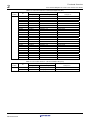
1
To our customers,
Old Company Name in Catalogs and Other Documents
On April 1st, 2010, NEC Electronics Corporation merged with Renesas Technology
Corporation, and Renesas Electronics Corporation took over all the business of both
companies. Therefore, although the old company name remains in this document, it is a valid
Renesas Electronics document. We appreciate your understanding.
Renesas Electronics website: http://www.renesas.com
April 1st, 2010
Renesas Electronics Corporation
Issued by: Renesas Electronics Corporation (http://www.renesas.com)
Send any inquiries to http://www.renesas.com/inquiry.
Notice
1.
2.
3.
4.
5.
6.
7.
All information included in this document is current as of the date this document is issued. Such information, however, is
subject to change without any prior notice. Before purchasing or using any Renesas Electronics products listed herein, please
confirm the latest product information with a Renesas Electronics sales office. Also, please pay regular and careful attention to
additional and different information to be disclosed by Renesas Electronics such as that disclosed through our website.
Renesas Electronics does not assume any liability for infringement of patents, copyrights, or other intellectual property rights
of third parties by or arising from the use of Renesas Electronics products or technical information described in this document.
No license, express, implied or otherwise, is granted hereby under any patents, copyrights or other intellectual property rights
of Renesas Electronics or others.
You should not alter, modify, copy, or otherwise misappropriate any Renesas Electronics product, whether in whole or in part.
Descriptions of circuits, software and other related information in this document are provided only to illustrate the operation of
semiconductor products and application examples. You are fully responsible for the incorporation of these circuits, software,
and information in the design of your equipment. Renesas Electronics assumes no responsibility for any losses incurred by
you or third parties arising from the use of these circuits, software, or information.
When exporting the products or technology described in this document, you should comply with the applicable export control
laws and regulations and follow the procedures required by such laws and regulations. You should not use Renesas
Electronics products or the technology described in this document for any purpose relating to military applications or use by
the military, including but not limited to the development of weapons of mass destruction. Renesas Electronics products and
technology may not be used for or incorporated into any products or systems whose manufacture, use, or sale is prohibited
under any applicable domestic or foreign laws or regulations.
Renesas Electronics has used reasonable care in preparing the information included in this document, but Renesas Electronics
does not warrant that such information is error free. Renesas Electronics assumes no liability whatsoever for any damages
incurred by you resulting from errors in or omissions from the information included herein.
Renesas Electronics products are classified according to the following three quality grades: “Standard”, “High Quality”, and
“Specific”. The recommended applications for each Renesas Electronics product depends on the product’s quality grade, as
indicated below. You must check the quality grade of each Renesas Electronics product before using it in a particular
application. You may not use any Renesas Electronics product for any application categorized as “Specific” without the prior
written consent of Renesas Electronics. Further, you may not use any Renesas Electronics product for any application for
which it is not intended without the prior written consent of Renesas Electronics. Renesas Electronics shall not be in any way
liable for any damages or losses incurred by you or third parties arising from the use of any Renesas Electronics product for an
application categorized as “Specific” or for which the product is not intended where you have failed to obtain the prior written
consent of Renesas Electronics. The quality grade of each Renesas Electronics product is “Standard” unless otherwise
expressly specified in a Renesas Electronics data sheets or data books, etc.
“Standard”:
8.
9.
10.
11.
12.
Computers; office equipment; communications equipment; test and measurement equipment; audio and visual
equipment; home electronic appliances; machine tools; personal electronic equipment; and industrial robots.
“High Quality”: Transportation equipment (automobiles, trains, ships, etc.); traffic control systems; anti-disaster systems; anticrime systems; safety equipment; and medical equipment not specifically designed for life support.
“Specific”:
Aircraft; aerospace equipment; submersible repeaters; nuclear reactor control systems; medical equipment or
systems for life support (e.g. artificial life support devices or systems), surgical implantations, or healthcare
intervention (e.g. excision, etc.), and any other applications or purposes that pose a direct threat to human life.
You should use the Renesas Electronics products described in this document within the range specified by Renesas Electronics,
especially with respect to the maximum rating, operating supply voltage range, movement power voltage range, heat radiation
characteristics, installation and other product characteristics. Renesas Electronics shall have no liability for malfunctions or
damages arising out of the use of Renesas Electronics products beyond such specified ranges.
Although Renesas Electronics endeavors to improve the quality and reliability of its products, semiconductor products have
specific characteristics such as the occurrence of failure at a certain rate and malfunctions under certain use conditions. Further,
Renesas Electronics products are not subject to radiation resistance design. Please be sure to implement safety measures to
guard them against the possibility of physical injury, and injury or damage caused by fire in the event of the failure of a
Renesas Electronics product, such as safety design for hardware and software including but not limited to redundancy, fire
control and malfunction prevention, appropriate treatment for aging degradation or any other appropriate measures. Because
the evaluation of microcomputer software alone is very difficult, please evaluate the safety of the final products or system
manufactured by you.
Please contact a Renesas Electronics sales office for details as to environmental matters such as the environmental
compatibility of each Renesas Electronics product. Please use Renesas Electronics products in compliance with all applicable
laws and regulations that regulate the inclusion or use of controlled substances, including without limitation, the EU RoHS
Directive. Renesas Electronics assumes no liability for damages or losses occurring as a result of your noncompliance with
applicable laws and regulations.
This document may not be reproduced or duplicated, in any form, in whole or in part, without prior written consent of Renesas
Electronics.
Please contact a Renesas Electronics sales office if you have any questions regarding the information contained in this
document or Renesas Electronics products, or if you have any other inquiries.
(Note 1) “Renesas Electronics” as used in this document means Renesas Electronics Corporation and also includes its majorityowned subsidiaries.
(Note 2) “Renesas Electronics product(s)” means any product developed or manufactured by or for Renesas Electronics.
User’s Manual
SH7670 CPU Board
M3A-HS71
User’s Manual
Renesas 32-Bit RISC Microcomputers
SuperH™ RISC engine Family / SH7670 Series
Rev.1.01 2008.05
Table of Contents
Chapter1 Overview .............................................................................................................................. 1-1
1.1 Overview .................................................................................................................................................................... 1-2
1.2 Configuration .............................................................................................................................................................. 1-2
1.3 External Specifications ............................................................................................................................................... 1-3
1.4 Block Diagram of SH7670 CPU Board ....................................................................................................................... 1-5
1.5 External View ............................................................................................................................................................. 1-6
1.6 SH7670 CPU Board Memory Mapping....................................................................................................................... 1-7
1.7 Absolute Maximum Ratings........................................................................................................................................ 1-8
1.8 Recommended Operating Conditions ........................................................................................................................ 1-8
Chapter2 Functional Overview ............................................................................................................ 2-1
2.1 Functional Overview................................................................................................................................................... 2-2
2.2 CPU............................................................................................................................................................................ 2-3
2.2.1 SH7670 Outline................................................................................................................................................. 2-3
2.2.2 SH7670 Pin Function Used on SH7670 CPU Board ......................................................................................... 2-3
2.2.3 SH7670 Multiplex Pin Used on the SH7670 CPU Board................................................................................. 2-11
2.3 Memory .................................................................................................................................................................... 2-15
2.3.1 RAM built in SH7670 ....................................................................................................................................... 2-15
2.3.2 Flash Memory Interface................................................................................................................................... 2-15
2.3.3 External SDRAM Interface .............................................................................................................................. 2-17
2.3.4 External EEPROM Interface............................................................................................................................ 2-20
2.4 USB Interface ........................................................................................................................................................... 2-21
2.5 Serial Port Interface.................................................................................................................................................. 2-22
2.6 ST Interface.............................................................................................................................................................. 2-23
2.7 LAN Interface ........................................................................................................................................................... 2-24
2.8 I/O Port ..................................................................................................................................................................... 2-26
2.9 Power Supply Circuit ................................................................................................................................................ 2-28
2.10 Clock Module.......................................................................................................................................................... 2-29
2.11 Reset Module ......................................................................................................................................................... 2-30
2.12 Interrupt Switch ...................................................................................................................................................... 2-31
2.13 E10A-USB Interface ............................................................................................................................................... 2-32
Chapter3 Operational Specifications ................................................................................................... 3-1
3.1 SH7670 CPU Board Connector Overview .................................................................................................................. 3-2
3.1.1 LAN Connector (J1) .......................................................................................................................................... 3-3
3.1.2 USB Connector (J3) .......................................................................................................................................... 3-4
3.1.3 Extension Connector (J5,J6,J8,J9,J11,J12, and J13) ....................................................................................... 3-5
3.1.4 STIF Connector (J7,J10) ................................................................................................................................... 3-9
3.1.5 External Power Supply Connector (J14 and J18)............................................................................................ 3-11
3.1.6 Power Supply Connector (J15) ....................................................................................................................... 3-12
3.1.7 H-UDI Connector (J16).................................................................................................................................... 3-13
3.1.8 UART Connector (J20).................................................................................................................................... 3-14
3.2 Switch and LED Outline............................................................................................................................................ 3-15
Rev. 1.01 2008.05.07
REJ11J0012-0101
(i)
3.2.1 Jumper (JP1~JP7) .......................................................................................................................................... 3-16
3.2.2 Switch and LED Functions .............................................................................................................................. 3-18
3.3 Board Dimensions of SH7670 CPU Board ............................................................................................................... 3-21
Appendix.............................................................................................................................................A-1
M3A-HS71 SCHEMATICS
Rev. 1.01 2008.05.07
REJ11J0012-0101
(ii)
Chapter1Overview
Chapter1
Overview
1-1
Overview
1
1.1 Overview
1.1 Overview
The SH7670 CPU board is a CPU evaluation board designed for users to evaluate the functionality and
performance of the SH7670 group of Renesas Technology original microcomputers, as well as develop and evaluate
the application software for this group of microcomputers. The features of the SH7670 evaluation board are as
follows.
Board Part Number: M3A-HS71
<The Features of SH7670 CPU Board>
z As external memories, a 64MB (8 Mbytes) flash memory (16-bit bus connection), two 256MB (32 Mbytes)
SDRAMs (32-bit bus connection) are mounted.
z As the SH7670 peripheral function interface, a USB connector, LAN connector are standard mounted. In
addition, the general purpose 20-pin MIL standard connector is also installed as the connector for MPEG
transport stream interface (STIF).
z All pins of SH7670 data bus, address bus, and on-chip peripheral functions are connected to the extension
connector. (For extension board and monitoring signals with using measurement instruments)
z The on-chip emulator E10A-USB made by Renesas Technology (with no AUD function: 14-pin connector) can
be used.
1.2 Configuration
Figure 1.2.1 shows an example of system configuration using the SH7670 CPU board.
USB LAN
J15
SH7670 CPU board
M3A-HS71
DC 5V
Power
Supply
(1.5A min.)
*
SH7670
RS-232C
STIF
H-UDI connector
High-performance Embedded
Workshop (HEW) *
HEW
debugger
SuperH RISC engine
C/C++ compiler package *
Host
*
Computer
E10A-USB *
* : The user must prepare these separately on their own.
Figure 1.2.1 SH7670 CPU Board System Configuration Example
Rev.1.01
2008.05.07
REJ11J0012-0101
1-2
Overview
1
1.3 External Specifications
1.3 External Specifications
Table 1.3.1 and Table 1.3.2 list the external specifications of SH7670 CPU board.
Table 1.3.1 External Specifications of SH7670 CPU Board (1)
No.
Item
Content
SH7670
1
CPU
• Input(XIN) clock: 16.67 MHz
• Bus clock: Maximum 66.67 MHz,
• CPU clock: Maximum 200 MHz
• On-chip memory
• RAM: 32KB
• Instruction cache : 8 KB
• Operand cache : 8 KB
Power voltage: internal : 1.2 V, I/O 3.3 V
256-pin BGA 0.8 mm pitch (Package code: PRBG0256GA-A)
The following memories are mounted
• SDRAM
• EDS2516APTA-75 (Elpida) x 2 : 64 MB
• 32-bit bus width
2
External Memory
• Flash memory
• S29GL064A90TFIR4 : 8 MB
• 16-bit data bus width fixed
• EEPROM (IIC3)
・HN58X24128FPIE x 1 : 16KB
3
Ether
4
USB
• RJ-45LAN connector with on-chip pulse transformer (8-pin, RJ-45)
• Realtek PHY-LSI RTL8201CP-VD-LF is mounted
• USB connector
→Series A socket built-in. (Mini-AB/Mini-B connectors for Host/Function
evaluation can be mounted on the board)
• VBUS power control
z H-UDI connector (14-pin)
z Serial port connector (D-sub 9-pin)
5
Connectors and
Through-hole
z 20-pin MIL standard connector
• SH7670 extension connector: 4 pcs.
• SH7670 ST I/F connector : 2 pcs.
z 40-pin MIL standard connector
• SH7670 extension connector: 2 pcs.
6
Rev.1.01
LED
2008.05.07
REJ11J0012-0101
• Power LED (1 pc.)
• User LED (Connect to the port pins of SH7670): 4 pcs.
• LED for Ethernet communication status (5 pcs.)
1-3
Overview
1
1.3 External Specifications
Table 1.3.2 External Specifications of SH7670 CPU Board (2)
No.
Item
7
Switch
8
Board Size
Rev.1.01
2008.05.07
REJ11J0012-0101
Content
• Reset switch: 1 pc.
• NMI switch: 1 pc.
• IRQ0 switch: 1 pc.
• Test switch: 1 pc.
• DIP switch for mode setting: 1 pc. (5-pole)
• DIP switch for user: 1 pc. (4-pole)
• Switch for PHY controller operation mode : 1 pc. (6-pole)
• Dimensions : 145mm x 150mm
• Mounting form : 4-layer, double-side mounted
• Board configuration : 1 board
1-4
Overview
1
1.4 Block Diagram of SH7670 CPU Board
1.4 Block Diagram of SH7670 CPU Board
Figure 1.4.1 shows the system block diagram of SH7670 CPU board.
H-UDI (14-pin)
Serial port connector
SCIF
H-UDI
Switch
(Interrupt, DIP switch)
ST
connector
INTC
STIF
SH7670
LAN
connector
PIO
PHY-LSI
EtherC
EEPROM
EEPROM
(16KB)
(16KB)
IIC3
PIO
VBUS
control
USB
USB
connector
(200MHz)
HIF
16bit
Extension connector
(HIF bus)
Peripheral
I/O
BSC
32bit
32bit
16bit
32bit
SDRAM
SDRAM
SDRAM
SDRAM
(64MB)
(64MB)
(16MB)
(16MB)
Flash
Flash memory
memory
(8MB)
(8MB)
Extension
connector
Figure 1.4.1 SH7670 CPU Board System Block Diagram
Rev.1.01
2008.05.07
REJ11J0012-0101
1-5
Overview
1
1.5 External View
1.5 External View
Figure 1.5.1 shows the SH7670 CPU board overview (the image of component placement).
<Top view of the component side>
<Top view of the solder side>
U11
1.2V
DC converter
U10
3.3V swiching
regulator
U2
Clock buffer
:SH7670 extension connector (Not mounted)
Figure 1.5.1 SH7670 CPU Board Overview
Rev.1.01
2008.05.07
REJ11J0012-0101
1-6
Overview
1
1.6 SH7670 CPU Board Memory Mapping
1.6 SH7670 CPU Board Memory Mapping
Figure 1.6.1 shows the SH7670 memory mapping of the SH7670 CPU board.
Logical
Address
H'0000 0000
H'007F FFFF
SH7670 Logical Space
SH7670 CPU Board Memory Mapping
CS0 Space: 64 MB
Flash Memory (8 MB)
16-bit bus
User Area
H'0400 0000
Reserved Area
Reserved Area
(Disabled)
Reserved Area
Reserved Area
(Disabled)
CS3 space: 64 MB
SDRAM (64 MB)
32-bit bus
CS4 space: 64 MB
User Area
CS5 space: 64 MB
User Area
CS6 space: 64 MB
User Area
Reserved Area
Reserved Area
(Disabled)
CS0~CS6 space
(Cache disabled space)
CS0~CS6 space
(Cache disabled space)
Reserved Area
(Disabled)
Reserved Area
(Disabled)
On-chip RAM (32 KB)
On-chip RAM (32 KB)
H'0800 0000
H'0C00 0000
H'0FFF FFFF
H'1000 0000
H'1400 0000
H'1800 0000
H'1C00 0000
H'2000 0000
H'8000 0000
H'FFF8 0000
H'FFF8 8000
H'FFF8 FFFF
H'FFFC 0000
On-chip RAM
Reserved
On-chip peripheral module
On-chip RAM
Reserved
On-chip peripheral module
H'FFFF FFFF
Figure 1.6.1 SH7670 CPU Board Memory Mapping
Rev.1.01
2008.05.07
REJ11J0012-0101
1-7
Overview
1
1.7 Absolute Maximum Ratings
1.7 Absolute Maximum Ratings
Table 1.7.1 lists the absolute maximum ratings of the SH7670 CPU board.
Table 1.7.1 Absolute Maximum Ratings of the SH7670 CPU Board
Symbol
Parameter
Rated Value
Remarks
VCC
5V system power supply voltage
-0.3V to 6.0V
Relative to VSS
3VCC
3.3V system power supply voltage
-0.3V to 4.6V
Relative to VSS
1.2VCC
1.2V system power supply voltage
-0.3V to 1.7V
Relative to VSS
Operating ambient temperature
-10°C to 55°C
No dewdrops allowed.
Topr
Use in corrosive gas environment prohibited.
Tstr
Storage ambient temperature
-20°C to 60°C
No dewdrops allowed.
Use in corrosive gas environment prohibited.
Note: The ambient temperature refers to the air temperature in places closest possible to the board.
1.8 Recommended Operating Conditions
Table 1.8.1 lists the recommended operating conditions of the SH7670 CPU board.
Table 1.8.1 Operating Condition of SH7670 CPU Board
Symbol
Parameter
VCC
5V system power supply voltage
3VCC
1.2VCC
‐
Rated Value
Remarks
4.75V to 5.25V
Relative to VSS
3.3V system power supply voltage
3.0V to 3.6V
Relative to VSS
1.2V system power supply voltage
1.1V to 1.3V
Relative to VSS
Maximum current consumption in
Within 1.5A
the board
Topr
Operating ambient temperature
0°C to 40°C
No dewdrops allowed.
Use in corrosive gas environment prohibited.
Rev.1.01
2008.05.07
REJ11J0012-0101
1-8
Chapter2Functional Overview
Chapter2
Functional Overview
2-1
Functional Overview
2
2.1 Functional Overview
2.1 Functional Overview
Table 2.1.1 lists the function modules of SH7670 CPU board.
Table 2.1.1 Functional Modules of SH7670 CPU Board
Section
2.2
Function
CPU
Content
SH7670
• Input(XIN) Clock: 16.67 MHz
• Bus Clock: 66.67 MHz
• CPU Clock: Maximum 200 MHz
2.3
Memory
The following memories are mounted
• SDRAM: Maximum 64 MB
• EDS2516APTA-75 x 2: 64 MB
• 32-bit bus width
• Flash memory
• S29GL064A90TFIR4 x 1: 8 MB
• 16-bit data bus width fixed
• EEPROM
• HN58X24128FPIE x 1: 16 KB
2.4
USB Interface
Mounts USB connector
2.5
Serial Port Interface
Connects the SH7670 SCIF0 to serial port connector
2.6
ST Interface
Connects the SH7670 ST interface signal to the ST connector(channel 1
and 2)
2.7
LAN Interface
Connects the SH7670 Ethernet controller to PHY LSI
2.8
I/O Port
Connects the SH7670 I/O port
2.9
Power Supply Circuit
Controls the system power control of SH7670 CPU board
2.10
Clock Module
Clock control
2.11
Reset Module
Reset control for device mounted on the SH7670 CPU board
2.12
Interrupt Switch
Connects the NMI pin and IREQ0 pin
2.13
E10A-USB Interface
SH7670 H-UDI interface
Operational Specifications
Connector, switch, LED
-
• SH7670 extension connector
• Switch, LED
• H-UDI connector
Details are described in Chapter 3
Rev.1.01 2008.05.07
REJ11J0012-0101
2-2
Functional Overview
2
2.2 CPU
2.2 CPU
2.2.1 SH7670 Outline
The SH7670 CPU board contains the 32-bit RISC microcomputer SH7670 that operates with a maximum 200MHz
of CPU clock frequency.
2.2.2 SH7670 Pin Function Used on SH7670 CPU Board
Table 2.2.1~Table 2.2.8 list the SH7670 pin functions used on the SH7670 CPU board.
Table 2.2.1 SH7670 Pin Selection Used on SH7670 CPU Board (1)
Type
Clock
Pin
I/O
Function of SH7670 CPU Board
Name
EXTAL
I
External clock
XTAL
O
Crystal
CKIO
O
System clock
Destination to Connect
Inputs 16.67 MHz from oscillator
Connects to oscillator
Clock output
CKIO is branched to connect the
Crystal resonator is connected
followings
• Connects to SDRAM
• Connects to an extension
connector
Operating
MD_BW
I
Mode setting
The bus width for CS0 space is set to 16-bit.
Connects to GND
MD_BW="L"
Mode
MD_CK1
I
MD_CK0
Clock mode
Clock mode is switched.
setting
• Connects to DIP switch for
mode setting
Clock mode 0 :
MD_CK0, MD_CK1
MD_CLK0="L",MD_CLK1="L"
Clock mode 1 :
MD_CLK0="H",MD_CLK1="L"
Clock mode 3 :
MD_CLK0="H",MD_CLK1="H"
Switching between MD_CLK0 and MD_CLK1
is executed with the DIP switch SW.
System
RES#
I
Control
Bus
CS0#
O
Power-on
When power-on-reset and pressing the reset
reset
SW, it becomes a power-on-reset state.
Chip select
Chip select signal
Connects to CE# signal of NOR
CS0#
flash memory (U3-26)
Control
CS3#
O
Chip select
Connects to reset circuit
Chip select signal
• Connects to the CS# pin of
CS3#
SDRAM (U4-19,U5-19)
• Connects to an extension
connector (J9-11),
CS4#
CS5#
CS6#
CKE
O
O
O
O
Chip select
Chip select
Chip select
CK enable
Chip select signal
Connects
CS4#(PB06/CS4#)
connector (J9-5)
to
Chip select signal
Connects
CS5#(PB05/CS5#/CE1A#/IRQ3/TEND1)
connector (J8-11)
Chip select signal
Connects
CS6#(PB03/CS6#/CE1B#/IRQ1/DREQ1)
connector (J9-7)
CK enable signal
• Connects to the CKE# pin of
CKE
SDRAM (U4-37,U5-37)
to
to
an
extension
an
extension
an
extension
• Connects to an extension
connector (J9-14)
Rev.1.01 2008.05.07
REJ11J0012-0101
2-3
Functional Overview
2
2.2 CPU
Table 2.2.2 SH7670 Pin Selection Used on SH7670 CPU Board (2)
Type
Pin
RAS#
I/O
O
Name
RAS
Function of SH7670 CPU
Board
Destination to Connect
RAS signal
• Connects to the RAS# pin of
RAS#
SDRAM (U4-18,U5-18)
• Connects to an extension
connector (J9-12)
CAS#
O
CAS
CAS signal
• Connects to the CAS# pin of
CAS#
SDRAM (U4-17,U5-17)
• Connects to an extension
connector (J9-13)
RD/WR#
O
Read-write
Read-write signal
RD/WR#
• Connects to the WE# pin of
SDRAM (U4-16,U5-16)
• Connects to an extension
connector (J9-15)
RD#
O
Read
Read signal
RD#
• Connects to the OE# signal of
NOR flash memory (U3-28)
• Connects to an extension
connector (J12-5)
WE0#/DQMLL
O
Least significant byte
D7-D0 is selected
written/least
WE0#/DQMLL(WE0#/DQM
significant byte
LL)
• Connects to the WE# pin of NOR
flash memory (U3-11)
• Connects to the DQML pin of
SDRAM (U5-15)
selection
• Connects to an extension
connector (J9-19)
WE1#/DQMLU
O
Third byte
D15-D8 is selected
written/third byte
DQMLU(WE1#/DQMLU/WE
selection
#)
• Connects to an extension
Second byte
D23-D16 is selected
• Connects to the DQMU pin of
written/second byte
DQMUL(WE2#/DQMUL/ICI
selection
ORD#)
• Connects to an extension
Most significant byte
D31-D24 is selected
• Connects to the DQML pin of
written/most
DQMUU(WE3#/DQMUU/ICI
significant byte
OWR#)
• Connects to an extension
Wait
WAIT#: PB00/WAIT#/SDA
Connects to an extension connector
Address bus
26-bit address bus
• A25-A00
• Connects to the DQMU pin of
SDRAM (U5-39)
connector (J9-18)
WE2#/DQMUL
O
SDRAM (U4-15)
connector (J9-17)
WE3#/DQMUU
O
connector (J9-16)
selection
WAIT#
I
SDRAM (U4-39)
(J9-10)
Address Bus
A25-A00
O
Connects to an extension
connector (J12)
• A22-A01
Connects to FLASH (U3)
• A16-A02
Connects to SDRAM (U4,U5)
Data Bus
D31-D00
O
Data bus
32-bit data bus
• D15-D00
Connects to FLASH (U3)
• D31-D00
SDRAM(U4,U5)
Connects to an extension
connector (J5)
Rev.1.01 2008.05.07
REJ11J0012-0101
2-4
Functional Overview
2
2.2.2 SH7670 Pin Function Used on SH7670 CPU Board
Table 2.2.3 SH7670 Pin Selection Used on SH7670 CPU Board (3)
Type
INTC
Pin
IRQ
I/O
I
Function of SH7670 CPU Board
Destination to Connect
Interrupt
Interrupt request pin which can select level
• Connects to an extension connector
request
and edge input.
Name
Each
IRQ
pin
is
connected
to
the
followings.
IRQ7#(J8-12)
• IRQ7#(PD07/IRQ7#/SDCLK)
IRQ6#(J8-13)
• IRQ6#(PD06/IRQ6#/SDCMD)
IRQ5#(J8-14)
• IRQ5#(PD05/IRQ5#/SDCD)
IRQ4#(J8-15)
• IRQ4#(PD04/IRQ4#/SDWP)
IRQ3#(J8-16)
• IRQ3#(PD03/IRQ3#/SDDATA3)
IRQ2#(J8-17)
• IRQ2#(PD02/IRQ2#/SDDATA2)
IRQ1#(J8-18)
• IRQ1#(PD01/IRQ1#/SDDATA1)
IRQ0#(J8-19)
• IRQ0#(PD00/IRQ0#/SDDATA0)
IRQ3(J8-11)
• IRQ3(PB05/CS5#/CE1A#/IRQ3/TEND1)
IRQ2(J9-6)
• IRQ2(PB04/CE2A#/IRQ2/DACK1)
IRQ1(J9-7)
• IRQ1(PB03/CS6#/CE1B#/IRQ1/DREQ1)
IRQ0(J9-8)
• IRQ0(PB02/CE2B#/IRQ0)
• Connects to push switch
IRQ0 (SW5)
• Connects to VBUS IRQ1(U8-2)
DMA
DREQ1
C
DREQ0
I
DMA transfer
External DMA transfer request input pin
request
DREQ1(PB03/CS6#/CE1B#/IRQ1/DREQ1)
• Connects to an extension connector
DREQ1(J9-7)
DREQ0(PF09/ST0_VLD/DREQ0)
• Connects to ST connector
DREQ1(J7-16)
DACK1
DACK0
O
DMA transfer
Request
request
external DMA transfer request
is
acknowledged
acknowledge
output
pin
to
DACK1(J9-6)
DACK1(PB04/CE2A#/IRQ2/DACK1)
• Connects to ST connector
DACK0(PF10/ST0_SYC//DACK0)
TEND1
TEND0
O
• Connects to an extension connector
DACK0(J7-15)
DMA transfer
DMA transfer completion output signal
completion
TEND1(PB05/CS5#/CE1A#/IRQ3/TEND1)
output
TEND0(PF11/ST0_PWM/TEND0)
• Connects to ST connector
Carrier sense
Carrier sense pin
Connects to PHY-LSI (U7-23)
Collision
Collision detection pin
• Connects to an extension connector
TEND1(J8-11)
TEND0(J7-17)
Ether
CRS
COL
I
I
CRS(PC15/CRS)
Connects to PHY-LSI (U7-1)
COL(PC14/COL)
4-bit sending data pin
Connects to PHY-LSI
MII_TXD3(PC07/MII_TXD3)
MII_TXD3(U7-3)
MII_TXD1
MII_TXD2(PC06/MII_TXD2)
MII_TXD2(U7-4)
MII_TXD0
MII_TXD1(PC05/MII_TXD1)
MII_TXD1(U7-5)
MII_TXD0(PC04/MII_TXD0)
MII_TXD0(U7-6)
Sending
Indicates that sending data is ready for
Connects to PHY-LSI (U7-2)
enable
MII_TXD3-0
Sending clock
Reference timing of TX_EN, TX_ER, and
MII_TXD3
MII_TXD2
TX_EN
O
O
Sending data
TX_EN(PC12/TX_EN)
TX_CLK
I
Connects to PHY-LSI (U7-7)
MII_TXD3-0
TX_CLK(PC13/TX_CLK)
TX_ER
O
Sending error
Pins
notifying
PHY-LSI
of
the
error
in
Connects to an extension connector
transmitting TX_ER(PC11/TX_ER)
(J11-6)
4-bit receiving data pin
Connects to PHY-LSI
MII_RXD3(PC03/MII_RXD3)
MII_RXD3(U7-18)
MII_RXD1
MII_RXD2(PC02/MII_RXD2)
MII_RXD2(U7-19)
MII_RXD0
MII_RXD1(PC01/MII_RXD1)
MII_RXD1(U7-20)
MII_RXD0(PC00/MII_RXD0)
MII_RXD0(U7-21)
Receive data
Indicates that there is enabled receiving
Connects to PHY-LSI (U7-22)
valid
data for MII_RXD3-0
MII_RXD3
MII_RXD2
RX_DV
I
I
Receive data
RX_DV(PC08/RX_DV)
Rev.1.01 2008.05.07
REJ11J0012-0101
2-5
Functional Overview
2
2.2.2 SH7670 Pin Function Used on SH7670 CPU Board
Table 2.2.4 SH7670 Pin Selection Used on SH7670 CPU Board (4)
Type
Ether
Pin
RX_CLK
I/O
I
Name
Receiving clock
Function of SH7670 CPU Board
Destination to Connect
Reference timing of RX_DV, RX_ER, and
Connects to PHY-LSI
MII_RXD3-0
(U7-16)
RX_CLK(PC10/RX_CLK)
RX_ER
I
Receive error
Pins recognizing the error state occurred in
Connects to PHY-LSI
receiving
(U7-24)
RX_ER: (PC09/RX_ER)
MDC
O
Clock for
Reference
management
information by MDIO
timing
input
of
transfer
Connects to PHY-LSI
(U7-25)
MDC: (PC17/MDC)
MDIO
I/O
Data I/O for
Bidirectional
management
management information
pin
for
exchanging
Connects to PHY-LSI
(U7-26)
MDIO(PC16/MDIO)
WOL
LNKSTA
EXOUT
STIF
ST_CLKO
O
I
O
O
MAGIC packet
Pin indicating Magic Packet™ * receive
receive
WOL(PC20/WOL)
connector (J11-3)
Link status
Link state input pin from PHY-LSI
Connects to an extension
LNKSTA(PC18/LNKSTA)
connector (J11-4)
External output pin
Connects to an extension
EXOUT(PC19/EXOUT)
connector (J11-5)
Data clock output
Connects to ST
General output
Clock output
Connects to an extension
ST_CLKOUT
connector (J7-2,J10-2)
Data clock input
Connects to ST
N
ST1_CLKIN(ST1_CLKIN/SSISCK1)
connector
ST0_CLKI
ST0_CLKIN(ST0_CLKIN/SSISCK0)
ST1_CLKIN(J10-1)
UT
ST1_CLKI
I
Clock input
N
ST1_SYC
ST0_CLKIN(J7-1)
I/O
Synchronous signal
ST0_SYC
Synchronous signal
Connects to ST
ST1_SYC(PE10/ST1_SYC/CTS2)
connector
ST0_SYC(PF10/ST0_SYC/DACK0)
ST1_SYC(J10-15)
ST0_SYC(J7-15)
ST1_REQ
I/O
Request
ST0_REQ
Request signal
Connects to ST
ST1_REQ(PE08/ST1_REQ/TxD2)
connector
ST0_REQ(PF08/ST0_REQ)
ST1_REQ(J10-18)
ST0_REQ(J7-18)
ST1_VLD
ST0_VLD
I/O
Data enable
Data enable
Connects to ST
ST1_VLD(PE09/ST1_VLD/SCK2)
connector
ST0_VLD(PF09/ST0_VLD/DREQ0)
ST1_VLD(J10-16)
ST0_VLD(J7-16)
ST1_D7
Data (0 is used for serial mode)
Connects to ST
ST1_D7(PE07/ST1_D7/SSIWS1)
connector
ST1_D5
ST1_D6(PE06/ST1_D6/SSIDATA1)
ST1_D7(J10-11)
ST1_D4
ST1_D5(PE05/ST1_D5/RTS1)
ST1_D6(J10-6)
ST1_D3
ST1_D4(PE04/ST1_D4/CTS1)
ST1_D5(J10-12)
ST1_D2
ST1_D3(PE03/ST1_D3/SCK1)
ST1_D4(J10-5)
ST1_D1
ST1_D2(PE02/ST1_D2/RxD1)
ST1_D3(J10-13)
ST1_D0
ST1_D1(PE01/ST1_D1/TxD1)
ST1_D2(J10-4)
ST0_D7
ST1_D0(PE00/ST1_D0/RxD2)
ST1_D1(J10-14)
ST0_D6
ST0_D7(PF07/ST0_D7/SSIWS0)
ST1_D0(J10-3)
ST0_D5
ST0_D6(PF06/ST0_D6/SSIDATA0)
ST0_D7(J7-11)
ST0_D4
ST0_D5(PF05/ST0_D5/RTS0)
ST0_D6(J7-6)
ST0_D3
ST0_D4(PF04/ST0_D4/CTS0)
ST0_D5(J7-12)
ST0_D2
ST0_D3(PF03/ST0_D3/SCK0)
ST0_D4(J7-5)
ST0_D1
ST0_D2(PF02/ST0_D2/RxD0)
ST0_D3(J7-13)
ST0_D0
ST0_D1(PF01/ST0_D1/TxD0)
ST0_D2(J7-4)
ST0_D0(PF00/ST0_D0)
ST0_D1(J7-14)
ST1_D6
I/O
Data
ST0_D0(J7-3)
Rev.1.01 2008.05.07
REJ11J0012-0101
2-6
Functional Overview
2
2.2.2 SH7670 Pin Function Used on SH7670 CPU Board
Table 2.2.5 SH7670 Pin Selection Used on SH7670 CPU Board (5)
Type
STIF
Pin
ST1_VCO
I/O
I
Function of SH7670 CPU Board
Name
VCX0 clock
Destination to
Connect
VCX0 clock
Connects
_CLKIN,
ST1_VCO_CLKIN
connector
ST0_VCO
(ST1_VCO_CLKIN/AUDIO_CLK)
ST1_VCO_CLKIN
to
ST
(J10-19)
_CLKIN
ST0_VCO_CLKIN
(J7-19)
ST1_PWM
O
PWM output
ST0_PWM
PWM output
Connects
ST1_PWM(PE11/ST1_PWM/RTS2)
connector
ST0_PWM(PF11/ST0_PWM/TEND0)
ST1_PWM(J10-17)
to
ST
ST0_PWM(J7-17)
USB
DP
I/O
USB D+ Data
USB bus D+ Data
Connects
to
USB
to
USB
to
USB
(J3-3)
DM
I/O
USB D- Data
USB bus D- data
Connects
(J3-2)
VBUS
I
VBUS input
Connects to Vbus of USB bus
Connects
(J3-1)
REFRIN
I
Reference input
Connects to USBAPVss through 5.6KΩ±1%
Connects to USB
resistance
USB_X1
I/O
USB_X2
Input between
Crystal resonator for USB is connected.
Connects
crystal resonator
USB_X1 can input an external clock
resonator (48 MHz)
for USB and
to crystal
for USB (X5)
external clock
AV33
I
USB
Transceiver analog pin power supply
Connects to 3.3V
Transceiver analog pin GND
Connects to GND
Transceiver digital pin power supply
Connects to 3.3V
Transceiver digital pin GND
Connects to GND
Transceiver analog core power supply
Connects to 1.2V
Transceiver analog core GND
Connects to GND
Transceiver digital pin power supply
Connects to 1.2V
Transceiver digital pin GND
Connects to GND
Transceiver digital core power supply
Connects to 1.2V
Transceiver digital core GND
Connects to GND
analog pin power
supply
AG33
DV33
I
I
USB
analog pin GND
USB
digital pin power
supply
DG33
AV12
I
I
USB
digital pin GND
USB
analog
core
power supply
AG12
DV12
I
I
USB
analog core GND
USB
digital pin power
supply
DG12
UV12
I
I
USB
digital pin GND
USB
digital
core
power supply
UG12
Rev.1.01 2008.05.07
REJ11J0012-0101
I
USB
digital core GND
2-7
Functional Overview
2
2.2.2 SH7670 Pin Function Used on SH7670 CPU Board
Table 2.2.6 SH7670 Pin Selection Used on SH7670 CPU Board (6)
Type
HIF
Pin
HIFD15-
I/O
I/O
Name
HIF data bus
HIFD00
Function of SH7670 CPU Board
Destination to
Connect
Address/data/command I/O for HIF
Connects
HIFD15(PG15/HIFD15)
extension
HIFD14(PG14/HIFD14)
HIFD15(J13-4)
HIFD13(PG13/HIFD13)
HIFD14(J13-5)
HIFD12(PG12/HIFD12)
HIFD13(J13-6)
HIFD11(PG11/HIFD11)
HIFD12(J13-7)
HIFD10(PG10/HIFD10)
HIFD11(J13-8)
HIFD09(PG09/HIFD09)
HIFD10(J13-9)
HIFD08(PG08/HIFD08)
HIFD09(J13-10)
HIFD07(PG07/HIFD07)
HIFD08(J13-11)
HIFD06(PG06/HIFD06)
HIFD07(J13-12)
HIFD05(PG05/HIFD05)
HIFD06(J13-13)
HIFD04(PG04/HIFD04)
HIFD05(J13-14)
HIFD03(PG03/HIFD03)
HIFD04(J13-15)
HIFD02(PG02/HIFD02)
HIFD03(J13-16)
HIFD01(PG01/HIFD01)
HIFD02(J13-17)
HIFD00(PG00/HIFD00)
HIFD01(J13-18)
to
an
connector
HIFD00(J13-19)
HIFCS#
I
HIF chip select
Chip select input for HIF
Connects
HIFCS#(PG23/HIFCS#)
extension
to
an
connector
(J8-3)
HIFRS
I
HIF
register
Instruction of switching access type for HIF
Connects
select
HIFRS(PG22/HIFRS)
extension
HIF write
Write strobe signal
HIFWR#(PG21/HIFWR#)
to
an
connector
(J8-4)
HIFWR#
I
Connects
extension
to
an
connector
(J8-5)
HIFRD#
I
HIF read
Read strobe signal
HIFRD#(PG20/HIFRD#)
Connects
Interrupt request from HIF to external device
Connects
HIFIHT#(PG19/HIFINT#)
extension
extension
to
an
connector
(J13-3)
HIFINT#
O
HIF interrupt
to
an
connector
(J8-6)
HIFMD
HIFDREQ
HIFEBL
HIFRDY
I
O
I
O
HIF mode
HIF boot mode is specified
Connects to the DIP
HIFMD only enable for power-on-reset by RES#
switch
pin (HIFMD/PA25/A25)
setting (SW8-7)
HIFDMAC
For external device, DMAC transfer to HIFRAM
Connects
transfer request
is requested
extension
HIFDREQ(PG18/HIFDREQ)
(J8-7)
HIF pin
By inputting high level, HIF pin except this pin is
Connects
enable
activated
extension
HIFEBL(PG16/HIFEBL)
(J8-9)
Indicates that, in this LSI, reset to HIF module is
Connects
released to be possible to acknowledge the
extension
access to HIF module from external devices.
(J8-8)
HIF boot ready
for
mode
to
an
connector
to
an
connector
to
an
connector
HIFRDY(PG17/HIFRDY)
Rev.1.01 2008.05.07
REJ11J0012-0101
2-8
Functional Overview
2
2.2.2 SH7670 Pin Function Used on SH7670 CPU Board
Table 2.2.7 SH7670 Pin Selection Used on SH7670 CPU Board (7)
Type
IIC3
Pin
SCL
I/O
I/O
Name
Serial clock
Function of SH7670 CPU Board
Destination to Connect
Serial clock I/O pin
• Connects to EEPROM
SCL(PB01/IOIS16#/SCL)
(U9-6)
• Connects to an extension
connector
(J9-9)
SDA
I/O
Serial data
Serial data I/O pin
• Connects to EEPROM
SDA(PB00/WAIT#/SDA)
(U9-5)
• Connects to an extension
connector
SCIF
TXD2
O
Sending data
Pins for sending data
(J9-10)
• Connects to ST connector
TXD1
TXD2(PE08/ST1_REQ/TxD2)
TXD2(J10-18)
TXD0
TXD1(PE01/ST1_D1/TxD1)
TXD1(J10-14)
TXD0(PF01/ST0_D1/TxD0)
TXD0(J7-14)
• TxD0 is also connected to
serial connector
RXD2
I
Receiving data
Pins for receiving data
• Connects to ST connector
RXD1
RXD2(PE00/ST1_D0/RxD2)
RXD2(J10-3)
RXD0
RXD1(PE02/ST1_D2/RxD1)
RXD1(J10-4)
RXD0(PF02/ST0_D2/RxD0)
RXD0(J7-4)
• RxD0 is also connected to
serial connector
SCK2
Clock input pin
Connects to ST connector
SCK1
SCK2(PE09/ST1_VLD/SCK2)
SCK2(J10-16)
SCK0
SCK1(PE03/ST1_D3/SCK1)
SCK1(J10-13)
SCK0(PF03/ST0_D3/SCK0)
SCK0(J7-13)
Modem control pin
Connects to ST connector
RTS1#
RTS2#(PE11/ST1_PWM/RTS2#)
RTS2#(J10-17)
RTS0#
RTS1#(PE05/ST1_D5/RTS1#)
RTS1#(J10-12)
RTS0#(PF05/ST0_D5/RTS0#)
RTS0#(J7-12)
Modem control pin
Connects to ST connector
CTS1#
CTS2#(PE10/ST1_SYC/CTS2#)
CTS2#(J10-15)
CTS0#
CTS1#(PE04/ST1_D4/CTS1#)
CTS1#(J10-5)
CTS0#(PF04/ST0_D4/CTS0#)
CTS0#(J7-5)
Serial data I/O pin
Connects
SSIDATA1(PE06/ST1_D6/SSIDATA1)
connector
SSIDATA0(PF06/ST0_D6/SSIDATA0)
SSIDATA1(J11-18)
RTS2#
CTS2#
SSI
SSIDATA1
SSIDATA0
I/O
O
I
I/O
Serial clock
Send request
Send possible
SSI data I/O
to
an
extension
SSIDATA0(J11-19)
SSISCK1
SSISCK0
I/O
SSI clock I/O
Serial clock I/O pin
Connects
SSISCK1(ST1_CLKIN/SSISCK1)
connector
SSISCK0(ST0_CLKIN/SSISCK0)
SSISCK1(J11-14)
to
an
extension
SSISCK0(J11-15)
SSIWS1
SSIWS0
I/O
SSI clock
Word selection I/O pin
Connects
LR I/O
SSIWS1(PE07/ST1_D7/SSIWS1)
connector
SSIWS0(PF07/ST0_D7/SSIWS0)
SSIWS1(J11-16)
to
an
extension
SSIWS0(J11-17)
AUDIO_
CLK
Rev.1.01 2008.05.07
REJ11J0012-0101
I
External clock for
External clock for audio is input
Connects
SSI audio
AUDIO_CLK
connector
(ST1_VCO_CLKIN/AUDIO_CLK)
(J11-13)
to
an
extension
2-9
Functional Overview
2
2.2.2 SH7670 Pin Function Used on SH7670 CPU Board
Table 2.2.8 SH7670 Pin Selection Used on SH7670 CPU Board (8)
Type
IO port
Pin
PB06, PB07,
I/O
I
Name
Input port for DIP
PC11, PC19
switch
PB04
Enable (VBUS)
O
Function of SH7670 CPU Board
Connects to DIP switch
Connects
Connects to the VBUS
for user (SW7)
to
the
VBUS
power
to
the
memory card
control IC
PB05
O
Destination to Connect
Assigned in DIP switch for user
power control IC (U8-1)
Enable
Connects
(LTC1470)
power control IC LTC1470
Connects to the memory
card power control IC
LTC1470 (U6-4)
Note *: Magic Packet is a trademark of Advanced Micro Devices, Inc.
Rev.1.01 2008.05.07
REJ11J0012-0101
2-10
Functional Overview
2
2.2.3 SH7670 Multiplex Pin Used on the SH7670 CPU Board
2.2.3 SH7670 Multiplex Pin Used on the SH7670 CPU Board
Table 2.2.9 to Table 2.2.15 list the function selections of SH7670 multiplex pin used on the SH7670 CPU board.
These pins are set to the port input pin as initial values. Thus, the MD bit of port control register should be set to
use the peripheral functions (except I/O port).
Table 2.2.9 Function Selection of SH7670 Multiplex Pin (BSC)
Peripheral
Pin
Function
BSC
SH7670
Multiplex Pin
SH7670 Port Control Register
Register
MD Bit Setting Value
A25
PACRH2
PA25MD0 = B'1
PA25/A25
A24
PACRH2
PA24MD0 = B'1
PA24/A24
A23
PACRH1
PA23MD0 = B'1
PA23/A23
A22
PACRH1
PA22MD0 = B'1
PA22/A22
A21
PACRH1
PA21MD0 = B'1
PA21/A21
A20
PACRH1
PA20MD0 = B'1
PA20/A20
A19
PACRH1
PA19MD0 = B'1
PA19/A19
A18
PACRH1
PA18MD0 = B'1
PA18/A18
A17
PACRH1
PA17MD0 = B'1
PA17/A17
Table 2.2.10 Function Selection of SH7670 Multiplex Pin (SCIF)
Peripheral
Pin
Function
SCIF
SH7670 Port Control Register
Register
SH7670
Multiplex Pin
MD Bit Setting Value
RxD0
PFCRL1
PF2MD[1:0] = B’10
PF02/ST0_D2/RxD0
TxD0
PFCRL1
PF1MD[1:0] = B'10
PF01/ST0_D1/TxD0
Table 2.2.11 Function Selection of SH7670 Multiplex Pin (Ether)
Peripheral
Pin
Function
Ether
Register
SH7670
Multiplex Pin
MD Bit Setting Value
MDC
PCCRH1
PC17MD0 = B'1
MDIO
PCCRH1
PC16MD0 = B'1
PC16/MDIO
CRS
PCCRL2
PC15MD0 = B'1
PC15/CRS
PC17/MDC
COL
PCCRL2
PC14MD0 = B'1
PC14/COL
TX_EN
PCCRL2
PC12MD0 = B'1
PC12/TX_EN
TX_CLK
PCCRL2
PC13MD0 = B'1
PC13/TX_CLK
TX_ER
PCCRL2
PC11MD0 = B'1
PC11/TX_ER
RX_DV
PCCRL2
PC8MD0 = B'1
PC08/RX_DV
RX_CLK
PCCRL2
PC10MD0 = B'1
PC10/RX_CLK
RX_ER
PCCRL2
PC9MD0 = B'1
PC09/RX_ER
MII_TXD0
PCCRL1
PC4MD0 = B'1
PC04/MII_TXD0
MII_TXD1
PCCRL1
PC5MD0 = B'1
PC05/MII_TXD1
MII_TXD2
PCCRL1
PC6MD0 = B'1
PC06/MII_TXD2
MII_TXD3
PCCRL1
PC7MD0 = B'1
PC07/MII_TXD3
MII_RXD0
PCCRL1
PC0MD0 = B'1
PC00/MII_RXD0
MII_RXD1
PCCRL1
PC1MD0 = B'1
PC01/MII_RXD1
MII_RXD2
PCCRL1
PC2MD0 = B'1
PC02/MII_RXD2
MII_RXD3
PCCRL1
PC3MD0 = B'1
PC03/MII_RXD3
Rev.1.01 2008.05.07
REJ11J0012-0101
SH7670 Port Control Register
2-11
Functional Overview
2
2.2.3 SH7670 Multiplex Pin Used on the SH7670 CPU Board
Table 2.2.12 Function Selection of SH7670 Multiplex Pin (STIF)
Peripheral
Pin
Function
STIF
SH7670 Port Control Register
Register
MD Bit Setting Value
SH7670
Multiplex Pin
ST0_D7
PFCRL1
PF7MD[1:0] = B’01
PF07/ST0_D7/SSIWS0
ST0_D6
PFCRL1
PF6MD[1:0] = B’01
PF06/ST0_D6/SSIDATA0
ST0_D5
PFCRL1
PF5MD[1:0] = B’01
PF05/ST0_D5/RTS0#
ST0_D4
PFCRL1
PF4MD[1:0] = B’01
PF04/ST0_D4/CTS0#
ST0_D3
PFCRL1
PF3MD[1:0] = B’01
PF03/ST0_D3/SCK0
ST0_D2
PFCRL1
PF2MD[1:0] = B’01
PF02/ST0_D2/RxD0
ST0_D1
PFCRL1
PF1MD[1:0] = B’01
PF01/ST0_D1/TxD0
ST0_D0
PFCRL1
PF0MD0 = B’1
PF00/ST0_D0
ST0_SYC
PFCRL2
PF10MD[1:0] = B’01
PF10/ST0_SYC/DACK0
ST0_VLD
PFCRL2
PF9MD[1:0] = B’01
PF09/ST0_VLD/DREQ0
ST0_PWM
PFCRL2
PF11MD[1:0] = B’01
PF11/ST0_PWM/TEND0
PF08/ST0_REQ
ST0_REQ
PFCRL2
PF8MD0 = B’1
ST0_CLKIN
PFCRL2
PF13MD[1:0] = B’01
ST0_CLKIN/SSISCK0
ST1_D7
PECRL1
PE7MD[1:0] = B’01
PE07/ST1_D7/SSIWS1
ST1_D6
PECRL1
PE6MD[1:0] = B’01
PE06/ST1_D6/SSIDATA1
ST1_D5
PECRL1
PE5MD[1:0] = B’01
PE05/ST1_D5/RTS1#
ST1_D4
PECRL1
PE4MD[1:0] = B’01
PE04/ST1_D4/CTS1#
ST1_D3
PECRL1
PE3MD[1:0] = B’01
PE03/ST1_D3/SCK1
ST1_D2
PECRL1
PE2MD[1:0] = B’01
PE02/ST1_D2/RxD1
ST1_D1
PECRL1
PE1MD[1:0] = B’01
PE01/ST1_D1/TxD1
ST1_D0
PECRL1
PE0MD[1:0] = B’01
PE00/ST1_D0/RxD2
ST1_SYC
PECRL2
PE10MD[1:0] = B’01
PE10/ST1_SYC/CTS2#
ST1_VLD
PECRL2
PE9MD[1:0] = B’01
PE09/ST1_VLD/SCK2
ST1_PWM
PECRL2
PE11MD[1:0] = B’01
PE11/ST1_PWM/RTS2#
ST1_REQ
PECRL2
PE8MD[1:0] = B’01
PE08/ST1_REQ/TxD2
ST1_CLKIN
PECRL2
PE13MD[1:0] = B’01
ST1_CLKIN/SSISCK1
ST1_VCO_CLKI
PECRL2
PE12MD[1:0] = B’01
ST1_VCO_CLKIN/AUDIO_CLK
N
Rev.1.01 2008.05.07
REJ11J0012-0101
2-12
Functional Overview
2
2.2.3 SH7670 Multiplex Pin Used on the SH7670 CPU Board
Table 2.2.13 Function Selection of SH7670 Multiplex Pin (HIF)
Peripheral
Pin
Function
HIF
SH7670 Port Control Register
Register
SH7670
Multiplex Pin
MD Bit Setting Value
HIFD15
PGCRL2
PG15MD0 = B’1
PG15/HIFD15
HIFD14
PGCRL2
PG14MD0 = B’1
PG14/HIFD14
HIFD13
PGCRL2
PG13MD0 = B’1
PG13/HIFD13
HIFD12
PGCRL2
PG12MD0 = B’1
PG12/HIFD12
HIFD11
PGCRL2
PG11MD0 = B’1
PG11/HIFD11
HIFD10
PGCRL2
PG10MD0 = B’1
PG10/HIFD10
HIFD09
PGCRL2
PG09MD0 = B’1
PG09/HIFD09
HIFD08
PGCRL2
PG08MD0 = B’1
PG08/HIFD08
HIFD07
PGCRL1
PG07MD0 = B’1
PG07/HIFD07
HIFD06
PGCRL1
PG06MD0 = B’1
PG06/HIFD06
HIFD05
PGCRL1
PG05MD0 = B’1
PG05/HIFD05
HIFD04
PGCRL1
PG04MD0 = B’1
PG04/HIFD04
HIFD03
PGCRL1
PG03MD0 = B’1
PG03/HIFD03
HIFD02
PGCRL1
PG02MD0 = B’1
PG02/HIFD02
HIFD01
PGCRL1
PG01MD0 = B’1
PG01/HIFD01
HIFD00
PGCRL1
PG00MD0 = B’1
PG00/HIFD00
HIFCS#
PGCRH2
PG23MD0 = B’1
PG23/HIFCS#
HIFRS
PGCRH2
PG22MD0 = B’1
PG22/HIFRS
HIFWR#
PGCRH2
PG21MD0 = B’1
PG21/HIFWR#
HIFRD#
PGCRH2
PG20MD0 = B’1
PG20/HIFRD#
HIFINT#
PGCRH2
PG19MD0 = B’1
PG19/HIFINT#
HIFDREQ
PGCRH2
PG18MD0 = B’1
PG18/HIFDREQ
HIFRDY
PGCRH2
PG17MD0 = B’1
PG17/HIFRDY
HIFEBL
PGCRH2
PG16MD0 = B’1
PG16/HIFEBL
Table 2.2.14 Function Selection of SH7670 Multiplex Pin (IIC3)
Peripheral
Pin
Function
IIC3
MD Bit Setting Value
SH7670
Multiplex Pin
SCL
PBCRL1
PB1MD[1:0] = B'10
PB01/IOIS16#/SCL
SDA
PBCRL1
PB0MD[1:0] = B'10
PB00/WAIT#/SDA
Rev.1.01 2008.05.07
REJ11J0012-0101
SH7670 Port Control Register
Register
2-13
Functional Overview
2
2.2.3 SH7670 Multiplex Pin Used on the SH7670 CPU Board
Table 2.2.15 Function Selection of SH7670 Multiplex Pin (Example for reference)
Peripheral
Pin
Function
BSC
SCIF
DMAC
SSI
INTC
SH7670
Multiplex Pin
MD Bit Setting Value
BS#
PBCRL1
PB7MD0 = B'1
PB07/BS#
CS4#
PBCRL1
PB6MD0 = B'1
PB06/CS4#
CS5B#/CE1A#
PBCRL1
PB5MD[1:0] = B'01
PB05/CS5#/CE1A#/IRQ3/TEND1
CE2A#
PBCRL1
PB4MD[1:0] = B'01
PB04/CE2A#/IRQ2/DACK1
CS6#/CE1B#
PBCRL1
PB3MD[1:0] = B'01
PB03/CS6#/CE1B#IRQ1/DREQ1
CE2B#
PBCRL1
PB2MD[1:0] = B'01
PB02/CE2B#/IRQ0
IOIS16#
PBCRL1
PB1MD[1:0] = B'01
PB01/IOIS16#/SCL
WAIT#
PBCRL1
PB0MD[1:0] = B'01
PB00/WAIT#/SDA
RTS2#
PECRL2
PE11MD[1:0] = B'10
PE11/ST1_PWM/RTS2#
CTS2#
PECRL2
PE10MD[1:0] = B'10
PE10/ST1_SYC/CTS2#
SCK2
PECRL2
PE9MD[1:0] = B'10
PE09/ST1_VLD/SCK2
PE08/ST1_REQ/TxD2
TxD2
PECRL2
PE8MD[1:0] = B'10
RTS1#
PECRL1
PE5MD[1:0] = B'10
PE05/ST1_D5/RTS1#
CTS1#
PECRL1
PE4MD[1:0] = B'10
PE04/ST1_D4/CTS1#
SCK1
PECRL1
PE3MD[1:0] = B'10
PE03/ST1_D3/SCK1
RxD1
PECRL1
PE2MD[1:0] = B'10
PE02/ST1_D2/RxD1
TxD1
PECRL1
PE1MD[1:0] = B'10
PE01/ST1_D1/TxD1
RxD2
PECRL1
PE0MD[1:0] = B'10
PE00/ST1_D0/RxD2
RTS0#
PFCRL1
PF5MD[1:0] = B’10
PF05/ST0_D5/RTS0 #
CTS0#
PFCRL1
PF4MD[1:0] = B’10
PF04/ST0_D4/CTS0#
SCK0
PFCRL1
PF3MD[1:0] = B’10
PF03/ST0_D3/SCK0
TEND0
PFCRL2
PF11MD[1:0] = B’10
PF11/ST0_PWM/TEND0
DACK0
PFCRL2
PF10MD[1:0] = B’10
PF10/ST0_SYC/DACK0
DREQ0
PFCRL2
PF9MD[1:0] = B’10
PF09/ST0_VLD/DREQ0
TEND1
PBCRL1
PB5MD[1:0] = B’11
PB05/CS5#/CE1A#/IRQ3/TEND1
DACK1
PBCRL1
PB4MD[1:0] = B’11
PB04/CE2A#/IRQ2/DACK1
DREQ1
PBCRL1
PB3MD[1:0] = B’11
PB03/CS6#/CE1B#/IRQ1/DREQ1
SSIWS1
PECRL1
PE7MD[1:0] = B'10
PE07/ST1_D7/SSIWS1
SSIDATA1
PECRL1
PE6MD[1:0] = B'10
PE06/ST1_D6/SSIDATA1
SSISCK1
PECRL2
PE13MD[1:0] = B’10
ST1_CLKIN/SSISCK1
SSIWS0
PFCRL1
PF7MD[1:0] = B'10
PF07/ST0_D7/SSIWS0
SSIDATA0
PFCRL1
PF6MD[1:0] = B'10
PF06/ST0_D6/SSIDATA0
SSISCK0
PFCRL2
PF13MD[1:0] = B’10
ST0_CLKIN/SSISCK0
AUDIO_CLK
PECRL2
PE12MD[1:0] = B’10
ST1_VCO_CLKIN/AUDIO_CLK
IRQ7#
PDCRL1
PD7MD[1:0] = B'01
PD07/IRQ7#/SDCLK
IRQ6#
PDCRL1
PD6MD[1:0] = B'01
PD06/IRQ6#/SDCMD
IRQ5#
PDCRL1
PD5MD[1:0] = B'01
PD05/IRQ5#/SDCD
IRQ4#
PDCRL1
PD4MD[1:0] = B'01
PD04/IRQ4#SDWP
IRQ3#
PDCRL1
PD3MD[1:0] = B'01
PD03/IRQ3#/SDDAT3
IRQ2#
PDCRL1
PD2MD[1:0] = B'01
PD02/IRQ2#/SDDAT2
IRQ1#
PDCRL1
PD1MD[1:0] = B'01
PD01/IRQ1#/SDDAT1
IRQ0#
PDCRL1
PD0MD[1:0] = B'01
PD00/IRQ0#/SDDAT0
IRQ3
PBCRL1
PB5MD[1:0] = B'10
PB05/CS5#/CE1A#/IRQ3/TEND1
IRQ2
PBCRL1
PB4MD[1:0] = B'10
PB04/CE2A#/IRQ2/DACK1
IRQ1
PBCRL1
PB3MD[1:0] = B'10
PB03/CS6#/CE1B#/IRQ1/DREQ1
IRQ0
PBCRL1
PB2MD[1:0] = B'10
PB02/CE2B#/IRQ0
Rev.1.01 2008.05.07
REJ11J0012-0101
SH7670 Port Control Register
Register
2-14
Functional Overview
2
2.3 Memory
2.3 Memory
The SH7670 CPU board includes the RAM (32 KB) built in SH7670, external flash memory, external SDRAM, and
external EEPROM.
The details are described as follows.
2.3.1 RAM built in SH7670
32 KB RAM, 8 KB instruction cache, and 8 KB operand cache are built in the SH7670.
2.3.2 Flash Memory Interface
The SH7670 CPU board standard mounts the flash memory shown in Table 2.3.1 for storing the user program.
The flash memory to boot operates with the external bus 16-bit mode fixed and the power supply voltage operates
with single 3.3V. Also, the flash memory write protect can be controlled enable or disable by the DIP switch.
Figure 2.3.1 shows the flash memory interface block diagram and Table 2.3.2 lists the bus state controller setting
(write/read) at 66.67 MHz operation for the SH7670 bus clock.
Table 2.3.1 Flash Memory Outline
Part Number
Bus Size
Capacity
Access Time
S29GL064A90TFIR4
16-bit mode
8 MB (16-bit x 4M word x 1pc.)
90 ns
S29GL064A90TFIR4
8Mbyte
(4M Word ×16bit)
SH7670
0
A23 D3
15
RY/BY#
6
A21-A16
A22-A17
4.7K
16
A15-A0
A16-A01
16
D15-D00
DQ15-DQ0
3.3V
3.3V
C6
CS0#
RD#
WE0#/DQMLL
B5
26
4.7K
3.3V
4.7K
C7
CE#
28
OE#
11
4.7K
WE#
12
Reset signal
3.3V
3.3V
47
14
RESET#
BYTE#
WP#/ACC
DIP
SW8-5
: Not mounted
Figure 2.3.1 Flash Memory Interface Block Diagram
Rev.1.01 2008.05.07
REJ11J0012-0101
2-15
Functional Overview
2
2.3.2 Flash Memory
Table 2.3.2 Bus State Controller Setting (Flash Memory Write/Read)
User Area
Target Device
CS0
Bus State Controller Setting
S29GL064A90TFIR4
CS0 space bus control register :CS0BCR
Initial value: H'36DB 0600 (at MD_BW ="L")
Recommended setting value : H'1000 0400
• Idle cycles between write-read cycles and write-write cycles
IWW[2:0] = B'001; 1 idle cycle inserted
• Data bus specification
BSZ[1:0] = B'10 ; 16-bit bus width
CS0 space wait control register: CS0WCR
Initial value: H'0000 0500
Recommended setting value : H'0000 0AC1
• Assert delay cycle from RD# and WEn# to address and CS0#
assert
SW[1:0] = B'01; 1.5 cycles
• Number of access wait cycle
WR[3:0] = B'0110; 5 cycles
• CS0# negate delay cycle from RD# and WEn# negate to
address
HW[1:0] = B'01; 1.5 cycles
<Write/Read Timing>
Write1
Th
T1
Write2
Tw1 Tw2 Tw3 Tw4 Tw5
T2
Tf Taw1 Th
T1
Tw1 Tw2 Tw3 Tw4 Tw5
Read1
T2
Tf Taw1 Th
T1
Tw1 Tw2 Tw3 Tw4 Tw5
T2
Tf
CKIO
tWC
tAD1
tAD1
tAD1
tCSD1
tCSD1
tAD1
tAD1
tAD1
tRC
A21-A1
tCSD1
tCSD1
tCSD1
tCSD1
CS0#
tRSD
tRSD
RD#
tWED1
tWP
tAS
tCS
tWED1
tCH
tAH
tWPH
tWED1
tAS
tWP
tWED1
tAH
tCH
tOEH
WE0#
tDS
tWDH1
tDH
tWDD1
tWDD1
D15-D0
DATA
tDS
DATA
tWDH1
tDH
ta(OE)
ta(AD)
ta(CE1)
tDF(CE)
tRDS1
DATA
tRDH1
tDF(OE)
Figure 2.3.2 Example of Flash Memory Read/Write Access Timing
Rev.1.01 2008.05.07
REJ11J0012-0101
2-16
Functional Overview
2
2.3.3 External SDRAM
2.3.3 External SDRAM Interface
The SH7670 CPU board standard mounts two 32-Mbyte SDRAMs as external SDRAM. It uses the bus state
controller with on-chip SH7670 to control the SDRAM.
Accessing to SDRAM is 32-bit bus access.
Table 2.3.3 lists the SDRAM specification used on the SH7670 CPU board, and Figure 2.3.3 shows the SDRAM
interface block diagram.
Table 2.3.3 SDRAM Specification
Specification
Content
Part Number
EDS2516APTA-75
Configuration
32 Mbytes (16-bit bus width) × 2 pcs.
Capacity
64 Mbytes
Access Time
5.4ns
CAS Latency
2 (at bus clock 66.67 MHz)
Refresh Interval
8192 refresh cycles every 64 ms
Low Address
A11- A0
Column Address
A8 - A0
Number of Banks
4 bank operations controlled by BA0, BA1
Figure 2.3.3 External SDRAM Interface Block Diagram
Rev.1.01 2008.05.07
REJ11J0012-0101
2-17
Functional Overview
2
2.3.3 External SDRAM
Table 2.3.4 lists the example for bus state controller setting at 66.67 MHz operation for the SH7670 bus clock.
Table 2.3.4 Bus State Controller Setting (SDRAM Read/Write)
User Area
CS3
Rev.1.01 2008.05.07
REJ11J0012-0101
Target Device
EDS2516APTA-75
Bus State Controller Setting
CS3 space bus control register : CS3BCR
Initial value: H'36DB 0600
Recommended setting value : H'0000 4600 (at 32 bus width)
• Memory specification
TYPE[2:0] = B'100; SDRAM
• Data bus specification
BSZ[1:0] = B'11; 32 bit bus width
CS3 space wait control register: CS3WCR
Initial value: H'0000 0500, Recommended setting value: H'0000 2892
• Wait precharge completion cycle count
WTRP[1:0] = B'01; 1 cycle
• Number of wait cycles from ACTV to READ (A) /WRITE (A)
command
WTRCD[1:0] = B'10; 2 cycles
• Area 3CAS latency
A3CL[1:0] = B'01; 2 cycles
• Wait precharge start cycle count
TRWL[1:0] = B'10; 2 cycles
• Idle cycles between REF command/self refresh release and
ACTV/REF/MRS command
WTRC[1:0] = B'10; 5 cycles
SDRAM control register: SDCR
Initial value: H'0000 0000, Recommended setting value: H'0000 0811
• Refresh control
RFSH = B'1; Refresh is performed
• Refresh control
RMODE = B'0 ; Auto-refreshing
• Bank Active mode
BACTV = B'0; Auto-precharge mode
• Number of bits of row address for area 3
A3ROW[1:0] = B'01; 13 bits
• Number of bits of column address for area3
A3COL[1:0] = B'01; 9 bits
Refresh timer control/Status register: RTCSR
Initial value:H'0000 0000, Recommended setting value:H'A55A 0010
• Clock select
CKS[2:0] = B'010; Bφ/16
• Refresh count
RRC[2:0] = B'000; Once
Refresh Time Constant Register: RTCOR
Initial value: H'0000 0000, Recommended setting value: H'A55A 0020
*The refresh request interval when clock select is set to Bφ/16 is as
follows.
1 cycle: 240 nsec (66.67 MHz/16=4.17 MHz)
Refresh request intervals in the SDRAM: 7.8μsec/time
7.8usec /240nsec = 32(0x20) cycle/ refresh counts
2-18
Functional Overview
2
2.3.3 External SDRAM
SDRAM SINGLE READ
SDRAM SINGLE WRITE
tRC
tRC
tRAS
tRP
tRAS
tRP
tRCD
tDPL
tDAL
ACT
Tr
Trw1
Trw2
READA
Tc1
Tcw
Td1
Tde
Tap
ACT
Tr
Trw1
Trw2
WRITEA
Tc1
Trw11
Trw12
Tap
ACT
Tr
CKIO
CKE
tSI
tSI
tHI
tCSD1
tHI
tCSD1
tCSD1
tCSD1
CS3#
tRASD1
tHI
tSI
tRASD1
tRASD1
tRASD1
RASL#
tHI
tSI
tCASD1
tCASD1
tCASD1
tCASD1
CASL#
tRWD1
tRWD1
RD/WR#
tDQMD1
tDQMD1
tDQMD1
tDQMD1
DQMUU-LL
tAD1
tAD1
tAD1
tAD1
tAD1
tAD1
tAD1
tAD1
tAD1
tAD1
tAD1
tAD1
tAD1
tAD1
tAD1
tAD1
tAD1
tAD1
A11-A2(A9-A0)
A12(A10/AP)
A15,A14(BA1,0)
tLZ
D0-31
tAC
Data
tRDS2
tRDH2
tOH
tOHZ
tHI
tSI
tWDD2
tWDH2
Figure 2.3.4 SDRAM Single Read/Write Timing Example
Rev.1.01 2008.05.07
REJ11J0012-0101
2-19
Functional Overview
2
2.3.4U External EEPROM
2.3.4 External EEPROM Interface
The SH7670 CPU board standard mounts 128k-bit EEPROM. It uses the I²C bus interface built in SH7670 to
control the EEPROM.
Table 2.3.5 lists the EEPROM specification outline, and Figure 2.3.5 shows the EEPROM interface block diagram.
Table 2.3.5 EEPROM Specification Outline
Part Number
Interface
Capacity
Package
HN58X24128FPIE
Double-wire serial (I²C)
128k-bit(16k-word×8-bit)
8-pin SOP
Figure 2.3.5 EEPROM Interface Block Diagram
Rev.1.01 2008.05.07
REJ11J0012-0101
2-20
Functional Overview
2
2.4U USB Interface
2.4 USB Interface
The SH7670 mounted on the SH7670 CPU board contains the USB controller preparing for function control
function and host control function for the USB standard 2.0.
In addition, the USB series A receptacle is standard mounted as a connector. The board is configured to be able to
mount a Mini-B receptacle. When a Mini-AB receptacle or Mini-B receptacle is mounted, the USB series A receptacle
should be removed.
Figure 2.4.1 shows USB interface block diagram.
Figure 2.4.1 USB Interface Block Diagram
[VBUS Power Supply/Over Current Detection Control]
In the VBUS power supply control, the VBUS power is supplied by setting the port PB04 to "L" level output, and the
VBUS power supply can be cut by setting the port PB04 to "H" level output. When the over current is flowed to the
VBUS, the over current detection can be checked by the interrupt or input port with the PB03/IRQ1 pins connected to
the pin FLAG of U8 to output "L" level from the pin FLAG of U8.
Rev.1.01 2008.05.07
REJ11J0012-0101
2-21
Functional Overview
2
2.5Serial Port Interface
2.5Serial Port Interface
The SH7670 mounted on the SH7670 CPU board includes a UART module. On the SH7670 CPU board, the SCIF
channel 0 is connected to the serial port connector. When the serial port interface is used, ST ch.0 cannot be used.
Figure 2.5.1 shows the serial port interface block diagram on the SH7670 CPU board.
Figure 2.5.1 Serial Port Interface Block Diagram
Rev.1.01 2008.05.07
REJ11J0012-0101
2-22
Functional Overview
2
2.6U ST Interface
2.6 ST Interface
The SH7670 CPU board includes the ST connector. When the ST interface is used, the serial port interface cannot
be used.
Figure 2.6.1 shows the ST interface block diagram.
SH7670
ST connector (Channel 0)
ST0_CLKIN/SSISCK0
ST_CLKOUT
PF00/ST0_D0
PF02/ST0_D2/RxD0
PF04/ST0_D4/CTS0#
PE06/ST0_D6/SSIDATA0
PF07/ST0_D7/SSIWS0
PF05/ST0_D5/RTS0#
PF03/ST0_D3/SCK0
PF01/ST0_D1/TxD0
R19
1
Y17
2
N20
3
M18
4
M20
5
L19
6
L20
7
L18
8
M19
9
N18
10
11
12
13
14
PF10/ST0_SYC/DACK0
PF09/ST0_VLD/DREQ0
PF11/ST0_PWM/TEND0
PF08/ST0_REQ
ST0_VCO_CLKIN
ST1_CLKIN/SSISCK1
N19
15
P20
16
P18
17
P19
18
R20
19
VCO
Out
VC
27MHz
W17
20
22uF
PE02/ST1_D2/RxD1
PE04/ST1_D4/CTS1#
PE06/ST1_D6/SSIDATA1
PE07/ST1_D7/SSIWS1
PE05/ST1_D5/RTS1#
PE03/ST1_D3/SCK1
PE/01/ST1_D1/TxD1
1
Y15
3
W14
4
Y13
5
V13
6
V12
7
W13
8
V15
9
V14
10
11
12
13
14
PE10/ST1_SYC/CTS2#
PE09/ST1_VLD/SCK2
PE11/ST1_PWM/RTS2#
PE08/ST1_REQ/TxD2
ST1_VCO_CLKIN/AUDIO_CLK
W15
15
Y14
16
W16
17
Y16
18
V16
19
VCO
Out
VC
27MHz
ST_CLKOUT
ST0_D0
ST0_D2
ST0_D4
ST0_D6
NC
GND
GND
NC
ST0_D7
ST0_D5
ST0_D3
ST0_D1
ST0_SYC
ST0_VLD
ST0_PWM
ST0_REQ
ST0_VCO_CLKIN
GND
ST connector (Channel 1)
15KΩ
2
PE00/ST1_D0/RxD2
ST0_CLKIN
20
ST1_CLKIN
ST_CLKOUT
ST1_D0
ST1_D2
ST1_D4
ST1_D6
NC
GND
GND
NC
ST1_D7
ST1_D5
ST1_D3
ST1_D1
ST1_SYC
ST1_VLD
ST1_PWM
ST1_REQ
ST1_VCO_CLKIN
GND
22uF
Figure 2.6.1 ST Interface Block Diagram
Rev.1.01 2008.05.07
REJ11J0012-0101
2-23
Functional Overview
2
2.7U LAN Interface
2.7 LAN Interface
The SH7670 mounted on the SH7670 CPU board includes the Ethernet controller in compliance with MAC layer
standard of IEEE802.3. The PHY address is fixed to H'01 by the pin processing in the external circuit of
PHYA00-PHYA04 pin.
Figure 2.7.1 shows the LAN interface block diagram on the SH7670 CPU board.
Figure 2.7.1 LAN Interface Block Diagram
Rev.1.01 2008.05.07
REJ11J0012-0101
2-24
Functional Overview
2
2.7U LAN Interface
The PHY controller operation mode SW (SW1) mounted on the SH7670 CPU board is the switch that determines
the operation mode of Ethernet PHY controller mounted on the SH7670 CPU board. This switch is set to Low (0V) in
ON, and High (3.3V) in OFF.
Table 2.7.1 lists the description for PHY controller operating mode SW function.
Table 2.7.1 PHY Controller Operating Mode SW Function
Number
Setting
Function
Initial Value
SW1-1
ON
ISOLATE = “L”
Isolate Disable
Initial value
ISOLATE
OFF
ISOLATE = “H”
Isolate Enable
SW1-2
ON
RPTR = “L”
Repeater mode Disable
RPTR
OFF
RPTR = “H”
Repeater mode Enable
SW1-3
ON
SPEED = “L”
100 Mbps Disable
SPEED
OFF
SPEED = “H”
100 Mbps Enable
SW1-4
ON
DUPLEX = “L”
Full Duplex Disable
DUPLEX
OFF
DUPLEX = “H”
Full Duplex Enable
SW1-5
ON
ANE = “L”
Auto-negotiation Disable
ANE
OFF
ANE = “H”
Auto-negotiation Enable
Initial value
SW1-6
ON
LDPS = “L”
LDPS mode Disable
Initial value
LDPS
OFF
LDPS “H”
LDPS mode Enable
Initial value
Initial value
Initial value
Note: SW1-2 should be set to Repeater mode Disable during the half-duplex mode of 10Base-T.
The LED1 to 5 indicate the status of Ethernet PHY controller mounted on the SH7670 CPU board. Thus, the
communication state of Ethernet can be confirmed.
Table 2.7.2 lists the Ethernet communication state.
Table 2.7.2 Ethernet Communication State
Number
Light on/off
Description
LED1
On
Ethernet is being LINK UP
LINK
Off
Ethernet is being LINK UP
LED2
On
Ethernet is full duplex
DUPLEX
Off
Ethernet is half duplex
LED3
On
Ethernet is connected with 10BASE-T
10ACT
Off
Ethernet is not connected with 10BASE-T
LED4
On
Ethernet is connected with 100BASE-T
100ACT
Off
Ethernet is not connected with 100BASE-T
LED5
On
COLLISION is occurred on the communication of Ethernet
COLLISION
Off
COLLISION is not occurred on the communication of Ethernet
Rev.1.01 2008.05.07
REJ11J0012-0101
2-25
Functional Overview
2
2.8 I/O Port
2.8 I/O Port
In the SH7670 CPU board, the I/O port of SH7670 is connected to the extension connector.
Moreover, some I/O port are connected to the DIP switch and LED for users to be used freely.
Figure 2.8.1 shows the I/O port block diagram, Table 2.8.1 lists the switch function, and Table 2.8.2 lists the I/O port
function.
Figure 2.8.1 I/O Port Block Diagram
Rev.1.01 2008.05.07
REJ11J0012-0101
2-26
Functional Overview
2
2.8 I/O Port
Table 2.8.1 Switch SW8 Function
Number
Setting
Function
SW1
OFF
MD_CK0 = “H”
Mode
MD_CK0
MD_CK1
MD_CK0
ON
MD_CK0 = “L”
0
L
L
SW2
OFF
MD_CK1 = “H”
1
H
L
MD_CK1
ON
MD_CK1 = “L”
3
H
H
SW3
OFF
HIFEBL = “H”
HIF pin is activated
HIFEBL
ON
HIFEBL = “L”
HIF is deactivated
SW4
OFF
HIFMD = “H”
Start-up from host interface (HIF)
HIFMD
ON
HIFMD = “L”
Not start-up from host interface (HIF)
SW5
OFF
FLASH_WP# = “H”
Write protect released on flash memory
FLASH_WP#
ON
FLASH_WP# = “L”
Write protect on flash memory
Table 2.8.2 I/O Port Function
SH7670 I/O Port Name
Connection on SH7670 CPU Board
PA17-PA23
Flash memory, Extension connector
PA24-PA25
Extension connector
PB00-PB01
EEPROM, Extension connector
PB02
SW, Extension connector
PB03-PB04
USB(VBUS) , Extension connector
PB05
Extension connector
PB06-PB07
SW, Extension connector
PC00-PC10,PC12-PC18
PHY-LSI, Extension connector
PC11,PC19
SW, Extension connector
PC20
LED, Extension connector
PD00-PD07
Extension connector
PE01-07,PE09,PE11
ST connector, Extension connector
PE00,PE08,PE10
LED, ST connector, Extension connector
PF01-PF02
RS232C, ST connector, Extension connector
PF00,PF03-PF11
ST connector, Extension connector
PG00-PG15,PG17-PG23
Extension connector (HIF)
PG16
SW, Extension connector (HIF)
Rev.1.01 2008.05.07
REJ11J0012-0101
2-27
Functional Overview
2
2.9 Power Supply Circuit
2.9 Power Supply Circuit
In the SH7670 CPU board, 5V-power supply is input to the board to generate 3.3V and 1.2V by a regulator.
The regulator used is an output voltage variable type so that any voltage value can be generated by changing the
resistance.
Figure 2.9.1 shows the block diagram of SH7670 CPU board power supply circuit.
5V TO 3.3V LINEAR REGULATOR
Flash
memory
5V
SDRAM
Other logic
IC
Extension
connector
3.3V
1
LMS1587CS-ADJ
SW2
1
J15
3
VIN
2
VOUT
3
2
3
2
TAB
4
ADJ
1
JP3
External
power supply
3.3V
110
22 F 22 F
10 F
180
SH7670
USB
J17
AC adaptor jack
5V TO 1.2V STEP DOWN REGULATOR
5V
JP4
1
1A
1Y
7
2
3Y
3A
6
10
21
3
2A
2Y
5
22
23
VCC
8
2
GND
4
4.7 F
RNA50C27AUS
SWG
5
HD74LV2G14A
5
DNF
R2A20101NP
VIN1
LX1
LX2
VIN2
1
11
20
ON/OFF# PGND1
PGND2
PWGD
PGND3
EAO
VREF
CRFB
VFB
15
16
17
AGND
FIN
4
25
2.2 H
68K
2
3 External
power
supply
1.2V
4.7 F
47pF
470KΩ
9
8
100K
332K
Figure 2.9.1 Power Supply Circuit Block Diagram
Rev.1.01 2008.05.07
REJ11J0012-0101
2-28
Functional Overview
2
2.10 Clock Module
2.10 Clock Module
The clock module of SH7670 CPU board consists of two blocks.
• Output from oscillator is connected to SH7670 EXTAL
• Ceramic oscillator is connected to EXTAL and XTAL
The 16.67MHz oscillator is connected to this board.
The bus clock output from SH7670 is connected to SDRAM through dumping.
When an extension board is connected to an extension connector, it is recommended that the clock buffer with
on-chip PLL is mounted to supply the stable clock signal.
Figure 2.10.1 shows the clock module block diagram.
Figure 2.10.1 Clock Module Block Diagram
Rev.1.01 2008.05.07
REJ11J0012-0101
2-29
Functional Overview
2
2.11U Reset Module
2.11 Reset Module
This module controls the SH7670 mounted on the SH7670 CPU board and the reset signal connected to flash
memory and PHY-LSI.
Figure 2.11.1 shows the SH7670 CPU board reset module block diagram.
Figure 2.11.1 Reset Module Block Diagram
Rev.1.01 2008.05.07
REJ11J0012-0101
2-30
Functional Overview
2
2.12U Interrupt Switch
2.12 Interrupt Switch
In the SH7670 CPU board, the push switches are connected to the SH7670 NMI pin and IRQ0 pin.
Users can freely use the test switch by wiring a jumper on the TP pin.
Figure 2.12.1 shows the interrupt switch block diagram.
Figure 2.12.1 Interrupt Switch Block Diagram
Rev.1.01 2008.05.07
REJ11J0012-0101
2-31
Functional Overview
2
2.13 E10A-USB Interface
2.13 E10A-USB Interface
The SH7670 CPU board contains a 14-pin H-UDI connector to connect to the E10A-USB.
Figure 2.13.1 shows the E10A-USB interface block diagram.
Figure 2.13.1 E10A-USB Interface Block Diagram
Rev.1.01 2008.05.07
REJ11J0012-0101
2-32
Chapter3Operational Specifications
Chapter3
Operational Specifications
3-1
Operational Specifications
3
3.1U SH7670 CPU Board Connector Overview
3.1 SH7670 CPU Board Connector Overview
Figure 3.1.1 shows the SH7670 CPU board connector assignments.
<Top view of the component side>
J3
J1
J15
J17
J20
J7
J16
J14
J10
J18
<Top view of the solder side>
Figure 3.1.1 SH7670 CPU Board Connector Assignments
Rev.1.01 2008.05.07
REJ11J0012-0101
3-2
Operational Specifications
3
3.1.1 LAN Connector (J1)
3.1.1 LAN Connector (J1)
The SH7670 CPU board includes the LAN connector (J1).
Figure 3.1.2 shows the LAN connector pin assignments (J1).
Figure 3.1.2 LAN Connector Pin Assignments (J1)
Table 3.1.1 lists the LAN connector pin assignments (J1).
Table 3.1.1 LAN Connector Pin Assignments (J1)
Pin
Signal Name
Pin
Signal Name
1
TD+
2
TD-
3
TCT
4
RD+
5
RD-
6
RCT
7
NC
8
NC
Rev.1.01 2008.05.07
REJ11J0012-0101
3-3
Operational Specifications
3
3.1.2 USB Connector (J3)
3.1.2USB Connector (J3)
The SH7670 CPU board includes the USB connector.
Figure 3.1.3 shows the USB connector pin assignments.
Figure 3.1.3 USB Connector Pin Assignments (J3)
Table 3.1.2 lists the USB connector pin assignments (J3).
Table 3.1.2 USB Connector Pin Assignments (J3)
Pin
1
3
Signal Name
Pin
Signal Name
VBUS
2
DM
DP
4
GND
Rev.1.01 2008.05.07
REJ11J0012-0101
3-4
Operational Specifications
3
3.1.3 Extension Connector (J5,J6,J8,J9,J11,J12, and J13)
3.1.3 Extension Connector (J5,J6,J8,J9,J11,J12, and J13)
The SH7670 CPU board has the through-holes for mounting extension connectors which I/O pin of SH7670 is
connected. The MIL standard connector can be mounted on J5, J6, J8, J9, J11, J12, and J13 so that it can be used
for the connection with extension board, the monitoring of SH7670 bus signal and so forth.
Figure 3.1.4 shows the extension connector pin assignments.
40
39
2
1
20
19
2
1
J6
20
19
2
1
J13
J5
Top view of
the solder side
19
20
J9
1
2
20
19
2
1
J8
20
19
2
1
J11
J12
40
39
2
1
Figure 3.1.4 Extension Connector Pin Assignments
Rev.1.01 2008.05.07
REJ11J0012-0101
3-5
Operational Specifications
3
3.1.3 Extension Connector (J5,J6,J8,J9,J11,J12, and J13)
Table 3.1.3 to Table 3.1.9 list the extension connector pin assignments (J5,J6,J8,J9,J11,J12, and J13).
Table 3.1.3 Extension Connector Pin Assignments (J5)
Pin
Signal Name
Pin
Signal Name
1
+5V
2
+5V
3
NC
4
D31
5
D30
6
D29
D28
8
D27
D26
10
D25
D23
7
9
11
D24
12
13
D22
14
D21
15
D20
16
D19
17
D18
18
D17
19
D16
20
GND
21
+5V
22
+5V
NC
24
D15
D14
26
D13
D11
23
25
27
D12
28
29
D10
30
D09
31
D08
32
D07
33
D06
34
D05
35
D04
36
D03
37
D02
38
D01
D00
40
GND
39
Table 3.1.4 Extension Connector Pin Assignments (J6)
Pin
Signal Name
Pin
Signal Name
1
+1.2V
2
+1.2V
3
PC17/MDC
4
PC16/MDIO
5
PC15/CRS
6
PC14/COL
PC13/TX_CLK
8
PC12/TX_EN
PC10/RX_CLK
10
PC09/RX_ER
PC07/MII_TXD3
7
9
11
PC08/RX_DV
12
13
PC06/MII_TXD2
14
PC05/MII_TXD1
15
PC04/MII_TXD0
16
PC03/MII_RXD3
17
PC02/MII_RXD2
18
PC01/MII_RXD1
19
PC00/MII_RXD0
20
GND
Rev.1.01 2008.05.07
REJ11J0012-0101
3-6
Operational Specifications
3
3.1.3 Extension Connector (J5,J6,J8,J9,J11,J12, and J13)
Table 3.1.5 Extension Connector Pin Assignments (J8)
Pin
Signal Name
Pin
Signal Name
1
NC
2
NC
3
PG23/HIFCS#
4
PG22/HIFRS
5
PG21/HIFWR#
6
PG19/HIFINT#
PG18/HIFDREQ
8
PG17/HIFRDY
PG16/HIFEBL
10
NC
PD07/IRQ7#/SDCLK
7
9
11
PB05/CS5#/CE1A#/IRQ3/TEND1
12
13
PD06/IRQ6#/SDCMD
14
PD05/IRQ5#/SDCD
15
PD04/IRQ4#/SDWP
16
PD03/IRQ3#/SDDAT3
17
PD02/IRQ2#/SDDAT2
18
PD01/IRQ1#/SDDAT1
19
PD00/IRQ0#/SDDAT0
20
GND
Table 3.1.6 Extension Connector Pin Assignments (J9)
Pin
Signal Name
Pin
Signal Name
1
NC
2
NC
3
CKIO
4
PB07/BS#
5
PB06/CS4#
6
PB04/CE2A#/IRQ2/DACK1
7
PB03/CS6#/CE1B#/IRQ1/DREQ1
8
PB02/CE2B#/IRQ0
9
PB01/IOIS16#/SCL
10
PB00/WAIT#/SDA
CS3#
12
RAS#
CAS#
14
CKE
WE3#/DQMUU/ICIOWR#
11
13
15
RD/WR#
16
17
WE2#/DQMUL/ICIORD#
18
WE1#/DQMLU/WE#
19
WE0#/DQMLL
20
GND
Table 3.1.7 Extension Connector Pin Assignments (J11)
Pin
1
3
Signal Name
Pin
Signal Name
NC
2
NC
PC18/LNKSTA
PC20/WOL
4
5
PC19/EXOUT
6
PC11/TX_ER
7
NC
8
NC
9
NC
10
NC
11
NC
12
NC
13
ST1_VCO_CLKIN/AUDIO_CLK
14
ST1_CLKIN/SSISCK1
ST0_CLKIN/SSISCK0
16
PE07/ST1_D7/SSIWS1
PF07/ST0_D7/SSIWS0
18
PE06/ST1_D6/SSIDATA1
PF06/ST0_D6/SSIDATA0
20
GND
15
17
19
Rev.1.01 2008.05.07
REJ11J0012-0101
3-7
Operational Specifications
3
3.1.3 Extension Connector (J5,J6,J8,J9,J11,J12, and J13)
Table 3.1.8 Extension Connector Pin Assignments (J12)
Pin
Signal Name
Pin
Signal Name
1
+3.3V
2
+3.3V
3
RES#
4
RESET_IN#
5
RD#
6
CS0#
WDTOVF#
8
NC
NC
10
NC
PA24/A24
7
9
11
HIFMD/PA25/A25
12
13
PA23/A23
14
PA22/A22
15
PA21/A21
16
PA20/A20
17
PA19/A19
18
PA18/A18
19
PA17/A17
20
GND
21
+3.3V
22
+3.3V
A16
24
A15
A14
26
A13
A11
23
25
27
A12
28
29
A10
30
A09
31
A08
32
A07
33
A06
34
A05
35
A04
36
A03
37
A02
38
A01
A00
40
GND
39
Table 3.1.9 Extension Connector Pin Assignments (J13)
Pin
Signal Name
Pin
Signal Name
1
NC
2
NC
3
PG20/HIFRD#
4
PG15/HIFD15
5
PG14/HIFD14
6
PG13/HIFD13
7
PG12/HIFD12
8
PG11/HIFD11
PG10/HIFD10
10
PG09/HIFD09
PG07/HIFD07
9
11
PG08/HIFD08
12
13
PG06/HIFD06
14
PG05/HIFD05
15
PG04/HIFD04
16
PG03/HIFD03
17
PG02/HIFD02
18
PG01/HIFD01
19
PG00/HIFD00
20
GND
Rev.1.01 2008.05.07
REJ11J0012-0101
3-8
Operational Specifications
3
3.1.4 STIF Connector (J7,J10)
3.1.4 STIF Connector (J7,J10)
The SH7670 CPU board includes the STIF connector to which the SH7670 output pin is connected.
The MIL standard connector can be mounted on J7 and J10.
Figure 3.1.5 shows the pin assignments of STIF connector.
Figure 3.1.5 Pin Assignment of STIF Connector
Rev.1.01 2008.05.07
REJ11J0012-0101
3-9
Operational Specifications
3
3.1.4 STIF Connector (J7,J10)
Table 3.1.10 lists the pin assignments of STIF connector (J7).
Table 3.1.10 Pin Assignment of STIF Connector (J7)
Pin
Signal Name
Pin
Signal Name
1
ST0_CLKIN/SSISCK0
2
ST_CLKOUT
3
PF00/ST0_D0
4
PF02/ST0_D2/RxD0
5
PF04/ST0_D4/CTS0#
6
PF06/ST0_D6/SSIDATA0
NC
8
GND
GND
10
NC
PF05/ST0_D5/RTS0#
7
9
11
PF07/ST0_D7/SSIWS0
12
13
PF03/ST0_D3/SCK0
14
PF01/ST0_D1/TxD0
15
PF10/ST0_SYC/DACK0
16
PF09/ST0_VLD/DREQ0
17
PF11/ST0_PWM/TEND0
18
PF08/ST0_REQ
19
ST0_VCO_CLKIN
20
GND
Table 3.1.11 lists the pin assignments of STIF connector (J10).
Table 3.1.11 Pin Assignment of STIF Connector (J10)
Pin
Signal Name
Pin
Signal Name
1
ST1_CLKIN/SSISCK1
2
ST_CLKOUT
3
PE00/ST1_D0/RxD2
4
PE02/ST1_D2/RxD1
5
PE04/ST1_D4/CTS1#
6
PE06/ST1_D6/SSIDATA1
7
NC
8
GND
9
GND
10
NC
PE07/ST1_D7/SSIWS1
12
PE05/ST1_D5/RTS1#
PE03/ST1_D3/SCK1
14
PE01/ST1_D1/TxD1
PE09/ST1_VLD/SCK2
11
13
15
PE10/ST1_SYC/CTS2#
16
17
PE11/ST1_PWM/RTS2#
18
PE08/ST1_REQ/TxD2
19
ST1_VCO_CLKIN/AUDIO_CLK
20
GND
Rev.1.01 2008.05.07
REJ11J0012-0101
3-10
Operational Specifications
3
3.1.5 External Power Supply Connector (J14 and J18)
3.1.5 External Power Supply Connector (J14 and J18)
The SH7670 CPU board has the through-holes for the external power supply connector (J14: 3.3V supply, J18:
1.2V supply) for SH7670.
Figure 3.1.6 shows the pin assignments of external power supply connector (J14 and J18).
Figure 3.1.6 Pin Assignments of External Power Supply Connector (J14 and J18)
Table 3.1.12 and Table 3.1.13 list the pin assignments of external power supply connector (J14 and J18).
Table 3.1.12 Pin Assignments of External Power Supply Connector (J14)
Pin
1
Signal Name
+3.3V
Pin
2
Signal Name
GND
Table 3.1.13 Pin Assignments of External Power Supply Connector (J18)
Pin
1
Signal Name
+1.2V
Rev.1.01 2008.05.07
REJ11J0012-0101
Pin
2
Signal Name
GND
3-11
Operational Specifications
3
3.1.6 Power Supply Connector (J15)
3.1.6 Power Supply Connector (J15)
The SH7670 CPU board includes the connector for power supply.
Figure 3.1.7 shows the pin assignment of power supply connector (J15).
Figure 3.1.7 Pin Assignment of Power Supply Connector (J15)
Table 3.1.14 lists the pin assignment of power supply connector (J15).
Table 3.1.14 Pin Assignment of Power Supply Connector (J15)
Pin
1
Signal Name
+5V
Rev.1.01 2008.05.07
REJ11J0012-0101
Pin
2
Signal Name
GND
3-12
Operational Specifications
3
3.1.7 H-UDI Connector (J16)
3.1.7 H-UDI Connector (J16)
The SH7670 CPU board includes the H-UDI (J16) connector for E10A-USB emulator connection.
Figure 3.1.8 shows the pin assignment of H-UDI connector (J16).
Figure 3.1.8 Pin Assignment of H-UDI Connector (J16)
Table 3.1.15 lists the pin assignment of H-UDI connector (J16).
Table 3.1.15 Pin Assignment of H-UDI Connector (J16)
Pin
Signal Name
Pin
Signal Name
1
TCK
2
TRST#
3
TDO
4
N.C.
5
TMS
6
TDI
7
RESET#
8
N.C.
9
(GND) ASEMD#
10
GND
UVCC
12
GND
GND
14
GND
11
13
Rev.1.01 2008.05.07
REJ11J0012-0101
3-13
Operational Specifications
3
3.1.8U UART Connector (J20)
3.1.8 UART Connector (J20)
The SH7670 CPU board includes the UART connector (J20).
Figure 3.1.9 shows the pin assignment of UART connector (J20).
Figure 3.1.9 Pin Assignment of UART Connector (J20)
Table 3.1.16 lists the pin assignment of UART connector (J20).
Table 3.1.16 Pin Assignment of UART Connector (J20)
Pin
Signal Name
Pin
Signal Name
1
NC
2
RXD(PF02/ST0_D2/RXD0)
3
TXD(PF01/ST0_D1/TXD0)
4
DTR#
5
GND
6
DSR#
7
RTS#
8
CTS#
9
NC
Pins 4-6 are loop back-connected. Pins 7-8 are loop back-connected.
Rev.1.01 2008.05.07
REJ11J0012-0101
3-14
Operational Specifications
3
3.2U Switch and LED Outline
3.2 Switch and LED Outline
The SH7670 CPU board includes switches and LEDs as its operational components. Figure 3.2.1 shows the
assignment of SH7670 CPU board operational components.
<Top view of the component side>
Figure 3.2.1 SH7670 CPU Board Operational Component Assignment
Rev.1.01 2008.05.07
REJ11J0012-0101
3-15
Operational Specifications
3
3.2.1U Jumper (JP1~JP7)
3.2.1 Jumper (JP1~JP7)
The SH7670 CPU board includes seven jumpers.
Figure 3.2.2 shows the assignment of SH7670 CPU board jumpers (JP1~JP7), and Table 3.2.1~Table 3.2.3 list the
SH7670 CPU board jumper settings (JP1~JP7).
JP1
Top view of the
component side
3
JP5
JP2 1
PWRSEL
JP7
JP3
1
3
3.3V PWRSEL
JP4
1
3
1.2V PWRSEL
JP6
Figure 3.2.2 Assignment of SH7670 CPU board Jumpers (JP1~JP7)
Rev.1.01 2008.05.07
REJ11J0012-0101
3-16
Operational Specifications
3
3.2.1U Jumper (JP1~JP7)
Table 3.2.1 Jumper Setting for USB Module (JP1)
Jumper
JP1
Setting
1-2
None (Open)
Function
USB HOST mode [VBUS power is supplied]
USB Function mode [VBUS power is not supplied]
Table 3.2.2 Jumper Setting for SH7670 Power Supply Switch (JP2,JP3,JP4)
Jumper
Setting
Function
JP2
1-2
External power supply voltage (Supplied from J15)
PWRSEL
2-3
External power supply voltage (Supplied from J17)
JP3
1-2
3.3V fixed power supply voltage (Supplied from U10)
3.3V PWRSEL
2-3
External power supply voltage (Supplied from J14)
JP4
1-2
1.2V fixed power supply voltage (Supplied from U11)
1.2V PWRSEL
2-3
External power supply voltage (Supplied from J18)
Table 3.2.3 Jumper Setting for Analog Power Supply (JP5,JP6,JP7)
Jumper
JP5
Setting
1-2
None (Open)
JP6
1-2
None (Open)
JP7
1-2
None (Open)
Function
Power for PHY analog 3.3V (AVDD33) is supplied
Power for PHY analog 3.3V (AVDD33) is not supplied
Power for USB analog 1.2V (AV12) is supplied
Power for USB analog 1.2V (AV12) is not supplied
Power for USB analog 3.3V (AV33) is supplied
Power for USB analog 3.3V (AV33) is not supplied
indicates the default.
Note: Do not change jumper settings during the operation of SH7670 CPU board. Ensure to turn off the power of
the SH7670 CPU board before changing jumper settings.
Rev.1.01 2008.05.07
REJ11J0012-0101
3-17
Operational Specifications
3
3.2.2U Switch and LED Functions
3.2.2 Switch and LED Functions
The SH7670 CPU board includes eight switches and ten LEDs.
Figure 3.2.3 shows the pin assignment of switches and LEDs mounted on SH7670 CPU board, and Table 3.2.4
lists the switches mounted on SH7670 CPU board.
Figure 3.2.3 Pin Assignment of Switches and LEDs on SH7670 CPU board
Table 3.2.4 Switches on SH7670 CPU board
No.
Function
Remarks
SW1
Switch for PHY controller operation setting
Refer to Table 3.2.6 for the functions
SW2
System power on/off switch
-
SW3
System reset input switch
See section 2.12 for details.
SW4
NMI interrupt switch
See section 2.13 for details.
SW5
IRQ0 switch
See section 2.13 for details.
SW6
TEST switch
See section 2.13 for details.
SW7
DIP switch for user (4-pole)
PB06,PB07,PC11, and PC19 are pulled up.
1 PC11/TX_ER
See section 2.9 for details.
2 PB07/BS#
3 PB06/CS4#
4 PC19/EXOUT OFF for all 4-pole: “H”, ON: ”L”
SW8
Switch for data mode setting
Rev.1.01 2008.05.07
REJ11J0012-0101
Refer to Table 3.2.5 for the functions
3-18
Operational Specifications
3
3.2.2U Switch and LED Functions
Table 3.2.5 lists the functions of switch SW8.
Table 3.2.6 lists the functions of switch SW1.
indicates the default.
Table 3.2.5 Data Mode Setting Switch Function
No.
Setting
Function
SW8-1
OFF
MD_CK0 = “H”
Mode
MD_CK0
MD_CK1
MD_CK0
ON
MD_CK0 = “L”
0
L
L
SW8-2
OFF
MD_CK1 = “H”
1
H
L
MD_CK1
ON
MD_CK1 = “L”
3
H
H
SW8-3
OFF
HIFEBL = “H”
Activation of HIF pin
HIFEBL
ON
HIFEBL = “L”
Cancel activation of HIF pin
SW8-4
OFF
HIFMD = “H”
Activate from host interface (HIF)
HIFMD
ON
HIFMD = “L”
Not activate from host interface (HIF)
SW8-5
OFF
FLASH_WP# = “H”
Cancel write protection for flash memory
FLASH_WP#
ON
FLASH_WP# = “L”
Write protection for flash memory
Table 3.2.6 PHY Controller Operation Mode Setting Switch Function
No.
Setting
Function
SW1-1
ON
ISOLATE = “L”
Isolate Disable
ISOLATE
OFF
ISOLATE = “H”
Isolate Enable
SW1-2
ON
RPTR = “L”
Repeater mode Disable
RPTR
OFF
RPTR = “H”
Repeater mode Enable
SW1-3
ON
SPEED = “L”
100Mbps Disable
SPEED
OFF
SPEED = “H”
100Mbps Enable
SW1-4
ON
DUPLEX = “L”
Full Duplex Disable
DUPLEX
OFF
DUPLEX = “H”
Full Duplex Enable
SW1-5
ON
ANE = “L”
Auto-negotiation Disable
ANE
OFF
ANE = “H”
Auto-negotiation Enable
SW1-6
ON
LDPS = “L”
LDPS mode Disable
LDPS
OFF
LDPS “H”
LDPS mode Enable
Rev.1.01 2008.05.07
REJ11J0012-0101
3-19
Operational Specifications
3
3.2.2U Switch and LED Functions
Table 3.2.7 lists the functions of LEDs mounted on SH7670 CPU board.
Table 3.2.7 LED Functions on SH7670 CPU Board
No.
Color
LED1
Yellow
Functions
LED for ETHER communication state
(Lights on when PHYAD0/LED0 of PHY-LSI outputs "L")
LED2
Yellow
LED3
Yellow
LED for ETHER communication state
(Lights on when PHYAD1/LED1 of PHY-LSI outputs "L")
LED for ETHER communication state
(Lights on when PHYAD2/LED2 of PHY-LSI outputs "L")
LED4
Yellow
LED for ETHER communication state
(Lights on when PHYAD3/LED3 of PHY-LSI outputs "L")
LED5
Yellow
LED for ETHER communication state
(Lights on when PHYAD4/LED4 of PHY-LSI outputs "L")
LED for power supply (Lights on when 5V power is supplied)
LED6
Blue
LED7
Yellow
LED for user (Lights on when PC20/WOL outputs "L")
LED8
Yellow
LED for user (Lights on when PE00/ST1_D0/RxD2 outputs "L")
LED9
Yellow
LED for user (Lights on when PE08/ST1_REQ/TxD2 outputs "L")
LED10
Yellow
LED for user (Lights on when PE10/ST1_SYC/CTS2# outputs "L")
Rev.1.01 2008.05.07
REJ11J0012-0101
3-20
Operational Specifications
3
3.3U Board Dimensions of SH7670 CPU Board
3.3 Board Dimensions of SH7670 CPU Board
Figure 3.3.1 shows board dimensions of SH7670 CPU board. Connectors can be mounted on J5-J13 so that the
connection to an extension board can be easily enhanced.
<Top view of the component side>
< Top view of component side perspective >
Figure 3.3.1 Board Dimensions of SH7670 CPU board
Rev.1.01 2008.05.07
REJ11J0012-0101
3-21
Operational Specifications
3
3.3U Board Dimensions of SH7670 CPU Board
*This is a blank page*
Rev.1.01 2008.05.07
REJ11J0012-0101
3-22
Appendix
SCHEMATICS
A-1
*This is a blank page*
A-2
1
2
3
4
5
SH7670 CPU board M3A-HS71 SCHEMATICS
A
A
B
TITLE
PAGE
INDEX
SH7670
FLASH/SDRAM
Memory Card Slot,USB Ether,EEPROM
Other Connectors
H-UDI,Reset,Power
Switch,Holes
1
2
3
4
5
6
7
Note:
VCC = Digital 5V
3VCC = 3.3V
3VCC_CPU = 3.3V
SDVCC = 3.3V
1.2VCC = 1.2V
3AVCC = Analog 3.3V
UA3V = USB Analog 3.3V
UA1.2V = USB Analog 1.2V
R
RA
VR
C
CE
CP
=
=
=
=
=
=
B
Fixed Resistors
Resister Array
Resistor Potentiometers
Ceramic Caps
Electrolytic Caps
Decoupling Caps
C
C
:not mounted
D
CHANGE
RENESAS SOLUTIONS CORPORATION
DRAWN
SCALE
Ver.1.00
DATE
1
2
CHECKED
DESIGNED
INDEX
( 1
/ 7
DK30686-A
07-12-18
3
APPROVED
D
M3A-HS71
4
5
)
5
4
[16.67MHz:CPU]CERALOCK Type
_1MΩ
X1
3
2
R16
1
_CSTCE16M6V
R10
0Ω
[5,7] PB07/BS#
[3,5] RD#
[3,5] WE0#/DQMLL
[3,5] WE1#/DQMLU/WE#
[3,5] WE2#/DQMUL/ICIORD#
[3,5] WE3#/DQMUU/ICIOWR#
[3,5] RD/WR#
[3,5] CKE
[3,5] RAS#
[3,5] CAS#
[5] EXCLK
_0Ω
8
3
2
5
7
CLKOUT
CLK1
CLK2
CLK3
CLK4
REF
1
VDD
6
GND
4
3VCC
CP2
_0.1µF
_CY2305SC-1H
SSI
C
SSIDATA1
SSIWS1
[5] SSIDATA1
[5] SSIWS1
User
DipSW EEPROM
U2
R18
[4,5] PB00/SDA
[4,5] PB01/SCL
PE00
[5,7] PE00
[27MHz:STIF]
X3
4
VCC OUT
3
2
GND VC
1
ST0_VCO_CLKIN
R19
33Ω
ST0_PWM
R20
15KΩ
VC-FXO-35FL_27.000MHz
R21
_0Ω
X4
3VCC
4
CP4
2
0.1µF
VCC OUT
3
GND VC
1
+ CE1
22µF
C1
0.1µF
ST1_PWM
R24
15KΩ
+ CE2
22µF
R25
_0Ω
C2
0.1µF
VCC OUT
3
2
GND OE
1
PF08/ST0_REQ
PF09/ST0_VLD
PF10/ST0_SYC
PF11/ST0_PWM
PE08/ST1_REQ
PE09/ST1_VLD
PE10/ST1_SYC
PE11/ST1_PWM
R27
SG-8002JF_48MHz
X6
B
C3
_8pF
C4
_8pF
PB07/BS#
RD#
WE0#/DQMLL
WE1#/DQMLU/WE#
WE2#/DQMUL/ICIORD#
WE3#/DQMUU/ICIOWR#
RDWR
CKE
RAS#
CAS#
B20
A18
A19
CKE
RAS#
CAS#
SDA
SCL
A4
C5
PB00/WAIT#/SDA
PB01/IOIS16#/SCL
G2
F2
E1
E2
E3
PC11/TX_ER
PC16/MDIO
PC18/LNKSTA
PC19/EXOUT
PC20/WOL
PE00
SSIDATA1
SSIWS1
TxD0
RxD0
SSIDATA0
SSIWS0
ST0_CLKIN
ST0_VCO_CLKIN
ST1_CLKIN
ST1_VCO_CLKIN
R82
0Ω
R84
0Ω
1.2VCC
PE00/ST1_D0/RxD2
PE01/ST1_D1/TxD1
PE02/ST1_D2/RxD1
PE03/ST1_D3/SCK1
PE04/ST1_D4/CTS1
PE05/ST1_D5/RTS1
PE06/ST1_D6/SSIDATA1
PE07/ST1_D7/SSIWS1
PF00/ST0_D0
PF01/ST0_D1/TxD0
PF02/ST0_D2/RxD0
PF03/ST0_D3/SCK0
PF04/ST0_D4/CTS0
PF05/ST0_D5/RTS0
PF06/ST0_D6/SSIDATA0
PF07/ST0_D7/SSIWS0
PF08/ST0_REQ
PF09/ST0_VLD/DREQ0
PF10/ST0_SYC/DACK0
PF11/ST0_PWM/TEND0
PE08/ST1_REQ/TxD2
PE09/ST1_VLD/SCK2
PE10/ST1_SYC/CTS2
PE11/ST1_PWM/RTS2
R19
R20
W17
V16
ST0_CLKIN/SSISCK0
ST0_VCO_CLKIN
ST1_CLKIN/SSISCK1
ST1_VCO_CLKIN/AUDIO_CLK
Y17
CP7 CP78 CP8
0.1*µF 22µF 10µF
USB_X1
USB_X2
[4] DM
[4] DP
Y8
Y9
W9
A3
C4
VBUS
PB04/CE2A#/IRQ2/DACK1
PB03/CS6#/CE1B#/IRQ1/DREQ1
Y11
REFRIN
Y7
U9
Y10
U11
U10
DV33
DV12
AV33
AV12
UV12
UA3V
UA1.2V
1.2VCC
R29
5.6KΩ
CP9 CP79 CP10 CP11 CP80 CP12 CP13
0.1*µF 22µF 10µF 0.1*µF 22µF 10µF 0.1*µF
Decoupling Caps
CP81 CP14 CP15
22µF 10µF 0.1*µF
W8
U8
W10
V11
V10
DM
DP
DG33
DG12
AG33
AG12
UG12
1.2VCC
CP23
0.1*µF
CP20
0.1*µF
CE3
4.7µF
ASEBRK#/ASEBRKAK#
TCK
TMS
TRST#
TDI
TDO
ASEMD#
SH7671
CP25
0.1*µF
CP26
0.1*µF
CP27
0.1*µF
CP28
0.1*µF
CP29
0.1*µF
CP30
0.1*µF
CP31
0.1*µF
CP32
0.1*µF
CP33
0.1*µF
CP34
0.1*µF
CP35
0.1*µF
CP36
0.1*µF
CP37
0.1*µF
CP38
0.1*µF
CP39
0.1*µF
+
CE4
4.7µF
E4
J4
N4
U5
U16
U17
P17
J18
J17
E17
D17
D16
D12
D8
D4
3VCC_CPU
1
2
TP2
UA1.2V
UA1.2V
TP4
R178
0Ω
PLL1.2V
1
D[0:31] [3,5]
3VCC
HIFD[0:15]
PC17/MDC
PC15/CRS
PC14/COL
PC13/TX_CLK
PC12/TX_EN
PC10/RX_CLK
PC09/RX_ER
PC08/RX_DV
PC07/MII_TXD3
PC06/MII_TXD2
PC05/MII_TXD1
PC04/MII_TXD0
PC03/MII_RXD3
PC02/MII_RXD2
PC01/MII_RXD1
PC00/MII_RXD0
F3
J3
J2
F1
G3
J1
K3
K2
G1
H3
H2
H1
K1
L3
L2
L1
MII_TXD3
MII_TXD2
MII_TXD1
MII_TXD0
MII_RXD3
MII_RXD2
MII_RXD1
MII_RXD0
PC17/MDC [4,5]
PC15/CRS [4,5]
PC14/COL [4,5]
PC13/TX_CLK [4,5]
PC12/TX_EN [4,5]
PC10/RX_CLK [4,5]
PC09/RXER [4,5]
PC08/RX_DV [4,5]
D0
D1
D2
D3
D7
D6
D5
D4
D11
D10
D9
D8
D12
D13
D14
D15
D23
D22
D21
D20
D16
D17
D18
D19
D31
D30
D29
D28
D24
D25
D26
D27
[5]
PD07/IRQ7#/SDCLK
PD06/IRQ6#/SDCMD
PD05/IRQ5#/SDCD
PD04/IRQ4#/SDWP
PD03/IRQ3#/SDDAT3
PD02/IRQ2#/SDDAT2
PD01/IRQ1#/SDDAT1
PD00/IRQ0#/SDDAT0
M3
N3
N2
N1
P3
P2
P1
R3
SDCLK
SDCMD
SDCD
SDWP
SDDAT3
SDDAT2
SDDAT1
SDDAT0
PG23/HIFCS# [5]
PG22HIFRS [5]
PG20/HIFRD# [5]
PG21/HIFWR# [5]
PG17/HIFRDY [5]
PG19/HIFINT# [5]
PG18/HIFDREQ [5]
PG16/HIFEBL [5,7]
MII_TXD[0:3] [4,5]
MII_RXD[0:3]
PD07/SDCLK [4,5]
PD06/SDCMD [4,5]
PD05/SDCD [4,5]
PD04/SDWP [4,5]
PD03/SDDAT3 [4,5]
PD02/SDDAT2 [4,5]
PD01/SDDAT1 [4,5]
PD00/SDDAT0 [4,5]
CP24
0.1*µF
1.2VCC
TP3
HIFCS#
HIFRS
HIFRD#
HIFWR#
HIFRDY
HIFINT#
HIFDREQ
Y20
D
JP6
HWP-2P-G
1
Y4
V5
Y5
W5
V6
Y6
W6
W7
Vss(PLL)
UA3V
1
PLL1.2V
HIFD0
HIFD1
HIFD2
HIFD3
HIFD4
HIFD5
HIFD6
HIFD7
HIFD8
HIFD9
HIFD10
HIFD11
HIFD12
HIFD13
HIFD14
HIFD15
PLL1.2V
3AVCC
UA3V
PG23/HIFCS#
PG22/HIFRS
PG20/HIFRD#
PG21/HIFWR#
PG17/HIFRDY
PG19/HIFINT#
PG18/HIFDREQ
PG16/HIFEBL
U20
TP1
1
W4
V4
Y3
W3
V3
Y2
W2
V1
Y1
U1
U2
T1
T2
T3
R1
R2
Vcc(PLL)
3AVCC
JP7
HWP-2P-G
PG00/HIFD00
PG01/HIFD01
PG02/HIFD02
PG03/HIFD03
PG04/HIFD04
PG05/HIFD05
PG06/HIFD06
PG07/HIFD07
PG08/HIFD08
PG09/HIFD09
PG10/HIFD10
PG11/HIFD11
PG12/HIFD12
PG13/HIFD13
PG14/HIFD14
PG15/HIFD15
VssQ
VssQ
VssQ
VssQ
VssQ
VssQ
VssQ
VssQ
VssQ
VssQ
VssQ
VssQ
VssQ
VssQ
VssQ
VssQ
CP19
0.1*µF
B12
C12
A11
B11
C11
A10
B10
C10
B7
A7
B8
C8
A8
C9
B9
A9
K20
K19
J20
J19
H20
H19
G20
G19
E18
D20
E19
F18
E20
F19
F20
G18
A0
A1
A2
A3
A4
A5
A6
A7
A8
A9
A10
A11
A12
A13
A14
A15
A16
A17
A18
A19
A20
A21
A22
A23
A24
A25
D0
D1
D2
D3
D4
D5
D6
D7
D8
D9
D10
D11
D12
D13
D14
D15
D16
D17
D18
D19
D20
D21
D22
D23
D24
D25
D26
D27
D28
D29
D30
D31
B19
K18
V2
U7
M17
A20
W11
D11
T18
M4
U3
W1
V7
V8
V9
C18
CP18
0.1*µF
Vss_00
Vss_01
Vss_02
Vss_03
Vss_04
Vss_05
Vss_06
Vss_07
CP22
0.1*µF
G4
T4
U4
U13
T17
L17
D14
D5
CP17
0.1*µF
T20
V17
Y19
Y18
V18
W19
M2
VssQ_00
VssQ_01
VssQ_02
VssQ_03
VssQ_04
VssQ_05
VssQ_06
VssQ_07
VssQ_08
VssQ_09
VssQ_10
VssQ_11
VssQ_12
VssQ_13
VssQ_14
CP16
0.1*µF
[6] ASEBRKAK#/ASEBRK#
[6] TCK
[6] TMS
[6] TRST#
[6] TDI
[6] TDO
[6] ASEMD#
H-UDI
CP21
0.1*µF
+
D00
D01
D02
D03
D04
D05
D06
D07
D08
D09
D10
D11
D12
D13
D14
D15
D16
D17
D18
D19
D20
D21
D22
D23
D24
D25
D26
D27
D28
D29
D30
D31
ST_CLKOUT
[4] VBUS
[4,5] PB04
[4,5] PB03/IRQ1
_DSX321G 48MHz
CP77 CP6
22µF 10µF
SH7670
Y15
V14
W14
V15
Y13
W13
V13
V12
N20
N18
M18
M19
M20
L18
L19
L20
P19
P20
N19
P18
Y16
Y14
W15
W16
W12
Y12
3VCC_CPU
1
2
B6
B5
C7
A6
D19
D18
C19
ST1_D0
ST1_D1
ST1_D2
ST1_D3
ST1_D4
ST1_D5
ST1_D6
ST1_D7
ST0_D0
ST0_D1
ST0_D2
ST0_D3
ST0_D4
ST0_D5
ST0_D6
ST0_D7
ST0_REQ
ST0_VLD
ST0_SYC
ST0_PWM
ST1_REQ
ST1_VLD
ST1_SYC
ST1_PWM
D7
D13
K17
R17
U12
R4
P4
H4
D6
D9
D10
D15
F17
G17
H17
H18
N17
U15
U14
U6
L4
K4
F4
RD#
WE0#/DQMLL
WE1#/DQMLU
WE2#/DQMUL
WE3#/DQMUU
RD/WR#
_1MΩ
R28
_560Ω
VccQ_14
VccQ_13
VccQ_12
VccQ_11
VccQ_10
VccQ_09
VccQ_08
VccQ_07
VccQ_06
VccQ_05
VccQ_04
VccQ_03
VccQ_02
VccQ_01
VccQ_00
CS0#
CS3#
PB06/CS4#
PB05/CS5#/CE1A#/IRQ3/TEND1
R26
18Ω
USB
0.1µF
4
C6
B18
A5
B3
[5] ST_CLKOUT
X5
3VCC
TxD0
RxD0
[5] ST0_CLKIN/SSISCK0
[5] ST0_VCO_CLKIN2
[5] ST1_CLKIN/SSISCK1
[5] ST1_VCO_CLKIN/AUDIO_CLK
[48MHz:USB] SOP Type
CP5
[5,7] ST0_D[0:7]
[5,7] TxD0
[5,7] RxD0
[5]
[5]
[5]
[5]
[5,7]
[5]
[5,7]
[5]
ST1_VCO_CLKIN
R23
33Ω
VC-FXO-35FL_27.000MHz
Serial
(COM)
0.1µF
ST Signal
3VCC
CP3
CKIO
HIFMD/PA25/A25
MD_CK0
MD_CK1
NMI
PB02/CE2B#/IRQ0
[5,7] PC11/TX_ER
[4,5] PC16/MDIO
[4,5] PC18/LNKSTA
[5,7] PC19/EXOUT
[5,7] PC20/WOL
[5,7] ST1_D[0:7]
SSIDATA0
SSIWS0
[5] SSIDATA0
[5] SSIWS0
EXTAL
XTAL
C20
D1
V19
U18
U19
B4
CS0#
CS3#
[3,5] CS0#
[3,5] CS3#
[5,7] PB06/CS4#
[4,5] PB05/CS5#
_0Ω
BUS Control
R15
[3] SDRAM_CLK0
[3] SDRAM_CLK1
[3,5,7] BT_MD
[7] MD_CK0
[7] MD_CK1
[7] NMI
[5,7] PB02/IRQ0
18Ω
18Ω
18Ω
JP5
HWP-2P-G
1
2
System
Contorol
SG-8002JF_16.67MHz
CKIO R12
R13
R14
A25
MD_BW
A2
A17
B17
C17
A16
B16
C16
A15
B15
C15
A14
B14
C14
A13
B13
C13
A12
A1
B2
B1
C3
C2
C1
D3
D2
ADDRESS BUS
1
T19
V20
W20
A00
A01
A02
A03
A04
A05
A06
A07
A08
A09
A10
A11
A12
A13
A14
A15
A16
PA17/A17
PA18/A18
PA19/A19
PA20/A20
PA21/A21
PA22/A22
PA23/A23
PA24/A24
DATA BUS
GND OE
XIN
XOUT
R5
18Ω
TESTMD#
RES#
WDTOVF#
HIF
2
M1
W18
R18
[3,4,5,6] RESET#
[5] WDTOVF#
3VCC_CPU
A[0:25] [3,5,7]
[4,5]
Ether
3
1
SD MEMORY
0.1µF
D
VCC OUT
R4
_4.7KΩ
R3
0Ω
X2
4
R2
4.7KΩ
U1
[16.67MHz:CPU] SOP Type
3VCC
2
1.2VCC
3VCC
R1
_0Ω
MD_BW pin is fixed to "L"
CS0# = 16bit
CP1
3
3VCC_CPU
3VCC
Vcc_07
Vcc_06
Vcc_05
Vcc_04
Vcc_03
Vcc_02
Vcc_01
Vcc_00
MD_BW BUS Size
"1"
32bit Bus
"0"
16bit Bus
1
2
3
4
6
7
8
9
1
2
3
4
6
7
8
9
1
2
3
4
6
7
8
9
1
2
3
4
6
7
8
9
5
10
RA1
A4.7KΩ
5
10
RA2
A4.7KΩ
5
10
C
RA3
A4.7KΩ
5
10
RA4
A4.7KΩ 3VCC
R22
0Ω
ST1_D2
ST1_D6
ST1_D5
ST1_D1
ST1_D0
ST1_D4
ST1_D3
ST1_D7
ST0_D5
ST0_D3
ST0_D7
ST0_D4
ST0_D6
ST0_D2
ST0_D0
ST0_D1
ST1_SYC
ST1_VLD
ST1_REQ
ST1_PWM
ST0_REQ
ST0_VLD
ST0_SYC
ST0_PWM
1
2
3
4
6
7
8
9
1
2
3
4
6
7
8
9
1
2
3
4
6
7
8
9
ST0_CLKIN
ST1_CLKIN
R31
R32
5
10
RA5
A4.7KΩ
5
10
RA6
A4.7KΩ
5
10
B
RA7
A4.7KΩ
_4.7KΩ
_4.7KΩ
3VCC
ST0_VCO_CLKIN R30
ST1_VCO_CLKIN R33
HIFD4
HIFD2
HIFD1
HIFD0
HIFD7
HIFD5
HIFD6
HIFD3
HIFD15
HIFD14
HIFD13
HIFD12
HIFD11
HIFD10
HIFD9
HIFD8
HIFCS#
HIFRS
HIFRD#
HIFWR#
HIFRDY
HIFINT#
HIFDREQ
1
2
3
4
6
7
8
9
1
2
3
4
6
7
8
9
R35
R36
R37
R38
R39
R40
R41
4.7KΩ
4.7KΩ
R34
0Ω
5
10
RA8
A4.7KΩ
5
10
RA9
A4.7KΩ
4.7KΩ
4.7KΩ
4.7KΩ
4.7KΩ
4.7KΩ
4.7KΩ
4.7KΩ
A
CHANGE
A
RENESAS SOLUTIONS CORPORATION
Delete R11,R6,R7,R8,R9,R17
Add JP5,JP6,JP7,R178,CP77,CP78,CP79,CP80,CP81
Add R82,R84
DRAWN
CHECKED
APPROVED
DESIGNED
SCALE
DATE
Ver.1.00
5
4
07-12-18
3
2
M3A-HS71
SH7670
( 2
/ 7
DK30686-A
1
)
1
2
FLASH
3
4
FLASH CS0
16bit access = 8MByte
[2,5] D[0:31]
[2,5,7] A[0:25]
5
SDRAM
D[0:31]
D[0:31]
A[0:25]
SA[2:16]
SDRAM
32bit access = 64MB
3VCC
A
3VCC_SDRAM
R42
A4.7KΩ
8
7
6
5
A4.7KΩ
8
7
6
5
A23
A24
A22
A21
A19
A18
A17
A20
3VCC
R47
4.7KΩ
[2,4,5,6]
R45
4.7KΩ
R46
4.7KΩ
RESET#
A23
A22
A21
A20
A19
A18
A17
A16
A15
A14
A13
A12
A11
A10
A9
A8
A7
A6
A5
A4
A3
A2
A1
_0Ω
3VCC_FLASH
15
13
10
9
16
17
48
1
2
3
4
5
6
7
8
18
19
20
21
22
23
24
25
RY/BY
A21
A20
A19
A18
A17
A16
A15
A14
A13
A12
A11
A10
A9
A8
A7
A6
A5
A4
A3
A2
A1
A0
12
RESET
47
26
28
11
14
[2,5] CS0#
[2,5] RD#
[2,5] WE0#/DQMLL
[7] FLASH_WP#
DQ15/A-1
DQ14
DQ13
DQ12
DQ11
DQ10
DQ9
DQ8
DQ7
DQ6
DQ5
DQ4
DQ3
DQ2
DQ1
DQ0
BYTE
CE
OE
WE
WP/ACC
45
43
41
39
36
34
32
30
44
42
40
38
35
33
31
29
D15
D14
D13
D12
D11
D10
D9
D8
D7
D6
D5
D4
D3
D2
D1
D0
3VCC_SDRAM
A16
A15
A14
A13
A12
A11
A10
A9
A8
A7
A6
A5
A4
A3
A2
3VCC_FLASH
VCC
RA12
1
2
3
4
RA13
1
2
3
4
RA14
1
2
3
4
RA15
1
2
3
4
A22Ω
8
7
6
5
A22Ω
8
7
6
5
A22Ω
8
7
6
5
A22Ω
8
7
6
5
SA16
SA15
SA14
SA13
SA12
SA11
SA10
SA9
SA8
SA7
SA6
U4
SA5
SA4
SA3
SA2
37
3VCC_FLASH
3VCC
CP40
0.1µF
VSS
VSS
R48
TP8
0Ω
27
46
3VCC_FLASH
3VCC
S29GL064A90TFIR4
SA16
SA15
SA14
SA13
SA12
SA11
SA10
SA9
21
20
36
35
22
34
33
32
BA1
BA0
A12
A11
A10
A9
A8
A7
SA8
SA7
SA6
SA5
SA4
SA3
SA2
31
30
29
26
25
24
23
A6
A5
A4
A3
A2
A1
A0
40
NC
CS3*
RAS*
CAS*
WE#
19
18
17
16
CS
RAS
CAS
WE
B
R49
4.7KΩ
[2,5] CS3#
[2,5] RAS#
[2,5] CAS#
[2,5] RD/WR#
[2,5] WE3#/DQMUU/ICIOWR#
[2,5] WE2#/DQMUL/ICIORD#
[2,5] CKE
[2] SDRAM_CLK1
A
TP7
0Ω
R50
R51
R52
R53
22Ω
22Ω
22Ω
22Ω
CS3*
RAS*
CAS*
WE#
R54
R55
22Ω
22Ω
DQMUU
DQMUL
DQMUU
DQMUL
39
15
DQMU
DQML
R56
CKE*
22Ω
SDRAM_CLK1
CKE*
SDRAM_CLK1
37
38
CKE
CLK
EDS2516APTA-75
A25
4.7KΩ
S29GL064A90TFIR4
R43
RA10
1
2
3
4
RA11
1
2
3
4
U3
R44
DQ15
DQ14
DQ13
DQ12
53
51
50
48
SD31
SD30
SD29
SD28
DQ11
DQ10
DQ9
DQ8
47
45
44
42
SD27
SD26
SD25
SD24
DQ7
DQ6
DQ5
DQ4
13
11
10
8
SD23
SD22
SD21
SD20
DQ3
DQ2
DQ1
DQ0
7
5
4
2
SD19
SD18
SD17
SD16
VDD
VDD
VDD
1
14
27
VSS
VSS
VSS
54
41
28
VDDQ
VDDQ
VDDQ
VDDQ
3
9
43
49
VSSQ
VSSQ
VSSQ
VSSQ
52
46
12
6
RA16
1
2
3
4
RA17
1
2
3
4
RA18
4
3
2
1
RA19
4
3
2
1
A22Ω
8
7
6
5
A22Ω
8
7
6
5
A22Ω
5
6
7
8
A22Ω
5
6
7
8
D31
D30
D29
D28
D27
D26
D25
D24
D23
D22
D21
D20
D19
D18
D17
D16
B
3VCC_SDRAM
CP41
0.1µF
CP42
0.1µF
CP43
0.1µF
CP45
0.1µF
CP46
0.1µF
3VCC_SDRAM
CP44
0.1µF
CP47
0.1µF
EDS2516APTA
C
R57
R58
[2,5] WE1#/DQMLU/WE#
22Ω
22Ω
DQMLU
DQMLL
SDRAM_CLK0
[2] SDRAM_CLK0
21
20
36
35
22
34
33
32
BA1
BA0
A12
A11
A10
A9
A8
A7
SA8
SA7
SA6
SA5
SA4
SA3
SA2
31
30
29
26
25
24
23
A6
A5
A4
A3
A2
A1
A0
40
NC
RAS*
CAS*
WE#
19
18
17
16
CS
RAS
CAS
WE
DQMLU
DQMLL
39
15
DQMU
DQML
CKE*
37
38
CKE
CLK
EDS2516APTA-75
U5
SA16
SA15
SA14
SA13
SA12
SA11
SA10
SA9
DQ15
DQ14
DQ13
DQ12
53
51
50
48
SD15
SD14
SD13
SD12
DQ11
DQ10
DQ9
DQ8
47
45
44
42
SD11
SD10
SD9
SD8
DQ7
DQ6
DQ5
DQ4
13
11
10
8
SD7
SD6
SD5
SD4
DQ3
DQ2
DQ1
DQ0
7
5
4
2
SD3
SD2
SD1
SD0
VDD
VDD
VDD
1
14
27
VSS
VSS
VSS
54
41
28
VDDQ
VDDQ
VDDQ
VDDQ
3
9
43
49
VSSQ
VSSQ
VSSQ
VSSQ
52
46
12
6
RA20
1
2
3
4
RA21
1
2
3
4
RA22
4
3
2
1
RA23
4
3
2
1
A22Ω
8
7
6
5
A22Ω
8
7
6
5
A22Ω
5
6
7
8
A22Ω
5
6
7
8
D15
D14
D13
D12
C
D11
D10
D9
D8
D7
D6
D5
D4
D3
D2
D1
D0
3VCC_SDRAM
CP48
0.1µF
CP49
0.1µF
CP50
0.1µF
CP52
0.1µF
CP53
0.1µF
3VCC_SDRAM
CP51
0.1µF
CP54
0.1µF
EDS2516APTA
D
D
CHANGE
RENESAS SOLUTIONS CORPORATION
DRAWN
CHECKED
APPROVED
DESIGNED
SCALE
DATE
Ver.1.00
1
2
07-12-18
3
4
M3A-HS71
FLASH/SDRAM
( 3
/ 7
DK30686-A
5
)
5
4
3
2
Memory Card Slot
ETHER PHY-LSI
Power Control
PWFBOUT
MCVCC
U6
D
3
4
EN1
EN0
6
7
3VIN
3VIN
2
5VIN
OUT
OUT
L1
PWFBOUT
1
8
+ CE6
1µF
3AVCC
R73
10KΩ
SDCD
SDWP
R70
R74
22Ω
22Ω
Memory Card
Slot
[2,5] PC10/RX_CLK
5
10
MCVCC
PWFBOUT
PWFBIN
RA24
A10KΩ
TP9 TP10TP11TP12TP13TP14
PC08/RX_DV
PC09/RXER
PC15/CRS
PC14/COL
R79
R81
22Ω
22Ω
R83
22Ω
R85
R86
R87
C
8
7
6
5
4
3
2
1
9
22Ω
22Ω
22Ω
CP63
0.1µF
RX_DV
RX_ER
CRS
COL
PWFBOUT
3VCC
COMMON
Card_Detect
W_Protect
3VCC
X7
4
CP62
0.1µF
DAT1
DAT0
VSS2
CLK
VDD
VSS1
CMD
CD/DAT3
DAT2
2
VCC OUT
3
GND OE
1
R80
0Ω
SG-8002JF_25MHz
CP56
10µF
[2,5] PC18/LNKSTA
LED0
LED1
LED2
LED3
LED4
36
25
26
MDC
MDIO
3
4
5
6
7
2
TXD3
TXD2
TXD1
TXD0
TXC
TXEN
18
19
20
21
16
RXD3
RXD2
RXD1
RXD0
RXC
22
24
23
1
8
32
RXDV
RXER/FXEN
CRS
COL
PWFBIN
PWFBOUT
46
47
X1
X2
9
10
12
13
15
LED0/PHYAD0
LED1/PHYAD1
LED2/PHYAD2
LED3/PHYAD3
LED4/PHYAD4
PWFBOUT
AVDD33
R68
49.9Ω
R72
49.9Ω
J1
TPTX+
TPTX-
34
33
TPRX+
TPRX-
31
30
PWFBOUT
RTL8201CP
R71
0Ω
RTSET
ISOLATE
RPTR
SPEED
DUPLEX
ANE
LDPS
MII/SNIB
RESETB
28
43
40
39
38
37
41
44
42
NC
27
R75
49.9Ω
1
2
3
4
5
6
7
8
R76
49.9Ω
TD+
TDTCT
RD+
RDRCT
N.C. GND
N.C. GND
R78
0Ω
C10
0.1µF
C9
0.1µF
RTSET
ISOLATE
RPTR
SPEED
DUPLEX
ANE
LDPS
MII/SNIB
RESET# [2,3,5,6]
C
DM1B-DSF-PEJ
TP15
LED0
3VCC
LED1
[2,5] PB04
R94
USB_EN
0Ω
[2,5] PB03/IRQ1
1
EN
2
FLG
3
R102
_4.7KΩ
4
TP16 SML-311YT
LED1
YELLOW
3VCC
LED1
JP1
U8
OUT2
IN
7
GND OUT1
6
NC2
5
NC1
VBUS-OUT
8
LED2
1
2
R95
4.7KΩ
HWP-2P-G
TP17
+ CE7
150µF
CP64
0.1µF
MIC-2025-2BM
SW1
1
2
3
4
5
6
VBUS
R96
4.7KΩ
R97
4.7KΩ
R98
4.7KΩ
R99
4.7KΩ
ON 12
11
10
9
8
7
TP18 SML-311YT
LED2
YELLOW
ISOLATE
RPTR
SPEED
DUPLEX
ANE
LDPS
LED2
LED3
LED3
R106
[2] VBUS
L2
VBUS*
100Ω
_L600
VBUS-IN
2
1
L3
_DLW21HN900SQ2
VBus
DD+
GND
LED4
FRAME
TP20
LED4 SML-311YT
YELLOW
LED5
5
R103
5.1KΩ
R104
510Ω
R105
5.1KΩ
B
R107
510Ω
R108
5.1KΩ
R109
510Ω
UBA-4R-D14T-1
SML-311YT
3
4
LED4
J3
1
2
3
4
USB-DM
USB-DP
[2] DM
TP19
LED3 SML-311YT
YELLOW
USB Socket-A
C12
1µF
C11
1µF
R93
5.1KΩ
R101
510Ω
R100
4.7KΩ
A6S-6104
B
R88
5.1KΩ
R89
510Ω
1-2 USB Host Mode
None USB Peripheral Mode
R92
0Ω
R91
4.7KΩ
9
10
TLA-6T707
R77
0Ω
VCC
R90
4.7KΩ
CP59
10µF
D
LED0
3VCC
CP58
0.1µF
C8
0.1µF
USB Connector
3VCC
CP57
0.1µF
3VCC
AGND
AGND
1
2
3
4
6
7
8
9
SDDAT1
SDDAT0
SDCLK
SDCMD
SDDAT3
SDDAT2
PD01/SDDAT1
PD00/SDDAT0
PD07/SDCLK
PD06/SDCMD
PD03/SDDAT3
PD02/SDDAT2
[2,5]
[2,5]
[2,5]
[2,5]
MII_RXD3
MII_RXD2
MII_RXD1
MII_RXD0
RX_CLK
J2
12
11
10
1
1
1
1
1
1
[2,5]
[2,5]
[2,5]
[2,5]
[2,5]
[2,5]
MII_TXD3
MII_TXD2
MII_TXD1
MII_TXD0
TX_CLK
TX_EN
[2,5] PC13/TX_CLK
[2,5] PC12/TX_EN
[2,5] MII_RXD[0:3]
MCVCC
U7
MDC
MDIO
[2,5] PC17/MDC
[2,5] PC16/MDIO
[2,5] MII_TXD[0:3]
3VCC
[2,5] PD05/SDCD
[2,5] PD04/SDWP
CP55
0.1µF
C7
0.1µF
CP61
0.1µF
R69
10KΩ
5.1KΩ
5.1KΩ
2KΩ
3VCC
C6
0.1µF
R67
10KΩ
LTC1470CS8
CP60
0.1µF
R63
R64
R65
PWFBIN
BLM18GG471SN
C5
0.1µF
+ CE5
22µF
CRS
RX_ER
RTSET
48
14
0Ω
1.5KΩ
5.1KΩ
5.1KΩ
DVDD33
DVDD33
R62
4.7KΩ
R66
[2,5] PB05/CS5#
PWFBIN
R59
R60
R61
DGND
DGND
DGND
Memory Card
3VCC
MDIO
MII/SNIB
COL
3AVCC
11
17
45
VCC
35
29
3VCC
1
3VCC
[2] DP
YELLOW
2
3
4
5
1
USB Mini A/B
D1
J4
1
2
3
5
_HZM6.2Z4MFA
VBus
DD+
GND
TP21
ID
4
FRAME
6
EEPROM
USB_ID
3VCC
3VCC
U9
_56579-0576
Decoupling Caps
3VCC
CP65
0.1µF
L4
_L600
R110
4.7KΩ
3VCC
A0
2
A1
WP
7
3
A2
SCL
6
R112
0Ω
PB01/SCL [2,5]
4
VSS
SDA
5
R113
0Ω
PB00/SDA [2,5]
VCC
8
R111
4.7KΩ
1
HN58X24128FPIE
A
A
RENESAS SOLUTIONS CORPORATION
CHANGE
Delete R82,R84
DRAWN
CHECKED
APPROVED
DESIGNED
SCALE
DATE
Ver.1.00
5
4
07-12-18
3
2
M3A-HS71
Memory Card Slot USB Ether EEPROM
( 4
/ 7
DK30686-A
1
)
5
4
3
2
1
VCC
ST Connector
SH7670 Extension
1.2VCC
Connector
R114
R116
R115
0Ω
0Ω
0Ω
J5
D31
D30
D29
D28
D27
D26
D25
D24
D23
D22
D21
D20
D19
D18
D17
D16
D
[2] ST0_CLKIN/SSISCK0
[2] ST_CLKOUT
J8
J7
[2,7] ST0_D[0:7]
ST0_D0
ST0_D2
ST0_D4
ST0_D6
ST0_D7
ST0_D5
ST0_D3
ST0_D1
[2] PF10/ST0_SYC
[2] PF09/ST0_VLD
[2] PF11/ST0_PWM
[2] PF08/ST0_REQ
[2] ST0_VCO_CLKIN2
1
2
3
4
5
6
7
8
9
10
11
12
13
14
15
16
17
18
19
20
[2]
[2]
[2]
[2]
[2]
[2]
[2,7]
PG23/HIFCS#
PG22HIFRS
PG21/HIFWR#
PG19/HIFINT#
PG18/HIFDREQ
PG17/HIFRDY
PG16/HIFEBL
[2,4]
[2,4]
[2,4]
[2,4]
[2,4]
[2,4]
[2,4]
[2,4]
[2,4]
PB05/CS5#
PD07/SDCLK
PD06/SDCMD
PD05/SDCD
PD04/SDWP
PD03/SDDAT3
PD02/SDDAT2
PD01/SDDAT1
PD00/SDDAT0
1
2
3
4
5
6
7
8
9
10
11
12
13
14
15
16
17
18
19
20
VCC
_XG4C-2031
XG4C-2031
R118
R119
0Ω
0Ω
D15
D14
D13
D12
D11
D10
D9
D8
D7
D6
D5
D4
D3
D2
D1
D0
1
2
3
4
5
6
7
8
9
10
11
12
13
14
15
16
17
18
19
20
[2,4] MII_TXD[0:3]
MII_TXD3
MII_TXD2
MII_TXD1
MII_TXD0
MII_RXD3
MII_RXD2
MII_RXD1
MII_RXD0
[2,4] MII_RXD[0:3]
J9
_XG4C-4031
R121
0Ω
0Ω
[2] ST1_CLKIN/SSISCK1
[2] ST_CLKOUT
ST1_D0
ST1_D2
ST1_D4
ST1_D6
ST1_D7
ST1_D5
ST1_D3
ST1_D1
[2,7] PE10/ST1_SYC
[2] PE09/ST1_VLD
[2] PE11/ST1_PWM
[2,7] PE08/ST1_REQ
[2] ST1_VCO_CLKIN/AUDIO_CLK
B
J11
J10
[2,7] ST1_D[0:7]
1
2
3
4
5
6
7
8
9
10
11
12
13
14
15
16
17
18
19
20
[2,7] PC20/WOL
[2,4] PC18/LNKSTA
[2,7] PC19/EXOUT
[2,7] PC11/TX_ER
[2] ST1_VCO_CLKIN/AUDIO_CLK
[2] ST1_CLKIN/SSISCK1
[2] ST0_CLKIN/SSISCK0
[2] SSIWS1
[2] SSIWS0
[2] SSIDATA1
[2] SSIDATA0
1
2
3
4
5
6
7
8
9
10
11
12
13
14
15
16
17
18
19
20
21
22
23
24
25
26
27
28
29
30
31
32
33
34
35
36
37
38
39
40
[2,3,4,6] RESET#
[6] RESET_IN#
[2,3] RD#
[2,3] CS0#
[2] WDTOVF#
A25
A24
A23
A22
A21
A20
A19
A18
A17
3VCC
A16
A15
A14
A13
A12
A11
A10
A9
A8
A7
A6
A5
A4
A3
A2
A1
A0
R122
R123
0Ω
0Ω
C
_XG4C-2031
J12
1
2
3
4
5
6
7
8
9
10
11
12
13
14
15
16
17
18
19
20
_XG4C-2031
XG4C-2031
1
2
3
4
5
6
7
8
9
10
11
12
13
14
15
16
17
18
19
20
CKIO
[2] EXCLK
[2,7] PB07/BS#
[2,7] PB06/CS4#
[2,4] PB04
[2,4] PB03/IRQ1
[2,7] PB02/IRQ0
[2,4] PB01/SCL
[2,4] PB00/SDA
[2,3] CS3#
[2,3] RAS#
[2,3] CAS#
[2,3] CKE
[2,3] RD/WR#
[2,3] WE3#/DQMUU/ICIOWR#
[2,3] WE2#/DQMUL/ICIORD#
[2,3] WE1#/DQMLU/WE#
[2,3] WE0#/DQMLL
3VCC
R120
D
_XG4C-2031
C
[2,3,7] A[0:25]
0Ω
J6
[2,4] PC17/MDC
[2,4] PC16/MDIO
[2,4] PC15/CRS
[2,4] PC14/COL
[2,4] PC13/TX_CLK
[2,4] PC12/TX_EN
[2,4] PC10/RX_CLK
[2,4] PC09/RXER
[2,4] PC08/RX_DV
1
2
3
4
5
6
7
8
9
10
11
12
13
14
15
16
17
18
19
20
21
22
23
24
25
26
27
28
29
30
31
32
33
34
35
36
37
38
39
40
[2,3] D[0:31]
R117
[2] PG20/HIFRD#
B
PG20/HIFRD
J13
[2] HIFD[0:15]
PG15/HIFD15
PG14/HIFD14
PG13/HIFD13
PG12/HIFD12
PG11/HIFD11
PG10/HIFD10
PG09/HIFD09
PG08/HIFD08
PG07/HIFD07
PG06/HIFD06
PG05/HIFD05
PG04/HIFD04
PG03/HIFD03
PG02/HIFD02
PG01/HIFD01
PG00/HIFD00
HIFD15
HIFD14
HIFD13
HIFD12
HIFD11
HIFD10
HIFD9
HIFD8
HIFD7
HIFD6
HIFD5
HIFD4
HIFD3
HIFD2
HIFD1
HIFD0
_XG4C-4031
1
2
3
4
5
6
7
8
9
10
11
12
13
14
15
16
17
18
19
20
_XG4C-2031
A
A
CHANGE
RENESAS SOLUTIONS CORPORATION
DRAWN
CHECKED
APPROVED
DESIGNED
SCALE
DATE
Ver.1.00
5
4
Connectors2
( 5
/ 7
DK30686-A
07-12-18
3
M3A-HS71
2
1
)
1
2
3
4
5
Power LED
H-UDI Interface
5V To 3.3V Linear Regulator
3VCC
3.3V External
VCC
3VCC
3VCC_EX
J14
5
10
R124
1KΩ
1-2 Power On
2-3 Power Off
Power
Switch
1
2
3
4
6
7
8
9
J15
S2B-XH-A
JP2
1
2
1
2
3
4
5
6
7
R125
0Ω
XG8V-0334
TCK
_TRST
TDO
N.C.
TMS
TDI
_RESET
8
11
R128
1KΩ
9
10
(GND)
GND
MS-12AAH1
ASEMD# [2]
+ CE9
10µF
Power
Connector
12
13
14
GND
GND
GND
VIN
3
3
[2] TCK
[2] TRST#
[2] TDO
[2] ASEBRKAK#/ASEBRK#
[2] TMS
[2] TDI
U10
LMS1587CS-ADJ
3
1
2
2
J16
3VCC
SW2
1
VOUT
2
TAB
4
TP22
3.3V
R126
110Ω
+ CE10
22µF
+ CE11
22µF
1-2 Fixed 3.3V
2-3 External 3.3V
R127
180Ω(1/8W)
1
3
2
N.C.
UVCC
7614-6002
CE8
10µF
A
VCC
ADJ
A
+
_S2B-XH-A
LED6
UB1111C
BLUE
1
RA25
A4.7KΩ
1
2
3VCC_EX
3VCC
3VCC_CPU
J17
HEC0470-01-630
JP3
1
2
3
HWP-3P-G
+ CE12
4.7µF
5V TO 1.2V STEP DOWN REGULATOR
VCC
3VCC
B
1.2VCC_IN
R129
_4.7KΩ
CE13 +
4.7µF
U12C
3
R130
0Ω
5
U11
HD74LV2G14A
R133
_4.7KΩ
CP67
_0.1µF
Power On Reset
1.2V EXTERNAL
10
21
VIN1
VIN2
LX1
LX2
11
20
22
23
2
5
ON/OFF PGND1
PWGD PGND2
EAO
PGND3
VREF
15
16
17
CRFB
VFB
AGND
FIN
9
8
4
25
J18
2.2uH
CP66
47pF
R132
470KΩ
R131
68KΩ
R134
100KΩ
R2A20101NP
B
1.2VCC_EX
L5
1
2
+ CE14
4.7µF
1.2VCC_EX
R135
332KΩ
+
_S2B-XH-A
1.2VCC_IN
1.2VCC
JP4
SWG_12
1
3VCC
3
3VCC
2
HWP-3P-G
3VCC
CP68
0.1µF
R137
330KΩ
C13
0.1µF
R138
4.7KΩ
R136
4.7KΩ
U13
1
VDD33
SWG
6
VDD18
7
8
2
3
CREXT
MR
RESP
RESN
GND
4
CE15
10µF
+ CE16
4.7µF
5
U12A
1
4
2
U14
1
U12B
7
6
4
POWER TEST PIN
RESET# [2,3,4,5]
2
U15
HD74LV2G14A
3VCC
VCC
TC7S08
SW3
B3SN-3012
8
[5] RESET_IN#
4
CP69
0.1µF
3VCC
1.2VCC
3VCC
TP23
TP24
TP25
5V
1.2V
3.3V
TP26
TP27
TP28
5V
1.2V
3.3V
C
3VCC
U12D
td= 33ms[0.1uF * 330KΩ]
1-2 Fixed 1.2V
2-3 External 1.2V
TC7S08
RNA50C27AUS
C
1
2
HD74LV2G14A
HD74LV2G14A
Board fixed hole.
CP70
0.1µF
MH1
1
Decoupling Caps
for TC7S08FU
CP71
0.1µF
MH2
1
J19
Decoupling Caps
for TC7S08FU
TP30
CQ1
0.1µF
CQ3
0.1µF
CQ2
0.1µF
MH3
1
3VCC
XG8S-0331
CQ4
0.1µF
CQ5
0.1µF
CQ6
0.1µF
CQ7
0.1µF
CQ8
0.1µF
CQ9
0.1µF
CQ10
0.1µF
CQ11
0.1µF
1
HOLE
1
2
3
GND
1.2VCC
1
HOLE
TP29
1
GND
HOLE
TP31
MH4
CQ12
0.1µF
1
1
HOLE
GND
TP32
3VCC_CPU
VCC
GND
CQ13
0.1µF
CQ14
0.1µF
CQ15
0.1µF
CQ16
0.1µF
CQ17
0.1µF
CQ18
0.1µF
CQ19
0.1µF
CQ20
0.1µF
CQ21
0.1µF
CQ22
0.1µF
D
CHANGE
D
RENESAS SOLUTIONS CORPORATION
R127 1/10W -> 1/8W (size:1608 -> 2012)
R137 33KR -> 330KR
Add CQ1 ~ CQ22
DRAWN
CHECKED
APPROVED
DESIGNED
SCALE
DATE
Ver.1.00
1
2
07-12-18
3
4
M3A-HS71
H-UDI,Power, Reset
( 6
/ 7
DK30686-A
5
)
5
4
3
2
1
NMI SWITCH CIRCUIT
User Port
3VCC
R139
10KΩ
R142
100Ω
3VCC
1
2
3
4
R144
0Ω
NMI [2]
R143
360Ω
R140
360Ω
R145
360Ω
R141
360Ω
LED7
SML-311YT
LED8
SML-311YT
LED9
SML-311YT
LED10
SML-311YT
TP33 TP34 TP35 TP36
PC20 PE00 PE08 PE10
D
SW4
B3SN-3012
NMI
SWITCH
D
U16B
SN74LVC14_3
U16A
SN74LVC14_3
+ CE17
4.7µF
Decoupling Caps
[2,5] PC20/WOL
3VCC
[2,5] PE00
CP72
0.1µF
[2,5] PE08/ST1_REQ
[2,5] PE10/ST1_SYC
R146
0Ω
R147
0Ω
R148
0Ω
R149
0Ω
IRQ SWITCH CIRCUIT
3VCC
Serial Port Connector(COM)
6
9
8
R152
0Ω
3VCC
PB02/IRQ0 [2,5]
16
5
U17
SW5
B3SN-3012
IRQ0
SWITCH
U16C
SN74LVC14_3
+ CE18
4.7µF
3VCC
U16D
SN74LVC14_3
R153
_4.7KΩ
C
[2,5] TxD0
[2,5] RxD0
R155
0Ω
R156
0Ω
R154
_4.7KΩ
1
C1+
3
4
C1C2+
C16
0.1µF
5
C2-
CTS#
TxD
RTS#
RxD
12
11
10
9
R1OUT
T1IN
T2IN
R2OUT
R157
0Ω
SP3232E
C14
0.1µF
TEST PIN SWITCH CIRCUIT
VCC
100Ω
V+
2
V-
6
UART connector
mount hole = GND
C15
0.1µF
C17
0.1µF
GND
R151
R1IN
T1OUT
T2OUT
R2IN
13
14
7
8
15
R150
10KΩ
3VCC
R1IN, Internal
Pull-down
J20
5
9
4
8
3
7
2
6
1
RI#
DTR#
CTS#
TxD
RTS#
RxD
DSR#
DCD#
C
XM2C-0912-112
3VCC
R158
10KΩ
CP73
0.1µF
+
Decoupling Caps
for SP3232E
CE19
4.7µF
TP37
R159
SW6
B3SN-3012
100Ω
TEST PIN
SWITCH
11
+ CE20
4.7µF
10
U16E
SN74LVC14_3
13
12
R160
0Ω
1
Mode
Switch
UserSwitch
U16F
SN74LVC14_3
3VCC
3VCC
R161
4.7KΩ
SW7
1
2
3
4
B
R162
4.7KΩ
R163
4.7KΩ
R165
4.7KΩ
R164
4.7KΩ
ON 8
7
6
5
R170
R171
R172
R173
R166
4.7KΩ
R167
4.7KΩ
R168
4.7KΩ
R169
4.7KΩ
SW8
0Ω
0Ω
0Ω
0Ω
1
2
3
4
5
PC11/TX_ER [2,5]
PB07/BS# [2,5]
PB06/CS4# [2,5]
PC19/EXOUT [2,5]
10
9
8
7
6
MD_CK0 [2]
MD_CK1 [2]
PG16/HIFEBL [2,5]
BT_MD [2,3,5]
FLASH_WP# [3]
B
A6S-5104
A6S-4104
AGND-GND
R174
0Ω
R175
0Ω
A
A
RENESAS SOLUTIONS CORPORATION
CHANGE
R144, R140, R145, R141 : 330R -> 360R
DRAWN
CHECKED
APPROVED
DESIGNED
SCALE
DATE
Ver.1.00
5
4
07-12-18
3
2
M3A-HS71
Switch, Holes
( 7
/ 7
DK30686-A
1
)
*This is a blank page*
Revision History
Rev.
SH7670 CPU Board M3A-HS71User's Manual
Date of Issue
Content of Revision
Page
Page
1.00
08/01/09
-
First edition issued
1.01
08/05/07
-
Revision history page location was changed.
Colophon was changed from ©2007 to ©2008.
*This is a blank page*
SH7670 CPU Board
User's Manual
M3A-HS71
Date of issue
2008.05.07
Rev. 1.01
Published by
Renesas Technology Corp.
Renesas Solutions Corp.
© 2008. Renesas Technology Corp., All rights reserved. Printed in Japan.
SH7670 CPU Board
M3A-HS71
User’s Manual
1753, Shimonumabe, Nakahara-ku, Kawasaki-shi, Kanagawa 211-8668 Japan
REJ11J0012-0101