1
CSD-MD50
EZ
SERVICE MANUAL
MD/CD STEREO
RADIO CASSETTE RECORDER
BASIC TAPE MECHANISM : 2ZM-1R7
BASIC MD MECHANISM : 7ZG-9B2
BASIC CD MECHANISM : 3ZG-3E2
S/M Code No. 09-994-328-4N2
DA
TA
MODEL CODE : 86HR8-0117(B)
86HR8-1111(W)
86HR8-4444(L)
86HR8-8888(ST)
TABLE OF CONTENTS
SPECIFICATIONS .................................................................................................................................. 3
ACCESSORIES/PACKAGE LIST ........................................................................................................... 3
PROTECTION OF EYES FROM LASER BEAM DURING SERVICING ................................................ 4
Precaution to replace Optical block......................................................................................................... 5
DISASSEMBLY INSTRUCTIONS ...................................................................................................... 6-10
ELECTRICAL MAIN PARTS LIST ................................................................................................... 11-15
TRANSISTOR ILLUSTRATION ............................................................................................................ 16
FL GRID ASSIGNMENT/ANODE CONNECTION .......................................................................... 17, 18
BLOCK DIAGRAM-1 (MAIN) ........................................................................................................... 19, 20
BLOCK DIAGRAM-2 (SYSTEM CONTROL) .................................................................................. 21, 22
BLOCK DIAGRAM-3 (MD) .............................................................................................................. 23, 24
WIRING-1 (MAIN) ........................................................................................................................... 25, 26
SCHEMATIC DIAGRAM-1 (TUNER) .............................................................................................. 27, 28
SCHEMATIC DIAGRAM-2 (DECK)................................................................................................. 29, 30
SCHEMATIC DIAGRAM-3 (MAIN) .................................................................................................. 31, 32
WIRING-2 (SYSTEM CONTROL/CD) ............................................................................................. 33, 34
SCHEMATIC DIAGRAM-4 (SYSTEM CONTROL) ......................................................................... 35, 36
WIRING-3 (FL/KEY) ........................................................................................................................ 37, 38
SCHEMATIC DIAGRAM-5 (CD) ..................................................................................................... 39, 40
WIRING-4 (POWER) ....................................................................................................................... 41, 42
SCHEMATIC DIAGRAM-6 (FL/KEY/POWER) ................................................................................ 43, 44
WIRING-5 (MD) ............................................................................................................................... 45, 46
SCHEMATIC DIAGRAM-7 (MD) ..................................................................................................... 47, 48
WIRING-6 (MECHANISM) .............................................................................................................. 49, 50
TEST MODE .................................................................................................................................... 51-55
ELECTRICAL ADJUSTMENT/PRACTICAL SERVICE FIGURE ..................................................... 56-58
IC DESCRIPTION ........................................................................................................................... 59-71
IC BLOCK DIAGRAM ....................................................................................................................... 72-77
MECHANICAL PARTS LIST 1/1 ........................................................................................................... 78
MECHANICAL EXPLODED VIEW 1/1 ............................................................................................ 79, 80
TAPE MECHANISM EXPLODED VIEW 1/1 ................................................................................... 81, 82
TAPE MECHANISM PARTS LIST 1/1 .................................................................................................. 83
CD MECHANISM EXPLODED VIEW 1/2 ............................................................................................. 84
CD MECHANISM PARTS LIST 1/2 ...................................................................................................... 85
CD MECHANISM EXPLODED VIEW 2/2 ............................................................................................. 86
CD MECHANISM PARTS LIST 2/2 ...................................................................................................... 86
MD MECHANISM EXPLODED VIEW 1/3 ............................................................................................. 87
MD MECHANISM PARTS LIST 1/3 ...................................................................................................... 87
MD MECHANISM EXPLODED VIEW 2/3 ............................................................................................. 88
MD MECHANISM PARTS LIST 2/3 ...................................................................................................... 89
MD MECHANISM EXPLODED VIEW 3/3 ............................................................................................. 90
MD MECHANISM PARTS LIST 3/3 ...................................................................................................... 91
SPRING APPLICATION POSITION ..................................................................................................... 92
REFERENCE NAME LIST .................................................................................................................... 93
2
SPECIFICATIONS
•
•
•
ACCESSORIES/PACKAGE LIST
REF. NO
!
1
2
3
4
PART NO.
KANRI
DESCRIPTION
NO.
8Z-CK4-952-010
RC UNIT,RC-ZAT04
8Z-CK3-906-010
IB,EZ(9L)I
87-006-240-010
AM LOOP ANT CON(KO)
87-A80-081-010
AC CORD SET ASSY,EZ BLK
3
Design and specifications are subject to change without
notice.
Dolby noise reduction manufactured under license from
Dolby Laboratories Licensing Corporation.
“DOLBY” and the double-D symbol
are trademarks
of Dolby Laboratories Licensing Corporation.
The word “BBE” and the “BBE symbol” are trademarks
of BBE Sound,Inc.
Under license from BBE Sound,Inc.
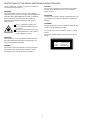
PROTECTION OF EYES FROM LASER BEAM DURING SERVICING
This set employs laser. Therefore, be sure to follow carefully the
instructions below when servicing.
CAUTION
Use of controls or adjustments or performance of procedures
other than those specified herein may result in hazardous
radiation exposure.
WARNING!
WHEN SERVICING, DO NOT APPROACH THE LASER EXIT
WITH THE EYE TOO CLOSELY. IN CASE IT IS NECESSARY TO
CONFIRM LASER BEAM EMISSION. BE SURE TO OBSERVE
FROM A DISTANCE OF MORE THAN 30cm FROM THE
SURFACE OF THE OBJECTIVE LENS ON THE OPTICAL
PICK-UP BLOCK.
ATTENTION
L'utilisation de commandes, réglages ou procédures autres que
ceux spécifiés peut entraîner une dangereuse exposition aux
radiations.
ADVARSEL!
Caution: Invisible laser radiation when
open and interlocks defeated avoid exposure to beam.
Advarsel:Usynling laserståling ved åbning,
når sikkerhedsafbrydere er ude af funktion.
Undgå udsættelse for stråling.
Usynlig laserståling ved åbning, når sikkerhedsafbrydereer ude
af funktion. Undgå udsættelse for stråling.
This Compact Disc player is classified as a CLASS 1 LASER
product.
The CLASS 1 LASER PRODUCT label is located on the rear
exterior.
VAROITUS!
Laiteen Käyttäminen muulla kuin tässä käyttöohjeessa mainitulla tavalla saattaa altistaa käyt-täjän turvallisuusluokan 1 ylittävälle näkymättömälle lasersäteilylle.
CLASS 1
KLASSE 1
LUOKAN 1
KLASS 1
VARNING!
Om apparaten används på annat sätt än vad som specificeras i
denna bruksanvising, kan användaren utsättas för osynling
laserstrålning, som överskrider gränsen för laserklass 1.
4
LASER PRODUCT
LASER PRODUKT
LASER LAITE
LASER APPARAT
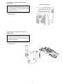
Precaution to replace Optical block
(KSS-213F)
Body or clothes electrostatic potential could ruin
laser diode in the optical block. Be sure ground
body and workbench, and use care the clothes
do not touch the diode.
1) After the connection, remove solder shown in
the right figure.
Precaution to replace Optical block
(KMS-260A)
Body or clothes electrostatic potential could ruin
laser diode in the optical block. Be sure ground
body and workbench, and use care the clothes
do not touch the diode.
1) After the connection, remove solder shown in
the right figure.
1 VEE
¡ TRK –
5
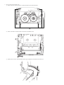
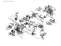
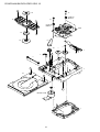
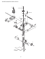
DISASSEMBLY INSTRUCTIONS
Disassembling Procedure
1.
Remove the seven screws (A BVT2+3-18*7) and remove the rear cabinet.
A
2.
Remove the two screws (B BVT2+3-12*2). Remove the MAIN C.B by pulling it upward.
B
3.
Remove the four screws (C BVT2+3-12*4).
C
6
4.
Open the deck lid. Release the two claws 1 and remove the PANEL DISP by pulling it upward.
1
1
1
1
5.
Close the deck lid. Raise the deck block from the rear.
6.
Remove the two screws (D BVT2+3-12*2). While raising the MAIN C.B., release the claws starting from 1 to 7, and remove
the MICOM/CD C.B.
D
6
1
7
4
5
2
3
7
7.
How to remove the COVER, FFC.
1) Remove the five screws (A BVT2+3-12*5) and remove the deck mechanism.
A
2) Remove the SPR T CASS from the rib and remove the BOX CASS.
3) Release the two claws of the COVER and FFC by pressing them in the direction of the arrow.
8
4) Raise the COVER and FFC in the direction of the arrow, and remove them.
8.
How to remove FL C.B.
1) Release the two claws 2 and pull the top of the FL C.B. to the front. The FL C.B. can be removed.
2
9.
2
How to remove the CD panel
1) Move the CAM SLIDE by 1 cm to the left.
2) Move down the DRIVE C.B. and establish the “un-chucking” status.
3) Press TRY, CD2 twice.
3
2
1
9
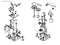
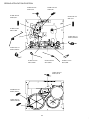
10. Remove the four screws A (S-SCREW, MD) and screws B
(BVTT +3-6).
Remove the four FFCs from the connector, and remove the
MD MECHANISM in the direction of the arrow. (Fig-1)
HEAD, OWH RF325-74A
D
C
A
C
B
PLATE ASSY,
SIDE L
A
B
PLATE, SIDE R
B
MD MECHANISM
FFC
Fig-3
13. Open the 7ZG-3 A2 in the direction of the arrow (a), remove
the BOSS by pressing it gently in the direction of the arrow
(b), and remove the 7ZG-3 A2 in the direction of the arrow
(c). (Fig-4)
FFC
BOSS
b
HLDR, SHLD BOT
b
Fig-1
a
11. Remove the HIDR and SHLD TOP in the direction of the
arrow. (Fig-2)
7ZG-3 A2
HLDR, SHLD TOP
c
Fig-4
Note During Assembling:
Rotate the gear fully in the direction of the arrow, and assemble
the main cam into the specified position as shown by the
illustration. (Fig-5)
Eject status
Fully in this direction
Fig-2
12. Remove the two screws C (VTT +2-4), and
remove the PLATE ASSY, SIDE L, PLATE, and
SIDE R in the direction of the arrow.
Remove the screw D (VW +1.7-5 w/o MFZN2C),
and remove the HEAD and OWH RF325-74A in
the direction of the arrow. (Fig-3)
Stud
Cover chassis
Fig-5
10
ELECTRICAL MAIN PARTS LIST
REF. NO
PART NO.
KANRI
NO.
DESCRIPTION
REF. NO
IC
87-020-454-010
87-A20-707-010
87-A20-708-010
87-A20-709-040
87-ZG9-601-010
IC,DM6851
C-IC,CXA2523AR
C-IC,CXD2652AR
C-IC,BD7910FV
C-IC,CXP81952
87-ZG9-605-110
87-ZG9-607-010
87-ZG9-608-010
87-ZG9-606-040
87-A20-755-080
C-IC,CXP81952-521R
C-IC,CXP81952M-523R
C-IC,CXP81952M-547R
C-IC,MN41V4400SJ-08
C-IC,AK93C45AF
87-A20-710-040
87-A20-711-040
87-A20-712-040
87-A20-698-080
87-A21-110-040
C-IC,S-8110AMP
C-IC,BA5970FP
C-IC,BA6417F
C-IC,AK4512VF
C-IC,AK4519VF
87-017-853-040
87-A20-797-040
87-A20-798-040
87-A20-714-040
87-A21-176-010
IC,NJM2100V
C-IC,NJU7221U30
C-IC,NJU7221U35
C-IC,NJM2370U33
C-IC,LC75710NE
87-A21-218-010
87-A21-211-010
8Z-CK3-620-010
87-A20-976-040
87-A21-159-040
IC,NJL64H380A
IC,BA178M06T
C-IC,LC875164A-****
C-IC,TC74HCT7007AF
C-IC,AK93C65AF(4K)
87-A21-281-080
87-A20-446-010
87-A20-459-010
87-A20-445-010
87-A21-213-010
IC,PST9125-T
C-IC,LA9241ML
C-IC,LC78622ED
IC,BA5936
IC,BA17808T
87-A21-212-010
87-A20-909-010
87-A21-116-040
87-A21-103-040
87-A20-419-010
IC,BA17805T
IC,LA4663
C-IC,BH3862FS
C-IC,MM1454XFBE
IC,TA2068N
87-A21-210-010
87-A20-913-010
IC,LC72121
IC,LA1837NL
89-318-155-080
87-026-447-080
87-026-223-080
89-109-521-080
87-026-610-080
TR,2SC1815 (0.4W)
TR,2SC1740S R
TR,DTC143TK
TR,2SA952 (0.6W)
TR,KTC3198GR
87-026-372-080
87-026-463-080
87-026-609-080
89-113-187-080
87-026-245-080
TR,RN1210
TR,2SA933S (0.3W)
TR,KTA1266GR
TR,2SA1318TU
TR,DTC114ES
89-406-555-080
87-026-464-080
89-327-143-080
87-A30-072-080
87-026-423-080
TR,2SD655 (0.5W)
TR,DTC114TS (0.3W)
TR,2SC2714 (0.1W)
C-TR,RT1P 144C
C-TR RN2305
89-115-884-080
89-341-164-080
87-026-412-080
CHIP -TRANSISTER 2SA1588Y
CHIP-TRANSISTOR,2SC4116 Y
C-TR RN1305
87-017-447-010
87-070-274-080
87-A40-657-080
87-A40-488-080
87-A40-534-080
87-017-090-080
87-070-136-080
PART NO.
KANRI
DESCRIPTION
NO.
87-020-465-080
DIODE,1SS133 (110MA)
87-A40-348-080
ZENER,MTZJ3.3A
87-A40-256-080
DIODE,RB441Q-40T-72
87-001-166-080
DIODE,1SS301
87-A40-412-040
C-DIODE,SB05-05CP
MAIN C.B
!
C100
C101
C102
C103
87-A90-505-080
87-018-205-080
87-018-205-080
87-018-205-080
87-018-205-080
FUSE
CAP,
CAP,
CAP,
CAP,
C104
C105
C106
C107
C108
87-010-892-090
87-010-196-080
87-010-196-080
87-015-997-090
87-010-260-080
CAPE6800-25SME
CHIP CAPACITOR,0.1-25
CHIP CAPACITOR,0.1-25
CAP,E 2200-16 SME
CAP, ELECT 47-25V
C109
C110
C111
C112
C113
87-010-198-080
87-010-198-080
87-010-198-080
87-010-198-080
87-010-124-090
CAP, CHIP 0.022
CAP, CHIP 0.022
CAP, CHIP 0.022
CAP, CHIP 0.022
CAP,E 4700-16
C114
C115
C116
C117
C118
87-010-196-080
87-015-997-090
87-010-196-080
87-A10-944-080
87-018-211-080
CHIP CAPACITOR,0.1-25
CAP,E 2200-16 SME
CHIP CAPACITOR,0.1-25
CAP,E 100-100 M SMG
CAP, CER 0.01-50
C120
C201
C202
C203
C204
87-010-196-080
87-010-406-080
87-010-406-080
87-010-406-080
87-010-406-080
CHIP
CAP,
CAP,
CAP,
CAP,
C209
C211
C212
C216
C217
87-010-197-080
87-010-260-080
87-010-379-080
87-016-279-080
87-016-279-080
CAP, CHIP 0.01 DM
CAP, ELECT 47-25V
CAP, ELECT 22-16V
CAP,E 1-50 BP
CAP,E 1-50 BP
C220
C221
C222
C223
C230
87-010-401-080
87-010-401-080
87-010-248-080
87-010-375-080
87-010-401-080
CAP, ELECT 1-50V
CAP, ELECT 1-50V
CAP, ELECT 220-10V
CAP,E 330-10 SME
CAP, ELECT 1-50V
C231
C234
C235
C236
C237
87-010-401-080
87-010-408-080
87-010-405-080
87-010-405-080
87-010-263-080
CAP,
CAP,
CAP,
CAP,
CAP,
ELECT
ELECT
ELECT
ELECT
ELECT
1-50V
47-50V
10-50V
10-50V
100-10V
C238
C239
C240
C241
C242
87-010-402-080
87-010-402-080
87-010-405-080
87-010-405-080
87-010-405-080
CAP,
CAP,
CAP,
CAP,
CAP,
ELECT
ELECT
ELECT
ELECT
ELECT
2.2-50V
2.2-50V
10-50V
10-50V
10-50V
C243
C244
C245
C246
C247
87-010-405-080
87-010-405-080
87-010-405-080
87-010-405-080
87-010-405-080
CAP,
CAP,
CAP,
CAP,
CAP,
ELECT
ELECT
ELECT
ELECT
ELECT
10-50V
10-50V
10-50V
10-50V
10-50V
C248
C249
C250
C251
C258
87-010-405-080
87-010-405-080
87-010-182-080
87-010-182-080
87-010-196-080
CAP, ELECT 10-50V
CAP, ELECT 10-50V
C-CAP,S 2200P-50 B
C-CAP,S 2200P-50 B
CHIP CAPACITOR,0.1-25
DIODE,GBU4DL
DIODE,1N4003 SEM
ZENER,MTZ J 13A
DIODE,1SS244
ZENER,MTZJ39A
C403
C404
C409
C410
C421
87-012-156-080
87-012-156-080
87-010-374-080
87-010-374-080
87-010-405-080
C-CAP,S 220P-50 CH
C-CAP,S 220P-50 CH
CAP, ELECT 47-10V
CAP, ELECT 47-10V
CAP, ELECT 10-50V
ZENER,HZS5B3
ZENER,MTZJ5.1B
C422
C429
87-010-405-080
87-010-405-080
CAP, ELECT 10-50V
CAP, ELECT 10-50V
TRANSISTOR
DIODE
11
CLAMP,TP00351-51
CERA-SOL 0.022
CERA-SOL 0.022
CERA-SOL 0.022
CERA-SOL 0.022
CAPACITOR,0.1-25
ELECT 22-50
ELECT 22-50
ELECT 22-50
ELECT 22-50
REF. NO
PART NO.
C430
C431
C432
C433
C434
KANRI
NO.
87-010-405-080
CAP,
87-010-184-080
CHIP
87-010-184-080
CHIP
87-010-406-080
CAP,
87-010-406-080
CAP,
DESCRIPTION
ELECT 10-50V
CAPACITOR 3300P(K)
CAPACITOR 3300P(K)
ELECT 22-50
ELECT 22-50
C787
C788
C789
C790
C791
KANRI
DESCRIPTION
NO.
87-012-280-080
CAP, U 3300P-50
87-012-280-080
CAP, U 3300P-50
87-012-275-080
C-CAP,U 1200P-50 B
87-012-275-080
C-CAP,U 1200P-50 B
87-010-405-080
CAP, ELECT 10-50V
C435
C436
C437
C438
C440
87-012-278-080
87-012-278-080
87-010-380-080
87-010-374-080
87-010-248-080
CAP,
CAP,
CAP,
CAP,
CAP,
CHIP SS 2200P BK
CHIP SS 2200P BK
ELECT 47-16V
ELECT 47-10V
ELECT 220-10V
C793
C794
C795
C796
C797
87-012-273-080
87-010-406-080
87-010-596-080
87-010-403-080
87-012-278-080
C-CAP,U 820P-50 B
CAP, ELECT 22-50
CAP, S 0.047-16
CAP, ELECT 3.3-50V
CAP, CHIP SS 2200P BK
C441
C442
C443
C451
C452
87-010-196-080
87-010-263-080
87-010-196-080
87-010-183-080
87-010-183-080
CHIP CAPACITOR,0.1-25
CAP, ELECT 100-10V
CHIP CAPACITOR,0.1-25
C-CAP,S 2700P-50 B
C-CAP,S 2700P-50 B
C798
C799
C812
C814
C820
87-012-278-080
87-010-829-080
87-012-286-080
87-012-286-080
87-010-408-080
CAP,
CAP,
CAP,
CAP,
CAP,
CHIP SS 2200P BK
U 0.047-16
U 0.01-25
U 0.01-25
ELECT 47-50V
C453
C454
C455
C457
C458
87-010-183-080
87-010-374-080
87-010-197-080
87-010-181-080
87-010-183-080
C-CAP,S 2700P-50 B
CAP, ELECT 47-10V
CAP, CHIP 0.01 DM
CAP,CHIP S 1800P
C-CAP,S 2700P-50 B
C821
C822
C823
C828
C829
87-012-286-080
87-012-286-080
87-012-286-080
87-010-196-080
87-010-196-080
CAP,
CAP,
CAP,
CHIP
CHIP
U 0.01-25
U 0.01-25
U 0.01-25
CAPACITOR,0.1-25
CAPACITOR,0.1-25
C459
C470
C471
C701
C702
87-010-374-080
87-010-406-080
87-010-406-080
87-010-260-080
87-010-404-080
CAP,
CAP,
CAP,
CAP,
CAP,
C959
C960
C961
CF801
CF802
87-010-196-080
87-010-196-080
87-012-174-080
87-008-261-010
87-008-261-010
CHIP CAPACITOR,0.1-25
CHIP CAPACITOR,0.1-25
CAP CHIP CERA SS 12P CHJ
FILTER, SFE10.7MA5-A
FILTER, SFE10.7MA5-A
C703
C704
C709
C710
C711
87-012-286-080
87-012-286-080
87-012-195-080
87-012-195-080
87-012-195-080
CAP, U 0.01-25
CAP, U 0.01-25
C-CAP,U 100P-50CH
C-CAP,U 100P-50CH
C-CAP,U 100P-50CH
CN101
CN201
CN202
CN203
CN204
87-099-408-010
87-A60-482-010
87-099-407-010
87-A60-423-010
87-099-556-010
CONN,8P EH V WHT
CONN,4P V 5267-04A-X
CONN,7P EH V WHT
CONN,14P V TOC-B
CONN,10P TUC-P10X-B1
C712
C713
C714
C717
C719
87-012-195-080
87-012-286-080
87-012-286-080
87-012-286-080
87-012-286-080
C-CAP,U 100P-50CH
CAP, U 0.01-25
CAP, U 0.01-25
CAP, U 0.01-25
CAP, U 0.01-25
CN205
CN206
CN209
CN351
!F101
87-099-556-010
87-099-670-010
81-754-629-010
87-A60-625-010
87-035-192-010
CONN,10P TUC-P10X-B1
CONN,9P TUC-P9X-B1
CONNECTOR, 2P
CONN,8P V 2MM JMT
FUSE, 4AT
C721
C722
C723
C725
C727
87-012-176-080
87-012-176-080
87-012-274-080
87-012-274-080
87-010-196-080
CAP 15P
CAP 15P
CHIP CAP,U 1000P-50B
CHIP CAP,U 1000P-50B
CHIP CAPACITOR,0.1-25
!F102
FFE801
JW102
JW105
L451
87-035-190-010
A8-6ZA-19C-170
87-008-372-080
87-008-372-080
87-007-342-010
FUSE, 2AT
6ZA-1 YFEENC
FILTER, EMI BL OIRNI
FILTER, EMI BL OIRNI
COIL,OSC 85K BIAS
C728
C729
C755
C756
C757
87-010-248-080
87-012-274-080
87-012-286-080
87-012-286-080
87-012-188-080
CAP, ELECT 220-10V
CHIP CAP,U 1000P-50B
CAP, U 0.01-25
CAP, U 0.01-25
C-CAP,U 47P-50 CH
L771
L772
L781
L832
L981
87-A50-266-010
87-A91-308-010
87-005-847-080
87-005-847-080
87-NF4-650-010
COIL,FM DET-2N(TOK)
FLTR,PCFAZH- 450T (TOK)
COIL,2.2UH(CECS)
COIL,2.2UH(CECS)
COIL,AM PACK 4N(TOK)
C758
C760
C761
C763
C764
87-012-167-080
87-010-196-080
87-010-196-080
87-010-829-080
87-012-337-080
C-CAP,U 5P-50 CH
CHIP CAPACITOR,0.1-25
CHIP CAPACITOR,0.1-25
CAP, U 0.047-16
C-CAP,U 56P-50 CH
S101
VR770
X721
87-A91-024-080
87-024-432-080
87-A70-061-010
SW,TACT KSH0611BT
SFR,4.7K RH063EC
VIB,XTAL 4.500MHZ CSA-309
C765
C766
C769
C770
C771
87-012-286-080
87-012-286-080
87-010-408-080
87-010-829-080
87-010-265-080
CAP,
CAP,
CAP,
CAP,
CAP,
U 0.01-25
U 0.01-25
ELECT 47-50V
U 0.047-16
ELECT 33-16V
C772
C773
C774
C775
C776
87-010-829-080
87-010-196-080
87-010-263-080
87-010-404-080
87-012-286-080
CAP,
CHIP
CAP,
CAP,
CAP,
U 0.047-16
CAPACITOR,0.1-25
ELECT 100-10V
ELECT 4.7-50V
U 0.01-25
C777
C778
C779
C780
C781
87-010-400-080
87-010-401-080
87-010-401-080
87-010-196-080
87-010-405-080
CAP,
CAP,
CAP,
CHIP
CAP,
ELECT 0.47-50V
ELECT 1-50V
ELECT 1-50V
CAPACITOR,0.1-25
ELECT 10-50V
C782
C783
C784
C785
C786
87-010-405-080
87-012-286-080
87-012-286-080
87-010-805-080
87-010-805-080
CAP,
CAP,
CAP,
CAP,
CAP,
ELECT 10-50V
U 0.01-25
U 0.01-25
S 1-16
S 1-16
ELECT
ELECT
ELECT
ELECT
ELECT
REF. NO
47-10V
22-50
22-50
47-25V
4.7-50V
PART NO.
MICOM/CD C.B
12
C118
C119
C120
C121
C122
87-010-190-080
87-018-205-080
87-018-205-080
87-018-205-080
87-018-205-080
S CHIP F 0.01
CAP, CERA-SOL
CAP, CERA-SOL
CAP, CERA-SOL
CAP, CERA-SOL
C123
C124
C125
C301
C302
87-A10-011-090
87-010-236-080
87-010-403-080
87-012-368-080
87-010-190-080
CAP,E 2200-25 SMG
CAP,E 1000-10 SME
CAP, ELECT 3.3-50V
C-CAP,S 0.1-50 F
S CHIP F 0.01
C303
C304
C305
C306
C307
87-012-150-080
87-012-150-080
87-010-320-080
87-012-149-080
87-010-312-080
C-CAP,S 20P-50
C-CAP,S 20P-50
CHIP CAP 68P
C-CAP,S 30P-50
C-CAP,S 15P-50
C308
C309
C310
C311
87-010-379-080
87-012-368-080
87-A10-908-010
87-012-369-080
CAP, ELECT 22-16V
C-CAP,S 0.1-50 F
CAP,DL 0.47F-5.5 Z FYD
C-CAP,S 0.047-50F
0.022
0.022
0.022
0.022
CH
CH
CH
CH
REF. NO
PART NO.
C315
C316
C317
C321
C322
KANRI
DESCRIPTION
NO.
87-010-248-080
CAP, ELECT 220-10V
87-010-178-080
CHIP CAP 1000P
87-012-368-080
C-CAP,S 0.1-50 F
87-012-153-080
C-CAP,S 120P-50 CH
87-012-153-080
C-CAP,S 120P-50 CH
REF. NO
CN302
CN303
CN304
CN306
CN308
KANRI
DESCRIPTION
NO.
87-099-668-010
CONN,9P TUC-P 9P-B1
87-099-567-010
CONN,10P TUC-P10P-B1
87-A60-422-010
CONN,8P V TOC-B
87-099-749-010
CONN,9P V 9604SC
87-A60-845-010
CONN,6P TRC-X06P-A2
C323
C324
C325
C326
C327
87-012-153-080
87-012-368-080
87-012-368-080
87-010-375-080
87-010-379-080
C-CAP,S 120P-50 CH
C-CAP,S 0.1-50 F
C-CAP,S 0.1-50 F
CAP, ELECT 330-10V
CAP, ELECT 22-16V
CN309
CN312
CN500
CN501
CN502
87-A60-920-010
87-A60-685-010
87-A60-424-010
87-A60-061-010
87-A60-062-010
CONN,8P TRC-X08P-A2
CONN,4P H WHT EH
CONN,16P V TOC-B
CONN,06P V 9604S-06C
CONN,05P V 9604S-05C
C328
C329
C330
C331
C355
87-010-247-080
87-012-369-080
87-010-406-080
87-010-406-080
87-010-190-080
CAP, ELECT 100-50V
C-CAP,S 0.047-50F
CAP, ELECT 22-50
CAP, ELECT 22-50
S CHIP F 0.01
CNA301
CNA401
J201
JW213
JW214
8Z-CK3-619-010
8Z-CK3-616-010
87-A60-420-010
87-003-219-010
87-003-219-010
CONN ASSY,7P V WHT H.P
CONN ASSY,9P V WHT CASS
JACK,3.5 ST (MSC)
FERRITE BEAD-BLO2RN2
FERRITE BEAD-BLO2RN2
C357
C500
C501
C502
C503
87-010-405-080
87-010-382-080
87-010-401-080
87-010-545-080
87-012-157-080
CAP, ELECT 10-50V
CAP, ELECT 22-25V
CAP, ELECT 1-50V
CAP, ELECT 0.22-50V
C-CAP,S 330P-50 CH
JW238
JW284
JW285
JW286
JW238
87-003-149-080
87-003-149-080
87-003-149-080
87-003-149-080
87-003-149-080
COIL,47UH
COIL,47UH
COIL,47UH
COIL,47UH
COIL,47UH
C510
C511
C512
C514
C515
87-010-374-080
87-010-197-080
87-010-248-080
87-010-544-080
87-010-198-080
CAP,
CAP,
CAP,
CAP,
CAP,
ELECT 47-10V
CHIP 0.01 DM
ELECT 220-10V
ELECT 0.1-50V
CHIP 0.022
SFR501
X301
X302
X501
87-024-176-080
87-030-273-010
87-A70-070-080
87-A70-166-080
SEMI-FIXED RESISTOR, 100K
VIB,XTAL 32.768K5PPM
VIB,CER 5.76MHZ CRHF
VIB,CER 16.93MHZ MXZ140 0.3%
C516
C518
C519
C520
C521
87-010-263-080
87-010-405-080
87-010-263-080
87-010-197-080
87-010-374-080
CAP,
CAP,
CAP,
CAP,
CAP,
ELECT 100-10V
ELECT 10-50V
ELECT 100-10V
CHIP 0.01 DM
ELECT 47-10V
KEY C.B
C523
C525
C526
C527
C529
87-010-176-080
87-010-186-080
87-010-400-080
87-012-156-080
87-012-140-080
C-CAP,S 680P-50 SL
CAP,CHIP 4700P
CAP, ELECT 0.47-50V
C-CAP,S 220P-50 CH
CAP 470P
C318
C319
C320
C370
C371
87-018-209-080
87-018-209-080
87-010-374-080
87-018-209-080
87-018-209-080
CAP,
CAP,
CAP,
CAP,
CAP,
C530
C531
C532
C533
C534
87-010-374-080
87-010-401-080
87-010-184-080
87-010-196-080
87-010-221-080
CAP,
CAP,
CHIP
CHIP
CAP,
CN310
CN311
D306
D307
D308
87-A60-846-010
87-A60-921-010
87-A40-664-080
87-A40-664-080
87-A40-664-080
CONN,6P TRC-X06X-A2
CONN,8P TRC-X08X-A2
LED,SEL6214S RED
LED,SEL6214S RED
LED,SEL6214S RED
C545
C549
C552
C554
C555
87-010-404-080
87-010-314-080
87-010-196-080
87-012-154-080
87-010-196-080
CAP, ELECT 4.7-50V
C-CAP,S 22P-50V
CHIP CAPACITOR,0.1-25
C-CAP,S 150P-50 CH
CHIP CAPACITOR,0.1-25
D309
D310
S301
S302
S303
87-A40-664-080
87-A40-664-080
87-A91-024-080
87-A91-024-080
87-A91-024-080
LED,SEL6214S RED
LED,SEL6214S RED
SW,TACT KSH0611BT
SW,TACT KSH0611BT
SW,TACT KSH0611BT
C556
C557
C558
C559
C560
87-010-248-080
87-010-405-080
87-010-405-080
87-010-196-080
87-010-196-080
CAP,
CAP,
CAP,
CHIP
CHIP
S304
S305
S306
S307
S308
87-A91-024-080
87-A91-024-080
87-A91-024-080
87-A91-024-080
87-A91-024-080
SW,TACT
SW,TACT
SW,TACT
SW,TACT
SW,TACT
KSH0611BT
KSH0611BT
KSH0611BT
KSH0611BT
KSH0611BT
C561
C562
C563
C564
C565
87-010-263-080
87-010-314-080
87-010-314-080
87-010-404-080
87-010-196-080
CAP, ELECT 100-10V
C-CAP,S 22P-50V
C-CAP,S 22P-50V
CAP, ELECT 4.7-50V
CHIP CAPACITOR,0.1-25
S309
S310
S311
S312
S313
87-A91-024-080
87-A91-024-080
87-A91-024-080
87-A91-024-080
87-A91-024-080
SW,TACT
SW,TACT
SW,TACT
SW,TACT
SW,TACT
KSH0611BT
KSH0611BT
KSH0611BT
KSH0611BT
KSH0611BT
C566
C570
C571
C572
C573
87-010-315-080
87-010-196-080
87-010-196-080
87-010-196-080
87-010-196-080
C-CAP,S 27P-50 CH
CHIP CAPACITOR,0.1-25
CHIP CAPACITOR,0.1-25
CHIP CAPACITOR,0.1-25
CHIP CAPACITOR,0.1-25
S314
S315
S316
S317
S318
87-A91-024-080
87-A91-024-080
87-A91-024-080
87-A91-024-080
87-A91-024-080
SW,TACT
SW,TACT
SW,TACT
SW,TACT
SW,TACT
KSH0611BT
KSH0611BT
KSH0611BT
KSH0611BT
KSH0611BT
C574
C575
C576
C577
C578
87-010-405-080
87-010-405-080
87-010-196-080
87-A10-096-080
87-010-196-080
CAP, ELECT 10-50V
CAP, ELECT 10-50V
CHIP CAPACITOR,0.1-25
CAP,E 1000-16
CHIP CAPACITOR,0.1-25
S319
S320
S321
S322
S323
87-A91-024-080
87-A91-024-080
87-A91-024-080
87-A91-024-080
87-A91-024-080
SW,TACT
SW,TACT
SW,TACT
SW,TACT
SW,TACT
KSH0611BT
KSH0611BT
KSH0611BT
KSH0611BT
KSH0611BT
SW301
87-A90-646-010
SW,RTRY 3-2-1 RE0131
C579
C585
C588
C589
CN301
87-012-156-080
87-018-127-080
87-010-196-080
87-010-196-080
87-099-567-010
C-CAP,S 220P-50 CH
CAP, CER 470P-50V
CHIP CAPACITOR,0.1-25
CHIP CAPACITOR,0.1-25
CONN,10P TUC-P10P-B1
87-012-368-080
87-012-368-080
87-012-149-080
87-012-369-080
C-CAP,S
C-CAP,S
C-CAP,S
C-CAP,S
ELECT 47-10V
ELECT 1-50V
CAPACITOR 3300P(K)
CAPACITOR,0.1-25
ELECT 470-10V
ELECT 220-10V
ELECT 10-50V
ELECT 10-50V
CAPACITOR,0.1-25
CAPACITOR,0.1-25
PART NO.
CERA-SOL 0.1
CERA-SOL 0.1
ELECT 47-10V
CERA-SOL 0.1
CERA-SOL 0.1
FL C.B
C332
C333
C334
C335
13
0.1-50 F
0.1-50 F
30P-50 CH
0.047-50F
REF. NO
PART NO.
C339
C340
C341
C342
C343
KANRI
NO.
87-012-156-080
C-CAP,S
87-012-156-080
C-CAP,S
87-012-156-080
C-CAP,S
87-012-156-080
C-CAP,S
87-012-156-080
C-CAP,S
DESCRIPTION
REF. NO
PART NO.
220P-50
220P-50
220P-50
220P-50
220P-50
CH
CH
CH
CH
CH
C218
C219
C220
C221
C222
KANRI
DESCRIPTION
NO.
87-012-172-080
CAPACITOR CHIP U 10P CH
87-016-296-080
C-CAP,TN 22-4SV(A)
87-010-662-080
C-CAP,E 22-6.3
87-010-831-080
C-CAP,U,0.1-16F
87-016-444-080
C-CAP,TN 47-10 F95E
C344
C345
C346
C347
C348
87-012-156-080
87-012-156-080
87-012-156-080
87-012-156-080
87-012-156-080
C-CAP,S
C-CAP,S
C-CAP,S
C-CAP,S
C-CAP,S
220P-50
220P-50
220P-50
220P-50
220P-50
CH
CH
CH
CH
CH
C223
C224
C225
C226
C227
87-010-831-080
87-A10-685-080
87-010-831-080
87-010-831-080
87-012-274-080
C-CAP,U,0.1-16F
C-CAP,S 470P-100 J CH
C-CAP,U,0.1-16F
C-CAP,U,0.1-16F
CHIP CAP,U 1000P-50B
C349
C350
C351
C352
C353
87-012-156-080
87-012-156-080
87-012-156-080
87-012-156-080
87-012-156-080
C-CAP,S
C-CAP,S
C-CAP,S
C-CAP,S
C-CAP,S
220P-50
220P-50
220P-50
220P-50
220P-50
CH
CH
CH
CH
CH
C228
C229
C232
C233
C236
87-012-274-080
87-012-274-080
87-012-274-080
87-012-274-080
87-010-831-080
CHIP CAP,U 1000P-50B
CHIP CAP,U 1000P-50B
CHIP CAP,U 1000P-50B
CHIP CAP,U 1000P-50B
C-CAP,U,0.1-16F
C354
CN307
FL301
87-012-156-080
87-A60-078-010
8Z-CK3-622-010
C-CAP,S 220P-50 CH
CONN,09P H 9604S-09F
FL,16-ST-32GNK
C300
C301
C302
C305
C307
87-010-831-080
87-010-831-080
87-010-831-080
87-016-462-080
87-010-831-080
C-CAP,U,0.1-16F
C-CAP,U,0.1-16F
C-CAP,U,0.1-16F
C-CAP,S 1-16 F
C-CAP,U,0.1-16F
8Z-CK3-617-010
87-A91-276-080
87-049-784-010
8Z-CK3-626-010
8Z-NF8-662-010
CONN ASSY,8P V WHT POWER MAIN
FUSE,125MA 125V F 251
AC JACK E
PT,ZCK-3 E
PT,SUB ZNF-8(E)
C308
C311
C312
C321
C322
87-010-831-080
87-010-662-080
87-012-195-080
87-012-274-080
87-012-274-080
C-CAP,U,0.1-16F
C-CAP,E 22-6.3
C-CAP,U 100P-50CH
CHIP CAP,U 1000P-50B
CHIP CAP,U 1000P-50B
C323
C324
C325
C400
C401
87-012-274-080
87-012-274-080
87-012-274-080
87-010-831-080
87-010-831-080
CHIP CAP,U 1000P-50B
CHIP CAP,U 1000P-50B
CHIP CAP,U 1000P-50B
C-CAP,U,0.1-16F
C-CAP,U,0.1-16F
C402
C403
C404
C405
C406
87-010-831-080
87-010-831-080
87-010-831-080
87-010-661-080
87-010-779-080
C-CAP,U,0.1-16F
C-CAP,U,0.1-16F
C-CAP,U,0.1-16F
C-CAP,E 10-16
C-CAP,E 100-6.3
C407
C408
C411
C412
C413
87-012-197-080
87-012-197-080
87-012-271-080
87-012-271-080
87-012-197-080
C-CAP,U 150P-50 CH
C-CAP,U 150P-50 CH
CAP, U 560P-50
CAP, U 560P-50
C-CAP,U 150P-50 CH
C414
C417
C418
C423
C424
87-012-197-080
87-012-268-080
87-012-268-080
87-012-286-080
87-012-286-080
C-CAP,U 150P-50 CH
C-CAP,U 330P-50 B
C-CAP,U 330P-50 B
CAP, U 0.01-25
CAP, U 0.01-25
C429
C430
C431
C434
C501
87-012-286-080
87-012-286-080
87-010-779-080
87-010-831-080
87-010-831-080
CAP, U 0.01-25
CAP, U 0.01-25
C-CAP,E 100-6.3
C-CAP,U,0.1-16F
C-CAP,U,0.1-16F
C502
C503
C504
C505
C506
87-010-831-080
87-010-662-080
87-010-831-080
87-010-662-080
87-010-831-080
C-CAP,U,0.1-16F
C-CAP,E 22-6.3
C-CAP,U,0.1-16F
C-CAP,E 22-6.3
C-CAP,U,0.1-16F
C507
C508
C509
C510
C511
87-010-661-080
87-010-831-080
87-010-662-080
87-010-831-080
87-010-661-080
C-CAP,E 10-16
C-CAP,U,0.1-16F
C-CAP,E 22-6.3
C-CAP,U,0.1-16F
C-CAP,E 10-16
C513
C514
C515
C516
C517
87-010-661-080
87-010-661-080
87-012-337-080
87-012-337-080
87-012-278-080
C-CAP,E
C-CAP,E
C-CAP,U
C-CAP,U
C-CAP,U
C518
C519
C520
C521
C522
87-012-278-080
87-010-831-080
87-010-661-080
87-010-831-080
87-010-661-080
C-CAP,U 2200P-50 B
C-CAP,U,0.1-16F
C-CAP,E 10-16
C-CAP,U,0.1-16F
C-CAP,E 10-16
POWER C.B
CNA100
!ICF100
!J101
!PT101
!PT102
MD MAIN C.B
C100
C101
C102
C103
C104
87-016-296-080
87-016-296-080
87-012-286-080
87-010-787-080
87-010-662-080
C-CAP,TN 22-4SV(A)
C-CAP,TN 22-4SV(A)
CAP, U 0.01-25
CAP, U 0.022-25
C-CAP,E 22-6.3
C105
C106
C107
C108
C109
87-010-831-080
87-016-462-080
87-012-195-080
87-012-274-080
87-016-436-080
C-CAP,U,0.1-16F
C-CAP,S 1-16 F
C-CAP,U 100P-50CH
CHIP CAP,U 1000P-50B
C-CAP,TN 47-4(B2)
C111
C112
C113
C114
C115
87-016-296-080
87-012-286-080
87-012-284-080
87-010-828-080
87-A10-369-080
C-CAP,TN 22-4SV(A)
CAP, U 0.01-25
CAP, U 6800P-50
CHIP CAPACITOR,U 0.033-25F
C-CAP,S 0.47-16 K B
C116
C117
C118
C119
C120
87-012-282-080
87-016-462-080
87-012-282-080
87-016-491-080
87-010-787-080
CAP, U 4700P-50
C-CAP,S 1-16 F
CAP, U 4700P-50
C-CAP,S 0.22-16 FZ
CAP, U 0.022-25
C121
C122
C123
C124
C125
87-012-286-080
87-010-829-080
87-012-286-080
87-010-662-080
87-010-662-080
CAP, U 0.01-25
CAP, U 0.047-16
CAP, U 0.01-25
C-CAP,E 22-6.3
C-CAP,E 22-6.3
C126
C201
C202
C203
C204
87-010-831-080
87-010-831-080
87-010-831-080
87-010-785-080
87-016-461-080
C-CAP,U,0.1-16F
C-CAP,U,0.1-16F
C-CAP,U,0.1-16F
C-CAP,U0.015-25BK
C-CAP,S 0.47-16F
C205
C206
C207
C208
C209
87-010-831-080
87-012-270-080
87-016-461-080
87-012-286-080
87-010-831-080
C-CAP,U,0.1-16F
CAP, U 470P-50
C-CAP,S 0.47-16F
CAP, U 0.01-25
C-CAP,U,0.1-16F
C210
C211
C212
C213
C214
87-012-172-080
87-012-172-080
87-012-195-080
87-010-662-080
87-012-274-080
CAPACITOR CHIP U 10P CH
CAPACITOR CHIP U 10P CH
C-CAP,U 100P-50CH
C-CAP,E 22-6.3
CHIP CAP,U 1000P-50B
C217
87-012-188-080
C-CAP,U 47P-50 CH
14
10-16
10-16
56P-50 CH
56P-50 CH
2200P-50 B
TRANSISTOR ILLUSTRATION
REF. NO
PART NO.
C523
C524
C525
C526
C527
KANRI
DESCRIPTION
NO.
87-010-662-080
C-CAP,E 22-6.3
87-010-662-080
C-CAP,E 22-6.3
87-012-274-080
CHIP CAP,U 1000P-50B
87-012-274-080
CHIP CAP,U 1000P-50B
87-010-661-080
C-CAP,E 10-16
REF. NO
C528
C530
C531
C600
C601
87-010-661-080
87-010-831-080
87-010-831-080
87-010-662-080
87-010-779-080
C-CAP,E 10-16
C-CAP,U,0.1-16F
C-CAP,U,0.1-16F
C-CAP,E 22-6.3
C-CAP,E 100-6.3
C602
C603
C604
C605
C607
87-010-779-080
87-010-662-080
87-010-779-080
87-012-286-080
87-010-831-080
C-CAP,E 100-6.3
C-CAP,E 22-6.3
C-CAP,E 100-6.3
CAP, U 0.01-25
C-CAP,U,0.1-16F
C608
CN400
CN401
FB501
L100
87-010-831-080
87-A60-027-080
87-A60-062-010
87-A90-828-080
87-A50-117-080
C-CAP,U,0.1-16F
C-CONN,8P H WHT
CONN,05P V 9604S-05C
C-F-BEAD, BK1608LM182
C-COIL,10UHLQH3C
L101
L102
L103
L201
L202
87-A50-012-080
87-A50-117-080
87-A50-117-080
87-A50-117-080
87-A50-117-080
C-COIL,100UH LQH3C
C-COIL,10UHLQH3C
C-COIL,10UHLQH3C
C-COIL,10UHLQH3C
C-COIL,10UHLQH3C
L203
L301
L501
L502
L503
87-A50-116-080
87-A50-117-080
87-A50-116-080
87-A50-116-080
87-A50-116-080
C-COIL,4.7UHLQH3C
C-COIL,10UHLQH3C
C-COIL,4.7UHLQH3C
C-COIL,4.7UHLQH3C
C-COIL,4.7UHLQH3C
L504
L505
L611
L612
L613
87-005-774-080
87-005-774-080
87-A50-163-080
87-005-512-080
87-005-512-080
C-COIL,4BLH
C-COIL,4BLH
C-COIL,ZBFS5101-PT
C-COIL,BLM21A05
C-COIL,BLM21A05
L614
L615
L616
R423
R424
87-A50-163-080
87-A90-034-080
87-A50-163-080
87-025-564-080
87-025-564-080
C-COIL,ZBFS5101-PT
C-FLTR,EMI BLM41P750
C-COIL,ZBFS5101-PT
C-RES,U M/F 47K D
C-RES,U M/F 47K D
R425
R426
X200
X301
87-022-583-080
87-022-583-080
87-A70-105-080
87-A70-100-080
C-RES,U M/F 12K D
C-RES,U M/F 12K D
C-VIB,XTAL 22.5792MHZ SMD-49
C-VIB,CER 12.0MHZ PBRC-BR-A
PART NO.
KANRI
NO.
C
DESCRIPTION
LOAD C.B
FC451
M450
SW451
SW452
87-ZG9-604-010
87-A90-672-010
87-A90-673-010
87-A90-117-010
FF-CABLE,5P 1.25 100MM
MOT,M25E-4
SW,MICRO ESE11SH1C
SW,PUSH 1-1-1 MPU1037MLB0
87-ZG9-603-010
87-A90-413-010
87-A90-616-010
87-A90-611-010
87-A90-612-010
FF-CABLE,8P 1.0 120MM
MOT,FF-110PH 9
MOT,FF-N30VA
SW,PUSH 3-2-2 MPU20300MLB0
SW,PUSH 2-1-1 MPU10371MLB1
MECHA C.B
FC400
M400
M401
SW400
SW401
B
ECB
2SA933S
2SC1740S
DTC114ES
DTC114TS
E
2SA1588
2SC2714
2SC4116
DTC143TK
ECB
RN1210
RN1305
RN2305
RT1P144C
CD MOTOR C.B
CON1
M1
SW1
SW2
87-099-210-010
87-045-305-010
87-036-110-010
87-036-110-010
CONN,5P 6216 H
MOTOR, RF-500TB DC-5V (2MA)
PUSH SWITCH
PUSH SWITCH
87-045-358-019
87-045-356-019
87-A90-042-019
MOT,RF-310TA 43
MOT,RF-310TA 30
SW,LEAF MSW 17310 MVPO
SFR1
SOL1
SW2
SW3
SW5
87-024-581-010
82-ZM1-618-310
87-A90-248-019
87-A90-248-019
87-A90-248-019
SFR,3.3K DIA 6H KOA
SOL ASSY,27
SW,MICRO ESE11SH2CXQ
SW,MICRO ESE11SH2CXQ
SW,MICRO ESE11SH2CXQ
SW6
87-A90-248-019
SW,MICRO ESE11SH2CXQ
DRIVE C.B
M20
M21
SW1
DECK C.B
RELAY-1 C.B
CNA400
8Z-CK3-615-010
CONN ASSY,8P V WHT DECK
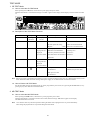
• Regarding connectors, they are not stocked as they are not the initial order items.
The connectors are available after they are supplied from connector manufacturers upon the order is received.
CHIP RESISTOR PART CODE
Chip Resistor Part Coding
8 8
A
Figure
Resistor Code
Value of resistor
Chip resistor
L
W
t
:A
Resistor Code : A
1.0
0.5
0.35
104
Dimensions (mm)
Wattage
1/16W
Type
1005
Tolerance
5%
Symbol
CJ
1/16W
1/10W
1608
2125
5%
5%
CJ
CJ
1/8W
3216
5%
CJ
Form
L
t
W
15
1.6
0.8
0.45
108
2
1.25
0.45
118
3.2
1.6
0.55
128
16
2SA952
2SA1318
2SC1815
2SD655
KTA1266
KTC3198
FL (16-ST-32GNK) GRID ASSIGNMENT/ANODE CONNECTION
17
18
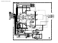
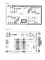
BLOCK DIAGRAM-1 (MAIN)
19
20
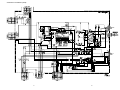
BLOCK DIAGRAM-2 (SYSTEM CONTROL)
21
22
BLOCK DIAGRAM-3 (MD)
23
24
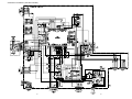
WIRING-1 (MAIN)
1
2
3
4
5
6
7
8
9
10
11
12
A
B
C
D
E
F
G
H
I
J
K
25
26
13
14
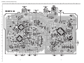
SCHEMATIC DIAGRAM-1 (TUNER)
27
28
SCHEMATIC DIAGRAM-2 (DECK)
29
30
SCHEMATIC DIAGRAM-3 (MAIN)
31
32
WIRING-2 (SYSTEM CONTROL/CD)
1
2
3
4
5
6
7
8
9
10
11
12
A
B
C
D
E
F
G
H
I
J
K
33
34
13
14
SCHEMATIC DIAGRAM-4 (SYSTEM CONTROL)
35
36
WIRING-3 (FL/KEY)
1
2
3
4
5
6
7
8
9
10
11
12
A
B
C
D
E
F
G
H
I
J
K
37
38
13
14
SCHEMATIC DIAGRAM-5 (CD)
39
40
WIRING-4 (POWER)
1
2
3
4
5
6
7
8
9
10
11
12
A
B
C
D
E
F
G
H
I
J
K
41
42
13
14
SCHEMATIC DIAGRAM-6 (FL/KEY/POWER)
43
44
WIRING-5 (MD)
7
6
5
4
3
2
(COMPONENT SIDE)
TO/FROM MAIN C.B
CN203
45
1
1
A
A
B
B
C
C
D
D
E
E
F
F
G
G
H
H
I
I
J
J
2
3
4
5
6
(CONDUCTOR SIDE)
TO/FROM MICOM/CD C.B
CN304
46
7
SCHEMATIC DIAGRAM-7 (MD)
47
48
WIRING-6 (MECHANISM)
1
2
3
4
5
6
7
8
9
10
11
12
A
B
C
D
E
F
G
H
I
J
TO MICOM/CD C.B
CN500
K
49
50
13
14
TEST MODE
1. CD TEST Mode
1-1. How to Active the CD TEST Mode
While pressing the CD 2 button, connect the AC power plug to the power outlet.
After the TEST mode is activated, the message “CD TEST” appears on the display and all displays on the FL tubes are turned
on.
1-2. Description of the TEST Mode Functions
Mode
Operating Control
FL Display
Start mode
Activating the
All displays
test mode
are ON
9
TOC READING
Search mode
Play mode
CD 2
Operation
Function
Continuous focus search
APC circuit check
PU lens repeats full swing
Laser current measurement
Repeats
Focus error waveform check
* Note
Track No. and
Normal playback
Focus servo
playing time are
When the TOC READING
Tracking servo
displayed
cannot be performed, the same
CLV servo
Eye catch rotates
movement as the search mode is
Sled servo
performed
Traverse mode
;
Track No. and
Playback pause state
Tracking servo OFF
playing time are
displayed
Eye catch flashes
Sled mode
6
5
All displays are ON Pick up moves inner
circumference
Sled servo
Mechanism operation check
Pick up moves outer
circumference
Note: If the focus search is continued for ten minutes or longer, CD stops working because driver IC is heated and protection circuit
works. Restart the TEST mode after turning off the power supply to cool down the heat for about ten minutes.
1-3. How to Exit the CD TEST Mode
Exit the CD TEST mode by disconnecting the AC power plug from the power outlet, or by pressing the POWER button, or by
pressing any key other than the CD function button.
2. MD TEST Mode
2-1. How to Active the MD TEST Mode
While pressing the MD 2 button, connect the AC power plug to the power outlet.
After the TEST mode is activated, waits about one second, then the message “MD TEST” appears on the display.
The MD TEST mode can be used.
Note: 1. If a machine shows any abnormal operations during the TEST mode, unplug the main AC power immediately.
2. Recording and played back are not possible during the TEST mode.
51
2-2. How to Exit the MD TEST Mode
1) Eject the disc by pressing the “MD EJECT” button or the “VOLUME UP” button.
2) Disconnect the AC power plug from the power outlet, or press the “POWER” button.
2-3. Operation Check Mode
1) Checking activation of the TEST mode
Playback system audio circuit can be checked as follows.
• Circuit that can be checked ............. DAC, LINE AMP, HEADPHONE AMP
• Output level ..................................... 1kHz, -12dB
2) Checking status of the switches
The ON/OFF status of the respective switches on the machine and mechanism can be checked on the LCD display.
Switch Name
Switch Status
REC PROTECT
When the WRITE PROTECT tab of a disc is closed
Display
ROCK frame is ON
Disc in use
Disc for record and
playback
REFRECT
When high reflection disc (CD) is used
POP frame is ON
Disc for playback only
INNER
When pick up is in the inner most circumference
JAZZ frame is ON
—
(LIMIT SW ON)
3) Detecting status of mechanism
Status of mechanism
FL Display
Unloading status
PRGM is turned on
Loading status
RANDOM is turned on
Status that the over-write-head has moved down
PRG and RANDOM are turned on
2-4. How to Switch the Mode to the Servo Standby Mode
After the MD TEST mode has started up, the mode is switched to the servo standby mode when the 9 button is pressed,
and the message “ALL SV OFF” appears on the display. The machine can enter any other modes from the “ALL SV OFF”
mode. The machine can return from any other modes to the “ALL SV OFF” mode by pressing the 9 button.
2-5. Checking the Sled Movement
1) The laser pickup moves to the outer circumference when the 6 button is pressed while the machine is in the “ALL SV
OFF” status. Then, the message “T. SLED RVS” appears on the display.
2) The laser pickup moves to the inner circumference when the 5 button is pressed while the machine is in the “ALL SV
OFF” status. Then, the message “T. SLED RVS” appears on the display.
2-6. Checking Laser Output
1) Every passing of the “TIMER/CLOCK” button in the “ALL SV OFF” state changes output of laser power.
Laser can be operated in the following order: OFF ™ LASER READ ™ LASER 1/2 ™LASER WRITE ™ OFF.
The FL displays are as shown.
Mode
FL Display
OFF
ALL SV OFF
LASER READ
LASER READ
+ T-BASS level 1
LASER 1/2 WRITE
LASER 1/2
+ T-BASS level 2
LASER WRITE
LASER WRITE + T-BASS level 3
2) When all checks are completed, press the 9 button to show the message “ALL SV OFF” on the display.
2-7. Operation Check of OWH (Over-write-head)
The OWH can moves up or down when the “VOLUME UP” button or “VOLUME DOWN” button is pressed while the machine
is in the loading status.
“VOLUME UP” button ............................ OWH moves up.
“VOLUME DOWN” button .................... OWH moves down.
Note: Don’t move down the OWH when the high reflection disc (CD) is used.
52
2-8. Checking Servo Operation
• Checking the focus search and spindle kick: 1
1) When the MD 2 button is pressed while the machine is in the “ALL SV OFF” status without inserting a disc, focus search
and spindle kick are performed continuously.
The message “FOCUS SRCH” appears on the display.
2) After the check is completed, press the 9 button to show the message “ALL SV OFF” on the display.
• Checking the focus search and spindle kick: 2
1) When the “TUNER/BAND” button is pressed while the machine is in the “ALL SV OFF” status with a disk inserted or
without inserted, focus search and spindle kick are performed continuously .
The message “FOCUS CHECK” appears on the display.
The S curve characteristics can be checked when a disc is inserted.
2) After the check is completed, press the 9 button to show the message “ALL SV OFF” on the display.
•
1)
2)
3)
Checking the focus servo
Insert a test disc.
Move the laser pickup to the center of a disc using the 6 button and 5 button.
Press the TAPE 1 2 button, and set the servo mode of the inserted disc as follows.
MO disk (MO) ................................... Select the “SELECT GRV” display.
PIT disk (CD) .................................... Select the “SELECT PIT” display.
4) Press the MD 2 button.
When the focus servo has no problem, the messages “FOCUS SRCH” appears then “FOCUS ON!” appears on the display.
5) After the check is completed, press the 9 button to show the message “ALL SV OFF” on display.
• Checking that all servos are turned ON
1) When the “ENTER” button is pressed while the machine is in the “FOCUS ON!” status, the tracking and sled servos are
turned on and all servos start moving.
When the all servos have no problem, the message “ALL SV ON” appears on the display.
2) After the check is completed, press the 9 button to show the message “ALL SV OFF” on display.
3. ADJUSTMENT (MD)
3-1. Temperature Compensation Adjustment
Test point: Adjustment result is shown on the display
Jig: Thermometer
Adjustment method:
1) After activating the MD TEST mode, press the 9 button to display the “ALL SV OFF” .
2) Press the “DISP” button to change the display to “TEMP=$⁄⁄”.
3) Press the “EDIT” button to change the display into “TMP+**c:±## ”.
4) Place a thermometer near MD mechanism to measure the room temperature.
5) Perform adjustment by pressing the 6 and 5 buttons until the thermometer reading and the value ** that is shown on the
display agree. Press the “ENTER” button.
6) After the adjustment is completed, press the 9 button to display “ALL SV OFF”.
7) When the setting is completed, display the “TMP+**c:+##” again and check the value that is calculated by adding or
subtracting the ## value to and from ** must be the room temperature.
Note: Don’t perform the above adjustment if the room temperature cannot be measured.
3-2. Laser Power Adjustment
Test point: Pick up laser output
Jig: Laser power meter
Adjustment method:
1) Press the “TIMER/CLOCK” button three times in the “ALL SV OFF” state to change the display to “LASER WRITE”.
2) Press the “EDIT” button once to display “LASER=$**”.
3) Measure the pick up laser output using the laser power meter, and perform adjustment so that the measuring value is 6.8±
0.03mW by pressing the 6 and 5 buttons. After the adjustment is completed, press the “ENTER”button.
4) Press the 9 button to display “ALL SV OFF”.
Note: If laser output exceeds 7.0mW, the pick up may be damaged.
53
3-3. AUTO SEQUENCE Adjustment (EFB/IVR/FOCUS AGC/TRACKING AGC adjustment)
Test disc: MDW-60. TGYS-1
When adjusting MO disc
1) Insert the test disc MDW-60.
2) Press the 9 button to display “ALL SV OFF”.
3) When the “EDIT” button is pressed, “AUTO ADJ” is displayed. When the adjustment is completed, “DONE” is displayed.
(When “FAILED” appears, it means that the adjustment has failed.)
4) Press 9 button to display “ALL SV OFF”.
Note: 1. If a test disc is dirty or has scratches, the complete adjustment may be not performed. Be sure to use a clean disc.
2. When adjusting the MO disc, the pre-recorded data on the MO disc is erased partly because WRITE POWER is on.
Use an exclusive disc for adjustment.
How to check IVR, EFB, and focus/tracking/sled gain.
1 Move the pick up to the center with 6 button and 5 button.
2 Press the MD 2 button to display “FOCUS ON!”.
3 Press the “ENTER” button to turn on “ALL SV ON”.
4 Press the 9 button, and press the “DISP” button twice.
Check that value of the display “IV$**: EF$ ⁄⁄” is within the specifications shown below.
“**” ............................... 13-17
“⁄⁄” ............................. 09-12
5 Repress the “DISP” button.
Check that value of the display “Gf**t##s33” is within the range shown below.
“**” ............................... 20-40
“##” ............................... 15-35
“33” ............................. 15-35
6 When the adjustment is completed, press the 9 button to display “ALL SV OFF”.
When adjusting PIT disc
1) Insert the test disc TGYS-1.
2) Press the 9 button to display “ALL SV OFF”.
3) When the “EDIT” button is pressed, “AUTO ADJ” is displayed. When the adjustment is completed, “DONE” is displayed.
(When the “FAILED” appears, it means that the adjustment has failed.)
4) When the adjustment is completed, press the 9 button to display “ALL SV OFF”.
How to check IVR, EFB, and focus/tracking/sled gain
Perform the same operations as the MO disc check. The data on the display must be within the following range.
“IVR” ............................ 14-19
“EFB” ........................... 09-12
“Focus gain” ................. 2A-45
“Tracking gain” ............. 20-40
“Sled gain” .................... 20-40
3-4. Error Rate Check (PIT disc)
1)
2)
3)
4)
5)
6)
7)
Insert the test disc TGYS-1.
Move the pick up to the center with 6 button and 5 button.
Press the “TAPE 1 2” button to display “SELECT PIT”.
Press MD 2 button to display “FOCUS ON!”.
Press the “ENTER” button to display “ALL SV ON”, and press the “DISP” button to display “Er00** 0000”.
Check the value of ** is “30” or less.
When the adjustment is completed, press the 9 button to display “ALL SV OFF”.
3-5. Record/Playback Error Rate Check (MO disc)
1)
2)
3)
4)
5)
6)
7)
Insert the test disc MDW-60.
Move the pick up to the center with 6 button and 5 button.
Press the “TAPE 1 2” button to display “SELECT GRV”.
Press the “VOLUME DOWN” button to display “REC Analog”.
Press the MD 2 button to display “FOCUS ON!”.
Press the “VOLUME DOWN” button after pressing the “ENTER” button to display “ALL SV ON”.
When the “MD REC” button is repressed, the OWH moves. The recording starts from the 600 cluster.
Then the display changes from “ALL SV ON” to “ADR**C##S”.
8) After recording of about 15 seconds, press the 9 button to display “ALL SV OFF”.
9) Press the “VOLUME UP” button to move up the OWH.
54
10) Press the MD 2 button to display “FOCUS ON!”.
11) Press the “ENTER” to display “ALL SV ON”, and press the “DISP” button to display “Er00**:0000”.
Check that the value of ### is “20” or less.
12) After the adjustment is completed, press the 9 button to display “ALL SV OFF”.
3-6. UTOC ERASE
Perform the following procedure only when the recorded disc needs to be erased.
1) Insert a disc from which UTOC is going to be erased.
2) Move the pick up to the center with 6 button and 5 button.
3) Press the “TAPE 1 2” button to display “SELECT GRV”.
4) Press the “MD REC” button to display “REC Analog”.
5) Press MD 2 button to display “FOCUS ON!”.
6) Press the “ENTER” button to display “ALL SV ON”.
7) When the “CD ™ MD SYNCHRO RECORDING” button is pressed, “UTOC ERASE” appears on the display and UTOC is
erased.
8) After the erasure is completed, “ALL SV OFF” appears on the display.
SERVICE JIG AND TOOLS
The following jigs and tools can be used.
Usage
CD Block
MD Block
Part Name
Part No.
CD mechanism stand
JIG, P-CD BY TORIKOSHI
SV-J00-018-010
P.U. extension FFC
FF-CABLE, 16P 1.0 250mm
87-CE1-640-010
S.T.I G-98-50
FFC, 8P-1.0
SV-J00-043-010
S.T.I G-98-50
FFC, 14P-1.0
SV-J00-043-010
55
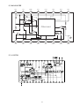
ELECTRICAL ADJUSTMENT
MAIN C.B
(CONDUCTOR SIDE)
TP4
FFE801
3
L981
L772
VR770
TP6
TP5
L771
IC771
CN201
2
6
MICOM/CD C.B (CONDUCTOR SIDE)
J201
IC501
SFR501
IC500
CN302
TP3
TP2
8
56
7
SFR1
9
R.P.E HEAD
0
0
< TUNER SECTION >
1. AM VT Check
Settings:
• Test point: TP4 (VT)
Method:
Set to AM 1611kHz and check that the test
point is less than 5.6V.
5. FM Tracking Check
Settings:
• Test point: J201 (PHONES)
Method:
Set to FM 98.0MHz and check that the test
point is less than 20dBµV.
2. AM IF Adjustment
Settings:
• Test point: J201 (PHONES)
L772 .............................................. 450kHz
6. DC Balance/Mono Distortion Adjustment
Settings:
• Test point: TP5, TP6
• Adjustment location: L771
• Input level: 54dB
Method:
Set to FM 98.0MHz and adjust L771 so that
the voltage between TP5 and TP6 becomes
0V±0.04V.
Next, check that the distortion is less than
1.3%.
3. AM Tracking Adjustment
Settings:
• Test point: J201 (PHONES)
• Adjustment location: L981
Method:
Set to AM 999kHz and adjust L981 so that the
test point becomes maximum.
7. FM Auto Stop Adjustment
Settings:
• Adjustment location: VR770
• Input level: 28dBµV
Method:
Set to FM 98.0MHz and adjust VR770 so that
the level 28dBµV±3dB.
4. FM VT Check
Settings:
• Test point: TP4 (VT)
Method:
Set to FM 108.0MHz and check that the test
point is more than less than 7.3V.
57
PRACTICAL SERVICE FIGURE
< CD SECTION >
< TUNER SECTION >
8. Tracking Balance Adjustment
< FM SECTION >
IHF Sensitiviy:
(THD 3%)
Oscilloscope
(DC range)
Signal to noise ratio:
+
TP2 (TB)
Distortion:
(Input: 54dB)
Stereo separation:
–
TP3 (VREF)
Intermediate frequency:
1) Connect an oscilloscope to the test points TP2 (TB) and
TP3 (VREF).
2) Turn on the power switch.
3) Insert test disc TCD-782 (YEDS-18) and press the CD
PLAY button.
4) Adjust SFR501 so that the waveform on the oscilloscope
is vertically symmetrical as shown in the figure below.
5) After the adjustment is completed, remove the connected
lead wires from the terminals.
More than 20dB
(at 88.0/98.0MHz)
More than 22dB
(at 108MHz)
More than 55dB
(at 98.0MHz)
Less than 1.5%
(at 98.0MHz)
More than 20dB
(at 98.0MHz)
10.7MHz
< AM SECTION >
Sensitivity:
(S/N 20dB)
Signal to noise ratio:
(Input: 74dB)
Distortion:
Intermediate frequency:
A
< DECK SECTION >
0V
Tape speed:
Wow & flutter:
(W.R.M.S)
Take-up torque:
F.F torque:
REW torque:
Back tension:
PB Output level:
REC/PB Output level:
Distortion (REC/PB):
B
A=B
VOLT/DIV: 0.2V
TIME/DIV: 1mS
< DECK SECTION >
9. Tape Speed Adjustment
Settings:
• Test tape: TTA-100
• Test point: CN201
• Adjustment location: SFR1
Method:
Playback the test tape by adjust SFR1 so that
the frequency counter reads 3000Hz±10Hz.
Check that the counter reading in the REV
mode is within the range of ±45Hz of that in
the FWD mode.
Noise level (PB):
Noise level (REC/PB):
Erasing ratio:
REC bias frequency:
Test tape:
10. Azimuth Adjustment
Settings:
• Test tape: TTA-300
• Test point: J201 (PHONES)
• Adjustment location: Head azimuth
adjustment screw
Method:
Playback the 10kHz signal of the test tape and
adjust the adjustment screw so that the output
becomes the -0.5dB point below the maximum
reading. The adjustment must ends with the
clockwise rotation of the adjustment screw.
Perform this adjustment in both FWD and
REV directions. Fix the adjustment screw with
adhesive agent upon completion of adjustment.
58
54dB±6dB (at 603kHz)
52dB±6dB
(at 999/1404kHz)
More than 36dB
(at 999kHz)
Less than 2.0%
(at 999kHz)
450kHz
3000Hz±60Hz
Less than 0.21%
30-55g-cm (FWD, REV)
75-160g-cm
75-160g-cm
3±4g-cm (FWD, REV)
190mV±1dB (LINE OUT)
190mV±2dB (LINE OUT)
Less than 3%
(NORM, CrO2)
Less than 3.5mV
(DOLBY NR OFF, NORM)
Less than 3.5mV
(DOLBY NR OFF, NORM)
More than 55dB
85kHz
NORMAL TTA-100
CrO2
TTA-200
IC DESCRIPTION
IC, CXD2652AR
Pin No.
Pin Name
I/O
Description
1
MNT0
O
Monitor output pin.
2
MNT1
O
Monitor output pin.
3
MNT2
O
Monitor output pin.
4
MNT3
O
Monitor output pin.
5
SWDT
I
Data input pin for micro-processor serial interface.
6
SCLK
I
Shift clock input pin for micro-processor serial interface.
7
XLAT
I
Latch input pin for micro-processor serial interface. Shut down: Latch.
8
SRDT
O
Data output pin for micro-processor serial interface.
9
SENS
O
Output internal status according to micro-processor serial interface address.
10
XRST
I
Reset input pin. "L": Reset.
11
SQSY
O
Disc sub-code Q synchronize / ADIP synchronize output.
12
DQSY
O
13
RECP
I
Laser power switching input pin. "H": Record power. 'L": Playback power.
14
XINT
O
Intrusion demand output pin. "L" setting when intrusion demand status is generated.
15
TX
I
Record data output enable signal input pin. "H": Enable.
16
OSCI
I
Crystal oscillator circuit input pin.
17
OSCO
O
Crystal oscillator circuit output pin. (OSCI inverted output)
18
XTSL
I
19
NC
–
Not used. (Connected to DVDD)
20
DVSS
–
Digital GND.
21
DIN
I
Input digital audio interface signal.
22
DOUT
O
Output digital audio interface signal.
23
ADDT
I
Analog record input pin. (Connected to external A/D converter output)
24
DADT
O
REC monitor output pin / Output decode audio data.
25
LRCK
O
Output LRCK (44.1kHz) to external audio block.
26
XBCK
O
Output bit clock (2.8224MHz) to external audio block.
27
FS256
O
Output 256Fs (11.2896MHz).
28
DVDD
–
Digital power supply.
29
A03
O
Output address for external DRAM.
30
A02
O
Output address for external DRAM.
31
A01
O
Output address for external DRAM.
32
A00
O
Output address for external DRAM.
33
A10
O
Output address for external DRAM. (Not used)
34
A04
O
Output address for external DRAM.
35
A05
O
Output address for external DRAM.
36
A06
O
Output address for external DRAM.
37
A07
O
Output address for external DRAM.
38
A08
O
Output address for external DRAM.
39
A11
O
Output address for external DRAM. (Not used.)
When source of the digital in is set to CD or MD, output sub-code Q synchronize of
UbitCD or MD format.
Switch input frequency of OSCI pin. (Connected to DVDD)
"H": 512Fs (22.5792MHz), "L": 1024Fs (45.158MHz).
59
Pin No.
Pin Name
I/O
Description
40
DVSS
–
Digital GND.
41
XOE
O
Output enable pin for external DRAM.
42
XCAS
O
Output CAS for external DRAM.
43
A09
O
Output address for external DRAM.
44
XRAS
O
Output RAS for external DRAM.
45
XWE
O
Write enable for external DRAM.
46
D1
I/O
Data pass for external DRAM.
47
D0
I/O
Data pass for external DRAM.
48
D2
I/O
Data pass for external DRAM.
49
D3
I/O
Data pass for external DRAM.
50
MVCI
I
Clock input pin for external VCO (784fs). (Connected to DVSS)
51
ASYO
O
Full swing output pin for playback EFM ("L" = VSS, "H" = VDD).
52
ASY1
I
Input omparator slice voltage for playback EFM.
53
AVDD
–
Analog power supply.
54
BIAS
I
Input comparator bias current for playback EFM.
55
RFI
I
Input RF signal for playback EFM.
56
AVSS
–
Analog GND.
57
PDO
O
Output phase comparison for analog PLL of EFM decoder.
58
PCO
O
Output phase comparison for playback digital PLL, master PLL and record EFM PLL.
59
FILI
I
Input filter for playback digital PLL, master PLL and record EFM PLL.
60
FILO
O
Output filter for playback digital PLL, master PLL and record EFM PLL.
61
CLTV
I
62
PEAK
I
Input peak hold signal for beam spectrum.
63
BOTM
I
Input bottom hold signal for beam spectrum.
64
ABCD
I
Input beam spectrum signal.
65
FE
I
Input focus error signal.
66
AUXI
I
Backup input 1.
67
VC
I
Input midpoint voltage.
68
ADIO
O
Monitor output pin for A/D converter input signal. (Not used)
69
AVDD
–
Analog power supply.
70
ADRT
I
Input maximum voltage of A/D converter operation range.
71
ADRB
I
Input minimum voltage of A/D converter operation range.
72
AVSS
–
Analog GND.
73
SE
I
Input sled error signal.
74
TE
I
Input tracking error signal.
75
AUX2
I
Backup input 2. (Connected to AVDD)
76
DCHG
I
Connected to the power supply of low impedance. (Connected to AVDD)
77
APC
I
Input error signal for laser digital APC. (Connected to AVDD)
78
ADFG
I
Input ADIP binary data FM signal (22.05kHz ± 1kHz).
79
FOCNT
O
Current setting output pin for CXA2523AR.
Input internal VCO control voltage for playback digital PLL, master PLL and record
EFM PLL.
60
Pin No.
Pin Name
I/O
Description
80
XLRF
O
Latch output pin for CXA2523AR control. Shut down: Latch.
81
CKRF
O
Shift clock output pin for CXA2523AR control.
82
DTRF
O
Data output pin for CXA2523AR control.
83
APCREF
O
Reference PWM output pin for laser APC.
84
LDDR
O
PWM output for laser digital APC. (Not used)
85
TRDR
O
Tracking servo drive PWM output (–).
86
TFDR
O
Tracking servo drive PWM output (+).
87
DVDD
–
Digital power supply.
88
FFDR
O
Focus servo drive PWM output (+).
89
FRDR
O
Focus servo drive PWM output (–).
90
FS4
O
Output 4Fs (176.4kHz). (Not used)
91
SRDR
O
Sled servo drive PWM output (–).
92
SFDR
O
Sled servo drive PWM output (+).
93
SPRD
O
Spindle servo drive PWM output. (PWM (–) or polarity)
94
SPFD
O
Spindle servo drive PWM output. (PWM (+) or PWM absolute value)
95
FGIN
I
Spindle CAV servo FG input. (Connected to DVSS.)
96
TEST 1
I
Test pin. (Connected to DVSS)
97
TEST 2
I
Test pin. (Connected to DVSS.)
98
TEST 3
I
Test pin. (Connected to DVSS.)
99
DVSS
–
Digital GND.
100
EFMO
O
Output "L" at playback, EFM (encode data) at recording.
61
IC, CXP81952M-547R
Pin No.
Pin Name
I/O
Description
1
MCAS
–
Not used.
2
MRAS
–
Not used.
3
BUP
–
Not used.
4
AMUTE
O
Output AUDIO MUTE signal.
5
ESK
O
Serial clock output pin for EEPROM interface.
6
EDO
O
Serial data output pin for EEPROM interface.
7
EDI
I
Serial data input pin for EEPROM interface.
8
ECS
O
Output EEPROM chip select signal.
9
NC
–
Not used.
10
RFLCT
I
Input terminal for DISC reflection rate detection SW.
11
NC
–
Not used.
12
LS
I
Input pin for pickup inner-circumference detect switch.
13
LDSW
I
Loading mechanism, EJECT position detect switch input.
14
PBSW
I
Loading mechanism, PB position detect switch input. (Not used)
15
RECSW
I
Loading mechanism, REC position detect switch input.
16 ~ 17
NC
–
Not used.
18
ACOFF
–
Not used.
19
SREQ
I
Input system-computer send request signal for system-computer interface.
20
EXTDIN
O
External digital IN permit signal output.
21
SLOW
O
Loading mechanism speed control signal output.
22
LOAD
O
Loading mechanism operating-direction control signal output 1.
23
EJECT
O
Loading mechanism operating-direction control signal output 2.
24
MREQ
O
Output MD microcomputer send request signal for system-computer interface.
25
DRIVE
O
Output EFM driver ON/OFF signal.
26 ~ 36
NC
–
Not used.
37
MP
–
Connected to VSS.
38
SRST
I
Input MD microcomputer reset signal.
39
DGND
–
Connected to VSS.
40
XTALO
O
Crystal oscillator terminal 1 for system clock oscillator.
41
XTALI
I
Crystal oscillator terminal 2 for system clock oscillator.
42
ARDY
I
Input READY signal for system-computer interface.
43
SIN
I
Input serial data for system-computer interface.
44
SOUT
O
Output serial data for system-computer interface.
45
ACLK
O
Output serial clock for system-computer interface.
46
XLAT
O
Output latch signal for CXD2652AR interface.
47
XRST
O
Output reset signal for CXD2652AR.
48
XSTBY
O
Output standby signal for CXA2523AR.
49
NC
–
Not used.
50
AVSS
–
Connected to VSS.
51
AVREF
–
Connected to VDD.
52
AVDD
–
Connected to VDD.
62
Pin No.
Pin Name
I/O
Description
53 ~ 55
NC
–
Not used (PLL UP).
56
SLF
–
Not used (PLL UP).
57
SLR
–
Not used (PLL UP).
58
TEMP
I
S-8110AMP OUT signal input pin.
59
MAGIC
–
Not used (PLL UP).
60
NC
–
Not used (PLL UP).
61
TEST
–
Not used (PLL UP).
62
DISCPRO
I
Input pin for prevention of DISC error erase SW.
63
MNT3
I
Monitor signal input pin 3 for CXD2652AR.
64
MNT2
I
Monitor signal input pin 2 for CXD2652AR.
65
MNT1
I
Monitor signal input pin 1 for CXD2652AR.
66
MNT0
I
Monitor signal input pin 0 for CXD2652AR.
67
SENS
I
Input SENS signal for CXD2652AR.
68
FLG
I
Monitor FLAG included in SRDT of CXD2652AR interface.
69 ~ 70
NC
–
Not used.
71
P-CONT
–
Not used.
72
RFSW
–
Not used.
73 ~ 74
NC
–
Not used.
75
DQSY
I
Synchronize input pin for digital-in SUB-Q.
76
XINT
I
Status synchronize input pin for CXD2652AR.
77
SRDT
I
Serial data input pin for CXD2652AR interface.
78
SWDT
O
Serial data output pin for CXD2652AR interface.
79
SCLK
O
Serial clock output pin for CXD2652AR interface.
80
SQSY
I
SUB-Q, ADIP synchronize input.
81 ~ 83
NC
–
Not used.
84
TXI
–
Connected to VSS.
85
TXO
–
Open. (Not used)
86
VSS
–
Connected to VSS.
87
VDD
–
Connected to VDD.
88
NC
–
Connected to VDD.
89
NC
–
Not used.
90
DRVMUTE
O
Outputs MUTE signal for BA5970FP.
91 ~ 94
NC
–
Not used.
95
RECP
O
Laser power switch signal output pin.
96
TX
O
Output permission signal of record data output.
97
MOD
O
Output ON/OFF signal for high frequency modulation circuit.
98
OPMUTE
O
Laser MUTE signal output pin.
99
ARST
O
AK4516VF reset signal output pin.
100
DENF
O
De-emphasis ON/OFF signal output pin.
63
IC, CXA2523AR
Pin No.
Pin Name
I/O
1
I
I
Input "I" RF signal converted to I-V.
Description
2
J
I
Input "J" RF signal converted to I-V.
3
VC
O
Output voltage for VCC/2.
4
A
I
Input current for main beam servo signal A.
5
B
I
Input current for main beam servo signal B.
6
C
I
Input currentt for main beam servo signal C.
7
D
I
Input current for main beam servo signal D.
8
E
I
Input current for side beam servo signal E.
9
F
I
Input current for side beam servo signal F.
10
PD
I
Input beam spectrum monitor signal.
11
APC
O
Output laser APC.
12
APCREF
I
Input reference voltage for laser power setting.
13
GND
–
GND.
14
TEMPI
I
Temperature sensor connection pin. (Not used)
15
TEMPR
I
Temperature sensor connection pin. Output reference voltage. (Not used)
16
SWDT
I
Input micro-processor serial interface data.
17
SCLK
I
Input micro-processor serial interface shift clock.
18
XLAT
I
Input micro-processor serial interface latch. "L": Latch.
19
XSTBY
I
Standby setting pin. "H": Normal mode, "L": Standby.
20
FOCNT
I
Internal current setting pin.
21
VREF
O
Output reference voltage. (Not used)
22
EQADJ
I/O
EQ central frequency setting pin.
23
3TADJ
I/O
BPF3T central frequency setting pin.
24
VCC
–
25
WBLADJ
I/O
BPF22 central frequency setting pin.
26
TE
O
Output tracking error signal.
27
CSLED
–
LPF capacitor connection pin for SLED error signal.
28
SE
O
Output SLED error signal.
29
ADFM
O
Output ADIP FM signal.
30
ADIN
I
Input ADIP signal comparator.
31
ADAGC
–
ADIPAGC capacitor connection pin.
32
ADFG
O
Output ADIP2 binary data signal.
33
AUX
O
13 output / Output temperature signal. Switched by serial command.
34
FE
O
Output focus error signal.
35
ABCD
O
Output beam spectrum signal for main beam servo detector.
36
BOTM
O
Output bottom hold signal for RF/ABCD.
37
PEAK
O
Output peak hold signal for RF/ABCD.
38
RF
O
RF equalizer output pin.
39
RF AGC
–
RFAGC capacitor connection pin.
40
AGCI
I
RFAGC input pin.
41
COMPO
O
User comparator output pin. (Not used)
Power supply pin.
64
Pin No.
Pin Name
I/O
Description
42
COMPP
I
User comparator non-inverted input pin. (Connected to GND)
43
ADDC
I/O
Capacitor connection pin for ADIP amplifier on return circuit.
44
OPO
O
Output pin for user operational amplifier. (Not used)
45
OPN
I
Non-inverted input pin for user operational amplifier.
46
RFO
O
RF amplifier output pin. Check point for eye pattern.
47
MORFI
I
Input pin where Groove RF signal is AC coupled.
48
MORFO
O
Output pin for Groove RF signal.
65
IC, LA9241ML
Pin No.
Pin Name
I/O
1
FIN2
I
Description
Pin to which external pickup photo diode is connected. RF signal is created by adding
with the FIN1 pin signal. FE signal is created by subtracting from the FIN1 pin signal.
2
FIN1
I
3
E
I
Pin to which external pickup photo diode is connected.
Pin to which external pickup photo diode is connected. TE signal is created by
subtracting from the F pin signal.
4
F
I
Pin to which external pickup photo diode is connected.
5
TB
I
DC component of the TE signal is input.
6
TE–
I
Pin to which external resistor setting the TE signal gain is connected between the TE pin.
7
TE
O
TE signal output pin.
8
TESI
I
TES “Track Error Sense” comparator input pin. TE signal is passed through a bandpass filter then input.
9
SCI
I
Shock detection signal input pin.
10
TH
I
Tracking gain time constant setting pin.
11
TA
O
TA amplifier output pin.
12
TD–
I
Pin to which external tracking phase compensation constants are connected between
the TD and VR pins.
13
TD
I
Tracking phase compensation setting pin.
14
JP
I
Tracking jump signal (kick pulse) amplitude setting pin.
15
TO
O
Tracking control signal output pin.
16
FD
O
Focusing control signal output pin.
17
FD–
I
Pin to which external focusing phase compensation constants are connected between
the FD and FA pins.
18
FA
I
Pin to which external focusing phase compensation constants are connected between
the FD– and FA– pins.
19
FA–
I
Pin to which external focusing phase compensation constants are connected between
the FA and FE pins.
20
FE
O
FE signal output pin.
21
FE–
I
Pin to which external FE signal gain setting resistor is connected between the FE pin.
22
AGND
—
Analog signal GND.
23
NC
—
No connection.
24
SP
O
Single ended output of the CV+ and CV– pin input signal.
25
SPG
I
Pin to which external spindle gain setting resistor in 12 cm mode is connected.
26
SP–
I
Pin to which external spindle phase compensation constants are connected together
with SPD pin.
27
SPD
O
Spindle control signal output pin.
28
SLEQ
I
Pin to which external sled phase compensation constants are connected.
29
SLD
O
Sled control signal output pin.
30, 31
SL–, SL+
I
Sled advance signal input pin from microprocessor.
32, 33
JP–, JP+
I
Tracking jump signal input pin from DSP.
34
TGL
I
Tracking gain control signal input from DSP. Low gain when TGL = H.
35
TOFF
I
Tracking off control signal input pin from DSP. Off when TOFF = H.
66
Pin No.
Pin Name
I/O
36
TES
O
37
HFL
O
Description
Pin from which TES signal is output to DSP.
“High Frequency Level” is used to judge whether the main beam position is on top of
bit or on top of mirror.
38
SLOF
I
Sled servo off control input pin.
39, 40
CV–, CV+
I
CLV error signal input pin from DSP.
41
RFSM
O
RF output pin.
42
RFS–
I
RF gain setting and EFM signal 3T compensation constant setting pin together with
RFSM pin.
43
SLC
O
“Slice Level Control” is the output pin which controls the RF signal data slice level by
DSP.
44
SLI
I
Input pin which control the data slice level by the DSP.
45
DGND
—
Digital system GND.
46
FSC
O
Output pin to which external focus search smoothing capacitor is connected.
47
TBC
I
“Tracking Balance Control” EF balance variable range setting pin.
48
NC
—
No connection.
49
DEF
O
Disc defect detector output pin.
50
CLK
I
Reference clock input pin. 4.23 MHz of the DSP is input.
51
CL
I
Microprocessor command clock input pin.
52
DAT
I
Microprocessor command data input pin.
53
CE
I
Microprocessor command chip enable input pin.
54
DRF
O
“Detect RF” RF level detector output.
55
FSS
I
“Focus Search Select” focus search mode (± search/+ search) select pin.
56
VCC2
—
Servo system and digital system Vcc pin.
57
REFI
—
Pin to which external bypass capacitor for reference voltage is connected.
58
VR
O
Reference voltage output pin.
59
LF2
I
Disc defect detector time constant setting pin.
60
PH1
I
Pin to which external capacitor for RF signal peak holding is connected.
61
BH1
I
Pin to which external capacitor for RF signal bottom holding is connected.
62
LDD
O
APC circuit output pin.
63
LDS
I
APC circuit input pin.
64
VCC1
—
RF system Vcc pin.
67
IC, LC78622ED
Pin No.
Pin Name
I/O
1
DEFI
I
2
TAI
I
Test signal input pin with built-in pull-down resistor. Be sure to connect to 0V.
3
PDO
O
Phase comparator output pin to control external VCO.
4
VVSS
—
5
ISET
I
6
VVDD
—
7
FR
I
8
VSS
—
9
EFMO
O
10
EFMIN
I
11
TEST2
I
Test signal input pin with built-in pull-down resistor. Be sure to connect to 0V.
12, 13
CLV+, CLV–
O
Disc motor control output. Three level output is possible using command.
14
V/P
___
O
Description
Defect sense signal (DEF) input pin. (Connect to 0V when not used).
For PLL.
GND pin for built-in VCO. Be sure to connect to 0V.
Pin to which external resistor adjusting the PD0 output current.
Power supply pin for built-in VCO.
Pin for VCO frequency range adjustment.
Digital system GND. Be sure to connect to 0V.
For slice level control.
EFM signal output pin.
EFM signal input pin.
Rough servo or phase control automatic selection monitoring output pin. Rough servo
at H. Phase servo at L.
15
HFL
I
Track detect signal input pin. Schmidt input.
16
TES
I
Tracking error signal input pin. Schmidt input.
17
TOFF
O
Tracking OFF output pin.
18
TGL
O
Tracking gain selection output pin. Gain boost at L.
19, 20
JP+, JP–
O
Track jump control signal output pin. Three level output is possible using command.
21
PCK
O
EFM data playback clock monitoring pin 4.3218 MHz when phase is locked in.
22
FSEQ
O
Sync signal detection output pin. H when the sync signal which is detected from EFM
signal and thesync signal which is internally generated agree.
23
VDD
—
Digital system power supply pin.
The pin is controlled by the serial data
command from microprocessor. When
24-28
SL+ - PUIN
I/O
General purpose input/output pin 1 to 5.
the pin is not used, set the pin to the input
terminal and connect to 0V, or alternately
set the pin to output terminal and leave
the pin open.
29
EMPH
O
De-emphasis monitor output pin. De-emphasis disc is being played back at H.
30
C2F
O
C2 flag output pin.
31
DOUT
O
DIGITAL OUT output pin. (EIAJ format).
32, 33
TEST3, TEST4
I
Test signal input pin with built-in pull-down resistor. Be sure to connect to 0V.
34
N.C.
—
35
MUTEL
O
36
LVDD
—
37
LCHO
O
L-channel output pin.
38
LVSS
—
L-channel GND. Be sure to connect to 0V.
39
RVSS
—
R-channel GND. Be sure to connect to 0V.
40
RCHO
O
41
RVDD
—
R-channel power supply pin.
42
MUTER
O
R-channel mute output pin.
Not used. Set the pin to open.
L-channel mute output pin.
L-channel 1-bit DAC.
R-channel 1-bit DAC.
68
L-channel power supply pin.
R-channel output pin.
Pin No.
Pin Name
I/O
Description
43
XVDD
—
44
XOUT
O
45
XIN
I
46
XVSS
—
Crystal oscillator GND pin. Be sure to connect to 0V.
47
SBSY
O
Subcode block sync signal output pin.
48
EFLG
O
C1, C2, single and dual correction monitoring pin.
49
PW
O
Subcode P, Q, R, S, T, U and W output pin.
50
SFSY
O
Subcode frame sync signal output pin. Falls down when subcode enters standby.
51
SBCK
I
Crystal oscillator power supply pin.
Pin to which external 16.9344 MHz crystal oscillator is connected.
Subcode read clock input pin. Schmidt input. (Be sure to connected to 0V when not in
use.)
52
FSX
O
Pin outputting the 7.35 kHz sync signal which is generated by dividing frequency of
crystal oscillator.
53
WRQ
O
Subcode Q output standby output pin.
54
RWC
I
Read/write control input pin. Schmidt input.
55
SQOUT
O
Subcode Q output pin.
COIN
I
Command input pin from microprocessor.
I
Command input read clock or subcode read input clock from SQOUT pin
56
___________
57
CQCK
________
58
RES
I
LC78622 reset input pin. Set this pin to L once when the main power is turned on.
59
TST11
O
Test signal output pin. Use this pin as open (normally L output).
60
16M
O
16.9344 MHz output pin.
61
4.2M
O
4.2336 MHz output pin.
62
TEST5
I
Test signal input pin with built-in pull-down resistor. Be sure to connect to 0V.
______
63
CS
I
Chip select signal input pin with built-in pull-down resistor. Be sure to connect to 0V
while it is not controlling.
64
TEST1
I
Test signal input pin without built-in pull-down resistor. Be sure to connect to 0V.
Note: The same potential must be applied to the respective power supply terminals. (VDD, VVDD, LVDD, RVDD, XVDD)
69
IC, LC875164A
Pin No.
Pin Name
I/O
Description
1
MOTOR
O
Motor control output. “H”: when operating.
2
—
O
Not used.
3
LA
O
BH3862FS serial latch output.
4
CL
O
BH3862FS serial clock output.
5
DA
O
BH3862FS serial data output.
6
Q-SW
O
Q-surround control.
7
SHIFT
O
Clock shift output.
8
ACIN
I
AC input detection.
9
REMO
I
Remote control received signal input.
10
RES
I
Reset input terminal.
11
XT1
I
32.768 kHz OSC input terminal.
12
XT2
O
32.768 kHz OSC output terminal.
13
GND
—
GND terminal.
14
CF1
I
5.6 MHz OSC input terminal.
15
CF2
O
5.6 MHz OSC output terminal.
16
+B
—
Power supply terminal.
17
—
O
Not used.
18
AD-1
I
A/D key input.
19
AD-2
I
A/D key input.
20
DOOR
I
CD door detection.
21
TUSW1
I
Tuner destination selection input.
22
TUSW2
I
Tuner destination selection input.
23
JOG-1
I
JOG-1 detection. (A output)
24
JOG-2
I
JOG-2 detection. (B output)
25
NC
—
Not used.
26
SRST
O
Microprocessor reset output for communication with MD microprocessor.
27
ARDY
O
Ready signal output for communication with MD microprocessor.
28
SREQ
O
Output request from system microprocessor for communication with MD
microprocessor.
29
MREQ
I
Output request from system microprocessor for communication with MD
microprocessor.
30
SIN
I
Serial data input for communication with MD microprocessor.
31
SOUT
O
Serial data output for communication with MD microprocessor.
32
ALCK
I
Serial clock input for communication with MD microprocessor.
33
FLDI
O
FL data output.
34
FLCE
O
FL chip enable.
35
FLCK
O
FL clock output.
36
NC
—
Not used.
37
NC
—
Not used.
38
DI
O
EEPROM serial data output.
39
DO
I
EEPROM serial data input.
70
Pin No.
Pin Name
I/O
Description
40
SK
O
EEPROM serial clock output.
41
CS
O
EEPROM chip selection.
42
NC
—
Not used.
43
POWER
O
Power regulator control output.
44
+B
—
Power supply input.
45
GND
—
GND terminal.
46
—
O
Not used.
47
CD+B
O
CD regulator control output. “H”: when operating.
48
TU+B
O
TU regulator control output. “H”: when operating.
49
CD
O
CD LED control output. “L”: to turn on the LED.
50
MD
O
MD LED control output. “L”: to turn on the LED.
51
TUNER
O
Tuner LED control output. “L”: to turn on the LED.
52
TAPE
O
Tape LED control output. “L”: to turn on the LED.
53
STANDBY
O
Stand-by LED control output. “L”: to turn on the LED.
54
—
O
Not used.
55
RELAY
O
Relay control output. “H”: when operating.
56
MUTE
O
MUTE operation. “H”: when operating.
57
CE
O
LC72121 chip enable output.
58
CLK
O
LC72121 serial clock output.
59
DI
O
LC72121 serial data output.
60
DO
I
LC72121 serial data input.
61
ST
I
Stereo reception detection.
62
COIN
O
CD serial data output.
63
CQCK
O
CD serial clock output.
64
SQOUT
I
CD sub-code Q input.
65
WRQ
I
CD sub-code Q reading standby.
66
DRF
I
CD RF level detection input.
67
NC
—
Not used.
68
RWC
O
CD input/output selector control.
69
DOOR+
O
CD loading “+” output.
70
GND
—
GND terminal.
71
+B
—
Power supply input.
72
DOOR-
O
CD loading “-” output.
73
REC A
I
REC SW-A detection. “L”: when detected.
74
REC B
I
REC SW-B detection. “L”: when detected.
75
TAPEIN
I
Cassette detection input. “L”: when detected.
76
STOP
I
Stop detection input. “L”: when detected.
77
AS
I
Auto stop detection input.
78
PB/REC
O
Cassette PLAY mode control output. PLAY: “L”, REC: “H”.
79
BEAT
O
Beat selector output. Initially: “L”
80
PL
O
Plunger solenoid control output. “H”: when operating.
71
IC BLOCK DIAGRAM
IC, BA5970FP
IC, BA6417F
72
IC, BD7910FV
IC, BH3862FS
73
IC, AK4519VF
IC, AK93C65AF
74
IC, BA5936
Rog CURRENT
DETECTOR
TERMINAL
IC, LC75710NE
75
IC, TC74HCT7007AF
IC, LC72121
VSSX
VSSA
VDD
VSSD
76
IC, MM1454XFBE
VCC
LIN
VREF
QF1
QF2
QF3
QF4
QF5
16
15
14
13
12
11
10
9
+
–
+
–
QSurround
BIAS
+
–
1
2
3
4
5
6
7
8
RIN
PNR
B/Q
DET
QF6
ROUT
LOUT
GND
IC, LA1837NL
77
MECHANICAL PARTS LIST 1/1
REF. NO
1
2
3
4
5
PART NO.
KANRI
DESCRIPTION
NO.
8Z-CK3-007-010
PANEL,CD
8Z-CK3-004-010
PANEL,MD
8Z-CK3-012-010
LENS,SENSOR
8Z-CK3-003-010
PANEL,CONT
8Z-CK3-024-010
LID,MD
REF. NO
PART NO.
36
37
38
39
40
KANRI
DESCRIPTION
NO.
8Z-CK3-220-010
COVER, FFC
8Z-CK3-009-010
BOX,CASS
8Z-CK3-208-010
COVER, PWB
87-043-116-010
ANT,WHIP
8Z-CK3-201-010
HLDR,VFD
6
7
8
9
10
8Z-CK3-221-010
88-CT4-026-010
8Z-CK3-031-010
82-NE6-067-010
8Z-CK3-008-010
SPR-T,FLAP
CUSH,FOOT
CABI,FRONT ASSY
BADGE,AIWA 30N
WINDOW,DISP
41
42
43
44
45
8Z-CK3-002-010
8Z-CK3-230-010
8Z-CK3-615-010
8Z-CK3-010-010
88-CT4-226-010
CABI,REAR
COVER, HT SINK
CONN ASSY,8P V WHT DECK
HLDR,CASS
HLDR,OIL DUMP
11
12
13
14
15
8Z-CK3-006-010
8Z-CK3-005-010
8Z-CK3-223-010
8Z-CK3-020-010
8Z-CK3-205-010
PANEL,DISP
PANEL,CASS
SPR-C,CASS
KEY,CASS
HLDR,MD
46
47
48
49
50
88-CT4-225-010
8Z-CK3-209-010
8Z-CK3-210-010
82-ZM1-264-010
87-064-185-010
GEAR,OIL DUMP
LEVER,CASS
SPR-P,ANT
LVR,EJECT R
HLDR,WIRE
16
17
18
19
20
8Z-CK3-609-010
8Z-CK3-610-010
88-CD2-602-110
8Z-CK3-206-010
8Z-CK3-627-010
FF-CABLE, 14P 1.0 200MM
FF-CABLE, 8P 1.0 200MM
SPKR,F 8CM 6OHM
HLDR,SPKR
VIB,PIEZO 4KHZ
51
52
A
B
C
8Z-CK3-225-010
8Z-CK3-013-010
87-067-020-010
87-067-703-010
87-067-758-010
COVER, REAR
COVER, CABI REAR
SCREW, VTT+3-4
TAPPING SCREW, BVT2+3-10
BVT2+3-12 W/O SLOT
21
22
23
24
25
8Z-CK3-207-010
8Z-CK3-019-010
8Z-CK3-018-010
8Z-CK3-022-010
8Z-CK3-011-010
COVER, SPKR
KEY,REC
KEY,POWER
LENS,POWER
LENS,FUNC
D
E
F
G
H
87-254-097-410
87-078-061-010
87-761-097-410
87-741-073-410
87-081-512-010
U+3-12 CR
VFT2+3-20DIA10,GLD
VFT2+3-10 GLD
UT 2+2.6-6 GLD
VTT+3-8
26
27
28
29
30
8Z-CK3-017-010
8Z-CK3-204-010
8Z-CK3-612-010
8Z-CK3-608-010
8Z-CK3-611-010
KEY,CONT
HLDR,CD R
FF-CABLE, 6P 1.25 250MM
FF-CABLE, 16P 1.0 250MM
FF-CABLE, 5P 1.25 150MM
I 87-067-698-010
31
32
33
34
35
8Z-CK3-203-010
8Z-CK3-021-010
8Z-CK3-202-010
8Z-CK3-613-010
8Z-CK3-212-010
HLDR,CD L
KNOB,RTRY JOG
HLDR,LED
FF-CABLE, 9P 1.25 200MM
SPR-T,CASS
BVT2+3-18(W/O,SLOT)
COLOR NAME TABLE
Basic color symbol
Color
Basic color symbol
Color
Basic color symbol
Color
B
Black
C
Cream
D
Orange
G
Green
H
Gray
L
Blue
LT
Transparent Blue
N
Gold
P
Pink
R
Red
S
Silver
ST
Titan Silver
T
Brown
V
Violet
W
White
WT
Transparent White
Y
Yellow
YT
Transparent Yellow
LM
Metallic Blue
LL
Light Blue
GT
Transparent Green
LD
Dark Blue
DT
Transparent Orange
78
MECHANICAL EXPLODED VIEW 1/1
39
52
D
51
I
20
2ZM-1 YR7N
21
C
C
C
48
G
50
19
44
F
C
43
41
47
H
37
F
42
P.C.B
40
7
FL
46
C
49
45
PT1
P.C.B
P.C.B
18
c
35
14
24
C
C
36
34
16
P.C.B
30
23
11
B
P.C.B
3ZG-3 E2
E
13
10
12
25
26
38
33
C
31
c
22
32
29
20 21
C
28
a
4
9
b
27
F
19
a
C
17
7ZG-9 B1
5
C
3
H
8
16
C
F
6
1
I
I
C
18
2
7
79
b
A
15
80
TAPE MECHANISM EXPLODED VIEW 1/1
14
B
15
30
DECK C.B
49
B
56
A
47
SOL2
16
12
48
13
50
D
17
B
C
10
11
36
44
42
9
51
37
41
7
46
A
C
18
43
55
19
35
41
F
A
4
5
33
45
6
20
22
34
3
21
RELAY C.B
40
E
25
2
32
39
26
29
B
A
HLDR WIRE 3
23
29
38
31
C
A
1
27
54
28
81
52
53
82
TAPE MECHANISM PARTS LIST 1/1
REF. NO
1
2
3
4
5
PART NO.
KANRI
DESCRIPTION
NO.
82-ZM1-327-210
CHAS ASSY,RN
82-ZM1-258-010
SPR-T,PINCH L
82-ZM1-341-010
LVR ASSY,PINCH L 2
82-ZM1-295-310
PLATE ASSY,LINK
82-ZM1-266-110
LVR,DIR
REF. NO
PART NO.
33
34
35
36
37
KANRI
DESCRIPTION
NO.
82-ZM1-227-210
LVR,TRIG
82-ZM1-224-410
LVR,FR
86-ZM4-201-010
SPR-E,TRIG 3
82-ZM1-239-010
CAPSTAN 2.2-41.7
82-ZM1-223-010
GEAR,PLAY
6
7
9
10
11
82-ZM1-214-010
82-ZM1-206-810
82-ZM1-269-210
82-ZM3-323-010
82-ZM1-210-110
SPR-T,DIR
CHAS,HEAD
SPR-T,BRG
SPR-T,LINK 3
GEAR,H T
38
39
40
41
42
82-ZM1-322-010
82-ZM1-220-210
82-ZM3-616-010
82-ZM1-216-310
82-ZM1-236-010
SPR-T,FR 60
GEAR,IDLER
RING MAGNET 4
GEAR,REEL
CAPSTAN,2-41.5
12
13
14
15
16
82-ZM1-213-010
82-ZM1-207-610
82-ZM1-283-310
82-ZM1-314-119
82-ZM1-208-110
SPR-T,HEAD
GUIDE,TAPE
S-SCREW,AZIMUTH
PLATE,HEAD
HLDR,HEAD
43
44
45
46
47
82-ZM1-225-010
82-ZM1-226-010
82-ZM3-333-210
82-ZM1-338-010
82-ZM1-349-010
GEAR,FR
GEAR,REW
SLIP DISK ASSY 2
BELT,FR 4
FLY-WHL,RH
17
18
19
20
21
82-ZM1-218-010
82-ZM1-263-110
82-ZM1-222-210
82-ZM1-217-310
82-ZM1-244-510
SPR-E,HB
LVR,EJECT
LVR,PLAY
REEL TABLE
SPR-C,BT
48
49
50
51
52
82-ZM1-348-010
82-ZM1-351-010
82-ZM1-245-210
82-ZM1-350-010
82-ZM1-247-110
FLY-WHL,LW
BELT,MAIN R7
HLDR,IC
HOLDR,MOTOR R7
PULLEY,MOTOR
22
23
25
26
27
82-ZM1-285-410
82-ZM1-257-010
82-ZM1-242-010
82-ZM1-243-010
82-ZM1-344-010
SPR-C,BT L
SPR-T,CAS
LVR,CAS
LVR,STOP
LVR ASSY,PINCH R
53
54
55
56
A
82-ZM1-288-010
80-ZM6-243-010
87-A90-343-010
87-A90-772-110
82-ZM1-315-010
SH,1.63-3.2-0.5 SLT
SH,1.75-3.6-0.5 SLT
MOT,SHU2R 70(M1)
HEAD,RPH KC9142(RPH)
S-SCREW,GUIDE TAPE
28
29
30
31
32
82-ZM1-259-110
82-ZM1-240-110
82-ZM1-298-010
82-ZM1-255-310
82-ZM1-221-110
SPR-T,PINCH R
LVR,REC
SPR-P,EARTH
SPR-E,LVR DIR
GEAR,CAM
B
C
D
E
F
80-ZM6-207-010
87-251-070-410
87-741-073-410
87-B10-008-010
82-ZM3-334-010
V+1.6-7
U+2.6-3
UT2+2.6-6 GLD
PW,2.15-6.8-0.4 SLT
PW,2.16-6-0.4
83
CD MECHANISM EXPLODED VIEW 1/2
C
17
16
13
CUSH-G,
MAIN A
17
C
CUSH-G,
MAIN A
3ZG2
14
A
B
15
11
9
10
7
5
8
B
4
C
6
A
D
C
2
12
D
3
A
MOTOR-2 C.B
B
1
84
CD MECHANISM PARTS LIST 1/2
REF. NO
1
2
3
4
5
PART NO.
KANRI
DESCRIPTION
NO.
83-ZG3-224-310
HLDR,M2
83-ZG3-228-610
CHAS,L6
83-ZG3-208-010
PULLEY,MOTOR
83-ZG3-213-010
LVR,SW
83-ZG3-209-610
CAM,SLIDE
6
7
8
9
10
83-ZG3-207-010
83-ZG3-204-210
83-ZG3-205-010
83-ZG3-217-010
83-ZG3-220-210
GEAR,TRAY
GEAR,C
GEAR,D
S-SCREW,GEAR D
GEAR,PULLEY 2
11
12
13
14
15
83-ZG3-214-010
83-ZG3-229-410
83-ZG3-210-110
83-ZG3-602-010
83-ZG3-212-010
BELT,L
TRAY,CD 2
HLDR,CHUCK
RING,MAG
CAP,DISC
REF. NO
16
17
A
B
C
PART NO.
KANRI
DESCRIPTION
NO.
83-ZG3-211-010
PLATE,DISC
81-ZG1-254-010
S-SCEW,MECH HLDR
87-067-945-110
VFT2+3-12(F10)
87-251-071-110
U+2.6-4
87-512-074-210
VFT2+2.6-8
D 87-352-075-210
85
VT2+2.6-10
CD MECHANISM EXPLODED VIEW 2/2
11
12
8
2
6
A
A
A
A
1
5
3
SW1
4
M20
M21
DRIVE C.B
CD MECHANISM PARTS LIST 2/2
REF. NO
PART NO.
KANRI
NO.
DESCRIPTION
1
2
3
4
5
83-ZG2-243-110
83-ZG2-235-010
83-ZG2-205-210
83-ZG2-236-010
83-ZG2-240-010
CHAS ASSY,SHT
GEAR,A3
GEAR,B
GEAR MOTOR 3
SHAFT,SLIDE 3
6
8
11
12
A
87-A90-836-010
83-ZG2-233-010
83-ZG2-245-110
83-ZG2-250-010
87-261-032-210
PICKUP,KSS-213F
TURN TABLE,A5
LEVER,SHUTTER
SPR-E,SHT 2
SCREW V+2-3
86
MD MECHANISM EXPLODED VIEW 1/3
B
B
HLDR,SHLD TOP
3
1
CUSH-R,MECHA RE
A
A
7ZG-8 A2
CUSH-R,MECHA FR
A
A
CUSH-R,MECHA RE
2
CUSH-R,MECHA FR
C
C
P.C.B
HLDR,SHLD BOT
MD MECHANISM PARTS LIST 1/3
REF. NO
1
2
3
A
B
PART NO.
87-ZG9-602-010
87-ZG9-603-010
87-ZG9-604-010
87-ZG9-209-010
87-067-020-010
C 87-067-421-010
KANRI
NO.
DESCRIPTION
FF-CABLE,21P 0.5 90MM
FF-CABLE,8P 1.0 120MM
FF-CABLE,5P 1.25 100MM
S-SCREW,MD TF
VTT+3-4
VTT+2-4
87
MD MECHANISM EXPLODED VIEW 2/3
E
21
D
20
19
a
18
17
16
13
15
14
C
12
11 B
9
10
8
a
7
5
A
6
3
2
4
1
PCB
7ZG-3 A2
88
MD MECHANISM PARTS LIST 2/3
REF. NO
1
2
3
4
5
PART NO.
KANRI
DESCRIPTION
NO.
87-ZG8-220-110
PLATE ASSY,LATCH
87-ZG8-259-010
SPR-T,LATCH
87-ZG8-230-110
LEVER,LATCH
87-ZG8-224-110
SPR-E,LATCH
87-ZG8-214-210
HLDR ASSY,CARTRIGE
6
7
8
9
10
87-ZG8-233-110
87-ZG8-255-210
87-ZG8-201-710
87-ZG8-256-110
87-ZG8-242-010
LEVER,SW H
PLATE,CARTRIGE
CHAS ASSY,MAIN
LEVER,SW S2
GEAR,MOT
11
12
13
14
15
87-ZG8-253-010
87-ZG8-246-010
87-ZG8-252-010
87-ZG8-231-010
87-ZG8-232-110
GEAR,REDUCTION S3
GEAR,IDLER 2
GEAR,REDUCTION L3
LEVER,SHUTTER
SPR-E,SHUTTER
REF. NO
PART NO.
16
17
18
19
20
KANRI
DESCRIPTION
NO.
87-ZG8-225-310
LEVER ASSY,CAM
87-ZG8-239-110
CAM,LOAD
87-ZG8-257-210
LEVER ASSY,REC
87-ZG8-213-210
PLATE,SLIDE R
87-ZG8-209-210
PLATE ASSY,SLIDE L
21
A
B
C
D
87-A90-605-110
87-B10-129-010
87-B10-128-010
87-B10-130-010
87-067-421-010
E 87-B10-131-010
89
HEAD,OWH RF325-74A
VTT+1.7-3.5 W/O MFZN2-C
V+1.7-2 W/O MFZN2-C
W-P,1.23-3.1-0.25 SLIT
VTT+2-4
VW+1.7-5 W/O MFZN2C
MD MECHANISM EXPLODED VIEW 3/3
6
11
H
PLATE,YOKE
D
5
C
10
HLDR LED
8
4
GEAR,
LEAD
3
7
2
9
A
17
B
1
12
16
15
13
14
E
A
P.C.B
G
90
F
MD MECHANISM PARTS LIST 3/3
REF. NO
1
2
3
4
5
PART NO.
KANRI
DESCRIPTION
NO.
87-ZG3-202-510
CHAS ASSY,OUT-SERT
87-ZG3-214-210
SPR-T,SPINDLE-A
83-ZG5-308-010
BRG,1.5-2
83-ZG5-302-110
TURN TABLE,MD1
83-ZG5-305-210
SPR-P,DISC
6
7
8
9
10
83-ZG5-605-010
87-ZG3-212-110
87-ZG3-211-010
87-A90-613-010
87-ZG3-216-010
MAGNET,CHUCK
SHAFT,LEAD
SHAFT,GUIDE
PICKUP,KMS-260A
SPR-P,RACK
11
12
13
14
15
87-ZG3-213-010
87-A90-413-010
87-ZG3-206-010
87-ZG3-205-010
87-ZG3-208-010
SPR-P,LEAD
MOT,FF-110PH 9
GEAR,A
GEAR,MOT SL
HLDR ASSY,MOTOR
REF. NO
16
17
A
B
C
D
E
F
G
H
91
PART NO.
KANRI
DESCRIPTION
NO.
87-A90-616-010
MOT,FF-N30VA
87-A90-611-010
SW,PUSH 3-2-2 MPU20300MLB0
87-261-547-310
V+2-3 BLK (1)
87-263-523-310
SCREW, V+1.7-2
87-261-509-310
SCREW, V+1.4-4
87-067-393-010
87-261-503-310
87-078-033-010
87-341-035-210
87-264-523-010
SCREW +1.4-1.4
PRECISION SCREW, V+1.4-2
PW 1.2-2.5-0.25 SLT
SCREW,UT1+2-6
SCREW,V+1.7-2
SPRING APPLICATION POSITION
82-ZM1-257-010
SPR-T,CAS
82-ZM1-218-010
SPR-E,HB
82-ZM1-285-410
SPR-C,BT L
82-ZM1-244-010
SPR-C,BT
82-ZM3-323-010
SPR-T,LINK
82-ZM1-259-110
SPR-T,PINCH R
82-ZM1-258-110
SPR-T,PINCH L
82-ZM1-269-010
SPR-T,BRG
82-ZM1-213-010
SPR-T,HEAD
82-ZM1-322-010
SPR-T,FR 60
86-ZM4-201-010
SPR-E,TRIG 3
82-ZM1-255-310
SPR-E,LER DIR
92
82-ZM1-214-010
SPR-T,DIR
REFERENCE NAME LIST
ELECTRICAL SECTION
MECHANICAL SECTION
DESCRIPTION
REFERENCE NAME
DESCRIPTION
REFERENCE NAME
ANT
CC-CAP
C-CAP TN
C-COIL
ANTENNAS
CHIP
CAP, CHIP
CAP, CHIP TANTALUM
COIL, CHIP
ADHESHIVE
AZ
BAR-ANT
BAT
BATT
SHEET ADHESHIVE
AZIMUTH
BAR-ANTENNA
BATTERY
BATTERY
C-DI
C-DIODE
C-FET
C-FOTR
C-JACK
DIODE, CHIP
DIODE, CHIP
FET, CHIP
FILTER, CHIP
JACK, CHIP
BRG
BTN
CAB
CASS
CHAS
BEARING
BUTTON
CABINET
CASSETTE
CHASSIS
C-LED
C-RES
C-SFR
C-SLIDE SW
C-SW
LED, CHIP
RES, CHIP
SFR, CHIP
SLIDE SWITCH, CHIP
SWITCH, CHIP
CLR
CONT
CRSR
CU
CUSH
COLLAR
CONTROL
CURSOR
CUSHION
CUSHION
C-TR
C-VR
C-ZENER
CAP, CER
CAP, E
TRANSISTOR, CHIP
VOLUME, CHIP
ZENER, CHIP
CAP, CERA-SOL
CAP, ELECT
DIR
DUBB
FL
FLY-WHL
FR
DIRECTION
DUBBING
FRONT LOADING
FLYWHEEL
FRONT
CAP, M/F
CAP, TC
CAP, TC-U
CAP, TN
CERA FIL
CAP, FILM
CAP, CERA-SOL
CAP, CERA-SOL SS
CAP, TANTALUM
FILTER, CERAMIC
FUN
G-CU
HDL
HIMERON
HINGE, BAT
FUNCTION
G-CUSHION
HANDOL
CLOTH
HINGE, BATTERY
CF
DL
E/CAP
FILT
FLTR
FILTER, CERAMIC
DELAY LINE
CAP, ELECT
FILTER
FILTER
HLDR
HT-SINK
IB
IDLE
IND, L-R
HOLDER
HEAT SINK
INSTRUCTION BOOKLET
IDLER
INDICATOR, L-R
FUSE RES
MOT
P-DIODE
P-SNSR
P-TR
RES, FUSE
MOTOR
PHOTO DIODE
PHOTO SENSER
PHOTO TRANSISTOR
KEY, CONT
KEY, PRGM
KNOB, SL
LBL
LID, BATT
KEY, CONTROL
KEY, PROGRAM
KNOB, SLIDE
LABEL
LID, BATTERY
POLY VARI
PPCAP
PT
PTR, RES
RC
VARIABLE CAPACITOR
CAP, PP
POWER TRANSFORMER
PTR, MELF
REMOTE CONTROLLER
LID, CASS
LVR
P-SP
PANEL, CONT
PANEL, FR
LID, CASSETTE
LEVER
P-SPRING
PANEL, CONTROL
PANEL, FRONT
RES NF
RESO
SHLD
SOL
SPKR
RES, NON-FLAMMABLE
RESONATOR
SHIELD
SOLENOID
SPEAKER
PRGM
PULLY, LOAD MO
RBN
SSEG
PROGRAM
PULLY, LOAD MOTOR
RIBBON
SPECIAL
SEGMENT
SW, LVR
SW, RTRY
SW, SL
TC CAP
THMS
SWITCH, LEVER
SWITCH, ROTARY
SWITCH, SLIDE
CAP, CERA-SOL
THERMISTOR
SH
SHLD-SH
SL
SP
SP-SCREW
SHEET
SHIELD-SHEET
SLIDE
SPRING
SPECIAL-SCREW
TR
TRIMMER
TUN-CAP
VIB, CER
VIB, XTAL
TRANSISTOR
CAP, TRIMMER
VARIABLE CAPACITOR
RESONATOR, CERAMIC
RESONATOR, CRYSTAL
SPACER, BAT
SPR
SPR-P
SPR-PC-PUSH
T-SP
SPACER, BATTERY
SPRING
P-SPRING
P-SPRING, C-PUSH
T-SPRING
VR
ZENER
VOLUME
DIODE, ZENER
TERM
TRIG
TUN
VOL
W
TERMINAL
TRIGGER
TUNING
VOLUME
WASHER
WHL
WORM-WHL
WHEEL
WORM-WHEEL
93
2–11, IKENOHATA 1–CHOME, TAITO-KU, TOKYO 110-8710, JAPAN TEL:03 (3827) 3111
737004
Printed in Singapore