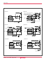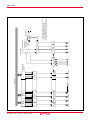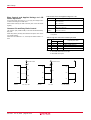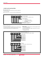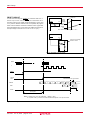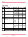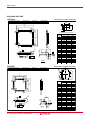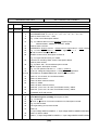
1
38C1 Group
REJ03B0075-0240Z
Rev.2.40
2004.6.14
SINGLE-CHIP 8-BIT CMOS MICROCOMPUTER
• LCD drive control circuit
DESCRIPTION
The 38C1 group is the 8-bit microcomputer based on the 740 family core technology.
The 38C1 group has the LCD drive control circuit, an 8-channel A/
D converter, and serial I/O as additional functions.
The various microcomputers in the 38C1 group include variations
of internal memory size and packaging. For details, refer to the
section on part numbering.
•
•
•
FEATURES
• Basic machine-language instructions ....................................... 71
• The minimum instruction execution time ............................ 0.5 µs
(at 8 MHz oscillation frequency)
• Memory size
•
•
•
•
•
•
•
ROM ................................................................ 16 K to 24 K bytes
RAM ................................................................... 384 to 512 bytes
Programmable input/output ports (Ports P2–P6) ..................... 30
Segment output pin/Input port (Port P0) ....................................... 8
Software pull-up/pull-down resistor ....................... Ports P0, P2–P6
Interrupts .................................................. 13 sources, 13 vectors
(includes key input interrupt)
Timers ........................................................... 8-bit ✕ 3, 16-bit ✕ 2
Serial I/O ...................................... 8-bit ✕ 1 (Clock-synchronous)
A/D converter .................................................. 8-bit ✕ 8 channels
(It can be used in the low-speed mode.)
•
•
Bias ............................................................................ 1/1, 1/2, 1/3
Duty ................................................................ Static, 1/2, 1/3, 1/4
Common output .......................................................................... 4
Segment output ......................................................................... 25
Main clock generating circuit ...................................................... 1
(connect to external ceramic resonator or on-chip oscillator)
Sub clock generating circuit ........................................................ 1
(connect to external quartz-crystal oscillator)
Power source voltage
In high-speed mode (f(XIN) ≤ 8.0 MHz) ..................... 4.0 to 5.5 V
In middle-speed mode (Mask ROM version: f(XIN) ≤ 6.0 MHz)
.................................................................................... 1.8 to 5.5 V
In middle-speed mode (One Time PROM version: f(XIN) ≤ 6.0 MHz)
.................................................................................... 2.2 to 5.5 V
In low-speed mode (Mask ROM version) .................. 1.8 to 5.5 V
In low-speed mode (One Time PROM version) ........ 2.2 to 5.5 V
Power dissipation (Mask ROM version)
In high-speed mode (frequency divided by 2) ........... Typ. 15 mW
(VCC = 5 V, f(XIN) = 8 MHz , Ta = 25 °C)
In low-speed mode ...................................................... Typ. 18 µW
(VCC = 2.5 V, f(XIN) = stop , f(XCIN) = 32 kHz , Ta = 25 °C)
Operating temperature range ................................... – 20 to 85°C
APPLICATIONS
Household appliances, consumer electronics, etc.
Rev.2.40
Jun 14, 2004
page 1 of 56
38C1 Group
P03/SEG3
P04/SEG4
P05/SEG5
P06/SEG6
P07/SEG7
SEG8
SEG9
SEG10
SEG11
SEG12
SEG13
SEG14
SEG15
SEG16
COM3
COM2
PIN CONFIGURATION (TOP VIEW)
48 47 46 45 44 43 42 41 40 39 38 37 36 35 34 33
P02/SEG2
P01/SEG1
P00/SEG0
P57/SRDY
P56/SCLK
P55/SOUT
P54/SIN
P53/CNTR1
P52/CNTR0
P51/INT1
P50/INT0
P47/AN7
P46/AN6
P45/AN5
P44/AN4
AN3/ADKEY3
49
32
50
31
51
30
52
29
53
28
54
27
55
26
M38C1XMX-XXXFP/HP
56
57
23
59
22
60
21
61
20
62
19
63
18
64
17
3
4
5
6
7
8
9
10
11 12
13 14 15 16
AN2/ADKEY2
AN1/ADKEY1
AN0/ADKEY0
P 64
P63/φOUT
P62/TOUT
CNVSS
RESET
P61/XCOUT
P60/XCIN
VSS
X IN
XOUT
VCC
P34(LED4)/(KW4)
P33(LED3)/(KW3)
2
Outline 64P6U-A/64P6Q-A
Fig. 1 Pin configuration of M38C1XMX-XXXFP/HP
Jun 14, 2004
24
58
1
Rev.2.40
25
page 2 of 56
COM1
COM0
P20/SEG17
P21/SEG18
P22/SEG19
P23/SEG20
P24/SEG21
P25/SEG22
P26/SEG23
P27/SEG24
VL3
VL2
VL1
P30/(LED0)/(KW0)
P31/(LED1)/(KW1)
P32/(LED2)/(KW2)
page 3 of 56
φ
On-chip
oscillator
5
6
XCOUT
Subclock
output
9 10
P6(5)
XCIN
Subclock
input
I/O port P6
4
13
12
XCIN
XCOUT
φ
Clock generating
circuit
Main
clock
output
XOUT
Main
clock
input
XIN
TOUT
Jun 14, 2004
1 64
Analog input AN
3 2
A/D converter (8)
PCH
CPU
I/O port P5
52 53 54 55 56 57 58 59
SI/O(8)
Timer 3 (8)
Timer Y (16)
Timer 1 (8)
Timer 2 (8)
Timer X (16)
ROM
63 62 61 60
Data bus
11
(0 V)
VSS
P5(8)
14
(5 V)
VCC
P4(4)
I/O port P4
PS
PCL
S
Y
X
A
8
Reset input
RESET
INT0,INT1
Rev.2.40
CNTR0,CNTR1
Fig. 2 Functional block diagram
Key-on wakeup
FUNCTIONAL BLOCK DIAGRAM
P2(8)
23 24 25 26 27 28 29 30
I/O port P2
P3(5)
15 16 17 18 19
I/O port P3
RAM
Input port P0
44 45 46 47 48 49 50 51
P0(8)
LCD display
register
(16 bytes)
LCD drive
control circuit
20
21
VL1
VL2
VL3
SEG8
SEG9
SEG10
40 SEG11
39 SEG12
38 SEG13
37 SEG14
36 SEG15
35 SEG16
41
42
43
33
32
COM0
COM1
COM2
34
COM3
31
22
38C1 Group
38C1 Group
PIN DESCRIPTION
Table 1 Pin description
Pin
Function
Name
VCC, VSS
Power source
• Apply voltage of power source to VCC, and 0 V to VSS.
CNVSS
CNVSS
• Connect to Vss.
RESET
Reset input
Clock input
• Reset input pin for active “L”.
• Input and output pins for the main clock generating circuit.
Function except a port function
(As for VCC, refer to the recommended operating condition)
XIN
• Connect a ceramic resonator or a quartz-crystal oscillator between the XIN and XOUT pins to set the
Clock output
XOUT
oscillation frequency.
• If an external clock is used, connect the clock source to the XIN pin and leave the XOUT pin open.
A feedback resistor is built-in.
LCD power source • Input 0 ≤ VL1 ≤ VL2 < VL3 voltage.
COM0–COM3 Common output
• LCD common output pins.
Input port P0
P00/SEG0–
• 8-bit input port.
VL1–VL3
P07/SEG7
• LCD segment output pins
• CMOS compatible input level.
• 1, 2, 4 or 8-bit input and 8-bit pull-down can be programmed.
SEG8–/SEG16 Segment output pin • LCD segment output pin.
P20/SEG17– I/O port P2
• LCD segment output pins
• 8-bit I/O port.
P27/SEG24
• CMOS compatible input level.
• CMOS 3-state output structure.
• 1-bit input/output and pull-down can be programmed.
P30(LED)/KW0– I/O port P3
• 5-bit I/O port.
P34(LED)/KW4
• CMOS compatible input level.
• Key input (key-on wake-up) interrupt
input pins
• CMOS 3-state output structure.
• 1-bit input/output and pull-up can be programmed.
AN0/ADKEY0– Analog input
AN3/ADKEY3
• Analog input pins for A/D converter.
• ADKEY input pins
When these pins are used as ADKEY pins, the input
voltage of ADKEY pin which is input “L” level is A/D
converted automatically.
P44/AN4–
I/O port P4
P47/AN7
• 4-bit I/O port.
• CMOS compatible input level.
• Analog input pins for A/D converter
• CMOS 3-state output structure.
• 1-bit input/output and pull-up can be programmed.
P50/INT0,
I/O port P5
• 8-bit I/O port.
P51/INT1
• CMOS compatible input level.
P52/CNTR0
• CMOS 3-state output structure.
• 1-bit input/output and pull-up can be programmed.
P53/CNTR1
• Interrupt input pins
• Timer X, timer Y function pins
• Serial I/O function pins
P54/SIN
P55/SOUT
P56/SCLK
P57/SRDY
P60/XCIN
I/O port P6
P61/XCOUT
• 5-bit I/O port.
• CMOS compatible input level.
• CMOS 3-state output structure.
P62/TOUT
P63/φOUT
• 1-bit input/output and pull-up can be programmed.
External clock cannot be input directly.)
Timer 2 output pin
System clock φ output
P64
Rev.2.40
• Sub-clock generating circuit I/O pins
(Oscillator is connected.
Jun 14, 2004
page 4 of 56
38C1 Group
PART NUMBERING
Product
M38C1
3
M
6
-
XXX
FP
Package type
FP : 64P6U-A package
HP : 64P6Q-A package
ROM number
Omitted in One Time PROM version.
ROM/PROM size
1 : 4096 bytes
2 : 8192 bytes
3 : 12288 bytes
4 : 16384 bytes
5 : 20480 bytes
6 : 24576 bytes
7 : 28672 bytes
8 : 32768 bytes
9 : 36864 bytes
A : 40960 bytes
B : 45056 bytes
C : 49152 bytes
D : 53248 bytes
E : 57344 bytes
F : 61440 bytes
The first 128 bytes and the last 2 bytes of ROM
are reserved areas ; they cannot be used.
Memory type
M: Mask ROM version
E: One Time PROM version
RAM size
0 : 192 bytes
1 : 256 bytes
2 : 384 bytes
3 : 512 bytes
4 : 640 bytes
5 : 768 bytes
6 : 896 bytes
7 : 1024 bytes
8 : 1536 bytes
9 : 2048 bytes
Fig. 3 Part numbering
Rev.2.40
Jun 14, 2004
page 5 of 56
38C1 Group
GROUP EXPANSION
Packages
Renesas plans to expand the 38C1 group as follows.
64P6Q-A .................................... 0.5 mm-pitch plastic molded QFP
64P6U-A .................................... 0.8 mm-pitch plastic molded QFP
Memory Type
Support for Mask ROM version, One Time PROM version.
Memory Size
ROM/PROM size ............................................... 16 K to 24 K bytes
RAM size .............................................................. 384 to 512 bytes
ROM size (bytes)
48K
32K
28K
M38C13M6/E6
24K
20K
M38C12M4
16K
12K
8K
4K
192 256
384
512
640
768
896
1024
RAM size (bytes)
Products under development or planning :the development schedule and specification may be revised without notice.
Fig. 4 Memory expansion plan
Currently products are listed below.
As of June. 2004
Table 2. List of products
Product
ROM size (bytes)
ROM size for User in ( )
RAM size (bytes)
M38C12M4-XXXFP
M38C12M4-XXXHP
M38C13M6-XXXFP
M38C13M6-XXXHP
M38C13E6FP
M38C13E6HP
16384
(16256)
384
24576
(24446)
512
Rev.2.40
Jun 14, 2004
page 6 of 56
Package
64P6U-A
64P6Q-A
64P6U-A
64P6Q-A
64P6U-A
64P6Q-A
Remarks
Mask ROM version
One Time PROM version (shipped in blank)
38C1 Group
FUNCTIONAL DESCRIPTION
CENTRAL PROCESSING UNIT (CPU)
[Stack Pointer (S)]
The stack pointer is an 8-bit register used during subroutine calls
and interrupts. This register indicates start address of stored area
(stack) for storing registers during subroutine calls and interrupts.
The low-order 8 bits of the stack address are determined by the
contents of the stack pointer. The high-order 8 bits of the stack
address are determined by the stack page selection bit. If the
stack page selection bit is “0” , the high-order 8 bits becomes
“0016”. If the stack page selection bit is “1”, the high-order 8 bits
becomes “0116”.
The operations of pushing register contents onto the stack and
popping them from the stack are shown in Figure 6.
Store registers other than those described in Figure 6 with program when the user needs them during interrupts or subroutine
calls.
The 38C1 group uses the standard 740 family instruction set. Refer to the table of 740 family addressing modes and machine
instructions or the 740 Family Software Manual for details on the
instruction set.
Machine-resident 740 family instructions are as follows:
The FST and SLW instruction cannot be used.
The STP, WIT, MUL, and DIV instruction can be used.
[Accumulator (A)]
The accumulator is an 8-bit register. Data operations such as data
transfer, etc., are executed mainly through the accumulator.
[Index Register X (X)]
The index register X is an 8-bit register. In the index addressing
modes, the value of the OPERAND is added to the contents of
register X and specifies the real address.
[Program Counter (PC)]
The program counter is a 16-bit counter consisting of two 8-bit
registers PCH and PCL. It is used to indicate the address of the
next instruction to be executed.
[Index Register Y (Y)]
The index register Y is an 8-bit register. In partial instruction, the
value of the OPERAND is added to the contents of register Y and
specifies the real address.
b0
b7
A
Accumulator
b0
b7
X
Index register X
b0
b7
Y
b7
Index register Y
b0
S
b15
b7
PCH
Stack pointer
b0
Program counter
PCL
b7
b0
N V T B D I Z C
Processor status register (PS)
Carry flag
Zero flag
Interrupt disable flag
Decimal mode flag
Break flag
Index X mode flag
Overflow flag
Negative flag
Fig. 5 740 Family CPU register structure
Rev.2.40
Jun 14, 2004
page 7 of 56
38C1 Group
On-going Routine
Interrupt request
(Note)
M (S)
Execute JSR
Push return address
on stack
M (S)
(PCH)
(S)
(S) – 1
M (S)
(PCL)
(S)
(S)– 1
(S)
M (S)
(S)
M (S)
(S)
Subroutine
POP return
address from stack
(S) + 1
(PCL)
M (S)
(S)
(S) + 1
(PCH)
M (S)
(S) – 1
(PCL)
Push return address
on stack
(S) – 1
(PS)
Push contents of processor
status register on stack
(S) – 1
Interrupt
Service Routine
Execute RTS
(S)
(PCH)
I Flag is set from “0” to “1”
Fetch the jump vector
Execute RTI
Note: Condition for acceptance of an interrupt
(S)
(S) + 1
(PS)
M (S)
(S)
(S) + 1
(PCL)
M (S)
(S)
(S) + 1
(PCH)
M (S)
POP contents of
processor status
register from stack
POP return
address
from stack
Interrupt enable flag is “1”
Interrupt disable flag is “0”
Fig. 6 Register push and pop at interrupt generation and subroutine call
Table 3 Push and pop instructions of accumulator or processor status register
Push instruction to stack
Pop instruction from stack
Accumulator
PHA
PLA
Processor status register
PHP
PLP
Rev.2.40
Jun 14, 2004
page 8 of 56
38C1 Group
[Processor status register (PS)]
The processor status register is an 8-bit register consisting of 5
flags which indicate the status of the processor after an arithmetic
operation and 3 flags which decide MCU operation. Branch operations can be performed by testing the Carry (C) flag , Zero (Z) flag,
Overflow (V) flag, or the Negative (N) flag. In decimal mode, the Z,
V, N flags are not valid.
• Bit 0: Carry flag (C)
The C flag contains a carry or borrow generated by the arithmetic logic unit (ALU) immediately after an arithmetic operation.
It can also be changed by a shift or rotate instruction.
• Bit 1: Zero flag (Z)
The Z flag is set if the result of an immediate arithmetic operation
or a data transfer is “0”, and cleared if the result is anything other
than “0”.
• Bit 2: Interrupt disable flag (I)
The I flag disables all interrupts except for the interrupt generated by the BRK instruction.
Interrupts are disabled when the I flag is “1”.
• Bit 3: Decimal mode flag (D)
The D flag determines whether additions and subtractions are
executed in binary or decimal. Binary arithmetic is executed
when this flag is “0”; decimal arithmetic is executed when it is
“1”.
Decimal correction is automatic in decimal mode. Only the ADC
and SBC instructions can be used for decimal arithmetic.
• Bit 4: Break flag (B)
The B flag is used to indicate that the current interrupt was generated by the BRK instruction. The BRK flag in the processor
status register is always “0”. When the BRK instruction is used to
generate an interrupt, the processor status register is pushed
onto the stack with the break flag set to “1”.
• Bit 5: Index X mode flag (T)
When the T flag is “0”, arithmetic operations are performed between accumulator and memory. When the T flag is “1”, direct
arithmetic operations and direct data transfers are enabled between memory locations.
• Bit 6: Overflow flag (V)
The V flag is used during the addition or subtraction of one byte
of signed data. It is set if the result exceeds +127 to -128. When
the BIT instruction is executed, bit 6 of the memory location operated on by the BIT instruction is stored in the overflow flag.
• Bit 7: Negative flag (N)
The N flag is set if the result of an arithmetic operation or data
transfer is negative. When the BIT instruction is executed, bit 7
of the memory location operated on by the BIT instruction is
stored in the negative flag.
Table 4 Set and clear instructions of each bit of processor status register
Set instruction
Clear instruction
Rev.2.40
Jun 14, 2004
C flag
Z flag
I flag
D flag
B flag
SEC
CLC
–
–
SEI
CLI
SED
CLD
–
–
page 9 of 56
T flag
SET
CLT
V flag
–
CLV
N flag
–
–
38C1 Group
[CPU Mode Register (CPUM)] 003B16
The CPU mode register contains the stack page selection bit and
the internal system clock selection bit.
The CPU mode register is allocated at address 003B16.
After system is released from reset, the on-chip oscillator mode is
selected, and the XIN–XOUT oscillation and the XCIN–XCOUT oscillation are stopped.
b7
When the low-, middle- or high-speed mode is used after the XIN–
XOUT oscillation and the XCIN–XCOUT oscillation are enabled, wait
in the on-chip oscillator mode until oscillation stabilizes, and then,
switch the operation mode.
When the middle- and high-speed mode are not used (XIN-X OUT
oscillation and external clock input are not performed), connect
XIN to VCC through a resistor.
b0
CPU mode register
(CPUM : address 003B16, initial value: 6816)
Processor mode bits
b1 b0
0 0 : Single-chip mode
0 1 :
1 0 : Not available
1 1 :
Stack page selection bit
0 : 0 page
1 : 1 page
Main clock selection bit
0 : XIN input signal (XIN–XOUT oscillating)
1 : On-chip oscillator
(internal system clock: only frequency divided by 8 is valid.)
Port Xc switch bit
0 : I/O port function (Oscillation stop)
1 : XCIN–XCOUT oscillating function
XIN–XOUT oscillation stop bit
0 : Oscillating
1 : Stopped
Main clock division ratio selection bit
(this bit is invalid when on-chip oscillator is selected.)
0 : f(XIN)/2 (high-speed mode)
1 : f(XIN)/8 (middle-speed mode)
Internal system clock selection bit
0 : Main clock selected (middle-/high-speed, on-chip oscillator mode)
1 : XCIN–XCOUT selected (low-speed mode)
Fig. 7 Structure of CPU mode register
After releasing reset
N
Start with a on-chip oscillator.
Initial value of CPUM is 6816.
As for the details of condition for
transition among each mode,
refer to the state transition of system clock.
Low-, middle-, or high-speed mode ?
Y
Start the oscillation
(bits 4 and 5 of CPUM)
Wait by on-chip oscillator operation until
establishment of oscillator clock
Select internal system clock.
Do not change bit 3 and bit 7, or bit 6 and bit 7
of CPUM at the same time.
Switch the main clock division ratio
selection bits (bit 6 of CPUM)
Select main clock division ratio.
Switch to high-speed mode here, if necessary.
Fig. 8 Switching method of CPU mode register
Jun 14, 2004
System can operate in on-chip oscillator
mode until oscillation stabilize.
Select internal system clock
(bit 3 or bit 7 of CPUM)
Main routine
Rev.2.40
Oscillator starts oscillation.
Do not change bit 3, bit 6 and bit 7
of CPUM until oscillation stabilizes.
page 10 of 56
38C1 Group
MEMORY
Special Function Register (SFR) Area
The Special Function Register area in the zero page contains control registers such as I/O ports and timers.
RAM
RAM is used for data storage and for stack area of subroutine
calls and interrupts.
Zero Page
The 256 bytes from addresses 0000 16 to 00FF 16 are called the
zero page area. The internal RAM and the special function registers (SFR) are allocated to this area.
The zero page addressing mode can be used to specify memory
and register addresses in the zero page area. Access to this area
with only 2 bytes is possible in the zero page addressing mode.
Special Page
ROM
The first 128 bytes and the last 2 bytes of ROM are reserved for
device testing and the rest is user area for storing programs.
Interrupt Vector Area
The 256 bytes from addresses FF0016 to FFFF16 are called the
special page area. The special page addressing mode can be
used to specify memory addresses in the special page area. Access to this area with only 2 bytes is possible in the special page
addressing mode.
The interrupt vector area contains reset and interrupt vectors.
RAM area
RAM size
(bytes)
Address
XXXX16
192
00FF16
256
013F16
384
01BF16
512
023F16
640
02BF16
768
033F16
896
03BF16
1024
043F16
1536
063F16
2048
083F16
000016
SFR area
Zero page
004016
010016
RAM
XXXX16
Reserved area
044016
Not used (Note)
ROM area
ROM size
(bytes)
Address
YYYY16
Address
ZZZZ16
4096
F00016
F08016
Reserved ROM area
(128 bytes)
8192
E00016
E08016
12288
D00016
D08016
16384
C00016
C08016
20480
B00016
B08016
24576
A00016
A08016
28672
900016
908016
32768
800016
808016
36864
700016
708016
40960
600016
608016
45056
500016
508016
49152
400016
408016
53248
300016
308016
FFFE16
57344
200016
208016
FFFF16
61440
100016
108016
Fig. 9 Memory map diagram
Rev.2.40
YYYY16
Jun 14, 2004
page 11 of 56
ZZZZ16
ROM
FF0016
FFDC16
Interrupt vector area
Reserved ROM area
Special page
38C1 Group
000016
Port P0 (P0)
002916
Timer X (low) (TXL)
Timer X (high) (TXH)
Timer Y (low) (TYL)
Timer Y (high) (TYH)
Timer 1 (T1)
Timer 2 (T2)
Timer 3 (T3)
Timer X mode register (TXM)
Timer Y mode register (TYM)
Timer 123 mode register (T123M)
002A16
φ output control register
002016
000116
002116
000216
002216
000316
002316
000416
000516
000616
000716
000816
000916
000A16
000B16
000C16
000D16
Port P2 (P2)
Port P2 direction register (P2D)
Port P3 (P3)
Port P3 direction register (P3D)
Port P4, ADKEY pin selection (P4)
Port P4 direction register (P4D)
Port P5 (P5)
Port P5 direction register (P5D)
Port P6 (P6)
Port P6 direction register (P6D)
002416
002516
002616
002716
002816
002B16
002C16
002D16
000E16
002E16
000F16
002F16
001016
001116
001216
001316
001416
001516
001616
001716
001816
001916
001A16
001B16
001C16
001D16
LCD display register 0(LCD0)
LCD display register 1(LCD1)
LCD display register 2(LCD2)
LCD display register 3(LCD3)
LCD display register 4(LCD4)
LCD display register 5(LCD5)
LCD display register 6(LCD6)
LCD display register 7(LCD7)
LCD display register 8(LCD8)
LCD display register 9(LCD9)
LCD display register 10(LCD10)
LCD display register 11(LCD11)
LCD display register 12(LCD12)
Serial I/O control register (SIOCON)
001E16
001F16
Fig. 10 Memory map of special function register (SFR)
Rev.2.40
003016
003116
003216
003316
003416
003516
Jun 14, 2004
page 12 of 56
PULL register
A/D control register (ADCON)
A/D conversion register (AD)
003616
003716
003916
Segment output enable register (SEG)
LCD mode register (LM)
003A16
Interrupt edge selection register (INTEDGE)
003B16
CPU mode register (CPUM)
Interrupt request register 1(IREQ1)
Interrupt request register 2(IREQ2)
Interrupt control register 1(ICON1)
Interrupt control register 2(ICON2)
003816
003C16
003D16
003E16
Serial I/O register (SIO)
Temporary data register 1 (TD0)
Temporary data register 2 (TD1)
Temporary data register 3 (TD2)
RRF register (RRF)
003F16
38C1 Group
I/O PORTS
Direction Registers (Ports P2–P6)
Pull-up/Pull-down Control
The I/O ports (P2–P6) have direction registers which determine
the input/output direction of each individual pin.
When “0” is written to the bit corresponding to a pin, that pin becomes an input pin. When “1” is written to that bit, that pin becomes an output pin.
If data is read from a pin set to output, the value of the port output
latch is read, not the value of the pin itself. Pins set to input are
floating. If a pin set to input is written to, only the port output latch
is written to and the pin remains floating.
By setting the PULL register (address 003316), I/O ports can control pull-up/pull-down (pins also used as segment output pin: pulldown, other pins: pull-up). Pull-up/pull-down of pins are performed
by setting the PULL register to “1”.
However, the contents of PULL register does not affect ports programmed as the output ports.
Input port P0 and I/O port P2 are pulled-down in the initial state.
Also, the pull-down setting is invalid for pins set to segment output
with the segment output enable register (address 003816).
Port P0
Port P0 is an input port.
P00/SEG0-P07/SEG7 pins are also used as segment output pins.
These pins can be used as segment output pins by setting segment output enable bits.
b7
b0
PULL register
(PULL: address 003316, initial value: 0716)
P00–P07 pull-down
P20–P23 pull-down
P24–P27 pull-down
P30–P34 pull-up
P44–P47 pull-up
P50–P53 pull-up
P54–P57 pull-up
P60–P64 pull-up
Note: These ports are invalid when selecting SEG.
Fig. 11 Structure of PULL register
Rev.2.40
Jun 14, 2004
page 13 of 56
Note
38C1 Group
Table 5 List of I/O port function
Name
Pin
Input/Output
COM0–COM3
Common
P00/SEG0–
Input Port P0 Input,
P07/SEG7
SEG8–/SEG16
Segment
Output
I/O Format
Non-Port Function
LCD common output
CMOS compatible
Related SFRs
LCD mode register
LCD segment output
PULL register
individual bits input level
Segment output enable register
LCD0–LCD3
Output
LCD mode register
LCD segment output
Fig. No.
(16)
(1)
(17)
LCD4–LCD8
P20/SEG17–
I/O Port P2
P27/SEG24
Input/output
CMOS compatible
LCD segment output
individual bits input level
P30(LED)/KW0–
I/O Port P3
P34(LED)/KW4
Input/output
PULL register
CMOS 3-state output
LCD8–LCD12
CMOS compatible
Key input (key-on wake-up) PULL register
individual bits input level
(2)
Segment output enable register
interrupt input
Interrupt control register
ADKEY input
A/D control register
(3)
CMOS 3-state output
AN0/ADKEY0–
A/D
AN3/ADKEY3
conversion
Input
Analog input
input
P44/AN4–
I/O Port P4
P47/AN7
(15)
P4 data latch
Input/output
CMOS 3-state output A/D conversion input
individual bits CMOS compatible
(ADKEY selected)
PULL register
(4)
A/D control register
input level
P50/INT0,
I/O Port P5
P51/INT1
Input/output
CMOS 3-state output Interrupt input
individual bits CMOS compatible
P52/CNTR0
input level
P53/CNTR1
PULL register
(3)
Interrupt edge selection register
Timer X function input/output PULL register
Timer X mode register
(5)
Timer Y function input
(6)
PULL register
Timer Y mode register
P54/SIN
Serial I/O function output
P55/SOUT
P56/SCLK
PULL register
(7)
Serial I/O control register
(8)
(9)
P57/SRDY
P60/XCIN
(10)
I/O port P6
P61/XCOUT
Input/output
CMOS compatible
individual bits input level
P62/TOUT
Sub-clock generating
PULL register
circuit input/output
CPU mode register
(11)
(12)
PULL register
(13)
Timer X mode register
PULL register
(14)
CMOS 3-state output Timer 2 output
φ clock output
P63/φOUT
φ output control register
P64
PULL register
Notes 1: For details of how to use double function ports as function I/O ports,refer to the applicable sections.
2: When an input level is at an intermediate potential,a current will flow from VCC to VSS through the input-stage gate.
Especially, power source current may increase during execution of the STP and WIT instructions.
Fix the unused input pins to “H” or “L” through a resistor.
Rev.2.40
Jun 14, 2004
page 14 of 56
(18)
38C1 Group
(1)Port P0
(2)Port P2
VL2/VL3
VL2/VL3
VL1/VSS
Segment output enable bit
VL1/VSS
Direction
register
Data bus
Data bus
Segment output enable bit
Port latch
Pull-down control
Segment output enable bit
Pull-down control
(3)Port P30–P34, P50, P51
(4)Port P4
Pull-up control
Pull-up control
Direction
register
Direction
register
Data bus
Data bus
Port latch
Analog input pin selection bit
Key input (key-on wakeup) interrupt input
INT0, INT1 interrupt input
(5)Port P52
Port latch
A/D conversion input
(6)Port P53
Pull-up control
Pull-up control
Direction
register
Data bus
Direction
register
Port latch
Data bus
Timer X operation mode bit
(Pulse output mode selected)
Timer output
CNTR1 interrupt input
CNTR0 interrupt input
Fig. 12 Port block diagram (1)
Rev.2.40
Jun 14, 2004
Port latch
page 15 of 56
38C1 Group
(7)Port P54
(8)Port P55
Pull-up control
Direction
register
Data bus
P55/SOUT P-channel output disable bit
Data bus
Port latch
(9)Port P56
Port latch
Serial I/O output
Serial I/O input
(10)Port P57
Pull-up control
Pull-up control
Synchronous clock
selection bit
Serial I/O port selection bit
SRDY output selection bit
Direction
register
Serial I/O port selection bit
Direction
register
Data bus
Pull-up control
Serial I/O transmit end signal
Synchronous clock selection bit
Serial I/O port selection bit
Direction
register
Data bus
Port latch
Port latch
Serial I/O ready output
Serial I/O clock output
Serial I/O clock input
(11)Port P60
(12)Port P61
Port selection • Pull-up control
Port selection • Pull-up control
Port Xc switch bit
Direction
register
Port Xc switch bit
Direction
register
Data bus
Port latch
Data bus
Port latch
Oscillator
Sub-clock generating circuit input
Port P60
Port Xc switch bit
Fig. 13 Port block diagram (2)
Rev.2.40
Jun 14, 2004
page 16 of 56
38C1 Group
(14)Port P63
(13)Port P62
Pull-up control
Pull-up control
Direction register
Port latch
Data bus
Direction register
Data bus
Port latch
φ output control bit
φ
TOUT output control bit
Timer output
(15)AN0/ADKEY0–AN3/ADKEY3
ADKEY selection bit
(16)COM0–COM3
VL3
ADKEY enable bit
Analog input selection bit
A/D conversion input
VL2
VL1
The gate input signal of each
transistor is controlled by the LCD
duty ratio and the bias value.
(18)Port P64
(17)SEG8–SEG16
Pull-up control
VL2/VL3
Direction register
VL1/VSS
The voltage applied to the sources of Pchannel and N-channel transistors is the
controlled voltage by the bias value.
Fig. 14 Port block diagram (3)
Rev.2.40
Jun 14, 2004
page 17 of 56
Data bus
Port latch
38C1 Group
INTERRUPTS
Interrupt Operation
Interrupts occur by thirteen sources: five external, seven internal,
and one software.
By acceptance of an interrupt, the following operations are automatically performed:
1. The contents of the program counter and the processor status
register are automatically pushed onto the stack.
2. The interrupt disable flag is set and the corresponding interrupt
request bit is cleared.
3. The interrupt jump destination address is read from the vector
table into the program counter.
Interrupt Control
Each interrupt is controlled by an interrupt request bit, an interrupt
enable bit, and the interrupt disable flag except for the software interrupt set by the BRK instruction. An interrupt occurs if the corresponding interrupt request and enable bits are “1” and the interrupt disable flag is “0”.
Interrupt enable bits can be set or cleared by software.
Interrupt request bits can be cleared by software, but cannot be
set by software.
The BRK instruction cannot be disabled with any flag or bit. The I
flag disables all interrupts except the BRK instruction interrupt.
When several interrupts occur at the same time, the interrupts are
received according to priority.
■ Notes on Interrupts
When the active edge of an external interrupt (INT0 , INT1, CNTR0
or CNTR1 ) is set or an interrupt source where several interrupt
source is assigned to the same vector address is switched, the
corresponding interrupt request bit may also be set. Therefore,
take following sequence:
(1) Disable the interrupt.
(2) Set the interrupt edge selection register (Timer X control register for CNTR0, Timer Y mode register for CNTR1).
(3) Clear the set interrupt request bit to “0.”
(4) Enable the interrupt.
Table 6 Interrupt vector addresses and priority
Interrupt Source
Priority
Vector Addresses (Note 1)
High
Low
Reset (Note 2)
INT0
1
2
FFFD16
FFFB16
FFFC16
FFFA16
INT1
3
FFF916
FFF816
Timer X
Timer Y
Timer 1
Timer 3
CNTR0
4
5
6
7
8
FFF316
FFF116
FFEF16
FFED16
FFEB16
FFF216
FFF016
FFEE16
FFEC16
FFEA16
CNTR1
9
FFE916
FFE816
Timer 2
Serial I/O
10
11
FFE716
FFE316
FFE616
FFE216
Key input
(Key-on wake-up)
A/D conversion
BRK instruction
12
FFE116
FFE016
13
14
FFDF16
FFDD16
FFDE16
FFDC16
Interrupt Request
Generating Conditions
At reset
At detection of either rising or
falling edge of INT0 input
At detection of either rising or
falling edge of INT1 input
At timer X underflow
At timer Y underflow
At timer 1 underflow
At timer 3 underflow
At detection of either rising or
falling edge of CNTR0 input
At detection of either rising or
falling edge of CNTR1 input
At timer 2 underflow
At completion of serial I/O data
transmission or reception
At falling of conjunction of input
level for port P3 (at input mode)
At completion of A/D conversion
At BRK instruction execution
Notes1: Vector addresses contain interrupt jump destination addresses.
2: Reset function in the same way as an interrupt with the highest priority.
Rev.2.40
Jun 14, 2004
page 18 of 56
Remarks
Non-maskable
External interrupt
(active edge selectable)
External interrupt
(active edge selectable)
External interrupt
(active edge selectable)
External interrupt
(active edge selectable)
External interrupt
(valid at falling)
Valid when A/D interrupt is selected
Non-maskable software interrupt
38C1 Group
Interrupt request bit
Interrupt enable bit
Interrupt disable flag (I)
Interrupt request
BRK instruction
Reset
Fig. 15 Interrupt control
b7
b0
Interrupt edge selection register
(INTEDGE : address 003A16, initial value: 0016)
INT0 interrupt edge selection bit
INT1 interrupt edge selection bit
Not used (return “0” when read)
0 : Falling edge active
1 : Rising edge active
b7
b0
Interrupt request register 1
(IREQ1 : address 003C16, initial value: 0016)
b7
b0
Interrupt request register 2
(IREQ2 : address 003D16, initial value: 0016)
CNT R0 interrupt request bit
CNT R1 interrupt request bit
Timer 2 interrupt request bit
Not used (returns “0” when read)
Serial I/O interrupt request bit
Key input interrupt request bit
AD conversion interrupt request bit
Not used (returns “0” when read)
INT0 interrupt request bit
INT1 interrupt request bit
Not used (return “0” when read)
Timer X interrupt request bit
Timer Y interrupt request bit
Timer 1 interrupt request bit
Timer 3 interrupt request bit
0 : No interrupt request issued
1 : Interrupt request issued
b7
b0
Interrupt control register 1
(ICON1 : address 003E16, initial value: 0016)
INT0 interrupt enable bit
INT1 interrupt enable bit
Not used (Do not write “1” to these bits.)
Timer X interrupt enable bit
Timer Y interrupt enable bit
Timer 1 interrupt enable bit
Timer 3 interrupt enable bit
b7
b0
Interrupt control register 2
(ICON2 : address 003F16, initial value: 0016)
CNTR0 interrupt enable bit
CNTR1 interrupt enable bit
Timer 2 interrupt enable bit
Not used (Do not write “1” to this bit)
Serial I/O interrupt enable bit
Key input interrupt enable bit
AD conversion interrupt enable bit
Not used (Do not write “1” to this bit)
0 : Interrupts disabled
1 : Interrupts enabled
Fig. 16 Structure of interrupt-related registers
Rev.2.40
Jun 14, 2004
page 19 of 56
38C1 Group
Key Input Interrupt (Key-on Wake Up)
A Key-on wake up interrupt request is generated by applying “L”
level voltage to any pin of port P3 that have been set to input
mode. In other words, it is generated when AND of input level
goes from “1” to “0”. An example of using a key input interrupt is
shown in Figure 17, where an interrupt request is generated by
pressing one of the keys consisted as an active-low key matrix
which inputs to ports P30–P33.
Port PXx
“L” level output
PULL register
Bit 3 = “1”
✽
✽✽
Port P34
latch
✽
✽✽
Port P33
latch
Key input interrupt request
Port P34
direction register = “1”
P34 output
P33 input
✽
✽✽
Port P32
latch
Port P33
direction register = “0”
Port P32
direction register = “0”
P32 input
Port P3
input read circuit
✽
✽✽
Port P31
latch
✽
✽✽
Port P30
latch
P31 input
P30 input
Port P31
direction register = “0”
Port P30
direction register = “0”
✽
P-channel transistor for pull-up
✽ ✽ CMOS output buffer
Fig. 17 Connection example when using key input control register, key input interrupt and port P3 block diagram
Rev.2.40
Jun 14, 2004
page 20 of 56
38C1 Group
TIMERS
Read and write operation on 16-bit timer must be performed for
both high- and low-order bytes. When reading a 16-bit timer, read
the high-order byte first. When writing to a 16-bit timer, write the
low-order byte first. The 16-bit timer cannot perform the correct
operation when reading during the write operation, or when writing
during the read operation.
The 38C1 group has five timers: timer X, timer Y, timer 1, timer 2,
and timer 3. Timer X and timer Y are 16-bit timers, and timer 1,
timer 2, and timer 3 are 8-bit timers.
All timers are down count timers. When the timer reaches “0”, an
underflow occurs at the next count pulse and the corresponding
timer latch is reloaded into the timer and the count is continued.
When a timer underflows, the interrupt request bit corresponding
to that timer is set to “1”.
Data bus
φSOURCE/16
φSOURCE
P52/CNTR0
Count source selection bit (Note 1)
"0"
Timer X stop
control bit
Timer X operating mode bits
“00”,“01”,“11”
(Note 2)"1"
CNTR0 edge switch bit
"0"
Timer X write
control bit
Timer X (low) latch (8) Timer X (high) latch (8)
Timer X (low) (8)
"10"
"1"
Pulse width
measurement mode
CNTR0 active
edge switch bit "0"
CNTR0
interrupt
request
Pulse output mode
Q
S
Timer Y operating mode bits
“00”,“01”,“10”
T
"1"
Q
P52 direction register
Pulse width HL continuously
measurement mode
Rising edge detection
P52 latch
Pulse output mode
Falling edge detection
φSOURCE/16
CNTR1 active
edge switch bit
"0"
P53/CNTR1
"10"
φSOURCE/16
Period
measurement mode
Timer Y (low) latch (8)
Timer Y (high) latch (8)
Timer Y (low) (8)
Timer Y (high) (8)
Timer Y
operating
mode bits
(Note 1)
Timer 1 count source
selection bit (Note 1)
"0"
Timer 1 latch (8)
Timer 2 count source
selection bit
(Note 1)
Timer 2 latch (8)
"0"
Timer 1 (8)
f(XCIN)
Timer 2 write
control bit
Timer 2 (8)
"1"
φSOURCE/16
"1"
TOUT output
edge switch bit "0"
P62 latch
Q
"0"
Timer 3 latch (8)
Timer 3 (8)
"1"
Timer 3 count
source selection bit
(Note 1)
φSOURCE: represents the supply source of internal clock φ. It is the oscillation frequency of XIN input
in the middle- and high-speed mode, on-chip oscillator in the on-chip oscillator mode,
and sub-clock in the low-speed mode.
Notes 1: Internal clock in the low-speed mode is the sub-clock oscillation/2.
Internal clock in the on-chip oscillator mode is the internal on-chip oscillator oscillation/8.
Except CNTR input, timer 1 and timer 3 count sources, the clock except system clock cannot
be used as the count source.
2: φSOURCE can be selected as the timer X count source only in the pulse output mode.
Write “0” to the count source selection bit except in the pulse output mode.
Jun 14, 2004
page 21 of 56
Timer 2
interrupt
request
T
"1"
f(XIN)/16
Rev.2.40
Timer 1
interrupt
request
QS
TOUT output control bit
Fig. 18 Timer block diagram
Timer Y
interrupt
request
TOUT output
control bit
P62/TOUT
P62 direction register
"11"
CNTR1
interrupt
request
Timer Y stop
control bit
"00","01","11"
"1"
Timer X
interrupt
request
Timer X (high) (8)
Timer 3
interrupt
request
38C1 Group
Timer X
Timer X is a 16-bit timer that can be selected in one of four modes
and can be controlled the timer X write and the real time port by
setting the timer X mode register.
(1) Timer mode
The timer counts the followings;
• f(X IN) (input frequency to X IN pin) divided by 16 in middle-, or
high-speed mode
• f(X CIN) (sub-clock oscillation frequency) divided by 16 in lowspeed mode
• f(XROSC) (on-chip oscillator oscillation frequency) divided by 16
in on-chip oscillator mode
●Timer X Write Control
If the timer X write control bit is “0”, when the value is written in the
address of timer X, the value is loaded in the timer X and the latch
at the same time.
If the timer X write control bit is “1”, when the value is written in the
address of timer X, the value is loaded only in the latch. The value
in the latch is loaded in timer X after timer X underflows.
If the value is written in latch only, when the value is written in
latch at the timer underflow, the value is loaded in the timer X and
the latch at the same time. Also, unexpected value may be set in
the high-order counter when the writing in high-order latch and the
underflow of timer X are performed at the same timing.
■Note on CNTR0 interrupt active edge selection
(2) Pulse output mode
Each time the timer underflows, a signal output from the CNTR0
pin is inverted and f(XIN), f(R OSC) or f(X CIN) can be selected for
the count source. Except for them, the operation in pulse output
mode is the same as in timer mode. When using a timer in this
mode, set the corresponding port P52 direction register to output
mode.
(3) Event counter mode
The timer counts signals input through the CNTR0 pin.
Except for this, the operation in event counter mode is the same
as in timer mode. When using a timer in this mode, set the corresponding port P52 direction register to input mode.
CNTR0 interrupt active edge depends on the CNTR0 active edge
switch bit.
■Note on count source selection bit
Except the pulse output mode, write “0” to the count source selection bit.
When the timer X count source selection bit is set to “1”, as for the
recommended operating condition of the main clock input frequency f(XIN), the rating value at the high-speed mode is applied.
■Note on interrupt in pulse output mode
When the count source selection bit is “1” in the pulse output
mode, the timing when the timer X interrupt request occurs may
be early or lately for one instruction cycle.
(4) Pulse width measurement mode
The count source is f(XIN)/16 in the middle-, or high-speed mode,
f(ROSC)/16 in on-chip oscillator mode, and f(XCIN)/16 in the lowspeed mode. If CNTR 0 active edge switch bit is “0”, the timer
counts while the input signal of CNTR0 pin is at “H”. If it is “1”, the
timer counts while the input signal of CNTR0 pin is at “L”. When
using a timer in this mode, set the corresponding port P5 2 direction register to input mode.
b7
b0
Timer X mode register
(TXM : address 002716, initial value: 0016)
Timer X write control bit
0 : Write value in latch and timer
1 : Write value in latch only
Count source selection bit (Note)
0 : φSOURCE/16
1 : φSOURCE (this can be used only in pulse output mode.)
Not used (Do not write “1” to these bits.)
Timer X operating mode bits
b5 b4
0 0 : Timer mode
0 1 : Pulse output mode
1 0 : Event counter mode
1 1 : Pulse width measurement mode
CNT R0 active edge switch bit
0 : Count at rising edge in event counter mode
Start from “H” output in pulse output mode
Measure “H” pulse width in pulse width measurement mode
Falling edge active for interrupt
1 : Count at falling edge in event counter mode
Start from “L” output in pulse output mode
Measure “L” pulse width in pulse width measurement mode
Rising edge active for interrupt
Timer X stop control bit
0 : Count start
1 : Count stop
Note: φSOURCE represents the oscillation frequency of XIN input in the middle- and high-speed mode,
on-chip oscillator in the on-chip oscillator mode, and sub-clock in the low-speed mode.
Do not write “1” to the count source selection bit except the pulse output mode.
Fig. 19 Structure of timer X mode register
Rev.2.40
Jun 14, 2004
page 22 of 56
38C1 Group
Timer Y
b7
Timer Y is a 16-bit timer that can be selected in one of four modes.
(1) Timer mode
The timer counts the followings;
• f(XIN)/16 in middle-, or high-speed mode
• f(XCIN)/16 in low-speed mode
• f(XROSC) divided by 16 in on-chip oscillator mode
(2) Period measurement mode
CNTR 1 interrupt request is generated at rising/falling edge of
CNTR1 pin input signal. Simultaneously, the value in timer Y latch
is reloaded in timer Y and timer Y continues counting down. Except for the above-mentioned, the operation in period measurement mode is the same as in timer mode.
The timer value just before the reloading at rising/falling of CNTR1
pin input signal is retained until the timer Y is read once after the
reload.
The rising/falling timing of CNTR 1 pin input signal is found by
CNTR1 interrupt. When using a timer in this mode, set the corresponding port P53 direction register to input mode.
(3) Event counter mode
The timer counts signals input through the CNTR1 pin.
Except for this, the operation in event counter mode is the same
as in timer mode. When using a timer in this mode, set the corresponding port P53 direction register to input mode.
(4) Pulse width HL continuously measurement mode
CNTR1 interrupt request is generated at both rising and falling
edges of CNTR1 pin input signal. Except for this, the operation in
pulse width HL continuously measurement mode is the same as in
period measurement mode. When using a timer in this mode, set
the corresponding port P53 direction register to input mode.
■Note on CNTR1 interrupt active edge selection
CNTR1 interrupt active edge depends on the CNTR1 active edge
switch bit. However, in pulse width HL continuously measurement
mode, CNTR 1 interrupt request is generated at both rising and
falling edges of CNTR1 pin input signal regardless of the setting of
CNTR1 active edge switch bit.
Rev.2.40
Jun 14, 2004
page 23 of 56
b0
Timer Y mode register
(TYM : address 002816, initial value: 0016)
Not used (returns “0” when read)
(Do not write “1” to these bits.)
Timer Y operating mode bits
b5 b4
0 0 : Timer mode
0 1 : Period measurement mode
1 0 : Event counter mode
1 1 : Pulse width HL continuously
measurement mode
CNTR1 active edge switch bit
0 : Count at rising edge in event counter mode
Measure the falling edge to falling edge
period in period measurement mode
Falling edge active for CNTR1 interrupt
1 : Count at falling edge in event counter mode
Measure the rising edge period in period
measurement mode
Rising edge active for CNTR1 interrupt
Timer Y stop control bit
0 : Count start
1 : Count stop
Fig. 20 Structure of timer Y mode register
38C1 Group
Timer 1, Timer 2, Timer 3
Timer 1, timer 2, and timer 3 are 8-bit timers. The count source for
each timer can be selected by timer 123 mode register. The timer
latch value is not affected by a change of the count source. However, because changing the count source may cause an inadvertent count down of the timer. Therefore, rewrite the value of timer
whenever the count source is changed.
●Timer 2 Write Control
If the timer 2 write control bit is “0”, when the value is written in the
address of timer 2, the value is loaded in the timer 2 and the latch
at the same time.
If the timer 2 write control bit is “1”, when the value is written in the
address of timer 2, the value is loaded only in the latch. The value
in the latch is loaded in timer 2 after timer 2 underflows.
●Timer 2 Output Control
When the timer 2 (T OUT) is output enabled, an inversion signal
from pin TOUT is output each time timer 2 underflows.
In this case, set the port P62 shared with the port TOUT to the output mode.
b7
b0
Timer 123 mode register
(T123M :address 002916, initial value: 0016)
TOUT output active edge switch bit
0 : Start at “H” output
1 : Start at “L” output
TOUT output control bit
0 : TOUT output disabled
1 : TOUT output enabled
Timer 2 write control bit
0 : Write data in latch and counter
1 : Write data in latch only
Timer 2 count source selection bit (Note)
0 : Timer 1 output
1 : φSOURCE/16
Timer 3 count source selection bit
0 : Timer 1 output
1 : f(XIN)/16
Timer 1 count source selection bit (Note)
0 : φSOURCE/16
1 : f(XCIN)
Not used (Do not write “1” to these bits.)
Note: φSOURCE represents the oscillation frequency of
XIN input in the middle- and high-speed mode,
on-chip oscillator in the on-chip oscillator mode,
and sub-clock in the low-speed mode.
■Note on Timer 1 to Timer 3
When the count source of timers 1 to 3 is changed, the timer
counting value may be changed large because a thin pulse is generated in count input of timer. If timer 1 output is selected as the
count source of timer 2 or timer 3, when timer 1 is written, the
counting value of timer 2 or timer 3 may be changed large because a thin pulse is generated in timer 1 output.
Therefore, set the value of timer in the order of timer 1, timer 2
and timer 3 after the count source selection of timer 1 to 3.
Rev.2.40
Jun 14, 2004
page 24 of 56
Fig. 21 Structure of timer 123 mode register
38C1 Group
Serial I/O
b7
b0
The serial I/O function can be used only for clock synchronous serial I/O.
For clock synchronous serial I/O, the transmitter and the receiver
must use the same clock. When the internal clock is used, transfer
is started by a write signal to the serial I/O register.
Serial I/O control register
(SIOCON : address 001D16, initial value: 0016)
Internal synchronous clock select bits
b2 b1 b0
0 0 0: f(XIN)/8
0 0 1: f(XIN)/16
0 1 0: f(XIN)/32
0 1 1: f(XIN)/64
1 0 0:
Do not set
1 0 1:
1 1 0: f(XIN)/128
1 1 1: f(XIN)/256
[Serial I/O Control Register (SIOCON)] 001D16
The serial I/O control register contains 8 bits which control various
serial I/O functions.
Serial I/O port selection bit
0: I/O port
1: SOUT,SCLK signal output
■ Notes on Serial I/O
Write data to the serial I/O register only when the SCLK pin is “H”.
P55/SOUT P-channel output disable bit
0: CMOS output (in output mode)
1: N-channel open-drain output
(in output mode)
Transfer direction selection bit
0: LSB first
1: MSB first
Synchronous clock selection bit
0: External clock
1: Internal clock
SRDY output selection bit
0: I/O port P57
1: SRDY signal output
Note: φSOURCE represents the oscillation frequency of
XIN input in the middle- and high-speed mode,
on-chip oscillator in the on-chip oscillator mode,
and sub-clock in the low-speed mode.
Fig. 22 Structure of serial I/O control register
Divider
1/8
1/16
φSOURCE
P57 latch
Data bus
1/32
1/64
1/128
1/256
Synchronous clock
selection bit "1"
(Note)
P57/SRDY
Internal synchronous
clock select bits
SCLK
Synchronous circuit
"0"
External clock
P56 latch
"0"
P56/SCLK
(Note) "1"
Serial I/O counter (3)
P55 latch
"0"
P55/SOUT
"1"
Serial I/O port selection bit
Serial I/O register (8)
P54/SIN
Note: It is selected by the synchronous clock selection bit, the
SRDY output selection bit, and the serial I/O port selection
bit.
Fig. 23 Block diagram of serial I/O function
Rev.2.40
Jun 14, 2004
page 25 of 56
Serial I/O
interrupt request
38C1 Group
Transfer clock (Note 1)
Serial I/O register
write signal
(Note 2)
Serial I/O output SOUT
D0
D1
D2
D3
D4
D5
D6
D7
Serial I/O input SIN
Serial I/O interrupt request bit set
Notes 1: When the internal clock is selected as the transfer clock, the divide ratio can be selected by setting bits 0 to 2 of the serial
I/O control register.
2: When the internal clock is selected as the transfer clock, the SOUT pin goes to high impedance after transfer completion.
When the external clock is selected as the transfer clock, a content of the serial I/O shift register is continued to shift
during inputting a transfer clock. The SOUT pin does not go to high impedance after transfer completion.
Fig. 24 Timing of serial I/O function
Rev.2.40
Jun 14, 2004
page 26 of 56
38C1 Group
A/D CONVERTER
Comparator and Control Circuit
The functional blocks of the A/D converter are described below.
The comparator and control circuit compare an analog input voltage with the comparison voltage and store the result in the A/D
conversion register. When an A/D conversion is completed, the
control circuit sets the AD conversion completion bit and the AD
interrupt request bit to “1”.
The comparator is constructed linked to a capacitor. The conversion accuracy may be low because the charge is lost if the conversion speed is not enough.
Accordingly, set f(XIN) to at least 500kHz during A/D conversion in
the middle- or high-speed mode.
Also, do not execute the STP and WIT instructions during the A/D
conversion.
In the low-speed mode, since the A/D conversion is executed by
the built-in self-oscillation circuit, the minimum value of f(XIN) frequency is not limited.
● A/D Converter
The conversion method of this A/D converter is the 8-bit resolution
successive comparison method. This A/D converter has the
ADKEY function for A/D conversion of “L” level analog input to
ADKEY pin automatically.
[A/D Conversion Register (AD)] 003516
The A/D conversion register is a read-only register that contains
the result of an A/D conversion. When reading this register during
an A/D conversion, the previous conversion result is read.
After power on or system is released from reset, the value is undefined.
[A/D Control Register (ADCON)] 003416
The A/D control register controls the A/D conversion process. Bits
0 to 2 of this register select specific analog input pins. Bit 3 signals
the completion of an A/D conversion. The value of this bit remains
at “0” during an A/D conversion, then changes to “1” when the A/D
conversion is completed. Writing “0” to this bit starts the A/D conversion. Bit 4 enables the ADKEY function. Writing “1” to this bit
enables the ADKEY function. When this function is set to be valid,
the analog input pin selection bits are invalid. Also, when the bit 4
is “1”, do not write “0” to bit 3 by program.
b7
b0
A/D control register
(ADCON : address 003416, initial value: 0816)
Analog input pin selection bits
0 0 0 : A N0
0 0 1 : A N1
0 1 0 : A N2
0 1 1 : A N3
1 0 0 : A N4
1 0 1 : A N5
1 1 0 : A N6
1 1 1 : A N7
AD conversion completion bit
0 : Conversion in progress
1 : Conversion completed
ADKEY enable bit (Note)
0 : Disabled
1 : Enabled
Not used (returns “0” when read)
(Do not write “1” to these bits.)
Resistor ladder
The resistor ladder divides the voltage between VCC and VSS by
256, and outputs the comparison voltages to the comparator.
Channel Selector
The channel selector selects one of the input ports AN7–AN0.
Note: When the ADKEY enable bit is “1”, analog input selection bit is invalid.
Do not execute the A/D conversion while ADKEY is enabled.
Even if ADKEY is enabled, values of bits 0 to 2 of ADCON are not affected.
Fig. 25 Structure of A/D control register
Data bus
b7
b0
A/D control register
ADKEY
control circuit
3
Channel selector
A/D control circuit
AN0/ADKEY0
AN1/ADKEY1
AN2/ADKEY2
AN3/ADKEY3
P44/AN4
P45/AN5
P46/AN6
P47/AN7
Comparator
A/D conversion register
8
Resistor ladder
VSS
Fig. 26 A/D converter block diagram
Rev.2.40
Jun 14, 2004
page 27 of 56
A/D interrupt request
VCC
38C1 Group
ADKEY Control Circuit
The ADKEY function is the function for A/D conversion of the “L”
level analog input voltage input to the ADKEY pin automatically.
This function can be used also in the state of STP and WIT.
• ADKEY Selection
Two or more ADKEY pins can be selected by the low-order 4 bits
of P4 data register.
If “L” level input to an ADKEY pin is detected, other bits are set to
“0” and only the corresponding ADKEY selection bit is set to “1”.
As a result, the pin with “L” level input can be recognized.
b7
b0
P4 data register (Address 000816, initial value: 0016)
P4
ADKEY0 selection bit
0: Invalid
1: Valid
ADKEY1 selection bit
0: Invalid
1: Valid
ADKEY2 selection bit
0: Invalid
1: Valid
ADKEY3 selection bit
0: Invalid
1: Valid
P44–P47 data latch
• ADKEY Enable
The ADKEY function is enabled by writing “1” to the ADKEY enable bit. Surely, in order to enable ADKEY functin, set “1” to the
ADKEY enable bit, after selecting the ADKEY pin.
ADKEY becomes disabled automatically after the A/D conversion
end by the ADKEY function. When the ADKEY enable bit of the A/
D control register is “1”, the analog input pin selection bits become
invalid. Please do not write “0” in the AD conversion completion bit
by the program during ADKEY enabled state.
[ADKEY Control Circuit]
The pins which performs A/D conversion is selected with the ranking of ADKEY0, ADKEY1, ADKEY2, and ADKEY3 when there is
an “L” level input simultaneously to two or more valid ADKEY pins.
In order to obtain a more exact conversion result, by the A/D conversion with ADKEY, execute the following;
➀ set the input to the ADKEY pin into a steep falling waveform,
➁ stabilize the input voltage within 8 clock cycle (1 µs at f(XIN) =
8MHz) after the input voltage is under VIL, and
➂ maintain the input voltage until the completion of the A/D conversion.
The threshold voltage with an actual ADKEY pin is the voltage between VIH-VIL.
In order not to make ADKEY operation perform superfluously in a
noise etc., in the state of the waiting for an input, set the voltage of
an ADKEY pin to VIH (0.9VCC) or more.
When the following operations are performed, the A/D conversion
operation cannot be guaranteed.
• When the CPU mode register is operated during A/D conversion
operation,
• When the AD conversion control register is operated during A/D
conversion operation,
• When STP or WIT instructin is executed during A/D conversion
operation,
• When the ADKEY pin selection bit is operated during A/D conversion operation at selecting ADKEY function, and
• Return operation by reset, STOP or WIT under A/D conversion
operation at selecting ADKEY function is performed.
Rev.2.40
Jun 14, 2004
page 28 of 56
Note; ADKEY pin is selected by port P4 data register.
The priority of ADKEY0–ADKEY3 is as follows;
ADKEY0>ADKEY1>ADKEY2>ADKEY3
Fig. 27 Structure of ADKEY pin selection bits
38C1 Group
Definition of A/D converter accuracy
The A/D conversion accuracy is defined below (refer to Figure 28).
• Relative accuracy
➀ Zero transition voltage (V0T)
This means an analog input voltage when the actual A/D conversion output data changes from “0” to “1.”
➁ Full-scale transition voltage (VFST)
This means an analog input voltage when the actual A/D conversion output data changes from “255” to ”254.”
➂ Linearity error
This means a deviation from the line between V0T and VFST of a
converted value between V0T and VFST.
➃ Differential non-linearity error
This means a deviation from the input potential difference required to change a converter value between V0T and VFST by 1
LSB at the relative accuracy.
Output data
• Absolute accuracy
This means a deviation from the ideal characteristics between 0 to
VREF (VCC in 38C1 Group) of actual A/D conversion characteristics.
Vn: Analog input voltage when the output data changes from “n” to
“n+1” (n = 0 to 254)
• 1LSB at relative accuracy →
VFST–V0T
254
• 1LSB at absolute accuracy →
VREF*
256
(V)
(V)
* VREF = VCC in the 38C1 Group.
Full-scale transition voltage (VFST)
255
254
Differential non-linearity error = b–a [LSB]
a
Linearity error = c [LSB]
a
b
a
n+1
n
Actual A/D conversion
characteristics
c
a: 1LSB by relative accuracy
b: Vn+1–Vn
c: Difference between ideal Vn
and actual Vn
Ideal line of A/D conversion
between V0–V254
1
0
V0
V1
Zero transition voltage (V0T)
Fig. 28 Definition of A/D conversion accuracy
Rev.2.40
Jun 14, 2004
page 29 of 56
Vn
Vn+1
V254
Analog voltage
VREF
(VCC)
38C1 Group
LCD DRIVE CONTROL CIRCUIT
The 38C1 group has the built-in Liquid Crystal Display (LCD) drive
control circuit consisting of the following.
LCD display register
Segment output enable register
LCD mode register
Selector
Timing controller
Common driver
Segment driver
Bias control circuit
A maximum of 25 segment output pins and 4 common output pins
can be used.
Up to 100 pixels can be controlled for LCD display. When the LCD
enable bit is set to “1” after data is set in the LCD mode register,
•
•
•
•
•
•
•
•
b7
the segment output enable register and the LCD display register,
the LCD drive control circuit starts reading the display data automatically, performs the bias control and the duty ratio control, and
displays the data on the LCD panel.
Table 7. Maximum number of display pixels at each duty ratio
Duty ratio
1
2
3
4
Maximum number of display pixel
25 dots
or 8 segment LCD 3 digits
50 dots
or 8 segment LCD 6 digits
75 dots
or 8 segment LCD 9 digits
100 dots
or 8 segment LCD 12 digits
b0
Segment output enable register
(SEG : address 003816, initial value: 0016)
Segment output enable bits
b3b2b1b0
0 0 0 0 : SEG8–SEG16 Enabled
0 0 0 1 : SEG4–SEG16 Enabled
0 0 1 0 : SEG2–SEG16 Enabled
0 0 1 1 : SEG1–SEG16 Enabled
0 1 ✕✕ : SEG0–SEG16 Enabled
1 0 0 0 : SEG0–SEG17 Enabled
1 0 0 1 : SEG0–SEG18 Enabled
1 0 1 0 : SEG0–SEG19 Enabled
1 0 1 1 : SEG0–SEG20 Enabled
1 1 0 0 : SEG0–SEG21 Enabled
1 1 0 1 : SEG0–SEG22 Enabled
1 1 1 0 : SEG0–SEG23 Enabled
1 1 1 1 : SEG0–SEG24 Enabled
Not used
(Do not write “1” to these bits)
b7
(Note 1)
b0
LCD mode register
(LM : address 003916, initial value: 0016 )
Duty ratio selection bits
b1b0
0 0 : 1 duty (static)
0 1 : 2 duty
1 0 : 3 duty
1 1 : 4 duty
Bias control bit (Note 2)
0 : 1/3 bias
1 : 1/2 bias
LCD enable bit
0 : LCD OFF
1 : LCD ON
Not used
(Do not write “1” to this bit.)
LCD circuit divider division ratio selection bits
b6b5
0 0 : Clock input
0 1 : 2 division of Clock input
1 0 : 4 division of Clock input
1 1 : 8 division of Clock input
LCDCK count source selection bit (Note 3)
0 : f(XCIN)/32
1 : φSOURCE/8192
Notes 1: Set the direction register of the port which is also used as the segment output enabled pin to “1”.
2: When “1 duty” is selected by the duty ratio selection bit, set the bias control bit to “1”.
3: LCDCK is a clock for a LCD timing controller.
φSOURCE represents the oscillation frequency of XIN input in the middle- and high-speed mode,
on-chip oscillator in the on-chip oscillator mode, and sub-clock in the low-speed mode.
Fig. 29 Structure of segment output enable register and LCD mode register
Rev.2.40
Jun 14, 2004
page 30 of 56
Rev.2.40
Jun 14, 2004
page 31 of 56
P26/SEG23 P27/SEG24
P00/SEG0 P01/SEG1 P02/SEG2 P03/SEG3
SEG16
Segment Segment
driver
driver
Segment Segment Segment Segment
driver
driver
driver
driver
Fig. 30 Block diagram of LCD controller/driver
VSS VL1 VL2 VL3
2
COM0 COM1 COM2 COM3
Common Common Common Common
driver
driver
driver
driver
Timing controller
2
LCDCK
LCD
divider
"1"
"0"
φsource/8192
f(XCIN)/32
LCDCK count source
selection bit
Note: According to the operation mode, φsource indicates
the oscillation frequency shown below;
• In middle- or high-speed mode: XIN input,
• In on-chip oscillator mode: on-chip oscillator, and
• In low-speed mode: oscillation frequency of sub-clock.
Duty ratio selection bits
LCD circuit
divider division
ratio selection bits
LCD enable bit
Bias control bit
Bias control
LCD display
register
Selector Selector
Address
001116
Selector Selector Selector Selector
Address
001016
Data bus
38C1 Group
38C1 Group
Bias Control and Applied Voltage to LCD
Power Input Pins
To the LCD power input pins (VL1–VL3), apply the voltage shown
in Table 8 according to the bias value.
Select a bias value by the bias control bit (bit 2 of the LCD mode
register).
Common Pin and Duty Ratio Control
The common pins (COM 0–COM3) to be used are determined by
duty ratio.
Select duty ratio by the duty ratio selection bits (bits 0 and 1 of the
LCD mode register).
When the LCD enable bit is “0”, the output of COM0–COM3 is “L”
level.
Table 8. Bias control and applied voltage to VL1–VL3
Bias value
1/3 bias
1/2 bias
1/1 bias
(static)
Voltage value
VL3=VLCD
VL2=2/3 VLCD
VL1=1/3 VLCD
VL3=VLCD
VL2=VL1=1/2 VLCD
VL3=VLCD
VL2=VL1=1/2 VSS
Note : V LCD is the maximum value of supplied voltage for the
LCD panel.
Table 9. Duty ratio control and common pins used
Duty
ratio
Duty ratio selection bits
1
2
Bit 1
0
0
Bit 0
0
1
3
4
1
1
0
1
Common pins used
COM0 (Note 1)
COM0, COM1 (Note 2)
COM0–COM2 (Note 3)
COM0–COM3
Notes 1: Set COM1, COM2 and COM3 to be open.
2: Set COM2 and COM3 to be open.
3: Set COM3 to be open.
Contrast control
Contrast control
VL3
VL3
R1
VL3
R4
VL2
VL2
VL2
R2
VL1
VL1
R3
1/3 bias
R1 = R2 = R3
Fig. 31 Example of circuit at each bias
Rev.2.40
Jun 14, 2004
page 32 of 56
VL1
R5
1/2 bias
R4 = R5
1/1 bias (static)
38C1 Group
LCD Display register
f(LCDCK)=
Address 001016 to 001C16 is the LCD display register. When “1”
are written to these addresses, the corresponding segments of the
LCD display panel are turned on.
(frequency of count source for LCDCK)
(divider division ratio for LCD)
Frame frequency=
f(LCDCK)
duty ratio
LCD Drive Timing
The LCDCK timing frequency (LCD drive timing) is generated internally and the frame frequency can be determined with the following equation;
Bits
7
Address
5
4
3
2
1
0
COM1
COM0
001016
SEG1
SEG0
001116
SEG3
SEG2
001216
SEG5
SEG4
001316
SEG7
SEG6
001416
SEG9
SEG8
001516
SEG11
SEG10
001616
SEG13
SEG12
001716
SEG15
SEG14
001816
SEG17
SEG16
001916
SEG19
SEG18
001A16
SEG21
SEG20
001B16
SEG23
SEG22
001C16
–
COM3
Fig. 32 LCD display register map
Rev.2.40
6
Jun 14, 2004
page 33 of 56
COM2
SEG24
COM1
COM0
COM3
COM2
38C1 Group
Internal logic
LCDCK timing
1/4 duty
Voltage level
VL3
VL2=VL1
VSS
COM0
COM1
COM2
COM3
VL3
VSS
SEG0
OFF
COM3
ON
COM2
COM1
OFF
COM0
COM3
ON
COM2
COM1
COM0
1/3 duty
VL3
VL2=VL1
VSS
COM0
COM1
COM2
VL3
VSS
SEG0
ON
OFF
COM0
COM2
ON
COM1
OFF
COM0
COM2
ON
COM1
OFF
COM0
COM2
1/2 duty
VL3
VL2=VL1
VSS
COM0
COM1
VL3
VSS
SEG0
ON
OFF
ON
OFF
ON
OFF
ON
OFF
COM1
COM0
COM1
COM0
COM1
COM0
COM1
COM0
1/1 duty (1/1 bias)
COM0
VL3
VL2=VL1=VSS
SEG0
VL3
VSS
OFF
Fig. 33 LCD drive waveform (1/2 bias, 1/1 bias)
Rev.2.40
Jun 14, 2004
page 34 of 56
ON
38C1 Group
Internal logic
LCDCK timing
1/4 duty
Voltage level
VL3
VL2
VL1
VSS
COM0
COM1
COM2
COM3
VL3
SEG0
VSS
OFF
COM3
ON
COM2
COM1
OFF
COM0
COM3
ON
COM2
COM1
COM0
1/3 duty
VL3
VL2
VL1
VSS
COM0
COM1
COM2
VL3
SEG0
VSS
ON
OFF
COM0
COM2
ON
COM1
OFF
COM0
COM2
ON
COM1
OFF
COM0
COM2
1/2 duty
VL3
VL2
VL1
VSS
COM0
COM1
VL3
SEG0
VSS
ON
OFF
ON
OFF
ON
OFF
ON
OFF
COM1
COM0
COM1
COM0
COM1
COM0
COM1
COM0
Fig. 34 LCD drive waveform (1/3 bias)
Rev.2.40
Jun 14, 2004
page 35 of 56
38C1 Group
OTHER FUNCTION REGISTERS
● φ clock output function
The internal clock φ can be output from port P63 by setting the φ
output control register.
At φ clock output, set “1” to the bit 3 of the port P6 direction register.
b7
b0
φ output control register
(CKOUT: address 002A16, initial value: 0016)
φ output control bit
0 0 : Port function
0 1 : φ frequency signal output
1 0 : XCIN frequency signal output
1 1 : Not available
Not used (returns “0” when read)
(Do not write “1” to this bit)
Fig. 35 Structure of clock output control register
● Temporary data register
The temporary data register (addresses 002C16 to 002E16) is the
8-bit register and does not have the control function. It can be
used to store data temporarily. It is initialized after reset.
b7
b0
● RRF register
The RRF register (address 002F16) is the 8-bit register and does
not have the control function.
As for the value written in this register, high-order 4 bits and loworder 4 bits interchange.
It is initialized after reset.
Temporary data registers 0, 1, 2
(TD0, TD1, TD2: address 002C16, 002D16, 002E16,
initial value: 0016)
DB0 data stored
DB1 data stored
DB2 data stored
DB3 data stored
DB4 data stored
DB5 data stored
DB6 data stored
DB7 data stored
b7
b0
RRF register
(RRFR: address 002F16, initial value: 0016)
DB4 data stored
DB5 data stored
DB6 data stored
DB7 data stored
DB0 data stored
DB1 data stored
DB2 data stored
DB3 data stored
Fig. 36 Structure of temporary data register, RRF register
Rev.2.40
Jun 14, 2004
page 36 of 56
38C1 Group
RESET CIRCUIT
Power on
To reset the microcomputer, RESET pin should be held at an “L”
level for 2 µs or more. Then the RESET pin is returned to an “H”
level (the power source voltage should be between VCC(min.) and
5.5 V), reset is released. After the reset is completed, the program
starts from the address contained in address FFFD16 (high-order
byte) and address FFFC16 (low-order byte). Make sure that the reset input voltage is less than 0.2 VCC for VCC of VCC (min.).
RESET
VCC
Power
source
voltage
0V
(Note)
Reset input
voltage
0.2 VCC
0V
Note: Reset release voltage VCC = 3.0 V
VCC
RESET
Power source voltage
detection circuit
Fig. 37 Example of reset circuit
ROSC
φ
RESET
Internal
reset
Reset address from vector table
?
Address
Data
?
?
?
FFFC
ADL
FFFD
ADH
SYNC
ROSC: about 35
clock cycles
Notes 1 : f(ROSC) and φ are in the relationship : f(ROSC) = 8•f(φ)
2 : A question mark (?) indicates an undefined status that depends on the previous status.
Fig. 38 Reset Sequence
Rev.2.40
Jun 14, 2004
page 37 of 56
ADH, ADL
38C1 Group
Address
Register contents
(1) Port P2 direction register
000516
0016
(2) Port P3 direction register
000716
0016
(3) Port P4 direction register
000916
0016
(4) Port P5 direction register
000B16
0016
Port P6 direction register
000D16
0016
(6) Serial I/O control register
001D16
0016
(7) Timer X (low)
002016
FF16
(8) Timer X (high)
002116
FF16
(9) Timer Y (low)
002216
FF16
(10) Timer Y (high)
002316
FF16
(11) Timer 1
002416
1016
(12) Timer 2
002516
FF16
(13) Timer 3
002616
FF16
(14) Timer X mode register
002716
0016
(15) Timer Y mode register
002816
0016
(16) Timer 123 mode register
002916
0016
(17) φ output control register
002A16
0016
(18) Temporary data register 0
002C16
0016
(19) Temporary data register 1
002D16
0016
(20) Temporary data register 2
002E16
0016
(21) RRF register
002F16
0016
(22) PULL register
003316
0716
(23) A/D control register
003416
0816
(24) Segment output enable register
003816
0016
(25) LCD mode register
003916
0016
(26) Interrupt edge selection register 003A16
0016
(27) CPU mode register
003B16
6816
(28) Interrupt request register 1
003C16
0016
(29) Interrupt request register 2
003D16
0016
(30) Interrupt control register 1
003E16
0016
(31) Interrupt control register 2
003F16
0016
(5)
(32) Processor status register
(33) Program counter
(PS) ✕ ✕ ✕ ✕ ✕ 1 ✕ ✕
(PCH)
Contents of address FFFD16
(PCL)
Contents of address FFFC16
Note: The contents of all other registers and RAM are undefined after
reset, so they must be initialized by software.
✕ : Undefined
Fig. 39 Internal state of microcomputer immediately after reset
Rev.2.40
Jun 14, 2004
page 38 of 56
38C1 Group
CLOCK GENERATING CIRCUIT
The oscillation circuit of 38C1 group can be formed by connecting
an oscillator, capacitor and resistor between XIN and XOUT (XCIN
and XCOUT). To supply a clock signal externally, input it to the X IN
pin and make the XOUT pin open. The clocks that are externally
generated cannot be directly input to XCIN. Use the circuit constants in accordance with the oscillator manufacturer's recommended values. No external resistor is needed between XIN and
XOUT since a feed-back resistor exists on-chip. However, a 10 MΩ
external feed-back resistor is needed between XCIN and XCOUT.
Immediately after reset is released, only the on-chip oscillator
starts oscillating, XIN -XOUT oscillation stops oscillating, and XCIN
and XCOUT pins function as I/O ports.
Oscillation Control
(1) Stop mode
The internal clock φ is the on-chip oscillator oscillation divided by
8.
Set the timer 1 interrupt enable bit to disabled (“0”) before executing the STP instruction. If the STP instruction is executed, the internal clock φ stops at an “H” level, and main clock, on-chip oscillator and sub-clock oscillators stop.
In this time, “10 16” is set to timer 1 and the on-chip oscillator is
connected forcibly for the system clock and the timer 1 count
source. Also, the bits of the timer 123 mode register except bit 4
are cleared to “0”.
When an external interrupt is received, the clock oscillated before
stop mode and the on-chip oscillator start oscillating.
However, bit 3 of CPUM is set to “1” forcibly and system returns to
the on-chip oscillator mode.
Tthe internal clock φ is supplied to the CPU after timer 1
underflows. However, when the system clock is switched from the
on-chip oscillator to main clock and sub-clock, generate the wait
time enough for oscillation stabilizing by program.
(2) Middle-speed mode
(2) Wait mode
Operation mode
(1) On-chip oscillator mode
The internal clock φ is the frequency of XIN divided by 8.
(3) High-speed mode
The internal clock φ is half the frequency of XIN.
(4) Low-speed mode
If the WIT instruction is executed, only the internal clock φ stops at
an “H” level. The states of main clock, on-chip oscillator and subclock are the same as the state before the executing the WIT instruction and the oscillation does not stop. Since the internal clock
φ restarts when an interrupt is received, the instruction is executed
immediately.
The internal clock φ is half the frequency of XCIN.
After reset release and when system returns from the stop mode,
the on-chip oscillator mode is selected.
Refer to the clock state transition diagram for the setting of transition to each mode.
The XIN–X OUT oscillation is controlled by the bit 5 of CPUM, and
the sub-clock oscillation is controlled by the bit 4 of CPUM. When
the mode is switched to the on-chip oscillator mode, set the bit 3
of CPUM to “1”.
In the on-chip oscillator mode, the oscillation by the oscillator can
be stopped. In the low-speed mode, the power consumption can
be reduced by stopping the XIN–XOUT oscillation.
When the mode is switched from the on-chip oscillator mode to
the low-speed mode, the on-chip oscillator is stopped.
Set enough time for oscillation to stabilize by programming to restart the stopped oscillation and switch the operation mode. Also,
set enough time for oscillation to stabilize by programming to
switch the timer count source .
Note: If you switch the mode between on-chip oscillator mode,
middle/high-speed mode and low-speed mode, stabilize
both XIN and XCIN oscillations. Especially be careful immediately after power-on and at returning from stop mode. Refer to the clock state transition diagram for the setting of
transition to each mode. Set the frequency in the condition
that f(XIN) > 3•f(XCIN).
When the middle- and high-speed mode are not used (XINX OUT oscillation and external clock input are not
performed), connect XIN to VCC through a resistor.
XIN
XCOUT
XCIN
Rf
Rd
CCIN
CCOUT
CIN
Jun 14, 2004
page 39 of 56
COUT
Fig. 40 Oscillator circuit example
XCIN
XCOUT
Rf
CCIN
XIN
XOUT
Open
Rd
External oscillation circuit
CCOUT
VCC
VSS
Fig. 41 External clock input circuit
Rev.2.40
XOUT
38C1 Group
On-chip oscillator
XIN
XOUT
“1”
Main clock
selection bit
CPUM BIT3
“0”
XIN-XOUT
oscillation stop bit
CPUM BIT5
XCOUT
XCIN
“1”
Internal system clock
selection bit (Note)
“0” CPUM BIT7
“1”
Timer 1 count
source selection bit
T123M BIT 5
“0”
“0”
Port Xc switch bit
CPUM BIT4
1/2
1/4
1/2
Timer 1
“1”
Main clock division
ratio selection bit
“1” CPUM BIT6
Main clock
“0” selection bit
CPUM BIT3
“0”
“1”
Internal system
clock selection bit
“0” CPUM BIT7
“1”
Timing φ
(Internal clock)
Q S
S
R
STP instruction
WIT instruction
R
Q
Q S
R
STP instruction
Reset
Interrupt disable flag I
Interrupt request
Note: When Xc oscillation is selected for internal system clock, set the port Xc switch bit to “1”.
Fig. 42 Clock generating circuit block diagram
Rev.2.40
Jun 14, 2004
page 40 of 56
38C1 Group
Reset release
Low-speed mode
On-chip oscillator mode
XIN stop
XCIN stop
φ=f(ROSC)/8
CM7=0
CM6=1 (Note 5)
CM5=1
CM4=0
CM3=1
CM4
XIN stop
XCIN oscillation
φ=f(ROSC)/8
CM7=0
CM6=1 (Note 5)
CM5=1
CM4=1
CM3=1
XIN stop
XCIN oscillation
φ=16kHz
CM7=1
CM6=1
CM5=1
CM4=1
CM3=* (Note 9)
CM7
CM6
CM4
CM5
CM5
XIN oscillation
XCIN stop
φ=f(ROSC)/8
CM7=0
CM6=1 (Note 5)
CM5=0
CM4=0
CM3=1
CM4
CM5
CM5
XIN oscillation
XCIN oscillation
φ=f(ROSC)/8
CM7=0
CM6=1(Note 5)
CM5=0
CM4=1
CM3=1
CM3
CM3
CM5
XIN oscillation
XCIN oscillation
φ=16kHz
CM7=1
CM6=1
CM5=0
CM4=1
CM3= * (Note 9)
CM7
CM7
XIN oscillation
XCIN oscillation
φ=16kHz
CM7=1
CM6=0 (Note 5)
CM5=0
CM4=1
CM3= * (Note 9)
CM6
CM7
Middle-speed mode
XIN oscillation
XCIN stop
φ=1MHz
CM7=0
CM6=1
CM5=0
CM4=0
CM3=0
CM4
XIN oscillation
XCIN oscillation
φ=1MHz
CM7=0
CM6=1
CM5=0
CM4=1
CM3=0
CM6
b7
b3
CM6
High-speed mode
XIN oscillation
XCIN stop
φ=4MHz
CM7=0
CM6=0 (Note 5)
CM5=0
CM4=0
CM3=0
CM4
XIN oscillation
XCIN oscillation
φ=4MHz
CM7=0
CM6=0 (Note 5)
CM5=0
CM4=1
CM3=0
CPU mode register
(CPUM : address 003B16, initial value: 6816)
Main clock selection bit
0: XIN input signal
1: On-chip oscillator
Port Xc switch bit
0: I/O port function (Oscillation stop)
1: XCIN, XCOUT function
XIN–XOUT oscillation stop bit
0: Oscillating
1: Stopped
Main clock division ratio selection bit
0: f(XIN)/2 (high-speed mode)
1: f(XIN)/8 (middle-speed mode)
Internal system clock selection bit
0: Main clock selected
(middle-/high-speed and on-chip oscillator mode)
1: XCIN–XCOUT selected
(low-speed mode)
Notes 1: Switch the mode by the arrows shown between the mode blocks.
The all modes can be switched to the stop mode or the wait mode.
2: Timer and LCD operate in the wait mode. System is returned to the source mode
when the wait mode is ended.
3: CM4, CM5 and CM6 are retained in the stop mode. System is returned to
the on-chip oscillator mode (CM3=1, CM7=0).
4: When the stop mode is ended, set the oscillation stabilizing wait time in the on-chip oscillator mode.
5: When the stop mode is ended, set the initial value to CM6 (CM6=1).
6: Execute the transition after the oscillation used in the destination mode is stabilized.
7: When system goes to on-chip oscillator mode, the oscillation stabilizing wait time is not needed.
8: Do not go to the high-speed mode from the on-chip oscillator mode.
9: Write the proper values for destination mode beforehand.
10: The example assumes that 8 MHz is being applied to the XIN pin and 32 kHz to the XCIN pin.
f(ROSC) indicates the oscillation frequency of on-chip oscillator.
Fig. 43 State transitions of system clock
Rev.2.40
Jun 14, 2004
page 41 of 56
38C1 Group
NOTES ON PROGRAMMING
Processor Status Register
Serial I/O
The contents of the processor status register (PS) after a reset are
undefined, except for the interrupt disable flag (I) which is “1”. After a reset, initialize flags which affect program execution.
In particular, it is essential to initialize the index X mode (T) and
the decimal mode (D) flags because of their effect on calculations.
In clock synchronous serial I/O, if the receive side is using an external clock and it is to output the SRDY signal, set the transmit enable bit, the receive enable bit, and the SRDY output enable bit to
“1”.
In serial I/O, the S OUT pin goes to high impedance state after
transmission is completed.
Interrupt
A/D Converter
The contents of the interrupt request bits do not change immediately after they have been written. After writing to an interrupt request register, execute at least one instruction before performing a
BBC or BBS instruction.
The comparator is constructed linked to a capacitor. The conversion accuracy may be low because the charge is lost if the conversion speed is not enough.
Accordingly, set f(XIN) to at least 500kHz during A/D conversion in
the middle- or high-speed mode.
Also, do not execute the STP or WIT instruction during an A/D
conversion.
In the low-speed mode, since the A/D conversion is executed by
the built-in self-oscillation circuit, the minimum value of f(X IN) frequency is not limited.
Decimal Calculations
To calculate in decimal notation, set the decimal mode flag (D) to
“1”, then execute an ADC or SBC instruction. Only the ADC and
SBC instructions yield proper decimal results. After executing an
ADC or SBC instruction, execute at least one instruction before
executing a SEC, CLC, or CLD instruction.
Instruction Execution Time
In decimal mode, the values of the negative (N), overflow (V), and
zero (Z) flags are invalid.
Timers
If a value n (between 0 and 255) is written to a timer latch, the frequency division ratio is 1/(n + 1).
Multiplication and Division Instructions
The index mode (T) and the decimal mode (D) flags do not affect
the MUL and DIV instruction.
The execution of these instructions does not change the contents
of the processor status register.
Ports
The contents of the port direction registers cannot be read.
The following cannot be used:
• The data transfer instruction (LDA, etc.)
• The operation instruction when the index X mode flag (T) is “1”
• The addressing mode which uses the value of a direction register as an index
• The bit-test instruction (BBC or BBS, etc.) to a direction register
• The read-modify-write instruction (ROR, CLB, or SEB, etc.) to a
direction register
Use instructions such as LDM and STA, etc., to set the port direction registers.
Rev.2.40
Jun 14, 2004
page 42 of 56
The instruction execution time is obtained by multiplying the frequency of the internal clock φ by the number of cycles needed to
execute an instruction.
The number of cycles required to execute an instruction is shown
in the list of machine instructions.
The frequency of the internal clock φ is half of the XIN frequency.
38C1 Group
NOTES ON USE
VL3 pin
Noise
When LCD drive control circuit is not used, connect VL3 to VCC.
Countermeasures against noise
(1) Shortest wiring length
➀ Wiring for RESET pin
Make the length of wiring which is connected to the RESET pin
as short as possible. Especially, connect a capacitor across the
RESET pin and the VSS pin with the shortest possible wiring
(within 20mm).
● Reason
The width of a pulse input into the RESET pin is determined by
the timing necessary conditions. If noise having a shorter pulse
width than the standard is input to the RESET pin, the reset is
released before the internal state of the microcomputer is completely initialized. This may cause a program runaway.
Noise
Reset
circuit
RESET
VSS
VSS
N.G.
XIN
XOUT
VSS
N.G.
VSS
RESET
VSS
O.K.
Fig. 44 Wiring for the RESET pin
➁ Wiring for clock input/output pins
• Make the length of wiring which is connected to clock I/O pins
as short as possible.
• Make the length of wiring (within 20 mm) across the grounding
lead of a capacitor which is connected to an oscillator and the
VSS pin of a microcomputer as short as possible.
• Separate the V SS pattern only for oscillation from other V SS
patterns.
● Reason
If noise enters clock I/O pins, clock waveforms may be deformed. This may cause a program failure or program runaway.
Also, if a potential difference is caused by the noise between
the VSS level of a microcomputer and the VSS level of an oscillator, the correct clock will not be input in the microcomputer.
Rev.2.40
Jun 14, 2004
page 43 of 56
O.K.
Fig. 45 Wiring for clock I/O pins
(2) Connection of bypass capacitor across VSS line and VCC line
In order to stabilize the system operation and avoid the latch-up,
connect an approximately 0.1 µF bypass capacitor across the VSS
line and the VCC line as follows:
• Connect a bypass capacitor across the VSS pin and the VCC pin
at equal length.
• Connect a bypass capacitor across the VSS pin and the VCC pin
with the shortest possible wiring.
• Use lines with a larger diameter than other signal lines for V SS
line and VCC line.
• Connect the power source wiring via a bypass capacitor to the
VSS pin and the VCC pin.
AA
AA
AA
AA
AA
VCC
Reset
circuit
XIN
XOUT
VSS
VSS
N.G.
AA
AA
AA
AA
AA
VCC
VSS
O.K.
Fig. 46 Bypass capacitor across the VSS line and the VCC line
38C1 Group
(3) Oscillator concerns
In order to obtain the stabilized operation clock on the user system
and its condition, contact the oscillator manufacturer and select
the oscillator and oscillation circuit constants. Be careful especially when range of voltage or/and temperature is wide.
Also, take care to prevent an oscillator that generates clocks for a
microcomputer operation from being affected by other signals.
➀ Keeping oscillator away from large current signal lines
Install a microcomputer (and especially an oscillator) as far as
possible from signal lines where a current larger than the tolerance of current value flows.
● Reason
In the system using a microcomputer, there are signal lines for
controlling motors, LEDs, and thermal heads or others. When a
large current flows through those signal lines, strong noise occurs because of mutual inductance.
➁ Installing oscillator away from signal lines where potential levels
change frequently
Install an oscillator and a connecting pattern of an oscillator
away from signal lines where potential levels change frequently.
Also, do not cross such signal lines over the clock lines or the
signal lines which are sensitive to noise.
● Reason
Signal lines where potential levels change frequently (such as
the CNTR pin signal line) may affect other lines at signal rising
edge or falling edge. If such lines cross over a clock line, clock
waveforms may be deformed, which causes a microcomputer
failure or a program runaway.
➀ Keeping oscillator away from large current signal lines
(4) Analog input
The analog input pin is connected to the capacitor of a voltage
comparator. Accordingly, sufficient accuracy may not be obtained
by the charge/discharge current at the time of A/D conversion
when the analog signal source of high-impedance is connected to
an analog input pin. In order to obtain the A/D conversion result
stabilized more, please lower the impedance of an analog signal
source, or add the smoothing capacitor to an analog input pin.
(5) Difference of memory type and size
When Mask ROM and PROM version and memory size differ in
one group, actual values such as an electrical characteristics, A/D
conversion accuracy, and the amount of -proof of noise incorrect
operation may differ from the ideal values.
When these products are used switching, perform system evaluation for each product of every after confirming product
specification.
(6) Wiring to VPP pin of One Time PROM version
Connect an approximately 5 kΩ resistor to the VPP pin the shortest
possible in series and also to the VSS pin.
Note: Even when a circuit which included an approximately 5 kΩ
resistor is used in the Mask ROM version, the microcomputer operates correctly.
● Reason
The VPP pin of the One Time PROM version is the power source
input pin for the built-in PROM. When programming in the built-in
PROM, the impedance of the VPP pin is low to allow the electric
current for writing flow into the built-in PROM. Because of this,
noise can enter easily. If noise enters the V PP pin, abnormal instruction codes or data are read from the built-in PROM, which
may cause a program runaway.
Microcomputer
Mutual inductance
M
About 5kΩ
CNVSS/VPP
XIN
XOUT
VSS
Large
current
VSS
GND
➁ Installing oscillator away from signal lines where potential
levels change frequently
N.G.
Do not cross
CNTR
XIN
XOUT
VSS
Fig. 47 Wiring for a large current signal line/Wiring of signal
lines where potential levels change frequently
Rev.2.40
Jun 14, 2004
page 44 of 56
Fig. 48 Wiring for the VPP pin of One Time PROM
38C1 Group
DATA REQUIRED FOR MASK ORDERS
ROM PROGRAMMING METHOD
The following are necessary when ordering a mask ROM production:
1.Mask ROM Order Confirmation Form✽
2.Mark Specification Form✽
3.Data to be written to ROM, in EPROM form (three identical copies) or one floppy disk
The built-in PROM of the blank One Time PROM version
(M38C13E6FP/HP) can be read or programmed with a generalpurpose PROM programmer using a special programming
adapter. Set the address of PROM programmer in the user ROM
area.
Table 10. Programming adapter
✽For the mask ROM confirmation and the mark specifications, ref e r t o t h e “ R e n e s a s Te c h n o l o g y ” H o m e p a g e ( h t t p : / /
www.renesas.com/en/rom/).
Package
Name of Programming Adapter
M38C13E6FP
PCA7438F-64A
M38C13E6HP
PCA7438H-64A
The PROM of the blank One Time PROM version is not tested or
screened in the assembly process and following processes. To ensure proper operation after programming, the procedure shown in
Figure 49 is recommended to verify programming.
Programming with PROM
programmer
Screening (Caution)
(150°C for 40 hours)
Verification with
PROM programmer
Functional check in
target device
Caution : The screening temperature is far higher
than the storage temperature. Never
expose to 150 °C exceeding 100 hours.
Fig. 49 Programming and testing of One Time PROM version
Rev.2.40
Jun 14, 2004
page 45 of 56
38C1 Group
ELECTRICAL CHARACTERISTICS
Absolute Maximum Ratings
Table 11 Absolute maximum ratings
Symbol
VCC
VI
VI
VI
VI
VI
VI
VI
VI
VO
Parameter
Power source voltage
Input voltage P00–P07, P20–P27, P30–P34,
P44–P47, P50–P57, P60–P64
Input voltage VL1
Input voltage VL2
Input voltage VL3
Input voltage RESET, XIN
Input voltage AN0–AN3
Input voltage CNVSS (Mask ROM version)
Input voltage CNVSS (One Time PROM version)
Output voltage P20–P27
VO
VO
VO
Pd
Topr
Tstg
Output voltage P30–P34, P44–P47, P50–P57, P60–P64
Output voltage SEG0–SEG24
Output voltage XOUT
Power dissipation
Operating temperature
Storage temperature
Rev.2.40
Jun 14, 2004
page 46 of 56
Conditions
All voltages are based on Vss.
Output transistors are cut off.
At output port
At segment output
Ta = 25°C
Ratings
–0.3 to 6.5
–0.3 to VCC+0.3
Unit
V
V
–0.3 to VL2
VL1 to VL3
VL2 to 6.5
–0.3 to VCC+0.3
–0.3 to VCC+0.3
–0.3 to VCC+0.3
–0.3 to 13
–0.3 to VCC+0.3
–0.3 to VL3+0.3
–0.3 to VCC+0.3
–0.3 to VL3+0.3
–0.3 to VCC+0.3
300
–20 to 85
–40 to 125
V
V
V
V
V
V
V
V
V
V
V
V
mW
°C
°C
38C1 Group
Recommended Operating Conditions
Table 12 Recommended operating conditions
(Vcc = 1.8 to 5.5 V (One Time PROM version: 2.2 to 5.5 V), Ta = –20 to 85°C, unless otherwise noted)
Symbol
VCC
Limits
Parameter
Power source voltage
(Note 1)
Mask ROM version
High-speed mode
High-speed mode
f(XIN) ≤ 8 MHz
f(XIN) ≤ 6 MHz
f(XIN) ≤ 4 MHz
f(XIN) ≤ 8 MHz
f(XIN) ≤ 6 MHz
Low-speed, on-chip oscillator operation mode
One Time PROM version High-speed mode
f(XIN) ≤ 4 MHz
Middle-speed mode
f(XIN) ≤ 8 MHz
f(XIN) ≤ 6 MHz
Low-speed, on-chip oscillator operation mode
When oscillation starts Mask ROM version
(Note 2)
One Time PROM version
Power source voltage
Middle-speed mode
VSS
CNVSS
VL3
VIA
VIH
VIH
VIH
VIH
VIH
VIL
VIL
VIL
VIL
VIL
LCD power source voltage
Analog input voltage AN0–AN7
“H” input voltage
“H” input voltage
“H” input voltage
“H” input voltage
“H” input voltage
“L” input voltage
“L” input voltage
“L” input voltage
“L” input voltage
“L” input voltage
P00–P07, P20–P27, P44–P47, P55, P57, P62–P64
P60, P61 (CM4=0)
P30–P34, P50–P54, P56
RESET
XIN
P00–P07, P20–P27, P44–P47, P55, P57, P62–P64
P60, P61 (CM4=0)
P30–P34, P50–P54, P56
RESET
XIN
Min.
4.0
3.0
2.0
2.0
1.8
1.8
2.5
2.5
2.2
2.2
2.2
2.5
Typ.
5.0
5.0
5.0
5.0
5.0
5.0
5.0
5.0
5.0
5.0
5.0
5.0
0
0
2.5
VSS
0.7VCC
0.7VCC
0.8VCC
0.8VCC
0.8VCC
0
0
0
0
0
Notes 1: When the A/D converter is used, refer to the recommended operating condition for A/D conversion.
2: Oscillation start voltage and oscillation start time depend on the oscillator, the circuit constant and temperature.
Especially, be careful that an oscillation start of the high-frequency oscillator may be difficult at low-voltage.
Until the oscillation is stabilized, wait in the on-chip oscillator mode.
Rev.2.40
Jun 14, 2004
page 47 of 56
Max.
5.5
5.5
5.5
5.5
5.5
5.5
5.5
5.5
5.5
5.5
5.5
5.5
0.2VCC
VCC
VCC
VCC
VCC
VCC
VCC
0.3VCC
0.3VCC
0.2VCC
0.2VCC
0.2VCC
Unit
V
V
V
V
V
V
V
V
V
V
V
V
V
V
V
V
V
V
V
V
V
V
V
V
V
V
38C1 Group
Table 13 Recommended operating conditions
(Vcc = 1.8 to 5.5 V (One Time PROM version: 2.2 to 5.5 V), Ta = –20 to 85°C, unless otherwise noted)
Symbol
ΣIOH(peak)
ΣIOH(peak)
ΣIOL(peak)
ΣIOL(peak)
ΣIOH(avg)
ΣIOH(avg)
ΣIOL(avg)
ΣIOL(avg)
IOH(peak)
IOH(peak)
IOH(peak)
IOL(peak)
IOL(peak)
IOL(peak)
IOH(avg)
IOH(avg)
IOH(avg)
IOL(avg)
IOL(avg)
IOL(avg)
Parameter
“H” total peak output current (Note 1)
P20–P27, P30–P34
“H” total peak output current (Note 1)
P44–P47, P50–P57, P60–P64
“L” total peak output current (Note 1)
P20–P27, P30–P34
“L” total peak output current (Note 1)
P44–P47, P50–P57, P60–P64
“H” total average output current (Note 1)
P20–P27, P30–P34
“H” total average output current (Note 1)
P44–P47, P50–P57, P60–P64
“L” total average output current (Note 1)
P20–P27, P30–P34
“L” total average output current (Note 1)
P44–P47, P50–P57, P60–P64
“H” peak output current (Note 2)
P20–P27
“H” peak output current (Note 2)
P30–P34
“H” peak output current (Note 2)
P44–P47, P50–P57, P60–P64
“L” peak output current (Note 2)
P20–P27
“L” peak output current (Note 2)
P30–P34
“L” peak output current (Note 2)
P44–P47, P50–P57, P60–P64
“H” average output current (Note 3)
P20–P27
“H” average output current (Note 3)
P30–P34
“H” average output current (Note 3)
P44–P47, P50–P57, P60–P64
“L” average output current (Note 3)
P20–P27
“L” average output current (Note 3)
P30–P34
“L” average output current (Note 3)
P44–P47, P50–P57, P60–P64
Min.
Limits
Typ.
Max.
–40
Unit
mA
–60
mA
80
mA
60
mA
–20
mA
–30
mA
40
mA
30
mA
–2
mA
–5
mA
–5
mA
5
mA
30
mA
10
mA
–1.0
mA
–2.5
mA
–2.5
mA
2.5
mA
15
mA
5
mA
Notes 1: The total output current is the sum of all the currents flowing through all the applicable ports. The total average current is an average value measured over
100 ms. The total peak current is the peak value of all the currents.
2: The peak output current is the peak current flowing in each port.
3: The average output current is average value measured over 100 ms.
Rev.2.40
Jun 14, 2004
page 48 of 56
38C1 Group
Table 14 Recommended operating conditions
(Vcc = 1.8 to 5.5 V (One Time PROM version: 2.2 to 5.5 V), Ta = –20 to 85°C, unless otherwise noted)
Symbol
Parameter
f(CNTR0) Timer X and Timer Y
f(CNTR1) Input frequency (duty cycle 50%)
f(XIN)
Main clock input frequency
(duty cycle 50%)
(Note 1)
Condition
Limits
Min.
Typ.
(4.0 V ≤ VCC ≤ 5.5 V)
(Mask ROM version: 2.0V ≤ VCC ≤ 4.0 V)
(One Time PROM version: 3.0 V ≤ VCC ≤ 4.0 V)
(Mask ROM version: VCC ≤ 2.0 V)
(One Time PROM version: 2.5 V ≤ VCC ≤ 3.0 V)
(One Time PROM version: V CC ≤ 2.5 V)
5✕VCC–8
2✕VCC–3
10✕VCC–19
3
8.0
2✕VCC
High-speed mode (4.0 V < VCC ≤ 5.5 V)
High-speed mode
(Mask ROM version: 2.0V ≤ VCC ≤ 4.0 V)
(One Time PROM version: 3.0 V ≤ VCC ≤ 4.0 V)
High-speed mode
(One Time PROM version: 2.5 V ≤ VCC ≤ 3.0 V)
Middle-speed mode (Note 3) (Note 4)
(Mask ROM version: 2.0 V ≤ VCC ≤ 5.5 V)
(One Time PROM version: 2.5 V ≤ VCC ≤ 5.5 V)
Middle-speed mode (Note 3) (Note 4)
f(XCIN)
Sub-clock input oscillation
frequency (Note 2) (Note 4)
(duty cycle 50%)
Max.
4.0
VCC
32.768
Unit
MHz
MHz
MHz
MHz
MHz
MHz
MHz
MHz
4✕VCC–6
MHz
8.0
MHz
6.0
80
MHz
kHz
Notes 1: When the A/D converter is used, refer to the recommended operating condition for A/D conversion.
2: When using the microcomputer in low-speed mode, set the clock input oscillation frequency on condition that f(XCIN) < f(XIN)/3.
3: When the timer X count source selection bit is set to “1”, as for the recommended operating condition of the main clock input frequency f(XIN), the rating
value at the high-speed mode is applied.
4: Oscillation start voltage and oscillation start time depend on the oscillator, the circuit constant and temperature.
Especially, be careful that an oscillation start of the high-frequency oscillator may be difficult at low-voltage.
Until the oscillation is stabilized, wait in the on-chip oscillator mode.
Rev.2.40
Jun 14, 2004
page 49 of 56
38C1 Group
Electrical Characteristics
Table 15 Electrical characteristics
(Vcc = 4.0 to 5.5 V, Ta = –20 to 85°C, unless otherwise noted)
Symbol
Parameter
VOH
“H” output voltage
P20–P27
VOH
“H” output voltage
P30–P34, P44–P47, P50–P57, P60–P64
VOL
“L” output voltage
P20–P27
VOL
“L” output voltage
P44–P47, P50–P57, P60–P64
VOL
“L” output voltage
P30–P34
VT+–VT-
Hysteresis
INT0, INT1, CNTR0, CNTR1, P30–P34
Hysteresis SCLK, SIN
Hysteresis RESET
“H” input current
P30–P34, P44–P47,
P50–P57, P60–P64
“H” input current P00–P07, P20–P27
VT+–VTVT+–VTIIH
IIH
IIH
IIH
IIL
IIL
IIL
IIL
VRAM
ROSC
“H” input current RESET, AN0–AN3
“H” input current XIN
“L” input current P00–P07, P20–P27
“L” input current
P30–P34, P44–P47,
P50–P57, P60–P64
“L” input current RESET, CNVSS, AN0–AN3
“L” input current XIN
RAM hold voltage (Mask ROM version)
RAM hold voltage (One Time PROM version)
On-chip oscillator oscillation frequency
Note: One Time PROM version: 2.2 to 5.5 V.
Rev.2.40
Jun 14, 2004
page 50 of 56
Test conditions
IOH = –1.0 mA
IOH = –0.2 mA
VCC = 1.8 to 5.5 V (Note)
IOH = –2.5 mA
IOH = –0.5 mA
VCC = 1.8 to 5.5 V (Note)
IOL = 2.5 mA
IOL = 0.5 mA
VCC = 1.8 to 5.5 V (Note)
IOL = 5 mA
IOL = 1 mA
VCC = 1.8 to 5.5 V (Note)
IOL = 15 mA
IOL = 3 mA
VCC = 1.8 to 5.5 V (Note)
Min.
VCC–2.0
VCC–0.8
Limits
Typ.
Max.
Unit
V
V
VCC–2.0
VCC–0.8
V
V
2.0
0.8
V
V
2.0
0.8
V
V
2.0
0.8
V
V
0.5
V
0.5
0.5
VI = VCC
5.0
V
V
µA
VI = VSS
Pull-down “OFF”
VCC = 5.0 V, VI = VCC
Pull-down “ON”
VCC = 3.0 V, VI = VCC
Pull-down “ON”
VI = VCC
VI = VCC
VI = VSS
VI = VSS
Pull-up “OFF”
VCC = 5.0 V, VI = VSS
Pull-up “ON”
VCC = 3.0 V, VI = VSS
Pull-up “ON”
VI = VSS
VI = VSS
At clock stop
At clock stop
VCC = 5.0 V, Ta = 25 °C
5.0
µA
60
120
240
µA
25
50
100
µA
5.0
–5.0
–5.0
µA
µA
µA
µA
4.0
–60
–120
–240
µA
–25
–50
–100
µA
–5.0
µA
µA
V
V
kHz
–4.0
1.8
2.2
2500
5000
5.5
5.5
7500
38C1 Group
Table 16 Electrical characteristics
(Vcc = 1.8 to 5.5 V (One Time PROM version: 2.2 to 5.5 V), Ta = –20 to 85°C, f(XCIN) = 32.768 kHz, output transistors “OFF”, AD converter
stopped, unless otherwise noted)
Limits
Symbol Parameter
Test conditions
Unit
Min.
Typ.
Max.
Power
High-speed
f(XIN) = 8 MHz
3.0
6.0
mA
ICC
Vcc = 5 V
source
mode
f(XIN) = 8 MHz (in WIT state)
0.8
1.6
mA
Mask ROM
current
f(XIN) = 4 MHz
1.5
3.0
mA
version
f(XIN) = 8 MHz
4.7
9.4
mA
Vcc = 5 V
0.9
1.8
mA
One Time PROM f(XIN) = 8 MHz (in WIT state)
2.5
5.0
mA
f(XIN) = 4 MHz
version
0.6
1.2
mA
f(XIN) = 4 MHz
Vcc = 2.5 V
0.3
0.6
mA
f(XIN) = 4 MHz (in WIT state)
Mask ROM
0.4
0.8
mA
f(XIN) = 2 MHz
version
0.9
1.8
mA
f(XIN) = 4 MHz
Vcc = 2.5 V
0.3
0.6
mA
One Time PROM f(XIN) = 4 MHz (in WIT state)
0.6
1.2
mA
f(XIN) = 2 MHz
version
Middle-speed Vcc = 5 V
1.2
2.4
mA
f(XIN) = 8 MHz
mode
0.8
1.6
mA
f(XIN) = 8 MHz (in WIT state)
Mask ROM
0.8
1.6
mA
f(XIN) = 4 MHz
version
1.8
3.6
mA
f(XIN) = 8 MHz
Vcc = 5 V
0.9
1.8
mA
One Time PROM f(XIN) = 8 MHz (in WIT state)
1.0
2.0
mA
f(XIN) = 4 MHz
version
0.5
1.0
mA
f(XIN) = 8 MHz
Vcc = 2.5 V
0.3
0.6
mA
f(XIN) = 8 MHz (in WIT state)
Mask ROM
0.3
0.6
mA
f(XIN) = 4 MHz
version
0.7
1.4
mA
f(XIN) = 8 MHz
Vcc = 2.5 V
0.4
0.8
mA
One Time PROM f(XIN) = 8 MHz (in WIT state)
0.4
0.8
mA
f(XIN) = 4 MHz
version
Low-speed
13
26
µA
f(XIN) = stop
Vcc = 5 V
mode
5.5
11
µA
WIT instruction executed
Mask ROM
version
Vcc = 5 V
One Time PROM
version
Vcc = 2.5 V
Mask ROM
version
Vcc = 2.5 V
One Time PROM
version
On-chip oscillator mode
f(XCIN) = stop
f(XIN) = stop
WIT instruction executed
19
6.5
38
13
µA
µA
f(XIN) = stop
WIT instruction executed
7.0
3.5
14
7.0
µA
µA
f(XIN) = stop
WIT instruction executed
10
3.5
20
7
µA
µA
600
90
30
0.1
1200
270
90
1.0
10
0.5
µA
µA
µA
µA
µA
mA
0.5
mA
0.4
mA
VCC = 5 V
VCC = 2.5 V
VCC = 2.5 V (in WIT state)
All oscillations stop
Ta = 25 °C
(STP instruction executed)
Ta = 85 °C
Current increased
f(XIN) = 8 MHz, VCC = 5 V
when AD converter is operating at middle-, high-speed mode
f(XIN) = stop, VCC = 5 V
at on-chip oscillator operation mode
f(XIN) = stop, VCC = 5 V
at low-speed mode
Rev.2.40
Jun 14, 2004
page 51 of 56
38C1 Group
A/D Converter Characteristics
Table 17 A/D converter recommended operating condition
(Vcc = 2.0 to 5.5 V (One Time PROM version: 2.2 to 5.5 V), Ta = –20 to 85°C, unless otherwise noted)
Symbol
VDD
Parameter
Power source voltage
VIH
“H” input voltage
ADKEY0–ADKEY3
VIL
“L” input voltage
ADKEY0–ADKEY3
AD converter control clock
(low-speed mode and onchip oscillator mode
excluded)
f(XIN)
Conditions
Mask ROM version
One Time PROM version
Limits
Typ.
Min.
5.0
2.0
5.0
2.2
0.9VCC
0
Mask ROM version
VCC ≤ 2.2 V
2.2 < VCC ≤ 2.5 V
One Time PROM version
VCC ≤ 2.5 V
Mask ROM version
One Time PROM version
2.5 < VCC ≤ 2.7 V
2.5 < VCC ≤ 5.5 V
2.7 < VCC ≤ 5.5 V
Max.
5.5
5.5
VCC
Unit
V
V
V
0.7VCC✕–0.5
V
20✕VCC–38
20✕VCC–26
3
40✕VCC–82
3
10✕VCC–19
8.0
MHz
MHz
MHz
Table 18 A/D converter characteristics
(Vcc = 2.0 to 5.5 V (One Time PROM version: 2.2 to 5.5 V), Ta = –20 to 85°C, unless otherwise noted)
Symbol
Parameter
—
LIN
DIF
V0T
Resolution
Linearity error
Differential non-linearity error
Zero transition voltage
VFST
Full-scale transition voltage
ABS
Absolute accuracy
(quantification error excluded)
Tconv
IIA
Conversion time (Note)
Analog input current
Test conditions
Min.
Ta = 25 °C, 2.5 ≤ VCC ≤ 5.5 V
Ta = 25 °C, 2.5 ≤ VCC ≤ 5.5 V
VCC = 5.12 V, Ta = 25 °C
0
VCC = 2.56 V, Ta = 25 °C
0
VCC = 5.12 V, Ta = 25 °C
5070
VCC = 2.56 V, Ta = 25 °C
2535
2.2 < VCC ≤ 5.5 V (2.7 < VCC ≤ 5.5 V for One Time PROM version),
f(XIN) ≤ 8.0 MHz, or low-speed or on-chip oscillator mode
2.2 < VCC ≤ 2.5 V (2.5 < VCC ≤ 2.7 V for One Time PROM version),
f(XIN) ≤ 2.0 MHz, or low-speed or on-chip oscillator mode
2.2 ≤ VCC < 2.3 V for One Time PROM version
Low-speed or on-chip oscillator mode excluded
Condition except above
106
Limits
Typ.
20
10
5100
2550
Unit
Max.
8
±1
±0.9
50
25
5120
2560
±2
BIT
LSB
LSB
mV
mV
mV
mV
LSB
±2
LSB
±5
LSB
±3
109
±5
LSB
tc(φAD)
µA
Note: The operation clock is XIN in the middle- or high-speed mode, or the on-chip oscillator in the other modes.
When the A/D conversion is executed in the middle- or high-speed mode, set f(XIN) ≥ 500 kHz.
tc(φAD): One cycle of control clock for A/D converter. XIN input is used in the middel- or high-speed mode, and on-chip oscillator is used in the low- or on-chip
oscillator mode for the control clock.
Rev.2.40
Jun 14, 2004
page 52 of 56
38C1 Group
Timing Requirements And Switching Characteristics
Table 19 Timing requirements 1
(Vcc = 4.0 to 5.5 V, Vss = 0 V, Ta = –20 to 85°C, unless otherwise noted)
Symbol
Parameter
tw(RESET)
tc(XIN)
twH(XIN)
twL(XIN)
tc(CNTR)
twH(CNTR)
twL(CNTR)
twH(INT)
twL(INT)
tc(SCLK)
twH(SCLK)
twL(SCLK)
tsu(SIN-SCLK)
th(SCLK-SIN)
Reset input “L” pulse width
Main clock input cycle time (XIN input)
Main clock input “H” pulse width
Main clock input “L” pulse width
CNTR0, CNTR1 input cycle time
CNTR0, CNTR1 input “H” pulse width
CNTR0, CNTR1 input “L” pulse width
INT0, INT1 input “H” pulse width
INT0, INT1 input “L” pulse width
Serial I/O clock input cycle time
Serial I/O clock input “H” pulse width
Serial I/O clock input “L” pulse width
Serial I/O input setup time
Serial I/O input hold time
Min.
2
125
50
50
250
105
105
80
80
1000
400
400
200
200
Limits
Typ.
Max.
Unit
µs
ns
ns
ns
ns
ns
ns
ns
ns
ns
ns
ns
ns
ns
Table 20 Timing requirements 2
(Vcc =1.8 to 4.0 V (2.2 to 4.0 V for One Time PROM version), Vss = 0 V, Ta = –20 to 85°C, unless otherwise noted)
Limits
Symbol
Parameter
tw(RESET)
tc(XIN)
Reset input “L” pulse width
Main clock input
2.0 V (One Time PROM version: 2.5 V) ≤ VCC ≤ 4.0 V
cycle time (XIN input) VCC ≤ 2.0 V (One Time PROM version: 2.5 V)
twH(XIN)
Main clock input
2.0 V (One Time PROM version: 2.5 V) ≤ VCC ≤ 4.0 V
“H” pulse width
VCC ≤ 2.0 V (One Time PROM version: 2.5 V)
twL(XIN)
Main clock input
2.0 V (One Time PROM version: 2.5 V) ≤ VCC ≤ 4.0 V
“L” pulse width
VCC ≤ 2.0 V (One Time PROM version: 2.5 V)
tc(CNTR)
CNTR0, CNTR1 input 2.0 V (One Time PROM version: 2.5 V) ≤ VCC ≤ 4.0 V
cycle time
VCC ≤ 2.0 V (One Time PROM version: 2.5 V)
twH(CNTR)
CNTR0, CNTR1 input “H” pulse width
twL(CNTR)
CNTR0, CNTR1 input “L” pulse width
twH(INT)
INT0, INT1 input “H” pulse width
twL(INT)
INT0, INT1 input “L” pulse width
tc(SCLK)
Serial I/O clock input cycle time
twH(SCLK)
Serial I/O clock input “H” pulse width
twL(SCLK)
Serial I/O clock input “L” pulse width
tsu(RxD-SCLK) Serial I/O input setup time
th(SCLK-RxD) Serial I/O input hold time
Rev.2.40
Jun 14, 2004
page 53 of 56
Min.
2
125
166
50
70
50
70
1000/VCC
1000/(5✕VCC–8)
tc(CNTR)/2–20
tc(CNTR)/2–20
230
230
2000
950
950
400
200
Typ.
Max.
Unit
µs
ns
ns
ns
ns
ns
ns
ns
ns
ns
ns
ns
ns
ns
ns
ns
ns
ns
38C1 Group
Table 21 Switching characteristics 1
(Vcc = 4.0 to 5.5 V, Vss = 0 V, Ta = –20 to 85°C, unless otherwise noted)
Symbol
twH(SCLK)
twL(SCLK)
td(SCLK-SOUT)
tV(SCLK-SOUT)
tr(SCLK)
tf(SCLK)
tr(CMOS)
tf(CMOS)
Limits
Parameter
Serial I/O clock output “H” pulse width
Serial I/O clock output “L” pulse width
Serial I/O output delay time
Serial I/O output valid time
Serial I/O clock output rising time
Serial I/O clock output falling time
CMOS output rising time P20–P27
CMOS output rising time P30–P34, P44–P47,
P50–P57, P60–P64
CMOS output falling time
Min.
tc(SCLK)/2–30
tc(SCLK)/2–30
(Note 1)
(Note 1)
Typ.
Max.
25
30
30
200
40
ns
ns
ns
ns
ns
ns
ns
ns
25
40
ns
140
–30
(Note 2)
(Note 2)
Unit
Notes 1: When the P55/SOUT P-channel output disable bit of the serial I/O control register (bit 4 of address 001D16) is “0.”
2: The XOUT, XCOUT pins are excluded.
Table 22 Switching characteristics 2
(Vcc = 1.8 to 4.0 V (2.2 to 4.0 V for One Time PROM version), Vss = 0 V, Ta = –20 to 85°C, unless otherwise noted)
Limits
Symbol
Parameter
Min.
Typ.
twH(SCLK)
Serial I/O clock output “H” pulse width
tC(SCLK)/2–80
twL(SCLK)
Serial I/O clock output “L” pulse width
tC(SCLK)/2–80
td(SCLK-SOUT) Serial I/O output delay time
(Note 1)
tV(SCLK-SOUT) Serial I/O output valid time
(Note 1)
–30
tr(SCLK)
Serial I/O clock output rising time
tf(SCLK)
Serial I/O clock output falling time
tr(CMOS)
CMOS output rising time P20–P27
CMOS output rising time P30–P34, P44–P47,
60
P50–P57, P60–P64
(Note 2)
tf(CMOS)
CMOS output falling time
(Note 2)
60
Max.
80
80
400
120
ns
ns
ns
ns
ns
ns
ns
ns
120
ns
350
Notes 1: When the P55/SOUT P-channel output disable bit of the serial I/O control register (bit 4 of address 001D16) is “0.”
2: The XOUT, XCOUT pins are excluded.
1 kΩ
Measurement output pin
Measurement output pin
100 pF
CMOS output
100 pF
N-channel open-drain output (Note)
Note: When bit 4 of the serial I/O control register (address
001D16) is “1” (N-channel open-drain output mode).
Fig. 50 Circuit for measuring output switching characteristics
Rev.2.40
Jun 14, 2004
page 54 of 56
Unit
38C1 Group
tC(CNTR)
tWL(CNTR)
tWH(CNTR)
CNTR0,CNTR1
0.8VCC
0.2VCC
tWL(INT)
tWH(INT)
INT0, INT1
0.8VCC
0.2VCC
tW(RESET)
RESET
0.8VCC
0.2VCC
tC(XIN)
tWL(XIN)
tWH(XIN)
0.8VCC
XIN
0.2VCC
tC(SCLK)
tf
SCLK
tWL(SCLK)
th(SCLK-SIN)
0.8VCC
0.2VCC
SIN
td(SCLK-SOUT)
SOUT
Fig. 51 Timing chart
Jun 14, 2004
tWH(SCLK)
0.8VCC
0.2VCC
tsu(SIN-SCLK)
Rev.2.40
tr
page 55 of 56
tv(SCLK-SOUT)
38C1 Group
PACKAGE OUTLINE
64P6U-A
Plastic 64pin 14✕14mm body LQFP
EIAJ Package Code
LQFP64-P-1414-0.8
Weight(g)
Lead Material
Cu Alloy
MD
e
JEDEC Code
–
b2
ME
HD
D
64
49
l2
1
48
Recommended Mount Pad
16
A
A1
A2
b
c
D
E
e
HD
HE
L
L1
Lp
HE
E
Symbol
33
17
A
32
L1
F
A3
A2
e
A3
M
L
c
x
A1
b
y
x
y
Lp
b2
I2
MD
ME
Detail F
64P6Q-A
Plastic 64pin 10✕10mm body LQFP
Weight(g)
–
Lead Material
Cu Alloy
MD
ME
JEDEC Code
–
e
EIAJ Package Code
LQFP64-P-1010-0.50
b2
HD
D
64
49
1
I2
Recommended Mount Pad
48
A
A1
A2
b
c
D
E
e
HD
HE
L
L1
Lp
HE
E
Symbol
33
16
17
32
A
F
e
L
M
Detail F
Jun 14, 2004
page 56 of 56
Lp
c
A1
x
A3
A2
L1
y
b
Rev.2.40
Dimension in Millimeters
Min
Nom
Max
1.7
–
–
0.1
0.2
0
1.4
–
–
0.32
0.37
0.45
0.105
0.125
0.175
13.9
14.1
14.0
13.9
14.1
14.0
0.8
–
–
16.0
15.8
16.2
15.8
16.2
16.0
0.3
0.5
0.7
1.0
–
–
0.45
0.6
0.75
–
0.25
–
–
–
0.2
0.1
–
–
0°
8°
–
0.225
–
–
–
–
0.95
–
14.4
–
–
–
14.4
A3
x
y
b2
I2
MD
ME
Dimension in Millimeters
Min
Nom
Max
–
–
1.7
0.1
0.2
0
–
–
1.4
0.13
0.18
0.28
0.105
0.125
0.175
9.9
10.0
10.1
9.9
10.0
10.1
–
0.5
–
11.8
12.0
12.2
11.8
12.0
12.2
0.3
0.5
0.7
1.0
–
–
0.45
0.6
0.75
–
0.25
–
–
–
0.08
–
–
0.1
–
0°
10°
–
–
0.225
1.0
–
–
–
–
10.4
–
–
10.4
REVISION HISTORY
Rev.
38C1 GROUP DATA SHEET
Date
Description
Summary
Page
1.0
2.0
01/16/02
03/28/02
1
4
6
10
12
14
18
20
27
28
32
36
41
44
47 to 54
47
49
51
52
2.1
05/09/02
53
54
56
6
10
16
22
25
39
47
49
52
First Edition
FEATURES; • Interrupts and • Power dissipation revised.
PIN DESCRIPTION; VL1–VL3 0 ≤ VL1 ≤ VL2 ≤ VL3 → 0 ≤ VL1 ≤ VL2 < VL3
Table 2; Date revised. Jan. → Mar.
Fig. 7; Bits 3 and 6 Description added.
Fig. 10; Address 000716 Port P3 direction register (P3D)
Address 000816 “ADKEY pin selection” added.
Table 5; Note 2 revised.
INTERRUPTS; fourteen sources → thirteen sources, eight internal → seven internal
Fig. 17; PULL register A Bit 2 = “1” → PULL register Bit 3 = “1”
● A/D Converter description added.
ADKEY Control Circuit; Description revised all.
Fig. 27; Figure title and note “pin” added.
Common Pin and Duty Ratio Control; Description added.
Table 9; Note revised.
Fig. 35; Bits 0 and 1 Functional description revised.
● RRF register; Description revised.
Fig. 43; Low-speed mode CM3 = 1 → CM3 = * (Note 9)
(3) line 5; voltage and temperature → voltage or/and temperature
ELECTRICAL CHARACTERISTICS ; Most contents revised.
Table 12; VCC revised, VL3 and Notes added.
Table 14; Note revised.
Table 16; Most contents revised.
Table 17; Added.
Table 18; Most contents revised.
Table 20; “(2.2 to 4.0 V for One Time PROM version)” added.
Table 22; “(2.2 to 4.0 V for One Time PROM version)” added.
PACKAGE OUTLINE revised.
Fig. 4 and Table 2; Revised.
[CPU Mode Register (CPUM)]; Description revised.
Fig. 13; Revised.
● Timer X, ■ Note on count source selection bit; Description revised.
Fig. 23; Note revised.
Clock generating circuit; Note revised.
Table 12;
“H” input voltage ADKEY0–ADKEY3, “L” input voltage ADKEY0–ADKEY3 eliminated.
Table 14; Note 3 added.
Table 17; “H” input voltage ADKEY0–ADKEY3, “L” input voltage ADKEY0–ADKEY3 added.
(1/2)
REVISION HISTORY
Rev.
38C1 GROUP DATA SHEET
Date
Description
Summary
Page
■ Notes on Serial I/O added.
[A/D Control Register (ADCON)] 003416
Also, when the bit 4 is “1”, do not write “0” to bit 3 by program.
28
Please do not write “0” in the AD conversion completion bit
5th item;
• Return operation by reset, STOP or WIT under A/D conversion operation at
selecting ADKEY function is performed.
46
Table 11 Absolute Maximum Ratings
VI Input voltage CNVSS (Mask ROM version) → –0.3 to VCC+0.3
47
VCC when oscillation starts revised.
Note 2 revised.
49
Table 14 Recommended operating conditions;
f(CNTR0), f(CNTR1) and f(XIN) revised.
Note 4 added.
51
Table 16 Electrical characteristics revised.
52
Table 17 A/D characteristics recommended operating condition; f(XIN) revised.
Table 18 A/D converter characteristics; ABS revised.
54
Table 21, 22 Switching characteristics; tr(CMOS) revised.
2.30 Dec. 24, 2003
6
Fig.4 “Under development” eliminated.
13
Description about Port P0 added.
14
I/O Format of P00/SEG0–P07/SEG7 revised.
38
● Oscillation Control (1) Stop mode; Description revised.
Fig.40 a resistor is added to XOUT pin nd Fig. title revised.
45
DATA REQUIRED FOR MASK ORDERS: URL revised.
2..40 Jun. 14, 2004 All pages Words standardized: On-chip oscillator, A/D converter
2.2 Nov. 07, 2003
25
27
(2/2)
Sales Strategic Planning Div.
Nippon Bldg., 2-6-2, Ohte-machi, Chiyoda-ku, Tokyo 100-0004, Japan
Keep safety first in your circuit designs!
1. Renesas Technology Corp. puts the maximum effort into making semiconductor products better and more reliable, but there is always the possibility that trouble
may occur with them. Trouble with semiconductors may lead to personal injury, fire or property damage.
Remember to give due consideration to safety when making your circuit designs, with appropriate measures such as (i) placement of substitutive, auxiliary
circuits, (ii) use of nonflammable material or (iii) prevention against any malfunction or mishap.
Notes regarding these materials
1. These materials are intended as a reference to assist our customers in the selection of the Renesas Technology Corp. product best suited to the customer's
application; they do not convey any license under any intellectual property rights, or any other rights, belonging to Renesas Technology Corp. or a third party.
2. Renesas Technology Corp. assumes no responsibility for any damage, or infringement of any third-party's rights, originating in the use of any product data,
diagrams, charts, programs, algorithms, or circuit application examples contained in these materials.
3. All information contained in these materials, including product data, diagrams, charts, programs and algorithms represents information on products at the time of
publication of these materials, and are subject to change by Renesas Technology Corp. without notice due to product improvements or other reasons. It is
therefore recommended that customers contact Renesas Technology Corp. or an authorized Renesas Technology Corp. product distributor for the latest product
information before purchasing a product listed herein.
The information described here may contain technical inaccuracies or typographical errors.
Renesas Technology Corp. assumes no responsibility for any damage, liability, or other loss rising from these inaccuracies or errors.
Please also pay attention to information published by Renesas Technology Corp. by various means, including the Renesas Technology Corp. Semiconductor
home page (http://www.renesas.com).
4. When using any or all of the information contained in these materials, including product data, diagrams, charts, programs, and algorithms, please be sure to
evaluate all information as a total system before making a final decision on the applicability of the information and products. Renesas Technology Corp. assumes
no responsibility for any damage, liability or other loss resulting from the information contained herein.
5. Renesas Technology Corp. semiconductors are not designed or manufactured for use in a device or system that is used under circumstances in which human life
is potentially at stake. Please contact Renesas Technology Corp. or an authorized Renesas Technology Corp. product distributor when considering the use of a
product contained herein for any specific purposes, such as apparatus or systems for transportation, vehicular, medical, aerospace, nuclear, or undersea repeater
use.
6. The prior written approval of Renesas Technology Corp. is necessary to reprint or reproduce in whole or in part these materials.
7. If these products or technologies are subject to the Japanese export control restrictions, they must be exported under a license from the Japanese government and
cannot be imported into a country other than the approved destination.
Any diversion or reexport contrary to the export control laws and regulations of Japan and/or the country of destination is prohibited.
8. Please contact Renesas Technology Corp. for further details on these materials or the products contained therein.
http://www.renesas.com
RENESAS SALES OFFICES
Renesas Technology America, Inc.
450 Holger Way, San Jose, CA 95134-1368, U.S.A
Tel: <1> (408) 382-7500 Fax: <1> (408) 382-7501
Renesas Technology Europe Limited.
Dukes Meadow, Millboard Road, Bourne End, Buckinghamshire, SL8 5FH, United Kingdom
Tel: <44> (1628) 585 100, Fax: <44> (1628) 585 900
Renesas Technology Europe GmbH
Dornacher Str. 3, D-85622 Feldkirchen, Germany
Tel: <49> (89) 380 70 0, Fax: <49> (89) 929 30 11
Renesas Technology Hong Kong Ltd.
7/F., North Tower, World Finance Centre, Harbour City, Canton Road, Hong Kong
Tel: <852> 2265-6688, Fax: <852> 2375-6836
Renesas Technology Taiwan Co., Ltd.
FL 10, #99, Fu-Hsing N. Rd., Taipei, Taiwan
Tel: <886> (2) 2715-2888, Fax: <886> (2) 2713-2999
Renesas Technology (Shanghai) Co., Ltd.
26/F., Ruijin Building, No.205 Maoming Road (S), Shanghai 200020, China
Tel: <86> (21) 6472-1001, Fax: <86> (21) 6415-2952
Renesas Technology Singapore Pte. Ltd.
1, Harbour Front Avenue, #06-10, Keppel Bay Tower, Singapore 098632
Tel: <65> 6213-0200, Fax: <65> 6278-8001
© 2004. Renesas Technology Corp., All rights reserved. Printed in Japan.
Colophon .1.0