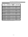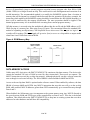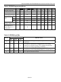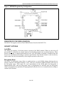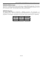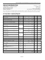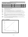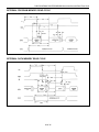
1
DS87C530/DS83C530 EPROM/ROM Microcontrollers with Real-Time Clock www.maxim-ic.com FEATURES PIN CONFIGURATIONS 80C52 Compatible 8051 Instruction-Set Compatible Four 8-Bit I/O Ports Three 16-Bit Timer/Counters 256 Bytes Scratchpad RAM Large On-Chip Memory 16kB EPROM (OTP) 1kB Extra On-Chip SRAM for MOVX ROMSIZE Features Selects Effective On-Chip ROM Size from 0 to 16kB Allows Access to Entire External Memory Map Dynamically Adjustable by Software Useful as Boot Block for External Flash TOP VIEW 7 46 DALLAS DS87C530 DS83C530 20 34 21 Nonvolatile Functions On-Chip Real-Time Clock with Alarm Interrupt Battery Backup Support of 1kB SRAM High-Speed Architecture 4 Clocks/Machine Cycle (8051 = 12) Runs DC to 33MHz Clock Rates Single-Cycle Instruction in 121ns Dual Data Pointer Optional Variable Length MOVX to Access Fast/Slow RAM /Peripherals 40 Power Management Mode Programmable Clock Source Saves Power Runs from (crystal/64) or (crystal/1024) Provides Automatic Hardware and Software Exit 52 EMI Reduction Mode Disables ALE Two Full-Duplex Hardware Serial Ports High Integration Controller Includes: Power-Fail Reset Early-Warning Power-Fail Interrupt Programmable Watchdog Timer 47 8 1 33 PLCC, WINDOWED CLCC 39 27 26 DALLAS DS87C530 DS83C530 14 1 13 TQFP The High-Speed Microcontroller User’s Guide must be used in conjunction with this data sheet. Download it at: www.maxim-ic.com/microcontrollers. 14 Total Interrupt Sources with Six External Note: Some revisions of this device may incorporate deviations from published specifications known as errata. Multiple revisions of any device may be simultaneously available through various sales channels. For information about device errata, click here: www.maxim-ic.com/errata. 1 of 45 REV: 071107 DS87C530/DS83C530 EPROM/ROM Microcontrollers with Real-Time Clock ORDERING INFORMATION TEMP RANGE MAX CLOCK SPEED (MHz) DS87C530-QCL 0C to +70C 33 52 PLCC DS87C530-QCL+ 0C to +70C 33 52 PLCC DS87C530-QNL -40C to +85C 33 52 PLCC DS87C530-QNL+ -40C to +85C 33 52 PLCC DS87C530-KCL* 0C to +70C 33 52 Windowed CLCC DS87C530-ECL 0C to +70C 33 52 TQFP DS87C530-ECL+ 0C to +70C 33 52 TQFP DS87C530-ENL -40C to +85C 33 52 TQFP DS87C530-ENL+ -40C to +85C 33 52 TQFP DS83C530-QCL 0C to +70C 33 52 PLCC DS83C530-QCL+ 0C to +70C 33 52 PLCC DS83C530-QNL -40C to +85C 33 52 PLCC DS83C530-QNL+ -40C to +85C 33 52 PLCC DS83C530-ECL 0C to +70C 33 52 TQFP DS83C530-ECL+ 0C to +70C 33 52 TQFP DS83C530-ENL -40C to +85C 33 52 TQFP DS83C530-ENL+ -40C to +85C 33 52 TQFP PART + Denotes a lead(Pb)-free/RoHS-compliant device. * The windowed ceramic LCC package is intrinsically lead(Pb) free. 2 of 45 PIN-PACKAGE DS87C530/DS83C530 EPROM/ROM Microcontrollers with Real-Time Clock DETAILED DESCRIPTION The DS87C530/DS83C530 EPROM/ROM microcontrollers with a real-time clock (RTC) are 8051compatible microcontrollers based on the Dallas Semiconductor high-speed core. They use 4 clocks per instruction cycle instead of the 12 used by the standard 8051. They also provide a unique mix of peripherals not widely available on other processors. They include an on-chip RTC and battery backup support for an on-chip 1k x 8 SRAM. The new Power Management Mode allows software to select reduced power operation while still processing. A combination of high-performance microcontroller core, RTC, battery-backed SRAM, and power management makes the DS87C530/DS83C530 ideal for instruments and portable applications. They also provide several peripherals found on other Dallas high-speed microcontrollers. These include two independent serial ports, two data pointers, on-chip power monitor with brownout detection and a watchdog timer. Power Management Mode (PMM) allows software to select a slower CPU clock. While default operation uses four clocks per machine cycle, the PMM runs the processor at 64 or 1024 clocks per cycle. There is a corresponding drop in power consumption when the processor slows. The EMI reduction feature allows software to select a reduced emission mode. This disables the ALE signal when it is unneeded. The DS83C530 is a factory mask ROM version of the DS87C530 designed for high-volume, costsensitive applications. It is identical in all respects to the DS87C530, except that the 16kB of EPROM is replaced by a user-supplied application program. All references to features of the DS87C530 will apply to the DS83C530, with the exception of EPROM-specific features where noted. Please contact your local Dallas Semiconductor sales representative for ordering information. Note: The DS87C530/DS83C530 are monolithic devices. A user must supply an external battery or super cap and a 32.768kHz timekeeping crystal to have permanently powered timekeeping or nonvolatile RAM. The DS87C530/DS83C530 provide all the support and switching circuitry needed to manage these resources. 3 of 45 DS87C530/DS83C530 EPROM/ROM Microcontrollers with Real-Time Clock Figure 1. Block Diagram DS87C530/ DS83C530 PIN DESCRIPTION PIN NAME FUNCTION PLCC TQFP 52 45 VCC +5V Processor Power Supply 1, 25 18, 46 GND Processor Digital Circuit Ground 29 22 VCC2 +5V RTC Supply. VCC2 is isolated from VCC to isolate the RTC from digital noise. 26 19 GND2 12 5 RST 23 16 XTAL2 24 17 XTAL1 RTC Circuit Ground Reset Input. This pin contains a Schmitt voltage input to recognize external active high reset inputs. The pin also employs an internal pulldown resistor to allow for a combination of wired OR external reset sources. An RC is not required for power-up, as the device provides this function internally. Crystal Oscillator Pins. XTAL1 and XTAL2 provide support for parallel-resonant, AT-cut crystals. XTAL1 acts also as an input if there is an external clock source in place of a crystal. XTAL2 is the output of the crystal amplifier. 4 of 45 DS87C530/DS83C530 EPROM/ROM Microcontrollers with Real-Time Clock PIN DESCRIPTION (continued) PIN PLCC TQFP 38 31 NAME FUNCTION PSEN Program Store-Enable Output. This active-low signal is a chip enable for optional external ROM memory. PSEN provides an active-low pulse and is driven high when external ROM is not being accessed. Address Latch-Enable Output. This pin latches the external address LSB from the multiplexed address/data bus on Port 0. This signal is commonly connected to the latch enable of an external 373 family transparent latch. ALE has a pulse width of 1.5 XTAL1 cycles and a period of four XTAL1 cycles. ALE is forced high when the device is in a Reset condition. ALE can be disabled and forced high by writing ALEOFF = 1 (PMR.2). ALE operates independently of ALEOFF during external memory accesses. 39 32 ALE 50 43 P0.0 (AD0) 49 42 P0.1 (AD1) 48 41 P0.2 (AD2) 47 40 P0.3 (AD3) 46 39 P0.4 (AD4) 45 38 P0.5 (AD5) 44 37 P0.6 (AD6) 43 36 P0.7 (AD7) 3 48 P1.0 4 49 P1.1 5 50 P1.2 6 51 P1.3 7 52 P1.4 8 1 P1.5 9 2 P1.6 10 3 P1.7 Port 0 (AD0–AD7), I/O. Port 0 is an open-drain, 8-bit, bidirectional I/O port. As an alternate function Port 0 can function as the multiplexed address/data bus to access off-chip memory. During the time when ALE is high, the LSB of a memory address is presented. When ALE falls to a logic 0, the port transitions to a bidirectional data bus. This bus is used to read external ROM and read/ write external RAM memory or peripherals. When used as a memory bus, the port provides active high drivers. The reset condition of Port 0 is tri-state. Pullup resistors are required when using Port 0 as an I/O port. Port 1, I/O. Port 1 functions as both an 8-bit, bidirectional I/O port and an alternate functional interface for Timer 2 I/O, new External Interrupts, and new Serial Port 1. The reset condition of Port 1 is with all bits at a logic 1. In this state, a weak pullup holds the port high. This condition also serves as an input mode, since any external circuit that writes to the port will overcome the weak pullup. When software writes a 0 to any port pin, the device will activate a strong pulldown that remains on until either a 1 is written or a reset occurs. Writing a 1 after the port has been at 0 will cause a strong transition driver to turn on, followed by a weaker sustaining pullup. Once the momentary strong driver turns off, the port again becomes the output high (and input) state. The alternate modes of Port 1 are outlined as follows. Port P1.0 P1.1 P1.2 P1.3 P1.4 P1.5 P1.6 P1.7 Alternate T2 T2EX RXD1 TXD1 INT2 INT3 INT4 INT5 Function External I/O for Timer/Counter 2 Timer/Counter 2 Capture/Reload Trigger Serial Port 1 Input Serial Port 1 Output External Interrupt 2 (Positive Edge Detect) External Interrupt 3 (Negative Edge Detect) External Interrupt 4 (Positive Edge Detect) External Interrupt 5 (Negative Edge Detect) 5 of 45 DS87C530/DS83C530 EPROM/ROM Microcontrollers with Real-Time Clock PIN DESCRIPTION (continued) PIN NAME FUNCTION 23 P2.0 (AD8) 31 24 P2.1 (AD9) 32 25 P2.2 (AD10) 33 26 P2.3 (AD11) 34 27 P2.4 (AD12) 35 28 P2.5 (AD13) 36 29 P2.6 (AD14) 37 30 P2.7 (AD15) Port 2 (A8–A15), I/O. Port 2 is a bidirectional I/O port. The reset condition of Port 2 is logic high. In this state, a weak pullup holds the port high. This condition also serves as an input mode, since any external circuit that writes to the port will overcome the weak pullup. When software writes a 0 to any port pin, the device will activate a strong pulldown that remains on until either a 1 is written or a reset occurs. Writing a 1 after the port has been at 0 will cause a strong transition driver to turn on, followed by a weaker sustaining pullup. Once the momentary strong driver turns off, the port again becomes both the output high and input state. As an alternate function Port 2 can function as MSB of the external address bus. This bus can be used to read external ROM and read/write external RAM memory or peripherals. 15 8 P3.0 16 9 P3.1 17 10 P3.2 18 11 P3.3 19 12 P3.4 20 13 P3.5 21 14 P3.6 22 15 P3.7 42 35 EA External Access Input, Active Low. Connect to ground to use an external ROM. Internal RAM is still accessible as determined by register settings. Connect to VCC to use internal ROM. 51 44 VBAT VBAT Input. Connect to the power source that maintains SRAM and RTC when VCC < VBAT. Can be connected to a 3V lithium battery or a super cap. Connect to GND if battery will not be used with device. 27 20 RTCX2 28 21 RTCX1 2, 11, 13, 14, 40, 41 4, 6, 7, 33, 34, 47 N.C. PLCC TQFP 30 Port 3, I/O. Port 3 functions as both an 8-bit, bi-directional I/O port and an alternate functional interface for external interrupts, Serial Port 0, Timer 0 and 1 Inputs, and RD and WR strobes. The reset condition of Port 3 is with all bits at a logic 1. In this state, a weak pullup holds the port high. This condition also serves as an input mode, since any external circuit that writes to the port will overcome the weak pullup. When software writes a 0 to any port pin, the device will activate a strong pulldown that remains on until either a 1 is written or a reset occurs. Writing a 1 after the port has been at 0 will cause a strong transition driver to turn on, followed by a weaker sustaining pullup. Once the momentary strong driver turns off, the port again becomes both the output high and input state. The alternate modes of Port 3 are outlined below. Port Alternate Function P3.0 RXD0 Serial Port 0 Input P3.1 TXD0 Serial Port 0 Output P3.2 INT0 External Interrupt 0 P3.3 INT1 External Interrupt 1 P3.4 T0 Timer 0 External Input P3.5 T1 Timer 1 External Input P3.6 WR External Data Memory Write Strobe P3.7 RD External Data Memory Read Strobe Timekeeping Crystals. A 32.768kHz crystal between these pins supplies the time base for the RTC. The devices support both 6pF and 12.5pF load capacitance crystals as selected by an SFR bit (described later). To prevent noise from affecting the RTC, the RTCX2 and RTCX1 pins should be guard-ringed with GND2. Not Connected. These pins should not be connected. They are reserved for use with future devices in the family. 6 of 45 DS87C530/DS83C530 EPROM/ROM Microcontrollers with Real-Time Clock COMPATIBILITY The DS87C530/DS83C530 are fully static, CMOS 8051-compatible microcontrollers designed for high performance. While remaining familiar to 8051 users, the devices have many new features. In general, software written for existing 8051-based systems works without modification on the DS87C530/DS83C530. The exception is critical timing since the high-speed microcontrollers perform its instructions much faster than the original for any given crystal selection. The DS87C530/DS83C530 run the standard 8051 instruction set. They are not pin compatible with other 8051s due to the timekeeping crystal. The DS87C530/DS83C530 provide three 16-bit timer/counters, full-duplex serial port (2), 256 bytes of direct RAM plus 1kB of extra MOVX RAM. I/O ports have the same operation as a standard 8051 product. Timers will default to a 12 clock-per-cycle operation to keep their timing compatible with original 8051 systems. However, timers are individually programmable to run at the new 4 clocks per cycle if desired. The PCA is not supported. The DS87C530/DS83C530 provide several new hardware features implemented by new Special Function Registers. A summary of these SFRs is provided below. PERFORMANCE OVERVIEW The DS87C530/DS83C530 feature a high-speed, 8051-compatible core. Higher speed comes not just from increasing the clock frequency, but also from a newer, more efficient design. This updated core does not have the dummy memory cycles that are present in a standard 8051. A conventional 8051 generates machine cycles using the clock frequency divided by 12. In the DS87C530/DS83C530, the same machine cycle takes 4 clocks. Thus the fastest instruction, one machine cycle, executes three times faster for the same crystal frequency. Note that these are identical instructions. The majority of instructions on the DS87C530/DS83C530 will see the full 3-to-1 speed improvement. Some instructions will get between 1.5 and 2.4 to 1 improvement. All instructions are faster than the original 8051. The numerical average of all opcodes gives approximately a 2.5 to 1 speed improvement. Improvement of individual programs will depend on the actual instructions used. Speed-sensitive applications would make the most use of instructions that are three times faster. However, the sheer number of 3 to 1 improved opcodes makes dramatic speed improvements likely for any code. These architecture improvements produce a peak instruction cycle in 121ns (8.25 MIPs). The Dual Data Pointer feature also allows the user to eliminate wasted instructions when moving blocks of memory. INSTRUCTION SET SUMMARY All instructions perform the same functions as their 8051 counterparts. Their effect on bits, flags, and other status functions is identical. However, the timing of each instruction is different. This applies both in absolute and relative number of clocks. For absolute timing of real-time events, the timing of software loops can be calculated using a table in the High-Speed Microcontroller User’s Guide. However, counter/timers default to run at the older 12 clocks per increment. In this way, timer-based events occur at the standard intervals with software executing at higher speed. Timers optionally can run at 4 clocks per increment to take advantage of faster processor operation. 7 of 45 DS87C530/DS83C530 EPROM/ROM Microcontrollers with Real-Time Clock The relative time of two instructions might be different in the new architecture than it was previously. For example, in the original architecture, the “MOVX A, @DPTR” instruction and the “MOV direct, direct” instruction used two machine cycles or 24 oscillator cycles. Therefore, they required the same amount of time. In the DS87C530/DS83C530, the MOVX instruction takes as little as two machine cycles or eight oscillator cycles but the “MOV direct, direct” uses three machine cycles or 12 oscillator cycles. While both are faster than their original counterparts, they now have different execution times. This is because the DS87C530/DS83C530 usually use one instruction cycle for each instruction byte. The user concerned with precise program timing should examine the timing of each instruction for familiarity with the changes. Note that a machine cycle now requires just 4 clocks, and provides one ALE pulse per cycle. Many instructions require only one cycle, but some require five. In the original architecture, all were one or two cycles except for MUL and DIV. Refer to the High-Speed Microcontroller User’s Guide for details and individual instruction timing. SPECIAL FUNCTION REGISTERS Special Function Registers (SFRs) control most special features of the DS87C530/DS83C530. This allows the device to incorporate new features but remain instruction-set compatible with the 8051. EQUATE statements can be used to define the new SFR to an assembler or compiler. All SFRs contained in the standard 80C52 are duplicated in this device. Table 1 shows the register addresses and bit locations. The High-Speed Microcontroller User’s Guide describes all SFRs. 8 of 45 DS87C530/DS83C530 EPROM/ROM Microcontrollers with Real-Time Clock Table 1. Special Function Register Locations * Functions not present in the 80C52 are in bold. REGISTER P0 BIT 7 BIT 6 BIT 5 BIT 4 BIT 3 BIT 2 BIT 1 BIT 0 ADDRESS P0.7 P0.6 P0.5 P0.4 P0.3 P0.2 P0.1 P0.0 80h SP 81h DPL 82h DPH 83h DPL1 84h DPH1 85h 0 0 0 0 0 0 0 SEL 86h PCON SMOD_0 SMOD0 — — GF1 GF0 STOP IDLE 87h TCON TF1 TR1 TF0 TR0 IE1 IT1 IE0 IT0 88h TMOD GATE C/ T M1 M0 GATE C/ T M1 M0 89h DPS TL0 8Ah TL1 8Bh TH0 8Ch TH1 8Dh CKCON WD1 WD0 T2M T1M T0M MD2 MD1 MD0 8Eh P1 P1.7 P1.6 P1.5 P1.4 P1.3 P1.2 P1.1 P1.0 90h EXIF IE5 IE4 IE3 IE2 XT/RG RGMD RGSL BGS 91h TRIM E4K X12/ 6 TRM2 TRM2 TRM1 TRM1 TRM0 TRM0 96h SCON0 SM0/FE_0 SM1_0 SM2_0 REN_0 TB8_0 RB8_0 TI_0 RI_0 98h SBUF0 99h P2 P2.7 P2.6 P2.5 P2.4 P2.3 P2.2 P2.1 P2.0 A0h IE EA ES1 ET2 ES0 ET1 EX1 ET0 EX0 A8h SADDR0 A9h SADDR1 AAh P3 P3.7 P3.6 P3.5 P3.4 P3.3 P3.2 P3.1 P3.0 B0h IP — PS1 PT2 PS0 PT1 PX1 PT0 PX0 B8h SADEN0 B9h SADEN1 SCON1 BAh SM0/FE_1 SM1_1 SM2_1 REN_1 TB8_1 RB8_1 TI_1 RI_1 C0h C1h SBUF1 — — — — — RMS2 RMS1 RMS0 C2h PMR CD1 CD0 SWB — XTOFF ALEOFF DME1 DME0 C4h STATUS PIP HIP LIP XTUP SPTA1 SPRA1 SPTA0 SPRA0 C5h ROMSIZE TA C7h T2CON TF2 EXF2 RCLK TCLK EXEN2 TR2 C/ T2 CP/ RL2 C8h T2MOD — — — — — — T2OE DCEN C9h RCAP2L CAh RCAP2H CBh 9 of 45 DS87C530/DS83C530 EPROM/ROM Microcontrollers with Real-Time Clock Table 1. Special Function Register Locations (continued) * Functions not present in the 80C52 are in bold. REGISTER BIT 7 BIT 6 BIT 5 BIT 4 BIT 3 BIT 2 BIT 1 BIT 0 ADDRESS TL2 CCh TH2 CDh PSW WDCON CY AC F0 RS1 RS0 OV FL P D0h SMOD_1 POR EPFI PFI WDIF WTRF EWT RWT D8h ACC EIE E0h — — ERTCI EWDI EX5 EX4 EX3 EX2 E8h B F0h RTASS F2h RTAS 0 0 F3h RTAM 0 0 F4h RTAH 0 0 0 EIP — — PRTCI PWDI PX5 PX4 PX3 PX2 F8h SSCE SCE MCE HCE RTCRE RTCWE RTCIF RTCE F9h RTCC F5h FAh RTCSS RTCS 0 0 FBh RTCM 0 0 FCh RTCH FDh RTCD0 FEh RTCD1 FFh NONVOLATILE FUNCTIONS The DS87C530/DS83C530 provide two functions that are permanently powered if a user supplies an external energy source. These are an on-chip RTC and a nonvolatile SRAM. The chip contains all related functions and controls. The user must supply a backup source and a 32.768kHz timekeeping crystal. REAL-TIME CLOCK The on-chip RTC keeps time of day and calendar functions. Its time base is a 32.768kHz crystal between pins RTCX1 and RTCX2. The RTC maintains time to 1/256 of a second. It also allows a user to read (and write) seconds, minutes, hours, day of the week, and date. Figure 2 shows the clock organization. Timekeeping registers allow easy access to commonly needed time values. For example, software can simply check the elapsed number of minutes by reading one register. Alternately, it can read the complete time of day, including subseconds, in only four registers. The calendar stores its data in binary form. While this requires software translation, it allows complete flexibility as to the exact value. A user can start the calendar with a variety of selections since it is simply a 16-bit binary number of days. This number allows a total range of 179 years beginning from 0000. The RTC features a programmable alarm condition. A user selects the alarm time. When the RTC reaches the selected value, it sets a flag. This will cause an interrupt if enabled, even in Stop mode. The alarm consists of a comparator that matches the user value against the RTC actual value. A user can select a match for 1 or more of the sub-seconds, seconds, minutes, or hours. This allows an interrupt 10 of 45 DS87C530/DS83C530 EPROM/ROM Microcontrollers with Real-Time Clock automatically to occur once per second, once per minute, once per hour, or once per day. Enabling interrupts with no match will generate an interrupt 256 times per second. Software enables the timekeeper oscillator using the RTC enable bit in the RTC Control register (F9h). This starts the clock. It can disable the oscillator to preserve the life of the backup energy-source if unneeded. Values in the RTC Control register are maintained by the backup source through power failure. Once enabled, the RTC maintains time for the life of the backup source even when VCC is removed. The RTC will maintain an accuracy of 2 minutes per month at 25C. Under no circumstances are negative voltages, of any amplitude, allowed on any pin while the device is in data retention mode (VCC < VBAT). Negative voltages will shorten battery life, possibly corrupting the contents of internal SRAM and the RTC. Figure 2. Real-Time Clock NONVOLATILE RAM The 1k x 8 on-chip SRAM can be nonvolatile if an external backup energy source is used. This allows the device to log data or to store configuration settings. Internal switching circuits will detect the loss of VCC and switch SRAM power to the backup source on the VBAT pin. The 256 bytes of direct RAM are not affected by this circuit and are volatile. CRYSTAL AND BACKUP SOURCES To use the unique functions of the DS87C530/DS83C530, a 32.768kHz timekeeping crystal and a backup energy source are needed. The following describes guidelines for choosing these devices. Timekeeping Crystal The DS87C530/DS83C530 can use a standard 32.768kHz crystal as the RTC time base. There are two versions of standard crystals available, with 6pF and 12.5pF load capacitance. The tradeoff is that the 6pF uses less power, giving longer life while VCC is off, but is more sensitive to noise and board layout. The 11 of 45 DS87C530/DS83C530 EPROM/ROM Microcontrollers with Real-Time Clock 12.5pF crystal uses more power, giving a shorter battery backed life, but produces a more robust oscillator. Bit 6 in the RTC Trim register (TRIM; 96h) must be programmed to specify the crystal type for the oscillator. When TRIM.6 = 1, the circuit expects a 12.5pF crystal. When TRIM.6 = 0, it expects a 6pF crystal. This bit will be nonvolatile so these choices will remain while the backup source is present. A guard ring (connected to the RTC ground) should encircle the RTCX1 and RTCX2 pins. Backup Energy Source The DS87C530/DS83C530 use an external energy source to maintain timekeeping and SRAM data without VCC. This source can be either a battery or 0.47F super cap and should be connected to the VBAT pin. The nominal battery voltage is 3V. The VBAT pin will not source current. Therefore, a super cap requires an external resistor and diode to supply charge. The backup lifetime is a function of the battery capacity and the data retention current drain. This drain is specified in the electrical specifications. The circuit loads the VBAT only when VCC has fallen below VBAT. Thus the actual lifetime depends not only on the current and battery capacity, but also on the portion of time without power. A very small lithium cell provides a lifetime of more than 10 years. Figure 3. Internal Backup Circuit IMPORTANT APPLICATION NOTE The pins on the DS87C530/DS83C530 are generally as resilient as other CMOS circuits. They have no unusual susceptibility to electrostatic discharge (ESD) or other electrical transients. However, no pin on the DS87C530/DS83C530 should ever be taken to a voltage below ground. Negative voltages on any pin can turn on internal parasitic diodes that draw current directly from the battery. If a device pin is connected to the “outside world” where it may be handled or come in contact with electrical noise, protection should be added to prevent the device pin from going below -0.3V. Some power supplies can give a small undershoot on power-up, which should be prevented. Application Note 93: Design Guidelines for Microcontrollers Incorporating NV RAM discusses how to protect the DS87C530/DS83C530 against these conditions. MEMORY RESOURCES Like the 8051, the DS87C530/DS83C530 use three memory areas. The total memory configuration of the device is 16kB of ROM, 1kB of data SRAM and 256 bytes of scratchpad or direct RAM. The 1kB of data 12 of 45 DS87C530/DS83C530 EPROM/ROM Microcontrollers with Real-Time Clock space SRAM is read/write accessible and is memory mapped. This on-chip SRAM is reached by the MOVX instruction. It is not used for executable memory. The scratchpad area is 256 bytes of register mapped RAM and is identical to the RAM found on the 80C52. There is no conflict or overlap among the 256 bytes and the 1kB as they use different addressing modes and separate instructions. OPERATIONAL CONSIDERATION The erasure window of the windowed LCC should be covered without regard to the programmed/unprogrammed state of the EPROM. Otherwise, the device may not meet the AC and DC parameters listed in the data sheet. PROGRAM MEMORY ACCESS On-chip ROM begins at address 0000h and is contiguous through 3FFFh (16kB). Exceeding the maximum address of on-chip ROM will cause the DS87C530/DS83C530 to access off-chip memory. However, the maximum on-chip decoded address is selectable by software using the ROMSIZE feature. Software can cause the microcontroller to behave like a device with less on-chip memory. This is beneficial when overlapping external memory, such as Flash, is used. The maximum memory size is dynamically variable. Thus a portion of memory can be removed from the memory map to access off-chip memory, then restored to access on-chip memory. In fact, all the on-chip memory can be removed from the memory map allowing the full 64kB memory space to be addressed from off-chip memory. ROM addresses that are larger than the selected maximum are automatically fetched from outside the part via Ports 0 and 2. Figure 4 shows a depiction of the ROM memory map. The ROMSIZE register is used to select the maximum on-chip decoded address for ROM. Bits RMS2, RMS1, RMS0 have the following effect: RMS2 RMS1 RMS0 MAXIMUM ON-CHIP ROM ADDRESS 0 0 0 0kB 0 0 1 1kB 0 1 0 2kB 0 1 1 4kB 1 0 0 8kB 1 0 1 16kB (default) 1 1 0 Invalid—reserved 1 1 1 Invalid—reserved The reset default condition is a maximum on-chip ROM address of 16kB. Thus no action is required if this feature is not used. When accessing external program memory, the first 16kB would be inaccessible. To select a smaller effective ROM size, software must alter bits RMS2–RMS0. Altering these bits requires a timed-access procedure. Care should be taken so that changing the ROMSIZE register does not corrupt program execution. For example, assume that a device is executing instructions from internal program memory near the 12kB boundary (~3000h) and that the ROMSIZE register is currently configured for a 16kB internal program space. If software reconfigures the ROMSIZE register to 4kB (0000h–0FFFh) in the current state, the 13 of 45 DS87C530/DS83C530 EPROM/ROM Microcontrollers with Real-Time Clock device will immediately jump to external program execution because program code from 4kB to 16kB (1000h–3FFFh) is no longer located on-chip. This could result in code misalignment and execution of an invalid instruction. The recommended method is to modify the ROMSIZE register from a location in memory that will be internal (or external) both before and after the operation. In the above example, the instruction which modifies the ROMSIZE register should be located below the 4kB (1000h) boundary, so that it will be unaffected by the memory modification. The same precaution should be applied if the internal program memory size is modified while executing from external program memory. Off-chip memory is accessed using the multiplexed address/data bus on P0 and the MSB address on P2. While serving as a memory bus, these pins are not I/O ports. This convention follows the standard 8051 method of expanding on-chip memory. Off-chip ROM access also occurs if the EA pin is a logic 0. EA overrides all bit settings. The PSEN signal will go active (low) to serve as a chip enable or output enable when Ports 0 and 2 fetch from external ROM. Figure 4. ROM Memory Map DATA MEMORY ACCESS Unlike many 8051 derivatives, the DS87C530/DS83C530 contain on-chip data memory. The devices also contain the standard 256 bytes of RAM accessed by direct instructions. These areas are separate. The MOVX instruction accesses the on-chip data memory. Although physically on-chip, software treats this area as though it was located off-chip. The 1kB of SRAM is between address 0000h and 03FFh. Access to the on-chip data RAM is optional under software control. When enabled by software, the data SRAM is between 0000h and 03FFh. Any MOVX instruction that uses this area will go to the on-chip RAM while enabled. MOVX addresses greater than 03FFh automatically go to external memory through Ports 0 and 2. When disabled, the 1kB memory area is transparent to the system memory map. Any MOVX directed to the space between 0000h and FFFFh goes to the expanded bus on Ports 0 and 2. This also is the default condition. This default allows the DS87C530/DS83C530 to drop into an existing system that uses these addresses for other hardware and still have full compatibility. 14 of 45 DS87C530/DS83C530 EPROM/ROM Microcontrollers with Real-Time Clock The on-chip data area is software selectable using 2 bits in the Power Management Register at location C4h. This selection is dynamically programmable. Thus access to the on-chip area becomes transparent to reach off-chip devices at the same addresses. The control bits are DME1 (PMR.1) and DME0 (PMR.0). They have the following operation: Table 2. Data Memory Access Control DME1 DME0 DATA MEMORY ADDRESS 0 0 0000h–FFFFh External Data Memory (default condition) 0 1 0000h–03FFh Internal SRAM Data Memory 0400h–FFFFh External Data Memory 1 0 1 1 Reserved MEMORY FUNCTION Reserved 0000h–03FFh Internal SRAM Data Memory 0400h–FFFBh Reserved—no external access FFFCh Read access to the status of lock bits FFFDh–FFFh Reserved—no external access Notes on the status byte read at FFFCh with DME1, 0 = 1, 1: Bits 2-0 reflect the programmed status of the security lock bits LB2–LB0. They are individually set to a logic 1 to correspond to a security lock bit that has been programmed. These status bits allow software to verify that the part has been locked before running if desired. The bits are read-only. Note: After internal MOVX SRAM has been initialized, changing bits DEM0/1 has no effect on the contents of the SRAM. STRETCH MEMORY CYCLE The DS87C530/DS83C530 allow software to adjust the speed of off-chip data memory access. The microcontrollers can perform the MOVX in as few as two instruction cycles. The on-chip SRAM uses this speed and any MOVX instruction directed internally uses two cycles. However, the time can be stretched for interface to external devices. This allows access to both fast memory and slow memory or peripherals with no glue logic. Even in high-speed systems, it may not be necessary or desirable to perform off-chip data memory access at full speed. In addition, there are a variety of memory-mapped peripherals such as LCDs or UARTs that are slow. The Stretch MOVX is controlled by the Clock Control Register at SFR location 8Eh as described below. It allows the user to select a Stretch value between 0 and 7. A Stretch of 0 will result in a two-machine cycle MOVX. A Stretch of 7 will result in a MOVX of nine machine cycles. Software can dynamically change this value depending on the particular memory or peripheral. On reset, the Stretch value will default to a 1, resulting in a three-cycle MOVX for any external access. Therefore, off-chip RAM access is not at full speed. This is a convenience to existing designs that may not have fast RAM in place. Internal SRAM access is always at full speed regardless of the Stretch setting. When desiring maximum speed, software should select a Stretch value of 0. When using very slow RAM or peripherals, select a larger Stretch value. Note that this affects data memory only and the only way to slow program memory (ROM) access is to use a slower crystal. 15 of 45 DS87C530/DS83C530 EPROM/ROM Microcontrollers with Real-Time Clock Using a Stretch value between 1 and 7 causes the microcontroller to stretch the read/write strobe and all related timing. Also, setup and hold times are increased by 1 clock when using any Stretch greater than 0. This results in a wider read/write strobe and relaxed interface timing, allowing more time for memory/peripherals to respond. The timing of the variable speed MOVX is in the Electrical Specifications section. Table 3 shows the resulting strobe widths for each Stretch value. The memory Stretch uses the Clock Control Special Function Register at SFR location 8Eh. The Stretch value is selected using bits CKCON.2–0. In the table, these bits are referred to as M2 through M0. The first Stretch (default) allows the use of common 120ns RAMs without dramatically lengthening the memory access. Table 3. Data Memory Cycle Stretch Values CKCON.2–0 MEMORY CYCLES RD OR WR STROBE WIDTH IN CLOCKS STROBE WIDTH TIME AT 33MHz (ns) M2 M1 M0 0 0 0 2 (forced internal) 2 60 0 0 1 3 (default external) 4 121 0 1 0 4 8 242 0 1 1 5 12 364 1 0 0 6 16 485 1 0 1 7 20 606 1 1 0 8 24 727 1 1 1 9 28 848 DUAL DATA POINTER The timing of block moves of data memory is faster using the Dual Data Pointer (DPTR). The standard 8051 DPTR is a 16-bit value that is used to address off-chip data RAM or peripherals. In the DS87C530/DS83C530, the standard data pointer is called DPTR, located at SFR addresses 82h and 83h. These are the standard locations. Using DPTR requires no modification of standard code. The new DPTR at SFR 84h and 85h is called DPTR1. The DPTR Select bit (DPS) chooses the active pointer. Its location is the lsb of the SFR location 86h. No other bits in register 86h have any effect and are 0. The user switches between data pointers by toggling the lsb of register 86h. The increment (INC) instruction is the fastest way to accomplish this. All DPTR-related instructions use the currently selected DPTR for any activity. Therefore it takes only one instruction to switch from a source to a destination address. Using the Dual Data Pointer saves code from needing to save source and destination addresses when doing a block move. The software simply switches between DPTR and 1 once software loads them. The relevant register locations are as follows. DPL DPH DPL1 DPH1 DPS 82h 83h 84h 85h 86h Low byte original DPTR High byte original DPTR Low byte new DPTR High byte new DPTR DPTR Select (lsb) 16 of 45 DS87C530/DS83C530 EPROM/ROM Microcontrollers with Real-Time Clock POWER MANAGEMENT Along with the standard Idle and power-down (Stop) modes of the standard 80C52, the DS87C530/DS83C530 provide a new Power Management Mode. This mode allows the processor to continue functioning, yet to save power compared with full operation. The DS87C530/DS83C530 also feature several enhancements to Stop mode that make it more useful. POWER MANAGEMENT MODE (PMM) Power Management Mode offers a complete scheme of reduced internal clock speeds that allow the CPU to run software but to use substantially less power. During default operation, the DS87C530/DS83C530 use four clocks per machine cycle. Thus the instruction cycle rate is (Clock/4). At 33MHz crystal speed, the instruction cycle speed is 8.25MHz (33/4). In PMM, the microcontroller continues to operate but uses an internally divided version of the clock source. This creates a lower power state without external components. It offers a choice of two reduced instruction cycle speeds (and two clock sources - discussed below). The speeds are (Clock/64) and (Clock/1024). Software is the only mechanism to invoke the PMM. Table 4 illustrates the instruction cycle rate in PMM for several common crystal frequencies. Since power consumption is a direct function of operating speed, PMM 1 eliminates most of the power consumption while still allowing a reasonable speed of processing. PMM 2 runs very slowly and provides the lowest power consumption without stopping the CPU. This is illustrated in Table 5. Note that PMM provides a lower power condition than Idle mode. This is because in Idle, all clocked functions such as timers run at a rate of crystal divided by 4. Since wake-up from PMM is as fast as or faster than from Idle and PMM allows the CPU to operate (even if doing NOPs), there is little reason to use Idle mode in new designs. Table 4. Machine Cycle Rate CRYSTAL SPEED (MHz) FULL OPERATION (4 CLOCKS) (MHz) PMM1 (64 CLOCKS) (kHz) PMM2 (1024 CLOCKS) (kHz) 11.0592 2.765 172.8 10.8 16 4.00 250.0 15.6 25 6.25 390.6 24.4 33 8.25 515.6 32.2 Table 5. Typical Operating Current in PMM CRYSTAL SPEED (MHz) FULL OPERATION (4 CLOCKS) (mA) PMM1 (64 CLOCKS) (mA) PMM2 (1024 CLOCKS) (mA) 11.0592 13.1 5.3 4.8 16 17.2 6.4 5.6 25 25.7 8.1 7.0 33 32.8 9.8 8.2 17 of 45 DS87C530/DS83C530 EPROM/ROM Microcontrollers with Real-Time Clock CRYSTAL-LESS PMM A major component of power consumption in PMM is the crystal amplifier circuit. The DS87C530/DS83C530 allow the user to switch CPU operation to an internal ring oscillator and turn off the crystal amplifier. The CPU would then have a clock source of approximately 2MHz to 4MHz, divided by either 4, 64, or 1024. The ring is not accurate, so software cannot perform precision timing. However, this mode allows an additional saving of between 0.5mA and 6.0mA, depending on the actual crystal frequency. While this saving is of little use when running at 4 clocks per instruction cycle, it makes a major contribution when running in PMM1 or PMM2. PMM OPERATION Software invokes the PMM by setting the appropriate bits in the SFR area. The basic choices are divider speed and clock source. There are three speeds (4, 64, and 1024) and two clock sources (crystal, ring). Both the decisions and the controls are separate. Software will typically select the clock speed first. Then, it will perform the switch to ring operation if desired. Lastly, software can disable the crystal amplifier if desired. There are two ways of exiting PMM. Software can remove the condition by reversing the procedure that invoked PMM or hardware can (optionally) remove it. To resume operation at a divide-by-4 rate under software control, simply select 4 clocks per cycle, and then crystal-based operation if relevant. When disabling the crystal as the time base in favor of the ring oscillator, there are timing restrictions associated with restarting the crystal operation. Details are described below. There are three registers containing bits that are concerned with PMM functions. They are Power Management Register (PMR; C4h), Status (STATUS; C5h), and External Interrupt Flag (EXIF; 91h) Clock Divider Software can select the instruction cycle rate by selecting bits CD1 (PMR.7) and CD0 (PMR.6) as follows: CD1 CD0 CYCLE RATE 0 0 Reserved 0 1 4 clocks (default) 1 0 64 clocks 1 1 1024 clocks The selection of instruction cycle rate will take effect after a delay of one instruction cycle. Note that the clock divider choice applies to all functions including timers. Since baud rates are altered, it will be difficult to conduct serial communication while in PMM. There are minor restrictions on accessing the clock selection bits. The processor must be running in a 4-clock state to select either 64 (PMM1) or 1024 (PMM2) clocks. This means software cannot go directly from PMM1 to PMM2 or visa versa. It must return to a 4-clock rate first. 18 of 45 DS87C530/DS83C530 EPROM/ROM Microcontrollers with Real-Time Clock Switchback To return to a 4-clock rate from PMM, software can simply select the CD1 and CD0 clock control bits to the 4 clocks per cycle state. However, the DS87C530/DS83C530 provide several hardware alternatives for automatic Switchback. If Switchback is enabled, then the device will automatically return to a 4-clock per cycle speed when an interrupt occurs from an enabled, valid external interrupt source. A Switchback will also occur when a UART detects the beginning of a serial start bit if the serial receiver is enabled (REN = 1). Note the beginning of a start bit does not generate an interrupt; this occurs on reception of a complete serial word. The automatic Switchback on detection of a start bit allows hardware to correct baud rates in time for a proper serial reception. A Switchback will also occur when a byte is written to the SBUF0 or SBUF1 for transmission. Switchback is enabled by setting the SWB bit (PMR.5) to a 1 in software. For an external interrupt, Switchback will occur only if the interrupt source could really generate the interrupt. For example, if INT0 is enabled but has a low priority setting, then Switchback will not occur on INT0 if the CPU is servicing a high priority interrupt. Status Information in the Status register assists decisions about switching into PMM. This register contains information about the level of active interrupts and the activity on the serial ports. The DS87C530/DS83C530 support three levels of interrupt priority. These levels are Power-fail, High, and Low. Bits STATUS.7–5 indicate the service status of each level. If PIP (Power-fail Interrupt Priority; STATUS. 7) is 1, then the processor is servicing this level. If either HIP (High Interrupt Priority; STATUS.6) or LIP (Low Interrupt Priority; STATUS.5) is high, then the corresponding level is in service. Software should not rely on a lower priority level interrupt source to remove PMM (Switchback) when a higher level is in service. Check the current priority service level before entering PMM. If the current service level locks out a desired Switchback source, then it would be advisable to wait until this condition clears before entering PMM. Alternately, software can prevent an undesired exit from PMM by entering a low priority interrupt service level before entering PMM. This will prevent other low priority interrupts from causing a Switchback. Status also contains information about the state of the serial ports. Serial Port Zero Receive Activity (SPRA0; STATUS.0) indicates a serial word is being received on Serial Port 0 when this bit is set to a 1. Serial Port 0 Transmit Activity (SPTA0; STATUS.1) indicates that the serial port is still shifting out a serial transmission. STATUS.2 and STATUS.3 provide the same information for Serial Port 1, respectively. These bits should be interrogated before entering PMM1 or PMM2 to ensure that no serial port operations are in progress. Changing the clock divisor rate during a serial transmission or reception will corrupt the operation. 19 of 45 DS87C530/DS83C530 EPROM/ROM Microcontrollers with Real-Time Clock Crystal/Ring Operation The DS87C530/DS83C530 allow software to choose the clock source as an independent selection from the instruction cycle rate. The user can select crystal-based or ring oscillator-based operation under software control. Power-on reset default is the crystal (or external clock) source. The ring may save power depending on the actual crystal speed. To save still more power, software can then disable the crystal amplifier. This process requires two steps. Reversing the process also requires two steps. The XT/ RG bit (EXIF.3) selects the crystal or ring as the clock source. Setting XT/ RG = 1 selects the crystal. Setting XT/ RG = 0 selects the ring. The RGMD (EXIF.2) bit serves as a status bit by indicating the active clock source. RGMD = 0 indicates the CPU is running from the crystal. RGMD = 1 indicates it is running from the ring. When operating from the ring, disable the crystal amplifier by setting the XTOFF bit (PMR.3) to a 1. This can only be done when XT/ RG = 0. When changing the clock source, the selection will take effect after a one-instruction-cycle delay. This applies to changes from crystal to ring and vise versa. However, this assumes that the crystal amplifier is running. In most cases, when the ring is active, software previously disabled the crystal to save power. If ring operation is being used and the system must switch to crystal operation, the crystal must first be enabled. Set the XTOFF bit to 0. At this time, the crystal oscillation will begin. The DS87C530/DS83C530 then provide a warm-up delay to make certain that the frequency is stable. Hardware will set the XTUP bit (STATUS.4) to 1 when the crystal is ready for use. Then software should write XT/ RG to 1 to begin operating from the crystal. Hardware prevents writing XT/ RG to 1 before XTUP = 1. The delay between XTOFF = 0 and XTUP = 1 will be 65,536 crystal clocks in addition to the crystal cycle startup time. Switchback has no affect on the clock source. If software selects a reduced clock divider and enables the ring, a Switchback will only restore the divider speed. The ring will remain as the time base until altered by software. If there is serial activity, Switchback usually occurs with enough time to create proper baud rates. This is not true if the crystal is off and the CPU is running from the ring. If sending a serial character that wakes the system from crystal-less PMM, then it should be a dummy character of no importance with a subsequent delay for crystal startup. Table 6 is a summary of the bits relating to PMM and its operation. The flow chart below illustrates a typical decision set associated with PMM. 20 of 45 DS87C530/DS83C530 EPROM/ROM Microcontrollers with Real-Time Clock Table 6. PMM Control and Status Bit Summary NAME LOCATION FUNCTION XT/ RG EXIF.3 Control. XT/ RG =1, runs from crystal or external clock; XT/ RG =0, runs from internal ring oscillator. X 0 to 1 only when XTUP = 1 and XTOFF= 0 RGMD EXIF.2 Status. RGMD=1, CPU clock = ring; RGMD = 0, CPU clock = crystal. 0 None CD1, CD0 PMR7, PMR.6 Control. CD1, 0 = 01, 4 clocks; CS1, 0 = 10, PMM1; CD1, 0 = 11, PMM2. 0, 1 SWB PMR.5 Control. SWB = 1, hardware invokes switchback to 4 clocks, SWB = 0, no hardware switchback. 0 Unrestricted XTOFF PMR.3 Control. Disables crystal operation after ring is selected. 0 1 only when XT/ RG =0 PIP STATUS.7 Status. 1 indicates a power-fail interrupt in service. 0 None HIP STATUS.6 Status. 1 indicates high priority interrupt in service. 0 None LIP STATUS.5 Status. 1 indicates low priority interrupt in service. 0 None XTUP STATUS.4 Status. 1 indicates that the crystal has stabilized. 1 None SPTA1 STATUS.3 Status. Serial transmission on serial port 1. 0 None SPRA1 STATUS.2 Status. Serial word reception on serial port 1. 0 None SPTA0 STATUS.1 Status. Serial transmission on serial port 0. 0 None SPRA0 STATUS.0 Status. Serial word reception on serial port 0. 0 None 21 of 45 RESET WRITE ACCESS Write CD1, 0 = 10 or 11 only from CD1, 0 = 01 DS87C530/DS83C530 EPROM/ROM Microcontrollers with Real-Time Clock Figure 5. Invoking and Clearing PMM 22 of 45 DS87C530/DS83C530 EPROM/ROM Microcontrollers with Real-Time Clock IDLE MODE Setting the lsb of the Power Control register (PCON; 87h) invokes the Idle mode. Idle will leave internal clocks, serial ports and timers running. Power consumption drops because the CPU is not active. Since clocks are running, the Idle power consumption is a function of crystal frequency. It should be approximately one-half the operational power at a given frequency. The CPU can exit the Idle state with any interrupt or a reset. Idle is available for backward software compatibility. The system can now reduce power consumption to below Idle levels by using PMM1 or PMM2 and running NOPs. STOP MODE ENHANCEMENTS Setting bit 1 of the Power Control register (PCON; 87h) invokes the Stop mode. Stop mode is the lowest power state since it turns off all internal clocking. The ICC of a standard Stop mode is approximately 1 A but is specified in the Electrical Specifications. The CPU will exit Stop mode from an external interrupt or a reset condition. Internally generated interrupts (timer, serial port, watchdog) are not useful since they require clocking activity. One exception is that a RTC interrupt can cause the device to exit Stop mode. This provides a very power efficient way of performing infrequent yet periodic tasks. The DS87C530/DS83C530 provide two enhancements to the Stop mode. As documented below, the device provides a bandgap reference to determine Power-fail Interrupt and Reset thresholds. The default state is that the bandgap reference is off while in Stop mode. This allows the extremely low-power state mentioned above. A user can optionally choose to have the bandgap enabled during Stop mode. With the bandgap reference enabled, PFI and Power-fail Reset are functional and are a valid means for leaving Stop mode. This allows software to detect and compensate for a brownout or power supply sag, even when in Stop mode. In Stop mode with the bandgap enabled, ICC will be approximately 50A compared with 1A with the bandgap off. If a user does not require a Power-fail Reset or Interrupt while in Stop mode, the bandgap can remain disabled. Only the most power sensitive applications should turn off the bandgap, as this results in an uncontrolled power-down condition. The control of the bandgap reference is located in the Extended Interrupt Flag register (EXIF; 91h). Setting BGS (EXIF.0) to a 1 will keep the bandgap reference enabled during Stop mode. The default or reset condition is with the bit at a logic 0. This results in the bandgap being off during Stop mode. Note that this bit has no control of the reference during full power, PMM, or Idle modes. The second feature allows an additional power saving option while also making Stop easier to use. This is the ability to start instantly when exiting Stop mode. It is the internal ring oscillator that provides this feature. This ring can be a clock source when exiting Stop mode in response to an interrupt. The benefit of the ring oscillator is as follows. Using Stop mode turns off the crystal oscillator and all internal clocks to save power. This requires that the oscillator be restarted when exiting Stop mode. Actual startup time is crystal-dependent, but is normally at least 4ms. A common recommendation is 10ms. In an application that will wake up, perform a short operation, then return to sleep, the crystal startup can be longer than the real transaction. However, the ring oscillator will start instantly. Running from the ring, the user can perform a simple operation and return to sleep before the crystal has even started. If a user selects the ring to provide the startup clock and the processor remains running, hardware will automatically switch to the crystal once a power-on reset interval (65,536 clocks) has expired. Hardware uses this value to assure proper crystal start even though power is not being cycled. 23 of 45 DS87C530/DS83C530 EPROM/ROM Microcontrollers with Real-Time Clock The ring oscillator runs at approximately 2MHz to 4MHz but will not be a precise value. Do not conduct real-time precision operations (including serial communication) during this ring period. Figure 6 shows how the operation would compare when using the ring, and when starting up normally. The default state is to exit Stop mode without using the ring oscillator. The RGSL ring-select bit at EXIF.1 (EXIF; 91h) controls this function. When RGSL = 1, the CPU will use the ring oscillator to exit Stop mode quickly. As mentioned above, the processor will automatically switch from the ring to the crystal after a delay of 65,536 crystal clocks. For a 3.57MHz crystal, this is approximately 18ms. The processor sets a flag called RGMD- Ring Mode, located at EXIF.2, that tells software that the ring is being used. The bit will be a logic 1 when the ring is in use. Attempt no serial communication or precision timing while this bit is set, since the operating frequency is not precise. Figure 6. Ring Oscillator Exit from Stop Mode NOTE: DIAGRAM ASSUMES THAT THE OPERATION FOLLOWING STOP REQUIRES LESS THAN 18ms TO COMPLETE. EMI REDUCTION One of the major contributors to radiated noise in an 8051-based system is the toggling of ALE. The DS87C530/DS83C530 allow software to disable ALE when not used by setting the ALEOFF (PMR.2) bit to 1. When ALEOFF = 1, ALE will still toggle during an off-chip MOVX. However, ALE will remain in a static when performing on-chip memory access. The default state of ALEOFF = 0 so ALE toggles with every instruction cycle. 24 of 45 DS87C530/DS83C530 EPROM/ROM Microcontrollers with Real-Time Clock PERIPHERAL OVERVIEW The DS87C530/DS83C530 provide several of the most commonly needed peripheral functions in microcomputer-based systems. These new functions include a second serial port, power-fail reset, Powerfail interrupt, and a programmable watchdog timer. These are described below, and more details are available in the High-Speed Microcontroller User’s Guide. SERIAL PORTS The DS87C530/DS83C530 provide a serial port (UART) that is identical to the 80C52. In addition it includes a second hardware serial port that is a full duplicate of the standard one. This port optionally uses pins P1.2 (RXD1) and P1.3 (TXD1). It has duplicate control functions included in new SFR locations. Both ports can operate simultaneously but can be at different baud rates or even in different modes. The second serial port has similar control registers (SCON1; C0h, SBUF1; C1h) to the original. The new serial port can only use Timer 1 for timer-generated baud rates. TIMER RATE CONTROL There is one important difference between the DS87C530/DS83C530 and 8051 regarding timers. The original 8051 used 12 clocks per cycle for timers as well as for machine cycles. The DS87C530/DS83C530 architecture normally uses 4 clocks per machine cycle. However, in the area of timers and serial ports, the DS87C530/DS83C530 will default to 12 clocks per cycle on reset. This allows existing code with real-time dependencies such as baud rates to operate properly. If an application needs higher speed timers or serial baud rates, the user can select individual timers to run at the 4-clock rate. The Clock Control register (CKCON; 8Eh) determines these timer speeds. When the relevant CKCON bit is logic 1, the DS87C530/DS83C530 use 4 clocks per cycle to generate timer speeds. When the bit is a 0, the DS87C530 uses 12 clocks for timer speeds. The reset condition is a 0. CKCON.5 selects the speed of Timer 2. CKCON.4 selects Timer 1 and CKCON.3 selects Timer 0. Unless a user desires very fast timing, it is unnecessary to alter these bits. Note that the timer controls are independent. POWER-FAIL RESET The DS87C530/DS83C530 use a precision bandgap voltage reference to decide if VCC is out of tolerance. While powering up, the internal monitor circuit maintains a reset state until VCC rises above the VRST level. Once above this level, the monitor enables the crystal oscillator and counts 65,536 clocks. It then exits the reset state. This power-on reset (POR) interval allows time for the oscillator to stabilize. A system needs no external components to generate a power-related reset. Anytime VCC drops below VRST, as in power failure or a power drop, the monitor will generate and hold a reset. It occurs automatically, needing no action from the software. Refer to the Electrical Specifications section for the exact value of VRST. POWER-FAIL INTERRUPT The voltage reference that sets a precise reset threshold also generates an optional early warning powerfail interrupt (PFI). When enabled by software, the processor will vector to program memory address 0033h if VCC drops below VPFW. PFI has the highest priority. The PFI enable is in the Watchdog Control SFR (WDCON–D8h). Setting WDCON.5 to logic 1 will enable the PFI. Application software can also 25 of 45 DS87C530/DS83C530 EPROM/ROM Microcontrollers with Real-Time Clock read the PFI flag at WDCON.4. A PFI condition sets this bit to a 1. The flag is independent of the interrupt enable and software must manually clear it. If the PFI is enabled and the bandgap select bit (BGS) is set, a PFI will bring the device out of Stop mode. WATCHDOG TIMER To prevent software from losing control, the DS87C530/DS83C530 include a programmable watchdog timer. The Watchdog is a free-running timer that sets a flag if allowed to reach a preselected timeout. It can be (re)started by software. A typical application is to select the flag as a reset source. When the Watchdog times out it sets its flag, which generates reset. Software must restart the timer before it reaches its timeout or the processor is reset. Software can select one of four timeout values. Then, it restarts the timer and enables the reset function. After enabling the reset function, software must then restart the timer before its expiration or hardware will reset the CPU. Both the Watchdog Reset Enable and the Watchdog Restart control bits are protected by a “Timed Access” circuit. This prevents errant software from accidentally clearing the Watchdog. Timeout values are precise since they are a function of the crystal frequency as shown in Table 7. For reference, the time periods at 33MHz also are shown. The Watchdog also provides a useful option for systems that do not require a reset circuit. It will set an interrupt flag 512 clocks before setting the reset flag. Software can optionally enable this interrupt source. The interrupt is independent of the reset. A common use of the interrupt is during debug, to show developers where the Watchdog times out. This indicates where the Watchdog must be restarted by software. The interrupt also can serve as a convenient time-base generator or can wake-up the processor from power saving modes. The Watchdog function is controlled by the Clock Control (CKCON–8Eh), Watchdog Control (WDCON–D8h), and Extended Interrupt Enable (EIE–E8h) SFRs. CKCON.7 and CKCON.6 are WD1 and WD0, respectively, and they select the Watchdog timeout period as shown in Table 7. Table 7. Watchdog Timeout Values WD1 WD0 INTERRUPT TIMEOUT TIME (33MHz) RESET TIMEOUT TIME (33MHz) 0 0 217 clocks 3.9718ms 217 + 512 clocks 3.9874ms 0 1 1 1 0 1 20 2 clocks 23 2 clocks 26 2 clocks 31.77ms 254.20ms 2033.60ms 20 31.79ms 23 254.21ms 26 2033.62ms 2 + 512 clocks 2 + 512 clocks 2 + 512 clocks As shown above, the Watchdog Timer uses the crystal frequency as a time base. A user selects one of four counter values to determine the timeout. These clock counter lengths are 217 = 131,072 clocks; 220 = 1,048,576; 223 = 8,388,608 clocks; and 226 = 67,108,864 clocks. The times shown in Table 7 are with a 33MHz crystal frequency. Once the counter chain has completed a full interrupt count, hardware will set an interrupt flag. Regardless of whether the user enables this interrupt, there are then 512 clocks left until the reset flag is set. Software can enable the interrupt and reset individually. Note that the Watchdog is a free-running timer and does not require an enable. 26 of 45 DS87C530/DS83C530 EPROM/ROM Microcontrollers with Real-Time Clock There are five control bits in special function registers that affect the Watchdog Timer and two status flags that report to the user. WDIF (WDCON.3) is the interrupt flag that is set at timer termination when there are 512 clocks remaining until the reset flag is set. WTRF (WDCON.2) is the flag that is set when the timer has completely timed out. This flag is normally associated with a CPU reset and allows software to determine the reset source. EWT (WDCON.1) is the enable for the Watchdog Timer reset function. RWT (WDCON.0) is the bit that software uses to restart the Watchdog Timer. Setting this bit restarts the timer for another full interval. Application software must set this bit before the timeout. Both of these bits are protected by Timed Access discussed below. As mentioned previously, WD1 and 0 (CKCON .7 and 6) select the timeout. The Reset Watchdog Timer bit (WDCON.0) should be asserted prior to modifying the Watchdog Timer Mode Select bits (WD1, WD0) to avoid corruption of the watchdog count. Finally, the user can enable the Watchdog Interrupt using EWDI (EIE.4). INTERRUPTS The DS87C530/DS83C530 provide 14 interrupt sources with three priority levels. The Power-Fail Interrupt (PFI) has the highest priority. Software can assign high or low priority to other sources. All interrupts that are new to the 8051 family, except for the PFI, have a lower natural priority than the originals. Table 8. Interrupt Sources and Priorities NAME FUNCTION VECTOR NATURAL PRIORITY 8051/DALLAS PFI Power-Fail Interrupt 33h 1 DALLAS INT0 External Interrupt 0 03h 2 8051 TF0 Timer 0 0Bh 3 8051 INT1 External Interrupt 1 13h 4 8051 TF1 Timer 1 1Bh 5 8051 TI0 or RI0 from Serial Port 0 23h 6 8051 Timer 2 2Bh 7 8051 TI1 or RI1 from Serial Port 1 3Bh 8 DALLAS INT2 External Interrupt 2 43h 9 DALLAS INT3 External Interrupt 3 4Bh 10 DALLAS INT4 External Interrupt 4 53h 11 DALLAS INT5 External Interrupt 5 5Bh 12 DALLAS WDTI Watchdog Timeout Interrupt 63h 13 DALLAS RTCI RTC Interrupt 6Bh 14 DALLAS SCON0 TF2 SCON1 27 of 45 DS87C530/DS83C530 EPROM/ROM Microcontrollers with Real-Time Clock TIMED-ACCESS PROTECTION It is useful to protect certain SFR bits from an accidental write operation. The Timed-Access procedure stops an errant CPU from accidentally changing these bits. It requires that the following instructions precede a write of a protected bit. MOV MOV 0C7h, #0AAh 0C7h, #55h Writing an AAh and then a 55h to the Timed-Access register (location C7h) opens a three-cycle window for write access. The window allows software to modify a protected bit(s). If these instructions do not immediately precede the write operation, then the write will not take effect. The protected bits are: EXIF.0 WDCON.6 WDCON.1 WDCON.0 WDCON.3 ROMSIZE.2 ROMSIZE.1 ROMSIZE.0 TRIM.7–0 RTCC.2 RTCC.0 BGS POR EWT RWT WDIF RMS2 RMS1 RMS0 — RTCWE RTCE Bandgap Select Power-On Reset flag Enable Watchdog Reset Restart Watchdog Watchdog Interrupt Flag ROM Size Select 2 ROM Size Select 1 ROM Size Select 0 All RTC Trim Functions RTC Write Enable RTC Oscillator Enable EPROM PROGRAMMING The DS87C530 follows standards for a 16kB EPROM version in the 8051 family. It is available in a UV erasable, ceramic windowed package and in plastic packages for one-time user-programmable versions. The part has unique signature information so programmers can support its specific EPROM options. PROGRAMMING PROCEDURE The DS87C530 should run from a clock speed between 4MHz and 6MHz when programmed. The programming fixture should apply address information for each byte to the address lines and the data value to the data lines. The control signals must be manipulated as shown in Table 9. The diagram in Figure 5 shows the expected electrical connection for programming. Note that the programmer must apply addresses in demultiplexed fashion to Ports 1 and 2 with data on Port 0. Waveforms and timing are provided in the Electrical Specifications section. Program the DS87C530 as follows: Apply the address value, Apply the data value, Select the programming option from Table 9 using the control signals, Increase the voltage on VPP from 5V to 12.75V if writing to the EPROM, Pulse the PROG signal five times for EPROM array and 25 times for encryption table, lock bits, and other EPROM bits, 6) Repeat as many times as necessary. 1) 2) 3) 4) 5) 28 of 45 DS87C530/DS83C530 EPROM/ROM Microcontrollers with Real-Time Clock DS87C530 SECURITY OPTIONS The DS87C530 employs a standard three-level lock that restricts viewing of the EPROM contents. A 64byte Encryption Array allows the authorized user to verify memory by presenting the data in encrypted form. Lock Bits The security lock consists of 3 lock bits. These bits select a total of 4 levels of security. Higher levels provide increasing security but also limit application flexibility. Table 10 shows the security settings. Note that the programmer cannot directly read the state of the security lock. User software has access to this information as described in the Memory section. Encryption Array The Encryption Array allows an authorized user to verify EPROM without allowing the true memory to be dumped. During a verify, each byte is Exclusive NORed (XNOR) with a byte in the Encryption Array. This results in a true representation of the EPROM while the Encryption is unprogrammed (FFh). Once the Encryption Array is programmed in a non-FFh state, the verify value will be encrypted. For encryption to be effective, the Encryption Array must be unknown to the party that is trying to verify memory. The entire EPROM also should be a non-FFh state or the Encryption Array can be discovered. The Encryption Array is programmed as shown in Table 9. Note that the programmer cannot read the array. Also note that the verify operation always uses the Encryption Array. The array has no impact while FFh. Simply programming the array to a non-FFh state will cause the encryption to function. Other EPROM Options The DS87C530 has user-selectable options that must be set before beginning software execution. These options use EPROM bits rather than SFRs. Program the EPROM selectable options as shown in Table 9. The Option Register sets or reads these selections. The bits in the Option Control Register have the following function: Bits 7 to 4 Reserved, program to 1. Bit 3 Watchdog POR default. Set = 1; Watchdog reset function is disabled on power-up. Set = 0; Watchdog reset function is enabled automatically. Bits 2 to 0 Reserved. Program to 1. DS87C530 Signature The Signature bytes identify the product and programming revision to EPROM programmers. This information is at programming addresses 30h, 31h, and 60h. This information is as follows: ADDRESS VALUE MEANING 30h 31h 60h DAh 30h 01h Manufacturer Model Extension 29 of 45 DS87C530/DS83C530 EPROM/ROM Microcontrollers with Real-Time Clock Table 9. EPROM Programming Modes RST PSEN ALE/PROG EA/VPP P2.6 P2.7 P3.3 P3.6 P3.7 Program Code Data H L PL 12.75V L H H H H Verify Code Data H L H H L L L H H Program Encryption Array Address 0-3Fh H L PL 12.75V L H H L H LB1 H L PL 12.75V H H H H H LB2 H L PL 12.75V H H H L L LB3 H L PL 12.75V H L H H L Program Option Register Address FCh H L PL 12.75V L H H L L Read Signature or Option Registers 30, 31, 60, FCh H L H H L L L L L MODE Program Lock Bits * PL indicates pulse to a logic low. Table 10. EPROM Lock Bits LEVEL 1 LOCK BITS PROTECTION LB1 LB2 LB3 U U U No program lock. Encrypted verify if encryption table was programmed. 2 P U U Prevent MOVC instructions in external memory from reading program bytes in internal memory. EA is sampled and latched on reset. Allow no further programming of EPROM. 3 P P U Level 2 plus no verify operation. Also, prevent MOVX instructions in external memory from reading SRAM (MOVX) in internal memory. 4 P P P Level 3 plus no external execution. 30 of 45 DS87C530/DS83C530 EPROM/ROM Microcontrollers with Real-Time Clock Figure 7. EPROM Programming Configuration ROM-SPECIFIC FEATURES (DS83C530) The DS83C530 supports a subset of the EPROM features found on the DS87C530. SECURITY OPTIONS Lock Bits The DS83C530 employs a lock that restricts viewing of the ROM contents. When set, the lock will prevent MOVC instructions in external memory from reading program bytes in internal memory. When locked, the EA pin is sampled and latched on reset. The lock setting is enabled or disabled when the devices are manufactured according to customer specifications. The lock bit cannot be read in software, and its status can only be determined by observing the operation of the device. Encryption Array The DS83C530 Encryption Array allows an authorized user to verify ROM without allowing the true memory contents to be dumped. During a verify, each byte is Exclusive NORed (XNOR) with a byte in the Encryption Array. This results in a true representation of the ROM while the Encryption is unprogrammed (FFh). Once the Encryption Array is programmed in a non-FFh state, the Encryption Array is programmed (or optionally left unprogrammed) when the devices are manufactured according to customer specifications. 31 of 45 DS87C530/DS83C530 EPROM/ROM Microcontrollers with Real-Time Clock DS83C530 ROM Verification The DS83C530 memory contents can be verified using a standard EPROM programmer. The memory address to be verified is placed on the pins shown in Figure 7, and the programming control pins are set to the levels shown in Table 9. The data at that location is then asserted on port 0. DS83C530 Signature The Signature bytes identify the DS83C530 to EPROM programmers. This information is at programming addresses 30h, 31h, and 60h. Because Mask ROM devices are not programmed in device programmers, most designers will find little use for the feature, and it is included only for compatibility. ADDRESS VALUE MEANING 30h 31h 60h DAh 31h 01h Manufacturer Model Extension 32 of 45 DS87C530/DS83C530 EPROM/ROM Microcontrollers with Real-Time Clock ABSOLUTE MAXIMUM RATINGS Voltage Range on Any Pin Relative to Ground……………………………………………….………-0.3V to (VCC + 0.5V) Voltage Range on VCC Relative to Ground…………………………………………………………………..-0.3V to +6.0V Operating Temperature Range………………………………………………………………………………….0°C to +70°C Storage Temperature Range……………………………………………………………………...-55°C to +125°C (Note 1) Soldering Temperature.…………………………………………………………See IPD/JEDEC J-STD-020 Specification This is a stress rating only and functional operation of the device at these or any other conditions above those indicated in the operation sections of this specification is not implied. Exposure to absolute maximum rating conditions for extended periods of time may affect reliability. DC ELECTRICAL CHARACTERISTICS (VCC = 4.5V to 5.5V, TA = -40°C to +85°C.) (Note 2) PARAMETER SYMBOL MIN TYP MAX UNITS NOTES Supply Voltage VCC 4.5 5.0 5.5 V 3 Power-Fail Warning VPFW 4.25 4.38 4.5 V 3 Minimum Operating Voltage VRST 4.0 4.13 4.25 V 3 Backup Battery Voltage VBAT 2.5 3.0 VCC-0.7 V Supply Current Active Mode at 33MHz ICC 30 46 mA 4 Supply Current Idle Mode at 33MHz IIdle 15 25 mA 5 1 100 A 6 1 150 A 6 50 170 A 6 50 195 A 6 0 0.5 A 7 0 1 A 7 Supply Current Stop Mode, Bandgap Disabled (0°C to +70°C) Supply Current Stop Mode, Bandgap Disabled (-40°C to +85°C) Supply Current Stop Mode, Bandgap Enabled (0°C to +70°C) Supply Current Stop Mode, Bandgap Enabled (-40°C to +85°C) Backup Supply Current, Data-Retention Mode (0°C to +70°C) Backup Supply Current, Data-Retention Mode (-40°C to +85°C) IStop ISPBG IBAT Input Low Level VIL -0.3 +0.8 V 3 Input High Level VIH 2.0 VCC+0.3 V 3 Input High Level XTAL1 and RST VIH2 3.5 VCC+0.3 V 3 Output Low Voltage at IOL = 1.6mA VOL1 0.15 0.45 V 3 Output Low Voltage Ports 0, 2, ALE, and PSEN at IOL = 3.2mA VOL2 0.15 0.45 V 3 Output High Voltage Ports 1, 2, 3, ALE, PSEN at IOH = -50A VOH1 2.4 V 3, 8 Output High Voltage Ports 1, 2, 3 at IOH = -1.5mA VOH2 2.4 V 3, 9 Output High Voltage Port 0 in Bus Mode IOH = -8mA VOH3 2.4 V 3, 10 Input Low Current Ports 1, 2, 3 at 0.45V IIL -70 A 11 Transition Current from 1 to 0 Ports 1, 2, 3 at 2V ITL -800 A 12 33 of 45 DS87C530/DS83C530 EPROM/ROM Microcontrollers with Real-Time Clock DC ELECTRICAL CHARACTERISTICS (continued) (VCC = 4.5V to 5.5V, TA = -40°C to +85°C.) PARAMETER SYMBOL MIN Input Leakage Port 0, EA, Pins, I/O Mode IL Input Leakage Port 0, Bus Mode RST Pulldown Resistance Note 1: TYP MAX UNITS NOTES -10 +10 A 13 IL -300 +300 A 14 RRST 50 200 k Note 2: Note 3: Storage temperature is defined as the temperature of the device when VCC = 0V and VBAT = 0V. In this state, the contents of SRAM are not battery backed and are undefined. All parameters apply to both commercial and industrial temperature operation unless otherwise noted. All voltages are referenced to ground. Note 4: Active current measured with 33MHz clock source on XTAL1, VCC = RST = 5.5V, other pins disconnected. Note 5: Idle mode current measured with 33MHz clock source on XTAL1, VCC = 5.5V, RST at ground, other pins disconnected. Note 6: Stop mode current measured with XTAL1 and RST grounded, VCC = 5.5V, all other pins disconnected. Note 7: Note 8: VCC = 0V, VBAT = 3.3V. 32.768kHz crystal with 12.5pF load capacitance between RTCX1 and RTCX2 pins. RTCE bit set to 1. RST = VCC. This condition mimics operation of pins in I/O mode. Port 0 is tri-stated in reset and when at a logic high state during I/O mode. During a 0-to-1 transition, a one-shot drives the ports hard for two clock cycles. This measurement reflects port in transition mode. When addressing external memory. This specification only applies to the first clock cycle following the transition. This is the current required from an external circuit to hold a logic low level on an I/O pin while the corresponding port latch bit is set to 1. This is only the current required to hold the low level; transitions from 1 to 0 on an I/O pin will also have to overcome the transition current. Ports 1, 2, and 3 source transition current when being pulled down externally. It reaches its maximum at approximately 2V. 0.45 < VIN < VCC. RST = VCC. This condition mimics operation of pins in I/O mode. 0.45 < VIN < VCC. Not a high-impedance input. This port is a weak address holding latch in Bus Mode. Peak current occurs near the input transition point of the latch, approximately 2V. Note 9: Note 10: Note 11: Note 12: Note 13: Note 14: TYPICAL ICC vs. FREQUENCY 34 of 45 DS87C530/DS83C530 EPROM/ROM Microcontrollers with Real-Time Clock AC ELECTRICAL CHARACTERISTICS (Note 1) PARAMETER Oscillator Frequency External Oscillator External Crystal SYMBOL 1/tCLCL 33MHz VARIABLE CLOCK MIN MAX MIN MAX 0 33 0 33 1 33 1 33 UNITS MHz ALE Pulse Width tLHLL 40 1.5tCLCL-5 ns Port 0 Address Valid to ALE Low tAVLL 10 0.5tCLCL-5 ns Address Hold after ALE Low tLLAX1 (Note 2) (Note 2) ns ALE low to Valid Instruction In tLLIV ALE Low to PSEN Low tLLPL 4 0.5tCLCL-11 ns PSEN Pulse Width tPLPH 55 2tCLCL-5 ns PSEN Low to Valid Instruction In tPLIV Input Instruction Hold after PSEN tPXIX Input Instruction Float after PSEN tPXIZ 26 tCLCL-5 ns Port 0 Address to Valid Instruction In tAVIV1 59 3tCLCL-32 ns Port 2 Address to Valid Instruction In tAVIV2 68 3.5tCLCL-38 ns PSEN Low to Address Float tPLAZ (Note 2) (Note 2) ns 43 2.5tCLCL-33 37 0 2tCLCL-24 0 ns ns ns Note 1: All parameters apply to both commercial and industrial temperature range operation unless otherwise noted. Specifications to -40°C are guaranteed by design and are not production tested. AC electrical characteristics are not 100% tested, but are characterized and guaranteed by design. All signals are characterized with load capacitance of 80pF except Port 0, ALE, PSEN, RD and WR with 100pF. Interfacing to memory devices with float times (turn off times) over 25ns may cause contention. This will not damage the parts, but will cause an increase in operating current. Specifications assume a 50% duty cycle for the oscillator. Port 2 and ALE timing will change in relation to duty cycle variation. Note 2: Address is driven strongly until ALE falls, and is then held in a weak latch until overdriven externally. 35 of 45 DS87C530/DS83C530 EPROM/ROM Microcontrollers with Real-Time Clock MOVX CHARACTERISTICS USING STRETCH MEMORY CYCLES PARAMETER SYMBOL Data Access ALE Pulse Width tLHLL2 Port 0 Address Valid to ALE Low tAVLL2 Address Hold After ALE Low for MOVX Write tLLAX2 RD Pulse Width tRLRH WR Pulse Width tWLWH RD Low Valid Data In tRLDV Data Hold After Read tRHDX Data Float After Read tRHDZ ALE Low to Valid Data In tLLDV Port 0 Address to Valid Data In tAVDV1 Port 2 Address to Valid Data In tAVDV2 ALE Low to RD or WR Low tLLWL Port 0 Address to RD or WR Low tAVWL1 Port 2 Address to RD or WR Low tAVWL2 Data Valid to WR Transition tQVWX Data Hold After Write tWHQX RD Low to Address Float tRLAZ RD or WR High to ALE High tWHLH Note 1: VARIABLE CLOCK MIN MAX 1.5tCLCL-5 UNITS ns 2tCLCL-5 0.5tCLCL-5 ns tCLCL-5 0.5tCLCL-10 ns tCLCL-7 2tCLCL-5 ns tMCS-10 STRETCH tMCS=0 tMCS>0 tMCS=0 tMCS>0 tMCS=0 tMCS>0 tMCS=0 tMCS>0 2tCLCL-5 ns tMCS-10 2tCLCL-22 tMCS-24 0 tCLCL-5 ns tMCS+tCLCL-26 3tCLCL-29 tMCS+2CLCL-29 3.5tCLCL-37 tMCS+2.5LCL-37 0.5tCLCL-10 0.5tCLCL+5 tCLCL-5 tCLCL+5 tCLCL-9 1.5tCLCL-17 -6 tMCS>0 ns tMCS=0 tMCS>0 ns ns ns ns ns 2.5tCLCL-16 tMCS=0 — ns 2tCLCL-7 tMCS>0 ns 2tCLCL-5 2.5tCLCL-31 tMCS=0 tMCS=0 tMCS>0 tMCS=0 tMCS>0 tMCS=0 tMCS>0 tMCS=0 tMCS>0 tMCS=0 tMCS>0 tMCS=0 tMCS>0 ns tCLCL-5 ns 2tCLCL-6 (Note 1) -4 10 tCLCL-5 tCLCL+5 tMCS=0 tMCS>0 ns ns tMCS=0 tMCS>0 tMCS is a time period related to the Stretch memory cycle selection. The following table shows the value of tMCS for each Stretch selection. 36 of 45 DS87C530/DS83C530 EPROM/ROM Microcontrollers with Real-Time Clock MOVX CHARACTERISTICS USING STRETCH MEMORY CYCLES (continued) M2 M1 M0 MOVX CYCLES tMCS 0 0 0 2 machine cycles 0 0 0 1 3 machine cycles (default) 4 tCLCL 0 1 0 4 machine cycles 8 tCLCL 0 1 1 5 machine cycles 12 tCLCL 1 0 0 6 machine cycles 16 tCLCL 1 0 1 7 machine cycles 20 tCLCL 1 1 0 8 machine cycles 24 tCLCL 1 1 1 9 machine cycles 28 tCLCL EXTERNAL CLOCK CHARACTERISTICS PARAMETER SYMBOL MIN TYP MAX UNITS Clock High Time tCHCX 10 ns Clock Low Time tCLCX 10 ns Clock Rise Time tCLCL 5 ns Clock Fall Time tCHCL 5 ns TYP MAX SERIAL PORT MODE 0 TIMING CHARACTERISTICS PARAMETER SYMBOL Serial Port Clock Cycle Time tXLXL Output Data Setup to Clock Rising tQVXH Output Data Hold from Clock Rising tXHQX Input Data Hold after Clock Rising tXHDX Clock Rising Edge to Input Data Valid tXHDV CONDITIONS MIN SM2 = 0, 12 clocks per cycle 12tCLCL SM2 = 1, 4 clocks per cycle 4tCLCL SM2 = 0, 12 clocks per cycle 10tCLCL SM2 = 1, 4 clocks per cycle 3tCLCL SM2 = 0, 12 clocks per cycle 2tCLCL SM2 = 1, 4 clocks per cycle tCLCL SM2 = 0, 12 clocks per cycle tCLCL SM2 = 1, 4 clocks per cycle tCLCL SM2 = 0, 12 clocks per cycle 11tCLCL SM2 = 1, 4 clocks per cycle 3tCLCL UNITS ns ns ns ns ns 37 of 45 DS87C530/DS83C530 EPROM/ROM Microcontrollers with Real-Time Clock EXPLANATION OF AC SYMBOLS In an effort to remain compatible with the original 8051 family, this device specifies the same parameters as such devices, using the same symbols. For completeness, the following is an explanation of the symbols. t A C D H L Time Address Clock Input data Logic level high Logic level low I P Q R V Instruction PSEN Output data RD signal Valid WR signal No longer a valid logic level Tri-State W X Z POWER-CYCLE TIMING CHARACTERISTICS PARAMETER SYMBOL Cycle Startup Time tCSU Power-On Reset Delay tPOR MIN TYP MAX 1.8 65,536 UNITS NOTES ms 1 tCLCL 2 Note 1: Startup time for crystals varies with load capacitance and manufacturer. Time shown is for an 11.0592MHz crystal manufactured by Fox. Note 2: Reset delay is a synchronous counter of crystal oscillations after crystal startup. At 33MHz, this time is 1.99ms. EPROM PROGRAMMING AND VERIFICATION (VCC = 4.5V to 5.5V, TA = +21°C to +27°C.) PARAMETER SYMBOL MIN Programming Voltage VPP 12.5 Programming Supply Current IPP Oscillator Frequency TYP MAX UNITS NOTES 13.0 V 1 50 mA 6 MHz 1/tCLCL 4 Address Setup to PROG Low tAVGL 48tCLCL Address Hold after PROG tGHAX 48tCLCL Data Setup to PROG Low tDVGL 48tCLCL Data Hold after PROG tGHDX 48tCLCL Enable High to VPP tEHSH 48tCLCL VPP Setup to PROG Low tSHGL 10 s VPP Hold after PROG tGHSL 10 s PROG Width tGLGH 90 Address to Data Valid tAVQV 48tCLCL Enable Low to Data Valid tELQV 48tCLCL Data Float after Enable tEHQZ 0 PROG High to PROG Low tGHGL 10 Note 1: All voltages are referenced to ground. 38 of 45 110 s 48tCLCL s DS87C530/DS83C530 EPROM/ROM Microcontrollers with Real-Time Clock EXTERNAL PROGRAM MEMORY READ CYCLE EXTERNAL DATA MEMORY READ CYCLE tVALL2 39 of 45 DS87C530/DS83C530 EPROM/ROM Microcontrollers with Real-Time Clock DATA MEMORY WRITE CYCLE tAVLL2 DATA MEMORY WRITE WITH STRETCH = 1 40 of 45 DS87C530/DS83C530 EPROM/ROM Microcontrollers with Real-Time Clock DATA MEMORY WRITE WITH STRETCH = 2 EXTERNAL CLOCK DRIVE 41 of 45 DS87C530/DS83C530 EPROM/ROM Microcontrollers with Real-Time Clock SERIAL PORT MODE 0 TIMING 42 of 45 DS87C530/DS83C530 EPROM/ROM Microcontrollers with Real-Time Clock POWER-CYCLE TIMING EPROM PROGRAMMING AND VERIFICATION WAVEFORMS 43 of 45 DS87C530/DS83C530 EPROM/ROM Microcontrollers with Real-Time Clock PACKAGE INFORMATION For the latest package outline information and land patterns, go to www.maxim-ic.com/packages. PACKAGE TYPE PACKAGE CODE DOCUMENT NO. 52 TQFP C52+2 21-0295 52 CQUAD K52-1 21-0383 52 PLCC Q52+1 21-0049 44 of 45 DS87C530/DS83C530 EPROM/ROM Microcontrollers with Real-Time Clock DATA SHEET REVISION SUMMARY REVISION 071107 070505 040104 112299 070798 022097 060895 1) 2) 3) 4) 5) 6) 7) 8) 9) 10) 11) 12) DESCRIPTION Corrected P1.5 pin for TQFP package from 4 to 1 (page 5). Added Pb-free/RoHS-compliant part numbers to Ordering Information table. Deleted the “A” from the IPC/JEDEC J-STD-020 specification in the Absolute Maximum Ratings. Removed “Preliminary” status. Soldering temperature parameter now references JEDEC specification. Added note to absolute maximums clarifying voltages referenced to ground and storage temperature. Updated ICC, IIDLE, ISTOP, ISPBG, IIL, and ITL to incorporate errata conditions. Added note clarifying DC electrical test conditions. Added note clarifying VOH3 specification applies to first clock cycle following the transition. Updated AC and MOVX electrical characteristics with final characterization values. Added tAVLL2 specification and corrected MOVX timing diagrams to show tAVLL2 instead of tAVLL. Updated IBAT to incorporate errata conditions. Contact factory for details. 1) 2) 3) 4) 5) 6) 7) 8) Added DS83C530 to data sheet. Updated PMM operating current estimates. Added note to clarify IIL specification. Added note to prevent accidental corruption of Watchdog Timer count while changing counter length. Changed IBAT specification to 1A over extended temperature range. Changed minimum oscillator frequency to 1MHz when using external crystal. Changed RST pulldown resistance from 170kto 200kmaximum. Corrected “Data memory write with stretch” diagrams to show falling edge of ALE coincident with rising edge of C3 clock. 1) Updated ALE pin description. 2) Added note pertaining to erasure window. 3) Added note pertaining to internal MOVX SRAM. 4) Changed Note 6 from RST=5.5V to RST=VCC. 5) Changed Note 10 from RST=5.5V to RST=VCC. 6) Changed serial port mode 0 timing diagram label from tQVXL to tQVXH. 7) Added information pertaining to 52-pin TQFP package. Initial release. 45 of 45 Maxim/Dallas Semiconductor cannot assume responsibility for use of any circuitry other than circuitry entirely embodied in a Maxim/Dallas Semiconductor product. No circuit patent licenses are implied. Maxim/Dallas Semiconductor reserves the right to change the circuitry and specifications without notice at any time. Maxim Integrated Products, 120 San Gabriel Drive, Sunnyvale, CA 94086 408-737-7600 © 2007 Maxim Integrated Products The Maxim logo is a registered trademark of Maxim Integrated Products, Inc. The Dallas logo is a registered trademark of Dallas Semiconductor Corporation.