1
SERVICE MANUAL
MODEL 1701/1702 MONITOR
Preliminary
OCT. 1984
PN-314004-01
Commodore Business Machines, Inc.
1200 Wilson Drive, West Chester, Pennsylvania 19380 U.S.A.
Commodore makes no expressed or implied warranties with regard to the information contained
herein. The information is made available solely on
an as is basis, and the entire risk as to quality and
accuracy is with the user. Commodore shall not be
liable for any consequential or incidental damages
in connection with the use of the information contained herein. The listing of any available replacement part herein does not constitute in any case
a recommendation, warranty or guaranty as to
quality or suitability of such replacement part.
Reproduction or use without expressed permission,
of editorial or pictorial content, in any matter is
prohibited.
This manual contains copyrighted and proprietary information. No part
of this publication may be reproduced, stored in a retrieval system, or
transmitted in any form or by any means, electronic, mechanical,
photocopying, recording or otherwise, without the prior written permission of Commodore Electronics Limited.
Copyright © 1984 by Commodore Electronics Limited.
All rights reserved.
CONTENTS
Page
Title
SPECIFICATIONS
1
SAFETY PRECAUTIONS .........................................................................................
2
ADJUSTMENTS
PURITY ......................................................................................................
4
CONVERGENCE ...........................................................................................
5
WHITE BALANCE ........................................................................................
5
B1 VOLTAGE, FOCUS, VERT. & HOR. ADJ. ...................................................
6
SUB TINT, SUB CONTRAST, COLOR SYNC, 3.58 MHz TRAP ...........................
7
BLOCK DIAGRAM .................................................................................................
8
CIRCUIT NOTES
VIDEO CIRCUIT ...........................................................................................
9
AUDIO CIRCUIT ..........................................................................................
10
COLOR DEMODULATION CIRCUIT ................................................................
11
CHROMA OUTPUT CIRCUIT ............ .......................... .............. ........ .............
12
CONTROL CIRCUIT ......................................................................................
13
H. OSC., V. OSC. & V. OUT CIRCUIT ............................................................
14
HORIZONTAL OUTPUT CIRCUIT ...................................................................
15
POWER CIRCUIT .........................................................................................
16
TROUBLESHOOTING GUIDE
NO RASTER, NO SOUND (B 1 NORMAL) ........................................................
17
NO RASTER, NO SOUND (B1 ABNORMAL) .................................... ................
18
NO RASTER, NORMAL SOUND .....................................................................
19
NO SOUND, NORMAL PICTURE ....................................................................
19
SINGLE HORIZONTAL LINE, NORMAL SOUND ................................................
20
IMPROPER HORIZONTAL OR VERTICAL SYNC ...............................................
22
iii
CONTENTS (Continued)
Title
Page
1701 PARTS LIST .. ...............................................................................................
23
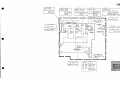
1701 BOARD LAyOUT......... .................................................................................
30
1701 SCHEMATIC NOTES .....................................................................................
31
1701 SCHEMATIC ................................................................................................
31
1702 MODEL IDENTIFICATION ........................................ ........................ ...............
32
1702 PARTS LIST .................................................................................................
33
1702 BOARD LAYOUT ..........................................................................................
40
1702 SCHEMATIC NOTES .....................................................................................
41
1702 SCHEMATIC ........................................... ..... ................................................
41
1702T BOARD LAYOUT ........................................................................................
42
1702T UNIQUE PARTS ..........................................................................................
43
1702T SCHEMATIC ..............................................................................................
43
iv
C1701/C1702 COLOR MONITORS
PRODUCT SPECIFICATION
GENERAL DESCRIPTION
The C1701 and C1702 are quality, high resolution color monitors, designed to maximize the video
capabilities of your Commodore Computer. They give you a superior color picture that enhances your
computing experience and are completely compatible with all Commodore equipment.
SCREEN SIZE
13 Inch (screen measured diagonally). NTSC color standard
DISPLAY
40 Columns x 25 lines
RESOLUTION
1000 Characters per screen
CONTROLS
Color, tint, brightness, contrast, volume, vertical hold and horizontal hold
AUDIO
Built-in audio amplifier and speaker
INPUTS
Chrominance, luminance, composite video and audio
OTHER FEATURES
Video cassette recorder compatible (1 V p-p, 75 Ohms)
COMPUTERS
Commodore 64, VIC 20, Plus/4 and C16
POWER REQUIREMENTS
120 Volts, 60 Hz, 0.85 Amps
POWER CONSUMPTION
87 Watts
All specifications subject to change without notice.
1
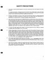
SAFETY PRECAUTIONS
1.
This product contains special designed circuits and components that were designed for safety
purposes.
For continued protection, changes should not be made to the original design unless authorized
in writing by the manufacturer. Replacement parts must be identical to those used in the original
circuits. Service should be performed by qualified personnel only.
2.
Alterations to the design or circuitry of this receiver should not be made. Any design alterations
or additions will void the manufactuer's warranty and will further relieve the manufacturer of
responsibility for personal injury or property damage resulting therefrom.
3.
Many electrical and mechanical parts in MONITOR sets have special safety-related characteristics.
These characteristics are often not evident from visual inspection nor can the protection afforded
by them necessarily be obtained by using replacement components rated for higher voltage, wattage, etc. Replacement parts which have these special safety characteristics are identified in the
parts list of this service manual. Electrical components having such features are identified by
shading on the schematics and by (*) on the parts list in this service manual. The use of a substitute
replacement which does not have the same safety characteristics as the recommended
replacement part shown in the parts list may create shock, fire, or other hazards.
4.
If any repair has been made to the chassis, it is recommended the the B1 setting be checked
or adjusted (See ADJUSTMENT OF B1 VOLTAGE).
5.
The high voltage applied to the picture tube must conform with that specified in this service manual.
Excessive high voltage can cause an increase in X-Ray emission, arcing and possible component
damage, therefore operation under excessive high voltage conditions should be kept to a minimum,
or should be prevented. If severe arcing occurs, remove the AC power immediately and determine the cause by visual inspection (incorrect installation, cracked or melted high voltage harness,
poor soldering, etc.). To maintain the proper minimum level of soft X-Ray emission, components
in the high voltage circuitry including the picture tube, must be the exact replacements or alternatives approved by the manufacturer of the complete product.
6.
Do not check high voltage by drawing an arc. Use a high voltage meter or a high voltage probe
with a VTVM. Discharge the picture tube before attempting meter connection by connecting a
clip lead to the ground frame and connecting the other end of the lead through a 1OkO 2W resistor
to the anode button.
7.
When service is required, observe the original lead dress. Extra precaution should be given to
assure correct lead dress in the high voltage circuit area. Where a short circuit has occurred,
those components that indicate evidence of overheating should be replaced. Always use the
manufacturer's replacement components.
2
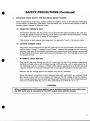
SAFETY PRECAUTIONS (Continued)
8.
ISOLATION CHECK (SAFETY FOR ELECTRICAL SHOCK HAZARD)
After re-assembling the product, always perfrom an isolation check on the exposed metal parts
of the cabinet, screwheads, cable jacks, controls shafts, etc., to be sure the product is safe to
operate without danger of electrical shock.
(A)
DIELECTRIC STRENGTH TEST
The isolation between the AC primary circuit and all metal parts exposed to the user, particularly any exposed metal part having a return path to the chassis should withstand a voltage
of 1, 100V AC (r.m.s.) for a period of one second.
This method of test requires test equipment not generally found in the service trade. *
(8)
LEAKAGE CURRENT CHECK
Plug the AC line cord directly into the AC outlet (do not use a line isolation transformer during this check). Using a "Leakage Current Tester", measure the leakage current from each
exposed metal part of the cabinet, particularly any exposed metal part having a return path
to the chassis, to a known good earth ground (water pipe, etc.). Any leakage current must
not exceed 0.5mA.
*
ALTERNATE CHECK METHOD
Plug the AC line cord directly into the AC output (do not use a line isolation transformer
during this check). Use an AC voltmeter having 1,000 ohms per volt or more sensitivity in
the following manner. Connect a 15000 10W resistor paralleled by a 0.15JLF AC-type
capacitor between an exposed metal part and a known good earth ground (water pipe, etc.).
Measure the AC voltage across the resistor with the AC voltmeter.
Move the resistor connection to each exposed metal part, particularly any exposed metal
part having a return path to the chassis, and measure the AC voltage across the resistor.
Now, reverse the plug in the AC outlet and repeat each measurement. Any voltage measured
must not exceed 0.35V AC (r.m.s). This corresponds to O.5mA AC (r.m.s.).
CAUTION:
When troubleshooting, with power applied, use an isolation transformer and confirm that
the CRT earth wire is connected to the CRT socket board and the chassis.
3
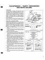
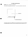
ADJUSTMENTS - PURITY, CONVERGENCE
AND WHITE BALANCE
PICTURE TUBE
The picture tube is a precision in-line gun type. For this
picture tube, dynamic convergence is carried out by a precision deflection yoke which eliminates the use of a convergence yoke and a convergence circuit. The adjustment
of the picture tube is therefore made easier as only the adjustment of static convergence by using a magnet is
enough. The deflection yoke and purity/convergency
magnets assembly has been set at the factory and requires
no field adjustments.
However, should the assembly be accidentally jarred or
tampered vyith, some or all adjustment may be necessary.
YOKE
LOCKING RING PURITY
COLOR PURITY & VERTICAL CENTER
Loosen yoke retaining clamp (Fig. 2-1). With a sharp knife,
cut between the picture tube and the wedge. Remove
wedges completely and clean off dried adhesive from the
picture tube. PAINT is used to lock the tabs of the purity/
convergence magnet assembly in place (Fig. 2-1). The paint
must be removed with the end of a screwdriver before any
adjustments are attempted.
1. Inject a Video Signal (RASTER) to the Video input
terminal.
2. Let the purity tabs come in line horizontally as is shown
in Fig. 2-3. A long tab should be in the same direction
as the other short tab.
3. Move the yoke slowly backward.
4. Tum the green cut-off control to maximum and the red
and blue cut-off controls to minimum. Then adjust the
screen control so that the green band can be seen best.
(Fig. 2-4)
5 . Rotate the two tabs in the opposite direction with them
kept at an angle. Move them in either direction so that
the green band is centered on the picture tube.
6 . Check the vertical center position by displaying a
horizontal line. If incorrect, bring it to the center by
rotating the two tabs, kept at an angle, together in
either direction. (Fig. 2-5, 2-6)
7. Repeat steps 5 and 6 alternately until the green band
and the vertical centre are in line.
a. Move the yoke slowly towards the bell of the tube so
that the whole surface of the picture tube is filled with
a pure green raster.
9. Turning the red cut-off control to maximum and the
green cut-off control to minimum, check for pure red
raster.
10. Turning the blue cut-off control to maximum and the
green cut-off control to minimum, check for pure blue
raster.
11. Secure yoke retaining clamp (do not install wedges at
this time).
MAGNETS (mark "P")
Fig. 2-1
(REAR VIEW)
LONG AND SHORT
PROTRUSIONS
Let the protrusions come in line
(FRONT VIEW)
_--c..-;?""7f'7':7"T-..L GREEN BAND
CENTRE
Bring the green band to the centre.
(FRONT VIEW)
Fig. 2-4
(TOP VIEW)
HORIZONTAL LINE
,~.....
Fig. 2-3
f
'.. /:..... VERTICAL CENTRE
,
,
,
I
."
(identified with a
'--- white notch)
Bring the horizontal line
nearest to the white
notches shown in the
dotted circles.
Fig. 2-5
RDG .
l~J,--___--,
Select the cut-off service
switch from N to S. and a
horizontal line will appear.
Fig. 2-6
4
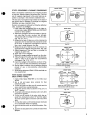
(FRONT VIEW)
(FRONT VIEW)
l)
GREEN \
AROUND~
CENTRE ~ MAGENTA
STATIC CONVERGENCE & DYNAMIC CONVERGENCE
Static convergence is achieved by four magnets located
on the neck, nearest the base of the picture tube. The front
pair of magnetic rings (closest to the purity tabs) are adjusted to converge the red and blue crosshatch lines.
The rear pair of convergence rings (closest to the base of
the picture tube) are adjusted to converge the magenta
(Red/Blue) and green crosshatch lines.
Dynamic convergence is achieved by tilting the deflection
yoke, Up-Down and Left-Right.
1. Inject Video Signal (CROSSHATCH) to the Video input terminal and adjust BRIGHTNESS and CONTRAST
control for distinct pattern.
2. Adjust the convergence around the edges of the picture tube tilting the yoke, up-down and left-right.
Temporarily install one wedge at the top of the yoke.
(Fig. 2-9, 2-10, 2-11)
3. Rotate the front pair of tabs as a unit to minimize the
separation of the red and blue lines around the center
of the screen. To adjust the convergence of red and
blue, vary the angle between the tabs.
4. Rotate the rear pair of tabs as a unit to minimize the
separation of the magenta and green lines. (Fig. 2-8)
5. Adjust the spacing of the rear tabs to converge the
magenta and green lines.
6. Apply paint to fix 6 magnets.
7. Remove the wedge installed temporarily on the yoke.
8. Tilting the angle of the yoke up, down and sideways,
adjust the yoke so as to obtain the circumference
convergence. (Fig. 2-10, 2-11)
9. Insert three wedges to the positions as shown in Fig.
2-12 to obtain the best circumference convergence.
10. Secure wedges in position with the adhesive backing
provided or use a non-conductive silicon/rubber
compound.
11. White balance adjustment (Black & White tracking) can
now be performed.
r
RED
AROUND
CENTRE
.'
.
'
BLUE
,
Fig. 2-7
Fig. 2-8
(REAR VIEW)
(l)WEDGE
DEF. YOKE
Fig. 2-9
(FRONT VIEW)
r
BLUE
;\1.<
I ""
BLUE -_."
RED
GREEN-~,,~'----~I~--~:~_'~-GREEN
RED - , . "
,;'-- _BLUE
>+~,
BLUE GREEN
RED
Tilting the yoke upward will move the lines
as shown with the arrows.
Fig. 2-10
(FRONT VIEW)
WHITE BALANCE ADJUSTMENT
(Black and White Tracking)
1. Inject a Video Signal (RASTER) to the Video input
terminal.
2. Set the red and green drive controls for their
mechanical center.
3. Turn the red, green and blue cut off controls and the
screen control fully counterclockwise.
4. Change the service switch as shown in Fig. 2-6, to
the "S" position.
5. Turn screen control slowly clockwise until a very faint
horizontal line appears.
6. Turn the cut off control of the color which has appeared first, clockwise by about 10° and then adjust
the screen control again so that the color may shine
faintly.
7. Turn the other color cut off controls slowly clockwise
until a reasonable white line appears.
8. Return the service switch to normal (N) position. (Fig.
2-6)
9. Adjust the red and green drive controls for best white
highlights.
Tilting the yoke upward will move the
lines as shown with the arrows.
Fig. 2-11
(REAR VIEW)
ANODE CAP
Fig. 2·12
5
NOTE: 1702 locations in (
8 1 VOLTAGE -
).
Inject a video signal
1701 (110V)
Regulate VR, R109, for B1 adjustment so that Dc voltage between TP-91 and earth is 110 volts.
1702 (125V.)
Confirm that the voltage at TP-94 and IC901 pin 4 is 125 volts.
NOTE: Meter should be periodically calibrated at 20K ohms/volt.
FOCUS
Adjust the FOCUS control for best overall definition and picture detail at normal brightness and contrast.
VERTICAL POSITION
Adjust the V. center VR R428 (R429) to the optimum vertical picture position.
VERTICAL HEIGHT AND LINEARITY
1.
2.
3.
4.
Display a pattern which allows easy confirmation of symmetry (such as a circle or crosshatch).
Reduce the vertical size with the V. HEIGHT VR.
Adjust the vertical linearity with the V. LIN. VR.
Readjust the vertical height, so that the picture extends to normal size.
HORIZONTAL WIDTH
Adjust H. WIDTH control coil L503 (L522) by turning it with a hexagonal adjusting bar only if RIGHT
and LEFT sides of picture can't be seen.
HORIZONTAL OSCILLATOR
1.
2.
3.
4.
5.
Set the H. FREQ. VR to the mechanical center position.
Connect a jumper clip between TP-33A and TP-33B.
While rotating the H. FREQ. VR, R504, keep the picture stationary or slowly moving.
Remove the jumper wire.
Make sure that the set maintains horizontal sync, when signals are switched.
6
SUB TINT AND SUB COLOR
1.
2.
Display a picture and set the tint and color VRs on the control panel to the central click position.
Adjust the sub tint VR, R305 and sub color VR, R303 for the optimum display.
SUB CONTRAST AND SUB BRIGHT
1.
2.
Display a picture and set the contrast and bright VRs on the control panel to the center click positions.
Adjust the sub contrast VR, R209 and sub bright VR, R22 (R863) for optimum display.
COLOR SYNC
1.
2.
3.
4.
5.
6.
Display a color video signal.
Connect jumper clips between TP-40 and earth (TP-E) and between TP-51 and IC301 pin 15
(TP-51 B).
Use a non-metallic screwdriver to turn trimmer capacitor C308.
Adjust so that the rolling color stripes become thick and the rolling slows or stops.
Remove jumper clips.
Confirm that color sync is not disrupted when signals are switched.
3.58 MHz TRAP
1.
2.
3.
Receive a Video Signal into the Video input terminal.
Connect oscilloscope probe to DL201 (Delay Line) output side.
Turn the core of T201 so that that 3.58MHz signal is minimized.
MINIMUM
7
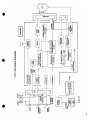
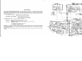
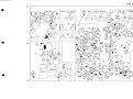
(X)
(LUMINANCE)
C
Y
(CHROMINANCE)
AUDIO
R
0
ACIN
FUSE
&.
LINE
FILTER
POWER
TRANSF:
I
F
I
I
I
I
J
BUFFER
BUFFER
VIDEO
BUFFER
!AUDIO AMP!
&. DRIVE I
I
.1 VOLTAGE
I
i
e
3.58
TRAP
l
I
DELAY
r-::UTPUT
~
It
B1
I
I
I
I
VIDEO
AMP.
I
iI
CONTROL
iii
I
I
I
I
i
VERTICAL
OUTPUT
I
HIGH
VOLTAGE
RECT.
I
'---
'----
H
-- ---
V
roo--
1
COLOR
DIFFERENCE
::E
C
I-
r---c;
>< ~
irE r---
e
fll.
I
Y
I
1SUPER
SCREEN
CONTROL
I
HORIZONTAL
HORIZONTAL t-OUTPUT
DRIVE
I
V. OSC &. V.
,..... -----------H. AT C &. H. OSC
~
AMP. I - -
BP AMP. KILLER
JSANDPASS}- COLOR DE MOD.
FILTER
&. ETC.
VIDEO AMP. &.
SYNC. SEPARATOR
f-"o
I X-RAY
prOTECTOR
TRAP
SW
3.58
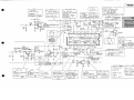
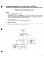
1701/1702 BLOCK DIAGRAM
RECT. CONTROL - B 1
"-
"
.............. 1
<"-~
'-'
;J
-
,....
i-+81
0
-0
F
R
F6
r;:l
R
SIGNAL
SELECT S
F: FRONT
R: REAR
0)
VIDEO
L~ ~J
AUDIO
e
CRT
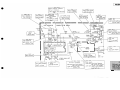
VIDEO CIRCUIT
3 ~2 - - - - ,
Buffer
r - - - )(
C202 - - - - - ,
-
-$hort : f""dtr sr(\~·
,C203 ope".
For sync. "",pli fie ....
-ope.n ; no color
.©~short} :
-@-®shart.
emItt~r .5 )"nOoth i~
-ope It ~ fa. uIt)' sync.
R2.oI,R202,C2o3
Sync. sera n~tor
~ln'I\"tc!'Y t;~ - cansiaht
.In" \ Ope"
I .
eo 0"" is
fuint
IDc,Rh~:~
• !?ZOZ. cplU\
J
:
.c.2.o3c;hort
-DL20I, R204
t>e.lQ.y of !u.tooi/1C1.l"\ce sitahGtI
I
~"ct
fa~lt)'
condenser
Srt1 c..
I
-J.
-snun.:
.&
Ill"
It
r
'open:I"lO
- R204 0f~t\ ~ Sc~en bq.col"neS~~~9.ht I
picfClre
L204 ~-------~
F're<t."Eh? chl1 yo. ¢teris tic.
synchTohitat;on -ShoTt. :1"10 Y/1s1e r
6V
/
2 -O-1 ---';"'--~-lL 201
r-R-
X352
2SC16S5 ,2SCISI5(Y,GR)
BUFFER
820
ISOK
R2
2.
r '2C]~
4
K
/'i:5_~
DL201
,.....A.,f\IIr+--tlI--+-J
270
C211
R202
t.aK
R353
I
R203
IBK
-T
C 20 4
3.3/50BP
-open. : imo.,e
-:::-
\/
/,
is
soft
Although specifically written on the
170 1 monitor, most circuit theorlea
apply to the 1702 alao. Refer to the
1702 schematic for differences In c0mponent values and IdentlflQatlon.
R206 - - - ,
S.,.Al\kir1 pu.lse
-open :dark piduR
I
r-__~__~____~3A·3~K____~~ R210
!
16VP-p
330
X202 --------------~
Vide.o a,mo.
I
6Vp.p
rvL
(VI
- R2.IO Men l
·R 2.1' O~i'\ j :
I
XIOI
C251
:=47/16
~ r--+--~--+---~
2SCI685,2SCI959(Y)
CIOI
RI02 VIDEO AMP
270 _ _- -
Rial
150
RI03
390
/
C351
CI02
RI04
2 .2K
T
~331
~/=
-
6.3
VI DEO
~U' II ~
~
X351
a
/
R209
R207 L 203
6.aK 270
R250
10K
IK
t
: no
YQS
ter
R251
10K
Emitter ';)(as and freb'.H?hC;.
'"I
SUS
CONTRA~
chlll""cteristic con-ec. tiot\.
• Rloe
OP"'h}
' C210 shOTt
I X250
SYNC /
SEPAl /
'---1.4-V-P-'p--' 101 16
• X202 ODefl
R2.0~ .R2.0'/, R223,c2/o - - - - ,
14V
/
ra.ster
} rIO pldu.~
I
150
,IC20J
HAI1401
l"(Q
"R2t2 c~"-
·x20Z ~:HI>skt: :s...-reen is Ilbnortnally
~-0ShCft hri'3ht I»"Id flybaCk
@-®Short line Cll'pears_
(HI
470/6.3
CIRCUIT NOTES,
COy~<:.t;ol"l.
i" "";;. lesistQnce
""T""...L
R206/
82
snort: ~hostin~
"
C2 \ I ---'-""'; C2.o4
Br-~ss
Ac. couplil1'}
I
13.6V
Lo(\ct yesi~ tlU1C~
-t>l2o\ cp~n. : no pktel ~
.
:no p,ctl\~
-
,.-___ 2SCISI5 (Y,GR)
SWITCHER
T201
3.S8MH Z
OV
TRfo?
(e)
....._T_1¥12_4
-""SCL.C.:.....16-""..S'-'-5_.2_S_C......;I,-8I5_{Y--,'.IGR)
'-_ _.l.
/ .....2'BUFFER
/
HA/l401 TROUBLE" SYMPTOM DF PRESIJME ...
---- X\O\ --~-~
Vic!eo amp.
·ope".
}
-®~
short :"0 pic.tl4re
-@-@
short
-@
-e
S~ort:
Screen is
dl1Tk
X351 ---':""'"
Buffer
~;~: shoTt }:no c.olor
C20\ ----'---,
f\.c. co~pl;F\~
·~-~short
-open : 110 pidl.(re
-@~ shert : color is
faint
·short : tal.\\ \ r
synchroniZPot;on
r - - - - - C 205"
-'---,
Differehti~1
(aperture compensation:
'mllinly preshooti j'~)
·open : imo.~t is shu rp
·short: screen
do.:rk.
;,5
X2~D
Differentca.l
(aperture CClnP'!n~tion:
lno.inly overshcotin~)
.~o'7 ope" }
.<;2O'Topen : jma~e is
- "short
soft
-----..,
Switche.r
T201 - - - - - . ,
3 .SRMHt tro..p co\1
·©-@short:color error
-Optm. no pic tl4Te
'@ -@ short: sc reel'l b~cctneS
-shoTt: 3.!;RMliz trap
briqht and
dot interference
-110 Tas.ter . no Sound
'multI sync.
.ho picture
. raster is brl~ht Clhd
flyback line ar~Qy".s
-sc.reen is too
Fn'i~h t
• SCree.n is dark
• \ma~e ~ua.\;ty is
I
un sa. tis-Factory
vertical stripes
9
AUDIO CIRCUIT
. - - - - R607, C60q
----,
N~t;ve teed ha.ck 'resistClhce
DC c.u.t
(.612.
cOhde.I'ISIt.'f"
Boc~;,
. open: sound level becomes
.c?~n : no souhd
hi~h
"R65D,C651
~6DS',c608
Coupli~ TeSls~n~
C6~D
Noise ab-;orb
1hp'4 to 'n!s~stClttce
unci condehser
·shot"t :hO
"Rbi 1 ------,
ColO - - - r
and cOhdenser'
SOUI\Q
T602 - -......
1)601 - - - ,
BillS Y~stl1l\ce
·o~: 1"\0 Sl!l.Incl
Couriil\l cohd~sel'"
'F-bOS" O~}
Audio ou~~-t tT"(lhsf.
·open: no sound
conde.nser
L.Ft diode
·open: sound !eve I
becomes low
'opel"' : no ')ound
·c.oo& open :no sound.
•
II
shari
XboZ .X603 -------.,
Audio out
·open:sound level becomes
low and lacks bass.
R613. R614 ---~
R607
C6~2
ISOK
C60S
.OI5MY
-
C609
.015 200V MY
\
R617
470K
;<601----.
~R61a
1"
R609
6.8K
iaOK
R6J2 ~
2.2K
........
(M.\8
(J
-
-
,...---
I
~
X601-
~606
.018MY
~
r
....
c6ob~-
C613
.
14.711601
Filter
IC601 HAIII07l
AUDIO
cpen :no sound
"Dc.
. FF-(,o\ open: noSouM
I or
101l6~
R61'T. Rbl8 - - - ,
"R6D2, R604
R603,C60S"
'R603
Y\.O SCUtlQ
~
+
t
l
FR601. cbi3 - - - ,
FilteY'
Outfl4t voH-C\~e
di"idih~ rec;istc~hce
R603
68
1
.J
\
R615
47K..l.-
·open ~: 1\0 $Qohd
·short
"='"
I
RG04
AudIO c!ri ve
R610
560
FR6011
(00 I
112FRI
IK
To,,~ ~uQ.lj ty c.orrection
. short:
(V
I
I
F
~ n!Si~l1lnce ~
-,
--1
L7
GC:- 4000A
R6IS
• open: sound leve.l beComes
low and lacks bass
R608
220K
\C610
..--;---;-""Arr--; i--+---+-----"W'r-i . 4 7150 8 P
, . - - "R(,!)! ,R6S2
Bias l'eSisto.hCe.
·open: sound levei
becc lY\es hi'jh
BOola t\c~ fesistllnc.e
'Input condense.r
·R{,o2 open:sound level becomes
hi~. VR does hot function.
'RbD4 (lpen: sound Ie. vel
becomes 10 w .
fa 81
IIOV
CbI4.C6IS -------"1
Noise absorb
. (;614 short: soul'\d level becomes
hiljh. VR does hot fundio/\.
.c bll,; ~rt: sound ic.; not Cl",dible
unless VR is "turned at
least ho.lf way.
CIRCUIT NOTES
Although specifically written on the
1701 monitor, most circuit theories
apply to the 1702 also. Refer to the
1702 schematic for differences in component values and identification.
10
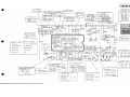
COLOR DEM. CIRCUIT
"f..301.R315;1~3 1.6. R3f'7
R3i'iLR321,C316
R3,-3
Emmire~ ~...-tGn~1e
C303
,---- c302
Br-~~ conQenser
c30S --...,
N:.c smoomlnj
.open: colD\" beccmcs • open : no
$rk
Ki \l~ smocil\,'i
~clor
T30i - - - ,
BP
take~off
transf.
R302.R303
Co\Oy c:orrec.tloh
..:yw "\: ltO ~Ior
'short; no color
-
R!oi---.,
's~rt\
C3 0 4-
color
'R3Dl open: faint
Dumpi~ ~is~nce
.open:
"open :c%Y error
hD coloy
·R304
ore"': Yec:\
'R:30!)
be.comes lnDihel11'o...
'f"'l Hed bf.CDtneS "ftl,,,t.
i~
ro.steY'
open.
"R 316 open
Got\t~st
'R31'T oru'
becomes
.R32\ open
weo.k
·(.31b
~ beCCl'les
'R303 ·r
nDf!Tl:
_.. color
dink is
"sheet: no picture.
'R~15
(bleeck.r ..-n\S~)
(bleeder feS'StllllC~)
Cou~in3 Cl)ndens~r
Su.~r-scene ccnh-ol
R304, R3DS, R322
tl\'\t c.orrectlon.
short
·xaot open
bi...e \:)ecomes vic,e.,-.
·R311. ~ : titlt VR doeS !\Of:
fu nc-U on
R.321
. -_ _ _ _AAr...rIK_ _ __
CIRCUIT NOTES
C304i:C305
180 -.45/50
Although speciflcally written on the
170 1 monitor, most circuit theories
apply to the 1702 also. Refer to the
1702 schematic for differences In component values and Identification.
R328
1M
/
R316
D302.---...,
22K
10.7V
I
10116
• 1'10
·no ccioY, edDY -fad~ away
piduye
·only tnDl1Ocln·omAtic.
· fnultr tint
·no monochroma.tic..
. faulty color sync.
"c.cicr no;SE!
. czlcr beat
• cclor el'"rcr
·dc. ..•
~
4Vp-p
+.dTP~5°1
IC301 HAII247
B.P AMP, ACC,KI
TINT, APC, VCO
a COLOR OEM
I
0301:!:
S2473H
C306
180
.----c306
T
Diff4e~n"ti4TeS,'5rnc. si~ ",,\, a,"'cl
clela.ys fho.o;e of- pllise.
- - D 30 I .---I.~-,
'OI'en : r-o"coloY
Foy noise prevention
.shon:: c:oloY' errOl"
. short : 1'0 pIC tttYl!.
dark yaster
I
.'
I
0302_.
ER,
1S 2 47 3 H ,-c~r-.-:.::I5::.:.1.:.55:,:5::.,
0303-0308
R310
W06-A,W06-8,151555
or 1512473
L351
330
~~-+----------~~.-~
0307
R311 330
22
I
I
~
~----------~------.-~~-+-~
0306
I
I
R312 3301
G~53--~~~I~~~I--r-~I-~
I~5~6
~
Be"'" I:",iter diode
. short : br;~h+et1.
+
C 316 z:::
R314
2.2K
~
~
22
R322
:.
~
~
•
-:-
..!...
J30g
R310,R3i \,R3i2 - - - - ,
Ie pl"t'tection reSistor
'R310
"pet: yellow i';ct......e
'R311 cpen: cyanic p;cture
: 1Tla.'Jhent~ t
·R312. open.
1
pIC ure
10K
D303 ....... D308
C310,C311,C312 - - - ,
030'1, R307.R30!i'-L.----.
For phase shOt ft
'C30'7 short :5C~n bec..::m'!s
'By" p'l~'" condl!nser
(ootp'lt
"IT;.. ba.se-~TCu.ncied
. <:310 shan' no caree.n Y'IsteY
. C311 shcrt: hO red ro.S teY
·c312. short: no bilAe. ra.s!er
"R301? cpen
130 I. c 30 &>,R3o'7, c309 ·'('3ot
~- L351,L31>2. L3S3
with T6rect to \U7'O\i"o."c:e sl'y,a.I)
bei'.1ht \:I."t ho ccjOl"
'00'7 opt'll }
obtain~
"R307 open
:no color
3.s8MH~
Roted,on. of Ie frt,.,,, CRT SFrki"~
filhr
o~n ,';hoT"t
·c308 op~"
'R30'1 open
'C 3017 ope... , sho~t
:tlO
colo ...
short: bllA4e picture
short: ·. . ed pIC Tt.U'e
,-£)30 S
short: ~reet'\ fic rure
t\ ;,h t"re:tu'!n"ff: It ~Y"
· L?S \
G3\3,C 314, R3\3. R~\4
APC
}
·E>303
"i) 304
s",ooth~,,:}
Shod}
opQ.n: ydlcw fictu.re
· L ~52 ~ :cpM;c.rictLlI't.
·L
3 S"3 ,,~" : m<l:1',enta
ftC.tun~
'C313
.c314 shOTt :1\0 color
. R 3 i4- open.
11
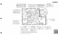
CHROMA OUTPUT CIRCUIT
~
~~
.
©~ShOTt
®~short
ope.n
X\ot
x 10Z
XI03
nd
bl",e
yo.ster To-ster
~reen
no blu.e no red
Yo..ster
Yo..steY"
110~ree.n.
RIIS.Rllb,RII'1---.
Rill, R1I3 . RI14 - - - - .
Olltput Tr colle.ctor ioad resister
'raster
• R,ll L
'(llSter
open: SCTeen
of
CRT cathod 'reSistor and Tesist.:>'" for
· RII:3 open :SCfecn of red
. RII b open: no red Ytlste.l"
• R 114 opel1 :sc.reen of ~\'~ert
.RII'7 open: no
~reen
I
I
J
~
RII6
3.3K
112S
Rlf7
3.3KI/2S
158V {160Vl
or
~-
Rloa
;~ ~.~'R2
RI14
12K 2W
LJ,JVv-_ _--I-~-,..,........:....--X-1
"R12.1. RIO'L Rill
II'"
r -......""'N~~IG CUT OFFI
RtlO
;;:;::;:::::::::;"t~"'fv..~'-.....J
l~~I:'a
DRIVE!
RI06
5 KB
180
_'.
Cl 0 3.CI D 4,C{o$'
I
7
ster
L'0'
180
~
z: C 10 I
open: no -red rQster
'~1I0
open : no 'jr-eel'\ raS ter
·C10..3 short :screen cf bi",e $O.turate
· clo4
sJ..ort :screen of
red Slltl4yat~
'C IDS' s~rt :screen of ~reen SAtu.rate
GE-3000A
T
~ !0I250;._R.,1~~~ET
a.djustrnent
·RIO I open O} weo..l-en
Rlo2. open . i>lu~ r~ster
°
'RI~
"=
(H)
n+
Cut off
y(\
~
-AC150
F9uencT ChClYnderiS1ic. cor~tjol1.
b (<.Ie
"'1.-._-
(;r:- I ~lI.
I,
1: ",,,,ite O(esistol'\c.e
ho
..." I
J-'I f:rQ~
l ~l~~
L-.J
t:",m~ter 'I"e sisto. hel!.
'Rlo'1 open;
LJ
(H)
R(OLRI03, RIDS'
Rlo2,Rto4, Rlob
RWT. Rlo8, Rlf 0
!~
~
0....3--"
GREEN OUT
RI05
IK
I
19~1 fr~
; r"l
i
" R CUT OFf)
_ _.JW\,--+--J 180
.....--+-+0....,.---.
12K 2W
RI031K
'RII! open: i'\o ~l"een raster
: 370ES822(£ )
I,
RII2
XI02
RI13
RED OUi'2K 2W
red raster
VOl
I I 370FV822(E)
RI21
150
0pen;ho
yaster
iCRT SOCKETi
RI02
_5KB
'Rlo9
co t'rl!.cti on.
'RII S' open: no blu.e. 'r11"5te.r
bll.le
u,r.a.t YeSistanc.e of base
'RlZS oren : ho b",\e raster
·~1'2.6, open.; no ~~e!l. r~ster
-RlzCf open! \10 ye.d rtlstl!:r
·RI2.1 opm: no biue Y'Ct5ter
FYe'!uency chayt\c.terlst;c.
j'l'riecti~ DI1tputTr frD'" CRT sparki"
RI2S',RI26.RI2.'1
D-r,ve adju5tm€:.nt
RI23,RI'2.2.RI24 ___.....
L103.Llo2., LI04
•i<. 103 ~1. W'ea.ket\
'RI04open
yec{ ra.ster
r
'RloS opo!l\l wea.ken
·R.lo6 opo::tt f; ~re.et1 raster
Ltol ------------~
HB s",ooth,n~
K1h fre~ll~ncr ·filter
.oreh :sct\!en IS bY~ht
a.nd dr'll~s ta: I ftl
·open: screen
Yi~ht.
IS
bri~kt:
o,l'\d dya~5 t",i j to
y;~ht ,
CIRCUIT NOTES
Although specifically written on the
1701 monitor. most circuit theories
apply to the 1702 also. Refer to the
1702 schematic for differences in component values and identification.
12
CONTROL
R04tRO~
'Ro~ 'fen: COLOR
RO'i.RIO _.----, -RII.RIZ.RI3 - - - - ,
BI'!eaer 'rl!~istlln(e
B"r i':}ht c..Jntto\
ROb. RO'7.KD&
Colo.,. contT'ol
Cmb-a.st CDhtrcl
'Ro'! open ;VR does hot
functiol\ when
c.ontrast is
VR
does not
functlon.
'RO~
·RIO
'fen: no
abnOT"lhllily
bT'i~ht.
~~~ ~
Rot.R02 .R03
RC4
IOK8
I
•
IJ<;YJIY\4t
'ROl!fen . ,,"Q~entct
s
\
R09
470
ROa
5.6K
~~K
turned to ""'(lX, vert\cal
oscillatio n beco/lll$
minimlAIn (approl(. 3cm)
3
('-V-CL-U-M-E)
/
3
RI6
5008
Rt4
6.8K
"'-R03
R02
IOK8
B2K (TI N r )
·Rlb Q)open: f~L4ltl
l'-~H
hoYizDr 10.1
sy'f\c.
(V. HOLD)
1l
I ,
12V
R23
1.51<
R2: 4.7K
ISU88RIGHTI
~
::~
____________________
,
Rib. R2~ - - - - - ,
H. Posit;Oh cllrltrol
(8RIGHT)
RI2
IOK8
I~
ore" :
does not
func.tion.
;~:~~~~=i<C~O~L~O~R~):~~~C~O~N~T~)~~~~.~r-~--~--__ ~
Tint c.chhol
open} red. L.~_
• RII opel\:screen beCDmes
s\;~htly do;rk.
'R13 open :BRICX:HT VR
epe" :scree", becomes
stT'O~
'ROI
raster
RK- ,RIS" - - - - - - - - - - .
V. Hol<l control
. Rlf
when 1/. HOLD VR is
Ria
1.8K
RI9
~/~________-+__2_._2_K~
RZO
L
__
1-.....
R22. 'K23 - .....
Su.b byi<j.hl: c:.onhol
R23~:no
raster
-
470
.GE-4000A
CB '.
CONTROL:J
A'SSY
.
R21
2.:"1(
~
R\~.Rlq,
I
I
I
R20.R2\ ---'-....,
Bleeder 're<>istarlce
•F: \~ ope;,} screen bec.omes
. P.l'1 open ;sli~htll da.rk.
' R20 o~n : coloy is faint.
·R2.1 0Fn.: screen becomeS
sli~.htl)' bri~ht.
:
CIRCUIT NOTES
Although specifically written on the
1701 monitor. most circuit theories
apply to the 1702 also. Refer to the
1702 achematic for differences in component values and identification.
13
r-
C4 0 2 . -
r---
r---R403.R404 - - - - - - - - - ,
v40S
V~'rtic(ll oscIIIa.tor bia.s circ.uit
A
nsoYb
of bhOYm~(
condenser
'R403 open: only Si~1e horizontcll lihe.
V()1+~<je
'll,pett}:OI'Ily sit'l'jle
-R.40+OP~": when 'J HOLD VR is ttlrhed.. V.BLK
r - R416,C40~ . R4Ig
·shOrt horizontoJ line
b~Qck bo.hd ""ill a.ppeo.\"', o.nd scree" .--R402., C40S --.:/_ _ _ _ _ _ _-, r FR4-0i • cA-!'? - - - -..... r--I¥.'- IS _ _ _--: For 1o.l<.e-off V. BLK pulse
r-- CS'OI ---~==:::::~"'--I
:~l~ ~P:::~~Znt~o.b\liu:.flicmi"1 lhh!~.,.a.tin~ drcuit
R414 , hC40g
Base biaS -resiSto.hce
Fo\'" pTeventin'.} verticil! sync s~1\Q1
·R41b open} :flyback Ii he appeo.rs,
;- R40i.D402 ,C4 03- /
(veT tical sy,..c si~nlll nice-off)
SMoot ~~
of X40/
,C40Q open
. open : iUulty harizontai sync.
1
Vee.. Sl'J\Ctk''':f
·c~s
:falll+-..
"
'FI~401 Of'!1\ } • vertieo.l o.m~itl4de 'open :'Jertico.l runpiitude 'R418 open: screeh becomes
. short ! picture is shift to l"i'aht.
o.hd stat.jhzatiol'\
/
.c4-04 open
" Vtrt,cal sr nc .
is Slna.U •
:i)-402.siIotil.0hlr si"SI~
.c40S 0rel\:when VHGL'P VR is tu.rned fu.\Iy
'R41+ of'\!'" i.. smo.lI.
<approx. 2 C1rl)
sii~htly bri~ht
C40\
.c~3shortJh.,rizont41
ri<Jht, it is possible to fold b(lck
(o.~rcx. 1.J;;c1n)
/
Condenser for p~ven1i~
'--"-T'_ _ _'_in_e_---'
o.t Cl stnctl( alllpIitude(apprDx. ho.lf)
verticD.l amplifier oscilliti"3
osc.lllcrtor
VertiCllI
I H. OSC, V. OSC & V. OUT CIRCUIT I
Q,
short}
~
1
1
1I,'
r
../
I r
~A"
-81'-11~0-V~\+---/~-----~C~4~0~3~i~-/iR;4;!8~~;2-i~-~c~J~0~~:y7~-41~J=2='=0=V=p=-=p==~~=~a~8=v=p=-=p=~---------~~~~~vF~R~4~
JLJL
..
100/~~R401
=-C501
lID
1
~~O
LC402
~2.2/1~~
-"
~+ ~402
h
r~* "'~ltOy4 ~
TANTAL +
.001 C401
~
4V
IV
I
I
3
,
4
r-L---'---'-,
R529
100
:>
v.
AMP
J
PHASE OET
16
15
14
6
.1 J
V.OSC
13
7
WAVE
12
/I
10
~~6 6.6~I2.SV 1.8V
•__
~.,."..,.
CS04~t'""
C503 1150
+
.015MY -~....
RSOI ~
5.6K"?-
1+
C506 m:
33/161
~. °V.SOCS C
~
-
~
X-
~I§]
?I"tectc'r
.@-<f)sherd· no sound
-eso1.
Rib .~ZS'
~ ... tcoth wave phase
adjustment
-eSOt'! cpen ( : Imaqe shift
/I
SI'orl
1 .. "
+
..-----.
?
to Idl
.
R704 ~
9531<
*1·1.
CMF
*
\ROI
X'lO! -----,
R.o.r
0701
HZ20'V,
"")
.. C701zz;:z
100/6.31
' @-<W !ohortl.·f1D TCl.ster
•
R701
4 . 7K
"#'
__
lO~5~:
~5C5
HAFe output vo\to.~e
Smeothi n~ circuit
.C...
>O'T optn l:f!1u.lty hO~;ZDnht(
'~')Ol open 5 sync. elf top half.
' C504- sl-Drl..:
fo.ulty horizontal
1s~;m;
\~R471
",,+
hcyiLcntal
lin~.
040li
47116,
'v
122~41~1
1
C411
\0 112;5
l~~F
100/160
'(opnCN)
ri
~ ~
. •. . . .
R4!2
5.5K
1
0.6V
=
?1--.......r..-----4~.!:.....--4J~_:r4--~i~----:---+I
-";:>'-!W!....l.<OM!Z!R!:l..SIDE PIN TRANS!~+-l---+I---------,::-::-:-:::+---~~---i,f-----I -I
R4 19 I , . . ,
2.2K 1/2S~\r-,-~~--t----T503!
_ _ _ _ _ _ _ _--.
AC c.urrent detection resistor
-open : only sinjl~ horiz:onta.1 !,he
(hcriLc1na.1 lin~ is kicks upward
~ xsol __--,
neSlltive feed ba.CK
--top haif oniy of sc.reen is
etCp.sSively donso. t ed
.
cs IS, CSI'l . CSQi', TS03 - - - - . ,
(rr
Fonno.tion
~YQ.bolic wdve
(side pit' cotnllensa.tion)
'(;SI'> o~" \
'1'S03Snurt J
dy-ive
1-!01'Izchtai
.ap'
: no yastet-short no sound
Ah}'
_...1..-_ _---,
,D401 shan
: S' 1(- '
,
mil , Imo.ae (lpi>ears
'C4Cl/ short
,
J, r
d
below center of CRT_
·C.Slrt ~n l.:hociz.onto.l a.mplitu.de shrinks ,
·Tso3.;V~
,-X4CI, D4CI, Noli'
Vertical output
'X401 open} .vertieCl! o.tnoiitude is
:cnly s;I\Qlt vertico.ll;ne
5
-eSI'I J.cd, :t,,\, po.rt of screen is rnissit'lq,
~D;06
in a.bout 1. second)
..-L-R40'T - - - - - - - - - - ,
Resistor foY AC current,
·op~l'l:
~~s
I
one sec.ond)
I
P-revention of capacitor d'ropout
due to o.pplict\-tio n of reverse
polo.rity volto.~e to C51'1 and C5\8
-C~08',Rs-o:3,RS'04
I
A~"
I~R~02
R';03
no
HAFC outpllt
sOIl ..... d
HA 1/244 TROUBLE SYMPTOM OF PRESUME -
<. HoRIZONTAL
ihjection resistor
·open :fCl.llity horizonto.l sync.
R527
I';'
L..c.....
8,'}"K 1125
(r::l) .,f,.t'_--til
)~
__-4I>-t-+-j-----4'Vv'v-v-
~t
SO~,Cso4, RSo/ -
-.l ..
OM;;-------...I_
I ...... HOYizohtal asci II" t;on e\ e""ehist r
·c!>c)~ open : no n~
e
41.2K iI.l.
CS27
1/2CMF
OOI5r11----.
I
""" \
(imo.se appears at lOP haif of
SCTl!.en at ,nlends of aOc<lt
I
I
+n'i:!:1I.420
680
-......... r-R410
Sif\~le
f
1,3.3/50
resistor f::r vertical
osc.illo.ticncondenser
'open:only
'54. 2\/
!
...............
HI. ~
'Y
"$.
X701
0.3V
Discha~e
I
Iii
L:
.-R40S
I
X5 ° I
45~
zt:C407
J
RS02 C508
,y
I>""
.... 6 a K
.0056
I_//
:~
?P
0.8Vp-p
~ /
C505
ri
,...,.-, (~R506
,~3l R 503
I
I I
.. 560
II.8K I 1"1.>
I~...J I
i
\1
_
1/4 CMF ?
r---'
[>-R504
'(H)
I --...
8
JH.FREQjR3 5.90 K
MY,
~
~:~
I
X4 O © '
J
+
'-
~
R ~O 5
7.51<
I
l
_1
T.~1;~9100V MY
1
IW'OMR
";-C412
+C408
.:c_3.3/160<ZlZ14.7/50
-$R40a
~681/2w
?200
'V (OPTION'
R410
~6.8 I W ,
C401]' - - - - - - - -_ _ _ _......
R:~9~ eMF
"SInOQthil1~ c.ondenser for DC vclta~e h~atjve
~" ·open:vertICCl
. I
l't d'
I
feedback
,--=---,
o.lIIP ' u e IS Sinai (o.pprox. 6 em)
IV. HEIGHTI
.short:only Sinale horiLonta.1 line ,
2208
IC50'
HAII244
H.AFC,
9
±\I.~?J
I12.7V
IV.LINj ,
.... C406
I--=?".082MY
R403
4.7K
R036E
/
~~
1061'
I
/
~~b~16 ~
I
rv:?OSiTiONl
IS2473H. ~
t;:-,3----~~'--tl--""=-0:-s:-0+k;~w"':'0"':'6-.A:-------·'-_ _ _ -+L-~~:!:':.~/2.~B~5~0~K~-~1 X402r V
I
0405~
A
IWOMR
2W
R2il~
R411 22K
~~~~7
+~'i2
68FR
(V)
s-
~I-
1
_I"'"
12K
I
47K
+
R405
!O.SV
~
\ ¥ - y . J1
~
8
,d
FORME..,
_4.7K
. . ..-~
TP<r-.33A
S
H.OSC
12.2V 6.6V 3V
TP -338
I/V~~:p: 5V
\ 3.6V 6.7V
2
,#'#..
V DC
(v) ---a.3V
/ /
#
#
TANTAL
~
~11
RDO"(C)
~IO.I.
v
lill
.033
~A
~~:w
'A
~l~
~
• --
I
~
r-CSOS. RS'08
S~wt~th wo.tIe ~eJ1era10r
CirCUIt for comparison wave
·C~S.R5Dg r'" :liW.tJ
I
h'
'I
onZOIlTa
.c')os short
~ync.
RIJ'OI ,R'703.R7o4
r- C'TOI, D'701
-
.-((52'1. CS2'7 - - - - - - ,
Pulse phase settih'J
-RQ.'T
1.M
\
;",o.~e shift
·C52.'T open to ri~ht,
' <'5'2'7 sherI:: faulty hori:z:onlul
Ab"OTmo.l B1 voltaqe
detection
-R'1040p.!n .
ro.ster
'0'101 short no sound
O"""}.
,)pen}:
r-D!>05
Pulse ampiihlde \imitter
.open : imo.~e shi ft to ri<jht
·short: fa .. lty horizcl'\t(l1 syt'IC.
sync:.
C1RCtIlT>
<VERTICAL
CIRCUIT)
· H. oscillo.t;on stop
(ho '(a. ste r , no SO;Ji1'\)
• V. DSC.l!o.t;ol1 stop
(sil'\~le. nOl'i:z:ontal 11he)
· fa.uli,! H.
• fal.llty V. sync.
· fo.L.llty V. ampl; tu~e
SyhC .
· o.bhOYmo.\ H.oscillat'on
· f~u.ltr v.
i'heo.ri+y
CIRCUIT NOTES
Ahhough specifically written on the
1701 monitor, most circuit theories
apply to the 1702 also. Refer to the
1702 schematic for differences in component values and identification.
14
HORIZONTAL OUTPUT CIRCUIT
xo1
r\orizonto.\ outpu.t
-open:
1"0
y~ste.'r
hO
sound
\-\or il.O""o. \ dyive 1vo.nsf.
1rt .
1'10 yA steY"
L
'sno
no
SOU
~
LS02,RSZ8
I HOl"iZDnta\ linearity
Ic.orrect ion coi I a.nd
C 530,C.531
Resohance condenser
for FBT
r - - - COl - - - - - . ,
"Prevention of unwll"\,ted ·opel'\ : horizonta\ width
is small
,(Cldio:tion
T 5"0 \ - - - - - - ,
. open.
C$12,C~J3,CSI4
I
C51:
collector pulse
clipper(for protection)
)(S"O\
ISOO
CSl4
1500
MPP
MFP
1.5KV
C512
1500 1. 5KV
MPP
I I
-
1.5KV
-
MPP
J. - I
1/160
II
II
II
C511
+147/160
•
.R511
I
'I
+I
I C520~
)
il
1./
'~f
0507.
V09·E I
•
6.aK, 5.6K or 4.2 K
(S.2KK'S,2K PARALLEL>
HF·I
"-+-~--++--."""'--1
l1orlz.ot\tal dyive colledor
'010.5 supply a ",c\ fi Itey
R520
5.6K 1/25
,,---<.J....,.
,I
I
~
12V
lISOI
R521
39K
16V
II
II
050:\
RF·I
or UF·2
--..<:....-,
III'
7
~8P~
I-----'M
I
10K
112
RS26
IK 1125
I
:I
C531
screen is tnissih~
. RS20 open : tol' laft of
.
scree'" is tniSS\n~
I
i
0504
UF--2
II
L ___ 3
RGB-IOG
VI9E
RS ·1
RF·I
ct;ll
CSI5 - - - - . ,
correction
.oren: sin~le vet'tica.\
line .
(.Onec t ion
• c:. S2 3 shorf; dl'ifts t o ri~ht
----,
Bl.(I'2.v) n~ctif;er and
protec.ts DI:;04- nOh' • .
·open }. no ra.ster
·short . 'nO si:lund
.open : ext~nc!s Up Qhd
cS"23 , D~07. RS2~
Hori~ohto.l lihellrity
RS22. £> ~o4
'rtAsh cu.ne'nt
S""oo\hi~
dow/'\ 5ii~ht{y
---,
roY" tllkl~ off H.BLK puke
. C~4 O~I'\: top ric;}ht of
I
i --;- - _L.........r~.....;.-/-_-'I_~
II
+
C530
510
I 5KV
IS~~/
ct;24,R~20.R~21
[,oii~----~T-i}---'--</<H'V II
I
T TTTT
.
,
S-clArve
becomes
dQ.l"k
T502
6
sound
'R~26 Of'eh :screen
F8T
I< 5"10, c. 1;"0 9
hO
Sh'\ooth ..... ~
vertical lin~
Y\d.
I
"(~stey
;
$\i~h'tly d~rk
.\.Lt:102 op~n: sin<;Jle
(H)
·open: no
:- cSlq I R~26,cS-20
·optn.: scree" becomes
Ido.mpil'\~ resistor
IMl
, . . - - - RSII
,.--- R~6,Rs-17 - - - ,
For beam limiter detection
/
1--
I
_2
,----- 1) 5" 03
----,
BH volto.de reet; fica.r;on
.open : screen bec.omes
o.bnormt4\1r 'oT'~ht
o.hd rlyba.ck \;he
o.ppeays.
RI
I
R S 14 ---....,
roy vertical lineqyity
correction
r--....l.--
.o~n : hoyiz.ontal w;dth
is slishtly smo.lL
,..--'--- L 5"04 - CRT "eo-ter applied
pulse value adj~stmet\t ·
.upen : no 'raster
CIRCUIT NOTES
Although speciflcaHy written on the
170 1 monitor. most circuit theories
apply to the 1702 also. Refer to the
1702 schematic for differences in component values and identification.
15
.---- R 103
l'y~vel'ltlon
of excessive
'l'Ifut TO -X \01
Xo2
"powe.r ye~1I.1 ~tor
.no<>.n : \-0,.; U>nto.\ width
vr -,s ~\'"I\a.I\
d
hol"izorttQ.\ width
.. s s~a."
• ~n. :
~-<D) shan
X02
2SC J tOGA or 2SCI454
POWER REGULATOR
G-© shcrt : '!\O 'roster
'nO 50u.nd
POWER CIRCUIT
..---- XIO\
Reali. \(lto'r d.,.ive
---..
\. _'110
~stel'"
·e-® sh.:rt J . no sou ",d
...__
~/.f
RI;3. C\OR, cqOb
RIOS
47K:t 1·1.
RO\ ----,
"Dlvide'r 'resistor
for pro~ctlh~
XIOI
2SCI890A(E,F)
1
REGULATOR RI 12
DRIVE
S20K
1I1V
RI03
4.7
3W
CMF
RIOI PTH
r----.,
,
0101 ..... 0104
ISI8S7A
LOI
COIL
C10l,C\02,C\03
fo,- protec.ti ~
J
I FR
1
I
:
I
I
I
I
I
Rlob - - - - ,
)(102. - - - - - - . . ,
~J
IL ____ .JI
I,
2
1
+
I I
I
~ ~IOK ~
RI04
~
Dlol'it:DI04
+
0101-0(04 ,cI04 ,CIOf(
CI04 7
-=-ZW
OMR
330/200
EYTor
RI06
ISOK
·O?~~1't
CIOS
10/160
RI07
33K
0105 'i:XI02
RD6.8Ev12SC2688
~~3!~~ 200
= ERROR
-
.................
B1.. rec.tification
and srnoothi I'I~
30IK"!:'·I.
CMFR
(K,L,M) ,
.1
Il.".,p.
}. 1\0 r(lst~
'@-<\)short • no SOIolnd
L -......-JV
...... . : . - . . . . . . .
250 \AC
filter
FRIOI
I.112
r:-'
F901
1.25A
I
CI02
.0 I
V()\tQ.~e
?ror~t;l'I~ XI02
I
I
I
DEG.
£,(I'or de1ect1on
~
AMP-
·©-<?)sho,.t: }:hofi:Onfili width
-©+)shol't
.S sl\1(lil
f~\OS
Cohee tel"
----,
bias
resisro.~ce of X /oZ
'op~!n:
'no raster
no soutHl
R WI ------,
Rlo4, Rlos
GE-9700A
Srnoothi","~
BiQ!> )'esisr~nce
of DIDS"
FUSE PCB ASS'Y
DIOS
COl
.047 125V
LO I
volt~e
st"'hc:;{o:rd.
EpaI'
~--~
FOI
I
4A
==
I
Z'2l1er diod~
F:Z i 0 \ - - - - - - ,
BOose Ir>put resiSTance
of X/Of
·ope!"', :hQrizontQ! width
125V
Red
;5 small
LOI, COl. C 02
N€UTRAL
HOT
L-Lne f,\te'('
(fo'( ?'(evC\t;n~
1I'''''llnted yadio.tion)
IZOV
CIRCUIT NOTES
Although speclficaUy written on the
1701 monitor, most circuit theories
apply to the 1702 also. Refer to the
1702 schematic for differences In component values and Identification.
50HZ 160HZ
16
TROUBLESHOOTING GUIDE
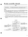
No raster, no sound (B1 is normal)
NOTE: 1702 locations in (
).
[Cause] Horizontal deflection circuit
Problems in the horizontal deflection circuit hinder generation of high focusing voltage, BH 160V and
B2 12V, resulting in no raster, no sound.
1.
As long as normal BH 160V is generated, the horizontal output circuit properly operates, producing pulses during the flyback period of the saw-tooth wave current passing through the horizontal deflection coil. If a problem is found with normal BH voltage, the problem area should be the
secondary coil of the flyback transformer.
2.
When the AC voltage between base and emitter of the horizontal output transistor X01 (0522)
is about O.SV, it is supplied with input pulses. The problem is therefore in the horizontal output
circuit. When, however, X01 (0522) is shorted, this AC voltage is not indicated even if there
are input pulses at X01 (0522).
3.
AC voltage is measured between the collector and ground of X501 (0521) horizontal drive as
shown. When the specified voltage is shown on the meter, the horizontal output circuit is the
problem; while, when there is no voltage indication, the trouble is in some element(s) preceding
X501 (0521). Check if those transistors and les are damaged using a voltage measurement.
C START
t
Vc. VB at X701 (0501)
X-Ray protector
• ABNORMAL
Check X701 (0501)
I
+ NORMAL
Is normal BH
160V generated?
NORMAL
+NO
+
IFailure in T502, L504 (T01, L523),
or high voltage module
Check Vc at X01 (0522)
horizontal output transistor
• Approx. NORMAL
More than AC 50 V
II
Check breakage of T501
(T521)
I
ABNORMAL (Trouble in horizontal
output circuit)
,
Check short or open of X01, 001,
Check AC voltage between base &
C512, C513, C514. C515 (0522,
emitter of X01 (0522) horizontal
0522, C526, C534, C535)
output transistor
AC _ 0.8V"'Trouble in horizontal output circuit
+OV
Check T501 (T521) primary coil,
Check AC voltage between
r - R512,C510,X501, R503, R504,
collector & ground of X501
R505, R508, C508, IC501 (0521,
(0521) horizontal drive
IC501, etc.)
17
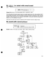
No raster, no sound (81 is abnormal)
NOTE
1702 locations in (
). The regulator PCB assembly used in 1702 models differs from the 1701
power PCB assembly. The B1 voltage circuits should be checked beginning with IC901.
[Cause]
Abnormal B1 voltage indicates trouble in the power supply circuit. When B1 voltage is not only low
but also abnormally high, X701 (Q501) of the X-ray protector is turned on, setting the collector voltage
to 0 V. The horizontal oscillator is then disabled resulting in no raster and no sound.
1.
When D 105, R105, R108, R109 are open, the base voltage of X 101 and X 102 rise to increase
B1 voltage to more than 130V. This causes the X-ray protector to work, resulting in no raster.
2.
If the base voltage drops as when R103 is open or C105 is shorted, the B1 voltage is reduced
to less than 40 V. This will mostly result in no raster, no sound.
3.
When the B1 voltage drops to about 70 V, because R91 0 is open and D1 05 is shorted, the screen
becomes dark and the raster size is reduced because of insufficient horizontal and vertical
amplitude.
C
START
)
!
Does 4.0A fuse blow?
~ YES
,NO
Rectifier including power supply
transformer has failed.
Can B1 be adjusted to 110 V with
B1 ADJ R109?
YES
r----------------------1NO
l
Misadjustment Horizontal deflection
circuit has failed when picture is
small with B1 = 110 V.
Does the base voltage at X101 change
with B1 ADJ R109?
I
t
ABNORMAL
D105 open or short
t
t NO
Is the emitter voltage of X102
correct?
+
I
NORMAL = 6.6V
X102 open or short, R105, R108,
R109 open. C105 short
I
YES
Does the emitter voltage of X10'1
change with B1 ADJ R109?
t
NO ~
X101, R103
open
I
YES
X02 has
failed
I
18
No picture (no raster) with normal sound
NOTE: 1702 locations are in (
).
[Cause] Malfunction of the video amplifier IC201, X202 (lC201, 0201)
The video signal and the audio signal output are supplied respectively to the video amplifier IC20 1
and the audio circuit IC601 . Sound is had but no picture; therefore, the faulty part is IC201 and its
external elements. Since pin 16 of the IC201 to the cathode of CRT is connected by a DC-coupled
amplifier, a fault raising the emitter voltage of X202 (0201) will cause the three initial ouptut transistors to cut off, resulting in no raster.
Check also the screen grid circuit for igniting the CRT heater and the high voltage module.
No sound (with normal picture)
NOTE: 1701 - Flowchart
1702 - Audio circuit has been reduced to IC601.
[Cause] Trouble in the audio circuit IC601, X601, X603 or X604 are faulty.
How is
collector
voltage of
X602?
NO
110V
(Normal)
OV
.X602, X603
short
.FR6010pen
• X601
(open I
• T602
(shortl
• X601
(shortl
• C60S open
• IC601 is
faulty
19
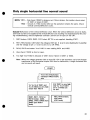
Only single horizontal line, normal sound
NOTE: 1701 - First check if FR401 is broken or not. If this is broken, the trouble is due to short
of X401 or break of 0401 .
1702 - Circuits in 1702 monitor differ but the operation remains the same. Check
vertical controls/deflection circuits.
[Cause] Malfunction of the vertical deflection circuit. When the vertical deflection circuit is faulty,
saw-tooth current is not applied to the vertical deflection coil, resulting in a single horizontal line. During troubleshooting, reduce brightness contrast to prevent an ion spot on the CRT.
1.
R401 broken, C403, 0402, C413 short: 82 12V is not supplied, disabling IC501.
2.
R411, R412 broken, C407 short: the voltage at IC501 pin 3 is set to zero disabling the V-amplifier
and the voltage at pin 2 is set to zero to turn off X402.
3.
R414, R415 are broken: VB of X401 is zero disabling X401 and X402.
4.
Also check if C402 is short or open.
5.
Too high VB of X402 is because of C401 short or failure in IC501 or X402.
Note: When the voltage generator fails to supply 82 12V to the secondary coil of the flyback
transformer of the horizontal output circuit due to malfunction, a single horizontal line
and no sound will result.
(
START
)
I
;-
VB at the vertical output
transistor X402 is nearly
zero
Vc. VB. VE of X401 and
Vc of X402 are very high
(more than 100 V)
R401, R411, R412 or
R413 broken. C403,
0402, C407, 0405 short
X402 open IC501
faulty
r---
Vc of X401 is very high
while VB, VE of X401
and Vc of X402 are
very low
R414, R415 broken,
X402 short,
IC501 faulty
20
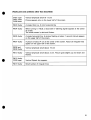
[Faulty parts and problems other than described]
X401 open
D401 short
C408 short
Vertical amplitude small (6 - 8 cm)
R403 faulty
A single thick (ca. 5 mm) horizontal line
R404 faulty
When turning V. HOLD, a black belt (V blanking signal) appears at the center
of screen.
The whole screen is dark and flickers.
R405 faulty
A single horizontal line. A picture flashing at about 1 second interval appears
on the upper half of the screen.
R407 faulty
A picture of about 4 cm at the center of the screen. About 25 irregular lines
appear on the upper half of the screen.
R408 and
R409 faulty
Vertical amplitude small (about 15 cm)
R410 faulty
Vertical amplitude small (about 2 cm). Picture goes slightly up and down and
flickers.
Picture appears only on the lower half of the screen
R416 faulty
C409 open
Vertical flyback line appears.
R419 faulty
Small number of irregular lines
21
Improper horizontal or vertical synchronization
NOTE: 1701 and 1702 locations are the same.
[Cause]
1)
Defective horizontal and vertical sync:
The sync separator and amplifier consists of an IC(lC201). The main cause of failure is often
a failure of the IC itself. It is also necessary to be careful of a possible failure of the external
components. Because the change of voltage at each pin of the IC is extremely small, it is very
difficult to discover a failed element by measuring voltage.
2)
Defective horizontal sync:
This is due to a failure of IC501 or the horizontal AFC circuit.
3)
Defective vertical sync:
This is due to a failure of either the separator and amplifier for the vertical synchronous signal,
or the vertical oscillator IC501 and its peripheral elements.
START
8.8V R le201
NO
pin 8?
YES
NO
9V at IC201
pin 9 ?
• C201 short
• R106 open
• IC201
faulty
YES
• C202 short
• IC201
faulty
• R201 open
• C211 short
22
Monitor parts may be secured locally. JVC part numbers have been provided for your convenience. ONLY Commodore part numbers (C314-xxx-xx) will be available from Commodore at this time.
1701 CHASSIS PARTS
LOCATION
JVC PART #
DESCRIPTION
OY01
J01
J02
L21
R05
S01
SP01
T01
T502
V01
Deflection Yoke
Pin Jack Vid In
Pin Jack Aud In
Oeg. Coil
Nonflammable Res. 220 ohm, 25W, ±10%
Power Switch
Speaker
Power Transformer
HV Module
Picture Tube
X01
Transistor
X02
Regulator
COM PART #
* CJZ6134-00A
C39Z27-224
C39Z27-223
* A39477-T
* QRF258K-221
* CEX40097 -002
EAS-10P225S
* CE30074-BOA
* CJ26107-22A
* 370FVB22(E) Sub:
* 370ESB22(E)
* 2S0869 Sub:
* 2S0898
* 2SC1106A
*SAFETY COMPONENTS - Use EXACT replacement ONLY.
1701 CABINET PARTS
LOCATION
1701/1702
1701/1702
1701/1702
1701
1701/1702
1701/1702
1701/1702
1701/1702
1701/1702
1701/1702
DESCRIPTION
Front Cabinet
Front Cntrl Panel Door
Power Button
Front Name Plate
RT Side Handle
LT Side Handle
Rear Cabinet
Rear AN Terminal Assy
Top Cabinet Panel
Replacement AC Cord
*SAFETY COMPONENTS -
JVC PART #
* QMP1460-244K
COM PART #
C
C
C
C
C
C
C
C
C
* C
314900-01
314901-01
314902-01
314903-01
314904-01
314905-01
314906-01
314907-01
314908-01
314909-01
Use EXACT replacement ONLY.
23
Monitor parts may be secured locally. JVC part numbers have been provided for your convenience. ONLY Commodore part numbers (C314-xxx-xx) will be available from Commodore at this time.
MAIN PCB ASSEMBLY #GE-1000A
LOCATION
DESCRIPTION
JVC PART #
COM PART #
INTEGRATED CIRCUITS
IC1201
IC1301
IC1501
IC1601
HA 11401
HA11247
HA11244
HA 11107
TRANSISTORS
X1101
X1202
X1250
X1301
X1351
X1352
X1401
X1402
X1501
X1601
X1602
X1603
X1701
2SC1959 (V)
2SA1015 (V)
2SC1815 (V,
2SC1815 (V,
2SC1815 (V,
2SC1815 (V,
2S0401A (K,
2S0401A (K,
2SC2371V
2S0668A (B,
2S0668A (C)
2SB648A (C)
2SC1815 (V,
GR)
GR)
GR)
GR)
L)
U
C)
GR)
DIODES
01201
01202
01203
01301
01302
01401
01402
01405
01503
01504
01505
01506
01507
01508
01601
01701
IS2471 V-V
W06B
W06B
1S2473H-V
1S2473H-V
1S2471 V-V
R011 E (B)-V
R036E (B)
RH-1
V19E
R011 E (B)-V
W06A
V09E
IS2473H-V
MA26WO (B)
HZ20-V1
Zener
Zener
Zener
Zener
*SAFETY COMPONENTS -
Use EXACT replacement ONLY.
24
Monitor parts may be secured locally. JVC part numbers have been provided for your convenience. ONLY Commodore part numbers (C314-xxx-xx) will be available from Commodore at this time.
MAIN PCB ASSEMBLY #GE-1000A (Continued)
LOCATION
DESCRIPTION
JVC PART #
COM PART #
RESISTORS
R1410
R1414
R1415
R1421
R1503
R1509
R1511
R1512
R1514
R1515
R1522
R1523
R1528
R1532
R1703
T1704
Metal Film. 6.8. 1W. ± 5%
Oxide Metal Film. 3.3K. 1W. ± 5%
Oxide Metal Film. 2.7K. 1W. ± 5%
Oxide Metal Film. 6.8K. 2W. ± 5%
Metal Film. 11.8K. 1/4 W. ± 1%
Oxide Metal Film. 10K. 2W. ±5%
Oxide Metal Film. 8.2K. 2W. ± 5%
Oxide Metal Film. 8.2K. 2W. ± 5%
Oxide Metal Film. 680. 2W. ± 5%
Metal Film. 8.2. 1W. ± 5%
Metal Film. 4.7. 1W. ±5%
Oxide Metal Film. 18. 2W. ± 5%
Oxide Metal Film. 390. 1W. ± 5%
Zinc. 270. ± 10%
Metal Film. 41.2K. 1/2W. ±1%
Metal Film. 9.53K. 1/4W. ± 1%
ORX019J-6R8S
ORG019J-332
ORG019J-272
ORG029-J-682
ORV141F-1182
ORG229J-103
ORG229J-822
ORG229J-822
ORG229J-6S1
ORX019J-SR2
ORX019J-4R7
ORG029J-180
ORG019J-391
ERS-C05DK271
ORV121 F-4122
ORV141 F-9531 Y
VARIABLE RESISTORS
R1209
R1303
R1305
R140S
R1422
R142S
R1524
1K
50K
20K
220
220
50K
4.7K
OVZ3234-013
OVZ3234-054
OVZ3234-024
A76195-221
A76195-221
OVZ3243-254
A76195-472
Tantalium •. 47 p,F. 35V. ±20%
BiPolar Electrolytic. 3.3 p,F. 50V. ± 20%
Trimmer Cap
BiPolar Electrolytic. 10 JtF. 16V. ± 20%
Tantalium. 2.2 JtF. 16V. ± 10%
Electrolytic. 3.3 p,F. 50K. ± 10%
Electrolytic. 100 p,F. 160V. +30%. -10%
Electrolytic. 3.3 p,F. 160V. + 30%. -10%
Polypropylene. 5600 pF. 50V. ± 5%
Electrolytic. 47 JtF. 160V. +30%. -10%
Metalized Polypropylene. 1500 pF. 1600V.
±5%
OEE61 VM-4 74RZ
OEN61 HM-335Z
CAPACITORS
C1202
C1204
C130S
C1351
C1402
C1407
C1411
C1412
C150S
C1511
C1512
OEN61 CM-1 06Z
OEE61 CK-225B
OEM41 HK-335M
OET52CR-107
OET52CR-335
OFP31 HJ-5625
OET52CR-476
OFZOOS2-1525
*SAFETY COMPONENTS - Use EXACT replacement ONLY.
25
Monitor parts may be secured locally. JVC part numbers have been provided for your convenience. ONLY Commodore part number (C314-xxx-xx) will be available from Commodore at this time.
MAIN PCB ASSEMBLY #GE-1000A (Continued)
LOCATION
JVC PART #
DESCRIPTION
COM PART #
CAPACITORS (Continued)
C1513
C1514
C1515
C1520
C1522
C1523
C1530
C1531
C1610
C1612
C1613
Metalized Polypropylene, 1500 pF, 1600V,
±5%
Metalized Polypropylene, 1500 pF, 1600V,
±5%
OFZ0082-1525
OFZ0082-1525
Metalized Polypropylene, .53 ",F, 200V, ± 10%
BiPolar Electrolytic, 1 JlF, 50V, ± 20%
Metalized Polypropylene, 510 pF, 1600V, ±5%
Electrolyic, 1 ",F, 160V, +30%, -10%
Metalized Polypropylene, 510 pF, 1600V,
±5%,
Metalized Polypropylene, 1500 pF, 1600V,
±5%
BiPolar Electrolytic, .417 ",F, 50V, ±20%
Electrolytic, 10 ",F, 160V, +30%, -10%
Electroyltic, 10 ",F, 160V, +30%, -10%
OFZ-0082-152S
OEN61HM-474Z
OET52CR-106
OET52CR-106
Peaking 820 ",H
Peaking 270 JlH
Peaking 22 ",H
Peaking 22 ",H
Peaking 22 JlH
Linearity
Width
Heater
A04725-820Z
A04725-270Z
A04725-22Z
A04725-22Z
A04725-22Z
A39835
CJ39503-00A
CJ30030-11
Trap 3.58
BP 3.58
Horizontal Drive
Side Pin
SOT
A75537-C
CE40191-00A
A46022-8M
C39084-A
ETA24Z5AY
OFZ0067-5345
OEN61 HM-1 052
OFZ0082-5115
OET62CR-105Z
OFZ-0082 511 S
COILS
L1201
L1203
L1351
L1352
L1353
L1502
L1503
L1504
TRANSFORMER
T1201
T1301
T1501
T1503
T1602
OTHER
DL1201
S1201
Y1301
FR1401
FR1601
Delay Line
Lever SW (Service)
Crystal
FR68 ohm, 2W, ± 5%
FR100, 1/2W, ±5%
*SAFETY COMPONENTS -
CE40472-001
CEX40078-001
A75746
* 2RH021 J-680M
* ORH127J-101M
Use EXACT replacement ONLY.
26
Monitor parts may be secured locally. JVC part numbers have been provided for your convenience. ONLY Commodore part numbers (C314-xxx-xx) will be available from Commodore at this time.
POWER PCB ASSEMBLY #GE-9000A
LOCATION
DESCRIPTION
JVC PART #
COM PART #
TRANSISTORS
X9101
X9102
2SC1890A (E, F)
2SC2688 (K, L, M)
DIODES
09101
09102
09103
09104
0910S
Silicon
Silicon
Silicon
Silicon
Zener
1S1887A
1S1887A
1S1887A
1S1887A
R06.8EV3-Y
RESISTORS
R9103
R9104
R910S
R9108
R9110
Metal
Oxide
Oxide
Metal
Metal
Film, 4.7, 3W, ±S%
Metal Film, 10K, 2W, ± 5%
Metal Fim, 18K, 1W, ± 5%
Film, 47K, 1/2W, ± 1%
Film, 3.01 K, 1/4 W, ± 1%
ORX039J-4RZ
ORG029J-103A
ORG019J-183S
ORV121 F-4702
ORV141 F-3011 Y
VARIABLE RESISTORS
R9109
(8 1 AOJ), 2K 8
OVZ3234-023
CAPACITORS
C9104
C910S
C9107
C9108
Electrolytic,
Electrolytic,
Electrolytic,
Electrolytic,
330 p,F, 200V, +30%, -10%
10 p,F, 2S0V, +50%, -10%
330 "F, 200V, +30%, -10%
1 p,F, 160V, + 30%, -10%
OES720R-337M
OEZ0077 -106M
OES720R-337M
QETS2CR-1 05
OTHER
F9101
FR9101
R9101
Fuse, 1.2SA
FR 220 ohm, 1/2W, ± S%
Positor
*SAFETY COMPONENTS -
* OMF51U1-1R25S
* ORH127J-221M
* A75511
Use EXACT replacement ONLY.
27
Monitor parts may be secured locally. JVC part numbers have been provided for your convenience. ONLY Commodore part numbers (C314-xxx-xx) will be available from Commodore at this time.
CRT SOCKET PCB ASSEMBLY #GE-3000A
LOCATION
DESCRIPTION
JVC PART #
COM PART #
TRANSISTOR
X3101
X3102
X3103
Silicon
Silicon
Silicon
2SC2611
2SC2611
2SC2611
Oxide Metal Film, 12K, 2W, ±5%
Oxide Metal Film, 12K, 2W, ±5%
Oxide Metal Film, 12K, 2W, ±5%
Composition, 3.3K, 1/2W, ±10%
Composition, 4.7K, 1/2W, ±10%
Composition, 3.3K, 1/2W, ±10%
ORG029J-123
QRG029J-1 23
QRG029J-123
QRZ0039-332
ORZ0039-472
ORZ0039-332
RESISTORS
R3112
R3113
R3114
R3115
R3116
R3117
VARIABLE RESISTORS
R3102
R3104
R3106
R3109
R3111
B Cut Off, 5KO, B
R Cut Off, 5KO, B
G Cut Off, 5KO, B
R Drive, 2200, B
G Drive, 2200, B
QVZ3234-053
OVZ3234-053
OVZ3234-053
OVZ3234-022
OVZ3234-022
Electrolytic, 10 p,F, 250V, + 50%, -10%
Ceramic, 1000 pF, 3000V, + 100%, -0%
OEZ0077 -106M
OCZ9017-102M
Peaking,
Peaking,
Peaking,
Peaking,
OOL043K-181
A04725-390
A04725-390
A04725-390
CAPACITORS
C3101
C3102
COILS
L3101
L3102
L3103
L3104
180
390
390
390
p,H
p,H
p,H
p,H
OTHER
CRT Socket
* A75522
*SAFETY COMPONENTS - Use EXACT replacement ONLY.
28
Monitor parts may be secured locally. JVC part numbers have been provided for your convenience. ONLY Commodore part numbers (C314-xxx-xx) will be available from Commodore at this time.
CONTROL PCB ASSEMBLY #GE-4000A
LOCATION
DESCRIPTION
JVC PART #
COM PART #
VARIABLE RESISTORS
R4003
R4004
R4006
R4012
R4015
R4016
R4022
R4024
Tint, 10K
Color, 10K
Cont, 10K
Bright, 10K
V Hold, 10K
H Position, 500
Sub Bright, 4.7K
Volume, 200K
CEX40206-B14
CEX40206-B 14
CEX40206-B 14
CEX40206-B 14
CEX40205-A 14
CEX40205-B52
OVZ3507-472
CEX40205-A25
*SAFETY COMPONENTS - Use EXACT replacement ONLY.
FUSE PCB ASSEMBLY #GE-9700A
LOCATION
DESCRIPTION
JVC PART #
COM PART #
CAPACITORS
C9701
C9702
Metalized Mylar, .047 p,F, AC125V, ±20%
Metalized Mylar, .047 p,F, AC125V, ±20%
OFZ9008-473M
OFZ9008-473M
OTHER
F9701
Fuse 4A
Line Filter
* OMF61 U1-4ROS
A39475-J
*SAFETY COMPONENTS - Use EXACT replacement ONLY.
29
1701 Board Layout
r
~;U0.60R-<:3
1~ ~
L
I T201 I
o~ ~ ~OoJ
!:
1 E
O.O,,?
B
)
I
DL201
W44
oft ~.
~V
<::>
O~
0 ~1R204
~~~~O
~~~ono.~o~
~
1
1~;;
O~
C-~o::,.
~
:
,
~
~ -s.. !,l, 0.2"~ ~o'~202
-e:r ""'0
~~oo-c=:r
~~
-----.r,.,";5.
n
3
'W
•
:e=:::>- '"0
C
NO
,c' 250
(
--1
)C515
ORN ORN
54
(])C509
°
c,s>
R510
~R506
R526
W43t-
CS21
~.Q ~ -c=:r..,'~
~:u
. . . N. "'.
0 ."'7.~
0
'"
~N~~ 000' '" h~° U~-c=:r-dts,'l,.
C2020
.c::t.31.
~
Ow::..c::::r
b ~ -c::::::r
-c::::::r
•
• ~! CO"
c::::>- U .205
3
~ W.07 w"
Qri ~050Rl0~7~,0. C).o,O~ ~ OOO~
~•q614R6,~
U::~~O·
~~ ~,O •~ ;; g
~.gu~. ~.357
,0·"0' ~.". ~
n - .
:
<>
"
o
'"
o
><
U'i0
.350
-c::::::r -c::::::r.
"'--F OOn
QI
g
o
•
<:>
1'1
..
(])
I
30
wo.
n
-
I!!
)
'5
woo
m
.317
'"
W I I_
!1'1
)~' ORIOO'·~I IT30'wo. q~301R:03
~
O£~
I
I~.
C611 C LJO~R3"'- ~ ~.r---'.
(jt°C.09
~
go
•
::0
;;
QI
E~X8602
2!
'"
nD
'--1" 0
C302
c=)
'"
R323
CD
J"-"L
•
.30.
COlOR
.302
.0.
~.•~
307
~.
~ o~
n
W92
~0
W,2 Wl3
W54
WI.
~.::
•
W'5.",
X401
C
;l
2
B
W
52
0
~
o~~ ~0 On~-c=:::>_ .505.
T~703
[OiUB
TINT.
.
-c::::::r
.3051
w.3
0 -c::::::r
,
.30'
,
14
T01
0.0.
c=lc..,
'----'
=
'---.r
0 -c::::::::r R322
-c::::::r n
-<i=r 000'
L->
-C::::J
-c::::::r ::::
BlK
.WHT
a
-0
; 'e'
g
• A·
:;
~
W40
COOS,--,
0'
ao
10
0W93 ~N
W33
r ----
.-
C613.........
0
<:
0
c'"
•
c.,,o
9
-0
w"
°0
0306.c::::p.
•
::
,,0'
-"'.
i
•
Z\
g
JCSO'
:
3
g
...r--\..
19
_ "
>----r
•
;;
W:Aol
:;
."f-
-II
R403
••"
0 '":tEtf412
___} _,
0
•
0
•
g
V.L1N. V.HEIGHT
. _
, . " ••
-W
•
W30
QS
-c::::::r.
W"
8
'1 .
C2m "
u",Q06
0202 0402
WI'
••
't--"
0404
-
SO
W2'
; S...
1_- re',
-
-)( 0;
°OCD
-
O GE-1000A
"---1
P
9
C;f:)'04.
0".
• t)'(a WI.- &0303U . 0
."
"'"
T602
L
-
_
0n~
ii
•n
2
•
2
•0
<
Co)
TP51.
--1
R420X402
0
.",.~,
~O
~
~
~611~
~-or~o ~@L9
C4~O~ '~I~ ~
~
0· ~ ~3081~gO ",,:''' ~o d~ COj Q' ~. I~O:Q~7
~
() ~ t i~;- l-ja:)4 =~ (f ~_
~
~
~
-0 '~421W~3il ~___
i5 0307~ O;~u0:uO~o3°·1 ~ .}::l
t;':ob'oOO~
(
C
2
S
0
2
~
~R410
~
0
0
,...~
~q
0
..""
o
g.
-
-
E
r
~
0
<::>)( []
(
<!!
_
TP12A
8
)C512
)
C513
)
)CS14
)C531
C530
L
0
;;
'/1103
(
;u
•
fA
\...?
1'1
j2
51
L502 (
... 9
•
52
53
I
~J~
.:;:;
0
...,
TS01
XS01
.r-------c
_
;
~523
R42B
i
,
050.
H.FREQ V.POSITION
,
0503
i
T
S
4
03
02
6
en
01
I
I
LS03
3
w.o
.J
o
frtIIII 'I·IOQOA
SPOI
~t8~IIA(B,C)
r
A/V f'ANEL
(REAR TERMINAL)
~~~;:. '~;-
II~HY ,.,
rt- ---lfl
~:~---~- J
orZSCZSIOV
or ZSC2482
orZSCZ687
AUOIO DRIVE
1
I
r ...... •
1701 Schematic Notes
'II Y4
_
GE-IOOOA
Itao
".1tc
J
*
IC30I@pIn
X602
2SD ••• A((;)
.r2SC2411~
AUDIO OUT
o
:$Yp..p
'HI
MAIN 'CB ASSY
ceo
.,001
"0'
IIOK
ceo.
.011 ,OOY MY
I
•• _ .
~L.
I
VOLTAGE & WAVEFORM NOTATIONS - Voltage readings and waveform measurements were taken
with a color video signal injected at the video input terminal. Figures in ( ) represent voltage readings
taken while receiving a black and white sign. Each variable resistor was set to condition at time of
shipment. After adjustments have been made, the figures will vary and the figures should be used
for reference only.
VOLTAGE READINGS
AUDIO
'"
vloro
IN
Multimeter set at 20KO/volt DC.
All values given are DC voltages.
(FRONT TERMINAL)
REFERENCE WAVEFORMS - Scope sweep speed set at:
Hor - 20 /tS/div Vert - 5V/div;
Unless other speed is specified.
SCHEMATIC NOTES Resistors:
Capacitors:
Inductors:
I
J
Unless specified otherwise:
All values are in ohms, 1/4 watt carbon
Values of 1 or higher are pF.
Values less than 1 are /tF, 50V, ceramic
Electrolytic values are in /tF, NP indicates non-polar (bipolar)
Values are in uH
X02
2SC1I06A or 2SCI4S4
POWER REGULATOR
9
'"
~I
m
indicates a test point connection
;m indicates chassis ground
Hz indicates cycles per second
<;;>
TP
IIw
I1rv
GE-9000A
POWER PCB ASS'Y
•• !lOV
"
1" ,.,
1t10'
I
o
Iw
0101_0104
SAFETY - For safety, maximum reliability, and continued good performance, use specified replacement parts. All safety items have been identified with the symbol *. FR is an abbreviation for FUSIBLE RESISTOR~. FR's act like fuses and are used as safety items. They are to be replaced
with specified parts.
I
j
ItIOI "TH
r-----,
'I'"n.
~~Olr. n
'801
1.2~
FR
'lr" ':. ___t~ _: ..,;~~,: ./"CI~~
OI~~1:
.07\..
II
LOI
fillO&
I 11K IW
I
IOMR
~
_
It
~
~ ~H""'!V'I--~"O'
I Ul
CIGI
I
I
:~~ L-IITiJI-_....4!i!!~!.lI:-·!!:C4..:~::.:.·_·¥6~1 +:~"O' fClO~~O: ~~,
J
,.
ttO"
110/100
NOTICE - This circuit diagram and the circuit constants are subject to change for improvement without
notice.
IGII: FIOII'O
IW T
0105
OMR
RO ..
UK
r-XI02
"oA 2SC2688
i&J
ItttO
101M!'·""
eM".
n'l.~
200
U<,L,M)
_
_ _ _~I~MP
~- 0'rt;iiiiii1i
-=:. .: --~~
rol
GE-9700A
~.'WOI
L
I
FUSE PCB ASS'Y
T
.....
::~.,.O~~I"..
I
I
I
Il~r
U U
IHI
Ir
::.=(V
IFV\::,.".:=
•.
'01
.!. . g~~,uv·~
~·"---~THI~
I~'I
""'-l-F
~
"0'
IV\I
~~;~
.OHZ 100HZ
r9"~
:: W
~:
olllii
1
':
1
L _______ J
0'1'01
DEFLECTION ,(OI<E
1701 Schematic
31
1702 MODEL IDENTIFICATION
BEFORE servicing a 1702 Monitor, please NOTE:
Some models are distinguished with the letter "T" next to the manufacturer's serial number.
_-----+------ Rating
Serial No.
I
-------------(T)
label
I
L--
Model discrimination point.
This designation indicates that a TOSHIBA picture tube and deflection yoke were used. A difference
in electrical specifications is required. The connect schematic and parts list is identified 1702 "T".
32
Monitor parts may be secured locally. JVC part numbers have been provided for your convenience. ONLY Commodore part number (C314-xxx-xx) will be available from Commodore at this time.
1702 CHASSIS PARTS
LOCATION
DY01
J1821
J1822
L01
01522
R01
S01
SP01
T01
V01
JVC PART #
DESCRIPTION
Deflection Yoke
US Pin Jack Vid In
US Pin Jack Aud In
Degausing Coil
Silicon Transistor
Un"flammable Resistor, 280fl, 20W, ±10%
Power Switch
Speaker 80, 2W
HV Module
Picture Tube
PC Magnet
Neon Lamp
*SAFETY COMPONENTS -
COM PART #
* CJ26161-00A
C39207-004
C39207-003
* A39477-T
* 2SD1426
* ORF208K-281
* CEX40097-002
EAS-10P225S
* CJ26156-ooB
* 370FVB22(E)
CE40305-ooB
OLZ9015-oo1
Use EXACT replacement ONLY.
1702 CABINET PARTS
LOCATION
1701/1702
1701/1702
1701/1702
1702
1701/1702
1701/1702
1701/1702
1701/1702
1701/1702
1701/1702
DESCRIPTION
Front Cabinet
Front Cntrl Panel
Power Door Button
Front Name Plate
RT Side Handle
LT Side Handle
Rear Cabinet
Rear AN Terminal Assembly
Top Cabinet Panel
Replacement AC Cord
*SAFETY COMPONENTS -
JVC PART #
* QMP1460-244K
COM PART #
C
C
C
C
C
C
C
C
C
C
314900-01
314901-01
314902-01
314903-02
314904-01
314905-01
314906-01
314907-01
314908-01
314909-01
Use EXACT replacement ONLY.
33
Monitor parts may be secured locally. JVC part numbers have been provided for your convenience. ONLY Commodore part numbers (C314xxx-xx) for will available from Commodore at this time.
MAIN PCB ASSEMBLY #GE-1003A
LOCATION
DESCRIPTION
JVC PART #
COM PART #
INTEGRATED CIRCUITS
HA11401
HA11247
AN5515
HA11244
AN5265
IC1201
IC1301
IC1421
IC1501
IC1601
TRANSISTORS
2SC1959 (Y)
2SA 1015 (Y,
2SC1815 (Y,
2SC1815 (Y,
2SC1815 (Y,
2SC1815 (Y,
2SA1015 (Y,
2SC1627A
* 2S01426
01101
01201
01251
01301
01341
01342
01501
01521
01522
GR)
GR)
GR)
GR)
GR)
GR)
DIODES
01201
01202
01204
01301
01302
01401
01421
01422
01501
01502
01503
01522
01523
01524
01525
01541
01551
Zener
Zener
Zener
1SS133
W06B
1SS133
1S1555
1SS133
MA4110 (M)
1SR124-400
1SR124-400
MA4110 (M)
1SS81
1SS133
1SR124-400
RM-2C
U19E
MA4220 (M)
1SR124-400
1SR124-400
*SAFETY COMPONENTS - Use EXACT replacement ONLY.
34
Monitor parts may be secured locally. JVC part numbers have been provided for your convenience. ONLY Commodore part numbers (C314-xxx-xx) will be available from Commodore at this time.
MAIN PCB ASSEMBLY #GE-1003A (Continued)
LOCATION
DESCRIPTION
JVC PART #
COM PART #14
DIODES (Continued)
D1701
D1702
Zener
1SR124-400
* HZ7B2L
Oxide Metal Film, 1000, 1W, ±5%
Metal Film, 1.50, 2W, ± 5%
Oxide Metal Film, 560, 1W, ±5%
Oxide Metal Film, 1K, 1W, ± 5%
Carbon, 1K, 1/2W, ± 5%
Oxide Metal Film, 12, 1W, ± 5%
Metal Film, 47, 2W, ± 5%
Carbon, 1K, 1/2W, ± 5%
Oxide Metal Film, 4700, 1W, ±5%
Metal Film, 2.7, 1W, ±5%
Metal Film, 5.6, 1W, ± 5%
Metal Film, 33, 1W, ±5%
Metal Film, 20K, 1/4W, ± 1%
Metal Film, 14K, 1/4W, ± 1 %
QRG019J-1 01 S
* QRX029J-1 R5A
QRGO 19J-560S
QRGO 19J-1 02
* QRD121J-102SY
QRG019J-120S
QRX029J-4R7 A
* QRD121J-102SY
QRG019J-471 S
* QRX019J-2R7S
QRX019J-5R6S
* QRX019J-330S
* QRV141 F-2002Y
* QRV 14 1F-1402Y
RESISTORS
R1414
R1421
R1511
R1523
R1526
R1530
R1531
R1532
R1534
R1551
R1607
R1701
R1702
R1705
VARIABLE RESISTORS
R1209
R1303
R1305
R1406
R1408
R1429
R1504
Sub Cont., 1K
Sub Color, 50K
QVZ3230-013
QVZ3230-054
Sub Tint, 20K
V. Linearity, 200
V. Height, 200
V. Position, 500
H. Frequency, 5K
QVZ3230-024
QVZ3234-022
QVZ3234-022
QVZ3211-052
CEX40202-053
Tantalium, .47 J.'F, 35V
BiPolar Electrolytic, 3.3 J.'F, 50V
Trimmer
BiPolar Electrolytic, 10 J.'F, 16V
Tantalium, 2.2 J.'F, 16V
Mylar, .1 J.'F, 50V
Mylar, .056 J.'F, 50V
Electrolytic, 100 J.'F, 35V
QEE61 VM-4 74BZ
QEN61 HM-335Z
CEX40212-001
QEN61 CM-1 06Z
QEE61 CK-225BZ
QFZ0083-1 04M
QFZ0083-563M
CAPACITORS
C1202
C1204
C1308
C1342
C1402
C1404
C1406
C1423
*SAFETY COMPONENTS -
* QET51VR-107
Use EXACT replacement ONLY.
35
Monitor parts may be secured locally. JVC part numbers have been provided for your convenience. ONLY Commodore part numbers (C314-xxx-xx) will be available from Commodore at this time.
MAIN PCB ASSEMBLY #GE-1003A (Continued)
LOCATION
C1425
C1426
C1502
C1508
C1523
C1526
C1529
C1530
C1531
C1534
C1535
C1541
C1551
JVC PART #
DESCRIPTION
Electrolytic, 470 p,F, 35V
TF, .15 p,F, 50V
Electrolytic, 220 p,F, 35V, +30%, -10%
Polypropylene, 5600 pF, 100V
Electrolytic, 33 p,F, 160V
Metalized Polypropylene, 5000 pF, 1600V
Metalized Polypropylene, .53 p,F, 200V
Electrolytic, 2.2 p,F, 50V
Electrolytic, 470 p,F, 25V, + 30%, -10%
Metalized Polypropylene, 1500 pF, 1600V, ±3%
Mylar, .082 p,F, 100V, ± 10%
Electrolytic, 1 p,F, 160V, + 30%, - 10%
Electrolytic, 1000 p,F, 16V, +30%, -10%
* OET51 VR-477
OFV81 HJ-1 54M
* OET51 VR-227
OFP32AJ-562M
* OET52CR-336
* OFZ0081-5001S
OFZOO67-534S
OEN61 HM-225Z
* OET51 ER-477
* OFZ0081-1 501 S
* OFM72AK-823M
OET62CR-105Z
* OET51CR-108
Peaking Coil, 820 p,H
Peaking Coil, 270 p,H
Peaking Coil, 22 p,H
Peaking Coil, 22 p,H
Peaking Coil, 22 p,H
Lin. Coil
W. Coil
HVT Choke
Heater Choke
A 76186-820Z
A76186-270Z
A76186-22Z
A76186-22Z
A76186-22Z
* CE40052-001
* CE40140-00F
CE40037-560
CJ30030-100
COM PART #
COILS
L1201
L1203
L1301
L1302
L1303
L1521
L1522
L1523
L1524
TRANSFORMERS
T1201
T1301
T1521
Trap, 3.58 MHz
BP, 3.58 MHz
SW Drive
A75537-0
CE40476
* CE40361-00B
MISCELLANEOUS
DL1201
S1201
X1301
Delay Line
Service Switch (Lever)
Crystal
*SAFETY COMPONENTS -
CE40535-001
CEX40078-001
A76351-D
Use EXACT replacement ONLY.
36
Monitor parts may be secured locally. JVC part numbers have been provided for your convenience. ONLY Commodore part numbers (C314xxx-xx) will be available from Commodore at this time.
CONTROL PCB ASSEMBLY #GE-1003A (4/6'
LOCATION
DESCRIPTION
JVC PART #
COM PART #
VARIABLE RESISTORS
R1854
R1860
R1863
R1866
R1869
R1871
R1875
R1877
Cont, 10K
Bright, 10K
Sub Bright, 4.7K
Tint, 10K
Color, 10K
Volume, 10K
V. Hold, 10K
H. Position, 1K
CEX40206-B 14
CEX40206-B 14
aVZ3507-472
CEX40206-B14
CEX40206-B 14
CEX40205-B 14
CEX40205-A 14
CEX40205-B13
MISCELLANEOUS
L1851
SW1821
J1821
J1822
Peaking Coil, 820 pH
Slide Switch (Signal Select)
US Pin Jack (Video In)
US Pin Jack (Audio In)
A 76186-820Z
CEX40325-001
C39207-004
C39207-003
37
Monitor parts may be secured locally. JVC part numbers have been provided for your convenience. ONLY Commodore part number (C314xxx-xx) will be available from Commodore at this time.
CRT SOCKET PCB ASSEMBLY #GE-1003A (3/6)
LOCATION
DESCRIPTION
JVC PART #
COM PART #
TRANSISTORS
01351
01352
01353
2SC2611
2SC2611
2SC2611
DIODES
01351
Silicon
RM-2C
RESISTORS
R1357R1359
R1360R1362
R1378
Oxide Metal Film, 12K
ORG029J-123
Composition, 3.3K
ORZ0039-332
ZN
ERZ-C05ZK271
VARIABLE RESISTORS
R1352
R1354
R1356
R1369
R1371
B Cut Off, 5K
R Cut Off, 5K
G Cut Off, 5K
R Drive, 200
G Drive, 200
CEX40302-053
CEX40202-053
CEX40202-053
CEX40202-022
CEX40202-022
CAPACITORS
C1351
C1352
C1356
Electrolytic, 4.7 ",F, 250V
Ceramic, 1000 pF, 3K V
Electrolytic, 4.7 ",F, 250V
* OET52ER-475
OCZ9017-102M
OET52ER-475
MISCELLANEOUS
L1351
Peaking Coil, 180 ",H
CRT Socket
*SAFETY COMPONENTS -
00L043K -1 81
* CE40085-00A
Use EXACT replacement ONLY.
38
Monitor parts may be secured locally. JVC part numbers have been provided for your convenience. ONLY Commodore part number (C314xxx-xx) will be available from Commodore at this time.
REGULATOR PCB ASSEMBLY #GE-1003A (2/6)
LOCATION
JVC PART #
DESCRIPTION
COM PART #
INTEGRATED CIRCUITS
* STR3125
IC1901
DIODES
01504
01901-
Bridge Rectifier
* 1B4B42
Si
* 1S1887A
Non-flammable, 2, 7W
Metal Film, 4.7, 2W
Composition, 6.8M, 1/2W
* QRF076K-2RO
* QRX029J-4R7 A
QRZ0039-685
Ceramic, 4700 pF
* QCZ9021-472U
Electrolytic,
Metal Film,
Electrolytic,
Metal Film,
* QEU720M-477M
* QFZ9020-1 04M
01904
RESISTORS
R1902
R1907
R1910
CAPACITORS
C1901C1903
C1904
C1906
C1907
C1908
C1910C1911
470 JlF, 200V, ±20%
.1 JlF
10 JlF, 160V, +30%, -10%
.1 JlF
QET52CR-106
QFZ9020-104M
QCZ9020-472M
Ceramic, .1 JlF
MISCELLANEOUS
L1901
T1901
F1901
F1902
TH1901
Coil - Line Filter
Power Transformer
Fuse, 4A
Fuse, 1A
Thermistor
*SAFETY COMPONENTS -
*
*
*
*
*
CE40247 -OOA
CE40489-00A
QMF66U 1-4ROS
QMF66U 1-1 ROS
CEX40137-001
Use EXACT replacement ONLY.
39
1 702 Board Layout
wO D
i :~~~~9~O~; _~
~n'"
~~70 ~ 0
~tr @lJ
a~'"
~ ~~
.
@
~:
. '"
~
B
II!!
;~~6
06
~n:
E U...
E [136}l
y;
u
6
-
a
~ GE-I003A 15/61 Ai INPUT ~
Ilil
L;i
llioR356 oR354 oR3S7
....
P~jJYIRI !
0il
0
~
gUn
~
AOOIOO
0
~
C356
"a
-
0"'"
Y
~
~~
I [!] 3
~~
C351
==. 0
o 0 0 0 0 0 0 0 0 0
iii
R906
-c:::::r
=,
~g
I
0 0 0 0 0 0 0 0 0
=
..
0 0 0
EO
--
0
GRl.t.:lJ
B
C 0111
0
o
Oi!l
:::
1
o
0
0
o ~~
0
0
()
0
~ 8~
~
Sf! ~ _
~ ::c!::
_
- ~
U")
~~
(]
HOT
~ tB
''''ng
I
L.LJ
<.!:>
>-
00
I >-
1
~
El
0
00
0:: 0
0
.....!!I9l..
-c:::::..J-
C>
(j703
~
C401
_
~o
~
"w
i"i
9
C303
Oioit
00
-- (301
055:! C>
-c:
R401
~o O~ o~
6(0301
n
8
to
--R424a
R
425
C401
E.
R322
a aR31iUI
a
R423
-
~
ii
R60Z
i
o~~
0
ml""
C>.
- -
~ II
a
rsuBl
nNT
a
C314
0 Oi!l
B
0342
MIl
_
51!
R313
I
~
~
I
§
WI!
~
- -
R608 a
[!]
a~ ~
3
~
~
0
0
Rl03
SUB COLOR
R606
0-..
L-J
C605
C526
I
--
III
!
m3
RS4~
C54U
EI
I~
-
(
~
~
R41l
91?Z5
~
n
-c:::::r
'.!X
~ R4j
1)1
R505
1-c:::::J-,~
R428
gW26
~I:a ~
I~
_13_1_
R421n=-..::......lo
,u-I-,.-u,
R406
a
R537
!I.HIQlT'
1:533 C> R ; m -
!.1
-iU
0
Of-
•
10 OL
c-=,AS""=Sy~======J===================,,,"===~=_==dJ
GE -1003A (1/6)
MAIN PB
.
D
.
(~
C>
136
0541
-wi!
!V.POSITIOII!
t::
~
R405~C5.
~(j~RS36b ~:~~~
~
R427
&Ioo~0523
~
l522
R4I
-<::hd-
R426
~C534
!
a
--
0-
OORS:S19
h~
I
§C}.J
0
R4M
.... L....-_ ____L_....l
2
~
--
R409
SW201
~ ~ -I!I~:;
lJJ!!J~
~
_~
0
~
D
~8
-{]
• 104 E H 0201
a
-<t:> 0201
Rl04 :~ O~ <t:> 0302
S
0
I!5_Wll_· -
_WI2
5
!4!Il ~ I
R601
IITl'"
a
e
110
EJ
~
!HIRO!
~
128
~Oo
0- ~
11
C> C421
R413
C>
OR3~311
~i
TP-llA
~
(422
WI3
-{]
R9k1
~
"'@&Irll't~
I
..
R404
.~
23
J
Rklla"R3UE
U45
~DO
"'
IT"'. I'"1:'0
i @()c
:;:!'lfd;.,~::.
""
[f:~Y~EJO"'laV.
-la
_
~
~20
• C503
~ ~
I
1<1 TNI
0
:
r-1_rF9.!!!.Ol..l4:.l!!_OA~I2!i.oi5~V...-_
~70
;B ~ @2A3117o I a C4~;: ~~
i!l 0
tjU
a
CO
I 40 Q ij g
~
~ ro ~I
0 ()
:J;'-~O. L....J
~-0 CJliD ~ZI P
0
--.JI I
0503
C504 a
R511_
.
O-t)()02",
:: ~
o
21
~
43,;;;-\:
E
0
oce
n
'0
~
oo-fl"'
-B
y~
a
~OCkl351 ~lllT3°D""· Oi!lO~.TH
~~2 -c:::::r
~ ~.
~
(1)2
C906
RS06
m151~ 0 ~
Ill"" :}i ,
a"
0
51
TH901
T901
.m
r-----==__.
a.
"'~U Oa
C34100
a~~~ ?61oo'Oiili
R227
-m;
~
L.._ _
_12_3_
~
~
R204
°OR205
R202
S
RED
OJ
1l.201!J
R203
~ :~63
a ctl
~CJCZR3)~3'"
-U(O
!O
0
C905
O~-a.. ~
~
~
~
!i1eum!@
U
Rfi?
0
Ii
~
~~~R209
=~
o
; ;1 21
'.d~1098H
m;.1
~~. ~
: {;
0
I
~
.--C904___
1
'0
..
0
4
I
0 0 0
O~
0
I : O~ - ~ 9001 -II'? .~""g.. l~
a gOO~~
""DO§09
I'8l
~
0 ~2
a
09
~ O~O ~
_ l!...J
~
-
UN
rl-. .dLoo:ooo~:00000~£~~-:90oo~oooooo~00000
U
El
.~
. . i.ill-.I"·I: ,. :
;:
1"""1
...
0
~OO
~ r
0
I
!i~
"'0 .I~ ~
0
163
Ot()
~I"'""'I
e
R607- R5lO -
ftS=E~'ER
[1
I
GE-1003A(5/6)
AV INPUT PB ASS' Y
(REAR)
DC
1 702 Schematic Notes
t
VOL
ATT I J
__
!).4V
4r+~~I~'8~V~_
C601
1150
~r
C602
I
:
220/16
3'1
VOLTAGE & WAVEFORM NOTATIONS - Voltage readings and waveform measurements were taken
with a color video signal injected at the video input terminal. Each variable resistor was set to condition at time of shipment, After adjustments have been made, the figures will vary and the figures
should be used for reference only.
Multimeter set at 20KO/volt DC.
All values given are DC voltages.
P-
R&D;'
SCHEMATIC NOTES -
I
Jazz
!
C30[
4.7
R60S
C6C5
t
1ff:
12K
16
'"'
~6V
4.511 !).5V
12\1
BP •
~I
5!lvl ~.------;180
3~6vi
lOA\I
I
-B-
~
IC301
I? tl
3.58MHl OSC
-J::J
/6
S't ,~
'.:::.:::I
:
TP-50
~
8
0301
T
R306 1.2K
lOtI:
tSl~~~
C306
-
""
R347
33K
Q342
2SCI815IY.GRJ
BUFFER
348
5.6K
1/4
~
l
)W)6.3
VIDEO AMP
,
*
L..j ['
jg;S ~J04
fsgl
*
Q34\
2SCJ815IY,GRJ
BUFFER
IC901
5TR3125
~
-
R,~07";;7
SOl
,F-\.P--O>---<O+----..,.--r---,
~ C906
:::==
L901
LlN~FllTER
~crJ5
m 4:'~~SE
C902 0~03
0904
+
"'-J:90~
........
~~; I
I
'''6
220
I
C2:5
~
~
",.,
~"7fo3
~
6.8K
Mit
: .001
'-.J
I
~bh'
R'2.
-~
f
1/4
L.. .>: :8":=: ZO".........-C.l-:.-._
':
t~+ '0]
I
~
L:
'--.
REG PB ASS' Y
2
~:'z~4
fJi
10K
-I
1
'4
2~Vp-p
,0331.4Y
FlllO
R230
.1V
180
I~O
1---<)-1
II
II
T
(V)
!Cl.2! 6,4111
!
-
rG'E-I003A(3/6)
:
T:~2jO
~~I~'o'J~{~
*"
:
:TRAP
1-
CS02
2201
25
Isue
A..A....
0
COM1.I
I3Vp-p
DC
fV"
&
-OV
Q251
2SCI815
f
18Vp-p
+
'--_1"_'_ _ _ _
'''_,__--'
I,8Vp
P
V.A'"
t
16
IV)""~~~
R429
500
112W
R40910K
QSOI
C.~~~
+
508
R509
C506 100
I
220/1614
fiSK
3.
~v13V
50
tOM:
6:\~I2:S
: AR
:
:
: .;tt9ioir\
v
153
!J3V
6
7)iiii(8
to.9V
V.OUT
,"4\1 10K
560
-
IR
~
R375
:
I
1
I
150
Q351~vG
6.9~~vr;,
2208
G DRiVE
L
1000
I
~- LJ~371
:
2208
180
\
~
\4'~'."
...
6 8
OS56
t-47/2:'0
~
•• -
R~~~~$~t~35~
@'tl
'-l
},-
~J
RM-2C
400"
l351
R3~~ II<
7V
I
12~~
OUT
180
~
R363
rt:3:0:
R356
, K8
C3~1
C352;::
j1125
.
m; 10/250
1
_.-....-
0351 Colledor
R519,.u
'12K
'''
ORI"EI~~547'l ~R:~oS~3IKl
I
n:~P~n
2TK
~~R
R3512W
Q351
ROUT
I7$V
R354
II1
370KNB22
1I I
I'
r-~
•
,5KB
val
~_
:uKW3
,--- ·m23.3<I,;l7
R36~i:ig
Uf3SS
:
I
5~~2
:
I
I
I
I
I
I
~UUUU~
1
asv,~ -,
0352 Collticlor
pI1
pIl
~~ ~
(HI
I
0353 Coll«1Or
l1..tlro~-,
(H)
~
.------~-t~
~~--+_--------~~------~====H=-==--~======~-=======~--i------+-------------r")----------------+--r-------II~
[l
+ C5.30
2.2/50
'
1
1/2W
A5;6
IK
R532
lK
1/2W
IIZW
11
I/2:W
~~ ?r?'jlSE
'I
2 3)-("\)-(1~'}o-(1"6..."...,7),6\1 ~4V
R412 10K
17V!
fi413 560
V.OUT
A~_
II)./V
L2V
IC422
~~O
,
C423~
100/~S T+,
J:
R408 R410
3.9
R406
2:008
~V'ORIVE
1m,
~
+
2SCI627A
0'1'01
T
vv~
LIN
~9S':'~4
C5~LQ.!).3l,)i..;.l
2!l.8V
1
_ >------
__
(541
'~H.DR!v-~RrK2:1rUjR,.l
R524,~
)
W
I
II
2"
a.3 "'-~
b~ ~C
s-.!!.A521
221/S.
0522
r±
820
C70"6
101
S22--r C521
4?001
680
SOO~
+
R511
2SDI426of
2SDI453
L.H OUT
C53
2'11
C526 ;:'.,082
.005
MPP T
IACt.SKi
..I.
56
""R~1~1
Q501 2SAIOIS(Y,GRJ
X-RAY PROTECTOR
~'~,7
II2S
C~00.-7
r:::L.
~2l
IJ
V
TV"
8704
22K
~1:\,1I4MFFI
~:~.
,~~
I#R
____J~l~
I",
LI"
HZ
D70l R101
100125
T-4ool
'MFR*.'
D525
(524
-:;"
~
1
.~
12!!lv
~
~
I
I
1
1"i
I
J:$...r"- :",.
I
CRT HEATER
*1
Ai\
-0
'
70Vo-o
j
!M)
-r__/~:'IS
tOVO'~
~
JL-JL
IHI
(1'1)
56.. H
''',-,
*2
J
L
S24t0
10o...H
l,;,.,
J ,,--~ ~ ,OJ.,
--,
rD2
,/''.[,
C531
f!]!~~1(
f
.;;,
-!t:dt: ~.
..oK
(HI
_
to CONTROL PCB
(HJ>OSIT10NI
I
I
_______ 1
ISRI24.r400
4
IISJ.;;"'('~t--"!~-"'\>:::=(§O~,___________________~
0551
~19-E
1>1 ~:
I
I
'I.' MFR
470/16
, . - - J l l l R~0,>,1 LIb
"3l
r566116
l31WMfR
1
H
I
T D523
RD22E8.047 G> I
II
I ' ')rlSfH24-400
0522 VI'3-E
II ~
UIS-E
R~51
11:-:-:5
~I
~
27'1'N6r""2W~~::
I~R~3'
47
+C523
II
~~~'.
+C7Ol +C702 \sllj'" "Ai6'
10/35
';;"
I
I
-~--2:J;--~;;~-$=1!=j4~=:C==:z,;;;-;::::===========t===+=========FOCUS
1::
~r--f<.lH-t+-jIi------<,SCREEN >-___________+----1
-400 lr
'"'_~
:
I
HI
~~O
(H)
0.0,lS21
COIL
1523
...
H,V.'"
IV.LlN!lV.HIGHTI
I
2!OVp_p
[J"l<
n
u
1/2CR
11--
0<
05021SS133
----_1 '--- _____
.0047
CUTOFF
~-..-....JR3SI
7J"-1 IK
I T ? 180
II I
/.
'I I ~ ..1 _t
RSI3 ISOlt"
050.3 RSl2
1551334.7K
:
!",!'l
R361
•
V.POSITION
i,
R6~~2~
em
'r[.
(H)
020l
I
152076AI
:3.31<
150......r
.. \
~~~
(
+
14 oV( 6.2\1IZ I2.2V
TP-B8
ssvrv'\ 18
R374
:I
~~R
I.!)Vp_p
6Ovp_p
I
1
<OK
150
'lFO
........l
R367
I
I
R51S
R373
;?ol)-=t n
11"r.
1nil 1
Gf"-IOO3A
25C2611
B OUT r7'lV
,
L....... _-"i}
1'...]180
'c,3 .....I-+_~~OOO,,-'+
p 53.I
I
~r30
'SWITCHER
_I
Q351
~
I
I
'. .
/
7 ;"
Q351"-'Q353
L.k:
'$13T
1;~47!~1
L __",I".:..I__
I,
:
:
'"I
R529 3.911;
L-.----.......
--~~-----------t_t_
A
Flll9
R2a9
CRT SOCKET PB ASS'Y
I
~~B4 :
RIKS"
I"
I'
-:~~~JMHt
1-
AMP
~--R-'~13~12-'--~'It-S;_)_XO________________- ,
I
270
R223
330
Q201
I
I
I
I
I ,.
from
C3~
I
~-R-4~'~':'"3-9K---~~---~---".;g;;;]r2V......T__'--...
I,
(H.POmlO')'"
GE-I003A(I/S)
..,
R222
10K
m
8424 15K
~2:08
C206
4
t...",
R~T'VVID£O
O~
:::-:-:::-:::-:::::Yl L.!:..-++~~=:::=::::"-H----:::j:::~'====::=:-"';;;:::::::~~IW~1Q;~~~--':'::"::'~_-~'
".'''EO~
:
IC501
~ 0P1N
Ol.i<l 5201
-.Ii.
-
1/4
' ( '
I
*3/1
W06B
820P
~~71-
10.._";'';'
'1]
from
~J"z~C;20e~. 0202
20/16
CS51T ...
-J,02
~
3
'I?r.
L0h
EiAv\."-I_.2SAIOI5{Y,GRl
~W
~
4
3
:2
63V '2:N 'ir-I
..
V.OSC
I ~~ J
I PHASE on Ii H.ose
WAvE fE~_
A
h ~
, ~
l~~
~-:!I~ ~15 2..SVI 13
*
_
+
:
+
LL
,c-, _
1
:4!;.,
7
"m
(VOl~M[) ~
II~
(BRIGHT) fSijBf
~====:;::::;:::;:;:::;=;t~~--~
~
2.2K
~!.
2 7K
U Dc ~ Tl
~j~7
R447~6
+ ,O~~
L-Ih~
'-;::;;;IV~';-;-_i__---R."45(28'-!'.r-rt>.;"':-----"':-f-.w.'-'.L
,>~~02~...
TC;04*
d"/~ ~
1r;;c==~;;,,'
r.! ~
//
I
~j5j25
!
I
... E.E~~~R~_I
.-'f..!",;"'/"--h:I'<V""-___==______---"R-"4OS~15K h
~~~~15
I L. J.
+ ......
R4;;!;2~i""~0==~:::::::;===========t~=t~~i
--+$-l
~V ~
~~- ~"
~
2:00B
~ C40~
C4()3
470/16 C406
lAY J!-,431J':-3.7V 7.111
3
4
5
..
114
r:riiiT' <COLOR) ~
4.7K
JI
.<V.~OlD)
I(
~o\7~
L.
"RSS2
~S1.l8508 ~_
\.....!.!:...:.
f. Y
fil~ ~gi, :~;~;~:p ~ II 'N; .g!~IB iml042I1Ii~! ~~:2;J~ ~~~:~~II i ~J; [,~,)
: .,~:.
;:e.""" ~
,"' ;;;, J~iy :~~:"zi:It::"--""t1Tr
-1,,, ~·nt';. 'Iio::'@ 11'~Pr
JJ
~OI3S
~llb
V V
:
~___
E l003A(2/6)
,4.3
~1
I
R906
I
-=-2~~K:
_TRA:,"_-u!848+4'+f;gg;,n)..
-
330
@£ CAP
I.
680
V
'(
:---j
:
0905
3.7v
270
ISS~)
0201
\,
2.220°"
IC~OI
I
f
10V
{]II
8.21(
...
R4W....-~3
wh~~ l2J
CSOI
I :
C907
-:;-10/160
c~ITo902VD90! 5N~~ Z +~jg'180
P-O-WE-~RIU
j,n
:
Ov
5
10116
1/4
(V)...~..
I
1/4
R902
1901
I
I
=-
Fl20€> 3.3K
AMP.
5.IV
C341
g!~llO(Mll~
_l'::-..._f'::..
-V-V--
oJ
F90Z
lA:'
~;~~;7;:c;:ov
I
I
Ill'
R212
390
~863
RBol
I.SK
T '*
1
~~~------~----~~~~--~--_1----~------------~~------------~~----~-----------~~---'~'~.'~~ r
1,5"P-p
R~~!
~;~~ rr=:;:;;;:=:;r==::::;:=:=::;-;c;>2i(;'l-;c:4'2i7;')-------------t'
IC421 Ci)
IC421 «0
I
-
PR904
:)!
:
I
J
11
IVP-P
_.~
--
~
12V
SYNC
;,..:
J -J..T"~"
10=
'------1
r--
CONTROL
./, --0.r,,",v
"
~
'b--{
REG.
BASIC VOl.!JlSHAREH
:~
II
:
LERROR AMP
lOI
rrli TH.OI
:
II
'~
220
10.6~
L----------------t-=.:.:..=----------t-+--t-"'-....;:'.,~,:-,.,...,CN"-~H:.
10_ _ _ _
1.5K
DlZOI I
~~8?1<0 \:~~
I
R205W
47K
1:1~ 1':J:W
7'.2)
~yJ..12V
"01
47
R3"Z
33K
R343
560
*
1 1~
C~
CI02
33/6.3
1.81(
~TAl
---.JL
~l!Iv
C342
10/16
Fl:204
R203 2.2K
T
~ ~tl9.5AIL
~RA~TI
~.
."......
(r~
.,),/20/16
~~V !o~~~
270
~?J""'"\6
~
+ l3.6\1
lOS ..,C103
2.21<
(POWER SW )
2.2K
IOK6
B.21<
I.
i--~0_',''18°-t-,
~
~
R3!3 R314
,MY
R867
' ' 9"'71,6~~~~l)--
R81.-
~~B'\?l
4.7K
RB59
0
~~~~ '~
5.61">
I
*' T
ISS!33
R312
~.~
~~~(
560 114
AI02
e211
C202
;.;.
107
~A21>l-.}--,--+--+.:!+...-..;;";,;0--fa"'VII-:-:)\''''6V''+---+220
OC~r--
~
~~
['''' R202 R2Z5 t-f§~:':~/i:"s~OJiF_;':3<~-t~~I"~'~;='_~+,,~,-----------------<;"'~~;;;;;~~!'~'~'''~'C;!'dS?;W!..1
+t+
3:!;;~6
~
"
25C1959(YJ
8~'>¥0
""
IC201
HA1l401
VIDEO &
SYNC SEPA
~J.}-----t--r===~-~;;;-,
~
I~ ~
Q!O!
~~_6_'.__~__~~__~
V ~
OCG.COll
I
470
R8S?
56K
GE -1 0 0 3 A( 4 16)
~ CONTROL PB ASSY
1
~ I
-
220
l20!
R201 1501(
=-
"
u::J
I
!
.
fTP-'
~~Ol
17
I
....;
.•::: ...
C31Q
C30~3\OrC3111 C3lrrC3131 47125
47 330 330
330 . 0 3 3 '
30
RJ01 3'3
!>
86-"
xg30~9
r307
190
;R3)16 112v
~
C343
10/16
GE-I003A(6/6)
}3b~Ll
20W
,A}_________,
Q301
25CI815
(Y,GR)
I
R322 10K
R345
82 1/4
<;;:>
Rl~
10/16
-
l'•
Ij :I
1
R8j~
1/4
--=
(
Y"'O.N 3:7\I13.5 V 37'.;r-~JIIO!Vi6.9V 6911Y~1.3"Y',,-,...,---y+-~.'''
......~------f'---:R:'31-:'O~:-33:;:O:----j--t-t~~~CI~
."'~.!)oo't"-1'-'::':
*-1 ~~~' Cl
30~2~O
2~ --t----R31\
330
C2~I,"",)
GE-I003A(1I6)
L.......,j
AV INPUT PB ASS' Y
HAlI247
TlNT.APC.VCO
8. COLOR DEM
DEMODlIlAP)R
BURST AMP
'--J
9.~~6+
B56
R4 70
Re6B
\K
I
~.8K
L2.2K
R864
: :
2."
'-::Y"'1
B.P AMP.Ace.KiLLER.
DETECTOR
CHROMA
j~O"
ISuBlISliBl
~ Will
R316
1
R880
ReSI
~
I
20K
KILLER
~'"
APC
~
",S"'.I
~ ~
R305
R303
SDK
DETECTOR
f
O€TECTOR
047
'HIS
l~
14
GAIN
CONTROL AM
ACe
~
I
J~:
*
I
~.:r'
;;1.' r
().!)Vp_p
1M 1/4
.471
~o,....(l1::-<Ji)oo-(J3
•. .-:.....
IC301®PIN
12VP- P
1.
--r
.001
C610
1000/16
IOOf
T [1L:f+1~60
MAIN PCB ASS'Y
Resistors: All values are in ohms, 1/6 watt carbon.
Capacitors: Values of 1 or higher are pF.
Values less than 1 are /LF, 50V, ceramic.
Electrolytic values are in /LF, NP indicates non-polar (bipolar).
Inductors:
Values are in uH.
NOTICE -This circuit diagram and the circuit constants are subject to change for improvement without
notice.
R6M
10150
'80
j2J
Unless specified otherwise:
SAFETY - For safety, maximum reliability, and continued good performance, use specified replacement parts. All safety items have been identified with the symbol *. FR is an abbreviation for FUSIBLE RESISTOR~. FR's act like fuses and are used as safety items. They are to be replaced with
specified parts.
C604
J8B21~J--'-+-------""----1Il.+----i9--l-u-,. }
Scope sweep speed set at:
Hor - 20 /LS/div Vert - 5V/div;
Unless other speed is specified.
indicates a test point connection
~ indicates chassis ground
Hz indicates cycles per second
+
10K
39 ""
~t-t-------~~~l~
AuelOl.r-=i
(FRONTI
REFERENCE WAVEFORMS -
R604
+
:
;
:
12,5v
~
+
IK
0-47
01
VIOEO IN
VOLTAGE READINGS -
f,.J
"
RS07
5.& IW OMR
~---i~~----~----~
I" '5.7'V
'5.6v
5£,V
CS03
10/50
-tN. NJ N11NI AI A2Mo, 0SH!" 81184 B2 B3
j,J L
~J
I
R608
~3}o_('}o_(S )-\.6)-\.7}o_(8}o_(9 ~
-j
I
+.C~~~1I6
li·=-~cc=c=it_r~+::_:~-+-t't;;;_t_--+~(AOOIT10HAlJ *;. C"01 ii303 R323 I
.
O.2.V\l-~1l + 005 R32B RlO' RI"~O kI,'
' ,,' -t--t······---t----.--<0JL5
l~ "'"
~~
~~~...
A32,,-f~~~~ I~_::I
~.
~:ClO4
...':~" ~
m' Rilb
'; -1t
~
nOI
--J.fAiiDIol
OUTPth f1
MUTE
~~-~- --- -~ l*l*l
.>l
'I
~
I
R60t
4.71<
'!'"
~
LI
A
..+-
t---~~
:.,..,
--"'1:
r ::
R32! 390
TP~51
-:
AUDIO
1~~-d~-C9J'p---,
fie - --U--
;.;
:oJ.
AN5265
IC601
AUDIO CHRO~A
LUMA
-----------------------------------------------------,1
r------------
._,
~EONlAMP
fb-L~
.
1 702 Schematic
41
1 702T Board Layout
~·Inu
~iU
051
===
0000000000='
-
SPEAKER
.0
__~, I ~~_____________________~
GE -I003A1(GE-I005A) (5/6)r
r~'~~~~~ CHRO~
Monitor parts may be secured locally. JVC part numbers have been provided for your convenience. ONLY Commodore part number (C314xxx-xx) will be available from Commodore at this time.
I
I
1702T
LOCATION
DESCRIPTION
S02
JVC PART #
COM PART #
Picture Tube
1""Ir"""""
If
rlf---l-----
l N~~U
"SAFETY COMPONENTS -
: ""
I""\~,~
~I riFl
J.
~
5
---
-1
~~"
I
I
I
o»(oqSI
S~~'
+
C602
220/16
IV"!!!:.
5
""D'D,.r=:,
.182:2
MAIN PCB ASSEMBLY #GE-1005A
DESCRIPTION
JVC PART #
"Ofo,J
COM PART #
~t::t:t:::::::::::::::::1~'~~-..,---,
7Ir
:
T
LF8;>J-,.
•
AV INPUT PB ASS'Y
(FRONT)
(GE.l.IO~AI
~5~
7fR5:~:
L....tBfh.
I
""
""'"- P
~
2SC1959{YI
'Ml
rtr6t
70/6.3
107
~
111:
I
* ORX029J-6RSA
* ORD121J-124SY
~~,
J~~
~
RIO)
103
150
390
1..___
OVZ3230-053
OE~""'OEG.~~:l IlL,
CAPACITORS
"SAFETY COMPONENTS -
1.--iIV--
" OFZOOS1-630 1S
<POWER SW}
SOl
Use EXACT replacement ONLY.
~l
)
TH90]
JVC PART #
RESISTORS
R1904
ceo.
L901
UHf Fll ITR
W1
r---(}--v'.!F
COM PART #
:C,'OY
60Hz
Ceramic, 10K, 1/2W, ±5%
"SAFETY COMPONENTS -
* ORD1295-1 03S
Use EXACT replacement ONLY.
R342
lOllS
[164°
33K
~V \~
lfroIF
"';;:'"
C90',",c..
ACl"Z~ : I
' ~ .
e901
4AF"901fUSE
0~03
0904
'~%I
rn~02
0901
~ ~}g
t;
9'~
IA
2 7W
.0047 ACISOV
I
II
!,
,,J...
ol~,
\907
+C904
470/180
~
~
6!aJV
10/16
R227
~I
6.8K
\ : .
T.O,
lliII
POWER TRANS
1,
L:
IIjg l'
__'"
'--------Q:-~,c::JlI~
I"
0905
164642
::
i
A.
+
~
TI
VI
I
:
-
6.aK
,504
(HI/
_ 12Vp_p
50
. ov
~Jil
~
2.8
R223
+
R508
R509
~
RSI3
:
I
0503
RSI2
506
b;<,C20S
11413 560
I
3V
101521 BASE
~vp_~
W
(V)
..J
Fl50"
Q521
~
!~
601:01_~
S-lrl
(V)
I)-P
JLA
~gt.
!H)
IV)
nr
n I
!~~
l......:.:'V.:.,l_
11..
h
r
I L. A~
R406
2006
I=:J~
~
2SCI627A
L4V
l5'8)...(7)..
;;L2V 725.8'1
*
m 1LJL
."
.00S8
~OV
"':.'j-
_...
~(
~il~ ~1-24 ., \~
'--
~:;i?::
~C522'04,
+
.
\\
220116'/4
R52!
330
\...~
522--r C521
Q522
2SD1426or
i ~ ~";~I 1S;;~IOI5IY.GRI
050,
~:B°,'
Hf!gzt.lol..
1r
"'04
~l~:':'::"
o~6~~
MPp'"":
0523
.R~.3C
II
0-----
C53
~
~
JJOtI+7
~
Jl
T T T
J2
WR
13
V lJf l'
to CO"TROL PCB
!H.POSITlON)
:
\
'yi~~IL
!~~W
fi.ai, :: ~~~~i.
\.::.J.'
7V~
R355
~ 7~+ ftij~2'
I
li~~
I:K:~ ~":~SI
180
It<
jji
'R,371
'--~ 2208
3 51: CUTOfF
.5K6
I
'T
~
\_
200:
L~~""-I,.r
\-
RM-2C
.
,""V
R363
~C35]
l *"'.712~O
_';j;"
••
052
~l2%K ;,g?~o~.
- . , ~_~
(tit
(HI
0"0'
•
... E.E£":~~_II
VI
........---+-----+-1r+!~23
I ~V ~ :
TS23
H.V.M
0
®
1/60
It
9
i
+1"-:425
I~i.5
P4211
"
t,
1!?:
~f66bll670V'"
CRTI-iEATER
:1<
*2
~g~HD!~
'"
Ls'h
00
:~~
(110""'02
t C"I
M470/16
Fl533
049-------------NEON LAMP
,OOv,.:H-lS ,:.:: l!]~~~~
JbA JLfL -Adt ~41OK
tl'tl
IH}
~
<
!H)
0522 Yl9-E
1\.(jj}
-~~fl
;J
l30vp_p
If\[
1~,,53! 4.7
~lD551
V:'re9-EOTb
II
!~ \'\2:WMFP
lSR124-400 ~'II
n6)\
'. '
---------'
FOCUS
SCREEN>------------+---'
[SCREHI]
5'
i~Jt-~'[24~"
II
II
I?
I
II
..-----0-:-----
(j)
I II
I ~" 41*....
R5-51
27IWor'2W'
I
1
II
~o
II~
~ i@
'0
I
~
II:
~~SRI241
22
2W 1-400
"7i7:
0525MFR C524
MA4220(M) .047 C\'.l
D52.3
UI9-E
~
I: :
RS27 :nK-~:
11
R2~f~ ~27K?: ~~:
3"3/160 .,..
33 lW MFR
..
4.7/250
~". IQ~Wl~ll-W170:;K"1
iJ
RS26
;;41
: = 5jJ~7~\c.,r--L~,H-c:AY.;..;.PRO=TE=C"'T..;;O.cR'---+.....,~~~~-~MA-4-"~0I-"'=~,-"_s~.:;:.'_2K~__.'t.~=~._-'O-'~'''''5''-'IO-O_I2-'~_~~~~-'",,':.;v-~-.....
_---1',_1f : :
150
&
C356
11354
5<.
8 \r\~
L
'
r~±U:i!--'--r--1
i~
R377 R378 0351
~
R370~i
\
h+C530
*11
2.2I:;;o8P"
1'r70/35
,082
IAC1.SK
~..
RlOI
+"0'
t
2W
I'
'
370KNB22
I I 1('3700'1622)
!2
t"r,ff VV
.-----,.or-
OMF?
~ilJ~ ,~u~
:
~2~5a
Ii 53
7V:3
IK
ISO
I
J
R4~;2;60
+-+-",--,,~=~~=q<------+++rf+~'
23Qvp p
t
I
'/2C"
,
H
I
~~
H I .
](Hlr~~~---~:
"""IV
R910
~
7~J ~
R37~~f83 Q~5,tvG~UT
I
I
~?~:72W
II I
--
\;51 '
nP'l'Hln
R,r,6~
-=i'C~29 M3
, ~+ ~~,124400 Irl >"""~'r'
!--"I'b"--.....ff'...h
:
~JR351
lK
7V
~ ~i64::::
~
T
I
I
lJK
~UUU U~
,J"
+
1.,.1,r------1~/ACI.5K
(V)
""
,/':. ' "
HOT·~
7l
R362 '3.31(1~SI 7
1&16~ ri8a~g2
o*~~~
I
I
I
I
1~30
b~
I__~_
~~--
~~'
V"',0421 IS,~v4-400
pop
(~11:;:';!/61
Q~_! C~lIIclor
I
L521 LIN COil
'OOC,',','
j)-----
R40a R410
2006 3.9
~IV.HIGHTI
+
C421
l:l r
H.DRIVC·~
Rr
O~V)b%R
26'1
"61
R367
1:50
Q352 ROUT
11374
_. ~
l73v
150
~
~
I
I
-==1-i-.-_:.~i~52i,':5~Jrl='CY=.P~0~S'~T""=0~N~I--'::=+=====:'J_+_~
V.OUT
1
'I
I
I
r-r
llZW
';,~(V~';;;;_.Jr----",4::.'o~?j11'''.I2':W~_-i!
.(y.HOLO)
R852
:u~~~
B OUT I7IV
: :
~j~7 ~~~9 R44.,~6
112W
fo'.iJ
R863
<H.'OSlTle")lK~i-
..-l. ~
.,,,
155133::,
le421(4)
'~Vp_p
t-:~~-\.}--
",m
"".I
~3kS ~f~9"*
+,
4.71(,
I.BK
~_
1
I
RS11jf51i
Re72
_
....'-----
0201
I
IS2076AI
or
I
f
1.8K
1
y"
I
ov
1.8K
C5
',\47" I
_~
f~K6BO
L-12j-_ _""'I5"O""'oov""',rH:,v,~
! ~__2~:~
R,oo'2.'
{HI
o-p
4.7K
CONTROL PB ASSY
(tit
R40910K
R405 151(
;;,..
T
Vi,
"'Svp_p
~i:H
18V
0""
867 toKB::
8.21(
r~K~5
Refl2l
Ress
470
~~:9 ~
2 71(
1*'
I
S201
330
6Ovp_p
1C.42.2
..u50
J
IV
L..-r;;;c;,w.;.,-+--~~-------- t-- rR229
~
-
1!3JV
10K
n
Re57
R853
~
-
RZ22!
WK
I
*31,ilI f2'\PIH
WOG
R4a7~6
"~'GE
IOO3A/(GE - IOO5A) (3/6) ~ov--~
C3~Y~Y
I
C4
:
CRT SOCKET PB ASS' Y 1*C°'i-,~ l!f'~
I
Q351"'Q353
GE-IOO3A
:
Q351
2SC2611
'~hO
~D, III VO'
330
'115~;go
~~:~
8-Y
I
I
13.9V
~
R412
0202
ZOIlG.
! )-0(2)-(3)0-( ';').0..(5)....,
C50S 100
180jl.~H
330
from IC501
-
~
~
+
•
1?
[l:c,J,o,'. 6ao 47oo1 ','.11 2SDt453,
+f
'V'l,*" L..::..++lS~'~13:':.:,':K:::',:OK=~-_-+-+-___..:+:.====::::.==..'!!;.;';D:OY:::~,~w;;,I'il.;"'--H_.O~U~T---,,------~~C~52~'.tJ
;
A.
""
2.2K
>-
\
l
~~~
•
R423 12K
Q251
2SC1815
SWITCHER
:--9- :
q.
~
F.9~.
, )..,.
h
'0
330
+--''-'R4C';';,.S,::':::.'-,--li''='=-----·'~
I
ISUB CONT.I
it.4HZ
ITRAP
;~
IC421
AN5515
lIN,
1:'
R,'.'O'
R424 15K
R529
21
(V)-'-i3
f4il 101<
---L
FlM,DY0I25~i;~"
MY
R~\O
Rass
L-
* I' : *
TP, '
R23~~ ~~~4
C>;4
4.7125
~ 2SAIOI5(Y.GRl
-Irov
R2lllj~ VIDEO AMP
15
560
~~6
C210
I,sVp_p
tV)
6.2V
MY
47K
R312
fu4V
~
4
~~ d~
./1 M~
I~//
/
C500l9
PP
C503
~4
,0082. ---CS07 51(8
Q501 3.9K
t6v ........... !3V
(HI
.033 MY
7
WAVE
H.OSC
13
R318
f
R23"t;;:rV
150
) Q201
R228
i
46.1V 32.7V 2"",
U. Oac
C405
~ 8~v
6
'.2<
C533
IC421(2)
'i
13.7v 'ltv A~v
I
10/16
L
RS65
r.~~1
~~8~O R3~~~ ~6e8508 ~- 4.7K 2.7K
R~(9 56 "2
"
"'14,,
.
i',.rriNT'
<COLO~ >/""CO'NT'
~ I ~ <VOLUME ) ~¥J8
I
I
~
~
~ I~
h
C~2
1
I
cast ~ "DP
~ GE-I003A/(GE-I005A) (4/6)
.i',O'R877
I
R316
9.5V~6+
+
..
~-ri~'-I
):::!:::
I IFso
2!iVp-p
1~~Orr
c58~
IZ2V 17V
RS02 00 I:'
C508
681( 1
~ ]~
4
TP-33A.
..!..-
l _+J"f~g;3S'!' X +±
E -1 003 A/(GE -I005A)(2/6) i
REG PB AS S' Y
~{f.IlV
eS02
22,0,/
+
'00
I'V
II
,_ _ ----1
PHA~E
• TP-336
:
t
I
R210
180
Y A"P
1
Li03
270
ISSI33
10K
~
I~~Y'OSC J
V.AMP
rhi 1;°1
t
ISI8S7A
14.3\1
I
on --.J.
A~
I
:
!
2.zk~~
@E
r ,I T T -
~~.
117'1 "'~
!
!
MY'
CAP
,4.3 v .itAV
I
! !
r----t
,'Iir[;:o,
[!]
~;~~
...L
l'
C-403
,.....;.1J'"""'\2)-(3)-(4~
t
0901"-0904
~:b'
~j~4
~.1
1J~~OI
114.
R2e6 3.3K
C206
~
470/~ ~6g2
--.-
680
l
!:
R906
1
'
1/4
'*
*3
~MR
IC401
16~0
:
I
I
8112SV
IV)
~6g,1
:
=IO/I60=',~.OK
~,!:
1
R902
UHf"R
I
....= ....-'--(:1)--,
~
F9-02 (
C901 ....... C903
I
~
R90e
ZW MFR
:
&1~I!OIMll~
I
117
OL201
6.''''''';;-;':C,.C-o.,ol-~-~f"""'--f""~-,,::.:,c:o..J~R09
R&~\
1,5Vp_p
G\,e2V
I
II f~:T I
i
C~~~AST ~ ~
5YV
~
C270S ~
8.21(
N-
: :
I
I
:t:' 1"C25.V?
2
126'1
:
:
J
r:-).
I
v
"0' '.1
'b~=== ~":'_'
REG. PCB ASSEMBLY #GE-1005A
DESCRIPTION
1118
ACI2$V
~
LOCATION
R343
~
T 1
+_i~c,:~gi~5~OB~};~':d_+~I~'H~'~;=!-~67v___"':"~;::::===~jg~~'V~~"'=''''~+t1
CLA",
-
: :
,ERRO' AM~ITNTROL
BASIC VOLTIISHARE""
-
l f---
Metalized, Polypropylene, 6300 pF, 1600V, +3%
REG.
I
47K
R,225
220
l----l---.
r:-
C~~]
C:342
H6V
HA1l2~ 7
IC301
~.----<~O{W-NI""'Il-P
R203 2 •2 1<
~
AMP I ~l
SYNC
IC901
ggrOR
~ ~I I
11= Fru
II
_ _ _ _,
I
l
KILLER
T
FORMf'"
L..--------------+-------------+-+-+-"-...,'~'~52:-t''''''I~H:
STR3125
C1526
(~
Q341
I :
Sub Tint, 5K
U
R204
PULSE
SEP
2SCI815(Y.GR)
BUFFER
VARIABLE RESISTORS
R1305
j,...!--J
7."" lo.a~
ov IOV 10.2 { 6.4Jl
13
1~1~
~~H1)j
C201
~~
21~: z 3c~n.3
,
12V........
470/iS
§~b5 Ri~b
20K
~.!,11' is 80
30
2~0;~~' 22
!OK 0>07 '?(]' _ :!: ~ 1 _
R307139
C30~3IoTc:mr cfbtrC3131
220J,
41 itr.''''.,,'''' , .itr..~,
"'0
J.8K
~
~" 12V
R33311
Q341
,.---1::=106 +CI03
RI02
II
(Hj
560 1/4
VIDEO AMP
1r.;o
ANTAL
A.4V~1
QIOI
V ......
\
Metal Film, 6.S, 2W, ± 5%
Ceramic, 120K, 1/2W, ± 5%
I
GAIN
C211:!::1I
L201
SYNC
- t;r
:;~ """'05
~ R~K64
A
1-------0-
16
~9-IO"';:;1l ~2
sa
R344
IVp_O
" RH-1S
RESISTORS
y
R306 1.21'\ X301I
lSi'"
~~
' ' R202
C2023:~~;~
VIDEO &
SYNC SEPA
1/.
~ 1----+-~t_'±a.it--~"~O-Ta,,'v,. 7~"'~vi-__--;220
R1421
R1533
HAII401
BUFFER
~~J.r-~~--------~~
RD6.SE (B)
D1402
D1521
~rr/4
2SCI815IY.GRJ
11'4
::"'-'.::'::"-'=---+--=-'R~'~22""2.21(
R201 150K
\!::!I'"
""
GE-I003A(S/S)
DIODES
,u.
"'-T'-IY""~
IC201
sV I l~p~5~e
36\1 180
BU'ST AMP
,,
'?2~O ~e,,~'.,D,' ,-1-+-----+----~rL~
R3"O,2
R328
CONTROL AM.ElLOETECTOILl
..J!L
D301
I~
Q342
C305
rtiITll I~
B.P AMP.ACC.KILLER.
Q301
.
~ I I~LATOR' II~~t6~,vD~t
f;.~~i5 ~
/0'-..
TP-50
~l)31612'V
C343
10/16
L.1-----~~811-----~--------------·~----H+~--~~
J~:
56'A
.:l
01
+
O.2Vp-p
~~ ~~ve ~7VY-:l~Il1ZV4iit:3;&!NT:!;:J.I I
fi
Use EXACT replacement ONLY.
*F
~1~1~--------_,
rr=~c==;t_ir_-t---+-t";';;;::+--+_+----_+----_t~l"
I
DETECTOR
",St".,
r"~~
_
G E -I 003A1 (GE -IOO5A) (1/6)
MAIN PCB ASS' Y
12K,m
Ace
I
'.12\1"0-0
l'o47
IOlot
~ :
o..5Vp-p
e60S
600
R323
Iisl 8P AM
IC30~IN
R606
4.7
)015-0
:::
"h\,
Ft,O'O'OO'IS
R605
_ _
--0-.
R.O'
+
C604
~o:\r
HI:
'VCL.~~4+~·=·V+-~l~~g;=:-Vl--"~'.'~V=+::++=='::.•='wj-0-"'--,
Reo:!
39 1/4
I>-~
i>J
C607
220/J6
+
~ _T~~ _ _ _
d03
jpv
~_t:J04~
tr'-'-24-<::'Tt"~lt'°,
4.5~'.!I~ 1<!~IC4~
r5~
~l2~.y?
?
R60e
IK
l'
•
~r'
10/50
,..
,NI ,AI
L
~(AODITIONALl~:
'-
I
+Jz'2~161\6
AUDIO
1
~;:.:8-+c.+-J
" 370NVB22-AB
" CE20037-00A
Def. Yoke
AN5265
IC601
rl...tl~~r--·..-~+----p.Jjjr:~;}-\l't.t~f':~I---'~4~~~,..'-t-l71-'~-,_~"~~V't-5._"'-,
I~
,i>J
LOCATION
Front
I~
1~~~CTO>f1
CHASSIS PARTS
V01
DY01
I
AV INPUT PB ASS'Y
(REAR)
1702T UNIQUE PARTS
r'.:.:'.:;"w:..39.:.:0_ _ _ _ _ _ _
(. TP-51
(!oil
1 702T Schematic
43
( : commodore
COMPUTERS
Date:
DOCU MENT REGISTRATION
Manual Name :
Part Number:
Issue Date:
T he return of this information is essential to the maintenance of your documentation. If necessary, document updates and changes will be distributed to registered persons. Subsequent versions and editions
of this document must be purchased.
Name: _________________________________
Company: ____________________________
Street: _______________________________
City: _______________________________
State: _______
Tear Here
Zip:
PLACE
STAMP
HERE
COMMODORE BUSINESS MACHINES
C-2654
West Chester, PA
Service Documentation
19380
(:: commodore
COMPUTERS
DOCUMENT CHANGE RECOMMENDATION
THIS FORM PROVIDES OUR CUSTOMERS WITH AN EASY METHOD OF SENDING IN DOCUMENT CHANGE RECOMMENDATIONS. JUST REMOVE, FILL IN, AND MAIL THIS FORM. OUR
STAFF WILL REVIEW ALL RECOMMENDATIONS AND, WHEN APPROPRIATE, MAKE THE
CHANGES TO THE DOCUMENT.
THANK YOU FOR YOUR COMMENTS.
DOCUMENT PART NUMBER, TITLE, DATE OF ISSUE:
USER'S EVALUATION OF MANUAL: Check Appropriate Block(s)
Excellent
0 Good
0 Fair
0 Poor
0 Complete
o
o
Incomplete
REASON FOR CHANGE RECOMMENDATIONS:
To correct error; 0 To improve content; 0 To improve quality; 0 Other (indicate below)
o
FOLD
PAGE, PARAGRAPH, OR DRAWING AFFECTED BY RECOMMENDATION:
DETAILS:
FOLD
2
dlZ
:A.lIJ
3.l'<:J.lS
:.l33l:US
:3NOHd
: AN'<:Jd II'J OJ
:3.l'<:JO
: 311'J'<:JN
PLACE
STAMP
HERE
COMMODORE BUSINESS MACHINES
C-2654
West Chester, PA
19380
Service Documentation
Fold and Tape
DO NOT STAPLE
Fold and Tape