1
Author(s)
Cookson, Shireen M.
Title
Laboratory experiments for communications analysis
Publisher
Monterey, California. Naval Postgraduate School
Issue Date
1995-06
URL
http://hdl.handle.net/10945/31424
This document was downloaded on May 17, 2015 at 02:45:21
NAVAL POSTGRADUATE SCHOOL
MONTEREY, CALIFORNIA
THESIS
LABORATORY EXPERIMENTS FOR
COMMUNICATIONS ANALYSIS
by
Shireen M. Cookson
June, 1995
Thesis Advisor:
Second Reader:
Randy L. Borchardt
Tri T. Ha
Approved for public release; distribution is unlimited.
[JfllC QUALITY INSPECTED 3
REPORT DOCUMENTATION PAGE
Form Approved OMB No. 0704-0188
Public reporting burden for this collection of information is estimated to average 1 hour per response, including the time for reviewing instruction, searching existing data
sources, gathering and maintaining the data needed, and completing and reviewing the collection of information. Send comments regarding this burden estimate or any other
aspect of this collection of information, including suggestions for reducing this burden, to Washington Headquarters Services, Directorate for Information Operations and
Reports, 1215 Jefferson Davis Highway, Suite 1204, Arlington, VA 22202-4302, and to the Office of Management and Budget, Paperwork Reduction Project (0704-0188)
Washington DC 20503.
1.
AGENCY USE ONLY (Leave blank)
2.
REPORT DATE
June, 1995
3.
REPORT TYPE AND DATES COVERED
Master's Thesis
TTTLE AND SUBTITLE LABORATORY EXPERIMENTS FOR
COMMUNICATIONS ANALYSIS
6.
AUTHOR(S) Shireen M. Cookson
7.
PERFORMING ORGANIZATION NAME(S) AND ADDRESS(ES)
Naval Postgraduate School
Monterey CA 93943-5000
9.
SPONSORING/MONITORING AGENCY NAME(S) AND ADDRESS(ES)
FUNDING NUMBERS
PERFORMING
ORGANIZATION
REPORT NUMBER
10. SPONSORING/MONITORING
AGENCY REPORT NUMBER
11. SUPPLEMENTARY NOTES The views expressed in this thesis are those of the author and do not reflect the
official policy or position of the Department of Defense or the U.S. Government.
12a. DISTRIBUTION/AVAILABILITY STATEMENT
Approved for public release; distribution is unlimited.
12b. DISTRIBUTION CODE
13. ABSTRACT (maximum 200 words)
This is a set of five laboratories designed to provide a working knowledge of the subjects
covered in a course on the basics of communication theory. There are a wide range of
topics covered. The concepts start with spectral anaysis of signals and continue with the
sampling of those signals. Sampling at and above the Nyquist rate is demonstrated, as well
as the inability to reconstruct an undersampled signal. Several signals are generated and
analyzed. Modulation is accomplished on single and double-tone frequencies. Frequencydivision multiplexed and time-division multiplexed signals are analyzed. Demodulation is
accomplished through the use of low pass filters, envelope detectors, an AM radio and a
phase locked loop. The equipment required for these laboratories is tabulated and
recommendations are provided for implementation. Laboratory manual, data sheets and
solutions are also provided.
15. NUMBER OF
PAGES 134
14. SUBJECT TERMS Communications, Systems, Laboratories, Modualtion
17. SECURITY CLASSIFICA- 18. SECURITY CLASSIFICATION OF THIS PAGE
TION OF REPORT
Unclassified
Unclassified
NSN 7540-01-280-5500
19. SECURITY CLASSIFICATION OF ABSTRACT
Unclassified
16. PRICE CODE
20. LIMITATION OF
ABSTRACT
UL
Standard Form 298 (Rev. 2-89)
Prescribed by ANSI Std. 239-18 298-102
11
Approved for public release; distribution is unlimited.
LABORATORY EXPERIMENTS
FOR COMMUNICATIONS ANALYSIS
Shireen M. Cookson
B.S., Clarkson University, 1986
Submitted in partial fulfillment
of the requirements for the degree of
MASTER OF SCIENCE IN ELECTRICAL ENGINEERING
from the
NAVAL POSTGRADUATE SCHOOL
June 1995
Author:
Approved by:
/Randy L. Borchardt, Thesis Advisor
Tri T. Ha, Second Reader
Michael A. Morgan, Chairman
Department of Electrical and Computer Engineering
111
IV
ABSTRACT
This is a set of five laboratories designed to provide a working knowledge of
the subjects covered in a course on the basics of communication theory. There are
a wide range of topics covered. The concepts start with spectral anaysis of signals
and continue with the sampling of those signals. Sampling at and above the Nyquist
rate is demonstrated, as well as the inability to reconstruct an undersampled signal.
Several signals are generated and analyzed. Modulation is accomplished on single
and double-tone frequencies. Frequency-division multiplexed and time-division
multiplexed signals are analyzed. Demodulation is accomplished through the use
of low pass filters, envelope detectors, an AM radio and a phase locked loop. The
equipment required for these laboratories is tabulated and recommendations are
provided for implementation. Laboratory manual, data sheets and solutions are also
provided.
Accesion For
NTIS CRA&I
DTIC TAB
Unannounced
Justification
D
D
By
Distribution/
Availability Codes
Dist
M
Avail and/or
Special
VI
TABLE OF CONTENTS
I. INTRODUCTION
1
II. LABORATORY DEVELOPMENT NOTES
3
A.
LABORATORY DESIGN
3
B.
LABORATORY 1: INTRODUCTION TO LABORATORY EQUIPMENT
3
C.
LABORATORY 2:
SAMPLING AND
CONVERSION
D.
ANALOG-TO-DIGITAL
4
LABORATORY 3: AMPLITUDE AND FREQUENCY MODULATION
5
E.
F.
LABORATORY 4: FREQUENCY-DIVISION MULTIPLEXING AND
TIME-DIVISION MULTIPLEXING
6
LABORATORY 5: PHASE LOCKED LOOP
7
m. LABORATORY EQUIPMENT
9
IV. CONCLUSION
11
APPENDIX A LABORATORY 1
13
APPENDIXB. LABORATORY2
33
APPENDIX C. LABORATORY 3
55
APPENDIXD. LABORATORY4
89
APPENDKE. LABORATORY5
105
vii
LIST OF REFERENCES
123
INITIAL DISTRIBUTION LIST
125
vui
I. INTRODUCTION
This document contains the development notes and results for a set of five
laboratories designed to provide a working knowledge of the subjects covered in an
introductory communications analysis course.
Each appendix contains a laboratory
document that will guide the student in the completion of each experiment, a data sheet
to accompany each lab, a solution guide and an equipment sheet.
Each laboratory
document references the data sheet by bold face Qs indicating questions that should be
answered on the data sheet. This will ensure that all pertinent information required for a
formal lab write up will be addressed.
Laboratory 1 provides an introduction to circuit construction and laboratory
equipment. This laboratory is designed for the student who has never assembled a circuit
in the lab. A summer is built using a /xA741 operational amplifier. The RAPIDS
computer system is introduced, as well as the Tektronix 2445B oscilloscope.
The
RAPIDS system is a system with which most students are not familiar and is required for
Laboratories 1, 2, and 3. Using the RAPIDS system, signals are viewed in the time and
frequency domains and compared to theoretical predictions.
It is also a prelude to
Laboratory 3 which utilizes the same circuit.
Laboratory 2 covers sampling, recovery and analog-to-digital conversion.
The
concepts of natural sampling and Nyquist rate are demonstrated through the use of a
LF198A sample and hold integrated circuit. Spectral analysis is performed on each signal.
To recover the signal, the sampled signal is passed through a low pass filter (LPF) built
by the student. The signal is also quantized and encoded using a printed circuit board
designed for lab use in the course EC2220.
Laboratory 3 is an exercise in amplitude and frequency modulation. Amplitude
modulated (AM) signals are generated via laboratory equipment and their spectra
analyzed. The message signal is detected through an envelope detector and compared to
1
the original in the frequency and time domains. Two signals are compared by listening
to their tones.
The procedure is repeated using a double tone created by the summer
circuit of laboratory 1.
FM signals are generated and analyzed in the time and
frequency domains. The HP8656B signal generator is also introduced in this lab.
Laboratory 4 demonstrates the concepts of frequency-division multiplexing (FDM)
and time-division multiplexing (TDM).
FDM signals are generated via laboratory
equipment and the composite signals analyzed in the frequency domain. The HP8590B
Spectrum Analyzer is introduced for this purpose. TDM signals are produced by the
construction of a circuit that uses a CD4051B CMOS analog multiplexor as a commutation
device. The TDM signal is a composite of four signals as viewed on the oscilloscope.
Laboratory 5 completes the assignments with the detection of FM signals using a
phase locked loop (PLL). The PLL is wired using a NE565 PLL integrated circuit. The
demonstration includes the free running, capture and lock states and concludes with FM
demodulation.
The design notes for each laboratory are outlined in the following chapters. A
composite list of laboratory equipment required for each station is provided and compared
to inventory on hand.
II. LABORATORY DEVELOPMENT NOTES
A.
LABORATORY DESIGN
The majority of the development centered around providing adequate setups and
circuits that would demonstrate the basic theories and concepts of communications
analysis. The laboratories were developed with the following questions in mind:
1. What are the concepts that have been covered and need to be demonstrated at
this particular point in the course?
2. What research circuits and/or setups will accomplish the demonstration of
these concepts?
3. Are the chosen circuits and/or setups at a level of student understanding?
4. What steps are required to accomplish the laboratory?
5. What questions allow the student to gain insight to the theory from analysis of
the laboratory data?
6. Are the setups/circuits reconstructible using the documented steps? Do they
adequately demonstrate concepts that require laboratory emphasis?
Each lab, with the exception of Laboratory 3, takes approximately 2-3 hours to
complete, depending on the experience of the student. Laboratory 3 takes approximately
4 hours due to the extent of the calculations and the introduction of new equipment. The
estimated time was hard to judge since they have not been tested from a student's point
of view.
B.
LABORATORY 1: INTRODUCTION TO LABORATORY EQUIPMENT
Laboratory 1 was completed last, taking into account the equipment and basic
working knowledge required for the rest of the laboratories. The equipment for the first
laboratory was included, as well as that common to most. This lab was constructed with
the student who is unfamiliar with circuit construction in mind. For those students who
are familiar with circuit construction, completion of this lab will still be beneficial.
A summer circuit is designed using a /xA741 operational amplifier [Ref. 1]. The
circuit provides summation of two signals with a gain of two. This circuit provides for
the demonstration of basic circuit construction and analysis. Two periodic waveforms are
applied as inputs and the output signal is analyzed.
The input and output signals are
viewed on the RAPIDS oscilloscope and spectrum analyzer screens.
Signal periods and
amplitudes are measured. The student is able to exercise Fourier series [Ref. 2] and
Fourier transform [Ref. 3] techniques and then compare the results to the RAPIDS output.
Hard copy plots from the RAPIDS system are generated.
The more conventional Tektronix 2445B oscilloscope is also introduced in an effort
to acquaint the student with more common equipment. The displayed signal on the
T2445B is compared to that displayed on the RAPIDS system by visualization as well as
measurements. This demonstrates the differences in accuracy and friendliness of available
equipment.
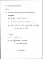
C.
LABORATORY
CONVERSION
2:
SAMPLING
AND
ANALOG-TO-DIGITAL
The concepts of sampling, filtering and analog-to-digital (A-D) conversion are
explored in Laboratory 2.
An LF198 sample and hold chip is used to construct the
circuit. The circuit was designed using the National Semiconductor LF198A specifications
for a typical 'Output Holds at Average of Sampled Input' application.
A logic input is
applied as the sample pulse as specified. The circuit is first used to perform natural sampling
on a DC signal. A DC signal was chosen so the voltage level could be modified by hand
during the sample pulse. When the circuit is not in sample mode, the output is zero, and
varying the DC voltage has no effect. A sine wave is then sampled above, at and below
Nyquist rate and recovered at each instance using a 60dB/decade lowpass Butterworth filter
(LPF). The LPF was constructed with the following specification, and components to ensure
a 60dB rolloff [Ref. 1]:
C3 = .01uf,
Ct = 5C3 = .005 uf,
R = —^— =
QC,
C 3
2000 Ji(.Ol)'
C2 = 2C3 = .02 uf,
- 16*0
v
(2 1)
'
v
The Fourier series and transform are computed for the sampled signal and compared to the
RAPIDS displays.
A-D conversion is accomplished through the use of a printed circuit board
constructed for the course EC2220: Applied Electronics. This circuit converts the analog
signal to a digital signal and displays the quantized output on a series of 16 LEDs. The
student constructs the quantizing characteristic plot by measuring the quantization step size.
The signal is converted back to analog on the board and compared to the original.
D.
LABORATORY 3: AMPLITUDE AND FREQUENCY MODULATION
Lab 3 exercises the generation and detection of AM and FM signals. All signals
produced throughout this lab are analyzed in both the frequency and time domains. The
student begins by producing an AM signal consisting of a single tone on a carrier. The
signal is analyzed at 100%, less than 100% and greater than 100% modulation [Ref. 1].
The message signal is detected by a student-built envelope detector [Ref. 5]. The detected
signal is compared to the original. Modulation indices are measured and the effects on the
signals spectra and detected output are determined.
Double sideband suppressed carrier
AM is then generated and detected in the same manner. This signal is then transmitted via
a 1.5 MHz carrier and received on an AM radio. The tone of the signal is listened to at
the input, the output of the envelope detector and the radio. Transmission of the signal
also incorporates the use of the HP8656B signal generator.
Using the summer circuit of
laboratory 1, two tones are added to produce a double tone signal. The AM exercise is
repeated using the double tone signal.
FM signals are generated using the same equipment as the AM signals. For sine
wave and square wave messages, the frequency deviation, bandwidth and modulation
indexes are measured and compared with theory. Theoretical Carson's rule calculations
are compared to measurements [Ref. 3].
E.
LABORATORY 4: FREQUENCY-DIVISION MULTIPLEXING AND TIMEDIVISION MULTIPLEXING
In the FDM portion of this lab, two signals are combined and the HP8590B
spectrum analyzer is introduced. Two message signals, both at 10 kHz, are amplitude
modulated onto separate carrier frequencies. These signals are then combined. The
sidebands are located and measured with respect to their center frequencies.
The
combined signals are then amplitude modulated onto a carrier frequency. This signal is
then analyzed. The result demonstrates that two messages at the same frequency can be
transmitted on one carrier and recovered. The concepts of increased signal bandwidth,
crosstalk and frequency spacing are also demonstrated.
Theoretical calculations for
determining the signals components are compared to measured values.
The TDM circuit is constructed using four integrated circuit chips adapted from
Ref. [4]. See Figure 2 of Appendix D. A square wave and a triangle wave are produced
using a XR8038 precision waveform generator. They are multiplexed with two external
inputs, a DC signal and a square wave, using a CD4051B analog multiplexor. The output
waveform is a combination of the four signals. Each signal is sampled once every clock
pulse. The clock frequency of 7.5 kHz is provided by a CD4029B up/down counter.
Each signal component, as well as the composite wave, are measured for frequency, period
and amplitude. The increase in signal bandwidth is also measured.
F.
LABORATORY 5: PHASE LOCKED LOOP
The phase locked loop experiment completes the lab sequence.
This circuit is
constructed using a NE565 PLL integrated circuit based on the National Semiconductor
NE/SE565 specifications.
An external resistor is determined by the student using the
equations provided in the lab. These equations also determine the center, capture and lock
frequencies. These frequencies are then measured and compared to those predicted.
A sine
wave is then applied to the PLL and the capture and lock ranges are exercised by varying the
frequency. An FM signal is then generated and applied to the circuit. Demodulated output
is monitored and compared to input as the frequency is varied.
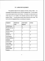
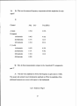
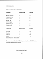
in. LABORATORY EQUIPMENT
The equipment required for the completion of all labs is listed in Table 1. It is
recommended that each station be set up with all the equipment listed. The total number
of each system required is based on 8 lab stations. This number was chosen based on an
average class of 16 to 24 students. The components required are listed for stocking
purposes in Table 1.
In several cases the systems required exceed the stock on hand. This
can be resolved by staggering lab times or purchasing more equipment.
Equipment
Required per
Total Number
In Stock
Team
Required
RAPIDS System
1
8
10
Wavetek 186 Func
2
16
12
1
8
12
1
8
12
1
8
25
1
8
35
1
8
10
1
8
9
Generator
Wavetek 142 Func
Generator
Wavetek 132
Func Generator
Tektronix DM502A
Multimeter
Tektronix PS503
Power Supply
Tektronix 2445B
Oscilloscope
HP8656B Signal
Generator
8
8
Speaker
8
10
AM Radio
8
1
461A Amplifier
8
7
Antenna
8
1
NE565 PLL
8
>40
4001 NOR
8
>50
CD4029B Counter
8
0
CD4051B
8
>50
XR8038
8
0
N4764
8
>40
/xA741 Op Amp
8
>50
LF198A Sample
8
35
16
70
A-D D-A PCB
8
30
Breadboard
8
30
Several
Plenty on hand
HP8590B Signal
1
Generator
Mulitplexor
and Hold
LM301
Resistors and
2
Several
Capacitors
Table 1. Equipment Requirements
10
IV. CONCLUSION
Overall, these laboratories cover several topics and help to build a broad scope of
knowledge for the student being introduced to the field of communications. Course syllabi
and notes were obtained and compared to the content to ensure no major subjects were missed.
Beginning electrical engineering students will enjoy the opportunity to see circuits in action,
rather than building a circuit to analyze it's internal functions. Non-electrical engineering
students will find the circuit construction enlightening, although trouble shooting will be
difficult without the proper background. All the major topics for an introductory course are
covered and will be reinforced by the completion of these laboratories after the material has
been introduced. Each laboratory gives the student the opportunity to think about the subject
matter, rather than follow a cookbook type of approach.
During the laboratory documentation phase, little knowledge of the subject by the
students was assumed. Therefore, each laboratory is self explanatory. Once each laboratory
was developed, it was tested. During testing, care was taken to remain objective. Special note
was taken to perform each step as written.
The laboratories have not been tested in the
classroom setting.
11
12
APPENDIX A. LABORATORY!
13
Lab 1: Introduction to Laboratory Equipment
Objectives: To introduce the student to the laboratory equipment, circuit construction
and troubleshooting techniques needed throughout the course.
Equipment:
(1) Breadboard
(1) RAPIDS PC and printer
(1) Tektronix P5S03 power supply
(1) Tektronix DM502A Digital Multimeter (DMM)
(1) Wavetek model 132 signal generator
(1) Wavetek model 186 signal generator
(1) Tektronix 2445B oscilloscope
Components:
(1) uA741 Operational Ampliphier
(1) 20 KQ resistor
(3) 10 KQ resistors
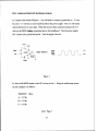
Part 1: Summer circuit construction
a) Locate the vertical and horizontal rows on the breadboard. The longer vertical rows
will be your busses. A bus will be used for power supplies and ground. Align the uA741
operational amplifier integrated circuit so the pins each connect to their own horizontal
row. If you are unfamiliar with building circuits, see the lab technician for clarification.
Lab 1 Page 1
14
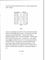
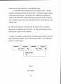
The end of the chip with the semicircular mark is the top. The pins are numbered from the
top left. See Figure 1.
Section of« breadboard
Vertical rows
Figure 1
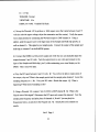
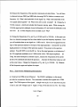
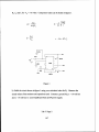
b) Figure 2 is a representation of a summer circuit. This circuit adds the two input signals,
denoted A and B, and multiplies them by a gain of two. The pins numbers on the op-amp
correspond to the numbers marked in Figure 1. Connect the circuit of Figure 2,
disregarding connections to A and B. They will be connected later. Use three horizontal
busses. One bus will be for ground, one for + 15 volts and one for -15 volts. Measure
the power before it is connected to the circuit! The ±15 volts and ground will come from
the P5S03 power supply. To measure the power, connect the ground and the positive
output of the power supply to the DMM. Adjust the power until it reads +15 volts.
Remove the positive lead from the power supply and connect it to the negative output of
the P5S03. The DMM should now read negative volts. Adjust the power supply for -15
volts.
Lab 1 Page 2
15
Turn off the power supply and connect the ground and the ± 15 volt leads to the circuit.
Leave the power off.
A +B
Figure 2
Part 2: Introduction to RAPIDS oscilloscope
a)
Turn on the power to the RAPIDS system. Select 'Lab Students' and "RAPIDS' and
hit <return>. You will eventually see a general options screen with choices Fl to F10.
Select the oscilloscope (F10). We will change the configuration of the screen using the
control options posted at each workstation. Run through the time series menu options to
see the effects on the oscilloscope display. Configure the screen as follows:
TEvffi/DIV: 100ns
<CTRL> F2
A = 500mV/div
<CTRL> F3
B = 500mV/div
<CTRL> F4
C= 1 V/div
<CTRL> F5
TRIGGER: Normal
F2
Lab 1 Page 3
16
VIEWTIME: 0.0s
<CTRL> F9
DISPLAY TYPE: Variable Compressed
<CTRL> F8
To display channels A, B, and C, press <CTRL> F7. Press A and then use the up/down
arrows to position the signal on the screen. Repeat for channels B and C so the signals do
not overlap.
b) Connect the 50 Q output of the Wavetek 132 to channel A on the RAPIDS Digital
Oscilloscope Peripheral (DOP) using a BNC cable. Connect the trigger output of the
Wavetek 132 (located on the back) to the trigger input on the DOP. Select trigger
positive and external on the DOP. Configure the Wavetek 132 to produce a 1 V peak-topeak (pp), 1kHz sine wave. Ensure there is no DC offset by adjusting the DC offset
switch on the back of the Wavetek 132. Verify your signal on the RAPIDS screen.
Adjust the trigger knob on the DOP to eliminate drift on the screen. Adjust the Wavetek
132 settings to:
Seq length: all buttons out
atten: -20 dB
mode: fiinc
c) Connect the 50 Q output of the Wavetek 186 to channel B on the RAPIDS DOP
using a BNC cable. Configure the Wavetek 186 to produce a 1 V pp, 4 kHz square
wave.
Lab 1 Page 4
17
Adjust the Wavetek 186 settings to:
Waveform: sinusoid norm (no offset)
Gen mode: cont
symmetry: norm
atten: -20 dB
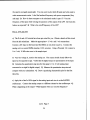
Your configuration should now look like Figure 3.
WAVETEK 132
WAVETEK 186
OUT
OUT
P3
^
6A
oc
OP
©
TRIG
Figure 3
d) Use a T-connector at the outputs of each Wavetek to split the signals. This will
enable you to continue to view your signal while applying it to your circuit. These will be
your A and B inputs to your summer. Apply the inputs to the summer circuit (order is
irrelevant). The BNC cable will have to be split to allow your signal to be applied
between input and ground. See the lab technician for help. In the same manner, connect
the output of the circuit (A + B) to channel C of the RAPIDS system.
Vary the
frequencies and amplitudes of your input signals to see the effects on the summed output.
Return your signals to their original values and print the RAPIDS screen showing the two
Lab 1 Page 5
18
inputs on channels A and B, and the output on channel C. Press F8 to label your plot.
Press <Shift> PRT SC to plot.
e) To pause the display during acquisition mode, press <return>. Use the up/down
arrows to position the marker on the screen to measure the period and amplitude of each
signal. The values will be displayed at the bottom of the screen. Make sure you are
measuring the correct amplitude by selecting the channel (press A, B or C). Q: What is
the period, amplitude and calculated frequency of each signal? Q: What is the Fourier
series and transform of each signal? Press <return> again to reacquire the display. Do not
disconnect your setup.
Part 3: Introduction to RAPIDS Spectrum Analyzer and Tektronix 2445B Oscilloscope.
a) Press F9 to view the RAPIDS spectrum analyzer. Run through the control keys
displayed at your workstation to see the effects of each on the display. Set up the screen
as follows:
INPUT VOLTAGE: 8.0 Vpp
<ALT> F8
TRANSLAT FREQ: 0.0 kHz
<ALT> F5
WINDOW TYPE: Rectangular
<ALT> F7
TRIGGER TYPE: Normal
F2
SAMPLE RATE: 50 kHz
<ALT> F2
SPECTRA AVGD: 1
<ALT> F9
MAGNITUDE SCALING: volts
<ALT> F6
Lab 1 Page 6
19
Press <ALT> F10 until channel A is displayed. Press <return> to pause the display to
measure the spectral frequency(s). Press <return> to reacquire the display. Repeat for
channels B and C. Q: What are the measured frequency components and their
amplitudes for each signal? Press F7 to label the screen and then <shift> PRT SC to print.
Provide spectral plots for each signal.
Q: How do these measurements compare to the
theoretical FT's computed in part 2?
b) Turn the power on to the oscilloscope. Remove the channel A connection to the
RAPIDS DOP and connect it to channel 1 on the oscilloscope. Set up the oscilloscope as
follows:
Vertical display:
Vertical mode: Ch 1
Chi volts/div: 500 mv
Vertical coupling: 50Q DC
Chi volts/div variable: fully CW
Horizontal display:
Mode: auto
Time/div: 500us
Slope: +
Source: Vert Chi
Sec/div variable: fully CW
Coupling: AC
To measure the amplitude of the signal press Av and position the cursors. To measure
the period of the signal press At and position the cursors. To measure the frequency of
the signal simultaneously press At and Av and position the cursors.
Q: What are the
measured frequency, period and amplitude of each signal? Q: How does this compare
Lab 1 Page 7
20
to the measurements taken with the RAPIDS system? Do not disconnect your summer
circuit. It will be used for laboratory 3.
Lab 1 Page 8
21
Lab 1: Introduction to Laboratory Equipment
Data Sheet
2e)
Q: Using the RAPIDS oscilloscope, what are the measured period and amplitude
as well as the calculated frequency of each signal?
Q: What is the Fourier series and transform of each signal?
Lab 1 Data Sheet Page 1
22
3a)
Q: What are the measured frequency components and their amplitudes for each
signal?
Q: How do these measurements compare to the theoretical FT's computed in
part 2?
Q:
Using the Tektronix 2445B oscilloscope, what are the measured frequency,
period and amplitude of each signal?
Q: How does this compare to the measurements taken with the RAPIDS system?
Lab 1 Data Sheet Page 2
23
Plot check list
ü
4 kHz square wave, 1 kHz sine wave and their sum. (channels A, B, & C)
□
Spectrum of sine wave
□
Spectrum of square wave
□
Spectrum of summed wave
Lab 1 Data Sheet Page 3
24
Lab 1: Introduction to Laboratory Equipment
Solutions
2e)
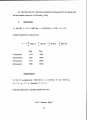
Q: Using the RAPIDS oscilloscope, what are the measured period and amplitude
as well as the calculated frequency of each signal?
Channel
Amp
A (sine)
(mv)
Period (ms)
Freq(
530
1.06
0.943
B (square)
470
0.250
4.000
C(A + B)
2.06
0.245
4.082
Q: What is the Fourier series and transform of each signal?
A:
Sine wave:
x(t) = — sin2 % 1000 /
2
X(f) =J- [*>(/+ 1000)
2
+
6(f- 1000)]
Lab 1 Solutions Page 1
25
Square wave:
x(t) =
AA
1
1
(saitot + — sin3o>* + — sin5o? +
3
5
7t
)
2
11
*(0 = — (sin2 n 4000 t + — sin2n 12000 t + — sin2it20000 t +
%
3
5
*(/) = J— YW
+
+
4000 )
W - 4000 )
+
-6(^+ 12000 ) + - b(f - 12000 )
7c
3
- b(f
5
20000 )
+
+
)
+
3
- 6(7 - 20000 )]
5
Sine + Square wave:
12
x(t) = — sin27cl000* + —
2
(äW2TC4000^
7C
X(f) = J- [6(/r+
2
+
100
°)
12000 )
+
+
SüI2TC
12000 t
3
+ — sin27i20000 t +
5
+ — b(f
3
1
+ —
)
W- 1°00)] +J— [ö(/"+ 4000)
TU
- 6(/* - 12000 )
3
+
- 6(/"
5
Lab 1 Solutions Page 2
26
+
20000 )
6(f- 4000)
+
+
— b(f - 20000 )]
5
3a)
Q: What are the measured frequency components and their amplitudes for each
signal?
A:
Channel
Amp
(mv)
Freq(KHz)
A (sine)
0.394
0.976
1st harmonic
0.402
4.052
2nd harmonic
0.171
12.10
3rd harmonic
0.104
20.16
1st harmonic
0.659
0.976
2nd harmonic
0.171
4.052
3rd harmonic
0.104
12.10
4th harmonic
0.209
B (square)
C (A+B)
Q: How do these measurements compare to the theoretical FT's computed in
part 2?
A:
The sine wave amplitude is off, but the frequency is quite close to 1 KHz.
The square and summed wave's fundamental amplitude is off but the amplitude of the
additional harmonics are correct with respect to the fundamental.
Lab 1 Solutions Page 3
27
Q:
Using the tektronix 2445B oscilloscope, what are the measured frequency,
period and amplitude of each signal?
A:
Channel
Amp
A (sine)
(mv)
Period (us)
Freq I
0.60
1.067
0.938
B (square)
0.56
0.249
4.020
C(A + B)
2.16
0.248
4.090
Q: How does this compare to the measurements taken with the RAPIDS system?
A: The RAPIDS system is not as accurate as the Tektronix oscilloscope. The
summed wave is much easier to read on the RAPIDS system.
The following plots are attached in order:
Plot 1: 4 KHz square wave, 1 KHz sine wave and their sum. (channels A, B, & C)
Plot 2: Spectrum of sine wave
Plot 3: Spectrum of square wave
Plot 4: Spectrum of summed wave
Lab 1 Solutions Page 4
28
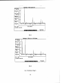
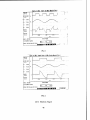
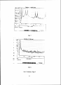
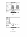
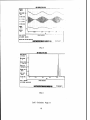
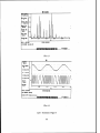
4 KHz square ♦ 1 KHz sine
IME/DIU:
toots
ACTIVE CHAHS:
MC
II : 500 mi/liu
wimrmmmm
E : 500 KMiV
C:
I Mill
0 : 100 «Mil'
IRI55E8:
Ural
liraillE:
0.0 S
4.SM
l.U
I.5J"-"
2.00
II:
PArH:C:\MP»
I/o FILEHRHC: hpitiys
DISPIA! IVPE: brittle Ceitpressd
Itftti Function, CR, SPC, ör^ Estf ■
12:21:69
Plotl
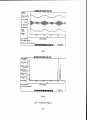
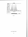
Spectrun of 1 KHz sine wave
IHPM 1)01 USE:
0.0 II W
ACTIVE CHftN:
II
L0.J
«
u
TRftrrsLftr FREO i 0.2
0.000 kHz
niHODK IVFE:
R«Un<ulir
0.1
1PK5EF. IVPE:
IHrml
»0.1
SIMPLE RATE:
50 W:
0.0
SPECTFA AIM:
I
PATH: C:\PAPI0
m'r'
' m '* ' u.i' '—ST
kHz
STATUS:ACQUIXIKS
I/O FllEHfWE: »spidSyi.011
Enter Function, CR, SPC. OP ESC
Plot 2
Lab 1 Solutions Page 5
29
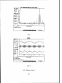
12135:37
5.!
Spectruw of 4 KHz square wave
mi««« mi,
tom\
SAHNE RATE:
SO kHz
SfECtM «USD
i
FftlH: C:\RAPID
I/O FILEHAItE: UtMnMi
Enter Function, CR, SPC, or Esc
Plot 3
Spectrun of 1 KHz sine ♦ 4 KHz Square
mun mmt:
8.0 u p/p
AC HUE CKAH:
C
t
u
TPANUAI FRED t 0.7
0.000 (Hz
KIHDDIf IKE:
Rectangular
0.!
IRI65ER TYPE:
Horn)I
* 0.2
SAHPIE RAIE:
SO (Hz
0.0
SFECIRA AV60:
i
r iJ. tr
FftlH: C:\RAP10
■
'
■
id- J
ITT i_*.
20 .V
kHz
STATUS:ACQUIRING
I/o FllEHAIIE: KspidSys.MS
Enter Functitfn. CR,- SPC; OP ESC
Plot 4
Lab 1 Solutions Page 6
30
4124:47
■^
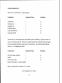
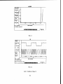
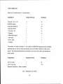
LAB 1 Equipment List
Equipment
Required/Team
On/Hand
Wavetek 132
24
RAPIDS station
10
Tektronix DM502A
25
Tektronix PS503
35
1 Wavetek 186
12
The number of teams is limited to 12, the number of Wavetek 186's available..
Components
Required/Team
On/Hand
Breadboard
1
30
|iA741 Op Amp
1
>50
Resistors/Capacitors - plenty available
Lab 1 Equipment List Page 1
31
32
APPENDIXE. LABORATORY2
33
Lab 2: Sampling and Analog to Digital Conversion
Objectives: To explore the sampling and quantization processes. To build and
demonstrate the characteristics of a low pass filter. To explore the Analog-to-Digital (AD) and Digital-to-Analog (D-A) conversion techniques. To analyze the spectra of several
signals.
Equipment:
(1) Breadboard
(1) Wavetek models 132 and 142 signal generators
(2) Tektronix P5S03 power supplies
(1) RAPIDS PC and printer
(1) Tektronix DM502A Digital Multimeter (DMM)
Components:
(1) LF198A Sample and Hold Chip
(2) LM301 Operational Amplifiers
(1) 30 KQ resistor
(6) 16 KQ resistors
(2) 30 pf capacitors
(1) .01 uf capacitors
(1) .02 uf capacitors
(1) .005 uf capacitors
(1) Prewired circuit board for A-D and D-A conversion
Lab 2 Page 1
34
Parti: Sample and Hold. LPF and Spectral Analysis
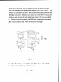
a) Construct the circuit of Figure 1. You will need to connect a ground bus, a + 15 volt
bus and a - 15 volt bus on your bread board from the power supply. The ±15 volt busses
will provide power to your chips. When the circuit is fully connected, measure the ±15
volts on the DMM before connecting them to the breadboard. Turn the power supply
off. Connect your ground and power. Turn the supply back on.
Output Channel C
Logic
Input
1kHz
Figure 1
b) Start the RAPIDS system on the PC as done in Lab 1. Bring the oscilloscope screen
up and configure it as follows:
TIME/DIV: lOOus
A=5V/div
B = 5 V/div
C = 2 V/div
Lab 2 Page 2
35
5V
ov
D = 2 V/div
TRIGGER: Normal
VBEWTIME: 0.0s
DISPLAY TYPE: Variable Full Scale
c) Set up the Wavetek 142 to produce a 1kHz square wave that varies between 0 and +5
volts (to raise the upper voltage, adjust the attenuation and the vernier). Verify the square
wave characteristics by connecting the Wavetek output to DOP channel A. Using a
splitter, send the square wave to the logic input of the Sample and Hold chip (pin 8), as
well as channel A. This signal is your sample pulse. Connect the output of the sample and
hold chip to channel C on the RAPIDS system.
d) Connect the DMM to a free power supply and verify that you can manually adjust the
output between 0 and 10 volts. Turn the output down to zero volts and connect to the
input of the Sample and Hold chip (pin 3) while maintaining your visual display on the
DMM. This is your DC input.
e) Vary the DC input between 0 and 10 volts. Q: You will not be able to make sense of
the output, why not? What is the sample period and the sample pulse duration? Lower the
sampling frequency to .1 Hz. Vary your DC value. Sketch the output. Q: What is
happening? What kind of sampling is this?
f) Using a Wavetek 132, connect 5sin 2rcl000t to DOP channel B. Q: What is the
Nyquist rate of this signal? Disconnect the DC input and connect the sinusoid. Vary the
sample pulse frequency and print plots of channels A B and C (on one plot) for
frequencies below, at and above the Nyquist rate. Q: Attach plots and comment on
results.
Lab 2 Page 3
36
Change the sample rate to 5000 Hz. Q: Calculate the first four harmonic's amplitude and
frequencies for the sample pulse and the sampled output (fs = 5000 Hz and fm= 1000 Hz).
g) Turn off all power. Construct the LPF circuit of Figure 2 on the same breadboard.
Connect the output (pin 6 on op amp 2) to channel D. Connect the output of the sample
and hold to the input of the LPF ( pin 3 on op amp 1). Turn the power on. Set the sample
pulse at a frequency of 5 kHz. The LPF output should look like a filtered version of the
input.
Rf
Rf
V V V
VV V
+ 15V
+ 15V
-15 V
-15V
C2 ~
7
7
2
K.1
R2
3
■'VV^VV
Cl ~
-=-
2
4
\&
LM301
R3
-AAA,
VV]
3
^1
^1^*
l^ 8
H^
30 pf
NC
4
LM301
51
^<"1
l^ 8
C3
-±-
^\°
Output
(Channel D)
NC
H^
30 pf
Input (Chanine] C)
Figure 2 Lowpass Butterworth Filter
R1 = R2=R3=16KQ, Rf=32KQ, Cx = .005 nf, C2=.02uf, C3=.01uf
h) Plot the spectrum of all 4 channels using the RAPIDS spectrum analyzer. Make sure
Lab 2 Page 4
37
the spectra averaged equals eight. You may want to plot both dB scale and volts scale to
make measurements easier. Label the baseband frequency and specra components (freq
and amp) Q: How do these compare to the calculated results in part If? Vary the
frequency of the input while viewing the spectrum of the output of the LPF. Q: Does this
behave as expected? Q: What is the cutoff frequency of the LPF?
Part 2: D-AandA-D
a) The D-A and A-D circuits have been pre-wired for you. Obtain a sketch of this circuit
from the lab technicians. Make the appropriate ± 15 volt and 5 volt connections.
Connect a DC input to the board and the DMM, as was done in part la. Connect the
analog out to a second DMM ensuring 0.001 accuracy. Using a Wavetek 132, connect a
0 to 5 volt, 10 kHz sine wave to the sample input.
b) Vary the voltage in, monitor the analog out. The output should closely follow the
input but be opposite in sign. Verify that the digital output is representative of the input.
Q: Calculate the quantization step size for this signal (0 to 10 volt analog input
converted to an eight bit digital output). Q: Measure the quantization step size and
compare with your calculations. Q: Draw a quantizing characteristic plot for the first
three bits.
c) Apply the a 5sin2n 1000t signal to the analog input and view it on the RAPIDS
oscilloscope. Connect the analog output to a different channel on the oscilloscope. Q:
What is happening at the output? What happens when you vary the frequency?
Lab 2 Page 5
38
Lab 2: Sampling and Analog to Digital Conversion
Data Sheet
le)
Q: You will not be able to make sense of the output, why not? What is the sample
period and the sample pulse duration?
Q: What happens when you vary the DC signal? What kind of sampling is this?
If)
Q: WhatistheNyquistrateof5sin2rcl000t?
Q: Attach plots and comment on results.
Lab 2 Data Sheet Page 1
39
Q: Determine the first 4 harmonics (amplitude and frequency) for the sample pulse
and the sampled output (for f=5000 and 4=1000).
A:
Sample Pulse:
Calculations:
Amp
Freq
1st harmonic:
2nd harmonic:
3rd harmonic:
4th harmonic:
Sampled Signal
Calculations:
Amp
LSB
1st harmonic:
2nd harmonic:
3rd harmonic:
4th harmonic:
Lab2 Datasheet Page2
40
USB
lh)
Q: How do the plotted spectra components compare to the calculated results in
part If?
Q: Does varying the frequency change the spectra output as expected?
Q: What is the 3dB down point of the LPF?
2b)
Q: Calculate the quantization step size for this signal (a 0 to 10 volt analog input
converted to an eight bit digital output).
Q: Measure the quantization step size and compare with your calculations.
Lab 2 Data Sheet Page 3
41
Q: Draw a quantizing characteristic plot for the first 3 bits.
2c)
Q: What is happening at the output? What happens as the sample pulse
frequency is varied?
Plot check list
□
Input, sample pulse and sampled output at Nyquist rate
□
Input, sample pulse and sampled output below Nyquist rate
□
Input, sample pulse and sampled output above Nyquist rate
□
Input, sample pulse and sampled output and LPF output
□
Spectrum of 5 kHz sample pulse (volts)
□
Spectrum of 5 kHz sample pulse (dB)
□
Spectrum of sampled signal (dB)
□
Spectrum of 1 kHz input
□
Spectrum of sampled signal (volts)
Lab2 Datasheet Page4
42
Lab 2: Sampling and Analog to Digital Conversion
Solutions
le)
Q: You will not be able to make sense of the output, why not? What is the sample
period and the sample pulse duration?
A: The sample pulses are too short to see a response. The sample period, T = 1
Hz. The duty cycle, d=0.5.
The pulse duration, T =dT=(.5)(l)=5 sees.
Q: What happens when you vary the DC signal? What kind of sampling is this?
A: The DC value can only be varied during the actual pulse of the sample signal.
At zero volts (sample pulse) the output is not sampled. This is natural sampling.
If)
Q: What is the Nyquist rate of 5 sin 27i(1000)t?
A: f■*s = "o
2f1=2000Hz
Q: Attach plots and comment on results.
A: The plots are attached. Below the Nysquist rate, the shape of the signal is
unidentifiable. The signal is aliased. At the Nyquist rate, the shape of the signal becomes
apparent. Above the Nyquist rate, the shape of the signal becomes more obvious as the
sampling frequencies get higher.
Lab 2 Solutions Page 1
43
Q: Determine the first 4 harmonics (amplitude and frequency) for the sample pulse
and the sampled output (for f=5000 and 4=1000).
A:
Sample Pulse:
fs= 5000 Hz, T = 1/f = 0.0002 sec, x = (0.00Q2)(.5) = 0 .0001, A = 2.5 V
Using the equation for a square wave:
.4111
V = 4 — (sino* + — sin3<i)f + — sin5o)/ + — sin7o*)
A
3
5
7
Amp
Freq
1st harmonic:
1.593
5000
2nd harmonic:
.5300
15000
3rd harmonic:
.1777
25000
4th harmonic:
.0590
35000
Sampled Signal:
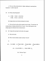
fs=NfOJ N = samples/cycle = 5000/1000 = 5, f0= 1000 Hz, T = l/f0 =0.001 sec,
Am = 5V, Ap = 5V,n = harmonic # = 1, 2, 3, 4
Using the equation for a naturally sampled sine wave:
Lab 2 Solutions Page 2
44
S(f) -
TA mANf
p
° XsincinTNfJ [b\f - fß ♦ nN)] ♦ 6|/ + /0(1 - «AT)]]
Amp LSB
USB
1st harmonic:
1.07
4000
6000
2nd harmonic:
.5185 9000
11000
3rd harmonic:
.4859 14000 16000
4th harmonic:
.4424 21000 23000
lh)
Q: How do the plotted spectra components compare to the calculated results in
part If?
A: Plots are attached. The frequencies and amplitudes were close to those
calculated in If. They may be slightly off because the amplitude of the message signal and
the sample pulse may not be exactly 5 (hard to read on Rapids screen). Only the odd
frequencies are present.
Q: Does varying the frequency change the spectra output as expected?
A: Yes, as the frequency changes we can watch the spectra components move
accordingly.
Q: What is the cutoff frequency of the LPF?
A: 1.074 Hz
Lab 2 Solutions Page 3
45
2b)
Q: Calculate the quantization step size for this signal (0 to 10 volt analog input
converted to an eight bit digital output).
A: The resolution for 8 bit quantizing is 28 = 256.
00000000 = Ov, 11111111 = lOv, VMlc-e=9.97 v
Cstepsize
VFS/(2n-l) = 9.97/(256-1) = .039 v
Q: Measure the quantization step size and compare with your calculations.
A: By measuring the voltage required to change one bit we can tell the
quantization step size is .03 volts.
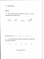
Q: Draw a quantizing characteristic plot for the first 3 bits.
.03
.06
.09 .12 .16
.20 23
26
Lab 2 Solutions Page 4
46
2c)
Q: What is happening at the output? What happens as the sample pulse
frequency is varied?
A: The output is unipolar. Increasing the sample frequency creates a smoother
analog output.
The attached plots are listed below, in order:
Plotl
Input, sample pulse and sampled output at Nyquist rate
Plot 2
Input, sample pulse and sampled output below Nyquist rate
Plot 3
Input, sample pulse and sampled output above Nyquist rate
Plot 4
Input, sample pulse and sampled output and LPF output
Plot 5
Spectrum of 5 kHz sample pulse (volts)
Plot 6
Spectrum of 5 kHz sample pulse (dB)
Plot 7
Spectrum of sampled signal (dB)
Plot 8
Spectrum of 1 kHz input
Plot 9
Spectrum of sampled signal (volts)
Lab 2 Solutions Page 5
47
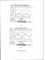
npct at 1 KHz Sawle at 2Hlz (Naguist Rate)
lIMt/OI«:
100 W
T-r^uj
aCIIUE CHftKS:
A e c
ft :
5 Mi«
f :
; Mi?
C :
J Mi'.'
0 :
2 Mi?
'V
MG'iEfi:
Horm I
/
\
V
WHIM:
0.0 $
T
STäT'Jf :MUSED
PMH:f:\mnF.!)t1
I/O FILEMftHE: F.ipidS'/s
[chTt]
'i Us
0
HU
j
.D1SHM JVfE: Uariibt« Full Sc»lt
Plotl
input at lKHz SaHple Rate at lKllz (klow Hamist Rate)
lint; Hi":
10« »S
—y_
(KIIK CHftHS:
ft !C
ft :
5 Mi»
8 :
S Mi»
I
"V
ft- 2 Mil'
I! :
2 Mio
IPJ55EF::
itoniji
\
UIEUTinE:
0.0 !
TW —
TUT
TTTT
SlflIUS: PAÜ5E&
FftIH:C:\5FECIW
I/O FIltHflUE: RafidSyj
ICIi.C:
(' n?
0 HU I
P Iff LUV tVFE:lUriibHF?ll Scate
JIJ3miH3R$S$SWISI
Plot 2
Lab 2 Solutions Page 6
48
11:45:5«
••«
IIHE/BIli:
100«
Input at 1 KHz Sawple at 5 KHz (aiow Huwist Rate)
.rmsu\nnrjiru\rL
«CUKE CHANS:
II 8 C
Ff»TH:C:\SFECIRUH
\
I.J
STftTUS:PAUSED
I/O fllEIKIIE: fspidSyj
Ch.C:
OISRflJ rVFE:lijrijM{Fii!ISc}|
Oils
(' Hl) J
5ffi3
-*
B3IIl!E3Mi»3awsaa___
:39:w
Plot 3
Input lKHz SaHple 5 KHz D: LFF Output
IlltE/DIU:
100 w
»cni/E CHNNJ:
swrwniwfwmtfü
m*:\smm
M5fl« WE: „ri,bl! Ml sole
—
mm-.twsa
^
' *
"""I
EI®mREMMfflK&m--. JiJÄiäTL..
Plot 4
Lab 2 Solutions Page 7
49
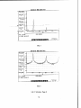
Spectrum of 5Kllz Sanple Pulse
STftYUS-ACOUIRXH6
FftlH: :.\SPtCn!lllt
I/O FILEMfittE: (tapidSys.DTl
JBniBIfflraEiil»
JM9:19 L
Plot 5
Spectra« of 5KHz Sawple Pulse
WIM DOUME:
f.O » t/p
flCTIUE CHAH:
-10
L -20
e
u -30
Il.fill:MT FEEQ
0.000 IK!
;-!o
H'HfOH UFE:
• •SO
%0
*MW
IfI56ER IVFE:
HWHJI
SJUFIE mv.
v< m
TTT
SFECTRft «MS:
kH3
FftlH: C:\5fEClMIH
SrfllUS:AC0UERXHS
1/0 FILEHAKE: ttMfyt.Otl '
.ijini^^?r^jman»M_
Plot 6
Lab 2 Solutions Page 8
50
l:13:iH
Spectnii ni '.jHplfd Signal
Mil «i rm
<l OOi iM:
UIW
lift
Wliff
j -50
\\\--/
V . .
'"'*■' H/-
mw
K5P TV)
TVf£: hi
i\ ,{\
>*~«j.W.t
ti
■■ J • ■ j
*V™*
■ • ■ • ,
Born;l
mm mv
SPECFRr fitf
J
Tur
■■i r
kH2
PATH: C --ffCf'UM
~irr
SNW '■ffi'tlilM
I/O FIULiiir: ■•spJdfyj.orj
IfflOTGSimi MMPfll
1 1:3;:«.:
Plot 7
.i
■' mt
ft
All:
T.
>?E0
SpectwiH of 1 KHz Input
L -55
!,*
.
II!
Ur
-C[i
■?0
"•'■*Afadii
^^^
SO«
SFE(
TO
O
kHz
p/tri-
i/o r
nm
smii/s:iicciiiniu
RspiJSyj.il 12
-JilüillMiiEMBiflf^WTiaB
Plot 8
Lab 2 Solutions Page 9
51
I PH.*
Spectruw of Sailed Signal
io
in
1
'"■' ;f
Ml
FflIH: C:\SPECISUH
I/O FILEKftHE: fapidSys DT5
STftlUSrflCOUIRIMG
llflliHfllffiilffiiSilllll
Plot 9
Lab 2 Solutions Page 10
52
Ti :4.i:!ii 1...
LAB 2 Equipment List
Based on 25 student class, 2-3 persons/team.
Equipment
Required/Team
On/Hand
Breadboard
1
30
Wavetek 132
1
12
Wavetek 142
1
12
RAPIDS station
1
10
Tektronix DM502A
2
25
Tektronix PS503
1
35
The number per team depend upon the RAPIDS system availability. Right now there are
only 10 PC's setup in the lab. More PC's could be added with the proper software loaded
but more interface hardware would have to be purchased. Recommend either limiting
teams to 10 or staggering lab times.
Components
Required/Team
On/Hand
LF198A (Samp & Hold)
1
35
LM301
2
70
Prewired A-D, D-A
1
30
Resistors/Capacitors - plenty available
Plenty of components on hand for 10-15 teams.
Lab 2 Equipment List Page 1
53
54
APPENDIX C. LABORATORY 3
55
Lab 3: Amplitude and Frequency Modulation
Objective: To generate AM and FM signals and observe their spectra. To detect, transmit
and receive AM signals.
Equipment:
(1) Breadboard
(2) Wavetek model 132 signal generator
(1) Tektronix P5S03 power supply
(1) RAPIDS PC and printer
(1) Tektronix DM502A Digital Multimeter (DMM)
(1) Wavetek model 186 signal generator
(1) speaker
(1) HP 8656B signal generator
(1) AM radio
(1)461 A amplifier
(1) Antenna
Components:
(1) N4764 Diode
(1) uA741 Operational Amplifier
(1) 20 KQ resistor
(4) 10 KQ resistors
(1) .01 uf capacitors
Lab 3 Page 1
56
Parti: Amplitude Modulation (AM) Generation and Detection
a) Turn on the power to the RAPIDS system and configure it as follows:
TIME/DIV: lOOus
A = 500mV/div
B = 500mV/div
TRIGGER: Normal
VIEWTIME: 0.0s
DISPLAY TYPE: Variable Compressed
b) Connect the Wavetek 132 to DOP channel A and configure it to produce a 1 V peakto-peak (pp), 1kHz square wave. Ensure there is no DC offset by adjusting the DC offset
switch on the back of the Wavetek 132. This will be your message signal. Connect the
output of the Wavetek 186 to channel B and configure it to produce a 2 V pp, 20 kHz sine
wave. This is your carrier signal. Adjust the Wavetek 186 to the following settings:
Waveform: sinusoid norm
Gen mode: cont
symmetry: norm (no offset)
atten: 0 dB
c) Split the message signal at the Wavetek 132 so the output connects to channel A and
VCA IN on the Wavetek 186. Your configuration should now look like Figure 1.
Lab 3 Page 2
57
WAVETEK132
WAVETEK186
VCA N
OFT
OUT
t
6A
Ö
TRIG
oc
OP
Figure 1
d) Channel B is now a conventional AM signal. Adjust the attenuation variable knob on
the 186 to produce AM signals that are 100%, <100% and > 100% modulated.
The
modulation index can be determined from:
% m - k xlOO =
max
" *** xlOO
A max + A mm.
Print a plot of the 100% modulated wave. Q: Compute and draw the spectra of the
square wave input and the AM wave. Include the time and frequency representations of
each. Using the RAPIDS spectrum analyzer, print the spectra of both channels to verify
your results. Configure the spectrum analyzer as follows:
INPUT VOLTAGE: 8.0 Vpp
TRANSLAT FREQ: 0.0 kHz
WINDOW TYPE: Rectangular
TRIGGER TYPE: Normal
Lab 3 Page 3
58
SAMPLE RATE: 50 kHz
SPECTRA AVGD: 1
MAGNITUDE SCALING: volts
e) Change the signal output of the Wavetek 132 to a sine wave. Construct the envelope
detector shown in Figure 2.
N4764
+
Vn,
HXM
#_
10 KQ
Figure 2
Split the AM signal output (from the Wavetek 186) and apply it the input of the envelope
detector. Read the voltage across the 20 KQ resistor and send this signal to DOP channel
C. Channel C is the demodulated signal. Compare this to the input signal. Adjust the
variable attenuation on the Wavetek 186 for 100%, <100% and >100% modulation
obtaining plots for each case. Q: Using the crosshairs on the RAPIDS system, measure
the modulation index for each case. How does this effect the output of the envelope
detector? Q: Compute and draw the spectra of the modulated sine wave. View and
plot the spectrum of the AM signal at each instance. Q: What effect does the
modulation index have on the spectra of each signal?
Lab 3 Page 4
59
f) Viewing the AM signal (channel B) on the spectrum analyzer, adjust the variable
attenuation on the carrier (Wavetek 186) until the carrier is suppressed. View the signal
on the oscilloscope. Notice the phase reversals at the zero crossings of the message
signal. If necessary, turn down the frequency to view this, but return it to 1 kHz when
complete. This is a double sideband suppressed carrier (DSBSC) signal. Look at the
detected message. Q: You will have to adjust the plot scale for the detected signal
(channel C), why? Plot the message, carrier and detected message. Q: At what
modulation index does DSBSC occur?
Q: What is the time and frequency
representations of the DSBSC signal? Q: What is the average power? Q: If the output
of the envelope detector was passed through a BPF centered at 21 kHz, what type of
output would we see? Sketch the output. What would the frequency representation be?
What would the power be? Change the input to a square wave just for fan.
Part 2: AM Transmission and Detection
a) Turn on the power to the HP8656B signal generator. On the center, bottom row,
press RF OFF until the far right display is blank indicating zero transmission. Change the
output of the Wavetek 132 to a 500 Hz, 2 V pp sine wave (set attenuation at zero).
Verify this on the oscilloscope channel A.
Disconnect the connection to channel A and
apply it to your bread board. Connect it between a vacant row and ground. Connect the
negative side of the speaker to ground and the positive side to the same row as the sine
wave. Check the polarities on the back of the speaker. The wire colors do not necessarily
indicate polarity. Listen to the tone. Move the positive lead of the speaker to the output
of the envelope detector. Q: How do the tones differ? What does this tell you about the
quality of this detector?
Lab 3 Page 5
60
b) Split the input to the Wavetek 186 so the signal off the Wavetek 132 also goes to the
HP8656B signal generator input, you will directly modulate this signal onto a 1.5 MHz
carrier.
Connect the RF out of the HP8656B to the HP461A amplifier input. Set the
amplifier on 20dB. Connect the output of the amplifier to the antenna. Plug in the radio.
Verify your setup with Figure 3. Note that we are modulating our sine wave onto the 20
kHz carrier at the Wavetek 186 and separately modulating it onto a 1.5 MHz carrier at
the HP8656B for comparison purposes.
WAVKTEK1M
VCA IN
OUT
ft
HD
<£
1 C
3)
Figure 3
The front of the HP8656B has 3 key pads marked modulation, carrier and data. On the
modulation pad, press FM, press OFF, and then press AM. Using the up/down arrow
keys below the AM button, adjust the modulation to 20%. On the carrier pad press
FREQ. Using the data pad type in 1.5 Mhz. Press RF ON. The display on the far right
should read -7.0 dB. If it does not, press AMPTD on carrier pad and adjust it by using
the up/down arrow keys below the AMPTD button. Tune the AM radio to pick up the
Lab 3 Page 6
61
frequencies we are transmitting. Q: What are these frequencies?
Sketch the impulses.
Once you hear the tone on the radio, vary the message frequency to hear the tone
differences. Alternate your speaker between the input signal and the detector output.
Q: Compare these tones with that emitting from the radio.
c) Construct the summer circuit used in Lab 1. Using a second Wavetek 132 apply a 3
kHz signal to one input and apply the 1 kHz signal from the original Wavetek 132 to the
second input. Using your positive speaker connection as a probe, listen to both inputs and
the output of the summer. You should hear a double tone. Adjust the frequencies so the
tones are distinct. On the HP8656B, turn off the RF. Connect the output of the summer
to the HP8656B input and transmit this signal to the AM radio. Q: Compare the tones
heard on the radio to the original.
Part 3: Frequency Modulation
a) Setup the configuration in Figure 4.
WAVETEK 132
WAVETEK 1M
VCGIN
OUT
OUT
f
OB
oc
OP
©
TRIG
Figure 4
Lab 3 Page 7
62
As before, the Wavetek 132 is the message signal. Set up the Wavetek 132 to produce a
1 V pp, 1kHz square wave, with the attenuation set to -20 dB. The Wavetek 186 is the
carrier signal. Set the attenuation to -20dB and change the frequency to 10 kHz.
b) Demonstrate the fundamental characteristic of an FM wave, the frequency deviation
(maximum departure from the carrier frequency) is directly proportional to the amplitude
of the modulating wave. Q: What is the time domain representation of this wave? View
the spectrum of the FM wave. Adjust the attenuation on the 132 until the carrier is nulled.
Print the oscilloscope and spectrum analyzer displays. Q: In the time domain, find
positive frequency deviation (f") and the negative frequency deviation ( f") using the
crosshairs of the oscilloscope. What is the peak frequency deviation? What is the
modulation index (ß)? Measure 2Af on the spectrum analyzer for this value of ß? Q:
Using Carsons rule, what is the bandwidth for this signal?
Q: Switch the message signal
to a sine wave. Q: What is the frequency representation of the FM sine wave? Q:
Measure f, f and 2Af. What is the frequency deviation, ß and the bandwidth? We
will demodulate a FM signal in laboratory 5.
Lab 3 Page 8
63
Lab 3: Amplitude and Frequency Modulation
Data Sheet
Id)
Q: Compute and draw the spectra of the square wave input and the AM wave.
Include the time and frequency representations of each.
Q: Using the crosshairs on the Rapids system, measure the modulation index for
each case (100%, <100%, >100% modulation). How does this effect the output of the
envelope detector?
Lab 3 Data Sheet Page 1
64
Q: Compute and draw the spectra of the modulated sine wave.
Q: What effect does the modulation index have on the spectra of each signal?
If)
Q: You will have to adjust the plot scale for the detected signal (channel C),
why?
Q: At what modulation index does DSBSC occur?
Lab 3 Data Sheet Page 2
65
Q: What are the time and frequency representations of the DSBSC signal?
Q: What is the power of the DSBSC signal?
Q: If the output of the envelope detector was passed through a BPF centered at
21 kHz, what type of output would we see? Sketch the output. What would the
frequency representation be? What would the power be?
Lab 3 Data Sheet Page 3
66
2a)
Q: How do the tones differ? What does this tell you about the quality of this
detector?
2b).
Q: What are the frequencies being transmitted?
Q: Compare these tones with that emitting from the radio.
2c)
Q: Compare the tones heard on the radio to the original.
Lab 3 Data Sheet Page 4
67
Q: What is the time domain complex envelope of this wave?
Q: What are fandf". What is the frequency deviation? What is the modulation
index (ß)? Measure 2Af on the spectrum analyzer for this value of ß?
Q: Using Carsons rule, what is the bandwidth for this signal?
Lab 3 Datasheet Page 5
68
Q: What is the frequency representation for the FM sine wave?
Q:
Measure f, f", and 2Af. What is the frequency deviation, ßand the
bandwidth?
Lab 3 Data Sheet Page 6
69
Plot check list
□
Square wave and 100% AM square wave
□
Square wave spectrum
□
100% modulated square wave spectrum
□
Sine wave, <100% modulated sine wave and detected sine wave
□
Spectrum of <100% modulated sine wave
□
Sine wave, =100% modulated sine wave and detected sine wave
□
Spectrum of =100% modulated sine wave
□
Sine wave, >100% modulated sine wave and detected sine wave
□
Spectrum of >100% modulated sine wave
□
Sine wave, AM DSBSC wave and detected sine wave
□
Spectrum of AM DSBSC wave
□
Square wave and FM square wave
□
Spectrum of FM square wave
□
Sine wave and FM sine wave
□
Spectrum of FM sine wave
Lab 3 Datasheet Page 7
70
Lab 3: Amplitude and Frequency Modulation
Solutions
Id)
Q: Compute and draw the spectra of the square wave input and the AM wave.
A: Square wave:
m(t) =
(sinco/ + — sin3to/ + — sin5<»>/ +
3
TC
w
2
(0 = —
7i
(OTI2IC1000/
)
5
1
+ —
3
m(f) = j— [»(/" + 1000)
7t
+
SüI2TC3000/
1
+ — sin27t5000/ +
5
b(f- 1000)] +y— [b(f + 3000)
3 %
+ j-^— [b(f+ 5000)
+
b(f- 5000)]
5 7C
AM wave:
x(t) = A [1 + k m(t)] sin
2TC//
2
1
x(t) = 1 [1 + ka— (sin2 %1000t + — sin27c3000/
a
7i
3
+ — sin 2 7c 5000/)] ««2 TC 20000/
5
Lab 3 Solutions Page 1
71
)
+
b(f - 3000)]
X(f) = j- [S(f + 20000 )
+
2
+ ka-^— [b(f + 21000 )
b(f - 20000 )]
+
k a — [b(f + 19000 )
+
b(f - 19000 )]
b(f - 21000 )]+ k-^— [b(f ♦ 17000 )
+
b(f - 17000 )]
+
b(f - 15000 )]
+
2 %
+ kaa-^— [b(f + 23000 ) + b(f - 23000 )]+ kafl—^— [b(f + 15000 )
6 %
10 %
+ * —^— [b(f + 25000 )
a
+
6(/"- 25000 )]
10 it
Q: Using the crosshairs on the RAPIDS system, measure the modulation index for each
case. How does this effect the output of the envelope detector?
A:
<100% :
[(5-1.6)/(5 + 1.6)] x 100 = 51.5%, ka= .515
=100% :
[(2.6-0)/(2.6 + 0)] x 100 = 100%, k,= 1
>100% :
[(1.5-(-.8))/(1.5 +(-.8))] x 100 = 328.6%, 1^= 3.2857
Q: Compute and draw the spectra of of the modualted sine wave.
A:
X(f) = j- [&(f
x(t) = 1 [1 + k irä.2 n; 1000 *] sin 2 % 20000 t
+
20000 )
+
b(f - 20000 ) + ka [b(f + 19000 )
+ k [b(f ♦ 21000 )
+
b(f - 21000 )]
Lab 3 Solutions Page 2
72
+
b(f - 19000 )
Q: What effect does the modualtion index have on the spectra of each signal?
A: Increasing the modulation increases the sideband amplitudes and decreases
the carrier amplitude.
If)
Q: You will have to adjust the plot scale for the detected signal (channel C),
why?
A: Power is decreased during modulation. The power of the carrier and the
sidebands are:
Carrier Power = — A*
2 c
Sideband Power = — k a A*
c
8
Q: At what modualtion index does DSBSC occur?
A:
ka = (l+l)/(l-l) = co
Q: What are the time and frequency representations of the DSBSCsignal?
A:
x(t)
= A csin 2%ft
* A m sin 2ir/
t
y
J
'
•>c
m
x(t) = .25 (cos 27119000 t - cos 2% 21000 t)
Lab 3 Solutions Page 3
73
X(f) = - [-(6(7
4
2
+
19000 )
+
b(f - 19000 )) +-(6(f + 21000 )
2
+
6(f - 21000 ))]
Q: What is the power of the DSBSC AM signal?
P = - A] - (0.5) (l2) = 0.5
2
Q: If the output of the envelope detector was passed through a BPF centered at
21 Khz, what type of output would we see? Sketch the output. What would the
frequency representation be? What would the power be?
A: The output would be Single Sideband centered at 2IK:
5K
X(f) = -(&(/"+ 21000 )
8
+
10K
15K 20K
b(f - 21000 ))
P = — Al = .25 l2 = .25
2a)
Q: How do the tones differ? What does this tell you about the quality of this
detector?
Lab 3 Solutions Page 4
74
A: The tone of the envelope detector is higher, indicating it is removing lower
frequencies. It could be improved.
2b)
Q: What are these frequencies?
A: 1.5 MHz + 500 Hz =1,500,500 Hz
1.5 MHz - 500 Hz =1,499,500 Hz
Q: Compare these tones with that emitting from the radio.
A: The tone from the radio and the original tone are the same. The tone from the
envelope detector is higher pitched and lower in power. Some of the frequncies in the
message signal are eliminated by the envelope detector.
2c)
Q: Compare the tones heard on the radio to the original.
A: They are the same.
Q: What is the time domain complex envelope this wave?
s(t) = .5
(2TI10000
+ ß (—sin2*1000*
it
s(t) =
(.5COS2TT
sin27c3000* + — sin2rr5000 /))
+
3%
10000 ) S2 - (.5sin2x10000 ) S
Lab 3 Solutions Page 5
75
5 it
4
s(t) = .5cos2ir 10000 cosß(—sin2*1000 /
4
+
it
sin2*3000/ +
3rc
4
sin2* 5000/)
5*
4
4
4
.5sin2* 10000 sinß(—sin2* 1000 / +
sin2*3000/ +
sin2rc5000/)
ir
3*
5*
4
4
4
Sj = cos ß(—sin2u 1000/ +
sin 2% 3000/ +
sin 2* 5000/)
%
3%
5%
4
S0 = sin ß(—sin 2% 1000/ +
4
sin2*3000/ +
4
sin2it5000/)
s compemr-(/)J =SIT + J/ SnQ
3 b)
Q: What are positive and negative frequency deviations, f and f". What is the
peak frequency deviation? What is the modualtion index (ß)? Measure 2Af on the
spectrum analyzer for this value of ß?
A: Measured values off1 and f:
f = (1.720 xlO'3 - 1.58 xlO"3)"1 = 7142 Hz
f = (1.250 xlO"3 - 1.03 xlO"3)"1 = 10.526 « 10 kHz
2Af = f - f = 3383 Hz
Af = 1692 Hz
ß = Af/4 = 1692/1000 =1.692 Hz
measured value of 2Af = 10980 - 7568 = 3412 Hz
Q: Using Carsons rule, what is the bandwidth for this signal?
A: B = 2Af+2fm=3412 + 2(1000) = 5412 Hz
Lab 3 Solutions Page 6
76
Q: What is the frequency representation of the FM sine wave.
A:
*(/> = AT,Jnm[b{f - fc - n/J
ß = 1.692
J0(ß) = .4
+
6(f + fc + n/J]
Jj(ß) = .5
J2(ß) = .3
73(ß) = .1
Q: Measure f, f and 2Af. What is the frequency deviation? What is ß and the
bandwidth?
A: f = (.75 xlO"3 - .615 xlO"3)"1 = 7407 Hz
f = (1.36 xlO'3 - 1265 xlO'3)"1 = 10.526 - lOKHz
2Af=3119 Hz
Af=1560Hz
ß = Af/fm=1.56 Hz
B = 2(1560)+ 2000 = 5120 Hz
Lab 3 Solutions Page 7
77
The plots listed below are attached in order:
Plot 1:
Square wave and 100% AM square wave
Plot 2:
Square wave spectrum
Plot 3:
100% modulated square wave spectrum
Plot 4:
Sine wave, <100% modulated sine wave and detected sine wave
Plot 5:
Spectrum of <100% modulated sine wave
Plot 6:
Sine wave, =100% modulated sine wave and detected sine wave
Plot 7:
Spectrum of =100% modulated sine wave
Plot 8:
Sine wave, >100% modulated sine wave and detected sine wave
Plot 9:
Spectrum of >100% modulated sine wave
Plot 10:
Sine wave, AM DSBSC wave and detected sine wave
Plot 11:
Spectrum of AM DSBSC wave
Plot 12:
Square wave and FM square wave
Plot 13:
Spectrum of FM square wave
Plot 14:
Sine wave and FM sine wave
Plot 15:
Spectrum of FM sine wave
Lab 3 Solutions Page 8
78
SQUARE HADE 160"/, HODULATIOH
mm:
mo i»
AC HUE CHANS:
Al
A : 500 «MiO
I i S00 HV/diV
C ■•
1 V/4i«
D : SCO KU/diV
IF.I55ER:
Horiul
OlEliriHE:
0.0 J
fA!H:C:\5fEClRUH
I/O r HEMME: ttpitiys
D15PLAV IVPE: brittle C«ipief«f
fiter Function, CR, SPC, or Esc
Plotl
SQUARE HAVE SPECIRUH
JAIMJ RATE:
50 1Hz
SFECIFA AM:
I
FAN: C:\JfECHIIH
kHz
STATUS:flC4UIRIH6
I/O FIlEIIAtlE: S5pidSyj.il(I
Enter Function, CR, SPC, or Esc
Plot 2
Lab 3 Solutions Page 9
79
10:25:39
AH LESS THAN MX MODULATION
HI -lill.lt:
MlH.^.i'/tF-JI
l-irn:ilsil:f:;piJ!yJ
n-n'"ii !V.:t;l*";;"Mt CcifreiH'i
.OniJillBiEDffiffliSIBiaJI.
Plot 3
AN LESS THAN 1W, KODOLAIION
SIIIIHE til IE:
50 kHz
imm
AUSD
l
FAN: C:\SFEC1RUH
I/O FREU: hpitiyf.M
EntiMuhctibhV: C«, SPC 6t\ Esc^
Plot 4
Lab 3 Solutions Page 10
80
Alt IHMWIOfrKItt
T»E/D1U:
too us
ACTIUE CHAHS:
mc
A : 100 KV/diU
I ■■
I U/diU
C :
2 U/diV
III'1
'.'I) Ii>:'ii'
D: SOU Hl)/diV
IR166EP.:
»on» I
..-j'>*^----^
UIEtllltlE:
0.0 5
<W
I'M
tW
•■ a •
hi
PflTH:C:\SPECIRUN
•
I/O FllEMME: RljidSyj
SIAttlSiACWIPIHi
DisPLflV IVfE; Viriible C«Hpre»ed
JHffiHD^ftlMIOTi-N.
|:ü/:2/
Plot 5
AH HODüLAIIOHä
IHPÜI «OLWE
8.01) p/p
KIKE CHftH:
I
IRAIISLAt PRE«: e 1.3
0.000 kHz I
UIHDOU IVfE:
Rectangular
TRIGGER IVFE:
Horn I
0.5
• 0.1
»IE KAIE:
SO kHz
SPEC IRA AIM:
1
0.9
FAIH: C:\SPEC1RDII
I/O FHEKAilE: R;pi«yt.DI2
" ™ !?T
15. J
\J\L.
in
1Hz
SIAIUS:AMUIR!H5
EnttP'Furi'ctibnV'CR, SPCi or M-
Plot 6
Lab 3 Solutions Page 11
81
l:3i:zi~L
AN HOHILATION GREATER THAN lift
IWE/DHI:
100 VS
AC HUE CHAH5:
IK
: 500 HU/diV
:
IK^^^
U/liU
C : 500 HV/diU
m>
0 •' 500 HV/di«
TRI66ER:
Norn;I
MEMIIIE:
0.0 f
FMH:C:\SPECtllllll
TW
'
TTT
SfftTUS:AC0UIRIH€
1/0 FllEHAIIE: (UpidSyj
tKfUV mE:Uiri>MeCtn»r«ued
JBBaB!!3affl!B3ilIBHMa3l_
Plot 7
AN MODULATION GREATER THAN 190*/
SPECTRA «1)5«
1
•
PAN: C:\5PECIMK
I/O FILEKAHE: RapidSys.DT2
EfitiOltfibtiohJ:CR,.SPC',;tiflKb.
Plot 8
Lab 3 Solutions Page 12
82
1:55:221
~n
1 KHz SQUARE Ml HODÜLATED ON 20XHz CARRIER
Plot 9
AH JSBSC
iinc/Dii:
too «
flCTIUE (WHS:
M C
I
A: 500 «Hill
1 ll/dio
C s SWM/liq
ijiNiw^^
IK IKS ER:
Hor Hat
*x
ffif*^.
*<w/
UIEIfl II»:
0.0 J
TSoT
Mill: C:iSPE(«Uil •
I/Bf aim»: R«p!d5yf
TIT
T!F
-_./',/*
T5T
SmrUS: ACQUltlKS
DISPl W Wl: lariaMe C«K»rc»e<
Entef FunMIöit.'CK'i'.SPC'bp' Esc
Plot 10
Lab 3 Solutions Page 13
83
J 2:W:34l
Tl
AHJSBSC
Plot 11
FH
TttlE/OW:
100 «5
ACTIVE CMS:
n
A = 500 Hll/diu
I Win
C : SOO «Miv
0 = 500 HU/«ii
IÜIG5EI:
Kor« »I
VIEUII Hit:
0.0 $
l !
Us
mil:t :^SPECIHIB
I/O FIl«: Sip tfSyj
STATUS :«C4tllMH6
DISPLA V HPE: lariable Full Sole
Entfcfr Ftinct oh, C«. SPC.ör'Est
Plot 12
Lab 3 Solutions Page 14
84
S:34:l?l
FK SQ HAUE
UIHODU mi:
Km iA)
KISSER IVPE:
torn; I
SAItPLE (ME:
50 kHz
SPECTRA AU60:
1
FAIR: C:\SFECIRUn
StMIISillCOIIIRIIIS
I/O FIIEHAHE: RspidSys.OIS
Efite^ Functibh/ CR,: SPCi ör;E
a.
Plot 13
MIE/Htl:
MO«
KltUE (HMS:
Al
A : 500 »II/dill
E:
iU/ditl
C: 500 mi/dfo
0 : 500 Kll/div
IRICfiER:
Ktrna 1
UIEiriHE:
0.0 I
PftT«:C:sSP
IJ^I
FILEMfl BE: RapitfSys
0ISHAV IVPE:»»i»ie Full Sole
Hit» Function, CRi SPC.'bhBb
Plot 14
Lab 3 Solutions Page 15
85
5:30:32 L_
FH SINUSOID
Will UOLTACE:
tf.O (I p/p
ACTIVE CHAN:
I
e
v
1RAKSLAT HU t 0.2
0.000 IHz
limOOU WE:
O.i
TRIGSER IVFE: U
Her« I
SftHPlE (ME:
SO kHz
SFECTRA »1160:
f
s
0.0
PATH: C:\SFHHIIII
I/O FltfHMIE: F3pi.jJvj.0I2
*tf
kHz
I*"4—TIT
SIA TUS: AC4UH IHfi
Ji ntefTuhct MitRr.SPCi bKßb!
Plot 15
Lab 3 Solutions Page 16
86
J"5:4B:34
LAB 3 Supply List
Based on 25 student class, 2-3 persons/team.
Equipment
Required/Team
On/Hand
Wavetek 132 or 142
2
24
RAPIDS station
10
Tektronix DM502A
25
Tektronix PS503
35
1 Wavetek 186
12
1 Speaker
10
1 HP8656B sig gen
7
1 AM radio
1
1 461A Amp
7
1 Antenna
1
The number of teams is limited to 7, the number of HP8656B signal generators available.
Although there is only one radio and antenna, the use of these is limited so they can be
shared. Recommend purchasing more speakers, and a few more radios and antennae of
better quality.
Components
Required/Team
On/Hand
N4764 Diode
1
40
uA741 Op Amp
1
>50
Resistors/Capacitors - plenty available
Lab 3 Equipment List Page 1
87
88
APPENDIX D. LABORATORY 4
89
Lab 4: Frequency-Division Multiplexing and Time-Division Multiplexing
Objective: To generate Frequency-Division Multiplexed (FDM) and Time-Division
Multiplexed (TDM) signals. Measure and observe the FDM spectra. Observe the
composite TDM signal in the time domain.
Equipment:
(1) Breadboard
(2) Wavetek model 132 signal generator
(1) Tektronix P5S03 power supplies
(1) Tektronix DM502A Digital Multimeter (DMM)
(1) Tektronix 2445B Oscilloscope
(2) Wavetek model 186 signal generator
(1) HP8656B signal generator
(1) HP8590B spectrum analyzer
Components:
(1) 4001 NOR (Inverting OR)
(1) CD4029B Up/Down counter
(1) CD4051B CMOS analog multiplexer
(1) XR8038 Precision waveform generator
(2) 330 KQ resistors
(3) 10 KQ resistors
(1) 68 KQ resistor
(1) 22 KQ resistor
Lab 4 Page 1
90
(1) lOOß resistor
(1) 10 uf capacitor
(1) .1 uf capacitor
(1) .047 uf capacitor
(1) .0033 uf capacitor
Parti: Frequency-Division Multiplexing
a) Turn on the power to the HP8590B and the HP8656B systems. Press RF OFF to
ensure the RF is off. Using the oscilloscope, configure one Wavetek 186 to produce a
200 mV peak-to-peak (pp), 300 kHz sine wave. This signal will be referred to as ft.
Configure the second Wavetek 186 to produce a 200 mV pp, 400 kHz sine wave. This
signal will be referred to as f2. Configure both Wavetek 132's to produce 5 V pp, 10 kHz
sine waves. These will be referred to as fml and f^.
fmi = fna=10 kHz, fi = 300 kHz, f2 = 400 kHz.
b) Connect fmi to VCA IN on the appropriate Wavetek 186 to modulate it with fi.
Apply the Wavetek 186 output to the input of the spectrum analyzer. Follow the
directions below to measure the spectrum of the AM wave on the spectrum analyzer:
1) There will be a spike on the far left of the screen. Press AMP and rotate the
knob so the amplitude of the signal is touching the top of the graticule.
2) Press FREQ and rotate the knob so the large center spike is at the center of the
screen.
3) Press SPAN and rotate the knob so the span of the display decreases. When
the spike goes off the screen, repeat step two. Keep decreasing the span in this manner
until you are able to see the right side spectrum of the carrier frequency and its side
Lab 4 Page 2
91
bands as you saw them in laboratory 3 on the RAPIDS screen.
4) Press MKR and place the marker on the zero frequency spike. The spike
represents a DC component within the machine itself. Note that the frequency reading
on the screen will not read zero. This is due to the ± 5 MHz accuracy rating on the
system. On the marker menu, located on the screen press DELTA Marker. Rotate the
knob to read the frequency of the lower and upper sidebands in relationship to the center
frequency spike.
Q: What are the frequencies for the carrier (fj) and its upper and lower sidebands.
Repeat step b to modulate f^ onto the carrier f2. Q: What are the frequencies for the
carrier (f2) and its upper and lower sidebands.
c) Using a T-connector, connect both of the AM signals from the Wavetek 186's to the
input of the spectrum analyzer. This will add the signals together. Your configuration
should now look like Figure 1.
WAVETEK 132
OUT
WAVETEK 132
WAVETEKIK
VCA IN
=3-
OUT
OUT
f
WAVETEK IK
VCA IN
3~
HRSMBSpdraaAMlpir
Figure 1
Lab 4 Page 3
92
OUT
Q: Measure the frequencies of the spectral components and sketch them. You will have
to alternate between FREQ and MKR after choosing DELTA Marker to measure each
frequency. Q: What is the bandwidth of each signal? Q: What is the bandwidth of the
two signals added together? Q: What is the AB to avoid crosstalk?
Q: Change f^ to
50 kHz, measure, sketch and calculate the frequency spacing again. While viewing the
300 kHz signal and it's sidebands, lower the frequency of fj and watch the sidebands come
into view.
Q: At what frequency does crosstalk occur? Why?
d) Change the frequencies of ^ and f^ to 80 kHz and fj to 500 kHz. At this point you
have two identical messages that have been shifted to provide frequency separation. Now
you will modulate them as one signal on a 1 MHz carrier. Move the two signals from the
input of the spectrum analyzer to the input of the signal generator. Connect RF out of the
signal generator to the input of the spectrum analyzer. Press preset on the spectrum
analyzer. Press RF OFF to turn the RF on. Set up the signal generator as in laboratory 3
for 30% amplitude modulation on a 1 MHz carrier with a -7dB output amplitude.
Q:
Using the same techniques as outlined in part a, measure the frequencies of the carrier
and all of it's sidebands and sketch the spectrum.
Annotate the theoretical values as well
as the actual values. Change the frequencies of f^ and f^ to 100 kHz.
Q: Measure
all the frequencies again and explain the output.
Part 2: Time-Division Multiplexing Demonstration
a) Construct the TDM circuit of Figure 2. The CD4051 mulitplexor in this circuit
provides the commutator function. The commutator combines four signals into a TDM
signal. The TDM inputs are four signals: triangle wave at pin 14, two sine waves at pins
12 and 5, and a DC voltage at pin 4. Apply a 5 Vpp, 30 Hz sine wave to Vin. Q: Using
Lab 4 Page 4
93
a probe and the oscilloscope, verify the amplitude, frequency and period of each input
wave. The commutator clock frequency can be measured at pin 15 of the CD4029.
Q:
Measure the clock frequency and period. With the information you have predict what the
TDM signal will look like. The output can be seen at pin 3 of the CD4051. Increase the
oscilloscope scale and ensure that each signal is being sampled in the order you predicted.
Q: Measure the period of one sample of the TDM signal. Explain how it does/does not
differ from your prediction. Q:
What is the bandwidth of this signal?
—^r
C4 T i—i16
J
U
»
40»
1
TT
I 11
4051
■
1
8
K7
R5
a vn»
+10 V
-sAAA-
u
I I I
Ka
4001
w
2 !-<—I
JLL
14
8
«038
1
7
Cl
Figure 2
Rj= 100Q, R2=22KQ, R3 = R4= 330 KQ, R5 = 68KQ, R6 = R7 = R8= 10KQ
Ct = 0.0033 uf, C2 = 0.047 nf, C3= 10 uf, C4= .1 uf
Lab 4 Page 5
94
Lab 4: Frequency-Division Multiplexing and Time-Division Multiplexing
Data Sheet
lb)
Q: What are the frequencies for the carrier (fx) and its upper and lower sidebands.
Q: What are the frequencies for the carrier (f2) and its upper and lower sidebands.
lc)
Q: Measure the frequecies of the spectral components and sketch them.
Q: What is the bandwidth of each signal?
Q: What is the bandwidth of the two signals added together?
Lab 4 Data Sheet Page 1
95
Q: What is the AB to avoid crosstalk?
Q: Change f^ to 50 kHz, measusre, sketch and calculate the frequency spacing
again.
Q: At what frequency does crosstalk occur? Why?
Id)
Q: Measure the frequencies of the carrier and all of it's sidebands and sketch the
spectrum of the FDM signal.
Annotate the theoretical values as well as the actual values.
Lab4 Datasheet Page2
96
Q: Measure all the frequencies again and explain the output.
2a)
Q: Using a probe and the oscilloscope, verify the amplitude, frequency and period
of each input wave.
Q: Measure the clock frequency and period.
Q: Predict what the signal will look like.
Lab 4 Data Sheet Page 3
97
Q: Measure the period of one sample of the TDM signal. Explain how it
does/does not differ from your prediction.
Q:
What is the bandwidth of this signal?
Lab4 Datasheet Page4
98
Lab 4: Frequency-Division Multiplexing and Time-Division Multiplexing
Solutions
lb)
Q: What are the frequencies for the carrier (fi) and its upper and lower sidebands.
A:
/N
2MK
3MK
3MK
Hi
Q: What are the frequencies for the carrier (f2) and its upper and lower sidebands.
/"N
3MK
lc)
4MK
410 K
Hz
Q: Measure the frequencies of the spectral components and sketch them.
/N
2MK
3t5K
/N
315K
3MK
3MK
4MK
Lab 4 Solutions Page 1
99
Hz
Q: What is the bandwidth of each signal?
A: The bandwidth of each signal is 20 kHz.
Q: What is the bandwidth of the two signals added together?
A: The bandwidth of the combined signal is 40 kHz.
Q: What is the AB to avoid inter modulation products?
A: AB = 75 kHz
Q: Change f^ to 50 kHz, measure, sketch and calculate the frequency spacing
again.
2»K
3MK
319K34CK
3MK
444 K
Q: At what frequency does crosstalk occur? Why?
A: Cross talk occurs at 340 kHz.
At 340 kHz the lower sideband extends to 310
kHz and overlaps the upper sideband of the 300 kHz signal.
Lab4 Datasheet Page2
100
Id)
Q: Measure the frequencies of the carrier and all of it's sidebands and sketch the
spectrum of the FDM signal.
Annotate the theoretical values as well as the actual values.
/N
JO
/N
A
JS» J&
.7
.78
u»
1.22
13
1.38 lvtz
1.5
US»
MBi
Q: Measure all the frequencies again and explain the output.
JM
Ali 312 JO*
JDUUS
US U(U(
LS6 MBz
Changing the messages to 100 kHz caused the upper and lower sidebands to cross and
produce crosstalk.
2a)
Q: Using a probe and the oscilloscope, verify the amplitude, frequency and period
of each input wave.
Lab4 Datasheet Page3
101
A:
Pin 4: DC voltage at 10 volts
Pin 5: input sine wave, 5 Vpp, 30 Hz, T = 0.033 sec
Pin 12: triangle wave, 3 V pp, 18 Hz, T = 0.055 sec
Pin 15: sine wave, 2 V pp, 18 Hz, T = 0.055 sec
Q: Measure the clock frequency and period.
A: f= 7.5 kHz, T = 0.133 x 10"3 sec
Q: Predict what the signal will look like.
SKI
SIC 2
SHS3
SGI
SK54
SIG2
SIG3
SJG4
Q: Measure the period of one sample of the TDM signal. Explain how it
does/does not differ from your prediction.
A: The measured period is at 0.136 x 10"3 sec. This matches theory. Each signal
gets sampled in turn for a duration of 0.136 x 10"3 seconds.
Lab 4 Data Sheet Page 4
102
Q:
What is the bandwidth of this signal?
A: The bandwidth expansion factor, N, equals 4. Therefore,
B = (4)(18) = 36Hz.
Lab 4 Data Sheet Page 5
103
LAB 4 Equipment List
Based on 25 student class, 2-3 persons/team.
Equipment
Required/Team
On/Hand
Wavetek 132 or 142
2
24
Tektronix DM502A
1
25
Tektronix PS503
1
35
Wavetek 186
2
12
HP8656B sig gen
1
7
HP8590B Spec An
1
9
Tektronix 2445B
1
10
Components
Required/Team
On/Hand
4001 NOR
1
>50
CD4029B
1
0
CD4051B
1
>50
XR8038
1
0
Resistors/Capacitors - plenty available
The number of teams is limited to 7. This lab requires the purchase of CD4029 Up/Down
counters and XR8038 waveform generators.
Lab 4 Equipment List Page 1
104
APPENDIXE. LABORATORY5
105
Lab 5: Phase Locked Loop
Objective: To use the NE565 Phase Locked Loop (PLL) integrated circuit to demodulate
a FM signal.
Equipment:
(1) Breadboard
(1) Wavetek models 132 and 186 signal generators
(1) Tektronix P5S03 power supplies
(1) Tektronix 2445B Oscilloscope (see lab 1 for operation)
(1) Tektronix DM502A Digital Multimeter (DMM)
Components:
(1) NE565 PLL IC
(2) 680 Q resistors
(1) resistor to be determined
(2) 0.1 (if capacitors
(2) .001 uf capacitors
Parti: Free Running PLL
a) Design the PLL circuit to have a center frequency of 64 kHz. The center frequency
f0 capture frequency fc and lock frequency f,, are determined by the external resistors
and capacitors chosen. The time constant is determined by the selection of capacitor C2.
For our purposes C2 is . 1 uf Q: Use the following equations to determine
Lab 5 Page 1
106
Ri, fc, and fj for Vcc = ±10 volts. Component values can be found on figure 1.
1.2
/.
A
2H/,
fc
**A
*/.
' 2* N
z ^ 3.6 x 10³ C,
i
-10V
0.001 pf
vm
+iev
-AA/V-+iov
Rl
tUV
»smpt
Figure 1
b) Build the circuit shown in figure 1 using your calculated value for Rv Measure the
actual values of the resistors and capacitors used. Connect a ground bus, a + 10 volt bus
and a -10 volt bus to your breadboard from an HP power supply.
Lab 5 Page 2
107
c) Display a 100 kHz sine wave with an amplitude of .25 mv from the Wavetek 186, on
the oscilloscope channel 2. Adjust the Wavetek 186 settings to:
Waveform: sinusoid norm
symmetry: norm
Gen mode: cont
atten: 20dB
Adjust the oscilloscope settings (see lab 1 for operation) to:
Chl:5v/div,AC
Ch2: 500mv/div,AC
After you have verified that the signal looks as expected, connect it in series with the
capacitor that is connected to pin 2. Maintain a reading of the signal on channel 2.
Monitor the output of the free running PLL from pin 4 on channel 1 of the oscilloscope.
Adjust the vertical position of each signal so they do not overlap. Vary the frequency of
the 186 output and watch the output pulse of the PLL. During the capture and lock
range, the frequency of the output should be equal to the frequency of the input (ie: it is
locked). Q: By varying the frequency, determine the range that the PLL remains locked
(upper and lower frequencies).
Bring the frequency outside the lower lock frequency.
Slowly increase the frequency to determine the lower capture frequency at which the
PLL follows the input frequency. Repeat for upper capture frequency. Determine the
center frequency. Q: What is the amplitude of the output?
d) Q: Recalculate the theoretical values of f0, f„ and £ using the actual values of the
resistors and capacitors. Compare these values to the measured frequencies.
Lab 5 Page 3
108
e) Change the values ofV^ to ±6 volts. Q: Recalculate the theoretical values of f0, fc,
and f, using the actual values of the resistors and capacitors. Q: What effect does the
power supply to the chip have on the output. Q: Repeat the procedure used in c) to
determine the lock and capture ranges and center frequency for Vcc= ± 6 volts. Q: What
is the amplitude of the output?
f) Change the amplitude of the input to .375 mv. Q: Measure fc, and f,. Repeat for
amplitudes of .5mv and 1 mv. Comment on the effects of these frequencies.
Part 2: FM Demodulation
a) Return Vcc to ± 10 volts.
From the Wavetek 132, verify a .05mv, 100 Hz sine wave
on channel 3 of the oscilloscope. Split the line from the Wavtek 132 and send the signal
to VCG in on the Wavetek 186 to produce a FM signal out of the Wavetek 186. Adjust
the Wavetek 132 settings to:
Seq length: 210-1
arten: 20 dB
mode: func
The "shadowing" on the signal is due to the frequency deviation of the FM signal. Q:
Vary the carrier frequency (186), measure fc, and f,. Take care to measure leading edge
to leading edge (or visa versa). Q: Comment on the difference (if any) from those of the
free running configuration.
b)
Increase the message signal (132) to 1000 hz. Q: Measure f0, fc, and fj for 4 =
1000 hz.
Lab 5 Page 4
109
c) Verify that channel 3 is your message signal, channel 2 is the FM input to the PLL and
channel 2 is the output signal. Move the output measurement probe to pin 7. This is the
demodulated output pin. The PLL demodulates with a 90° phase shift and amplifies the
signal via and internal amplifier. Q: Is the output shifted? What is the amplitude?
Switch the message signal to a triangle wave. Q: Is the output shifted? What is the
amplitude? Vary the frequency of the carrier. Q: What happens to the demodulated
output when the frequency exceeds the lock range?
Lab 5 Page 5
110
Lab 5: Phase Lock Loop
Data Sheet
la)
Q: Use the following equations to determine f0, fc, and f, for Vcc = ±10 volts.
Component values can be found on figure 1.
/=_L2_
°
V,
J
4R1C1
l~
v
Measured values for: Rx=
lc)
fmj_
x . 3.6rl03C2
, Ct=
c
**fl
2%\
, C2
Q: By varying the frequency, determine the range that the PLL remains locked
(upper and lower frequencies).
A:
tjj
tcl
t0
icu
ifo
I
I
I
I
I
Lab 5 Data Sheet Page 1
111
Lock range:
Capture range:
Q: What is the amplitude of the output?
Id)
Q: Recalculate the theoretical values of f0, fc, and fj using the actual values of the
resistors and capacitors.
le)
Q: With Vcc= ±6 volts, recalculate the theoretical values of f0, fc, and f, using the
actual values of the resistors and capacitors.
Lab 5 Data Sheet Page 2
112
Q: What effect does the Power supply to the chip have on the output.
Q: What are the measured values for lock and capture ranges and center
frequency for Vcc= ± 6 volts.
A:
Lock range:
MI
fci
f0
feu
flu
I
I
I
I
I
Capture range:
Q: What is the amplitude of the output?
Lab 5 Data Sheet Page 3
113
If)
Q: What are fc, and fj for an input amplitude of .375 mv, .5mv and 1 mv?
A:
Amp
f,
fc
fc
lVpp
2Vpp
.75Vpp
2a)
Q: Vary the carrier frequency (186) and measure f0, fc, and f,
A:
Lock range:
tn
ici
t0
I
I
I
tccu
Capture range:
Q: Why does this differ from the free running configuration?
Lab 5 Data Sheet Page 4
114
fj
2b)
Q: Measure f0, fc, and f, for 4 = 1000 hz.
^:
Lock range:
2c)
h
fd
f0
feu
flu
I
I
I
I
I
Capture range:
Q: Is the output shifted? What is the amplitude?
Q: For a triangle wave, is the output shifted? What is the amplitude?
Q: What happens when the frequency exceeds the lock range?
Lab 5 Data Sheet Page 5
115
Lab 5: Phase Locked Loop
Solutions
la)
Q: Use the following equations to determine f0, fc, and f, for Vcc = ±10 volts.
Component values can be found on fig 1.
fa
1.2
//
4*A
2nf,
8/0
T
3
= 3.6xl0 C,
c
2%\
A: ¥„ = ±10
64xl03 =
—
4(Ä1).001xlO~
(8X64x10^
*Rt = 4.688xl03Q
= 51_2rlo3fl.
10
x - (3.6x10 3X-1*10 ■*) - .36*10 ~3
2«(51.2x10")
fc
2n\
.36x10 -3
Measured values for: Rx= 4.67 kQ
= 4751 Hz
, Ct= 1.065 x 10'9 , C,= 100.2 x 10'9
Lab 5 Solutions Page 1
116
lc)
Q: By varying the frequency, determine the range that the PLL remains locked
(upper and lower frequencies).
A:
%
rci
f0
fcu
flu
I
I
I
I
I
33.9K
56. IK
Lock range: 50.8 kHz
59.3K
62.4K
84.7K
Capture range: 6.3 kHz
Q: What is the amplitude of the output?
A: A=10V
Id)
Q: Recalculate the theoretical values of f0, f„ and f[ using the actual values of the
resistors and capacitors.
A: V =±10
/ =
m
1
T
—
60.319xl03 Hz
9
4(4.67rl0 )1.065xl0"
3
(8X64.319x10-) _
10
4g 255xlo3Hz
= (S-öxlO^ClOO^xlO-9) - 360.72xl0"6
Lab 5 Solutions Page 2
117
2n(48.255xl03)
fc
" 2*\
le)
360.72xl0"6
= 4614 .2Hz
Q: With V^ ±6 volts, recalculate the theoretical values of f0, fC) and fj using the
actual values of the resistors and capacitors.
A: Vcc = ±10
1.2
fo3
° 4(4.67xl0 )1.065xl0"9
fl
T
. (8)(^-319xl03)
60.319xl03 Hz
m 80 425xlo3jyz
= (S.örlO^lOO^rlO-9) = 360.72x10"
2n(80.425xl03)
/,-—.
2*\
5956 .9Hz
360.72x10"
Q: What effect does the power supply to the chip have on the output.
Lab 5 Solutions Page 3
118
A: The lock and capture ranges get larger as the supply voltage lowers. The
center frequency remains the same.
Q: What are the measured values for lock and capture ranges and center
frequency for Vcc= ± 6 volts.
A:
f
1
fo
1
55.3K
59.9K
64.7K
fB
1
16.4K
inee: 86.2 kHz
1
flu
1
102.6K
Capture range: 9.4 kHz
Q: What is the amplitude of the output?
A: A=6V
If)
Q: What are fc, and f, for an input amplitude of .375 mv, .5mv and 1 mv?
A:
2a)
Amp
f,
fc
fc
f,
lVpp
16.7
54.1
65.2
99.9
2Vpp
15.8
53.3
64.5
104
.75Vpp
16.4
53.6
64.2
108
Q: Vary the carrier frequency (Wavetek 186) and measure fo; fc, and f,
Lab 5 Solutions Page 4
119
A;
h
fcl
f0
feu
flu
I
I
I
I
I
25.5K
54.8K
Lock range: 76.5 kHz
62.6K
70.4K
102K
Capture range: 15.6 kHz
Q: Why does this differ from the free running configuration?
A: The frequency deviation causes the bandwidth to change. The changes the
capture and lock ranges.
2b)
Q: Measure f0, fc, and f, for ^ = 1000 hz.
A:
rH
I
tcl
I
t0
I
icu
I
fju
I
25.5K
55.4K
62.6K
70.4K
88.7K
Lock range: 63.2 kHz
2c)
Capture range: 15.0 kHz
Q: Is the output shifted? What is the amplitude?
A: The output is shifted by 90° with an amplitude of .245V.
Q: For a triangle wave, is the output shifted? What is the amplitude?
A: The output is shifted by 90° with an amplitude of .245V.
Lab 5 Solutions Page 5
120
Q: What happens when the frequency exceeds the lock range?
A: The circuit does not demodulate the output outside the lock range.
Lab 5 Solutions Page 6
121
LAB 5 Equipment List
Based on 25 student class, 2-3 persons/team.
Equipment
Required/Team
On/Hand
Wavetek 186
1
12
Wavetek 142
1
12
Tektronix DM502A
1
25
Tektronix PS503
1
35
Tektronix 2445B
1
10
1
>40
Components
NE565 PLLIC
Resistors/Capacitors - plenty available
Plenty of components on hand for 12 teams.
Lab 5 Equipment List Page 1
122
LIST OF REFERENCES
1. Coughlin R. F. and Driscoll F. F., Operational Ampliphiers and Linear Integrated Circuits,
Prentice Hall, Englewood Cliffs, N. J., 1991
2. Miller, G. M., Modern Electronic Communication, Regents/Prentice Hall, Englewood Cliffs,
N. 1,1978
3. Haykin, S., An Introduction to Analog and Digital Communications, John Wiley and Sons
Inc., New York, N. Y., 1989
4. Oliver, M. E., Laboratory Manual to Modern Electronic Communications by Gary M. Miller,
Regents/Prentice Hall, Englewood Cliffs, N. J., 1993
5. Roden, M. S., Analog and Digital Communications Systems, Prentice-Hall Inc., Englewood
Cliffs, N. J., 1991
6. Couch, L. W., Digital and Analog Communications Systems, Macmillan Publishing, New
York, N. Y.,1993
123
124
INITIAL DISTRIBUTION LIST
1.
DefenseTechnical Information Center
Cameron Station
Alexandria, Virginia 22304-6145
2
2.
Library, Code 52
Naval Postgraduate School
Monterey, California 93943-5101
2
3.
Chairman, Code EC
Department of Electrical and Computer Engineering
Naval Postgraduate School
Monterey, California 93943-5121
1
4.
Randy L. Borchardt, Code EC/Bt
Department of Electrical and Computer Engineering
Naval Postgraduate School
Monterey, California 93943-5121
2
5.
Tri T. Ha, Code EC/Ha
Department of Electrical and Computer Engineering
Naval Postgraduate School
Monterey, California 93943-5121
2
6.
ShireenM. Cookson
P.O. Box 154
Edwards AFB, California 93523
2
125