1
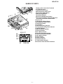
MD-MT180
SERVICE MANUAL
No. S4224MDMT180S
PORTABLE MINIDISC RECORDER
MODEL MD-MT180(S)
• In the interests of user-safety the set should be restored to its
original condition and only parts identical to those specified be
used.
CONTENTS
Page
SPECIFICATIONS ................................................................................................................................................................. 2
NAMES OF PARTS ............................................................................................................................................................... 3
OPERATION MANUAL .......................................................................................................................................................... 4
DISASSEMBLY ...................................................................................................................................................................... 9
REMOVING AND REINSTALLING THE MAIN PARTS ....................................................................................................... 10
ADJUSTMENT ...................................................................................................................................................................... 12
MD ERROR MESSAGE DISPLAY CONTENT LIST ........................................................................................................... 25
NOTES ON SCHEMATIC DIAGRAM .................................................................................................................................. 26
TYPES OF TRANSISTOR AND DIODE .............................................................................................................................. 26
BLOCK DIAGRAM ............................................................................................................................................................... 27
SCHEMATIC DIAGRAM ...................................................................................................................................................... 28
WIRING SIDE OF P.W.BOARD ........................................................................................................................................... 32
VOLTAGE ............................................................................................................................................................................ 43
WAVEFORMS OF MD CIRCUIT ......................................................................................................................................... 44
TROUBLESHOOTING ......................................................................................................................................................... 45
FUNCTION TABLE OF IC .................................................................................................................................................... 48
PARTS GUIDE/EXPLODED VIEW
PACKING METHOD
SHARP CORPORATION
This document has been published to be used
for after sales service only.
The contents are subject to change without notice.
MD-MT180
FOR A COMPLETE DESCRIPTION OF THE OPERATION OF THIS UNIT, PLEASE REFER TO
THE OPERATION MANUAL.
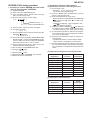
SPECIFICATIONS
Power source:
DC 1.2 V:
DC 5 V:
DC 1.5 V:
DC 4.5 V:
Power consumption:
Output power:
7 W (AC adaptor)
RMS: 20 mW (10 mW + 10 mW)
(0.2 % T.H.D.)
Approx. 3.5 hours (90 %)
Approx. 5.5 hours (fully charged) (When using the AC adaptor included with the unit)
Width: 3" (76 mm) Height: 29/32" (22.9 mm) Depth: 3-9/32" (83 mm)
0.33 lbs. (148 g) with rechargeable battery
Line/optical digital
Earphones (impedance: 32 ohms)
Portable MiniDisc recorder
Non-contact, 3-beam semiconductor laser pickup
Stereo 2 channels/monaural 1 channel
20 - 20,000 Hz ( 3 dB)
Approx. 400 - 1,350 rpm
ACIRC (Advanced Cross Interleave Reed-Solomon Code)
ATRAC/ATRAC3 (Adaptive TRansform Acoustic Coding), 24-bit computed type
Magnetic modulation overwrite method
44.1 kHz (32 kHz and 48 kHz signals are converted to 44.1 kHz, and then recorded.)
Unmeasurable (less than 0.001 % W. peak)
Charging time:
Dimensions:
Weight:
Input jack:
Output jack:
Type:
Signal readout:
Audio channels:
Frequency response:
Rotation speed:
Error correction:
Coding:
Recording method:
Sampling frequency:
Wow and flutter:
Rechargeable Nickel-Metal Hydride battery (AD-N55BT) x 1
AC adaptor (AC 120 V, 60 Hz)
Battery case (Commercially available, "AA" size (LR6), alkaline battery x 1)
Optional car adaptor, AD-CA20X (for cars with a 12 - 24 V DC negative ground
electrical system)
Battery life:
Stereo
2 times long
4 times long
When using the rechargeable
battery (fully charged) included
with the unit
Continuous
recording:
Approx. 7
hours
Continuous
play: Approx.
11 hours
Continuous
recording:
Approx. 9.5
hours
Continuous
play: Approx.
13 hours
Continuous
recording:
Approx. 12.5
hours
Continuous
play: Approx.
15 hours
When using one, commercially
available, high capacity, "AA"
size (LR6), alkaline battery (The
rechargeable battery is in the
unit, discharged.)
Continuous
recording:
Approx. 6
hours
Continuous
play: Approx.
15.5 hours
Continuous
recording:
Approx. 9.5
hours
Continuous
play: Approx.
19 hours
Continuous
recording:
Approx. 13
hours
Continuous
play: Approx.
22 hours
When using one, commercially
available, high capacity, "AA"
size (LR6), alkaline battery with
the rechargeable battery (fully
charged)
Continuous
recording:
Approx. 15.5
hours
Continuous
play: Approx.
27 hours
Continuous
recording:
Approx. 23
hours
Continuous
play: Approx.
32 hours
Continuous
recording:
Approx. 30
hours
Continuous
play: Approx.
38 hours
● The continuous recording time is for analog inputs
Input sensitivity:
LINE
Reference input
level
Input impedance
100 mV
20 kohms
when the volume level is set to "VOL 0".
● The continuous play time shows the value when the
volume level is set to "VOL 15".
● The above values are the standard values when the
unit is charged and used at an ambient temperature of
77°F (25°C).
● The operating time when using an alkaline battery
may be different, depending on the type and manufacturer of the battery, and on the operating temperature.
Output level:
Specified
output
Maximum
output level
Load
impedance
Earphones
-
10 mW +
10 mW
32 ohms
LINE
250 mV
(-12 dB)
-
10 k ohms
Specifications for this model are subject to change without prior
notice
–2–
MD-MT180
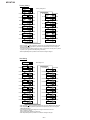
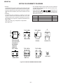
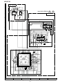
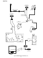
NAMES OF PARTS
1
7
5 6
4
2
8
3
9
10
13
11
12
15 16 17
14
18
19
20
25
26
27
28
21
22 23 24
–3–
1. Battery Case Connection Terminals
2. 5 V DC Input Jack
3. Optical/Line Input Jack
4. Earphones/Line Output Jack
5. Record/Track Mark Button
6. Menu/Charge Button
7. Bass/Delete Button
8. Enter/Fast Play/Synchro Button
9. Volume/Cursor/Fast Forward/Fast Reverse/
Recording Level/ Name Select Button
10. Open Lever
11. Stop/Power Off/Hold Button
12. Rechargeable Battery Cover
13. Play/Pause Button
14. Level Meter
15. Stereo Recording Indicator
16. Long-play/Recording Mode Indicator
17. Repeat Indicator
18. Monaural Mode Indicator
19. Record Indicator
20. Disc Mode Indicator
21. Synchro Recording Indicator
22. Total Track Number Indicator
23. Disc Name Indicator
24. TOC Indicator
25. Battery Indicator
26. Random Indicator
27. Track Number Indicator
28. Character/Time Information Indicator
MD-MT180
OPERATION MANUAL
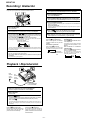
Using with the Rechargeable Battery
■ Charging the rechargeable battery
Insert the
– side first.
Do not force the
battery cover
open too far.
When the rechargeable battery is used for the first time
or when you want to use it after a long period of disuse,
be sure to charge it fully.
1
Insert the rechargeable battery.
A rechargeable battery other than the AD-N55BT
cannot be charged.
2
Plug the AC adaptor into the AC outlet, and
then insert the plug on the other end into
the DC IN 5V jack.
3
Press the MENU/CHRG button.
The battery indicator will scroll, and battery will begin charging.
AC 120V,
60Hz
Scrolling
● After the rechargeable battery is charged or used, it
To the DC IN
5V jack
will get slightly warm. This is normal.
● When the portable MD is turned on or operating, the
battery will not be charged.
Using with the Alkaline Battery
Use one commercially available alkaline battery (LR6,
"AA" size).
Open
2
1
Press
Back of the
portable MD
RELEASE
When using the alkaline battery, be sure to insert the
rechargeable battery also.
1
2
Open the case cover.
3
Attach the battery case to the portable MD.
Insert an alkaline battery into the battery
case.
Caution:
● While you are using the rechargeable battery and the
alkaline battery at the same time, do not remove either
of them. If you do, when the unit is in the play mode,
playback will stop. When in the recording mode, the
recorded contents will be erased, and the power may
be disconnected.
● Do not replace the battery or the rechargeable battery
during operation.
● Do not use a rechargeable battery (nickel-cadmium battery etc.) in the battery case.
● If the unit is not used for a long period of time, remove
the battery. (Even if the power is turned off, the battery
will be drained slowly but continuously.)
LOCK
–4–
MD-MT180
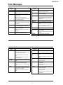
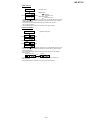
Error Messages
ERROR MESSAGES
MEANING
BATT ENPTY
● The battery has run down.
BLANK MD
● Nothing is recorded.
Can't COPY
ERROR MESSAGES
Can'tSTAMP
(Replace the disc with a recorded disc.)
Can'tWRITE
● You tried to record from a copy prohibited MiniDisc.
● Cannot save the TOC information correctly to a MiniDisc.
DEFECT!
● The disc is scratched.
(If the recorded sound is not right, retry
recording or replace the disc with a recordable one.)
● You tried to record signals other than
music (such as data).
● A track cannot be edited.
(Change the stop position of the track and
then edit it.)
Can't PLAY
DISC FULL
● The disc is out of recording space.
Er-MD (**)
● The microprocessor has reported a
system fault and the unit is out of order.
● You tried to play back a track that cannot be played with this equipment.
Can't READ (*) ● The disc data cannot be read because
the disc is damaged.
(Reload the Minidisc or replace it with another one.)
Can't REC
● Stamp function does not work.
(Check the number of tracks.)
(Record using the analog cable.)
Can't EDIT
MEANING
(To have it repaired, go to the distributor
where you purchased the unit.)
HOLD
● The unit is in the hold mode.
LOCKED
● You removed a MiniDisc when recording or editing.
(Turn off the power before removing the
MiniDisc.)
● Recording cannot be performed correctly due to vibration or shock.
NO DISC
● A disc has not been loaded.
Number or symbol appears in (*) position.
ERROR MESSAGES
NO SIGNAL
MEANING
● Poor connection of the digital cable.
● No output signal comes out from the
connected unit to playback.
(Use the AC power for the connected
unit.)
● The input signal has improper sampling frequency.
PLAY MD
● You tried to record on a playback-only
disc.
PROTECTED
● The write protection tab of a MiniDisc
is set to the protected position.
ERROR MESSAGES
TEMP OVER
● Since a track number is currently being located or updated, the unit cannot
accept your command.
● The temperature is too high.
(Turn off the power, and wait for a while.)
TOC FORM
(**)
● There is an error in the recording signal.
(Erase all of the tracks, and then record
again.)
TOC FULL
● There is no space left for recording
character information (track names,
disc names, etc.).
Tr. Protect
● The track has been protected from being erased.
● You tried to record on a playback-only
disc.
SORRY
MEANING
(Edit the track with the device on which it
was recorded.)
? DISC
● A disc which contains data other than
music was played.
(A disc which contains nonmusic data
cannot be played.)
(Wait for a while and try the operation
again.)
● There is an error in the signal recorded
on the disc.
Number or symbol appears in (*) position.
–5–
MD-MT180
MiniDisc System Limitations
The unit may have the following symptoms when recording or editing. The unit is not out of order.
SYMPTOM
LIMITATIONS
"DISC FULL" or "TOC FULL" appears
even though the MiniDisc still has recording time left.
More than 255 tracks (maximum) cannot be recorded regardless of
the recording time. If the MiniDisc is recorded or edited repeatedly or
if it has scratches (recording skips scratched parts), you may not be
able to record the maximum tracks above.
The remaining recording time does not
increase even though you erased
tracks.
The unit does not count non-recorded portions that last 12 or fewer
seconds to display the remaining recording time. The time may not
increase even if you erase short tracks.
The total of the recorded time and the
remaining time does not match the maximum recordable time.
One cluster (approximately 2 seconds) is the minimum unit for recording. For example, a 3-second track uses 2 clusters (approximately 4 seconds). Therefore, the actual recordable time may be
shorter than the displayed time.
(The number of seconds indicates that in the stereo recording mode
(SP). It varies depending on the recording mode.)
Combine function does not work.
A MiniDisc on which recording and editing are repeated may not allow the combine function.
Sound skips in fast reverse/forward.
If one track is divided and recorded in separate places on a repeatedly recorded or edited MiniDisc, sound may skip.
A track number is created in the middle
of a track.
A track number may be created if there are scratches or dust on the
MiniDisc.
Troubleshooting
Many potential "problems" can be resolved by the owner without calling a service technician. If something seems to be wrong
with this product, check the following before calling your authorized SHARP dealer or service center.
The unit does not turn on.
Some sounds are skipped.
● Is the AC adaptor disconnected?
● Is the battery exhausted?
● Is the battery exhausted?
● Is the unit being subjected to excessive vibration?
● Is the unit in the hold mode?
● Has condensation formed inside the unit?
● Is the unit being influenced by mechanical shock or by
static electricity?
The MiniDisc cannot be ejected.
● Has the track number or character information been
written on the disc yet?
● Is the unit in the recording or editing mode?
No sound is heard from the earphones.
● Is the volume set too low?
● Is the earphones plugged in?
● Are you trying to play a MiniDisc with data on it instead
of a MiniDisc containing music?
When the operation buttons are pressed, the unit does
not respond.
● Is the unit in the hold mode?
● Is the battery exhausted?
Recording and editing are impossible.
● Is the MiniDisc protected against accidental erasure?
● Is the unit connected properly to the other equipment?
● Is the AC adaptor unplugged or did a power failure occur when recording or editing?
● Is the unit in the hold mode?
● Is an optical signal being output from the stereo system? Read the operation manual for the stereo system.
● Is the earphones plug inserted firmly?
–6–
MD-MT180
1
2
Connect the AC adaptor
Conecte el adaptador de CA
Inserting a MiniDisc
Inserción de un minidisco
AC 120V, 60 Hz
1
Insert according to the direction of the arrow.
120V CA, 60Hz
2
4
Insértelo de acuerdo con la dirección de la flecha.
3
1
To an AC outlet
A un tomacorriente
de CA
To the DC IN 5V jack
A la toma DC IN 5V
2
1 Plug the AC adaptor into the
1 Slide the OPEN lever to re- 3 Insert a MiniDisc as shown.
Insert the plugs firmly.
lease the compartment door.
Deslice la palanca OPEN para
abrir la puerta del compartimiento.
Inserte firmemente las clavijas.
AC outlet.
end into the DC IN 5V jack.
Enchufe el adaptador de CA en
el tomacorriente de CA.
Inserte la clavija del otro
extremo en la toma DC IN 5V.
Levántela.
When you record on a MiniDisc,
check that the erase prevention tab
is set to the “Recordable” position.
Before using the unit with a rechargeable battery, the battery has to be charged.
Antes de emplear el aparato con una batería recargable, se deberá cargar la
batería.
Recordable
Grabable
3
4 Close the compartment door.
Cierre la puerta del compartimiento.
2 Lift it up.
2 Insert the plug on the other
Inserte un minidisco como se
muestra.
Recording
prevented
Grabación
prevenida
Cuando grabe en un MD, compruebe
que la lengüeta de prevención contra borrado esté puesta en la posición
"Grabable".
Preparation for use
Preparación para su utilización
Connections / Conexiones
The unit does not work if the unit is in the hold mode.
El aparato no funciona si está en el modo de retención.
LINE IN
Press the HOLD button for 2 seconds or more.
Pulse el botón HOLD durante 2 o más segundos.
To the DC IN 5V jack
A la toma DC IN 5V
Hold
Retención
White: To Left
Blanco: A la izquierda
Release
Liberación
Red: To Right
Rojo: A la derecha
LINE OUT
RIGHT
LEFT
To a stereo system with “LINE OUT” or “AUDIO OUT”
jacks.
Note:
If the audio system has only one pair of jacks then they are usually
for input only and recording via this connection is not possible.
Para un sistema estéreo con tomas "LINE OUT" o
"AUDIO OUT" .
Nota:
Si el sistema de audio tiene sólo un par de tomas, son
usualmente sólo para entrada y no puede realizarse la grabación
mediante esta conexión.
CAUTION:
It is not recommendable to put the MiniDisc into a rear
pocket, as this may damage the product when sitting.
PRECAUCIÓN:
No es recomendable poner el MD en un bolsillo trasero,
porque esto podría dañar el producto al sentarse.
–7–
MD-MT180
Recording / Grabación
Check that the unit is connected to the stereo system.
Compruebe que el aparato esté conectado al sistema estéreo.
5 Press the MENU/CHRG button repeatedly to select the "REC MODE".
Pulse repetidamente el botón MENU/CHRG para seleccionar "REC MODE".
6 Press the ENTER/SYNC button.
Pulse el botón ENTER/SYNC.
7 Press the MENU/CHRG button repeatedly to select recording mode.
Pulse repetidamente el botón MENU/CHRG para seleccionar el mode de grabación.
8 Press the ENTER/SYNC button.
The mode will be set automatically after 7 seconds even if the ENTER/SYNC
button is not pressed.
Pulse el botón ENTER/SYNC.
El mode se establecerá automáticamente después de 7 segundos aunque no se pulse el
botón ENTER/SYNC.
1 Press
the REC button.
Pulse el botón REC.
9 Press the 06 button to start the MiniDisc unit recording.
2 Begin playback on the stereo system connected to this portable MD.
Pulse el botón 06 para iniciar la grabación del aparato de MD.
Inicie la reproducción en el sistema estéreo conectado a este MD portátil.
10Begin playback on the stereo system, and the output will be recorded.
3 Press the REC LEVEL 5 or 4 button to adjust the recording level.
Adjust the recording level so that the maximum sound volume from the source makes
the reading swing somewhere between –4 dB and 0 dB.
Pulse el botón REC LEVEL 5 o 4 para ajustar el nivel de grabación.
Ajuste el nivel de grabación de modo que el nivel máximo de volumen del sonido de la
fuente haga que la indicación oscile entre –4 dB y 0 dB.
Inicie la reproducción en el sistema estéreo, y se grabará la salida.
To stop recording
Press the ■ :OFF/HOLD button.
Level meter indicator
When “TOC” appears, the MiniDisc
recorded contents have not yet been
updated.
Indicador del medidor de nivel
Para detener la grabación
Pulse el botón ■:OFF/HOLD.
This unit can adjust the digital recording level just the same as the analog recording.
Este aparato puede ajustar el nivel de grabación digital del mismo mode que en el caso
de la grabación analógica.
Mientras aparece “TOC”, aún no se habrá
actualizado el contenido grabado en el MD.
4 Press the PAUSE button on the stereo system to enter the playback pause mode.
TOC display
Visualización
TOC
Here you can search for the track to record.
Pulse el botón PAUSE del sistema estéreo para establecer el modo de pausa de
reproducción.
Aquí podrá buscar la pista a grabarse.
Playback / Reproducción
Right
channel
Canal
derecho
Left
channel
Canal
izquierdo
To the PHONES jack
A la toma PHONES
1 Insert the earphones plug into the PHONES jack.
Inserte la clavija de los auriculares en la toma PHONES.
2 Insert a MiniDisc.
Inserte un MD.
3 Press the 06 button.
Playback starts automatically with a playback only MiniDisc or a MiniDisc
which is protected against accidental erasure (Auto-play function).
Pulse el botón 06.
La reproducción empezará automáticamente con un MD de sólo reproducción o un
MD que está protegido contra borrado accidental (Función de reproducción
automática).
To stop playback
Press the ■:OFF/HOLD button.
If the unit is not operated for at least 2
minutes when in the stop mode, the
power will shut off automatically.
Para detener la reproducción
Pulse el botón ■:OFF/HOLD.
Si el aparato no se utiliza durante un
mínimo de 2 minutos en el modo de
parada, la alimentación se desconectará
automáticamente.
–8–
To update the recorded contents
of the MiniDisc
Press the ■:OFF/HOLD button when
in the stop mode.
The power turns off after recorded
contents have been updated on the
MiniDisc.
Para actualizar el contenido
grabado del MD
Pulse el botón ■:OFF/HOLD mientras
esté en el modo de parada.
La alimentación se desconectará
después de haber actualizado el
contenido grabado en el MD.
MD-MT180
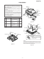
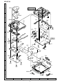
DISASSEMBLY
Cares before disassembling
When assembling the machine after disassembling or
repair, observe the following requirements so as to ensure
safety and performance.
1. Remove the batteries from the machine, and take out the
mini-disc.
2. When assembling after repair, be sure to position the
wires in the same location.
Use the specified screws to fix the cabinet and the
mechanism unit. The use of the screws with length other
than specified may cause contact with the mechanism
unit resulting in malfunction.
3. When repairing, pay close attention so not to damage the
IC from static electricity.
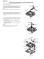
STEP
1
REMOVAL
Bottom Cabinet
PROCEDURE
FIGURE
1. Screw ..................... (A1) x5
2. Open the Battery Door.
3. Hook ....................... (A2) x1
9-1
Top Cabinet
1. Open the Top cabinet.
2. Screw ..................... (B1) x2
3. Flexible PWB .......... (B2) x2
9-1
9-2
3
Main PWB
1. Screw .................... (C1) x3
2. Flexible PWB ......... (C2) x2
3. Hook ...................... (C3) x3
9-2
1. Screw .................... (D1) x2
9-3
Mechanism Unit
Top Cabinet
(A1) x1
ø1.4 x2.5mm
Bottom Cabinet
Battery Terminal
(A1) x2
ø1.4 x4mm
Battery Door
2
Open Lever
(A1) x1
ø1.4 x4mm
1
Hook
(A2) x1
Pull
2
4
(A1) x1
ø1.4 x2.5mm
Figure 9-1
(C1) x1
ø1.4 x2.5mm
(C1) x1
ø1.4 x2mm
*(C2) x1
(B2) x2
(C2) x1
Main PWB
Pull
(C1) x1
ø1.4 x2.5mm
Pull
Pull
Hook
(C3) x3
(D1) x1
ø1.4 x1.5mm
Mechanism Unit
Pull
Top Cabinet
Bracket
(B1) x2
ø1.4 x2.5mm
(D1) x1
ø1.4 x1.5mm
EJECT SWITCH
Be careful not to break the EJECT
SWITCH when remove and attach
the bottom cabinet.
Caution:
Carefully handle the main PWB and flexible PWB. After removing the
flexible PWB (*) for the optical pickup from the connector, do not touch
directly the front end of flexible PWB with your hand so as to prevent
damage of optical pickup by static electricity.
Figure 9-3
Figure 9-2
–9–
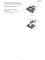
MD-MT180
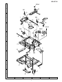
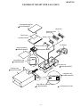
REMOVING AND REINSTALLING THE MAIN PARTS
Remove the mechanism according to the disassembling methods 1 to 4. (See Page 9.)
(A2) x2
ø1.4 x1.8mm
How to remove the magnetic head (See Fig. 10-1.)
1. Remove the solder joints (A1) x 2 of the head flexible plate.
2. Remove the screws (A2) x 2 pcs. of the magnetic head.
Note:
Mount carefully so as not to damage the magnetic head.
MD Mechanism
Magnetic Head
Solder Joints
(A1)x2
How to remove the spindle motor (See Fig. 10-2.)
1. Remove the solder joints (B1) x 4 of flexible PWB.
2. Remove the screws (B2) x 3 pcs., and remove the spindle
motor.
Figure 10-1
How to remove the sled motor (See Fig. 10-3.)
1. Remove the stop washer (C1) x 1 pc., and remove the drive
gear (C2) x 1 pc.
2. Remove the solder joints (C3) x 3 of flexible PWB.
3. Remove the screws (C4) x 2 pcs., and remove the sled
motor and the left bracket.
4. Remove the screw (C5) x 1 pc., and remove the right
bracket.
Note:
Take care so that the motor gear is not damaged.
(If the gear is damaged, noise is caused.)
(B2) x3
ø1.4 x3mm
Spindle
Motor
Solder Joints
(B1)x4
MD Mechanism
Figure 10-2
Stop Washer
(C1)x1
Drive Gear
(C2)x1
(C5) x1
ø1.7 x3.5mm
(C4) x2
ø1.4 x1.5mm
Sled Motor
Right
Bracket
Solder Joints
(C3)x3
MD Mechanism
Left
Bracket
Cartridge Holder
Figure 10-3
– 10 –
MD-MT180
How to remove the Lift motor (See Fig. 11-1.)
1. Remove the solder joints (D1) x 2 of the lift motor lead wire.
2. Remove the screw (D2) x 1 pc., and remove the lift motor.
Note:
Take care so that the motor gear is not damaged.
(If the gear is damaged, noise is caused.)
Lift Motor
SolderJoints
(D1)x2
How to reinstall the optical pickup
(See Fig. 11-2.)
1. Remove the screw (E1) x 1 pc., and remove the spring.
2. Slowly raise the optical pickup.
(D2) x1
ø1.4 x5mm
Figure 11-1
Optical Pickup Unit
(E1) x1
ø1.7 x3.5mm
Spring
Figure 11-2
– 11 –
MD-MT180
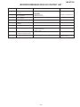
ADJUSTMENT
Test disc
MD adjustment needs two types of disc, namely recording disc (low reflection disc) and playback-only disc (high
reflection disc).
Type
Parts No.
Test disc
1
High reflection disc MMD-110 (TEAC Test MD)
88GMMD-110
2
Low reflection disc
MMD-212 (TEAC Test MD) 74-minute disc
88GMMD-212
3
Low reflection disc
MMD-213A (TEAC Test MD) 80-minute disc
4
Low reflection disc
Recording minidisc
88GMMD-213A
UDSKM0001AFZZ
Note: Use the low reflection disc on which music has been recorded.
Entering the TEST mode
1. Setting at port (power nonconnected state)
(1) Set the port as follows.
TEST1 : "Low" (TP416)
TEST0 : "High"
(2) Turn the Power ON.
(3) Test Mode START [ T E S T _ ]
2. Setting by special button operation (in standby state)
(1) Holding down the MENU button and ENTER button, press the PLAY
button.
(2) Normal mode setting initialization (BASS setting, VOL setting, etc.)
*Since the unit is changed to the setting for production line inspection , be sure to set it to the default setting state in the following default
setting procedure before returning it to the user.
(3) Test Mode START [ T E S T _ ]
(4) When the VOL.+ button is pressed, indication of microcomputer version for one second [ Y 1 2 A c X ]
Destination
Microcomputer version
EEPROM version
(5) When the VOL.– button is pressed, whole LCD lighting for 2 seconds
Leaving the TEST mode
(1) Press the STOP
button in the TEST mode stop state.
Shipping setting method
Holding down simultaneously the VOLUME – Button and PLAY
Button of the set unit without disc, supply the power from the DC IN plug.
After the indication "INIT" -> "BYE OK" disappears, release the power supply of DC IN.
Test Mode
1. AUTO 1 Mode
2. AUTO 2 Mode
3. TEST-PLAY Mode
4. TEST-REC Mode
5. MANUAL 1 Mode
6. MANUAL 2 Mode
• Perform preliminary automatic adjustment.
• If the combination of mechanism and pickup
PWB has been changed, be sure to start from
AUTO1.
• Perform ATT (attenuator) automatic adjustment.
• Perform continuous playback (error rate display,
jump test)
• Continuous playback from the specified address
is performed.
• 1 line, 10 lines or 384 lines manual jump is
performed.
• C1 error rate display (pit section), ADIP error
rate display (groove section)
• The temperature correction is performed only when
servo start is performed, but the posture correction
is not performed during continuous playback.
• Continuous record from the specified address
is performed.
• Change of record laser output(servo gain is also
changed according to laser output).
• The temperature correction is performed only
when servo start is performed, but the posture
correction is not performed during continuous
recording.
• Temperature is displayed. (Updating in real time)
• Seeing the displayed adjustment value, perform
preliminary manual adjustment.
(Error rate indication, jump test)
• Temperature is displayed. (Updating in real time)
• Seeing the displayed adjustment value perform
manfully the preliminary adjustment.
(Error rate indication, jump test)
• Continuous playback is performed
(Error rate display, jump test).
7. RESULT 1 Mode
• The value adjusted in AUTO1 or MANUAL1 is
indicated.
• (Execution in servo "OFF" state").
8. RESULT 2 Mode
• The value adjusted in AUTO 2 or MANUAL 2 is
indicated.
• Adjustment value is changed manually.
(Error rate display, jump test).
9. DIGITAL INPUT Mode
• Digital input information is displayed.
10. ERROR INFORMATION • Error information is displayed.
Mode
• Error information is initialized
11. NORMAL Mode
• The mode is changed from the TEST mode to
the normal mode without adjustment.
• In the normal mode the internal operation mode,
memory capacity, etc. areindicated.
• In the normal mode both temperature correction
and posture correction are perfomed.
12. EEPROM Mode
• Factors of digital servo are changed manually.
(Each servo is turned on individually.)
• Cut-off frequency of BASS1, BASS2 and BASS3
is selected manually.
• Temperature detection terminal voltage is
measured, and the reference value is set.
• Defaults are selected and set.
• Setting of EEPROM protect area is updated.
(In case of protect releasing)
13.AUTO J Mode
• AUTO 1/2, focus balance adjustment, TESTPLAY (ADIP/C1 error check), EEPROM are
updated sequentially.
– 12 –
MD-MT180
• Whenever the MENU button is pressed in the continuous
playback mode, the indication changes as follows.
* Pre-mastered disc
Continuous playback (SUBQ address indication) [ S Q
]
Operation in each TEST mode
1. AUTO1 Mode
• When the STOP button is pressed while the AUTO1 menu
appears or during automatic adjustment, the mode changes
to the TEST mode stop state. At this time the adjustment
value is not output.
• Be sure to adjust, using the specified disc MMD-213A or
MMD-212.
At this time release the EEPROM (IC402) protection. (Refer
to EEPROM write procedure.)
• Adjustment NG; Adjustment item out of range, focus ON
failure, and adjustment error
• When the PLAY
button is pressed while ADJ. OK is
displayed, AUTO2 is executed.
2. AUTO2 Mode
• When the STOP button is pressed while the AUTO2 menu
appears or during automatic adjustment, the mode changes
to the TEST mode stop state. At this time the adjustment
value is not output.
• Adjustment NG; Adjustment item out of range, and adjustment error.
button is pressed while ADJ. OK is
• When the PLAY
displayed, TEST_PLAY is executed.
Continuous playback (C1 error indication) [ C E
]
Continuous playback (SUBQ address indication) [ S Q
* Recordabl disc
Continuous playback (ADIP address indication) [ A P
]
Continuous playback (C1 error indication) [ C E
]
Continuous playback (ADIP error indication) [ A E
]
Continuous playback (ADIP address indication) [ A P
]
]
4. TEST-REC Mode
• When the STOP button is pressed while the TEST-REC
menu appears, or in the TEST-REC mode or continuous
record mode, the mode changes to the TEST mode stop
state.
• When the PLAY button is pressed while the TEST-REC
menu appears, the continuous record is initiated from the
current pickup position.
• Whenever the MENU button is pressed in the TEST-REC
menu, the target address changes as follows.
0032 → 03C0 → 0700 → 08A0 → 0950 → 0032 → ........
When the PLAY button is pressed while a target
address is displayed, continuous playback is performed
after searching that address.
• Whenever the ENTER button is pressed in the TEST-REC
mode target address is displayed, the digit which is
changed by the FAST FORWARD/FAST REVERSE
/
button changes as follows.
0032 → 0032 → 0032 → 0320 → ........
• When the FAST FORWARD
button Is pressed in the
TEST-REC mode target address is displayed, the digit of
address specified by the BASS button is set to +1h.(0 to F)
• When the FAST REVERSE
button is pressed in the
TEST-REC mode target address is displayed, the digit of
address specified by the BASS button is set to -1h.(0 to F)
* When the FAST FORWARD/FAST REVERSE
/
button is held down, the setting changes continuously,
one cycle being 100 ms.
3. TEST-PLAY Mode
• When the STOP button is pressed while the TEST-PLAY
menu appears, or in TEST-PLAY or continuous playback
mode, the mode changes to the TEST mode stop state.
• When the PLAY button is pressed while the TEST-PLAY
menu appears, continuous playback is initiated from the
current pickup position.
• Whenever the MENU button is pressed in the TEST-PLAY
menu, the target address changes as follows.
0032 → 03C0 → 0700 → 08A0 → 0950 → 0032 → ........
When the PLAY button is pressed while a target address
is displayed, continuous playback is performed after searching that address.
• Each time the ENTER button is pressed while the TESTPLAY mode target address is displayed, the digit which is
changed by pressing the FAST FORWARD/FAST REVERSE
/
button is changed as follows.
0032 → 0032 → 0032 → 0032 → ........
• When the FAST FORWARD
button is pressed in the
TEST-PLAY mode target address is displayed, the digit of
address specified by the ENTER button is set to +1h. (0 to F)
• When the FAST REVERSE
button is pressed in the
TEST-PLAY mode target address is displayed, the digit of
address specified by the ENTER button is set to -1h. (0 to F)
* When the FAST FORWARD/FAST REVERSE
/
button is held down, the setting changes continuously, one
cycle being 100 ms.
• When the BASS button is pressed in the continuous playback mode, the number of jump lines changes as follows.
1 → 10 → 384 → 1 →........
* After the number of jump lines is indicated for one second,
the address indication is restored [
T R _ ]
• When the FAST FORWARD
button is pressed in the
continuous playback mode, the specified number of lines
is jumped in the FWD direction.
• When the FAST REVERSE
button is pressed in the
continuous playback mode, the specified number of lines
is jumped in the REV direction.
* When the FAST FORWARD/FAST REVERSE
/
button is held down, jump is repeated every
approx. 100 ms.
– 13 –
MD-MT180
5. NORMAL Mode
• When the STOP
button is pressed while the NORMAL
menu appears, the mode changes to the TEST mode stop
state.
• Indication during operation
Indication of memory capacity on main unit LCD
[
] + Level meter
: Internal mode
: Address (Cluster section)
: Address (Sector section)
• Selection of sound volume, BASS, etc. is possible (without
indication)
• Recording is also possible.
• If the STOP
button is pressed during operation in the
NORMAL mode, the NORMAL mode is canceled, and the
power is turned off.
6. Error data display Mode
• Reversing when FAST REVERSE
button is pressed
• When the STOP button is pressed while the error data
indication menu appears or during error data indication, the
mode changes to the TEST mode stop state.
• Error data 0 is the latest error.
• Error which occurred in the TEST mode is also stored in the
memory.
• When the MENU button is pressed while the error data
indication menu appears, the error data is initialized.
[ C L E A R _ ]
•
: Error Code
Explanation of error history code
13h : Excessive number of retry to draw servo during its
adjustment.
16h : COUT detection time over during servo adjustment.
17h : The level of input signal from the RF amplifier is out of
the allowable range.
1Fh : Cannot clear the factor of ENDEC DINT.
21h : Cannot focus on the disc.
22h : Cannot start up the spindle.
23h : Track search time over.
32h : Cannot read P-TOC.
42h : Cannot read U-TOC.
44h : Cannot write U-TOC.
45h : Cannot perform write test of U-TOC.
52h : Cannot write SD. (Sound Data)
71h : Time over during initialization of the pickup position.
72h : Check sum error occurred when reading EEPROM.
73h : Cannot operate the recording head (by using the EJECT
lever).
91h : The ambient temperature is out of the allowable range.
7. Auto J Mode
• AUTO 1/2, focus balance adjustment, TEST-PLAY (ADIP/C1
error check), EEPROM are updated sequentially.
• If the STOP button is pressed while processed, the same
operation as the normal STOP button operation will be
performed.
– 14 –
MD-MT180
EEPROM (IC402) writing procedure
2. Temperature reference setting method
1. Procedure to replace EEPROM and write initial
value of microcomputer in EEPROM
[1] Measurement, calculation and setting procedure
(1) Set the TEST mode.
• Set TEST 1, 0 = '01', and turn on power
(or set PLAY ON in standby state).
(2) Press the MENU button, ENTER button and Play
button to start the test mode.
(3) Start the EEPROM mode 'Temp' menu.
• Button operation in order of BASS, FAST REVERSE
x 3 times, PLAY , PLAY in the test mode
STOP state.
• 'TM§§
' is displayed. (§§= Temperature code,
= Temperature reference)
, and determine
(4) Once press FAST FORWARD
the displayed microcomputer TEMP input AD value.
• 'TPin##' is displayed. (## = TEMP input AD value)
(5) At the ambient temperature, determine the temperature corrected value from the temperature measurement value correction table.
(6) Determine the temperature reference, using the following formula.
• Temperature reference = Microcomputer TEMP
input AD value + Temperature corrected value
(7) Set the temperature reference value by button operation, and check whether the temperature code indication corresponds to "Temperature Code Identification
Table".
(1) Replace EEPROM.
(2) Refer to the latest EEPROM data list.
(3) Press the MENU button, ENTER button and Play
button to start the test mode.
(4) Press the VOL.+ button, version display
[Ver.
X ]
EEPROM version (c ~ z)
Microcomputer ROM version
(5) Press the VOL.– button, the whole LCD lights.
(6) Test mode stop state.
[ T E S T ]
(7) Press the "BASS" button, and press 3 times the "FAST
" button.
REVERSE
[ E E P R O M ]
(8) Perform the operation to display "EEPROM SETTING
ENTER CHART", compare the EEPROM DATA LIST
with the display, and set according to the EEPROM
DATA LIST with the VOL.+ or VOL.– button.
(9) Set the temperature reference. (Refer to the Temperature Reference Setting Method.)
(10) Set according to the EEPROM DATA LIST.
(11) Press the Stop button.
[ T E S T ]
(12) Press the Stop button.
(13) After data is written in EEPROM, turn off power .
(14) Restore protection of EEPROM.
[2] Temperature measurement value correction table
Ambient
temperature
Temperature
correction
+ 9oC ~ +11oC
- 05h
Center
temperature
+ 10.0oC
+12oC ~ +14oC
- 04h
+ 12.7oC
+15 C ~ +16 C
- 03h
+ 15.4oC
+17oC ~ +19oC
- 02h
+ 18.2oC
+20 C ~ +22 C
+23oC ~ +24oC
- 01h
± 00h
+ 20.9oC
+ 23.6oC
+25oC ~ +27oC
o
o
o
o
+ 01h
+ 26.3oC
o
o
+ 02h
+ 29.0oC
o
o
+ 03h
+ 31.8oC
+28 C ~ +30 C
+31 C ~ +33 C
[3] Temperature code identification
Ambient
temperature
Temperature
correction
Center
temperature
– 9oC ~ +10oC
08h
+ 0.5oC
o
o
07h
+ 12.5oC
o
o
+15 C ~ +33 C
06h
+ 23.6oC
+26oC ~ +43oC
05h
+ 35.0oC
+ 3 C ~ +21 C
– 15 –
MD-MT180
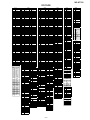
EEPROM DATA LIST (EEPROM version c)
Sled setting (Continued)
TEMP setting
Item display
Item display
T M _ _
Set values
Calculate values
Focus setting
Item display
Set values
F G 1 _
40H
F Z H _
F L n _
EDH
09H
F L p _
F T s _
06H
18H
F S B _
F T B _
40H
28H
T O 1 _
T O R _
50H
58H
0EH
1CH
B P E _
B P W _
71
75
H
B P 1 _
B R E _
33
95
H
B R W _
S R S _
33H
3CH
H
H
Bass setting
Item display
Tracking setting
Item display
Set values
S K E _
S D E _
Set values
B 1 A _
B 2 A _
00
00
H
B 3 A _
00
H
H
ADJ. SET setting
Set values
Item display
Set values
T G 1 _
T B o _
14
20
H
C O K _
28
H
H
12
20
H
64
11
H
T B t _
T K o _
F A B _
H S G _
H
L S G _
12
H
T K t _
T D o _
0DH
67H
T D t _
S C t _
34H
3AH
C L p _
C L r _
24
30
J P I _
K 1 0 _
0EH
65H
T H P _
T H G _
02
02
T O P _
T O G _
T 1 P _
00H
F2H
20H
Control setting
Item display
H
H
H
H
Spindle setting
Item display
Set values
S P G _
S P i _
30H
9AH
S P m _
S P o _
62H
4FH
S D 1 _
S D 2 _
7F
7F
S P K _
S P W _
EBH
0FH
S P B _
S R i _
66H
C0H
S R m _
S R o _
9A
7B
H
S B R _
O S L _
60
14
H
P J G _
46
H
H
H
H
H
Sled setting
Item display
Set values
S K S _
7F
S K L _
S L C _
7FH
24H
S T L _
S T M _
07
42
S T E _
S D V _
A6H
60H
S J P _
W T m _
03
18
S R V _
S L T _
54H
5CH
M V S _
S L S _
0AH
28H
H
H
H
H
02
01
H
C T 2 _
C T 3 _
32
50
H
T S A _
U S A _
20
18
H
P L E _
R C E _
A0H
94H
S D F _
F B 0 _
1FH
FCH
B H S _
B S 0 _
00
17
H
B S 1 _
B U 0 _
70
01
H
B D 0 _
B D 1 _
05H
DCH
B M K _
B E C _
1EH
00H
C S T _
I J U _
69
81
I J D _
M C T _
55H
A1H
E R C _
C V 0 _
5AH
16H
C V 1 _
S S K _
10H
B9H
A C T _
C 1 E _
63
52
H
A D E _
F G 2 _
00
70
H
T G 2 _
M F P _
2AH
◊◊H
S P M _
M S L _
◊◊
◊◊
U S 0 _
U S 1 _
◊◊
◊◊
U S 2 _
◊◊
◊ ◊ H : CHECK-SUM
H
H
– 16 –
Set values
C T 0 _
C T 1 _
H
H
H
H
H
H
H
H
H
H
H
H
H
H
MD-MT180
Test Mode Change Chart
Test Mode Menu
TEST
: Test Mode STOP
FAST REVERSE
FAST FORWARD
Slide internal
periphery move
Slide external
periphery move
BASS
FAST REVERSE
AUTO1
FAST FORWARD
: Pre-auto adjustment menu
FAST REVERSE
AUTOJ
: Auto 1 & 2, Focus balance adjustment menu
FAST FORWARD
FAST REVERSE
AUTO2
FAST FORWARD
T
PLAY
FAST FORWARD
T
: ATT auto adjustment menu
FAST REVERSE
REC
FAST FORWARD
: ATT manual adjustment menu
FAST REVERSE
MANU1
FAST FORWARD
: Pre-adjustment value check menu
FAST REVERSE
MANU2
FAST FORWARD
: ATT adjustment value check menu
FAST REVERSE
RSLT1
FAST FORWARD
: Continuous playback menu
FAST REVERSE
RSLT2
FAST FORWARD
: Continuous record menu
FAST REVERSE
Din Mon
FAST FORWARD
E
: Pre-manual adjustment menu
FAST REVERSE
: Test mode normal playback menu
FAST REVERSE
DATA
FAST FORWARD
: Digital input signal monitor menu
FAST REVERSE
NORMAL
FAST FORWARD
: Error history display menu
FAST REVERSE
EEPROM
: EEPROM setting menu
FAST FORWARD
* When the [STOP ] button is pressed in specific menu, the "TEST MODE STOP" state is set.
* When the [PLAY ] button operation is performed in the specific menu, the operation of this
menu is executed.
Preautomatic Adjustment
AUTO1
: Preautomatic Adjustment menu
PLAY
AT1
: During preadjustment adjustment
Adjustment error
Normal end
ADJ. NG
ADJ. OK
: Preadjustment error (adjustment value output)
: Preadjustment normal end (adjustment value output)
PLAY
AT2
: During ATT automatic adjustment
* When the [STOP ] button is pressed in specific menu, the "TEST MODE STOP" state is set.
*"
" represent the adjustment number as follows.
0 0 : Innermost periphery move
0 2 : ABEF offset tentative measurement
0 4 : RF side focus gain coarse adjustment
0 5 : Focus ATT tentative setting
0 6 : RF side bit section tracking gain adjustment
0 7 : COUT level setting for pit section adjustment
0 8 : External periphery move
0 9 : RF side groove section tracking gain adjustment
1 0 : COUT level setting for groove section adjustment
1 1 : RF side TCRS gain adjustment
1 2 : Tracking ATT initial setting
1 3 : RF side focus gain minor adjustment
1 4 : Focus ATT initial setting
1 5 : S gain "High" ABEF offset measurement
1 6 : TCRS offset measurement
1 7 : S gain "Low" ABEF offset measurement
– 17 –
MD-MT180
ATT Auto Adjustment
AUTO2
: ATT auto adjustment menu
PLAY
AT2
: During ATT auto adjustment
Adjustment error
ADJ. NG
Normal end
: ATT adjustment error (adjustment value output)
: ATT adjustment normal end (adjustment value output)
ADJ. OK
ENTER
: Focus balance Adjustment mode
: Focus balance
# # # : Jitter error
b###
PLAY
: Continuous playback (high reflection)
: Continuous playback (low reflection)
SQ####
AP####
* When the [STOP ] button is pressed in specific menu, the "TEST MODE STOP" state is set.
*"
" represent the adjustment number as follows.
0 0 : Innermost periphery move
0 3 : Pit section tracking ATT setting
0 4 : Pit section focus ATT setting
0 6 : External periphery move
(low reflection only)
0 7 : TCRS ATT setting
(low reflection only)
0 8 : Groove section tracking ATT setting
(low reflection only)
0 9 : Groove section focus ATT setting
(low reflection only)
Continuous Playback
• Continuous playback from current pickup position
T
PLAY
: Continuous playback menu
PLAY
SQ####
AP####
: Continuous playback (pit section)
: Continuous playback (groove section)
# # # # : Address
• Continuous playback from any address
T
PLAY
: Continuous playback menu
MENU
Ad 0 0 3 2
: Start address setting
PLAY
SQ####
AP####
: Continuous playback (pit section)
: Continuous playback (groove section)
# # # # : Address
* When the [STOP ] button is pressed in specific menu, the "TEST MODE STOP" state is set.
* In the start address set state the start address changes as follows when the [MENU] button is pressed.
03C0H
0700H
08A0H
0 0 3 2 H (initial value)
MENU
MENU
Ad0 3 C 0
Ad0 0 3 2
MENU
Ad0 7 0 0
Ad0 9 5 0 H
Ad0 8 A 0
MENU
0950H
* In the start address setting state the start address change digit changes when the [ENTER] button is pressed.
1st digit (initial value)
2nd digit
3rd digit
ENTER
ENTER
Ad0 0 3 2
Ad0 0 3 2
Ad0 0 3 2
ENTER
* In the start address set state the value of selection digit changes in the range of "0h to Fh"
when the [FAST FORWARD/REVERSE
/
] button is pressed.
* In the continuous playback state the number of jump lines changes as follows shown
the [BASS] button is pressed.
1 (initial value)
10
384
BASS
1TR
BASS
10TR
3 8 4TR
BASS
* When the [FAST FORWARD
] button is pressed in the continued playback mode, jump of specified
number of lines occurs in the external periphery direction.
If the key is held down jump occurs continuously (100 ms cycle).
* When the [FAST REVERSE
] button is pressed in the continuous playback mode, jump of
specified number of lines occurs in the internal periphery direction.
If the key is held down, jump occurs continuously (100 ms cycle).
– 18 –
MD-MT180
Continuous Rrecord
• Continuous record from the current pickup position
T
REC
: Continuous record menu
PLAY
: Continuous record
# # # #: Address
• Continuous record playback from any address
AP# # # #
T
REC
: Continuous record menu
PLAY
: Start address setting
Ad 0 0 3 2
PLAY
: Continuous record
# # # #: Address
AP# # # #
* When the [STOP ] button is pressed in specific menu, the "TEST MODE STOP" state is set.
* In the start address set state the start address changes as follows when the [MENU] button is pressed.
0 0 3 2 H (initial value)
03C0H
0700H
08A0H
MENU
MENU
MENU
Ad0 0 3 2
Ad0 3 c 0
Ad0 8 A 0
Ad0 7 0 0
Ad0 9 5 0
MENU
* In the start address setting state the start address change digit changes when the [ENTER] button is pressed.
1st digit (initial value)
Ad0 0 3 2
2nd digit
ENTER
3rd digit
Ad0 0 3 2
ENTER
Ad0 0 3 2
ENTER
Test Mode Normal Playback
NORMAL
: TEST mode normal playback menu
PLAY
@@@@@@
: Continuous playback
@@@@@@: Mode and address display
* When the [STOP ] button is pressed in specific menu, the "TEST MODE STOP" state is set.
* When the NORMAL mode is canceled, the power is turned off.
– 19 –
MD-MT180
Error History Display
• Error history clear
E
DATA
: Error history display menu
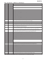
MENU
CLEAR
: Error history clear
• Error history display
E
DATA
: Error history display menu
PLAY
E0§§
FAST FORWARD
FAST REVERSE
: Error history 0 display
§ § : Error code
: Error history 1 display
§ § : Error code
E1§§
FAST FORWARD
FAST REVERSE
: Error history 2 display
§ § : Error code
E2§§
FAST FORWARD
FAST REVERSE
: Error history 3 display
§ § : Error code
E3§§
FAST FORWARD
FAST REVERSE
: Error history 4 display
§ § : Error code
E4§§
FAST FORWARD
FAST REVERSE
E5§§
FAST FORWARD
FAST REVERSE
: Error history 5 display
§ § : Error code
: Error history 6 display
§ § : Error code
E6§§
FAST FORWARD
FAST REVERSE
E7§§
FAST FORWARD
FAST REVERSE
E8§§
FAST FORWARD
FAST REVERSE
E9§§
FAST FORWARD
FAST REVERSE
: Error history 7 display
§ § : Error code
: Error history 8 display
§ § : Error code
: Error history 9 display
§ § : Error code
RC :
: Total Recording Time
* When the [STOP
] button is pressed in specific menu, the "TEST MODE STOP" state is set.
EEPROM Setting
EEPROM
: EEPROM setting menu
PLAY
FAST REVERSE
: TEMP setting menu
Temp
FAST FORWARD
FAST REVERSE
Focus
FAST FORWARD
: Focus setting menu
FAST REVERSE
Track
FAST FORWARD
: Tracking setting menu
FAST REVERSE
Spin
FAST FORWARD
: Spin setting menu
FAST REVERSE
Sled
FAST FORWARD
: Sled setting menu
FAST REVERSE
Bass
FAST FORWARD
: BASS setting menu
FAST REVERSE
ADJSET
FAST FORWARD
CTRL
FAST FORWARD
FAST FORWARD
L S I _I F
: Adjustment setting menu
FAST REVERSE
: Control setting menu
FAST REVERSE
: LSI setting menu
* When the [STOP ] button is pressed in specific menu, the "TEST MODE STOP" state is set.
* When the [PLAY ] button operation is performed in the specific state, the specific setting menu is set.
– 20 –
MD-MT180
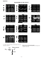
Focus Setting
Focus
: Focus setting menu
PLAY
FG1
FAST FORWARD
FAST REVERSE
FZH
FAST FORWARD
FAST REVERSE
FLn
FAST FORWARD
FAST REVERSE
FLp
FAST FORWARD
FAST REVERSE
FTS
FAST FORWARD
FAST REVERSE
FSB
FAST FORWARD
FAST REVERSE
FTB
FAST FORWARD
FAST REVERSE
TO1
FAST FORWARD
FAST REVERSE
TOR
* When the [STOP ] button is pressed in specific menu, the "TEST MODE STOP" state is set.
* When the [MENU] button operation is performed in the specific state, the menu changes to
"TEMP SETTING menu".
* In specific state the setting changed in the range of "00h to FFh" when the [VOL.+/–] button
is pressed.
(The upper limit varies depending on the items)
* When the [ENTER] button is pressed in each state, the set digit is changed.
Spin Setting
S p i n
: Spin setting menu
PLAY
SPG
FAST FORWARD
FAST REVERSE
SPi
FAST FORWARD
FAST REVERSE
SPm
FAST FORWARD
FAST REVERSE
SPo
FAST FORWARD
FAST REVERSE
SD1
FAST FORWARD
FAST REVERSE
SD2
FAST FORWARD
FAST REVERSE
SPK
FAST FORWARD
FAST REVERSE
SPW
FAST FORWARD
FAST REVERSE
SPB
FAST FORWARD
FAST REVERSE
SRi
FAST FORWARD
FAST REVERSE
SRm
FAST FORWARD
FAST REVERSE
SRo
FAST FORWARD
FAST REVERSE
SBR
FAST FORWARD
FAST REVERSE
OSL
FAST FORWARD
PJG
FAST REVERSE
* When the [STOP ] button is pressed in specific menu, the "TEST MODE STOP" state is set.
* When the [MENU] button operation is performed in the specific state, the menu changes to
"TEMP SETTING menu".
* In specific state the setting changed in the range of "00h to FFh" when the
[VOL.+/–] button is pressed.
(The upper limit varies depending on the items)
* When the [ENTER] button is pressed in each state, the set digit is changed.
– 21 –
MD-MT180
Tracking Setting
T r a c k
: Tracking setting menu
PLAY
TG1
FAST FORWARD
FAST REVERSE
FAST FORWARD
TBo
FAST FORWARD
FAST REVERSE
FAST FORWARD
FAST REVERSE
FAST FORWARD
FAST REVERSE
FAST FORWARD
FAST REVERSE
FAST FORWARD
FAST REVERSE
FAST FORWARD
FAST REVERSE
FAST FORWARD
FAST REVERSE
TOG
SCt
FAST FORWARD
FAST REVERSE
TOP
TDt
FAST FORWARD
FAST REVERSE
THG
TDo
FAST FORWARD
FAST REVERSE
THP
TKt
FAST FORWARD
FAST REVERSE
K10
TKo
FAST FORWARD
FAST REVERSE
JPI
TBt
FAST FORWARD
FAST REVERSE
CLr
FAST REVERSE
FAST FORWARD
CLp
FAST REVERSE
T1P
* When the [STOP ] button is pressed in specific menu, the "TEST MODE STOP" state is set.
* When the [MENU] button operation is performed in the specific state, the menu changes to
"TEMP SETTING menu".
* In the specific state the setting changes in the range of "00h to FFh" when the [VOL.+/–] button
is pressed. (The upper limit varies depending on the items)
* When the [ENTER] button is pressed in each state, the set digit is changed.
Sled Setting
S l e d
: Sled setting menu
PLAY
SKS
FAST FORWARD
FAST REVERSE
FAST FORWARD
SKL
FAST FORWARD
FAST REVERSE
FAST FORWARD
SLC
FAST FORWARD
FAST REVERSE
FAST FORWARD
FAST REVERSE
FAST FORWARD
FAST REVERSE
FAST FORWARD
FAST REVERSE
FAST FORWARD
FAST REVERSE
FAST FORWARD
FAST REVERSE
FAST FORWARD
FAST REVERSE
BRE
FAST REVERSE
FAST FORWARD
SRV
FAST FORWARD
FAST REVERSE
BP1
WTm
FAST FORWARD
FAST REVERSE
BPW
SJP
FAST FORWARD
FAST REVERSE
BPE
SDV
FAST FORWARD
FAST REVERSE
SDE
STE
FAST FORWARD
FAST REVERSE
SKE
STM
FAST FORWARD
FAST REVERSE
SLS
STL
FAST FORWARD
FAST REVERSE
MVS
FAST REVERSE
BRW
FAST REVERSE
FAST FORWARD
FAST REVERSE
SRS
SLT
* When the [STOP ] button is pressed in specific menu, the "TEST MODE STOP" state is set.
* When the [MENU] button operation is performed in the specific state, the menu changes to
"TEMP SETTING menu".
* In the specific state the setting changes in the range of "00h to FFh" when the
[VOL.+/–] button is pressed.
(The upper limit varies depending on the items)
* When the [ENTER] button is pressed in each state, the set digit is changed.
– 22 –
MD-MT180
TEMP Setting
Temp
: Temp setting menu
PLAY
TM§§
FAST FORWARD
T p i n
: TEMP reference
: Reference
§ § : Temperature code
FAST REVERSE
: TEMP A/D input value
: Measurement value
* When the [STOP ] button is pressed in specific menu, the "TEST MODE STOP" state is set.
* When the [MENU] button operation is performed in the specific state, the menu changes to
"TEMP SETTING menu".
* In the specific state the setting changes in the range of "00h to FFh" when the
[VOL.+/–] button is pressed.
* When the [ENTER] button is pressed in each state, the set digit is changed.
Adjustment Setting
ADJSET
: Adjustment setting menu
PLAY
COK
FAST FORWARD
FAST REVERSE
FAB
FAST FORWARD
FAST REVERSE
HSG
FAST FORWARD
FAST REVERSE
LSG
* When the [STOP ] button is pressed in specific menu, the "TEST MODE STOP" state is set.
* When the [MENU] button operation is performed in the specific state, the menu changes to
"TEMP SETTING menu".
* In the specific setting display state the setting change digit changes when the [ENTER]
button is pressed.
1st digit (initial value)
2nd digit
ENTER
ENTER
* In the specific state the setting changes in the range of "0h to Fh" when the [VOL.+/–]
button is pressed.
* When the [ENTER] button is pressed in each state, the set digit is changed.
– 23 –
MD-MT180
Control Setting
CTRL
: Control setting menu
PLAY
CT0
FAST FORWARD
FAST REVERSE
CT1
FAST FORWARD
US2
FAST REVERSE
FAST REVERSE
CT2
FAST FORWARD
FAST REVERSE
FAST REVERSE
CT3
FAST FORWARD
FAST REVERSE
FAST REVERSE
FAST REVERSE
FAST REVERSE
FAST REVERSE
FAST REVERSE
FAST REVERSE
FAST REVERSE
FAST REVERSE
FAST REVERSE
FAST REVERSE
FAST REVERSE
FAST REVERSE
FAST REVERSE
FAST REVERSE
FAST REVERSE
FAST REVERSE
FAST REVERSE
FAST REVERSE
FAST REVERSE
FAST REVERSE
FAST REVERSE
FAST REVERSE
FAST REVERSE
FAST REVERSE
FAST REVERSE
CST
FAST FORWARD
MCT
FAST REVERSE
FAST REVERSE
BEC
FAST FORWARD
FAST FORWARD
ERC
BMK
FAST FORWARD
FAST FORWARD
CV0
BD1
FAST FORWARD
FAST FORWARD
CV1
BD0
FAST FORWARD
FAST FORWARD
SSK
BU0
FAST FORWARD
FAST FORWARD
ACT
BS1
FAST FORWARD
FAST FORWARD
C1E
BS0
FAST FORWARD
FAST FORWARD
ADE
BHS
FAST FORWARD
FAST FORWARD
FG2
FBO
FAST FORWARD
FAST FORWARD
TG2
SDF
FAST FORWARD
FAST FORWARD
MFP
RCE
FAST FORWARD
FAST FORWARD
SPM
PLE
FAST FORWARD
FAST FORWARD
MSL
USA
FAST FORWARD
FAST FORWARD
US0
TSA
FAST FORWARD
FAST FORWARD
US1
FAST FORWARD
IJD
FAST REVERSE
FAST REVERSE
FAST REVERSE
FAST FORWARD
– 24 –
IJU
FAST FORWARD
MD-MT180
MD ERROR MESSAGE DISPLAY CONTENT LIST
Display content
Error code
Error content
Can' t READ*
Readout of the information is not
completed.
Can' t READ*
Readout of the TOC information
is not completed.
Can' t READ*
Readout of the U-TOC information
is not completed.
Can't LOCK
The EJECT lever cannot be locked.
Er-MD41
Judged it abnormal by the U-TOC
write test.
Er-MD80
EEPROM readout Check sum error
TOC FORM**
Abnormal data DISC detection
NAME FULL
The number of characters for names
exceeds the specification limit.
OPEN
The disc compartment is open.
f: Focus error
r: READ ERR
s: Search time over
w: SD write time over
p: Time over at spindle start-up
L*: UTOC SELECTOR is Loop
a_: Address abnormal
t_: FTNO > LTNO
Remarks
* indicates the detailed factor.
* indicates the detailed factor.
Open lid is detected while the
system is running.
– 25 –
MD-MT180
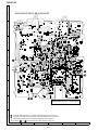
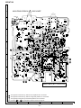
NOTES ON SCHEMATIC DIAGRAM
• Resistor:
To differentiate the units of resistors, such symbol as K and
M are used: the symbol K means 1000 ohm and the symbol
M means 1000 kohm and the resistor without any symbol is
ohm-type resistor. Besides, the one with “Fusible” is a fuse
type.
• Capacitor:
To indicate the unit of capacitor, a symbol P is used: this
symbol P means micro-micro-farad and the unit of the
capacitor without such a symbol is microfarad. As to electrolytic capacitor, the expression “capacitance/withstand voltage” is used.
(CH), (TH), (RH), (UJ): Temperature compensation
(ML): Mylar type
B
(G)
(3)
E
(S)
1
TOP VIEW
TOP
VIEW
DESCRIPTION
REF. NO
EJECT
OFF—ON
SW403
LID OPEN
OFF—ON
SW601
DISC PROTECT
OFF—ON
TOP VIEW
S
TOP
VIEW
MA132WK
TOP VIEW
F10J2E
F05J2L
G
D
2SJ520 TL
TOP VIEW
XP01401
HRB0103B
RB731U
SBE803
Figure 26 TYPES OF TRANSISTOR AND DIODE
– 26 –
POSITION
SW401
C
(D)
(2)
2SB1462 J
2SD1819 AS
DTC123 TKA
KTA2015 Y
MCH3409
UN5210
UN5213
TOP VIEW
• The indicated voltage in each section is the one measured
by Digital Multimeter between such a section and the chassis with no signal given.
• Parts marked with “
”(
) are important for
maintaining the safety of the set. Be sure to replace these
parts with specified ones for maintaining the safety and
performance of the set.
M901
SPINDLE
MOTOR
M902
SLED
MOTOR
M903
LIFT
MOTOR
M
M
M
+2.5V
+2.5V
IC651
LB1930M
MOTOR
DRIVER
+2.5V
IC101
IR3R58M
RF SIGNAL
PROCESSOR
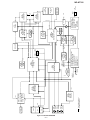
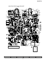
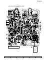
Figure 27 BLOCK DIAGRAM
– 27 –
+4.5V
BATTERY
(1.2V)
CHARGING
TERMINAL(1.5V)
4.5V
REGULATOR
IC873
6204B45M
+2.5V
FG
IC253,260,809 XP04313
IC256 XP04315
IC258,259,892 XP04501
Q250,Q251,Q257
IC251 FTD2017 N-CH MOS FET
IC255 NJM022V OPE AMP.
IC257 S80808LN RESET
SPIN
VCCMICOM
+2.5V
REGULATOR
IC902
62FP1602
IC841
6372C251
2.5V UP
CONVERTER
VGBATT
F841
0.4A,DC60V
IC601
LV8201W
PWM/MOTOR DRIVER
+2.5V
+2.5V
IC201
LR378161
ENDEC/SERVO/
ATRAC
IC202
IX2824AF
16M BIT
D-RAM
+2.5V
LCD UNIT
IC871
74HC1G86
EXCLUSIVE
OR GATE
IC852
IR3M14N
DC/DC
CONVERTER
Q851
IC802 XP04501
Q801,Q803,Q891
–2.5V
PS801
1.1A
–2.5V
J801
DC-IN (5V)
SW401 EJECT
SW403 LID OPEN
KEY SWITCH
PWB
J703A
HEADPHONES
IC703
IR3R59N
AUDIO AMP.
+2.5V
IC701
IR3R54N
AUDIO AMP.
IC801 MM3032A
3.0V REGULATOR
IC803 S80819LN
RESET
Q461
+2.5V
+2.5V
IC431
S80820LN
RESET
IC401
IX0529AW
SYSTEM
MICROCOMPUTER
IC402
58X2402T
EEPROM
IC771
6204B23M
2.3V
REGULATOR
IC501
AK4551VT
AD/DA
CONVERTER
+2.5V
J701
OPTICAL/
LINE-IN
VCC+2.5V
PLAYBACK SIGNAL
RECORD SIGNAL
T
F
PICK
OPIC
LASER
OPTICAL PICUP
MAGNETIC
HEAD
IC353 MCH6616
IC354 CPH5608
HEAD DRIVER
IC351 74ACT02T
+4.5V
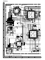
MD-MT180
PCNT1
MD-MT180
MAIN PWB-A
R206
100K
+B
VCCDRAM CK200
L202
10µH
C201
10/6.3
TP407
R413
1K
PLVO
TP415
TP401
TEMP
R424
22K
R423
22K
DINT
AURESET
1
TP441
TP610
+B
3
2
4
D431
MA132WK
IC431
S80820LN
C431
0.47
R431
330K
2 VDD
4
VSS
3
RESET
M903
LIFT
MOTOR
D461
RB731U
3
4
2
5
1
6
• NOTES ON SCHEMATIC DIAGRAM can be found on page 26.
• The numbers 1 to 15 are waveform numbers shown in page 44.
4
Figure 28 SCHEMATIC DIAGRAM (1/4)
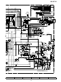
– 28 –
5
6
D467
1SS389
R467
22K
L603
22µH TRDRR
TRDRF
FODRR
FODRF
VCC4R5
+B
SW403
LID OPEN
C604
1
SLCNT1
SLCNT2
SLCNT3
L604
22µH
C602
1
C601
1
L601
22µH
IC601
LV8201W
PWM/MOTOR DRIVER
3
+
C603
1
L602
22µH
M
2
C13
0.1
PLVBA
SPDRR
DCNT1
H
1
CHGC
HKEY
HKEY
RKEY
R402
100K
RPLAY
XL401
4.19MHz
CK403
EMPH0
BEEP
TP400
TP402
C613
1
CHG
C401 LDVAR
0.1
R425
22K
78
77
76
SW401
EJECT
SPIN
CIN
DSPSTB
DISCPR
DSPDAT
RMDAT
VSS
LCDRST
SPWDS
DISCPR
SYWR
SYRD
SYRS
PE4
VSS
EPRT
EEPK
EEPD
EPCS
DSPSCK
SCK0
DSPSTB
48 RADAT
49 VSS
50 DLBHP
1 OUT
+
–
MECHANISM
FLEXIBLE PWB (19)
IC401
IX0529AW
SYSTEM
MICROCOMPUTER
R466
560K
M
1
2
3
PCN
PCN
TP406
R406
10K
CK405
XRT
R405
10K
FOK
SENSE
100
99
98
97
96
95
94
93
92
91
90
89
88
87
86
85
84
83
82
81
80
79
78
77
76
R463
100K
C454
0.0022
R464
220K R465
100K
M901
SPINDLE
MOTOR
1
PCNT1
PCNT2
VCC
EJSW
CKSTP
CIN
XRST
FOK
SPIN
RFPCNT SENSE
DCNT1
PLVON
MCMON
CHGON
VSS
AVSS
LDVAR
CHGCNT
HKEY2
Vref
HKEY1
AVCC
RKEY
TEMP
ARQK
CHIMON
PLVBAT
R461
100K
COM
W
V
U
R605
1M
1
L605
22µH
23 SYD0
24 SYD1
25 SYD2
4
3
2
51 52 53 54 55 56 57 58 59 60 61 62 63 64 65 66 67 68 69 70 71 72 73 74 75
+B
C617
0.0047
C618
0.0047
C608 C619
1
0.0047
C611
0.1
M902
SLED
MOTOR
C620
0.0068
C621
1
R602
120K
R603
330K
GND1
PWM
C612
0.1
CN601
U
W
V
M
32 31 30 29 28 27 26 25 24 23 22 21 20 19 18 17
MUTE 16
NC 15
SEL
OUT2R 14
VS3
VS2 13
OUT3
17 S/S OUT2F 12
PGND3
SWO
18 BRK PGND2 11
PGND4
19 VCO PGND1 10
OUT1F 9
SVO
VS1 8
VS4
OUT1R 7
SUO
GND2 6
FG
IN2R 5
VCC2 49 CP2 63 WCIN
50 CP1 64 COMIN
IN2F 4
IN3
IN1R 3
S3
S2
IN1F 2
S1
COM 1
49 50 51 52 53 54 55 56 57 58 59 60 61 62 63 64
C605
1
C615
1
11
33
34
35
36
37
38
39
40
41
42
43
44
SLCNT3 45
SLCNT2 46
SLCNT1 47
48
CPC1
CPC2
VG
RF
VS
WOUT
VOUT
UOUT
VS
RF2
UCIN
VCIN
TP661
TP660
TP659
TP658
TP657
TP656
TP655
TP654
TP653
TP652
TP651
R610
1
R604
100K
SYD3
SYD4
SYD5
SYD6
SYD7
VSS
RCLAT
MCPGI
INPGI
INPGCK
RCPCNT
TEST1
TEST0
JPNP
VCC
OPICGA
PBOPON
PBLAT
LDON
DISCP
SGAIN
RACLK
+B
VCREF
VCTL
RMIN
RMAX
VCOIN
VCC1
SPDRF
R611
1
F
MAGNETIC
HEAD(20)
SPDRF
SPDRR
TP411
TP409
R411
100K
DSPSCK
13
+B
11 10 9 8 7 6 5 4 3 2 1
TP410
SLCNT1
SLCNT2
SLCNT3
DHLAT
EMPH0
BUZOUT
MD0
MD1
DCEXT
WDT0VF
MD2
RESET
NMI
µSTBY
VCC
XTAL
EXTAL
VSS
PLAY
REC
STOP
PF4
DINT
ARQD
RPLAY
1
3
2
C652
0.1
SW601
DISC
D651 PROTECT
F10J2E
TP602
OPICGA
PBMUTE
PBAULT
LDON
DISC
SGAIN
26
27
28
29
30
31
32
33
34
35
36
37
38
39
40
41
42
43
44
45
46
47
48
49
50
AUSCLK
AUDATA
5
4
3
2
1
R403
1K
LDCNT2
LDCNT1
6 G G
7 O2 I2
8
I1
9 O1
10 VCC
TP665
+B
R422
100K
IC651
LB1930M
MOTOR
DRIVER
TP416
TP417
DISCPR
R361
15
R404
100K
SPIN
123
RCAULT
MCPGIN
INPGIN
INPGCK
IC353
MCH6616
HEAD
DRIVER
G
4
3
2
1
R414
1K
R415
1K
IC351
74ACT02T
HEAD
DRIVER
VCCHEAD
D1 G1
S
D2 G2
C351
47P
(CH)
C361
0.039
6 54
S1 D1
G1 G2
D2 S2
D351
SBE803
3
4
2
1
5
TP351
IC354
CPH5608
HEAD DRIVER
2
IC402
58X2402T
EEPROM
R412
15K
5
TP408
6
7
TP411A
8
DSPDAT
R920
100K
Q901
UN5210
C353
10/6.3
1
VCC2R
25 24 23 22 21 20 19 18 17 16 15 14 13 12 11 10 9 8 7 6 5 4 3 2 1
+B
IC2
IX282
16M B
D-RA
C100
10/6.3
R416
1K
+B
EFMO
E
SYD2
SYD1
SYD0
SYWR
SYRD
SYRS
HDON
SYD7
SYD6
SYD5
SYD4
SYD3
+B
543
C202
33/6.3
+B
+B
C354
0.1
A8
A7
A6
7 A10
8 A0
9 A1
A5
10 A2
A4
11 A3
12 VCC GND
L171
10µH
OPTICAL PICKUP (1)
D
VCC GND
I/O1 I/O4
I/O2 I/O3
WE CAS
OE
RAS
A9
L100
10µH
+B
R205
27K
TP171
1
2
3
4
5
6
+B
TP201A
TP201
OPIC
C357
0.1
TP205
C207 C209
0.1
0.1
+B
EFMO
12
22
GND
8
7
9
6
10
5
4
11
3
12
2
13
14 VCC
1
LDCNT2
LDCNT1
CK207
TP204
R222
1M
L204
1 2 3 4 5 6 7 8 9 10 11 12 13 14 15 16 17 18 19 20 21 22 23 24 25
IC201
LR378161
ENDEC/SERVO/
ATRAC
+B
C172
33/6.3
LDVAR
LDON
DGND
DGND
VCC
B
A
COM
CVCC
MP/R
RF2
AGND
VCC
RF4
RF3
E
F
RF1
T+
F+
T–
F–
9
C121
220P
(CH)
TP212
CK225
50
49
48 CK224
47 TP203
46 CK222
45
44
43
42
41
40
39
38
37
36
35
34
33
32
31
30
29
28
27
26
TP207
FODRF
FODRR
TRDRF
TRDRR
C204 CK211
0.47
CK100
R101
22K
R102
22K
2
LDON
LDVAR
OPICGA
R161
1.2K
F–
F+
T+
T–
C165
0.033
C122
220P
(CH)
+B
C171
33/6.3
TP110
TP111
TP114
TP115
TP116
TP117
TP118
TP119
TP120
L101
100mA
TP105
TP106
TP107
TP108
TP101
TP102
TP103
TP121
TP122
1 2 3 4 5 6 7 8 9 10 11 12 13 14 15 16 17 18 19 20 21 22
1
80
81
82
83
84
85
DINT CK206 86
R204 C203 87
0.1
1K
88
XRT
89
SYD0
90
SYD1
91
SYD2
92
SYD3
93
SYD4
94
SYD5
95
SYD6
96
SYD7
97
SYWR
98
SYRD
99
SYRS
100
CK204
FOK
SENSE
CIN CK205
4
3 +B
R140
390K
76
77
78
TP210 79
10
R139
39K
C212
8P (CH)
75 74 73 72 71 70 69 68 67 66 65 64 63 62 61 60 59 58 57 56 55 54 53 52 51
EFMO
TEMON
PLCK
ACRCER
HDON
OPTCNT
RAA11
DAPON
RAD0
51 X700KO
73 ADDATA
ADPON
RAD1
52 TCRS
74 DADATA
FOK
RAWEX
53 TEST0
75 FEMON
SENSE
RARASX
COUT
RAA9
54 TEST1
76 TOTMON
MCCK
RAD3
DINTX
RAD2
VDD2
RACASX
DGND
DGND
RSTX
RAOEX
SYSD0
RAA8
SYSD1
RAA7
SYSD2
RAA6
98 SYWRX
23 SLDRR
SYSD3
RAA5
99 SYRDX
24 SPDRF
SYSD4
RAA4
VDD2
SYSD5
100 SYRS
25 SPDRR
SYSD6
RAA10
RAA0
SYSD7
RAA1
RAA2
RAA3
C205
0.1
TP206
CK209
CK210
+B
CN101
TP208
TP209
11
DFCK
BCLK
LRCK
DGND
PLLBVC
DOUT
DIN
X1O
X1I
DGND
VDD1
VPO
VXI
EMPH
LDCNT2
LDCNT1
LEDON1
DILOCK
14
CK208
EFMMON
AVCC
EFMI
AGND
AVCC2
VREF
WBI
TCG
AIN
BIN
EIN
FIN
VBAT
VDD1
DGND
TEST2
X176KO
FODRF
FODRR
TRDRF
TRDRR
SLDRF
25
1
CK108
SGAIN
TEMP
26
15
C
XL201
33.8688MHz
C211
5P(CH)
100mA
R207
680
CK201
+2.5V
ADIP
AGC
34
ADAGI
ADAGC
C133
0.22
TP130
TP131
TP132
TP133
R137
56K
R138
390K
R136
390K
35
DTEMP
RFADD
AOUT
BOUT
TCGO
TCGI
EOUT
FOUT
FIN
FSW
EIN
EOU
ESW
13 14 15 16 17 18 19 20 21 22 23 24
R135
56K
BOUT
R133
12
120K
CK203
CK202
C131
0.1
C221
22P
(CH)
36
C132
33 ADIPNF 0.22
ADIPO
32
GND2
31
WBO
C113
30
1
VCC2
+B
29
OPICPW
SW 28
CK102 DISC
MODE
27
10 BIN
BSW
11
TP202
CK139
BPF
3+4
PITG
NIN
1+2
PIN
2-1
R132
820K
R134
820K
B
+B
EFMO
48 47 46 45 44 43 42 41 40 39 38 37
BIAS
RF1
1
R
RF2
2 and
RF3
3
DIFF
SW
C102 RF4
4
1
REFI
5
TP144
6
REFO
AOUT
BIAS
7
R131 ASW
8
120K AIN
9
C103
1
220K
VCC1
C110
EFMAGC 0.22
C108
DCNF
1
C107
0.033
C106
1
1234
PLAYBACK SIGNAL
RECORD SIGNAL
C109
1
GND1
R112
C112
0.033
IC101
IR3R58M
RF SIGNAL
PROCESSOR
R111
12K
C114
5P(CH)
A
C111
1
+
MD-MT180
R456 R457
5.6K 8.2K
HKEY2
R458
18K
HPLAY
DADATA
ADDATA
DFCK
HKEY1
STOP
DSPDAT
TP481
DSPSCK R481
TP482
DSPSTB 33K C482 TP483
0.01 TP484
TP485
R483 R482
18K 18K
TP487
1
R718
1K
C711
100P
(CH)
R728A
10K
C714
1
C712
100P(CH)
C733
0.1
C734
0.1
AGND
C701
10/6.3
R701
100
D496
MA8075M
IC703
IR3R59N
AUDIO AMP.
4
L-CH
2
R-CH
3
1
J703A
HEADPHONES
HREC
HPLAY
R467
22K
7
STOP
D281
MA111
+B
PCNT2
PLVBAT
CHGON
PLVON
CHGCNT
TP805
L801
100MHZ
R810
1
VCCBATT
4
2 VDD
3
C254
0.1
C
,
B
EXCEPT FOR
MAIN PWB VERSION
C866
0.1
C867
0.1
TP803
TP804
VSS
RESET
R272
100
C291
1
D251
MA111
R250
100
1 OUT
C864
0.1
C865
0.1
R257
27K
6 54
123
R271
68K
C255
0.1
IC253,260,809 POWER SELECT CHARGE DRIVER
IC256 DIGITAL TRANSISTOR
IC258,259,802,892 POWER TRANSISTOR
+B
8
9
10
Figure 29 SCHEMATIC DIAGRAM (2/4)
– 29 –
11
12
BATTERY
BATTERY
TERMINAL(211) TERMINAL(227)
D802
MA8051M
R808
1
IC256
XP04315
1234
IC257 +B
S80808LN
C252
0.1 R252
150K
Q251
2SD1819 AS
R292
100K
J801
DC-IN
5V
CHARGING
TERMINAL(226)
TP806
D803
1SS388
C801
1
R296
47K
R291
100
R254
R255 C253
4.7K 0.1 22K
C251
0.1
8 7 6 5 R253
39K
R261
1K
R262
120K
R269
39K
R802
Q891
XP01401 560
R462
27K
IC809
XP04313
R251
100
R288
47K
R806
56K
1 OUT 4
VSS
2 VDD 3
R270
68K
IC260
XP04313
+B
D467
1SS389
3
2
1
6
5
4
O V+
– O
+ –
V- +
R284
R287
390K 560K
+B
CK809
6
5
4
4
5
6
R282
1M
5
+B
IC255
NJM022V
OPE AMP.
TP860
Q257
2SB1462J
1
2
3
321
1
TP801
TP802 2
3
IC251
FTD2017
N-CH MOS FET
IC892
XP04501
1
2
3
R293
680
CK805
L800
100MHz
IC803
IC801
S80819LN
MM3032A
RESET
3.0V REGULATOR
R267 R266
10K 47K
R283
100K
R279
100
3
2
1
1
6
5
4
R818
560K
C818
0.1
G1 4
5 G2
S1 3
6 S2
S1 2
7 S2
D1
8 D
XP04313
IC258
XP04501
VCCMICOM
+B
C860
10/6.3
4
5
6
2
4
R286
2.2K
R819
22K
TP841
VGBATT
IC259
XP04501
L860
100µH
C802
0.01
C840
220/4
R850
100K
1
2
3
R803
1.2K
4
3
D801
F05J2L
PS801
1.1A
+B
R813
10K
Q250
KTA2015 Y
R294
100K
R295
100K
IC253 R281
22K
4
3
2
5
1
6
C841
1
4
TP842
L841
22
C847
0.1
IC873
6204B45M
4.5V REGULATOR
SW403
LID OPEN
C842
33/6.3
C850
0.1
C846
R844
47
5
4
R256
56K
C851
1
D843
D842
C845
HRB0103B HRB0103B 0.1
D841
F10J2E 1
2
3
F841
0.4A,DC60V
C259
0.1
3
2
1
VCC
R277
39K
5
STAND 2
BY
CTRL 1
DC/DC
CONVERTER
C848
0.1
C837
1
+B
C836
1
4
VCC4R5
3 OUT
C830
1
8 ROSC
IC841
6372C251
2.5V UP
CONVERTER
4
C843
0.22
7 EIP
R853
270K
GND
0.1
C839
0.33
R857
330K
RKEY
R423
22K
5 EO ERRAMP
6 EIN
VREF
+B
IC852
IR3M14N
BUF
CMP
Q R
OSC
RSFF S
C856
R831 68P
180K (CH)
DINT
R832
180K
R424
22K
R855
390K
+B
C857
R854 18P
10K (CH)
3
R816
1.5K
Q803
UN5213
+B
S
R856
3.3M
R466
560K
LIHP
VEE
Q461
2SD1819 AS
R814
10K
R871
100K
L821
10µH
DCVDD
R285
100K
R891
47K
G
+B
C821
1
D821
M1FH3
R460
68K
Q801
2SJ520 TL L802 R809
100MHz 1
+B
S
D
IC802
R807
XP04501 G 22K R811
1
R812
1
6
10K
2
5
C876
1
EXCLUSIVE
OR GATE
Q851
MCH3409
S
D
L851
10µH
G
C852
22/6.3
C853
220/4
R892
10K
+B
D861
C862 F10J2E
1
D
VCC 5
1
2
3 GND
4
R815
10K
-2R5
+2.5V
D851
M1FH3
CHGCNT
HKEY2
HKEY1
C130
0.1
PLVBAT
R425
22K
C863
1
PCNT1
Q821
MCH3409
TEMP
C454
0.0022
R464
220K R465
100K
LOUT
ROUT
C765 C766
0.22 0.22
+B
IC871
74HC1G86
D862
F10J2E
CHGON
C401 LDVAR
0.1
D461
RB731U
3
4
2
5
1
6
C492
1
R–
R766
15
C761
2.2
LHPVCC
PBAULT
AURESET
C753
1
L452
TP729 150mA
TP722
TP724
100mA TP723
L454
L453
100mA
R767
L-CH 4.7
R-CH
R768
4.7
R765
15
+B
PLVON
TP415
TP401
R402
100K
R+
LLPFO
SW401
EJECT
1
PCNT1
PCNT2
TP406
R406
10K
CK405
XRT
R405
10K
FOK
SENSE
4
R703
100K
13 14 15 16 17 18 19 20 21 22 23 24
+B
1
LPF
AMPuGAIN SEL.
LHPVEE
LPF
RIN
ATT
RLPFO
RHPVEE
AMPuGAIN SEL.
LIN
ATT
C760
0.1
PBMUTE
BEEP
RCAULT
AUSCLK
AUDATA
EMPH0
C869
47/6.3
TP407
R413
1K
TP772
LI
RI
D495
MA8075M
R762
100K
R761
150K
HP
RHPVCC
BIAS
LOGIC
LAT
+B
12 11 10 9 8 7 6 5 4 3 2 1
C771
33/6.3
+2.5V
TP771
DCNT1
2.3V
REGULATOR
BEEP
C774
1
4
C754
1
+B
5
R757
2.2K
R758
100
C773
0.22
C758
1
DAT
1
2
3
C762
2.2
R754
150K
TP412
6204B23M
+B
RIHP
INPGCK
INPGIN
MCPGIN
8
7 IC771
J701
OPTICAL/
Q711
LINE-IN
TP706
DTC123 TKA
7
TP708 9 VCC
C715
0.1
Vout
TP707 8
GND
C713 R713
10K TP701
1
1
L-CH
L702TP702 2 L
TP703 3
R-CH
L703
R
TP704 4
R715
GND
100K
L704
5
R716
TP705
C716
100K
0.1 R714
10K
L702~704:100mA
R711
6.8K
7 6 5 4 3 2 1
R702
22
C702
10/6.3
6
R712
6.8K
DGND
VCC
13 14 15 16 17 18 19 20 21 22 23 24
L+
9 10 11 12 13 14 15 16
+2.5V
+B
12 11 10 9 8
+B
CLK
IC501
5
SDTI SDTO
LRCK DEM1
MCLK DEM0
SCLK VDD
PWAD VSS
PWDA AINL
AOUTL AINR
AOUTR VCOM
8 76 54321
TP500
VCCADDA
C551 C503
0.022 3.3/10
R502 C510
470 2.2
C502
0.0022
R719
6.8K
L–
C501
0.0022
IC202
IX2824AF
16M BIT
D-RAM
IC701
IR3R54N
AUDIO AMP.
R501C509
470 2.2
C511
1
R717
1K
+B
R720
6.8K
IC501
AK4551VT
AD/DA
CONVERTER
3
2
LCD
DRIVER
+B
+B
VCC2R5V
TP402
1
C481 CN482
0.1
+B
100
99
98
97
96
95
94
93
92
91
90
89
88
87
86
85
84
83
82
81
80
79
78
77
76
1
2
3
4
5
6
7
3
+2.5V
A8 18
7 A10
A7 17
8 A0
A6 16
9 A1
A5 15
10 A2
A4 14
11 A3
12 VCC GND 13
C202
33/6.3
4
KEY SWITGH
FLEXIBLE PWB (228)
7
C703
0.01
VCC GND 24
I/O1 I/O4 23
I/O2 I/O3 22
WE CAS 21
OE 20
RAS
A9 19
VCCDRAM CK200
L202
10µH
12
IC902
62FP1602
REGULATOR
2
3
2
10
11
12
CN451
+B
1
2
3
4
5
6
R453
18K
R451 R452
5.6K 8.2K
BCLK
LRCK
ADPON
DAPON
OPTCNT
DIN
EMPH1
LCD UNIT
(229)
1 BASS
REC
MENU
DOLBY
ENTER
STOP
PLAY
SKIP DOWN
VOL DOWN
VOL UP
SKIP UP
GND
1
2
3
4
5
6
7
8
9
LCD
TP451
TP452
TP453
TP454
TP455
TP456
TP457
TP458
TP459
TP460
TP461
TP462
HREC
MD-MT180
SUB PWB-B
D2
1SS385
C3
0.1
D1
1SS385
CK13A
8 7 6 5
R1
10K
1 2 3 4 5 6 7
1 2 3 4
IC2
TC7W74FK
1413121110 9 8
A
VCC
B
QH
QA
QG
QB
QF
QC
QE
QD
Q
GND CK
IC1
74VHC164FT
C2
0.1
CK VCC
D
PR
Q
CL
GND
Q
A
B
MAIN PWB VERSION
C
,
MAIN PWB-A
R2
10K
C1
100P
(CH)
B
CKG
CK14 CK16
CKV
CK13
+B
C734
0.1
AGND
LOUT
LIHP
ROUT
RI
R762
100K
LPF
LLPFO
C492
1
R–
R+
L+
LPF
L–
RIN
ATT
AMPuGAIN SEL.
LHPVEE
C753
1
C703
0.01
R766
15
C761
2.2
LHPVCC
DAT
LAT
AURESET
R765
15
PBAULT
PBMUTE
BEEP
CLK
13 14 15 16 17 18 19 20 21 22 23 24
D496
MA8075M
C760
0.1
TP771
RCAULT
AUSCLK
AUDATA
RLPFO
RHPVEE
AMPuGAIN SEL.
LIN
ATT
BIAS
RHPVCC
HP
BEEP
12 11 10 9 8 7 6 5 4 3 2 1
LOGIC
TP772
C754
1
D495
MA8075M
C762
2.2
R761
150K
R757
2.2K
R758
100
D
R703
100K
IC703
IR3R59N
AUDIO AMP.
INPGCK
INPGIN
MCPGIN
C758
1
LI
C701
10/6.3
R701
100
+B
R754
150K
R711
6.8K
DGND
VCC
13 14 15 16 17 18 19 20 21 22 23 24
R702
22
C702
10/6.3
TP412
R712
6.8K
7 6 5 4 3 2 1
VEE
C
12 11 10 9 8
RIHP
IC701
IR3R54N
AUDIO AMP.
R720
6.8K
R719
6.8K
R767
L-CH 4.7
R-CH
R768
4.7
C765 C766
0.22 0.22
3
2
RCAULT
MCPGIN
INPGIN
INPGCK
R422
100K
TP416
TP417
OPICGA
PBMUTE
PBAULT
LDON
DISC
SGAIN
G
DSPDAT
RMDAT
VSS
LCDRST
SPWDS
DISCPR
SYWR
SYRD
SYRS
PE4
VSS
EPRT
EEPK
EEPD
EPCS
DSPSCK
SCK0
DSPSTB
23 SYD0
24 SYD1
25 SYD2
PCNT1
PCNT2
VCC
EJSW
CKSTP
CIN
XRST
FOK
SPIN
RFPCNT SENSE
DCNT1
PLVON
MCMON
CHGON
VSS
AVSS
LDVAR
CHGCNT
HKEY2
Vref
HKEY1
AVCC
RKEY
TEMP
ARQK
CHIMON
PLVBAT
1
2
3
IC401
IX0484AW
SYSTEM
MICROCOMPUTER
48 RADAT
49 VSS
50 DLBHP
78
77
76
SLCNT1
SLCNT2
SLCNT3
DHLAT
EMPH0
BUZOUT
MD0
MD1
DCEXT
WDT0VF
MD2
RESET
NMI
µSTBY
VCC
XTAL
EXTAL
VSS
PLAY
REC
STOP
PF4
DINT
ARQD
RPLAY
F
SYD3
SYD4
SYD5
SYD6
SYD7
VSS
RCLAT
MCPGI
INPGI
INPGCK
RCPCNT
TEST1
TEST0
JPNP
VCC
OPICGA
PBOPON
PBLAT
LDON
DISCP
SGAIN
RACLK
100
99
98
97
96
95
94
93
92
91
90
89
88
87
86
85
84
83
82
81
80
79
78
77
76
1
PCNT1
PCNT2
TP406
R406
10K
CK405
XRT
R405
10K
FOK
SENSE
PLVON
TP415
TP401
TEMP
RKEY
R402
100K
DINT
R423
22K
RPLAY
XL401
4.19MHz
+B
AURESET
CK403
EMPH0
BEEP
AUSCLK
AUDATA
TP400
TP402
CHGCNT
HKEY2
HKEY1
C130
0.1
PLVBAT
R424
22K
51 52 53 54 55 56 57 58 59 60 61 62 63 64 65 66 67 68 69 70 71 72 73 74 75
+B
CHGON
C401 LDVAR
0.1
R425
22K
25 24 23 22 21 20 19 18 17 16 15 14 13 12 11 10 9 8 7 6 5 4 3 2 1
26
27
28
29
30
31
32
33
34
35
36
37
38
39
40
41
42
43
44
45
46
47
48
49
50
SW401
EJECT
4
SPIN
CIN
DISCPR
DSPDAT
DSPSTB
DSPSCK
E
H
• NOTES ON SCHEMATIC DIAGRAM can be found on page 26.
1
2
3
4
Figure 30 SCHEMATIC DIAGRAM (3/4)
– 30 –
5
6
MD-MT180
D2
1SS385
8 7 6 5
R1
10K
CK VCC
D
PR
Q
CL
GND
Q
1413121110 9 8
1 2 3 4 5 6 7
1 2 3 4
IC2
TC7W74FK
C3
0.1
D1
1SS385
A
VCC
B
QH
QA
QG
QB
QF
QC
QE
QD
Q
GND CK
IC1
74VHC164FT
C2
0.1
MAIN PWB VERSION
MAIN PWB-A
R2
10K
C1
100P
(CH)
+B
OPICGA
PBMUTE
PBAULT
LDON
DISC
SGAIN
DSPDAT
RMDAT
VSS
LCDRST
SPWDS
DISCPR
SYWR
SYRD
SYRS
PE4
VSS
EPRT
EEPK
EEPD
EPCS
DSPSCK
SCK0
DSPSTB
1
2
3
IC401
IX0484AW
SYSTEM
MICROCOMPUTER
48 RADAT
49 VSS
50 DLBHP
78
77
76
100
99
98
97
96
95
94
93
92
91
90
89
88
87
86
85
84
83
82
81
80
79
78
77
76
C703
0.01
C701
10/6.3
R701
100
VEE
C761
2.2
R766
15
D496
MA8075M
LPF
C492
1
R–
R+
L+
LPF
L–
RIN
ATT
LHPVCC
DAT
CLK
LAT
AURESET
PBAULT
SW401
EJECT
C765 C766
0.22 0.22
R424
22K
CHGCNT
HKEY2
HKEY1
C130
0.1
PLVBAT
+B
RKEY
R402
100K
DINT
R423
22K
RPLAY
TP400
XL401
4.19MHz
C753
1
R767
L-CH 4.7
R-CH
R768
4.7
AURESET
CK403
EMPH0
BEEP
PBMUTE
BEEP
TEMP
TP402
AUSCLK
AUDATA
R765
15
CHGON
C401 LDVAR
0.1
51 52 53 54 55 56 57 58 59 60 61 62 63 64 65 66 67 68 69 70 71 72 73 74 75
+B
LLPFO
13 14 15 16 17 18 19 20 21 22 23 24
PLVON
TP415
TP401
R425
22K
R422
100K
TP416
TP417
23 SYD0
24 SYD1
25 SYD2
SLCNT1
SLCNT2
SLCNT3
DHLAT
EMPH0
BUZOUT
MD0
MD1
DCEXT
WDT0VF
MD2
RESET
NMI
µSTBY
VCC
XTAL
EXTAL
VSS
PLAY
REC
STOP
PF4
DINT
ARQD
RPLAY
RCAULT
MCPGIN
INPGIN
INPGCK
AMPuGAIN SEL.
LHPVEE
R703
100K
1
PCNT1
PCNT2
TP406
R406
10K
CK405
XRT
R405
10K
FOK
SENSE
25 24 23 22 21 20 19 18 17 16 15 14 13 12 11 10 9 8 7 6 5 4 3 2 1
PCNT1
PCNT2
VCC
EJSW
CKSTP
CIN
XRST
FOK
SPIN
RFPCNT SENSE
DCNT1
PLVON
MCMON
CHGON
VSS
AVSS
LDVAR
CHGCNT
HKEY2
Vref
HKEY1
AVCC
RKEY
TEMP
ARQK
CHIMON
PLVBAT
RLPFO
RHPVEE
AMPuGAIN SEL.
LIN
ATT
BIAS
RHPVCC
HP
BEEP
C760
0.1
TP771
RCAULT
AUSCLK
AUDATA
SPIN
CIN
DISCPR
DSPDAT
DSPSTB
DSPSCK
4
3
2
R762
100K
R757
2.2K
R758
100
12 11 10 9 8 7 6 5 4 3 2 1
LOGIC
TP772
C754
1
D495
MA8075M
C762
2.2
R761
150K
TP412
LI
IC703
IR3R59N
AUDIO AMP.
INPGCK
INPGIN
MCPGIN
SYD3
SYD4
SYD5
SYD6
SYD7
VSS
RCLAT
MCPGI
INPGI
INPGCK
RCPCNT
TEST1
TEST0
JPNP
VCC
OPICGA
PBOPON
PBLAT
LDON
DISCP
SGAIN
RACLK
RI
DGND
VCC
13 14 15 16 17 18 19 20 21 22 23 24
+B
C758
1
R711
6.8K
7 6 5 4 3 2 1
AGND
LOUT
LIHP
ROUT
12 11 10 9 8
R702
22
C702
10/6.3
R754
150K
R712
6.8K
C734
0.1
R719
6.8K
RIHP
IC701
IR3R54N
AUDIO AMP.
R720
6.8K
26
27
28
29
30
31
32
33
34
35
36
37
38
39
40
41
42
43
44
45
46
47
48
49
50
7
8
X
9
10
Figure 31 SCHEMATIC DIAGRAM (4/4)
– 31 –
11
12
MD-MT180
A
MAIN PWB VERSION B X0021AWZZ
SUB PWB-B is added to this version PWB.
SUB PWB-B is shown in page 36,37.
J701
OPTICAL/LINE-IN
J703A
HEADPHONES
SW403
LID OPEN
TP705
B
TP701
TP711
TP703
TP727
TP725 TP722
TP724
J801
DC-IN
5V
TP801
TP712
TP721
TP726
TP704
TP723
TP706
TP702
SW601 TP665
DISC PROTECT
TP708
TP802
TP714
TP707
TP713
TP729
TP806
TP455
TP772
C
TP459
TP6
R857
IC771
C851
TP656
Q851
C863
TP415
C837
TP661
D843
XL201
TP202
C860
TP411
C212 L860
C211
TP204
TP208
TP210
TP209
SW401
EJECT
R222
75
51
70
76
TP417
65
60
55
3
C845
TP651 TP652
TP115
95
24
1
TP132
TP131 TP130
10
100
15
25
TP144
TP118
1
TP201
5
C207
TP103
20
TP658
TP207
C205
R205
L202
12
TP171
10
15
12
C202
TP410
IC202
R206
TP110
C209
5
26
20
TP117
TP108
2
30
TP106 TP102
TP114
TP133
TP107
5
D841
TP841
TP122
35
C203
1
F
IC201
TP119
C204
3
TP111
40
90
4
TP842
TP120
TP655
R204
TP116
TP803
R850
C850
TP416
2
C843
TP653
TP205
45
85
1
C842
IC841
50
80
TP406
TP351
TP660
TP212
TP408
TP401
TP101
TP400
R844
TP409
TP407
C201
1
C847
D842
IC902
1
TP452
TP441
E
5
C848
TP402
TP412
C840
L851
3
L841
D861
D862
R891
R892
1
4
F841
0.4A,DC60V
TP456
TP659
R853
TP481
C862
C853
TP461
TP485
C821
D
4
IC852
R832
8
C839
TP657
5
TP458
TP500
R856
4
TP610
C830
R854
5
TP121
C774
TP860
C857
TP654
TP482
IC873
L821
R831
TP454
C846
1
TP484
C841
3
D851
Q821
C773
TP602
C852
TP451
TP462
TP483
TP804
C836
TP457
TP7
Q801
TP460 TP805
TP453
TP487
D821
TP771
R855 C856
TP5
13
TP105
TP206
9
G
10 11
MAIN PWB-A (BOTTOM VIEW)
H
: Through-hole where the top, bottom and +B patterns are connected.
: Through-hole where the top, bottom and ground patterns are connected.
: Through-hole where the top and bottom patterns are connected.
• The numbers 1 to 15 are waveform numbers shown in page 44.
1
2
3
4
Figure 32 WIRING SIDE OF P.W.BOARD (1/11)
– 32 –
5
6
15
MD-MT180
MAIN PWB VERSION B X0021AWZZ
SUB PWB-B is added to this version PWB.
SUB PWB-B is shown in page 36,37.
J703A
HEADHONES
J701
OPTICAL/LINE-IN
SW403
LID OPEN
R701
L453
R464
R766
C754
R757
C753
D496
R461
R465
C510
R501
37
36
C131
CK203
C511
C551
R261
R262
R250
R255
R253
R252
C252
3
D251
D281
4
1
3
5
1
IC251
6
4
2
R285
6
4
C612
R256
R293
C100
4
Q250 Q251
C864
R139
R287
1
6
3
4
6
1
CHASSIS
GND
C172
6
3
1
C865
C171
1
3
4
R288
4
C259
3
6
1
4
6
1
C106 R272
8
3
C253
R254
C254
C255
R266 IC431
R269
R267
R270
8
R281 3
IC258
35
5
Q257
30
L204
C502
40
IC256
C114
R131
25
C110
IC255
1
4
SW401
EJECT
2
4
IC253
C130
C615
24
TP201A
C113
CK200
R610
C611
R611
48
35
20
45
C107
5
1
C133
OPTICAL
PICKUP (1)
L100
33
IC101
48
R140
L171
49
45
5
R271
3
CK809
1
IC260
30
10
C112
7
R207
R282
C122
R605
40
1
C221
R286
R101
R102
C617
55
8
9
IC501
4
CK100
R135
R137
CN101
C618
60
R603
32
C102
12
64
25
R134R133
15
8
CK108
1
C103
R422
C111
CK211
22
R405
C109
CK222
R161
R13613
5
IC601
51
CK102
C165
2
1
R431
45
CK210
R138
10
40
3
50
L603
20
R604
35
30
C401
6
C431
55
R111
CK225 CK209
4
R406
20
25
D431
60
26
10
6
10
C501
XL401
65
15
CK207
R412
TP411A CK208
C619
C608
R463
IC401
1
15
C605
75
70
C121
CK224
C603
L604
16
R602 C613
C621
C876
R871
IC651
8
Q901
TP203
L601
L605
80
R132
C357
5
L101
17
85
90
10
1
8
C601
C604
C620
R413
R415
R416
5
IC351
L602
95
R112
IC871
1
IC402
16 CK202
15
R402
5
R411
R920
3
10
5
C602
4
C503
76
R414
2
14
3
5
4
3
100
C108
C351
5
1
7
1
D651
IC354
1
C762
CK403
6
CK405
CK206
1
4
C761
D467
CK139
1
C652
4
D351
3
R361
C361
C354
C353
13
C509
R423
R424
15
10
R758
D461
CK205
CK204
24
20
12
R502
7
R453
11
IC353
R481
R466
CN451
12
R467
C481
CN482
R425
CN601
C482
IC703
5
C758 R762
C760
R457
R451
R452
R768
C492
R767
D495
R458
1
1
R761
CP7
R404
C765 R765
C766
R403
CK418
C771
1
LCD UNIT(229)
(+)
C454
C734
CP6
R456
1
MECHANISM
FLEXIBLE PWB
(19)
CHARGING TERMINAL(226)
R702
L704
C711
C715
R718
C716
KEY SWITCH
FLEXIBLE PWB
(228)
13
(–)
R754
Q461
IC801
3
L454
R720
R728A
CP5
4
3
C802
PS801
1.1A
12
R719
R460
1
4
R482
R812
2
2
BATTERY TERMINAL (227)
1
C733
C801
2
4
10
5
R712
R711
R462
4
3
1
L452
2
15
IC701
R717
CK805
6
R813
9
IC803
1 1
4
20
8
IC802
CHASSIS
R807
GND
13
L702
Q803
7
R816
R811
R814
R809
L802
(–)
(+)
C132
7
8
9
10
Figure 33 WIRING SIDE OF P.W.BOARD (2/11)
– 33 –
11
IC809
R279
R284
R277
C251
R251
R294
IC259
R283
C818
R818
IC892
R292
R296
IC257
R291
14
R295
MAIN PWB-A (TOP VIEW)
R819
BATTERY TERMINAL (211)
C291
CHARGING TERMINAL(226)
2
3
R703
24
D801
3
R715 R716
Q711
L800
R815
C702
C869
L703
CK201
3
1
4
C712
2
D803
R802
Q891
3
C714
C713
1
R806
C703 C701
5
R714
R713
L801
D802
R803
J801
DC-IN
5V
1
R483
R257
R808 R810
12
MD-MT180
A
MAIN PWB VERSION C X0021AWZZ
SUB PWB-B is added to this version PWB.
SUB PWB-B is shown in page 36,37.
J701
OPTICAL/LINE-IN
J703A
HEADPHONES
SW403
LID OPEN
TP705
TP701
TP711
B
TP703
TP727
TP724
J801
DC-IN
5V
TP801
TP723
TP725 TP722
TP712
TP721
TP726
TP704
TP702
SW601 TP665
DISC PROTECT
TP706
TP708
TP802
TP714
TP707
TP713
TP729
TP806
TP455
TP772
TP459
TP6
TP487
R857
TP482
IC771
C851
TP656
Q851
C863
TP415
TP412
C840
C837
TP661
L851
D843
XL201
TP202
C860
TP411
TP400
C212 L860
C211
TP204
TP208
TP210
TP209
SW401
EJECT
R222
75
51
70
76
TP417
65
60
55
3
C845
TP651 TP652
TP115
TP119
C204
TP131 TP130
TP132
10
100
15
20
25
1
TP201
TP108
TP144
5
C207
5
IC202
20
TP658
R206
TP110
C209
TP103
TP207
C205
R205
L202
12
TP171
10
15
12
C202
TP410
2
30
26
TP117
TP118
TP133
95
24
1
TP106 TP102
TP114
F
TP107
5
D841
TP841
TP122
35
C203
1
TP111
40
IC201
4
TP842
TP120
TP655
90
3
TP803
R850
C850
45
R204
TP116
2
C843
TP653
TP205
TP416
85
1
C842
IC841
50
80
TP406
TP351
TP660
TP212
TP408
TP401
TP101
R844
TP409
TP407
C201
1
C847
D842
IC902
1
TP452
TP441
E
5
C848
3
TP402
D861
D862
R891
R892
4
F841
0.4A,DC60V
TP456
1
L841
D
TP659
R853
TP481
C862
C853
TP461
TP485
C821
4
IC852
R832
8
C839
TP657
5
TP458
TP500
R856
4
TP610
C830
R854
5
TP121
C774
TP860
C857
TP654
TP454
L821
R831
1
TP484
C846
3
D851
Q821
C773
C852
TP451
TP462
TP483
TP804
IC873
TP457
TP7
Q801
TP460 TP805
TP602
C836
D821
TP771
TP453
R855 C856
TP5
C841
C
13
TP105
TP206
9
10 11
G
MAIN PWB-A (BOTTOM VIEW)
H
: Through-hole where the top, bottom and +B patterns are connected.
: Through-hole where the top, bottom and ground patterns are connected.
: Through-hole where the top and bottom patterns are connected.
• The numbers 1 to 15 are waveform numbers shown in page 44.
1
2
3
4
Figure 34 WIRING SIDE OF P.W.BOARD (3/11)
– 34 –
5
6
15
MD-MT180
MAIN PWB VERSION C X0021AWZZ
SUB PWB-B is added to this version PWB.
SUB PWB-B is shown in page 36,37.
J703A
HEADHONES
J701
OPTICAL/LINE-IN
SW403
LID OPEN
R701
L453
C605
R464
R766
R403
R768
C492
R767
R757
R761
C753
D496
D495
L100
C615
C510
R501
C171
C612
CK203
C511
C551
R261
R262
L204
C502
R250
8
C100
R255
D251
D281
1
R285
6
4
1
6
3
4
Q257
6
4
2
3
1
R256
R293
6
3
4
6
1
R139
R281 3
Q250 Q251
R287
1
R282
4
IC258
5
R288
C259
1
3
IC260
6
4
3
CHASSIS
GND
C172
1
3
4
IC251
1
4
C252
6
C106 R272
8
3
C253
R254
5
R252
R253
C255
R270
4
SW401
EJECT
2
C254
R267
R406
C131
R266 IC431
R269
XL401
37
5
1
IC255
1
IC256
R131
C114
35
CK809
C133
C113
R610
CK200
35
C611
48
R611
R604
C608
33
OPTICAL
PICKUP (1)
40
30
36
TP201A
C110
R140
L171
49
45
24
45
7
R207
R286
30
IC101
48
C107
9
IC501
1
C864
R605
5
20
25
C112
R271
3
C865
55
C122
C617
10
8
C221
4
CK100
R135
R101
R102
C121
60
R603
40
C102
1
15
R138
R137
CN101
C618
20
32
C103
R134R133
R13613
C619
8
10
C501
CK108
CK211
22
R405
R422
C401
CK222
TP203
R161
1
64
25
51
12
5
IC601
45
CK102
L603
10
40
50
1
15
L605
35
30
2
1
R431
CK210
C165
C431
55
3
C111
CK225 CK209
10
4
C109
CK207
R411
20
25
D431
60
R111
C876
15
26
6
6
4
IC253
C130
CK224
L604
16
R602 C613
C621
R412
TP411A CK208
L101
L601
8
Q901
C604
17
65
R112
IC871
R871
5
8
C601
C603
C602
IC402
70
R132
IC351
C620
75
IC401
10
1
IC651
10
5
L602
R413
R415
R416
5
C357
3
R920
14
3
80
R414
2
1
7
85
90
5
1
16 CK202
15
R402
95
C108
5
4
C503
76
CK403
C351
1
5
4
3
100
4
C761
C762
R423
R424
13
D467
CK139
IC354
CK405
CK206
1
1
D651
C652
4
6
D351
3
R361
C361
C354
C353
1
CK205
15
10
C509
D461
CK204
20
12
R502
7
R453
11
IC353
R481
R461
CN482
24
R758
R465
C481
R452
12
R467
R463
C482
R466
CN451
R457
R451
IC703
5
C758 R762
C760
R425
CN601
1
C765 R765
C766
1
R754
R458
R404
C754
CK418
CP7
1
LCD UNIT(229)
(+)
C734
CP6
R456
1
MECHANISM
FLEXIBLE PWB
(19)
CHARGING TERMINAL(226)
R702
L704
L702
C716
KEY SWITCH
FLEXIBLE PWB
(228)
13
C454
C869
C801
Q461
IC801
(–)
R720
CP5
4
3
3
L454
C771
R719
R460
1
12
R482
R812
2
2
BATTERY TERMINAL (227)
4
1
R728A
4
10
5
R712
R711
PS801
1.1A
1
L452
2
15
C711
C715
R717
C733
4
3
2
C802
13
20
IC701
IC803
6
R813
9
CK805
3
R703
8
1 1
4
R718
7
R462
CHASSIS
R807
GND
L703
CK201
Q803
2
IC802
3
C702
24
R816
R809
R811
R814
R815
R715 R716
Q711
D801
L802
(–)
(+)
C132
7
8
9
10
Figure 35 WIRING SIDE OF P.W.BOARD (4/11)
– 35 –
11
IC809
R279
R284
R277
C251
R251
R294
IC259
R283
C818
R818
IC892
R292
R296
IC257
R291
14
R295
MAIN PWB-A (TOP VIEW)
R819
BATTERY TERMINAL (211)
C291
CHARGING TERMINAL(226)
L800
C712
3
1
4
2
D803
R802
Q891
3
C714
C713
1
R806
C703 C701
5
R714
R713
L801
D802
R803
J801
DC-IN
5V
1
R483
R257
R808 R810
12
MD-MT180
A
MAIN PWB VE
SUB PWB-B is added to
B
SW403
LID OPEN
1
4
TP726
2
13
IC703
15
CK418
20
3
C
TP665
15
14
13
10
5
12
1
24
20
5
6
CP7
IC703
15
10
1
13
12
D
7
CK203
16 CK202
CK205
15
76
85
90
80
10
75
8
E
CK403
70
65
IC401
4
1
60
4
40
CK809
1
3
SW401
EJECT
2
2
1
55
35
9
IC501
XL401
5
IC255
45
51
3
50
5
8
4
CK102
3
1
4
6
6
1
10
5
15
45
IC101
20
4
48
8
5
1
35
37
36
TP201A
1
4
6
4
6
1
6
3
4
1
6
3
1
4
6
3
4
3
1
1
4
C113
G
CK108
30
CK139
25
2
40
IC251
24
3
3
CK100
13
4
3
1
12
F
100
MAIN PWB-A (TOP VIEW)
X0021AWZZ B :P33
X0021AWZZ C :P35
H
1
2
3
4
Figure 36 WIRING SIDE OF P.W.BOARD (5/11)
– 36 –
5
6
T
MD-MT180
C3
CKV
14
SUB PWB-B
8
D1
C2
IC1
MAIN PWB VERSION B , C
CK13A
CK13
CK14 8
5
D2
10
R1
IC2
5
SUB PWB-B is added to this version PWB.
R2 1
CK16
C1
1
7
4
CKG
TP705
TP701
TP711
TP703
TP727
TP801
TP723
TP725 TP722
TP712
TP721
TP726
TP704
TP724
TP706
TP702
TP665
TP708
TP802
TP714
TP707
TP729
TP713
TP806
TP455
TP772
TP459
TP6
TP771
TP804
TP602
TP457
TP7
TP451
TP462
TP483
3
TP460 TP805
TP453
TP487
TP484
TP860
TP454
TP610
TP482
1
5
TP500
L821
4
TP656
TP659
C840
4
5
3
1
TP661
L851
TP415
TP456
1
8
C853
TP461
TP481
TP485
TP657
5
TP458
4
TP654
TP5
TP452
TP412
TP441
XL201
TP351
TP409
TP407
TP660
3
TP202
1
TP411
TP803
TP209
75
51
70
76
TP417
65
60
IC841
TP212
TP408
55
40
IC201
1
TP115
TP119
35
30
TP131 TP130
10
100
15
25
1
5
26
20
TP117
IC202
20
TP658
5
TP201
TP108
TP144
TP118
TP133
95
24
1
TP106 TP102
TP132
TP114
TP107
TP841
TP122
90
3
TP111
TP120
TP655
85
2
TP842
45
TP416
TP116
5
50
TP651 TP652
80
TP406
4
TP653
TP205
TP402
TP204
TP208
TP210
TP121
TP101
TP401
TP400
TP110
TP103
TP207
10
15
TP171
13
12
TP105
TP410
TP206
MAIN PWB-A (BOTTOM VIEW)
X0021AWZZ B :P32
X0021AWZZ C :P34
7
8
9
10
Figure 37 WIRING SIDE OF P.W.BOARD (6/11)
– 37 –
11
12
MD-MT180
MAIN PWB VERSION X X0035AWZZ
A
J701
OPTICAL/LINE-IN
J703A
HEADPHONES
SW403
LID OPEN
TP705
TP701
TP711
TP703
TP727
TP726
TP704
TP725 TP722
TP712
TP721
B
TP724
J801
DC-IN
5V
TP801
TP723
TP702
SW601 TP665
DISC PROTECT
TP706
TP708
TP802
TP714
TP707
TP713
TP729
TP806
TP455
TP772
TP459
TP6
R857
TP482
IC771
C851
TP656
Q851
C863
C840
TP661
L851
C1 R2
E
51
70
76
TP417
C3
D2
D1
R1
TP115
C204
C201
40
IC201
TP122
35
95
TP132
TP131 TP130
15
24
1
25
TP144
TP118
1
TP108
5
C207
20
TP658
TP103
TP207
C205
R205
L202
12
TP171
10
15
12
C202
TP410
IC202
R206
TP110
C209
5
26
20
TP117
F
2
30
10
100
TP201
5
D841
TP841
TP106 TP102
TP114
TP133
TP107
TP120
TP655
4
TP842
45
C203
1
TP111
TP803
R850
C850
50
90
3
C843
TP653
TP205
TP416
R204
TP116
55
1
C842
IC841
TP651 TP652
85
2
60
80
TP406
IC902
65
3
C845
TP402
8
R222
75
8
TP119
5
TP210
TP209
10
7
TP351
TP660
TP212
TP408
TP401
IC2
IC1
5
C212 L860
C211
TP204
TP208
14
1
C860
TP411
TP202 TP101
R844
TP409
TP407
C2
C847
XL201
1
1
1
D843
D842
TP400
4
5
C848
3
TP452
TP441
SW401
EJECT
C837
4
L841
TP412
D
TP415
D861
D862
R891
R892
1
F841
0.4A,DC60V
TP456
TP659
R853
TP481
C862
C853
TP461
TP485
C821
4
IC852
R832
8
C839
TP657
5
TP458
TP500
R856
4
TP610
C830
R854
5
TP121
C774
TP860
C857
TP654
L821
IC873
TP454
R831
TP484
C846
1
C852
C841
3
D851
Q821
C773
TP804
TP451
TP462
TP483
Q801
TP460 TP805
TP602
C836
TP457
TP7
C
TP453
TP487
D821
TP771
R855 C856
TP5
13
TP105
TP206
9
10 11
MAIN PWB-A (BOTTOM VIEW)
G
H
: Through-hole where the top, bottom and +B patterns are connected.
: Through-hole where the top, bottom and ground patterns are connected.
: Through-hole where the top and bottom patterns are connected.
• The numbers 1 to 15 are waveform numbers shown in page 44.
1
2
3
4
Figure 38 WIRING SIDE OF P.W.BOARD (7/11)
– 38 –
5
6
15
MD-MT180
MAIN PWB VERSION X X0035AWZZ
J703A
HEADHONES
J701
OPTICAL/LINE-IN
SW403
LID OPEN
C171
R403
C753
D496
C754
R757
R761
R754
R461
C510
CK203
C511
R501
36
C131
C551
R261
R262
R250
R253
R255
D251
4
D281
1
3
5
1
IC251
6
4
2
R285
6
4
C612
C100
1
6
3
4
3
1
4
R256
R293
Q250 Q251
R287
1
6
3
4
6
1
R139
R288
3
R281 3
IC258
4
C259
IC256
6
3
1
4
C252
6
C106 R272
8
3
C253
R254
C254
C255
R266 IC431
R269
L204
C502
37
R252
1
CK100
C114
35
8
IC260
30
5
1
4
SW401
EJECT
Q257
25
C110
40
5
1
R282
24
IC255
CHASSIS
GND
C172
R464
R766
20
45
C111
R131
IC101
48
CK809
2
C864
L100
C615
15
TP201A
C113
CK200
R610
5
C107
7
R207
C133
OPTICAL
PICKUP (1)
C611
R611
R604
48
35
10
C112
R140
L171
49
45
33
1
9
R286
C122
R605
30
R768
C492
R767
D495
R101
R102
C617
55
40
C102
R271
3
C865
60
R603
32
R134R133
R135
R137
C618
20
25
C103
R422
R13613
CN101
8
10
C221
1
R405
C109
CK211
22
64
6
4
CK108
CK222
R161
1
16 CK202
15
8
R270
12
5
IC601
51
CK210
C165
2
1
R431
45
3
50
L603
10
40
CK102
C619
C608
35
30
C401
6
C431
55
R111
CK225 CK209
10
4
R406
20
25
D431
60
R267
15
R112
R412
IC501
C501
XL401
65
1
15
R502
R425
C876
10
R138
R602 C613
70
IC401
C121
L604
16
C605
75
26
TP203
L601
8
TP411A CK208
L101
L605
80
C108
IC871
R871
5
C503
4
IC253
C130
CK224
C603
C602
IC402
Q901
C604
C621
R413
R415
1
8
C601
17
85
90
R132
IC351
C620
1
CK207
10
5
L602
95
5
R416
5
IC651
3
C357
14
3
4
4
R402
R414
2
1
7
3
13
C761
76
100
15
10
12
C509
R423
R424
20
C762
CK403
C351
5
R920
C867
1
CK204
CK206
1
5
4
1
D651
IC354
CK405
IC703
5
D467
CK139
6
C652
1
R361
C361
C354
4
D351
C866
IC353
3
CK205
24
R758
D461
C353
(+)
R481
7
11
R411
CHARGING TERMINAL(226)
R467
C481
12 R453
13
L453
C482
R465
R452
CN451
R457
1
C760
CN482 1
R404
C765 R765
C766
C758 R762
R463
1
LCD UNIT(229)
R701
CK418
R458
CP7
R466
1
CN601
CP6
R456
KEY SWITCH
FLEXIBLE PWB
(228)
MECHANISM
FLEXIBLE PWB
(19)
R702
L704
C716
R482
IC801
C454
C734
R451
Q461
(–)
R720
CP5
4
3
L454
C771
R719
R728A
R460
1
3
C802
PS801
1.1A
12
C733
R812
2
4
1
R711
R462
C801
2
2
10
5
R712
4
BATTERY TERMINAL (227)
C711
C715
R718
R717
1
L452
2
15
IC701
CK805
4
3
6
R813
9
IC803
1 1
4
20
8
IC802
CHASSIS
R807
GND
13
L702
Q803
7
R816
R811
R814
R809
L802
(–)
(+)
C132
7
8
9
10
Figure 39 WIRING SIDE OF P.W.BOARD (8/11)
– 39 –
11
IC809
R279
R284
R277
C251
R251
R294
IC259
R283
C818
R818
IC892
R292
R296
IC257
R291
14
R295
MAIN PWB-A (TOP VIEW)
R819
BATTERY TERMINAL (211)
C291
CHARGING TERMINAL(226)
2
3
R703
24
D801
3
R715 R716
Q711
L800
R815
C702
C869
L703
CK201
3
1
4
C712
2
D803
R802
Q891
3
C714
C713
1
R806
C703 C701
5
R714
R713
L801
D802
R803
J801
DC-IN
5V
1
R483
R257
R808 R810
12
MD-MT180
MAIN PWB VERSION D X0021AWZZ
A
J701
OPTICAL/LINE-IN
J703A
HEADPHONES
SW403
LID OPEN
TP705
TP701
TP711
TP703
TP727
TP726
TP704
TP712
TP721
B
TP724
J801
DC-IN
5V
TP801
TP723
TP725 TP722
TP702
SW601 TP665
DISC PROTECT
TP706
TP708
TP802
TP714
TP707
TP713
TP729
TP806
TP455
TP772
TP459
TP6
R857
IC771
C851
TP656
Q851
C863
C840
TP661
L851
C837
R222
75
51
70
76
TP417
65
60
C845
55
TP115
95
30
TP106 TP102
TP114
TP131 TP130
TP132
10
100
15
25
1
TP201
TP108
TP144
F
5
C207
TP103
20
TP207
C205
R205
L202
12
TP171
10
15
12
C202
TP410
IC202
TP658
R206
TP110
C209
5
26
20
TP117
TP118
TP133
TP107
24
1
TP119
C204
C203
1
TP111
35
2
TP841
TP122
90
3
TP120
40
IC201
R204
5
D841
TP842
45
TP655
4
R850
C850
TP651 TP652
85
TP116
C843
TP653
TP205
TP416
TP406
TP803
IC841
50
80
1
C842
TP402
TP210
TP209
SW401
EJECT
3
TP212
TP408
C201
TP204
TP208
TP401
TP400
C212 L860
C211
TP351
TP660
TP121
C860
TP411
TP101
R844
TP409
TP407
TP202
C847
XL201
1
2
1
D843
D842
IC902
5
C848
3
TP452
TP441
E
4
L841
TP412
D
TP415
D861
D862
R891
R892
1
F841
0.4A,DC60V
TP456
TP659
R853
TP481
C862
C853
TP461
TP485
C821
4
IC852
R832
8
C839
TP657
5
TP458
TP500
R856
4
TP610
C830
R854
5
TP654
TP482
C774
TP860
C857
IC873
TP454
L821
R831
TP484
C846
1
C852
C841
3
D851
Q821
C773
TP804
TP451
TP462
TP483
Q801
TP460 TP805
TP602
C836
TP457
TP7
C
TP453
TP487
D821
TP771
R855 C856
TP5
13
TP105
TP206
9
10 11
MAIN PWB-A (BOTTOM VIEW)
G
H
: Through-hole where the top, bottom and +B patterns are connected.
: Through-hole where the top, bottom and ground patterns are connected.
: Through-hole where the top and bottom patterns are connected.
• The numbers 1 to 15 are waveform numbers shown in page 44.
1
2
3
4
Figure 40 WIRING SIDE OF P.W.BOARD (9/11)
– 40 –
5
6
15
MD-MT180
MAIN PWB VERSION D X0021AWZZ
J703A
HEADHONES
J701
OPTICAL/LINE-IN
SW403
LID OPEN
24
30
R403
C753
C754
C510
CK203
C511
R501
35
37
36
C131
C551
R261
R262
R250
C252
D251
4
4
3
D281
1
3
5
1
IC251
6
4
2
R285
6
4
C612
6
3
4
1
R256
R293
Q250 Q251
C864
R139
R287
1
6
3
4
6
1
CHASSIS
GND
C100
1
3
4
R288
3
6
1
4
6
1
C106 R272
8
3
R255
R252
R253
8
C253
R254
C254
C255
5
C259
IC256
C111
L204
C502
XL401
R267
R406
IC255
1
4
SW401
EJECT
2
R281 3
IC258
25
C110
40
5
1
IC260
20
45
C107
CK809
1
Q257
IC101
48
R271
3
C865
C171
C172
R464
R766
D496
R757
R761
R754
R465
C114
R131
5
15
TP201A
C113
CK200
R610
C611
R611
48
35
10
C112
7
R207
C133
OPTICAL
PICKUP (1)
L100
C615
49
45
33
1
R140
L171
40
C102
9
R282
R605
30
8
10
C221
R286
C122
55
R768
C492
R767
D495
R101
R102
C617
R603
32
C103
CK100
R135
C618
60
6
4
R405
R134R133
R138
R137
CN101
16 CK202
15
8
R270
R422
R13613
20
25
51
C109
CK211
22
64
IC501
C501
CK108
CK222
R161
1
2
50
CK210
C165
3
1
R431
45
12
5
IC601
40
CK102
C619
R604
35
30
C401
6
C431
55
R132
CK225 CK209
10
4
R111
C876
20
25
TP411A CK208
D431
60
C121
CK224
C603
15
R266 IC431
R269
65
L603
10
R502
R425
70
1
15
C608
75
IC401
10
CK207
R412
C503
4
IC253
C130
R602 C613
C621
L604
16
C605
80
26
TP203
L601
8
Q901
L101
L605
85
90
R112
IC871
R871
IC402
5
8
C601
17
R413
R415
1
IC651
10
C604
C620
1
R416
5
C357
3
IC351
L602
95
5
R414
2
5
C602
4
4
R402
C108
C351
5
R920
C867
1
14
3
3
D651
IC354
1
7
1
13
C761
76
100
CK403
6
CK204
CK206
1
5
4
15
10
12
C509
R423
R424
5
C762
CK139
1
C652
4
R361
C361
IC353
3
D351
C866
(+)
C354
C353
CK405
24
20
R758
D461
CK205
IC703
D467
11
R411
CHARGING TERMINAL(226)
R467
R481
7
12 R453
13
L453
C482
C481
R461
R452
CN451
R457
1
C760
CN482 1
R404
C765 R765
C766
C758 R762
R463
1
LCD UNIT(229)
R701
CK418
R458
CP7
R466
1
CN601
CP6
R456
KEY SWITCH
FLEXIBLE PWB
(228)
MECHANISM
FLEXIBLE PWB
(19)
R702
L704
C716
R482
Q461
C454
C734
R451
4
IC801
(–)
R720
CP5
3
L454
C771
R719
R728A
R460
1
3
C802
PS801
1.1A
12
C733
R812
2
4
1
R711
R462
C801
2
2
10
5
R712
4
BATTERY TERMINAL (227)
C711
C715
R718
R717
1
L452
2
15
IC701
CK805
4
3
6
R813
9
IC803
1 1
4
20
8
IC802
CHASSIS
R807
GND
13
L702
Q803
7
R816
R811
R814
R809
L802
(–)
(+)
C132
7
8
9
10
Figure 41 WIRING SIDE OF P.W.BOARD (10/11)
– 41 –
11
IC809
R279
R284
R277
IC259
R283
R251
R294
C251
C818
R818
IC892
R292
R296
IC257
R291
14
R295
MAIN PWB-A (TOP VIEW)
R819
BATTERY TERMINAL (211)
C291
CHARGING TERMINAL(226)
2
3
R703
24
D801
3
R715 R716
Q711
L800
R815
C702
C869
L703
CK201
3
1
4
C712
2
D803
R802
3
C714
C713
1
R806
Q891
5
R714
R713
L801
D802
R803
J801
DC-IN
5V
1
C703 C701
R483
R257
R808 R810
12
MD-MT180
TO MAIN PWB
P33,P35,P39,P41
8-C,D
CN601
M902
SLED MOTOR
MAGNETIC HEAD (20)
TO MAIN PWB
P33,P35,P39,P41
9-C,D
MECHANISM
FLEXIBLE PWB (19)
CN451
M901
SPINDLE MOTOR
M903
LIFT MOTOR
KEY SWITCH FLEXIBLE PWB (228)
LCD UNIT (229)
OPTICAL PICKUP (1)
CN101
P33,P35,P39,P41
8,9-E,F
TO MAIN PWB
CN482
P33,P35,P39,P41
9,10-C,D
TO MAIN PWB
Figure 42 WIRING SIDE OF P.W.BOARD (11/11)
– 42 –
MD-MT180
VOLTAGE
IC101
PIN
NO.
1
2
3
4
5
6
7
8
9
10
11
12
13
14
15
16
17
18
19
20
21
22
23
24
25
26
27
28
29
30
31
32
33
34
35
36
37
38
39
40
41
42
43
44
45
46
47
48
VOLTAGE
0.27V
0.27V
0.27V
0.27V
1.31V
1.31V
1.31V
1.31V
1.31V
1.31V
1.31V
1.31V
1.31V
1.31V
1.31V
1.31V
1.31V
1.31V
1.31V
1.31V
1.31V
1.31V
1.31V
0.28V
1.49V
0V
0V
2.61V
2.61V
2.36V
0V
1.31V
1.31V
0.26V
1.08V
0V
1.31V
1.31V
0.27V
2.61V
1.53V
0V
1.31V
0.19V
0.29V
1.31V
0.29V
0.51V
IC202
PIN
NO.
1
2
3
4
5
6
7
8
9
10
11
12
13
14
15
16
17
18
19
20
21
22
23
24
PIN
NO.
1
2
3
4
5
6
7
8
9
10
11
12
13
14
15
16
17
18
19
20
21
22
23
24
25
26
27
28
29
30
31
32
33
34
35
36
37
38
39
40
41
42
43
44
45
46
47
48
49
50
VOLTAGE
2.6V
1.8V
0V
0V
0V
0.3V
1.1V
1.45V
0.58V
0V
0.59V
2.61V
0V
0.55V
0.85V
0.85V
0.85V
0.85V
1.1V
1.88V
2.05V
1.82V
1.82V
0V
IC201
VOLTAGE PIN
NO.
51
0.79V
2.61V
52
53
1.31V
54
0V
2.61V
55
1.31V
56
1.31V
57
1.31V
58
59
1.31V
60
1.31V
61
1.31V
1.31V
62
1.31V
63
64
1.63V
65
0V
66
0V
67
1.31V
68
0V
0V
69
70
0V
0V
71
0V
72
0V
73
0V
74
0.23V
75
0.6V
76
0.6V
77
78
0.6V
79
1.45V
80
1.03V
81
2.61V
82
0.6V
83
0.9V
84
0.9V
85
0.9V
86
0.9V
87
1.88V
88
0V
89
2.1V
90
1.8V
91
1.8V
92
1.1V
93
1.8V
94
2.5V
95
1.1V
96
1.8V
97
1.1V
98
2.5V
99
1.98V
100
1.1V
IC251
PIN
NO.
1
2
3
4
5
6
7
8
VOLTAGE
2.1V
0V
0V
0V
4.36V
2.1V
2.1V
2.1V
IC253
PIN
NO.
1
2
3
4
5
6
VOLTAGE
0V
0V
0V
4.55V
4.51V
0V
IC255
PIN
NO.
1
2
3
4
5
6
7
8
VOLTAGE
–1.03V
0V
0V
–2.3V
0V
0V
–1.69V
2.6V
IC256
PIN
NO.
1
2
3
4
5
6
VOLTAGE
0V
0V
0V
0V
1.95V
1.95V
VOLTAGE
1.3V
0V
0V
0V
2.6V
0V
0V
0V
0V
0V
0.9V
1.6V
0V
0.71V
0.71V
2.6V
1.3V
0.46V
0V
1.3V
1.3V
0V
0V
0V
1.3V
1.3V
0V
0V
0V
0V
0V
2.6V
0V
0V
1.3V
2.6V
2.6V
0V
0.86V
0.86V
0.86V
0.86V
0.86V
0.86V
0.86V
0.86V
0.86V
2.52V
2.52V
0V
PIN
NO.
1
2
3
4
5
6
7
8
9
10
11
12
13
14
15
16
17
18
19
20
21
22
23
24
25
26
27
28
29
30
31
32
33
34
35
36
37
38
39
40
41
42
43
44
45
46
47
48
49
50
IC351
IC257
PIN
NO.
1
2
3
4
VOLTAGE
0V
0V
0V
0V
IC258
PIN
NO.
1
2
3
4
5
6
VOLTAGE
0V
0.59V
4.16V
0V
0V
0V
PIN
NO.
1
2
3
4
5
6
7
8
9
10
11
12
13
14
IC259
PIN
NO.
1
2
3
4
5
6
VOLTAGE
0V
0.54V
0.54V
0V
0.54V
2.51V
VOLTAGE
0V
0V
–2.36V
0V
0V
–0.2V
0V
0V
4.47V
0V
0V
4.47V
0V
1.18V
4.46V
0V
1.18V
4.46V
0V
4.5V
PIN
NO.
1
2
3
4
5
6
VOLTAGE
0.23V
0.23V
0V
0.42V
0V
2.61V
VOLTAGE
1.07V
0V
0V
0V
0V
2.52V
2.52V
2.52V
2.52V
0V
0V
2.52V
2.52V
0V
2.52V
2.44V
2.52V
2.52V
2.52V
2.52V
1.14V
1.18V
2.49V
0V
2.49V
2.44V
0V
2.61V
2.47V
2.5V
0.15V
2.52V
2.52V
0V
2.13V
1.49V
2.52V
2.52V
2.52V
0V
0V
0V
0V
0V
0V
0V
2.52V
0V
2.61V
2.52V
0V
2.5V
2.52V
2.52V
2.52V
VOLTAGE
0V
2.52V
0V
0V
0V
0V
2.52V
0V
IC431
PIN
NO.
1
2
3
4
IC354
PIN
NO.
1
2
3
4
5
PIN
NO.
1
2
3
4
5
6
7
8
VOLTAGE
0V
2.52V
0V
0V
IC501
PIN
NO.
1
2
3
4
5
6
7
8
9
10
11
12
13
14
15
16
– 43 –
IC701
IC601
VOLTAGE
IC402
VOLTAGE
IC353
IC260
PIN
NO.
1
2
3
4
5
6
IC401
VOLTAGE PIN
NO.
51
0V
0V
52
2.52V
53
2.5V
54
0V
55
0V
56
0V
57
0V
58
0V
59
0V
60
2.38V
61
2.52V
62
2.45V
63
2.45V
64
2.52V
65
0V
66
2.52V
67
0V
68
0V
69
0V
70
2.52V
71
2.52V
72
0.9V
73
0.88V
74
0.88V
75
1.03V
76
0.8V
77
78
0.8V
79
0.58V
80
0.58V
81
0V
0V
82
2.61V
83
2.58V
84
2.58V
85
2.52V
86
0V
87
2.52V
88
0V
89
90
2.52V
0V
91
2.52V
92
2.52V
93
0V
94
0V
95
0V
96
0V
97
0V
98
0V
99
100
2.52V
VOLTAGE
0V
1.1V
1.1V
0V
2.31V
0V
0V
0V
0V
1.3V
1.26V
1.29V
0V
0V
0.54V
0.62V
PIN
NO.
1
2
3
4
5
6
7
8
9
10
11
12
13
14
15
16
17
18
19
20
21
22
23
24
25
26
27
28
29
30
31
32
33
34
35
36
37
38
39
40
41
42
43
44
45
46
47
48
49
50
51
52
53
54
55
56
57
58
59
60
61
62
63
64
VOLTAGE
0V
0V
0V
0V
0V
0V
0V
2.1V
0V
0V
0V
0V
2.1V
0V
0V
2.52V
0V
2.61V
0.78V
2.61V
0V
0V
0V
0.32V
0.25V
2.61V
0.23V
0V
0V
2.61V
0.21V
1.3V
2.1V
0V
0V
1.85V
0V
1.85V
2.1V
1.68V
0V
2.61V
0V
2.52V
2.52V
2.52V
1.3V
2.2V
3.91V
6.5V
7.81V
0V
0V
0V
0V
0V
0V
0V
0V
0V
0V
0V
IC651
PIN
NO.
1
2
3
4
5
6
7
8
9
10
VOLTAGE
0V
0V
0V
0V
0V
0V
1.07V
0V
1.07V
0V
PIN
NO.
1
2
3
4
5
6
7
8
9
10
11
12
13
14
15
16
17
18
19
20
21
22
23
24
VOLTAGE
0.9V
0V
0.72V
0V
0V
0V
0V
0V
0V
0V
0V
0V
0V
0V
0V
0V
–2.39V
0V
0V
2.56V
0.88V
0V
0V
0V
IC703
PIN
NO.
1
2
3
4
5
6
7
8
9
10
11
12
13
14
15
16
17
18
19
20
21
22
23
24
IC809
PIN
NO.
1
2
3
4
5
6
VOLTAGE
2.579V
0V
2.579V
0V
2.321V
IC801
PIN
NO.
1
2
3
4
VOLTAGE
0V
4.6V
2.02V
0V
IC802
PIN
NO.
1
2
3
4
5
6
VOLTAGE
0.49V
1.06V
0V
0.49V
1V
4.76V
IC803
PIN
NO.
1
2
3
4
VOLTAGE
4.55V
4.60V
0V
0V
VOLTAGE
2.516V
2.098V
2.038V
0V
IC852
PIN
NO.
1
2
3
4
5
6
7
8
VOLTAGE
0V
2.5V
0V
0V
0.93V
0.93V
0V
0V
IC871
PIN
NO.
1
2
3
4
5
VOLTAGE
1.286V
2.513V
0V
0V
2.515V
IC873
PIN
NO.
1
2
3
4
5
VOLTAGE
6.94V
0V
2.51V
4.53V
IC892
PIN
NO.
1
2
3
4
5
6
IC771
PIN
NO.
1
2
3
4
5
0V
2.52V
4.53V
4.56V
0V
0V
IC841
PIN
NO.
1
2
3
4
5
VOLTAGE
0V
0V
0.29V
0V
0V
2.61V
–2.41V
0V
0V
0V
0V
1.32V
2.52V
2.61V
0V
2.61V
0V
–2.41V
–2.41V
0V
0V
1.29V
0V
0V
VOLTAGE
VOLTAGE
0V
0V
0V
1.69V
0.6V
0V
IC902
PIN
NO.
1
2
3
VOLTAGE
0V
0V
2.61V
MD-MT180
WAVEFORMS OF MD CIRCUIT
T
Stopped
CH1=1mV
DC 10:1
1
CH2=500mV
DC 10:1
CH3=5V
DC 10:1
TP208
(FEMON)
5
IC501(9)
(SDTi)
6
IC501(12)
(SCLK)
TP120
(F+)
CK206
(CIN)
4
CK204
(FOK)
7
T
Stopped
CH1=1V
DC 10:1
9
CH2=2V
DC 10:1
CH3=500mV
DC 10:1
1994 / 12 / 16 01:03:40
2ms/div
(2ms/div)
ENV
TP201
(EFMMON)
1
TP210
10 (TEMON)
IC501(10)
(LRCK)
8
T
T
2
11
3
3
TP209
(TOTMON)
IC501(11)
(MCLK)
4
=Filter=
Smoothiing : OFF
BW : FULL
=Offset=
CH1 :
0.00V
CH2 :
0.000V
CH3 :
0.00V
CH4 :
0.00V
=Record Length=
Main :
10K
Zoom : 10K
T
Stopped
CH1=2V
DC 10:1
CH2=2V
DC 10:1
=Trigger=
Mode : NORMAL
Type : EDGE CH4
Detay :
0.0ns
Hold OFF :
MINIMUM
=Filter=
Smoothiing : OFF
BW : FULL
1994 / 12 / 15 23:31:21
50ms/div
(50ms/div)
ENV
Stopped
CH1=2V
DC 10:1
T
13
1994 / 12 / 16 00:24:17
CH4=2V
50us/div
DC 10:1
(50us/div)
NORM:100MS / s
T
4
12
CH3=2V
DC 10:1
2
2
3
CH2=2V
DC 10:1
1
1
2
T
Stopped
CH1=2V
DC 10:1
1994 / 12 / 15 22:54:19
CH4=2V
50ms/div
DC 10:1
(50ms/div)
NORM:200kS / s
1
IC201(25)
(SPDRR)
1
=Offset=
:
0.00V
:
0.00V
:
0.00V
:
0.00V
CH1
CH2
CH3
CH4
CH2=2V
DC 10:1
=Record Length=
Main :
5K
Zoom : 5K
CH3=2V
DC 10:1
=Trigger=
Mode : AUTO
Type : EDGE CH3
Detay :
0.0ns
Hold OFF :
MINIMUM
=Filter=
Smoothiing : OFF
BW : FULL
1994 / 12 / 18 09:26:46
CH4=2V
1s/div
DC 10:1
(1s/div)
ENV
Stopped
CH1=2V
DC 10:1
CH1
CH2
CH3
CH4
=Offset=
:
0.00V
:
0.00V
:
0.000V
:
0.00V
=Record Length=
Main :
10K
Zoom : 10K
=Trigger=
Mode : NORMAL
Type : EDGE CH2
Detay :
0.0ns
Hold OFF :
MINIMUM
1994 / 12 / 16 01:23:16
500ms/div
(500ms/div)
MORM:200MS/s
TP208
(FEMON)
1
10
IC601(18)
(SPDRR)
VM
TP210
(TEMON)
9
T
TP201
(EFMMON)
T
2
2
1
=Tracel=
Bandwidth
FULL
20MHz
=Filter=
Smoothiing : OFF
BW : FULL
CH1
CH2
CH3
CH4
=Offset=
:
0.00V
:
0.00V
:
0.00V
:
0.00V
=Record Length=
Main :
10K
Zoom : 10K
T
Stopped
CH1=2V
DC 10:1
CH2=2V
DC 10:1
CH3=500mV
DC 10:1
=Trigger=
Mode : NORMAL
Type : EDGE CH1
Detay :
0.0ns
Hold OFF :
MINIMUM
=Filter=
Smoothiing : OFF
BW : FULL
1994 / 12 / 15 08:57:26
2ms/div
(2ms/div)
ENV
CH1
CH2
CH3
CH4
Stopped
CH1=2V
DC 10:1
P-P
1.280V
Smooth
OFF ON
=Offset=
:
0.00V
:
0.00V
:
0.00V
:
0.00V
CH2=2V
DC 10:1
=Record Length=
Main :
10K
Zoom : 10K
CH3=2V
DC 10:1
=Trigger=
Mode : AUTO
Type : EDGE CH2
Detay :
0.0ns
Hold OFF :
MINIMUM
=Filter=
Smoothiing : OFF
BW : FULL
Stopped
CH1=2V
DC 10:1
1994 / 12 / 15 09:58:45
CH4=2V
1s/div
DC 10:1
(1s/div)
ENV
CH1
CH2
CH3
CH4
=Offset=
:
0.000V
:
0.00V
:
0.00V
:
0.00V
CH2=2V
DC 10:1
=Record Length=
Main :
1K
Zoom : 1K
CH3=2V
DC 10:1
=Trigger=
Mode : AUTO
Type : EDGE CH1
Detay :
0.0ns
Hold OFF :
MINIMUM
1994 / 12 / 15 08:39:46
1s/div
(1s/div)
NORM:1kS/s
T
9
TP201
(EFMMON)
1
TP208
(FEMON)
10
TP210
(TEMON)
12
IC201(25)
(SPDRR)
13
IC601(18)
(SPDRR)
VM
1
TP210
10 (TEMON)
2
T
1
2
T
10
TP210
(TEMON)
11
TP209
(TOTMON)
1
=Filter=
Smoothiing : OFF
BW : FULL
=Offset=
CH1 :
0.00V
CH2 :
0.00V
CH3 :
0.000V
CH4 :
0.0V
Stopped
CH1=500mV
DC 10:1
=Record Length=
Main :
10K
Zoom : 10K
=Trigger=
Mode : NORMAL
Type : EDGE CH1
Detay :
0.0ns
Hold OFF :
MINIMUM
3
4
=Filter=
Smoothiing : OFF
BW : FULL
=Offset=
:
0.00V
:
0.00V
:
0.00V
:
0.00V
9
TP201
(EFMMON)
10
TP210
(TEMON)
=Record Length=
Main :
10K
Zoom : 10K
T
Stopped
CH1=2V
DC 10:1
1994 / 12 / 15 09:10:03
20us/div
(20us/div)
ENV
CH2=2V
DC 10:1
CH1
CH2
CH3
CH4
CH2=2V
DC 10:1
CH3=1V
DC 10:1
=Trigger=
Mode : AUTO
Type : EDGE CH1
Detay :
0.0ns
Hold OFF :
MINIMUM
=Filter=
Smoothiing : OFF
BW : FULL
=Offset=
CH1 :
0.00V
CH2 :
0.00V
CH3 :
0.00V
CH4 :
0.0V
=Record Length=
Main :
10K
Zoom : 10K
=Trigger=
Mode : AUTO
Type : EDGE CH1
Detay :
0.0ns
Hold OFF :
MINIMUM
1994 / 12 / 15 21:54:52
CH4=1V
500us/div
DC 10:1
(500us/div)
ENV
1
14
CK108
(ADIPO)
T
T
2
3
15
=Filter=
Smoothiing : OFF
BW : FULL
CH1
CH2
CH3
CH4
=Offset=
:
0.000V
:
0.00V
:
0.000V
:
0.0V
=Record Length=
Main :
4K
Zoom : 4K
=Trigger=
Mode : NORMAL
Type : EDGE CH1
Detay :
0.0ns
Hold OFF :
MINIMUM
TP121
(T-)
4
=Filter=
Smoothiing : OFF
BW : FULL
CH1
CH2
CH3
CH4
=Offset=
:
0.00V
:
0.00V
:
0.00V
:
0.00V
For TP208, TP209, and TP210, use the specific LPF, and
observe the waveform.
10K
=Record Length=
Main :
10K
Zoom : 10K
=Trigger=
Mode : NORMAL
Type : EDGE CH2
Detay :
0.0ns
Hold OFF :
MINIMUM
When watching the EEM monitor (TP201)
Set MSL from 00H to 80H with EEPROM control setting. After
completion restore 00H.
Measurement
TP
0.001
– 44 –
MD-MT180
TROUBLESHOOTING
It is advisable to use the TEST mode (refer to Error Data Display Mode, P14) indicating the causes of troubles before
starting repair. Causes of operation errors (up to 10 errors) are recorded as error codes. This information is useful
for repair.
When MD playback does not function
When the objective lens of the optical pickup is dirty, this section may not operate. Clean the objective lens, and check the playback
operation. When this section does not operate even after the above step is taken, check the following items.
Remove the cabinet and follow the troubleshooting instructions.
"Track skipping and/or no TOC (Table Of Contents) may be caused by build up of dust other foreign matter on the laser pickup
lens. Before attempting any adjustment make certain that the lens is clean. If not, clean it as mentioned below."
Turn the power off.
Gently clean the lens with a lens cleaning tissue and a small amount of lens cleaner on the market.
Do not touch the lens with the bare hand.
Is the power supply turned on when the main unit
is pressed?
button
No
Perform the check stated in item "Power is not turned on
when the PLAY button is pressed".
Yes
Perform the check stated in item "Abnormal display".
Does the display operate normally?
No
Yes
Is playback state set?
Yes
No
Perform the check stated in item "Playback state cannot be
set".
Perform the check stated in item "Audio playback circuit".
Is audio output normal?
No
Yes
Is recording/playback operation normal?
No
Perform the check stated in item "Recording/playback
operation".
• Abnormal display
Is waveform output from CN482 pins 1 to 3?
Are the pin 7 (VCC) and pin 6 (GND) normal?
Is waveform output from IC401 pins 9,11,13?
No
Yes
No
Yes
Check between IC401 and
CN482.
Check for pattern breakage of flexible PWB, check for
defects of display microcomputer (replace the display unit).
– 45 –
Check the periphery of IC401.
MD-MT180
• Audio playback circuit
Although the playback time display is acting., no sound is given during playback in the normal mode.
Is audio waveform output from IC501 pins 15 and 16?
No
Check IC201 pins 70 to 72, pin 74 and IC501 pins 9, 10, 11, 12.
Yes
Is audio waveform output from IC703 pins 8 and 17.
No
Check the pins 4 and 21 of IC703.
Yes
Is audio waveform output from J703A pins 2 and 3.
No
Check whether there is defective solder joint of audio signal line
between IC703 and J703A
Yes
Check headphones jack, and periphery of headphone.
• The spindle motor fails to run. Does the head move
Does the waveform appear on the IC201 pins 24 and 25 after
TEST mode AUTO2 completion and in this state?
No
Check the IC201 periphery.
Yes
Does waveform appear on the IC601 pin 36?
No
Replace. IC601
Yes
Does waveform appear on IC601 pins 56, 57 and 58?
No
Yes
Replace the spindle motor.
– 46 –
L605, IC201, IC601, CN601 and flex, etc. soldering check
MD-MT180
• Recording/playback operation.
Insert a low reflection disc, and ascertain audio output by normal playback, and then set TEST REC mode.
Change MSL from 00H to 80H by the control setting of EEPROM. After completing the operation, return in to 00H.
Does the head move down, failing to start record even
when the continuous record mode is set after address ?
No
Yes
Does the RF waveform appear at TP201 when recording/
Playback is performed.
Check voltage of pins 57 and 58 of IC201, pins 3, 4, 7, and 9 of
IC651, pins 4 and 5 of CN601. Check whether disc is recordinhibited.
Yes
No
Does level of pins 44 of IC401 and pin 86 of change
depending on record and playback ?
No
Check periphery of IC401 and IC101.
Yes
Is RF pattern output from IC201 pin 50 ?
No
Check for soldering failure of IC201 .
Yes
Check whether there is any damage in IC101, periphery of
laser diode.
Check for defects of IC351 head, flexible PWB.
Check whether input waveform is observed on the pins 5
and 6 of IC701.
No
Check whether the audio signal line between IC701 and J701 is
defective.
No
Check whether the voltage of pins 13 to 15 of IC701 varies with
the recording VOLUME +/– button operation. Check whether the
soldering of IC701 is poor.
No
Check whether the pin 7 of IC501 and the pin 81 of IC201 are in
H state.
Yes
Is audio waveform observed on the pins 10 and 12 of IC701 ?
Yes
Is the output waveform output to the pin 8 of IC501 ?
Yes
Check the periphery of IC501 and the waveform of the pins
70 to 73 of IC201.
– 47 –
MD-MT180
FUNCTION TABLE OF IC
IC401 RH-iX0484AWZZ :System Microcomputer (IX0484AW) (1/2) Main PWB Version B,C,X
IC401 RH-iX0529AWZZ :System Microcomputer (IX0529AW) (1/2) Main PWB Version D
Pin No.
Port Name
Terminal Name Input/Output
Output
Function
1
P12
CIN
2
P13
SPIN
3*
P14
RFPCNT
Output
RF control
Disc record inhibition switch input
Input/Output
Track cross signal/focus drive detection
Spindle motor FG pulse detection input
4
P15
DISCPR
Output
5*
TIOCA2
SPWDS
Output
Reserve
6*
P17
LCDRST
Output
Reserve
7
VSS
VSS
8*
TxD0
RMDAT
Output
—
Remote control indication data output
Ground potential
9
TxD1
DSPDAT
Output
Unit indication data output
10*
P32
P32
Output
Reserve
11
P33
DSPSTB
Output
Main unit display strobe output
12*
SCK0
SCK0
Output
Serial I/O clock output (not used)
13
SCK1
DSPSCK
Output
Unit indication data clock output
14
PE0
_EPCS
Output
15
PE1
EEPD
Input/Output
16
PE2
EEPK
Output
Output
EEPROM chip selection output
EEPROM serial data input/output
EEPROM serial clock output
17
PE3
EPRT
18
VSS
VSS
—
19*
PE4
PE4
Output
Reserve
20
PE5
SYRS
Output
System LSI register selection output
21
PE6
_SYRD
Output
System LSI read enable output
22
PE7
_SYWR
Output
System LSI write enable output
Input/Output
EEPROM write protection
Ground potential
23-30
PD0-PD7
SYD0-SYD7
31
VSS
VSS
32
PC0
RCLAT
Output
33
PC1
_MCPGI
Input
Microphone plug insertion detection input
34
PC2
_INPGI
Input
Line/digital plug insertion detection
35
PC3
INPGCK
Input
Line/digital plug type detection
36
PC4
RCPCNT
Input/Output
37*
PC5
TEST1
Input
38*
PC6
TEST0
Input
Test mode setting input 0
39
PC7
JPNP
Input
Kana conversion/Kana input existence/nonexistence discrimination
40
VCC
VCC
41
PB0
OPICGA
Output
P.U detection sensitivity switching output
42
PB1
PBOPON
Output
Audio IC output stage control output
43
PB2
PBLAT
Output
Audio IC data latch output
44
PB3
LDON
Output
P.U. laser ON/OFF control output
45
PB4
DISCP
Output
RF amp TE polarity switching output
—
—
System LSI parallel data bus
Ground potential
Record audio IC data latch output
Record circuit power control output
Test mode setting input 1
Positive power supply
46
PB5
SGAIN
Output
RF amp gain polarity switching output
47
PB6
RACLK
Output
Audio IC data clock output
48
PB7
RADAT
Output
Audio IC serial data output
49
VSS
VSS
—
Ground potential
50*
PA0
DLBHP
Input
51
PA1
SLCNT1
Output
Stepping control 1
52
PA2
SLCNT2
Output
Stepping control 2
53
PA3
SLCNT3
Output
Stepping control 3
54*
P20
DHLAT
Output
Latch output for dolby headphone
55
P21
EMPH0
Output
Audio emphasis control output 0
56
P22
BUZOUT
Output
Beep sound pulse output
57
MD0
MD0
Input
Judgement input
Operation mode selection input 0
In this unit, the terminal with asterisk mark (*) is open terminal which is not connected to the outside.
– 48 –
MD-MT180
IC401 RH-iX0484AWZZ :System Microcomputer (IX0484AW) (2/2) Main PWB Version B,C,X
IC401 RH-iX0529AWZZ :System Microcomputer (IX0529AW) (2/2) Main PWB Version D
Pin No.
Port Name
Terminal Name Input/Output
Input
Function
58
MD1
MD1
59
P23
DCEXT
60*
WDT0VF
WDT0VF
61
MD2
MD2
Input
Operation mode selection input 2
62
RES
_RESET
Input
Microcomputer hard reset input
63
NMI
NMI
Input
Nonmaskable interruption input (not used)
64
STBY
_STBY
Input
Microcomputer standby input (not used)
65
VCC
VCC
—
Positive power supply
66
XTAL
XTAL
—
Crystal connection terminal
67
EXTAL
EXTAL
—
Crystal connection terminal
68
VSS
VSS
—
Ground potential
69
PF7
_PLAY
Input
Unit PLAY button operation detection input
70
PF6
_REC
Input
Unit REC button operation detection input
71
PF5
_STOP
Input
Unit STOP button operation detection input
72*
PF4
PF4
73
IRQ3
_DINT
Input
System LSI interruption
74
IRQ2
ARQD
Input
Disk cap opens and closes detection/it is started and required
75
IRQ1
_RPLAY
Input
Remote control PLAY key operation detection input
76
IRQ0
_ARQK
Input
Start request by the key /DC-IN input
77
AVCC
AVCC
78
VREF
VREF
79
AN0
PLVBAT
Input
Battery voltage detection input
80
AN1
CHIMON
Input
D/C - D/C converter unusual voltage detection
81
AN2
TEMP
Input
Ambient temperature detection input
82
AN3
RKEY
Input
Remote control key operation detection input
83
AN4
HKEY1
Input
Unit key operation detection input 1
84
AN5
HKEY2
85
P46/AN6/DA0 CHGCNT
Output
Charging current control output
86
DA1
LDVAR
Output
P.U. laser power setting output
87
AVSS
AVSS
—
88
VSS
VSS
—
89
P24
CHGON
Output
Battery charge ON/OFF control output
90*
TIOCB4
MCMON
Output
Internal operation status monitor
91
P26
PLVON
Output
Battery power supply line ON/OFF
92
P27
DCNT1
Output
Mechanism driver enable output
93
PG0
SENSE
Input/Output
System LSI servo sense input
94
PG1
_FOK
Input/Output
Focus OK signal input
95
PG2
_XRST
Output
System LSI hard reset output
96*
PG3
CKSTP
Output
Microcomputer standby operation monitor output
97
PG4
_EJSW
Input/Output
98
VCC
VCC
99
P10
PCNT2
Output
Servo DC-DC converter ON/OFF control
100
P11
PCNT1
Output
Main DC-DC converter ON/OFF control
Input/Output
Output
Output
Operation mode selection input 1
DC-IN detection (level)
Watch dog timer (not used)
Reserve
—
A/D and D/A converter positive power supply
—
A/D and D/A converter reference voltage
Input
—
Unit key operation detection input 2
A/D and D/A converter ground potential
Ground potential
Ejection lever operation detection input
Positive power supply
In this unit, the terminal with asterisk mark (*) is open terminal which is not connected to the outside.
– 49 –
MD-MT180
IC201 VHiLR378161-1 :Endec/Servo/Atrac (LR378161)
System LSI expansion output port (LR378161)
Pin No.
Port Name
Terminal Name Input/Output
Function
Remarks
56
EXPORT0
LEDON1
Output
LED ON/OFF
'H':ON"L":OFF
57
EXPORT1
LDCNT1
Output
Recording head raising-lowering control output 1
See the separate table *3.
58
EXPORT2
LDCNT2
Output
Recording head raising-lowering control output 2
(Open)
59
EXPORT3
EMPH1
Output
Audio emphasis control output 1
See the separate table *2.
78
EXPORT4
HDON
Output
Not used.
'H': Record electric current
79
EXPORT5
OPTCNT
Output
Optical digital input circuit control
'H': Circuit operation ON
80
EXPORT6
DAPON
Output
D/A converter operation control output
'H': Operation ON
81
EXPORT7
ADPON
Output
A/D converter operation control output
'H': Operation ON
*1: List of TEST port settings
*2: List of EMPH port settings
EMPH1
EMPH0
Normal mode
H
H
L
No adjustment mode
H
H
Test mode
L
L
(Settings prohibited)
L
TEST1
TEST0
H
H
H
L
L
Details
*3: List of LDCNT port settings
LDCNT1
LDCNT0
fs=32K: 'ON'
H
H
Brake
L
fs=48K: 'ON'
H
L
Drive UP
H
OFF
L
H
Drive DOWN
L
fs=44.1K: 'ON'
L
L
Output OFF
Details
Details
FEMON
DADATA
ADDATA
DFCK
BCLK
LRCK
DGND
PLLBVC
DOUT
DIN
X1O
X1I
DGND
VDD1
VPO
VXI
EMPH1
LDCNT2
LDCNT1
LEDON1
DILOCK
TEST1
TEST0
TCRS
X700KO
IC201 VHiLR378161-1 :Endec/Servo/Atrac (LR378161)
75 74 73 72 71 70 69 68 67 66 65 64 63 62 61 60 59 58 57 56 55 54 53 52 51
76
77
78
79
80
81
82
83
84
85
86
87
88
89
90
91
92
93
94
95
96
97
98
99
100
LR378161
1 2 3 4 5 6 7 8 9 10 11 12 13 14 15 16 17 18 19 20 21 22 23 24 25
EFMMON
AVCC
EFMI
AGND
AVCC2
VREF
WBI
TCG
AIN
BIN
EIN
FIN
VBAT
VDD1
DGND
TEST2
X176KO
FODRF
FODRR
TRDRF
TRDRR
SLDRF
SLDRR
SPDRF
SPDRR
TOTMON
TEMON
HDON
OPTCNT
DAPON
ADPON
FOK
SENSE
COUT
MCCK
DINTX
VDD2
DGND
RSTX
SYSD0
SYSD1
SYSD2
SYSD3
SYSD4
SYSD5
SYSD6
SYSD7
SYWRX
SYRDX
SYRS
– 50 –
50
49
48
47
46
45
44
43
42
41
40
39
38
37
36
35
34
33
32
31
30
29
28
27
26
EFMO
PLCK
ACRCER
RAA11
RAD0
RAD1
RAWEX
RARASX
RAA9
RAD3
RAD2
RACASX
DGND
RAOEX
RAA8
RAA7
RAA6
RAA5
RAA4
VDD2
RAA10
RAA0
RAA1
RAA2
RAA3
MD-MT180
IC601 VHiLV8201W+-1 :PWM Driver (LV8201W)(1/2)
Pin No.
Terminal Name
Function
1
COM
Spindle motor COM point connection terminal.
2
IN1F
H bridge 1 logic input terminal. Output from pins 9 and 7.
3
IN1R
4
IN2F
5
IN2R
6
GND2
GND terminal in the MOS circuit section.
7
OUT1R
H bridge 1 reverse output terminal.
8
VS1
H bridge 1 motor power supply terminal. The capacitor is connected to the GND terminal.
9
OUT1F
H bridge 1 forward output terminal.
10
PGND1
H bridge 1 output section GND terminal.
11
PGND2
H bridge 2 output section GND terminal.
12
OUT2F
H bridge 2 forward output terminal.
13
VS2
H bridge 2 motor power supply terminal. The capacitor is connected to the GND terminal.
14
OUT2R
H bridge 2 reverse output terminal.
15*
NC
NC terminal.
16
MUTE
Mute terminal for H bridge 1-, 2-, 3-phase thread, and half bridge.
Output terminals of drivers above have high impedance when L is input.
17
S/S
Start/stop terminal in the spindle motor section. Started with “H” level input.
18
BRK
Brake terminal in the spindle motor section. Counter torque brake applied with “L” level input.
19
VCO
VCO oscillation terminal. The capacitor is connected to the GND terminal.
VCO oscillation frequency is changed in accordance with the revolution speed of the motor (voltage at VCOIN terminal).
20
VCC1
Terminal for supplying power to the bipolar circuit. The capacitor is connected to the GND terminal.
Used by connecting to the VCC2 terminal (pin 44).
21
VCOIN
VCO control voltage input terminal. The capacitor is connected to the GND terminal.
Control output is generated according to the revolution speed of the motor inside the logic, and charged/discharged to the
capacitor connected to the GND terminal. The voltage at this terminal controls the VCO oscillation frequency.
22
RMAX
VCO maximum frequency setting terminal. The resistor is connected to the GND terminal. The frequency rises by
lowering the resistance. With the VCOIN terminal set to VCC-1V, the VCO oscillation frequency is set to more
than 48 times of the switching frequency at the highest revolution speed of the motor.
23
RMIN
VCO minimum frequency setting terminal. The frequency rises by lowering the connection resistance.
24*
VCTL
Speed control input terminal.
25*
VCREF
Terminal with referential voltage for speed control.
26*
NC
NC terminal
H bridge 2 logic input terminal. Output from pins 12 and 14.
27
PWM
PWM signal input terminal in digital input mode (when SEL terminal is “H”). Output TR is turned on by inputting “H”.
28
GND1
GND of bipolar circuit section.
29*
NC
NC terminal
30*
SWCO
Position detection comparator output terminal in the thread driver section.
31*
SVCO
32*
SUCO
33*
SCOM
Input terminal for position detection comparator COM in the thread driver section.
34
SEL
Switching terminal for digital input “H”/analog input “L”. In digital input, torque directional signal is input into
the BRK terminal (pin 18) and PWM signal into PWM terminal to drive the spindle motor.
35
VS3
Power supply terminal for half bridge output section. The capacitor is connected to the GND terminal.
36
OUT3
Half bridge output terminal
37
PGND3
GND terminal for half bridge output section.
38
SWO
3-phase thread W-phase output terminal.
39
PGND4
Thread output section GND terminal.
40
SVO
3-phase thread V-phase output terminal.
41
VS4
Power supply terminal for 3-phase thread output section. The capacitor is connected to the GND terminal.
42
SUO
3-phase thread U-phase output terminal.
43
FG
FG pulse output terminal (MOS output). It outputs the pulse equivalent to 3-hole.
In this unit, the terminal with asterisk mark (*) is open terminal which is not connected to the outside.
– 51 –
MD-MT180
IC601 VHiLV8201W+-1 :PWM Driver (LV8201W)(2/2)
Pin No.
Terminal Name
Function
44
VCC2
Terminal for supplying power to MOS circuit. Used by connecting to VCC1 terminal (pin 20).
45
IN3
Half bridge logic input terminal. Output from pin 36.
46
S3
Logic input terminal in 3-phase thread section. Output from pins 42, 40, and 38.
47
S2
48
S1
49
CP2
Output terminal for charge pump booster pulse. The capacitor is connected between this terminal and
CPC2 terminal (pin 52). Open this when used with doubled voltage.
50
CP1
Charge pump booster output terminal. The capacitor is connected between this terminal and CPC1 terminal (pin 51).
51
CPC1
Charge pump booster terminal. The capacitor is connected between this terminal and CP1 terminal (pin 50).
52
CPC2
Charge pump booster terminal. The capacitor is connected between this terminal and CP2 terminal (pin 49).
Open this when used with doubled voltage.
53
VG
Charge pump booster output terminal. The capacitor is connected to the GND terminal.
54,60
RF
Output current detection terminal. The drive current is detected by connecting the GND terminal with low resistance.
55,59
VS
Power supply terminal for driving the spindle motor. The capacitor is connected to the GND terminal.
56
WOUT
Spindle section output terminal. The motor coil is connected.
57
VOUT
58
UOUT
61
UCIN
Input terminal for spindle motor position detection comparator. The capacitor is connected between this
62
VCIN
terminal and COMIN terminal (pin 64).
63
WCIN
64
COMIN
Input terminal for spindle motor position detection comparator. The capacitor is connected between this
terminal and pins 61-63.
In this unit, the terminal with asterisk mark (*) is open terminal which is not connected to the outside.
COMIN
WCIN
VCIN
UCIN
RF2
VS
UOUT
VOUT
WOUT
VS
RF
VG
CPC2
CPC1
CP1
CP2
IC601 VHiLV8201W+-1 :PWM Driver (LV8201W)
64 63 62 61 60 59 58 57 56 55 54 53 52 51 50 49
1
2
3
4
5
6
7
8
9
10
11
12
VS2
OUT2R
NC
MUTE
13
14
15
16
LV8201W
17 18 19 20 21 22 23 24 25 26 27 28 29 30 31 32
S/S
BRK
VCO
VCC1
VCOIN
RMAX
RMIN
VCTL
VCREF
NC
PWM
GND1
NC
SWCO
SVCO
SUCO
COM
IN1F
IN1R
IN2F
IN2R
GND2
OUT1R
VS1
OUT1F
PGND1
PGND2
OUT2F
– 52 –
48
47
46
45
44
43
42
41
40
39
38
37
36
35
34
33
S1
S2
S3
IN3
VCC2
FG
SUO
VS4
SVO
PGND4
SWO
PGND3
OUT3
VS3
SEL
SCOM
MD-MT180
IC202 RH-iX2824AFZZ: 16M Bit D-RAM (IX2824AF)
Function
Terminal Name
Pin No.
1
Vcc
Power supply (2.6V)
2
I/O1
Data input/data output
3
I/O2
Data input/data output
4
WE
Write enable
5
RAS
Low address strobe
6*
NC
Not connected
7
A10
Address input
8-11
A0-A3
Address input
12
Vcc
Power supply (2.6V)
13
GND
Ground (0V)
14-19
A4-A9
Address input
20
OE
Output enable
21
CAS
Column address strobe
22
I/O3
Data input/data output
23
I/O4
Data input/data output
24
GND
Ground (0V)
In this unit, the terminal with asterisk mark (*) is open terminal which is not connected to the outside.
– 53 –
MD-MT180
—MEMO—
– 54 –
MD-MT180
PARTS GUIDE
PORTABLE MINIDISC RECORDER
MODEL MD-MT180(S)
“HOW TO ORDER REPLACEMENT PARTS”
To have your order filled promptly and correctly, please furnish the
following information.
1. MODEL NUMBER
2. REF. No.
3. PART NO.
4. DESCRIPTION
For U.S.A. only
Contact your nearest SHARP Parts Distributor to order.
For location of SHARP Parts Distributor,
Please call Toll-Free;
1-800-BE-SHARP
MARK: SPARE PARTS-DELIVERY SECTION
Explanation of capacitors/resistors parts codes
Capacitors
Resistors
VCC ....................... Ceramic type
VCK ........................ Ceramic type
VCT ........................ Semiconductor type
VC • • MF ............... Cylindrical type (without lead wire)
VC • • MN ............... Cylindrical type (without lead wire)
VC • • TV ................ Square type (without lead wire)
VC • • TQ ............... Square type (without lead wire)
VC • • CY ............... Square type (without lead wire)
VC • • CZ ............... Square type (without lead wire)
VC • • • • • • • • • J .. The 13th character represents capacity difference.
("J" ±5%, "K" ±10%, "M" ±20%, "N" ±30%,
"C" ±0.25 pF, "D" ±0.5 pF, "Z" +80-20%.)
VRD ....................... Carbon-film type
VRS ........................ Carbon-film type
VRN ....................... Metal-film type
VR • • MF ............... Cylindrical type (without lead wire)
VR • • MN ............... Cylindrical type (without lead wire)
VR • • TV ................ Square type (without lead wire)
VR • • TQ ............... Square type (without lead wire)
VR • • CY ............... Square type (without lead wire)
VR • • CZ ............... Square type (without lead wire)
VR • • • • • • • • • J .. The 13th character represents error.
("J" ±5%, "F" ±1%, "D" ±0.5%.)
If there are no indications for the electrolytic capacitors, error is ±20%.
If there are no indications for other parts, the resistors are ±5%
carbon-film type.
NOTE:
Parts marked with “
” are important for maintaining the safety of the set.
Be sure to replace parts with specified ones for maintaining the safety and performance of the set.
MD-MT180
NO.
PRICE
RANK
PART CODE
DESCRIPTION
INTEGRATED CIRCUITS
PRICE
RANK
PARTS CODE
DESCRIPTION
COILS
IC1
VHIVHC164FT-1
J
IC2
VHITC7W74FK-1
J
IC101
IC201
IC202
IC251
IC253
VHIIR3R58M/-1
VHILR378161-1
RH-IX2824AFZZ
VSFTD2017++-1
VSXP04313++-1
J
J
J
J
J
AM
BQ
AX
AL
AC
IC255
IC256
IC257
IC258,259
IC260
VHINJM022V/-1
VSXP04315++-1
VHIS80808LN-1
VSXP04501++-1
VSXP04313++-1
J
J
J
J
J
AG
AC
AE
AC
AC
IC351
IC353
IC354
IC401
VHI74ACT02T-1
VSMCH6616++-1
VHICPH5608/-1
RH-IX0484AWZZ
J
J
J
J
AE
AG
AH
BB
IC401
RH-IX0529AWZZ
J
BA
IC402
IC431
IC501
IC601
IC651
IC701
IC703
IC771
IC801
IC802
IC803
IC809
VHI58X2402T-1
VHIS80820LN-1
VHIAK4551VT-1
VHILV8201W+-1
VHILB1930M/-1
VHIIR3R54N/-1
VHIIR3R59N/-1
VHI6204B23M-1
VHIMM3032A+-1
VSXP04501++-1
VHIS80819LN-1
VSXP04313++-1
J
J
J
J
J
J
J
J
J
J
J
J
AF
AD
AU
BA
AH
AQ
AN
AF
AE
AC
AE
AC
IC841
IC852
IC871
IC873
IC892
IC902
VHI6372C251-1
VHIIR3M14N/-1
VHI74HC1G86-1
VHI6204B45M-1
VSXP04501++-1
VHI62FP1602-1
J
J
J
J
J
J
AH
AK
AE
AF
AC
AF
CMOS LOGIC,VHC164FT
[Main PWB Version B,C,X]
CMOS LOGIC,TC7W74FK
[Main PWB Version B,C,X]
RF Signal Processor,IR3R58M
Endec/Servo/Atrac,LR378161
16M BIT D-RAM,IX2824AF
N-ch MOS FET,FTD2017
Power Select Charge Drive,
XP04313
Ope Amp.,NJM022V
Digital Transistor,XP04315
Reset,S80808LN
Power Transistor,XP04501
Power Select Charge Drive,
XP04313
Head Driver,74ACT02T
Head Driver,MCH6616
Head Driver,CPH5608
System Microcomputer,IX0484AW
[Main PWB Version B,C,X]
System Microcomputer,IX0529AW
[Main PWB Version D]
EEPROM,58X2402T
Reset,S80820LN
AD/DA Converter,AK4551VT
PWM Driver,LV8201W
Motor Driver,LB1930M
Audio Amp.,IR3R54N
Audio Amp.,IR3R59N
2.3V Regulator,6204B23M
3.0V Regulator,MM3032A
Power Transistor,XP04501
Reset IC,S80819LN
Power Select Charge Drive,
XP04313
2.5V UP Converter,6372C251
DC/DC Converter,IR3M14N
Exclusive or Gate,74HC1G86
4.5V Regulator,6204B45M
Power Transistor,XP04501
Regulator,62FP1602
VSKTA2015Y+-1
VS2SD1819AS-1
VS2SB1462J+-1
VS2SD1819AS-1
VSDTC123TKA-1
VS2SJ520TL+-1
VSUN5213+++-1
VSMCH3409++-1
VSMCH3409++-1
VSXP01401++-1
VSUN5210+++-1
J
J
J
J
J
J
J
J
J
J
J
AC
AC
AC
AC
AC
AM
AC
AF
AF
AC
AC
Silicon,PNP,KTA2015 Y
Silicon,NPN,2SD1819 AS
Silicon,PNP,2SB1462 J
Silicon,NPN,2SD1819 AS
Digital,NPN,DTC123 TKA
FET,2SJ520 TL (P-ch)
Digital,NPN,UN5213
FET,MCH3409
FET,MCH3409
Silicon,PNP,XP01401
Digital,NPN,UN5210
D1,2
VHD1SS385++-1
J
D251
D281
D351
D431
D461
D467
D495,496
D651
D801
D802
D803
D821
D841
D842,843
D851
D861,862
VHDMA111///-1
VHDMA111///-1
VHDSBE803//-1
VHDMA132WK/-1
VHDRB731U//-1
VHD1SS389//-1
VHEMA8075M/-1
VHDF10J2E//-1
VHDF05J2L//-1
VHEMA8051M/-1
VHD1SS388++-1
VHDM1FH3+++-1
VHDF10J2E//-1
VHDHRB0103B-1
VHDM1FH3+++-1
VHDF10J2E//-1
J
J
J
J
J
J
J
J
J
J
J
J
J
J
J
J
AC
AC
AD
AB
AC
AB
AC
AC
AC
AC
AC
AD
AC
AC
AD
AC
Silicon,1SS385
[Main PWB Version B,C,X]
Silicon,MA111
Silicon,MA111
Silicon,SBE803
Silicon,MA132WK
Silicon,RB731U
Silicon,1SS389
Zener,MA8075M
Silicon,F10J2E
Silicon,F05J2L
Zener,MA8051M
Silicon,1SS388
Schottky,M1FH3
Silicon,F10J2E
Silicon,HRB0103B
Schottky,M1FH3
Silicon,F10J2E
TRANSISTORS
Q250
Q251
Q257
Q461
Q711
Q801
Q803
Q821
Q851
Q891
Q901
NO.
DIODES
L100
L101
L171
L202
L204
L452
L453,454
L601~604
L605
L702~704
L800,801
L802
L821
L841
L851
L860
VPBNN100K0000
RCILC0353AFZZ
RCILC0356AFZZ
VPBNN100K0000
RCILC0353AFZZ
RCILC0352AFZZ
RCILC0353AFZZ
RCILC0372AFZZ
RCILC0372AFZZ
RCILC0353AFZZ
RCILZ0027AWZZ
RCILZ0027AWZZ
RCILC0016AWZZ
RCILC0372AFZZ
RCILC0016AWZZ
VPCBM101K0000
10 µH
Tip Solid Induction,100mA
10 µH
10 µH
Tip Solid Induction,100mA
Tip Impeder,150mA
Tip Solid Induction,100mA
22 µH,Choke
22 µH,Choke
Tip Solid Induction,100mA
100 MHz,Tip Impeder
100 MHz,Tip Impeder
10 µH
22 µH,Choke
10 µH
100 µH
J
J
J
J
J
J
J
J
J
J
J
J
J
J
J
J
AC
AB
AC
AC
AB
AB
AB
AC
AC
AB
AD
AD
AE
AC
AE
AC
J
J
AH Crystal,33.8688 MHz
AD Ceramic,4.19 MHz
AA 100 pF (CH),50V
[Main PWB Version B,C,X]
AB 0.1 µF,16V
[Main PWB Version B,C,X]
AD 10 µF,6.3V,Electrolytic,Tantalum
AC 1 µF,6.3V
AC 1 µF,6.3V
AB 0.033 µF,16V
AC 1 µF,6.3V
AB 0.22 µF,10V
AC 1 µF,6.3V
AB 0.03 µF,16V
AC 1 µF,6.3V
AB 5 pF (CH),50V
AB 220 pF (CH),50V
AB 0.1 µF,16V
AB 0.22 µF,10V
AC 0.033 µF,25V
AE 33 µF,6.3V,Electrolytic,Tantalum
AD 10 µF,6.3V,Electrolytic,Tantalum
AE 33 µF,6.3V,Electrolytic,Tantalum
AB 0.1 µF,16V
AC 0.47 µF,10V
AB 0.1 µF,16V
AB 0.1 µF,16V
AB 0.1 µF,16V
AA 5 pF (CH),50V
AA 8 pF (CH),50V
AA 22 pF (CH),50V
AB 0.1 µF,16V
AB 0.1 µF,16V
AB 0.1 µF,16V
AB 0.1 µF,16V
AC 1 µF,6.3V
AA 47 pF (CH),50V
AD 10 µF,6.3V,Electrolytic,Tantalum
AB 0.1 µF,16V
AB 0.1 µF,16V
AB 0.039 µF,50V
AB 0.1 µF,16V
AC 0.47 µF,10V
AA 0.0022 µF,50V
AB 0.1 µF,16V
AA 0.01 µF,25V
AC 1 µF,6.3V
AA 0.0022 µF,50V
AB 3.3 µF,10V,Electrolytic,Tantalum
AC 2.2 µF,16V
AC 1 µF,6.3V
AB 0.022 µF,25V
AC 1 µF,6.3V
AC 1 µF,6.3V
AB 0.1 µF,16V
AC 1 µF,6.3V
VIBRATORS
XL201
XL401
RCRSC0028AFZZ
RCRM-0203AFZZ
CAPACITORS
C1
VCCCCY1HH101J
J
C2,3
VCKYCY1CB104K
J
C100
C102,103
C106
C107
C108,109
C110
C111
C112
C113
C114
C121,122
C130,131
C132,133
C165
C171,172
C201
C202
C203
C204
C205
C207
C209
C211
C212
C221
C251
C252
C253~255
C259
C291
C351
C353
C354
C357
C361
C401
C431
C454
C481
C482
C492
C501,502
C503
C509,510
C511
C551
C601~605
C608
C611,612
C613
VCSAFA0JJ106M
VCKYCY0JB105K
VCKYCY0JB105K
VCKYCZ1CB333K
VCKYCY0JB105K
VCKYCY1AB224K
VCKYCY0JB105K
VCKYCZ1CB333K
VCKYCY0JB105K
VCCCCZ1HH5R0C
VCCCCZ1HH221J
VCKYCY1CB104K
VCKYCY1AB224K
VCKYCY1EB333K
VCSAFA0JJ336M
VCSATA0JJ106M
VCSAFA0JJ336M
VCKYCY1CB104K
VCKYCY1AB474K
VCKYCY1CB104K
VCKYCY1CB104K
VCKYCY1CB104K
VCCCCY1HH5R0C
VCCCCY1HH8R0D
VCCCCY1HH220J
VCKYCY1CB104K
VCKYCY1CB104K
VCKYCY1CB104K
VCKYCY1CB104K
VCKYCY0JB105K
VCCCCY1HH470J
VCSATA0JJ106M
VCKYCY1CB104K
VCKYCY1CB104K
VCKYTV1HB393K
VCKYCY1CB104K
VCKYCY1AB474K
VCKYCY1HB222K
VCKYCY1CB104K
VCKYCY1EB103K
VCKYCY0JB105K
VCKYCY1HB222K
VCSATA1AJ335M
VCKYTV1CF225Z
VCKYCY0JB105K
VCKYCY1EB223K
VCKYCY0JB105K
VCKYCY0JB105K
VCKYCY1CB104K
VCKYCY0JB105K
J
J
J
J
J
J
J
J
J
J
J
J
J
J
J
J
J
J
J
J
J
J
J
J
J
J
J
J
J
J
J
J
J
J
J
J
J
J
J
J
J
J
J
J
J
J
J
J
J
J
–1–
MD-MT180
NO.
PRICE
RANK
PART CODE
DESCRIPTION
NO.
C615
C617~619
C620
C621
C652
C701,702
C703
C711,712
C713,714
C715,716
C733,734
C753,754
C758
C760
C761,762
C765,766
C771
C773
C774
C801
C802
C818
C821
C830
C836
C837
C839
C840
C841
C842
C843
C845,846
C847,848
C850
C851
C852
C853
C856
C857
C860
C862,863
C864,865
C866,867
VCKYCY0JB105K
VCKYCZ1EB472K
VCKYCY1HB682K
VCKYCY0JB105K
VCKYCY1CB104K
VCSATA0JJ106M
VCKYCY1EB103K
VCCCCY1HH101J
VCKYCY0JB105K
VCKYCY1CB104K
VCKYCY1CB104K
VCKYCY0JB105K
VCKYCY0JB105K
VCKYCY1CB104K
VCKYTV1CF225Z
VCKYTV1CB224K
VCSAFA0JJ336M
VCKYCY1AB224K
VCKYCY0JB105K
VCKYCY0JB105K
VCKYCY1EB103K
VCKYCY1CB104K
VCKYCY0JB105K
VCKYCY0JB105K
VCKYCY0JB105K
VCKYCY0JB105K
VCKYCY1AB334K
VCEAPW0GW227M
VCKYCY0JB105K
VCSAFA0JJ336M
VCKYCY1AB224K
VCKYCY1CB104K
VCKYCY1CB104K
VCKYCY1CB104K
VCKYCY0JB105K
RC-SZ0001AWZZ
VCEAPW0GW227M
VCCCCY1HH680J
VCCCCY1HH180J
VCSATA0JJ106M
VCKYCY0JB105K
VCKYCY1CB104K
VCKYCY1CB104K
J
J
J
J
J
J
J
J
J
J
J
J
J
J
J
J
J
J
J
J
J
J
J
J
J
J
J
J
J
J
J
J
J
J
J
J
J
J
J
J
J
J
J
C869
C876
VCSATE0JJ476M
VCKYCY0JB105K
J
J
1 µF,6.3V
0.0047 µF,25V
0.0068 µF,50V
1 µF,6.3V
0.1 µF,16V
10 µF,6.3V,Electrolytic,Tantalum
0.01 µF,25V
100 pF (CH),50V
1 µF,6.3V
0.1 µF,16V
0.1 µF,16V
1 µF,6.3V
1 µF,6.3V
0.1 µF,16V
2.2 µF,16V
0.22 µF,16V
33 µF,6.3V,Electrolytic,Tantalum
0.22 µF,10V
1 µF,6.3V
1 µF,6.3V
0.01 µF,25V
0.1 µF,16V
1 µF,6.3V
1 µF,6.3V
1 µF,6.3V
1 µF,6.3V
0.33 µF,10V
220 µF,4.0V,Electrolytic
1 µF,6.3V
33 µF,6.3V,Electrolytic,Tantalum
0.22 µF,10V
0.1 µF,16V
0.1 µF,16V
0.1 µF,16V
1 µF,6.3V
22 µF,6.3V,Electrolytic
220 µF,4.0V,Electrolytic
68 pF (CH),50V
18 pF (CH),50V
10 µF,6.3V,Electrolytic,Tantalum
1 µF,6.3V
0.1 µF,16V
0.1 µF,16V [Except for Main
PWB Version B,C]
AD 47 µF,6.3V,Electrolytic,Tantalum
AC 1 µF,6.3V
R1,2
VRS-CY1JB000J
VRS-CZ1JB000J
VRS-TV2AB000J
VRS-CY1JB103J
J
J
J
J
AA
AB
AA
AA
R101,102
R111
R112
R131
R132
R133
R134
R135
R136
R137
R138
R139
R140
R161
R204
R205
R206
R207
R222
R250,251
R252
R253
R254
R255
R256
R257
R261
VRS-CZ1JB223J
VRS-CY1JB123J
VRS-CZ1JB224J
VRS-CZ1JB124D
VRS-CZ1JB824D
VRS-CZ1JB124D
VRS-CZ1JB824D
VRS-CZ1JB563D
VRS-CZ1JB394D
VRS-CZ1JB563D
VRS-CZ1JB394D
VRS-CY1JB393J
VRS-CY1JB394J
VRS-CY1JB122J
VRS-CY1JB102J
VRS-CY1JB273F
VRS-CY1JB104F
VRS-CY1JB681J
VRS-CY1JB105J
VRS-CY1JB101J
VRS-CY1JB154F
VRS-CY1JB393F
VRS-CY1JB223J
VRS-CY1JB472J
VRS-CY1JB563J
VRS-CY1JB273F
VRS-CY1JB102J
J
J
J
J
J
J
J
J
J
J
J
J
J
J
J
J
J
J
J
J
J
J
J
J
J
J
J
AB
AA
AA
AB
AB
AB
AB
AA
AA
AA
AA
AA
AA
AA
AA
AA
AA
AA
AA
AA
AA
AF
AA
AA
AA
AA
AA
AC
AB
AA
AC
AB
AD
AA
AA
AC
AB
AB
AC
AC
AB
AC
AB
AE
AB
AC
AC
AA
AB
AC
AC
AC
AC
AC
AD
AC
AE
AB
AB
AB
AB
AC
AG
AD
AA
AA
AD
AC
AB
AB
RESISTORS
0 ohm,Jumper,0.8×1.55mm,Green
0 ohm,Jumper,0.5×1.0mm
0 ohm,Jumper,1.25×2mm,Green
10 kohm,1/16W
[Main PWB Version B,C,X]
22 kohms,1/16W
12 kohms,1/16W
220 kohms,1/16W
120 kohms,1/16W
820 kohms,1/16W
120 kohms,1/16W
820 kohms,1/16W
56 kohms,1/16W
390 kohms,1/16W
56 kohms,1/16W
390 kohms,1/16W
39 kohms,1/16W
390 kohms,1/16W
1.2 kohms,1/16W
1 kohm,1/16W
27 kohms,1/16W
100 kohm,1/16W
680 ohms,1/16W
1 Mohm,1/16W
100 ohm,1/16W
150 kohms,1/16W
39 kohms,1/16W
22 kohms,1/16W
4.7 kohms,1/16W
56 kohms,1/16W
27 kohms,1/16W
1 kohm,1/16W
–2–
R262
R266
R267
R269
R270,271
R272
R277
R279
R281
R282
R283
R284
R285
R286
R287
R288
R291
R292
R293
R294,295
R296
R361
R402
R403
R404
R405,406
R411
R412
R413~416
R422
R423
R424,425
R431
R451
R452
R453
R456
R457
R458
R460
R461
R462
R463
R464
R465
R466
R467
R481
R482,483
R501,502
R602
R603
R604
R605
R610,611
R701
R702
R703
R711,712
R713,714
R715,716
R717,718
R719,720
R728A
R754
R757
R758
R761
R762
R765,766
R767,768
R802
R803
R806
R807
R808
R809
R810
R811
R812~815
R816
R818
PRICE
RANK
PARTS CODE
VRS-CY1JB124F
VRS-CY1JB473F
VRS-CY1JB103F
VRS-CY1JB393F
VRS-CY1JB683F
VRS-CY1JB101J
VRS-CY1JB393J
VRS-CY1JB101J
VRS-CY1JB223J
VRS-CY1JB105J
VRS-CY1JB104J
VRS-CY1JB394J
VRS-CY1JB104J
VRS-CY1JB222J
VRS-CY1JB564J
VRS-CY1JB473J
VRS-CY1JB101J
VRS-CY1JB104J
VRS-CY1JB681J
VRS-CY1JB104J
VRS-CY1JB473J
VRS-TQ2BB150J
VRS-CY1JB104J
VRS-CY1JB102J
VRS-CY1JB104J
VRS-CY1JB103J
VRS-CY1JB104J
VRS-CY1JB153J
VRS-CY1JB102J
VRS-CY1JB104J
VRS-CY1JB223F
VRS-CY1JB223J
VRS-CY1JB334J
VRS-CY1JB562J
VRS-CY1JB822J
VRS-CY1JB183J
VRS-CY1JB562J
VRS-CY1JB822J
VRS-CY1JB183J
VRS-CY1JB683J
VRS-CY1JB104J
VRS-CY1JB273J
VRS-CY1JB104J
VRS-CY1JB224J
VRS-CY1JB104J
VRS-CY1JB564J
VRS-CY1JB223J
VRS-CY1JB333F
VRS-CY1JB183F
VRS-CY1JB471J
VRS-CY1JB124J
VRS-CY1JB334J
VRS-CY1JB104J
VRS-CZ1JB105J
VRS-CY1JB1R0J
VRS-CY1JB101J
VRS-CY1JB220J
VRS-CY1JB104J
VRS-CY1JB682J
VRS-CY1JB103J
VRS-CY1JB104J
VRS-CY1JB102J
VRS-CY1JB682J
VRS-CY1JB103J
VRS-CY1JB154J
VRS-CY1JB222J
VRS-CY1JB101J
VRS-CY1JB154J
VRS-CY1JB104J
VRS-CY1JB150J
VRS-CY1JB4R7J
VRS-CY1JB561J
VRS-CY1JB122J
VRS-CY1JB563J
VRS-CY1JB223J
VRS-TV2AB1R0F
VRS-TV2AB1R0J
VRS-TV2AB1R0F
VRS-TV2AB1R0J
VRS-CY1JB103F
VRS-CY1JB152J
VRS-CY1JB564J
J
J
J
J
J
J
J
J
J
J
J
J
J
J
J
J
J
J
J
J
J
J
J
J
J
J
J
J
J
J
J
J
J
J
J
J
J
J
J
J
J
J
J
J
J
J
J
J
J
J
J
J
J
J
J
J
J
J
J
J
J
J
J
J
J
J
J
J
J
J
J
J
J
J
J
J
J
J
J
J
J
J
AA
AA
AA
AF
AA
AA
AA
AA
AA
AA
AA
AA
AA
AA
AA
AA
AA
AA
AA
AA
AA
AA
AA
AA
AA
AA
AA
AA
AA
AA
AA
AA
AA
AA
AA
AA
AA
AA
AA
AA
AA
AA
AA
AA
AA
AA
AA
AA
AA
AA
AA
AA
AA
AB
AA
AA
AA
AA
AA
AA
AA
AA
AA
AA
AA
AA
AA
AA
AA
AB
AA
AA
AA
AA
AA
AB
AA
AB
AA
AA
AA
AA
DESCRIPTION
120 kohms,1/16W
47 kohms,1/16W
10 kohm,1/16W
39 kohms,1/16W
68 kohms,1/16W
100 ohm,1/16W
39 kohms,1/16W
100 ohm,1/16W
22 kohms,1/16W
1 Mohm,1/16W
100 kohm,1/16W
390 kohms,1/16W
100 kohm,1/16W
2.2 kohms,1/16W
560 kohms,1/16W
47 kohms,1/16W
100 ohm,1/16W
100 kohm,1/16W
680 ohms,1/16W
100 kohm,1/16W
47 kohms,1/16W
15 ohms,1/8W
100 kohm,1/16W
1 kohm,1/16W
100 kohm,1/16W
10 kohm,1/16W
100 kohm,1/16W
15 kohms,1/16W
1 kohm,1/16W
100 kohm,1/16W
22 kohms,1/16W
22 kohms,1/16W
330 kohms,1/16W
5.6 kohms,1/16W
8.2 kohms,1/16W
18 kohms,1/16W
5.6 kohms,1/16W
8.2 kohms,1/16W
18 kohms,1/16W
68 kohms,1/16W
100 kohm,1/16W
27 kohms,1/16W
100 kohm,1/16W
220 kohms,1/16W
100 kohm,1/16W
560 kohms,1/16W
22 kohms,1/16W
33 kohms,1/16W
18 kohms,1/16W
470 ohms,1/16W
120 kohms,1/16W
330 kohms,1/16W
100 kohm,1/16W
1 Mohm,1/16W
1 ohm,1/16W
100 ohm,1/16W
22 ohms,1/16W
100 kohm,1/16W
6.8 kohms,1/16W
10 kohm,1/16W
100 kohm,1/16W
1 kohm,1/16W
6.8 kohms,1/16W
10 kohm,1/16W
150 kohms,1/16W
2.2 kohms,1/16W
100 ohm,1/16W
150 kohms,1/16W
100 kohm,1/16W
15 ohms,1/16W
4.7 ohms,1/16W
560 ohms,1/16W
1.2 kohms,1/16W
56 kohms,1/16W
22 kohms,1/16W
1 ohm,1/10W
1 ohm,1/10W
1 ohm,1/10W
1 ohm,1/10W
10 kohm,1/16W
1.5 kohms,1/16W
560 kohms,1/16W
MD-MT180
NO.
R819
R831,832
R844
R850
R853
R854
R855
R856
R857
R871
R891
R892
R920
PRICE
RANK
PART CODE
VRS-CY1JB223J
VRS-CY1JB184F
VRS-CY1JB470J
VRS-CY1JB104J
VRS-CY1JB274J
VRS-CY1JB103J
VRS-CY1JB394F
VRS-CY1JB335J
VRS-CY1JB334F
VRS-CY1JB104J
VRS-CY1JB473J
VRS-CY1JB103J
VRS-CY1JB104J
J
J
J
J
J
J
J
J
J
J
J
J
J
DESCRIPTION
AA
AA
AA
AA
AA
AA
AA
AA
AA
AA
AA
AA
AA
22 kohms,1/16W
180 kohms,1/16W
47 ohms,1/16W
100 kohm,1/16W
270 kohms,1/16W
10 kohm,1/16W
390 kohms,1/16W
3.3 Mohms,1/16W
330 kohms,1/16W
100 kohm,1/16W
47 kohms,1/16W
10 kohm,1/16W
100 kohm,1/16W
AM
AD
AD
AF
AE
AM
AD
AF
AW
AT
AW
AK
AD
AD
AD
Socket,22Pin
Socket,12Pin
Socket,7Pin
Socket,11Pin
Square Tip Type Fuse,0.4A,DC60V
Jack,Optical/Line In
Jack,Headphones
Jack,DC IN,5V
Motor Ass’y [Spindle]
Motor Ass’y [Sled]
Motor Ass’y [Lift]
Conductive Restn Switch,1.1A
Switch,Push Type [Eject]
Switch,Push Type [Lid Open]
Switch,Push Type [Disc Protect]
NO.
215
216
217
218
219
220
221
222
223
224
225
226
227
228
229
230
231
601
603
604
605
606
607
608
609
OTHER CIRCUITRY PARTS
CN101
CN451
CN482
CN601
1 F841
J701
J703A
J801
M901
M902
M903
1 PS801
SW401
SW403
SW601
QCNCW046XAWZZ
QCNCW804MAFZZ
QCNCW804GAFZZ
QCNCW716LAFZZ
QFS-L401AAFNZ
VHLGP1FD210-1
QJAKM0021AWZZ
QJAKC0007AWZZ
RMOTV0044AWZZ
RMOTS0002AWZZ
RMOTV0033AWZZ
VHHSMDM110V-1
QSW-M0001AWZZ
QSW-M0172AFZZ
QSW-M0170AFZZ
J
J
J
J
J
J
J
J
J
J
J
J
J
J
J
GCASZ0002AWSA
PCOVW1015AWZZ
QCNWG0029AWZZ
RADPA3059AWZZ
RPHOH0011AWZZ
TINSE0411AWZZ
TINSE0412AWZZ
UBATM0009AWSA
1
92LHPM280
LANGZ0053AWFW
LANGZ0052AWFW
LCHSM0148AWM1
LHLDX3016AWM1
MLEVF0073AWFW
MLEVF0074AWFW
MLEVF0075AWFW
MLEVF0102AWFW
MLEVF0103AWFW
MLEVF0104AWFW
MSPRP0044AWFJ
MSPRP0067AWFJ
MSPRT0054AWFJ
NBRGC0004AWZZ
NGERH0096AWZZ
NGERH0125AWZZ
NSFTD0011AWZZ
QPWBH0023AWZZ
RCILH0003AWM1
LX-BZ0040AWZZ
LX-BZ0059AWZZ
LX-JZ0027AWZZ
LX-JZ0034AWZZ
LX-JZ0167AFZZ
LX-WZ9290AFZZ
RMOTV0044AWZZ
RMOTS0002AWZZ
RMOTV0033AWZZ
J
J
J
J
J
J
J
J
J
J
J
J
J
J
J
J
J
J
J
J
J
J
J
J
J
J
J
J
J
BT
AD
AC
AG
AK
AC
AC
AC
AC
AC
AC
AB
AB
AB
AB
AC
AB
AG
AK
AT
AB
AB
AA
AA
AB
AA
AW
AT
AW
Optical Pickup Unit
Bracket,Left
Bracket,Right
Main Chassis Ass’y
Cartridge Holder Ass’y
Lever,Lift
Lever,Eject
Lever,Cancel
Lift Link Lever
Lift Move Lever
Protect Lever,Eject
Spring,Thrust
Spring,Drive Grip
Spring,Eject Lever
Metal
Gear,Drive
Drive Wheel
Drive Screw
Mechanism Flexible PWB Ass’y
Magnetic Head Ass’y
Screw,ø1.4×1.5mm
Screw,ø1.4×1.8mm
Screw,ø1.7×3.5mm
Screw,ø1.4×5mm
Screw,ø1.4×3.0mm
Washer,ø0.8×ø2.4×0.2mm
Motor Ass’y [Spindle]
Motor Ass’y [Sled]
Motor Ass’y [Lift]
GCABA1258AWSA
GCABB1272AWSA
GCOVA1414AWSB
GDORB0005AWSB
HDECQ0820AWSA
JKNBZ0860AWSA
JKNBZ0861AWSB
LANGT0127AWFW
LANGT0128AWM1
LANGT0129AWFW
LANGZ0057AWM1
LBOSZ0002AWZZ
LHLDZ1406AWZZ
MLEVP0119AWZZ
J
J
J
J
J
J
J
J
J
J
J
J
J
J
AN
AL
AD
AD
AK
AM
AC
AE
AG
AD
AH
AC
AB
AC
Top Cabinet
Bottom Cabinet
Cover,Terminal
Door,Battery
Decoration Plate,Window
Button,Operation
Knob,Eject
Bracket,Key Switch
Bracket,Ass’y.,Mechanism
Arm Bracket,L
Terminal Ass’y.,Battery (+)
Boss
Holder,Battery Terminal (-)
Lever,Eject
J
J
J
J
J
J
J
J
J
J
J
J
J
J
J
J
J
J
J
J
J
J
J
J
J
AC
AB
AB
AB
AB
AA
AH
AB
AC
AA
AC
AC
AE
AN
BA
AC
AB
AB
AB
AB
AB
AB
AB
Lever,Detect
Spring,Detect Lever
Spring,Eject Lever
Cushion,LCD Unit
Cushion,Battery
Felt
Shield Sheet,A
Insulation Sheet,Battery
Shield Sheet,B
Tape
Tape,Window
Terminal,Charging (+,-)
Terminal,Battery (-)
Key Switch Flexible PWB Ass’y.
LCD Unit Ass’y.
Sheet,Knob
Sheet,LCD
Screw,ø1.4×2.5mm
Screw,ø1.4×2.5mm
Screw,ø1.4×1.5mm
Screw,ø1.4×2mm
Screw,ø1.4×4mm
Screw,ø1.4×2mm
Screw,ø1.4×2.5mm
Screw,ø1.4×3mm
J
J
J
J
J
J
J
J
AL
AC
AK
AX
AT
AG
AF
AY
Battery Case
Battery Carrying Case
Connecting Cord,RCA Type
AC Adapter
Earphones
Operation Manual
Quick Guide
Rechargeable Battery
P.W.B. ASSEMBLY (Not Replacement Item)
PWB-A
92LPWB3804MDSS J
—
Main
OTHER SERVICE PARTS
CABINET PARTS
201
202
203
204
205
206
207
208
209
210
211
212
213
214
MLEVP0120AWZZ
MSPRD0174AWFJ
MSPRT0068AWFJ
PCUSU0008AWZZ
PCUSZ0040AWZZ
PSHEF0026AWZZ
PSHET0086AWZZ
PSHET0087AWZZ
PSHET0098AWZZ
PSHEZ0115AWZZ
PSHEZ0137AWZZ
QTANB9028AWFQ
QTANB9043AWFQ
RUNTK0018AWZZ
RUNTZ0046AWZZ
PSHET0103AWZZ
PSHET0105AWZZ
LX-BZ0048AWFN
LX-BZ0063AWFC
LX-BZ0960AFZZ
LX-BZ1008AFFC
LX-CZ0010AWFC
LX-CZ0011AWFD
LX-CZ0016AWFN
LX-CZ0019AWFF
DESCRIPTION
ACCESSORIES
MD MECHANISM PARTS
11
2
3
4
5
6
7
8
9
10
11
12
13
14
15
16
17
18
19
20
501
502
503
504
505
506
M901
M902
M903
PRICE
RANK
PARTS CODE
–3–
UDSKM0001AFZZ
88GMMD-110
J
J
88GMMD-212
J
88GMMD-213A
J
AZ Recording Mini Disc
BV High Reflection Disc MMD-110
(TEAC Test MD)
BU Low Reflection Disc MMD-212
(TEAC Test MD)
BT Low Reflection Disc MMD-213A
(TEAC Test MD)
MD-MT180
502x2
A
20
501
13
503
1
B
12
18
505x3
M901
19
15
17
C
503
501x2
M903
3
506
D
M902
9
16
4
E
2
10
11
504
F
G
5
8
7
H
6
1
2
14
3
4
Figure 4 MD MECHANISM EXPLODED VIEW
–4–
5
6
MD-MT180
205
A
MD
MECHANISM
225
B
603x2
210
209
201
222
605
604
212
C
215
216
604
213
206
220
226x2
219
229
D
PWB-A
227
231
224
218
228
E
601
607
223
230
601
211
F
221
208
214
217
203
603
608
609
G
603
608
606x2
202
207
H
204
606
1
2
3
4
Figure 5 CABINET EXPLODED VIEW
–5–
5
6
MD-MT180
PACKING OF THE SET (FOR U.S.A. ONLY)
Pad,Operation Manual
SPAKZ0490AWZZ
Earphones
Connecting Cord,
RCA Type
Quick Guide
Battery Case
Operation Manual
Battery Carring Case
Bag,Polyethylene
SSAKH0033AWZZ
AC Adaptor
Rechargeable Battery
Label,SER.No.,Set
TLABN0092AWZZ
Pad,Unit
SPAKA0336AWZZ
Packing Case
SPAKC1341AWZZ
Label,Bar Code
TLABR1254AWZZ
Label,SER.No.,Packing Case
TLABN0190AWZZ
–6–
: Not Replacement Item
MD-MT180
–MEMO–
MD-MT180
–MEMO–
MD-MT180
COPYRIGHT
©
2002 BY SHARP CORPORATION
ALL RIGHTS RESERVED.
No part of this publication may be reproduced,
stored in a retrieval system, or transmitted in
any from or by any means, electronic, mechanical,
photocopying, recording, or otherwise, without
prior written permission of the publisher.
SHARP CORPORATION
AV Systems Group
Audio Systems Division
Higashihiroshima, Hiroshima 739-0192, Japan
Printed in Japan
A0204-667SS•HA•M
SC