1
MF1161-02
CMOS 4-BIT SINGLE CHIP MICROCOMPUTER
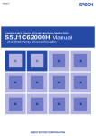
S5U1C6S3N2E2 Manual
(Evaluation Board for S1C60N09/6S3N2/62N33)
NOTICE
No part of this material may be reproduced or duplicated in any form or by any means without the written permission of Seiko
Epson. Seiko Epson reserves the right to make changes to this material without notice. Seiko Epson does not assume any
liability of any kind arising out of any inaccuracies contained in this material or due to its application or use in any product or
circuit and, further, there is no representation that this material is applicable to products requiring high level reliability, such
as medical products. Moreover, no license to any intellectual property rights is granted by implication or otherwise, and there
is no representation or warranty that anything made in accordance with this material will be free from any patent or copyright
infringement of a third party. This material or portions thereof may contain technology or the subject relating to strategic
products under the control of the Foreign Exchange and Foreign Trade Law of Japan and may require an export license from
the Ministry of International Trade and Industry or other approval from another government agency.
© SEIKO EPSON CORPORATION 2001 All rights reserved.
The information of the product number change
Starting April 1, 2001, the product number will be changed as listed below. To order from April 1,
2001 please use the new product number. For further information, please contact Epson sales
representative.
Configuration of product number
Devices
S1
C
60N01
F
0A01
00
Packing specification
Specification
Package (D: die form; F: QFP)
Model number
Model name (C: microcomputer, digital products)
Product classification (S1: semiconductor)
Development tools
C
60R08
S5U1
D1
1
00
Packing specification
Version (1: Version 1 ∗2)
Tool type (D1: Development Tool ∗1)
Corresponding model number (60R08: for S1C60R08)
Tool classification (C: microcomputer use)
Product classification
(S5U1: development tool for semiconductor products)
∗1: For details about tool types, see the tables below. (In some manuals, tool types are represented by one digit.)
∗2: Actual versions are not written in the manuals.
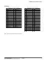
Comparison table between new and previous number
S1C60 Family processors
Previous No.
E0C6001
E0C6002
E0C6003
E0C6004
E0C6005
E0C6006
E0C6007
E0C6008
E0C6009
E0C6011
E0C6013
E0C6014
E0C60R08
New No.
S1C60N01
S1C60N02
S1C60N03
S1C60N04
S1C60N05
S1C60N06
S1C60N07
S1C60N08
S1C60N09
S1C60N11
S1C60N13
S1C60140
S1C60R08
S1C62 Family processors
Previous No.
E0C621A
E0C6215
E0C621C
E0C6S27
E0C6S37
E0C623A
E0C623E
E0C6S32
E0C6233
E0C6235
E0C623B
E0C6244
E0C624A
E0C6S46
New No.
S1C621A0
S1C62150
S1C621C0
S1C6S2N7
S1C6S3N7
S1C6N3A0
S1C6N3E0
S1C6S3N2
S1C62N33
S1C62N35
S1C6N3B0
S1C62440
S1C624A0
S1C6S460
Previous No.
E0C6247
E0C6248
E0C6S48
E0C624C
E0C6251
E0C6256
E0C6292
E0C6262
E0C6266
E0C6274
E0C6281
E0C6282
E0C62M2
E0C62T3
New No.
S1C62470
S1C62480
S1C6S480
S1C624C0
S1C62N51
S1C62560
S1C62920
S1C62N62
S1C62660
S1C62740
S1C62N81
S1C62N82
S1C62M20
S1C62T30
Comparison table between new and previous number of development tools
Development tools for the S1C60/62 Family
Previous No.
ASM62
DEV6001
DEV6002
DEV6003
DEV6004
DEV6005
DEV6006
DEV6007
DEV6008
DEV6009
DEV6011
DEV60R08
DEV621A
DEV621C
DEV623B
DEV6244
DEV624A
DEV624C
DEV6248
DEV6247
New No.
S5U1C62000A
S5U1C60N01D
S5U1C60N02D
S5U1C60N03D
S5U1C60N04D
S5U1C60N05D
S5U1C60N06D
S5U1C60N07D
S5U1C60N08D
S5U1C60N09D
S5U1C60N11D
S5U1C60R08D
S5U1C621A0D
S5U1C621C0D
S5U1C623B0D
S5U1C62440D
S5U1C624A0D
S5U1C624C0D
S5U1C62480D
S5U1C62470D
Previous No.
DEV6262
DEV6266
DEV6274
DEV6292
DEV62M2
DEV6233
DEV6235
DEV6251
DEV6256
DEV6281
DEV6282
DEV6S27
DEV6S32
DEV6S37
EVA6008
EVA6011
EVA621AR
EVA621C
EVA6237
EVA623A
New No.
S5U1C62620D
S5U1C62660D
S5U1C62740D
S5U1C62920D
S5U1C62M20D
S5U1C62N33D
S5U1C62N35D
S5U1C62N51D
S5U1C62560D
S5U1C62N81D
S5U1C62N82D
S5U1C6S2N7D
S5U1C6S3N2D
S5U1C6S3N7D
S5U1C60N08E
S5U1C60N11E
S5U1C621A0E2
S5U1C621C0E
S5U1C62N37E
S5U1C623A0E
Previous No.
EVA623B
EVA623E
EVA6247
EVA6248
EVA6251R
EVA6256
EVA6262
EVA6266
EVA6274
EVA6281
EVA6282
EVA62M1
EVA62T3
EVA6S27
EVA6S32R
ICE62R
KIT6003
KIT6004
KIT6007
New No.
S5U1C623B0E
S5U1C623E0E
S5U1C62470E
S5U1C62480E
S5U1C62N51E1
S5U1C62N56E
S5U1C62620E
S5U1C62660E
S5U1C62740E
S5U1C62N81E
S5U1C62N82E
S5U1C62M10E
S5U1C62T30E
S5U1C6S2N7E
S5U1C6S3N2E2
S5U1C62000H
S5U1C60N03K
S5U1C60N04K
S5U1C60N07K
CONTENTS
S5U1C6S3N2E2 Manual (Evaluation Board for S1C60N09/6S3N2/62N33)
This manual describes how to operate the S5U1C6S3N2E2, a debugging tool for the S1C6S3N2, S1C62N33
and S1C60N09 4-bit single-chip microcomputers.
Refer to the Technical Manual of each model for details of the S1C6S3N2, S1C62N33 and S1C60N09, and
the "S5U1C62000A Manual" and the "S5U1C62xxxD Manual" for the development procedure and other
information.
CONTENTS
1
INTRODUCTION _____________________________________________ 1
1.1
1.2
S5U1C6S3N2E2 Outline .......................................................................................... 1
S5U1C6S3N2E2 Components .................................................................................. 1
2
PRODUCT SPECIFICATIONS __________________________________ 2
3
NAMES AND FUNCTIONS OF PARTS ___________________________ 3
3.1
3.2
Basic Functions ........................................................................................................ 3
Functions of Parts .................................................................................................... 3
3.2.1 Front panel ........................................................................................................... 3
3.2.2 Rear panel ............................................................................................................ 3
3.2.3 Board (under top cover) ....................................................................................... 4
3.3
4
CABLE CONNECTION ________________________________________ 8
4.1
4.2
4.3
5
S5U1C6S3N2E2 I/O and LCD Connectors ............................................................. 6
Connection to ICE .................................................................................................... 8
Power Cable Connection ......................................................................................... 9
Connection to Target System .................................................................................... 9
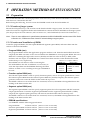
OPERATION METHOD OF S5U1C6S3N2E2 ______________________ 10
5.1
Preparation ............................................................................................................. 10
5.1.1 Creation of target system .................................................................................... 10
5.1.2 Creation and installation of ROMs ..................................................................... 10
5.2
Independent Use of S5U1C6S3N2E2 ...................................................................... 11
5.2.1 Power on/off ......................................................................................................... 11
5.2.2 Debugging ........................................................................................................... 11
5.3
Operation When ICE is Connected ......................................................................... 11
5.3.1 Power on/off ......................................................................................................... 11
5.3.2 Debugging ........................................................................................................... 11
6
PRECAUTIONS _______________________________________________ 12
6.1
6.2
Precautions for Operation ...................................................................................... 12
Differences from Actual IC ..................................................................................... 12
S5U1C6S3N2E2 MANUAL
(EVALUATION BOARD FOR S1C60N09/6S3N2/62N33)
EPSON
i
1 INTRODUCTION
1 INTRODUCTION
1.1 S5U1C6S3N2E2 Outline
The S5U1C6S3N2E2 is a development tool
for the S1C6S3N2, S1C62N33 and
S1C60N09.
Most of the same functions that the
S1C6S3N2/62N33/60N09 CPU has can be
implemented by writing an application
program and by creating option data with
the function and segment option generators
into EPROMs, and then installing them in
the S5U1C6S3N2E2. (The model to be
evaluated can be switched using the DIP
switch on the S5U1C6S3N2E2 board.)
EVA
E0C6
S32/6
6S32
233/6
009
EVAL
UATI
R
ON BO
AR
D
∗ The name 'EVA6S32R' on the development tool
is the old name of the product.
In addition, the S5U1C6S3N2E2 can interface with the in-circuit emulator ICE (S5U1C62000H), and so
perform a higher level of debugging. The set-up data for each option can be loaded from a PC.
1.2 S5U1C6S3N2E2 Components
When unpacking the S5U1C6S3N2E2, make sure all of the following components are included.
(1)
(2)
(3)
(4)
(5)
(6)
(7)
(8)
(9)
S5U1C6S3N2E2 main unit ................................................................................................................... 1
LCD connection cable and connector (60-pin flat type) ................................................................. 1 set
I/O connection cable and connector (50-pin flat type) .................................................................. 1 set
Power cable (3-pin) ............................................................................................................................... 1 set
Fuse (3 A) ................................................................................................................................................ 1
S5U1C6S3N2E2 Manual (Evaluation Board for S1C60N09/6S3N2/62N33) (this manual) ..... 1
Warranty registration card .................................................................................................................. 1
Warranty certificate .............................................................................................................................. 1
Notes on use .......................................................................................................................................... 1
Manual
Warranty
certificate
Warranty
registration card
Notes on use
I/O I/O
#0 #1
LC LC
D D
#0 #1
E V A 6 S 3 2 R
E0C6S32/6233/6096 EVALUATION BOARD
EPSON
LCD EMU.
I/O connection cable
and connector
LCD connection cable
and connector
Power cable
Fuse
Fig. 1.2.1 S5U1C6S3N2E2 package
S5U1C6S3N2E2 MANUAL
(EVALUATION BOARD FOR S1C60N09/6S3N2/62N33)
EPSON
1
2 PRODUCT SPECIFICATIONS
2 PRODUCT SPECIFICATIONS
The components specifications of the S5U1C6S3N2E2 are listed below.
■ S5U1C6S3N2E2
Dimensions:
Weight:
Color:
Power supply:
Board:
Operating conditions:
203 mm (width) × 275 mm (depth) × 65 mm (height) (Including rubber feet)
About 2 kg
(main unit only)
Cygnus white
5 V (±10%) DC, 3 A or more
(from external power supply)
When connected to the ICE, power is supplied by the ICE.
Main board × 1
Sub board × 1
Operating temperature
5°C to 40°C
Storage temperature
-20°C to 60°C
Operating humidity
35% to 80%
Storage humidity
20% to 90%
Resistance to vibration
Operating
0.25G max.
Transportation 2G max.
Resistance to impulse
Operating
1G max.
Standby
2G max.
■ LCD connection cable (supplied with S5U1C6S3N2E2)
S5U1C6S3N2E2 connector:
Cable connector:
Cable:
Interface:
Length:
J3372-P302VE (3M) or equivalent
7960-6500SC (3M)
60-pin flat cable × 1
CMOS interface (5 V)
About 50 cm
■ I/O cable (supplied with S5U1C6S3N2E2)
S5U1C6S3N2E2 connector:
Cable connector:
Cable:
Interface:
Length:
J3433-P302VE (3M) or equivalent
7950-6500SC (3M)
50-pin flat cable × 1
CMOS interface (5 V)
About 50 cm
■ Power cable (supplied with S5U1C6S3N2E2)
S5U1C6S3N2E2 connector:
Cable connector:
Other side connector:
Cable length:
Capacity:
MOLEX 5276-03A or equivalent
MOLEX 5196-03
(According to power supply specifications)
About 80 cm
5 V DC, 3 A or more
■ Accessories
Fuse type/rating:
MGC-ULCSA 125V 3 A × 1
60-pin connector for connecting to target system:
3432-6002LCSC × 1
50-pin connector for connecting to target system:
3433-6002LCSC × 1
(For LCD cable connection)
(For I/O cable connection)
■ EPROM
For programs:
For function option:
For segment option:
2
Intel i27C64–i27C512 or equivalent
Intel i27C64–i27C512 or equivalent
Intel i27C64–i27C512 or equivalent
EPSON
2
1
1
(Access time 250 ns or less)
(Access time 250 ns or less)
(Access time 250 ns or less)
S5U1C6S3N2E2 MANUAL
(EVALUATION BOARD FOR S1C60N09/6S3N2/62N33)
3 NAMES AND FUNCTIONS OF PARTS
3 NAMES AND FUNCTIONS OF PARTS
This section describes the names and functions of the parts of the S5U1C6S3N2E2.
3.1 Basic Functions
The S5U1C6S3N2E2 has the following basic functions:
■ Program execution (Run function)
Install the EPROM containing the application program and execute the program.
■ Interface with ICE
The S5U1C6S3N2E2 can interface with the ICE so that a higher level debugging environment may be
established.
■ Setting hardware options by installing function option and segment option ROMs
Hardware options, i.e., I/O ports and LCD segments, can be specified by writing option data for the
function option created by the function option generator and the segment option created by the
segment option generator into EPROM, and installing it to the S5U1C6S3N2E2.
3.2 Functions of Parts
3.2.1 Front panel
■ Connectors
I/O
#0
LC
•••••••••••••••••••••••••••••••••
•••••••••••••••••••••••••••••••••
D
#0
LC
D
#1
EPSON
••••••••••••••••••••••••••••
••••••••••••••••••••••••••••
I/O
E0C6S32/6233/6009 EVALUATION BOARD
#1
EVA6S32R
▲ Position of pin 1
Fig. 3.2.1.1 Front panel
• I/O #0
Connector for the I/O cable. The I/O cable
is used to connect the S5U1C6S3N2E2 to the
target system.
• LCD #0
Connector for the LCD cable. The LCD cable
is used to connect the S5U1C6S3N2E2 to the
target system.
3.2.2 Rear panel
■ Switch
+5V GND
O I
DC IN
••••••••••••••••••••••••••••
••••••••••••••••••••••••••••
F1
••••••••••••••••••••••••••••
••••••••••••••••••••••••••••
F5
POWER SW
• POWER SW
This is a switch to turn on or off the external
power supply to the S5U1C6S3N2E2. (Turn
off the POWER switch when the ICE is
connected.)
▲ Position of pin 1
■ Connectors
Fig. 3.2.2.1 Rear panel
Note: Be sure to disconnect external power source
before connection with the ICE, because power is
supplied from the ICE when the S5U1C6S3N2E2
is connected to the ICE.
• DC IN 5 V
This is a connector with external power
supply source. The external power supply
should be in direct current of 5 V for 3 A or
more.
• F1, F5
Connectors for the ICE interface cable.
S5U1C6S3N2E2 MANUAL
(EVALUATION BOARD FOR S1C60N09/6S3N2/62N33)
EPSON
3
3 NAMES AND FUNCTIONS OF PARTS
3.2.3 Board (under top cover)
DEVICE SW
FUSE1
1
2
RESET
OSC3CR OSC1CR EVRUN OSCC
GND
AD0
CSDC AMPON HVLD SVDON
SHEXLD
HLT/SLP
S.HEX
SWRUN
VADJ
OSC1ADJ OSC3ADJ
LFHX SWRUN CSDC AMPON HVLD
POWER
SVDON OSCC EVRUN DONE
VSVD
L.HEX
F.HEX
H.HEX
Fig. 3.2.3.1 Layout on the board
■ ROM sockets
• L.HEX, H.HEX
These are IC sockets for target program ROMs. Insert the ROM (L.HEX) containing the 8 low-order
bits (I7 to I0) of the machine code into the L.HEX socket, and the ROM (H.HEX) containing the 4 highorder bits (IB to I8) into the H.HEX socket.
• F.HEX
This is the IC socket into which the ROM (F.HEX) is inserted. This ROM includes the function options
generated by the function option generator.
• S.HEX
This is the IC socket into which the ROM (S.HEX) is inserted. This ROM includes the segment options
generated by the segment option generator.
■ Switch
• RESET switch
This switch resets the CPU and starts the target program from page 01H, step 00H.
• DEVICE SW (DIP switch)
This switch is used to select the model (S1C6S3N2, S1C62N33 or S1C60N09) to be evaluated. Table
3.2.3.1 shows the correspondence between the model and the switch settings.
Table 3.2.3.1 Selecting the model
Model
S1C6S3N2
S1C62N33
S1C60N09
SW1
ON
OFF
ON
SW2
ON
ON
OFF
■ Control
• VADJ
This is the control for adjusting the LCD contrast.
(Refer to Section 6.2, "Differences from Actual IC".)
• VSVD (can be used only when the S5U1C6S3N2E2 is set for the S1C6S3N2 or the S1C62N33)
This is the control for varying the power supply voltage in simulation to check SVD (BLD) operation.
(Refer to Section 6.2, "Differences from Actual IC".)
4
EPSON
S5U1C6S3N2E2 MANUAL
(EVALUATION BOARD FOR S1C60N09/6S3N2/62N33)
3 NAMES AND FUNCTIONS OF PARTS
• OSC1ADJ (can be used only when the S5U1C6S3N2E2 is set for the S1C60N09)
OSC3ADJ (can be used only when the S5U1C6S3N2E2 is set for the S1C6S3N2 or the S1C62N33)
This is the control for varying the CR oscillation frequency. This control is effective only when CR
oscillation is selected for the oscillator type by mask option. The CR oscillation frequency can be
checked by connecting an oscilloscope or other instrument to the monitor pin (OSC1CR, OSC3CR).
■ FUSE
• FUSE1
This is 3 A tubular fuse for external power supply, and is blown off by current of 3 A or more.
■ LEDs
• POWER
This LED lights when the S5U1C6S3N2E2 turns on.
• HLT/SLP
This LED lights when the CPU enters HALT status.
• AD0
This LED indicates the status of the address bit 0 (AD0) of the program memory. It can be used to
check whether or not the S5U1C6S3N2E2 is in the free run status.
• SHEXLD
This LED lights when LCD segment option data from a personal computer is loaded using the incircuit emulator ICE. As result, it can differentiate whether the currently specified segment option is
due to the ROM (-S.HEX) or has been loaded from a personal computer. Refer to the "S5U1C62000A
Manual" in regard to the loading of the segment option using the ICE.
• LFHX
This LED lights when function option data from a personal computer is loaded using the in-circuit
emulator ICE. As result, it can differentiate whether the currently specified function option is due to
the ROM (-F.HEX) or has been loaded from a personal computer. Refer to the "S5U1C62000A Manual"
in regard to the loading of the function option using the ICE.
• DONE/PG
This LED lights when initial reset of this board has been completed after the S5U1C6S3N2E2 is turned
on.
• HVLD, SVDON*, OSCC*, AMPON*, CSDC, SWRUN, EVRUN*
These LEDs indicate the values ("1" or "0") of the following resisters. LED lights when "1" is set in the
resister, and it goes off when "0" is set to the resister.
HVLD
HVLD (HLMOD) register (076H•D3)
SVDON* SVDON (BLS) register
(076H•D2)
OSCC*
OSCC register
(0FEH•D1)
AMPON* AMPON register
(0F7H•D0)
CSDC
CSDC register
(078H•D3)
SWRUN
SWRUN register
(07EH•D2)
EVRUN* EVRUN register
(0FCH•D2)
■ Monitor pins
The value of the HVLD (HLMOD), SVDON (BLS)*, OSCC*, AMPON*, CSDC, SWRUN and EVRUN*
registers can be checked by an oscilloscope or other instrument. GND can be used to connect the GND
pin of an oscilloscope.
∗ Effective only when the S5U1C6S3N2E2 is set for the S1C6S3N2 or the S1C62N33.
S5U1C6S3N2E2 MANUAL
(EVALUATION BOARD FOR S1C60N09/6S3N2/62N33)
EPSON
5
3 NAMES AND FUNCTIONS OF PARTS
3.3 S5U1C6S3N2E2 I/O and LCD Connectors
S1C6S3N2
Table 3.3.1 I/O #0 connector pins
No.
1
3
5
7
9
11
13
15
17
19
21
23
25
27
29
31
33
35
37
39
41
43
45
47
49
Signal name
VDD (+5 V)
VDD (+5 V)
Cannot be connected
K00
K02
K10
Cannot be connected
Cannot be connected
Cannot be connected
P00
P02
P10
P12
Cannot be connected
R00
R02
R10
R12
Cannot be connected
Cannot be connected
Cannot be connected
Cannot be connected
AMPP
VSS (GND)
VSS (GND)
No.
2
4
6
8
10
12
14
16
18
20
22
24
26
28
30
32
34
36
38
40
42
44
46
48
50
Table 3.3.2 LCD #0 connector pins
No.
1
3
5
7
9
11
13
15
17
19
21
23
25
27
29
31
33
35
37
39
41
43
45
47
49
51
53
55
57
59
Signal name
VDD (+5 V)
VDD (+5 V)
Cannot be connected
K01
K03
Cannot be connected
Cannot be connected
Cannot be connected
Cannot be connected
P01
P03
P11
P13
Cannot be connected
R01
R03
R11
R13
Cannot be connected
Cannot be connected
Cannot be connected
RESET
AMPM
VSS (GND)
VSS (GND)
Signal name
COM0
COM2
Cannot be connected
Cannot be connected
SEG0
SEG2
SEG4
SEG6
SEG8
SEG10
SEG12
SEG14
SEG16
SEG18
SEG20
SEG22
SEG24
SEG26
SEG28
SEG30
SEG32
SEG34
SEG36
Cannot be connected
Cannot be connected
Cannot be connected
Cannot be connected
Cannot be connected
Cannot be connected
Cannot be connected
No.
2
4
6
8
10
12
14
16
18
20
22
24
26
28
30
32
34
36
38
40
42
44
46
48
50
52
54
56
58
60
Signal name
COM1
COM3
Cannot be connected
Cannot be connected
SEG1
SEG3
SEG5
SEG7
SEG9
SEG11
SEG13
SEG15
SEG17
SEG19
SEG21
SEG23
SEG25
SEG27
SEG29
SEG31
SEG33
SEG35
SEG37
Cannot be connected
Cannot be connected
Cannot be connected
Cannot be connected
Cannot be connected
Cannot be connected
Cannot be connected
S1C62N33
Table 3.3.3 I/O #0 connector pins
No.
1
3
5
7
9
11
13
15
17
19
21
23
25
27
29
31
33
35
37
39
41
43
45
47
49
6
Signal name
VDD (+5 V)
VDD (+5 V)
Cannot be connected
K00
K02
K10
Cannot be connected
Cannot be connected
Cannot be connected
P00
P02
P10
P12
Cannot be connected
R00
R02
R10
R12
Cannot be connected
SIN
SCLK
Cannot be connected
AMPP
VSS (GND)
VSS (GND)
No.
2
4
6
8
10
12
14
16
18
20
22
24
26
28
30
32
34
36
38
40
42
44
46
48
50
Table 3.3.4 LCD #0 connector pins
No.
1
3
5
7
9
11
13
15
17
19
21
23
25
27
29
31
33
35
37
39
41
43
45
47
49
51
53
55
57
59
Signal name
VDD (+5 V)
VDD (+5 V)
Cannot be connected
K01
K03
Cannot be connected
Cannot be connected
Cannot be connected
Cannot be connected
P01
P03
P11
P13
Cannot be connected
R01
R03
R11
R13
Cannot be connected
SOUT
SIOF
RESET
AMPM
VSS (GND)
VSS (GND)
EPSON
Signal name
COM0
COM2
Cannot be connected
Cannot be connected
SEG0
SEG2
SEG4
SEG6
SEG8
SEG10
SEG12
SEG14
SEG16
SEG18
SEG20
SEG22
SEG24
SEG26
SEG28
SEG30
SEG32
SEG34
SEG36
SEG38
Cannot be connected
Cannot be connected
Cannot be connected
Cannot be connected
Cannot be connected
Cannot be connected
No.
2
4
6
8
10
12
14
16
18
20
22
24
26
28
30
32
34
36
38
40
42
44
46
48
50
52
54
56
58
60
Signal name
COM1
COM3
Cannot be connected
Cannot be connected
SEG1
SEG3
SEG5
SEG7
SEG9
SEG11
SEG13
SEG15
SEG17
SEG19
SEG21
SEG23
SEG25
SEG27
SEG29
SEG31
SEG33
SEG35
SEG37
SEG39
Cannot be connected
Cannot be connected
Cannot be connected
Cannot be connected
Cannot be connected
Cannot be connected
S5U1C6S3N2E2 MANUAL
(EVALUATION BOARD FOR S1C60N09/6S3N2/62N33)
3 NAMES AND FUNCTIONS OF PARTS
S1C60N09
Table 3.3.5 I/O #0 connector pins
No.
1
3
5
7
9
11
13
15
17
19
21
23
25
27
29
31
33
35
37
39
41
43
45
47
49
Signal name
VDD (+5 V)
VDD (+5 V)
Cannot be connected
K00
K02
Cannot be connected
Cannot be connected
Cannot be connected
Cannot be connected
P00
P02
P10
P12
Cannot be connected
R00
R02
Cannot be connected
Cannot be connected
Cannot be connected
Cannot be connected
Cannot be connected
Cannot be connected
Cannot be connected
VSS (GND)
VSS (GND)
No.
2
4
6
8
10
12
14
16
18
20
22
24
26
28
30
32
34
36
38
40
42
44
46
48
50
Table 3.3.6 LCD #0 connector pins
No.
1
3
5
7
9
11
13
15
17
19
21
23
25
27
29
31
33
35
37
39
41
43
45
47
49
51
53
55
57
59
Signal name
VDD (+5 V)
VDD (+5 V)
Cannot be connected
K01
K03
Cannot be connected
Cannot be connected
Cannot be connected
Cannot be connected
P01
P03
P11
P13
Cannot be connected
R01
R03
Cannot be connected
Cannot be connected
Cannot be connected
Cannot be connected
Cannot be connected
RESET
Cannot be connected
VSS (GND)
VSS (GND)
Signal name
COM0
COM2
Cannot be connected
Cannot be connected
SEG0
SEG2
SEG4
SEG6
SEG8
SEG10
SEG12
SEG14
SEG16
SEG18
SEG20
SEG22
SEG24
SEG26
SEG28
SEG30
SEG32
SEG34
SEG36
Cannot be connected
Cannot be connected
Cannot be connected
Cannot be connected
Cannot be connected
Cannot be connected
Cannot be connected
No.
2
4
6
8
10
12
14
16
18
20
22
24
26
28
30
32
34
36
38
40
42
44
46
48
50
52
54
56
58
60
Signal name
COM1
COM3
Cannot be connected
Cannot be connected
SEG1
SEG3
SEG5
SEG7
SEG9
SEG11
SEG13
SEG15
SEG17
SEG19
SEG21
SEG23
SEG25
SEG27
SEG29
SEG31
SEG33
SEG35
SEG37
Cannot be connected
Cannot be connected
Cannot be connected
Cannot be connected
Cannot be connected
Cannot be connected
Cannot be connected
Note: Do not use pins that cannot be connected.
S5U1C6S3N2E2 MANUAL
(EVALUATION BOARD FOR S1C60N09/6S3N2/62N33)
EPSON
7
4 CABLE CONNECTION
4 CABLE CONNECTION
This section describes how to connect the power cable to the S5U1C6S3N2E2, and the
S5U1C6S3N2E2 to the ICE and the target system.
Note: Turn the power of all equipment off before connecting or disconnecting cables.
4.1 Connection to ICE
The S5U1C6S3N2E2 is connected to the ICE by connecting the two interface cables (F1 and F5). Use
S5U1C6S3N2E2 connectors F1 and F5 with the projections facing outwards. Use ICE connectors F1 and F5
with the projections facing inwards (cable side).
Figures 4.1.1 and 4.1.2 show the external view and connection diagram of the ICE interface cable.
2 1
: :
: :
: :
: :
: :
50 49
S5U1C6S3N2E2 side
2 1
: :
: :
: :
: :
: :
50 49
ICE side
Fig. 4.1.1 External view of the ICE interface cable
S5U1C6S3N2E2
ICE
ICE
S5U1C6S3N2E2
F1
F1
F5
F5
<Side view>
Red mark
<Top view>
Fig. 4.1.2 Connection diagram
Note: The S5U1C6S3N2E2 has an external power input connector for +5 V (VDD) and GND (VSS). Leave
this connector unconnected when the S5U1C6S3N2E2 is connected to the ICE.
8
EPSON
S5U1C6S3N2E2 MANUAL
(EVALUATION BOARD FOR S1C60N09/6S3N2/62N33)
4 CABLE CONNECTION
4.2 Power Cable Connection
When using the S5U1C6S3N2E2 on its own, it must be supplied with power (5 V DC, 3 A or more) from
an external source through the power cable.
When the S5U1C6S3N2E2 is connected to the ICE, the power is supplied by the ICE; therefore, the power
cable is not necessary. Disconnect the power cable if it is already connected.
Figure 4.2.1 shows the connection of the power cable pins.
Black
-
Connect to the
external power
supply
+
Connect to the
power connector
of the S5U1C6S3N2E2
Red
Fig. 4.2.1 Connection of power cable pins
In addition, the power can be supplied from the DC jack (DCIN). The AC adaptor provided with the ICE
can be used.
Note: Be sure to use only one power source either the AC adaptor or the power cable for independent
use of the S5U1C6S3N2E2. Do not connect the AC adaptor and the power cable when using the
S5U1C6S3N2E2 with the ICE.
4.3 Connection to Target System
The I/O #0 and LCD #0 connectors are used to connect the S5U1C6S3N2E2 to the target system.
S5U1C6S3N2E2
I/O
connector
I/O #0
Target
system
I/O cable
LCD #0
LCD
LCD cable
connector
Front
Fig. 4.3.1 Connection of target system
Take the following precautions when connecting the S5U1C6S3N2E2 to the target system:
• Power is supplied to the S5U1C6S3N2E2, unlike the actual chip.
• Do not use pins that cannot be connected.
S5U1C6S3N2E2 MANUAL
(EVALUATION BOARD FOR S1C60N09/6S3N2/62N33)
EPSON
9
5 OPERATION METHOD OF S5U1C6S3N2E2
5 OPERATION METHOD OF S5U1C6S3N2E2
5.1 Preparation
This section describes the common preparation work necessary when the S5U1C6S3N2E2 is used by itself
and when it is connected to the ICE.
Before doing the following, be sure to turn the POWER switch of the S5U1C6S3N2E2 off.
5.1.1 Creation of target system
Mount the LCD panel, keys, and switches on the board to build a target system. Use the I/O connector
and LCD connector supplied with the S5U1C6S3N2E2 to connect the S5U1C6S3N2E2 to the target system.
(For the pin layout of each connector, refer to Section 3.3, "S5U1C6S3N2E2 I/O and LCD Connectors".)
Note: There is some difference in specifications between the S5U1C6S3N2E2 and the actual CPU. Refer
to Section 6.2, "Differences from Actual IC" when building a target system.
5.1.2 Creation and installation of ROMs
Create the program ROMs, function option ROM and segment option ROM, and insert them into the
sockets of the S5U1C6S3N2E2.
• Program ROMs (two)
The program ROMs contain the application program machine code. Write the Intel-HEX format files
output by the HEX converter or the cross-assembler into EPROMs to create program ROMs. Since two
HEX files containing the high-order section (-H.HEX) and the low-order section (-L.HEX) of the
machine code are output, two EPROMs are created. Insert them into the socket H.HEX and L.HEX
under the top cover, respectively.
Table 5.1.2.1 Offset address
These ROMs are not effective when connecting the
EPROM type
Offset value
S5U1C6S3N2E2 to the ICE. In addition, it is necessary to
27C64
0000H (no offset)
write the object data into the EPROM attaching the offset
27C128
0000H (no offset)
address as Table 5.1.2.1 according to the type of EPROM to
27C256
4000H
be used.
27C512
C000H
• Function option ROM (one)
The function option ROM is used to specify function options, such as I/O port specifications. Create
the function option ROM from the function option HEX file (-F.HEX) output by the function option
generator, and insert it into the F.HEX socket under the top cover.
This ROM is effective even when the ICE is connected, however, this ROM is disregarded due to the
loading of the data from the ICE.
• Segment option ROM (one)
The segment option ROM is used to specify segment options for LCD assignment and SEG terminal
output specifications. Create the segment option ROM from the segment option HEX file (-S.HEX)
output by the segment option generator, and insert it into the S.HEX socket in the top cover.
This ROM is effective even when the ICE is connected, however, this ROM is disregarded due to the
loading of the data from the ICE.
• EPROM specifications
Use EPROMs with the following specifications:
Program ROM:
27C64 to 27C512 (250 ns or less access time)
Function option ROM: 27C64 to 27C512 (250 ns or less access time)
Segment option ROM: 27C64 to 27C512 (250 ns or less access time)
10
EPSON
S5U1C6S3N2E2 MANUAL
(EVALUATION BOARD FOR S1C60N09/6S3N2/62N33)
5 OPERATION METHOD OF S5U1C6S3N2E2
5.2 Independent Use of S5U1C6S3N2E2
This section describes operation when using the S5U1C6S3N2E2 by itself.
The S5U1C6S3N2E2 may be used independently by connecting a power supply to it. Use a 5 V DC
regulator (more than 3 A) or the AC adaptor supplied with the ICE as an external power supply. When
using an external power supply, connect it with the correct polarity (+ and -).
(Refer to Section 4.2, "Power Cable Connection".)
5.2.1 Power on/off
Before turning the POWER switch of the S5U1C6S3N2E2 on, confirm the following:
(1) The power cable is connected correctly.
(2) The target system is connected correctly.
(3) The ROMs have been installed correctly.
After confirming the above items, turn the POWER switch of the S5U1C6S3N2E2 on using the following
procedure. When turning the S5U1C6S3N2E2 off, follow the procedure from (2) to (1):
(1) Turn the regulator on and set the output voltage to 5 V ±10%.
When using the AC adaptor, plug the AC adaptor into the AC line and the S5U1C6S3N2E2.
(2) Turn the POWER switch of the S5U1C6S3N2E2 on.
5.2.2 Debugging
When the S5U1C6S3N2E2 is used alone, it provides the following debugging function. The method of
operation is given below.
• Program free run
When the RESET switch (under the top cover) is pressed, the S5U1C6S3N2E2 enters the program run
state, and executes the application program from page 1, step 0.
• Other functions
The SVD operation can be confirmed with the VSVD control.*
The LCD contrast can be adjusted with the VADJ control. (Refer to Section 6.2, "Differences from
Actual IC".)
The HVLD (HLMOD), SVDON (BLS)*, OSCC*, AMPON*, CSDC, SWRUN and EVRUN* resister
values can be confirmed with the LED indicators and the monitor pins.
∗ These functions can be used when the S5U1C6S3N2E2 is set for the S1C6S3N2 or the S1C62N33.
5.3 Operation When ICE is Connected
This section explains the operation and use of the S5U1C6S3N2E2 when it is connected to the ICE. Set up
the S5U1C6S3N2E2 as follows when it is connected to the ICE:
(1) Do not connect the power supply and the AC adaptor.
(2) Keep on turning the POWER switch off.
5.3.1 Power on/off
Power to the S5U1C6S3N2E2 is supplied by the ICE, and the power is switched on and off by pressing the
POWER switch of the ICE. Keep the POWER switch of the S5U1C6S3N2E2 off.
5.3.2 Debugging
Debugging is done with the host computer, and the S5U1C6S3N2E2 is controlled by the ICE. For the
method of operation, refer to the "S5U1C62000A Manual" and the "S5U1C62xxxD Manual". The
S5U1C6S3N2E2 can control the following three functions:
(1) Pseudo power supply voltage change with the VSVD control *
(2) LCD contrast adjustment with the VADJ control
(3) RESET switch
∗ This function can be used when the S5U1C6S3N2E2 is set for the S1C6S3N2 or the S1C62N33.
S5U1C6S3N2E2 MANUAL
(EVALUATION BOARD FOR S1C60N09/6S3N2/62N33)
EPSON
11
6 PRECAUTIONS
6 PRECAUTIONS
Take the following precautions when using the S5U1C6S3N2E2:
6.1 Precautions for Operation
• Turn the power of all equipment off before connecting or disconnecting cables.
• When ROMs are inserted into the ROM sockets L, H, lock the lever securely by positioning it horizontally. After the ROMs have been removed from the sockets, lock the lever at the same position above.
If the lever is left upright, poor contact may result.
• When using the S5U1C6S3N2E2 by itself, confirm that the following ROMs have been installed
correctly, then operate the S5U1C6S3N2E2.
Program ROMs
2
L.HEX, H.HEX
Function option ROM 1
F.HEX
Segment option ROM 1
S.HEX
6.2 Differences from Actual IC
Be aware that the S5U1C6S3N2E2 differs in terms of functionality and characteristics from the actual IC.
If these differences are ignored, there is a possibility that the application will not operate properly on an
actual IC even though it might have performed well on the ICE.
Note: The functions indicated with an "∗" in the following explanation can be used when the
S5U1C6S3N2E2 is set for the S1C6S3N2 or the S1C62N33.
■ Core CPU
The S5U1C6S3N2E2 supports the three models, S1C6S3N2, S1C62N33 and S1C60N09. Since each
model has a different core CPU built-in, there is a difference as shown in the following table.
When developing the software for the S1C62N33,
• be sure to initialize the D flag by the initial routine in the application program,
• do not read interrupt factor flags and do not write data to the interrupt mask register in the EI status.
Table 6.2.1 Difference on core CPU function
Model
S5U1C6S3N2E2 S1C6S3N2
S1C62N33
Core CPU
S1C6200A
S1C6200A
S1C6200
Initial value of D flag
0
0
Undefined
Reading interrupt factor flags,
writing to the interrupt mask
Valid
Valid
Invalid
register in the EI status
S1C60N09
S1C6200B
0
Valid
∗ There is no difference in the functions of the S1C6200A and S1C6200B.
■ I/O
<Interface voltage>
The interface voltage between the S5U1C6S3N2E2 and the target system is fixed at +5 V. Therefore, if
the target system requires the same interface voltage as that of the actual IC, add a level shifter circuit
or some other appropriate circuit to the target system.
<Output port drive capability>
The drive capability of each output port on the S5U1C6S3N2E2 is higher than that of the actual IC.
Check the drive capability of each output terminal on the model by referring to its Technical Manual
before designing the system and software.
12
EPSON
S5U1C6S3N2E2 MANUAL
(EVALUATION BOARD FOR S1C60N09/6S3N2/62N33)
6 PRECAUTIONS
<Protective diode at each port>
The S5U1C6S3N2E2 I/O ports are all connected to VDD and VSS through a protective diode and the
interface voltage with the target system is fixed at +5 V. Therefore, the ports cannot interface with a
voltage level exceeding VDD–VSS even when the output specification is set to open-drain output.
<Pull-down resistance>
The K ports of the S5U1C6S3N2E2 have a 1 MΩ pull-down resistor and the P ports have a 200 kΩ
pull-down resistor which are different from those of the actual IC. For the resistor value of the actual
IC, refer to the Technical Manual for each model.
The set-up time when the input port is pulled down to low with the pull-down resistor is different
from the actual IC. For example, when a key matrix circuit is configured with input and output ports,
a delay occurs in the input fall time by the pull-down resistor. Note that the delay time between the
S5U1C6S3N2E2 and the actual IC is not same.
■ LCD
• The S5U1C6S3N2E2 has the VADJ control for adjusting the LCD contrast. In the actual IC, the LCD
drive voltage level is fixed.
• The S5U1C6S3N2E2 can output 1/3-bias waveforms only, and cannot output 1/2-bias waveforms.
• The output drive capability of the SEG and COM terminals is different.
• When a SEG terminal is set to DC output, the output level is not be initialized in the S5U1C6S3N2E2.
However, it is initialized in the S1C6S3N2 and S1C60N09. In the S1C62N33, it is not initialized similar
to the S5U1C6S3N2E2, but the undefined status is different from the S5U1C6S3N2E2.
■ Difference in current consumption
Current consumption in the S5U1C6S3N2E2 greatly differs from that in the actual IC. To evaluate the
approximate current consumption of the actual IC, check the LEDs on the S5U1C6S3N2E2. The
following lists the items that greatly affect the amount of current consumption:
• Those that can be estimated by checking LEDs and monitor pins
a) Run and Halt execution ratio (on the ICE)
b) AMP operation (AMPON)*
c) OSC3 oscillation ON/OFF circuit (OSCC)*
d) SVD circuit ON/OFF circuit (SVDON or BLS)*
e) Heavy load protection mode (HVLD or HLMOD)
• Those that require attention during system and software design
f) Currents consumed by the internal pull-down resistors
g) Input ports in a floating state
■ Functional difference
<SVD (BLD) circuit>*
• The SVD (BLD) function is implemented by varying the apparent power supply voltage with the
VSVD volume on the S5U1C6S3N2E2 board.
• There is a delay between the time change the power supply voltage and the SVD (BLD) data is
detected. For the S5U1C6S3N2E2, it is shorter than the actual IC. For the actual IC, refer to the Technical Manual of each model and detect the voltage after the sufficient time interval.
<AMP circuit>*
There is a delay between the time change the voltage of the AMP pins and the AMP data is detected.
For the S5U1C6S3N2E2, it is shorter than the actual IC. For the actual IC, refer to the Technical Manual
of each model and choose the sufficient time interval.
S5U1C6S3N2E2 MANUAL
(EVALUATION BOARD FOR S1C60N09/6S3N2/62N33)
EPSON
13
6 PRECAUTIONS
<Oscillation circuit>
• The oscillation circuits in the S5U1C6S3N2E2 and the oscillation frequencies are configured according
to the selected model as follows:
When the S5U1C6S3N2E2 is set for the S1C6S3N2:
The OSC1 oscillation frequency is fixed at 32.768 kHz with a crystal oscillator.
The OSC3 oscillation frequency is fixed at 1 MHz when ceramic oscillation is selected. When CR
oscillation is selected, the frequency can be adjusted approximately from 700 kHz to 1.3 MHz.
When the S5U1C6S3N2E2 is set for the S1C62N33:
The OSC1 oscillation frequency is fixed at 32.768 kHz with a crystal oscillator.
The OSC3 oscillation frequency is fixed at 455 kHz when ceramic oscillation is selected. When CR
oscillation is selected, the frequency can be adjusted approximately from 300 kHz to 560 kHz.
When the S5U1C6S3N2E2 is set for the S1C60N09:
The OSC1 oscillation frequency is fixed at 32.768 kHz when crystal oscillation is selected. When CR
oscillation is selected, the frequency can be adjusted approximately from 44 kHz to 85 kHz.
Refer to the Technical Manual of each model for the operating frequency range of the actual IC.
• The oscillation stabilization time for OSC3 and OSC1 is shorter than the actual IC. The time from
turning the OSC3 oscillation on to switching the system clock to OSC3 should be secured according to
the time of the actual IC. *
• Use separate instructions for turning the OSC3 oscillation on and for switching the clock from OSC1
to OSC3. The same applies when turning the OSC1 oscillation off after switching the clock from OSC3
to OSC1. The S5U1C6S3N2E2 may operate if this processing is performed at the same time. Be sure to
use separate instructions according to the actual IC when creating the program. *
• The oscillation start and stop times are different from those of the actual IC, because the logic level of
the S5U1C6S3N2E2 is higher than that of the actual IC.
<Waiting time>
The actual IC requires an appropriate waiting time for the operation of the following functions, but
the S5U1C6S3N2E2 may operate properly without the waiting time. Therefore, it may cause a malfunction in the actual IC even though the program operates properly in the S5U1C6S3N2E2. Be sure to
follow the notes described in the Technical Manual of each model.
SVD function
(SVDON or BLS)*
AMP function
(AMPON)*
<Undefined data memory area>
In the S5U1C6S3N2E2, values that are read from unmapped memory areas will be undefined. However, the undefined status differs from the actual IC, therefore pay attention to the memory area when
creating programs. Refer to the Technical Manual of each model for the memory map.
<Reset circuit>
• The S5U1C6S3N2E2 does not contain an oscillation stop detection circuit (to generate a system reset
signal when the oscillation has stopped). Note that the oscillation stop detection circuit can not
guarantee operation with 100% accuracy.
• The sequence of operations from when the S5U1C6S3N2E2 is turned on until the program starts
operating is different from the actual IC. The S5U1C6S3N2E2 can start executing the program after the
user program and option data are loaded on the S5U1C6S3N2E2.
14
EPSON
S5U1C6S3N2E2 MANUAL
(EVALUATION BOARD FOR S1C60N09/6S3N2/62N33)
International Sales Operations
AMERICA
ASIA
EPSON ELECTRONICS AMERICA, INC.
EPSON (CHINA) CO., LTD.
- HEADQUARTERS -
28F, Beijing Silver Tower 2# North RD DongSanHuan
ChaoYang District, Beijing, CHINA
Phone: 64106655
Fax: 64107319
1960 E. Grand Avenue
EI Segundo, CA 90245, U.S.A.
Phone: +1-310-955-5300
Fax: +1-310-955-5400
SHANGHAI BRANCH
4F, Bldg., 27, No. 69, Gui Jing Road
Caohejing, Shanghai, CHINA
Phone: 21-6485-5552
Fax: 21-6485-0775
- SALES OFFICES West
150 River Oaks Parkway
San Jose, CA 95134, U.S.A.
Phone: +1-408-922-0200
Fax: +1-408-922-0238
Central
101 Virginia Street, Suite 290
Crystal Lake, IL 60014, U.S.A.
Phone: +1-815-455-7630
Fax: +1-815-455-7633
Northeast
301 Edgewater Place, Suite 120
Wakefield, MA 01880, U.S.A.
Phone: +1-781-246-3600
Fax: +1-781-246-5443
EPSON HONG KONG LTD.
20/F., Harbour Centre, 25 Harbour Road
Wanchai, Hong Kong
Phone: +852-2585-4600 Fax: +852-2827-4346
Telex: 65542 EPSCO HX
EPSON TAIWAN TECHNOLOGY & TRADING LTD.
10F, No. 287, Nanking East Road, Sec. 3
Taipei
Phone: 02-2717-7360
Fax: 02-2712-9164
Telex: 24444 EPSONTB
HSINCHU OFFICE
Southeast
3010 Royal Blvd. South, Suite 170
Alpharetta, GA 30005, U.S.A.
Phone: +1-877-EEA-0020 Fax: +1-770-777-2637
13F-3, No. 295, Kuang-Fu Road, Sec. 2
HsinChu 300
Phone: 03-573-9900
Fax: 03-573-9169
EPSON SINGAPORE PTE., LTD.
No. 1 Temasek Avenue, #36-00
Millenia Tower, SINGAPORE 039192
Phone: +65-337-7911
Fax: +65-334-2716
EUROPE
EPSON EUROPE ELECTRONICS GmbH
SEIKO EPSON CORPORATION KOREA OFFICE
- HEADQUARTERS Riesstrasse 15
80992 Munich, GERMANY
Phone: +49-(0)89-14005-0
Fax: +49-(0)89-14005-110
SALES OFFICE
Altstadtstrasse 176
51379 Leverkusen, GERMANY
Phone: +49-(0)2171-5045-0
Fax: +49-(0)2171-5045-10
UK BRANCH OFFICE
Unit 2.4, Doncastle House, Doncastle Road
Bracknell, Berkshire RG12 8PE, ENGLAND
Phone: +44-(0)1344-381700
Fax: +44-(0)1344-381701
50F, KLI 63 Bldg., 60 Yoido-dong
Youngdeungpo-Ku, Seoul, 150-763, KOREA
Phone: 02-784-6027
Fax: 02-767-3677
SEIKO EPSON CORPORATION
ELECTRONIC DEVICES MARKETING DIVISION
Electronic Device Marketing Department
IC Marketing & Engineering Group
421-8, Hino, Hino-shi, Tokyo 191-8501, JAPAN
Phone: +81-(0)42-587-5816
Fax: +81-(0)42-587-5624
ED International Marketing Department Europe & U.S.A.
FRENCH BRANCH OFFICE
1 Avenue de l' Atlantique, LP 915 Les Conquerants
Z.A. de Courtaboeuf 2, F-91976 Les Ulis Cedex, FRANCE
Phone: +33-(0)1-64862350
Fax: +33-(0)1-64862355
BARCELONA BRANCH OFFICE
Barcelona Design Center
Edificio Prima Sant Cugat
Avda. Alcalde Barrils num. 64-68
E-08190 Sant Cugat del Vallès, SPAIN
Phone: +34-93-544-2490
Fax: +34-93-544-2491
421-8, Hino, Hino-shi, Tokyo 191-8501, JAPAN
Phone: +81-(0)42-587-5812
Fax: +81-(0)42-587-5564
ED International Marketing Department Asia
421-8, Hino, Hino-shi, Tokyo 191-8501, JAPAN
Phone: +81-(0)42-587-5814
Fax: +81-(0)42-587-5110
S5U1C6S3N2E2 Manual
(Evaluation Board for S1C60N09/6S3N2/62N33)
ELECTRONIC DEVICES MARKETING DIVISION
EPSON Electronic Devices Website
http://www.epson.co.jp/device/
First issue December, 1998
Printed March, 2001 in Japan M A