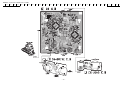
1
XR-EM70
XR-EM71
K
EZ
SERVICE MANUAL
COMPACT DISC
STEREO SYSTEM
BASIC TAPE MECHANISM : AZM-1 A4NM
BASIC CD MECHANISM : 3ZG-3 E13NM
SYSTEM
COMPACT
DISC
XR-EM70
CX-LEM70
XR-EM71
CX-LEM71
SPEAKER
REMOTE
CONTROLLER
SX-LEM70
RC-BAT15
This Service Manual is the Revision Publishing and replaces
Simple Manual of XR-EM70 <K>/ 71 <EZ>, (S/M Code No. 09-018-449-6T1).
S/M Code No. 09-019-449-6R1
N
O
SI
I
V TA
E
R
A
D
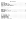
TABLE OF CONTENTS
SPECIFICATIONS ..............................................................................................................................................................3
PROTECTION OF EYES FROM LASER BEAM DURING SERVICING ...................................................................... 4
ELECTRICAL MAIN PARTS LIST .............................................................................................................................. 5 ~ 9
TRANSISTOR ILLUSTRATION ........................................................................................................................................ 10
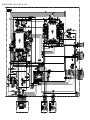
WIRING 1 (MAIN / PHONE / OPTICAL) ......................................................................................................................... 11
SCHEMATIC DIAGRAM 1 (MAIN 1 / 2 / PHONE / OPTICAL / HEAD) .......................................................................... 12
SCHEMATIC DIAGRAM 2 (MAIN 2 / 2 : AMP SECTION) ............................................................................................ 13
WIRING 2 (FRONT) ....................................................................................................................................................... 14
WIRING 3 (FL) ............................................................................................................................................................... 15
SCHEMATIC DIAGRAM 3 (FRONT / FL / DECK / FRAME / DRIVE) ............................................................................ 16
WIRING 4 (CD / CD DRIVE / CD LOAD) .................................................................................................................. 17
SCHEMATIC DIAGRAM 4 (CD / CD DRIVE / CD LOAD) ........................................................................................ 18
WIRING 5 (TUNER) ....................................................................................................................................................... 19
SCHEMATIC DIAGRAM 5 (TUNER) ............................................................................................................................. 20
WIRING 6 (PT) ............................................................................................................................................................... 21
SCHEMATIC DIAGRAM 6 (PT) ..................................................................................................................................... 22
WIRING 7 (DECK / FRAME / DRIVE / HEAD) ................................................................................................................ 23
IC BLOCK DIAGRAM ................................................................................................................................................ 24, 25
FL (HNA 11MS25) GRID ASSIGNMENT AND ANODE CONNECTION .................................................................... 26
IC DESCRIPTION .................................................................................................................................................... 27 ~ 32
ADJUSTMENT (TUNER / DECK / CD / FL) .............................................................................................................. 33 ~ 39
CD TEST MODE ............................................................................................................................................................. 40
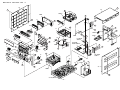
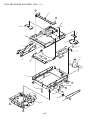
MECHANICAL EXPLODED VIEW 1 / 1 ......................................................................................................................... 41
MECHANICAL PARTS LIST 1 / 1 ................................................................................................................................... 42
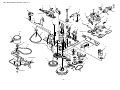
TAPE MECHANISM EXPLODED VIEW 1 / 2 ............................................................................................................... 43
TAPE MECHANISM PARTS LIST 1 / 2 ......................................................................................................................... 44
TAPE MECHANISM EXPLODED VIEW 2 / 2 ............................................................................................................... 45
TAPE MECHANISM PARTS LIST 2 / 2 ......................................................................................................................... 46
CD MECHANISM EXPLODED VIEW 1 / 2 ................................................................................................................... 47
CD MECHANISM PARTS LIST 1 / 2 ............................................................................................................................. 48
CD MECHANISM EXPLODED VIEW 2 / 2 ................................................................................................................... 49
CD MECHANISM PARTS LIST 2 / 2 ............................................................................................................................. 49
GENERAL SPEAKER DISASSEMBLY INSTRUCTIONS (FOR REFERENCE) ........................................................... 50
SPEAKER PARTS LIST <SX LEM70 (YJMN)> .......................................................................................................... 51
ACCESSORIES / PACKAGE LIST ................................................................................................................................... 51
2
SPECIFICATIONS
MAIN UNIT CX-LEM70 (K) / CX-LEM71 (EZ)
TUNER
FM tuning range
FM usable sensitivity (IHF)
FM antenna terminal
MW tuning range
MW usable sensitivity
LW tuning range
LW usable sensitivity
MW/LW antenna
AMPLIFIER
Power output
Input
Outputs
CASSETTE DECK
Track format
Frequency response
Recording system
Heads
CD PLAYER
Laser
D/A converter
Signal-to-noise ratio
Harmonic distortion
Wow and flutter
87.5 MHz to 108 MHz
16.8 dBf
75 ohms (unbalanced)
531 kHz to 1602 kHz (9 kHz step)
530 kHz to 1710 kHz (10 kHz step)
350 µV/m
144 kHz to 290 kHz
1400 µV/m
Loop antenna
GENERAL
Power requirements
Power consumption
Power consumption in
standby mode
Rated: 28 W + 28 W
(6 ohms, T.H.D. 1%, 1 kHz/DIN 45500)
Reference: 35 W + 35 W
(6 ohms, T.H.D. 10 %, 1 kHz/DIN 45324)
EZ: DIN MUSIC POWER
75 W + 75 W
AUX IN: 700 mV
SPEAKERS: 6 ohms or more
PHONES: 32 ohms or more
DIGITAL OUT (OPTICAL) jack
4 tracks, 2 channels stereo
50 Hz - 15000 Hz
AC bias
Recording/playback X 1, erase X 1
Dimensions (W x H x D)
Weight
Semiconductor laser (λ = 780 nm)
1 bit dual
88 dB (1 kHz, 0 dB)
Unmeasurable (1 kHz, 0 dB)
Unmeasurable
230 V AC, 50 Hz
60 W
With ECO mode on or auto: 0.8 W
With ECO mode off: 11.1 W
191.5 x 249.0 x 389.0 mm
5.3 kg
SPEAKER SYSTEM SX-LEM70
Speaker system
Speaker units
Impedance
Dimensions (W x H x D)
Weight
2 way, bass reflex (magnetic shielded)
Woofer: 120 mm cone
Tweeter: 25 mm dome
6 ohms
155 x 250 x 218 mm
2.4 kg
Design and specifications are subject to change without notice.
3
PROTECTION OF EYES FROM LASER BEAM DURING SERVICING
CAUTION
This set employs laser. Therefore, be sure to follow carefully the
instructions below when servicing.
Use of controls or adjustments or performance of procedures other than those specified herin may result in
hazardous radiation exposure.
WARNING!!
WHEN SERVICING, DO NOT APPROACH THE LASER
EXIT WITH THE EYE TOO CLOSELY. IN CASE IT IS
NECESSARY TO CONFIRM LASER BEAM EMISSION.
BE SURE TO OBSERVE FROM A DISTANCE OF MORE
THAN 30cm FROM THE SURFACE OF THE OBJECTIVE
LENS ON THE OPTICAL PICK-UP BLOCK.
ATTENTION
Lutillisation de commandes, réglages ou procédures
autres que ceux spécifiés peut entraîner une dangereuse
exposition aux radiations.
ADVARSEL
Usynlig laserståling ved åbning, når sikkerhedsafbrydereer
ude af funktion. Undgå udsættelse for stråling.
Caution: Invisible laser radiation when
open and interlocks defeated avoid
exposure to beam.
Advarsel: Usynlig laserståling ved åbning,
når sikkerhedsafbrydere er ude af funktion.
Undgå udsættelse for stråling.
This Compact Disc player is classified as a CLASS 1
LASER product.
The CLASS 1 LASER PRODUCT label is located on the
rear exterior.
VAROITUS!
Laiteen Käyttäminen muulla kuin tässä käyttöohjeessa
mainitulla tavalla saataa altistaa käyt-täjän
turvallisuusluokan 1 ylittävälle näkymättömälle
lasersäteilylle.
CLASS 1
KLASSE 1
LUOKAN 1
KLASS 1
VARNING!
Om apparaten används på annat sätt än vad som
specificeras i denna bruksanvising, kan användaren
utsättas för osynling laserstrålning, som överskrider
gränsen för laserklass 1.
LASER PRODUCT
LASER PRODUKT
LASER LAITE
LASER APPARAT
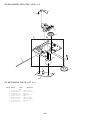
Precaution to replace Optical block
(KSS-213F)
CD PICK-UP Assy PWB
Body or clothes electrostatic potential could
ruin laser diode in the optical block. Be sure
ground body and workbench, and use care the
clothes do not touch the diode.
1) After the connection, remove solder shown in
right figure.
Solder
4
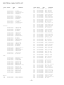
ELECTRICAL MAIN PARTS LIST
REF. NO.
PART NO.
IC
KANRI
NO.
DESCRIPTION
87-020-454-010
87-A21-831-010
8B-CLX-610-010
87-A20-455-010
87-A22-112-040
IC,DN6851
IC,SPS-422-1-F1
C-IC,LC876564V-5Y22
IC,HA12211
C-IC,BD3861FS
87-017-825-010
87-A20-446-010
87-A21-365-010
87-017-917-080
87-A20-445-010
IC,GP1F32T
C-IC,LA9241ML
IC,NJM7808FA(A)
IC,BU4066BCF
IC,BA5936S
87-A21-319-010
87-A21-695-010
87-A20-440-040
87-A21-928-010
C-IC,LC78622NE
IC,LA1845L
C-IC,BU1920FS<EZ>
IC,LC72131D-N
REF. NO.
TRANSISTOR
CAP,E 10-50 SMG
CAP,E 10-50 SMG
CAP,E 10-50 SMG
CAP,E 10-50 SMG
C-CAP,U 100P-50CH
C110
C111
C112
C113
C114
87-012-195-080
87-A12-092-080
87-A12-092-080
87-012-195-080
87-012-195-080
C-CAP,U 100P-50CH
CAP,E 22-50 SMG
CAP,E 22-50 SMG
C-CAP,U 100P-50CH
C-CAP,U 100P-50CH
C117
C118
C119
C120
C123
87-A12-317-080
87-A12-317-080
87-012-286-080
87-012-286-080
87-010-177-080
C-CAP,U 0.1-50 ZF
C-CAP,U 0.1-50 ZF
CAP, U 0.01-25
CAP, U 0.01-25
C-CAP,S 820P-50 SL
C124
C127
C128
C131
C133
87-010-177-080
87-012-195-080
87-012-195-080
87-010-831-080
87-012-282-080
C-CAP,S 820P-50 SL
C-CAP,U 100P-50CH
C-CAP,U 100P-50CH
C-CAP,U,0.1-16F
CAP, U 4700P-50
C140
C186
C187
C188
C189
87-012-278-080
87-010-759-080
87-A12-077-080
87-A12-077-080
87-012-195-080
C-CAP,U 2200P-50 B
C-CAP,U, 0.1-25F
CAP,E 33-35 SMG
CAP,E 33-35 SMG
C-CAP,U 100P-50CH
C190
C303
C304
C307
C311
87-012-195-080
87-012-268-080
87-012-268-080
87-010-759-080
87-010-787-080
C-CAP,U 100P-50CH
C-CAP,U 330P-50 B
C-CAP,U 330P-50 B
C-CAP,U, 0.1-25F
CAP, U 0.022-25
C312
C313
C314
C315
C316
87-010-787-080
87-A12-071-080
87-A12-071-080
87-012-276-080
87-012-276-080
CAP, U 0.022-25
CAP,E 47-25 SMG
CAP,E 47-25 SMG
C-CAP, U 1500P-50 B
C-CAP, U 1500P-50 B
C321
C322
C324
C325
C327
87-A10-025-080
87-A10-025-080
87-A12-071-080
87-A12-057-080
87-A12-090-080
C-CAP,U 0.22-16Z F
C-CAP,U 0.22-16Z F
CAP,E 47-25 SMG
CAP,E 330-6.3 SMG
CAP,E 4.7-50 SMG
C328
C332
C335
C336
C337
87-A12-090-080
87-010-759-080
87-A12-087-080
87-A12-087-080
87-010-759-080
CAP,E 4.7-50 SMG
C-CAP,U, 0.1-25F
CAP,E 1-50 SMG
CAP,E 1-50 SMG
C-CAP,U, 0.1-25F
C340
C341
C342
C343
C344
87-010-759-080
87-010-759-080
87-A12-070-080
87-012-280-080
87-012-286-080
C-CAP,U, 0.1-25F
C-CAP,U, 0.1-25F
CAP,E 33-25 SMG
CAP, U 3300P-50
CAP, U 0.01-25
C345
C346
C351
C352
C354
87-012-188-080
87-012-286-080
87-012-270-080
87-012-270-080
87-012-271-080
C-CAP,U 47P-50 CH
CAP, U 0.01-25
CAP, U 470P-50
CAP, U 470P-50
CAP, U 560P-50
C355
C356
C357
C358
C359
87-012-274-080
87-A12-071-080
87-012-286-080
87-012-279-080
87-012-279-080
CHIP CAP,U 1000P-50B
CAP,E 47-25 SMG
CAP, U 0.01-25
C-CAP,U 2700P-50 B
C-CAP,U 2700P-50 B
87-012-279-080
87-A10-781-080
87-A10-781-080
87-010-759-080
87-012-282-080
C-CAP,U 2700P-50 B
C-CAP,U 0.15-10 KB
C-CAP,U 0.15-10 KB
C-CAP,U, 0.1-25F
C-CAP,U 4700P-50 B
87-012-282-080
87-010-759-080
87-012-337-080
87-012-337-080
87-012-199-080
C-CAP,U 4700P-50 B
C-CAP,U, 0.1-25F
C-CAP,U 56P-50 J CH
C-CAP,U 56P-50 J CH
CAP 220P
C-TR,DTC144EKA
C-TR,RT1N 141C
TR,2SA1296GR
TR,2SA1981Y
TR,2SD655E
87-A30-075-080
87-A30-484-080
87-A30-087-080
87-A30-076-080
89-322-405-680
C-TR,2SA1235F
C-TR,KRA102S
C-FET,2SK2158
C-TR,2SC3052F
TR,2SC2240(GR/BL)
87-A30-306-010
87-A30-307-010
87-A30-268-040
87-A30-119-040
87-A30-186-010
TR,2SB1677
TR,2SD2619
C-TR,2SA1514K(S)
C-TR,2SC3906K R
FET,2SK3053
87-A30-455-040
87-A30-105-080
87-026-610-080
87-A30-494-080
89-213-702-010
C-TR,DTA144EKA
C-TR,RT1P 441C
TR,KTC3198GR
TR,2SA1980G
TR,2SB1370E
87-A30-521-080
87-A30-489-080
87-A30-060-080
89-503-602-080
87-A30-664-080
C-TR,2SC5345SF/S(O)
C-TR,KRA107S
C-TR,KTC3875GR<EZ>
C-FET,2SK360E
C-TR,2SC2620B
87-A30-086-040
87-A30-234-080
C-TR,CSD1306E
TR,CSC4115BC
87-A40-291-080
87-017-978-080
87-A40-270-080
87-A40-269-080
87-A40-455-080
DIODE,1N4148 (CPT)
DIODE,1N4003
C-DIODE,MC2838
C-DIODE,MC2836
DIODE,RL203 GW
87-A40-747-080
87-A40-749-080
87-A40-764-080
87-020-465-080
87-A40-760-080
ZENER,UZ5.1BSB
ZENER,UZ5.6BSB
ZENER,UZ10BSC
DIODE,1SS133 (110MA)
ZENER,UZ9.1BSA
87-A40-455-090
87-A40-553-080
87-A40-748-080
87-A40-777-080
87-A40-763-080
DIODE,RL203 GW
DIODE,1N4003 LES
ZENER,UZ5.6BSA
ZENER,UZ30BSB
ZENER,UZ10BSB
87-017-149-080
ZENER,HZS6A2L
C360
C368
C369
C370
C371
C-CAP,U 1000P-50 B
C-CAP,U 1000P-50 B
C372
C378
C381
C382
C388
DIODE
MAIN C.B
C101
C102
C103
C104
C107
C108
C109
KANRI
NO.
87-A12-091-080
87-A12-091-080
87-A12-091-080
87-A12-091-080
87-012-195-080
87-A30-435-040
87-A30-073-080
89-112-965-080
87-A30-495-080
89-406-555-080
87-012-274-080
87-012-274-080
5
PART NO.
DESCRIPTION
REF. NO.
PART NO.
C391
C403
C409
C422
C426
KANRI
NO.
87-010-787-080
87-010-759-080
87-012-282-080
87-016-459-080
87-A12-088-080
DESCRIPTION
C-CAP,U 0.022-25 KB
C-CAP,U, 0.1-25F
CAP, U 4700P-50
CAP,E 470-10 M SMG
CAP,E 2.2-50 SMG
C427
C439
C440
C441
C442
87-A12-088-080
87-A10-304-080
87-A10-304-080
87-A10-307-080
87-A10-307-080
CAP,E
CAP,M
CAP,M
CAP,M
CAP,M
C443
C444
C451
C452
C460
87-010-785-080
87-010-785-080
87-012-275-080
87-012-275-080
87-A12-087-080
C461
C462
C463
C464
C465
REF. NO.
C560
C561
C861
C862
C863
KANRI
NO.
87-A12-089-080
87-A12-071-080
87-010-405-080
87-010-759-080
87-012-199-080
CAP,E 3.3-50 SMG
CAP,E 47-25 SMG
CAP, ELECT 10-50V<EZ>
C-CAP,U, 0.1-25F<EZ>
CAP 220P<EZ>
C864
C865
C866
C867
C868
87-012-199-080
87-012-274-080
87-012-270-080
87-012-286-080
87-010-405-080
CAP
CHIP
CAP,
CAP,
CAP,
C-CAP,U0.015-25BK
C-CAP,U0.015-25BK
C-CAP,U 1200P-50 KB
C-CAP,U 1200P-50 KB
CAP,E 1-50 SMG
C869
C870
C871
C872
C873
87-012-286-080
87-012-184-080
87-012-180-080
87-012-280-080
87-012-280-080
CAP, U 0.01-25<EZ>
C-CAP,U 33P-50 CH<EZ>
C-CAP,U 22P-50 CH<EZ>
CAP, U 3300P-50<EZ>
CAP, U 3300P-50<EZ>
87-A12-087-080
87-A12-087-080
87-A12-087-080
87-A12-065-080
87-012-271-080
CAP,E 1-50 SMG
CAP,E 1-50 SMG
CAP,E 1-50 SMG
CAP,E 33-10 SMG
C-CAP,U 560P-50 KB
CN230
CN301
CN402
CN403
CN410
84-722-638-010
87-A60-625-010
87-A60-189-010
87-099-195-010
87-099-719-010
CONN,5P H WHT EH
CONN,8P V 2MM JMT
CONN,16P V TUC-P16P-B1
CONN,7P V BLK 6216
CONN,30P TYK-B(X)
C466
C467
C468
C470
C471
87-012-271-080
87-012-274-080
87-012-274-080
87-012-274-080
87-012-274-080
C-CAP,U
C-CAP,U
C-CAP,U
C-CAP,U
C-CAP,U
CN502
CNA201
FB405
FB406
J404
87-A90-510-010
8B-CJZ-640-010
87-A90-896-080
87-A90-896-080
87-A61-711-010
HLDR,WIRE 2.5-9P
CONN ASSY,9P TID-A(200)
F-BEAD, 035600STY7
F-BEAD, 035600STY7
JACK,PIN 2P MSP-242V-01 PBSN
C472
C473
C474
C475
C481
87-A12-471-080
87-010-759-080
87-012-278-080
87-012-278-080
87-A12-090-080
C-CAP,U 1000P-50 J SL
C-CAP,U, 0.1-25F
C-CAP,U 2200P-50 KB
C-CAP,U 2200P-50 KB
CAP,E 4.7-50 SMG
JW432
JW433
L301
L302
L351
87-A90-896-080
87-A90-896-080
87-A50-049-010
87-A50-049-010
87-007-342-010
F-BEAD, 035600STY7
F-BEAD, 035600STY7
COIL,TRAP 85K(COI)
COIL,TRAP 85K(COI)
COIL,OSC 85K BIAS
C482
C483
C484
C485
C486
87-A12-090-080
87-A12-088-080
87-A12-088-080
87-012-282-080
87-012-282-080
CAP,E 4.7-50 SMG
CAP,E 2.2-50 SMG
CAP,E 2.2-50 SMG
CAP, U 4700P-50
CAP, U 4700P-50
L402
L403
L861
L871
L872
87-A50-610-010
87-A50-610-010
87-005-847-080
87-A50-027-010
87-A50-027-010
COIL,1UH K(MDEC)
COIL,1UH K(MDEC)
COIL,2.2UH(CECS)<EZ>
COIL,1 POLE MPX(TOK)
COIL,1 POLE MPX(TOK)
C487
C488
C489
C490
C495
87-010-785-080
87-010-785-080
87-010-785-080
87-010-785-080
87-A12-087-080
C-CAP,U0.015-25BK
C-CAP,U0.015-25BK
C-CAP,U0.015-25BK
C-CAP,U0.015-25BK
CAP,E 1-50 SMG
R129
R130
R131
R132
SFR351
87-A00-258-080
87-A00-258-080
87-A00-258-080
87-A00-258-080
87-024-436-080
RES,M/F
RES,M/F
RES,M/F
RES,M/F
SFR,47K
C496
C497
C498
C503
C504
87-A12-087-080
87-A12-087-080
87-A12-087-080
87-010-759-080
87-010-759-080
CAP,E 1-50 SMG
CAP,E 1-50 SMG
CAP,E 1-50 SMG
C-CAP,U, 0.1-25F
C-CAP,U, 0.1-25F
SFR352
TH101
TH102
TM401
X862
87-024-436-080
87-A91-042-080
87-A91-042-080
87-A61-712-010
87-A70-307-010
SFR,47K RH063EC
C-THMS,100K 55001
C-THMS,100K 55001
TERMINAL, 4P SP MSP-324V1-01
VIB,XTAL 4.332MHZ CSA-309ST<EZ>
C505
C506
C509
C510
C511
87-010-759-080
87-010-759-080
87-010-759-080
87-010-759-080
87-010-759-080
C-CAP,U,
C-CAP,U,
C-CAP,U,
C-CAP,U,
C-CAP,U,
C512
C519
C520
C521
C522
87-010-759-080
87-A10-520-000
87-A10-520-000
87-010-928-000
87-A10-011-090
C-CAP,U, 0.1-25F
CAP,E 3300-35 M SMG
CAP,E 3300-35 M SMG
CAP,E 4700-25 M SMG
CAP,E 2200-25 SMG
C50
C51
C52
C53
C54
87-012-274-080
87-A12-091-040
87-A12-310-080
87-A12-310-080
87-A12-310-080
CHIP CAP,U 1000P-50B
CAP,E 10-50 SMG
C-CAP,U 0.01-50 K B
C-CAP,U 0.01-50 K B
C-CAP,U 0.01-50 K B
C525
C526
C530
C531
C532
87-A10-918-080
87-A10-918-080
87-A12-079-080
87-A12-062-080
87-012-286-080
CAP,E 100-16 SMG
CAP,E 100-16 SMG
CAP,E 100-35 SMG
CAP,E 100-10 SMG
CAP, U 0.01-25
C55
C56
C57
C60
CN50
87-A12-310-080
87-A12-310-080
87-A12-310-080
87-A10-025-080
87-099-040-010
C-CAP,U 0.01-50 K B
C-CAP,U 0.01-50 K B
C-CAP,U 0.01-50 K B
C-CAP,U 0.22-16 ZF
CONN,23P H BLK 6216
C534
C535
C536
C538
C539
87-A12-072-080
87-010-367-040
87-A12-067-080
87-012-282-080
87-012-278-080
CAP,E 100-25 SMG
CAP,E 4.7-25 M BP SRA
CAP,E 330-16 SMG
CAP, U 4700P-50
C-CAP,U 2200P-50 B
CN53
CNA52
D50
D51
D52
87-099-212-010
8B-CLX-617-010
87-A41-062-040
87-A41-062-040
87-A41-062-040
CONN,05P V BLK 6216
CONN ASSY,9P DECK PL-CONT
LED,LTL-1CHEE-012A RED
LED,LTL-1CHEE-012A RED
LED,LTL-1CHEE-012A RED
C540
C541
C545
C546
C547
87-A12-062-080
87-A12-079-080
87-010-831-080
87-A12-064-080
87-010-831-080
CAP,E 100-10 SMG
CAP,E 100-35 SMG
C-CAP,U,0.1-16F
CAP,E 1000-10 SMG
C-CAP,U,0.1-16F
D53
D54
FC050
FC053
S50
87-A41-062-040
87-A41-062-040
88-923-091-110
88-905-231-110
87-A91-024-180
LED,LTL-1CHEE-012A RED
LED,LTL-1CHEE-012A RED
FF-CABLE,23P 1.25 90MM
FF-CABLE,5P 1.25 230MM
SW-TACT KSHG611BT
S51
S52
87-A91-024-180
87-A91-024-180
SW-TACT KSHG611BT
SW-TACT KSHG611BT
2.2-50 SMG
0.056-50 J
0.056-50 J
0.1-50 J
0.1-50 J
560P-50 KB
1000P-50 KB
1000P-50 KB
1000P-50 KB
1000P-50 KB
0.1-25F
0.1-25F
0.1-25F
0.1-25F
0.1-25F
PART NO.
DESCRIPTION
220P<EZ>
CAP,U 1000P-50B<EZ>
U 470P-50<EZ>
U 0.01-25<EZ>
ELECT 10-50V<EZ>
0.22-1W
0.22-1W
0.22-1W
0.22-1W
RH063EC
J
J
J
J
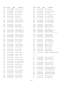
FRONT C.B
6
REF. NO.
PART NO.
S53
S54
S55
S56
S57
KANRI
NO.
87-A91-024-180
87-A91-024-180
87-A91-024-180
87-A91-024-180
87-A91-024-180
DESCRIPTION
SW-TACT
SW-TACT
SW-TACT
SW-TACT
SW-TACT
KSHG611BT
KSHG611BT
KSHG611BT
KSHG611BT
KSHG611BT
S58
S59
S60
S61
S62
87-A91-024-180
87-A91-024-180
87-A91-024-180
87-A91-024-180
87-A91-024-180
SW-TACT
SW-TACT
SW-TACT
SW-TACT
SW-TACT
S63
S64
S65
S66
S67
87-A91-024-180
87-A91-024-180
87-A91-024-180
87-A91-024-180
87-A91-687-010
SW-TACT
SW-TACT
SW-TACT
SW-TACT
SW,RTRY
S68
S69
87-A91-687-010
87-A92-291-010
C501
C502
C503
C504
C505
REF. NO.
C605
C606
C611
C612
C613
KANRI
NO.
87-012-195-080
87-012-195-080
87-010-831-080
87-010-831-080
87-010-831-080
C-CAP,U 100P-50CH
C-CAP,U 100P-50CH
C-CAP,U,0.1-16F
C-CAP,U,0.1-16F
C-CAP,U,0.1-16F
KSHG611BT
KSHG611BT
KSHG611BT
KSHG611BT
KSHG611BT
C614
C621
C651
C652
C653
87-010-831-080
87-010-831-080
87-A12-063-040
87-010-831-080
87-016-459-040
C-CAP,U,0.1-16F
C-CAP,U,0.1-16F
CAP,E 220-10 SMG
C-CAP,U,0.1-16F
CAP,E 470-10 SMG
KSHG611BT
KSHG611BT
KSHG611BT
KSHG611BT
RE012104PV-VOL
C654
C655
C656
C658
C659
87-010-831-080
87-A12-069-040
87-010-831-080
87-010-831-080
87-010-831-080
C-CAP,U,0.1-16F
CAP,E 22-25 SMG
C-CAP,U,0.1-16F
C-CAP,U,0.1-16F
C-CAP,U,0.1-16F
SW,RTRY RE012104PV-VOL
SW,RTRY RE121PVB25FINB1-24E
C660
C661
C662
C664
C665
87-010-831-080
87-012-266-080
87-012-197-080
87-010-831-080
87-012-172-080
C-CAP,U,0.1-16F
C-CAP,U 220P-50 B
C-CAP,U 150P-50 CH
C-CAP,U,0.1-16F
C-CAP,U 10P-50 D CH
87-A12-062-040
87-010-831-080
87-A12-062-040
87-A12-062-040
87-A12-062-040
CAP,E 100-10 SMG
C-CAP,U,0.1-16F
CAP,E 100-10 SMG
CAP,E 100-10 SMG
CAP,E 100-10 SMG
C666
C667
C668
C669
C671
87-012-172-080
87-012-170-080
87-A12-090-040
87-012-286-080
87-012-195-080
C-CAP,U 10P-50 D CH
C-CAP,U 8P-50 D CH
CAP,E 4.7-50 SMG
CAP, U 0.01-25
C-CAP,U 100P-50CH
C506
C507
C508
C509
C510
87-010-831-080
87-010-831-080
87-A11-058-080
87-A11-070-080
87-012-268-080
C-CAP,U,0.1-16F
C-CAP,U,0.1-16F
C-CAP,U 0.22-10 K B
C-CAP,U 0.033-16 K B
C-CAP,U 330P-50 B
C672
C673
C674
C681
C682
87-010-831-080
87-012-274-080
87-010-831-080
87-012-270-080
87-012-270-080
C-CAP,U,0.1-16F
CHIP CAP,U 1000P-50 K B
C-CAP,U,0.1-16F
CHIP CAP,U 470P-50B
CHIP CAP,U 470P-50B
C511
C512
C513
C514
C515
87-A10-828-080
87-010-785-080
87-A10-781-080
87-012-278-080
87-010-787-080
C-CAP,U 0.33-6.3 K B
C-CAP,U0.015-25BK
C-CAP,U 0.15-10 K B
CAP, U 2200P-50
C-CAP,U 0.022-25 K B
C683
C684
C685
C686
CN501
87-A12-088-040
87-A12-088-040
87-012-274-080
87-012-274-080
87-A60-424-010
CAP,E 2.2-50 SMG
CAP,E 2.2-50 SMG
C-CAP, U 1000P-50 B
C-CAP, U 1000P-50 B
CONN,16P V TOC-B
C516
C517
C518
C519
C520
87-A10-504-080
87-A10-260-080
87-012-197-080
87-012-286-080
87-012-282-080
C-CAP,U 0.047-16 K B
C-CAP,U 0.1-16 K B
C-CAP,U 150P-50 J CH
CAP, U 0.01-25
CAP, U 4700P-50
CN502
CN601
CN602
CN603
CNA601
87-099-199-010
87-A60-077-010
87-099-200-010
87-099-210-010
8B-CLX-619-010
CONN,6P 6216 H
CONN,10P H 9604S-10F
CONN,7P 6216H
CONN,05P H BLK 6216
CONN ASSY,3P D-OUT
C521
C522
C523
C524
C525
87-012-266-080
87-A11-058-080
87-012-280-080
87-A11-049-080
87-A12-066-040
C-CAP,U 220P-50 B
C-CAP,U 0.22-10 K B
CAP, U 3300P-50
C-CAP,U 1-6.3 K B
CAP,E 47-16 SME
FC501
FC502
FC602
FC603
R551
8B-CLX-618-010
88-906-081-110
88-907-211-110
88-905-131-110
87-022-249-080
FF-CABLE,16P 150MMCD-P
FF-CABLE,6P 1.25 80MM
FF-CABLE,7P 1.25 200MM
FF-CABLE,5P 1.25 130MM
CHIP RES,U 27K-1/16W F
C527
C529
C530
C531
C532
87-012-176-080
87-012-280-080
87-012-195-080
87-010-831-080
87-012-274-080
CAP 15P
CAP, U 3300P-50
C-CAP,U 100P-50 CH
C-CAP,U,0.1-16F
CHIP CAP,U 1000P-50B
R552
R553
R554
R555
R556
87-022-249-080
87-022-249-080
87-022-249-080
87-022-284-080
87-022-284-080
CHIP RES,U 27K-1/16W F
CHIP RES,U 27K-1/16W F
CHIP RES,U 27K-1/16W F
C-RES,U 68K-1/16W F
C-RES,U 68K-1/16W F
C533
C534
C535
C536
C537
87-A12-090-040
87-010-831-080
87-A12-066-040
87-010-831-080
87-A12-091-040
CAP,E 4.7-50 SMG
C-CAP,U,0.1-16F
CAP,E 47-16 SMG
C-CAP,U,0.1-16F
CAP,E 10-50 SMG
R559
R560
R563
R564
R687
87-022-251-080
87-022-251-080
87-022-288-080
87-022-288-080
87-A50-190-080
C-RES U33K 1/16WF
C-RES U33K 1/16WF
C-RES,U 150K-1/16W F
C-RES,U 150K-1/16W F
C-COIL,S BLM21A102S
C538
C539
C540
C541
C542
87-A11-070-080
87-A11-049-080
87-A10-781-080
87-A12-062-040
87-012-274-080
C-CAP,U 0.033-16 K B
C-CAP,U 1-6.3 K B
C-CAP,U 0.15-10 K B
CAP,E 100-10 SMG
CHIP CAP,U 1000P-50B
R688
SFR501
X651
87-A50-190-080
87-024-437-080
87-A70-046-010
C-COIL,S BLM21A102S
SFR100K,RH063EC
VIB,XTAL 16.934MHZ
C551
C552
C581
C582
C583
87-010-831-080
87-010-831-080
87-016-459-040
87-010-831-080
87-A12-066-040
C-CAP,U,0.1-16F
C-CAP,U,0.1-16F
CAP,E 470-10 SMG
C-CAP,U,0.1-16F
CAP,E 47-16 SMG
C584
C601
C602
C603
C604
87-010-831-080
87-010-831-080
87-012-195-080
87-012-195-080
87-012-195-080
C-CAP,U,0.1-16F
C-CAP,U,0.1-16F
C-CAP,U 100P-50CH
C-CAP,U 100P-50CH
C-CAP,U 100P-50CH
C101
C102
C103
C104
C105
87-A12-069-040
87-A12-069-040
87-A12-078-040
87-010-831-080
87-010-831-080
CAP, ELECT 22-25V SMG
CAP, ELECT 22-25V SMG
CAP,E 47-35 SMG
C-CAP,U,0.1-16F
C-CAP,U,0.1-16F
C106
C107
C108
C109
87-012-178-080
87-012-184-080
87-010-787-080
87-A12-086-080
C-CAP,U 18P-50 CH
C-CAP,U 33P-50 CH
CAP, U 0.022-25
CAP,E 0.47-50 SMG
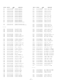
CD C.B
PART NO.
DESCRIPTION
FL C.B
7
REF. NO.
PART NO.
C110
C111
C112
C113
C114
KANRI
NO.
87-010-831-080
87-A12-063-040
87-A10-353-080
87-010-831-080
87-010-831-080
DESCRIPTION
C-CAP,U,0.1-16F
CAP,E 220-10 SMG
C-CAP,U0.22-10KB
C-CAP,U,0.1-16F
C-CAP,U,0.1-16F
CN101
CN102
CN103
FC102
FL101
87-099-720-010
87-A60-077-010
87-099-761-010
88-910-171-110
8B-CLX-611-010
L101
REF. NO.
C919
C920
C921
C922
C923
KANRI
NO.
87-012-184-080
87-012-184-080
87-012-180-080
87-012-174-080
86-ZA1-616-080
C-CAP,U 33P-50 CH
C-CAP,U 33P-50 CH
C-CAP,U 22P-50 CH
CAP CHIP CERA SS 12P CHJ
C-CAP,U 0.01-50 K B (MUR)
CONN,30P TYK-B(P)
CONN,10P H 9604S-10F
CONN,23P H 9604
FF-CABLE,10P 1.25 170MM
FL,HNA-11MS25
C924
C925
C926
C927
C942
87-012-164-080
87-012-164-080
86-ZA1-616-080
87-012-195-080
87-012-172-080
C-CAP,U 2P-50 CK
C-CAP,U 2P-50 CK
C-CAP,U 0.01-50 K B (MUR)
C-CAP,U 100P-50CH
CAPACITOR CHIP U 10P CH
87-A50-657-010
COIL,CLK 9.43MHZ (TOKO)7KLY
C772
C780
C786
C788
C789
87-012-286-080
87-012-274-080
87-012-286-080
87-012-167-080
87-A11-228-080
CAP, U 0.01-25
C-CAP,U 1000P-50 KB
CAP, U 0.01-25
C-CAP,U 5P-50 CH
C-CAP,U 0.027-25 K B
C947
C948
C952
C957
C958
87-012-286-080
87-012-270-080
87-012-286-080
87-012-174-080
87-012-286-080
CAP, U 0.01-25
CAP, U 470P-50
CAP, U 0.01-25
CAP CHIP CERA SS 12P CHJ
CAP, U 0.01-25
C790
C791
C792
C793
C795
87-A11-228-080
87-010-831-080
87-012-286-080
87-A10-262-080
87-012-286-080
C-CAP,U 0.027-25 K B
C-CAP,U,0.1-16F
CAP, U 0.01-25
C-CAP,U 1-10 Z F
CAP, U 0.01-25
C962
C963
C971
C972
C973
87-A10-262-080
87-010-831-080
87-A12-067-080
87-A11-063-080
87-012-286-080
C-CAP,U 1-10 Z F
C-CAP,U,0.1-16F
CAP,E 330-16 SMG
C-CAP,S 4.7-10 Z F
CAP, U 0.01-25
C798
C799
C800
C801
C802
87-010-831-080
87-010-982-040
87-012-191-080
87-A10-262-080
87-010-829-080
C-CAP,U,0.1-16F
CAP,E 33-25 GAS
CHIP CAP 68 PF
C-CAP,U 1-10 Z F
CAP, U 0.047-16
C974
C976
C979
C981
C982
87-012-286-080
87-010-831-080
87-012-195-080
87-010-553-040
87-010-831-080
CAP, U 0.01-25
C-CAP,U,0.1-16F
C-CAP,U 100P-50CH
CAP,E 47-16 GAS
C-CAP,U,0.1-16F
C804
C807
C808
C809
C815
87-010-555-040
87-A10-463-080
87-A10-262-080
87-A10-262-080
87-A10-463-080
CAP,E 100-10 GAS
C-CAP,U 0.47-10 Z F
C-CAP,U 1-10 Z F
C-CAP,U 1-10 Z F
C-CAP,U 0.47-10 Z F
C983
C984
C985
C987
C989
87-A11-132-080
87-012-286-080
87-012-195-080
87-012-286-080
87-012-286-080
CAP,TC U 0.01-50 K B
CAP, U 0.01-25
C-CAP,U 100P-50CH
CAP, U 0.01-25
CAP, U 0.01-25
C816
C818
C821
C822
C823
87-A10-463-080
87-012-276-080
87-A11-063-080
87-012-270-080
87-012-274-080
C-CAP,U 0.47-10 Z F
CAP, CHIP SS 1500 PBK
C-CAP,S 4.7-10 Z F
CAP, U 470P-50
CHIP CAP,U 1000P-50B
C990
C991
C992
C993
C994
87-012-195-080
87-012-182-080
87-012-172-080
87-012-274-080
87-012-195-080
C-CAP,U 100P-50CH
C-CAP,U 27P-50 CH
CAPACITOR CHIP U 10P CH
CHIP CAP,U 1000P-50B
C-CAP,U 100P-50CH
C824
C825
C831
C837
C842
87-A11-063-080
87-A11-317-080
87-010-552-040
87-A12-022-080
87-010-831-080
C-CAP,S 4.7-10 Z F
C-CAP,U 0.068U-16 K B
CAP,E 22-16 GAS
C-CAP,U 0.22-16 Z F
C-CAP,U,0.1-16F
C995
C996
C997
C998
C999
87-012-274-080
87-012-195-080
87-010-831-080
87-010-553-040
87-012-286-080
CHIP CAP,U 1000P-50B
C-CAP,U 100P-50CH
C-CAP,U,0.1-16F
CAP,E 47-16 GAS
CAP, U 0.01-25
C844
C850
C851
C852
C853
87-012-286-080
87-A10-262-080
87-012-286-080
87-012-286-080
87-012-286-080
CAP, U 0.01-25
C-CAP,U 1-10 Z F
CAP, U 0.01-25
CAP, U 0.01-25
CAP, U 0.01-25
CF831
CF832
CN991
D901
D902
87-008-423-010
82-785-747-010
87-A60-650-010
87-A41-048-040
87-A41-048-040
FLTR,CF SFE10.7MS3G-A
CF,MS2 GHY,R
CONN,16P H GRY TUC-P16X-C1
C-VARI-CAP,HVM16-03 TL
C-VARI-CAP,HVM16-03 TL
C859
C860
C901
C902
C903
87-010-831-080
87-012-286-080
87-012-162-080
87-012-165-080
87-012-164-080
C-CAP,U,0.1-16F
CAP, U 0.01-25
C-CAP,U 1P-50 CK
CAP 3P
C-CAP,U 2P-50 CK
D903
J832
J940
JW959
L801
87-A41-048-040
87-A61-534-010
87-A60-633-010
87-A11-132-080
87-A50-694-010
C-VARI-CAP,HVM16-03 TL
TERMINAL,ANT PAL AJ-2021
CONN,2P H 2.5MM JMT
CAP,TC U 0.01-50 K B
COIL,FM-DET 2 (COILS)
C904
C905
C906
C907
C908
87-A12-348-080
87-012-162-080
87-012-172-080
87-012-166-080
87-012-165-080
C-CAP,U 560P-25 J CH
C-CAP,U 1P-50 CK
CAPACITOR CHIP U 10P CH
C-CAP,U 4P-50 CH
CAP 3P
L802
L811
L832
L901
L902
87-A91-551-010
87-005-847-080
87-005-847-080
86-ZA1-612-010
86-ZA1-613-010
FLTR,PCFJZH-450 L(TOK)
COIL,2.2UH(CECS)
COIL,2.2UH(CECS)
COIL,FM ANT/RF-1-Z
COIL,FM ANT/RF-2-Z
C909
C910
C911
C912
C913
86-ZA1-615-080
87-012-164-080
87-012-166-080
87-012-195-080
86-ZA1-616-080
C-CAP,U
C-CAP,U
C-CAP,U
C-CAP,U
C-CAP,U
L903
L904
L905
L906
L907
87-005-847-080
86-ZA1-613-010
86-ZA1-612-010
87-005-847-080
86-ZA1-614-010
COIL,2.2UH K CECS
COIL,FM ANT/RF-2-Z
COIL,FM ANT/RF-1-Z
COIL,2.2UH(CECS)
COIL,FM OSC-Z
C914
C915
C916
C917
C918
86-ZA1-616-080
86-ZA1-616-080
86-ZA1-616-080
87-012-178-080
87-012-172-080
C-CAP,U 0.01-50 K B (MUR)
C-CAP,U 0.01-50 K B (MUR)
C-CAP,U 0.01-50 K B (MUR)
C-CAP,U 18P-50 CH
CAPACITOR CHIP U 10P CH
L908
L941
L942
L951
R790
88-ZA1-624-010
87-A50-020-010
87-A50-019-010
8B-ZA3-668-010
87-012-286-080
COIL,FM IFT 7-6.2 (COILS)
COIL,ANT LW(COI)
COIL,OSC LW(COI)
COIL,AM PACK 2Z(TOK)
CAP, U 0.01-25
TC942
X991
87-A91-774-080
87-A70-061-010
TRIMMER,PLY 30P 6.8X5.4 CDYL
VIB,XTAL 4.500MHZ CSA-309
TUNER C.B
680P-25 J CH
2P-50 CK
4P-50 CH
100P-50CH
0.01-50 K B (MUR)
PT C.B
8
PART NO.
DESCRIPTION
REF. NO.
PART NO.
!
!
!
C251
CN201
PT250
PT251
RY251
KANRI
NO.
87-A12-074-080
87-A61-110-010
8B-CLX-615-010
8B-MA6-675-010
87-A91-418-010
DESCRIPTION
CAP,E 470-25 SMG
CONN,9P V TID-A
PT,EZ BCL-30
PT,SUB BMA E (VRK)
RELAY,AC12V G5PA-1-M
!
!
T250
T251
87-A60-317-010
87-A60-317-010
TERMINAL, 1P MSC
TERMINAL, 1P MSC
REF. NO.
87-010-831-080
87-012-272-080
87-012-272-080
8B-CLX-626-010
87-A60-420-010
C-CAP,U,0.1-16F
C-CAP,U 680P-50 B
C-CAP,U 680P-50 B
CONN ASSY,5P V W HP
JACK,3.5 ST (MSC)
CON1
SFR1
SOL2
SW2
SW3
87-009-352-010
87-024-581-010
82-ZM3-628-010
87-A90-248-010
87-A90-248-010
CONN,9P H WHT PH
SFR,3.3K H KVSF637A
SOL ASSY,23SO
SW,MICRO ESE11SH2CXQ
SW,MICRO ESE11SH2CXQ
SW4
SW5
SW6
W1
87-A90-248-010
87-A90-248-010
87-A90-248-010
86-ZM4-601-110
SW,MICRO ESE11SH2CXQ
SW,MICRO ESE11SH2CXQ
SW,MICRO ESE11SH2CXQ
RBN-CORD,4P-300MM
87-A90-948-010
SW,LVR 2-1-2 MPU11263MLB0
86-NFZ-675-010
87-045-305-010
87-A91-662-010
8Z-ZG4-614-010
CONN,5P H 6216-11H
MOT,RF-500TB
SW,PUSH 1-1-1 MPU11244MLB0
F-CABLE,2P 130MM LED
85-ZM3-602-010
86-ZM1-605-010
PWB,FLEX A
CONN ASSY,AR3
S1
DRIVE C.B
87-010-759-080
87-A60-620-010
C-CAP,U 0.1-25 ZF
CONN,3P V 2MM JMT
CN1
M1
S2
W2
CD-DRIVE C.B
CON3
M20
M21
SW1
DESCRIPTION
FRAME C.B
OPTICAL C.B
C401
CN408
KANRI
NO.
DECK C.B
PHONE C.B
C231
C232
C233
CNA230
J231
PART NO.
87-A60-086-010
87-045-358-010
87-045-356-010
87-A90-042-010
CONN,6P H 6216
MOT,RF-310TA 43
MOT,RF-310TA 30
SW,LEAF MSW-17310MVP0
HEAD C.B
CNA301
CD-LOAD C.B
CON6
M1
SW1
SW2
87-099-210-010
87-045-305-010
87-036-110-010
87-036-110-010
CONN,5P H BLK 6216
MOTOR,RF-500TB
SW, MICRO SPPB62
SW, MICRO SPPB62
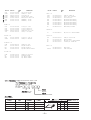
CHIP RESISTOR PART CODE
Chip Resistor Part Coding
8 8
A
Figure
Resistor Code
Value of resistor
Chip resistor
L
W
t
:A
Resistor Code : A
1.0
0.5
0.35
104
1.6
0.8
0.45
108
2
1.25
0.45
118
3.2
1.6
0.55
128
Dimensions (mm)
Wattage
1/16W
Type
1005
Tolerance
5%
Symbol
CJ
1/16W
1/10W
1608
2125
5%
5%
CJ
CJ
1/8W
3216
5%
CJ
Form
L
t
W
9
TRANSISTOR ILLUSTRATION
E C B
E C B
B C E
2SA1980G
2SA1981Y
2SC2240(GR/BL)
2SD655E
2SA1296GR
CSC4115BC
KTC3198GR
2SB1677
2SD2619
D
G
B C E
2SB1370E
C
S
D
S
G
B
E
G D S
2SK3053
2SK2158
2SK360E
10
2SA1235F
2SA1514K(S)
2SC2620B
2SC3052F
2SC3906KR
2SC5345SF/S(O)
CSD1306E
DTA144EKA
DTC144EKA
KRA102S
KRA107S
KTC3875GR
RT1N141C
RT1P441C
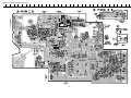
WIRING – 1 (MAIN / PHONE / OPTICAL)
32
31
30
29
28
27
26
25
24
23
22
21
20
19
18
17
16
15
14
13
12
11
10
9
8
7
6
5
4
3
2
1
A
B
C
D
E
F
G
H
I
J
K
L
M
N
O
P
Q
R
S
T
U
– 11 –
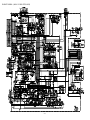
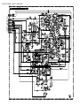
SCHEMATIC DIAGRAM – 1 (MAIN 1 / 2 / PHONE / OPTICAL / HEAD)
– 12 –
SCHEMATIC DIAGRAM – 2 (MAIN 2 / 2 : AMP SECTION)
– 13 –
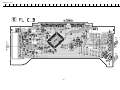
WIRING – 2 (FRONT)
32
31
30
29
28
27
26
25
24
23
22
21
20
19
18
17
16
15
14
13
12
11
10
9
8
7
6
5
4
3
2
1
A
B
C
D
E
F
G
H
I
J
K
L
M
N
O
P
Q
R
S
T
U
– 14 –
WIRING – 3 (FL)
32
31
30
29
28
27
26
25
24
23
22
21
20
19
18
17
16
15
14
13
12
11
10
9
8
7
6
5
4
3
2
1
A
B
C
D
E
F
G
H
I
J
K
L
M
N
O
P
Q
R
S
T
U
– 15 –
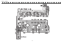
SCHEMATIC DIAGRAM – 3 (FRONT / FL / DECK / FRAME / DRIVE)
– 16 –
WIRING – 4 (CD / CD – DRIVE / CD – LOAD)
32
31
30
29
28
27
26
25
24
23
22
21
20
19
18
17
16
15
14
13
12
11
10
9
8
7
6
5
4
3
2
1
A
B
C
D
E
F
G
H
I
J
K
L
M
N
O
P
Q
R
S
T
U
– 17 –
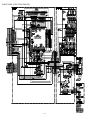
SCHEMATIC DIAGRAM – 4 (CD / CD – DRIVE / CD – LOAD)
– 18 –
WIRING – 5 (TUNER)
32
31
30
29
28
27
26
25
24
23
22
21
20
19
18
17
16
15
14
13
12
11
10
9
8
7
6
5
4
3
2
1
A
B
C
D
E
F
G
H
I
J
K
L
M
N
O
P
Q
R
S
T
U
– 19 –
SCHEMATIC DIAGRAM – 5 (TUNER)
– 20 –
WIRING – 6 (PT)
15
14
13
12
11
10
9
8
7
6
5
4
3
2
1
A
B
C
D
E
F
G
H
I
J
K
L
M
N
O
P
Q
R
S
T
U
– 21 –
SCHEMATIC DIAGRAM – 6 (PT)
– 22 –
WIRING – 7 (DECK / FRAME / DRIVE / HEAD)
15
14
13
12
11
10
9
8
7
6
5
4
3
2
1
A
B
C
D
E
F
G
H
I
J
K
L
M
N
O
P
Q
R
S
T
U
– 23 –
IC BLOCK DIAGRAM
– 24 –
– 25 –
FL (HNA 11MS25) GRID ASSIGNMENT / ANODE CONNECTION
GRID ASSIGNMENT
ANODE CONNECTION
26
IC DESCRIPTION
IC, LC78622NE
Description
Pin No.
Pin Name
I/O
1
DEFI
I
Defect detection signal (DEF) input. ("L" is applied when not used.)
2
TAI
I
For PLL/Test input. (Connected to 0V)
3
PDO
O
Phase comparison output to control the external VCO.
4
VVSS
Ground of the built-in VCO. Normally 0V.
5
ISET
I
For the connection of a resistor which adjusts the PDO output current.
6
VVDD
Power supply of the built-in VCO.
7
FR
I
Adjusts the VCO frequency range.
8
VSS
Ground of digital circuits. Normally 0V.
9
EFMO
O
For slice level control/EFM signal output.
10
EFMIN
I
EFM signal input.
11
T2
I
Test input. A pull-down resistor is incorporated. (Connected to 0V)
12
CLV+
13
CLV-
O
Disc motor control tri-state output.
14
V/P
O
15
HFL
I
Track detection signal input. Schmitt trigger input.
16
TES
I
Track error signal input. Schmitt trigger input.
17
TOFF
O
Tracking off output.
18
TGL
O
Tracking gain switching output. "L" raises the gain.
19
JP+
20
JP-
O
Track jump control tri-state output.
21
PCK
O
22
FSEQ
O
23
VDD
Power supply of digital circuits.
24
SL+
O
Controlled by serial data command issued by the microprocessor.
25
SL
O
Controlled by serial data command issued by the microprocessor.
26
V/P MONI
I
Prevent high speed rotation of no recording CD-R/RW disc by watch V/P.
27
SW-INSIDE
I
CD pickup inside limit switch.
28
CD R/W
O
CD-RW disc select control.
29
EMPH
O
Deemphasis monitor. "H": when playing a deemphasis disc. (Not used)
30
C2F
O
C2 flag output. (Not used)
31
DOUT
O
Output a digital OUT signal. (EIAJ format)
32
T3
33
T4
I
Test input. (Connected to 0V)
34
PCCL
Not used.
35
MUTE-L
O
Lch 1-bit DAC/Lch muting output. (Not used)
36
LVDD
Lch power supply.
37
O-LCH
O
Lch output.
38
LVSS
Lch ground. Normally 0V.
39
RVSS
Rch 1-bit DAC/Rch ground. Normally 0V.
Output to monitor the automatic switching between the rough servo control and phase servo
control. "H" : Rough servo, "L": Phase servo.
Monitors the clock signal for EFM data playback. 4.3218MHz when the phase is locked.
(Not used)
Sync signal detection output. Goes "H" when the sync signal detected from the EFM
signal matches the sync signal generated internally. (Not used)
27
Pin No.
Pin Name
I/O
Description
40
O-RCH
O
Rch output.
41
RVDD
Rch power supply.
42
MUTE-R
O
Rch muting output. (Not used)
43
XVDD
Power supply of crystal oscillator.
44
XOUT
O
45
XIN
I
46
XVSS
Ground of crystal oscillator. Normally 0V.
47
SBSY
O
Subcode block sync signal output. (Not used)
48
EFLG
O
C1, C2, single, duplex correction monitor. (Not used)
49
PW
O
Output of subcodes P, Q, R, S, T, U and W. (Not used)
50
SFSY
O
Subcode frame sync signal output. Falls when the subcode is set to the standby state. (No used)
51
SBCK
I
52
FSX
O
7.35kHz sync signal output obtained by dividing the oscillator frequency. (Not used)
53
WRQ
O
Subcode Q standby output.
54
RWC
I
Read/write control input. Schmitt trigger input.
55
SQOUT
O
Subcode Q output.
56
COIN
I
Command input from the microprocessor.
57
CQCK
I
58
RES
I
LC78622NE reset input.
59
T11
O
Test output. Set to open (normally "L" output.) (Not used)
60
16M
O
16.9344MHz output. (Not used)
61
4.2M
O
4.236MHz output.
62
T5
I
Test input. A pull-down resistor is incorporated. (Connected to 0V)
63
CS
I
Chip select input. (Connected to 0V)
64
T1
I
Test input with no pull-down resistor. (Connected to 0V)
For the connection of a 16.934MHz crystal oscillator.
Subcode read-out clock input. Schmitt trigger input. ("L" is applied when not used.)
(Connected to 0V)
Command input retrieval clock or subcode retrieval clock input from SQOUT. Schmitt trigger
input.
28
IC, LA9241ML
Description
Pin No.
Pin Name
I/O
1
FIN2
I
2
FIN1
I
3
E
I
4
F
I
For the connection of the pickup photodiode.
5
TB
I
Inputs the DC components in the TE signal.
6
TE
I
7
TE
O
TE signal output.
8
TESI
I
TES (track error sense) comparator input. The TE signal is passed through a BPF.
9
SCI
I
Shock detection input.
10
TH
I
Sets the time constant for the tracking gain.
11
TA
O
TA amp output.
12
TD
I
Composes the tracking phase compensation constant between the TD and VR pins.
13
TD
O
Sets the tracking phase compensation.
14
JP
I
Sets the amplitude of the tracking jump signal (kick pulses).
15
TO
O
Tracking control signal output.
16
FD
O
Focusing control signal output.
17
FD
I
Composes the focusing phase compensation constant between the FD and FA pins.
18
FA
O
Composes the focusing phase compensation constant between the FD- and FA- pins.
19
FA
I
Composes the focusing phase compensation constant between the FA and FE pins.
20
FE
O
FE signal output.
21
FE
I
22
A-GND
Ground of analog signals.
23
NC
Not connected.
24
SP
O
Single-ended output of the signals input to the CV+ and CV- pins.
25
SPG
I
For the connection of a resistor which sets the gain in the spindle 12cm mode. (Not used)
26
SP
I
For the connection of the spindle phase compensation constant with the SPD pin.
27
SPD
O
Spindle control signal output.
28
SLEQ
I
For the connection of sled phase compensation constant.
29
SLD
O
Sled control signal output.
30
SL
31
SL+
I
Sled feed signal input from the microprocessor.
32
JP
33
JP+
I
Tracking signal input from the DSP.
34
TGL
I
Tracking gain control signal input from the DSP. Low gain when TGL is "H".
35
TOFF
I
Tracking off control signal input from the DSP. Off when TOFF is "H".
36
TES
O
Outputs the TES signal to the DSP.
37
HFL
O
For the connection of the pickup photodiode. Addition to the FIN1 pin creates an RF
signal and subtraction from it create an EF signal.
For the connection of the pickup photodiode.
For the connection of the pickup photodiode. Subtraction from the F pin creates a TE
signal.
For the connection of a resistor which sets the gain of the TE signal between this pin
and the TE pin.
For the connection of a resistor whichs sets the gain of the FE signal between this pin
and the TE pin.
The HFL (high frequency level) signal is used to judge whether the main beam is positioned
on the pit or on the mirror.
29
Pin No.
Pin Name
I/O
38
SLOF
I
Sled servo off control input.
Description
39
CV
40
CV+
I
CLV error signal input from the DSP.
41
RFSM
O
RF output.
42
RFS
O
Sets the RF gain and the EFM signal's 3T compensation constant together with the RFSM pin.
43
SLC
O
44
SLI
I
Input to control the DSP's data slice level.
45
D-GND
Ground of digital signals.
46
FSC
O
Output for the focus search smoothing capacitor.
47
TBC
I
The TBC (tracking balance control) signal sets the EF balance variation range.
48
NC
Not connected.
49
DEF
O
Disc defect detection output.
50
CLK
I
Reference clock input. 4.23MHz is input from the DSP.
51
CL
I
Microprocessor command clock input.
52
DAT
I
Microprocessor command data input.
53
CE
I
Microprocessor chip enable input.
54
DRF
O
DRF (detect RF) is an output to detect the RF level.
55
FSS
I
56
VCC2
VCC of servo and digital circuits.
57
REFI
For the connection of bypass capacitor for the reference voltage.
58
VR
O
Reference voltage output.
59
LF2
Sets the time constant for disc defect detection.
60
PH1
For the connection of a capacitor to hold the RF signal peak.
61
BH1
For the connection of a capacitor to hold the RF signal bottom.
62
LDD
O
APC circuit output.
63
LDS
I
APC circuit input.
64
VCC1
VCC of RF signal circuits.
The SLC (slice level control) signal is output to control the DSP's data slice level of the RF
waveform.
The FSS (focus search select) signal switches the focus search modes (+/-search / +search with
respect to the reference voltage). (Not used)
30
IC, LC876564V-5Y22
Pin No.
Pin Name
I/O
Description
1
O-COIN
O
CD IC control data output.
2
O-CDCONT
O
CD block power ON / OFF control output.
3
O-OPEN (CD)
O
CD tray open data output.
4
O-CLOSE (CD)
O
CD tray close data output.
5
O-OPEN (CT)
O
Deck open / close output.
6
O-PL
O
Deck solenoid output.
7
I-AS
I
Deck auto stop signal input.
8
O-MOTOR
O
Deck motor ON / OFF output.
9
O-CLOSE (CT)
O
Deck open / close output.
10
O-CLKSFT
O
MICON clock shift control.
11
I-RESET
I
Reset input.
12
I-TU SIG
I
Tuner SD detect input.
13
I-CDSW (DOOR)
I
CD mecha switch A/D converter input.
14
VSS1
GND.
15
CF1
Connection of 9.43MHz oscillator.
16
CF2
Connection of 9.43MHz oscillator.
17
VDD1
Power supply input.
18
I-HOLD
I
Power failure detection input.
19
I-LEVEL
I
Signal level input.
20
I-STOP (HEAD)
I
Deck cam switch input and tape tray condition detect input.
21
I-CSTSW
I
Cassette tape and side A, B tab of cassette detect input.
22
I-ENC3 (VOL)
I
Volume rotary encoder A/D input.
23
I-ENC2 (TREBLE)
I
Treble rotary encoder A/D input.
24
I-ENC1 (BASS)
I
Bass rotary encoder A/D input.
25
I-KEY2
I
Key input. (A/D)
26
I-KEY1
I
Key input. (A/D)
27
I-TM BASE
I
Reference clock input for watch.
28
I-RDCL
I
RDS clock input. (EZ only)
29
I-RMC
I
System remote control signal input.
30 ~ 40
G11 ~ G1
O
FL grid G11 ~ G1 output.
41 ~ 45
P21 ~ P17
O
FL segment P21 ~ P17 output.
46
VDD3
Power supply input.
47 ~ 50
P16 ~ P13
O
FL segment P16 ~ P13 output.
51
VP
Power supply for FL display.
52 ~ 62
P12 ~ P2
O
FL segment P12 ~ P2 output.
63
LW/P1
I/O
64 ~ 67
NC
Not connected.
68
SI (ECHO)
Connected to GND through a resistor.
69
SLT (ECHO)
Connected to GND through a resistor.
70
SCK (ECHO)
Connected to GND through a resistor.
71
I-MIC
I
Microphone input. (Connected to GND through a resistor)
72
VDD4
Power supply input.
LW diode input / FL segment P1 output.
31
Pin No.
Pin Name
I/O
Description
73
O-LED (CD)
O
CD function LED ON / OFF.
74
O-LED (TU)
O
Tuner function LED ON / OFF.
75
O-LED (AU)
O
AUX function LED ON / OFF.
76
O-LED (TA)
O
Tape function LED ON / OFF.
77
O-LED (PW)
O
Power function LED ON / OFF. (Light up : ECO standby)
78
O-ECO
O
Relay switch ON / OFF output.
79
O-TUCE
O
PLL IC chip enable output.
80
O-TUDO
O
PLL IC control data output.
81
O-TUCL
O
PLL IC control clock output.
82
I-TUDI
I
Tune IF count serial data input.
83
I-STEREO
I
Tuner stereo detect input.
84
I-RDDT
I
RDS data input. (EZ only)
85
O-TUCONT
O
Tuner ON / OFF control output.
86
O-CLK (FUNC)
O
Function IC control clock output.
87
O-DATA (FUNC)
O
Function IC control data output.
88
O-AMP-CONT
O
Amplifier ON / OFF control output. (Not used)
89
VSS2
GND.
90
VDD2
Power supply input.
91
O-MUTE
O
Audio mute ON / OFF control output.
92
O-DOLBY
O
Dolby ON / OFF control output. (Not used)
93
O-BIAS
O
Bias ON / OFF control output.
94
O-PB/REC
O
PB IN /REC OUT control output.
95
O-REC-SEL
O
REC IN / REC MUTE control output.
96
I-DRF
I
CD focus ON detect data input.
97
I-WRQ
I
CD interrupt subcode out standby signal input.
98
I-SQOUT
I
CD IC subcode Q data input.
99
O-RWC
O
CD IC control chip enable output.
100
O-CQCK
O
CD IC control clock output.
32
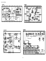
ADJUSTMENT (TUNER / DECK / CD / FL)
<TUNER SECTION>
PWB TUNER
1
4
4
VT
PARTS SIDE
L904
JW970
L905
9
L907
PATTERN SIDE
2
L902
IC991
L908
L801
L901
L802
24
1
L942
IC801
TC942
L941
CN991
4
12 11
7
6
L951
CN991
5
GND
CLK
Rch
Lch
Lch
1
2
3
4
5
6
7
9
5
3
1. VT Adjustment (LW)
Requirement
Measuring Device: Digital Multimeter
Test Point: VT, GND
Adjustment Point: L942
(1) Adjust the reception frequency of the set to 144 kHz.
(2) Adjust L942 until the test point voltage (VT) is 1.3 V ± 0.05 V.
(3) Adjust the reception frequency of the set to 290 kHz.
(4) Check that the test point (VT) voltage is below 8 V.
2. VT Check (MW)
Requirement
Measuring Device: Digital Multimeter
Test Point: VT, GND
(1) Adjust the reception frequency of the set to 1602 kHz.
(2) Check that the test point voltage is below 8 V.
(3) Adjust the reception frequency of the set to 531 kHz.
(4) Check that the test point voltage is above 0.6 V.
DIGITAL MULTIMETER
V
VT
GND
DIGITAL MULTIMETER
V
VT
GND
3. CLOCK Check
Requirement
Measuring Device: Frequency Counter
Test Point: CLOCK, GND
(1) Change to MW and adjust the reception frequency of the set to 1602 kHz.
(2) Check that the test point (CLOCK) frequency is 2052 kHz ± 45 Hz.
4. VT Adjustment (FM)
Requirement
Measuring Device: Digital Multimeter
Test Point: VT, GND
Adjustment Point: L907
(1) Adjust the reception frequency of the set to 108.0 kHz.
(2) Adjust L907 until the test point voltage (VT) is 7 V ± 0.05V.
(3) Adjust the reception frequency of the set to 87.5 MHz.
(4) Check that the test point voltage is above 0.5 V.
33
FREQUENCY COUNTER
Hz
CLOCK
GND
DIGITAL MULTIMETER
V
VT
GND
6
7
9
<MW/LW Adjustment>
For MW/LW adjustment, do wiring and connection as in the following.
60cm
Standard Signal Generator
SET
TP
Lch
Rch
GND
Connect to the respective measuring device
5. IF adjustment (MW)
Requirement
Measuring Device: Oscilloscope and Millivoltmeter
Test Point: Lch, Rch, GND
Adjustment Point: L802
(1) Adjust the setting of Standard Signal Generator (hereinafter S.S.G) to 450 kHz of 30 % variation.
(2) Adjust the reception frequency of the set to 999 kHz.
(3) While looking at the waveform on the oscilloscope, reduce the output level all the way.
(4) Adjust L802 until the value of the millivoltmeter reaches the maximum.
6. Tracking Adjustment (MW)
Requirement
Measuring Device: Oscilloscope and millivoltmeter
Test Point: Lch, Rch, GND
Adjustment Point: L951
(1) Adjust the S.S.G setting to 999 kHz of 30 % variation.
(2) While looking at the waveform on the oscilloscope, reduce the output level all the way.
(3) Adjust L951 until the value of the millivoltmeter reaches the maximum.
7. Tracking Adjustment (LW)
Requirement
Measuring Device: Oscilloscope and millivoltmeter
Test Point: Lch, Rch, GND
Adjustment Point: L941, TC942
(1) Adjust the S.S.G setting to 144 kHz, 30 % variation and reduce the output level all the way.
(2) Adjust L941 until the value of millivoltmeter reaches the maximum.
(3) Adjust the S.S.G setting to 290 kHz, 75 kHz variation, and reduce the output level all the way.
(4) Adjust TC942 until the value of the millivoltmeter reaches the maximum.
(5) Repeat the adjustment 2 or 3 times from step 1 to 4 above.
8. Auto Stop Check (MW)
Requirement
(1) Adjust the S.S.G setting to 999 kHz, 30 % variation, and 78 dBuV for the output level.
(2) Activate the tuner search function, and check that there is reception of 999 kHz.
34
OSCILLOSCOPE
CH1
CH2
GND
Lch
Rch
GND
AC MILLIVOLTMETER
Lch
CH1
CH2
GND
GND
Rch
<FM Adjustment>
For adjusting FM, do wiring and connection as in the following.
i
Standard Signal
Generator
SET
TP
Lch
Rch
GND
Connect to the respective measuring device
9. Tracking Adjustment (FM)
Requirement
Measuring device: Millivoltmeter
Test Point: Lch, Rch, GND
Adjustment Point: L901, L902, L904, L905
(1) Adjust the S.S.G setting to 108.0 MHz, 75 kHz variation and reduce the output level all the way.
(2) Adjust L901, L902, L904, L905 until the value of millivoltmeter reaches the maximum.
(3) Adjust the S.S.G setting to 98.0 MHz, 75 kHz variation, and 66 dBuV for the output level.
(4) Check that the test point voltage is below 13 dBuV.
10. Auto Stop Check (FM)
Requirement
(1) Adjust the S.S.G setting to 98.0 MHz, 75 kHz variation, and 40 dBuV for the output level.
(2) Activate the tuner search function, and check that there is reception of 98.0 MHz.
35
AC MILLIVOLTMETER
Lch
CH1
CH2
GND
GND
Rch
<DECK SECTION>
PWB MAIN
PATTERN SIDE
1
Lch
3
Rch
SFR352
SFR351
2
5
SP OUT
GND
Prepare the following before adjusting the deck.
Preparation
Measuring Device: Audio Signal Generator / Attenuator / Wow & Flutter Meter (Frequency Counter) / Oscilloscope / Millivolmeter /
Dummy Load (6 ohm).
1) Connect the set to the measuring device as shown in the following diagram.
2) Output 1V(1 kHz) from the generator and adjust the attenuator until AUX IN becomes 0.5 V.
3) Set AUX for FUNCTION and adjust the volume until the millivoltmeter value becomes 2 V.
AUDIO SIGNAL
GENERATOR
AC MILLIVOLTMETER
CENTER UNIT
OSCILLOSCOPE
ATTENUATOR
AUX(L)
DUMMY
LOAD
AUX(R)
OUTPUT
INPUT
OUTPUT (0.5V)
SPOUT(L)
(1KHz,1V)
SPOUT(R)
WOW&FLUTTER METER
Hz
HP OUT
%
INPUT
36
6Ω
OUTPUT
CH1 CH2
CH1
CH2
4
1. Checking Tape Speed
Requirements
Test Tape: TTA-100 (3 kHz)
Test Point: Lch, Rch, GND
Adjustment Point: SFR1
1) Insert the test tape (TTA-100), FWD play back the centre of the tape and check that the speed is 3,000 Hz ± 45 Hz.
2) RVS playback and check that ± 45 Hz is added according to the FWD speed.
2. Adjusting Head Azimuth
Requirements
Test Tape: TTA-300 (10 kHz)
Test Point: Lch, Rch, GND
Adjustment Point: Head Azimuth Screws
1) Set the V mode of the oscilloscope to ADD.
2) Insert the test tape (TTA-300), FWD playback the centre of the tape and adjust, using the head azimuth screws until the waveform of the
oscilloscope has reached the maximum when playing back at 10 kHz.
3) Reverse the tape, RVS playback and adjust, using the head azimuth screws until the waveform of the oscilloscope has reached the maximum.
4) After the adjustment, bond lock (1600B) the screws.
3. Checking Playback Frequency Reponse
Requirements
Test Tape: TTA-300 (315 Hz / 10 kHz)
Test Point: Lch, Rch, GND
1) Insert the test tape (TTA-300) and playback 315 Hz and 10 kHz.
2) Use the 315 Hz output level as a standard, check that the 10 kHz level is within ± 3 dB.
4. Checking Playback Sensitivity
Requirements
Test Tape: TTA-200 (400 Hz)
Test Point: Lch, Rch, GND
1) Insert the tape (TTA-200) and playback.
2) Check that the output level is within 900 mV ± 3 dB.
5. Adjusting the REC / PB Frequency Response
Requirements
Test Tape: TTA-602
Test Point: Lch, Rch, GND
Input Point: AUX (1 kHz / 10 kHz)
Adjustment Point: SFR351 (Lch), SFR352 (Rch)
1) Set AUX for function and reduce attenuator output by 20 dB.
2) Insert the test tape (TTA-602) and record 1 kHz and 10 kHz alternately from AUX.
3) Playback the tape, adjust SFR351 (Lch) / SFR352 (Rch) until the playback output level of 1 kHz is within ± 1 dB according to the standard
when the playback output level of 1 kHz is used as the standard.
37
<CD SECTION>
PWB CD
6
VC
R546
1
RIOP
SFR501 FE
IC501
TE
4
RF
2
3
IC651
CD Adjustment Method
Perform the adjustments after the machine enters the test mode.
Place the CD mechanism on level ground.
Equipment and tools required
Measuring equipment: Oscilloscope (Use the probe of 10:1)
Digital Multimeter (Use it in the DC Volt range)
Jitter meter (Kikusui 6235)
Test Disc:
TCD-782
ATD-001
1. Focus Offset Adjustment
1) Connect a digital multimeter to the test point (FE), (VC).
2) Play back the 2nd track of TCD-782.
3) Adjust SFR501 until the digital multimeter indicates 0 ± 10 mV.
DIGITAL MULTIMETER
V
FE
VC
2. RF Waveform Check
1) Connect an oscilloscope to test point (RF), (VC).
2) Play back the 2nd track of TCD-782.
3) Check that the RF waveform has the maximum amplitude and
the center of the wedge waveform has the clear blank.
OSCILLOSCOPE
Approx.
1.8 ± 0.3
Vp-p
OUTPUT
3. Jitter Check
1) While an oscilloscope is kept connected in the same test point as
in step 2. RF Waveform Check, connect the output terminal of an
oscilloscope to the input terminal of the jitter meter.
2) Set the VOLT range selector of an oscilloscope to 500 mV range
or lower.
3) Play back the 2nd track of TCD-782.
4) Check that the jitter meter indicates 28.0 ns or less.
38
0V
VOLT / DIV: 500mV
EYE PATTERN
must be CLEAR and MAX
RF
VC
OSCILLOSCOPE
JITTER METER
OUTPUT
RF
VC
INPUT
ns
4. Tracking Balance Check
1) Connect the test point (TE), (VC) to the oscilloscope.
2) Playback the second track of TCD-782 and press the PAUSE button.
3) Check that the traverse waveforms of the oscilloscope are up and
down symmetrical.
OSCILLOSCOPE
A
VC
OUTPUT
B
VOLT / DIV: 500mV
TIME / DIV: 1ms
TE
VC
5.
Play Ability Check
1) Play back the 3rd, 8th, and 13th track of ATD-001. Check that the
noise does not occur and sound skipping does not occur.
6.
Laser Current Check
* Do not perform this measurement unless the laser is suspected to
be defective.
1) Connect a digital multimeter across the resistor R546 (10 ohm).
2) Play back the TCD-782 and check the DC voltage value on the
digital multimeter.
3) Calculate the laser current (Iop) by dividing the DC voltage across
R546 by the resistor value (R546 = 10 ohm). Check that the laser
current (Iop) is SPEC VALUE ± 10 %.
DIGITAL MULTIMETER
V
R546
R546
EXAMPLE
KSS-213F
05Y93
DA372
SPEC VALUE
37.2 mA
<FL SECTION>
PWB FL
PARTS SIDE
PATTERN SIDE
R149
TP
GND
77
L101
IC101
1. Clock Adjustment
1) Connect an oscilloscope to test point OSC (IC101 77 pin) and GND (IC101 89 pin).
2) Insert the AC plug while pressing POWER and TUNER / BAND buttons.
3) Adjust L101 until the oscilloscope indicates 318.87 Hz ± 0.08 Hz (3.1352 ~ 3.1368 ms)
39
CD TEST MODE
1. How to Start the CD Test Mode
While pressing the CD FUNCTION button, insert the AC plug to the power outlet.
When the test mode started, the message [CD TEST] is displayed.
2. How to Exit the CD Test Mode
Press the POWER button or disconnect the AC plug.
3. Function and Usage of the CD Test Mode
No
Mode
Button for
Activation
Display
Operation
All lights are
lit.
Contents
1
Start Mode
Microcomputer check
2
Search Mode
STOP button
READING
LD illuminates all the time
Focus search continues
operations *1
Spindle motor continuous kick
APC circuit check
Laser current measurement
Focus search waveform check
3
Play Mode
PLAY button
Normal
Normal playback
If TOC cannot be read, focus
search is continued
Each servo circuit is checked
DRF check
4
Traverse Mode
PAUSE button
Normal
Tracking servo OFF/ON
STOP button to cancel
Tracking balance check
5
Sled Mode
FF button
CD TEST
Pickup moves to the inner
circumference *2
RWD button
CD TEST
Pickup is moves to the outer
circumference *2
Sled circuit check
Mechanism operation check
Pickup Check
* 1.
The driver IC heats up and the protection circuit starts working when the focus search is continued for 10 minutes or longer. There can be a
case that operations cannot be performed correctly. In such a case, turn off the main power. After cooling down the machine, restart the
machine.
* 2.
Be careful not to damage the gear because the sled motor rotates while the FF or RWD button is being pressed even if the pickup is located in
the innermost track or the outermost track.
40
MECHANICAL EXPLODED VIEW 1 / 1
10
A
F
28
A
3ZG-3
PWB
A
11
A
A
E
16
FL
G
A
B
9
A
17
8
G
A
12
PWB
7
A
PWB
E
18
D
E
6
19
A
PWB
A
PWB
27
21
PWB
5
A
HT-SINK,
SUB B
20
29
A
HT-SINK,
ASSY MAIN 2
B
A
A
22
A
D
13
15
D
B
A
4
HT-SINK,
SUB A
14
25
23
H
C
3
2
24
1
PWB
A
PWB
A
D
26
AZM-1
F
CHAS,MAIN
41
MECHANICAL PARTS LIST 1 / 1
REF. NO. PART NO.
KANRI
DESCRIPTION
NO.
CABI,FR<EZ[S]>
CABI,FR K<K[S]>
PANEL,TRAY CASS
KNOB,RTRY VOL
KNOB,RTRY BT
1
1
2
3
4
8B-CLX-001-010
8B-CLX-022-010
8B-CLX-008-010
8B-CLX-010-010
8B-CLX-011-010
5
6
6
7
8
8B-CLX-014-010
8B-CLX-009-110
8B-CLX-028-110
8B-CLX-013-010
8B-CLX-012-010
KEY,POWER
WINDOW ASSY,DISP<EZ[S]>
WINDOW ASSY,DISP K<K[S]>
KEY,CONT
KEY,FUNC
9
10
11
12
13
8B-CLX-018-010
8B-CLX-004-110
8B-CLX-203-010
88-923-091-110
8B-CLX-015-010
14
15
16
17
18
8B-CLX-016-010
88-905-231-110
8B-CLX-007-010
8B-CLX-202-010
88-905-131-110
REF. NO. PART NO.
KANRI
DESCRIPTION
NO.
FF-CABLE,10P 1.25 170MM
FF-CABLE,16P 1.0 150MM CD-PICK
FF-CABLE,6P 1.25 80MM
FF-CABLE,7P 1.25 210MM
F-BEAD,15-25-15 E2515MRT
19
20
21
22
23
88-910-171-110
8B-CLX-618-010
88-906-081-110
88-907-211-110
87-003-317-010
24
25
26
27
27
87-085-185-010
87-A80-157-010
8B-CLX-005-110
8B-CLX-002-010
8B-CLX-026-010
BUSHING,AC CORD(E) CM-22B
AC CORD ASSY,E BLK CC
PANEL,SIDE R
CABI,REAR<EZ[S]>
CABI,REAR K<K[S]>
REFLECTOR,FUNC
PANEL,SIDE L
HLDR,FL
FF-CABLE,23P 1.25 90MM
KEY,EJECT CD
28
29
A
B
C
8B-CLX-003-010
8B-CLX-017-010
87-067-703-010
87-B10-315-010
87-B10-318-010
PANEL,TOP
REFLECTOR,POWER
BVT2+3-10 W/0 SL0T
BVIT3B+3-8 R W/O
BVIT3C+4-8 R W/O
KEY,EJECT CASS
FF-CABLE, 5P 1.25 230MM
PANEL,TRAY CD
CHAS,CD
FF-CABLE,5P 1.25 130MM
D
E
F
G
H
87-721-096-410
87-B10-294-010
87-067-761-010
87-NF4-224-010
88-AR1-217-010
QT2+3-10 W/O SLOT
BVT2+2.6-8
BVT2+3-10 BLK
S-SCREW,IT3B+3-8 CU
S-SCREW,BFT2+3-8
!
COLOR NAME TABLE
Basic color symbol
Color
Basic color symbol
Color
Basic color symbol
Color
B
Black
C
Cream
D
Orange
G
Green
H
Gray
L
Blue
LT
Transparent Blue
N
Gold
P
Pink
R
Red
S
Silver
ST
Titan Silver
T
Brown
V
Violet
W
White
WT
Transparent White
Y
Yellow
YT
Transparent Yellow
LM
Metallic Blue
LL
Light Blue
GT
Transparent Green
LD
Dark Blue
DT
Transparent Orange
GM
Metallic Green
YM
Metallic Yellow
DM
Metallic Orange
PT
Transparent Pink
LA
Aqua Blue
GL
Light Green
HT
Transparent Gray
HM
Metallic Gray
NH
Champagne Gold
M
Wood Pattern
42
TAPE MECHANISM EXPLODED VIEW 1 / 2
C
1
C
2
3
7
4
8
5
10
11
13
6
15
12
14
16
D
PWB
B
17
E
18
19
E
9
6ZM-4
A
A
43
TAPE MECHANISM PARTLIST 1 / 2
REF. NO. PART NO.
KANRI
NO.
8A-ZM1-214-010
8A-ZM1-223-010
8A-ZM1-209-010
8A-ZM1-233-010
8A-ZM1-215-210
PLATE,F STOPPER
SPR-T,LOCK F
GEAR,SLIDE B
FRAME,MAIN BL
LEVER ASSY,SLIDE L
6
7
8
9
10
8A-ZM1-217-010
8A-ZM1-212-010
8A-ZM1-208-110
8A-ZM1-230-210
8A-ZM1-220-010
LEVER ASSY,SLIDE R
LEVER,LOCK F
GEAR,SLIDE A
BELT,BASE
SPR-E,CLAMP
11
12
13
14
15
8A-ZM1-216-310
8A-ZM1-234-110
87-045-305-010
86-ZL1-210-010
8Z-ZG4-614-010
PLATE ASSY,CLAMP
TRAY,CASSETTE BL
MOTOR, RF-500TB DC-5V (2MA)
PULLEY,MOT
F-CABLE,2P 130MM LED
16
17
18
19
A
8A-ZM1-202-110
86-ZL1-214-010
8A-ZM1-207-110
8A-ZM1-213-110
87-067-660-010
BASE,
SPR-P,CASS
GEAR,FRAME
GEAR,PULLEY
TAPPING SCREW, BVT2+3-8
B
C
D
E
88-ZG5-302-010
88-ZG5-317-010
87-251-072-410
8A-ZM1-240-010
S-SCREW,8ZG5+2-4 W/O
S-SCREW,8ZG5S+2-4 W/O
U+2.6-5
S-SCREW,GEAR F/P
1
2
3
4
5
DESCRIPTION
44
TAPE MECHANISM EXPLODED VIEW 2 / 2
21
6
5
4
B
53
B
3
J
14
22
A
16
HEAD C.B
23
24
2
15
52
54
a
8
18
19
7
9
13
25
10
8
17
11
26
47
12
49
9
DECK C.B
48
1
a
H
51
I
b
50
PLATE,SHLD DECK
20
27
b
45
46
31
30
G
29
32
D
28
33
41
HLDR,MOT L
44
34
E
36
35
42
37
40
38
43
D
C
CUSH-G
39
F
R7NM
45
TAPE MECHANISM PARTLIST 2 / 2
REF. NO. PART NO.
KANRI
NO.
82-ZM1-358-010
82-ZM1-258-210
82-ZM1-363-010
82-ZM1-266-310
82-ZM1-214-010
DESCRIPTION
CHAS ASSY,FPC
SPR-T,PINCH L
LEVER,ASSY PINCH LD
LVR,DIR
SPR-T,DIR
6
7
8
9
10
82-ZM1-333-210
86-ZM1-203-010
86-ZM1-221-010
82-ZM1-240-110
82-ZM1-241-310
11
12
13
14
15
36
37
38
39
40
KANRI
NO.
82-ZM1-224-410
82-ZM3-333-310
82-ZM1-338-110
82-ZM1-305-210
82-ZM1-227-310
LVR,FR
SLIP DISK ASSY 2
BELT,FR 4
SPR-E,TRIG 2
LVR,TRIG
PLATE,LINK2
CAP,REEL
SPR-C,BT 2L
LVR,REC(*)
LVR,MC
41
42
43
44
45
82-ZM1-225-210
82-ZM1-226-010
86-ZM4-214-010
86-ZM4-215-010
82-ZM1-221-310
GEAR,FR
GEAR,REW
FLY-WHL ASSY,R4W
FLY-WHL ASSY,L4W
GEAR,CAM(*)
82-ZM1-242-010
82-ZM1-243-010
82-ZM3-339-110
82-ZM1-222-310
82-ZM1-223-010
LVR,CAS
LVR,STOP
SHAFT,COUPLER N3
LVR,PLAY(*)
GEAR,PLAY
46
47
48
49
50
82-ZM1-255-310
82-ZM3-335-310
86-ZM1-206-010
87-A90-343-010
82-ZM3-221-210
SPR-E,LVR DIR
PULLEY,COUPLER M3
BELT,MAIN L
MOT,SHU2R 70
PULLEY,MOT 2M
16
17
18
19
20
82-ZM3-353-010
82-ZM1-210-110
82-ZM1-269-210
82-ZM1-219-110
86-ZM1-217-110
SPR-T,HEAD 2
GEAR,H T
SPR-T,BRG
SPR-T,LINK
BELT,MOT
51
52
53
54
A
86-ZM4-601-110
86-ZM1-605-010
86-ZM1-202-010
82-ZM1-288-010
85-ZM3-202-010
RBN-CORD,4P 300MM
CONN ASSY, AR3
SHAFT,REEL
SH,1.63-3.2-0.5 SLT
S-SCREW,TG
21
22
23
24
25
82-ZM1-314-110
87-A92-197-010
82-ZM1-208-310
82-ZM1-207-910
82-ZM1-218-010
PLATE,HEAD
HEAD,RPH HADKH5666A FPC
HLDR,HEAD
GUIDE,TAPE
SPR-E,HB
B
C
D
E
F
80-ZM6-207-010
82-ZM3-318-110
87-067-178-010
87-B10-008-010
82-ZM3-334-010
V+1.6-7
S-SCREW W,MOTOR M2
VTT+2.6-3
W-P,2.08-8-0.4-SLIP
PW 2.16-6-0.4
26
27
28
29
30
82-ZM1-206-910
82-ZM1-362-010
82-ZM1-259-210
82-ZM3-628-010
82-ZM1-322-010
CHAS,HEAD
LEVER,ASSY PINCH RD
SPR-T,PINCH R
SOL ASSY,23 SO
SPR-T,FR 60
G
H
I
J
82-ZM3-222-010
87-B10-043-010
80-ZM6-243-010
86-ZM4-206-110
S-SCREW,SHILD PLATE
W-P,0.99-4-0.25 SLT
SH 1.75-3.6-0.5 SLT
S-SCREW,AZIMUTH L
31
32
33
34
35
82-ZM1-220-210
82-ZM3-616-010
86-ZM1-219-010
86-ZM1-220-010
82-ZM1-216-510
GEAR,IDLER
RING MAGNET 4
CLR,REEL SLIP
FELT,DIA 5.3-14-0.8
GEAR,REEL
1
2
3
4
5
REF. NO. PART NO.
46
DESCRIPTION
CD MECHANISM EXPLODED VIEW 1 / 2
9
F
18
C
F
13
18
14
a
16
3ZG-2 E3NM
b
15
11
5
10
E
7
8
4
B
6
2
D
a
12
3
17
A
PWB
b
47
1
CD MECHANISM PARTS LIST 1 / 2
REF. NO. PART NO.
KANRI
NO.
83-ZG3-224-510
83-ZG3-228-610
83-ZG3-208-010
83-ZG3-213-010
83-ZG3-209-610
HLDR M2
CHAS,L6
PULLEY,MOTOR
LVR,SW
CAM,SLIDE
6
7
8
9
10
83-ZG3-207-010
83-ZG3-204-210
83-ZG3-205-010
83-ZG3-219-010
83-ZG3-220-210
GEAR,TRAY
GEAR,C
GEAR,D
PLATE,CLAMP
GEAR,PULLEY 2
11
12
13
14
15
83-ZG3-214-010
83-ZG3-231-210
83-ZG3-230-110
86-ZG1-239-110
83-ZG3-604-010
BELT,L
TRAY,CD 3
HLDR,CHUCK 2(*)
PLATE,DISC PC
RING,MAG 2
16
17
18
A
B
86-ZG1-238-010
87-045-305-010
83-ZG3-225-010
87-067-945-110
87-251-071-410
HLDR,MAGNET 6ZG N
MOTOR, RF-500TB DC-5V (2MA)
CUSH-G, MAIN A
VFT2+3-12(F10)
U+2.6-4
C
D
E
F
83-ZG3-235-010
87-352-075-210
83-ZG3-217-010
81-ZG1-254-010
VFT2+2.6-8
VT2+2.6-10
S-SCREW,GEAR D
S-SCREW,MECH HLDR
1
2
3
4
5
DESCRIPTION
48
CD MECHANISM EXPLODED VIEW 2 / 2
7
8
2
3
1
A
4
M21
6
SW1
5
PWB
CD MECHANISM PARTS LIST 2 / 2
REF. NO. PART NO.
1
2
3
4
5
KANRI
NO.
83-ZG2-262-010
87-A90-836-010
83-ZG2-235-010
83-ZG2-236-010
83-ZG2-205-310
DESCRIPTION
CHAS ASSY,E3
PICKUP,KSS-213F
GEAR,A3
GEAR,MOTOR 3
GEAR,B
6
7
8
A
83-ZG2-253-010
83-ZG2-245-510
83-ZG2-250-210
87-261-032-210
SHAFT,SLIDE 5
LEVER,SHUTTER(*)
SPR-E,SHT 2
V+2-3
49
GENERAL SPEAKER DISASSEMBLY INSTRUCTIONS (FOR REFERENCE)
Type.1
Type.4
TOOLS
Insert a flat-bladed screwdriver into the position indicated by the
arrows and remove the panel. Remove the screws of each speaker
unit and then remove the speaker units.
1 Plastic head hammer
2 (() flat head screwdriver
3 Cut chisel
1
2
3
How to Remove the PANEL, FR
Type.2
Remove the grill frame and four pieces of rubber caps by pulling
out with a flat-bladed screwdriver. Remove the screws from hole
where installed rubber caps. Insert a flat-bladed screwdriver into
the position indicated by the arrows and remove the panel. Remove the screws of each speaker unit and then remove the speaker
units.
1.
Insert the (() flat head screwdriver tip into the gap
between the PANEL, FR and the PANEL, SPKR. Tap the
head of the (() flat head screwdriver with the plastic
hammer head, and create the clearance as shown in Fig-1.
2.
Insert the cut chisel in the clearance, and tap the head of
the cut chisel with plastic hammer as shown in Fig-2, to
remove the PANEL, FR.
3.
Place the speaker horizontally. Tap head of the cut chisel
with plastic hammer as shown in Fig-3, and remove the
PANEL, FR completely.
Type.3
Insert a flat-bladed screwdriver into the position indicated by the
arrows and remove the panel. Turn the speaker unit to counterclockwise direction while inserting a flat-bladed screwdriver into
one of the hollows around speaker unit, and then remove the speaker
unit. After replacing the speaker unit, install it turning to clockwise
direction until "click" sound comes out.
Fig-1
Fig-2
Fig-3
How to Attach the PANEL, FR
Attach the PANEL, FR to the PANEL, SPKR. Tap the four
corners of the PANEL, FR with the plastic hammer to fit the
PANEL, FR into the PANEL, SPKR completely.
– 50 –
SPEAKER PARTS LIST <SX LEM70 (YJMN)>
REF. NO. PART NO.
1
2
3
4
5
8B-CPX-002-010
8B-CPX-003-010
8B-CPX-004-010
8B-CPX-016-010
8B-CPX-602-010
6
7
8A-CJ5-415-010
8B-CP5-610-010
KANRI
DESCRIPTION
NO.
RING,W
RING,TW
GRILLE,FRAME ASSY
BADGE,AIWA 27.5
SPKR,W 130 25/2
TERMINAL
CORD,SPKR
ACCESSORIES / PACKAGE LIST
REF. NO. PART NO.
!
1
1
2
3
4
KANRI
DESCRIPTION
NO.
8B-CLX-905-010
IB,K(E)M<K>
8B-CLX-906-010
IB,EZ(9L)M<EZ>
87-006-226-010
ANT,LOOP AM
87-A90-118-010
ANT,WIRE FM (Z)
8B-CLX-951-010
RC UNIT,RC-BAT15
5
87-099-726-010
PLUG,ADPTR CONV (K)<K>
51
211, IKENOHATA 1CHOME, TAITO-KU, TOKYO 110, JAPAN TEL:03 (3827) 3111
9301978 921338
Printed in Singapore