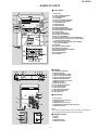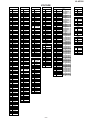
1
XL-HP500
SERVICE MANUAL
No. SY298XLHP500/
MICRO COMPONENT SYSTEM
MODEL
XL-HP500
XL-HP500 Micro Component System consisting of XL-HP500
(main unit) and CP-HP500 (speaker system).
• In the interests of user-safety the set should be restored to its
original condition and only parts identical to those specified be
used.
CONTENTS
Page
IMPORTANT SERVICE NOTES (FOR U.S.A. ONLY) ....................................................................................................... 2
SPECIFICATIONS ............................................................................................................................................................. 2
NAMES OF PARTS ........................................................................................................................................................... 3
DISASSEMBLY .................................................................................................................................................................. 5
REMOVING AND REINSTALLING THE MAIN PARTS ..................................................................................................... 7
ADJUSTMENT ................................................................................................................................................................... 9
NOTES ON SCHEMATIC DIAGRAM .............................................................................................................................. 12
TYPES OF TRANSISTOR AND LED ............................................................................................................................... 12
BLOCK DIAGRAM ........................................................................................................................................................... 13
SCHEMATIC DIAGRAM / WIRING SIDE OF P.W.BOARD ............................................................................................. 16
VOLTAGE ........................................................................................................................................................................ 33
WAVEFORMS OF CD CIRCUIT ...................................................................................................................................... 34
TROUBLESHOOTING ..................................................................................................................................................... 35
FUNCTION TABLE OF IC ................................................................................................................................................ 39
FL DISPLAY ..................................................................................................................................................................... 46
REPLACEMENT PARTS LIST/EXPLODED VIEW
PACKING OF THE SET (FOR U.S.A. ONLY)
SHARP CORPORATION
This document has been published to be used
for after sales service only.
The contents are subject to change without notice.
XL-HP500
FOR A COMPLETE DESCRIPTION OF THE OPERATION OF THIS UNIT, PLEASE REFER
TO THE OPERATION MANUAL.
IMPORTANT SERVICE NOTES (FOR U.S.A. ONLY)
BEFORE RETURNING THE AUDIO PRODUCT
(Fire & Shock Hazard)
Before returning the audio product to the user, perform the following
safety checks.
1. Inspect all lead dress to make certain that leads are not pinched
or that hardware is not lodged between the chassis and other metal
parts in the audio product.
2. Inspect all protective devices such as insulating materials, cabinet,
terminal board, adjustment and compartment covers or shields,
mechanical insulators etc.
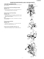
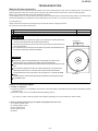
3. To be sure that no shock hazard exists, check for leakage current
in the following manner.
* Plug the AC line cord directly into a 120 volt AC outlet.
* Using two clip leads, connect a 1.5k ohm, 10 watt resistor paralleled
by a 0.15µF capacitor in series with all exposed metal cabinet
parts and a known earth ground, such as conduit or electrical
ground connected to earth ground.
* Use a VTVM or VOM with 1000 ohm per volt, or higher, sensitivity
to measure the AC voltage drop across the resistor (See diagram).
* Connect the resistor connection to all exposed metal parts having
a return path to the chassis (antenna, metal cabinet, screw heads,
knobs and control shafts, escutcheon, etc.) and measure the AC
voltage drop across the resistor.
VTVM
AC SCALE
1.5k ohms
10W
0.15 µ F
TO EXPOSED
METAL PARTS
TEST PROBE
CONNECT TO
KNOWN EARTH
GROUND
All check must be repeated with the AC line cord plug connection
reversed.
Any reading of 0.3 volt RMS (this corresponds to 0.2 milliamp. AC.)
or more is excessive and indicates a potential shock hazard which
must be corrected before returning the audio product to the owner.
SPECIFICATIONS
■ General
Power source
Power
consumption
Dimensions
Weight
■ CD player
AC 120 V, 60 Hz
102 W
Signal readout
Width: 8-1/8" (205 mm)
Height: 10-1/4" (260 mm)
Depth: 14-7/16" (366 mm)
13.2 lbs. (6.0 kg)
■ Amplifier (Except for Canada)
Output power
Output terminals
Input terminals
50 watts minimum RMS per channel into 6
ohms from 60 Hz to 20 kHz, 10% total harmonic distortion
Speakers: 6 ohms
Headphones: 16 - 50 ohms (recommended:
32 ohms)
Subwoofer pre-out (audio signal): 200 mV/
10 k ohms at 70 Hz
Video/Auxiliary (audio signal): 500 mV/47 k
ohms
■ Amplifier (For Canada)
Output power
Output terminals
Input terminals
Type
RMS: 100 W (50 W + 50 W) (10 % T.H.D.)
Speakers: 6 ohms
Headphones: 16 - 50 ohms (recommended:
32 ohms)
Subwoofer pre-output (audio signal): 200
mV/10 k ohms at 70 Hz
Video/Auxiliary (audio signal): 500 mV/47 k
ohms
Specifications for this model are subject to change without
prior notice.
D/A converter
Frequency
response
Dynamic range
3-disc multi-play compact disc changer
player
Non-contact, 3-beam semiconductor laser
pickup
1-bit D/A converter
20 - 20,000 Hz
90 dB (1 kHz)
■ Tuner
Frequency range
FM: 87.5 - 108 MHz
AM: 530 - 1,720 kHz
■ Cassette deck
Frequency
response
Signal/noise ratio
Wow and flutter
50 - 14,000 Hz (normal tape)
50 dB (recording/playback)
0.3 % (WRMS)
■ Speaker
Type
Maximum input
power
Rated input power
Impedance
Dimensions
Weight
–2–
2-way type speaker system
2" (5 cm) Tweeter
5-1/8" (13 cm) Woofer
100 W
50 W
6 ohms
Width: 6-1/2" (165 mm)
Height: 10-1/4" (260 mm)
Depth: 9-1/2" (241 mm)
5.5 lbs. (2.5 kg)/each
XL-HP500
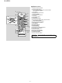
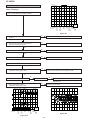
NAMES OF PARTS
■ Front panel
1. Disc Trays
2. Power On/Stand-by Button
3. Timer/Sleep Button
4. Clock Button
5. Tuning and Time Down Button
6. Tuning and Time Up Button
7. Timer Set Indicator
8. Headphone Jack
9. CD Eject Buttons
10. CD Direct Play Buttons
11. Equalizer Mode Select Button
12. Extra Bass/Demo Mode Button
13. Volume Control
14. Cassette Compartment
15. Tape Reverse Play Button
16. CD or Tape Stop Button
17. CD Play or Repeat, Tape Forward Play Button
18. CD Track Down or Fast Reverse, Tape Fast Wind,
Tuner Preset Down Button
19. CD Track Up or Fast Forward, Tape Fast Wind,
Tuner Preset Up Button
20. CD Button
21. Tape Record Pause Button
22. Video/Auxiliary Button
23. Tape Reverse Mode Select Button
24. Memory/Set Button
25. Tuner (Band) Button
26. Tape Button
1
9
2
10
3
4
5
6
7
11
12
13
14
15
8
16 17 18 19
20
22
21
23 24 25 26
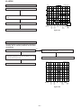
■ Display
1 2
3 4 5
1. Disc Number Indicators
2. CD Play Indicator
3. Tape Reverse Mode Indicator
4. Tape Reverse Play Indicator
5. Tape Forward Play Indicator
6. FM Stereo Mode Indicator
7. FM Stereo Receiving Indicator
8. Memory Indicator
9. Extra Bass Indicator
10. Timer Recording Indicator
11. Timer Play Indicator
12. CD Pause Indicator
13. CD Repeat Play Indicator
14. Tape Record Indicator
15. Sleep Indicator
6 7 8 9
10
11
12 13
14 15
4
■ Rear panel
5
1. Cooling Fan
2. Subwoofer Pre-output Jack
3. AC Power Cord
4. FM/AM Loop Antenna Jack
5. Video/Auxiliary (Audio Signal) Input Jacks
6. Speaker Terminals
1
2
6
Note:
This product is equipped with a cooling fan inside, which begins to
run at a specified volume level for better heat radiation.
3
1
2
3
■ Speaker system
4
1. Tweeter
2. Woofer
3. Bass Reflex Duct
4. Speaker Terminals
–3–
XL-HP500
■ Remote control
1. Remote Control Transmitter
2. CD Direct Play Buttons
3. CD Track Down or Fast Reverse, Tape Fast Wind,
Tuner Preset Down Button
4. Clock Button
5. Equalizer Mode Select Button
6. Extra Bass Button
7. Power On/Stand-by Button
8. CD Button
9. Tuner (Band) Button
10. Tape Button
11. Video/Auxiliary Button
12. CD Track Up or Fast Forward, Tape Fast Wind,
Tuner Preset Up Button
13. Volume Up and Down Buttons
14. Disc Direct Search Buttons
15. Clear Button
16. CD Memory Button
17. CD Stop Button
18. CD Pause Button
19. Tape Reverse Mode Select Button
20. Tape Reverse Play Button
21. Tape Stop Button
22. CD Play or Repeat Button
23. Tape Record Pause Button
24. CD Random Button
25. Tape Forward Play Button
1
7
2
8
17
18
19
20
21
22
23
24
25
9
10
3
12
13
14
4
5
6
11
15
16
Buttons with " " mark in the illustration can be operated on the remote control only.
–4–
XL-HP500
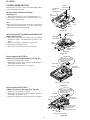
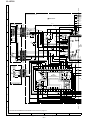
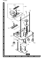
DISASSEMBLY
Top Cabinet
Caution on Disassembly
Follow the below-mentioned notes when disassembling
the unit and reassembling it, to keep it safe and ensure
excellent performance:
1. Take cassette tape and compact disc out of the unit.
2. Be sure to remove the power supply plug from the wall
outlet before starting to disassemble the unit.
3. Take off nylon bands or wire holders where they need to
be removed when disassembling the unit. After servicing
the unit, be sure to rearrange the leads where they were
before disassembling.
4. Take sufficient care on static electricity of integrated
circuits and other circuits when servicing.
STEP
REMOVAL
PROCEDURE
FIGURE
1
Top Cabinet
1. Screw ...................... (A1) x5
5-1
2
Side Panel
(Left/Right)
1. Screw .................... (B1) x10
5-1
3
Rear Panel
1. Screw ...................... (C1) x7
2. Screw ...................... (C2) x2
3. Flat Cable ............... (C3) x1
5-2
4
CD Changer
Mechanism Unit
1. Hook ........................ (D1) x2
2. Socket ..................... (D2) x1
3. Flat Cable ............... (D3) x2
5-2
Front Panel
1. Screw ......................
2. Hook ........................
3. Socket .....................
4. Flat Cable ...............
5. Flat Wire ..................
5
6
Main PWB
(B1) x1
ø3x10mm
(A1) x2
ø3x12mm
Front Panel
Side Panel
(Right)
(A1) x1
ø3x10mm
(A1) x2
ø3x12mm
(B1) x2
ø3x10mm
(B1) x2
ø3x10mm
(B1) x3
ø3x10mm
Rear
Panel
Side Panel
(Left)
(B1) x2
ø3x10mm
Figure 5-1
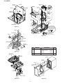
CD Changer
Mechanism Unit
(D3) x2
(E1) x3 5-2,5-3
(E2) x2
5-3
(E3) x2
(E4) x1
(E5) x1
Front Panel
Hook
(D1)x1
CD Servo PWB
1. Screw ....................... (F1) x2 5-2,6-1
2. Socket ...................... (F2) x2
6-1
7
Power PWB
1. Screw ...................... (G1) x4
6-1
8
Display PWB
1. Knob ........................ (H1) x1
2. Screw ...................... (H2) x9
3. Flat Cable ............... (H3) x1
6-2
9
Tape Mechanism 1. Screw ....................... (J1) x4
6-2
10
Headphones PWB 1. Screw ...................... (K1) x1
6-2
11
CD Servo PWB
(Note 1)
1. Screw ....................... (L1) x3
2. Socket ...................... (L2) x6
6-3
12
CD Changer
Mechanism Unit
1. Screw ...................... (M1) x4
2. Screw ...................... (M2) x2
3. Top Board ............... (M3) x1
4. Stabilizer Holder ..... (M4) x1
5. Disk Tray ................. (M5) x3
6. Screw ...................... (M6) x3
7. Guide,Mecha Holder .. (M7) x1
8. Screw ...................... (M8) x1
9. Stopper ................... (M9) x1
10. Holder,Mecha ..... (M10) x1
11. Screw .................. (M11) x4
6-3
6-4
(D2) x1
Rear
Panel
Display PWB
Pull
(C3) x1
Pull
Main PWB
Hook
(D1)x1
(E1) x1
ø3x10mm
Jack PWB
(C1) x7
ø3x10mm
(F1) x1
ø3x10mm
(C2) x2
ø3x10mm
Figure 5-2
(E3) x1
(E4) x1
Tape
Mechanism
(E5) x1
Front Panel
Note 1:
After removing the connector for the optical pickup from the
connector, wrap the conductive aluminium foil around the front end
of the connector so as to protect the optical pickup from electrostatic damage.
Main PWB
Display PWB
Hook
(E2)x1
Pull
(E3) x1
Hook
(E2)x1
Pull
(E1) x2
ø3x10mm
Power PWB
Figure 5-3
–5–
XL-HP500
(F1) x1
ø3x10mm
Stabilizer Holder
(M4) x1
(F2) x1
Push
(M2) x2
ø2 x7mm
(F2) x1
(M6) x1
ø2.6 x12mm
Main PWB
Pawl
(M7) x1
(M10) x1
(G1) x4
ø4x8mm
(M9) x1
Spring
CD
Mechanism
Top Board
(M3) x1
(M11) x4
ø2.6 x10mm
(M6) x2
ø2 x6mm
(M8) x1
ø3 x3mm
Power PWB
Disc Tray 1
Figure 6-1
Turn clockwise the
main cam to raise the
CD mechanism up to
the uppermost position.
(H3) x1
Front Panel
1
2
3
Disc Tray 2
(M5) x3
(H1) x1
Disc Tray 3
Press in turns the arrow
parts, starting with the
uppermost one, to
withdraw the disc trays.
Figure 6-4
(H2) x9
ø2.6x10mm
Tape
Mechanism
Display PWB
(K1) x1
ø3x10mm
Open
Cassette
Holder
Headphones
PWB
STEP
(J1) x4
ø3x10mm
FIGURE
Woofer
1. Net Frame ...............
2. Catching Holder ......
3. Screw ......................
4. Screw ......................
(A1) x1
(A2) x4
(A3) x4
(A4) x4
6-5
2
Tweeter
1. Screw ...................... (B1) x2
6-5
Figure 6-2
CD Changer
Mechanism Unit
PROCEDURE
REMOVAL
1
(M1) x2
ø3x10mm
Tweeter
(B1) x2
ø3x10mm
(A4) x4
ø4x12mm
(A2) x2
(A3) x2
Net Frame ø3x12mm
(A1) x1
(L2) x6
Woofer
(M1) x2
ø3x10mm
(A3) x2
ø3x12mm
(L1) x3
ø3x10mm
CD Servo PWB
(A2) x2
Figure 6-3
Figure 6-5
–6–
XL-HP500
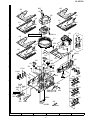
REMOVING AND REINSTALLING THE MAIN PARTS
TAPE MECHANISM SECTION
Clutch Ass'y
Perform steps 1 to 9 of the disassembly method to remove the
tape mechanism.
Record/Playback
Head
How to remove the Record/Playback Head
(See Fig. 7-1)
1. When you remove the screws (A1) x 2 pcs and (A2) x 1 pc.,
the record/playback head can be removed.
Erase Head
How to remove the Pinch Roller
(See Fig. 7-2)
(A1)x2
Ø2x6mm
1. Carefully bend the pinch roller pawl in the direction of the
arrow <A>, and remove the pinch roller (B1) x 1 pc., in the
direction of the arrow <B>.
Note:
When installing the pinch roller, pay attention to the spring
mounting position.
(A2)x1
Ø2x9mm
Figure 7-1
How to remove the Belt
(See Fig. 7-3)
1. Remove the main belt (C1) x 1 pc., from the motor side.
2. Remove the FF/REW belt (C2) x 1 pc.
How to remove the Motor (See Fig. 7-4)
Pinch Roller
(B1)x1
Pull
1. Remove the screws (D1) x 2 pcs., to remove the motor.
Pinch
Roller
<A> Pawl
<B>
Figure 7-2
FF/REW
Clutch
Motor
FF/REW
Belt
(C2)x1
Main Belt
(C1)x1
Flywheel
Figure 7-3
Motor
Clutch Ass'y
(D1)x2
Ø2.6x5mm
Figure 7-4
–7–
XL-HP500
CD MECHANISM SECTION
Perform steps 1 to 4 and 11 to 12 of the disassembly method
to remove the CD mechanism.
(A1) x2
ø2.6 x5mm
Stop Washer
(A3) x1
Optical Pickup
How to remove the Optical Pickup
(See Fig. 8-1)
CD
Mechanism
1. Remove the screws (A1) x 2 pcs and shaft (A2) x 1 pc.
2. Remove the stop washer (A3) x 1 pc and gear (A4) x 1 pc.
3. Remove the optical pickup.
Note:
After pulling out the optical pickup connector, wrap the tip of
it with conductive aluminium foil or the like to protect the
optical pickup from the static electricity.
Shaft
(A2) x1
Gear
(A4) x1
Figure 8-1
(B2) x2
ø2.6 x4mm
How to remove the Tray Motor and the Main Cam
Motor (See Fig. 8-2)
(B2) x2
ø2.6 x4mm
1. Remove the CD changer mechanism unit by the method
described in page 7, and disassemble as shown in the
figure.
2. Remove the belt (B1) x 2 pcs from the motor side.
3. Remove the screws (B2) x 4 pcs.
4. Remove the tray motor and the main cam motor.
Belt
(B1) x1
Belt
(B1) x1
Main Cam
Motor
Tray Motor
Figure 8-2
How to remove the CD Disc
(When CD is in the playback state) (See Fig. 8-3)
Turn the main cam clockwise
and raise the CD mechanism
and disk holder up to the
uppermost position.
1. Remove the cabinet and front panel.
2. Disassemble as shown in the figure so that the CD disc of
CD changer becomes visible.
3. Remove the CD disc as shown in the figure.
Disk Holder
CD Disk
CD Changer
Mechanism Unit
(When CD is in playback state)
Figure 8-3
How to remove the CD Disc
(When CD exists in the tray) (See Fig. 8-4)
Turn the main cam clockwise
and raise the CD mechanism
and disk holder up to the
uppermost position.
1. Remove the cabinet and front panel.
2. Disassemble as shown in the figure so that the CD disc of
CD changer can be taken out.
3. Remove the CD disc from the tray as shown in the figure.
Disc Holder
CD Mechanism
CD Changer
Mechanism unit
CD Disk
1
2
3
Press in turns the arrow
parts, starting with the
uppermost one, to
withdraw the disc trays
Disk Tray 1
Disk Tray 2
Disk Tray 3
(When CD exists in the tray)
Figure 8-4
–8–
XL-HP500
ADJUSTMENT
• Tape Speed
MECHANISM SECTION
• Driving Force Check
Torque Meter
Test Tape
Adjusting
Point
Specified
Value
Instrument
Connection
MTT-111
Variable
Resistor in
motor.
3,000 ± 30 Hz
Speaker
Terminal
(Load
resistance:
6 ohms)
Specified Value
Play: TW-2111
Normal
speed
Over 80 g
• Torque Check
Torque Meter
Specified Value
Play: TW-2111
30 to 80 g.cm
Fast forward: TW-2231
70 to 180 g.cm
Rewind: TW-2231
70 to 180 g.cm
TAPE MECHANISM
TUNER SECTION
Tape
Motor
fL: Low-range frequency
fH: High-range frequency
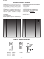
• AM IF/RF
Signal generator: 400 Hz, 30%, AM modulated
Test Stage
Frequency
Variable Resistor in motor
Figure 9-1
Frequency
Display
Setting/ Instrument
Adjusting Connection
Parts
AM IF
450 kHz
1,602 kHz
T351
AM Band
Coverage
—
531 kHz
(fL): T306 *2
1.1 ± 0.1 V
990 kHz
(fL): T303
AM Tracking 990 kHz
CD SECTION
• Adjustment
Since this CD system incorporates the following automatic
adjustment functions, readjustment is not needed when
replacing the pickup. Therefore, different PWBs and pickups
can be combined freely.
Each time a disc is changed, these adjustments are
performed automatically. Therefore, playback of each disc
can be performed under optimum conditions.
*1
*1
*1. Input: Antenna Output: TP302
*2. Input: Antenna Output: TP301
• FM RF
Signal generator: 1 kHz, 40 kHz dev., FM modulated
Setting/
Adjusting
Point
Test Stage Frequency Frequency
Display
FM Band
Coverage
—
87.50 MHz
FM RF
98.00 MHz 98.00 MHz
(10-30 dB)
Items adjusted automatically
(1) Offset adjustment (The offset voltage between the head
amplifier output and the VREF reference voltage is
compensated inside the IC.)
* Focus offset adjustment
* Tracking offset adjustment
(2) Tracking balance adjustment
(3) Gain adjustment (The gain is compensated inside the IC
so that the loop gain at the gain crossover frequency will
be 0 dB.)
* Focus gain adjustment
* Tracking gain adjustment
Instrument
Connection
T301 (fL):
1.3 V ± 0.1 V
*1
L312
*2
*1. Input: Antenna Output: TP301
*2. Input: Antenna Output: Speaker terminal
• FM IF
Signal generator: 10.7 MHz, FM modulated
Setting/
Adjusting
Point
Test Stage Frequency Frequency
Display
10.7 MHz
*1. Input: Antenna
98 MHz
Error
T302
*1
(Turn the
core of transformer T302
fully counterclock wise)
Output: TP301
IC302
T351
T301
FM OSC
T302
FM IF
IC303
CNP302
AM IF
L312
FM RF
FM/AM
LOOP
ANTENNA
01
10*
CAM error. Can't detect CAM switch when CAM is
moving.
11*
When it detect CAM operation error during initialize
process.
20*
TRAY error. Can't detect TRAY switch when TRAY is
moving.
21*
When it detect TRAY operation error during initialize
process.
22*
When it detect invalid TRAY switch during normal
operation.
23*
When it detect invalid TRAY switch during initialize
procecss.
31
When it change to CD function, DSP cannot read
initial data.
* 'CHECKING'
If Error is detected, 'CHECKING' will be displayed instead of
'ER-CD**'. 'ER-CD**' display will only be displayed when error
had been detected for the 5th times.
TP301
R357
TP302
AM BAND
COVERAGE fL
Explanation
When Pickup set inner position, inner switch
cannot detect 'ON' level for 10 secs.
MAIN PWB-A1
IC301
IF
CD ERROR CODE DESCRIPTION
Instrument
Connection
T303
AM TRACKING fL
T306
Figure 9-2 ADJUSTMENT POINTS
–9–
XL-HP500
TEST MODE
• Setting the test mode
Any one of test mode can be set by pressing several keys as follows.
<X-BASS> + <CD> + <ON/STAND-BY> TEST: CD operation test.
Function: -CD test mode.
-Enter test 4 mode.
C D
T E S T
IL isn't done
OPEN/CLOSE operation is using manual.
<<
>>, <<
>> buttons make pick's slide possible.
<<PLAY>> key input.
Do TOC IL. Do normal play.
When these following key is input
into PLAY key, track number can
be appoint directly.
<<MEMORY>>
key input.
Adjustment result
automatically will
display as below.
for each 2 sec :
a) "FOFF_XX"
b) "TOFF_XX"
c) "TBAL_XX"
d) "TGAN_XX"
f) "FGAN_XX"
g) "RFLS_XX"
explanation:
a) Focus off set
b) Tracking off set
c) Tracking balance
d) Tracking Gain
f) Focus Gain
g) RF level shift
= "FOFF_XX"
= "TOFF_XX"
= "TBAL_XX"
= "TGAN_XX"
= "FGAN_XX"
= "RFLS_XX"
<<MEMORY>> key input.
Laser ON.
<<MEMORY>> key input.
Tracking OFF play at that
specific point.
<<MEMORY>> key input.
<<
<<
<<
1>> key: Track 4
2>> key: Track 9
3>> key: Track 15
Tracking ON play from
that specific point.
<<MEMORY>> key input.
<<STOP>> key input.
STOP
VOL — Last memory
BAL — CENTER
P.GEQ — FLAT
X-BASS — OFF
Adjustment result automatically will
display as below for each 2 sec :
a) "FOFF_XX"
b) "TOFF_XX"
c) "TBAL_XX"
d) "TGAN_XX"
f) "FGAN_XX"
g) "RFLS_XX"
<<STOP>> key input.
STOP
Sliding the PICKUP with
>>, <<
>> button
<<
must only be in STOP mode.
To cancel : Power OFF
– 10 –
XL-HP500
Standard Specification of Stereo System Error Message Display Contents
Error Contents
CD
DISPLAY
Notes
Pickup Mechanism Error.
'ER-CD01'
PU-IN SW Detection NG.
CD Changer Mechanism Error.
'ER-CD**'
(*)
10: CAM SW Detection NG during normal operation.
11: CAM SW Detection NG during initialize process.
20: TRAY SW Detection NG during normal operation.
21: TRAY SW Detection NG during initialize process.
22: Invalid TRAY SW value during normal operation.
23: Invalid TRAY SW value during initialize process.
CD DSP Communication Error
'ER-CD31'
Focus Not Match/
'NO DISC'
DSP COMMUNICATION ERROR
IL Time Over.
TUNER
PLL Unlock.
FM 87.50
MHz
PLL Unlock.
(*) CHECKING:
If error is detected, 'CHECKING' will be displayed instead of 'ER-CD**' .
'ER-CD**' display will only be displayed when error had been detected for the 5th times.
Speaker abnormal detection and +B PROTECTION display
In case speaker abnormal detection or +B PROTECTION had occurred, it can be check by pressing 'POWER', 'VIDEO' and 'XBASS' key twice. Display will show "S** B**". S is referring to speaker abnormal detection and B is referring to +B PROTECTION.
** is in hex valve.
+B PROTECTION is condition when irregular process occur on power supply line.
– 11 –
XL-HP500
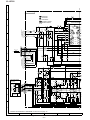
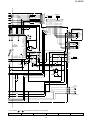
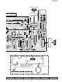
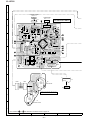
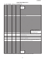
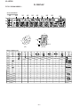
NOTES ON SCHEMATIC DIAGRAM
• Resistor:
To differentiate the units of resistors, such symbol as K and
M are used: the symbol K means 1000 ohm and the symbol
M means 1000 kohm and the resistor without any symbol is
ohm-type resistor. Besides, the one with “Fusible” is a fuse
type.
• Capacitor:
To indicate the unit of capacitor, a symbol P is used: this
symbol P means pico-farad and the unit of the capacitor
without such a symbol is microfarad. As to electrolytic
capacitor, the expression “capacitance/withstand voltage”
is used.
(CH), (TH), (RH), (UJ): Temperature compensation
(ML): Mylar type
(P.P.): Polypropylene type
• Schematic diagram and Wiring Side of P.W.Board for this
model are subject to change for improvement without prior
notice.
REF. NO
DESCRIPTION
• The indicated voltage in each section is the one measured
by Digital Multimeter between such a section and the chassis with no signal given.
1. In the tuner section,
indicates AM
indicates FM stereo
2. In the main section, a tape is being played back.
3. In the deck section, a tape is being played back.
4. In the power section, a tape is being played back.
5. In the CD section, the CD is stopped.
• Parts marked with “ 1 ” (
) are important for
maintaining the safety of the set. Be sure to replace these
parts with specified ones for maintaining the safety and
performance of the set.
POSITION
REF. NO
ON—OFF
SW720
VIDEO/AUX
ON—OFF
DESCRIPTION
POSITION
SW4
PICKUP IN
SW701
POWER ON/STAND-BY
ON—OFF
SW721
DISC 3 EJECT
ON—OFF
SW702
CLOCK
ON—OFF
SW722
DISC 2 EJECT
ON—OFF
DISC 1 EJECT
ON—OFF
SW703
TIMER/SLEEP
ON—OFF
SW723
SW704
TUNING/TIME UP
ON—OFF
SW724
DISC 1
ON—OFF
SW705
TUNING/TIME DOWN
ON—OFF
SW725
DISC 2
ON—OFF
SW706
REC/PAUSE
ON—OFF
SW726
DISC 3
ON—OFF
SW707
REVERSE MODE
ON—OFF
SW727
EQUALIZER
ON—OFF
SW708
MEMORY/SET
ON—OFF
SW728
X-BASS/DEMO
ON—OFF
SW712
PRESET UP
ON—OFF
SWB101
CAM 1
ON—OFF
SW713
PRESET DOWN
ON—OFF
SWB102
CAM 2
ON—OFF
SW714
PLAY
ON—OFF
SWB103
CAM 3
ON—OFF
SW715
STOP
ON—OFF
SWB104
CAM 4
ON—OFF
SW716
REVERSE PLAY
ON—OFF
SWB105
CD EJECT
ON—OFF
SW717
CD
ON—OFF
SWB106
CD TRAY CLOSE
ON—OFF
SW718
TUNER (BAND)
ON—OFF
SWB107
CD IN
ON—OFF
ON—OFF
SWB108
CD SET
ON—OFF
SW719
TAPE
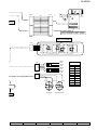
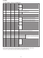
TYPES OF TRANSISTOR AND LED
FRONT
VIEW
E C B
(S) (G) (D)
(1) (2) (3)
KRC102 M
KRC104 M
KTA1266 GR
KTA1271 Y
KTA1273 Y
KTA1274 Y
KTC3199 GR
KTC3194 Y
KTC3203 Y
2SC1845 F
FRONT
VIEW
B C
FRONT
VIEW
E
KTC2026
– 12 –
SLR342VC
XL-HP500
CAM2
CAM3
CAM4
3
2
1
SWB104 CAM4
CNP6
CAM1
4
SWB103 CAM3
TRAY 4
5
SWB102 CAM2
TRAY 3
6
SWB101 CAM1
TRAY 2
7
SWB108 CD SET
8
SWB107 CD IN
13 12 11 10 9
CNP5
SWB106 CD TRAY CLOSE
7
T_MOT_H/L
6
TRAY 1
5
CAM_M–
4
SWB105 CD EJECT
3
CAM_M+
CD RES
2
TRAY_M–
CL
1
TO DISPLAY SECTION
TRAY_M+
DI
1
DO
2
CE
3
DRF
4
WRQ
+8V (+B4)
5
DGND (DRIVER)
6
+5V (+B7)
DGND
7
TO DISPLAY SECTION
+5V (+B8)
AGND
8
L-CH
CNP9
R-CH
TO MAIN SECTION
MOB1
MAIN CAM MOTOR
–
M
+
–
M
+
62 CLK
LCHO
RCHO
42
75
69
57
63 DI
56
64 DO
55
65 WRQ
51
50
66 RES
44
67 DRF
IC1
LC78646E
CD SERVO
43
40
37
28
19
6
48 XOUT
XL1
16.9344 MHz
MOB2
TRAY MOTOR
68
VDD5
45
61 CE
1
17 25
42 41 23 22 36 37 38 39
SLDO 23
9
10
LDD
8
LDS
TIN1
7
TIN2
FIN2
41 46
FIN1
RVDD
LVDD
VVDD
XVDD
FDO 21
TDO 20
79 80
18
24
+3.3V
IC2
M63001FP
FOCUS/TRACKING/
VCC1
SPIN/SLED
VCC2
DRIVER
~
ADAVDD
18 38 47 77
VDD
RFVDD
5
35
40 VCC4
28 VCC3
SPDO 22
29
21
14
~
49 XIN
+5V
+3.3V
2
CONT5 26
8
Q2
4
ZD1
3.3V
5
6
7
15 16
26 27
LASER
DRIVER
+3.3V
Q1
TRACKING COIL
FOCUS COIL
PICKUP UNIT
+5V (+B7)
CONSTANT
VOLTAGE
M1
SPINDLE
MOTOR
M2
SLED
MOTOR
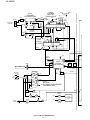
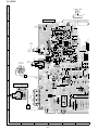
Figure 13 BLOCK DIAGRAM (1/3)
– 13 –
+
M
–
–
M
+
SW4
PICKUP IN
XL-HP500
17 13
MO/ST
8
18
7
16
12 20
L
R
14
15
T306
+B6
X352
4.5 MHZ
IC302
LC72131
PLL(TUNER)
1
20
+B5
FM+B
Q361
CE
DI
CLK
DO
VT
22 15 16
OSC
11
FM/AM
T303
AM OSC IN
AM BAND
COVERAGE
21
AM RF IN
AM OSC OUT
24 23
AM
TRACKING
4 5 9
VCO
Q302
X351
456 kHz
CF351
FM/AM
1 2
OSC
BUFF
T301
FM OSC
450 kHz
CF352
T351
AM IF
VCC
FM RF L312
8
FM
MPXIN DET
5 7
GND
CF302
9
3 4
+B6
10.7 MHz
+B6
FM/AM
OUT AM IF
T302
6
1
ZD351
5.1V
STEREO
1
2
3
FM IF
+B5
+B6
7
3 4 5 6
MO/ST
FM/AM LOOP
ANTENNA
B.P.F
BF301
IC303
LA1832S
FM IF DET.
FM MPX./AM IF
AM MIX
CNP302
IC301
TA7358AP
FM FRONT END
9 10
17
21
+B5
Q360 FM
SWITCHING
+B5
JK690
VIDEO/AUX
L
AUX L 9
R
R 16
TAPE L 10
R 15
L 11
TUNER
R 14
CD L 12
R 13
BI901
8
7
6
AC BIAS
L
R
23
POP REDUCE 6 T1/T2
L REC 9 REC
R REC 16
H/N
+B5
IC101
AN7345K
PLAYBACK AND RECORD
/PLAYBACK AMP.
SWITCHING
Q105
Q114
Q106
SWITCHING
+B5
Q111
L103
BIAS
OSC
BIAS
MOTOR
DRIVER
Q113
SWITCHING
ERASE
HEAD
REC/PLAY
7 L REC
18 R
11
12 NOR/
13
15 HIGH T1/T2
Q112
Q603
Q604
SYSTEM
MUTE
3
Q107
Q108
MUTING
4 L PB
21 R
2
21 R
–20dB
ATT Q601
Q602
4 L
7 18 8 17
P.B
SWITCHING
Q101~
Q104
IC601
LC75341
AUDIO PROCESSOR
VF1
REC./P.B.
HEAD
REC.
P.B.
L-CH
R-CH
DI 1
CE 2
CLK 24
–VF
CNP9
FROM CD SECTION
23
+B3
Q500
TAPE
MECHANISM
ASS'Y
+B5
Q109
SWITCHING
Q110
+B3
BIAS
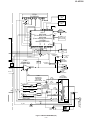
Figure 14 BLOCK DIAGRAM (2/3)
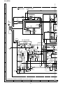
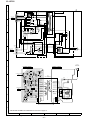
– 14 –
Q501
SOLENOID
DRIVER
C
XL-HP500
FL701
FL DISPLAY
1
13 15 ~ 19 29 ~ 34
5 ~ 12
TO CD
SECTION
CNP6
35 ~ 41 14 45
+B9
TAPE
MECHANISM
ASS'Y
Q701
+B10
91 68 ~ 56 42 46 40 25 13 30
VDD
38
72
~
39
IC701
+B10
IX0574AW
AVDD
34
(To Serial No.211XXXXX) 33
IX0578AW
(From Serial No.212XXXXX) 31
SYSTEM
MICROCOMPUTER
37
78
RX701
REMOTE
1 SENSOR 2
3
79 VLOAD
80
CE
CLK
DI
DO
VDD
100
VDD
~
90
92
93
1 2 4 5 6 7 8 9 1 0 11 12
Q702
TO CD SECTION
CNP5
+B7
+B10
FAN MOTOR
DRIVER
Q906
SP DET.
L 1
R 15
13
SYSTEM
MUTE
41
16 1 7 20 21 22 23 24
RESET
Q603
Q604
15
+B10
XL700
4.19403 MHz
+B10
IC901
STK402-071
POWER AMP.
Q901~
Q904
M
M971(212-3)
FAN
MOTOR
SO901
SPEAKER
TERMINAL
SP RELAY Q905
ON-OFF
RL914
7 L-OUT
10 R-OUT
8
KEY
SW701-SW708
SW712-SW728
–
86
RESET
~
~
85
+B10
+B3
JK951
HEADPHONES
JK953
SUB
WOOFER
9
C/PLAY
-B2
IC851
KIA7812AP
CONSTANT
VOLTAGE
REGULATOR D802
+B2
VF2
+B5
+B10
+B7
+B8
+B9
A_10V
IC851
IC855
VOLTAGE
REGULATOR
IC852
PT801
MAIN POWER
TRANSFORMER
F801
4A 125V
IC852
KIA7810AP
CONSTANT
VOLTAGE
REGULATOR
F803
2A 125V
UNSW_5.6V
D_5V
A_5V
SW_5V
IC854
AN78L05
D803,
D804
IC853
KIA7805AP
RL841
F804
2A 125V
IC853, IC854
CONSTANT VOLTAGE REGULATOR
Q801 VOLTAGE
REGULATOR
T.F.
AC POWER
SUPPLY CORD
AC 120 V, 60 Hz
–VF
BIAS
VF1
+B3
+B4
M_+12.6V
LD+8V
F802
4A 125V
D855
AC_RLY
Q841
RELAY
DRIVER
D842~
D845
PT841
SUB POWER
TRANSFORMER
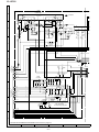
Figure 15 BLOCK DIAGRAM (3/3)
– 15 –
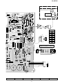
XL-HP500
IC901
STK402-071
POWER AMP.
+
–VCC
CH2
OUT
9
10
12
C914
100/63
11
R920
0.22
(2W)
C932
0.22
8
14 C908
470P
13
R922
100
R903
1K
7
R918
0.22
(2W)
6
OUT
CH1
5
R925
22K
C913
100/63
R919
0.22
(2W)
4
R917
0.22
(2W)
3
+VCC
+
–
2
+B
CH2
–
1
C907
470P
FM SIGNAL
R-CH
(2CH)
(50 WATTS/CH)
15
R910
1K
L-CH
CH1
R912
820
A
3P
C906
R908
56K
22/16
R904
1K
R935
56K
L
R936
56K
R
C926
0.22
(ML)
C927
0.22
(ML)
C928
0.22
(ML)
R937
56K
R916
5.6K
C929
0.22
(ML)
R941
4.7
(1/2W)
R940
4.7
(1/2W)
R902
56K
C904
0.001
C901
0.22/50
R901
56K
C925
47/50
Q901
KTC3199 GR
Q904
KTC3199 GR
C903
0.001
C912
0.022(ML)
R
Q903
KTC3199 GR
D907
DS1SS133
D906
DS1SS133
Q902
KTC3199 GR
R911
C915
10/63
R915
5.6K
L
R
R914
0.1 (1W)
R923
1K
C911
0.022(ML)
C905
3P
–B
R924
1K
0.1
(1W)
R907
56K
C909 820
22/16
R913
D905
DS1SS133
B
+B
L
C916
10/63
100
C910
R921
R909
1K
C
C902
0.22/50
FAN MOTOR 5V
+B
+B
D
LUG902(229)
CHASSIS
GND
P18 2 - C
TO MAIN PWB(2/3)
+B
E
1
2
3
BI801
L-CH
R926
22K
A_GND
C948
2200/50
R-CH
–B
+B2
4
SP_RLY
R927
22K
C949
2200/50
UNSW_5.6V
–B
13
3
1
18
19
20
C860
47/25
2
4
3
5
4
6
5
7
6
8
7
SUB_B
+B
C864
0.1(ML)
+B
18V
C856
3300/35
R857
3.3
(1/2W)
+B
2
C855
0.1(ML)
IC853
KIA7805AP
+B
1
2
LUG903(229)
D855
DS1SS133
CHASSIS
GND
C859
0.1(ML)
IC854
AN78L05
+B
C861
0.047
17
1
3
G
16
C852
22/50
+B
2
15
R854
22K
D860
GD1N4004
CD_GND
14
C853
47/25
+B
C858
0.1(ML)
+B
SW_+5V
D853
DS1SS133
C857
47/25
A_+5V
UNSW5.6V
3
R858
220
+B
C862
10/50
+B
12
IC852
KIA7810AP
+B
+B
10
11
R856
C851
1
0.047 (1/2W)
R860
220
D852
DS1SS133
D851
DS1SS133
D_+5V
+B
1
3
D859
DS1SS133
R852
10K
+B_PROTECT
9
D857
DS1SS133
+B
CNS801
2
1
2
C854
0.1(ML)
+B
ZD852
DZ9.1BSB
3
R853
22K
A_+10V
8
P18 2 - E, P19 9,10 - H
TO MAIN PWB(2/3)
F
+B
D856
DS1SS133
7
LD_+8V
12.6V
+B
IC851
KIA7812AP
D858
DS1SS133
IC855
KTC2026
+B
C865
10/50
M_+12.6V
R859
22K
6
SP_DET
C863
22/50
5
1
IC851,852,853,854
Constant Voltage Regulator
CD_D_GND
CD_A_GND
M GND
APRO_GND
D_GND
TAPE_A_GND
H
• NOTES ON SCHEMATIC DIAGRAM can be found on page 12.
1
2
3
4
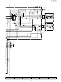
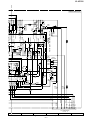
Figure 16 SCHEMATIC DIAGRAM (1/11)
– 16 –
5
6
XL-HP500
MAIN PWB-A1(1/3)
2
+B
1
D912
DS1SS133
R950
68K
CNP971
+B
RL914
R945
2.2K
L
+B
R944
2.2K
M_+12.0V
SP_RLY
R_CH
GND
R
C927
0.22
(ML)
M
1
HEADPHONES PWB-A3
JK951
HEADPHONES
HD902
FW902
1
1
2
2
3
3
4
4
5
5
R962
330 (1/2W)
R961
330 (1/2W)
C643
0.001
L_OUT
R_OUT
L_CH
2
CNS971
WT902
C931
10/50
Q906
KTC3203 Y
R947
15K
R949
1K (1/2W)
+
M971
FAN MOTOR (212-3)
C930
47/50
D911
DS1SS133
C929
0.22
(ML)
0.2V
JACK PWB-A4
4.4V
HD903
R946
1
1
2
2
3
3
+
+
L-CH
–
–
L-CH_GND
JK953
SUB WOOFER
R965
8.2K (1/2W)
R966
8.2K (1/2W)
WT904
47K
FW903
C960
3.3/25
Q905
KTC3199 GR
R967
680 (1/2W)
R941
4.7
(1/2W)
R-CH
SO901
SPEAKERS
6 OHMS MIN
+B
R-CH_GND
LUG902(229)
CHASSIS
GND
6V
1
CNS801
2
1
3
2
4
3
5
4
6
5
7
6
8
7
P32 1 - A
CNP801
TO POWER PWB
801
+B
LUG903(229)
CHASSIS
GND
7
8
9
10
Figure 17 SCHEMATIC DIAGRAM (2/11)
– 17 –
11
12
XL-HP500
220P
C652
FM SIGNAL
CD SIGNAL
AUX SIGNAL
C651
220P
MAIN PWB-A1(2/3)
A
PLAYBACK SIGNAL
RECORD SIGNAL
R601
1K
R602
1K
IC601
LC75341
AUDIO PROCESSOR
1 DI
10K
1/50
4
C607
0.15
R607
3.3K
C605
0.15
C611
C613
Q602
KTC3199 GR
R616
2.2K
R610
2.2K
C631
RS
LSEL0
8
C617
1/50
C619
1/50
C621
1/50
R
LIN
7
C615
4.7/50
R612
390
Q604
KTC3199 GR
C636
0.001
1/50
+
–
C
R614
3.3K
C638
0.001
R618
330
R-CH
3
LTRE
6
0.0022
RB
LBASS
5
C635
0.001
+
–
R615
3.3K
Q601
KTC3199 GR
Q603
KTC3199 GR
C637
0.001
A_GND
2
R611
2.2K
R
+
–
TO MAIN PWB(1/3)
P16 1 - E
1
R617
2.2K
V
+
–
LOUT
+
–
R619
330
CCB
INTERFACE
3 VSS
R613
390
L-CH
CE
2
+
–
C609
+
–
R605
+
–
B
L4
9
AUX
L3
10
DECK
0.0047
L2
11
TUNER
L1
12
CD
C623
1/50
BI901
CNS9
+B
5
+B
4
3
2
+B
1
LD_+8V
CD_D_GND
13
A_+5V
11
D_+5V
10
CD_D_GND
CD_A_GND
R149
3.4V
0V
2
3
0V
2
3.4V
Q114
KRC104 M
R112
0.7V
180P
R105
3.3K
0V
0V
Q101
2SC1845 F
R103
2.2K
2
3
5
6
7
C109
0V
0V
R113
1K
C113
0.033
C111
100/16
C115
560P
R115
56
R107
47K
R111
R123
6.8K
56K
8
9
15K
• NOTES ON SCHEMATIC DIAGRAM can be found on page 12.
2
3
4
Figure 18 SCHEMATIC DIAGRAM (3/11)
– 18 –
5
220/10
22/16
C134
C133
10K
C132
47/25
16
56K
H
1
R134
100
C130
0.0033
R132
17
15 14
ALC
Nor/CrO2
ALC RIPPLE
18
–
+
Hich=CHROME
+
–
4
R117 R119
330P 100K 3.9K
4.7K
R126
R150
68K
SPARE
C118
47/25
560P
1
0V
0.7V
19
10
6
11
IC101
Q103
2SC1845 F
20
C131
47/25
C103
21
–
112K
+
Hich=T1
+
112K
–
R135
10K
G
22
T2_L2
0V
HEAD PLATE
BLOCK(210-1)
23
T2_L1
C126
22/16
C129 0.0033
1
24
R128
5.6K
100
2
0.7V
C127
0.022
3
1
100K 3.9K
R127
4.7K
C123
270P
2
1
T2_R1
C110
330P R118 R120
R114
1K
3.3/50
2
Q104
2SC1845 F
0V
C143
4
0V
0.022
5
3
A_GND
C104
180P
C121
4
3
T2_R2
0V
R106
3.3K
R124
6.8K
C117
47/25
4
0.7V
R122
12K
C114 C116
0.033 560P
R121
12K
6
ERASE
M_GND
C106
5
7
560P
R-CH
L-CH
RECORD/
PLAYBACK HEAD
5
6
C112
100/16
C105
6
0V
Q105
KTC3199 GR
8
ERASE HEAD
2.2K
4.7K
0V
R116
56
R108
47K
R104
0.7V
Q106
KTC3199 GR
BI102
0.7V
0V
Q102
2SC1845 F
R110
0V
K
R139
10K
15K
4.7K
TAPE MECHANISM
Ass'y(210)
R109
F
220K
R138
10K
1.5K
Q112
KTA1266 GR
R136
REC_R
1
R130
9.3V
3
0V 1
R148
4.7K
C128
0.022
8.6V
C125
22/16
9.3V
R133
R147
10K
150
C141
100/16
R131 1.5K
R146
10K
Q113
KRC104 M
Q108
KTC3199 GR
16
270P
15
C124
TO MAIN PWB(1/3)
P16 1 - F~G
7
E
C642
0.001
R129
5.6K
LD+8V
18K
6
C625
100P
1
A-5V
18K
R646
10K
2
D_5V
D_GND
7
R645
R609
3
C641
0.001
C639
2.2/50
4
D
CD_GND
8
R621
22K
5
L-CH
22K
6
P31 11 - D
CNP9
TO CD SERVO PWB
A_GND
9
R620
7
R-CH
C640
22/50
8
XL-HP500
R693
39K
4
R691
6.8K
C691
390P
3
R690
6.8K
C690
390P
2
L-CH
JK690
VIDEO/AUX
1
R-CH
R692
39K
C653
220P
CLK
VREF
+
–
CHASSIS
GND
C603
22/16
22
C610
1/50
C608
0.15
21
CE
R604
10K
A_+10V
+
–
ROUT
R603
1K
24
VDD 23
+
–
E
C602
0.022
C601
220/16
+
–
RBASS
RTRE
RIN
20
19
18
R4
R3
K
R2
ER
R1
D
R606
3.3K
C606
0.15
28
+B
21
D_GND
22
C614
1/50
C612
0.0022
D1
C616
4.7/50
27
CLK
17
30
TUN_R
C618
1/50
+
–
RSEL0
X
GND
TO MAIN PWB(3/3)
P21 11 - H
601
5341
OCESSOR
16
24
C632
0.0047
C620
1/50
15
25
C622
1/50
14
R642
C624
1/50
TUN_L
10K
26
DO
13
29
R641
100P
10K
C626
R608
10K
TO DISPLAY PWB
P22 2 - F
CNP701A
R137
220K
R136
220K
Q107
KTC3199 GR
R139
10K
0V
16
C135
0.022
220/10
16
C134
22/16
C133
10K
C132
47/25
DO
15
CE
R158
220
13
11.6V
12
+B_PROTECT
11
3
D_GND
R141
4.7K
10
1
R142
82
(1/2W)
S_MUTE
0V
0V
REC/PLAY
R145
4.7
SW_5V
8
7
M_+13V
0V
6
5
SP_RLY
3
SP_RLY
–20dB
CNP701B
17
20
18
8
9
19
6
12
14
4
SP_DET
SP_DET
UNSW5.6V
SW_+5V
M_+12.6V
D_GND
+B_PROTECT
UNSW5.6V
A_+10V
C138
0.0082
APRO_GND
R144
22K
9
T_BIAS
TAPE_A_GND
R143
47K
Q111
KTC3203 Y
12
2
L103
330µH
R135
10K
C129 0.0033
11
Q109
KTA1266 GR
C139
0.039(ML)
10
C131
47/25
9
IC101
VCC
AN7345K
PLAYBACK AND RECORD/
PLAYBACK AMP.
6K
6K
0V
DI
Q110
KRC104 M
0V
11.6V
13
C137
0.047(ML)
15 14
ALC
Nor/CrO2
ALC RIPPLE
16
14
CLK
M_GND
C130
0.0033
R134
0.7V
C140
47/25
8
K
R140
47K
R
5
2
1
1
FC701
4
TO MAIN PWB(1/3)
P16 1 - E~H
7
8
9
10
Figure 19 SCHEMATIC DIAGRAM (4/11)
– 19 –
11
12
XL-HP500
C323
0.022
B
D301
DS1SS133
R358
3.9K
+B
C334
22P
(UJ)
AM OSC IN
AM MIX OUT
1
AM BAND
COVERAGE fL
1
2
R323
68K
FM
ANTANNA
D
0.022
2
C350
T306
6
4
5
3
VD301
SVC348S
C335
560P
23
FM IF IN
AM OSC OUT
24
10/16
1
C332
0.022
C352
1
C331
0.047
R351
5.6K
2
C330
15P
(UJ)
0.022
3
2
1
C351
3
5
6
R336
10K
C
2
D302
DS1SS133
CNP302
AM
LOOP
ANTANNA
3 T303
4
C342
0.022
AM TRACKING fL
C361
AM SIGNAL
22
FM AFC
FM SIGNAL
C362 R365
3.3/50 10K
A
FM FRONTEND
IC301
TA7358AP
9
R382
150
C313
22P
(CH)
VD303
SVC211C
C317
0.001
C316 0.022
C315 0.0047
C314
0.0047
R322
680
47K
C318
100P
D303
DS1SS133
R375
470
R316
4.7K
Q361
KTA1266 GR
Q302
KTC3194 Y
C384
0.001
+B
R327
33
C302
0.001
D304
DS1SS133
H
• NOTES ON SCHEMATIC DIAGRAM can be found on page 12.
1
2
3
4
Figure 20 SCHEMATIC DIAGRAM (5/11)
– 20 –
5
6
4
1K
R372
DI
3
1K
2
IC302
LC72131
PLL(TUNER)
C322
100P
R325
1
R373
2
22 21 20
1K
T302
FM IF
C382
15P
(CH)
X352
FM RF
R311
100K
C312
0.022
3
C381
12P(CH)
C393 C390
120P 100P
4.5MHZ
X IN
X OUT
VSS
AOUT
CE
R309
10K
T301
FM OSC
1
C
1
C389 R38
1/50 1.5K
R314
22
G
C394
47/16
C397
0.022
R381
10K
C307
10/16
R374
8
TP301
7
C310
15P(CH)
VD302
SVC211C
C308
4.7P (CH)
C309
0.001
L312
1SS133
D305
F
6
C305
4.7P
(CH)
E
CHASSIS
GND
5
CF302 FM IF
C304
0.01
4
C324
4.7P
(UJ)
3
+B
C311 C306
18P 0.022
2
R302
10
1
R313
33K
1 2 3
C303
10P(CH)
BF301
7
6
9
10 11
8
+B
C386
330P
R395
47K
R359
1.8K
R376
1K
9
C391
47/16
C356
0.001
C370
1/50
C357
2.2/50
IF OUT
PHASE
L-CH OUT
PHASE
MO/ST
(FM/AM)
R-CH OUT
VCC
MPX IN
FM DET
MPX VCO
STEREO
12
C358
1/50
R355
3.3K
L352
100µH
C396
100/10
C395
0.022
TP302
C369
27P (UJ)
3.9K
C373
0.027
C374
0.027
C368 R356 R357
470K
1/50 1K
X351
456KHZ
R363
3.9K
C366 0.001
C365 0.022
C364 2.2/50
C363 0.022
C361
0.022
C362 R365
3.3/50 10K
C367 R350
1/50 2.7K
IC303
LA1832S
FM IF DET./FM MPX./AM IF R364
22P
C355
3
R388
3.9K
C398
100/10
C399
0.022
270
R353
SD
FM/AM OUT
GND
VSM
AM IF IN
AM LOW CUT
10 11
R360
4.7K
82K
21
22
Figure 21 SCHEMATIC DIAGRAM (6/11)
– 21 –
10
24
25
11
26
27
28
29
CLK
5
9
DO
R390
8
CE
4
8
7
15 14 13
DI
3
7
6
16
R385
5.6K
R377
47K
L351
100µH
R387
5.6K
AM IF
R384
5.6K
C380
10/16
5
C354
0.022
CF351
FM IF
10.7MHZ
R393
1K
2
C353
0.022
1
CF352
R352
1K
AM RF IN
REG
4
17
C338
0.001
MO/ST SD
IF IN
T351
C385
0.01
C387
0.022
AM OSC IN
AM MIX OUT
FM AFC
FM IF IN
AM OSC OUT
3
C388
0.001
FM/AM
C389 R380
1/50 1.5K
R379
2.2K
0.022
20 19 18
ST IND
DO
FM/AM
VDD
FM IN
IF
CONT AM IN
C394
47/16
C392
0.001
C350
2
21
TUN_L
4.7K
R378
AIN
PD
CL
R381
10K
1
22
C372 R362
1/50 2.2K
TUN_R
1K
R372
DI
19 18 17 16 15 14 13 12
AOUT
23
C371
1/50
D_GND
1K
R373
20
CE
24
A_+10V
1K
R374
XL-HP500
MAIN PWB-A1(3/3)
R361
2.2K
+B
ZD351
DZ5.1BSB
R392
R391
270
Q360
KTA1266 GR
270
R383
5.6K
+B
R386
10K
+B
30
TO MAIN PWB(2/3)
P19 12 - C
12
XL-HP500
A
P01
P02
P03
P04
P05
NX
NX
NX
NX
NX
NX
NX
NX
NX
P06
P07
P08
P09
P10
P11
P12
P13
P14
P15
P16
P17
P18
NP
NP
F2
F2
R766
1.5
FL701
FL DISPLAY
TRY 1 SW
T_MOT H-L
10
11
12
13
R763
47K
9
C MOT–
C MOT+
T MOT–
S1
77 S13
76 S14
75 S15
74 S16
73 DIST 1/S17
D701
DS1SS133
72 DIST 0/S18
IC
IX05
(To Serial N
71
C
70 DIST IN
D
S2
78 S12
D703
DS1SS133
T MOT+
CNP7A
FC6 13
81 82 83 84 85 86 87 88 89 90
S10
80 S11
79 VLOAD
Q701
KTC3319 GR
TRY 2 SW
7
8
TO CD SERVO
PWB
C707
1/50
TRY 3 SW
C706
6
R764
1K
S3
0.001
C708
TRY 4 SW
S4
0.001
C709
CAM 1 SW
5
S5
0.001
C710
4
100K
S6
0.001
C711
CAM 2 SW
S7
0.001
C712
3
R765
S8
0.001
C713
2
CAM 3 SW
33
P25 10 - B
CNP6
CAM 4 SW
R762
B
1
S9
0.001
C714
1
47/25
0.001
C715
45 44 43 42 41 40 39 38 37 36 35 34 33 32 31 30 29 28 27 26 25 24 23 22 21 20 19 18 17 16 15
R761
10K
R756
1K
R760
10K
R755
1K
R759
R758
10K
10K
R754
1K
R753
1K
R757
10K
R752
1K
R767
5.6K
R751
1K
R768
5.6K
R750
1K
R769
5.6K
R749
1K
R770
5.6K
R748
1K
R771
5.6K
R747
1K
R772
5.6K
R746
1K
R773
5.6K
R745
1K
R774
5.6K
R744
1K
69
68 T_MOT H-L
IX05
(From Serial N
67 T MOTOR+
66 T MOTOR–
65 C MOTOR+
SYS
MICROCO
64 C MOTOR–
63 TRAY 4 SW
62 TRAY 3 SW
61 TRAY 2 SW
60 TRAY 1 SW
59 CAM 4 SW
58 CAM 3 SW
57 CAM 2 SW
56 CAM 1 SW
SMUTE
51
T_SOL_A
T1 RUN
52
VDD
JOG 1
53
T_MOTOR
54
TIMER LED
55
1K
1K
1K
560
2.2K
680
680
1K
R736
R735
R734
R733
R732
R731
R730
JOG 2
E
R737
MIC SW
50 49 48 47 46 45 44 43 42 41
FC701
16
16
DO 15
CE 14
CLK 13
DI 12
P19 12 - G
CNP701B
TO MAIN PWB(2/3)
FPA/FPB
+B_PROTECT 11
D_GND 10
9
REC/PLAY
7
M_+13V
SW_5V
6
UNSW5.6
SP_DET
4
SP_RLY
2
–20dB
1
+B
+B
+B
+
3
R780
10K
N.C. (OP PACK)
F. REC
R. REC
3
4
5
6
FC702
7
R506
10K
Q501
KTA1271 Y
R507
10K
R504
4.7K
R505
8.2K
TAPE MECHANISM
PWB Ass'y(210-3)
TAPE MECHANISM Ass'y(210)
H
• NOTES ON SCHEMATIC DIAGRAM can be found on page 12.
1
2
3
4
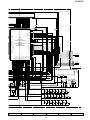
Figure 22 SCHEMATIC DIAGRAM (7/11)
– 22 –
5
6
0.001
2
C717
M_+13V
+B
1
3
10K
D500
DS1SS133
–
1
2
Q500
KTA1273 Y
CNS702
T1 RUN
1
GND
2
T_SOL_A
3
T_MOTOR
4
5
FPA
6
FPB
7
C502
47/25
M
+
TAPE
MOTOR
(210-2)
END SW
–COM
+SOL
+MTR
VR701
VOLUME
R781
0.001
CNP701A
SOLENOID
G
+B
+B
C716
5
R782
8
R799
1
S_MUTE
T_BIAS
10K
F
XL-HP500
DISPLAY PWB-A2
G10
G4
G3
G2
G1
NP
NP
F1
F1
6
5
4
3
2
1
G6
7
G7
8
G8
26 25 24 23 22 21 20 19 18 17 16 15 14 13 12 11 10 9
G9
G5
P01
P02
P03
P04
P05
NX
NX
NX
NX
NX
NX
NX
FL701
FL DISPLAY
C700
1/50
70 DIST IN
69
IX0578AW
(From Serial No.212XXXXX)
SYSTEM
C MOTOR–
MICROCOMPUTER
TRAY 4 SW
66 T MOTOR–
65 C MOTOR+
60 TRAY 1 SW
59 CAM 4 SW
58 CAM 3 SW
57 CAM 2 SW
56 CAM 1 SW
R795
1.5
C703
15P
VDD 16
R710
CD_CLK 17
CD_DI 18 R711
R712
CD_DO 19
R713
CD_CE 20
CE 21 R714
CLK 22 R715
DI 23 R716
DO 24 R717
62 TRAY 3 SW
61 TRAY 2 SW
R794
10K
1K
R708
R793
10K
XL700
X1 12
4.19403 MHz
VPP/IC 13
C704
XT2 14
18P
1K
R709
CD_DRF 15
67 T MOTOR+
+B
1K
1K
1K
1K
1K
1K
CNP5A
CD RESOUT
1K
1K
CD_CLK
CD_DI
AVSS 25
55
CD_DO
CD_CE
FPA/FPB SW 28
PROTECT 29
AVDD
NO USE 30
BI706
VF2
P_IN
5.6K
VF1
AC_RLY CON
1K
7
FC5
7
6
P25 9 - B
CNP5
TO CD SERVO
PWB
5
4
3
2
1
1
1
CNS706
2
1
3
2
4
3
5
P32 1 - D
CNP706
4 TO POWER PWB
6
5
D708
DS1SS133
R723 1K
R724 1K
R725 1K
–VF
R790
R721
KEY 2
KEY 1
KEY 0
1K
R726
1K
R727
1K
R728
1K
R729
1K
R730
680
R731
680
R732
2.2K
R733
560
R734
1K
R735
1K
R736
1K
R737
JOG 2
CD_DRF
CD_WRQ
50 49 48 47 46 45 44 43 42 41 40 39 38 37 36 35 34 33 32 31
MIC SW
1K
R720
0.022
AVREF
CD_WRQ
P_IN
27
SP DET
REMOCON
VSS
SMUTE
51
T_SOL_A
T1 RUN
52
VDD
JOG 1
53
T_MOTOR
54
TIMER LED
26
C705
63
+B
G1
RESET 10
X2 11
68 T_MOT H-L
64
G2
G3
G5
G6
G7
G8
G9
G10
S1
S2
S3
S4
G4
9
IC701
IX0574AW
(To Serial No.211XXXXX)
71
C701
220/10
+B
D706
DS1SS133
UN_SW5.6V
+B
R797
100K
C718
0.01
1
+B
RX701
REMOTE
SENSOR
C719
3.3/50
Q702
KRC102 M
2
3
D707
DS1SS133
R796
47K
+B
10K
R783
4.7K
R782
DS1SS133
R798
100
1
C720
+B
D705
+B
100µH
2
3
0.022
5V BACK UP
10K
C722
150P
L701
R789
D709
DS1SS133
72 DIST 0/S18
S5
S6
S7
S8
S9
C702
81 82 83 84 85 86 87 88 89 90 91 92 93 94 95 96 97 98 99 100
0.022
S10
80 S11
1
1K
R700
VDD
79 VLOAD
2
–20dBATT
78 S12
3
1K
R702
T-BIAS 4
77 S13
1K
SP_RLY 5 R703
76 S14
1K
R704
T_REC/PLAY 6
75 S15
1K
R705
CD_RESOUT 7
74 S16
1K
R706
AC_RLY 8
73 DIST 1/S17
C721
47/25
R784
R780
10K
10K
RD19
VR701
VOLUME
2
0.001
0.001
C716
K
LED701
SLR342VC
1
3
C717
1
R785
10K
KEY 2
680
SW721
DISC 3
R786
RD11
KEY 1
10K
R787
10K
8
RD23
RD24
RD25
1.5K
SW724
2.2K
SW725
2.7K
SW726
3.9K
SW727
SW728
DISC 3 EQUALIZER
X-BASS
/DEMO
DISC 1 DISC 1
RD12
RD13
DISC 2
RD14
RD15
RD16
RD17
RD18
820
1K
1.5K
2.2K
2.7K
3.9K
5.6K
SW713
SW714
SW715
SW716
SW717
SW718
SW719
SW720
PLAY
REVERSE
STOP PLAY
CD
TUNER
(BAND)
TAPE
VIDEO
/AUX
PRESET
RD01
RD02
RD03
RD04
RD05
RD06
680
820
1K
1.5K
2.2K
2.7K
3.9K
SW702
SW703
SW704
SW705
SW706
SW707
SW708
REVERSE
MODE
MEMORY
/SET
SW701
9
DISC 2
RD22
680
POWER
ON/STAND BY
7
RD21
820
1K
SW722 SW723
SW712
PRESET
KEY 0
RD20
CLOCK TIMER/
SLEEP
TUNING TUNING
/TIME
/TIME
REC/PAUSE
10
Figure 23 SCHEMATIC DIAGRAM (8/11)
– 23 –
RD07
11
12
XL-HP500
A
CD SERVO PWB-C
C34
100P
C33
0.022
C32
100P
C30
100P
C28
100P
C27
0.022
CD SIGNAL
1
C6
0.1
Q1
KTA1266 GR
CNP1
TP3
C4
0.001
+B
C2
0.01
C1
47/25
C
80 79 78 77 76 75 74 73 72 71 70
1 SLCO
2 SLCIST
C55
3 EFMIN
4 RF
R12
330
C8
0.0027
5 RFVDD
6 RSVSS
0.022
C50 22P(CH)
4
4
4
4
5
5
5
5
6
6
6
6
7
7
7
7
8
8
8
8
FO–
GND
PD
VR
C38
0.01
LD
5
5
+
4
4
4
4
3
3
3
3
2
2
2
2
1
1
1
1
PU-IN
16
15
14
13
12
11
10
9
8
7
6
5
4
FD
17
FO+
18
FO–
19
3
2
R18
1K
R16
1K
R15
1K
R44
STANDBY
VCC
20
1
R20
10K
SL+
SL–
PUIN
IC2
M63001FP
FOCUS/TRACKING/
SPIN/SLED DRIVER
GND
+
SW4
PICKUP-IN
21
CNP3
5
MUTE
SP–
+
5
M–
SP+
6
VREF
6
C40
220/6.3
CNS3B
6
+
–
M2
SLED
MOTOR
6
–
CNP3A
M
CNS3A
M1
SPINDLE
MOTOR
+
1
6
2
21 22 23 24 25 26 27 28 29 30 31
R14
1K
+B
C39
100/10
E
18 ADAVDD
19 ADAVSS
20 TDO
4
CNP2
TR+
GND
C11
15 TE
0.22/50
16 RFMON
C12
17 JITTC
100P
+B
18
19
C54
20
0.022
FO+
FDO
3
12 REF1
13 FE
14 TEC
R13
1K
2
3
TR–
LD
2
3
GND
VR
2
3
C53
0.001
C52
0.001
PD
TR–
2
TR+
SL–
FO–
1
SL+
FO+
FO+
1
C19
3.3/16
OS-CON
SLDO
TR+
1
TR–
IC
LC786
CD SE
10 TIN2 F
11 VREF
12K
D
1
CNS2B
TR+
CNS2A
TR–
C10
10/50
C9
100/10
8 7
5
7 FIN1 A
8 FIN2 B
9 TIN1 E
TP1
TP2
CONT3
1
FSEQ
1
R39 C35
680 0.047(ML)
1
C5
0.047
R10
27K
CONT2
22K
V/1P
R3
DEFECT
F
C37
2
R40
680
2
VVSS
2
CONT5
8.2K
2
R41 12K
R4
VVDD
B
PCKIST
8.2K
3
SLDO
GPDAC
CONT4
R5
3
R42
1.2K
A
3
LDS
4
3
FR
5
4
LDD
5
4
SPDO
5
4
0.1
+B
5
C
C36
0.22/50
22K
PDO1
R6
E
PDO2
VREF
SBCK/FG
6
TO
C
7
6
R11
F
7
6
10K
B
7
6
C3
47/25
A
7
R9
10
VREF
E
+B
+B
VCC
R1
8.2K
VCC
R7 47
R2
8.2K
B
CNS1B
CNS1A
PICKUP UNIT(306)
R46
2.7K
F
+
+
+
CD MOTOR PWB-D
31
32
33
34
35
37
M–
38
+B
+B
39
40
41
42
CAM_M+
C41
100/10
G
36
TRAY_M–
30
VCC4
29
M+
28
CAM_M–
SP+
27
VCC3
26
SP–
25
SPO
24
VCC2
23
TRAY_M+
+
–
+
22
C43
100/10
+B
R49
1
+B
R50
1
CAM_M+
CAM_M–
H
• NOTES ON SCHEMATIC DIAGRAM can be found on page 12.
1
2
3
4
Figure 24 SCHEMATIC DIAGRAM (9/11)
– 24 –
5
6
XL-HP500
1
1K
DI
R33
1K
CL
R32
1K
CD RES
+B
0.022
7
6
4
3
2
1
5
CNP6
1
2
2
3
3
3
4
4
4
5
5
5
ASLRCK 55
IGMOUT 54
1
1
2
2
EFLG 53
C2F 52
XVSS 51
3
3
4
4
5
5
6
6
DI
XL1
16.9344MHz
R43
220
TEST
41
C22
R18
1K
C16
330/6.3
C23
10/50
R24
1.5K
0.01
C14
100/10
C24
10/50
R25
1.5K
C59
0.01
+B
C42
0.01
+B
+B
C48
0.022
R27
10K
R26
10K
SWB101
CAM1
SWB102
CAM2
SWB103
CAM3
SWB104
CAM4
CNS8
8
R-CH
7
AGND
6
L-CH
5
DGND
4
+5V
3
+5V
2
DGND
1
P22 2 - D
CNS9
FROM MAIN PWB (2/3)
+8V
CNP9
C51
0.022
+B
Q2
KTC3203 Y
+B
R20
10K
SWB105
CD EJECT
SWB106
CD TRAY CLOSE
SWB107
CD IN
SWB108
CD SET
+B
C26
0.0015
C25
0.0015
CNP8
+B
R22
100
ZD1
DZ3.3BSB
LVDD
C44
0.001
VDD
DOUT
5 26 27 28 29 30 31 32 33 34 35 36 37 38 39 40
R31
2.2K
11
10
LVSS 43
LCHO 42
VSS
MON15
MON14
MON12
MON13
MON11
FSEQ
V/1P
12
XVDD 47
RVDD 46
RCHO 45
RVSS 44
C13
0.022
BIM2
1
FSX/16MIN 50
XIN 49
XOUT 48
9
SWITCH PWB-E
2
60
DATA
BCK 59
LRCK 58
ASDFIN 57
ASDACK 56
3
18 ADAVDD
19 ADAVSS
20 TDO
DEFECT
7
1
CL
CE
DO
vRES
vWRQ
VSS
VDD5
DRF
CONT3
CONT2
PDO1
8
R29
2.2K
R30
2.2K
IC1
LC78646E
CD SERVO
SBCK/FG
13 12 11 10 9
L1
0.82µH
C36
0.22/50
R39 C35
680 0.047(ML)
R40
680
VVSS
PDO2
1
R28
2.2K
R52
4.7K
8 7
CONT5
7
+B
6 75 74 73 72 71 70 69 68 67 66 65 64 63 62 61
1
6
13
6
CNP5
C27
FC6
5
CNP7
100P
C28
4
CNS7
R34
100P
C30
3
CAM4
DO
CAM3
CE
1K
CAM2
1K
R35
CAM1
R36
TRAY 3
TRAY 4
100P
TO DISPLAY PWB
P22 2 - B
CNSP7A
TO DISPLAY PWB
CNP5A
P23 11 - D
2
TRAY 2
C32
FC5
1
T_MOT_H/L
DRF
TRAY 1
WRQ
1K
CAM_M–
1K
R37
CAM_M+
R38
0.022
TRAY_M–
100P
C33
TRAY_M+
C34
+B
R51
3.3
R47
C18
100/10
R23
220
100
ZD2
DZ3.9BSB
R46
2.7K
R45
2.7K
+B
+B
MOB2
TRAY MOTOR
R49
1
CNP4
+B
R50
1
4
4
3
3
2
2
1
1
CNS4
–
+
M
–
+
M
MOB1
MAIN CAM MOTOR
• The numbers 1 to 12 are waveform numbers shown in page 34.
7
8
9
10
Figure 25 SCHEMATIC DIAGRAM (10/11)
– 25 –
11
12
XL-HP500
TO DISPLAY PWB
P29 11 - E
CNP701A
A
FC701
16
1
MAIN PWB-A1
C322
C358
C355
R619
C640
R616
C638
R620
R615
R901
C909
C903
C932
C914
R903
R927
R921
R926
1
R925
R912
R904
CHASSIS
GND
H
2
3
4
Figure 26 WIRING SIDE OF P.W.BOARD (1/7)
– 26 –
5
6
R917
R919
R918
R920
R914
C927
R908
LUG902(229)
HD903
3
C906
C929
R940
D911
1
FW903
2 1
IC901
RIGHT
3
R90
15 14 13 12 11 10 9 8 7 6 5 4
R941
SO901
SPEAKERS
R967
R966
R965
G
C908
R910
LEFT
WT904
RL914
1
Q603
R604
Q601
R915
C901
C915
R936
R922
3 2 1
JK953
SUB
WOOFER
C635
C637
Q604
C911
R923
E
C
B
B
C
E
HEAT SINK
GND
F
C960
R613
Q602
E
C
B
R617
R362
C371
C636
E
C
B
Q901
R353
C357
C368
R610
E
C
B
D907
D905
R935
R611
R357
R945
R944
C912
Q902
R614
C639
Q903
B
C
E
D912
JACK PWB-A4
C396
R391
R386
C365
R621
C364
R612
C363
R618
R902
C902
C910
R947
E
C
B
C374
C372
C916
R946
X351
R351
R358
C342
C361
FM RF
E C B
C925
C312
C313
C305
R314
R322
FM IF
R325
R950
Q905
E
C
B
R937
CHASSIS
GND
B
C
E
C931
R916
C691
R691
R363
R361
R364
C373
R356
D906
CNS971
R949
R924
Q904
C690
BR
R350
C926
2
1
Q906
RD
R690
C930
R693
E
C356
TP302
C928
RED
C369
C367
C388
R355
C351
C399
C366
IC303
R692
LEFT
C354
C353
T306
AM BAND
COVERAGE fL
1 2 CNP971
RIGHT
TP301
C334
C332 R323
C338
T303
C330
AM TRACKING fL
C335
C331
C370
24 23 22 21 20 19 18 17 16 15 14 13
VD301
M971(212-3)
FAN MOTOR
L352
ZD351
CF351
C904
GND
JK690
VIDEO/AUX
C352
C350
R352
R309
C362
C323
D
R395
VD302
R311
L312
D305
R313
R365
C317
R316
1 2 3
BF301
C395
1 2 3 4 5 6 7 8 9 10 11 12
C316
D302
C311
R376
T302 CF302
C308 C309 1 2 3
R336
D301
C303
C315
IC301
C304
CNP302
3 2 1
3 2 1
AM
LOOP
ANTENNA
B C E
R327
R302
C310
C314
C306
Q302
9
8
7
6
5
4
3
2
1
R382
CF352
3
2
1
T301
C324
AM IF
VD303
FM OSC
C389
FM
ANTENNA
B
C
E
R375
C307
C
L351
C385
R381
R377
R388
T351 R383 C391
R385
R392
C393
C394
22 21 20 19 18 17 16 15 14 13 12
C392
C380
R380
C397
R379IC302 C387
R393 C386
R387
Q360
R384 R360
R359
1 2 3 4 5 6 7 8 9 10 11
C382
C381
Q361
R378
R372
C398
R373
R374
X352
C390
C318
C384
D303
D304
CHASSIS
GND
B
R390
E C B
C302
XL-HP500
TAPE MECHANISM Ass'y(210)
RECORD/PLAYBACK/ERASE HEAD
Q108
C118
13
IC101 15
1
C103
BI102
C106
1
20
24
C105
R114
8
Q104
R145
L103
C139
COLOR TABLE
R112
BR
R106
CNS9
WH
GY
WH
GY
WH
GY
WH
RD
R141
R144
C140
3 2 1
Q109
R142
E C B
B C E
Q111
RD
R140
WT902
C865
C858
R852
C859
R907
ORANGE
YL
YELLOW
GR
GREEN
BL
BLUE
VL
VIOLET
GY
GRAY
WHITE
BK
BLACK
PK
PINK
1
FW902
1
C852
1 2 3
D858
R857
R911
C907
C857
HD902
C861
C862
C851
D855
C853
RED
OR
WH(W)
IC854
5
E
C
B
C860
R858
R860
C905
C913
R859
ZD852
IC855
C909
R903
D857
D852
R856
D851
D860
D853
BROWN
RD(R)
HEADPHONES PWB-A3
C643
C863
8
7
6
5
4
3
2
1
R143
5 4 3 2 1
C642
R619
C638
1
BK
1
2
3
4
5
6
R962
BI901
R605
Q110
E
C
B
E C B
BL
YL
WH
PK
BK
WH
GY
CNP9
TO CD SERVO PWB
P30 4 - B
15 13 11 9 7 5 3 1
CNP701B
R149
WH
C641 GY
WH
GY
WH
GY
WH
R105
Q103
R103
E C B Q101
R104
E C B Q102
E C B
C141
R148
YL
WH
BK
PK
BK
WH
C114
C137
3 2 1
E
C
B
Q106
BL
R961
16 14 12 10 8 6 4 2
1
2
3
E
C
B
C116
R120
5
9
C112
R118
C110
C138 C104
R111
Q114
R645
Q113
R616
12
C111
C610
R601
R603
R646
R108
C620
C632
R606
R124
R115
R147
C618
C109
R113
R642
C126
R116
1
R121
R123
C117
R119
C115
R117
C113
R146
C622
1
R130
C128
R126
R128
C124
R150
10
C121
R107
C616
5
13
15
C612
C608
C606
C624
R109 Q105
5
20
R127
6
C130
C135
C129
C125
R131
R129
C123
C143
R110
10
1
12
R608
C614
C601
R135
C131
R133
R137
R609
C625
C602
24
C603
R602
C623
IC601C626
C652
C653
Q107
C607
C611
B
C
E
Q112
C621
HEAD PLATE
BLOCK(210-1)
R122
R132
C133
C127
R139
C617
C613
C651
R134
C132
R158
R138
C605
C609
R607
C619
C615
R136
B C E
C134
8
R641
C631
JK951
HEADPHONES
D856
R854
D859
C854
R853
C864
C855
3 2 1
3 2 1
IC852
IC851
GY
WH
GY
WH
GY
WH
RD
8
3 2 1
IC853
7
6
5
4
3
2
1
1
C856
C949
C948
R913
R917
BI801
2 1
CNS801
CNP801
TO POWER PWB
P32 2 - G
R909
LUG903(229)
CHASSIS
GND
7
8
9
10
Figure 27 WIRING SIDE OF P.W.BOARD (2/7)
– 27 –
11
12
XL-HP500
A
TO CD SERVO PWB
P30 3 - B
CNP5
FC5
B C E
SW723
1
1 2
BI706
R766
CNS702
6
1
Q500
R731
R735
R733
R737
50
40
RD11
E C B
R736
51
60
45 55
R726
R714
R715
R505
E
C
B
SW720
VIDEO
/AUX
RD18
2 4 6
1 3 5 7
1
R716
R732
R793
R795
2
C502
R507
C721
3
D500
Q501
R504
RD23
RD25
SW728
X-BASS
/DEMO
C716 C717
R780
D709
RD
R725
RD12
SW719
TAPE SW714
PLAY
D708
R790
C706
R797
RD24
E
D706
Q702 3 2 1
C718
SW727
EQUALIZER
SW712
PRESET
R789
D707
R796
VR701
VOLUME
D705 R799
R781
R798
R
SW713
PRESET
C705 R724
R727
R729
R720
R721
C719
31
15
85
20
75
25 IC701
70
35
65
R723
D
R785
D703
81
80
C703
XL700
C704
30
90
5 95
1
1
R704
2
R706
R703
R762
R700
R708
SW721
L701
R705
C722
3
C701
RD19
R764
C702
100
C720
R712
R711
R710
R709
SW722
3
SW726
RX701
R702
R713
CNP5A
7 5 3 1
6 4 2
2
29 30 31 32 33 34 35 36 37
C700
REMOTE
SENSOR
RD21
SW725
FL701
FL DISPLAY
5 6 7 8 9 10 11 12 13 14 15 16 17 18 19
R765
RD20
SW724
C
Q701
10
RD22
B
DISPLAY PWB-A2
1
7
R786
DISC
SELECT
R506
SW70
7
M
7
COLOR TABLE
G
BR
BROWN
RD( R)
RED
OR
ORANGE
YL
YELLOW
GR
GREEN
BL
BLUE
VL
GY
FC702
RD
WH
GY
WH
GY
F
1 2 345
1
1
CNS706
CNP706
VIOLET TO POWER PWB
P32 2 - F
GRAY
WH( W)
WHITE
BK
BLACK
PK
PINK
SOLENOID
TAPE MECH
H
1
2
3
4
Figure 28 WIRING SIDE OF P.W.BOARD (3/7)
– 28 –
5
6
XL-HP500
TO CD SERVO PWB
P30 4 - E
CNP6
FC6
R772
D701 R760
R757
R754
R753
R755
CNP7A
R752
LED701
R748
SW703
R746
R744
RD04
RD03
RD01
RD02
SW702
RD05
SW704
SW705
R782
R784
1
FC701
R783
1
2
3
4
5
6
7
8
9
10
11
12
13
14
15
16
16
SW707 RD06
RD07
SW708
MEMORY
/SET
SW706
REC/PAUSE
REVERSE
MODE
1
SOLENOID
CNP701A
RD15
SW718
TUNER
(BAND)
SW717
CD
RD16
RD17
R730
STOP
SW716
REVERSE
PLAY
R725
RD12
SW719
TAPE SW714
PLAY
SW715
R717
RD14
CNP701B
R794
TUNNING/TIME
7
TAPE MECHANISM
PWB Ass'y(210-3)
TAPE MOTOR (210-2)
TAPE MECHANISM Ass'y(210)
7
8
9
10
Figure 29 WIRING SIDE OF P.W.BOARD (4/7)
– 29 –
11
12
TO MAIN PWB
P27 7 - D
R728
RD13
R726
R787
R745
R735
R733
R736
R737
R731
RD11
R750
R734
SW713
PRESET
SW720
VIDEO
/AUX
RD18
R747
R751
51
50
R786
40
45 55
60
R749
R724
C711
R774
R768
C713
R770
C715
R759 13 11 9 7 5 3 1
12 10 8 6 4 2
CLOCK
D703
C710
R773
C709
R756
R761
R758
SW701
44 45
TIMER/
SLEEP
29 30 31 32 33 34 35 36 37 38 39 40 41
R763
R767
C712
R771
13
C707
FL701
FL DISPLAY
C714
R769
C708
1
POWER
ON/
STAND-BY
LAY PWB-A2
XL-HP500
A
TO DISPLAY PWB
P28 2 - C
CNP5A
C37
R7
R42
C1
R11
C50
R4
R1
R6
R3
1
IC2
1
2
3
4
5
6
10
15
21
CNP3
C40
20
C59
R22
C23
50
45
35
30
R24
R26
C25
C22
C44
C14
41
40
C13
11
10
9
6
1
20 21
2
R20
R18
R16
R15
R14
R13
C11
C19
42
R50
C43
35
C39
C48
L1
R25
12
C9
40
5
R43
C54
4
C52
C12
CNP1
IC1
10
15 25
C10
R2
5
1
C53
R5
R32
R35
C55
R12
C8
70
75
C18
C24
65 55
C6
R49
Q2 B C E
R27
61 60
80
R47
ZD2
C26
XL1
R52
R10
C5
C2
C51
C16
R39
R40 C27
R41
C36
R23
C42
ZD1
C30
C28
C35
7
6
5
4
3
2
1
5
R38
R36
C38
7
8
D
C32
R9
8
7
6
5
4
3
2
1
CNP2
C
C3
CD SERVO PWB-C
CNP9
8 7 6 5 4 3 2 1
CNP5
C34
C33
C4
1 3 5 7
2 4 6
R37
B
C
E
R33
R34
Q1
B
3
7
R51
FC5
1
TO MAIN PWB
P27 11 - D
CNS9
R28
R45
R29
30
25
22 C41
R30
R31
R44
R46
CNP7
CNP8
1 2 3 4 5
1 2 3 4 5 6
12 10 8 6 4 2
13 11 9 7 5 3 1
CNP6
CNP4 1 2 3 4
E
1
13
FC6
F
CNS3A
BL
GY
WH
GY
WH
GY
CNP3A
M2
SLED MOTOR
1
2
3
4
5
6
6 5 4 3 2 1
6 5 4 3 2 1
CNS3B
CNP7A
TO DISPLAY PWB
P29 10 - C
SW4
PICKUP IN
CD MOTOR PWB-D
G
M1
SPINDLE MOTOR
H
• The numbers 1 to 12 are waveform numbers shown in page 34.
1
2
3
4
Figure 30 WIRING SIDE OF P.W.BOARD (5/7)
– 30 –
5
6
XL-HP500
CNS1B
CNS1A
WH
GY
WH
GY
WH
GY
RD
7
6
5
4
3
2
1
WB-C
7
6
5
4
3
2
1
7
8
1
GY
WH
GY
WH
GY
WH
GY
BK
8
7
6
5
4
3
2
1
1
8
7
6
5
4
3
2
1
CD PICKUP UNIT (306)
CNS2A
CNS2B
SWITCH PWB-E
CNS7
5
YL
OR
RD
BR
BK
CD SET
SWB108
CD EJECT
SWB105
BIM2
5
4
3
2
1
SWB107
CD IN
1
SWB106
CD TRAY
CLOSE
SWB101
CAM1
CNS8
1
2
3
4
5
6
BR
RD
OR
YL
GR
BL
SWB102
CAM2
SWB103
CAM3
BR
RED
OR
ORANGE
YL
YELLOW
GR
GREEN
BR
RD
OR
YL
OR
YL RD
BR
BROWN
RD(R)
SWB104
CAM4
CNS4
1
2
3
4
COLOR TABLE
BL
BLUE
VL
VIOLET
GY
GRAY
WH(W)
WHITE
BK
BLACK
PK
PINK
1
FC6
MOB2
TRAY MOTOR
MOB1
MAIN CAM MOTOR
CNP7A
SPLAY PWB
9 10 - C
7
8
9
10
Figure 31 WIRING SIDE OF P.W.BOARD (6/7)
– 31 –
11
12
XL-HP500
F802
4A 125V
A
CNP801
C808
0.1
GND
2
–VCC
3
P17 7 - E
CNS801
+B
VCC
1
F801
4A 125V
–B
D802
D3SBA60F
+B
4
FROM MAIN PWB (1/3)
POWER PWB-B2
C809
0.1
5
D803
GD1N4004
C807
0.1
F803
2A 125V
C806
0.1
F804
2A 125V
6
7
D804
D805
C805
22/50
TF
D846
DS1SS133
PT801
POWER TRANSFORMER
(MAIN)
C844
0.0047/250
RL841
–28
Q801
KTA1274 Y
R805
47
R804
47
ZD801
DZ6.2BSA
R801
100K
R807
10
C804
220/63
ZD803
DZ300BSB
R808
–28
–33
2.2K
(1/2W)
C803
47/50
R806
47K
R803
12K
C802
47/50
C801
100/35
R802
47K
D806
GD1N4004
B
GD1N4004
GD1N4004
C
R841
220K
FW804
1
1
CNP706
D
VF1
4
AC_RLAY
5
R842
1K
D842
GD1N4004
D844
D843
GD1N4004 GD1N4004
WHITE
AC POWER SUPPLY CORD
AC 120V,60Hz
C843
0.047
3
C842
470/35
P_IN
P23 11 - E
CNS706
FROM
DISPLAY PWB
D845
GD1N4004
Q841
KTC3199 GR
2
R843
47K
1
–VF
C841
1000/6.3
BLACK
VF2
4
FW804B
FW804A
4
PT841
POWER TRANSFORMER
(SUB)
POWER PWB-B1
AC POWER
SUPPLY CORD
AC 120 V, 60 Hz
E
POWER PWB-B1
POWER PWB-B2
C803
R805
R804
C802
C801
ZD801
R842
R802
C843
R803
R801
R841
F803
2A 125V
B
C
E
D806
C805
Q801
C804
R807
R808
R806
ZD803
CNS706
P28 2 - F
5 4 3 2 1
CNP706
D805
TO DISPLAY PWB
PT801
POWER TRANSFORMER
(MAIN)
BLACK
F804
2A 125V
R843
D844
D843
B
C
E
Q841
D842
WHITE
D803
F
C807
D845
D804
C806
C841
C844
RL841
F801
4A 125V
T.F.
CNS801
P27 11 - G
CNP801
TO MAIN PWB
1 2 3 4 5 6 7
C842
C808
C809
FW804A
PT841
POWER TRANSFORMER
(SUB)
4
4
1
1
D846
F802
4A 125V
FW804B
D802
G
FW804
H
• NOTES ON SCHEMATIC DIAGRAM can be found on page 12.
1
2
3
4
5
Figure 32 SCHEMATIC DIAGRAM (11/11) / WIRING SIDE OF P.W.BOARD (7/7)
– 32 –
6
XL-HP500
VOLTAGE
PIN
NO.
1
2
3
4
5
6
7
8
9
10
11
12
13
14
15
16
17
18
19
20
21
22
23
24
25
26
27
28
29
30
31
32
33
34
35
36
37
38
39
40
41
42
43
44
45
46
47
48
49
50
51
52
53
54
55
56
57
58
59
60
61
62
63
64
65
66
67
68
69
70
71
72
73
74
75
76
77
78
79
80
VOLTAGE
1.62 V
1.02 V
1.62 V
1.88 V
3.30 V
0V
1.67 V
1.67 V
1.67 V
1.67 V
1.67 V
1.67 V
1.61 V
1.61 V
0V
0V
0V
3.30 V
0V
1.66 V
1.66 V
1.66 V
1.66 V
1.66 V
0V
3.30 V
0V
0V
0V
3.30 V
0V
0V
0V
0V
1.63 V
0V
0V
3.30 V
0V
0V
3.73 V
3.73 V
0V
0V
3.72 V
3.74 V
3.30 V
3.30 V
0V
0V
0V
3.30 V
0V
0V
0V
0V
0V
3.30 V
0V
0V
0V
0V
0V
3.28 V
4.93 V
4.91 V
0V
4.92 V
0V
3.52 V
3.52 V
2.37 V
0.96 V
2.35 V
0V
1.04 V
3.29 V
2.53 V
0V
3.28 V
IC301
IC2
IC1
PIN
NO.
1
2
3
4
5
6
7
8
9
10
11
12
13
14
15
16
17
18
19
20
21
22
23
24
25
26
27
28
29
30
31
32
33
34
35
36
37
38
39
40
41
42
VOLTAGE
1.68 V
1.68 V
1.87 V
2.13 V
2.13 V
2.13 V
2.13 V
0V
0V
0V
0V
0V
0V
0V
2.13 V
2.13 V
1.68 V
4.90 V
2.91 V
1.68 V
0V
0V
4.90 V
4.90 V
1.68 V
2.13 V
2.13 V
4.90 V
0V
0V
0V
0V
0V
0V
0V
4.20 V
0V
3.52 V
3.52 V
7.72 V
0.33 V
0.33 V
IC101
PIN
NO.
1
2
3
4
5
6
7
8
9
10
11
12
13
14
15
16
17
18
19
20
21
22
23
24
VOLTAGE
0V
0V
0.58 V
1.94 V
0V
1.32 V
0V
0.58 V
3.26 V
3.26 V
0V
0V
6.64 V
4.01 V
0V
3.28 V
0.58 V
0V
2.55 V
0V
1.96 V
0.56 V
0V
0V
PIN
NO.
1
2
3
4
5
6
7
8
9
VOLTAGE
0.8 V
1.5 V
3.6 V
1.5 V
0V
3.8 V
2.8 V
3.6 V
3.6 V
IC302
PIN
NO.
1
2
3
4
5
6
7
8
9
10
11
12
13
14
15
16
17
18
19
20
21
22
VOLTAGE
2.54 V
0V
0V
0V
0V
5.00 V
9.88 V
4.68 V
0V
0V
5.14 V
0V
5.14 V
0V
0V
2.56 V
5.16 V
0V
0V
9.89 V
0V
2.54 V
IC303
PIN
NO.
1
2
3
4
5
6
7
8
9
10
11
12
13
14
15
16
17
18
19
20
21
22
23
24
VOLTAGE
2.10 V
5.07 V
2.10 V
2.10 V
0V
5.15 V
0V
3.51 V
5.06 V
4.34 V
1.93 V
0V
2.26 V
1.20 V
1.20 V
2.09 V
0V
1.39 V
2.13 V
1.39 V
2.08 V
2.08 V
5.06 V
3.55 V
IC601
PIN
NO.
1
2
3
4
5
6
7
8
9
10
11
12
13
14
15
16
17
18
19
20
21
22
23
24
VOLTAGE
0V
0V
0V
4.95 V
0V
0V
4.93 V
0V
0V
0V
4.93 V
0V
4.93 V
4.93 V
0V
4.93 V
4.96 V
4.93 V
4.93 V
4.93 V
4.95 V
4.95 V
9.90 V
0V
IC901
PIN
NO.
1
2
3
4
5
6
7
8
9
10
11
12
13
14
15
VOLTAGE
–0.13 V
–0.14 V
–––––
35.1 V
–33.70 V
0V
0V
35.9 V
–35.9 V
0V
0V
–34.8 V
0V
–0.14 V
–0.13 V
– 33 –
PIN
NO.
1
2
3
4
5
6
7
8
9
10
11
12
13
14
15
16
17
18
19
20
21
22
23
24
25
26
27
28
29
30
31
32
33
34
35
36
37
38
39
40
41
42
43
44
45
46
47
48
49
50
IC701
PIN
NO.
51
4.76 V
52
4.65 V
53
0V
54
0V
55
4.65 V
56
4.70 V
57
4.74 V
58
0V
59
0V
60
4.85 V
61
2.29 V
62
1.98 V
63
0V
64
4.60 V
65
0V
66
4.75 V
67
0V
68
0V
69
0V
70
0V
71
0V
72
0V
73
0V
74
5.00 V
75
0V
76
4.94 V
77
1.39 V
78
5.00 V
79
5.00 V
80
0V
81
0.32 V
82
5.00 V
83
5.00 V
84
4.78 V
85
5.00 V
86
1.94 V
87
4.94 V
88
5.00 V
89
4.90 V
90
0V
91
1.94 V
92
13.21 V
93
13.21 V
94
13.21 V
95
3.75 V
96
4.78 V
97
4.64 V
98
0V
99
0V
100
0V
VOLTAGE
IC851
VOLTAGE
4.94 V
0V
0V
4.94 V
0V
1.77 V
1.73 V
1.73 V
0V
0.39 V
0V
0V
4.78 V
4.78 V
4.78 V
0V
0V
0V
–28.90 V
–28.90 V
–28.90 V
–28.90 V
–28.90 V
–28.90 V
–28.90 V
–28.90 V
–28.90 V
–28.90 V
–29.36 V
–29.36 V
–29.36 V
–29.36 V
–29.36 V
–29.36 V
–29.36 V
–29.36 V
–29.36 V
–29.36 V
–29.36 V
–29.36 V
–29.36 V
–26.33 V
–26.33 V
–26.33 V
–26.33 V
–26.33 V
–26.33 V
–26.33 V
–26.33 V
–26.33 V
PIN
NO.
1
2
3
VOLTAGE
19.57 V
1.33 V
13.23 V
IC852
PIN
NO.
1
2
3
VOLTAGE
19.57 V
0V
4.95 V
IC853
PIN
NO.
1
2
3
VOLTAGE
19.57 V
0V
4.95 V
IC854
PIN
NO.
1
2
3
VOLTAGE
5.66 V
0.61 V
9.33 V
IC855
PIN
NO.
1
2
3
VOLTAGE
8.29 V
13.23 V
7.79 V
XL-HP500
WAVEFORMS OF CD CIRCUIT
Stopped
CH1=500 mV
DC 10:1
CH3=500 mV
DC 10:1
T
1
IC1 21
Stopped
CH1=200 mV
DC 10:1
500 ms/div
(500 ms/div)
NORM:20 kS/s
T
1999/04/07 09:51:15
500 ms/div
(500 ms/div)
NORM:20 kS/s
CH2=500 mV
DC 10:1
FDO
T
1
FDO
1
IC1 21
2
6
IC1 22
1
TDO
2
IC1 20
3
SPDO
CH1
v/DIV
500 mV
=Filter=
Smoothing : ON
BW : FULL
=Offset=
CH1 :
0.000 V
CH2 :
0.0 V
CH3 :
0.000 V
CH4 :
0.00 V
Stopped
CH1=500 mV
DC 10:1
1
IC1 21
3
IC1 67
CH2=10 V
DC 10:1
=Record Length=
Main :
100 K
Zoom :
2K
CH3=1 V
DC 10:1
=Filter=
Smoothing : ON
BW : FULL
=Trigger=
Mode : AUTO
Type : EDGE CH1
Delay :
0.0 ns
Hold off :
0.2 µs
Stopped
CH1=500 mV
DC 10:1
500 ms/div
(500 ms/div)
NORM:20 kS/s
T
2
IC1 73
CH3=1 V
DC 10:1
=Trigger=
Mode : NORMAL
Type : EDGE CH2
Delay :
2.924 ms
Hold off :
0.2 µs
1999/04/05 17:33:17
CH4=1 V
500 ms/div
(500 ms/div)
DC 10:1
NORM:20 kS/s
3
4
DRF
PDO2
IC1 74
T
TE
IC1 15
=Record Length=
Main :
100 K
Zoom :
2K
PDO1
7
FDO
1
8
4
=Offset=
CH1 :
0.000 V
CH2 :
0.000 V
CH3 :
0.00 V
CH4 :
0.00 V
3
CH Position To
-3 div
-1 div
0 div
+1 div
+3 div
=Filter=
=Offset=
=Record Length=
Smoothing : ON CH1 :
0.000 V
Main :
100 K
BW : FULL
CH2 :
0.0 V
Zoom :
2K
CH3 :
0.00 V
CH4 :
0.00 V
1
CH2
Position
0.20 div
IC1 21
FDO
1
CH1
v/DIV
500 mV
=Trigger=
Mode : AUTO
Type : EDGE CH1
Delay :
0.0 ns
Hold off :
0.2 µs
=Filter=
Smoothing : ON
BW : FULL
Stopped
CH1=2 V
DC 10:1
=Offset=
CH1 :
0.000 V
CH2 :
0.0 V
CH3 :
0.00 V
CH4 :
0.00 V
=Record Length=
Main :
100 K
Zoom :
2K
T
=Trigger=
Mode : AUTO
Type : EDGE CH2
Delay :
0.0 ns
Hold off :
0.2 µs
1999/04/07 09:25:28
500 ns/div
(500 ns/div)
NORM:200 MS/s
T
5
9
IC1 4
IC1 39
Vp-p=1.0 V~1.3 V
0.5 mV/div,0.5 µsec/div
Stopped
CH1=10 V
DC 10:1
1
DOUT
=Filter=
Smoothing : ON
BW : FULL
T
CH2=1 V
DC 10:1
Stopped
CH1=2 V
DC 10:1
100 ms/div
(100 ms/div)
NORM:100 kS/s
10
=Offset=
CH1 :
0.00 V
CH2 :
0.00 V
CH3 :
0.00 V
CH4 :
0.00 V
=Record Length=
Main :
1K
Zoom :
100
T
CH2=2 V
DC 10:1
CH3=2 V
DC 10:1
=Trigger=
Mode : NORMAL
Type : EDGE CH1
Delay :
2.887 ms
Hold off :
0.2 µs
1999/04/05 20:50:17
5 µs/div
(5 µs/div)
NORM:100 kS/s
IC1 58
TE
4
IC1 15
1
2
LRSY
11
IC1 59
2
DATACK
3
IC1 67
T
1
DRF
12
IC1 60
T
3
DATA
=Filter=
Smoothing : ON
BW : FULL
=Offset=
CH1 :
0.0 V
CH2 :
0.00 V
CH3 :
0.00 V
CH4 :
0.00 V
=Record Length=
Main :
100 K
Zoom :
2K
=Filter=
Smoothing : ON
BW : FULL
=Trigger=
Mode : NORMAL
Type : EDGE CH1
Delay :
2.924 ms
Hold off :
0.2 µs
– 34 –
CH3
v/DIV
2V
=Offset=
CH1 :
0.00 V
CH2 :
0.00 V
CH3 :
0.00 V
CH4 :
0.00 V
=Record Length=
Main :
5K
Zoom : 100
=Trigger=
Mode : AUTO
Type : EDGE CH3
Delay :
0.0 ns
Hold off :
0.2 µs
XL-HP500
TROUBLESHOOTING
When the CD does not function
The CD section may not operate when the objective lens of the optical pickup is dirty. Clean the objective lens, and check the
playback operation. When this section does not operate even after the above step is taken, check the following items.
Remove the cabinet and follow the trouble shooting instructions.
"Track skipping and/or no TOC (Table Of Contents) may be caused by build up of dust other foreign matter on the laser pickup
lens. Before attempting any adjustment make certain that the lens is clean. If not, clean it as mentioned below."
Turn the power off.
Gently clean the lens with a lens cleaning tissue and a small amount of isopropyl alcohol.
Do not touch the lens with the bare hand.
1.
Parts code
UDSKA0004AFZZ
CD optical pickup Lens cleaner disc
HOW TO USE
1. Using the brush in the cleaner cap, apply 1 or 2 drops of the cleaning fluid to the
brush on the CD cleaner disc which has the mark next to it.
2. Place the CD cleaner disc onto the CD disc tray with the brush side down,then
press the play button.
3. You will hear music for about 20 seconds and the CD player will automatically stop.
If it still play continuously, press the stop button.
Cleaning fluid
CAUTION
The CD lens cleaner should be effective for 30-50 operations, however if the
brushes become worn out earlier then please replace the cleaner disc.
If the CD cleaner brushes become very wet then wipe off any excess fluid with a soft
cloth.
Do not drink the cleaner fluid or allow it contact with the eyes. In the event of this
happening then drink and / or rinse with clean water and seek medical advice.
The CD cleaner disc must not be used on car CD players or on computer CD-ROM
drives.
All rights reserved. Unauthorized duplicating, broadcasting and renting this product
is prohibited by law.
Cleaner disc
When a CD cannot be played
1. "E-CD01" is displayed.
(1) Check the power to IC1 (LC78646E), the presence of the clock signal (16.9344 MHz) and the status of the RESET terminal
(pin 66 on IC1).
(2) Does the pickup move to the PICKUP-IN Switch (SW4) position ?
If (1) and (2) are OK, check the system microcomputer (especially the communication line with the DSP).
2. Pressing the CD operation key is accepted, but playback does not occur.
(1) Focus-HF system check
(2) Tracking system check
(3) Spin system check
(4) PLL system check
(5) Others
– 35 –
XL-HP500
Stopped
CH1=500 mV
DC 10:1
(1) Focus-HF system check.
Although a CD is inserted and the cover is closed, "NO
DISC" is displayed.
CH3=500 mV
DC 10:1
T
500 ms/div
(500 ms/div)
NORM:20 kS/s
FDO
1
Press the Tray1 CD Eject Button (SW723) without inserting
a disc, and try starting the playback operation.
TDO
3
CH1
v/DIV
500 mV
=Filter=
Smoothing : ON
BW : FULL
=Offset=
CH1 :
0.000 V
CH2 :
0.0 V
CH3 :
0.000 V
CH4 :
0.00 V
=Record Length=
Main :
100 K
Zoom :
2K
=Trigger=
Mode : AUTO
Type : EDGE CH1
Delay :
0.0 ns
Hold off :
0.2 µs
Figure 36-1
1. Does the pickup move to the PICKUP-IN Switch (SW4)
position ?
No
Sled motor (M2).
Yes
No
2. Does the focus (lens) move up and down ?
(Waveform drawing Figure 36-1)
Check the focus peripheral circuit.
Yes
No
3. Is the laser lit ?
Check the laser diode driver Q1 peripheral circuit.
Yes
No
4. Is the turntable rotating ?
Spindle motor (M1).
When a disc is loaded, start playback operation.
No
1. Is focus servo activated ?
(Waveform drawing Figure 36-2)
Pins 7~11, 79 and 80 on IC1
Check the laser diode driver Q1 peripheral circuit.
Yes
No
2. Does DRF change from "L" to "H" ?
Is the disc rotating ?
No
3. Is the HF waveform normal ?
(Waveform drawing Figure 36-3)
CH2=10 V
DC 10:1
CH3=1 V
DC 10:1
Check the spin system.
If the disc is spinning and a HF waveform is generated,
DRF will go H.
Yes
Stopped
CH1=500 mV
DC 10:1
No
If the level is not normal.
500 ms/div
(500 ms/div)
NORM:20 kS/s
FDO
1
T
2
DRF
TE
3
CH Position To
-3 div
-1 div
0 div
+1 div
+3 div
=Filter=
=Offset=
=Record Length=
Smoothing : ON CH1 :
0.000 V
Main :
100 K
BW : FULL
CH2 :
0.0 V
Zoom :
2K
CH3 :
0.00 V
CH4 :
0.00 V
CH2
Position
0.20 div
Vp-p=1.0 V~1.3 V
0.5 mV/div,0.5 µsec/div
=Trigger=
Mode : AUTO
Type : EDGE CH1
Delay :
0.0 ns
Hold off :
0.2 µs
Figure 36-3
Figure 36-2
– 36 –
XL-HP500
(2) Tracking system check.
Check the TE waveform at pin 15 on IC1.
If the waveform shown in Figure 37-1 appears and soon after
NO DISC appears ?
Yes
The tracking servo is not activated.
Check the peripheral circuits at pins 14, 15 and 20 on IC1, and
CNS1A/B.
Yes
A normal jump operation cannot be completed or the beginning of
the track cannot be found.
Check the around pin 20 on IC1.
No
"Initialization" is possible, but play is not possible ?
No
Data cannot be read. Check the VCO-PLL (Pin73~78 on IC1)
system.
"Initialization" is not possible.
Stopped
CH1=10 V
DC 10:1
T
CH2=1 V
DC 10:1
100 ms/div
(100 ms/div)
NORM:100 kS/s
TE
2
T
1
DRF
=Filter=
Smoothing : ON
BW : FULL
=Offset=
CH1 :
0.0 V
CH2 :
0.00 V
CH3 :
0.00 V
CH4 :
0.00 V
=Record Length=
Main :
100 K
Zoom :
2K
=Trigger=
Mode : NORMAL
Type : EDGE CH1
Delay :
2.924 ms
Hold off :
0.2 µs
Figure 37-1
(3) Spin system check.
Press the OPEN/CLOSE switch without inserting a disc, and
then try starting the play operation.
1. The turntable rotates a little ?
(Waveform drawing Figure 37-2)
The spin driver circuit is OK.
Yes
No
2. The turntable doesn't rotate.
Check around pin 22 on IC1, pins 26 and 27 on IC2, and CNS3A/B.
Stopped
CH1=200 mV
DC 10:1
T
1999/04/07 09:51:15
500 ms/div
(500 ms/div)
NORM:20 kS/s
CH2=500 mV
DC 10:1
T
FDO
2
1
SPDO
=Filter=
Smoothing : ON
BW : FULL
=Offset=
CH1 :
0.000 V
CH2 :
0.000 V
CH3 :
0.00 V
CH4 :
0.00 V
=Record Length=
Main :
100 K
Zoom :
2K
Figure 37-2
– 37 –
=Trigger=
Mode : NORMAL
Type : EDGE CH2
Delay :
2.924 ms
Hold off :
0.2 µs
XL-HP500
(4) PLL system check.
Stopped
CH1=500 mV
DC 10:1
When a disc is loaded, start play operation.
CH3=1 V
DC 10:1
1999/04/05 17:33:17
CH4=1 V
500 ms/div
(500 ms/div)
DC 10:1
NORM:20 kS/s
PDO1
3
4
The HF waveform is normal, but the TOC data cannot be
read.
PDO2
T
FDO
1
Check the PDO waveform. (Figure 38-1)
CH1
v/DIV
500 mV
=Filter=
Smoothing : ON
BW : FULL
=Offset=
CH1 :
0.000 V
CH2 :
0.0 V
CH3 :
0.00 V
CH4 :
0.00 V
=Record Length=
Main :
100 K
Zoom :
2K
=Trigger=
Mode : AUTO
Type : EDGE CH2
Delay :
0.0 ns
Hold off :
0.2 µs
Check around pins 73~78 on IC1.
Figure 38-1
(5) Others.
The HF waveform is normal and the time is displayed
normally, but no sound is produced. Or the sound
has dropouts.
No
Is pin 52 (C2F) on IC1 "L" ?
There are too many error flags on a damaged disc which
makes error correction impossible.
Yes
1. When playing at normal speed.
Check the peripheral circuit at pin 39 (DOUT) on IC1 and
the waveform (Figure 38-2).
Check again using a known good disc.
Stopped
CH1=2 V
DC 10:1
If OK, Check the unit.
T
1999/04/07 09:25:28
500 ns/div
(500 ns/div)
NORM:200 MS/s
T
1
DOUT
=Filter=
Smoothing : ON
BW : FULL
=Offset=
CH1 :
0.00 V
CH2 :
0.00 V
CH3 :
0.00 V
CH4 :
0.00 V
=Record Length=
Main :
1K
Zoom :
100
Figure 38-2
– 38 –
=Trigger=
Mode : NORMAL
Type : EDGE CH1
Delay :
2.887 ms
Hold off :
0.2 µs
XL-HP500
FUNCTION TABLE OF IC
IC1 VHiLC78646E-1: CD Servo (LC78646E) (1/2)
Pin No.
Terminal Name Input/Output Setting in Reset
1
SLCO
2
Function
Output
—
Control output.
SLCIST
Input
—
3
EFMIN
Input
—
4
RF
Output
—
5
RFVDD
Input
—
RF power terminal.
6
RFVSS
—
—
RF earth terminal. To be connected to 0 V.
7
FIN1
Input
—
A+C signal input terminal.
8
FIN2
Input
—
B+D signal input terminal.
9
TIN1
Input
—
E signal input terminal.
10
TIN2
Input
—
F signal input terminal.
11
VREF
Output
RFVDD/2
12
REF1
Input
—
13*
FE
Output
ZHI
14
TEC
Output
—
15*
TE
Output
ZHI
16*
RFMON
Output
ZHI
17
JITTC
—
—
Capacitor connection terminal for jitter detection.
18
ADAVDD
Input
—
Power terminal for servo A/D, D/A.
19
ADAVSS
—
—
Earth terminal for serve A/D, D/A. To be connected to 0 V.
20
TDO
Output
ADAVDD/2
Output terminal for tracking control. D/A output.
21
FDO
Output
ADAVDD/2
Output terminal for focus control. D/A output.
22
SPDO
Output
ADAVDD/2
Output terminal for spindle control. D/A output.
23
SLDO
Output
ADAVDD/2
Output terminal for sled control. D/A output.
24*
GPDAC
Output
ADAVDD/2
25*
CONT4
Input/Output
Input Mode
26
CONT5
Input/Output
Input Mode
27*
SBCK/CONT6
Input/Output
Input Mode
Servo D/A general-purpose output terminal.
Controlled by commands from the
microcomputer. When not used, set
General-purpose I/O terminal 5.
them as input terminals and connect
General-purpose I/O terminal 6 or
to 0 V, or set them as output
Subcode reading clock input terminal. terminals and leave open.
28
SBCK/FG
Input
—
Subcode reading clock input terminal/FG signal input terminal/external
emphasis setting terminal. Terminal functions are set by commands. When
not used, connect to 0 V.
29*
DEFECT
Output
L
Defect terminal.
30*
V/*P
Output
H
Auto switching monitor output terminal for rough servo phase control. “H”:
rough servo, “L”: phase servo.
31*
FSEQ
Output
L
Sync signal detection output terminal.
The status changes to “H” when the sync signal detected in EFM and the
sync signal of internal generation are identified.
32*
MONI1
Output
L
Internal signal monitor terminal 1.
33*
MONI2
Output
L
Internal signal monitor terminal 2.
34*
MONI3
Output
L
Internal signal monitor terminal 3.
35*
MONI4
Output
L
Internal signal monitor terminal 4.
36*
MONI5
Output
L
Internal signal monitor terminal 5.
37
VSS
—
—
Digital system earth terminal. To be connected to 0 V.
38
VDD
Input
—
Digital system power terminal.
39*
DOUT
Output
L
Digital OUT output terminal. (EIAJ format)
40
TEST
Input
L
Input terminal for test. To be connected to 0 V.
41
LVDD
Input
—
42
LCHO
Output
LVDD/2
43
LVSS
—
—
For slice level
control.
Resistor connection terminal for SLCO output current setting.
RF signal input terminal.
RF signal monitor terminal.
VREF voltage output terminal.
Reference supply setting terminal.
FE signal monitor terminal.
LPF capacitor connection terminal for TE signal.
TE signal monitor terminal.
RF internal signal monitor terminal.
General-purpose I/O terminal 4.
Power supply for Left channel.
Left channel
D/A converter
Left channel output.
GND for Left channel. Must be connected to 0 V.
In this unit, the terminal with asterisk mark (*) is (open) terminal which is not connected to the outside.
– 39 –
XL-HP500
IC1 VHiLC78646E-1: CD Servo (LC78646E) (2/2)
Pin No.
Terminal Name Input/Output Setting in Reset
44
RVSS
—
—
45
RCHO
Output
LVDD /2
46
RVDD
Input
—
47
XVDD
Input
—
48
XOUT
49
XIN
50
FSX/16MIN
51
XVSS
52*
Function
Right channel
D/A converter
GND for Right channel. Must be connected to 0 V.
Right channel output.
Power supply for Right channel.
Power supply for crystal oscillator.
Crystal
Oscillator
Output
Oscillator
Input
Oscillator
Connected for the 33.8688 MHz crystal oscillator ciement.
Input/Output
Input
—
—
C2F
Output
H
C2 FLAG monitor port.
53*
EFLG
Output
L
C1, C2 error corrected monitor port.
54*
16MOUT
Output
Clock
55
ASLRCK
Input
—
56
ASDACK
Input
—
57
ASDFIN
Input
—
58*
LRCK
Output
L
59*
BCK
Output
L
60*
DATA
Output
L
61
CE
Input
—
62
CL
Input
—
Microcomputer
63
DI
Input
—
Interface
64
DO
Output
(H)
65
*WRQ
Output
H
Interruption signal output.
66
*RES
Input
—
Chip reset signal input port.
This port must be set LOW after first applied power on.
67
DRF
Output
L
Focus detection output port.
68
VDD5
Input
—
Power supply for Microprocessor.
69
VSS
—
—
GND for digital circuit. Must be connected to 0 V.
70*
CONT3
Input/Output
Input
71*
CONT2
Input/Output
Input
72*
CONT1
Input/Output
Input
73
PDO1
Output
—
Internal VCO control phase comparator output port 1.
74
PDO2
Output
Input
Internal VCO control phase comparator output port 2.
75
VVSS
—
—
76
PCKIST
Input
—
77
VVDD
Input
—
Power supply for internal VCO.
78
FR
Input
—
VCO frequency range adjustment port.
79
LDS
Input
—
LASER power detected signal input port.
80
LDD
Output
—
LASER power control signal output port.
7.35 kHz Synchronization signal monitor port.
or Clock input port for Digital filter & D/A
Crystal
Oscillator
GND for crystal oscillator. Must be connected to 0 V.
16.9344 MHz output port.
Left/Right clock input port.
(If this port does not use, must be connect to 0 V.)
Anti-shock
Bit clock input port.
(If this port does not use, must be connect to 0 V.)
Left/Right channel data input port.
(If this port does not use, must be connect to 0 V.)
Left/Right clock output port.
Digital data
Bit clock output port.
Left/Right channel data output port.
Chip enable signal input port.
Data transfer clock input port.
Data input port.
Data output port. (N-ch. open drain output.)
General purpose port 3. Controlled with serial data command from microcomputer. When not used, General purpose input/
General purpose port 2. output terminal. Set it as the input terminal and open
it by connecting to 0 V, or set it as the output terminal
General purpose port 1. and open it.
PLL
GND for internal VCO. Must be connected to 0 V.
PDO output current adjustment resistor connection port.
In this unit, the terminal with asterisk mark (*) is (open) terminal which is not connected to the outside.
Be sure to supply the same potential to each power terminal. (VVDD, ADAVDD, VDD, LVDD, RVDD, XVDD)
Terminal witch is controlled by the power terminal (VDD5 V) for a microcomputer interface :
CE (61 pin), CL (62 pin), DI (63 pin), DO (64 pin), WRQ (65 pin), RES (66 pin), DRF (67 pin)
– 40 –
XL-HP500
LDD
LDS
FR
VVDD
PCKIST
VVSS
PD02
PD01
CONT1
CONT2
CONT3
VSS
VDD5
DRF
*RES
*WRQ
DO
DI
CL
CE
IC1 VHiLC78646E-1: CD Servo (LC78646E)
80
79
78
77
76
75 74
73
72 71
70
69 68
67
66 65
64
63 62
61
SLCO
1
60 DATA
SLCIST
2
59 DATACK
EFMIN
3
58 LRSY
RF
4
57 ASDFIN
RFVDD
5
56 ASDACK
RFVSS
6
55 ASLRCK
FIN1
7
54 16MOUT
FIN2
8
53 EFLG
TIN1
9
52 C2F
TIN2 10
51 XVSS
LC78646E
VREF 11
50 FSX/16MIN
REF1 12
49 XIN
31
32 33
34
35 36
37
FIN1
MONI4
(3.3V)VSS
–
+
MIX
EQ
40
RF
TEC
38 39
TEST
29 30
VDD
28
DOUT
26 27
MONI5
25
MONI2
24
TE
23
V/*P
22
FE
FDO
21
MONI3
41 LVDD
MONI1
42 LCHO
TDO 20
FSEQ
43 LVSS
ADAVSS 19
DEFECT
44 RVSS
ADAVDD 18
SBCK/FG
45 RCHO
JITTC 17
SBCK/CONT6
RFMON 16
CONT5
46 RVDD
CONT4
47 XVDD
TE 15
GPDAC
TEC 14
SLDO
48 XOUT
SPDO
FE 13
RFVDD
RFVSS
PH
AGC
+
FIN2
–
+
–
TIN1
+
–
TBAL
TIN2
–
+
LPF
+
BH
LPF
SW
+
–
LPF
+
–
+
–
–
TBAL
LEVEL SET
MNI
CONT
–
+
REF1
RFMON
RAM
VREF
DEFECT
TRACK JUMP
ADIN
ADAVDD
ADAVSS
SERVO PROCESSOR
A/D
LDS
AUTO ADJUST
JITTER
DETECT
JITTC
SLCO
EFMIN
SLCIST
SW
DRF
DRF
VDD5V
RUPTURE DEFECT
PLL
VCEC
FRAME SYNC
DETECT,PROTECT INSERT,
EFM DECODE
CLV,CAV
CONTROL
SBCK/FG
XIN
XOUT
16MOUT
XVDD
XVSS
*RES
*WRQ
CL
CE
DI
DO
VDD5V
CONT1, 2, 3
CONT4, 5,
SBCK/CONT6
FD0
TD0
SLD0
SPD0
GPDAC
D/A
S/H
SLICE LEVEL
CONTROL
PCK
PDO1
PDO2
FR
PCKIST
VVDD
VVSS
LDD
APC
V/*P
SUBCODE DECODE CRC
CLOCK
GENERATOR
COMMAND
INTERFACE
MONITOR SIGNAL SELECTOR
ERROR
CORRECTION
AUDIO CD
C1-2,C2-2
VDD
VSS
MONI1~5
RAM
FSX/16MIN
C2F
EFLG
AUDIO OUT
GENERAL-PURPOSE
PORTS
FSEQ
DOUT
8FS
DIGITAL FILTER
INTERPOLATION
MUTE
ATTENUATION
DEEMPHSIS
SERIAL
OUT
LRSY
DATACK
DATA
1bit DAC
LPF
EXTERNAL
AUDIO IN
ASLRCK
ASDACK
ASDFIN
RVDD
RVSS
RCHO
LCHO
LVDD
LVSS
TEST
Figure 41 BLOCK DIAGRAM OF IC
– 41 –
XL-HP500
IC2 VHIM63001FP-1: Focus/Tracking/Spin/Sled Driver (M63001FP)
Pin No.
1
Terminal Name
Terminal Name
Pin No.
Function
IN2–
CH2 inverted input
22
IN5–
Function
CH5 inverted input
2
IN1A–
CH1 inverted input
23
IN5+
CH5 non-inverted output
3*
IN1B–
CH1 output offset control
24
VCC2
Power supply 2 (CH4)
4
OUT1–
CH1 inverted output
25
IN4–
CH4 inverted input
5
OUT1+
CH1 non-inverted output
26
OUT4–
CH4 inverted output
6
OUT2–
CH2 inverted output
27
OUT4+
CH4 non-inverted output
7
OUT2+
CH2 non-inverted output
28
VCC3
Power supply 3 (CH5)
8-14
GND
GND
29-35
GND
GND
15
OUT3+
CH3 non-inverted output
36
OUT5+
CH5 non-inverted output
16
OUT3–
CH3 inverted output
37
OUT5–
CH5 inverted output
17
IN3–
CH3 inverted input
38
OUT6+
CH6 non-inverted output
18
VCC1
Power supply 1 (CH1,CH2,CH3)
39
OUT6–
CH6 inverted output
19
STANDBY
STANDBY signal input
40
VCC4
Power supply 4 (CH6)
20
VREF
CH1-CH4 Reference voltage input
41
IN6–
CH6 inverted input
21
MUTE
MUTE SIGNAL INPUT (CH6)
42
IN6+
CH6 non-inverted input
23 IN5+
22 IN5–
MUTE 21
24 VCC2
VREF 20
26 OUT4–
25 IN4–
27 OUT4+
IN3– 17
28 VCC3
OUT3– 16
STANDBY 19
VCC1 18
OUT3+ 15
GND
11
MP63001FP
29
33
10
30
34
9
14
35
8
31
36 OUT5+
7
OUT2+
13
37 OUT5–
6
OUT2–
12
38 OUT6+
5
OUT1+
32
39 OUT6–
4
OUT1–
40 VCC4
3
IN1B–
41 IN6–
2
42 IN6+
1
IN2–
IN1A–
GND
In this unit, the terminal with asterisk mark (*) is (open) terminal which is not connected to the outside.
VCC1
VCC4
VREFMAMP
10K
H:DISABLE
VCC1
VCC1
–
+
10K
10K
5K
VCC1
–
+
10K
5K
IoMAX
300mA
OUT2+
5K
10K
10K
5K
5K
OUT5+
12.5K
5K
VCC3
–
+
13.3K
10K
5K
10K
OUT3+
13.3K
VCC2
5K
VCC1
–
+
5K
IoMAX
300mA
VCC2
–
+
VCC1
13.3K
TSD
VREF
SLIDE
10K
5K
Figure 42 BLOCK DIAGRAM OF IC
– 42 –
OUT4+
13.3K
VCC2
–
+
GND GND
OUT3–
IoMAX
300mA
LOADING
OUT5–
IN4–
VCC1
–
+
VCC3
VCC3
VREFMAMP
IN5+
VREFM1
IoMAX
300mA
CHANGER
OUT6–
VCC3
–
+
10K
IoMAX
300mA
OUT2–
12.5K
IN5–
STANDBY
CH1~6
TRACKING
IN3–
VREF
5K
VCC4
–
+
10K
13.3K
OUT6+
12.5K
10K
LOW.OPEN:DISABLE
VCC1
STANDBY
VCC1
–
+
10K
10K
VCC4
VREFMAMP
IN6+
OUT1–
13.3K
VCC1
–
+
MUTE
CH6
FOCUS
IN2–
10K
VCC4
–
+
MUTE
OUT1+
13.3K
12.5K
IN6–
VREFM3
13.3K
+
–
10K
IN1A–
+
–
IN1B–
VREFM4
VCC1
–
+
5K
IoMAX
500mA
SPM
OUT4–
XL-HP500
IC601 VHiLC75341/-1: Audio Processor (LC75341)
Terminal Name
Pin No.
Terminal Name
Pin No.
Function
Function
1
DI
Serial data and clock input pin
for control.
13-16
R1-4
Input signal pin.
17
RSEL0
Input selector output pin.
2
CE
Chip enable pin.
Data written into an internal latch
in a timing of "H" to "L".
Each analog switch is activated.
Data transfer enabled at "H" level.
18
RIN
Volume + equaliser output pin
19
RTRE
Treble band filter comprising
capacitor and resistor connection
pin.
3
VSS
Ground pin.
20
RBASS
4
LOUT
Bass band filter comprising
capacitor and resistor connection
pin and bass/treble output pin.
Bass band filter comprisingcapacitor
and resistor connection pin.
21
ROUT
5
LBASS
Bass band filter comprisingcapacitor
and resistor connection pin.
Bass band filter comprising
capacitor and resistor connection
pin and bass/treble output pin.
22
VREF
6
LTRE
Treble band filter comprising
capacitor and resistor connection
pin.
7
LIN
Volume + equaliser output pin
0.5x VDD voltage generation block
for analog ground. Capacitor of
several 10µF to be connected
between VREF and AWSS (VSS) as
a countermeasure against power
ripple.
8
LSEL0
Input selector output pin.
23
VDD
Supply pin
9-12
L4-1
Input signal pin.
24
CLK
Serial data and clock input pin
for control.
LSEL0
LIN
LTRE
LBASS
LOUT
IC601 VHiLC75341/-1: Audio Processor (LC75341)
8
7
6
5
4
L4 9 CD
L3 10
L2 11
L1 12
Tuner
Tape
CONTROL
CIRCUIT
Video
CONTROL
CIRCUIT
R1 13
LVref
2 CE
CCB
INTERFACE
1 DI
24 CLK
CONTROL
CIRCUIT
R2 14
3 VSS
RVref
RSEL0
17
18
19
20
21
ROUT
22 VREF
RBASS
R4 16
RTRE
23 VDD
RIN
R3 15
Figure 43 BLOCK DIAGRAM OF IC
– 43 –
XL-HP500
IC701 RH-iX0574AWZZ: System Microcomputer (IX0574AW) (To Serial No.211XXXXX) (1/2)
IC701 RH-iX0578AWZZ: System Microcomputer (IX0578AW) (From Serial No.212XXXXX) (1/2)
Pin No.
Port Name
Terminal Name
Input/Output
Function
1
VDD
VDD
2
P37
-20dBATT
Input
(+) Power supply.
Output
-20dB Attenuator.
3*
P36
NO USE
Output
Open
4
P35
T-BIAS
Output
Tape record bias.
5
P34
SP_RELAY
Output
Speaker relay control.
6
P33
T-REC/PLAY
Output
Tape REC/PLAY change.
7
P32
CD RESOUT
Output
CD DSP reset.
8
P31
AC_RELAY
Output
AC relay control.
9
P30
NO USE
Input
Connect to GND.
10
RESET
RESET
Input
Reset.
11
X2
X2
Output
Main clock.
12
X1
X1
Input
Main clock.
13
VPP/IC
VPP/IC
—
GND
14*
XT2
XT2
—
Open
15
P04
CD_DRF
16
VDD
VDD
17
P27
CD CLK
Output
CD DSP clock.
18
P26
CD DI
Output
CD DSP command.
19
P25
CD DO
Input
20
P24
CD CE
Output
CD DSP CE output.
21
P23
CE
Output
CE output.
22
P22
CLK
Output
Clock output.
23
P21
DI
Output
Data output.
24
P20
DO
Input
Input
Input
—
CD DRF level detection.
(+) Power supply.
CD DSP CODE Q out.
Data input.
25
AVSS
AVSS
26
P17
NO USE
Input
Connect to GND.
Analog ground.
27
ANI6
NO USE
Input
Connect to GND.
28
ANI5
FPA/FPB SW
Input
Tape F.P A/B SW & PLAY 2 SW.
29
ANI4
PROTECT
Input
Power abnormal detect.
30
ANI3
NO USE
Input
Connect to GND.
31-33
ANI2-ANI0
KEY 2-KEY 0
Input
Key input.
34
AVDD
AVDD
Input
Analog VDD.
35
AVREF
AVREF
36
INTP3
P_IN
37
P02
CD_WRQ
Input
CD write read request.
38
INTP1
SP DET
Input
Speaker abnormal detect.
39
INTP0
REMOCON
Input
Remocon input.
40
VSS
VSS
—
Ground voltage.
41
P74
SMUTE
Output
42
P73
T1-RUN
Input
43
P72
T_SOL_A
Output
Tape solenoid control.
44
P71
T_MOTOR
Output
Tape motor control.
45
P70
TIMER LED
Output
Timer LED control.
46
VDD
VDD
Input
(+) Power supply.
47
P127
JOG 1
Input
Volume jog input 1.
48
P126
JOG 2
Input
Volume jog input 2.
49
P125
NO USE
Input
Connect to GND.
50*
P124
NO USE
Output
51*
P123
NO USE
Output
Open
52
P122
NO USE
Output
Open
53
P121
NO USE
Input
Open
—
Analog ref voltage.
Input
Power failure detect.
System mute control.
TAPE 1 RUN PULSE input.
Open
In this unit, the terminal with asterisk mark (*) is (open) terminal which is not connected to the outside.
– 44 –
XL-HP500
IC701 RH-iX0574AWZZ: System Microcomputer (IX0574AW) (To Serial No.211XXXXX) (2/2)
IC701 RH-iX0578AWZZ: System Microcomputer (IX0578AW) (From Serial No.212XXXXX) (2/2)
Pin No.
Port Name
Terminal Name
Input/Output
Function
54
P120
NO USE
Output
Open
55
P117
NO USE
Input
Open
56
P116
CAM 1 SW
Input
EH mecha CAM 1 SW detection.
57
P115
CAM 2 SW
Input
EH mecha CAM 2 SW detection.
58
P114
CAM 3 SW
Input
EH mecha CAM 3 SW detection.
59
P113
CAM 4 SW
Input
EH mecha CAM 4 SW detection.
60
P112
TRAY EJT SW
Input
EH mecha tray eject SW detection.
61
P111
TRAY CLS SW
Input
EH mecha tray close SW detection.
62
P110
TRAY IN SW
Input
EH mecha tray stock in SW detection.
63
P107
TRAY SET SW
Input
EH mecha tray set SW detection.
64
P106
C MOTOR–
65
P105
C MOTOR+
Output
EH mecha CAM motor control.
66
P104
T MOTOR–
Output
EH mecha tray motor control.
67
P103
T MOTOR+
Output
EH mecha tray motor control.
68
P102
T MOTOR H-L
Output
EH mecha tray speed control.
Output
EH mecha CAM motor control.
69*
P101/FIP30
NO USE
Output
70
P100/FIP29
DIST IN
Input
Open
71*
P97
NO USE
Output
Open
72
P96/FIP27
DIST0/S18
Output
Destination output./FL segment driver.
73
P95/FIP26
DIST1/S17
Output
Destination output./FL segment driver.
74-78
FIP25-FIP21
S16-S12
Output
FL segment driver.
79
VLOAD
VLOAD
Input
80-90
FIP20-FIP10
S11-S1
Output
FL segment driver.
91-100
FIP9-FIP0
G10-G1
Output
FL grid driver.
Destination input.
FL driver power supp. -30 V
In this unit, the terminal with asterisk mark (*) is (open) terminal which is not connected to the outside.
– 45 –
XL-HP500
FL DISPLAY
FL701 VVKNA10SS23-1
GRID ASSIGNMENT
1G
2G
3G
4G
5G
6G
8G
7G
9G
10G
1a
2a
3a
a
a
h j k
f
col
b
g
b
m
e
Dp
(1G)
c
p
r
c
n
d
small dot
(2G~9G)
ANODE CONNECTION
1G
P1
P2
P3
P4
P5
P6
P7
P8
P9
P10
P11
P12
P13
P14
P15
P16
P17
P18
1
2G
3G
MP3
(
)
2
2b
2c
3
3a
3b
3c
5G
6G
RDS
TA
TP
8G
9G
PTY
7G
PTYI
ST
a
b
k
j
h
f
m
d
g
p
e
n
r
c
a
b
k
j
h
a
b
k
j
h
a
b
k
j
h
a
b
k
j
h
a
b
k
j
h
a
b
k
j
h
col
Dp
small dot
a
b
k
j
h
f
m
d
g
p
e
n
r
c
f
m
d
g
p
e
n
r
c
f
m
d
g
p
e
n
r
c
f
m
d
g
p
e
n
r
c
f
m
d
g
p
e
n
r
c
f
m
d
g
p
e
n
r
c
f
m
d
g
p
e
n
r
c
1a
1b
1c
2a
4G
– 46 –
10G
(white)
(Rsh.o)
SLEEP
X-BASS
MEMORY
MHz
kHz
REC
XL-HP500
PARTS GUIDE
MICRO COMPONENT SYSTEM
MODEL
XL-HP500
XL-HP500 Micro Component System consisting of XL-HP500
(main unit) and CP-HP500 (speaker system).
“HOW TO ORDER REPLACEMENT PARTS”
To have your order filled promptly and correctly, please furnish the
following information.
1. MODEL NUMBER
2. REF. No.
3. PART NO.
4. DESCRIPTION
For U.S.A. only
Contact your nearest SHARP Parts Distributor to order.
For location of SHARP Parts Distributor,
Please call Toll-Free;
1-800-BE-SHARP
MARK: SPARE PARTS-DELIVERY SECTION
Explanation of capacitors/resistors parts codes
Capacitors
Resistors
VCC ....................... Ceramic type
VCK ........................ Ceramic type
VCT ........................ Semiconductor type
VC • • MF ............... Cylindrical type (without lead wire)
VC • • MN ............... Cylindrical type (without lead wire)
VC • • TV ................ Square type (without lead wire)
VC • • TQ ............... Square type (without lead wire)
VC • • CY ............... Square type (without lead wire)
VC • • CZ ............... Square type (without lead wire)
VC • • • • • • • • • J .. The 13th character represents capacity difference.
("J" ±5%, "K" ±10%, "M" ±20%, "N" ±30%,
"C" ±0.25 pF, "D" ±0.5 pF, "Z" +80-20%.)
VRD ....................... Carbon-film type
VRS ........................ Carbon-film type
VRN ....................... Metal-film type
VR • • MF ............... Cylindrical type (without lead wire)
VR • • MN ............... Cylindrical type (without lead wire)
VR • • TV ................ Square type (without lead wire)
VR • • TQ ............... Square type (without lead wire)
VR • • CY ............... Square type (without lead wire)
VR • • CZ ............... Square type (without lead wire)
VR • • • • • • • • • J .. The 13th character represents error.
("J" ±5%, "F" ±1%, "D" ±0.5%.)
If there are no indications for the electrolytic capacitors, error is ±20%.
If there are no indications for other parts, the resistors are ±5%
carbon-film type.
CAUTION:FOR CONTINUED
PROTECTION AGAINST FIRE
HAZARD, REPLACE ONLY WITH
SAME TYPE F801,802 4A, 125V/
F803,804 2A, 125V FUSES.
ATTENTION:POUR ASSURER
UNE LONGUE PROTECTION CONTRE
UN INCENDIE, REMPLACER SEULEMENT
PAR UN FUSIBLE DE
TYPE F801,802 4A, 125V/
F803,804 2A, 125V FUSES.
NOTE:
Parts marked with “
” are important for maintaining the safety of the set.
Be sure to replace parts with specified ones for maintaining the safety and performance of the set.
XL-HP500
NO.
PRICE
RANK
PART CODE
DESCRIPTION
INTEGRATED CIRCUITS
IC1
IC2
VHILC78646E-1
VHIM63001FP-1
J
J
IC701
RH-IX0574AWZZ
J
IC701
RH-IX0578AWZZ
J
IC701
RH-IX0578AWZZ
J
IC851
VHIKIA7812AP1
J
IC852
VHIKIA7810AP1
J
IC853
VHIKIA7805AP1
J
IC854
VHIAN78L05/-1
J
IC901
VHISTK40271-1
J
AY CD Servo,LC78646E
AX Focus/Tracking/Spin/Sled Driver,
M63001FP
AM Playback and Record/Playback
Amp.,AN7345K
AG FM Front End,TA7358AP
AP PLL (Tuner),LC72131
AN FM IF Det./FM Mpx./AM IF,
LA1832S
AM Audio Processor,LC75341
AX System Microcomputer,
IX0574AW
(To Serial No.21100500)
[For Canada]
AX System Microcomputer,
IX0574AW
(To Serial No.21104113)
[Except for Canada]
AX System Microcomputer,
IX0578AW
(From Serial No.21200501)
[For Canada]
AX System Microcomputer,
IX0578AW
(From Serial No.21204118)
[Except for Canada]
AF Constant Voltage Regulator,
KIA7812AP
AF Constant Voltage Regulator,
KIA7810AP
AF Constant Voltage Regulator,
KIA7805AP
AE Constant Voltage Regulator,
AN78L05
AZ Power Amp.,STK402-071
IC101
VHIAN7345K/-1
J
IC301
IC302
IC303
VHITA7358AP-1
VHILC72131/-1
VHILA1832S/-1
J
J
J
IC601
IC701
VHILC75341/-1
RH-IX0574AWZZ
J
J
VSKTC2026//-1
VSKTA1266GR-1
VSKTC3203Y/-1
VS2SC1845F/-1
VSKTC3199GR-1
VSKTA1266GR-1
VSKRC104M//-1
VSKTC3203Y/-1
VSKTA1266GR-1
VSKRC104M//-1
VSKTC3194Y/-1
VSKTA1266GR-1
VSKTA1273Y/-1
VSKTA1271Y/-1
VSKTC3199GR-1
VSKTC3199GR-1
VSKRC102M//-1
VSKTA1274Y/-1
VSKTC3199GR-1
VSKTC3199GR-1
VSKTC3203Y/-1
J
J
J
J
J
J
J
J
J
J
J
J
J
J
J
J
J
J
J
J
J
AF
AB
AC
AC
AB
AB
AC
AC
AB
AC
AD
AB
AE
AC
AB
AB
AC
AE
AB
AB
AC
Silicon,NPN,KTC2026
Silicon,PNP,KTA1266 GR
Silicon,NPN,KTC3203 Y
Silicon,NPN,2SC1845 F
Silicon,NPN,KTC3199 GR
Silicon,PNP,KTA1266 GR
Digital,NPN,KRC104 M
Silicon,NPN,KTC3203 Y
Silicon,PNP,KTA1266 GR
Digital,NPN,KRC104 M
Silicon,NPN,KTC3194 Y
Silicon,PNP,KTA1266 GR
Silicon,PNP,KTA1273 Y
Silicon,PNP,KTA1271 Y
Silicon,NPN,KTC3199 GR
Silicon,NPN,KTC3199 GR
Digital,NPN,KRC102 M
Silicon,PNP,KTA1274 Y
Silicon,NPN,KTC3199 GR
Silicon,NPN,KTC3199 GR
Silicon,NPN,KTC3203 Y
VHDDS1SS133-1
VHDDS1SS133-1
VHDDS1SS133-1
VHDDS1SS133-1
VHDDS1SS133-1
VHDD3SBA60F-1
VHDGD1N4004-1
VHDGD1N4004-1
VHDDS1SS133-1
VHDDS1SS133-1
VHDDS1SS133-1
VHDGD1N4004-1
VHDDS1SS133-1
VHDDS1SS133-1
VHPSLR342VCJ1
VHCSVC348S/-1
VHCSVC211C/-1
J
J
J
J
J
J
J
J
J
J
J
J
J
J
J
J
J
AB
AB
AB
AB
AB
AG
AB
AB
AB
AB
AB
AB
AB
AB
AC
AK
AG
Silicon,DS1SS133
Silicon,DS1SS133
Silicon,DS1SS133
Silicon,DS1SS133
Silicon,DS1SS133
Silicon,D3SBA60F
Silicon,GD1N4004
Silicon,GD1N4004
Silicon,DS1SS133
Silicon,DS1SS133
Silicon,DS1SS133
Silicon,GD1N4004
Silicon,DS1SS133
Silicon,DS1SS133
LED,Red,SLR342VC
Variable Capacitance,SVC348S
Silicon,SVC211C,Variable Cap
TRANSISTORS
IC855
Q1
Q2
Q101~104
Q105~108
Q109
Q110
Q111
Q112
Q113,114
Q302
Q360,361
Q500
Q501
Q601~604
Q701
Q702
Q801
Q841
Q901~905
Q906
DIODES
D301~305
D500
D701
D703
D705~709
D802
D803~806
D842~845
D846
D851~853
D855~859
D860
D905~907
D911,912
LED701
VD301
VD302,303
NO.
ZD1
ZD2
ZD351
ZD801
ZD803
ZD852
PRICE
RANK
PARTS CODE
DESCRIPTION
VHEDZ3R3BSB-1
VHEDZ3R9BSB-1
VHEDZ5R1BSB-1
VHEDZ6R2BSA-1
VHEDZ300BSB-1
VHEDZ9R1BSB-1
J
J
J
J
J
J
AB
AC
AC
AB
AB
AB
Zener,3.3V,DZ3.3BSB
Zener,3.9V,DZ3.9BSB
Zener,5.1V,DZ5.1BSB
Zener,6.2V,DZ6.2BSA
Zener,30V,DZ300BSB
Zener,9.1V,DZ9.1BSB
RFILR0008AWZZ
RFILF0124AFZZ
RFILF0003AWZZ
RFILA0009AWZZ
J
J
J
J
AE
AD
AK
AE
Band Pass Filter
FM IF
FM IF
AM IF
RTRNP0452AWZZ
RTRNP0483AWZZ
RCILB0065AWZZ
RCILI0017AWZZ
RCILA0052AWZZ
RCILB0067AWZZ
RCILI0019AWZZ
J
J
J
J
J
J
J
BC
AL
AC
AB
AE
AD
AD
Power (Main)
Power (Sub)
OSC,FM
FM IF
AM Antenna
AM OSC
AM IF
VP-XHR82K0000
VP-MK331K0000
RCILR0056AWZZ
VP-DH101K0000
VP-DH101K0000
J
J
J
J
J
AC
AB
AB
AB
AB
0.82 µH
330 µH,Choke
FM RF
100 µH,Choke
100 µH,Choke
J
J
J
J
AF
AF
AE
AH
Crystal,456 kHz
Crystal,4.5 MHz
Ceramic,16.9344 MHz
Crystal,4.19403 MHz
J
J
J
J
J
J
J
J
J
J
J
J
J
J
J
J
J
J
J
J
J
J
J
J
J
J
J
J
J
J
J
J
J
J
J
J
J
J
J
AB
AA
AB
AA
AB
AB
AA
AB
AB
AB
AA
AA
AB
AC
AB
AD
AA
AB
AB
AA
AA
AA
AA
AA
AA
AB
AB
AB
AA
AB
AC
AB
AA
AB
AA
AA
AA
AB
AA
47 µF,25V,Electrolytic
0.01 µF,16V
47 µF,25V,Electrolytic
0.001 µF,50V
0.047 µF,50V,Mylar
0.1 µF,16V
0.0027 µF,16V
100 µF,10V,Electrolytic
10 µF,50V,Electrolytic
0.22 µF,50V,Electrolytic
100 pF,50V
0.022 µF,25V
100 µF,10V,Electrolytic
330 µF,6.3V,Electrolytic
100 µF,10V,Electrolytic
3.3 µF,16V,Electrolytic
0.01 µF,16V
10 µF,50V,Electrolytic
0.0015 µF,50V,Mylar
0.022 µF,25V
100 pF,50V
100 pF,50V
100 pF,50V
0.022 µF,25V
100 pF,50V
0.047 µF,50V,Mylar
0.22 µF,50V,Electrolytic
0.1 µF,16V
0.01 µF,16V
100 µF,10V,Electrolytic
220 µF,6.3V,Electrolytic
100 µF,10V,Electrolytic
0.01 µF,16V
100 µF,10V,Electrolytic
0.001 µF,50V
0.022 µF,25V
22 pF (CH),50V
0.022 µF,50V
0.001 µF,50V
FILTERS
BF301
CF302
CF351
CF352
TRANSFORMERS
1 PT801
1 PT841
T301
T302
T303
T306
T351
COILS
L1
L103
L312
L351,352
L701
VIBRATORS
X351
X352
XL1
XL700
92LCRSTL1425A
RCRSP0019AWZZ
RCRM-0047AWZZ
RCRSP0003AWZZ
CAPACITORS
C1
C2
C3
C4
C5
C6
C8
C9
C10
C11
C12
C13
C14
C16
C18
C19
C22
C23,24
C25,26
C27
C28
C30
C32
C33
C34
C35
C36
C37
C38
C39
C40
C41
C42
C43
C44
C48
C50
C51
C52,53
–1–
VCEAZA1EW476M
VCTYMN1CY103N
VCEAZA1EW476M
VCKYMN1HB102K
VCQYKA1HM473K
VCTYPA1CX104K
VCTYMN1CX272K
VCEAZA1AW107M
VCEAZA1HW106M
VCEAZA1HW224M
VCKYMN1HB101K
VCTYMN1EF223Z
VCEAZA1AW107M
VCEAZA0JW337M
VCEAZA1AW107M
RC-EZ0004AWZZ
VCTYMN1CY103N
VCEAZA1HW106M
VCQYKA1HM152K
VCTYMN1EF223Z
VCKYMN1HB101K
VCKYMN1HB101K
VCKYMN1HB101K
VCTYMN1EF223Z
VCKYMN1HB101K
VCQYKA1HM473K
VCEAZA1HW224M
VCTYPA1CX104K
VCTYMN1CY103N
VCEAZA1AW107M
VCEAZA0JW227M
VCEAZA1AW107M
VCTYMN1CY103N
VCEAZA1AW107M
VCKYMN1HB102K
VCTYMN1EF223Z
VCCCMN1HH220J
VCKYPA1HF223Z
VCKYMN1HB102K
XL-HP500
NO.
C54,55
C59
C103,104
C105,106
C109,110
C111,112
C113,114
C115,116
C117,118
C121
C123,124
C125,126
C127,128
C129,130
C131,132
C133
C134
C135
C137
C138
C139
C140
C141
C143
C302
C303
C304
C305
C306
C307
C308
C309
C310
C311
C312
C313
C314,315
C316
C317
C318
C322
C323
C324
C330
C331
C332
C334
C335
C338
C342
C350
C351
C352
C353,354
C355
C356
C357
C358
C361
C362
C363
C364
C365
C366
C367,368
C369
C370~372
C373,374
C380
C381
C382
C384
C385
C386
C387
C388
C389
C390
C391
C392
C393
C394
PART CODE
VCTYMN1EF223Z
VCTYPA1CX103K
VCKYMN1HB181K
VCKYMN1HB561K
VCKYMN1HB331K
RC-EZY107AF1C
VCTYPA1EX333K
VCKYMN1HB561K
RC-EZY476AF1E
VCTYMN1EF223Z
VCKYMN1HB271K
RC-EZY226AF1C
VCTYPA1CX223K
VCTYMN1CX332K
RC-EZY476AF1E
RC-EZY226AF1C
RC-EZY227AF1A
VCTYMN1EF223Z
VCQYKA1HM473K
VCQPKA2AA822J
VCQYKA1HM393K
VCEAZA1EW476M
RC-EZY107AF1C
RC-EZY335AF1H
VCKYMN1HB102K
VCCCMN1HH100J
VCTYMN1CY103N
VCCCMN1HH4R7C
VCTYMN1EF223Z
RC-EZY106AF1C
VCCCMN1HH4R7C
VCKYMN1HB102K
VCCCMN1HH150J
VCCSMN1HL180J
VCTYMN1EF223Z
VCCCMN1HH220J
VCTYMN1CX472K
VCTYMN1EF223Z
VCKYMN1HB102K
VCKYMN1HB101K
VCKYPA1HB101K
VCTYMN1EF223Z
VCCUMN1HJ4R7D
VCCUMN1HJ150J
VCKYPA1HF473Z
VCTYMN1EF223Z
VCCUMN1HJ220J
VCKYMN1HB561K
VCKYMN1HB102K
VCTYMN1EF223Z
VCKYPA1HF223Z
VCTYMN1EF223Z
RC-EZY106AF1C
VCTYMN1EF223Z
VCCSMN1HL220J
VCKYMN1HB102K
RC-EZY225AF1H
RC-EZY105AF1H
VCTYMN1EF223Z
VCEAZA1HW335M
VCTYMN1EF223Z
VCEAZA1HW225M
VCKYPA1HF223Z
VCKYMN1HB102K
VCEAZA1HW105M
VCCUMN1HJ270J
VCEAZA1HW105M
VCTYPA1CX273K
RC-EZY106AF1C
VCCCMN1HH120J
VCCCMN1HH150J
VCKYMN1HB102K
VCTYMN1CY103N
VCKYMN1HB331K
VCTYMN1EF223Z
VCKYMN1HB102K
RC-EZY105AF1H
VCKYBT1HB101K
RC-EZY476AF1C
VCKYMN1HB102K
VCKYPA1HB121K
RC-EZY476AF1C
J
J
J
J
J
J
J
J
J
J
J
J
J
J
J
J
J
J
J
J
J
J
J
J
J
J
J
J
J
J
J
J
J
J
J
J
J
J
J
J
J
J
J
J
J
J
J
J
J
J
J
J
J
J
J
J
J
J
J
J
J
J
J
J
J
J
J
J
J
J
J
J
J
J
J
J
J
J
J
J
J
J
PRICE
RANK
DESCRIPTION
AA
AA
AA
AA
AA
AB
AA
AA
AB
AA
AA
AB
AA
AA
AB
AB
AB
AA
AB
AA
AB
AB
AB
AB
AA
AA
AA
AA
AA
AB
AA
AA
AA
AA
AA
AA
AA
AA
AA
AA
AA
AA
AA
AA
AB
AA
AA
AA
AA
AA
AB
AA
AB
AA
AA
AA
AB
AB
AA
AB
AA
AB
AB
AA
AB
AA
AB
AA
AB
AA
AA
AA
AA
AA
AA
AA
AB
AA
AB
AA
AA
AB
0.022 µF,25V
0.01 µF,16V
180 pF,50V
560 pF,50V
330 pF,50V
100 µF,16V,Electrolytic
0.033 µF,25V
560 pF,50V
47 µF,25V,Electrolytic
0.022 µF,25V
270 pF,50V
22 µF,16V,Electrolytic
0.022 µF,16V
0.0033 µF,16V
47 µF,25V,Electrolytic
22 µF,16V,Electrolytic
220 µF,10V,Electrolytic
0.022 µF,25V
0.047 µF,50V,Mylar
0.0082 µF,100V,Polypropylene
0.039 µF,50V,Mylar
47 µF,25V,Electrolytic
100 µF,16V,Electrolytic
3.3 µF,50V,Electrolytic
0.001 µF,50V
10 pF (CH),50V
0.01 µF,16V
4.7 pF (CH),50V
0.022 µF,25V
10 µF,16V,Electrolytic
4.7 pF (CH),50V
0.001 µF,50V
15 pF (CH),50V
18 pF,50V
0.022 µF,25V
22 pF (CH),50V
0.0047 µF,16V
0.022 µF,25V
0.001 µF,50V
100 pF,50V
100 pF,50V
0.022 µF,25V
4.7 pF (UJ),50V
15 pF (UJ),50V
0.047 µF,50V
0.022 µF,25V
22 pF (UJ),50V
560 pF,50V
0.001 µF,50V
0.022 µF,25V
0.022 µF,50V
0.022 µF,25V
10 µF,16V,Electrolytic
0.022 µF,25V
22 pF,50V
0.001 µF,50V
2.2 µF,50V,Electrolytic
1 µF,50V,Electrolytic
0.022 µF,25V
3.3 µF,50V,Electrolytic
0.022 µF,25V
2.2 µF,50V,Electrolytic
0.022 µF,50V
0.001 µF,50V
1 µF,50V,Electrolytic
27 pF (UJ),50V
1 µF,50V,Electrolytic
0.027 µF,16V
10 µF,16V,Electrolytic
12 pF (CH),50V
15 pF (CH),50V
0.001 µF,50V
0.01 µF,16V
330 pF,50V
0.022 µF,25V
0.001 µF,50V
1 µF,50V,Electrolytic
100 pF,50V
47 µF,16V,Electrolytic
0.001 µF,50V
120 pF,50V
47 µF,16V,Electrolytic
NO.
–2–
C395
C396
C397
C398
C399
C502
C601
C602
C603
C605~608
C609,610
C611,612
C613,614
C615,616
C617~624
C625,626
C631,632
C635~638
C639
C640
C641~643
C651~653
C690,691
C700
C701
C702
C703
C704
C705
C706
C707
C708~717
C718
C719
C720
C721
C722
C801
C802,803
C804
C805
C806~809
C841
C842
C843
1 C844
C851
C852
C853
C854,855
C856
C857
C858,859
C860
C861
C862
C863
C864
C865
C901,902
C903,904
C905,906
C907,908
C909,910
C911,912
C913,914
C915,916
C925
C926~929
C930
C931
C932
C948,949
C960
PRICE
RANK
PARTS CODE
VCTYMN1EF223Z
RC-EZY107AF1A
VCTYMN1EF223Z
RC-EZY107AF1A
VCTYMN1EF223Z
RC-EZY476AF1E
RC-EZY227AF1C
VCTYMN1EF223Z
RC-EZY226AF1C
VCFYDA1HA154J
RC-EZY105AF1H
VCTYMN1CX222K
RC-EZY105AF1H
RC-EZY475AF1H
RC-EZY105AF1H
VCKYMN1HB101K
VCTYMN1CX222K
VCKYMN1HB102K
VCEAZA1HW225M
VCEAZA1HW226M
VCKYPA1HB102K
VCKYMN1HB221K
VCKYMN1HB391K
RC-EZY105AF1H
RC-EZY227AF1A
VCTYMN1EF223Z
VCCSMN1HL150J
VCCSMN1HL180J
VCTYMN1EF223Z
VCEAZA1EW476M
RC-EZY105AF1H
VCKYMN1HB102K
VCTYMN1CY103N
VCEAZA1HW335M
VCTYMN1EF223Z
RC-EZY476AF1E
VCKYMN1HB151K
VCEAZA1VW107M
VCEAZA1HW476M
VCEAZA1JW227M
VCEAZA2AW226M
VCFYHA1HA104J
VCEAZA0JW108M
VCEAZA1VW477M
VCQYKA1HM473K
RC-KZ002LAWZZ
VCKYPA1HF473Z
VCEAZA1HW226M
VCEAZA1EW476M
VCQYKA1HM104K
VCEAZW1VW338M
VCEAZA1EW476M
VCQYKA1HM104K
VCEAZA1EW476M
VCKYPA1HF473Z
VCEAZA1HW106M
VCEAZA1HW226M
VCQYKA1HM104K
VCEAZA1HW106M
VCEAZA1HW224M
VCKYPA1HB102K
VCCSPA1HL3R0C
VCKYMN1HB471K
VCEAZA1CW226M
VCQYKA1HM223K
VCEAZA1JW107M
VCEAZA1JW106M
VCEAZA1HW476M
VCFYHA1HA224J
VCEAZA1HW476M
VCEAZA1HW106M
VCFYHA1HA224J
RC-EZ0104AWZZ
VCEAZA1EW335M
DESCRIPTION
J
J
J
J
J
J
J
J
J
J
J
J
J
J
J
J
J
J
J
J
J
J
J
J
J
J
J
J
J
J
J
J
J
J
J
J
J
J
J
J
J
J
J
J
J
J
J
J
J
J
J
J
J
J
J
J
J
J
J
J
J
J
J
J
J
J
J
J
J
J
J
J
J
J
AA
AB
AA
AB
AA
AB
AC
AA
AB
AB
AB
AA
AB
AB
AB
AA
AA
AA
AB
AB
AA
AA
AA
AB
AB
AA
AA
AA
AA
AB
AB
AA
AA
AB
AA
AB
AA
AC
AB
AD
AC
AB
AC
AD
AB
AC
AB
AB
AB
AB
AH
AB
AB
AB
AB
AB
AB
AB
AB
AB
AA
AA
AA
AC
AB
AC
AB
AB
AC
AB
AB
AC
AH
AB
0.022 µF,25V
100 µF,10V,Electrolytic
0.022 µF,25V
100 µF,10V,Electrolytic
0.022 µF,25V
47 µF,25V,Electrolytic
220 µF,16V,Electrolytic
0.022 µF,25V
22 µF,16V,Electrolytic
0.15 µF,50V,Polyester
1 µF,50V,Electrolytic
0.0022 µF,16V
1 µF,50V,Electrolytic
4.7 µF,50V,Electrolytic
1 µF,50V,Electrolytic
100 pF,50V
0.0022 µF,16V
0.001 µF,50V
2.2 µF,50V,Electrolytic
22 µF,50V,Electrolytic
0.001 µF,50V
220 pF,50V
390 pF,50V
1 µF,50V,Electrolytic
220 µF,10V,Electrolytic
0.022 µF,25V
15 pF,50V
18 pF,50V
0.022 µF,25V
47 µF,25V,Electrolytic
1 µF,50V,Electrolytic
0.001 µF,50V
0.01 µF,16V
3.3 µF,50V,Electrolytic
0.022 µF,25V
47 µF,25V,Electrolytic
150 pF,50V
100 µF,35V,Electrolytic
47 µF,50V,Electrolytic
220 µF,63V,Electrolytic
22 µF,50V,Electrolytic
0.1 µF,100V,Thin Film
1000 µF,6.3V,Electrolytic
470 µF,35V,Electrolytic
0.047 µF,50V,Mylar
0.0047 µF,250V,Ceramic
0.047 µF,50V
22 µF,50V,Electrolytic
47 µF,25V,Electrolytic
0.1 µF,50V,Mylar
3300 µF,35V,Electrolytic
47 µF,25V,Electrolytic
0.1 µF,50V,Mylar
47 µF,25V,Electrolytic
0.047 µF,50V
10 µF,50V,Electrolytic
22 µF,50V,Electrolytic
0.1 µF,50V,Mylar
10 µF,50V,Electrolytic
0.22 µF,50V,Electrolytic
0.001 µF,50V
3 pF,50V
470 pF,50V
22 µF,16V,Electrolytic
0.022 µF,50V,Mylar
100 µF,63V,Electrolytic
10 µF,63V,Electrolytic
47 µF,50V,Electrolytic
0.22 µF,50V,Thin Film
47 µF,50V,Electrolytic
10 µF,50V,Electrolytic
0.22 µF,50V,Thin Film
2200 µF,50V,Electrolytic
3.3 µF,25V,Electrolytic
J
J
J
J
J
AA
AA
AA
AA
AA
0 ohm,Jumper,ø1.4×3.5mm,Ivory
8.2 kohms,1/8W
22 kohms,1/8W
8.2 kohms,1/8W
22 kohms,1/8W
RESISTORS
R1,2
R3
R4,5
R6
VRD-MN2BD000C
VRD-MN2BD822J
VRD-MN2BD223J
VRD-MN2BD822J
VRD-MN2BD223J
XL-HP500
NO.
R7
R9
R10
R11
R12
R13~16
R18
R20
R22
R23
R24,25
R26,27
R28,29
R30,31
R32~38
R39,40
R41
R42
R43
R44
R45,46
R47
R49,50
1 R51
R52
R103,104
R105,106
R107,108
R109,110
R111,112
R113
R114
R115
R116
R117,118
R119,120
R121,122
R123,124
R126,127
R128,129
R130,131
R132,133
R134,135
R136,137
R138
R139
R140
R141
R142
R143
R144
R145
R146,147
R148
R149
R150
R158
R302
R309
R311
R313
R314
R316
R322
R323
R325
R327
R336
R350
R351
R352
R353
R355
R356
R357
R358
R359
R360
R361,362
R363,364
R365
R372~374
PRICE
RANK
PART CODE
VRD-ST2CD470J
VRD-MN2BD100J
VRD-ST2CD273J
VRD-MN2BD103J
VRD-MN2BD331J
VRD-MN2BD102J
VRD-MN2BD102J
VRD-MN2BD103J
VRD-ST2CD101J
VRD-MN2BD221J
VRD-MN2BD152J
VRD-MN2BD103J
VRD-MN2BD222J
VRD-ST2CD222J
VRD-ST2CD102J
VRD-MN2BD681J
VRD-MN2BD123J
VRD-MN2BD122J
VRD-MN2BD221J
VRD-ST2CD123J
VRD-MN2BD272J
VRD-MN2BD101J
VRD-ST2EE1R0J
VRG-ST2EG3R3J
VRD-ST2CD472J
VRD-MN2BD222J
VRD-MN2BD332J
VRD-MN2BD473J
VRD-MN2BD472J
VRD-ST2CD153J
VRD-MN2BD102J
VRD-ST2CD102J
VRD-ST2CD560J
VRD-MN2BD560J
VRD-MN2BD104J
VRD-MN2BD392J
VRD-MN2BD123J
VRD-MN2BD682J
VRD-MN2BD472J
VRD-MN2BD562J
VRD-MN2BD152J
VRD-MN2BD101J
VRD-MN2BD103J
VRD-ST2CD224J
VRD-ST2CD103J
VRD-MN2BD103J
VRD-MN2BD473J
VRD-ST2CD472J
VRD-RT2HD820J
VRD-MN2BD473J
VRD-MN2BD223J
VRD-ST2CD4R7J
VRD-MN2BD103J
VRD-MN2BD472J
VRD-ST2EE151J
VRD-MN2BD683J
VRD-ST2EE221J
VRD-MN2BD100J
VRD-ST2CD103J
VRD-MN2BD104J
VRD-MN2BD333J
VRD-ST2CD220J
VRD-MN2BD472J
VRD-MN2BD681J
VRD-MN2BD683J
VRD-MN2BD473J
VRD-MN2BD330J
VRD-MN2BD103J
VRD-MN2BD272J
VRD-MN2BD562J
VRD-MN2BD102J
VRD-MN2BD271J
VRD-MN2BD332J
VRD-MN2BD102J
VRD-ST2CD474J
VRD-ST2CD392J
VRD-MN2BD182J
VRD-MN2BD472J
VRD-MN2BD222J
VRD-MN2BD393J
VRD-MN2BD103J
VRD-MN2BD102J
J
J
J
J
J
J
J
J
J
J
J
J
J
J
J
J
J
J
J
J
J
J
J
J
J
J
J
J
J
J
J
J
J
J
J
J
J
J
J
J
J
J
J
J
J
J
J
J
J
J
J
J
J
J
J
J
J
J
J
J
J
J
J
J
J
J
J
J
J
J
J
J
J
J
J
J
J
J
J
J
J
J
AA
AA
AA
AA
AA
AA
AA
AA
AA
AA
AA
AA
AA
AA
AA
AA
AA
AA
AA
AA
AA
AA
AA
AB
AA
AA
AA
AA
AA
AA
AA
AA
AA
AA
AA
AA
AA
AA
AA
AA
AA
AA
AA
AA
AA
AA
AA
AA
AA
AA
AA
AA
AA
AA
AA
AA
AA
AA
AA
AA
AA
AA
AA
AA
AA
AA
AA
AA
AA
AA
AA
AA
AA
AA
AA
AA
AA
AA
AA
AA
AA
AA
DESCRIPTION
47 ohms,1/6W
10 ohm,1/8W
27 kohms,1/6W
10 kohm,1/8W
330 ohms,1/8W
1 kohm,1/8W
1 kohm,1/8W
10 kohm,1/8W
100 ohm,1/6W
220 ohms,1/8W
1.5 kohms,1/8W
10 kohm,1/8W
2.2 kohms,1/8W
2.2 kohms,1/6W
1 kohm,1/6W
680 ohms,1/8W
12 kohms,1/8W
1.2 kohms,1/8W
220 ohms,1/8W
12 kohms,1/6W
2.7 kohms,1/8W
100 ohm,1/8W
1 ohm,1/4W
3.3 ohms,1/4W,Fusible
4.7 kohms,1/6W
2.2 kohms,1/8W
3.3 kohms,1/8W
47 kohms,1/8W
4.7 kohms,1/8W
15 kohms,1/6W
1 kohm,1/8W
1 kohm,1/6W
56 ohms,1/6W
56 ohms,1/8W
100 kohm,1/8W
3.9 kohms,1/8W
12 kohms,1/8W
6.8 kohms,1/8W
4.7 kohms,1/8W
5.6 kohms,1/8W
1.5 kohms,1/8W
100 ohm,1/8W
10 kohm,1/8W
220 kohms,1/6W
10 kohm,1/6W
10 kohm,1/8W
47 kohms,1/8W
4.7 kohms,1/6W
82 ohms,1/2W
47 kohms,1/8W
22 kohms,1/8W
4.7 ohms,1/6W
10 kohm,1/8W
4.7 kohms,1/8W
150 ohms,1/4W
68 kohms,1/8W
220 ohms,1/4W
10 ohm,1/8W
10 kohm,1/6W
100 kohm,1/8W
33 kohms,1/8W
22 ohms,1/6W
4.7 kohms,1/8W
680 ohms,1/8W
68 kohms,1/8W
47 kohms,1/8W
33 ohms,1/8W
10 kohm,1/8W
2.7 kohms,1/8W
5.6 kohms,1/8W
1 kohm,1/8W
270 ohms,1/8W
3.3 kohms,1/8W
1 kohm,1/8W
470 kohms,1/6W
3.9 kohms,1/6W
1.8 kohms,1/8W
4.7 kohms,1/8W
2.2 kohms,1/8W
3.9 kohms,1/8W
10 kohm,1/8W
1 kohm,1/8W
NO.
R375
R376
R377
R378
R379
R380
R381
R382
R383
R384
R385
R386
R387
R388
R390
R391,392
R393
R395
R504
R505
R506,507
R601
R602
R603
R604,605
R606,607
R608,609
R610,611
R612
R613
R614,615
R616,617
R618,619
R620,621
R641,642
R645,646
R690,691
R692,693
R700
R702~706
R708
R709,710
R711
R712,713
R714~717
R720,721
R723
R724
R725~730
R731
R732
R733
R734
R735,736
R737
R744
R745
R746
R747
R748~756
R757~761
R762
R763
R764
R765
R766
R767~774
R780,781
R782
R783~786
R787
R789
R790
R793,794
R795
R796
R797
R798
R799
R801
R802
R803
–3–
PRICE
RANK
PARTS CODE
VRD-ST2CD471J
VRD-MN2BD102J
VRD-MN2BD473J
VRD-MN2BD472J
VRD-MN2BD222J
VRD-MN2BD152J
VRD-MN2BD103J
VRD-ST2EE151J
VRD-MN2BD562J
VRD-ST2CD562J
VRD-MN2BD562J
VRD-ST2CD103J
VRD-ST2CD562J
VRD-MN2BD392J
VRD-ST2CD823J
VRD-ST2EE271J
VRD-MN2BD102J
VRD-MN2BD473J
VRD-MN2BD472J
VRD-MN2BD822J
VRD-MN2BD103J
VRD-ST2CD102J
VRD-MN2BD102J
VRD-ST2CD102J
VRD-ST2CD103J
VRD-MN2BD332J
VRD-MN2BD103J
VRD-MN2BD222J
VRD-MN2BD391J
VRD-ST2CD391J
VRD-MN2BD332J
VRD-MN2BD222J
VRD-MN2BD331J
VRD-MN2BD223J
VRD-ST2CD103J
VRD-ST2CD183J
VRD-MN2BD682J
VRD-ST2CD393J
VRD-ST2CD102J
VRD-ST2CD102J
VRD-ST2CD102J
VRD-MN2BD102J
VRD-ST2CD102J
VRD-MN2BD102J
VRD-ST2CD102J
VRD-ST2CD102J
VRD-ST2CD102J
VRD-MN2BD102J
VRD-ST2CD102J
VRD-MN2BD681J
VRD-ST2CD681J
VRD-MN2BD222J
VRD-MN2BD561J
VRD-ST2CD102J
VRD-MN2BD102J
VRD-MN2BD102J
VRD-ST2CD102J
VRD-MN2BD102J
VRD-ST2CD102J
VRD-MN2BD102J
VRD-MN2BD103J
VRD-ST2CD330J
VRD-MN2BD473J
VRD-ST2CD102J
VRD-MN2BD104J
VRD-ST2EE1R5J
VRD-MN2BD562J
VRD-MN2BD103J
VRD-MN2BD472J
VRD-MN2BD103J
VRD-ST2CD103J
VRD-ST2CD103J
VRD-ST2CD562J
VRD-MN2BD103J
VRD-ST2EE1R5J
VRD-MN2BD473J
VRD-MN2BD104J
VRD-MN2BD101J
VRD-MN2BD103J
VRD-ST2CD104J
VRD-ST2CD473J
VRD-ST2CD123J
J
J
J
J
J
J
J
J
J
J
J
J
J
J
J
J
J
J
J
J
J
J
J
J
J
J
J
J
J
J
J
J
J
J
J
J
J
J
J
J
J
J
J
J
J
J
J
J
J
J
J
J
J
J
J
J
J
J
J
J
J
J
J
J
J
J
J
J
J
J
J
J
J
J
J
J
J
J
J
J
J
J
AA
AA
AA
AA
AA
AA
AA
AA
AA
AA
AA
AA
AA
AA
AA
AA
AA
AA
AA
AA
AA
AA
AA
AA
AA
AA
AA
AA
AA
AA
AA
AA
AA
AA
AA
AA
AA
AA
AA
AA
AA
AA
AA
AA
AA
AA
AA
AA
AA
AA
AA
AA
AA
AA
AA
AA
AA
AA
AA
AA
AA
AA
AA
AA
AA
AA
AA
AA
AA
AA
AA
AA
AA
AA
AA
AA
AA
AA
AA
AA
AA
AA
DESCRIPTION
470 ohms,1/6W
1 kohm,1/8W
47 kohms,1/8W
4.7 kohms,1/8W
2.2 kohms,1/8W
1.5 kohms,1/8W
10 kohm,1/8W
150 ohms,1/4W
5.6 kohms,1/8W
5.6 kohms,1/6W
5.6 kohms,1/8W
10 kohm,1/6W
5.6 kohms,1/6W
3.9 kohms,1/8W
82 kohms,1/6W
270 ohms,1/4W
1 kohm,1/8W
47 kohms,1/8W
4.7 kohms,1/8W
8.2 kohms,1/8W
10 kohm,1/8W
1 kohm,1/6W
1 kohm,1/8W
1 kohm,1/6W
10 kohm,1/6W
3.3 kohms,1/8W
10 kohm,1/8W
2.2 kohms,1/8W
390 ohms,1/8W
390 ohms,1/6W
3.3 kohms,1/8W
2.2 kohms,1/8W
330 ohms,1/8W
22 kohms,1/8W
10 kohm,1/6W
18 kohms,1/6W
6.8 kohms,1/8W
39 kohms,1/6W
1 kohm,1/6W
1 kohm,1/6W
1 kohm,1/6W
1 kohm,1/8W
1 kohm,1/6W
1 kohm,1/8W
1 kohm,1/6W
1 kohm,1/6W
1 kohm,1/6W
1 kohm,1/8W
1 kohm,1/6W
680 ohms,1/8W
680 ohms,1/6W
2.2 kohms,1/8W
560 ohms,1/8W
1 kohm,1/6W
1 kohm,1/8W
1 kohm,1/8W
1 kohm,1/6W
1 kohm,1/8W
1 kohm,1/6W
1 kohm,1/8W
10 kohm,1/8W
33 ohms,1/6W
47 kohms,1/8W
1 kohm,1/6W
100 kohm,1/8W
1.5 ohms,1/4W
5.6 kohms,1/8W
10 kohm,1/8W
4.7 kohms,1/8W
10 kohm,1/8W
10 kohm,1/6W
10 kohm,1/6W
5.6 kohms,1/6W
10 kohm,1/8W
1.5 ohms,1/4W
47 kohms,1/8W
100 kohm,1/8W
100 ohm,1/8W
10 kohm,1/8W
100 kohm,1/6W
47 kohms,1/6W
12 kohms,1/6W
XL-HP500
NO.
R804,805
R806
R807
R808
R841
R842
R843
R852
R853,854
R856
R857
R858
R859
R860
R901,902
R903,904
R907,908
R909,910
R911,912
R913,914
R915,916
R917~920
1 R921,922
R923,924
R925
R926,927
R935~937
R940,941
R944,945
R946
R947
R949
R950
R961,962
R965,966
R967
RD01
RD02
RD03
RD04
RD05
RD06
RD07
RD11
RD12
RD13
RD14
RD15
RD16
RD17
RD18
RD19
RD20
RD21
RD22
RD23
RD24
RD25
PRICE
RANK
PART CODE
VRD-ST2EE470J
VRD-ST2CD473J
VRD-ST2EE100J
VRD-RT2HD222J
VRD-ST2CD224J
VRD-ST2CD102J
VRD-ST2CD473J
VRD-ST2CD103J
VRD-ST2CD223J
VRD-RT2HD1R0J
VRD-RT2HD3R3J
VRD-ST2CD221J
VRD-ST2CD223J
VRD-ST2EE221J
VRD-ST2CD563J
VRD-MN2BD102J
VRD-ST2CD563J
VRD-MN2BD102J
VRD-MN2BD821J
VRN-VV3AAR10J
VRD-MN2BD562J
VRN-VV3DAR22J
VRG-ST2EC101J
VRD-MN2BD102J
VRD-MN2BD223J
VRD-ST2CD223J
VRD-MN2BD563J
VRD-RT2HD4R7J
VRD-ST2CD222J
VRD-ST2CD473J
VRD-ST2CD153J
VRD-RT2HD102J
VRD-ST2CD683J
VRD-RT2HD331J
VRD-RT2HD822J
VRD-RT2HD681J
VRD-MN2BD681J
VRD-MN2BD821J
VRD-MN2BD102J
VRD-MN2BD152J
VRD-MN2BD222J
VRD-MN2BD272J
VRD-MN2BD392J
VRD-MN2BD681J
VRD-MN2BD821J
VRD-ST2CD102J
VRD-MN2BD152J
VRD-ST2CD222J
VRD-MN2BD272J
VRD-MN2BD392J
VRD-MN2BD562J
VRD-ST2CD681J
VRD-MN2BD821J
VRD-MN2BD102J
VRD-MN2BD152J
VRD-MN2BD222J
VRD-MN2BD272J
VRD-MN2BD392J
J
J
J
J
J
J
J
J
J
J
J
J
J
J
J
J
J
J
J
J
J
J
J
J
J
J
J
J
J
J
J
J
J
J
J
J
J
J
J
J
J
J
J
J
J
J
J
J
J
J
J
J
J
J
J
J
J
J
DESCRIPTION
AA
AA
AA
AA
AA
AA
AA
AA
AA
AA
AA
AA
AA
AA
AA
AA
AA
AA
AA
AB
AA
AC
AB
AA
AA
AA
AA
AA
AA
AA
AA
AA
AA
AA
AA
AA
AA
AA
AA
AA
AA
AA
AA
AA
AA
AA
AA
AA
AA
AA
AA
AA
AA
AA
AA
AA
AA
AA
47 ohms,1/4W
47 kohms,1/6W
10 ohm,1/4W
2.2 kohms,1/2W
220 kohms,1/6W
1 kohm,1/6W
47 kohms,1/6W
10 kohm,1/6W
22 kohms,1/6W
1 ohm,1/2W
3.3 ohms,1/2W
220 ohms,1/6W
22 kohms,1/6W
220 ohms,1/4W
56 kohms,1/6W
1 kohm,1/8W
56 kohms,1/6W
1 kohm,1/8W
820 ohms,1/8W
0.1 ohm,1W
5.6 kohms,1/8W
0.22 ohms,2W
100 ohm,1/4W,Fusible
1 kohm,1/8W
22 kohms,1/8W
22 kohms,1/6W
56 kohms,1/8W
4.7 ohms,1/2W
2.2 kohms,1/6W
47 kohms,1/6W
15 kohms,1/6W
1 kohm,1/2W
68 kohms,1/6W
330 ohms,1/2W
8.2 kohms,1/2W
680 ohms,1/2W
680 ohms,1/8W
820 ohms,1/8W
1 kohm,1/8W
1.5 kohms,1/8W
2.2 kohms,1/8W
2.7 kohms,1/8W
3.9 kohms,1/8W
680 ohms,1/8W
820 ohms,1/8W
1 kohm,1/6W
1.5 kohms,1/8W
2.2 kohms,1/6W
2.7 kohms,1/8W
3.9 kohms,1/8W
5.6 kohms,1/8W
680 ohms,1/6W
820 ohms,1/8W
1 kohm,1/8W
1.5 kohms,1/8W
2.2 kohms,1/8W
2.7 kohms,1/8W
3.9 kohms,1/8W
AL
AF
AG
AG
AF
AB
AB
AC
AC
AB
AC
AC
AC
AB
AC
AB
AC
AC
AD
AB
AC
Connector Ass’y,8/6Pin
Connector Ass’y,6/5Pin
Connector Ass’y,8/7Pin
Connector Ass’y,9/8Pin
Connector Ass’y,5/5Pin
Plug,7Pin
Plug,8Pin
Plug,6Pin
Plug,6Pin
Plug,4Pin
Socket,7Pin
Socket,7Pin
Socket,13Pin
Plug,5Pin
Socket,13Pin
Plug,6Pin
Plug,8Pin
Plug,3Pin
Socket,16Pin
Plug,5Pin
Plug,7Pin
NO.
CNP971
CNS1A/B
CNS2A/B
CNS3A/B
CNS4
CNS8
CNS702
CNS971
1 F801,802
1 F803,804
FC5
FC6
FC701
FC702
FL701
FW804
FW804A/B
FW902
FW903
HD902
HD903
JK690
JK951
JK953
M1
M2
M971(212-3)
MOB1
MOB2
1 RL841
1 RL914
RX701
SO901
SW4
SW701
OTHER CIRCUITRY PARTS
BI102
QCNWN2432AWZZ
BI706/CNS706 QCNWN2425AWZZ
BI801/CNS801 QCNWN2393AWZZ
BI901/CNS9
QCNWN2431AWZZ
BIM2/CNS7
QCNWN2416AWZZ
CNP1
QCNCM705GAFZZ
CNP2
QCNCM705HAFZZ
CNP3
92LCONE6P53253
CNP3A
92LCONE6P53254
CNP4
92LCONE4P53253
CNP5
QCNCWZF07AWZZ
CNP5A
QCNCWZY07AWZZ
CNP6
QCNCWZF13AWZZ
CNP7
92LCONE5P53253
CNP7A
QCNCWZY13AWZZ
CNP8
QCNCM705FAFZZ
CNP9
92LCONE8P53254
CNP302
92LCONE3P5268
CNP701A,701B QCNCWZX16AWZZ
CNP706
92LCONE5P53253
CNP801
92LCONE7P5267X
J
J
J
J
J
J
J
J
J
J
J
J
J
J
J
J
J
J
J
J
J
PRICE
RANK
PARTS CODE
92LCONE2P53253
QCNWN0858AWZZ
QCNWN0859AWZZ
QCNWN2412AWZZ
QCNWN2414AWZZ
QCNWN2413AWZZ
QCNCWZY07AWZZ
QCNWN1389AWZZ
QFS-D402DAWNI
QFS-D202DAWNI
QCNWN2395AWZZ
QCNWN2397AWZZ
QCNWN2409AWZZ
QCNWN2394AWZZ
VVKNA10SS23-1
QCNWN2508AWZZ
QCNCW015DAWZZ
QCNWN2392AWZZ
QCNWN2447AWZZ
QCNCW019EAWZZ
QCNCW019CAWZZ
QSOCJ0224AWZZ
QJAKM0004AWZZ
QSOCJ0111AWZZ
92LMTR2996CASY
92LMTR1854BASY
RMOTV0027AWZZ
92LMTR2395DASY
92LMTR2395DASY
RRLYD0018AWZZ
RRLYD0014AWZZ
VHLGP1UM271-1
QTANA0424AWZZ
QSW-F9001AW01
92LSWICHT1663T
J
J
J
J
J
J
J
J
J
J
J
J
J
J
J
J
J
J
J
J
J
J
J
J
J
J
J
J
J
J
J
J
J
J
J
AB
AG
AF
AG
AE
AE
AC
AC
AC
AC
AD
AF
AF
AE
AW
SW702
SW703
SW704
92LSWICHT1663T
92LSWICHT1663T
92LSWICHT1663T
J
J
J
AC
AC
AC
SW705
92LSWICHT1663T
J
AC
SW706
SW707
92LSWICHT1663T
92LSWICHT1663T
J
J
AC
AC
SW708
SW712
SW713
92LSWICHT1663T
92LSWICHT1663T
92LSWICHT1663T
J
J
J
AC
AC
AC
SW714
SW715
SW716
92LSWICHT1663T
92LSWICHT1663T
92LSWICHT1663T
J
J
J
AC
AC
AC
SW717
SW718
92LSWICHT1663T
92LSWICHT1663T
J
J
AC
AC
SW719
SW720
SW721
SW722
SW723
SW724
SW725
SW726
SW727
SW728
92LSWICHT1663T
92LSWICHT1663T
92LSWICHT1663T
92LSWICHT1663T
92LSWICHT1663T
92LSWICHT1663T
92LSWICHT1663T
92LSWICHT1663T
92LSWICHT1663T
92LSWICHT1663T
J
J
J
J
J
J
J
J
J
J
AC
AC
AC
AC
AC
AC
AC
AC
AC
AC
SWB101/102
SWB103/104
SWB105
SWB106
QSW-F0353AFZZ
QSW-F0353AFZZ
QSW-P0920AFZZ
QSW-P0920AFZZ
J
J
J
J
AD
AD
AC
AC
SWB107
SWB108
VR701
WT902
WT904
QSW-P0920AFZZ
QSW-P0920AFZZ
QSW-Z0013AWZZ
QCNCW012EAWZZ
QCNCW012CAWZZ
J
J
J
J
J
AC
AC
AF
AC
AC
AB
AC
AB
AB
AB
AC
AK
AD
AS
AP
AM
AQ
AQ
AH
AK
AH
AE
AD
AC
DESCRIPTION
Plug,2Pin
Connector Ass’y,7/7Pin
Connector Ass’y,8/8Pin
Connector Ass’y,6/6Pin
Connector Ass’y,4Pin
Connector Ass’y,6Pin
Socket,7Pin
Connector Ass’y,2Pin
Fuse,4A,125V
Fuse,2A,125V
Flat Cable,7Pin
Flat Cable,13Pin
Flat Cable,16Pin
Flat Cable,7Pin
FL Display
Flat Wire,4Pin
Holder,Flat Cable
Flat Wire,5Pin
Flat Wire,3Pin
Holder,Flat Wire,5Pin
Holder,Flat Wire,3Pin
Jack,Video/AUX
Jack,Headphones
Sub Woofer Output
Motor with Chassis [Spindle]
Motor with Gear [Sled]
Motor,Air Cooling Fan
Main Cam Motor Ass’y
Tray Motor Ass’y
Relay
Relay
Remote Sensor,GP1UM271
Terminal,Speaker
Switch,Leaf Type [PICKUP IN]
Switch,Key Type
[POWER ON/STAND BY]
Switch,Key Type [CLOCK]
Switch,Key Type [TIMER/SLEEP]
Switch,Key Type
[TUNING/TIME UP]
Switch,Key Type
[TUNING/TIME DOWN]
Switch,Key Type [REC/PAUSE]
Switch,Key Type
[REVERSE MODE]
Switch,Key Type [MEMORY/SET]
Switch,Key Type [PRESET UP]
Switch,Key Type
[PRESET DOWN]
Switch,Key Type [PLAY]
Switch,Key Type [STOP]
Switch,Key Type
[REVERSE PLAY]
Switch,Key Type [CD]
Switch,Key Type
[TUNER (BAND)]
Switch,Key Type [TAPE]
Switch,Key Type [VIDEO/AUX]
Switch,Key Type [DISC 3 EJECT]
Switch,Key Type [DISC 2 EJECT]
Switch,Key Type [DISC 1 EJECT]
Switch,Key Type [DISC 1]
Switch,Key Type [DISC 2]
Switch,Key Type [DISC 3]
Switch,Key Type [EQUALIZER]
Switch,Key Type
[X-BASS/DEMO]
Switch,Leaf Type [CAM1,2]
Switch,Leaf Type [CAM3,4]
Switch,Push Type [CD EJECT]
Switch,Push Type
[CD TRAY CLOSE]
Switch,Push Type [CD IN]
Switch,Push Type [CD SET]
Switch,Push Type [VOLUME]
Socket,5Pin
Socket,3Pin
CD MECHANISM PARTS
301
302
–4–
NGERH0011AWZZ J
NGERH0012AWZZ J
AC Gear,Middle
AC Gear,Drive
XL-HP500
NO.
PRICE
RANK
PART CODE
303
304
305
1 306
306- 1
MLEVP0080AWZZ
NSFTM0020AWFW
92LMCUSN1524A
92LHPC1LXASY
————
J
J
J
J
AC
AD
AD
BD
—
306- 2
306- 3
307
308
701
702
703
704
M1
M2
SW4
NGERR0043AFZZ
MSPRC0961AFZZ
PCUSG0001AWSA
PCUSG0004AWSA
XBSSD26P06000
XHBSD20P05000
XBBSD20P03000
LX-WZ1070AFZZ
92LMTR2996CASY
92LMTR1854BASY
QSW-F9001AW01
J
J
J
J
J
J
J
J
J
J
J
AC
AA
AD
AD
AA
AA
AA
AA
AS
AP
AD
DESCRIPTION
Rail,Guide
Shaft,Guide
Cushion
Pickup Unit Ass’y
Pickup Unit
(Not Replacement Item)
Gear,Rack
Spring,Rack
Cushion
Cushion
Screw,ø2.6×6mm
Screw,ø2×5mm
Screw,ø2×3mm
Washer,ø1.5×ø3.8×0.25mm
Motor with Chassis [Spindle]
Motor with Gear [Sled]
Switch,Leaf Type [Pickup In]
CHANGER MECHANISM PARTS
101
102
103
104
106
107
108
109
110
111
112
113
114
115
116
117
118
119
120
121
122
124
125
126
127
128
129
130
131
132
133
134
135
136
137
138
139
140
801
802
803
804
805
806
MOB1
MOB2
SWB101/102
SWB103/104
SWB105
SWB106
GCOVA1152AWZZ
GCOVA1153AWZZ
LANGF0024AWZZ
LANGF0025AWZZ
LANGF0028AWZZ
LANGK0169AWZZ
LCHSM0037AWZZ
LCHSM0038AWZZ
LHLDM1008AWZZ
MCAMP0127AFZZ
MLEVP0052AWZZ
MLEVP0053AWZZ
MLEVP0054AWZZ
MLEVP0055AWZZ
MLEVP0056AWZZ
MLEVP0057AWM1
MLEVP0058AWZZ
MSPRD0078AWFJ
MSPRD0079AWFJ
MSPRD0080AWFJ
NBLTK0027AWZZ
NGERH0052AWZZ
NGERH0053AWZZ
NGERH0054AWZZ
NGERH0055AWZZ
NGERH0056AWZZ
NGERH0057AWZZ
NGERH0058AWZZ
NPLYR0004AWZZ
NROLP0007AWZZ
NSFTL0001AWZZ
PGIDM0017AWZZ
PGIDM0018AWZZ
PGIDM0019AWZZ
PGUMS0016AWZZ
PMAGF0001AWZZ
92LNBAND1318A
MSPRD0184AWFJ
LX-EZ0005AWFD
XBPSD26P04000
XBPSD30P03000
XEBSD20P06000
XEBSD20P07000
XEBSD26P12000
92LMTR2395DASY
92LMTR2395DASY
QSW-F0353AFZZ
QSW-F0353AFZZ
QSW-P0920AFZZ
QSW-P0920AFZZ
J
J
J
J
J
J
J
J
J
J
J
J
J
J
J
J
J
J
J
J
J
J
J
J
J
J
J
J
J
J
J
J
J
J
J
J
J
J
J
J
J
J
J
J
J
J
J
J
J
J
SWB107
SWB108
QSW-P0920AFZZ
QSW-P0920AFZZ
J
J
AL
AF
AE
AB
AB
AF
AP
AK
AD
AR
AC
AC
AC
AC
AC
AC
AB
AB
AB
AB
AB
AC
AB
AB
AC
AB
AB
AB
AC
AB
AB
AC
AF
AE
AB
AF
AA
AB
AA
AA
AA
AA
AB
AA
AQ
AQ
AD
AD
AC
AC
Tray,Disc Guide
Tray,Disc
Top Board
Bracket,Switch
Bracket,Mecha Holder
Stopper
Main Base
Changer Box
Stabilizer
Main Cam
Lever,Tray Change
Lever,Top Joint
Lever,Midle Joint
Lever,Bottom Joint
Lever,Front Switch
Lever,Rear Switch Ass’y
Lever,Tray Lock
Spring,Tray Switch
Spring,Disc Top
Spring,Tray Lock Lever
Belt,Cam Drive
Gear,Idler
Gear,Cam
Gear,Midle
Gear,Center
Gear,Center Tray
Gear,Tray Idler
Gear,Tray Drive
Pulley,Drive
Rollar,Cam Guide
Shaft,Tray Change
Guide,Mecha Holder
Holder,Mecha
Stabilizer Holder
Tray Rubber
Magnet
Nylon Band,80mm
Spring,Tray Switch B
Screw,Special
Screw,ø2.6×4mm
Screw,ø3×3mm
Screw,ø2×6mm
Screw,ø2×7mm
Screw,ø2.6×12mm
Main Cam Motor Ass’y
Tray Motor Ass’y
Switch,Leaf Type [CAM1,2]
Switch,Leaf Type [CAM3,4]
Switch,Push Type [CD EJECT]
Switch,Push Type
[CD TRAY CLOSE]
AC Switch,Push Type [CD IN]
AC Switch,Push Type [CD SET]
CABINET PARTS
201
201- 1
92LCAB4763AASY J
————
201- 2
201- 3
GCOVA1364AWSA J
GCOVA1460AWSA J
BB Front Panel Ass’y
— Front Panel
(Not Replacement Item)
AB Indicator,Timer
AC Cover,Sensor
NO.
PRICE
RANK
PARTS CODE
201- 4
201- 5
201- 6
201- 7
201- 8
201- 9
201-10
201-11
201-12
201-13
201-14
201-16
201-17
201-18
201-19
202
202- 1
GCOVA1461AWSA
GDORF0117AWSA
HBDGB1001AWSA
HDECQ0936AWSA
HDECQ0937AWSA
HDECZ0026AWSA
JKNBZ0904AWSB
JKNBZ0905AWSA
JKNBZ0906AWSA
JKNBZ0907AWSA
JKNBZ0908AWSA
LHLDZ9008AWSA
MLIFP0008AWZZ
MSPRD0180AWFJ
QCNWN1860AWZZ
92LCAB4782BASY
————
J
J
J
J
J
J
J
J
J
J
J
J
J
J
J
J
AK
AF
AD
AG
AD
AP
AF
AF
AG
AG
AF
AC
AD
AB
AC
AP
—
202- 2
203
203- 1
PCUSG0022AWZZ J
92LCAB4782CASY J
————
AB
AP
—
PCUSG0022AWZZ
GCAB-1223AWSA
GCOVA1456AWSA
GCOVA1457AWSA
GCOVA1458AWSA
GITAR1123AWSA
GITAR1124AWSA
JKNBK0093AWSA
KMECB0031AWZZ
92LF513-891
92LF525-345
92LF567-716
92LF522-063
92LFF19U-31
92LF514-133
92LF514-134
92LFF19S-31
LANGK0111AWFW
92LFAN4751ASY1
LANGK0316AWFW
NFANP0001AWZZ
RMOTV0027AWZZ
92LCSPR1431C
LBSHC0005AWZZ
LCHSM0164AWFW
LCHSZ0022AWZZ
LHLDZ1439AWZZ
MLOKC0004AWZZ
MSPRD0110AWFJ
PCUSG0022AWZZ
PRDAR0255AWFW
92LRDAT1468B
QACCD0022AWZZ
QCNWN1844AWZZ
QFSHD0001AWZZ
QLUGP0001AWZZ
92LCSPR1431C
92LNBAND1318A
LX-BZ2222AXZZ
LX-HZ0009AWFD
LX-JZ0010AFFD
LX-JZ0036AWFD
LX-JZ0037AWFD
XBBSD20P04000
XEBSD26P10000
XEBSD30P10000
XEBSD30P12000
XESSD30P10000
XHBSD26P04000
XHBSD40P08000
XJBSD30P06000
XJBSD30P10000
XJBSF30P10000
XJSSD30P10000
XEBSD30P08000
AB
AS
AH
AH
AH
AM
203- 2
204
205
206
207
208
208
209
210
210- 1
210- 2
210- 3
210- 4
210- 5
210- 6
210- 7
210- 8
211
212
212- 1
212- 2
212- 3(M971)
212- 4
1 213
214
215
216
217
218
221
222
225
1 226
227
1 228
229
231
232
601
602
603
604
605
606
607
608
609
610
611
612
613
614
615
616
618
–5–
J
J
J
J
J
J
J
J
J
J
J
J
J
J
J
J
J
J
J
J
J
J
J
J
J
J
J
J
J
J
J
J
J
J
J
J
J
J
J
J
J
J
J
J
J
J
J
J
J
J
J
J
J
J
J
AK
BD
BG
BE
AZ
AZ
AL
AL
AL
AL
AE
AQ
AE
AD
AM
AA
AD
AP
AN
AE
AD
AB
AB
AV
AE
AM
AC
AB
AC
AA
AA
AB
AC
AA
AB
AB
AA
AA
AA
AA
AA
AA
AA
AA
AA
AA
AA
AA
DESCRIPTION
Panel,Cassette Cover
Holder,Cassette
Badge,SHARP
Panel,FL Display
Window,Cassette
Decoration Panel
Button,Function
Button,ON/STAND-BY
Button,Disc Select
Button,Play/Stop
Button,X-Bass
Spacer,Button
Damper
Spring,Cassette
Lead Wire with Lug
Side Panel Ass’y ,Left
Side Panel Ass’y,Left
(Not Replacement Item)
Cushion,Leg
Side Panel Ass’y ,Right
Side Panel Ass’y,Right
(Not Replacement Item)
Cushion,Leg
Cabinet,Top
CD 1 Tray Cover
CD 2 Tray Cover
CD 3 Tray Cover
Rear Panel [Except for Canada]
Rear Panel [For Canada]
Knob,VOLUME
Tape Mechanism Ass’y
Head Plate Block
Motor with Pulley
Tape Mechanism PWB Ass’y
Clutch Ass’y Block
Belt,Main
Pinch Roller Block,Right
Pinch Roller Block,Left
Belt,FF/REW
Bracket,Cassette Lock Lever
Fan Motor Ass’y
Bracket,Fan Motor
Rotary,Fan
Motor,Air Cooling Fan
Spring,Ring
Bushing,AC Power Supply Cord
Chassis,Main
Chassis,Changer Unit
Holder,FL Display
Lock Lever,Cassette
Spring,Cassette Lock Lever
Cushion,Leg
Heat Sink,Main
Heat Sink,Sub
AC Power Supply Cord
Lead Wire with Lug
Holder,Fuse
Lug (LUG902,903)
Spring,Ring
Nylon Band,80mm
Screw,Special
Screw,Special
Screw,ø3×10mm
Screw,Special
Screw,ø3×12mm
Screw,ø2×4mm
Screw,ø2.6×10mm
Screw,ø3×10mm
Screw,ø3×12mm
Screw,ø3×10mm
Screw,ø2.6×4mm
Screw,ø4×8mm
Screw,ø3×6mm
Screw,ø3×10mm
Screw,ø3×10mm
Screw,ø3×10mm
Screw,ø3×8mm
XL-HP500
NO.
PRICE
RANK
PART CODE
DESCRIPTION
SPEAKER BOX PARTS
901
901- 1
GBOXS0112AWSA J
————
901- 2
901- 3
901- 4
901- 5
901- 6
902
902- 1
QCNWN2421AWZZ
PCUSG0138AWZZ
QTANA9010AWZZ
PCOVZ1022AWSA
PDUC-0015AWSA
CPNLS1074AW01
————
J
J
J
J
J
J
AM
AC
AG
AL
902- 2
902- 3
903
903- 1
LHLDZ8002AWSA J
XJBSD30P12000
J
CWAKP1074AW01 J
————
AG
AA
AS
—
903- 2
904
905
906
SP1,2
SP3,4
HBDGB1001AWSA
TSPC-1132AWZZ
XJBSD30P10000
XJBSD40P12000
RSPA00068AW6T
RSPA10081AW6W
AD
AC
AA
AA
AR
AY
J
J
J
J
J
J
—
AV
—
Speaker Box Ass’y
Speaker Box
(Not Replacement Item)
Network Cord
Cushion,Foot
Terminal
Cover,Duct Pipe
Duct Pipe
Front Panel Ass’y
Front Panel
(Not Replacement Item)
Catching Holder
Screw,ø3×12mm
Net Frame Ass’y
Net Flame
(Not Replacement Item)
Badge,SHARP
Label,Specification
Screw,ø3×10mm
Screw,ø4×12mm
Tweeter
Woofer
PACKING PARTS (EXCEPT FOR U.S.A.)
SPAKA0395AWZZ
SPAKA0396AWZZ
J
J
SPAKC1510AWZZ
SPAKZ0963AWZZ
SPAKZ1005AWZZ
SSAKA0007AWZZ
SSAKH0094AWZZ
SSAKH0099AWZZ
TLABN0100AWZZ
TLABZ0593AWZZ
TLABZ1340AWZZ
J
J
J
J
J
J
J
J
J
AM Packing Add.,Unit,Left/Right
AL Packing,Add.,Front
Speaker,Top/Bottom
AU Packing Case
Sheet,Speaker
Sheet,Net Frame
AB Polyethylene Bag,Accessories
AE Polyethylene Bag,Unit
AD Polyethylene Bag,Speaker
AB Label,Serial No.
AB Label,Energy Star
AC Label,Pop
PACKING PARTS (FOR CANADA)
SPAKA0395AWZZ
SPAKA0396AWZZ
J
J
SPAKC1511AWZZ
SPAKZ0963AWZZ
SPAKZ1005AWZZ
SSAKA0007AWZZ
SSAKH0094AWZZ
SSAKH0099AWZZ
TLABN0112AWZZ
TLABR1291AWZZ
TLABZ0593AWZZ
TLABZ1340AWZZ
J
J
J
J
J
J
J
J
J
J
AM Packing Add.,Unit,Left/Right
AL Packing,Add.,Front Speaker,
Top/Bottom
Packing Case
Sheet,Speaker
Sheet,Net Frame
AB Polyethylene Bag,Accessories
AE Polyethylene Bag,Unit
AD Polyethylene Bag,Speaker
AA Label,Serial No.
AB Label,Bar Code
AB Label,Energy Star
AC Label,Pop
ACCESSORIES
QANTL0007AWZZ J
QCNWN2430AWZZ J
TINSE0498AWZZ J
TINSK0145AWZZ
TINSZ0892AWZZ
RRMCG0347AWSA
GFTAB1049AWSA
J
J
J
J
AK AM/FM Loop Antenna
AM Speaker Cord
AQ Operation Manual
[Except for Canada]
AF Operation Manual [For Canada]
AG Quick Guide [Except for Canada]
AS Remote Control
Battery Lid,Remote Control
P.W.B. ASSEMBLY (Not Replacement Item)
PWB-A1~4
1 PWB-B1,2
PWB-C
PWB-D
PWB-E
92LPWB4763MANS J
92LPWB4763PWRS J
92LPWB4751CDUS J
QPWBF0027AWZZ J
QPWBF0322AWZZ J
BW
BG
BE
AD
AC
Main/Display/Headphones/Jack
Power/Power
CD Servo
CD Motor (PWB Only)
Switch (PWB Only)
AZ
CD Optical Pickup Lens Cleaner
Disc
OTHER SERVICE PARTS
UDSKA0004AFZZ
J
–6–
XL-HP500
306-2
A
306
306-1
306-3
701
704
B
701
304
C
302
702
301
D
303
703x2
E
M1
F
307
308
M2
305x2
G
SW4
H
PWB-D
1
2
3
4
Figure 7 CD MECHANISM EXPLODED VIEW
–7–
5
6
XL-HP500
806
102
102
134
A
135
118
118
101
121
101
121
B
102
136
801x4
CD MECHANISM
804
111
C
106
138
805
118
110
120
101
121
133
D
806x3
107
122
131 124
122
131
132
E
117x2
802x2
103
109
125
129
802
x2
132
137
126
116x2
115
114
113
132
803
108
127
128
129x3
F
129
130
130
SWB101/102 , 804
SWB103/104
PWB-E
SWB
105
112
129
128
130
129x3
104
SWB
108 SWB
SWB 107
106
G
108
805
130
112
129
128
130
129x3
140
MOB1
805
139
119x3
130
112
MOB2
80mm
H
1
2
3
4
Figure 8 CD CHANGER MECHANISM EXPLODED VIEW
–8–
5
6
XL-HP500
609x2
BELT CONNECTION
FF/REW
Clutch
A
Main
Belt
Motor
608x2
CD CHANGER UNIT
FF/REW
Belt
Flywheel
Flywheel
CAUTION : RING SPRING ASSY.INTO
FAN POSITION.
OK
RING GAP
204
205
NG
206
RING GAP
609x2
207
B
FAN RIB
614x13
FAN RIB
CAUTION : MUST VISUAL CHECK
AFTER FULLY INSERTED THE FAN TO
MOTOR.
215
4.9mm
( FOR REFERENCE ONLY )
GAP IS 4.9 mm BETWEEN FAN AND FAN
MOTOR BRACKET.
603x2
208
FAN BLADE
FAN MOTOR BRACKET.
PWB-A1
PWB-A4
C
608x2
608x3
614
PWB-C
202
225
614
202-1
615x2
614x3
229
603x2
B
D
222
229
227
202-2
Silicon
Grease
yy
,,
y
yy
,,
,
yy
,,
,
y
607x9
601
Silicon
Grease
605x2
PWB-A3
PWB-A2
604x3
201-13
PWB-B2
612x4
E
201-11
613x2 212-3
(M971)
201
201-2
201-1
606x2
216
607
201-10
212-4
A
201-3 201-19
201-6
201-16
212-1
201-7
FL701
F
201-12
201-14
201-17
231
PWB-B1
212-2
226
213
618
B
209
212
228x8
610x4
203-1
A
211
221
G
217
218
616x2
201-9
214
201-5
210-1
210-2
210-3
210-4
210-5
210-6
210-7
210-8
201-8
611x2
602
232
203-2
203
201-4
H
201-18
614x3
210
Note: Only the unit and consumable parts are supplied as parts supply for the Tape mechanism.
1
2
3
4
Figure 9 CABINET EXPLODED VIEW
–9–
5
6
XL-HP500
A
TWEETER
SP1(L-CH)
SP2(R-CH)
B
TWEETER
SP1(L-CH)
SP2(R-CH)
Capacitor
2.2µ,100V
WOOFER
SP3(L-CH)
SP4(R-CH)
RED
Capacitor
2.2µ,100V
BK
RED
902
BK
WOOFER
SP3(L-CH)
SP4(R-CH)
902-3x2
901
C
902-1
902-2x2
901-2
D
901-5
902-2x2
901-6
901-1
902-3x2
E
903-2
903-1
904
903
SP1,2
905x2
F
901-4
SP3,4
906x4
G
901-3x4
H
1
2
3
4
Figure 10 SPEAKER EXPLODED VIEW
– 10 –
5
6
XL-HP500
PACKING OF THE SET (FOR U.S.A. ONLY)
Setting position of switches and knobs
Tape Mechanism
STOP
UNIT
Front Speaker(L/R)
Polyethylene Bag,Unit
SSAKH0094AWZZ
Polyethylene Bag,Speaker
SSAKH0099AWZZ
Label,Energy Star
TLABZ0593AWZZ
Packing,Add.,
Front Speaker,Top/Bottom
SPAKA0396AWZZ
Packing Add.,Unit,Left/Right
SPAKA0395AWZZ
Label,Serial No.
TLABN0100AWZZ
Bottom
Label,Pop
TLABZ1340AWZZ
A
Sheet,Speaker
SPAKZ0963AWZZ
Sheet,Net Frame
SPAKZ1005AWZZ
B
Polyethylene Bag,Accessories
SSAKA0007AWZZ
Speaker Cord
AM Loop
Antenna
Remote Control
Operation Manual
Quick Guide
B
A
Packing Case
SPAKC1510AWZZ
: Not Replacement Item
– 11 –
XL-HP500
–MEMO–
XL-HP500
COPYRIGHT
©
2002 BY SHARP CORPORATION
ALL RIGHTS RESERVED.
No part of this publication may be reproduced,
stored in a retrieval system, or transmitted in
any form or by any means, electronic, mechanical,
photocopying, recording, or otherwise, without
prior written permission of the publisher.
SHARP CORPORATION
AV Systems Group
Audio Systems Division
Higashihiroshima, Hiroshima 739-0192, Japan
Printed in Japan
A0211-1459SS•HA•M
SC • SL • LAG