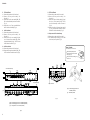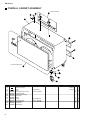
1
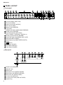
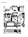
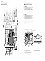
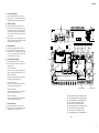
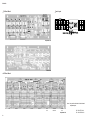
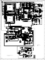
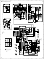
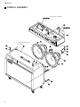
GUITAR PRE-AMPLIFIER
SERVICE MANUAL
CONTENTS
SPECIFICATIONS·············································································· 3
PANEL LAYOUT················································································· 4
CIRCUIT BOARD LAYOUT ······························································ 5
BLOCK DIAGRAM·············································································· 6
DISASSEMBLY PROCEDURE ························································ 7
LSI PIN DESCRIPTION····································································· 9
IC BLOCK DIAGRAM ······································································ 12
CIRCUIT BOARDS··········································································· 14
TEST PROGRAM············································································· 18
ERROR MESSAGES······································································· 21
MIDI IMPLEMENTATION CHART················································· 22
PARTS LIST
OVERALL CIRCUIT DIAGRAM
GA
011400
HAMAMATSU, JAPAN
19980301-198000
2.1K-656
Printed in Japan '98.03
DG100-212
IMPORTANT NOTICE
This manual has been provided for the use of authorized Yamaha Retailers and their service personnel. It has been assumed that
basic service procedures inherent to the industry, and more specifically Yamaha Products, are already known and understood by
the users, and have therefore not been restated.
WARNING:
Failure to follow appropriate service and safety procedures when servicing this product may result in personal
injury, destruction of expensive components and failure of the product to perform as specified. For these
reasons, we advise all Yamaha product owners that all service required should be performed by an authorized
Yamaha Retailer or the appointed service representative.
IMPORTANT:
This presentation or sale of this manual to any individual or firm does not constitute authorization, certification,
recognition of any applicable technical capabilities, or establish a principal-agent relationship of any form.
The data provided is belived to be accurate and applicable to the unit(s) indicated on the cover. The research engineering, and
service departments of Yamaha are continually striving to improve Yamaha products. Modifications are, therefore, inevitable and
changes in specification are subject to change without notice or obligation to retrofit. Should any discrepancy appear to exist,
please contact the distributor's Service Division.
WARNING:
Static discharges can destroy expensive components. Discharge any static electricity you body may have
accumulated by grounding yourself to the ground buss in the unit (heavy gauge black wires connect to this
buss.)
IMPORTANT:
Turn the unit OFF during disassembly and parts replacement. Recheck all work before you apply power to the
unit.
LITHIUM BATTERY HANDLING
This product uses a lithium battery for memory back-up.
WARNING:
Lithium batteries are dangerous because they can be exploded by improper handling. Observe the following
precautions when handling or replacing lithium batteries.
Leave lithium battery replacement to qualified service personnel.
Always replace with batteries of the same type.
When installing on the PC board by soldering, solder using the connection terminals provided on the battery cells.
Never solder directly to the cells. Perform the soldering as quickly as possible.
Never reverse the battery polarities when installing.
Do not short the batteries.
Do not attempt to recharge these batteries.
Do not disassemble the batteries.
Never heat batteries or throw them into fire.
ADVARSEL!
Lithiumbatteri-Eksplosionsfare ved fejlagtig håndtering. Udskiftning må kun ske med batteri af samme fabrikat og type. Levér det
brugte batteri tilbage til leverandøren.
VARNING
Explosionsfara vid felaktigt batteribyte.
Använd samma batterityp eller en ekvivalent typ som rekommenderas av apparattillverkaren.
Kassera använt batteri enligt fabrikantens instruktion.
VAROITUS
Paristo voi räjähtää, jos se on virheellisesti asennettu.
Vaihda paristo ainoastaan laitevalmistajan suosittelemaan tyyppiin.
Hävitä käytetty paristo valmistajan ohjeiden mukaisesti.
The following information complies with Dutch Official Gazette 1995. 45; ESSENTIALS OF ORDER ON THE COLLECTION OF
BATTERIES.
•Please refer to the diassembly procedure for the removal of Back-up Battery.
•Leest u voor het verwijderen van de backup batterij deze beschrijving.
WARNING: CHEMICAL CONTENT NOTICE!
The solder used in the production of this product contains LEAD. In addition, other electrical/electronic and/or plastic (where
applicable) components may also contain traces of chemicals found by the California Health and Welfare Agency (and possibly
other entities) to cause cancer and/or birth defects or other reproductive harm.
DO NOT PLACE SOLDER, ELECTRICAL/ELECTRONIC OR PLASTIC COMPONENTS IN YOUR MOUTH FOR ANY REASON
WHAT SO EVER!
Avoid prolonged, unprotected contact between solder and your skin! When soldering, do not inhale solder fumes or expose eyes
to solder/flux vapor!
If you come in contact with solder or components located inside the enclosure of this product, wash your hands before handling
food.
WARNING
Components having special characteristics are marked
originally installed.
2
and must be replaced with parts having specification equal to those
DG100-212
SPECIFICATIONS
Digital Section
Complete Digital Signal Processing
Internal 8 Channel Preset
Digital Reverb (SPRING, HALL, PLATE)
Digital Tape Echo
Speaker Simulator (LINE OUT)
Analog Section
100W Solid State Power Amp
30 cm Speaker (Celestion Vintage 30) X 2
MIDI Function
Receive : Program change, Control Change (No. 7, 91, 94), Bulk In
Transmit : Bulk Out, Merge Out
Controller/Switch
Front Panel : TRIM, OUTPUT, GAIN, MASTER, TREBLE, HIGH
MID, LOW MID, BASS (TIME), PRESENCE (FEED BACK),
REVERB (LEVEL)
Rear Panel : LINE OUT volume, EFFECT BLEND
Switch : AMP SELECT (LEAD1, LEAD2, DRIVE1, DRIVE2,
CRUNCH1, CRUNCH2, CLEAN1, CLEAN2), REVERB,
MODE, , , STORE, RECALL
Connection Jacks
INPUT HIGH/LOW, SPEAKER, EFFECT SEND/RETURN:
Standard Phone Mono Jack
LINE OUT: Cannon Jack
MIDI IN, MIDI OUT: 5 pin DIN
A/D Converter
20 bit
D/A Converter
20 bit
Sampling Frequency
48 kHz
Memory Number
128
Input Level/Impedance
INPUT HIGH: –30dBm (THRU)/1MΩ
INPUT LOW: –20dBm (THRU)/1MΩ
EFFECT RETURN: 0dBm/120kΩ
Output Level/Impedance
SPEAKER: 100W RMS/4Ω
LINE OUT: +4dBm/600Ω
EFFECT SEND: 0dBm/120kΩ
Display
AMP SELECT display LED X 8
MODE display LED X 3
REVERB type display X 3
7 segment LED X 2 digits
Power Requirements
U.S. and Canadian models : 120V, 60Hz
General model : 230V, 50Hz
Power Consumption
100W
Indicator
Trim Level Display LED (Green)
Trim Clip Display LED (Red)
Dimensions (w/Caster)
712 (W) X 574 (H) X 284 (D) mm
28” (W) X 22.6” (H) X 11.2” (D)
Weight
33.5 kg (73 lbs 13 oz)
3
DG100-212
PANEL LAYOUT
Front panel
Input Jack (INPUT HIGH, LOW)
Trim Control (TRIM)
Output Level Control (OUTPUT)
Gain Volume (GAIN)
Master Volume (MASTER)
Tone Controls
(TREBLE, HIGH MID, LOW MID, BASS, PRESENCE)
Reverb Volume (REVERB)
Amp Select Button/Amp Select Display
(LEAD 1, 2/DRIVE 1, 2/CRUNCH 1, 2/CLEAN 1, 2)
Reverb Type Select Button (REVERB)
Reverb Type Display Lamp (SPRING, HALL, PLATE)
Mode Select Button (MODE)
Mode Display Lamp (AMP/TAPE ECHO/UTIL.)
Display
/ Buttons
Store Button (STORE)
Recall Button (RECALL)
Power Switch (POWER)
Rear panel
Speaker Jack (SPEAKER)
MIDI OUT Jack
MIDI IN Jack
Effect Blend Control (EFFECT BLEND)
Effect Return Jack (EFFECT RETURN)
Effect Send Jack (EFFECT SEND)
Line Out Jack (LINE OUT)
Line Out Level Control (LINE OUT LEVEL)
Speaker Plug
4
DG100-212
CIRCUIT BOARD LAYOUT
WARNING
IMPORTANT
R
R
MAIN 5/5
MAIN 4/5
MAIN 3/5
MAIN 2/5
AC cord
ANR
DM
CN8
CN404
ANR
CN310
CN315
CN316
CN317
CN402
CN401
CN403
CN314
CN7
SPG
CN302
SPH
CN102
CN313
CN312
CN301
CN6
DM
CN9
K304
CN309
CN5
CN101
Power
Transformer
MAIN 1/5
CN304
CN303
CN4
CN307
K303
CN308
K302
VR
K301
CN602
CN603
CN604
CN318
CN601
CN504
CN503
CN305 CN306
CN501
CN701
CN502
MAIN 1/5
VR
CN201
CN202
PN
ANF2
ANF
PN
Power switch
5
DG100-212
DISASSEMBLY PROCEDURE
AC IN
1. Pre-Main Unit
1-1 Remove the four (4) screws marked [70A]. The
back board (U) can then be removed. (Fig. 1)
1-2 Remove the plug of the connector assembly
(speaker) located on the rear panel and the six
(6) screws marked [30A]. The pre-main unit can
then be removed by sliding it backward.(Fig. 1,
Fig. 2)
TRANS
LOAD:
4~8
POWER
PS
5V
15V
2. Speakers
2-1 Remove the four (4) screws marked [70A]. The
back board (U) can then be removed. (Fig. 1)
2-2 Remove the four (4) screws marked [70B]. The
back board (L) can then be removed. (Fig. 1)
2-3 Remove the plug of the connector assembly
(speaker) located on the rear panel and the eight
(8) hexagonal nuts with flanges marked [60A].
The right and left speakers can then be removed.
(Fig. 1)
ANF
ANR
OUTPUT
VR
HB
IC402
PW
MUTING
POWER AMP
SUPPLY
SP JACK
RETURN
JK403
EFECT
LEVEL
JK402
LINE OUT LEVEL
IC401
JK401
SEND
LINE OUT
POWER SW
BLOCK DIAGRAM
S-RAM
D•FF
PN
[30A]
MOTOR
DRIVE
[70A]
[70A]
[60A]
P
R
V
D•FF
IC21,27
CPU
IC13
P
R
E
DSP
B
A
S
S
IC3
[70B]
[70B]
L
•
M
I
D
A/D
Pre-main unit
H
•
M
I
D
IC2
6
Speakers
VR
G
A
I
N
JK701
INPUT 2
ANF2
IC701
GREEN
INPUT LEVEL
IND
RED
JK501
INPUT 1
ANF
TRIM
IC501
VR
M
A
S
T
T
R
E
IC105
BUFF
IC36
[60A] x 4
DF
IC119
IC118
IC104
DM
Pre-main unit
Back board (Upper)
F-ROM
IC12,14
DRA
IC34
IC124
IC8,11
I/ V
D/A
IC122
D/A
IC123
I/ V
IC125
Connector assembly (speaker)
[60]:
Hexagonal Nut 5.0 x 35 MFC2BL
(EX000990)
[70]:
Oval Head Tapping Screw 4.0 x 30 MFC2BL
(EN240090)
(Fig. 1)
[30A]: Oval Head Screw 5.0 x 35 MFC2BL
(VP104600)
(Fig. 2)
DG100-212
3. Front Panel Assembly
3-1 Remove the pre-main unit. (See Procedure 1)
3-2 Remove the five (5) screws marked [30B]. The
front panel assembly can then be removed. (Fig. 3)
4. ANR Circuit Board
4-1 Remove the pre-main unit. (See Procedure 1)
4-2 Remove the screw marked [50], the two (2)
screws marked [170], the two (2) knobs marked
[60] and the four (4) hexagonal nuts marked [A].
The ANR circuit board assembly can then be
removed. (Fig. 3)
4-3 Remove the two (2) screws marked [40d]. The
ANR circuit board can then be removed from the
ANR circuit board assembly. (Fig. 3)
6. Main (1/5-2/5) Circuit Board
6-1 Remove the pre-main unit. (See Procedure 1)
6-2 Each circuit board can then be removed in its
manner as below.
Main 1/5 Circuit Board
Remove the six (6) screws marked [60B]. The
main 1/5 circuit board can then removed. (Fig. 3)
Main 2/5 Circuit Board
Remove the screw marked [150A]. The main 2/5
circuit board can then removed. (Fig. 3)
Main 3/5 Circuit Board
Remove the screw marked [150B]. The main 3/5
circuit board can then removed. (Fig. 3)
Main 4/5 Circuit Board
Remove the screw marked [150C]. The main 4/5
circuit board can then removed. (Fig. 3)
Main 5/5 Circuit Board
Remove the screw marked [150D]. The main 5/5
circuit board can then removed. (Fig. 3)
7. Power Transformer
7-1 Remove the pre-main unit. (See Procedure 1)
7-2 Remove the four (4) screws marked [80A]. The
Transformer can then be removed. (Fig. 3)
R
DM Circuit Board
Remove the pre-main unit. (See Procedure 1)
Remove the ANR circuit board. (See Procedure 4)
Remove the two (2) screws marked [40] and the
six (6) screws marked [30C]. The DM circuit
board can then be removed. (Fig. 3)
[60]
[170]
[50]
[A]
[60]
[40]
DM
MAIN 5/5
R
5.
5-1
5-2
5-3
[A]
MAIN 4/5
MAIN 3/5
MAIN 2/5
MAIN 1/5
[30C] x 6
ANR
[150D]
[150C] [150B] [150A]
[60B] x 6
Sub angle
[80A]
[40d]
[30B] x 5
Front panel assembly
[30B]:
[30C]:
[40]:
[40d]:
[50]:
[60B]:
Power transformer
Bind Head Tapping Screw-A4.0 x 8 MFZN2BL (VP156800)
Bind Head Tapping Screw-B 3.0 x 6 MFZN2BL (EP600230)
Bind Head Tapping Screw-B 3.0 x 8 MFZN2BL (EP600190)
Pan Head Screw SP3.0 x 8 MFZN2Y (EK400500)
Bind Head Screw A3.0 x 8 MFZN2BL (VP156700)
Bind Head Tapping Screw-B 3.0 x 6 MFZN2BL (EP600230)
[80A]:
Bind Head Screw A4.0 x 8 MFZN2BL (VP156800)
[150]:
Pan Head Screw SP3.0 x 12 MFZN2Y (EL200070)
[170]:
Bind Head Tapping Screw-B 3.0 x 8 MFZN2BL (EP600190)
(Fig. 3)
7
DG100-212
8. PN Circuit Board
8-1 Remove the pre-main unit. (See Procedure 1)
8-2 Remove the front panel assembly. (See
Procedure 3)
8-3 Remove the ten (10) screws marked [80B]. The
PN circuit board assembly can then be removed.
(Fig. 4)
8-4 Remove the seven (7) top cap assemblies from
the PN circuit board assembly. (Fig. 4)
9.
11. VR Circuit Board
11-1 Remove the pre-main unit. (See Procedure 1)
11-2 Remove the front panel assembly. (See
Procedure 3)
11-3 Remove the eight (8) knobs marked [90] and
the four (4) screws marked [30D]. The VR
circuit board assembly can then be removed.
(Fig. 4)
11-4 Remove the eight (8) hexagonal nuts marked
[C]. The VR circuit board can then be removed
from the VR circuit board assembly. (Fig. 5)
ANF Circuit Board
9-1 Remove the pre-main unit. (See Procedure 1)
9-2 Remove the front panel assembly. (See
Procedure 3)
9-3 Remove the two (2) screws marked [100], the
two (2) hexagonal nuts marked [B] and the
hexagonal nut marked [110A]. The ANF circuit
board can then be removed. (Fig 4)
12. Replacement Of The Lithium Battery
12-1 Remove the pre-main unit. (See Procedure 1)
12-2 The lithium battery marked [D], on the DM
circuit board, can be replaced. (Fig. 6)
10. ANF2 Circuit Board
Battery VS246400
10-1 Remove the pre-main unit. (See Procedure 1)
10-2 Remove the hexagonal nut marked [110B]. The
ANF2 circuit board can then be removed. (Fig. 4)
VS246300(Battery holder for VS246400)
Battery
Notice for back-up battery removal
Push against the holder hook, then the
battery will pop up.
Druk tegen de houder, de batterij springt
dan naar voren.
VR
[D]
PN
VR circuit board assembly
[30D]
DM
[80B]
ANF
ANF2
[80B]
[C]
Front panel assembly
Angle, motor volume
[140b]:
[110B]
[D]:
[110A]
[100],[B]
[90]
Bind Head Tapping Screw-B 3.0 x 6 MFZN2BL (EP600230)
Bind Head Tapping Screw-B 3.0 x 6 MFZN2BL (EP600230)
Hexagonal Nut 9.0 x 12 x 2 MFNI33 (LX200060)
(Fig. 4)
8
Bind Head Tapping Screw-B 3.0 x 6
MFZN2BL (EP600230)
Lithium Battery CR2032
Top cap assemblies
(Fig. 5)
[30B]:
[80B]:
[110]:
Battery holder
(Fig. 6)
DG100-212
LSI PIN DESCRIPTION
HD6413002FP16 (XQ375A00) CPU <H8/3002>
PIN
NO.
1
2
3
4
5
6
7
8
9
10
11
12
13
14
15
16
17
18
19
20
21
22
23
24
25
26
27
28
29
30
31
32
33
34
35
36
37
38
39
40
41
42
43
44
45
46
47
48
49
50
NAME
I/O
PA6
PA7
VCC
PB0
PB1
PB2
PB3
PB4
PB5
O
O
PB6//DREQ0
PB7//DREQ1
/RESO
VSS
P90/TXD0
P91/TXD1
P92/RXD0
P93/RXD1
P94/SCK0
P95/SCK1
P40/D0
P41/D1
P42/D2
P43/D3
VSS
P44/D4
P45/D5
P46/D6
P47/D7
D8
D9
D10
D11
D12
D13
D14
D15
VCC
A0
A1
A2
A3
A4
A5
A6
A7
VSS
A8
A9
A10
A11
I
I
I
I
I
I
I
I
O
O
O
I
I
O
I
I/O
I/O
I/O
I/O
FUNCTION
Port A
Address bus
Power supply
Port B
Reset
Ground
Transmit data (MIDI OUT)
KSN-ACK
Receive data (MIDI IN)
KSN-RX
Port 9
Port 9
(Ground)
I/O
I/O
I/O
I/O
I/O
I/O
I/O
I/O
I/O
I/O
I/O
I/O
Data bus
Power supply
O
O
O
O
O
O
O
O
Address bus
(Ground)
O
O
O
O
PIN
NO.
NAME
I/O
51
52
53
54
55
56
57
58
59
60
61
62
63
64
65
66
67
68
69
70
71
72
73
74
75
76
77
78
79
80
81
82
83
84
85
86
87
88
89
90
91
92
93
94
95
96
97
98
99
100
A12
A13
A14
A15
A16
A17
A18
A19
VSS
P60//WAIT
P61//BREQ
P62//BACK
ø
/STBY
/RES
NMI
VSS
EXTAL
XTAL
VCC
/AS
/RD
/HWR
/LWR
MD0
MD1
MD2
AVCC
VREF
P70/AN0
P71/AN1
P72/AN2
P73/AN3
P74/AN4
P75/AN5
P76/AN6
P77/AN7
AVSS
P80
P81//CS3
P82//CS2
P83//CS1
P84//CS0
VSS
PA0
PA1
PA2
PA3
PA4
PA5
O
O
O
O
O
O
O
O
FUNCTION
Address bus
Ground
I
I
I
O
I
I
I
I
O
O
O
O
O
I
I
I
I
I
I
I
I
I
I
I
I
O
O
O
O
O
Port 6
øout
Stand-by mode signal
Reset
Non-maskable interrupt
Ground
Clock
Clock
Power supply
Address strobe
Read strobe
Write strobe (High)
Write strobe (Low)
Mode select
Analog power supply
Reference voltage
Analog data input (EQ)
Analog input (EQ)
Analog data input
Analog input (CS)
Analog data input (BEND)
Analog input (MOD)
Analog input (FC)
Analog input (BAT)
Analog ground
Port 8
Chip select
Ground
I
I
I
O
O
O
Port A
9
DG100-212
YSS228D-F (XQ962D00) DSP3 (Digital Signal Processor)
PIN
NO.
1
2
3
4
5
6
7
8
9
10
11
12
13
14
15
16
17
18
19
20
21
22
23
24
25
26
27
28
29
30
31
32
33
34
35
36
37
38
39
40
41
42
43
44
45
46
47
48
49
50
51
52
53
54
55
56
57
58
59
60
61
62
63
64
65
66
67
68
69
70
71
72
73
74
75
76
77
78
79
80
10
NAME
VSS
XI
XO
VDD
/SYNCI
/SYNCO
CKI
CKO
CKSL
VSS
MCKS
/SSYNC
/IC
/TEST
BTYP
/IRQ
TRIG
VDD
VSS
/CS
/DS
R/W
CA7
CA6
CA5
CA4
CA3
CA2
CA1
CA0/CD15
CD14
CD13
CD12
CD11
CD10
CD09
CD08
CD07
CD06
VSS
VDD
CD05
CD04
CD03
CD02
CD01
CD00
/DTACK
SI0
SI1
SI2
SI3
SI4
SI5
SI6
SI7
VSS
VDD
SO0
SO1
SO2
SO3
SO4
SO5
SO6
SO7
DB00
DB01
DB02
DB03
DB04
DB05
DB06
DB07
DB08
DB09
DB10
DB11
DB12
VDD
FUNCTION
I/O
81
82
83
Power supply
84
System synch. input
85
System synch. output
86
System clock input (30MHz)
87
System clock output (30MHz)
88
System master clock select (0:60M,1:30MHz)
89
Ground
90
Master clock for serial I/O(128xFs)
91
Synch. signal for serial I/O
92
Initial clear
93
Test mode setting
94
CPU data bus 8/16 bit select(0:8,1:16)
95
Interrupt request
96
Trigger signal
97
Power supply
98
Ground
99
Chip select
100
Data strobe
101
Read/Write select
102
103
104
105
CPU address bus
106
107
108
109
CPU address/data bus
110
111
112
113
114
CPU data bus
115
116
117
118
119
Ground
120
Power supply
121
122
123
124
CPU data bus
125
126
127
DTACK signal output
128
129
130
131
132
Serial data input
133
134
135
136
Ground
137
Power supply
138
139
140
141
142
Serial data output
143
144
145
146
147
148
149
150
151
152
Parallel data bus
153
154
155
156
157
158
159
Power supply
160
Ground
I
I
O
I
O
I
I
I
I
I
I
O
I/O
I
I
I
I
I
I
I
I
I
I
I/O
I/O
I/O
I/O
I/O
I/O
I/O
I/O
I/O
I/O
I/O
I/O
I/O
I/O
I/O
I/O
O
I
I
I
I
I
I
I
I
O
O
O
O
O
O
O
O
I/O
I/O
I/O
I/O
I/O
I/O
I/O
I/O
I/O
I/O
I/O
I/O
I/O
PIN
NO.
System master clock input (60M or30MHz)
System master clock input (60M or30MHz)
NAME
I/O
I/O
I/O
I/O
I/O
I/O
I/O
I/O
I/O
I/O
I/O
I/O
I/O
I/O
I/O
I/O
I/O
I/O
I/O
I/O
TIMO/DBOE I/O
VSS
VDD
DA00
I/O
DA01
I/O
DA02
I/O
DA03
I/O
DA04
I/O
DA05
I/O
DA06
I/O
DA07
I/O
DA08
I/O
DA09
I/O
DA10
I/O
DA11
I/O
DA12
I/O
DA13
I/O
DA14
I/O
DA15
I/O
VSS
VDD
DA16
I/O
DA17
I/O
DA18
I/O
DA19
I/O
DA20
I/O
DA21
I/O
DA22
I/O
DA23
I/O
DA24
I/O
DA25
I/O
DA26
I/O
DA27
I/O
DA28
I/O
DA29
I/O
DA30
I/O
DA31
I/O
VDD
VSS
A00
O
A01
O
A02
O
A03
O
A04
O
A05
O
A06
O
A07
O
A08
O
A09
O
A10
O
A11
O
A12
O
A13
O
A14
O
A15/RAS O
A16/CAS O
A17/CE O
/WE
O
/OE
O
VDD
VSS
DB13
DB14
DB15
DB16
DB17
DB18
DB19
DB20
DB21
DB22
DB23
DB24
DB25
DB26
DB27
DB28
DB29
DB30
DB31
FUNCTION
I/O
Ground
Parallel data bus
Timing signal/Parallel data bus control
Ground
Power supply
External memory data bus
Ground
Power supply
External memory data bus
Power supply
Ground
External memory address bus
External memory address bus/Row address strobe
External memory address bus/Column address strobe
External memory address bus/Chip enable
External memory write enable
External memory output enable
Power supply
DG100-212
YSF210-M (XK280A00) Digital Filter
PIN
NO.
NAME
I/O
1
2
3
4
5
6
7
8
XO
XI
VSS2
BCI
SDSY
IBIT1
IBIT2
IBIT3
O
I
9
10
11
12
MUTE
NC
SDI
VDD2
I
I
I
I
I
I
I
FUNCTION
System clock
Ground
Bit clock
L/R select and input timing
Input bit selection
IBIT 1
IBIT 2
IBIT 3
22 bit 20 bit 18 bit 16 bit AV DSP MEL
H
L
H
L
H
H
H
H
L
L
H
H
H
H
H
H
L
L
Mute
No connection
Input data
Power supply
PIN
NO.
NAME
I/O
13
14
OBIT1
OBIT2
I
I
FUNCTION
Output bit selection
OBIT 1
OBIT 2
15
16
NC
ASY
I
17
18
19
20
21
22
23
24
VSS1
BCO
WCO
SHL
DRO
NC
DLO
VDD1
O
O
O
O
O
22 bit 20 bit 18 bit no output
H
L
H
L
H
H
L
L
No connection
Synchronous/Asynchronous system clock
section
Ground
Bit clock of DLO, DRO
Word clock of DLO, DRO
Deglich signal of L/R channel
Output data of R channel
No connection
Output data of L channel
Power supply
AK5390-VP (XQ199A00) ADC (Analog.Digita Converter)
PIN
NO.
NAME
I/O
1 AGND
2
APD
3 AINL+
4 AINL5 ACAL
6 LGND
7
VL+
8
NC
9 DACL
10
DPD
11 CMODE
O
I
I
12 SMODE
I
13
14
L//R
SCLK
FUNCTION
Analog ground
I
I
I
I
I/O
I/O
Analog signal input (L channel -)
Analog signal input (L channel +)
Analog calibration
Analog logic ground
Analog logic power supply
Digital calibration
Digital power down
Master clock select
(L: CLK=256fs, H:CLK=384fs)
Interface clock select
(L: slave mode, H: master mode)
Input channel select
Serial data clock
PIN
NO.
NAME
I/O
FUNCTION
15 SDATA
16 FSYNC
17
VD+
18 DGND
19
CLK
20 OCLK
21
NC
22
ICLK
23
VA+
24
VA25 AINR-
O
I/O
Serial data output
Frame synch. clock
Digital power supply (+)
Digital ground
Master clock
128 fs clock output
I
O
I
I
128 fs clock input
Analog power supply (+)
Analog power supply (-)
Analog signal input (R channel -)
26
AINR+
I
Analog signal input (R channel +)
27
28
VREFVREF+
O
O
Reference voltage (-)
Reference voltage (+)
PCM1702P (XN136A00) DAC (Digital to Analog Converter)
PIN
NO.
NAME
1 DATA
2 CLOCK
3 +Vdd
4 DGND
5
-Vdd
6
LE
7
NC
8
NC
I/O
I
I
I
I
FUNCTION
Serial data input
Bit clock
Digital power supply (+5V)
Digital ground
Digital power supply (-5V)
Latch enable
Reserved
Reserved
PIN
NO.
NAME
I/O
9
+Vcc
10 BPO DC I/O
11 I OUT
O
12 AGND
13 AGND
14 SERVO DC I/O
15 REF DC I/O
16
-Vcc
FUNCTION
Analog power supply (+5V)
BPO decouple
Current output
Analog ground
Analog ground
Servo decouple
Ref. decouple
Analog power supply (-5V)
11
DG100-212
IC BLOCK DIAGRAM
TCHCU04AF-TP1(XD660A00)
Hex Inverter
1A
1
14
2
13
6A
2A
3
12
6Y
2Y
4
11
5A
3Y
Vss
5
10
6
9
7
8
2
4Y
1B
3
1Y
4
2A
5
14
VDD
1A
1
14
Vcc
2
13
4B
1B
2
13
4B
1Y
3
12
4A
1Y
3
12
4A
2A
4
11
4Y
2A
4
11
4Y
2B
5
10
3B
2B
5
10
3B
2Y
6
9
3A
2Y
6
9
3A
VSS
7
8
3Y
GND
7
8
3Y
TC74HC164AF (XQ967A00)
8-Bit Shift Register
A
1
14
VCC
B
2
B
QH
13
QH
QA
3
QA
QG
12
QG
QB
4
QB
QF
11
QF
4Y
QC
5
QC
QE
10
11
3A
QD
6
QD
CLEAR
CK A
10
3B
GND
7
16
Vcc
15
STROBE
1B
4A
14
4A
1Y
4B
13
4B
2A
4Y
12
2B
3A
3B
1A
1
1B
4A
G
S
1
1A
1A
5Y
TC74HC157AF-TP1(XH603A00)
Quad 2 to 1 Multiplexer
SELECT
TC74VHC32F (XN963A00)
Quad 2 Input OR
VDD
1Y
3A
SN74HC08NSR (XD831A00)
Quad 2 Input AND
SIRIAL
INPUT
TC74HC175AF -TP1(XD658A00)
Quad D-Type Flip-Flop
CL
1
1Q
2
1Q
3
1D
QE
2D
9
CLEAR
2Q
8
CLOCK
2Q
7
Vss
8
16
VDD
15
4Q
14
4Q
4
13
4D
5
12
3D
11
3Q
10
3Q
9
CK
A
Q CL
CK
Q D
CL Q
CK
D Q
OUTPUTS
OUTPUTS
2B
6
7
GND
8
2Y
3Y
2Y
9
3Y
SN74HC244NSR (XD233A00)
Octal 3-State Bus Buffer
OUTPUT
CONTROL
1
2G
1Q
2
Q
18
1Y1
1D
3
4
17
2A4
2D
4
2Y3
5
16
1Y2
2Q
1A3
6
15
2A3
2Y2
7
14
1A4
8
2Y1
(GND) Vss
1
20
VDD (Vcc)
2
19
2Y4
3
1A2
1G
1A1
12
SN74HC374ANSR (XQ042A00)
Octal 3-State D-Type Flip-Flop
20
Vcc
Q
19
8Q
OE
D CK
OE
CK D
18
5
D CK
OE
Q
CK D
OE
Q
3Q
6
Q
1Y3
3D
7
13
2A2
4D
8
9
12
1Y4
4Q
9
10
11
2A1
GND
10
6
Q D
CK
Q CL
D Q
CK
CL Q
TC74HC4040F (XR684A00)
12-Stage Binary Ripple Counter
Q12
1
Q12
Q6
2
Q6
8D
Q5
3
17
7D
Q7
4
16
7Q
Q4
5
Q
15
6Q
Q3
OE
D CK
OE
CK D
14
6D
Q2
7
D CK
OE
Q
CK D
OE
Q
13
5D
Vss
8
12
5Q
11
CLOCK
6
16
VDD
Q11
15
Q11
Q5
Q10
14
Q10
Q7
Q8
13
Q8
Q4
Q9
12
Q9
Q3
CL
11
CLR
Q2
CK
10
Input Pulses (
Q1
9
Q1
)
DG100-212
NE5532P(IG102500)
Dual Operational Amplifier
2
Non-Inverting
Input A
3
-DC Voltage Supply
4
+V
-
+
+
-
-V
8
+DC Voltage
Supply
7
Output B
6
Inverting
Input B
5
+
1
Inverting
Input A
+
Output A
NJM072D(IG107000)
Dual Operational Amplifier
A
B
1
2
+V
3
4
5
-IN
Non-Inverting
Input B
OUT
A
A
6
-V
7
8
-IN
+IN
+IN
A
B
9
+V
OUT
B
B
MB3790PF(XR967A00)
ASSP
R CN 0.5
V IN 14
V IN 13
3
100
CONTROL 16
V OUT
V OUT
6
ALARM1
7
ALARM2
SBD
590k
1.24V
Reference
Voltage
Power Supply
Circuit
V IN
2.65V
+
-
500
V IN
+
V SENSE 12
4
3µA
Q
S
-
+
2.37V
-
R
V OUT
9
240k
RESET
V th:3V
V OUT
10
V th:1.5V
11
5
2
CT
V BAT2
V BAT1
GND 8
RESET
N.C. 1
16 CONTROL
V BAT1 2
15 N.C.
V OUT 3
14 V IN
V OUT 4
13 V IN
V BAT2 5
12 V SENSE
ALARM1 6
11 C T
ALARM1 7
10 RESET
GND 8
9 RESET
LB1641 (XF494A00)
Motor Driver
P1
OUT1
2
Vcc2
8
OUT2
10
P2
9
Vcc1
7
PRE DRIVER
3
IN 1
GND
5
INPUT LOGIC
4
6
Vz
IN 2
1
13
DG100-212
CIRCUIT BOARDS
DM Circuit Board
MIDI
IN
OUT
to DM-CN9
Component side
Note : See parts list for details of circuit board
component parts.
ENA-VZ77180-1/9
14
DG100-212
DM Circuit Board
to DM-CN9
Pattern side
Note : See parts list for details of circuit board
component parts.
ENA-VZ77180-1/9
15
DG100-212
PN Circuit Board
Panel Layout
Component side
Pattern side
VR Circuit Board
Note : See parts list for details of circuit board
component parts.
GAIN
MASTER
TREBLE
HIGH MID
LOW MID
BASS
TIME
PRESENCE
FEED BACK
REVERB
LEVEL
Component side
16
PN : ENA-VZ77230-1/4
VR : CNA-VZ89700-1/10
DG100-212
MAIN Circuit Board
5/5
ANR Circuit Board
4/5
3/5
2/5
LINE OUT
LINE OUT
LEVEL
EFFECT
SEND
RETURN
BLEND
1/5
Component side
ANF2 Circuit Board
ANF Circuit Board
Component side
HIGH
Note : See parts list for details of circuit board
component parts.
Component side
LOW
INPUT
TRIM
OUTPUT
Component side
CNA-VZ89700-1/10
17
DG100-212
TEST PROGRAM
A. SET-UP
E. TEST PROGRAM
1. If no specific frequency is required, set the test
frequency at 1 kHz.
2. If no specific TRIM and OUTPUT settings are
required, set the volumes of TRIM and
OUTPUT at maximum.
3. Before turning the POWER switch on, set the
Idling Adjustment Volume (VR303, 470 ohms)
at minimum.
B. HOW TO ENTER THE TEST PROGRAM
While simultaneously pressing the MODE, the
REVERB and the DRIVE2 switches, turn the
POWER switch on. The DG100-212 will enter
the self test mode.
C. FACTORY PRESET OF RAM
While simultaneously pressing the LEAD1 and
the RECALL switches, turn POWER switch on.
The RAM will be cleared, the factory setting data
are restored on the RAM, and the DG100-212
will enter the normal mode.
D. PROCEEDING THROUGH THE TESTS
1. Switch Functions
Increment :
test no. select upward
Decrement :
test no. select downward
RECALL :
start of the selected test
STORE :
exit (in case of error)
LEAD1
~ CLEAN2 :
no effect
REVERB, MODE : no effect
2. LED Display Functions
When the DG100-212 is in the self test mode,
the LED display shows the number for the
status as below.
Function
(status)
test no. selection
test execution
ok
error
LED display
lower num.
upper num.
(blank)
(test no.)
(check no.)
(test no.)
8.
8.
(error no.)
E
If the LED displays "E" and "(error no.)", the
DG100-212 status can be changed to "test no.
selection" by pressing the STORE key. When
the status has been changed, the LED display
shows a next test no.
When the DG100-212 is in "test no. selection", the
test no. can be changed by using the increment
and the decrement keys.
18
(Relay Check)
Check that the relay is switched ON within 2 ~
3 minutes after the POWER switch is turned on.
(Menu of Test Program)
0. LED Check
1. Switch Check
2. Motor Drive Volume check
3. Volume Center Check
4. Battery Check
5. MIDI Check
6. SRAM Check
7. Flash Memory Erase/Write Check
8. Sound Check
9. TEST END
0. LED Check
(Test Contents)
When the DG100-212 enters the self test mode,
the LED Check is started and the LEDs light
automatically for the check in the sequence as
below.
·All the LEDs light simultaneously.
·All the LEDs go out simultaneously.
·The LEDs light one by one in the sequence as
below.
LEAD1 Program
LEAD2 Memory
DRIVE1 Channel
DRIVE2 Merge
CRUNCH1 All Data
CRUNCH2 User Mem.
CLEAN1 SP SIM
CLEAN2 VOL PEDAL
SPRING
HALL
PLATE
AMP
TAPE ECHO
UTIL.
LED display upper num.
top
LED display upper num.
right upper
LED display upper num.
right lower
LED display upper num.
bottom
LED display upper num.
left lower
LED display upper num.
left upper
LED display upper num.
center
LED display upper num.
dot
LED display lower num.
top
LED display lower num.
right upper
LED display lower num.
right lower
LED display lower num.
bottom
LED display lower num.
left lower
LED display lower num.
left upper
LED display lower num.
center
LED display lower num.
dot
·All the LEDs go out simultaneously
·All the LEDs light simultaneously
The LED Check is finished and the DG100-212
selects the next test no., so the LED shows a "1".
(Error Number)
not appearing
E0 ~ E3
If a Motor Drive Volume Check operation has
not been finished in 20 seconds, the LED display
shows "E0" ~ "E3" by replacing "2" to "E".
1. Switch Check
Press the RECALL key when the LED display
shows "1". The Switch Check is started and the
LED display shows the first check number "11".
(Test Contents)
Press the keys according to the LED display
guide in the order as below.
(The Exit function of the STORE key is
available on the error status.)
11 LEAD1 Program Switch
12 LEAD2 Memory Switch
13 DRIVE1 Channel Switch
14 DRIVE2 Merge Switch
15 CRUNCH1 All Data Switch
16 CRUNCH2 User Mem. Switch
17 CLEAN1 SP SIM Switch
18 CLEAN2 VOL PEDAL Switch
19 REVERB Switch
1A MODE Switch
1B Increment Switch
1C Decrement Switch
1D STORE Switch
1E RECALL Switch
When all the LEDs display light simultaneously,
the Switch Check is finished. Then the DG100212 selects the next test no., so the LED display
shows a "2".
(Error Number)
E1 ~ EE
The switch corresponding to the error number
has a problem or the wrong switch was pressed.
3. Volume Center Check
Press the RECALL key when the LED display
shows "3", and the Volume Check is started and
the LED display shows one of the numbers from
"31" to "38".
(Test Contents)
Select the knob that requires adjustment and
turn it until the LED display shows the next
volume check number.
33 TREBLE
34 HIGH MID
35 LOW MID
36 BASS
37 PRESENCE
The A/D converter value is shown with binary
digits by using the AMP SELECT LEDs. Set
the knob to the center and turn the trimmer
potentiometer to adjust the AMP SELECT
LEDs as shown on the list below.
2. Motor Drive Volume check
Press the RECALL key when the LED display
shows "2", The Motor Drive Volume Check is
started and the LED display shows the first
check number "21".
(Test Contents)
Once the Motor Drive Check has been started,
all the volumes rotate automatically as below.
21 to the Minimum
22 to the Maximum
23 to the Center
When all the LEDs light simultaneously, the
Volume Check is finished. Then the DG100-212
selects the next test no., so the LED display
shows a "3".
(Error Number)
AMP
SELECT
LED
LEAD1
Program
On
LEAD2
Memory
Off
DRIVE1
Channel
Off
DRIVE2
Merge
Off
AMP CRUNCH1 CRUNCH2 CLEAN1 CLEAN2
SELECT All Data User Mem.
LED
Off
Off
Off
Off
If the knob data is the same as the data of the list
above, the adjustment of that knob can be
passed. The trimmer potentiometer numbers are
shown below.
TREBLE :
VR603
HIGH MID :
VR605
LOW MID :
VR607
BASS :
VR609
PRESENCE :
VR611
Once the required Volume Center Check has
been finished, press the RECALL key and the
DG100-212 selects the next test no., so the LED
display shows "4".
(Error Number)
not appearing
4. Battery Check
Press the RECALL key when the LED display
shows "5". The Battery Check is started.
DG100-212
(Test Contents)
The RAM Backup Battery check is executed
automatically.
When all the LEDs light simultaneously, the
Battery Check is finished. Then the DG100-212
selects the next test no., so the LED display
shows "5".
(Error Number)
E0 : Battery Low (RAM DATA are kept.)
E1 : Unknown Error
E2 : Battery Low (RAM DATA are not
kept.) or Not Installed
(Test Contents)
The Flash Memory Erase/Write check is executed
automatically.
When the check is started, the LED display shows
from "70" to "73" successively. When all the LEDs
light simultaneously, the Flash Memory
Erase/Write check is finished. Then the DG100212 selects the next test no., so the LED display
shows "8".
(Error Number)
E0, E1 : Flash Erase Error
E2, E3 : Flesh Write Error
5. MIDI Check
Connect the MIDI IN and the MIDI OUT terminals
with a MIDI cable. Press the RECALL key when
the LED display shows "5". The MIDI Check is
started.
(Test Contents)
The loop back MIDI check is executed automatically.
When the MIDI check is started, the LED display
shows "51" and then "52". When all the LEDs
light simultaneously, the MIDI Check is finished.
Then the DG100-212 selects the next test no., so
the LED display shows "6".
(Error Number)
E0 : Error
E1 : Error
8. Sound Check
Before executing this sound check, the idling
adjustment, the output wave adjustment and
center voltage adjustment must be finished. the
three adjustments can be done while the LED
display shows "8".
(Idling Adjustment)
1. set the idling adjustment volume (VR303) at
minimum.
2. connect the 4ohm load to the speaker terminals.
3. Set the output volume at minimum.
4. Adjust the VR303 so that the DC voltage between
the terminals of the RA301 should be 5 mV +/-1 mV.
(Output Wave Adjustment)
1. After adjusting the Idling adjustment, set the
OUTPUT VR at maximum.
2. When the signal of -2dBm / 1 kHz is inputted from
the RETURN terminal, adjust the VR 301 (4.7
kohms) so that the wave shape should be a sine
wave symmetrical for upper and lower as below.
6. SRAM Check
Press the RECALL key when the LED display
shows "6". The SRAM Check is started.
(Test Contents)
The SRAM read/write check is executed
automatically.
When the SRAM Check is started, the LED display
shows "61" and then "62". When all the LEDs
light simultaneously, the SRAM Check is finished.
Then the DG100-212 selects the next test no., so
the LED display shows "7".
(Error Number)
E0 : RAM Address Error
E1 : RAM Read/Write Error
7. Flash Memory Erase/Write Check
Press the RECALL key when the LED display
shows "7". The Flash Memory Erase/Write
Check is started.
(Attention)
When the result of the test number 6 has alredy
been "Error", don't execute this test, or the
DG100-212 won't set up at normal mode by the
rewrited wrong data in the Flash Memory.
Don't turn the POWER switch off while executing
this test, the DG100-212 won't set up at normal
mode by no data in the Flash Memory.
T•P
T•P
0.22x2
RA301
(Center Voltage Adjustment)
1. Adjust the VR302 so that the voltage of the
output circuit (RA301) should be 34 +/- 1 V.
* By adjusting the Output Adjustment and the
Center Voltage Adjustment alternatively, search
the best point.
Adjust the VR301
to be a sine wave.
After finifhing the adjustments above, press the
RECALL key when the LED display shows "8".
The Sound Check is started.
19
DG100-212
(Test Contents)
The DG100-212 sets the conditions for the
signal Sound Check through the analogue
circuit, the A/D converter, the DSP-3 and the
D/A Converter.
When the Sound Check is started, the LED display
shows "81". The Sound Check has two conditions.
If the RECALL key is pressed when the LED
display shows "81", the LED display changes to
"82" and the condition changes to the next as
below.
81 : DSP3-1
82 : DSP3-2
Check the following items in each condition of
"81" and "82".
Items
1.Input Sensitivity
(High)
2.Input Sensitivity
(Low)
3.RETURN Level
4.SEND Level
5.LINE OUT
Level
6.Frequency
Response
(HIGH IN)
7.Remain Noise
8.Sensitivity of
LED for Input
Level
9.Output
Conditions
1 kHz, -30dBm
Responses
(standards)
+28 dBm +/-2 dB
1 kHz, -20dBm
+28 dBm +/-2 dB
1 kHz, 0dBm
Condition of 1. and
100 kohms SEND
load
Condition of 1. and
100 kohms LINE
OUT load
-40 dBm Input
1 kHz standard
SP Output Terminal
TRIM, OUTPUT
VR MIN IHF A net
Lo Input
TRIM Vol:
maximum
OUTPUT Vol:
maximum
RETURN,10%THD
+28 dBm +/-2 dB
-1 dBm +/-2 dB
+3 dBm +/-2 dB
100 Hz: 0.5 +/-1dB
10 kHz: 0.5 +/-1dB
less than -60 dBm
Input
LED
-30 dBm: no light
-20 dBm: GR only
+3 dBm: both lit
more than +28 dBm
(95W)
* 0 dBm = 0.775 V
Load = 4 ohms
If the Sound Check has been finished, press the
RECALL key when the LED display shows "82".
The LED display shows "9".
(Error Number)
not appearing
9. TEST END
A "9" on the LED display signals the end of the
TEST and the exit of the Test Program. Press
the RECALL key when the LED display shows
"9". The mode of the DG100-212 changes to the
normal mode and all of the function data are set
to the condition of the latest program number in
normal mode. The Motor Drive Volumes rotate
automatically to the settings of that data.
20
DG100-212
ERROR MESSAGES
If an error occurs during operation, one of the following error message numbers will appear on the display.
: Motor Drive Error
CAUSE:
SOLUTION:
The volume knob has not returned to its assigned position after 20 seconds has elapsed from the start of the recall
operation or, the device does not recognize the recall command.
Turn off the power and check the circuit for Motor Drive.
: MIDI Receive Buffer Full
CAUSE:
SOLUTION:
Too much MIDI data is being received by the DG100-212 at one time.
Try reducing the amount of data being sent or, break the data into smaller blocks.
: Communication Error.
CAUSE:
SOLUTION:
An abnormality is detected during MIDI communications.
Check all connections, etc. and try again.
: Bulk Receive Check Sum Error.
CAUSE:
SOLUTION:
The check sum does not match the received MIDI bulk data.
Check all connections and data, and try again.
: Bulk Receive Data Abnormality.
CAUSE:
SOLUTION:
An abnormality is detected in the received MIDI bulk data.
Check all connections and data, and try again.
: Backup Battery Error.
CAUSE:
SOLUTION:
Backup battery power is depleted.
Continued use of the device will result in the loss of data. Return the device to the music dealer where you purchased it
or, the nearest Yamaha Service center and have the battery replaced.
21
DG100-212
YAMAHA
[ Digital Guitar Amplifier ]
Date:24-Dec-1997
Model DG100-212 MIDI Implementation Chart
Version : 1.0
+----------------------------------------------------------------------+
:
: Transmitted
:
Recognized
:
Remarks
:
:
Function ... :
:
:
:
:-------------------+----------------+----------------+----------------:
:Basic
Default
: x
: 1 - 16, off
: memorized
:
:Channel Changed
: x
: 1 - 16, off
:
:
:-------------------+----------------+----------------+----------------:
:
Default
: x
: 1,3
: memorized
:
:Mode
Messages : x
: x
:
:
:
Altered
: ************** : x
:
:
:-------------------+----------------+----------------+----------------:
:Note
: x
: x
:
:
:Number : True voice: ************** : x
:
:
:-------------------+----------------+----------------+----------------:
:Velocity Note ON
: x
: x
:
:
:
Note OFF : x
: x
:
:
:-------------------+----------------+----------------+----------------:
:After
Key's
: x
: x
:
:
:Touch
Ch's
: x
: x
:
:
:-------------------+----------------+----------------+----------------:
:Pitch Bender
: x
: x
:
:
:-------------------+----------------+----------------+----------------:
:
0 6 : x
: x
:
:
:
7 : x
: o
: Main Volume
:
:
8 - 90 : x
: x
:
:
:
91 : x
: o
: Reverb SW.
:
: Control
92 : x
: x
:
:
:
94 : x
: o
: Tape Echo SW. :
: Change 95 - 127 : x
: x
:
:
:
:
:
:
:
:
:
:
:
:
:
:
:
:
:
:
:
:
:
:
:
:
:
:
:
:
:
:
:
:
:-------------------+----------------+----------------+----------------:
:Prog
: x
: o 0 - 127
: Program Change :
:Change : True #
: ************** :
: Number 1-128 :
:-------------------+----------------+----------------+----------------:
:System Exclusive
: o
: o
: Bulk Dump
:
:-------------------+----------------+----------------+----------------:
:System : Song Pos. : x
: x
:
:
:
: Song Sel. : x
: x
:
:
:common : Tune
: x
: x
:
:
:-------------------+----------------+----------------+----------------:
:System
:Clock
: x
: x
:
:
:Real Time :Commands: x
: x
:
:
:-------------------+----------------+----------------+----------------:
:Aux :Local ON/OFF : x
: x
:
:
:
:All Notes OFF: x
: x
:
:
:Mes- :Active Sense : o
: x
:
:
:sages:Reset
: x
: x
:
:
:-------------------+----------------+----------------+----------------:
:
:
:
:
:
:
:
:
+-------------------+----------------+----------------+----------------+
Mode 1 : OMNI ON, POLY
Mode 2 : OMNI ON, MONO
o : Yes
Mode 3 : OMNI OFF, POLY
Mode 4 : OMNI OFF, MONO
x : No
22
A
B
C
D
E
F
G
H
I
J
K
DG100-212 OVERALL CIRCUIT DIAGRAM 1/2( DM,ANR)
1
L
DG100-212
DM
1
RAM
ASSP
Photo Coupler
2
2
SRAM
SRAM
DATA SELECTOR
DSP3
OR
to PN-CN202
3
3
OR
OR
to VR-CN603
BUS BUFFER
4
4
DRAM
AND
BUS BUFFER
to PN-CN201
5
5
CPU
to MAIN1/5-CN308
DSP3
6
6
DRAM
D-FF
D-FF
7
7
to VR-CN602
to VR-CN604
8
8
REGULATOR
OP AMP
9
9
ADC
to ANF-CN501
OP AMP
10
10
REGULATOR
COUNTER
SHIF T REGISTOR
DAC
11
11
DIGITAL
FILTER
D-FF
OP AMP
AND
DAC
12
12
INVERTER
INVERTER
13
13
KEC-54161-1/2,2/2
1
:Mylar Capacitor
:Ceramic Capacitor
:Semicondactive Cera Cap
to MAIN1/5-CN304
ANR
Power
14
14
BLEND
to ANF-CN501
EFFECT
OP AMP
15
15
to MAIN 1/5-CN305
LINE OUT
LEVEL
16
16
Note : See parts list for details of circuit board
component parts.
OP AMP
17
17
KEC-54163-3/5
DG100-212
A
DG100-212
B
C
D
E
F
G
H
I
J
K
L
A
B
C
D
E
F
G
H
I
J
K
L
M
N
O
P
Q
DG100-212 OVERALL CIRCUIT DIAGRAM 2/2 (MAIN1/5~5/5,PN,VR,ANF,ANF2)
DG100-212
1
1
to DM-CN4
ANF2
to DM-CN5
PN
VR
HIGH
AMP
PLATE
AMP
LEAD1,LEAD2,DRIVE1,DRIVE2
TAPE
ECHO
MOTOR DRIVER
OP AMP
2
TAPE
UTIL
ECHO
2
CRUNCH1,CRUNCH2,CLEAN1,CLEAN2
,
GAIN
MASTER
TREBLE
HIGH MID
LOW MID
BASS
(TIME)
PRESENCE
(FEED BACK)
KEC-54163-5/5 1
3
,STORE,RECALL
D-FF
SPRING HALL PLATE
REVERB
(LEVEL)
3
MODE,REVERB
LEAD1
Program
DRIVE1
Channel
CRUNCH1 CLEAN1
All Data SP SIM
D-FF
INPUT
D-FF
4
4
LEAD2
Memory
CRUNCH2 CLEAN2
User Mem VOL PEDAL
AMP SELECT
D-FF
ANF
DRIVE2
Marge
KEC-54163-2/5
to DM-CN9
7seg LED Display
KEC-54162
LOW
5
to DM-CN7
OP AMP
5
to DM-CN6
BLEND
to ANR-CN403
to DM-CN101
MAIN
OUTPUT
6
Power transformer
AC Cord
1/5
to ANR-CN404
to DM-CN8
6
Cord relief
Japanese model
U.S & Canadian models
KEC-54163-4/5
General export model
1
Birtish model
MAIN 2/5
Japanese models
7
U.S &
Canadian models
General export model
& Birtish model
7
:Mylar Capacitor
:Ceramic Capacitor
TL
:Semiconductive Cera Cap
REGULATOR
T
T3.15AL
T
T
SPEAKERS
8
8
NJM7805FA(XJ607A00)
REGULATOR +5V
32
NJM7915FA(XD854A00)
REGULATOR -15V
SPEAKERS
4~8 OHMS/SPEAKER
100W
1
1:OUTPUT
2:COMMON
3:INPUT
9
NJM7815FA(XD853A00)
REGULATOR +15V
S4VB(IH001090)
DIODE STACK
1 2
3
1:INPUT
2:COMMON
3:OUTPUT
D5FB20(IH001370)
DIODE STACK
1 2
3
1:COMMON
2:INPUT
3:OUTPUT
MAIN 3/5
9
S1VB20(VS197600)
DIODE STACK
POWER Transformer
BL
Japanese models
WH
POWER Switch
MAIN 4/5
10
U.S &
Canadian models
10
WH
BL
GR
WARNING
Components having special characteristics are marked ! and must
be replaced with parts having specifications equal to those originally installed.
BE
General export model
MAIN 5/5
BR
Note : See parts list for details of circuit board
component parts.
GR
YE
11
11
BE
Birtish model
BR
GR
KEC-54163-1/5
1
YE
to ANR-CN402
Flame Proof Carbon Resistor
12
12
DG100-212
A
DG100-212
B
C
D
E
F
G
H
I
J
K
L
M
N
O
P
Q
GUITAR AMPLIFIER
PARTS LIST
CONTENTS
OVERALL ASSEMBLY····································································································································· 2
PRE-MAIN UNIT················································································································································ 4
OVERALL CABINET ASSEMBLY ·················································································································· 6
FRONT PANEL ASSEMBLY ··························································································································· 7
CHASSIS ASSEMBLY······································································································································ 8
ELECTRICAL PARTS ································································································································ 9~18
Notes : DESTINATION ABBREVIATIONS
J
U
C
X
M
H
: Japanese model
: U.S.A. model
: Canadian model
: General model
: South African model
: North European model
A
E
D
B
I
O
: Australian model
: European model
: German model
: British model
: Indonesian model
: Chinese model
WARNINNG
Components having special characteristics are marked
and
must be replaced with parts having specifications equal to
those originally installed.
. The numbers in "QTY " show quantities for each unit.
. The parts with "- - " in "PART NO. " are not available as spare parts.
DG100-212
OVERALL ASSEMBLY
Pre-main unit; See page 4
Overall cabinet assembly;
See page 6
2
DG100-212
REF NO.
*
*
*
*
*
*
*
10
12
14
18
20
30
40
50
60
70
80
90
100
110
112
114
120
132
142
152
162
PART NO. DESCRIPTION
OVERALL ASSEMBLY
Pre-main Unit
Pre-main Unit
Pre-main Unit
Pre-main Unit
VZ893900 OVERALL CABINET ASSEMBLY
VP104600 Oval Head Screw
EW300020 Washer
XU436A00 Speaker
EX000990 Hexagonal Nut
EN240090 Oval Head Screw
VB890200 Washer
VR144600 Connector Assembly
VR145100 Connector Assembly
Name Plate
Name Plate
Name Plate
Label, Serial Numbe
VZ992800 Connector Assembly
VP156800 Bind Head Screw
Label
ET800070 Toothed Lock Washer-A
*: New Parts
REMARKS
DG100-212
J
U
E
B
5.0X35 MFC2BL
5S MFC2BL
VINTAGE30
5.0 MFZN2BL
4.0X30 MFC2BL
4S MFC2BL
L=500mm
L=200mm
SP FRAME
A4.0X8 MFZN2BL
4.0 MFZN2BL
U
U
U
U
RANK
6
6
2
8
8
8
01
01
2
01
(VZ74050)
(VZ74060)
(VZ74800)
(VZ74810)
(2004040)
J
U
E,B
QTY
(VZ74070)
(VZ74080)
(VZ73630)
(CB06869)
01
01
06
03
01
(VA03930)
RANK:Japan only
3
DG100-212
PRE-MAIN UNIT
AC cord assembly
Power transformer
Earth mark
ANR circuit board assembly
Chassis assembly; See page 8
Front panel assembly; See page 7
Power switch assembly
4
DG100-212
REF NO.
*
*
*
*
*
*
*
*
*
*
*
*
10
12
14
18
20
22
24
28
30
40
40a
40b
40c
40d
50
60
70
80
90
100
100a
110
112
114
118
120
124
130
140
170
180
192
202
215
228
PART NO. DESCRIPTION
PRE-MAIN UNIT
Pre-main Unit
Pre-main Unit
Pre-main Unit
Pre-main Unit
Front Panel Assembly
Front Panel Assembly
Front Panel Assembly
Front Panel Assembly
Chassis Assembly
Chassis Assembly
Chassis Assembly
Chassis Assembly
VP156800 Bind Head Screw
ANR Circuit Board Assembly
VZ974400 Circuit Board
VZ746600 Sub Angle, L
VZ746500 Sub Angle, R
EK400500 Pan Head Screw
VP156700 Bind Head Screw
VU578300 Volume Knob
VZ736500 Side Angle
VZ736600 Side Angle
VP156700 Bind Head Screw
Power Switch Assembly
V2217000 Switch
MG000610 AC Cord
VZ176600 AC Cord Assembly
VZ971600 AC Cord Assembly
V2017600 AC Cord Assembly
CB806850 Cord Strain Relief
CB032840 Cord Strain Relief
VZ735700 Meter Cover
CB069250 Cord Holder
EP600190 Bind Head Tapping Screw-B
VP156800 Bind Head Screw
V2135100 Label
FCC Label
ET800070 Toothed Lock Washer-A
VH096700 Caution Label, Cord
*: New Parts
REMARKS
DG100-212
J
U
E
B
J
U
E
B
J
U
E
B
QTY
RANK
5
01
2
2
01
01
04
8
01
(VZ74050)
(VZ74060)
(VZ74800)
(VZ74810)
(VZ74040)
(V001390)
(V001400)
(V001410)
(VZ74020)
(VZ74030)
(VZ74780)
(VZ74790)
A4.0X8 MFZN2BL
(VZ74390)
(XU365B0)
ANR
SP 3.0X8 MFZN2Y
A3.0X8 MFZN2BL
BLEND,LINE OUT LEVEL
A3.0X8 MFZN2BL
(V225770)
JW
J 2P 15A 2.1m
UC 3P SJT VAR
E 3P 6A VAR
BS 3P 10A 2.5m
SR-6N3-4
SR-5N-4
DG100-212
BK-1
3.0X8 MFZN2BL
A4.0X8 MFZN2BL
C.UL
4.0 MFZN2BL
POWER switch
J
U
E
B
06
02
03
E
10
2
U,E
U
U
U,E
B
01
01
01
(V222070)
01
RANK:Japan only
5
DG100-212
OVERALL CABINET ASSEMBLY
Handle assembly
Front board assembly
PART NO. DESCRIPTION
VZ893900 OVERALL CABINET ASSEMBLY
Cabinet Assembly
10
Vinyl
20
30 AA809050 Corner
31 EX802320 Round Head Wood Screw
40 NB812640 Handle Assembly
50 VZ894500 Front Board Assembly
50a V2237300 Name Plate
60 AA801680 Caster
70 AA801690 Socket
71 VB857600 Bind Head Screw
72 EX802310 Spring Washer
80 VZ894600 Back Board
90 V2168900 Shield Sheet
REMARKS
REF NO.
*
*
*
*
*
*: New Parts
6
QTY
RANK
6
16
05
DG100-212
122KURO 9A
3.5X16 FNM33G
(VZ89410)
(VZ89440)
07
NO.15 ZMC2-BL
5.0X20 ZMC2BL
#2 5.0 FCM3BL
4
4
16
16
2
06
04
01
RANK:Japan only
DG100-212
FRONT PANEL ASSEMBLY
VR circuit board assembly
20b
20a
70b
70c
70d
70h
70e
70a
70j
PN circuit board assembly
REF NO.
*
*
*
*
*
*
*
*
*
10
20
20a
20b
30
40
50
60
70
70a
70b
70c
70d
70e
70f
70g
70h
70i
70j
80
90
100
110
120
130
PART NO. DESCRIPTION
Front Panel Assembly
Front Panel Assembly
Front Panel Assembly
Front Panel Assembly
VZ736200 Front Panel
VR Circuit Board Assembly
VZ974200 Circuit Board
VZ736100 Angle, Motor Volume
EP600230 Bind Head Tapping Screw-B
VZ974600 Circuit Board
ET800080 Toothed Lock Washer-A
ET800150 Toothed Lock Washer-A
PN Circuit Board Assembly
VZ772300 Circuit Board
VV374000 Top Cap Assembly
VV374100 Top Cap Assembly
VZ739800 Top Cap Assembly
VZ739900 Top Cap Assembly
VV374500 Top Cap Assembly
VV374600 Top Cap Assembly
V2134000 Top Cap Assembly
PH Connector Assembly
PH Connector Assembly
EP600230 Bind Head Tapping Screw-B
VV945400 Knob, VOLUME(CH)
VU578300 Knob, VOLUME(S)
LX200060 Hexagonal Nut
VL802300 Flat Washer
V2156100 Circuit Board
*: New Parts
70i
70f
70g
REMARKS
DG100-212 J
DG100-212 U
DG100-212 E
DG100-212 B
QTY
RANK
4
01
2
2
01
01
(VZ74040)
(V001390)
(V001400)
(V001410)
(VZ74000)
(XU365B0)
VR
3.0X6 MFZN2BL
ANF
7.0 MFZN2Y
9.0 MFZN2Y
(XU365B0)
(VZ74010)
(XU332A0)
PN
06
06
LEAD1/CRUNCH1
LEAD2/CRUNCH2
DRIVE1/CLEAN1
REVERB/MODE
cursor(up/down)
STORE/RECALL
DRIVE2/CLEAN2
11P L=300 C&C
12P L=300 C&C
3.0X6 MFZN2BL
06
06
(VZ97520)
(VZ97530)
10
8
2
2
2
GAIN,......,REVERB
TRIM,OUTPUT
9.0 12X2 MFNI33
9X14 0.5 FNM3
ANF2
01
05
04
01
01
(XU365B0)
RANK:Japan only
7
DG100-212
CHASSIS ASSEMBLY
8
DG100-212
REF NO.
*
*
*
*
*
*
*
*
*
*
*
*
*
10
20
30
40
50
52
54
60
70
72
74
80
90
95
100
110
115
120
130
140
150
160
170
180
190
200
PART NO. DESCRIPTION
Chassis Assembly
Chassis Assembly
Chassis Assembly
Chassis Assembly
VZ735800 Chassis
VZ771800 Circuit Board
EP600230 Bind Head Tapping Screw-B
EP600190 Bind Head Tapping Screw-B
VZ974000 Circuit Board
VZ975900 Circuit Board
VZ976300 Circuit Board
EP600230 Bind Head Tapping Screw-B
XU118A00 Power Transformer
XU295A00 Power Transformer
XU296A00 Power Transformer
VP156800 Bind Head Screw
VZ735900 Bush Plate
VZ736000 Bush Plate
VP156600 Bind Head Screw
VZ739200 Heat Sink
V0029700 Heat Sink
VP156900 Bind Head Screw
VZ736400 Spacer, Heat Sink
VK196000 Sheet
EL200070 Pan Head Screw
LB201120 Phone Jack
VL786300 Spacer, Speaker Out
LX200060 Hexagonal Nut
VL802300 Flat Washer
CA060690 Earth Mark
*: New Parts
REMARKS
DG100-212 J
DG100-212 U
DG100-212 E
DG100-212 B
DM
3.0X6 MFZN2BL
3.0X8 MFZN2BL
MAIN
MAIN
MAIN
3.0X6 MFZN2BL
QTY
RANK
8
2
01
01
6
01
4
01
2
01
6
6
2
4
01
(VZ74020)
(VZ74030)
(VZ74780)
(VZ74790)
(XU331B0)
J
U
E,B
(XU365B0)
(XU365B0)
(XU365B0)
J
U
E,B
A4.0X8 MFZN2BL
J,U
E,B
A3.0X6 MFZN2BL
J,U
E,B
A4.0X12 MFZN2BL
BFG-20ADH-6 22X29
SP 3.0X12 MFZN2Y
JL2B X-G7639
SR400B300G
9.0 12X2 MFNI33
9X14 0.5 FNM3
SPEAKER
2
U,E,B
01
01
03
04
01
01
01
RANK:Japan only
9
DG100-212
ELECTRICAL PARTS
REF NO.
*
*
*
*
*
*
*
*
*
*
BT1
BT1
C001
C003
-006
C013
C024
C025
C027
C030
C034
C037
C040
C042
C044
C050
C053
-055
C058
C059
C060
C061
C063
C064
C066
C067
C068
C069
C071
C074
C077
* C078
* -081
* C082
C083
C084
C085
C091
-096
C097
C098
C101
C102
C103
C104
C105
C106
C107
C108
C109
C110
C111
C112
C113
C114
C115
C116
C117
DM
MAIN
MAIN
MAIN
VR
ANF
ANF2
ANR
PN
VZ771800
VS246400
VS246300
UB245100
UB245100
UB245100
UB245100
UB245100
UB245100
UB245100
UB245100
UB245100
UB245100
UB245100
UB245100
UB245100
UB245100
UB245100
UB245100
UB051120
UB052100
UB245100
UB245100
UB245100
UB245100
UB245100
UB245100
UB044100
UB044100
UB245100
UB245100
UB245100
UR828100
UR828100
UR848220
UR847100
UR847100
UB245100
UB245100
UB245100
VD930900
VD930900
VJ899000
VJ899000
UB245100
UR847100
UR847100
UB245100
UR847100
UR847100
UN847100
UN847100
UB245100
FG651680
FG651680
FG651220
FG651220
UB245100
UA353680
DM
CR2450
CR2450BH
F 0.100 25V Z
F 0.100 25V Z
F 0.100 25V Z
F 0.100 25V Z
F 0.100 25V Z
F 0.100 25V Z
F 0.100 25V Z
F 0.100 25V Z
F 0.100 25V Z
F 0.100 25V Z
F 0.100 25V Z
F 0.100 25V Z
F 0.100 25V Z
F 0.100 25V Z
F 0.100 25V Z
F 0.100 25V Z
SL 12P 50V J
SL 100P 50V J
F 0.100 25V Z
F 0.100 25V Z
F 0.100 25V Z
F 0.100 25V Z
F 0.100 25V Z
F 0.100 25V Z
F 0.010 50V Z
F 0.010 50V Z
F 0.100 25V Z
F 0.100 25V Z
F 0.100 25V Z
100.00 10.0V
100.00 10.0V
220.00 25.0V
10.00 25.0V
10.00 25.0V
F 0.100 25V Z
F 0.100 25V Z
F 0.100 25V Z
0.1000 25V M
0.1000 25V M
CH 5P 50V C
CH 5P 50V C
F 0.100 25V Z
10.00 25.0V
10.00 25.0V
F 0.100 25V Z
10.00 25.0V
10.00 25.0V
10.00 25.0V
10.00 25.0V
F 0.100 25V Z
68P 50V J
68P 50V J
22P 50V J
22P 50V J
F 0.100 25V Z
6800P 50V J
*: New Parts
10
REMARKS
PART NO. DESCRIPTION
ELECTRICAL PARTS
VZ771800 Circuit Board
VZ974000 Circuit Board
VZ975900 Circuit Board
VZ976300 Circuit Board
VZ974200 Circuit Board
VZ974600 Circuit Board
V2156100 Circuit Board
VZ974400 Circuit Board
VZ772300 Circuit Board
Circuit Board
Lithium Battery
Battery Holder
Monolithic Ceramic Cap.
Monolithic Ceramic Cap.
Monolithic Ceramic Cap.
Monolithic Ceramic Cap.
Monolithic Ceramic Cap.
Monolithic Ceramic Cap.
Monolithic Ceramic Cap.
Monolithic Ceramic Cap.
Monolithic Ceramic Cap.
Monolithic Ceramic Cap.
Monolithic Ceramic Cap.
Monolithic Ceramic Cap.
Monolithic Ceramic Cap.
Monolithic Ceramic Cap.
Monolithic Ceramic Cap.
Monolithic Ceramic Cap.
Monolithic Ceramic Cap.
Monolithic Ceramic Cap.
Monolithic Ceramic Cap.
Monolithic Ceramic Cap.
Monolithic Ceramic Cap.
Monolithic Ceramic Cap.
Monolithic Ceramic Cap.
Monolithic Ceramic Cap.
Monolithic Ceramic Cap.
Monolithic Ceramic Cap.
Monolithic Ceramic Cap.
Monolithic Ceramic Cap.
Monolithic Ceramic Cap.
Electrolytic Cap.
Electrolytic Cap.
Electrolytic Cap.
Electrolytic Cap.
Electrolytic Cap.
Monolithic Ceramic Cap.
Monolithic Ceramic Cap.
Monolithic Ceramic Cap.
Semiconductive Cera. Cap.
Semiconductive Cera. Cap.
Monolithic Ceramic Cap.
Monolithic Ceramic Cap.
Monolithic Ceramic Cap.
Electrolytic Cap.
Electrolytic Cap.
Monolithic Ceramic Cap.
Electrolytic Cap.
Electrolytic Cap.
Electrolytic Cap.-BP
Electrolytic Cap.-BP
Monolithic Ceramic Cap.
Ceramic Capacitor-SL
Ceramic Capacitor-SL
Ceramic Capacitor-SL
Ceramic Capacitor-SL
Monolithic Ceramic Cap.
Mylar Capacitor
QTY
RANK
DG100-212
J
U
E,B
(XU331B0)
(XU365B0)
(XU365B0)
(XU365B0)
(XU365B0)
(XU365B0)
(XU365B0)
(XU365B0)
(XU332B0)
(XU331B0)
03
03
01
01
01
01
01
01
01
01
01
01
01
01
01
01
01
01
01
01
01
01
01
01
01
01
01
01
01
01
01
01
01
01
01
01
01
01
01
01
01
01
01
01
01
01
01
01
01
01
01
01
01
01
01
RANK:Japan only
DG100-212
REF NO.
C118
C119
C120
C121
C122
C123
C124
C125
C126
-129
C130
C131
C132
C133
-136
C137
-140
C141
-143
C144
C145
C146
C147
C148
C151
C152
C155
C156
C157
C158
C159
C160
C163
C164
C165
C166
C167
C168
C169
C170
C171
-174
C175
C176
C177
-180
C181
-190
C191
-195
C196
CN102
CN004
CN005
CN006
CN007
CN008
CN009
CN101
D1
EM001
-011
EM101
-103
EM104
-106
IC002
IC003
IC004
IC005
PART NO.
UA353680
VD930900
UB245100
VD534400
VD930900
VD534400
UR847100
UR847100
VD930900
VD930900
VD534400
UR847220
UR847220
UR847100
UR847100
VD930900
VD930900
UR847220
UR847220
UR847470
UR847220
UR847470
UR848100
UR848100
UR847220
UR847220
VD930900
VD930900
FG651680
FG651680
UA353330
UA353330
UR847220
UR847220
UA352470
UA352470
UA353820
UA353820
UR847220
UR847220
UR847100
UR847100
UN847100
UN847100
UR847100
UR847100
VD930900
VD930900
UB245100
UB245100
UB052100
LB918080
VB390400
VB390500
VB390700
VB390800
LB932040
VB390600
VB389800
VT332900
FZ006970
FZ006970
FZ006970
FZ006970
FZ006920
FZ006920
XQ962D00
XQ962D00
IG102500
IG102500
*: New Parts
DESCRIPTION
Mylar Capacitor
Semiconductive Cera. Cap.
Monolithic Ceramic Cap.
Monolithic Ceramic Cap.
Semiconductive Cera. Cap.
Monolithic Ceramic Cap.
Electrolytic Cap.
Electrolytic Cap.
Semiconductive Cera. Cap.
Semiconductive Cera. Cap.
Monolithic Ceramic Cap.
Electrolytic Cap.
Electrolytic Cap.
Electrolytic Cap.
Electrolytic Cap.
Semiconductive Cera. Cap.
Semiconductive Cera. Cap.
Electrolytic Cap.
Electrolytic Cap.
Electrolytic Cap.
Electrolytic Cap.
Electrolytic Cap.
Electrolytic Cap.
Electrolytic Cap.
Electrolytic Cap.
Electrolytic Cap.
Semiconductive Cera. Cap.
Semiconductive Cera. Cap.
Ceramic Capacitor-SL
Ceramic Capacitor-SL
Mylar Capacitor
Mylar Capacitor
Electrolytic Cap.
Electrolytic Cap.
Mylar Capacitor
Mylar Capacitor
Mylar Capacitor
Mylar Capacitor
Electrolytic Cap.
Electrolytic Cap.
Electrolytic Cap.
Electrolytic Cap.
Electrolytic Cap.-BP
Electrolytic Cap.-BP
Electrolytic Cap.
Electrolytic Cap.
Semiconductive Cera. Cap.
Semiconductive Cera. Cap.
Monolithic Ceramic Cap.
Monolithic Ceramic Cap.
Monolithic Ceramic Cap.
Base Post Connector
Connector Base Post
Connector Base Post
Connector Base Post
Connector Base Post
Base Post Connector
Connector Base Post
Connector Base Post
Diode (chip)
LC Filter
LC Filter
LC Filter
LC Filter
LC Filter
LC Filter
IC
IC
IC
IC
REMARKS
6800P 50V J
0.1000 25V M
F 0.100 25V Z
1.500 25V Z
0.1000 25V M
1.500 25V Z
10.00 25.0V
10.00 25.0V
0.1000 25V M
0.1000 25V M
1.500 25V Z
22.00 25.0V
22.00 25.0V
10.00 25.0V
10.00 25.0V
0.1000 25V M
0.1000 25V M
22.00 25.0V
22.00 25.0V
47.00 25.0V
22.00 25.0V
47.00 25.0V
100.00 25.0V
100.00 25.0V
22.00 25.0V
22.00 25.0V
0.1000 25V M
0.1000 25V M
68P 50V J
68P 50V J
3300P 50V J
3300P 50V J
22.00 25.0V
22.00 25.0V
470P 50V J
470P 50V J
8200P 50V J
8200P 50V J
22.00 25.0V
22.00 25.0V
10.00 25.0V
10.00 25.0V
10.00 25.0V
10.00 25.0V
10.00 25.0V
10.00 25.0V
0.1000 25V M
0.1000 25V M
F 0.100 25V Z
F 0.100 25V Z
SL 100P 50V J
XH- 8P TE
PH- 8P TE
PH- 9P TE
PH-11P TE
PH-12P TE
VH- 4P TE
PH-10P TE
PH- 2P TE
1SS355 TE-17
LS MT Y223NB
LS MT Y223NB
LS MT Y223NB
LS MT Y223NB
LS MT B271KB
LS MT B271KB
YSS228E-F
YSS228E-F
NE5532P
NE5532P
QTY
RANK
01
01
01
01
01
01
01
01
01
01
01
01
01
01
01
01
01
01
01
01
01
01
01
01
01
DSP3
DSP3
OP AMP
OP AMP
01
01
01
01
01
01
01
01
01
01
01
01
01
03
01
01
01
01
01
01
02
02
02
02
01
01
20
20
06
06
RANK:Japan only
11
DG100-212
REF NO.
* IC008
IC008
* IC011
IC011
IC012
IC013
IC014
IC018
IC019
IC021
IC025
IC027
IC028
IC029
IC033
* IC034
IC035
IC036
IC101
IC102
IC110
IC117
IC118
IC119
IC120
IC121
IC122
IC123
IC124
IC125
IC128
IC129
IC130
JK1
L1-4
R002
R005
R006
R008
R014
R015
R018
R025
R028
R031
R032
R035
R036
R037
R038
R040
R043
R044
R046
R049
R101
R102
R105
R106
R107
R108
-111
R112
-117
R118
-121
R122
R123
R125
-128
PART NO.
XU462A00
XT776A00
XU462A00
XT776A00
XS544A00
XQ375A00
XS544A00
XH603A00
XR967A00
XQ042A00
VR903700
XQ042A00
XN963A00
XN963A00
XD831A00
XU707A00
XD233A00
XD233A00
XD660A00
XR684A00
XQ967A00
XD658A00
XQ199A00
XK280A00
XA507A00
XG780A00
XN136A00
XN136A00
IG102500
IG102500
XA507A00
XG780A00
XT384A00
VK519000
VS740100
RD255270
RD257100
RD257100
RD255100
RD255100
RD255100
RD255100
RD257100
RD257100
RD257100
RD257100
RD256100
RD257100
RD257100
RD257100
RD256220
RD255220
RD255220
RD255220
RD257100
RD259100
RD255680
HF757100
HF757100
RD255220
HF756330
HF756330
HF756560
HF756560
HF754470
HF754470
HF756100
HF754100
RD254100
RD254100
*: New Parts
12
DESCRIPTION
IC
IC
IC
IC
IC
IC
IC
IC
IC
IC
Photo Coupler
IC
IC
IC
IC
IC
IC
IC
IC
IC
IC
IC
IC
IC
IC
IC
IC
IC
IC
IC
IC
IC
IC
DIN Connector
Chip Inductance
Carbon Resistor (chip)
Carbon Resistor (chip)
Carbon Resistor (chip)
Carbon Resistor (chip)
Carbon Resistor (chip)
Carbon Resistor (chip)
Carbon Resistor (chip)
Carbon Resistor (chip)
Carbon Resistor (chip)
Carbon Resistor (chip)
Carbon Resistor (chip)
Carbon Resistor (chip)
Carbon Resistor (chip)
Carbon Resistor (chip)
Carbon Resistor (chip)
Carbon Resistor (chip)
Carbon Resistor (chip)
Carbon Resistor (chip)
Carbon Resistor (chip)
Carbon Resistor (chip)
Carbon Resistor (chip)
Carbon Resistor (chip)
Carbon Resistor
Carbon Resistor
Carbon Resistor (chip)
Carbon Resistor
Carbon Resistor
Carbon Resistor
Carbon Resistor
Carbon Resistor
Carbon Resistor
Carbon Resistor
Carbon Resistor
Carbon Resistor (chip)
Carbon Resistor (chip)
REMARKS
MSM514260C-60TS-K
UPD424260G5-70-7JF
MSM514260C-60TS-K
UPD424260G5-70-7JF
W24257S-70LL
HD6413002FP16
W24257S-70LL
TC74HC157AF-TP1
MB3790PF
SN74HC374ANSR
HCPL-M600
SN74HC374ANSR
TC74VHC32F
TC74VHC32F
SN74HC08NSR
MBM29F400-BA-70
SN74HC244NSR
SN74HC244NSR
TC74HCU04AF-TP1
TC74HC4040F
TC74HC164AF
TC74HC175AF-TP1
AK5390-VP
YSF210-M
AN78N05
AN79N05
PCM1702P
PCM1702P
NE5532P
NE5532P
AN78N05
AN79N05
PST600C-MMP3P
5P3 YKF51-50B
BLM21B751S 2125
270.0 0.1 J
10.0K 0.1 J
10.0K 0.1 J
100.0 0.1 J
100.0 0.1 J
100.0 0.1 J
100.0 0.1 J
10.0K 0.1 J
10.0K 0.1 J
10.0K 0.1 J
10.0K 0.1 J
1.0K 0.1 J
10.0K 0.1 J
10.0K 0.1 J
10.0K 0.1 J
2.2K 0.1 J
220.0 0.1 J
220.0 0.1 J
220.0 0.1 J
10.0K 0.1 J
1.0M 0.1 J
680.0 0.1 J
10.0K 1/4 J
10.0K 1/4 J
220.0 0.1 J
3.3K 1/4 J
3.3K 1/4 J
5.6K 1/4 J
5.6K 1/4 J
47.0 1/4 J
47.0 1/4 J
1.0K 1/4 J
10.0 1/4 J
10.0 0.1 J
10.0 0.1 J
DRAM 4M
DRAM 4M
DRAM 4M
DRAM 4M
SRAM 256K
CPU
SRAM 256K
DATA SELECTOR
ASSP
D-FF
D-FF
OR
OR
AND
FLASH ROM 4M
BUFFER
BUFFER
INVERTER
B.COUNTER
SHIFT REGISTER
D-FF
A/D CONVERTER
DIGITAL FILTER
REGULATOR +5V
REGULATOR +5V
D/A CONVERTER
D/A CONVERTER
OP AMP
OP AMP
REGULATOR +5V
REGULATOR +5V
SYSTEM RESET
MIDI IN/OUT
QTY
RANK
16
16
07
09
07
03
05
03
04
03
01
01
01
03
03
01
03
03
02
22
10
02
02
08
08
06
06
02
02
03
04
03
01
01
01
01
01
01
01
01
01
01
01
01
01
01
01
01
01
01
01
01
01
01
01
01
01
01
01
01
01
01
01
01
01
01
01
RANK:Japan only
DG100-212
PART NO.
HF755820
HF755820
HF756470
HF756470
HF756220
HF756220
HF756100
HF756100
HF758100
HF758100
HF756470
RE047100
RE047100
VV556400
VV556400
VU682100
VE463500
VN277000
DESCRIPTION
Carbon Resistor
Carbon Resistor
Carbon Resistor
Carbon Resistor
Carbon Resistor
Carbon Resistor
Carbon Resistor
Carbon Resistor
Carbon Resistor
Carbon Resistor
Carbon Resistor
Resistor Array
Resistor Array
Transistor
Transistor
Quartz Crystal Unit
Quartz Crystal Unit
Quartz Crystal Unit
820.0 1/4 J
820.0 1/4 J
4.7K 1/4 J
4.7K 1/4 J
2.2K 1/4 J
2.2K 1/4 J
1.0K 1/4 J
1.0K 1/4 J
100.0K 1/4 J
100.0K 1/4 J
4.7K 1/4 J
10KX4
10KX4
2SC2412K Q,R,S
2SC2412K Q,R,S
30.00M HZ DOC-49S2
AT-49/12.0000MHZ
24.576M AF3817CQA
C301
C302
C303
C304
C305
C306
C307
C308
C309
C310
C311
C312
C313
C314
C315
C316
C317
C318
C319
C320
C321
C322
C323
C324
C325
C326
C327
C329
C330
C331
C332
C333
C334
C335
C336
-338
C401
C402
-405
C406
C407
VZ974000
VZ975900
VZ976300
VZ974200
VZ974600
V2156100
VZ974400
EP630230
VA078900
VE646600
FI383470
VL802400
VS819200
VD930900
VZ878800
UR759100
UR759100
UR739330
FG644100
FG644100
UR739330
FG644100
UR896100
UR847100
UR847100
FG644100
FG644100
UN847100
UR867220
UR896100
UR866100
UR847100
UR896100
FH211470
UJ897470
UJ897100
FH211470
FG644100
UR847100
UR847100
FG644100
UA354100
UA355100
VZ878800
VD930900
VD930900
UR866100
UR847100
UR847100
UR866100
UA355100
Circuit Board
Circuit Board
Circuit Board
Circuit Board
Circuit Board
Circuit Board
Circuit Board
Bind Head Tapping Screw-C
Jumper Wire
Heat Sink
Capacitor
Polypropylene Capacitor
Monolithic Ceramic Cap.
Semiconductive Cera. Cap.
Electrolytic Cap.
Electrolytic Cap.
Electrolytic Cap.
Electrolytic Cap.
Ceramic Capacitor-F
Ceramic Capacitor-F
Electrolytic Cap.
Ceramic Capacitor-F
Electrolytic Cap.
Electrolytic Cap.
Electrolytic Cap.
Ceramic Capacitor-F
Ceramic Capacitor-F
Electrolytic Cap.-BP
Electrolytic Cap.
Electrolytic Cap.
Electrolytic Cap.
Electrolytic Cap.
Electrolytic Cap.
Ceramic Capacitor-SL
Electrolytic Cap.
Electrolytic Cap.
Ceramic Capacitor-SL
Ceramic Capacitor-F
Electrolytic Cap.
Electrolytic Cap.
Ceramic Capacitor-F
Mylar Capacitor
Mylar Capacitor
Electrolytic Cap.
Semiconductive Cera. Cap.
Semiconductive Cera. Cap.
Electrolytic Cap.
Electrolytic Cap.
Electrolytic Cap.
Electrolytic Cap.
Mylar Capacitor
MAIN
MAIN
MAIN
VR
ANF
ANF2
ANR
3.0X8 MFZN2BL
0.55
OSH-4725C-1
4700P 400V U.C.S.V
0.022U/630V
0.100 50V Z
0.1000 25V M
2200U 160V
1000 35.0V
1000 35.0V
3300 16.0V
0.0100 50V Z
0.0100 50V Z
3300 16.0V
0.0100 50V Z
1.0 100.0V
10.00 25.0V
10.00 25.0V
0.0100 50V Z
0.0100 50V Z
10.00 25.0V
22.00 50.0V
1.0 100.0V
1.00 50.0V
10.00 25.0V
1.0 100.0V
47P 500V K
47.0 100.0V
10.0 100.0V
47P 500V K
0.0100 50V Z
10.00 25.0V
10.00 25.0V
0.0100 50V Z
0.0100 50V J
0.1000 50V J
2200U 160V
0.1000 25V M
0.1000 25V M
1.00 50.0V
10.00 25.0V
10.00 25.0V
1.00 50.0V
0.1000 50V J
*
*
*
*
*
*
*
*
*
*
*
*
*
*
*
*
*
*
*
*
*
*
*
REMARKS
R129
R130
R131
R132
R133
-138
R139
R140
R141
R142
R143
RA1
-16
TR1
TR2
X001
X003
X101
REF NO.
*: New Parts
QTY
RANK
01
01
01
01
01
01
01
01
01
01
01
01
01
01
01
06
03
03
J
U
E,B
(XU365B0)
(XU365B0)
(XU365B0)
(XU365B0)
(XU365B0)
(XU365B0)
(XU365B0)
01
01
01
01
01
01
01
01
01
01
01
01
01
01
01
01
01
01
01
01
01
01
01
01
01
01
RANK:Japan only
13
DG100-212
REF NO.
C408
C409
C410
C411
C412
C413
* C414
C415
C416
-418
C419
C420
C421
C422
C423
C424
C425
C426
-428
* C501
C502
C503
-506
C507
C508
* C601
C602
C603
C604
C605
C606
C607
C608
C609
C610
C611
C612
C613
C614
C615
C616
C617
C618
C619
C701
C702
C703
C704
C705
C706
C707
C708
CN301
CN302
CN303
CN304
CN305
CN306
CN307
CN308
CN309
CN310
CN312
CN314
CN315
CN317
CN318
CN401
CN402
CN403
PART NO.
UA355100
UR847100
FG652100
UR847330
UR847100
FG613100
UR866100
FG652100
UR847100
UR847100
UR847220
UR847220
UR847100
FG652100
UR847100
UR847100
FG652100
VD930900
VD930900
UR866100
FG652100
UR847100
UR847100
UA355100
UA355100
UR848220
FG644100
UR847100
VD930900
VD930900
FG644100
VD930900
FG644100
VD930900
FG644100
VD930900
VD930900
FG644100
VD930900
FG644100
VD930900
FG644100
VD930900
FG644100
VR168700
FG652100
UR847100
VR168700
FG652100
UR847100
UR847100
UR847100
LB918030
LB932050
LB932040
DESCRIPTION
Mylar Capacitor
Electrolytic Cap.
Ceramic Capacitor-SL
Electrolytic Cap.
Electrolytic Cap.
Ceramic Capacitor-B
Electrolytic Cap.
Ceramic Capacitor-SL
Electrolytic Cap.
Electrolytic Cap.
Electrolytic Cap.
Electrolytic Cap.
Electrolytic Cap.
Ceramic Capacitor-SL
Electrolytic Cap.
Electrolytic Cap.
Ceramic Capacitor-SL
Semiconductive Cera. Cap.
Semiconductive Cera. Cap.
Electrolytic Cap.
Ceramic Capacitor-SL
Electrolytic Cap.
Electrolytic Cap.
Mylar Capacitor
Mylar Capacitor
Electrolytic Cap.
Ceramic Capacitor-F
Electrolytic Cap.
Semiconductive Cera. Cap.
Semiconductive Cera. Cap.
Ceramic Capacitor-F
Semiconductive Cera. Cap.
Ceramic Capacitor-F
Semiconductive Cera. Cap.
Ceramic Capacitor-F
Semiconductive Cera. Cap.
Semiconductive Cera. Cap.
Ceramic Capacitor-F
Semiconductive Cera. Cap.
Ceramic Capacitor-F
Semiconductive Cera. Cap.
Ceramic Capacitor-F
Semiconductive Cera. Cap.
Ceramic Capacitor-F
Monolithic Mylar Capacitor
Ceramic Capacitor-SL
Electrolytic Cap.
Monolithic Mylar Capacitor
Ceramic Capacitor-SL
Electrolytic Cap.
Electrolytic Cap.
Electrolytic Cap.
Base Post Connector
Base Post Connector
Base Post Connector
Shield Wire
XH Connector Assembly
XH Connector Assembly
XH Connector Assembly
VH Connector Assembly
Connector Assembly
Connector Assembly
Connector Assembly
Connector Assembly
Connector Assembly
Connector Assembly
VG879900 Base Post Connector
Shield Wire
LB918020 Base Post Connector
VB389900 Connector Base Post
*: New Parts
14
REMARKS
0.1000 50V J
10.00 25.0V
100P 50V J
33.00 25.0V
10.00 25.0V
1000P 50V K
1.00 50.0V
100P 50V J
10.00 25.0V
10.00 25.0V
22.00 25.0V
22.00 25.0V
10.00 25.0V
100P 50V J
10.00 25.0V
10.00 25.0V
100P 50V J
0.1000 25V M
0.1000 25V M
1.00 50.0V
100P 50V J
10.00 25.0V
10.00 25.0V
0.1000 50V J
0.1000 50V J
220.00 25.0V
0.0100 50V Z
10.00 25.0V
0.1000 25V M
0.1000 25V M
0.0100 50V Z
0.1000 25V M
0.0100 50V Z
0.1000 25V M
0.0100 50V Z
0.1000 25V M
0.1000 25V M
0.0100 50V Z
0.1000 25V M
0.0100 50V Z
0.1000 25V M
0.0100 50V Z
0.1000 25V M
0.0100 50V Z
ECQ-V1H224JL3
100P 50V J
10.00 25.0V
ECQ-V1H224JL3
100P 50V J
10.00 25.0V
10.00 25.0V
10.00 25.0V
XH- 3P TE
VH- 5P TE
VH- 4P TE
2P L=250 B&C
4P L=400 B&C
5P L=450 B&C
3P L=60 B&C
4P L=250 B&C 105˚C
3P L=200MM
3P L=200MM
3P L=200MM
3P L=200MM
3P L=200MM
3P L=200MM
VA- 2P TE
8P L=100 B&C
XH- 2P TE
PH- 3P TE
QTY
RANK
01
01
01
01
01
01
01
01
01
01
01
01
01
01
01
01
01
01
01
01
01
01
01
01
01
01
01
01
01
01
01
01
01
01
01
01
01
01
01
01
01
01
01
01
01
01
01
01
01
(VZ97560)
(VZ97470)
(VZ97480)
(VZ97430)
(VZ97390)
(VR14290)
(VR14290)
(VR14290)
(VR14290)
(VR14290)
(VR14290)
U,C,B,E
01
(VZ97580)
01
01
RANK:Japan only
DG100-212
REF NO.
*
*
*
*
CN404
CN501
CN502
CN503
CN504
CN601
CN602
CN603
CN604
CN701
D301
-309
D401
D402
D501
-505
D701
-704
DB301
DB302
DB303
EM601
F301
F301
F301
F302
F302
F302
F303
F303
F303
F304
F304
F304
F305
F305
F305
FT301
FT302
IC301
IC302
IC303
IC401
-403
IC501
IC601
-608
IC701
JK401
JK402
JK403
JK501
JK701
K301
K302
K303
K304
K401
L401
L402
LD501
LD502
R301
R302
R303
R304
R305
R306
R307
R308
PART NO. DESCRIPTION
LB918040 Base Post Connector
Shield Wire
Shield Wire
LB918050 Base Post Connector
VB390200 Connector Base Post
LB918030 Base Post Connector
PH Connector Assembly
PH Connector Assembly
PH Connector Assembly
PH Connector Assembly
VB941200 Diode
VB941200 Diode
VB941200 Diode
VB941200 Diode
VB941200 Diode
VB941200 Diode
VB941200 Diode
VB941200 Diode
IH001370 Diode Stack
IH001090 Diode
VS197600 Diode Stack
FZ006970 LC Filter
V0014600 Fuse
KB001660 Fuse
LB201530 Fuse Holder
VZ093400 Fuse
KB000710 Fuse
LB201530 Fuse Holder
VZ093400 Fuse
KB000710 Fuse
LB201530 Fuse Holder
V0014600 Fuse
KB000760 Fuse
LB201530 Fuse Holder
KB000750 Fuse
VS822500 Fuse
LB201530 Fuse Holder
IE000010 FET
IE000010 FET
XD853A00 IC
XD854A00 IC
XJ607A00 IC
IG107000 IC
IG107000 IC
IG107000 IC
XF494A00 IC
XF494A00 IC
IG107000 IC
VS133700 XLM Connector
VL790300 Jack
VL830500 Jack
LB301800 Phone Jack
LB301800 Phone Jack
VA855400 Terminal
VA855400 Terminal
VA855400 Terminal
VA855400 Terminal
VC719300 Terminal Plate
VB971100 Coil
VB971100 Coil
VR080200 LED
VR080300 LED
HF756220 Carbon Resistor
HF757100 Carbon Resistor
HF757100 Carbon Resistor
HF755220 Carbon Resistor
HF758100 Carbon Resistor
HF758120 Carbon Resistor
HF756220 Carbon Resistor
HF758100 Carbon Resistor
*: New Parts
REMARKS
XH- 4P TE
3P L=250 B&C
2P L=100 B&C
XH- 5P TE
PH- 6P TE
XH- 3P TE
8P L=100 B&C
10P L=100 B&C
9P L=100 B&C
6P L=70 B&C
1SS133,1SS176
1SS133,1SS176
1SS133,1SS176
1SS133,1SS176
1SS133,1SS176
1SS133,1SS176
1SS133,1SS176
1SS133,1SS176
D5FB20 5.0A 200V
S4VB20 2.6A 200V
S1VB20 1.0A 200V
LS MT Y223NB
T 3.00A JUC
T 1.60AL/250V S
PC-PH1
TL 0.5A J.U.C
T 500 AL/250V S
PC-PH1
TL 0.5A J.U.C
T 500 AL/250V S
PC-PH1
T 3.00A JUC
T 3.15AL/250V S
PC-PH1
T 2.00AL/250V
T 2.00A JUC
PC-PH1
2SK30ATM Y
2SK30ATM Y
NJM7815FA
NJM7915FA
NJM7805FA
NJM072D
NJM072D
NJM072D
LB1641
LB1641
NJM072D
NC3MAH
HLJ3305-01-3000
HLJ3305-01-3030
HLJ0544
HLJ0544
RANK
01
(VZ97570)
(VZ97550)
01
01
01
(VZ97490)
(VZ97510)
(VZ97500)
(V207050)
01
01
01
01
01
01
01
01
05
04
02
02
J,U
E,B
J,U
E,B
J,U
E,B
J,U
E,B
E,B
J,U
REGULATOR
REGULATOR
REGULATOR +5V
OPAMP
OPAMP
OPAMP
MOTOR DRIVER
MOTOR DRIVER
OPAMP
LINE OUT
SEND
RETURN
INPUT LOW
INPUT HIGH
J
J
P-424
FL5R200QN 20uH
FL5R200QN 20uH
SLR-342VR3F RE
SLR-342MG3F GR
2.2K 1/4 J
10.0K 1/4 J
10.0K 1/4 J
220.0 1/4 J
100.0K 1/4 J
120.0K 1/4 J
2.2K 1/4 J
100.0K 1/4 J
QTY
TRIM(Red)
TRIM(Green)
02
01
02
01
02
01
02
01
02
02
01
03
03
03
03
02
04
04
04
03
03
04
04
03
03
03
03
01
01
01
01
01
01
01
01
01
01
01
01
01
01
01
01
01
RANK:Japan only
15
DG100-212
REF NO.
R309
R310
R311
R312
-315
R316
R317
R318
R319
R320
R321
R322
R323
R324
R325
R326
R327
R328
R329
R330
R331
R332
R333
R334
R335
R336
R337
R338
R339
R340
R341
R401
R402
R403
R404
R405
R406
R407
R408
R409
R410
R411
R412
R413
R414
R415
R416
R417
R418
R419
R420
-423
R424
R425
-427
R428
R429
R430
R431
R432
R433
R434
R435
R501
R502
R503
R504
R505
R506
R507
PART NO.
HF755220
HF758100
HF756390
HF758100
HF758100
HF757220
HF757100
HF758150
HF756100
HF758100
HF755100
HF757680
HF758100
HF759220
HF756270
HF758680
VC761800
HF756330
VC750000
VC749400
HV755220
VC753800
HF755470
HF755470
HF755680
HF755680
HV755150
HV754100
HV755150
VC755500
VC761800
HF758100
HF755270
HF757120
HF757100
HF757100
HF757470
HF757470
HF758470
HF757470
HF757100
HF757100
HF756100
HF756100
HF757220
HF757470
HF757470
HF757100
HF757470
HF758470
HF757100
HF757100
HF756220
HF758100
HF758100
HF755330
HF755330
HF758220
HF755270
HF755270
HF757220
HF758220
HF757100
HF756100
HF758100
HF756470
HF757390
HF756680
HF756100
HF757100
*: New Parts
16
DESCRIPTION
Carbon Resistor
Carbon Resistor
Carbon Resistor
Carbon Resistor
Carbon Resistor
Carbon Resistor
Carbon Resistor
Carbon Resistor
Carbon Resistor
Carbon Resistor
Carbon Resistor
Carbon Resistor
Carbon Resistor
Carbon Resistor
Carbon Resistor
Carbon Resistor
Metal Oxide Film Resistor
Carbon Resistor
Metal Oxide Film Resistor
Metal Oxide Film Resistor
Flame Proof C. Resistor
Metal Oxide Film Resistor
Carbon Resistor
Carbon Resistor
Carbon Resistor
Carbon Resistor
Flame Proof C. Resistor
Flame Proof C. Resistor
Flame Proof C. Resistor
Metal Oxide Film Resistor
Metal Oxide Film Resistor
Carbon Resistor
Carbon Resistor
Carbon Resistor
Carbon Resistor
Carbon Resistor
Carbon Resistor
Carbon Resistor
Carbon Resistor
Carbon Resistor
Carbon Resistor
Carbon Resistor
Carbon Resistor
Carbon Resistor
Carbon Resistor
Carbon Resistor
Carbon Resistor
Carbon Resistor
Carbon Resistor
Carbon Resistor
Carbon Resistor
Carbon Resistor
Carbon Resistor
Carbon Resistor
Carbon Resistor
Carbon Resistor
Carbon Resistor
Carbon Resistor
Carbon Resistor
Carbon Resistor
Carbon Resistor
Carbon Resistor
Carbon Resistor
Carbon Resistor
Carbon Resistor
Carbon Resistor
Carbon Resistor
Carbon Resistor
Carbon Resistor
Carbon Resistor
REMARKS
220.0 1/4 J
100.0K 1/4 J
3.9K 1/4 J
100.0K 1/4 J
100.0K 1/4 J
22.0K 1/4 J
10.0K 1/4 J
150.0K 1/4 J
1.0K 1/4 J
100.0K 1/4 J
100.0 1/4 J
68.0K 1/4 J
100.0K 1/4 J
2.2M 1/4 J
2.7K 1/4 J
680.0K 1/4 J
1.5K 2W J
3.3K 1/4 J
10.0K 1W J
5.6K 1W J
220.0 1/4 J
1.0 2W J
470.0 1/4 J
470.0 1/4 J
680.0 1/4 J
680.0 1/4 J
150.0 1/4 J
10.0 1/4 J
150.0 1/4 J
4.7 2W J
1.5K 2W J
100.0K 1/4 J
270.0 1/4 J
12.0K 1/4 J
10.0K 1/4 J
10.0K 1/4 J
47.0K 1/4 J
47.0K 1/4 J
470.0K 1/4 J
47.0K 1/4 J
10.0K 1/4 J
10.0K 1/4 J
1.0K 1/4 J
1.0K 1/4 J
22.0K 1/4 J
47.0K 1/4 J
47.0K 1/4 J
10.0K 1/4 J
47.0K 1/4 J
470.0K 1/4 J
10.0K 1/4 J
10.0K 1/4 J
2.2K 1/4 J
100.0K 1/4 J
100.0K 1/4 J
330.0 1/4 J
330.0 1/4 J
220.0K 1/4 J
270.0 1/4 J
270.0 1/4 J
22.0K 1/4 J
220.0K 1/4 J
10.0K 1/4 J
1.0K 1/4 J
100.0K 1/4 J
4.7K 1/4 J
39.0K 1/4 J
6.8K 1/4 J
1.0K 1/4 J
10.0K 1/4 J10K 63M J
QTY
RANK
01
01
01
01
01
01
01
01
01
01
01
01
01
01
01
01
01
01
01
01
01
01
01
01
01
01
01
01
01
01
01
01
01
01
01
01
01
01
01
01
01
01
01
01
01
01
01
01
01
01
01
01
01
01
01
01
01
01
01
01
01
01
01
01
01
01
01
01
01
01
RANK:Japan only
DG100-212
REF NO.
R508
R509
R510
R511
R512
R513
R514
R515
R516
R601
R602
R603
R604
R605
R606
R607
R608
R609
R610
R611
R612
R613
R614
R615
R616
R701
R702
R703
R704
R705
R706
R707
R708
R709
R710
RA301
-303
RY301
SPGH
TR301
-303
TR304
-306
TR307
TR308
TR309
TR310
TR311
TR312
TR313
TR314
TR501
TR502
TR503
VR301
VR302
VR303
* VR401
* VR402
* VR501
VR502
VR601
VR602
VR603
VR604
VR605
VR606
VR607
VR608
VR609
PART NO.
HF757150
HF758100
HF757330
HF758100
HF758100
HF756330
HF757330
HF756150
HF757330
HF756470
HF754100
HF756470
HF754100
HF756470
HF754100
HF756470
HF754100
HF756470
HF754100
HF756470
HF754100
HF756470
HF754100
HF756470
HF754100
HF757100
HF759100
HF757270
HF756470
HF757100
HF757100
HF759100
HF756470
HF756470
HF757100
VJ787600
VJ787600
VL369700
IC174070
IC174070
IA097030
IA097030
IC270500
IC270500
IA114500
VQ116600
VQ116600
VA107000
VY705000
VY705000
IC174070
IA111520
IC174070
VA787900
VB244500
VA787500
VZ658600
VZ658700
V2212700
VU647700
VU647600
VU647600
VA788500
VU647600
VA788500
VU647600
VA788500
VU647600
VA788500
*: New Parts
DESCRIPTION
Carbon Resistor
Carbon Resistor
Carbon Resistor
Carbon Resistor
Carbon Resistor
Carbon Resistor
Carbon Resistor
Carbon Resistor
Carbon Resistor
Carbon Resistor
Carbon Resistor
Carbon Resistor
Carbon Resistor
Carbon Resistor
Carbon Resistor
Carbon Resistor
Carbon Resistor
Carbon Resistor
Carbon Resistor
Carbon Resistor
Carbon Resistor
Carbon Resistor
Carbon Resistor
Carbon Resistor
Carbon Resistor
Carbon Resistor
Carbon Resistor
Carbon Resistor
Carbon Resistor
Carbon Resistor
Carbon Resistor
Carbon Resistor
Carbon Resistor
Carbon Resistor
Carbon Resistor
Metal Plate Resistor
Metal Plate Resistor
Relay
Connector Assembly
Transistor
Transistor
Transistor
Transistor
Transistor
Transistor
Transistor
Pair Transistor
Pair Transistor
Transistor
Transistor
Transistor
Transistor
Transistor
Transistor
Trimmer Potentiometer
Trimmer Potentiometer
Trimmer Potentiometer
Rotary Variable Resistor
Rotary Variable Resistor
Rotary Variable Resistor
Rotary Variable Resistor
Motor Drive Volume
Motor Drive Volume
Trimmer Potentiometer
Motor Drive Volume
Trimmer Potentiometer
Motor Drive Volume
Trimmer Potentiometer
Motor Drive Volume
Trimmer Potentiometer
REMARKS
15.0K 1/4 J
100.0K 1/4 J
33.0K 1/4 J
100.0K 1/4 J
100.0K 1/4 J
3.3K 1/4 J
33.0K 1/4 J
1.5K 1/4 J
33.0K 1/4 J
4.7K 1/4 J
10.0 1/4 J
4.7K 1/4 J
10.0 1/4 J
4.7K 1/4 J
10.0 1/4 J
4.7K 1/4 J
10.0 1/4 J
4.7K 1/4 J
10.0 1/4 J
4.7K 1/4 J
10.0 1/4 J
4.7K 1/4 J
10.0 1/4 J
4.7K 1/4 J
10.0 1/4 J
10.0K 1/4 J
1.0M 1/4 J
27.0K 1/4 J
4.7K 1/4 J
10.0K 1/4 J
10.0K 1/4 J
1.0M 1/4 J
4.7K 1/4 J
4.7K 1/4 J
10.0K 1/4 J
MPC725 0.22+0.22
MPC725 0.22+0.22
DC RY5W-K
SP
2SC1740S R,S
2SC1740S R,S
2SA970 GR,BL
2SA970 GR,BL
2SC2705 O,Y
2SC2705 O,Y
2SA1145 O,Y
A1837/C4793
A1837/C4793
2SC3423 O,Y
2SC5200 R,O
2SC5200 R,O
2SC1740S R,S
2SA1115 E,F
2SC1740S R,S
B 4.7K 3P RHE
B 470.0K 3P KVS
B 470 3P RHEOA
16MM 50K A
16MM 20K B
RK1631210 50KB
RK1631210 50KC
RK16812MG 10KB
RK16812MG 10KB
B 220.0K 3P RHE
RK16812MG 10KB
B 220.0K 3P RHE
RK16812MG 10KB
B 220.0K 3P RHE
RK16812MG 10KB
B 220.0K 3P RHE
QTY
RANK
01
01
01
01
01
01
01
01
01
01
01
01
01
01
01
01
01
01
01
01
01
01
01
01
01
01
01
01
01
01
01
01
01
01
01
02
02
05
(VZ87890)
01
01
01
01
01
01
01
04
04
02
05
05
01
01
01
01
01
01
LINE OUT LEVEL
BLEND
OUTPUT
TRIM
GAIN
MASTER
TREBLE
HIGH MID
LOW MID
04
07
07
01
07
01
07
01
07
01
RANK:Japan only
17
DG100-212
REMARKS
VR610
VR611
VR612
VR613
ZD301
ZD401
ZD402
ZD501
ZD601
-608
PART NO.
VU647600
VA788500
VU647600
VU647600
VQ554700
VQ313000
VQ313000
VP764200
VQ451000
VQ451000
DESCRIPTION
Motor Drive Volume
Trimmer Potentiometer
Motor Drive Volume
Motor Drive Volume
Zener Diode
Zener Diode
Zener Diode
Zener Diode
Zener Diode
Zener Diode
C201
-203
C204
C205
C206
CN201
CN202
D201
-214
IC201
* IC201
IC202
-205
LD201
-206
LD201
-206
LD207
-214
* LD207
-214
*
R201
R202
-205
R206
R207
R208
R209
R210
-212
R213
R214
-220
R221
-234
SW201
-214
VZ772300
UB245100
UB245100
UR847100
UB245100
UB245100
VC166500
VB389600
VT332900
VT332900
VH630700
VU647500
XQ042A00
XQ042A00
VG261500
VG261500
VA277900
VA277900
VN327300
VN327300
V2176100
V2176100
RD257100
RD255820
RD255820
RD257100
RD255820
RD255820
RD257100
RD255820
RD255820
RD257100
RD255820
RD255820
RD255560
RD255560
KA907030
KA907030
Circuit Board
Monolithic Ceramic Cap.
Monolithic Ceramic Cap.
Electrolytic Cap.
Monolithic Ceramic Cap.
Monolithic Ceramic Cap.
Connector Base Post
Connector Base Post
Diode (chip)
Diode (chip)
LED Display
IC Socket
IC
IC
LED
LED
LED Spacer
LED Spacer
LED
LED
LED Spacer
LED Spacer
Carbon Resistor (chip)
Carbon Resistor (chip)
Carbon Resistor (chip)
Carbon Resistor (chip)
Carbon Resistor (chip)
Carbon Resistor (chip)
Carbon Resistor (chip)
Carbon Resistor (chip)
Carbon Resistor (chip)
Carbon Resistor (chip)
Carbon Resistor (chip)
Carbon Resistor (chip)
Carbon Resistor (chip)
Carbon Resistor (chip)
Push Switch
Push Switch
PN
F 0.100 25V Z
F 0.100 25V Z
10.00 25.0V
F 0.100 25V Z
F 0.100 25V Z
PH-12P SE
PH-11P SE
1SS355 TE-17
1SS355 TE-17
HDSP-5521
100-024-000
SN74HC374ANSR
SN74HC374ANSR
GL3PR8 RE
GL3PR8 RE
*
XU436A00
VR144600
VR145100
VZ992800
Speaker
Connector Assembly
Connector Assembly
Connector Assembly
VINTAGE30
L=500mm
L=200mm
SP FRAME
U
*
Power Switch Assembly
V2217000 Switch
JW
POWER switch
*
*
*
MG000610
VZ176600
VZ971600
V2017600
J 2P 15A 2.1m
UC 3P SJT VAR
E 3P 6A VAR
BS 3P 10A 2.5m
J
U
E
B
*
*
*
XU118A00 Power Transformer
XU295A00 Power Transformer
XU296A00 Power Transformer
REF NO.
*
*
AC Cord
AC Cord Assembly
AC Cord Assembly
AC Cord Assembly
LB201120 Phone Jack
*: New Parts
18
RK16812MG 10KB
B 220.0K 3P RHE
RK16812MG 10KB
RK16812MG 10KB
MTZJ9.1B 9.1V
MTZJ5.6B 5.6V
MTZJ5.6B 5.6V
MTZJ12A 12.0V
MTZJ5.1B 5.1V
MTZJ5.1B 5.1V
SLP-155B-81 RE
SLP-155B-81 RE
BL
BL
10.0K 0.1 J
820.0 0.1 J
820.0 0.1 J
10.0K 0.1 J
820.0 0.1 J
820.0 0.1 J
10.0K 0.1 J
820.0 0.1 J
820.0 0.1 J
10.0K 0.1 J
820.0 0.1 J
820.0 0.1 J
560.0 0.1 J
560.0 0.1 J
SKHHAL
SKHHAL
QTY
RANK
07
01
07
07
01
01
01
01
01
01
BASS
PRESENCE
REVERB
(XU332B0)
01
01
01
01
01
01
01
01
01
04
LEAD1 Program,...
...,CLEAN2 VOL PEDAL
03
03
01
01
01
01
01
01
LEAD1,LEAD2,...
...,STORE,RECALL
01
01
01
01
01
01
01
01
01
01
01
01
01
01
01
01
D-FF
D-FF
AMP,TAPE ECHO,...
...,STORE,PLATE
06
03
(V225770)
06
J
U
E,B
JL2B X-G7639
SPEAKER
03
RANK:Japan only