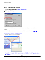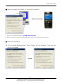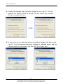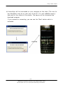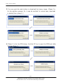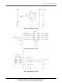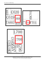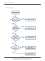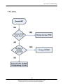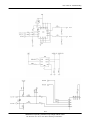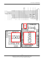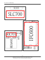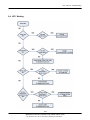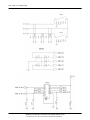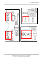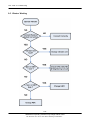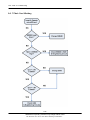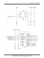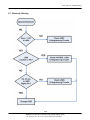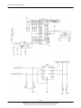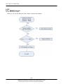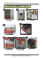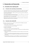
1
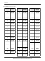
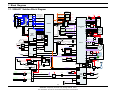
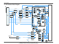
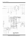
UMTS TELEPHONE
SGH-i617
UMTS TELEPHONE
CONTENTS
1.
Safety Precautions
2.
Specification
3.
Product Function
4.
Array course control
5.
Exploded View and Parts List
6.
MAIN Electrical Parts List
7.
Block Diagrams
8.
PCB Diagrams
9.
Flow Chart of Troubleshooting
10.
Reference data
11.
Disassembly and Assembly
Instructions
GSPN (Global Service Partner Network)
Country
North America
Latin America
CIS
Europe
China
Asia
Mideast & Africa
Web Site
service.samsungportal.com
latin.samsungportal.com
cis.samsungportal.com
europe.samsungportal.com
china.samsungportal.com
asia.samsungportal.com
mea.samsungportal.com
This Service Manual is a property of Samsung Electronics Co.,Ltd.
Any unauthorized use of Manual can be punished under applicable
International and/or domestic law.
ⓒ Samsung Electronics Co.,Ltd.
2007. 11.
Rev.1.0
1. Safety Precautions
1-1. Repair Precaution
● Repair in Shield Box, during detailed tuning.
Take specially care of tuning or test, because cellular phone is sensitive for surrounding
interference(RF noise).
● Be careful to use a kind of magnetic object or tool, because performance of parts is damaged by
the influence of magnetic force.
● Surely use a standard screwdriver when you disassemble this product, otherwise screw will be
worn away.
● Use a thicken twisted wire when you measure level.
A thicken twisted wire has low resistance, therefore errors of measurement are few.
● Repair after separate Test Pack and Set because for short danger (for example an
overcurrent and furious flames of parts etc) when you repair board in condition of connecting Test
Pack and tuning on.
● Take specially care of soldering, because Land of PCB is small and weak in heat.
● Surely tune on/off while using AC power plug, because a repair of battery charger is dangerous
when tuning ON/OFF PBA and Connector after disassembling charger.
● Don't use as you pleases after change other material than replacement registered on SEC System.
Otherwise engineer in charge isn't charged with problem that you don't keep this rules.
1-1
SAMSUNG Proprietary-Contents may change without notice
This Document can not be used without Samsung's authorization
Safety Precautions
1-2. ESD(Electrostatically Sensitive Devices) Precaution
Several semiconductor may be damaged easily by static electricity. Such parts are called by ESD
(Electrostatically Sensitive Devices), for example IC, BGA chip etc. Read Precaution below.
You can prevent from ESD damage by static electricity.
● Remove static electricity remained your body before you touch semiconductor or parts with
semiconductor. There are ways that you touch an earthed place or wear static electricity prevention
string on wrist.
● Use earthed soldering steel when you connect or disconnect ESD.
● Use soldering removing tool to break static electricity, otherwise ESD will be damaged by
static electricity.
● Don't unpack until you set up ESD on product. Because most of ESD are packed by box and
aluminum plate to have conductive power, they are prevented from static electricity.
● You must maintain electric contact between ESD and place due to be set up until ESD is
connected completely to the proper place or a circuit board.
1-2
SAMSUNG Proprietary-Contents may change without notice
This Document can not be used without Samsung's authorization
2. Specification
2-1. GSM General Specification
GSM 850
EGSM 900
DCS1800
PCS1900
W-CDMA
850
W-CDMA
1900
W-CDMA
2100
Freq.
Band[MHz]
Uplink/Downlin
k
824~849
869~894
880~915
925~960
1710~1785
1805~1880
1850~1910
1930~1990
824~849
869~894
1850~1910
1930~1990
1920~1980
2110~2170
ARFCN range
128~25
0~124 &
975~1023
512~885
512~810
Tx/Rx spacing
45MHz
45MHz
95MHz
80MHz
45MHz
80MHz
130MHz
Mod. Bit rate/
Bit Period
270.833kbps
3.692us
270.833kbps
3.692us
3.84Mcps
3.84Mcps
3.84Mcps
Time Slot
Period/Frame
Period
576.9us
4.615ms
576.9us
4.615ms
576.9us
4.615ms
576.9us
4.615ms
Frame length
: 10ms
Slot length :
0.667ms
Frame length
: 10ms
Slot length :
0.667ms
Frame length
: 10ms
Slot length :
0.667ms
Modulation
0.3GMSK
0.3GMSK
0.3GMSK
0.3GMSK
QPSK
HQPSK
QPSK
HQPSK
QPSK
HQPSK
24dBm~50dBm
24dBm ~ 50dBm
24dBm ~ 50dBm
MS Power
270.833kbps 270.833kbps
3.692us
3.692us
33dBm~5dBm 33dBm~5dBm 30dBm~0dBm 30dBm~0dBm
Power Class
4
(max
+33dBm)
4
(max
+33dBm)
1
(max
+30dBm)
1
(max
+30dBm)
Sensitivity
-102dBm
-102dBm
-100dBm
-100dBm
TDMA Mux
8
8
8
8
Cell Radius
35Km
35Km
2Km
2Km
UL:4132~4233 UL:9262~9538
DL:4357~4458 DL:9662~9938
UL:9612~9888
DL:10562~
10838
3
3
3
(max +24dBm) (max +24dBm) (max +24dBm)
-106.7dBm
-106.7dBm
-106.7dBm
2Km
2Km
2Km
2-1
SAMSUNG Proprietary-Contents may change without notice
This Document can not be used without Samsung's authorization
Specification
2-2. GSM TX power class
TX Power
TX Power
TX Power
control level
GSM850
GSM900
control level
5
33±2 dBm
0
30±3 dBm
0
30±3 dBm
6
31±2 dBm
1
28±3 dBm
1
28±3 dBm
7
29±2 dBm
2
26±3 dBm
2
26±3 dBm
8
27±2 dBm
3
24±3 dBm
3
24±3 dBm
9
25±2 dBm
4
22±3 dBm
4
22±3 dBm
10
23±2 dBm
5
20±3 dBm
5
20±3 dBm
11
21±2 dBm
6
18±3 dBm
6
18±3 dBm
12
19±2 dBm
7
16±3 dBm
7
16±3 dBm
13
17±2 dBm
8
14±3 dBm
8
14±3 dBm
14
15±2 dBm
9
12±4 dBm
9
12±4 dBm
15
13±2 dBm
10
10±4 dBm
10
10±4 dBm
16
11±3 dBm
11
8±4 dBm
11
8±4 dBm
17
9±3 dBm
12
6±4 dBm
12
6±4 dBm
18
7±3 dBm
13
4±4 dBm
13
4±4 dBm
19
5±3 dBm
14
2±5 dBm
14
2±5 dBm
15
0±5 dBm
15
0±5 dBm
DCS1800
control level
2-2
SAMSUNG Proprietary-Contents may change without notice
This Document can not be used without Samsung's authorization
PCS1900
3. Operation Instruction and Installation
Main Function
- MP3 / 48 Poly Melody
- BT 2.0
- Video Sharing / Streaming
- USB 1.1
- WAP2.0, JAVA, MPEG4
- MIDP 2.0 / CLDC 1.1
- Auto Time Setting,
- MMS / SMS
- Weight: 115.3g
- Camera: - 2.0M (LSI)
- LCD :
2.4" QVGA TFT (AMLCD)
- Size: 114x60x12.8mm
- GPRS/EDGE : class 10
- Battery: 1700mAH
- Memory: 2Gb MuxOneNAND Flash +512Mb (x8)*2 Mobile DDR
- Band: GSM850/900/1800/1900, W850/1900/2100
- BB: Qualcomm MSM6260, PM6650
- RF: Qualcomm RTR6275, RFR6275
3-1
SAMSUNG Proprietary-Contents may change without notice
This Document can not be used without Samsung's authorization
Operation Instruction and Installation
3-2
SAMSUNG Proprietary-Contents may change without notice
This Document can not be used without Samsung's authorization
4. Array course control
4-1. Equipment for Software Download
- There is 3 set to download the binary image into your device.
[First set]
1
7
1.
2.
3.
4.
5.
8
JIG (UMTS TEST JIG) : (GH80-03308A)
USB Cable
Test Cable(SGH-I617 cable): JIG to phone(GH39-00890A)
Power Cable: JIG to power supply
Serial Cable: PC to JIG
4-1
SAMSUNG Proprietary-Contents may change without notice
This Document can not be used without Samsung's authorization
Array course control
6. Power Supply : (E3610A)
7. Test Cable(SGH-I617 cable) : JIG to phone(GH39-00886A)
8. RF Cable : (GH39-00397A)
[Second Set]
1. JIG (S20P SGH-i617 DLC JIG)
2. Portable Power Supply
[Third Set]
1. USB DATA Link Cable
2. Battery
4-2
SAMSUNG Proprietary-Contents may change without notice
This Document can not be used without Samsung's authorization
Array course control
4-2. Software Download
4-2-1. Pre-requisite for Download
• Download Program (there is 3 ways to download.)
- [Image Version].exe
- [BADA] Download V0.9.3_Single.exe
- [BADA] Download V0.9.3_Multi(LINE).exe (Mult-idownloader)
• USB Driver
- [PDA]: Samsung MITs USB Sync <Samsung MITs USB Sync.zip> (If you
installed the latest ActiveSync program, you don’t need to install the PDA driver.)
- [Phone]: Samsung CDMA Modem [Samsung CDMA Modem.zip]
• SGH_I617 Mobile Device
• Binary files
• ActiveSync Setting
• Driver Installation.
4-2-2. Driver Installation
• [PDA]
- Make Sure that you install the latest ActiveSync program.
• [Phone]
- Make sure that you install the driver for a phone.
- You have to install the driver of Samsung CDMA Modem of downloading a phone image
- Restart your host PC after you install the phone driver.
4-3
SAMSUNG Proprietary-Contents may change without notice
This Document can not be used without Samsung's authorization
Array course control
4-2-3. S/W Download Process
4-2-3-1. Exe Download ([Image Version].exe)
■ ActiveSync Setting.
• Make sure that ActiveSync program is checked before connecting your device to the host
computer.
• If the ActiveSync is not working on your computer, Make sure that check box, Allow USB
connection at the connection settings, is checked.
• Press ‘OK’ button to save a configuration.
• If the device is connected with the host pc through the ActiveSync, Do NOT open the explorer of
the ActiveSync.
4-4
SAMSUNG Proprietary-Contents may change without notice
This Document can not be used without Samsung's authorization
Array course control
■ How to connect the device to your host computer.
• Execute the download program ([Image Version].exe)
• Make sure that you have to connect the device with the PC through the ActiveSync.
■ Download Procedure
1. If you check the check box, "Next" button will be activated. Then you can
go on next step.
4-5
SAMSUNG Proprietary-Contents may change without notice
This Document can not be used without Samsung's authorization
Array course control
2. Disable the standby and hibernation modes on the host PC. And the
capacity of a battery should be enough. Do NOT launch any program
during the update process.
3. If you try to go on next step without connection between the device and
the PC, it will be occurred that error message is indicated below. And the
device version is not correct, you can NOT go on next step.
4-6
SAMSUNG Proprietary-Contents may change without notice
This Document can not be used without Samsung's authorization
Array course control
4. ActiveSync will be terminated on your computer at this step. (The icon for
the ActiveSync may be on your tray of the PC. It is not updated merely.)
And wait for the reboot of the device. The device will be connected the
download program.
If you succeed in connecting, you can see the 'Start' button which is
activated.
4-7
SAMSUNG Proprietary-Contents may change without notice
This Document can not be used without Samsung's authorization
Array course control
5. You can push the start button to download the binary image. (Phase 0 is
for the partition process. So, it may be omitted. In normal case, download
is started from phase 1.)
6. Phase 2 is for the PDA binary. And the PC try to open the COM port after
finishing Phase 2.
4-8
SAMSUNG Proprietary-Contents may change without notice
This Document can not be used without Samsung's authorization
Array course control
7. You can see the message for the completion after finishing Phase 3.
■ Trouble Shooting.
• If you face with the problem during Download, disconnect your device from the PC. Then turn off
the device and turn on it by pressing power key, back key, and volume up key simultaneously. The
device will be reconnected with the PC. So you can go on next step.
(If the download is failed in Phase 2, Do NOT terminate the download program. Just reconnect your
device in download mode.)
4-9
SAMSUNG Proprietary-Contents may change without notice
This Document can not be used without Samsung's authorization
Array course control
4-2-3-2. Single Download ([BADA] Download V0.9.3_Single.exe)
■ ActiveSync Setting.
• Make sure that the active sync program is checked before connecting your device to the
host computer.
• If the ActiveSync is not working on your computer, Make sure that check box, Allow USB
connection at the connection settings, is released.
• Press ‘OK’ button to save a configuration.
■ How to connect the device to your host computer.
• Select the binary files by using Eboot, PDA and PHONE buttons.
4-10
SAMSUNG Proprietary-Contents may change without notice
This Document can not be used without Samsung's authorization
Array course control
4-11
SAMSUNG Proprietary-Contents may change without notice
This Document can not be used without Samsung's authorization
Array course control
■ Load the binary download program by executing the
“[BADA] Download V0.9.3_Single.exe”
1. First select the bootloader image by clicking the EBOOT button. The Eboot
Checkbox will be activated.
2. Click the PDA Button to select the PDA image, then the PDA checkbox will
be activated.
4-12
SAMSUNG Proprietary-Contents may change without notice
This Document can not be used without Samsung's authorization
Array course control
3. Click the PHONE Button to select the PHONE image, then the PHONE
checkbox will be activated.
4. If you need to update phone bootloader, you should check the 'Phone
Bootloader Update' checkbox. So does 'EFS Clear'.
4-13
SAMSUNG Proprietary-Contents may change without notice
This Document can not be used without Samsung's authorization
Array course control
5. If the device connected with the host PC, the color of progress bar will be
changed with blue. In that time, You can push the start button to download
the binary image.
4-14
SAMSUNG Proprietary-Contents may change without notice
This Document can not be used without Samsung's authorization
Array course control
6. You can see the below picture, when it is done. And the device will be
rebooted. If your device is turned on successfully, every downloading
procedure is finished.
7. If some error occurs, You have to restart download program or push the
all reset button.
4-15
SAMSUNG Proprietary-Contents may change without notice
This Document can not be used without Samsung's authorization
Array course control
8. If you want to omit to download PDA image, you can release the PDA
check box. And Eboot, Phone download are the same as this.
4-16
SAMSUNG Proprietary-Contents may change without notice
This Document can not be used without Samsung's authorization
Array course control
4-2-3-3. Multi Download ([BADA] Download V0.9.3_Multi(LINE).exe)
■ Multi-download is almost same as single download.
■ The difference is below.
1. There is four progress bars. It means you can download four devices at
once.
2. The device will be rebooted automatically after download. In that time,
'MITs USB RNDIS Driver' is not detected in the host PC. It means you can't
use the active sync program. So Make sure that you have to restart the
device after first booting. (Just pull out the battery. And wait for a minute.)
4-17
SAMSUNG Proprietary-Contents may change without notice
This Document can not be used without Samsung's authorization
Array course control
4-18
SAMSUNG Proprietary-Contents may change without notice
This Document can not be used without Samsung's authorization
5. Exploded View and Parts List
5-1. Cellular phone Exploded View
QMW02
QFR01
QAR01
QKP01
QLC01
QME01
QCK12
QME03
QRE04
QCR12
QAR04
QCB01
QMP01
QAN02
QAN05
QCR06
QSH01
QCA01
QSP01
QAN03
QMO01
QCK01
QSD01
QRE01
QVO01
QIF01
QRF01
QSC13
QCR06
QCR06
QBA01
QBA00
5-1
SAMSUNG Proprietary-Contents may change without notice
This Document can not be used without Samsung's authorization
Exploded View and Parts List
5-2. Cellular phone Parts List
Design LOC
Description
SEC CODE
QAN02
INTENNA-SGH I617
GH42-01272A
QAN03
INTENNA-SGH-I617_GPS
GH42-01263A
QAN05
ASSY RUBBER-INTENNA CONTACT 1
GH98-04736A
QAR01
AUDIO-RECEIVER
3009-001310
QAR04
RMO RUBBER-RECEIVER BACKUP
GH73-11065A
QBA00
PMO COVER-BATTERY
GH72-42962A
QBA01
INNER BATTERY PACK-1700MAH,BLK
GH43-02910A
QCA01
CAMERA MODULE-SGHI617
GH59-04619A
QCB01
CBF COAXIAL CABLE
GH39-00469A
QCK12
ASSY KEY-WHEEL DECO
GH98-06966A
QCR06
SCREW-MACHINE
6001-001155
QCR06
SCREW-MACHINE
6001-001155
QCR06
SCREW-MACHINE
6001-001155
QCR12
SCREW-MACHINE
6001-001530
QFR01
ASSY CASE-FRONT
GH98-05655A
QKP01
ASSY KEYPAD-(CIN/BLK)
GH98-05657A
QLC01
LCD-MODULE, SGHI617
GH07-01145A
QME01
KEY FPCB-SGHI617 KEY PAD FPCB
GH59-04743A
QME03
KEY FPCB-WHEEL KEY,SGHI617
GH59-04754A
QMO01
MOTOR DC-SGH I617
GH31-00350A
QMP01
PBA MAIN-SGH I617
GH92-03886A
QMW02
PCT WINDOW-COVER MAIN
GH72-44239A
QRE04
ASSY BRACKET-REAR SHIELD
GH98-05658A
QRF01
TAPE-RF COVER
GH74-34460A
QSC13
PMO COVER-REAR SCREW
GH72-42961A
QSH01
ICT SHIELD-COVER
GH70-02950A
QSP01
SPEAKER
3001-002203
QRE01
ASSY COVER-REAR
GH98-05656A
QCK01
PMO KEY-POWER
GH72-42960A
QIF01
PMO COVER-IF
GH72-42957A
QSD01
PMO COVER-SD
GH72-42956A
QVO01
PMO KEY-VOLUME
GH72-42959A
5-2
SAMSUNG Proprietary-Contents may change without notice
This Document can not be used without Samsung's authorization
Exploded View and Parts List
Description
SEC Code
BAG PE
6902-000634
CBF INTERFACE-DLC APCBS10BBE(S
GH39-00922A
ADAPTOR-ATADS10JBE,BLK,USA
GH44-01700A
LABEL(R)-WATERSOAK(NEW)
GH68-14285A
LABEL(R)-MAIN(AT&T)
GH68-16523A
BOX-SPACE AT&T
GH69-05279A
CUSHION-CASE(AT&T)
GH69-05862A
BOX-UNIT(AT&T)
GH69-05930A
MPR-VOL KEY BOHO VINYL
GH74-07312A
TAPE-BATTERY
GH74-34463A
TAPE INSU
GH74-34466A
PAA ETC-SGHI617(ATT)
GH99-25251A
5-3
SAMSUNG Proprietary-Contents may change without notice
This Document can not be used without Samsung's authorization
Exploded View and Parts List
5-4
SAMSUNG Proprietary-Contents may change without notice
This Document can not be used without Samsung's authorization
6. MAIN Electrical Parts List
SEC Code
Design LOC
Description
STATUS
0401-001144
D402
DIODE-SWITCHING
SA
0403-001339
ZD600
DIODE-ZENER
SA
0403-001463
ZD300
DIODE-ZENER
SA
0403-001467
ZD701
DIODE-ZENER
SA
0403-001547
D401
DIODE-ZENER
SA
0403-001547
D607
DIODE-ZENER
SA
0406-001167
ZD602
DIODE-TVS
SA
0406-001167
ZD700
DIODE-TVS
SA
0406-001167
ZD702
DIODE-TVS
SA
0406-001167
ZD703
DIODE-TVS
SA
0406-001167
ZD704
DIODE-TVS
SA
0406-001167
ZD705
DIODE-TVS
SA
0406-001167
ZD706
DIODE-TVS
SA
0406-001210
ZD604
DIODE-TVS
SA
0406-001210
ZD605
DIODE-TVS
SA
0406-001210
ZD607
DIODE-TVS
SA
0406-001223
D704
DIODE-TVS
SA
0406-001231
D600
DIODE-TVS
SA
0406-001231
D601
DIODE-TVS
SA
0406-001231
D602
DIODE-TVS
SA
0406-001231
D603
DIODE-TVS
SA
0406-001231
D604
DIODE-TVS
SA
0406-001231
D605
DIODE-TVS
SA
0406-001231
D606
DIODE-TVS
SA
0406-001231
D701
DIODE-TVS
SA
0406-001231
D702
DIODE-TVS
SA
0406-001231
D705
DIODE-TVS
SA
0406-001231
D706
DIODE-TVS
SA
0406-001231
D707
DIODE-TVS
SA
0406-001231
D708
DIODE-TVS
SA
6-1
SAMSUNG Proprietary-Contents may change without notice
This Document can not be used without Samsung's authorization
Main Electrical Parts List
SEC Code
Design LOC
Description
STATUS
0406-001231
D709
DIODE-TVS
SA
0406-001231
D710
DIODE-TVS
SA
0406-001231
D711
DIODE-TVS
SA
0406-001231
D712
DIODE-TVS
SA
0406-001231
D713
DIODE-TVS
SA
0406-001231
D714
DIODE-TVS
SA
0406-001231
D715
DIODE-TVS
SA
0406-001231
D716
DIODE-TVS
SA
0406-001231
ZD606
DIODE-TVS
SA
0406-001231
ZD608
DIODE-TVS
SA
0407-000115
D400
DIODE-ARRAY
SA
0407-000115
D700
DIODE-ARRAY
SA
0504-000168
TR400
TR-DIGITAL
SA
0504-000168
TR401
TR-DIGITAL
SA
0504-000168
TR403
TR-DIGITAL
SA
0504-000168
TR700
TR-DIGITAL
SA
0505-001165
TR402
FET-SILICON
SA
0601-001905
LED700
LED
SA
0801-002321
U801
IC-CMOS LOGIC
SA
0801-002882
U901
IC-CMOS LOGIC
SA
0801-003013
U300
IC-CMOS LOGIC
SA
0801-003016
U902
IC-CMOS LOGIC
SA
0801-003052
U900
IC-CMOS LOGIC
SA
0801-003140
U407
IC-CMOS LOGIC
SA
0904-002074
UCP800
IC-DSP
SA
1001-001408
U501
IC-ANALOG SWITCH
SA
1001-001408
U502
IC-ANALOG SWITCH
SA
1001-001410
U904
IC-ANALOG SWITCH
SA
1001-001471
U905
IC-ANALOG SWITCH
SA
1003-001984
U404
IC-LEVEL DRIVER
SA
6-2
SAMSUNG Proprietary-Contents may change without notice
This Document can not be used without Samsung's authorization
Main Electrical Parts List
SEC Code
Design LOC
Description
STATUS
1106-001511
UME901
IC-SRAM
SA
1108-000127
UME300
IC-MCP
SA
1108-000134
UME900
IC-MCP
SA
1201-002240
U503
IC-AUDIO AMP
SA
1201-002426
PAM100
IC-POWER AMP
SA
1201-002550
PAM201
IC-POWER AMP
SA
1201-002577
PAM200
IC-POWER AMP
SA
1201-002610
U504
IC-AUDIO AMP
SA
1203-002716
U403
IC-VOL. DETECTOR
SA
1203-003924
U800
IC-VOL. DETECTOR
SA
1203-004018
U604
IC-DC/DC CONVERTER
SA
1203-004107
U406
IC-VOL. DETECTOR
SA
1203-004120
U605
IC-MULTI REG.
SA
1203-004172
U700
IC-DC/DC CONVERTER
SA
1203-004340
U609
IC-MULTI REG.
SA
1203-004447
U601
IC-MULTI REG.
SA
1203-004449
U608
IC-MULTI REG.
SA
1203-004469
U610
IC-VOL. DETECTOR
SA
1203-004518
U401
IC-BATTERY
SA
1203-004606
U607
IC-MULTI REG.
SA
1203-004607
U606
IC-MULTI REG.
SA
1203-004798
U702
IC-SWITCH VOL. REG.
SA
1203-004926
U402
IC-POWER SUPERVISOR
SA
1205-002784
U906
IC-SWITCH
SA
1205-003095
RFS101
IC-SWITCH
SA
1205-003114
UCD500
IC-CODEC
SA
1205-003115
U903
IC-TRANSCEIVER
SA
1205-003215
UCP300
IC-MODEM
SA
1205-003235
U505
IC-DATA COMM./GEN.
SA
1205-003285
U100
IC-TRANSCEIVER
SA
6-3
SAMSUNG Proprietary-Contents may change without notice
This Document can not be used without Samsung's authorization
Main Electrical Parts List
SEC Code
Design LOC
Description
STATUS
1205-003286
U200
IC-RECEIVER
SA
1404-001221
TH300
THERMISTOR-NTC
SA
1404-001221
TH301
THERMISTOR-NTC
SA
2007-000070
R412
R-CHIP
SA
2007-000137
R308
R-CHIP
SA
2007-000138
R220
R-CHIP
SA
2007-000138
R221
R-CHIP
SA
2007-000140
R119
R-CHIP
SA
2007-000140
R122
R-CHIP
SA
2007-000148
R628
R-CHIP
SA
2007-000148
R629
R-CHIP
SA
2007-000149
R401
R-CHIP
SA
2007-000162
R707
R-CHIP
SA
2007-000167
R805
R-CHIP
SA
2007-000168
R620
R-CHIP
SA
2007-000170
R329
R-CHIP
SA
2007-000170
R418
R-CHIP
SA
2007-000171
L508
R-CHIP
SA
2007-000171
R111
R-CHIP
SA
2007-000171
R201
R-CHIP
SA
2007-000171
R206
R-CHIP
SA
2007-000171
R215
R-CHIP
SA
2007-000171
R217
R-CHIP
SA
2007-000171
R331
R-CHIP
SA
2007-000171
R524
R-CHIP
SA
2007-000171
R638
R-CHIP
SA
2007-000171
R642
R-CHIP
SA
2007-000171
R822
R-CHIP
SA
2007-000172
R202
R-CHIP
SA
2007-000249
R330
R-CHIP
SA
6-4
SAMSUNG Proprietary-Contents may change without notice
This Document can not be used without Samsung's authorization
Main Electrical Parts List
SEC Code
Design LOC
Description
STATUS
2007-001284
R207
R-CHIP
SA
2007-001290
R311
R-CHIP
SA
2007-001291
R118
R-CHIP
SA
2007-001298
R211
R-CHIP
SA
2007-001301
R640
R-CHIP
SA
2007-001301
R641
R-CHIP
SA
2007-001308
R123
R-CHIP
SA
2007-001308
R209
R-CHIP
SA
2007-001323
R404
R-CHIP
SA
2007-001335
R513
R-CHIP
SA
2007-001335
R514
R-CHIP
SA
2007-007009
R219
R-CHIP
SA
2007-007014
R403
R-CHIP
SA
2007-007014
R413
R-CHIP
SA
2007-007014
R417
R-CHIP
SA
2007-007107
R320
R-CHIP
SA
2007-007107
R321
R-CHIP
SA
2007-007107
R323
R-CHIP
SA
2007-007107
R324
R-CHIP
SA
2007-007107
R333
R-CHIP
SA
2007-007107
R334
R-CHIP
SA
2007-007132
R421
R-CHIP
SA
2007-007139
R519
R-CHIP
SA
2007-007142
R402
R-CHIP
SA
2007-007193
R103
R-CHIP
SA
2007-007193
R109
R-CHIP
SA
2007-007308
R422
R-CHIP
SA
2007-007308
R423
R-CHIP
SA
2007-007309
R105
R-CHIP
SA
2007-007312
R424
R-CHIP
SA
6-5
SAMSUNG Proprietary-Contents may change without notice
This Document can not be used without Samsung's authorization
Main Electrical Parts List
SEC Code
Design LOC
Description
STATUS
2007-007316
R309
R-CHIP
SA
2007-007468
R406
R-CHIP
SA
2007-007491
R208
R-CHIP
SA
2007-007741
R205
R-CHIP
SA
2007-007741
R630
R-CHIP
SA
2007-007766
R203
R-CHIP
SA
2007-008040
R705
R-CHIP
SA
2007-008043
R704
R-CHIP
SA
2007-008045
R112
R-CHIP
SA
2007-008045
R216
R-CHIP
SA
2007-008052
R806
R-CHIP
SA
2007-008052
R807
R-CHIP
SA
2007-008052
R808
R-CHIP
SA
2007-008052
R809
R-CHIP
SA
2007-008055
R407
R-CHIP
SA
2007-008055
R408
R-CHIP
SA
2007-008055
R419
R-CHIP
SA
2007-008055
R420
R-CHIP
SA
2007-008055
R429
R-CHIP
SA
2007-008055
R601
R-CHIP
SA
2007-008055
R610
R-CHIP
SA
2007-008055
R611
R-CHIP
SA
2007-008055
R616
R-CHIP
SA
2007-008055
R622
R-CHIP
SA
2007-008055
R702
R-CHIP
SA
2007-008055
R800
R-CHIP
SA
2007-008055
R811
R-CHIP
SA
2007-008055
R812
R-CHIP
SA
2007-008055
R816
R-CHIP
SA
2007-008055
R817
R-CHIP
SA
6-6
SAMSUNG Proprietary-Contents may change without notice
This Document can not be used without Samsung's authorization
Main Electrical Parts List
SEC Code
Design LOC
Description
STATUS
2007-008055
R900
R-CHIP
SA
2007-008055
R901
R-CHIP
SA
2007-008055
R902
R-CHIP
SA
2007-008055
R903
R-CHIP
SA
2007-008055
R905
R-CHIP
SA
2007-008055
R915
R-CHIP
SA
2007-008263
R400
R-CHIP
SA
2007-008403
R626
R-CHIP
SA
2007-008419
R606
R-CHIP
SA
2007-008419
R607
R-CHIP
SA
2007-008419
R609
R-CHIP
SA
2007-008419
R815
R-CHIP
SA
2007-008478
R214
R-CHIP
SA
2007-008478
R501
R-CHIP
SA
2007-008478
R504
R-CHIP
SA
2007-008478
R510
R-CHIP
SA
2007-008478
R511
R-CHIP
SA
2007-008478
R912
R-CHIP
SA
2007-008483
R506
R-CHIP
SA
2007-008483
R614
R-CHIP
SA
2007-008483
R621
R-CHIP
SA
2007-008483
R910
R-CHIP
SA
2007-008486
R411
R-CHIP
SA
2007-008486
R515
R-CHIP
SA
2007-008516
R300
R-CHIP
SA
2007-008516
R312
R-CHIP
SA
2007-008516
R314
R-CHIP
SA
2007-008516
R316
R-CHIP
SA
2007-008516
R700
R-CHIP
SA
2007-008516
R804
R-CHIP
SA
6-7
SAMSUNG Proprietary-Contents may change without notice
This Document can not be used without Samsung's authorization
Main Electrical Parts List
SEC Code
Design LOC
Description
STATUS
2007-008516
R814
R-CHIP
SA
2007-008516
R818
R-CHIP
SA
2007-008516
R819
R-CHIP
SA
2007-008516
R904
R-CHIP
SA
2007-008531
R113
R-CHIP
SA
2007-008531
R701
R-CHIP
SA
2007-008531
R803
R-CHIP
SA
2007-008542
R100
R-CHIP
SA
2007-008542
R101
R-CHIP
SA
2007-008542
R106
R-CHIP
SA
2007-008542
R107
R-CHIP
SA
2007-008542
R108
R-CHIP
SA
2007-008542
R129
R-CHIP
SA
2007-008542
R130
R-CHIP
SA
2007-008542
R135
R-CHIP
SA
2007-008542
R222
R-CHIP
SA
2007-008542
R223
R-CHIP
SA
2007-008542
R224
R-CHIP
SA
2007-008542
R318
R-CHIP
SA
2007-008542
R322
R-CHIP
SA
2007-008542
R332
R-CHIP
SA
2007-008542
R507
R-CHIP
SA
2007-008542
R508
R-CHIP
SA
2007-008542
R520
R-CHIP
SA
2007-008542
R521
R-CHIP
SA
2007-008544
R500
R-CHIP
SA
2007-008544
R505
R-CHIP
SA
2007-008544
R509
R-CHIP
SA
2007-008544
R512
R-CHIP
SA
2007-008547
R212
R-CHIP
SNA
6-8
SAMSUNG Proprietary-Contents may change without notice
This Document can not be used without Samsung's authorization
Main Electrical Parts List
SEC Code
Design LOC
Description
STATUS
2007-008582
R703
R-CHIP
SA
2007-008588
R131
R-CHIP
SA
2007-008588
R132
R-CHIP
SA
2007-008588
R133
R-CHIP
SA
2007-008588
R134
R-CHIP
SA
2007-008588
R801
R-CHIP
SA
2007-008588
R802
R-CHIP
SA
2007-008686
R116
R-CHIP
SA
2007-008765
R210
R-CHIP
SNA
2007-008765
R213
R-CHIP
SNA
2007-008774
R518
R-CHIP
SA
2007-008806
R124
R-CHIP
SA
2007-008806
R327
R-CHIP
SA
2007-008806
R405
R-CHIP
SA
2007-009115
R913
R-CHIP
SA
2007-009115
R914
R-CHIP
SA
2007-009116
R114
R-CHIP
SA
2007-009116
R115
R-CHIP
SA
2007-009160
R627
R-CHIP
SA
2007-009169
R909
R-CHIP
SA
2007-009170
R319
R-CHIP
SA
2007-009170
R602
R-CHIP
SA
2007-009170
R906
R-CHIP
SA
2007-009170
R907
R-CHIP
SA
2007-009170
R908
R-CHIP
SA
2007-009194
R911
R-CHIP
SNA
2007-009257
R619
R-CHIP
SA
2007-009374
R502
R-CHIP
SA
2007-009374
R503
R-CHIP
SA
2007-009804
R110
R-CHIP
SA
6-9
SAMSUNG Proprietary-Contents may change without notice
This Document can not be used without Samsung's authorization
Main Electrical Parts List
SEC Code
Design LOC
Description
STATUS
2007-009879
R117
R-CHIP
SA
2007-009880
R120
R-CHIP
SA
2007-009880
R121
R-CHIP
SA
2203-000233
C207
C-CER,CHIP
SA
2203-000233
C208
C-CER,CHIP
SA
2203-000233
C212
C-CER,CHIP
SA
2203-000233
C221
C-CER,CHIP
SA
2203-000233
C225
C-CER,CHIP
SA
2203-000233
C241
C-CER,CHIP
SA
2203-000233
C245
C-CER,CHIP
SA
2203-000233
C250
C-CER,CHIP
SA
2203-000233
C406
C-CER,CHIP
SA
2203-000254
C407
C-CER,CHIP
SA
2203-000278
C553
C-CER,CHIP
SA
2203-000278
C830
C-CER,CHIP
SA
2203-000330
C117
C-CER,CHIP
SA
2203-000330
C122
C-CER,CHIP
SA
2203-000330
C151
C-CER,CHIP
SA
2203-000330
C167
C-CER,CHIP
SA
2203-000425
C408
C-CER,CHIP
SA
2203-000425
C409
C-CER,CHIP
SA
2203-000425
C822
C-CER,CHIP
SA
2203-000425
C823
C-CER,CHIP
SA
2203-000438
C147
C-CER,CHIP
SA
2203-000438
C231
C-CER,CHIP
SA
2203-000438
C243
C-CER,CHIP
SA
2203-000466
C253
C-CER,CHIP
SA
2203-000489
C302
C-CER,CHIP
SA
2203-000550
C802
C-CER,CHIP
SA
2203-000550
C803
C-CER,CHIP
SA
6-10
SAMSUNG Proprietary-Contents may change without notice
This Document can not be used without Samsung's authorization
Main Electrical Parts List
SEC Code
Design LOC
Description
STATUS
2203-000550
C828
C-CER,CHIP
SA
2203-000627
C616
C-CER,CHIP
SNA
2203-000627
C617
C-CER,CHIP
SNA
2203-000714
C127
C-CER,CHIP
SA
2203-000812
C104
C-CER,CHIP
SA
2203-000812
C157
C-CER,CHIP
SA
2203-000812
C213
C-CER,CHIP
SA
2203-000812
C249
C-CER,CHIP
SA
2203-001101
C536
C-CER,CHIP
SA
2203-001101
C537
C-CER,CHIP
SA
2203-001153
C434
C-CER,CHIP
SA
2203-001259
C234
C-CER,CHIP
SA
2203-001385
C254
C-CER,CHIP
SA
2203-002668
C123
C-CER,CHIP
SA
2203-002668
C139
C-CER,CHIP
SA
2203-002687
C535
C-CER,CHIP
SA
2203-002687
C541
C-CER,CHIP
SA
2203-002709
C404
C-CER,CHIP
SA
2203-002709
C418
C-CER,CHIP
SA
2203-002709
C420
C-CER,CHIP
SA
2203-002709
C421
C-CER,CHIP
SA
2203-002709
C425
C-CER,CHIP
SA
2203-002709
C427
C-CER,CHIP
SA
2203-002709
C430
C-CER,CHIP
SA
2203-002709
C552
C-CER,CHIP
SA
2203-002709
C908
C-CER,CHIP
SA
2203-003054
C264
C-CER,CHIP
SA
2203-005050
C239
C-CER,CHIP
SA
2203-005052
C554
C-CER,CHIP
SA
2203-005053
C251
C-CER,CHIP
SA
6-11
SAMSUNG Proprietary-Contents may change without notice
This Document can not be used without Samsung's authorization
Main Electrical Parts List
SEC Code
Design LOC
Description
STATUS
2203-005281
C106
C-CER,CHIP
SA
2203-005281
C235
C-CER,CHIP
SA
2203-005480
C311
C-CER,CHIP
SA
2203-005482
C341
C-CER,CHIP
SA
2203-005483
C203
C-CER,CHIP
SA
2203-005503
C100
C-CER,CHIP
SA
2203-005503
C101
C-CER,CHIP
SA
2203-005503
C102
C-CER,CHIP
SA
2203-005503
C103
C-CER,CHIP
SA
2203-005682
C112
C-CER,CHIP
SA
2203-005682
C131
C-CER,CHIP
SA
2203-005682
C132
C-CER,CHIP
SA
2203-005682
C159
C-CER,CHIP
SA
2203-005682
C171
C-CER,CHIP
SA
2203-005682
C201
C-CER,CHIP
SA
2203-005682
C224
C-CER,CHIP
SA
2203-005682
C228
C-CER,CHIP
SA
2203-005682
C230
C-CER,CHIP
SA
2203-005682
C246
C-CER,CHIP
SA
2203-005682
C262
C-CER,CHIP
SA
2203-005682
C342
C-CER,CHIP
SA
2203-005682
C343
C-CER,CHIP
SA
2203-005682
C435
C-CER,CHIP
SA
2203-005682
C437
C-CER,CHIP
SA
2203-005682
C444
C-CER,CHIP
SA
2203-005682
C600
C-CER,CHIP
SA
2203-005682
C601
C-CER,CHIP
SA
2203-005682
C602
C-CER,CHIP
SA
2203-005682
C603
C-CER,CHIP
SA
2203-005682
C604
C-CER,CHIP
SA
6-12
SAMSUNG Proprietary-Contents may change without notice
This Document can not be used without Samsung's authorization
Main Electrical Parts List
SEC Code
Design LOC
Description
STATUS
2203-005682
C636
C-CER,CHIP
SA
2203-005682
C638
C-CER,CHIP
SA
2203-005682
C639
C-CER,CHIP
SA
2203-005682
C709
C-CER,CHIP
SA
2203-005682
C714
C-CER,CHIP
SA
2203-005682
C716
C-CER,CHIP
SA
2203-005682
C722
C-CER,CHIP
SA
2203-005682
C725
C-CER,CHIP
SA
2203-005682
C727
C-CER,CHIP
SA
2203-005682
C728
C-CER,CHIP
SA
2203-005682
C729
C-CER,CHIP
SA
2203-005682
C730
C-CER,CHIP
SA
2203-005682
C731
C-CER,CHIP
SA
2203-005682
C732
C-CER,CHIP
SA
2203-005682
C733
C-CER,CHIP
SA
2203-005682
C734
C-CER,CHIP
SA
2203-005682
C831
C-CER,CHIP
SA
2203-005682
C832
C-CER,CHIP
SA
2203-005683
C169
C-CER,CHIP
SA
2203-005683
C508
C-CER,CHIP
SA
2203-005683
C516
C-CER,CHIP
SA
2203-005683
C532
C-CER,CHIP
SA
2203-005683
C640
C-CER,CHIP
SA
2203-005683
C641
C-CER,CHIP
SA
2203-005683
C710
C-CER,CHIP
SA
2203-005683
C715
C-CER,CHIP
SA
2203-005683
C718
C-CER,CHIP
SA
2203-005725
C107
C-CER,CHIP
SA
2203-005725
C109
C-CER,CHIP
SA
2203-005725
C113
C-CER,CHIP
SA
6-13
SAMSUNG Proprietary-Contents may change without notice
This Document can not be used without Samsung's authorization
Main Electrical Parts List
SEC Code
Design LOC
Description
STATUS
2203-005725
C135
C-CER,CHIP
SA
2203-005725
C154
C-CER,CHIP
SA
2203-005725
C155
C-CER,CHIP
SA
2203-005725
C177
C-CER,CHIP
SA
2203-005725
C240
C-CER,CHIP
SA
2203-005725
C259
C-CER,CHIP
SA
2203-005725
C544
C-CER,CHIP
SA
2203-005727
C505
C-CER,CHIP
SA
2203-005727
C506
C-CER,CHIP
SA
2203-005727
C522
C-CER,CHIP
SA
2203-005727
C523
C-CER,CHIP
SA
2203-005727
C530
C-CER,CHIP
SA
2203-005727
C539
C-CER,CHIP
SA
2203-005729
C550
C-CER,CHIP
SA
2203-005734
C223
C-CER,CHIP
SA
2203-005734
C227
C-CER,CHIP
SA
2203-005734
C244
C-CER,CHIP
SA
2203-005736
C148
C-CER,CHIP
SA
2203-005736
C162
C-CER,CHIP
SA
2203-005736
C166
C-CER,CHIP
SA
2203-005736
C178
C-CER,CHIP
SA
2203-005736
C179
C-CER,CHIP
SA
2203-005736
C232
C-CER,CHIP
SA
2203-005739
C181
C-CER,CHIP
SA
2203-005740
C118
C-CER,CHIP
SA
2203-005742
C120
C-CER,CHIP
SA
2203-005742
C121
C-CER,CHIP
SA
2203-005789
L122
C-CER,CHIP
SA
2203-005792
C558
C-CER,CHIP
SA
2203-005806
C115
C-CER,CHIP
SNA
6-14
SAMSUNG Proprietary-Contents may change without notice
This Document can not be used without Samsung's authorization
Main Electrical Parts List
SEC Code
Design LOC
Description
STATUS
2203-005806
C128
C-CER,CHIP
SNA
2203-005806
C152
C-CER,CHIP
SNA
2203-005806
C158
C-CER,CHIP
SNA
2203-005806
C206
C-CER,CHIP
SNA
2203-005806
C247
C-CER,CHIP
SNA
2203-005806
C305
C-CER,CHIP
SNA
2203-005806
C818
C-CER,CHIP
SNA
2203-006048
C909
C-CER,CHIP
SA
2203-006120
C500
C-CER,CHIP
SA
2203-006121
C202
C-CER,CHIP
SA
2203-006121
C442
C-CER,CHIP
SA
2203-006194
C153
C-CER,CHIP
SA
2203-006194
C242
C-CER,CHIP
SA
2203-006194
C548
C-CER,CHIP
SA
2203-006194
C549
C-CER,CHIP
SA
2203-006194
C555
C-CER,CHIP
SA
2203-006194
C711
C-CER,CHIP
SA
2203-006194
C719
C-CER,CHIP
SA
2203-006194
C720
C-CER,CHIP
SA
2203-006194
C721
C-CER,CHIP
SA
2203-006194
C801
C-CER,CHIP
SA
2203-006194
C804
C-CER,CHIP
SA
2203-006194
C805
C-CER,CHIP
SA
2203-006194
C907
C-CER,CHIP
SA
2203-006257
C533
C-CER,CHIP
SA
2203-006257
C538
C-CER,CHIP
SA
2203-006260
C436
C-CER,CHIP
SA
2203-006305
C216
C-CER,CHIP
SA
2203-006305
C222
C-CER,CHIP
SA
2203-006324
C400
C-CER,CHIP
SA
6-15
SAMSUNG Proprietary-Contents may change without notice
This Document can not be used without Samsung's authorization
Main Electrical Parts List
SEC Code
Design LOC
Description
STATUS
2203-006324
C401
C-CER,CHIP
SA
2203-006324
C410
C-CER,CHIP
SA
2203-006324
C424
C-CER,CHIP
SA
2203-006348
C443
C-CER,CHIP
SA
2203-006361
C619
C-CER,CHIP
SA
2203-006361
C620
C-CER,CHIP
SA
2203-006361
C911
C-CER,CHIP
SA
2203-006399
C217
C-CER,CHIP
SA
2203-006399
C902
C-CER,CHIP
SA
2203-006410
C170
C-CER,CHIP
SA
2203-006423
C111
C-CER,CHIP
SA
2203-006423
C116
C-CER,CHIP
SA
2203-006423
C125
C-CER,CHIP
SA
2203-006423
C126
C-CER,CHIP
SA
2203-006423
C133
C-CER,CHIP
SA
2203-006423
C134
C-CER,CHIP
SA
2203-006423
C143
C-CER,CHIP
SA
2203-006423
C144
C-CER,CHIP
SA
2203-006423
C145
C-CER,CHIP
SA
2203-006423
C146
C-CER,CHIP
SA
2203-006423
C200
C-CER,CHIP
SA
2203-006423
C215
C-CER,CHIP
SA
2203-006423
C218
C-CER,CHIP
SA
2203-006423
C226
C-CER,CHIP
SA
2203-006423
C229
C-CER,CHIP
SA
2203-006423
C248
C-CER,CHIP
SA
2203-006423
C261
C-CER,CHIP
SA
2203-006423
C309
C-CER,CHIP
SA
2203-006423
C414
C-CER,CHIP
SA
2203-006423
C431
C-CER,CHIP
SA
6-16
SAMSUNG Proprietary-Contents may change without notice
This Document can not be used without Samsung's authorization
Main Electrical Parts List
SEC Code
Design LOC
Description
STATUS
2203-006423
C432
C-CER,CHIP
SA
2203-006423
C501
C-CER,CHIP
SA
2203-006423
C507
C-CER,CHIP
SA
2203-006423
C509
C-CER,CHIP
SA
2203-006423
C513
C-CER,CHIP
SA
2203-006423
C517
C-CER,CHIP
SA
2203-006423
C518
C-CER,CHIP
SA
2203-006423
C521
C-CER,CHIP
SA
2203-006423
C525
C-CER,CHIP
SA
2203-006423
C527
C-CER,CHIP
SA
2203-006423
C534
C-CER,CHIP
SA
2203-006423
C540
C-CER,CHIP
SA
2203-006423
C546
C-CER,CHIP
SA
2203-006423
C547
C-CER,CHIP
SA
2203-006423
C551
C-CER,CHIP
SA
2203-006423
C631
C-CER,CHIP
SA
2203-006423
C634
C-CER,CHIP
SA
2203-006423
C800
C-CER,CHIP
SA
2203-006423
C806
C-CER,CHIP
SA
2203-006423
C807
C-CER,CHIP
SA
2203-006423
C808
C-CER,CHIP
SA
2203-006423
C809
C-CER,CHIP
SA
2203-006423
C810
C-CER,CHIP
SA
2203-006423
C811
C-CER,CHIP
SA
2203-006423
C812
C-CER,CHIP
SA
2203-006423
C813
C-CER,CHIP
SA
2203-006423
C814
C-CER,CHIP
SA
2203-006423
C816
C-CER,CHIP
SA
2203-006423
C817
C-CER,CHIP
SA
2203-006423
C819
C-CER,CHIP
SA
6-17
SAMSUNG Proprietary-Contents may change without notice
This Document can not be used without Samsung's authorization
Main Electrical Parts List
SEC Code
Design LOC
Description
STATUS
2203-006423
C820
C-CER,CHIP
SA
2203-006423
C826
C-CER,CHIP
SA
2203-006423
C827
C-CER,CHIP
SA
2203-006423
C829
C-CER,CHIP
SA
2203-006423
C900
C-CER,CHIP
SA
2203-006423
C903
C-CER,CHIP
SA
2203-006423
C906
C-CER,CHIP
SA
2203-006423
C910
C-CER,CHIP
SA
2203-006423
C915
C-CER,CHIP
SA
2203-006474
C438
C-CER,CHIP
SA
2203-006556
C119
C-CER,CHIP
SA
2203-006556
C124
C-CER,CHIP
SA
2203-006556
C130
C-CER,CHIP
SA
2203-006556
C141
C-CER,CHIP
SA
2203-006556
C165
C-CER,CHIP
SA
2203-006556
C325
C-CER,CHIP
SA
2203-006620
C210
C-CER,CHIP
SNA
2203-006648
C163
C-CER,CHIP
SA
2203-006665
C219
C-CER,CHIP
SA
2203-006665
C220
C-CER,CHIP
SA
2203-006665
C266
C-CER,CHIP
SA
2203-006668
C204
C-CER,CHIP
SA
2203-006681
C440
C-CER,CHIP
SA
2203-006681
C612
C-CER,CHIP
SA
2203-006681
C707
C-CER,CHIP
SA
2203-006707
C209
C-CER,CHIP
SA
2203-006707
C211
C-CER,CHIP
SA
2203-006824
C320
C-CER,CHIP
SA
2203-006824
C413
C-CER,CHIP
SA
2203-006824
C415
C-CER,CHIP
SA
6-18
SAMSUNG Proprietary-Contents may change without notice
This Document can not be used without Samsung's authorization
Main Electrical Parts List
SEC Code
Design LOC
Description
STATUS
2203-006824
C417
C-CER,CHIP
SA
2203-006824
C419
C-CER,CHIP
SA
2203-006824
C422
C-CER,CHIP
SA
2203-006824
C423
C-CER,CHIP
SA
2203-006824
C426
C-CER,CHIP
SA
2203-006824
C503
C-CER,CHIP
SA
2203-006824
C504
C-CER,CHIP
SA
2203-006824
C605
C-CER,CHIP
SA
2203-006824
C613
C-CER,CHIP
SA
2203-006824
C614
C-CER,CHIP
SA
2203-006824
C622
C-CER,CHIP
SA
2203-006824
C624
C-CER,CHIP
SA
2203-006824
C628
C-CER,CHIP
SA
2203-006824
C629
C-CER,CHIP
SA
2203-006838
C411
C-CER,CHIP
SA
2203-006838
C412
C-CER,CHIP
SA
2203-006838
C416
C-CER,CHIP
SA
2203-006838
C502
C-CER,CHIP
SA
2203-006838
C510
C-CER,CHIP
SA
2203-006838
C512
C-CER,CHIP
SA
2203-006838
C623
C-CER,CHIP
SA
2203-006838
C700
C-CER,CHIP
SA
2203-006838
C701
C-CER,CHIP
SA
2203-006838
C702
C-CER,CHIP
SA
2203-006838
C703
C-CER,CHIP
SA
2203-006838
C704
C-CER,CHIP
SA
2203-006838
C712
C-CER,CHIP
SA
2203-006838
C713
C-CER,CHIP
SA
2203-006838
C723
C-CER,CHIP
SA
2203-006838
C724
C-CER,CHIP
SA
6-19
SAMSUNG Proprietary-Contents may change without notice
This Document can not be used without Samsung's authorization
Main Electrical Parts List
SEC Code
Design LOC
Description
STATUS
2203-006838
C904
C-CER,CHIP
SA
2203-006839
C164
C-CER,CHIP
SA
2203-006839
C303
C-CER,CHIP
SA
2203-006839
C312
C-CER,CHIP
SA
2203-006839
C316
C-CER,CHIP
SA
2203-006839
C317
C-CER,CHIP
SA
2203-006839
C322
C-CER,CHIP
SA
2203-006839
C327
C-CER,CHIP
SA
2203-006839
C328
C-CER,CHIP
SA
2203-006839
C330
C-CER,CHIP
SA
2203-006839
C331
C-CER,CHIP
SA
2203-006839
C334
C-CER,CHIP
SA
2203-006839
C335
C-CER,CHIP
SA
2203-006839
C338
C-CER,CHIP
SA
2203-006839
C433
C-CER,CHIP
SA
2203-006839
C625
C-CER,CHIP
SA
2203-006839
C627
C-CER,CHIP
SA
2203-006840
C205
C-CER,CHIP
SA
2203-006841
C306
C-CER,CHIP
SA
2203-006841
C308
C-CER,CHIP
SA
2203-006841
C310
C-CER,CHIP
SA
2203-006841
C318
C-CER,CHIP
SA
2203-006841
C323
C-CER,CHIP
SA
2203-006841
C324
C-CER,CHIP
SA
2203-006841
C332
C-CER,CHIP
SA
2203-006841
C339
C-CER,CHIP
SA
2203-006841
C340
C-CER,CHIP
SA
2203-006841
C441
C-CER,CHIP
SA
2203-006841
C524
C-CER,CHIP
SA
2203-006841
C630
C-CER,CHIP
SA
6-20
SAMSUNG Proprietary-Contents may change without notice
This Document can not be used without Samsung's authorization
Main Electrical Parts List
SEC Code
Design LOC
Description
STATUS
2203-006841
C632
C-CER,CHIP
SA
2203-006841
C633
C-CER,CHIP
SA
2203-006841
C705
C-CER,CHIP
SA
2203-006841
C815
C-CER,CHIP
SA
2203-006841
C821
C-CER,CHIP
SA
2203-006841
C901
C-CER,CHIP
SA
2203-006841
C905
C-CER,CHIP
SA
2203-006841
C912
C-CER,CHIP
SA
2203-006841
C913
C-CER,CHIP
SA
2203-006841
C914
C-CER,CHIP
SA
2203-006841
C916
C-CER,CHIP
SA
2203-006841
C917
C-CER,CHIP
SA
2203-006872
C319
C-CER,CHIP
SA
2203-006872
C542
C-CER,CHIP
SA
2203-006872
C543
C-CER,CHIP
SA
2203-006872
C545
C-CER,CHIP
SA
2203-006885
C637
C-CER,CHIP
SA
2203-006890
C336
C-CER,CHIP
SA
2203-006890
C439
C-CER,CHIP
SA
2203-006896
C114
C-CER,CHIP
SA
2203-006896
C136
C-CER,CHIP
SA
2203-006896
C156
C-CER,CHIP
SA
2203-006978
C706
C-CER,CHIP
SA
2203-006979
C304
C-CER,CHIP
SA
2203-006979
C307
C-CER,CHIP
SA
2203-006979
C314
C-CER,CHIP
SA
2203-006979
C315
C-CER,CHIP
SA
2203-006979
C321
C-CER,CHIP
SA
2203-006979
C326
C-CER,CHIP
SA
2203-006979
C329
C-CER,CHIP
SA
6-21
SAMSUNG Proprietary-Contents may change without notice
This Document can not be used without Samsung's authorization
Main Electrical Parts List
SEC Code
Design LOC
Description
STATUS
2203-006979
C333
C-CER,CHIP
SA
2203-006979
C337
C-CER,CHIP
SA
2203-007210
C635
C-CER,CHIP
SA
2404-001268
TA605
C-TA,CHIP
SA
2404-001274
TA101
C-TA,CHIP
SA
2404-001350
TA200
C-TA,CHIP
SA
2404-001350
TA201
C-TA,CHIP
SA
2404-001377
TA500
C-TA,CHIP
SA
2404-001377
TA501
C-TA,CHIP
SA
2404-001377
TA502
C-TA,CHIP
SA
2404-001377
TA503
C-TA,CHIP
SA
2404-001381
TA504
C-TA,CHIP
SA
2404-001381
TA600
C-TA,CHIP
SA
2404-001381
TA603
C-TA,CHIP
SA
2404-001396
TA100
C-TA,CHIP
SA
2404-001474
TA401
C-TA,CHIP
SA
2404-001474
TA402
C-TA,CHIP
SA
2404-001484
TA602
C-TA,CHIP
SA
2404-001484
TA604
C-TA,CHIP
SA
2703-001722
L125
INDUCTOR-SMD
SA
2703-001723
L117
INDUCTOR-SMD
SA
2703-001733
L233
INDUCTOR-SMD
SA
2703-001737
L231
INDUCTOR-SMD
SA
2703-001938
L230
INDUCTOR-SMD
SA
2703-002155
L215
INDUCTOR-SMD
SA
2703-002198
L228
INDUCTOR-SMD
SA
2703-002199
L205
INDUCTOR-SMD
SA
2703-002199
L212
INDUCTOR-SMD
SA
2703-002201
L100
INDUCTOR-SMD
SA
2703-002205
L124
INDUCTOR-SMD
SA
6-22
SAMSUNG Proprietary-Contents may change without notice
This Document can not be used without Samsung's authorization
Main Electrical Parts List
SEC Code
Design LOC
Description
STATUS
2703-002207
L222
INDUCTOR-SMD
SA
2703-002269
L112
INDUCTOR-SMD
SA
2703-002367
L223
INDUCTOR-SMD
SA
2703-002484
L208
INDUCTOR-SMD
SA
2703-002544
L202
INDUCTOR-SMD
SA
2703-002544
L206
INDUCTOR-SMD
SA
2703-002544
L216
INDUCTOR-SMD
SA
2703-002596
L217
INDUCTOR-SMD
SA
2703-002608
L126
INDUCTOR-SMD
SA
2703-002608
L506
INDUCTOR-SMD
SA
2703-002768
L605
INDUCTOR-SMD
SNA
2703-002768
L606
INDUCTOR-SMD
SNA
2703-002793
C180
INDUCTOR-SMD
SA
2703-002793
L102
INDUCTOR-SMD
SA
2703-002793
L104
INDUCTOR-SMD
SA
2703-002793
L105
INDUCTOR-SMD
SA
2703-002793
L107
INDUCTOR-SMD
SA
2703-002795
L507
INDUCTOR-SMD
SNA
2703-002798
L224
INDUCTOR-SMD
SNA
2703-002824
L700
INDUCTOR-SMD
SA
2703-002840
L401
INDUCTOR-SMD
SA
2703-002840
L402
INDUCTOR-SMD
SA
2703-002840
L404
INDUCTOR-SMD
SA
2703-002842
L121
INDUCTOR-SMD
SA
2703-002900
L103
INDUCTOR-SMD
SA
2703-002900
L108
INDUCTOR-SMD
SA
2703-002900
L110
INDUCTOR-SMD
SA
2703-002900
L111
INDUCTOR-SMD
SA
2703-002900
L113
INDUCTOR-SMD
SA
2703-002901
L127
INDUCTOR-SMD
SNA
6-23
SAMSUNG Proprietary-Contents may change without notice
This Document can not be used without Samsung's authorization
Main Electrical Parts List
SEC Code
Design LOC
Description
STATUS
2703-002901
L203
INDUCTOR-SMD
SNA
2703-002901
L204
INDUCTOR-SMD
SNA
2703-002901
L227
INDUCTOR-SMD
SNA
2703-002903
L221
INDUCTOR-SMD
SA
2703-002906
L119
INDUCTOR-SMD
SA
2703-002907
L218
INDUCTOR-SMD
SNA
2703-002910
L213
INDUCTOR-SMD
SA
2703-002910
L214
INDUCTOR-SMD
SA
2703-002917
L234
INDUCTOR-SMD
SA
2703-002918
L219
INDUCTOR-SMD
SA
2703-002919
L116
INDUCTOR-SMD
SA
2703-002919
L123
INDUCTOR-SMD
SA
2703-002919
L232
INDUCTOR-SMD
SA
2703-002953
L106
INDUCTOR-SMD
SA
2703-002955
L220
INDUCTOR-SMD
SA
2703-002958
L109
INDUCTOR-SMD
SA
2703-003125
C168
INDUCTOR-SMD
SA
2703-003125
L115
INDUCTOR-SMD
SA
2703-003125
L201
INDUCTOR-SMD
SA
2703-003125
L207
INDUCTOR-SMD
SA
2703-003127
L226
INDUCTOR-SMD
SA
2801-004318
OSC800
CRYSTAL-SMD
SA
2801-004466
OSC400
CRYSTAL-SMD
SA
2801-004466
OSC801
CRYSTAL-SMD
SA
2801-004560
OSC500
CRYSTAL-SMD
SA
2809-001280
OSC200
OSCILLATOR-VCTCXO
SA
2901-001283
F900
FILTER-EMI SMD
SA
2901-001326
F700
FILTER-EMI/ESD
SA
2901-001326
F703
FILTER-EMI/ESD
SA
2901-001326
F705
FILTER-EMI/ESD
SA
6-24
SAMSUNG Proprietary-Contents may change without notice
This Document can not be used without Samsung's authorization
Main Electrical Parts List
SEC Code
Design LOC
Description
STATUS
2901-001453
F701
FILTER-EMI SMD
SA
2901-001453
F702
FILTER-EMI SMD
SA
2901-001460
F704
FILTER-EMI/ESD
SA
2904-001414
F206
FILTER-SAW
SA
2904-001668
F205
FILTER-SAW
SA
2904-001738
F200
FILTER-SAW
SA
2904-001739
F204
FILTER-SAW
SA
2904-001751
F203
FILTER-SAW
SA
2904-001769
F100
FILTER-SAW
SA
2904-001789
F101
FILTER-SAW
SA
2904-001790
F201
FILTER-SAW
SA
2909-001283
F501
FILTER-LC
SA
2910-000022
DUF201
DUPLEXER-SAW
SA
2910-000032
DUF200
DUPLEXER-FBAR
SA
2910-000039
DUF100
DUPLEXER-FBAR
SA
2911-000079
RFS100
DUPLEXER-FEM
SA
2911-000085
F102
DUPLEXER-FEM
SA
3301-001438
L500
BEAD-SMD
SA
3301-001438
L501
BEAD-SMD
SA
3301-001438
L502
BEAD-SMD
SA
3301-001438
L503
BEAD-SMD
SA
3301-001756
L225
BEAD-SMD
SA
3301-001756
L300
BEAD-SMD
SA
3301-001851
L504
BEAD-SMD
SA
3301-001851
L505
BEAD-SMD
SA
3404-001303
TAC701
SWITCH-TACT
SA
3404-001303
TAC702
SWITCH-TACT
SA
3404-001317
TAC700
SWITCH-TACT
SA
3705-001225
ANT100
CONNECTOR-COAXIAL
SA
3705-001358
RFS102
CONNECTOR-COAXIAL
SA
6-25
SAMSUNG Proprietary-Contents may change without notice
This Document can not be used without Samsung's authorization
Main Electrical Parts List
SEC Code
Design LOC
Description
STATUS
3708-002162
SLC700
CONNECTOR-FPC/FFC/PIC
SA
3708-002283
HDC702
CONNECTOR-FPC/FFC/PIC
SA
3709-001453
SIM400
CONNECTOR-CARD EDGE
SA
3710-002081
SOC700
SOCKET-BOARD TO BOARD
SA
3710-002081
SOC701
SOCKET-BOARD TO BOARD
SA
3710-002081
SOC702
SOCKET-BOARD TO BOARD
SA
3710-002499
IFC600
SOCKET-INTERFACE
SA
3711-005522
CN203
HEADER-BOARD TO BOARD
SA
3711-005954
HDC700
HEADER-BOARD TO BOARD
SA
3711-006217
BTC400
HEADER-BATTERY
SA
4202-001337
ANT500
ANTENNA-CHIP
SA
4302-001181
BAT400
BATTERY-LI(2ND)
SA
4709-001399
CPL100
COUPLER-DIRECTION
SA
4709-001405
CPL201
COUPLER-DIRECTION
SA
4709-001406
CPL200
COUPLER-DIRECTION
SNA
GH70-02640A
SC101
ICT SHIELD-CAN CLIP
SA
GH70-02640A
SC102
ICT SHIELD-CAN CLIP
SA
GH70-02640A
SC103
ICT SHIELD-CAN CLIP
SA
GH70-02640A
SC104
ICT SHIELD-CAN CLIP
SA
GH70-02640A
SC105
ICT SHIELD-CAN CLIP
SA
GH70-02640A
SC106
ICT SHIELD-CAN CLIP
SA
GH70-02640A
SC107
ICT SHIELD-CAN CLIP
SA
GH70-02640A
SC108
ICT SHIELD-CAN CLIP
SA
GH71-06262A
ANT201
NPR-ANTENNA CONTACT V2
SA
GH71-06262A
ANT202
NPR-ANTENNA CONTACT V2
SA
Please consult the GSPN website (Samsung Portal) for the most recent version of the product's
part list.
6-26
SAMSUNG Proprietary-Contents may change without notice
This Document can not be used without Samsung's authorization
7. Block Diagrams
7-1. SGH-i617 Solution Block Diagram
PHONE MEM
WCDMA
850 /1900 Rx
GPS Rx
GPS
BPF
W1900
Dplx
FEM
W2100
Dplx
RFR6275
W850
PAM
GSM/DCS/PCS Rx
W850
Dplx
(K5D1258DCA)
A1(0:12) / D1(0:31)
RF BLOCK
GSM_PA_EN, PA_R0, PA_R1,
PA_ON_W850, PA_ON_W1900,
PA_ON_W2100, GSM_PA_BAND,
WCDMA_MODE_A, WCDMA_MODE_B,
TX_ON
SDRAM( _BA0/_BA1/_RAS/_CS1/
_CS1/_CAS/_WE/_CKE/_CLK/
_DQM0/_DQM1/_DQM2/_DQM3 )
(to PAM)
NAND( _CS/_ALE/_WE/_RE/_CLE )
TCXO
19.2MHz
W850Rx
W850Tx
W1900
PAM
W1900Rx
W2100Rx
W2100Tx
VCC_2.6V
NAND ( _CLE/_ALE/_WE/_RE )
nCS_DPRAM_FROM_MSM
TX(_IP/_IM/_QP/_QM)
W2100 PAM
GSM PAM
RTR6275
MODEM
SBCK,SBDT,SBST,DAC_REF,
RF_ON_TX_ON,TX_AGC_ADJ
PDA Memory
(KAT00G00QM)
TCXO_EN
32.768kHz
BUFF_TCXO
TCXO
DDR
VCC_1.8V
SLEEP_CLK
2x512Mb(64Mx8)
VREG_2.6V_MSMA
VREG_1.2V_MSMC
VREG_2.8V_SYNT
VBAT
AMUX_OUT
SBI
SIM I/F(SIM_CLK/_IO/_RST)
2Gbit(128Mx16)
HKAIN_0
VF
(For Battery identification)
USB Filter
(USBUF01P6)
Thermistor
AMUX_OUT
(Battery, Pam temp sensor etc)
VCC_1.8V
HKAIN_4
(For charger)
CAM_HSYNC/_VSYNC
CAM_PWR_EN
USB
KEY_R(0:7)
SBI
nMSM_RST_30
FONE_RST
nMSM_RST
nPWR_ON
Level Shifter
PHONE_ON
V_COIN
WHEEL_INTB30
Wheel Key
ASS Y
nWHEEL_OFF30
PDA POWER
VBAT
KEY_R6
KEY_C(1:5)
VCC_1.8V
VBAT
T_FLASH_PWR_EN
VCC_1.38V
PON_RESET_N
CBL0/1PWR_N
Initialization/ Charger Circuit
VBAT
V_EXT_5V
V_BAT
VF
MAIN
BATT
VDD_USB_5V
CHG_END
V_BAT
Charger IC
(ISL9214IRZ)
VDD_USB_5V
VCC_1.8V
USB Transceiver
(MIC2551AYML25)
OMAP_USB(_DP/_DM)
UWIRE_CLK,
UWIRE _SDO
CD_CLK_12M
UWIRE_CS1_CODEC
(SUD492H)
Voltage Detector
(R3112Q121C)
Voltage Detector
(R3111Q331C)
MICP_MSM, MICN_MSM
VVIB_3.3V
LDO
(RP150)
M
V_EXT_5V
VBAT
VDD_USB_5V
VBAT
Bluetooth
(BC41B143A)
PCMCLK
PCMSYNC
PCMOUT
PCMIN
LFB212G45BA1A220
JACKINT
(TXD/RXD)_MSM
AUDIO_1.8V
LDO
(XC6401)
VBAT
AUDIO_3.3V
AMP_SHDN
PWR_HOLD
Level Shifter
EAR_AMP_ON18
UART_SEL
AMP
(MAX9724)
CODEC_EAR_L, CODEC_EAR_R
R/LOUT1
MIC_P_EAR, MIC_N_EAR
MIC_P_EAR, MIC_N_EAR
MIC1,2N
VCC_30
USB(_DP/_DM)
MSM_USB(_DP/_DM)
MIC_BIAS
USB_SEL
IF CON
MIC
MOTOR
VBT_1.8V
26MHz
UART_(TXD/RXD)
OMAP_USB(_DP/_DM)
Indicated LED
LED_QWERTY
nSEL_BT_VOICE
RXP, RXN
JIG_ON
VCC_30
I2S_SCLK
I2S_SDI
I2S_SDO
I2S_LRCK
MONO1,2
SPKP_MSM, SPKN_MSM
(TXD/RXD)_OMAP
LED_RED
LED_GREEN
LED_BLUE
BT_TXD /_RXD / _INT
PWR_HOLD
PWR_ON_SW V_BAT
T-Flash
Conn
VBAT
BT_PWR_EN
Level Shifter
V_EXT_5V,
VDD_USB_5V
V_EXT_5V
Level Translator
(ST6G3228)
Dual RGB Controller
(AAT4297)
VIB_EN
OMAP_USB_SEL
USB_SEL
JIG_ON
Wired
OR
LED_ENM
USB(_PUEN/_OEN/_DATA/
_VPO/_VMO/_SUSP/_DET)
TA_nCONNECTED
nCHG_ON
VMMC_3.0V
VMMC_1.8V
nTF_DETECT
UART_SEL
VF (For Battery identification)
(To MSM6260 HKAIN_2)
LDO
(XC6401)
T_FLASH (_D(0:3)/_DATA_DIR/
_CLK_F/_CLK/_CMD_DIR/_CMD)
PWR_HOLD
PHONE_ON
KPDPWR_N
KEYPAD
VCC_3.0V
WHEEL_INTA30
nPWR_FAIL
(XC61CN3202NR)
Dual DC/DC
JIG_PWR_ON
MIC_P_KEY
MIC_N_KEY
To
Audi o
Codec
MSM_ON
(LTC3548EDD)
JIG_ON
C
PWR_ON_SW
OMAP1710
USB
JIG_ON
PS_HOLD
VOL_UP
VOL_DOWN
KEY_C4
KEY_C(0:6)
PS_HOLD_F
RTC
BATT
VDOPARO_3.3V
KEY_C3
VBAT
USB_SEL
VCAM_1.5V
LDO
(MIC5330)
VBAT
PDA_ACTIVE
REF_OUT, PM_INT_N
USB_VBUS
VCAM_1.8V /_2.8V
LDO
(RP150)
KEY_R7
PON_RESET_N
Load Switch
(MIC94061)
2M
CAMERA
VBAT
48MHz
VDD_USB_5V
(from I/F Conn)
CAM_HS/_VS
I2C_SCL/_SDA
PH_ACTIVE18
SIM
USB( _OE/_DAT/_SEO )_MSM
EMI CAM_D(0:7)
Filter CAM_MCK/_PCK
CAM_RST
OHP_nRESET
RESET
(R3112Q151C)
PDA_ACTIVE_OUT
HKAIN_5
PMIC(_SBCK/_SBST/_SBDT)
MSM_SIM(_CLK/_RST/_IO)
SIM
USB(_DP/_DM)_MSM
CAM_DATA(0:7)
CAM_MCLK/_PCLK
NAND(_NFOE/ _NFCS_3/ _NFWE),
FLASH(_ADV/ _RDY/ _CLK)
PH_ACTIVE26
HKAIN_2
VREG_3.3V_USB
MSM_USB(_DP/_DM)
APPLICATION
IC
DDR_A(0:12) / DDR_D(0:15)
DDR(_UDQM/ _LDQM/ _UDQS/ _LDQS/
_nWE/ _nCAS/ _nRAS/ _nCS/ _CKE/
_nSCLK/ _CLK/ _BANK_0/ _BANK_1)
LED13V
DC/DC
(LT3491)
Level Shifter
VBAT
(For TTY)
BVDE
(PM6650-3P)
VREG_2.85V_USIM
MLCD_PWM
VREG_2.85V_TCXO
PHONE
PMIC
VREG_2.8V_TCXO
SIM
(MSM6260)
VREG_2..6V_MSMP
VREG_2.6V_RF
OneNAND
MAIN LCD
(2.4" )
VBAT
NAND_A(1:16) / NAND_D(0:15)
NAND_A(1:16) / NAND_D(0:15)
VREG_1.8V_MSME
LCD_HSYNC/VSYNC
LCD_PCLK/ENABLE
SPI_I/F (DOUT/CS/CLK)
nINT_MSM2OMAP
16KByte
(IDT70P258)
LCD
MLCD_RESET
nINT_OMAP2MSM
nINT_FROM_DPRAM
RFS_ANT_SEL(0/1/2/3)_N
(from MSM)
DPRAM
nCS_DPRAM_MSM
MLCD_HSYNC/VSYNC
MLCD_PCLK/ENABLE
32.768kHz
nCS_DPRAM_OMAP, DQM0,
DQM1, NAND(_NFWE/ _NFOE)
VCC_3.0V
EMI Filter
LCD_DATA(0:15)
MLCD_D(0:15)
VCC_1.8V
A2(1:13) / D2(0:15)
RX(_IP/_IM/_QP/_QM)
12MHz
VREG_2.6V_MSMP
NAND
LDO
(XC6401)
512Mbit(64Mx8)
NAND_BUSY
VCC_1.8V
VBAT
D2(0:7)
TRK_LO_ADJ
GSM Tx/Rx
W2100 Tx/Rx
W850/1900 Tx
W1900Tx
VCC_2.6V
VREG_1.8V_MSME
SDRAM
256Mb(8Mx32)
MIC_P_KEY, MIC_N_KEY
MIC1,2
7-1
SAMSUNG Proprietary-Contents may change without notice
This Document can not be used without Samsung's authorization
AUDIO
CODEC
(WM8753)
VBAT
R/LOUT2 CODEC_OUT_L/_R
OUT3,4
Amp
(SAPA1D1)
RCV_P/ RCV_N
SPK_RP
SPK_RN
SPK
RCV
Block Diagrams
7-2. RF Solution Block Diagram
GSM_PA
GSM_SAW_SW_Mode
GSM850/900 Tx
W2100/GSM
PAM
PSC/DCS Tx
(AWT6223R)
W2100 Duplexer
(ACMD-7602)
W1900 Duplexer
(ACMD-7403)
W850 Duplexer
(FAR-D5GA-881M50D1AAH-Z)
Coupler
(CP0603A0836
HNTR)
W850 Tx
BPF
Quadrature
Upconverter
LPF
Tx_I_P
Tx_I_N
LPF
Tx_Q_P
Tx_Q_N
BPF
PCS/DCS Tx
W1900/2100
Switch
(CXG1199UR)
Quadrature
Upconverter
BPF
VCTCXO
(KT3225R19200DCV28LEA)
19.2MHZ
BPF
W1900
PAM
(ACPM
7331)
W1900 Tx SAW
(FAR-F6KA1G8800-L4AFH)
RF_ON
DAC_REF
W850
PAM
(ACPM
7311SG1)
W850 Tx SAW
(SAFEB836MAL
0F00)
SSBI
TCXO
LO Generation
& Distribution
VCONTROL
TCXO
PLL #1
LPF
S
S
B
I
Gain Ctl &
Bias Circuits
Loop
Filter
LPF & DC
Correction
Quadrature
Downconverter
to PDET
GSM 850 Rx P
GSM 850 Rx N
LPF & DC
Correction
Quadrature
Downconverter
EGSM Rx P
EGSM Rx N
DCS Rx P
DCS Rx N
Power
Detector
Quadrature
Downconverter
PCS Rx P
PCS Rx N
Rx_I_P
PDET
LNA
PLL #2
Loop
Filter
U_PLL
F ref
UMTS
VCOs
WCDMA 1900 Rx
LNA
WCDMA 850 Rx
LNA
GPS
Unbalanced
SAW
(B9000)
WCDMA 1900
Rx SAW
(SAFEB1G96FL
0F00R14)
LO Generation
& Distribution
ctls
SSBI
Quadrature
Downconverter
WCDMA 850
Rx SAW
(FAR-F5KB881M50-B4ED)
GPS Balanced
SAW
(B7840)
GPS Rx
Rx_Q_P
Rx_Q_N
Loop
Filter
W2100 Rx SAW
(FAR-F6KB2G1400-B4GC)
GPS ANT
(AISGHI617TA)
Rx_I_N
LPF
WCDMA 2100 Rx
Quadrature
Downconverter
FEM
(LMSP4LMA704)
Coupler
(CP0603A1960
MNTR)
W1900 Tx
GSM850/900 Tx
W2100 Tx SAW
(FAR-F6KA1G9500-D4DG)
Coupler
(CP0603A1960
BNTR)
W2100 Tx
RTR 6275
RF TRANCEIVER
GSM850/900 Tx
SAW & Switch
(LMSM32AA533)
LPF
Quadrature
Downconverter
LPF
LPF
Rx1_I_P
Rx1_I_N
Quadrature
Downconverter
LPF
Rx1_Q_P
Rx1_Q_N
LO Generation
& Distribution
GPS
VCO
Pre-LNA
TCXO
F ref
RFR 6275
UMTS RF RECEIVER
7-2
SAMSUNG Proprietary-Contents may change without notice
This Document can not be used without Samsung's authorization
F ref
G_PLL
Loop
Filter
MSM 6260
8. PCB Diagrams
Top
TH300 D715
R705
R704
R703
D712
C629
C627
C628
C630 R628
C632
C633
C705
C707 C319 C332 C335
C323
MSM_D1(15)
U700
C706
R701
ZD701
C302
C314
C318
C329
C333
CP_SLEEP_CLK_OUT
U300
R304
R300 C327 R312 R316 C312
C311R308
C917
C605
U605
C423
L401
C401
C410
C400
R412
R 4 0 2 C40 4
C411
C425
C412
This Document can not be used without Samsung's authorization
C420
SAMSUNG Proprietary-Contents may change without notice
C431
8-1
C623
JTC800
R403
C430 R411
GND_JVDD_USB_J TXD_JRXD_J JIG_J DP_J DM_J VBATT_J
C419
C427 C443
C426
D400
C432
U402
TR400
R410 R409
C626
C424
C415
C445 C407
R406
C421
C444
C422
R419
TA401 TA605 R629
C413
R413 R405
U403
D402
TA402
C620
D401 C619 U606
C416 C408 C409
R417
C417
L402
OSC400
R207
R206
TR401
C418
OSC200
C224
L216
L217
C256
C215
C908
U404
R216
L225
C213
C 2 18
L212
R209
L208
C242
C246
C247
C248
C916
C622
C320
L300
C336
C330
R328
C331
C315
R330
R319
C33 4
R322
C341
C340
F200
C225 R211
A_ANT
U702
C308 C310
C324 C306 C322 C321
U906
R332
R210
C221
R111
T R 4 0 3 TR402
R418
C229
C230
L224
L227
BTC400
MAM_A1(1)
C338 C337
R215
R213
C235 C237
U908
L205
R203
U200
L213
L219 C227
R212 C226
R214
L220
F203
L215
C223 L218
C228 L221
L202 C207
L206 C212
C217
L203 L204
C222
L214
C205
C201
C206 C200 C202
L700
MSM_D2(0)
R311 R318 C303 C304
R329 C339
R819 C827 C826
C204 R205
C262
C 261
C21 6
C219
C170 L122
R124
C 16 8
CPL100
DUF100
R202R200 C209 C211 C220
C264 C254
SD_CAS
SD_WE
U900
R201 C203
R208 C210
L201
L207
C259
PAM201
C263
C250
C245
C253
C234
CPL200
DUF200
C249
C169
C244
DUF201
C265 C232
L228 C251 F205
C909
R908
SD_RAS
U609
R702
U801
C902
U902
C815
U901
U608
UCP300
C901
R804
C631
C305
R638 ZD606
C809
R900 R903
C819
R817 R818
C804 R907 R906
C813
C817
F201
R217 CPL201
C231
L223 C238
C239
UME300
R803
R314
C634 R901 C900 C316 C328 C326 C317
NAND_NFCS_800
C814
C910
SD_CS
U ME901
DDR_nCS
NAND_A(800
C808
R814
C8 1 2
C810
TA200
PAM200
C167
T A 2 0 1 C243
R221
R219 L233
R119 R220
C236 C233
R323 R320
C240
F20 4 L 2 2 2
C241
R F S 1 0 1 R 1 2 2 TH301
L126
R902
C818
DDR_D(800
nCS_DPRAM_MSM
C829
U610
ZD607
C903
nCS_DPRAM_OMAP
DDR_A(800
ZD300 C911
U904
R331
C805
R915
C914
R324 D714
R321 D713
L210
R309
FLASH_CLK NAND_D(800 NAND_NFOE FLASH_ADV
R815
R802
R801
U407
U406
R820
R821
C635
C80 6
R428 R425 R400
DDR_nRAS
UCP800
R408
NAND_NFWE NAND_CLE
NAND_ALE NAND_RE
C821
R627
R619
R401 C913
R407
R429
TA603
OHP_nRESET
C820 C811 R911 R909 R910
R816
C912
R812
R811
R914
R913
R912
U601 U401
C440
C441
C442
U905
R611
C807
C309
UME900
DDR_nWE
L605
C828
R610
C614
C613
TA602
TP505
R621 C616
F 900
C527
U501
C915
C906
C553
C802 C803 C816 R805C830
C822C823
C727
R905
R626 C617
ZD604 R620
OSC800 OSC801 U903
D710
TAC702
NAND_CS NAND_WE
R614
D704
TA604
C729
C307
DDR_nCAS
U604
C525 R616
U502
LED700
ZD703
R904
C907
TP506
R507
R508
C 5 49
R518
C552 R519
C905
C554
OSC500
C548
C5 51
U 5 0 5 L6 06
TP315
L211
C904
C 55 0
C5 5 5
L507
C558
U800
C800
C556
C557
C72 8
D711
TAC701
L506
C260
L508
F501
C801 R800
F206
ANT500
PCB Diagrams
D702 C722
HEA800
TP_VREG_MSMP300
TP_VCC800
TP_MSM_nTRST
TP_OMAP_TRST
TP_MSM_TDI
TP_OMAP_TDI
TP_MSM_TMS
TP_OMAP_TMS
TP_MSM_TCK
TP_OMAP_TCK
TP_MSM_RTCK
TP_OMAP_RTCK
R613 R623
EAR600
U602
R622 R612
SLC700
SC106
D716
ZD706
C6 15
U500
C 71 1
IFC600
C612
R423
C637
TP601
8-2
SAMSUNG Proprietary-Contents may change without notice
This Document can not be used without Samsung's authorization
F101
C151
C162 C177
TA101
R117
C159
C163
C1 65
C164
L116
C 132
TP602
SC108
R520
D605
D603 D602 D604
D700
C544
C157 R123
TP600
R422R424
PAM100
C180
C181
L117 L115 C139 C158
C166
RFS100
C1 1 9
C1 4 0 C 13 7
F100
SC105
D601 TA600
SC101
C131 C138
C129 C123
L106 L103 C113
C114
C1 1 5
L123
R110
R113
C 1 56
C155
L119 L112 L109
C111
C112
R100
C148 R134
L121 R133 C141
R132 C130
R131 C124
C524 L601
L600
C542
R502 C539
F102
R121
R116
R115
C118
R120
C 10 9
C120
C1 0 7
C1 2 1
U100
R109
R118
C122
L102
L104
L105
L107
C179 R130
C178 R129
L108
L110
L111
L113
C 1 71
C 1 45
C146
C152
C154
C147
R106
C136
C134
C135
R107
R112
C153
R108
C143
R114
C636
D607
SC102
C117
C100
C101
C102
C103
R103
C126
C128
C 1 33
SC104
R105
C127
R101
C 1 16
C 71 5
C 71 4
D708D709
C709
C721
C723
C716
C 7 20
HDC702
ZD702
C718
C710
ZD704 C719
C724
ZD705
BOTH801
C 43 7 C 4 3 5
C436
TP_PM_INT_N
C125
C 1 44
SIM400
SC103
TA502TA503
R601 R602 R609
SOC700
C601 C602 C600
U503
R606
D606
C604 C603
R608 R600
ZD600D600
R515
C533 R503 C530 C517
R617
L602 R607
R522
R521
R523
U907
C534
C535
R421
C434
C500
C501
C536
U504
UCD500
C537
L505 L504
TA100
C538
C503
C504
C700
C507
C547
C546
F703 F705 F700
TA504
F701
D706 D705
SOC702
F704
R808 R700
R807
R806
C4 3 3
R420
C708
R822
ZD605
C701C702
R809
TA501
C502
ZD608
C704
C703
F702
HDC701
ZD700
PS_HOLD_F
C545 C543 C526
R509 C516 C513
R510
L502 CC551283
R512
R511 L503 C521
C5 2 2
R506
HDC700
R327
C624 C625
C508
C510
C512
R500
R501 L500 C505
C5 0 9
R505
R504 L501 C506
TP_OMAP_GND
L509
U607
TA500
TP_MSM_GND
R514
R513
TP_JTAG_nRESET
C532
TP_FONE_RST
C 5 4 1 C 54 0
C406
R404
C325
TP_OMAP_TDO
C104
L100
BAT400
R630
TP_MSM_TDO
D608
ZD602
L608
BOTH802
PWR_HOLD
C712
C713
D701 C725
D609
R707
SOC701 TR700
C730 C731
L230
D707
BOTH803
C618
ANT201 ANT202
L603
BOTH804
D610
TAC700
Bottom
SC107
C106
L124
L125
BOTH800
9. Flow Chart of Troubleshooting
9-1. Power On
z PDA Part
9-1
SAMSUNG Proprietary-Contents may change without notice
This Document can not be used without Samsung's authorization
Flow Chart of Troubleshooting
TR402 & neighboring circuits
U604 & neighboring circuits
9-2
SAMSUNG Proprietary-Contents may change without notice
This Document can not be used without Samsung's authorization
Flow Chart of Troubleshooting
9-3
SAMSUNG Proprietary-Contents may change without notice
This Document can not be used without Samsung's authorization
Flow Chart of Troubleshooting
z PHONE Part
9-4
SAMSUNG Proprietary-Contents may change without notice
This Document can not be used without Samsung's authorization
Flow Chart of Troubleshooting
TR401
UCP800 & neighboring circuits
9-5
SAMSUNG Proprietary-Contents may change without notice
This Document can not be used without Samsung's authorization
Flow Chart of Troubleshooting
U402 & neighboring circuits
9-6
SAMSUNG Proprietary-Contents may change without notice
This Document can not be used without Samsung's authorization
Flow Chart of Troubleshooting
UCP300 & neighboring circuits
9-7
SAMSUNG Proprietary-Contents may change without notice
This Document can not be used without Samsung's authorization
Flow Chart of Troubleshooting
OSC200 & neighboring circuits
9-8
SAMSUNG Proprietary-Contents may change without notice
This Document can not be used without Samsung's authorization
Flow Chart of Troubleshooting
9-9
SAMSUNG Proprietary-Contents may change without notice
This Document can not be used without Samsung's authorization
Flow Chart of Troubleshooting
9-2. LCD Working
9-10
SAMSUNG Proprietary-Contents may change without notice
This Document can not be used without Samsung's authorization
Flow Chart of Troubleshooting
U606 & neighboring circuits
F704 & neighboring circuits
U700 & neighboring circuits
9-11
SAMSUNG Proprietary-Contents may change without notice
This Document can not be used without Samsung's authorization
Flow Chart of Troubleshooting
9-12
SAMSUNG Proprietary-Contents may change without notice
This Document can not be used without Samsung's authorization
Flow Chart of Troubleshooting
9-3. Audio Working
z Speaker Working
9-13
SAMSUNG Proprietary-Contents may change without notice
This Document can not be used without Samsung's authorization
Flow Chart of Troubleshooting
z Reciever Working
9-14
SAMSUNG Proprietary-Contents may change without notice
This Document can not be used without Samsung's authorization
Flow Chart of Troubleshooting
z MIC Working
9-15
SAMSUNG Proprietary-Contents may change without notice
This Document can not be used without Samsung's authorization
Flow Chart of Troubleshooting
z Hands-Free Stereo Headset Working
9-16
SAMSUNG Proprietary-Contents may change without notice
This Document can not be used without Samsung's authorization
Flow Chart of Troubleshooting
9-17
SAMSUNG Proprietary-Contents may change without notice
This Document can not be used without Samsung's authorization
Flow Chart of Troubleshooting
9-18
SAMSUNG Proprietary-Contents may change without notice
This Document can not be used without Samsung's authorization
Flow Chart of Troubleshooting
9-19
SAMSUNG Proprietary-Contents may change without notice
This Document can not be used without Samsung's authorization
Flow Chart of Troubleshooting
9-20
SAMSUNG Proprietary-Contents may change without notice
This Document can not be used without Samsung's authorization
Flow Chart of Troubleshooting
9-4. KEY Working
9-21
SAMSUNG Proprietary-Contents may change without notice
This Document can not be used without Samsung's authorization
Flow Chart of Troubleshooting
9-22
SAMSUNG Proprietary-Contents may change without notice
This Document can not be used without Samsung's authorization
Flow Chart of Troubleshooting
9-23
SAMSUNG Proprietary-Contents may change without notice
This Document can not be used without Samsung's authorization
Flow Chart of Troubleshooting
9-5. Vibrator Working
9-24
SAMSUNG Proprietary-Contents may change without notice
This Document can not be used without Samsung's authorization
Flow Chart of Troubleshooting
9-25
SAMSUNG Proprietary-Contents may change without notice
This Document can not be used without Samsung's authorization
Flow Chart of Troubleshooting
9-6. T-Flash Card Working
9-26
SAMSUNG Proprietary-Contents may change without notice
This Document can not be used without Samsung's authorization
Flow Chart of Troubleshooting
9-27
SAMSUNG Proprietary-Contents may change without notice
This Document can not be used without Samsung's authorization
Flow Chart of Troubleshooting
9-28
SAMSUNG Proprietary-Contents may change without notice
This Document can not be used without Samsung's authorization
Flow Chart of Troubleshooting
9-7. Bluetooth Working
9-29
SAMSUNG Proprietary-Contents may change without notice
This Document can not be used without Samsung's authorization
Flow Chart of Troubleshooting
9-30
SAMSUNG Proprietary-Contents may change without notice
This Document can not be used without Samsung's authorization
Flow Chart of Troubleshooting
9-31
SAMSUNG Proprietary-Contents may change without notice
This Document can not be used without Samsung's authorization
Flow Chart of Troubleshooting
9-2.RF
9-2-1. GSM850 Receiver
**If you check the tx chain,
Check the not only RF Device but also resistor, inductor and capacitor.
9-32
SAMSUNG Proprietary-Contents may change without notice
This Document can not be used without Samsung's authorization
Flow Chart of Troubleshooting
9-33
SAMSUNG Proprietary-Contents may change without notice
This Document can not be used without Samsung's authorization
Flow Chart of Troubleshooting
9-2-2. GSM850 Transmitter
**If you check the tx chain,
Check the not only RF Device but also resistor, inductor and capacitor.
9-34
SAMSUNG Proprietary-Contents may change without notice
This Document can not be used without Samsung's authorization
Flow Chart of Troubleshooting
9-35
SAMSUNG Proprietary-Contents may change without notice
This Document can not be used without Samsung's authorization
Flow Chart of Troubleshooting
9-2-3. GSM900 Receiver
**If you check the tx chain,
Check the not only RF Device but also resistor, inductor and capacitor.
9-36
SAMSUNG Proprietary-Contents may change without notice
This Document can not be used without Samsung's authorization
Flow Chart of Troubleshooting
9-37
SAMSUNG Proprietary-Contents may change without notice
This Document can not be used without Samsung's authorization
Flow Chart of Troubleshooting
9-2-4. GSM900 Transmitter
**If you check the tx chain,
Check the not only RF Device but also resistor, inductor and capacitor.
9-38
SAMSUNG Proprietary-Contents may change without notice
This Document can not be used without Samsung's authorization
Flow Chart of Troubleshooting
9-39
SAMSUNG Proprietary-Contents may change without notice
This Document can not be used without Samsung's authorization
Flow Chart of Troubleshooting
9-2-5. DCS1800 Receiver
**If you check the tx chain,
Check the not only RF Device but also resistor, inductor and capacitor.
9-40
SAMSUNG Proprietary-Contents may change without notice
This Document can not be used without Samsung's authorization
Flow Chart of Troubleshooting
9-41
SAMSUNG Proprietary-Contents may change without notice
This Document can not be used without Samsung's authorization
Flow Chart of Troubleshooting
9-2-6. DCS1800 Transmitter
**If you check the tx chain,
Check the not only RF Device but also resistor, inductor and capacitor.
9-42
SAMSUNG Proprietary-Contents may change without notice
This Document can not be used without Samsung's authorization
Flow Chart of Troubleshooting
9-43
SAMSUNG Proprietary-Contents may change without notice
This Document can not be used without Samsung's authorization
Flow Chart of Troubleshooting
9-2-7. PCS1900 Receiver
**If you check the tx chain,
Check the not only RF Device but also resistor, inductor and capacitor.
9-44
SAMSUNG Proprietary-Contents may change without notice
This Document can not be used without Samsung's authorization
Flow Chart of Troubleshooting
9-45
SAMSUNG Proprietary-Contents may change without notice
This Document can not be used without Samsung's authorization
Flow Chart of Troubleshooting
9-2-8. PCS1900 Transmitter
**If you check the tx chain,
Check the not only RF Device but also resistor, inductor and capacitor.
9-46
SAMSUNG Proprietary-Contents may change without notice
This Document can not be used without Samsung's authorization
Flow Chart of Troubleshooting
9-47
SAMSUNG Proprietary-Contents may change without notice
This Document can not be used without Samsung's authorization
Flow Chart of Troubleshooting
9-2-9. WCDMA850 Receiver
**If you check the tx chain,
Check the not only RF Device but also resistor, inductor and capacitor.
9-48
SAMSUNG Proprietary-Contents may change without notice
This Document can not be used without Samsung's authorization
Flow Chart of Troubleshooting
C:\Documents and Settings\관리자\바탕 화면\서비스메뉴얼_RF_i617\EPS\U200.tif
9-49
SAMSUNG Proprietary-Contents may change without notice
This Document can not be used without Samsung's authorization
Flow Chart of Troubleshooting
9-2-10. WCDMA850 Transmitter
**If you check the tx chain,
Check the not only RF Device but also resistor, inductor and capacitor.
9-50
SAMSUNG Proprietary-Contents may change without notice
This Document can not be used without Samsung's authorization
Flow Chart of Troubleshooting
9-51
SAMSUNG Proprietary-Contents may change without notice
This Document can not be used without Samsung's authorization
Flow Chart of Troubleshooting
9-52
SAMSUNG Proprietary-Contents may change without notice
This Document can not be used without Samsung's authorization
Flow Chart of Troubleshooting
9-2-11. WCDMA1900 Receiver
**If you check the tx chain,
Check the not only RF Device but also resistor, inductor and capacitor.
9-53
SAMSUNG Proprietary-Contents may change without notice
This Document can not be used without Samsung's authorization
Flow Chart of Troubleshooting
9-54
SAMSUNG Proprietary-Contents may change without notice
This Document can not be used without Samsung's authorization
Flow Chart of Troubleshooting
9-2-12. WCDMA1900 Transmitter
**If you check the tx chain,
Check the not only RF Device but also resistor, inductor and capacitor.
9-55
SAMSUNG Proprietary-Contents may change without notice
This Document can not be used without Samsung's authorization
Flow Chart of Troubleshooting
9-56
SAMSUNG Proprietary-Contents may change without notice
This Document can not be used without Samsung's authorization
Flow Chart of Troubleshooting
9-57
SAMSUNG Proprietary-Contents may change without notice
This Document can not be used without Samsung's authorization
Flow Chart of Troubleshooting
9-2-13. WCDMA2100 Receiver
**If you check the tx chain,
Check the not only RF Device but also resistor, inductor and capacitor.
9-58
SAMSUNG Proprietary-Contents may change without notice
This Document can not be used without Samsung's authorization
Flow Chart of Troubleshooting
9-59
SAMSUNG Proprietary-Contents may change without notice
This Document can not be used without Samsung's authorization
Flow Chart of Troubleshooting
9-2-14. WCDMA2100 Transmitter
**If you check the tx chain,
Check the not only RF Device but also resistor, inductor and capacitor.
9-60
SAMSUNG Proprietary-Contents may change without notice
This Document can not be used without Samsung's authorization
Flow Chart of Troubleshooting
9-61
SAMSUNG Proprietary-Contents may change without notice
This Document can not be used without Samsung's authorization
Flow Chart of Troubleshooting
9-62
SAMSUNG Proprietary-Contents may change without notice
This Document can not be used without Samsung's authorization
Flow Chart of Troubleshooting
9-2-15. BLUETOOTH
9-63
SAMSUNG Proprietary-Contents may change without notice
This Document can not be used without Samsung's authorization
Flow Chart of Troubleshooting
9-64
SAMSUNG Proprietary-Contents may change without notice
This Document can not be used without Samsung's authorization
Flow Chart of Troubleshooting
9-65
SAMSUNG Proprietary-Contents may change without notice
This Document can not be used without Samsung's authorization
Flow Chart of Troubleshooting
9-66
SAMSUNG Proprietary-Contents may change without notice
This Document can not be used without Samsung's authorization
10. Reference data
Reference Abbreviate
― AAC: Advanced Audio Coding.
― AVC : Advanced Video Coding.
― BER : Bit Error Rate
― BPSK: Binary Phase Shift Keying
― CA : Conditional Access
― CDM : Code Division Multiplexing
― C/I : Carrier to Interference
― EN : European Standard
― ES : Elementary Stream
― ETSI: European Telecommunications Standards Institute
― MPEG: Moving Picture Experts Group
― PN : Pseudo-random Noise
― PS : Pilot Symbol
― QPSK: Quadrature Phase Shift Keying
― RS : Reed-Solomon
― SI : Service Information
― TDM : Time Division Multiplexing
― TS : Transport Stream
10-1
SAMSUNG Proprietary-Contents may change without notice
This Document can not be used without Samsung's authorization
Reference data
10-2
SAMSUNG Proprietary-Contents may change without notice
This Document can not be used without Samsung's authorization
11. Disassembly and Assembly Instructions
11-1. Disassembly
The work guide to disjoint SET - Disjoint REAR
1
2
Remove the Rear Screws (6-points)
Disjoint the Rear
The work guide to disjoint SET - Disjoint Upper
1
2
Disjoint the Upper
Disjoint the Receiver connector
3
4
11-1
Remove the sheet label
Disjoint the receiver
SAMSUNG Proprietary-Contents may change without notice
This Document can not be used without Samsung's authorization
Disassembly and Assembly Instructions
The work guide to disjoint SET - Disjoint PBA
1
2
Remove the Screw (1-point)
Disjoint the tape and f-pcb connectors
4
3
Disjoint the inntena wire connector
Disjoint the lcd connector
5
6
Disjoint the PBA
Remove the Shield can
11-2
SAMSUNG Proprietary-Contents may change without notice
This Document can not be used without Samsung's authorization
Disassembly and Assembly Instructions
7
8
Disjoint the motor wire connector
Disjoint the hookers (3-point)
and speaker wire connector
and Disjoint the blocket
9
10
Remove the inntena rubber
Disjoint the camera connetor
The work guide to disjoint SET - Disjoint Blocket
1
2
Disjoint the lcd
3
Remove the domsheet
Remove the Screw (1-point)
11-3
SAMSUNG Proprietary-Contents may change without notice
This Document can not be used without Samsung's authorization
Disassembly and Assembly Instructions
The work guide to assemble SET - BLOCKET
2
1
3
Join the lcd
Attach the domsheet
Insert the Screw
5
4
Join the inntena wire connector
Array the inntena wire
6
7
8
Join the connectors
Join the hookers (3-point)
and attach the tape
and Join the blocket
Insert the Screw
11-4
SAMSUNG Proprietary-Contents may change without notice
This Document can not be used without Samsung's authorization
Disassembly and Assembly Instructions
The work guide to assemble SET - UPPER
1
2
Join the receiver
Attach the sheet label
4
3
Join the receiver wire connector
Join the upper
11-5
SAMSUNG Proprietary-Contents may change without notice
This Document can not be used without Samsung's authorization
Disassembly and Assembly Instructions
The work guide to assemble SET - REAR
1
Join the Rear
2
Insert the Screws (6-points)
11-6
SAMSUNG Proprietary-Contents may change without notice
This Document can not be used without Samsung's authorization