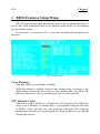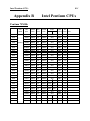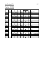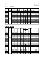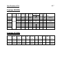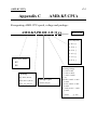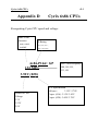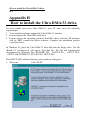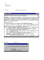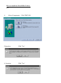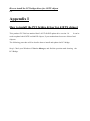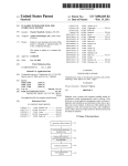
1
Foreword Foreword Thank you for purchasing the AB-PX5/AX5/TX5 as the heart of your computer’s system. We hope this instruction booklet will enable you to install PX5/AX5/TX5 in your system safely and without any errors. Although you may be familiar with some of the concepts we will explain, please read over them again to avoid any problems. 1. The motherboard in most PCs use many connecting cables to connect peripherals to the main unit. The important thing to remember is that these cables all have a ‘direction’. Later in the chapter, we will talk more about the definition of connecting cables and the method of installation. Please pay special attention to our prompts. Because we are using the exclusive ABIT SOFTMENU technology to modify the motherboard , the jumper is not required anymore. We also use simple and easy to understand software design to complete this task. Because of this, you can install the motherboard directly into the system. However, we still suggest you first carry out a simple test before you install the motherboard inside the computer. 2. In this booklet, we will write out in full any new technical words we encounter for the first time and use their contractions thereafter. 3. If, when you are installing the CPU problems occur and there is no way to solve them, we suggest you first clear the CMOS information (refer to Chapter 2). If you still have problems, contact us. 4. How to perform a simple basic test? It’s simple. Place the mother board on a flat insulated surface (like the packaging the motherboard came in). Plug the CPU into Part No:MN-096-2C1-41 Rev:1.21 the ZIF socket (if you are installing a fan, install it on top). Plug DRAM module in and then plug the keyboard in. Plug in the electrical cord (ensure electrical supply is turned off when doing this) and pay attention to polarity (refer to Chapter 2). Plug in the display card and plug the 15 Pin D-Sub monitor signal connector into the display card. Make sure the connections are correct and secure and then turn on the power source for the monitor and then the main power supply. If a picture appears on the monitor, congratulations, the basic test has been successful. Finally, good luck with the complete installation. Computers – Things to Know! CMOS (Complementary Metal-Oxide Semiconductor) Maybe you’ve heard of CMOS DATA quite a bit but have never seen it. What exactly is CMOS? Is it important? Well, if it wasn’t important, you would never had heard of it. CMOS basically stores or saves the parameters you assign the BIOS (Basic Input Output System) with in memory. This memory or SRAM can be both read from and written to but it needs battery power to avoid losing this information when the computer is turned off. When the batteries go flat or you need to swap batteries, you may not remember the parameters you set. To avoid this, we recommend you record these parameters or stick them to your hard drive for easy reference. Table of Contents Foreword Chapter 1 Introduction of AX5/PX5/TX5 Features ¬ AX5 ............................................................................................ 1-2 l Specifications......................................................................... 1-2 l Layout diagram...................................................................... 1-4 - PX5............................................................................................. 1-5 l Specifications......................................................................... 1-5 l Layout diagram...................................................................... 1-7 ® TX5............................................................................................. 1-8 l Specifications......................................................................... 1-8 l Layout diagram.................................................................... 1-11 ¯ System block diagram................................................................ 1-12 Chapter 2 Installing the Mainboard ¬ Installing the Mainboard to the Casing ......................................... 2-3 - Standard External Connectors...................................................... 2-4 ® Jumpers and Switches................................................................ 2-12 ¯ Presentation and Installation of the CPU .................................... 2-13 ° Installing System Memory ¡i DRAM Memory ¡j ......... 2-16 Chapter 3 Introduction of BIOS ¬ CPU Setup ¡i CPU SOFT MENU™¡j ............................. 3-3 - Standard CMOS Setup Menu ...................................................... 3-9 ® BIOS Features Setup Menu ....................................................... 3-11 ¯ Chipset Features Setup Menu .................................................... 3-17 ° Power Management Setup Menu ............................................... 3-19 ± PCI & Onboard I/O Setup ......................................................... 3-23 ² Load BIOS Defaults .................................................................. 3-28 Part No:MN-096-2C1-41 Rev:1.21 ³ Load Setup Defaults .................................................................. 3-28 ´ Password Setting ....................................................................... 3-29 µ IDE HDD Auto Detection ......................................................... 3-30 Appendix A Quick Installation Appendix B Intel Pentium CPUs Appendix C AMD-K5 CPUs Appendix D Cyrix/IBM 6x86 CPUs Appendix E General Discussion about HDD Installation Appendix F Technical Support Appendix G Flash BIOS User Instructions Appendix H How to install Ultra DMA/33 drive Appendix I How to install the PCI bridge driver for 430TX chipset Introduction of AX5/PX5/TX5 Features Chapter 1 1-1 Introduction of AX5/PX5/TX5 Features The AX5/PX5/TX5 have been especially designed for File server, Workstation and Professional users. It can support a wide range of processors, including all Intel CPUs (P54C) and Intel CPUs with MMX (P55C), as well as all AMD-K5/K6 and Cyrix 6x86/6x86L/6x86MX CPUs. It also takes into account, as much as possible, all future CPUs. The AX5/PX5/TX5 uses SOFT MENU™ technology, which means that all the parameters can be configured without using DIP switches or jumpers. The configuration is entirely achieved through a “Soft Switch” that allows the user to set CPU speed and operating voltage with ease. The AX5/PX5/TX5 uses Intel 430TX series chipsets, and has 512K Level2 Pipeline Burst SRAM on board. 168-pin DIMM ( Dual In-Line Memory Module ) slots and 72-pin SIMM (Single In-Line Memory Module )slots meet the requirements for all memory configurations required by high level computing. The 168-pin DIMM slots support traditional Fast Page and EDO ( Extended Data Out ) DRAM as a memory standard for next generation 64-bit systems. The 168-pin DIMM slots have been reserved to meet requirements for both present and future upgrades. The AX5/PX5/TX5 also provides two Universal Serial Bus (USB) ports and meets the Concurrent PCI ( Peripheral Component Interconnect ) Rev. 2.1 standard. It also supports IDE interface for Fast HDD (Mode 0~4) and Ultra DMA/33 ( Direct Memory Access ), as well as IDE Bus Master. These features also meet present and future interface standards and needs. System BIOS features include Plug-and-Play (PnP), Advanced Configuration Power Interface (ACPI), the newest Desktop Management Interface (DMI), as well as AX5/PX5/TX5’s unique CPU operating frequency and voltage setup feature in order to meet modern computing demands. 1-2 Chapter 1 ¬ AX5 nSpecifications 1. Support ATX power supply. 2. CPU frequency and voltage setup with CPU “SOFT MENU™” l Setup of the mainboard’s frequency and voltage without DIP Switches or Jumpers. l Modification of CPU operating voltage and frequency by the BIOS Setup . 3. Uses ZIF CPU Socket 7 for easy CPU installation l Support switching power for CPU to get more stable environment l Supports Intel CPUs: 1) Pentium 100MHz to 200MHz 2) Pentium processor with MMXTM technology 166MHz to 233MHz l Supports AMD CPUs: 1)AMD-K5™ PR100 ~ PR166. 2) AMD-K6TM 166MHz ~ 233MHz. l Supports Cyrix/IBM CPUs: 1) Cyrix 6x86TM P120+ ~ P200+. 2) Cyrix 6x86LTM P150+ ~ P200+. 3) Cyrix 6x86MXTM PR150 ~ PR233 . 4. Chipset l Intel 430TX chipset l Supports standard version PCI 2.1 5. L2 Cache Memory l 512K of cache memory (Pipeline Burst SRAM) 6. System DRAM l Four 72-pin SIMM sockets: support FP and EDO DRAM l Three 168-pin DIMM sockets: support FP, EDO and Synchronous DRAM (SDRAM) l DIMM sockets use PC modules (3.3V Unbuffered DRAM) l Up to 256MB memory configuration possible Introduction of AX5/PX5/TX5 Features 1-3 7. System BIOS l AWARD BIOS l Supports Plug-and-Play (PnP) l Supports Advanced Configuration Power Interface (ACPI) l Supports Desktop Management Interface (DMI) 8. Multi I/O features l Two Universal Serial Bus (USB) ports l Four fast IDE channels (PIO mode 0~4, Ultra “DMA/33” and Bus Master) l One standard EPP/ECP parallel port and two 16550A serial ports l Two floppy disk drive connectors (FDD) (360K, 720K, 1.2M, 1.44M and 2.88M) l Support PS/2 type mouse 9. Other features l Standard ATX architecture dimensions l Four ISA bus slots and four PCI bus slots l Supports 3-MODE for a special Japanese floppy disk drive l Supports two bootable hard disks--able to run two different operating systems l Supports IDE interface CD-ROM and LS-120 type floppy disk drive (Boot only) Note: All brand names and trademarks are the property of their respective owners. *Specifications and information contained in this catalogue are subject to change without notice. 1-4 Chapter 1 n Layout diagram Fig 1-1 Layout diagram Introduction of AX5/PX5/TX5 Features 1-5 - PX5 nSpecifications 1. Supports AT power supply 2. CPU frequency and voltage setup with CPU “SOFT MENU™” l Setup of the mainboard’s frequency and voltage without DIP Switches or Jumpers. l Modification of CPU operating voltage and frequency by the BIOS Setup. 3. Uses ZIF CPU Socket 7 for easy CPU installation l Support switching power for CPU to get more stable environment l Supports Intel CPUs: 1) Pentium 100MHz to 200MHz . 2 ) Pentium processor with MMXTM technology 166MHz to 233MHz l Supports AMD CPUs: 1 ) AMD-K5™ PR100 ~ PR166. 2) AMD-K6TM 166MHz ~ 233MHz. l Supports Cyrix/IBM CPUs: 1) Cyrix 6x86TM P120+ ~ P200+. 2) Cyrix 6x86LTM P150+ ~ P200+. 3) Cyrix 6x86MXTM PR150 ~ PR233 . 4. Chipset l Intel 430TX chipset l Supports standard version PCI 2.1 5. L2 Cache Memory l 512K of cache memory (Pipeline Burst SRAM) 6. System DRAM l Two 72-pin SIMM sockets: support FP and EDO DRAM l Two 168-pin DIMM sockets: support FP, EDO and Synchronous DRAM (SDRAM) l DIMM sockets use PC modules (3.3V Unbuffered DRAM) l Up to 256MB memory configuration possible 1-6 Chapter 1 7. System BIOS l AWARD BIOS l Supports Plug-and-Play (PnP) l Supports Advanced Configuration Power Interface (ACPI) l Supports Desktop Management Interface (DMI) 8. Multi I/O features l Two Universal Serial Bus (USB) ports l Four fast IDE channels (PIO mode 0~4, Ultra “DMA/33” and Bus Master) l One standard EPP/ECP parallel port and two 16550 serial ports l Two floppy disk drive connectors (FDD) (360K, 720K, 1.2M, 1.44M and 2.88M) l Support PS/2 type mouse 9. Other features l Standard AT architecture dimensions l Four ISA bus slots and four PCI bus slots l Supports 3-MODE for a special Japanese floppy disk drive l Supports two bootable hard disks--able to run two different operating systems l Supports IDE interface CD-ROM and LS-120 type floppy disk drive (Boot only) No e: Al b a d am s nd tr de ar s re th p op rt o t ei r sp ct ve ow er . * pe if ca io s nd in or at on co ta ne i t is ca al gu a e ub ec t c an e no ic . it ou Introduction of AX5/PX5/TX5 Features n Layout diagram Fig 1-2 Layout diagram 1-7 1-8 Chapter 1 ® TX5 nSpecifications 1. Supports AT and ATX power supply 2. CPU frequency and voltage setup with CPU “SOFT MENU™” l Setup of the mainboard’s frequency and voltage without DIP Switches or Jumpers. l Modification of CPU operating voltage and frequency by the BIOS Setup. 3. Uses ZIF CPU Socket 7 for easy CPU installation l Support switching power for CPU to get more stable environment l Supports Intel CPUs: 1) Pentium 120MHz to 200MHz 2 ) Pentium processor with MMXTM technology 166MHz to 233MHz l Supports AMD CPUs: 1 ) AMD-K5™ PR120 to PR166. 2) AMD-K6TM 166MHz ~ *266MHz . l Supports Cyrix/IBM CPUs: 1) Cyrix 6x86TM P150+ ~ P200+. 2) Cyrix 6x86LTM P150+ ~ P200+. 3) Cyrix 6x86MXTM PR150 ~ PR233 . * Supports 2.2 Volts Vcore voltage.( Starting form Rev 1.2), Can support AMD-K6TM 266 MHz processor. 4. Chipset l Intel 430TX chipset l Supports standard version PCI 2.1 5. L2 Cache Memory l 512K of cache memory (Pipeline Burst SRAM) 6. System DRAM l Four 72-pin SIMM sockets: support FP and EDO DRAM l Two 168-pin DIMM sockets: support FP, EDO and Synchronous DRAM (SDRAM) l DIMM sockets use PC modules (3.3V Unbuffered DRAM) Introduction of AX5/PX5/TX5 Features 1-9 l Up to 256MB memory configuration possible 7. System BIOS l AWARD BIOS l Supports Plug-and-Play (PnP) l Supports Advanced Configuration Power Interface (ACPI) l Supports Desktop Management Interface (DMI) 8. Multi I/O features l Two Universal Serial Bus (USB) ports l Four fast IDE channels (PIO mode 0~4, Ultra “DMA/33” and Bus Master) l One standard EPP/ECP parallel port and two 16550 serial ports l Two floppy disk drive connectors (FDD) (360K, 720K, 1.2M, 1.44M and 2.88M) l Support PS/2 type mouse 9. Other features l Standard AT architecture dimensions l Three ISA bus slots and four PCI bus slots l Supports 3-MODE for a special Japanese floppy disk drive l Supports two bootable hard disks--able to run two different operating systems l Support monitor for system temperature, Fan running and voltage, also support l Support special interface EISCA to monitor system environment l Supports IDE interface CD-ROM and LS-120 type floppy disk drive (Boot only) 1-10 Computer Knowledge Chapter 1 The EISCA(Enhanced Intelligent System Cooler Architecture) is a specially designed 12-pin interface which integrates the Mainboard and the CPU cooling system. This system is a total solution for PC system heat sink problems. Due to increasing CPU speed, which causes higher temperatures, finding ways to effectively deal with CPU temperatures is becoming a more and more crucial problem. Effectively and precisely determining CPU temperature was a very important requirement. The area directly under the CPU socket is the location on the mainboard. closest to the CPU, and heat is conducted away from this area through air circulation. Determining temperature change under these circumstances is very imprecise, as it only allows us to detect large changes in temperature. In addition, because the air under the CPU socket is confined to this area, the sensor cannot detect temperature in real time. Tests have proven that under such circumstances, even after 5 minutes the sensor located under the CPU socket is unable to detect real temperature change, so it can not meet the requirements for thermal problems. In EISCA architecture, the thermal sensor is located at the heat-sink. In this way, the sensor is able to detect CPU temperature in real time and more precisely. The EISCA monitors voltage, fan speed and fan on/off control to meet the important specifications. Note: All brand names and trademarks are the property of their respective owners. *Specifications and information contained in this catalogue are subject to change without notice. Introduction of AX5/PX5/TX5 Features n Layout diagram Fig 1-3 Layout diagram 1-11 1-12 Chapter 1 ¯ System block diagram Pentium Processor 3.3V Host BUS Control Address Data Second Level Cache Ctrl CACHE (SRAM) Tag Ctrl Addr MTXC Ctrl Main Memory (DRAM) TIO[0..7] TAG PCI BUS Control Address/Data CD ROM & Hard Disk Fast IDE USB USB 1 2 PIIX4 Universal Serial Bus ISA BUS Serial Winbond W83977 Fig. 1-4 LPT FDC System block diagram PCI Device(s) ISA Device(s) Installing the Mainboard 2-1 Chapter 2 Installing the Mainboard This AX5/PX5/TX5 mainboard not only provides all standard equipment for classic personal computers, but also provides great flexibility for meeting future upgrade demands. This chapter will introduce step by step all the standard equipment and will also present, as completely as possible future upgrade capabilities. This mainboard is able to support all Intel Pentium including P55C with MMX, Cyrix 6x86, 6x86L, 6x86MX and AMD-K5/K6 processors now on the market. (For details, see specifications in Chapter 1.) However, we cannot guarantee that the description given in this manual on the circuitry of your mainboard will work for processors not listed in Chapter 1. For example, the operating voltage of Cyrix’s next generation CPUs is unknown at the present time. Thus we were not able to include these specifications in your motherboard. We will supply further information about CPU support when new CPUs arrive on the market. This chapter is organized according the following features: Œ Installing the Mainboard to the Casing • Standard external connectors Ž Jumpers and switches • Presentation and Installing of the CPU. º Installing the system memory. NNNN Before proceeding with the installation Before installing the mainboard please be sure to turn off or disconnect the power supply unit. Before making any modifications to the hardware configuration of the mainboard, the power supply to any areas of the mainboard you plan to modify should be turned off to avoid unnecessary damage to the hardware. 2-2 Chapter 2 & Us r ri nd y ns ru ti ns Our objective is to enable the novice computer user to perform the installation by themselves. We have attempted to write this document in a very clear, concise and descriptive manner to help overcome any obstacles you may face during installation. Please read our instructions carefully and follow them carefully step-by-step. Installing the Mainboard 2-3 ¬ Installing the Mainboard to the Casing Most computer cases will have a base on which there will be many mounting holes that allows the mainboard to be securely attached and at the same time, prevents short circuits. There are two ways to attach the mainboard to the base. lwith spacers lor with bolts In principle, the best way to attach the motherboard is with bolts, and only if you are unable to do this should you attach the board with spacers. Take a careful look at the mainboard and you will see many mounting holes on it. Line these holes up with the mounting holes on the base. If the holes line up, and there are screw holes this means you can attach the mainboard with bolts. If the holes line up and there are only slots, this means you can only attach the mainboard with spacers. Take the tip of the spacers and insert it into the slots. After doing this to all the slots, you can slide the mainboard into position aligned with the slots. After the mainboard has been positioned, check to make sure everything is OK before putting the casing back on. Note: If the mainboard has mounting holes, but don’t line up with the holes on the base and their are no slots to attach the spacers, don’t panic, you can still attach the spacers to the mounting holes. Just cut the spacers (along the dotted line) (the spacer may be a little hard so be careful of our hands). In this way you can still attach the mainboard to the base without worrying about short circuits. Computer Knowledge Why is it that Cyrix is always raised in relation to IBM in books? In fact, these two 6*86 CPUs (limited to the 6*86 series) are basically the same thing. Because Cyrix does not have its own production line, it has contracted IBM to manufacture their 6*86 CPUs for them. However, IBM has stipulated that the Cyrix CPUs they produce have both the Cyrix and IBM mark printed on it. 2-4 Chapter 2 - Standard External Connectors Inside the case of any computer several cables and plugs have to be connected. These cables and plugs are usually connected one-by-one to connectors located on the mainboard. You need to carefully pay attention to any connection orientation the cables may have and, if any, notice the position of the first pin of the connector. In the explanations that follow, we will describe the significance of the first pin. PN1 - Keylock connector Please pay attention to pin position and orientation This connector has a specific orientation. Connect the five-thread keylock connector cable to the PN1 connector pins on the mainboard. Pin number 1 2 3 4 5 Computer Knowledge Name or significance of signal +5VDC No connection Ground Keyboard inhibit Signal Ground power LED power LED power LED key lock key lock The “keylock switch” is used to lock the computer’s keyboard. This disables the keyboard so that unauthorized persons cannot use it. When this function is in use, you will need to use the unlock key to activate the keyboard. Installing the Mainboard 2-5 PN1 - Power ON/OFF connectors There is no specific orientation. Since most cases do not support this feature, most of you ignore this instruction. If the case support this kind of power switch connector, please connect this connector into Mainboard. In this case, you have to use ATX type power supply to get this function. Pin number 10 11 Name or significance of the signal Power on/off Ground PN1 - SMI Switch There is no specific orientation. Connect the two-thread cable to the PN1 connector pins on the mainboard. Since most cases do not support this feature, most of you ignore this instruction. Furthermore, this feature is not necessary as it is already a part of the mainboard. Pin number 13 14 Name or significance of signal +5VDC suspend PN1 - HDD LED connector This connector has a specific orientation. Connect the two-thread IDE LED connector cable attached to the case to the IDE LED connector on the mainboard. Pin number 7 8 Name or significance of signal LED’s Cathode LED’s Anode 2-6 Chapter 2 PN2 - Speaker connector There is no specific orientation. Connect the four-thread speaker cable to the PN2 connector pins on the mainboard. Pin number 4 5 6 7 Name or significance of signal +5VDC Ground Ground Sound Signal PN2 - Hardware Reset connectors There is no specific orientation. Connect the two-thread hardware reset cable to the PN2 connector pins on the mainboard. Pin number 1 2 Name or significance of signal Hardware reset signal Ground PN2 - Sleep LED connector This connector has a specific orientation. Connect the two-thread Sleep LED connector cable attached to the case to the Sleep LED connector on the mainboard. Pin number 9 10 Name or significance of signal LED’s Cathode LED’s Anode FAN1 - CPU Fan power connector (AX5/PX5) This has a specific orientation. Connect the three-threads CPU fan cable to the FAN1 connector. Pin number 1 2 3 Name of the signal or signification Ground +12V Ground Installing the Mainboard 2-7 FAN1 - CPU Fan power connector (TX5) This has a specific orientation. Connect the three-threads CPU fan cable to the FAN1 connector. If, at the bottom of the fan, there are only two threads, just connect them to PIN2 and PIN3. Pin number 1 2 3 Name of the signal or signification Sensor signal +12V Control on/off IR - Infrared remote Connectors Watch the pin number and the orientation This has a specific orientation. Your mainboard supports this feature, but you must buy the infrared remote device as an option. (AX5) : Pin number 1 2 3 4 5 Name of the signal or signification +5VDC No connection Transmit data Ground Receive data (PX5 TX5) : Pin number 1 2 3 4 5 Name of the signal or signification +5VDC No connection Receive data Ground Transmit data 2-8 Chapter 2 ATXPWR - ATX Power input Connectors These have a specific orientation. The three warning marks indicate that if you make a mistake in pin number or connection orientation, you could destroy your equipment. During installation, you just need to connect to the correct pins and in the correct orientation, and to connect connector of the power supply unit to the connector on the mainboard. Pin number 1 2 3 4 5 6 7 8 9 10 Name of the signal or signification +3.3VDC +3.3VDC Ground +5VDC Ground +5VDC Ground POWERGOOD +5VDC +12VDC Pin number 11 12 13 14 15 16 17 18 19 20 Name of the signal or signification +3.3VDC -12VDC Ground PS_ON Ground Ground Ground -5VDC +5VDC +5VDC P8/P9 - AT Power input Connectors (the AX5 do not support this connector) These have a specific orientation. The three warning marks indicate that if you make a mistake in pin number or connection orientation, you could destroy your equipment. During installation, you just need to connect to the correct pins and in the correct orientation, and to connect connectors P8 and P9 of the power supply unit to the connectors on the mainboard. Pin number 1 2 3 4 5 6 Name of the signal or signification POWERGOOD +5VDC +12VDC -12VDC Ground Ground Pin number 7 8 9 10 11 12 Name of the signal or signification Ground Ground -5VDC +5VDC +5VDC +5VDC Installing the Mainboard 2-9 Mechanics of Mouse/Keyboard/USB/COM1/COM2/LPT (AX5) Mouse - PS/2 Mouse connector Watch the pin number and the orientation This has a specific orientation. Connect the six-threads PS/2 Mouse cable provided to the connector on the mainboard. Pin number 1 2 3 4 5 6 Computer knowledge Name of the signal or signification Mouse data No connection Ground +5VDC Ground Mouse clock The “PS/2 Mouse Port” is different from COM1 or COM2 serial ports to which you can also connect a Mouse. This mainboard features an extra PS/2 Mouse port, so when you buy a mouse, be sure that it is a PS/2 Mouse before connecting it to this port. But if you cannot find any PS/2 Mouse, you can still use COM1 or COM2 to connect a serial mouse to your computer. Keyboard - PS/2 Keyboard Connector (AX5) 2-10 Chapter 2 This has an orientation pin. Connect your keyboard connector to the connector on the mainboard. Pin number 1 2 3 4 5 6 Name of the signal or signification Keyboard data No connection Ground +5VDC Ground Keyboard clock KB1 - Keyboard Connector (PX5/TX5) This has an orientation pin. Connect your keyboard connector to the connector on the mainboard. Pin number 1 2 3 4 5 Name of the signal or signification Keyboard clock Keyboard data No connection Ground +5VDC I/O Port connectors Watch the pin number and the orientation Connector name IDE 1 IDE 2 FDC LPT COM1 COM2 USB Pin number 40 40 34 26 10 10 16 Name of the peripheral connected IDE Channel 1 IDE Channel 2 Floppy Disk connector Parallel port connector Serial port COM1 connector Serial port COM2 connector Universal Serial Bus connector Installing the Mainboard 2-11 LM1 - Enhanced Intelligent System Coller Architecture Connectors (TX5) This has an orientation pin. Connect your EISCA connector to the connector on the mainboard. Pin number 1 2 3 4 5 6 7 8 9 10 11 12 Name of the signal or signification I2C Serial Bus Clock I2C Serial Bus Data Set for active low for wire interrupt line Key +5VDC Alarm speaker output Ground Vcore detect fanl sensor input Vio detect fan2 sensor input +12VDC 2-12 Chapter 2 ® Jumpers and Switches CCMOS : Delete the contents of the CMOS This jumper is set on pins 1 and 2 at the factory, in order for the computer to function normally, so please do not change this setting. The main feature of this jumper is to solve situations where the computer crashes due to improper usage. For instance: l You have forgotten the password you set. l You have changed inappropriately the settings in the BIOS menu. l You want to change the version of flash BIOS. All these errors are very serious, you must avoid them. But if you have made one of these errors, this jumper can save your life. First turn off the power supply and open the computer case, than place the jumper on pins 2 and 3 in order to save your computer. But if you use your computer normally, you should not need to use this feature. After you have deleted the CMOS information, the computer is saved, but you still have to go back to the BIOS Setup menu, and reset one by one all the specifications: CPU, date, hour, FDD and HDD parameters. etc., before your computer will get back into normal operation. Installing the Mainboard 2-13 ¯ Presentation and Installation of the CPU Jumperless Mainboard (Mainboard with no DIP Switch or Jumper) The AX5/PX5/TX5 mainboard can be installed with CPU without the hardware setting of the CPU. On other boards, when you want to install the CPU, you have, more or less, to setup some jumpers or DIP switches. With the AX5/PX5/TX5 mainboard, you will not need to adjust any jumper or switch. The CPU speed and model is set up by software, in order to allow the user to complete setup and installation procedures easily. After you have inserted the CPU on the CPU socket, you can close the computer case and turn the computer on. You just need to enter the CPU SOFT MENU™ located in the BIOS Setup, and to setup the speed and the voltage of the CPU to compete the installation. Even if you don’t need to setup any switch, we recommend you to read our presentation of the CPUs, it will be useful information for you. Since 1996, every two or three months, Intel adds new models to the Pentium CPU series. That is why the CPU market is filled with a lot of different models and brands. All CPUs have different electrical specifications. That’s why installing a CPU is becoming more and more complex. You can’t help that, because everybody wants to be able to upgrade its hardware. So, you have to take a bit of time to read this section, in order to be able to install a cheaper and better processor. The AX5/PX5/TX5 mainboard does not only support all the CPUs listed in the specifications, but also has reserved several circuits in order to be able to support future processors. But before we go further in our presentation, we must clarify that “we have only tested the CPUs listed in Chapter 1”, we cannot guarantee that this board will be able to support future products, because we cannot forecast future developments. But we will do our best to support any possible CPU. 2-14 Chapter 2 Related terminology : External clock Also referred to as the external CPU clock, or “Bus clock”, it is the input clock of the CPU. For instance, Intel Pentium P90, P120 and P150 all have a 60MHz external CPU clock, but have different internal clock multiplier factors. Clock multiplier factor The real operation clock within the CPU is the multiple of the external clock. We refer to this factor as the clock multiplier factor. The four factors possible are 1.5, 2, 2.5 and 3. The factor differs from one CPU to another. For instance, the Intel Pentium 166 CPU has a 66MHz external clock, with a multiplier factor of 2.5, so that the speed of the internal clock is 66MHz x 2.5. Internal clock Also referred to as the real internal CPU clock, it is the actual internal operating clock of the CPU. The Internal Clock is a multiple of the external clock and of the clock multiplier factor. For instance, the Intel Pentium 90 CPU has a 60MHz external clock and its clock multiplier factor is 1.5; the Intel Pentium P133 CPU has a 66MHz external clock and its clock multiplier factor is 2. Internal CPU clock = clock multiplier factor * external CPU clock AT Bus clock Also referred to as ISA SPEED, or AT CLOCK, or even ISA Bus clock. Ten years ago, the original specification of AT Bus clock installed in the first generation PC/AT computers was 8MHz, this means that there are some interface cards which can only work at 8MHz. In order to guarantee compatibility with older hardware, we still support 8MHz AT Bus clock, but if your interface card is newer or faster, you can choose a higher speed for the AT Bus clock, in order to increase the transmission rate of the interface cards. But we recommend you not to be too ambitious. An 8MHz setup ensures maximum compatibility. Installing the Mainboard 2-15 CPU Voltage - Vcore and Vio From the voltage point of view, 586 series CPU can be divided into two categories: single voltage CPU and dual voltage CPUs. Single voltage CPUs include: Intel Pentium P54C series, AMD-K5 and Cyrix 6x86, etc. Dual voltage CPUs include: Intel P55C with MMX, future AMD-K6 CPUs, Cyrix 6x86L and 6x86MX. The voltage of dual voltage CPUs has two components: Vcore and Vio. Vcore provides all the power for internal processing, and its power consumption is quite important. Vio provides the power necessary for the external interface of the CPU. P-Rating The P-Rating was defined by some manufacturers other than Intel to rate the performance of their CPU in comparison with Intel Pentium CPUs. For instance, Cyrix 6x86 P166+ has a higher actual speed compared with Intel Pentium P166, its internal clock needs only 133MHz versus 166MHz for Intel’s product. The main reason is that Cyrix has improved the internal architecture of the 6x86 CPU, which means that with the same internal clock speed, the actual clock speed will be different. Having read the related terminology above, please refer to the information in appendices B, C or D for the type and specifications of your own CPU. We suggest that you note down these specifications, which will help you when you install the CPU. CPU Settings: ¡I ¡I CPU SOFT MENU ¡I ¡I To configure the speed and the voltage of the CPU, you must enter to the CPU SOFT MENU in BIOS Setup. 2-16 Chapter 2 ° Installing System Memory Memory ¡j ¡i DRAM When this mainboard was designed, we not only have taken into account the present needs, but we have also tried to care about demands for future upgrades: 1. 168-pin DIMM sockets: ¶ AX5 support three 168 pin DIMM sockets · PX5/TX5 support two168 pin DIMM sockets If you want to extend your memory capacity, you will have no solution other than to use 168-pin 3.3V unbuffered DIMM sockets. 2. 72-pin SIMM sockets: ¶ AX5/TX5 support four 72 pin SIMM sockets · PX5 support two 72 pin SIMM sockets 3. Easy installation You just need to insert the modules, without the help of God. Isn’t it great? Besides the features mentioned above, you can use simultaneously 72-pin SIMM modules and 168-pin DIMM modules, but you will rarely encounter this kind of configuration. Before you proceed with installation, be patient, first read what follows: 1. Factory default setting of the mainboard is for 60ns FP or EDO modules. If your memory modules are faster than 60ns, say 45ns, you can modify the BIOS settings in order to speed up the operating speed of the system. But if you don’t want to modify these settings, or if you don’t know how to modify them, it’s no big deal. But if you set the external CPU clock at 66MHz or more, we recommend you use 60ns or even faster DRAM modules. 2. Memory error check and correction do not support this feature on this mainboard. Since the Intel 430TX chipset does not support this feature, since the memory error check and correction feature may not be effective, and since you cannot easily find memory modules with memory check and Installing the Mainboard correction feature, this mainboard does not support it. 2-17 2-18 Chapter 2 3. Maximum memory capacity 256M bytes supported by this mainboard. Computer knowledge ¡i Relationships between memory modules and Pentium CPUs ¡j Pentium P54C . P55C, Cyrix 6x86 and AMD-K5/K6 are all 64 bit CPUs, but 72-pin SIMM modules are only 32-bit. That’s why they have to be used in pairs, because the CPU will always be only able to see 64 bits. This means that 72-pin SIMM modules have to be installed in pairs. For instance, SIMM1 and SIMM2 must form a pair, and SIMM3 and SIMM4 must form another pair. Of course, the two members of a pair must be of the same kind ¡i EDO or FP DRAM ¡j, and you cannot use pairs from different “species”. But the AX5/TX5 support different “pairs” and use different type of memory modules, notice: l ¡i SIMM1 and SIMM2 ¡j must use the same memory type, as well as ¡i SIMM3 and SIMM4 ¡j . l ¡i SIMM1 and SIMM2 ¡j use the same memory type, and ¡i SIMM3 and SIMM4 ¡j can use the same type, or a different type, in order to permit you to obtain the best speed configuration for each “single” pair, and to make the system work at its maximum capacity. If one memory pair is slower, it will have no influence on the pair whose speed is higher. 168-pin DIMM modules are 64 bit, so you can use single modules. On the AX5/PX5/TX5 mainboard, these modules can support not only EDO and FP DRAM, but also Synchronous DRAM memory configurations. When you install DIMM modules on the mainboard, you don’t have to setup anything, just be sure that you use 3.3V unbuffered 168-pin DIMM modules, and insert them in the memory socket. Installing the Mainboard 2-19 Computer ¡i 168-pin DIMM modules specifications ¡j Knowledge According to the standards defined by JEDEC, there are a lot of different types of specifications for 168-pin DIMM sockets. Here are the possible types: l 3.3V UNBUFFERED DIMM l 3.3V BUFFERED DIMM l 5V UNBUFFERED DIMM l 5V BUFFERED DIMM These types of DIMM modules differ not only by the electrical design, but also by their architecture. So, if you buy different types of DIMM modules, you will not be able to insert them in the DIMM sockets. Currently, the standard for PC is 3.3V UNBUFFERED DIMM, which is the standard supported by this series. After installing the DRAM, the BIOS of the mainboard will automatically detect the size of the memory installed on the mainboard. Below is a list of all the possible situations: Scenario 1: You use only 72-pin SIMM modules: l The maximum memory size is 256M bytes. l Support possible for single density or double density memory modules. l Memory modules supported: 1Mx32 ¡i 4M ¡j , 2Mx32 ¡i 8M ¡j, 4Mx32 ¡i 16M ¡j, 8Mx32 ¡i 32M ¡j or 16Mx32 ¡i 64M ¡j . l You can also directly refer to table 2-1. Scenario 2: You use only 168-pin DIMM modules: l The maximum memory size is 256M bytes. l Support possible for single density or double density memory modules. l Memory modules supported: 1Mx64 ¡i 8M ¡j , 2Mx64 ¡i 16M ¡j, 4Mx64 ¡i 32M ¡j, 8Mx64 ¡i 64M ¡j or 16Mx64 ¡i 128M ¡j . l DIMM1 is the first pair, DIMM2 is the second pair. Usually, you first insert modules in DIMM1 socket, than in DIMM2 socket, but it is possible to do the reverse. l You can also directly refer to table 2-2. 2-20 Chapter 2 Scenario 3: You use 72-pin SIMM modules and 168-pin DIMM modules: l The maximum memory size is: 256M bytes. l Support possible for single density or double density memory modules. l Memory modules supported: Refer to case 1 and case 2 above. l Support possible for mixed use of single density and double density modules. l Since there is a lot of possible configurations, no table is given. System DRAM AX5 PX5 TX5 72- pin SIMM socket 4 SIMM 2 SIMM 4 SIMM Support FP DRAM Yes Yes Yes Support EDO DRAM Yes Yes Yes 168-pin DIMM specifications 3.3V Unbuffered 3.3V Unbuffered 3.3V Unbuffered 168-pin DIMM socket 3 DIMMs 2 DIMMs 2 DIMMs Support FP DRAM Yes Yes Yes Support EDO DRAM Yes Yes Yes Support synchronous DRAM (SDRAM) Yes Yes Yes DRAM Error Check No No No Maximum memory size 256MB 256MB 256MB Installing the Mainboard 2-21 Table 2-1 72-pin SIMM Module Installation ¡i SIMM1, SIMM2 ¡j 1st ¡i 2nd pair ¡j ¡i SIMM3, SIMM4 ¡j * 2nd ¡i 1st pair ¡j 1Mx32 ¡i 4Mx2 ¡j 2Mx32 ¡i 8Mx2 ¡j 4Mx32 ¡i 16Mx2 ¡j 8Mx32 ¡i 32Mx2 ¡j 16Mx32 ¡i 64Mx2 ¡j Total memory size 8MB 16MB NO MODULE INSERTED 32MB 64MB 128MB 8MB 1Mx32 ¡i 4Mx2 ¡j 16MB 2Mx32 ¡i 8Mx2 ¡j NO MODULE INSERTED 32MB 4Mx32 ¡i 16Mx2 ¡j 64MB 8Mx32 ¡i 32Mx2 ¡j 128MB 16Mx32 ¡i 64Mx2 ¡j Since the installation described above is valid for the first pair as well as for the second pair, it will not be repeated. 16MB 1Mx32 ¡i 4Mx2 ¡j 24MB 2Mx32 ¡i 8Mx2 ¡j 40MB 1Mx32 ¡i 4Mx2 ¡j 4Mx32 ¡i 16Mx2 ¡j 72MB 8Mx32 ¡i 32Mx2 ¡j 136MB 16Mx32 ¡i 64Mx2 ¡j 24MB 1Mx32 ¡i 4Mx2 ¡j 32MB 2Mx32 ¡i 8Mx2 ¡j 48MB 2Mx32 ¡i 8Mx2 ¡j 4Mx32 ¡i 16Mx2 ¡j 80MB 8Mx32 ¡i 32Mx2 ¡j 144MB 16Mx32 ¡i 64Mx2 ¡j 40MB 1Mx32 ¡i 4Mx2 ¡j 48MB 2Mx32 ¡i 8Mx2 ¡j 64MB 4Mx32 ¡i 16Mx2 ¡j 4Mx32 ¡i 16Mx2 ¡j 96MB 8Mx32 ¡i 32Mx2 ¡j 160MB 16Mx32 ¡i 64Mx2 ¡j 72MB 1Mx32 ¡i 4Mx2 ¡j 80MB 2Mx32 ¡i 8Mx2 ¡j 96MB 8Mx32 ¡i 32Mx2 ¡j 4Mx32 ¡i 16Mx2 ¡j 128MB 8Mx32 ¡i 32Mx2 ¡j 192MB 16Mx32 ¡i 64Mx2 ¡j 136MB 1Mx32 ¡i 4Mx2 ¡j 144MB 2Mx32 ¡i 8Mx2 ¡j 160MB 16Mx32 ¡i 64Mx2 ¡j 4Mx32 ¡i 16Mx2 ¡j 192MB 8Mx32 ¡i 32Mx2 ¡j 256MB 16Mx32 ¡i 64Mx2 ¡j *: indicates that only AX5 . TX5 supports this configuration Perhaps you have already found out the rules from the table above. This table, we belive, contains all possible configurations. In fact, you just need to insert two or four 72-pin SIMM modules in the socket to complete the installation. 2-22 Chapter 2 Table 2-2 168-pin DIMM Module Installation ¡i DIMM1 ¡j st nd rd ¡i DIMM2 ¡j nd st rd 1 ¡i 2 or 3 ¡j 2 ¡i 1 or 3 ¡j pair pair ¡i DIMM3 ¡j rd 3 ¡i 1st or 2nd ¡j 8MB 2Mx64 ¡i 16M ¡j 16MB 32MB NO NO MODULE MODULE 4Mx64 ¡i 32M ¡j INSERTED 8Mx64 ¡i 64M ¡j INSERTED ¡i 1Mx64 ¡i Total memory size pair 1Mx64 ¡i 8M ¡j 16Mx64 *1 128M ¡j 8M ¡j 64MB 128MB*1 8MB NO 2Mx64 ¡i 16M ¡j NO 16MB MODULE 4Mx64 ¡i 32M ¡j MODULE 32MB INSERTED 8Mx64 ¡i 64M ¡j INSERTED ¡i 1Mx64 ¡i 16Mx64 128M ¡j 64MB 128MB 8M ¡j 8MB 2Mx64 ¡i 16M ¡j NO NO 16MB 4Mx64 ¡i 32M ¡j MODULE MODULE 32MB 8Mx64 ¡i 64M ¡j INSERTED INSERTED 64MB 16Mx64 128MB ¡i 128M ¡j Since the installation described above is valid for the first pair as well as for the second pair, it will not be repeated. 1Mx64 ¡i 8M ¡j 16MB 1Mx64 ¡i 8M ¡j 2Mx64 ¡i 16M ¡j NO 24MB 4Mx64 ¡i 32M ¡j MODULE 40MB 8Mx64 ¡i 64M ¡j INSERTED ¡i 16Mx64 128M ¡j 1Mx64 ¡i 1Mx64 ¡i 8M ¡j 16MB NO 2Mx64 ¡i 16M ¡j 24MB MODULE 4Mx64 ¡i 32M ¡j 40MB INSERTED 8Mx64 ¡i 64M ¡j 8M ¡j ¡i 1Mx64 ¡i 1Mx64 ¡i 8M ¡j 8M ¡j 24MB 40MB 4Mx64 ¡i 32M ¡j 4Mx64 ¡i 32M ¡j 72MB 8Mx64 ¡i 64M ¡j 8Mx64 ¡i 64M ¡j 136MB 16Mx64 128M ¡j 1Mx64 ¡i 72MB 136MB*1 2Mx64 ¡i 16M ¡j ¡i 8M ¡j 16Mx64 *1 128M ¡j 2Mx64 ¡i 16M ¡j 1Mx64 ¡i ¡i 16Mx64 *1 128M ¡j 8M ¡j 2Mx64 ¡i 16M ¡j 2Mx64 ¡i 72MB 136MB 16M ¡j 4Mx64 ¡i 32M ¡j 256MB*1*2 24MB NO 32MB MODULE 48MB Installing the Mainboard 2-23 8Mx64 ¡i 64M ¡j ¡i ¡i DIMM1 ¡j st nd rd ¡i DIMM2 ¡j nd st rd 1 ¡i 2 or 3 ¡j 2 ¡i 1 or 3 ¡j pair pair 2Mx64 ¡i INSERTED 16Mx64 128M ¡j ¡i DIMM3 ¡j rd pair 1Mx64 ¡i 8M ¡j 32MB MODULE 4Mx64 ¡i 32M ¡j 48MB INSERTED 8Mx64 ¡i 64M ¡j 80MB 16Mx64 *1 128M ¡j 144MB*1 16M ¡j 8M ¡j 8M ¡j 32MB 2Mx64 ¡i 16M ¡j 2Mx64 ¡i 16M ¡j 48MB 16M ¡j 4Mx64 ¡i 32M ¡j 4Mx64 ¡i 32M ¡j 80MB 8Mx64 ¡i 64M ¡j 8Mx64 ¡i 64M ¡j 144MB 16Mx64 *1 128M ¡j 256MB*1*2 16Mx64 128M ¡j 1Mx64 ¡i 1Mx64 ¡i ¡i 8M ¡j 40MB 2Mx64 ¡i 16M ¡j NO 48MB 32M ¡j 4Mx64 ¡i 32M ¡j MODULE 64MB 8Mx64 ¡i 64M ¡j INSERTED 96MB 16Mx64 128M ¡j ¡i 160MB 1Mx64 ¡i 32M ¡j 40MB 2Mx64 ¡i 16M ¡j 48MB MODULE 4Mx64 ¡i 32M ¡j 64MB INSERTED 8Mx64 ¡i 64M ¡j 96MB 16Mx64 *1 128M ¡j 160MB*1 ¡i 8M ¡j 1Mx64 ¡i 8M ¡j 48MB 64MB 2Mx64 ¡i 16M ¡j 2Mx64 ¡i 16M ¡j 32M ¡j 4Mx64 ¡i 32M ¡j 4Mx64 ¡i 32M ¡j 96MB 8Mx64 ¡i 64M ¡j 8Mx64 ¡i 64M ¡j 160MB 16Mx64 *1 128M ¡j 256MB*1*2 ¡i 16Mx64 128M ¡j 1Mx64 ¡i ¡i 8M ¡j 2Mx64 ¡i 16M ¡j 8Mx64 ¡i 8M ¡j NO 1Mx64 ¡i 4Mx64 ¡i 24MB 16M ¡j ¡i 4Mx64 ¡i Total memory size 2Mx64 ¡i ¡i 4Mx64 ¡i 1st or 2nd ¡j 3 ¡i NO 1Mx64 ¡i 2Mx64 ¡i 80MB 144MB 72MB NO 80MB 64M ¡j 4Mx64 ¡i 32M ¡j MODULE 96MB 8Mx64 ¡i 64M ¡j INSERTED 128MB 2-24 Chapter 2 16Mx64 128M ¡j ¡i 192MB 1Mx64 ¡i 8Mx64 ¡i 8M ¡j 72MB NO 2Mx64 ¡i 16M ¡j 80MB MODULE 4Mx64 ¡i 32M ¡j 96MB INSERTED 8Mx64 ¡i 64M ¡j 128MB 16Mx64 *1 128M ¡j 192MB*1 64M ¡j ¡i 1Mx64 ¡i 8Mx64 ¡i 96MB 64M ¡j 4Mx64 ¡i 32M ¡j 4Mx64 ¡i 32M ¡j 128MB 8Mx64 ¡i 64M ¡j 8Mx64 ¡i 64M ¡j 192MB 16Mx64 *1 128M ¡j 256MB*1*2 ¡i rd pair 16Mx64 128M ¡j DIMM2 ¡j nd 1 ¡i 2 or 3 ¡j st rd 2 ¡i 1 or 3 ¡j ¡i ¡i DIMM3 ¡j rd 3 ¡i 1st or 2nd ¡j pair 1Mx64 ¡i 8M ¡j 136MB NO 144MB 128M ¡j4Mx64 ¡i 32M ¡j MODULE 160MB 8Mx64 ¡i 64M ¡j INSERTED 192MB 16Mx64 128M ¡j ¡i 256MB 1Mx64 ¡i 128M ¡j 8M ¡j 136MB NO 2Mx64 ¡i 16M ¡j 144MB MODULE 4Mx64 ¡i 32M ¡j 160MB INSERTED 8Mx64 ¡i 64M ¡j ¡i 1Mx64 ¡i 16Mx64 ¡i Total memory size pair 2Mx64 ¡i 16M ¡j 16Mx64 ¡i 80MB 16M ¡j nd 16Mx64 ¡i 8M ¡j 2Mx64 ¡i DIMM1 ¡j st 1Mx64 ¡i 2Mx64 ¡i 16M ¡j ¡i ¡i 8M ¡j 8M ¡j 144MB 2Mx64 ¡i 16M ¡j 160MB 128M ¡j4Mx64 ¡i 32M ¡j 4Mx64 ¡i 32M ¡j 192MB 8Mx64 ¡i 64M ¡j 8Mx64 ¡i 64M ¡j 16Mx64 128M ¡j 1Mx64 ¡i 256MB*1 2Mx64 ¡i 16M ¡j ¡i 8M ¡j 192MB 16Mx64 *1 128M ¡j 256MB 1 ¡i 16Mx64 * 128M ¡j 256MB*1*2 *: indicates that only AX5 supports this configuration *1: Support FP or EDO DRAM only *2: The maximum capacity of memory In fact, the table above shows that you just need to insert the DIMM module in any of the two sockets to complete the installation of the memory. Installing the Mainboard 2-25 The voltage for the 72pin SIMM is +5V, and the 168pin DIMM is +3V, according the specification, it strongly recommend that should not mix both kinds of memory module, it may cause the total amount of memory size is different with the memory that plug-in when install mix both kinds of memory module. It may be the following reasons : 1.The DRAM’s specification is different, can be mixed. 2.The DIMM and SIMM using the same RAS signal, and sharing and it limit by the chipset design. Computer Knowledge Introduction of BIOS Chapter 3 3-1 Introduction of BIOS The BIOS is a program located on a Read-Only Memory chip on the mainboard. This program will not be lost when you turn the computer off. This program is also referred to as the boot program. It is the only channel for the hardware circuit to communicate with the operating system. Its main function is to manage the setup of the mainboard and interface cards parameters, including simple parameters such as time, date, hard disk drive, as well as more complex parameters such as hardware synchronization, device operating mode, CPU SOFT MENU™ techniques, setup of CPU voltage and speed. The computer will operate normally, or will operate at its best, only if all these parameters are correctly configured through the BIOS. M Don’t change the parameters inside the BIOS unless you know what you are doing The parameters inside the BIOS are used to setup the hardware synchronization or the device operating mode. If the parameters are not correct, they will produce errors, the computer will crash, and sometimes you will even not be able to boot the computer after it has crashed. We recommend that you do not change the parameters inside the BIOS unless you are familiar with them. If you are not able to boot your computer anymore, please refer to the section “Erase CMOS data” in Chapter 2. When you start the computer, it is controlled by the BIOS program. The BIOS first operates an auto-diagnostic for all the necessary hardware, configurates the parameters of the hardware synchronization, and detects all the hardware. Only when these tasks are completed does it give up control of the computer to the program of the next level, which is the operating system. Since the BIOS is the only channel for hardware and software to communicate, it will be the key factor to system stability, and to ensure that your system performs at its best. After the BIOS has achieved the auto-diagnostic and auto-detection operations, it will display the following message: PRESS DEL TO ENTER SETUP 3-2 Chapter 3 Three to five seconds after the message is displayed, if you press the Del key, or if you press simultaneously the Ctrl Alt Esc keys, you will access the BIOS Setup menu. At that moment, the BIOS will display the following message: Fig 3 BIOS Setup main menu In the BIOS Setup main menu of Figure 3, you can see several options. We will explain these options step by step in the following pages of this chapter, but let us first see a short description of the function keys you may use here: l Press Esc to quit the BIOS Setup. l Press ¡ô¡õ¡÷¡ö (up, down, left, right) to choose, in the main menu, the option you want to confirm or to modify. l Press F10 when you have completed the setup of BIOS parameters to save these parameters and to exit the BIOS Setup menu. l Press Page Up/Page Down or +/- keys when you want to modify the BIOS parameters for the active option. Computer knowledge CMOS DATA Maybe you have heard somebody saying that their CMOS DATA was lost. What is the CMOS? Is it important? The CMOS is the memory used to store the BIOS parameters that you have configured. This memory is passive. You can read its data, and you can also store data in it. But this memory has to be powered by a battery, in order to avoid any loss of its data when the computer is turned off. Since you may have to change the CMOS battery when it is out of power and indoing so, you will loose all CMOS data, therefore, we recommend that you write down all the parameters of your hardware, or to put a label with these parameters on your hard disk. Introduction of BIOS 3-3 ¬ CPU Setup ¡i CPU SOFT MENU™ ¡j The CPU can be setup through a programmable switch (CPU SOFT MENU™ ), that replaces traditional manual hardware configuration. This feature allows the user to complete more easily the installation procedures. You can install the CPU without configuring any jumpers or switches. The CPU must be setup according its specifications. In the first option, you can press <F1> at any time to display all the items that can be chosen for that option. Fig 3-1 CPU SOFT MENU™ CPU Name Is: ä Intel Pentium ä Intel Pentium MMX ä AMD K5 ä AMD K6 ä Cyrix /IBM 6x86 ä Cyrix /IBM 6x86L ä Cyrix /IBM 6x86MX ä IDT C6 But when you boot the computer, the mainboard will automatically detect the CPU brand and type. 3-4 Chapter 3 CPU Operating Speed: This option sets the CPU speed. Different CPU brands use different techniques to indicate the CPU speed. For example, AMD and Cyrix use PRating. In this field, the CPU speed is indicated like this: CPU speed (external clock x multiplier factor) Select the CPU speed according the type and the speed of your CPU. ¡i ¡i ¡i ¡i ¡i Note 1 ¡j For Intel Pentium CPUs, you can choose the following settings: ä 100 (66x1.5) ä 120 (60x2) ä 133 (66x2) ä 150 (60x2.5) ä 166 (66x2.5) ä 200 (66x3) ä 233 (66x3.5) Note 2 ¡j For AMD-K5 CPUs from AMD, you can choose the following P-Ratings: ä PR100 (66x1.5) ä PR133 (66x1.5) ä PR166 (66x2.5) ä PR200 (66x3) Note 2 ¡j For AMD-K6 CPUs from AMD, you can choose the following P-Ratings: ä 166 (66x2.5) ä 200 (66x3) ä 233 (66x3.5) Note 3 ¡j For Cyrix /IBM 6x86 and 6x86L CPUs, you can choose the following P-Ratings: ä PR120+ (50x2) äPR133+ (55x2) ä PR150+ (60x2) äPR166+ (66x2) ä PR200 (75x2) Note 4 ¡j User define external clock and multiplier factor: ä User Define / External Clock: ä 50MHz ä 55MHz ä 60MHz ä 66MHz ä 75MHz ä 83MHz / Multiplier Factor: You can choose the following multiplier factors: ä 1.5 ä 1.75 ä 2.0 ä 2.5 ä 3.0 ä 3.5 However, differences will exist because of the Introduction of BIOS 3-5 various brands and types available. Normally, we do not recommend that you use the “User Define” option to setup CPU speed and multiplier factor. This option is for setup of future CPUs whose specifications are still unknown. The specifications of all present CPUs are included in the default settings. Unless you are very familiar with all CPU parameters, it is very easy to make mistakes when you define by yourself the external clock and the multiplier factor. / Turbo Frequency: This item will only be displayed if your CPU external clock supports Turbo mode. The Turbo mode allows you to speed up the external clock by approximately 2.5%. This feature is used to verify the design flexibility. It is a very important tool for test units to verify CPU stability. Do not use this feature. ä Disable: CPU external clock is operating within the normal limits. ä Enable: CPU external clock is operating within the limits of the Turbo mode. Solution in case of booting problem due to invalid clock setup: Normally, if the CPU external clock setup is wrong, you will not be able to boot. In this case, turn the system off than on again. The CPU will automatically use its standard parameters to boot. You can then enter BIOS Setup again and set up the external clock. When you change your CPU: The AX5/PX5/TX5 mainboard have been designed in such a way that you can turn the system on after having inserted the CPU in the socket without having to configure any jumpers or DIP switches. But if you change your CPU, normally, you just have to turn off the power supply, change the CPU and then, set up the CPU parameters through CPU SOFT MENU™ . However, if the CPU brand and type is the same, and if the new CPU is slower than the old one, we offer you three methods to successfully complete the CPU change operation. Method 1: Setup up the CPU for the lowest speed for its brand. Turn the power supply off and change the CPU. Then turn the system on again, and set up the CPU parameters through CPU SOFT MENU. 3-6 Chapter 3 Method 2: Try turning the system on a few times (3~4 times) and the system will automatically use its standard parameters to boot. You can then enter BIOS SETUP again and set up the new parameters. Method 3: Since you have to open the computer case when you change the CPU, it could be a good idea to use the CCMOS jumper to erase the parameters of the original CPU and to enter BIOS Setup to set up CPU parameters again. Note : The increase by 2.5% of the CPU speed is not a standard feature of this product. It is only for use by our development department to verify that the CPU is able to work normally when CPU speed, operating temperature and power supply are 2.5% higher or lower than the standard values. This is to guarantee product stability. We require the manufacturer of the Clock Generator to meet the demands of our development department and to add a TURBO Frequency feature used for testing purposes by our R&D department. Of course, you can use this feature to test the stability of your own system, but after you have tested the product, we recommend that you set it back to its normal value in order to guarantee system stability. CPU Power Plane: In the previous chapter we explained that the 586 CPUs can be divided into two types: single voltage and dual voltage. This option will normally auto-detect the type of your CPU, so you don’t need to make any changes. ä Single Voltage: Single voltage CPU ä Dual Voltage: Dual voltage CPU ¤ When the CPU is single voltage, the following options will be displayed to set up the voltage: / Plane voltage: ä 3.52v ¡G For Intel VRE standard CPUs and AMK-K5 or Cyrix 8x86 CPUs ä 3.38v ¡G For Intel STD and VR standards CPUs Introduction of BIOS 3-7 ¤ When the CPU is dual voltage, two options will be displayed to set up Vcore and Vio plane voltage / Core Plane Voltage: ä 2.20v ¡G For AMD K6/PR266 and future CPUs ( TX5 Rev.1.2 or above revision only ) : ä 2.90v ¡G For AMD K6/PR-200 CPU and Cyrix 6x86MX CPU. ä 2.80v ¡G For Intel Pentium MMX and C yrix 6x86L CPU. ä 2.70v ¡G For future CPUs. ä 2.50v ¡G For future CPUs. (Depend on hardware revision.) ä 3.20v ¡G For AMD K6/PR-233 and future CPUs. (Depend on hardware revision.) ä 3.30v ¡G For Intel MMX CPU. / I/O Plane Voltage: ä 3.52v ¡G Reserved ä 3.38v ¡G For some of the dual voltage CPUs (default) currently available. ä 3.30v ¡G For some of the dual voltage CPUs (default) currently available. The CPU voltage must be set according to voltage indications via CPU Marking given by the manufacturer. Since the CPU voltage will decrease as technology improves, we have reserved some options according to what we can forecast from present documentation. We cannot give you detailed information about the voltage required by each kind of CPU in this chapter. For the correct values, refer to appendices B, C and D. ¤ Set up the voltage via CPU Marking: If you consider using the Appendices to set up as too complicated, you can use the CPU Marking: within the options under “CPU Marking Is,” set up via CPU Marking on the CPU. Notes: 1. If your CPU is a dual voltage one and that the voltage set up is 3.52V, our mainboard features a hardware protection circuit that will lower the voltage between 2.8V and 2.9V, which is within the CPU 3-8 Chapter 3 operating voltage limits. 2. The voltage value given is the central value. For example, the voltage range of 3.52V is 3.45V to 3.6V. The central voltage value between 3.45V and 3.6V is 3.52V. Introduction of BIOS 3-9 Attention: After setting up the parameters and you leave the BIOS SETUP, and you have verified that the system can be booted, do not press the Reset button or turn off the power supply. Otherwise the BIOS will not read correctly, the parameters will fail and you must enter CPU SOFT MENU™ again to set up the parameters all over again. 3-10 Chapter 3 - Standard CMOS Setup Menu It is the basic configuration parameters of the BIOS. These parameters include the settings of date, hour, VGA card, FDD and HDD. Fig 3-2 l Standard CMOS Setup Menu Set up of HDD operating mode ¡i NORMAL, LBA, LARGE ¡j Since old operating systems were only able to support HDD whose capacity was not bigger than 528MB, any hard disk with more than 528MB was unusable. AWARD BIOS features a solution to this problem: you can, according to your operating system, choose three operating modes: NORMAL, LBA or LARGE. ä Normal mode: Standard normal mode supports hard disks of 528MB or less. This mode directly uses positions indicated by Cylinders (CYLS), Heads, and Sectors to access data. Introduction of BIOS 3-11 ä LBA (Logical Block Addressing) mode: LBA mode supports hard disk drives up to 8.4Giga. This mode uses a different method to calculate the position of disk data to be accessed. It translates Cylinders (CYLS), Heads and Sectors into a logical address where data are located. The Cylinders, Heads, and Sectors displayed in this menu do not reflect the actual structure of the hard disk, they are just reference values used to calculate actual positions. Currently, all high capacity hard disks support this mode, that’s why we recommend you use this mode. The HDD AUTODETECTION option in the Main Menu will automatically detect the parameters of your hard disk and the mode supported. ä LARGE Mode: When the number of cylinders (CYLs) of the hard disk exceeds 1024 and DOS is not able to support it, or if your operating system does not support LBA mode, you should select this mode. l FDD supporting 3 Mode: 3 Mode floppy disk drives (FDD) are 3 1/2” drives used in Japanese computer systems. If you need to access data stored in this kind of floppy, you must select this mode, and of course you must have a 3 Mode floppy drive. 2 For further information about HDD installation, refer to Appendix E. 3-12 Chapter 3 ® BIOS Features Setup Menu BIOS Features Setup Menu has already been set for maximum operation. If you do not really understand each of the options in this menu, we recommend you use default values. In each item, you can press <F1> at any time to display all the options for this item. Fig 3-3 BIOS Features Setup Virus Warning: This item can be set as Enable or Disable. When this feature is enabled, if there is any attempt from a software or an application to access the boot sector or the partition table, the BIOS will warn you that a boot virus is attempting to access to the hard disk. CPU Internal Cache: This item is used to Enable or to Disable the CPU internal cache. When the cache is set at Disable, it is much slower, so the default setting for this item is Enable. Some old and very bad programs will make the computer malfunction or crash if the system speed is to high. In that case, you should Disable this feature. Introduction of BIOS 3-13 CPU External Cache: This item is used to enable or to disable the CPU external cache. When the external cache is enabled, the system works faster. The default is Enable. Quick power on self test: After the computer has been powered on, the BIOS of the mainboard will run a series of tests in order to check the system and its peripherals. If the Quick power on self test feature is Enable, the BIOS will simplify the test procedures in order to speed up the boot process. The default is Enable. Boot Sequence: When the computer boots up, it can load the operating system from floppy drive A:, hard disk drive C:, SCSI disk drive or CD-ROM. There are many options for the boot sequence: ä A, C, SCSI ä C, A, SCSI ä C, CD-ROM, A ä CD-ROM, C, A ä D, A, SCSI (at least 2 IDE HDD can be used) ä E, A, SCSI (at least 3 IDE HDD can be used) ä F, A, SCSI (at least 4 IDE HDD can be used) ä SCSI, A, C ä SCSI, C, A ä A, SCSI, C ä LS120, C Swap Floppy Drive: This item can be set as Enable or Disable. When this feature is enabled, you don’t need to open the computer case to swap the position of floppy disk drive connectors. Drive A: can be set as drive B:, and drive B: can be set as drive A:. Boot Up Floppy Seek: When computer boots up, the BIOS detects if the system has FDD or not. When this item is enabled, if the BIOS detects no floppy drive, it will display a floppy disk drive error message. If this item is disabled, the BIOS will skip this test. 3-14 Chapter 3 Boot Up NumLock Status: ä On: At boot up, the Numeric Keypad is in numeric mode. ä Off: At boot up, the Numeric Keypad is in cursor control mode. IDE HDD Block Mode: This item can be set as Enable or Disable. Most of new hard disk drives (IDE drives) support multi-sector transfers. This feature speeds up hard disk drive access performance and reduces the time necessary to access data. When this item is enabled, the BIOS will automatically detect if your hard disk drive supports this feature or not, and will choose the right settings for you. 2 For further details about hard disk drive installation, refer to appendix E. Typematic Rate Setting: This item allows you to adjust the keystroke repeat rate. When enabled, you can set the two keyboard typematic control that follow (Typematic Rate and Typematic Rate Delay). If this item is disabled, the BIOS will use the default setting. Typematic Rate (Chars/Sec): When you press a key continuously, the keyboard will repeat the keystroke according to the rate you have set. (Unit: characters/second ¡^ Typematic Rate Delay (Msec): When you press a key continuously, if you exceed the delay you have set here, the keyboard will automatically repeat the keystroke according a certain rate. (Unit: milliseconds) Introduction of BIOS 3-15 Security Option: This option can be set to System or to Setup. After you have created a password through PASSWORD SETTING, this option will deny access to your system (System) or modification of computer setup (BIOS Setup) by unauthorized users. ä SYSTEM: When you choose System, a password is required each time the computer boots up. If the correct password is not given, the system will not start. ä SETUP: When you choose Setup, a password is required only when accessing the BIOS Setup. If you have not set a password in the PASSWORD SETTING option, this option is not available. Notice: Don’t forget your password. If you forget the password, you will have to open the computer case and clear all information in the CMOS before you can start up the system. But doing this, you have to reset all the options you had set up before. PCI /VGA Palette Snoop: This option allows the BIOS to preview VGA Status, and to modify the information delivered from the Feature Connector of the VGA card to the MPEG Card. This option can solve the display inversion to black after you have used the MPEG card. Delay IDE Initial: This item is using for support some old model or special type of hard disks or CDROMs . Because the BIOS may not detect those kinds of devices during system booting . OS Select For DRAM > 64MB: When the system memory is bigger than 64MB, the communication method between the BIOS and the operating system will differ from one operating system to another. If you use OS/2, select OS2; if you choose another operating system, select Non-OS2. 3-16 Chapter 3 Video BIOS Shadow: This option is used to define whether the BIOS on the video card uses shadow feature or not. You should set this option to Enable, otherwise the display performance of the system will greatly decrease. Shadowing address ranges (C8000-CBFFF Shadow): This option allows you to decide if the memory block (BIOS) of an interface card at the address C8000-CBFFF uses the shadow feature or not. If you have no interface card using this memory block, don’t enable this option. Shadowing address ranges (CC000-CFFFF Shadow): This option allows you to decide if the memory block (BIOS) of an interface card at the address CC000-CFFFF uses the shadow feature or not. If you have no interface card using this memory block, don’t enable this option. Shadowing address ranges (D0000-D3FFF Shadow): This option allows you to decide if the memory block (BIOS) of an interface card at the address D0000-D3FFF uses the shadow feature or not. If you have no interface card using this memory block, don’t enable this option. Shadowing address ranges (D4000-D7FFF Shadow): This option allows you to decide if the memory block (BIOS) of an interface card at the address D4000-D7FFF uses the shadow feature or not. If you have no interface card using this memory block, don’t enable this option. Shadowing address ranges (D8000-DBFFF Shadow): This option allows you to decide if the memory block (BIOS) of an interface card at the address D8000-DBFFF uses the shadow feature or not. If you have no interface card using this memory block, don’t enable this option. Introduction of BIOS 3-17 Shadowing address ranges (DC000-DFFFF Shadow): This option allows you to decide if the memory block (BIOS) of an interface card at the address DC000-DFFFF uses the shadow feature or not. If you have no interface card using this memory block, don’t enable this option. Computer knowledge SHADOW What is the SHADOW? The BIOS of standard video or interface cards is stored in ROM, and it is often very slow. With the Shadow feature, the CPU reads the BIOS on the VGA card and copies it into RAM. When the CPU runs this BIOS, the operation is speeded up. 3-18 Chapter 3 ¯ Chipset Features Setup Menu The Chipset Features Setup Menu is used to modify the contents of the buffers in the chipset on the mainboard. Since the parameters of the buffers are closely related to hardware, if the setup is not correct or false, the mainboard will become unstable or you will not be able to boot up. If you don’t know the hardware very well, use default values (use the LOAD SETUP DEFAULTS option). Fig 3-4 Chipset Features Setup You can use the arrow keys to move between the items. Use "PgUP", "PgDn", "+" and "-" to change the values. When you have finished setting up the chipset, press "ESC" to go back to the main menu. Auto Configuration: This option allows (Enable) or prevents (Disable) the BIOS from using default values for Auto Configuration. The BIOS default is Enable. ä When you select Enable, the BIOS will automatically use the values related to DRAM. You will not be able to set up the following options. ä When you select Disable, you can manually set up DRAM options. Introduction of BIOS 3-19 Attention:Unless you are very familiar with your computer and with the DRAM configuration and speed, we recommend you not change the DRAM options but enable this option. DRAM settings: The other DRAM settings are all closely related to hardware. If you do not understand this very well, don’t make any changes. Our BIOS is able to autodetect the characteristics of your DRAM and to choose the best settings. Memory Hole At 15M-16M: This option is used to free up the 15M-16M memory block. Some special peripherals need to use a memory bloc located between 15M and 16M, and this memory block has a size of 1M. We recommend that you disable this option. There are small differences in the chipset feature setup according to different mainboard models, but this has no influence upon performance. Our default setup should be the best one. That is the reason why we do not describe all the features of this menu. 3-20 Chapter 3 ° Power Management Setup Menu The difference between Green PCs and traditional computers is that Green PCs have a power management feature. With this feature, when the computer is powered on but inactive, the power consumption is reduced in order to save energy. When the computer operates normally, it is in Normal mode. In this mode, the Power Management Program will control the access to video, parallel ports, serial ports and drives, and the operating status of the keyboard, mouse and other device. These are referred to as Power Management Events. In cases where none of these events occur, the system enters the power saving mode. When one of the controlled events occurs, the system immediately returns to normal mode and operates at its maximum speed. Power saving modes can be divided into three modes according to their power consumption: Doze Mode, Standby Mode , and Suspend Mode. The four modes proceed in the following sequence: Normal Mode===> Doze Mode===> Standby Mode===> Suspend Mode The system consumption is reduced according the following sequence: Normal > Doze > Standby > Suspend 1. In the Main Menu, select "Power Management Setup" and press "Enter". The following screen is displayed: Fig 3-5 Power Management Setup Menu Introduction of BIOS 3-21 2. Use arrow keys to go to the item you want to configure. To change the settings, use "PgUP", "PgDn", "+" and "-". 3. After you have configured the Power Management feature, press “Esc” to go back to the Main Menu. We are now going to briefly explain the options in this menu: Power Management: Four options: ä User Define User Define defines the delay for accessing the power modes. ä Disable Disable Power Management features. ä Min Saving When the three saving modes are enabled, the system is set up for minimum power savings. Doze = 1 hour Standby = 1 hour Suspend = 1 hour ä Max Saving When the three saving modes are enabled, the system is set up for maximum power savings. Doze = 1 minute Standby = 1 minute Suspend = 1 minute PM Control by APM: Power Management is completely controlled by the APM. APM stands for Advanced Power Mangement, it is a power management standard set by Microsoft, Intel and other major manufacturers. Video Off Method: Three video off methods are available: "Blank", "V/H SYNC+Blank" and "DPMS". The default is "V/H SYNC+Blank". If this setting does not shut off the screen, select “Blank”. If your monitor and video card support DMPS standard, select “DPMS”. 3-22 Chapter 3 Video Off After: Select the saving mode in which the video is switched off. ä Always On The video will never be switched off in no saving mode. ä All Modes Off The video will be switched off in all saving modes. ä Standby The video will only be switched off in Standby or Suspend mode. ä Suspend The video will only be switched off in Suspend mode. IDE HDD Power Down: If the system has not accessed data on the hard disk drive during the specified time period, the engine of the HDD will stop in order to save electricity. You can set 1 to 15 minutes or select Disable according to your use of the HDD. Doze Mode: When the setting selected for "Power Management" is "User Define", you can define for this mode any delay from 1 minute to 1 hour. If no power management event occurs during this time period, meaning that computer is inactive during this period, the system will enter the Doze power saving mode. If this mode is disabled, the system will enter the next mode in the sequence (Standby or Suspend mode). Standby Mode: When the setting selected for "Power Management" is "User Define", you can define for this mode any delay from 1 minute to 1 hour. If no power management event occurs during this time period, meaning the computer is inactive during this period, the system will enter the Standby power saving mode. If this mode is disabled, the system will enter the next mode in the sequence (Suspend mode). Introduction of BIOS 3-23 Suspend Mode: When the setting selected for "Power Management" is "User Define", you can define for this mode any delay from 1 minute to 1 hour. If no power management event occurs during this time period, meaning the computer is inactive during this period, the system will enter the Suspend power saving mode. The CPU stops working completely. If this mode is disabled, the system will not enter the Suspend mode. Throttle Duty Cycle: This is used to specify the CPU speed in saving mode. Seven options are available: 12.5%, 25.0%, 37.5%, 50.0%, 62.5%, 75.0% or 87.5%. CPU Fan Off In Suspend: CPU fan can be turn off in suspend mode. Power Button Override: Support ACPI Power Button Over-ride. The user presses the power button for more then four seconds while the system is in the working state, then the system will transition to the soft-off(Power off by software). This is called the power button over-ride. Break Event From Suspend: Support ACPI RTC Alarm Function (via IRQ8). Reload Global Timer Events When one of the speficied occurs, the count down made for entry in power saving mode goes back to zero. Since the computer will enter a power saving mode only after an inactivity delay specified (time speficied for Doze, Standby and Suspend modes) and after it has no activity, during this time period, any event will cause the computer to re-count the time elapsed. Resume events are operations or signals that cause the computer to resume time counting. Resume by Ring: Special function supports by ATX power supply. To connect a external EODEM with the build-in serial port, the system will be turned on when telephone ring-up. 3-24 Chapter 3 ± PCI & Onboard I/O Setup In this menu, you can change the INT# and IRQ of the PCI bus and the onboard I/O device, I/O port address and other hardware settings. Fig 3-6 PCI & Onboard I/O Setup Reset PnP Config Data: If you want to clear ESCD data next time you boot up, and ask the BIOS to reset the settings for the Plug & Play ISA Card and the PCI Card, select Enabled. But the next time you boot up, this option will automatically be set as Disabled. Computer Knowledge ESCD (Extended System Configuration Data) The ESCD contains the IRQ, DMA, I/O Port, Memory information of the system. This is a specification and a feature specific to Plug & Play BIOS. Introduction of BIOS 3-25 BIOS Auto-Config PCI IRQ: This option enables or disables the BIOS capability to automatically assign IRQs. The BIOS default is Disable. When you select Enable, the BIOS will automatically assign the correct IRQ to the interrupt number (INT#) of the PCI slots. When this option is disabled, you have to assign IRQs used by the interrupt number (INT#) of the PCI slots. Xth Available IRQ: You can select four IRQs out of the 10 listed (IRQ3, 4, 5, 7, 9, 10, 11, 12, 14, 15) to be assigned for use by the interrupt number (INT#) of the PCI slot. 1st Available IRQ: This means that the first interrupt number (INT#) found on the PCI bus will use this IRQ. That is, this IRQ will be assigned to the first interrupt number (INT#) found on the PCI bus. 2nd Available IRQ: This means that the second interrupt number (INT#) found on the PCI bus will use this IRQ. That is, this IRQ will be assigned to the second interrupt number (INT#) found on the PCI bus. The third and the fourth available IRQ will be assigned in sequence to the third and the fourth interrupt numbers (INT#) found on the PCI bus. PCI IDE Card 2nd Channel: This option can be enabled or disabled. BIOS default is Enable. Since this channel uses IRQ15, if you want to use this channel, you have to enable this option to make the BIOS assign IRQ15 to this channel. PCI IDE Card IRQ Map to: Three options are available for this item: PCI Auto, PCI-slotX and ISA. ä PCI-Auto: The onboard BIOS auto-detects which PCI slot has an IDE card inserted in. 3-26 Chapter 3 ä PCI-slotX: Some old PCI IDE cards cannot be detected by the BIOS. If the onboard BIOS cannot detect a PCE IDE card, you have to specify on which PCI slot the IDE card is inserted, to make the BIOS assign IRQ14 for use by the interrupt number (INT#) of this PCI slot. ä ISA: If you select ISA, it means that your PCI IDE card features a “paddleboard” and a cable that can be connected to IRQ on the ISA slot, because the BIOS will not assign any IRQ to this PCI slot. Attention:Primary Channel and Secondary Channel : The BIOS needs two independent interrupt number (INT#) lines to be allocated to the PCI IDE card. Be careful not to choose twice the same interrupt number (INT#). Note: The interrupt signals of PCI slots were design in the following connect rules, if the drivers or BIOS which bundle by the PCI cards that you using (specially for some old model of PCI cards) limitations to avoid some confict with other IRQ signals you should watch out this kind of situation. + The INT#A signal of the first PCI slot, the INT#B signal of the second PCI slot, the INT#C signal of the third PCI slot and the INT#D signal of the fourth PCI slot, are the same, so be careful not to use them simultaneously. + The INT#B signal of the first PCI slot, the INT#C signal of the second PCI slot, the INT#D signal of the third PCI slot and the INT#A signal of the fourth PCI slot, are the same, so be careful not to use them simultaneously. + The INT#C signal of the first PCI slot, the INT#D signal of the second PCI slot, the INT#A signal of the third PCI slot and the INT#B signal of the fourth PCI slot, are the same, so be careful not to use them simultaneously. + The INT#D signal of the first PCI slot, the INT#A signal of the second PCI slot, the INT#B signal of the third PCI slot and the INT#C signal of the fourth PCI slot, are the same, so be careful not to use them simultaneously. On Board FDD Controller: This is to Enable or Disable the Onboard FDD Controller. Introduction of BIOS 3-27 On board Serial Port 1: This is used to specify the I/O address and IRQ of Serial Port 1. Ten options are available: Disable, 3F8h/IRQ4, 2F8h/IRQ3, 3E8h/IRQ4 or 2E8h/IRQ3.3F8/IRO10, 2F8/IRQ11, 3E8/IRQ10, 2E8/IRQ11, and AUTO. On board Serial Port 2: This is used to specify the I/O address and IRQ of Serial Port 2. Ten options are available: Disable, 3F8h/IRQ4, 2F8h/IRQ3, 3E8h/IRQ4 or 2E8h/IRQ3. 3F8/IRO10, 2F8/IRQ11, 3E8/IRQ10, 2E8/IRQ11, and AUTO. On board IR Controller: This is to Enable or Disable the Onboard IR Controller. / IR Address Select: This is used to specify the I/O address. Four options are available: 2F8H, 2E8H, 3F8H , 3E8H, 3E0H ,and 2E0H . / IR IRQ Select: This is used to specify the IRQ of IR. Four options are available: IRQ3,IRQ4,IRQ10 or IRQ11. / IR Transmission Delay: Set IR transmission delays 4 character-time(40 bit-time) when SIR is changed form RX mode to TX mode. / IR Mode Select: Four options are available: ä IrDA (HPSIR)mode. ä ASK IR (Amplitude Shift Keyed IR)mode. On board parallel Port: Set the I/O address and IRQ of the onboard parallel port. Four options are available: Disable, 3BCh/IRQ7, 278h/IRQ5 and 378h/IRQ7. Default is 378h/IRQ7. / Parallel Port Mode: Can be set as ECP, EPP , ECP+EPP, or Normal (SPP) mode. Default is Normal (SPP) mode. / ECP Mode Use DMA: When the mode selected for the onboard parallel port is ECP, the DMA channel selected can be Channel 1 or Channel 3. 3-28 Chapter 3 / EPP Mode Select: When the mode selected for the onboard parallel port is EPP, two EPP version options are available: EPP1.7 or EPP1.9 . On board IDE-1 Controller: Onboard PCI IDE 1 controller can be set as Enable or Disable. / Master drive PIO Mode: ä Auto: the BIOS can auto-detect the PIO mode of the HDD in order to set its data transfer rate. (Default) ä Mode 0~Mode 4: User can specify the PIO mode of the HDD in order to set its data transfer rate. / Slave drive PIO Mode: ä Auto: the BIOS can auto-detect the PIO mode of the HDD in order to set its data transfer rate. (Default) ä Mode 0~Mode 4: User can specify the PIO mode of the HDD in order to set its data transfer rate. On board IDE-2 Controller: The onboard IDE-2 controller can be set at Enable of Disable. / Master drive PIO Mode: ä Auto: the BIOS can auto-detect the PIO mode of the HDD installed in order to set its data transfer rate. (Default) ä Mode 0~Mode 4: User can specify the PIO mode of the HDD in order to set its data transfer rate. / Slave drive PIO Mode: ä Auto: the BIOS can auto-detect the PIO mode of the HDD installed in order to set its data transfer rate. (Default) ä Mode 0~Mode 4: User can specify the PIO mode of the HDD in order to set its data transfer rate. Computer knowledge MODE 0~4 reflects the HDD data transfer rate. The higher the MODE value is, the better is the HDD data transfer rate. But it does not mean that you can select the highest MODE value just as you like, you first have to be sure that your HDD supports this MODE, otherwise the hard disk will not be able to operate normally. 2 For further information about HDD installation, refer to Appendix E. Introduction of BIOS 3-29 ² Load BIOS Defaults BIOS defaults are the reference settings that allow your system to work at a comparatively low performance. When you choose the option, the following message is displayed: “Load BIOS Defaults (Y/N)? N” If you want to use BIOS default values, press “Y”, than <Enter>. ³ Load Setup Defaults Setup defaults are the settings that allow your system to operate at its highest performance. When you choose this option, the following message is displayed: “Load Setup Defaults (Y/N)? N” If you want to use BIOS Setup default values, press “Y”, than <Enter> to complete the loading of the settings for best performance. You should first load the best settings, than enter the CPU Soft Menu to set up CPU parameters, otherwise the BIOS will replace set parameters by default parameters. 3-30 Chapter 3 ´ Password Setting This option allows you to set a password required to start the system (System) or to access to the BIOS (Setup). After you have set a password through the PASSWORD SETTING option, you can enter the Security Option in the “BIOS Features Setup Menu” to select the security level in order to prevent any unauthorized access. Password setting procedure: When you choose the Password setting option, the following message is displayed: “Enter Password:“ Type your password. When complete, press <Enter>. The following message is displayed: “Confirm Password:“ Type your password again. When complete, press <Enter>. The password setting is completed. Password clearing procedure: When you select the Password setting option, the following message is displayed: “Enter Password:“ Press <Enter>, the message “Password Disable” is displayed. Press a key. The password clearing procedure is completed. Notice: Do not forget your password. If you forget it, you will have to open the computer case, clear the contents of the CMOS, and boot the system up again. But doing this, you must reset all your settings. Introduction of BIOS 3-31 µ IDE HDD Auto Detection After you have installed the hard disk, in old systems, you had to know the hard disk specifications, such as the number of cylinders, heads and sectors, and to enter the relevant information into the hard disk information section. If the CMOS data were erased, and you had forgotten the hard disk specifications, it was a great problem. But now, you can use this option to autodetect the hard disk type and specifications, and the BIOS will automatically detect all the relevant information and place them in the Hard Disk data section of the Standard CMOS Setup Menu, in order to allow you to use your hard disk. Quick Installation Appendix A A-1 Quick Installation Appendix A will give you a simplified installation procedure, in order to allow you to install tour mainboard quickly and correctly. If you need further information or if you need to change some other settings, read from Chapters 1. Installing the CPU: Lift up the lever of the CPU socket, insert your CPU on the socket, and lower the lever back in position. Don’t worry, if you don’t respect the correct orientation, you will not be able to insert the CPU. Adjusting CPU voltage and speed: According to your CPU voltage and speed, set up the CPU in the CPU SOFT MENU™ of the BIOS SETUP. For information about your CPU, refer to appendices B, C or D, and to information labeled on the CPU itself. Installing DRAM: SIMM1 ~ SIMM4, DIMM1 ~ DIMM3 (AX5) SIMM1 ~ SIMM2, DIMM1 ~ DIMM2 (PX5) SIMM1 ~ SIMM4, DIMM1 ~ DIMM2 (TX5) Since Pentium are 64-bit CPUs, you have to use two 72-pin DRAM modules, or one 168-pin DRAM module. Installing FDD: FDC- Connect one end of the 34-pin cable that comes with the drive to the FDD connector, and the other end of the cable to the FDC pin connector on the mainboard. Note: Be sure that the red line on the cable connects to the first pin of the connectors. A-2 Appendix A Installing HDD: IDE1- Connect one end of the 40-pin cable that comes with the drive to the HDD connector, and the other end to IDE1 pin connector on the mainboard. Note: Be sure that the red line on the cable connects to the first pin of the connectors. Installing CD-ROM Drive: IDE2- Connect one end of the 40-pin cable that comes with the drive to the CD-ROM connector, and the other end to the IDE2 pin connector on the mainboard. Note: Be sure that the red line on the cable connects to the first pin of the connectors. Installing parallel port: LPT- Connect the 26-pin cable that comes with the hardware to the LPT connector on the mainboard. Installing serial port: COM1- Connect the 10-pin cable that comes with the hardware to connector COM1 on the mainboard. COM2- Connect the other 10-pin cable to connector COM2 on the mainboard. Attach the bracket of Parallel Port, Serial Port and PS2 Mouse on the computer case. Watch the pin position and the orientation PN1 - There is a specific orientation for pin 1 to pin 5. Insert the five-threads keylock cable into correct pins of connector on the mainboard. Installing Keylock connector: Pin number 1 2 3 4 5 Name of the signal or signification +5VDC No connection Ground Keyboard inhibit Signal Ground Quick Installation A-3 Watch the pin position and the orientation PN1 - There is a specific orientation for pin 7 and pin 8. Connect the twothreads IDE LED connector to the connector on mainboard. Installing HDD LED connector: Pin number 7 8 Name of the signal or signification HDD LED signal ¡i LED Cathode ¡j HDD LED signal ¡i LED Anode ¡j Installing Suspend and Power ON/OFF switch connector: Watch the pin position and the orientation PN1 - There is a specific orientation for pin 10 and pin 11. Connect the twothreads suspend switch connector of the computer case to correct pins of connector on the mainboard. You can ignore this connector since most of computer cases do not support this feature (the mainboard itself supports it). Pin number 10 11 Name of the signal or signification Power on/off Ground Sleep LED connector: PN2 - This connector has a specific orientation. Connect the two-threads Green LED connector on the mainboard. Pin number 9 10 Name of the signal or signification LED’s Cathode LED’s Anode Installing speaker connector: PN2 - There is no specific orientation for pin 4 to pin 7. Connect the four-threads speaker cable to the PN2 connector pins on the mainboard. Pin number 4 5 6 7 Name of the signal or signification +5VDC Ground Ground Sound Signal A-4 Appendix A Watch the pin position and the orientation ATXPWR - Connect the power supply unit to the correct connectors on the mainboard. Installing ATX Power input connector: Pin number 1 2 3 4 5 6 7 8 9 10 Name of the signal or signification +3.3VDC +3.3VDC Ground +5VDC Ground +5VDC Ground POWERGOOD +5VDC +12VDC Pin number 11 12 13 14 15 16 17 18 19 20 Name of the signal or signification +3.3VDC -12VDC Ground PS_ON Ground Ground Ground -5VDC +5VDC +5VDC Watch the pin position and the orientation Connect connectors P8 and P9 (PX5,TX5) or the power supply unit to the correct connectors on the mainboard. Installing Power input connector: Pin number 1 2 3 4 5 6 Name of the signal or signification POWERGOOD +5VDC +12VDC -12VDC Ground Ground Installing Keyboard connector: Pin number 7 8 9 10 11 12 Name of the signal or signification Ground Ground -5VDC +5VDC +5VDC +5VDC KB1 - There is an orientation pin. Connect your keyboard connector to connector on the mainboard. Quick Installation A-5 Installing PS2 Mouse: Mouse - Connect the six-threads PS/2 Mouse cable that comes with the hardware to the connector on the mainboard. Install the bracket located on the other end of the computer case. When you buy a Mouse, it has to be a PS/2 Mouse for it to be connected to this port. Attach the bracket of Parallel Port, Serial Port and PS2 Mouse on the computer case. Installing CPU Fan Power connector: FAN1 - There is a specific orientation. Connect the three-threads CPU Fan power cable to the Fan connector on the mainboard. AX5/PX5 Pin number 1 2 3 FAN1 Name of the signal or signification Ground +12V Ground TX5 FAN1/FAN2/FAN3 Pin number Name of the signal or signification 1 Sensor 2 +12V 3 Control on/off Adjusting other jumpers: Some jumpers are reserved for future functions or are not to be adjusted in normal operation. Adjust them according to the following recommendations. CCMOS ¡G Put jumper on pin 1 and pin 2. BIOS Setup: Parameters and CPU settings After you have followed the steps described above and completed the installation, when you power the computer on, you will see the following message displayed: PRESS DEL TO ENTER SETUP Press immediately Del key to enter BIOS Setup. Select Load Setup Defaults, than enter CPU Soft Menu to set CPU parameters. A-6 Appendix A Intel Pentium CPUs B-1 Appendix B Intel Pentium CPUs Pentium 75MHz CPU CPU Internal Bus External Speed Spec. Clock Factor Clock P54CS Q0649 75MHz 1.5 50MHz STD STD Yes P54C Sx753 75MHz 1.5 50MHz STD STD Yes P54C SX961 75MHz 1.5 50MHz STD STD Yes P54C 75 MHz Power Vcore VIO CPU Timing DP Supp. Note SX969 75MHz 1.5 50MHz STD STD Yes P54C Q0700/S 75MHz 1.5 50MHz STD STD Yes P54C Q0749/S 75MHz 1.5 50MHz STD MD Yes P54C Q0837 75MHz 1.5 50MHz STD STD Yes P54C SY005 75MHz 1.5 50MHz STD STD Yes P54C Q0540 75MHz 1.5 50MHz STD STD Yes P54C Q0541 75MHz 1.5 50MHz STD STD Yes P54C Q0666 75MHz 1.5 50MHz STD STD Yes P54C SX961 75MHz 1.5 50MHz STD STD Yes P54C SZ977 75MHz 1.5 50MHz STD STD Yes P54C Q0700 75MHz 1.5 50MHz STD STD Yes P54C Q0749 75MHz 1.5 50MHz STD MD Yes P54C SX998 75MHz 1.5 50MHz STD MD Yes P54C SZ994 75MHz 1.5 50MHz STD MD Yes P54C SU070 75MHz 1.5 50MHz STD MD Yes P54C Q0689 75MHz 1.5 50MHz 2.9V 3.3V Yes P54C SK091 75MHz 1.5 50MHz 2.9V 3.3V Yes P54C Q0851 75MHz 1.5 50MHz 2.9V 3.3V Yes P54C SK122 75MHz 1.5 50MHz 2.9V 3.3V P54C SU097 75MHz 1.5 50MHz STD STD Yes P54C SU098 75MHz 1.5 50MHz STD STD Yes Yes B-2 Appendix B Pentium 90MHz CPU CPU Internal Bus External Speed Spec Clock Factor Clock P54C Sx653 90MHz 1.5 60MHz STD STD Yes P54C Sx957 90MHz 1.5 60MHz STD STD Yes P54C Q0654 90MHz 1.5 60MHz VR STD Yes P54C Sx958 90MHz 1.5 60MHz VR STD Yes P54C 90 MHz Power Vcore VIO CPU Timing DP Supp. Note Q0655 90MHz 1.5 60MHz STD MD Yes P54C Sx959 90MHz 1.5 60MHz STD MD Yes P54C Q0699/S 90MHz 1.5 60MHz STD STD Yes P54C Sx968 90MHz 1.5 60MHz STD STD Yes P54C Sx969 90MHz 1.5 60MHz STD STD Yes P54C Q0783 90MHz 1.5 60MHz STD STD Yes P54C Sy006 90MHz 1.5 60MHz STD STD Yes P54C Q0542 90MHz 1.5 60MHz STD STD Yes P54C Q0613 90MHz 1.5 60MHz VR STD Yes P54C Q0543 90MHz 1.5 60MHz STD DP Yes P54C Sx879 90MHz 1.5 60MHz STD STD Yes P54C Sx885 90MHz 1.5 60MHz STD MD Yes P54C Sx909 90MHz 1.5 60MHz VR STD Yes P54C Q0628 90MHz 1.5 60MHz STD STD Yes P54C Q0611 90MHz 1.5 60MHz STD STD Yes P54C Q0612 90MHz 1.5 60MHz VR STD Yes P54C Sx923 90MHz 1.5 60MHz STD STD Yes P54C Sx922 90MHz 1.5 60MHz VR STD Yes P54C Sx921 90MHz 1.5 60MHz STD MD Yes P54C Sz951 90MHz 1.5 60MHz STD STD Yes P54C Q0653 90MHz 1.5 60MHz STD STD Yes P54C Q0654 90MHz 1.5 60MHz VR STD Yes P54C Sz978 90MHz 1.5 60MHz STD STD Yes P54C Q0699 90MHz 1.5 60MHz STD STD Yes P54C Sz995 90MHz 1.5 60MHz STD STD Yes P54C SU031 90MHz 1.5 60MHz STD STD Yes P54C Q0695 90MHz 1.5 60MHz 2.9V 3.3V Yes P54C SK092 90MHz 1.5 60MHz 2.9V 3.3V Yes P54C Q0852 90MHz 1.5 60MHz 2.9V 3.3V Yes P54C SK123 90MHz 1.5 60MHz 2.9V 3.3V Yes Intel Pentium CPUs B-3 Pentium 100MHz CPU Speed P54C P54C CPU Internal Bus External Spec Clock Factor Clock Sx886 100MHz 1.5 66MHz Power Vcore VIO STD CPU Timing DP Supp. Note MD No Sx910 100MHz 1.5 66MHz VR MD No Sx956 100MHz 1.5 66MHz STD STD No P54C Sx960 100MHz 1.5 66MHz VRE MD No P54C Q0657 100MHz 1.5 66MHz VR MD No P54C Q0658 100MHz 1.5 66MHz VRE MD Yes P54C Sx962 100MHz 1.5 66MHz VRE MD Yes P54C Q0698/S 100MHz 1.5 66MHz VRE MD Yes P54C Q0697/S 100MHz 1.5 66MHz STD STD Yes P54C Sx963 100MHz 1.5 66MHz STD STD Yes P54C Sx970 100MHz 1.5 66MHz VRE MD Yes P54C Q0784 100MHz 1.5 66MHz STD STD Yes P54C SY007 100MHz 1.5 66MHz STD STD Yes P54C Q0563 100MHz 1.5 66MHz STD STD Yes P54C Q0587 100MHz 1.5 66MHz VR STD Yes P54C Q0614 100MHz 1.5 66MHz VR STD Yes P54C Q0677 100MHz 1.5 66MHz VRE MD Yes P54C Q0656 100MHz 1.5 66MHz STD MD Yes P54C Q0698 100MHz 1.5 66MHz VRE MD Yes P54C Q0697 100MHz 1.5 66MHz STD STD Yes P54C SZ996 100MHz 1.5 66MHz STD STD Yes P54C SU032 100MHz 1.5 66MHz STD STD Yes P54C Q0853 100MHz 1.5 66MHz 2.9V 3.3V MD Yes P54C SK124 100MHz 1.5 66MHz 2.9V 3.3V MD Yes P54C SY046 100MHz 1.5 66MHz P54C Q0784 100MHz 1.5 66MHz STD STD Yes P54C SU110 100MHz 1.5 66MHz STD STD Yes P54C SU099 100MHz 1.5 66MHz STD STD Yes P54C 100 MHz Yes B-4 Appendix B Pentium120MHz CPU CPU Internal Bus External Speed Spec. Clock Factor Clock P54CQS Q0708 120MHz 2 60MHz STD STD Yes P54CQS 120 MHz Q0711 120MHz 2 60MHz VRE MD Yes P54CQS Q0730 120MHz 2 60MHz STD MD Yes P54CQS Sk084 120MHz 2 60MHz STD MD Yes P54CQS Sk086 120MHz 2 60MHz VRE MD Yes P54C Sx994 120MHz 2 60MHz VRE MD No Q0732/S 120MHz 2 60MHz VRE MD No P54C Power Vcore VIO CPU Timing DP Supp. Note P54C Q0785 120MHz 2 60MHz VRE STD No P54C SY008 120MHz 2 60MHz VRE STD No P54C SY033 120MHz 2 60MHz STD STD No P54C Q0707 120MHz 2 60MHz VRE STD No P54C Q0732 120MHz 2 60MHz VRE MD No P54C SU033 120MHz 2 60MHz VRE MD No P54C Q0776 120MHz 2 60MHz STD Yes P54C SK110 120MHz 2 60MHz STD Yes P54C Q0808 120MHz 2 60MHz STD Yes P54C SX999 120MHz 2 60MHz STD Yes P54C SY030 120MHz 2 60MHz STD Yes P54C SU100 120MHz 2 60MHz STD STD No P54CS Q031 120MHz 2 60MHz STD KIT Yes P54CS SY062 120MHz 2 60MHz STD KIT Yes Convert to P54C Convert to P54C Intel Pentium CPUs B-5 Pentium 133MHz CPU CPU Internal Bus External Speed Spec Clock Factor Clock P54CS Q0772 133MHz 2 66MHz STD STD Yes P54CS Q0773 133MHz 2 66MHz STD Kit Yes P54CS Q0774 133MHz 2 66MHz VRE MD Yes P54CS Q0877 133MHz 2 66MHz VRE STD Yes P54CS Sk106 133MHz 2 66MHz STD STD Yes P54CS S106J 133MHz 2 66MHz STD Yes P54CS Sk107 133MHz 2 66MHz STD Yes P54CS Q0843 133MHz 2 66MHz STD Yes P54CS SY022 133MHz 2 66MHz STD Yes P54CS Q0844 133MHz 2 66MHz STD Yes P54CS SY023 133MHz 2 66MHz STD Yes SU038 133MHz 2 66MHz STD Yes STD P54CS 133 MHz Power Vcore VIO CPU Timing DP Supp. Note P54CS SU073 133MHz 2 66MHz P54CS Q0882 133MHz 2 66MHz Yes Yes P54CS SY082 133MHz 2 66MHz Yes P54CQS Q0733 133MHz 2 66MHz STD MD Yes Convert to P54CS P54CQS Sk098 133MHz 2 66MHz STD MD Yes Convert to P54CS P54CQS Q0751 133MHz 2 66MHz STD MD Yes P54CQS Q0775 133MHz 2 66MHz VRE MD Yes Convert to P54CS B-6 Appendix B Pentium 150MHz CPU CPU Internal Bus External Speed Spec Clock Factor Clock P54CS Q0835 150MHz 2.5 60MHz STD STD Yes P54CS SY015 150MHz 2.5 60MHz STD STD Yes P54CS Q0878 150MHz 2.5 60MHz STD STD Yes P54CS SU071 150MHz 2.5 60MHz STD STD Yes Q0939 150MHz 2.5 60MHz 2.9V 3.3V P55C Q0941 150MHz 2.5 60MHz 2.9V 3.3V PPGA P55C Q974 150MHz 2.5 60MHz 2.8V 3.3V CPGA P55C Q977 150MHz 2.5 60MHz 2.8V 3.3V PPGA P55C 150 MHz Power Vcore VIO CPU Timing DP Supp. Note PPGA CPGA Pentium 166MHz CPU CPU Internal Bus External Speed Spec Clock Factor Clock SY016 166MHz 2.5 66MHz VRE Yes P54CS Power Vcore VIO CPU Timing DP Supp. Note P54CS Q0841 166MHz 2.5 66MHz VRE Yes P54CS SY017 166MHz 2.5 66MHz VRE Yes P54CS Q0949 166MHz 2.5 66MHz VRE P54CS SY037 166MHz 2.5 66MHz VRE P54CS 166MHz Kit No PPGA up No PPGA up Q0951F 166MHz 2.5 66MHz VRE Kit Yes PPGA P54CS SY044 166MHz 2.5 66MHz VRE Kit Yes PPGA P54CS Q0836 166MHz 2.5 66MHz VRE Yes P54CS Q0886 166MHz 2.5 66MHz VRE Yes PPGA P54CS Q0890 166MHz 2.5 66MHz VRE Yes PPGA P54CS SY072 166MHz 2.5 66MHz VRE Yes P55C Q0940 166MHz 2.5 66MHz 2.9V 3.3V CPGA P55C Q0942 166MHz 2.5 66MHz 2.9V 3.3V PPGA P55C Q975 166MHz 2.5 66MHz 2.8V 3.3V CPGA P55C Q978 166MHz 2.5 66MHz 2.8V 3.3V PPGA P55C Q019 166MHz 2.5 66MHz 2.8V 3.3V PPGA Intel Pentium CPUs B-7 Pentium 200MHz CPU CPU Internal Bus External Speed Spec Clock Factor Clock P54CS Q0951 200MHz 3 66MHz VRE No PPGA up P54CS SY045 200MHz 3 66MHz VRE Kit No PPGA up Q0951F 200MHz 3 66MHz VRE Kit Yes PPGA P54CS SY044 200MHz 3 66MHz VRE Yes PPGA P55C Q018 200MHz 3 66MHz P54CS 200 MHz Power Vcore 2.8V VIO CPU DP Timing Supp. Note 3.3V PPGA Pentium 233MHz CPU CPU Internal Bus External CPU Speed Speed Clock Factor Cclock Vcore VIO DIP Timing Supp Note P55C 200MHz SY060 200MHz 3 66MHz 2.8V 3.3V PPGA P55C 233MHz SL2BM 233MHz 3 66MHz 2.8V 3.3V PPGA B-8 Appendix B Y Bus Factor Power STD VR 3.15V~3.465V (Recommended voltage is 3.38V) 3.300V~3.465V (Recommended voltage is 3.38V) VRE 3.450V~3.6V (Recommended voltage is 3.52V) MD Standard Timing Min. Delay (denoting shorter minimum valid delay AC timing for some signal) Kit Supports timing for C55/C88 cache chipsets & design Timing STD P54C 1. Beginning with the P54C E-Step, standard timings have been replaced by existing Min Delay timing. P54CS 1. P54CS PPGA UP:No DP,No APIC,No FRC 2. Beginning with the P54C E-Step, standard timings have been replaced by existing Min Delay timing. P55C 1. P55C A-Step is NOT production stepping 2. A-1 step: Vcc and timing on initial samples is 2.9V +/- 0.1V 3. A-2 Step and B step: Vcc and timing on production stepping is 2.8V +/- 0.1V AMD-K5 CPUs C-1 Appendix C AMD-K5 CPUs Recognizing AMD CPU speed, voltage and package: AMD-K5-PR100 A B Q xx Reserved Case Temperature Q= 60 ¢J R= 70 ¢J W=55 ¢J X= 65 ¢J Y= 75 ¢J Processor name K5 K6 Z= 85 ¢J P-Rating PR75 ,PR90 ,PR100, PR120 ,PR133 ,PR150 , PR166 ,166 ,200 ,233 Package Type A=SPGA (296 pin) Operating Voltage B= 3.45V-3.60V C= 3.30V-3.465V F= 3.135V-3.465V G= x/y H=2.86V-3.00V / 3.30V3.465V J= 2.57V-2.84V / 3.30V3.465V K= 2.38V-2.63V / 3.30V3.465V x = Vcore ; y= Vio C-2 Appendix C D-1 Cyrix 6x86 CPUs Appendix D Cyrix 6x86 CPUs Recognizing Cyrix CPU speed and voltage: Name of the processor P-Rating 6x86, 6x86L 90+,120+,133+, 6x86MX 150+,166+,200+ 6x86-P166+ GP 133 MHz CPU Core Frequency 100,110,120, 133,150 3.52V (028) Center of Core Voltage 3.3V 3.52V 2.9V VCC Specification Full spec.: 3.15V-3.70V C-spec. (016): 3.15V-3.45V C-spec. (028): 3.40V-3.70V D-2 Appendix D General Discussion about HDD Installation Appendix E E-1 General Discussion about HDD Installation Most of the present HDDs use IDE interface. Installing an IDE hard disk does not require a huge amount of intelligence like installing the driver for a SCSI hard disk, but this means that the user often must install the hard disk by himself and cope with all the problems he may encounter. Here, we will try to help you solve these possible problems. The data stored in the hard disk are accessed through a chipset located on the mainboard. You probably often hear about the PIO mode, Master mode or DMA mode of HDD. These modes reflect the way data is transferred from and to the IDE drive and the mainboard. What is the PIO mode? When the system needs to access hard disk data, the CPU delivers input/output (I/O) orders through the chipset on the mainboard to the hard disk drive, and than puts these data into the system memory. This is the PIO mode. What is the Master mode? When the system needs to access hard disk data, these data are directly accessed from the hard disk by the chipset on the mainboard (using a DMA or a PIO mode), and then the data is put into the memory. In this case, the CPU does not participate in the data transfer. What is the DMA mode? Usually, DMA mode refers to accessing the hard disk data by the chipset, it does not refers to data transfer mode. Here are some examples of data transfer rates for IDE HDD with PIO interface: PIO Mode 0 The fastest data transfer rate reaches 3.3Mbyte/sec PIO Mode 1 The fastest data transfer rate reaches 5.2Mbyte/sec PIO Mode 2 The fastest data transfer rate reaches 8.3Mbyte/sec PIO Mode 3 The fastest data transfer rate reaches 11.1Mbyte/sec PIO Mode 4 The fastest data transfer rate reaches 16.6Mbyte/sec E-2 Appendix E The higher the MODE value is, the best is the hard disk data transfer rate. But this does not mean that you can select the highest mode value as you like. You must be sure that your hard disk supports that type of fast data transfer, otherwise your hard disk will not be able to operate correctly. Here are some examples of data transfer rates for IDE HDD with DMA mode: DMA Mode 0 The fastest data transfer rate reaches 4.16Mbyte/sec DMA Mode 1 The fastest data transfer rate reaches 13.3Mbyte/sec DMA Mode 2 The fastest data transfer rate reaches 16.6Mbyte/sec Usually, PIO mode means that the hard disk data are accessed by the CPU through the chipset and placed into memory, and the chipset is using PIO mode to access hard disk data. MASTER mode means that hard disk data are accessed by the chipset, and that the chipset places the data into memory. The chipset is using DMA or PIO mode to access data stored in the hard disk drive. The Master mode can reduce the CPU load, especially in a Multi-task environment. This can help system performance. General Discussion about HDD Installation E-3 Installing a hard disk: In the Standard CMOS Setup Menu, ♦ Primary means the first connector on the mainboard, that is, connector IDE1 on our mainboard. ♦ Secondary means the second connector on the mainboard, that is, connector IDE2 on our mainboard. ♦ Two HDDs can be connected to the each connector: The first HDD is referred to as Master, The second HDD is referred to as Slave. The Master or Slave status of the hard disk drive is set on the hard disk itself. Refer to the hard disk drive manual. Installing one HDD : The red line on the connection cable must be lined up with pin 1 on the connector. Be sure that your hard disk drive is set at Master. Actually, most hard disk drives are set at Master as a default, so you don’t need to adjust any setting. Just connect one end of the 40 pin cable on the drive connector, and the other end to connector IDE1 on the mainboard. Installing one HDD + one CD-ROM drive: The red line on the connection cable must be lined up with pin 1 on the connector. Method 1: Set the HDD at Master, and the CD-ROM drive at Slave. Connect one connector of the 40-pin cable to the hard disk, another one to the CD-ROM drive, and the other end to connector IDE1 on the mainboard. Method 2: Set the HDD as Master and connect one end of the 40-pin cable to the HDD, and the other end to connector IDE1 on the mainboard. You can ignore the setting of the CD-ROM drive, just connect one end of the 40-pin cable to the CD-ROM drive, and the other end to connector IDE2 on the mainboard. We recommend you use this kind of connection, which has no influence on HDD speed. E-4 Appendix E Installing two HDDs: The red line on the connection cable must be lined up with pin 1 on the connector. Method 1: Set the hard disk drive used for boot up at Master, and the other drive at Slave. Connect one of the connectors of the 40-pin cable to the first drive, another connector to the second drive, and the other end of the cable to connector IDE1 on the mainboard. Method 2: Set the hard disk drive used for boot up at Master, connect one end of the 40-pin cable to the drive, and the other end to connector IDE1 on the mainboard. Set the other hard disk drive at Master, connect one end of the 40-pin cable to the drive, and the other end to connector IDE2 on the mainboard. Installing two HDDs + one CD-ROM drive: The red line on the connection cable must be lined up with pin 1 on the connector. Method 1: Set the hard disk drive used for boot up as Master, set the other HDD at Slave, connect one connector of the 40-pin cable to the first drive, another connector to the second drive, and the other end of the cable to connector IDE1 on the mainboard. You can ignore the setting of the CD-ROM drive. Connect one end of the 40-pin cable to the drive, and the other end to connector IDE2 on the mainboard. We recommend you use this method, which has no influence on HDD speed. Method 2: Set the hard disk drive used for boot up at Master, connect one end of the 40-pin cable to the drive, and the other end to connector IDE1 on the mainboard. Set the other hard disk drive at Master, and be sure that the CD-ROM drive is set at Slave. Most of CD-ROM drives are set at Slave as a default, so you will normally not have to set the CD-ROM drive. After you have verified the settings, connect one connector of the 40-pin cable to the HDD, another connector to the CD-ROM drive, and the other end of the cable to connector IDE2 on the mainboard. General Discussion about HDD Installation E-5 Installing three HDDs: The red line on the connection cable must be lined up with pin 1 on the connector. Method 1: Set the hard disk drive used for boot up at Master, set the second drive at Slave. Connect one connector of the 40-pin cable to the first drive, another connector to the second drive, and the other end of the cable to connector IDE1 on the mainboard. Set the other (the third) drive at Master, and connect one end of the 40-pin cable to the drive, and the other end to connector IDE2 on the mainboard. Method 2: Set the hard disk drive used for boot up at Master, and connect one end of the 40-pin cable to the drive and the other end to connector IDE1 on the mainboard. Set another drive (the second drive) at Master and the third drive at Slave, connect one connector of the 40-pin cable to the second drive, another connector to the third drive, and the other end of the cable to connector IDE2 on the mainboard. Installing three HDDs + one CD-ROM drive: The red line on the connection cable must be lined up with pin 1 on the connector. Set the hard disk drive used for boot up at Master, set another HDD (the second) at Slave, connect one connector of the 40-pin cable to the first drive, another connector to the second drive, and the other end of the cable to connector IDE1 on the mainboard. Set the third hard disk drive at Master, set the CD-ROM drive at Slave, connect one connector of the 40-pin cable to the third HDD, another connector to the CD-ROM drive, and the other end of the cable to connector IDE2 on the mainboard. BIOS Setup: ♦ If all your HDDs are new, you can use the IDE HDD Auto Detection option in the CMOS to autodetect the parameters of all your drives. You don’t need to set any hard disk parameter. ♦ If one or several of your HDDs are old, and if you don’t know their parameters, and you want to reconfigure your drives, you can also use the IDE HDD Auto Detection option in the CMOS to autodetect the drives parameters. E-6 Appendix E ♦ If one or several of your HDD are old, and if you don’t want to erase the data stored in your drives, you will have to remember the parameters (Type, Cylinders, Heads, Sectors, Mode) of the drive(s) you don’t want to erase. After you have used the IDE HDD Auto Detection option in the CMOS, enter the Standard CMOS Setup Menu to change the settings of the related hard disk drive. Software use: The basic step in using a hard disk drive is to make a HDD Low Level Format, than run FDISK, and than FORMAT the drive. Most of present HDD have already been subjected to low level format at the factory, so you probably can skip this operation. Boot with a bootable floppy disk, then enter FDISK. Using FDISK: (DOS command) This command is found in the DOS disks. FDISK is a tool used to organize and to partition the hard disk. The hard disk must have been partitioned before use. You can create one unique partition on the hard disk, or create several partition and use a different Operating System on each partition. Just don’t forget that you have to specify an Active partition, otherwise your hard disk will not be bootable. For further information about FDISK, refer to the FDISK section in the DOS user’s manual. After you have partitioned the hard disk with FDISK, the system will reboot automatically. Boot from a system floppy disk, and type FORMAT C:/S Using FORMAT: (DOS command) This command is found in the DOS disks. FORMAT is used to format the hard disk. The HDD have to be formatted before use. Don’t forget to add /S after C:, otherwise the hard disk will not be bootable after formatting. Technical Support Appendix F F-1 Technical Support L When you have a problem during operation... In order to help our technical support personnel to quickly find out what is the problem of your mainboard and to give you the answers you need, before filling in the technical support form, eliminate any peripheral that is not related to the problem, and indicate on the form the key peripherals. Fax this form to your dealer or to the company where you bought the hardware in order to benefit from our technical support. (You can refer to the examples given below.) 2 Example 1: With a system including: mainboard (with CPU, DRAM, COAST...) HDD, CD-ROM, FDD, VGA CARD, MPEG CARD, SCSI CARD, SOUND CARD..., after the system is assembled, if you cannot boot up, check the key components of the system using the procedure described below. First remove all interface cards except the VGA card and try to reboot. F If you still cannot boot up: Try installing another brand/model VGA card and see if the system will start. If it still does not start, note the VGA card model, mainboard model, Bios identification number, CPU on the technical support form (refer to main instructions), and describe the problem in the problem description space provided. F If you can boot up: Insert back the interface cards you have removed one by one and try to start the system each time you insert a card, until the system doesn’t start anymore. Keep the VGA card and the interface card that causes the problem inserted on the mainboard, remove any other card or peripheral, and start again. If you still cannot start, note down the information related to both cards in the Add-On Card space provided, and don’t forget to indicate the mainboard model, version, BIOS identification number, CPU (refer to main instructions), and give a description of the problem. F-2 Appendix F 2 Example 2: With a system including the mainboard (with CPU, DRAM, COAST...) HDD, CD-ROM, FDD, VGA CARD, LAN CARD, MPEG CARD, SCSI CARD, SOUND CARD, after assembly and after having installed the Sound Card Driver, when you restart the system, when it runs the Sound Card Driver, it resets automatically. This problem may be due to the Sound Card Driver. During the Starting DOS… procedure, press SHIFT (BY-PASS) key, to skip CONFIG.SYS and AUTOEXEC.BAT; edit CONFIG.SYS with a text editor, and in front on the line that loads the Sound Card Driver, add a remark REM, in order to disable the Sound Card Driver. See the example below. CONFIG.SYS: DEVICE=C:\DOS\HIMEM.SYS DEVICE=C:\DOS\EMM386.EXE HIGHSCAN DOS=HIGH,UMB FILES=40 BUFFERS=36 REM DEVICEHIGH=C:\PLUGPLAY\DWCFGMG.SYS LASTDRIVE=Z Restart the system. If the system starts and does not reset, you can be sure that the problem is due to the Sound Card Driver. Note down the Sound Card model, mainboard model, BIOS identification number on the technical support file (refer to main instructions), and describe the problem in the space provided. JJJ Technical Support F-3 $$ Main instructions... To fill in this “Technical Support Form”, refer to the step-by-step instructions given below: *1. MODEL: Note the model number given in your user’s manual. Example: PT5R2, PR5R2... *2. Mainboard model number (REV): Note the mainboard model number labeled on the mainboard as “REV:*.**”. Exemple: REV:2.11 *3.BIOS ID# : See below: Example: “3R” is the “BIOS” ID number “2A59GA1EC” is the “BIOS” part number F-4 Appendix F 4. DRIVER REV: Note the driver version number indicated on the DEVICE DRIVER disk as “Release *.**”. Example: < IDE Device Driver Drivers Diskette Release 1.09A Release 1.09A *5. OS/APPLICATION: Indicate what are the operating system and the applications your are running on the system. Example: MS-DOS 6.22, Windows 3.1.... *6. CPU: Indicate the brand and the speed (MHz) of your CPU. Example: (A) In the “Brand” space, write “Intel”, in the “Specifications” space, write “150MHz”¡C (B) In the “Brand” space, write “Cyrix”, in the “Specifications” space, write “P166+”¡C (C) In the “Brand” space, write “AMD”, in the “Specifications” space, write “P75”. 7. HDD: Indicate the brand and specifications of your HDD(s), specify if the HDD is using ¨IDE1 or ¨IDE2. If you know the disk capacity, indicate it and check (“ü”) “ ”; in case you give no indication, we will consider that your HDD is “þIDE1” Master. Example: In the “HDD” space, check the box, in the Brand space, write “Seagate”, in the Specifications space, write “ST31621A (1.6GB)”. 8. CD-ROM Drive: Indicate the brand and specifications of your CDROM drive, specify if it uses ¨ IDE1 or ¨IDE2 ¡A and check (“ü”) “ ”; in case you give no indication, we will consider that your CDROM is “þIDE2” Master. Example: In the “CD-ROM drive” space, check the box, in the Brand space, write “Mitsumi”, in the Specifications space, write “FX400D”. Technical Support 9. System Memory (DRAM): F-5 Indicate the brand and specifications (SIMM/DIMM) of your system memory. Examples: In the Brand space, write “Panasonic”, in the Specifications space, write “SIMM-FP DRAM 4MB-06”. Or, in the Brand, write “NPNX”, in the Specifications space, write “SIMMEDO DRAM 8MB-06”. Or, in the Brand space, write “SEC”, in the Specifications space, write “DIMMS DRAM 8MB-G12”. 10. COAST: Indicate the brand and specifications of your COAST. Example: In the Brand space, write “Winbond”, in the Specifications space, write “256KB” or “W25P010AF-8”¡C 11. ADD-ON CARD: Indicate which add-on cards you are “absolutely sure” are related to the problem. If you cannot identify the problem origin, indicate all the add-on cards inserted into your system. Note: Items between the “*” are absolutely necessary. F-6 Appendix F Technical Support F-7 & Technical Support Form ( Phone #: Company name: J Contact: Model * Mainboard model no. OS/Application * Hardware name C.P.U HDD IDE1 IDE2 System Memory (DRAM) COAST ADD-ON CARD ? Problem Description: Brand * IDE1 IDE2 CD-ROM Drive /Fax #: BIOS ID # * DRIVER REV Specifications F-8 Appendix F Appendix G Example 1 Flash BIOS User Instructions To update BIOS and create a backup of the current system BIOS execute this command: AWDFLASH NEWBIOS /Py SAVEBIOS /Sy Example 2 To update BIOS, create a backup of current system BIOS, and clear the CMOS, execute this command: AWDFLASH NEWBIOS SAVEBIOS /CC Example 3 To update BIOS and clear PnP settings execute this command: AWDFLASH NEWBIOS /Sn /CP Example 4 To make a backup of the current system BIOS execute the following command: AWDFLASH NEWBIOS /Pn SAVEBIOS Notes: “NEWBIOS” indicates file name for the new BIOS which can be downloaded from our website at http://www.abit.com.tw (user can choose a different file name in place of NEWBIOS). “SAVEBIOS” indicates the filename of the old system BIOS (user can choose a different file name in place of SAVEBIOS). G-2 Appendix G Explanation of parameter names: /CC: Clears CMOS data /CP: Clears PnP data Remarks: ¬ When executing AWDFLASH.EXE, do not run HIMEM.SYS and EMM386.EXE in the CONFIG.SYS. - Please take the following actions to solve problems caused by power shortage or other other unpreventable malfunctions during BIOS update that lead to update failure. First, it is strongly suggested that you format a disk that can boot your computer before you update your BIOS. If the above mentioned problem occurs during BIOS update you will be able to use this disk to automatically execute a BIOS update. The content of the disk should be the following: a. Startup system files (COMMAND.COM, MSDOS.SYS, IO.SYS...) b. AWDFLSH.EXE c. The NEWBIOS file which can be downloaded from ABIT’s website. d. AUTOEXEC.BAT, which has the following content: A:\AWDFLASH NEWBIOS /Py /Sn /CC . ® When a version of BIOS that is for the incorrect mainboard model the following message will appear: “The program file’s part number does not match with your system!” How to install the Ultra DMA/33 drive. H-1 Appendix H How to install the Ultra DMA/33 drive. For best results from your Ultra DMA/33, your PC must meet the following requirements: 1. Your motherboard must support the Ultra DMA/33 interface. 2. It must support the Ultra DMA hard drive. 3. It must support the operating system’s Ultra DMA driver software. All packages sold by ABIT contain this driver software. Complete the installation process exactly as below; In Windows 95, place the Ultra DMA/33 diver disk into the floppy drive. The file ‘Bmide_95’ (compressed) will appear. Run this file. The file will automatically decompress the following files; README.TXT, _INST32I.EX_, _SETUT.DLL, _SETUP.LIB, PIIXDRV.Z, SETUP.EXE, SETUP.INS Run SETUP.EXE and the following seven windows will appear 1. Welcome: Click ‘NEXT’ H-2 Appendix H 2. License: 3. Question: Notebook - close the view Click ‘Yes’ How to install the Ultra DMA/33 drive. H-3 4. Select Components: Click ‘INSTALL 5.Question: Click ‘Yes’ 6. Question: Click ‘Yes’ H-4 Appendix H 7. Information: Click ‘OK’ After previous instructions have been followed, the driver will automatically install. It will automatically restart the computer after it has finished installing. How to install the PCI bridge driver for 430TX chipset I-1 Appendix I How to install the PCI bridge driver for 430TX chipset This product CD-Title has attached Intel’s 82371xB INF update drive version 3.0. It can be used to update both 430TX and 440LX chipset, if your motherboard uses one of these Intel chipsets. The following procedure will be describe how to install and update the PCI bridge. Step1. Check your Windows 95 Device Manager, and find the question mark showing the PCI Bridge. I-2 Appendix I Step2. Execute the Product CD-Title ABIT95.EXE and choice Driver è PCI Bridge Driver for Windows 95, then you will see the screen below: How to install the PCI bridge driver for 430TX chipset I-3 Step3. Click NEXT Step 4. You will see the license agreement dialog screen, click Yes. I-4 Appendix I Step 5. Click Next, then wait a while, until you see the installation complete screen. How to install the PCI bridge driver for 430TX chipset I-5 Step 6. Restart your computer, then check the Device Manager again. First, you can check Hard Disk Controller, then take a look to see if the Bus Master driver is already recognized. I-6 Appendix I How to install the PCI bridge driver for 430TX chipset I-7 Step 7. Also check System Device, to find out if three devices are identified as well. ( Please see the arrows below. ) You have completed all things now.