1
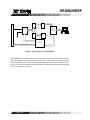
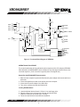
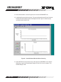
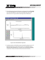
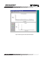
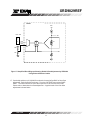
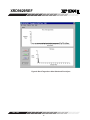
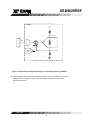
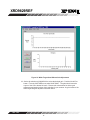
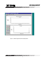
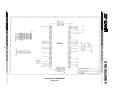
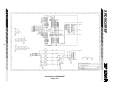
July 1998-2
XRD9829REF
USER MANUAL
CIS 30-BIT COLOR SINGLE LINE SCANNER
EXAR Corporation, 48720 Kato Road, Fremont, CA 94538 • (510) 668-7000 • FAX (510) 668-7017
XRD9829REF
EVALUATION KIT PART LIST
This kit contains the following:
•
•
•
•
•
XRD9829REF CIS 30-Bit Color Single Line Scanner
XRD9829REF User Manual
ScanIt 1.0 Software Installation Diskettes (2)
XRD9829 Data Sheet
Scan Targets (Black, White, Color)
FEATURES
•
•
•
•
•
One line scanning functionality of XRD9829 with CANON 300 DPI CIS
Easy use with most personal computers through Parallel Port Interface
Simple way of loading the Serial Port of XRD9829 to adjust gain and offset
Software ScanIt to view single line scan
Optimized Layout with Four Layers
SYSTEM REQUIREMENTS
•
•
•
•
Intel 486 compatible computer with Windows 95 operating system
8 MBytes system memory
25-pin D-shape parallel port receptacles
3 1/2” floppy disk drive
INTRODUCTION
The XRD9829REF is a demo system which includes a PCB design with a CANON CWB30216G 300 DPI Color Contact Image Sensor (CIS). It demonstrates how to interface a CIS
with EXAR’s XRD9829, a 10-bit Linear CIS/CCD Sensor Signal Processor to get a single line
scan. The XRD9829REF is designed to provide a signal path for the CIS output signals to be
processed, digitized by the XRD9829 and transmitted to a personal computer. There are no
software algorithms or hardware implementations to adjust for true color response.
The XRD9829REF board is loaded with the XRD9829, a Vantis MACH435, two FIFO SRAMs
and peripheral circuits for the CIS. The MACH435, which is a CMOS Programmable Logic
Device (CPLD) provides timing signals to the XRD9829, the SRAMs and the CIS. It also
programs the XRD9829 to operate in the correct mode and adjust for gain and offset values.
The XRD9829 processes the analog output from the CIS sensor, level-shifts and converts the
signal into digital codes. The SRAMs gate the digitized data from the XRD9829 and stores the
data temporarily. Controlled by the software, the SRAMs send the data through a parallel port
connection to the PC and histograms of raw data are displayed in the monitor using the ScanIt
software. A block diagram of the XRD9829REF is shown below in Figure 1.
Rev. 1.00
2
XRD9829REF
DATA
FLIPFLOP
DATA
FIFO
SRAM
CANON CWB-30216G 300DPI COLOR CIS
CIS OUTPUT
XRD9829
PARALLEL
PORT DB25
CONNECTOR
5-BIT BUS NIBBLE
DATA
1.25V
DC
FLIPFLOP
DATA
FIFO
SRAM
INTEL 486 Compatible
DATA
XRD9829 CONTROL SIGNALS
MACH435 CPLD
CIS CONTROL SIGNALS
PARALLEL PORT CONTROL
Figure 1. Block Diagram of XRD9829REF
The XRD9829 is a complete linear CIS or CCD sensor signal processor on a single monolithic
chip. The XRD9829 includes a high speed 10-Bit ADC, a 6-Bit Programmable Gain Amplifier
with gain adjustment of 1 to 10 and an 8-Bit programmable input referred offset calibration range
of 800 mV. See the XRD9829EVAL User Manual / PCB board for evaluating the XRD9829
CIS / CCD signal processor chip.
Rev. 1.00
3
XRD9829REF
AVDD
Power
Down
VIN0
VIN1
4-1
VIN2
DVDD
+
MUX
VREF+
VRT
BUFFER
VIN3
_
V
RL
PGA
10-BIT
10
ADC
V DCREF
DCEXT
INT/EXT_V
DATA
OUT
PORT
DB4:0 / DB9:5
VRB
DCREF
6
CLP
G<5:0>
DGND
6-BIT GAIN
REGISTER
MUX SEL
5
Power
Down
DC/AC
8-BIT DAC
AVDD
AGND
AGND
AGND
8
O<7:0>
CIS/CCD
8-BIT OFFSET
REGISTER
VRT
CCD
CIS
CONTROL LOGIC
ADCCLK
PDB
SCLK
SDATA
LD
Figure 2. Functional Block Diagram of XRD9829
OPERATIONAL PROCEDURE
The routine listed below will first calibrate the photo response of the CIS using the XRD9829.
After calibration, the XRD9829REF can be used to scan any color target to show CIS non-color
corrected response. (Color correction is typically done in the digital asic.)
How to Run the XRD9829REF Demonstration:
1. Make sure the computer is powered off and the AC power adapter is disconnected from a
wall outlet
2. Connect the parallel port cable to the printer port of the computer
3. Connect the AC power adapter into a wall outlet
4. Turn on the computer and activate Windows 95
Loading EXAR Software
5.
6.
7.
8.
Load the diskette labeled ScanIt 1.0 Disk # 1 into the floppy drive
Select the Start menu in the program manager and choose RUN
Inside the small pop-up window, type: A:\setup
Follow the instructions to finish software installation
Rev. 1.00
4
XRD9829REF
Parallel Port Configurations
9. Confirm the parallel port address as follows:
a.
b.
c.
d.
e.
f.
g.
h.
i.
j.
Select the Start Menu, choose Settings, then choose Control Panel
From the Control Panel window which pops up, double-click on System
In the System Properties window, select Device Manager
From the Device Manager window, double-click on Ports (COM & LPT)
Double-click on Printer Port (LPT1). If you can not find it, please goto Step 10
From the pop-up window, select Resources
Verify the Input/Output Range is set to 0378 - 037F
If the range is not correct, clear the Use Automatic Settings check box by
clicking it
Choose correct address which is 0378 by default and click OK
Re-start the computer as advised
10. If you do not have a Printer Port configured on your computer, please follow the steps
listed below:
a.
b.
c.
d.
e.
f.
g.
h.
From the Control Panel window which pops up, double-click on Add New Hardware
From the pop-up window, click the Next > button
Select ‘No’ when prompted for ‘Do you want Windows to search for your new
hardware?’, then click the Next > button
Choose Ports (COM & LPT), then click the Next > button
Choose Printer Port, then click the Next > button
Make a note of the Input/Output Range of Printer Port of your computer and click
OK.
You will use these values later when configure the ScanIt software
Re-start the computer as advised
Offset Adjustment With a Black Target
11. Set the dip switches located on the side panel of the scanner to 1100010000 as shown
in Figure 2 and push the Serial Port button which is located on the front panel of the
demo system. This will reset the XRD9829.
Rev. 1.00
5
XRD9829REF
S
1
S
0
D D D D D D D D
7 6 5 4 3 2 1 0
1
0
Figure 3. Dip Switches Set to Value 1100010000 to Reset the XRD9829
Rev. 1.00
6
XRD9829REF
Control Registers
Function
D7
D6
D5
D4
D3
D2
D1
D0
Power-up
(Register
State
S1/S0)
(Note 1)
Gain
(00)
G5
G4
G3
G2
G1
G0
X
(MSB)
X
000000XX
(LSB)
Offset
O7
(01)
(MSB)
Mode
X
O6
O5
O4
O3
O2
O1
O0
01000000
X
VRT
INPUT DC
DC/AC
CIS/CCD
MUX SEL
MUX SEL
XX000000
0: INTERNAL
REFERENCE
0: DC
0: CIS
1: EXTERNAL
(VDCREF)
1: AC
1: CCD
X
XXX0000X
(LSB)
(10)
0:INTERNAL
0 0: VIN0
0 0: VIN0
(VDCREF=
AGND)
0 1: VIN1
1 0: VIN2
0 1: VIN1
1 0: VIN2
1: EXTERNAL
1 1: VIN3
1 1: VIN3
TEST2
TEST1
(VDCREF=VDCEXT)
Mode
& Test
(11)
X
X
X
DIGITAL RESET
TEST3
0: NO RESET
0: TEST3
0: TEST2
0: TEST1
1: RESET
DISABLED
DISABLED
DISABLED
(REGISTERS ARE
1: OUTPUT
1: OUTPUT
1: VIN1 PIN
RESET TO
OF BUFFER
OF PGA
TIED TO
POWER-UP
TIED TO VIN3
TIED TO
INPUT OF
STATES)
PIN (VIN3 PIN
VIN2 PIN
ADC
BECOMES
(VIN2 PIN
(PGA OUTPUT
BECOMES
DISCONNECTED
AN OUTPUT)
FROM INPUT
AN OUTPUT)
OF ADC)
Table 1. Control Register Description for XRD9829
Note:
1
These are the control register settings upon initial power–up. The previous register settings are retained following a
logic power-down initiated by the PDB signal.
Rev. 1.00
7
XRD9829REF
12. Select the Start Menu, choose Programs, then choose XRD9829REF icon
13. A window will pop up as shown below. The upper window shows the Plot of Captured
Data and the lower window shows the Histogram of data. Figure 3 shows the popup window when ScanIt is first
ed
a
ts.rt
Figure 4. ScanIt Software Window Before Scanning
14. Select SETUP from the pull-down menu and choose I/O ADDRESS. In the window
that pops up, type in the Input/Output Range of Printer Port of your computer. The
default setting is 378H.
Rev. 1.00
8
XRD9829REF
15. Pick the black target out from the kit and put it on a flat area. Place the XRD9829REF
on top of the black target with the CIS sensor facing downwards. From the CAPTURE
menu select SNAP SHOT for a single line scan of the black target with the dip
switches set to zero. A typical result of a black target scan is shown below:
Figure 5. Non-calibrated Black Target Scan
16. Set the dip switches to 1000010000 to select the external DC reference for the 1.25V
global offset adjustment. Push the Serial Port button. The XRD9829 will subtract
whatever voltage appears on Pin 16, in this case, 1.25V, from the input. From the
CAPTURE menu select SNAP SHOT. A typical result of the global offset adjustment
is shown below. Please notice that the black code value has moved down.
Rev. 1.00
9
XRD9829REF
Figure 6. Black Target Scan After Global Offset Adjust
Rev. 1.00
10
XRD9829REF
XRD9829
VDD
VIN0 - VIN2
C
I
S
VRT
VIN0
RL
VIN3
5V
100K
VRB
34K
Figure 7. Simplified Block Diagram Showing Global Offset Adjustment by XRD9829
Using External Resistor Ladder
17. Set the dip switches to 0111000000 to select the internal offset DAC for fine offset
adjustment. Push the Serial Port button. From the CAPTURE menu select SNAP
SHOT. The offset should now move the output of the CIS to almost zero scale.
Please refer to data sheet for offset adjustment. A typical result of the fine offset
adjustment is shown below.
Rev. 1.00
11
XRD9829REF
Figure 8. Black Target Scan After Global and Fine Adjust
Rev. 1.00
12
XRD9829REF
XRD9829
VDD
VRT
C
I
S
VIN0
RL
8-Bit Offset
DAC
VRB
Figure 9. Simplified Block Diagram Showing Fine Offset Adjustment by XRD9829
18. Switch the black target to the enclosed white target. From the CAPTURE menu select
SNAP SHOT for a single line scan of the white target. A typical result of a white
target is shown below.
Rev. 1.00
13
XRD9829REF
Figure 10. White Target Scan Without Gain Adjustment
19. Set the dip switches to 0000000100 to select the desired gain. Push the Serial Port
button. From the CAPTURE menu select SNAP SHOT. The gain should move the
output of the CIS to almost full scale. Please refer to data sheet for further gain
adjustment and optimal values of dip switches for your scanner. A typical result of the
white target with gain adjustment is shown below.
Rev. 1.00
14
XRD9829REF
Figure 11. White Target Scan After Gain Adjustment
Rev. 1.00
15
XRD9829REF
XRD9829
VDD
VRT
C
I
S
VIN0
PGA
RL
VRB
6-Bit Gain Register
Figure 12. Simplied Block Diagram Showing Gain Adjustment by XRD9829
20. Once the XRD9829 has been fully calibrated, any target can be scanned. For
example: Scan a gray scale to demonstrate the stair step response or a color
target for color responsitivity
Rev. 1.00
16
XRD9829REF
Figure 13. Gray-scale Target Scan
Important:
1. If at any time an unexpected result is shown or the demo system seems to not
working, please pull the AC adapter out from the wall outlet to cycle power. Start the
procedures again from Step 11.
2. Keep the scanner away from other electrical equipment, power cords, light dimmers
etc. as stray electrical fields can end up in the digitized data.
Rev. 1.00
17
XRD9829REF
Rev. 1.00
18
Schematics for XRD9829REF
Page 1 of 3.
Rev. 1.00
19
XRD9829REF
Schematics for XRD9829REF
Page 2 of 3.
XRD9829REF
Rev. 1.00
20
Schematics for XRD9829REF
Page 3 of 3.
XRD9829REF
Notes
Rev. 1.00
21
XRD9829REF
Notes
Rev. 1.00
22
XRD9829REF
Notes
Rev. 1.00
23
XRD9829REF
NOTICE
EXAR Corporation reserves the right to make changes to the products contained in this publication in order to
improve design, performance or reliability. EXAR Corporation assumes no responsibility for the use of any
circuits described herein, conveys no license under any patent or other right, and makes no representation that
the circuits are free of patent infringement. Charts and schedules contained here in are only for illustration
purposes and may vary depending upon a user’s specific application. While the information in this publication
has been carefully checked; no responsibility, however, is assumed for in accuracies.
EXAR Corporation does not recommend the use of any of its products in life support applications where the
failure or malfunction of the product can reasonably be expected to cause failure of the life support system or to
significantly affect its safety or effectiveness. Products are not authorized for use in such applications unless
EXAR Corporation receives, in writing, assurances to its satisfaction that: (a) the risk of injury or damage has
been minimized; (b) the user assumes all such risks; (c) potential liability of EXAR Corporation is adequately
protected under the circumstances.
Copyright 1998 EXAR Corporation
Datasheet July 1998
Reproduction, in part or whole, without the prior written consent of EXAR Corporation is prohibited.
Rev. 1.00
24