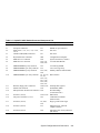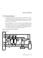
1
AlphaPC 164SX Motherboard
Technical Reference Manual
Order Number:
EC–R57EB–TE
Revision/Update Information: This is a revised document. It supersedes the
AlphaPC 164SX Motherboard Technical
Reference Manual, EC–R57EA–TE.
Compaq Computer Corporation
October 1998
The information in this publication is subject to change without notice.
COMPAQ COMPUTER CORPORATION SHALL NOT BE LIABLE FOR TECHNICAL OR EDITORIAL
ERRORS OR OMISSIONS CONTAINED HEREIN, NOR FOR INCIDENTAL OR CONSEQUENTIAL DAMAGES RESULTING FROM THE FURNISHING, PERFORMANCE, OR USE OF THIS MATERIAL. THIS
INFORMATION IS PROVIDED "AS IS" AND COMPAQ COMPUTER CORPORATION DISCLAIMS ANY
WARRANTIES, EXPRESS, IMPLIED OR STATUTORY AND EXPRESSLY DISCLAIMS THE IMPLIED WARRANTIES OF MERCHANTABILITY, FITNESS FOR PARTICULAR PURPOSE, GOOD TITLE AND AGAINST
INFRINGEMENT.
This publication contains information protected by copyright. No part of this publication may be photocopied or
reproduced in any form without prior written consent from Compaq Computer Corporation.
©1998 Compaq Computer Corporation. All rights reserved. Printed in U.S.A.
AlphaPC, COMPAQ, DECchip, DIGITAL, DIGITAL UNIX, the Compaq logo, and the DIGITAL logo registered in
United States Patent and Trademark Office.
Altera is a registered trademark of Altera Corporation.
Cypress and hyperCache are trademarks of Cypress Semiconductor Corporation.
GRAFOIL is a registered trademark of Union Carbide Corporation.
IEEE is a registered trademark of The Institute of Electrical and Electronics Engineers, Inc.
Intel is a registered trademark of Intel Corporation.
Microsoft and Visual C++ are registered trademarks and Windows NT is a trademark of Microsoft Corporation.
SMC and Standard Microsystems are registered trademarks of Standard Microsystems Corporation.
UNIX is a registered trademark in the United States and other countries, licensed exclusively through
X/Open Company Ltd.
Other product names mentioned herein may be trademarks and/or registered trademarks of their respective
companies.
Contents
Preface
1
Introduction
1.1
1.1.1
1.1.2
1.1.3
1.1.4
1.1.5
1.1.6
1.2
1.2.1
1.2.2
1.2.3
1.3
2
System Components and Features . . . . . . . . . . . . . . . . . . . . . . . . . . . . . . . . . . .
21174 Core Logic Chip . . . . . . . . . . . . . . . . . . . . . . . . . . . . . . . . . . . . . . . . .
Memory Subsystem . . . . . . . . . . . . . . . . . . . . . . . . . . . . . . . . . . . . . . . . . . . .
L2 Bcache Subsystem Overview . . . . . . . . . . . . . . . . . . . . . . . . . . . . . . . . . .
PCI Interface Overview . . . . . . . . . . . . . . . . . . . . . . . . . . . . . . . . . . . . . . . . .
ISA Interface Overview . . . . . . . . . . . . . . . . . . . . . . . . . . . . . . . . . . . . . . . . .
Miscellaneous Logic . . . . . . . . . . . . . . . . . . . . . . . . . . . . . . . . . . . . . . . . . . .
Software Support . . . . . . . . . . . . . . . . . . . . . . . . . . . . . . . . . . . . . . . . . . . . . . . . .
AlphaBIOS Windows NT Firmware . . . . . . . . . . . . . . . . . . . . . . . . . . . . . . . .
Alpha SRM Console Firmware. . . . . . . . . . . . . . . . . . . . . . . . . . . . . . . . . . . .
Motherboard Software Developer’s Kit (SDK) . . . . . . . . . . . . . . . . . . . . . . . .
Hardware Design Support. . . . . . . . . . . . . . . . . . . . . . . . . . . . . . . . . . . . . . . . . . .
1-1
1-3
1-3
1-4
1-4
1-4
1-5
1-5
1-5
1-6
1-6
1-6
System Configuration and Connectors
2.1
2.2
2.3
2.4
2.5
2.6
2.7
2.7.1
2.7.2
2.7.3
2.7.4
2.7.5
2.7.6
AlphaPC 164SX Configuration Switches . . . . . . . . . . . . . . . . . . . . . . . . . . . . . . .
CPU Speed Selection (CF[6:4]) . . . . . . . . . . . . . . . . . . . . . . . . . . . . . . . . . . . . . .
Bcache Size Switches (CF0 and CF1) . . . . . . . . . . . . . . . . . . . . . . . . . . . . . . . . .
Password Bypass (CF2) . . . . . . . . . . . . . . . . . . . . . . . . . . . . . . . . . . . . . . . . . . . .
Fail-Safe Booter (CF7) . . . . . . . . . . . . . . . . . . . . . . . . . . . . . . . . . . . . . . . . . . . . .
Mini-Debugger (CF3) . . . . . . . . . . . . . . . . . . . . . . . . . . . . . . . . . . . . . . . . . . . . . .
AlphaPC 164SX Connector Pinouts . . . . . . . . . . . . . . . . . . . . . . . . . . . . . . . . . . .
PCI Bus Connector Pinouts . . . . . . . . . . . . . . . . . . . . . . . . . . . . . . . . . . . . . .
ISA Expansion Bus Connector Pinouts . . . . . . . . . . . . . . . . . . . . . . . . . . . . .
SDRAM DIMM Connector Pinouts. . . . . . . . . . . . . . . . . . . . . . . . . . . . . . . . .
EIDE Drive Bus Connector Pinouts . . . . . . . . . . . . . . . . . . . . . . . . . . . . . . . .
Diskette (Floppy) Drive Bus Connector Pinouts. . . . . . . . . . . . . . . . . . . . . . .
Parallel Bus Connector Pinouts . . . . . . . . . . . . . . . . . . . . . . . . . . . . . . . . . . .
2-4
2-4
2-5
2-5
2-5
2-6
2-6
2-6
2-8
2-9
2-10
2-11
2-11
iii
2.7.7
2.7.8
2.7.9
2.7.10
2.7.11
2.7.12
2.7.13
2.7.14
3
3-1
3-2
3-2
3-3
3-4
AlphaPC 164SX Bcache Interface . . . . . . . . . . . . . . . . . . . . . . . . . . . . . . . . . . . .
21174 Core Logic Chip . . . . . . . . . . . . . . . . . . . . . . . . . . . . . . . . . . . . . . . . . . . . .
21174 Chip Overview . . . . . . . . . . . . . . . . . . . . . . . . . . . . . . . . . . . . . . . . . .
Main Memory Interface . . . . . . . . . . . . . . . . . . . . . . . . . . . . . . . . . . . . . . . . .
PCI Devices . . . . . . . . . . . . . . . . . . . . . . . . . . . . . . . . . . . . . . . . . . . . . . . . . .
PCI/ISA Bridge Chip . . . . . . . . . . . . . . . . . . . . . . . . . . . . . . . . . . . . . . . . . . .
PCI Expansion Slots . . . . . . . . . . . . . . . . . . . . . . . . . . . . . . . . . . . . . . . . . . .
ISA Bus Devices . . . . . . . . . . . . . . . . . . . . . . . . . . . . . . . . . . . . . . . . . . . . . . . . . .
Combination Controller Chip . . . . . . . . . . . . . . . . . . . . . . . . . . . . . . . . . . . . .
ISA Expansion Slots . . . . . . . . . . . . . . . . . . . . . . . . . . . . . . . . . . . . . . . . . . .
ISA I/O Address Map . . . . . . . . . . . . . . . . . . . . . . . . . . . . . . . . . . . . . . . . . . .
Flash ROM Address Map . . . . . . . . . . . . . . . . . . . . . . . . . . . . . . . . . . . . . . .
Interrupts . . . . . . . . . . . . . . . . . . . . . . . . . . . . . . . . . . . . . . . . . . . . . . . . . . . . . . . .
System Clocks . . . . . . . . . . . . . . . . . . . . . . . . . . . . . . . . . . . . . . . . . . . . . . . . . . .
Reset and Initialization . . . . . . . . . . . . . . . . . . . . . . . . . . . . . . . . . . . . . . . . . . . . .
DC Power Distribution. . . . . . . . . . . . . . . . . . . . . . . . . . . . . . . . . . . . . . . . . . . . . .
Serial ROM and Debug Port Support . . . . . . . . . . . . . . . . . . . . . . . . . . . . . . . . . .
4-2
4-3
4-3
4-4
4-5
4-6
4-6
4-6
4-7
4-8
4-8
4-9
4-9
4-12
4-14
4-15
4-16
Upgrading the AlphaPC 164SX
5.1
5.2
5.3
5.3.1
iv
Power Requirements . . . . . . . . . . . . . . . . . . . . . . . . . . . . . . . . . . . . . . . . . . . . . .
Environmental Requirements . . . . . . . . . . . . . . . . . . . . . . . . . . . . . . . . . . . . . . . .
Board Dimensions. . . . . . . . . . . . . . . . . . . . . . . . . . . . . . . . . . . . . . . . . . . . . . . . .
ATX Hole Specification . . . . . . . . . . . . . . . . . . . . . . . . . . . . . . . . . . . . . . . . .
ATX I/O Shield Requirements . . . . . . . . . . . . . . . . . . . . . . . . . . . . . . . . . . . .
Functional Description
4.1
4.2
4.2.1
4.2.2
4.2.3
4.2.4
4.2.5
4.3
4.3.1
4.3.2
4.3.3
4.3.4
4.4
4.5
4.6
4.7
4.8
5
2-12
2-12
2-13
2-13
2-13
2-14
2-14
2-14
Power and Environmental Requirements
3.1
3.2
3.3
3.3.1
3.3.2
4
COM1/COM2 Serial Line Connector Pinouts. . . . . . . . . . . . . . . . . . . . . . . . .
Keyboard/Mouse Connector Pinouts . . . . . . . . . . . . . . . . . . . . . . . . . . . . . . .
SROM Test Data Input Connector Pinouts . . . . . . . . . . . . . . . . . . . . . . . . . .
Input Power Connector Pinouts . . . . . . . . . . . . . . . . . . . . . . . . . . . . . . . . . . .
Enclosure Fan Power Connector Pinouts . . . . . . . . . . . . . . . . . . . . . . . . . . .
Microprocessor Fan Power Connector Pinouts . . . . . . . . . . . . . . . . . . . . . . .
Soft Power Connector Pinouts. . . . . . . . . . . . . . . . . . . . . . . . . . . . . . . . . . . .
Multipurpose Connector Pinouts . . . . . . . . . . . . . . . . . . . . . . . . . . . . . . . . . .
Configuring SDRAM Memory . . . . . . . . . . . . . . . . . . . . . . . . . . . . . . . . . . . . . . . .
Upgrading SDRAM Memory . . . . . . . . . . . . . . . . . . . . . . . . . . . . . . . . . . . . . . . . .
Increasing Microprocessor Speed. . . . . . . . . . . . . . . . . . . . . . . . . . . . . . . . . . . . .
Preparatory Information . . . . . . . . . . . . . . . . . . . . . . . . . . . . . . . . . . . . . . . . .
5-1
5-2
5-3
5-3
5.3.2
5.3.3
5.3.4
A
Required Tools . . . . . . . . . . . . . . . . . . . . . . . . . . . . . . . . . . . . . . . . . . . . . . .
Removing the 21164PC Microprocessor . . . . . . . . . . . . . . . . . . . . . . . . . . . .
Installing the 21164PC Microprocessor . . . . . . . . . . . . . . . . . . . . . . . . . . . . .
5-3
5-4
5-4
Support, Products, and Documentation
A.1
A.2
A.2.1
A.2.2
A.2.3
A.2.4
A.3
A.4
A.5
Customer Support . . . . . . . . . . . . . . . . . . . . . . . . . . . . . . . . . . . . . . . . . . . . . . . . .
Supporting Products . . . . . . . . . . . . . . . . . . . . . . . . . . . . . . . . . . . . . . . . . . . . . . .
Memory . . . . . . . . . . . . . . . . . . . . . . . . . . . . . . . . . . . . . . . . . . . . . . . . . . . . .
Thermal Products . . . . . . . . . . . . . . . . . . . . . . . . . . . . . . . . . . . . . . . . . . . . .
Power Supply. . . . . . . . . . . . . . . . . . . . . . . . . . . . . . . . . . . . . . . . . . . . . . . . .
Enclosure . . . . . . . . . . . . . . . . . . . . . . . . . . . . . . . . . . . . . . . . . . . . . . . . . . . .
Alpha Products . . . . . . . . . . . . . . . . . . . . . . . . . . . . . . . . . . . . . . . . . . . . . . . . . . .
Alpha Documentation . . . . . . . . . . . . . . . . . . . . . . . . . . . . . . . . . . . . . . . . . . . . . .
Third–Party Documentation . . . . . . . . . . . . . . . . . . . . . . . . . . . . . . . . . . . . . . . . .
A-1
A-2
A-2
A-2
A-2
A-3
A-3
A-4
A-5
Index
v
Figures
1–1
2–1
2–2
2–3
3–1
3–2
4–1
4–2
4–3
4–4
4–5
4–6
4–7
4–8
5–1
vi
AlphaPC 164SX Functional Block Diagram . . . . . . . . . . . . . . . . . . . . . . . . . . . . .
AlphaPC 164SX Switch/Connector/Component Location. . . . . . . . . . . . . . . . . . .
AlphaPC 164SX Configuration Switches . . . . . . . . . . . . . . . . . . . . . . . . . . . . . . .
Multipurpose Connector Pinouts . . . . . . . . . . . . . . . . . . . . . . . . . . . . . . . . . . . . . .
ATX Hole Specification . . . . . . . . . . . . . . . . . . . . . . . . . . . . . . . . . . . . . . . . . . . . .
ATX I/O Shield Dimensions . . . . . . . . . . . . . . . . . . . . . . . . . . . . . . . . . . . . . . . . .
AlphaPC 164SX L2 Bcache Array . . . . . . . . . . . . . . . . . . . . . . . . . . . . . . . . . . . .
Main Memory Interface . . . . . . . . . . . . . . . . . . . . . . . . . . . . . . . . . . . . . . . . . . . . .
AlphaPC 164SX PCI Bus Devices . . . . . . . . . . . . . . . . . . . . . . . . . . . . . . . . . . . .
AlphaPC 164SX ISA Bus Devices . . . . . . . . . . . . . . . . . . . . . . . . . . . . . . . . . . . .
Interrupt Request Register . . . . . . . . . . . . . . . . . . . . . . . . . . . . . . . . . . . . . . . . . .
AlphaPC 164SX System Clocks . . . . . . . . . . . . . . . . . . . . . . . . . . . . . . . . . . . . . .
System Reset and Initialization . . . . . . . . . . . . . . . . . . . . . . . . . . . . . . . . . . . . . . .
AlphaPC 164SX Power Distribution . . . . . . . . . . . . . . . . . . . . . . . . . . . . . . . . . . .
Fan/Heat-Sink Assembly . . . . . . . . . . . . . . . . . . . . . . . . . . . . . . . . . . . . . . . . . . .
1-2
2-2
2-4
2-15
3-3
3-4
4-2
4-3
4-5
4-8
4-10
4-13
4-14
4-15
5-5
Tables
1–1
2–1
2–2
2–3
2–4
2–5
2–6
2–7
2–8
2–9
2–10
2–11
2–12
2–13
2–14
2–15
3–1
3–2
4–1
4–2
4–3
5–1
AlphaPC 164SX SDRAM Memory Configurations . . . . . . . . . . . . . . . . . . . . . . . .
AlphaPC 164SX Switch/Connector/Component List. . . . . . . . . . . . . . . . . . . . . . .
PCI Bus Connector Pinouts . . . . . . . . . . . . . . . . . . . . . . . . . . . . . . . . . . . . . . . . .
ISA Expansion Bus Connector Pinouts (J22, J23) . . . . . . . . . . . . . . . . . . . . . . . .
SDRAM DIMM Connector Pinouts (J7 through J10). . . . . . . . . . . . . . . . . . . . . . .
EIDE Drive Bus Connector Pinouts (J5, J6) . . . . . . . . . . . . . . . . . . . . . . . . . . . . .
Diskette (Floppy) Drive Bus Connector Pinouts (J11). . . . . . . . . . . . . . . . . . . . . .
Parallel Bus Connector Pinouts (J13) . . . . . . . . . . . . . . . . . . . . . . . . . . . . . . . . . .
COM1/COM2 Serial Line Connector Pinouts (J3). . . . . . . . . . . . . . . . . . . . . . . . .
Keyboard/Mouse Connector Pinouts (J4) . . . . . . . . . . . . . . . . . . . . . . . . . . . . . . .
SROM Test Data Input Connector Pinouts (J21) . . . . . . . . . . . . . . . . . . . . . . . . .
Input Power Connector Pinouts (J2) . . . . . . . . . . . . . . . . . . . . . . . . . . . . . . . . . . .
Enclosure Fan (+12 V dc) Power Connector Pinouts (J16) . . . . . . . . . . . . . . . . .
Microprocessor Fan Power Connector Pinouts (J14) . . . . . . . . . . . . . . . . . . . . . .
Soft Power Connector Pinouts (J1). . . . . . . . . . . . . . . . . . . . . . . . . . . . . . . . . . . .
Multipurpose Connector Pinouts (J20) . . . . . . . . . . . . . . . . . . . . . . . . . . . . . . . . .
Power Supply DC Current Requirements . . . . . . . . . . . . . . . . . . . . . . . . . . . . . . .
AlphaPC 164SX Motherboard Environmental Requirements . . . . . . . . . . . . . . . .
ISA I/O Address Map . . . . . . . . . . . . . . . . . . . . . . . . . . . . . . . . . . . . . . . . . . . . . .
AlphaPC 164SX System Interrupts . . . . . . . . . . . . . . . . . . . . . . . . . . . . . . . . . . . .
ISA Interrupts . . . . . . . . . . . . . . . . . . . . . . . . . . . . . . . . . . . . . . . . . . . . . . . . . . . .
AlphaPC 164SX SDRAM Memory Configurations . . . . . . . . . . . . . . . . . . . . . . . .
1-3
2-3
2-6
2-8
2-9
2-10
2-11
2-11
2-12
2-12
2-13
2-13
2-13
2-14
2-14
2-14
3-1
3-2
4-8
4-10
4-11
5-2
vii
Preface
Overview
This manual describes the AlphaPC 164SX motherboard, a board for computing systems based on the Alpha 21164PC microprocessor and the 21174 core logic chip.
Audience
This manual is intended for system designers and others who use the AlphaPC
164SX motherboard to design or evaluate computer systems based on the Alpha
21164PC microprocessor and the 21174 core logic chip.
Scope
This manual describes the features, configuration, functional operation, and interfaces of the AlphaPC 164SX motherboard. This manual does not include specific
bus specifications (for example, PCI or ISA buses). Additional information is available in the AlphaPC 164SX schematics, program source files, and the appropriate
vendor and IEEE specifications. See Appendix A for information on how to order
related documentation and obtain additional technical support.
Manual Organization
As outlined on the next page, this manual includes the following chapters, appendixes, and an index.
ix
•
Chapter 1, Introduction, is an overview of the AlphaPC 164SX motherboard,
including its components, features, and uses.
•
Chapter 2, System Configuration and Connectors, describes the user-environment configuration, board connectors and functions, and switch functions. It also
identifies switch settings and connector locations.
•
Chapter 3, Power and Environmental Requirements, describes the AlphaPC
164SX power and environmental requirements and provides board dimensions.
•
Chapter 4, Functional Description, provides a functional description of the
AlphaPC 164SX motherboard, including the 21174 core logic chip, L2 backup
cache (Bcache) and memory subsystems, system interrupts, clock and power
subsystems, and peripheral component interconnect (PCI) and Industry Standard
Architecture (ISA) devices.
•
Chapter 5, Upgrading the AlphaPC 164SX, describes how to upgrade the
AlphaPC 164SX motherboard’s SDRAM memory and microprocessor speed.
•
Appendix A, Support, Products, and Documentation, lists sources for components and accessories not included with the AlphaPC 164SX motherboard and
describes how to obtain information and technical support, and how to order
products and associated literature.
Conventions
This section defines product-specific terminology, abbreviations, and other conventions used throughout this manual.
Abbreviations
•
Register Access
The following list describes the register bit and field abbreviations:
Bit/Field Abbreviation Description
RO (read only)
RW (read/write)
WO (write only)
x
Bits and fields specified as RO can be read but not written.
Bits and fields specified as RW can be read and written.
Bits and fields specified as WO can be written but not read.
•
Binary Multiples
The abbreviations K, M, and G (kilo, mega, and giga) represent binary multiples
and have the following values.
K
M
G
=
=
=
210 (1024)
220 (1,048,576)
230 (1,073,741,824)
For example:
2KB
4MB
8GB
=
=
=
2 kilobytes
=
4 megabytes =
8 gigabytes =
2 × 210 bytes
4 × 220 bytes
8 × 230 bytes
Addresses
Unless otherwise noted, all addresses and offsets are hexadecimal.
Bit Notation
Multiple-bit fields can include contiguous and noncontiguous bits contained in
brackets ([]). Multiple contiguous bits are indicated by a pair of numbers separated
by a colon (:). For example, [9:7,5,2:0] specifies bits 9,8,7,5,2,1, and 0. Similarly,
single bits are frequently indicated with brackets. For example, [27] specifies bit 27.
Caution
Cautions indicate potential damage to equipment, software, or data.
Data Field Size
The term INTnn, where nn is one of 2, 4, 8, 16, 32, or 64, refers to a data field of
nn contiguous NATURALLY ALIGNED bytes. For example, INT4 refers to a
NATURALLY ALIGNED longword.
Data Units
The following data-unit terminology is used throughout this manual.
Term
Byte
Word
Longword/Dword
Words
½
1
2
Bytes
1
2
4
Bits
8
16
32
Other
—
—
Longword
xi
Term
Words
Bytes
Bits
Other
Quadword
Octaword
Hexword
4
8
16
8
16
32
64
128
256
2 Longwords
2 Quadwords
2 Octawords
Note
Notes emphasize particularly important information.
Numbering
All numbers are decimal or hexadecimal unless otherwise indicated. The prefix 0x
indicates a hexadecimal number. For example, 19 is decimal, but 0x19 and 0x19A
are hexadecimal (also see Addresses). Otherwise, the base is indicated by a subscript; for example, 1002 is a binary number.
Ranges and Extents
Ranges are specified by a pair of numbers separated by two periods (..) and are inclusive. For example, a range of integers 0..4 includes the integers 0, 1, 2, 3, and 4.
Extents are specified by a pair of numbers in brackets ([]) separated by a colon (:)
and are inclusive. Bit fields are often specified as extents. For example, bits [7:3]
specifies bits 7, 6, 5, 4, and 3.
Register and Memory Figures
Register figures have bit and field position numbering starting at the right (low
order) and increasing to the left (high order).
Memory figures have addresses starting at the top and increasing toward the bottom.
xii
Signal Names
All signal names are printed in boldface type. Signal names that originate in an
industry-standard specification, such as PCI or IDE, are printed in the case as found
in the specification (usually uppercase). Active-high signals are indicated by the _h
suffix. Active-low signals have the _l suffix, a pound sign “#” appended, or a “not”
overscore bar. Signals with no suffix are considered high-asserted signals. For example, signals data_h[127:0] and cia_int are active-high signals. Signals mem_ack_l,
FRAME#, and RESET are active-low signals.
UNPREDICTABLE and UNDEFINED
Throughout this manual the terms UNPREDICTABLE and UNDEFINED are used.
Their meanings are quite different and must be carefully distinguished.
In particular, only privileged software (that is, software running in kernel mode)
can trigger UNDEFINED operations. Unprivileged software cannot trigger
UNDEFINED operations. However, either privileged or unprivileged software can
trigger UNPREDICTABLE results or occurrences.
UNPREDICTABLE results or occurrences do not disrupt the basic operation of the
processor. The processor continues to execute instructions in its normal manner. In
contrast, UNDEFINED operations can halt the processor or cause it to lose information.
The terms UNPREDICTABLE and UNDEFINED can be further described as follows:
•
UNPREDICTABLE
–
Results or occurrences specified as UNPREDICTABLE might vary
from moment to moment, implementation to implementation, and
instruction to instruction within implementations. Software can never
depend on results specified as UNPREDICTABLE.
–
An UNPREDICTABLE result might acquire an arbitrary value that is
subject to a few constraints. Such a result might be an arbitrary function of the input operands or of any state information that is accessible to the process in its current access mode. UNPREDICTABLE
results may be unchanged from their previous values.
Operations that produce UNPREDICTABLE results might also produce exceptions.
xiii
–
An occurrence specified as UNPREDICTABLE may or may not happen based on an arbitrary choice function. The choice function is
subject to the same constraints as are UNPREDICTABLE results and
must not constitute a security hole.
Specifically, UNPREDICTABLE results must not depend upon, or be
a function of, the contents of memory locations or registers that are
inaccessible to the current process in the current access mode.
Also, operations that might produce UNPREDICTABLE results must
not write or modify the contents of memory locations or registers to
which the current process in the current access mode does not have
access. They must also not halt or hang the system or any of its components.
For example, a security hole would exist if some UNPREDICTABLE
result depended on the value of a register in another process, on the
contents of processor temporary registers left behind by some previously running process, or on a sequence of actions of different processes.
•
xiv
UNDEFINED
–
Operations specified as UNDEFINED can vary from moment to
moment, implementation to implementation, and instruction to
instruction within implementations. The operation can vary in effect
from nothing, to stopping system operation.
–
UNDEFINED operations can halt the processor or cause it to lose
information. However, UNDEFINED operations must not cause the
processor to hang, that is, reach an unhalted state from which there is
no transition to a normal state in which the machine executes instructions. Only privileged software (that is, software running in kernel
mode) can trigger UNDEFINED operations.
1
Introduction
This chapter provides an overview of the AlphaPC 164SX motherboard, including
its components, features, and uses. The motherboard is a module for computing systems based on the 21174 core logic chip.
The AlphaPC 164SX provides a single-board hardware and software development
platform for the design, integration, and analysis of supporting logic and subsystems.
The board also provides a platform for PCI I/O device hardware and software development.
1.1 System Components and Features
The AlphaPC 164SX is implemented in industry-standard parts and uses an Alpha
21164PC microprocessor running at 400 or 533 MHz. Figure 1–1 shows the board’s
functional components.
Introduction
1–1
System Components and Features
Figure 1–1 AlphaPC 164SX Functional Block Diagram
18
Index
Alpha 21164PC
Microprocessor
Control
1MB, L2
Bcache
Bcache Tag
10
Data
128
128-Bit Data
Quick Switches
Flash ROM
Address
Commands
168-Pin
Unbuffered
SDRAM DIMM
Sockets (× 4)
Control
16
DECchip 21174-CA
Control, I/O Interface,
and Address
Address/Control
PCI
Support
– Synthesizer
EIDE
Controller
PCI-to-ISA
Bridge
2 Dedicated 32-Bit PCI Slots
2 Dedicated 64-Bit PCI Slots
2 Dedicated ISA Slots
4 Devices
Combination
Controller
1–2
Introduction
Diskette
Parallel Port
2 Serial Ports
System Components and Features
1.1.1 21174 Core Logic Chip
The Alpha 21164PC microprocessor is supported by the 21174 core logic chip,
which provides an interface between three units—memory, the PCI bus, and the
21164PC (along with flash ROM). This core logic chip is the interface between the
21164PC microprocessor, main memory (addressing and control), and the PCI bus.
Quick switches provide the memory interface data path isolation.
The 21174 includes the majority of functions necessary to develop a high-performance PC or workstation, requiring minimum discrete logic on the module. It provides flexible and generic functions to allow its use in a wide range of systems.
1.1.2 Memory Subsystem
The synchronous dynamic random-access memory (SDRAM) is contained in two
banks of dual inline memory modules (DIMMs). Single- or double-sided DIMMs
may be used. Two DIMMs provide 32Mb to 256MB of memory, while four DIMMs
provide up to 512MB. Table 1–1 lists the DIMM sizes tested and the corresponding
main memory size for 128-bit arrays.
Note:
Each DIMM can be 72 bits or 64 bits wide, with 100 MHz or faster
speed.
Table 1–1 AlphaPC 164SX SDRAM Memory Configurations
(Sheet 1 of 2)
Bank 11
Bank 01
Total Memory
J7
J8
J9
J10
32MB
2Mb × 72
2Mb × 72
—
—
64MB
2Mb × 72
2Mb × 72
2Mb × 72
2Mb × 72
4Mb × 72
4Mb × 72
—
—
96MB
4Mb × 72
4Mb × 72
2Mb × 72
2Mb × 72
128MB
4Mb × 72
4Mb × 72
4Mb × 72
4Mb × 72
8Mb × 72
8Mb × 72
—
—
8Mb × 72
8Mb × 72
2Mb × 72
2Mb × 72
160MB
Introduction
1–3
System Components and Features
Table 1–1 AlphaPC 164SX SDRAM Memory Configurations
Bank 0
Total Memory
(Sheet 2 of 2)
1
Bank 11
J7
J8
J9
J10
192MB
8Mb × 72
8Mb × 72
4Mb × 72
4Mb × 72
256MB
8Mb × 72
8Mb × 72
8Mb × 72
8Mb × 72
16Mb × 72
16Mb × 72
—
—
16Mb × 72
16Mb × 72
16Mb × 72
16Mb × 72
512MB
1
64-bit-wide DIMMs can also be used.
1.1.3 L2 Bcache Subsystem Overview
The AlphaPC 164SX board-level L2 backup cache (Bcache) is a 1MB, directmapped, synchronous, pipelined burst SROM with a 128-bit data path. The board is
capable of handling an L2 cache size of 2MB. See Section 2.3 for more information
about the Bcache.
1.1.4 PCI Interface Overview
The AlphaPC 164SX PCI interface, with a 33-MHz data transfer rate, is the main
I/O bus for the majority of functions (SCSI interface, graphics accelerator, and so
on). PCI-EIDE support is provided by an onboard controller chip (Cypress
CY82C693U-NC), which also provides a PCI-to-ISA bridge, a mouse and keyboard
controller, and a time-of-year (TOY) clock.
The PCI bus has four dedicated PCI expansion slots (two 64-bit and two 32-bit).
1.1.5 ISA Interface Overview
The ISA bus provides the following system support functions:
1–4
•
Two expansion slots.
•
An SMC FDC37C669 combination controller chip that provides:
–
A diskette controller
–
Two universal asynchronous receiver-transmitters (UARTs) with full
modem control
–
A bidirectional parallel port
Introduction
Software Support
1.1.6 Miscellaneous Logic
The AlphaPC 164SX contains the following miscellaneous components:
•
Operating system support — through a 1MB flash ROM that contains supporting
firmware.
•
Synthesizer for clocks:
•
•
–
A clock synthesizer (MC12439) provides a programmable 400- and
533-MHz clock source to the 21164PC microprocessor. The microprocessor supplies a clock to the system PLL/clock buffer for the 21174.
–
The 21174 core logic chip provides the SDRAM and PCI clocks.
–
A 14.318-MHz crystal and frequency generator provide a clock source for
the combination controller (FDC37C669) and the PCI-to-ISA bridge
(CY82C693U-NC). The controller’s onchip generator then provides other
clocks as needed.
–
A 32-kHz crystal provides the TOY clock source.
Flash ROM:
–
Fail-safe booter
–
Boot code
–
BIOS: Windows NT or Alpha SRM console
Altera EPM7064LC44-7 for DMA boundary issue.
1.2 Software Support
The support elements described in this section are either included with the
AlphaPC 164SX or are available separately.
1.2.1 AlphaBIOS Windows NT Firmware
The AlphaPC 164SX motherboard ships with AlphaBIOS firmware and online documentation that describes how to configure the firmware for Windows NT. This firmware
initializes the system and enables you to install and boot the Windows NT operating
system. The AlphaBIOS firmware resides in the flash ROM on the 21A05-A0 variation
of the AlphaPC 164SX motherboard. Binary images of the AlphaBIOS firmware are
included in the motherboard Software Developer’s Kit (SDK), along with a license
describing the terms for use and distribution.
Introduction
1–5
Hardware Design Support
1.2.2 Alpha SRM Console Firmware
The Alpha SRM Console firmware is required to install and boot DIGITAL UNIX
on the AlphaPC 164SX. This Alpha firmware comes factory installed in the 21A05A1 variation of the AlphaPC 164SX. When installed, this firmware occupies the
flash blocks reserved for the primary firmware. Binary images of the Alpha SRM
Console firmware are included in the SDK and Firmware Update compact disk,
along with a license describing the terms for use and distribution.
1.2.3 Motherboard Software Developer’s Kit (SDK)
The SDK and Firmware Update is designed to provide an environment for developing software for Alpha motherboard products. It is also specially suited for low-level
software development and hardware debug for other Alpha microprocessor-based
designs.
The following list includes some of the components of the SDK:
•
The Alpha Motherboard Debug Monitor firmware with source code
•
Power-up initialization SROM and SROM Mini-Debugger with source code
•
Sample PALcode sources modeled after DIGITAL UNIX with source code
•
Fail-safe booter with source code
•
Various additional tools with source code
The following development platforms are supported by the SDK:
•
DIGITAL UNIX with the C Developer’s Extensions
•
Windows NT (Alpha) with the Microsoft Visual C++ Development System for
Alpha
•
Windows NT (Intel) with the Microsoft Visual C++ Development System and
Tools provide limited support. This environment is currently useful for SROM
and PALcode development only.
1.3 Hardware Design Support
The full design database, including schematics and source files, is supplied. User
documentation is also included. The database allows designers with no previous
Alpha architecture experience to successfully develop a working Alpha system with
minimal assistance.
1–6
Introduction
2
System Configuration and Connectors
This chapter describes the AlphaPC 164SX configuration, board connectors and
functions, and switch functions. It also identifies switch and connector locations.
The AlphaPC 164SX uses switches to implement configuration parameters such as
system speed and boot parameters. These switches must be configured for the user’s
environment. Onboard connectors are provided for the I/O interfaces, DIMMs, and
serial and parallel peripheral ports.
Figure 2–1 shows the board outlines and identifies the location of switches, connectors, and major components. Table 2–1 lists and defines these items.
System Configuration and Connectors
2–1
Figure 2–1 AlphaPC 164SX Switch/Connector/Component Location
U56
J23
XU59
U55
Q7
SW1
J22
Q8
J20
Q5
Q4
U53
U51
U54
J21
U52
U50
J19
U49
XB1
J18
X3
U48
J17
X2
U46
X1
U47
J16
J15
U45
U44
U40 U41 U42 U43
U39
U36 U37 U38
U35
J14
U34
J11
U32
21164PC
U31
J5
J6
21174
U33
J13
U28
U27
U29
U25
U20
U21
U22
U23
J7 J8 J9 J10
U24
U17
U30
U26
U19
U18
U10
U11
J4
U12
U15
U14
U13
U7
U16
U8
U9
U5
U6
U3
U2
U4
U1
J2
J1
2–2
System Configuration and Connectors
J3
Table 2–1 AlphaPC 164SX Switch/Connector/Component List
Item No. Description
Item No.
Description
XB1
J1
J2
J20
J21
J22
LEDs/speaker/buttons connectors
SROM test port connector
ISA slot 1
J3
J4
J5
J6
RTC battery (CR2032)
Soft power connector
Input power (+3 V, +5 V, -5 V, +12 V,
-12 V)
COM1/COM2 (DB9) connectors
Keyboard/mouse connectors
EIDE drive 2/3 connector
EIDE drive 0/1 connector
J11
J13
J14
J23
SW1
U48
U10, U11,
U20, U22
SDRAM DIMM 0 [0:63] connector
U21
SDRAM DIMM 1 [64:128] connector U33
SDRAM DIMM 2 [0:63] connector
U19, U26,
U29
SDRAM DIMM 3 [64:128] connector U1, U3, U4,
U5, U7,
U12, U13,
U17, U18,
U23, U24,
U25, U27
Diskette (floppy) drive connector
U40 to U43
Parallel I/O connector
U30
Microprocessor fan/fan sense connector U46
J15
J16
PCI slot 3 (32-bit)
Fan power, enclosure (+12 V)
U36 to U38
U47
J17
PCI slot 2 (32-bit)
J18
PCI slot 1 (64-bit)
U2, U28,
U32
U31
J19
PCI slot 0 (64-bit)
U45
J7
J8
J9
J10
ISA slot 0
Configuration switchpack
System clock PLL (CY2081)
L2 cache data SRAMs
L2 cache tag SRAM
21174 core logic chip
Memory address/control buffers
Data switches
Interrupt shift registers
Flash ROM (1MB)
PCI-ISA Bridge
(CY82C693U-NC)
IDE buffers
Combination controller
(FDC37C669)
Reg-reg cache isolate logic
Microprocessor, socketed
(Alpha 21164PC)
Microprocessor clock synthesizer
(MC12439)
System Configuration and Connectors
2–3
AlphaPC 164SX Configuration Switches
2.1 AlphaPC 164SX Configuration Switches
The AlphaPC 164SX motherboard has a switchpack located at SW1, as shown previously in Figure 2–1. The switches set the hardware configuration and boot options.
Figure 2–2 shows the switch functions.
Figure 2–2 AlphaPC 164SX Configuration Switches
Note: Switch defaults are in bold.
0
CF0
CF1
1
CF Bit:
0
1
.5MB
0
0
2MB
0
1
Reserved
1
1
Password Bypass:
0 bypasses password protection
1 requires AlphaBIOS password
Mini-Debugger:
0 enables Mini-Debugger
1 disables Mini-Debugger
CF2
CF3
1MB
1
0
CF4
CF5
CF6
CF Bit: 400 MHz 533 MHz
4
1
1
5
1
0
6
1
1
Note:
All other combinations
are reserved.
CF7
Fail-Safe Booter:
0: Fail Safe
1: AlphaBIOS or SRM console
2.2 CPU Speed Selection (CF[6:4])
The clock synthesizer at U45 makes it possible to change the frequency of the
microprocessor’s clock output. The switch configuration is set in SW1, CF[6:4].
These three switches set the speed at power-up as listed in Figure 2–2. The
microprocessor frequency divided by the ratio determines the system clock
frequency.
2–4
System Configuration and Connectors
Bcache Size Switches (CF0 and CF1)
2.3 Bcache Size Switches (CF0 and CF1)
The Bcache size switches are located at SW1 (CF0 and CF1), as shown in
Figure 2–2. The AlphaPC 164SX is configured with 1MB of Bcache during
production; the other combinations shown in Figure 2–2 (.5MB and 2MB) are for
other implementations.
Note:
The standard motherboard (21A05-A0 for Windows NT and 21A05-A1
for DIGITAL UNIX) is manufactured with 64K × 32 data SSRAMs. An
OEM, however, can create an L2 cache in either a 2MB variation, using
128K × 32 data SSRAMs, or a .5MB variation, using 32K × 32 data
SSRAMs.
2.4 Password Bypass (CF2)
AlphaBIOS provides password protection. However, password bypass is provided
for system setup or startup when the AlphaBIOS password is unavailable.
Password bypass is disabled by default, with switch CF2 of SW1 in the on position
(see Figure 2–2). When this function is enabled, it disables the AlphaBIOS password
verification and enables the user to set up or start up their system without the
AlphaBIOS password. Password bypass also clears the password.
To disable this function and require a password, slide CF2 to the on position.
2.5 Fail-Safe Booter (CF7)
The fail-safe booter provides an emergency recovery mechanism when the primary
firmware image contained in flash memory has been corrupted. When flash memory
has been corrupted, and no image can be loaded safely from the flash, you can run
the fail-safe booter and boot another image from a diskette that is capable of reprogramming the flash.
For more information about the fail-safe booter, refer to the AlphaPC 164SX
Motherboard Windows NT User’s Manual.
System Configuration and Connectors
2–5
Mini-Debugger (CF3)
2.6 Mini-Debugger (CF3)
The Alpha SROM Mini-Debugger is stored in the flash ROM and is enabled/
disabled by switch CF3. The default position for this switch is on (see Figure 2–2).
When this switch is off, it causes the SROM initialization to trap to the MiniDebugger after all initialization is complete, but before starting the execution of the
system flash ROM code.
2.7 AlphaPC 164SX Connector Pinouts
This section lists the pinouts of all AlphaPC 164SX connectors. See Figure 2–1 for
connector locations.
2.7.1 PCI Bus Connector Pinouts
Table 2–2 shows the PCI bus connector pinouts.
Table 2–2 PCI Bus Connector Pinouts
Pin
Signal
Pin
Signal
(Sheet 1 of 2)
Pin
Signal
Pin
Signal
TMS
INTC
—
RST#
—
AD[26]
+3V
AD[18]
Gnd
+3V
PAR
AD[11]
Not used
AD[04]
Vdd
-12V
Vdd
PRSNT1#
Gnd
A4
A8
A12
A16
A20
A24
A28
A32
A36
A40
A44
A48
A52
A56
A60
B2
B6
B10
B14
TDI
Vdd
Gnd
Vdd
AD[30]
Gnd
AD[22]
AD[16]
TRDY#
SDONE
AD[15]
Gnd
C/BE#[0]
Gnd
REQ64#
TCK
Vdd
—
—
32-Bit and 64-Bit PCI Connectors (J15, J17, J18, J19)
A1
A5
A9
A13
A17
A21
A25
A29
A33
A37
A41
A45
A49
A53
A57
A61
B3
B7
B11
2–6
TRST#
Vdd
—
Gnd
GNT#
+3V
AD[24]
AD[20]
+3V
STOP#
SBO#
+3V
AD[09]
+3V
AD[02]
Vdd
Gnd
INTB
PRSNT2#
A2
A6
A10
A14
A18
A22
A26
A30
A34
A38
A42
A46
A50
A54
A58
A62
B4
B8
B12
+12V
INTA
Vdd
—
Gnd
AD[28]
IDSEL
Gnd
FRAME#
STOP#
Gnd
AD[13]
Not used
AD[06]
AD[00]
Vdd
TDO
INTD
Gnd
System Configuration and Connectors
A3
A7
A11
A15
A19
A23
A27
A31
A35
A39
A43
A47
A51
A55
A59
B1
B5
B9
B13
AlphaPC 164SX Connector Pinouts
Table 2–2 PCI Bus Connector Pinouts
(Sheet 2 of 2)
Pin
Signal
Pin
Signal
Pin
Signal
Pin
Signal
B15
B19
B23
B27
B31
B35
B39
B43
B47
B51
B55
B59
Gnd
Vdd
AD[27]
AD[23]
+3V
IRDY#
LOCK#
+3V
AD[12]
Not used
AD[05]
Vdd
B16
B20
B24
B28
B32
B36
B40
B44
B48
B52
B56
B60
CLK
AD[31]
AD[25]
Gnd
AD[17]
+3V
PERR#
C/BE#[1]
AD[10]
AD[08]
AD[03]
ACK64#
B17
B21
B25
B29
B33
B37
B41
B45
B49
B53
B57
B61
Gnd
AD[29]
+3V
AD[21]
C/BE#[2]
DEVSEL#
+3V
AD[14]
Gnd
AD[07]
Gnd
Vdd
B18
B22
B26
B30
B34
B38
B42
B46
B50
B54
B58
B62
REQ#
Gnd
C/BE#[3]
AD[19]
Gnd
Gnd
SERR#
Gnd
Not used
+3V
AD[01]
Vdd
A65
A69
A73
A77
A81
A85
A89
A93
B65
B69
B73
B77
B81
B85
B89
B93
C/BE#[5]
Gnd
D[56]
D[50]
Gnd
D[40]
D[34]
Gnd
C/BE#[6]
D[61]
Gnd
D[51]
D[45]
Gnd
D[35]
—
A66
A70
A74
A78
A82
A86
A90
A94
B66
B70
B74
B78
B82
B86
B90
B94
Vdd
D[60]
D[54]
Gnd
D[44]
D[38]
Gnd
—
C/BE#[4]
Vdd
D[55]
D[49]
Gnd
D[39]
D[33]
Gnd
64-Bit PCI Connectors Only (J18, J19)
A63
A67
A71
A75
A79
A83
A87
A91
B63
B67
B71
B75
B79
B83
B87
B91
Gnd
PAR64
D[58]
Vdd
D[48]
D[42]
Gnd
D[32]
—
Gnd
D[59]
D[53]
Vdd
D[43]
D[37]
Gnd
A64
A68
A72
A76
A80
A84
A88
A92
B64
B68
B72
B76
B80
B84
B88
B92
C/BE#[7]
D[62]
Gnd
D[52]
D[46]
Vdd
D[36]
—
Gnd
D[63]
D[57]
Gnd
D[47]
D[41]
Vdd
—
System Configuration and Connectors
2–7
AlphaPC 164SX Connector Pinouts
2.7.2 ISA Expansion Bus Connector Pinouts
Table 2–3 shows the ISA expansion bus connector pinouts.
Table 2–3 ISA Expansion Bus Connector Pinouts (J22, J23)
Pin
Signal
Pin
Signal
Pin
Signal
Pin
Signal
1
5
9
13
17
21
25
29
33
37
41
45
49
53
57
61
65
69
73
77
81
85
89
93
97
Gnd
Vdd
–5V
–12V
+12V
SMEMW#
IOW#
DACK3#
DACK1#
REFRESH#
IRQ7
IRQ5
IRQ3
TC
Vdd
Gnd
IOCS16#
IRQ11
IRQ15
DACK0#
DACK5#
DACK6#
DACK7#
Vdd
Gnd
2
6
10
14
18
22
26
30
34
38
42
46
50
54
58
62
66
70
74
78
82
86
90
94
98
IOCHCK#
SD6
SD4
SD2
SD0
AEN
SA18
SA16
SA14
SA12
SA10
SA8
SA6
SA4
SA2
SA0
LA23
LA21
LA19
LA17
MEMW#
SD9
SD11
SD13
SD15
3
7
11
15
19
23
27
31
35
39
43
47
51
55
59
63
67
71
75
79
83
87
91
95
—
RSTDRV
IRQ9
DRQ2
ZEROWS#
Gnd
SMEMR#
IOR#
DRQ3
DRQ1
SYSCLK
IRQ6
IRQ4
DACK2#
BALE
OSC
MEMCS16#
IRQ10
IRQ12
IRQ14
DRQ0
DRQ5
DRQ6
DRQ7
MASTER#
—
4
8
12
16
20
24
28
32
36
40
44
48
52
56
60
64
68
72
76
80
84
88
92
96
—
SD7
SD5
SD3
SD1
IOCHRDY
SA19
SA17
SA15
SA13
SA11
SA9
SA7
SA5
SA3
SA1
SBHE#
LA22
LA20
LA18
MEMR#
SD8
SD10
SD12
SD14
—
2–8
System Configuration and Connectors
AlphaPC 164SX Connector Pinouts
2.7.3 SDRAM DIMM Connector Pinouts
Table 2–4 shows the SDRAM DIMM connector pinouts.
Table 2–4 SDRAM DIMM Connector Pinouts (J7 through J10)1
(Sheet 1 of 2)
Pin
Signal
Pin
Signal
Pin
Signal
Pin
Signal
1
5
9
13
17
21
25
29
33
37
41
45
49
53
57
61
65
69
73
77
81
85
89
93
97
101
105
109
113
117
121
Gnd
DQ3
DQ6
DQ9
DQ13
CB0
NC
DQMB1
A0
A8
+3V
S2
+3V
CB3
DQ18
NC
DQ21
DQ24
+3V
DQ31
NC
Gnd
DQ35
DQ38
DQ41
DQ45
CB4
NC
DQMB5
A1
A9
2
6
10
14
18
22
26
30
34
38
42
46
50
54
58
62
66
70
74
78
82
86
90
94
98
102
106
110
114
118
122
DQ0
+3V
DQ7
DQ10
+3V
CB1
+3V
S0
A2
A10
CK0
DQMB2
NC
Gnd
DQ19
NC
DQ22
DQ25
DQ28
Gnd
SDA
DQ32
+3V
DQ39
DQ42
+3V
CB5
+3V
S1
A3
BA0
3
7
11
15
19
23
27
31
35
39
43
47
51
55
59
63
67
71
75
79
83
87
91
95
99
103
107
111
115
119
123
DQ1
DQ4
DQ8
DQ11
DQ14
Gnd
WE
NC
A4
A12
Gnd
DQMB3
NC
DQ16
+3V
CKE1
DQ23
DQ26
DQ29
CK2
SCL
DQ33
DQ36
DQ40
DQ43
DQ46
Gnd
CAS
RAS
A5
A13
4
8
12
16
20
24
28
32
36
40
44
48
52
56
60
64
68
72
76
80
84
88
92
96
100
104
108
112
116
120
124
DQ2
DQ5
Gnd
DQ12
DQ15
NC
DQMB0
Gnd
A6
+3V
NC
NC
CB2
DQ17
DQ20
Gnd
Gnd
DQ27
DQ30
NC
+3V
DQ34
DQ37
Gnd
DQ44
DQ47
NC
DQMB4
Gnd
A7
+3V
System Configuration and Connectors
2–9
AlphaPC 164SX Connector Pinouts
Table 2–4 SDRAM DIMM Connector Pinouts (J7 through J10)1
Pin
125
129
133
137
141
145
149
153
157
161
165
Signal
CK1
S3
+3V
CB7
DQ50
NC
DQ53
DQ56
+3V
DQ63
SA0
Pin
126
130
134
138
142
146
150
154
158
162
166
Signal
2
BA1
DQMB6
NC
Gnd
DQ51
NC
DQ54
DQ57
DQ60
Gnd
SA1
(Sheet 2 of 2)
Pin
Signal
Pin
Signal
127
131
135
139
143
147
151
155
159
163
167
Gnd
DQMB7
NC
DQ48
+3V
PD
DQ55
DQ58
DQ61
CK3
SA2
128
132
136
140
144
148
152
156
160
164
168
CKE0
PD3
CB6
DQ49
DQ52
Gnd
Gnd
DQ59
DQ62
NC
+3V
1
2
Pins 1 through 84 are on the front side and pins 85 through 168 are on the back side.
The AlphaPC 164SX uses BA1 as both BA1 and ADDR12. Therefore, four-bank DIMMs using ADDR[11:0]
are the maximum size. (Two-bank DIMMs can use ADDR[12:0].)
3 Pull-down.
2.7.4 EIDE Drive Bus Connector Pinouts
Table 2–5 shows the EIDE drive bus connector pinouts.
Table 2–5 EIDE Drive Bus Connector Pinouts (J5, J6)
Pin
Signal
Pin
Signal
Pin
Signal
Pin
Signal
1
5
9
13
17
21
25
29
33
37
RESET
IDE_D6
IDE_D4
IDE_D2
IDE_D0
MARQ
IOR
MACK
ADDR1
CS0
2
6
10
14
18
22
26
30
34
38
Gnd
IDE_D9
IDE_D11
IDE_D13
IDE_D15
Gnd
Gnd
Gnd
NC
CS1
3
7
11
15
19
23
27
31
35
39
IDE_D7
IDE_D5
IDE_D3
IDE_D1
Gnd
IOW
CHRDY
IRQ
ADDR0
ACT
4
8
12
16
20
24
28
32
36
40
IDE_D8
IDE_D10
IDE_D12
IDE_D14
NC (key pin)
Gnd
BALE
IOCS16
ADDR2
Gnd
2–10
System Configuration and Connectors
AlphaPC 164SX Connector Pinouts
2.7.5 Diskette (Floppy) Drive Bus Connector Pinouts
Table 2–6 shows the diskette (floppy) drive bus connector pinouts.
Table 2–6 Diskette (Floppy) Drive Bus Connector Pinouts (J11)
Pin
Signal
Pin
Signal
Pin
Signal
Pin
Signal
1
5
9
13
17
21
25
29
33
Gnd
Gnd
Gnd
Gnd
Gnd
Gnd
Gnd
ID0
ID1
2
6
10
14
18
22
26
30
34
DEN0
DEN1
MTR0
DR0
DIR
WDATA
TRK0
RDATA
DSKCHG
3
7
11
15
19
23
27
31
—
Gnd
Gnd
Gnd
Gnd
Gnd
Gnd
Gnd
Gnd
—
4
8
12
16
20
24
28
32
—
NC
INDEX
DR1
MTR1
STEP
WGATE
WRTPRT
HDSEL
—
2.7.6 Parallel Bus Connector Pinouts
Table 2–7 shows the parallel bus connector pinouts.
Table 2–7 Parallel Bus Connector Pinouts (J13)
Pin
Signal
Pin
Signal
Pin
Signal
Pin
Signal
1
5
9
13
17
21
25
STB
PD3
PD7
SLCT
SLIN
Gnd
Gnd
2
6
10
14
18
22
—
PD0
PD4
ACK
AFD
Gnd
Gnd
—
3
7
11
15
19
23
—
PD1
PD5
BUSY
ERR
Gnd
Gnd
—
4
8
12
16
20
24
—
PD2
PD6
PE
INIT
Gnd
Gnd
—
System Configuration and Connectors
2–11
AlphaPC 164SX Connector Pinouts
2.7.7 COM1/COM2 Serial Line Connector Pinouts
Table 2–8 shows the COM1/COM2 serial line connector pinouts.
Table 2–8 COM1/COM2 Serial Line Connector Pinouts (J3)
COM1 Pin
(Top)
COM1 Signal
COM2 Pin
(Bottom)
COM2 Signal
1
2
3
4
5
6
7
8
9
DCD1
RxD1
TxD1
DTR1
SG1
DSR1
RTS1
CTS1
RI1
1
2
3
4
5
6
7
8
9
DCD2
RxD2
TxD2
DTR2
SG2
DSR2
RTS2
CTS2
RI2
2.7.8 Keyboard/Mouse Connector Pinouts
Table 2–9 shows the keyboard/mouse connector pinouts.
Table 2–9 Keyboard/Mouse Connector Pinouts (J4)
2–12
Keyboard Pin
(Top)
Keyboard Signal
Mouse Pin
(Bottom)
Mouse Signal
1
2
3
4
5
6
1
2
3
4
5
6
MSDATA
NC
Gnd
Vdd
MSCLK
NC
KBDATA
NC
Gnd
Vdd
KBCLK
NC
System Configuration and Connectors
AlphaPC 164SX Connector Pinouts
2.7.9 SROM Test Data Input Connector Pinouts
Table 2–10 shows the SROM test data input connector pinouts.
Table 2–10 SROM Test Data Input Connector Pinouts (J21)
Pin
Signal
Description
1
2
3
4
5
6
NC
SROM_CLK_L
Gnd
NC
TEST_SROM_D_L
NC
—
Clock out
—
—
SROM serial data in
—
2.7.10 Input Power Connector Pinouts
Table 2–11 shows the input power connector pinouts.
Table 2–11 Input Power Connector Pinouts (J2)1
Pin
Voltage
Pin
Voltage
Pin
Voltage
Pin
Voltage
1
5
9
13
17
+3.3 V dc
Gnd
5 V SB
Gnd
Gnd
2
6
10
14
18
+3.3 V dc
+5 V dc
+12 V dc
PS_ON
–5 V dc
3
7
11
15
19
Gnd
Gnd
+3.3 V dc
Gnd
+5 V dc
4
8
12
16
20
+5 V dc
P_DCOK
–12 V dc
Gnd
+5 V dc
1
This pinout is ATX-compliant.
2.7.11 Enclosure Fan Power Connector Pinouts
Table 2–12 shows the enclosure fan power connector pinouts.
Table 2–12 Enclosure Fan (+12 V dc) Power Connector Pinouts (J16)
Pin
Voltage
1
2
3
Gnd
+12 V dc
Gnd
System Configuration and Connectors
2–13
AlphaPC 164SX Connector Pinouts
2.7.12 Microprocessor Fan Power Connector Pinouts
Table 2–13 shows the microprocessor fan power connector pinouts.
Table 2–13 Microprocessor Fan Power Connector Pinouts (J14)
Pin
Signal
Description
1
2
3
+12 V dc
—
FAN_CONN_L Fan connected
Gnd
—
2.7.13 Soft Power Connector Pinouts
Table 2–14 shows the soft power connector pinouts.
Table 2–14 Soft Power Connector Pinouts (J1)
Pin
Signal
Description
1
2
Input
Gnd
System power on/off
—
2.7.14 Multipurpose Connector Pinouts
J20 is a multipurpose connector that provides pins for the following functions:
•
•
•
System speaker
LEDs for power and the EIDE drive
Buttons for reset and halt
Table 2–15 shows the multipurpose connector pinouts, and Figure 2–3 shows the
connector layout.
Table 2–15 Multipurpose Connector Pinouts (J20)
2–14
Pin
Signal
Description
1
2
Gnd
HALT_BUTTON1
—
Halt system
3
4
Gnd
RESET_BUTTON
—
Reset system
5
6
HD_PU
HD_LED
Hard drive power-up
Pull-up to Vdd
System Configuration and Connectors
(Sheet 1 of 2)
AlphaPC 164SX Connector Pinouts
Table 2–15 Multipurpose Connector Pinouts (J20)
Pin
Signal
Description
7
—
No connection
8
10, 12, 14, 16
POWER_LED_L
Gnd
Pull-up to Vdd
—
9
15
11, 13
SPKR
Vdd
—
Speaker output
—
No connection
1
(Sheet 2 of 2)
The halt button is not used with the Windows NT operating system.
Figure 2–3 Multipurpose Connector Pinouts
J20
HD_PU
SPKR
Vdd
1
2
HALT_BUTTON (See note.)
3
4
RESET_BUTTON
5
6
HD_LED
7
8
POWER_LED_L
9
10
11
12
13
14
15
16
Note: The halt button is not used with Windows NT.
System Configuration and Connectors
2–15
3
Power and Environmental Requirements
This chapter describes the AlphaPC 164SX power and environmental requirements,
and physical board parameters.
3.1 Power Requirements
The AlphaPC 164SX derives its main dc power from a user-supplied power supply.
The board has a total power dissipation of 90 W, excluding any plug-in PCI and ISA
devices. An onboard +5-V to +2.5-V dc-to-dc converter is designed to handle 24 A of
current. Table 3–1 lists the power requirement for each dc supply voltage.
The power supply must supply a dcok signal to the system reset logic. Refer to
Section 4.6 for additional information.
Table 3–1 Power Supply DC Current Requirements
Voltage/Tolerance
Current1
+3.3 V dc, ±5%
5.0 A
+5 V dc, ±5%
12.0 A
–5 V dc, ±5%
0.0 A
+12 V dc, ±5%
1.0 A
–12 V dc, ±5%
100.0 mA
1
Values indicated are for an AlphaPC 164SX motherboard with an Alpha 21164PC microprocessor operating at 533 MHz, with 128MB SDRAM, excluding adapter cards and disk drives.
Caution:
Fan sensor required. The 21164PC microprocessor cooling fan must
drive an RPM indicator signal. If the airflow stops, the sensor on the
motherboard detects that the RPM has stopped, and resets the system.
Power and Environmental Requirements
3–1
Environmental Requirements
3.2 Environmental Requirements
The 21164PC microprocessor is cooled by a small fan blowing directly into the
chip’s heat sink. The AlphaPC 164SX motherboard is designed to run efficiently by
using only this fan. Additional fans may be necessary depending upon cabinetry and
the requirements of plug-in cards.
The AlphaPC 164SX motherboard is specified to run within the environment listed
in Table 3–2.
Table 3–2 AlphaPC 164SX Motherboard Environmental Requirements
Parameter
Specification
Operating temperature
10°C to 40°C (50°F to 104°F)
Storage temperature
–55°C to 125°C (–67°F to 257°F)
Relative humidity
10% to 90% with maximum wet bulb temperature 28°C
(82°F) and minimum dew point 2°C (36°F)
Rate of (dry bulb) temperature 11°C/hour ±2°C/hour (20°F/hour ±4°F/hour)
change
3.3 Board Dimensions
The AlphaPC 164SX is an ATX-size printed-wiring board (PWB) with the following
dimensions:
•
Length: 30.48 cm (12.0 in ±0.0005 in)
•
Width: 24.38 cm (9.6 in ±0.0005 in)
•
Height: 6.00 cm (2.4 in)
The board can be used in certain desktop and deskside systems that have adequate
clearance for the 21164PC heat sink and its cooling fan. All ISA and PCI expansion
slots are usable in standard desktop or deskside enclosures.
3–2
Power and Environmental Requirements
Board Dimensions
3.3.1 ATX Hole Specification
Figure 3–1 shows the ATX hole specification for the AlphaPC 164SX.
Figure 3–1 ATX Hole Specification
.800
TYP Between
Connectors
.650
.500
.400
4.900
1.612
1.300
.600
.625
8.950
PCI Connector
(4 Places)
6.100
9.600
ISA Connector
(2 Places)
11.100
12.000
FM-06122.AI4
Power and Environmental Requirements
3–3
Board Dimensions
3.3.2 ATX I/O Shield Requirements
Figure 3–2 shows the ATX I/O shield dimensions for the AlphaPC 164SX.
74.8
78.2
85.4
87.2
94.4
98.9
43.5
35.5
24.7
16.7
R 1.00
68.4
64.9
Figure 3–2 ATX I/O Shield Dimensions
21.36
16.05
5.00 TYP
9.25
3.58
2.45
4.35
11.15
15.47
17.95
22.95
23.96
29.10
33.10
90.17
95.40
81.18
70.39
72.19
55.05
64.04
44.26
46.06
37.91
28.92
18.13
19.93
0.99
9.98
11.78
8.00
16.15
14.35
25.14
42.28
40.48
34.13
51.27
64.91
60.26
14.96
R 1.00
7.19 TYP
FM-05986.AI4
3–4
Power and Environmental Requirements
4
Functional Description
This chapter describes the functional operation of the AlphaPC 164SX. The description introduces the 21174 core logic chip and describes its implementation with the
21164PC microprocessor, its supporting memory, and I/O devices. Figure 1–1 shows
the AlphaPC 164SX major functional components.
Bus timing and protocol information found in other data sheets and reference documentation is not duplicated. See Appendix A for a list of supporting documents and
order numbers.
Note:
For detailed descriptions of bus transactions, chip logic, and operation,
refer to the Alpha 21164PC Microprocessor Hardware Reference Manual and the 21174 Core Logic Chip Technical Reference Manual. For
details of the PCI interface, refer to the PCI System Design Guide.
Functional Description
4–1
AlphaPC 164SX Bcache Interface
4.1 AlphaPC 164SX Bcache Interface
The 21164PC microprocessor controls the board-level L2 backup cache (Bcache)
array (see Figure 4–1). The data bus (data_h[127:0]) signals are shared with the system interface.
Figure 4–1 AlphaPC 164SX L2 Bcache Array
index_h[21:4]
21164PC
Microprocessor
data_ram_oe_h
Bcache
SRAM
data_ram_we_h
tag_ram_oe_h
tag_ram_we_h
tag_data_h[32:30],19
index_h[21:6]
Tag
Array
Data
Array
tag_data_h[29:20]
tag_data_par_h
tag_valid_h
tag_dirty_h
data_h[127:0]
st_clkx_h
fill_dirty_h
idle_bc_h
21174
The Bcache is a 1MB, direct-mapped, pipelined, synchronous burst SRAM
(SSRAM) with a 128-bit data path. It is populated with a quantity of four
133-MHz, 64K × 32 SSRAMs for data store, and one 133-MHz, 32K × 32
SSRAM for tag store. The Bcache supports 64-byte transfers to and from
memory.
4–2
Functional Description
21174 Core Logic Chip
4.2 21174 Core Logic Chip
The 21174 core logic chip provides a cost-competitive solution for designers using the
21164PC microprocessor to develop uniprocessor systems. The chip provides a
128-bit memory interface and a PCI I/O interface, and includes the 21174-CA chip
packaged in a 474-pin plastic ball grid array (PBGA).
Figure 4–2 shows the AlphaPC 164SX implementation of the 21174 core logic chip.
Figure 4–2 Main Memory Interface
data_h[127:0]
21164PC
Quick
mem_dat[128:0]
Switches
DIMM 0
DIMM 1
DIMM 2
DIMM 3
be_l[0:2]
addr_h[39:4]
System Control *
*
21174
addr_bus_req_h
addr_cmd_par_h
cack_h
cmd_h[3:0]
dack_h
fill_h
fill_dirty_h
fill_error_h
fill_id_h
idle_bc_h
int4_valid_h[3:0]
sys_reset_l
tag_dirty_h
victim_pending_h
memadr_[13:0]
memwe_l
bnmemadr[13:0]
Buffers
bnmemwe_l
memcas_l[7:0]
bnmemcas_l[7:0]
memrasb_l[7:0]
bnmemrasb_l[7:0]
memrasa_l[7:0]
bnmemrasa_l[7:0]
miscellaneous
bnmiscellaneous
64-Bit PCI
I/O Bus
4.2.1 21174 Chip Overview
The 21174 application-specific integrated circuit (ASIC) accepts addresses and commands from the 21164PC microprocessor and drives the main memory array with the
address, control, and clock signals. It also provides an interface to the 64-bit PCI I/O
bus.
Functional Description
4–3
21174 Core Logic Chip
The 21174 chip provides the following functions:
•
Serves as the interface between the 21164PC microprocessor, main memory
(addressing and control), and the PCI bus. A three-entry CPU instruction queue
is implemented to capture commands should the memory or I/O port be busy.
•
Provides control to the Quick Switch chips to isolate the L2 cache from the main
memory bus during private reads and writes.
•
Generates the clocks, row, and column addresses for the SDRAM DIMMs, as
well as all of the memory control signals (RAS, CAS, WE). All of the required
SDRAM refresh control is contained in the 21174.
•
Provides all the logic to map 21164PC noncacheable addresses to PCI address
space, as well as all the translation logic to map PCI DMA addresses to system
memory.
Two DMA conversion methods are supported:
•
Direct mapping, in which a base offset is concatenated with the PCI address.
•
Scatter-gather mapping, which maps an 8KB PCI page to any 8KB memory
page. The 21174 contains an eight-entry scatter-gather translation lookaside
buffer (TLB), where each entry holds four consecutive page table entries (PTEs).
4.2.2 Main Memory Interface
Quick Switches provide the interface between the 21164PC/L2 cache (data_h[127:0])
and the memory/21174 (mem_data_h[127:0]). The AlphaPC 164SX supports four
168-pin unbuffered 72-bit or 64-bit SDRAM DIMM modules. Even parity is generated
on the PCI bus.
The AlphaPC 164SX supports a maximum of 512MB of main memory. The memory
is organized as two banks. Table 1–1 lists total memory options along with the corresponding DIMM sizes required. All CPU cacheable memory accesses and PCI DMA
accesses are controlled and routed to main memory by the 21174 core logic chip.
The AlphaPC 164SX implements the alternate memory mode for SDRAM RAS
and CAS control signals. Alternate memory mode is explained in the 21174 Core
Logic Chip Technical Reference Manual.
4–4
Functional Description
21174 Core Logic Chip
4.2.3 PCI Devices
The AlphaPC 164SX uses the PCI bus as the main I/O bus for the majority of peripheral functions. As Figure 4–3 shows, the board implements the ISA bus as an expansion bus for system support functions and for relatively slow peripheral devices.
Figure 4–3 AlphaPC 164SX PCI Bus Devices
21174
PCI
CY82C693U-NC
ISA
EIDE
Primary
J6
Secondary
J5
ISA Bus
Device
IDSEL Select
Slot 2
16
Slot 0
17
Slot 1
18
PCI/ISA Bridge
19
Slot 3
20
PCI
Slot 0
J19
PCI
Slot 1
J18
PCI
Slot 2
J17
PCI
Slot 3
J15
The PCI bus supports multiplexed, burst mode, read and write transfers. It supports synchronous operation of 33 MHz. It also supports either a 32-bit or 64-bit
data path with 32-bit device support in the 64-bit configuration. Depending upon
the configuration and operating frequencies, the PCI bus supports up to 264-MB/s
(33 MHz, 64-bit) peak throughput. The PCI provides parity on address and data
cycles. Three physical address spaces are supported:
•
32-bit memory space
•
32-bit I/O space
•
256-byte-per-agent configuration space
Functional Description
4–5
ISA Bus Devices
The bridge from the 21164PC system bus to the 64-bit PCI bus is provided by the
21174 chip. It generates the required 32-bit PCI address for 21164PC I/O accesses
directed to the PCI. It also accepts 64-bit double address cycles and 32-bit single address
cycles. However, the 64-bit address support is subject to some constraints.
4.2.4 PCI/ISA Bridge Chip
The CY82C693U-NC chip provides the bridge between the PCI and the ISA bus,
and between the PCI and the EIDE bus. It also incorporates the logic for the following:
•
Keyboard/mouse controller – An 8042-compatible interface is brought out to
separate 6-pin DIN connectors (J4).
•
Real-time clock – A DS1287-compatible clock is backed up by a replaceable
battery (XB1).
•
A PCI interface (master and slave).
•
An ISA interface (master and slave).
•
PCI and ISA arbitration.
Refer to the Cypress document CY82C693U hyperCache/Stand-Alone PCI
Peripheral Controller with USB Data Sheet for additional information.
4.2.5 PCI Expansion Slots
Four dedicated PCI expansion slots are provided on the AlphaPC 164SX. This
allows the system user to add additional 32-bit or 64-bit PCI options. While both the
32-bit and the 64-bit slots use the standard 5-V PCI connector and pinout, +3.3 V is
supplied for those boards that require it. The CY82C693U-NC chip provides the
interface to the ISA expansion I/O bus.
4.3 ISA Bus Devices
Figure 4–4 shows the AlphaPC 164SX ISA bus implementation with peripheral
devices and connectors. Two dedicated ISA expansion slots are provided. System
support features such as serial lines, parallel port, and diskette controller are embedded on the module by means of an FDC37C669 combination controller chip.
4–6
Functional Description
ISA Bus Devices
4.3.1 Combination Controller Chip
The AlphaPC 164SX uses the Standard Microsystems Corporation FDC37C669
combination controller chip (see Figure 4–4). It is packaged in a 100-pin QFP configuration. The chip provides the following ISA peripheral functions:
•
Diskette controller – Software compatible to the Intel N82077 FDC. Integrates the functions of the formatter/controller, digital data separator, write
precompensation, and data-rate selection logic requiring no external filter
components. Supports the 2.88-MB drive format and other standard diskette
drives used with 5.25-inch and 3.5-inch media. FDC data and control lines are
brought out to a standard 34-pin connector (J11). A ribbon cable interfaces the
connector to one or two diskette drives.
•
Serial ports – Two UARTs with full modem control, compatible with NS16450
or PC16550 devices, are brought out to two separate onboard, 9-pin
D-subminiature connectors (J3).
•
Parallel port – The bidirectional parallel port is brought out to an onboard
25-pin connector (J13). It can be brought out through a 25-pin female
D-subminiature connector on the bulkhead of a standard PC enclosure.
An onboard clock generator chip supplies a 14.3-MHz reference clock for the diskette data separator and serial ports.
Functional Description
4–7
ISA Bus Devices
Figure 4–4 AlphaPC 164SX ISA Bus Devices
PCI
la[23:17]
PCI-to-ISA
Bridge
CY82C693U-NC
ISA0
ISA1
sd[15:0]
sd[7:0]
Transceivers
Diskette
Combination
Controller
37C669
Parallel
COM1/2
EIDE – Primary
EIDE – Secondary
sa[15:0]
sa[19:0]
4.3.2 ISA Expansion Slots
Two ISA expansion slots are provided for plug-in ISA peripherals (J22 and J23).
4.3.3 ISA I/O Address Map
Table 4–1 lists the AlphaPC 164SX ISA I/O space address mapping.
Table 4–1 ISA I/O Address Map
4–8
Range (hex)
Usage
000-00F
8237 DMA #1
020-021
8259 PIC #1
040-043
8253 timer
060-061
Ubus IRQ12 and NMI control
Functional Description
(Sheet 1 of 2)
Interrupts
Table 4–1 ISA I/O Address Map
(Sheet 2 of 2)
Range (hex)
Usage
070
CMOS RAM address and NMI mask register
080-08F
DMA page registers
0A0-0A1
8259 PIC #2
0C0-0DF
8237 DMA #2
2F8-2FF
Serial port—COM2
370-377
Secondary diskette (floppy)
3BC-3BF
Parallel port—LPT1
3F0-3F7
Primary diskette (floppy)
3F8-3FF
Serial port—COM1
4.3.4 Flash ROM Address Map
After reset, the flash ROM is set to location 0. The 21174 supports cache fills and
uncacheable reads from the flash ROM (that is, the 21174 does multiple reads to the
flash ROM to assemble full octawords). The 21164PC can start executing directly
from the flash ROM.
Once the boot code that was stored in the flash ROM has been executed, and memory has been initialized, the flash ROM is mapped to locations
87.C000.000–87.FFFF.FFFF.
4.4 Interrupts
Interrupts and general-purpose inputs are acquired by the 21174 through a freerunning 32-bit external shift register. The int_sr_load_l signal is asserted low to load
the interrupts into the shift register. The int_clk signal clocks the shift register contents into the 21174 through the int_sr_in pin. The shift register operates continuously at a rate of ¼ the chipset clock rate.
The state of each interrupt can be read through the interrupt request register. Note
that the state of the interrupts will persist in the interrupt request register for up to
3 µs after the interrupt has been deasserted at the shift register. If the interrupt bit in
the interrupt request register is not promptly cleared, a second interrupt might be
taken before the shift register scans the deasserted value into the interrupt request
Functional Description
4–9
Interrupts
register. Interrupts latched in the interrupt request register can be reset individually
by writing a 1 to the bit to be cleared. This immediately clears the bit to avoid taking
a second interrupt. Figure 4–5 shows the interrupt request register.
Figure 4–5 Interrupt Request Register
31
24 23
20 19
16 15
12 11
08 07 06 05
03 02 01 00
00 01 02 03 04 05 06 07 D0 D1 D2 D3 C0 C1 C2 C3 B0 B1 B2 B3 A0 A1 A2 A3
Reserved
NMI INT
Halt INT
Reserved
Real-time CLK_INT
ISA_INT
PCI_INT An
PCI_INT Bn
PCI_INT Cn
PCI_INT Dn
CONFIG[7:0]
63 62 61
32
Reserved
21174 CLK_INT
ERROR INT
The interrupt mask register provides individual mask bits for each interrupt.
Table 4–2 lists the AlphaPC 164SX system interrupts, and Table 4–3 lists the ISA
interrupts.
Table 4–2 AlphaPC 164SX System Interrupts
21164PC Interrupt IPL1
Suggested Usage
AlphaPC 164SX Usage
cpu_irq[0]
20
Corrected system error
Reserved
cpu_irq[1]
21
—
PCI and ISA interrupts
cpu_irq[2]
22
Interprocessor and
timer interrupts
TOY clock interrupt
cpu_irq[3]
23
—
Reserved
pwr_fail_irq
30
Powerfail interrupt
Reserved
sys_mch_chk_irq 31
System machine check
interrupt
NMI and 21174 errors
mch_hlt_irq
Halt
Reserved
1
4–10
—
IPL = interrupt priority level (fixed)
Functional Description
Interrupts
Table 4–3 ISA Interrupts
Interrupt
Number
Interrupt Source
IRQ0
Internal timer
IRQ1
Keyboard
IRQ2
Interrupt from controller 2
IRQ3
COM2
IRQ4
COM1
IRQ5
Available
IRQ6
Diskette (floppy)
IRQ7
Parallel port
IRQ8#1
Reserved
IRQ9
Available
IRQ10
USB
IRQ11
Available
IRQ12
Mouse
IRQ13
Available
IRQ14
EIDE
IRQ15
EIDE
1
The # symbol indicates an active low signal.
Functional Description
4–11
System Clocks
4.5 System Clocks
Figure 4–6 shows the AlphaPC 164SX clock generation and distribution scheme.
The AlphaPC 164SX system includes input clocks to the microprocessor as well as
clock distribution for the various system memory and I/O devices. There are other
miscellaneous clocks for ISA bus support. System clocking can be divided into the
following three main areas:
4–12
•
Microprocessor input clock — The input clock runs at the operating frequency
of the 21164PC microprocessor. The AlphaPC 164SX supports cycle times from
2.50 ns to 1.88 ns. This implies input clock frequencies from 400 MHz to
533 MHz. The clock is provided by using a synthesizer. The synthesizer’s output
is used as the input clock for the 21164PC.
•
Clock distribution — Clock distribution includes the distribution of system
clocks from the 21164PC microprocessor to the system logic. The AlphaPC
164SX clock distribution scheme is flexible enough to allow the majority of cycletime combinations to be supported. Because the PCI is synchronous to the system
clock generated by the 21164PC microprocessor, the PCI cycle time is a multiple
of the 21164PC cycle time. This distribution scheme supports a PCI operation of
33 MHz.
•
Miscellaneous clocks — The miscellaneous clocks include those needed for
ISA and the combination controller. These clocks are provided by a crystal and a
frequency generator with fixed scaling.
Functional Description
System Clocks
Figure 4–6 AlphaPC 164SX System Clocks
Microprocessor
Clock
Synthesizer
clk_in_h
21164PC
Microprocessor
clk_in_l
irq_h[3:0]
21174
dram_clkax2
CY2308
PLL
DIMM0
dram_clkbx2
DIMM1
dram_clkcx2
DIMM2
dram_clkdx2
DIMM3
pciclk_slot0
pciclk_slot1
pciclk_slot2
PCI
Slots
pciclk_slot3
Page
Boundary
PAL
cyb_pal_clk
pciclk_sio
14.3-MHz
Oscillator
37C669
Comb.
14mhz_out
Controller
Bridge
osc
sysclk
ISA
Slots
At system reset, the clock synthesizer is programmed to provide a 400-MHz clock to
the 21164PC. The IRQ pins in the 21164PC are either pulled up or down to set the
internal driver to divide by 6, providing a system clock of 66 MHz (sys_clk_out1).
If an operating frequency other than 400 MHz is selected by the configuration
switches, the boot code changes the synthesizer output; the 21174 drives the correct
divide ratio onto the IRQ lines and resets the CPU. If an invalid speed setting is
selected, the system defaults to the operating speed of 400 MHz.
Functional Description
4–13
Reset and Initialization
The 21164PC microprocessor produces the divided clock output signal sys_clk_out1
that drives the CY2308 PLL clock-driver chip. This clock provides the references to
synchronize the 21164PC microprocessor and the 21174 chip. The 21174 provides
the system memory and I/O (PCI) clock references. It also provides system-level
clocking to DIMMs, PCI slots, the PCI-ISA bridge, the PCI ID controller, and the
PCI arbiter.
A 14.3-MHz crystal produces the signal 14mhz_out. This signal is delivered to the
FDC37C669 combination controller for the diskette data separator and other I/O
clocks. The combination controller produces output clock osc, which is then delivered to the two ISA slots and the PCI-to-ISA bridge for synchronization.
4.6 Reset and Initialization
A TL7702B power monitor senses the +3.3-V rail to ensure that it is stable before
+2.5 V is applied to the 21164PC. In normal operation, if the +3.3-V rails fall below
+2.5 V, the power monitor enables shdn_l, which turns off the +2.5-V regulator.
An external reset switch can be connected to J20. The reset function initializes the
21164PC and the system logic. The p_dcok signal provides a full system initialization, equivalent to a power-down and power-up cycle.
In addition, the fan sense signal (fan_ok_l) is logically ORed with the reset switch
output and the p_dcok signal. This signal (monitor_reset_l) is used to reset the
MAX708R +3.3-V monitor. If any of the signals become asserted, or if +3.3 V drops
to +2.5 V, then dc_ok_h is deasserted, which causes a system reset.
Figure 4–7 shows the logic controlling system reset and initialization.
Figure 4–7 System Reset and Initialization
J2
Sense
+3.3 V
shdn_l
To +2.5-V Regulator
21174
J14
2
Fan
Sensor
fan_ok_l
cpu_reset
J20
4
Reset
Switch
4–14
Debounce
3
J2
Power 8
Supply
PCI-ISA
Bridge
p_dcok
Functional Description
3-V
dc_ok_h
Monitor
21164PC
DC Power Distribution
4.7 DC Power Distribution
The AlphaPC 164SX derives its system power from a user-supplied PC power supply. The power supply must provide +12 V dc and −12 V dc, −5 V dc, +3 V dc, and
+5 V dc (Vdd). The dc power is supplied through power connector J2 , as shown in
Figure 4–8. Power is distributed to the board logic through dedicated power planes
within the six-layer board structure.
Figure 4–8 shows that the +12 V dc, −12 V dc, and −5 V dc are supplied to ISA connectors J22 and J23. The +12 V dc and −12 V dc are supplied to ISA connectors and
PCI32 connectors J15 and J17. The +12 V dc is also supplied to the CPU fan connector J14, and auxiliary fan connector J16. Vdd (+5.0 V) is supplied to ISA connectors,
PCI32 connectors, and most of the board’s integrated circuits. Vdd also drives the
+2.5-V regulator, which supplies the 21164PC microprocessor.
Figure 4–8 AlphaPC 164SX Power Distribution
Power Connector J2
10
+12 V
12
−12 V
+5 V (Vdd)
4, 6,
19, 20
ISA Conn.
18
PCI32
Conn.
PCI64
Conn.
Spkr
Conn.
+5-V
Pull-Ups
Integrated
Circuits/Clocks
Fan
CPU
Fan
−5 V
Pull-Downs
3,5,7,13,
15,16,17 Gnd
21164PC
+3.3 V
1, 2, 11
+3.3-V Pull-Ups
+2.5-V
Regulator
Functional Description
4–15
Serial ROM and Debug Port Support
4.8 Serial ROM and Debug Port Support
Though it is not needed for normal operation, there is logic support for the use of a
serial ROM and debug port. If an SROM is populated, the 21164PC loads its boot
code from the SROM instead of from flash ROM. This code initializes the system,
then transfers control to either the Mini-Debugger or the selected firmware, depending upon the setting of the configuration jumper.
4–16
Functional Description
5
Upgrading the AlphaPC 164SX
For higher system speed or greater throughput, SDRAM memory can be upgraded
by replacing DIMMs with those of greater size.
When configuring or upgrading SDRAM, observe the following rules:
•
Each DIMM must be a 168-bit unbuffered version and have a frequency of
100 MHz.
•
Each bank consists of two DIMMs and must be fully populated.
•
Both DIMMs in the same bank must be of equal size.
5.1 Configuring SDRAM Memory
Although not an exhaustive list, Table 5–1 lists the tested SDRAM memory
configurations available. As additional configurations become available, they will be
posted in online revisions of this manual on the Alpha OEM World Wide Web
Internet site. See Appendix A for the URL.
For a list of vendors who supply components and accessories for the
AlphaPC 164SX, see Appendix A.
Refer to Figure 2–1 for DIMM connector locations.
Note: 1Mb × 72 and 1Mb × 64 DIMMs are not supported.
Upgrading the AlphaPC 164SX
5–1
Upgrading SDRAM Memory
Table 5–1 AlphaPC 164SX SDRAM Memory Configurations
Bank 11
Bank 01
Total Memory
J7
J8
J9
J10
32MB
2Mb × 72
2Mb × 72
—
—
64MB
2Mb × 72
2Mb × 72
2Mb × 72
2Mb × 72
4Mb × 72
4Mb × 72
—
—
96MB
4Mb × 72
4Mb × 72
2Mb × 72
2Mb × 72
128MB
4Mb × 72
4Mb × 72
4Mb × 72
4Mb × 72
8Mb × 72
8Mb × 72
—
—
160MB
8Mb × 72
8Mb × 72
2Mb × 72
2Mb × 72
192MB
8Mb × 72
8Mb × 72
4Mb × 72
4Mb × 72
256MB
8Mb × 72
8Mb × 72
8Mb × 72
8Mb × 72
16Mb × 72
16Mb × 72
—
—
16Mb × 72
16Mb × 72
16Mb × 72
16Mb × 72
512MB
1
64-bit-wide DIMMs can also be used.
5.2 Upgrading SDRAM Memory
You can upgrade memory in the AlphaPC 164SX by adding more DIMMs or
replacing the ones you have with a greater size. Refer to Figure 2–1 for DIMM
connector locations.
Use the following general guidelines:
1. Observe antistatic precautions. Handle DIMMs only at the edges to prevent
damage.
2. Remove power from the system.
5–2
Upgrading the AlphaPC 164SX
Increasing Microprocessor Speed
3. Align the DIMM so that the notch in the DIMM matches the key in the socket.
4. Firmly push the DIMM straight into the connector. Ensure that the DIMM snaps
into the plastic locking levers on both ends.
5. Restore power to the system.
5.3 Increasing Microprocessor Speed
This section describes how to complete the following actions to increase
microprocessor speed:
•
Replace the Alpha 21164PC microprocessor with an Alpha chip that has a higher
speed rating.
•
Reconfigure the clock divisor switches.
5.3.1 Preparatory Information
Caution:
Static-Sensitive Component – Due to the sensitive nature of electronic
components to static electricity, anyone handling the microprocessor
must wear a properly grounded antistatic wriststrap. Use of antistatic
mats, ESD approved workstations, or exercising other good ESD practices is recommended.
An Alpha 21164PC microprocessor with a higher speed rating is available from your
local distributor. See Appendix A for information about supporting products.
When replacing the microprocessor chip, also replace the thermal conducting
GRAFOIL pad. See Appendix A for information about the parts kit, which includes
the heat sink, GRAFOIL pad, two hex nuts, heat-sink clips, 52-mm fan, and four
screws.
5.3.2 Required Tools
The following tools are required when replacing the microprocessor chip:
A TS30 manual nut/torque driver (or equivalent) with the following attachments is
required to affix the heat sink and fan to the microprocessor’s IPGA package:
•
1/4-inch hex bit
•
3/8-inch socket with 1/4-inch hex drive
•
#2 Phillips-head screwdriver bit
Upgrading the AlphaPC 164SX
5–3
Increasing Microprocessor Speed
5.3.3 Removing the 21164PC Microprocessor
Remove the microprocessor currently in place at location U31 by performing the
following steps:
1. Unplug the fan power/sensor cable from connector J14 (see Figure 2–1).
2. Remove the four 6–32 × 0.625-inch screws that secure the fan to the heat sink.
3. Remove the fan.
4. If the sink/chip/fan clip is used, remove it by unhooking its ends from around the
ZIF socket retainers.
5. Using a 3/8-inch socket, remove the two nuts securing the heat sink to the microprocessor studs.
6. Remove the heat sink by gently lifting it off the microprocessor.
7. Remove and discard the GRAFOIL heat conduction pad.
8. Thoroughly clean the bottom surface of the heat sink before affixing it to the
new microprocessor.
9. Lift the ZIF socket actuator handle to a full 90° angle.
10. Remove the microprocessor chip by lifting it straight out of the socket.
5.3.4 Installing the 21164PC Microprocessor
Install the new microprocessor in location U31 by performing the following steps:
Note:
Install the heat sink only after the microprocessor has been assembled to
the ZIF socket.
1. Observe antistatic precautions.
2. Lift the ZIF socket actuator handle to a full 90° angle.
3. Ensure that all the pins on the microprocessor package are straight.
4. The ZIF socket and microprocessor are keyed to allow for proper installation.
Align the microprocessor, with its missing AD01 pin, with the corresponding
plugged AD01 position on the ZIF socket. Gently lower into position.
5. Close the ZIF socket actuator handle to its locked position.
6. Install the heat sink and heat-sink fan as directed in the following steps. A heatsink/fan kit is available from the vendor listed in Appendix A. Refer to
Figure 5–1 for heat-sink and fan assembly details.
5–4
Upgrading the AlphaPC 164SX
Increasing Microprocessor Speed
Figure 5–1 Fan/Heat-Sink Assembly
Screw, 6–32 × 0.625 in
Qty 4
Torque to 3 ±1 in-lb
Fan
Clip, Heat-Sink/Chip/Fan
Nut, Hex,
Aluminum
Flats, Qty 2
Torque to15 ±2 in-lb
Heat Sink, with Fan
Mounting Holes
Thermal Pad
Airflow
Alpha 21164PC
a. Put the GRAFOIL thermal pad in place. The GRAFOIL pad is used to
improve the thermal conductivity between the chip package and the heat
sink by replacing micro air pockets with a less insulative material. Perform
the following steps to position the GRAFOIL pad:
1. Perform a visual inspection of the package slug to ensure that it is free of
contamination.
2. Wearing clean gloves, pick up the GRAFOIL pad. Do not perform this
with bare hands because skin oils can be transferred to the pad.
3. Place the GRAFOIL pad on the gold-plated slug surface and align it with
the threaded studs.
Upgrading the AlphaPC 164SX
5–5
Increasing Microprocessor Speed
b. Attach the microprocessor heat sink. The heat-sink material is clear
anodized, hot-water-sealed, 6061-T6 aluminum. The nut material is 2011-T3
aluminum (this grade is critical). Perform the following steps to attach the
heat sink:
1. Observe antistatic precautions.
2. Align the heat-sink holes with the threaded studs on the ceramic package.
3. Handle the heat sink by the edges and lower it onto the chip package,
taking care not to damage the stud threads.
4. Set a calibrated torque driver to 15 in-lb, ±2 in-lb, (2.3 Nm, ±0.2 Nm).
The torque driver should have a mounted 3/8-inch socket.
5. Insert a nut into the 3/8-inch socket, place on one of the studs, and tighten
to the specified torque. Repeat for the second nut.
6. If the sink/chip/fan clip is used, properly install it by positioning it over
the assembly and hooking its ends around the ZIF socket retainers.
c. Attach the heat-sink fan assembly:
1. Place the fan assembly on top of the heat sink, aligning the fan mounting
holes with the corresponding threaded heat-sink holes. Align the fan so
that the fan power/sensor wires exit the fan closest to connector J14 (see
Figure 2–1). Fan airflow must be directed into the heat sink (fan label facing down toward the heat sink).
2. Using a calibrated torque driver set to 3 in-lb, ±1 in-lb, secure the fan to
the heat sink with four 6–32 × 0.625-inch screws.
3. Plug the fan power/sensor cable into connector J14.
Note:
5–6
When installing the microprocessor, you must change the frequency of
its clock output by setting the system clock divisor switches, as
described in Section 2.2.
Upgrading the AlphaPC 164SX
A
Support, Products, and Documentation
A.1 Customer Support
The Alpha OEM website provides the following information for customer support.
URL
Description
http://www.digital.com/alphaoem Contains the following links:
•
•
Developers’ Area: Development tools, code examples,
driver developers’ information, and technical white
papers
Motherboard Products: Motherboard details and
performance information
•
Microprocessor Products: Microprocessor details and
performance information
•
News:
•
Technical Information: Motherboard firmware and
drivers, hardware compatibility lists, and product
documentation library
•
Customer Support: Feedback form
Press releases
Support, Products, and Documentation
A–1
Supporting Products
A.2 Supporting Products
This section lists sources for components and accessories that are not included with
the AlphaPC 164SX.
A.2.1 Memory
Dual inline memory modules (DIMMs) are available from a variety of vendors. For a
list of the qualified vendors, visit the Alpha OEM World Wide Web Internet site at
URL:
http://www.digital.com/alphaoem
Click on Technical Information.
Then click on Alpha OEM Hardware Compatibility List.
A.2.2 Thermal Products
Components included in this heat-sink and fan solution are heat sink, GRAFOIL
pad, two hex nuts, heat-sink clips, 52-mm fan, and four screws. These are available
from:
United Machine and Tool Design Company, Inc.
18 River Road
P.O. Box 168
Fremont, NH 03044
Phone: 603-642-5040
Fax: 603-642-5819
PN 70-33148-01
A.2.3 Power Supply
An ATX form-factor power supply, suitable for use with the AlphaPC 164SX
(+3.3 V, +5 V, –5 V, +12 V, –12 V), is available from:
Quantum Power Labs, Inc.
1410 Gail Borden Place C-4
El Paso, TX 79935
Phone: 915-599-2688
Fax: 915-599-2699
PN AP2-5300FRV (300 W)
A–2
Support, Products, and Documentation
Alpha Products
Antec, Inc.
2859 Bayview Drive
Fremont, CA 94538
Phone: 510-770-1200, ext. 313
PN PP-253V (250 W)
A.2.4 Enclosure
An enclosure, suitable for housing the AlphaPC 164SX and its power supply, is
available from:
Delta Axxion Technology
1550 Northwestern
El Paso, TX 79912
Phone: 915-877-5288
PN DL17
A.3 Alpha Products
To order the AlphaPC 164SX motherboard, contact your sales office. The following
tables list some of the Alpha products available.
Note:
The following products and order numbers might have been revised. For
the latest versions, contact your local distributor.
Chips
Order Number
Alpha 21164PC microprocessor (400 MHz)
211PC-01
Alpha 21164PC microprocessor (533 MHz)
211PC-03
Motherboard kits include the motherboard and motherboard user’s manual.
Motherboard Kits
Order Number
AlphaPC 164SX Motherboard Kit for Windows NT
21A05-A0
AlphaPC 164SX Motherboard Kit for DIGITAL UNIX
21A05-A1
Support, Products, and Documentation
A–3
Alpha Documentation
Design kits include full documentation and schematics. They do not include related
hardware.
Design Kits
Order Number
AlphaPC 164SX Motherboard Software Developer’s Kit
(SDK) and Firmware Update
QR-21A04-12
A.4 Alpha Documentation
The following table lists some of the available Alpha documentation. You can download Alpha documentation from the Alpha OEM World Wide Web Internet site:
http://www.digital.com/alphaoem
Title
Order Number
Alpha Architecture Reference Manual1
EY–W938E–DP
Alpha Architecture Handbook
EC–QD2KB–TE
Alpha 21164PC Microprocessor Hardware Reference Manual EC–R2W0A–TE
Alpha 21164PC Microprocessor Data Sheet
EC–R2W1A–TE
1To
purchase the Alpha Architecture Reference Manual, contact your sales office or call
Butterworth-Heinemann (DIGITAL Press) at 1-800-366-2665.
If you have feedback about the Alpha technical documentation, please send your
comments to [email protected].
A–4
Support, Products, and Documentation
Third–Party Documentation
A.5 Third–Party Documentation
You can order the following third-party documentation directly from the vendor.
Title
Vendor
PCI Local Bus Specification, Revision 2.1
PCI Multimedia Design Guide, Revision 1.0
PCI System Design Guide
PCI-to-PCI Bridge Architecture Specification,
Revision 1.0
PCI BIOS Specification, Revision 2.1
PCI Special Interest Group
U.S.
1–800–433–5177
International 1–503–797–4207
Fax
1–503–234–6762
CY82C693U hyperCache/Stand-Alone PCI
Peripheral Controller with USB Data Sheet
Cypress Semiconductor Corporation
3901 North First Street
San Jose, CA 95134
Phone: 1-800-858-1810
Super I/O Floppy Disk Controller with Infrared
Support (FDC37C669) Data Sheet
Standard Microsystems Corporation
80 Arkay Drive
Hauppauge, NY 11788
Phone: 1-800-443-7364
Fax: 1-516-231-6004
Support, Products, and Documentation
A–5
Index
Numerics
21164 microprocessor. See Microprocessor.
21174 Core logic chip. See Core logic chip.
37C669. See Combination controller.
Components and features, 1-1
Connectors, 2-3
pinouts, 2-6 to 2-14
Conventions
numbering, xii
Core logic chip, ?? to 4-4
A
CPU. See Microprocessor.
Abbreviations, x
Current
dc ampere requirements, 3-1
Airflow requirements, 3-2
ATX hole specification, 3-3
ATX I/O shield requirements, 3-4
B
D
Data field size, xi
Data units, xi
DC power requirements, 3-1
Bcache
interface, 4-2
subsystem, 1-4
Bit notation, xi
Block diagram, 1-2
C
CAS, 4-4
Clocks, 1-5
14.3-MHz reference, 4-7
Combination controller, 1-4, 4-6, 4-7
Debug monitor
system support, 1-5
Design support, 1-6
DIGITAL UNIX
SDK support, 1-6
SRM console firmware, 1-6
Dimensions
motherboard, 3-2
Direct mapping, 4-4
Diskette controller, 4-7
DMA conversion, 4-4
Communication ports, 4-7
Component list, 2-3
Index–1
E
Environmental requirements, 3-2
Extents and ranges, xii
F
FDC37C669. See Combination controller.
Flash ROM
AlphaBIOS firmware, 1-5
I
I/O shield dimensions, 3-4
Interface
main memory, 4-4
Interrupts, 4-9
system assignment, 4-10
INTnn, xi
ISA
bus, 4-5
devices, 4-6
expansion slots, 4-6
interface, 1-4
Memory
alternate mode, 4-4
main, 4-4
SDRAM DIMM pinouts, 2-9
subsystem, 1-3
Microprocessor
speeds, 1-1
upgrading, 5-1 to 5-6
Motherboard
ATX hole specification, 3-3
ATX I/O shield, 3-4
component descriptions, 2-3
dimensions, 3-2
Mouse
controller, 4-6
N
Numbering convention, xii
O
Operating systems
software support, 1-5
Ordering products and documentation, A-3
J
P
Jumpers
Bcache size, 2-5
Packaging
21174 chip, 4-3
Parallel port, 4-7
K
PCI
Keyboard
controller, 4-6
M
Mapping
direct (DMA), 4-4
scatter-gather, 4-4
Index–2
21174 role, 4-6
bus, 4-5
bus speed, 4-5
device implementation, 4-5
expansion slots, 4-6
interface, 1-4
Pinouts
connectors, 2-6 to 2-14
Power
distribution, 4-15
requirements, 3-1
Power supply
dc ampere requirements, 3-1
wattage requirements, 3-1
Processor. See Microprocessor.
PTE, 4-4
R
Ranges and extents, xii
RAS, 4-4
U
UARTs, 4-7
UNDEFINED
definition, xiii
UNIX. See DIGITAL UNIX.
UNPREDICTABLE
definition, xiii
Upgrading
microprocessor, 5-3
Reset, 4-14
W
RO
definition, x
RW
definition, x
S
Windows NT
AlphaBIOS firmware, 1-5
SDK support, 1-6
WO
definition, x
Scatter-gather
mapping, 4-4
SDK, 1-5 to 1-6
Serial ports, 4-7
Serial ROM. See SROM.
Shield dimensions
I/O, 3-4
Software support, 1-5
SRM Console, 1-6
SROM, 4-16
Support
technical, A-1
System
components and features, 1-1
software support, 1-5
T
Time-of-year clock, 4-6
TLB, 4-4
Index–3