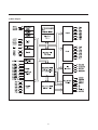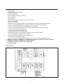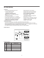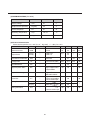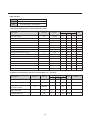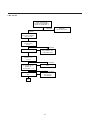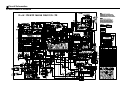
1
S/M No:CP490P-010
Colour Television
CHASSIS : CP-490
MODEL : DTR-14D3VG
DTR-14D3TM
DTR-16D3VG
DTR-20D3VG
DTR-20D3TM
DTR-21D3TMW
DTR-21D3VGW
DTR-21D3TGW
✔ Caution
: In this Manual, some parts can be changed for improving, their
performance without notice in the parts list. So, if you need the
latest parts information,please refer to PPL(Parts Price List) in
Service Information Center (http://svc.dwe.co.kr).
DAEWOO ELECTRONICS CO., LTD.
CONTENTS
Specifications ................................................................................................ 1
Safety Instruction .......................................................................................... 2
Circuit block Diagram .................................................................................... 3
Alignment Instructions ................................................................................. 4
IC Description ................................................................................................ 8
Circuit Description ....................................................................................... 34
Trouble Shooting Charts ............................................................................. 49
Electrical Parts List ..................................................................................... 56
CP-490 each model Parts List .................................................................... 62
Mechanical Exploded View and Parts List ................................................ 64
PCB Layouts ................................................................................................ 67
• PRINTED CIRCUIT BOARDS
• SCHEMATIC DIAGRAM
Specifications
VG : WITHOUT TXT. MODEL, TM : WITH TXT. MODEL
TV Standard
PAL/SECAM-B/G, D/K, I, H, NTSC-3.58/4.43
Mains Voltage
100~250V AC, 50/60Hz
Power Consumption
14”, 16” = 85W
20”, 21” = 90W
Sound output
. 2 Speaker (at 80% MOD. 10% THD) : 5W + 5W (TWITTER 2.5W + 2.5W)
6W + 6W (TWITTER 2.5W + 2.5W)
14”, 16”
20”
. 3 Speaker (at 80% MOD. 10% THD) : 8W + 8W + 8W(21”)
Speaker
. 2 Speaker : 7.5W, 8 OHM(2EA)
. 3 Speaker : 12W, 8 OHM(3EA)
Antenna
75 ohm unbalanced
Impedance
300 ohm balanced with supplied balun
Tuning system
Voltage Synthesize Tuning System
Memory channel
100 channels
Reception
VHF - L : CH2 - CH4
channel Unit
VHF - H : CH5 - CH12
Cable Band : CHS1’ - CHS3’, CHS1 - CHS20
UHF : CH21 - CH69
Remote control
VG : R-28B04, TM : R-28B03
Screen size
14” : 34cm (A34JLL 90 02)
20” : 48cm (A48JLL 90 02)
21” : 51cm (A51JLL 90 02)
Weight
14” : 9.7Kg(set)
20” : 19.6Kg(set)
21” : 26.5Kg(set)
Indication
On-Screen Display
- MENU
• Picture (Brightness, Color, Contrast, Sharpness, TINT)
• TIMER (TM/TMW/TGW:CLOCK, OFF TIME, WAKE-UP-TIME, ACTIVATE, WAKE-UPPROG/VG:CLOCK, ON TIME, OFF TIME)
• LANGUAGE
• PRESET
• EDIT (TM, TMW, TGW)
• SLEEP •BLUE BACK •GAME
• AV1, AV2
•NORMAL1, NORMAL2, FAVORITE
• SOUND MUTE
• VOLUME CONTROL
• WOOFER (21” ONLY)
• 16:9, ZOOM, NORMAL
1
Safety Instruction
WARNING: Before servicing this chassis, read the “X-RAY RADIATION precaution”, “safety precaution”
and “product safety notice” below.
X-RAY RADIATION PRECAUTION
1. Excessive high voltage can produce potentially
hazardous X-RAY RADIATION.To avoid such
hazards, the high voltage must not exceed the
specified limit. The nominal value of the high
voltage of this receiver is 23-24kv(14”), 2627kv(20”, 21”) at max beam current. The high
voltage must not, under any circumstances,
exceed 27.5kv (14", 20”), 29.0kv(21”).
Each time a receiver requires servicing, the high
voltage should be checked. It is recommended
the reading of the high voltage recorded as a part
of the service records. it is important to use an
accurate and reliable high voltage meter.
2. The only source of X-RAY Radiation in this TV
receiver is the picture tube. For continuous
RADIATION protection, the replacement tube
must be exactly the same type tube as specified
in the parts list.
SAFETY PRECAUTION
2. If any Fuse in this TV receiver is blown, replace it
with the FUSE specified in the Replacement
Parts List.
3. When replacing a high wattage resistor(oxide
metal film resistor) in circuit board, keep the
resistor 10mm away from circuit board.
4. Keep wires away from high voltage or high
temperature components.
5. This receiver must operate under AC260 volts,
50Hz/60Hz. (AC 100~250 volts, 50/60Hz)NEVER
connect to DC supply or any other power or
frequency.
1. Potentials of high voltage are present when this
receiver is operating. Operation of the receiver
outside the cabinet or with the back cover
removed involves a shock hazard from the
receiver.
1) Servicing should not be attempted by anyone
who is not thoroughly familiar with the
precautions necessary when working on highvoltage equipment.
2) Always discharge the picture tube to avoid the
shock hazard before removing the anode cap.
3) Discharge the high potential of the picture tube
before handling the tube. The picture tube is
highly evacuated and if broken, glass
fragments will be violently expelled.
PRODUCT SAFETY NOTICE
Many electrical and mechanical parts in this
chassis have special safety-related characteristics.
These characteristics are often passed unnoticed
by a visual inspection and the X-RAY RADIATION
protection afforded by them cannot necessarily be
obtained by using replacement components rated
for higher voltage, wattage, etc.
2
Circuit Block Diagram
3
Alignment Instructions
1. AFT
1.1 Standard B/G,D/K,I
1) Set a Signal Generator with
- RF FREQUENCY = 38.9 MHz,
- RF OUTPUT LEVEL = 80 5 dBuV
- System = PAL / SECAM - B/G, D/K, I
NTSC - 3.58/4.43
2) Connect the Signal Generator RF Output to P101 (Tuner IF Output).
There must be no signal input to the tuner.
3) Press the “AFT” KEY and wait until the TV screen display “AFT OK”.
2. AGC
1) Set a Pattern Generator with RF LEVEL 63° 2 dBuV .
2) Connect a OSCILLOSCOPE PROBE to P102 (TUNER AGC INPUT).
3) Adjust AGC UP/DOWN KEY the voltage drop 2.0V±0.5V dc point its maximum voltage.
Alternative Method
1) Set a Pattern Generator with
- RF LEVEL 80 5 dBuV
- PAL CROSSHATCH
( without SOUND CARRIER )
2) Connect a OSCILLOSCOPE
( Bandwidth
100MHz ) PROBE
to P101 (TUNER IF OUTPUT).
3) Use AGC UP/DOWN KEY to obtain
an envelop amplitude 200 + 20 mVp-p.
3. SCREEN
1) Receive the color bar pattern and heat run over 15
minutes.
2) On the normal mode1 adjust the screen volume that
the horizontal line appears on the screen after pushing the AFT-L key on the SVC remote control unit.
3) Adjust the screen volume that the horizontal lines
reach the cut-off point
4. WHITE BALANCE
1) Set the TV to NOR I mode.
2) Set the R,G,B LEVEL to CENTER with R,G,B UP/DOWN KEY .
3) Adjust the R,G,B UP/DOWN KEY of the color which appears abnormally
on the screen to obtain WHITE BALANCE.
5. FOCUS
1) Apply a RETMA PATTERN signal.
2) Adjust the FOCUS VOLUME on FBT to obtain optimal resolution.
4
6. GEOMETRY
6.1 VERTICAL CENTER
1) Set the TV to NOR I mode.
2) Pressing the V-SIZE UP/DOWN KEY, the
lower half of the screen is blanked.
3) Adjust the border line of blanked picture
coincident with the mechanical center marks
of the CRT using the V-CENTER UP/DOWN KEY.
6.2 VERTICAL SIZE
The VERTICAL CENTER adjustment
has to be done in advance.
1) Apply a RETMA PATTERN signal.
2) Set the TV to NOR I mode.
3) Adjust the upper part of the picture
with the V-SIZE UP/DOWN keys.
6.3 VERTICAL SLOPE
The VERTICAL SIZE adjustment
has to be done in advance.
1) Apply a RETMA PATTERN signal.
2) Adjust the lower part of the picture
with the V-SLOPE UP/DOWN keys.
6.4 VERTICAL S-CORRECTION
1) Apply a CROSSHATCH PATTERN signal.
2) Adjust the S-COR UP/DOWN KEY to obtain
the same distance between horizontal lines.
6.5 HORIZONTAL CENTER
1) Apply a RETMA PATTERN signal.
2) Adjust picture centering with H-CENTER
LEFT/RIGHT keys.
5
If EEPROM(I702) has been changed ;
- Option data has to be changed and
- all alignment function has to be readjusted.
The initial state of adjustment are as follows;
- V-Center, V-Slope V-Size, H-Center, R, G, B, AFT = Center (30/64 - 33/64)
- S-Correction = 00/64
- AGC = 15~60/64
Service Remocon
6
IC Description
DW90244-AS/(Z8 DIGITAL TELEVISION CONTROLLER)
= Z9024106PSC (ZILOG TYPE NO.)
(1) General Description
The Z9023X Digital Television Controller (DTC) family is ZILOG’s latest and most powerful Z8-based DTC product offering,
These parts feature larger system RAM and Rom Options, together with a host of new features including a newcolor palette
systen, flexible inter-row spacing, higher character cell resolution, background mesh effect, dedicated I. R. capture registers,
on-chip Analog-to-Digital conversion, and a hardware Master mode I2C interface. The famililiar Z8 core in combination with
these advanced features makes the Z9023X family an ideal choice for low to midrange televisions in both PAL and MTSC
markets.
The Z9023X family consists of three basic device types; ICE Chip (Z90239), ROM Mask Parts (Z90233/Z90234), and OTP
Part (Z90231), The OTP (Z90231) supports field programmable 32KB system ROM. ICE Chip (Z90239) is used in Z90239
Emulator and ProtoPaK. As described above, Z90233 supports 16KB system ROM and Z90234 supports 24KB system
ROM for mask.
The Z9021X family takes full advantage of the Z8’s expanded register file space to offer greater flexibility in On Screen Display creation.
(2) Feature
Z8-Based CMOS Microcontroller for Consumer Television, Cable Box, and Satellite Receiver Applications
• 42 - Pin SDIP Package except Z90239 (124 PGA)
• Z8@ MCU Core at 6 MHz
• Mask ROM sizes Available in 16 and 24KB
• Ten 6-bit Pulse Width Modulators
• One 14-bit Pulse Width Modulator
• On-Chip Infrared (IR) Capture Registers
• Four Channel 4-bit Analog-to-Digital Converter
• Twenty Seven General Purpose I/O Pins
• I2C Master Serial Communication Port
On Screen Display (OSD) Section
• Supports Displays up to 10 rows by 24 Columns with 256 Characters
• Character Cell Resolution of 14 Pixels by 18 Scan lines
• Variable Inter-row Spacing from 0-15 Horizontal Scan Lines
• Foreground and Background Colors Fully Programmable by Character
7
(3) Block Diagram
8
(4) PIN CONFIGURATION(Z90241)
1
2
3
4
5
6
7
8
9
10
11
12
13
14
15
16
17
18
19
20
21
P40
P20
P21
P22
P23
P24(SCLØ)
P25(SDAØ)
P26(SCL1)
P27(SDA1)
GND
VCC
X-TAL1
X-TAL2
P55/PWM6
RESET
P56/PWM6
P54/PWM5
P53/PWM4
P52/PWM3
P51/PWM2
P50/PWM1
P47/PWM10
P46/PWM9
F BLANK
B
G
R
V-SYNC
H-SYNC
P63
P45/PWM8
P44/PWM7
P43
P42
OSD X2
OSD X1
VCC
IR IN
AGND
P62/ADCO
P61/ADC2
P60/ADC3
42
41
40
39
38
37
36
35
34
33
32
31
30
29
28
27
26
25
24
23
22
(5) PIN DESCRIPTION
Table 1. Z90231/233/234 42-Pin SDIP Package
Pin Number
34
30, 13
36
1
20, 19, 18, 17, 2, 3, 4, 5, 6 ,7
7, 6, 5, 4, 3, 2, 1
42, 41, 40, 39, 38, 37, 35, 21
21
40, 42
39, 41
16, 12, 10, 9
20, 19, 18, 17, 15, 14, 11, 8
31
32
28
29
26
27
25
24, 23, 22
9, 10, 11, 12
33
Pin Function
+5 Volts
0 Volts
Infra Red remote capture input
14-bit Pulse Width Modulator output
6-bit Pulse Width Modulator output
Bit programmable Input/Output ports
Bit programmable Input/Output ports
Half tone output
I2C Data
I2C Clock
Bit programmable Input/Output ports
Bit programmable Input/Output ports
Crystal oscillator Input
Crystal oscillator output
Dot clock oscillator Input
Dot clock oscillator output
Horizontal Sync
Vertical Sync
Video blank
Video R, G, B
4-bit Analog to Digital converter input
Device reset
I/O/PWR
Reset State
Name
PWR
PWR
I
O
O
I/O
I/O
O
I/O
I/O
I/O
I/O
I
O
I
O
I
I
O
O
AI
I
PWR
PWR
I
I
I
I
I
I
I
I
I
I
I
O
I
O
I
I
O
O
I
I
Vdd
Vss, AVss
IRIN
PWM11
PWM [10:1]
P5 [6:0]
P2 [7:0]
HLFTN
SDATA0, 1
SCLK0, 1
P6 [3:0]
P4 [4:0]
XTAL1
XTAL2
OSDX1
OSDX2
HSYNC
VSYNC
CBLANK
R, G, B
ADC[3:0]
/RESET
NOTE : 1. It is input on POR. It must be configured to be output ports for PWM applications
9
Note
1
1
DW5255MBI
(TVTEXT 8-bit Micro controller, Rom-version)
=SDA5254 (SIEMENS Type No.)
(1) General Description
The SDA 525x contains a slicer for TTX, VPS and WSS, an accelerating acquisition hardware modul, a display generator for “Level 1” TTX data and an 8 bit microcontroller running at 333 ns cycle time. The controller with dedicated hardware guarantees flexibility, does most of the internal processing of TTX acquisition, transfers data to/from the external
memory interface and receives/transmits data via I2C and UART user interfaces. The block diagram shows the internal
organization of the SDA 525x. The Slicer combined with dedicated hardware stores TTX data in a VBI buffer of 1 Kbyte.
The microcontroller firmware does the total acquisition task (hamming- and parity-checks, page search and evaluation
of header control bits) once per field.
(2) Feature
• Acquisition:
- Feature selection via special function register
- Simultaneous reception of TTX, VPS and WSS
- Fixed framing code for VPS and TTX
- Acquisition during VBI
- Direct access to VBI RAM buffer
- Acquisition of packets X/26, X/27, 8/30 (firmware)
- Assistance of all relevant checks (firmware)
- 1-bit framing code error tolerance (switchable)
• Display:
- Features selectable via special function register
- 50/60 Hz display
- Level 1 serial attribute display pages
- Blanking and contrast reduction output
- 8 direct addressable display pages for SDA 5250, SDA 5254 and SDA 5255
- 1 direct addressable display pages for SDA 5251 and SDA 5252
- 12 x 10 character matrix
- 96 character ROM (standard G0 character set)
- 143 national option characters for 11 languages
- 288 characters for X/26 display
- 64 block mosaic graphic characters
- 32 characters for OSD in expanded character ROM + 32 characters inside OSD box
- Conceal/reveal
- Transparent foreground/background - inside/outside of a box
- Contrast reduction inside/outside of a box
- Cursor (colour changes from foreground to background colour)
- Flash (flash rate 1s)
- Programmable horizontal and vertical sync delay
- Full screen background colour in outer screen
- Double size / double width / double height characters
• Synchronization:
- Display synchronization to sandcastle or Horizontal Sync (HS) and Veritical Sync (VS) with start-stop-oscillator
- Independent clock systems for acquisition, display and controller
10
• Microcontroller
- 8 bit C500-CPU (8051 compatible)
- 18 MHz internal clock
- 0.33 µs instruction cycle
- Eight 16-bit data pointer registers (DPTR)
- Two 16-bit timers
- Watchdog timer
- Capture comprare timer for infrared remote control decoding
- Serial interface (UART)
- 256 bytes on-chip RAM
- 8 Kbyte on-chip on-chip display-RAM (access via MOVX) for SDA 5250, SDA 5254 and SDA 5252
- 1 Kbyte on-chip display-RAM (access via MOVX) for SDA 5250, SDA 5254 and SDA 5255
- 1 Kbyte on-chip TVT/VPS-Acquisition-buffer-RAM (access via MOVX)
- 1 Kbyte on-chip extended-RAM (access via MOVX) for SDA 5250, SDA 5254 and SDA 5255
- 6 channel 8-bit pulse width modulation unit
- 2 channel 14-bit pulse width modulation unit
- 4 multiplexed ADC inputs with 8-bit resolution
- One 8-bit I/O port with open drain output and optional I2C-Bus emulation (PORT 0)
- Two 8-bit multifunctional I/O ports (PORT 1, PORT3)
- One 4-bit port working as digital or analog inputs (PORT 2)
- One 2-bit I/O port with optional function
- One 3-bit I/O port with optional RAM/ROM address expansion up to 512 Kbyte (ROMIess-Version)
• P-SDIP-52-1 package or P-MQFP-64-1 for ROM-Versions (SDA 5251, SDA 5252, SDA 5254, SDA 5255)
• P-MQFP-80-1 Package for ROMIess-Version (SDA 5250 M)
• P-LCC-84-2 Package for Emulator-Version (SDA 5250)
• 5 V Supply Voltage
(3) Block Diagram
11
(4) Pin Configuration P-SDIP-52-1 (ROM-Versions)
Pin Configuration P-SDIP-52-1 (ROM-Versions)
(top view)
12
24LC08B (EEPROM)
(1) Features
• Single supply with operation down to 2.5V
• Page-write buffer for up to 16 bytes
• Low power CMOS technology
• 2ms typical write cycle time for page-write
- 1mA active current typical
• Hardware write protect for entire memory
- 10 A standby current typical at 5.5V
• Can be operated as a serial ROM
- 5 A standby current typical at 3.0V
• Factory programming(QTP) available
• Organized as two or four blocks of 256 bytes
• ESD protection > 4,000V
(2x256x8) and (4x256x8)
• 1,000,000 ERASE/WRITE cycles(typical)
2 TM
• Two wire serial interface bus, I C compatible
• Data retention > 40 years
• Schmitt trigger, filtered inputs for noise suppression
• 8-pin DIP, 8-lead or 14-lead SOIC packages
• Output slope control to eliminate ground bounce
• Available for extended temperature ranges
• 100KHz(2.5V) and 400KHz(5V) compatibility
- Commercial : 0 C to +70 C
• Self-timed write cycle(including auto-erase)
-Industrial : -40 C to +85 C
(2) General Description
The Microchip Technology Inc. 24LC08B is a 8K-bit Electrically Erasable PROM.
The device is organized as four blocks of 256x9bit memory with a two wire serial interface. Low voltage
design permits operation down to 2.5 volts with standby and active currents of only 5 A and 1mA respectively.
The 24LC08B also has a page-write capability for up to 16 bytes of data.
The 24L08B is available in the standard 8-pin DIP surface mount 80IC packages.
(3) Block Diagram
WP
I/O
CONTROL
LOGIC
MEMORY
CONTROL
LOGIC
HV GENERATOR
XDEC
EEPROM ARRAY
(4X256X8)
PAGE LATCHES
SDA
SCL
YDEC
VCC
VSS
SENSE AMP
R/W CONTROL
(4) Pin Description
PIN
SYMBOL
DESCRIPTION
1-3
A0, A1, A2
Device Address lnputs
4
Vss
Ground
5
SDA
Serial Data/Address
6
SCL
Serial Clock
7
WP
8
Vcc
+5V Power supply
13
TDA884X ( One Chip TV-processor )
(1) General Description
The TDA884X family is a pin-aligned range of single chip video and audio processors.
With this family it is possible to cover in one layout a whole range of applications from simple small screen single standard
sets (as well PAL as NTSC with built-in delay line) to full multi-standard (including SECAM) 16:9 sets. Switching from the
TDA837x family to TDA884X family has been made very easy:the SDIP packages of the families are almost pin aligned and
minimal layout adaptations are necessary. Omitting the delay line TDA4665 and SECAM add-on TDA8395 with surrounding
components, VCO coil, direct connection of U, V in-and outputs and adapting the software to access the 5 extra registers
are the most relevant changes needed.
(2) Feature
• IF
- Alignment free IF-PLL, IF frequency selection via I2C (no external coil needed)
- Vision IF amplifier with high sensitivity and good figures for differential phase and gain
- PLL demodulator with high linearity offering the possibility for (single standard) intercarrier stereo audio application
- Alignment PLL via I2C
• AUDIO
- Alignment free multi standard PLL audio demodulator (4.5 to 6.5 MHz.)
- Volume control
• Video
- Integrated fixed luminance delay line
- Integrated chroma trap (auto calibrated)
- Integrated chroma bandpass filters with switchable centre frequency (auto calibrated)
- Asymmetrical peaking circuit in the luminance channel with switchable noise coring function
- Black stretching of non standard CVBS or luminance signals, switchable via I2C bus
• RGB
- RGB control (brightness, contrast, saturation)
- Improved black current stabilisation (continuos cathode calibration)
- White point adjustment
- Blue stretch which offsets colours near white to blue
- Option to insert “blue back” when no video signal is available
• Input / Output
- Flexible video source select with CVBS input for the internal signal and two external video inputs(one switchable for
CVBS or Y/C).
- The output signal of the video source select is externally available ( also as CVBS when Y/C input is used).
- External audio input.
- Linear RGB input with fast blanking.
• Synchronization and Deflection
- Horizontal synchronization with two control loops and alignment free horizontal oscillator.
- Slow start and slow stop of the horizontal drive output to enable low stress start-up and switch-off from the line
circuit at nominal line supply voltage.
- Vertical count-down circuit for stable behavior with provisions for non-standard signals.
- Vertical geometry control.
- Vertical drive optimized for DC coupled vertical output stages.
- Option for blanking of PAL plus helper signal
- Option to stop the vertical deflection for Vg2 alignment
- Option to switch-off in the vertical overscan
• Control
- Full I2C bus control, as well for customer controls as for factory alignment.
14
- All automatic controls have an option for forced mode.
• Power consumption
- Low power consumption.
• Packaging
- SDIP-56 (Shrinked Dual In Line Package, 56 pins).
(3) Block Diagram
15
(4) Pin Description
No
Name
Description
1
SOUND IF INPUT
The sound equivalent input impedance is 8k5 ohm // 5pF which has to be
taken into account for proper termination of the ceramic filters.
The DC impedance is very high.
The minimum input signal for catching is l mV rms.
2
EXT AUDIO INPUT
An external sound signal (500mVrms) for example from SCART can be applied to this
pin via a coupling capacitor. The input has been made suitable to allow maximum
2Vrms. The input impedance is 25kohm.
3
VCO REF FILTER
The IF VCO tuned circuit is applied to these pin.
4
Its resonance frequency must be two times the IF-frequency and in between a
range of 64-120MHz.
This range is suitable for the IF standards as 33.4, 38.9, 45.75 and 58.75MHz.
The VCO frequency can be adjusted by I2C bus so a fixed coil can be used.
5
PLL LOOP FILTER
Standard loopfilter is : R=390Ω and c=100nF in series to ground. The loopfilter bandwidth is 60kHz and is optimal for both fast catching and sufficient video suppression for
optimal sound performance.
The loopfilter time constant can be changed by I2C bus function FFI (Fast filter IF-PlLL).
When FFI=1, the PLL can better handle non-standard transmitter signals with large
phase modulation. The standard PLL loopfilter value can be left unchanged.
FFI=0 Normally selected or standard transmitter signals
FFI=1 Specially to handle non-standard transmitter signals with large phase
modulation. The function can be used for both positive and negative
modulated signals
6
IF VIDEO OUTPUT
Although the video output impedance is low it is recommended to avoid high frequency
current in the output due to for instance sound trap filters.
This can be achieved by means of an emitter follower at the video output with a 1KΩ
resistor in series with the base.
7
BUS INPUT : SCL
Serial clock line
8
BUS INPUT : SDA
Serial data line
9
BANDGAP
DECOUPLING
The bandgap circuit provides a very stable and temperature independent
reference voltage.
This reference voltage (6.7V) ensures optimal performance of the TDA8842
and is used in almost all functional circuit blocks.
10
CHROMA INPUT
The supplied C S-VHS input burst amplitude should be nominally 300mVPP (assumed
is a colour bar signal with 75% saturation and with chroma/burst
ratio of 2.2/1 ). The C S-VHS input is internally clamped to 4V via 50KΩ.
The external AC coupling capacitor with 50KΩ forms a high pass filter. A recommended
coupling capacitor is 1 nF; the high pass filter cut off
frequency is then approximately 3KHz.
11
CVBS/Y INPUT
The CVBS/Y signal of 1Vpp ( inclusive sync amplitude) is AC coupled to pin11.
12
37
SUPPLY
The TDA884X has two supply pins 12 and 37. Both pins must be supplied simultane
ously. Notice that the IC has not been designed to use one of both pins as start pin.The
nominal supply voltage is 8V with min/max values of 7.2-8.8V. The current consumption
is about 60mA for each pin 12 and 37.
In stand-by condition the 8V IC-supply can be switched off as to safe energy. After
switching on the 8V again the normal start-up procedure must be followed.
A voltage detection circuit is connected to both pins.
16
No
Name
Description
Power-up : If the 8V increases >6.8V then; (after IC-initialization and auto re-calibration)
Hout starts at 2fH
Hout continues at fH
Power-down : If the 8V drops <6.8V then; a power on reset, POR, is generate.
The Hout is disabled immediately and
RGB blanked
IC must be re-initialized for correct re-start of the set
13
17
INT CVBS INPUT
EXT CVBS INPUT
It is recommended that the CVBS1 int and CVBS2 ext input amplitudes are
1 Vpp (inclusive sync amplitude).
This, because the noise detector switches the ø1 loop to slow mode
(i.e. auto ø1mode when FOA, FOB = 0,0) when noise level exceeds
100mVrms (i.e. at S/N of 20dB).
14
GROUND
All internal circuits are connected to this ground pin 14.
15
AUDIO OUTPUT
The output signal is volume controlled and is active for both internal and external audio
signals. The nominal gain is +9dB and -71dB, which gives a total control range of 80dB.
The output signal range therefor is 0.14- 1400mVrms
The bandwidth is >100kHz, the DC level is 3.3V and the output impedance is 250Ω.
16
DECOUPLING
FILTER TUNING
Voltage variations at pin 16, which can be due to external leakage current or
crosstalk from interference sources, should be less than 50mV to ensure that
tuning of filters/delay cells remains correct.
18
BLACK CURRENT
INPUT
For correct operation of the loop CURRENT information is supplied to the
black current input pin.
19
20
21
BLUE OUTPUT
GREEN OUTPUT
RED OUTPUT
The RGB outputs are supplied to the video output stages from pins 21, 20
and 19 respectively.
For nominal signals (i.e. CVBS/S-VHS, TXT inputs) and for nominal control settings,
then the RGB output Signal amplitudes is typically 2VBLACK_WHITE.
22
V-GUARD INPUT/
BEAM CURRENT
LIMITER
Vertical Guard
The TDA835X vertical deflection IC’s have a guard output which generates a pulse
during every vertical retrace. This pulse can be monitored by the TDA884X. Whenever
the height of this pulse is larger than 3.65V the vertical deflection IC’s work correctly.
The DC level during scan is not critical, but it should be below the 3.65V detection level.
The vertical guard is controlled by the I2C bits EVG and NDF.
When EVG (Enable Vertical Guard) is set to 1, for NDF (No vertical Deflection) = 1
implies deflection failure. The RGB outputs are blanked when NDF = 1.
Beam current limiting
The beam current limiting function is realized by reducing the contrast followed by the
brightness when the beam current reaches a too high level. The circuit can be divided into:
- Peak white limiting (PWL): reacts internally on high local peaks in the RGB signal.
- Average beam current limiting (ABL): reacts on the average picture content. it is an
external function.
23
24
25
RED INPUT
GREEN INPUT
BLUE INPUT
The Rin, Gin, Bin input signals (nominal signal amplitude of 700mV) are
AC coupled to pin 23, 24 and 25 respectively.
Clamping action occurs during burstkey period.
26
RGB INSERTION
SWITCH INPUT
The table below a survey is given of the three modes which can be selected
with a voltage on RGB insertion switch input pin ;
Vpin26 I2C function
Selected RGB signal
0.9V-3V
IE1=0
RGB (internal)
IE1=1
Rin,Gin,Bin (fast insertion on pin23,24,25)
> 4V
IE1=X
OSD can be inserted at the RGBout pins
17
No
Name
Description
27
31
32
LUMINANCE in,
B-Y / R-Y in
The Luminance out, B-Y / R-Y out signals from the output pins from the device itself or
from YUV signal processing IC’s MUST be DC coupled to the Luminance in, B-Y / R-Y
inputs pin 27,31 and 32. Internally these pins are AC coupled to the input clamps.
The clamping action is slow to ensure optimal clamping perormance for noisy YUV signals. In case YUV signal processing IC’s are placed in the YUV path then be sure that
the maximum voltage (DC-level and peak video level)does not exceed 5.5V. The
TDA917X family IC’s meet this requirement. When the output of a feature IC
exceeds the maximum DC-level of 5.5V then level shifters must be placed at the inputs
of the TDA884X. The Yin signal can be amplified, approximately 6dB, by means of the
I2C bit GAI in order to adapt to old feature IC’s like the TDA4565.
Because of the high input impedance outside burstkey clamping, it is advised to minimise
the track length to the Luminance in, B-Y / R-Y in pins. Adequate ground shielding of these
signal tracks is advised for good interference immunity. The TDA8840; TDA8841 and
TDA8842 only have Luminance out, B-Y/R-Y out signals and these signals are internally
connected to the Luminance in, B-Y/R-Y inputs. Also the GAI-bit is disabled in these types.
28
29
30
LUMINANCE in,
B-Y / R-Y in
The luminace output signal is approximately 1V BLACK-WHITE with typical output
impedance of 250Ω. The colour difference output signals (B-Y / R-Y) have
respectively a nominal output level 1.33VPP and 1.05VPP, the output impedance of pins
29 and 30 is 500Ω when a colour system is identified. The Luminance out and
B-Y/R-Y out signals can be connected to additional YUV signal processing IC’s.
How to connect these signals (AC or DC) depends on the input signals characteristic
of signal processing IC, at which these output signals are connected to.
33
SUBCARRIER
Reference output (Fsc)
The reference output can be used as a reference for comb filter applications.
For PCB layout considerations, a short signal track connection with interface devices is
advised. It is advised to minimise parasitic capacitance of pin to ground (i. e. avoid
large ground planes around signal track). The parasitic capacitance at this pin to
ground should be less than 10PF.
34
35
X-TAL 3.58
X-TAL 4.43
To ensure correct operation of both:
- colour processing internal circuits,
- sync calibration internal circuits,
it is only allowed to have 3.6MHz Xtals on pin34: both 4.4MHz,3.6MHz Xtals are
allowed on pin 35. If pin 35 is not used: then it is left open in application (also
XA,XB=O,1 ).
36
LOOP FILTER
PHASE
DETECTOR
One of the important aspects of the PLL is the loop filter connected to pin 36;
it influences the dynamic performance of the loop.
38
CVBS1 OUT
The output amplitude is 2Vpp (transfer gain ratio between CVBSINT or
CVBSEXT or CVBS/Y and CVBS1OUT is 2).
The maximum output impedance is 250 Ω. For application with the SAA4961 combfilter, 6dB attenuation is required. It is advised to use an emitter follower circuit as shown
in Fig 35. For scart application the same emitter follower can be used. It is advised that
the signal paths to the comb filter and back to the TDA8842 are as short as possible so
as to avoid crosstalk from interference sources.
The follower is placed as close as possible to pin 38.
39
BLACK PEAK
HOLD CAPACITOR
For the correct working of the black stretcher an external time constant should
be added at the black peak hold capacitor input.
40
HOR OUTPUT
This open collector output is meant to drive the horizontal output stage.
The output is active low, i.e. the line transistor should conduct during the low
period of the output.
41
SANDCASTLE
OUTPUT/
FLYBACK INPUT
Pin 41 is a combined input/output pin.
The pin provides a three level sandcastle pulse.
Both burstkey pulse and vertical blanking pulse are always available, the line
18
No
Name
Description
blanking pulse is only present when the external flyback pulse is fed to this pin.The line
flyback pulse, fed to this pin is used for two functions:
- input signal for the PHI-2 1oop and
- RGB line blanking. (without flyback pulse blanking occurs only during the
burstkey pulse)
Because of the combined input/output function, the connected circuit should be
carefully designed for optimal performance.
Flyback pulse
The selection of the flyback pulse is important. Please note that the flyback pulse
width may not vary on beam current variations because they can not be compensated
by the PHI-2loop.
42
PHI-2 control loop
Loopfilter:
The loopfilter is a first order filter. This pin requires a capacitor(C) only. The recommended value is 4.7nF. The minimal value for C = 1nF. The loopgain than is reduced
to 0dB for 3kHz. A value up to 10nF is allowed but makes the loop slower.
To avoid disturbances in the loop the capacitor should be connected to the TDA884X
ground pin as short as possible.
Loopgain:
The static loopgain (K) is 120µs/µs. This implies that phase variations ( t0) due to storage time variations ( td)are reduced by this factor of 120. This is valid when only a
capacitor is connected to the PHI-2 pin.
Any resistor connected externally reduces the loopgain. For R = 10MΩ -> K = 60, and
for R = 1MΩ -> K = 12.
Shift control range:
The picture can be centered on screen by means of the horizontal shift (HS) via I2C
bus. The range is +/-2µs.
The delay between the positive going Hout (line transistor switches off then) and start
burstkey pulse (ref PHI-2) must be ≤17µs.
Flash protection:
A flash protection becomes active when this pin is forced >6V. The horizontal drive is
switched-off immediately. Once the voltage is <6V the horizontal drive is switched-on
again via the slow start procedure.
A series resistor of 1kΩ is required for current limitation.
See also XPR function for overvoltage protection.
PHI-2 switched off:
The PHI-2 loop is switched off when the PHI-2 pin is forced externally to 1V. This is for
analysis purpose only.
43
PHI-1 control loop
The loopfilter connected to pin 43 is suitable for various signal conditions as
strong/weak and VCR signal.
This is achieved by switching of the loopfilter time constant by changing the
PHI-1 output current.
Via I2C bus FOA/B, different time constants can be chosen, including an
automatic mode which gives optimal performance under varying conditions.
44
GROUND
To this pin are connected the IC-substrate and horizontal output.
45
AVL output
The AVL capacitor is connected to pin 45. The recommended capacitor value is 1 to
4.7µF; it’s optimal value is a compromise between fast volume settling, AVL hold time
(dynamic sound range) and harmonic distortion.
- small AVL capacitor: gives fast volume settling but reduces the dynamic sound
range and performance on harmonic distortion for mainly low audio frequencies
- large AVL capacitor value gives maximal AVL performance but increases the
volume settling time.
The active control range for pin 45 is 1V for maximum gain and 5 V for minimal gain.
During channel switching it’s recommended to force a sound mute (make SM=1). The
AVL then can’t be disturbed by noise peaks during channel setting; this ensures a fast
setting of the volume level.
19
No
Name
Description
46
47
VERT DRIVE +
VERT DRIVE -
The vertical drive has a current output. The output is balanced which ensures
a good common mode behavior with temperature and makes the output signal
less sensitive for disturbances.
48
49
IF INPUT
The PLL frequency range is 32-60MHz with corresponding VCO frequency
64-120MHz.
The IF input impedances is 2KΩ⁄ in parallel with 3pF and matches the required
load for commonly used SAW filters.
A DC coupling is allowed, so no series capacitors between SAW filter and IF
input are necessary.
50
EHT/OVERVOLTAGE
PROTECT INPUT
The input range for EHT tracking is 1.2V - 2.8V, for a compensation of +/-5% on
vertical and / or EW. The tracking on EW can be switched on/off by HCO. The nominal
voltage of pin 50 for no compensation is 2V.
The EHT feedback signal must be filtered in order to prevent disturbances in vertical
and/or EW deflection. A compromise has to be determined for tracking speed on
normal EHT variation and ripple immunity.
Special linear zoom facilities on both Vertical and East-West gives the possibility to
adapt the picture size for both 16:9 and 4:3 screens. When zoom is used, the
geometry correction remains correct in both vertical and horizontal direction. Using
VSC(Vertical Scroll) the (expanded) picture can be shifted up and down. By
programming the vertical slope, VS, subtitles at the bottom part of the picture can be
made visible while the picture position at the top of the screen remains fixed (subtitle
mode).
ZOOM FUNCTION
51
VERTICAL
SAWTOOTH
CAPACITOR
This pin requires a capacitor to ground of l00nF +, - 5%. Short connection to the ground
pin of the TDA884X is required. Important: For this capacitor, a type with good tem
perature behaviour, long term stability and low leakage must be chosen.
Change of the capacitance value due to temperature and/or aging leads to a proportional change in vertical amplitude. Tolerance of the external capacitor can be compensated by means of the vertical slope adjustment of I2C bus function VS.
The charge current can be fine tuned with =/- 20%.
The optimal sawtooth amplitude is 2.9V and is determined by the external capacitor
and charge current. For R = 39KΩ at pin 52, the vertical slope VS = 1F and field frequency = 50Hz, the charge current is 16µA. For 60Hz the charge current is increased
by 20%. The sawtooth bottom-level is 2.3V.
The vertical retrace time is determined by the discharge current of 1mA and lasts about
5 horizontal lines.
52
REFERENCE
CURRENT INPUT
This pin requires a resistor to ground.
The optimal reference current is 100µA. which is determined by this resistor.
53
AGC
DECOUPLING
CAPACITOR
The AGC capacitor value is 2.2µF and has been defined for an optimal
compromise between AGC speed and tilt for all AGC modes
(negative/positive modulation).
54
TUNER AGC
OUTPUT
This output is used to control (reduce) the tuner gain for strong RF signals.
The tuner AGC is an open collector output which is acting as a variable
current source to ground.
55
AUDIO
DEEMPHASSIS
The pin requires a capacitor to ground that defines the deemphasis time constant.
The DC and mute level is 3V.
The signal is internally connected through to the Audio switch.
56
DECOUPLING
SOUND
DEMODULATOR
This pin requires a capacitor of 10µF connected to ground.
The pin acts as a low pass filter needed for the DC feedback loop.
20
TDA6106Q ( Video Output Amplifier )
(1) General Description
The TDA6106Q is a monolithic video output amplifier (5MHz bandwidth) in a SIL 9 MPpackage, using high-voltage
DMOS technology, and is intended to drive the cathode of CRT directly .
To obtain maximum performance, the amplifier should be used with black-current control.
(2) Feature
• Black - current measurement output for automatic black current stabilization (ABS)
• Single supply voltage of 200V
• Internal protection against positive appearing CRT flash-over discharge
• Protection against ESD
• Internal 2.5V reference circuit
• Controllable switch-off behavior
(3) Block Diagram
Pin 6
Vdd
TDA61O6Q
Vdd
MIRROR
in
Vdd
MIRROR
1
out
Vbias
out
Pin 9
Vof
1X
2
in
Pin 8
Voc
1X
CURRENT
SOURCE
Pin 3
vin
Pin5
Iom
—DIFF.STAGE
+
out
out
MIRROR
out
3
(4) Pin Description
PIN
SYMBOL
DESCRIPTION
1
N.C
2
N.C
3
V in
inverting input
4
GND
ground, substrate
5
I om
Black-current measurement output
6
V dd
supply voltage high
7
N.C
8
V oc
cathode output
9
V of
feedback/transient output
21
out
in
gnd
Pin 4
Gnd
I804 PC817
(1) General Description
The specification applies to the structures and characteristics of Model No. PC817
(2) Block Diagram
(3) Absolute maximum ratings
Parameter
Symbol
Forward current
IF
*1) Peak forward current
IFM
1
A
Reverse voltage
VR
6
V
Power dissipation
P
70
mW
Collector-emitter voltage
VCEO
35
V
Emitter-collector voltage
VECO
6
V
Collector current
IC
50
mA
Collector power dissipation
Pc
150
mW
Total Power dissipation
Ptot
200
mW
Operating temperature
Topr
-30~+100
C
Storage temperature
Tstg
-55~+125
C
*2) Isolation voltage
Viso
5
*3) Soldering temperature
Tsol
260
Input
Output
*1) Pulse width 100 s, duty ratio: 0.001
*2) AC for 1 minute, 40~60% RH
*3) For 10 seconds.
22
Rating
50
Unit
mA
kVrms
C
TDA8356 (DC-coupled vertical deflection circuit)
(1) General Description
The TDA8356 is power circuit for use in 90 and 110 color deflection systems for field frequencies of 50 to 120 Hz.
The circuit provides a DC driven vertical deflection output circuit, operating as a high efficient class G system.
(2) Feature
• High efficient fully DC-coupled vertical output bridge circuit
• Vertical fly-back switch
• Guard circuit
• Protection against : - short circuit of the output pins (7 and 4)
- short circuit of the output pins to Vp
• Temperature (thermal) protection
• High EMC immunity because of common mode inputs
(3) Block Diagram
(4) MAXIMUM RATINGS (Ta=25˚C)
PIN
SYMBOL
DESCRIPTION
1
I drive (pos)
input power stage (positive); include Ii(sb) signal bias
2
I drive (neg)
input power stage (negative); include Ii(sb) signal bias
3
Vp
operating supply voltage
4
V o(b)
output voltage B
5
GND
ground
6
V fb
input fly-back supply voltage
7
V o(a)
output voltage A
8
V o(guard)
guard output voltage
9
V I(fb)
input feedback voltage
23
TA8218AH (AUDIO IC AMP) : 3 SPEAKER MODEL (CONTAINS WOOFER)
(1) General Description
The TA8218AH is 3 channel audio amplifier for consumer applications.
This IC provides an output power of 6 watts per channel.(at Vcc=20V, f=1kHz, THD=10%, RL=8Ω) It is suitable
for power amplifier of TV and Home stereo.
(2) Features
• Built-in 3ch amplifier
• High Output power : Pout=6W/ch(Typ.)
(Vcc=20V, RL=8Ω, f=1kHz, THD=10%)
• Low Noise : Vno=0.14mVrms(Typ.)
(Vcc=20V, RL=8Ω, Gv=34dB, Rg=10kΩ, BW=20Hz~20kHz)
• Built in Audio Muting Circuit (Active
Low)
Main Amp/Surround Amp independent Control.
• Built in Various protection Circuits
Protection Circuit : Thermal Shut Down, Over Voltage, Out
GND short.
• Operation Supply Voltage Range : Vcc(opr) = 10 ~ 30V(Ta=25˚C)
(3) Block Diagram
24
(4) MAXIMUM RATINGS (Ta = 25˚C)
CHARACYERISTIC
SYMBOL
RATING
UNIT
Supply Voltage
VCC
30
V
Output Current (Peak/ch)
IO(peak)
2.0
A
Power Dissipation
Pd
50
W
Operating Temperature
Topr
-20~75
˚C
Storage Temperature
Tstg
-55~150
˚C
Note: Derated above Ta=25˚C in the proportion of 400mW/˚C
(5) Electrical Characteristics
Unless otherise specified, Vcc = 20V, RL = 8Ω, Rg = 600Ω, f = 1 KHz, Ta = 25˚C
CHARACTERISTIC
Quescent Current
SYMBOL TEST CIRCUIT
TEST CONDITION
MIN.
TYP.L
MAX.
UNIT
ICCQ
–
Vin=0
40
90
160
mA
Pout(1)
Pout(2)
–
–
THD=10%
THD=1%
5.0
–
6.0
4.5
–
–
W
THD
–
Pout=2W
–
0.1
0.6
%
Voltage Gaim
Gv
–
Vout=0.775Vrms (0dBm)
32.5
34.0
35.5
dB
Input Resistance
RIN
–
–
–
30
–
kΩ
Ripple Rejection Ratio
R.R.
–
Rg=0, fripple=100Hz
Vripple=0dBm
-50
-60
–
dB
Output Noise Voltage
Vno
–
–
0.14
0.3
mVrms
Cross Talk
C.T.
–
Rg=10kΩ
BW=20Hz~20kHz
Rg=0
Vout=0.775Vrms(0dBm)
Two channels input
–
-60
–
dB
VTH(OFF)
–
Mute ON
–
3.7
4.0
VTH(ON)
–
Mute OFF
2.5
2.8
–
ATT
–
-52
-60
–
Output Power
Total Harmonic Distortion
Muting Threshold
Muting Attenuation
Vout=0.775Vrms
pin
Pin
Mute
Three channels input
25
V
dB
UPC1406HA(Audio output Amplifier)
(1) Feature
• Each attenuator is completely separate and is very easy to control with remote control (e.g Volume, Balance)
• This IC’s characteristic control curve is linear against logarithmic output and offers smooth control.
• Channel Seperation : 64dB MIN
• Typical Application : Sound MPX attenuator for TV, Radio and mobil receiver
(2) General Description
• The UPC1406HA is a silicon monolithic integrated circuit for sound control (e, g, Volume, Balance)
This IC has a good characteristic control curve (‘A’ Cuve) and is very suitable for remote control applications.
The two attenuators are completely separate and is easy to control the balance between the two attenuators.
This IC is manufactured in a 9 pin slim SIP.
(3) Block Diagram
26
KA4558H/A/I
(1) General Description
The KA4558 series is a monolithic integrated circuit designed for dual operational amplifier.
(2) Features
• No frequency compensation reguired.
• No latch-up.
• Large common mode and differential voltage range.
• Gain and phase match between amplifiers.
• Internally frequency compensated.
• Low noise input transistors.
(3)Block Diagram
(4) SCHEMATIC DIAGRAM (One Section Only)
Vcc
R1
Q7
Q13
Q5
Q11
Q8
Q1
IN( – )
R8
Q2
Q15
Q9
IN( + )
R7
R5
C2
Q12
R8 Q14
Q6
OUTPUT
Q3
Q4
Q10
R9
C1
R3
R2
Z1
R4
VEE
27
(5) ABSOLUTE MAXIMUM RATINGS
CHARACYERISTIC
SYMBOL
RATING
UNIT
Supply Voltage (KA4558A/AI)
(KA4558/I)
VCC
± 22
± 18
V
V
Differential Input Voltage
VI(DIFF)
± 30
V
Input Voltage
VI
± 15
V
Power Dissipation
PD
400
mW
Operating Temperature Range (KA4558I/AI)
(KA4558/KA4558A)
TOPR
-40 ~ +85
0 ~ +70
˚C
˚C
Storage Temperature Range
TSTG
-65 ~ +150
˚C
(6) ELECTRICAL CHARACTERISTICS
(Vcc=15V, VEE=-15V, Ta=25˚C, unless otherwise specified)
KA4558A/AI
CHARACTERISTIC
SYMBOL
Input Offset Voltage
VIO
Input Offset Current
IIO
Input Bias Current
IBAIS
Large Signal
Voltage Range
Common Mode Input
Voltage Range
TEST CONDITION
Rs ≤ 10KΩ
MIN
Common mode
Rejection Ratio
CMRR
Supply Voltage
Rejection Ratio
PSRR
Output Voltage Swing
VO(P.P)
Rs ≤ 10KΩ
6
5
3
20
200
200
500
5
TA = TA(MAX)
TA = TA(MAX)
30
20
100
50
500
500
1500
200
30
25
±12
±13
±12
±13
NOTE 1
70
76
76
76
±12
±10
NOTE 1
NOTE 1
ICC
Power Consumption
(both Amplifiers)
Pc
TA = TA(MAX)
TA = TA(MIN)
Riss Time
tRES
Overshoot
OS
28
20
±13
90
90
70
90
90
90
±14
±13
3.5
76
76
±12
±10
90
90
±14
±13
3.5
1.2
NOTE 1 : KA4558A :TA(MIN) ≤ TA ≤ TA(MAX) = 0 ≤ TA ≤ + 70˚C
KA4558A/I : TA(MAX) ≤ TA ≤ TA(MAX) = -40 ≤ TA ≤ +85˚C
6
7.5
±12
70
VI = 10V, RL ≥ 2KΩ,
CL ≤ 100PF
VI = 20mV, RL ≥ 2KΩ,
CL ≤ 100PF
VI = 20mV, RL ≥ 2KΩ,
CL ≤ 100PF
2
MAX
200
300
300
500
800
800
200
UNIT
mV
nA
nA
V/mV
15
NOTE 1
TA = TA(MAX)
TA = TA(MAX)
SR
TYP
5
Supply Current
(Both Amplifiers)
Slew Rate
MIN
1
Rs ≤ 10KΩ
RL ≥ 10KΩ
RL ≥ 2KΩ
MAX
1
TA = TA(MAX)
TA = TA(MAX)
V ( - ) = ± 10V, Rl ≤ 2KΩ
NOTE 1
VI(R)
TYP
NOTE 1
OPP
GV
KA4558/I
5.0
4.5
6.0
150
135
180
70
1.2
V
dB
dB
V
5.6
5.0
6.7
170
150
200
mA
mV
V/µS
0.3
0.3
µS
15
15
%
STR-S6708 (Hybrid IC for a Switching Regulator)
(1) General Description
The STR-S6708 is a Hybrid IC with a built in power transistor and a separate excitation control IC,
designed for converter type switching mode power supply applications.
The IC is capable of quasi-resonant mode and requires small number of external component.
(2) Feature
• Small SIP isolated package : Resin sealed type (transfer mold)
• Lower power dissipation at a lighter load
• Many protection function : - Pulse-by-pulse over current protection
- Over-voltage protection with a latch
- Thermal protection with a latch
- These protection functions are incorporated and can be latched with an external signal.
(3) Block Diagram
(4) Pin Description
No. of Terminal
Symbol
1
2
3
4
5
6
C
GND
B
SINK
DRIVE
OCP
7
8
F/B
INH
9
VIN
Description
Function
Collector Terminal
Ground Terminal
Base Terminal
Sink Terminal
Drive Terminal
Overcurrent Protection
Terminal
Feedback Terminal
Inhibit Terminal
Latch Terminal
VIN Terminal
P Tr Collector
Ground (P Tr Emitter)
P Tr Base
Base Current (I B2) input
Base Drive Current (I B1) Output
Overcurrent Sensing Signal Input
Constant voltage Control Signal Input
off Time Synchronizing
Latch Circuit Operation Signal Input
Control Circuit Power Supply Input
29
Other Function
Symbol
Function
OVP
Overvoltage Protection Circuit Built-in
TSD
Thermal Shutdown Circuit Built-in
(5) Electrical Characteristics of Control Part (Ta = 25˚C)
Description
Terminal
Symbol
On-State Voltage
9-2
Off-State Voltage
Rating
Unit
Min.
Typ.
Max.
VIN(ON)
7.6
8
8.4
V
9-2
VIN(OFF)
4.6
4.9
5.2
V
Operating Circuit Current
9-2
I IN(ON)
20
35
mA
Stand-by Circuit Current
9-2
I IN(OFF)
–
–
200
µA
On Time
–
T ON
33
–
41
µ sec
Off Time
–
T OFF
45
–
55
µ sec
OCP Terminal Threshold Voltage
6-2
V OCP
-1.1
-1
-0.9
V
F/B Terminal Threshold Voltage
7-2
VF/B
–
0.65
–
V
INH Terminal Threshold Voltage 1
8-2
V INH-1
0.65
0.75
0.85
V
INH Terminal Threshold Voltage 2
8-2
VIHN-2
–
1.4
2.0
V
INH Terminal Threshold Voltage 3
8-2
V Latch
3.2
5.1
5.6
V
OVP Operating Voltage
9-2
VIN(OVP)
9.2
–
10.7
V
Latch Circuit Hold Current
9-2
IH
–
–
500
µA
Latch Circuit off Voltage
9-2
VIN(La. OFF)
2.5
3.1
–
V
–
Tj(TSD)
125
150
–
˚C
Unit
Remark
MIC Thermal Shutdown Starting Temp
(6) Electrical Characteristics of Power Transistor Part (T r1) (Ta=25˚C)
Description
Terminal
Symbol
Collector Saturation Voltage
1-2
Collector Cutoff Current
Base-Emitter
Saturation Voltage
Rating
Min.
Typ.
Max.
VCE(sat)
–
–
0.4
V
1-2
I CEX
–
–
0.1
mA
3-2
V BE(sat)
–
–
1.5
V
DC Current Gain
h FE
29
–
61
Thermal Resistance
Oj-F
30
1.3
˚C/W
PCA84C 122A(IC REMOCON)
(1) Features
• ROM, RAM and I/O is device dependent
• Two test inputs T0, T1
• 3 Single-level vectored interrupt sources
• 8 bit programmable timer/counter with 5-bit pre-scaler
• Single supply voltage from 2.0V to 5.5V
• On-board oscillator 1MHz to 5MHz
• Operating temperature range -20 to +50 C
(2) General Description
The PCA84C122A is a stand-alone micro controller designed for use in remote control unit for a wide
range of applications.
(3) Pin Description
PIN
3
2
23
22
10
11
14
15
19
18
17
16
1
24
12
13
4
5
6
SIGNAL
P00
P01
P02
P03
P04
P05
P06
P07
P10
P11
P12
P13
P14
P15
P16
P17
TP/INT
T1
RESET
8
9
21
7
20
XTAL 1
XTAL 2
OUT
VDD
Vss
DESCRIPTION
Standard I/O Port lines, generally used for keypad scanning
Standard I/O Port lines, generally used for keypad scanning
Test T0 and external interrupt input
Test T1
Active HIGH reset, normally tied to Vss because internal
Power-on reset can serve the same function
Crystal or ceramic resonator
Pulse train output pin, capable of sinking 27mA
Power supply
Ground
31
Circuit Description
Vision IF amplifier, AFC, video demodulator
The IF signal from the tuner is fed through a SAW filter to the differential IF input (pin 48 and 49).
The first IF stage consists of 3 AC-coupled amplifiers with a total gain control range of over 66 dB.
The reference carrier for the video demodulator is obtained by a PLL carrier regenerator
(eliminating notch filter compromises, as in reference tuned circuits for passive carrier regeneration).
Only an oscillator coil is needed( pin 3 and 4) that can be aligned via l2C-bus to the double IF frequency.
The AFC information is derived from the VCO control voltage of the IF-PLL
and can be read via I2C-bus.
Bit AFB toggles when the picture carrier is exactly at the desired IF frequency (= half the aligned IF-PLL frequency).
AFA is active in a window around this point.
For fast search-tuning applications this window can be increased by a factor 3 (AFW bit).
Tuner A.G.C.
The automatic gain control (A.G.C.) circuit operates on top sync level at negative modulated signals
or on peak white level at positive modulation, selected by MOD bit.
The tuner A.G.C. is controlled via pin 54.
The tuner A.G.C. take over point (T.O.P.) can be set over a wide range: 0.8 mVrms .. 80 mVrms
IF input signal amplitude.
The tuner AGC output may have to operate above Vcc of TDA8842.
Therefore pin 54 is an open collector output, that can operate from 0.3 up to Vcc+ 1 Volt
(at > 2 mA sink current)
Tuning
The AFC information of the TDA8842 is not available as an analogue voltage.
Automatic following (=frequency tracking, AFC) can be done via the I2C-bus by software.
The TDA8842 AFC window is typically 80 kHz wide.
This value is made higher than the 62.5 kHz tuning step, to prevent an automatic following loop from continuously
adapting the tuning frequency..
With this AFC window ( 40 kHz) the maximum tuning error is less than 62.5 kHz.
For high speed search-tuning-algorithms, the AFC window can be widened to 240 kHz via bit AFW.
32
Circuit Description
Sound
The main functions are :
- Limiter
- PLL-Demodulator
- Pre-amplifier and mute
- Audio switch
- Volume controlled amplifier
• Limiter
The sound carrier signal is supplied to this limiter input via an external bandpass filter. This external bandpass filter is
used for selectivity, the internal filter at the pin is used for noise reduction. The limiter consists of AC coupled amplifier stages. The minimum input amplitude for limiting is typical 1mVrms. The input impedance is 8KΩ in parallel with
5pF.
• PLL-Demodulator
Sound demodulation is achieved by a PLL FM-demodulator and does not need any external alignment.
The PLL has been optimised for a low S/N ratio with still an acceptable power consumption The PLL catching range
is 4.2
- 6.8MHz which is suitable for all multistandard applications.
• Pre-amplifier and mute
The pre-amplifier output signal available at the deemphasis pin can be used for SCART application. At this pin the
deemphasis capacitor has to be connected. The output level is 500m Vrms for a AM swing of 50kHz
A pre-amplifier with DC feedback has been provided. The DC component of the deemphasis signal is always 3V, also
during sound mute. Sound mute plop is therefore minimized.
When no video signal is identified the deemphasis output is automatically muted.
• Audio switch
Anaudio switch has been provided for full SCART function. The audio switch is controlled by the I2C bus Source
Select INA/INC. for positive modulation, MOD, the external sound input is automatically selected for an external AM
sound demodulator.
• Volume controlled amplifier
The volume control is active for both internal and external audio signals. The nominal gain is +9dB and minimal 71dB, which gives a total control range of 80dB minimal.
In the Fixed Audio Volume mode, FAV, the deemphasis signal is fed directly to the sound output buffer. The gain then
is 1(0dB). This feature is mainly for further stereo processing where a fixed audio level is required. This saves an
external buffer at the deemphasis pin.
• Automatic Volume Levelling (AVL)
The Automatic Volume Levelling(AVL) circuit is an automatic gain control on the volume which regulates the audio
level to a constant sound level with non-standard TV signals (i.e. advertisement). The regulated output level can be
adjusted by means of the volume control. The AVL function can be activated via I2C-bus and is available for the
TDA8840/1/2/6/6A. By means of the external AVL capacitor the time constant can be chosen.
The AVL circuit works properly for an AVL input signal range of approx. 75-750m Vrms. (In external mode thus 1501500mV). This is the so called “boost range” and is 20dB. Within the “boost range” any desired stabilised output level
can be adjusted by means of the volume control. The characteristic is automatically adapted for selected crystals as
4.43MHz (PAL) and 3.57MHz(NTSC) standards by means of the 0/6dB attenuator controlled by the XA bit.
An external AVL capacitor, connected to pin 45, acts as a “memory” capacitor and integrates the audio peak signal.
33
The charge (or attack) current is 1mA, the discharge (or decay) current is 200nA. This equals a current ratio of 5000.
The time constant is defined by the AVL capacitor.
The DC voltage (1-5V) across the AVL capacitor controls a gain stage that stabilizes the audio output level.
Horizontal and vertical synchronization
The main functions are :
- Horizontal sync separator
- Horizontal oscillator and calibration system
- PHI-1 detector
- PHI-2 dector and sandcastle generation
- Horizontal output with slow start/stop facility
- Coincidence detector
- Noise detector
- Vertical sync separator
- Vertical divider system
• Horizontal sync separator
The horizontal sync separator is supplied from the CVBS/Y inputs (chosen video source). For horizontal synchronisation the sync separator slices in the middle of the sync pulse and the slicing level is independent of the sync pulse
amplitude. For the vertical synchronisation the sync pulse is sliced at level of about 30% (closer to the black level).
This ensures optimal output signals for a stable horizontal and vertical deflection under various video input conditions.
The top sync level is clamped at the CVBS input. The black level is stored internally.
• Horizontal oscillator and calibration system
The horizontal oscillator requires no external components and is fully integrated. The adjustment for nominal frequency is derived automatically by a calibration circuit.
The oscillator generates a sawtooth signal with double horizontal frequency. This sawtooth signal is used to derive
several other gating and timing signals.
After calibration the horizontal oscillator is controlled by the PHI-1 loop for synchronisation with the incoming video
input signal.
The calibrator is responsible for the automatic adjustment of the horizontal oscillator. One of the colour crystals is
being used as reference. For that reason a correct crystal selection by XA, XB(Xtal selection)is very important during
power-on. Calibration occurs during the vertical retrace period and only under following conditions :
- At power-on/initialization
- After power dip (shoutdown detection), re-initialization is required.
- After loss of synchronization (e.g.after channel switching)
• PHI-1 detector
The PHI-1 detector is a PLL circuit that synchronizes the horizontal oscillator with the incoming video signal. The PLL
compares the output of the H-sync separator with the horizontal oscillator. The PLL output current is converted to a
voltage by means of the external loop filter. This voltage controls the horizontal oscillator. The loop filter is connected
externally so the time constant can be defined according to the customer requirements. Because the static loop gain
is very high there will be no phase shift when switching between input signals with different line frequencies (e.g.Fh
with 50 and 60 Hz. systems).
• PHI-2 detector and sandcastle
As described, the Horizontal PLL(PHI-1 loop) synchronizes the horizontal oscillator with the incoming video signal.
The PHI-2 loop provides a stable picture position on screen.
This is necessary because due to beam current variations the storage time of the line transistor varies and, due to
that, the picture position on screen.
The PHI-2 detector compares the horizontal oscillator signal (reference)with the horizontal flyback input pulse, pin41.
This flyback pulse is related to the horizontal deflection.
34
The PHI-2 circuit shifts the horizontal drive, pin 40, such that the picture position on screen is constant.
The flyback input pin 41 is combined with the sandcastle output. This combined function provides a three level sandcastle signal and is available starting with the highest level : burstkey, line blanking (=flyback pulse) and vertical blanking.
Sandcastle waveform
The phase of the video signal with respect to the deflection current can be adapted by I2C bus Hs (horizontal shift, shift
picture left/rignt).
The PHI-2 loop filter is a first order filter. The capacitor is connected externally on pin 42.
• H-output and slow start/stop
The horizontal output is the driver pin for the line deflection. It is an open collector output. Under normal operation condition the duty cycle of the output pulse is 45% off(Hout=high) / 55% on (Hout=low).
A build in slow start/stop circuit ensures a smooth start/stop behaviour of the line deflection and protects the line output transistor.
During switch-on the horizontal output starts with the double frequency (31.25kHz) and with a duty cycle of 75% off
(Hout=high)/25% on (hout=low). After about 50ms the frequency is changed to the normal value (15.625kHz) and the
duty cycle to 45% off (Hout=high)/55% on (hout=low).
Also during switching-off via stand by (STB) the frequency is switched to the double value and the RGB drive is set to
maximum to discharge the voltage on the EHT capacitor to half of its maximum value. After about 100ms the RGB
drive is set to minimum and 50ms later the horizontal drive is switched-off.
Slow start / slow stop horizontal output
• Noise detector
The TDA884X has an internal noise detector. If the PHI-1 FOA/FOB is set to 00(Automatic mode) or 10(Gated
mode) the noise detector is used to switch the time constant of the horizontal PLL. The input of the detector is connected to the selected CVBS input.
The noise detector measures the RMS value of the noise during a part of the sync pulse. (The detection level is
100m Vrms and corresponds to 20dB S/N-ratio for 1Vpp CVBS).
A field counter is used for hysteresis after 2 successive fields whether noise is detected. When noise is detected the
horizontal PLL time constant is switched to slow.
35
• Coincidence detector (Synchronization Lock SL)
The coincidence detector detects whether the incoming CVBS signal is synchronized with the horizontal oscillator,
thus whether the PHI-1 loop is in-lock. The output is available by I2C bus, SL, and can be used for search tuning and
OSD. In automatic mode (FOA/FOB=00) the coincidence detector switches for out of lock condition the PHI-1loop to
fast to ansure fast horizontal catching. During search tuning the coincidence detector can be made less sensitive
(about 5 dB) by control bit STM(search tuning mode). This prevents false stops.
• Vertical sync separator
The vertical sync separator separates the vertical sync pulse from the composite sync signal. This separated sync
pulse is used to trigger the vertical divider system. To generate a trigger pulse for the divider the minimum pulse
width of the incoming vertical sync pulse must be 17µs.
The integrator network is designed such that for anticopy signals (e.g. Macrovision) with vertical pulses of 10µs(0n)
and 22µs(off) still a vertical sync pulse is generated. (because more lines with vertical pulses are present, pulse
width of less than 17µs is allowed, by integration still the required level is reached).
To improve the behaviour for such anticopy signals, a special circuit has been implemented to prevent disturbance
of the PHI-1. This circuit is only active when there is coincidence (SL=1) and a “super norm” signal is detected
(exact 525 or 625 lines / frame)
Vertical synchronisation, normal(above) and with anticopy signal(below)
• Vertical divider system
The divider system uses a counter that delivers the timing for the vertical ramp generator in the geometry processor.
The clock is derived from the horizontal line oscillator.
The divider system synchronizes on the vertical sync pulse of the vertical sync separator.
For the TDA8846/47/57 only the 60Hz figures are valid.
The divider has three modes of operation :
1. Search mode(large window)
This mode is activated when the circuit is not synchronized or when a non-standard signal is received. In the
search mode the divider can catch between about 45 and 64.5Hz. For the TDA8846/47/57 these figures are about
54 to 64.5Hz)
Only in RGB input mode, the catching range is enlarged and ranges from 45 to 72 Hz. (54 to 72 for TDA
8846/47/57). With this range it is possible to display converted Personal Computer signals on an adapted TVreceiver.
2. Standard mode (narrow window)
This mode is switched on (coming from search mode) when more than 15 successive vertical sync pulses are
detected in the narrow window. When the circuit is in the standard mode and a vertical sync pulse is missing the
retrace of the vertical ramp generator is started at the end of the window (thus automatic insertion of missing vertical sync pulses). As consequence the disturbance of the picture is very small. The circuit will switch back to the
search window when 6 succeeding vertical periods no sync pulses are found within the window. In the narrow window mode the PHI-1 is inhibited during the verical eqalization pulses to prevent disturbance.
36
3. Standard TV-norm : divider ratio 525(60Hz) or 625(50Hz)
When the system is switched to the narrow window (standard mode) it is checked whether the incoming vertical
sync pulses are according to the TV norm, if so IVW=1, When 15 standard TV-norms are counted the divider
system is switched to the standard divider ratio mode. In this mode the divider is always reset at the standard
value even if the vertical sync pulse is missing.
The system switches back to the narrow window when 3 vertical sync pulses are missed. When also in the narrow
window 3 vertical sync pulses are missed the divider will switch to the search window mode.
As described above the vertical divider needs some waiting time before switching back to the search window mode.
When a fast reaction is required for instance during channel switching the system can be forced to the search window by means of I2C bus, setting NCIN=1 (vertical divider mode). Immediate after forcing to search mode NCIN has
to be set back to 0 for optimum performance.
The vertical synchronisation mode of operation can be selected by I2C bus FORF/S, forced field frequency.
Furthermore50/60Hz identification is available by I2C bus FSI(50/60Hz), and norm signal identification with IVW.
Interlace can be switched on and off by I2C bus DL.
Geometry (vertical & horizontal) and drive of vertical deflection
We can distinguish the following main blocks, which will be described in more detail below :
- Vertical sawtooth generator
- Vertical geometry processor
- Horizontal(E-W) geometry processor
- EHT tracking + overvoltage protection
• Vertical sawtooth generator
The vertical sawtooth generator delivers the reference signals for vertical and horizontal geometry processor.
An accurate reference current (Iref)of 100µA is realised by means of an internal bandgap reference voltage(3.9V)
and an external resistor (39kΩ). This 100µA reference current is used to derive a 16µA current to charge the external capacitor during vertical scan. This circuitry ensures a very linear sawtooth(Usaw) that is used for further processing on vertical and horizontal(E-W).
The charge current for the sawtooth is automatically adapted for 50/60Hz via control bit FSI. Furthermore the
charge current can be adjusted with the I2C bus control, VS(vertical slope). The range of +/– 20% should be used to
compensate for tolerance of the extrnal capacitor. When vertical zoom is applies, VS. can be used to vary the position of the bottom part of the picture independent from the upper part (subtitle shift)
The external capacitor is discharged during vertical retrace by the vertical divider system.
• Vertical geometry processor
The sawtooth signal that is derived from the sawtooth generator can be controlled by I2C bus. Control functions are
: VA(Vertical Amplitude, VSH(Vertical Shift), SC(S-Correction), VX(Vertical eXpand(zoom)), VSC(Vertical SCroll).
The vertical geometry processor has a differential current output for a DC coupled vertical output stage(drive).
It is important to notice that the TDA884X is designed for use with a DC coupled output stage. This is the reason
why a vertical linearity alignment is not necessary (and therefore not available).
A half picture blanking function (service blanking, SBL) is available for vertical alignment.
• Horizontal geometry processor(E-W drive) (Not in all versions)
The horizontal geometry signal for E-W drive can control via the I2C bus the following functions :
EW(EW-Width), PW(Parabola/Width), CP(Corner/Parabola) and TC(Trapezium Correction).
The EW-width adjust range is such that linear zoom is possible on the picture size when used together
with vertical expand (zoom).
The horizontal geometry processor has a single-ended current output for E-W drive.
37
• EHT tracking + overvoltage protection
Both the vertical and the E-W drive can be modulated for EHT compensation.
This tracking makes the picture size independent of EHT variations due to the beam current. The compensation
range is -5 to +5%. The horizontal tracking can be switched off by I2C bus function HCO(Horiz. Compensation).
A second function of this pin is for overvoltage protection, XPR(X-ray PRotection). XPR is set to “one” when the
voltage on the pin exceeds 3.9 Volts and can be read by I2C bus. It is possible to switch the horizontal output
automatically off via slow stop for XPR = 1 when PRD (PRotection Detection mode) is set to 1.
Filters and CVBS/Y/C switches
See also the related block diagram as well as the diagrams at the end of the report.
The main functions are :
- CVBSINT, CVBSEXT, CVBS/Y and Chroma signal selection.
- Filter calibration.
- Chrominance signal processing.
- Luminance signal processing.
• CVBSINT, CVBSEXT, CVBS/Y and Chroma signal selection
The input selector has CVBSINT, CVBSEXT, CVBS/Y and Chroma as inputs which can be selected via the I2C
bus(INA, INB, INC)
For the TDA884X/5X devices, the selected video signal, CVBS1 out(2Vpp), is present at pin 38.
When Y/C is selected then the Y and C signals are added to form a CVBS signal and then supplied to the CVBS1
output.
• Filter calibration
The filter calibration loop is an auto-tuning loop which calibrates every field retrace. The loop is stabilised when the
resonant frequency of the cloche filter is Fsc(Fsc = VCXO reference signal which is at 4.4MHz or 3.6MHz
depending upon which Xtal is selected).
The chroma bandpass and chroma trap filters are also controlled to Fsc. The chroma bandpass centre frequency
can be set to 1.1Fsc via I2C bus command CB.
For SECAM reception the cloche resonant frequency is set to 4.28MHz and the chroma trap is shifted to 4.3MHz to
ensure optimal subcarrier rejection.
• Chrominance signal processing
For chroma signal processing, the selected signal is supplied to both the PAL/NTSC chroma bandpass filter and the
SECAM colche filter via a variable gain amplifier which is controlled by ACC and ACL detection circuits.
The dynamic range of the ACC is 26dB and detects only the burst amplitude; consequently the burst signal at the
bandpass/cloche filter input is constant for a burst signal range +6dB–> -20dB where 0dB = 300mVPP burst.
The ACL is a chroma amplitude detector and is active when the chroma/burst ratio exceeds approximately 3. It
ensures that CVBS signal to chroma bandpass & cloche filter is limited for large chroma/burst ratios(>3). which
results in a constant saturation for such non-standard transmissions.
The ACL is independent of the ACC; it controls only the chroma amplitude and does not influence the colour burst
sensitivity. The ACL function can be switched on/off via bus command ACL.
The output signal of the chroma bandpass circuit is supplied to the PAL/NTSC decoder and the output signal of the
cloche filter is supplied to the SECAM decoder for further chroma processing.
38
• Luminance signal processing
For luminance processing, the selected video signal is supplied to the H/V sync circuits for sync processing and also
to an adjustable delay line (Ons - 320ns, minimum step is 40ns, controlled via bus bits YD0-YD3).
The chroma trap is bypassed for no burst transmissions when in own intelligence mode (automode).
In Y/C modes the video signal follows a direct path with 160ns delay so as to ensure similarity with chroma path
delay.
The output signal is supplied to the peaking and coring stages whose operation is illustrated below.
The peaking function is realised with t = 160ns delay cells (i.e. frequency response reaches a maximum at a
frequency f = 1/2t = 3.125MHz).
The coring function has a non-linear transfer characteristic which implies that a noise suppression range (coring
range) of 15 IRE is realised. This means that extra noise introduced due to increased gain of the peak ng amplifier
is defeated by the coring function. The coring stage is activated via the I2C bus (COR).
Asymmetric peaking is introduced to enhance picture definition. The negative/positive overshoot ratio is
approximately 1.8.
The degree of peaking is controlled by the peaking amplifier via the I2C bus (PEAKING). The output of the peaking
amplifier is summed with the delayed (160ns) selected video signal. The output of the peaking/coring stages (i. e.
output of summing stage) is fed as internal luminance signal (YINT) to the YUV selection circuit.
Colour Decoder
The main functions are:
- PLL/VCXO
- PAL/NTSC demodulation
- SECAM demodulation
- ASM (Automatic System Manager)
• PLL/VCXO
The PLL operates during the burstkey period; it generates a VCXO reference signal (fVCXO), in phaselock with the
incoming burst signal(fBURST).
Prior to lock condition, the signals fVCSO and fBURST are not synchronous and are present at phase detector input.
The loop filter averages the phase detector output current and the resulting control signal to the
VCXO is proportional to Sin(2π∆ft) where ∆f = fVCXO – fBURST.
A lock situation occurs when ∆f<VCXO holding range; once in lock, the phase detector output current is proportional
to E = VCXO - BURST ( E is the static phase error).
The combined phase detector and VCXO sensitivity is high gain mode when a colour system is not yet identified.
For fast colour acquistion, the phase detector is in high gain mode when a colour system is not yet identfied.
The VCXO loop(not to be confused with phase locked loop, PLL) compensates for any attenuation loss or phase
shift in the crystal so that the it’s loop gain is unity and loop phase shift is zero. The VCXO reference outputs (0˚ and
90˚) are stable sinusoids.
VCXO oscillation is at series resonance of the selected Xtal. Since the PLL automatically tunes the VCXO to the
burst (if inside the PLL holding range) fine tuning of the VCXO with a trimming capacitance is not necessary.
The motional capacitance of the Xtal is damped by the internal resistance of the VCXO pins (i.e. 1K) in dorder to
realise the holding range.
The catching range (pull-in) of the PLL loop is governed by the PLL loop filter; the loop filter can be chosen so that
PLL holding and catching range are similar (direct catching).
The HUE phase rotator is inoperational when the PLL is active (i.e. no phase rotation during the burstkey period).
Outside the burstkey period, the hue control rotates the VCXO reference phases from -40˚ to 40˚ linearly for I2C bus
command (HUE:0 –>63).
39
• PAL/NTSC demodulation
The 0˚ and 90˚ reference signals from the VCXO are supplied to the HUE phase rotator; it’s outputs (H0, H90) are
supplied to the (B-Y) and (R-Y) burst demodulators respectively.
The demodulated burst from the (B-Y) demodulator supplies NTSC ident information to the ASM(IDN signal).
The demodulated burst from (R-Y) demodulator supplies PAL ident information to the ASM(IDP signal).
For correct demodulation of (R-Y) PAL burst and chroma signals, then the H90 signal requies 180˚ phase shift on
alternate lines. This is realised with the H/2 switch before the (R-Y) demodulator. It is not active during demodulation
of NTSC signals.
The (B-Y)/(R-Y) baseband signals are obtained from the chroma signal by the (B-Y)/(R-Y) demodulators, filtered
and supplied via the PAL/SECAM SWITCH(PS) to the internal baseband delay line.
The demodulator gain ratio (B-Y)/(R-Y) is typically 1.78 in order to compensate for scaling in the transmitter.
For NTSC applications it is possible to bypass the delay line via I2C bus command BPS; the gain is also corrected
then by a factor two.
The VINT and UINT signals from delay line outputs are fed to the YUV selection circuit (see YUV/RGB processing
part).
• SECAM demodulation
SECAM demodulation is realised with a PLL type demodulator.
When the VCXO is connected to pin 35 (controlled by XTS) and if a 4.43MHz Xtal is present on that pin then
SECAM demodulation is possible. The auto tuning loop, consisting of PLL demodualator and oscillator, ensures that
the PLL oscillator is locked to the 4.43MHz Xtal frequency during calibration time in the vertical retrace period. The
SECAM reference voltage, generated at pin 16, is regulated in order that the PLL demodulator output is set to a
reference voltage derived from a stable bandgap voltage.
Outside calibration the oscillator remains tracking the SECAM chrominance resulting in the corresponding
demodulated voltage. This is delivered to the LF de-emphasis stag and to the line ident stage of the Automatic
System Manager (IDS signal). The H/2 switch distributes the demodulated signal to the (R-Y) and (B-Y) amplifiers
and via the PAL/SECAM switch(PS) to the baseband delay line. The bypass mode of the delay line is not possible
for SECAM.
The VINT and UINT signals from delay line outputs are fed to the YUV selection circuit (see YUV/RGB processing
part).
• ASM (Automatic System Manager)
The ASM is field synchronous; it can identify PAL/NTSC/SECAM colour standards. The different possibilities are
controlled by the I2C bus input commands. These input commands are communicated to the ASM via the I2C bus.
The I2C bus input commands, also supplied to the ASM via the I2C bus, indicate which Xtals must be connected to
pins 34 and 35. This is exxential for correct calibration of the horizontal oscillator.
The I2C command FCO disables the colour killer in forced modes only and allows maximum colour sensitivity.
For colour identification purposes there is also communication with the ASM and:
- the PAL/NTSC ident circuits (IDP, IDN)
- the SECAM ident (IDS)
- the VCXO via Xtalswitch (XTS)
- the PAL/SECAM switch (PS)
- the R-Y demodulator (H/2)
40
RGB processing and control
This paragraph can be divided into :
- YUV/RGB processing
- RGB-control
(1) YUV/RGB processing
• The main functions are :
- Y-signal processing/black stretcher
- (B-Y)/(R-Y) signal processing/matrixing
- Dynamic skin tone correction
- Second RGB insertion
• Y-signal processing/black stretcher
Internally the luminance signal is clamped and supplied to the RGB matrix circuit (via black stretcher).
The black stretcher circuit, which is only operational during line scan, extends the grey signal level towards the act 1
black level (i,e,actual black level is measured during burstkey). The amount of extension is dependent upon the
difference between actual black level and the darkest part of the incoming video signal; it is thus dependent upon
the IRE value of the video signal.
The darkest part of the video signal is registered on an internal-capacitor by means of an internal discharge current
of approximately 130mA.
For black stretcher input/output characteristics, refer to device specification.
The black stretcher can be switched on/off via the I2C bus (BKS). The black stretcher is fully integrated this means
that the black stretcher time constant is fixed.
• (B-Y)/(R-Y) Signal processing/matrixing
The (B-Y)/(R-Y) signals are clamped during the burstkey period. The saturation of the (B-Y)/(R-Y) signals is
controlled via the I2C bus(SAT). The control range is minimal 52dB with a 6dB (minimum) reserve above nominal;
refer also to device specification. The (B-Y)/(R-Y) signals are supplied to dynamic skin control function
The selected matrix is controlled via the I2C bus(MAT).
In the I2C bus description can be seen which matrix can be selected for the several TDA884X types. After the R-Y,
B-Y martixing, the output-signals are added with the luminance signal in order to generate the internal RGB signals
• Dynamic Skin Tone Correction
The Dynamic Skin Tone Correction (DSTC) circuit corrects the hue of those colours which are located in the UVplane area that matches to skin tones. Correction takes place by shifting those colours towards the preferred skin
tone axis. The amount of correction is dependent on the luminance, saturation and distance to preferred skin tone
axis. Therefore it’s hard to give an exact figure about the amount of correction. The DSTC can be switched on by the
I2C-bit DS(Dynamic Skin), also it is possible to switch between two skin tone correction angles by the DSA bit. If it
set to “0” the correction angle is 117 degrees;
If it is “1” the correction angle 123 degrees. There are two angles because depending on which part of the world
there is a preferred skin tone. For example the 117 degrees angel can be the preferred skin tone in Asia where as in
the USA 123 degrees may be preferred.
41
RGB signal selection has three modes to choose from:
- RGB (composite)
- fast RGB insertion (R1ING1INB1IN)
- OSD mode
Before the RGB signal selection the RGB signals are clamped to a similar DC level during burstkey period.
Selection is controlled by the RGB insertion input switch. Fast insertion on the RGB inputs is made active/inactive
via the I2C bus(IE1). With the I2C bit IN1 the status of the insertion switch input is sensed.
The RGB input stages (i,e,RGB clamps and selection) are linear circuits to handle RGB signals supplied from the
SCART connector.
• Second RGB insertion
The RGB signals inserted via the second RGB-internal YUV-signals are selected. At the YUV-outputs the selected
signal will be available. Converting the RGB signals to YUV signals has the advantage that the YUV-interface and
the YUV processing of the one chip can be used.
(2) RGB-control
• RGB processing
The selected RGB signals (i,e,composite RGB and Rin, Gin, Bin) are via the I2C bus controlled on
- contrast
- brightness
- RGB white-point adjust (one individual control per channel)
In OSD mode these RGB signal controls are inactive. OSD is added at the RGB output pins, which then provide
nominal black levels at the RGB-outputs only.
Contrast can be adapted over a 20dB gain range by means of the I2C function : CONTRAST:00 –> 63.
Nominal contrast setting is realised with I2C bus setting CONTRAST = 32.
For brightness, a change of DC-level of ± 0.7V at RGB output (w.r.t to nominal) is possible fora change in I2C bus
command (BRIGHTNESS:00 –> 63). For nominal brightness, the RGB output is at black level which is equivalent to
a ICATHODE of the CRT of 0mA
For white-point adjustment, a ±3dB change in channel gain is possible for a change in I2C bus commands (WHITE
POINT RGB:00 –> 63.) Nominal white-point adjustment settings are realised with I2C bus setting WHITE POINT
RGB = 32.
RGB output illustration during fast insertion
42
For fast insertion on RIN, GIN, BIN inputs then brightness, contrast and white point RGB is possible
RGB output illustration during OSD mode
During OSD, the DC level on RGB outputs is 200mV less then DC level on RGB outputs during black current
measurement (contrast, brightness and white point RGB are inactive)
• Blue stretcher
The Blue stretcher can be divided into two stretch-frunction
- the Standard blue stretcher
- the Extended blue stretcher
The blue stretcher reduces the R- and G- signals by 14% whenever the video signal exceeds a threshold level of
80%.
The extended blue stretch
With the extended blue stretch the reduction of the G-signal is 8% and for the R-signal it is 22% whenever the signal
exceeds the threshold level of 80%
When adjusting the white point be sure that the blue stetcher is inactive. In principal all features should be switched
off during white point adjustments.
• RGB output stages.
Looking at the RGB output signals several DC-levels can be seen.
The DC-levels of the H- and V-blanking are 0.5V below nominal black level of the video signal.
At the end of the vertical blanking (line 19, 20, 21) the measuring pulses for Continuous Cathode (CCC)loop or two
point black current stabilisation can be observed.
These measuring pulses have three DC-levels:
- A DC-level of-0.1V with respect to nominal black level during the leakage measurement (LO). This level is chosen
so that it lies close to the black level in order to have an accurate measurement close to cut off voltage of the
picture tube
- A pulse of +0.25V with respect to nominal black level, which corresponds with a cathode current of 8µA
- A pulse of 0.38V above nominal black level which corresponds with a cathode current of 20µA
The pulse-levels of +0.25V and +0.38V can only be seen measured on alternating fields.
The RGB blanking level tracks with the DC level of the black current measurement pulses. The RGB output stages
supply the buffered RGB signals to pins 21, 20 and 19 respectively.
43
• Continuous Cathode Calibration (CCC)
The Continuous Cathode Calibration (CCC) loop (or two point stabilisation loop) is an auto-tuning loop which
stabilises th black level (offset) as well as the cathode drive level (gain) of each gun of the CRT sequentially and
independently on alternating fields.
In case of no stabilisation, the transfer characteristic changes as function of temperature and ageing of the tube.
The CCC-loop can be divided into two loops :
- a black level stabilisation loop. (offset compensation)
- a cathode drive stabilisation loop. (gain compensation)
• Beam current limiter / vertical guard
The beam current limiter circuit functions as an average beam current limiter(ABL) as well as peak white limiter
(PWL). The average beam current limiter needs external circuitry to function it a relative slow function. The peak
white limiter is an internal detection circuit, which has a fast function;
Both functions reduce the contrast and brightness of RGB signals.
The peak white limiter comes into action if the difference between measurement DC level and white level exceeds
approximately 2.6V (at nominal white point settings). Then an internal (peak white limiter) discharge current (IPWL) of
200µA will flow, then VBCL decreases; if no capacitor is present at the BCL (no integration), then VBCL will fall
immediately after peak signal detection.
For both average beam current limiting and peak white limiting :
- contrast reduction begins when VBCL < 3.0V;
- brightness reduction begins when VBCL < 2.0V.
VBCL is normally 3.3V when average beam current limiting and peak white limiting are not active.
The contrast and / or brightness reduction of the RGBOUT is proportional to the voltage decrease on the BCL pin.
Besides the beam current limiter input the vertical guard input is added to the same pin of the TDA884X, both
functions are independent of each other.
The vertical guard blanks the RGBOUT when the vertical deflection fails. The vertical deflection works correctly when
the vertical gurad circuitry in the TDA884X detects a pulse level above 3.7V during the vertical retrace.
The vertical guard function indicates vertical deflection as “failure” when there are no pulses during vertical retrace
and / or the DC level is continuosusly above or below the verticl guard detection level of 3.7V.
44
Power Supply STR-S6708
(1) VIN terminal, start-up circuit
Astart-up circuit is to start and stop a operation of a control IC by detectiong a voltage appearing at a VIN terminal
(pin-9). At start up of a power supply, when a voltage at the Vin terminal reaches to 8V (typical) by charging up
C6 by the function of a start-up resistor, Rs, a control circuit starts operating by the function of the start-up circuit.
(2) Oscillator, F/B terminal voltage (pin#7)
A oscillator generates pulse signals which turns a power transistor on and off by making use of charge. and
discharge of C1 and C2 incorporated in the Hybrid IC. (refer to the block diagram of page 30)
Constant voltage control of a switch mode power supply is performed by changing both ON-time and OFF-time
except when the load is light (ex. remote control stand-by mode of TVs).
When the power transistor is on C2 is charged to the set voltage (approx. 2.3V at Ta = 25˚C). ON the other hand, C1
starts charging up through R1 from almost 0V and the voltage across C1 increases in accordance with the inclination
determined by the product of C1 and R1. When the voltae across C1 reaches approx. 0.75V (Tc = 25˚C), the output
from the oscillator is reversed and the power transistor turns off. At the same time C1 is quickly discharged by the
function of a internal circuit of the oscillator and the voltage across it decreases to almost 0V. When the power
transistor turns off, C2 starts discharging through R2 and the voltage across C2 decreases in accordance with the
inclination determined by the product of C2 and R2. When the voltage across C2 decreases to about 1V, the output
from the oscillator is reversed again and the transistor continues turning on ad off by repeating the above mentioned
operations.
The ON-time determined by the above C1 and R1, and the OFF-time determined by C2 and R2 shall be respectively
the maximum ON-time and maximum OFF-time of the power transistor. R1 and R2 are fixed at specific values by inline functional trimming.
The ON-time is controlled by changing a charge current of C1, which is as the result of that a photo coupler
connected to the F/B terminal (Pin #7) has the current in accordance with a output signal from a output voltage
detection circuit (an error amplifier) provided in the secondary output flows to the terminal. As an AC input voltage to
the power supply gets the higher and a load current the smaller, the current flowing to the F/B terminal gets the larger,
and the ON-time gets the shorter.
(3) Function of INH terminal (Pin #8), control of OFF-time
Signal to the INH terminal is used as inputs to COMP.1 and COMP.2 inside of the control IC. A threshold voltage of
COMP.1, V 1 is set at 0.75V (Ta=25˚C) and an input signal to a drive circuit becomes almost 0V (the power transistor
is in OFF mode) when a voltage at the INH terminal reaches the V 1. As long as the INH terminal voltage does not get
lower than V 1, the power transistor sustains OFF mode. On the other hand, a threshold voltage of COMP.2, V 2 is
set at 1.5V (Ta=25˚C). When the INH terminal voltage reaches V 2 an output from COMP.2 reverses and, as a result,
C2 starts firing and a voltage across C2 drops to almost 0V in a moment. As the result of this immediate discharge of
C2, the OFF-time of the oscillator which has been determined by the product of C2 and R2( 55µsec) can be quicker
up to approx. 2µsec. As long as the INH terminal voltage does not get lower than V 2, a voltage across C2 stays at
almost 0V and a output from the oscillator keeps the power transistor being OFF.
TH
TH
TH
TH
TH
TH
(4) Quasi-resonant operation
By inputting a voltage signal which is synchronized with the energy discharge time of a secondary winding of a
transformer to the INH terminal, quasi-resonant operation can be achieved.
45
(5) Stand-By Mode
When going into light load mode such as remote control standby mode, internal impedance at a signal terminal of a
microcomputer gets higher. Then the microcomputer have the current, I1, which has been bypassed from C9 through
R11 and D10 by the function of a microcomputer, flow into the base of Q4 to turn it on. As a current flows via R12 and
D11 into a photo coupler when Q4 to turn it on, each output voltage (including voltages of d1 and d2 windings) starts
descending and becomes stable when the voltage of the winding, S1 reaches Vs (Vs=V 11+V ( )+V ( 4)). In this event,
a voltage across C10, which is a line voltage to the microcomputer, also descends and consequently the
microcomputer cannot be activated. A stable power source for the microcomputer can be established by supplying
the current, I2, from C9 through R9 and Q3 while Q4 is on.
R
Z DIO
BE Q
Since the voltages of d1 and d2 winding in the primary also go down according to their ratios to S1’ at the same time,
power shall be supplied to the VIN terminal (Pin #9) from d2 winding when the load is light. In addition, because a
voltage at the INH terminal (Pin #8) gets lower than VTH1 in accordance with the decrease of D1 winding voltage,
OFF-time of the power transistor is fixed at set time (TOFF=50µsec at Ta=25˚C) of the built-in oscillator, and only ONtime changes depending on input and output conditions of the power supply. Therefore, it enables to hold an
oscillation frequency in light load mode below 20KHz(typical).
• Refer to the Typical Application Circuit below
(6) Drive circuit
The STR-S6700 series applies the proportional drive system in
order to minimize turn-on and saturation loss, and storage time.
In the conventional RCC system, turn-on loss and switching
noise due to the surge current appearing when the power
transistor turns on are high as because the transistor is driven
by the drive current shown at the right . In addition, since IB
decreases linearly when the transistor turns off and a peak
value of IB2 is not large, the storage time is long and the
VCE(SAT) voltage is high, which results in large turn-off loss.
46
(7) OCP (overcurrent protection) function
Overcurrent protection is performed pulse by pulse by directly
detecting collector current of the power transistor.
Configuration of the OCP circuit is shown at the right.
Detecting voltage is set to -1V below a reference point of
GND(ground). In addition, since the detecting voltage is set by
a comparator, very stable characteristics against temperature
is achieved and drift of the detecting voltage against
temperature change is almost 0V.
(8) Latch circuit
It is a circuit which sustains an output from the oscillator low and stops operation of the power supply when
overvoltage protection (OVP) circuit and thermal shutdown(TSD) circuit are in operation. As the sustaining current of
the latch circuit is 500µA maximum when VIN terminal voltage is 4V, the power supply circuit sustains the off state as
long as current of 500µA minmum flows to VIN terminal from a start-up resistor. In order to prevent a malfunction to be
caused by a noise and so on, delay time is provided by C1 incorporated in the IC and, therefore, the latch circuit
operates when the OVP or TSD circuit is in operation, or an external signal input is provided for about 10µsec or
longer. In addition, even after the latch circuit start operating, the constant voltage regulator (Reg) circuit is in
operation and the circuit current is at high level. As a result, VIN terminal voltage rapidiy decreases. When VIN terminal
voltage become lower than the shutdown voltage, VIN(OFF), (4.9V typical), it starts increasing as the circuit current is
below 500µA. When it reaches the ON-state voltage, VIN(ON) (8V typical), Vin terminal voltage starts decreasing
because the circuit current increases again.
(9) Thermal shutdown circuit
It is a circuit to trigger the latch circuit when the frame temperature of the IC exceeds 150˚C (typical). Although the
temperature is actually sensed at the control chip, it works against overheating of the power transistor as the power
transistor and the control IC are mounted on the same lead frame.
(10) Overvoltage protection circuit
It is a circuit to trigger the latch circuit when Vin terminal voltage exceeds 10V (typical). Although it basically functions
as protection of VIN terminal against overvoltage, since VIN terminal is usually supplied from the drive winding of the
transformer and the voltage is proportional to the output voltage, it also functions against the overvoltage of secondary
output which cause when the control circuit opens or in some other events.
47
Trouble Shooting Charts
1. NO RASTER
CHECK MAIN B+(+124V/+110V) LINE
ABNORMAL
NORMAL
CHECK VOLTAGE AT
(+) OF C807(220 F 400V)
310Vdc AT AC 220V
CHECK HEATER VOLTAGE,
VIDEO B+(200V) LINE,
16.5V & 48V LINE
NORMAL
ABNORMAL
ABNORMAL
CHECK / REPLACE F801
FUSE(T4A 250V)
CHECK / REPLACE
D801(PBS4D8GV-CA)
R803(10W 1.0OHM)
CHECK / REPLACE
I801(STR-S6708)
& PERIPHERAL
COMPONENT
NORMAL
CHECK HORIZONTAL
DRIVE PULSE AT PIN 40
OF I501(TDA8842)
[REFER TO WAVE
FORM § ]
ABNORMAL
CHECK /REPLACE
I804(PC817)
D812(FML-G16S)
R889(2W 56K)
NORMAL
CHECK / REPLACE
R431 (2W, 2K)
R433, 432(2W, 6.8K)
Q401 (2SD1207)
T401 (HD-15D)
Q402 (2SD2499)
CHECK HORIZONTAL
Vcc(+8V DC) AT
PIN 37 OF I501
ABNORMAL
CHECK POWER SWITCHING
VOLTAGE AT PIN 43 OF I701
*POWER ON; HIGH
*STAND-BY ; LOW
CHECK SDA(PIN 8)
& SCL(PIN7)
WAVEFORM OF I501
CHECK / REPLACE
I803(KA7808)
I810(RQ12RFII)
OK
ABNORMAL
NORMAL
ABNORMAL
CHECK VOLTAGE(+5V DC)
AT PIN 11 & PIN 37 OF I701
NORMAL ABNORMAL
CHECK / REPLACE
I501(TDA8842)
CHECK / REPLACE
D813 (FML-16S)
D814
(RGP30J)
R825
(2W 33)
Q802 (KTA 940)
I802(PCLDW)
T801 (TSM-4445A47)
CHECK SDA(PIN 3)
& SCL(PIN4)
WAVEFORM OF I701
OK
NORMAL
CHECK / REPLACE
X701(6 MHz, 18MHz)
CHECK / REPLACE
T402 F.B.T
& CRT
CHECK / REPLACE I701
48
2. NO PICTURE(RASTER OK)
CHECK VIDEO SIGNAL
AT PIN 13 OF I501(TDA8842)
[REFER TO WAVEFORM ¤Ø]
ABNORMAL
NORMAL
CHANGE INPUT MODE
RF¤AAV1 ¤AAV2 ¤ARF
CHECK WAVEFORM AT
PIN 29, PIN 30 OF I501
CHECK / REPLACE
I701
& PERIPHERAL
COMPONENT
ABNORMAL
ABNORMAL
NORMAL
CHECK / REPLACE
I501
CHECK PICTURE CONDITION
NORMAL¥ , NORMAL¥–
FAVOURITE
CHECK /
REPLACE
Q702, Q703
ABNORMAL
CHECK TUNING VOLTAGE
AT VT OF TUNER
ABNORMAL
NORMAL
CHECK /
REPLACE
R759,R720
I703(UPC574J)
OK
ABNORMAL
CHECK WAVEFORM
AT PIN 19, 20, 21
OF I501
NORMAL
CHECK VIDEO SIGNAL
AT CATHOD OF CRT
[REFER TO WAVEFORM
¤ı§ §æ]
ABNORMAL
CHECK / REPLACE
AT PIN 40, 41, 42
OF I701
CHECK / REPLACE
I901, I902, I903
OK
(CRT BOARD)
CHECK / REPLACE TUNER
NORMAL
CHECK / REPLACE
CRT
NORMAL
NORMAL
CHECK / REPLACE
Q101, Q102, SF101
NORMAL
ABNORMAL
CHECK 33V LINE
CHECK BAND SELECT
VOLTAGE AT BL,BH,BU
& B+ VOLTAGE
OF TUNER
ABNORMAL
NORMAL
ABNORMAL
CHECK / REPLACE
OK Q705,Q706,Q707
Q708,Q709,Q710
49
CHECK SIGNAL
AT PIN 18
OF I501
ABNORMAL
CHECK VOLTAGE
VIDEO B+,
HEATER
ABNORMAL
OK
CHECK / REPLACE
I501
ABNORMAL
CHECK
HORIZONTAL
CIRCUIT PARTS
3. NO VERTICAL SCANING(ONE HORIZONTAL LINE ON SCREEN)
CHECK / REPLACE
P401 & DY ¤Ø]
CHECK VERTICAL Vcc
+16.5V AT PIN3
& +48V AT PIN6
OF I301(TDA 8356)
NORMAL
ABNORMAL
CHECK SIGNAL
AT PIN1 & PIN2
OF I301 [REFER TO
WAVEFORM § § ]
CHECK / REPLACE
D401(RGP 15J)
D409(RGP 15J)
R303(1W 15K)
ABNORMAL
NORMAL
CHECK / REPLACE
CRT
CHECK OUTPUT
WAVEFORM AT PIN46,
PIN47 OF I501
CHECK SIGNAL
AT PIN7 OF I301
NORMAL
NORMAL
ABNORMAL
CHECK / REPLACE
R304, R305
C304, R307
CHECK / REPLACE
I301
OK
50
ABNORMAL
CHECK / REPLACE
I501
4. NO COLOR
CHECK VIDEO SIGNAL
AT PIN13 OF I501(TDA8842)
[REFER TO WAVEFORM ¤Ø]
ABNORMAL
NORMAL
CHECK SYSTEM MODE
AUTO¤APAL¤ASECAM
¤AN3¤AN4¤AN5
CHECK SIGNAL
AT PIN29, PIN30
OF I501
ABNORMAL
NORMAL
CHECK / REPLACE I501
CHECK / REPLACE
X501(4.43MHz X-TAL)
X502(3.58MHz X-tal)
CHECK SIGNAL
AT PIN19, 20, 21
OF I501
ABNORMAL
NORMAL
CHECK VIDEO SIGNAL
AT CATHOD OF CRT
[REFER TO
WAVEFORM¤ı§ §æ]
CHECK / REPLACE
I501
ABNORMAL
NORMAL
CHECK / REPLACE
CRT
CHECK / REPLACE
I901, I902, I903
(CRT BOARD)
OK
51
REFER TO
NO PICTURE CHART
5. NO SOUND(PICTURE OK)
CHECK AUDIO SIGNAL
AT PIN15 OF I501
ABNORMAL
CHECK MUTE VOLTAGE
AT PIN20 OF I701
*MUTE : HIGH
ABNORMAL
NORMAL
CHECK SIF SIGNAL
AT PIN1 OF I501
CHECK /REPLACE
R619, C657, Q635, Q640,
Q641, D640, I701
ABNORMAL
NORMAL
CHECK SIGNAL WAVEFORM
AT PIN6 OF I501
[REFER TO WAVEFORM¥M]
CHECK / REPLACE I501
NORMAL
NORMAL
CHECK SIGNAL
AT PIN AT 3 & 13
OF I604
ABNORMAL
CHECK 12V LINE
R651, D633, C640
CHECK / REPLACE
Q501, Q604, Q605
Q602, Q603 & PERI. COMP
NORMAL
CHECK Q645, Q632
R660, R661
CHECK SIGNAL
AT PIN3 & 7 OF
I602
NORMAL
CHECK & REPLACE
I604
CHECK SIGNAL
AT PIN 10&16 OF
I606
NORMAL
CHECK & REPLACE
SP01, SP02
ABNORMAL
CHECK 12V LINE
OF I602
CHECK & REPLACE
I602
ABNORMAL
CHECK 26V LINE
OF I606
CHECK & REPLACE
OF I606
52
ABNORMAL
CHECK / REPLACE
TUNER, SAW FILTER
Q101, Q102 & PERI. COMP
6. NO EXTERNAL A/V(RF OK)
CHECK EXTERNAL AUDIO SIGNAL
AT PIN4, 5, 11, 14 OF
I604 / VIDEO SIGNAL
AT PIN 11, 17 OF I501
ABNORMAL
NORMAL
OK
CHECK RCA JACK
CHECK WAVEFORM
AT PIN7 & 8 OF I501
ABNORMAL
OK
CHECK / REPLACE I701
CHECK / REPLACE I501
OK
7. NO ON-SCREEN DISPLAY(PICTURE OK)
CHECK HORI. & VER. SYNC
AT PIN46 & 45
OF I701 RESPECTIVELY
NORMAL
ABNORMAL
CHECK / REPLACE
Q304, Q305(VER. SYNC)
R414, D430(HORI. SYNC)
OK
ABNORMAL
NORMAL
CHECK WAVEFORM
AT PIN23, 24, 25, 26
OF I501
ABNORMAL
CHECK / REPLACE
PERI. COMP
CHECK OSD R/G/B SIGNAL
& BLANKING SIGNAL
AT PIN 47, 48, 49 & 50 OF I701
CHECK IN/OUT WAVEFORM
AT PIN 38, 39 OF I701
NORMAL
OK
CHECK / REPLACE
I501
CHECK / REPLACE
I701 & PERI. COMP
OK
53
8. REMOTE CONTROL UNIT TROUBLE(LOCAL CONTROL OK)
CHECK PULSE AT COLLECTOR
OF Q1(TRANSMITTER BOARD)
ABNORMAL
CHECK / REPLACE
Q1 / LED1
(TRANSMITTER BOARD)
CHECK PULSE
AT PIN36 OF I701
NG
CHECK IC1
(DHR-001S)
OK
NG
CHECK / REPLACE
X1, C1
ABNORMAL
OK
CHECK / REPLACE
IC01 (TSP1238)
NORMAL
CHECK / REPLACE
I701 & PERI. COMP
OK
54
Electrical Parts List
✔ Caution: In this Service Manual, some parts can be changed for improving, their performance without notice in the parts list. So, if you need the
latest parts information, please refer to PPL(Parts Price List) in Service information Center(http://svc.dwe.co.kr)
LOC
PART-CODE
ZZ100
ZZ110
00100
10000
M821
ZZ120
M211
M541
ZZ130
M801
M811
M821
ZZ131
ZZ132
ZZ140
CRT1
V01
V02
V03
V04
V05
V901
M191
M201A
M201B
M201C
M211A
M211B
M481
M481A
M561
PA601
PA602
SP01A
SP02
SP02A
ZZ200
M201
M251
M252
ZZ290
00001
0000A
0000B
C101
C102
C103
C104
C105
C106
C107
C108
C109
C110
C111
C112
C113
C114
C115
C116
48B3228B03
PTACPWD146
47P7500001
48586A1617
4858213800
PTBCSHA607
4852152321
4855415800
PTPKCPA607
4858054300
4858187901
4858261100
58G0000084
48519A4610
PTCACAA609
PTRTPWA001
58D1000046
48A96R0044850PM0012TC26019BE
2224050033
48A96414P1
4851936901
4856013300
4856215402
4856013301
7122401412
7128301212
4854854201
4856716000
48556136SS
4850704S25
4850703S54
7128301011
48A8305400
7128301011
PTFMSJA607
4852068511
4852535810
4852535910
PTMPMSA609
T2SD2499—
4857027200
7174300811
CCZB1H102K
CCZF1E103Z
CEXF1E470V
CEXF1H479V
CEXF1H479V
CCZF1E103Z
CEXF1H479V
CCZF1E103Z
CEXF1H100V
CCZF1E103Z
CMXM2A104J
CCZF1E103Z
CCZF1E103Z
CCZB1H101K
CEXF1H109V
CMXM2A223J
PART-NAME
TRANSMITTER REMOCON
ACCESSORY AS
BATTERY
MANUAL INSTRUCTION
BAG INSTRUCTION
COVER BACK AS
COVER BACK
SPEC PLATE
PACKING AS
BOX
PAD
BAG P.E
COIL DEGAUSSING
CRT GROUND NET
CABINET AS
CRT AS
COIL DY
RUBBER WEDGE
MAGNET CP
TAPE CLOTH
BOND SILICON
CRT BARE
BUTTON CTRL
SCREW CRT FIXING
WASHER RUBBER
SCREW CRT FIXING
SCREW TAPPING
SCREW TAPPING
BUTTON POWER
SPRING
MARK BRAND
CONNECTOR
CONNECTOR
SCREW TAPPING
SPEAKER SYSTEM
SCREW TAPPING
MASK FRONT AS
MASK FRONT
GRILL L
GRILL R
PCB MAIN MANUAL AS
TR
HEAT SINK
SCREW TAPPTITE
C CERA
C CERA
C ELECTRO
C ELECTRO
C ELECTRO
C CERA
C ELECTRO
C CERA
C ELECTRO
C CERA
C MYLAR
C CERA
C CERA
C CERA
C ELECTRO
C MYLAR
PART TYPE
REMARK
R-28B03
DTR-21D3TMW
AAM 1.5V
ALL
L.D.P.E T0.05X250X400
DTR-14D3VG
HIPS BK
150ART P/E FILM (C/TV)
DTR-14D3VG
SW-2
EPS 14D3
LDPE T0.02X1200X1000000
DC-1450
1401H-1015-1P
DTR-14D3TM
PAL 14’ ITC CRT AS
ODY-M1401
HMR 28 SR (|0X54)
NY-225 (MINI NECK)
19X30 BEIGE
RTV 252
A34JLL90X
4940301+5537001
30X80 BK
CR T2.0
30X140 YL
T2S TRS 4X14 MFZN BK
T2S WAS 3X12 MFZN BK
ABS BK
SWPA PIE0.5
SILVER ETCHING DIA-CUTTIN
YH025-04+35098+ULW=300
YH025-03+35098+ULW=600
T2S WAS 3X10 MFZN
SS-5090F01 7.5W 4 OHM
T2S WAS 3X10 MFZN
DTR-14D3VG
HIPS BK
SECC T0.5 14D3 L
SECC T0.5 14D3 R
DTR-14D3TM
2SD2499
AL T1.0
TT2 RND 3X8 MFZN
50V B 1000PF K (AXIAL)
25V F 0.01MF Z (AXIAL)
25V RSS 47MF (5X11) TP
50V RSS 4.7MF (5X11) TP
50V RSS 4.7MF (5X11) TP
25V F 0.01MF Z (AXIAL)
50V RSS 4.7MF (5X11) TP
25V F 0.01MF Z (AXIAL)
50V RSS 10MF (5X11) TP
25V F 0.01MF Z (AXIAL)
100V 0.1MF J (TP)
25V F 0.01MF Z (AXIAL)
25V F 0.01MF Z (AXIAL)
50V B 100PF K (AXIAL)
50V RSS 1MF (5X11) TP
100V 0.022MF J TP
55
LOC
PART-CODE
C117
C119
C199
C301
C302
C303
C304
C306
C308
C311
C312
C401
C402
C403
C404
C405
C406
C409
C410
C411
C412
C413
C414
C415
C416
C417
C418
C419
C420
C422
C423
C428
C429
C501
C502
C503
C504
C505
C506
C508
C509
C510
C512
C513
C515
C516
C517
C518
C530
C544
C601
C602
C605
C606
C610
C611
C619
C631
C632
C634
CMXM2A104J
CMXM2A473J
CCZF1E103Z
CMXM2A104J
CCZB1H181K
CCZB1H181K
CMXM2A104J
CBZF1H104Z
CEXF1V471C
CMXM2A223J
CMXM2A103J
CBZR1C472M
CEXF1H109V
CCZF1E103Z
CCZB1H151K
CMXM2A223J
CCXB2H102K
CCXB3D221K
CMYH3C692J
CMYE2D334J
CEXF2C339C
CEXF1H100V
CCXB2H471K
CMXM2A104J
CCXB2H471K
CEXF2E100V
CMXM2A223J
CEXF1E101V
CXSL2H470J
CBZF1H104Z
CCXB2H102K
CEXF2C470V
CCXF2H103Z
CBZF1H104Z
CEXF1H229V
CMXM2A223J
CMXM2A223J
CEXF1E101V
CMXM2A473J
CMXM2A473J
CEXF1H100V
CMXM2A473J
CEXF1H108V
CBZF1H104Z
CZCH1H180J
CBZF1H104Z
CBZR1C472M
CZCH1H180J
CEXF1H228V
CEXF1H100V
CCZB1H102K
CCZB1H181K
CZSL1H560J
CZSL1H680J
CBZF1H104Z
CEXF1H100V
CBZR1C562M
CEXF1H478V
CEXF1H478V
CEXF1H100V
PART-NAME
C MYLAR
C MYLAR
C CERA
C MYLAR
C CERA
C CERA
C MYLAR
C CERA SEMI
C ELECTRO
C MYLAR
C MYLAR
C CERA
C ELECTRO
C CERA
C CERA
C MYLAR
C CERA
C CERA
C MYLAR
C MYLAR
C ELECTRO
C ELECTRO
C CERA
C MYLAR
C CERA
C ELECTRO
C MYLAR
C ELECTRO
C CERA
C CERA SEMI
C CERA
C ELECTRO
C CERA
C CERA SEMI
C ELECTRO
C MYLAR
C MYLAR
C ELECTRO
C MYLAR
C MYLAR
C ELECTRO
C MYLAR
C ELECTRO
C CERA SEMI
C CERA
C CERA SEMI
C CERA
C CERA
C ELECTRO
C ELECTRO
C CERA
C CERA
C CERA
C CERA
C CERA SEMI
C ELECTRO
C CERA
C ELECTRO
C ELECTRO
C ELECTRO
PART TYPE
100V 0.1MF J (TP)
100V 0.047MF J (TP)
25V F 0.01MF Z (AXIAL)
100V 0.1MF J (TP)
50V B 180PF K (AXIAL)
50V B 180PF K (AXIAL)
100V 0.1MF J (TP)
50V F 0.1MF Z
35V RUS 470MF (10X20) TP
100V 0.022MF J TP
100V 0.01MF J (TP)
16V Y5R 4700PF M (AXIAL)
50V RSS 1MF (5X11) TP
25V F 0.01MF Z (AXIAL)
50V B 150PF K (AXIAL)
100V 0.022MF J TP
500V B 1000PF K (TAPPING)
2KV B 220PF K (TAPPING)
1.6KV BUP 6900PF J
200V PU 0.33MF J
160V RUS 3.3MF (8X16) TP
50V RSS 10MF (5X11) TP
500V B 470PF K (TAPPING)
100V 0.1MF J (TP)
500V B 470PF K (TAPPING)
250V RSS 10MF (10X20) TP
100V 0.022MF J TP
25V RSS 100MF (6.3X11) TP
500V SL 47PF J (TAPPING)
50V F 0.1MF Z
500V B 1000PF K (TAPPING)
160V RSS 47MF (13X25) TP
HIKF 500V 0.01MF Z
50V F 0.1MF Z
50V RSS 2.2MF (5X11) TP
100V 0.022MF J TP
100V 0.022MF J TP
25V RSS 100MF (6.3X11) TP
100V 0.047MF J (TP)
100V 0.047MF J (TP)
50V RSS 10MF (5X11) TP
100V 0.047MF J (TP)
50V RSS 0.1MF (5X11) TP
50V F 0.1MF Z
50V CH 18PF J (AXIAL)
50V F 0.1MF Z
16V Y5R 4700PF M (AXIAL)
50V CH 18PF J (AXIAL)
50V RSS 0.22MF (5X11) TP
50V RSS 10MF (5X11) TP
50V B 1000PF K (AXIAL)
50V B 180PF K (AXIAL)
50V SL 56PF J (AXIAL)
50V SL 68PF J (AXIAL)
50V F 0.1MF Z
50V RSS 10MF (5X11) TP
16V Y5R 5600PF M (AXIAL)
50V RSS 0.47MF (5X11) TP
50V RSS 0.47MF (5X11) TP
50V RSS 10MF (5X11) TP
REMARK
LOC
PART-CODE
C635
C636
C638
C639
C640
C641
C642
C643
C644
C645
C646
C647
C648
C649
C650
C651
C652
C653
C654
C655
C656
C657
C658
C659
C660
C661
C662
C663
C664
C665
C666
C667
C668
C669
C670
C671
C672
C673
C675
C676
C677
C701
C702
C703
C704
C705
C709
C710
C711
C712
C713
C714
C715
C716
C717
C718
C719
C720
C721
C722
CEXF1H478V
CEXF1H478V
CEXF1H100V
CEXF1H100V
CEXF1E101V
CEXF1H100V
CEXF1E101V
CEXF1H100V
CEXF1H100V
CEXF1H100V
CEXF1E470V
CEXF1H109V
CEXF1H479V
CEXF1H479V
CEXF1H229V
CEXF1H229V
CEXF1H100V
CEXF1H109V
CMXM2A223J
CMXM2A104J
CEXF1E101V
CEXF1H220V
CEXF1E470V
CEXF1H100V
CMXM2A153J
CMXM2A153J
CEXF1E470V
CEXF1H100V
CEXF1H100V
CEXF1E470V
CEXF1H100V
CMXM2A153J
CEXF1V102V
CEXF1V102V
CMXM2A104J
CEXF1E470V
CEXF1V102V
CEXF1E470V
CMXM2A104J
CEXF1V102V
CMXM2A104J
CEXF1H100V
CEXF1C102V
CZSL1H220J
CZSL1H220J
CCZF1E103Z
CCZB1H102K
CMXB1H104J
CMXB1H104J
CEXF1H470V
CCXF1H103Z
CMXB1H333J
CMXL1J224J
CMXB1H333J
CCZF1E103Z
CEXF1H100V
CMXL1J334J
CCZF1E103Z
CEXF1E470V
CZSL1H390J
PART-NAME
C ELECTRO
C ELECTRO
C ELECTRO
C ELECTRO
C ELECTRO
C ELECTRO
C ELECTRO
C ELECTRO
C ELECTRO
C ELECTRO
C ELECTRO
C ELECTRO
C ELECTRO
C ELECTRO
C ELECTRO
C ELECTRO
C ELECTRO
C ELECTRO
C MYLAR
C MYLAR
C ELECTRO
C ELECTRO
C ELECTRO
C ELECTRO
C MYLAR
C MYLAR
C ELECTRO
C ELECTRO
C ELECTRO
C ELECTRO
C ELECTRO
C MYLAR
C ELECTRO
C ELECTRO
C MYLAR
C ELECTRO
C ELECTRO
C ELECTRO
C MYLAR
C ELECTRO
C MYLAR
C ELECTRO
C ELECTRO
C CERA
C CERA
C CERA
C CERA
C MYLAR
C MYLAR
C ELECTRO
C CERA
C MYLAR
C MYLAR
C MYLAR
C CERA
C ELECTRO
C MYLAR
C CERA
C ELECTRO
C CERA
PART TYPE
REMARK
50V RSS 0.47MF (5X11) TP
50V RSS 0.47MF (5X11) TP
50V RSS 10MF (5X11) TP
50V RSS 10MF (5X11) TP
25V RSS 100MF (6.3X11) TP
50V RSS 10MF (5X11) TP
25V RSS 100MF (6.3X11) TP
50V RSS 10MF (5X11) TP
50V RSS 10MF (5X11) TP
50V RSS 10MF (5X11) TP
25V RSS 47MF (5X11) TP
50V RSS 1MF (5X11) TP
50V RSS 4.7MF (5X11) TP
50V RSS 4.7MF (5X11) TP
50V RSS 2.2MF (5X11) TP
50V RSS 2.2MF (5X11) TP
50V RSS 10MF (5X11) TP
50V RSS 1MF (5X11) TP
100V 0.022MF J TP
100V 0.1MF J (TP)
25V RSS 100MF (6.3X11) TP
50V RSS 22MF (5X11) TP
25V RSS 47MF (5X11) TP
50V RSS 10MF (5X11) TP
100V 0.015MF J (TP)
100V 0.015MF J (TP)
25V RSS 47MF (5X11) TP
50V RSS 10MF (5X11) TP
50V RSS 10MF (5X11) TP
25V RSS 47MF (5X11) TP
50V RSS 10MF (5X11) TP
100V 0.015MF J (TP)
35V RSS 1000MF (13X25) TP
35V RSS 1000MF (13X25) TP
100V 0.1MF J (TP)
25V RSS 47MF (5X11) TP
35V RSS 1000MF (13X25) TP
25V RSS 47MF (5X11) TP
100V 0.1MF J (TP)
35V RSS 1000MF (13X25) TP
100V 0.1MF J (TP)
50V RSS 10MF (5X11) TP
16V RSS 1000MF (10X20) TP
50V SL 22PF J (AXIAL)
50V SL 22PF J (AXIAL)
25V F 0.01MF Z (AXIAL)
50V B 1000PF K (AXIAL)
50V EU 0.1MF J (TP)
50V EU 0.1MF J (TP)
50V RSS 47MF (6.3X11) TP
50V F 0.01MF Z (TAPPING)
50V EU 0.033MF J (TP)
63V MEU 0.22MF J (TP)
50V EU 0.033MF J (TP)
25V F 0.01MF Z (AXIAL)
50V RSS 10MF (5X11) TP
63V MEU 0.33MF J (TP)
25V F 0.01MF Z (AXIAL)
25V RSS 47MF (5X11) TP
50V SL 39PF J (AXIAL)
56
LOC
PART-CODE
C723
C724
C725
C730
C731
C732
C733
C740
C741
C801
C802
C803
C804
C805
C807
C808
C809
C811
C812
C813
C817
C818
C819
C820
C821
C822
C823
C825
C826
C829
C830
C831
C832
C833
C834
C840
C841
C842
C899
CA03
CC01
D102
D103
D301
D401
D402
D403
D404
D405
D406
D409
D430
D502
D503
D504
D505
D601
D602
D603
D604
CZSL1H360J
CCZF1E103Z
CEXF1E470V
CCZB1H561K
CCZB1H101K
CCZB1H101K
CCZB1H101K
CEXF1H229V
CEXF1H229V
CL1JB3104M
CCXF3A472Z
CCXF3A472Z
CCXF3A472Z
CCXF3A472Z
CEYN2W221P
CEXF1E221V
CEXF1E221V
CMXH3C152J
CEXF2A100C
CCXB1H102K
CCXB2H471K
CEYF2C221C
CEXF2C101C
CCXB2H102K
CEYF1H222V
CCXB2H471K
CEXF1E102V
CEXF1E471V
CEXF1E471V
CCZF1E103Z
CEXF1E101V
CBZF1H104Z
CBZF1H104Z
CMXL1J334J
CEXF1E221C
CEXF2C470V
CEXF1E102V
CCXB2H102K
CH1BFE472M
CBZF1H104Z
CEXF1E101V
D1N4148—D1SS85TA—
DMTZJ5R1ADRGP15J—DRGP15J—DRGP15J—D1N4148—D1N4148—D1N4148—DRGP15J—DMTZJ5R1AD1N4148—D1N4148—D1N4148—D1N4148—D1SS85TA—
D1N4148—D1N4148—D1N4148—-
PART-NAME
C CERA
C CERA
C ELECTRO
C CERA
C CERA
C CERA
C CERA
C ELECTRO
C ELECTRO
C LINE ACROSS
C CERA
C CERA
C CERA
C CERA
C ELECTRO
C ELECTRO
C ELECTRO
C MYLAR
C ELECTRO
C CERA
C CERA
C ELECTRO
C ELECTRO
C CERA
C ELECTRO
C CERA
C ELECTRO
C ELECTRO
C ELECTRO
C CERA
C ELECTRO
C CERA SEMI
C CERA SEMI
C MYLAR
C ELECTRO
C ELECTRO
C ELECTRO
C CERA
C CERA AC
C CERA SEMI
C ELECTRO
DIODE
DIODE
DIODE ZENER
DIODE
DIODE
DIODE
DIODE
DIODE
DIODE
DIODE
DIODE ZENER
DIODE
DIODE
DIODE
DIODE
DIODE
DIODE
DIODE
DIODE
PART TYPE
REMARK
50V SL 36PF J (AXIAL)
25V F 0.01MF Z (AXIAL)
25V RSS 47MF (5X11) TP
50V B 560PF K
50V B 100PF K (AXIAL)
50V B 100PF K (AXIAL)
50V B 100PF K (AXIAL)
50V RSS 2.2MF (5X11) TP
50V RSS 2.2MF (5X11) TP
AC250V 0.1MF M ECQ-UV WRL
1KV F 4700PF Z (T)
1KV F 4700PF Z (T)
1KV F 4700PF Z (T)
1KV F 4700PF Z (T)
450V LHS 220MF (30X40)
25V RSS 220MF (8X11.5) TP
25V RSS 220MF (8X11.5) TP
1.6KV BUP 1500PF J (TP)
RUS 100V 10MF 5*11
50V B 1000PF K (TAPPING)
500V B 470PF K (TAPPING)
160V RUS 220MF (18X35.5)
160V RUS 100MF (16X25) TP
500V B 1000PF K (TAPPING)
50V RSS 2200MF (18X35.5)
500V B 470PF K (TAPPING)
25V RSS 1000MF (13X20) TP
25V RSS 470MF (10X16) TP
25V RSS 470MF (10X16) TP
25V F 0.01MF Z (AXIAL)
25V RSS 100MF (6.3X11) TP
50V F 0.1MF Z
50V F 0.1MF Z
63V MEU 0.33MF J (TP)
25V RUS 220MF (8X11.5) TP
160V RSS 47MF (13X25) TP
25V RSS 1000MF (13X20) TP
500V B 1000PF K (TAPPING)
AC400V 4700PF M U/C/V
50V F 0.1MF Z
25V RSS 100MF (6.3X11) TP
1N4148 (TAPPING)
1SS85TA
MTZJ 5.1A (TAPPING)
RGP15J
RGP15J
RGP15J
1N4148 (TAPPING)
1N4148 (TAPPING)
1N4148 (TAPPING)
RGP15J
MTZJ 5.1A (TAPPING)
1N4148 (TAPPING)
1N4148 (TAPPING)
1N4148 (TAPPING)
1N4148 (TAPPING)
1SS85TA
1N4148 (TAPPING)
1N4148 (TAPPING)
1N4148 (TAPPING)
LOC
PART-CODE
D633
D634
D635
D636
D640
D701
D702
D703
D704
D705
D710
D711
D801
D802
D803
D804
D805
D806
D807
D808
D809
D812
D813
D814
D821
D831
DA01
DA02
DA03
DA04
DA07
DA08
DC01
DC02
DC03
EP01
F801
F801A
F801B
I301
I301
I301A
I301B
I501
I602
I604
I606
I606
I606A
I606B
I701
I702
I703
I801
I801
I801A
I801B
I802
I803
I804
DMTZJ6R8BDMTZJ5R6BDUZ9R1BM—
DUZ9R1BM—
DMTZJ10B—
D1N4148—D1N4148—D1N4148—DUZ9R1BM—
DUZ9R1BM—
DUZ9R1BM—
DUZ9R1BM—
DPBS408GUD1S1888—DRGP15J—DRGP15J—DRGP15J—DRGP15J—DUZ7R5BM—
DRGP15J—DRGP15J—DFMLG16S—
DFMLG16S—
DRGP30J—DUZ9R1BM—
DRGP15J—DUZ9R1BM—
DUZ9R1BM—
DUZ9R1BM—
DUZ9R1BM—
DUZ9R1BM—
DUZ9R1BM—
DKLR114L—
DUZ9R1BM—
DUZ9R1BM—
4859102130
5FKGB4022R
4857415001
4857415001
PTA2SW7717
1TDA8356—
4857027717
7174301011
1TDA8842N2
1UPC1406HA
1TC4052BPPTB2SW7524
1TA8218AH4857027524
7174301211
1DW5255MB1
1AT24C08PC
1UPC574J—
PTA2SW7901
1STRS67084857027901
7174301211
1PCLDW——
1KA7808—1LTV817C—
PART-NAME
DIODE ZENER
DIODE ZENER
DIODE ZENER
DIODE ZENER
DIODE ZENER
DIODE
DIODE
DIODE
DIODE ZENER
DIODE ZENER
DIODE ZENER
DIODE ZENER
DIODE BRIDGE
DIODE
DIODE
DIODE
DIODE
DIODE
DIODE ZENER
DIODE
DIODE
DIODE
DIODE
DIODE
DIODE ZENER
DIODE
DIODE ZENER
DIODE ZENER
DIODE ZENER
DIODE ZENER
DIODE ZENER
DIODE ZENER
LED
DIODE ZENER
DIODE ZENER
JACK EARPHONE
FUSE GLASS TUBE
CLIP FUSE
CLIP FUSE
HEAT SINK ASS`Y
IC VERTICAL
HEAT SINK
SCREW TAPPTITE
IC VIDEO
IC
IC
HEAT SINK ASS`Y
IC AUDIO AMP
HEAT SINK
SCREW TAPPTITE
IC MICOM
IC
IC
HEAT SINK ASS`Y
IC POWER
HEAT SINK
SCREW TAPPTITE
IC HYBRID
IC REGULATOR
IC PHOTO COUPLER
PART TYPE
REMARK
LOC
MTZJ 6.8B (TAPPING)
MTZJ 5.6B (TAPPING)
UZ-9.1BM 9.1V
UZ-9.1BM 9.1V
MTZJ 10B (TAPPING)
1N4148 (TAPPING)
1N4148 (TAPPING)
1N4148 (TAPPING)
UZ-9.1BM 9.1V
UZ-9.1BM 9.1V
UZ-9.1BM 9.1V
UZ-9.1BM 9.1V
PBS408GU-CA
1S1888 (TAPPING)
RGP15J
RGP15J
RGP15J
RGP15J
UZ-7.5BM 7.5V
RGP15J
RGP15J
FML-G16S
FML-G16S
RGP30J
UZ-9.1BM 9.1V
RGP15J
UZ-9.1BM 9.1V
UZ-9.1BM 9.1V
UZ-9.1BM 9.1V
UZ-9.1BM 9.1V
UZ-9.1BM 9.1V
UZ-9.1BM 9.1V
KLR114L
UZ-9.1BM 9.1V
UZ-9.1BM 9.1V
YSC-1537
KS MF51 4A 250V NR
PFC5000-0702
PFC5000-0702
1TDA8356— + 7174301011
TDA8356
AL EX
TT2 RND 3X10 MFZN
TDA8842/N2
UPC 1406HA
TC4052BP
1TA8218AH- + 7174301211
TA8218AH
AL EX
TT2 RND 3X12 MFZN
DW5255MB1
AT24C08-10PC
UPC574J
1STRS6708- + 7174301211
STR-S6708
AL EX
TT2 RND 3X12 MFZN
PCLDW
KA7808
LTV-817C
PART-CODE
I806
1PQ5RS1A—
I808
1SE125N—I810
PTT2SW6900
I810
1PQ12RF11I810A 4857026900
I810B 7174300811
IC01 1TS0P1238W
J001~J06785801065GY
J068 RD-AZ750JJ069 RD-AZ750JJ070~J09485801065GY
J096~J18085801065GY
JV01 4859200401
JV02 4859108450
JV03 4859107050
L101 5CPZ100K04
L102 58C9780027
L401 5CPZ109M02
L405 58H0000016
L501 5CPZ829K02
L502 5CPZ689K02
L603 58CX430599
L604 5CPZ829K02
L701 5CPZ689K02
L702 5CPZ100K02
L801 5PLF20A1—
L803 5MC0000100
L804 5MC0000100
L805 58CX430599
M353 4853530901
M682 4856812001
M683 4856814900
P102 485923162S
P401 4859240020
P501 485923192S
P502 485923182S
P601 485923172S
P602 485923162S
P605A 4850705S03
P605B 485923182S
P801 4859242220
P802 4859242220
PW000 4859901111
PWC1 PTWASW2910
Q101 TKTC3197—
Q102 TKTC3198YQ303 TKTC3198YQ304 TKTC3198YQ305 TKTC3198YQ401 T2SD1207TQ402 PTG2SW7200
Q501 TKTC3198YQ503 TKTC3198YQ504 TKTA1266YQ505 TKTC3198YQ506 TKTC3198YQ507 TKTC3198YQ603 TKTC3198YQ604 TKTC3198YQ605 TKTC3198Y-
57
PART-NAME
PART TYPE
IC REGULATOR
IC
HEAT SINK ASS`Y
IC REGULATOR
HEAT SINK
SCREW TAPPTITE
IC PREAMP
WIRE COPPER
R CARBON FILM
R CARBON FILM
WIRE COPPER
WIRE COPPER
SOCKET RGB
JACK PIN BOARD
JACK PIN BOARD
COIL PEAKING
COIL CHOKE
COIL PEAKING
COIL H-LINEARITY
COIL PEAKING
COIL PEAKING
COIL CHOKE
COIL PEAKING
COIL PEAKING
COIL PEAKING
FILTER LINE
COIL BEAD
COIL BEAD
COIL CHOKE
HOLDER LED
TIE CABLE
CLAMP WIRE
CONN WAFER
CONN WAFER
CONN WAFER
CONN WAFER
CONN WAFER
CONN WAFER
CONNECTOR
CONN WAFER
CONN WAFER
CONN WAFER
CORD POWER
CORD POWER ASS`Y
TR
TR
TR
TR
TR
TR
HEAT SINK ASS`Y
TR
TR
TR
TR
TR
TR
TR
TR
TR
PQ5RS1A
SE125N
1PQ12RF11- + 7174300811
PQ12RF11
AL EX
TT2 RND 3X8 MFZN
TS0P1238WI1
AWG22 1/0.65 TIN COATING
1/6 75 OHM J
1/6 75 OHM J
AWG22 1/0.65 TIN COATING
AWG22 1/0.65 TIN COATING
YRS21-R1
YSC03P-4120-14A
PH-JB-9601 (PH06P-4120-C)
10UH 10.5MM K (LAL04TB)
TRF-1201B (0.97 UH)
1UH M (AXIAL 3.5MM)
L-102 (102UH)
8.2UH K (AXIAL 3.5MM)
6.8UH K (AXIAL 3.5MM)
AZ-9004Y 940K TP
8.2UH K (AXIAL 3.5MM)
6.8UH K (AXIAL 3.5MM)
10UH K (AXIAL 3.5MM)
LF-20A1
HC-3550
HC-3550
AZ-9004Y 940K TP
P.P
NYLON66 DA100
NYLON 66
YW025-03 (STICK)
YFW500-05
YW025-06 (STICK)
YW025-05 (STICK)
YW025-04 (STICK)
YW025-03 (STICK)
YH025-05+YST025+ULW=300
YW025-05 (STICK)
YFW800-02
YFW800-02
KKP-419C KLCE-2F (2.1ME)
4859901111+ HOUSING
KTC3197 (TP)
KTC3198Y
KTC3198Y
KTC3198Y
KTC3198Y
2SD1207-T (TAPPING)
T2SD2499— + 7174300811
KTC3198Y
KTC3198Y
KTA1266Y (TP)
KTC3198Y
KTC3198Y
KTC3198Y
KTC3198Y
KTC3198Y
KTC3198Y
REMARK
LOC
PART-CODE
Q631
Q632
Q633
Q635
Q640
Q641
Q645
Q701
Q702
Q705
Q706
Q707
Q708
Q709
Q710
Q711
Q713
Q714
Q801
Q802
R101
R102
R103
R104
R105
R106
R107
R108
R109
R110
R111
R112
R113
R114
R115
R116
R301
R302
R303
R304
R305
R307
R310
R314
R320
R321
R322
R323
R324
R401
R402
R403
R404
R405
R406
R407
R408
R409
R411
R412
TKTC3198YTKTC3198YTKTC3198YTKTC3198YTKTC3198YTKTC3198YTKTC3198YTKTC3198YTKTC3198YTKTC3198YTKTC3198YTKTC3198YTKTA1266YTKTA1266YTKTA1266YTKTC3198YTKTC3198YTKTC3198YT2SC4793—
TKTA1659YRD-AZ470JRD-AZ472JRD-AZ122JRD-AZ122JRD-AZ101JRD-AZ123JRD-AZ243JRD-AZ122JRD-AZ183JRD-AZ391JRD-AZ104JRD-AZ104JRD-AZ221JRD-AZ563JRD-AZ562JRD-AZ562JRN-AZ3902F
RN-AZ1501F
RS01Z153JRD-4Z189JRD-4Z189JRS02Z271JRD-4Z472JRD-4Z223JRD-AZ302JRD-AZ103JRD-AZ103JRD-AZ103JRD-AZ102JRD-AZ102JRD-AZ153JRD-AZ479JRD-AZ101JRD-AZ122JRD-4Z562JRD-AZ752JRS02Z561JS
RS02Z103JS
RS01Z109JRS01Z109J-
PART-NAME
TR
TR
TR
TR
TR
TR
TR
TR
TR
TR
TR
TR
TR
TR
TR
TR
TR
TR
TR
TR
R CARBON FILM
R CARBON FILM
R CARBON FILM
R CARBON FILM
R CARBON FILM
R CARBON FILM
R CARBON FILM
R CARBON FILM
R CARBON FILM
R CARBON FILM
R CARBON FILM
R CARBON FILM
R CARBON FILM
R CARBON FILM
R CARBON FILM
R CARBON FILM
R METAL FILM
R METAL FILM
R M-OXIDE FILM
R CARBON FILM
R CARBON FILM
R M-OXIDE FILM
R CARBON FILM
R CARBON FILM
R CARBON FILM
R CARBON FILM
R CARBON FILM
R CARBON FILM
R CARBON FILM
R CARBON FILM
R CARBON FILM
R CARBON FILM
R CARBON FILM
R CARBON FILM
R CARBON FILM
R CARBON FILM
R M-OXIDE FILM
R M-OXIDE FILM
R M-OXIDE FILM
R M-OXIDE FILM
PART TYPE
REMARK
KTC3198Y
KTC3198Y
KTC3198Y
KTC3198Y
KTC3198Y
KTC3198Y
KTC3198Y
KTC3198Y
KTC3198Y
KTC3198Y
KTC3198Y
KTC3198Y
KTA1266Y (TP)
KTA1266Y (TP)
KTA1266Y (TP)
KTC3198Y
KTC3198Y
KTC3198Y
2SC4793
KTA 1659-Y
1/6 47 OHM J
1/6 4.7K OHM J
1/6 1.2K OHM J
1/6 1.2K OHM J
1/6 100 OHM J
1/6 12K OHM J
1/6 24K OHM J
1/6 1.2K OHM J
1/6 18K OHM J
1/6 390 OHM J
1/6 100K OHM J
1/6 100K OHM J
1/6 220 OHM J
1/6 56K OHM J
1/6 5.6K OHM J
1/6 5.6K OHM J
1/6 39K OHM F
1/6 1.5K OHM F
1W 15K OHM J (TAPPING)
1/4 1.8 OHM J
1/4 1.8 OHM J
2W 270 OHM J (TAPPING)
1/4 4.7K OHM J
1/4 22K OHM J
1/6 3K OHM J
1/6 10K OHM J
1/6 10K OHM J
1/6 10K OHM J
1/6 1K OHM J
1/6 1K OHM J
1/6 15K OHM J
1/6 4.7 OHM J
1/6 100 OHM J
1/6 1.2K OHM J
1/4 5.6K OHM J
1/6 7.5K OHM J
2W 560 OHM J SMALL
2W 10K OHM J SMALL
1W 1 OHM J (TAPPING)
1W 1 OHM J (TAPPING)
58
LOC
PART-CODE
R413
R414
R415
R416
R417
R418
R422
R431
R432
R433
R501
R502
R503
R504
R505
R507
R508
R511
R512
R513
R514
R516
R517
R518
R519
R521
R522
R524
R527
R528
R529
R530
R531
R532
R533
R534
R535
R536
R537
R538
R539
R540
R541
R542
R601
R602
R603
R604
R605
R606
R607
R608
R609
R610
R611
R612
R613
R614
R615
R618
RS01Z109JRD-2Z273JRS02Z209JS
RD-AZ303JRD-4Z102JRD-AZ393JRD-4Z273JRS02Z202JS
RS02Z682JS
RS02Z682JS
RD-AZ102JRD-AZ101JRD-AZ101JRD-AZ181JRD-AZ479JRD-4Z109JRD-AZ301JRD-AZ101JRD-AZ101JRD-AZ101JRD-AZ682JRD-AZ564JRD-AZ222JRD-AZ103JRD-AZ470JRD-AZ104JRD-AZ750JRD-AZ303JRD-AZ101JRD-AZ182JRD-AZ751JRD-AZ203JRD-AZ682JRD-AZ221JRD-AZ472JRD-AZ103JRD-AZ102JRD-AZ101JRD-AZ121JRD-AZ102JRD-AZ103JRD-AZ103JRD-AZ333JRD-AZ331JRD-AZ471JRD-AZ561JRD-AZ562JRD-AZ681JRD-AZ270JRD-AZ391JRD-AZ102JRD-AZ102JRD-AZ102JRD-AZ102JRD-AZ203JRD-AZ562JRD-AZ562JRD-AZ562JRD-AZ103JRD-AZ912J-
PART-NAME
R M-OXIDE FILM
R CARBON FILM
R M-OXIDE FILM
R CARBON FILM
R CARBON FILM
R CARBON FILM
R CARBON FILM
R M-OXIDE FILM
R M-OXIDE FILM
R M-OXIDE FILM
R CARBON FILM
R CARBON FILM
R CARBON FILM
R CARBON FILM
R CARBON FILM
R CARBON FILM
R CARBON FILM
R CARBON FILM
R CARBON FILM
R CARBON FILM
R CARBON FILM
R CARBON FILM
R CARBON FILM
R CARBON FILM
R CARBON FILM
R CARBON FILM
R CARBON FILM
R CARBON FILM
R CARBON FILM
R CARBON FILM
R CARBON FILM
R CARBON FILM
R CARBON FILM
R CARBON FILM
R CARBON FILM
R CARBON FILM
R CARBON FILM
R CARBON FILM
R CARBON FILM
R CARBON FILM
R CARBON FILM
R CARBON FILM
R CARBON FILM
R CARBON FILM
R CARBON FILM
R CARBON FILM
R CARBON FILM
R CARBON FILM
R CARBON FILM
R CARBON FILM
R CARBON FILM
R CARBON FILM
R CARBON FILM
R CARBON FILM
R CARBON FILM
R CARBON FILM
R CARBON FILM
R CARBON FILM
R CARBON FILM
R CARBON FILM
PART TYPE
1W 1 OHM J (TAPPING)
1/2 27K OHM J
2W 2 OHM J SMALL
1/6 30K OHM J
1/4 1K OHM J
1/6 39K OHM J
1/4 27K OHM J
2W 2K OHM J SMALL
2W 6.8K OHM J SMALL
2W 6.8K OHM J SMALL
1/6 1K OHM J
1/6 100 OHM J
1/6 100 OHM J
1/6 180 OHM J
1/6 4.7 OHM J
1/4 1 OHM J
1/6 300 OHM J
1/6 100 OHM J
1/6 100 OHM J
1/6 100 OHM J
1/6 6.8K OHM J
1/6 560K OHM J
1/6 2.2K OHM J
1/6 10K OHM J
1/6 47 OHM J
1/6 100K OHM J
1/6 75 OHM J
1/6 30K OHM J
1/6 100 OHM J
1/6 1.8K OHM J
1/6 750 OHM J
1/6 20K OHM J
1/6 6.8K OHM J
1/6 220 OHM J
1/6 4.7K OHM J
1/6 10K OHM J
1/6 1K OHM J
1/6 100 OHM J
1/6 120 OHM J
1/6 1K OHM J
1/6 10K OHM J
1/6 10K OHM J
1/6 33K OHM J
1/6 330 OHM J
1/6 470 OHM J
1/6 560 OHM J
1/6 5.6K OHM J
1/6 680 OHM J
1/6 27 OHM J
1/6 390 OHM J
1/6 1K OHM J
1/6 1K OHM J
1/6 1K OHM J
1/6 1K OHM J
1/6 20K OHM J
1/6 5.6K OHM J
1/6 5.6K OHM J
1/6 5.6K OHM J
1/6 10K OHM J
1/6 9.1K OHM J
REMARK
LOC
PART-CODE
R619
R623
R624
R631
R632
R633
R634
R635
R636
R637
R638
R639
R640
R641
R642
R647
R648
R649
R650
R651
R652
R653
R654
R655
R656
R657
R658
R659
R660
R661
R662
R663
R664
R665
R666
R667
R670
R671
R672
R673
R674
R675
R676
R677
R678
R679
R680
R681
R682
R683
R684
R685
R686
R687
R688
R690
R691
R692
R693
R695
RD-AZ472JRD-AZ562JRD-AZ103JRD-AZ224JRD-AZ224JRD-AZ224JRD-4Z102JRD-4Z102JRD-AZ750JRD-AZ101JRD-AZ224JRD-4Z102JRD-4Z102JRD-AZ101JRD-AZ750JRD-AZ104JRD-AZ104JRD-AZ472JRD-AZ224JRD-4Z181JRD-AZ101JRD-AZ101JRD-AZ101JRD-AZ101JRD-AZ101JRD-AZ101JRD-AZ101JRD-AZ101JRD-AZ104JRD-AZ104JRD-AZ472JRD-AZ224JRD-AZ242JRD-AZ242JRD-AZ303JRD-AZ242JRD-AZ102JRD-AZ102JRD-AZ472JRD-AZ152JRD-AZ473JRD-AZ473JRD-AZ183JRD-AZ183JRD-AZ392JRD-AZ182JRD-AZ223JRD-AZ472JRN-AZ6800F
RN-AZ1801F
RN-AZ6800F
RD-4Z229JRD-4Z471JRD-4Z229JRD-4Z229JRD-2Z271JRD-2Z271JRD-AZ224JRD-AZ153JRD-4Z223J-
PART-NAME
R CARBON FILM
R CARBON FILM
R CARBON FILM
R CARBON FILM
R CARBON FILM
R CARBON FILM
R CARBON FILM
R CARBON FILM
R CARBON FILM
R CARBON FILM
R CARBON FILM
R CARBON FILM
R CARBON FILM
R CARBON FILM
R CARBON FILM
R CARBON FILM
R CARBON FILM
R CARBON FILM
R CARBON FILM
R CARBON FILM
R CARBON FILM
R CARBON FILM
R CARBON FILM
R CARBON FILM
R CARBON FILM
R CARBON FILM
R CARBON FILM
R CARBON FILM
R CARBON FILM
R CARBON FILM
R CARBON FILM
R CARBON FILM
R CARBON FILM
R CARBON FILM
R CARBON FILM
R CARBON FILM
R CARBON FILM
R CARBON FILM
R CARBON FILM
R CARBON FILM
R CARBON FILM
R CARBON FILM
R CARBON FILM
R CARBON FILM
R CARBON FILM
R CARBON FILM
R CARBON FILM
R CARBON FILM
R METAL FILM
R METAL FILM
R METAL FILM
R CARBON FILM
R CARBON FILM
R CARBON FILM
R CARBON FILM
R CARBON FILM
R CARBON FILM
R CARBON FILM
R CARBON FILM
R CARBON FILM
PART TYPE
REMARK
1/6 4.7K OHM J
1/6 5.6K OHM J
1/6 10K OHM J
1/6 220K OHM J
1/6 220K OHM J
1/6 220K OHM J
1/4 1K OHM J
1/4 1K OHM J
1/6 75 OHM J
1/6 100 OHM J
1/6 220K OHM J
1/4 1K OHM J
1/4 1K OHM J
1/6 100 OHM J
1/6 75 OHM J
1/6 100K OHM J
1/6 100K OHM J
1/6 4.7K OHM J
1/6 220K OHM J
1/4 180 OHM J
1/6 100 OHM J
1/6 100 OHM J
1/6 100 OHM J
1/6 100 OHM J
1/6 100 OHM J
1/6 100 OHM J
1/6 100 OHM J
1/6 100 OHM J
1/6 100K OHM J
1/6 100K OHM J
1/6 4.7K OHM J
1/6 220K OHM J
1/6 2.4K OHM J
1/6 2.4K OHM J
1/6 30K OHM J
1/6 2.4K OHM J
1/6 1K OHM J
1/6 1K OHM J
1/6 4.7K OHM J
1/6 1.5K OHM J
1/6 47K OHM J
1/6 47K OHM J
1/6 18K OHM J
1/6 18K OHM J
1/6 3.9K OHM J
1/6 1.8K OHM J
1/6 22K OHM J
1/6 4.7K OHM J
1/6 680 OHM F
1/6 1.8K OHM F
1/6 680 OHM F
1/4 2.2 OHM J
1/4 470 OHM J
1/4 2.2 OHM J
1/4 2.2 OHM J
1/2 270 OHM J
1/2 270 OHM J
1/6 220K OHM J
1/6 15K OHM J
1/4 22K OHM J
59
LOC
PART-CODE
R696
R697
R701
R702
R703
R705
R706
R707
R709
R710
R711
R716
R717
R718
R719
R720
R721
R722
R723
R724
R725
R726
R727
R728
R729
R730
R731
R732
R733
R734
R735
R736
R737
R738
R739
R740
R743
R744
R745
R750
R751
R753
R756
R757
R758
R759
R760
R761
R762
R763
R764
R766
R768
R769
R770
R779
R780
R781
R782
R801
RD-2Z152JRD-4Z471JRD-AZ471JRD-AZ272JRD-AZ272JRD-AZ103JRD-AZ103JRD-AZ103JRD-AZ103JRD-4Z109JRD-AZ912JRD-AZ823JRD-AZ472JRD-AZ472JRD-4Z103JRS02Z562JS
RD-AZ682JRD-AZ822JRD-AZ682JRD-AZ100JRD-AZ104JRS02Z562JS
RD-AZ472JRD-4Z100JRD-AZ333JRD-AZ333JRD-AZ333JRD-AZ472JRD-AZ472JRD-AZ472JRD-AZ472JRD-AZ472JRD-AZ472JRD-AZ101JRD-AZ101JRD-AZ101JRD-AZ101JRD-AZ101JRD-AZ103JRD-AZ101JRD-AZ473JRD-AZ331JRD-AZ102JRD-AZ102JRD-AZ102JRD-AZ103JRD-AZ513JRD-AZ472JRD-AZ513JRD-AZ101JRD-AZ101JRD-AZ333JRD-AZ103JRD-AZ103JRD-AZ103JRD-AZ242JRD-AZ103JRD-AZ103JRD-AZ103JDEC140M290
PART-NAME
R CARBON FILM
R CARBON FILM
R CARBON FILM
R CARBON FILM
R CARBON FILM
R CARBON FILM
R CARBON FILM
R CARBON FILM
R CARBON FILM
R CARBON FILM
R CARBON FILM
R CARBON FILM
R CARBON FILM
R CARBON FILM
R CARBON FILM
R M-OXIDE FILM
R CARBON FILM
R CARBON FILM
R CARBON FILM
R CARBON FILM
R CARBON FILM
R M-OXIDE FILM
R CARBON FILM
R CARBON FILM
R CARBON FILM
R CARBON FILM
R CARBON FILM
R CARBON FILM
R CARBON FILM
R CARBON FILM
R CARBON FILM
R CARBON FILM
R CARBON FILM
R CARBON FILM
R CARBON FILM
R CARBON FILM
R CARBON FILM
R CARBON FILM
R CARBON FILM
R CARBON FILM
R CARBON FILM
R CARBON FILM
R CARBON FILM
R CARBON FILM
R CARBON FILM
R CARBON FILM
R CARBON FILM
R CARBON FILM
R CARBON FILM
R CARBON FILM
R CARBON FILM
R CARBON FILM
R CARBON FILM
R CARBON FILM
R CARBON FILM
R CARBON FILM
R CARBON FILM
R CARBON FILM
R CARBON FILM
POSISTOR
PART TYPE
1/2 1.5K OHM J
1/4 470 OHM J
1/6 470 OHM J
1/6 2.7K OHM J
1/6 2.7K OHM J
1/6 10K OHM J
1/6 10K OHM J
1/6 10K OHM J
1/6 10K OHM J
1/4 1 OHM J
1/6 9.1K OHM J
1/6 82K OHM J
1/6 4.7K OHM J
1/6 4.7K OHM J
1/4 10K OHM J
2W 5.6K OHM J SMALL
1/6 6.8K OHM J
1/6 8.2K OHM J
1/6 6.8K OHM J
1/6 10 OHM J
1/6 100K OHM J
2W 5.6K OHM J SMALL
1/6 4.7K OHM J
1/4 10 OHM J
1/6 33K OHM J
1/6 33K OHM J
1/6 33K OHM J
1/6 4.7K OHM J
1/6 4.7K OHM J
1/6 4.7K OHM J
1/6 4.7K OHM J
1/6 4.7K OHM J
1/6 4.7K OHM J
1/6 100 OHM J
1/6 100 OHM J
1/6 100 OHM J
1/6 100 OHM J
1/6 100 OHM J
1/6 10K OHM J
1/6 100 OHM J
1/6 47K OHM J
1/6 330 OHM J
1/6 1K OHM J
1/6 1K OHM J
1/6 1K OHM J
1/6 10K OHM J
1/6 51K OHM J
1/6 4.7K OHM J
1/6 51K OHM J
1/6 100 OHM J
1/6 100 OHM J
1/6 33K OHM J
1/6 10K OHM J
1/6 10K OHM J
1/6 10K OHM J
1/6 2.4K OHM J
1/6 10K OHM J
1/6 10K OHM J
1/6 10K OHM J
ECPCC140M290
REMARK
LOC
PART-CODE
R803
R804
R805
R808
R809
R810
R811
R812
R813
R814
R815
R816
R817
R818
R819
R820
R821
R824
R825
R826
R830
R831
R832
R833
R835
R889
R899
RC01
RC02
RC03
RC04
RC05
RC06
RC07
SF101
SW01
SW02
SW03
SW04
SW05
SW06
SW801
T401
T402
T801
TU01
X501
X502
X701
Z501
Z502
RX10B109JN
RS02Z153JRS02Z153JRS02Z160JS
RS01Z109JRS01Z688JRD-4Z330JRD-4Z912JRD-4Z202JRD-4Z272JRD-4Z101JRF02Z188JRD-4Z182JRD-4Z102JRD-4Z472JRD-4Z153JRS02Z109JS
RS02Z229JS
RS02Z330JRS02Z470JS
RD-4Z102JRD-4Z472JRD-4Z472JRD-4Z473JRS01Z228JRS02Z563JS
RC-2Z565KP
RD-AZ102JRD-AZ152JRD-AZ202JRD-AZ362JRD-AZ103JRD-AZ101JRD-4Z301J5PK6259K—
5S50101090
5S50101090
5S50101090
5S50101090
5S50101090
5S50101090
5S40101143
50D0000022
50H0000190
50M4445A74859717930
5XE4R4336E
5XEX3R579C
5XE18R000E
5PTPS45MB5PXPS5R5MB
PART-NAME
R CEMENT
R M-OXIDE FILM
R M-OXIDE FILM
R M-OXIDE FILM
R M-OXIDE FILM
R M-OXIDE FILM
R CARBON FILM
R CARBON FILM
R CARBON FILM
R CARBON FILM
R CARBON FILM
R FUSIBLE
R CARBON FILM
R CARBON FILM
R CARBON FILM
R CARBON FILM
R M-OXIDE FILM
R M-OXIDE FILM
R M-OXIDE FILM
R M-OXIDE FILM
R CARBON FILM
R CARBON FILM
R CARBON FILM
R CARBON FILM
R M-OXIDE FILM
R M-OXIDE FILM
R CARBON COMP
R CARBON FILM
R CARBON FILM
R CARBON FILM
R CARBON FILM
R CARBON FILM
R CARBON FILM
R CARBON FILM
FILTER SAW
SW TACT
SW TACT
SW TACT
SW TACT
SW TACT
SW TACT
SW POWER PUSH
TRANS DRIVE
FBT
TRANS SMPS
TUNER VARACTOR
CRYSTAL QUARTZ
CRYSTAL QUARTZ
CRYSTAL QUARTZ
FILTER CERA
FILTER CERA
PART TYPE
REMARK
10W 1 OHM J BENCH 4P
2W 15K OHM J (TAPPING)
2W 15K OHM J (TAPPING)
2W 16 OHM J SMALL
1W 1 OHM J (TAPPING)
1W 0.68 OHM J
1/4 33 OHM J
1/4 9.1K OHM J
1/4 2K OHM J
1/4 2.7K OHM J
1/4 100 OHM J
2W 0.18 OHM J (TAPPING)
1/4 1.8K OHM J
1/4 1K OHM J
1/4 4.7K OHM J
1/4 15K OHM J
2W 1 OHM J SMALL
2W 2.2 OHM J SMALL
2W 33 OHM J (TAPPING)
2W 47 OHM J SMALL
1/4 1K OHM J
1/4 4.7K OHM J
1/4 4.7K OHM J
1/4 47K OHM J
1W 0.22 OHM J
2W 56K OHM J SMALL
1/2 5.6M OHM K
1/6 1K OHM J
1/6 1.5K OHM J
1/6 2K OHM J
1/6 3.6K OHM J
1/6 10K OHM J
1/6 100 OHM J
1/4 300 OHM J
K6259K
SKHV17910A
SKHV17910A
SKHV17910A
SKHV17910A
SKHV17910A
SKHV17910A
PS3-22SP (P.C.B)
HD-15D
FSA36012M
TSM-4445A7
DT2-BV12D
HC-49/U 4.433619MHZ 30PPM
HC-49U 3.579545M (TP)
HC-49/U 18.000MHZ 30PPM
TPS-4.5MB(TRAP)
TPS5.5MB-TF21 (TP)
60
LOC
PART-CODE
PART-NAME
PART TYPE
Z503
Z504
Z601
Z602
Z603
Z604
Z801
ZZ300
C904
C905
C906
C907
C908
C909
C911
C912
C913
C914
D901
D902
D903
D904
I901
I902
I903
J182
J183
J184
P501A
P502A
P906
Q901
Q902
Q903
R901
R902
R903
R904
R905
R906
R907
R908
R909
R910
R911
R912
R913
R914
R915
R916
SCT1
5PTPS60MB5PTPS65MB5PXFSH5R5M
5PXFSH6R5M
5PSFE45MB5PXFSH6R0M
DSVC471D14
PTCPMSA607
CMXL2E104K
CMXL2E104K
CMXL2E104K
CCXB1H561K
CCXB1H561K
CCXB1H561K
CCYB3D472K
CEXF1E221V
CEXF1H100V
CEXF1H100V
D1N4148—D1N4148—D1N4148—D1N4148—1TDA6106Q1TDA6106Q1TDA6106Q85801065GY
85801065GY
85801065GY
4850706S12
4850705S03
4859262120
TKTA1266YTKTC3198YTKTA1266YRD-AZ302JRD-AZ302JRD-AZ302JRD-AZ202JRD-AZ202JRD-AZ202JRD-4Z104JRD-4Z104JRD-4Z104JRC-2Z152KRC-2Z152KRC-2Z152KRD-AZ103JRD-AZ152JRD-AZ753JRD-AZ104J4859303030
FILTER CERA
FILTER CERA
FILTER CERA
FILTER CERA
FILTER CERA
FILTER CERA
VARISTOR
PCB CRT MANUAL AS
C MYLAR
C MYLAR
C MYLAR
C CERA
C CERA
C CERA
C CERA
C ELECTRO
C ELECTRO
C ELECTRO
DIODE
DIODE
DIODE
DIODE
IC AMP
IC AMP
IC AMP
WIRE COPPER
WIRE COPPER
WIRE COPPER
CONNECTOR
CONNECTOR
CONN WAFER
TR
TR
TR
R CARBON FILM
R CARBON FILM
R CARBON FILM
R CARBON FILM
R CARBON FILM
R CARBON FILM
R CARBON FILM
R CARBON FILM
R CARBON FILM
R CARBON COMP
R CARBON COMP
R CARBON COMP
R CARBON FILM
R CARBON FILM
R CARBON FILM
R CARBON FILM
SOCKET CRT
TPS 6.0MB(EFC-S6ROME3)
TPS 6.5MB(EFC-S6R5ME3)
SFSH5.5MCB-TF21 (TP)
SFSH6.5MCB-TF21 (TP)
SFE 4.5MB
SFSH6.0MCB-TF21 (TP)
SVC471D14A
DTR-14D3VG
250V MEU 0.1MF K
250V MEU 0.1MF K
250V MEU 0.1MF K
50V B 560PF K (TAPPING)
50V B 560PF K (TAPPING)
50V B 560PF K (TAPPING)
2KV B 4700PF K
25V RSS 220MF (8X11.5) TP
50V RSS 10MF (5X11) TP
50V RSS 10MF (5X11) TP
1N4148 (TAPPING)
1N4148 (TAPPING)
1N4148 (TAPPING)
1N4148 (TAPPING)
TDA6106Q
TDA6106Q
TDA6106Q
AWG22 1/0.65 TIN COATING
AWG22 1/0.65 TIN COATING
AWG22 1/0.65 TIN COATING
YH025-06+YST025+ULW=300
YH025-05+YST025+ULW=300
YFW800-01
KTA1266Y (TP)
KTC3198Y
KTA1266Y (TP)
1/6 3K OHM J
1/6 3K OHM J
1/6 3K OHM J
1/6 2K OHM J
1/6 2K OHM J
1/6 2K OHM J
1/4 100K OHM J
1/4 100K OHM J
1/4 100K OHM J
1/2 1.5K OHM K
1/2 1.5K OHM K
1/2 1.5K OHM K
1/6 10K OHM J
1/6 1.5K OHM J
1/6 75K OHM J
1/6 100K OHM J
ISMM03S
REMARK
CP-490 Each Model Difference Parts List
No
LOC.
PART NAME
DTR-14D3VG
DTR-14D3TM
DTR-20D3VG
DTR-20D3TM
DTR-21D3VG
DTR-21D3TM
DTR-21D3VGM
DTR-21D3TMW
C722
C CERA
50V B 120PF K
CCZB1H121K
50V SL 39PF J
CZSL1H390J
50V B 120PF K
CCZB1H121K
50V SL 39PF J
CZSL1H390J
50V B 120PF K
CCZB1H121K
50V SL 39PF J
CZSL1H390J
50V B 120PF K
CCZB1H121K
50V SL 39PF J
CZSL1H390J
2
C723
C CERA
50V B 75PF K
CCZB1H750K
50V SL 36PF J
CZSL1H360J
50V B 75PF K
CCZB1H750K
50V SL 36PF J
CZSL1H360J
50V B 75PF K
CCZB1H750K
50V SL 36PF J
CZSL1H360J
50V B 75PF K
CCZB1H750K
50V SL 36PF J
CZSL1H360J
3
D720
DIODE
1N4148(TAPPING)
D1N4148—-
NONE
1N4148(TAPPING)
D1N4148—-
NONE
1N4148(TAPPING)
D1N4148—-
NONE
1N4148(TAPPING)
D1N4148—-
NONE
4
D830
DIODEZENER
NONE
NONE
NONE
NONE
MTZJ 10C(TAPPING)
DMTZJ10C—
5
J180
WIRECOPPER
AWG22 1/0.65
TIN COATING
85801065GY
NONE
NONE
NONE
NONE
6
J094
WIRECOPPER
AWG22 1/0.65
TIN COATING
85801065GY
NONE
NONE
NONE
NONE
7
J095
WIRECOPPER
NONE
8
R302
R METALFILM
1/6 1.5K OHM F
RN-AZ1501F
1/6 1.8K OHM F
RN-AZ1801F
9
R407
R METALFILM
1/6 7.5K OHM J
RD-AZ752J-
1/6 5.6K OHM J
RD-AZ562J-
10
R415
R M-OXIDE FILM
2W 2.0•ÿ
RS02Z209JS
2W 3.0•ÿ
RS02Z309JS
2W 1.5•ÿ
RS02Z159JS
11
R682
“R METALFILM”
1/6 680.0 OHM F
RN-AZ6800F
1/6 820.0 OHM F
RN-AZ8200F
1/6 1.8K OHM F
RN-AZ1801F
12
R699
“R CARBONFILM”
1/6 10K OHM J
RD-AZ103J-
NONE
1/6 10K OHM J
RD-AZ103J-
NONE
13
R684
“R METALFILM”
1/6 680.0 OHM F
RN-AZ6800F
61
1
NONE
NONE
NONE
1/6 10K OHM J
RD-AZ103J1/6 820.0 OHM F
RN-AZ8200F
NONE
AWG22 1/0.65
TIN COATING
85801065GY
1/6 2.2K OHM F
RN-AZ2201F
NONE
1/6 10K OHM J
RD-AZ103J1/6 1.8K OHM F
RN-AZ1801F
No
LOC.
PART NAME
DTR-14D3VG
DTR-14D3TM
DTR-20D3VG
DTR-20D3TM
DTR-21D3VG
DTR-21D3TM
DTR-21D3VGM
DTR-21D3TMW
62
14
R783
R CARBONFILM
1/6 10K OHM J
RD-AZ103J-
NONE
1/6 10K OHM J
RD-AZ103J-
NONE
1/6 10K OHM J
RD-AZ103J-
NONE
1/6 10K OHM J
RD-AZ103J-
NONE
15
P603
CONNWAFER
NONE
NONE
NONE
NONE
NONE
NONE
YW025-03 (STICK)
485923162S
YW025-03 (STICK)
485923162S
16
C410
C MYLAR
1.6KV BUP 6900PF J
CMYH3C692J
1.6KV BUP 7500PF J
CMYH3C752J
1.6KV BUP 6000PF J
CMYH3C602J
17
C411
C MYLAR
200V PU 0.33MF J
CMYE2D334J
200V PU 0.36MF J
CMYE2D364J
200V PU 0.3MF J
CMYE2D304J
18
I603
IC
NONE
NONE
NONE
NONE
NONE
NONE
UPC 1406HA
1UPC1406HA
UPC 1406HA
1UPC1406HA
19
I605
IC AMP
NONE
NONE
NONE
NONE
NONE
NONE
KA4558
1KA4558—-
KA4558
1KA4558—-
20
I701
IC MICOM
Z9024106PSC
1Z9024106P
DW5255MB1
1DW5255MB1
Z9024106PSC
1Z9024106P
DW5255MB1
1DW5255MB1
Z9024106PSC
1Z9024106P
DW5255MB1
1DW5255MB1
Z9024106PSC
1Z9024106P
DW5255MB1
1DW5255MB1
21
I808
IC Error AMP
SE125N
1SE125N—-
SE103N
1SE103N—
22
P501A
CONNECTOR
YH025-06+YST025
+ULW=300
4850706S12
YH025-06+YST025
+ULW=400
4850706S02
23
P502A
CONNECTOR
YH025-05+YST025
+ULW=300
4850705S03
24
PA601
CONNECTOR
YH025-04+35098
+ULW=300
4850704S25
NONE
NONE
NONE
NONE
25
PA602
CONNECTOR
YH025-03+35098
+ULW=600
4850703S54
NONE
NONE
NONE
NONE
26
P401
CONNWAFER
YFW500-05
4859240020
YH025-05+YST025
+ULW=400
4850705S04
YH025-03+35098
+ULW=700
4850703S55
YFW500-06
4859240120
No
LOC.
PART NAME
DTR-14D3VG
DTR-14D3TM
DTR-20D3VG
27
P602
CONNWAFER
YW025-03(STICK)
485923162S
28
W01
WIRELEAD 1007
AWG22 1/0.65
BK5-170-5
WP-1BK1715
NONE
AWG22 1/0.65
BK5-170-5
WP-1BK1715
29
X701
X-TAL
5XE6R0000C
HC-49/U
6.000MHz20PP
5XE18R000E
HC-49/U
18.000MHz30PP
5XE6R0000C
NONE
NONE
DTR-20D3TM
DTR-21D3VG
DTR-21D3TM
DTR-21D3VGM
DTR-21D3TMW
NONE
NONE
NONE
NONE
NONE
AWG22 1/0.65
BK5-170-5
WP-1BK1715
NONE
AWG22
1/0.65 BK5-170-5
WP-1BK1715
NONE
HC-49/U
6.000MHz20PP
5XE18R000E
HC-49/U
18.000MHz30PP
5XE6R0000C
HC-49/U
6.000MHz20PP
5XE18R000E
HC-49/U
18.000MHz30PP
5XE6R0000C
HC-49/U
6.000MHz20PP
5XE18R000E
HC-49/U
18.000MHz30PP
NONE
NONE
NONE
NONE
SS-80A0310W 8 OHM
48A8305100
SS-80A0310W 8 OHM
48A8305100
R-28B03
48B3228B03
R-28B04
48B3228B04
R-28B03
48B3228B03
30
SP01
WOOFERSYSTEM
31
SP02
SPEAKERSYSTEM SS-5090F01
7.5W 4 OHM
48A8305400
32
ZZ131
COILDEGAUSSING DC-1450
58G0000084
DC-2050
58G0000086
DC-2070
58G0000074
33
ZZ132
CRT GROUNDNET
1401H-1015-1P
48519A4610
2001H-1015-1P
48519A5010
2101H-1015-1P
48519A5210
34
ZZ100
TRANSMITTER
REMOCON
R-28B04
48B3228B04
35
V01
COIL DY
ODY-M1401
58D1000046
ODY-M2002
58D1000045
ODY-F2102(L)
58D0000074
36
V901
CRT BARE
A34JLL90X
48A96414P1
A48JLL90X(W)
48A96420P1
A51JSW90X
48A96321P1
SS-58126F02
12W 8 OHM
48A8305000
63
R-28B03
48B3228B03
R-28B04
48B3228B04
R-28B03
48B3228B03
R-28B04
48B3228B04
Mechanical Exploded View
1. 14D3
64
2. 20D3
65
3. 21D3
66
4. 16D3
67
Printed Circuit Boards
67
Circuit Schematics
CP-490 SCHEMATIC DIAGRAM
ENGINEER NOTE
DAEWOO ELECTRONICS CO., LTD.
686, AHYEON-DONG, MAPO-GU,
SEOUL, KOREA.
C.P.O. BOX 8003 SEOUL KOREA
TELEX : DWELEC K28177-8
T E L : 82-2-360-8179
F A X : 82-2-360-8184
PRINTED DATE : MAY. 1999