1
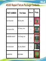
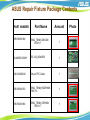
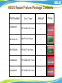
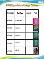
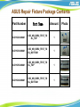
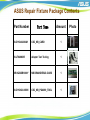
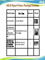
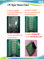
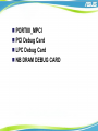
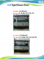
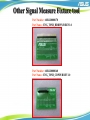
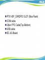
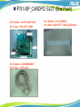
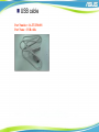
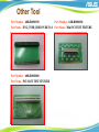
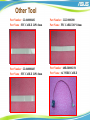
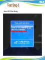
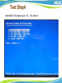
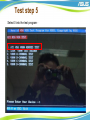
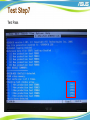
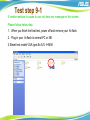
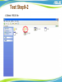
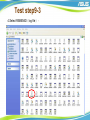
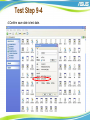
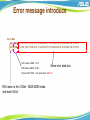
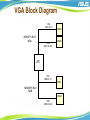
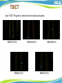
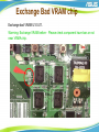
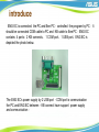
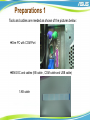
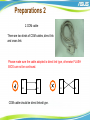
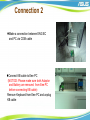
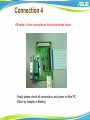
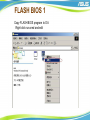
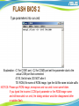
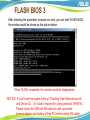
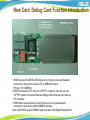
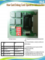
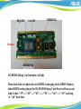
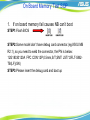
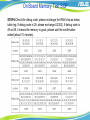
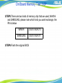
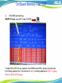
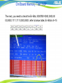
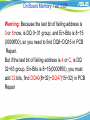
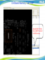
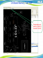
NB_MB Level 3-1 Training Materials (version 1.7) Chapter 1 ASUS Repair Fixture introduce………P3-P10 Chapter 2 CPU Signal Measure Fixture tool …...…..P11-P12 Chapter 3 Port 80 Debug Card Fixture tool..……….P13-P15 Chapter 4 Other Signal Measure Fixture tool ...…....P16-P20 Chapter 5 EeePC Debug Card Fixture tool…….…...P21-P24 Chapter 6 Other tool…………………………..….…P25-P28 Chapter 7 Test Program and Fixture tool SOP …......P29-P49 Chapter 8 Eee PC Flash BIOS Fixture tool SOP…....P50-P63 Chapter 9 EC JIG_BOARD3………………………...P64-P75 Chapter 10 New Card Debug Card SOP..………..….P76-P78 Chapter 11 NB DRAM DEBUG CARD SOP..…..….P79-P82 Chapter 12 On Board Memory Test SOP……..…..…P83-P93 Chapter 13 WTP Test SOP……..…..………………..P94 Chapter 1 ASUS Repair Fixture introduce ASUS Repair Fixture Package Contents PART NUMBER 80-C1TAK0-0300 90-C1G404-10P0Z Part Name PORT80_MPCI LPC Debug Card Amount 1 1 60-NDDDB1000-B01P PCI-E Debug Card 80-C1K090-00A01 CSC_NB_MXM230 1 08-900037800 DDR2-DIMM 1 1 Photo ASUS Repair Fixture Package Contents PART NUMBER Part Name Amount 60R-R0000190 ENG_TSNB_IDECON REV1.0 1 90-N00EG1D00Y EC JIG_BOARD3 1 14G122300240 24 pin FFC Cable 1 60R-R0000170 ENG_TSNB_HDDPIN/B REV1.0 1 60R-R0000160 ENG_TSNB_CDPIN/B REV1.0 1 Photo ASUS Repair Fixture Package Contents Part Name Amount FFC CABLE 26P 1.0mm 1 60R-R0000100 Mini PCI Test Fixture 1 60R-R0000080 PCI SLOT Test Fixture 1 22-060000482 FFC CABLE 24P 1.0mm 1 22-220000200 FFC CABLE 28P 1.0mm 1 Part Number 22-060000483 Photo ASUS Repair Fixture Package Contents Part Number Part Name Amount 60R-R0000230 AC WIRE CABLE 1 20-LT0102659 Centrino 2 1 20-LT0102660 Centrino 3 1 Centrino 4 1 AMD 638 1 20-LT0102661 20-LT0102662 Photo ASUS Repair Fixture Package Contents Part Name Amount 80-C1K020-00A01 CSC_NB_DDR2_TEST_TO OL_TOP 1 80-C1K030-00A01 CSC_NB_DDR2_TEST_TO OL_BOTTOM 1 Part Number 80-C1K050-00A01 80-C1K040-00A01 CSC_NB_DDR3_TEST_TO OL_TOP CSC_NB_DDR3_TEST_TO OL_BOTTOM 1 1 Photo ASUS Repair Fixture Package Contents Part Number Part Name Amount 80-C1K0A0-00A01 CSC_NB_CARD 1 20-LT0400685 Adapter Test Tooling 1 90R-NZADB1000Y NB DRAM DEBUG CARD 1 80-C1K0G0-00B01 CSC_NB_PGA989_TOOL 1 Photo ASUS Repair Fixture Package Contents Part Number Part Name Amount 80-C1K090-00A01 CSC_NB_MXM230 1 80-C1K0B0-00A01 (CSC_NB_VGA_CA RD1 80C1K0C0-00A01 (CSC_NB_VGA_CA RD2 NB VGA BOARD Converter Board(二合一) 1 80-C1K0D0-00A01 (CSC_NB_KB_24PIN 80-C1K0E0-00A01 CSC_NB_KB_28PIN NB KB cable Converter Board (24pin & 28pin) 1 Photo Chapter 2 CPU Signal Measure Fixture Tool CPU Signal Measure Fixture Part Number: 20-LT0102659 Part Name: NB CENTRINO 2 CPU SOCKET TEST(Sonoma) Part Number : 20-LT0102660 Part Name : NB CENTRINO 3 CPU SOCKET TEST(Napa) Part Number : 20-LT0102661 Part Name : NB CENTRINO 4 CPU SOCKET TEST(Santarosa) Part Number : 90R-NZADB1000Y Part Name : NB DRAM DEBUG CARD Chapter 3 Port 80 Debug Card Fixture Tool PORT80_MPCI PCI Debug Card LPC Debug Card NB DRAM DEBUG CARD Port 80 Debug Card Tool Part Number : 80-C1TAK0-0300 Part Name PORT80_MPCI Part Number : 70-C1G343-A01 Part Name : DIAGS_LPC_CAPTURE Part Number : 60-NDDDB1000-B01P Part Name :W1J NEWCARD DEBUG CARD Part Number : 70-C1G343-A01 Part Name : DIAGS_LPC_CAPTURE Chapter 4 Other Signal Measure Fixture tool RAM Signal Measure Fixture DDR-DIMM DDR2-DIMM CSC_NB_DDR2_TEST_TOOL_TOP CSC_NB_DDR2_TEST_TOOL_BOTTOM CSC_NB_DDR3_TEST_TOOL_TOP CSC_NB_DDR3_TEST_TOOL_BOTTOM IDE/ODD Signal Measure Fixture ENG_TSNB_HDDPIN/B REV1.0 ENG_TSNB_CDPIN/B REV1.0 RAM Signal Measure Fixture Part Number : 08-900029500 Part Name : DDR-DIMM Part Number : 08-900037800 Part Name : DDR2-DIMM Part Number : 80-C1K020-00A01 Part Name :CSC_NB_DDR2_TEST_TOOL_TOP Part Number : 80-C1K030-00A01 Part Name : CSC_NB_DDR2_TEST_TOOL_BOTTOM RAM Signal Measure Fixture Part Number : 80-C1K050-00A01 Part Name : CSC_NB_DDR3_TEST_TOOL_TOP Part Number : 80-C1K040-00A01 Part Name : CSC_NB_DDR3_TEST_TOOL_BOTTOM Other Signal Measure Fixture tool Part Number : 60R-R0000170 Part Name : ENG_TSNB_HDDPIN/B REV1.0 Part Number : 60R-R0000160 Part Name : ENG_TSNB_CDPIN/B REV1.0 Chapter 5 EeePC Debug Card Tool P701-ISP_CARDPCI SLOT (Bios Flash) COM cable 28pin FPC Cable(Top-Bottom) USB cable EC JIG Board P701-ISP_CARDPCI SLOT (Bios Flash) Part Number : 60-2OA80827A039 Part Name : P701-ISP_CARD Part Number :14G010006400SY Part Name : COM cable Part Number : 14G122300281 Part Name :28pin FPC Cable(Top-Bottom) USB cable Part Number : 16-TT4700491 Part Name : USB cable Chapter 6 Other Tool ENG_TSNB_IDECON REV1.0 PCI SLOT Test Tool Mini PCI Test Tool FFC CABLE 24P 1.0mm FFC CABLE 26P 1.0mm FFC CABLE 28P 1.0mm AC WIRE CABLE Other Tool Part Number : 60R-R0000190 Part Number : 60R-R0000100 Part Name : ENG_TSNB_IDECON REV1.0 Part Name : Mini PCI TEST FIXTURE Part Number : 60R-R0000080 Part Name : PCI SLOT TEST FIXTURE Other Tool Part Number : 22-060000482 Part Name : FFC CABLE 24P 1.0mm Part Number : 22-220000200 Part Name : FFC CABLE 28P 1.0mm Part Number : 22-060000483 Part Name : FFC CABLE 26P 1.0mm Part Number : 60R-R0000230 Part Name : AC WIRE CABLE Chapter 7 Test Program and Fixture Tool SOP VRAM Test Program SOP Eee PC Flash BIOS Tool Operation SOP EC JIG Board SOP PCI-E Debug Card SOP VRAM Test Program SOP Test Step1 Access http://sip.asus.com download VGA test program. Test Step 2 Unzip VGA test program into your AI-flash. Warning: AI-flash must support booting file. Test Step 3 Select USB AI-flash Booting。 Test Step4 Select M/B VGA chipset type。Ex:A7J select 3 Test step 5 Select 0 into the test program。 Test step 6 Test during, abnormal line on the screen. Test Step7 Test Pass Test step8 Test error message Test step 9-1 If random serious to cause to can not view any message on the screen. Please follow below step. 1. When you finish the final test, power off and remove your Ai-flash. 2. Plug in your Ai-flash to normal PC or NB 3.Slecet test model VGA type.Ex:A7J M56 Test Step9-2 4.Slelect R5XX file。 Test step9-3 4.Select R5MEMID(log file)。 Test Step 9-4 4.Confirm save date is test date. Test step9-5 5.Read test message。 Error message introduce Error Bits rk0 CHA: 0 1 2 3 4 5 6 7 8 9 10 11 12 13 14 15 16 17 18 19 20 21 22 23 24 25 26 27 28 29 30 31 rk0 CHB: 0 1 2 3 4 5 6 7 8 9 10 11 12 13 14 15 16 17 18 19 20 21 22 23 24 25 26 27 28 29 30 31 CHA mean is MDA,0~31 CHB mean is MDA, 32~63, Show error data bus If show CHB 10 fail,You need check MDA 42 Rk0 mean is first 128bit,MDA MDB inside and each 64 bit。 VGA Block Diagram CHA MDA 0~31 MEMORY BUS MDA CHB MDA 32~63 VRAM VRAM ATI CHC MDB 0~31 VRAM MEMORY BUS MDB VRAM CHD MDB 32~63 Exemplification Model:A7J Error message below: Error Bits rk0 CHA: 17 23 30 rk0 CHB: 15 24 Memory Data Bus rk0 CHA: 17 23 30 = MDA17, MDA23, MDA30 rk0 CHB: 15 24 = MDA47,MDA56 TSICT User TSICT Program to check the error data bus location。 MDA17(U10) MDA47(U11) MDA23(U10) MDA30(U10) MDA47(U11) Exchange Bad VRAM chip Exchange bad VRAM U10 U11. Warming: Exchange VRAM before,Please check component have loss or not near VRMA chip. Chapter 8 Eee PC Flash BIOS Tool operation SOP introduce ENG EC is connected the PC and Eee PC,controlled the program by PC。It should be connected COM cable to PC and KB cable to Eee PC。ENG EC contains 4 ports:2 KB connects, 1 COM port,1 USB port。ENG EC is depicted the photo below。 The ENG EC’s power supply by 2 USB port,COM port is communication the PC and ENG EC between,KB connect have support power supply and communication。 Preparations 1 Tools and cables are needed as shown of the pictures below: One PC with COM Port ENG EC and cables (KB cable , COM cable and USB cable) 1.KB cable Preparations 2 2.COM cable There are two kinds of COM cables, direct link and cross link: Please make sure the cable adopted is direct link type, otherwise FLASH BIOS can not be continued. √ TX TX RX RX TX TX RX RX ╳ COM cable should be direct linked type. Preparations 3 3.USB cable One Eee PC to flash BIOS. Program for Flashing BIOS should be installed on PC. Connection 1 Connect ENG EC to PC via USB cable Plug ENG EC directly to PC is also feasible Connection 2 Make a connection between ENG EC and PC via COM cable Connect KB cable to Eee PC (NOTICE: Please make sure both Adaptor and Battery are removed from Eee PC before connecting KB cable) Remove Keyboard from Eee PC and unplug KB cable Connection 3 Connect KB cable to keyboard, (Please notice the cable direction) The other side of KB cable should be connected to ENG EC Please notice the difference between the two KB connectors when connecting KB cable Connection 4 KB cable is often connected as the picture shows below Finally please check all connections, and power on Eee PC (Either by Adaptor or Battery) FLASH BIOS 1 Copy FLASH BIOS program to OA Right click run.cmd and edit FLASH BIOS 2 Type parameters into run.cmd Explanation: -C1 for COM1 port, -C2 for COM2 port set the parameter due to the actua COM port that connected -S115, Set bit rate, DO NOT alter it 701.ROM, file name of ROM image, type the full file name include suffix NOTICE: Please put ROM image, enespi.exe and run.cmd in one same folder. If you typed the incorrect COM port parameter or the ROM image name and still executed run.cmd, the dialog window would be disappeared after a sudden flash. FLASH BIOS 3 After checking the parameter, execute run.cmd, you can start FLASH BIOS, the window would be shown as the picture below When FLASH completed, the window would be disappeared. NOTICE: IF you found the system halts at “Checking Flash Manufacture ID and Device ID…”,or it didn’t respond for a long period at “WWWW…”. Please check the USB and KB cable are well connected (remove adaptor and battery of Eee PC before unplug KB cable). Wait until upgrade complete and remove adaptor and battery NOTICE:DO NOT remove power when FLASHING BIOS. When FLASHING completed, power should be cut off firstly for Eee PC (Remove both adaptor and battery), then unplug KB cable. Problem Analysis When FLASH BIOS completed, if POWER LED doesn’t light in power on, BIOS was not correctly flashed, please FLASH BIOS again. If POWER LED and WIFI LED are both on, clear CMOS, if the issue still existed, please FLASH BIOS again. Chapter 9 EC JIG_BOARD3 Chapter 10 New Card Debug Card SOP New Card Debug Card Function Introduction 1.If M/B reserved the NEWCARD debug circuit, then we can use Newcard connector to show post code via LPC or SMBUS interface (Priority: LPC>SMBUS) 2.If M/B reserved the LPC circuit to 12P FPC connector, then we can use 12P FFC cable to connector Newcard Debug card and show post code via LPC interface. 3.If M/B didn’t reserved debug circuit, then we can only use Newcard connector to show post code via SMBUS interface. Note: ASUS BIOS support SMBUS post code after Intel Santa Rosa platform. New Card Debug Card Operation Introduction 1.DIP switch Function: ON OFF SW1 Boot with Debugcard’s ROM Boot with M/B’s ROM SW2 Reserved Reserved SW3 Don’t Flash BIOS Flash BIOS (ps:1) SW4 Choose SIO 2E/2F Choose SIO 4E/4F (ps2) ps1: debug card must have LPC/FWH ROM with BIOS code. ps2: Choose SIO address , avoiding the confliction with M/B SIO address. 2. LPC/FWH ROM connector: Socket for LPC/FWH ROM(Can’t use ISA ROM) 3. LED function: POWER-ON LED (When +3v is available, LED turn ON) Debug ROM LED (When switch1 ON, LED turn ON) FLASH BIOS LED (When switch3 ON, LED turn ON) Chapter11 NB DRAM DEBUG CARD SOP SO-DIMM Debug Card user guide R1.0 SO-DIMM Debug Card with the SMBUS interface debug card(The funtion is the same with Newcard Debug card via SMbus interface),It provides two type ---DDRII&DDRIII, when you use it, please plug it in the SO-DIM socket.About it's component intorduction is below the photo . When Debug card show "00", please ask BIOS RD to check if the program code of SMBUS interface debug is supported this model or not. DDRII Pin High Bit Low Bit For design use TOP DDRIII Pin CPLD IC High Bit Low Bit DDRII Pin Bottom DDRIII Pin SO-DIMM Debug Card introduce of light Please look below of photo,the one DIMM socket plug in the DDR3 Memory, other DIMM socket plug in the SO-DIMM Debug Card.Pwoert after,you can find it show "15"--->"4F"---->"b2"----->"92"---->"A0"---->"A9" and stop at "Ab" then boot. Chapter 12 On Board Memory Test SOP On Board Memory Test SOP • This test program can test on board memory. • There are two test mode: 1. On board memory fail causes NB can’t boot (only for K40IJ,K50IJ) 2. NB can boot On Board Memory Test SOP 1. If on board memory fail causes NB can’t boot STEP1:Flash BIOS STEP2:Some model don’t have debug card connector.(eg.K50IJ MB R2.1), so you need to weld the connector, the PN is below: 12G18330120A FPC CON 12P,0.5mm,S/T,SMT JST/12FLT-SM2TB(LF)(SN) STEP3:Please insert the debug card and boot up On Board Memory Test SOP STEP4:Check the debug code, please exchange the RAM chip as below table (eg. If debug code is 29, please exchange U2302). If debug code is AA or 88, it means the memory is good, please wait the confirmation ended (about 10 minutes). On Board Memory Test SOP STEP5:There are two kinds of memory chip that we used, NANYA and SAMSUNG, please note which kind you want exchange, the PN is below NANYA 03G15162F210 SAMSUNG 03G15162F311 STEP6:Flash the original BIOS On Board Memory Test SOP 2. If the NB can boot up, STEP1:Please run mt211.exe in DOS. To take K40IJ,K50IJ for an example: One DIMM have 64DQ, please check the last bit of failing address first, if the last bit is 0 or 8, the failing address is DQ 0~31 group, if 4 or C, is DQ 32~63 group. On Board Memory Test SOP The next, you need to check the Err-Bits, 0000ff00=0000,0000,00 00,0000,1111,1111,0000,0000, refer to below table, Err-Bits is 8~15 On Board Memory Test SOP Warning: Because the last bit of failing address is 0 or 8 now, is DQ 0~31 group, and Err-Bits is 8~15 (0000ff00), so you need to find DQ8~DQ15 in PCB Repair. But if the last bit of failing address is 4 or C, is DQ 32~63 group, Err-Bits is 8~15(0000ff00), you must add 32 bits, find DQ40(8+32)~DQ47(15+32) in PCB Repair On Board Memory Test SOP Search DQ8~15,find M_A_DQ8~15 are all in U2302 on top On Board Memory Test SOP Press bottom and find M_A_DQ8~15 Are also in U2402 On Board Memory Test SOP So you can exchange U2302 and U2402, and U23XX should be take priority over U24XX. Warning: If the last bit of failing address is 4 or C, search DQ40~DQ47, find they are all in U2306 and U2406. Chapter 13 WTP Test SOP