1
CDMA 800/AMPS-V2260, T2260
CDMA Dual Mode 800-1900-V2267,
T2267
CDMA
CDMA 800/1900
COMPUTER SOFTWARE COPYRIGHTS
The Motorola products described in this instruction manual may include copyrighted Motorola computer programs stored in semi-conductor memories or other
media. Laws in the United States and other countries preserve for Motorola certain
exclusive rights for copyrighted computer programs, including the exclusive right
to copy or reproduce in any form the copyrighted computer program. Accordingly,
any copyrighted Motorola computer programs contained in the Motorola products
described in this instruction manual may not be copied or reproduced in any manner
without the express written permission of Motorola. Furthermore, the purchase of
Motorola products shall not be deemed to grant either directly or by implication,
estoppel, or otherwise, any license under the copyrights, patents or patent applications of Motorola, except for the normal non-exclusive, royalty free license to use
that arises by operation of law in the sale of a product.
2
4/3/01
CONTENTS
Cellular Subscriber Sector
Preface . . . . . . . . . . . . . . . . . . . . . . . . . . . . . . . . . 5
Major Differences Shark &ST800 Manta . . . . . . . 5
General Shark Logic Circuit . . . . . . . . . . . . . . . . . 6
Shark RF circuit . . . . . . . . . . . . . . . . . . . . . . . . . . . 7
Performance Specifications General . . . . . . . . . . . 9
Overall System. . . . . . . . . . . . . . . . . . . . . . . . . . . 10
Environmental . . . . . . . . . . . . . . . . . . . . . . . . . . . 11
CDMA 800/AMPS-V2260, T2260
CDMA Dual Mode 800-1900-V2267, T2267
Block Diagram of PCS receiver . . . . . . . . . . . . . 27
Tx Block Diagram . . . . . . . . . . . . . . . . . . . . . . . . 27
PCS Transmitter Block Diagram . . . . . . . . . . . . 28
Tests and Adjustments . . . . . . . . . . . . . . . . . . . 29
Introduction . . . . . . . . . . . . . . . . . . . . . . . . . . . . 29
Test interface . . . . . . . . . . . . . . . . . . . . . . . . . . . . 29
Foreward . . . . . . . . . . . . . . . . . . . . . . . . . . 12
Adjustments. . . . . . . . . . . . . . . . . . . . . . . . . . . . . 29
Scope of Manual . . . . . . . . . . . . . . . . . . . . . . . . . 12
Connections for testing and adjustments. . . . . . . 30
Replacement Parts Ordering . . . . . . . . . . . . . . . . 12
Keypad Button Functions . . . . . . . . . . . . . . . . . . 31
Service . . . . . . . . . . . . . . . . . . . . . . . . . . . . . . . . . 13
TX Output Power Adjustments (center Of Band) 31
General Safety Information . . . . . . . . . . . . . . . . . 13
Maximum Deviation Adjust . . . . . . . . . . . . . . . . 32
Portable Operation . . . . . . . . . . . . . . . . . . . . . . . . 13
Microphone Deviation Adjust. . . . . . . . . . . . . . . 32
Mobile Operation . . . . . . . . . . . . . . . . . . . . . . . . . 13
DTMF Adjust . . . . . . . . . . . . . . . . . . . . . . . . . . . 32
SAT Deviation Adjust. . . . . . . . . . . . . . . . . . . . . 33
Description . . . . . . . . . . . . . . . . . . . . . . . . 14
Overall Concept . . . . . . . . . . . . . . . . . . . . . . . . . . 14
Operation . . . . . . . . . . . . . . . . . . . . . . . . . . . . . . . 14
Service Area . . . . . . . . . . . . . . . . . . . . . . . . . . . . . 15
Theory of Operation . . . . . . . . . . . . . . . . . . . . . 16
AMPS Receiver Circuitry . . . . . . . . . . . . . . . . . . 16
AMPS Transmitter Circuitry . . . . . . . . . . . . . . . . 16
CDMA Receiver Circuitry . . . . . . . . . . . . . . . . . 16
CDMA Transmitter Circuitry. . . . . . . . . . . . . . . . 16
Frequency Synthesizer Circuitry . . . . . . . . . . . . . 17
Transmit Power Control Circuitry . . . . . . . . . . . . 17
Receive Audio Amps Mode . . . . . . . . . . . . . . . . . 17
Receive Audio CDMA Mode . . . . . . . . . . . . . . . 17
Transmit Audio Amps Mode . . . . . . . . . . . . . . . . 17
Transmit Audio CDMA Mode . . . . . . . . . . . . . . . 18
Audio Logic block diagram . . . . . . . . . . . . . . . . . 19
Forward Audio Functionality. . . . . . . . . . . . . . . . 20
Logic Circuitry description CDMA Basel-Start . 21
CDMA Base stand Re Path . . . . . . . . . . . . . . . . . 22
Data Deviation Adjust . . . . . . . . . . . . . . . . . . . . . 33
RX Discriminator Adjust . . . . . . . . . . . . . . . . . . 33
Amps Call Processing . . . . . . . . . . . . . . . . . . . . . 33
CDMA Call Processing. . . . . . . . . . . . . . . . . . . . 34
Testing . . . . . . . . . . . . . . . . . . . . . . . . . . . . . . . . 36
Test Mode Test menu . . . . . . . . . . . . . . . . .36
Introduction . . . . . . . . . . . . . . . . . . . . . . . . .36
Status Display Level . . . . . . . . . . . . . . . . . . .36
Servicing Level . . . . . . . . . . . . . . . . . . . . . . . .36
CDMA Specific Features . . . . . . . . . . . . . . . . .36
Test Menu . . . . . . . . . . . . . . . . . . . . . . . . . . .36
Markov Calls . . . . . . . . . . . . . . . . . . . . . . . . . . . . 37
Service Option 2 . . . . . . . . . . . . . . . . . . . . . . . . . 37
Test Mode . . . . . . . . . . . . . . . . . . . . . . . . . . . . . . 38
Handset Commands . . . . . . . . . . . . . . . . . . . . . . 38
Nam Programming . . . . . . . . . . . . . . . . . . . . . . . 48
Introduction . . . . . . . . . . . . . . . . . . . . . . . . . . . . . 48
Test Mode Programming. . . . . . . . . . . . . . . . . . . 48
Test Mode NAM Programming Sequence . . . . . 49
AMPS receiver Block Diagram . . . . . . . . . . . . . . 24
AMPS Transmitter Block Diagram . . . . . . . . . . . 25
3
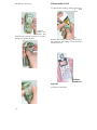
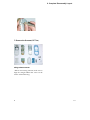
Disassembly . . . . . . . . . . . . . . . . . . . . . . . . . . . . 55
© 2000 Motorola, Inc.
CDMA 800/1900
Introduction . . . . . . . . . . . . . . . . . . . . . . . . . . . . . 55
Recommended Tools . . . . . . . . . . . . . . . . . . . . . . 55
Disassembly Procedure . . . . . . . . . . . . . . . . . . . . 55
Assembly Procedure . . . . . . . . . . . . . . . . . . . . . . 55
Troubleshooting . . . . . . . . . . . . . . . . . . . . . . . . 59
Introduction . . . . . . . . . . . . . . . . . . . . . . . . . . . . . 59
Troubleshooting and Repair. . . . . . . . . . . . . . . . . 59
Testing after Repair . . . . . . . . . . . . . . . . . . . . . . . 59
Replacement Parts . . . . . . . . . . . . . . . . . . . . . . . 69
See the Schematics / Parts section for a detailed view
and print only parts list.
4
4/3/01
PREFACE
CDMA 800/AMPS-V2260, T2260
CDMA Dual Mode 800-1900-V2267, T2267
Cellular Subscriber Sector
Logic Changes
General:
1. Dual Mode single band-800MHz AMPSand 800MHz CDMA. There are two models -(1)V.
V2260 (II) Timeport T2260.
2. Dual band dual Mode- 800 MHz AMPS and 1900 MHz CDMA (PCS) There are two models-
V. 2267
Time port T2267
Competitively priced with the value added fictionalizing and feature set(s)
Microbrowser capable.
Full matrix 95x32 Pixel dot matrix display with hard icons.
Intergrated headset jack conveniently located on the top left side of the unit.
MT and MO SMS
Form factor proven through global research. Designed to be the most comfortable phone on the
market
Smart button
Main Housings:
This product utilizes completely new front and rear housings, the housing utilizes new materials, finishes and textures which maximizes the feeling of comfort.
AAAL Battery door protects the batteries, but allow for the unit to fully function (charge, Tx and
Rx) without the door in place. The door connects with the phone and be released with the push
of a button.
Contact points on the back of the phone below the antenna for factory, and service testing,
flexing, flashing etc.
A power port for the internal charger/CLA for all the models. This is located on the lower right
5
© 2000 Motorola, Inc.
CDMA 800/1900
side of the unit.
The integrated Headset Jack is located on the top left side of the unit.
All the rear housings accommodate the removable belt clip attachments.
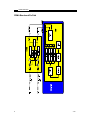
SHARK LOGIC CIRCUIT
The main chip sets of SHARK CDMA are the CASPER, CIA and CCAP-LITE.
The CASPER include the 32 bits 68338 MCU, which controls the whole part of the phone and the
CSP, which processes the CDMA baseband digital signals and DSP, which performs the 8K/
13Kbps Q-CELP Vocoding function.
The CIA provides the analog CDMA signal interface and the Audio function.
CCAP-LITE provides the power management function of the phone.
The memory consist of 16Mbits of Flash(1M x 16) and 2Mbits SRAM
(128K x 16).
The logic parts have the watchdog, keypad, backlite, oscillator circuit
And display and charging circuit.
The charging circuit contains COVIC IC which is 8 pin. Aids in Kick
Start charging/ overvoltage protection.
Display is a LCD 96 x 32 graphic matrix with additional icon COG and KS0717 Driver IC.
There is no butt plug, the communication to the phone takes place using special cable that plugs
at the back of the phone, above the batteries, you have to remove the battery door to access these
test points.
Shark uses 3 AAAL cells 1.2Volts.
There are two models in shark: Timeport and V.
6
4/3/01
Preface
SHARK RF CIRCUIT
The RF circuit is very similar to CALIBER product, The Dual-Band
CDMA SHARK contains two completely separate receiver paths: an 800 MHz path that converts
analog signals and a 1900 MHz path for the digital CDMA signal. The two paths have different
RF, LO and IF frequencies.
In shark there is no accessory port for RF from the butt plug. To perform RX and TX test attach
the special cable to the RF test point on the back side near the antenna, remove the groumet.
Frequency of operation and channel
1900 Mhz Receiver Band 1930 to 1990 Mhz
1900 Mhz Transmitter Band 1850 to 1910 Mhz
The maximum output power applied to the antenna is:
Analog: 24.5dBm
PCS CDMA: 23.5dBm
Shark uses the ME3C mixer-exciter IC rather than the MOON IC part.
The ME3C allows full control of the RF power range from –39 dBm to +11dBm without having to
vary the ZIFSYN output power. The ME3 requires two LO’s, one for PCS, the other for analog.
The IF input pins are the same regardless of analog/PCS. There is one enable pin for the ME3C,
one pin for analog/PCS mode, and one for AGC pin. The two separate RF mixer outputs are
combined and drive to exciter. The ME3C PCS does require an interstage RF filter between the
Mixer and the exciter, but AMPS mode doesn’t require an interstage RF filter.
Shark uses DUAL BAND VCO Module for main LO, 14 pin part with two outputs one for AMPS
and another for PCS, the control voltage from ZIFSYN IC varies from 0.5 V to 2.2 V, the VCC to
the IC is supplied by the VSF 1900 and VSF 800. The output is split into RX_LO and TX_LO for
both AMPS and PCS LO.
The rest of the RF circuit is similar to DUAL BAND Caliber product.
7
4/3/01
CDMA 800/1900
CDMA –PCS 1900 Mhz BAND
Performance specification:
General
Frequency and channel information:
Channel
25
200
400
600
800
1000
1175
8
Tx Frequency (Mhz)
1851.25
1860.00
1870.00
1880.00
1890.00
1900.00
1908.50
Rx Frequency(Mhz)
1931.25
1940.00
1950.00
1960.00
1970.00
1980.00
1988.50
4/3/01
Preface
CDMA 1900MHz Performance Specifications General
Table 1:
Function
Specification
Frequency Range
1850 to 1910 MHz(tx), 1930 to 1990(RX)
RF Channel Bandwidth
1.25 MHz
Channels
48 (Channels spaced at an increment of-25)
Duplex Spacing
80 MHz
Frequency Stability
Center Frequency* +/- 8.5 X10⁻⁸
+/- 150 Hz of incoming RX CDMA signal.
Operation Voltage
+3.6 V nominal (3.0 -4.2 V DC)
RF Power output
0.20 Watts - 23 dBm into 50 ohms (CDMA, nominal)
input/output impedance
50 ohms(nominal)
Spurious /Harmonic emissions
Complies with title 47, Part 22 of the code of federal regulations.
Vocoders
8kbps, 13kbps, EVRC
Transmit Time Error
+/- 1 US
Modulation Type
1M25D1W(1.25MHz bandwidth), OQPSK, G7W(CDMA)
Transmit Duty Cycle
Variable- full, 1/2, 1/4, 1/8 rate(CDMA Mode)
CDMA Transmit Waveform
Quality(rho)
0.94
Receive Sensitivity
-104dBm(CDMA, 0.5% Static FER, 8kbps Vocoder)
Display
96 X 32 LCD
Specifications
Overall System CDMA 800MHz
Table 2:
Function
Frequency Range
9
Specification
824.04 - 848.97 MHz Tx,
Channels 1 to 799, f Tx = 0.03 * N+ 825 MHz
Channels 990 to 1023, f Tx = 0.03(N—1023) + 825 MHz
869.04 - 893.97 MHz Rx
Channels 1 to 799 is f Rx = 0.03 * N+ 870 MHz
Channels 990 to 1023, f Rx = 0.03(N—1023) + 870 MHz
4/3/01
CDMA 800/1900
Table 2:
Function
Specification
Channel Spacing
30 KHz
Channels
832
Duplex spacing
45 MHz(amps)
Frequency Stability
+/- 2.5 ppm (Amps)
Operating Voltage
3.6 - 4.8 VDC
Display
96 X 32 LCD
RF Power Output
0.6 watts - 28.0 dBM into 50 ohms (AMPS, nominal)
0.25 watts - 24.0 dBM into 50 ohms (CDMA, nominal)
Input/Output Impedance
50 ohms (nominal)
Spurious / Harmonic
Emissions
Complies with Title 47, Part 22 of the code of Federal Regulations.
Audio Distortion
Less than 5% at
Hum and Noise(CMSG)
32 dBm below +/- 8kHz deviation(transmit and receive)
Modulation
F3: + 12 kHz for 100% at 1 kHz, AMPS (wide)
1M25D1W (1.25 MHz bandwidth) CDMA
Transmit Audio
Response
6 dBm/octave pre-emphasis
Transmit Audio sensitivity
(AMPS)
+ 2.9 kHz deviation (nom.) @ 97 dBm SPL input @ 1 kHz
Transmit Duty Cycle
full, 1/2, 1/4, 1/8 rate (CDMA Mode)
CDMA Transmit
Waveform
Quality(Rho)
0.94
Receiver Sensitivity
-116 dBm (AMPS, SINAD, C-MSG weighted)
-104 dBm (CDMA, 0.5% Static FER)
Alternate Channel
Desense Protection
-60 db@+/- 60kHz (Amps)
Table 3: Environmental
Function
Specification
Temperature Range
Operational -30 o C to +60 o C (-22 o F to +140 o F)
Storage -55 o C to +85 o C (-67 o F to +185 o F)
Thermal Shock -40 o C to +85 o C (-40 o F to +185 o F)
meets Mil. Std. 810C
Shock
Exceeds EIA Standards RS152B (Section 15) and IS-19
10
4/3/01
Preface
Table 3: Environmental
Function
Specification
Drop
Exceeds EIA Standards RS316B and IS-19
Humidity
95% Relative Humidity; meets EIA Standard IS-19
Vibration
Exceeds EIA Standards RS316B and IS-19
Salt Fog
Salt Solution fog at 35 o C (95 o F), tested for 48 hours
Dust
140 mesh blown silica flour test, tested for 5 hours
Notes:
• EIA (Electronic Industries Association) Standard RS152B states the
minimum stan-dards for Land Mobile Communications, FM or PM
transmitters 25-470 MHz.
• EIA IS-19 states the recommended standards for 800 MHz cellular
subscriber units.
• EIA Standard RS316B states the standards for portable land mobile
communications.
• U.S. Military Standard 810D establishes uniform environmental test
methods for deter-mining the resistance of equipment to the effects of
natural and induced environments peculiar to military operations.
• TIA/EIA/IS-98 Recommended Minimum Performance Standards for
Dual-Mode Wide band Spread spectrum Cellular Mobile Stations.
Specifications subject to change without notice.
11
4/3/01
CDMA 800/1900
Foreword
Scope of Manual
This manual is intended for use by experienced technicians familiar with similar types of equipment. It is intended primarily to support basic servicing, which consists primarily of mechanical
repairs and circuit board replacement.
Authorized distributors may opt to receive additional training to become authorized to perform
limited component repairs. Contact your regional Customer Support Manager for details.
Model and Kit Identification
Motorola products are specifically identified by an overall model number on the product label. In
most cases, assemblies and kits which make up the equipment also have kit numbers stamped on
them.
Replacement Parts Ordering
Motorola maintains a parts office staffed to process parts orders, identify part
numbers, and otherwise assist in the maintenance and repair of Motorola Cellular
products. Orders for all parts should be sent to the Motorola International Logistics Department at the following address:
Attn.: Global Spare Parts Department
Motorola Cellular Subscriber Group
2001 N, Division St.
Harvard, IL 60033-3674
U. S. A.
FAX: 1-815-884-8354
When ordering replacement parts or equipment information, the complete identification number should be included. This applies to all components, kits, and
chassis. If the component part number is not known, the order should include the
number of the chassis or kit of which it is a part, and sufficient description of the
desired component to identify it.
12
4/3/01
Preface
Service
Motorola’s regional Cellular Subscriber Service Centers offer some of the finest repair capabilities available to Motorola Subscriber equipment users. The Cellular Subscriber Service Centers
are able to perform computerized adjustments and repair most defective transceivers and boards.
Contact your regional Customer Service Manager for more information about Motorola’s repair
capabilities and policy for in-warranty and out-of-warranty repairs in your region.
General Safety Information
CAUTION
Do not jump start vehicle or use an
automotive battery charger while the
vehicle adapter option and the
portable
radiotelephone
are
connected to the vehicle electrical
system, as this may cause serious
damage to the radio. Disconnect the
radio by removing the cable kit fuses.
Portable Operation
DO NOT hold the radio so that the antenna is very close to, or touching, exposed parts of the
body, especially the face or eyes, while transmitting. The radio will perform best if it is held in the
same manner as you would hold a telephone handset, with the antenna angled up and over your
shoulder. Speak directly into the mouthpiece.
DO NOT operate the telephone in an airplane.
DO NOT allow children to play with any radio equipment containing a transmitter.
Mobile Operation (Vehicle Adaptor)
As with other mobile radio transmitting equipment, users are advised that for satisfactory operation of the equipment and for the safety of personnel, it is recommended that no part of the human
body shall be allowed to come within 20 centimeters of the antenna during operation of the equipment.
DO NOT operate this equipment near electrical blasting caps or in an explosive atmosphere.
Mobile telephones are under certain conditions capable of interfering with blasting operations.
When in the vicinity of construction work, look for and observe signs cautioning against mobile
radio transmission. If transmission is prohibited, the cellular telephone must be turned off to
prevent any transmission. In standby mode, the mobile telephone will automatically transmit to
acknowledge a call if it is not turned off.
All equipment must be properly grounded according to installation instructions for safe operation.
13
4/3/01
CDMA 800/1900
14
4/3/01
Cellular Subscriber Sector
CDMA 800/AMPS-V2260, T2260
CDMA Dual Mode 800-1900-V2267, T2267
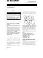
DESCRIPTION
Table 4:
Note
The following description is intended only as a
preliminary general introduction to cellular
systems. This description is greatly simplified
and does not illustrate
are shared by both the mobile station and
base station and are called “pseudo-random
code sequences”. Since CDMA is a spread
CELL B
the full operating capabilities, techniques, or
technology involved in cellular systems.
Overall Concept
Cellular systems are used to provide radiotelephone
service in the frequency range of 824-894
MHz.
A cellular system provides higher call handling capacity and system availability than
would be possible with conventional radiotelephone systems that require total system
area coverage on every operating
channel. The cellular system divides the system coverage area into several adjoining
sub-areas, or cells.
Each cell contains a base station (cell site)
which provides transmitting and receiving
facilities. CDMA is a “spread spectrum”
technology, which means that it spreads the
information contained in a particular signal
of interest over a greater bandwidth than the
original signal. With CDMA, unique digital
codes, rather than separate RF frequencies or
channels are
used to differentiate subscribers. The codes
©2000 Motorola, Inc.
CELL A
CELL D
CELL C
spectrum technology, all users share a range
of the radio spectrum. CDMA cell coverage
is dependent upon the way the network is
designed. For each system 3 characteristics
must be considered: coverage, quality, and
capacity. These 3
must be balanced for desired lever of performance.
Some of the CDMA benefits are:
- Improved call quality with better and
more consistent sound.
- Enhanced privacy.
- Variable rate vocoder.
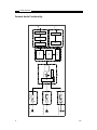
Figure 1: Hypothetical Cell System
Operation
In Figure 1: “Hypothetical Cell System”, the
area bounded by bold lines represents the
total coverage area of a cellular system.
This area is divided into several cells, each
containing a cell site base station which
interfaces radiotelephone subscribers to the
switching system. Since there are no channels in CDMA, a user has a better chance of
completing a call. Also, now there is no hard
handoff between
cell sites since all sites operate on the same
frequency. This is called soft handoffs. In
this system, subscribers in cell A & D simultaneously operate in the same frequency. As
a user moves from cell site to cell site, the
base station monitors the signal strength of
the user. Based on this signal strength, the
base station decides which cell shall carry
the call. When a radiotelephone is in use well
within a cell, the signal strength received at
the cell site base station will be high. As the
phone is moved towards the edge of the cell,
its received signal strength decreases.
Signal strength information therefore
provides an indication of the subscriber’s
distance from a cell’s base station. This
change is handled automatically, and is completely transparent to the user. For example,
assume that a cellular tele-phone
initiates a call in cell A and then moves
across the system area through cells B and C
to cell D. As the phone moves into cell B, it
is instructed to change to a different frequency that operates through the B cell
on that frequency. A similar change is performed when the phone moves from cell B to
cell C and again
when the phone moves from cell C to cell D.
In this example, the radiotelephone has operated in four cell sites, through four cell sites,
and on the same spread spectrum without
interruptions in voice communications. As the radiotelephone leaves a cell, the
frequency on which the phone and base station were operating is made available to
another subscriber in that cell. Since this
radiotelephone is dual mode, the
radiotelephone can operate in either a
16
CDMA system or Analog system.
Service Area
The area within which calls can be placed
and received is defined by the system operator.
(Because this is a radio system, there is no
exact boundary that can be drawn on a map.)
If the portable is outside the radio service
area, a No Svc (no service) message will
appear on the phone’s display, and calls
cannot be placed or received. If this happens
during a conversation, the call is lost. Places
where the ability to place or receive calls
would be lost are in totally enclosed areas,
such as underground parking garages, in
buildings without windows, and in elevators.
This situation would be indicated either by
the No Svc message illuminating, or by the
sound of either a fast busy signal or a highlow siren signal when call placement is
attempted. General usage in buildings having
reason-able glass area is usually quite good.
However, it may be necessary to move closer
to a window to ensure reliable opera-tion.
4/3/01
THEORY OF OPERATION
Cellular Subscriber Sector
CDMA 800/AMPS-V2260, T2260
CDMA Dual Mode 800-1900-V2267, T2267
Theory of Operation
AMPS
Reciever Circuitry
RF enters the phone via the internal antenna,
A1. The received RF signal is routed through
monoblock duplex filter FL13, and FL12.
The RF signal is routed through additional
gain and filtering stages,Q40, , FL40, and
Q40. The received signal then enters the
Mixer U120.
The local oscillator input to the Filter FL120
is a 978-1004 MHz VCO, U680 controlled
by the IF/Synthesizer IC U700. The 109.65
MHz mixer output is routed through FL201
into the IFIC U700.
Transmitter Circuitry
The modulated TX Offset VCO signal is
mixed with the 978-1004 MHz local oscillator signal in TX Mixer U600 to produce an
823-849 MHz transmit signal. This signal
passes through filter FL600 and voltage control attenuator thru U600 which controls the
TX output power. Then the TX signal is
amplified by U430. The output passes
through the mono-block duplex filter FL12
and FL13 to RF switch the internal antenna
accessory connector.
17
CDMA PCS
Reciever Circuitry
RF enters the phone via the internal antenna,
A1. The received RF signal is routed through
monoblock duplex filter FL13 and FL10.
Then the RF signal is routed through a direct
path through additional gain and filtering
stages,Q20, FL20. The received signal then
enters the Mixer Q100.
The local oscillator input to the mixer is double of 1019-1050 MHz VCO, U600 controlled by the IF/Synthesizer IC U700. The
109.8 MHz mixer output is routed through
FL200 into the IFIC U700.
Transmitter Circuitry
The modulated TX Offset VCO signal is
mixed with the 1019-1050 MHz local oscillator signal in TX Mixer U600 to produce an
1850-1910 MHz transmit signal. This signal
passes through filter FL601. Then the TX
signal is amplified by U832 and passes
through Tx coupler. The output passes
through the mono-block duplex filter FL10
to FL13 to the internal antenna.
© 2000 Motorola, Inc.
CDMA 800/1900
Frequency Synthesizer Circuitry
Receive Audio - AMPS Mode
The phone contains three PLL frequency
synthesizers in the IF/Synthesizer IC U700.
One synthesizer controls the tunable 9781004 MHz main local oscillator, U680 and
the tunable 1019MHz - 1050MHz main local
oscillator for PCS 1900 mode. The second
synthesizer controls the TX offset oscillator
(internal to U700) which operates at a fixed
frequency of 309.3 MHz for AMPS, and
309.6 MHz for CDMA. The TX offset signal
is divided by 2 before going to the TX mixer.
TX modulation occurs in the TX offset synthesizer in AMPS mode. The third synthesizer (also internal to U700) operates at a
fixed frequency of 219.3 MHz for AMPS,
219.8 MHz for CDMA. This oscillator is
divided by 2 and used to mix the received
first IF signal down to baseband. All synthesizers obtain their frequency reference from
the 16.8 MHz reference oscillator, U325.
AMPS discriminator audio is routed to
U1900 to be digitized. All receive audio filtering and gain control is performed in the
digital domain by DSP U1100. The processed RX
Transmit Power Control Circuitry
The power control signal controls voltage
controlled attenuator U600 which is the TX
mixer. A detected sample of the TX output
signal with a variable reference voltage. A
closed loop adjusts the Power Control signal
such that the sampled RF signal level
matches the reference level. In AMPS mode,
the RF power range is +8 dBm to +28 dBM.
In CDMA mode the RF power range is -50
dBm to +24 dBm. In CDMA mode, the
power control can operate in either openloop or closed-loop modes. In open-loop
mode, the power level is proportional to the
received signal level. In closed loop mode,
the power level is controlled by the CDMA
cell, based on received signal strength at the
cell site.
18
audio is converted back to analog by U1900
and amplified by the GCAP IC U2000. The
received audio is then routed to either the
boom speaker or internal earpiece speaker.
Receive Audio - CDMA Mode
Received CDMA OQPSK data (RX I, RX Q)
is gain controlled and converted to digital by
U1900. The 1.2288 Mb/sec. RX data stream
is then decoded by the U1100 Modem IC to
produce a signal containing only the desired
data. The digital speech data is routed
through the microprocessor U1100, decoded
by the U1100 CELP Vocoder, and sent to
U1900 to be converted into analog audio.
The audio signal is then amplified by U2000
and sent to the earpiece speaker.
Transmit Audio - AMPS Mode
Audio from the internal microphone is
ampli-fied
and converted to data by U1900. In AMPS
mode, the digitized microphone audio is then
sent to DSP U1100 which performs all compression, pre-emphasis, limiting, and bandpass filtering functions in the digital domain.
All AMPS signalling (SAT, ST, DTMF) is
also generated in the digital domain by DSP
U1100. The digitized AMPS TX audio signal
is converted back to analog by the U1900
and sent to the 154.65 MHz TX Offset VCO
to modulate the transmitter.
4/3/01
Theory of Operation
Transmit Audio - CDMA Mode
In CDMA mode, the digitized TX audio is
processed by a CELP variable rate vocoder,
U1100. The digital signal is then routed
through microprocessor U1100 and processed by the CDMA Modem IC, U1100,
which produces the 1.2288 Mb/sec. CDMA
data
stream. This stream is then converted to analog OQPSK signals (TX I, TX Q) by D/A
U1900. The TX I and TX Q signals are sent
to the IF/Synthesizer IC U700 which modulates the 154.8 MHz TX offset VCO.
19
CDMA 800/1900
20
4/3/01
Troubleshooting
AUDIO LOGIC BLOCK DIAGRAM:
21
4/3/01
22
External Audio
Boom Microphone
nternal Microphone
Ext_Mic_Amp
Boom_Mic_Amp
int_Mic_Amp
Mix
CIA
MCS(111)
Mic Gain
CRIB
CPU
DSP
casper
DAC
DAC
GAIN
FLT
FLT
CIX Tx Analog
TX_1/Q
fm/pm
CDMA 800/1900
Forward Audio Functionality:
4/3/01
Troubleshooting
Logic Circuitary Description:CDMA baseband Tx Path
23
4/3/01
CDMA 800/1900
CDMA Baseband Rx Path
24
4/3/01
Troubleshooting
RF Interface Diagram
25
4/3/01
CDMA 800/1900
AMPS Reciever Block Diagram
Q\
6
B
IL
=
K
W
D
3
6
3
0
$
3
0
$
)
,
K
W
D
3
:
6
Q
LR
W
F
OH
H
6
G
Q
D
%
$
0
'
&
:
$
6
)
,
O
D
7
;
U
H
OLW
)
2
/
U
H
L[
0
B
2
/
:
$
6
)
5
7
7
$
$
1
/
U
H
[
H
O
S
X
'
Q
R
L
W
F
H
6
;
7
U
H
[
OH
LS
'
7
1
$
26
K
F
W
D
0
7
1
$
K
F
W
D
0
=
U
R
W
F
H
Q
Q
R
&
S
8
W
H
6
W
V
H
7
R
7
4/3/01
Troubleshooting
Amps Transmitter Block Diagram
27
4/3/01
CDMA 800/1900
AMPS Transmitter Block Diagram
-25 dBm
AMPS LO
979 - 1004 MHz
-20 dBm
-1 dBm -3 dBm
+25.5 dBm
Balun
+23 dBm
To RF Detect
SAW
FILTER
Celeritek
AMPS PA
ANTENNA
ZIFSYN
ME3C
Duplexer
Tx I
COUPLER
Diplexer
Antenna
Switch
Tx Q
LC FILTER
FO=154.65/189.8 MHz
To
PCS Tx
Balun
* Powers measured with
high-impedance FET probe with a 10:1
adapter.
* Powers measured only available
when AMPS TX max power level
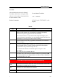
AMPS Tx Troubleshoting Summary
6\PSWRP
3UREDEOH&DXVH
9HULILFDWLRQDQG5HPHG\
7HVWFRPPDQGVXVSHQG
D /RZ7;,)
=LS6\Q9&$YROWDJHVKRXOGEHa9PD[SRZHU
/HYHO
,)OHYHODW&VKRXOGEHRYHU²G%P
&KHFNWKH,)ILOWHU)/VROGHULQJ
/RZ
7UDQVPLW
SRZHU
UHVSHFW
E /RZ7;/RFDO
7KH/RFDOLQSXWOHYHODW0(&SLQ/VKRXOGEHRYHU²G%P
OHYHO
&KHFNWKHPDLQ9&2$036SDUWDQGFRXSOHUVROGHULQJ
F 0(& 6XSSO\
0(&SLQDJF7;$YROWDJHVKRXOGEHa9
9ROWDJHSUREOHP
&KHFN WKH 0(& H[FLWHU PD[ RXWSXWSRZHU WKHQ SRZHURXWSXW DW &
0(&,&VKRXOGEHORDG9&KHFNWKH0(9
VKRXOGEHRYHU²G%P
WRLGHDO
$IWHU3$)LQDOGULYHUSKDVLQJ3$FXUUHQWVKRXOGEHLQaP$
SRZHU
3$ SLQYROWDJHVKRXOGEHLQ a9
G3RZHU
$PSOLILHU
3UREOHP
3$ SLQ YROWDJH VKRXOG EH VDPH ZLWK % RU FKHFN 4 DQG SLQ
DQGYROWDJHVKRXOGEHVDPHZLWK%DQGSLQ YROWDJHVKRXOGEH
DURXQG9
&KHFN 3$ *DLQ DQG RXWSXW 5HPRYH &3/ DQG FKHFN WKH PD[ SRZHU
RXWWKHSRZHURXWVKRXOGEHRYHUG%P
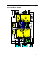
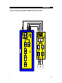
Some Important Notes For PCS Reciever
The Dual-Band CDMA SHARK contains two completely separate receiver paths: an 800 MHz
path that converts analog signals and a 1900 MHz path for the digital CDMA signal. The block
diagram shows both these paths. The two paths have different RF, LO and IF frequencies. The
most important, easily measurable figure of merit for each receiver is sensitivity, which
expressed as the signal level at which the analog receiver sees 12 dB SINAD and the digital
28
4/3/01
Troubleshooting
receiver experiences 0.5 % FER. (The specifications for these two levels are -116 dBm and -104
dBm, respectively) In this portion of the service notes, we will consider each stage in its schematic representation and will make some points about each block. DC levels and RF levels will
be noted. In PCS Receiver line up presentation, RF levels noted in the Rx Sections are approximate based on -70 dBm input power in the Center of the Band (1960 MHz, CH600) at the
mechanical switch and do not necessarily reflect the levels measured with high impedance
probe. Frequency of operation and channelization 1900 MHz Receiver Band 1930 to 1990 MHz
1900 MHz Channelization 1-1200, Frequency = 0.05 * Channel# +1930
Block Diagram of PCS Reciever
ANT
ANT Match
Z-Match
LNA
1900 TX Section
Combo (RF side)
Gain 15 dB
NF 1.8 dB
IIP3 5.5 dBm
Coaxial Switch
I.L. 0.3 dB
Ref. Des. J10
I.L. 2.0 ~ 3.0 dB
Freq.
Freq. 1930~1990 MHz
Ref. Des. FL20
Mixer
IF AMP
Gc 12 dB
NF 8 dB
IIP3 -1 dBm
Gain 12 dB
NF 3.5 dB
IIP3 -10 dBm
Zif_Syn
Duplexer 1900
Band Switch
I.L. 1.0 dB(PCS)
Ref. Des. FL13
I.L. 2.5 ~ 4.0 dB
Freq.. 1930~1990 MHz
Freq
Ref. Des. FL10
ATT 1
IF SAW
I.L 0.3 dB (@OFF)
I.L 25 dB (@ ON)
I.L. 10 dB
Freq.. 109.8 MHz
Freq
Ref. Des. FL200
LO_1900
To Test Set Up
Combo (LO side)
I.L. 1.8 ~ 3.0 dB
Freq.
Freq. 2040~2100 MHz
Ref. Des. FL20
Offset VCO
( Band Shift )
Tx Block Diagram
The Shark Transmitter line-up is a little different with Caliber design, Shark used ME3 IC and
doesn’t use isolator and electrical RF switch. Unlike MANTA, this is done with two separate lineups. The line-up splits in the ME3C, and recombines into the diplexer. The maximum output
power supplied to the antenna is: Analog:24.5 dBm PCS CDMA:23.5 dBm
ACCESORY
CO NNECTOR
ANTENNA
Antenna
Switch
IL = -0.2dB
Diplexer
IL = -0.5dB
PCS
DUPLEXER
IL = -3dB
AMPS
DUPLEXER
IL= -1.7dB
To RX
AMPS LO
979 - 1004 MHz
RF DETECT
Balun
Celeritek
AMPS PA
SAW
FILTER
IL= - 2 dB
ZIFSY N
ME3C
Ceramic
FILTER
IL = - 3 dB
COUPLER
IL = -0.25 dB
Tx I
Tx Q
LC FILTER
FO= 154. 65/ 189. 8 M
Hz
IL= - 4.0 dB
COUPLER
IL = -0.25 dB
Celeritek
PCS PA
Balun
PCS LO
2039 - 2100 MHz
29
4/3/01
CDMA 800/1900
PCS Transmitter Block Diagram
G%P
G%P
ZIF/SYN
TXoffset
VCO
TXIF
Filter
G%P
G%P
ME3 / Balun / RF filter
G%P
TXRF
Filter
G%P
PA
Coupler
G%P#5)FRQQHFWRU
Duplexer/Diplexer
Switch
Balun
TX_I
TX_Q
Balun
* Powers measured with high-impedance FET
probe.
* Powers measured only available when PCS
TX
23.5dBm at Radio output
30
4/3/01
Tests & Adjustments
Cellular Subscriber Sector
Test & Adjustments
CDMA 800/AMPS-V2260, T2260
CDMA Dual Mode 800-1900-V2267, T2267
Consult with Motorola regarding specific
hardware and software requirements for the
diagnostic computer.
Introduction
These phones allow keypad controlled
cali-bration
(often referred to as “phasing”) of
various operating parameters, as follows:
- Transmit output power
- TX deviation (SAT, DATA, DTMF,
microphone)
- RX discriminator output
These parameters are stored in memory on
the Logic Board and affect the operation of
the transceiver. All transceiver units and all
replacement RF/AL boards are shipped
from the factory with these adjustments
already made. However, if components are
replaced, checking and adjustment of the
parameters may be necessary. Checking and
adjusting parameters is also useful a troublshooting/
diagnostic tool to isolate defec-tive components.
The adjusting parameters accessible through
keypad commands are a subset of the complete complement of adjustments, but are the
key parameters necessary for basic opertion.
Access to all adjustments requires a computer connected to the accessory connector
(J3). In addition, the computer must be
loaded with the proper diagnostic software.
31
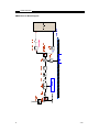
Test Interface
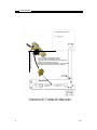
Figure 7: “Connections for Testing and
Adjustments” on page 48 shows the audio
and RF connections to a communications
analyzer when using the MCEL 2000 or
Zero Board test
interface, and test cable.
RF Cable adaptor :2887920K01
Ass’y cable SharkRadio,CDMA
DB25: AE20103172
Zero Board Ass’y with Legacy code
SYN0223B
Adjustments
To properly check and adjust the adjustment
parameters using keypad commands, perform the following procedures in sequence.
Impotrtant
Only those memory locations referred to in
the following procedure should be programmed. Data in other memory locations
which are “Stepped through” during the procedure.
© 2000 Motorola, Inc.
CDMA 800/1900
The Rf in/out port connects
to the test cables coaxis RF port.
The test cable RF port(SMA connector)
has a 1.5 dB loss compared to testing
using the Antenna Test Adaptor in the antenna port.
When using the test cable RF port,
SINAD should be meaus red with RF ! Level-114.5 dBm
and Power out measurement will be 1.5 dB low
ZERO BOARD
32
4/3/01
Tests & Adjustments
Keypad Button Functions
Below is a description of the non-numeric
keys used during the keypad calibration
procedure:
Step 1. Connect the test cable RF to a
servicing analyzer, using a coaxial cable.
Enter Manual Test Mode.
Depress the # button. The display should
show the ’ prompt.
Step 2. Enter 11434# via the keypad to
program the synthesizer for channel 434.
Step 3. Enter 05# to key the transmitter.
TX Output Power Adjustment(Center
of Band)
Step 4. Enter 73#. The portable display will
show Step number “00” on the left and the
corresponding hex value for the TX output
power on the right.
Table 5:
Power
Step
00
01
02
03
04
05
06
07
08
09
0A
0B
Output Power
(at antenna port, +/0.5 dBm)
28dBm
28dBm
28dBm
24dBm
20dBm
16dBm
12dBm
8dBm
Do not adjust
Do not adjust
Do not adjust
Do not adjust
each of the power steps listed in
Table 6: “Output Power Levels” for the values shown as indicated on the servicing analyzer. Make adjustments as described in Step
6 and Step 7.
Step 6. Enter a 2-digit hexadecimal number
via the keypad. This immediately updates the
hex power level value, and the output
power should change as indicated on the
analyzer. If the new entry does not produce
the desired analyzer reading (i.e. too high or
too low),
a) depress the CLR button and enter another
2-digit number, or
b) use the VOL button to incrementally
increase the hex value to obtain the desired
reading on the analyzer. (The volume control
may not be used to decrease the hex value.)
Table 6:
Note
In order to enter hex digits A thru F,
depress the SND button followed by:
0 hex A
1 hex B
2 hex C
3 hex D
4 hex E
5 hex F
Step 7. With all necessary adjustments made
and power Step “0B” showing in the display,
depress * to enter all updated data and exit
the 73# command.
Step 5. Using the * button to advance
through the power steps. Adjust
33
4/3/01
CDMA 800/1900
Maximum Deviation Adjust
Table 7:
Note
Before SAT, DTMF, data, or microphone
deviations can be adjusted, the maximum
deviation must be checked (and adjusted,
if necessary). Proceed as follows.
Step 8. Inject an unbalanced 1kHz 2.24V
rms audio signal at J3 pin 8 (TX audio in).
Connect the audio generator ground lead to
J3 pin 6 (audio ground). The audio signal
source must be low impedance (or the injection signal must be measured at pin 10 to
ensure the proper level of 2.24 V rms).
Step 9. Enter the following commands:
58# to enable compandor
10# to unmute TX audio
356# to select external audio path
11434# to place the telephone on channel
434
Step 10. Enter 72#. Step 04 will be displayed
on the left side of the display. Use the * button to toggle down to Step 0B (left side of
display).
Step 11. Read the peak deviation on the
analyzer. If it is not in the range of 11 to 12
kHz (preferably closer to 12kHz). Use the
volume control or enter numbers via the keypad (as explained in Step 6) to adjust the
maximum deviation to fall within the 11 to
12 kHz range. (Make adjustments so that the
deviation remains as close to 12 kHz as
possible, without exceeding 12 kHz.).
Step 12. Depress the * key to exit the 72#
command. The display should show the ’
prompt.
34
Microphone Deviation Adjust
Step 13. Adjust audio generator signal level
at J3 pin 8 (TX audio in) to 90 mV rms (still
at 1 kHz).
Step 14. Enter 11434# to place the portable
on channel 434. Enter 356# to select the
external handset audio path.
Step 15. Read the average deviation on the
analyzer. If reading is 2.05 kHz + 7% (corresponds to 2.9 kHz peak), proceed to Step 28.
If it is not, enter 72#, use the * button to toggle down to Step 05 (left side of display),
and use the volume control or enter numbers
via the keypad (as explained in Step 6) to
adjust for a microphone deviation of 2.05
kHz + 7%. After adjustment, note the hex
value for Step 05 and exit the 72# command
by repeatedly depressing the * button until
the display shows the ’ prompt.
Step 16. Enter 72#, use the * button to toggle
down to Step 06 (left side of display), and
enter the Step 05 hex value noted in Step 26.
Exit the 72# command by repeatedly
depressing the * button until the display
shows the ’ prompt. Remove the injection
audio signal.
DTMF Adjust
Step 17. Enter the following commands:
09# to mute TX audio
59# to turn off compandor
473# to set receive audio volume to level 3
(disables DTMF boost)
335# to turn on DTMF tone “5”
Step 18. Read the peak deviation on the
communications analyzer. If
4/3/01
Tests & Adjustments
reading is 9.0 rad + 10%, proceed to Step 30.
If it is not, enter 72#, use the * button to toggle down to Step 07 (left side of display),
and use the volume control or enter numbers
via the keypad (as explained in Step 6) to
adjust for a deviation of9.0 rad + 10%.
After adjustment, exit the 72# command by
repeatedly depressing the * button until the
display shows the ’ prompt.
Step 19. Enter 34# to turn off the DTMF
tone.
SAT Deviation Adjust
Step 20. Enter 251# to enable a 6000 Hz
SAT tone.
Step 21. Read the average deviation on the
communications analyzer. If the reading is
1.4 kHz + 10% (corresponds to 2.0 kHz
peak), proceed to Step 33. If it is not, enter
72#, use the * button to toggle down to Step
09 (left side of display), and use the
volume control or enter numbers
via the keypad (as explained in Step 6) to
adjust for a deviation of 1.4 kHz + 10%.
After adjustment, exit the 72# command by
repeatedly depressing the * button until the
display shows the ’ prompt.
Step 22. Enter 26# to turn off the 6000 Hz
SAT tone.
Data Deviation Adjust
Step 23. Enter 14# to turn on the 10 kHz
signaling tone.
Step 24. Read the average deviation on the
communications analyzer. If the reading is
5.7 kHz + 10% (corresponds to 8.0 kHz
peak), proceed to Step 36.
If it is not, enter 72#, use the * button to tog35
gle down to Step 08 (left side of display),
and use the volume control or enter numbers
via the keypad (as explained in Step 6) to
adjust for a deviation of 5.7kHz + 10%.
After adjustment, exit the 72# command by
repeatedly depressing the * button until the
display shows the ’ prompt.
Step 25. Enter 15# to turn off the 10 kHz
signaling tone.RX Discriminator Adjust
Step 26. Inject a -50 dBm, 883.020 MHz
RX Discriminator Adjust
Step 26. Inject a -50 dBm, 883.020 MHz
(channel 434) signal FM modulated with a 1
kHz tone at + 2.9 kHz deviation into the
antenna port, using an SLN8576A antenna
test adaptor.
Step 27. Enter the following commands:
08# to unmute the RX audio 474# to set the
receive audio volume to level 4356# to select
the external handset audio path
Step 28. Enter 72#, use the * button to toggle
down to step 0A (left side of display), and
use the volume control or enter numbers via
the keypad (as explained in Step 6) to obtain
100 mV rms +15% at pin 7 of J3 (RX audio
out). After adjustment, exit the 72#
command by repeatedly depressing the *
button until the display shows the ’ prompt.
Step 29. Exit Manual Test Mode by
depressing the PWR button. This
completes the keypad adjustment
procedure.
AMPS Call Processing
The transceiver is connected to an RF
Communications Test System capable of
AMPS and CDMA base station simulation
and the test simulation and the test described
below are performed. The external antenna
4/3/01
CDMA 800/1900
on a Portable is RF coupled to the Test System. The phone is powered by a battery. All
of these tests are performed on a pass/fail
basis except where otherwise specified.
The following AMPS Call Processing tests
must be done in a single test sequence.
Step 1. Initialize: Set the RF Communication
Test System to provide an AMPS control
channel at -50 dBm on channel 334.
Step 2. AMPS Registration: Turn the mobile
transceiver on and force an AMPS Registration.
Step 3. AMPS Page: Page the mobile transceiver.
When the transceiver alert rings, answer the
call using the FLIP for a Portable, the SEND
key for a Mortable. Verify that the mobile
has transferred to the traffic channel
and is transponding SAT.
Step 4. AMPS Handoff: Initiate a handoff to
another AMPS traffic channel. Verify that
the mobile has handed off to the new traffic
channel and is transponding SAT. Terminate
the call using the FLIP for a Portable, the
END key for a Mortable. Verify that the
mobile has terminated the all and de-keyed
the transmitter.
b. An AMP traffic channel with a 6 kHz tone
modulated at 2 kHz of deviation.
c. A CDMA traffic channel handoff message
set to the corresponding AMPS traffic channel frequency with SATcolor code 1 and
power attenuation code 3.
d. A CDMA System Parameters Message
with the following threshold data: Pilot
detection threshold
(T_Add) = 28 Pilot drop threshold (T_Drop)
= 32
Comparison threshold (T_Comp) = 5
Drop timer value (T_Tdrop) = 3
Step 2. CDMA Slotted Mode Page: Turn the
mobile transceiver on and force a CDMA
Registration. Page the mobile with a Service
Option 1 call. Verify that the mobile establishes and maintains a CDMA call by
measuring Rho.
Step 3. CDMA Softer Handoff: Set sector B
power to -75 dBm.
The mobile must report sector B as
included in the Candidate set. Increase sector
B power to -65 dBm. The mobile must report
sector B to be added to the Active set.
Initiate a softer handoff and decrease sector
B power to -80 dbm. The mobile must report
sector B to be dropped from the Active set.
The following CDMA Call Processing test
must be done in a single test sequence.
Step 4. CDMA Hard Handoff: Perform a
CDM Hard handoff theo channel 691 while
still in a Service Option 1 call.
Verify that the mobile hands off and maintains the call by measuring Rho.
Step 1. Initialize: Configure the test system
to the following set parameters:
a. A CDMA pilot on channel 777 with sector
A power at -70 dBm and sector B power at
-80 dBm.
Step 5. CDMA to AMPS Handoff: To
perform a CDMA to AMPS handoff, send
the CDMA traffic channel handoff message
to the mobile transceiver and activate the
AMPS traffic channel. Verify that the mobile
CDMA Call Processing
36
4/3/01
Tests & Adjustments
hands off to the AMPS traffic channel and is
transponding SAT.
Step 6. Exit.
37
4/3/01
CDMA 800/1900
38
4/3/01
TESTING
CDMA 800/AMPS-V2260, T2260
CDMA Dual Mode 800-1900-V2267, T2267
Cellular Subscriber Sector
Test Mode / Test Menu
Introduction
Manual Test Mode software allows service
personnel to monitor the telephone status on
the display, and manually control tele-phone
functions via the keypad.
Manual Test Mode operates at two levels: Status Display Level, which allows the
phone to operate normally while providing
status indications in the display. Servicing
Level, which disables normal call-processing
and allows commands to be entered through
the keypad to manually control operation of
the phone.
Status Display Level
Status Display Level is the power-up state in
Manual Test Mode. Manual Test Mode is
entered by momentarily shorting the MANUAL test pin(j3006) of the TEST POINTconnector J3 to ground, while turning the
phone on. See Figure 7: “Connections for
Testing and Adjustments” on page 48 In this
level of Manual Test Mode the phone will
place and receive calls as normal, but the display shows status information. The
first line of data indicates channel number,
RSSI value, and call-processing mode. The
second line of data indicates SAT frequency,
carrier state, signaling tone state, power
level, voice/data channel mode, Rx audio
state, and Tx audio state. The format and
explanation of this status information is
given in Table 1 under “02# Radio Status
39
Request.” When dialing a phone number, the
status display ceases when the first digit of
the phone number is entered. The telephone
number is displayed in the normal manner as
entered. When the Snd button (or End or
Clr) is pressed, the status information display
resumes.
Servicing Level
The servicing level allows service personnel
to manually control operation of a phone by
entering test commands through the
tele-phone keypad. Parameters such as
oper-ating channel, output power level, muting, and data transmission can all be selected
by entering the corresponding commands. To
enter the Servicing Level, press the # button
while in Status Display level (power-up state
of Manual Test Mode). In the Servicing
Level, automatic call processing functions
are disabled, and the phone is instead controlled manually by keypad commands.
Table 2: “Test Commands For Manual Test
Mode” on page 14 shows the test commands
and the corresponding results.
NOTE
There is no Status Display when the phone
is in CDMA mode.
CDMA Specific Features
Test Menu
A Test Menu allows a user to initiate Markov
calls, place Service Option 2 calls and set
Software Configuration Options. The Test
© 2000 Motorola, Inc.
CDMA 800/1900
Menu is intended to provide a simple mechanism to perform various test and S/W debugging functions. Items will be added to and
deleted from the menu period-ically. When
Test Menu is enabled, it is entered by pressing the FCN key twice. Refer to Step “09” on
page 27 for information on how to enable/
disable the Test Menu during NAM
programming. Almost every Test Menu
command accepts a parameter or data in the
scratchpad. The procedure for transferring
the scratchpad data and executing the Test
Menu command is as follows:
Step 1. Decide which Test Menu command is
going to be executed.
Step 2. Enter the necessary user input into
the scratchpad.
Step 3. Press the FCN key twice to acti-vate
the Test Menu.
Step 4. Press the volume keys until the
desired Test Menu command is indicated on the display.
Step 5. Press the SND key to activate the
command.
While the Test Menu is displayed, any keypress that is not volume or SND will also
cause the menu to be exited without executing the current option. The Test Menu will
also be exited whenever an incoming call is
detected.
Markov Calls
During a Markov call, the “(G)ood” rate will
be on the top line, and the “(T)otal” on the
bottom line of the display. The display will
cycle through all rates: (F)ull, (1/2) Half, (1/
4) Quarter, and (1/8) Eight.
- Mobile originated Markov calls are
performed by entering a telephone number
and selecting a Test Menu option. Refer to
the “Test Menu” section for further information.
40
- Mobile terminated Markov calls (Land to
Mobile) are currently NOT supported.
Pressing the SND key initiates a Markov call
with the number in the scratchpad. If
scratchpad is empty, “1234567” is used. This
feature has no value in AMPS mode.
Service Option 2
For Service Option 2 calls, the In Use
indi-cator will come on, but the display will
remain blank.
• - Mobile originated Service Option 2 calls
are performed by entering a telephone
number and selecting a Test Menu option.
Refer to the “Test Menu” section for
further information.
• - Mobile terminated Service Option 2 calls
will be automatically answered. Pressing
the SND key initiates a Service Option 2
call with the number in the scratchpad.
This feature has no value in AMPS mode.
SW (Software) DIP
Pressing the SND key initiates a one or more
SW DIP functions based on the number in
the scratchpad. Possible SW DIP functions
are:
1: Disables closed loop power control.
4: Forces vocoder to provide full rate voice
(may be enabled at any time during a call).
128: Sets the conversation audio path to
“audio out” and “audio in” on the external
connector.
For example, to disable closed loop power
control, the user enters the following key
sequence:
1 + FCN + FCN + ^ + SND
Undo all SW DIP settings (default at power
on) by pressing:
0 + FCN + FCN + ^ + SND
These may be combined to do more than
one at a time. For example, 4 and 1 may be
combined by entering 5 before entering
menu and selecting SW DIP.
4/3/01
Identity and Security
Test Mode
Also included in the software is a Manual
Test Mode, which allows viewing the ESN,
software version number, and programming
the phone number (NAM).
Handset Commands
To enter Manual Test Mode:
- 0 0 * * 83786633
(83786633 spells “TESTMODE” on the
keypad).
Table 8:
Key
Function
*
Toggles the display to the next location (enters data displayed to buffer).
When hit at last program step, the command is terminated (if required,
information may also be programmed into the EEPROM).
If the command relates to a test function with multiple data displays, the *
key is used to pause scanning data or to step through sequential test func-tions.
Entering the * key during a pause time resumes scanning.
CLR/END
Resets the location to presently programmed information (if the command
allows user input).
#
Terminates command without changing any of the programmed informa-tion.
Each command consists of at least two digits entered from the telephone
keypad with the entry terminated using the # key.
For commands that initiate an action that requires a response or that
accu-mulates
error counts, the # key terminates the test.
DIGIT
Enter digit value. If the value to be modified is filled or exceeded, the CLR
must be pressed before more digit selections are allowed. This is valid only if
the command allows user input.
SND
Send
KeysPhasing
0-5 enter
immediately
after the only
send key are
Forinto
TheHEX
Gain mode.
and power
handset
test commands
translated into HEX A-F respectively.
Volume up/
down
Increments/decrements the current data value. If the maximum value for this
data location is exceeded then it is set to zero.
STO
Shortcut to save values and quit test command.
41
4/3/01
CDMA 800/1900
This will cause the phone to enter the Test
Table 9:
Keypad
Entry
Command
Description
Status
Display
Result
#
Suspend
Terminate normal mode and enter Test Command Mode.
This command is valid only when in normal mode. The #
key must be held for 2 seconds to suspend with handset.
Performs initialization as in the INIT test command.
01#
Restart
Equivalent to turning power off, then on again.
02#
Radio Start
Request
03#
(not used)
04#
Initialize Transceiver
Initialize the current radio as follows:
1. Carrier = OFF
2. RF power attenuation set to level 2
3. Signaling Tone = OFF
4. SAT transponding = OFF
5. Audio Path = TO INTERNAL SPEAKER
6. DTMF & Audio Tones = OFF
7. Receive Audio & Transmit Audio = MUTED
8. AMPS Mode
If the radio is a CDMA only model (not dual mode), it
will default to CDMA mode instead.
05#
Carrier on
Turn on the carrier.
05# turns the carrier on with a nominal value for the DAC
for an output power level.
06#
Carrier Off
Turn off the carrier.
42
AAAZBBBCDEFGHI
Display the current radio status:
Handset Display Format:
AAA = Current channel
(1000-1023 represented as A00-A23)
Z = Blank - AMPS
Analog Mode:
BBB = RSSI reading (averaged) for this channel.
C = Digital Color Code (data channel) 0-3 DCC, 4
invalid
= SAT Frequency (voice channel)
0=5970 Hz; 1=6000 Hz; 2=6030 Hz;
3=No SAT Lock
D = Carrier (0=OFF, 1=ON)
E = Word sync status (data channel) and Signalling
tone (voice channel)
(0=OFF, 1=sync acquired/ON)
F = RF Power Level (Steps 0-7)
G = Reception Mode
(0=voice channel, 1=data channel)
H = Receive Audio (0=enabled, 1=muted)
I = Transmit Audio (0=enabled, 1=muted)
CDMA Mode: (Not currently supported)
Bit fields undefined
4/3/01
Identity and Security
Table 9:
Keypad
Entry
Command
Description
Status
Display
Result
07#
RXMUTE
Mute Recieve Audio
08#
RXUNMUTE
Unmute recieve audio
09#
TXMUTE
Mute Transmit audio.
10#
TXUNMUTE
Unmute transmit audio
11X#
Loadsynth
Load the specified channel into the radio synthesizer.
X-Enter up to 4-digits for the channel number. Channel
numbers must be in the range of 1 to 1024.
Narrow mode channel numbers not currently supported.
12X#
Set-Attn
13#
(not used)
14#
STON
Enables continuous signalling tone.
15#
STOFF
Disables signalling tone.
16#-18#
(Not Used)
19#
Version
In AMPS mode: Set the AMPS RF power attenuation to the
value specified (0-7).
In CDMA mode: Set the TX gain adjust DAC to the value
Note: Use the PATH command (35A#) to select the audio path to test before using commands 07#
specified (0-255)
through 10#. (Default path is to internal speaker and microphone).
43
Displays version corresponding to the two digit option x.
The following table show the valid options for x:
Decimal
00 Call processor
01 CDMA test command document number
02 Date
03 Time
22 DSP mask version
23 DSP patch version
- The call processor (factory version) number in the
format: 00 XXXX
- The CDMA test command document number: 01 XXXX
- The date the build was created in the format: 01JAN96
- The time the build was created in the format: xxyyzz
where xx is the hour, yy is the minute, and zz is the
second.
- The version of the DSP mask xxxxyyyyyyzzzz
where xxxx is the version, yyyyyy is the date, and zzzz is
the device.
- The version of the DSP patch xxxxyyyyyyzzzz
where xxxx is the version, yyyyyyis the date, and zzzz is
the device.
All data fields can be viewed by hitting the * key repeatedly.
To exit hit the # key.
4/3/01
CDMA 800/1900
Table 9:
Keypad
Entry
Command
Description
Status
Display
Result
19X
Multi-Version
20#-24#
(not -used)
25X#
Sat/Dsat On
Enable SAT/DSAT transponding.
For AMPS mode, the bye following the opcode is the color
code of the SAT frequency that the radio may expect to
receive. The command only uses the narrow phase lock
loop mode and locks only to the frequency selected
(+/- 15 Hz).
Valid color codes for X:
0 = 5970 Hz
1 = 6000 Hz
2 = 6030 Hz
26#
Sat/Dsat Off
Disable the transponding of Sat/Dsat.
27X#
Cdata
AMPS: Continuous Transmit Data on the reverse Analog
Control Channel.
CDMA: Random Transmit Data (RTD) on the reverse
CDMA channel.
Input Action
0 Start (AMPS) / Variable Rate (CDMA)
1 Full Rate (CDMA)
2 Half Rate (CDMA)
4 Quarter Rate (CDMA)
8 Eighth Rate (CDMA)
9 Stop RTD (AMPS, CDMA)
28#
HITNON
Tuen on high tone (frequency 1150 Hz +/- 55Hz)
29#
HITNOFF
Turn off high tone.
30#
LOTNON
Turn on low tone (frequency 770 Hz +/- 40 Hz)
44
Displays version corresponding to the two digit option x.
The following table show the valid options for x:
Decimal
00 Call processor
01 CDMA test command document number
02 Date
03 Time
22 DSP mask version
23 DSP patch version
- The call processor (factory version) number in the
format: 00 XXXX
- The CDMA test command document number: 01 XXXX
- The date the build was created in the format: 01JAN96
- The time the build was created in the format: xxyyzz
where xx is the hour, yy is the minute, and zz is the
second.
- The version of the DSP mask xxxxyyyyyyzzzz
where xxxx is the version, yyyyyy is the date, and zzzz is
the device.
4/3/01
Identity and Security
Table 9:
Keypad
Entry
Command
Description
Status
Display
Result
31#
LOTONFF
Turn off low tone.
32#
INVM
Initialize non-volatile memory to all zeros. This command
should be reserved for special situations where reprogram-ming
will be required (such as memory chip or circuit board
replacement or when a radiotelephone is to be reissued to
a new subscriber).
This command may take a minute or more to complete;
during which time the number 32 will be displayed. DO
NOT turn off the radiotelephone until the normal servicing
level display resumes.
33X#
DTMFON
Generates a continuous DTMF tone as specified by
input X.
Input X may be 0-9 for keypad DTMF, 10-18 for single low
or high tone, and 20-25 for tripled low or high tone.
34#
DTMFOFF
Turn off DTMF tones.
45
4/3/01
CDMA 800/1900
Table 9:
Keypad
Entry
Command
Description
35X#
Path
36#
(not used)
37#
(not used)
38#
SND-SN
39#-44#
(not used)
45#
READRSSI
46#
(not used)
46
Status
Display
Result
Change the audio path to A, where A =:
0 = Hands free (selects input signal AUDIO IN @ J3-pin 8
and outputs audio signal AUDIO OUT/ON-OFF @ J3pin 7; internal speaker and microphone are muted.)
1 = Speaker (normal audio path; selects internal mic and
outputs audio @ AUDIO OUT/ON-OFF @ J3-pin 7;
internal speaker is muted.)
2 = Alert (activates the alert transducer for as long as the
# key is pressed. To prevent overstressing the alert
transducer., DO NOT hold the # key down for
extended periods.)
3 = Handset (selects the internal mic and speaker.)
4 = Mute (all audio paths and supplies are off, DSP put to
sleep.) This command must be followed by a different
AUDIO-PATH command (not MUTE) in order to guar-antee
proper DSP functionality. Failure to do so may
result in a radio failure.
5 = Internal MIC Test (routes the internal mic audio
directly to AUDIO OUT/ON-OFF @ J3-pin 7, and
routes audio input at AUDIO IN @ J3-pin 8 directly to
the earpiece speaker.)
6 = External Handset (selects input audio at AUDIO IN @
J3-pin 8, and outputs audio at AUDIO OUT/ON-OFF
@ J3-pin 7; internal speaker and mic are muted, and
sidetone is turned on.)
7 = Reserved (not supported)
8 = Reserved (not supported)
9 = Boom MIC (selects input audio at AUDIO IN and
outputs audio at AUDIO OUT/ON-OFF to headset
connector; internal speaker and mic are muted, and
sidetone is turned on.)
This command enables all internal and external hardware
controls necessary to route audio to/from the correct
outputs/inputs.
AABB
Returns serial number contents.
If all bytes = 00, no serial number is programmed.
Display four byte serial number in hexadecimal one byte at
a time, along with a byte count. The * key causes the next
byte/count to be displayed.
Returns the RSSI reading taken on the current
channel. The number is displayed as a three digit
decimel number.
4/3/01
Identity and Security
Table 9:
Keypad
Entry
Command
Description
Status
Display
Result
47X#
set-aud
Sets the audio level to the value specified by X.
Audio level X is represented as 0 = lowest, 15 = loudest.
Range of 8-15 has DTMF Feedback boost bit enabled.
48#
SIDETN
Enable sidetone.
(Command 05# must also be executed).
49#
SIDETF
Disable sidetone.
(Command 06# must also be executed)
50# -54#
not used
55#
Prog-nam
56#
Auto-Cycle
47
nam
Programs the NAM through the handset.
This version uses supports only currently required NAM
fields and it supports programming of data logger bytes. At
the last step, the user enters a 1 to begin programming the
data logger bytes.
Handset key entry is defined in Table 1: “Handset
Command Key Entry” on page 13.
Refer to “NAM Programming” on page 25 of this manual
for programming details.
Puts the radio in autocycle mode (CDMA only). Exit this
command with the # key.
This command causes the radio to infinitely loop between
2 cycles. One cycle is the display/transmit and the other is
standby. The display/transmit cycle has a duration of 90
seconds and the radio has the following setup:
- Display has all 8’s showing.
- Turn on variable rate random transmit data.
- Carrier is enabled.
The standby cycle has a duration of 4.5 minutes and the
radio has the following setup:
- Display is blank.
- Turn off variable rate random transmit data
- Carrier is disabled.
This test command forces the radio into CDMA mode.
4/3/01
CDMA 800/1900
Table 9:
Keypad
Entry
Command
Description
Status
Display
Result
57X#
CP_Mode
Select radio call processing mode. This command will set
up the radio to operate in the mode selected and will also
perform initialization as specified by the INIT command.
The synthesizer will be reprogrammed to setup parameters
for the mode selected.
0 AMPS signalling (stop call processing test
commands and PCM Loopback)
1 Not supported - NAMPS signalling
2 Not supported - Reserved for NAMPS expansion
3 Not supported - Reserved for NAMPS expansion
4 Not supported - Reserved for NAMPS expansion
5 CDMA signalling (stop call processing test
commands and PCM Loopback)
6xy SIMVC test command
From the handset, x is the maximum rate and y is the
minimum rate.
Valid rates for x and y are:
4 - Full rate
3 - Half rate
2 - Quarter rate
1 - Eighth rate
From the Computer, no parameters are accepted
and Full rate is forced. (This is not supported yet)
7 Start PCM Loopback
8 CDMA T-Tester mode (channel must be set by
LOAD-SYTH. Handset only).
9 Not supported - CDMA force random data transmis-sion
12 Stop CPU - There is no way out of this except cycling
power.
58#
COMPD-ON
Turns on the computer.
59#
COMPD-OFF
Turns off the computer.
60#-67#
not used
68#
Read Model
69#-71#
not used
48
MODEL Read radio model type.
Displays three radio model bytes: hardware (model), flex
(type), and factory.
4/3/01
Identity and Security
Table 9:
Keypad
Entry
72X
49
Command
Description
gain phase
Status
Display
Result
Program AMPS (only) gain phasing values through the
handset.
Gain phasing depends on the call processing mode. It is
the responsibility of the user to select the proper call
processing mode before using this test command.
This command reprograms the EEPROM phasing values
for MOD, MIC, AUX, etc.
The value in X selects which step to start on. If no value for
X is entered, it will start at step 0.
The command keys are defined in Table 1: “Handset
Command Key Entry” on page 13.
NOTE: If you power down the radio after changes are
made, the power up sequence re-programs the hardware
with the correct phasing values.
Refer to the “Tests and Adjustments” on page 47 for
instructions on entering parameters from the keypad.
AMPS GAIN PHASING RANGE
STEP # PARAMETER (HEX)
00-04 MOD 0- MOD 4 0-7
05 Aux. audio path deviation 0-1
06 MIC audio deviation 0-F
07 DTMF deviation 0-3
08 Data deviation 0-3
09 SAT deviation 0-3
0A Discriminator audio gain 0-7
0B AFC WARP Analog 0-FF
4/3/01
CDMA 800/1900
Table 9:
Keypad
Entry
73#
50
Command
Description
PWR-Phase
Status
Display
Result
Programs power phasing values through the handset.
Power phasing depends on the call processing mode. It is
the responsibility of the user to select the proper call
processing mode before using this test command.
This command reprograms the EEPROM phasing values
for Max. Power Level, Attenuator Slope Adjust, etc.
The value in X selects which step to start on. If no value for
X is entered, it will start at step 0.
The command keys are defined in Table 1: “Handset
Command Key Entry” on page 13.
NOTE: If you power down the radio after changes are
made, the power up sequence re-programs the hardware
with the correct phasing values.
Refer to “Tests and Adjustments” on page 47 for instruc-tions
on entering parameters from the keypad.
Analog Power Level Parameters:
RANGE
STEP # POWER LEVEL (HEX)
00 Power Step 0 00-FF
01 Power Step 1 00-FF
02 Power Step 2 00-FF
03 Power Step 3 00-FF
04 Power Step 4 00-FF
05 Power Step 5 00-FF
06 Power Step 6 00-FF
07 Power Step 7 00-FF
08-0B Do Not Adjust
CDMA Power Level Parameters:
RANGE
STEP # POWER LEVEL (HEX)
00 Attenuator Slope Adjust 00-FF
01 Attenuator Offset Adjust 00-FF
02 Clamp Adjust 00-FF
03 VCA Slope Adjust 00-FF
04 VCA Offset Adjust 00-FF
05 PMax 1 (Chan. 991-1023, 1-100) 00-FF
06 PMax 2 (Chan. 101-322) 00-FF
07 PMax 3 (Chan. 323-544) 00-FF
08 PMax 4 (Chan. 545-766) 00-FF
09 PMax 5 (Chan. 767-990) 00-FF
4/3/01
Identity and Security
Table 9:
Keypad
Entry
73#
Command
Description
Status
Display
PWR-Phase
NAM Programming
Introduction
The Number Assignment Module (NAM) is
a section of memory that retains information
about the phone’s characteristics, such as the
assigned telephone number, system identifi-cation
number, and options information.
Two methods are available to program the
NAM using the keypad: Test Mode and User
Mode.
Regardless of the method used, the NAM
must be programmed before the phone can
be placed into service. This chapter covers
the NAM Programming steps for Test Mode
NAM Programming.
Test Mode Programming
Table 3: “Minimum Required Test Mode
NAM Programming Steps” on page 25
51
Result
STEP # POWER LEVEL (HEX)
0A Ch. Gain Adj. 1 (Chan. 991-1023, 1-100) 00-FF
0B Ch. Gain Adj. 2 (Chan. 101-322) 00-FF
0C Ch. Gain Adj. 3 (Chan. 323-544) 00-FF
0D Ch. Gain Adj. 4 (Chan. 545-766) 00-FF
0E Ch. Gain Adj. 5 (Chan. 767-990) 00-FF
0F TX Gain Adjust 1 00-FF
10 TX Gain Adjust 2 00-FF
11 TX Gain Adjust 3 00-FF
12 TX Gain Adjust 4 00-FF
13 TX Gain Adjust 5 00-FF
14 TX Gain Adjust 6 00-FF
15 TX Gain Adjust 7 00-FF
16 TX Gain Adjust 8 00-FF
17 VC Sense Slope Adjust 00-FF
18 VC Sense Offset Adjust 00-FF
19 VC Sense Zero Adjust 00-FF
1A Available 00-FF
1B Not Available 00-FF
shows
the minimum required Test Mode NAM
programming steps. Table 4: “Test Mode
NAM Programming Sequence” on page 26
lists all NAM programming steps, complete
with parameters and definitions.
IMPORTANT
Consult with the System Operator
regarding NAM information. Incorrect
NAM entries can cause the phone to
operate improperly or not at all.
.
For Test Mode NAM programming, the
portable must be in the Servicing Level of
Manual Test Mode (See “Test Mode/Test
Menu” on page 11.) To enter test mode, the
Manual Test pin (recessed center pin of the
J6 battery connector) must be momentarily
grounded while powering up the phone.
This can be accomplished in a variety of
ways, such as by using a 6.8 VDC power
4/3/01
CDMA 800/1900
supply and an MCEL 2000 test cable or test
plug. After powering up in test mode, press
the # button to enter Servicing Level. Once
in Test Mode Servicing Level, enter 55# to
place the phone in NAM programming
mode. The display will show factory default
NAM data or show new data as it is entered,
scrolling from left to right. Sequentially step
through the procedures shown in Table 4:
“Test Mode NAM Programming Sequence”
on page 26 using the * key. Enter new data
as required, or skip past factory default
values for parameters that do not need to be
changed.
If a second phone number is to be
programmed, step 11 bit 6 must be set to 1.
This bit enables dual-NAM operation and
will cause NAM programming steps 1-6 and
12 to be repeated for the second phone
number.
Minimum Required Test Mode
NAM Programming Steps
Table 10:
Service Type
Minimum Required
Programming
Steps
Single NAM
Dual NAM (part A)
Dual NAM (part B)
1, 3, 4, 6, 8, 9
1, 3, 4, 6, 8, 9, 11
1, 3, 4, 6
Test Mode NAM Programming Sequence
Advances to the next programming
step; also programs the NAMafter the last
programming step is entered. A valid value
must be entered. Otherwise the phone will
not advance to the next NAM step.
Clears the entered information and
displays previously entered data for the current programming step.
Exits the programming mode without
programming the NAM.
Test Mode NAM Programming Sequence
Table 11: *
Factory
Default
Step
Description
CLR=
Home System ID (SID) Number. Number assigned by system operator
for system identification.
01
00000
02
00000100
#
A OPTION BYTE. The display for step 02 represents the status of eight
options, A7 through A0. Bit A7 (msb) is programmed first, followed by A6A0. Bits enter display on the right and scroll left.
0
Local Use (Bit A7). If set to 1 phone will respond to local control orders in
the home area or when the group ID is matched. Assigned by system
operator.
52
4/3/01
Identity and Security
Table 11:
Factory
Default
Step
03
Description
0
Preferred System (Bit A6). Applies to units capable of operating on two
service systems (A or B). 0 = system B; 1 = system A.
0
End-to-End Signaling (Bit A5). When enabled, the phone is equipped for
DTMF signaling during a call. 1 = enabled, 0 = disabled.
0
Markov test override MSB (Bit A4). Enter 0.
0
Markov test override (Bit A3). Enter 0.
1
Bit not used (Bit A2). Enter 1.
0
Markov test override LSB. Enter 0
0
MIN Mark (Bit A0). Supplied by system operator. When enabled the user’s
area code will be sent with each call initiated or answered.
1 = enabled, 0 = disabled.
1111110111
User 10 digit radiotelephone phone number (MIN). 10_digits including
area code; changing this value sets default for AOC. Number is assigned
by system operator.
04
010
042
074
106
Station class mark (SCM). A 2 digit number assigned by the system
operator. Indicates maximum power step, VOX capability, and number of
channels used.
CDMA only & Non-Slotted mode configuration
CDMA only & Slotted mode configuration
Dual Mode & Non-Slotted mode configuration
Dual Mode & Slotted mode configuration
05
Last digit of
access overload class
Access overload class. Specifies the level of priority assigned to the
phone when accessing the system. Assigned by system operator.
06
000000
Security code. A 6-digit number supplied by the user. This number is
used by the user to access or change “security” features such as the 3digit unlock code or the service level.
07
123
Unlock code. A 3-digit number supplied by the user. If the lock feature is
enabled by the user, the phone can be operated only by individuals who
know the unlock code.
08
4
Service level. This 1-digit number supplied by the user allows various call
placement restrictions if desired.
53
4/3/01
CDMA 800/1900
Table 11:
Factory
Default
Step
09
01100000
Test Menu
enabled
Description
B OPTION BYTE The display for step 10 represents the status of eight
options, B7 through B0. B7 (msb) is programmed first followed by B6-B0.
Bits enter display on the right and scroll left.
00100000
Test Menu
disabled
54
0
Display Pilot Set Status/AMPS Status Mode (Bit B7).
CDMA: These statistics are useful for testing handoff parameters. When
enabled, this feature displays the strongest pilot offset in the
“Active Set” (only member during Idle) on the top line of the
display, and the strongest pilot in the “Neighbor Set” on the
bottom line. Each line has the same format. The left most 3-digit
number is the pilot offset, and the right number is a relative signal
strength.
IDLE HANDOFF (handoffs on a paging channel) occurs when a
Neighbor pilot is judged to be better. That neighbor pilot will be
promoted to the active set, and thus move to the top line of the
display.
SOFT HANDOFF (handoff on a traffic channel) occurs when a
Neighbor pilot fulfills requirements set by the network, and the
network directs the mobile to add the new pilot to the Active Set.
Pilot Set status is enabled by setting Step #9, bit #7 to 1. Channel
Statistics is disabled by setting Step #9, bit #7 to 0.
WARNING: Turning on this option makes it difficult to see the
Markov error rate statistics in a call.
AMPS: In AMPS mode, setting this bit to 1 causes status information
similar to current Motorola AMPS products to be displayed. The
contents of the display depends on the channel being monitored.
0
Test Menu (Bit B6). This bit allows the user to enable or disable the FCN
key Test Menu. Refer to “Test Menu” on page 12 for further information on
Test Menu.
1 = enabled, 0 = disabled.
1
Paging Channel Message Filtering (Bit B5). This bit limits the amount of
paging channel messaging seen by the data logger debugging tool. A user
not using this tool should see no noticeable difference in performance.
1 = enabled, 0 = disabled.
0
Portable Data Logging (Bit B4). Enter 0.
4/3/01
Identity and Security
Table 11:
Factory
Default
Step
Description
0
Single Serving System Scan (Bit B3). This bit allows the user to enable
or disable the serving system scanning on serving systems other than the
phone’s home serving system. If the phone has an odd Home System
Identifier (Step 1), it’s home serving system is A, otherwise it is B. If Single
Serving System Scanning is enabled, only the home serving system will
be scanned, otherwise both serving systems will be scanned.
1 = enabled, 0 = disabled.
1
Auto Recall (Bit B2). When set to one, the user may access repertory by
a one or two digit send sequence (speed dialing).
0
Disable Service Levels (Bit B1). If set to 1, the service level (call
restric-tions)
cannot be changed by the user.
0
0 Lock Disable (Bit B0). When set to 1, the user cannot lock and unlock the
phone unit via the 3 digit lock code.
00000000
C OPTION BYTE The display for step 11 represents the status of eight
options, C7 through C0. C7 (msb) is programmed first followed by C6-C0.
Bits enter display on the right and scroll left.
0
User Mode NAM Programming Disable (Bit C7). When set to 1, User
Mode NAM programming cannot be accessed.
0
Dual NAM System Registration Enable (Bit C6). Enter 1 if dual NAM
operation is desired (for models capable of dual system operation).
Enter 0 for single NAM operation
0
Test Mobile Enable/Auto Answer (Bit C5). Enter 0.
0
Auto Redial Disable (Bit C4). When set to 1, the user cannot access the
6-minute auto redial feature.
0
Three Wire Bus Speaker Disable (Bit C3). This bit is used to disable
internal handset speaker when adding V.S.P. option. 1 = handset speaker
disabled,
0 = handset speaker enabled.
0
Bit not used (Bit C2). Enter 0.
0
Selectable System Scan Disable (Bit C1). When set to 1, the user
cannot select the primary system.
0
Diversity Antenna (Bit C0). (Extended systems only)
0 = Non-diversity, 1 = Diversity.
11
0334
AMPS Initial paging channel. There are 4 significant bits for the initial
paging channel. For system A enter 0333 and system B enter 0334.
12
0333
AMPS Initial A system channel. To initialize system A enter 0333.
10
55
4/3/01
CDMA 800/1900
Table 11:
Factory
Default
Step
Description
13
0334
AMPS Initial B system channel. To initialize system B enter 0334.
14
021
AMPS Dedicated Paging Channels. Number of dedicated paging chan-nels
is 21. Enter 021.
15
00001000
D OPTION BYTE. The display for step 16 represents the status of
eight options, D7 through D0. D7 (msb) is programmed first, followed
by D6-D0. Bits enter display on the right and scroll to left.
0
Enhanced Scan (Bit D7). Enter 1.
0
Cellular Connection 1 (Bit E6). Normally set to 0.
0
Long Tone DTMF Enable (Bit E5). Normally set to 1.
0
Transportable Transducer Disable (Bit E4). Enter 0.
1
Bit not used (Bit E3). Normally set to 0.
0
Handset Test Mode Disable (Bit E2). Enter 0.
0
Failed Page Indication Disable (Bit E1).
0
Word Sync Scan Disable (Bit E0). Set to 1.
00100111
E OPTION BYTE. The display for step 16 represents the status of
eight options, E7 through E0. E7 (msb) is programmed first, followed
by E6-E0. Bits enter display on the right and scroll to left.
0
Bit not used (Bit E7). Enter 0.
0
* Preferred mode (Bit E6). Normally set to 0.
Bit 6 - 1 and Bit 5 - 1 = Analog preferred
Bit 6 - 1 and Bit 5 - 0 = Analog only
1
Preferred mode (Bit E5). Normally set to 1.
Bit 5 - 1 and Bit 6 - 1 = CDMA preferred
Bit 5 - 1 and Bit 6 - 0 = CDMA only
0
Extended Address Method (Bit E4). Enter 0.
0
Preferred Analog Serving System (Bit E3). Normally set to 0.
1
Config. for mob term using home SID, NID pair (Bit E2). Enter 1.
1 = Allow mobile terminated call while using a home (SID, NID) pair.
0 = Disallow mobile terminated call while using a home (SID, NID) pair.
1
Config. for mob term while SID roamer (Bit E1) Enter 1.
1 = Allow mobile terminated call while a SID roamer.
0 = Disallow mobile terminated call while a SID roamer.
16
56
4/3/01
Identity and Security
Table 11:
Factory
Default
Step
Description
1
† Config. for mob term while NID roamer (Bit E0). Enter 1.
1 = Allow mobile terminated call while a NID roamer.
0 = Disallow mobile terminated call while a NID roamer.
17
0
CDMA: Slot Cycle Index. TBD
18
Entry
Required
CDMA: SID (SID_NIDp). Up to 5-digits.
19
00000
CDMA: Network ID Number (NID of SID_NIDp). Up to 5-digits.
20
111111
Mobile Country Code (first 3-digits), IMSI 11 (1-digit), IMSI 12 (1-digit).
21
Entry
Required
CDMA: Primary Channel. System A up to 4 decimal digits.
22
Entry
Required
CDMA: Primary Channel. System B up to 4 decimal digits.
23
Entry
Required
CDMA: Secondary Channel. System A up to 4 decimal digits.
24
Entry
Required
Secondary Channel. System B up to 4 decimal digits.
25
0
Data Logger Switch. Enter 0.
1 = enabled, 0 = disabled.
* These bits will determine which modes of
operation the radio will attempt
when seeking communication with a Base
Station. Care should be taken when
either the CDMA only or the Analog only
modes of operation are selected,
because this configuration will cause a dual
mode phone to operate as a single
mode phone. Another issue to be aware of is
that whenever Bit 5 is set to 0, no
handoffs between Analog and CDMA mode
can take place. No examination of
the RF environment is performed when setting these fields.
† Setting these bits also effects the registrations that are transmitted by the
Mobile Station. If bits are set such that the
57
Mobile cannot receive any incoming
calls (in CDMA mode), it is not necessary to
send out any Registration mes-sages.
It should be noted that if all Mobile Terminated Call Preference bits are
set to zero, that there would (in a spec compliant system) be no way for the
Mobile Station to receive incoming calls.
4/3/01
CDMA 800/1900
58
4/3/01
Cellular Subscriber Sector
CDMA 800/AMPS-V2260, T2260
CDMA Dual Mode 800-1900-V2267, T2267
DISASSEMBLY
Introduction
- Anti-Static Mat 6680387A95
Care must be taken during the disassembly
- Ground Cord 6680334B36
and reassembly of the unit in order to avoid
- Wrist Band 4280385A59
damaging or stressing the housing and inter-
- Plastic Prying Tool SLN7223A
nal components. Ensure that a properly
- Rear Housing Removal Tool
grounded high impedance conductive wrist
- Dental Pick
strap is used while
- Tweezers
performing these procedures on electronic
- T6 Torque Screw Driver
units.
Disassembly Procedure
Recommended Tools
The following tools are recommended for
Refer to the disassembly instructions and
photo sequence on the following pages.
use during the disassembly and reassembly
of the phone.
- Anti-Static Mat Kit (0180386A82);
includes:
Assembly Procedure
Once the unit is disassembled and the repair
is carried out it then becomes obvious that to
CAUTION
Many of the integrated circuit devices used
assemble the unit, the procedure is the
reverse of that previously completed for disassembly.
in this equipment are vulnerable to damage
from static charges. An anti-static wrist
band, connected to an anti-static (conduc-
Antenna Removal
tive) work surface, must be
1-1 Turn off the power.
worn during all phases of disassembly,
1-2Remove a Rubbor Boot.
repair, and reassembly.
1-3 Remove antenna by turning counterclockwise.
© 2000 Motorola, Inc.
.
2-2 After removing Battery Housing lift up
the Battery
.3.Disassembly of Rear Housing
At first ,remove screws on top of Rear
Housin
g, and
then
Bottom
Last,
remove
screws
on the
middle
of Rear
Housin
g.
2.Disassembly of Battery
2-1 Push the Latch and then remove the
Battery Housing out of the front housing.
4.Disassembly of PC Boards.
4-1 After removing Rear Housing , remove
60
4/3/01
Side Buttons one by one.
5.Disassembly of LCD
5-1 Disassemble LCD by pulling Snap Fit to
a
both
side
4-2.Disassemble PC
Boards into
Front housing and PC Boards by carefully
pulling one against another.
5-2
Remove the LCD by inserting a in the top of
Zif Connector and lifting it away from the
attached surface.
6.Disassembly of
Key Pad
6-1 Remove a Key Pad.
4/3/01
8. Complete Disassembly Layout.
7. Remove the Groumet, RF Test,
using antenna screw
* Before unscrewing antenna, make sure to
align the straight indent that exists on the
surface of Rear Housing .
62
4/3/01
TROUBLESHOOTING
Cellular Subscriber Sector
CDMA 800/AMPS-V2260, T2260
CDMA Dual Mode 800-1900-V2267, T2267
Troubleshooting
Introduction
Known good replacement parts and assemblies should be available to be used for troubleshooting by substitution, and for replacement of defective parts/assemblies. Defective circuit boards should be forwarded to
the appropriate Motorola service facility for
repair. Refer to the “Replacement Parts”
section of this manual for a list of replacement part descriptions and part numbers.
CAUTION
Many of the integrated circuit devices
used in this equipment are vulnerable to
damage from static charges. An ESD-safe
workstation should be used when-ever
a transceiver is opened.
Testing after Repair
After any repair work has been carried out,
the unit should be thoroughly tested to
ensure that it operates correctly. This is especially important if the Logic / RF assembly
is replaced.
For general repairs which do not include
replacing the Logic/RF assembly, simply
placing a call and checking signal strength,
and transmit and recieve audio quality is
normally sufficient.
When the Logic/RF assembly is replaced,
the unit must have a comprehensive test on
a compatible communications analyzers. See
“Testing” for further details. Placing a call
on air is usually carried out at this stage to
complete the testing procedure.
Troubleshooting and Repair
The troubleshooting chart in Table 7,
“Assembly Replacement Level Troubleshooting and Repair Chart,” on page 56
shows some typical malfunction symptoms
and the corresponding verification and
repair procedures. Refer to the disassembly
instructions located in the “Disassembly”
section of this manual for instructions on
removing parts/assemblies.
63
© 2000 Motorola, Inc.
CDMA 800/1900
LOGIC TROUBLESHOOTING
Phone is not powered on(1)
Battery Discharged
Measure battery voltage and if the battery voltage is <3.6 V DC, recharge the battery using the
AC charger.
Battery contact opened or misaligned
Supply the B+ power through test port J3002(B+), J3001(GND) by using the test interface cable. If
the phone is powered on, check the battery fail or battery contact defect
B+ Supply defective
Apply the power BATT+ through the battery contact. Check the B+ voltage by measuring 3.64.2V at the pin 48 of U2000 CCAP lite. If the B+ doesn’t come out, check the Q3300
Power Supply defective
Supply the B+ power through test port J3002(B+), J3001(GND) by using the test interface cable.
Depress the PWR button and measure the supplied voltage of each part within 300ms of start of
ON_OFF signal.
Check the Logic_4.75 voltage by measuring 4.75V at the pin 41 of U2000 CCAP lite
Check the Logic_2.75 voltage by measuring 2.75V at the pin 28 of U2000 CCAP lite
Check the Audio_2.75 voltage by measuring 2.75V at the pin 22 of U2000 CCAP lite
Check the Logic_1.8 voltage by measuring 2.75V at the pin 3 of U2000 CCAP lite
If the above supply voltages don’t create by CCAP lite, Replace the U2000 part or check the logic
2.75/ Audio 2.75 power path shortage
Phone is not powered on (2)
Reset Signal
Check the RESETB Signal from CCAP lite U2000 by measuring the voltage of C2044 or pin 30 of
U2000
Depress PWR button, then the RESETB signal shall maintain ‘Low’ for approximately 255msec
after power on and go to ‘High’
If reset signal don’t come out, check the CCAP U2000 part.
64
4/3/01
Troubleshooting
Clock Fail
Check the 16.8MHz reference clock by measuring the signal via C1994 (Nominal 1.0 Vp-p sinewave)
If 16.8MHz clock is not probed, check the reference oscillator part of RF side.
Depress PWR button, then Check the clock from the CIA as below
CLK0 : 5.6Mhz CRIB input clock
(measured via TP1915)
CLK1: 32.749khz RF dither circuit clock (measured via R332)
CLK2: 32.749khz MCU input clock (measured via TP1913)
CLK3: 1.12Mhz DSP input clock (measured via TP1912)
CHIPx8: 9.8304Mhz Chipx8 clock (measured via TP1911)
Check the 32.768khz crystal clock (measured via R1142)
32khz_Buff_out: 32.768khz sleep mode clock out (measured via TP1130)
Casper 68338 PLL locking
Verify the 68338 CPU PLL locking by measuring the XFC signal through C1154
After Logic 2.75V &1.8V supplied to Casper U1100, XFC level shall be 650-700mV
After RESETB signal released, XFC level shall be 850-900mV within 10ms of CPU start.
If PLL locking is failed, Replace the U1100 Casper or Check the PLL circuit (C1152, C1153, C1154,
R1151)
Phone is not powered on (3)
Check Watchdog
Check watchdog level from CASPER to CCAP lite by measuring the WDI level via R1181.
Depress PWR button, then the WDI signal maintain ‘Low’ for approximately 270~280 msec after
power on and goes to ‘High’
Take off the R1181 0Ohm resister and put the 1kOhm resister to the R1180 DNP
Check if the phone operate normally.
If the phone is not powered on and logic_2.75 doesn’t go down, it show the program does not
perform normally (Casper, Memory, CIA etc.or Software failure)
Check the phone mode
Check the manual test line via R1178
If the manual test line is ‘Low’, the phone will go to flash mode and if ‘High’, the phone will go
to the normal turn on sequence.
In flash mode, if the flash programmer recognize the phone UART, the possible defect is on the
65
4/3/01
CDMA 800/1900
Software.
Flash the phone with right version, or replace to the programmed Flash part
Verify by EST Box
Connect the J3901-J3910 port to EST box BDM cable.
Take off the R1181 0Ohm resister and put the 1kOhm resister to the R1180 DNP
Execute the Vision Click tool and set up the MCU register of EST
Read the Flash code from $000000 and verify the the right hex code can be read.
Test the SRAM area $600000 - $63FFFF via memory test diagnostics tool
If the Flash or SRAM defect is found, Replace the parts.
No Display
Connection Failure
Check the 16pin J3200 Display Connector’s connection to Flex cable of Display.
If the connection defective is found, repair the connection or replace the 16pin J3200 connector
Electrical Interface Failure
Check the J3200 soldering status and re-solder the connector
Check the interface signal LCD logic_2.75 (measured via R3200), LCD reset signal (measured via
R3201) and D0-7, EL, AL0 signal from the board to LCD.
If more than one signal defect is found, repair the cause.
Display module Defect
Assemble the Display module to a known good Shark main board, and check the function.
If the display fail is not solved, replace the Display module with new good one.
Display is erratic or partial no display
Connection Failure
Check the 16pin J3200 Display Connector’s connection to Flex cable of Display
If the connection defective is found, repair the connection or replace the 15pin J3200 connector
Display module Defect
Assemble the Display module to a known good Shark main board, and check the function.
If the display fail is not solved, replace the Display module with new good one.
66
4/3/01
Troubleshooting
No LED Backlight
LED BL Regulator defect
Set the phone mode as a ‘Backlight Always On’ of ‘Backlight Select’ of ‘Display Options’ menu.
Verify the 2.8V BL Regulator Vout via U2400 pin 4 and BL control signal ‘High’ via U2400 pin 1
If the 2.8 Voltage BL Regulator Vout is failed with BL control signal ‘High’, replace the U2400
regulator IC.
Dim LED
If any dim LEDs are found out of 4 LCD LEDs and 8 keypad LEDs, measure Vf voltage of the
dim LEDs on the point of LED Anode (The typical Vf is 2.03 volt)
If the Vf is too high, replace the LED with good one.
No turn-On LED
If any dim LEDs are found out of 4 LCD LEDs and 8 keypad LEDs, replace the LEDs with good
ones.
Trouble Shooting(Power-up)
a) Battery either discharged or defective.
1. Measure battery voltage across a 50 ohm (>1 Watt)load.
2. If the battery voltage is <3.4 V DC, recharge the battery using the
appropriate battery charger.
3. If the battery will not recharge, replace the battery.
+ - +
b) Battery mis-aligned.
1. Visually inspect the battery polarity
2. Check if two battery contact terminals of rear
housing are able to match battery contacts on board.
- + -
c) Shield defective
1. Check if carton tape is on power shield
2. Check if power shield can are short to battery contacts
67
4/3/01
CDMA 800/1900
d) Components defective
1. Change L2000 if BOOST is same to B+.
2. Check 16.8MHz if Logic_2.75 and Aud_2.75 is high.
3. Check u-P(U1100) and memory(U1200, U1300) if WDI is low
e) When charger is attached at low battery
1. Check if drain of Q2 is high for 1.5sec after charger is attached
2. Check if base voltage of Q2207 is 0.7V during Q2 is on
Trouble Shooting(Power Down On ’SND’)
a) Battery either discharged or defective.
1. Measure battery voltage across a 50 ohm (>1 Watt) load.
2. If the battery voltage is <3.4 V DC,
recharge the battery using the appropriate battery charger.
3. If the battery will not recharge, replace the battery.
b) PA defective
1. Setup the power supply : 4.5V, 500mA
2. Setup the HP8924 : Sectr A Pwr(-83dBm), Data rate(random)
3. Check current drain of phone at call state. Does power supply display ‘CC’ ?
4. Check if the bias point(PA_VGG1) of PA is -1.3V~-3V and do Phasing.
Trouble Shooting(Accessory Not Working)
1. Check if the voltage range of CHG_SNS_CIA is 1.7V~< 2.4V on VPA
2. Check if the voltage of CHG_SNS_CIA is 0.8V~1.7V on EIHF
3. Check if the voltage of CHG_SNS_CIA is below 0.8V on AC charger
4. Check if the voltage of EXT_B+ is more .45V than battery voltage during charging
68
4/3/01
Troubleshooting
Trouble Shooting(Battery defective)
a) battery cannot be charged.
1.Push the button 'FCN'+'0'+'0'+'*'+'*'+’8'+'3’+'7'+'8'+'6'+'6'+'3’+'3’ +'STO' and set into test mode.
2. Store 11000000 at 5509# and press 01# sequentially to restart phone.
3. Push the button 'FCN' twice and select the 'Battery Status Mode On'
4. You can see following message on LCD
5. If the temperature of the battery is -40'C, check the thermistor node on bad soldering.
AAA = Average battery temperature
‘C = Unit of temperature
D = 0 : charger is off
1 : charger is on
E = V : VPA(CLA, fast charger)
E : EIHF(DHFA, fast charger)
A : AC charger(slow charger)
F.FFV = Average battery voltage
GGG = Ideal (non phased) charger current in mA
HHH = N/A
I = Charger algorithm state
0 : Destroyed
1 : Battery detects
2 : No charge
*3 : Rapid charge
*4 : Top off charge
*5 : Maintenance charge
*6 : Paused
7 : COVIC charging
J = N : Nickel Battery
69
4/3/01
CDMA 800/1900
b) battery cannot be charged insufficiently
1. check whether the voltage of battery displays more 50mVthan actual battery voltage
2. If that, do voltage phasing again.
3. Check if the voltage of EXT_B+ is more .45V than battery voltageduring charging
70
4/3/01
Troubleshooting
Symptom
1. Phone will not turn on
or stay on.
2. Phone exhibits poor
reception and/or erratic
operation (such as calls
frequently dropping, weak
and/or distorted audio,
etc.)
71
Probable Cause
Verification and Remedy
a) Battery either discharged or
defective.
1. Measure battery voltage across a 50 ohm (>1 Watt) load.
2. If the battery voltage is <3.4 V DC, recharge the battery
using the appropriate battery charger.
3. If the battery will not recharge, replace the battery.
b) Battery connector open
or misaligned.
1. Visually inspect the battery connectors on both the battery
pack and the transceiver, including the solder connections
from the battery connector to the main PC board.
2. Realign the contacts or, if necessary, replace either the battery or battery connector.
c) Keypad membrane defective.
1. Replace the keypad membrane with a known good part.
2. Temporarily connect +6 V DC to the battery contacts.
3. Depress the PWR button; if unit turns on and stays on, disconnect the power source and reassemble the phone with the
new keypad membrane.
d) Keypad board defective.
1. Replace keypad board assembly with a known good assembly.
2. Temporarily connect +6 V DC to the battery contacts.
Depress the PWR button.
3. If the units turns on and stays on, discon-nect the power
source and reassemble the phone with the new keypad board
assembly.
e) RF/Audio-Logic Board
defective.
1. Remove the RF/Audio-Logic Board. Substitute a known
good board.
2. Temporarily connect +6 V DC to the battery contacts.
3. Depress the PWR button; if unit turns on and stays on, disconnect the power source and reassemble the phone with the
new RF/Audio-Logic board and re-test phone.
a) Defective antenna or
damaged antenna connector.
1. Make sure the antenna shaft ferrule is screwed into the
antenna socket.
2. Make sure pin on antenna coil is seated in antenna connector socket.
3. Replace the antenna with a known good antenna.
b) Defective RF/ Audio-Logic
Board.
Replace the transceiver board (refer to symptom 1c Verification and Re edy.)
4/3/01
CDMA 800/1900
Symptom
3. Display is erratic, or
provides partial or nodisplay.
Probable Cause
a) Defectivedisplay module.
b) RF/Audio-Logic board
defective.
4. Alert ringer volume is
distorted or too low.
5. Transmit audio is weak,
distorted, or dead.
6. Receive audio is weak
and/or distorted.
72
Verification and Remedy
1. Gain access to RF/Audio-Logic board or keypad board as
described in the “Disassembly” section of this manual.
2. Check connection. If connection not at fault, proceed to b.
Replace the RF/Audio-Logic Board (refer to
symptom 1f Verification and Remedy).
a) Alert ringer
defective.
Replace the defective speaker or alert ringer with a known
good speaker or alert ringer.
b) RF/Audio-Logic board
defective.
Replace the RF/Audio-Logic Board (refer to symptom 1f Verification and Remedy).
a) Microphonedefective.
Replace defective microphone.
b) RF/Audio-Logic board
defective.
Replace the RF/Audio-Logic Board (refer to
symptom 1f Verification and Remedy).
a) Speaker defective.
Replace defective speaker.
b) RF/Audio-Logic board
defective.
Replace the RF/Audio-Logic Board (refer to symptom 1f Verification and Remedy).
4/3/01
REPLACEMENT PARTS
CDMA 800/AMPS-V2260, T2260
CDMA Dual Mode 800-1900-V2267, T2267
Cellular Subscriber Sector
Replacement Parts
Table 12:
6:)$&
;&956+$5.&'0$6%7$%/.0;
3DUW
'HVFULSWLRQ
/
$66<;&956+$5.6%
$
763(&6%6+$5.&'0$0+=
$
763(&75$16&(,9(5/$%(/,1*,16
6+1$
++6+$5.*60&20021
.
*5200(75)02'
.
6:$55$<0</$5'20(602'
-
$/(57006+$5.&217$&7('
(
63($.(500'<16+$5.
/
0,&(/(&7003,16
73
© 1999 Motorola, Inc.
CDMA shark
Table 12:
6+1$
++6+$5.814&'0$%/$&.6%
%
6&5(:725;3/86:$8726(5
.
+61*)517$66</.=%/.
.
5($5+61*$66<:26,0675$
.
*5,3/)7/.=%/.0
.
*5,35760$57/.=
.
.<3'0/.=&'0$(1*/,6+
.
/(1602'8/86
.
$66<',63/$<02'6+$5.
.
$17$66<6+$5.&'0$
6<1&
;&95%5'6%02'&'0$
74
4/3/01
Replacement Parts
SYN7828C
Ref Des
Part #
A1
3989033K01
CONT ANT SHARK
ANTGND_2
4209935N03
CLIP Z
C100
2113743N40
CAP CHIP 39.0 PF 5% COG
C101
2113743N18
CAP CHIP 4.7 PF +-.25PF COG
C104
2113743E20
CAP CHIP .10 UF 10%
C106
2113743E20
CAP CHIP .10 UF 10%
C107
2113743N12
CAP CHIP 2.7 PF +-.25PF COG
C108
2113743N40
CAP CHIP 39.0 PF 5% COG
C11
2113743N40
CAP CHIP 39.0 PF 5% COG
C1100
2113743M24
CAP CHIP 100000 PF +80-20% Y5V
C1101
2113743M24
CAP CHIP 100000 PF +80-20% Y5V
C1102
2113743M24
CAP CHIP 100000 PF +80-20% Y5V
C1103
2113743M24
CAP CHIP 100000 PF +80-20% Y5V
C1104
2113743M24
CAP CHIP 100000 PF +80-20% Y5V
C1105
2113743M24
CAP CHIP 100000 PF +80-20% Y5V
C1107
2113743M24
CAP CHIP 100000 PF +80-20% Y5V
C1108
2113743M24
CAP CHIP 100000 PF +80-20% Y5V
C1109
2113743M24
CAP CHIP 100000 PF +80-20% Y5V
C1131
2113743E20
CAP CHIP .10 UF 10%
C1132
2113743L41
CAP CHIP 10000 PF 10% X7R
C1141
2113743N30
CAP CHIP 15.0 PF 5% COG
C1142
2113743N30
CAP CHIP 15.0 PF 5% COG
C1152
2113743L41
CAP CHIP 10000 PF 10% X7R
75
Description
4/3/01
CDMA shark
C1153
2113743E20
CAP CHIP .10 UF 10%
C1154
2113741F49
CAP CHIP CL2 X7R REEL 10000
C1170
2113928N01
CAP CER CHIP 0.1UF 10% 6.3
C1171
2113743N40
CAP CHIP 39.0 PF 5% COG
C12
2113740F39
CAP CHIP REEL CL1 +/-30 33
C1200
2113743M24
CAP CHIP 100000 PF +80-20% Y5V
C1201
2113743M24
CAP CHIP 100000 PF +80-20% Y5V
C1300
2113743M24
CAP CHIP 100000 PF +80-20% Y5V
C14
2113743N40
CAP CHIP 39.0 PF 5% COG
C152
2113743M24
CAP CHIP 100000 PF +80-20% Y5V
C154
2113743L17
CAP CHIP 1000 PF 10% X7R
C155
2113743M24
CAP CHIP 100000 PF +80-20% Y5V
C156
2113743N12
CAP CHIP 2.7 PF +-.25PF COG
C158
2113743N40
CAP CHIP 39.0 PF 5% COG
C159
2113743N40
CAP CHIP 39.0 PF 5% COG
C160
2113743N40
CAP CHIP 39.0 PF 5% COG
C180
2113743N40
CAP CHIP 39.0 PF 5% COG
C1800
2113743M24
CAP CHIP 100000 PF +80-20% Y5V
C1801
2113743N30
CAP CHIP 15.0 PF 5% COG
C1802
2113743M24
CAP CHIP 100000 PF +80-20% Y5V
C181
2113743L17
CAP CHIP 1000 PF 10% X7R
C182
2113743N34
CAP CHIP 22.0 PF 5% COG
C184
2113743N54
CAP CHIP 150 PF 5% COG
C1900
2113743M24
CAP CHIP 100000 PF +80-20% Y5V
C1901
2113743M24
CAP CHIP 100000 PF +80-20% Y5V
C1910
2113743E20
CAP CHIP .10 UF 10%
C1911
2113741F13
CAP CHIP CL2 X7R REEL 330
76
4/3/01
Replacement Parts
C1912
2113743N40
CAP CHIP 39.0 PF 5% COG
C1920
2113741F25
CAP CHIP CL2 X7R REEL 1000
C1921
2113743E20
CAP CHIP .10 UF 10%
C1930
2113928C04
CAP CER CHIP 4.7UF 6.3V10%0805
C1940
2113743E20
CAP CHIP .10 UF 10%
C1941
2113741F23
CAP CHIP CL2 X7R REEL 820
C1950
2113743K15
CER CHIP CAP .100UF
C1951
2113743E20
CAP CHIP .10 UF 10%
C1952
2113743E20
CAP CHIP .10 UF 10%
C1953
2113743M24
CAP CHIP 100000 PF +80-20% Y5V
C1954
2113743M24
CAP CHIP 100000 PF +80-20% Y5V
C1960
2113741F33
CAP CHIP CL2 X7R REEL 2200
C1961
2113743E10
CAP CHIP .033 UF 10% X7R
C1962
2113743M24
CAP CHIP 100000 PF +80-20% Y5V
C1990
2113743M08
CAP CHIP 22000 PF +80-20% Y5V
C1991
2113743L41
CAP CHIP 10000 PF 10% X7R
C1992
2113743L41
CAP CHIP 10000 PF 10% X7R
C1993
2113743L41
CAP CHIP 10000 PF 10% X7R
C1994
2113743L41
CAP CHIP 10000 PF 10% X7R
C2000
2109489T02
CAP CER X5R 10UF 10% 16 1210
C2001
2113743M24
CAP CHIP 100000 PF +80-20% Y5V
C2002
2185736G01
CAP CER Y5V 22UF 10V 3225 SMD
C2004
2185736G01
CAP CER Y5V 22UF 10V 3225 SMD
C2005
2113743N40
CAP CHIP 39.0 PF 5% COG
C2006
2185736G01
CAP CER Y5V 22UF 10V 3225 SMD
C2008
2113743N40
CAP CHIP 39.0 PF 5% COG
C2009
2113928A01
CAP CER CHIP 1.0 UF 10V
77
4/3/01
CDMA shark
C201
2113743N17
CAP CHIP 4.3 PF +-.25PF COG
C2010
2113928K09
CAP CER CHIP 10.0 UF 6.3V 10%
C2011
2113928C04
CAP CER CHIP 4.7UF 6.3V10%0805
C2012
2113743L17
CAP CHIP 1000 PF 10% X7R
C2018
2113743M24
CAP CHIP 100000 PF +80-20% Y5V
C2019
2113743M24
CAP CHIP 100000 PF +80-20% Y5V
C202
2113743N19
CAP CHIP 5.1 PF + -.5PF COG
C2020
2113928C04
CAP CER CHIP 4.7UF 6.3V10%0805
C2021
2113928C04
CAP CER CHIP 4.7UF 6.3V10%0805
C203
2113743N11
CAP CHIP 2.4 PF +-.25PF COG
C204
2113743N22
CAP CHIP 6.8 PF + -.5PF COG
C2044
2113743N40
CAP CHIP 39.0 PF 5% COG
C2050
2113743E03
CER CHIP CAP .015UF
C206
2113743N11
CAP CHIP 2.4 PF +-.25PF COG
C2060
2113743E20
CAP CHIP .10 UF 10%
C2061
2113743E03
CER CHIP CAP .015UF
C2062
2113743M24
CAP CHIP 100000 PF +80-20% Y5V
C2063
2113743M24
CAP CHIP 100000 PF +80-20% Y5V
C2081
2113743E10
CAP CHIP .033 UF 10% X7R
C2082
2113741F41
CAP CHIP CL2 X7R REEL 4700
C2083
2113743E20
CAP CHIP .10 UF 10%
C2084
2185736G01
CAP CER Y5V 22UF 10V 3225 SMD
C209
2113743L41
CAP CHIP 10000 PF 10% X7R
C210
2113743N03
CAP CHIP 1.0 PF +-.25PF COG
C213
2113743N12
CAP CHIP 2.7 PF +-.25PF COG
C214
2113743N01
CAP CHIP 0.5 PF +-.25PF COG
C215
2113743N12
CAP CHIP 2.7 PF +-.25PF COG
78
4/3/01
Replacement Parts
C216
2113743N19
CAP CHIP 5.1 PF + -.5PF COG
C2200
2109489T02
CAP CER X5R 10UF 10% 16 1210
C2201
2113743G26
CAP CHIP 4.7 UF 16V +80-20%
C2202
2113743N40
CAP CHIP 39.0 PF 5% COG
C2202
2113928C04
CAP CER CHIP 4.7UF 6.3V10%0805
C2401
2113928A01
CAP CER CHIP 1.0 UF 10V
C2402
2113743L33
CAP CHIP 4700 PF 10% X7R
C2403
2113743N40
CAP CHIP 39.0 PF 5% COG
C2404
2113743N40
CAP CHIP 39.0 PF 5% COG
C2405
2113743N40
CAP CHIP 39.0 PF 5% COG
C2406
2113743N40
CAP CHIP 39.0 PF 5% COG
C2407
2113743N40
CAP CHIP 39.0 PF 5% COG
C2408
2113743N40
CAP CHIP 39.0 PF 5% COG
C2409
2113743N40
CAP CHIP 39.0 PF 5% COG
C2410
2113743N40
CAP CHIP 39.0 PF 5% COG
C2600
2113743E20
CAP CHIP .10 UF 10%
C300
2113743E20
CAP CHIP .10 UF 10%
C3000
2113743N40
CAP CHIP 39.0 PF 5% COG
C3001
2113743N40
CAP CHIP 39.0 PF 5% COG
C3002
2113743N40
CAP CHIP 39.0 PF 5% COG
C3003
2113743N40
CAP CHIP 39.0 PF 5% COG
C3004
2113743N40
CAP CHIP 39.0 PF 5% COG
C3005
2113743N40
CAP CHIP 39.0 PF 5% COG
C301
2113743L41
CAP CHIP 10000 PF 10% X7R
C302
2113743N36
CAP CHIP 27.0 PF 5% COG
C303
2113743N30
CAP CHIP 15.0 PF 5% COG
C304
2113743N24
CAP CHIP 8.2 PF + -.5PF COG
79
4/3/01
CDMA shark
C305
2113743N26
CAP CHIP 10.0 PF 5% COG
C306
2113743M24
CAP CHIP 100000 PF +80-20% Y5V
C307
2311049A76
CAP TANT CHIP 2.2UF 10% 6V
C308
2113743L41
CAP CHIP 10000 PF 10% X7R
C309
0662057M01
RES. CHIP 0
C3100
2113743N40
CAP CHIP 39.0 PF 5% COG
C3101
2113743N40
CAP CHIP 39.0 PF 5% COG
C3102
2113743N40
CAP CHIP 39.0 PF 5% COG
C3103
2113743N40
CAP CHIP 39.0 PF 5% COG
C3104
2113743N40
CAP CHIP 39.0 PF 5% COG
C3105
2113743N40
CAP CHIP 39.0 PF 5% COG
C3106
2113743N40
CAP CHIP 39.0 PF 5% COG
C3107
2113743N40
CAP CHIP 39.0 PF 5% COG
C3108
2113743N40
CAP CHIP 39.0 PF 5% COG
C3109
2113743N40
CAP CHIP 39.0 PF 5% COG
C3110
2113743N40
CAP CHIP 39.0 PF 5% COG
C3200
2113743N40
CAP CHIP 39.0 PF 5% COG
C3201
2113743N40
CAP CHIP 39.0 PF 5% COG
C3202
2113743N40
CAP CHIP 39.0 PF 5% COG
C330
2113743L25
CAP CHIP 2200 PF 10% X7R
C3300
2109489T02
CAP CER X5R 10UF 10% 16 1210
C3301
2113743E20
CAP CHIP .10 UF 10%
C331
2113928G01
CAP CER CHIP .22 UF 6.3V 10%
C332
2113743L17
CAP CHIP 1000 PF 10% X7R
C3401
2113743N50
CAP CHIP 100 PF 5% COG
C3500
2113743N40
CAP CHIP 39.0 PF 5% COG
C3501
2113743N40
CAP CHIP 39.0 PF 5% COG
80
5% 20X40
4/3/01
Replacement Parts
C351
2113743N40
CAP CHIP 39.0 PF 5% COG
C352
2113743L41
CAP CHIP 10000 PF 10% X7R
C3700
2113743N40
CAP CHIP 39.0 PF 5% COG
C3701
2113743N40
CAP CHIP 39.0 PF 5% COG
C3800
2113743N40
CAP CHIP 39.0 PF 5% COG
C3801
2113743N40
CAP CHIP 39.0 PF 5% COG
C3802
2113743N40
CAP CHIP 39.0 PF 5% COG
C3803
2113743N40
CAP CHIP 39.0 PF 5% COG
C400
2113743N40
CAP CHIP 39.0 PF 5% COG
C402
2113743L17
CAP CHIP 1000 PF 10% X7R
C403
2113743M24
CAP CHIP 100000 PF +80-20% Y5V
C405
2113743N38
CAP CHIP 33.0 PF 5% COG
C430
2113743N50
CAP CHIP 100 PF 5% COG
C431
2113743N14
CAP CHIP 3.3 PF +-.25PF COG
C432
2113743N11
CAP CHIP 2.4 PF +-.25PF COG
C435
2113743N50
CAP CHIP 100 PF 5% COG
C436
2113743E20
CAP CHIP .10 UF 10%
C438
2113928C04
CAP CER CHIP 4.7UF 6.3V10%0805
C439
2113743L41
CAP CHIP 10000 PF 10% X7R
C440
2113928P04
CAP CER CHIP 1.0UF 20% 6.3V
C441
2113743N10
CAP CHIP 2.2 PF +-.25PF COG
C442
2113743M24
CAP CHIP 100000 PF +80-20% Y5V
C443
2113743N50
CAP CHIP 100 PF 5% COG
C444
2113743N50
CAP CHIP 100 PF 5% COG
C445
2113740L18
CAP CER CHIP 10.0 PF +/-.25PF
C500
2113928C03
CAP CER CHIP 1.0 UF 6.3V 10%
C501
2113743N16
CAP CHIP 3.9 PF +-.25PF COG
81
4/3/01
CDMA shark
C502
2113743N26
CAP CHIP 10.0 PF 5% COG
C503
2113743N30
CAP CHIP 15.0 PF 5% COG
C505
2113743N05
CAP CHIP 1.2 PF +-.25PF COG
C506
2113743N24
CAP CHIP 8.2 PF + -.5PF COG
C507
2113743E12
CAP CHIP .047 UF 10% X7R
C508
2311049B08
CAP TANT CHIP 1.0 UF 10V 10%
C509
2113743M24
CAP CHIP 100000 PF +80-20% Y5V
C60
2113928N01
CAP CER CHIP 0.1UF 10% 6.3
C600
2113743N40
CAP CHIP 39.0 PF 5% COG
C601
2113743M24
CAP CHIP 100000 PF +80-20% Y5V
C602
2113743N40
CAP CHIP 39.0 PF 5% COG
C603
2113743N40
CAP CHIP 39.0 PF 5% COG
C604
2113743M24
CAP CHIP 100000 PF +80-20% Y5V
C61
2113743N40
CAP CHIP 39.0 PF 5% COG
C616
2113743M24
CAP CHIP 100000 PF +80-20% Y5V
C62
2113743N40
CAP CHIP 39.0 PF 5% COG
C621
2113743M24
CAP CHIP 100000 PF +80-20% Y5V
C624
2409154M15
IND CER MLTILYR 15.0NH 1005
C625
2113743N14
CAP CHIP 3.3 PF +-.25PF COG
C626
2113743N10
CAP CHIP 2.2 PF +-.25PF COG
C627
2113743N10
CAP CHIP 2.2 PF +-.25PF COG
C628
2113743N14
CAP CHIP 3.3 PF +-.25PF COG
C629
2113743N40
CAP CHIP 39.0 PF 5% COG
C634
2113743N28
CAP CHIP 12.0 PF 5% COG
C635
2113743N40
CAP CHIP 39.0 PF 5% COG
C636
2113743N38
CAP CHIP 33.0 PF 5% COG
C637
2113743N38
CAP CHIP 33.0 PF 5% COG
82
4/3/01
Replacement Parts
C638
2113743N42
CAP CHIP 47.0 PF 5% COG
C639
2113743N20
CAP CHIP 5.6 PF + -.5PF COG
C640
2113743N33
CAP CHIP 20.0 PF 5% COG
C65
2113743N40
CAP CHIP 39.0 PF 5% COG
C670
2113928C03
CAP CER CHIP 1.0 UF 6.3V 10%
C671
2113743M24
CAP CHIP 100000 PF +80-20% Y5V
C672
2113743L41
CAP CHIP 10000 PF 10% X7R
C676
2113743L17
CAP CHIP 1000 PF 10% X7R
C677
2113743N12
CAP CHIP 2.7 PF +-.25PF COG
C678
2113743N16
CAP CHIP 3.9 PF +-.25PF COG
C679
2113743L17
CAP CHIP 1000 PF 10% X7R
C682
2113743L41
CAP CHIP 10000 PF 10% X7R
C684
2113743N40
CAP CHIP 39.0 PF 5% COG
C685
2311049A89
CAP TANT CHIP 22 UF 4V 10%
C690
2113743N58
CAP CHIP 4.0PF 16V .25PF COG
C692
2113743N40
CAP CHIP 39.0 PF 5% COG
C693
2113743N40
CAP CHIP 39.0 PF 5% COG
C694
2113743M24
CAP CHIP 100000 PF +80-20% Y5V
C695
2113743M24
CAP CHIP 100000 PF +80-20% Y5V
C696
2113743N40
CAP CHIP 39.0 PF 5% COG
C700
2113743E20
CAP CHIP .10 UF 10%
C701
2113743N40
CAP CHIP 39.0 PF 5% COG
C703
2113743N40
CAP CHIP 39.0 PF 5% COG
C704
2113743E20
CAP CHIP .10 UF 10%
C705
2113743N40
CAP CHIP 39.0 PF 5% COG
C706
2113743E20
CAP CHIP .10 UF 10%
C707
2113743N40
CAP CHIP 39.0 PF 5% COG
83
4/3/01
CDMA shark
C708
2311049B08
CAP TANT CHIP 1.0 UF 10V 10%
C709
2113743M24
CAP CHIP 100000 PF +80-20% Y5V
C721
2113743L41
CAP CHIP 10000 PF 10% X7R
C723
2113743M24
CAP CHIP 100000 PF +80-20% Y5V
C724
2113743M24
CAP CHIP 100000 PF +80-20% Y5V
C730
2113743L01
CAP CHIP 220 PF 10% X7R
C731
2113743L01
CAP CHIP 220 PF 10% X7R
C732
2113743L41
CAP CHIP 10000 PF 10% X7R
C734
2113743L17
CAP CHIP 1000 PF 10% X7R
C740
2113743N28
CAP CHIP 12.0 PF 5% COG
C741
2113743N28
CAP CHIP 12.0 PF 5% COG
C750
2113743L41
CAP CHIP 10000 PF 10% X7R
C751
2113743L41
CAP CHIP 10000 PF 10% X7R
C752
2113743L41
CAP CHIP 10000 PF 10% X7R
C753
2113743L41
CAP CHIP 10000 PF 10% X7R
C754
2113743L21
CAP CHIP 1500 PF 10% X7R
C755
2113743L41
CAP CHIP 10000 PF 10% X7R
C756
2113743L41
CAP CHIP 10000 PF 10% X7R
C775
2113743L17
CAP CHIP 1000 PF 10% X7R
C776
2113928N01
CAP CER CHIP 0.1UF 10% 6.3
C777
2113743L41
CAP CHIP 10000 PF 10% X7R
C778
2113743L41
CAP CHIP 10000 PF 10% X7R
C779
2113743L41
CAP CHIP 10000 PF 10% X7R
C780
2113743E20
CAP CHIP .10 UF 10%
C781
2113743E20
CAP CHIP .10 UF 10%
C782
2113743E20
CAP CHIP .10 UF 10%
C783
2113743E20
CAP CHIP .10 UF 10%
84
4/3/01
Replacement Parts
C784
2113743E20
CAP CHIP .10 UF 10%
C785
2113743L41
CAP CHIP 10000 PF 10% X7R
C786
2113743L41
CAP CHIP 10000 PF 10% X7R
C787
2113743N40
CAP CHIP 39.0 PF 5% COG
C789
2113743F16
CAP CHIP 1.0 UF 16V +80-20%
C790
2113743N36
CAP CHIP 27.0 PF 5% COG
C901
2113743M24
CAP CHIP 100000 PF +80-20% Y5V
C903
2113743M24
CAP CHIP 100000 PF +80-20% Y5V
C905
2113743M24
CAP CHIP 100000 PF +80-20% Y5V
C930
2113743L17
CAP CHIP 1000 PF 10% X7R
C931
2311049A76
CAP TANT CHIP 2.2UF 10% 6V
C98
2113743N40
CAP CHIP 39.0 PF 5% COG
C99
2113743N07
CAP CHIP 1.5 PF +-.25PF COG
CPL400
5885811G09
CPLR CER MLTLYR 836MHZ 1608
CPL681
5885811G10
CPLR CER MLTLYR 991MHZ 1608
CR2002
4809653F02
RECT SCHOTTKY 1.0A UPS5817
CR2020
4809924D09
DIODE SCHTTKY DUAL MA742 SS
CR2200
4809653F02
RECT SCHOTTKY 1.0A UPS5817
CR2201
4809606E02
DIODE DUAL ARRAY DAN222
CR300
4809877C17
DIODE VARACTOR MA4ST340 SOD323
CR3100
4813830A70
DIODE DL 5.6V COM ANODE
CR3101
4813830A70
DIODE DL 5.6V COM ANODE
CR3500
4809948D15
DI0DE DUAL TVS 12V SM12 SOT23
CR3700
4813830A70
DIODE DL 5.6V COM ANODE
CR400
4809606E05
DIODE DUAL SCHOTTKEY SOT-143
CR500
4862824C01
DIODE VARACTOR
CR502
4809877C17
DIODE VARACTOR MA4ST340 SOD323
85
4/3/01
CDMA shark
CR700
4809606E03
DIODE DUAL ARRAY DAP222
CR800
4809606E08
DIODE DUAL SCHOTTKEY RB715F
DS2401
4809496B11
LED CHIP YEL-GRN 1608 CL191YG
DS2402
4809496B11
LED CHIP YEL-GRN 1608 CL191YG
DS2403
4809496B11
LED CHIP YEL-GRN 1608 CL191YG
DS2404
4809496B11
LED CHIP YEL-GRN 1608 CL191YG
DS2405
4809496B11
LED CHIP YEL-GRN 1608 CL191YG
DS2406
4809496B11
LED CHIP YEL-GRN 1608 CL191YG
DS2407
4809496B11
LED CHIP YEL-GRN 1608 CL191YG
DS2408
4809496B11
LED CHIP YEL-GRN 1608 CL191YG
DS2409
4809496B11
LED CHIP YEL-GRN 1608 CL191YG
DS2410
4809496B11
LED CHIP YEL-GRN 1608 CL191YG
DS2411
4809496B11
LED CHIP YEL-GRN 1608 CL191YG
DS2412
4809496B11
LED CHIP YEL-GRN 1608 CL191YG
FL12
9185783G06
FLTR CER DP 800MHZ SMD MD158
FL180
9109303U02
FLTE CER LC 991MHZ 3225 SMD
FL200
9185646H08
FLTR SAW IF 110MHZ 7X9MM SMD
FL202
9109142L03
FLTR XTAL 109.65MHZ 5X7MM SMD
FL40
9103913K04
FLTR SAW TX 881MHZ SMD
FL600
9103913K03
FLTR SAW TX 836MHZ SMD
J10
0987378K01
CONN RF MOD3
J3200
0909059E01
RECPT ZIF 16 POS SMD
J3400
0985882K01
RECPT CHRG 3POSTN SMD
J3500
0987647K01
CONN 2.5MM 2SW SMD
J3700
3909301S02
CNTCT BATT PCB ZAPPA
J3701
3909301S02
CNTCT BATT PCB ZAPPA
J3800
0985622G01
SKT TOP ENTRY 2 POS
86
4/3/01
Replacement Parts
L102
2409646M05
IND CER MULTILYR 8.2NH 1608
L11
2409646M78
IN CER MULTILYR 5.6NH 1608
L13
2409646M22
IND CER MULTILYR 82 NH 1608
L150
2409646M02
IND CER MULTILYR 4.7NH 1608
L151
2409646M70
IND CER MULTILYR 56NH 1608
L152
2409646M06
IND CER MULTILYR 10NH 1608
L180
2409154M15
IND CER MLTILYR 15.0NH 1005
L181
2404574Z11
IND CHIP WW 150NH 2% 2012 SMD
L200
2404574Z08
IND CHIP WW 82NH 2% 2012 SMD
L2000
2409092R09
IND CHIP PWR 1008 15 UH SMD
L201
2485793G14
IND CHIP WW 68 NH 2% 1608 SMD
L203
2404574Z13
IND CHIP WW 220NH 2% 2012 SMD
L204
2404574Z13
IND CHIP WW 220NH 2% 2012 SMD
L205
2413926D22
IND 82.0 NH 10%
L300
2485793G10
IND CHIP WW 33 NH 2% 1608 SMD
L330
2462587Q66
IND CHIP 100,000 NH 10%
L430
2409414M33
IND CHIP WW 5.6NH 10% 2012 SMD
L433
2409154M01
IND CER MLTILYR 1.0NH 1005
L434
2409154M31
IND CER MLTILYR 3.9NH 1005
L435
2409154M28
IND CER MLTILYR 2.2NH 1005
L501
2485793G08
IND CHIP WW 22 NH 2% 1608 SMD
L601
2409154M80
IND CER MLTILYR 2.2 NH 1005
L604
2409154M96
IND CER MLTILYR 47.0NH 1005
L605
2409154M96
IND CER MLTILYR 47.0NH 1005
L606
2409154M17
IND CER MLTILYR 22.0NH 1005
L607
2113743N46
CAP CHIP 68.0 PF 5% COG
L608
2409154M14
IND CER MLTILYR 12.0NH 1005
87
4/3/01
CDMA shark
L609
2409154M14
IND CER MLTILYR 12.0NH 1005
L610
2409154M96
IND CER MLTILYR 47.0NH 1005
L612
2409154M15
IND CER MLTILYR 15.0NH 1005
L622
2409154M10
IND CER MLTILYR 5.6NH 1005
L630
2409646M98
IND CER MULTILYR 100NH 1608
L676
2409646M11
IND CER MULTILYR 27NH 1608
L677
2409646M85
IN CER MULTILYR 22 NH 1608
L680
2409646M09
IND CER MULTILYR 18NH 1608
L728
2409646M73
IND CER MULTILYR 100NH 1608
L729
2409646M73
IND CER MULTILYR 100NH 1608
L777
2462587Q44
IND CHIP 560 NH 10%
PCB
8488720K01
PCB SHARK CDMA SINGLE BAND
Q100
4809527E24
TSTR NPN RF MRF949LT1 SC-90
Q1170
4809579E40
TSTR FET DUAL N/P FDG6320C SC7
Q1176
4809579E02
TSTR MOSFET N-CHAN 25K1830
Q150
4809527E33
TSTR NPN RF MRF1047 SC70
Q1930
4809608E03
TSTR DIG PNP DTA114YE
Q200
4809940E01
TSTR NPN MRF947 A/P
Q201
4809608E03
TSTR DIG PNP DTA114YE
Q2204
4813824B11
TSTR PNP 30V HI BETA
Q2206
4809579E12
TSTR MOSFET P-CHAN ML6302
Q2207
4809939C23
TSTR DUAL NPN/NPN UM6
Q2600
4809608E03
TSTR DIG PNP DTA114YE
Q301
4809939C04
TSTR DUAL PNP/NPN UMC3
Q3300
4809807C37
TSTR FET 3W P-CHN SI6969DQ TSO
Q350
4809608E03
TSTR DIG PNP DTA114YE
Q430
4809579E29
TSTR FET P-CHAN SI3443DV 6TSOP
88
4/3/01
Replacement Parts
Q431
4809940E03
TSTR DIG NPN DTC114TE
Q432
4809579E02
TSTR MOSFET N-CHAN 25K1830
Q60
4809939C23
TSTR DUAL NPN/NPN UM6
Q601
4809608E03
TSTR DIG PNP DTA114YE
Q61
4809939C23
TSTR DUAL NPN/NPN UM6
Q680
4809940E01
Q750
4809579E02
TSTR MOSFET N-CHAN 25K1830
Q751
4809579E02
TSTR MOSFET N-CHAN 25K1830
Q901
4809579E12
TSTR MOSFET P-CHAN ML6302
Q903
4809579E12
TSTR MOSFET P-CHAN ML6302
Q905
4809579E12
TSTR MOSFET P-CHAN ML6302
Q909
2113743N40
CAP CHIP 39.0 PF 5% COG
R100
0662057M52
RES. CHIP 120 5% 20X40
R101
0662057M66
RES. CHIP 470 5% 20X40
R103
0662057M14
RES. CHIP 3.3 5% 20X40
R110
0662057M01
RES. CHIP 0
R1110
0609591M37
RES CHIP DUAL 10K 5% 0.63W
R1111
0662057M98
RES. CHIP 10K 5% 20X40
R1112
0662057M98
RES. CHIP 10K 5% 20X40
R1113
0662057M98
RES. CHIP 10K 5% 20X40
R1114
0609591M37
RES CHIP DUAL 10K 5% 0.63W
R1115
0609591M37
RES CHIP DUAL 10K 5% 0.63W
R1119
0662057M85
RES. CHIP 3000 5% 20X40
R1130
0662057M26
RES. CHIP 10 5% 20X40
R1141
0662057N31
RES. CHIP 220K 5% 20X40
R1142
0662057B46
CHIP RES 10.0 MEG OHMS 5%
R1151
0662057U93
RES CHIP 4.7K 1% 1/16W
89
5% 20X40
4/3/01
CDMA shark
R1160
0662057M90
RES. CHIP 4700 5% 20X40
R1171
0662057M98
RES. CHIP 10K 5% 20X40
R1172
0662057N34
RES. CHIP 300K 5% 20X40
R1174
0662057M98
RES. CHIP 10K 5% 20X40
R1175
0662057N10
RES. CHIP 30K 5% 20X40
R1176
0662057M98
RES. CHIP 10K 5% 20X40
R1177
0662057M98
RES. CHIP 10K 5% 20X40
R1178
0662057M98
RES. CHIP 10K 5% 20X40
R1179
0662057M54
RES. CHIP 150 5% 20X40
R1182
0662057N01
RES CHIP 12K 5% 20X40
R150
0662057M58
RES. CHIP 220 5% 20X40
R151
0662057M34
RES. CHIP 22 5% 20X40
R152
0662057M58
RES. CHIP 220 5% 20X40
R153
0662057M61
RES. CHIP 300 5% 20X40
R154
0662057M61
RES. CHIP 300 5% 20X40
R155
0662057M32
RES. CHIP 18 5% 20X40
R180
0662057M40
RES. CHIP 39 5% 20X40
R181
0662057M01
RES. CHIP 0
R1910
0662057M92
RES. CHIP 5600 5% 20X40
R1911
0662057N25
RES. CHIP 120K 5% 20X40
R1920
0662057N15
RES. CHIP 47K 5% 20X40
R1921
0662057N20
RES. CHIP 75K 5% 20X40
R1930
0662057M74
RES. CHIP 1000 5% 20X40
R1931
0662057M88
RES. CHIP 3900 5% 20X40
R1932
0662057M90
RES. CHIP 4700 5% 20X40
R1940
0662057M90
RES. CHIP 4700 5% 20X40
R1941
0662057N19
RES. CHIP 68K 5% 20X40
90
5% 20X40
4/3/01
Replacement Parts
R1961
0662057N03
RES. CHIP 15K 5% 20X40
R1990
0662057N13
RES. CHIP 39K 5% 20X40
R1991
0662057M74
RES. CHIP 1000 5% 20X40
R1992
0662057M90
RES. CHIP 4700 5% 20X40
R1993
0662057M74
RES. CHIP 1000 5% 20X40
R1994
0662057M95
RES. CHIP 7500 5% 20X40
R1995
0662057V07
RES CHIP 15K 1% 1/16W
R1996
0662057V07
RES CHIP 15K 1% 1/16W
R1997
0662057M95
RES. CHIP 7500 5% 20X40
R2009
0662057M26
RES. CHIP 10 5% 20X40
R201
0662057M70
RES. CHIP 680 5% 20X40
R2011
0662057M02
RES. CHIP 1.0 5% 20X40
R202
0662057M67
RES. CHIP 510 5% 20X40
R2021
0662057M26
RES. CHIP 10 5% 20X40
R2050
0662057N37
RES. CHIP 390K 5% 20X40
R2051
0662057N19
RES. CHIP 68K 5% 20X40
R2052
0662057N15
RES. CHIP 47K 5% 20X40
R206
0662057M70
RES. CHIP 680 5% 20X40
R2062
0662057M66
RES. CHIP 470 5% 20X40
R2063
0662057M58
RES. CHIP 220 5% 20X40
R207
0662057M98
RES. CHIP 10K 5% 20X40
R208
0662057M67
RES. CHIP 510 5% 20X40
R2081
0662057N11
RES. CHIP 33K 5% 20X40
R2082
0662057N09
RES. CHIP 27K 5% 20X40
R2083
0662057N09
RES. CHIP 27K 5% 20X40
R2085
0662057M32
RES. CHIP 18 5% 20X40
R209
0662057N23
RES. CHIP 100K 5% 20X40
91
4/3/01
CDMA shark
R210
0662057M01
RES. CHIP 0
R2200
0680195M64
RES 0.24 OHM 1/2W
R2205
0662057M60
RES. CHIP 270 5% 20X40
R2207
0662057N37
RES. CHIP 390K 5% 20X40
R2208
0662057N01
RES CHIP 12K 5% 20X40
R2209
0662057N01
RES CHIP 12K 5% 20X40
R2210
0662057N39
RES. CHIP 470K 5% 20X40
R2212
0662057N19
RES. CHIP 68K 5% 20X40
R2401
0662057M50
RES. CHIP 100 5% 20X40
R2402
0662057M50
RES. CHIP 100 5% 20X40
R2403
0662057M50
RES. CHIP 100 5% 20X40
R2404
0662057M50
RES. CHIP 100 5% 20X40
R2405
0662057M50
RES. CHIP 100 5% 20X40
R2406
0662057M50
RES. CHIP 100 5% 20X40
R2407
0662057M50
RES. CHIP 100 5% 20X40
R2408
0662057M50
RES. CHIP 100 5% 20X40
R2409
0662057M50
RES. CHIP 100 5% 20X40
R2410
0662057M50
RES. CHIP 100 5% 20X40
R2411
0662057M50
RES. CHIP 100 5% 20X40
R2412
0662057M50
RES. CHIP 100 5% 20X40
R2601
0662057M50
RES. CHIP 100 5% 20X40
R2602
0662057N27
RES. CHIP 150K 5% 20X40
R2603
0662057N03
RES. CHIP 15K 5% 20X40
R300
0662057M86
RES. CHIP 3300 5% 20X40
R301
0662057M98
RES. CHIP 10K 5% 20X40
R302
0662057M74
RES. CHIP 1000 5% 20X40
R303
0662057M80
RES. CHIP 1800 5% 20X40
92
5% 20X40
4/3/01
Replacement Parts
R3200
0662057M50
RES. CHIP 100 5% 20X40
R3201
0662057M50
RES. CHIP 100 5% 20X40
R3202
0609591M17
RES CHIP DUAL 220 5% .63W
R3203
0609591M17
RES CHIP DUAL 220 5% .63W
R3204
0609591M17
RES CHIP DUAL 220 5% .63W
R3205
0609591M17
RES CHIP DUAL 220 5% .63W
R3206
0609591M17
RES CHIP DUAL 220 5% .63W
R3301
0662057V19
RES CHIP 47K 1% 1/16W
R3302
0662057V02
RES CHIP 10K 1% 1/16W
R331
0662057M98
RES. CHIP 10K 5% 20X40
R332
0662057M84
RES. CHIP 2700 5% 20X40
R333
0662057N03
RES. CHIP 15K 5% 20X40
R3400
0662057M92
RES. CHIP 5600 5% 20X40
R3401
0662057N01
RES CHIP 12K 5% 20X40
R3402
0662057M98
RES. CHIP 10K 5% 20X40
R3403
0662057N01
RES CHIP 12K 5% 20X40
R351
0662057M98
RES. CHIP 10K 5% 20X40
R401
0662057M43
RES. CHIP 51 5% 20X40
R402
0662057M98
RES. CHIP 10K 5% 20X40
R403
0662057N25
RES. CHIP 120K 5% 20X40
R404
0662057M90
RES. CHIP 4700 5% 20X40
R405
0662057M95
RES. CHIP 7500 5% 20X40
R406
0662057N09
RES. CHIP 27K 5% 20X40
R430
0662057N03
RES. CHIP 15K 5% 20X40
R431
0662057M76
RES. CHIP 1200 5% 20X40
R432
0662057M92
RES. CHIP 5600 5% 20X40
R434
0662057N23
RES. CHIP 100K 5% 20X40
93
4/3/01
CDMA shark
R435
0662057M46
RES. CHIP 68 5% 20X40
R436
0662057M98
RES. CHIP 10K 5% 20X40
R500
0662057N05
RES. CHIP 18K 5% 20X40
R501
0662057M92
RES. CHIP 5600 5% 20X40
R502
0662057M78
RES. CHIP 1500 5% 20X40
R503
0662057M98
RES. CHIP 10K 5% 20X40
R504
0662057M82
RES. CHIP 2200 5% 20X40
R60
0662057N01
RES CHIP 12K 5% 20X40
R605
0662057N23
RES. CHIP 100K 5% 20X40
R607
0662057N13
RES. CHIP 39K 5% 20X40
R61
0662057N33
RES. CHIP 270K 5% 20X40
R615
0662057N06
RES. CHIP 20K 5% 20X40
R617
0662057M01
RES. CHIP 0
R62
0662057N25
RES. CHIP 120K 5% 20X40
R63
0662057N19
RES. CHIP 68K 5% 20X40
R64
0662057N07
RES. CHIP 22K 5% 20X40
R65
0662057N13
RES. CHIP 39K 5% 20X40
R670
0662057M60
RES. CHIP 270 5% 20X40
R671
0662057M46
RES. CHIP 68 5% 20X40
R672
0662057M74
RES. CHIP 1000 5% 20X40
R683
0662057M43
RES. CHIP 51 5% 20X40
R684
0662057M19
RES. CHIP 5.1 5% 20X40
R685
0662057M52
RES. CHIP 120 5% 20X40
R686
0662057M43
RES. CHIP 51 5% 20X40
R687
0662057M52
RES. CHIP 120 5% 20X40
R688
0662057M86
RES. CHIP 3300 5% 20X40
R689
0662057M84
RES. CHIP 2700 5% 20X40
94
5% 20X40
4/3/01
Replacement Parts
R690
0662057M50
RES. CHIP 100 5% 20X40
R700
0662057M26
RES. CHIP 10 5% 20X40
R701
2113743N46
CAP CHIP 68.0 PF 5% COG
R703
0662057M26
RES. CHIP 10 5% 20X40
R707
0662057N01
RES CHIP 12K 5% 20X40
R709
0662057M26
RES. CHIP 10 5% 20X40
R728
0662057M50
RES. CHIP 100 5% 20X40
R729
0662057M26
RES. CHIP 10 5% 20X40
R730
0662057M76
RES. CHIP 1200 5% 20X40
R731
0662057M76
RES. CHIP 1200 5% 20X40
R732
0662057M26
RES. CHIP 10 5% 20X40
R734
0662057M01
RES. CHIP 0
R752
0662057M50
RES. CHIP 100 5% 20X40
R800
0662057M76
RES. CHIP 1200 5% 20X40
R801
0662057N01
RES CHIP 12K 5% 20X40
R902
0662057M01
RES. CHIP 0
R903
0662057N23
RES. CHIP 100K 5% 20X40
R904
0662057M50
RES. CHIP 100 5% 20X40
R906
0662057M50
RES. CHIP 100 5% 20X40
R907
0662057M01
RES. CHIP 0
R930
0662057N33
RES. CHIP 270K 5% 20X40
S3120
4009368L01
SW TACTILE RT ANGL SMD
S3121
4009368L01
SW TACTILE RT ANGL SMD
S3122
4009368L01
SW TACTILE RT ANGL SMD
SH1
2688276K01
CDMA ZIFSIN SHIELD
SH2
2689795K01
SHIELD TXCO SHARK CDMA SB
SH3
2689118K01
SHIELD RCVR SHARK
95
5% 20X40
5% 20X40
5% 20X40
4/3/01
CDMA shark
SH4
2689120K02
SHIELD SHARK CDMA SB TX
SH5
2689119K01
SHIELD CCAP SHARK
SH6
2688277K02
SHIELD SHARK CDMA LOGIC IC
SH7
2689117K01
SHIELD VCO SHARK
TM3300
0687802K01
THERM NTC 50K 1% 3950K 2012
U100
5109572E26
IC GAAS RF SW SPDT AS139
U101
5109781E91
IC LV BIAS STAB/ENN MDC5001T1
U1200
5199422A01
IC FLASH 16MB GT28F160C3BA90
U1201
5109522E24
IC SNGL OR GATE TC7SH32FU
U1203
5109522E23
IC SNGL INV GATE TC7SH04FU
U1300
5189334K01
2MEG SRAM
U150
5109781E91
IC LV BIAS STAB/ENN MDC5001T1
U151
5109572E26
IC GAAS RF SW SPDT AS139
U180
5109940K28
IC MMIC GAAS MXR W/IF TQ5M31
U1800
5109632D99
IC CUST PAC MAX511EEE 16QSOP
U1900
5109923D36
IC CUST CIA SC29100GRC2 J21K
U200
5109572E37
IC GAAS SPDT SW SOT-363
U2000
5109879E65
IC BICMOS CCAP LITE 1.8V 48QFP
U2020
5109781E78
IC NEG LDO REG ILC7362 23SOT
U2200
5109923D46
TSTR CUST COVIC MSOP-8
U2400
5109512F17
IC VOLT REG MC33263NW-28R2 SOT
U430
5109730C32
MMIC RF PA CMM 0530 LC 00BT
U600
5109940K29
IC MIX/EXC CDMA/AMPS ME3 32BCC
U680
4809283D18
OSC MOD VCO 991MHZ SMD CDMA
U700
5109879E19
IC BICMOS ZIF/SYNTH SC79836GC
U831
5109768D06
IC TEMP SNSR LM60CIM3X SOT23
U901
5109522E24
IC SNGL OR GATE TC7SH32FU
96
4/3/01
Replacement Parts
U930
5109512F17
IC VOLT REG MC33263NW-28R2 SOT
VR3400
4813833B10
DIODE SCHOTTKY .5A 30V
VR3600
4809788E06
DIODE ZENER 6.8V UDZ6.8B
VR3601
4809788E08
DIODE ZENER 8.2V UDZTE178.2B
VR800
4813830A73
DIODE 2.7V 5% 225MW
Y1140
4809995L09
XTAL QUARTZ 32.768KHZ MC-146
2409646M93
IN CER MULTILYR 3.3NH 1608
3989579K02
CONT LOWER ANT
5199477A01
IC BICMOS CASPER 224 PBGA
2311049A62
CAP TAN CHIP A/P 4.7 10 10
4809863M17
OSC MOD REF 16.8MHZ 5032 SMD
97
4/3/01
CDMA shark
MECHANICAL PARTS LIST
SUG1739AA
XCVR SHARK CDMA DB V. BLK
PART #
DESCRIPTION
5488547K01
LBL MFG MA SHARK
SHN7278A
H&H GENERIC MOD3
0585977K01
GROMMET RF MOD3
4085941K01
SW ARRAY MYLAR DOMES MOD3
5009005J07
ALERT MAG 12MM LF SPRNG CNTCT
5009076E25
SPEAKER, 20 MM DYN SHARK
5009135L07
MIC ELECT 6MM PINS
SHN7545A
H&H CUSTOM LK R CDMA
0309315B07
SCREW TORX PLUS W/AUTOSER 1.8
0309315B11
SCR METRIC PT THREAD FORMING
1587934K05
HSNG FRNT ASSY V. GNMTL BLK
1587958K01
HSNG REAR ASSY SHARK T/CDMA DB
3288019K01
SIDE BUTTON LH VOLUME
3288020K01
SIDE BUTTON RH W/SMART
3888018K23
KYPD SHARK V. CDMA GENERIC
6188017K01
LENS LKR M3
7288454K02
ASSY DISPLAY MOD SHARK
8588448K01
ANT 3/8L 33MM
SYN8212B
XCVR MOD3 DB XCVR BD C841 PA
98
4/3/01
Replacement Parts
A1
3989033K01
CONT ANT SHARK
C100
2113743N30
CAP CHIP 15.0 PF 5% COG
C102
2113743M24
CAP CHIP 100000 PF +80-20% Y5V
C103
2113743N54
CAP CHIP 150 PF 5% COG
C104
2113743N28
CAP CHIP 12.0 PF 5% COG
C105
2113743L41
CAP CHIP 10000 PF 10% X7R
C106
2113743N58
CAP CHIP 4.0PF 16V .25PF COG
C1060
2113743G26
CAP CHIP 4.7 UF 16V +80-20%
C1061
2113743L41
CAP CHIP 10000 PF 10% X7R
C107
2113743L17
CAP CHIP 1000 PF 10% X7R
C108
2113743N36
CAP CHIP 27.0 PF 5% COG
C109
2113743N28
CAP CHIP 12.0 PF 5% COG
C110
2113928N01
CAP CER CHIP 0.1UF 10% 6.3
C1100
2113743M24
CAP CHIP 100000 PF +80-20% Y5V
C1101
2113743M24
CAP CHIP 100000 PF +80-20% Y5V
C1102
2113743M24
CAP CHIP 100000 PF +80-20% Y5V
C1103
2113743M24
CAP CHIP 100000 PF +80-20% Y5V
C1104
2113743M24
CAP CHIP 100000 PF +80-20% Y5V
C1105
2113743M24
CAP CHIP 100000 PF +80-20% Y5V
C1107
2113743M24
CAP CHIP 100000 PF +80-20% Y5V
C1108
2113743M24
CAP CHIP 100000 PF +80-20% Y5V
C1109
2113743M24
CAP CHIP 100000 PF +80-20% Y5V
C1131
2113743E20
CAP CHIP .10 UF 10%
C1132
2113743L41
CAP CHIP 10000 PF 10% X7R
C1141
2113743N30
CAP CHIP 15.0 PF 5% COG
C1142
2113743N30
CAP CHIP 15.0 PF 5% COG
C1152
2113743L41
CAP CHIP 10000 PF 10% X7R
99
4/3/01
CDMA shark
C1153
2113743E20
CAP CHIP .10 UF 10%
C1154
2113741F49
CAP CHIP CL2 X7R REEL 10000
C1170
2113928N01
CAP CER CHIP 0.1UF 10% 6.3
C1171
2113743N40
CAP CHIP 39.0 PF 5% COG
C12
2113743N38
CAP CHIP 33.0 PF 5% COG
C120
2113743L41
CAP CHIP 10000 PF 10% X7R
C1200
2113743M24
CAP CHIP 100000 PF +80-20% Y5V
C1201
2113743M24
CAP CHIP 100000 PF +80-20% Y5V
C121
2113743L41
CAP CHIP 10000 PF 10% X7R
C122
2113743N34
CAP CHIP 22.0 PF 5% COG
C124
2113743N54
CAP CHIP 150 PF 5% COG
C13
2113743N01
CAP CHIP 0.5 PF +-.25PF COG
C1300
2113743M24
CAP CHIP 100000 PF +80-20% Y5V
C13311
2113743N40
CAP CHIP 39.0 PF 5% COG
C1800
2113743M24
CAP CHIP 100000 PF +80-20% Y5V
C1801
2113743M24
CAP CHIP 100000 PF +80-20% Y5V
C1802
2113743M24
CAP CHIP 100000 PF +80-20% Y5V
C1900
2113743M24
CAP CHIP 100000 PF +80-20% Y5V
C1901
2113743M24
CAP CHIP 100000 PF +80-20% Y5V
C1910
2113743E20
CAP CHIP .10 UF 10%
C1911
2113741F13
CAP CHIP CL2 X7R REEL 330
C1912
2113743N26
CAP CHIP 10.0 PF 5% COG
C1920
2113741F25
CAP CHIP CL2 X7R REEL 1000
C1921
2113743E20
CAP CHIP .10 UF 10%
C1930
2113928C04
CAP CER CHIP 4.7UF 6.3V10%0805
C1940
2113743E20
CAP CHIP .10 UF 10%
C1941
2113741F23
CAP CHIP CL2 X7R REEL 820
100
4/3/01
Replacement Parts
C1950
2113743K15
CER CHIP CAP .100UF
C1951
2113743E20
CAP CHIP .10 UF 10%
C1952
2113743E20
CAP CHIP .10 UF 10%
C1953
2113743M24
CAP CHIP 100000 PF +80-20% Y5V
C1954
2113743M24
CAP CHIP 100000 PF +80-20% Y5V
C1960
2113741F33
CAP CHIP CL2 X7R REEL 2200
C1961
2113743E10
CAP CHIP .033 UF 10% X7R
C1962
2113743M24
CAP CHIP 100000 PF +80-20% Y5V
C1990
2113743M08
CAP CHIP 22000 PF +80-20% Y5V
C1991
2113743L41
CAP CHIP 10000 PF 10% X7R
C1992
2113743L41
CAP CHIP 10000 PF 10% X7R
C1993
2113743L41
CAP CHIP 10000 PF 10% X7R
C1994
2113743L41
CAP CHIP 10000 PF 10% X7R
C20
2113743N64
CAP CHIP 7.0PF 16V .5PF COG
C2000
2311049A57
CAP TANT CHIP A/P 10UF 10% 16V
C2001
2113743E20
CAP CHIP .10 UF 10%
C2002
2311049A89
CAP TANT CHIP 22 UF 4V 10%
C2004
2185736G01
CAP CER Y5V 22UF 10V 3225 SMD
C2006
2185736G01
CAP CER Y5V 22UF 10V 3225 SMD
C2009
2113928A01
CAP CER CHIP 1.0 UF 10V
C201
2113743N40
CAP CHIP 39.0 PF 5% COG
C2010
2309121D19
CAP CHIP TANT 10 UF 10% 10 V
C2011
2113928C04
CAP CER CHIP 4.7UF 6.3V10%0805
C2012
2113743L17
CAP CHIP 1000 PF 10% X7R
C2018
2113743M24
CAP CHIP 100000 PF +80-20% Y5V
C2019
2113743M24
CAP CHIP 100000 PF +80-20% Y5V
C202
2113743N13
CAP CHIP 3.0 PF +-.25PF COG
101
4/3/01
CDMA shark
C2020
2113928C04
CAP CER CHIP 4.7UF 6.3V10%0805
C2021
2113928C04
CAP CER CHIP 4.7UF 6.3V10%0805
C2022
2113928C03
CAP CER CHIP 1.0 UF 6.3V 10%
C204
2113743N67
CAP CHIP 9.0PF 16V .5PF COG
C2044
2113743N40
CAP CHIP 39.0 PF 5% COG
C2050
2113743E03
CER CHIP CAP .015UF
C1802
2113743M24
CAP CHIP 100000 PF +80-20% Y5V
C1900
2113743M24
CAP CHIP 100000 PF +80-20% Y5V
C1901
2113743M24
CAP CHIP 100000 PF +80-20% Y5V
C1910
2113743E20
CAP CHIP .10 UF 10%
C1911
2113741F13
CAP CHIP CL2 X7R REEL 330
C1912
2113743N26
CAP CHIP 10.0 PF 5% COG
C1920
2113741F25
CAP CHIP CL2 X7R REEL 1000
C1921
2113743E20
CAP CHIP .10 UF 10%
C1930
2113928C04
CAP CER CHIP 4.7UF 6.3V10%0805
C1940
2113743E20
CAP CHIP .10 UF 10%
C1941
2113741F23
CAP CHIP CL2 X7R REEL 820
C1950
2113743K15
CER CHIP CAP .100UF
C1951
2113743E20
CAP CHIP .10 UF 10%
C1952
2113743E20
CAP CHIP .10 UF 10%
C1953
2113743M24
CAP CHIP 100000 PF +80-20% Y5V
C1954
2113743M24
CAP CHIP 100000 PF +80-20% Y5V
C1960
2113741F33
CAP CHIP CL2 X7R REEL 2200
C1961
2113743E10
CAP CHIP .033 UF 10% X7R
C1962
2113743M24
CAP CHIP 100000 PF +80-20% Y5V
C1990
2113743M08
CAP CHIP 22000 PF +80-20% Y5V
C1991
2113743L41
CAP CHIP 10000 PF 10% X7R
102
4/3/01
Replacement Parts
C1992
2113743L41
CAP CHIP 10000 PF 10% X7R
C1993
2113743L41
CAP CHIP 10000 PF 10% X7R
C1994
2113743L41
CAP CHIP 10000 PF 10% X7R
C20
2113743N64
CAP CHIP 7.0PF 16V .5PF COG
C2000
2311049A57
CAP TANT CHIP A/P 10UF 10% 16V
C2001
2113743E20
CAP CHIP .10 UF 10%
C2002
2311049A89
CAP TANT CHIP 22 UF 4V 10%
C2004
2185736G01
CAP CER Y5V 22UF 10V 3225 SMD
C2006
2185736G01
CAP CER Y5V 22UF 10V 3225 SMD
C2009
2113928A01
CAP CER CHIP 1.0 UF 10V
C201
2113743N40
CAP CHIP 39.0 PF 5% COG
C2010
2309121D19
CAP CHIP TANT 10 UF 10% 10 V
C2011
2113928C04
CAP CER CHIP 4.7UF 6.3V10%0805
C2012
2113743L17
CAP CHIP 1000 PF 10% X7R
C2018
2113743M24
CAP CHIP 100000 PF +80-20% Y5V
C2019
2113743M24
CAP CHIP 100000 PF +80-20% Y5V
C202
2113743N13
CAP CHIP 3.0 PF +-.25PF COG
C2020
2113928C04
CAP CER CHIP 4.7UF 6.3V10%0805
C2021
2113928C04
CAP CER CHIP 4.7UF 6.3V10%0805
C2022
2113928C03
CAP CER CHIP 1.0 UF 6.3V 10%
C204
2113743N67
CAP CHIP 9.0PF 16V .5PF COG
C2044
2113743N40
CAP CHIP 39.0 PF 5% COG
C2050
2113743E03
CER CHIP CAP .015UF
C332
2113743L17
CAP CHIP 1000 PF 10% X7R
C3401
2113743N50
CAP CHIP 100 PF 5% COG
C3500
2113743N28
CAP CHIP 12.0 PF 5% COG
C3501
2113743N28
CAP CHIP 12.0 PF 5% COG
103
4/3/01
CDMA shark
C351
2113743N26
CAP CHIP 10.0 PF 5% COG
C352
2113743N26
CAP CHIP 10.0 PF 5% COG
C3700
2113743N28
CAP CHIP 12.0 PF 5% COG
C3701
2113743N28
CAP CHIP 12.0 PF 5% COG
C40
2113743M24
CAP CHIP 100000 PF +80-20% Y5V
C402
2113743L17
CAP CHIP 1000 PF 10% X7R
C403
2113743M24
CAP CHIP 100000 PF +80-20% Y5V
C405
2113743N38
CAP CHIP 33.0 PF 5% COG
C41
2113743N50
CAP CHIP 100 PF 5% COG
C42
2113743N40
CAP CHIP 39.0 PF 5% COG
C43
2113743M24
CAP CHIP 100000 PF +80-20% Y5V
C430
2113743N50
CAP CHIP 100 PF 5% COG
C432
2113743N42
CAP CHIP 47.0 PF 5% COG
C433
2113743N50
CAP CHIP 100 PF 5% COG
C434
2113743N46
CAP CHIP 68.0 PF 5% COG
C437
2113743L41
CAP CHIP 10000 PF 10% X7R
C438
2113928C04
CAP CER CHIP 4.7UF 6.3V10%0805
C44
2113743N28
CAP CHIP 12.0 PF 5% COG
C440
2113928P04
CAP CER CHIP 1.0UF 20% 6.3V
C442
2113743M24
CAP CHIP 100000 PF +80-20% Y5V
C443
2113743N50
CAP CHIP 100 PF 5% COG
C444
2113743N50
CAP CHIP 100 PF 5% COG
C445
2113740F25
CAP CHIP REEL CL1 +/-30 8.2
C446
2113743N58
CAP CHIP 4.0PF 16V .25PF COG
C45
2113743N65
CAP CHIP 8.0PF 16V .5PF COG
C500
2113928C03
CAP CER CHIP 1.0 UF 6.3V 10%
C501
2113743N16
CAP CHIP 3.9 PF +-.25PF COG
104
4/3/01
Replacement Parts
C502
2113743N24
CAP CHIP 8.2 PF + -.5PF COG
C503
2113743N28
CAP CHIP 12.0 PF 5% COG
C504
2113743N38
CAP CHIP 33.0 PF 5% COG
C505
2113743N07
CAP CHIP 1.5 PF +-.25PF COG
C506
2113743N26
CAP CHIP 10.0 PF 5% COG
C507
2113743E12
CAP CHIP .047 UF 10% X7R
C508
2311049B08
CAP TANT CHIP 1.0 UF 10V 10%
C509
2113743M24
CAP CHIP 100000 PF +80-20% Y5V
C510
2113743N09
CAP CHIP 2.0 PF +-.25PF COG
C511
2113743L41
CAP CHIP 10000 PF 10% X7R
C512
2113743N50
CAP CHIP 100 PF 5% COG
C514
2113743N38
CAP CHIP 33.0 PF 5% COG
C600
2113743N40
CAP CHIP 39.0 PF 5% COG
C601
2113743M24
CAP CHIP 100000 PF +80-20% Y5V
C602
2113743N40
CAP CHIP 39.0 PF 5% COG
C604
2113743M24
CAP CHIP 100000 PF +80-20% Y5V
C605
2113743N10
CAP CHIP 2.2 PF +-.25PF COG
C608
2113743N26
CAP CHIP 10.0 PF 5% COG
C616
2113743M24
CAP CHIP 100000 PF +80-20% Y5V
C617
2113743N40
CAP CHIP 39.0 PF 5% COG
C618
2113743N40
CAP CHIP 39.0 PF 5% COG
C621
2113743M24
CAP CHIP 100000 PF +80-20% Y5V
C622
2113743N58
CAP CHIP 4.0PF 16V .25PF COG
C623
2113743N08
CAP CHIP 1.6 PF +-.25PF COG
C624
2409154M15
IND CER MLTILYR 15.0NH 1005
C625
2113743N14
CAP CHIP 3.3 PF +-.25PF COG
C626
2113743N10
CAP CHIP 2.2 PF +-.25PF COG
105
4/3/01
CDMA shark
C627
2113743N10
CAP CHIP 2.2 PF +-.25PF COG
C628
2113743N14
CAP CHIP 3.3 PF +-.25PF COG
C629
2113743N40
CAP CHIP 39.0 PF 5% COG
C632
2113743N28
CAP CHIP 12.0 PF 5% COG
C635
2113743N36
CAP CHIP 27.0 PF 5% COG
C636
2113743N50
CAP CHIP 100 PF 5% COG
C637
2113743N50
CAP CHIP 100 PF 5% COG
C670
2113743A23
CAP CHIP .220 UF 10% X7R
C671
2113743L41
CAP CHIP 10000 PF 10% X7R
C672
2113743L25
CAP CHIP 2200 PF 10% X7R
C676
2113743L17
CAP CHIP 1000 PF 10% X7R
C677
2113743N18
CAP CHIP 4.7 PF +-.25PF COG
C678
2113743N16
CAP CHIP 3.9 PF +-.25PF COG
C679
2113743L17
CAP CHIP 1000 PF 10% X7R
C680
2113743M24
CAP CHIP 100000 PF +80-20% Y5V
C681
2113743N28
CAP CHIP 12.0 PF 5% COG
C682
2113743L41
CAP CHIP 10000 PF 10% X7R
C684
2113743N28
CAP CHIP 12.0 PF 5% COG
C685
2311049A76
CAP TANT CHIP 2.2UF 10% 6V
C688
2113743N40
CAP CHIP 39.0 PF 5% COG
C689
2113743M24
CAP CHIP 100000 PF +80-20% Y5V
C690
2113743N12
CAP CHIP 2.7 PF +-.25PF COG
C700
2113743E20
CAP CHIP .10 UF 10%
C701
2113743N40
CAP CHIP 39.0 PF 5% COG
C703
2113743N40
CAP CHIP 39.0 PF 5% COG
C704
2113743E20
CAP CHIP .10 UF 10%
C705
2113743N40
CAP CHIP 39.0 PF 5% COG
106
4/3/01
Replacement Parts
C706
2113743E20
CAP CHIP .10 UF 10%
C707
2113743N40
CAP CHIP 39.0 PF 5% COG
C708
2311049B08
CAP TANT CHIP 1.0 UF 10V 10%
C709
2113743M24
CAP CHIP 100000 PF +80-20% Y5V
C721
2113743L41
CAP CHIP 10000 PF 10% X7R
C723
2113743M24
CAP CHIP 100000 PF +80-20% Y5V
C724
2113743M24
CAP CHIP 100000 PF +80-20% Y5V
C730
2113743L01
CAP CHIP 220 PF 10% X7R
C731
2113743L01
CAP CHIP 220 PF 10% X7R
C732
2113743L41
CAP CHIP 10000 PF 10% X7R
C733
2113743L17
CAP CHIP 1000 PF 10% X7R
C740
2113743M24
CAP CHIP 100000 PF +80-20% Y5V
C741
2113743M24
CAP CHIP 100000 PF +80-20% Y5V
C750
2113743L41
CAP CHIP 10000 PF 10% X7R
C751
2113743L41
CAP CHIP 10000 PF 10% X7R
C752
2113743L41
CAP CHIP 10000 PF 10% X7R
C753
2113743L41
CAP CHIP 10000 PF 10% X7R
C754
2113743L21
CAP CHIP 1500 PF 10% X7R
C755
2113743L41
CAP CHIP 10000 PF 10% X7R
C756
2113743L41
CAP CHIP 10000 PF 10% X7R
C775
2113743L17
CAP CHIP 1000 PF 10% X7R
C776
2113928N01
CAP CER CHIP 0.1UF 10% 6.3
C777
2113743L41
CAP CHIP 10000 PF 10% X7R
C778
2113743L41
CAP CHIP 10000 PF 10% X7R
C779
2113743L41
CAP CHIP 10000 PF 10% X7R
C780
2113743E20
CAP CHIP .10 UF 10%
C781
2113743E20
CAP CHIP .10 UF 10%
107
4/3/01
CDMA shark
C782
2113743E20
CAP CHIP .10 UF 10%
C783
2113743E20
CAP CHIP .10 UF 10%
C784
2113743E20
CAP CHIP .10 UF 10%
C785
2113743L41
CAP CHIP 10000 PF 10% X7R
C786
2113743L41
CAP CHIP 10000 PF 10% X7R
C787
2113743N40
CAP CHIP 39.0 PF 5% COG
C789
2113743F16
CAP CHIP 1.0 UF 16V +80-20%
C790
2113743N36
CAP CHIP 27.0 PF 5% COG
C834
2113743L33
CAP CHIP 4700 PF 10% X7R
C835
2113740F15
CAP CHIP REEL CL1 +/-30 3.3
C836
2113740F03
CAP CHIP REEL CL1 +/-30 1.0
C837
2113743N54
CAP CHIP 150 PF 5% COG
C838
2113743L41
CAP CHIP 10000 PF 10% X7R
C839
2113743N46
CAP CHIP 68.0 PF 5% COG
C840
2113743L35
CAP CHIP 5600 PF 10% X7R
C841
2113740F21
CAP CHIP REEL CL1 +/-30 5.6
C842
2113928P04
CAP CER CHIP 1.0UF 20% 6.3V
C843
2113743N50
CAP CHIP 100 PF 5% COG
C844
2113743N50
CAP CHIP 100 PF 5% COG
C845
2113743N50
CAP CHIP 100 PF 5% COG
C846
2113743N28
CAP CHIP 12.0 PF 5% COG
C848
2409154M01
IND CER MLTILYR 1.0NH 1005
C900
2113743M24
CAP CHIP 100000 PF +80-20% Y5V
C901
2113743M24
CAP CHIP 100000 PF +80-20% Y5V
C903
2113743M24
CAP CHIP 100000 PF +80-20% Y5V
C905
2113743M24
CAP CHIP 100000 PF +80-20% Y5V
C930
2113743L17
CAP CHIP 1000 PF 10% X7R
108
4/3/01
Replacement Parts
C931
2311049A76
CAP TANT CHIP 2.2UF 10% 6V
CPL400
5885811G09
CPLR CER MLTLYR 836MHZ 1608
CPL510
5885811G07
CPLR CER MLTLYR 1880MHZ 1608
CPL680
5885811G08
CPLR CER MLTLYR 2070MHZ 1608
CPL681
5885811G10
CPLR CER MLTLYR 991MHZ 1608
CR1060
4809606E02
DIODE DUAL ARRAY DAN222
CR20
4809948D22
DIODE PIN BAR65-02W SCD-80
CR2002
4809653F02
RECT SCHOTTKY 1.0A UPS5817
CR2020
4809924D09
DIODE SCHTTKY DUAL MA742 SS
CR2200
4809653F02
RECT SCHOTTKY 1.0A UPS5817
CR2201
4809606E02
DIODE DUAL ARRAY DAN222
CR300
4809877C17
DIODE VARACTOR MA4ST340 SOD323
CR3100
4813830A70
DIODE DL 5.6V COM ANODE
CR3101
4813830A70
DIODE DL 5.6V COM ANODE
CR3500
4809948D15
DI0DE DUAL TVS 12V SM12 SOT23
CR3700
4813830A70
DIODE DL 5.6V COM ANODE
CR40
4809948D22
DIODE PIN BAR65-02W SCD-80
CR400
4809606E05
DIODE DUAL SCHOTTKEY SOT-143
CR500
4862824C01
DIODE VARACTOR
CR501
4809948D10
DIODE PIN BAR63-03
CR502
4809877C21
DIODE HYPERABRUPT VARACTOR
CR700
4809606E03
DIODE DUAL ARRAY DAP222
CR800
4809606E08
DIODE DUAL SCHOTTKEY RB715F
DS2401
4809496B11
LED CHIP YEL-GRN 1608 CL191YG
DS2402
4809496B11
LED CHIP YEL-GRN 1608 CL191YG
DS2403
4809496B11
LED CHIP YEL-GRN 1608 CL191YG
DS2404
4809496B11
LED CHIP YEL-GRN 1608 CL191YG
109
4/3/01
CDMA shark
DS2405
4809496B11
LED CHIP YEL-GRN 1608 CL191YG
DS2406
4809496B11
LED CHIP YEL-GRN 1608 CL191YG
DS2407
4809496B11
LED CHIP YEL-GRN 1608 CL191YG
DS2408
4809496B11
LED CHIP YEL-GRN 1608 CL191YG
DS2409
4809496B11
LED CHIP YEL-GRN 1608 CL191YG
DS2410
4809496B11
LED CHIP YEL-GRN 1608 CL191YG
DS2411
4809496B11
LED CHIP YEL-GRN 1608 CL191YG
DS2412
4809496B11
LED CHIP YEL-GRN 1608 CL191YG
FL10
9185783G05
FLTR CER DP 1900MHZ SMD MD152
FL12
9185783G06
FLTR CER DP 800MHZ SMD MD158
FL120
9109303U02
FLTE CER LC 991MHZ 3225 SMD
FL13
9185906G09
FLTR CER DIPLX 859/1230 2012
FL20
9185807G03
FLTR CER RX-LO COMBO 1.9GHZ
FL200
9185646H07
FLTR SAW IF 110MHZ 7X9MM SMD
FL201
9185838J01
FLTR XTAL 109.65MHZ 3.8MM SMD
FL40
9103913K02
FLTR SAW TX 881MHZ SMD
FL600
9103913K03
FLTR SAW TX 836MHZ SMD
FL601
9185782G03
FLTR CER TX 1800/1900MHZ SMD
FL602
9103914K04
FLTR CER LC BP 172.3MHZ 4532
FL603
9109069E06
FLTR SAW BP 1880MHZ 3X3MM SMD
FL604
5885758J01
BALUN CHIP 1.8-2.0GHZ 2012 SMD
J10
0987378K01
CONN RF MOD3
J3200
0909059E01
RECPT ZIF 16 POS SMD
J3400
0985882K01
RECPT CHRG 3POSTN SMD
J3500
0987647K01
CONN 2.5MM 2SW SMD
J3700
3909301S02
CNTCT BATT PCB ZAPPA
J3701
3909301S02
CNTCT BATT PCB ZAPPA
110
4/3/01
Replacement Parts
J3800
0985622G01
SKT TOP ENTRY 2 POS
L10
2409154M85
IND CER MLTILYR 5.6 NH 1005
L10
2409154M10
IND CER MLTILYR 5.6NH 1005
L100
2409154M37
IND CER MLTILYR 12.0NH 1005
L101
2409646M22
IND CER MULTILYR 82 NH 1608
L11
2409154M58
IND CER MTLILYR 3.9 NH 1005
L120
2409154M15
IND CER MLTILYR 15.0NH 1005
L121
2413926D26
IND CER CHIP 180.0 NH 10%
L20
2409154M05
IND CER MLTILYR 2.2NH 1005
L200
2485793G15
IND CHIP WW 82 NH 2% 1608 SMD
L2000
2409092R09
IND CHIP PWR 1008 15 UH SMD
L201
2485793G13
IND CHIP WW 56 NH 2% 1608 SMD
L2017
2462587V36
CHIP IND 150 NH 5% 0805
L203
2413926D29
IND CER CHIP 330.0 NH 10%
L204
2413926D29
IND CER CHIP 330.0 NH 10%
L205
2413926D22
IND 82.0 NH 10%
L21
2409154M19
IND CER MLTILYR 33.0NH 1005
L22
2409154M10
IND CER MLTILYR 5.6NH 1005
L24
2409154M07
IND CER MLTILYR 3.3NH 1005
L300
2485793G10
IND CHIP WW 33 NH 2% 1608 SMD
L330
2462587Q66
IND CHIP 100,000 NH 10%
L40
2409154M14
IND CER MLTILYR 12.0NH 1005
L41
2409154M05
IND CER MLTILYR 2.2NH 1005
L43
2409154M64
IND CER MTLILYR 12.0NH 1005
L430
2462587V24
CHIP IND 15 NH 5% 0805
L433
2409154M01
IND CER MLTILYR 1.0NH 1005
L434
2409154M07
IND CER MLTILYR 3.3NH 1005
111
4/3/01
CDMA shark
L439
2409154M11
IND CER MLTILYR 6.8NH 1005
L500
2485793G12
IND CHIP WW 47 NH 2% 1608 SMD
L501
2485793G07
IND CHIP WW 18 NH 2% 1608 SMD
L502
2413926D29
IND CER CHIP 330.0 NH 10%
L511
2409154M09
IND CER MLTILYR 4.7NH 1005
L604
2409154M96
IND CER MLTILYR 47.0NH 1005
L605
2409154M96
IND CER MLTILYR 47.0NH 1005
L607
2113743N46
CAP CHIP 68.0 PF 5% COG
L608
2409154M14
IND CER MLTILYR 12.0NH 1005
L609
2409154M14
IND CER MLTILYR 12.0NH 1005
L610
2409154M96
IND CER MLTILYR 47.0NH 1005
L611
2409154M09
IND CER MLTILYR 4.7NH 1005
L612
2409154M15
IND CER MLTILYR 15.0NH 1005
L613
2409154M01
IND CER MLTILYR 1.0NH 1005
L614
2409154M19
IND CER MLTILYR 33.0NH 1005
l620
2409154M19
IND CER MLTILYR 33.0NH 1005
L621
2409154M01
IND CER MLTILYR 1.0NH 1005
L622
2409154M10
IND CER MLTILYR 5.6NH 1005
L623
2409154M10
IND CER MLTILYR 5.6NH 1005
L676
2409646M11
IND CER MULTILYR 27NH 1608
L728
2409646M73
IND CER MULTILYR 100NH 1608
L729
2409646M73
IND CER MULTILYR 100NH 1608
L777
2462587Q44
IND CHIP 560 NH 10%
L831
2113743N30
CAP CHIP 15.0 PF 5% COG
L832
2409646M97
IN CER MULTILYR
L833
2409646M97
IN CER MULTILYR
Q100
4809527E20
TSTR NPN RF 2SC4784 SC70
112
4/3/01
Replacement Parts
Q1060
4809579E40
TSTR FET DUAL N/P FDG6320C SC7
Q1170
4809579E40
TSTR FET DUAL N/P FDG6320C SC7
Q1176
4809579E02
TSTR MOSFET N-CHAN 25K1830
Q1930
4809608E03
TSTR DIG PNP DTA114YE
Q20
4809527E18
TSTR NPN RF BFP420
Q200
4809940E01
TSTR NPN MRF947 A/P
Q201
4809608E03
TSTR DIG PNP DTA114YE
Q2204
4813824B11
TSTR PNP 30V HI BETA
Q2206
4809579E12
TSTR MOSFET P-CHAN ML6302
Q2207
4809939C23
TSTR DUAL NPN/NPN UM6
Q2600
4809608E03
TSTR DIG PNP DTA114YE
Q301
4809939C04
TSTR DUAL PNP/NPN UMC3
Q3300
4809807C37
TSTR FET 3W P-CHN SI6969DQ TSO
Q350
4809608E03
TSTR DIG PNP DTA114YE
Q352
4809608E03
TSTR DIG PNP DTA114YE
Q40
4809527E24
TSTR NPN RF MRF949LT1 SC-90
Q430
4809579E29
TSTR FET P-CHAN SI3443DV 6TSOP
Q431
4809940E03
TSTR DIG NPN DTC114TE
Q432
4809579E02
TSTR MOSFET N-CHAN 25K1830
Q500
4809579E02
TSTR MOSFET N-CHAN 25K1830
Q601
4809608E03
TSTR DIG PNP DTA114YE
Q690
4809579E42
FET DUAL P-CHAN FDG6304P SC70
Q750
4809579E02
TSTR MOSFET N-CHAN 25K1830
Q751
4809579E02
TSTR MOSFET N-CHAN 25K1830
Q900
4809579E12
TSTR MOSFET P-CHAN ML6302
Q901
4809579E12
TSTR MOSFET P-CHAN ML6302
Q903
4809579E12
TSTR MOSFET P-CHAN ML6302
113
4/3/01
CDMA shark
Q905
4809579E12
TSTR MOSFET P-CHAN ML6302
R100
0662057M92
RES. CHIP 5600 5% 20X40
R101
0662057M91
RES. CHIP 5100 5% 20X40
R102
0662057M44
RES. CHIP 56 5% 20X40
R1060
0660076N25
RES CHIP 100 OHM 1/16 W
R1061
0662057N47
RES. CHIP 1.0 MEG 5% 20X40
R1062
0662057M33
RES. CHIP 20 5% 20X40
R1100
0662057M01
RES. CHIP 0 5% 20X40
R1101
0662057M01
RES. CHIP 0 5% 20X40
R1110
0609591M37
RES CHIP DUAL 10K 5% 0.63W
R1111
0662057M98
RES. CHIP 10K 5% 20X40
R1112
0662057M98
RES. CHIP 10K 5% 20X40
R1113
0662057M98
RES. CHIP 10K 5% 20X40
R1114
0609591M37
RES CHIP DUAL 10K 5% 0.63W
R1115
0609591M37
RES CHIP DUAL 10K 5% 0.63W
R1119
0662057M85
RES. CHIP 3000 5% 20X40
R1130
0662057M26
RES. CHIP 10 5% 20X40
R1141
0662057N31
RES. CHIP 220K 5% 20X40
R1142
0662057B46
CHIP RES 10.0 MEG OHMS 5%
R1151
0662057U93
RES CHIP 4.7K 1% 1/16W
R1160
0662057M90
RES. CHIP 4700 5% 20X40
R1171
0662057M98
RES. CHIP 10K 5% 20X40
R1172
0662057N34
RES. CHIP 300K 5% 20X40
R1174
0662057M98
RES. CHIP 10K 5% 20X40
R1175
0662057N10
RES. CHIP 30K 5% 20X40
R1176
0662057M98
RES. CHIP 10K 5% 20X40
R1177
0662057M98
RES. CHIP 10K 5% 20X40
114
4/3/01
Replacement Parts
R1178
0662057M98
RES. CHIP 10K 5% 20X40
R1179
0662057M54
RES. CHIP 150 5% 20X40
R1181
0662057M01
RES. CHIP 0 5% 20X40
R1182
0662057N01
RES CHIP 12K 5% 20X40
R120
0662057M46
RES. CHIP 68 5% 20X40
R1900
0662057M01
RES. CHIP 0 5% 20X40
R1901
0662057M01
RES. CHIP 0 5% 20X40
R1910
0662057M92
RES. CHIP 5600 5% 20X40
R1911
0662057N25
RES. CHIP 120K 5% 20X40
R1920
0662057N15
RES. CHIP 47K 5% 20X40
R1921
0662057N20
RES. CHIP 75K 5% 20X40
R1930
0662057M74
RES. CHIP 1000 5% 20X40
R1931
0662057M88
RES. CHIP 3900 5% 20X40
R1932
0662057M90
RES. CHIP 4700 5% 20X40
R1940
0662057M90
RES. CHIP 4700 5% 20X40
R1941
0662057N19
RES. CHIP 68K 5% 20X40
R1961
0662057N03
RES. CHIP 15K 5% 20X40
R1990
0662057N13
RES. CHIP 39K 5% 20X40
R1991
0662057M74
RES. CHIP 1000 5% 20X40
R1992
0662057M90
RES. CHIP 4700 5% 20X40
R1993
0662057M74
RES. CHIP 1000 5% 20X40
R1994
0662057M95
RES. CHIP 7500 5% 20X40
R1995
0662057V07
RES CHIP 15K 1% 1/16W
R1996
0662057V07
RES CHIP 15K 1% 1/16W
R1997
0662057M95
RES. CHIP 7500 5% 20X40
R20
0662057N01
RES CHIP 12K 5% 20X40
R2001
0662057M01
RES. CHIP 0 5% 20X40
115
4/3/01
CDMA shark
R2002
0662057M01
RES. CHIP 0 5% 20X40
R2003
0662057M01
RES. CHIP 0 5% 20X40
R2009
0662057M26
RES. CHIP 10 5% 20X40
R201
0662057M70
RES. CHIP 680 5% 20X40
R2011
0662057M02
RES. CHIP 1.0 5% 20X40
R202
0662057M67
RES. CHIP 510 5% 20X40
R2021
0662057M26
RES. CHIP 10 5% 20X40
R203
0662057M67
RES. CHIP 510 5% 20X40
R2050
0662057N37
RES. CHIP 390K 5% 20X40
R2051
0662057N19
RES. CHIP 68K 5% 20X40
R2052
0662057N15
RES. CHIP 47K 5% 20X40
R206
0662057M70
RES. CHIP 680 5% 20X40
R2062
0662057M66
RES. CHIP 470 5% 20X40
R2063
0662057M58
RES. CHIP 220 5% 20X40
R207
0662057M98
RES. CHIP 10K 5% 20X40
R2081
662057N11
RES. CHIP 33K 5% 20X40
R2082
0662057N09
RES. CHIP 27K 5% 20X40
R2083
0662057N09
RES. CHIP 27K 5% 20X40
R2085
0662057M32
RES. CHIP 18 5% 20X40
R209
0662057N23
RES. CHIP 100K 5% 20X40
R22
0662057M92
RES. CHIP 5600 5% 20X40
R2200
0680195M64
RES 0.24 OHM 1/2W
R2205
0662057M74
RES. CHIP 1000 5% 20X40
R2207
0662057N37
RES. CHIP 390K 5% 20X40
R2208
0662057V02
RES CHIP 10K 1% 1/16W
R2209
0662057V02
RES CHIP 10K 1% 1/16W
R2210
0662057N39
RES. CHIP 470K 5% 20X40
116
4/3/01
Replacement Parts
R2212
0662057N19
RES. CHIP 68K 5% 20X40
R23
0662057M28
RES. CHIP 12 5% 20X40
R2400
0662057M01
RES. CHIP 0 5% 20X40
R2401
0662057M50
RES. CHIP 100 5% 20X40
R2402
0662057M50
RES. CHIP 100 5% 20X40
R2403
0662057M50
RES. CHIP 100 5% 20X40
R2404
0662057M50
RES. CHIP 100 5% 20X40
R2405
0662057M50
RES. CHIP 100 5% 20X40
R2406
0662057M50
RES. CHIP 100 5% 20X40
R2407
0662057M50
RES. CHIP 100 5% 20X40
R2408
0662057M50
RES. CHIP 100 5% 20X40
R2409
0662057M50
RES. CHIP 100 5% 20X40
R2410
0662057M50
RES. CHIP 100 5% 20X40
R2411
0662057M50
RES. CHIP 100 5% 20X40
R2412
0662057M50
RES. CHIP 100 5% 20X40
R2601
0662057M50
RES. CHIP 100 5% 20X40
R2602
0662057N27
RES. CHIP 150K 5% 20X40
R2603
0662057N03
RES. CHIP 15K 5% 20X40
R300
0662057M86
RES. CHIP 3300 5% 20X40
R301
0662057M98
RES. CHIP 10K 5% 20X40
R302
0662057M74
RES. CHIP 1000 5% 20X40
R303
0662057M80
RES. CHIP 1800 5% 20X40
R3201
0662057M50
RES. CHIP 100 5% 20X40
R3301
0662057V19
RES CHIP 47K 1% 1/16W
R3302
0662057V02
RES CHIP 10K 1% 1/16W
R331
0662057M98
RES. CHIP 10K 5% 20X40
R332
0662057M84
RES. CHIP 2700 5% 20X40
117
4/3/01
CDMA shark
R333
0662057N03
RES. CHIP 15K 5% 20X40
R3400
0662057M92
RES. CHIP 5600 5% 20X40
R3401
0662057N01
RES CHIP 12K 5% 20X40
R3402
0662057M98
RES. CHIP 10K 5% 20X40
R3403
0662057N01
RES CHIP 12K 5% 20X40
R40
0662057N07
RES. CHIP 22K 5% 20X40
R401
0662057M43
RES. CHIP 51 5% 20X40
R402
0662057M98
RES. CHIP 10K 5% 20X40
R403
0662057N17
RES. CHIP 56K 5% 20X40
R404
0662057M90
RES. CHIP 4700 5% 20X40
R405
0662057M95
RES. CHIP 7500 5% 20X40
R430
0662057N03
RES. CHIP 15K 5% 20X40
R431
0662057M76
RES. CHIP 1200 5% 20X40
R432
0662057M92
RES. CHIP 5600 5% 20X40
R434
0662057M50
RES. CHIP 100 5% 20X40
R435
0662057M98
RES. CHIP 10K 5% 20X40
R44
0662057M92
RES. CHIP 5600 5% 20X40
R45
0662057M28
RES. CHIP 12 5% 20X40
R500
0662057N05
RES. CHIP 18K 5% 20X40
R501
0662057M92
RES. CHIP 5600 5% 20X40
R502
0662057M78
RES. CHIP 1500 5% 20X40
R503
0662057M98
RES. CHIP 10K 5% 20X40
R504
0662057M82
RES. CHIP 2200 5% 20X40
R505
0662057M84
RES. CHIP 2700 5% 20X40
R511
0662057M43
RES. CHIP 51 5% 20X40
R603
0662057N23
RES. CHIP 100K 5% 20X40
R605
0662057N23
RES. CHIP 100K 5% 20X40
118
4/3/01
Replacement Parts
R607
0662057N13
RES. CHIP 39K 5% 20X40
R612
0662057M01
RES. CHIP 0 5% 20X40
R615
0662057N06
RES. CHIP 20K 5% 20X40
R670
0662057M94
RES. CHIP 6800 5% 20X40
R671
0662057M52
RES. CHIP 120 5% 20X40
R672
0662057M82
RES. CHIP 2200 5% 20X40
R682
0662057M43
RES. CHIP 51 5% 20X40
R683
0662057M43
RES. CHIP 51 5% 20X40
R700
0662057M26
RES. CHIP 10 5% 20X40
R703
0662057M26
RES. CHIP 10 5% 20X40
R707
0662057M01
RES. CHIP 0 5% 20X40
R709
0662057M26
RES. CHIP 10 5% 20X40
R728
0662057M50
RES. CHIP 100 5% 20X40
R729
0662057M26
RES. CHIP 10 5% 20X40
R730
0662057M76
RES. CHIP 1200 5% 20X40
R731
0662057M76
RES. CHIP 1200 5% 20X40
R732
0662057M26
RES. CHIP 10 5% 20X40
R752
0662057M50
RES. CHIP 100 5% 20X40
R800
0662057M76
RES. CHIP 1200 5% 20X40
R801
0662057N01
RES CHIP 12K 5% 20X40
R833
0662057M66
RES. CHIP 470 5% 20X40
R835
0662057M76
RES. CHIP 1200 5% 20X40
R836
0662057N03
RES. CHIP 15K 5% 20X40
R837
0662057N03
RES. CHIP 15K 5% 20X40
R847
0662057M01
RES. CHIP 0 5% 20X40
R900
0662057M01
RES. CHIP 0 5% 20X40
R901
0662057M01
RES. CHIP 0 5% 20X40
119
4/3/01
CDMA shark
R902
0662057M01
RES. CHIP 0 5% 20X40
R903
0662057N23
RES. CHIP 100K 5% 20X40
R904
0662057M50
RES. CHIP 100 5% 20X40
R906
0662057M50
RES. CHIP 100 5% 20X40
R907
0662057M01
RES. CHIP 0 5% 20X40
R930
0662057N33
RES. CHIP 270K 5% 20X40
S3120
4009368L01
SW TACTILE RT ANGL SMD
S3121
4009368L01
SW TACTILE RT ANGL SMD
S3122
4009368L01
SW TACTILE RT ANGL SMD
SH1
2688276K01
CDMA ZIFSIN SHIELD
SH2
2688748K01
SHIELD M3 CDMA TCXO
SH3
2688275K01
CDMA TX SHIELD
SH4
2688274K01
CDMA RX SHIELD
SH5
2688278K01
CDMA POWER SHIELD
SH6
2688277K01
CDMA LOGIC SHIELD
TM3300
0687802K01
THERM NTC 50K 1% 3950K 2012
U120
5109940K28
IC MMIC GAAS MXR W/IF TQ5M31
U1200
5199422A01
IC FLASH 16MB GT28F160C3BA90
U1201
5109522E24
IC SNGL OR GATE TC7SH32FU
U1203
5109522E23
IC SNGL INV GATE TC7SH04FU
U1300
5109509A31
IC SRAM 128KX16 HY62VF16201
U1800
5109632D99
IC CUST PAC MAX511EEE 16QSOP
U1900
5109923D36
IC CUST CIA SC29100GRC2 J21K
U200
5109572E37
IC GAAS SPDT SW SOT-363
U2000
5109879E51
IC CCAP LITE 1.8V K12E 48 QFP
U2020
5109781E78
IC NEG LDO REG ILC7362 23SOT
U2200
5109923D46
TSTR CUST COVIC MSOP-8
120
4/3/01
Replacement Parts
U2400
5109512F17
IC VOLT REG MC33263NW-28R2 SOT
U301
4809863M16
OSC MOD REF TCXO 16.8MHZ KT17
U430
5109730C32
MMIC RF PA CMM 0530 LC 00BT
U600
5109940K29
IC MIX/EXC CDMA/AMPS ME3 32BCC
U680
4809283D66
OSC MOD VCO 900/2000MHZ SMD
U700
5109879E19
IC BICMOS ZIF/SYNTH SC79836GC
U831
5109768D06
IC TEMP SNSR LM60CIM3X SOT23
U832
5109730C33
MMIC RF PHEMT PA CMM1530LC00BT
U901
5109522E24
IC SNGL OR GATE TC7SH32FU
U930
5109512F17
IC VOLT REG MC33263NW-28R2 SOT
VR3400
4813833B10
DIODE SCHOTTKY .5A 30V
VR3600
4809788E06
DIODE ZENER 6.8V UDZ6.8B
VR3601
4809788E08
DIODE ZENER 8.2V UDZTE178.2B
VR800
4813830A73
DIODE 2.7V 5% 225MW
Y1140
4809995L09
XTAL QUARTZ 32.768KHZ MC-146
8487333K01
PCB CDMA MOD3 PORTABLE
5199477A01
IC BICMOS CASPER 224 PBGA
2311049A62
CAP TAN CHIP A/P 4.7 10 10
121
4/3/01