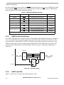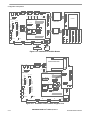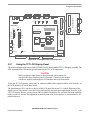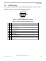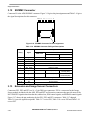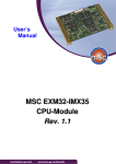
1
M9328MX21ADSE
Application Development System
User’s Manual
Document Number: UMS-21100
Rev. A
07/2006
Chapter 1 General Information
1.1
1.2
1.3
1.4
1.5
Description . . . . . . . . . . . . . . . . . . . . . . . . . . . . . . . . . . . . . . . . . . . . . . . . . . . . . . . . . . . . . . . . .
M9328MX21ADSE Features . . . . . . . . . . . . . . . . . . . . . . . . . . . . . . . . . . . . . . . . . . . . . . . . . . .
System and User Requirements . . . . . . . . . . . . . . . . . . . . . . . . . . . . . . . . . . . . . . . . . . . . . . . . .
M9328MX21ADSE Diagram . . . . . . . . . . . . . . . . . . . . . . . . . . . . . . . . . . . . . . . . . . . . . . . . . . .
ADS Specifications. . . . . . . . . . . . . . . . . . . . . . . . . . . . . . . . . . . . . . . . . . . . . . . . . . . . . . . . . . .
1-1
1-1
1-2
1-2
1-4
Chapter 2 Configuration and Operation
2.1
2.2
2.2.1
2.2.2
2.3
2.3.1
2.3.2
2.3.3
2.3.4
2.3.5
2.3.6
2.3.7
2.3.8
2.3.9
2.3.10
2.3.11
2.3.12
2.4
2.5
2.5.1
2.5.2
2.5.3
2.5.4
2.5.5
2.5.6
2.5.7
Introduction. . . . . . . . . . . . . . . . . . . . . . . . . . . . . . . . . . . . . . . . . . . . . . . . . . . . . . . . . . . . . . . . . 2-1
Configuring Board Components . . . . . . . . . . . . . . . . . . . . . . . . . . . . . . . . . . . . . . . . . . . . . . . . . 2-1
Peripheral Selection Switch (S1) . . . . . . . . . . . . . . . . . . . . . . . . . . . . . . . . . . . . . . . . . . . . . 2-2
Mode/User Switch (S2) . . . . . . . . . . . . . . . . . . . . . . . . . . . . . . . . . . . . . . . . . . . . . . . . . . . . 2-3
Operation . . . . . . . . . . . . . . . . . . . . . . . . . . . . . . . . . . . . . . . . . . . . . . . . . . . . . . . . . . . . . . . . . . 2-4
Functional Block Diagram . . . . . . . . . . . . . . . . . . . . . . . . . . . . . . . . . . . . . . . . . . . . . . . . . . 2-4
On-Board Memory . . . . . . . . . . . . . . . . . . . . . . . . . . . . . . . . . . . . . . . . . . . . . . . . . . . . . . . . 2-4
Memory Map . . . . . . . . . . . . . . . . . . . . . . . . . . . . . . . . . . . . . . . . . . . . . . . . . . . . . . . . . . . . 2-5
USB On-The-Go Interface . . . . . . . . . . . . . . . . . . . . . . . . . . . . . . . . . . . . . . . . . . . . . . . . . . 2-6
UART and IrDA . . . . . . . . . . . . . . . . . . . . . . . . . . . . . . . . . . . . . . . . . . . . . . . . . . . . . . . . . . 2-6
Ethernet . . . . . . . . . . . . . . . . . . . . . . . . . . . . . . . . . . . . . . . . . . . . . . . . . . . . . . . . . . . . . . . . . 2-7
Touchscreen ADC. . . . . . . . . . . . . . . . . . . . . . . . . . . . . . . . . . . . . . . . . . . . . . . . . . . . . . . . . 2-8
CD Quality CODEC . . . . . . . . . . . . . . . . . . . . . . . . . . . . . . . . . . . . . . . . . . . . . . . . . . . . . . . 2-9
Keypad . . . . . . . . . . . . . . . . . . . . . . . . . . . . . . . . . . . . . . . . . . . . . . . . . . . . . . . . . . . . . . . . . 2-9
Memory Mapped I/O . . . . . . . . . . . . . . . . . . . . . . . . . . . . . . . . . . . . . . . . . . . . . . . . . . . . . 2-10
Audio Indicator (Buzzer) . . . . . . . . . . . . . . . . . . . . . . . . . . . . . . . . . . . . . . . . . . . . . . . . . . 2-12
LED Indicators . . . . . . . . . . . . . . . . . . . . . . . . . . . . . . . . . . . . . . . . . . . . . . . . . . . . . . . . . . 2-12
Using The Board Connectors . . . . . . . . . . . . . . . . . . . . . . . . . . . . . . . . . . . . . . . . . . . . . . . . . . 2-12
Add-On Module Connections and Usage . . . . . . . . . . . . . . . . . . . . . . . . . . . . . . . . . . . . . . . . . 2-13
Using the TFT LCD Display Panel. . . . . . . . . . . . . . . . . . . . . . . . . . . . . . . . . . . . . . . . . . . 2-15
Using the Keypad . . . . . . . . . . . . . . . . . . . . . . . . . . . . . . . . . . . . . . . . . . . . . . . . . . . . . . . . 2-16
Using a NAND Flash Card . . . . . . . . . . . . . . . . . . . . . . . . . . . . . . . . . . . . . . . . . . . . . . . . . 2-16
Using a SD/MMC Card . . . . . . . . . . . . . . . . . . . . . . . . . . . . . . . . . . . . . . . . . . . . . . . . . . . 2-16
Using Image Sensor Daughter Card . . . . . . . . . . . . . . . . . . . . . . . . . . . . . . . . . . . . . . . . . . 2-16
Using the PCMCIA Daughter Card . . . . . . . . . . . . . . . . . . . . . . . . . . . . . . . . . . . . . . . . . . 2-16
Using the TV Encoder Card . . . . . . . . . . . . . . . . . . . . . . . . . . . . . . . . . . . . . . . . . . . . . . . . 2-17
Chapter 3 Support Information
3.1
Introduction. . . . . . . . . . . . . . . . . . . . . . . . . . . . . . . . . . . . . . . . . . . . . . . . . . . . . . . . . . . . . . . . . 3-1
3.2
CPU to Base Board Connectors PX1, PX2, PY1, and PY2 . . . . . . . . . . . . . . . . . . . . . . . . . . . . 3-1
3.3
CPU to Option Card Connectors . . . . . . . . . . . . . . . . . . . . . . . . . . . . . . . . . . . . . . . . . . . . . . . 3-12
3.4
UART/RS-232 Connectors . . . . . . . . . . . . . . . . . . . . . . . . . . . . . . . . . . . . . . . . . . . . . . . . . . . . 3-18
3.4.1
UART1 Connector . . . . . . . . . . . . . . . . . . . . . . . . . . . . . . . . . . . . . . . . . . . . . . . . . . . . . . . 3-18
3.4.2
UART4 Connector . . . . . . . . . . . . . . . . . . . . . . . . . . . . . . . . . . . . . . . . . . . . . . . . . . . . . . . 3-19
3.4.3
External UART Connector . . . . . . . . . . . . . . . . . . . . . . . . . . . . . . . . . . . . . . . . . . . . . . . . . 3-20
M9328MX21ADSE User’s Manual, Rev. A
Freescale Semiconductor
1
3.5
3.6
3.7
3.8
3.9
3.10
3.11
3.12
3.13
3.14
Multi-ICE Connector . . . . . . . . . . . . . . . . . . . . . . . . . . . . . . . . . . . . . . . . . . . . . . . . . . . . . . . .
Ethernet Connector . . . . . . . . . . . . . . . . . . . . . . . . . . . . . . . . . . . . . . . . . . . . . . . . . . . . . . . . . .
USB OTG Connector . . . . . . . . . . . . . . . . . . . . . . . . . . . . . . . . . . . . . . . . . . . . . . . . . . . . . . . .
NAND Flash Connector . . . . . . . . . . . . . . . . . . . . . . . . . . . . . . . . . . . . . . . . . . . . . . . . . . . . . .
External Keypad Connector . . . . . . . . . . . . . . . . . . . . . . . . . . . . . . . . . . . . . . . . . . . . . . . . . . .
LCD Panel Connector . . . . . . . . . . . . . . . . . . . . . . . . . . . . . . . . . . . . . . . . . . . . . . . . . . . . . . . .
TV Encoder Connector . . . . . . . . . . . . . . . . . . . . . . . . . . . . . . . . . . . . . . . . . . . . . . . . . . . . . . .
SD/MMC Connector. . . . . . . . . . . . . . . . . . . . . . . . . . . . . . . . . . . . . . . . . . . . . . . . . . . . . . . . .
Extension and Image Sensor Connectors . . . . . . . . . . . . . . . . . . . . . . . . . . . . . . . . . . . . . . . . .
Disposal Information . . . . . . . . . . . . . . . . . . . . . . . . . . . . . . . . . . . . . . . . . . . . . . . . . . . . . . . .
3-20
3-21
3-22
3-22
3-25
3-26
3-27
3-28
3-28
3-33
M9328MX21ADSE User’s Manual, Rev. A
2
Freescale Semiconductor
About This Book
This manual explains how to connect and operate the M9328MX21ADS i.MX21 Application
Development System.
Audience
The audience for this manual is handheld communication device designers. It is assumed that users are
engineers or technicians with experience using development systems.
Organization
The manual consists of three chapters.
• Chapter 1 General Information introduces the user to the features and capabilities of the ADS.
• Chapter 2 Configuration and Operation contains configuration information, connection
descriptions, and other operational information that may be useful during the development process.
• Chapter 3 Support Information contains connector pin assignments, connector signal descriptions,
and other useful information about the ADS.
Revision History
The following table summarizes changes to this document since the previous release (Rev. A).
Revision History
Location
Revision
Conventions
Units and measures in this manual conform to the International System of Units (SI) as defined by
National Institute of Standards and Technology Special Publication 811.
M9328MX21ADSE User’s Manual, Rev. A
Freescale Semiconductor
P-1
Definitions, Acronyms, and Abbreviations
The following acronyms and abbreviations are used in this manual. This list does not include signal,
register, and software mnemonics.
ADS
Application Development System
CD
Compact Disk
CMOS
Complementary Metal Oxide Semiconductor
CODEC
Code/Decode
CPU
Central Processing Unit
DCE
Data Communications Equipment
DIN
Deutsches Institut für Normung
DIP
Dual In-line Package
DTE
Data Terminal Equipment
DUART
I2C
ICE
I/O
IrDA
JTAG
LCD
LED
MB
MCU
MMC
NAND
OTG
PC
PCMCIA
SD
SDRAM
SI
SSI
TFT
UART
USB
VDC
Dual Universal Asynchronous Receiver/Transmitter
Inter-Integrated Circuit
In-Circuit Emulator
Input/Output
Infrared Data Association
Joint Test Access Group
Liquid Crystal Display
Light Emitting Diode
Megabyte
Microcontroller Unit
Multi-media Card
Negative AND
On the Go
Personal Computer
Personal Computer Memory Card International Association
SanDisk (Smart Media)
Synchronous Dynamic Random Access Memory
System International (international system of units and measures)
Synchronous Serial Interface
Thin Film Transistor
Universal Asynchronous Receiver/Transmitter
Universal Serial Bus
Volts Direct Current
M9328MX21ADSE User’s Manual, Rev. A
P-2
Freescale Semiconductor
Chapter 1 General Information
1.1
Description
The M9328MX21ADSE helps you develop applications for the i.MX21 MCU.
The ADS has 19 connectors and sockets that support application software, target board debugging, and
optional circuit cards. A separate LCD display panel and a separate keypad are supplied with the ADS.
When you connect the LCD panel and keypad to the ADS Base board, they align with each other.
1.2
M9328MX21ADSE Features
ADS features include:
• i.MX21 Multimedia Application Processor
• Two clock-source crystals, 32.768 KHz and 26 MHz
• Power connector for +5.0-volts in from an external regulated power supply, an in-line fuse, and a
power on/off switch.
• Voltage regulators that step down the 5.0 VDC input to Vcc (3.0 VDC), 2.5 VDC, 1.8 VDC and
1.5 VDC
• Multi-ICE debug support
• Two 8 MB × 16-bit Burst Flash memory devices configured as one 32 MB, 32-bit device
• Two 16 MB × 16-bit SDRAM devices configured as one 64 MB, 32-bit device
• High speed expansion connectors for adding optional cards.
• Two-board system: modular CPU board plugs into Base board; Base board has connections for
LCD display panel and keypad
• Memory mapped expansion I/O
• Software readable board revisions
• Configuration and user definable DIP switches
• SD/MMC memory card connector
• Two RS-232 transceivers and DB9 connectors (one configured for DCE and one for DTE
operation) supporting on-chip UART ports
• External UART with RS-232 transceiver and DB9 connector
• IrDA transceiver that conforms to Specification 1.4 of the Infrared Data Association
• USB OTG (On The Go) interface transceiver and USB mini AB connector
• Separate LCD panel assembly that connects to the Base board and interfaces directly with the ADS
• Touch panel controller for use with the LCD
• Separate keypad unit with 36 push button keys
M9328MX21ADSE User’s Manual, Rev. A
Freescale Semiconductor
1-1
General Information
•
•
•
•
•
•
•
•
•
•
•
1.3
Separate CMOS Image Sensor Card
Audio CODEC includes an 11.28 MHz crystal oscillator, a 3.5 mm audio input jack, a 3.5 mm
microphone jack, and a 3.5 mm headphone jack
Cirrus Logic CS8900A-CQ3Z Ethernet controller, with RJ-45 connector for connecting to a system
hub
Two 32 × 3-pin DIN expansion connectors with most i.MX21 I/O signals
Variable resistor for emulation of a battery voltage level
NAND Flash card (Plugs into CPU Board)
LED indicators for power, external bus activity, Ethernet activity, and two LEDs for user defined
status indiction
Universal power supply with 5.0-volt output @ 2.4 Amperes
USB cable
RS-232 serial cable
Two RJ-45 Ethernet cables, network, and crossover
System and User Requirements
To use the ADS, you need:
• An IBM PC or compatible computer that has:
— A Windows® 98, Windows ME™, Windows XP™, Windows 2000, or Windows NT® (version
4.0) operating system
— A parallel port and a Multi-ICE device (not included)
• A + 5 VDC power supply @ 2.4 A, with a 2 mm female (inside positive) power connector
(included)
CAUTION
Never supply more than +5.5-volts power to your M9328MX21ADSE.
Doing so can damage board components.
1.4
M9328MX21ADSE Diagram
Figure 1-1 shows the connectors and other major parts of the ADS Base board and CPU board.
M9328MX21ADSE User’s Manual, Rev. A
1-2
Freescale Semiconductor
General Information
OFF
P8
P3
ON
P2
EXT UART DCE
SW1
SD2_D1
SD2_D0
J3
BASE BOARD
NC
NC
SD2_D2
SD2_D3
J5
J4
P7
IrDA
USB OTG
RI
CD
DSR
NC
ACT
U16
UART1 DCE
DTR
P9
ETHERNET
F1
2A
P4
P1
UART4 DTE
3
2
1
VR1
BATT EM
J6
LCD CON
+5V IN
CPU BOARD
PX1/PY1
LINK
ACT
P20
MULTI-ICE
S2
BOOT0
BOOT1
BOOT2
BOOT3
CLKMODE0
CLKMODE1
SW1 IRQ
SW2 READ
1
2
3
4
5
6
7
8
LED1
LED2
LED3
LED4
LED7
BUZZER
NAND FLASH CARD
5V PWR
VCC PWR
STAT2
STAT1
BUS ACT
PK1
S1
1
2
3
4
5
6
7
8
P10
LINE IN
UART1_ON
UART4_ON
IrDA_ON
NEXUS_EN
JTAG_CTRL
TONE_OUT
PEN_CS_B
PEN_IRQ_B
PM1
U6
U7
U8
U9
P13
U5
P5
CPU
PM2
KEYPAD CON
SW2
RESET
TV ENCODER
CON
LED6 LED5
J1 J3 J2
PK2
PX2/PY2
P11
MIC IN
P6
HEADPHONE
PE3
EXP CON 2
PE2
EXP CON 1
PE1
SD/MMC
J7
ONE WIRE
P12
CSI
Figure 1-1. M9328MX21ADSE Application Development System
Important board components on the CPU card are:
• U5 — i.MX21 MCU
• PX1, PX2 — connections to the Base board (bottom side)
• PK1, PK2 — connections to option cards
• P20 — ARM Multi-ICE connector
• PM1 & PM2 — NAND Flash card connectors
• J1, J2, J3 — Power interruption jumpers for measuring CPU current consumption
Important board components on the Base board are:
• PY1, PY2 — connections to the CPU board
• P1 — RS-232 DB9 connector for the processor’s UART1, DCE pinout
• P2 — RS-232 DB9 connector for the processor’s UART4, DTE pinout
• P3 — RS-232 DB9 connector for the External UART, DCE pinout
• P4 — USB OTG connector
• P5 — Keypad module connector
• P6 — SD/MMC card connector
• P7 — LCD/touch panel connector
M9328MX21ADSE User’s Manual, Rev. A
Freescale Semiconductor
1-3
General Information
•
•
•
•
•
•
•
•
•
•
•
•
•
•
•
•
•
•
•
•
•
1.5
P8 — 5.0-volt input power connector
P9 — RJ-45 Ethernet connectors
P10 — Line In to audio CODEC
P11 — Microphone In to audio CODEC
P12 — Headphone Out to audio CODEC
P13 — TV Encoder connector
PE1 — Connector to an Image Sensor card
PE2, PE3 — I/O Extension connectors
S1 — Peripheral enable and JTAG select DIP switches
S2 — Boot mode, clock mode, and user defined DIP switches
SW1 — Power switch
SW2 — Reset switch
LED1 — 5 volt power LED (green)
LED2 — 3 volt power LED (green)
LED3 and LED4 — General-purpose LEDs (orange)
LED5, LED6 — Ethernet activity LEDs (green, orange)
LED7 — external bus activity LED (red)
U16 — IrDA transceiver
VR1 — emulate the battery voltage level
J3, J4, J5 and J6 — Modem control enable jumpers for RS-232 DTE interface on P2
J7 — One wire interface
ADS Specifications
Table 1-1 shows M9328MX21ADSE specifications.
Table 1-1. Specifications
Characteristic
Specifications
Clock speed (SDRAM/FLASH)
CPU 266MHz, System 133MHz
Ports
10Base-T (RJ-45), RS-232 serial, USB OTG
Temperature:
operating
storage
0° to +50° C
-40° to +85° C
Relative humidity
0 to 90% (noncondensing)
Power requirements
4.5V — 5.5 VDC @ 2.4 A
Dimensions
7.15 x 9.45 in (18.2 x 24.1 cm)
M9328MX21ADSE User’s Manual, Rev. A
1-4
Freescale Semiconductor
Configuration and Operation
Chapter 2 Configuration and Operation
2.1
Introduction
This section contains configuration information, connection descriptions, and other operational
information that may be useful during the development process.
2.2
Configuring Board Components
Table 2-1 is a summary of configuration settings. The following paragraphs provide additional information
about configuring and using the ADS.
Table 2-1. Component Configuration Settings
Component
Position
Effect
System Power Switch, SW1
SW1
OFF
ON
Move this switch to the ON position to enable the power source
connected to P8 to power the system.
Factory setting is OFF.
BOARD
EDGE
System Reset Switch, SW2
Push to reset the M9328MX21ADSE.
SW2
S1
ON
1 2 3 4 5 6 7 8
Peripheral Selection Switch,
S1
The UART1 and UART4 transceivers are forced enabled, the IrDA
module is enabled by software, Nexus is disabled, ARM mode JTAG
is selected, and the buzzer is connected to PWMO. The LCD touch
panel signals are connected.
Factory setting is shown.
Subsection 2.2.1 explains other settings for this switch.
S1
Mode Switch, S2
S2
ON
1 2 3 4 5 6 7 8
Configures 32-bit Burst Flash as the boot device and the Default
clock bypass mode is selected.
Factory setting is shown
Subsection 2.2.2 explains other settings for this switch.
S2
Power Headers
(on CPU card)
J1, VCC (3.0 V)
J2, 1.8 V
J3, 1.5 V
1
2
Connects specified power signal.
Factory Setting
(Leave jumper installed during normal use.)
1
2
Connect ammeter across pins to measure processor current
consumption from the specified power source.
M9328MX21ADSE User’s Manual, Rev. A
Freescale Semiconductor
2-1
Configuration and Operation
Table 2-1. Component Configuration Settings (continued)
Component
Position
Modem Control Enable
Jumpers
(on Base board)
J3, DTR
J4, DSR
J5, CD
J6, RI
2.2.1
1
2
3
1
2
3
Effect
The specified RS-232 control signal of P2 connects to the specified
I/O signal.
J3 - DTR (pin 4) is controlled by SD2_D0 (output)
J4 - DSR (pin 6) can be read on SD2_D1 (input)
J5 - CD (pin 1) can be read on SD2-D2 (input)
J6 - RI (pin 9) can be read on SD2-D3 (input)
The specified RS-232 control signal of P2 is not connected to any I/O
signal and cannot be controlled or read.
J3 - DTR is forced active (positive), SD2_D0 is unused
J4 - DSR cannot be read, SD2_D1 is unused
J5 - CD cannot be read, SD2_D2 is unused
J6 - RI cannot be read, SD2_D3 is unused
Peripheral Selection Switch (S1)
S1 is a DIP switch that consists of eight slide switches. Seven of the switches enable and disable software
control of the UART transceivers, the IrDA buffers, the Nexus buffer, the touch panel controls, and the
buzzer. One switch selects JTAG operation mode.
Table 2-2 shows S1 functionality.
Table 2-2. S1 Switch Settings
Switch Name
S1-1, UART1_ON
S1-2, UART4_ON
S1-3, IrDA_ON
S1-4, NEXUS_EN
S1-5, JTAG _CTRL
S1-6, TONE_OUT
S1-7, PEN_CS_B
S1-8, PEN_IRQ_B
Setting
ON
Effect
Forces the UART1 transceiver to be enabled.
OFF
UART1_EN_B bit controls the UART1 transceiver
ON
Forces the UART4 transceiver to be enabled.
OFF
UART4_EN_B bit controls the UART4 transceiver
ON
Forces the IrDA module buffers to be enabled.
OFF
IrDA_EN bit controls the IrDA buffers
ON
Internal test only.
OFF
Set to OFF for debugging purposes.
ON
Internal test only.
OFF
ARM Multi-ICE mode selected after TRST.
ON
The buzzer is controlled by the PWMO output.
OFF
PWMO is disconnected from the buzzer circuit.
ON
CSPI_SS0 controls the chip enable of the Touch controller.
OFF
Disables CSPI_SS0 control of the Touch controller chip enable.
ON
UART3_CTS is connected to PENIRQ_B out of the Touch controller.
OFF
UART3_CTS is not connected to PENIRQ_B out of the Touch controller.*
*PENIRQ_B is not connected to anything.
Figure 2-1 shows an example configuration. The switches are set so that the UART1 transceiver and the
IrDA module are forced enabled; the UART4 transceiver can be enabled by software; and the NEXUS
buffer and buzzer are disabled. In addition, ARM mode JTAG is selected and the LCD touch control
signals are enabled.
M9328MX21ADSE User’s Manual, Rev. A
2-2
Freescale Semiconductor
Configuration and Operation
ON
1 2 3 4 5 6 7 8
UART1_ON
UART4_ON
IrDA_ON
NEXUS_ON, (Set to OFF)
JTAG_CTRL, (Set to OFF)
TONE_OUT
PEN_CS_B
PEN_IRQ_B
S1
Figure 2-1. Switch S1
2.2.2
Mode/User Switch (S2)
S2 is a DIP switch that consists of eight slide switches. S2-1 to S2-4 configure boot mode and S2-5 and
S2-6 control the clock bypass modes. These switch settings take effect only on power up or after a reset.
S2 also provides two user definable switches (S2-7 and S2-8). S2-7 can be used to cause an interrupt when
switched (SW1_IRQ through signal UART3_CTS).
Table 2-3 lists the settings for the boot-mode subswitches, S2-1 through S2-4.
.
Table 2-3. Boot Mode Switch Settings
BOOT3
S2-4
BOOT2
S2-3
Internal bootstrap ROM (USB/UART)
ON
NAND, 8-bit, 2KB per page
ON
Boot Mode, Device
BOOT1
S2-2
BOOT0
S2-1
ON
ON
ON/OFF
ON
OFF
ON
NAND, 16-bit, 2KB per page
ON
ON
OFF
OFF
NAND, 16-bit, 512bytes per page
ON
OFF
ON
ON
CS0, 16-bit, D[15:0]
ON
OFF
ON
OFF
CS0, 32-bit
ON
OFF
OFF
ON
NAND 8-bit, 512bytes per page
ON
OFF
OFF
OFF
Figure 2-2 shows an example configuration. S2-1 through S2-4 configure the system to boot from the 8-bit
NAND Flash. S2-5 and S2-6 are always set to OFF. S2-7 and S2-8 are set for user-defined functions.
ON
1 2 3 4 5 6 7 8
BOOT0
BOOT1
BOOT2
BOOT3
CLKMODE0, (Set to OFF)
CLKMODE1, (Set to OFF)
SW1 IRQ
SW2 READ
S2
Figure 2-2. Switch S2
M9328MX21ADSE User’s Manual, Rev. A
Freescale Semiconductor
2-3
Configuration and Operation
2.3
Operation
This section describes how the system functions and how to use the boards.
2.3.1
Functional Block Diagram
Figure 2-3 shows the functional interconnections of the ADS in a block diagram format.
Base Board
Ethernet
port
USB series
mini-AB
connector
UART signals
3V regulator, CPU
Reset signal
UART
controller
Ethernet
controller
USB OTG
Transceiver
Addr /Data Bus
Addr /Data Bus
USBOTG signals
LCD Board
IO pins , PWM
NAND Flash
Connector
Boot mode,
UARTs, IrDA
selection
Speaker
Out
Touch screen
controller
i.MX21
Burst Flash
TFT LCD DCDC converter
Addr /Data bus
IO pins
2.5V, 1.8V and
1.5V regulators
Transceiver
I2C
Addr/Data Bus
Battery Level
Measurement
Emulation
Addr /Data bus
High Speed
Connectors
LCD panel
(240x320 pixels) & Touch
screen
Base board connectors
TV
Encoder
connector
OWIRE
Line In
Mic In
White
LED
driver
NFC signals
Decoder & Chip
select logic
S/W readable
DIP switches
Multi-ICE
connector
SDRAM
1-wire Interface
Silicon & Board
revision register
LCDC
CPU Board
LEDs & Buzzer
LCD
connector
Ext.
UART
UART1,
UART2 &
IrDA
Power Connector,
Power Switch & fuse
SSI
Audio
CODEC
KPP
Peripheral signals
Peripheral signals
CSI signals
MMC/SD signals
Expansion
Connector 2
Expansion
Connector 1
Image sensor
connector
MMC/SD
connector
Keypad
Connector
Keypad Board
Figure 2-3. Functional Block Diagram of M9328MX21ADSE
2.3.2
On-Board Memory
Figure 2-4 and Figure 2-5 show the on-board memory interface. The M9328MX21ADSE is equipped with
8M x 32-bit Burst Flash and 16M x 32-bit SDRAM. The chip selects CS0 and CS2 (CSD0) are used for
Burst Flash and SDRAM chip selects, respectively.
M9328MX21ADSE User’s Manual, Rev. A
2-4
Freescale Semiconductor
Configuration and Operation
VCC VCC VCC
8MX16-Bit Burst Flash
CS0
CS
WP
ACC
8MX16-Bit Burst Flash
ECB
RDY
A2...A24
A0...A22
BCLK
OE
LBA
DQM3_EB3
FLASH_RST
CLK
OE
AVD
WE
RESET
D0.15
D0..15
DQM1_EB1
WE
D16..31
D0.15
Figure 2-4. Burst Flash Interface
VCC
16MX16-Bit SDRAM
CS2
SDCKE0
SDCLK
RAS
CAS
WE
CS
CKE
CLK
RAS
CAS
WE
A2..A18
A0..10
BA0
A19
A20
DQM1_EB1
DQM0_EB0
A11
BA0
BA1
LDQM
UDQM
D0..15
D0..15
16MX16-Bit SDRAM
DQM3_EB3
DQM2_EB2
LDQM
UDQM
D16..31
D0..15
Figure 2-5. SDRAM Interface
2.3.3
Memory Map
Table 2-4 shows the memory map for external peripherals on the ADS board. Because the Burst Flash and
the Ethernet Controller do not take up the entire address space of the associated chip selects, software can
access the same physical memory location at more than one range of addresses. For instance, SDRAM uses
M9328MX21ADSE User’s Manual, Rev. A
Freescale Semiconductor
2-5
Configuration and Operation
the entire 64 MB address space allowed for CSD0, but the Burst Flash occupies only 32 MB of the 64 MB
space available to CS0, so it appears in two different ranges of addresses. CS1 covers 16 MB allowing
many repetitions of the memory mapped peripherals.
Table 2-4. M9328MX21ADSE Memory Map
Peripheral
Chip Select
Address Range (HEX)
Act Mem Size
SDRAM
CSD0
0xC000_0000 to 0xC3FF_FFFF
64 MB
Burst FLASH
CS0
0xC800 0000 to 0xC9FF_FFFF
32 MB
Ethernet Controller
CS1
0xCC00 0000 to 0xCC00_000F*
16 BYTES
External DUART
CS1
0xCC20 0000 to 0xCC20_000F*
16 BYTES
Read CPU and
Base board versions
CS1
Read 0xCC40_0000*
D7-D0 = CPU, D15-D8 = Base board
2 BYTES
CS1
Write to 0xCC80_0000* (Output)
2 BYTES
CS1
Read 0xCC80_0000* (Input)
2 BYTES
Memory Mapped I/O
* For I/O operations only D15 - D0 are used
2.3.4
USB On-The-Go Interface
The i.MX21 USB OTG Device Module interfaces with a Phillips ISP1301BS USB transceiver connected
to P4, a mini AB USB connector. The interface can function as either a USB host or USB device. The
interface includes a Maxim MAX3355EUD+ USB power supply chip which can provide power on the
USB bus in host mode. This power supply chip is enabled by the USB_PWR signal. For details on the
operation of the USB interface, refer to the i.MX21 data sheet. Figure 2-6 shows the USB interface
connection.
ISP1301BS
P4
Di.MX21
D+
VBUS
USB Device
ID
VBUS
USB MINI AB
IDIN
IDOUT
USB_PWR
SHDN
MAX3355EUD+
Figure 2-6. USB OTG Interface
2.3.5
UART and IrDA
Figure 2-7 shows how to connect the UART and IrDA circuits.
M9328MX21ADSE User’s Manual, Rev. A
2-6
Freescale Semiconductor
Configuration and Operation
i.MX21
RS232 Transceiver
VCC
P1
UART1_TXD1
UART1_RXD1
UART1
UART1_RTS1
DCE
EN
UART1_CTS1
S1-1
GND
Software Enable
via MMIO Latch
RS232 Transceiver
USBH1_TXDM
USBH1_RXDP
USBH1_RXDM
USBH1_RXDP
TXD4
RXD4
RTS
CTS
SD2_D1
DSR*
SD2_D2
CD*
SD2_D3
RI*
SD2_D0
DTR*
P2
UART4
VCC
DTE
EN
S1-2
* If enabled by jumper
GND
Buffer
Software Enable
via MMIO Latch
IrDA
UART3_TXD
UART3_RXD
VCC
EN
EN
S1-3
GND
Software Enable
via MMIO Latch
Figure 2-7. UARTs and IrDA Interface
2.3.6
Ethernet
The ADS is equipped with a Cirrus Logic CS8900A-CQ3Z Crystal LAN ISA Ethernet Controller that can
interface with the i.MX21. The CS8900A-CQ3Z has 10BaseT transmit and receive filters and operates in
I/O mode. Figure 2-8 shows the Ethernet interface.
M9328MX21ADSE User’s Manual, Rev. A
Freescale Semiconductor
2-7
Configuration and Operation
i.MX21
VCC
CS8900A-CQ3Z
SA8
SA9
Isolation
Transformer
SA0
SA4..7
SA10..19
BA1..3
SA1..3
D0..15
D0..15
P9
RJ45 Connector
AEN
CS_LAN
B_OE
IOR
IOW
B_RW
B_DQM3_EB3
UART3_RTS
SBHE
INTRQ0
CHIPSEL
Figure 2-8. Ethernet Interface
2.3.7
Touchscreen ADC
The ADS is equipped with an Analog Devices AD7873BRQZ ADC. The ADC communicates with the
touchscreen of the LCD on the Base board. Variable resistor VR1 on the Base board can be used to change
the VBAT input voltage to the ADC. The i.MX21 communicates with the ADC via the CSPI1 interface.
Setting S1-7 to ON connects CSPI1_SS0 to the ADC chip select. Setting S1-8 to ON connects the ADC
interrupt out to UART3_CTS. Figure 2-9 shows the ADC interface.
VCC
i.MX21
S1
8
AD7873BRQZ
PENIRQ VREF
UART3_CTS
P7
VBAT
7
CSPI1_SS0
VR1
CS
X+
CSPI1_SCLK
DCLK
CSPI1_MISO
DOUT
X-
CSPI1_MOSI
DIN
Y-
Y+
LCD CONNECTOR
Figure 2-9. ADC Interface
M9328MX21ADSE User’s Manual, Rev. A
2-8
Freescale Semiconductor
Configuration and Operation
2.3.8
CD Quality CODEC
The ADS has a Wolfson WM8731SEDS 32-bit linear low power stereo CODEC with a built-in headphone
driver (U24). The CODEC is controlled by the i.MX21, which sends the digital audio data via an SSI2
interface and control data via an I2C interface.
The CODEC has stereo line and mono microphone level audio inputs as well as stereo headphone outputs.
It features a mute function, programmable line level volume control, and a bias voltage output suitable for
an electret type microphone. Table 2-5 shows the CODEC connectors and describes their basic functions.
Table 2-5. Audio Connectors
Connector
Descriptions
P10
Stereo line in jack
P11
Dynamic microphone input jack
P12
Headphone jack for audio out
The WM8731SEDS data sheet is available at http://www.wolfsonmicro.com/
2.3.9
Keypad
The ADS includes an external keypad module that connects to the Base board. The keys provide tactile
feedback. The i.MX21 keypad interface reads the pad via the KCOL[5:0] and KROW[5:0] signals. the
interface has chording diodes to prevent ghost key presses. The keys are labeled with numeric, cursor
control, soft key, and spare key functions, but the actual functionality is determined by user software. The
default keypad can be replaced by a custom design. The UART2 signals that are multiplexed internally
with the KCOL[7,6] and KROW[7,6] signals are brought out to keypad connector P5. This allows the use
of an 8x8 keypad matrix. Table 2-6 shows the key switch connections to the keypad signals by function
name (as labeled on the PCB) and the switch reference designators.
Table 2-6. Keypad Layout and Connections
KCOL5
KCOL4
KCOL3
KCOL2
KCOL1
KCOL0
KROW5
APP1
SW1
SEND
SW2
KEY 1
SW3
UP
SW4
KEY 2
SW5
END
SW6
KROW4
APP2
SW7
HOME
SW8
LEFT
SW9
ACTION
SW10
RIGHT
SW11
BACK
SW12
KROW3
DOWN
SW13
APP3
SW14
1SW15
2 ABC
SW16
3 DEF
SW17
EXTRA 2
SW18
KROW2
VOL UP
SW19
APP4
SW20
4 GHI
SW21
5 JKL
SW22
6 MNO
SW23
EXTRA 3
SW24
KROW1
VOL DOWN
SW25
EXTRA 1
SW26
7 PQRS
SW27
8 TUV
SW28
9 WXYZ
SW29
EXTRA 4
SW30
KROW0
POWER
SW31
RECORD
SW32
*
SW33
0+
SW34
#
SW35
EXTRA 5
SW36
M9328MX21ADSE User’s Manual, Rev. A
Freescale Semiconductor
2-9
Configuration and Operation
2.3.10
Memory Mapped I/O
The ADS uses Memory Mapped I/O to add I/O functions without using the I/O resources of the processor.
The following paragraphs describe the I/O functions.
2.3.10.1
Input I/O
A memory read of hex address 0xCC80_0000 inputs the state of the ADS signals connected to latches U5
and U7. Table 2-7 shows which signal is associated with each data bit.
Table 2-7. Input Buffer Signals
BIT
Signal
Description
BIT 0
SD_WP
Secure Data Write Protect
BIT 1
SW_SEL
Software readable switch
BIT 2
RESET_E_UART
External UART Reset
BIT 3
RESET_BASE
Ethernet controller Reset
BIT 4
CSI_CTL2
Image Sensor control 2
BIT 5
CSI_CTL1
Image Sensor control 1
BIT 6
CSI_CTL0
Image Sensor control 0
BIT 7
UART1_EN
UART1 transceiver enable
BIT 8
UART4_EN
UART4 transceiver enable
BIT 9
LCDON
LCD enable
BIT 10
IRDA_EN
IrDA transceiver enable
BIT 11
IRDA_FIR_SEL
Reserved
BIT 12
IRDA_MD0_B
IrDA SD/Mode (inverted)
BIT 13
IRDA_MD1
Reserved
BIT 14
LED4_ON
LED 4 control
BIT 15
LED3_ON
LED 3 control
M9328MX21ADSE User’s Manual, Rev. A
2-10
Freescale Semiconductor
Configuration and Operation
2.3.10.2
Output I/O
A memory write to hex address 0xCC80_0000 causes U5 and U7 to latch the logic state of the data bus.
Each latch output is associated with the data bus signal of the same number (Bit 0 is equal to DATA0, and
so on). All output bits are forced to logic 0 (low) on power up or reset. Table 2-8 shows the functions
associated with each data bit.
Table 2-8. Output Latch Functions
Bit
Signal
Description
BIT 0
TP6
Test point
BIT 1
TP7
Test point
BIT 2
RESET_E_UART*
External UART Reset (U17)
BIT 3
RESET_BASE*
Ethernet controller Reset (U9)
BIT 4
CSI_CTL2
Image Sensor control 2
BIT 5
CSI_CTL1
Image Sensor control 1l
BIT 6
CSI_CTL0
Image Sensor control 0
BIT 7
UART1_EN**
UART1 transceiver enable
BIT 8
UART4_EN**
UART4 transceiver enable
BIT 9
LCDON
LCD enable
BIT 10
IRDA_EN**
IrDA transceiver enable
BIT 11
IRDA_FIR_SEL
Reserved
BIT 12
IRDA_MD0_B
IrDA SD/Mode (inverted)
BIT 13
IRDA_MD1
Reserved
BIT 14
LED4_ON
LED 4 control, logic 1 turns on LED
BIT 15
LED3_ON
LED 3 control, logic 1 turns on LED
* Toggle the pin from a logic 0 (low) to a logic 1 (high) and back to logic 0 to reset the
selected peripheral.
** The associated x_ON switch (see Table 1-2) must be set OFF to allow the state of
these bits to control the associated interface. Setting the bit to logic 1 (high) enables the
interface and setting it to logic 0 (low) disables the interface.
M9328MX21ADSE User’s Manual, Rev. A
Freescale Semiconductor
2-11
Configuration and Operation
2.3.11
Audio Indicator (Buzzer)
The ADS includes an audio indicator or buzzer, U23. When S1-6 is ON, the PWMO pin of the i.MX21
controls this function. This buzzer operates from 1 KHz to 10 KHz. The maximum sound level is reached
when the frequency is 3 KHz and the duty cycle is 50%.
2.3.12
LED Indicators
Table 2-9 shows the ADS LED indicators and their associated functions.
Table 2-9. Function of LED Indicators
Reference #
Color
Name
Function
LED1
Green
5V PWR
5 V power is ON
LED2
Green
VCC PWR
3 V power is ON
LED3
Orange
STAT 2
User status controlled by Output BIT 15*
LED4
Orange
STAT 1
User status controlled by Output BIT 14*
LED5
Green
ACTIVE
Blinking indicates LAN Activity
LED6
Orange
LINK
Link good or host controlled output
LED7
Red
BUS ACT
Blinking indicates external bus activity
* A logic high level at the controlling pin turns on the LED. A logic low turns it off.
2.4
Using The Board Connectors
Table 2-10 shows the ADS connectors and functions, as well as special instructions for using the
connectors. Figure 1-1 in Chapter 1 shows the connector locations and reference designators.
Table 2-10. M9328MX21ADSE Connectors
Connector
Function
Comments
P1
UART1
RS-232 DCE interface to UART1 of the i.MX21
P2
UART4
RS-232 DTE interface to UART4 of the i.MX21
P3
External UART
RS-232 DCE interface to Port A of the ST16C2552 UART
P4
USB OTG
USB On The Go mini AB connector
P5
Keypad module
Connect the Keypad ribbon cable between this connector and the
corresponding connector of the Keypad Module, J1.
P6
SD/MMC
Slide the MMC card into the connector until it snaps into place.
P7
LCD panel
Connect LCD ribbon cable between this connector and the
corresponding connector of the LCD display panel, J11.
P8
Power
Plug the 5-volt power-supply jack end into this connector.
M9328MX21ADSE User’s Manual, Rev. A
2-12
Freescale Semiconductor
Configuration and Operation
Table 2-10. M9328MX21ADSE Connectors (continued)
Connector
2.5
Function
Comments
P9
Ethernet
Standard Ethernet connector. A cable for direct network and one for
crossover connections (direct to a PC) have been provided.
P10
Line In
Standard 3.5 mm connector for stereo audio input to the
WM8731SEDS CODEC
P11
Microphone In
Standard 3.5 mm connector for a microphone. Use only dynamic
microphones with a 200 to 600 ohms impedance.
P12
Headphone
Standard 3.5 mm connector for stereo audio. This is the amplified
stereo output of the WM8731SEDS. Use headphones with a 16 to 32
ohms impedance.
P13
TV encoder
This connector is used with P7 together to connect the TV encoder
card.
PE1
Image Sensor
Connect the image-sensor daughter board to this connector.
PE2, PE3
Expansion
Standard 48 pin, three row, male DIN connectors. Can be connected
to directly or cabled to a custom circuit board.
PY1, PY2
CPU
Connect the CPU module to these connectors.
PX1, PX2
Base board
Connect these to the Base board PY connectors.
PK1, PK2
Option Cards
Connect an appropriate Option Card to these connectors
P20 (CPU)
Multi-ICE
Standard ARM Multi-ICE connector
PM1, PM2
(CPU)
NAND Flash
Plug the NAND Flash module into this connector.
Add-On Module Connections and Usage
Figure 2-10 through Figure 2-12 show how to connect the ADS add-on modules. The following
paragraphs describe how to connect and use the add-on modules.
M9328MX21ADSE User’s Manual, Rev. A
Freescale Semiconductor
2-13
Configuration and Operation
OFF
P8
P3
ON
P2
EXT UART DCE
SW1
U16
UART1 DCE
DTR
P9
ETHERNET
F1
2A
P4
P1
UART4 DTE
ACT
NC
NC
NC
SD2_D0
SD2_D1
SD2_D2
SD2_D3
J3
BASE BOARD
J4
3
2
1
VR1
BATT EM
J6
J5
TFT LCD PANEL
(240 x 320 dots)
CPU BOARD
PX1/PY1
34 CONDUCTOR
RIBBON CABLE
ACT
MULTI-ICE
P20
PK1
LED1
LED2
LED3
LED4
LED7
BUZZER
P10
LINE IN
BOOT0
BOOT1
BOOT2
BOOT3
CLKMODE0
CLKMODE1
SW1 IRQ
SW2 READ
1
2
3
4
5
6
7
8
S1
1
2
3
4
5
6
7
8
NAND FLASH CARD
S2
5V PWR
VCC PWR
STAT2
STAT1
BUS ACT
PN1
U6
U7
U8
U9
P13
VR1
U5
PM1
PN2
UART1_ON
UART4_ON
IrDA_ON
NEXUS_EN
JTAG_CTRL
TONE_OUT
PEN_CS_B
PEN_IRQ_B
P5
KEYPAD
P1
CPU
KEYPAD CON
LINK
TV ENCODER
CON
LED6 LED5
SW2
RESET
LCD BOARD
J11
RI
CD
DSR
P7
IrDA
USB OTG
LCD CON
+5V IN
J1 J3 J2
PM2
PK2
Send
Key 1
Home
Left
Key 2
20 CONDUCTOR
RIBBON CABLE
PX2/PY2
P11
MIC IN
Action
Down
App1
App2
P6
PE3
PE2
EXP CON 2
SD/MMC
J7
ONE WIRE
HEADPHONE
PE1
EXP CON 1
Back
Right
App3
App4
Vol Up
P12
End
Up
Vol Down
Extra 1
Power
Record
1
2
3
Extra 2
4
5
6
Extra 3
7
8
9
Extra 4
*
0
#
Extra 5
CSI
SD/MMC
Card
IMAGE SENSOR
Figure 2-10. Installation of the Main Boards
U9
PCMCIA DAUGHTER CARD
OFF
P8
P3
ON
P2
EXT UART DCE
SW1
P9
ETHERNET
F1
2A
P4
P1
UART4 DTE
DTR
SD2_D1
SD2_D0
J3
NC
NC
SD2_D2
SD2_D3
J4
J5
P2
3
2
1
VR1
BATT EM
J6
PK1/PK3
BASE BOARD
P7
IrDA
USB OTG
RI
CD
DSR
NC
ACT
U16
UART1 DCE
LCD CON
+5V IN
CPU BOARD
P1
PX1/PY1
P20
5V PWR
VCC PWR
STAT2
STAT1
BUS ACT
LED1
LED2
LED3
LED4
LED7
BOOT0
BOOT1
BOOT2
BOOT3
CLKMODE0
CLKMODE1
SW1 IRQ
SW2 READ
1
2
3
4
5
6
7
8
BUZZER
S1
1
2
3
4
5
6
7
8
P10
LINE IN
UART1_ON
UART4_ON
IrDA_ON
NEXUS_EN
JTAG_CTRL
TONE_OUT
PEN_CS_B
PEN_IRQ_B
MULTI-ICE
PK1
U6
U7
U8
U9
U5
PM1
PK2/PK4
P5
CPU
PM2
P13
S1
S2
KEYPAD CON
ACT
S2
NAND FLASH CARD
LINK
TV ENCODER
CON
LED6 LED5
SW2
RESET
J1 J3 J2
PK2
PX2/PY2
P11
MIC IN
P6
HEADPHONE
PE3
PE2
EXP CON 2
EXP CON 1
PE1
SD/MMC
J7
ONE WIRE
P12
CSI
Figure 2-11. Installation of the PCMCIA Daughter Card
M9328MX21ADSE User’s Manual, Rev. A
2-14
Freescale Semiconductor
Configuration and Operation
P1
EXT UART DCE
SW1
P9
ETHERNET
F1
2A
UART4 DTE
U16
UART1 DCE
DTR
SD2_D1
J3
NC
NC
SD2_D2
SD2_D3
J4
J2
P7
IrDA
USB OTG
RI
CD
DSR
NC
ACT
SD2_D0
BASE BOARD
P4
P1
J5
3
2
1
VR1
BATT EM
J6
CPU BOARD
PX1/PY1
P2
P20
MULTI-ICE
BUZZER
PK1
BOOT0
BOOT1
BOOT2
BOOT3
CLKMODE0
CLKMODE1
SW1 IRQ
SW2 READ
1
2
3
4
5
6
7
8
LED1
LED2
LED3
LED4
LED7
S1
1
2
3
4
5
6
7
8
P10
LINE IN
UART1_ON
UART4_ON
IrDA_ON
NEXUS_EN
JTAG_CTRL
TONE_OUT
PEN_CS_B
PEN_IRQ_B
NAND FLASH CARD
5V PWR
VCC PWR
STAT2
STAT1
BUS ACT
PM1
U6
U7
U8
U9
CVBS
ACT
S2
P13
J1
J3
U5
P5
CPU
PM2
KEYPAD CON
LINK
TV ENCODER
CON
LED6 LED5
SW2
RESET
VGA
ON
P2
S-VIDEO
P8
P3
TV ENCODER CARD
OFF
LCD CON
+5V IN
J1 J3 J2
PK2
PX2/PY2
P11
MIC IN
P6
HEADPHONE
PE3
EXP CON 2
PE2
EXP CON 1
PE1
SD/MMC
J7
ONE WIRE
P12
CSI
Figure 2-12. Installation of the TV Encoder Card
2.5.1
Using the TFT LCD Display Panel
The ADS is equipped with a Sharp LQ035Q7DB02 touch control enabled TFT LCD display assembly. The
ADS documentation CD contains specifications for the TFT LCD component.
CAUTION
Make sure that the input power to the main board is disconnected or
switched off before connecting the LCD module. Connecting the module
with power applied can damage the LCD module and/or the main board.
To use the TFT LCD display, connect the 34 conductor ribbon cable supplied with the ADS from J11 on
the LCD module to P7 on the Base board.
The potentiometer VR1, which is to the left of the LCD panel just below J11, controls flickering of the
display screen. This control is set at the factory and normally does not require adjustment. However, if the
TFT LCD display flickers, you may adjust VR1 to stabilize the display. Use a suitable flat head or phillips
head screwdriver. Because the adjustment is normally done with power applied, we recommend use of a
plastic blade tool.
M9328MX21ADSE User’s Manual, Rev. A
Freescale Semiconductor
2-15
Configuration and Operation
2.5.2
Using the Keypad
To use the keypad module, connect the 20 conductor ribbon cable supplied with the ADS from connector
P1 of the Keypad module to P5 of the M9328MX21ADSE Base board.
2.5.3
Using a NAND Flash Card
CAUTION
To avoid circuit damage, do not plug-in the NAND Flash card with power
applied to the board.
To use the NAND Flash module supplied with the ADS, connect PN1 & PN2 of the NAND Flash module
to PM1 & PM2 on the CPU board. Before installing the card, make sure that S1-4 (the NEXUS_ON
switch) is OFF and that the PCMCIA Daughter Card is not installed. For details on the NAND Flash
interface, refer to the specification document on the documentation CD.
2.5.4
Using a SD/MMC Card
Connector P6 on the Base board is a SD/MMC card holder. You must obtain a compatible card for use with
this connector. Note the card power is connected to 3.0 V
2.5.5
Using Image Sensor Daughter Card
Connector PE1 is pre-configured to operate directly with the IM8012 image sensor daughter card supplied
with the ADS. Communication with this card takes place through the I2C interface. For details on image
sensor operation, refer to the data sheet on the documentation CD
CAUTION
To avoid circuit damage, do not plug-in the image sensor card with power
applied to the board.
To install the image sensor card, plug its 48 position DIN connector into PE1 of the Base board. When the
image sensor card is installed, the two boards are at a right angle to each other, with the image sensor facing
away from the Base board.
2.5.6
Using the PCMCIA Daughter Card
CAUTION
Make sure that the input power to the Base board is disconnected when
installing the PCMCIA daughter card.
To use the PCMCIA daughter card supplied with the ADS, install the card in the sockets PK1 and PK2 on
the CPU board. Before installing the daughter card, make sure that S1-4 (the NEXUS_ON switch) is OFF
and that there is no NAND Flash card installed at PM1 & PM2.
You must supply a compatible PCMCIA card for use with the PCMCIA daughter card.
M9328MX21ADSE User’s Manual, Rev. A
2-16
Freescale Semiconductor
Configuration and Operation
2.5.7
Using the TV Encoder Card
A TV encoder card is supplied with the ADS. The main component is a FS453LF (PC to TV Video Scan
converter) from FOCUS Enhancements Semiconductor. For details on TV encoder operation, refer to its
data sheet, available at http://www.focusinfo.com/
CAUTION
Make sure that input power is disconnected or switched off before the TV
encoder card is installed. Connecting the card with power applied can
damage the TV encoder card and the Base board.
This TV encoder cannot be used at the same time as the LCD display because they share connector P7 on
the Base board. To use the TV encoder module, you must disconnect the LCD board from P7 on the Base
board and install the TV encoder module in P7 and P13 of the Base board.
M9328MX21ADSE User’s Manual, Rev. A
Freescale Semiconductor
2-17
Configuration and Operation
M9328MX21ADSE User’s Manual, Rev. A
2-18
Freescale Semiconductor
Chapter 3 Support Information
3.1
Introduction
This section contains connector pin assignments, connector signal descriptions, and other useful
information about the M9328MX21ADSE. Both the CPU and Base board connectors are described.
The tables in this section list signal names as they appear in the schematics for the boards. The figures
usually refer to the same signal name, but may substitute a generally accepted standard name for that
function. For example, all RS-232 transmitted data signals are referred to as TXD regardless of which
RS-232 connector is being illustrated. Also, the use of “_B” at the end of a signal name indicates that the
active state of the signal is logic level zero or ground potential (active low).
3.2
CPU to Base Board Connectors PX1, PX2, PY1, and PY2
The PX1 and PX2 connectors located at the bottom side of the ADS CPU card connect this board to the
ADS Base board through connectors PY1 and PY2 located on the top side of the board. Figure 3-1 shows
the pin assignments for the PX1 and PY1 connectors. Table 3-1 provides signal descriptions for these
connectors. Figure 3-2 shows the pin assignments for the PX2 and PY2 connectors and Table 3-2 provides
signal descriptions for these connectors.
M9328MX21ADSE User’s Manual, Rev. A
Freescale Semiconductor
3-1
Support Information
PX1
OE_ACD
FLM_VSYNC_SPS
SPL_SPR
VCC
CLS
LSCLK
LD16_R4
LD14_R2
LD12_R0
LD10_G4
LD8_G2
LD6_G0
LD4_B4
LD2_B2
LD0_B0
UART3_RXD
UART3_TXD
USBG_RXDP
USBG_RXDM
USBG_TXDP
USBG_TXDM
USBG_SDA
P5V
USBH1_TXDP
USBH1_TXDM
USBH1_RXDP
USBH1_RXDM
USB_BYP_B
P5V
TP22
CLK_26
UART1_RTS
UART1_RXD
UART2_RTS
UART2_RXD
BOOT3
BOOT1
PWM0
JTAG_CTRL
RESET_IN_B
POR_B
CLKMODE0
B_CS5_B
B_CS1_B
B_OE_B
B_NEXUSEVTI
B_A0
B_A2
B_D7
B_D6
B_D5
B_D4
B_D3
B_D2
B_D1
B_D0
B_A20
B_A22
B_A24
TP25
1
3
5
7
9
11
13
15
17
19
21
23
25
27
29
31
33
35
37
39
41
43
45
47
49
51
53
55
57
59
61
63
65
67
69
71
73
75
77
79
81
83
85
87
89
91
93
95
97
99
101
103
105
107
109
111
113
115
117
119
•
•
•
•
•
•
•
•
•
•
•
•
•
•
•
•
•
•
•
•
•
•
•
•
•
•
•
•
•
•
•
•
•
•
•
•
•
•
•
•
•
•
•
•
•
•
•
•
•
•
•
•
•
•
•
•
•
•
•
•
•
•
•
•
•
•
•
•
•
•
•
•
•
•
•
•
•
•
•
•
•
•
•
•
•
•
•
•
•
•
•
•
•
•
•
•
•
•
•
•
•
•
•
•
•
•
•
•
•
•
•
•
•
•
•
•
•
•
•
•
2
4
6
8
10
12
14
16
18
20
22
24
26
28
30
32
34
36
38
40
42
44
46
48
50
52
54
56
58
60
62
64
66
68
70
72
74
76
78
80
82
84
86
88
90
92
94
96
98
100
102
104
106
108
110
112
114
116
118
120
VCC
CONTRAST
LP_HSYNC
PS
REV
LD17_R5
LD15_R3
LD13_R1
LD11_G5
LD9_G3
LD7_G1
LD5_B5
LD3_B3
LD1_B1
VCC
UART3_RTS
UART3_CTS
USBG_OE_B
USBG_ON_B
USBG_FS
USBG_SCL
P5V
USBH1_FS
USB_OC_B
USBH1_OE_B
USBH_ON_B
USB_PWR
USBOTG_EN
B_DQM3_EB3_B
GND
VCC
UART1_CTS
UART1_TXD
UART2_CTS
UART2_TXD
BOOT2
BOOT0
TIN
TOUT
RESET_OUT_B
RTCK_GPIO
CLKMODE1
B_CS4_B
B_CS0_B
B_RW_B
NEXUS_EN_B
B_A1
B_A3
B_D15
B_D14
B_D13
B_D12
B_D11
B_D10
B_D9
B_D8
B_A21
B_A23
B_A25
GND
Figure 3-1. CPU to Base Board PX1/PY1 Connector Pin Assignments
M9328MX21ADSE User’s Manual, Rev. A
3-2
Freescale Semiconductor
Support Information
Table 3-1. CPU to Base Board PX1/PY1 Connector Signals
Pin(s)
Signal
1
OE_ACD
2, 7,
30, 62
VCC
3
Description
OUTPUT ENABLE / ALTERNATE CRYSTAL DIRECTION
+3.0 VDC power
FLM_VSYNC_SPS FIRST LINE MARKER / VERTICAL SYNCHRONIZATION
4
CONTRAST
LCD bias voltage used as contrast control
5
SPL_SPR
6
LP_HSYNC
8
PS
9
CLS
Start signal output for gate driver. Inverted version of PS (Sharp panel dedicated signal)
10
REV
Signal for common electrode driving signal preparation (Sharp panel dedicated signal)
11
LSCLK
12
LD17_R5
LCD DATA 17 / RED BIT 5 — Output data to LCO
13
LD16_R4
LCD DATA 16 / RED BIT 4 — Output data to LCD
14
LD15_R3
LCD DATA 15 / RED BIT 3 — Output data to LCD
15
LD14_R2
LCD DATA 14 / RED BIT 2 — Output data to LCD
16
LD13_R1
LCD DATA 13 / RED BIT 1 — Output data to LCD
17
LD12_R0
LCD DATA 12 / RED BIT 0 — Output data to LCD
18
LD11_G5
LCD DATA 11 / GREEN BIT 5 — Output data to LCD
19
LD10_G4
LCD DATA 10 / GREEN BIT 4 — Output data to LCD
20
LD9_G3
LCD DATA 9 / GREEN BIT 3 — Output data to LCD
21
LD8_G2
LCD DATA 8 / GREEN BIT 2 — Output data to LCD
22
LD7_G1
LCD DATA 7 / GREEN BIT 1 — Output data to LCD
23
LD6_G0
LCD DATA 6 / GREEN BIT 0 — Output data to LCD
24
LD5_B5
LCD DATA 5 / BLUE BIT 5 — Output data to LCD
25
LD4_B4
LCD DATA 4 / BLUE BIT 4 — Output data to LCD
26
LD3_B3
LCD DATA 3 / BLUE BIT 3 — Output data to LCD
27
LD2_B2
LCD DATA 2 / BLUE BIT 2 — Output data to LCD
28
LD1_B1
LCD DATA 1 / BLUE BIT 1 — Output data to LCD
29
LD0_B0
LCD DATA 0 / BLUE BIT 0 — Output data to LCD
31
UART3_RXD
SAMPLING LEFT to RIGHT— Horizontal scan direction
LINE PULSE / HORIZONTAL SYNCHRONIZATION
Control signal output for source driver (Sharp panel dedicated signal)
LCD SHIFT CLOCK — Output to LCD
UART3 RECEIVED DATA — Serial input signal
M9328MX21ADSE User’s Manual, Rev. A
Freescale Semiconductor
3-3
Support Information
Table 3-1. CPU to Base Board PX1/PY1 Connector Signals (continued)
Pin(s)
Signal
Description
32
UART3_RTS
UART3 REQUEST TO SEND — Active low input signal
33
UART3_TXD
UART3 TRANSMITTED DATA — Serial output signal
34
UART3_CTS
UART3 CLEAR TO SEND — Active low output signal
35
USBG_RXDP
USB OTG RECEIVED DATA PLUS input
36
USBG_OE_B
USB OTG OUTPUT ENABLE
37
USBG_RXDM
USB OTG RECEIVED DATA MINUS input
38
USBG_ON_B
USB OTG transceiver ON
39
USBG_TXDP
USB OTG TRANSMITTED DATA PLUS output
40
USBG_FS
41
USBG_TXDM
42
USBG_SCL
USB OTG SERIAL CLOCK
43
USBG_SDA
USB OTG SERIAL DATA
44, 45, 57
P5V
Swithched +5 VDC power
46
USBH1_FS
47
USBH1_TXDP
48
USB_OC_B
49
USBH1_TXDM
USB TRANSMITTED DATA MINUS output
50
USBH1_OE_B
USB OUTPUT ENABLE
51
USBH1_RXDP
USB RECEIVED DATA PLUS input
52
USBH_ON_B
53
USBH1_RXDM
54
USB_PWR
55
USB_BYP_B
USB BY PASS input active low
56
USBOTG_EN
Not used
58
B_DQM3_EB3_B
59
TP22
Test point
60, 120
GND
GROUND
61
CLK_26
63
UART1_RTS
UART1 REQUEST TO SEND — Active low input signal
64
UART1_CTS
UART1 CLEAR TO SEND — Active low output signal
65
UART1_RXD
UART1 RECEIVED DATA — Serial input signal
USB OTG FULL SPEED
USB OTG TRANSMITTED DATA MINUS output
USB FULL SPEED
USB TRANSMITTED DATA PLUS output
USB OVER CURRENT input low.
USB transceiver ON
USB RECEIVED DATA MINUS input
USB POWER output.
BUFFERED ENABLE BYTE 3 — D[7:0] for SDRAM, D[31:24] for other memory types
26 MHz clock from TV Encoder Card
M9328MX21ADSE User’s Manual, Rev. A
3-4
Freescale Semiconductor
Support Information
Table 3-1. CPU to Base Board PX1/PY1 Connector Signals (continued)
Pin(s)
Signal
Description
66
UART1_TXD
UART1 TRANSMITTED DATA — Serial output signal
67
UART2_RTS
UART2 REQUEST TO SEND — Active low input signal
68
UART2_CTS
UART2 CLEAR TO SEND — Active low output signal
69
UART2_RXD
UART2 RECEIVED DATA — Serial input signal
70
UART2_TXD
UART2 TRANSMITTED DATA — Serial output signal
71
BOOT3
BOOT location select input bit 3
72
BOOT2
BOOT location select input bit 2
73
BOOT1
BOOT location select input bit 1
74
BOOT0
BOOT location select input bit 0
75
PWM0
PULSE WIDTH MODULATOR OUTPUT
76
TIN
TIMER INPUT CAPTURE — Timer input
77
JTAG_CTRL
78
TOUT
79
RESET_IN_B
80
RESET_OUT_B
81
POR_B
82
RTCK_GPIO
RETURN CLOCK — JTAG signal, can be general purpose I/O
83
CLKMODE0
CLOCK MODE BIT 0 — Selects PLL bypass modes
84
CLKMODE1
CLOCK MODE BIT 1 — Selects PLL bypass modes
85
B_CS5_B
BUFFERED CHIP SELECTS 5 — Chip select signal, active low output (Reserved)
86
B_CS4_B
BUFFERED CHIP SELECTS 4 — Chip select signal, active low output (Reserved)
87
B_CS1_B
BUFFERED CHIP SELECTS 1 — Chip select signal, active low output
88
B_CS0_B
BUFFERED CHIP SELECTS 0 — Chip select signal, active low output (Reserved)
89
B_OE_B
BUFFERED OUTPUT ENABLE— Enables external devices to drive the data bus,
active low output
90
B_RW_B
BUFFERED READ/WRITE — A low indicates an external write operation, a high indicates
a read operation type
91
B_NEXUSEVTI
Internal use only
92
NEXUS_EN_B
Internal use only
93
B_A0
BUFFERED ADDRESS 0— Buffered address output (Reserved)
94
B_A1
BUFFERED ADDRESS 1— Buffered address output
95
B_A2
BUFFERED ADDRESS 2 — Buffered address output
JTAG CONTROL — input to select between and ARM and normal JTAG operation
TIMER OUTPUT
RESET IN — Active low reset signal to the processor
RESET OUT — Active low reset signal from the processor
POWER ON RESET
M9328MX21ADSE User’s Manual, Rev. A
Freescale Semiconductor
3-5
Support Information
Table 3-1. CPU to Base Board PX1/PY1 Connector Signals (continued)
Pin(s)
Signal
Description
96
B_A3
BUFFERED ADDRESS 3 — Buffered address output
97
B_D7
BUFFERED DATA 7— Buffered bidirectional data bus bit
98
B_D15
BUFFERED DATA 15 — Buffered bidirectional data bus bit
99
B_D6
BUFFERED DATA 6 — Buffered bidirectional data bus bit
100
B_D14
BUFFERED DATA 14 — Buffered bidirectional data bus bit
101
B_D5
BUFFERED DATA 5— Buffered bidirectional data bus bit
102
B_D13
BUFFERED DATA 13 — Buffered bidirectional data bus bit
103
B_D4
BUFFERED DATA 4 — Buffered bidirectional data bus bit
104
B_D12
BUFFERED DATA 12 — Buffered bidirectional data bus bit
105
B_D3
BUFFERED DATA 3 — Buffered bidirectional data bus bit
106
B_D11
BUFFERED DATA 11 — Buffered bidirectional data bus bit
107
B_D2
BUFFERED DATA 2 — Buffered bidirectional data bus bit
108
B_D10
BUFFERED DATA 10— Buffered bidirectional data bus bit
109
B_D1
BUFFERED DATA 1 — Buffered bidirectional data bus bit
110
B_D9
BUFFERED DATA 9— Buffered bidirectional data bus bit
111
B_D0
BUFFERED DATA 0— Buffered bidirectional data bus bit
112
B_D8
BUFFERED DATA 8— Buffered bidirectional data bus bit
113
B_A20
BUFFERED ADDRESS 20 — Buffered address output (Reserved)
114
B_A21
BUFFERED ADDRESS 21 — Buffered address output
115
B_A22
BUFFERED ADDRESS 22 — Buffered address output
116
B_A23
BUFFERED ADDRESS 23 — Buffered address output
117
B_A24
BUFFERED ADDRESS 24 — Buffered address output (Reserved)
118
B_A25
BUFFERED ADDRESS 25 — Buffered address output (Reserved)
119
TP25
Test point
M9328MX21ADSE User’s Manual, Rev. A
3-6
Freescale Semiconductor
Support Information
PX2
SD1_D3
SD1_D2
SD1_D1
SD1_D0
SD2_CLK
SD2_D3
SD2_D1
CSI_HSYNC
CSI_PIXCLK
CSI_D7
CSI_D5
CSI_D3
CSI_D1
I2C_CLK
SSI3_CLK
SSI3_RXD
SSI2_CLK
SSI2_RXD
SSI1_CLK
SSI1_RXD
SAP_CLK
SAP_FS
CSPI1_MOSI
CSPI1_SCLK
CSPI1_SS1
CSPI1_RDY
CSPI2_MOSI
CSPI2_SCLK
CSPI2_SS1
P5V
VCC
CPU_BD_ID7
CPU_BD_ID6
CPU_BD_ID5
CPU_BD_ID4
KP_COL5
KP_COL4
KP_COL3
KP_COL2
KP_COL1
KP_COL0
B_DQM0_EB0_B
B_DQM2_EB2_B
B_A4
B_A6
B_A8
B_A10
B_A12
B_A14
B_A16
B_A18
B_D16
B_D18
B_D20
B_D22
B_D24
B_D26
B_D28
B_D30
RESET_SW
1
3
5
7
9
11
13
15
17
19
21
23
25
27
29
31
33
35
37
39
41
43
45
47
49
51
53
55
57
59
61
63
65
67
69
71
73
75
77
79
81
83
85
87
89
91
93
95
97
99
101
103
105
107
109
111
113
115
117
119
•
•
•
•
•
•
•
•
•
•
•
•
•
•
•
•
•
•
•
•
•
•
•
•
•
•
•
•
•
•
•
•
•
•
•
•
•
•
•
•
•
•
•
•
•
•
•
•
•
•
•
•
•
•
•
•
•
•
•
•
•
•
•
•
•
•
•
•
•
•
•
•
•
•
•
•
•
•
•
•
•
•
•
•
•
•
•
•
•
•
•
•
•
•
•
•
•
•
•
•
•
•
•
•
•
•
•
•
•
•
•
•
•
•
•
•
•
•
•
•
2
4
6
8
10
12
14
16
18
20
22
24
26
28
30
32
34
36
38
40
42
44
46
48
50
52
54
56
58
60
62
64
66
68
70
72
74
76
78
80
82
84
86
88
90
92
94
96
98
100
102
104
106
108
110
112
114
116
118
120
VCC
SD1_CMD
SD1_CLK
VCC
SD2_CMD
SD2_D2
SD2_D0
CSI_VSYNC
CSI_MCLK
CSI_D6
CSI_D4
CSI_D2
CSI_D0
IS2_DATA
SSI3_TXD
SSI3_FS
SSI2_TXD
SSI2_FS
SSI1_TXD
SSI1_FS
SAP_RXD
SAP_TXD
CSPI1_MISO
CSPI1_SS0
CSPI1_SS2
VCC
CSPI2_MISO
CSPI2_SS0
CSPI2_SS2
P5V
CPU_BD_ID0
CPU_BD_ID1
CPU_BD_ID2
CPU_BD_ID3
VCC
KP_ROW5
KP_ROW4
KP_ROW3
KP_ROW2
KP_ROW1
KP_ROW0
B_DQM1_EB1_B
TP21
B_A5
B_A7
B_A9
B_A11
B_A13
B_A15
B_A17
B_A19
B_D17
B_D19
B_D21
B_D23
B_D25
B_D27
B_D29
B_D31
GND
Figure 3-2. CPU to Base Board PX2/PY2 Connector Pin Assignments
M9328MX21ADSE User’s Manual, Rev. A
Freescale Semiconductor
3-7
Support Information
Table 3-2. CPU to Base Board PX2/PY2 Connector Signals
Pin(s)
Signal
Description
1
SD1_D3
2, 8,
52, 61, 70
VCC
3
SD1_D2
4
SD1_CMD
5
SD1_D1
6
SD1_CLK
7
SD1_D0
9
SD2_CLK
SD/MMC CLOCK — Clock output to SD/MMC card
10
SD2_CMD
SD/MMC COMMAND — Serial command bit to SD/MMC card, bidirectional
11
SD2_D3
SD/MMC DATA BIT 3 — Serial data bit to SD/MMC card, bidirectional
12
SD2_D2
SD/MMC COMMAND — Serial command bit to SD/MMC card, bidirectional
13
SD2_D1
SD/MMC DATA BIT 1 — Serial data bit to SD/MMC card, bidirectional
14
SD2_D0
SD/MMC DATA BIT 2 — Serial data bit to SD/MMC card, bidirectional
15
CSI_HSYNC
CMOS SENSOR INTERFACE HORIZONTAL SYNC— Control input
16
CSI_VSYNC
CMOS SENSOR INTERFACE VERTICAL SYNC — Control input
17
CSI_PIXCLK
CMOS SENSOR INTERFACE PIXAL CLOCK — Data latch strobe
18
CSI_MCLK
19
CSI_D7
CMOS SENSOR INTERFACE DATA 7— Image Sensor input data
20
CSI_D6
CMOS SENSOR INTERFACE DATA 6— Image Sensor input data
22
CSI_D5
CMOS SENSOR INTERFACE DATA 5— Image Sensor input data
21
CSI_D4
CMOS SENSOR INTERFACE DATA 4— Image Sensor input data
23
CSI_D3
CMOS SENSOR INTERFACE DATA 3— Image Sensor input data
24
CSI_D2
CMOS SENSOR INTERFACE DATA 2— Image Sensor input data
25
CSI_D1
CMOS SENSOR INTERFACE DATA 1— Image Sensor input data
26
CSI_D0
CMOS SENSOR INTERFACE DATA 0— Image Sensor input data
27
I2C_CLK
I SQUARED C CLOCK — Serial clock, bidirectional
28
IS2_DATA
I SQUARED C DATA — Serial data, bidirectional
29
SSI3_CLK
SYCHRONOUS SERIAL INTERFACE TRANSMITTER CLOCK — Bidirectional, output in
master mode and input in slave mode
SD/MMC DATA BIT 3 — Serial data bit to SD/MMC card, bidirectional
+3.0 VDC power
SD/MMC DATA BIT 2 — Serial data bit to SD/MMC card, bidirectional
SD/MMC COMMAND — Serial command bit to SD/MMC card, bidirectional
SD/MMC DATA BIT 1 — Serial data bit to SD/MMC card, bidirectional
SD/MMC CLOCK — Clock output to SD/MMC card
SD/MMC DATA BIT 0 — Serial data bit to SD/MMC card, bidirectional
CMOS SENSOR INTERFACE MASTER CLOCK — Clock output to sensor card
M9328MX21ADSE User’s Manual, Rev. A
3-8
Freescale Semiconductor
Support Information
Table 3-2. CPU to Base Board PX2/PY2 Connector Signals (continued)
Pin(s)
Signal
Description
30
SSI3_TXD
SYCHRONOUS SERIAL INTERFACE TRANSMITTED DATA — Serial output signal
31
SSI3_RXD
SYCHRONOUS SERIAL INTERFACE RECEIVED DATA — Serial input signal
32
SSI3_FS
33
SSI2_CLK
SYCHRONOUS SERIAL INTERFACE TRANSMITTER CLOCK — Bidirectional, output in
master mode and input in slave mode
34
SSI2_TXD
SYCHRONOUS SERIAL INTERFACE TRANSMITTED DATA — Serial output signal
35
SSI2_RXD
SYCHRONOUS SERIAL INTERFACE RECEIVED DATA — Serial input signal
36
SSI2_FS
37
SSI1_CLK
SYCHRONOUS SERIAL INTERFACE TRANSMITTER CLOCK — Bidirectional, output in
master mode and input in slave mode
38
SSI1_TXD
SYCHRONOUS SERIAL INTERFACE TRANSMITTED DATA — Serial output signal
39
SSI1_RXD
SYCHRONOUS SERIAL INTERFACE RECEIVED DATA — Serial input signal
40
SSI1_FS
SYCHRONOUS SERIAL INTERFACE FRAME SYNC
41
SAP_CLK
SYCHRONOUS AUDIO PORT CLOCK — Serial transmit clock, bidirectional, output in
master mode, input in slave mode
42
SAP_RXD
SYCHRONOUS AUDIO PORT RECEIVED DATA — Serial data input
43
SAP_FS
44
SAP_TXD
45
CSPI1_MOSI
MASTER OUT / SLAVE IN — CSPI data signal (bidirectional)
46
CSPI1_MISO
MASTER IN / SLAVE OUT — CSPI data signal (bidirectional)
47
CSPI1_SCLK
SERIAL CLOCK — Bidirectional
48
CSPI1_SS0
SLAVE SELECT 0 — CSPI signal (bidirectional)
49
CSPI1_SS1
SLAVE SELECT 1 — CSPI signal (bidirectional)
50
CSPI1_SS2
SLAVE SELECT 2 — CSPI signal (bidirectional)
51
CSPI1_RDY
READY — CSPI serial burst trigger, active low input
53
CSPI2_MOSI
MASTER OUT / SLAVE IN — CSPI data signal (bidirectional)
54
CSPI2_MISO
MASTER IN / SLAVE OUT — CSPI data signal (bidirectional)
55
CSPI2_SCLK
SERIAL CLOCK — Bidirectional
56
CSPI2_SS0
SLAVE SELECT 0 — CSPI signal (bidirectional)
57
CSPI2_SS1
SLAVE SELECT 1 — CSPI signal (bidirectional)
58
CSPI2_SS2
SLAVE SELECT 2 — CSPI signal (bidirectional)
59, 60
P5V
SYCHRONOUS SERIAL INTERFACE FRAME SYNC
SYCHRONOUS SERIAL INTERFACE FRAME SYNC
SYCHRONOUS AUDIO PORT FRAME SYNC — Bidirectional, output in master mode,
input in slave mode
SYCHRONOUS AUDIO PORT TRANMITTED DATA — Serial data output
Swithched +5 VDC power
M9328MX21ADSE User’s Manual, Rev. A
Freescale Semiconductor
3-9
Support Information
Table 3-2. CPU to Base Board PX2/PY2 Connector Signals (continued)
Pin(s)
Signal
Description
62
CPU_BD_ID0
CPU BOARD ID 0 — Indicates the build revision of the CPU board
63
CPU_BD_ID7
CPU BOARD ID 1 — Indicates the build revision of the CPU board
64
CPU_BD_ID1
CPU BOARD ID 2 — Indicates the build revision of the CPU board
65
CPU_BD_ID6
CPU BOARD ID 3 — Indicates the build revision of the CPU board
66
CPU_BD_ID2
CPU BOARD ID 4 — Indicates the build revision of the CPU board
67
CPU_BD_ID5
CPU BOARD ID 5 — Indicates the build revision of the CPU board
68
CPU_BD_ID3
CPU BOARD ID 6 — Indicates the build revision of the CPU board
69
CPU_BD_ID4
CPU BOARD ID 7 — Indicates the build revision of the CPU board
71
KP_COL5
KEYPAD COLUMN 5 — Bidirectional signal use to scan a keypad
72
KP_ROW5
KEYPAD ROW 5 — Bidirectional signal use to scan a keypad
73
KP_COL4
KEYPAD COLUMN 4 — Bidirectional signal use to scan a keypad
74
KP_ROW4
KEYPAD ROW 4 — Bidirectional signal use to scan a keypad
75
KP_COL3
KEYPAD COLUMN 3 — Bidirectional signal use to scan a keypad
76
KP_ROW3
KEYPAD ROW 3 — Bidirectional signal use to scan a keypad
77
KP_COL2
KEYPAD COLUMN 2 — Bidirectional signal use to scan a keypad
78
KP_ROW2
KEYPAD ROW 2 — Bidirectional signal use to scan a keypad
79
KP_COL1
KEYPAD COLUMN 1 — Bidirectional signal use to scan a keypad
80
KP_ROW1
KEYPAD ROW 1 — Bidirectional signal use to scan a keypad
81
KP_COL0
KEYPAD COLUMN 0 — Bidirectional signal use to scan a keypad
82
KP_ROW0
KEYPAD ROW 0 — Bidirectional signal use to scan a keypad
83
B_DQM0_EB0_B
BUFFERED ENABLE BYTE 0 — D[31:24] for SDRAM, [D7:0] for other memory types
(Reserved)
84
B_DQM1_EB1_B
BUFFERED ENABLE BYTE 1 — D[23:16] for SDRAM, D[15:8] for other memory types
(Reserved)
85
B_DQM2_EB2_B
BUFFERED ENABLE BYTE 2 — D[15:8] for SDRAM, D[23:16] for other memory types
(Reserved)
86
TP21
Test point
87
B_A4
BUFFERED ADDRESS 4 — Buffered address output (Reserved)
88
B_A5
BUFFERED ADDRESS 5 — Buffered address output (Reserved)
89
B_A6
BUFFERED ADDRESS 6 — Buffered address output (Reserved)
90
B_A7
BUFFERED ADDRESS 7 — Buffered address output (Reserved)
91
B_A8
BUFFERED ADDRESS 8 — Buffered address output (Reserved)
M9328MX21ADSE User’s Manual, Rev. A
3-10
Freescale Semiconductor
Support Information
Table 3-2. CPU to Base Board PX2/PY2 Connector Signals (continued)
Pin(s)
Signal
Description
92
B_A9
BUFFERED ADDRESS 9 — Buffered address output (Reserved)
93
B_A10
BUFFERED ADDRESS 10 — Buffered address output (Reserved)
94
B_A11
BUFFERED ADDRESS 11 — Buffered address output (Reserved)
95
B_A12
BUFFERED ADDRESS 12 — Buffered address output (Reserved)
96
B_A13
BUFFERED ADDRESS 13 — Buffered address output (Reserved)
97
B_A14
BUFFERED ADDRESS 14 — Buffered address output (Reserved)
98
B_A15
BUFFERED ADDRESS 15 — Buffered address output (Reserved)
99
B_A16
BUFFERED ADDRESS 16 — Buffered address output (Reserved)
100
B_A17
BUFFERED ADDRESS 17 — Buffered address output (Reserved)
101
B_A18
BUFFERED ADDRESS 18 — Buffered address output (Reserved)
102
B_A19
BUFFERED ADDRESS 19 — Buffered address output (Reserved)
103
B_D16
BUFFERED DATA 16 — Buffered data (bidirectional) (Reserved)
104
B_D17
BUFFERED DATA 17 — Buffered data (bidirectional) (Reserved)
105
B_D18
BUFFERED DATA 18 — Buffered data (bidirectional) (Reserved)
106
B_D19
BUFFERED DATA 19 — Buffered data (bidirectional) (Reserved)
107
B_D20
BUFFERED DATA 20 — Buffered data (bidirectional) (Reserved)
108
B_D21
BUFFERED DATA 21 — Buffered data (bidirectional) (Reserved)
109
B_D22
BUFFERED DATA 22 — Buffered data (bidirectional) (Reserved)
110
B_D23
BUFFERED DATA 23 — Buffered data (bidirectional) (Reserved)
111
B_D24
BUFFERED DATA 24 — Buffered data (bidirectional) (Reserved)
112
B_D25
BUFFERED DATA 25 — Buffered data (bidirectional) (Reserved)
113
B_D26
BUFFERED DATA 26 — Buffered data (bidirectional) (Reserved)
114
B_D27
BUFFERED DATA 27 — Buffered data (bidirectional) (Reserved)
115
B_D28
BUFFERED DATA 28 — Buffered data (bidirectional) (Reserved)
116
B_D29
BUFFERED DATA 29 — Buffered data (bidirectional) (Reserved)
117
B_D30
BUFFERED DATA 30 — Buffered data (bidirectional) (Reserved)
118
B_D31
BUFFERED DATA 31 — Buffered data (bidirectional) (Reserved)
119
RESET_SW
120
GND
RESET SWITCH Connected to the Reset switch on the Base board
GROUND
M9328MX21ADSE User’s Manual, Rev. A
Freescale Semiconductor
3-11
Support Information
3.3
CPU to Option Card Connectors
The PK1 and PK2 connectors located at the top side of the ADS CPU card are used to connect the board
to option cards. The option cards are designed to add new capabilities to the ADS. A number of option
cards, such as the PCMCIA Adaptor Card, are available. You may want to develop your own add-on cards.
Figure 3-3 shows pin assignments for the PK1 connector and Table 3-3 provides signal descriptions for the
connector. Figure 3-4 shows pin assignments for the PK2 connector and Table 3-4 provides signal
descriptions for the connector.
PK1
VCC
PWMO
RESET_IN_B
RESET_OUT_B
P2.5V
RW_B
CS5_B
CS3_B
P1.8V
A0
D7
D6
D5
D4
D3
D2
D1
D0
DQM1_EB1_B
DQM0_EB0_B
SDCKE0
MA10
VCC
A16
A14
P1.8V
A15
A13
A12
P5V
1
3
5
7
9
11
13
15
17
19
21
23
25
27
29
31
33
35
37
39
41
43
45
47
49
51
53
55
57
59
•
•
•
•
•
•
•
•
•
•
•
•
•
•
•
•
•
•
•
•
•
•
•
•
•
•
•
•
•
•
•
•
•
•
•
•
•
•
•
•
•
•
•
•
•
•
•
•
•
•
•
•
•
•
•
•
•
•
•
•
2
4
6
8
10
12
14
16
18
20
22
24
26
28
30
32
34
36
38
40
42
44
46
48
50
52
54
56
58
60
CS0_B
TP13
P2.5V
NEXUSEVTI_GPIO
SDCKE1
BCLK
CLKO
CS4_B
CS1_B
A1
D8
D9
D10
D11
D12
D13
D14
D15
SDCLK
A18
A17
A10
A9
A7
A6
A8
A11
P5V
OE_B
ECB_B
Figure 3-3. CPU to Option Card PK1 Connector Pin Assignments
M9328MX21ADSE User’s Manual, Rev. A
3-12
Freescale Semiconductor
Support Information
Table 3-3. CPU to Option Card PK1 Connector Signals
Pin(s)
Signal
Description
1, 45
VCC
2
CS0_B
3
PWMO PC_SPKOUT
4
TP13
5
RESET_IN_B
6, 9
P2.5V
7
RESET_OUT_B
8
NEXUSEVTI_GPIO
10
SDCKE1
11
RW_B PC_WE
12
BCLK
BURST CLOCK — Output signal to external burst devices; synchronizes burst loading
and incrementing
13
CS5_B
CHIP SELECT 5 — Chip select signal, active low output
14
CLKO
CLOCK OUT — Clock out from the processor, NC if R44 not installed
15
CS3_B
CHIP SELECT 3 — Chip select signal, active low output
16
CS4_B
CHIP SELECT 4 — Chip select signal, active low output
17, 51
P1.8v
18
CS1_B
19
A0
ADDRESS BIT 0 — Output line for addressing external devices.
20
A1
ADDRESS BIT 1 — Output line for addressing external devices.
21
D7
DATA BIT 7 — Bidirectional data bit from the processor
22
D8
DATA BIT 8 — Bidirectional data bit from the processor
23
D6
DATA BIT 6 — Bidirectional data bit from the processor
24
D9
DATA BIT 9 — Bidirectional data bit from the processor
25
D5
DATA BIT 5 — Bidirectional data bit from the processor
26
D10
DATA BIT 10 — Bidirectional data bit from the processor
27
D4
DATA BIT 4 — Bidirectional data bit from the processor
28
D11
DATA BIT 11 — Bidirectional data bit from the processor
29
D3
DATA BIT 3 — Bidirectional data bit from the processor
30
D12
DATA BIT 12 — Bidirectional data bit from the processor
31
D2
DATA BIT 2 — Bidirectional data bit from the processor
+3.0 VDC power
CHIP SELECT 0 — Chip select signal, active low output
PCMCIA SPEAKER OUT — Digital audio output to drive a speaker*
Test point
RESET IN — Active low reset signal to the processor
+2.5 VDC power
RESET OUT — Active low reset signal from the processor
NEXUS EVENT IN — can be general purpose I/O
SDRAM CLOCK ENABLE 1 — Active high outputs to SDRAM
PCMCIA — Output signal used to latch memory write data*
+1.8 VDC power
CHIP SELECT 1 — Chip select signal, active low output
M9328MX21ADSE User’s Manual, Rev. A
Freescale Semiconductor
3-13
Support Information
Table 3-3. CPU to Option Card PK1 Connector Signals
Pin(s)
Signal
Description
32
D13
DATA BIT 13 — Bidirectional data bit from the processor
33
D1
DATA BIT 1 — Bidirectional data bit from the processor
34
D14
DATA BIT 14 — Bidirectional data bit from the processor
35
D0
DATA BIT 0 — Bidirectional data bit from the processor
36
D15
DATA BIT 15 — Bidirectional data bit from the processor
37
DQM1_EB1_B
38
SDCLK
39
DQM0_EB0_B
40
A18
41
SDCKE0
42
A17
43
MA10
44
A10
ADDRESS BIT 10 — Output line for addressing external devices
46
A9
ADDRESS BIT 9 — Output line for addressing external devices
47
A16
ADDRESS BIT 16 — Output line for addressing external devices
48
A7
ADDRESS BIT 7 — Output line for addressing external devices
49
A14
ADDRESS BIT 14 — Output line for addressing external devices
50
A6
ADDRESS BIT 6 — Output line for addressing external devices
52
A8
ADDRESS BIT 8 — Output line for addressing external devices
53
A15
ADDRESS BIT 15 — Output line for addressing external devices
54
A11
ADDRESS BIT 11 — Output line for addressing external devices
55
A13
ADDRESS BIT 13 — Output line for addressing external devices
56, 59
P5V
Switched +5 VDC power
57
A12
ADDRESS BIT 12 — Output line for addressing external devices
58
OE_B PC_IOWR
60
ECB_B
ENABLE BYTE 1 — D23-D16 for SDRAM, D15-D8 for other memory types
SDRAM CLOCK — Main clock signal to SDRAM devices
ENABLE BYTE 0 — D31-D24 for SDRAM, D7-D0 for other memory types
ADDRESS BIT 18 — Output line for addressing external devices
SDRAM CLOCK ENABLE 0 — Active high outputs to SDRAM
ADDRESS BIT 17 — Output line for addressing external devices
MULTIPLEXED ADDRESS BIT 1O — Multiplexed address bit to SDRAM
PCMCIA IO WRITE— Active low output for I/O writes*
END CURRENT BURST — Active low input signal asserted by external burst devices
* The signal name in italics is the function intended for operation with this connector. It is multiplexed inside the i.MX21
processor with the listed signal.
M9328MX21ADSE User’s Manual, Rev. A
3-14
Freescale Semiconductor
Support Information
VCC
NFIO0
NFIO2
NFIO4
P2.5V
NFIO6
NFWE_B
NFALE
NFWP_B
NFRB
D23
D22
D21
D20
D19
D18
D17
D16
SDWE_B
A20
A19
A3
A4
A5
A2
A21
P1.8V
TP12
TP13
TP14
1
3
5
7
9
11
13
15
17
19
21
23
25
27
29
31
33
35
37
39
41
43
45
47
49
51
53
55
57
59
PK2
• •
• •
• •
• •
• •
• •
• •
• •
• •
• •
• •
• •
• •
• •
• •
• •
• •
• •
• •
• •
• •
• •
• •
• •
• •
• •
• •
• •
• •
• •
2
4
6
8
10
12
14
16
18
20
22
24
26
28
30
32
34
36
38
40
42
44
46
48
50
52
54
56
58
60
NFIO1
NFIO3
P2.5V
NFIO5
NFIO7
NFRE_B
P1.8V
NFCLE
NFCE_B
PC_PWRON
D24
D25
D26
D27
D28
D29
D30
D31
RAS_B
CAS_B
CS2_B
MA11
DQM2_EB2_B
DQM3_EB3_B
A23
A22
LBA_B
A24
A25
VCC
Figure 3-4. CPU to Option Card PK2 Connector Pin Assignments
M9328MX21ADSE User’s Manual, Rev. A
Freescale Semiconductor
3-15
Support Information
Table 3-4. CPU to Option Card PK2 Connector Signals
Pin(s)
Signal
Description
1, 60
VCC
2
NFIO1 PC_VS2
3
NFIO0 PC_BVD1
4
NFIO3 PC_WP
PCMCIA WRITE PROTECT — Input signal from the PCMCIA card*
5
NFIO2 PC_VS1
PCMCIA VOLTAGE SENSE 1 input signal to select PCMCIA card voltage*
6, 9
P2.5V
7
NFIO4 PC_READY
8
NFIO5 PC_WAIT
PCMCIA WAIT — Input signal to extend the current access*
10
NFIO7 PC_CD1
PCMCIA CARD DETECT 1 — Input signal to indicate a card is inserted*
11
NFIO6 PC_CD2
PCMCIA CARD DETECT 2 — Input signal to indicate a card is inserted*
12
NFRE_B PC_RW
13
NFWE_B PC_BVD2
14, 53
P1.8V
15
NFALE PC_OE
PCMCIA OUTPUT ENABLE — Output used to enable memory read data*
16
NFCLE PC_POE
PCMCIA Buffer OUTPUT ENABLE — Output used tri-state control signals*
17
NFWP_B PC_CE2
PCMCIA CARD ENABLE 2 — Output used to enable odd bytes*
18
NFCE_B PC_CE1
PCMCIA CARD ENABLE 1 — Output used to enable even bytes*
19
NFRB PC_RST
20
PC_PWRON
21
D23
DATA BIT 23 — Bidirectional data bit from the processor
22
D24
DATA BIT 24 — Bidirectional data bit from the processor
23
D22
DATA BIT 22 — Bidirectional data bit from the processor
24
D25
DATA BIT 25 — Bidirectional data bit from the processor
25
D21
DATA BIT 21 — Bidirectional data bit from the processor
26
D26
DATA BIT 26 — Bidirectional data bit from the processor
27
D20
DATA BIT 20 — Bidirectional data bit from the processor
28
D27
DATA BIT 27 — Bidirectional data bit from the processor
29
D19
DATA BIT 19 — Bidirectional data bit from the processor
30
D28
DATA BIT 28 — Bidirectional data bit from the processor
31
D18
DATA BIT 18 — Bidirectional data bit from the processor
+3.0 VDC power
PCMCIA VOLTAGE SENSE 2 — Input signal to select card voltage*
PCMCIA BATTERY VOLTAGE DETECT 1 — Input signal to report battery status*
+ 2.5 VDC power
PCMCIA READY — Input signal to indicate the card is ready for access*
PCMCIA READ/WRITE — Data direction control, active low to write*
PCMCIA BATTERY VOLTAGE DETECT 2 — Input signal to report battery status*
+1.8 VDC power
PCMCIA RESET — Output to reset a card’s Configuration Option Register*
PCMCIA input to indicate card power is applied and stable
M9328MX21ADSE User’s Manual, Rev. A
3-16
Freescale Semiconductor
Support Information
Table 3-4. CPU to Option Card PK2 Connector Signals (continued)
Pin(s)
Signal
Description
32
D29
DATA BIT 29 — Bidirectional data bit from the processor
33
D17
DATA BIT 17 — Bidirectional data bit from the processor
34
D30
DATA BIT 30 — Bidirectional data bit from the processor
35
D16
DATA BIT 16 — Bidirectional data bit from the processor
36
D31
DATA BIT 31 — Bidirectional data bit from the processor
37
SDWE_B
38
RAS_B
39
A20
40
CAS_B
41
A19
42
CS2_B
43
A3
44
MA11
45
A4
46
DQM2_EB2_B PC_REG
47
A5
48
DQM3_EB3_B PC_IORD
49
A2
ADDRESS BIT 2 — Output line for addressing external devices
50
A23
ADDRESS BIT 23 — Output line for addressing external devices
51
A21
ADDRESS BIT 21 — Output line for addressing external devices
52
A22
ADDRESS BIT 22 — Output line for addressing external devices
54
LBA_B
55
TP12
56
A24
57
TP13
58
A25
59
TP14
SDRAM WRITE ENABLE — Write data strobe to SDRAM, active low
ROW ADDRESS STROBE — Clocks row address to SDRAM
ADDRESS BIT 20 — Output line for addressing external devices
COLUMN ADDRESS STROBE — clocks column address to SDRAM
ADDRESS BIT 19 — Output line for addressing external devices
CHIP SELECT 2 — Chip select signal, active low output
ADDRESS BIT 3 — Output line for addressing external devices
MULTIPLEXED ADDRESS BIT 11 — Multiplexed address bit to SDRAM
ADDRESS BIT 4 — Output line for addressing external devices
PCMCIA REGISTER SELECT — Output to select Attribute Memory*
ADDRESS BIT 5 — Output line for addressing external devices
PCMCIA I/O READ — Output signals to read I/O*
LOAD BURST ADDRESS — Active low signal asserted during burst mode
accesses
Test point
ADDRESS BIT 24 — Output line for addressing external devices
Test point
ADDRESS BIT 25 — Output line for addressing external devices
Test point
*The signal name in italics is the function intended for operation with this connector. It is multiplexed inside the i.MX21
processor with the listed signal.
M9328MX21ADSE User’s Manual, Rev. A
Freescale Semiconductor
3-17
Support Information
3.4
UART/RS-232 Connectors
This section describes the DB9 RS-232 serial interface connectors on the ADS. Each serial interface is
controlled by a UART that is either inside the i.MX21 processor or part of an external device.
3.4.1
UART1 Connector
5
4
3
2
CD
G
DT
R
RX
D
TX
D
ND
Connector P1 connects to the UART1 pins of the i.MX21 MCU. UART1 is the primary functionality of
the pins. This female DB9 connector is configured for RS-232 DCE operation. Figure 3-5 shows pin
assignments and Table 3-5 provides signal descriptions for the connector.
1
R
6
DS
S
7
RT
S
8
CT
9
RI
P1
Figure 3-5. Connector P1 (UART1) DCE Pin Assignments
Table 3-5. Connector P1 (UART1) DCE Signal Descriptions
Pin(s) Signal
1
Description
CD
CARRIER DETECT — RS-232 output signal, pulled active positive
2
TXD
TRANSMITTED DATA — RS-232 serial data output signal
3
RXD
RECEIVED DATA — RS-232 serial data input signal
4
DTR
DATA TERMINAL READY — RS-232 input signal, the logic level signal is available at TP8
5
GND
GROUND
6
DSR
DATA SET READY — RS-232 output signal, pulled active positive
7
RTS
READY TO SEND — RS-232 input signal, active positive
8
CTS
9
RI
CLEAR TO SEND — RS-232 output signal, active positive
RING INDICATOR — RS-232 output signal, forced inactive negative
M9328MX21ADSE User’s Manual, Rev. A
3-18
Freescale Semiconductor
Support Information
3.4.2
UART4 Connector
1
2
3
G
ND
D
TX
RX
CD
D
DT
R
Connector P2 connects to the UART4 pins of the i.MX21 MCU. UART4 is the secondary functionality of
these pins. This male DB9 connector is configured for RS-232 DTE operation. Figure 3-6 shows pin
assignments and Table 3-6 provides signal descriptions for the connector.
4
5
P2
7
8
9
DS
R
RT
S
CT
S
RI
6
Figure 3-6. Connector P2 (UART4) DTE Pin Assignments
Table 3-6. Connector P2 (UART4) DTE Signal Descriptions
Pin Signal
Description
1
CD
CARRIER DETECT — RS-232 input signal, can be jumpered to SD2_D2 at J5 or ignored
2
RXD
RECEIVED DATA — RS-232 serial data input signal, connected to USBH1_TXDP when
UART4 is enable.
3
TXD
TRANSMITTED DATA — RS-232 serial data output signal, connected to USBH1_TXDM
when UART4 is enabled
4
DTR
DATA TERMINAL READY — RS-232 output signal, can be jumpered to SD2_D0 or forced
active positive at J3
5
GND
GROUND
6
DSR
DATA SET READY — RS-232 input signal, can be jumpered to SD2_D1 at J4 or ignored,
active positive
7
RTS
READY TO SEND — RS-232 output signal, active positive, connected to USBH1_RXDM
when UART4 is enabled
8
CTS
CLEAR TO SEND — RS-232 input signal, active positive, connected to USBH1_RXDP
when UART4 is enabled
9
RI
RING INDICATOR — RS-232 input signal, active positive, can be jumpered to SD2_D3 at
J6 or ignored
M9328MX21ADSE User’s Manual, Rev. A
Freescale Semiconductor
3-19
Support Information
3.4.3
External UART Connector
5
4
3
2
CD
G
DT
R
RX
D
TX
D
ND
Connector P3 is connected to Port A of U17, an Exar ST16C255 DUART. This female DB9 connector is
configured for RS-232 Data Communications Equipment (DCE) operation. Figure 3-7 shows the pin
assignments and Table 3-7 provides signal descriptions for the connector.
1
R
6
DS
S
7
RT
S
8
CT
9
RI
P3
Figure 3-7. Connector P3 (EXT UART) DCE Pin Assignments
Table 3-7. Connector P3 (EXT UART) DCE Signal Descriptions
Pin(s) Signal
3.5
Description
1
CD
CARRIER DETECT — RS-232 output signal, pulled active positive
2
TXD
TRANSMITTED DATA — RS-232 serial data output signal
3
RXD
RECEIVED DATA – RS-232 serial data input signal
4
DTR
DATA TERMINAL READY — RS-232 serial data input signal, the logic level signal is
available at TP9
5
GND
GROUND
6
DSR
DATA SET READY — RS-232 output signal, pulled active positive
7
RTS
READY TO SEND — RS-232 input signal, active positive,
8
CTS
9
RI
CLEAR TO SEND — RS-232 output signal, active positive,
RING INDICATOR — RS-232 output signal, forced inactive negative
Multi-ICE Connector
Connector P20 is the ADS Multi-ICE connector. Figure 3-8 shows pin assignments and Table 3-8 provides
signal descriptions for the connector.
P20
VCC
1
• •
2
VCC
TRST_B
3
• •
4
GND
TDI
5
• •
6
GND
TMS
7
• •
8
GND
TCK
9
• •
10
GND
RTCK
11
• •
12
GND
TDO
13
• •
14
GND
RESET_IN_B
15
• •
16
GND
NC
17
• •
18
GND
NC
19
• •
20
GND
Figure 3-8. Multi-ICE Connector P20 (on the CPU) Pin Assignments
M9328MX21ADSE User’s Manual, Rev. A
3-20
Freescale Semiconductor
Support Information
Table 3-8. Multi-ICE Connector P20 (on the CPU) Signal Descriptions
Pin(s)
Signal
1, 2
VCC
3
TRST_B
4, 6, 8, 10, 12,
14, 16, 18, 20
GND
+3.0 VDC power
TARGET RESET — Active low output signal that resets the target
GROUND
5
TDI
TEST DATA INPUT — Serial data output line, sampled on the rising edge of the TCK signal
7
TMS
TEST MODE SELECT – Output signal that sequences the target’s JTAG state machine,
sampled on the rising edge of the TCK signal
9
TCK
TEST CLOCK — Output timing signal, for synchronizing test logic and control register
access
11
RTCK
13
TDO
15
RETURN CLOCK
JTAG TEST DATA OUTPUT — Serial data input from the target
RESET_IN_B RESET IN — Active low reset signal to the processor
17, 19
3.6
Description
NC
NO CONNECTION
Ethernet Connector
Connector P9 is the RJ-45 Ethernet connector for the ADS. Figure 3-9 shows pin numbering and Table 3-9
provides signal descriptions for the connector.
1
Figure 3-9. Ethernet Connector P9 Pin Numbers
Table 3-9. Ethernet Connector P9 Signal Descriptions
Pin(s)
Signal
Description
1
TPO+ DIFFERENTIAL OUTPUT PLUS
2
TPO- DIFFERENTIAL OUTPUT MINUS
3
TPI+
4, 5, 7, 8
NC
DIFFERENTIAL INPUT PLUS
NO CONNECTION
6
TPI-
DIFFERENTIAL INPUT MINUS
M9328MX21ADSE User’s Manual, Rev. A
Freescale Semiconductor
3-21
Support Information
3.7
USB OTG Connector
Connector P4 is the USB OTG connector. Figure 3-10 shows pin assignments and Table 3-10 provides
signal descriptions for the connector.
1 2
3 4 5
Figure 3-10. USB Connector P4 Pin Assignments
Table 3-10. USB OTG Connector P4 Signal Descriptions
Pin(s) Signal
1
3.8
Description
VBUS VBUS
2
D-
USB DATA MINUS
3
D+
USB DATA PLUS
4
ID
ID
5
GND
GROUND
NAND Flash Connector
PM1 and PM2 on the CPU board allow the ADS to interface with a NAND Flash module. Figure 3-12 and
Figure 3-12 show pin assignments. Table 3-12 and Table 3-12 provide signal descriptions for the
connectors.
P1.8V
TP26
P2.5V
TP27
VCC
NC
NC
NC
GND
GND
1
3
5
7
9
11
13
15
17
19
PM1
• •
• •
• •
• •
• •
• •
• •
• •
• •
• •
2
4
6
8
10
12
14
16
18
20
NC
NFRB
NFRE_B
NFCE_B
NFCLE
NFALE
NFWE_B
NFWP_B
GND
GND
Figure 3-11. NAND Flash Connector PM1 (on the CPU Board) Pin Assignments
M9328MX21ADSE User’s Manual, Rev. A
3-22
Freescale Semiconductor
Support Information
Table 3-11. NAND Flash Connector PM1 Signal Descriptions
Pin(s)
Signal
1
P1.8V
2
NC
3
TP26
Description
+1.8 VDC power
Not Connect
Test point
4
NFRB
NAND FLASH READY/BUSY
5
P2.5V
+ 2.5 VDC power
6
NFRE_B
7
TP27
8
NFCE_B
9
VCC
10
NFCLE
11
NC
12
NFALE
13
NC
14
NFWE_B
15
NC
16
NFWP_B
17
GND
GOUND
18
GND
GOUND
19
GND
GOUND
20
GND
23
NFIO4
24
25
26
27
NAND FLASH READ ENABLE
Test point
NAND FLASH CHIP ENABLE
+3 VDC power
NAND FLASH COMMAND LATCH ENABLE
Not Connect
NAND FLASH ADDRESS LATCH ENABLE
Not Connect
NAND FLASH WRITE ENABLE
Not Connect
NAND FLASH WRITE PROTECT
GOUND
NAND FLASH I/O BIT 4 — Bidirectional data transfer signal
A14 NFIO9 NAND FLASH I/O BIT 9 — Bidirectional data transfer signal*
NFIO5
NAND FLASH I/O BIT 5 — Bidirectional data transfer signal
A13 NFIO8 NAND FLASH I/O BIT 8 — Bidirectional data transfer signal*
NFIO6
28, 30
GND
29
NFIO7
NAND FLASH I/O BIT 6 — Bidirectional data transfer signal
GROUND
NAND FLASH I/O BIT 7 — Bidirectional data transfer signal
*The signal name in italics is the function intended for operation with this connector.
It is multiplexed in the i.MX21 processor with the listed signal.
NC
NFIO0
NFIO1
NFIO2
NFIO3
NFIO4
NFIO5
NFIO6
NFIO7
GND
1
3
5
7
9
11
13
15
17
19
PM2
• •
• •
• •
• •
• •
• •
• •
• •
• •
• •
2
4
6
8
10
12
14
16
18
20
NC
A25
A24
A23
A22
A21
A15
A14
A13
GND
Figure 3-12. NAND Flash Connector PM2 (on the CPU) Pin Assignments
M9328MX21ADSE User’s Manual, Rev. A
Freescale Semiconductor
3-23
Support Information
Table 3-12. NAND Flash Connector PM2 Signal Descriptions
Pin(s)
Signal
1
NC
2
NC
3
NFIO0
4
5
6
7
8
9
10
11
12
13
14
15
16
17
18
Description
No Connect
No Connect
NAND FLASH I/O BIT 0 — Bidirectional data transfer signal
A25 NFIO15 NAND FLASH I/O BIT 15 — Bidirectional data transfer signal*
NFIO1
NAND FLASH I/O BIT 1— Bidirectional data transfer signal
A24 NFIO14 NAND FLASH I/O BIT 14 — Bidirectional data transfer signal*
NFIO2
NAND FLASH I/O BIT 2— Bidirectional data transfer signal
A23 NFIO13 NAND FLASH I/O BIT 13 — Bidirectional data transfer signal*
NFIO3
NAND FLASH I/O BIT 3— Bidirectional data transfer signal
A22 NFIO12 NAND FLASH I/O BIT 12 — Bidirectional data transfer signal*
NFIO4
NAND FLASH I/O BIT 4— Bidirectional data transfer signal
A21 NFIO11 NAND FLASH I/O BIT 11 — Bidirectional data transfer signal*
NFIO5
NAND FLASH I/O BIT 5— Bidirectional data transfer signal
A15 NFIO10 NAND FLASH I/O BIT 10 — Bidirectional data transfer signal*
NFIO6
NAND FLASH I/O BIT 6— Bidirectional data transfer signal
A14 NFIO9 NAND FLASH I/O BIT 9— Bidirectional data transfer signal*
NFIO7
NAND FLASH I/O BIT 7— Bidirectional data transfer signal
A13 NFIO8 NAND FLASH I/O BIT 8— Bidirectional data transfer signal*
19
GND
GOUND
20
GND
GOUND
*The signal name in italics is the function intended for operation with this connector.
It is multiplexed in the i.MX21 processor with the listed signal.
M9328MX21ADSE User’s Manual, Rev. A
3-24
Freescale Semiconductor
Support Information
3.9
External Keypad Connector
Connector P5 is the ADS External Keypad connector. Figure 3-13 shows pin assignments and Table 3-13
provides signal descriptions for the connector.
P5
VCC
1
• •
2
NC
UART2_RXD
3
• •
4
UART2_RTS
UART2_TXD
5
• •
6
UART2_CTS
KP_COL5
7
• •
8
KP_ROW5
KP_COL4
9
• •
10
KP_ROW4
KP_COL3
11
• •
12
KP_ROW3
KP_COL2
13
• •
14
KP_ROW2
KP_COL1
15
• •
16
KP_ROW1
KP_COL0
17
• •
18
KP_ROW0
NC
19
• •
20
GND
Figure 3-13. External Keypad Connector P5 Pin Assignments
Table 3-13. External Keypad Connector P5 Signal Descriptions
Pin(s)
Signal
1
VCC
2, 19
NC
Description
+3 volt power
NO CONNECTION
3
UART2_RXD KEY_COL7 KEYPAD COLUMN 7 — Bidirectional signal used to scan a keypad
4
UART2_RTS KEY_ROW6 KEYPAD ROW 6 — Bidirectional signal used to scan a keypad
5
UART2_TXD KEY_COL6 KEYPAD COLUMN 6 — Bidirectional signal used to scan a keypad
6
UART2_CTS KEY_ROW7 KEYPAD ROW 7 — Bidirectional signal used to scan a keypad
7
KP_COL5
KEYPAD COLUMN 5 — Bidirectional signal used to scan a keypad
8
KP_ROW5
KEYPAD ROW 5 — Bidirectional signal used to scan a keypad
9
KP_COL4
KEYPAD COLUMN 4 — Bidirectional signal used to scan a keypad
10
KP_ROW4
KEYPAD ROW 4 — Bidirectional signal used to scan a keypad
11
KP_COL3
KEYPAD COLUMN 3 — Bidirectional signal used to scan a keypad
12
KP_ROW3
KEYPAD ROW 3 — Bidirectional signal used to scan a keypad
13
KP_COL2
KEYPAD COLUMN 2 — Bidirectional signal used to scan a keypad
14
KP_ROW2
KEYPAD ROW 2 — Bidirectional signal used to scan a keypad
15
KP_COL1
KEYPAD COLUMN 1 — Bidirectional signal used to scan a keypad
16
KP_ROW1
KEYPAD ROW 1 — Bidirectional signal used to scan a keypad
17
KP_COL0
KEYPAD COLUMN 0 — Bidirectional signal used to scan a keypad
18
KP_ROW0
KEYPAD ROW 0 — Bidirectional signal used to scan a keypad
20
GND
GROUND
* The signal name in italics is the function intended for operation with this connector. It is multiplexed in
the i.MX21 processor with the listed signal.
M9328MX21ADSE User’s Manual, Rev. A
Freescale Semiconductor
3-25
Support Information
3.10
LCD Panel Connector
Connector P7 is the ADS LCD panel connector. Figure 3-14 shows pin assignments and Table 3-14
provides signal descriptions the connector.
P7
VCC
1
• •
2
GND
OE_ACD
3
• •
4
FLM_VSYNC_SPS
LP_HYSYNC
5
• •
6
LSCLK
LD5_B5
7
• •
8
LD4_B4
LD3_B3
9
• •
10
LD2_B2
LD11_G5
11
• •
12
LD10_G4
LD9_G3
13
• •
14
LD8_G2
LD17_R5
15
• •
16
LD16_R4
LD15_R3
17
• •
18
LD14_R2
CONTRAST
19
• •
20
LCDON
SPL_SPR
21
• •
22
REV
PS
23
• •
24
CLS
LD1_B1
25
• •
26
LD0_B0
LD7_G1
27
• •
28
LD6_G0
LD13_R1
29
• •
30
LD12_R0
TOP
31
• •
32
BOTTOM
LEFT
33
• •
34
RIGHT
Figure 3-14. LCD Panel Connector P7 Pin Assignments
Table 3-14. LCD Panel Connector P8 Signal Descriptions
Pin(s)
Signal
Description
1
VCC
+3 volt power
2
GND
GROUND
3
4
OE_ACD
OUTPUT ENABLE / ALTERNATE CRYSTAL DIRECTION
FLM_VSYNC_SPS FIRST LINE MARKER / VERTICAL SYNCHRONIZATION
5
LP_HSYNC
6
LSCLK
LINE PULSE / HORIZONTAL SYNCHRONIZATION
LCD SHIFT CLOCK — Output to LCD
7
LD5_B5
LCD DATA 5 / BLUE BIT 5 — Output data to LCD
8
LD4_B4
LCD DATA 4 / BLUE BIT 4 — Output data to LCD
9
LD3_B3
LCD DATA 3 / BLUE BIT 3 — Output data to LCD
10
LD2_B2
LCD DATA 2 / BLUE BIT 2 — Output data to LCD
11
LD11_G5
LCD DATA 11 / GREEN BIT 5 — Output data to LCD
12
LD10_G4
LCD DATA 10 / GREEN BIT 4 — Output data to LCD
13
LD9_G3
LCD DATA 9 / GREEN BIT 3 — Output data to LCD
14
LD8_G2
LCD DATA 8 / GREEN BIT 2 — Output data to LCD
15
LD17_R5
LCD DATA 17 / RED BIT 5 — Output data to LCD
16
LD16_R4
LCD DATA 16 / RED BIT 4 — Output data to LCD
17
LD15_R3
LCD DATA 15 / RED BIT 3 — Output data to LCD
M9328MX21ADSE User’s Manual, Rev. A
3-26
Freescale Semiconductor
Support Information
Table 3-14. LCD Panel Connector P8 Signal Descriptions (continued)
Pin(s)
Signal
Description
18
LD14_R2
19
CONTRAST
LCD DATA 14 / RED BIT 2 — Output data to LCD
20
LCDON
21
SPL_SPR
22
REV
23
PS
24
CLS
25
LD1_B1
LCD bias voltage used as contrast control
LCD enable — Active High, Enables the Sharp LCD
SAMPLING LEFT to RIGHT— Horizontal scan direction
Signal for common electrode driving signal preparation (Sharp panel dedicated signal)
Control signal output for source driver (Sharp panel dedicated signal)
Start signal output for gate driver. This signal is inverted version of PS (Sharp panel
dedicated signal)
LCD DATA 1 / BLUE BIT 1 — Output data to LCD
26
LD0_B0
LCD DATA 0 / BLUE BIT 0 — Output data to LCD
27
LD7_G1
LCD DATA 7 / GREEN BIT 1 — Output data to LCD
28
LD6_G0
LCD DATA 6 / GREEN BIT 0 — Output data to LCD
29
LD13_R1
LCD DATA 13 / RED BIT 1 — Output data to LCD
30
LD12_R0
31
TOP
32
BOTTOM
Positive pen-Y analog input
33
LEFT
Negative pen-X analog input
34
RIGHT
Positive pen-X analog input
3.11
LCD DATA 12 / RED BIT 0 — Output data to LCD
Negative pen-Y analog input
TV Encoder Connector
Connector P13 is the TV encoder connector. Figure 3-15 gives the pin assignments and Table 3-15 gives
the signal descriptions for this connector.
P13
VCC
1
• •
2
P5V
I2C_CLK
3
• •
4
NC
I2C_DATA
5
• •
6
NC
GND
7
• •
8
GND
CLK_26M
9
• •
10
GND
Figure 3-15. TV encoder Connector P13 Pin Assignments
Table 3-15. TV encoder Connector P13 Signal Descriptions
Pin(s)
Signal
1
VCC
+3 VDC power
2
P5V
+5 VDC power
3
I2C_CLK
4,6
NC
5
7, 8, 10
9
Description
I SQUARED C CLOCK — Serial clock, bidirectional
NO CONNECTION
I2C_DATA I SQUARED C DATA — Serial data, bidirectional
GND
GROUND
CLK_26M 26M Clock signal from TV encoder card
M9328MX21ADSE User’s Manual, Rev. A
Freescale Semiconductor
3-27
Support Information
3.12
SD/MMC Connector
Connector P6 is the ADS SD/MMC connector. Figure 3-16 gives the pin assignments and Table 3-16 gives
the signal descriptions for this connector.
1110 8 7 6 5 4 3
12
2 1 9
13
14
Figure 3-16. SD/MMC Connector P6 Pin Assignments
Table 3-16. SD/MMC Connector P6 Signal Descriptions
Description
Pin(s)
3.13
Signal
MMC Card
Reserved
SD Card
1-Bit Mode
4-Bit Mode
Not Used
Data Line DAT3
1
SD1_DAT3
2
SD1_CMD
3, 6, 11
GND
GROUND
4
VCC
+3 VDC power
Command / Response
5
SD1_CLK
Clock
7
SD1_DAT0
Data Line DAT0
8
SD1_DAT1
Not Used
Interrupt (IRQ)
Data Line DAT1 or
Interrupt (IRQ)
9
SD1_DAT2
Not Used
ReadWait (RW)
Data Line DAT2 or
Read Wait (RW)
10
CSPI1_RDY
Card Detect, configured as GPIO, PB20
12
SD_WP
Write Protect Detect, connects to I/O input bit 0
13, 14
NC
No Connection
Extension and Image Sensor Connectors
Connectors PE1, PE2 and PE3 are 16 x 3-pin DIN type connectors. PE1 is a connector for the Image
Sensor module included with the ADS. PE2 and PE3 are Extension connectors that provide most of the
MC9328MX21 signals other than data bus, address bus, EIM control signals, and SDRAM control signals.
Figure 3-17 shows the pin numbering for the PE1, PE2, and PE3 connectors. Table 3-17 through
Table 3-19 provide signal descriptions. Table 3-17 covers PE1, Table 3-18 covers PE2 and Table 3-19
covers PE3.
M9328MX21ADSE User’s Manual, Rev. A
3-28
Freescale Semiconductor
Support Information
16
15
14
13
12
11
10
9
8
7
6
5
4
3
2
1
C
•
•
•
•
•
•
•
•
•
•
•
•
•
•
•
•
B
•
•
•
•
•
•
•
•
•
•
•
•
•
•
•
•
A
•
•
•
•
•
•
•
•
•
•
•
•
•
•
•
•
Figure 3-17. Connectors PE1, PE2, and PE3 Pin Numbering
Table 3-17. Image Sensor Connector PE1 Signal Description
Pin(s)
Signal
Description
A1,B1,C1
GND
A2
CSI_D0
CMOS SENSOR INTERFACE DATA 0— Image Sensor input data
A3
CSI_D2
CMOS SENSOR INTERFACE DATA 2— Image Sensor input data
A4
CSI_D4
CMOS SENSOR INTERFACE DATA 4— Image Sensor input data
A5
CSI_D6
CMOS SENSOR INTERFACE DATA 6— Image Sensor input data
A6
CSI_PIXCLK
CMOS SENSOR INTERFACE PIXAL CLOCK — Data latch strobe
A7
CSI_VSYNC
CMOS SENSOR INTERFACE VERTICAL SYNC — Control input
A8
I2C_CLK
A9
CSPI2_SS1
SLAVE SELECT 1 — CSPI signal (bidirectional)
A10
CSPI2_SS2
SLAVE SELECT 2 — CSPI signal (bidirectional)
A11-A15
NC
A16,B16,C16
VCC
B2-B15
NC
C2
CSI_D1
CMOS SENSOR INTERFACE DATA 1— Image Sensor input data
C3
CSI_D3
CMOS SENSOR INTERFACE DATA 3— Image Sensor input data
C4
CSI_D5
CMOS SENSOR INTERFACE DATA 5— Image Sensor input data
C5
CSI_D7
CMOS SENSOR INTERFACE DATA 7— Image Sensor input data
C6
CSI_HSYNC
C7
CSI_MCLK
C8
I2C_DAT
C9
NC
C10
CSI_CTL0
CMOS SENSOR CONTORL 0 — Control output from MM I/O
C11
CSI_CTL1
CMOS SENSOR CONTORL 1 — Control output from MM I/O
C12
CSI_CTL2
CMOS SENSOR CONTORL 2 — Control output from MM I/O
C13-C15
NC
GROUND
I SQUARED C CLOCK — Serial clock, bidirectional
NO CONNECTION
+3 VDC power
NO CONNECTION
CMOS SENSOR INTERFACE HORIZONTAL SYNC— Control input
CMOS SENSOR INTERFACE MASTER CLOCK — Clock output to the sensor card
I SQUARED C DATA — Serial data, bidirectional
NO CONNECTION
NO CONNECTION
M9328MX21ADSE User’s Manual, Rev. A
Freescale Semiconductor
3-29
Support Information
Table 3-18. Extension Connector PE2 Signal Description
Pin(s)
Signal
Description
A1
SD1_CLK
SD/MMC CLOCK — Clock output to SD/MMC card
A2
SD1_CMD
SD/MMC COMMAND — Serial command bit to SD/MMC card, bidirectional
A3
SD1_D3
SD/MMC DATA BIT 3 — Serial data bit to SD/MMC card, bidirectional
A4
SD1_D2
SD/MMC DATA BIT 2 — Serial data bit to SD/MMC card, bidirectional
A5
SD1_D1
SD/MMC DATA BIT 1 — Serial data bit to SD/MMC card, bidirectional
A6
SD1_D0
SD/MMC DATA BIT 0 — Serial data bit to SD/MMC card, bidirectional
A7
UART1_RTS
UART1 REQUEST TO SEND — Active low input signal
A8
UART1_CTS
UART1 CLEAR TO SEND — Active low output signal
A9
UART1_RXD
UART1 RECEIVED DATA — Serial input signal
A10
UART1_TXD
UART1 TRANSMITTED DATA — Serial output signal
A11
UART3_RTS
UART3 REQUEST TO SEND — Active low input signal
A12
UART3_CTS
UART3 CLEAR TO SEND — Active low output signal
A13
UART3_RXD
UART3 RECEIVED DATA — Serial input signal
A14
UART3_TXD
UART3 TRANSMITTED DATA — Serial output signal
A15
UART2_RTS
UART2 REQUEST TO SEND — Active low input signal
A16
UART2_CTS
UART2 CLEAR TO SEND — Active low output signal
B1
KP_ROW5
KEYPAD ROW 5 — Bidirectional signal used to scan a keypad
B2
KP_ROW4
KEYPAD ROW 4 — Bidirectional signal used to scan a keypad
B3
KP_ROW3
KEYPAD ROW 3 — Bidirectional signal used to scan a keypad
B4
KP_ROW2
KEYPAD ROW 2 — Bidirectional signal used to scan a keypad
B5
KP_ROW1
KEYPAD ROW 1 — Bidirectional signal used to scan a keypad
B6
KP_ROW0
KEYPAD ROW 0 — Bidirectional signal used to scan a keypad
B7
KP_COL5
KEYPAD COLUMN 5 — Bidirectional signal used to scan a keypad
B8
KP_COL4
KEYPAD COLUMN 4 — Bidirectional signal used to scan a keypad
B9
KP_COL3
KEYPAD COLUMN 3 — Bidirectional signal used to scan a keypad
B10
KP_COL2
KEYPAD COLUMN 2 — Bidirectional signal used to scan a keypad
B11
KP_COL1
KEYPAD COLUMN 1 — Bidirectional signal used to scan a keypad
B12
KP_COL0
KEYPAD COLUMN 0 — Bidirectional signal used to scan a keypad
B13
SAP_RXD
SYCHRONOUS AUDIO PORT RECEIVED DATA — serial data input
B14
SAP_FS
SYCHRONOUS AUDIO PORT FRAME SYNC — Bidirectional, output in master mode,
input in slave mode
M9328MX21ADSE User’s Manual, Rev. A
3-30
Freescale Semiconductor
Support Information
Table 3-18. Extension Connector PE2 Signal Description (continued)
Pin(s)
Signal
Description
B15
UART2_RXD
UART2 RECEIVED DATA — Serial input signal
B16
UART2_TXD
UART2 TRANSMITTED DATA — Serial output signal
C1
GND
C2
CSPI1_MOSI
MASTER OUT / SLAVE IN — CSPI data signal (bidirectional)
C3
CSPI1_MISO
MASTER IN / SLAVE OUT — CSPI data signal (bidirectional)
C4
CSPI1_SCLK
SERIAL CLOCK — Bidirectional
C5
CSPI1_SS0
SLAVE SELECT 0 — CSPI signal (bidirectional)
C6
CSPI1_SS1
SLAVE SELECT 1 — CSPI signal (bidirectional)
C7
CSPI1_SS2
SLAVE SELECT 2 — CSPI signal (bidirectional)
C8
CSPI1_RDY
READY — CSPI serial burst trigger, active low input
C9
SSI1_CLK
SYCHRONOUS SERIAL INTERFACE TRANSMITTER CLOCK — Bidirectional, output in
master mode and input in slave mode
C10
SSI1_TXD
SYCHRONOUS SERIAL INTERFACE TRANSMITTED DATA — Serial output signal
C11
SSI1_RXD
SYCHRONOUS SERIAL INTERFACE RECEIVED DATA — Serial input signal
C12
SSI1_FS
SYCHRONOUS SERIAL INTERFACE FRAME SYNC
C13
SAP_CLK
SYCHRONOUS AUDIO PORT CLOCK — Serial transmit clock, bidirectional, output in
master mode, input in slave mode
C14
SAP_TXD
SYCHRONOUS AUDIO PORT TRANMITTED DATA — Serial data output
C15
B_NEXUSEVTI
C16
VCC
GROUND
BUFFERED NEXUS EVENT IN
+ 3 VDC power
M9328MX21ADSE User’s Manual, Rev. A
Freescale Semiconductor
3-31
Support Information
Table 3-19. Extension Connector PE3 Signal Description
Pin(s)
Signal
Description
A1
CSPI2_MOSI
MASTER OUT / SLAVE IN — CSPI data signal (bidirectional)
A2
CSPI2_MISO
MASTER IN / SLAVE OUT — CSPI data signal (bidirectional)
A3
CSPI2_SCLK
SERIAL CLOCK — Bidirectional
A4
CSPI2_SS0
SLAVE SELECT 0 — CSPI signal (bidirectional)
A5
CSPI2_SS1
SLAVE SELECT 1 — CSPI signal (bidirectional)
A6
CSPI2_SS2
SLAVE SELECT 2 — CSPI signal (bidirectional)
A7
I2C_CLK
I SQUARED C CLOCK — Serial clock, bidirectional
A8
I2C_DATA
I SQUARED C DATA — Serial data, bidirectional
A9
SSI3_CLK
SYCHRONOUS SERIAL INTERFACE TRANSMITTER CLOCK — Bidirectional, output in
master mode and input in slave mode
A10
SSI3_TXD
SYCHRONOUS SERIAL INTERFACE TRANSMITTED DATA — Serial output signal
A11
SSI3_RXD
SYCHRONOUS SERIAL INTERFACE RECEIVED DATA — Serial input signal
A12
SSI3_FS
A13
SSI2_CLK
SYCHRONOUS SERIAL INTERFACE TRANSMITTER CLOCK — Bidirectional, output in
master mode and input in slave mode
A14
SSI2_TXD
SYCHRONOUS SERIAL INTERFACE TRANSMITTED DATA — Serial output signal
A15
SSI2_RXD
SYCHRONOUS SERIAL INTERFACE RECEIVED DATA — Serial input signal
A16
SSI2_FS
B1
USBG_RXDP
USB OTG RECEIVED DATA PLUS input
B2
USBG_RXDM
USB OTG RECEIVED DATA MINUS input
B3
USBG_TXDP
USB OTG TRANSMITTED DATA PLUS output
B4
USBG_TXDM
USB TRANSMITTED DATA MINUS output
B5
USBG_OE_B
USB OTG OUTPUT ENABLE
B6
USBG_FS
USB OTG FULL SPEED
B7
USBG_ON_B
USB OTG transceiver ON
B8
USBG_SCL
USB OTG SERIAL CLOCK
B9
USBG_SDA
USB OTG SERIAL DATA
B10
USBH1_RXDM
USB RECEIVED DATA MINUS input
B11
USBH1_RXDP
USB RECEIVED DATA PLUS input.
B12
USBH1_TXDM
USB TRANSMITTED DATA MINUS output
B13
USBH1_TXDP
USB TRANSMITTED DATA PLUS output
SYCHRONOUS SERIAL INTERFACE FRAME SYNC
SYCHRONOUS SERIAL INTERFACE FRAME SYNC
M9328MX21ADSE User’s Manual, Rev. A
3-32
Freescale Semiconductor
Support Information
Table 3-19. Extension Connector PE3 Signal Description (continued)
Pin(s)
Signal
B14
USBH1_FS
B15
USBH1_OE_B
USB OUTPUT ENABLE
B16
USBH_ON_B
USB transceiver ON
C1
GND
C2
TIN
C3
TOUT
C4
SD2_CLK
SD/MMC CLOCK — Clock output to SD/MMC card
C5
SD2_CMD
SD/MMC COMMAND — Serial command bit to SD/MMC card, bidirectional
C6
SD2_D3
SD/MMC DATA BIT 3 — Serial data bit to SD/MMC card, bidirectional
C7
SD2_D2
SD/MMC DATA BIT 2 — Serial data bit to SD/MMC card, bidirectional
C8
SD2_D1
SD/MMC DATA BIT 1 — Serial data bit to SD/MMC card, bidirectional
C9
SD2_D0
SD/MMC DATA BIT 0 — Serial data bit to SD/MMC card, bidirectional
C10
PWMO
PULSE WIDTH MODULATOR OUTPUT
C11
Description
USB FULL SPEED
GROUND
TIMER INPUT CAPTURE — Timer input
TIMER OUTPUT COMPARE — Timer output
RESET_OUT_B RESET OUT — Active low reset signal from the processor
C12
RTCK_GPIO
RETURN CLOCK — JTAG signal, can be general purpose I/O
C13
USB_OC_B
USB OVER CURRENT input active low
C14
USB_PWR
USB POWER
C15
USB_BYP_B
C16
VCC
3.14
USB BY PASS input active low
+3 VDC power
Disposal Information
This symbol means this product may be subject to special disposal requirment.
For product disposal information, please refer to http://www.freescale.com/productdisposal.
M9328MX21ADSE User’s Manual, Rev. A
Freescale Semiconductor
3-33
Support Information
M9328MX21ADSE User’s Manual, Rev. A
3-34
Freescale Semiconductor
How to Reach Us:
Home Page:
www.freescale.com
E-mail:
[email protected]
USA/Europe or Locations Not Listed:
Freescale Semiconductor
Technical Information Center, CH370
1300 N. Alma School Road
Chandler, Arizona 85224
+1-800-521-6274 or +1-480-768-2130
[email protected]
Europe, Middle East, and Africa:
Freescale Halbleiter Deutschland GmbH
Technical Information Center
Schatzbogen 7
81829 Muenchen, Germany
+44 1296 380 456 (English)
+46 8 52200080 (English)
+49 89 92103 559 (German)
+33 1 69 35 48 48 (French)
[email protected]
Japan:
Freescale Semiconductor Japan Ltd.
Headquarters
ARCO Tower 15F
1-8-1, Shimo-Meguro, Meguro-ku,
Tokyo 153-0064
Japan
0120 191014 or +81 3 5437 9125
[email protected]
Asia/Pacific:
Freescale Semiconductor Hong Kong Ltd.
Technical Information Center
2 Dai King Street
Tai Po Industrial Estate
Tai Po, N.T., Hong Kong
+800 2666 8080
[email protected]
For Literature Requests Only:
Freescale Semiconductor Literature Distribution Center
P.O. Box 5405
Denver, Colorado 80217
1-800-441-2447 or 303-675-2140
Fax: 303-675-2150
[email protected]
UMS-21100
Rev A, 07/2006
Information in this document is provided solely to enable system and software
implementers to use Freescale Semiconductor products. There are no express or
implied copyright licenses granted hereunder to design or fabricate any integrated
circuits or integrated circuits based on the information in this document.
Freescale Semiconductor reserves the right to make changes without further notice to
any products herein. Freescale Semiconductor makes no warranty, representation or
guarantee regarding the suitability of its products for any particular purpose, nor does
Freescale Semiconductor assume any liability arising out of the application or use of any
product or circuit, and specifically disclaims any and all liability, including without
limitation consequential or incidental damages. “Typical” parameters that may be
provided in Freescale Semiconductor data sheets and/or specifications can and do vary
in different applications and actual performance may vary over time. All operating
parameters, including “Typicals”, must be validated for each customer application by
customer’s technical experts. Freescale Semiconductor does not convey any license
under its patent rights nor the rights of others. Freescale Semiconductor products are
not designed, intended, or authorized for use as components in systems intended for
surgical implant into the body, or other applications intended to support or sustain life,
or for any other application in which the failure of the Freescale Semiconductor product
could create a situation where personal injury or death may occur. Should Buyer
purchase or use Freescale Semiconductor products for any such unintended or
unauthorized application, Buyer shall indemnify and hold Freescale Semiconductor and
its officers, employees, subsidiaries, affiliates, and distributors harmless against all
claims, costs, damages, and expenses, and reasonable attorney fees arising out of,
directly or indirectly, any claim of personal injury or death associated with such
unintended or unauthorized use, even if such claim alleges that Freescale
Semiconductor was negligent regarding the design or manufacture of the part.
Freescale™ and the Freescale logo are trademarks of Freescale Semiconductor, Inc.
All other product or service names are the property of their respective owners.
© Freescale Semiconductor, Inc. 2006. All rights reserved.