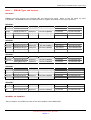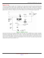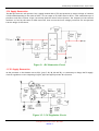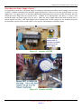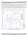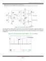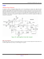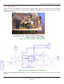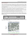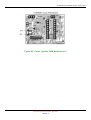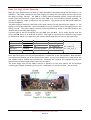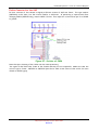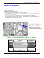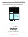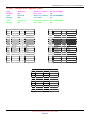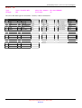
1
DA100 (50Hz) and DA50W Chassis – Repair Notes DA100 (50Hz) and DA50W Chassis Repair Notes Revision 3 – May 2003 Alan van Winkelen Page 1 of 80 Sharp Electronics (UK) Limited - May 2003 Revision 3 DA100 (50Hz) and DA50W Chassis – Repair Notes Contents Contents ..........................................................................................2 Figures............................................................................................5 Introduction ......................................................................................7 Product Specifications...........................................................................8 IC Identification.................................................................................9 Note 1 – EPROM Types and Versions........................................................................... 10 FW Models............................................................................................................................................................................... 10 28HW53H and 32HW53H:.................................................................................................................................................. 10 GF Models .................................................................................................................................................................................11 Note 2 - Second NVM Fitting .................................................................................. 11 Note 3 IC1801 Types ........................................................................................... 11 Note 4 – IC801 Types ........................................................................................... 11 Dolby Pro Logic PWB ............................................................................................. 12 Power Supply ................................................................................... 13 Power Supply Lines ............................................................................................... 14 Circuit Operation ................................................................................................. 15 Figure 6: Q701 Gate Waveform ................................................................................ 16 Standby Power Supply ........................................................................................... 17 Degauss Circuit ................................................................................................... 18 +5V Supply Generation........................................................................................... 19 +3.3V Supply Generation ........................................................................................ 19 Overriding the Power Supply Control ........................................................................... 20 Power Factor Correction Circuit................................................................................. 21 Figure 14: Power Factor Correction PWB – 66 and 76cm Models (PWB on left) ........................... 22 Faults in the Power Supply ...................................................................................... 23 High HT....................................................................................................................................................................................23 No Operation ..........................................................................................................................................................................25 Other Problems in the Power Supply.................................................................................................................................25 Horizontal Stage............................................................................... 26 Focus Modulation (66cm and 76cm models only) ............................................................... 29 Circuit Operation ...................................................................................................................................................................29 Faults in the Horizontal Stage .................................................................................. 31 Horizontal Output Transistor Failure............................................................................................................................... 31 Horizontal Drive Problems................................................................................................................................................... 31 Large Picture........................................................................................................................................................................... 31 East/West Circuit ............................................................................. 32 Circuit Operation ................................................................................................. 32 Page 2 of 80 Sharp Electronics (UK) Limited - May 2003 Revision 3 DA100 (50Hz) and DA50W Chassis – Repair Notes Faults in the East/West Circuit................................................................................. 35 CRT PWB ....................................................................................... 36 Faults on the CRT PWB.......................................................................................... 36 Class D Output Stages ........................................................................ 37 Pins 8 and 9 – Frequency ......................................................................................................................................................37 Pin 12 – Standby/Mute Control Pin ....................................................................................................................................37 Vertical Stage ................................................................................. 38 Circuit Operation ................................................................................................. 38 Vertical Fly-Back ................................................................................................ 38 Faults in the Vertical Stage..................................................................................... 42 Audio ........................................................................................... 43 On Board Circuit Operation ..................................................................................... 43 Mute Circuit Operation ........................................................................................................................................................43 Centre Speaker PWB ............................................................................................................................................................44 Faults in the Audio Circuit...................................................................................................................................................45 Dolby Pro-Logic Circuit Operation .............................................................................. 47 Faults in the Dolby Pro-Logic Circuit ................................................................................................................................49 Control and Communication .................................................................... 50 Communication Lines.............................................................................................. 50 Parallel Bus ..............................................................................................................................................................................50 I2C Bus.....................................................................................................................................................................................50 M3 Bus......................................................................................................................................................................................50 Slave ......................................................................................................................................................................................... 51 Reset In ................................................................................................................................................................................... 51 Reset Out (1)........................................................................................................................................................................... 51 Reset Out (2) .......................................................................................................................................................................... 51 Reset Operation .................................................................................................. 51 Protection - Microprocessor..................................................................................... 52 Audio Output...........................................................................................................................................................................52 Beam Current ..........................................................................................................................................................................52 Horizontal Mute .....................................................................................................................................................................52 AV Link............................................................................................................ 53 Faults Connected with the Microprocessor ..................................................................... 53 EPROM’s and NVM’s.............................................................................................. 54 Blanking the NVM ................................................................................................ 54 NVM Programming Jig ........................................................................................... 55 Video and Synchronisation Processor ......................................................... 56 Analogue Front End .............................................................................................. 56 Input Selector .................................................................................................... 57 Clamping ........................................................................................................... 57 Automatic Gain Control .......................................................................................... 57 Page 3 of 80 Sharp Electronics (UK) Limited - May 2003 Revision 3 DA100 (50Hz) and DA50W Chassis – Repair Notes Analogue to Digital Converters .................................................................................. 57 Digitally Controlled Clock Oscillator ............................................................................ 57 Analogue Video Output........................................................................................... 57 Average Beam Current Limiting ................................................................................. 57 Protection Circuitry .............................................................................................. 57 Scan Velocity Modulation Output ............................................................................... 58 Protection – Video/Sync Processor.............................................................................. 58 Safety.......................................................................................................................................................................................58 Vertical Protection (VPROT) ...............................................................................................................................................58 Faults Connected to the VDP.................................................................................... 59 Picture Rotation................................................................................ 60 Circuit Description ............................................................................................... 60 Scan Velocity Modulator ...................................................................... 61 Circuit Description ............................................................................................... 61 Faults in the Picture Rotation and Scan Velocity Modulator Circuit ......................................... 62 Preventative Maintenance ..................................................................... 63 Servicing Tips .................................................................................. 64 Error Codes ....................................................................................................... 67 Part Changes ................................................................................... 68 Remote Control Battery Covers ................................................................................. 68 CRT Types ........................................................................................................ 68 Service Mode .................................................................................. 69 Entering the Service Mode ...................................................................................... 69 Geometry Adjustments........................................................................................... 70 G2 Setting ........................................................................................................ 70 G2 Adjustment ................................................................................................... 70 Grey Scale Adjustment .......................................................................................... 71 Voltage Tables ................................................................................. 72 IC1001 – Microprocessor ........................................................................................ 73 IC801 – Video Sync Processor (VDP) ........................................................................... 74 IC305 – Multiple Sound Processor (MSP)....................................................................... 75 IC1801 – Cathode Drive Amplifier (CDA) ...................................................................... 76 IC301 / IC302 - Audio Amplifiers ............................................................................. 77 IC702 - Primary Control ........................................................................................ 77 IC501 - Vertical Output ........................................................................................ 78 IC1003 - NVM ................................................................................................... 78 IC2401 - Megatext .............................................................................................. 79 IC201 - IF ....................................................................................................... 80 Page 4 of 80 Sharp Electronics (UK) Limited - May 2003 Revision 3 DA100 (50Hz) and DA50W Chassis – Repair Notes Figures Figure 1: DA100 (50Hz) Chassis – model 56FW53H ................................................................................................................. 7 Figure 2: Power Supply Layout (Component Side).................................................................................................................... 13 Figure 3: Power Supply Component Locations (Print Side) .................................................................................................... 13 Figure 4: Location of Supply Measurement Points................................................................................................................... 14 Figure 5: Power Supply Schematic Diagram .............................................................................................................................. 15 Figure 6: Q701 Gate Waveform................................................................................................................................................... 16 Figure 7: Standby Power Supply .................................................................................................................................................. 17 Figure 8: Degauss Circuit .............................................................................................................................................................. 18 Figure 9: +5V Generation Circuit ................................................................................................................................................. 19 Figure 10: 3.3V Regulation Circuit ............................................................................................................................................... 19 Figure 11: Location of R792 ..........................................................................................................................................................20 Figure 12: Location of R623..........................................................................................................................................................20 Figure 13: Power Factor Circuit (56FW53H)............................................................................................................................ 21 Figure 14: Power Factor Correction PWB – 66 and 76cm Models (PWB on left)..............................................................22 Figure 15: 56FW53H Power Factor Correction PWB..............................................................................................................22 Figure 16: Location of 56FW53H Power Factor PWB.............................................................................................................22 Figure 17: Location of D735 .........................................................................................................................................................23 Figure 18: Location of Audio Stage components (Main PWB) ...............................................................................................23 Figure 19: Location of Centre Speaker PWB ............................................................................................................................24 Figure 20: Location of Components on the CRT PWB .............................................................................................................24 Figure 21: Location of SMD Capacitor on IC708 .....................................................................................................................25 Figure 22: Horizontal Output Stage...........................................................................................................................................27 Figure 23: Location of Horizontal Stage Components ............................................................................................................28 Figure 24: Q601 Base Drive Waveform .....................................................................................................................................28 Figure 25: GF Focus Modulator Circuit ......................................................................................................................................29 Figure 26: Picture of the FW Focus Modulator PWB .............................................................................................................29 Figure 27: FW Focus Modulator Circuit.....................................................................................................................................30 Figure 28: Location of Link Wire JL2 ........................................................................................................................................ 31 Figure 29: East West Circuit .......................................................................................................................................................32 Figure 30: East/West Circuit – Print Side ................................................................................................................................33 Figure 31: East/West Circuit - Component Side......................................................................................................................33 Figure 32: East/West Drive Waveform - Pin 32 of IC801....................................................................................................34 Figure 33: 66cm and 76cm CRT PWB .........................................................................................................................................36 Figure 34: 56FW53H CRT PWB...................................................................................................................................................36 Figure 35: Vertical Output Amplifier .........................................................................................................................................38 Figure 36: Vertical Fly-back Circuit ...........................................................................................................................................39 Figure 37: Vertical Protection Signal (VPROT - Pin 11 of IC801) ........................................................................................39 Figure 38: Vertical Scan Coil Waveform - Top of Coil ...........................................................................................................40 Figure 39: Vertical Scan Coil Waveform - Bottom of Coil.....................................................................................................40 Figure 40: Vertical Stage - Component Side ............................................................................................................................ 41 Figure 41: Vertical Stage - Print Side........................................................................................................................................ 41 Figure 42: Audio Amplifier Circuit (left channel)....................................................................................................................43 Page 5 of 80 Sharp Electronics (UK) Limited - May 2003 Revision 3 DA100 (50Hz) and DA50W Chassis – Repair Notes Figure 43: Centre Speaker PWB Location ................................................................................................................................44 Figure 44: Centre Speaker Circuit Diagram..............................................................................................................................44 Figure 45: Centre Speaker Modification 1 ................................................................................................................................45 Figure 46: Centre Speaker PWB Modification 2......................................................................................................................46 Figure 47: Pro-Logic PWB..............................................................................................................................................................47 Figure 48: Dolby Pro-Logic Circuit Diagram (66GF64H) ........................................................................................................48 Figure 49: Dolby Pro-Logic PWB Connector ..............................................................................................................................49 Figure 50: Communication Block Diagram ..................................................................................................................................50 Figure 51: Reset Timing ................................................................................................................................................................. 51 Figure 52: Audio Protection Circuit ............................................................................................................................................52 Figure 53: Horizontal Mute Circuit.............................................................................................................................................52 Figure 54: AV Link Schematic Diagram......................................................................................................................................53 Figure 55: Internal Architecture of IC801 (VDP 3120) ........................................................................................................56 Figure 56: VDP Protection Circuits .............................................................................................................................................58 Figure 57: Position of C824 ..........................................................................................................................................................59 Figure 58: Picture Rotation Circuit (located on CRT PWB) ...................................................................................................60 Figure 59: Scan Velocity Modulator Circuit.............................................................................................................................. 61 Figure 60: SVM and Tilt Coil Connectors...................................................................................................................................62 Figure 61: CRT Base PWB Modification (66cm and 76cm sets only) ...................................................................................63 Figure 62: Fault Finding Flow Chart 1.........................................................................................................................................65 Figure 63: Fault Finding Flow Chart 2 ........................................................................................................................................66 Figure 64: LED Fault Code Table.................................................................................................................................................67 Figure 65: HW OPC LED Error Code Jig ...................................................................................................................................67 Page 6 of 80 Sharp Electronics (UK) Limited - May 2003 Revision 3 DA100 (50Hz) and DA50W Chassis – Repair Notes Introduction The DA100 (50Hz) chassis and its derivatives (DA50W) are fitted in many Sharp widescreen television sets. Production started in 1999 with the FW models and continued up to the HW models. There have been a number of changes to the circuit configuration, layout and operation but the overall circuit theory and fault finding techniques remain the same for all chassis. This article will endeavour to assist the engineer in various faultfinding procedures that have been found to be beneficial in reducing repair times and cost. One important item to note is that the large and expensive (microprocessor, VDP, MSP, etc) IC’s only rarely fail. It is worthwhile considering that there have been a number of different types of CRT used with this chassis for the same model type. Philips, Thomson (Videocolor) and LG CRT have been used. Note that the scanning coils are supplied with the CRT and therefore the horizontal output stage components will be different for different CRT types. With the Philips CRT there are two focus anodes, so the fly-back transformer is also different in these models. Most of the problems on this chassis are related to either the power circuits (chopper and horizontal) or memory. Resetting or replacing the memory can easily cure many faults that appear to lie in the picture processing circuitry or drive areas. Figure 1: DA100 (50Hz) Chassis – model 56FW53H Page 7 of 80 Sharp Electronics (UK) Limited - May 2003 Revision 3 DA100 (50Hz) and DA50W Chassis – Repair Notes Product Specifications The basic chassis comes with NICAM and fast text as standard and can drive CRT’s from 56 to 76cm in both 4:3 and 16:9 formats. The only 4:3 sets that use this chassis are the 59ESD7H and 66ESD7H, both of which are Dolby Pro-Logic models. All variants of this chassis are fitted with three SCART sockets on the rear of the board – composite video, SVideo and RGB can be fed into these sockets. In addition to this, some models have front AV sockets (phono and S-Video). All Dolby Pro-Logic models have full functionality, allowing connection of separate speakers for front left, front right, rear left, rear right and sub-woofer. In the Pro-logic mode (once correctly set up in the user menu) the internal speakers – left, right and centre - become the centre channel. Double Copper CRT Types 3 3 Thomson 2001 to 2002 3 3 3 Thomson 2001 to 2002 3 3 3 Philips/Thomson 1999 to 2002 66cm 3 3 Thomson/LG 1999 to 2001 66FW54H 66cm 3 3 3 Thomson/LG 1999 t0 2001 66FW54H 66cm 3 3 3 Thomson/LG 2000 to 2002 66GF63H 66cm 3 3 3 Philips/Thomson 2000 to 2002 66GF64H 66cm 3 3 3 Philips 2000 to 2002 76FW53H 76cm 3 3 Thomson/LG 1999 to 2001 76FW54H 76cm 3 3 3 Thomson/LG 1999 to 2001 76FW54H 76cm 3 3 3 Thomson/LG 2000 to 2002 76GF63H 76cm 3 3 3 Philips 2000 to 2002 76GF64H 76cm 3 3 3 Philips 2000 to 2002 Model Screen Size Fast Text NICAM 66cm 3 32HW53H 76cm 56FW53H 56cm 66FW53H 28HW53H Pro-Logic 3 3 Production In some FW and GF models, and in all HW models, an earth plane was added to the top surface of the PWB (double copper), this is green in colour. This reduces interference and the possible corruption of the NVM caused by power supply variations and CRT discharges. It is possible to identify these chassis as the fourth digit of the serial number starts with the number 5. In later FW sets, a power factor module was fitted as a separate PWB. This was connected between the output of the mains bridge rectifier and the main smoothing block. Its function is to ensure that the current/voltage draw from the mains is kept in sync. This eliminates ‘spikes’ or ‘troughs’ in the mains voltage waveform which keeps the electricity suppliers happy. Note that the first three digits before the serial number are in fact the month and year of manufacture, i.e. 201 512112 is January 2002. Page 8 of 80 Sharp Electronics (UK) Limited - May 2003 Revision 3 DA100 (50Hz) and DA50W Chassis – Repair Notes IC Identification Several different types of IC are used in the DA100 (50Hz) chassis. These are listed in the table below. Note that although these IC’s may be available from other sources, it is strongly recommended to obtain these directly from Sharp Electronics (UK) Limited, or their approved distributors, using the part numbers given below. There can be compatibility issues when incorrect IC’s are fitted - even if they have the correct type number. IC Reference Number IC Type Number Sharp Part Number Function Package Comment IC1001 ST10R272L RH-IX1685BMZZ Microprocessor SMD Fitted to all models IC1002 27C4000 Depends on model EPROM/OTP/MTP DIL See note IC1003 24645 RH-IX1603BMZZ NVM SMD Fitted to all models IC1004 24645 RH-IX1603BMZZ NVM SMD See note IC1005 PST529 VHIPST529C2-1 Reset for IC1001 Wire Fitted to all models IC1300 BA4558 VHIBA4558F/-1 Centre speaker drive SMD Not 56FW53H IC1302 TDA7480 VHITDA7480/-1 Centre speaker audio output DIL Not 56FW53H Cathode Drive Amplifier QIL Depends upon CRT base IC1801 Depends on model IC201 TDA4472 RH-IX1672BMZZ IF Processor SMD Fitted to all models IC202 BA10393 RH-IX1556BMZZ AFT Feedback SMD Fitted to all models IC203 UPC574J RH-IX0037CEZZ 33V Regulator (tuner) Wire Fitted to all models IC301 TDA7480 VHITDA7480/-1 Audio output DIL Fitted to all models IC302 TDA7480 VHITDA7480/-1 Audio output DIL Fitted to all models IC304 M5218L VHIM5218L//-1 Headphone Amplifier DIL Fitted to all models IC305 MSP3410D RH-IX1636BMZZ Audio Processor DIL Fitted to all models IC401 HEF4053 RH-IX1602BMZZ Video switch SMD Fitted to all models IC501 TDA7480 VHITDA7480/-1 Vertical Output DIL Fitted to all models IC502 BA4558 VHIBA4558F/-1 Vertical feedback DIL Fitted to all models IC503 BA10393 RH-IX1556BMZZ AGC and EW control DIL Fitted to all models IC701 PST529 VHIPST529C2-1 Reset for IC702 Wire Fitted to all models IC702 ST6203 RH-IX1646BMZZ Primary Control SMD Fitted to all models IC703 MOC1806 RH-FX0106BMZZ Opto from microprocessor SMD Fitted to all models IC704 MOC1806 RH-FX0106BMZZ Opto to microprocessor SMD Fitted to all models IC705 MOC1806 RH-FX0106BMZZ Power Supply FB SMD Fitted to all models IC706 TL431 RH-IX1674BMZZ Reference Zener Wire Fitted to all models IC707 L4978 RH-IX1704BMZZ +5V Regulator SMD Fitted to all models IC708 TLP165J RH-FX0111BMZZ Degauss Optical Diac SMD Fitted to all models Video/Deflection Processor DIL See note IC801 Depends on model Page 9 of 80 Sharp Electronics (UK) Limited - May 2003 Revision 3 Note 1 2 3 4 DA100 (50Hz) and DA50W Chassis – Repair Notes Note 1 – EPROM Types and Versions FW Models EPROM types and versions vary between CRT and Teletext IC types. Refer to the list below for more information. The EPROM version is normally written on a paper label stuck to the top of the device. 56FW53H: CRT Type CRT Part Number Megatext Type Megatext Part Number EPROM Version EPROM Part Number Thomson VB56EGV230*1N SDA5275 RH-IX1709BMZZ H9-04x03 CH-IX1711CJH7 Philips VB56ESF0203*N SDA5275 RH-IX1709BMZZ H9-05x03 CH-IX1711CJH5 Thomson VB56EGV230*1N SDA5273 RH-IX1673BMZZ H9-03x05 CH-IX1664CJH9 Philips VB56ESF0203*N SDA5273 RH-IX1673BMZZ H9-02x05 CH-IX1664CJHG CRT Type CRT Part Number Megatext Type Megatext Part Number EPROM Version EPROM Part Number Thomson VB66EGV2321£N SDA5275 RH-IX1709BMZZ H5-04x03 CH-IX1711CJH6 Thomson VB66EGV2321£N SDA5273 RH-IX1673BMZZ H5-03x04 CH-IX1664CJH5 LG VB66QBD2910£N SDA5273 RH-IX1673BMZZ H5-02x01 CH-IX1664CJH7 CRT Type CRT Part Number Megatext Type Megatext Part Number EPROM Version EPROM Part Number Thomson VB66EGV2321£N SDA5275 RH-IX1709BMZZ H6-03x03 CH-IX1664CJH6 LG VB66QBD2910£N SDA5275 RH-IX1709BMZZ H6-02x03 CH-IX1664CJHE CRT Type CRT Part Number Megatext Type Megatext Part Number EPROM Version EPROM Part Number Thomson VB76EGV2321*N SDA5275 RH-IX1709BMZZ H5-04x03 CH-IX1711CJH6 LG VB76QAG280W12 SDA5275 RH-IX1709BMZZ H4-00x00 CH-IX1711CJH4 Thomson VB76EGV2321*N SDA5273 RH-IX1673BMZZ H5-03x04 CH-IX1664CJH5 LG VB76QAG280W12 SDA5273 RH-IX1673BMZZ H5-02x01 CH-IX1664CJH7 66FW53H: 66FW54H: 76FW53H: 76FW54H: CRT Type CRT Part Number Megatext Type Megatext Part Number EPROM Version EPROM Part Number Thomson VB76EGV2321*N SDA5275 RH-IX1709BMZZ H6-03x03 CH-IX1664CJHF LG VB76QAG280W12 SDA5275 RH-IX1709BMZZ H6-02x05 CH-IX1664CJHE 28HW53H and 32HW53H: The part number for IC1002 for both of the above models is CH-IX1841CJH0 Page 10 of 80 Sharp Electronics (UK) Limited - May 2003 Revision 3 DA100 (50Hz) and DA50W Chassis – Repair Notes GF Models The table below details the different part numbers for IC1002. Note that this IC can either be an EPROM or a MTP. An EPROM has a small window in its top to enable the IC to be erased by ultra-violet light. A MTP does not have this window and normally works at 3.3V. Model CRT EPROM Type EPROM Part Number 66GF63H Philips EPROM CH-IX1711CJH1E 66GF63H Thomson MTP CH-IX1711CJH1M 66GF64H Philips EPROM CH-IX1711CJH0 76GF63H Philips MTP CH-IX1841CJH7 76GF64H Philips EPROM CH-IX1664CJHAE 76GF64H Philips MTP CH-IX1664CJHAM Note 2 - Second NVM Fitting Some sets use a second NVM, designated IC1004 to store teletext page information and some audio data in the case of Dolby Pro-logic models. Sets that have the second NVM fitted are: 66FW54H 76FW54H 66GF64H 76GF63H 76GF64H The part number for this device is the same as IC1003. Note 3 IC1801 Types IC1801 is the cathode drive amplifier mounted on the CRT base PWB. Depending upon the chassis type, the CDA IC can be one of three types as listed below: IC Type Sharp Part Number Comment TEA5101A RH-IX1416BMZZ All FW and some GF STV5109 RH-IX1803BMZZ Some GF and all HW models TDA6019JF RH-IX1833BMZZ Late 56FW53H models These IC are not interchangeable. Note 4 – IC801 Types IC801 can be one of two types. It is either a 3120 or 3130, and they are not interchangeable. The part number for the VDP3120C2 is RH-IX1688BMN2, the part number for the VDP3130Y is RH-IX1858BMZZ. The 3130 are fitted in all HW models and some later FW and GF models. Some patterning can occur when fitting later revisions of the VDP3120C2 to earlier chassis versions. In this situation remove C824, which is connected from pin 33 of IC801 to ground. Page 11 of 80 Sharp Electronics (UK) Limited - May 2003 Revision 3 DA100 (50Hz) and DA50W Chassis – Repair Notes Dolby Pro Logic PWB The Dolby Pro-Logic PWB has the following IC list. Note that some of the reference numbers are the same as the IC’s fitted on the centre speaker PWB. IC Reference Number IC Type Number Sharp Part Number Function of IC Package Type IC1301 DPL3519A RH-IX1679BMZZ Pro-Logic Processor DIL IC1302 TDA7480 VHITDA7480/-1 Left Audio Output Amplifier DIL IC1303 TDA7480 VHITDA7480/-1 Right Audio Output Amplifier DIL IC1304 TDA7480 VHITDA7480/-1 Surround Output Amplifier DIL IC1305 TDA7481 VHITDA7481/-1 Sub-woofer Output Amplifier DIL IC1701 KA431AZ RH-IX1674BMZZ Power Supply Reference Wire IC1702 KA431AZ RH-IX1674BMZZ 5V Supply Reference Wire IC1703 MOC8106 RH-FX0106BMZZ Power Supply Feed Back SMD Page 12 of 80 Sharp Electronics (UK) Limited - May 2003 Revision 3 DA100 (50Hz) and DA50W Chassis – Repair Notes Power Supply This power supply has been used in many Sharp television receivers during the past six years and is reliable. It works by changing both the pulse width and frequency of operation, this enables correct regulation of the secondary supplies. The major difference between the models is the amount of current that the power supply can provide; this is reflected in the wattage consumed from the AC supply. Note that later versions of the chassis have a power factor module fitted between the power supply and the mains input. The function of this is to ensure that current is drawn over the complete input voltage cycle, not just at the peaks. It is important to note that when the receiver is in the standby mode, the power supply is turned off, this reduces power consumption to less than 3W. When pin 15 of IC702 is high (5VDC), Q702 is turned on and the gate of the FET is effectively taken to ground, stopping the charging operation of C714. To turn the set on, pin 15 goes low (open circuit), this allows the charge to build up on C714 and thus the transistor turns on and the power supply starts. Figure 2: Power Supply Layout (Component Side) Figure 3: Power Supply Component Locations (Print Side) Page 13 of 80 Sharp Electronics (UK) Limited - May 2003 Revision 3 DA100 (50Hz) and DA50W Chassis – Repair Notes Power Supply Lines Supply Typical Voltage Range Nominal Resistance Voltage/Resistance Measurement Point +150V 145V to 155V >10kΩ D720 +18V 15V to 20V >10kΩ D718 -18V -15V to –20V >900Ω D719 +10V 7V to 10V >10kΩ D722 +5V 5.0V to 5.2V >300Ω IC707 pin 6 Figure 4: Location of Supply Measurement Points Page 14 of 80 Sharp Electronics (UK) Limited - May 2003 Revision 3 DA100 (50Hz) and DA50W Chassis – Repair Notes Circuit Operation Depending on the input mains circuit, there is either 320VDC (conventional bridge rectifier/capacitor arrangement) or 360VDC (power factor circuit) fed into the top of the chopper transformer. This voltage is also used to charge C714 via R713 and R714, allowing the voltage on the gate of Q701 to increase. When the voltage on the gate of Q701 reaches 4.5V, it turns on and current flows in the primary winding of T701. This will cause pin 15 to increase and when the zener voltage of D716 is exceeded, turning Q703 on and Q701 off. Figure 5: Power Supply Schematic Diagram When Q703 turns off, after C713 has discharged, the cycle will repeat. Obviously as the circuit operates in this condition, there will be no voltage regulation and the supply will increase to its maximum level, which is about 220V. This is undesirable, so there has to be some kind of control based on the HT supply. Feedback is achieved via IC705, its input (LED) is fed with a stabilised 12V supply on its anode by a shunt regulator off the +16V supply (R765, R766 and D726). The cathode of the LED is fed with a proportion of the +150V supply via the programmable zener diode IC706. A potential divider comprising of R743, R744 and R746 set the input voltage to IC706. As the brightness of the LED increases or decreases, the conduction of the transistor will change in sympathy. The collector is taken to a crude supply line generated off pin 15, rectified by D715 and smoothed by C718. This supply will be fed into C713 via the opto transistor; the speed of charge depends upon the luminosity of the LED. Q703 will turn on and turn off Q701 Over current is prevented by Q702. Its base is connected across the earth return resistor (R716) in the drain circuit of Q701. This resistor has a very low value and therefore a large amount of current has to flow before Q702 will turn on and remove the bias on the gate of Q701. Once the voltage on the gate of the FET has been Page 15 of 80 Sharp Electronics (UK) Limited - May 2003 Revision 3 DA100 (50Hz) and DA50W Chassis – Repair Notes removed, the current flowing from source to drain will decrease, the volt drop across R716 will decrease and Q702 will turn off, allowing the gate to rise again. If the over current condition continues, the power supply will trip. Q702 is also turned on by pin 15 of IC702 during standby to turn the power supply off. On Dolby Pro-Logic models this signal controls the operation of the Dolby Pro-Logic power supply. Figure 6: Q701 Gate Waveform Note that the above waveform has been taken on the primary side of the power supply. It is therefore essential that an isolation transformer be used in conjunction with the set. This will ensure safe connection to the primary side reference. This waveform will also change in pulse width depending upon the load demanded from the power supply. The greater the load the longer the on time. The FET will switch on at about 4.5V, this is indicated as a short levelling off period on the upward ramp. Page 16 of 80 Sharp Electronics (UK) Limited - May 2003 Revision 3 DA100 (50Hz) and DA50W Chassis – Repair Notes Standby Power Supply This part of the circuit has changed compared to previous chassis where this supply was derived by means of a bridge rectifier with two additional 68k resistors and a 5.1V zener diode to limit the voltage. This has been replaced by a series regulator circuit, which is supplied from one side of the mains, with an earth return via the bridge rectifier. One of the main reasons for this circuit is power consumption. Coupled with the degauss control circuit, standby wattage is reduced to less than 3W. D708 and D707 form part of a bridge rectifier, two diodes of the main bridge rectifier are used for the other part. Therefore, at the junction of D707 and D708 there is a 100Hz signal comprising of positive half cycles at mains potential. Each time this signal exceeds 47v D729 will conduct via R774 and R775, turning on Q717. Figure 7: Standby Power Supply When Q717 turns on the gate of Q715 is taken to ground. Since this is a N Channel MOSFET Q715 is turned off and no current will flow through this device. During the period when Q717 is turned off Q715 will turn on allowing C739 to charge to approximately 7V which is limited to 5V by R777 and D710. It can now be seen that the period of Q715 conduction is very short (it is only turned on when the 100Hz signal at the junction of D707 and D708 is less than 47V). Therefore, a top-up supply from the bridge rectifier circuit comprising of D734 and D731 is added to the cathode of D710 via R721 and R703. The 100Hz signal at the junction Q717 and D733 is also used as a timing signal for the real time clock within the slave processor – IC702 pin 8. However, before it can be used the signal is passed through a Schmidt Trigger circuit (Q708 and Q709) to ensure that the signal is free from noise. Page 17 of 80 Sharp Electronics (UK) Limited - May 2003 Revision 3 DA100 (50Hz) and DA50W Chassis – Repair Notes Degauss Circuit This circuit is configured to ensure that the degauss circuit will not operate unless the switch mode power supply is running and pin 14 of IC702 is low. A positive bias is applied to the emitter of Q714 from T701 pin 15 (rectified by D727 and limited by R762, R768 and D728) via the optical diac; IC708. Since Q714 is a pnp device, once the base is taken low compared to the emitter, Q714 will turn on allowing current to flow through IC708 (LED section of this device), turning on the triac T702, allowing current to flow through the degauss coils. Figure 8: Degauss Circuit Current will continue to flow through the degauss coils until either the PTC (POR701) has increased in resistance sufficiently to significantly reduce the current flow, or IC702 pin 14 goes high, turning of Q714, preventing current flow through IC708, turning the triac T702 off. Since the default condition for IC702 pin 14 is low, it can be seen that the degauss circuit should now operate each time the television is turned on from the main on/off switch or switched from standby to normal operation. This is the case if the main processor has set up communication with the slave processor or not. Page 18 of 80 Sharp Electronics (UK) Limited - May 2003 Revision 3 DA100 (50Hz) and DA50W Chassis – Repair Notes +5V Supply Generation This DC-DC converter will operate from a supply between 8V to 55V and produces an output voltage of between 3.3V and 50V depending on the value of R747. For an output of 5V, R747 must be 2k7Ω. C741 connected to pin 3 provides a soft-start routine. If pin 3 is held low then the device will not operate. The frequency of the internal oscillator is fixed by the value of R706 and C735. Over-current and over-voltage protection are incorporated into the design of this device. Figure 9: +5V Generation Circuit +3.3V Supply Generation As the processor in this chassis runs at 3.3V (pins 7, 28, 38, 49 and 78), it is necessary to change the 5V supply. A series regulation circuit comprising of Q710, Q711 and Q712 provides this function. Figure 10: 3.3V Regulation Circuit Page 19 of 80 Sharp Electronics (UK) Limited - May 2003 Revision 3 DA100 (50Hz) and DA50W Chassis – Repair Notes Overriding the Power Supply Control It is possible to ascertain if the power supply is working by removing the standby control voltage from the base of Q702. If R792 is disconnected, the power supply should start if there are no other problems with it or the supply lines. It is good practice to disconnect R623 when undertaking this exercise, as this will ensure that the horizontal output stage does not become active. If R623 is not disconnected, and there is a fault in the horizontal stage, the power supply may not start. When the power supply starts with R792 disconnected, it should regulate correctly. Note that supplies can be disconnected, but the integrity of the feedback loop must be maintained, failure to do so would result in very high HT and subsequent component faults. Figure 11: Location of R792 Figure 12: Location of R623 Page 20 of 80 Sharp Electronics (UK) Limited - May 2003 Revision 3 DA100 (50Hz) and DA50W Chassis – Repair Notes Power Factor Correction Circuit To ensure good linearity of the mains supply voltage waveform, it is necessary to ensure that current is taken at the start of the voltage cycle, i.e. zero voltage switching. This function is achieved with the use of a Power Factor Correction Circuit. It is located between the main bridge rectifier and main reservoir capacitor and is physically located on a sub-board on the left-hand side of the main chassis (when viewed from the rear of the set. The board will also have the focus modulator circuit on it (76cm and some 66cm models only). The circuit is basically a DC to DC converter that increases the power supply input voltage to about 400VDC. Note that the main reservoir capacitor, C705, is decreased in value and increased in voltage rating because of this. It is a 68µF rated at 450V in power factor module sets, and a 220µF, 385V capacitor in non-power factor module sets. Figure 13: Power Factor Circuit (56FW53H) Page 21 of 80 Sharp Electronics (UK) Limited - May 2003 Revision 3 DA100 (50Hz) and DA50W Chassis – Repair Notes Figure 14: Power Factor Correction PWB – 66 and 76cm Models (PWB on left) Note that on the 56FW53H the Power Factor PWB is mounted at the front of the set, underneath the CRT. Figure 15: 56FW53H Power Factor Correction PWB Figure 16: Location of 56FW53H Power Factor PWB Page 22 of 80 Sharp Electronics (UK) Limited - May 2003 Revision 3 DA100 (50Hz) and DA50W Chassis – Repair Notes Faults in the Power Supply High HT In some cases the HT can rise to over 200V, this can cause damage to other parts of the circuitry. This is normally caused by failure of IC705 - the power supply voltage regulation feedback opto coupler. The device is easily damaged by excessive heat while soldering, so remember to keep your soldering iron turned down to 250oC or below, and not to solder for more than 10 seconds on each leg. If these conditions are not met the transparent barrier between the LED and opto transistor will be damaged. Note that sometimes the set will work for several weeks or months before failing if the opto has been damaged during fitting. To alleviate damage to other parts of the circuitry when the HT rises, an avalanche diode was fitted across the main HT smoothing capacitor (C720) from late 1999 production. This device has a rated maximum voltage of 170V, and will go short circuit if this voltage is reached. If the avalanche diode was not fitted, it is worthwhile to check the following components for damage before turning the set on. Note that this diode must be fitted to all chassis (part number RH-EX0875BMZZ). Reference Function Part Number Comment Q601 Horizontal output transistor RH-TX0192BMZZ Leaky or short circuit IC301/2 Audio output IC’s VHITDA7480/-1 Short circuit. Also check supply feed chokes IC1801 CDA IC on CRT base PWB See previous list Short circuit. Check pin 5 to ground (<500Ω) C720 HT reservoir capacitor RC-EZ0258CEZZ Physically damaged IC1301 Centre channel amplifier VHITDA7480/-1 Short circuit. Located on centre speaker PWB Q5407 Scan velocity modulator transistor VS2SA1837//-1 CRT PWB – short or open circuit Q5408 Scan velocity modulator transistor VS2SC4793//-1 CRT PWB – short or open circuit L315/6 IC302 feed chokes VP-CF3R3K0000 Open circuit L350/1 IC301 feed chokes VP-CF3R3K0000 Open circuit Figure 17: Location of D735 (note the use of hot melt glue to prevent the diode from shorting out to the tracking) Figure 18: Location of Audio Stage components (Main PWB) Page 23 of 80 Sharp Electronics (UK) Limited - May 2003 Revision 3 DA100 (50Hz) and DA50W Chassis – Repair Notes Figure 19: Location of Centre Speaker PWB Figure 20: Location of Components on the CRT PWB When the avalanche diode is fitted, only four components generally need to be replaced (D735, Q601, IC705 and C720), this is because it prevents further damage to the circuitry should the power supply be kept running. Sharp produce a kit that contains these four items - use the part number FWSERVKIT01// If the set is operated for prolonged periods without the avalanche diode fitted, then damage will occur to other parts of the circuit. The CRT PWB suffers normally all the electrolytic capacitors have to be replaced if this is the case. The moral is, DO NOT run the set when high HT is present. Page 24 of 80 Sharp Electronics (UK) Limited - May 2003 Revision 3 DA100 (50Hz) and DA50W Chassis – Repair Notes No Operation No operation can be caused by a number of components, the most common being around the primary control IC, IC702. If the supply on pin one of this IC falls below 5V, the operation of the power supply becomes unreliable. As can be seen from the previous circuit description, the supply circuit is fairly complex, however only a few components cause problems. For low supply voltage to IC702 check that R770 (270Ω safety) and R771 (470kΩ) are OK. It has also been known for R721 and R703 (both 150kΩ) to fail causing a low 5V line. IC707 (the secondary 5V regulator) can fail leading to a set that does not turn on, even though the power supply starts up. No operation of the power supply or low HT (at about 30 to 40V) can be caused by R713 and R714 going high or breaking down under load. It is important that these two resistors are checked by substitution as they often read OK on a meter, even though they are faulty. Note that they should be metal film resistors and not carbon composition. Other Problems in the Power Supply Erratic remote control operation has been traced to a number of components in the power supply. Normally the faults encountered are no remote control operation or intermittent control of the volume, either increasing dramatically or rising slowly with the OSD visible. D729 can cause these problems, but it is more common for noise to enter IC702 and spurious remote control commands to be outputted to the microprocessor. To prevent this happening fit a 470nF, 16V SMD capacitor across the input of the optical diac – pins 1 and 3 of IC708 (see picture below). The Sharp part number for this capacitor is VCKYTV1CF474Z. This capacitor was fitted during production of all GF and HW models. Figure 21: Location of SMD Capacitor on IC708 Intermittent failure of the chopper transistor can be caused by dry joints in the snubber circuit (C710, R715 and D711) or poor connections on the main reservoir capacitor, C705. Q701 has to be the correct type (S5F10N80A – Sharp part number RH-TX0198BMZZ), fitting the incorrect transistor can lead to a power supply that does not work, causes excessive RF interference or is unreliable. If there is a mains surge (or lightning strike) Q701 will invariably fail. D712, Q702, Q703 and R716 will also have suffered damage, as will the rectifier diodes (D701, D702, D703 and D704). It is advisable to change all of these components to prevent further failures, even if they are not faulty. IC706 can cause high or low HT. It is a programmable zener diode that provides a stabilised voltage to the opto coupler. The Sharp part number for this device is RH-IX1704BMZZ. Erratic operation of the processor (locking out, no control, etc) can be caused by the 3.3V rising to 5V due to one of the components in the series regulator going faulty - Q710, Q711 or Q712. Check for 3.3V on the emitter of Q712. Page 25 of 80 Sharp Electronics (UK) Limited - May 2003 Revision 3 DA100 (50Hz) and DA50W Chassis – Repair Notes Reference Description Part Number D701/2/3/4 Diode, RF2005 RH-DX0555BMZZ D729 Zener Diode, TZMC47 RH-EX0568BMZZ IC702 IC, ST6203B RH-IX1646BMZZ IC703/4/5 IC, MOC8106SR2V-M RH-IX0106BMZZ IC706 IC, KA431AZ RH-IX1674BMZZ IC707 ICL4978 RH-IX1704BMZZ Q701 Transistor, S5F10N80A RH-TX0198BMZZ Q702 Transistor, 2PD602AR RH-TX0182BMZZ Q703 Transistor, 2SD2391Q RH-TX0151BMZZ Q710 Transistor, 2SC2412 VS2SC2412KQ-1 Q711 Transistor BC547 RH-TX0106BMZZ Q711 Transistor, BC547 TH-TX0106BMZZ Q712 Transistor, 2SC2412 VS2SC2412KQ-1 R703 Resistor, 150kΩ ½W SMD VRD-RA2HD154J R713 Resistor, 560kΩ ½W metal film VRC-MA2HG564J R714 Resistor, 560kΩ ½W metal film VRC-MA2HG564J R716lk Depends on model - refer to service manual for part number R721 Resistor, 150kΩ ½W SMD VRD-RA2HD154J R770 Resistor, 270Ω ½W fusible RR-XZ0229BMZZ R771 Resistor, 470kΩ 1W metal oxide VRS-VV3AB474J Page 26 of 80 Sharp Electronics (UK) Limited - May 2003 Revision 3 DA100 (50Hz) and DA50W Chassis – Repair Notes Horizontal Stage As in previous Sharp chassis a transformer-less driver circuit has been used, with the driver stage obtaining its running voltage from the fly-back transformer, T601. At switch on +8V from the power supply is applied to Q603 collector via R605 and Q602 collector via R628 and R608. At the same time –16V is applied to Q602 emitter via R619. Horizontal drive from IC801 is sent to the base of Q603, This will cause Q603 to switch, which in turn switches the horizontal output transistor Q601, producing an e.m.f on pins 6 and 10 of the fly-back transformer T601. The e.m.f at pin 10 is rectified by D611 to produce the positive run voltage and the e.m.f at pin 6 is rectified by D610 to produce the negative run voltage. When the drive signal is high, the emitter of Q603 will also go high, turning on Q602. This results in Q602 collector going low and Q601 turning off. When the drive signal is low, Q603 emitter also goes low turning off Q602 and allowing Q601 to turn on. As the current drawn from the +8V supply is minimal (via R628 and R608, both 1kΩ), Q601 does not turn on fully, but does allow the transformer to energise sufficiently to produce secondary voltages. D611 conducts on turns on Q601 harder, until the drive signal goes high on the next cycle. Once the horizontal stage is running, D611 provides a low impedance/high current path to turn on Q601. D610 provides the same function to turn off Q601. These low impedance supplies are required to ensure that the output transistor spends a minimal amount of time in the linear part of its characteristic. While Q601 draws current and voltage is developed across it, power is generated which is dissipated as heat. This can lead to premature failure of Q601. With this type of driver circuit, it is essential that the circuit is started softly, otherwise transient pulses can damage the horizontal output transistor. This is achieved by doubling the horizontal drive frequency; this effectively reduces Q601 on time, until the run voltage has been established. In addition to producing the EHT, focus, screen voltage and horizontal scan from the fly-back transformer T601, the +/-13V rails for the field output are produced at pins 5 and 9. D609 rectifies the voltage at pin 9 producing the +13V and D608 produces the –13v via pin 5 of the LOPT. Figure 22: Horizontal Output Stage Horizontal fly-back pulses (HFB) from pin 1 are fed to IC801 for both timing purposes and safety (prevents excessive EHT), HFB is also rectified by D510 to produce +25V for vertical fly-back. Page 27 of 80 Sharp Electronics (UK) Limited - May 2003 Revision 3 DA100 (50Hz) and DA50W Chassis – Repair Notes From the primary winding (pin 7) the HT is stepped up and rectified by D621 to produce the supply required by the CRT drive circuit. Finally a negative going voltage is fed from pin 8 to the protection circuit. This voltage represents the beam current. The greater the beam current (raster going brighter) the greater this voltage would be in a negative direction. This negative voltage is then fed to the IC1001 pin 95 via D622 and Q606. Once this voltage has exceeded safe working levels IC1001 pin 95 will go low switching the television to standby (no power supply operation). Figure 23: Location of Horizontal Stage Components Figure 24: Q601 Base Drive Waveform Page 28 of 80 Sharp Electronics (UK) Limited - May 2003 Revision 3 DA100 (50Hz) and DA50W Chassis – Repair Notes Focus Modulation (66cm and 76cm models only) Due to their larger screen size's, the 66cm and 76cm models employ a focus modulating circuit. This is driven by the line output signal. The function of the focus modulator is to ensure that the outer extremes of the CRT face are kept in focus. As the beam travels to the edges of the shadow mask, it will become distorted due to the increased distance travelled when compared with the centre. Circuit Operation The primary winding of T1602 is connected in the earth return of the line scanning coils, before the signal goes to earth via the S correction capacitor. This signal is then coupled to the bottom end of the focus control potentiometers. This is the same for both the FW and GF focus modulator circuits. Figure 25: GF Focus Modulator Circuit Figure 26: Picture of the FW Focus Modulator PWB Page 29 of 80 Sharp Electronics (UK) Limited - May 2003 Revision 3 DA100 (50Hz) and DA50W Chassis – Repair Notes Figure 27: FW Focus Modulator Circuit The FW focus modulator circuit is slightly different to the GF circuit due to the type of screen being used. As it is not a pure flat screen, the curvature of the screen effects the time that the electron beam takes to reach the screen by a greater amount than with a flat screen. This effects the focus in both the horizontal and vertical directions. The horizontal picture is compensated by using the technique described above, however the vertical correction is derived from the east/west output signal. Page 30 of 80 Sharp Electronics (UK) Limited - May 2003 Revision 3 DA100 (50Hz) and DA50W Chassis – Repair Notes Faults in the Horizontal Stage Horizontal Output Transistor Failure If the negative supply used to turn off the horizontal output transistor is too low, then it will not turn off fully. This will result in a large voltage across the collector/emitter junction and current being drawn at the same time. The power generated will have to be dissipated by the transistor itself and therefore it will get very hot. Eventually it will fail. A cause of this is failure of C607 (low capacity or leaky), causing the negative supply to fall. Note that it is advisable to change this for a 105oC device if it has not already been done. For intermittent failure of the horizontal output transistor it is recommended that C607, D610 and D611 be replaced. Dry joints in the output stage can also cause this problem – the most common areas affected are the horizontal coil earth return circuit C613, R613 and associated circuitry and the scan coil connector itself. Sometimes C613 or R613 will go open circuit resulting in no horizontal scan leading to the possibility of the horizontal output transistor going short or leaky. C613 can also go faulty under load, so it is best to check by substitution. C528, C632 and C615 are also known to cause the output transistor to fail intermittently. It has been known for the power supply opto coupler feedback IC, IC705 to cause the HT to rise slowly. This results in Q601 failing before the avalanche diode goes short circuit. Note that the horizontal output transistor must be the correct type. Failure to use the correct transistor will result in erratic operation or premature failure of the device. Use part number Q601 is RH-TX0144BMZZ for Q601. Horizontal Drive Problems Sometimes it will appear that there is no horizontal drive signal, even though the microprocessor has gone through the boot sequence. In this situation, it is possible to release the horizontal mute to enable the horizontal stage to start. There are a number of ways that this can be achieved, one is to short out the base/emitter junction of Q607, and the other is to temporarily isolate link JL2. Figure 28: Location of Link Wire JL2 Large Picture If D1601 on the focus modulator PWB (76cm models only), goes leaky or short circuit, the result is an over large picture due to the EHT dropping to about 20kV. Page 31 of 80 Sharp Electronics (UK) Limited - May 2003 Revision 3 DA100 (50Hz) and DA50W Chassis – Repair Notes East/West Circuit In addition to the normal function of an east/west correction circuit used with 4:3, 110° CRT, a wide screen television correction has to be changed for the different types of scanning modes. Wide screen television generally has three scanning modes, 4:3, 14:9 and 16:9, additionally the 16:9 scanning modes has three variants, Full, Panorama and Cinema. Full mode is used to stretch a picture which is in 4:3 format and contains fast moving action (motor racing), therefore, it does not matter if the horizontal linearity is not constant across the screen. Panorama is similar to full mode but this time the action is slow or even stationary (news programs), therefore, your eye would pickup on any variation in linearity. To overcome this the linearity in the centre of the screen is kept constant and the edges of the picture are stretched to fill the screen. Cinema mode is intended for use with pictures that are in true 16:9 format. When setting the geometry, the television must be put into the FULL mode. The east/west circuit is based around transistor Q506. This transistor operates slightly differently to a conventional east/west output device as it is turned on to increase the horizontal amplitude and not to reduce the scan. This enables the circuit to work more efficiently and therefore the transistor does not become excessively hot during operation. Circuit Operation Figure 29: East West Circuit IC503 is a switching amplifier with integrated horizontal pulses being fed to one input from the horizontal driver circuit via Q501 and an east/west parabolic signal from IC801 to the other input. This will produce a PWM signal running at horizontal frequency the width of the pulses will be determined by the east/west parabolic signal. This signal is then passed a driver circuit (Q506, class D biased), low passed filtered (L603, C610 – C610 is part of the diode modulator circuit) to the diode modulator (D603 and D604). Additionally from L603 the signal is fed to one end of a centre tap coil (L604) via C611. The other end of L604 is connected to ground with the centre tap connected to the horizontal linearity circuit. Therefore the horizontal linearity can now be adjusted by the east/west Parabolic signal. Page 32 of 80 Sharp Electronics (UK) Limited - May 2003 Revision 3 DA100 (50Hz) and DA50W Chassis – Repair Notes Figure 30: East/West Circuit – Print Side Figure 31: East/West Circuit - Component Side Page 33 of 80 Sharp Electronics (UK) Limited - May 2003 Revision 3 DA100 (50Hz) and DA50W Chassis – Repair Notes Figure 32: East/West Drive Waveform - Pin 32 of IC801 It can be seen in the waveform that there are 'noise spikes' throughout the display. This is due to the oscilloscope being used to record this picture. An analogue oscilloscope will display a smoother curve. Page 34 of 80 Sharp Electronics (UK) Limited - May 2003 Revision 3 DA100 (50Hz) and DA50W Chassis – Repair Notes Faults in the East/West Circuit When fault finding in the east/west circuit, it is important to ascertain in which part of the circuit the fault lies. Check the control output of IC801 – pin 32. There should be a parabola waveform on this pin at a base frequency of 50Hz. It will change wave shape depending upon the amount of correction applied, so it is important to enter the service mode and ensure that none of the adjustments are at minimum or maximum. If this waveform is present, and changes as adjustments are made, then the fault will lie in the drive or output circuitry. Faults in this area include: 1. R519 going high or open circuit – it is a 100kΩ connected to the 150V supply. 2. Q506 going short, open or overheating – change L603, L604, D502, D503, D504, D516 and C528. 3. D603 and D604 going open or short-circuit. 4. Dry joint on C601 and/or C610. If the waveform is not present, or is severely distorted, or the adjustment range is poor, then the fault could be caused by the memory IC – IC1003 or the VDP - IC801. It is recommended that if this is the case, then the NVM is blanked (see the NVM blanking section of this article) first. If this does not cure the problem, then it is probable that IC801 is at fault. Sometimes it will not be possible to set the geometry correctly in all modes after blanking he NVM. In this case it will be necessary to ensure that the EPROM (IC1002) is correct as per the information given at the start of this article. When the correct EPROM is fitted, the NVM will have to be blanked to enable the correct information to be downloaded into it. Replacement EPROM’s have been produced so that minimal geometry adjustments are required. If the picture geometry is very poor after following the above procedure, the fault will be elsewhere in the east/west circuitry. Reference Function Part Number Comment R519 Ramp charging resistor VRD-RA2HD104J Goes high or open – on component side of PWB Q506 Eat/west output transistor RH-TX0151BMZZ Open or leaky – SMD L603 Feed coil RCLIP0286BMZZ Low resistance – normally 8Ω L604 Line earth return coil RCLIP0284BMZZ Low resistance D502/3/4 Clamping diodes RH-DX0551BMZZ Intermittently faulty D516 Clamping diode RH-EX0837BMZZ Intermittently faulty C528 Reservoir capacitor VCEAGA1JW106M Leaky D603 East/west modulator diode RH-DX0299BMZZ Open or short circuit D604 East/west modulator diode RH-DX0302BMZZ Open or short circuit Notes D516 is not shown on the GF circuit diagram, although it is fitted to the chassis. R519 is sometimes a 150kΩ resistor, check the value before replacing, as fitting the incorrect value will result in poor east/west geometry performance. Page 35 of 80 Sharp Electronics (UK) Limited - May 2003 Revision 3 DA100 (50Hz) and DA50W Chassis – Repair Notes CRT PWB There are two types of CRT PWB fitted to this chassis. One is for use with the 66cm and 76cm versions of this chassis and the other is for the 56FW53H only. The major difference is that the 56cm model does not have a scan velocity modulator or picture rotation circuits on this PWB. This means that it is physically smaller than the other models. Note that the CDA IC, IC1801, can be one of three types – see note in IC Identification section. Figure 33: 66cm and 76cm CRT PWB Figure 34: 56FW53H CRT PWB Faults on the CRT PWB It is possible for the grey scale to wonder, picture brightness to ramp up or down. If the G2 is set correctly, IC1801 is suspect. Check by substitution. If the reference voltage on pin 2 of IC1801 is about 10V, picture smearing will occur. This is normally on the red channel. If the voltage is below 9V the picture will blank. In both cases, Q912 or its associated components can be responsible. This transistor can get hot during operation (especially on the GF models due to more current being drawn through the device). If you suspect that the transistor may fail due to its temperature being too high it is permissible to fit a 68Ω, 0.5W resistor between the collector and emitter of Q912. It is easier to fit this resistor to the print side of the PWB. Page 36 of 80 Sharp Electronics (UK) Limited - May 2003 Revision 3 DA100 (50Hz) and DA50W Chassis – Repair Notes Class D Output Stages Sharp have used class D output stages for a number of years in discrete component form, but now these are incorporated into specially designed integrated circuit. These devices are ideal for use with television audio and vertical output stages where high efficiency (low energy use) is required. A TDA7480 is used for audio and vertical outputs and the TDA7481 to drive the sub-woofer in the Dolby Pro-Logic versions of the chassis. The following table defines the operation of each pin of the TDA7480. Pin Name Function Nominal Voltage Pin Negative Supply Voltage -13.1V 1 -VCC 1 -VCC Negative Supply Voltage -13.1V 2 2 3 -VCC Negative Supply Voltage -13.1V 3 4 OUT PWM Output 0V 4 5 BOOTDIODE Bootstrap Diode Anode -2.1V 5 6 BOOT Bootstrap Capacitor 9.9V 6 7 NC Not Connected 0V 7 8 FEEDCAP Feedback Integrating Capacitor 0V 8 9 FREQUENCY Frequency Setting Resistor -11.8V 9 10 SGN-GND Signal Ground 0V 10 11 IN Input 0V 11 12 ST-BY-MUTE Standby/Mute Control Pin 5.0V 12 13 NC Not Connected 0V 13 14 +VCC SIGN Positive Signal Supply Voltage 14.1V 14 15 VREG 10V Internal Regulator -2.1V 15 16 +VCC POW Positive Power Supply Voltage 14.1V 16 17 -VCC Negative Supply Voltage (De-coupled by 100nF) -13.1V 17 18 -VCC Negative Supply Voltage -13.1V 18 19 -VCC Negative Supply Voltage -13.1V 19 20 -VCC Negative Supply Voltage -13.1V 20 Note that pins 1, 2, 3, 17, 18, 19 and 20 are all connected together by a large area of print on the bottom of the PWB. This area is used as a heatsink for the device. It is very important that all these legs are connected when replacing the device, as premature failure may occur if they are not. It is also worth noting that when correctly fitted the IC itself does not get hot during operation. Pins 8 and 9 – Frequency The external components on these pins will determine the base frequency of the PWM section of this device. Remember for the audio circuit the frequency will vary from the base frequency by at least the bandwidth of the audio signal (20kHz). This ensures that no beat signal is produced which could interfere with the main audio signal itself. Pin 12 – Standby/Mute Control Pin The voltage at pin 12 will determine the working condition of this device. A voltage of less than 0.8v will tell the device to switch to standby (no output), a voltage between 1.8V to 2.5V will result in the output being attenuated between 60 to 80 dB. For normal operation the voltage at pin 12 should be greater than 2.7V. Page 37 of 80 Sharp Electronics (UK) Limited - May 2003 Revision 3 DA100 (50Hz) and DA50W Chassis – Repair Notes Vertical Stage Circuit Operation The operation of the vertical output circuit is similar to the audio with the exception that there is no mute circuit, although C511 will stop the circuit from operating until the +13V supply, is present. Figure 35: Vertical Output Amplifier The PWM signal from pin 4 of the IC, is passed through a low pass filter (L352 and C504) producing a ramp signal at the field deflection coils. This ramp waveform will vary between +13V when the scan is at the top of the screen decreasing to –13V when the scan has reached the bottom of the screen. The field scan coils are returned to ground via Q503. Q503 is turned on during the vertical scan period and turns off during vertical fly-back. IC502 will produce an error signal. This error signal is fed to the vertical drive input (IC501 pin 11), for the purpose of linearity and amplitude correction. Vertical Fly-Back At the point where vertical fly-back is initiated Q503 turns off and Q502 turns on, allowing the +25V supply to connect to the field scan coils. Since there is –13V on the other side of the scan coils derived from the vertical drive signal, we effectively have 38V across the field coils, which will force the scan to the top of the screen. The vertical drive signal that is comes from IC801, pin 31, has a negative going pulse in addition to the normal ramp waveform. This negative pulse is used to initiate vertical fly-back. This drive signal is applied to the emitter of Q505 via R508. The potential divider R526 and R514 will fix Q505 base voltage so that it will only turn on during the period of the negative going pulse. Once Q505 turns on its collector voltage will fall turning on Q507 taking its emitter to ground, which results in: Page 38 of 80 Sharp Electronics (UK) Limited - May 2003 Revision 3 DA100 (50Hz) and DA50W Chassis – Repair Notes Q503 turning off due to the removal of its gate bias. Q502 turns on because of D507 conducting and pulling its base voltage lower than its emitter. Figure 36: Vertical Fly-back Circuit From the junction of Q502 collector and the scan coils the vertical fly-back pulse is applied to IC801 pin 11 (Vprot Signal). This is an indication that the vertical output stage is operational. If IC801 cannot detect the negative edge of this pulse then IC801 will presume that the vertical stage is not operating correctly and blank the RGB drive. Figure 37: Vertical Protection Signal (VPROT - Pin 11 of IC801) Page 39 of 80 Sharp Electronics (UK) Limited - May 2003 Revision 3 DA100 (50Hz) and DA50W Chassis – Repair Notes Figure 38: Vertical Scan Coil Waveform - Top of Coil Figure 39: Vertical Scan Coil Waveform - Bottom of Coil Page 40 of 80 Sharp Electronics (UK) Limited - May 2003 Revision 3 DA100 (50Hz) and DA50W Chassis – Repair Notes Figure 40: Vertical Stage - Component Side Figure 41: Vertical Stage - Print Side Page 41 of 80 Sharp Electronics (UK) Limited - May 2003 Revision 3 DA100 (50Hz) and DA50W Chassis – Repair Notes Faults in the Vertical Stage Most vertical faults can be traced to either software corruption or output IC failure. If the NVM corrupts, then it can cause severe vertical distortion, no drive or fold-over at the top of the screen. An NVM problem can be eliminated by blanking it first by using the blanking OTP (see the NVM blanking section of this article). Note that the vertical output IC is the same as that used in the audio stage, so substituting the IC will prove if it is faulty. In the case of the 56FW53H fitted with a Thomson CRT, ensure that the NVM location F7 on page 0C is OD. This location controls the vertical blanking point and if set incorrectly can cause red, blue and green lines to flash intermittently at the top of the screen. This location can be incremented to 0E, 0F or 10 if necessary. 10 is the maximum value allowable, as any setting greater than this will cause the blanking level to become unstable. If the fault persists with a setting of 10, there is a fault elsewhere on the chassis. You may experience a blank picture symptom that has been caused by a fault in the vertical stage. To alleviate any problems should there be a vertical collapse, i.e. a line burnt onto the CRT face, IC801 monitors the vertical fly-back pulse on pin 11. If this is missing, IC801 will blank the picture by shutting down its RGB output. When fault finding this fault condition, it is advisable to check the VPROT pin of IC801 (pin 11). This should have a 50Hz pulse at 5V amplitude applied to it. If there is a problem in the fly-back circuit, this pulse is not generated, or may be corrupted, and IC801 cuts off the RGB drive to the CRT base panel. Normally Q502 and/or Q503 being leaky or short circuit causes this fault. In most cases the +25V line is also low. Sometimes red, green and blue lines can be seen at the top of the screen. This normally means that the automatic grey-scaling lines (generated during the vertical fly-back period) are not being blanked correctly. Adjustment of the G2 setting on the horizontal output transformer will normally cure this problem. However, it is possible for this fault to be generated by mis-operation of the vertical fly-back circuit. First check that the +25V supply generated by D510/C520 is not low (below +18V), and there is no excessive ripple. If there is a problem in this area, the fly-back circuit is unable to generate enough of a pulse to send the spot back to the top of the screen. It is not unusual to find that either C520 or R530 (feed resistor) to be faulty in some way. If you have a severe vertical distortion problem, or a very small picture, it is possible that the mute pin (pin 12) is not +5V. At any voltage less than 2.7V, the output of the IC will be attenuated by 70dB, therefore if C511 or R509 fail, the above symptoms with be noted. Foldover at the bottom of the screen after about fifteen minutes operation can be caused by SMD capacitor C505 (100nF). Replace it with Sharp part number VCKYTV1HF104Z. Page 42 of 80 Sharp Electronics (UK) Limited - May 2003 Revision 3 DA100 (50Hz) and DA50W Chassis – Repair Notes Audio On Board Circuit Operation At switch on C362 is discharged holding IC301, pin 12 low preventing any output until supply has been established. Once supply has been established and pin 12 is greater than 2.7V the IC will start to oscillate, producing a PWM signal with a frequency and a mark space ratio which is dependant on the input signal at pin 11. L352 and C361 form a low pass filter for conversion of the PWM signal into an analogue signal to drive the loudspeaker. A proportion of this drive signal is fed into an averaging circuit via R358 as a protection signal i.e. if the average of the signal at the junction of R358 and L352 is not zero then the software will switch the television to standby mode. Figure 42: Audio Amplifier Circuit (left channel) Mute Circuit Operation During system reset or when the ‘Horizontal Mute (HOUT) is present, the audio outputs will be muted due to an increase in Q305 base bias, turning it on and taking pin 12 to ground. Page 43 of 80 Sharp Electronics (UK) Limited - May 2003 Revision 3 DA100 (50Hz) and DA50W Chassis – Repair Notes Centre Speaker PWB On all sets except the 56FW53H, a centre speaker amplifier PWB is added to the chassis. This centre speaker PWB has gone through a number of revisions. Not all PWB's are compatible, so be sure to use the correct circuit diagram when servicing. Figure 43: Centre Speaker PWB Location Figure 44: Centre Speaker Circuit Diagram Note that on the 66GF64H and 76GF64H, there is a speaker located in the rear cabinet. This is the centre speaker. Page 44 of 80 Sharp Electronics (UK) Limited - May 2003 Revision 3 DA100 (50Hz) and DA50W Chassis – Repair Notes Faults in the Audio Circuit Faults in the audio stage are normally caused by high HT (see power supply section for more details on this fault scenario). When the HT become excessive, it is possible for one or all of the audio output IC’s to fail. Usually, the feed coils L350 and L351 (for IC301) and L315 and L316 (for IC302) will go open circuit as the IC draws excessive current. The part number for these coils is VP-CD3R3K0000. Remember to also check IC1302 on the centre speaker PWB as this also fails. The feed coils are L1302 and L1303, which have the same part number as the main channel feed coils. If a whistling sound is heard from the centre speaker, it could be that it is beating with either of the main audio channel amplifiers. In this case R1312 can be changed for an 8k2Ω resistor (Sharp part number VRSTV1JD822J). This will change the frequency of operation of the class D amplifier and stop the beat. If the speakers are left disconnected (left, right and centre), it is possible for the protection circuit to operate. This can be particularly frustrating when repairing a set. As the leads connecting the speakers to the PWB are fairly long, they can be kept in situ, even when the chassis is tilted to provide ease of service. IC1300 on the centre speaker PWB can run hot and result in a dead set (short circuit on +16 or - 16v rails). To reduce the operating temperature of IC1300, add jumper wires JL2 and JL3 as shown in figure 41. Check for and if necessary re-solder dry joints on C1306. Also check the condition of IC1300 and replace if necessary. Note that if the track is cut below IC1300 and jumper link JL1 is fitted (as in figure 45) it is not necessary to carry out the modification as detailed in figure 46. The parts required for this improvement are listed in the table below. Reference Description Part Number JF2 Jumper VRS-TV1JD000J JF3 Jumper VRS-TV1JD000J IC1300 Op-amp IC VHIBA4558F/-1 In the case of a dead set, caused by short circuit IC1300, it is possible to run the set by completely disconnecting the centre speaker PWB. Figure 45: Centre Speaker Modification 1 Page 45 of 80 Sharp Electronics (UK) Limited - May 2003 Revision 3 DA100 (50Hz) and DA50W Chassis – Repair Notes Figure 46: Centre Speaker PWB Modification 2 Page 46 of 80 Sharp Electronics (UK) Limited - May 2003 Revision 3 DA100 (50Hz) Chassis – Article for Television Magazine Dolby Pro-Logic Circuit Operation Dolby Pro-Logic functions are provided by a separate PWB on the models ending with the number 4, i.e. 66GF64H. This panel contains all the power supply, processing IC’s and output devices required for the Dolby Pro-Logic function. The PWB is virtually identical between models, except that the GF models route the sub-woofer output onto the main PWB as it exits the DPL processor (IC1301). It also uses a different output on IC1301 for the sub-woofer. This means that the FW and GF PWB’s are not interchangeable. The power supply is identical in operation to the main chassis, but only generates four supplies. +/-17V supply for the output amplifiers, +8V for the Dolby Pro-Logic processor and a +5V supply used for the muting circuits. This power supply is turned off during standby by IC702 on the main chassis in the identical way to the main power supply A stereo signal is fed into the Dolby Pro-Logic PWB from the MSP. This is either derived from the off air NICAM source or an external AV source. This signal is converted into a Dolby Pro-Logic signal by IC1301 from which it is outputted to the various channel amplifiers as listed in the table below. Speaker Output IC Number Impedance IC1301 pin – FW IC1301 pin – GF Left IC1302 8Ω 24 – DACC1_L 24 – DACC1_L Right IC1303 8Ω 23 – DACC1_R 23 – DACC1_R Surround IC1304 16Ω each speaker 27 – SC1_OUT_R 31 – SC1_OUT_L Sub-Woofer IC1305 4Ω base reflex 21 – DACC2_R MSP (IC305) pin 31 Note that the output from the surround amplifier is connected to two 16Ω speakers. Both speakers are connected in parallel, but in anti-phase to each other. If the front speakers are connected to the rear speaker output, IC1304 will eventually fail. Invariably the customer will complain that the rear speakers did not have enough volume before the IC failed. The power supply used on this PWB is similar in operation to the main chassis, but the heatsink containing the chopper transistor gets very hot. Sometimes it is too hot to touch - this is normal. Figure 47: Pro-Logic PWB Page 47 of 80 Sharp Electronics (UK) Limited - March 2003 Revision 2 DA100 (50Hz) Chassis – Article for Television Magazine Figure 48: Dolby Pro-Logic Circuit Diagram (66GF64H) Page 48 of 80 Sharp Electronics (UK) Limited - March 2003 Revision 2 DA100 (50Hz) Chassis – Article for Television Magazine Faults in the Dolby Pro-Logic Circuit In the case of an incorrectly operating or dead set, the Dolby Pro-Logic PWB can be ruled out by disconnecting it from the main PWB. This is easily achieved by disconnecting the large multi-way cable from the main PWB. The set should start up normally, but there will be no sound if the television has been set to external speakers. Figure 49: Dolby Pro-Logic PWB Connector Sometimes the television may appear to be dead due to the failure of the Dolby Pro-Logic power supply. Invariably Q1701 will have failure, the +/-17V rectifier diodes (D1708 and D1710) as well as some or all of the output devices – IC1302, IC1303, IC1304 and IC1305. Some problems are customer generated especially when it is related to user settings. One of the most common is that the set is not configured for external speakers (no sound from the external speakers) or that the set has not been set up for Dolby Pro-Logic which results in no Pro Logic Function. Refer to the operation manual for more information on this. There are differences between the Dolby Pro-Logic PWB fitted to the FW and GF range of television receivers. The fundamental circuits are identical, however the sub-woofer speaker drive signal is taken from the MSP (IC305 pin 31) and not the Dolby Pro-Logic processor. As the MSP is used to drive the sub-woofer drive IC, its impedance is different, which means that the matching circuit comprising of Q1304 is different to the FW models. This also means that the software is different between the models. The GF models also have a speaker mounted in the read cover, this is a subwoofer speaker and is driven from the sub-woofer drive amplifier (IC1305). Page 49 of 80 Sharp Electronics (UK) Limited - March 2003 Revision 2 DA100 (50Hz) Chassis – Article for Television Magazine Control and Communication As with all current Sharp television chassis, the microprocessor (CPU) is responsible for the control of the set, communicating with all other areas of the chassis via various data buses. Similar to other chassis the CPU does not operate during standby. As there needs to be some form of control on the primary side of the power supply, a slave processor is used. This slave processor has a volatile memory, therefore each time power is applied to the television the switch mode powers supply has to start, enabling the slave processor program to be downloaded from the OTP before switching to standby. Figure 50: Communication Block Diagram Communication Lines There are several types of communication lines that provide information to the CPU, and are used to control the various devices connected to it. These are as follows. Parallel Bus This provides communication between the CPU and the ROM (OTP, MTP or EPROM). This device contains the software (operating system) I2C Bus There are two I2C buses, I2C(2) is used to communicate with the NVM’s (EPROM’s), these devices contain data relating to all adjustments, whether it is an end user adjustment, service adjustment or an automatic setting performed by the CPU. I2C(1) provides serial data communications between the CPU and Tuner, Video Processor, Multiple Sound Processor and the Dolby Processor (if fitted). M3 Bus This bus line provides data communication between CPU and the Megatext processor. Page 50 of 80 Sharp Electronics (UK) Limited - March 2003 Revision 2 DA100 (50Hz) Chassis – Article for Television Magazine Slave There are two data lines that communicate with the slave processor located on the primary side of the power supply. As this has to be isolated, communication is via two opto-couplers. IC703 is used to send information to IC702 and opto-coupler IC704 is used for the return path. Reset In Main system reset. This will operate each time the main switch mode powers supply starts. Reset is a state change from low to high generated by IC1005. Reset Out (1) IC801 reset (low). If IC801 is not reset then the line oscillator will not function. Reset out (1) will only occur after reset in. Reset Out (2) Resets all other areas of this television, this will only occur after reset out (1). Note that the reset for the teletext IC is inverted. Reset Operation It can be seen from the diagram below that all of the reset signals are a change in state, either from low to high or high to low. The order of events is as shown, supply, reset in, reset out (1), reset out (2). The horizontal oscillator will not start until reset out (1) has occurred. Even though IC801 generates the horizontal drive signal, it will not be present until the mute has been released (HOUT=0V) Figure 51: Reset Timing Page 51 of 80 Sharp Electronics (UK) Limited - March 2003 Revision 2 DA100 (50Hz) Chassis – Article for Television Magazine Protection - Microprocessor Audio Output The outputs from all of the audio output stages are fed to the base of Q303 and Q304. C377 and R361 form an averaging circuit. As the output voltage fed to the speakers should have an average DC of 0V over a period of time, the DC voltage at the base of these transistors should be zero. If this base voltage were to increase in a positive direction Q303 will turn on, removing the bias from IC1001 pin 100, and the television will switch to standby. The same is true if the base voltage increases negatively, this time Q304 will turn on, turning on Q302 causing IC1001 pin 100 to fall and the television will again switch two standby. Figure 52: Audio Protection Circuit Beam Current If the beam current increases, D622 will conduct due to the ABL sense pin of T601 (earth return of the EHT over-winding) going more negative, Q606 will turn on. This will remove the bias from IC1001 pin 100 and the television will switch to standby Horizontal Mute During the boot sequence the horizontal drive is muted by the HOUT signal from the microprocessor (IC1001 pin 57). Its function is to remove the horizontal drive by turning on Q607, thus placing a short between the horizontal drive signal and ground, at the same time this HOUT pulse will cause the audio mute circuits to activate, preventing any noise from the speakers during start up and shut down. HOUT will also occur when the microprocessor cannot communicate with the other devices connected to the I2C buses Figure 53: Horizontal Mute Circuit Page 52 of 80 Sharp Electronics (UK) Limited - March 2003 Revision 2 DA100 (50Hz) Chassis – Article for Television Magazine AV Link This television chassis has the capability of directly controlling a VCR via the SCART socket or the VCR controlling the television. In either chase the VCR must be compatible with the ‘AV Link’ system, also during the installation of the television and VCR it will be necessary to decide whether it is the television or VCR which has overall control. Figure 54: AV Link Schematic Diagram Data from the television to VCR is from IC1001 pin 16 via Q1005 and is outputted from pin 10 of either the AV-1 or RGB SCART sockets. Data from the VCR is from the same SCART connection but this time it is fed into IC1001 pin 92 via D1003. D411 provides protection from excess voltage being applied to the SCART sockets. Faults Connected with the Microprocessor Normally faults associated with the microprocessor cause the television not to function, i.e. turn on or operate correctly. By checking the signal on pin 36 (ALE), it can be seen that the internal system is undertaking instruction cycles. This pin changes state at each instruction cycle that the processor executes, so it is a good indicator that the IC is working. The normal frequency of this square wave signal is 8.77MHz. Page 53 of 80 Sharp Electronics (UK) Limited - March 2003 Revision 2 DA100 (50Hz) Chassis – Article for Television Magazine EPROM’s and NVM’s To enable the microprocessor to control its various external devices correctly, it needs a program to run its internal operations. This program is stored in an external storage device that is normally referred to as the EPROM, but this is not totally correct for all models. There are three types of storage devices fitted to Sharp television receivers. These are EPROM’s, OTP’s and MTP’s. EPROM’s have a small transparent window in the top of the device to allow ultraviolet light to erase the memory - OTP’s and MTP’s do not have this window. OTP’s (One Time Program) are devices that can only be programmed once. This makes them cheaper than EPROM’s, but less flexible. MTP’s (Multi Time Program) are similar to OTP’s but can be programmed many times, hence the name Multi Time Program. Note that all these devices are static sensitive, so anti-static precautions need to be adhered to when handling them. NVM’s are used for storing various values that are adjusted while in the service mode and any changes made by the user while setting up the television. They are also used to store various transient data values made during the operation of the microprocessor. If a blank NVM is fitted, a set of default data stored in the EPROM is downloaded into it via the microprocessor during the boot procedure. This process takes about a minute to complete and only occurs at initial switch on after replacing the NVM. It is important that this process is not interrupted as doing so may cause corruption of the data. Note that if a set switches on within ten seconds after fitting a new NVM, this writing procedure has not been completed and there may be a problem elsewhere in the set. If a NVM has been changed, it is possible that when the television is powered on, the picture may have problems such as poor geometry, incorrect audio and picture setting, etc. This is because the default data needs to be modified by the engineer to take account of CRT and component tolerances and any customer preference data will have been lost. It is advisable to check that the correct EPROM version is fitted before blanking or changing the NVM. Refer to the list at the start of this article for more information on the type of IC1002 used for a particular chassis. Blanking the NVM As the data stored in the NVM is vital to the televisions functionality, if a fault occurs, it can be difficult to determine if the problem is due to hardware or software (data corruption) failure. In such cases it is helpful to be able to identify which situation is present. This is achieved by ensuring that the NVM contains correct data. If the NVM is loaded with a working set of default values the television will either work (if data corruption was the problem) or will remain faulty (if a hardware defect is present). Problems caused by faulty software can be many and varied, some of which may appear to be a hardware fault. Some of the worst memory corruption’s can lead to premature failure of the power output stages (horizontal and vertical). Most problems though are permanent such as no sound, blank raster, blanking faults (half a picture, missing parts of the picture, etc), OSD and teletext problems. The list of faults can be quite extensive. Without access to an NVM programmer or blanking jig, the engineer has little option but to replace the NVM, turn the set on and wait. In all Sharp FW, HW and GS range of televisions, when a blank NVM is fitted, it takes about a minute for default data to be downloaded from the ROM. If this process is interrupted, corruption can occur and the whole process has to be repeated. There are two types of blanking jigs for the DA100(50Hz) chassis, one for the FW/GF televisions and one for the HW. These jigs come in the form of an EPROM (OTP or MTP) as below: FW/GF Blanking Jig FW-SERV-JIG01 HW Blanking Jig HW-SERV-JIG01 Page 54 of 80 Sharp Electronics (UK) Limited - March 2003 Revision 2 DA100 (50Hz) Chassis – Article for Television Magazine Note that the HW blanking jig works at the lower supply voltage of 3.3V. Although it will not be damaged when fitted to a set with a 5V supply, the NVM will not be blanked if it is used. The reverse is also the case – FW jig used with a 3.3V supply. Using the jig is simple, just follow the instructions below: 1. Turn the television off at the mains 2. Remove IC1002 3. Replace IC1002 with the correct blanking jig 4. For sets with two NVM’s, disconnect pin 5 of IC1004 5. Turn the set on (out of stand by) 6. Wait for one minute 7. Turn set off at the mains 8. Remove the blanking jig from IC1002 socket 9. Replace original IC1002 10. Turn set on on (out of stand by) 11. Set will take about a minute to come on NVM Programming Jig To make fault finding a lot easier, Sharp have issued details of a handy little jig that enables these little IC’s to be programmed quickly and easily. In most cases the NVM does not have to be removed from the PWB. Using default data available on the Sharp Technical web site (for account holders only) or for non Sharp account holders, on a disk available from Sharp parts centre, payment by credit card. Alternatively the kit can be purchased from Willow Vale Electronics. The part number for the jig is NVM-PROG-JIG1. Sharp price code BC The part number for the disk is NVM-DATADISK1. Sharp price code AL Once the jig has been made, and the software installed onto a PC it is possible to program the NVM, view the data and even take data out of a good NVM. Version 1.17 of the Ponyprog software is recommended for use with this jig, as other versions have been know to cause various communication failures and therefore crashed data. Note that more details of this jig were given in the February 2003 issue of Television magazine. Page 55 of 80 Sharp Electronics (UK) Limited - March 2003 Revision 2 DA100 (50Hz) Chassis – Article for Television Magazine Video and Synchronisation Processor This IC is a member of the ‘Micronas’ VDP 31xxB IC family. These are high-quality video processors that allow the economic integration of features in all classes of TV sets. The VDP 31xxB family is based on functional blocks contained in the two previous chips form Micronas – the VPC3200A Video Processor and DDP3300A Display and Deflection Processor. Figure 55: Internal Architecture of IC801 (VDP 3120) The VDP 31xxB contains the entire video, display, and deflection processing for 4:3 and 16:9 television’s operating at either 50 or 60Hz featuring: • 2H adaptive Comb-filter • Dynamic peaking • Scan Velocity Modulator • Soft-limiter (gamma correction) • 1H Comb-filter • Picture vertical generator • Colour Transient Improvement. • High-performance H/V deflection • RGB Insertion • • CRT Control Separate Analogue to Digital Converter for CRT measurements • Programmable RGB Matrix • EHT compensation • 4 composite inputs (one for S-VHS) • • Composite video & sync output One 20.25 MHz crystal (for all systems), few external components • Horizontal scaling (0.25 to 4) • Embedded RISC controller (80 MIPS) • Panorama vision • I2C-Bus Interface • Black level expander • Single 5 V power supply Analogue Front End This block provides the analogue interfaces to all video inputs and mainly carries out analogue-to digital conversion for the following digital video processing. Most of the functional blocks in the front-end are digitally controlled (clamping, AGC, and clock-DCO). The control loops are closed by the Fast Processor (‘FP’) embedded in the decoder. Page 56 of 80 Sharp Electronics (UK) Limited - March 2003 Revision 2 DA100 (50Hz) Chassis – Article for Television Magazine Input Selector Up to five analogue inputs can be connected. Four inputs are for composite video or S-VHS luminance signal. These inputs are clamped to the sync back porch and are amplified by a variable gain amplifier. One of these inputs is for connection of S-VHS chrominance signal (it is internally biased and has a fixed gain amplifier). Clamping The composite video input signals are AC coupled to the IC. The clamping voltage is stored on the coupling capacitors and is generated by digitally controlled current sources. The clamping level is referenced to the back porch of the video signal. S-VHS chrominance is also AC coupled. The input pin is internally biased to the centre of the Analogue to Digital Converter input range. Automatic Gain Control A digitally working automatic gain control adjusts the magnitude of the selected base-band by +6/– 4.5dB in 64 logarithmic steps to the optimal range of the Analogue to Digital Converter. The gain of the video input stage including the Analogue to Digital Converter is 213 steps/V with the AGC set to 0dB. Analogue to Digital Converters Two Analogue to Digital Converters are provided to digitise the input signals. Each converter runs with 20.25 MHz and has 8-bit resolution. An integrated band-gap circuit generates the required reference voltages for the converters. Digitally Controlled Clock Oscillator The clock generation is also a part of the analogue front end. The crystal oscillator is controlled digitally by the control processor; the clock frequency can be adjusted within ±150 ppm. Analogue Video Output The input signal of the luminance Analogue to Digital Converter is available at the analogue video output pin. A source follower must buffer the signal at this pin. The output voltage is 2V, thus the signal can be used to drive a 75Ω line. The magnitude is adjusted with an AGC in 8 steps together with the main AGC. Average Beam Current Limiting The average beam current limiter (BCL) uses the sense input for the beam current measurement. The BCL uses a different filter to average the beam current during the active picture. The filter bandwidth is approximately 2kHz. The beam current limiter has an automatic offset adjustment that is active two lines before the first cut-off measurement line and allows the setting of a threshold current. If the beam current is above the threshold, the excess current is low-pass filtered and used to attenuate the RGB outputs by adjusting the white-drive multipliers for the internal (digital) RGB signals, and the analogue contrast multipliers for the analogue RGB inputs, respectively. The lower limit of the attenuator is programmable, thus a minimum contrast can always be set. During the CRT measurement, the ABL attenuation is switched off. This is why some faults are ‘masked in the service mode. After the white drive measurement line, it takes 3 lines to switch back to BCL limited drives and brightness. Protection Circuitry ‘Vertical fly-back’ and the ‘Safety’ inputs provide picture tube and drive stage protection. Vertical fly-back; This pin searches for a negative edge in every field, otherwise the RGB drive signals Page 57 of 80 Sharp Electronics (UK) Limited - March 2003 Revision 2 DA100 (50Hz) Chassis – Article for Television Magazine are blanked. This feature can be selected by software. The safety input pin has two thresholds. Between zero and the lower threshold, normal functioning takes place. Between the lower and the higher threshold, the RGB signals are blanked. Above the higher threshold, the RGB signals are blanked and the horizontal drive is shut off. Both thresholds have a small amount of hysteresis. The main oscillator and the horizontal drive circuitry are run from a separate (standby) power supply and are already active while the television is powering up. Note that in this chassis the standby supply pin is connected to VCC. Scan Velocity Modulation Output This output delivers the analogue SVM signal. The Digital to Analogue Converter is a current sink like the RGB Digital to Analogue Converters. At zero signal level the output current is 50% of the maximum output current. Protection – Video/Sync Processor The video/sync processor (IC801) contains protection circuit that can monitor the scanning circuits operation. Safety On pin 12 of IC801, EHT is calculated by measuring the rectified horizontal fly-back pulse. D615 and C617 rectify and smooth this supply, D617 limits the bias at pin 12 (under normal conditions this voltage is less than 1V). There are two thresholds once the first threshold has been met the RGB drives are blanked. If the D.C. voltage continues to rise and passes the second threshold, then the horizontal drive is stopped so that forward X-rays are not emitted. Vertical Protection (VPROT) This pin monitors the operation of the vertical output stage. The vertical fly-back pulses are applied to pin 11 (this is a 50Hz, 5V peak pulse). This signal is taken from the vertical flyback generator circuit (Q502 and Q503). If the negative edge of this signal cannot be detected then the RGB drives are blanked. Figure 56: VDP Protection Circuits Page 58 of 80 Sharp Electronics (UK) Limited - March 2003 Revision 2 DA100 (50Hz) Chassis – Article for Television Magazine Faults Connected to the VDP In later versions of this chassis a slightly different version of VDP was fitted. The type number (VDP3120) is the same, but the revision number is different. If patterning is experienced after changing IC801 (VDP3120 only), remove C824 if fitted. This capacitor is fitted from pin 33 of IC801 to ground. Figure 57: Position of C824 Note that poor dressing of the cables can also cause patterning. Two types of VDP have been fitted to the chassis and they are not compatible. Make sure that the correct type is fitted – VDP3120 or VDP3130 (see the IC table at the start of this article for more details on IC801 types). Page 59 of 80 Sharp Electronics (UK) Limited - March 2003 Revision 2 DA100 (50Hz) Chassis – Article for Television Magazine Picture Rotation Due to the width of a 16:9 CRT the horizontal tilt of the picture can be influence by external magnetic fields. To overcome this problem, an extra coil is fitted around the CRT, which is connected to a DC amplifier, controlled by the microprocessor. Figure 58: Picture Rotation Circuit (located on CRT PWB) Circuit Description The microprocessor (IC1001) will output a PWM signal from pin 55. This signal is then passed through a LPF comprising of R1620 and C1608 and fed to an error amplifier (IC1601). The output from this error amp can swing from a positive to a negative voltage depending on the mark space ratio of the PWM signal from IC1001. Under normal conditions (CRT is not effected by external magnetic fields) there will be no output from the error amplifier, therefore, both Q1603 and Q1604 are turned off causing no current to flow through the coil around the CRT neck. However if the output from the error amplifier is positive then Q1603 will turn on allowing current to flow from the +13V rail, through the coil to ground. If the error amplifier output is negative going then Q1604 will turn on, allowing current to flow from ground to the –13V rail. The end user has control of this adjustment via the picture menu. Notes The location of this circuit can vary between 66cm models (located on CRT base) and 76cm models (located on sub PWB). The circuit is not fitted on the HW series of televisions or the 56FW53H. Page 60 of 80 Sharp Electronics (UK) Limited - March 2003 Revision 2 DA100 (50Hz) Chassis – Article for Television Magazine Scan Velocity Modulator The purpose of this circuit is to maintain the luminance level as the electron spot moves across the CRT face. The distance that the electron beam travels from the electron gun to the CRT face at the outer edges of the CRT is greater than the distance from the electron gun to the centre of the CRT face. This distance is emphasised more on 16:9 CRT’s than 4:3 CRT’s with deflection angles of 110° This result in the intensity of the electron spot varying as it travels across the CRT face. To overcome this a coil is placed around the CRT neck, close to the gun assembly. The purpose of this coil is to increase/decrease the speed, the spot travels across the CRT face, therefore, maintaining luminance transitions. Figure 59: Scan Velocity Modulator Circuit Circuit Description The signal that is used to control this circuit is derived from IC801 pin 34 and the amount of correction can be adjusted by the end user via the picture menu. The drive signal is based upon the luminance signal and controls the conduction of Q5407 and Q5408 depending upon the intensity of the signal at that point of the scan/screen location. If there is a bright area at the edge of the picture, the current in the SVM coil will increase and accelerate the electron beam. This results in a brighter picture at that instant. If the scene is dark, the coil is not energised. As picture information is changing all the time, so does the SVM signal. If viewed on an oscilloscope, the output signal looks like an inverted luminance signal. Page 61 of 80 Sharp Electronics (UK) Limited - March 2003 Revision 2 DA100 (50Hz) Chassis – Article for Television Magazine Faults in the Picture Rotation and Scan Velocity Modulator Circuit One of the most common problems in this area occurs after a receiver has been serviced. The plugs for the scan velocity modulator and the rotation coils are the same, and it is easy to mix the two up. If no adjustments are made to either of these circuits, then there may not be any noticeable change to the picture. If left in this condition for a number of hours, the rotation output transistors will fail prematurely. Figure 60: SVM and Tilt Coil Connectors Page 62 of 80 Sharp Electronics (UK) Limited - March 2003 Revision 2 DA100 (50Hz) Chassis – Article for Television Magazine Preventative Maintenance Ensure that: 1. The 170V avalanche diode is fitted across C720. 2. C604 is rated at 105C. 3. R713 and R714 are metal film types. 4. R1721 and R1722 (Pro-Logic power supply) are metal film types. 5. On the 66FW53/4H and 76FW53/4H that the two extra capacitors are fitted to the CRT base, as shown in the diagram below. 6. There are no dry joints in the horizontal output circuitry, especially on C613 and R613. 7. The EPROM fitted is correct for the CRT and circuit combination (see IC information at the start of this article for more information on this). Figure 61: CRT Base PWB Modification (66cm and 76cm sets only) Reference Description Part Number C1826 Capacitor, 4.7nF 500V VCKYPA2HB472K C1827 Capacitor, 10nF 250V RC-KZ0029CEZZ C604 Capacitor, 330µF 10V 105C VCEAGA1AW337M C720 Capacitor, 100µF 200V RC-EZ0258CEZZ D735 Avalanche Diode, 170V RH-EX0875BMZZ R1721 Resistor, 560kΩ 0.5W Metal Film VRC-MA2HG564J R1722 Resistor, 560kΩ 0.5W Metal Film VRC-MA2HG564J R713 Resistor, 560kΩ 0.5W Metal Film VRC-MA2HG564J R714 Resistor, 560kΩ 0.5W Metal Film VRC-MA2HG564J Page 63 of 80 Sharp Electronics (UK) Limited - March 2003 Revision 2 DA100 (50Hz) Chassis – Article for Television Magazine Servicing Tips When servicing this chassis, it is advisable to remove it from the plastic support frame, by taking out the eight or ten fixing screws. This only takes about a minute and can save many more when searching for a component located underneath one of the bracing bars! It is not acceptable to remove any of this support frame as this may result in the chassis cracking. Note that the 56cm version of the chassis does not have a support frame because the base of the cabinet and rear cover supports it. On the 56FW53H the front of the chassis locates into a slot at the front of the cabinet. If this not correctly aligned then the PWB will crack when the rear is cover is put on. When pushing the chassis back into the cabinet on the 56FW53H only, take care not to damage IC705 on the bottom of the PWB. This device can catch one of the strengthening ribs on the bottom of the cabinet if the chassis sags when being pushed back into place. For general fault finding, the flow chart below is invaluable for tracking down the most probable fault area. As with all fault finding flow charts it is not infallible. It is possible to work on the chassis away from the cabinet and CRT. When power is connected to the unit, it will start up and respond to the remote control just as if it is connected to the CRT and other peripheral components. However, it is important to ensure that the chassis is not run in this condition for too long due to incorrect loading of the horizontal and vertical output stages. This results in excessive heat being generated in the driving semiconductors, which can lead to their premature failure. In the case of some power supply failure this is one of the most convenient ways of fault finding, and to ensure that the chassis can be worked on for a reasonable time, disconnect the horizontal feed resistor, R623. If the speakers are disconnected, the protection circuit may operate intermittently. This will cause the set to shut down. It is therefore important to leave the speakers connected. This is not a problem as the leads are fairly long and allow the chassis to be moved without impediment. Page 64 of 80 Sharp Electronics (UK) Limited - March 2003 Revision 2 DA100 (50Hz) Chassis – Article for Television Magazine Chart 1 - No 140v rail Before switching on ensure that the aerial is not connected CTV not faulty Neon illuminated Standby mode Power Supply Starts Plug or internal fuse has failed No Check Bridge Rectifier,Q701, Q702, Q703 and D712 Yes Power Supply Starts For A Few Seconds Only No Press CH+ button on main PWB NICAM or OPC LED's illuminated Power Supply is working correctly Yes Check data communication (see LED's Fault code table) No Change Line Drive Missing 140v Check IC702 pin15 = 0v goto chart 2 Yes Between 20 - 40 Volts Check HT (D720 Cathode) Remove R623 Short circuit on a supply other than the main HT No Note: Zero An avalanche diode (D735) has been added across C720 Later production D735 has its own location Power Supply in standby mode HT has increased Check Check IC702 Short Circuit D735 and C720 Ok Protection circuit operating Ensure that the loudspeakers are connected Check IC1001 pin 100 (5v = Normal\zero= standby) Power Supply not working Replace R713 and R714. Check D712, Q702 and Q703 Figure 62: Fault Finding Flow Chart 1 Page 65 of 80 Sharp Electronics (UK) Limited - March 2003 Revision 2 replace IC705 Note: Always fit the latest four pin device. (Technical bulletin CTV2002 05 02) DA100 (50Hz) Chassis – Article for Television Magazine Chart 2 - 140v rail Present Before switching on ensure that the aerial is disconnected Line Drive Fault Less Than1.8v Check Q607 (crow bar) and IC801 Power supply is working correctly EHT Protection circuit operating More Than 1.8v Check D617 and amplitude of the line fly-back pulse Check IC801 pin 12 NICAM or OPC LED's illuminated Yes Check data communication (see LED's Fault code table) re-program NVM if necessary RGB output Fault Check IC1801 No No Ok No LT supply to RGB output Q912 and associated components Low Check IC1801 pin 2 12v Check Line drive IC801 pin 50 Check No No Video Yes Check Video input selection and IF stage OSD Yes Correct Waveform Check IC801 pin 11 Incorrect Waveform (see waveform) Vertical Output Fault Increase Screen control No Vertical Scan 1) Ensure IC501 pin 12 = 5v 2) Check IC501 +/- supply 3) Re-program NVM Note: If screen control is not correctly adjusted then stepping brightness will occur Reduced Vertical Scan Vertical Flyback fault 1) If R501 is over heating, reprogram NVM. 2) Check R530,Q502,Q503,Q507 and D507 Figure 63: Fault Finding Flow Chart 2 Page 66 of 80 Sharp Electronics (UK) Limited - March 2003 Revision 2 DA100 (50Hz) Chassis – Article for Television Magazine Error Codes Each chassis has a method of flashing the LED’s on the front of the set to indicate whether various devices connected to the I2C bus are operational. These codes are shown in the table below. LED Fault Code Table LED M ain Reset or EPROM Green Orange NICAM OPC off On NVM 2 Flashes/Pause Off M SP 3 Flashes/Pause Off Video 4 Flashes/Pause Off I2C 1 Locked keeps repeating boot sequence I2C 2 Locked (NVM ) On On M egaText/M 3 bus On 1 Flash/Pause(1:3) Boot Green - On Orange - On Sequence Green - On Orange - Off Green - Off Orange - Off Notes Boot sequence can repeat six times before the fault code is displayed. Time taken for re-boot will vary depending on what section is faulty. NVM normally are not faulty they only need re-programming. Default NVM data is contained in the EPROM. When replacing EPROM always blank the NVM first. NVM Blanking Devices FW-SERV-JIG01 EPROM OTP (5v device) Not used in HW models HW-SERV-JIG01 MTP (3v3 device) Used with PWB's that have double sided c PC interface See technical bulletin CTV2002 04 01 Figure 64: LED Fault Code Table Note that the HW sets do not have an OPC LED, so the following ‘jig’ will have to be made. Figure 65: HW OPC LED Error Code Jig Page 67 of 80 Sharp Electronics (UK) Limited - March 2003 Revision 2 DA100 (50Hz) Chassis – Article for Television Magazine Part Changes There have been a number of parts changes to this chassis during its four-year life span. This can be frustrating when referring to the service manual parts listing and the parts do not tie up. Normally the changes revolve around CRT types, fitting of the Power Factor Module and introduction of the double copper chassis. For the double copper chassis an alternative service manual is available and other changes can be noted from the Sharp Technical Web (account holders only). Non account holders can obtain this information from Alan Dyson’s Techline Services (0906 861 5915). Service literature can be bought from Willow Vale Electronics or CPC. Remote Control Battery Covers A number of remote control covers are available for these television models. The type of cover is different for the type of remote control, refer to the table below for the correct cover part number. Remote Control Part Number Battery Cover Part Number RRMCG1060BMSA RRMCG1070BMSA RRMCG1071BMSA GCOVHA009WJSA RRMCGA006WJSA RRMCG1073BMSA GCOVHA010WJSA RRMCG1059BMSA GCOVHA013WJSA CRT Types Note that there are a number of different types of CRT fitted to certain models (see lists at the start of this article). It is very important that the chassis and CRT types. Because of this, Sharp have a special ordering procedure when account holders need a CRT. Page 68 of 80 Sharp Electronics (UK) Limited - March 2003 Revision 2 DA100 (50Hz) Chassis – Article for Television Magazine Service Mode All adjustments to this chassis, except for focus, are carried out in the service mode. The service mode is provided to enable the engineer to correctly set up the receiver to the CRT fitted in the set. Note that these adjustments may vary from one receiver to another. Entering the Service Mode To enter the service mode, carry out the following procedure: 1. Connect a test pattern to the antenna terminal. 2. Tune the receiver to this signal. 3. Turn the receiver off using the mains switch. 4. Press volume down and channel up buttons on the front of the receiver at the same time. 5. Keeping these buttons pressed, turn the mains on. 6. When the set starts up it will be in service mode. 7. Release the two buttons. Use the channel up and down buttons to move between the options. Use the volume control buttons to change the data. To store the data, use the stand-by button on the remote control. To exit the service mode, turn the receiver off using the mains switch. When the service mode is entered the following On Screen Display appears -SERVICE SOFTWARE AND HEXADECIMAL COUNTER DISPLAY: SW ON XXXX SW OFF XXXX HOURS ON XXXX The figures displayed in the XXXX locations are hexadecimal representations of the number of times that particular function has been executed. For example if the hexadecimal number displayed after SW ON was 0E4A, this would correspond to the receiver being turned on 3658 times. The following adjustments can be carried out in the service mode: Horizontal Shift Green Gain DVCO Adjustment (NTSC) East West Width Blue Gain DVCO Adjustment (PAL) Pin Phase Red Cut Off AGC Adjustment Pin Amp Green Cut Off AFT Adjustment Corner Amplitude Blue Cut Off OPC Value Corner Symmetry Alter NVM Page Auto Installation On/Off Vertical Linearity Alter NVM Position Vertical Amplitude Alter NVM Value S Correction Teletext Mix Mode Contrast Vertical Shift Teletext Contrast Red Gain OSD Contrast Page 69 of 80 Sharp Electronics (UK) Limited - March 2003 Revision 2 DA100 (50Hz) Chassis – Article for Television Magazine Geometry Adjustments All geometry adjustments are based on an internally generated test pattern as shown below. When carrying out any of the above geometry adjustments, use the internally generated test pattern for guidance. G2 Setting Follow the procedure below to set the G2 and Grey scale: 1. Tune the set to the output of a RF signal generator. 2. In the user menu, set the picture levels to the FACTORY settings. 3. In the user menu, set the tint control to its central position. 4. Enter the test mode. 5. Set the ABL levels in the NVM by adjusting positions 60, 61, 62, 63, 64 and 65 on page 00 to read 80. Store each location by pressing the standby button on the remote control. 6. When the ABL levels have been set, adjust the G2 and grey scale (if necessary) as below. G2 Adjustment After setting the ABL levels as above, go to the Red Cut Off adjustment. The following data will appear on the screen. Using a cross hatch pattern set the G2 control on the line output transformer so that the display in the Red cut off box reads between 60 and 80 as indicated above. Important After setting the G2 control, it is necessary to re-set at least one of the RGB adjustments to force the software to re-set the correct ABL levels. Just adjust one of the grey-scale gain or drives by one point. There is no need to press the standby button to store this adjustment. Page 70 of 80 Sharp Electronics (UK) Limited - March 2003 Revision 2 DA100 (50Hz) Chassis – Article for Television Magazine Grey Scale Adjustment 1. Using a grey scale pattern set the Red Cut-off value to 32 and the Red Gain value to 50. 2. Leave the Red Cut Off and Gain as above and adjust Green and Blue Cut-off and Gain to achieve correct grey scale tracking. As with all grey scale adjustments it will be necessary to re-adjust the settings to achieve good tracking. Note When adjusting the grey scale, the figures displayed in the boxes are an indication of the CRT’s performance only. These adjustments are for guidance only. If any problems should be encountered the adjustments should be carried out using a Colorimeter as explained in the service manual. Page 71 of 80 Sharp Electronics (UK) Limited - March 2003 Revision 2 DA100 (50Hz) Chassis – Article for Television Magazine Voltage Tables These tables are for guidance only Page 72 of 80 Sharp Electronics (UK) Limited - March 2003 Revision 2 DA100 (50Hz) Chassis – Article for Television Magazine IC1001 – Microprocessor Type: Thomson ST10R272L Sharp Part Number: RH-IX1686BMZZ Package: SMD gull wing Price Code: AW This IC is the same type for all models (FW, GF and HW). To date, it has no alternative. Pin DC Voltage 56 RES2OUT O Reset output 2 1 P5.13 Name I/O I Vertical Sync Comment 0V 57 HOUT O Horizontal mute control 3.3V 2 P5.14 I AFT 1 0V 58 POH 7 I Control - 3 P5.15 I AFT 2 0V 59 A0 O EPROM Address Line - 4 VBS X Ground 0V 60 A1 O EPROM Address Line - 5 XTAL1 I/O Crystal 1.4V 61 A2 O EPROM Address Line - 6 XTAL2 I/O Crystal 1.4V 62 A3 O EPROM Address Line - 7 VDD I Supply 3.3V 63 A4 O EPROM Address Line - 8 3.0 X Not Connected - 64 A5 O EPROM Address Line - 9 3.1 X Not Connected - 65 A6 O EPROM Address Line - 10 3.2 O To primary IC - 66 A7 O EPROM Address Line - 11 3.3 O OPC LED - 67 A8 O EPROM Address Line 12 3.4 O AGC Out Variable 68 VSS X Ground 0V 3.3V 0V - 13 3.5 I Not Connected - 69 VDD I Supply 14 3.6 O Stereo LED - 70 A9 O EPROM Address Line 15 3.7 I OPC Input Variable 71 A10 O EPROM Address Line - 16 3.8 O AV Link (AV2) - 72 A11 O EPROM Address Line - 17 3.9 I AGC input Variable 73 A12 O EPROM Address Line - 18 3.10 O M3 clock 4.3V 74 A13 O EPROM Address Line - 19 3.11 I/O M3 data 4.3V 75 A14 O EPROM Address Line - 20 3.12 I/O Enable 4.3V 76 A15 O EPROM Address Line 21 3.13 I/O Service data 0V 77 VSS X Ground 22 3.15 X Not Connected - 78 VDD I Supply 3.3V 23 A16 O EPROM Address Line - 79 RSTIN I Reset input 5.0V 24 A17 O EPROM Address Line - 80 RSTOUT O Reset output 3.3V 25 A18 O EPROM Address Line - 81 NMI I Control 26 A19 O EPROM Address Line - 82 P6.0 I AV3 Select (RGB) 0V/5V 27 VSS X Ground OV 83 P6.1 I AV2 Select 0V/5V 28 VDD I Supply 3.3V 84 P6.2 I AV1 Select 0V/5V 29 A20 X Not Connected - 85 P6.3 I SELV - 30 A21 X Not Connected - 86 P6.4 O SCL2 4.3V - 0V 3.0V 31 A22 X Not Connected - 87 P6.5 X Not connected - 32 A23 X Not Connected - 88 P6.6 X Not connected - 33 RD O Read enable - 89 P6.7 X Not connected - 34 WR/WAL X Not connected - 90 P2.8 X Not connected - 35 READY X Not connected - 91 P2.9 I From primary processor 36 ALE O All Logic Enable 4.3V 92 P2.10 O AL (AV link data) 37 EA X Earth 0V 93 P2.11 I/O SDA1 4.2V 38 VDD I Supply 3.3V 94 P7.0 O SCL1 4.2V 39 VSS X Earth 0V 95 P7.1 X Not connected 40 RPD I Control - 96 P7.2 I/O SDA2 Variable 4.2V 41 D0 X EPROM Data Line - 97 P7.3 O AFT control 42 D1 X ERPOM Data Line - 98 P5.10 X Not connected - 43 D2 X EPROM Data Line - 99 P5.11 X Not connected - 44 D3 X EPROM Data Line - 100 P5.12 I Audio Protection (low active) 45 D4 X EPROM Data Line - 46 D5 X EPROM Data Line - 47 D6 X EPROM Data Line - 48 D7 X EPROM Data Line 49 VDD I Supply 3.3V 50 VSS X Ground 0V 51 SELF1 I Band switching control 52 BG/L I Band switching control - 53 L/L’ I Band switching control - 54 RESOUT O Reset out 55 ROT OUT O Rotation output - Variable 5V Note that because not all the pins are used on the microprocessor, voltages are only shown as necessary on the above table. - 3.3V Variable Page 73 of 80 Sharp Electronics (UK) Limited - March 2003 Revision 2 DA100 (50Hz) Chassis – Article for Television Magazine IC801 – Video Sync Processor (VDP) Type: Micronas VDP 3120C2 Sharp Part Number: RH-IX1688BMN2 Package: DIL Price Code: BH This IC is the same type for all FW models. GF and HW models can be fitted with the VDP 3130 (part number RH-IX1858BMZZ). The voltage for this IC are similar. Comment DC Voltage 43 44 FBLIN I Earth 0V 45 RIN2 I Reset (RES1) 5.0V 46 GIN2 I Clock 4.6V 47 BIN2 I From RGB SCART 0V I/O Data 3.9V 48 FBLIN2 I From RGB SCART 0.47V Pin Name I/O 1 TEST X 2 RESQ 3 SCL 4 SDA 5 DSGND X Ground 0V 6 HCS X Not connected 1.4V 7 FSY X Not connected 1.3V 8 CSY O Composite sync 4.7V 9 MSY X Not connected 5.08V 10 INTLC X Not connected 2.5V 11 VPROT I Vertical protection 0.3V 12 SAFTEY I EHT safety 13 HFLB I Horizontal fly back 14 GND X 15 VSUPD 16 GND0 BIN I Blue input 0V I From RGB SCART 0V I From RGB SCART 0V 0V 49 CLK20 X Not connected 2.6V 50 HOUT O Horizontal drive 2.8V 51 XTAL1 I Crystal - 52 XTAL2 O Crystal 2.4V 53 VSTBY I Supply 5.13V 54 CLK5 X Not connected 3.6V 55 GNDF X Earth 0V 0.77V 56 ISGND X Earth 0V 0V 57 VRT I Control 2.6V Ground 0V 58 VSUPF I Supply 5.1V I Supply 5.0V 59 VOUT O Video output 1.4V X Earth 0V 60 CIN I Chrominance input 1.5V 61 VIN1 I Front AV and front S-Video or composite 1.4V 17 PR0 I Not used 3.3V 18 PR1 X Not connected 0V 19 PR2 X Not connected 0V 62 VIN2 I AV2 composite video 1.4V 20 PORT2 X Earth 0V 63 VIN3 I RGB SCART composite video 1.4V 64 VIN4 I Tuner composite video 0V 21 PORT3 X Earth 0V 22 PORT4 X Earth 0V 23 PORT5 X Earth 0V 24 PROT6 X Earth 0V 25 DSGND X Earth 0V 26 RSW2 I Not used 0V 27 RSW1 I Not used 0V 28 SENSE I Not used 0V 29 GNDM X Earth 0V 30 VERTQ X Earth 0V 31 VERT O Vertical drive 1.7V 32 EW O East/west control 1.0V 33 XREF I Reference 2.3V 34 SVM O SVM output 4.5V 35 GND X Earth 0V 36 VSUP I Supply 5.14V 37 ROUT O Red output 4.6V 38 GOUT O Green output 4.6V 39 BOUT O Blue output 4.6V 40 VRD I Control 2.5V 41 RIN I Red input 0V 42 GIN I Green input 0V Page 74 of 80 Sharp Electronics (UK) Limited - March 2003 Revision 2 DA100 (50Hz) Chassis – Article for Television Magazine IC305 – Multiple Sound Processor (MSP) Type: ITT MSP3410D PSD1P64 Sharp Part Number: RH-IX1636BMZZ Package: DIL Price Code: BD This IC is the same type for all FW models. To date, it has no alternative. Pin Name I/O 1 AUD CL OUT X 2 NC X 3 NC X 4 D CTR OUT1 X 5 D CTR OUT0 X 6 ADR SEL 7 STBY 8 NC 9 SCL 10 SDA 11 I2SCL 12 I2SWS 13 I2SDAOUT I/O 14 I2SDAIN I/O Comment DC Voltage 45 ASG4 X Earth 0V Not connected 2.4V 46 SC3 IN L Not connected 0.5V 47 SC3 IN R I RGB left 3.75V I RGB right 3.75V Not connected 0.5V 48 ASG2 X Earth 0V Not connected 1.4V 49 SC2 IN L I SCART 2 left 3.75V Not connected 1.4V 50 SC2 IN R I SCART 2 right 3.75V X Earth 0V 51 ASG1 X Earth 0V I Supply 5.0V 52 SC1 IN L I SCART 1 left 3.55V X Not connected 0.6V 53 SC1 IN R I SCART1 right 3.55V I Clock 4.5 to 4.9V 54 VREFTOP I Reference voltage 2.54V I/O Data 3.7 to 3.9V 55 MONO IN X Not used 0V I/O Pro Logic control 1.2V 56 AVSS X Analogue earth 0V I/O Pro Logic control 1.3V 57 AVSUP I Analogue supply 5.0V Pro Logic control 1.4V 58 ANA IN1+ I FM input 1.49V Pro Logic control 1.4V 59 ANA IN- X Not used 1.47V 0V 15 ADR DA X Not connected 1.2V 60 ANA IN2+ X Not used 16 ADR WS X Not connected 1.2V 61 TESTI01 X Earth 0V 17 ADR CL X Not connected 1.2V 62 XTAL IN I Crystal 2.25V 18 DVSUP I Digital supply 5.0V 63 XTAL OUT O Crystal 2.2V 19 DVSS X Digital earth 0V 64 NC X Not connected 0V Note that on the GF Pro Logic models pin 31 is used for the sub-woofer output. 20 I2S DA IN2 X Not connected 1.2V 21 NC X Not connected 0V 22 NC X Not connected 0V 23 NC X Not connected 0V 24 RESET I Reset in (RES2) 5.1V 25 DAC R O Headphone right 1.2V 26 DAC L O Headphone left 1.2V 27 VREF2 X Earth 0V 28 DACM R O Main right 0V 29 DACM L O Main left 0V 30 NC X Not connected 0V 31 NC X Not connected 0.3V 32 NC X Earth 0V 33 SC2 OUT R O SCART 2 right 3.76V 34 SC2 OUT L O SCART 2 left 3.76V 35 VREF1 X Earth 0V 36 SC1 OUT R O SCART 1 right 3.76V 37 SC1 OUT L O SCART 1 left 3.78V 38 CAPL A I 39 AHVSUP I 6.85V Supply 8.0V Ground 0V 40 CAPL M I 41 AHVSS X 7.95V 42 AGNDC I 43 SC4 IN L I Front left 3.15V 44 SC4 IN R I Front right 3.75V 3.72V Page 75 of 80 Sharp Electronics (UK) Limited - March 2003 Revision 2 DA100 (50Hz) Chassis – Article for Television Magazine IC1801 – Cathode Drive Amplifier (CDA) Type: TEA5101A Sharp Part Number: RH-IX1416BMZZ Package: QIL Price Code: Type: STV5109 Sharp Part Number: RH-IX1803BMZZ Package: QIL Price Code: Type: TDA6019JF Sharp Part Number: RH-IX1833BMZZ Package: QIL Price Code: AN AS AR TDA6109 TEA5101 Pin Name I/O DC Voltage Pin Name 1 B input I 3.18V 1 B input I/O I 3.18V DC Voltage 2 Reference I 11.4V 2 Reference I 11.4V 3 G input I 0V 3 G input I 0V 4 R input I 3.18V 4 R input I 3.18V 5 Supply I 168V 5 Supply I 168V 6 R sense O 0.1V 6 R sense O 0.1V 7 R output I 140V 7 R output I 140V 8 Ground X 0V 8 Ground X 0V 9 R feedback I 131V 9 R feedback I 131V 10 G output I 133V 10 G output I 133V 11 G sense O 0V 11 G sense O 0V 12 G feedback I 135V 12 G feedback I 135V 13 B output O 130V 13 B output O 130V 14 B sense O 0.1V 14 B sense O 0.1V 15 B feedback O 134V 15 B feedback O 134V STV5109 Pin Name I/O DC Voltage 1 R sense I 2.6V 2 G sense I 2.6V 3 B sense I 2.6V 4 Ground X 0V 5 I sense O 5.6V 6 Supply I 170V 7 B out O 85V 8 G out O 85V 9 R out O 85V Page 76 of 80 Sharp Electronics (UK) Limited - March 2003 Revision 2 DA100 (50Hz) Chassis – Article for Television Magazine IC301 / IC302 - Audio Amplifiers Type: Thomson TDA7480 Sharp Part Number: VHITDA7480/-1 Package: DIL Price Code: AK This IC is the same type for all FW models. To date, it has no alternative. Comment DC Voltage 11 Input I Signal input 0V 1 -Ve I Negative supply -18.0V 12 Mute I <2.7V mute 5.1V 2 -Ve I Negative supply -18.0V 13 NC X Not connected 0.5V Pin Name I/O 3 -Ve I Negative supply -18.0V 14 +Ve I Positive supply 17.2V 4 Output O PWM output 0V 15 V reg I Reference -7.0V 5 Boot Diode I Boost diode -7.0V 16 +Ve I Positive supply 17.2V 6 Boot I Boost 10.0V 17 -Ve I Negative supply -18.0V 7 NC X Not connected 0V 18 -Ve I Negative supply -18.0V 8 Feedback C I Feedback 0V 19 -Ve I Negative supply -18.0V 9 Frequency C I Freq control -15.0V 20 -Ve I Negative supply -18.0V 10 Ground X Signal ground 0V IC702 - Primary Control Type: Thomson/SGS ST6203B Sharp Part Number: RH-IX1646BMZZ Package: SMD gull wing Price Code: AL This IC is the same type for all FW models. To date, it has no alternative. Note that the earth connection of the meter has to be taken at the negative end of the main smoothing block. A more convenient connection is the chopper transistor heatsink. Pin Name I/O Comment DC Voltage 9 PB5 I/O Key scan 5.2V 1 VDD I Supply 5.2V 10 PB3 I/O Key scan 0V 2 OSCIN I Oscillator 2.5V 11 PB1 I/O Key scan 0V 3 OSCOUT O Oscillator 2.5V 12 PB0 I/O Key scan 0V 4 NMI I Remote input 5.0V 13 PA3 O To processor 5.2V 5 TEST X Grounded 0V 14 PA2 O Degauss 0V 6 RESET I From reset 5.2V 15 PA1 O Power control 0V 7 PB7 I From processor 5.2V 16 VSS X Ground 0V 8 PB6 I 100Hz reference 0.48V Page 77 of 80 Sharp Electronics (UK) Limited - March 2003 Revision 2 DA100 (50Hz) Chassis – Article for Television Magazine IC501 - Vertical Output Type: Thomson TDA7480 Sharp Part Number: VHITDA7480/-1 Package: DIL Price Code: AK This IC is the same type for all FW models. To date, it has no alternative. Comment DC Voltage 11 Input I Signal input 1 -Ve I Negative supply -13.1V 12 Mute I <2.7V mute 5.0V 2 -Ve I Negative supply -13.1V 13 NC X Not connected 0V Pin Name I/O 0V 3 -Ve I Negative supply -13.1V 14 +Ve I Positive supply 14.1V 4 Output O PWM output 0V 15 V reg I Reference -2.1V 5 Boot Diode I Boost diode -2.1V 16 +Ve I Positive supply 14.1V 6 Boot I Boost 9.9V 17 -Ve I Negative supply -13.1V 7 NC X Not connected 0V 18 -Ve I Negative supply -13.1V 8 Feedback C I Feedback 0V 19 -Ve I Negative supply -13.1V 9 Frequency C I Freq control -11.8V 20 -Ve I Negative supply -13.1V 10 Ground X Signal ground 0V IC1003 - NVM Type: Xicor X25645S8 Sharp Part Number: RH-IX1603BMZZ Package: SMD Price Code: AV In the Dolby Pro Logic version of this chassis (models ending in 4) and the76GF63H, there is another NVM fitted. This is IC1004 and it is used as a teletext page store. It is not necessary to change this IC if you suspect a data corruption causing an operational problem on the set. Pin 1 Name I/O Comment DC Voltage NC X Earth 0V 2 S1 X Earth 0V 3 S2 X Earth 0V 4 VSS X Earth 0V 5 SDA I/O Date 4.2V 6 SCL I Clock 4.2V 7 WP I Write protect 5.0V 8 VCC I Supply 5.0V Page 78 of 80 Sharp Electronics (UK) Limited - March 2003 Revision 2 DA100 (50Hz) Chassis – Article for Television Magazine IC2401 - Megatext **FW53H Type: Siemens SDA5273-2 Sharp Part Number: RH-IX1673BMZZ Package: DIL Price Code: BE **FW54H (Pro-Logic Models) Type: Siemens SDA5275-3 Sharp Part Number: RH-IX1709BMZZ Package: DIL Price Code: BG Note that a different type of IC is used for the Dolby Pro-Logic version of this chassis. It also has a page store (IC2402) associated with the Mega Text IC when used in the Pro-Logic set. Pin DC Voltage 38 VSS 3 X Grounded 0V Not connected 1.1V 39 VBB I Reference -1.9V X Not connected 2.0 to 2.3V 40 VSS 2 X Grounded 0V I Vertical pulse 0.V 41 VSSA 2 X Grounded 0V HS I Horizontal pulse 0.1V 42 RGB GND X Grounded 0V 5 XOUT O Crystal 1.5V 43 VSS 1 X Grounded 0V 6 XIN I Crystal 2.0V 44 R O Red output 0V 0V 1 Name I/O CLK X 2 TSCQ 3 VS 4 Comment 7 GPO X Not connected 0V 45 G O Green output 8 TM X Grounded 0V 46 B O Blue output 0V 9 CVBS I Composite video 5.0V 47 BLAN O Blanking output 0.5V 10 VDD 1 I Supply 5.0V 48 CORQ X Not used 4.98V 11 VDDA I Supply 5.0V 49 M3CLK I Clock 4.98V 12 VSSA 1 X Ground 0V 50 M3LDA I/O Data 0V 13 VDD 2 I Supply 5.0V 51 I2CEN I Data enable 0V 52 INTQ X Not connected 0V 14 RES I Reset In 2.9V 15 VDD 3 I Supply 5.0V 16 AVREF I Reference voltage 2.9V 17 VDD 4 I Supply 5.0V 18 A8 O Used with IC2402 0.1V 19 A7 O Used with IC2402 0.1V 20 A6 O Used with IC2402 0.1V 21 A5 O Used with IC2402 0.2V 22 A4 O Used with IC2402 0.2V 23 A3 O Used with IC2402 0.2V 24 A2 O Used with IC2402 0.1V 25 A1 O Used with IC2402 0V 26 A0 O Used with IC2402 1.5V 27 A9 O Used with IC2402 0V 28 A10 X Not connected 3.5V 29 A11 X Not connected 3.9V 30 RASQ O Used with IC2402 1.2V 31 WEQ O Used with IC2402 0V 32 D1 I/O Used with IC2402 4.6V 33 D2 I/O Used with IC2402 4.2V 34 D3 I/O Used with IC2402 4.6V 35 D4 I/O Used with IC2402 4.2V 36 VSS 4 X Grounded 0V 37 CASQ X Not connected 4.6V Page 79 of 80 Sharp Electronics (UK) Limited - March 2003 Revision 2 DA100 (50Hz) Chassis – Article for Television Magazine IC201 - IF Type: Temic TDA4472 MFL Sharp Part Number: RH-IX1672BMZZ Package: DIL Price Code: AP This IC is the same type for all models. To date, it has no alternative. Pin Name I/O Comment DC Voltage 16 GND X Earth 0V 1 SIF I Sound IF 3.2V 17 C I PLL control 4.25V 2 SIF I Sound IF 3.14V 18 PLL I PLL control 2.2V 3 IS X Not connected 3.4V 19 AFC X Not connected 3.47V 4 GND X Earth 0V 20 VCO I VCO control 3.1V 5 SAGC I Sound AGC 1.8V 21 VCO I VCO control 3.3V 6 VIF I Video IF 2.24V 22 AFC I AFT conrol 2.1V 7 VIF I Video IF 2.2V 23 +V I Supply 5.1V 8 VAGC I Video AGC 2.4V 24 FM O To AFT control 2.1V 9 GND X Earth 0V 25 AM X Not connected 0V 10 AGC I Overall AGC 0.8V 26 OFS X Not connected 3.5V 11 RF AGC I RF AGC 3.4V 27 SOF2 X Not connected 0V 12 VOUT O Video output 2.1V 28 SIF2 X Not connected 0V 13 ST X Not connected 0V 14 L/L X Not connected 0V 15 BL X Not connected 0V Page 80 of 80 Sharp Electronics (UK) Limited - March 2003 Revision 2