1
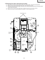
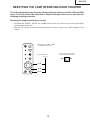
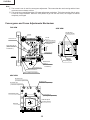
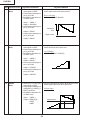
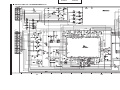
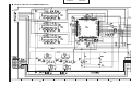
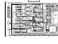
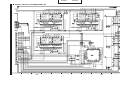
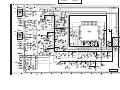
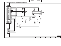
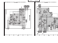
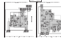
XV-Z1E/A
TENTATIVE
SERVICE MANUAL
SERVICE-ANLEITUNG
PAL/SECAM/NTSC SYSTEM
LCD PROJECTOR
LCD PROJEKTOR
MODELS
MODELLE
XV-Z1E/A
In the interests of user-safety (Required by safety regulations in some countries) the set should be restored to its original condition and only parts identical to those specified should be used.
Im lnteresse der Benutzersicherheit (erforderliche Sicherheitsregeln in einigen Ländern) muß das Gerät in seinen
Originalzustand gebracht werden. Außerdem dürfen für die spezifizierten Bauteile nur identische Teile verwendet
werden.
SHARP CORPORATION
1
XV-Z1E/A
CONTENTS
Page
•
•
•
•
•
•
•
•
•
•
•
•
•
•
•
•
•
•
NOTE TO SERVICE PERSONNEL .................... 3
SPECIFICATIONS ...............................................4
OPERATION MANUAL ...................................... 6
REMOVING OF MAJOR PARTS ........................ 9
CONTROLLING THE TOTAL
OPERATING HOURS OF THE LAMP .............. 14
RESETTING THE LAMP
OPERATING HOUR COUNTER ...................... 15
THE OPTICAL UNIT OUTLINE ........................ 16
CONVERGENCE AND
FOCUS ADJUSTMENT .................................... 17
ELECTRICAL ADJUSTMENT .......................... 21
TROUBLESHOOTING TABLE ......................... 29
•
Page
CHASSIS LAYOUT ........................................ 123
BLOCK DIAGRAM ..........................................125
OVERALL WIRING DIAGRAM ....................... 127
DESCRIPTION OF SCHEMATIC DIAGRAM ... 129
WAVEFORMS ................................................. 130
SCHEMATIC DIAGRAM ................................. 131
PRINTED WIRING BOARD ASSEMBLIES .... 167
PARTS LIST
ELECTRICAL PARTS ............................... 177
CABINET AND MECHANICAL PARTS ..... 204
ACCESSORIES PARTS ............................ 211
PACKING PARTS ...................................... 211
PACKING OF THE SET ................................. 212
INHALT
Seite
•
•
•
•
• HINWEISE FÜR DAS
WARTUNGSPERSONAL ................................. 43
• TECHNISCHE DATEN ..................................... 44
• BEDIENUNGSANLEITUNG ............................. 46
• ENTFERNEN DER HAUPTTEILE .................... 49
• KONTROLL DER GESAMTBETRIE
BSSTUNDEN DER LAMPE ............................. 54
• RÜCKSTELLUNG DES
LAMPEN-BETRIEBSSTUNDENZÄHLERS ...... 55
• ÜBERSICHT DER OPTIKEINHEIT .................. 56
• EINSTELLUNG VON KONVERGENZ
UND BRENNPUNKT ........................................ 57
• ELEKTRISCHE EINSTELLUNG....................... 61
• STÖRUNGSSUCHTABELLE ........................... 69
•
•
•
•
•
•
•
•
•
•
•
•
•
•
•
•
.......................................................................... 83
.......................................................................... 84
.......................................................................... 86
.......................................................................... 89
.......................................................................... 94
.......................................................................... 95
.......................................................................... 96
.......................................................................... 97
........................................................................ 101
........................................................................ 109
........................................................................ 123
•
•
•
•
•
•
•
Seite
CHASSIS-ANORDNUNG ............................... 123
BLOCKSCHALTBILD ..................................... 125
GESAMTSCHALTPLAN ................................. 127
BESCHREIBUNG DES SCHEMATISCHEN
SCHALTPLANS ............................................... 129
WELLENFORMEN ..........................................130
SCHEMATISCHER SCHALTPLAN ................ 131
LEITERPLATTENEINHEITEN ........................ 167
ERSATZTEILLISTE
ELEKTRISCHE BAUTEILE ...................... 177
CEHÄUSE UND MECHANISCHE
BAUTEILE ................................................. 204
ZUBEHÖRTEILE ....................................... 211
VERPACKUNGSTEILE ............................. 211
VERPACKEN DES GERÄTS ......................... 212
....................................................................... 125
........................................................................ 127
........................................................................ 129
........................................................................ 130
........................................................................ 131
........................................................................ 167
................................................................... 177
................................................................... 204
................................................................... 211
................................................................... 211
• ........................................................................ 212
2
XV-Z1E/A
NOTE TO SERVICE PERSONNEL
12345678901234567890123456789012123456789012345678901234567890121234567890123456789012345678901212
12345678901234567890123456789012123456789012345678901234567890121234567890123456789012345678901212
UV-RADIATION PRECAUTION
12345678901234567890123456789012123456789012345678901234567890121234567890123456789012345678901212
12345678901234567890123456789012123456789012345678901234567890121234567890123456789012345678901212
The light source, metal halide lamp, in the LCD
projector emits small amounts of UV-Radiation.
UV-Radiation and Medium Pressure
Lamp Precautions
AVOID DIRECT EYE AND SKIN EXPOSURE.
1. Be sure to disconnect the AC plug when replacing
the lamp.
2. Allow one hour for the unit to cool down before
servicing.
3. R e p l a c e o n l y w i t h s a m e t y p e l a m p . Ty p e
CLMPF0042DE01 rated 75V/265W.
4. The lamp emits small amounts of UV-Radiation, avoid
direct-eye contact.
5. The medium pressure lamp involves a risk of
explosion. Be sure to follow installation instructions
described below and handle the lamp with care.
To ensure safety please adhere to the following:
1. Be sure to wear sun-glasses when servicing the
projector with the lamp
turned “on” and the top
enclosure removed.
Lamp Replacement
2. Do not operate the lamp outside of the lamp housing.
Note:
Since the lamp reaches a very high temperature during
units operation replacement of the lamp should be
done at least one hour after the power has been turned
off. (to allow the lamp to cool off.)
Installing the new lamp, make sure not to touch the
lamp (bulb) replace the lamp by holding its reflector
2.
[Use original replacement only.]
3. Do not operate for more than 2 hours with the
enclosure removed.
1 Lamp
2 Reflector
DANGER ! –– Never turn the power on without
the lamp to avoid electric-shock or damage of the
devices since the stabilizer generates high voltages
at its start.
3
XV-Z1E/A
Specifications
4
XV-Z1E/A
Specifications
5
XV-Z1E/A
Location of Controls
6
XV-Z1E/A
Operating the Wireless Mouse Remote Control
7
XV-Z1E/A
Demensions
[Units: mm]
8
XV-Z1E/A
REMOVING OF MAJOR PARTS
Before starting this job, detach the lamp cage unit and the filter cover.
1. Removing the top cabinet
1-1. Remove the three screws at the carrying handle side.
1-1
1-2. Remove the two screws at the terminals side.
1-3. Detach the terminal door, and remove the four screws off the terminal cover.
1-4. Slowly lift the back of the top cabinet and disconnect the operation key unit connector (KY). Pull up and away
the top cabinet.
1-5. Place the top cabinet upside down. Remove the four screws off the operation key unit. Take out the operation
key unit.
1-4
Top Cabinet
1-2
(KY)
1-3
Terminal Door
1-2
9
XV-Z1E/A
2. Removing the front cabinets
2-1. Tilt the front-right cabinet forward. Pull it up out of position.
2-2. Tilt the front-left cabinet forward. Disconnect the infrared R/C receiver unit. Pull up the cabinet out of position.
Front-right Cabinet
Infrared R/C Receiver Unit
2-2
2-1
Front-left Cabinet
10
XV-Z1E/A
3. Removing the rear cabinet and video terminal cover
3-1. Remove the two screws off the rear cabinet and the screw from the static ground lead. Pull up the cabinet
and disconnect the speaker connector (SP). Now the rear cabinet is free.
3-2. Remove the four screws off the video terminal cover. Detach the cover.
3-1
Rear Cabinet
(SP)
Make sure the bimetal lead terminals are at the bottom
of the boss a and rib b .
a Boss
b
Rib
11
XV-Z1E/A
4. Removing the PWBs
4-1. Remove the two screws that fix the PC terminal cover to the bottom cabinet.
4-2. Remove the two screws off the output shield. Take out the output shield and disconnect the R-LCD, G-LCD
and B-LCD connectors (RP, GP, and BP).
4-3. Remove the four screws off the output unit. Disconnect the insulating barrier, the ground leads and the
connectors (FN, Q, LL, FF, LF, BL, RC and EA). Pull up and away the output unit and the signal/Video Input
terminal unit.
4-4. Remove the screw off the back of the output unit. Separate this unit from the signal/PC terminal unit.
4-5. Remove the screw off the bottom cabinet and the screw off the power panel. Now take out the power panel.
4-2
4-3
Insulating
Barrier
Output Shield
4-3
Output Unit
Power Panel
4-5
4-1
4-4
4-1
Signal/Video Input
terminal Unit
Video Input Terminal Cover
12
XV-Z1E/A
5. Removing the optics mechanism assembly
5-1. Remove the two screws off the angles A and B of the carrying handle. Detach the carrying handle.
5-2. Remove the two screws off the lamp socket holder. Take out the lamp socket.
5-3. Disconnect the bimetal connector (BA). Remove the four screws off the optics mechanism assembly, and pull
up and away this assembly.
5-4. Remove the two screws off the exhaust panel. Separate the panel from the bottom cabinet.
5-5. Remove the screw off the power/ballast unit assembly. Pull up and away the unit.
Power/Ballast Unit
5-5
5-3
5-1
(BA)
Carrying
Handle
5-1
5-3
Optics
Mechanism
Ass'y
5-4
Exhaust
Panel
5-3
5-2
5-3
13
XV-Z1E/A
CONTROLLING THE TOTAL OPERATING HOURS OF THE LAMP
The following control is carried out when the lamp has been used for 1900 hours and 2000
hours.
1. After 1900-hour use
When the power is turned on, "LAMP" appears in the on-screen display for about 1 minute (flashing in yellow)
and the lamp LED indicator lights up in red. When the 1,900-hour point comes up during use of the unit, the
"LAMP" display starts flashing in yellow on the screen for 1 minute at the very 1,900-hour point. Now the lamp
LED indicator changes from green to red.
2. After 2000-hour use
When the power is turned on, "LAMP" appears in the on-screen display for about 5 minutes (flashing in red) and
the lamp LED indicator lights up in red. Five minutes thereafter, the power turns itself off and the unit is interrupted.
When the 2000-hour point comes up during use of the unit, the "LAMP" display starts flashing in red on the
screen for 5 minutes at the very 2000-hour point. Five minutes later, the power turns itself off and the unit is
interrupted. (The lamp LED indicator stays red since the 1900-hour point.)
If you try to turn on the power three times after the 2000-hour point, the unit remains off.
3. When the 2000-hour point comes up, take the following steps.
Replace the lamp with new one. While holding down both the "VOL."" and "ADJ."" keys on the unit, turn on the
main power switch (located on the side of the unit). The lamp operating hourmeter is now reset to zero. Turn on
the unit and make sure the time display shows "0000H".
4. Displaying the total operating hours of the lamp (used to check the total time)
Change the STATUS3 data settings: PICTURE at 0, BRIGHT at MAX, COLOR at MIN, TINT at MIN, and
SHARPNESS at MAX. Hold down the SOUND DOWN and ENTER keys for longer than 3 seconds. By doing
this, the total operating hours will be displayed on the screen.
TIME
000H
14
TOTAL TIME
000H
XV-Z1E/A
RESETTING THE LAMP OPERATING HOUR COUNTER
The unit is designed to keep its power off when the lamp has been used for 1900 and 2000
hours. This is to protect the lamp fixture. Replace the lamp with new one and take the
following resetting procedure.
Resetting the lamp operating hour counter
1. Hold down the “ENTER”, “ADJ."” and “ADJ.|” buttons on the unit, and turn on the main power switch
(located above the AC inlet).
2. Now the unit is turned on and the lamp operating hour counter is reset to zero. “000H” appears on the
screen.
Hold down the “ADJ.|”, “ADJ."”
and “ENTER” keys at once.
*
(To be held down
at once)
IN
OFF
ADJ.|
ADJ."
MN
EN
Turn on the main power switch
(located above the AC inlet)
ENTER
15
ON
XV-Z1E/A
THE OPTICAL UNIT OUTLINE
Layout of the optical system
Note: Layout for positioning the optical system.
Projection Lens
Polarizer film
Incident polarizer plate B
Incident polarizer plate R
Dichroic coating
(B transmission)
B-LCD
Dichroic coating
(R transmission)
R-LCD
-c
AL
Cross dichroic prism
M5
ct
te
or
oa
M6
or
B
irr
re
m
fle
d
BLUE
R
Relay lens 3
Dichroic coating
(B reflection)
G-LCD
Condenser lens R
R-Filter
AL-deposited face
Polarizer film
Incident polarizer plate G
Relay lens 2
RED
Marking
Condenser lens G
AR-coated face
GREEN
-c
AL
Marking
M2
d
BLUE
G
te
oa
B/
G
re
Relay lens 1
or
ct
fle
or
B
* M3
ct
or
fle
irr
re
m
M4
Dichroic coating
AL-deposited face
or
W
Fly-eye lens (outgoing light)
ed
at
-c
o
M1
AL
AL-deposited
face
m
irr
Metal-halide lamp
(Light source)
* The M3 mirrors have a coating
wedge (for different film thickness). Set up these mirrors, with
their markings positioned as
shown above, so that their
coated faces and both sides be
in the correct directions.
Fly-eye lens (incoming light)
UV cut filter
16
XV-Z1E/A
CONVERGENCE AND FOCUS ADJUSTMENT
» Start the convergence and focus adjustments with the top cabinet and the signal shield
removed but the power on. Use the remote control gun to adjust the image. Take the
following procedures.
1. Focusing the projection lens
(A) Replacing all the 3 LCD panels
1. Before replacing all the 3 LCD panels, project an image on the screen and bring it into focus.
2. Replace the panels with new ones. But until the focus has been completely readjusted, be careful not to
change the distance between the set and the screen, nor to move the projection lens focus and zoom
rings.
If the focus is readjusted with a different positional relation, the relation between the projection distance
and the screen size is affected. In other words, a short-distance image (40 WIDE, for example) may get
out of the focus range, or a long-distance image (300 WIDE, for example) may come out of focus.
(
)
(B) Replacing 1 or 2 of the 3 LCD panels
1. In adjusting the focus after replacement of one or two LCD panels, project an image on the screen and turn
the projection lens focus ring to get the non-replaced LCD panel into focus.
2. But until the focus has been completely adjusted for the new LCD panels, be careful not to change the
distance between the set and the screen, nor to move the projection lens focus and zoom rings.
(If the distance has been changed or the projection lens readjusted, repeat the above steps 1 and 2.)
2. Adjusting the G-LCD panel
(A) Focus adjustment. (Make this adjustment on the white-only screen.)
1. Right-and-left focus adjustment (θY direction) .
Loosen the lock screws "b" and "c" and insert the eccentric screwdriver into the notch and hole "b". Turn
the screwdriver until the right and left halves on the screen get into focus.
First get the right and left halves in balance. Then improve the accuracy while making the adjustment 2
below.
2. Top-center-bottom focus adjustment (θX and Z directions).
Loosen the lock screws "a" and "c" and insert the eccentric screwdriver into the notch and hole "a" or "c".
Turn the screwdriver until the top, center and bottom on the screen get into focus. In adjusting this top-tobottom focus, temporarily tighten the lock screw "b" to fix the θY direction adjustment.
3. Repeat the above steps 1 and 2 to finely adjust the focus. Finally tighten up all the lock screws.
)
(
Note :
1 Carefully proceed with the focus adjustment because the adjusting directions are correlated.
2 In adjusting the convergence and focus, do not move the projection lens zoom and focus rings until the end
of all the adjustments.
(B) Convergence adjustment
» The G-LCD panel has no convergence adjustment mechanism. Use this panel as convergence adjustment
reference.
3. B-LCD panel adjustment (the same for the R-LCD panel)
(A) Focus adjustment
» Take the same procedure as for the G-LCD panel focus adjustment. Note that the adjustment range is small
in the Z direction. If the convergence is quite different between the B-LCD and G-LCD panels, roughly adjust
the convergence first and then the focus.
(B) Convergence adjustment
» Use a crosshatch pattern signal for this adjustment.
Make the adjustment just for the G-colour and the relevant colour.
(1) Loosen the convergence lock screw "d".
(2) With the G-LCD panel’s screen center as reference, adjust the B-LCD panel in the X, Y and θZ directions.
(3) Finally tighten up the convergence lock screw "d".
17
XV-Z1E/A
Note :
1 The eccentric cam is used for convergence adjustment. This means that the cam’s turning and the linear
movement are not always uniform.
2 This model is not equipped with the LCD image adjustment mechanism. This is because the dichroic prism
is used for image formation. When the LCD panels all get into the best focus, the images are almost
completely converged.
Convergence and Focus Adjustments Mechanism
TOP VIEW
SIDE VIEW
G-LCD panel
mounting screws
R-LCD
G-LCD
Lock screw "a"
Notch and hole "b"
(Use an eccentric
screwdriver.)
Notch and hole "a"
(Use an eccentric
screwdriver.)
X
X
θY
Z
θZ
Y
Lock screw "b"
(θY direction)
FRONT
G-LCD
B-LCD
Z
Notches and
holes "c"
(Use on eccentric
screwdriver.)
X
θY
Lock screws "c"
Notches and holes "c"
(Use an bladed screwdriver.)
SIDE VIEW
Eccentric cam
(X direction adjustment)
Eccentric cam
(θZ direction adjustment)
Eccentric cam
(Y direction adjustment)
R•B adjusting plate
Lock screw "d"
(convergence adjustment)
Y
X
R•B-LCD
R•B-LCD panel
mounting screws
θZ
18
G adjusting plate
XV-Z1E/A
Convergence and Focus Adjustments at a Glance
Adjustment directions
Adjustment
Direction
X direction
Convergence Y direction
θZ direction
Z direction
Focus
θX direction
θY direction
Definition
Direction of LCD panel
LCD right and left
LCD top and bottom
LCD turning axis
LCD optical axis
LCD top-to-bottom flapping
LCD right-to-left flapping
Rotation around Z axis
Rotation around X axis
Rotation around Y axis
Convergence and Focus Adjustment for the XV-Z1 Optical Mechanism
Colour
Adjustment
Convergence
R/B
colours
Focus
G colour
Focus
Direction
Movement
Position
Adjusting tool
Lock screw
Tightening tool
X direction
±0.8mm Eccentric cam
Eccentric cam adjusting wrench
d
Hex wrench
Y direction
±0.8mm Eccentric cam
Eccentric cam adjusting wrench
d
Hex wrench
θZ direction
±1°
Eccentric cam adjusting wrench
d
Hex wrench
Z direction
±0.8mm Notch and hole "a" & "c" Eccentric screwdriver,
a, c
Phillips
θX direction
±1°
Notch and hole "a" & "c"
a, c
screwdriver
θY direction
±1°
Notch and hole "b" & "c"
Z direction
±0.2mm
θX direction
±1°
θY direction
±1°
Eccentric cam
Bladed screwdriver
b, c
Same as for R and B colours
Focus Adjustments the Other Way
Lock screw
Position
a
Notch and hole "a"
b
Notch and hole "b"
c
Notch and hole "c"
Related direction
Z and θX directions
θY direction
Z, θX and θY directions
Convergence and Focus Adjusting and Tightening Tools
Tool
Eccentric cam
adjusting wrench
Specific or General
Specific
Tool code
Configuration
9DASPN-XGNV1U
80
Eccentric screwdriver Specific
9EQDRiVER-NV1A
General (redesigned)
9EQLNC-XGNV1U
(R
2)
CUT
Hex wrench
(16)
5
100
(50)
0.5
2
General
—
19
ø5
Phillips screwdriver
85min
9EQDRiVER-NV1B
(ø3.5)
General
3.5
Bladed screwdriver
For M2.6 pan-head machine screw
XV-Z1E/A
Replacing the LCDs
With the top cabinet removed
(1) Remove the output shield.
(2) Disconnect the LCD flat cable from the output PWB connector.
(3) Remove the lock screws "b" and "c". Detach the R/B adjusting plate or the G adjusting plate together with the LCD
panel.
(4) Separate the LCD panel from the adjusting plate.
(5) Mount a new LCD panel in the reverse order of the above steps (1), (2), (3) and (4).
~ Readjust the convergence and focus. Note that the G LCD panel needs no convergence adjustment and has
a small adjustment range in the Z direction.
TOP VIEW
2
1
R-LCD
3
Lock screws "c"
SIDE VIEW
2
G adjusting plate
FRONT
Lock
screws "b"
X
3
3
X
θY
Z
Lock
screws "c"
θZ
Y
~
G-LCD
G-LCD
4
Z
Lock screws "c"
3
X
B-LCD
θY
1
2
SIDE VIEW
R•B adjusting plate
Y
R•B-LCD
X
θZ
4
R•B-LCD panel
mounting screws
20
G-LCD panel
mounting screws
XV-Z1E/A
ELECTRICAL ADJUSTMENT
NOTE : The settings have been factory-adjusted to their best points. If any of them gets out of spec or after
any relevant part has been replaced, make the related adjustment.
Step Adjustment Position
1
PLL
(NTSC)
(R4314, R4318)
Adjustment Conditions
Adjustment Method
» Adjust center level and pulse width of R4314/R3418.
1. Receive the monoscope
pattern signal of NTSC.
2. Connect the oscilloscope to
TP4301 and TP4302.
TP4302
Center
GND
TP4301
Center
1µ
GND
2
PLL
(PAL)
(R4313, R4320)
1. Receive the monoscope
pattern signal of PAL.
2. Connect the oscilloscope to
TP4301 and TP4302.
» Adjust center level and pulse width of R4313/R4320,
same as NTSC.
3
VCO primary
OSC
(L1001)
1. No signal.
2. Short the TP1001 and GND.
3. Connect the frequency
counter to TP1002 and
GND.
» Adjust frequency of the core of L1001
H-center
(NTSC)(DAC)
1. Receive the monoscope
pattern signal of NTSC.
2. Push S2001 and set the follow DAC mode.
» Using the Operation key switch '
right and left overscan.
4
fo : 15.625 ±0.01kHz
",
adjust same as
",
adjust same as
Overscan : 93~95%
Group : VIDEO 1
Subject : H-CENT+9
setting.
Group : TEST
Subject : H-POS
5
H-center
(PAL)(DAC)
» Using the Operation key switch '
right and left overscan.
1. Receive the monoscope
pattern signal of PAL.
2. Push S2001 and set the follow DAC mode.
Overscan : 93~95%
Group : VIDEO 1
Subject : PAL-H-CENT +9
setting.
Group : TEST
Subjec : H-POS
21
XV-Z1E/A
Step Adjustment Position
6
Reference black
Level
Adjustment Conditions
Adjustment Method
» Using the Operation key switch '
level as same as pedestal level.
1. Receive the 10 step gray
scale signal. (NTSC or PAL)
2. Connect the oscilloscope to
pin (3) of P1501.
3. Group : VIDEO 5
Subject : T-BRT
", adjust the black
Black
Pedestal
7
Contrast
(DAC)
» Using the Operation key switch ' ", adjust level between black level and 100% white level.
1. Receive the 10 step gray
scale signal of NTSC.
2. Connect the oscilloscope to
pin (3) of P1501.
3. Push S2001 and set the follow DAC mode.
1.60 ±0.05Vp-p
Group : VIDEO 1
Subject : SUB-R 0
SUB-G 0
SUB-B 0
setting.
4. Group : VIDEO 1
Subject : CONT
8
Contrast of
component
mode
(DAC)
» Using the Operation key switch ' ", adjust level between black level and 100% white level.
1. Receive the 10 step gray
scale signal of NTSC.
2. Connect the oscilloscope to
pin (3) of P1501.
3. Push S2001 and set the follow DAC mode.
1.55 ±0.05Vp-p
Group : VIDEO 5
Subject : C-CONT
9
Bright of
component
mode
(DAC)
» Using the Operation key swsitch ' ", adjust the black
level as same as clamp level.
1. Receive the 10 step gray
scale signal of NTSC.
2. Connect the oscilloscope to
pin (3) of P1501.
3. Push S2001 and set the follow DAC mode.
Group : VIDEO 5
Subject : C-BRIGHT
22
XV-Z1E/A
Step Adjustment Position
10
AGC
Adjustment Conditions
Adjustment Method
» Using the Operation key switch ' ", adjust level between black and 100% white level.
1. Receive the 10 step gray
scale signal of NTSC.
2. Connect the oscillosope to
pin (3) of P1501.
3. Push S2001 and set the follow DAC mode.
1.2 ±0.05Vp-p
Group : VIDEO 5
Subject : AGCADJ
11
D/A Output level
(NTSC) (DAC)
» Using the Operation key switch ' ", adjust level between black and 100% white level.
1. Receive the 10 step gray
scale signal of NTSC.
2. Connect the oscilloscope to
pin (5) of P1501.
3. Push S2001 and set the follow DAC mode.
0.6 ±0.05Vp-p
Group : VIDEO 5
Subject : DAV
12
D/A Output level
(PAL) (DAC)
» Using the Operation key switch ' ", adjust level between black and 100% white level.
1. Receive the 10 step gray
scale signal of PAL.
2. Connect the oscilloscope to
pin (5) of P1501.
3. Push S2001 and set the follow DAC mode.
0.6 ±0.05Vp-p
Group : VIDEO 1
Subject : DAVREF
13
Signal center
(DAC)
» Using the Operation key switch '
tween signal center and GND.
1. Receive the 10 step gray
scale signal of NTSC.
2. Connect the oscilloscope to
pin (2) of P4303.
3. Push S2001 and set the follow DAC mode.
DC 7.0 ±0.1Vp-p
Group : VIDEO 2
Subject : SIG CTR
Signal center
23
",
adjust level be-
XV-Z1E/A
Step Adjustment Position
14
Reference level
(DAC)
Adjustment Conditions
Adjustment Method
» Using the Operation key switch ' ", adjust level between signal center and reference level.
1. Receive the 10 step gray
scale signal of NTSC.
2. Connect the oscilloscope to
pin (2) of P4303.
3. Push S2001 and set the follow DAC mode.
DC 2.0 ±0.1Vp-p
(SUB-BIAS, R-BIAS, B-BIAS)
Group : VIDEO 2
Subject : SUB-BIAS
4. Connect the oscilloscope to
pin (1) of P4303.
Reference
level
Subject : R-BIAS
5. Connect the oscilloscope to
pin (3) of P4303.
Signal center
Subject : B-BIAS
15
Gain
(DAC)
» Using the Operation key switch ' ", adjust level between black and 100% white level.
1. Receive the 10 step gray
scale signal of NTSC.
2. Connect the oscilloscope to
pin (2) of P4303.
3. Push S2001 and set the follow DAC mode.
1.4 ±0.05Vp-p
(DRIVE1, R-DRIVE, B-DRIVE)
Group : VIDEO 2
Subject : DRIVE 1
4. Cinnect the oscilloscope to
pin (1) of P4303.
Subject : R-DRIVE
5. Connect the oscilloscope to
pin (3) of P4303.
Subject : B-DRIVE
16
BRIGHT
(DAC)
» Using the Operation key switch ' ", adjust level between signal center and 100% white level.
1. Receive the 10 step gray
scale signal of NTSC.
2. Connect the oscilloscope to
(2-BRIGHT)(1-R-BRT)(3B-BRT) of P4303.
3. Push S2001 and set the follow DAC mode.
2.55 ±0.1Vp-p
Group : VIDEO 1
Subject : BRIGHT(G)
: R-BRT
: B-BRT
Signal center
24
XV-Z1E/A
Step Adjustment Position
17
Gamma
(DAC)
Adjustment Conditions
Adjustment Method
» Using the Operation key switch ' ", adjust level between 2nd gradation and GND for
4.4 ±0.1Vp-p
1. Receive the 10 step gray
scale signal of NTSC.
2. Connect the oscilloscope to
pin (2) of P4303.
3. Push S2001 and set the follow DAC mode.
adjust level between black level and GND for
3.0 ±0.1Vp-p
Group : VIDEO 4
Subject : RGB GAM 1
RGB CTR 1
4. Connect the oscilloscope to
pin (1) of P4303.
Group : VIDEO 4
Subject : R GAM 1
R CTR 1
5. Connect the oscilloscope to
pin (3) of P4303.
2nd gradation
Black level
Group : VIDEO 4
Subject : B GAM 1
B CTR 1
3.0V
4.4V
GND
18
SID signal level
» Using the Operation key switch ' ", adjust level between signal center and SID signal level.
1. Receive the 10 step gray
scale signal of NTSC.
2. Connect the oscilloscope to
pin (6) of P4303.
3. Push S2001 and set the follow DAC mode.
4.0 ±0.1Vp-p
Group : VIDEO 3
Subject : SID CTR
4.0V
4.0V
25
XV-Z1E/A
Step Adjustment Position
19
TINT
(DAC)
Adjustment Conditions
Adjustment Method
1. Receive the colour bar signal.
2. Connect the oscilloscope to
pin (2) of P1501.
3. Push S2001 and set the follow DAC mode.
» Using the Operation key switch
freshtone B-Y waveform.
' ",
adjust the
» Using the Operation key switch
freshtone for B-Y waveform.
' ",
adjust the
Group : VIDEO 2
Subject : TINT
20
TINT of
component
(DAC)
1. Receive the colour bar
sugnal for component terminal.
2. Connect the oscilloscope to
pin (2) of P1501.
3. Push S2001 and set the follow DAC mode.
Group : VIDEO 5
Subject : C-TINT
21
Colour of NTSC
(DAC)
» Using the Operation key switch ' ", adjust level between Red and 100% white level.
1. Receive the colour bar signal of NTSC.
2. Connect the oscilloscope to
pin (1) of P4303.
3. Push S2001 and set the follow DAC mode.
0.15 ±0.05Vp-p
100% White Red
Group : VIDEO 2
Subject : COLOR
22
PAL COLOUR
(DAC)
» Using the Operation key switch ' ", adjust level between Red and 100% white level.
1. Receive the colour bar signal of PAL.
2. Connect the oscilloscope to
pin (1) of P4303.
3. Push S2001 and set the follow DAC mode.
0.35 ±0.05Vp-p
100% White Red
Group : VIDEO 2
Subject : P-COLOR
26
XV-Z1E/A
Step Adjustment Position
23
SECAM
COLOUR
(DAC)
Adjustment Conditions
Adjustment Method
» Using the Operation key switch '
tween red and 100% white level.
1. Receive the colour bar signal of SECAM.
2. Connect the oscilloscope to
pin (1) of P4303.
3. Push S2001 and set the follow DAC mode.
",
adjust level be-
",
adjust level be-
0.2 ±0.05Vp-p
100% White Red
Group : VIDEO 2
Subject : S-COLOR
24
COLOUR of
component
(DAC)
» Using the Operation key switc '
tween red and 100% white level.
1. Receive the colour bar signal of NTSC.
2. Connect the oscilloscope to
pin (1) of P4303.
3. Push S2001 and set the follow DAC mode.
0 ±0.05Vp-p
100% White Red
Group : VIDEO 5
Subject : C-COLOR
25
26
Common DC
bias
(DAC)
(VCOMCTR)
(RC)
(GC)
(BC)
1. Receive the monoscope
signal of NTSC or PAL.
2. Push S2001 and set the follow DAC mode.
White balance
(DAC)
1. Receive the monoscope
signal of NTSC or PAL.
2. Push S2001 and set the follow DAC mode.
» Using the Operation key switch
to the sharpest contrast.
' ",
adjust visually
» Using the Operation key switch
to the white.
' ",
adjust visually
Group : VIDEO 3
Subject : VCOMCTR 43
set before adjustment.
3. Subject : RC
: GC
: BC
Froup : VIDEO 2
Subject : R-BIAS
B-BIAS
27
XV-Z1E/A
Step Adjustment Position
Adjustment Conditions
Adjustment Method
27
Sign display
position
(L2003)
1. Receive the monoscope
signal of NTSC or PAL.
2. Push the volume key ' "
» Adjust L2003 so the volume sign on screen display is
symmetrical to the right and left side.
28
Vertical position
(NTSC)
1. Receive the monoscope
signal of NTSC.
2. Push S2001 and set the follow DAC mode.
» Using the Operation key switch ' ", display is symmetrical to the upper and lower side.
Overscan : 93~95%
Group : TEST
Subject : V-POS
29
Vertical position
(PAL)
» Using the Operation key switch
points of V-POS.
1. Receive the monoscope
signal of PAL.
2. Push S2001 and set the follow DAC mode.
' ",
adjust the 21
Group : TEST
Subject : V-POS
30
Samplehold
1. Receive the colour bar signal of NTSC.
2. Push S2001 and set the follow DAC mode.
» Using the Operation key switch
points of SH-POS.
' ",
adjust the 8
» Using the Operation key switch
points of SH-POS.
' ",
adjust the 3
Group : TEST
Subject : SH-POS
31
Sensor of
thermostat
1. Push S2001 and set the follow DAC mode.
Group : TEST
Subject : HL
28
XV-Z1E/A
TROUBLE
TROUBLE
SHOOTING
SHOOTING
TABLE
TABLE
(Continued)
Checking the PWB performance
RGB input in trouble
Through-output in trouble
Remote control in trouble
Feed test pattern signal from PC.
Go to "Checking the through-output
circuit".
Go to "Checking the remote control
circuit".
Is specified cable connected between No
PC and projector?
Yes
Use specified cable.
No
Is supply voltage as specified?
Yes
Power circuit in trouble.
Does image appear?
Yes
No
Is the image proper?
Yes
Check control circuit (IC5001, IC5002,
IC5003 and IC5010).
No
Does G picture appear?
Yes
Are D/A outputs of IC1003, IC1004
and IC1028 as specified?
No
Yes
Go to "Checking the G signal line of
output PWB".
Does R picture appear?
Go to "Checking the G signal line of
signal PWB".
No
Yes
Are D/A outputs of IC1005, IC1006
and IC1029 as specified?
No
Yes
Go to "Checking the R signal line of
output PWB".
Are D/A outputs of IC1007, IC1008
and IC1030 as specified?
No
Yes
Go to "Checking the B signal line of
output PWB".
Go to "Checking the B signal line of
signal PWB".
29
Go to "Checking the R signal line of
signal PWB".
XV-Z1E/A
TROUBLE SHOOTING TABLE (Continued)
Checking the G signal line of signal PWB
Is there signal input at pin (11) of
IC1011?
No
Yes
Check pin (4) line of connector TN.
Is there signal output at pin (35) of
IC1011?
No
Yes
Do voltages at pins (6), (18) and (19) No
of IC1012 change?
Yes
Is there HSYNC signal input at pin
(23) of IC1011?
IC1012, IC5002 or nearby circuit in
trouble.
No
Yes
Is there signal input at pin (7) of
IC1015?
Go to "Checking synchronization".
No
IC1011 or nearby circuit in trouble.
Yes
Are there signal outputs at pins (197) No
thru (204) of IC1201?
Is there clock output at pin (14) of
IC1201?
Yes
Yes
Is there sync signal input at pins (15),
(216) or (217) of IC1201?
No
No
IC1201 or nearby circuit in trouble.
IC1015 or nearby circuit in trouble.
Yes
Are there signal inputs at pins (1),
(2), (3), (5) thru (8), (127) thru (130),
(132) thru (136), (138), (139), (145)
thru (149), (151) thru (154), (156)
thru (160) of IC1206?
Go to "Checking synchronization".
No
No
Yes
Check IC1002 and its peripheral parts.
IC1206 or nearby circuit in trouble.
Yes
Are there signal inputs at pins (143),
(144), (146), (147), (148), (152) and
(154) of IC1001?
Is there clock input at pin (49) of
IC1201?
No
Are there clock inputs at pins (60),
(103) and (143) of IC1206?
No
Yes
Yes
IC1001 or nearby circuit in trouble.
Are there signal outputs at CH10 thru
CH17, CH20 thru CH27, CH30 thru
CH37, CH40 thru CH47, CH50 thru
CH57, and CH60 thru CH67 of
IC1001?
No
Is there clock input at pin (94) of
IC1001?
Yes
Is there clock output at pin (233) of
IC1001?
Yes
No
Yes
IC1003, IC1004, IC1028 or nearby
circuit in trouble.
IC1001 or nearby circuit in trouble.
30
No
IC1009 or nearby circuit in trouble.
XV-Z1E/A
TROUBLE SHOOTING TABLE (Continued)
Checking the R signal line of signal PWB
Is there signal input at pin (7) of
IC1011?
No
Yes
Check pin (4) line of connector TN.
Is there signal output at pin (40) of
IC1011?
No
Yes
Do voltages at pins (5), (18) and (19) No
of IC1012 change?
Yes
Is there HSYNC signal input at pin
(23) of IC1011?
IC1012, IC5002 or nearby circuit in
trouble.
No
Yes
Is there signal input at pin (7) of
IC1014?
Go to "Checking synchronization".
No
IC1011 or nearby circuit in trouble.
Yes
Are there signal inputs at pins (189)
thru (196) of IC1201?
No
No
Yes
Yes
Is there sync signal input at pins (15),
(216) or (217) of IC1201?
Is there clock output at pin (14) of
IC1201?
No
IC1201 or nearby circuit in trouble.
IC1015 or nearby circuit in trouble.
Yes
Are there signal outputs at pins (1),
(2), (3), (5) thru (8), (127) thru
(130), (132) thru (136), (138), (139),
(145) thru (149), (151) thru (154),
(156) thru (160) of IC1206?
Go to "Checking synchronization".
No
No
Yes
Check IC1002 and its peripheral parts.
IC1206 or nearby circuit in trouble.
Yes
Are there signal outputs to pins
(129), (131), (132), (133), (136),
(137), (138) and (142) of IC1001?
Is there clock input at pin (49) of
IC1201?
No
Are there clock inputs at pins (60),
(103) and (143) of IC1206?
No
Yes
Yes
IC1001 or nearby circuit in trouble.
Are there signal outputs at CH10 thru
CH17, CH20 thru CH27, CH30 thru
CH37, CH40 thru CH47, CH50 thru
CH57, and CH60 thru CH67 of
IC1001?
No
Yes
Is there clock output at pin (233) of
IC1001?
Is there clock input at pin (94) of
IC1001?
Yes
No
Yes
IC1003, IC1004, IC1028 or nearby
circuit in trouble.
IC1001 or nearby circuit in trouble.
31
No
IC1009 or nearby circuit in trouble.
XV-Z1E/A
TROUBLE SHOOTING TABLE (Continued)
Checking the B signal line of signal PWB
Is there signal input at pin (15) of
IC1011?
No
Yes
Check pin (4) line of connector TN.
Is there signal output at pin (30) of
IC1011?
No
Yes
Do voltages at pins (7), (18) and (19) No
of IC1012 change?
Yes
Is there HSYNC signal input at pin
(23) of IC1011?
IC1012, IC5002 or nearby circuit in
trouble.
No
Yes
Is there signal input at pin (7) of
IC1016?
Go to "Checking synchronization".
No
IC1011 or nearby circuit in trouble.
Yes
Are there signal outputs at pins (205)
thru (208), (212) thru (215) of IC1201?
No
Is there clock output at pin (14) of
IC1201?
Yes
Yes
Is there sync signal input at pins (15),
(216) or (217) of IC1201?
No
No
IC1201 or nearby circuit in trouble.
IC1015 or nearby circuit in trouble.
Yes
Are there signal outputs at pins (1),
(2), (3), (5) thru (8), (127) thru (130),
(132) thru (136), (138), (139), (145)
thru (149), (151) thru (154), (156)
thru (160) of IC1206?
Go to "Checking synchronization".
No
No
Yes
Check IC1002 and its peripheral parts.
IC1206 or nearby circuit in trouble.
Yes
Are there signal outputs at pins
(156), (157), (158), (162), (163),
(164), (166) and (167) of IC1001?
Is there clock input at pin (49) of
IC1201?
No
Are there clock inputs at pins (60),
(103) and (143) of IC1206?
No
Yes
Yes
IC1001 or nearby circuit in trouble.
Are there signal outputs at CH10 thru
CH17, CH20 thru CH27, CH30 thru
CH37, CH40 thru CH47, CH50 thru
CH57, and CH60 thru CH67 of
IC1001?
No
Is there clock input at pin (94) of
IC1001?
Yes
Is there clock output at pin (233) of
IC1001?
Yes
No
Yes
IC1003, IC1004, IC1028 or nearby
circuit in trouble.
IC1001 or nearby circuit in trouble.
32
No
IC1009 or nearby circuit in trouble.
XV-Z1E/A
TROUBLE SHOOTING TABLE (Continued)
Checking the G signal line of output PWB
Are outputs at pins (3), (4) and (5) of
IC4034 as specified?
No
IC4034, IC5002 or nearby circuit in
trouble.
No
Check connector CC. Do signals go
to pins (4), (5), (7), (8), (10) and (11)
of this connector?
Yes
Are there signal inputs at pins (1)
each of IC4038 thru IC4043?
Yes
No
Connector CC poorly soldered or in
trouble.
No
Are FRP1 and FRP2 signals fed to
pins (9) and (12) of IC4077?
Yes
Any of IC4038 thru IC4043 faulty.
Are there signal outputs at pins (7),
(8) and (14) of IC4044 and IC4045?
No
IC4038 thru IC4043, IC4044, IC4045
or nearby circuit in trouble.
Yes
Are signals fed from pins (2) thru (7) No
of connector GP to the panel?
Connector GP poorly soldered or in
trouble.
Yes
Does flicker happen?
No
Go to "Checking the image for
shifting".
Yes
Is frame pulse fed to pin (1) of
connector GP?
No
Does frame pulse go out of IC4077?
Yes
Yes
Yes
Q4024, Q4025, Q4026 or their signal
line in trouble.
Is common bias at pin (24) of
connector GP as specified?
IC4077 or nearby
circuit in trouble.
No
IC1001 or nearby
circuit in trouble.
Yes
Panel in trouble.
Checking the image for shifting
Are signals fed via IC4074, IC4075
and IC4076 to the panel?
Yes
Panel in trouble.
No
Are signals fed to IC4074, IC4075
and IC4076?
Yes
IC4074, IC4075, IC4076 or nearby
circuit in trouble.
33
No
IC1001 or nearby circuit in trouble.
XV-Z1E/A
TROUBLE SHOOTING TABLE (Continued)
Checking the R signal line of output PWB
Are outputs at pins (2), (18) and (19)
of IC4034 as specified?
No
IC4034, IC5002 or nearby circuit in
trouble.
No
Check connector CC. Do signals go
to pins (13), (14), (16), (17), (19) and
(20) of this connector?
Yes
Are there signal inputs at pins (1)
each of IC4401 thru IC4406?
Yes
No
Connector CC poorly soldered or in
trouble.
No
Are FRP1 and FRP2 signals fed to
pins (9) and (12) of IC4077?
Yes
Any of IC4401 thru IC4406 faulty.
Are there signal outputs at pins (7),
(8) and (14) of IC4036 and IC4407?
No
IC4401 thru IC4406, IC4436, IC4407
or nearby circuit in trouble.
No
Connector RP poorly soldered or in
trouble.
No
Go to "Checking the image for
shifting".
Yes
Are signals fed from pins (2) thru (7)
of connector RP to the panel?
Yes
Does flicker happen?
Yes
Is frame pulse fed to pin (1) of
connector RP?
Yes
Is common bias at pin (24) of
connector RP as specified?
No
Does frame pulse go out of IC4077?
Yes
Q4024, Q4025, Q4026 or their signal
line in trouble.
Yes
Panel in trouble.
34
Yes
IC4077 or nearby
circuit in trouble.
No
IC1001 or nearby
circuit in trouble.
XV-Z1E/A
TROUBLE SHOOTING TABLE (Continued)
Checking the B signal line of output PWB
Are outputs at pins (6), (7) and (8) of
IC4034 as specified?
No
IC4034, IC5002 or nearby circuit in
trouble.
No
Check connector CC. Do signals go
to pins (22), (23), (25), (26), (28) and
(29) of this connector?
Yes
Are there signal inputs at pins (1)
each of IC4001 thru IC4006?
Yes
No
Connector CC poorly soldered or in
trouble.
No
Are FRP1 and FRP2 signals fed to
pins (9) and (12) of IC4077?
Yes
Any of IC4001 thru IC4006 faulty.
Are there signal outputs at pins (7),
(8) and (14) of IC4007 and IC4008?
No
IC4001 thru IC4006, IC4007, IC4008
or nearby circuit in trouble.
No
Connector BP poorly soldered or in
trouble.
No
Go to "Checking the image for
shifting".
Yes
Are signals fed from pins (2) thru (7)
of connector BP to the panel?
Yes
Does flicker happen?
Yes
Is frame pulse fed to pin (1) of
connector BP?
Yes
Is common bias at pin (24) of
connector BP as specified?
No
Does frame pulse go out of IC4077?
Yes
Q4024, Q4025, Q4026 or their signal
line in trouble.
Yes
Panel in trouble.
35
Yes
IC4077 or nearby
circuit in trouble.
No
IC1001 or nearby
circuit in trouble.
XV-Z1E/A
TROUBLE SHOOTING TABLE (Continued)
Checking synchronization
Do horizontal and vertical sync
signals (at pins (13) and (14) of RGB
connector) come out of PC?
No
Yes
Are there signal outputs at pins
(3)(IN+) of IC2003 and IC2004?
No
Yes
Connector or nearby circuit in trouble.
Are there signal outputs at pins
(15)(H) and (217)(V) of IC1201?
No
Yes
IC2003, IC2004 or nearby circuit in
trouble.
Go to "Checking the PLL circuit".
Is there signal output at pin (3)(IN+)
of IC2005?
No
Yes
Connector or nearby circuit in trouble.
Is there signal output at pin (216)(C)
of IC1201?
No
Yes
IC2005 or nearby circuit in trouble.
Go to "Checking the PLL circuit".
Checking the PLL circuit
Are there signal outputs at pins
(6)(X1/EXT) and (22)(EXFBK) of
IC1013?
No
Yes
IC1201 or nearby circuit in trouble.
Is there signal output at pin
(15)(DOTCLK) of IC1013?
No
Yes
IC1013, IC1201 or nearby circuit in
trouble.
Check the sync circuit and its
peripheral parts.
36
XV-Z1E/A
TROUBLE SHOOTING TABLE (Continued)
Checking the remote control circuit
Press the MENU key. Are there
signal outputs at pins (29) and (30) of
connector CA?
No
Yes
Remote control receiver or its nearby
circuit in trouble.
IC5001, IC5101, IC5102 or nearby
circuit in trouble.
Checking the through-output circuit
No
Does analog output come from PC?
Yes
No digital output.
Is specified cable connected between
LCP and monitor?
No
Yes
Use specified cable.
No
Are LCP and monitor in sync?
Yes
IC2003, IC2004, IC2005 or nearby
circuit in trouble.
IC2001 or nearby circuit in trouble.
37
XV-Z1E/A
TROUBLE SHOOTING TABLE (Continued)
No image
Is lamp on?
No
Lamp fails to light up.
Yes
Is voltage aplied to connector EA?
No
Refer to the troubleshooting of the
lamp/ballast unit.
No
Check input terminal circuit and its
parts.
No
Check peripheral circuit of IC602 and
its parts.
No
Are there Y-signal inputs at pin (39),
C-signal input at pin (20) of IC801?
Yes
Are there signal at pins (1), (12) and
(19) of VS connector?
Yes
Are there H-SYNC puls at pins (5),
(6), of IC801?
Yes
Are there RGB signal at pins (31),
(32) and (33) of IC801?
Yes
Yes
Check peripheral circuit
of IC803, IC814.
Are there RGB signal at pins (5), (7)
and (9) of CC connector?
No
No
Check peripheral circuit
of IC408, IC401~IC410.
Check peripheral scan convertor
circuit.
Yes
Are there RGB signal at pins (9), (10) No
and (11) of IC4028?
Check peripheral double scan circuit.
Yes
Are there RGB signal at pin (5) of
No
IC4001, R signal at pin (5) of IC4002,
B signal at pin (5) of IC4003?
Check peripheral circuit of IC4028,
IC4029, IC4030 and IC4031.
Yes
Are there palus signal at pins (3)~(8)
of LCD panel?
No
Check the LCD terminals' waveforms
and connection with LCD panel.
Yes
Check the LCD terminals' waveforms
and connection with LCD panel.
38
XV-Z1E/A
TROUBLE SHOOTING TABLE (Continued)
No colour or unusual tint with NTSC signal
Set user control to standard value.
Check the video board.
Replace the video board. Are colour
and tint as specified?
No
No
Is colour mode judged properly?
IC5001 or nearby circuit in trouble.
Yes
Yes
No
Does user control work?
Video board in trouble.
IC1201, IC1206 or nearby circuit in
trouble.
Yes
Change process value for
adjustment.
No colour or unusual tint with PAL signal
Set user control to standard value.
Check the video board.
Replace the video board. Are colour
and tint as specified?
No
No
Is colour mode judged properly?
IC5001 or nearby circuit in trouble.
Yes
Yes
No
Does user control work?
Video board in trouble.
IC1201, IC1206 or nearby circuit in
trouble.
Yes
Change process value for
adjustment.
No colour or unusual tint with SECAM signal
Set user control to standard value.
Check the video board.
Replace the video board. Are colour
and tint as specified?
No
No
Is colour mode judged properly?
IC5001 or nearby circuit in trouble.
Yes
Yes
No
Video board in trouble.
Does user control work?
Yes
Change process value for
adjustment.
39
IC1201, IC1206 or nearby circuit in
trouble.
XV-Z1E/A
TROUBLE SHOOTING TABLE (Continued)
No synchronization
Is there video signal input at pins (15), No
(17) or (19) of IC6001?
Yes
Check the signal line from the
connector.
Are HSYNC and VSYNC signals from
pins (41) and (42) of IC6001 in sync
with input signal?
No
Yes
Check IC6001 and its peripheral
circuits.
Which of vertical and horizontal
syncs fails?
Vertical
Is there signal input from pin (22) of
connector VS to pin (214) of IC1201?
Yes
Horizontal
Is there signal input from pin (20) of
connector VS to pin (215) of IC1201?
No
Yes
Check IC1201 and its peripheral
circuits.
40
No
Check the signal line from IC6005.
XV-Z1E/A
TROUBLE SHOOTING TABLE (Continued)
Lamp failure to light up
Does new lamp light up?
No
Yes
Is discharge noise heard?
No
Yes
Lamp faulty. Replace.
Replace TGU1701. Check
connectors.
Is voltage applied across C1703?
No
Yes
Is F701 blown out?
No
Yes
Check DB701 and its peripheral parts.
Replace F701. Check and replace
Q1701.
Is voltage applied to pin (16) of
IC1701?
No
Yes
Is voltage applied to pin (1) of
connector BL?
No
Yes
Check IC5001 and its peripheral
circuits.
Is F704 or TF1701 blown out?
No
Yes
Replace Q1702.
Replace F704 or TF1701.
Is FET drive voltage applied from pin
(2) of IC1701?
No
Yes
IC1701 or nearby circuit in trouble.
Is voltage applied at TGU1701?
No
Yes
Q1703 or nearby circuit in trouble.
TGU1701 faulty.
41
XV-Z1E/A
TROUBLE SHOOTING TABLE (Continued)
No sound
Is sound heard with 3D SOUND off?
No
Yes
Does voltage at pin (9) of IC301
change with VOL UP/DOWN keys?
Check IC302 and its peripheral
circuits.
No
Yes
IC305 or nearby circuit in trouble.
Are there audio signal inputs at pins
(2) and (23) of IC301?
No
Yes
Are there audio signal inputs at pins
(1) and (9) of IC304?
IC306, IC6002, IC6003 or nearby
circuit in trouble.
No
Yes
IC307 or nearby circuit in trouble.
Are there audio signal inputs at pins
(1) and (3) of connector SP?
No
Yes
IC304 or nearby circuit in trouble.
Replace speaker.
Checking IC302 and its peripheral circuits
Are there signal inputs at pins (27)
and (28) of IC302?
No
Yes
Are there signal outputs at pins (17)
and (18) of IC302?
IC306, C320, C321, R334, or related
part in trouble.
No
Yes
IC302 or nearby circuit in trouble.
IC306, C344, C345, R357, R358 or
related part in trouble.
42
XV-Z1E/A
XV-Z1E/A
CHASSIS LAYOUT / CHASSIS-ANORDNUNG
H
POWER/BALLAST UNIT–C
POWER/BALLAST UNIT–B
OPERATION KEY UNIT
INPUT UNIT
REDENC0228CEZC
REDENC0240CEZC
REDENC0228CEZB
REDENC0240CEZB
RUNTK0566CEZZ
CTANZ0712CE01
G
OUTPUT UNIT
DUNTK9553DE01/02/03/04
F
R/C RECEIVER UNIT
DUNTK9552DE01/02/03/04
POWER/BALLAST UNIT–A
REDENC0228CEZA
REDENC0240CEZA
E
OUTPUT SUB UNIT
DUNTK9554DE01/02/03/04
D
POWER/BALLAST UNIT–D
REDENC0228CEZD
REDENC0240CEZD
Ref. No.17 **
C
SIGNAL UNIT
DUNTK9551DE01/02/03/04
B
A
1
2
3
4
123
5
6
7
8
9
10
124
11
12
XV-Z1E/A
XV-Z1E/A
BLOCK DIAGRAM / BLOCKSCHALTBILD
H
G
F
E
D
C
B
A
1
2
3
125
4
5
6
7
8
9
10
126
11
12
XV-Z1E/A
XV-Z1E/A
OVERALL WIRING DIAGRAM / GESAMTSCHALTPLAN
H
G
F
E
D
C
B
XV-Z1E
XV-Z1A
A
1
2
3
4
127
5
6
7
8
9
10
128
11
12
XV-Z1E/A
XV-Z1E/A
DESCRIPTION OF SCHEMATIC DIAGRAM
VOLTAGE MEASUREMENT CONDITION:
1.
H
Voltages at test points are measured at the supply voltage of AC 220V. Signals
are fed by a colour bar signal generator for servicing purpose and the above
voltages are measured with a 20-kohm/V tester.
WAVEFORM MEASUREMENT CONDITION:
1.
Waveforms at test points are observed at the supply voltage of AC 220V.
Signals are fed by a colour bar signal generator for servicing purpose.
INDICATION OF RESISTOR & CAPACITOR:
RESISTOR
1. The unit of resistance “Ω” is omitted.
(K=kΩ=1000 Ω, M=MΩ).
G
2. All resistors are ± 5%, unless otherwise noted.
(J= ± 5%, F= ± 1%, D= ± 0.5%)
3. All resistors are 1/10W, unless otherwise noted.
4.
T :
1.
2.
DISCONNECT THE AC PLUG FROM THE AC OUTLET BEFORE
REPLACEING PARTS.
SEMICONDUCTOR HEAT SINKS SHOULD BE REGARDED AS
POTENTIAL SHOCK HAZARDS WHEN THE CHASSIS IS OPERATING.
IMPORTANT SAFETY NOTICE:
PARTS MARKED WITH “å”(
)ARE IMPORTANT FOR MAINTAINING
THE SAFETY OF THE SET. BE SURE TO REPLACE THESE PARTS WITH
SPECIFIED ONES FOR MAINTAINING THE SAFETY AND PERFORMANCE
OF THE SET.
Special
N : Metal Coating
F
CAUTION:
This circuit diagram is original one, therefore there may be a slight difference from yours.
SAFETY NOTES:
All resistors are Carbon type, unless otherwise noted.
C : Solid
W : Cement
S : Oxide Film
WAVEFORMSWELLENFORMEN
WELLENFORMEN
CAPACITOR
1. All capacitors are µF, unless otherwise noted.
(P=pF=µµF).
2. All capacitors are 50V, unless otherwise noted.
3. All capacitors are Ceramic type, unless otherwise noted.
(ML):
Mylar
(TA): Tantalum
(PF):
Polypro Film
(ST): Styrol
1
SC6001
H: 10µsec/div
V: 500mV/div
2
SC6001
H: 10µsec/div
V: 500mV/div
3
SC6001
H: 10µsec/div
V: 200mV/div
4
SC6001
H: 50µsec/div
V: 200mV/div
5
IC801
H: 10µsec/div
V: 500mV/div
6
IC801
H: 10µsec/div
V: 500mV/div
7
IC801
H: 10µsec/div
V: 500mV/div
8
IC801
H: 10µsec/div
V: 500mV/div
9
IC801
H: 10µsec/div
V: 500mV/div
0
IC801
H: 10µsec/div
V: 500mV/div
q
IC801
H: 10µsec/div
V: 1V/div
w
IC801
H: 10µsec/div
V: 1V/div
e
P1501
H: 10µsec/div
V: 500mV/div
r
P1501
H: 10µsec/div
V: 500mV/div
t
P1501
H: 10µsec/div
V: 500mV/div
y
P1501
H: 5µsec/div
V: 500mV/div
BESCHREIBUNG DES SCHEMATISCHEN SCHALTPLANS
SPANNUNGSMESSUNGEN:
1.
Spannungen an den Prüfpunkten werden bei einer Netzspannung von 220V
gemessen, Signale werden für die Wartung mit einem Farbbalken-Signal
generator zugeführt, und Spannungen werden mit einem Meßinstrument
(20 kΩ/V) ermittelt.
SIGNALFORMMESSUNGEN:
E 1.
Die Wellenformen an den Testpunkten werden bei einer Netzspannung von
220V verfolgt. Signale werden für die Wartung mit einem Farbbalken-Signal
generator zugeführt.
1.
2.
WIDERSTAND
1. Die Widerstandseinheit “Ω” wird weggelassen.
(K=kΩ=1000 Ω, M=MΩ).
D 2. Alle Widerstände haben ± 5%, sofern nicht anders angegeben.
(J= ± 5%, F= ± 1%, D= ± 0.5%)
3. Alle Widerstände haben 1/10W, sofern nicht anders angegeben.
T :
VOR DEM AUSWECHSELN VON TEILEN MUSS UNBEDINGT
NETZSTECKER AUS DER NETZSTECKDOSE GEZOGEN WERDEN.
DIE WARMEABLEITER DER HALBLEITER SOLLTEN BEIM BETRIEB
DES CHASSIS ALS MÖGLICHE URSACHEN VON GEFÄHRLICHEN
ELEKTRISCHEN SCHLÄGEN BETRACHTET WERDEN.
WICHTIGE SICHERHEITSANMERKUNGEN:
MIT “å”(
)BEZEICHNETEN TEILE SIND BESONDERS WICHTIG
FÜR DIE AUFRECHTERHALTUNG DER SICHERHEIT . BEIM WECHDIESER
TEILE SOLLTEN DIE VORGESCHRIEBENEN TEILE IMMER VERWENDET
WERDEN, UM SOWOHL DIE SICHERHEIT ALS AUCH DIE LEISTUNG DES
GERÄTES AUFRECHTZUERHALTEN.
Alle Widerstände sind Kohletyp, sofern nicht anders angegeben.
C : Fest
W : Zement
S : Oxidfilm
ACHTUNG:
bei diesem Schaltplan handelt es sich um den ursprünglichen. Esönnen
daher geringfügige Unterschiede zu dem lhrem bestehen.
SICHERHEITSANMERKUNGEN:
BEZEICHNUNG DES WIDERSTANDS UND
KONDENSATORS:
4.
KONDENSATOR
1. Die Kapazitätseinheit ist µF, sofern nicht anders angegeben.
(P=pF=µµF).
2. Alle Kondensatoren haben 50V, sofern nicht anders angegeben.
3. Alle Kondensatoren sind Keramiktyp, sofern nicht anders angegeben.
(ML):
Mylar
(TA): Tantal
(PF):
Polyprofilm
(ST): Styrol
Spezial
N : Metallüberzug
C
B
A
1
2
3
129
4
5
6
7
8
9
10
130
11
12
XV-Z1E/A
XV-Z1E/A
OUTPUT UNIT-1/5 / AUSGABEEINHEIT-1/5
H
G
F
SIGNAL
E
D
C
B
TO THEAMISTOR
A
1
2
3
141
4
5
6
7
8
9
10
142
11
12
XV-Z1E/A
XV-Z1E/A
OUTPUT UNIT-2/5 / AUSGABEEINHEIT-2/5
H
G
F
E
D
SIGNAL UNIT
C
B
A
1
2
3
4
143
5
6
7
8
9
10
144
11
12
XV-Z1E/A
XV-Z1E/A
OUTPUT UNIT-3/5 / AUSGABEEINHEIT-3/5
H
TO SIGNAL
UNIT
24
23
22
21
20
19
18
17
16
1
2
3
4
5
6
7
8
9
G
15
14
13
10
11
12
15
14
13
10
11
12
F
24
23
22
21
20
19
18
17
16
1
2
3
4
5
6
7
8
9
E
24
23
22
21
20
19
18
17
16
15
14
13
10
11
12
D
1
3
2
5
4
7
6
9
8
2
5
8
11
13
C
36
1
3
4
6
7
35
34
33
32
31
30
29
28
27
26
25
9
17
16
15
14
12
37
24
38
23
39
22
40
21
41
20
42
19
43
18
44
17
45
16
46
15
47
14
10
B
48
13
1
2
3
4
5
6
7
8
9
10
11
12
A
1
2
3
145
4
5
6
7
8
9
10
146
11
12
XV-Z1E/A
XV-Z1E/A
OUTPUT UNIT-4/5 / AUSGABEEINHEIT-4/5
H
G
F
E
D
C
B
A
1
2
3
4
147
5
6
7
8
9
10
148
11
12
XV-Z1E/A
XV-Z1E/A
OUTPUT UNIT-5/5 / AUSGABEEINHEIT-5/5
H
G
F
E
D
C
B
A
1
2
3
149
4
5
6
7
8
9
10
150
11
12
XV-Z1E/A
XV-Z1E/A
OUTPUT SUB UNIT / AUSGABE-NEBENEINHEIT
H
TO R/C
G
F
E
D
C
B
A
1
2
3
4
151
5
6
7
8
9
10
152
11
12
XV-Z1E/A
XV-Z1E/A
SIGNAL UNIT-1/5 / SIGNALEINHEIT-1/5
H
G
F
E
D
C
B
A
1
2
3
4
131
5
6
7
8
9
10
132
11
12
XV-Z1E/A
XV-Z1E/A
SIGNAL UNIT-2/5 / SIGNALEINHEIT-2/5
H
G
F
E
D
C
B
A
1
2
3
133
4
5
6
7
8
9
10
134
11
12
XV-Z1E/A
XV-Z1E/A
SIGNAL UNIT-3/5 / SIGNALEINHEIT-3/5
H
G
F
E
D
C
B
A
1
2
3
4
135
5
6
7
8
9
10
136
11
12
XV-Z1E/A
XV-Z1E/A
SIGNAL UNIT-4/5 / SIGNALEINHEIT-4/5
H
G
F
E
D
C
B
A
1
2
3
137
4
5
6
7
8
9
10
138
11
12
XV-Z1E/A
XV-Z1E/A
SIGNAL UNIT-5/5 / SIGNALEINHEIT-5/5
H
G
F
E
D
C
B
A
1
2
3
4
139
5
6
7
8
9
10
140
11
12
XV-Z1E/A
XV-Z1E/A
VIDEO INPUT UNIT-1/2 / VIDEOEINGANGSEINHEIT-1/2
H
G
F
E
D
C
B
A
CTANZ0712CE01
1
2
3
153
4
5
6
7
8
9
10
154
11
12
XV-Z1E/A
XV-Z1E/A
VIDEO INPUT UNIT-2/2 / VIDEOEINGANGSEINHEIT-2/2
H
G
F
E
D
C
B
A
CTANZ0712CE01
1
2
3
4
155
5
6
7
8
9
10
156
11
12
XV-Z1E/A
XV-Z1E/A
POWER/BALLAST UNIT-A / NETZ-/BALLASTEINHEIT A
(XV-Z1E)
POWER/BALLAST UNIT-B / NETZ-/BALLASTEINHEIT B
(XV-Z1E)
G
G
F
F
E
E
D
D
C
C
B
B
A
A
1
RDENC0228CEZB
H
RDENC0228CEZA
H
2
3
4
157
5
6
1
2
3
4
158
5
6
XV-Z1E/A
XV-Z1E/A
POWER/BALLAST UNIT-D / NETZ-/BALLASTEINHEIT D
(XV-Z1E)
H
G
G
F
RDENC0228CEZC
H
F
E
E
D
D
C
C
B
B
A
A
1
2
3
4
159
5
6
RDENC0228CEZD
POWER/BALLAST UNIT-C / NETZ-/BALLASTEINHEIT C
(XV-Z1E)
1
2
3
4
160
5
6
XV-Z1E/A
XV-Z1E/A
POWER/BALLAST UNIT-A / NETZ-/BALLASTEINHEIT A
(XV-Z1A)
POWER/BALLAST UNIT-B / NETZ-/BALLASTEINHEIT B
(XV-Z1A)
H
H
G
G
F
F
E
E
D
D
C
C
B
B
A
A
1
2
3
4
161
5
6
1
2
3
4
162
5
6
XV-Z1E/A
XV-Z1E/A
POWER/BALLAST UNIT-C / NETZ-/BALLASTEINHEIT C
(XV-Z1A)
POWER/BALLAST UNIT-D / NETZ-/BALLASTEINHEIT D
(XV-Z1A)
H
H
G
G
F
F
E
E
D
D
C
C
B
B
A
A
1
2
3
4
163
5
6
1
2
3
4
164
5
6
XV-Z1E/A
XV-Z1E/A
IN INFRARED R/C RECEIVER UNIT / INFRAROT-EMPFÄNGEREINHEIT
OPERATION KEY UNIT / BEDIENUNGSTASTENEINHEIT
H
H
G
G
F
F
E
E
D
D
C
C
B
B
A
A
1
2
3
4
165
5
6
1
2
3
4
166
5
6
XV-Z1E/A
Ref. No.
Part No.
PARTS LIST
H
Description
Code
NOTE: THE PARTS HERE SHOWN ARE SUPPLIED AS AN
ASSEMBLY BUT NOT INDEPENDENTLY.
RLCDP0049CEZZ J LCD Module Unit, Red
DU
RLCDP0050CEZZ J LCD Module Unit, Green
DU
RLCDP0051CEZZ J LCD Module Unit, Blue
DU
"HOW TO ORDER REPLACEMENT PARTS"
2. REF. NO.
3. PART NO.
4. DESCRIPTION
5. CODE
6. QUANTITY
PRINTED WIRING BOARD ASSEMBLIES
(NOT REPLACEMENT ITEM)
MARK ★: SPARE PARTS-DELIVERY SECTION
MODEL XV-Z1E
ERSATZTEILLISTE
DUNTK9551DE01
DUNTK9551DE03
DUNTK9551DE04
AUSTAUSCH VON TEILEN
Ersatzteile, die besondere Sicherheitseigenschften haben, sind in
dieser Anleitung markiert. Elektrische Komponenten mit solchen
EEigenshaften sind in den Ersatzteil durch "å" gekenn-zeichnet.
Der Gebrauch von Ersatzteilen, die nicht deselben Sicherheitseigenschaften haben wie die vom Hersteller empfohlenen ud in der
Bedienungsanleitung angegebenen, können zur Ursache von
Blitzeinschlägen, Bränden und anderen Gefahren werden.
DUNTK9554DE01
DUNTK9554DE03
"WIE MAN ERSATSTEILE BESTELLT"
Damit Ihre Bestellung promt und korrekt ausgeführt wird, geben Sie
bitte folgende Informationen.
D
1. MODELL NR.
3. ERSATZTEIL NR.
5. KODE
DUNTK9553DE01
DUNTK9553DE03
DUNTK9553DE04
DUNTK9554DE04
DUNTK9552DE01
2. REF. NR.
4. BESCHREIBUNG
6. QUANTITÄT
DUNTK9552DE03
DUNTK9552DE04
MARKIERUNG ★ : ERSATZTEILE-LIEFERUNG
RUNTK0566CEZZ
CTANZ0712CE01
CDENC0228CE02
C
– Signal Unit (For Europe)
—
– Signal Unit (For U.K.)
—
– Signal Unit
—
(For Australia and New Zealand)
– Output Unit (For Europe)
—
– Output Unit (For U.K.)
—
– Output Unit
—
(For Australia and New Zealand)
– Output Sub Unit
—
(For Europe)
– Output Sub Unit
—
(For U.K.)
– Output Sub Unit
—
(For Australia and New Zealand)
– Infrared R/C Receiver Unit —
(For Europe)
– Infrared R/C Receiver Unit —
(For U.K.)
– Infrared R/C Receiver Unit —
(For Australia and New Zealand)
– Operation Key Unit
—
– Video Input Unit
—
– Power/Ballast Unit
—
MODEL XV-Z1A
DUNTK9551DE02
DUNTK9553DE02
DUNTK9554DE02
DUNTK9552DE02
RUNTK0566CEZZ
CTANZ0712CE01
CDENC0240CE02
B
–
–
–
–
–
–
–
Description
Code
SIGNAL UNIT
PARTS REPLACEMENT
1. MODEL NUMBER
★
Part No.
DUNTK9551DE01/02/03/04
To have your order filled promptly and correctly, please furnish the
following informations.
F
Ref. No.
LCD PANELS
Replacement parts which have these special safety characteristics
identified in this manual: electrical components having such features are identified by "å" in the Replacement Parts Lists.
The use of a substitute replacement part which does not have the
same safety characteristics as the factory recommended replacement parts shown in this service manual may create shock, fire or
other hazards.
G
★
XV-Z1E/A
Signal Unit
Output Unit
Output Sub Unit
Infrared R/C Receiver Unit
Operation Key Unit
Video Input Unit
Power/Ballast Unit
—
—
—
—
—
—
—
A
INTEGRATED CIRCUITS
IC301
IC302
IC303
IC304
IC305
IC306
IC307
IC401
IC402
IC403
IC404
IC405
IC406
IC408
IC411
IC412
IC418
IC601
IC602
IC603
IC801
IC802
IC803
IC805
IC806
IC807
IC808
IC811
IC812
IC814
IC816
IC1001
IC1002
IC1003
IC1004
IC1005
IC1006
IC1007
IC1008
IC1009
IC1010
IC1011
IC1013
IC1014
IC1015
IC1016
IC1017
IC1101
IC3003
VHiTA8184F/-1
VHiSRS5250S-1
VHiNJU4052V-1
VHiTDA1517/-1
VHiM62352GP-1
VHiNJM2283F-1
VHiNJM062V/-1
VHiNJM2240M-1
VHiNJM2240M-1
VHiLT1253CS-1
VHiMM1041XM-1
VHiNJM2233V-1
VHiBA7046F/-1
VHiNJM2283F-1
VHiTC7S08U/-1
VHiTC7S04U/-1
VHiTC4W53U/-1
RH-iX2174CEZZ
VHiTHC4538T-1
VHiTHC4538T-1
VHiTDA8854H-1
VHiLT1253CS-1
VHiTDA4565/-1
VHiNJM2060M-1
VHiTC90A11F-1
VHiM518221S-1
VHiPST600DM-1
VHiTA1226N/-1
VHiLT1253CS-1
VHiTA8814N/-1
VHiNJM2283F-1
RH-iX2379CEZZ
RH-iX2063CEZZ
RH-iX0142TAZZ
VHiSC7S04F/-1
VHiNJM2107F-1
VHiMB40778F-1
RH-iX2174CEZZ
VHiMC14577F-1
VHiNJM2283F-1
VHiMC14577F-1
VHiMC14577F-1
VHiTC7S08U/-1
RH-iX2204CEZZ
VHiPQ20VZ11-1
VHiPQ05TZ11-1
VHiPQ05TZ11-1
VHiPQ20VZ11-1
VHiCXA1839Q-1
Q301
VS2SA1037KQ-1
J
J
J
J
J
J
J
J
J
J
J
J
J
J
J
J
J
J
J
J
J
J
J
J
J
J
J
J
J
J
J
J
J
J
J
J
J
J
J
J
J
J
J
J
J
J
J
J
J
TA8184F
SRS5250S
NJU4052BV
TDA1517/N2
M62352GP
NJM2283M
NJM062V
NJM2240M
NJM2240M
LT1253CS8
MM1041XM
NJM2233V
BA7046F
NJM2283M
TC7S08FU
TC7S04FU
TC4W53FU
MC74HC4538FR
TC74HC4538AFT
TC74HC4538AFT
I.C.
LT1253CS8
TDA4565/V6
NJM2060M
TC90A11F
MSM518221-30JS
IC-PST600DMT
TA1226N
LT1253CS8
TA8814N
NJM2283M
iX2379CE
UPD42102G-3
UPC659G
SC7S04F
NJM2107F
MB40778PF
MC74HC4538FR
MC14577BF
NJM2283M
MC14577BF
MC14577BF
TC7S08FU
PQ12TZ11
PQ20VZ11
PQQ05TZ11
PQ05TZ11
PQ20VZ11
I.C.
AN
AY
AF
AL
AQ
AF
AG
AG
AG
AT
AG
AE
AF
AF
AE
AE
AF
AG
BE
AT
AN
AE
AZ
BA
AE
AW
AT
AV
AF
AY
AV
AU
AC
AE
AN
AG
AG
AF
AG
AG
AE
AG
AH
AH
AH
AH
AZ
TRANSISTORS
1
2
3
177
4
5
6
7
J 2SA1037KQ
8
AA
9
Ref. No.
Part No.
★
Q302
Q303
Q304
Q309
Q310
Q311
Q313
Q314
Q317
Q401
Q402
Q403
Q404
Q405
Q406
Q407
Q408
Q411
Q416
Q801
Q802
Q803
Q804
Q805
Q806
Q808
Q809
Q810
Q811
Q812
Q813
Q814
Q815
Q816
Q817
Q903
Q905
Q906
Q907
Q910
Q911
Q912
Q913
Q915
Q916
Q917
Q1001
Q1002
Q1003
Q1004
Q1005
Q1006
Q1007
Q1008
Q1009
Q1010
VS2SA1037KQ-1
VS2SD1664R/-1
VS2SD1664R/-1
VSDTC114EK/-1
VSDTC114EK/-1
VSDTC114EK/-1
VSDTC114EK/-1
VS2SC2412KQ-1
VS2SC2412KQ-1
VS2SC2412KQ-1
VS2SC2412KQ-1
VS2SC2412KQ-1
VS2SC2412KQ-1
VS2SC2412KQ-1
VS2SC2412KQ-1
VS2SC2412KQ-1
VS2SC2412KQ-1
VS2SC2412KQ-1
VS2SC2412KQ-1
VS2SA1037KQ-1
VS2SA1037KQ-1
VS2SA1037KQ-1
VS2SA1037KQ-1
VS2SC2412KQ-1
VS2SC2412KQ-1
VS2SC2412KQ-1
VS2SA1037KQ-1
VS2SA1037KQ-1
VS2SC2412KQ-1
VS2SA1037KQ-1
VS2SC2412KQ-1
VS2SC2412KQ-1
VS2SA1037KQ-1
VS2SC2412KQ-1
VS2SC2412KQ-1
VS2SA1037KQ-1
VS2SC2412KQ-1
VS2SC2412KQ-1
VS2SC2412KQ-1
VS2SC2412KQ-1
VS2SC2412KQ-1
VS2SA1037KQ-1
VS2SC2412KQ-1
VS2SC2412KQ-1
VSDTC124EK/-1
VSDTC124EK/-1
VS2SC2412KQ-1
VS2SA1037KQ-1
VS2SA1037KQ-1
VS2SA1037KQ-1
VS2SA1037KQ-1
VS2SC2412KQ-1
VS2SC2412KQ-1
VS2SA1037KQ-1
VS2SC2412KQ-1
VS2SC2412KQ-1
J
J
J
J
J
J
J
J
J
J
J
J
J
J
J
J
J
J
J
J
J
J
J
J
J
J
J
J
J
J
J
J
J
J
J
J
J
J
J
J
J
J
J
J
J
J
J
J
J
J
J
J
J
J
J
J
10
178
11
Description
Code
2SA1037KQ
2SD1664R
2SD1664R
DTC114EK
DTC114EK
DTC114EK
DTC114EK
2SC2412KQ
2SC2412KQ
2SC2412KQ
2SC2412KQ
2SC2412KQ
2SC2412KQ
2SC2412KQ
2SC2412KQ
2SC2412KQ
2SC2412KQ
2SC2412KQ
2SC2412KQ
2SA1037KQ
2SA1037KQ
2SA1037KQ
2SA1037KQ
2SC2412KQ
2SC2412KQ
2SC2412KQ
2SA1037KQ
2SA1037KQ
2SC2412KQ
2SA1037KQ
2SC2412KQ2SC2412KQ
2SA1037KQ
2SC2412KQ
2SC2412KQ
2SA1037KQ
2SC2412KQ
2SC2412KQ
2SC2412KQ
2SC2412KQ
2SC2412KQ
2SA1037KQ
2SC2412KQ
2SC2412KQ
DTC124EK
DTC124EK
2SC2412KQ
2SA1037KQ
2SA1037KQ
2SA1037KQ
2SA1037KQ
2SC2412KQ
2SC2412KQ
2SA1037KQ
2SC2412KQ
2SC2412KQ
AA
AC
AC
AB
AB
AB
AB
AA
AA
AA
AA
AA
AA
AA
AA
AA
AA
AA
AA
AA
AA
AA
AA
AA
AA
AA
AA
AA
AA
AA
AA
AA
AA
AA
AA
AA
AA
AA
AA
AA
AA
AA
AA
AA
AB
AB
AA
AA
AA
AA
AA
AA
AA
AA
AA
AA
12