1
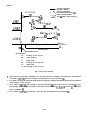
LX-HOO
TECHNICAL MANUAL
—
.—
EPSON
EPSON is a registered trademark of SEIKO EPSON CORPORATION.
IBM is a registered trademark of International Business Machines Corporation.
NOTICE
‘ All rights reserved. Reproduction of any part of this manual in any form
whatsoever without SEIKO EPSON’s express, written permission is forbidden.
The contents of this manual are subject to change without notice.
● All efforts have been made to ensure the accuracy of the contents of this manual.
However, should any errors be detected, SEIKO EPSON would greatly appreciate
being informed of them.
● The above notwithstanding, SEIKO EPSON can assume no responsibility for any
errors in this manual or their consequences.
●
@ Copyright 1987 by SEIKO EPSON CORPORATION
Nagano, Japan
-i-
REV.-A
PRECAUTIONS
Precautionary notations throughout the text are categorized relative to: 1 ) personal injury, and 2) damage
to equipment.
DANGER
Signals a precaution which, if ignored, could result in serious or fatal personal injury.
Great caution should be exercised in performing procedures preceded by DANGER
headings.
WARNING
Signals a precaution which, if ignored, could result in damage to equipment.
The precautionary measures itemized below should always be observed when performing repair/maintenance procedures.
DANGER
1. ALWAYS DISCONNECT THE PRODUCT FROM BOTH THE POWER SOURCE AND THE
HOST COMPUTER BEFORE PERFORMING ANY MAINTENANCE OR REPAIR
PROCEDURE.
2. NO WORK SHOULD BE PERFORMED ON THE UNIT BY PERSONS UNFAMILIAR WITH
BASIC SAFETY MEASURES AS DICTATED FOR ALL ELECTRONICS TECHNICIANS IN
THEIR LINE OF WORK.
3. WHEN PERFORMING TESTING AS DICTATED WITHIN THIS MANUAL, DO NOT
CONNECT THE UNIT TO A POWER SOURCE UNTIL INSTRUCTED TO DO SO. WHEN
THE POWER SUPPLY CABLE MUST BE CONNECTED, USE EXTREME CAUTION IN
WORKING ON POWER SUPPLY AND OTHER ELECTRONIC COMPONENTS.
WARNING
1. REPAIRS ON EPSON PRODUCT SHOULD BE PERFORMED ONLY BY AN EPSON-CERTlFIED REPAIR TECHNICIAN.
2. MAKE CERTAIN THAT THE SOURCE VOLTAGE IS THE SAME AS THE RATED
VOLTAGE, LISTED ON THE SERIAL NUMBER/RATING PLATE. IF THE EPSON
PRODUCT HAS A PRIMARY AC RATING DIFFERENT FROM THE AVAILABLE POWER
SOURCE, DO NOT CONNECT IT TO THE POWER SOURCE.
3. ALWAYS VERIFY THATTHE EPSON PRODUCT HAS BEEN DISCONNECTED FROM THE
POWER SOURCE BEFORE REMOVING OR REPLACING PRINTED CIRCUIT BOARDS
AND/OR INDIVIDUAL CHIPS.
4. IN ORDER TO PROTECT SENSITIVE /.LP CHIPS AND CIRCUITRY, USE STATIC
DISCHARGE EQUIPMENT, SUCH AS ANTI-STATIC WRIST STRAPS, WHEN ACCESSING INTERNAL COMPONENTS.
5. REPLACE MALFUNCTIONING COMPONENTS ONLY WITH THOSE COMPONENTS
RECOMMENDED BY THE MANUFACTURER; INTRODUCTION OF SECOND-SOURCE
ICS OR OTHER NONAPPROVED COMPONENTS MAY DAMAGE THE PRODUCT AND
VOID ANY APPLICABLE EPSON WARRANTY.
- ii -
REV.-A
PREFACE
This manual describes functions, theory of electrical and mechanical operations, maintenance, and repair of the LX-800.
The instructions and procedures included in this document are intended for
the experienced repair technician, who should pay attention to the precautions
on the preceding page. The chapters are organized as follows:
Chapter 1 —
Provides a general product overview, lists specifications, and
illustrates the main components of the printer
—
Chapter 2 —
Describes the theory of printer operation
Chapter 3 —
Discusses the options
Chapter 4 —
Includes a step-by-step guide for product disassembly, assembly, and adjustment
Chapter 5 —
Chapter 6 —
Provides Epson-approved techniques for troubleshooting
Describes preventive maintenance techniques and lists lubricants and adhesives required to service the equipment
●
The contents of this manual are subject to change without notice.
- iv -
REVISION SHEET
IREVISION I DATE ISSUED
CHANGE DOCUMENT
1st issue
1-1, 5, 8, 12 through 18
2-2,11, 13,28,30,38 through
42
4-1, 13, 17, 19
5-1, 2, 6
6-1
A-2, 17, 18
-v-
REV.-A
TABLE OF CONTENTS
CHAPTER 1.
CHAPTER 2.
CHAPTER 3.
CHAPTER 4.
CHAPTER 5.
CHAPTER 6.
APPENDIX
GENERAL DESCRIPTION
OPERATING PRINCIPLES
OPTIONAL EQUIPMENT
DISASSEMBLY, ASSEMBLY, AND ADJUSTMENT
TROUBLESHOOTING
MAINTENANCE
- vi -
REV.-A
CHAPTER 1
GENERAL DESCRIPTION
...
1.1 FEATURES . . . . . . . . . . . . . . . . . . . . . . . . . . . . . . . . . . . . . . . . . . . . . . . . . . . . . . . . . . . . . . . . . . . . . . . . . . . . . . . . . . . . . . . . . . . . . . 1-1
...
1.2 INTERFACE . . . . . . . . . . . . . . . . . . . . . . . . . . . . . . . . . . . . . . . . . . . . . . . . . . . . . . . . . . . . . . . . . . . . . . . . . . . . . . . . . . . . . . . . . . . . 1-3
..
1.3 SPECIFICATIONS . . . . . . . . . . . . . . . . . . . . . . . . . . . . . . . . . . . . . . . . . . . . . . . . . . . . . . . . . . . . . . . . . . . . . . . . . . . . . . . . . . 1-6
.
1.4 OPERATING CONTROLS . . . . . . . . . . . . . . . . . . . . . . . . . . . . . . . . . . . . . . . . . . . . . . . . . . . . . . . . . . . . . . . . . . . .1-12
1.4.1 Dip Switch and Jumper Settings . . . . . . . . . . . . . . . . . . . . . . . . . . . . . . . . . . . . . . . . . .1-12
1.4.2 Control Panel (and Auto Sheet Load Function) . . . . . . . . . . . . . . . . 1-14
1.4.3 Self Test and Hexadecimal Dump Functions . . . . . . . . . . . . . . . . . . . . 1-15
—. —
. . . . . . . . . . . . . . . . . . . . . . . . . . . . . . . . . 1-16
1.4.4 SeiecType Function . . . . . . . . . . . . . . . . . . . . . . . . . . . . . . . . . . . .—.
1.4.5 Buzzer and Error Functions . . . . . . . . . . . . . . . . . . . . . . . . . . . . . . . . . . . . . . . . . . . . . . . . . . . . . .1-17
1.4.6 Printer Initialization and Default Values . . . . . . . . . . . . . . . . . . . . . . . . . . . . 1-17
1.5 MAIN COMPONENTS . . . . . . . . . . . . . . . . . . . . . . . . . . . . . . . . . . . . . . . . . . . . . . . . . . . . . . . . . . . . . . . . . . . . . . . . . . . 1-18
1.5.1 Printer Mechanism Model-3A10 . . . . . . . . . . . . . . . . . . . . . . . . . . . . . . . . . . . . . . . . . . . .1-18
.
1.5.2 ROC Filter Unit. . . . . . . . . . . . . . . . . . . . . . . . . . . . . . . . . . . . . . . . . . . . . . . . . . . . . . . . . . . . . . . . . . . . . . . . . . . .1-19
.
1.5.3 ROCX Board Unit . . . . . . . . . . . . . . . . . . . . . . . . . . . . . . . . . . . . . . . . . . . . . . . . . . . . . . . . . . . . . . . . . . . . . . .1-20
.
1.5.4 LCPNL Board Unit . . . . . . . . . . . . . . . . . . . . . . . . . . . . . . . . . . . . . . . . . . . . . . . . . . . . . . . . . . . . . . . . . . . . . .1-20
..
1.5.5 Housing . . . . . . . . . . . . . . . . . . . . . . . . . . . . . . . . . . . . . . . . . . . . . . . . . . . . . . . . . . . . . . . . . . . . . . . . . . . . . . . . . . . . . . . . .1-21
LIST OF FIGURES
Fig. 1-1.
Exterior View of LX-800 . . . . . . . . . . . . . . . . . . . . . . . . . . . . . . . . . . . . . . . . . . . . . . . . . . . . . . . . . . 1. -1
Fig. 1-2.
Exterior View of LX-800 with Tractor Unit. . . . . . . . . . . . . . . . . . . . . . . 1-2
Fig. 1-3.
Data Transmission Timing of 8-Bit Parallel Interface.... 1-3
Fig. 1-4.
57-30360 36-Pin Connector . . . . . . . . . . . . . . . . . . . . . . . . . . . . . . . . . . . . . . . . . . . . . . . . . . . .1-3
Fig. 1-5.
Printhead Pin Configuration . . . . . . . . . . . . . . . . . . . . . . . . . . . . . . . . . . . . . . . . . . . . . . . . . . .1-6
Fig. 1-6.
Printable Area for Cut Sheet Paper . . . . . . . . . . . . . . . . . . . . . . . . . . . . . . . . . . . . . 1-9
Fig. 1-7.
Printable Area for Roll Paper . . . . . . . . . . . . . . . . . . . . . . . . . . . . . . . . . . . . . . . . . . . . . . . . . .1-9
Fig. 1-8.
Printable Area for Fan Fold Paper . . . . . . . . . . . . . . . . . . . . . . . . . . . . . . . . . . . . . . . . 1-1o
Fig. 1-9.
..
Control Panel . . . . . . . . . . . . . . . . . . . . . . . . . . . . . . . . . . . . . . . . . . . . . . . . . . . . . . . . . . . . . . . . . . . . . . . . . . . . . . 1-14
. -16
Fig. 1-10. SelecType Flow Chart . . . . . . . . . . . . . . . . . . . . . . . . . . . . . . . . . . . . . . . . . . . . . . . . . . . . . . . . . . . . . . 1
Fig. 1-11. Mode13Al O Printer Mechanism . . . . . . . . . . . . . . . . . . . . . . . . . . . . . . . . . . . . . . . . . . . . .1-18
l-i
REV.-A
Fig. 1-12. ROC Filter Unit (120V Version) . . . . . . . . . . . . . . . . . . . . . . . . . . . . . . . . . . . . . . . . . . . . . . 1-19
Fig. 1-13. ROC Filter Unit (220V/240V Versions) . . . . . . . . . . . . . . . . . . . . . . . . . . . . . . . 1-20
.
Fig. 1-14. ROCX Board Unit . . . . . . . . . . . . . . . . . . . . . . . . . . . . . . . . . . . . . . . . . . . . . . . . . . . . . . . . . . . . . . . . . . . . . . . 1-20
.
Fig. 1-15. LCPNL Board Unit . . . . . . . . . . . . . . . . . . . . . . . . . . . . . . . . . . . . . . . . . . . . . . . . . . . . . . . . . . . . . . . . . . . . . . 1-20
..
Fig. 1-16. Housing . . . . . . . . . . . . . . . . . . . . . . . . . . . . . . . . . . . . . . . . . . . . . . . . . . . . . . . . . . . . . . . . . . . . . . . . . . . . . . . . . . . . . . . . .1-21
LIST OF TABLES
.
Table 1-1. LX-800 Options . . . . . . . . . . . . . . . . . . . . . . . . . . . . . . . . . . . . . . . . . . . . . . . . . . . . . . . . . . . . . . . . . . . . . . . . . .1-2
Table 1-2. Connector Pin Assignments and Signal Functions . . . . . . . . 1-4
Table 1-3. Printer Select/Deselect (DC1/DC3) Control . . . . . . . . . . . . . . . . . . . . . 1-5
Table 1-4. Printer Speed, Character Size, and Column Width . . . . . . . . 1-7
.
Table 1-5. Type of Paper . . . . . . . . . . . . . . . . . . . . . . . . . . . . . . . . . . . . . . . . . . . . . . . . . . . . . . . . . . . . . . . . . . . . . . . . . . . . .1-8
. -12
Table 1-6. DIP Switch Settings . . . . . . . . . . . . . . . . . . . . . . . . . . . . . . . . . . . . . . . . . . . . . . . . . . . . . . . . . . . . . . . . 1
Table 1-7. International Character Set . . . . . . . . . . . . . . . . . . . . . . . . . . . . . . . . . . . . . . . . . . . . . . . . . . .1-13
Table 1-8. DIP Switches Factory Settings . . . . . . . . . . . . . . . . . . . . . . . . . . . . . . . . . . . . . . . . . . . . . 1-13
.
Table 1-9. Jumper Setting . . . . . . . . . . . . . . . . . . . . . . . . . . . . . . . . . . . . . . . . . . . . . . . . . . . . . . . . . . . . . . . . . . . . . . . . . .1-13
Iii
REV.-B
1.1
FEATURES
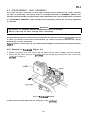
The LX-800 is a multifunctional and high speed serial dot impact printer with a compact body and the
low price.
Features include:
● 180 cps maximum speed (draft-elite), 150 cps (draft-pica)
● Upward compatibility with the LX-86
● Built in two NLQ fonts (Roman and Saris-serif)
● Direct selection of NLQ/Draft modes, and easy selection of 4 typestyle modes with SelecType controls
● Built in IBM graphics characters
● Super/Subscript, Italics, and Elite modes can be supported in NLQ
● Automatic sheet loading function
● A 3K-byte input buffer for improved throughput from the host computer
● Pull tractor feeding
● Optional interface for the EPSON #81 XX series
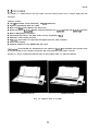
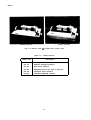
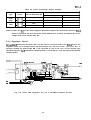
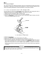
Tw=models of the LX-800 are manufactured. The model for t~e U.S and Australia uses printer cover
A and the model for all countries except the U.S. and Australia uses printer cover B.
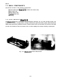
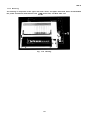
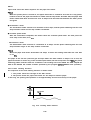
Figures 1-1 and 1-2 show the external view of the LX-800. Table 1-1 lists the options.
(Printer cover B)
(Printer cover A)
Fig. 1-1. Exterior View of LX-800
1-1
REV.-A
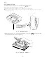
(Printer Cover B)
(Printer Cover A)
Fig. 1-2. Exterior View of LX-800 with Tractor Unit
Table 1-1. LX-800 Options
I
Option
No.
Description
I
#83 1 0
Roll Paper Holder
#81 33
APPLE II Intelligent Interface
#8 143
New Serial Interface
#8 145
#81 48
RS-232C/Current Loop Type 2 InterFace
Intelligent Serial Interface
#8 165
Intelligent IEEE-488 Interface
1-2
REV.-A
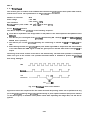
1.2 INTERFACE
The LX-800 has a 8-bit parallel interface as a standard. The specifications for the 8-bit parallel interface
are as follows:
Data Format:
8-bit parallel
Synchronization:
Hand Shaking:
By STROBE pulse
By both ACKNLG and BUSY, or either of them
Logic Level:
ITL (LS type) compatible
Data transmission timing:
See Figure 1-3.
Connector:
57-30360 (AMPHENOL) or equivalent (See Figure 1-4.)
BUSY
ACKNLG
OATA
STROBE
0.5JAS
min.
1= 0.5JAS
min.
“w
O..sus
min.
NOTE: Transmission time (rising and falling time) of every input signal must be less than 0.2Ks.
Fig. 1-3. Data Transmission Timing for 8-Bit Parallel Interface
1.
19. GNO (
Pair with 1.)
2.
20. GNO (
Pair w;tn2.)
3.
Z 1. GNO ( Pair w;th3.)
4.
22. GNO ( Pair wnh4.)
5.
23. GNO (
6.
24. GNO ( Pair w;th6.)
Pair w;tn5.)
7.
25. GNO ( Pair witn7.)
e.
2 6 . GNO ( Pair w;th S . )
9.
27. GNO ( P a i r w;tn9.)
10
2S. GNO ( Pair w:th 1 0 . )
11
2 9 . GND ( Pair with 11. )
12
3 0 . GNO ( Pair witn 1 2 . )
13
31. m
14
32. m
15
3 3 . GNO
16
34. NC
17
3 5 . +5V
18
36. m
Fig.1-4. 57-30360 36-Pin Connector
1-3
REV.-A
Table 1-2 shows the connector pin assignments and signal functions of the 8-bit parallel interface.
Table 1-2. Connector Pin Assignments and Signal Functions
~in No.
Signal Name
Return Pin No.
DIR
Functional Description
1
STROBE
19
In
Strobe pulse to read the input data. Pulse width
must be more than 0.51Js. Input data is latched after
falling edge of this signal.
2
3
4
5
6
7
8
9
DATA 1
DATA2
DATA3
DATA4
DATA5
DATA6
DATA7
DATA8
20
In
21
22
23
24
25
26
27
In
In
In
In
In
In
In
10
ACKNLG
28
out
This pulse indicates data are received and the
printer is ready to accept next data.
Pulse width is approx. 12 KS.
11
BUSY
29
out
HIGH indicates printer can not accept next data.
12
PE
30
out
HIGH indicates paper-out. This signal is effective
only when ERROR signal is “LOW”.
13
SLCT
—
out
Always
14
AUTOFEED-XT
—
In
If the signal is “LOW” when the printer is initialized,
a line feed is automatically performed by input of
“CR” code. (Auto LF)
15
—
—
—
Not used.
16
GND
—
—
Ground for twisted-pair grounding.
17
Chassis GND
—
—
Chassis ground level of printer
18
—
—
—
Not used.
9 to 30
GND
—
—
Ground for twisted-pair grounding.
31
I NIT
16
In
Pulse (width: 50MS min., active “LOW”) input for
printer initialization.
32
ERROR
—
out
LOW indicates that some error has occurred in the
printer.
33
GND
—
.
Ground for twisted-pair grounding
34
—
—
—
Not used.
35
—
—
out
Always “HIGH”. (Pulled up to +5V through a
3.3k-ohm register.)
36
SLCT-IN
—
In
If the signal is “LOW” when printer is initialized, the
DC l/DC3 control is disabled.
1-4
Parallel input data to the printer.
“HIGH” level means data “ 1“.
“LOW” level means data “O”.
“HIGH” output. (Pulled up to +5V through
3.3 K ohms register.)
REV.-B
NOTES 1. “Return” denotes a twisted pair return line connected to signal ground. When interfacing
the printer to the host, use twisted pairs for each signal. Shield the twisted pairs, and connect
the shield to GND in order to reduce interface.
2. All interface conditions are based on TTL levels. Both the rise and fall times of all signals
must be less than 0.2Ks.
3. Refer to the Parallel Interface Timing Chart for the timing of the signals.
4. Data transfer protocol must not ignore the ACKNLG or BUSY signal. (Data can be transferred
either after recognizing the ACKNLG signal or when the BUSY signal is LOW.)
5. The AUTO FEED XT and SLCT IN signals are valid when they are not fixed to LOW level by
the DIP switch or jumper.
6. Printing tests, including those of the interface circuits, can be performed without using
external equipment: set interface connector data lines 1-8 to the desired code (a floating
signal will be a logical 1, and a grounded signal will be a O) connect the ACKNLG signal
to the STROBE signal.
7. The PE signal is valid when the ERROR signal is LOW.
Table 1-3. Printer Select/Deselect (DC—1/DC3) Control
—
SLCT IN Signal State
at Initialization
I
HIGH
Printer
Select/Deselect
Dcl/Dc3
DC 1
I
Select
Data entry
I Enable
Enable (Waits for a DC1. Input data is ignored until a DC 1 code is received.)
DC3
Deselect
DC1
Select
Enable
DC3
Select
Enable
LOW
1-5
REV.-A
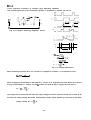
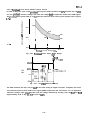
1.3 SPECIFICATIONS
This chapter describes the specifications of the LX-800 printer.
● General Specifications
Serial impact dot matrix
Printing method:
Pin configuration:
9 wires (see Figure 1-5)
Pin diameter:
0.29 mm
Dot Pinch:
0.35 mm (1/72 inch)
#1
#2
()
()
i 0.29mm
t
#3
# 4 <>
0.35mm (1 /72”)
#5
t
#6
( )
#7
#8
#9
Fig. 1-5. Printhead Pin Configuration
Printing direction:
Text mode:
Bi-directional with logic seeking
Bit-image mode:
Uni-directional (left to right)
Dot matrix:
9 X 9 (Draft)
11 X 18 (NQL)
6 X 8 (Graphics)
Character sets:
96 ASCII characters
96 Italic characters
32 International characters
32 International Italic characters
32 Graphics characters
96 IBM Graphics characters
Fonts:
Draft, NLQ-Roman, Saris-serif
Printing speed:
See Table 1-4
Character size:
See Table 1-4
Column width:
See Table 1-4
480 dots/line at 60 dots/inch (Bit-image)
1-6
—.—
REV.-A
Table 1-4. Printing Speed, Character Size, and Column Width
Charecter Size (mm) Column Width Pitch (meximum
Type Style
(maximum Chara- Characters
Font Normal Double Empha- Con- Printing Speed (CPS) Width
Height
cters/LinsCPL)
/inch-CPl)
Width
Draft
(Pica)
0
—
o
—
.
0
—
Draft
(Elite)
—
sized densed
—
150
2.1
3.1
80
10
—
—
75
4.2
3.1
40
5
0
—
75
2.1
3.1
80
10
—
37
4.2
3.1
40
5
—
0
—
o
128
1.05
3.1
132
17
64
2.1
3.1
66
8.5
0
—
o
o
—
—
—
—
180
2.1
3.1
96
12
—
90
4.2
3.1
48
6
—
—
o
150
1.05
3.1
160
20
o
—
—
NLQ
o
—
—
—
Supersubscript
...—
0
—
—
—
25
1.6
Line spacing:
1/6” or Programmable (n/2 16“)
Line feed speed:
Approx. 95ms/line (Line feed)
(1 line = 1/6”)
Approx. 75ms/line (Form feed)
Paper feed method:
Friction feed or Tractor feed
Paper path:
From rear of printer
● Paper Specifications
Type of paper:
See Table 1-5
1-7
REV.-B
Table 1-5. Type of Paper
Size
Thickness
(Width)
(Width)
(Width)
182 mm to 216 mm
101 mm to 254 mm
7. 15“ to 8.5”
4“ to 10”
216 & 3 mm
8.5” & 0.12“
(Length)
(Diameter of roll)
Max. 305 mm
Max. 127 mm
Max. 12“
Max. 5“
0.06 mm to 0.1 mm
Max. 0.25 mm
0.07 mm to 0.09 mm
1 original +2
Copies
Weight
Roll paper
Fan-fold paper
Cut sheet
52g/m2 to 82g/m2
(1 sheet)
52g/m2 to 64g/m2
52g/m2 to 82g/m2
(2 sheets)
35g/m2 to 58g/m2
(3 sheets)
35g/m2 to 58g/m2
for 2 sheets
+
35g/m2 to 47g/m2
for 1 sheet
Feeding method
Friction feed
Tractor feed
Friction feed
Precautions
1. Do not use continuous
1. Release the friction
1. Use the Roll paper
form or copy paper.
2. Dismount the Tractor
unit.
mechanism using the
release lever.
2. Use the pressure sensitive paper for copying. Be sure that perforations have a smooth
finsh.
1-8
holder.
2. Dismount the Tractor
unit.
REV.-A
Printable area:
See Figures 1-6 through 1-8
7.1 5“ - 8.50/182 mm - 216 mm
0.1 2“, 3 g
or more
I-
0.1 2“, 3 mm
=more
I
I
I
mm
0.87”, :
T
or n m
1
7 F
r
i
n
t
a
1 2“”,
b
305 mm t
e
—
Printable area
T
XYZ
ABC
T
.—
a
r
e
a
L
XYZ
J
ABC
L
,3(
1 .2’.
or mor
lm
Fig. 1-6. Printable Area for Cut Sheet Paper
8.5”, 216 mm
●
0.1 2“/3 mm
‘or more
Printable area
0.1 2“/3 mm–
or more
0.98”/25 mm
or more
!
XYZ
ABC
Fig. 1-7. Printable Area for Roll Paper
1-9
REV.-A
4“ - 10 ”/101 mm - 254 mm
L
R
Printable area
7
0
0
0
0
0
0
0
o
Printable
area
/
0.35 ”/9 mm
or more
4
0.35 ”/9 mm
or more
0
0
0
0
o
0
0
1:
1-
XYZ
T
XYZ :
7 0
ABC
o
0
0
0- - - - - - - - - - - - - - - - - - - - - - - - - - 00
0
0
0
0
o ABC
i
Printabh
area
o
0
0
0
0
0
0
0
0
0
0
0
0
L: 0.75”/19 mm [PaDer width is less than 9.5”/241 mm)
1.02”)26 mm ~Paper width is more than 9.5 ”/241 mm)
R: 0.75”/19 mm (Paper width is less than 9.5 ”/241 mm)
0.94”/24 mm (Paper width is more than 9.5 ”/241 mm)
Fig. 1-8. Printable Area for Fan Fold Paper
Ribbon Cartridge
Cartridge number:
#8750
Color:
Black
Life:
3 million characters (14 dots/character)
Electrical Specifications
120VAC + 10%
Power Voltage:
220/240VAC * 1 0 %
Frequency range:
59.5Hz to 60.5Hz (120VAC)
49.5Hz to 60.5Hz (220/240VAC)
Power consumption: Max. 70VA
Insulating resistance: More than 10M ohms
(between the AC line and chassis)
Dielectric strength:
1 KVAC rms/minute or 1.2KVAC rms/second
between AC line and chassis (120V)
1.25 kVAC rms/minute or 1.5 kVAC rms/second
between AC line and chassis (220/240V)
1-1o
REV.-A
● Environmental Specifications
Temperature:
–30”C to 60 ”C/–22°F to 149°F (Storage)
5°C to 35”C/4 1“F to 95°F (Operating)
Humidity:
5% to 85%RH, no condensation (Storage)
10% to 80%RH, no condensation (Operating)
Resistance to shock:
2G, 1 ms (Storage)
IG, 1 ms (Operating)
Resistance to vibration:
0.50G, max. 55Hz (Storage)
0.25G, max 55Hz (Operating)
● Reliability
MCBF:
3 million lines (Printer mechanism except the printhead)
MTBF:
4000 hours
Life of printhead:
200 million strokes/needle
● Safety Approvals
. safety Standards:
—
UL 478 (U. S.A.)
CSA 22.2 No. 0.154 (Canada)
VDE 0806 (West Germany)
RFI:
FCC class B (U. S.A.)
VDE 0871 (West Germany)
● Physical
Dimensions:
91 mm (height)
(Refer to Figure A-19)
377 mm (width)
399 mm (width including paper feed knob)
308 mm (depth)
Weight:
5.1 kg
1-11
REV.-B
1.4 OPERATING CONTROLS
This section describes the operating controls of LX-800 printer.
1.4.1 DIP Switch and Jumper Settings
The DIP switches that users can set are SW1 and SW2. These switches are positioned at the rear center
of the printer and have the functions shown in Tables 1-6 through 1-8. (Note: the
status of the DIP
switches is read only when at power on or at input of the INIT signal).
Table 1-6. DIP Switch Settings
Function
DIP SW
ON
OFF
1-1
Typeface select
Condensed
Normal
1-2
ZERO font select
0
0
1-3
Character Table select
I
Graphic
I
Italic
1-4 I Paper-out detection
I
Valid
I
invalid
1-5 I Printing quality select
I
NLQ
I
Draft
1-6
1-7
International character set select
See Table 1-7
1-8
2-1
Page length select
12“
1 1“
2-2
Cut sheet feeder mode
Valid
Invalid
2-3
1“ skip over perforation
Valid
Invalid
2-4
AUTO FEED XT control
Fix to LOW
Depends on external signal
1-12
REV.-B
Table 1-7. International Character Set
?SW 1-6
Sw 1-7
SW 1-8
U.S.A.
ON
ON
ON
FRANCE
ON
ON
OFF
GERMANY
ON
OFF
ON
U.K.
ON
OFF
OFF
DENMARK
OFF
ON
ON
Country
I
SWEDEN
OFF
I
ON
I
OFF
ITALY
OFF
OFF
ON
SPAIN
OFF
OFF
OFF
I
Table 1-8. DIP Switches Factory Settings
DIP SW No.
1-1
1-2
1-3
1-4
1-5
1-6
1-7
1-8
2-1
2-2
2-3
2-4
U. S.A., Southeast Asia,
Middle and Near East
OFF
OFF
OFF
OFF
OFF
ON
ON
ON
OFF
OFF
OFF
OFF
Germany,
OFF
OFF
OFF
OFF
OFF
ON
OFF
ON
ON
OFF
OFF
OFF
U. K., Australia
OFF
OFF
OFF
OFF
OFF
ON
OFF
OFF
OFF
OFF
OFF
OFF
France, Italy, Spain
OFF
OFF
ON
OFF
OFF
ON
ON
ON
OFF
OFF
OFF
OFF
Country
Northern Europe
Jumper J 1 on the ROCX board has the function and factory setting shown in Table 1-9.
Table 1-9. Jumper Setting
Jumper
J1
Function
SLCT IN control
Open
Close
Factory setting
Depends on external signal
Fix to LOW
Open
1-13
REV.-B
1.4.2 Control Panel (and Auto Sheet Load Function)
Figure 1-9 shows the control panel of LX-800 printer.
a
b
c
d
e
f
9
Fig. 1-9. Control Panel
The functions of the LEDs and switches are:
a. POWER LED (green)
Lights when the power switch is turned on and AC power is applied.
b. READY LED (green)
Lights when the printer is ready to receive data.
c. PAPER OUT LED (red)
Lights when the printer runs out of paper.
d. ON LINE LED (green)
Lights when the printer is ON-LINE.
e. ON/OFF LINE Switch (non-locking push switch)
Switches between the ON-LINE and OFF-LINE modes.
The printer is automatically set ON-LINE and becomes ready when power is turned on. If the printer
is set OFF-LINE, printing is stopped and the printer enters the busy state.
f,
NLQ/FORM FEED Switch (non-locking push switch)
● When this switch is pressed once in the OFF-LINE mode, the paper is advanced vertically to the
top of form on the next page.
● When this switch is pressed in the ON-LINE mode, the NLQ-Roman or NLQ-Sans-serif fonts are
selected, and the buzzer sounds to inform the user which font is selected.
Two beeps
NLQ-Roman:
NLQ-Sans-serif:
Three beeps
1-14
REV.-B
g. DRAFT/LINE FEED and AUTO LOAD Switch (non-locking push switch)
● When this switch is pressed once in the OFF-LINE mode, the paper is advanced vertically one line,
and the paper advanced continuously while this switch is pressed.
● When this switch is pressed in the ON-LINE mode, the Draft font is selected, and beeps once a
buzzer to inform the Draft font is selected.
● Cut sheets are automatically loaded when the paper is placed at the sheet guide, printer is paper
out, OFF-LINE state and the this switch is pressed.
1.4.3 Self Test and Hexadecimal Dump Functions
The conditions of LX-800 may be checked via the self test functions. The self test checked:
● Circuit
● Printer mechanism
● Printing quality
● ROM (firmware) code number
The code number of ROM is printed on the first line of the self test.
To start the self test in either the Draft mode or NLQ mode,+urn the power on while pressing the
DRAFT/LINE FEED or NLQ/FORM FEED switch, respectively. In the NLQ self test mode, both Roman font
and Saris-serif font are printed every other line. When the DIP switch 1-5 set to on (NLQ mode), only
NLQ mode self test is performed, no related switches. To stop the self test, turn the power off by power
switch.
The conditions of data transmission between LX-800 and the host computer may be checkedvia the
hexadecimal dump functions. To set the hexadecimal dump mode, turn the power while pressing the
both LINE FEED and FORM FEED switches. Then the message “Data Dump Mode” is printed.
The printer prints 16 hexadecimal values, followed by the corresponding ASCII characters. If there is
no corresponding printable characters for a value (e.g. a control code), a period (.) is printed. One line
is printed for each set of 16 values received, and any remaining data (less than 16 values) can be printed
by pushing the ON/OFF LINE switch.
To cancel the hexadecimal dump mode, turn the power off by power switch.
1-15
REV.-B
1.4.4 SelecType Function
SelecType is a feature of the LX-800 which permits type style programming via the control panel
switches without software assistance.
In the SelecType mode, following 4 type styles can be selected:
● Emphasized
● Double-strike
● Condensed
● Elite
Figure 1-10 shows the operation flow chart of SelecType function:
< ENTER >
Hold down ON/OFF LINE SW, and
press NLQ/FORM FEED SW. (Printer beeps once and ON-LINE LED
starts blinking.)
< Select the type style >
I
I
Press ON\OFF LINE SW the number of times indicated below for the mode. (Pay attention to the number
of beeps the printer makes when the buzzer sounds.)
1
Emphasized
3
I 2 I Double-striked
I 4 I
Condensed
Elite
I
I
<
Set type style >
Press FORM FEED SW.
N
]Y
< EXIT >
I
Press LINE FEED SW.
I
I
I
OFF-LINE
I
Fig. 1-10. SelecType Flow Chart
1-16
REV.-B
1.4.5 Buzzer and Error Functions
The buzzer rings under the following circumstances:
● When a BEL code is sent to the printer, the buzzer
rings once (for 0.1 sec.).
● When the NLQ Roman font is set using the FORM FEED switch, the buzzer
rings twice (for 0.1 sec. each, with 0.1 sec. pause between rings).
● When the NLQ Saris serif font is set using the NLQ/FORM FEED switch, the buzzer
rings three times (for O. 1 sec. each, with O. 1 sec. pause between rings).
● When the Draft font is set using the DRAFT/LINE FEED switch, the buzzer
rings once (for O. 1 sec.).
● When the printer enters the SelecType mode, the buzzer
rings once (for O. 1 sec.).
● When paper out is detected, the buzzer
rings eight times (for 0.5 sec. each, with 0.5 sec. pause between rings).
● When abnormal carriage operation is detected (hardware error), the buzzer
rings five times (for 0.5 sec. each, with 0.5 sec. pause between rings).
● ✍ -W—hen abnormal voltage is detected (hardware error), the buzzer
.—
rings five times (for 0.5 sec. each, with 0.5 sec. pause between rings).
When the paper end sensor detects paper out, the state of the interface changes as follows:
ERROR signal ~ LOW
BUSY signal ~ HIGH
PE signal+ HIGH
The printer enters an error state when any of the following occurs:
a. Home position is not detected after the printer mechanism has been initialized (home position
seek).
b. The +24V voltage (which is used to drive the printhead and motors) rises to +27V or more.
When the printer enters an error state, the printer stops the printing, and the state of the interface
changes as follows:
ERROR signal ~ LOW
BUSY signal ~ HIGH
1.4.6 Printer Initialization and Default Values
The LX-800 initialized when any of the following occurs.
● The power switch is turned on.
● Intetiace signal INIT goes low.
When the printer is initialized, the following operations are performed:
a. Seek to carriage home position.
b. Set to ON-LINE mode.
c. Clear the all buffers.
d. Set the line spacing to 1/6 inches.
e. Set the page length to 11 or 12 inches, according to the DIP switch.
f. Clear all vertical tab positions.
9“ Set the horizontal tab position to every 8 columns.
i. Set the print mode according to the DIP switches.
1-17
REV.-B
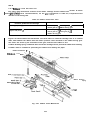
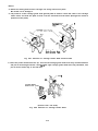
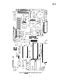
1.5 MAIN COMPONENTS
The LX-800 consists of the following components:
● Printer Mechanism Model-3A10 (include the Tractor Unit)
● ROC Filter Unit
● ROCX Board Unit
● LCPNL Board Unit
● Housing
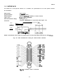
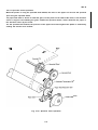
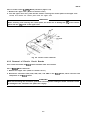
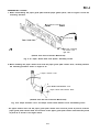
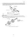
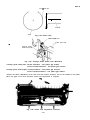
1.5.1 Printer Mechanism Model-3A10
The Model-3A10 printer mechanism was developed expressly for use with LX-800 printer: the
components include a carriage motor, carriage mechanism, paper feed motor, paper feed mechanism,
ribbon feed mechanism, printhead, sensors, and the tractor unit. For the tractor unit, there are two tabs
on both side frames to allow the printer cover to float slightly when tractor feeding is performed.
Fig. 1-11. Model-3A10 Printer Mechanism
1-18
REV.-A
1.5.2 ROC Filter Unit
The ROC filter unit contains a power cord ( 120 V version) or AC inlet (220/240 V version), power switch,
fuse, filter circuit, and power transformer.
..—
Fig. 1-12. ROC Filter Unit (120V version)
Fig. 1-13. ROC Filter Unit (220 V/240V versions)
1-19
REV.-A
1.5.3 ROCX Board Unit
The ROCX board contains the main control circuit, driver circuit, and voltage regulator circuit. The main
ICS on the ROCX boards are the pPD78 10HG CPU and the E05A03 gate array which controls everything.
/
\----=-.
Y
Fig. 1-14. ROCX Board Unit
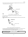
1.5.4 LCPNL Board Unit
The LCPNL board unit is a control panel of LX-800 which contains the indicator LEDs, switches and
buzzer.
Fig. 1-15. LCPNL Board Unit
1-20
REV.-A
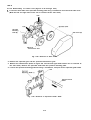
1.5.5 Housing
The housing is comprised of the upper and lower cases, and paper feed knob, which accommodate
the printer mechanism, ROCX board unit, LCPNL board unit, and ROC filter unit.
Fig. 1-16. Housing
1-21
REV.-A
CHAPTER 2
OPERATING PRINCIPLES
2.1 GENERAL . . . . . . . . . . . . . . . . . . . . . . . . . . . . . . . . . . . . . . . . . . . . . . . . . . . . . . . . . . . . . . . . . . . . . . . . . . . . . . . . . . . . . . . . . . . . . . . . . . . 2-1
....
2.2 CABLE CON NECTIONS....... . . . . . . . . . . . . . . . . . . . . . . . . . . . . . . . . . . . . . . . . . . . . . . . . . . . . . . . . . . . . . 2-3
2-3
2.3 POWER SUPPLY CIRCUIT
2.3.1 ROC Filter Unit. . . . . . . . . . . . . . . . . . . . . . . . . . . . . . . . . . . . . . . . . . . . . . . . . . . . . . . . . . . . . . . . . . . . . . . . . . . . . 2-3
2.3.1.1 Fuse and Filter Circuit . . . . . . . . . . . . . . . . . . . . . . . . . . . . . . . . . . . . . . . . . . . . . . . . . . . . 2-4
2.3.1.2 Power Transformer . . . . . . . . . . . . . . . . . . . . . . . . . . . . . . . . . . . . . . . . . . . . . . . . . . . . . . . ..2-4
.
2.3.2 Regulator Circuit . . . . . . . . . . . . . . . . . . . . . . . . . . . . . . . . . . . . . . . . . . . . . . . . . . . . . . . . . . . . . . . . . .. 2-5
......
2.3.2.1 Operation Principles of Chopper
Type Switching Regulator...............................................2.6
. -7
2.3.2.2 +24V Supply Circuit . . . . . . . . . . . . . . . . . . . . . . . . . . . . . . . . . . . . . . . . . . . . . . . . . . . . . . 2
2.3.2.3 +5V Supply Circuit . . . . . . . . . . . . . . . . . . . . . . . . . . . . . . . . . . . . . . . . . . . . . . . . . . . . . . .. .2-8
2.4 CONTROL CIRCUIT........ . . . . . . . . . . . . . . . . . . . . . . . . . . . . . . . . . . . . . . . . . . . . . . . . . . . . . . . . . . . . . . . . . . . . . . . . 2-9
2.4.1 Functions of the CPU . . . . . . . . . . . . . . . . . . . . . . . . . . . . . . . . . . . . . . . . . . . . . . . . . . . . . . . . . . . . . . . . 2-11
2.4.2 E05A03 Gate Array Functions . . . . . . . . . . . . . . . . . . . . . . . . . . . . . . . . . . . . . . . . . . . . . .. 2-14
....
2.4.3 Data Flow . . . . . . . . . . . . . . . . . . . . . . . . . . . . . . . . . . . . . . . . . . . . . . . . . . . . . . . . . . . . . . . . . . . . . . . . . . . . . . . . . . . . .2-18
2.4.3.1
.
Initialization . . . . . . . . . . . . . . . . . . . . . . . . . . . . . . . . . . . . . . . . . . . . . . . . . . . . . . . . . . . . . . . . . . . . . . .2-19
2.4.3.2 Print Data Processing . . . . . . . . . . . . . . . . . . . . . . . . . . . . . . . . . . . . . . . . . . . . . . . . . . . . .2 -20
2.4.4 Reset Circuit . . . . . . . . . . . . . . . . . . . . . . . . . . . . . . . . . . . . . . . . . . . . . . . . . . . . . . . . . . . . . . . . . . . . . . . . . . . . . . . . . 2-22
..
2.4.5 Carriage Motor . . . . . . . . . . . . . . . . . . . . . . . . . . . . . . . . . . . . . . . . . . . . . . . . . . . . . . . . . . . . . . . . . . . . . . . . . . . 2-23
2.4.5.1 Home Position Sensor . . . . . . . . . . . . . . . . . . . . . . . . . . . . . . . . . . . . . . . . . . . . . . . . . . . . . 2-23
2.4.5.2 Carriage Motor Control . . . . . . . . . . . . . . . . . . . . . . . . . . . . . . . . . . . . . . . . . . . . . .. 2-24
...
2.4.5.3 Home Position Seek. . . . . . . . . . . . . . . . . . . . . . . . . . . . . . . . . . . . . . . . . . . . . . . . . . . . . . . .. 2-26
2.4.5.4 Carriage Motor Drive Circuit . . . . . . . . . . . . . . . . . . . . . . . . . . . . . . . . . . . . . . . . 2-27
2.4.6 Paper Feed Motor . . . . . . . . . . . . . . . . . . . . . . . . . . . . . . . . . . . . . . . . . . . . . . . . . . . . . . . . . . . . . . . . . . 2-27
.....
2.4.6.1 Paper End Sensor . . . . . . . . . . . . . . . . . . . . . . . . . . . . . . . . . . . . . . . . . . . . . . . . . . . . . . . . . . . . . 2-29
2.4.6.3 Paper Feed Motor Control . . . . . . . . . . . . . . . . . . . . . . . . . . . . . . . . . . . . . . . . . . . . . 2-29
.
2.4.6.3 Auto Loading Function . . . . . . . . . . . . . . . . . . . . . . . . . . . . . . . . . . . . . . . . . . . . . . . . ..2-30
2.4.6.4 Paper Feed Motor Drive Circuit . . . . . . . . . . . . . . . . . . . . . . . . . . . . . . . . . . 2-31
..
2.4.7 Printhead . . . . . . . . . . . . . . . . . . . . . . . . . . . . . . . . . . . . . . . . . . . . . . . . . . . . . . . . . . . . . . . . . . . . . . . . . . . . . . . . . . . . . .2-32
2.4.7.1 Printhead
Control . . . . . . . . . . . . . . . . . . . . . . . . . . . . . . . . . . . . . . . . . . . . . . . . . . . . . . . . . . . . 2. -32
2.4.7.2 Printhead Drive Pulse Width Control Circuit . . . . . . . . . 2-33
2.4.7.3 Printhead Drive Circuit . . . . . . . . . . . . . . . . . . . . . . . . . . . . . . . . . . . . . . . . . . . . . . . . . .2 -34
Z.i
REV.-A
2.4.8 Print Timing Control . . . . . . . . . . . . . . . . . . . . . . . . . . . . . . . . . . . . . . . . . . . . . . . . . . . . . . . . . . . . . . . . . 2. -34
2.4.8.1 Print Timing Control for the
..
Carriage and Printhead . . . . . . . . . . . . . . . . . . . . . . . . . . . . . . . . . . . . . . . . . . . . . . . . . .2-34
2.4.8.2 Bidirectional Logic Seeking . . . . . . . . . . . . . . . . . . . . . . . . . . . . . . . . . . . . . . . . . . . 2-35
2.5 PRINTER MECHANISM OPERATION . . . . . . . . . . . . . . . . . . . . . . . . . . . . . . . . . . . . . . . . . . . . . . 2-37
.
2.5.1 Sensor Mechanism . . . . . . . . . . . . . . . . . . . . . . . . . . . . . . . . . . . . . . . . . . . . . . . . . . . . . . . . . . . . . . . . . . . .2-37
2.5.2 Carriage Mechanism . . . . . . . . . . . . . . . . . . . . . . . . . . . . . . . . . . . . . . . . . . . . . . . . . . . . . . . . . . . . . . . . . 2. -38
2.5.3 Paper Feed Operation . . . . . . . . . . . . . . . . . . . . . . . . . . . . . . . . . . . . . . . . . . . . . . . . . . . . . . . . . . . . . . . 2. 4 0
2.5.3.1 Friction Feed Operation . . . . . . . . . . . . . . . . . . . . . . . . . . . . . . . . . . . . . . . . . . . . . . . . . .2 4 0
2.5.3.2 Sprocket Feed Operation . . . . . . . . . . . . . . . . . . . . . . . . . . . . . . . . . . . . . . . . . . . . . . . 2-40
. 42
2.5.4 Ribbon Feed Mechanism . . . . . . . . . . . . . . . . . . . . . . . . . . . . . . . . . . . . . . . . . . . . . . . . . . . . . . . . . . 2
LIST OF FIGURES
.
Fig. 2-1. Cable Connections . . . . . . . . . . . . . . . . . . . . . . . . . . . . . . . . . . . . . . . . . . . . . . . . . . . . . . . . . . . . . . . . . . . . .2-2
Fig. 2-2. Power Supply Circuit Block Diagram . . . . . . . . . . . . . . . . . . . . . . . . . . . . . . . . . . 2-3
.. 4
Fig. 2-3. Filter Circuit . . . . . . . . . . . . . . . . . . . . . . . . . . . . . . . . . . . . . . . . . . . . . . . . . . . . . . . . . . . . . . . . . . . . . . . . . . . . . . . . 2
Fig. 24. Power Transformer . . . . . . . . . . . . . . . . . . . . . . . . . . . . . . . . . . . . . . . . . . . . . . . . . . . . . . . . . . . . . . . . . . . .2. 4
Fig. 2-5.
+24V/+5V DC Regulator and
+ 12V Half-Wave Rectifier Circuits . . . . . . . . . . . . . . . . . . . . . . . . . . . . . . . . . . . . . . 2-5
Fig. 2-6. Chopper Switching Regulator Circuit . . . . . . . . . . . . . . . . . . . . . . . . . . . . . . . . . . 2-6
.
Fig. 2-7 Voltage Waveforms . . . . . . . . . . . . . . . . . . . . . . . . . . . . . . . . . . . . . . . . . . . . . . . . . . . . . . . . . . . . . . . . . . . .2-6
.
Fig. 2-8 +24V Supply Circuit . . . . . . . . . . . . . . . . . . . . . . . . . . . . . . . . . . . . . . . . . . . . . . . . . . . . . . . . . . . . . . . . .2-7
Fig. 2-9 IC494 Block Diagram and Switching Waveform . . . . . . . . . . . . . 2-7
.
Fig. 2-10 +5V Supply Circuit . . . . . . . . . . . . . . . . . . . . . . . . . . . . . . . . . . . . . . . . . . . . . . . . . . . . . . . . . . . . . . . . . . . .2-8
Fig. 2-11. Control Cirucit Block Diagram . . . . . . . . . . . . . . . . . . . . . . . . . . . . . . . . . . . . . . . . . . . . . . .2-10
. -14
Fig. 2-12. E05A03 Block Diagram . . . . . . . . . . . . . . . . . . . . . . . . . . . . . . . . . . . . . . . . . . . . . . . . . . . . . . . . . . . 2
Fig. 2-13. LX-800 Memory Map . . . . . . . . . . . . . . . . . . . . . . . . . . . . . . . . . . . . . . . . . . . . . . . . . . . . . . . . . . . . . . . . 2. -18
.
Fig. 2-14. Initialization Flow . . . . . . . . . . . . . . . . . . . . . . . . . . . . . . . . . . . . . . . . . . . . . . . . . . . . . . . . . . . . . . . . . . . . . . .2-19
.
Fig. 2-15. Print Data Flow . . . . . . . . . . . . . . . . . . . . . . . . . . . . . . . . . . . . . . . . . . . . . . . . . . . . . . . . . . . . . . . . . . . . . . . . . .2-20
..
Fig. 2-16. Line Buffer . . . . . . . . . . . . . . . . . . . . . . . . . . . . . . . . . . . . . . . . . . . . . . . . . . . . . . . . . . . . . . . . . . . . . . . . . . . . . . . . . . . 2-21
Fig. 2-17. Reset Circuit . . . . . . . . . . . . . . . . . . . . . . . ... . . . . . . . . . . . . . . . . . . . . . . . . . . . . . . . . . . . . . . . . . . . . . . . . . . . . . . .2 -22
Fig. 2-18. Home Position Sensor Circuit . . . . . . . . . . . . . . . . . . . . . . . . . . . . . . . . . . . . . . . . . . . . . . . . .2-23
Fig. 2-19. Basic Phase Switching Patterns . . . . . . . . . . . . . . . . . . . . . . . . . . . . . . . . . . . . . . . . . . . 2-24
Fig. 2-20. Basic Operation Sequence . . . . . . . . . . . . . . . . . . . . . . . . . . . . . . . . . . . . . . . . . . . . . . . . . . . . . . .2 -24
Fig. 2-21. Home Position Seek Operation Flow . . . . . . . . . . . . . . . . . . . . . . . . . . . . . . . . . . . 2-26
Fig. 2-22. Carriage Motor Drive Circuit . . . . . . . . . . . . . . . . . . . . . . . . . . . . . . . . . . . . . . . . . . . . . . . . . .2-27
Fig. 2-23. Paper End Sensor Circuit . . . . . . . . . . . . . . . . . . . . . . . . . . . . . . . . . . . . . . . . . . . . . . . . . . . . . . . . .2 -28
2-ii
REV.-A
Fig. 2-24. Paper End Detection Area . . . . . . . . . . . . . . . . . . . . . . . . . . . . . . . . . . . . . . . . . . . . . . . . . . . . . . .2 -28
Fig. 2-25. Phase Switching Basic Pattern . . . . . . . . . . . . . . . . . . . . . . . . . . . . . . . . . . . . . . . . . . . . . 2-29
Fig. 2-26. Basic Operation Sequence ................... mm.m.o.m..mm........ ".".a".""""""..- 2-29
. -30
Fig. 2-27. Printing Start Position . . . . . . . . . . . . . . . . . . . . . . . . . . . . . . . . . . . . . . . . . . . . . . . . . . . . . . . . . . . . . 2
Fig. 2-28. Paper Feed Motor Drive Circuit . . . . . . . . . . . . . . . . . . . . . . . . . . . . . . . . . . . . . . . . . . . . . 2-31
Drive Pulse Pattern . . . . . . . . . . . . . . . . . . . . . . . . . . . . . . . . . . . . . . . . . . . . . . . . 2-32
Fig. 2-30. Printhead Drive Pulse Width Range . . . . . . . . . . . . . . . . . . . . . . . . . . . . . . . . . . . . 2-33
Fig. 2-29. Printhead
Fig. 2-31. +24V DC Monitor Circuit..................................................".."". 2-33
Fig. 2-32. Printhead
. -34
Drive Circuit . . . . . . . . . . . . . . . . . . . . . . . . . . . . . . . . . . . . . . . . . . . . . . . . . . . . . . . . . . . . 2
Fig. 2-33. Solenoid Current and Drive
.
Voltage Waveforms . . . . . . . . . . . . . . . . . . . . . . . . . . . . . . . . . . . . . . . . . . . . . . . . . . . . . . . . . . . . . . . . . . .2-34
Fig. 2-34. The Relationship Between the Carriage
...
and Control Signals . . . . . . . . . . . . . . . . . . . . . . . . . . . . . . . . . . . . . . . . . . . . . . . . . . . . . . . . . . . . . . . . . . . 2-35
.
Fig. 2-35. Logic Seeking . . . . . . . . . . . . . . . . . . . . . . . . . . . . . . . . . . . . . . . . . . . . . . . . . . . . . . . . . . . . . . . . . . . . . . . . . . . . . .2-36
Fig. 2-36. Printer Mechanism External View (Model-3A10) . . . . . . . . . . . . 2-37
Fig. 2-37. Carriage Mechanism . . . . . . . . . . . . . . . . . . . . . . . . . . . . . . . . . . . . . . . . . . . . . . . . . . . . . . . . . . . . . . . . . 2. -38
Fig. 2-38. Printhead Printing Operation . . . . . . . . . . . . . . . . . . . . . . . . . . . . . . . . . . . . . . . . . . . . . . .. .2-39
.
. -40
Fig. 2-39. Friction Feed Operation . . . . . . . . . . . . . . . . . . . . . . . . . . . . . . . . . . . . . . . . . . . . . . . . . . . . . . . . . . . 2
Fig. 2-40. Sprocket Feed Operation . . . . . . . . . . . . . . . . . . . . . . . . . . . . . . . . . . . . . . . . . . . . . . . . . . . . . . . . . .2-41
Fig. 2-41. Ribbon Feed Mechanism . . . . . . . . . . . . . . . . . . . . . . . . . . . . . . . . . . . . . . . . . . . . . . . . . . . . . . . . . .2 -42
LIST OF TABLES
.
Table 2-1. Voltage Types and Applications . . . . . . . . . . . . . . . . . . . . . . . . . . . . . . . . . . . . . . . . . . . 2-3
Table 2-2. Power Transformer Output Voltages . . . . . . . . . . . . . . . . . . . . . . . . . . . . . . . . . . 2-11
Table 2-3. CPU Port Assignments . . . . . . . . . . . . . . . . . . . . . . . . . . . . . . . . . . . . . . . . . . . . . . . . . . . . . . . . . . . . 2-11
.
Table 24. E05A03 Functions . . . . . . . . . . . . . . . . . . . . . . . . . . . . . . . . . . . . . . . . . . . . . . . . . . . . . . . . . . . . . . . . . . . .2-16
Table 2-5. E05A03 Port Assignments . . . . . . . . . . . . . . . . . . . . . . . . . . . . . . . . . . . . . . . . . . . . . . . . . . . . .2 -17
Table 2-6. Ribbon Feed Gear Train . . . . . . . . . . . . . . . . . . . . . . . . . . . . . . . . . . . . . . . . . . . . . . . . . . . . . . . . . . .2 4 2
2-iii
REV.-A
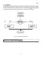
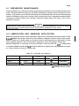
2.1 GENERAL
This chapter describes the component connections, specifications and operation of the power supply
circuit section, the software for the control circuit section, and the operation of the hardware and the
printer mechanism.
Please note that the following units are assumed when omitted in this chapter.
Resistor:
Units are Ohms.
Capacitor:
Units are Farads.
The components listed below are referred to as follows:
ROCX board: Main board
LCPNL board: Control panel
Model-3Al O: Printer mechanism
.—
—
2-1
REV.-B
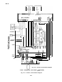
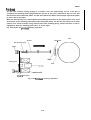
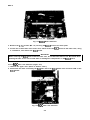
2.2 CABLE CONNECTIONS
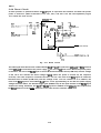
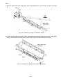
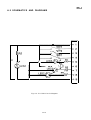
Figure 2-1 shows the interconnection of the primary components, with the main board at the center.
I1
MODEL-3A1O PRINTER MECHANISM
I
J
CR
PRINT
HEAD
PAPER
END
HOME
Posh ON
‘f;OuOTjR
II
CN5
CN4
I
12pin
12pin
c @
“~ z
N v
L
ROCX BOARD
ET= 1
g .g
Vcn
BOARD) m~
(MAIN
A
‘zc hz
.= N
n z
g u b
c co
‘~ z /
* u
36pin
CN1
8-BIT
PARALLEL
l/F
r
I
1 #8100 SERIES I
I l/F BOARD
I
A—- - - -—1
/1
R
ROCK FILTER UNIT
AC120V
AC220V
AC240V
(POWER TRANSFORMER
AND FILTER)
Ail 20V
AC220V
AC240V
Fig. 2-1. Cable Connections
The ROCX board connectors are as follows:
CN 1 : 8-bit parallel interface connector. Used for data communication with the host computer.
CN2: Connector for the #8 100 series optional interface
CN3: Receives data from the LCPNL board switches, and outputs the signals to the LEDs and the
buzzer.
CN4: Outputs data to the printhead.
CN5: Outputs the control signals and drive voltages to the paper feed and carriage motors.
CN6: Receives the paper end signal from the printer mechanism.
CN7: Receives the home position signal from the printer mechanism.
CN8: Receives AC voltages from the ROC filter unit.
The pin numbers and functions for each connector are listed in Tables A-8 through A-15 of the
APPENDIX.
2-2
REV.-A
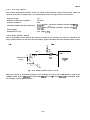
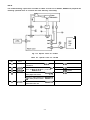
2.3 POWER SUPPLY CIRCUIT
This section describes the operation of the ROC filter unit and regulator circuit on the ROCX board.
Figure 2-2 shows the block diagram of the power supply circuit. Table 2-1 shows output voltages and
their applications.
---—- - -— - ------q1
I
i r-l
Power
SwNch
~-
IN
Power
I
i
I
I
I
I
I
I
F i l t e r
_-_.
----------
Full-Wave
Rectifier
F2
— - - - -- - - - -7
I
.
I
O + 24VDC
~ Switching
Regulator
and
Smoothing
Circuit
circuit
:AC1 ~
II
Circuit
TransI
1
JI
I
I
II
T
I
1AC2 I
I
I
1;
I
II
L -—-----——- — - - JI I : ~
1
ROC Filter Unit
4 — - t Half-Wave
I
I Rectifier
Circuit
4
—
II
I
I
I
I
I
I
O GP
I
I
— Switching ~ + 5VOC
Regulator
I
Circuit
‘
~
GND
—
1
I
I
I
I
o + 12V
0 GND
I
O 12VAC
I
k -
— - .
I
I
- - - - - - - - - - - - - - - - - - -A
ROCX Board
O 12VAC
Fig. 2-2. Power Supply Circuit Block Diagram
Table 2-1. Voltage Types and Applications
Application
Power Voltage
+ 24 VDC-GP
Printhead common voltage
Paper feed motor drive voltage
Carriage motor drive voltage
Optional interface board
+5 VDC-GND
Logic circuit
Paper feed motor hold voltage
Carriage motor hold voltage
Control panel power
Optional interface board
+ 12VDC-GND
Optional interface board
12V AC
Optional interface board
2.3.1 ROC Filter Unit
The ROC filter unit consists of an AC power cord (or AC power inlet), power switch, fuse, filter circuit,
and power transformer. The AC power cord, AC power inlet, fuse, and power transformer differ
depending on the power supply voltage. Three kinds of ROC filter units, for 120 V, 220 V, and 240 V,
are available.
2-3
REV.-A
2.3.1.1 Fuse and Filter Circuit
The AC input from the power line first flows across the power switch and fuse F1. After being filtered
by C 1 and C2, it is supplied to the primary side of the power transformer via the L1/C3 noise prevention
circuit. Power line noise (external noise) and internal noise from the printer are eliminated by this circuit.
The value of fuse F1 changes as follows, according to the power supply voltage:
120 V version: 125 V or 250 V, 1.25 A
220 V version: 250 V, 0.63A
240 V version: 250 V, 0.63A
Power
Switch
r’;;
F1
cl
.
To @pin of
Power Transformer
L1
29~H
– C3
2200PF
x2
AC IN
0
–
0.1 IF
C2 = =
To @pin of
0 Power Transformer
////
Fig. 2-3. Filter Circuit
2.3.1.2 Power Transformer
Three types of power transformers, for 240 V, 220 V, and 120 V, are available. The AC voltage from
the filter circuit is transformed to the voltages listed in Table 2-2 so that they can be output to the
regulator circuit (on the ROCX board) at the next stage. The power transformer includes thermal fuses
TF1 and TF2.
CN 1
TF1
T
a)~
50/60Hz
Gii=El:
To the
ROCX Board
@
primary side
Secondary Side
Fig. 2-4. Power Transformer
\..
2-4
REV.-A
Table 2-2. Power Transformer Output Voltages
Rated Voltage
Type
Pin No.
No-load AC Voltage [V]
220V
240V
0-0
120V
AC [V]
DC [V]
29.3
27.1
32.3
@-@
9.0
8.33
+9.0/– 9.9
a-o
29.3
27.7
33.3
n-m
8.96
8.41
+9.27/– 10.0
NOTE: Column “DC @/]” for the rated voltages indicates the output of the transformer when the ROCX
board is connected. The plus and minus values between pins 10 and 9 are different due to the
voltage drop across thermal fuse TF2.
2.3.2 Regulator Circuit
AC-tind AC2 output from the ROC filter unit are input to connector CN8 of the ROCX board. The
regulator circuit can be divided mainly into two portions, the +24 V/+5 V and + 12 V lines. AC 1 is
full-wave rectified by diode bridge DB 1 and converted to +24 V and +5 V via the chopper type
switching regulator. AC2 is half-wave rectified by D4-C 10, converted to + 12 V, and input to the optional
interface board.
T
20v:
Sc2
Au
3
4
1
1
m
az,
~m 0747
2M-3.ISA-MI Otal-3.1=1
KV 3.15A
&_
r,
r
,
.24V
r
F2
cl●
●
WI
C;t a
,
13A)
pPc494c
MT
*UK
=
‘~’i
04
2M01n3
WI
Clo
“=*V
‘
1000,
I **I
I
In,
I
R6S
O.in
2!3
Fig. 2-5. +24/+5 VDC Regulator and +12 V Half-Wave Rectifier Circuits
2-5
REV.-A
2.3.2.1 Operation Principles of Chopper Type Switching Regulator
The operating principle of the switching regulator is illustrated in Figures 2-6 and 2-7.
:fl,~
“
St
Fig. 2-6 Chopper Switching Regulator Circuit
V/I
1 C) Max = J+
L
=
c
=
Vi 1P
VO
.tc
IPtD + IOt 1
v,
10
to
=
~ -
L
Fig. 2-7 Voltage Waveforms
When switching transistor St is on, current Is is supplied to inductor L in proportion to time;
(vi –L Vo)
,s =
t
When energy has accumulated in the inductor L, current 10 is supplied to the load. When St is off, the
energy accumulated in L causes current
ID
=
ID
to flow via diode D and to supply load current 10;
Ip – * t
The longer the on-time of St, the more the output voltage increases, and the shorter the on-time of St,
the more the output voltage decreases. Theoretically, electric power efficiency is assumed to be 100%;
Output voltage Vo = + Vi
2-6
REV.-A
2.3.2.2 +24 V Supply Circuit
The +24 V supply circuit is a chopper type switching regulator circuit. Figure 2-8 shows the block
diagram of the +24 V supply circuit based on Figure 2-6.
w
a
C22
AC1 Q
AC1 O
Q +24VDC
R50
2 4/0 5
F2
DB1
D3SB1 o
L2
LP401 -02SD
Q25
C3747
R67
o.47/3w
125V
3.1 5A
z+
R49
330
6800 /-f
50V
(3A)
494
z ~ ~ C26
2200jL\35V
R47
3.3K
ZBF503
-01 TA
R46
330
—
OGP
Fig. 2-8. +24 V Supply Circuit
AC 1 input from the ROC filter unit is full-wave rectified by DB 1 and is smoothed by C22. The voltage
across C22 becomes 32.3 VDC. Transistors Q23, Q24, and Q25, which are used as Darlington
amplifiers, D7, L2 and C26 in Figure 2-8 are equivalent to switching transistor St, flywheel diode D,
choke coil L, and smoothing capacitor C in Figure 2-6. Switching is controlled by the 494 (IC3A), and
pin 9 of the 494 is the emitter of the internal switching transistor. Therefore, switching is performed
as follows:
494 internal transistor: ON ~ Q23: ON ~ Q24: ON ~ Q25: ON
494 internal transistor: OFF ~ Q23: OFF ~ Q24: OFF ~ Q25: OFF
Figure 2-9 shows a block diagram of IC 494.
a
+323V
DC
~. ---,
!
+24VDC
T
& IC 3A ?!”5
Oscdat.r W,v.-fonll
,
,
1
1
i,
1
Q IC 3A Ptn9
1,, ”s!s,., W... -from
f
:
I
1,11
c Q25 Ern,tw
W.v.-fom
(
f
1/6w
GND
v
Fig. 2-9. IC494 Block Diagram and Switching Wava-form
2-7
[
(
[
(
(
REV.-A
When the printer power is turned on, ZD1 on the +20 VDC line turns on, Q22 turns on, and Vcc is
applied to IC 494. Then the oscillator (OSC) starts generating an approximately 20 kHz sawtooth
waveform, which is regulated by R40 and C20, and the reference voltage generator outputs the +5
VDC & 10% reference voltage. Internal switching transistor Tr is switched on and off using the output
from error amplifiers 1 and 2. EA1 and EA2 limit voltage and current, respectively. EA1 compares the
voltage obtained by dividing the +24 V applied to pin 1 by R22 and R21 (approx. 4.9 V) with the + 5
V reference voltage applied to pin 2. EA2 compares the voltage monitored by R66 with the voltage
obtained by dividing the +24 V applied to pin 16 by R21 (approx. 0.31 V). Therefore, the current is
limited to approximately 3.1 [amps].
2.3.2.3 +5 V Supply Circuit
The +5 V supply circuit is also a chopper type switching regulator, which is the same as the +24 V
supply circuit.
L1
Q21
C3746
+24V o
,
C9
470P
~P201 –2R5SD
Q20
Al O 15(
2K SRI
20
78L05A
~1
R12
33
R1 1
Vvv
330
1
I
G
13
()
–004
2
0 –=
0.1-C8
R13
2
GP o
D1
ERB81
RI 4
1 Ov
B7
ZBF503
-=01 TA
A
T
Q GND
77)7Fig. 2-10. +5 V Supply Circuit
When +24 V is applied to this circuit, current flows via R12 and R1 1, and operation of SR1 is started.
SR1 includes a +5 V reference voltage generator and compares the voltage at terminal O (pin 2) with
the reference voltage. When this voltage is lower than the reference voltage, SR 1 turns terminal I (pin
1 ) on. If the voltage is higher than the reference voltage, SR 1 turns the terminal off. This controls the
switching transistors Q20 and Q21, and the output voltage is kept constant. Actual output voltage is
5.024 V (calculated value) because the GND terminal (pin 3) of SR 1 is raised to 0.024 V using the divider
composed of R 14 and R 13.
2-8
REV.-A
2.4 CONTROL CIRCUIT
This section describes the software operation, specifications, and circuit operation of the control circuit
(ROCX board). This section consists of the following descriptions:
1. Function of the CPU which controls the overall operation and its peripheral circuits (Section 2.4.1)
2. Gate array function (Section 2.4.2)
3. Outline of the overall firmware operation (Section 2.4.3)
4. Software control and circuit operation of the analog circuits (Sections 2.4.4 through 2.4.8)
The control circuit is very simple, and consists mainly of four chips: the CPU, gate array, ROM, and RAM.
(Refer to Figure 2-1 1.) The main operation of the control circuit is to control the CPU and the gate array.
Other components are described in each section that describes the functions of the CPU and gate array.
Figure 2-11 shows a block diagram of the control circuit.
..—
2-9
REV.-A
1
Ill
I
Ill
PESENSOR
PAPER FEEC
MOTOR
I
CARRIAGE
MOTOR
HOME
I
I
.
)mho
-–r
m-m
mmoo
4<
G
u
ho
m-m
<<
A G.A. E 0 5 A 0 3 B A
—
PRINT
HEAD
/
‘f”)
‘u’
Fig. 2-11. Control Circuit Block Diagram
HOST COMPUTER (OPTIONAL IIF BOARD)
Fig. 2-11. Control Circuit Block Diagram
2-1o
REV.-B
2.4.1 Functions of the CPU
The core of the control circuit is the 78 10H CPU (IC2B). Table 2-3 shows the function of each pin and
the related circuits.
Table 2-3. CPU Port Assignments
Pin
Number
Port
Assignment
1/0
1
PAO
o
2
PA1
3
PA2
o
PFCOM
1/0 port. Switches the paper feed motor drive voltage and the
holding voltage. When this signal is HIGH (LOW), the drive
voltage (holding voltage) is applied to the paper feed motor.
4
PA3
I
LF SW
1/0 port. Reads the state of the LINE FEED switch on the
control panel.
‘ - 5
PA4
I
FF SW
1/0 port. Reads the state of the FORM FEED switch on the
control panel.
6
PA5
I
PE SW
1/0 port. Reads the state of the paper end sensor. When no
paper is loaded, this signal goes LOW.
7
PA6
8
PA7
9
PBO
t
16
!
PB7
I
1
Swl - 1
17
Pco
o
TXD
TXD output port. Outputs the data from the serial 1/0 channel
in the CPU to the TXD (transmit data to the host computer)
terminal of the optional interface.
18
Pcl
I
RXD
RXD input port. Used as a receive control signal when the
optional serial interface board (for serial/parallel data conversion) is connected. (Data reception detection)
19
PC2
o
ONLINE LP
1/0 port. Controls the ON LINE LED on the control panel. When
this signal is LOW, the LED lights.
20
PC3
I
ONLINE SW
INT2 input port. Reads the state of the ON LINE switch on the
control panel. Connected to the interrupt controller in the CPU,
which executes the ON LINE/OFF LINE switch interrupt routine
when this signal is LOW.
21
PC4
o
Em
22
PC5
o
ACKNLG
1/0 port. Outputs the acknowledge signal to the interface. This
signal is LOW active.
23
PC6
0
FIRE
COO output port. Outputs the drive pulse width signal, which is
determined by the timer/event counter in the CPU, to the FIRE
terminal of gate array E05A03. This signal is LOW active.
24
PC7
0
BUZZER
1/0 port. Outputs the buzzer signal to the control panel. When
this signal is LOW, the buzzer rings.
Signal Line
Description
Name
CRCOM
—
Not used.
—
I
Not used.
P/s
SW1
1/0 port. Switches the carriage motor drive voltage and the
holding voltage. When this signal is HIGH (LOW), the drive
voltage (holding voltage) is applied to the carriage motor.
1/0 port. Reads the P/~ signal from the optional interface.
- 8
1/0 port. Reads the state of DIP SW1.
1/0 port. Outputs an error signal to the interface board when
the printer is in an error state. When this signal is LOW, the
printer is in an error state.
2-11
REV.-A
Table 2-3. CPU Port Assignment (cent’d)
Pin
Number
Port
Assignment
,,0
Signal Line
Name
Description
25
NMI
I
—
Non-maskable interrupt input. The interrupt routine is executed
at the trailing edge of this signal. This pin is invalid because it
is tied to ground.
26
INT 1
I
—
Interrupt input. The interrupt routine is executed at the leading
edge of this signal. This pin is invalid because it is tied to
ground.
27
MODE 1
I
—
External memory space setting port. MODES 1 and O (pin 29)
are both pulled up to HIGH so that an external memory of 64K
bytes (addresses O through FFFFH) can be used.
28
RESET
I
RESET
29
MODE O
I
—
30
x2
I
—
-
—
Ground terminal.
—
Ground terminal for the A/D converter in the CPU.
31
xl
32
Vss
33
AVSS
34
ANO
SW2-1
Reset terminal. When this signal is LOW, the printer is reset,
and ports A through C and D are set to be high impedance
input ports, and port F is set to be an address output (start
address OH).
Refer to pin 27, MODE 1.
CPU external clock input. This printer is driven with a 14.74
MHz clock. The operation codes are fetched at approximately
1.3 MHz, and memory read/write operations are performed at
approximately 1.6 MHz.
Analog input port of the 8-bit A/D converter in the CPU. Reads
the states of DIP SW2-1 through SW2-3.
1
36
i
AN2
I
37
AN3
I
SW2-4
Analog input port of the 8-bit A/D converter in the CPU. Reads
the state of DIP SW2-4. This signal line is connected to the
AUTO FEED XT signal line of the interface. When DIP SW2-4
is ON, the automatic paper feed function is valid. When the
DIP switch is OFF, this function is controlled by a signal from
the host computer (not fixed).
38
AN4
I
—
Analog input port for the 8-bit A/D converter in the CPU.
Reads the SLCT IN signal from the interface. When the SLCT~ signal is HIGH, DC l/DC3 control from the host computer is
valid. When it is LOW, DC l/DC3 control is ignored, and the
printer is always selected as a device. (The signal can be tied
LOW using jumper J 1.)
39
AN5
I
+24
40
AN6
-
—
Not used.
41
AN7
-
—
Not used.
42
VAREF
I
—
Reference voltage input for the 8-bit A/D converter in the CPU.
43
A VC C
I
—
Power supply input for the 8-bit A/D converter in the CPU.
44
m
o
m
1
SW2-3
Analog input port for the 8-bit A/D converter in the CPU.
Monitors the +24 V voltage and controls the printhead drive
pulse width.
Memory read timing strobe signal. Connected to the RD strobe
terminal of the gate array and the output enable terminal of
the ROM and RAM.
2-12
REV.-B
Table 2-3. CPU Port Assignment (cent’d)
Pin
Number
Port
~ssignment
1/0
Signal Line
Name
45
WR
o
WR
Memory write timing strobe signal. Connected to the WR
strobe terminal of the gate array and the write enable terminal
of the RAM.
46
ALE
0
ALE
Address latch enable signal. Controls address latching performed inside the gate array (enables latching when the signal
is HIGH).
47
PFO
1
PF7
A8
0
8-bit 1/0 ports with output latch. Used as the upper address
bus according to the MODE 0/1 terminal selection. For 64K
external memory assignment), Al 3 through Al 5 are input to
the address decoder in the gate array.
PDO
!
PD7
1/0
1
54
55
1
62
63
.—
64
DBO (AO)
!
Multiplexed addressldata bus. Used as the lower address and
data bus.
DB7 (A7)
D
I
Vcc
I
VD
[
A 15
Description
—
Power supply for the.—
internal RAM (+5 VDC).
Power supply for the CPU (+5 VDC). When this voltage is not
stable, such as at either a leading or trailing edge (when the
printer power is turned on or off), the reset circuit prevents the
CPU from running.
NOTES: 1. All barred signal are LOW active.
2. “1/0” denotes either input or output when viewing the signal from the CPU.
2-13
REV.-A
2.4.2 E05A03 Gate Array Functions
This section describes the E05A03 functions. Figure 2-12 shows the E05A03 block diagram.
(3
TIMING
REGISTER
STROBE
LATCH
(Input
Data)
I NO-7
I
I
I
DBO-7
ALE
PRINTHEAD
DRIVER
DB6
—
1
I
A
I
1
-
I I I I I ~’ I
I II
L
1 l-l
DB7
CARRIAGE
MOTOR DRIVER
IATCH
(ControIl
(w
BUSY
~T
RESET
(RESI)
AB15
RESO
AM4
AB13
Fig. 2-12. E05A03 Block Diagram
2-14
REV.-A
Functions of the E05A03 gate array (IC3B) are as follows:
1. Address latch
The gate array latches data on address data lines DBO - DB7 at the leading edge of the ALE signal,
and outputs it to ABO - AB7 (when ALE is high, the data is passed through without latching.)
2. Address mapping
——
The gate array inputs an address on AB 13- AB 15, and selects CS 1 or CS2 or enables the R/W mode
of this gate array using internal decoder 2.
3. Handshaking
● The gate array latches data on INO - IN7 at the leading edge of the STROBE signal, and automatically
outputs the BUSY signal. The BUSY signal (DB7) is latched by the timing register to inform the CPU
that data has been transmitted to the CPU.
● The timing for the BUSY signal, which is set at either the trailing or leading edge of the STROBE
signal, is selected by the control program (firmware).
● The BUSY signal output from the timing register is wire-ORed with the BUSY signal controlled by
the firmware.
——
.—
4. Printhead solenoid drive pulse
. When the FIRE signal from the CPU is brought Low, the data that was previously latched is output
on HD 1 - HD9 to drive the corresponding solenoids in the printhead.
● When FIRE is high, HDI - HD9 are all low.
5. Shift register
● This gate array includes a shift register (8bits X 3), and the MSB (Most Significant Bit) can be read
by accessing the specified address (XX03H) once. The data is shifted one bit to the left at the leading
edge of the ~ signal.
6. Initialization
——
When the INIT or RESI signal is low, the gate array sets RESO low and initializes the following.
● Printhead latch (HD 1 - HD9 are all set low even if FIRE is low.)
● PF motor latch (PFA - PFD) are all set low.)
——
● CR motor latch (CRA - CRD) are all set high.)
. Timing generator (enters the state indicating that no data has been received.)
● Control latch (BUSY is set high (software-BUSY), PE is set low, and PELP, NLQLP, and CNDLP are set
high.)
7. Address decoder 2
Address decoder 2 selects one of the twelve modes listed in Table 2-13 according to the combination
of lower address bits OOH - 07H, ~, and ~.
2-15
REV.-A
Table 2-4 shows the E05A03 functions and Table 2-5 shows the E05A03 pin functions.
Table 2-4. E05A03 Functions
Lower Address
Function
R/W
Pin Name
R
INO - IN7
w
—
R
STRB
HOME
w
—
R
INO - IN7
w
—
Writes data to the lower eight bits of the 24-bit shift register
(DB7 - DBO ~ Bits 7 - o).
R
—
Reads the MSB of the 24-bit shift register and shifts the data
one bit to the left (MSB ~ DB7).
OOH
Reads the data which was latched using STROBE, and resets
the STROBE-BUSY output.
Writes data to the upper eight bits of the 24-bit shift register
(DB7
- DBO ~ Bits 23 - 16).
Bit 7: 1 (Indicates the trailing edge of the STROBE signal.)
Bit 6: 1 (The HOME input is HIGH.)
OIH
Writes data to the middle eight bits of the 24-bit shift register
(DB7 - DBO ~ Bits 15 - 8).
Directly reads INO - IN7. Does not affect the BUSY signal.
02H
BUSY
03H
w
Bit 7: 1 (The BUSY signal is output at the leading edge of
STROBE.)
O (The BUSY signal is output at the trailing edge of
STROBE.)
Bit 6: 1 (Resets software-BUSY.)
O (Sets software-BUSY.)
NLQLP
Bit 4: 1 (NLQLP is LOW.) ● See NOTES 2.
0 (NLQLP is HIGH.)
CNDLP
Bit 3: 1 (CNDL is LOW.) ‘See NOTES 2.
0 (CNDL is HIGH.)
PE
PELP
Bit 2: 1 (PE is HIGH and PELP LOW.)
O (PE is LOW and PELP HIGH.)
04H
w
HD1 - HD8
Latches (and inverts) the data for pins 1 - 8 of the printhead.
(DB7 - DBO ~ HD1 - HD8 Data is output when FIRE goes
LOW.)
05H
w
HD9
Latches (and inverts) the data for pin 9 of the printhead. (DB7
~ HD9 Data is output when FIRE goes LOW.)
06H
w
PFA - PFD
Latches the phase data for the PF motor.
(DB7 - DB4 ~ PFA - PFD)
07H
w
——
CRA - CRD
Latches the phase data for the CR motor.
(DB3 - DBO ~ CRA - CRD)
NOTES: 1. The above functions are mapped to every eight bytes from COOOH to DFFFH.
2. These are not used in this printer.
2-16
Table 2-5. E05A03 Port Assignments
.—
Description
Pin No.
Signal
Direction
1
Vcc
In
2
NLQ LP
out
NLQ lamp (~/off) “See NOTES 1
3
PE LP
out
Paper end lamp (~/off)
4
CR D
out
Carriage (CR) motor phase D drive pulse
5
CR C
out
CR motor phase C drive pulse
6
CR B
out
CR motor phase B drive pulse
7
CR A
out
CR motor phase A drive pulse
8
DB 7
In/Out
1
15
!
DB8
16
AB 15
In
1
18
1
AB 13
In
19
ALE
In
Address latch enable
20
WR
In
Write stroba-
21
m
In
Read strobe
22
FIRE
In
Printhead solenoids trigger (_/rest)
23
HOME
In
Home position signal (Home/Not home)
24
RESI
In
Reset signal input
25
RESO
out
Reset signal output
26
PF A
out
Paper feed (PF) motor phase A drive pulse
27
PF B
out
PF motor phase B drive pulse
28
PF C
out
PF motor phase C drive pulse
29
PF D
out
PF motor phase D drive pulse
30
Cs 1
out
Chip select 1 (lower address)
31
Cs 2
out
Chip select 2 (upper address) “See NOTES 1.
32,33
GND
—
GND
34
CND LP
out
CONDENSED lamp (on/off) ● See NOTES 1.
35
PE
out
Paper end (Valid/Invalid)
36
BUSY
out
Busy
37
1
44
AB O
1
AB 7
out
Address bus O - 7
45
INIT
In
Initialize
46
STROBE
In
Strobe
47
IN 7
In
Data bus 1 - 8
1
54
i
IN O
55
HD 9
{
63
!
HD 1
64
Vcc
out
In
Power (+ 5V DC)
Data bus 7 - 0
Address bus 15 - 13
Printhead solenoid drive pulse #9 - #1
Power (+ 5V DC)
NOTES: 1. These are not used in this printer.
2. Signal direction is viewed from the E05A03 side.
2-17
REV.-A
2.4.3 D a t a F l o w
This section describes the firmware start-up operation when the printer is initialized, data flow
(especially printing data flow), and command processing. Figure 2-13 shows a memory map of the
LX-800.
FFFFt
FFOOt
CPU Internal RAM Area
(Down Load Area)
Not Used
EOOOI
Gate Array Function
Address Area
(Memory Mapped 1/01
Coool
Stack Area
Not Used
Lim Buffer
AOOOI
I
Buffer and Work Area
(RAM IC4CI
8k bytes
80001
\
hag. Buff.,
(2K bytes)
\l
\l
hut Oata Buffer
i3k bvtes)
I
I
Program Area
(ROM IC3C)
32k byles
00001
Fig. 2-13. LX-800 Memory Map
The CPU can access an external memory of 64K bytes, and executes the program (32K bytes) in the
external ROM (IC3C). The external RAM (IC4C) area (8K bytes) and the CPU internal RAM (256 bytes)
are used as a buffer and working area. The CPU accesses the gate array using the instruction codes
(See Table 2-4). COOOH through DFFFH are defined as memory mapped 1/0.
2-18
REV.-A
2.4.3.1
Initialization
When the reset signal is input, the printer is initialized as follows:
GATE ARRAY
CPU
4 ————— .— ———————— — — . — — . —— 1
i
;
Clears all port outputs. Executes the program from t
I
address OH.
1
I
1
I
Clears the ports using hardware resetting.
● Sets the print head data to High-Z(the high
impedance state).
● Sets the BUSY signal HIGH.
I
1
I
~------------------------’
i —————
Sets up the 1/0 ports. Initializes the CR and PF
motors.
——————————————— 1
~ Receives the phase data for the motors from the
I CPU, and holds the CR and LF motors.
I
— — —— — ——— — — — — —- — -—-—--—--—- 1
1
$
Clears the memory. Sends the ACK signal to the
host computer via the interface.
I
-“’’’’’’’’’’’’’;’’’”:l
Performs carriage home position seek.
t
b
Initializes the gate array.
(Outputs the instructions to the gate array.)
I
;
———
———
—
——
——
— — ————— —— ————
Initialized (the instruction codes are set).
I — .———.—————— - — — — ——— — —— 1
~---------------------
I
i
Reads the DIP switch settings on the optional interface board if the board is installed.
1
I
————— —————— ———. -— ——— ————
~ Controls the paper end signal of the interface and
I the paper end l a m p o n t h e control panel.
I
—
— —
— — - —
— — — — — —
Is this self-test printing or hexadecimal dump mode? (Monitors the switch signals from
— - — — — — — — -
J
I
—— J
Y
I
Select either the self-test
printing or the hexadecimal
dump mode.
Entars tha interface data waiting state.
I
● Sets the BUSY signal LOW.
I — — — — — — —— ———— .————————— J
Enters the interface waiting state (main routine for ~
data processing).
--
Reads the DIP switch settings on the optional in! terface board upon receiving the instruction code.
; (XX02H is read.)
I
I
Checks whether the paper is set or not. Sends the
result to the gate array.
1
i
I
Fig. 2-14. Initialization Flow
2-19
REV.-A
2.4.3.2 Print Data Processing
After the initialization, the CPU enters the data waiting state. When data is input from the interface,
the CPU starts reading the data. Besides this process (main routine), the actual printing process is
performed by an interrupt routine. The print data is processed by repeating the main and interrupt
routines.
Array
CPU
\
Data
@- —D
—
Input
ACK
Data
5
$
~
2
STRB ----–m
~
t
* BUSY
Buffer
D
@
-
---- A *
@
J
Command
Analyze
4
(Add the
Attribute)
*:
9
fiA
M a i n routi”e
- : Interrupt ro”tine
CG
6
;
Down I
~ Load ~
--r ---
e
(!)7
CG Copy Araa
+
FIRE
P
I
Imaga Buffer
o
I
Printing
Fig. 2-15. Print Data Flow
The data flow in the Draft printing mode is as follows. Step numbers used in the explanation below
correspond to the data flow numbers used in Figure 2-15.
2-20
REV.-A
@ The CPU detects the STRB signal from the gate array (Reads MMIO and XXOI H). When the gate
array detects the trailing edge of the STRB signal, it automatically sets the BUSY signal HIGH and
latches the transferred data.
@ The CPU fetches the data latched by the gate array (reads MMIO and XXOOH), and stores the data
in the input buffer. The CPU analyzes each byte of data to determine whether it is a control code
or print data, then returns the ACK signal to the interface.
@ Steps@ and@ are repeated until the input data buffer becomes full. When the buffer becomes full,
the BUSY signal is set HIGH.
@ Either during steps@ and@ or after the input data buffer becomes fuil, the CPU analyzes each byte
of data. If the data is not a printing command (CR), the CPU sets the printing mode and parameters
and transfers the data to the line buffer. The line buffer is shown in Figure 2-16.
. - ---Character
code
Attribute
1
Attribute
Character
code
2
- - - - - -.
—
—lb’’e+lb’ta-t-lb’te
3bytes (every 1 data)
4
-
Fig. 2-16. Line Buffer
The line buffer temporarily stores the data for one line using the format shown in Figure 2-16, and
also contains the command flags (1 6 bits), for attributes 1 and 2, for each character. The command
flags indicate what kind of command or mode is specified for the character. According to the
command flags, any of the EPSON ESC/P commands, NLQ, underline, emphasized character, and
font selection, is specified for the character.
When either the CPU detects a printing command (CR) or the line buffer becomes full, the printing
process (interrupt routine) is started.
The CPU transfers the character codes from the line buffer to the CG (Character Generator), and
transfers image data to the CG copy area. The CG copy area refers to the attribute flags in the line
buffer and expands the image data. The expanded data is then transferred to the image buffer.
The CPU writes the (vertical) dot patterns in the image buffer to port HD of the gate array (writes
MMIO, XX04H, and XX05H). At the same time, the CPU references the contents of the line buffer,
and outputs the FIRE signal (which corresponds to the dot patterns expanded in the image buffer)
to the gate array.
When the NLQ mode is selected, note the following difference from the Draft mode:
● During command analysis in step @, if the data is determined to bean NLQ character, the steps after
step @ are repeated two times for every one pass (NLQ requires two-pass printing).
When the download mode is selected, the following point is different from the draft mode:
● When referencing the CG in step @, the CPU accesses the down load buffer but not the CG.
2-21
REV.-A
2.4.4 Reset Circuit
A reset operation is performed when the INIT signal is input from the interface and when the printer
power is turned on. (Refer to Sections 1.4.6, 2.4.1, 2.4.2, and 2.4.3.1 for the reset operation.) Figure
2-17 shows the reset circuit.
E05A03 (3B)
R63
+5
INIT
---- 1
I
l—
RESI
I
~ - - - I
‘:;’’’”3’)+
INIT
A
(CN2, Pin8)
C27
470p
AND
H
4
I
I
+AJ--c3
R43
24 4 7 K
R42
IK
D
I
+24
ZD2
HZS1 5-3
R34
+ D5
MA165
12K
+-+
C15
I p/5ov r
I
I
/
L—--—
RESO
RESET (CPU, Pin 28)
T
*m(cN2pin’3)
(lC)
Fig. 2-17. Reset Circuit
The I NIT signal from which noise is attenuated by R63 and C27 is input to the E05A03. The RESI terminal
of the E05A03 is connected to the power supply (+ 5 V and +24 V) reset circuit. When the printer power
is turned on, the level of the RESI signal is held at its threshold level or below (LOW level) until the voltage
of the +24 V line reaches the Zener voltage of ZD2 (when the power is turned off, the sequence
reverses). The same sequence is followed for the + 5 V line. The level of the RESI signal is held at its
threshold level or below (LOW level) until the voltage of the +5 V line reaches +5 V. In addition, the
level of the RESI signal is held LOW by R43 and C 15 for approximately 47 ms after the power supply
voltages become stable. The Schmitt trigger gate (CMOS level) at the input terminal of the RESI signal
shapes the analog waveform. The INIT and RESI signals are ANDed in the E05A03, then output from
the RESO terminal to the RESET terminals of the CPU and the interface board.
2-22
REV.-A
2.4.5 Carriage Motor
This section describes the sensor circuit, an outline of the firmware, and the drive circuit, which are
used to control the carriage motor. The specifications of the carriage motor are as follows:
Angle per step:
7.5°
Number of steps per revolution:
48 steps
Number of phases:
Four
Excitation system and drive frequency:
Unipolar drive, 2-2 phase excitation system (900 PPS)
Drive voltage:
Unipolar drive, 1-1 phase excitation system (450 PPS)
+24 VDC
Resistance per coil:
41.5 ohms A7Y0
2.4.5.1 Home Position Sensor
The home position sensor detects the reference position of the carriage. The sensor is located at the
home position which is to the left of the first column. Figure 2-18 shows the home position sensor circuit.
—
—.—
+5
r
I
-I
1 ‘:
R 20
5.6K
CN7
w
1
R32
IK
I
1
I
i
1
L_ -d
Home Position i
Sensor
~
- - HOME
L3
E05A03
(3B)
2
<
Fig. 2-18. Home Position Sensor Circuit
When the carriage is at the home position, the reed switch is closed, and a LOW signal is input to the
HOME terminal of the E05A03. The CPU reads MMIO port XX 1 H of the E05A03 to determine when
the carriage is at the home position.
2-23
REV.-A
2.4.5.2 Carriage Motor Control
The carriage motor control system is an open-loop system. There are two basic phase switching speeds:
450 PPS (l-1 phase drive) and 900 PPS (2-2 phase drive), as shown below. The phase switching is
performed according to the time data (time required to switch a phase) which is determined by the
firmware, for the number of counts determined by the firmware. Figure 2-19 shows the basic phase
switching patterns.
CRA
CRB
CRC
CRD
Carriage
Movement
Direction
-
*
Left
Left
~ ‘ight
~ ‘ight
(l-1 Phase Switching)
(2-2 Phase Switching)
Fig. 2-19. Basic Phase Switching Patterns
Constant Speed
1
I
I
H.P.
speed
v
I
~
I
Rt
I
I
C. H.P.S ~
I
I
~Printing Area
11
:I
A
START
----Drive
I
I
I
I
I
I
I
,,
I
q
I
Rt ,
I
A
u
STOP
I
I
I
I
----------------------
IMNv
1
m ‘uLrLrl—
Hold
1
~ time
Fig. 2-20. Basic Operation Sequence
2-24
REV.-A
Figure 2-20 shows the basic sequence for the carriage operation.
● C. H.P.S. (Refer to Section 2.4.5.3)
When the printer is initialized, a carriage home position seek is performed. Then the carriage motor
enters the holding mode at the operation start position (START).
● Rt
At least 6 ms of rush time (Rt) is set just before acceleration and after deceleration to stabilize the
motor operation. It takes 75 ms for the carriage motor to restart from the stop mode.
● Acceleration mode
The acceleration mode consists of a maximum of 12 steps, and the time period for each step becomes
shorter as the step number increments. In the acceleration mode, the CPU checks the home position
signal each time the phase is switched, and a carriage error occurs if the home position signal goes
HIGH.
● .Ccmstant speed mode
.
After acceleration completes, the carriage motor enters the constant speed mode. Printing is started
when the carriage motor enters this mode. The time period for each step is the same, 2.22 ms at
450 PPS and 1.11 ms at 900 PPS.
● Deceleration mode
The deceleration mode consists of a maximum of 12 steps. The time period for each step becomes
longer as the step number increments.
The 450 PPS speed (l-1 phase drive) is used for printing NLQ characters, and the 900 PPS speed (2-2
phase drive) is used for printing Draft characters. The patterns for the phase switching and the time
data are contained in the working area of the RAM. The CPU uses this data as a reference table, and
outputs the phase data to the E05A03 in accordance with the timing of the character to be printed.
(MMIO XX07H write operation)
2-25
REV.-A
2.4.5.3 Home Position Seek
Figure 2-21 shows the home position seek operation (actual carriage movement)
Q
A
I
Held for 20 to 30 ms
according to the phase
data combination.
I
N
Moves from left to right until
it leaves the home position.
1
1
Moves from right to left for
four steps, then stops.
J
J
Is this the
home position?
Moves from left to right for
four steps, then stops.
I
Y
+
,N
Decelerates for five steps,
then stops.
I
<
f
Moves from right to left until
it reaches the home position.
N
I
1
Y
Moves from right to left with
a step time intewal of 10 ms
until it reaches the home
position.
I
I
Decelerates for five steps,
then stops.
I
I
Fig. 2-21 Home Position Seek Operation Flow
A home position seek is performed when the hardware is initialized. Because the carriage control is
an open-loop system, the CPU must perform a home position seek in order to get the carriage to a known
reference position. This operation is performed at 450 PPS (l-1 phase drive). The printing start position
(column 1) is 25 steps to the right of the home position. The carriage does not return to the home position
unless the printer power is turned off. When the carriage motor is in the acceleration mode or the normal
printing mode, the CPU checks the home position signal every time the phase is switched. If the CPU
detects that the carriage is at the home position, it regards this as a carriage error.
2-26
REV.-A
2.4.5.3 Carriage Motor Drive Circuit
Figure 2-22 shows the carriage motor drive circuit.
I
E05A03
6
CRB
5
CRC
N5
—
:RA
0-6
;RB
Q2
+
5
R29
R30
-o1
R31
CRD
4
J
3.3Kx4 ‘
7b_D1843x4
(3B)
+24
R2
3.3K
+5
A
CPU
1
—
Q19
B131 B
(2B)
u
,—,
3
EMO1 ZW
cRCOM
ciiCOM
4
Fig. 2-22 Carriage Motor Drive Circuit
The carriage motor drive circuit is a constant voltage switching circuit (unipolar drive). When output
CR of the E05A03 is HIGH, the voltage is applied to the coil of the motor. When PAO of the CPU is HIGH,
the +24 V is applied to CRCOM (drive mode). When it is LOW, +5 V is applied to CRCOM (holding
mode).
2.4.6 Paper Feed Motor
This section describes the sensor circuit, an outline of the firmware, and the drive circuit, which are
used to control the paper feed motor. The specifications of the paper feed motor are as follows:
Angle per step:
7.5”
Number of steps per revolution:
Number of phases:
48 steps
Excitation system and drive frequency:
Drive voltage:
Unipolar drive, 2-2 phase excitation system (480 PPS)
+24 VDC
Resistance per coil:
58 ohms *7%
Four
2-27
REV.-B
2.4.6.1 Paper End Sensor
The paper end sensor detects whether paper is present or not. Figure 2-23 shows the paper end sensor
circuit.
+5
1
CN6
R4
5.6K
-27
(26)
2
Fig. 2-23. Paper End Sensor Circuit
When the paper runs out (of the detection area), the reed switch closes, and port PA5 of the CPU goes
LOW. The paper end detector is checked each time the phase is switched. The firmware controls the
following three operations:
● When a paper end is detected during printing, firmware stops printing and sets the printer OFF LINE.
● When a paper end is detected during initialization, firmware sets the printer OFF LINE.
● When the AUTO LOAD switch is pressed in the OFF LINE state: Firmware executes the auto loading
function (refer to Section 2.4.6.3) if paper is not already loaded or executes paper feeding (normally
one line) when the paper is loaded.
If the paper is loaded or ejected by pressing the FF or LF switch without executing printing, the printer
is not placed OFF LINE due to paper end detection.
Paper
T
Approx. 50mrn
JL
Frame (L)
I
a
-
62.5mm
288mm
Fig. 2-24. Paper End Detection Area
2-28
I
Frame (R)
REV.-A
2.4.6.2 Paper Feed Motor Control
The paper feed motor is controlled by an open-loop system just like the carriage motor. The basic phase
switching speed is 480 PPS (2-2 phase drive), and the phase switching is performed according to the
phase pattern stored in the firmware. Figure 2-25 shows the basic phase switching pattern.
PFA
PFB
PFC
PFD
Platen
Movement
B
a
c
k
_
Normal
—
Direction
Fig. 2-25. Phase Switching Basic Pattern
Constant Speed
Speed
I
1
I
1
1
Power ON
r
~Rtl ~
STOP
1
I
1
I
I
I
1
I
I
I
1
1
I
I
1
;
I
Rt2 ;
1
8
#
Drive
Hold
~---vuvu ----------
~----%
Fig. 2-26. Basic Operation Sequence
2-29
REV.-B
Figure 2-26 shows the basic sequence for the paper feed motor.
● Rtl
When the printer power is turned on, the paper feed motor is rushed for 30 to 60 ms in any phase.
It takes 25 ms for the paper feed motor to restart from the stop mode. And after that, the paper feed
motor rotates both back and front for each 16 steps to fix the back-rush between the motor pinion
and gears.
● Acceleration mode
The acceleration mode consists of a maximum of four steps, and the phase switching time for each
step becomes shorter as the step number increments.
● Constant speed mode
After the acceleration completes, the motor enters the constant speed mode. The time period for
each step is the same, 2.03 ms.
. Deceleration mode
The deceleration mode consists of a maximum of 12 steps, and the phase switching time for each
step becomes longer as the step number increments.
● Rt2
When the paper feed motor decelerates and stops, it enters the holding mode after the rush time
of 15 ms.
The paper is fed 1/6 inch (4.23 mm) per 36 steps. When the total number of steps is 10 or less, the
paper feed motor is driven only in the constant speed mode, but with a step time of 3.28 ms. The phase
switching pattern and time data are contained in the working area of the RAM. The CPU outputs the
data to the E05A03 the number of times specified by the program. (MMIO XX06H write operation)
2.4.6.3 Auto Loading Function
The sequence for the auto loading function is shown below.
1. The printer moves the carriage to the 40th column.
2. The printer drives the paper feed motor for 433 steps to load the paper.
In this way, the printing start position is set approximately 22 mm from the top of the paper.
k
Approx.
22mm
1st column
EPSON LX-800
Fig. 2-27. Printing Start Position
2-30
REV.-A
The auto loading function is valid under the following conditions:
● When the printer is OFF LINE.
● Just after the signal from the paper end sensor changes from LOW to HIGH. (The leading edge of
the signal is checked for.)
2.4.6.4 Paper Feed Motor Drive Circuit
Figure 2-28 shows the paper feed motor drive circuit.
CN5
E05A03
PFA
A
12
al 7
PFB
I
“
8
“
11
I Q16
PFC
PFD
7
3.3K X 4
77!7 D1 8 4 3 x 4
— .— (3B)
+ 2 4
+ 5
+J+”JL
RI
3.3K
CPU
3
PA2
3
‘5
4
(lC)
5.6K
(2B)
Q18
B1 093
J
R17
33
D3
9
10
EMOIZW ~
I
Fig. 2-28. Paper Feed Motor Drive Circuit
The paper feed motor drive circuit is a constant voltage switching circuit (unipolar drive), which is the
same as the carriage motor drive circuit. When output port PF of the E05A03 is HIGH, voltage is applied
to the motor coil. When PA2 of the CPU is HIGH, +24 V is applied to PFCOM. When it is LOW, +5
V is applied to PFCOM.
2-31
REV.-A
2 . 4 . 7 Printhead
This section gives an outline of the software that controls the printhead, the drive pulse width control,
and the drive circuit. The specifications of the printhead are as follows:
Number of solenoids
Drive voltage
: Nine
: +24 VDC
: 19.2 ohms +10%
Coil resistance
Printhead drive pulse width: 360 PS &10 ps (at 24 V, 25°C)
2.4.7.1 Printhead Control
The data is output to the printhead in the following sequence:
1. Print data is expanded in the image buffer as dot patterns. The CPU outputs the dot patterns to the
E05A03.
2. The data for pins 1 through 8 of the printhead is latched by HD 1 through HD8 of the E05A03. (MMIO
XX04H write operation)
3. The data for pin 9 of the printhead (usually for underlining) is latched by HD9 of the E05A03 via
DB7.
4. After latching the data, the printhead drive pulse width signal FIRE is output from the event counter
in the CPU. While the FIRE signal is LOW, the gate opens so that the data at HD 1 through HD9 is
output.
The timing of the event counter in the CPU is set mechanically. The data write operation is completed
within one cycle of the counter. The operation described below is inhibited to protect the printhead
from being damaged.
FIRE
Normal
~
Dot Pattern
Half
Dot Pattern
x
time ~
Fig. 2-29. Printhead Drive Pulse Pattern
Figure 2-29 shows the sequences for the normal and half dot printing, which can be performed at any
pin of the printhead. Driving the printhead continuously to print adjacent half dots (the portion marked
●
in the above figure) is inhibited. If this pattern exists after expanding the image data, one dot will be
ignored.
2-32
REV.-A
2.4.7.2 Printhead Drive Pulse Width Control Circuit
In order to keep the value of the printhead drive pulse width constant, the CpU monitors the +24 VDC
line, the printhead common voltage, and uses the voltage level to adjust the width of the FIRE signal.
The printhead drive pulse width is controlled to be within the area shown by the oblique lines in Figure
425
2-Bn
I
!W.
405
400
=
I
(n
CD
I
I
I
I
I
I
1
I
I
I
I
I
I
I
I
I
1
I
I
I
1
24
I
,
26.4
I
I
,
21.6
300
325
I
I
I
I
-.—
345
350 ;
I
I
350
i
wYz////z
I
Printhead Driving Voltage [V] ~
Fig. 2-30. Printhead Drive Pulse Width Range
+24V
R36
2 . 2 K l/2W
VAref 4 2
4)
+5
AVCC
43
+24
s=
*W\
o
! t ?!-
-.-,
.-.
7%
I
Fig. 2-31. +24 VDC Monitor Circuit
The CPU monitors the +24 V line at AN5 of the 8-bit analog to digital converter, computes the result,
and controls the drive pulse width of the signal (FIRE) output from the event timer. 4.7 V is applied to
reference voltage input VAref by ZD3, and the voltage obtained by dividing +24 V by R37 and R35
(approximately 4.08 V at +24.OV) is input to AN5.
2-33
REV.-A
2.4.7.3 Printhead Drive Circuit
Figures 2-32 and 2-33 show the printhead drive circuit and the waveform of the drive voltage.
CN4
+24V
Solenoid
Coil
Q1-Q9
C3293
HDn
E05A03
(3B)
R52
I
R61
IK
T
GP
Fig. 2-32. Printhead Drive Circuit
s.,e.oid..rre.t~::::;:
Waveform
~A4:l-
J
Drive Transistor
Collector Voltage
Waveform
.=approx. 360Ps
B=approx. 40ps
C=approx. 1.11 ms
Fig. 2-33. Solenoid Current and Drive Voltage Waveforms
2.4.8 Print Timing Control
This section describes the print timing control for the carriage and printhead and the bidirectional logic
seeking function.
2.4.8.1 Print Timing Control for the Carriage and Printhead
The phase switching of the carriage motor and the printhead driving are controlled by the CPU, and
the relationship between the two is shown in Figure 2-34.
2-34
REV.-A
FIRE
1
HD1
1
,,;
,,
,
HD2
1;
H~~ ~
.—
—
HD8
HD9
HD1
HD9
-8
(H)
(H)
80
41
22
14
08
14
80
80
80
80
22
80
41
80
00
80
00...
00 . . . . .
Fig. 2-34. The Relationship Between the Carriage and Printhead
Control Signals
Figure 2-34 shows the relationship between the carriage and the printhead when character “~” is
printed in the Draft mode. The dot data of HD 1 through HD8 and HD9 synchronizes with the LOW level
of ~. The phase switching for the carriage motor is performed asynchronously with the application
of the drive voltage to the printhead. A delay time (Dt) of 46 psec. in the Draft mode (900 PPS) and
92 psec. in the NLQ mode (450 PPS) is used in order to protect the +24 V line from being overloaded.
Printing for one line is performed in the sequence described above. In the NLQ mode, half of the dot
pattern is printed for one line, the paper is fed for 1/216 inch, and the remaining half of the dot pattern
is printed. In the half speed mode (valid when the printing speed is 900 PPS), the printhead drive pulse
width is doubled (720 Ps) and the carriage drive speed is halved (450 PPS).
2.4.8.2 Bidirectional Logic Seeking
The bidirectional logic seeking is controlled by the CPU. The CPU starts printing after expanding the
print data. However, the processing of the next group of data is started while printing the former group.
In this way, the CPU can determine the carriage return position for the next group of data so that the
carriage can be moved the shortest distance before printing the next line. Figure 2-35 shows this
operation.
2-35
REV.-A
D
EPSON
\
f
@)
@
--N;;:
&@
@l@
T E R M INA L
:
@
LINE1
LINE2
Carriage Operation
(Constant Speed)
Carriage Operation
(Acceleration/Decelerat ion]
Paper Feed Operation
This is Draft mode printing
@
b
I
I
4,,1<,1 ~
PR
@
@
LINE3
INT E R ~~
@
~;
I
10
1 2 3 4 5
+-
Printing Area
\
@
15
1+
----(column )
11--
Acceleration Area
Home PositIon
1-3:
Printing of the 1st line
4-5:
Logic seeking
6:
Paper feed
7-9:
Printing of the 2nd line
10:
Paper feed
1 1-12: Printing of the 3’rd line
Fig. 2-35. Logic Seeking
1. Upon receive in print data “EPSON” for a line from the host computer, the printing is performed in
an action of @ to @ with the carriage and printhead moving to position Q.
2. The CPU, receiving the next data from the host computer, analyzes it and determines the acceleration
start position of the carriage.
3. In an action of @ to @, the carriage is moved to position @, here paper feed is operated @. Then
the carriage goes through acceleration printing and deceleration @,@, @to position Q, next paper
feed is operated @.
4. In an action of @ to @, acceleration, printing, and deceleration are performed ~.
2-36
REV.-A
2.5 PRINTER MECHANISM OPERATION
The printer mechanism includes sensors, the carriage, the paper feed, and the ribbon feed mechanism.
Figure 2-36 shows an external view of the printer mechanism.
Fig. 2-36. Printer Mechanism External View (Model-3A10)
2.5.1 Sensor Mechanism
This subsection describe the two sensor mechanisms: home position sensor and paper end sensor.
Home Position Sensor
The home position sensor functions to determine the home position of the carriage, and sends a
reference signal for print start position. The home position sensor mechanism consists of the
mechanical switch which is operated by lever at the bottom of the frame. When the detection pIate
pushes the lever of sensor, the mechanical switch closes.
Paper End Sensor
The paper end sensor detects the presence/absence of paper. The paper end sensor mechanism
consists of a mechanical switch which is operated by paper end sensor Iever. When the paper supply
has run out, the mechanical switch closes.
2-37
REV.-B
2.5.2
Carriage
Mechanism
The carriage mechanism includes the printhead, the carriage, the timing belt, the carriage motor, and
the platen. Fig. 2-37 shows the carriage mechanism.
The timing belt is connected into the bottom of the carriage. This belt is driven by the carriage motor
and moved via the belt driven pulley. The printhead is mounted on the carriage, and the entire unit is
moved right and left along the carriage guide shaft and plate.
Left
v
z Carriage Guide Shaft
: Driving Pulley
Fig. 2-37. Carriage Mechanism
2-38
REV.-B
Printhead
The dot wire operation during printing is as follows: when the head driving coil for a dot wire is
energized, the actuating plate engaged with the dot wire at one end is attracted to the iron core and
drives the dot wire toward the platen. The dot wire strikes the ribbon and the paper against the platen
to print a dot in the paper.
When the head driving coil is deenergized, the actuating plate returns to the initial position as a result
of the action of the actuating plate spring. After striking the platen, the dot wire also returns to its initial
position as a result of impact energy and from the wire resetting spring, and the dot wire is held in
engagement with the actuating plate until it is driven again.
Fig. 2-38 shows the printhead printing operation.
Platen
Ribbon Mask
Dot Wire
—
Wire Resetting Spring
Stopper
(]
Actuating Plate
-
Paper
Act~ating Plate Spring
Fig. 2-38. Printhead Printing Operation
2-39
REV.-B
2.5.3 Paper Feed Mechanism
The paper feed mechanism operates by friction feed method for cut sheets, and roll paper, and by the
sprocket feed method for fanfold paper.
2.5.3.1 Friction Feed Operation
The paper is held against the platen by two paper feed rollers and by the printer cover. At this time,
the paper feed motor is driven to rotate the platen gear, via the paper feed reduction gear, in the direction
shown in Figure 2-39. The rotation of the platen Gear feeds the paper in the direction of the arrow due
to friction from the paper feed rollers and platen.
Because the paper is held against the platen by the spring force of the paper feed rollers, the paper
can be released by shifting the paper release lever forward.
Paper Feed Motor
Fig. 2-39. Friction Feed Operation
2-40
REV.-B
2.5.3.2 Sprocket Feed Operation
When the printer is using the sprocket feed method, the holes in the paper are set over the sprocket
pins along the sprocket wheel.
The paper feed motor is driven to rotate the gears, via the pinion on the shaft of the motor, in the direction
shown in Figure 2-40. Rotating the gears rotates the sprocket wheels, which advances the paper in
the direction shown by the arrow.
For the sprocket feed method, the pressure of the paper feed rollers against the platen is released by
shifting the release lever forward.
—
ar
Motor
Fig. 2-40. Sprocket Feed Operation
2-41
REV.-B
2 . 5 . 4 Ribbon F e e d M e c h a n i s m
The ribbon feed mechanism consists of the ribbon cartridge and the ribbon feed section. A ribbon
I driving gearalways turns counterclockwise, via the geartrains shown in Table 2-6, irrespective of the
direction of the timing belt.
Table 2-6 Ribbon Feed Gear Train
Gear Train
Direction of Movement of Carriage
Left to right (arrow ● )
Belt driven pulley ~ Planet gear (1) +
Planet gear (2) + Ribbon driving gear
Right to left (arrow ~)
Belt driven pulley ~ Planet gear (1) ~
Planet gear (3) ~ Planet gear (4) ~
Ribbon driving gear
Figure 2-41 shows ribbon feed mechanism. The inked ribbon is inside the cartridge case in an endless
state, held between the ribbon feed and ribbon pressure roller mounted on the ribbon driving gear.
The rollers are driven by the movement of the gear, and the inked ribbon is fed.
A ribbon breaking spring is attached at the exit of the cartridge case to prevent the ribbon from slacking.
A ribbon mask is installed for preventing the ribbon from staining the paper.
Ribbon Feed Roller
L
‘k
Ribbon ‘ressure ‘O’’er\ \
Ribbon Transmission Gear W
Ribbon Breaking
Spring
Ribbon Driving Gear
‘ane””w
riage
Fig. 2-41. Ribbon Feed Mechanism
2-42
REV.-A
CHAPTER 3
OPTIONAL EQUIPMENT
3.1 GENERAL . . . . . . . . . . . . . . . . . . . . . . . . . . . . . . . . . . . . . . . . . . . . . . . . . . . . . . . . . . . . . . . . . . . . . . . . . . . . . . . . . . . . . . . . . . . . . . . . . . .3-1
...
3.2 OPTIONAL INTERFACES . . . . . . . . . . . . . . . . . . . . . . . . . . . . . . . . . . . . . . . . . . . . . . . . . . . . . . . . . . . . . . . . . . . . . . .3-1
LIST OF TABLES
Table 3-1. Optional Interfaces . . . . . . . . . . . . . . . . . . . . . . . . . . . . . . . . . . . . . . . . . . . . . . . . . . . . . . . . . . . . . . . . . . . . . 3-1
..
3-i
REV.-A
3.1 GENERAL
This chapter describes the options available for the LX-800.
3.2 OPTIONAL INTERFACES
The LX-800 use the 8100 series optional interfaces. The optional interfaces are listed in Table 3-1.
Table 3-1. Optional Interfaces
Cat No.
RS-232C
Current Loop
Description
X-ON/OFF
Max. Bit Rates
Control
(BPS)
o
0
19200
2K
o
x
9600
2K/8K
o
0
19200
Buffer Size
Function
Listen Only
Operation
Address
Operation
2K/8K
AH, L, DC
o
0
Buffer Size
Flag Control
● 8 143
None
8145
8148
IEEE-488
(G P-IB)
8165
Application
Special
Interface
8133W
o . . . . . Available
●
APPLE 11, using 8K-byte ROM
x . . . . . Not available
When the #8 143 is used in LX-800, serial/parallel conversion is available only following conditions.
Baud rate:
75 to 9600 bps
Handshaking: DTR or X-ON/OFF control
NOTE: Refer to the “Optional Interface Technical Manual” for details.
3-1
REV.-A
CHAPTER 4
D ISASSEMBLY, ASSEMBLY, AND
ADJUSTMENT
4.1 GENERAL REPAIR INFORMATION . . . . . . . . . . . . . . . . . . . . . . . . . . . . . . . . . . . . . . . . . . . . . . . . . .4-1
. -3
4.2 DISASSEMBLY AND ASSEMBLY . . . . . . . . . . . . . . . . . . . . . . . . . . . . . . . . . . . . . . . . . . . . . . . . . . . . 4
.
4.2.1 Removal of Printhead . . . . . . . . . . . . . . . . . . . . . . . . . . . . . . . . . . . . . . . . . . . . . . . . . . . . . . . . . . . . . . .4-3
4.2.2 Removal of Cases . . . . . . . . . . . . . . . . . . . . . . . . . . . . . . . . . . . . . . . . . . . . . . . . . . . . . . . . . . . . . . . . . . . . . . . .
4.2.2.1 Upper Case Removal . . . . . . . . . . . . . . . . . . . . . . . . . . . . . . . . . . . . . . . . . . . . . . . . . . . . . . .
4.2.2.2 Control Panel (LCPNL Board) Removal . . . . . . . . . . . . . . . . . . . . . 4-5
4.2.3 Removal of Electric Circuit Boards . . . . . . . . . . . . . . . . . . . . . . . . . . . . . . . . . . . . . . .4-5
.......................................4
. -5
4 . 2 . 3 . 1 R O C X B o a r d R e m. .o. . .v. .a. . .l. . . “–
4.2.3.2 ROC Filter Unit Removal . . . . . . . . . . . . . . . . . . . . . . . . . . . . . . . . . . . . . . . . . . . . . . .4 -6
4.2.4 Removal of Printer Mechansim . . . . . . . . . . . . . . . . . . . . . . . . . . . . . . . . . . . . . . . . . . . . . .4 -7
4.2.4.1 Removal of Platen Unit and Paper Guide . . . . . . . . . . . . . . . . 4-7
4.2.4.2 Removal of Printer Mechanism . . . . . . . . . . . . . . . . . . . . . . . . . . . . . . . . . . . 4-8
4.2.5 Disassembly of Printer Mechanism . . . . . . . . . . . . . . . . . . . . . . . . . . . . . . . . . . . . . .4-9
4.2.5.1 Paper Feed Mechanism Removal . . . . . . . . . . . . . . . . . . . . . . . . . . . . . . . . 4-9
4.2.5.2 Removal of Paper Feed Motor . . . . . . . . . . . . . . . . . . . . . . . . . . . . . . . . . . . . . 4-12
4.2.5.3 Removal of Paper End Sensor. . . . . . . . . . . . . . . . . . . . . . . . . . . . . . . . . . . . . . 4-12
4.2.5.4 Disassembly of Platen Unit . . . . . . . . . . . . . . . . . . . . . . . . . . . . . . . . . . . . . . . . . .4-13
4.2.5.6 Removal of Carriage Unit . . . . . . . . . . . . . . . . . . . . . . . . . . . . . . . . . . . . . . . . . . . . . .4-13
4.2.5.6 Removal of Carriage Motor . . . . . . . . . . . . . . . . . . . . . . . . . . . . . . . . . . . . . . . . . .4 1 6
4.2.5.7 Removal of Home Position Sensor . . . . . . . . . . . . . . . . . . . . . . . . . . . . . 4 1 7
4.2.5.8 Disassembly of Ribbon Feed Mechanism . . . . . . . . . . . . . . . . 417
4.2.5.9 Disassembly of Tractor Unit . . . . . . . . . . . . . . . . . . . . . . . . . . . . . . . . . . . . . . . . .4 1 8
4.3 a
4.3.1 Platen Gap Adjustment. . . . . . . . . . . . . . . . . . . . . . . . . . . . . . . . . . . . . . . . . . . . . . . . . . . . . . . . . . . .4. 2 0
4-i
—
LIST OF FIGURES
Fig. 4-1
.
Printhead Removal . . . . . . . . . . . . . . . . . . . . . . . . . . . . . . . . . . . . . . . . . . . . . . . . . . . . . . . . . . . . . . . . . . . . .4-3
Fig. 4-2.
Upper Case Removal-l . . . . . . . . . . . . . . . . . . . . . . . . . . . . . . . . . . . . . . . . . . . . . . . . . . . . . . . . . . . . . .
Fig. 4-3.
Upper Case Removal-2 . . . . . . . . . . . . . . . . . . . . . . . . . . . . . . . . . . . . . . . . . . . . . . . . . . . . . . . . . . . . . .
Fig. 44.
Control Panel Removal . . . . . . . . . . . . . . . . . . . . . . . . . . . . . . . . . . . . . . . . . . . . . . . . . . . . . . . . .. .4-5
...
Fig. 4-5.
ROCX Board Removal . . . . . . . . . . . . . . . . . . . . . . . . . . . . . . . . . . . . . . . . . . . . . . . . . . . . . . . . . . . . . . 4. -6
Fig. 4-6.
. -6
ROC Filter Unit Removal . . . . . . . . . . . . . . . . . . . . . . . . . . . . . . . . . . . . . . . . . . . . . . . . . . . . . . . . . 4
Fig. 4-7.
Printer Mechanism Removal . . . . . . . . . . . . . . . . . . . . . . . . . . . . . . . . . . . . . . . . . . . . . . . . . . .4 -7
Fig. 4-8.
.
Platen Unit Removal . . . . . . . . . . . . . . . . . . . . . . . . . . . . . . . . . . . . . . . . . . . . . . . . . . . . . . . . . . . . . . . . .4-7
Fig. 4-9.
Printer Mechanism Rear View . . . . . . . . . . . . . . . . . . . . . . . . . . . . . . . . . . . . . . . . . . . . . . .4-8
Fig. 4-10. Printer Mechanism Removal . . . . . . . . . . . . . . . . . . . . . . . . . . . . . . . . . . . . . . . . . . . . . . . . . . .4 -8
Fig. 4-11. Removal of Paper Guide Plate Releae Lever . . . . . . . . . . . . . . . . . . . . . 4-9
Fig. 4-12. Removal of Release Lever . . . . . . . . . . . . . . . . . . . . . . . . . . . . . . . . . . . . . . . . . . . . . . . . . . . . . . . .4 -9
Fig. 4-13. Removal of Paper Feed Roller Shaft . . . . . . . . . . . . . . . . . . . . . . . . . . . . . . . . . . . . 4-1o
Fig. 4-14. Removal of Paper Guide Plate and Spacer . . . . . . . . . . . . . . . . . . . . . . . . 4-10
Fig. 4-15. Paper Guide Plate and Spacer Assembly Points . . . . . . . . . . . . . 4-11
Fig. 4-16. Paper Release Lever and Paper Guide Plate
Release Lever Assembling Point. . . . . . . . . . . . . . . . . . . . . . . . . . . . . . . . . . . . . . . . . . . .4-11
Fig. 4-17. Removal of Paper Feed Motor . . . . . . . . . . . . . . . . . . . . . . . . . . . . . . . . . . . . . . . . . . . . . . . .4-12
Fig. 4-18. Removal of Paper End Sensor . . . . . . . . . . . . . . . . . . . . . . . . . . . . . . . . . . . . . . . . . . . . . . . .4-12
Fig.4-19. Platen Unit Assembling Point . . . . . . . . . . . . . . . . . . . . . . . . . . . . . . . . . . . . . . . . . . . . . . . .4-13
Fig. 4-20. Printer Mechanism Bottom View . . . . . . . . . . . . . . . . . . . . . . . . . . . . . . . . . . . . . . . . . .4-13
Fig. 4-21. Removal of Carriage Guide Shaft Ground Plate . . . . . . . . . . . . . . 4-14
Fig. 4-23. Removal of Carriage Guide Plate . . . . . . . . . . . . . . . . . . . . . . . . . . . . . . . . . . . . . . . . . .4-15
Fig. 4-24. Carriage Guide Shaft and Head Adjust Lever . . . . . . . . . . . . . . . . . . 4-15
Fig. 4-25. Carriage Motor Frame Removal . . . . . . . . . . . . . . . . . . . . . . . . . . . . . . . . . . . . . . . . . . . . .4-16
Fig. 4-26. Removal of Carriage Motor . . . . . . . . . . . . . . . . . . . . . . . . . . . . . . . . . . . . . . . . . . . . . . . . . . . . .4 -16
Fig. 4-27. Removal of Home Position Sensor . . . . . . . . . . . . . . . . . . . . . . . . . . . . . . . . . . . . . . . . 4-17
Fig. 4-28. Ribbon Gear Cover Removal . . . . . . . . . . . . . . . . . . . . . . . . . . . . . . . . . . . . . . . . . . . . . . . . . . .4-17
Fig. 4-29. Removal of Side Cover . . . . . . . . . . . . . . . . . . . . . . . . . . . . . . . . . . . . . . . . . . . . . . . . . . . . . . . . . . . . . 4. -18
Fig. 4-30. Removal of Sprocket Guide Shaft. . . . . . . . . . . . . . . . . . . . . . . . . . . . . . . . . . . . . . . . . 4-18
Fig. 4-31. Paper Guide Roller Removal and Attaching ........................4-l 9
Fig. 4-32. Sprocket Wheel Attaching . . . . . . . . . . . . . . . . . . . . . . . . . . . . . . . . . . . . . . . . . . . . . . . . . . . . . .4 -19
. -20
Fig. 4-33. Removal of Ribbon Mask . . . . . . . . . . . . . . . . . . . . . . . . . . . . . . . . . . . . . . . . . . . . . . . . . . . . . . . . 4
Fig. 4-34. Platen Gap . . . . . . . . . . . . . . . . . . . . . . . . . . . . . . . . . . . . . . . . . . . . . . . . . . . . . . . . . . . . . . . . . . . . . . . . . . . . . . . . . . . 4-21
..
Fig. 4-35. Carriage Guide Shaft Lever Movement . . . . . . . . . . . . . . . . . . . . . . . . . . . . . . . 4-21
Fig. 4-36. Platen Gap Adjustment Positions . . . . . . . . . . . . . . . . . . . . . . . . . . . . . . . . . . . . . . . . . 4-21
4-ii
REV.-A
LIST OF TABLES
..
Table 4-1. Repair Tools . . . . . . . . . . . . . . . . . . . . . . . . . . . . . . . . . . . . . . . . . . . . . . . . . . . . . . . . . . . . . . . . . . . . . . . . . . . . . . . . . .4-1
Table 4-2. Measuring Instruments . . . . . . . . . . . . . . . . . . . . . . . . . . . . . . . . . . . . . . . . . . . . . . . . . . . . . . . . . . . . . .4-1
.
Table 4-3. Abbreviations List of Small Parts . . . . . . . . . . . . . . . . . . . . . . . . . . . . . . . . . . . . . . . . . . .4 -2
Table 44. Form and Abbreviated Part Name of Screw . . . . . . . . . . . . . . . . . . . . . . . 4-2
4-iii
REV.-B
4.1 GENERAL REPAIR INFORMATION
This chapter describes the disassembly, assembly, and adjustment procedures for replacing any of the
main components of the LX-800.
DANGER
● Prior to beginning the disassembly, assembly, and adjustment procedures, be sure to disconnect
the AC power cord.
● When assembling, disassembling, and adjusting the printer, wear gloves to protect your hands
from being cut by the printer mechanism or an edge of a plate, such as the ground plate.
WARNING
● The printer mechanism, the various boards, and other parts are sometimes held without screws
by plastic clips. When removing these units be careful not to damage the plastic clips.
The tools and measuring instruments listed in Tables 4-1 and 4-2 are recommended for use when
disassembling and repairing the printers.
—
.—
Table 4-1. Repair Tools
Description
Type
Part No.
o
0
0
0
0
0
0
0
0
0
B74 1400200
B74 1400100
B74 1600100
B7404OO1OO
B7405OO1OO
B64 1000100
B740200 100
B740800400
B740800700
B743800200
B743800300
B776701 201
Brush No. 1
Brush No. 2
Cleaning Brush
Round nose pliers
Diagonal cutting nipper
Tweezers
Electric soldering iron
E-ring holder #2.5”
E-ring holder #5
Phillips screwdriver No. 2
Screwdriver No. O
Thickness gauge (0.47 mm)
:
NOTES: 1. The tool marked is used when attaching the E-ring (2.3 mm).
●
2.0 = Commercially available tool
3. @ = EPSON exclusive tool
Table 4-2. Measuring instruments
Description
Oscilloscope
Tester
Slide calipers
Multi meter
Logic Analyzer
NOTE: A = Mandatory,
Specification
Class
50 MHz
A
A
A
B
B
B = Recommended
After printer disassembly, assembly, and adjustment, be sure to perform lubrication, adhesive
application, cleaning, and maintenance as indicated in Chapter 6, in order to maintain optimal printer
performance.
4-1
REV.-A
All small parts are described by abbreviations.
Table 4-3. Abbreviations List of Small Parts
Part Name
Abbreviation
Cs
Cup Screw
Cross-recessed head machine screw (Pan head)
C.P. screw with Outside toothed lock washer
C.P. screw with Plain washer
Cross-recessed head machine screw Spring washer
and Plain washer assemblies (Pan head) —
Cross-recessed head Tapping screw (Cup screw)
Cross-recessed head Tapping screw (Bind)
C.T.B. screw with Plain washer
C.T.B (S tight) screw with Outside toothed lock
washer
C.T.P. (S tight) screw with Outside toothed lock
washer
C.T.P. (S tight) with Plain washer
CP
CPO
CP (P)
CPSP
CTC
CTB
CTB (P)
CTBS (0)
CTPS (0)
CTPS (P)
Table 4-4 describes the relationship between the form and the abbreviated part name of screw.
Table 4-4. Form and Abbreviated Part Name of Screw
Heed
1.~ross–recessed head 1.Bind
@
?.—
SLotted head
Washer
(~ bled)
Body
1.~lain washer
1 .~ormal
(5J(-j)a
b
@
2.~ap tight
~tight
(with Notch)
2.~an
e
o
2.@tside toothed
lock washer
~
Q@
m
3.@p
3.~apping
3.~pring washer
lnIIBEJo Q@
ma
@
4.~russ
@
4-2
REV.-A
4.2 DISASSEMBLY AND ASSEMBLY
This chapter describes disassembly of the LX-800. Assembly can be performed by simply reversing
the order of disassembly, with special notes for assembly mentioned as “ASSEMBLY POINTS.” For
assembly and disassembly procedures which require adjustment, the necessary adjustment is indicated
as “ADJUSTMENT REQUIRED.” After assembly and disassembly, perform the necessary adjustment
as indicated.
WARNING
. Read Section 4.1 (GENERAL REPAIR INFORMATION) before disassembly.
. Remove paper and the ribbon cartridge before disassembly.
The disassembly sequence of this section is grouped into five parts:(1) removal of printhead, (2) removal
of cases, (3) removal of the electric circuits boards, (4) removal of printer mechanism unit, and (5)
disassembly of printer mechanism.
Ref~to Figures A- 16 through A- 18, the LX-800 exploded diagrams and the printer mechanism exploded
diagram.
4.2.1 Removal of Printhead (Figure 4-1)
1.
Remove the printer cover, and confirm that the paper and the ribbon cartridge have been removed.
2. Unlock the two levers securing the printhead to the carriage, by pulling them down, and lift the
printhead to remove it.
Print
Fig. 4-1. Printhead
Removal
3. Disconnect the head cable from the connector on the printhead.
4-3
REV.-A
4.2.2 Removal of Cases
This section describes the upper case and control panel (LCPNL) removal.
4.2.2.1 Upper Case Removal (Figures 4-2 through 4-3)
1. Remove the sheet guide unit, printer cover, tractor unit, and paper guide.
2. Insert a standard screwdriver into the two holes at the front of the lower case, unlock the notches,
then lift the upper case.
Upper Case Guide
~--yThe notch can be unlocked
by pushing it in the direction
shown by the arrow, using
the screwdriver.
Case Notch
Fig. 4-2. Upper Case Removal - 1
3. While lifting the upper case, disconnect the FPC of the control panel (LCPNL) from connector CN3
on the ROCX board, and remove the upper case.
Fig. 4-3. Upper Case Removal -2
4-4
REV.-A
4.2.2.2 Control Panel (LCPNL Board) Removal (Figure 4-4)
1. Remove the upper case. (Refer to Section 4.2.2.1)
2. Turn the upper case over, push the two notches securing the control panel to the upper case
inward, and remove the control panel from the upper case.
WARNING
When mounting and removing the control panel, be careful not to damage the FPC of the control
panel with the FPC guide of the upper case.
/7
c
Guide
Fig. 44. Control Panel Removal
4.2.3 Removal of Electric Circuit Boards
This section describes the ROCX board and ROC filter unit removal.
4.2.3.1 ROCX Board Removal
1. Remove the upper case. (Refer to Section 4.2.2.1)
2. Disconnect connectors CN5, CN4, CN6, CN7, and CN8 on the ROCX board, which connect each
component to the ROCX board.
WARNING
When disconnecting the connectors, pull them out slowly while holding the board. The board could
be damaged if the connectors are pulled out roughly.
4-5
REV.-A
Fig. 4-5. ROCX Board Removal
3. Remove the C.T.C. screws (M3 x 6) securing the ROCX board to the base plate.
4. Loosen the six bent tabs of the lower case, which secure the ROCX board to the lower case, using
a screwdriver, and remove the ROCX board.
WARNING
When removing the ROCX board from the lower case, do not bend the tabs too far. Be careful when
pushing the tabs so as not to break them or damage the components on the ROCX board.
4.2.3.2 ROC Filter Unit Removal (Figure 4-6)
1. Remove the upper case. (Refer to Section 4.2.2.1)
2. Disconnect the cable connecting the ROC filter unit to the ROCX board from connector CN8 on the
ROCX board.
Fig. 4-6. ROC Filter Unit Removal
4-6
REV.-A
3. Remove the five screws securing the ROC filter unit to the base plate.
The screws are as follows:
1 X C.B.O. (M4 X 8)
1 X C. T. B.S.(O) (M4 X 8)
2 X C.T.B. (M4 X 14
1 X C. T. P.S.(O) (M3 X 6)
4. Remove the ROC filter unit (including the AC cable (120 V), AC inlet (220/240 V), and power switch).
4.2.4 Removal of Printer Mechanism
This section describes the platen unit, paper guide, and printer mechanism removal. Before removing
the printer mechanism, remove the platen unit and the paper guide so that the printer mechanism can
be removed quickly and easily.
Fig. 4-7. Printer Mechanism Removal
4.2.4.1 Removal of Platen Unit and Paper Guide (Figures 4-8 through 4-9)
1. Remove the upper case. (Refer to Section 4.2. 1.1)
2. Turn the shaft holders at the left and right sides of the platen unit as shown in Figure 4-8, and lift
the platen unit to remove it.
a. Push the shaft holder outward using a screwdriver.
b. Turn the shaft holder counterclockwise.
Frame
/
(Left Side)
/
ten
‘Shaft Holder
Fig. 4-8. Platen Unit Removal
4-7
REV.-A
3. Disconnect the cable from connector CN6 on the ROCX board.
4. Unlock the two notches of the paper guide by pushing them frontward from the back side of the
printer mechanism, and remove the paper guide.
Fig. 4-9. Printer Mechanism Rear View
ADJUSTMENT REQUIRED
If any problems occur (such as non-uniform print density) after removing and installing the platen
unit or replacing the platen unit with a new one, perform the following adjustment.
● 4.3.1 Platen Gap Adjustment
4.2.4.2 Removal of Printer Mechanism (Figure 4-10)
1. Remove the platen unit and the paper guide. (Refer to Section 4.2.4.1.)
2. Disconnect the cables from connectors CN5, CN4, and CN7 on the ROCX board. (Refer to Figure
4-5.)
3. Loosen the six tabs of the lower case, which secure the printer mechanism to the lower case, by
pushing them with a screwdriver. The printer mechanism can be removed easily using the following
procedure:
WARNING
I-
When loosening the tabs, be sure to push them softly so as not damage the lower case or printer
mechanism.
Fig. 4-10 Printer Mechanism Removal
4-8
REV.-A
a. Loosen tabs @) and @, and lift the left side of the frame 1 cm from the lower case.
b. Loosen tab @ and lift the left side of the frame 5 more cm from the lower case.
c. Slide the printer mechanism in the direction shown by the arrow in Figure 4-10 to remove it from
tabs @ and @. Use tab @ as a fulcrum.
4.2.5 Disassembly of Printer Mechanism
This section describes the removal of each component from the printer mechanism. Refer to Figure
A-1 8, the Printer Mechanism Exploded Diagram, and Table A-16, “Component Name List”.
4.2.5.1 Paper Feed Mechanism Removal (Figures 4-11 through 4-16)
1. Remove the printer mechanism. (Refer to Section 4.2.4)
2. Push the notch of the paper guide plate release lever, and pull the paper guide release lever and
the paper guide release shaft to remove them.
—
per Guide Plate
lease Shaft
Frame (Left Sid
/
Paper Guide
Plate Release
Lever
%
Push
Fig. 4-11. Removal of Paper Guide Plate Release Lever
3. Push the notch of the paper guide plate release lever from the inside of the frame, and remove the
release lever.
lease L
rame
Notch
Fig. 4-12. Removal of Release Lever
4-9
.*-
REV.-A
4. Push the paper feed roller shaft down, slide it approximately 2 cm to the left, and lift it to remove
it.
Frame
/
Fig. 4-13. Removal of Paper Feed Roller Shaft
5. Loosen the four tabs securing the paper guide plate and the paper guide plate spacer to the frame,
using a screwdriver, and lift them to remove them. (Push the tabs out from the frame.)
Fig. 4-14. Removal of Paper Guide Plate and Spacer
4-1o
REV.-A
ASSEMBLING POINTS:
1. When reassembling the paper guide plate and the paper guide spacer, refer to Figure 4-15 for the
mounting direction.
$:1 I . \ \
Paoer Guide Plate SDacer
.<’7 h-fl
Forward+-
1 I
.—~ The side containing
the cutout is the
right side.
-.—
(Viewed from front of Printer Mechanism)
Fig. 4-15. Paper Guide Plate and Spacer Assembly Points
2. When installing the paper release lever and the paper guide plate release lever, carefully observe
the mounting positions shown in Figure 4-16.
Paper Release Lever
Paper Guide Plate Release Lever
Paper Guide Plate Release Shaft
B
(Viewed from left side of Printer Mechanism)
Fig, 4-16. Paper Release Lever and Paper Guide Plate Release Lever Assembling Point
. The paper release lever and the paper guide plate release lever must be joined at point A, and the
paper guide plate release shaft and a section of the paper guide plate release shaft must be joined
at point B, as shown in the figure above.
4-11
REV.-A
4.2.5.2 Removal of Paper Feed Motor (Figure 4-17)
1. Remove the printer mechanism. (Refer to Section 4.2.4)
2. Disconnect the motor cable from the paper feed motor.
3. Loosen the tab of the frame, which secures the paper feed motor to the frame, by pushing it using
a screwdriver, and remove the paper feed motor by turning it in the direction shown by the arrow
below, using point A as a fulcrum.
/
I
\
Paper Feed Motor
(Viewed from left side)
(Viewed from upward)
Fig. 4-17. Removal of Paper Feed Motor
4.2.5.3 Removal of Paper End Sensor (Figure 4-18)
1. Remove the platen unit and paper guide. (Refer to Section 4.2.4.1)
2. Loosen the tab securing the paper end sensor to the paper guide, remove the paper end sensor by
turning it in the direction shown by the arrow below, using point A as a fulcrum.
Notch
(Cross section of Paper Guide)
Fig. 4-18. Removal of Paper End Sensor
4-12
REV.-B
4.2.5.4 Disassembly of Platen Unit (Figure 4-19)
1. Remove the platen unit. (Refer to Section 4.2.4.1)
2. Remove the left shaft holder and the paper feed knob from the platen unit.
3. Pull out the platen gear at the right side of the platen unit.
4. Remove the five E-rings from the platen, and pull out the right shaft holder and the flat spring.
ASSEMBLY POINT:
When reassembling the platen unit, refer to Figure 4-19 to install the flat spring and the shaft holder
correctly, and insure that the gap between the platen and the platen gear is adequate.
Flat Spring
, Platen
&
Platen Gear
.—
—
Fig. 4-19. Platen Unit Assembling Point
4.2.5.5 Removal of Carriage Unit (Figures 4-20 through 4-24)
1. Remove the printer mechanism. (Refer to Section 4.2.4)
2. Remove the printhead and disconnect the head cable.
3. Turn the printer mechanism over, and manually move the carriage unit over to the cutout in the
carriage motor frame. (Move the carriage unit so that the joint of the carriage unit and the timing
belt can be seen through the cutout.)
Fig. 4-20. Printer Mechanism Bottom View
4-13
REV.-A
4. Detach the timing belt from the carriage unit using round nose pliers.
Be careful not to damage it.
5. Lift portion A of the carriage guide shaft ground plate to remove it from the notch in the carriage
motor frame, and slide the plate so that it can be removed from the frame (through the cutout at
portion B of the plate).
Carriaga Guide
Shaft Ground.
Plata
A
18
/
74
“orFrame\ +<’
%.*
Fig. 4-21. Removal of Carriage Guide Shaft Ground Plate
6. Place the printer mechanism face up. Turn the left carriage guide shaft lever fully counterclockwise
and pull it out through cutout A. Then turn the right carriage guide shaft lever fully clockwise, and
pull it out the same way as the left lever.
Frame I
A
Carriage Guide
Shaft Laver (Left) _
\
h%
)Q
.
(Viewed from Left Side)
Fig. 4-22. Removal of Carriage Guide Shaft
4-14
REV.-A
7. Push the notch of the frame, which secures the carriage guide plate to the frame, and slide the
carriage quide plate to the left to remove it.
Plate
al
—
—. —
Fig. 4-23. Removal of Carriage Guide Plate
8. Lift the carriage unit, carriage guide shaft, and head adjust lever to remove them.
ASSEMBLING POINTS:
1. Before installing the carriage guide shaft and the head adjust lever, position them as shown in Figure
4-24.
v%
Head Adjust Lever
“D” cut
\
.
\
Carriage Guide Shaft
Fig. 4-24. Carriage Guide Shaft and Head Adjust Lever
2. The colors of the left and right carriage guide shaft lever are gray and black, respectively. The hole
in each lever must slide onto the corresponding end of the shaft.
3. When connecting the head cable, pass it correctly through the FPC guide at the frame.
ADJUSTMENT REQUIRED
When the carriage unit is reassembled, perform the following adjustment.
● 4.3.1 Platen Gap Adjustment
4-15
REV.-A
4.2.5.6 Removal of Carriage Motor (Figures 4-25 through 4-26)
1. Perform steps 1 to 5 of Section 4.2.5.5.
2. Disconnect the motor cable from the carriage motor. Disconnect the lead wire of the home position
sensor from the molded clip at the bottom of the frame. (Refer to Figure 4/-25.)
3. Loosen the four tabs securing the carriage motor frame to the chassis frame, using a screwdriver,
and remove the carriage motor frame.
+ —%
i
Tab
Tab
Fig. 4-25. Carriage Motor Frame Removal
4. Remove the belt tension spring from the carriage motor frame. Remove the E type (3.2) retaining
ring on the carriage motor side, then remove the plain washer, belt pulley flange, belt pulley shaft
holder, belt pulley and timing belt.
%3’”
e
Retaining Ring E type (3.2)
Plain Washer
Belt Pulley Frange
&
Belt Pulley Shaft Holder
o
v
\
\
\,
*&
Belt Pulley
Carriage Motor Frame
Q
&
Carriage
Belt Tension
Motor <x
*
Spring
%
Fig. 4-26. Removal of Carriage Motor
5. Move the carriage motor in the direction shown by the arrow to remove it.
4-16
REV.-B
ASSEMBLY POINT:
Attach the E-rings as follows:
● When attaching a ring to the left pulley shaft, set it so that its opening faces to the left.
. When attaching a ring to the right pulley shaft, set it so that its opening faces to the right.
Confirm that the attached retaining rings do not move, using the tweezers.
4.2.5.7 Removal of Home Position Sensor (Figure 4-27)
1. Perform steps 1 to 3 of Section 4.2.5.6 to remove the carriage motor frame.
2. Push the notch of the home position sensor, and remove the home position sensor from the carriage
motor frame.
—
Fig. 4-27. Removal of Home Position Sensor
4.2.5.8 Disassembly of Ribbon Feed Mechanism (Figure 4-28)
1. Remove the printer mechanism. (Refer to section 4.2.4)
2. Turn the printer mechanism over, and loosen the four bent tabs of the ribbon gear cover using a
screwdriver. (At this time, just loosen the tabs slightly but do not remove the ribbon gear cover. If
it is removed before the printer mechanism is turned over, the gears will be scattered.)
Tab
(Printer mechanism bottom view)
Fig. 4-28. Ribbon Gear Cover Removal
3. Place the printer mechanism face up, and lift the ribbon gear cover to remove it.
4-17
REV.-A
4.2.5.9 Disassembly of Tractor Unit (Figures 4-29 through 4-32)
1. Loosen the three tabs of the sprocket mounting plate using a screwdriver and remove the side cover.
(Both the left and right side covers can be removed at the same time.)
Push
Sprocket
Mounting
Plate (R)
Side Cover (R)
Transmission Gear
Fig. 4-29. Removal of Side Cover
2. Remove the sprocket gear and the sprocket transmission gear.
3. Remove the shaft holder. (Refer to Figure 4-8. The left and right shaft holders can be removed at
the same time.) Remove the sprocket shaft from the sprocket mounting plate.
4. Loosen the sprocket mounting plate tab using a screwdriver, and pull out the sprocket guide shaft.
Sprocket Guide
Shaft
Fig. 4-30. Removal of Sprocket Guide Shaft
4-18
REV.-B
5. Pull out the sprocket assembly and the paper guide roller from the sprocket shaft and the sprocket
guide shaft. When pulling out the paper guide roller, move it along the sprocket shaft toward the
side with the T-shaped notch. (When assembling the paper guide roller, insert the sprocket shaft
from the side with the T-shaped notch.)
Sprocket Shaft
o
paper Guide Roller’
—
Fig. 4-31. Paper Guide Roller Remova~and Attaching
ASSEMBLY POINTS:
1. Attach the paper guide roller to the sprocket shaft from the direction indicated in Figure 4-31.
2. Attach the sprocket wheel to the sprocket shaft so that the sprocket wheel marks are on the left
side and so that the marks on the two wheels line up.
Sprocket Wheel
Shaft
er portion goes on
side.)
/
Marks to be matched
Fig. 4-32. Sprocket Wheel Attachment
4-19
REV.-A
4.3 ADJUSTMENT
This section describes the adjustment procedures required for reassembling the LX-800 printer. When
disassembly or replacement is performed during maintenance or repairs of the parts described in this
section, the following adjustments should be performed to ensure proper operation.
4 . 3 . 1 P l a t e n G a p Adjustment (Figures 4-33
through 4-36)
The gap between the platen and the printhead should be adjusted when the carriage guide shaft or
carriage guide shaft levers are rotated or removed, or the printing is abnormal.
1. Remove the printer mechanism. (Refer to Section 4.2.4)
2. Install the paper guide and the platen unit on the printer mechanism.
3. Remove the printhead, then remove the ribbon mask using tweezers. When removing the ribbon
mask, pull it frontward slightly, then lift it.
/
Ribbon Mask
G
Carriage
Fig. 4-33. Removal of Ribbon Mask
4. Reinstall the printhead.
5. Set the head adjust lever at the nearest position to the platen.
6. Manually move the carriage to the paper-end sensor lever position (column 10).
7. Insert a thickness gauge (0.47 mm) between the platen and the printhead, and adjust the left and
right carriage guide shaft levers so that the gap becomes 0.47 + 0.02 mm. When the thickness
gauge starts to slip down due to its own weight, the gap adjustment is adequate. If the 0.49 mm
thickness gauge cannot be inserted and the 0.45 mm one can be inserted easily, the gap adjustment
is adequate.
WARNING
When setting the position of the carriage guide shaft lever, be sure that both tabs A and B do not
enter the notch at the same time. It is designed so that tab B may not enter when tab A is inside,
and that tab A may not enter when tab B is inside.
4-20
REV.-A
0.47 * 0.02 mm
~
-
t
l
-
T\–
Printhead
Platen
Fig. 4-34. Platen Gap
t Lever
Frame (Left side)
.—
Carriage Guide
Shaft Lever (Left)
Fig. 4-35. Carriage Guide Shaft Lever Movement
Carriage guide shaft (left): Turned clockwise - The platen gap widens.
Turned counterclockwise - The platen gap narrows.
Carriage guide shaft (right): Turned clockwise - The platen gap narrows.
Turned counterclockwise - The platen gap widens.
Perform the above adjustment at the 10th and 70th column positions, and at the middle of the platen.
When the gaps at all three positions match, the adjustment is complete.
,’v?,?la
Fig. 4-36. Platen Gap Adjustment Positions
4-21
REV.-A
CHAPTER 5
TROUBLESHOOTING
...
5.1 GENERAL . . . . . . . . . . . . . . . . . . . . . . . . . . . . . . . . . . . . . . . . . . . . . . . . . . . . . . . . . . . . . . . . . . . . . . . . . . . . . . . . . . . . . . . . . . . . . . . . 5-1
.
5.2 UNIT REPLACEMENT . . . . . . . . . . . . . . . . . . . . . . . . . . . . . . . . . . . . . . . . . . . . . . . . . . . . . . . . . . . . . . . . . . . . . . . . . . .5-3
..
5.3 UNIT REPAIR . . . . . . . . . . . . . . . . . . . . . . . . . . . . . . . . . . . . . . . . . . . . . . . . . . . . . . . . . . . . . . . . . . . . . . . . . . . . . . . . . . . . . . . . . .5-11
..
5.3.1 ROCX Board . . . . . . . . . . . . . . . . . . . . . . . . . . . . . . . . . . . . . . . . . . . . . . . . . . . . . . . . . . . . . . . . . . . . . . . . . . . . . . . . 5-11
.
5.3.2 Printer Mechanism . . . . . . . . . . . . . . . . . . . . . . . . . . . . . . . . . . . . . . . . . . . . . . . . . . . . . . . . . . . . . . . . . . . .5-14
LIST OF FIGURES
Fig. 5-1. Troubleshooting Procedure . . . . . . . . . . . . . . . . . . . . . . . . . . . . . . . . . . . . . . . . . . . . . . . . . . . . . . . .5-1
Fig. 5-2. Special Tools for LX-800 . . . . . . . . . . . . . . . . . . . . . . . . . . . . . . . . . . . . . . . . . . . . . . . . . . . . . . . . . . . . . 5-2
Fig. 5-3. Printhead Resistance . . . . . . . . . . . . . . . . . . . . . . . . . . . . . . . . . . . . . . . . . . . . . ..... . . . . . . . . . . . . . . . . . 5-1o
LIST OF TABLES
Table 5-1. Special Tools for LX-800 . . . . . . . . . . . . . . . . . . . . . . . . . . . . . . . . . . . . . . . . . . . . . . . . . . . . . . . . .5-2
..
Table 5-2. List of Units . . . . . . . . . . . . . . . . . . . . . . . . . . . . . . . . . . . . . . . . . . . . . . . . . . . . . . . . . . . . . . . . . . . . . . . . . . . . . . . 5-3
Table 5-3. Symptom and Reference Pages . . . . . . . . . . . . . . . . . . . . . . . . . . . . . . . . . . . . . . . . . . . .5-3
. -11
Table 54. ROCX Board Parts List . . . . . . . . . . . . . . . . . . . . . . . . . . . . . . . . . . . . . . . . . . . . . . . . . . . . . . . . . . . 5
Table 5-5. ROCX Board Unit Repair . . . . . . . . . . . . . . . . . . . . . . . . . . . . . . . . . . . . . . . . . . . . . . . . . . . . . . . . .5 -14
Table 5-6. Printer Mechanism Parts List . . . . . . . . . . . . . . . . . . . . . . . . . . . . . . . . . . . . . . . . . . . . . . . .5-14
Table 5-7. Printer Mechanism Unit Repair . . . . . . . . . . . . . . . . . . . . . . . . . . . . . . . . . . . . . . . . . . . .5-15
5-i
REV.-B
5.1 GENERAL
The difficulty in troubleshooting is that error symptoms vary, depending on the defective component.
However, troubleshooting may be accomplished more easily by following the process shown in Figure
5-1. This flowchart shows the two levels of repair: one is unit replacement, in which the defective
subassembly is identified and replaced; and the other is component isolation and repair.
F
Troubleshooting
Unit replacement
—
Electric
circuit
Q
Electric circuit
unit repair
Printer
mechanism
Printer mechanism
unit repair
G
Fig. 5-1. Troubleshooting Procedure
‘ARN’NG~
● Read section 4.1 (GENERAL REPAIR INFORMATION).
5-1
REV.-B
For troubleshooting, repair tools are listed in Tables 4-1 and 4-2. In addition, EPSON has prepared the
following specified tools to increase the work efficiency and safety:
Fig. 5-2. Special Tools for LX-800
Table 5-1. Special Tools for LX-800
No.
Name
Description
Part No.
o
#E626
Extension cable between the ROCX (CN5)
and motors.
B765 107901
@
#E524
B765 105201
@
#E523
Connector board and extension cable between the ROCX (CN4) and a printhead.
0
#E594
Extension cable between the ROCX (CN6)
and a paper end sensor.
B765 105401
B765 105101
Extension cable between the ROCX (CN7)
and a home position sensor
@
#E201
Extension cable between the ROCX (CN8)
and a ROC Filter unit.
5-2
B777603801
REV.-A
5.2 UNIT REPLACEMENT
The unit replacement procedure is based on symptom analysis. According to the particular symptom
found by the multimeter, the units listed in Table 5-2 need to be replaced.
Table 5-2. List of Units
Unit Name
Unit Code No.
Description
125V/1 .25A (for 120V)
X50206 1050
250VI0.63A (for 220/240V)
X502063030
120V version
Y565503000
120V 2 plugs version
Y565507000
220V version
Y565504000
240V version
Y565505000
ROCX board unit
Control board
Y565201 000
LCPNL board unit
Control panel
Y565501OOO
Fuse (Fl)
ROC Filter Unit
Model-3A10
I printer mechanism
I
Y565590000
Table 5-3 shows the flow chart to be referred to depending on the symptoms.
Table 5-3. Symptom and Reference Pages
Symptom
Problem Indicators
Reference
Page
Printer Does Not Operate
with Power Switch ON
. No indicator on the control panel lights.
. Carriage does not move.
5-4
Abnormal Carriage
Operation
. Carriage moves away from home position ‘at power ON.
. Although the carriage returns to the home position, the
printer does not enter READY mode.
5-5
Incorrect Printing (in selftest) with Normal Carriage
Operation
. No printing is executed.
● Some dots do not appear.
Abnormal Paper Feed
. No paper is fed.
. Separation between lines varies with irregular paper feed.
5-7
Abnormal Operation of
Control Panel
. No paper is fed (by operation of the LF or FF switch) in
OFF-LINE mode.
. No operation mode is set from the control panel.
. ON-LINE or OFF-LINE mode is not obtained.
5-8
Incorrect Printing in ON
LINE Mode
. Carriage operates normally at power ON and the result of
the self-test is correct. However, the print data from the
computer is not output normally.
5-9
5-3
5-6
REV.-A
(1) Printer does not operate when power switch is on.
1 on the ROC Filte
Y
Measure the output voltage
from ROC Filter unit.
Refer to Table 2-2.
Replace the ROC Filter
unit.
v
END
Replace the printer
mechanism.
*
T7
END
5-4
(2) The carriage does not operate correctly.
connectors CN4, CN5,
CN6 and CN7, connecting the
ROCX board and the printer
mechanism, inserted securel
I
I
Y
secure connectors.
N
—
END
*
N
Replace the printer
mechanism.
Y
N
d
Y
‘v
END
5-5
I
REV.-B
(3) The carriage operates normally, but the self-test printing is incorrect.
I
Set the gap-adjustment lever
at the side nearest the platen
A.
‘the printer mechanism and the ROCX board-
v1
Measure the printhead
resistance. See Figure
5-3. <Page 5-10>
Q
Reinsert them
correctly.
N
a
Y
u
T)
Replace the printhead.
I
N
END
1
Replace the printer
mechanism.
Y
N
‘t
Replace the ROCX
board.
5-6
/7
END
(4) The self-test printing is normal, but the paper is not fed
Y
START
Set the paper correctly.
Y
—
Replace the printer
mechanism.
turned manually with
\
Y
N
$’+
Replace the printer
mechanism.
Replace the ROCX board.
END
END
END
*
5-7
REV.-A
(5) The control panel does not operates correctly.
T
START
CN3 between the contro
panel and the ROCX board
Reinsert connector CN3
Y
N
*
Y
END
Replace the ROCX circuit
board.
*
Y
N
Replace the control panel.
Y
●
1
Replace the control
panel.
●
I
Replace the ROCX circuit
board..
(6) The printing is incorrect in the ON-LINE mode.
NOTE: It is assumed that the host computer operates normally.
Y
START
1
Perform test printing.
*
N
Refer to other troubleshooting items.
.
—
Y
interface board
Replace the optional
interface board.
N
Standard Parallel
I
e
I
●
END
Replace the connection
cable from the host computer.
N
Y
/7
I
Replace the ROCX circuit
board.
END
5-9
REV.-A
o
#l
()
# 2
o
# 3
o
# 4
o
i#5
O
X6
o
# 7
O
# 8
o
# 9
Printhead
( Wire assignment)
Coil Resistance:
19.2 & 1.9 Q at 25°C
(Between each dot wire and common.)
(Terminal assignment )
Fig. 5-3. Printhead
5-1o
Resistance
REV.-A
5.3 UNIT REPAIR
This section indicates possible causes and checkpoints for different symptoms. The checkpoints include
waveforms and resistance values for normal operation. By referring to the checkpoints, determine the
detective component and perform the proper repair. Tables 5-5 and 5-7 have the following five columns:
. Problem:
Identify the problems listed in this column.
● Symptom:
Check symptoms against those given in this column.
● Cause:
Check problems against the causes listed in this column.
. Checkpoint:
Use the instructions given in this column for troubleshooting.
● Solution:
Make repairs according to the instructions given in this column.
5 . 3 . 1 ROCX B o a r d
Table 5-4 shows the main components of the ROCX Board. The unit repair procedure for the ROCX
board is described in Table 5-5.
—
Table 54. ROCX Board Parts List
.—
Location
F2
I
Part Name
I
Description
I
Part No.
I
X502084020
Fuse
I 125V, 3.15A, UL, CSA
Q21
Q25
Q1 - Q9
2SD1832C4
2SD1833C4
2SD1647C3
60V, 5A, 20W
60V, 7A, 25W
5V, IOOmA, 700mW
X3021 83209
X302 183309
X302 164709
3A
1 c, 2C
4C
SRI
2B
3B
pPc494c
7407
@D4364C
PPC78L05J
/.LPD7810HG
E05A03
Switching Regulator IC
Hex. Buf. Drv. O.C.
Static RAM
Switching Regulator IC
CPU
Gate array
X440064940
X4201 OOO7O
X4001 43644
X440078054
X400078 101
Y448800001
ZD1
ZD2
ZD3
HZS20-2TD
HZS 15-3TD
HZS4.7NB2- 1 TJ
20 ~0,5V, 150mA, 400mW
15 AO.5V, 150mA, 400mW
4.7 ~0.5V, 150mA, 400mW
X3301 60309
X3301 60209
X3301 60109
I
5-11
REV.-A
Table 5-5. ROCX Board Unit Repair
Problem
The printer does
not operate at all.
(The power lamp
on the control
panel does not
light.)
● The l/F cable is
disconnected.
Symptom
The +24V DC
line is dead.
The +5V DC
line is dead.
Reset circuit is
dead.
The printer
mechanism
does not initialize at power on.
Cause
Checkpoint
Solution
Check fuse (Fl) on the
ROC Filter unit.
Replace F1.
Measure the output voltage of ROC filter unit. Refer to Table 2-2.
Replace the ROC
filter unit.
Resistors are
open.
Measure the resistances
of R21 and R66.
R21: 3160
R66: O.1f-1
Replace the R21
or R66
Switching regulator IC or Switching
transistors are
defective.
Measure the wave-form
of IC3A or Swithcing
transistors. Refer to Figure 2-9.
Replace the
IC3A, Q25, Q24,
or Q23.
Measure the voltage of
IC3A Pin 8.
(Pin 8 = 20VDC)
Replace the IC3A
or Q22.
Fuse (F2) is open.
Check fuse on the ROCX
board.
Replace F2.
Switching regulator IC SR1 or
switching transistors are defective.
Measure the waveform of
SR1 and Q21.
Replace SR1,
Q20, or Q21.
Resistor is open.
Measure the resistance
of R13.
R13: 2Q
Replace R13.
+24V, +5V line is
defective.
Check the +24V, +5V
line.
Gate array (36) is
defective.
Check the level of IC3B
Pin 25.
In operating: High
Replace Gate array (3 B).
The ROM is
defective.
Check the pin insertions
of ROM.
Replace ROM
[3 C).
The Gate array is
defective.
Check the level of IC3B
Pin 25.
In operating: High
Replace Gate array (3 B).
ROC filter unit is
defective.
5-12
REV.-A
Table 5-5. ROCX Board Unit Repair (Cent’d)
Problem
Symptom
The printer does
not operate. (The
power lamp on the
control panel
lights.)
. The l/F cable is
disconnected.
Buzzer rigns 5
times.
In self-test mode,
printing is
abnormal
Carriage control
is abnormal.
.—
Paper feed control is abnormal.
A specific dot is
missing.
Cause
Checkpoint
Solution
Home position
sensor is
defective.
Check the level of IC3B
Pin 23.
Carriage at the home
position: LOW
+24V line is
abnormal.
Check the +24V line.
Phase switching is
abnormal.
Measure the wave-form
of transistors Q12, 13,
16, 17 collector. Refer to
Figure 2-19.
Replace the refective transistor
(or IC3B).
Common voltage
switching is
defective.
Check the voltage of
transistor Q19 emitter.
In driving: +24V
In holding +5V
Replace Q19 (or
IC2B).
Phase switching is
abnormal.
Measure the wave-form
of transistors Q 10, 11,
14, 15 collector. Refer to
Figure 2-25.
Replace the defective transistor
(or IC3B).
Common voltage
switching is
defective.
Check the voltage of
transistor Q 18 emitter.
In driving: +24V
In holding: +5V
Replace Q18 (or
IC2B).
Printhead drive is
defective.
Observe the high/low
change at HDn (Pin 55 63) of the IC4B and at
collector of transistor Qn.
If there are not
high/low
changes, replace
IC3B. Otherwise,
replace any defective
,..,c%i ~
transistors.
“n”~
5-13
Replace Gate array (3 B).
REV.-A
5.3.2 Printer Mechanism
If trouble occurs with the printer mechanism, troubleshoot it as described in Table 5-7.
Refer to sections 4.2 Disassembly and Assembly and 4.3 Adjustment for replacement and adjustment
of parts. If the same problem or symptom persists, check other items in the cause column and try again.
Table 5-6 lists the recommended parts to keep in stock for repairing the printer mechanism. The location
numbers given in this table correspond to the numbers shown in Figure A-1 7.
Table 5-6. Printer Mechanism Parts List
Location No.
402
413
416
417
418
430
444
446
448
Part Description
Frame
Paper Feeding Roller Spring
Home Position Sensor
Carriage Motor
Timing Belt
Paper End Sensor
Head Cable
Paper Feed Motor
Printhead
I
Part No.
F333OO1O1O
F322253020
F333053000
F33305 1010
F33305 1020
F333252000
F333003080
F3330031 10
F4201OOOOO
5-14
REV.-A
Table 5-7. Printer Mechanism Unit Repair
Problem
Carriage motor
does not operate.
Carriage does not
operate normally
at power ON.
(When the power
is turned on with
the carriage manually moved to its
cenTer position.)
Printing is not performed in SelfTest.
Checkpoint
Solution
Symptom
Cause
The carriage
motor does not
operate at all at
power ON.
Foreign substances
are lodged in the
gears or
mechanism.
Move the timing belt
manually and check if
the carriage motor
rotates.
Remove any foreign substances.
The carriage moter is defective.
Measure the coil resistance of the motor.
. Resistance value:
Approx. 41.50 k 7%
(25”C)
Replace the carriage motor.
Defective belt driven pulley assembly, or belt driving
pulley on the shaft
of the carriage
motor.
Check for broken or
worn pulleys.
● Replace the
The timing belt is
defective.
Checkthat timing belt is
inserted correctly into
the bottom of the
carriage.
Reinsert the timing belt.
Check if the timing belt
is broken.
Replace the timing belt.
Check if the carriage
moves smoothly when it
is moved manually.
Clean and
lubricate.
Check if the tension of
the timing belt is too
high.
Replace the belt
tension spring.
The carriage
motor rotates,
but the carriage
does not move.
belt driven pulIey assembly.
● Replace the
carriage motor.
The carriage
moves left
slightly and
stops.
Carriage movsment is not
smooth.
Buzzer rings 5
times.
The home position
sensor is
defective.
Use an oscilloscope to
check the output
waveform.
Replace the
home position
sensor.
The carriage
moves, but
printing is not
performed at
all.
The common
wires of the head
cable are
disconnected.
Check the connector for
the common wires of the
head cable.
The contact of the
head cable connectors is poor.
Check the connector continuity of the head cable.
. Replace the
printhead
cable.
● Replace the
printhead.
The common
wires of the head
cable are
disconnected.
Check the continuity of
the common wires in the
head cable.
The paper guide
plate is not in the
right postion.
Verify that the paper
guide plate is mounted in
the right position.
Reset the paper
guide plate.
The paper guide is
weak.
Verify that the paper
guide is effective.
Replace the paper guide plate.
Printing stops
before the end
of a page.
5-15
REV.-A
Table 5-7. Printer Mechanism Unit Repair (cent’d)
Problem
Printing is
abnormal.
Symptom
A specific dot is
not printed.
A dot is occasionally not
printed.
The overall
printing color is
light, or the
printing density
is not uniform.
Cause
Checkpoint
The ribbon cartridge is installed
incorrectly.
Check that the ribbon
cartridge is installed
correctly.
Reset the ribbon
cartridge.
The printhead is
disconnected.
Check the continuity of
the printhead.
Replace the
printhead.
The head cable is
disconnected.
Check the continuity of
the head cable.
Replace the head
cable.
The printhead is
defective.
Measure the coil resistance of the printhead.
See Fig. 5-3.
● Resistance value:
19.2 Q A 10%
Replace the
printhead.
Verify that the dot wire is
not broken.
Replace the
printhead.
Verify that the printhead
or head cable is firmly inserted into the
connector.
Insert the printhead or head cable firmly.
Check for foreign objects
in the head cable
connector.
Clean and
reconnect,
The printhead is
defective.
Verify that the tip of the
dot wire is not worn.
Replace the
printhead.
The printhead is
defective.
Verify that the tip of the
dot wire is not worn.
Replace the
printhead.
The paper thickness lever is not
set at the correct
position.
Check that the set position of the paper thickness lever is proper for
the paper.
Place the lever in
the right
position.
The ribbon life is
completed.
Perform a visual check.
Replace the ribbon cartridge.
The printhead or
head cable is not
connected
correctly.
The platen gap is
not properly
adjusted.
The printing is
misaligned during bidirectional
printing.
Solution
The timing belt
tension is not correct, or defective.
5-16
Perform adjustment according
to Section 4.3.1
“Platen Gap
Adjustment”.
Verify that the timing belt
is inserted firmly into the
carriage.
Reinsert the timing belt firmly.
Check if the timing belt
is loose.
Replace the belt
tension spring.
REV.-A
Table 5-7. Printer Mechanism Unit Repair (cent’d)
Problem
Symptom
Cause
Checkpoint
Solution
Paper does not
● Sheet load-
The paper end
Verify that the switch
Replace the pa-
feed correctly.
ing mechanism does
not operate.
. Printing is
performed,
but the paper
is not fed.
sensor is
defective.
clicks when the paper
end sensor lever is
approached.
per end sensor.
The paper release
lever is not in the
right position.
Verify that the paper release lever is in the right
position.
Place the lever in
the right
position.
Foreign substances
are caught in the
paper path.
Perform a visual check of
the paper path.
Remove any foreign substances.
The paper feed
motor does not
drive the gear
correctly.
Verify that no foreign
substance is lodged between the gears and that
the gears are not broken
or worn.
. Remove the
foreign
substance.
. Replace the
defective gear.
The paper feed
motor is defective.
Mea%iure the coil resistance of the paper feed
motor.
. Resistance value: 58Q
& 794
Replace the paper feed motor.
The paper feed
quantity is not
uniform.
The backlash between the paper
feed motor and
the paper feed reduction gear is not
correct.
Check the backlash.
Replace the paper feed reduction gear.
Paper does not
feed correctly.
The paper is
fed aslant.
Phases of the right
and left sprocket
assembly do not
match.
Verify that the marks on
the right and left sprocket assembly are at the
same position.
Refer to Section
4.2.3.9 “Tractor
Unit
Disassembly”.
Ribbon feed is
da fective.
The ribbon
does not feed.
The ribbon cartridge is defective.
Verify that the ribbon is
fed when the ribbon cartridge is dismounted and
the knob is rotated manually in the direction of
the arrow.
Replace the ribbon cartridge.
Foreign substances
are caught in the
gears, or the gear
is worn.
Verify that the ribbon
drive gear rotates when
the carriage is moved
manually to right and
left.
● Remove any
The planetary lever in the cartridge holder is
defective.
Verify that the planetary
Iever turns in reverse and
engages with the gear
when the carriage is
moved manually to the
right and left.
The ribbon is
fed only when
the carriage
moves to the
right (or to t h e
left).
5-17
foreign
substances.
● Replace the
defective gear.
. Lubricate.
Replace the belt
driven pulley
assembly.
REV.-A
Table 5-7. Printer Mechanism Unit Repair (cent’d)
Problem
Symptom
Ribbon feed is
The ribbon feed
defective.
quantity is not
uniform.
Paper becomes
stained.
The paper becomes ink
stained where
printing is not
performed.
Csuse
Checkpoint
The ribbon slips
inside the ribbon
cartridge.
Verify that the ribbon is
fed when the ribbon cartridge is dismounted and
the knob is rotated manually in the direction of
the arrow.
Replace the ribbon cartridge.
The ribbon mask
is in the incorrect
position.
Verify that the ribbon
mask is in the correct
position.
Reset the ribbon
mask.
The paper thickness lever is not
set at the correct
position.
Check that the set position of the paper thickness lever is proper for
the paper.
Place the lever in
the right
position.
The platen gap is
not properly
adjusted.
Printing is performed after the
end of the paper
or without paper.
Printing does
not stop after
the end of the
paper.
Solution
The paper end
sensor is
defective.
5-18
Perform adjustment according
to Section 4.3.1
“Platen Gap
Adjustment”.
Verify that the switch
clicks when the paper
end sensor lever is
approached.
Replace the paper end sensor.
REV.-A
CHAPTER 6
MAINTENANCE
6.1 PREVENTIVE MAINTENANCE . . . . . . . . . . . . . . . . . . . . . . . . . . . . . . . . . . . . . . . . . . . . . . . . . . . . . . . . . . . . . .6-1
.
6.2 LUBRICATION AND ADHESIVE APPLICATION . . . . . . . . . . . . . . . . . . . . . . . . . . . . 6-1
LIST OF FIGURES
Fig. 6-1
Correct Adhesive Application . . . . . . . . . . . . . . . . . . . . . . . . . . . . . . . . . . . . . . . . . . . . . . . . . . . . . . 6. -2
Fig. 6-2 LX-800 Lubrication Points . . . . . . . . . . . . . . . . . . . . . . . . . . . . . . . . . . . . . . . . . . . . . . . . . . . . . . . . . . . .6-3
.
LIST OF TABLES
Tabla 6-1. Lubricants and Adhesive . . . . . . . . . . . . . . . . . . . . . . . . . . . . . . . . . . . . . . . . . . . . . . . . . . . . . . . . . . . 6-1
Table 6-2. Lubrication Points . . . . . . . . . . . . . . . . . . . . . . . . . . . . . . . . . . . . . . . . . . . . . . . . . . . . . . . . . . . . . . . . . . . . .. . . 6-2
.
Table 6-3. Adhesive Application Points . . . . . . . . . . . . . . . . . . . . . . . . . . . . . . . . . . . . . . . . . . . . . . . . . . . . . 6-2
6-i
REV.-B
6.1 PREVENTIVE MAINTENANCE
Proper maintenance is essential to maintain optimal printer performance for the longest possible period
and to minimize malfunction frequency. Preventive maintenance includes regular cleaning of the case
exterior, using alcohol, and occasional vacuuming of the mechanism interior to remove dust and paper
particles. Following cleaning, refer to Section 6.2 to verify that the unit is adequately lubricated. Before
returning the serviced printer to the consumer, inspect the springs, paper feed rollers, and the basic
operation of the unit.
WARNING
Disconnect the printer from the power supply before performing maintenance. Do not use thinner,
trichloroethylene, or ketone-based solvents on the plastic components of the printer.
6.2 LUBRICATION AND ADHESIVE APPLICATION
EPSON recommends that the points illustrated in Figure 6-2 be lubricated at the points listed in Table
6-2with EPSON O-2 and G-27, which have been tested for compliance with the needs of this printer.
(Refer to Table 6-1 for details about O-2 and G-27.) Be sure that the parts to be lubricated are clean
before applying lubricant, and avoid excessive application, which may damage related parts.
Adhesive application is necessary at the point indicated in Table 6-3 when the pan is disassembled
or replaced. EPSON recommends Neji lock #2 (G) adhesive be applied to the point diagramed in Figure
6-1. Avoid overflow of excess to related parts.
Table 6-1. Lubricants and Adhesive
Classification
Oil
Grease
Adhesive
Description
Capacity
Availability
o-2
40 cc
@
B7 10200001
G-27
40 gm
@
B702700001
Neji lock #2 (G)
1000 gm
@
B730200200
Parts No.
@: EPSON-exclusive product
6-1
REV.-A
Table 6-2. Lubrication Points (Refer to Figure 6-2)
I
Ref. No.
Lubricent
Lubrication Points
o-2
(1)
Carriage guide shaft. (On the both left and right sides of
carriage.)
(2)
Carriage guide plate. (Contact portion with the carriage. 50 mm
(L) X 2 mm (W))
G-27
(3)
Platen gear. (Quarter of gears circle.)
G-27
(4)
Shafts that sets the ribbon gears.
G-27
(5)
Gear portions of the ribbon gears.
G-27
(6)
Felt ring (inside of the carriage)
o-2
NOTE: Lubrication is necessary in the process of assembly.
Table 6-3. Adhesive Application Point (Refer to Figure 6-l.)
Adhesive Application Point
No. of Point
Engaging part between timing belt and carriage.
1
<To Timing Belt>
Fig. 6-1. Correct Adhesive Application
6-2
REV.-A
Fig. 6-2. LX-800 Lubrication Points
6-3
REV.-A
APPENDIX
.
A.1 PRINCIPAL IC SPECIFICATIONS . . . . . . . . . . . . . . . . . . . . . . . . . . . . . . . . . . . . . . . . . . . . . . . . . . . . A-1
..
A.1.l wPD781OHG (CPU) . . . . . . . . . . . . . . . . . . . . . . . . . . . . . . . . . . . . . . . . . . . . . . . . . . . . . . . . . . . . . . . . . . A-2
A.1.2 E05A03BA (E05A03CA) Gate Array . . . . . . . . . . . . . . . . . . . . . . . . . . . . . . . . . . .A-7
.
A.1.3 2064C CMOS S-RAM . . . . . . . . . . . . . . . . . . . . . . . . . . . . . . . . . . . . . . . . . . . . . . . . . . . . . . . . . . . . . .A-9
.. O
A.1.4 494 Regulator . . . . . . . . . . . . . . . . . . . . . . . . . . . . . . . . . . . . . . . . . . . . . . . . . . . . . . . . . . . . . . . . . . . . . . . . . . . .A-1
...
A.1.5 7407 . . . . . . . . . . . . . . . . . . . . . . . . . . . . . . . . . . . . . . . . . . . . . . . . . . . . . . . . . . . . . . . . . . . . . . . . . . . . . . . . . . . . . . . . . . . . . .A12
3
.
A.2 SCHEMATICS AND DIAGRAMS . . . . . . . . . . . . . . . . . . . . . . . . . . . . . . . . . . . . . . . . . . . . . . . . . . . . .A-1
LIST OF FIGURES
Fig. A-1.
. -2
pPD781 0/781 1 Pin Diagram . . . . . . . . . . . . . . . . . . . . . . . . . . . . . . . . . . . . . . . . . . . . . . . . A
Fig. A-2. 1.LPD7810/7811 Block Diagram . . . . . . . . . . . . . . . . . . . . . . . . . . . . . . . . . . . . . . . . . . . .A -3
Fig. A-3.
.
OP Code Fetch Timing . . . . . . . . . . . . . . . . . . . . . . . . . . . . . . . . . . . . . . . . . . . . . . . . . . . . . . . . . . . . .A-6
Fig. A-4.
.
Memory Read Timing . . . . . . . . . . . . . . . . . . . . . . . . . . . . . . . . . . . . . . . . . . . . . . . . . . . . . . . . . . . . . . .A-6
Fig. A-5.
.
Memory Write Timing . . . . . . . . . . . . . . . . . . . . . . . . . . . . . . . . . . . . . . . . . . . . . . . . . . . . . . . . . . . . . .A-6
Fig. A-6.
E05A03BA (E05A03CA) Pin Diagram . . . . . . . . . . . . . . . . . . . . . . . . . . . . . . . .A-7
Fig. A-7.
E05A03BA (E05A03CA) Block Diagram . . . . . . . . . . . . . . . . . . . . . . . . . . . . A-8
Fig. A-8.
..
2064C Pin Diagram . . . . . . . . . . . . . . . . . . . . . . . . . . . . . . . . . . . . . . . . . . . . . . . . . . . . . . . . . . . . . . . . . A-9
Fig. A-9.
2064C S-RAM Block Diagram . . . . . . . . . . . . . . . . . . . . . . . . . . . . . . . . . . . . . . . . . . . . . . . . .A-9
Fig. A-10. 494 IC Pin and Block Diagrams . . . . . . . . . . . . . . . . . . . . . . . . . . . . . . . . . . . . . . . . . . . .A-1 O
Fig. A-1 1. 494 Dead Time and Feedback Control . . . . . . . . . . . . . . . . . . . . . . . . . . . . . . .A-1 1
.. 2
Fig. A-1 2. 7407 Pin Diagram . . . . . . . . . . . . . . . . . . . . . . . . . . . . . . . . . . . . . . . . . . . . . . . . . . . . . . . . . . . . . . . . . . . . A-1
3
.
Fig. A-1 3. LCPNL Circuit Diagram . . . . . . . . . . . . . . . . . . . . . . . . . . . . . . . . . . . . . . . . . . . . . . . . . . . . . . . . . . .A-1
. -1 5
Fig. A-14. ROCX Board Circuit Diagram . . . . . . . . . . . . . . . . . . . . . . . . . . . . . . . . . . . . . . . . . . . . . . . A
Fig. A-1 5. ROCX Board Component Layout . . . . . . . . . . . . . . . . . . . . . . . . . . . . . . . . . . . . . . . . . .A-1 7
9
.
Fig. A-1 6. LX-800 Exploded Diagram . . . . . . . . . . . . . . . . . . . . . . . . . . . . . . . . . . . . . . . . . . . . . . . . . . . . . .A-1
Fig. A-17. Printer Mechanism Model-3Al O Exploded Diagram . . . . . . A-20
Fig. A-18. Model-3Al O Tractor Unit Exploded Diagram . . . . . . . . . . . . . . . . . . . A-21
. -22
Fig. A-1 9. LX-800 Case Outline Drawing . . . . . . . . . . . . . . . . . . . . . . . . . . . . . . . . . . . . . . . . . . . . . . A
A-i
REV.-A
LIST OF TABLES
Table A-1.
Primary ICS on the ROCX Board . . . . . . . . . . . . . . . . . . . . . . . . . . . . . . . . . . . . . . .A-1
.
Table A-2. PPD781O Mode Setting . . . . . . . . . . . . . . . . . . . . . . . . . . . . . . . . . . . . . . . . . . . . . . . . . . . . . . A-4
. 4
Table A-3. ~PD7811 PF Operation . . . . . . . . . . . . . . . . . . . . . . . . . . . . . . . . . . . . . . . . . . . . . . . . . . . . . . .A
.
Table A-4. wPD781O PF Operation . . . . . . . . . . . . . . . . . . . . . . . . . . . . . . . . . . . . . . . . . . . . . . . . . . . . . . .A-4
Table A-5. KPD7810/7811 Port Functions . . . . . . . . . . . . . . . . . . . . . . . . . . . . . . . . . . . . . . . . .A-5
.
Table A-6. 2064C Truth Table . . . . . . . . . . . . . . . . . . . . . . . . . . . . . . . . . . . . . . . . . . . . . . . . . . . . . . . . . . . . . . . .A-9
. O
Table A-7. 494 IC Port Functions . . . . . . . . . . . . . . . . . . . . . . . . . . . . . . . . . . . . . . . . . . . . . . . . . . . . . . . . . .A-1
Table A-8. Connector CN1 Pin Assignment . . . . . . . . . . . . . . . . . . . . . . . . . . . . . . . . . . . . . . A-1 6
Table A-9. Connactor CN2 Pin Assignment . . . . . . . . . . . . . . . . . . . . . . . . . . . . . . . . . . . . . . .A-1 6
Table A-10. Connector CN3 Pin Assignment . . . . . . . . . . . . . . . . . . . . . . . . . . . . . . . . . . . . . . .A-1 6
Table A-1 1. Connector CN4 Pin Assignment . . . . . . . . . . . . . . . . . . . . . . . . . . . . . . . . . . . . . . .A-1 6
Table A-12. Connector CN5 Pin Assignment . . . . . . . . . . . . . . . . . . . . . . . . . . . . . . . . . . . . . . .A-1 6
Table A-1 3. Connector CN6 Pin Assignment . . . . . . . . . . . . . . . . . . . . . . . . . . . . . . . . . . . . . . . A-1 6
Table A-14. Connector CN7 Pin Assignment . . . . . . . . . . . . . . . . . . . . . . . . . . . . . . . . . . . . . . . A-1 6
Table A-1 5. Connector CN8 Pin Assignment . . . . . . . . . . . . . . . . . . . . . . . . . . . . . . . . . . . . . . . A-1 6
Table A-16. Parts No. Reference Table. . . . . . . . . . . . . . . . . . . . . . . . . . . . . . . . . . . . . . . . . . . . . . . . . . .A-18
A-ii
REV.-A
A.1 PRINCIPAL IC SPECIFICATIONS
This chapter describes the principal ICS used in LX-800. The ICS are shown in Table A-1.
Table A-1. Primary ICS on the ROCX Board
I
Location
2B
3B
4C
3A
1 c, 2C
No.
\ ICs Nmne I
pPD7810HG
E05A03
2064C
pPc494c
7407
A-1
Part Code No.
X400078 101
Y448800001
X4001 43644
X440064940
X4201 OOO7O
I
REV.-B
A.1.l PPD781OHG ( C P U )
The 7810 (78 11 ) HG has the following differences from the conventional G type.
(a) Driving oscillation frequency is guaranteed up to 15 MHz.
(b) Reference voltage AVref (A/D converter reference voltage) is different.
For point (b), the multiplier for the AVref terminal’s peripheral circuit is different. Therefore, a board
with the HG type can use only HG type replacement parts. (The G type cannot be substituted.)
The PPD78 10/781 1 is an 8-bit CPU that includes two 8-bit timer counters, an 8-bit A/D converter, 256
bytes of RAM, and a serial interface. A system can be constructed easily using this IC. The main features
of this IC are as:
● 256 bytes of built-in RAM (addresses FFOOH - FFFFH)
● 4096 bytes of mask ROM (addresses O - OFFFH) for the 7811 CPU
● Direct addressing of up to 64K bytes
● 8-bit A/D converter
● 158 instructions
● 1 KS instruction cycle
● 16-bit event counter
● Two 8-bit timer counters
● 3 external and 8 internal interrupts; 6 priority levels and 6 interrupt addresses
● General purpose serial interface (asynchronous, synchronous, and 1/0 modes)
● 1/0 line (78 1 1: 40-bit 1/0 port; 78 10: 24 bit edge detection, 4 inputs)
● Zero cross detection
● Standby function
● Built-in clock pulse circuit
● NMOS
Figures A-1 and A-2 illustrate the 78 10/781 1 microprocessor, and Tables A-2 through A-5 describe
its functions.
PAO
PA 1
PA2
PA3
PA4
PAS
PA6
PA7
PBO
PB1
PB2
PB3
PB4
PB5
PB6
PB7
Pco
Pc 1
PC2
PC3
PC4
PC5
PC6
PC7
m
INT 1
m
I
5
6
7
8
9
10
11
12
13
14
15
16
17
18
19
20
21
22
60
59
%
56
55
54
53
;?
50
49
48
47
46
45
44
43
42
41
40 I
;:
25
Vcc
VDIY
PD7
PD6
PD5
PD4
PD3
PD2
PO 1
PDO
PF7
PF6
PF5
PF4
PF3
PF2
PF 1
PFO
ALE
~
RD
A VC
C
VAREF
AN7
AN6
AN5
AN4
AN3
AN2
AN]
ANO
AV SS
Fig. A-1. pPD7810/7811 Pin Diagram
A-2
0
[
PORTF
m
H
II
m
PORTB
PORTC
PORTD
11
I
PORTA
m
11’oflo
In
—
2
1
In
1
<
‘zn
—
<
z
a
w
I
ID
1-
Z
—
x’
u
Q
v
a
Fig. A-2. wPD7810/7811 Block Diagram
A-3
.
REV.-A
Table A-2. PPD781O Mode Setting
Mode 1
Mode O
External memory
o
0
4K Byte Addresses O to OFFFH
o
1 (Note)
16K Byte Addresses O to 3FFFH
1 (Note)
1 (Note)
64K Byte Addresses O to OFEFFH
NOTE: Pull-up is made.
Table A-3. KPD7811 PF Operation
I
PF7
PF6
PF5
PF4
PF3
PF2
PF1
PFO
External Memory
Port
Port
Port
Port
Port
Port
Port
Port
256 Bytes (max.)
Port
Port
Port
Port
AB1 1
AB1O
I
AB9
I
AB8
I
4K Bytes (max.)
I
Port
Port
AB 13
AB 12
AB 11
AB1O
I
AB9
I
AB8
I
16K Bytes (max.)
I
AB 15
AB14
AB 13
AB 12
AB 11
AB 10
AB9
AB8
64K Bytes (max.)
Table A-4. ~PD7810 PF Operation
MODE 1 MODE O
PF7
PF6
PF5
PF4
PF3
PF2
PF1
PFO
External Memory
o
0
Port
Port
Port
Port
AB 11
AB 10
AB9
AB8
4K Bytes
o
1
Port
Port
AB13
ABI 2
AB 11
AB1O
AB9
AB8
16K Bytes
1
1
AB15
AB 14
AB 13
AB12
AB1 1
AB1O
AB9
AB8
64K Bytes
A-4
I
\
REV.-A
Table A-5. APD7810/7811 Port Functions
Description
Pin
Signal
Direction
1 - 8
PAO -7
In/Out
Poti A. Eight-bit 1/0 with output latch. 1/0 possible by mode A
(MA) register. Output HIGH.
9-
16
PBO - 7
In/Out
Poti B. Eight-bit 1/0 with output latch. 1/0 possible by mode B
register (MB). Output HIGH.
17
-24
Pco - 7
In/Out
Port C. Eight-bit l/O with output latch. Port/control mode can be
set by mode control C (MCC) register. Output HIGH.
25
NMI
In
Non-maskable interrupt of the edge trigger (trailing edge).
26
INT 1
In
Maskable interrupt input of the edge trigger (leading edge). Also
used as the AC input zero cross detecting terminal.
27, 29
MODE 1, 0
In/Out
781 1: O = LOW and 1 = HIGH
7810 modes set in accordance with external memory (see Table
A-2).
28
RESET
In
LOW reset
-m 31
x2, xl
—
Crystal connection for built-in clock pulse. When clock pulses are
supplied externally, input must be to Xl.
32
Vss
.
Supply voltage, Vss, OV
33
AVSS
—
Analog Vss
3 4 - 4 1
ANO - 7
In
Eight analog inputs of the A/D converter. AN7 -4 can be used
as the input terminals to detect the leading edge and to set the
test flag upon detection of the trailing edge.
42
VAref
In
Reference voltage
43
AVCC
—
Analog Vcc
44
m
out
Read strobe. LOW at the read machine cycle and at reset, HIGH
at other times.
45
WR
out
Write strobe. LOW during the write machine cycle and at reset,
HIGH at other times.
46
ALE
out
Address latch enable. Latches the lower 8 address bits to access
external memory.
4 7 - 5 4
PFO -7
Port F
781 1: Port bit-by-bit 1/0 possible by mode F register. In extension mode, gradual address output assignment is possible in
accordance with the size of external memory. See Table A-3.
78 10: By setting modes O and 1, assignment to the address bus
(AB 15 - 8) can be made in accordance with the size of the
external memory. The remaining terminals can be used as 1/0
ports. See Table A-4.
55
PDO -7
Port D.
781 1: Port bit-by-bit 1/0 possible.
In extension mode, PD7-O act as the multiplexed address/data
bus (AD7-0).
78 10: Multiplexed address/data bus to access external memory.
-62
63
Voo
—
Supply voltage, Vm, +5V
64
Vcc
—
Supply voltage, Vcc, +5V
A-5
REV.-A
. CPU Timing (Figures A-3 through A-5)
Three oscillations define one state. The OP code fetch requires four states: during T1 to T3, program
memory is read; instructions are interpreted during T4. Address bus lines 15 - 8 are output from TI
to T4. Address bus lines 7 - 0 (PD7 - O) are used in the multiplex mode; the address is latched during
T1 at the ALE signal. Since the memory addressed is enabled after disengaging the driver (AD7 - O),
~ is output from T1 - T3, fetched at T3, and processed internally at T4. The ALE and ~ signals are
executed from T1 - T3; the OP code fetch for these two signals is performed at T4. The WR signal
is output from the middle of T1 to the beginning of T3. The address and ALE timing is the same as
that for memory read; however, following address output bus lines AD7 -0 (pD7 - O) are not disabIed,
and write data is output at AD7 - 0 at the beginning of T1 and the end of T3.
NOTE: When lines PD7 - 0 are set to the multiplexed addressldata bus (AD7 - O), and PF7 -0 to
the address bus (AB7 - O), the ~ and WR signals in the machine cycle are high when memory
is not being accessed.
CLOCK
\
ALE
AB15 -8
(PF7 -O)
Y
AD7 - 0
(PD7 -O)
x
/
ADDRESS
x
A D D R E S S }-- --<
OP CODE
>---c
m
Fig. A-3. OP Code Fetch Timing
T1
T2
T3
CLOCK
AB15 -8
(PF7 -O)
x
AD7 - 0
(PD7 -O)
x
ADDRESS
A D D R E S S }- -- {
READ DATA >---
x
c
‘~
Fig. A-4. Memory Read Timing
CLOCK
AB15 -8
(PF7 -O)
x
AD7 - 0
(PD7 -O)
x
x
x
x
‘~
ADDRESS
ADDRESS
Y
WRITE DATA
Fig. A-5. Memory Write Timing
A-6
REV.-A
A.1.2 E05A03BA (E05A03CA) Gate Array
The E05A03BA gate array intergrates many CPU peripheral functions, so that fewer chips are required
to construct a complete system. Figure A-6 shows the E05A03BA pin diagram, and Figure A-7 shows
the E05A03BA block diagram. The details of the E05A03BA are given in section 2.4.2.
Vcc
NLOLP ~ ~
—
Vcc
1
2
63
~ --HD 1
3
62
~ ---HD2
4
61
~ --HD3
5
60
4 --HD4
6
59
~ --HD5
7
58
4 --HD6
6
57
~ --HD7
9
56
~ ---HD8
–
10
55
+ --HD9
11
54
~-- INO
12
53
~~ IN 1
13
52
~~ IN2
14
51
15
50
~-- IN3
~+-- IN4
16
49
--Q- IN5
17
48
~+- IN6
18
47
~-- IN7
19
46
~-- STRB
20
45
++-- INIT
21
44
~---AB7
22
43
4--AB6
23
42
4--AB5
24
41
~--AB4
25
40
~~AB3
~~AB2
26
39
27
38
~--AB 1
28
37
4--ABO
29
36
~ - - B U S Y
30
35
~--PE
31
34
~ - - CNDLP
32
33
GND
Fig. A-6. E05A03BA (E05A03CA) Pin Diagram
A-7
Lower
Address
I
ALE
I
I
I
I~ Address
I
Decode
Signal
CR Motor
Drivek
Latch
I
I
CPU
Ih
I
AD 13
1 I
15 t
T
Address/Data Bus
PF Motor
Driver
#
Data
Latch
\
Decoder
I/
I
m
Printhead
Driver
WR
I
I
I
I
Lamp
Driver
I
Parallel l/F
Fig. A-7. E05A03BA (E05A03CA) Block Diagram
A-8
REV.-A
A.1.3 2064C CMOS SRAM
The 2064C is a 8K-byte CMOS static RAM. The 2064C has low power consumption, and its input/output
level is compatible with the ITL ICS. Figure A-8 shows the 2064C pin diagram, and Figure A-9 shows
a block diagram for the 2064C static RAM.
● Features
● Capacity of 8192 words X 8 bits
. ITL-compatible 1/0
A12
● Power supply + 5V DC
● 28-pin DIP Switch
A?
● Functions
25 A8
A 6 L● AO - Al 2 Input address
● w
Write enable
A5 5
24 A 9
● Output enable
A4 ~ 2 0 64C
23 All
● Csl, CS2 Chip select
A 3 7
● DO - D7 Input/Output data
● NC
No connection
21 AtO
A2 8
d--b,,
—
-A4 %
AO 10
20 KI
19 D7
D1
AO
At
A2
A3
A4
A5
A6
A7
A8
A9
AtO
All
A12
Memory
Ce I I Array
512 X 46 X 6
D 2
17 0 5
D 3 13
16 D4
Vss 14
Fig. A-8. 2064C Pin Diagram
Csl
CS2
ICI
CSI.CS2
Cm?ml
Logic
6
t
00 D*
02
03
D
4
05
06 07
Fig. A-9. 2064C SRAM Block Diagram
Table A-6. 2064C Truth Table
Csl
CS2
m
w
Ao - A12
H
x
—
—
—
High impedance
Wait
—
L
—
—
—
High impedance
Wait
L
H
x
L
Stable
Input data
Read
L
H
L
H
Stable
Output data
Write
L
H
H
H
Stable
High impedance
Output disable
NOTES: 1. X = HIGH or L O W
2. – = HIGH, LOW or High-impedance
A-9
DATA 1/0
MODE
REV.-A
A.1.4 494 Regulator IC
The 494 regulator IC is described in Figures A-10 and A-1 1 and Table A-7.
( TL&9SONLV )
~<iEziq
, CONTROL ,
#
NON
INV
OUTPU1
c0N7R0L
INV
I
c!
El
R,
c1
c1
E2
0
DEAD I
1 I ME +
CONTROL
NONINVER1lNG
V
➤
v<,
Cnnw annl?lcn
(?EF WT
INPUT
INVE~J;tJf
NONINVE~;;;:
~—
GND
1NvERW4;
I
I
II
6 ---(1 L495 ONLY)
FEE08ACR
I
r+:;
INPuT
FEED OEAO CT
INV
INPUT BACK TIME
CONTROL
RT
GNO
Cl
-
Fig. ‘A”-10. 494 IC Pin and Block Diagrams
Table A-7. 494 IC Port Functions
I
pin
No.
I
Ill
I
\
I
(
2
Signal
NON INV
I
INV
I
Description
I Non. Inv. Input of error amplifier for output voltage detection.
I Inv. Input of error amplifier foroutput voltage detection.
3
FEEDBACK
Feedback for phase correction.
4
CONTROL
Controls transistor OFF time.
5
CT
Capacitor for oscillation frequency adjustment.
6
RT
Resistor for oscillation frequency adjustment.
7
GND
8
cl
Transistor collector for pulse amplification.
9
El
Transistor emitter for pulse amplification.
E2
I Transistor emitter for pulse amplification.
10
I
Ground
11
C2
Transistor collector for pulse amplification.
12
Vcc
Power
13
OUTPUT CONTROL
14
REF OUT
15
INV
16
NON INV
Selection of parallel or push-pull.
● 1-5V reference voltage
Inv. Input of error amplifier for output current detection.
Non. Inv. Input of error amplifier for output current detection.
A-1 O
VCC=15V
Vcc
TEST
INPUTS
c
OEAOTIME
Cl
El
12K13
t
- FEEDsACK
OOUTPUT2
O(OpEN)
,L495
O(OpEN) }
o
N
L
v
I
50KCl
GND
VOLTAGE
AT Cl
VOLTAGE
A TC2
VOLTAGE
ATCT
D E A D - T I M E Tt:REsHoLO VOLr~E -CONTROL
IN PUT
Ov
I
I
THRESHOLO
vOLTAGE --
FEEO BACK j
I
07 v
OUTV
M:X
CYCLE
I
l_o”/*-
1
1
~ MAX
(J J--d
VOLTAGE
WAVEFORMS
Fig. A-1 1.494 Dead Time and Feedback Control
A-1 1
REV.-A
A.1.5
7407
The 7407 has hex open-collector buffers as shown in Figure A-12.
Vcc
6A
6Y
5A
5Y
4A
4Y
Fig. A-1 2. 7407 Pin Diagram
/4-1 2
A.2 SCHEMATICS AND DIAGRAMS
—
<
*
<
cl
f
Fig. A-1 3. LCPNL Circuit Diagram
A-1 3
SW2
1
Swl
ii’
‘5 W
‘SW
R70 W
‘7 w
x
I
’34
B3S
%2
0s
’35
R34
.-*
cm
’37
Z03
● 4}
CNI
C17
Fig, A-15, ROCX Board Component Layout
A-1 7
REV.-B
Table A-16. Part No. Referenca Table
Ref. No.
100
101
102
103
104
105
106
107
108
109
110
111
112
113
114
115
116
117
118
119
120
121
200
250
300
301
302
303
304
305
400
401
402
403
404
405
406
407
408
409
410
411
412
413
414
415
416
417
418
419
420
421
422
423
Description
LOWER CASE ASSEMBLY
BASE PLATE
RUBBER FOOT
INSULATOR
GROUND PLATE
DAMPER
CTB SCREN (M3x8)
CTPS(0) SCREW (M3x6)
UPPER CASE
GEAR WHEEL COVER
PAPER FEED KNOB
SHEET GUIDE FRAME
SHEET GUIDE (LEFT)
SHEET GUIDE (RIGHT)
LOGO PLATE
PRINTER COVER A
PRINTER COVER B
CTB SCREW (M4x 12)
CBO SCREW (M4x8)
CTC SCREW (M3x6)
CTBS(0) SCREW (M4x8)
PAPER GUIDE
ROCX BOARD UNIT
LCPNL PANEL
ROC FILTER UNIT (120V)
ROC FILTER UNIT (220V)
ROC FILTER UNIT (240V)
ROC FILTER UNIT (120V. 2PLUGS)
FUSE ( 125V/1 .25A)
FUSE (250V/O.63A)
PRINTER MECHANISM UNIT
RIBBON PIANETARY LEVER ASSEMBLY
FRAME
PAPER RELEASE LEVER
PAPER GUIDE PLATE
PAPER GUIDE PLATE RELEASE SHAFT
PAPER GUIDE PLATE RELEASE LEVER
PAPER FEED ROLLER
PAPER FEED ROLLER SHAFT
RIBBON DRIVING GEAR
RIBBON TRANSMISSION GEAR
RIBBON GEAR
RIBBON GEARS COVER
PAPER FEEDING ROLLER SPRING
PAPER GUIDE PIATE SPACER
CARRIAGE MOTOR FRAME
HOME POSITION SENSOR
CARRIAGE MOTOR
TIMING BELT
BELT PULLEY
BELT PULLEY FLANGE
BELT PULLEY SHAFT HOLDER
BELT TENSION SPRING
PLAIN WASHER 3.2 X 0.5 X 7
A-1 8
Ref. No.
Description
424
425
426
427
428
429
430
431
432
433
434
435
436
437
438
439
440
RETAINING RING TYPE-E (2.3)
CARRIAGE UNIT
HEAD GROUND PLATE
HEAD LOCK LEVER SPRING
HEAD LOCK LEVER (LEFT)
HEAD LOCK LEVER (RIGHT)
PAPER END SENSOR
PAPER GUIDE
PLATEN
SHAFT HOLDER
PLATEN GEAR
LEAF SPRING 8.2 X 0.15 X 15
RETAINING RING TYPE-E (6)
CARRIAGE GUIDE SHAFT
CARRIAGE GUIDE SHAFT LEVER (LE~
CARRIAGE GUIDE SHAFT LEVER (RIGHT)
CARRIAGE GUIDE SHAH GROUND
PLATE
CARRIAGE GUIDE
HEAD ADJUSTMENT LEVER
MOTOR CABLE
HEAD CABLE
RIBBON MASK
PAPER FEED MOTOR
PAPER FEED REDUCTION GEAR
PRINTHEAD
SPROCKET ASSEMBLY (LEFT)
SPROCKET ASSEMBLY (RIGHT)
PAPER HOLDING COVER (LEFT)
PAPER HOLDING COVER (RIGHT)
PAPER HOLDING COVER SPRING
SPROCKET LOCK LEVER
SHAFT HOLDER
SPROCKET MOUNTING PLATE (LEFT)
SPROCKET MOUNTING PLATE (RIGHT)
SPROCKET SHAFT
SPROCKET GEAR
SPROCKET TRANSMISSION GEAR
SPROCKET GUIDE SHAFT
SIDE COVER (LEFT)
SIDE COVER (RIGHT)
PAPER GUIDE ROLLER
441
442
443
444
445
446
447
448
501
502
503
504
505
506
507
508
509
510
511
512
513
514
515
516
-,
EPSON
i
SEIKO EPSON CORPORATION
BUSINESS & INDUSTRIAL INSTRUMENT DIVISION
EPSON OVERSEAS MARKETING LOCATIONS
EPSON AMERICA, INC.
2780 Lomita Blvd.,
Torrance, Calif. 90505, U.SA.
Phone: (213) 539-9140
Telex: 182412
EPSON DEUTSCHLAND GmbH
Zulpicher Stra13e 6,4000 Dusseldorf 11
F.R, Germany
Phone: (021 1) 56030
Telex: 8584786
EPSON UK LTD.
Dorland House. 388 High Road,
Wemblev, Middlesex, HA9 6UH, U.K.
Phone: (01) 902-8892
Telex: 8814169
EPSON FRANCE S. A.
55, Rue Deguingand, 92300,
Levallois-Perret, France
Phone: (1) 4739-6770
Telex: 614202
EPSON AUSTRALIA PTY. LTD.
Unit 3, 17 Rodborough Road,
Frenchs Forest, NSW 2086, Australia
Phone: (02) 452-5222
Telex: 75052
EPSON ELECTRONICS
(SINGAPORE) PTEo LTD.
No. 1 Maritime Square #02-19
World Trade Centre, Singapore 0409
Phone: 2786071/2
Telex: 39536
EPSON ELECTRONICS TRADING LTD.
25/F, Harbour Centre,
25 Harbour Road, Wanchai,
EPSON ELECTRONICS TRADING LTD.
(TAIWAN BRANCH)
Hong Kong
Phone: 5-8314600
Telex: 65542
10F, No. 287 Nanking E. Road Sec. 3,
Taipei, Taiwan, R.O.C.
Phone: (02) 7160855
Telex: 24444
EPSON-SEGI S.P.A.
Via Timavo, 12,20124 Milano, Italv
Phone: 02-6709136
Telex: 315132 SEGII
EPSON-STI S.A.
Paris, 152,08036 Barcelona, Spain
Phone: 410-3400
Telex: 50129 SITK
SEIKO EPSON CORPORATION
(Hirooka Office)
80 Harashinden, Hirooka
Shio]iri-shi, Nagano-ken
399-07 Japan
Phone: (0263) 52-2552
Telex: 3342-214 (SEPSON J)
Printad in Japan
87.07 -.6